Embed Size (px)
DESCRIPTION
High-speed Electronics and Optoelectronics - Devices and Circuits
Citation preview

This page intentionally left blank
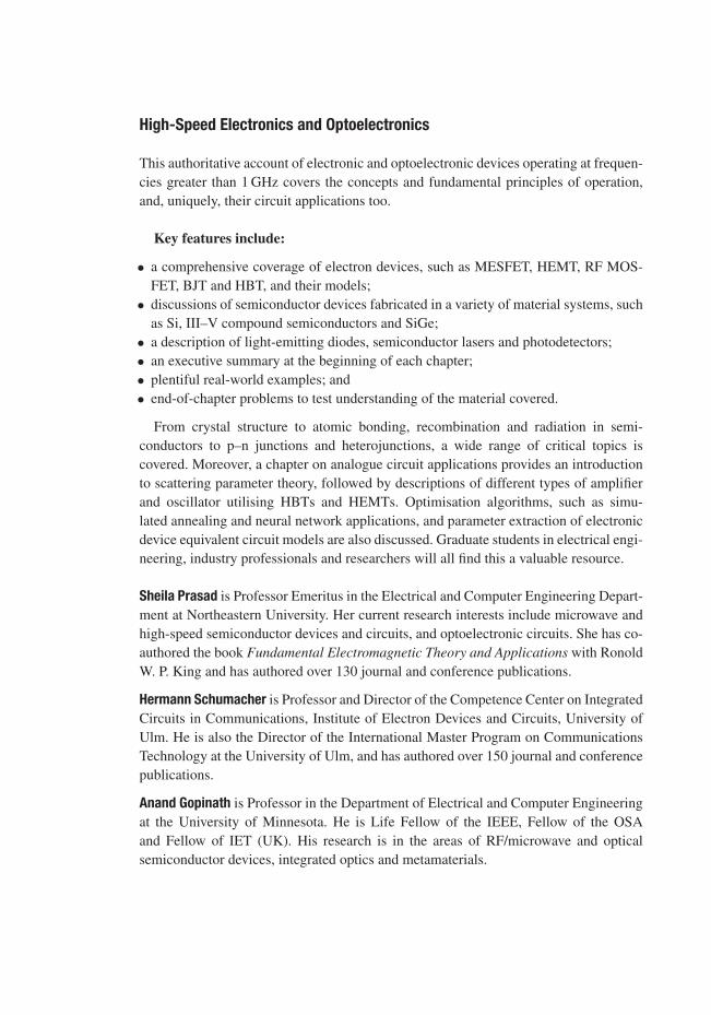
High-Speed Electronics and Optoelectronics
This authoritative account of electronic and optoelectronic devices operating at frequen-cies greater than 1 GHz covers the concepts and fundamental principles of operation,and, uniquely, their circuit applications too.
Key features include:
• a comprehensive coverage of electron devices, such as MESFET, HEMT, RF MOS-FET, BJT and HBT, and their models;
• discussions of semiconductor devices fabricated in a variety of material systems, suchas Si, III–V compound semiconductors and SiGe;
• a description of light-emitting diodes, semiconductor lasers and photodetectors;• an executive summary at the beginning of each chapter;• plentiful real-world examples; and• end-of-chapter problems to test understanding of the material covered.
From crystal structure to atomic bonding, recombination and radiation in semi-conductors to p–n junctions and heterojunctions, a wide range of critical topics iscovered. Moreover, a chapter on analogue circuit applications provides an introductionto scattering parameter theory, followed by descriptions of different types of amplifierand oscillator utilising HBTs and HEMTs. Optimisation algorithms, such as simu-lated annealing and neural network applications, and parameter extraction of electronicdevice equivalent circuit models are also discussed. Graduate students in electrical engi-neering, industry professionals and researchers will all find this a valuable resource.
Sheila Prasad is Professor Emeritus in the Electrical and Computer Engineering Depart-ment at Northeastern University. Her current research interests include microwave andhigh-speed semiconductor devices and circuits, and optoelectronic circuits. She has co-authored the book Fundamental Electromagnetic Theory and Applications with RonoldW. P. King and has authored over 130 journal and conference publications.
Hermann Schumacher is Professor and Director of the Competence Center on IntegratedCircuits in Communications, Institute of Electron Devices and Circuits, University ofUlm. He is also the Director of the International Master Program on CommunicationsTechnology at the University of Ulm, and has authored over 150 journal and conferencepublications.
Anand Gopinath is Professor in the Department of Electrical and Computer Engineeringat the University of Minnesota. He is Life Fellow of the IEEE, Fellow of the OSAand Fellow of IET (UK). His research is in the areas of RF/microwave and opticalsemiconductor devices, integrated optics and metamaterials.

High-Speed Electronics andOptoelectronics: Devices andCircuits
S H E I L A P R A S A DNortheastern University, Boston
H E R M A N N S C H U M A C H E RUniversity of Ulm, Germany
A N A N D G O P I N A T HUniversity of Minnesota, Minneapolis
CAMBRIDGE UNIVERSITY PRESS
Cambridge, New York, Melbourne, Madrid, Cape Town, Singapore,
São Paulo, Delhi, Dubai, Tokyo
Cambridge University Press
The Edinburgh Building, Cambridge CB2 8RU, UK
First published in print format
ISBN-13 978-0-521-86283-7
ISBN-13 978-0-511-57982-0
© Cambridge University Press 2009
2009
Information on this title: www.cambridge.org/9780521862837
This publication is in copyright. Subject to statutory exception and to the
provision of relevant collective licensing agreements, no reproduction of any part
may take place without the written permission of Cambridge University Press.
Cambridge University Press has no responsibility for the persistence or accuracy
of urls for external or third-party internet websites referred to in this publication,
and does not guarantee that any content on such websites is, or will remain,
accurate or appropriate.
Published in the United States of America by Cambridge University Press, New York
www.cambridge.org
eBook (EBL)
Hardback

Contents
Preface Page viiAcknowledgements ix
Part One Devices 1
1 Review of semiconductor materials and physics 3
1.1 Executive summary 31.2 Semiconductor materials 41.3 Types of solids 51.4 Crystal structure 51.5 Crystal directions and planes 61.6 Atomic bonding 81.7 Atomic physics 91.8 The de Broglie relation 111.9 Quantum mechanics 121.10 Statistical mechanics 161.11 Electrons in a semiconductor 161.12 The Kronig–Penney model 161.13 Semiconductors in equilibrium 181.14 Direct and indirect semiconductors 201.15 Recombination and radiation in semiconductors 251.16 Carrier transport in semiconductors 291.17 p–n junction 301.18 Schottky diode 341.19 Heterostructures 351.20 Silicon–germanium heterostructures 401.21 Problems 43References 45
2 Electronic devices 46
2.1 Executive summary 462.2 MESFET 462.3 High electron mobility transistor 67

vi Contents
2.4 Radio Frequency MOSFETs 952.5 Bipolar and hetero-bipolar transistors 1152.6 Problems 156References 158
3 Optimisation and parameter extraction of circuit models 163
3.1 Executive summary 1633.2 Optimisation of device models 1633.3 Simulated annealing 1643.4 Neural networks applied to modelling 1683.5 Optimisation of neural networks by the genetic algorithm 1803.6 Structured genetic algorithm 1813.7 Semi-analytical device parameter extraction 1843.8 Basic expressions for small-signal parameter extraction 2033.9 Small-signal model of the collector-up (inverted) HBT 2123.10 Problems 214References 218
4 Optoelectronics 221
4.1 Executive summary 2214.2 Optical sources 2214.3 Photodetectors 2614.4 Problems 284References 285
Part Two Circuits 289
5 Building blocks for high-speed analogue circuits 291
5.1 Executive summary 2915.2 Basic relations for two-port networks 2915.3 Noise in two-ports 3065.4 Transistor amplifiers 3135.5 Oscillators 3835.6 Mixers 3965.7 Baluns, unbals and hybrids 4125.8 Problems 419References 421
Index 423
Preface
Starting from the development of transistor technology to laser technology, the fieldof solid state devices and their circuit applications has advanced rapidly. The siliconbipolar junction transistor was first applied to low frequency circuits. The subsequentadvances in materials science made it possible to fabricate compound semiconductortransistors capable of operating at microwave frequencies and high speeds. This pre-sented the capability of applications in both analogue and digital circuits. At the sametime, the wide choice of high performance semiconductor materials also enabled thedevelopment of optoelectronic devices such as lasers and light-emitting diodes. Thecommunications industry continues to grow and diversify, thus necessitating the designof circuits which will satisfy the requirements of mobile telephones which are becom-ing more and more sophisticated in their performance. Circuit design has applicationsin other areas such as optical communications.
This book focusses on high-speed electronics and optoelectronics where the devicesoperate at frequencies ≥1 GHz. It is presented in two parts with devices being dis-cussed in the first part and the circuit applications in the second part. In Part One,semiconductor devices fabricated in a variety of material systems – Si, III–V compoundsemiconductors and SiGe – are presented. We discuss the concepts and the fundamen-tal principles of operation. We do not attempt to present the latest results as they willalready be obsolete by the time the book is published. It is assumed that the reader hashad a course in fundamental solid state physics.
Chapter 1 reviews semiconductor materials and physics. For the reader who is famil-iar with the topics, this chapter will be a brief review. If not, the reader can go to thereferences section to get a detailed coverage of the topics. Semiconductor materials aredescribed followed by brief discussions of crystal structure and bonding. The sectionon quantum mechanics is intended to present only the important concepts and is nota comprehensive treatment of the subject. Semiconductor properties are described fol-lowed by types of semiconductors. Semiconductor junctions are treated in detail as theyare the basis of the devices to be treated in subsequent chapters.
Chapter 2 presents high-frequency/high-speed electronic devices starting with theMESFET, which was the first transistor to operate at microwave frequencies. The devel-opment of the high electron mobility transistor (HEMT) represented a major advance intechnology and is presented here in detail. The recent application of MOSFETs to radiofrequency has been successful and the properties are covered in detail. Finally, bipolar

viii Preface
and heterojunction bipolar transistors (HBTs) are described. Models for the transistorsare presented and their method of implementation is described.
Chapter 3 presents the optimisation and parameter extraction of the circuit models ofthe electronic devices. The simulated annealing algorithm is discussed followed by theapplication of neural networks to circuit modelling. The genetic algorithm is definedand its application to optimisation is shown. Parameter extraction methods are given forcircuit models using semi-analytical methods and basic expressions are derived.
Chapter 4 deals with various optical sources such as light-emitting diodes and lasers,giving details of their physical properties and their modes of operation. The discussionof emitters is followed by an extensive coverage of a variety of photodetectors.
In Part Two of the book, we discuss analogue circuits at the gate level. We willassume that the reader has a background (at the undergraduate level) in fundamentalanalogue circuit theory. Chapter 5 (Part Two of the book) deals with the components ofhigh-speed analogue circuits. After a review of scattering parameter theory, the powerand noise relations for two-port networks are discussed. Transistor amplifiers are cov-ered in detail, showing the application of the devices described in Chapter 2. This isfollowed by a discussion of oscillators and mixers for high-speed circuits. Importantpassive components of high-speed circuits complete this chapter.
We have a layered approach to each chapter in the book. There is an executivesummary at the beginning of each chapter. This will make the book valuable also fortechnical managers who may not want to go through the chapter content in detail. Wehave extensive problems at the end of each chapter, which will give the student appli-cations of the theory. This book should be useful to research engineers and graduatestudents. Results from various research papers are presented, many of which are onlyavailable in journals which are referenced extensively. However, the reader need notgo to the original papers as the results are given in sufficient detail to give a goodunderstanding of the material.

Acknowledgements
Sheila Prasad
I would like to express my gratitude to Professor Clifton G. Fonstad, Jr, at the Mas-sachusetts Institute of Technology. My long collaboration with him started with the firstsabbatical leave at MIT when I worked in his group. It initiated my work on HBTs atmicrowave frequencies and the continued support he provided to me and my studentsin his laboratory resulted in this successful research. I acknowledge my colleague atNortheastern University, Dr Michael Vai (now at MIT Lincoln Laboratory), with whomI performed research on optimisation and modelling techniques. Many students workedwith me on various aspects of the research reported in this book. I would particularlylike to acknowledge the work of Dr Bin Li whose research results continue to be citedin publications. I would also like to acknowledge my student Kofi Deh for his helpwith the figures and manuscript editing. Dr Henry Choy and Dr Wojtek Giziewicz, bothof whom were students at MIT, gave me invaluable suggestions for the book mate-rial and also helped me with MATLAB, graphics programmes and Latex when needed.I acknowledge my colleague at Northeastern University, Professor Jeff Hopwood (nowat Tufts University), with whom I had many useful discussions about the content of thebook. It has been a great experience to work with both of my co-authors. Last but notleast, I would like to thank my husband, Fred Hinchey, for his great patience and supportin the course of this book project.
Hermann Schumacher
I gratefully acknowledge the valuable assistance of Dr Andreas Trasser, Dr WolfgangHaag and Ms Ursula Winter in proofreading the original manuscript. Their helpful sug-gestions had a significant impact. Most importantly, I am eternally indebted to mywife Christiane. Without her patience and loving care, this book would never havematerialised.
Anand Gopinath
I acknowledge the valuable discussions on lasers and photodiodes with my pastand present graduate students including Ross Schermer, Prakash Koonath, William

x Acknowledgements
Berglund, Jaesang Oh, Kang-Hyun Baek, Klein Johnson and others. I am grateful tomy wife Marian for her patience and support while this book was being written.
Joint acknowledgements
Finally, we would like to thank our publisher Dr Julie Lancashire for her patience andher guidance throughout this book project. We also thank Dr Phil Meyler who encour-aged us to initiate this project by submitting a book proposal which was accepted byCambridge University Press. Thanks are also due to Ms Sarah Matthews who has beenvery helpful in the last and most difficult stages of the project.

Part One
Devices

1 Review of semiconductor materialsand physics
1.1 Executive summary
Semiconductor devices are fabricated using specific materials that offer the desiredphysical properties. There are three classes of solid state materials: insulators, semi-conductors and conductors. This distinction is based on the electrical conductivity ofthese materials with insulators having the lowest and conductors having the highest con-ductivity. Semiconductors fall in between and their conductivity is affected by severalfactors such as temperature, the incidence of light, the application of a magnetic fieldand impurities. This versatility makes semiconductors very important in electronics andoptoelectronics applications.
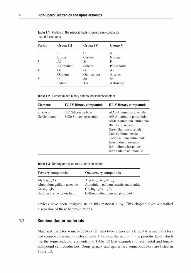
Semiconductors themselves are divided into two classes: elemental and compound.Each type has distinctive physical properties which are exploited in device design. Typ-ical elemental semiconductor device materials are silicon and germanium; examples ofcompound semiconductors are GaAs, InP, AlGaAs and SiGe. The single crystal struc-ture of these materials is that of a periodic lattice and this determines the propertiesof the semiconductors. Silicon has the diamond crystal structure and the compoundsemiconductors have the zincblende lattice structure. The bonding between atoms in acrystal of the semiconductors is termed covalent bonding, where electrons are sharedbetween atoms. Fundamental principles of quantum mechanics are applied to determinethe energy band structure of the semiconductor.
The basic device physics involves the description of the energy band structure, thedensity of states, the carrier concentration and the definition of donors and acceptors.Semiconductors are categorised as direct or indirect depending on the bandgap. Theabsorption mechanism is described and radiation and recombination processes impor-tant to device performance are detailed. The two carrier transport processes are driftand diffusion. The currents due to these transport processes are expressed in terms ofthe applied electric field, the carrier mobility and the carrier concentration. The junctionformed by p-type semiconductor (excess holes) and n-type semiconductor (excess elec-trons) is described and the characteristics of such a junction are given. The importantSchottky diode, a junction formed by a metal and a semiconductor layer (n-doped inthis case) is characterised.
Heterostructures formed by dissimilar semiconductors are important in device design.The properties of heterojunctions of semiconductor materials are presented. Silicon–germanium heterojunctions are of particular interest as high performance electronic
4 High-Speed Electronics and Optoelectronics
Table 1.1 Portion of the periodic table showing semiconductormaterial elements
Period Group III Group IV Group V
2 B C NBoron Carbon Nitrogen
3 Al Si PAluminium Silicon Phosphorus
4 Ga Ge AsGallium Germanium Arsenic
5 In Sn SbIndium Tin Antimony
Table 1.2 Elemental and binary compound semiconductors
Elements IV–IV Binary compounds III–V Binary compounds
Si Silicon SiC Silicon carbide AlAs Aluminium arsenideGe Germanium SiGe Silicon germanium AlP Aluminium phosphide
AlSb Aluminium antimonideBN Boron nitrideGaAs Gallium arsenideGaN Gallium nitrideGaSb Gallium antimonideInAs Indium arsenideInP Indium phosphideInSb Indium antimonide
Table 1.3 Ternary and quaternary semiconductors
Ternary compounds Quaternary compounds
AlxGa1−xAs AlxGa1−xAsySb1−yAluminium gallium arsenide Aluminium gallium arsenic antimonideGaAs1−xPx GaxIn1−xAs1−yPyGallium arsenic phosphide Gallium indium arsenic phosphide
devices have been designed using this material alloy. This chapter gives a detaileddiscussion of these heterojunctions.
1.2 Semiconductor materials
Materials used for semiconductors fall into two categories: elemental semiconductorsand compound semiconductors. Table 1.1 shows the section in the periodic table whichhas the semiconductor elements and Table 1.2 lists examples for elemental and binarycompound semiconductors. Some ternary and quaternary semiconductors are listed inTable 1.3.
Review of semiconductor materials and physics 5
1.3 Types of solids
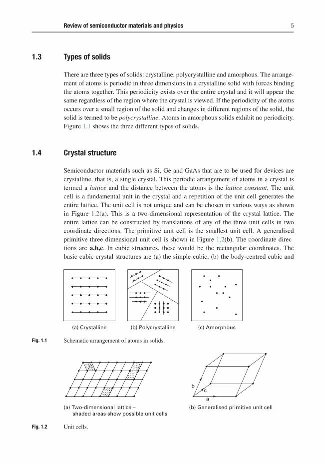
There are three types of solids: crystalline, polycrystalline and amorphous. The arrange-ment of atoms is periodic in three dimensions in a crystalline solid with forces bindingthe atoms together. This periodicity exists over the entire crystal and it will appear thesame regardless of the region where the crystal is viewed. If the periodicity of the atomsoccurs over a small region of the solid and changes in different regions of the solid, thesolid is termed to be polycrystalline. Atoms in amorphous solids exhibit no periodicity.Figure 1.1 shows the three different types of solids.
1.4 Crystal structure
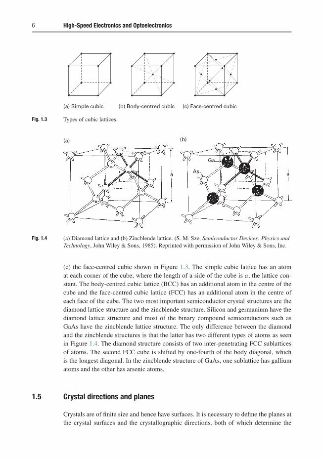
Semiconductor materials such as Si, Ge and GaAs that are to be used for devices arecrystalline, that is, a single crystal. This periodic arrangement of atoms in a crystal istermed a lattice and the distance between the atoms is the lattice constant. The unitcell is a fundamental unit in the crystal and a repetition of the unit cell generates theentire lattice. The unit cell is not unique and can be chosen in various ways as shownin Figure 1.2(a). This is a two-dimensional representation of the crystal lattice. Theentire lattice can be constructed by translations of any of the three unit cells in twocoordinate directions. The primitive unit cell is the smallest unit cell. A generalisedprimitive three-dimensional unit cell is shown in Figure 1.2(b). The coordinate direc-tions are a,b,c. In cubic structures, these would be the rectangular coordinates. Thebasic cubic crystal structures are (a) the simple cubic, (b) the body-centred cubic and
(a) Crystalline (b) Polycrystalline (c) Amorphous
Fig. 1.1 Schematic arrangement of atoms in solids.
(a) Two-dimensional lattice – shaded areas show possible unit cells
(b) Generalised primitive unit cell
b
a
c
Fig. 1.2 Unit cells.
6 High-Speed Electronics and Optoelectronics
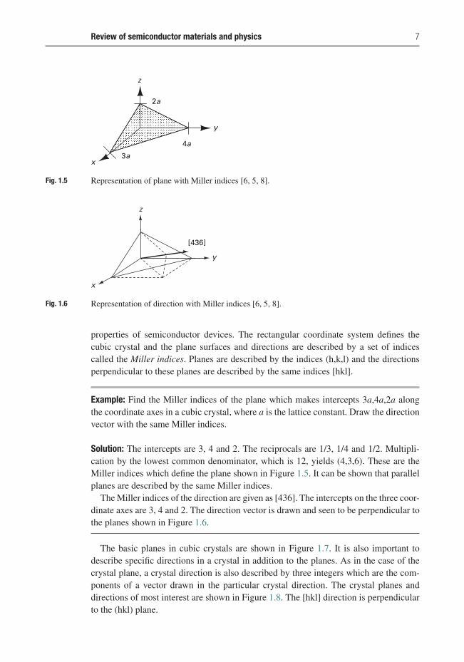
(a) Simple cubic (b) Body-centred cubic (c) Face-centred cubic
Fig. 1.3 Types of cubic lattices.
a
(a) (b)
Ga
aAs
Fig. 1.4 (a) Diamond lattice and (b) Zincblende lattice. (S. M. Sze, Semiconductor Devices: Physics andTechnology, John Wiley & Sons, 1985). Reprinted with permission of John Wiley & Sons, Inc.
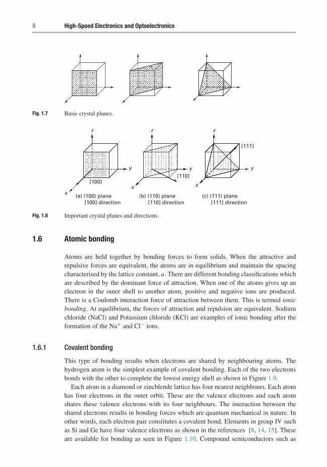
(c) the face-centred cubic shown in Figure 1.3. The simple cubic lattice has an atomat each corner of the cube, where the length of a side of the cube is a, the lattice con-stant. The body-centred cubic lattice (BCC) has an additional atom in the centre of thecube and the face-centred cubic lattice (FCC) has an additional atom in the centre ofeach face of the cube. The two most important semiconductor crystal structures are thediamond lattice structure and the zincblende structure. Silicon and germanium have thediamond lattice structure and most of the binary compound semiconductors such asGaAs have the zincblende lattice structure. The only difference between the diamondand the zincblende structures is that the latter has two different types of atoms as seenin Figure 1.4. The diamond structure consists of two inter-penetrating FCC sublatticesof atoms. The second FCC cube is shifted by one-fourth of the body diagonal, whichis the longest diagonal. In the zincblende structure of GaAs, one sublattice has galliumatoms and the other has arsenic atoms.
1.5 Crystal directions and planes
Crystals are of finite size and hence have surfaces. It is necessary to define the planes atthe crystal surfaces and the crystallographic directions, both of which determine the
Review of semiconductor materials and physics 7
z
2a
y
4a
3ax
Fig. 1.5 Representation of plane with Miller indices [6, 5, 8].
x
y
z
[436]
Fig. 1.6 Representation of direction with Miller indices [6, 5, 8].
properties of semiconductor devices. The rectangular coordinate system defines thecubic crystal and the plane surfaces and directions are described by a set of indicescalled the Miller indices. Planes are described by the indices (h,k,l) and the directionsperpendicular to these planes are described by the same indices [hkl].
Example: Find the Miller indices of the plane which makes intercepts 3a,4a,2a alongthe coordinate axes in a cubic crystal, where a is the lattice constant. Draw the directionvector with the same Miller indices.
Solution: The intercepts are 3, 4 and 2. The reciprocals are 1/3, 1/4 and 1/2. Multipli-cation by the lowest common denominator, which is 12, yields (4,3,6). These are theMiller indices which define the plane shown in Figure 1.5. It can be shown that parallelplanes are described by the same Miller indices.
The Miller indices of the direction are given as [436]. The intercepts on the three coor-dinate axes are 3, 4 and 2. The direction vector is drawn and seen to be perpendicular tothe planes shown in Figure 1.6.
The basic planes in cubic crystals are shown in Figure 1.7. It is also important todescribe specific directions in a crystal in addition to the planes. As in the case of thecrystal plane, a crystal direction is also described by three integers which are the com-ponents of a vector drawn in the particular crystal direction. The crystal planes anddirections of most interest are shown in Figure 1.8. The [hkl] direction is perpendicularto the (hkl) plane.
8 High-Speed Electronics and Optoelectronics
Fig. 1.7 Basic crystal planes.
(a) (100) plane [100] direction
(b) (110) plane [110] direction
(c) (111) plane [111] direction
[100]
x
y
z
[110]
x
y
z
[111]
x
y
z
Fig. 1.8 Important crystal planes and directions.
1.6 Atomic bonding
Atoms are held together by bonding forces to form solids. When the attractive andrepulsive forces are equivalent, the atoms are in equilibrium and maintain the spacingcharacterised by the lattice constant, a. There are different bonding classifications whichare described by the dominant force of attraction. When one of the atoms gives up anelectron in the outer shell to another atom, positive and negative ions are produced.There is a Coulomb interaction force of attraction between them. This is termed ionicbonding. At equilibrium, the forces of attraction and repulsion are equivalent. Sodiumchloride (NaCl) and Potassium chloride (KCl) are examples of ionic bonding after theformation of the Na+ and Cl− ions.
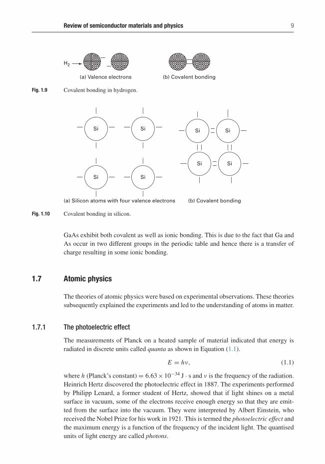
1.6.1 Covalent bonding
This type of bonding results when electrons are shared by neighbouring atoms. Thehydrogen atom is the simplest example of covalent bonding. Each of the two electronsbonds with the other to complete the lowest energy shell as shown in Figure 1.9.
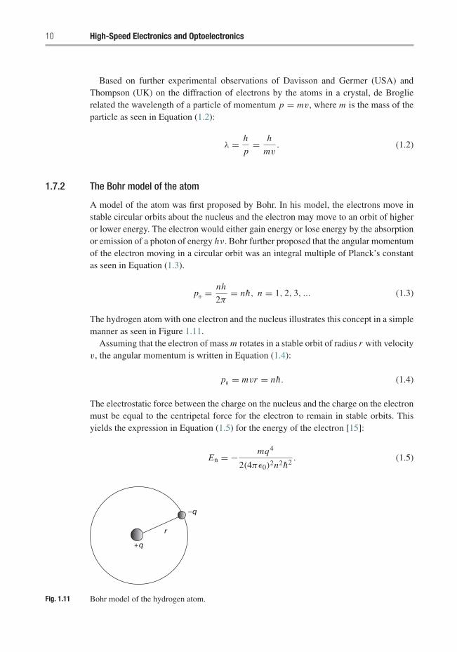
Each atom in a diamond or zincblende lattice has four nearest neighbours. Each atomhas four electrons in the outer orbit. These are the valence electrons and each atomshares these valence electrons with its four neighbours. The interaction between theshared electrons results in bonding forces which are quantum mechanical in nature. Inother words, each electron pair constitutes a covalent bond. Elements in group IV suchas Si and Ge have four valence electrons as shown in the references [8, 14, 15]. Theseare available for bonding as seen in Figure 1.10. Compound semiconductors such as
Review of semiconductor materials and physics 9
(a) Valence electrons (b) Covalent bonding
H2
Fig. 1.9 Covalent bonding in hydrogen.
Si Si Si Si
Si Si
Si Si
(a) Silicon atoms with four valence electrons (b) Covalent bonding
Fig. 1.10 Covalent bonding in silicon.
GaAs exhibit both covalent as well as ionic bonding. This is due to the fact that Ga andAs occur in two different groups in the periodic table and hence there is a transfer ofcharge resulting in some ionic bonding.
1.7 Atomic physics
The theories of atomic physics were based on experimental observations. These theoriessubsequently explained the experiments and led to the understanding of atoms in matter.
1.7.1 The photoelectric effect
The measurements of Planck on a heated sample of material indicated that energy isradiated in discrete units called quanta as shown in Equation (1.1).
E = hν, (1.1)
where h (Planck’s constant) = 6.63×10⁻³⁴ J · s and ν is the frequency of the radiation.Heinrich Hertz discovered the photoelectric effect in 1887. The experiments performedby Philipp Lenard, a former student of Hertz, showed that if light shines on a metalsurface in vacuum, some of the electrons receive enough energy so that they are emit-ted from the surface into the vacuum. They were interpreted by Albert Einstein, whoreceived the Nobel Prize for his work in 1921. This is termed the photoelectric effect andthe maximum energy is a function of the frequency of the incident light. The quantisedunits of light energy are called photons.
10 High-Speed Electronics and Optoelectronics
Based on further experimental observations of Davisson and Germer (USA) andThompson (UK) on the diffraction of electrons by the atoms in a crystal, de Broglierelated the wavelength of a particle of momentum p = mv, where m is the mass of theparticle as seen in Equation (1.2):
λ = h
p= h
mv. (1.2)
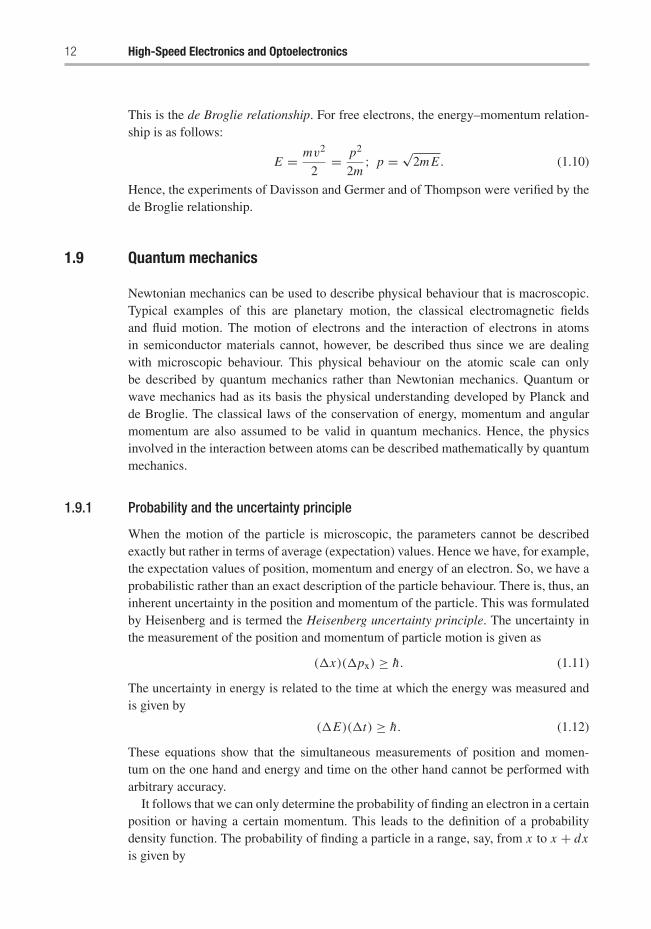
1.7.2 The Bohr model of the atom
A model of the atom was first proposed by Bohr. In his model, the electrons move instable circular orbits about the nucleus and the electron may move to an orbit of higheror lower energy. The electron would either gain energy or lose energy by the absorptionor emission of a photon of energy hν. Bohr further proposed that the angular momentumof the electron moving in a circular orbit was an integral multiple of Planck’s constantas seen in Equation (1.3).
pθ= nh
2π= nh, n = 1, 2, 3, ... (1.3)
The hydrogen atom with one electron and the nucleus illustrates this concept in a simplemanner as seen in Figure 1.11.
Assuming that the electron of mass m rotates in a stable orbit of radius r with velocityv, the angular momentum is written in Equation (1.4):
pθ= mvr = nh. (1.4)
The electrostatic force between the charge on the nucleus and the charge on the electronmust be equal to the centripetal force for the electron to remain in stable orbits. Thisyields the expression in Equation (1.5) for the energy of the electron [15]:
En = − mq4
2(4πε0)2n2h2. (1.5)
+q
–q
r
Fig. 1.11 Bohr model of the hydrogen atom.

Review of semiconductor materials and physics 11
2 3 4 n = 51
Fig. 1.12 Electron orbits in Bohr model (not to scale).
The electron orbits in the Bohr model are shown in Figure 1.12.
1.8 The de Broglie relation
The initial theoretical and experimental results of Planck, Einstein and Bohr laid thefoundation for the development of quantum mechanics. It was de Broglie, however,who first postulated that if waves were seen to behave as particles then it could be thatparticles might behave like waves.
In the Bohr formulation, the electron which travels in a circular orbit of radius r isassumed to behave like a wave with a wavelength λ. It travels in a circular path equalin length to the circumference 2πr , which will be an integral number of wavelengths sothat
nλ = 2πr. (1.6)
The Bohr formulation yielded the linear velocity of the electron to be
v = q2
4πε0nh. (1.7)
Using this velocity relation, the wavelength can be written as
λ = h
mv= h
p, (1.8)
where p is the linear momentum of the electron. Thus, de Broglie postulated that therelationship between the wavelength and the linear momentum p of a particle is givenby Equation (1.2).
p = h
λ= h
2π
2π
λ= hk. (1.9)
12 High-Speed Electronics and Optoelectronics
This is the de Broglie relationship. For free electrons, the energy–momentum relation-ship is as follows:
E = mv2
2= p2
2m; p = √
2m E . (1.10)
Hence, the experiments of Davisson and Germer and of Thompson were verified by thede Broglie relationship.
1.9 Quantum mechanics
Newtonian mechanics can be used to describe physical behaviour that is macroscopic.Typical examples of this are planetary motion, the classical electromagnetic fieldsand fluid motion. The motion of electrons and the interaction of electrons in atomsin semiconductor materials cannot, however, be described thus since we are dealingwith microscopic behaviour. This physical behaviour on the atomic scale can onlybe described by quantum mechanics rather than Newtonian mechanics. Quantum orwave mechanics had as its basis the physical understanding developed by Planck andde Broglie. The classical laws of the conservation of energy, momentum and angularmomentum are also assumed to be valid in quantum mechanics. Hence, the physicsinvolved in the interaction between atoms can be described mathematically by quantummechanics.
1.9.1 Probability and the uncertainty principle
When the motion of the particle is microscopic, the parameters cannot be describedexactly but rather in terms of average (expectation) values. Hence we have, for example,the expectation values of position, momentum and energy of an electron. So, we have aprobabilistic rather than an exact description of the particle behaviour. There is, thus, aninherent uncertainty in the position and momentum of the particle. This was formulatedby Heisenberg and is termed the Heisenberg uncertainty principle. The uncertainty inthe measurement of the position and momentum of particle motion is given as
(�x)(�px) ≥ h. (1.11)
The uncertainty in energy is related to the time at which the energy was measured andis given by
(�E)(�t) ≥ h. (1.12)
These equations show that the simultaneous measurements of position and momen-tum on the one hand and energy and time on the other hand cannot be performed witharbitrary accuracy.
It follows that we can only determine the probability of finding an electron in a certainposition or having a certain momentum. This leads to the definition of a probabilitydensity function. The probability of finding a particle in a range, say, from x to x + dxis given by
Review of semiconductor materials and physics 13
Table 1.4 Classical variables and quantum operators
Classical variable Quantum operator
x xf (x) f (x)Momentum p(x) h
j∂∂x
Kinetic energy p2
2m−h2
2m∂2
∂x2
Potential energy V VTotal energy E −h
j∂∂t
∫ ∞
−∞P(x)dx = 1, (1.13)
where P(x) is a normalised function. The average value of a function x is defined as
〈 f (x)〉 =∫ ∞
−∞f (x)P(x)dx = 1. (1.14)
The correspondence between classical and quantum mechanical quantities is shown inTable 1.4.
The basic principles of quantum mechanics will now be reviewed. Each particle ina physical system is described by a wave function �(x, y, z, t). The function and itsspace derivatives are continuous, finite and single-valued.
The probability of finding a particle with wave function � in the volume dxdydz is�∗�dxdydz. Then we have the following definition for three-dimensional space:∫ ∞
−∞�∗�dxdydz = 1. (1.15)
The expectation value of any physical quantity X can be written as
< X > =∫ ∞
−∞�∗ Xoper�dxdydz, (1.16)
where Xoper is the operator corresponding to the variable X .The classical equation for energy conservation is Kinetic energy + Potential energy =
Total energy:
p2
2m+ V = E . (1.17)
1.9.2 The wave equation
We obtain the quantum mechanical energy equation by substituting the correspondingoperators which operate on the one-dimensional wave function �(x, t):
−h2
2m
∂2�(x, t)
∂x2+ V (x)�(x, t) = E�(x, t) = −h
j
∂�(x, t)
∂t. (1.18)
14 High-Speed Electronics and Optoelectronics
V = 0 V = 0
–a 0 ax
V
∞ ∞
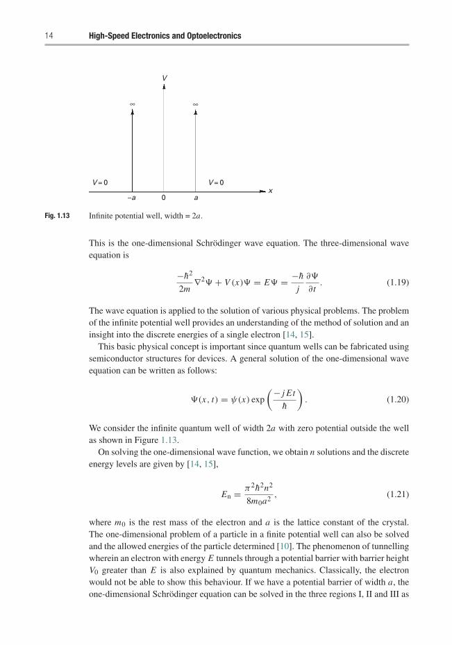
Fig. 1.13 Infinite potential well, width = 2a.
This is the one-dimensional Schrodinger wave equation. The three-dimensional waveequation is
−h2
2m∇2� + V (x)� = E� = −h
j
∂�
∂t. (1.19)
The wave equation is applied to the solution of various physical problems. The problemof the infinite potential well provides an understanding of the method of solution and aninsight into the discrete energies of a single electron [14, 15].
This basic physical concept is important since quantum wells can be fabricated usingsemiconductor structures for devices. A general solution of the one-dimensional waveequation can be written as follows:
�(x, t) = ψ(x) exp
(− j Et
h
). (1.20)
We consider the infinite quantum well of width 2a with zero potential outside the wellas shown in Figure 1.13.
On solving the one-dimensional wave function, we obtain n solutions and the discreteenergy levels are given by [14, 15],
En = π2h2n2
8m0a2, (1.21)
where m0 is the rest mass of the electron and a is the lattice constant of the crystal.The one-dimensional problem of a particle in a finite potential well can also be solvedand the allowed energies of the particle determined [10]. The phenomenon of tunnellingwherein an electron with energy E tunnels through a potential barrier with barrier heightV0 greater than E is also explained by quantum mechanics. Classically, the electronwould not be able to show this behaviour. If we have a potential barrier of width a, theone-dimensional Schrodinger equation can be solved in the three regions I, II and III as
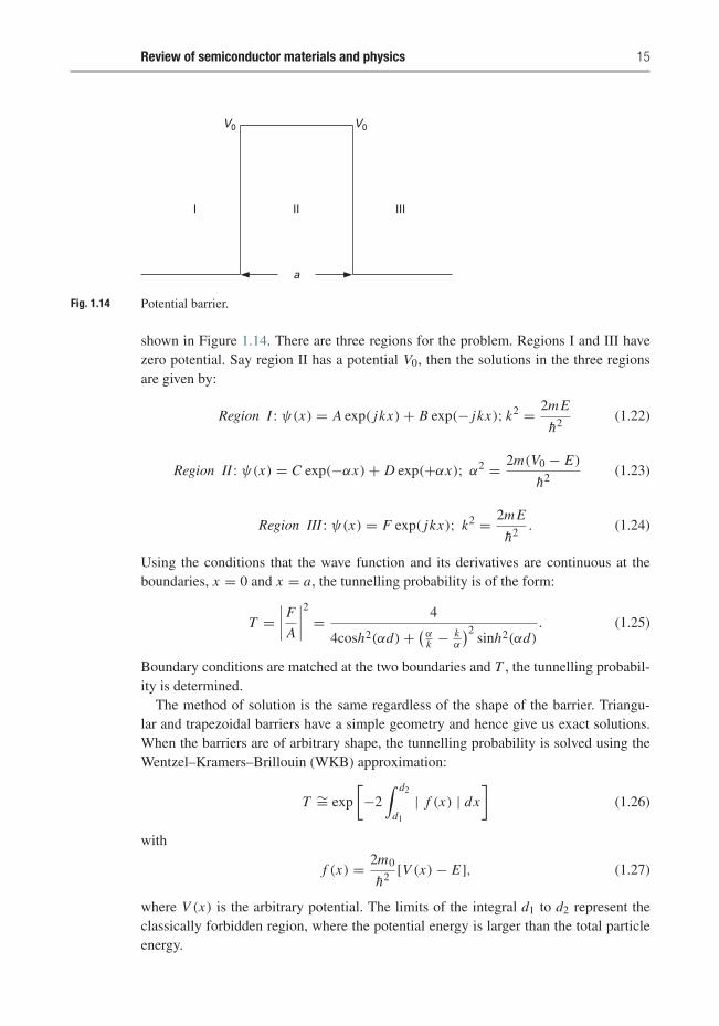
Review of semiconductor materials and physics 15
V0 V0
I II
a
III
Fig. 1.14 Potential barrier.
shown in Figure 1.14. There are three regions for the problem. Regions I and III havezero potential. Say region II has a potential V0, then the solutions in the three regionsare given by:
Region I : ψ(x) = A exp( jkx) + B exp(− jkx); k2 = 2m E
h2(1.22)
Region II : ψ(x) = C exp(−αx) + D exp(+αx); α2 = 2m(V0 − E)
h2(1.23)
Region III : ψ(x) = F exp( jkx); k2 = 2m E
h2. (1.24)
Using the conditions that the wave function and its derivatives are continuous at theboundaries, x = 0 and x = a, the tunnelling probability is of the form:
T =∣∣∣∣ F
A
∣∣∣∣2
= 4
4cosh2(αd) + (αk − k
α
)2sinh2(αd)
. (1.25)
Boundary conditions are matched at the two boundaries and T , the tunnelling probabil-ity is determined.
The method of solution is the same regardless of the shape of the barrier. Triangu-lar and trapezoidal barriers have a simple geometry and hence give us exact solutions.When the barriers are of arbitrary shape, the tunnelling probability is solved using theWentzel–Kramers–Brillouin (WKB) approximation:
T ∼= exp
[−2
∫ d2
d1
| f (x) | dx
](1.26)
with
f (x) = 2m0
h2[V (x) − E], (1.27)
where V (x) is the arbitrary potential. The limits of the integral d1 to d2 represent theclassically forbidden region, where the potential energy is larger than the total particleenergy.
16 High-Speed Electronics and Optoelectronics
1.10 Statistical mechanics
1.10.1 The free electron
When the three-dimensional Schrodinger equation is solved, the general solution givesthe wave function for the electron in motion in a region of zero potential. Thebehaviour of electrons in semiconductor crystals can be assumed to be like that of so-called free electrons under certain conditions, hence the importance of this result. Thetime-independent wave function solution is given by
ψ(r) = A exp(k · r), (1.28)
where A is a complex quantity and is the amplitude, k is the wave vector and ris the three-dimensional space vector. This results in energies of the same form asEquation (1.21).
1.10.2 Fermi–Dirac distribution
The Fermi–Dirac distribution function f (E) gives the probability that states with energyE are occupied by particles [10]:
f (E) = 1
1 + exp(
E−EFkT
) , (1.29)
EF represents the Fermi energy where f(E) becomes equal to 1/2.
1.11 Electrons in a semiconductor
Since semiconductors have periodic lattice structures, the electrons are subjected toa periodic potential. Hence the Schrodinger equation must be solved for a periodicpotential [10]. The Bloch theorem states that the one-dimensional wave function foran electron in a periodic potential is given by
ψ(x) = Vk(x) exp( jkx), (1.30)
where Vk(x) is a periodic potential with the same periodicity as the semiconductorcrystal with lattice constant a such that
Vk(x) = Vk(x + na), (1.31)
where n is an integer.
1.12 The Kronig–Penney model
An important model for the band structure is the Kronig–Penney model (Figure 1.15).The one-dimensional periodic potential is given by
V (x) = 0, 0 ≤ x ≤ a (1.32)
V (x) = V0, −b ≤ x ≤ 0 (1.33)
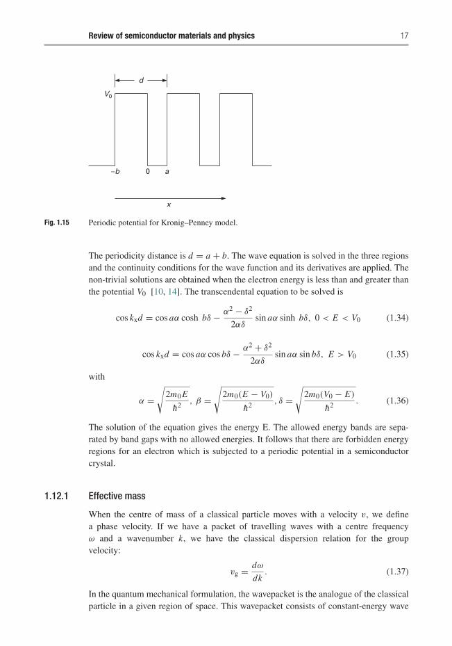
Review of semiconductor materials and physics 17
V0
–b 0
x
a
d
Fig. 1.15 Periodic potential for Kronig–Penney model.
The periodicity distance is d = a + b. The wave equation is solved in the three regionsand the continuity conditions for the wave function and its derivatives are applied. Thenon-trivial solutions are obtained when the electron energy is less than and greater thanthe potential V0 [10, 14]. The transcendental equation to be solved is
cos kxd = cos aα cosh bδ − α2 − δ2
2αδsin aα sinh bδ, 0 < E < V0 (1.34)
cos kxd = cos aα cos bδ − α2 + δ2
2αδsin aα sin bδ, E > V0 (1.35)
with
α =√
2m0 E
h2, β =
√2m0(E − V0)
h2, δ =
√2m0(V0 − E)
h2. (1.36)
The solution of the equation gives the energy E. The allowed energy bands are sepa-rated by band gaps with no allowed energies. It follows that there are forbidden energyregions for an electron which is subjected to a periodic potential in a semiconductorcrystal.
1.12.1 Effective mass
When the centre of mass of a classical particle moves with a velocity v, we definea phase velocity. If we have a packet of travelling waves with a centre frequencyω and a wavenumber k, we have the classical dispersion relation for the groupvelocity:
vg = dω
dk. (1.37)
In the quantum mechanical formulation, the wavepacket is the analogue of the classicalparticle in a given region of space. This wavepacket consists of constant-energy wave
18 High-Speed Electronics and Optoelectronics
function solutions and a centre energy is defined. Hence the wavepacket group velocityin the quantum-mechanical formulation can be written as in Equation (1.20):
vg = 1
h
d E
dk. (1.38)
Using the force–momentum relations, we define the effective mass of an electron in acrystal as
m∗ =(
1
h2
d2 E
dk2
)−1
. (1.39)
Section 1.14.1 defines heavy and light holes corresponding to wide and narrow bandsrespectively.
1.12.2 Carriers in semiconductors
The two types of carriers in semiconductors are the conduction band electrons and thevalence band holes. The electrons occupy the conduction band when the temperature israised above 0 K. The unoccupied states in the valence band are holes and are definedto have a positive charge with the same magnitude as the electronic charge. Hence, weconsider electrons in determining the conduction band properties and holes in deter-mining the valence band properties. The band structures of several semiconductors aregiven by Pierret, and Streetman and Banerjee [10, 15] and others.
1.13 Semiconductors in equilibrium
1.13.1 Intrinsic semiconductors
A semiconductor is described as being intrinsic when there are no impurities and nodefects in the crystal. The concentration of electrons in the conduction band is equalto the concentration of holes in the valence band. At 0 K, the electrons occupy all theavailable energy states in the valence band and all the states in the conduction bandare empty. This follows from the fact that at 0 K, each electron is in the lowest possi-ble energy state. As the temperature is increased the electrons are excited due to theacquired thermal energy and move into the conduction band leaving behind holes in thevalence band. Therefore, the equilibrium concentration of electrons in the conductionband n0 is equal to the equilibrium concentration of holes in the valence band p0 inintrinsic semiconductors [2, 15]:
n0 = p0 = ni, (1.40)
where ni is simply referred to as the intrinsic concentration of holes and electrons.
1.13.2 Extrinsic semiconductors
When impurity atoms are added to the intrinsic semiconductor such that the electronconcentration is no longer equal to the hole concentration, it becomes an extrinsic
Review of semiconductor materials and physics 19
EFp
EC
Ei
Evp n
EFn
Fig. 1.16 Band diagram.
semiconductor and n0 �= p0. Thus the doping of a semiconductor with impurities canproduce excess electrons or holes. These atoms can be either donors or acceptors. If thedopant produces an excess of electrons, the dopant is referred to as a donor, the semi-conductor becomes n-type material with n > p and the current is predominantly due tothe negatively charged electrons. If, on the other hand, the dopant generates holes, thedopant is referred to as an acceptor, the result is a p-type semiconductor with p > nand the current is predominantly due to the positively charged holes. Note that the holecharge has the same magnitude as the electronic charge [2, 8, 15].
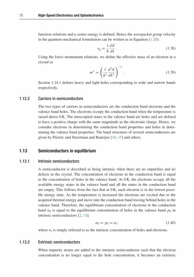
1.13.3 Semiconductor band diagrams
The band diagrams for p- and n-type semiconductors at thermal equilibrium are given inFigure 1.16. The bottom of the conduction band is Ec, the top of the valence band is Ev,the intrinsic energy level is at mid-band and is denoted by Ei and the Fermi level is EF.
1.13.4 Electron and hole distribution
The distribution of electrons in the conduction band and holes in the valence band isobtained using the Fermi–Dirac probability function. The electron distribution in theconduction band is written as
n(E) = gc(E) f (E), (1.41)
where gc(E) is the density of quantum states in the conduction band and f (E) is theFermi–Dirac probability function given in Equation (1.29). The hole distribution in thevalence band can be written in a similar way:
p(E) = gv(E)[1 − f (E)]. (1.42)
The density of states functions are written as
gc(E) = m∗n
√2m∗
n(E − Ec)
π2h3, E ≥ Ec (1.43)
gv(E) =m∗
p
√2m∗
p(Ev − E)
π2h3, E ≤ Ev. (1.44)
The equilibrium concentration of electrons can now be written as
n0 =∫ ∞
Ec
n(E)dE, (1.45)
20 High-Speed Electronics and Optoelectronics
where n(E) is given by Equation (1.41). Similarly, the equilibrium hole concentrationis written as
p0 =∫ Ev
−∞p(E)dE, (1.46)
where p(E) is given by Equation (1.42). The equilibrium electron and hole concentra-tions in the conduction and valence bands respectively are written as
n0 = Nc exp
(−(Ec − EF)
kT
)(1.47)
p0 = Nv exp
(−(EF − Ev)
kT
), (1.48)
where Nc and Nv are the effective density of states functions in the conduction andvalence bands respectively.
Nc = 2
(2πm∗
nkT
h2
)3/2
(1.49)
Nv = 2
(2πm∗
pkT
h2
)3/2
. (1.50)
The intrinsic carrier concentration ni is given by
n2i = n0 p0. (1.51)
By substitution of Equations (1.47) and (1.48), we can write the intrinsic concentra-tion as
n2i = Nc Nv exp
(−(Ec − Ev)
kT
)(1.52)
= Nc Nv exp−Eg
kT, (1.53)
where Eg is the bandgap energy.
1.14 Direct and indirect semiconductors
When light illuminates a semiconductor, and the photon energy is equal to or larger thanthe band gap, the light is absorbed, and creates hole–electron pairs. These holes andelectrons are equal in number to maintain charge neutrality, and since they are not inequilibrium, in due course they recombine; this recombination may be radiative or non-radiative. Radiative recombination, when a photon is emitted usually at the bandgapenergy, only occurs in direct bandgap material, whereas non-radiative recombinationmay occur in both direct and indirect bandgap semiconductors. In indirect semicon-ductors, this non-radiative recombination requires a phonon to mediate the process.Non-radiative processes in direct bandgap material are usually through traps or dueto surface recombination. The direct or indirect band gap defines whether the lowest
Review of semiconductor materials and physics 21
position of the conduction band aligns with the maximum of the valence band alongmomentum space, where the effective momentum value k is equal to zero.
Direct bandgap semiconductors are capable of photon emission, by radiative recom-bination, but indirect semiconductors have a low probability of radiative recombination.However, indirect bandgap semiconductors may have isoelectronic impurity stateswhich are direct, and therefore the recombination from these states may also be radia-tive. GaP, which is an indirect gap semiconductor, may be doped with zinc oxide ornitrogen to produce these states, and the widely used green or red light–emitting diodesare examples of this emission.
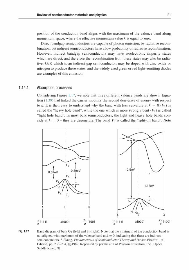
1.14.1 Absorption processes
Considering Figure 1.17, we note that three different valence bands are shown. Equa-tion (1.39) had linked the carrier mobility the second derivative of energy with respectto k. It is then easy to understand why the band with less curvature at k = 0 (V1) iscalled the “heavy hole band”, while the one which is more strongly bent (V2) is called“light hole band”. In most bulk semiconductors, the light and heavy hole bands con-cide at k = 0 – they are degenerate. The band V3 is called the “split-off band”. Note
V2
V2 V3
V1
V3
V1
0.67eV
L X
0.80eV 2.5eV
1.12eV
Γ7
πa [111]
Γ8
Γ6
λ
λ
Γ
L XΓ
2πa
[100]k [000] πa [111] 2π
a[100]k [000]
Fig. 1.17 Band diagram of bulk Ge (left) and Si (right). Note that the minimum of the conduction band isnot aligned with maximum of the valence band at k = 0, indicating that these are indirectsemiconductors. S. Wang, Fundamentals of Semiconductor Theory and Device Physics, 1stEdition, pp. 233–234, c©1989. Reprinted by permission of Pearson Education, Inc., UpperSaddle River, NJ.
22 High-Speed Electronics and Optoelectronics
L X
1.42eV
πa [111]
Γ
λ
Δ
2πa
[100]k [000]
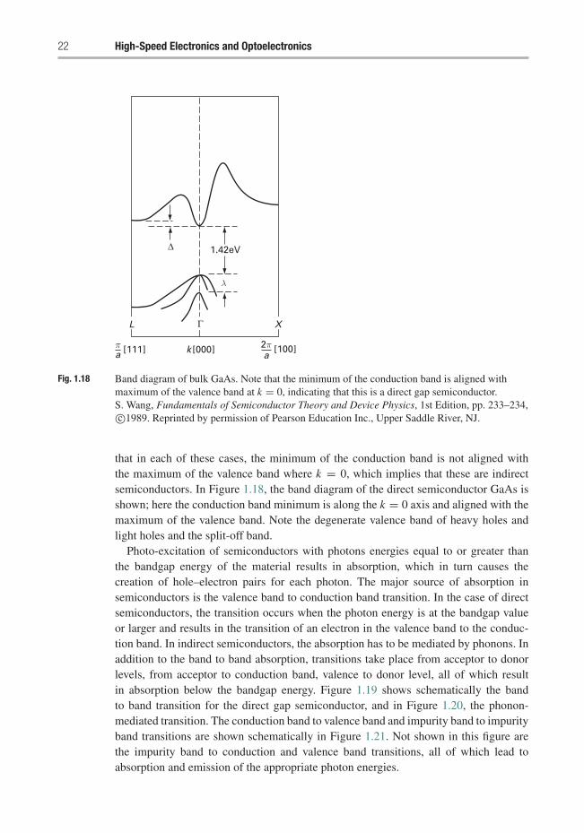
Fig. 1.18 Band diagram of bulk GaAs. Note that the minimum of the conduction band is aligned withmaximum of the valence band at k = 0, indicating that this is a direct gap semiconductor.S. Wang, Fundamentals of Semiconductor Theory and Device Physics, 1st Edition, pp. 233–234,c©1989. Reprinted by permission of Pearson Education Inc., Upper Saddle River, NJ.
that in each of these cases, the minimum of the conduction band is not aligned withthe maximum of the valence band where k = 0, which implies that these are indirectsemiconductors. In Figure 1.18, the band diagram of the direct semiconductor GaAs isshown; here the conduction band minimum is along the k = 0 axis and aligned with themaximum of the valence band. Note the degenerate valence band of heavy holes andlight holes and the split-off band.
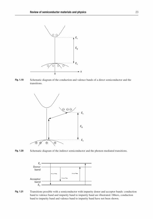
Photo-excitation of semiconductors with photons energies equal to or greater thanthe bandgap energy of the material results in absorption, which in turn causes thecreation of hole–electron pairs for each photon. The major source of absorption insemiconductors is the valence band to conduction band transition. In the case of directsemiconductors, the transition occurs when the photon energy is at the bandgap valueor larger and results in the transition of an electron in the valence band to the conduc-tion band. In indirect semiconductors, the absorption has to be mediated by phonons. Inaddition to the band to band absorption, transitions take place from acceptor to donorlevels, from acceptor to conduction band, valence to donor level, all of which resultin absorption below the bandgap energy. Figure 1.19 shows schematically the bandto band transition for the direct gap semiconductor, and in Figure 1.20, the phonon-mediated transition. The conduction band to valence band and impurity band to impurityband transitions are shown schematically in Figure 1.21. Not shown in this figure arethe impurity band to conduction and valence band transitions, all of which lead toabsorption and emission of the appropriate photon energies.
Review of semiconductor materials and physics 23
Ec
Ev
Eg
k0
Fig. 1.19 Schematic diagram of the conduction and valence bands of a direct semiconductor and thetransitions.
Ec
Ev
Eg
Fig. 1.20 Schematic diagram of the indirect semiconductor and the phonon-mediated transitions.
Donorband
Ec
Acceptorband
Ev
Fig. 1.21 Transitions possible with a semiconductor with impurity donor and acceptor bands: conductionband to valence band and impurity band to impurity band are illustrated. Others, conductionband to impurity band and valence band to impurity band have not been shown.
24 High-Speed Electronics and Optoelectronics
The absorption rate of the band to band transitions, for both the direct and indirecttransitions may be calculated using quantum theory, but is not included here.
Free carrier absorption also occurs in most semiconductors as the carrier density isalways non-zero. The absorption of a photon by a carrier within a band results in thecarrier having a larger energy. The absorption coefficient is proportional to the carrierdensity [3]. This effect is important in the design of waveguide devices, where typicallythis may result in absorption of the order of 1 dB cm−1 when the carrier densities arehigh in the 1018 cm−3 region.
1.14.2 Exciton absorption
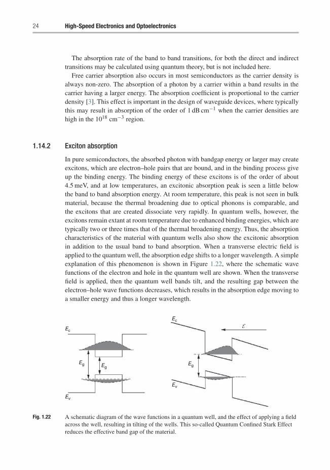
In pure semiconductors, the absorbed photon with bandgap energy or larger may createexcitons, which are electron–hole pairs that are bound, and in the binding process giveup the binding energy. The binding energy of these excitons is of the order of about4.5 meV, and at low temperatures, an excitonic absorption peak is seen a little belowthe band to band absorption energy. At room temperature, this peak is not seen in bulkmaterial, because the thermal broadening due to optical phonons is comparable, andthe excitons that are created dissociate very rapidly. In quantum wells, however, theexcitons remain extant at room temperature due to enhanced binding energies, which aretypically two or three times that of the thermal broadening energy. Thus, the absorptioncharacteristics of the material with quantum wells also show the excitonic absorptionin addition to the usual band to band absorption. When a transverse electric field isapplied to the quantum well, the absorption edge shifts to a longer wavelength. A simpleexplanation of this phenomenon is shown in Figure 1.22, where the schematic wavefunctions of the electron and hole in the quantum well are shown. When the transversefield is applied, then the quantum well bands tilt, and the resulting gap between theelectron–hole wave functions decreases, which results in the absorption edge moving toa smaller energy and thus a longer wavelength.
Ec
Ec
E
Ev
Ev
Eg EgEg
Fig. 1.22 A schematic diagram of the wave functions in a quantum well, and the effect of applying a fieldacross the well, resulting in tilting of the wells. This so-called Quantum Confined Stark Effectreduces the effective band gap of the material.
Review of semiconductor materials and physics 25
1063 2 1.5 1 0.7
105
104
103
102
100.2 0.6
AmorphousSi Si
GaP
GaAs
InP
Ge
Photon Energy (eV)
Ga0.3In0.7As0.64P0.36
InGaAs
1 1.4 1.8Wavelength (μm)
Ab
sorp
tio
n C
oef
fici
ent
(cm
–1)
Fig. 1.23 Absorption coefficient for various semiconductors (M. Shur, Physics of Semiconductor Devices,Prentice Hall, 1990 c©Prentice Hall).
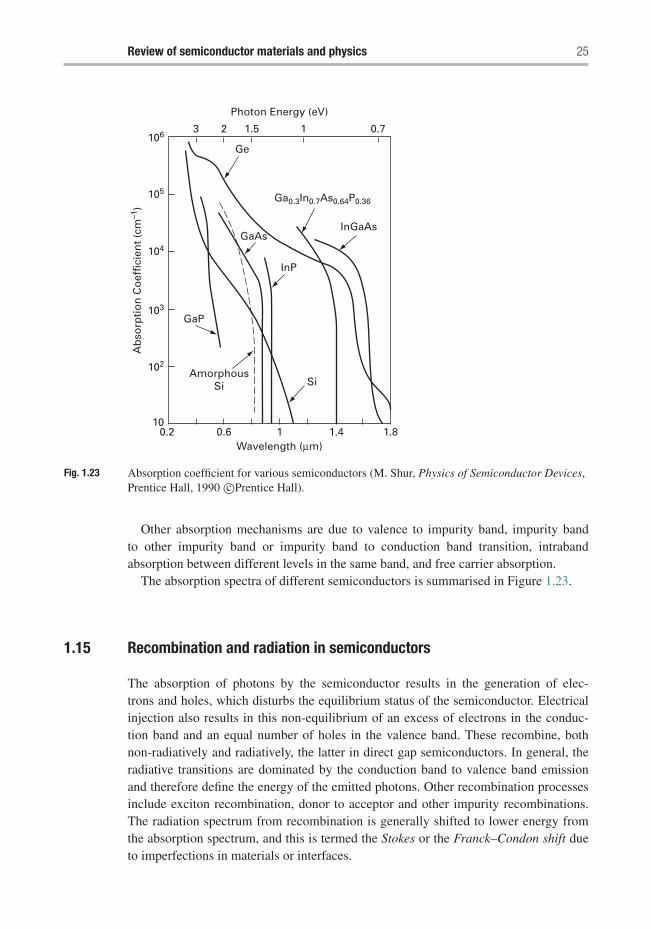
Other absorption mechanisms are due to valence to impurity band, impurity bandto other impurity band or impurity band to conduction band transition, intrabandabsorption between different levels in the same band, and free carrier absorption.
The absorption spectra of different semiconductors is summarised in Figure 1.23.
1.15 Recombination and radiation in semiconductors
The absorption of photons by the semiconductor results in the generation of elec-trons and holes, which disturbs the equilibrium status of the semiconductor. Electricalinjection also results in this non-equilibrium of an excess of electrons in the conduc-tion band and an equal number of holes in the valence band. These recombine, bothnon-radiatively and radiatively, the latter in direct gap semiconductors. In general, theradiative transitions are dominated by the conduction band to valence band emissionand therefore define the energy of the emitted photons. Other recombination processesinclude exciton recombination, donor to acceptor and other impurity recombinations.The radiation spectrum from recombination is generally shifted to lower energy fromthe absorption spectrum, and this is termed the Stokes or the Franck–Condon shift dueto imperfections in materials or interfaces.
26 High-Speed Electronics and Optoelectronics
In general the excess electrons and holes decay at some rate, resulting in the densityvarying as exp(−t/τ), where τ is defined as the lifetime of the carriers. The decay ofthese carriers results in transfer of energy to the lattice in the form of phonons for thenon-radiative decay and transfer of energy to photons for radiative decay.
The corresponding lifetimes are labelled as τnr and τr for the non-radiative and radia-tive decay, respectively, and the corresponding non-radiative and radiative rates are Rnr
and Rr, respectively. Thus, the total lifetime constant τ is given as:
1
τ= 1
τnr+ 1
τr. (1.54)
The corresponding total spontaneous rate of recombination is given by
Rspon = Rnr + Rr. (1.55)
Devices such as the light-emitting diode (LED) largely depend on spontaneous emis-sion, and in this case the internal quantum efficiency is given by
ηinternal = Rr
Rnr + Rr. (1.56)
The exponential decay rate of the excess carriers is inversely proportional to recombi-nation rate, and if the excess of electron is �n, then the recombination rates Rr and Rnr
are given by the expressions: Rr = �n/τr and Rnr = �n/τnr. Then internal quantumefficiency may also be written as
ηinternal =1τr
1τr
+ 1τnr
= 1
1 + τrτnr
= τnr
τr + τnr. (1.57)
The total spontaneous recombination rate is given by the equation:
Rtotal = A�n + B�n2 + C�n3. (1.58)
The first term is the Shockley–Read–Hall recombination due to defects and traps, thesecond is the spontaneous emission due to radiative transition, and the third is the Augerrecombination term. Auger recombination is non-radiative, occurs at high injectionlevels, and is a three-particle process. It becomes important in ternary and quater-nary compounds of InP-based materials, and is evident in the long wavelength laserstructures.
1.15.1 Spontaneous and stimulated emission
The radiative recombination process discussed above occurs spontaneously, and thisis used in traditional LED structures. In lasers, stimulated emission is the source oflight, and in this section the relationship between absorption, spontaneous emission andstimulated emission, first outlined by Einstein in 1917, is discussed. The derivationsgiven here follow the approach outlined by Casey and Panish [4] and Agrawal [1].
It can be shown that the blackbody radiation law is given by
P(E) = 8πn 3 E2
h3c3(eE/kT − 1), (1.59)
Review of semiconductor materials and physics 27
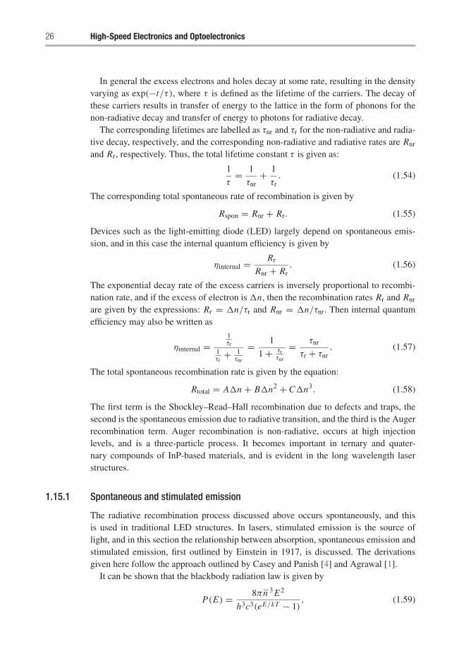
E2
E1
F2
F1
Ec
Ev
Fig. 1.24 Transitions from level E1 to E2 for absorption and from E2 to E1 for emission, F1 and F2 arethe electron and hole quasi-Fermi levels respectively.
where n is the index of the material under consideration, h is Planck’s constant, c is thespeed of light in vacuum, E is the energy given by hν, ν is the frequency and k isBoltzmann’s constant. This is the expression for the energy density blackbody radiationP(E), and is in thermal equilibrium, when the input radiation is equal to the outgoingradiation.
For a semiconductor, consider the transitions from the conduction band to the valenceband and also the reverse. The energy levels in each of these bands have to obey thePauli exclusion principle, which implies only two carriers at each level. Thus, the bandis a series of levels, as shown in Figure 1.24, and the transition energy for an electronfrom a level E1 in the valence band to a level E2 in the conduction band requires that anincident photon has energy given by hν = E2 − E1. Let the probability of this transitiontaking place be given by B12, and let f1 be the probability that an electron exists at levelE1 and (1− f2) be the probability that a vacancy occurs at level E2. Also assume that theradiation density of photon energy incident on the semiconductor is given by P(E21).Then the upward transition rate is given by
r12 = B12 f1(1 − f2)P(E21). (1.60)
Note that f1 and f2 take the form of the Fermi–Dirac distribution
fi = 1
e(Ei−Fi)/kT + 1, (1.61)
where Fi is the corresponding quasi-Fermi level, k is Boltzmann’s constant and T thetemperature in Kelvin.
Similarly, the downward transition rate, now called the stimulated transition, isgiven as
r21(stim) = B21 f2(1 − f1)P(E21), (1.62)
where B21 is the transition probability, f2 is the probability that an electron is presentat E2 and (1 − f1) is the probability that there is vacancy at E1.
Finally, there is the spontaneous transition from E2 to E1, without any incidentradiation involved, given by
r21(spon) = A21 f2(1 − f1). (1.63)
28 High-Speed Electronics and Optoelectronics
In thermal equilibrium, the input radiation is equal to the output, the Fermi levels F1 =F2, and hence
r12 = r21(spon) + r21(stim). (1.64)
Equating, simplifying and noting that P(E21) is the blackbody radiation term,
P(E21) = 8πn3 E2
h3c3(eE21/kT − 1)(1.65)
= A21 f2(1 − f1)
B12 f1(1 − f2) − B21 f2(1 − f1)(1.66)
= A21
B12eE21/kT − B21. (1.67)
Equating Equations (1.65) and (1.67) and separating them into temperature-dependentand temperature-independent terms give the following results:
A21 = 8πn 3 E2
h3c3B21 (1.68)
and
B21 = B12. (1.69)
These are Einstein’s coefficients and their relationships with each other.The condition under which stimulated emission dominates is an interesting one. This
requires a non-equilibrium condition in which the presence of incident radiation isrequired. This results in the population densities in the conduction and valence bands tobe different from the equilibrium condition. For stimulated emission to dominate, thestimulated emission rate, r21(stim), needs to exceed the absorption rate r12. Substitutingfrom Equations (1.60) and (1.62),
B21 f2(1 − f1)P(E21) > B12 f1(1 − f2)P(E21). (1.70)
Since B21 = B12, this equation becomes
f2(1 − f1) > f1(1 − f2). (1.71)
Substituting for f1 and f2 from Equation 1.61, this equation becomes
e(F2−F1)/kT > e(E2−E1)/kT (1.72)
or
F2 − F1 > E2 − E1. (1.73)
This implies that the difference in the quasi-Fermi levels is greater than the emissionenergy of the photon. If the emission is at bandgap energy, then the difference betweenquasi-Fermi levels needs to be greater than the bandgap energy Eg.
Review of semiconductor materials and physics 29
1.16 Carrier transport in semiconductors
Drift and diffusion are the two mechanisms whereby carriers are transported in semi-conductors such that there is current flow. It will be assumed that thermal equilibriumwill not be disturbed during these processes [2, 8, 10, 15].
1.16.1 Drift current
When an external electric field is applied to a semiconductor, it produces a force that willaccelerate the electrons and holes in opposite directions as long as there are availableenergy states in the conduction and valence bands. The net drift of charge will producea current which is the drift current. If the electric field is denoted as E , the drift currentdensities for electrons and holes are written as
Jn(drift) = qnvndr = qμnnE (1.74)
Jp(drift) = qpvpdr = qμpnE, (1.75)
where q is the charge on a particle (electron or hole), J is the surface density of current,vndr and vpdr are the drift velocities of electrons and holes, respectively, and μ is themobility.
1.16.2 Diffusion current
Electrons flow from a region of higher concentration to a region of lower concentration,producing a flux of electrons and an electron diffusion current which is in the oppositedirection to the flux. The hole flow is such that the hole flux and the hole diffusioncurrent are in the same direction since the holes are positively charged. The diffusioncurrent densities for electrons and holes are given by
Jndiff = q Dndn
dx(1.76)
Jpdiff = −q Dpdp
dx, (1.77)
where Dn and Dp are the electron and hole diffusion coefficients respectively. Thediffusion coefficient is related to the mobility μ by the Einstein relation:
D = μkT
q. (1.78)
Hence,Dn
μn= Dp
μp= kT
q. (1.79)
Adding Equations (1.74)–(1.77),
J = (qμnn + qμp p)E + q Dndn
dx− q Dp
dp
dx. (1.80)
30 High-Speed Electronics and Optoelectronics
1.17 p–n junction
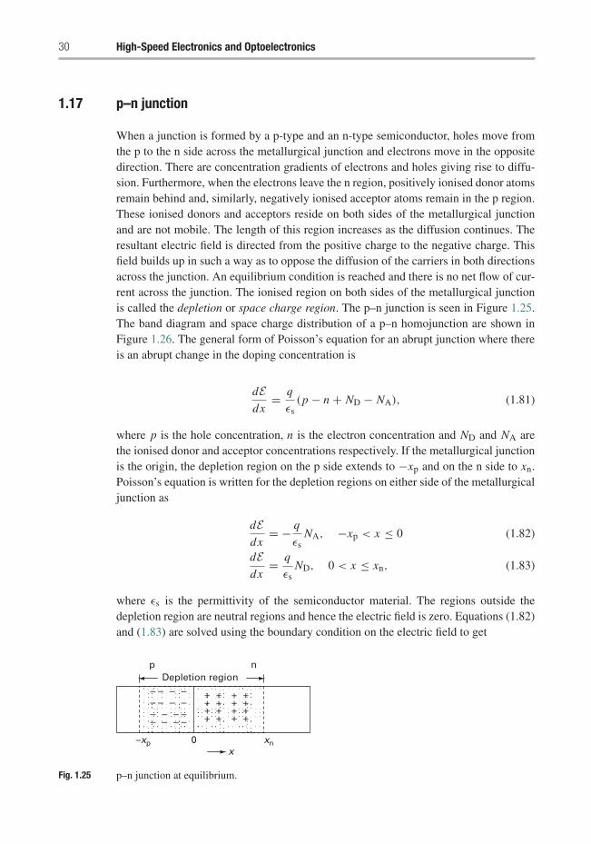
When a junction is formed by a p-type and an n-type semiconductor, holes move fromthe p to the n side across the metallurgical junction and electrons move in the oppositedirection. There are concentration gradients of electrons and holes giving rise to diffu-sion. Furthermore, when the electrons leave the n region, positively ionised donor atomsremain behind and, similarly, negatively ionised acceptor atoms remain in the p region.These ionised donors and acceptors reside on both sides of the metallurgical junctionand are not mobile. The length of this region increases as the diffusion continues. Theresultant electric field is directed from the positive charge to the negative charge. Thisfield builds up in such a way as to oppose the diffusion of the carriers in both directionsacross the junction. An equilibrium condition is reached and there is no net flow of cur-rent across the junction. The ionised region on both sides of the metallurgical junctionis called the depletion or space charge region. The p–n junction is seen in Figure 1.25.The band diagram and space charge distribution of a p–n homojunction are shown inFigure 1.26. The general form of Poisson’s equation for an abrupt junction where thereis an abrupt change in the doping concentration is
dEdx
= q
εs(p − n + ND − NA), (1.81)
where p is the hole concentration, n is the electron concentration and ND and NA arethe ionised donor and acceptor concentrations respectively. If the metallurgical junctionis the origin, the depletion region on the p side extends to −xp and on the n side to xn.Poisson’s equation is written for the depletion regions on either side of the metallurgicaljunction as
dEdx
= − q
εsNA, −xp < x ≤ 0 (1.82)
dEdx
= q
εsND, 0 < x ≤ xn, (1.83)
where εs is the permittivity of the semiconductor material. The regions outside thedepletion region are neutral regions and hence the electric field is zero. Equations (1.82)and (1.83) are solved using the boundary condition on the electric field to get
0x
xn–xp
p nDepletion region
++++
+ + ++ + +
+ + ++ + +
– – – –– – ––– – –– – – –
–
Fig. 1.25 p–n junction at equilibrium.
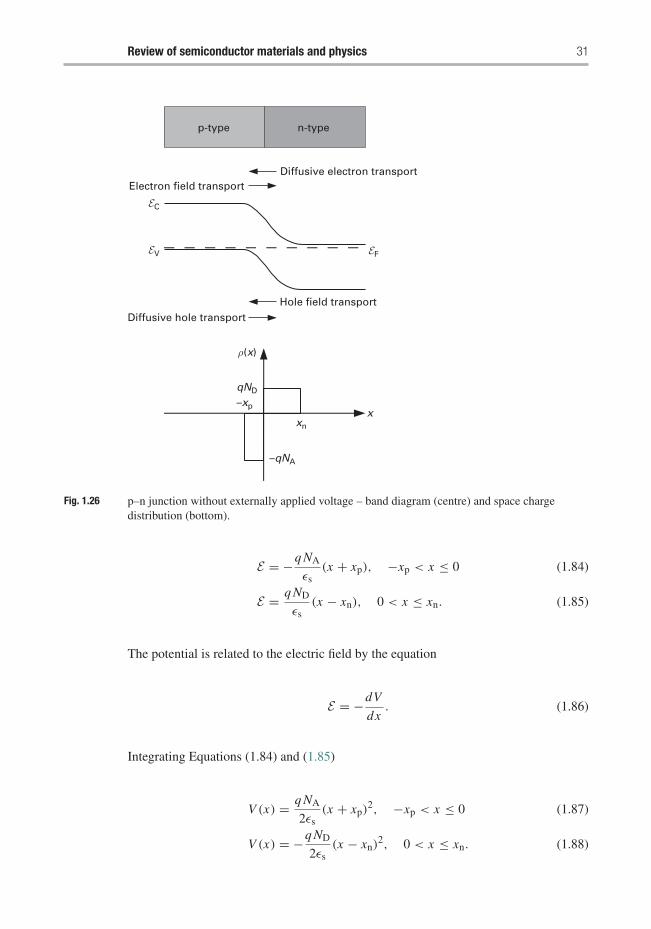
Review of semiconductor materials and physics 31
p-type n-type
Electron field transport
EC
EV
Diffusive electron transport
EF
Hole field transportDiffusive hole transport
ρ(x)
qND
xn
–xpx
–qNA
Fig. 1.26 p–n junction without externally applied voltage – band diagram (centre) and space chargedistribution (bottom).
E = −q NA
εs(x + xp), −xp < x ≤ 0 (1.84)
E = q ND
εs(x − xn), 0 < x ≤ xn. (1.85)
The potential is related to the electric field by the equation
E = −dV
dx. (1.86)
Integrating Equations (1.84) and (1.85)
V (x) = q NA
2εs(x + xp)
2, −xp < x ≤ 0 (1.87)
V (x) = −q ND
2εs(x − xn)
2, 0 < x ≤ xn. (1.88)
32 High-Speed Electronics and Optoelectronics
1.17.1 The built-in potential
The built-in potential on the p side of the junction is the potential difference across thedepletion region. It is determined similarly on the n side.
Vbip = q NA
2εsx2
p (1.89)
Vbin = q ND
2εsx2
n . (1.90)
The total built-in potential across the junction is
Vbi = (Vbip + Vbin) (1.91)
= q
2εs[NAx2
p + NDx2n ]. (1.92)
The continuity of the electric field across the junction at x = 0 requires that
NAxp = NDxn. (1.93)
It is assumed that the dopants are fully ionised and the total ionised positive chargeper unit area on the n side is equal to the total ionised negative charge per unit area onthe p side. At thermal equilibrium, there is no net current flow and hence the drift anddiffusion currents are equal. The electron current is
Jn = 0 (1.94)
= Jndrift + Jndiff (1.95)
= qμnnE + q Dndn
dx. (1.96)
The hole current is written as
Jp = 0 (1.97)
= Jpdrift + Jpdiff (1.98)
= qμp pE − q Dpdp
dx. (1.99)
When the net hole current is zero, and with the electric field equal to the gradient of thepotential, it may be shown that
Vbi = kT
qln
NAND
n2i
. (1.100)
It has been assumed that there is full ionisation of the dopant impurity levels such thatthe majority carrier concentrations are the doping concentrations and the equilibriumconcentrations are related by
n0 p0 = n2i . (1.101)
1.17.2 The depletion layer width
The widths of the depletion layer in the p- and n-type semiconductors may be calculated.The maximum electric field occurs at the metallurgical junction, x = 0. This is given by
εsEmax = q NDxn = q NAxp. (1.102)
Review of semiconductor materials and physics 33
Using the Equations (1.92) and (1.93) with
| Vbi | = Emax
2[xn + xp] (1.103)
W = xn + xp (1.104)
=√
2εs
q
(1
ND+ 1
NA
)| Vbi |. (1.105)
1.17.3 The depletion capacitance
The depletion capacitance is the capacitance at the p–n junction. The depletion layer ismodelled as a parallel plate capacitor. The capacitance is written as
Cj = εs A
W, (1.106)
where A is the area of the p–n junction and W is the depletion layer width given byEquation (1.105). The junction capacitance is given by
C = A
√qεs NA ND
2Vbi(NA + ND). (1.107)
1.17.4 p–n junction under bias
At thermal equilibrium, the total electrostatic potential across the p–n junction is thebuilt-in potential,Vbi, and the potential difference between the p and n regions is qVbi.If now a voltage VA is applied with the positive terminal connected to the p side and thenegative to the n side, the junction is forward-biased and the total electrostatic potentialacross the junction is Vbi − VA, resulting in a reduction of the depletion layer width.A potential barrier was formed at thermal equilibrium restricting the motion of themajority carriers. The application of the forward bias reduces the height of the bar-rier. If, on the other hand, a voltage is applied with the positive terminal connected tothe n side and the negative terminal to the p side, the electrostatic potential across thejunction is Vbi − (−VA) and the height of the barrier is increased with the reverse bias.The depletion widths and the energy band diagrams are shown in the figure. The widthof the depletion layer is given by
W =√
2εs
q
(ND + NA
NA ND
)(Vbi ∓ VA). (1.108)
1.17.5 Current–voltage characteristics
The total current density in a p–n junction is given as:
J = q
[Dnnp0
Ln+ Dp pn0
Lp
] [exp
(qVA
kT
)− 1
], (1.109)
34 High-Speed Electronics and Optoelectronics
where
Ln = √Dnτn (1.110)
Lp = √Dpτp (1.111)
np0 = n2i
NA(1.112)
pn0 = n2i
ND. (1.113)
The current density expression now reduces to
J = J0
[exp
(qVA
kT
)− 1
](1.114)
where
J0 = qn2i
[√Dn
τn
1
NA+
√Dp
τp
1
ND
], (1.115)
where Dn and Dp are the Einstein coefficients for electrons and holes and τn and τp arethe electron and hole lifetimes.
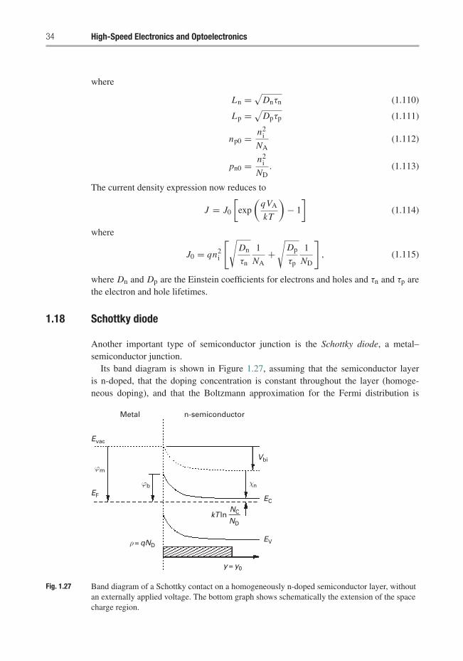
1.18 Schottky diode
Another important type of semiconductor junction is the Schottky diode, a metal–semiconductor junction.
Its band diagram is shown in Figure 1.27, assuming that the semiconductor layeris n-doped, that the doping concentration is constant throughout the layer (homoge-neous doping), and that the Boltzmann approximation for the Fermi distribution is
Metal
Evac
ϕm
EF
ϕb
n-semiconductor
Vbi
χn
kT lnNC
ND
EC
EVρ = qND
y = y0
Fig. 1.27 Band diagram of a Schottky contact on a homogeneously n-doped semiconductor layer, withoutan externally applied voltage. The bottom graph shows schematically the extension of the spacecharge region.
Review of semiconductor materials and physics 35
valid. We see that under ideal circumstances, the Schottky barrier height ϕb is thedifference between the metal work function ϕm and the electron affinity χn. In prac-tice, however, the effective Schottky barrier height ϕb is also influenced by states at themetal–semiconductor interface and shows only a small dependence on the metal workfunction. On GaAs, ϕb ≈ 0.8 eV.
The built-in voltage can be easily calculated:
Vbi = ϕb − kT lnNC
ND, (1.116)
where NC is the density of states in the conduction band and ND the semiconductordoping concentration.
The Schottky barrier ϕb causes a depletion of the semiconductor layer immedi-ately adjacent to the metal–semiconductor interface. Devoid of electrons, the positivelycharged ionised donors remain and form a space charge region with a space charge den-sity ρ = q ND. It is indicated in the bottom graph of Figure 1.27 – we make the usual‘box shape’ assumption for the space charge region, i.e. we assume the space chargeconcentration to be constant throughout until y = y0, then ending abruptly.
For a homogeneously doped semiconductor with a permittivity of εs and a dopingconcentration of ND,
y0 =√
2εsVbi
q ND(1.117)
without any externally applied voltage.
1.19 Heterostructures
The ability to mix semiconductors of different chemical composition in a singlecrystal gives an important degree of freedom in device design. The combinationof semiconductor materials of different stoichiometry in a single crystal is called aheterostructure.
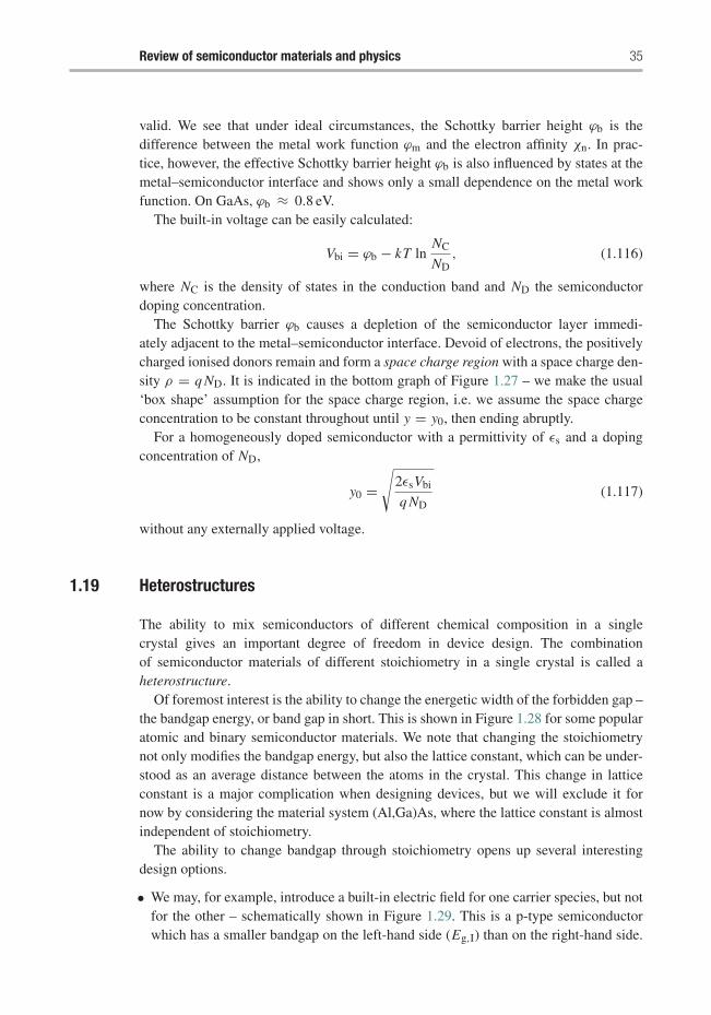
Of foremost interest is the ability to change the energetic width of the forbidden gap –the bandgap energy, or band gap in short. This is shown in Figure 1.28 for some popularatomic and binary semiconductor materials. We note that changing the stoichiometrynot only modifies the bandgap energy, but also the lattice constant, which can be under-stood as an average distance between the atoms in the crystal. This change in latticeconstant is a major complication when designing devices, but we will exclude it fornow by considering the material system (Al,Ga)As, where the lattice constant is almostindependent of stoichiometry.
The ability to change bandgap through stoichiometry opens up several interestingdesign options.
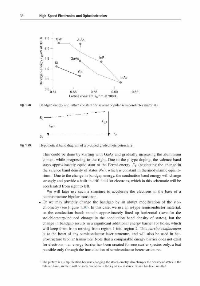
• We may, for example, introduce a built-in electric field for one carrier species, but notfor the other – schematically shown in Figure 1.29. This is a p-type semiconductorwhich has a smaller bandgap on the left-hand side (Eg,I) than on the right-hand side.
36 High-Speed Electronics and Optoelectronics
Fig. 1.28 Bandgap energy and lattice constant for several popular semiconductor materials.
EC
EV
Eg,1
Eg,2
EF
Fig. 1.29 Hypothetical band diagram of a p-doped graded heterostructure.
This could be done by starting with GaAs and gradually increasing the aluminiumcontent while progressing to the right. Due to the p-type doping, the valence bandstays approximately equidistant to the Fermi energy EF (neglecting the change inthe valence band density of states NV), which is constant in thermodynamic equilib-rium.1 Due to the change in bandgap energy, the conduction band energy will changestrongly and provide a built-in drift field for electrons, which in this schematic will beaccelerated from right to left.
We will later use such a structure to accelerate the electrons in the base of aheterostructure bipolar transistor.
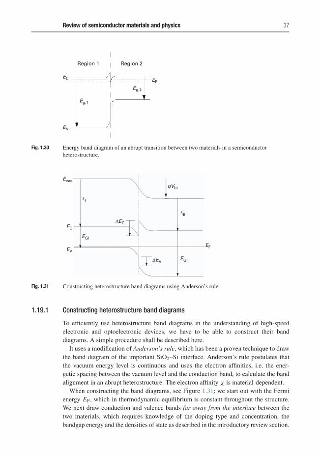
• Or we may abruptly change the bandgap by an abrupt modification of the stoi-chiometry (see Figure 1.30). In this case, we use an n-type semiconductor material,so the conduction bands remain approximately lined up horizontal (save for thestoichiometry-induced change in the conduction band density of states), but thechange in bandgap results in a significant additional energy barrier for holes, whichwill keep them from moving from region 1 into region 2. This carrier confinementis at the heart of any semiconductor laser structure, and will also be used in het-erostructure bipolar transistors. Note that a comparable energy barrier does not existfor electrons – an energy barrier has been created for one carrier species only, a featpossible only through the introduction of semiconductor heterostructures.
1 The picture is a simplification because changing the stoichiometry also changes the density of states in thevalence band, so there will be some variation in the EF to EV distance, which has been omitted.
2.5
2.0
GaP
Si
Ban
dg
ap e
ner
gy
EG
/eV
at
300
K
GaAs
AlAs
InP
InAs
Ge
1.5
1.0
0.5
0.00.54 0.56 0.58
Lattice constant a0/nm at 300 K0.60 0.62
Review of semiconductor materials and physics 37
Region 1
EC
EV
Eg,1
EF
Eg,2
Region 2
Fig. 1.30 Energy band diagram of an abrupt transition between two materials in a semiconductorheterostructure.
Evac
EC
EV
EGI
ΔEV
ΔEC
EGII
EF
qVbi
χII
χI
Fig. 1.31 Constructing heterostructure band diagrams using Anderson’s rule.
1.19.1 Constructing heterostructure band diagrams
To efficiently use heterostructure band diagrams in the understanding of high-speedelectronic and optoelectronic devices, we have to be able to construct their banddiagrams. A simple procedure shall be described here.
It uses a modification of Anderson’s rule, which has been a proven technique to drawthe band diagram of the important SiO2–Si interface. Anderson’s rule postulates thatthe vacuum energy level is continuous and uses the electron affinities, i.e. the ener-getic spacing between the vacuum level and the conduction band, to calculate the bandalignment in an abrupt heterostructure. The electron affinity χ is material-dependent.
When constructing the band diagrams, see Figure 1.31; we start out with the Fermienergy EF, which in thermodynamic equilibrium is constant throughout the structure.We next draw conduction and valence bands far away from the interface between thetwo materials, which requires knowledge of the doping type and concentration, thebandgap energy and the densities of state as described in the introductory review section.
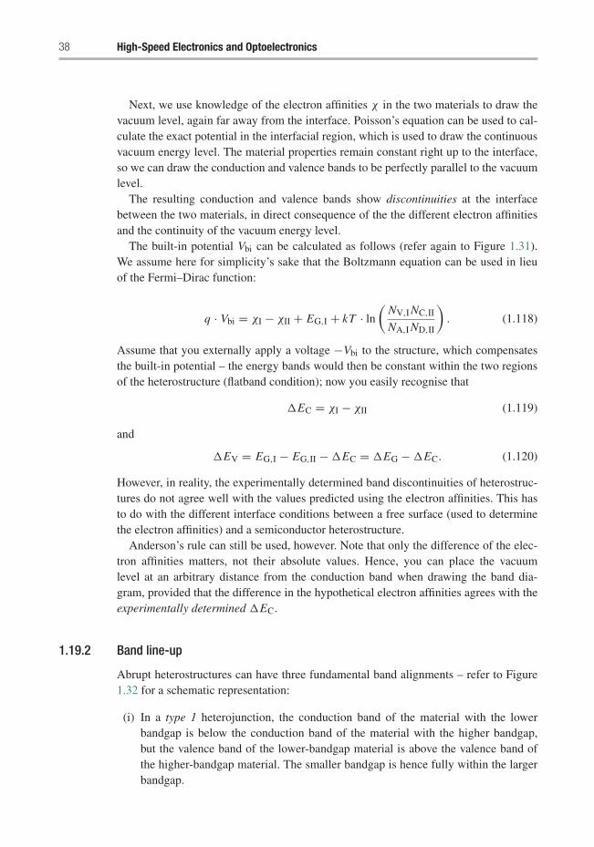
38 High-Speed Electronics and Optoelectronics
Next, we use knowledge of the electron affinities χ in the two materials to draw thevacuum level, again far away from the interface. Poisson’s equation can be used to cal-culate the exact potential in the interfacial region, which is used to draw the continuousvacuum energy level. The material properties remain constant right up to the interface,so we can draw the conduction and valence bands to be perfectly parallel to the vacuumlevel.
The resulting conduction and valence bands show discontinuities at the interfacebetween the two materials, in direct consequence of the the different electron affinitiesand the continuity of the vacuum energy level.
The built-in potential Vbi can be calculated as follows (refer again to Figure 1.31).We assume here for simplicity’s sake that the Boltzmann equation can be used in lieuof the Fermi–Dirac function:
q · Vbi = χI − χII + EG,I + kT · ln
(NV,I NC,II
NA,I ND,II
). (1.118)
Assume that you externally apply a voltage −Vbi to the structure, which compensatesthe built-in potential – the energy bands would then be constant within the two regionsof the heterostructure (flatband condition); now you easily recognise that
�EC = χI − χII (1.119)
and
�EV = EG,I − EG,II − �EC = �EG − �EC. (1.120)
However, in reality, the experimentally determined band discontinuities of heterostruc-tures do not agree well with the values predicted using the electron affinities. This hasto do with the different interface conditions between a free surface (used to determinethe electron affinities) and a semiconductor heterostructure.
Anderson’s rule can still be used, however. Note that only the difference of the elec-tron affinities matters, not their absolute values. Hence, you can place the vacuumlevel at an arbitrary distance from the conduction band when drawing the band dia-gram, provided that the difference in the hypothetical electron affinities agrees with theexperimentally determined �EC.
1.19.2 Band line-up
Abrupt heterostructures can have three fundamental band alignments – refer to Figure1.32 for a schematic representation:
(i) In a type 1 heterojunction, the conduction band of the material with the lowerbandgap is below the conduction band of the material with the higher bandgap,but the valence band of the lower-bandgap material is above the valence band ofthe higher-bandgap material. The smaller bandgap is hence fully within the largerbandgap.
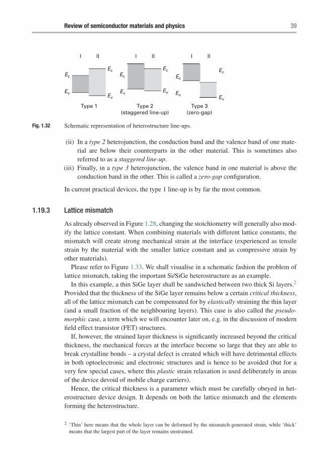
Review of semiconductor materials and physics 39
Ec
Ev
Ec
I II I II I II
Ec
Ec
Ec
Ec
Ev
Type 1 Type 2(staggered line-up)
Type 3(zero-gap)
Ev Ev Ev
Ev
Fig. 1.32 Schematic representation of heterostructure line-ups.
(ii) In a type 2 heterojunction, the conduction band and the valence band of one mate-rial are below their counterparts in the other material. This is sometimes alsoreferred to as a staggered line-up.
(iii) Finally, in a type 3 heterojunction, the valence band in one material is above theconduction band in the other. This is called a zero-gap configuration.
In current practical devices, the type 1 line-up is by far the most common.
1.19.3 Lattice mismatch
As already observed in Figure 1.28, changing the stoichiometry will generally also mod-ify the lattice constant. When combining materials with different lattice constants, themismatch will create strong mechanical strain at the interface (experienced as tensilestrain by the material with the smaller lattice constant and as compressive strain byother materials).
Please refer to Figure 1.33. We shall visualise in a schematic fashion the problem oflattice mismatch, taking the important Si/SiGe heterostructure as an example.
In this example, a thin SiGe layer shall be sandwiched between two thick Si layers.2
Provided that the thickness of the SiGe layer remains below a certain critical thickness,all of the lattice mismatch can be compensated for by elastically straining the thin layer(and a small fraction of the neighbouring layers). This case is also called the pseudo-morphic case, a term which we will encounter later on, e.g. in the discussion of modernfield effect transistor (FET) structures.
If, however, the strained layer thickness is significantly increased beyond the criticalthickness, the mechanical forces at the interface become so large that they are able tobreak crystalline bonds – a crystal defect is created which will have detrimental effectsin both optoelectronic and electronic structures and is hence to be avoided (but for avery few special cases, where this plastic strain relaxation is used deliberately in areasof the device devoid of mobile charge carriers).
Hence, the critical thickness is a parameter which must be carefully obeyed in het-erostructure device design. It depends on both the lattice mismatch and the elementsforming the heterostructure.
2 ‘Thin’ here means that the whole layer can be deformed by the mismatch-generated strain, while ‘thick’means that the largest part of the layer remains unstrained.
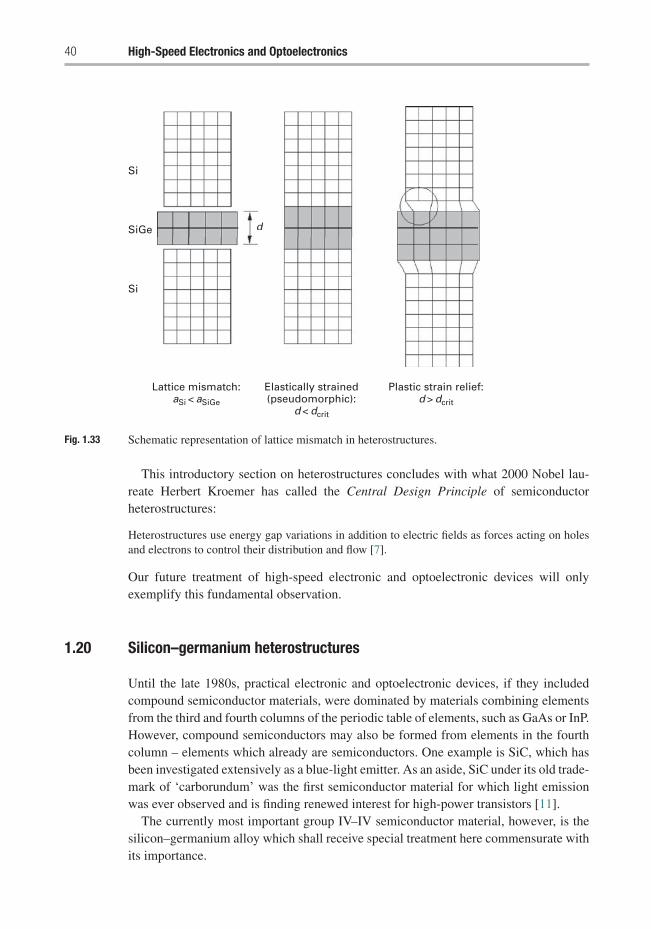
40 High-Speed Electronics and Optoelectronics
Lattice mismatch:aSi < aSiGe
Elastically strained(pseudomorphic):
d < dcrit
Plastic strain relief:d > dcrit
d
Si
Si
SiGe d
Fig. 1.33 Schematic representation of lattice mismatch in heterostructures.
This introductory section on heterostructures concludes with what 2000 Nobel lau-reate Herbert Kroemer has called the Central Design Principle of semiconductorheterostructures:
Heterostructures use energy gap variations in addition to electric fields as forces acting on holesand electrons to control their distribution and flow [7].
Our future treatment of high-speed electronic and optoelectronic devices will onlyexemplify this fundamental observation.
1.20 Silicon–germanium heterostructures
Until the late 1980s, practical electronic and optoelectronic devices, if they includedcompound semiconductor materials, were dominated by materials combining elementsfrom the third and fourth columns of the periodic table of elements, such as GaAs or InP.However, compound semiconductors may also be formed from elements in the fourthcolumn – elements which already are semiconductors. One example is SiC, which hasbeen investigated extensively as a blue-light emitter. As an aside, SiC under its old trade-mark of ‘carborundum’ was the first semiconductor material for which light emissionwas ever observed and is finding renewed interest for high-power transistors [11].
The currently most important group IV–IV semiconductor material, however, is thesilicon–germanium alloy which shall receive special treatment here commensurate withits importance.
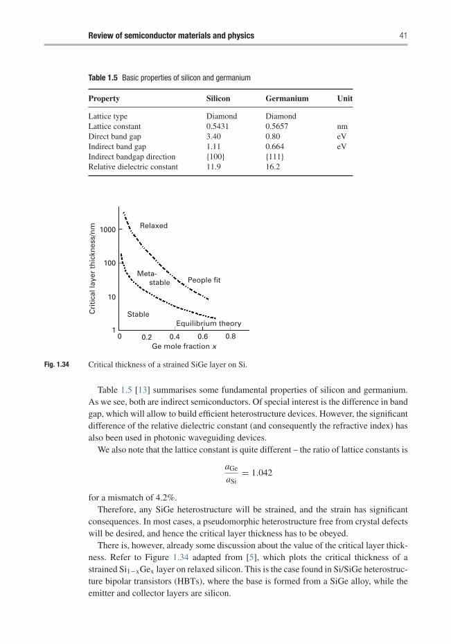
Review of semiconductor materials and physics 41
Table 1.5 Basic properties of silicon and germanium
Property Silicon Germanium Unit
Lattice type Diamond DiamondLattice constant 0.5431 0.5657 nmDirect band gap 3.40 0.80 eVIndirect band gap 1.11 0.664 eVIndirect bandgap direction {100} {111}Relative dielectric constant 11.9 16.2
100
1000
10
10 0.2 0.4 0.6
Ge mole fraction x
Cri
tica
l lay
er t
hic
knes
s/n
m
0.8
Stable
Meta- stable
Relaxed
People fit
Equilibrium theory
Fig. 1.34 Critical thickness of a strained SiGe layer on Si.
Table 1.5 [13] summarises some fundamental properties of silicon and germanium.As we see, both are indirect semiconductors. Of special interest is the difference in bandgap, which will allow to build efficient heterostructure devices. However, the significantdifference of the relative dielectric constant (and consequently the refractive index) hasalso been used in photonic waveguiding devices.
We also note that the lattice constant is quite different – the ratio of lattice constants is
aGe
aSi= 1.042
for a mismatch of 4.2%.Therefore, any SiGe heterostructure will be strained, and the strain has significant
consequences. In most cases, a pseudomorphic heterostructure free from crystal defectswill be desired, and hence the critical layer thickness has to be obeyed.
There is, however, already some discussion about the value of the critical layer thick-ness. Refer to Figure 1.34 adapted from [5], which plots the critical thickness of astrained Si1−xGex layer on relaxed silicon. This is the case found in Si/SiGe heterostruc-ture bipolar transistors (HBTs), where the base is formed from a SiGe alloy, while theemitter and collector layers are silicon.
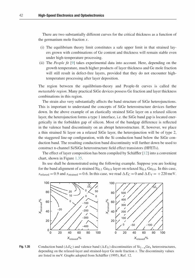
42 High-Speed Electronics and Optoelectronics
There are two substantially different curves for the critical thickness as a function ofthe germanium mole fraction x .
(i) The equilibrium theory limit constitutes a safe upper limit in that strained lay-ers grown with combinations of Ge content and thickness will remain stable evenunder high-temperature processing.
(ii) The People fit [9] takes experimental data into account. Here, depending on thegrowth temperature, much higher products of layer thickness and Ge mole fractionwill still result in defect-free layers, provided that they do not encounter high-temperature processing after layer deposition.
The region between the equilibrium-theory and People-fit curves is called themetastable region. Many practical SiGe devices possess Ge fraction and layer thicknesscombinations in this region.
The strain also very substantially affects the band structure of SiGe heterojunctions.This is important to understand the concepts of SiGe heterostructure devices furtherdown. In the above example of an elastically strained SiGe layer on a relaxed siliconlayer, the heterojunction forms a type 1 interface, i.e. the SiGe band gap is located ener-getically in the forbidden gap of silicon. Most of the bandgap difference is reflectedin the valence band discontinuity on an abrupt heterostructure. If, however, we placea thin strained Si layer on a relaxed SiGe layer, the heterojunction will be of type 2,the staggered line-up configuration, with the Si conduction band below the SiGe con-duction band. The resulting conduction band discontinuity will further down be used toconstruct n-channel Si/SiGe heterostructure field effect transistors (HFETs).
The effect of layer composition has been compiled by Schaffler [12] into a convenientchart, shown in Figure 1.35.
Its use shall be demonstrated using the following example. Suppose you are lookingfor the band alignment of a strained Si0.1 Ge0.9 layer on relaxed Si0.4 Ge0.6. In this case,xrelaxed = 0.9 and xstrained = 0.6. In this case, we read �EC = 0 and �EV = +220 meV.
100
80
60
40–20
–100
500
400
300
200
100
0
0 20 40 60 80 100
–50 –100
–200
–300
–400
2010
0
0
0 0
50
ΔEC ΔEV
20
00 20 40 60 80 100
Xrelaxed/% Xrelaxed/%
Xst
rain
ed/%
100
80
60
40
20
Xst
rain
ed/%
Fig. 1.35 Conduction band (�EC) and valence band (�EV) discontinuities of Si1−xGex heterostructures,depending on the relaxed-layer and strained-layer Ge mole fraction x . The discontinuity valuesare listed in meV. Graphs adopted from Schaffler (1995), Ref. 12.
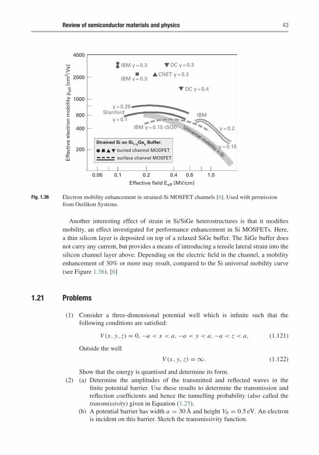
Review of semiconductor materials and physics 43
4000
2000
1000
IBM y = 0.3
IBM y = 0.3
IBM y = 0.15 (SOI)
IBM
DC y = 0.4
y = 0.2
y = 0.15
CNET y = 0.3
DC y = 0.3
Stanfordy = 0.29
y = 0.1600
400
Strained Si on Si1–yGey Buffer:
buried channel MODFET
surface channel MOSFET
200
0.06 0.1 0.2
Effective field Eeff [MV/cm]
0.4 0.6 1.0
Eff
ecti
ve e
lect
ron
mo
bili
ty μ
eff [
cm2 /
Vs]
Universal mobility n-Si
Fig. 1.36 Electron mobility enhancement in strained-Si MOSFET channels [6]. Used with permissionfrom Oerlikon Systems.
Another interesting effect of strain in Si/SiGe heterostructures is that it modifiesmobility, an effect investigated for performance enhancement in Si MOSFETs. Here,a thin silicon layer is deposited on top of a relaxed SiGe buffer. The SiGe buffer doesnot carry any current, but provides a means of introducing a tensile lateral strain into thesilicon channel layer above. Depending on the electric field in the channel, a mobilityenhancement of 30% or more may result, compared to the Si universal mobility curve(see Figure 1.36). [6]
1.21 Problems
(1) Consider a three-dimensional potential well which is infinite such that thefollowing conditions are satisfied:
V (x, y, z) = 0,−a < x < a,−a < y < a,−a < z < a, (1.121)
Outside the well
V (x, y, z) = ∞. (1.122)
Show that the energy is quantised and determine its form.(2) (a) Determine the amplitudes of the transmitted and reflected waves in the
finite potential barrier. Use these results to determine the transmission andreflection coefficients and hence the tunnelling probability (also called thetransmissivity) given in Equation (1.25).
(b) A potential barrier has width a = 30 A and height V0 = 0.5 eV. An electronis incident on this barrier. Sketch the transmissivity function.
44 High-Speed Electronics and Optoelectronics
(c) The barrier width is reduced to 5 A. Sketch the transmissivity function.Comment on the difference as the barrier width is reduced.
(3) For the Kronig–Penney model, obtain the solution of the transcendental equationand show the allowed energy bands (MATLAB is useful in this problem).
(4) A sample of GaAs is doped with a background concentration of NA = 3 ×1015 cm−3 acceptors. Then, 1019 cm−3 donors are added. Find the room tem-perature concentrations of electrons and holes in the original material and thematerial that results after the addition of the donors. Draw the band diagram foreach of the materials.
(5) A silicon ingot is doped with 1017 cm−3 arsenic atoms. Find the carrier concen-trations and the Fermi level at 300◦ K. Assume complete ionisation of impurityatoms. Draw the band diagram. Show the Fermi level and use the intrinsic Fermilevel as the energy reference. Repeat for a temperature of 77◦ K.
(6) (a) The energy band gap for GaAs at 300 K is 1.42 eV. Assume that the Fermienergy level is at mid-band. Calculate the probability that an energy state atE = Ec + kT/2 is occupied by an electron.
(b) What is the probability that the energy state at E = Ev − kT/2 is empty?(c) Using the density of states function g(E), determine the volume density of
states between 0 and 2 eV. (Integrate g(e)d E .)
(7) A sample of InP is doped with 5 × 10¹⁶ tellurium atoms/cm3 and 2 × 1015 cm−3
zinc atoms. Calculate the electron and hole concentrations.
(8) A sample of GaAs is illuminated with light of intensity 1.5 mW cm−2 at a wave-length of λ = 470 nm. The area of the illuminated surface is 15 mm2. If the carrierlifetimes are 10 ns, how many photons are incident on the surface of the GaAssample? If there is uniform absorption of the photons within 1 μm of the samplesurface, determine the equilibrium concentrations of electrons and holes in thedark and the excess carrier concentrations when the sample is illuminated.
(9) (a) An n+–p diode has a long p region. The current I is measured at a con-stant forward bias of 500 mV. Derive an expression for the fractional changein current �I/I resulting from a temperature change of �T . Evaluate thisexpression at T = 300 K. Assume that the diode current is dominated byrecombination of electrons in the neutral p region and consider the temper-ature dependence to be due solely to the factors that have an exponentialdependence on temperature.
(b) Suppose that part of the diode current results from recombination in thedepletion region. How will this affect the sensitivity of the temperaturemeasurement?
(10) A Silicon p–n junction has 5×1017 cm−3 donor atoms and 4×1019 cm−3 acceptoratoms. The junction area is 150 μm2. Determine the junction capacitance giventhat the reverse bias is 5 V. How does this change for the same forward bias?
(11) It is found experimentally that a Schottky barrier is formed when Al is evaporatedon n-type GaAs with a donor concentration of 4 × 1015 cm−3. Al has a workfunction of 4.36 V and GaAs has an electron affinity of 4.07 V.
(a) Determine the built-in voltage Vbi, the depletion layer width W and thecapacitance at zero bias, assuming no surface states.
Review of semiconductor materials and physics 45
(b) If the Fermi level at the surface is pinned so that
qφ0 = 1
3Eg
qφB = (Eg − qφ0),
determine the same quantities as in part (a) with a reverse bias of 1 V.(12) An n+-GaAs/p-AlGaAs heterojunction is formed with ND = 1019 cm−3 and
NA = 5 × 1017 cm−3. Draw the band diagram and determine the followingquantities:(a) The electric field E(x) and the potential difference V (x) at the junction.(b) The built-in potentials on either side of the junction and the total built-in
potential, Vbi.(c) The depletion widths in the two regions.(d) If a forward bias of 3 V is applied, calculate the depletion widths.(e) Calculate the capacitance of this diode.(f) Calculate the current in the diode.
References
[1] Agrawal G. P., Dutta N. K. (1993). Semiconductor Lasers, Van Nostrand Reinhold.[2] Anderson B. L., Anderson R. L. (2005). Fundamentals of Semiconductor Devices. McGraw-
Hill.[3] Bhattacharya P. (1997). Semiconductor Optoelectronic Devices, 2nd edn. Prentice Hall.[4] Casey H. C., Panish M. B. (1978). Heterostructure Lasers Part A: Fundamental Principles.
Quantum electronics – principles and applications, Academic Press.[5] Gruhle A. (1994). SiGe Heterojunction Bipolar Transistors of Silicon-based Millimeter
Wave Devices. Springer Verlag, 149–189.[6] Hackbarth T., Zeuner M., Konig U. (2002). The future of SiGe beyond HBT applications.
Uniaxis chip Magazine, July 10–12.[7] Kroemer H. (1982). Heterostructure bipolar transistors and integrated circuits. Proceedings
of the IEEE 70. 1 (January), 13–25.[8] Neaman D. A. (2003). Semiconductor Physics and Devices: Basic Principles. McGraw-Hill.[9] People R., Bean J. C. (1985). Calculation of critical layer thickness versus lattice mismatch
for Gex Si1−x /Si strained-layer heterostructures. Appl. Phys. Lett. 47, 322–324.[10] Pierret R. F. (2003). Advanced Semiconductor Fundamentals. Modular Series on Solid State
Devices, Vol. VI. Prentice Hall.[11] Round H. J. (1907). A note on Carborundum. Elect.World 49, 10, 309.[12] Schaffler F. (1995). Properties of Strained and Relaxed Silicon Germanium of EMIS Data
Reviews. 12. IEE INSPEC, 10–12.[13] Schaffler F. (1997). High mobility Si and Ge structures. Semicond. Sci. Technol. 12, 10,
1515–1549.[14] Singh J. (1994). Semiconductor Devices – An Introduction. McGraw-Hill.[15] Streetman B., Banerjee S. (2000). Solid State Elecronic Devices, 5th edn. Prentice Hall.
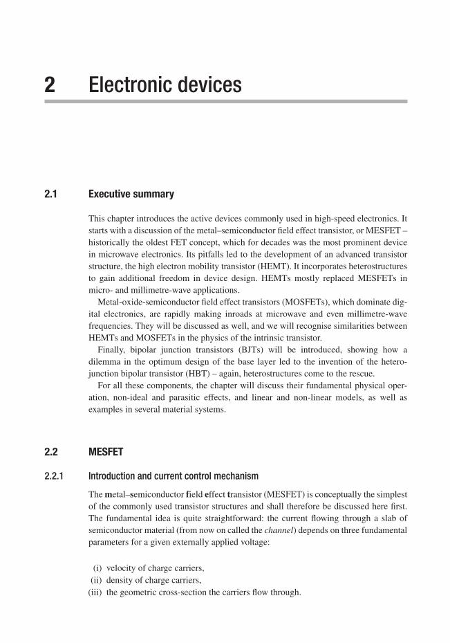
2 Electronic devices
2.1 Executive summary
This chapter introduces the active devices commonly used in high-speed electronics. Itstarts with a discussion of the metal–semiconductor field effect transistor, or MESFET –historically the oldest FET concept, which for decades was the most prominent devicein microwave electronics. Its pitfalls led to the development of an advanced transistorstructure, the high electron mobility transistor (HEMT). It incorporates heterostructuresto gain additional freedom in device design. HEMTs mostly replaced MESFETs inmicro- and millimetre-wave applications.
Metal-oxide-semiconductor field effect transistors (MOSFETs), which dominate dig-ital electronics, are rapidly making inroads at microwave and even millimetre-wavefrequencies. They will be discussed as well, and we will recognise similarities betweenHEMTs and MOSFETs in the physics of the intrinsic transistor.
Finally, bipolar junction transistors (BJTs) will be introduced, showing how adilemma in the optimum design of the base layer led to the invention of the hetero-junction bipolar transistor (HBT) – again, heterostructures come to the rescue.
For all these components, the chapter will discuss their fundamental physical oper-ation, non-ideal and parasitic effects, and linear and non-linear models, as well asexamples in several material systems.
2.2 MESFET
2.2.1 Introduction and current control mechanism
The metal–semiconductor field effect transistor (MESFET) is conceptually the simplestof the commonly used transistor structures and shall therefore be discussed here first.The fundamental idea is quite straightforward: the current flowing through a slab ofsemiconductor material (from now on called the channel) depends on three fundamentalparameters for a given externally applied voltage:
(i) velocity of charge carriers,(ii) density of charge carriers,
(iii) the geometric cross-section the carriers flow through.
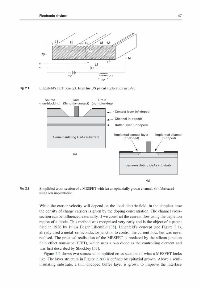
Electronic devices 47
17
15
11+
+
15 15 13 15 12
1610
18
14
2221
Fig. 2.1 Lilienfeld’s FET concept, from his US patent application in 1926.
Semi-insulating GaAs substrate
Semi-insulating GaAs substrate
Implanted channel(n-doped)
Implanted contact layer(n+-doped)
Contact layer (n+-doped)
Channel (n-doped)
Buffer layer (undoped)
Drain(non-blocking)
Gate(Schottky contact)
Source(non-blocking)
(a)
(b)
Fig. 2.2 Simplified cross-section of a MESFET with (a) an epitaxially grown channel, (b) fabricatedusing ion implantation.
While the carrier velocity will depend on the local electric field, in the simplest casethe density of charge carriers is given by the doping concentration. The channel cross-section can be influenced externally, if we constrict the current flow using the depletionregion of a diode. This method was recognised very early and is the object of a patentfiled in 1926 by Julius Edgar Lilienfeld [35]. Lilienfeld’s concept (see Figure 2.1),already used a metal–semiconductor junction to control the current flow, but was neverrealised. The practical realisation of the MESFET is predated by the silicon junctionfield effect transistor (JFET), which uses a p–n diode as the controlling element andwas first described by Shockley [57].
Figure 2.2 shows two somewhat simplified cross-sections of what a MESFET lookslike. The layer structure in Figure 2.2(a) is defined by epitaxial growth. Above a semi-insulating substrate, a thin undoped buffer layer is grown to improve the interface
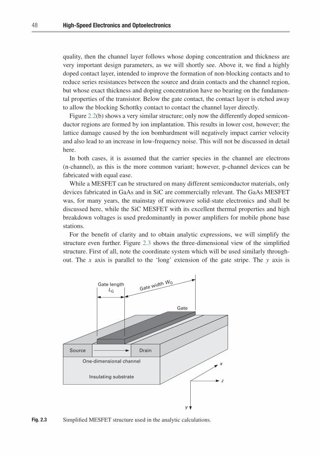
48 High-Speed Electronics and Optoelectronics
quality, then the channel layer follows whose doping concentration and thickness arevery important design parameters, as we will shortly see. Above it, we find a highlydoped contact layer, intended to improve the formation of non-blocking contacts and toreduce series resistances between the source and drain contacts and the channel region,but whose exact thickness and doping concentration have no bearing on the fundamen-tal properties of the transistor. Below the gate contact, the contact layer is etched awayto allow the blocking Schottky contact to contact the channel layer directly.
Figure 2.2(b) shows a very similar structure; only now the differently doped semicon-ductor regions are formed by ion implantation. This results in lower cost, however; thelattice damage caused by the ion bombardment will negatively impact carrier velocityand also lead to an increase in low-frequency noise. This will not be discussed in detailhere.
In both cases, it is assumed that the carrier species in the channel are electrons(n-channel), as this is the more common variant; however, p-channel devices can befabricated with equal ease.
While a MESFET can be structured on many different semiconductor materials, onlydevices fabricated in GaAs and in SiC are commercially relevant. The GaAs MESFETwas, for many years, the mainstay of microwave solid-state electronics and shall bediscussed here, while the SiC MESFET with its excellent thermal properties and highbreakdown voltages is used predominantly in power amplifiers for mobile phone basestations.
For the benefit of clarity and to obtain analytic expressions, we will simplify thestructure even further. Figure 2.3 shows the three-dimensional view of the simplifiedstructure. First of all, note the coordinate system which will be used similarly through-out. The x axis is parallel to the ‘long’ extension of the gate stripe. The y axis is
Drain
x
z
y
Source
One-dimensional channel
Insulating substrate
Gate lengthLG
Gate
Gate width WG
Fig. 2.3 Simplified MESFET structure used in the analytic calculations.
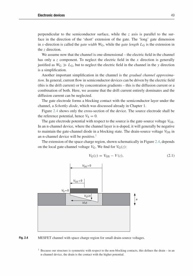
Electronic devices 49
perpendicular to the semiconductor surface, while the z axis is parallel to the sur-face in the direction of the ‘short’ extension of the gate. The ‘long’ gate dimensionin x-direction is called the gate width WG, while the gate length LG is the extension inthe z direction.
We assume now that the channel is one-dimensional – the electric field in the channelhas only a z component. To neglect the electric field in the x direction is generallyjustified as WG � LG, but to neglect the electric field in the channel in the y directionis a simplification.
Another important simplification in the channel is the gradual channel approxima-tion. In general, current flow in semiconductor devices can be driven by the electric field(this is the drift current) or by concentration gradients – this is the diffusion current or acombination of both. Here, we assume that the drift current entirely dominates and thediffusion current can be neglected.
The gate electrode forms a blocking contact with the semiconductor layer under thechannel, a Schottky diode, which was discussed already in Chapter 1.
Figure 2.4 shows only the cross-section of the device. The source electrode shall bethe reference potential, hence VS = 0.
The gate electrode potential with respect to the source is the gate-source voltage VGS.In an n-channel device, where the channel layer is n-doped, it will generally be negativeto maintain the gate-channel diode in a blocking state. The drain-source voltage VDS inan n-channel device will be positive.1
The extension of the space charge region, shown schematically in Figure 2.4, dependson the local gate-channel voltage VG. We find for VG(z):
VG(z) = VGS − V (z), (2.1)
VDS > 0
VGS < 0
VS = 0
VG(z)
V(z)a
Fig. 2.4 MESFET channel with space charge region for small drain-source voltages.
1 Because our structure is symmetric with respect to the non-blocking contacts, this defines the drain – in ann-channel device, the drain is the contact with the higher potential.
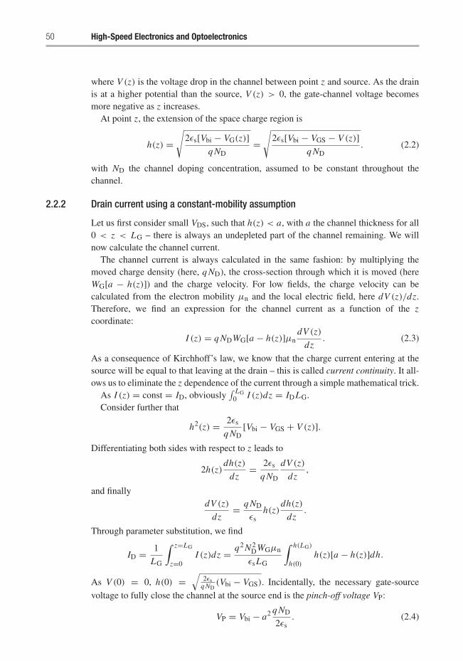
50 High-Speed Electronics and Optoelectronics
where V (z) is the voltage drop in the channel between point z and source. As the drainis at a higher potential than the source, V (z) > 0, the gate-channel voltage becomesmore negative as z increases.
At point z, the extension of the space charge region is
h(z) =√
2εs[Vbi − VG(z)]q ND
=√
2εs[Vbi − VGS − V (z)]q ND
. (2.2)
with ND the channel doping concentration, assumed to be constant throughout thechannel.
2.2.2 Drain current using a constant-mobility assumption
Let us first consider small VDS, such that h(z) < a, with a the channel thickness for all0 < z < LG – there is always an undepleted part of the channel remaining. We willnow calculate the channel current.
The channel current is always calculated in the same fashion: by multiplying themoved charge density (here, q ND), the cross-section through which it is moved (hereWG[a − h(z)]) and the charge velocity. For low fields, the charge velocity can becalculated from the electron mobility μn and the local electric field, here dV (z)/dz.Therefore, we find an expression for the channel current as a function of the zcoordinate:
I (z) = q NDWG[a − h(z)]μndV (z)
dz. (2.3)
As a consequence of Kirchhoff’s law, we know that the charge current entering at thesource will be equal to that leaving at the drain – this is called current continuity. It all-ows us to eliminate the z dependence of the current through a simple mathematical trick.
As I (z) = const = ID, obviously∫ LG
0 I (z)dz = IDLG.Consider further that
h2(z) = 2εs
q ND[Vbi − VGS + V (z)].
Differentiating both sides with respect to z leads to
2h(z)dh(z)
dz= 2εs
q ND
dV (z)
dz,
and finallydV (z)
dz= q ND
εsh(z)
dh(z)
dz.
Through parameter substitution, we find
ID = 1
LG
∫ z=LG
z=0I (z)dz = q2 N 2
DWGμn
εsLG
∫ h(LG)
h(0)h(z)[a − h(z)]dh.
As V (0) = 0, h(0) =√
2εsq ND
(Vbi − VGS). Incidentally, the necessary gate-source
voltage to fully close the channel at the source end is the pinch-off voltage VP:
VP = Vbi − a2 q ND
2εs. (2.4)
Electronic devices 51
Using VP, we can write Equation (2.2) in the following form:
h(z) = a
√V (z) − VGS − Vbi
Vbi − VP. (2.5)
The required value h(LG) is now found very easily – we know that V (z = LG) = VDS
and therefore
h(z = LG) = a
√VDS − VGS − Vbi
Vbi − VP. (2.6)
We can now finally solve the current integral using the constant-mobility assumption,and find for the drain current:
ID(VGS, VDS) = q2 N 2Dμna3WG
6εsLG(2.7){
3VDS
Vbi − VP− 2
(VDS − VGS + Vbi)3/2 − (Vbi − VGS)
3/2
(Vbi − VP)3/2
}.
We had so far assumed that the channel would remain at least partially open. Thisrequires that h(LG) ≤ a. From Equation (2.6) we find that this translates into
VDS ≤ VGS − VP ≡ Vk, (2.8)
where Vk is the knee voltage.For
• VDS ≤ Vk the MESFET is in the linear regime, while for• VDS > Vk it is in the saturated regime.
Figure 2.5 shows simulated output current–voltage characteristics for a hypotheti-cal MESFET with a pinch-off voltage VP = −2 V and a built-in voltage of Vbi =0.7 V, calculated using Equation (2.7). The drain current has been normalised toq2 N 2
Dμna3/(6εsLG).Note that for very small VDS, the dependence of ID on VDS is almost linear. MES-
FETs can be used as electronically controllable resistors, e.g. in variable microwaveattenuators or in transmit/receive switches.
For VDS → Vk, the drain current saturates. A common assumption in simple FETmodels is that for VDS > Vk, ID(VDS > Vk) = ID(VDS = Vk) = const.
Conceptually, current continuity in the constant-mobility model requires that forincreasing z, the electric field increases to compensate for the decrease in undepletedchannel height. Near VDS = Vk, a − h(z) → 0 would imply dV (z)/dz → ∞ at thedrain end, which is a fundamental flaw of this model. It is still valuable to investigateMESFET behaviour at low VDS.
2.2.3 Constant-velocity approximation
In all semiconductor materials, the assumption that the carrier velocity increases linearlywith increasing electric field, i.e. that mobility is a constant, only holds for small electricfields. For large electric fields, the carrier velocity becomes independent of the electric
52 High-Speed Electronics and Optoelectronics
1.0 1.5Drain-source voltage VDS/Vk
0.5
0.4
0.3
0.2
0.1
01.5
VGS = –1.5 V
VGS = –1.0 V
VGS = –0.5 V
VGS = 0 V
0.0
No
rmal
ised
dra
in c
urr
ent
I d
Fig. 2.5 Simulated output I –V characteristics of a MESFET using the constant-mobility assumption(VP = −2 V, Vbi = 0.7 V).
field (in good approximation); its value is then called the drift saturation velocity, vsat,n
for electrons or vsat,p for holes, respectively.Let us now boldly assume that the charge carriers in the channel reach their drift
saturation velocity immediately after entering the channel at the source side.The channel current in our n-channel MESFET now becomes
I (z) = q NDvsat,nWG[a − h(z)] = const = ID,
due to the current continuity requirement. As the carrier velocity is now constant, thisimplies that the channel height must also be constant: h(z) = const = h. Hence,
ID = q NDvsat,nWG(a − h). (2.9)
The extension of the space charge region can be easily calculated at z = 0 for ahomogeneous channel doping profile:
h = h(0) = a
√Vbi − VGS
Vbi − VP. (2.10)
Inserting this into Equation (2.9), we find
ID = q NDvsat,nWGa
(1 −
√Vbi − VGS
Vbi − VP
). (2.11)
The value for VGS = 0 is referred to as IDSS:
IDSS = q NDvsat,nWGa
(1 −
√1
1 − VPVbi
). (2.12)
The constant-velocity model is a priori only valid for high electric fields in thechannel, in the saturation region of MESFET operation (VDS > Vk). For very small
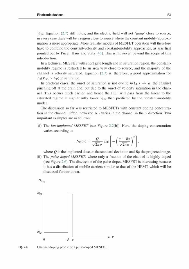
Electronic devices 53
VDS, Equation (2.7) still holds, and the electric field will not ‘jump’ close to source,in every case there will be a region close to source where the constant mobility approxi-mation is more appropriate. More realistic models of MESFET operation will thereforehave to combine the constant-velocity and constant-mobility approaches, as was firstpointed out by Pucel, Haus and Statz [46]. This is, however, beyond the scope of thisintroduction.
In a technical MESFET with short gate length and in saturation region, the constant-mobility regime is restricted to an area very close to source, and the majority of thechannel is velocity saturated. Equation (2.7) is, therefore, a good approximation forID(VGS > VP) in saturation.
In practical cases, the onset of saturation is not due to h(LG) → a, the channelpinching off at the drain end, but due to the onset of velocity saturation in the chan-nel. This occurs much earlier, and hence the FET will pass from the linear to thesaturated regime at significantly lower VDS than predicted by the constant-mobilitymodel.
The discussion so far was restricted to MESFETs with constant doping concentra-tion in the channel. Often, however, ND varies in the channel in the y direction. Twoimportant examples are as follows:
(i) The ion-implanted MESFET (see Figure 2.2(b)). Here, the doping concentrationvaries according to
ND(y) = Q√2πσ
exp
[−
(y − RP√
2πσ
)2],
where Q is the implanted dose, σ the standard deviation and RP the projected range.(ii) The pulse-doped MESFET, where only a fraction of the channel is highly doped
(see Figure 2.6). The discussion of the pulse-doped MESFET is interesting becauseit has a distribution of mobile carriers similar to that of the HEMT which will bediscussed further down.
ND
y
ND2
ND1
d a0
Fig. 2.6 Channel doping profile of a pulse-doped MESFET.
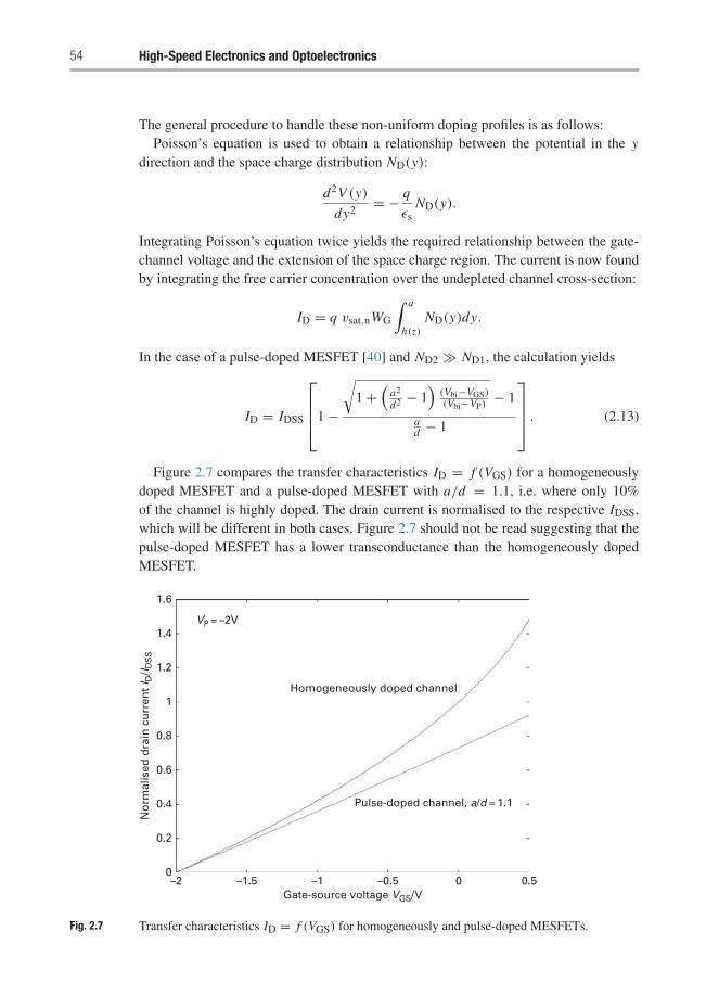
54 High-Speed Electronics and Optoelectronics
The general procedure to handle these non-uniform doping profiles is as follows:Poisson’s equation is used to obtain a relationship between the potential in the y
direction and the space charge distribution ND(y):
d2V (y)
dy2= − q
εsND(y).
Integrating Poisson’s equation twice yields the required relationship between the gate-channel voltage and the extension of the space charge region. The current is now foundby integrating the free carrier concentration over the undepleted channel cross-section:
ID = q vsat,nWG
∫ a
h(z)ND(y)dy.
In the case of a pulse-doped MESFET [40] and ND2 � ND1, the calculation yields
ID = IDSS
⎡⎢⎢⎣1 −
√1 +
(a2
d2 − 1)
(Vbi−VGS)(Vbi−VP)
− 1
ad − 1
⎤⎥⎥⎦ . (2.13)
Figure 2.7 compares the transfer characteristics ID = f (VGS) for a homogeneouslydoped MESFET and a pulse-doped MESFET with a/d = 1.1, i.e. where only 10%of the channel is highly doped. The drain current is normalised to the respective IDSS,which will be different in both cases. Figure 2.7 should not be read suggesting that thepulse-doped MESFET has a lower transconductance than the homogeneously dopedMESFET.
Fig. 2.7 Transfer characteristics ID = f (VGS) for homogeneously and pulse-doped MESFETs.
Gate-source voltage VGS/V
VP = –2V
–2 –1.5 –1 –0.5 0 0.5
Pulse-doped channel, a/d = 1.1
Homogeneously doped channel
0
0.2
0.4
0.6
0.8
1
1.2
1.4
1.6
No
rmal
ised
dra
in c
urr
ent
I D/I
DS
S
Electronic devices 55
A striking difference is that ID = f (VGS) is very linear for the pulse-doped MESFET,which is an important advantage from the circuit designer’s point of view.
All of the above models consider the drain current in the saturation regime to beindependent of the drain-source voltage. In reality, however, ID depends weakly on VDS
there.The predominant reason for the ID = f (VDS) behaviour in the saturated regime is
the scattering of charge carriers into the buffer/substrate layer under the channel. For asemi-insulating substrate, where the Fermi level is near mid-gap, the potential barrierbetween the channel and the substrate is approximately EG/2 and may be overcomeby electrons with sufficient kinetic energy. These electrons may produce two differenteffects, both of which lead to an ID = f (VDS) dependence:
(i) They may lead to a parasitic conduction current through the buffer or the substrate,adding to the channel current.
(ii) They may be captured by crystal faults or impurities in the buffer or the substrate,which act as charge traps. The resulting modification of charge below the channelinfluences the channel cross-section, just as a gate electrode would (‘backgating’).
The latter effect leads to a pronounced frequency dependence of the ID = f (VDS)
behaviour.
2.2.4 Large-signal CAD model
For circuit design applications, the physical models considered so far are not conve-nient. For once, it would be useful to have a model which describes the full range ofoperation in one closed formula. More importantly, the physical design parameters suchas channel thickness and doping concentration are often not accessible to the circuitdesigner.
Large-signal CAD models, therefore, are empirical in nature and have extractableparameters which can be determined from measurements on the final device.
An early empirical model which may be used for MESFETs in the saturation regimeis the ‘square-law’ JFET model implemented in SPICE:
ID(VGS) = β(VGS − VP)2, (2.14)
where
β = IDSS
V 2P
.
It fits the transfer characteristics of the constant-mobility model quite well at VDS = Vk.The model can be made to fit to non-parabolic transfer characteristics through a
modification introduced by Statz et al. [58]:
56 High-Speed Electronics and Optoelectronics
ID(VGS) = β(VGS − VP)2
1 + α(VGS − VP). (2.15)
The linear region can be elegantly included in a closed form through the use of ahyperbolic tangent function, as was first pointed out by Curtice [10]:
ID(VGS, VDS) = IS(VGS) tanh (γ VDS), (2.16)
where IS(VGS) is the drain current according to Equation (2.15).The dependence of the drain current on the drain-source voltage in the saturation
regime can be introduced through an additional 1 + λVDS term. We arrive finally at thecommon CAD model expression for the MESFET:
ID(VGS, VDS) = β(VGS − VP)2
1 + α(VGS − VP)tanh (γ VDS)(1 + λVDS). (2.17)
Capacitance modelWe will now leave the quasi-static realm and introduce capacitances. The discussionwill be restricted first to the intrinsic FET structure, while parasitic capacitances will beintroduced in context with the small-signal equivalent circuit.
Assume a MESFET with a homogeneously doped channel region with VDS = 0,which implies a constant extension of the gate space charge region, h. The charge onthe gate electrode counter-balances the charge in the channel. In this case (n-channel)the gate charge is positive:
QG0 = q NDWGLG(a − h) = −q NDWGLGa
(1 −
√Vbi − VGS
Vbi − VP
), (2.18)
using Equation (2.5) and V (z) = 0 due to VDS = 0.The gate-channel capacitance for VDS = 0 can now be calculated as the first deriva-
tive of the gate charge with respect to the gate-channel voltage (which is identical toVGS as VDS = 0):
CGC = δQG0
δVGS= C0
√Vbi − VP
Vbi − VGS, (2.19)
where
C0 = qNDWGLGa
2(Vbi − VP).
For VDS > 0, the Meyer capacitance approach originally developed for MOSFETs [38]is often used, which distinguishes between the linear (VDS < Vk) and the saturated(VDS > Vk) regimes:
• For VDS < Vk,
CGS = 2
3CGC
[1 −
(Vk − VDS
2Vk − VDS
)2]
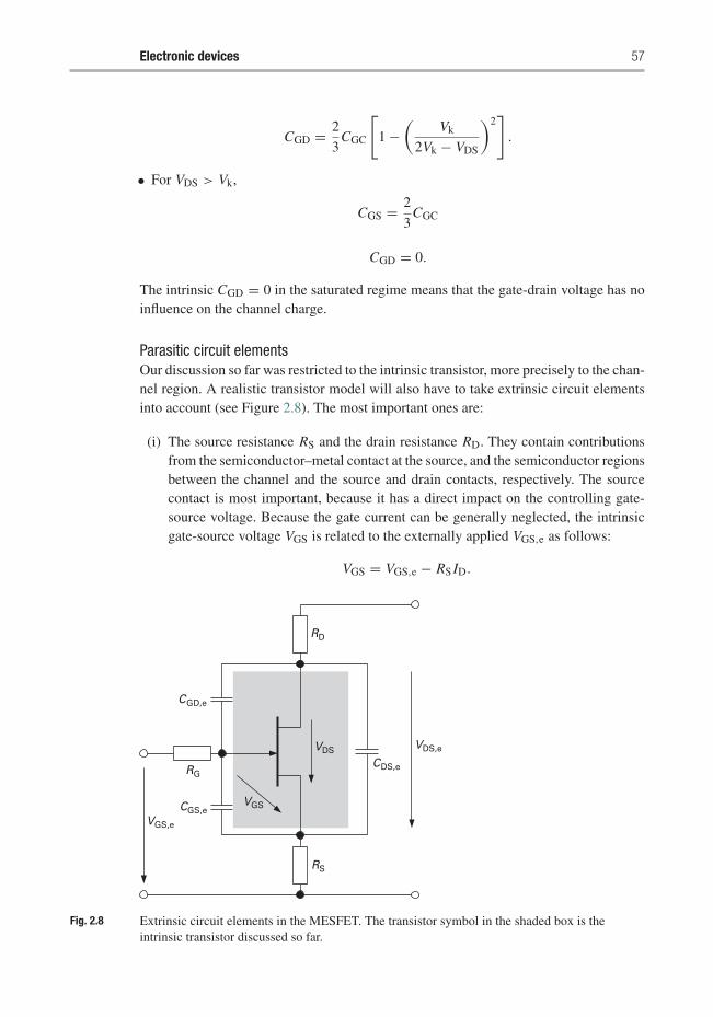
Electronic devices 57
CGD = 2
3CGC
[1 −
(Vk
2Vk − VDS
)2].
• For VDS > Vk,
CGS = 2
3CGC
CGD = 0.
The intrinsic CGD = 0 in the saturated regime means that the gate-drain voltage has noinfluence on the channel charge.
Parasitic circuit elementsOur discussion so far was restricted to the intrinsic transistor, more precisely to the chan-nel region. A realistic transistor model will also have to take extrinsic circuit elementsinto account (see Figure 2.8). The most important ones are:
(i) The source resistance RS and the drain resistance RD. They contain contributionsfrom the semiconductor–metal contact at the source, and the semiconductor regionsbetween the channel and the source and drain contacts, respectively. The sourcecontact is most important, because it has a direct impact on the controlling gate-source voltage. Because the gate current can be generally neglected, the intrinsicgate-source voltage VGS is related to the externally applied VGS,e as follows:
VGS = VGS,e − RS ID.
VDS,eVDS
RD
RS
VGS
VGS,e
RG
CGS,e
CDS,e
CGD,e
Fig. 2.8 Extrinsic circuit elements in the MESFET. The transistor symbol in the shaded box is theintrinsic transistor discussed so far.
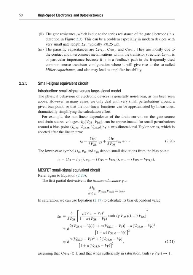
58 High-Speed Electronics and Optoelectronics
(ii) The gate resistance, which is due to the series resistance of the gate electrode (in xdirection in Figure 2.3). This can be a problem especially in modern devices withvery small gate length LG, typically ≤0.25 μm.
(iii) The parasitic capacitances are CGS,e, CGD,e and CDS,e. They are mostly due tothe contact and interconnect metallisations within the transistor structure. CGD,e isof particular importance because it is in a feedback path in the frequently usedcommon-source transistor configuration where it will give rise to the so-calledMiller capacitance, and also may lead to amplifier instability.
2.2.5 Small-signal equivalent circuit
Introduction: small-signal versus large-signal modelThe physical behaviour of electronic devices is generally non-linear, as has been seenabove. However, in many cases, we only deal with very small perturbations around agiven bias point, so that the non-linear functions can be approximated by linear ones,dramatically simplifying the calculation effort.
For example, the non-linear dependence of the drain current on the gate-sourceand drain-source voltages, ID(VGS, VDS), can be approximated for small perturbationsaround a bias point (ID,0, VGS,0, VDS,0) by a two-dimensional Taylor series, which isaborted after the linear term:
id = δ ID
δVGSvgs + δ ID
δVDSvds + · · · . (2.20)
The lower-case symbols id, vgs and vds denote small deviations from the bias point:
id = (ID − ID,0); vgs = (VGS − VGS,0); vds = (VDS − VDS,0).
MESFET small-signal equivalent circuitRefer again to Equation (2.20).
The first partial derivative is the transconductance gm:
δ ID
δVGS|VGS,0,VDS,0 ≡ gm.
In saturation, we can use Equation (2.17) to calculate its bias-dependent value:
gm = δ
δVGS
[β(VGS − VP)
2
1 + α(VGS − VP)tanh (γ VDS)(1 + λVDS)
]
≈ β2(VGS,0 − VP)[1 + α(VGS,0 − VP)] − α(VGS,0 − VP)
2[1 + α(VGS,0 − VP)
]2
= βα(VGS,0 − VP)
2 + 2(VGS,0 − VP)[1 + α(VGS,0 − VP)
]2, (2.21)
assuming that λVDS � 1, and that when sufficiently in saturation, tanh (γ VDS) → 1.
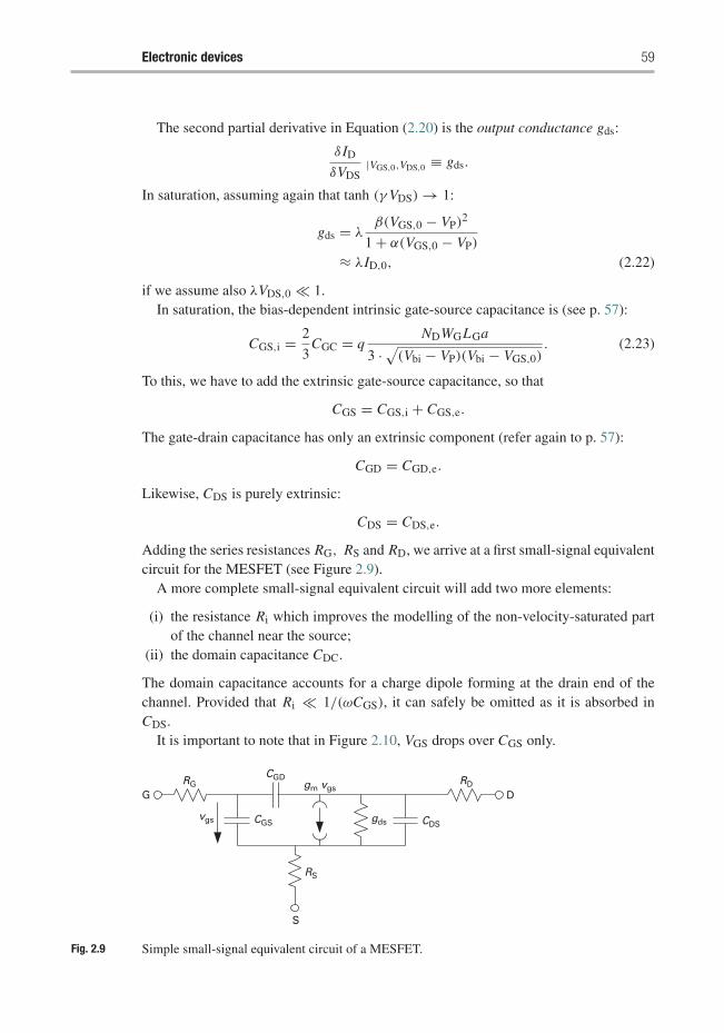
Electronic devices 59
The second partial derivative in Equation (2.20) is the output conductance gds:
δ ID
δVDS|VGS,0,VDS,0 ≡ gds.
In saturation, assuming again that tanh (γ VDS) → 1:
gds = λβ(VGS,0 − VP)
2
1 + α(VGS,0 − VP)
≈ λID,0, (2.22)
if we assume also λVDS,0 � 1.In saturation, the bias-dependent intrinsic gate-source capacitance is (see p. 57):
CGS,i = 2
3CGC = q
NDWGLGa
3 · √(Vbi − VP)(Vbi − VGS,0)
. (2.23)
To this, we have to add the extrinsic gate-source capacitance, so that
CGS = CGS,i + CGS,e.
The gate-drain capacitance has only an extrinsic component (refer again to p. 57):
CGD = CGD,e.
Likewise, CDS is purely extrinsic:
CDS = CDS,e.
Adding the series resistances RG, RS and RD, we arrive at a first small-signal equivalentcircuit for the MESFET (see Figure 2.9).
A more complete small-signal equivalent circuit will add two more elements:
(i) the resistance Ri which improves the modelling of the non-velocity-saturated partof the channel near the source;
(ii) the domain capacitance CDC.
The domain capacitance accounts for a charge dipole forming at the drain end of thechannel. Provided that Ri � 1/(ωCGS), it can safely be omitted as it is absorbed inCDS.
It is important to note that in Figure 2.10, VGS drops over CGS only.
S
RS
RGCGD
CGS
gm vgs
gds CDS
RDD
vgs
G
Fig. 2.9 Simple small-signal equivalent circuit of a MESFET.
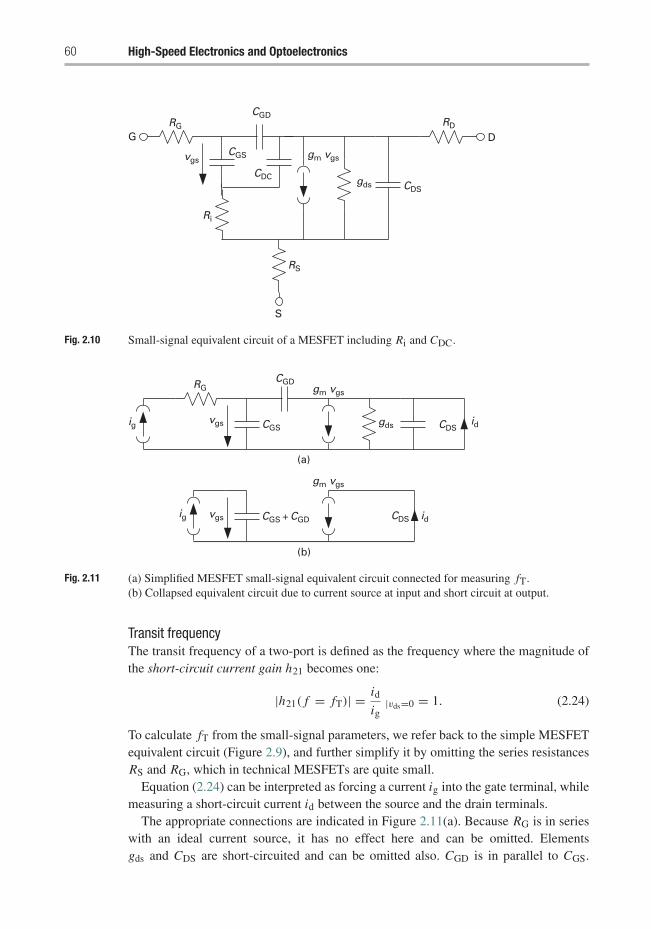
60 High-Speed Electronics and Optoelectronics
DRD
CDSgds
gm vgs
CGD
RS
S
CGS
CDC
vgs
Ri
RGG
Fig. 2.10 Small-signal equivalent circuit of a MESFET including Ri and CDC.
CGS + CGD
gm vgs
gm vgs
CGS
ig vgs
ig
(b)
(a)
vgs
RGCGD
CDS id
CDSgds id
Fig. 2.11 (a) Simplified MESFET small-signal equivalent circuit connected for measuring fT.(b) Collapsed equivalent circuit due to current source at input and short circuit at output.
Transit frequencyThe transit frequency of a two-port is defined as the frequency where the magnitude ofthe short-circuit current gain h21 becomes one:
|h21( f = fT)| = id
ig|vds=0 = 1. (2.24)
To calculate fT from the small-signal parameters, we refer back to the simple MESFETequivalent circuit (Figure 2.9), and further simplify it by omitting the series resistancesRS and RG, which in technical MESFETs are quite small.
Equation (2.24) can be interpreted as forcing a current ig into the gate terminal, whilemeasuring a short-circuit current id between the source and the drain terminals.
The appropriate connections are indicated in Figure 2.11(a). Because RG is in serieswith an ideal current source, it has no effect here and can be omitted. Elementsgds and CDS are short-circuited and can be omitted also. CGD is in parallel to CGS.
Electronic devices 61
Figure 2.11(b) shows the extremely simple equivalent circuit after taking these findingsinto consideration. The current transfer function is now:
id = gmvgs = iggm
jω(CGS + CGD),
which means that
h21(ω) = gm
jω(CGS + CGD).
The magnitude of h21 becomes unity at
ωT = gm
CGS + CGD,
or
fT = gm
2π(CGS + CGD). (2.25)
We will now relate the transit frequency to physical parameters. Let us go back to thesimple velocity-saturated MESFET model (Section 2.2.3). In the simple model, we donot use the Meyer capacitance approach, but attribute the full gate-channel capacitanceEquation (2.19) to the gate-source capacitance. Parasitic capacitances are neglected:
CGS = q NDWGLGa
2√(Vbi − VP)(Vbi − VGS)
.
For the transconductance, we derive Equation (2.11) with respect to VGS and find
gm = q NDvsatWGa
2√(Vbi − VP)(Vbi − VGS)
.
Therefore,
fT = gm
2πCGS= 1
2π
vsat
LG. (2.26)
The transit frequency can be directly deduced from the carrier transit time through thechannel.
Maximum frequency of oscillationThe maximum frequency of oscillation fmax is a measure of the power gain of a two-port (see Section 5.2.4). A common formulation [32] quoted in [36] for fmax from thesmall-signal parameters is
fmax = fT
2√(RG + Ri + RS)gds + 2π fT RGCGD
. (2.27)
The expression refers to the equivalent circuit in Figure 2.10, but neglecting CDC.Note the importance of the series resistances, which did not factor into the calculation
of fT at all. fmax is much more useful to benchmark FETs for power amplification atmicrowave frequencies.
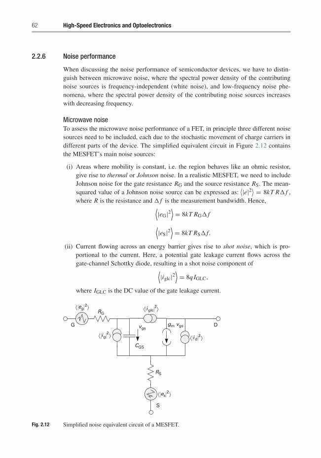
62 High-Speed Electronics and Optoelectronics
2.2.6 Noise performance
When discussing the noise performance of semiconductor devices, we have to distin-guish between microwave noise, where the spectral power density of the contributingnoise sources is frequency-independent (white noise), and low-frequency noise phe-nomena, where the spectral power density of the contributing noise sources increaseswith decreasing frequency.
Microwave noiseTo assess the microwave noise performance of a FET, in principle three different noisesources need to be included, each due to the stochastic movement of charge carriers indifferent parts of the device. The simplified equivalent circuit in Figure 2.12 containsthe MESFET’s main noise sources:
(i) Areas where mobility is constant, i.e. the region behaves like an ohmic resistor,give rise to thermal or Johnson noise. In a realistic MESFET, we need to includeJohnson noise for the gate resistance RG and the source resistance RS. The mean-squared value of a Johnson noise source can be expressed as:
⟨|e|2⟩ = 8kT R� f ,where R is the resistance and � f is the measurement bandwidth. Hence,⟨
|eG|2⟩= 8kT RG� f⟨
|eS|2⟩= 8kT RS� f.
(ii) Current flowing across an energy barrier gives rise to shot noise, which is pro-portional to the current. Here, a potential gate leakage current flows across thegate-channel Schottky diode, resulting in a shot noise component of⟨
|iglc|2⟩= 8q IGLC,
where IGLC is the DC value of the gate leakage current.
DG
RG
ig ⟩2
vgs
CGS
RS
S
gm vgs
es2
eg2
iglc2
id2⟨
⟩⟨ ⟩⟨
⟩⟨
⟩⟨
Fig. 2.12 Simplified noise equivalent circuit of a MESFET.
Electronic devices 63
(iii) In the channel, the carrier velocity experiences fluctuations due to phonon andimpurity scattering – this kind of noise is commonly called channel noise, firstpredicted by van der Ziel [62]. According to van der Ziel,⟨
|id|2⟩= 8kT gm P� f,
where P is a fitting parameter equal to 1. . . 3.2
Note that van der Ziel did not yet include velocity saturation effects. In fact, ana-lytic FET noise models are strictly valid only below the onset of saturation. How-ever, deviating behaviour in the saturated region and in the presence of velocitysaturation can be accommodated by a bias dependence in the parameter P [20].
(iv) Another effect must be taken into account. Due to the close proximity of the gateelectrode to the channel, any charge fluctuation in the channel will lead to a phasefluctuation with the opposite sign on the gate electrode. This effect is the inducedgate noise and was again pointed out by van der Ziel [63]:⟨
|ig|2⟩= 8kT� f (ωCGS)
2 R/gm,
where R is a fitting parameter, which accommodates different geometries and biaspoints.
Because of their linked physical origin,⟨|id|2
⟩and
⟨|ig|2⟩
are not statistically indepen-dent, but show a strong correlation. The correlation coefficient is imaginary (due to thecapacitive coupling) and strongly bias-dependent.
The gate leakage noise contribution⟨|iglc|2
⟩is commonly neglected, because the gate
diode is reverse biased. Using this assumption, Cappy [6] expressed the minimum noisefigure as
Fmin = 1 + 2
√P + R − 2C
√P R
f
fT(2.28)√
gm(RS + RG) + P R(1 − C2)
R + P − 2C√
R P,
where C is the magnitude of the correlation coefficient. For C = 1, Equation (2.28) isequivalent to the famous Fukui equation [21] for the minimum noise figure of FETs:
Fmin = 1 + kFf
fT
√gm(RG + RS), (2.29)
where kF is a fitting factor.Both Equations (2.28) and (2.29) calculate fT using the approximation in Equa-
tion (2.25).The noise equations contain an implicit bias dependence, which cannot be discussed
in detail. Delagebeaudeuf et al. [12] showed for the bias dependence of parameter P ,
P = ID
EcritLGgm, (2.30)
2 van der Ziel discusses this in terms of the channel conductance gd0, which is identical to the transconduc-tance gm at the very low VDS.
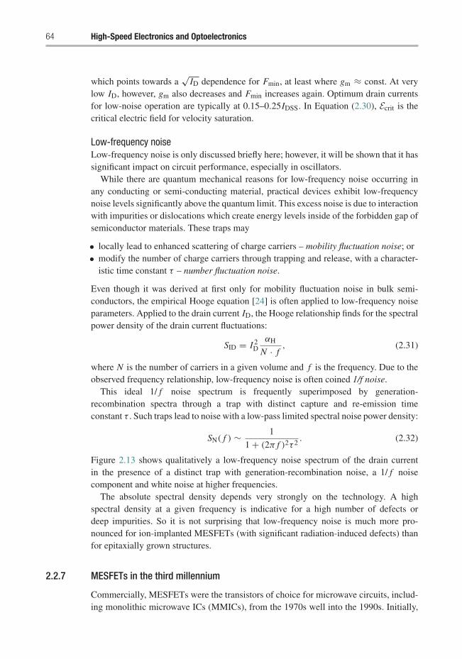
64 High-Speed Electronics and Optoelectronics
which points towards a√
ID dependence for Fmin, at least where gm ≈ const. At verylow ID, however, gm also decreases and Fmin increases again. Optimum drain currentsfor low-noise operation are typically at 0.15–0.25IDSS. In Equation (2.30), Ecrit is thecritical electric field for velocity saturation.
Low-frequency noiseLow-frequency noise is only discussed briefly here; however, it will be shown that it hassignificant impact on circuit performance, especially in oscillators.
While there are quantum mechanical reasons for low-frequency noise occurring inany conducting or semi-conducting material, practical devices exhibit low-frequencynoise levels significantly above the quantum limit. This excess noise is due to interactionwith impurities or dislocations which create energy levels inside of the forbidden gap ofsemiconductor materials. These traps may
• locally lead to enhanced scattering of charge carriers – mobility fluctuation noise; or• modify the number of charge carriers through trapping and release, with a character-
istic time constant τ – number fluctuation noise.
Even though it was derived at first only for mobility fluctuation noise in bulk semi-conductors, the empirical Hooge equation [24] is often applied to low-frequency noiseparameters. Applied to the drain current ID, the Hooge relationship finds for the spectralpower density of the drain current fluctuations:
SID = I 2D
αH
N · f, (2.31)
where N is the number of carriers in a given volume and f is the frequency. Due to theobserved frequency relationship, low-frequency noise is often coined 1/f noise.
This ideal 1/ f noise spectrum is frequently superimposed by generation-recombination spectra through a trap with distinct capture and re-emission timeconstant τ . Such traps lead to noise with a low-pass limited spectral noise power density:
SN( f ) ∼ 1
1 + (2π f )2τ 2. (2.32)
Figure 2.13 shows qualitatively a low-frequency noise spectrum of the drain currentin the presence of a distinct trap with generation-recombination noise, a 1/ f noisecomponent and white noise at higher frequencies.
The absolute spectral density depends very strongly on the technology. A highspectral density at a given frequency is indicative for a high number of defects ordeep impurities. So it is not surprising that low-frequency noise is much more pro-nounced for ion-implanted MESFETs (with significant radiation-induced defects) thanfor epitaxially grown structures.
2.2.7 MESFETs in the third millennium
Commercially, MESFETs were the transistors of choice for microwave circuits, includ-ing monolithic microwave ICs (MMICs), from the 1970s well into the 1990s. Initially,
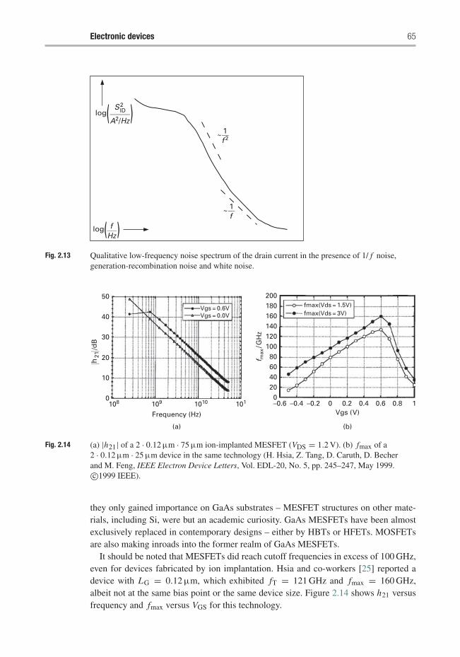
Electronic devices 65
logS2
ID
A2/Hz( )
log f
1~f 2
1~f
Hz( )Fig. 2.13 Qualitative low-frequency noise spectrum of the drain current in the presence of 1/ f noise,
generation-recombination noise and white noise.
50
40
30
20
10
0108 109
Frequency (Hz)
/dB
(a)
1011010
200180160140120100
80604020
0–0.6 –0.4 –0.2 0 0.2
Vgs (V)
f max
/ GH
z
(b)
0.4 0.6 0.8 1
Vgs = 0.6V fmax(Vds = 1.5V)fmax(Vds = 3V)Vgs = 0.0V
h21
Fig. 2.14 (a) |h21| of a 2 · 0.12 μm · 75 μm ion-implanted MESFET (VDS = 1.2 V). (b) fmax of a2 · 0.12 μm · 25 μm device in the same technology (H. Hsia, Z. Tang, D. Caruth, D. Becherand M. Feng, IEEE Electron Device Letters, Vol. EDL-20, No. 5, pp. 245–247, May 1999.c©1999 IEEE).
they only gained importance on GaAs substrates – MESFET structures on other mate-rials, including Si, were but an academic curiosity. GaAs MESFETs have been almostexclusively replaced in contemporary designs – either by HBTs or HFETs. MOSFETsare also making inroads into the former realm of GaAs MESFETs.
It should be noted that MESFETs did reach cutoff frequencies in excess of 100 GHz,even for devices fabricated by ion implantation. Hsia and co-workers [25] reported adevice with LG = 0.12 μm, which exhibited fT = 121 GHz and fmax = 160 GHz,albeit not at the same bias point or the same device size. Figure 2.14 shows h21 versusfrequency and fmax versus VGS for this technology.
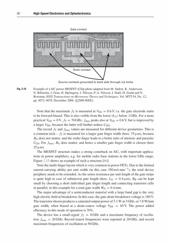
66 High-Speed Electronics and Optoelectronics
Gate contact
Drain contact
Source contacts grounded to back side through via holes
Fig. 2.15 Example of a SiC power MESFET (Chip photo adapted from M. Sudow, K. Andersson,N. Billstrom, J. Gran, H. Hjelmgren, J. Nilsson, P.-A. Nilsson, J. Stahl, H. Zirath and N.Rorsman, IEEE Transactions on Microwave Theory and Techniques, Vol. MTT-54, No. 12,pp. 4072–4078, December 2006. c©2006 IEEE).
Note that the maximum fT is measured at VGS = 0.6 V, i.e. the gate electrode startsto be forward-biased. This is also visible from the lower |h21| below 1 GHz. For a morepractical VGS = 0 V, fT = 70 GHz. fmax peaks also at VGS = 0.6 V, but is improved bya larger VDS, because the latter will further reduce CDG.
The record fT and fmax values are measured for different device geometries. This isa common trick – fT is measured for a larger gate finger width (here, 75 μm), becauseRG does not matter, and the wider finger leads to a better ratio of intrinsic and parasiticCGS. For fmax, RG does matter, and hence a smaller gate finger width is chosen (here25 μm).
The MESFET structure makes a strong comeback on SiC, with important applica-tions in power amplifiers, e.g. for mobile radio base stations in the lower GHz range.Figure 2.15 shows an example of such a structure [60].
Note the multi-finger layout which is very common in power FETs. Due to the limitedcurrent-carrying ability per unit width (in this case 350 mA mm−1), the total deviceperiphery needs to be extended. As the series resistance per unit length of the gate stripeis quite high in case of submicron gate length (here, LG = 0.4 μm), RB can be keptsmall by choosing a short individual gate finger length and connecting transistor cellsin parallel, in this example for a total gate width WG = 0.4 mm.
The major advantage of a semiconductor material with a large band gap is the veryhigh electric field at breakdown. In this case, the gate-drain breakdown voltage is 180 V.The transistor shown produces a saturated output power of 3.1 W at 3 GHz, or 7.8 W/mmgate width, when biased at a drain-source voltage VDS = 65 V. The power addedefficiency in this mode of operation is 70%.
The device has a small-signal fT = 8 GHz and a maximum frequency of oscilla-tion fmax = 20 GHz. Record transit frequencies were reported at 28 GHz, and recordmaximum frequencies of oscillation at 50 GHz.
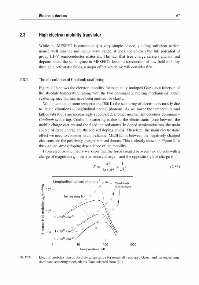
Electronic devices 67
2.3 High electron mobility transistor
While the MESFET is conceptually a very simple device, yielding sufficient perfor-mance well into the millimetre wave range, it does not unleash the full potential ofgroup III–V semiconductor materials. The fact that free charge carriers and ioniseddopants share the same space in MESFETs leads to a reduction of low-field mobilitythrough electrostatic fields, a major effect which we will consider first.
2.3.1 The importance of Coulomb scattering
Figure 2.16 shows the electron mobility for nominally undoped GaAs as a function ofthe absolute temperature, along with the two dominant scattering mechanisms. Otherscattering mechanisms have been omitted for clarity.
We notice that at room temperature (300 K) the scattering of electrons is mostly dueto lattice vibrations – longitudinal optical phonons. As we lower the temperature andlattice vibrations are increasingly suppressed, another mechanism becomes dominant –Coulomb scattering. Coulomb scattering is due to the electrostatic force between themobile charge carriers and the fixed ionised atoms. In doped semiconductors, the mainsource of fixed charge are the ionised doping atoms. Therefore, the main electrostaticeffect we need to consider in an n-channel MESFET is between the negatively chargedelectrons and the positively charged ionised donors. This is clearly shown in Figure 2.16through the strong doping dependence of the mobility.
From electrostatic theory we know that the force created between two objects with acharge of magnitude q – the elementary charge – and the opposite sign of charge is
F = q2
4πεsd2∝ 1
d2. (2.33)
10
Longitudinal optical phonons Coulombinteraction
Increasing ND
5 × 1014 cm–3
1 × 1015 cm–3
5 × 1015 cm–3
1
104Ele
ctro
n H
all m
ob
ility
μn/c
m2 /
Vs
105
106
100 1000Temperature T/K
Fig. 2.16 Electron mobility versus absolute temperature for nominally undoped GaAs, and the underlyingdominant scattering mechanisms. Data adapted from [59].
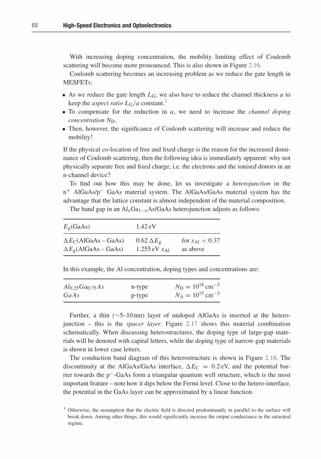
68 High-Speed Electronics and Optoelectronics
With increasing doping concentration, the mobility limiting effect of Coulombscattering will become more pronounced. This is also shown in Figure 2.16.
Coulomb scattering becomes an increasing problem as we reduce the gate length inMESFETs:
• As we reduce the gate length LG, we also have to reduce the channel thickness a tokeep the aspect ratio LG/a constant.3
• To compensate for the reduction in a, we need to increase the channel dopingconcentration ND.
• Then, however, the significance of Coulomb scattering will increase and reduce themobility!
If the physical co-location of free and fixed charge is the reason for the increased domi-nance of Coulomb scattering, then the following idea is immediately apparent: why notphysically separate free and fixed charge, i.e. the electrons and the ionised donors in ann-channel device?
To find out how this may be done, let us investigate a heterojunction in then+ AlGaAs/p− GaAs material system. The AlGaAs/GaAs material system has theadvantage that the lattice constant is almost independent of the material composition.
The band gap in an AlxGa1−xAs/GaAs heterojunction adjusts as follows:
Eg(GaAs) 1.42 eV
�EC(AlGaAs – GaAs) 0.62�Eg for xAl < 0.37�Eg(AlGaAs – GaAs) 1.255 eV xAl as above
In this example, the Al concentration, doping types and concentrations are:
Al0.25Ga0.75 As n-type ND = 1018 cm−3
Ga As p-type NA = 1015 cm−3
Further, a thin (∼5–10 nm) layer of undoped AlGaAs is inserted at the hetero-junction – this is the spacer layer. Figure 2.17 shows this material combinationschematically. When discussing heterostructures, the doping type of large-gap mate-rials will be denoted with capital letters, while the doping type of narrow-gap materialsis shown in lower case letters.
The conduction band diagram of this heterostructure is shown in Figure 2.18. Thediscontinuity at the AlGaAs/GaAs interface, �EC = 0.2 eV, and the potential bar-rier towards the p−-GaAs form a triangular quantum well structure, which is the mostimportant feature – note how it dips below the Fermi level. Close to the hetero-interface,the potential in the GaAs layer can be approximated by a linear function.
3 Otherwise, the assumption that the electric field is directed predominantly in parallel to the surface willbreak down. Among other things, this would significantly increase the output conductance in the saturatedregime.
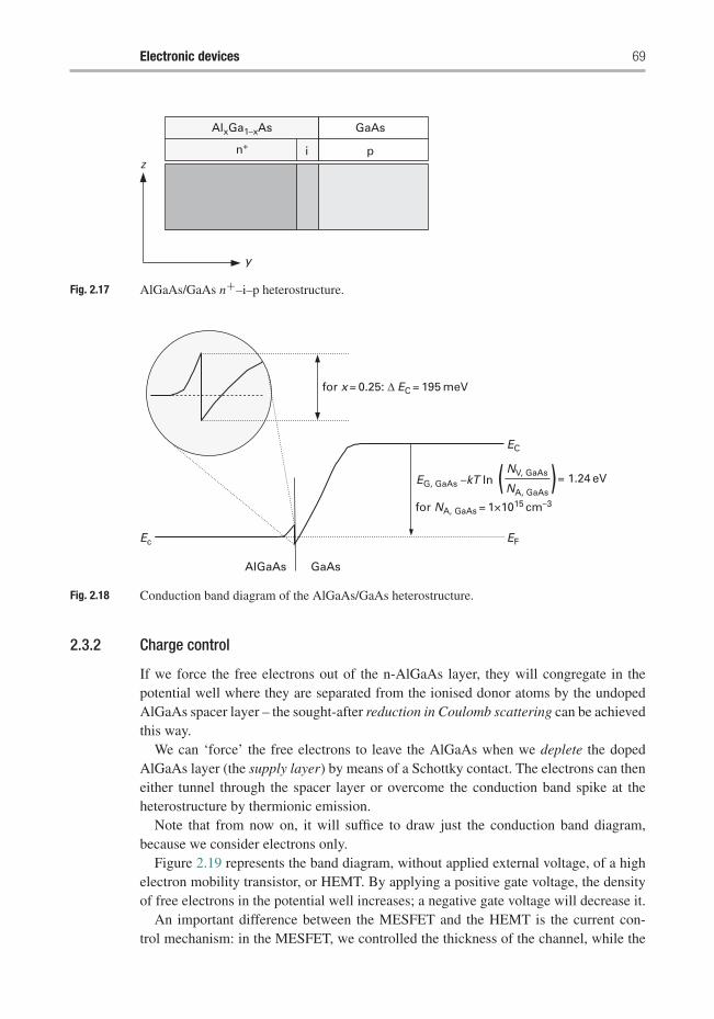
Electronic devices 69
AlxGa1–xAs
n+ i p
y
z
GaAs
Fig. 2.17 AlGaAs/GaAs n+–i–p heterostructure.
AlGaAs
Ec EF
for x = 0.25: Δ EC = 195 meV
EG, GaAs –kT In = 1.24 eV( )NV, GaAs
NA, GaAs
EC
GaAs
for NA, GaAs = 1×1015 cm–3
Fig. 2.18 Conduction band diagram of the AlGaAs/GaAs heterostructure.
2.3.2 Charge control
If we force the free electrons out of the n-AlGaAs layer, they will congregate in thepotential well where they are separated from the ionised donor atoms by the undopedAlGaAs spacer layer – the sought-after reduction in Coulomb scattering can be achievedthis way.
We can ‘force’ the free electrons to leave the AlGaAs when we deplete the dopedAlGaAs layer (the supply layer) by means of a Schottky contact. The electrons can theneither tunnel through the spacer layer or overcome the conduction band spike at theheterostructure by thermionic emission.
Note that from now on, it will suffice to draw just the conduction band diagram,because we consider electrons only.
Figure 2.19 represents the band diagram, without applied external voltage, of a highelectron mobility transistor, or HEMT. By applying a positive gate voltage, the densityof free electrons in the potential well increases; a negative gate voltage will decrease it.
An important difference between the MESFET and the HEMT is the current con-trol mechanism: in the MESFET, we controlled the thickness of the channel, while the
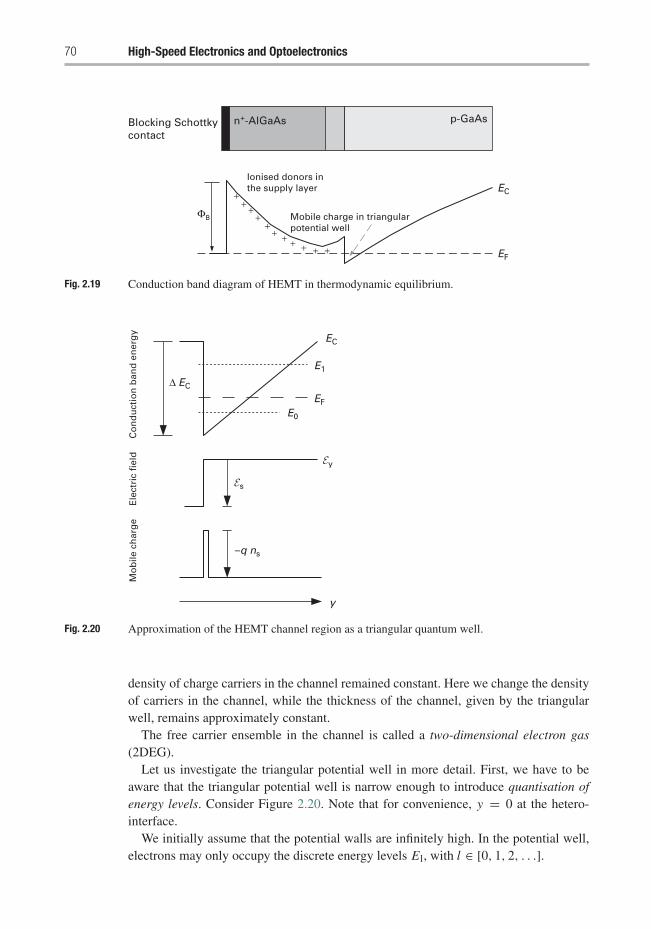
70 High-Speed Electronics and Optoelectronics
Blocking Schottkycontact
n+-AlGaAs
Ionised donors inthe supply layer
ΦB
++
++
++ + + + + +
Mobile charge in triangularpotential well
EF
EC
p-GaAs
Fig. 2.19 Conduction band diagram of HEMT in thermodynamic equilibrium.
EC
EFE0
Δ EC
Ey
Es
Mo
bile
ch
arg
eE
lect
ric
fiel
dC
on
du
ctio
n b
and
en
erg
y
–q ns
y
E1
Fig. 2.20 Approximation of the HEMT channel region as a triangular quantum well.
density of charge carriers in the channel remained constant. Here we change the densityof carriers in the channel, while the thickness of the channel, given by the triangularwell, remains approximately constant.
The free carrier ensemble in the channel is called a two-dimensional electron gas(2DEG).
Let us investigate the triangular potential well in more detail. First, we have to beaware that the triangular potential well is narrow enough to introduce quantisation ofenergy levels. Consider Figure 2.20. Note that for convenience, y = 0 at the hetero-interface.
We initially assume that the potential walls are infinitely high. In the potential well,electrons may only occupy the discrete energy levels El, with l ∈ [0, 1, 2, . . .].
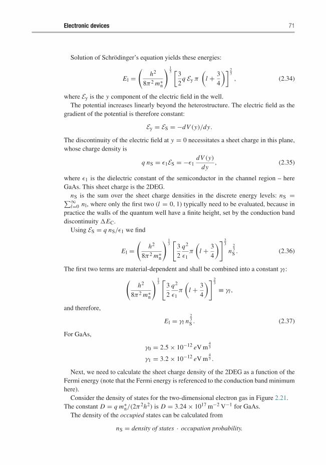
Electronic devices 71
Solution of Schrodinger’s equation yields these energies:
El =(
h2
8π2 m∗n
) 13 [
3
2q Ey π
(l + 3
4
)] 23
, (2.34)
where Ey is the y component of the electric field in the well.The potential increases linearly beyond the heterostructure. The electric field as the
gradient of the potential is therefore constant:
Ey = ES = −dV (y)/dy.
The discontinuity of the electric field at y = 0 necessitates a sheet charge in this plane,whose charge density is
q nS = ε1ES = −ε1dV (y)
dy, (2.35)
where ε1 is the dielectric constant of the semiconductor in the channel region – hereGaAs. This sheet charge is the 2DEG.
nS is the sum over the sheet charge densities in the discrete energy levels: nS =∑∞l=0 nl, where only the first two (l = 0, 1) typically need to be evaluated, because in
practice the walls of the quantum well have a finite height, set by the conduction banddiscontinuity �EC.
Using ES = q nS/ε1 we find
El =(
h2
8π2 m∗n
) 13
[3
2
q2
ε1π
(l + 3
4
)] 23
n23S . (2.36)
The first two terms are material-dependent and shall be combined into a constant γl :(h2
8π2 m∗n
) 13
[3
2
q2
ε1π
(l + 3
4
)] 23
≡ γl ,
and therefore,
El = γl n23S . (2.37)
For GaAs,
γ0 = 2.5 × 10⁻¹² eV m43
γ1 = 3.2 × 10⁻¹² eV m43 .
Next, we need to calculate the sheet charge density of the 2DEG as a function of theFermi energy (note that the Fermi energy is referenced to the conduction band minimumhere).
Consider the density of states for the two-dimensional electron gas in Figure 2.21.The constant D = q m∗
n/(2π2h2) is D = 3.24 × 10¹⁷ m−2 V−1 for GaAs.
The density of the occupied states can be calculated from
nS = density of states · occupation probability.
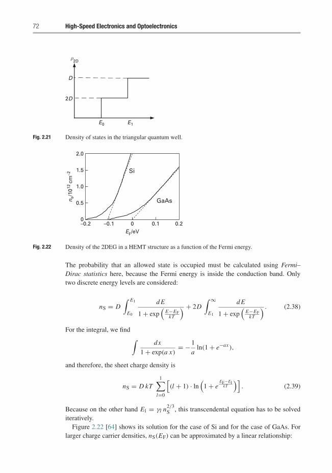
72 High-Speed Electronics and Optoelectronics
D
2D
E0 E1
ρ2D
Fig. 2.21 Density of states in the triangular quantum well.
–0.2
ns/
1012
cm
–2
0
0.5
1.0
1.5
2.0
–0.1EF/eV
0 0.1
GaAs
Si
0.2
Fig. 2.22 Density of the 2DEG in a HEMT structure as a function of the Fermi energy.
The probability that an allowed state is occupied must be calculated using Fermi–Dirac statistics here, because the Fermi energy is inside the conduction band. Onlytwo discrete energy levels are considered:
nS = D∫ E1
E0
d E
1 + exp(
E−EFkT
) + 2D∫ ∞
E1
d E
1 + exp(
E−EFkT
) . (2.38)
For the integral, we find ∫dx
1 + exp(a x)= −1
aln(1 + e−ax ),
and therefore, the sheet charge density is
nS = D kT1∑
l=0
[(l + 1) · ln
(1 + e
EF−ElkT
)]. (2.39)
Because on the other hand El = γl n2/3S , this transcendental equation has to be solved
iteratively.Figure 2.22 [64] shows its solution for the case of Si and for the case of GaAs. For
larger charge carrier densities, nS(EF) can be approximated by a linear relationship:
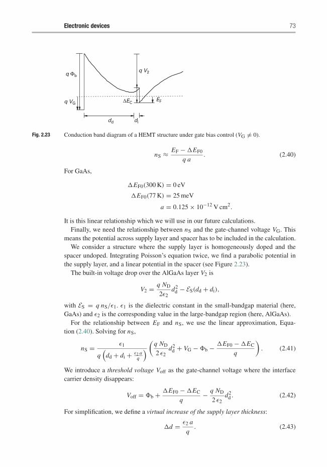
Electronic devices 73
q Φb
q VG
q V2
dd di
ΔECEF
Fig. 2.23 Conduction band diagram of a HEMT structure under gate bias control (VG �= 0).
nS ≈ EF − �EF0
q a. (2.40)
For GaAs,
�EF0(300 K) = 0 eV
�EF0(77 K) = 25 meV
a = 0.125 × 10⁻¹² V cm2.
It is this linear relationship which we will use in our future calculations.Finally, we need the relationship between nS and the gate-channel voltage VG. This
means the potential across supply layer and spacer has to be included in the calculation.We consider a structure where the supply layer is homogeneously doped and the
spacer undoped. Integrating Poisson’s equation twice, we find a parabolic potential inthe supply layer, and a linear potential in the spacer (see Figure 2.23).
The built-in voltage drop over the AlGaAs layer V2 is
V2 = q ND
2ε2d2
d − ES(dd + di),
with ES = q nS/ε1. ε1 is the dielectric constant in the small-bandgap material (here,GaAs) and ε2 is the corresponding value in the large-bandgap region (here, AlGaAs).
For the relationship between EF and nS, we use the linear approximation, Equa-tion (2.40). Solving for nS,
nS = ε1
q(
dd + di + ε2 aq
) (q ND
2 ε2d2
d + VG − �b − �EF0 − �EC
q
). (2.41)
We introduce a threshold voltage Voff as the gate-channel voltage where the interfacecarrier density disappears:
Voff = �b + �EF0 − �EC
q− q ND
2 ε2d2
d . (2.42)
For simplification, we define a virtual increase of the supply layer thickness:
�d = ε2 a
q. (2.43)
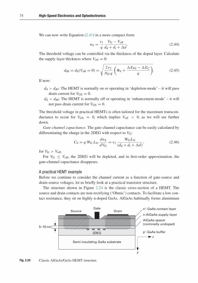
74 High-Speed Electronics and Optoelectronics
We can now write Equation (2.41) in a more compact form:
nS = ε1
q
VG − Voff
dd + di + �d. (2.44)
The threshold voltage can be controlled via the thickness of the doped layer. Calculatethe supply layer thickness where Voff = 0:
dd0 = dd(Voff = 0) =√
2 ε2
ND q
(�b + �EF0 − �EC
q
). (2.45)
If now:
dd > dd0: The HEMT is normally on or operating in ‘depletion-mode’ – it will passdrain current for VGS = 0.
dd < dd0: The HEMT is normally off or operating in ‘enhancement-mode’ – it willnot pass drain current for VGS = 0.
The threshold voltage in practical HEMTs is often tailored for the maximum transcon-ductance to occur for VGS = 0, which implies Voff < 0, as we will see furtherdown.
Gate-channel capacitance. The gate-channel capacitance can be easily calculated bydifferentiating the charge in the 2DEG with respect to VG:
C0 = q WG LGdnS
dVG= ε2
WGLG
(dd + di + �d), (2.46)
for VG > Voff.For VG ≤ Voff, the 2DEG will be depleted, and in first-order approximation, the
gate-channel capacitance disappears.
A practical HEMT exampleBefore we continue to consider the channel current as a function of gate-source anddrain-source voltages, let us briefly look at a practical transistor structure.
The structure shown in Figure 2.24 is the classic cross-section of a HEMT. Thesource and drain contacts are non-rectifying (‘Ohmic’) contacts. To facilitate a low con-tact resistance, they sit on highly n-doped GaAs. AlGaAs habitually forms aluminium
Source
5–10 nm
Semi-insulating GaAs substrate
2DEG
n+-GaAs contact layer
n-AlGaAs supply layer
AlGaAs spacer(nominally undoped)
p–-GaAs bufferz
y
GateDrain
Fig. 2.24 Classic AlGaAs/GaAs HEMT structure.
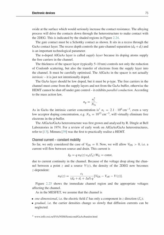
Electronic devices 75
oxide at the surface which would seriously increase the contact resistance. The alloyingprocess will drive the contacts down through the heterostructure to make contact withthe 2DEG. This is indicated by the shaded regions in Figure 2.24.
The gate contact must be a Schottky contact as shown. It sits in a recess through theGaAs contact layer. The recess depth controls the gate-channel separation (dd + di) andis an important technological parameter.
The n-doped AlGaAs layer is called supply layer because its doping atoms supplythe free carriers in the channel.
The thickness of the spacer layer (typically 5–10 nm) controls not only the reductionof Coulomb scattering, but also the transfer of electrons from the supply layer intothe channel. It must be carefully optimised. The AlGaAs in the spacer is not actuallyintrinsic – it is just not intentionally doped.
The GaAs layer should be low doped, but it must be p-type. The free carriers in thechannel must come from the supply layers and not from the GaAs buffer, otherwise theHEMT cannot be shut off under gate control – it exhibits parallel conduction. Accordingto the mass action law,
np = n2i
NA.
As in GaAs the intrinsic carrier concentration is4 ni = 2.1 · 106 cm−3, even a verylow acceptor doping concentration, e.g. NA = 1015 cm−3, will virtually eliminate freeelectrons in the p-buffer.
The AlGaAs/GaAs heterostructure was first grown and analysed by R. Dingle at BellLaboratories in 1974. For a review of early work on AlGaAs/GaAs heterostructures,refer to [13]. Mimura [39] was the first to practically realise a HEMT.
Channel current – constant mobilitySo far, we only considered the case of VDS = 0. Now, we will allow VDS > 0, i.e. acurrent will flow between source and drain. This current is
ID = q nS(z) vn(Ez) WG = const,
due to current continuity in the channel. Because of the voltage drop along the chan-nel between a point z and a source V (z), the density of the 2DEG now becomesz-dependent:
nS(z) = ε1
(dd + di + �d) q[VGS − Voff − V (z)].
Figure 2.25 shows the immediate channel region and the appropriate voltagesaffecting the channel.
As in the MESFET, we assume that the channel is
• one-dimensional, i.e. the electric field E has only a component in z direction (Ez);• gradual, i.e. the carrier densities change so slowly that diffusion currents can be
neglected.
4 www.ioffe.rssi.ru/SVA/NSM/Semicond/GaAs/bandstr.html
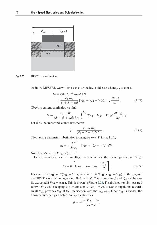
76 High-Speed Electronics and Optoelectronics
VGS VDS > 0
VG(z)
V(z)
Fig. 2.25 HEMT channel region.
As in the MESFET, we will first consider the low-field case where μn = const.
ID = q nS(z) WG μn Ez(z)
= ε1 WG
dd + di + �d[VGS − Voff − V (z)] μn
dV (z)
dz. (2.47)
Obeying current continuity, we find
ID = ε1 μn WG
(dd + di + �d) LG
∫ LG
0[VGS − Voff − V (z)]
dV (z)
dzdz.
Let β be the transconductance parameter:
β = ε1 μn WG
(dd + di + �d) LG. (2.48)
Then, using parameter substitution to integrate over V instead of z:
ID = β
∫ V (LG)
V (0)[VGS − Voff − V (z)] dV .
Note that V (LG) = VDS, V (0) = 0.Hence, we obtain the current–voltage characteristics in the linear regime (small VDS):
ID = β
[(VGS − Voff) VDS − V 2
DS
2
]. (2.49)
For very small VDS � 2(VGS − Voff), we note ID ≈ β VDS (VGS − Voff). In this regime,the HEMT acts as a ‘voltage-controlled resistor’. The parameters β and Voff can be eas-ily extracted if VDS = const. This is shown in Figure 2.26. The drain current is measuredfor two VGS while keeping VDS = const � 2(VGS − Voff). Linear extrapolation towardssmall VGS provides Voff at the intersection with the VGS axis. Once Voff is known, thetransconductance parameter can be calculated as
β = − ID(VGS = 0)
VDS Voff.
Electronic devices 77
Voff
VGS
ID
–β VDSVoff
VDS << 2(VGS –Voff), const
Fig. 2.26 Extraction of Voff and β at small VDS.
Channel current – constant velocityThe ansatz in Equation (2.47) assumes that nS(z) > 0 for all 0 < z < LG. If VDS issufficiently large, the gate-channel voltage may drop below Voff in the channel and thechannel will become fully depleted. As V (z) ≤ VDS, this happens first at the drain end:VGS − VDS = Voff or
VDS ≡ Vk = VGS − Voff. (2.50)
This corresponds to what we saw in the MESFET, where the undepleted channel heightdisappeared at the drain end.
As in the MESFET, we can argue that velocity saturation prevents channel closure –nS(z) → 0 implies Ez(z) → ∞ due to the current continuity requirement, so that theconstant-mobility assumption breaks down much earlier and vn(z) → vsat.
Using a two-region model for the electron velocity, where mobility is constant for|Ez| < Ecrit and velocity is constant for |Ez| > Ecrit, we can calculate the drain-sourcevoltage VDSS for which velocity saturation happens at the drain end of the channel(z = LG). At this point the local electric field is Ez(z = LG) = Ecrit. Using the constant-mobility current Equation (2.49), we find
ID = ε1μnWG
LG(dd + di + �d)
[(VGS − Voff)VDSS − V 2
DSS
2
].
On the other hand, ID can be calculated using a constant-velocity ansatz:
ID = q nS WG vsat.
In the two-region model, μnEcrit ≡ vsat. Further, nS can be calculated from Equa-tion (2.44) using VG = VGS − VDSS, so that
ID = ε1 WG μn
(dd + di + �d)(VGS − Voff − VDSS) Ecrit LG.
The drain current expressions for constant mobility and constant velocity must beequal for VDS = VDSS, because we are transitioning from the constant mobility to
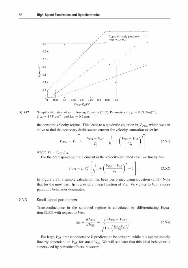
78 High-Speed Electronics and Optoelectronics
00
0.1
0.2
0.3
0.4
0.5
0.6
0.7
0.350.30.250.20.15
(VGS –Voff)/V
Approximately parabolicnear VGS =Voff
I D/A
mm
–1
0.10.05 0.4
Fig. 2.27 Sample calculation of ID following Equation (2.52). Parameters are β = 83 S (Vm)−1,Ecrit = 1 kV cm−1 and LG = 0.2 μm.
the constant-velocity regime. This leads to a quadratic equation in VDSS, which we cansolve to find the necessary drain-source current for velocity saturation to set in:
VDSS = V0
⎡⎣1 + VGS − Voff
V0−
√1 +
(VGS − Voff
V0
)2⎤⎦ , (2.51)
where V0 = Ecrit LG.For the corresponding drain current in the velocity-saturated case, we finally find
IDSS = β V 20
⎡⎣√1 +
(VGS − Voff
V0
)2
− 1
⎤⎦ . (2.52)
In Figure 2.27, a sample calculation has been performed using Equation (2.52). Notethat for the most part, ID is a strictly linear function of VGS. Very close to Voff, a moreparabolic behaviour dominates.
2.3.3 Small-signal parameters
Transconductance in the saturated regime is calculated by differentiating Equa-tion (2.52) with respect to VGS:
gm = d IDSS
dVGS= β (VGS − Voff)√
1 +(
VGS−VoffV0
)2. (2.53)
For large VGS, transconductance is predicted to be constant, while it is approximatelylinearly dependent on VGS for small VGS. We will see later that this ideal behaviour issuperseded by parasitic effects, however.
Electronic devices 79
The gate-source capacitance CGS can be found by differentiating the total channelcharge QT with respect to VGS:
CGS = d QT
dVGS= d
dVGSWG q
∫ LG
0nS(z)dz.
Particularly simple – and practically important – is the case of velocity saturation in thewhole channel. As
ID = q nS(z) vsat WG = const ⇒ nS(z) = const = nSS,
where
nSS = β V 20
q vsat WG
⎡⎣√1 +
(VGS − Voff
V0
)2
− 1
⎤⎦and therefore
QT = q nSS WG LG = β V 20 LG
vsat
⎡⎣√1 +
(VGS − Voff
V0
)2
− 1
⎤⎦ .
The gate-source capacitance becomes in this case
CGS = d QT
dVGS(2.54)
= LG
vsat
β V0 (VGS − Voff)√(VGS − Voff)2 + V 2
0
= LG
vsatgm.
As in case of the MESFET, we find for the transit time of carriers under the gate:
τT = LG
vsat= CGS
gm.
The gate-drain capacitance can be calculated similarly:
CGD = d QT
dVGD= 0
in this simple model because QT �= f (VGD). In reality, CGD is non-zero because of thegeometric capacitance between the metal contacts and other parasitic effects. As in theMESFET, CGD � CGS in saturation.
For the small-signal equivalent circuit, we can use the same topology as for theMESFET. Accordingly, the transit frequency can be approximated by
fT = gm
2πCGS. (2.55)
80 High-Speed Electronics and Optoelectronics
2.3.4 ‘High electron mobility’?
The common name ‘high electron mobility transistor’ deserves some critical reflection.Remember that while Coulomb scattering is the dominant mobility-limiting mecha-nism at cryogenic temperatures, phonon scattering is dominant at room temperature(Figure 2.16).
Realistic enhancement factors for the electron mobility in HEMTs are
• a factor of two at room temperature;• up to a factor of 100 at cryogenic temperatures (e.g. 77 K – liquid nitrogen).
Furthermore, we found that in short-channel FETs velocity saturation dominates in thechannel – hence the enhancement in mobility has two major advantages:
(i) reduction of series resistances, most importantly RS;(ii) lowering of the critical field for velocity saturation, i.e. saturated velocity will be
reached sooner.
However, there are other advantages of the HEMT structure which are also significant:
• The carrier distribution is similar to that of a pulse-doped MESFET – we expect aconstant transconductance gm and therefore a high linearity. There are parasitic effectswhich prevent this from happening – more about this later.
• In active operation, the supply layer is fully depleted and hence the gate-sourcecapacitance CGS should be constant. Again, this is not quite true in reality (see p. 81).
• The potential barrier towards the substrate reduces carrier injection into the substrateand increases output resistance.
Note that, compared to a MESFET with an epitaxially grown channel, the HEMTstructure is technologically not much more complicated.
As an aside, the HEMT has many other names and has jokingly been called a multi-acronym device (MAD). To name but a few:
HFET heterostructure field effect transistorMODFET modulation-doped field effect transistorTEGFET two-dimensional electron gas FETSDFET selectively doped field effect transistor
2.3.5 Non-ideal behaviour
In the following pages, we will discuss how in practical HEMTs the experimentallyobserved behaviour deviates from the theory developed so far. The explanation of thesenon-ideal features will have important implications for the design of optimised HEMTdevices.
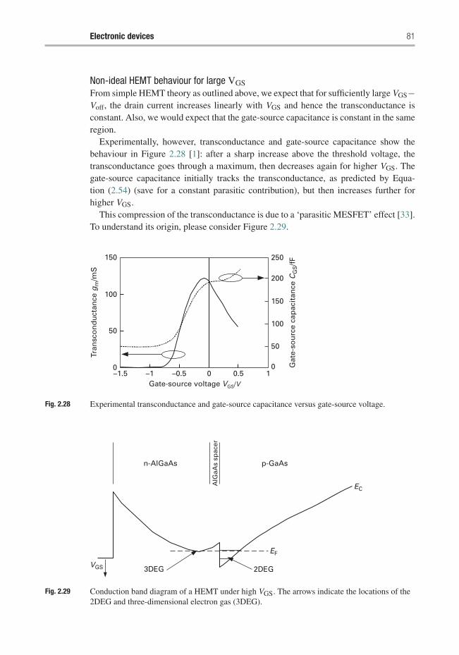
Electronic devices 81
Non-ideal HEMT behaviour for large VGSFrom simple HEMT theory as outlined above, we expect that for sufficiently large VGS−Voff, the drain current increases linearly with VGS and hence the transconductance isconstant. Also, we would expect that the gate-source capacitance is constant in the sameregion.
Experimentally, however, transconductance and gate-source capacitance show thebehaviour in Figure 2.28 [1]: after a sharp increase above the threshold voltage, thetransconductance goes through a maximum, then decreases again for higher VGS. Thegate-source capacitance initially tracks the transconductance, as predicted by Equa-tion (2.54) (save for a constant parasitic contribution), but then increases further forhigher VGS.
This compression of the transconductance is due to a ‘parasitic MESFET’ effect [33].To understand its origin, please consider Figure 2.29.
150
100
50
0–1.5 –1 –0.5
Gate-source voltage VGS/V
0 0.5
Gat
e-so
urc
e ca
pac
itan
ce C
GS/f
F
Tran
sco
nd
uct
ance
gm
/mS
10
50
100
150
250
200
Fig. 2.28 Experimental transconductance and gate-source capacitance versus gate-source voltage.
n-AlGaAs p-GaAs
EC
EF
VGS 2DEG3DEG
AlG
aAs
spac
er
Fig. 2.29 Conduction band diagram of a HEMT under high VGS. The arrows indicate the locations of the2DEG and three-dimensional electron gas (3DEG).
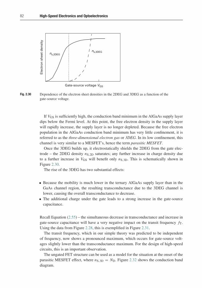
82 High-Speed Electronics and Optoelectronics
Gate-source voltage VGS
ns,2DEGns,3DEG
Ele
ctro
n s
hee
t d
ensi
ty
Fig. 2.30 Dependence of the electron sheet densities in the 2DEG and 3DEG as a function of thegate-source voltage.
If VGS is sufficiently high, the conduction band minimum in the AlGaAs supply layerdips below the Fermi level. At this point, the free electron density in the supply layerwill rapidly increase, the supply layer is no longer depleted. Because the free electronpopulation in the AlGaAs conduction band minimum has very little confinement, it isreferred to as the three-dimensional electron gas or 3DEG. In its low confinement, thischannel is very similar to a MESFET’s, hence the term parasitic MESFET.
Once the 3DEG builds up, it electrostatically shields the 2DEG from the gate elec-trode – the 2DEG density nS,2D saturates; any further increase in charge density dueto a further increase in VGS will benefit only nS,3D. This is schematically shown inFigure 2.30.
The rise of the 3DEG has two substantial effects:
• Because the mobility is much lower in the ternary AlGaAs supply layer than in theGaAs channel region, the resulting transconductance due to the 3DEG channel islower, causing the overall transconductance to decrease.
• The additional charge under the gate leads to a strong increase in the gate-sourcecapacitance.
Recall Equation (2.55) – the simultaneous decrease in transconductance and increase ingate-source capacitance will have a very negative impact on the transit frequency fT.Using the data from Figure 2.28, this is exemplified in Figure 2.31.
The transit frequency, which in our simple theory was predicted to be independentof frequency, now shows a pronounced maximum, which occurs for gate-source volt-ages slightly lower than the transconductance maximum. For the design of high-speedcircuits, this is an important observation.
The ungated FET structure can be used as a model for the situation at the onset of theparasitic MESFET effect, where nS,3D = ND. Figure 2.32 shows the conduction banddiagram.
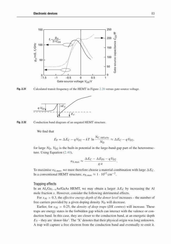
Electronic devices 83
150 250
200
150
100
50
0
100
50
0–1.5 –1 –0.5
Gate-source voltage VGS/V
gm
/mS
, fT/G
Hz
fT = —–––gm
2πCGS
Gat
e-so
urc
e ca
pac
itan
ce C
GS
/fF
0 0.5 1
Fig. 2.31 Calculated transit frequency of the HEMT in Figure 2.28 versus gate-source voltage.
ΔE C
E F
q VD2
Fig. 2.32 Conduction band diagram of an ungated HEMT structure.
We find that
EF = �EC − qVD2 − kT lnNC,AlGaAs
ND≈ �EC − qVD2,
for large ND. VD2 is the built-in potential in the large-band-gap part of the heterostruc-ture. Using Equation (2.40),
nS,max ≈ �EC − �EF0 − qVD2
q a.
To maximise nS,max, we must therefore choose a material combination with large �EC.In a conventional HEMT structure, nS,max ≈ 1 · 1012 cm−2.
Trapping effectsIn an AlxGa1−xAs/GaAs HEMT, we may obtain a larger �EC by increasing the Almole fraction x . However, consider the following detrimental effects.
For xAl > 0.3, the effective energy depth of the donor level increases – the number offree carriers provided by a given doping density ND will decrease.
Earlier, for xAl > 0.25, the density of deep traps (DX centres) will increase. Thesetraps are energy states in the forbidden gap which can interact with the valence or con-duction band. In this case, they are closer to the conduction band, at an energetic depthET – they are ‘donor-like’. The ‘X’ denotes that their physical origin was long unknown.A trap will capture a free electron from the conduction band and eventually re-emit it.
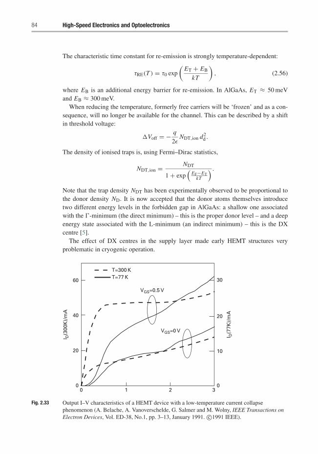
84 High-Speed Electronics and Optoelectronics
The characteristic time constant for re-emission is strongly temperature-dependent:
τRE(T ) = τ0 exp
(ET + EB
kT
), (2.56)
where EB is an additional energy barrier for re-emission. In AlGaAs, ET ≈ 50 meVand EB ≈ 300 meV.
When reducing the temperature, formerly free carriers will be ‘frozen’ and as a con-sequence, will no longer be available for the channel. This can be described by a shiftin threshold voltage:
�Voff = − q
2εNDT,ion d2
d .
The density of ionised traps is, using Fermi–Dirac statistics,
NDT,ion = NDT
1 + exp(
EF−ETkT
) .
Note that the trap density NDT has been experimentally observed to be proportional tothe donor density ND. It is now accepted that the donor atoms themselves introducetwo different energy levels in the forbidden gap in AlGaAs: a shallow one associatedwith the �-minimum (the direct minimum) – this is the proper donor level – and a deepenergy state associated with the L-minimum (an indirect minimum) – this is the DXcentre [5].
The effect of DX centres in the supply layer made early HEMT structures veryproblematic in cryogenic operation.
60
T=300 KT=77 K
VGS=0.5 V
VGS=0 V
20
I D(3
00K
)/m
A
I D(7
7K)/
mA
00 1 2 3
0
10
20
30
40
Fig. 2.33 Output I–V characteristics of a HEMT device with a low-temperature current collapsephenomenon (A. Belache, A. Vanoverschelde, G. Salmer and M. Wolny, IEEE Transactions onElectron Devices, Vol. ED-38, No.1, pp. 3–13, January 1991. c©1991 IEEE).

Electronic devices 85
Figure 2.33 shows an example of a device showing such a current collapse phe-nomenon [3]. Apart from the change in output conductance in saturation and the various‘kink’ effects, which shall not be discussed here, we note
• At low VDS, the output conductance in the linear regime decreases considerably – thisis due to an increase in the source resistance RS. The decrease in RS with decreasingT is unexpected, as the mobility itself will increase. The decrease in the free carrierconcentration, however, dominates.
• In the saturated regime, VDS > 0.5 V, the transconductance also decreases signifi-cantly with decreasing temperature.
The occurrence of DX centres is closely linked to the use of AlGaAs as the barriermaterial – other supply layer materials such as GaInP do not show this effect and willcorrespondingly fare better in their low-temperature performance [7].
2.3.6 Structural HEMT variations
Increasingly, structural variations of the original HEMT concept are being used to cir-cumvent the non-ideal behavioural effects explained above and to improve performance.
Pulse-doped HEMT structureDue to the severeness of the DX centre limitation, a method to eliminate this limitationhas the highest priority.
Because NDT ∼ ND, the trap-induced threshold voltage shift is
�Voff ∼ ND d2d .
On the other hand, the supply layer must be able to supply the necessary carrier densityin the 2DEG:
ND dd > nS.
If, therefore, we concentrate the doping in a narrow sheet – increase ND and decreasedd – the trap-induced threshold voltage shift can be drastically reduced.
This concept leads to the delta-doped (or pulse-doped) HEMT structure (seeFigure 2.34).
SourceGate
2DEG
Semi-insulating GaAs substrate
dd
Drain
Undoped barriern+-doped supply layerUndoped supply layer
AlGaAs
Fig. 2.34 Layer structure of a delta-doped HEMT.
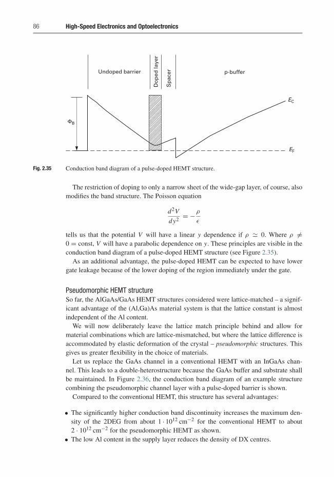
86 High-Speed Electronics and Optoelectronics
Undoped barrier
ΦB
p-buffer
EC
EFD
op
ed la
yer
Sp
acer
Fig. 2.35 Conduction band diagram of a pulse-doped HEMT structure.
The restriction of doping to only a narrow sheet of the wide-gap layer, of course, alsomodifies the band structure. The Poisson equation
d2V
dy2= −ρ
ε
tells us that the potential V will have a linear y dependence if ρ � 0. Where ρ �=0 = const, V will have a parabolic dependence on y. These principles are visible in theconduction band diagram of a pulse-doped HEMT structure (see Figure 2.35).
As an additional advantage, the pulse-doped HEMT can be expected to have lowergate leakage because of the lower doping of the region immediately under the gate.
Pseudomorphic HEMT structureSo far, the AlGaAs/GaAs HEMT structures considered were lattice-matched – a signif-icant advantage of the (Al,Ga)As material system is that the lattice constant is almostindependent of the Al content.
We will now deliberately leave the lattice match principle behind and allow formaterial combinations which are lattice-mismatched, but where the lattice difference isaccommodated by elastic deformation of the crystal – pseudomorphic structures. Thisgives us greater flexibility in the choice of materials.
Let us replace the GaAs channel in a conventional HEMT with an InGaAs chan-nel. This leads to a double-heterostructure because the GaAs buffer and substrate shallbe maintained. In Figure 2.36, the conduction band diagram of an example structurecombining the pseudomorphic channel layer with a pulse-doped barrier is shown.
Compared to the conventional HEMT, this structure has several advantages:
• The significantly higher conduction band discontinuity increases the maximum den-sity of the 2DEG from about 1 · 1012 cm−2 for the conventional HEMT to about2 · 1012 cm−2 for the pseudomorphic HEMT as shown.
• The low Al content in the supply layer reduces the density of DX centres.
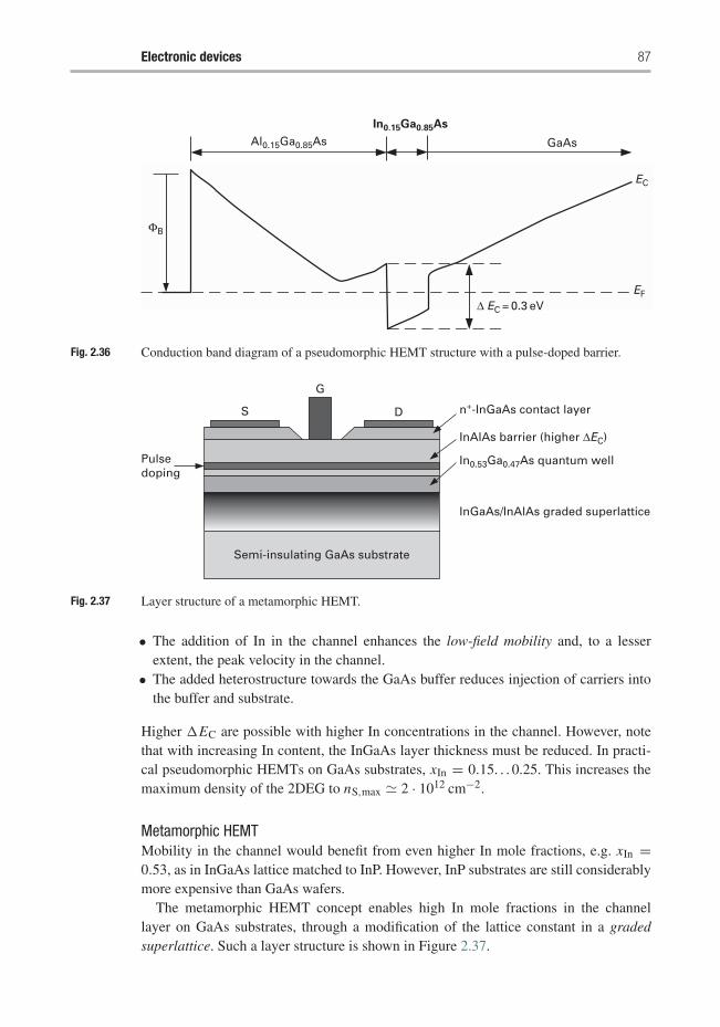
Electronic devices 87
Al0.15Ga0.85AsIn0.15Ga0.85As
GaAs
EC
EFΔ EC = 0.3 eV
ΦB
Fig. 2.36 Conduction band diagram of a pseudomorphic HEMT structure with a pulse-doped barrier.
Pulsedoping
S
G
D
Semi-insulating GaAs substrate
InGaAs/InAlAs graded superlattice
InAlAs barrier (higher ΔEC)
n+-InGaAs contact layer
In0.53Ga0.47As quantum well
Fig. 2.37 Layer structure of a metamorphic HEMT.
• The addition of In in the channel enhances the low-field mobility and, to a lesserextent, the peak velocity in the channel.
• The added heterostructure towards the GaAs buffer reduces injection of carriers intothe buffer and substrate.
Higher �EC are possible with higher In concentrations in the channel. However, notethat with increasing In content, the InGaAs layer thickness must be reduced. In practi-cal pseudomorphic HEMTs on GaAs substrates, xIn = 0.15. . . 0.25. This increases themaximum density of the 2DEG to nS,max � 2 · 1012 cm−2.
Metamorphic HEMTMobility in the channel would benefit from even higher In mole fractions, e.g. xIn =0.53, as in InGaAs lattice matched to InP. However, InP substrates are still considerablymore expensive than GaAs wafers.
The metamorphic HEMT concept enables high In mole fractions in the channellayer on GaAs substrates, through a modification of the lattice constant in a gradedsuperlattice. Such a layer structure is shown in Figure 2.37.
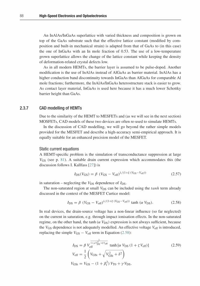
88 High-Speed Electronics and Optoelectronics
An InAlAs/InGaAs superlattice with varied thickness and composition is grown ontop of the GaAs substrate such that the effective lattice constant (modified by com-position and built-in mechanical strain) is adapted from that of GaAs to (in this case)the one of InGaAs with an In mole fraction of 0.53. The use of a low-temperaturegrown superlattice allows the change of the lattice constant while keeping the densityof deformation-related crystal defects low.
As in all modern HEMTs, the barrier layer is assumed to be pulse-doped. Anothermodification is the use of InAlAs instead of AlGaAs as barrier material. InAlAs has ahigher conduction band discontinuity towards InGaAs than AlGaAs for comparable Almole fractions; furthermore, the InAlAs/InGaAs heterostructure stack is easier to grow.As contact layer material, InGaAs is used here because it has a much lower Schottkybarrier height than GaAs.
2.3.7 CAD modelling of HEMTs
Due to the similarity of the HEMT to MESFETs and (as we will see in the next section)MOSFETs, CAD models of these two devices are often re-used to simulate HEMTs.
In the discussion of CAD modelling, we will go beyond the rather simple modelsprovided for the MESFET and describe a high-accuracy semi-empirical approach. It isequally suitable for an enhanced precision model of the MESFET.
Static current equationsA HEMT-specific problem is the simulation of transconductance suppression at largeVGS (see p. 81). A suitable drain current expression which accommodates this (thediscussion follows I. Kallfass [27]) is
IDS(VGS) = β (VGS − Voff)λ/(1+ξ (VGS−Voff)) (2.57)
in saturation – neglecting the VDS dependence of IDS.The non-saturated region at small VDS can be included using the tanh term already
discussed in the context of the MESFET Curtice model:
IDS = β (VGS − Voff)λ/(1+ξ (VGS−Voff)) tanh (α VDS). (2.58)
In real devices, the drain-source voltage has a non-linear influence (so far neglected)on the current in saturation, e.g. through impact ionisation effects. In the non-saturatedregime, on the other hand, the tanh (α VDS) expression is not always sufficient, becausethe VGS dependence is not adequately modelled. An effective voltage Veff is introduced,replacing the simple VGS − Voff term in Equation (2.58):
IDS = β V
λ
1+μV 2DS+ξVeff
eff tanh [α VDS (1 + ζVeff)] (2.59)
Veff = 1
2
(VGSt +
√V 2
GSt + δ2
)VGSt = VGS − (1 + β2
r ) VT0 + γ VDS.
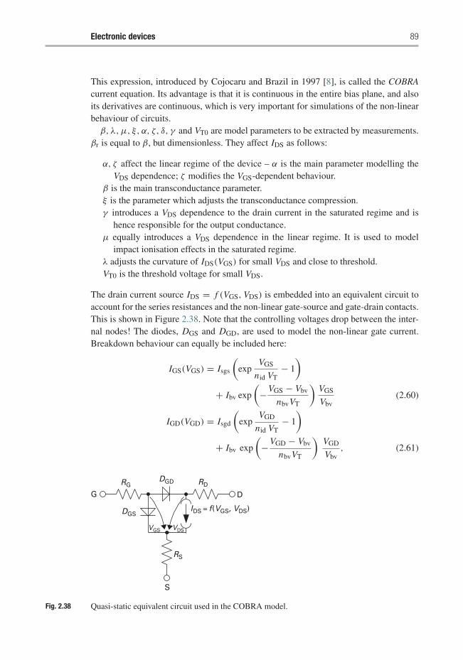
Electronic devices 89
This expression, introduced by Cojocaru and Brazil in 1997 [8], is called the COBRAcurrent equation. Its advantage is that it is continuous in the entire bias plane, and alsoits derivatives are continuous, which is very important for simulations of the non-linearbehaviour of circuits.
β, λ, μ, ξ, α, ζ, δ, γ and VT0 are model parameters to be extracted by measurements.βr is equal to β, but dimensionless. They affect IDS as follows:
α, ζ affect the linear regime of the device – α is the main parameter modelling theVDS dependence; ζ modifies the VGS-dependent behaviour.
β is the main transconductance parameter.ξ is the parameter which adjusts the transconductance compression.γ introduces a VDS dependence to the drain current in the saturated regime and is
hence responsible for the output conductance.μ equally introduces a VDS dependence in the linear regime. It is used to model
impact ionisation effects in the saturated regime.λ adjusts the curvature of IDS(VGS) for small VDS and close to threshold.VT0 is the threshold voltage for small VDS.
The drain current source IDS = f (VGS, VDS) is embedded into an equivalent circuit toaccount for the series resistances and the non-linear gate-source and gate-drain contacts.This is shown in Figure 2.38. Note that the controlling voltages drop between the inter-nal nodes! The diodes, DGS and DGD, are used to model the non-linear gate current.Breakdown behaviour can equally be included here:
IGS(VGS) = Isgs
(exp
VGS
nid VT− 1
)+ Ibv exp
(− VGS − Vbv
nbvVT
)VGS
Vbv(2.60)
IGD(VGD) = Isgd
(exp
VGD
nid VT− 1
)+ Ibv exp
(− VGD − Vbv
nbvVT
)VGD
Vbv, (2.61)
RG
G
RD
D
DGD
DGS
RS
IDS = f(VGS, VDS)
S
VGS VDS
Fig. 2.38 Quasi-static equivalent circuit used in the COBRA model.
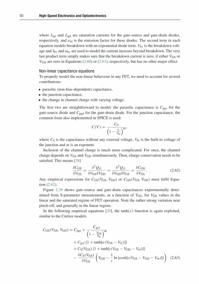
90 High-Speed Electronics and Optoelectronics
where Isgs and Isgd are saturation currents for the gate-source and gate-drain diodes,respectively, and nid is the emission factor for these diodes. The second term in eachequation models breakdown with an exponential diode term. Vbv is the breakdown volt-age and Ibv and nbv are used to model the current increase beyond breakdown. The verylast product term simply makes sure that the breakdown current is zero, if either VGS orVGD are zero in Equations (2.60) or (2.61), respectively, but has no other major effect.
Non-linear capacitance equationsTo properly model the non-linear behaviour in any FET, we need to account for severalcontributions:
• parasitic (non-bias-dependent) capacitance,• the junction capacitance,• the change in channel charge with varying voltage.
The first two are straightforward to model: the parasitic capacitance is Cpgs for thegate-source diode and Cpgd for the gate-drain diode. For the junction capacitance, thecommon form also implemented in SPICE is used:
C(V ) = C0(1 − V
Vbi
)m ,
where C0 is the capacitance without any external voltage, Vbi is the built-in voltage ofthe junction and m is an exponent.
Inclusion of the channel charge is much more complicated. For once, the channelcharge depends on VGS and VGD simultaneously. Then, charge conservation needs to besatisfied. This means [28]
δCGS
δVGS= δ2 QG
δVGSδVGD= δ2 QG
δVGDδVGS= δCGD
δVGS. (2.62)
Any empirical expressions for CGS(VGS, VGD) or CGD(VGS, VGD) must fulfil Equa-tion (2.62).
Figure 2.39 shows gate-source and gate-drain capacitances experimentally deter-mined from S-parameter measurements, as a function of VGS, for VDS values in thelinear and the saturated regime of FET operation. Note the rather strong variation nearpinch-off, and generally in the linear regime.
In the following empirical equations [29], the tanh(x) function is again exploited,similar to the Curtice models.
CGS(VGS, VGD) = Cpgs + Cgs1(1 − VGS
Vbi
)m
+ Cgs2 {1 + tanh[κ(VGS − Vt2)]}+ CS(VGS) {1 + tanh[ι(VGS − VGD − Vt4)]}− δCS(VGS)
δVGS
(VGD − 1
ιln {cosh[ι(VGS − VGD − Vt4)]}
)(2.63)
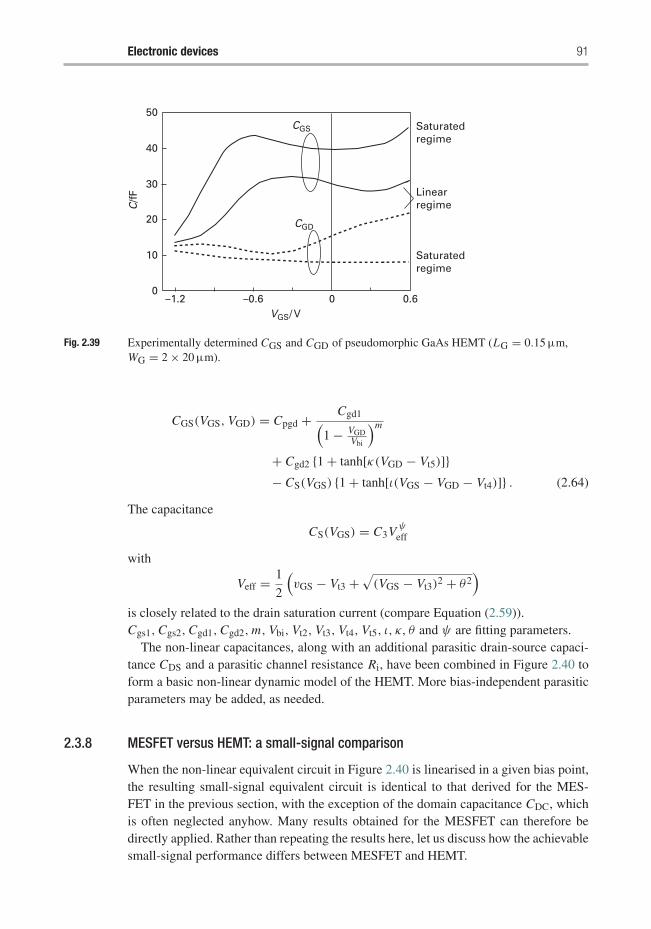
Electronic devices 91
50
C/f
F
40
30
20
10
0–1.2 –0.6
VGS/ V
CGD
CGS Saturatedregime
Linearregime
Saturatedregime
0 0.6
Fig. 2.39 Experimentally determined CGS and CGD of pseudomorphic GaAs HEMT (LG = 0.15 μm,WG = 2 × 20 μm).
CGS(VGS, VGD) = Cpgd + Cgd1(1 − VGD
Vbi
)m
+ Cgd2 {1 + tanh[κ(VGD − Vt5)]}− CS(VGS) {1 + tanh[ι(VGS − VGD − Vt4)]} . (2.64)
The capacitance
CS(VGS) = C3V ψ
eff
with
Veff = 1
2
(vGS − Vt3 +
√(VGS − Vt3)2 + θ2
)is closely related to the drain saturation current (compare Equation (2.59)).Cgs1,Cgs2,Cgd1,Cgd2,m, Vbi, Vt2, Vt3, Vt4, Vt5, ι, κ, θ and ψ are fitting parameters.
The non-linear capacitances, along with an additional parasitic drain-source capaci-tance CDS and a parasitic channel resistance Ri, have been combined in Figure 2.40 toform a basic non-linear dynamic model of the HEMT. More bias-independent parasiticparameters may be added, as needed.
2.3.8 MESFET versus HEMT: a small-signal comparison
When the non-linear equivalent circuit in Figure 2.40 is linearised in a given bias point,the resulting small-signal equivalent circuit is identical to that derived for the MES-FET in the previous section, with the exception of the domain capacitance CDC, whichis often neglected anyhow. Many results obtained for the MESFET can therefore bedirectly applied. Rather than repeating the results here, let us discuss how the achievablesmall-signal performance differs between MESFET and HEMT.
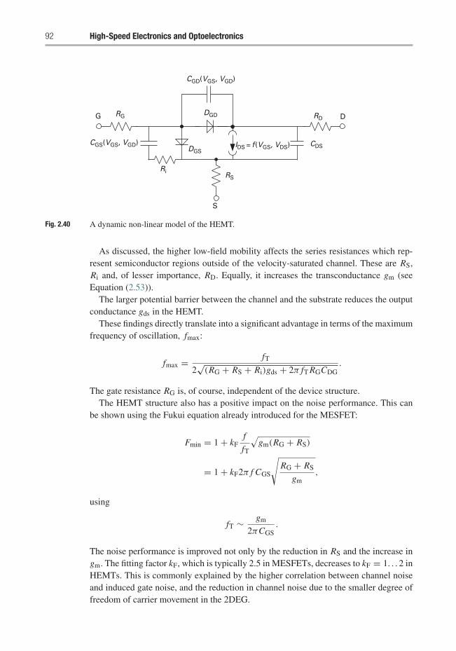
92 High-Speed Electronics and Optoelectronics
G
S
RG
Ri
DGS
RS
DGD
IDS = f (VGS, VDS) CDS
DRD
CGS(VGS, VGD)
CGD(VGS, VGD)
Fig. 2.40 A dynamic non-linear model of the HEMT.
As discussed, the higher low-field mobility affects the series resistances which rep-resent semiconductor regions outside of the velocity-saturated channel. These are RS,Ri and, of lesser importance, RD. Equally, it increases the transconductance gm (seeEquation (2.53)).
The larger potential barrier between the channel and the substrate reduces the outputconductance gds in the HEMT.
These findings directly translate into a significant advantage in terms of the maximumfrequency of oscillation, fmax:
fmax = fT
2√(RG + RS + Ri)gds + 2π fT RGCDG
.
The gate resistance RG is, of course, independent of the device structure.The HEMT structure also has a positive impact on the noise performance. This can
be shown using the Fukui equation already introduced for the MESFET:
Fmin = 1 + kFf
fT
√gm(RG + RS)
= 1 + kF2π f CGS
√RG + RS
gm,
using
fT ∼ gm
2πCGS.
The noise performance is improved not only by the reduction in RS and the increase ingm. The fitting factor kF, which is typically 2.5 in MESFETs, decreases to kF = 1. . . 2 inHEMTs. This is commonly explained by the higher correlation between channel noiseand induced gate noise, and the reduction in channel noise due to the smaller degree offreedom of carrier movement in the 2DEG.

Electronic devices 93
2.3.9 A practical HEMT example
The example chosen here is a metamorphic HEMT [4] because it illustrates many of theconcepts discussed.
The device structure is shown in Figure 2.41. The rather thick (1 μm) linearly gradedbuffer adapts the lattice constant of the GaAs substrate to the much larger lattice con-stant of In0.53Ga0.47As and Al0.48In0.52As (the ternary compounds are lattice-matchedto each other). Note the ‘double doping’ structure – there are δ-doped AlInAs layersbelow and above the InGaAs quantum well. In this case, it allows a density of the 2DEGof nS,max = 4 · 1012 cm2, together with the excellent carrier confinement in the quan-tum well. The excellent confinement is due to the large conduction band discontinuitybetween In0.53Ga0.47As and Al0.48In0.52As.
The ohmic contacts are placed on an In0.53Ga0.47As cap layer, which reduces the con-tact resistance and shields the metal–semiconductor interface from the Al-containingalloy, which is prone to formation of Al oxides at the exposed surface. The gate contacthas a T shape which reduces the series resistance of the gate stripe and hence RG. It isagain shown in Figure 2.42.
The cross-section of the gate metallisation is significantly larger than what wouldbe possible for a simple stripe with a 250 nm footprint, due to the T-gate structure.A refractory metal is used here so that the gate can be fabricated before the ohmiccontacts – this allows an easy self-alignment of the ohmic contacts with respect to theT-gate structure, minimising the distance between the source and drain contacts and thechannel, reducing RS and RD. The surface between the gate and the ohmic contacts ispassivated by a SiN layer.
The plot in Figure 2.43 shows the drain current and transconductance of the device,normalised to 1 mm gate width, at VDS = 1 V, which is well into the saturated regimefor this device. The actual gate width of the characterised device is 20 μm. The gm
maximum is placed at VGS = 0 – this is frequently done as it facilitates gate biasing.The threshold voltage is slightly below 0.6 V. The gm depression at higher VGS is alsoclearly visible.
AuGe–Au Ohmic contacts
T-Gate
SiN spacer
Semi-insulatingGaAs substrate
Al0.48 In0.52 As, δ-dotiert
Al0.48 In0.52 As, δ-doped
Al0.48 Ga0.52 As → Al0.48 In0.52 As
Linearly graded buffer1 μm
In0.53 Ga0.47 As cap
In0.53 Ga0.47 As quantum well
Fig. 2.41 Layer structure of the metamorphic HEMT structure discussed here.
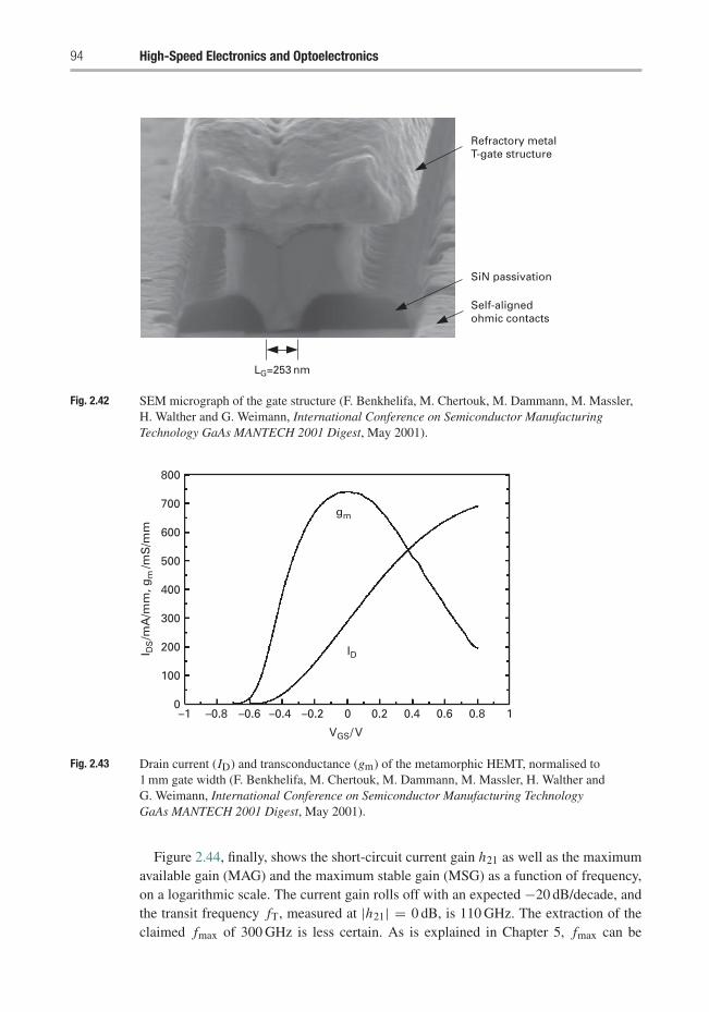
94 High-Speed Electronics and Optoelectronics
Refractory metalT-gate structure
SiN passivation
Self-alignedohmic contacts
LG=253 nm
Fig. 2.42 SEM micrograph of the gate structure (F. Benkhelifa, M. Chertouk, M. Dammann, M. Massler,H. Walther and G. Weimann, International Conference on Semiconductor ManufacturingTechnology GaAs MANTECH 2001 Digest, May 2001).
0–1 –0.8 –0.6 –0.4 –0.2
ID
gm
0
VGS/ V
I DS
/mA
/mm
, gm
/mS
/mm
0.2 0.4 0.6 0.8 1
100
200
300
400
500
600
700
800
Fig. 2.43 Drain current (ID) and transconductance (gm) of the metamorphic HEMT, normalised to1 mm gate width (F. Benkhelifa, M. Chertouk, M. Dammann, M. Massler, H. Walther andG. Weimann, International Conference on Semiconductor Manufacturing TechnologyGaAs MANTECH 2001 Digest, May 2001).
Figure 2.44, finally, shows the short-circuit current gain h21 as well as the maximumavailable gain (MAG) and the maximum stable gain (MSG) as a function of frequency,on a logarithmic scale. The current gain rolls off with an expected −20 dB/decade, andthe transit frequency fT, measured at |h21| = 0 dB, is 110 GHz. The extraction of theclaimed fmax of 300 GHz is less certain. As is explained in Chapter 5, fmax can be
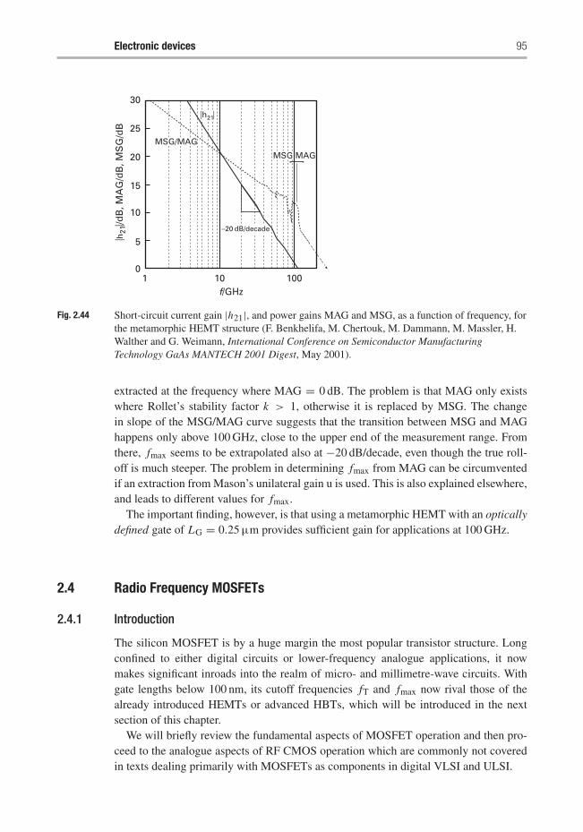
Electronic devices 95
10
5
10
15
20
25
30
10f/GHz
⎢h21
⎢/dB
, MA
G/d
B, M
SG
/dB
100
MSG/MAG
⎢h21⎢
–20 dB/decade
MSG MAG
Fig. 2.44 Short-circuit current gain |h21|, and power gains MAG and MSG, as a function of frequency, forthe metamorphic HEMT structure (F. Benkhelifa, M. Chertouk, M. Dammann, M. Massler, H.Walther and G. Weimann, International Conference on Semiconductor ManufacturingTechnology GaAs MANTECH 2001 Digest, May 2001).
extracted at the frequency where MAG = 0 dB. The problem is that MAG only existswhere Rollet’s stability factor k > 1, otherwise it is replaced by MSG. The changein slope of the MSG/MAG curve suggests that the transition between MSG and MAGhappens only above 100 GHz, close to the upper end of the measurement range. Fromthere, fmax seems to be extrapolated also at −20 dB/decade, even though the true roll-off is much steeper. The problem in determining fmax from MAG can be circumventedif an extraction from Mason’s unilateral gain u is used. This is also explained elsewhere,and leads to different values for fmax.
The important finding, however, is that using a metamorphic HEMT with an opticallydefined gate of LG = 0.25 μm provides sufficient gain for applications at 100 GHz.
2.4 Radio Frequency MOSFETs
2.4.1 Introduction
The silicon MOSFET is by a huge margin the most popular transistor structure. Longconfined to either digital circuits or lower-frequency analogue applications, it nowmakes significant inroads into the realm of micro- and millimetre-wave circuits. Withgate lengths below 100 nm, its cutoff frequencies fT and fmax now rival those of thealready introduced HEMTs or advanced HBTs, which will be introduced in the nextsection of this chapter.
We will briefly review the fundamental aspects of MOSFET operation and then pro-ceed to the analogue aspects of RF CMOS operation which are commonly not coveredin texts dealing primarily with MOSFETs as components in digital VLSI and ULSI.
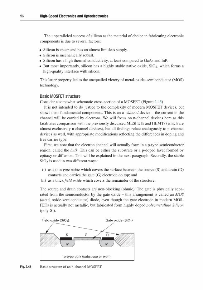
96 High-Speed Electronics and Optoelectronics
The unparalleled success of silicon as the material of choice in fabricating electroniccomponents is due to several factors:
• Silicon is cheap and has an almost limitless supply.• Silicon is mechanically robust.• Silicon has a high thermal conductivity, at least compared to GaAs and InP.• But most importantly, silicon has a highly stable native oxide, SiO2, which forms a
high-quality interface with silicon.
This latter property led to the unequalled victory of metal-oxide–semiconductor (MOS)technology.
Basic MOSFET structureConsider a somewhat schematic cross-section of a MOSFET (Figure 2.45).
It is not intended to do justice to the complexity of modern MOSFET devices, butshows their fundamental components. This is an n-channel device – the current in thechannel will be carried by electrons. We will focus on n-channel devices here as thisfacilitates comparison with the previously discussed MESFETs and HEMTs (which arealmost exclusively n-channel devices), but all findings relate analogously to p-channeldevices as well, with appropriate modifications reflecting the differences in doping andfree carrier type.
First, we note that the electron channel will actually form in a p-type semiconductorregion, called the bulk. This can be either the substrate or a p-doped layer formed byepitaxy or diffusion. This will be explained in the next paragraph. Secondly, the stableSiO2 is used in two different ways:
(i) as a thin gate oxide which covers the surface between the source (S) and drain (D)contacts and carries the gate (G) electrode on top; and
(ii) as a thick field oxide which covers the remainder of the structure.
The source and drain contacts are non-blocking (ohmic). The gate is physically sepa-rated from the semiconductor by the gate oxide – this arrangement is called an MOS(metal oxide-semiconductor) diode, even though the gate electrode in modern MOS-FETs is actually not metallic, but fabricated from highly doped polycrystalline Silicon(poly-Si).
Field oxide (SiO2) Gate oxide (SiO2)
p-type bulk (substrate or well)
S G D
n+n+
Fig. 2.45 Basic structure of an n-channel MOSFET.
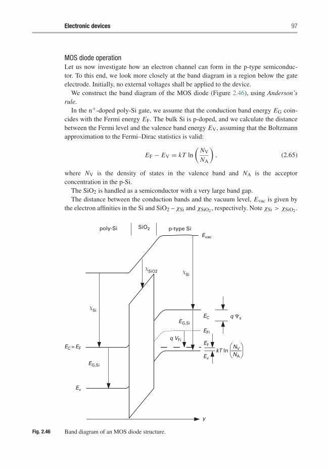
Electronic devices 97
MOS diode operationLet us now investigate how an electron channel can form in the p-type semiconduc-tor. To this end, we look more closely at the band diagram in a region below the gateelectrode. Initially, no external voltages shall be applied to the device.
We construct the band diagram of the MOS diode (Figure 2.46), using Anderson’srule.
In the n+-doped poly-Si gate, we assume that the conduction band energy EG coin-cides with the Fermi energy EF. The bulk Si is p-doped, and we calculate the distancebetween the Fermi level and the valence band energy EV, assuming that the Boltzmannapproximation to the Fermi–Dirac statistics is valid:
EF − EV = kT ln
(NV
NA
), (2.65)
where NV is the density of states in the valence band and NA is the acceptorconcentration in the p-Si.
The SiO2 is handled as a semiconductor with a very large band gap.The distance between the conduction bands and the vacuum level, Evac is given by
the electron affinities in the Si and SiO2 – χSi and χSiO2 , respectively. Note χSi > χSiO2 .
poly-Si SiO2 p-type SiEvac
EC = EF
EG,Si
Ev
y
EG,Si
EC
EFi
EF
Ev
kT lnNV——NA
q VFi
q �s
χSi
χSiO2
χSi
Fig. 2.46 Band diagram of an MOS diode structure.
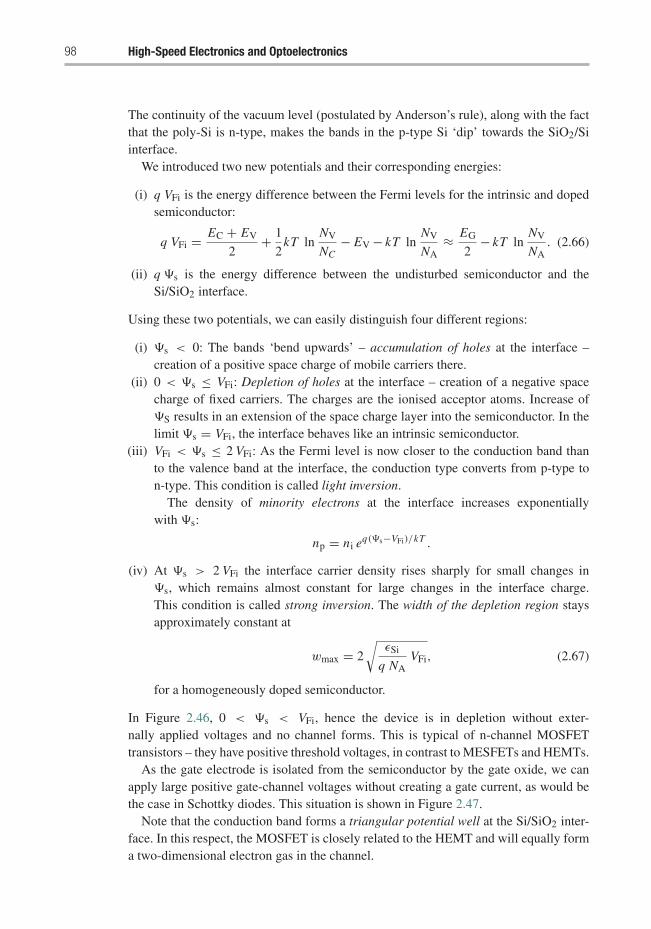
98 High-Speed Electronics and Optoelectronics
The continuity of the vacuum level (postulated by Anderson’s rule), along with the factthat the poly-Si is n-type, makes the bands in the p-type Si ‘dip’ towards the SiO2/Siinterface.
We introduced two new potentials and their corresponding energies:
(i) q VFi is the energy difference between the Fermi levels for the intrinsic and dopedsemiconductor:
q VFi = EC + EV
2+ 1
2kT ln
NV
NC− EV − kT ln
NV
NA≈ EG
2− kT ln
NV
NA. (2.66)
(ii) q �s is the energy difference between the undisturbed semiconductor and theSi/SiO2 interface.
Using these two potentials, we can easily distinguish four different regions:
(i) �s < 0: The bands ‘bend upwards’ – accumulation of holes at the interface –creation of a positive space charge of mobile carriers there.
(ii) 0 < �s ≤ VFi: Depletion of holes at the interface – creation of a negative spacecharge of fixed carriers. The charges are the ionised acceptor atoms. Increase of�S results in an extension of the space charge layer into the semiconductor. In thelimit �s = VFi, the interface behaves like an intrinsic semiconductor.
(iii) VFi < �s ≤ 2 VFi: As the Fermi level is now closer to the conduction band thanto the valence band at the interface, the conduction type converts from p-type ton-type. This condition is called light inversion.
The density of minority electrons at the interface increases exponentiallywith �s:
np = ni eq(�s−VFi)/kT .
(iv) At �s > 2 VFi the interface carrier density rises sharply for small changes in�s, which remains almost constant for large changes in the interface charge.This condition is called strong inversion. The width of the depletion region staysapproximately constant at
wmax = 2√
εSi
q NAVFi, (2.67)
for a homogeneously doped semiconductor.
In Figure 2.46, 0 < �s < VFi, hence the device is in depletion without exter-nally applied voltages and no channel forms. This is typical of n-channel MOSFETtransistors – they have positive threshold voltages, in contrast to MESFETs and HEMTs.
As the gate electrode is isolated from the semiconductor by the gate oxide, we canapply large positive gate-channel voltages without creating a gate current, as would bethe case in Schottky diodes. This situation is shown in Figure 2.47.
Note that the conduction band forms a triangular potential well at the Si/SiO2 inter-face. In this respect, the MOSFET is closely related to the HEMT and will equally forma two-dimensional electron gas in the channel.
Electronic devices 99
Evac
Ev
EC
EC
EFi
Ev
q VFi
q VG
q Vox
q �s
Fig. 2.47 MOS diode band diagram with positive VG.
The externally applied gate voltage drops partially across the gate oxide, partiallyacross the semiconductor and increases �s. In the situation drawn in Figure 2.47, thehypothetical intrinsic Fermi level already drops below the Fermi level in the undisturbedp-type semiconductor (�s > VFi), but �s > 2VFi has not been reached – the structureis in light inversion. An even more positive VG will introduce strong inversion.
If Vox is the voltage drop across the oxide,
VG = Vox + �s + 1
q
(kT ln
NV
NA− EG
), (2.68)
The last term in Equation (2.68) is the flat-band voltage VFB:
VFB =: 1
q
(kT ln
NV
NA− EG
). (2.69)
It is called flat-band because for VG = VFB, �s + Vox = 0 and the bands becomecompletely horizontal.
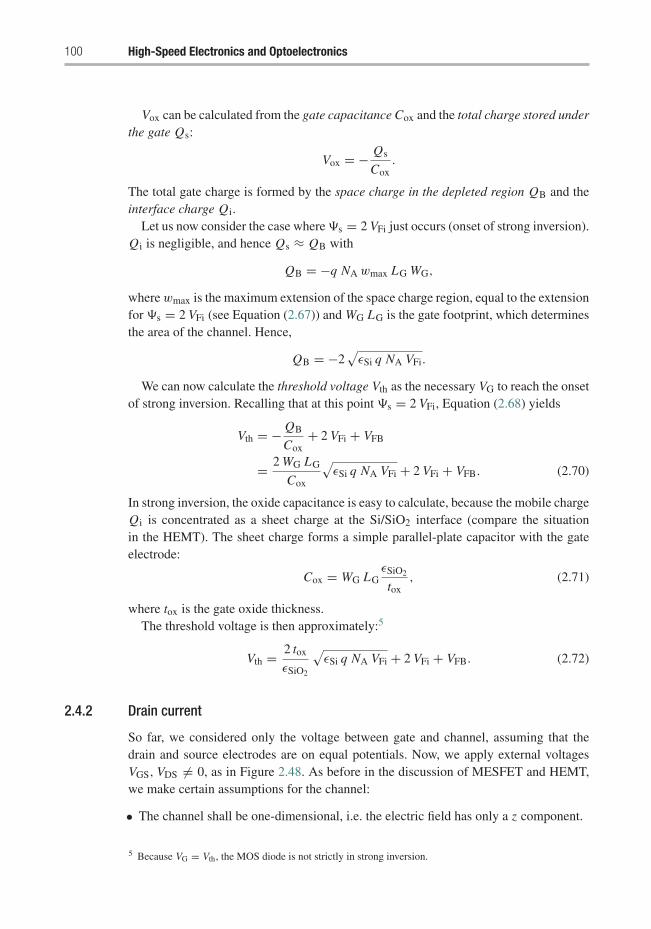
100 High-Speed Electronics and Optoelectronics
Vox can be calculated from the gate capacitance Cox and the total charge stored underthe gate Qs:
Vox = − Qs
Cox.
The total gate charge is formed by the space charge in the depleted region QB and theinterface charge Qi.
Let us now consider the case where �s = 2 VFi just occurs (onset of strong inversion).Qi is negligible, and hence Qs ≈ QB with
QB = −q NA wmax LG WG,
where wmax is the maximum extension of the space charge region, equal to the extensionfor �s = 2 VFi (see Equation (2.67)) and WG LG is the gate footprint, which determinesthe area of the channel. Hence,
QB = −2√εSi q NA VFi.
We can now calculate the threshold voltage Vth as the necessary VG to reach the onsetof strong inversion. Recalling that at this point �s = 2 VFi, Equation (2.68) yields
Vth = − QB
Cox+ 2 VFi + VFB
= 2 WG LG
Cox
√εSi q NA VFi + 2 VFi + VFB. (2.70)
In strong inversion, the oxide capacitance is easy to calculate, because the mobile chargeQi is concentrated as a sheet charge at the Si/SiO2 interface (compare the situationin the HEMT). The sheet charge forms a simple parallel-plate capacitor with the gateelectrode:
Cox = WG LGεSiO2
tox, (2.71)
where tox is the gate oxide thickness.The threshold voltage is then approximately:5
Vth = 2 tox
εSiO2
√εSi q NA VFi + 2 VFi + VFB. (2.72)
2.4.2 Drain current
So far, we considered only the voltage between gate and channel, assuming that thedrain and source electrodes are on equal potentials. Now, we apply external voltagesVGS, VDS �= 0, as in Figure 2.48. As before in the discussion of MESFET and HEMT,we make certain assumptions for the channel:
• The channel shall be one-dimensional, i.e. the electric field has only a z component.
5 Because VG = Vth, the MOS diode is not strictly in strong inversion.
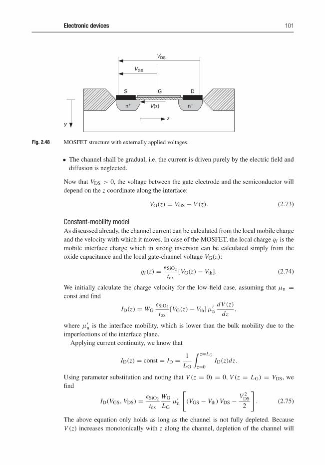
Electronic devices 101
VDS
VGS
V(z)
zy
S
n+ n+
G D
Fig. 2.48 MOSFET structure with externally applied voltages.
• The channel shall be gradual, i.e. the current is driven purely by the electric field anddiffusion is neglected.
Now that VDS > 0, the voltage between the gate electrode and the semiconductor willdepend on the z coordinate along the interface:
VG(z) = VGS − V (z). (2.73)
Constant-mobility modelAs discussed already, the channel current can be calculated from the local mobile chargeand the velocity with which it moves. In case of the MOSFET, the local charge qi is themobile interface charge which in strong inversion can be calculated simply from theoxide capacitance and the local gate-channel voltage VG(z):
qi (z) = εSiO2
tox[VG(z) − Vth]. (2.74)
We initially calculate the charge velocity for the low-field case, assuming that μn =const and find
ID(z) = WGεSiO2
tox[VG(z) − Vth]μ′
ndV (z)
dz,
where μ′n is the interface mobility, which is lower than the bulk mobility due to the
imperfections of the interface plane.Applying current continuity, we know that
ID(z) = const = ID = 1
LG
∫ z=LG
z=0ID(z)dz.
Using parameter substitution and noting that V (z = 0) = 0, V (z = LG) = VDS, wefind
ID(VGS, VDS) = εSiO2
tox
WG
LGμ′
n
[(VGS − Vth) VDS − V 2
DS
2
]. (2.75)
The above equation only holds as long as the channel is not fully depleted. BecauseV (z) increases monotonically with z along the channel, depletion of the channel will
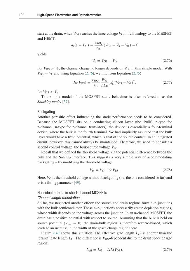
102 High-Speed Electronics and Optoelectronics
start at the drain, when VDS reaches the knee voltage Vk, in full analogy to the MESFETand HEMT.
qi (z = LG) = εSiO2
tox(VGS − Vk − Vth) = 0
yields
Vk = VGS − Vth (2.76)
For VDS > Vk, the channel charge no longer depends on VDS in this simple model. WithVDS = Vk and using Equation (2.76), we find from Equation (2.75)
ID(VGS) = εSiO2
tox
WG
2 LGμ′
n (VGS − Vth)2, (2.77)
for VDS > Vk.This simple model of the MOSFET static behaviour is often referred to as the
Shockley model [57].
BackgatingAnother parasitic effect influencing the static performance needs to be considered.Because the MOSFET sits on a conducting silicon layer (the ‘bulk’, p-type forn-channel, n-type for p-channel transistors), the device is essentially a four-terminaldevice, where the bulk is the fourth terminal. We had implicitly assumed that the bulklayer would have a fixed potential, which is that of the source contact. In an integratedcircuit, however, this cannot always be maintained. Therefore, we need to consider asecond control voltage, the bulk-source voltage VBS.
Recall that we defined the threshold voltage via the potential difference between thebulk and the Si/SiO2 interface. This suggests a very simple way of accommodatingbackgating – by modifying the threshold voltage:
Vth = Vt0 − γ VBS. (2.78)
Here, Vt0 is the threshold voltage without backgating (i.e. the one considered so far) andγ is a fitting parameter [49].
Non-ideal effects in short-channel MOSFETsChannel length modulation.So far, we neglected another effect: the source and drain regions form n–p junctionswith the bulk semiconductor. These n–p junctions necessarily create depletion regions,whose width depends on the voltage across the junction. In an n-channel MOSFET, thedrain has a positive potential with respect to source. Assuming that the bulk is held onsource potential (VBS = 0), the drain-bulk region is therefore reverse-biased, whichleads to an increase in the width of the space charge region there.
Figure 2.49 shows this situation. The effective gate length Leff is shorter than the‘drawn’ gate length LG. The difference is VDS-dependent due to the drain space chargeregion:
Leff = LG − �L(VDS). (2.79)
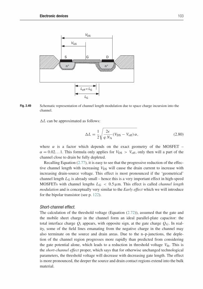
Electronic devices 103
VDS
VGS
S
n+ n+
G
Leff < LG
LG
D
Fig. 2.49 Schematic representation of channel length modulation due to space charge incursion into thechannel.
�L can be approximated as follows:
�L = 1
2
√2ε
q NA(VDS − Voff) α, (2.80)
where α is a factor which depends on the exact geometry of the MOSFET –α = 0.02. . . 1. This formula only applies for VDS > Voff, only then will a part of thechannel close to drain be fully depleted.
Recalling Equation (2.77), it is easy to see that the progressive reduction of the effec-tive channel length with increasing VDS will cause the drain current to increase withincreasing drain-source voltage. This effect is most pronounced if the ‘geometrical’channel length LG is already small – hence this is a very important effect in high-speedMOSFETs with channel lengths LG < 0.5 μm. This effect is called channel lengthmodulation and is conceptually very similar to the Early effect which we will introducefor the bipolar transistor (see p. 122).
Short-channel effect.The calculation of the threshold voltage (Equation (2.72)), assumed that the gate andthe mobile sheet charge in the channel form an ideal parallel-plate capacitor: thetotal interface charge Qi appears, with opposite sign, at the gate charge QG . In real-ity, some of the field lines emanating from the negative charge in the channel mayalso terminate on the source and drain areas. Due to the n–p-junctions, the deple-tion of the channel region progresses more rapidly than predicted from consideringthe gate potential alone, which leads to a reduction in threshold voltage Vth. This isthe short-channel effect proper, which says that for otherwise unchanged technologicalparameters, the threshold voltage will decrease with decreasing gate length. The effectis more pronounced, the deeper the source and drain contact regions extend into the bulkmaterial.
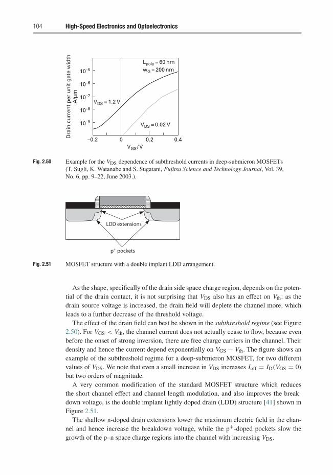
104 High-Speed Electronics and Optoelectronics
10–5
10–6
10–7
10–8
10–9
–0.2Dra
in c
urr
ent
per
un
it g
ate
wid
thA
/μm
0 0.2VGS/ V
VDS = 0.02 V
VDS = 1.2 V
Lpoly = 60 nmwG = 200 nm
0.4
Fig. 2.50 Example for the VDS dependence of subthreshold currents in deep-submicron MOSFETs(T. Sugli, K. Watanabe and S. Sugatani, Fujitsu Science and Technology Journal, Vol. 39,No. 6, pp. 9–22, June 2003.).
LDD extensions
p+ pockets
Fig. 2.51 MOSFET structure with a double implant LDD arrangement.
As the shape, specifically of the drain side space charge region, depends on the poten-tial of the drain contact, it is not surprising that VDS also has an effect on Vth: as thedrain-source voltage is increased, the drain field will deplete the channel more, whichleads to a further decrease of the threshold voltage.
The effect of the drain field can best be shown in the subthreshold regime (see Figure2.50). For VGS < Vth, the channel current does not actually cease to flow, because evenbefore the onset of strong inversion, there are free charge carriers in the channel. Theirdensity and hence the current depend exponentially on VGS − Vth. The figure shows anexample of the subthreshold regime for a deep-submicron MOSFET, for two differentvalues of VDS. We note that even a small increase in VDS increases Ioff = ID(VGS = 0)but two orders of magnitude.
A very common modification of the standard MOSFET structure which reducesthe short-channel effect and channel length modulation, and also improves the break-down voltage, is the double implant lightly doped drain (LDD) structure [41] shown inFigure 2.51.
The shallow n-doped drain extensions lower the maximum electric field in the chan-nel and hence increase the breakdown voltage, while the p+-doped pockets slow thegrowth of the p–n space charge regions into the channel with increasing VDS.
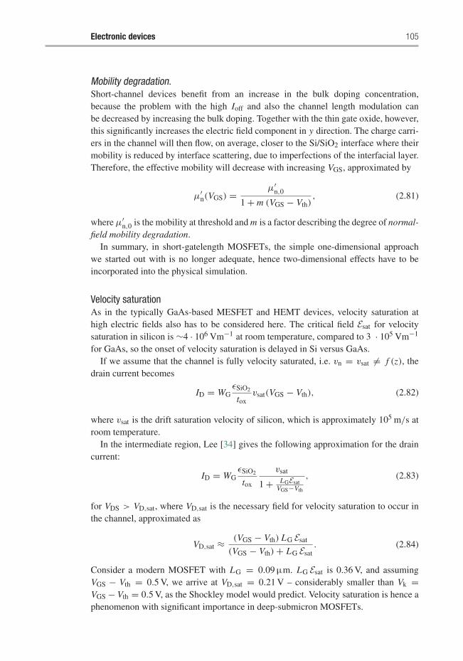
Electronic devices 105
Mobility degradation.Short-channel devices benefit from an increase in the bulk doping concentration,because the problem with the high Ioff and also the channel length modulation canbe decreased by increasing the bulk doping. Together with the thin gate oxide, however,this significantly increases the electric field component in y direction. The charge carri-ers in the channel will then flow, on average, closer to the Si/SiO2 interface where theirmobility is reduced by interface scattering, due to imperfections of the interfacial layer.Therefore, the effective mobility will decrease with increasing VGS, approximated by
μ′n(VGS) = μ′
n,0
1 + m (VGS − Vth), (2.81)
where μ′n,0 is the mobility at threshold and m is a factor describing the degree of normal-
field mobility degradation.In summary, in short-gatelength MOSFETs, the simple one-dimensional approach
we started out with is no longer adequate, hence two-dimensional effects have to beincorporated into the physical simulation.
Velocity saturationAs in the typically GaAs-based MESFET and HEMT devices, velocity saturation athigh electric fields also has to be considered here. The critical field Esat for velocitysaturation in silicon is ∼4 · 106 Vm−1 at room temperature, compared to 3 · 105 Vm−1
for GaAs, so the onset of velocity saturation is delayed in Si versus GaAs.If we assume that the channel is fully velocity saturated, i.e. vn = vsat �= f (z), the
drain current becomes
ID = WGεSiO2
toxvsat(VGS − Vth), (2.82)
where vsat is the drift saturation velocity of silicon, which is approximately 105 m/s atroom temperature.
In the intermediate region, Lee [34] gives the following approximation for the draincurrent:
ID = WGεSiO2
tox
vsat
1 + LGEsatVGS−Vth
, (2.83)
for VDS > VD,sat, where VD,sat is the necessary field for velocity saturation to occur inthe channel, approximated as
VD,sat ≈ (VGS − Vth) LG Esat
(VGS − Vth) + LG Esat. (2.84)
Consider a modern MOSFET with LG = 0.09 μm. LG Esat is 0.36 V, and assumingVGS − Vth = 0.5 V, we arrive at VD,sat = 0.21 V – considerably smaller than Vk =VGS − Vth = 0.5 V, as the Shockley model would predict. Velocity saturation is hence aphenomenon with significant importance in deep-submicron MOSFETs.
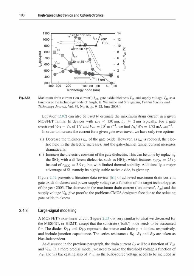
106 High-Speed Electronics and Optoelectronics
400300
400
500
600
700
800
900
1000
1100
300 200
Vdd
Tox
Ion
Ion
Technology node (nm)
To
x (n
m),
Vd
d (
V)
I on(μ
A/μ
m)
100 80
15 nm
30 to 35 nm
40 to 50 nm
Lg: 70 to 100 nm2001ITRS
60 40 20
0
2
4
6
8
10
12
14
Fig. 2.52 Maximum drain current (‘on-current’) Ion, gate oxide thickness Tox and supply voltage Vdd as afunction of the technology node (T. Sugli, K. Watanabe and S. Sugatani, Fujitsu Science andTechnology Journal, Vol. 39, No. 6, pp. 9–22, June 2003.).
Equation (2.82) can also be used to estimate the maximum drain current in a givenMOSFET family. In devices with LG ≤ 130 nm, tox ≈ 2 nm typically. For a gateovertravel VGS − Vth of 1 V and Vsat = 105 m s−1, we find ID/WG = 1.72 mA μm−1.
In order to increase the current for a given gate over travel, we have only two options:
(i) Decrease the thickness tox of the gate oxide. However, as tox is reduced, the elec-tric field in the dielectric increases, and the gate-channel tunnel current increasesdramatically.
(ii) Increase the dielectric constant of the gate dielectric. This can be done by replacingthe SiO2 with a different dielectric, such as HfO2, which features εHfO2 = 25 ε0
instead of εSiO2 = 3.9 ε0, but with limited thermal stability. Additionally, a majoradvantage of Si, namely its highly stable native oxide, is given up.
Figure 2.52 presents a literature data review [61] of achieved maximum drain current,gate oxide thickness and power supply voltage as a function of the target technology, asof the year 2003. The decrease in the maximum drain current (‘on current’, Ion) and thesupply voltage Vdd give proof to the problems CMOS designers face due to the reducinggate oxide thickness.
2.4.3 Large-signal modelling
A MOSFET’s non-linear circuit (Figure 2.53), is very similar to what we discussed forthe MESFET, or HEMT, except that the substrate (‘bulk’) node needs to be accountedfor. The diodes DBS and DBD represent the source and drain p–n diodes, respectively,and include junction capacitance. The series resistances RG, RS and RD are taken asbias-independent.
As discussed in the previous paragraph, the drain current ID will be a function of VGS
and VDS. In a more precise model, we need to make the threshold voltage a function ofVDS and via backgating also of VBS, so the bulk-source voltage needs to be included as
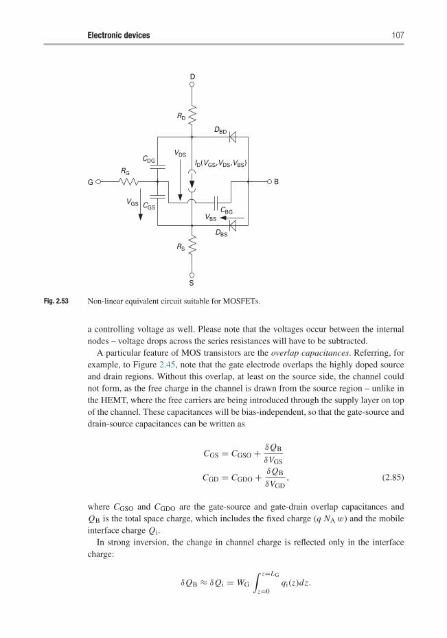
Electronic devices 107
D
RD
RG
CDG
VGS
VDS
CBGVBS
DBS
RS
ID(VGS,VDS,VBS)
CGS
DBD
B
S
G
Fig. 2.53 Non-linear equivalent circuit suitable for MOSFETs.
a controlling voltage as well. Please note that the voltages occur between the internalnodes – voltage drops across the series resistances will have to be subtracted.
A particular feature of MOS transistors are the overlap capacitances. Referring, forexample, to Figure 2.45, note that the gate electrode overlaps the highly doped sourceand drain regions. Without this overlap, at least on the source side, the channel couldnot form, as the free charge in the channel is drawn from the source region – unlike inthe HEMT, where the free carriers are being introduced through the supply layer on topof the channel. These capacitances will be bias-independent, so that the gate-source anddrain-source capacitances can be written as
CGS = CGSO + δQB
δVGS
CGD = CGDO + δQB
δVGD, (2.85)
where CGSO and CGDO are the gate-source and gate-drain overlap capacitances andQB is the total space charge, which includes the fixed charge (q NA w) and the mobileinterface charge Qi.
In strong inversion, the change in channel charge is reflected only in the interfacecharge:
δQB ≈ δQi = WG
∫ z=LG
z=0qi(z)dz.
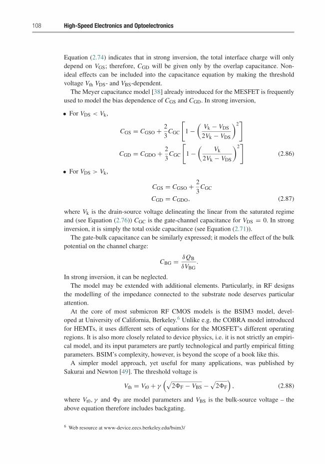
108 High-Speed Electronics and Optoelectronics
Equation (2.74) indicates that in strong inversion, the total interface charge will onlydepend on VGS; therefore, CGD will be given only by the overlap capacitance. Non-ideal effects can be included into the capacitance equation by making the thresholdvoltage Vth VDS- and VBS-dependent.
The Meyer capacitance model [38] already introduced for the MESFET is frequentlyused to model the bias dependence of CGS and CGD. In strong inversion,
• For VDS < Vk,
CGS = CGSO + 2
3CGC
[1 −
(Vk − VDS
2Vk − VDS
)2]
CGD = CGDO + 2
3CGC
[1 −
(Vk
2Vk − VDS
)2]
(2.86)
• For VDS > Vk,
CGS = CGSO + 2
3CGC
CGD = CGDO, (2.87)
where Vk is the drain-source voltage delineating the linear from the saturated regimeand (see Equation (2.76)) CGC is the gate-channel capacitance for VDS = 0. In stronginversion, it is simply the total oxide capacitance (see Equation (2.71)).
The gate-bulk capacitance can be similarly expressed; it models the effect of the bulkpotential on the channel charge:
CBG = δQB
δVBG.
In strong inversion, it can be neglected.The model may be extended with additional elements. Particularly, in RF designs
the modelling of the impedance connected to the substrate node deserves particularattention.
At the core of most submicron RF CMOS models is the BSIM3 model, devel-oped at University of California, Berkeley.6 Unlike e.g. the COBRA model introducedfor HEMTs, it uses different sets of equations for the MOSFET’s different operatingregions. It is also more closely related to device physics, i.e. it is not strictly an empiri-cal model, and its input parameters are partly technological and partly empirical fittingparameters. BSIM’s complexity, however, is beyond the scope of a book like this.
A simpler model approach, yet useful for many applications, was published bySakurai and Newton [49]. The threshold voltage is
Vth = Vt0 + γ(√
2�F − VBS − √2�F
), (2.88)
where Vt0, γ and �F are model parameters and VBS is the bulk-source voltage – theabove equation therefore includes backgating.
6 Web resource at www-device.eecs.berkeley.edu/bsim3/
Electronic devices 109
The drain-source saturation voltage, Vk, is modelled as
Vk = K (VGS − Vth)m, (2.89)
where K and m are model parameters. This formulation is more flexible compared toEquation (2.76) and allows to include velocity saturation effects.
The drain current at VDS = Vk is
ID,sat = WG
LeffB (VGS − Vth)
n, (2.90)
where B and n are model parameters. With variation of n, we can address both theconstant-mobility model (n = 2) and the constant velocity model (n = 1); however, asn is not VDS-dependent, we cannot move from one regime to the other.
A VGS-dependent n, on the other hand, would allow to include the deterioration ofmobility at high electric fields normal to the Si/SiO2 interface (see Equation (2.81)).
The drain current formulation distinguishes between the saturated and non-saturatedregions:
• For VDS > Vk,
ID = ID,sat (1 + λ VDS), (2.91)
where λ = λ0 − λ1 VBS.• For VDS < Vk,
ID = ID,sat (1 + λ VDS)
(2 − VDS
Vk
)VDS
Vk. (2.92)
2.4.4 Small-signal model and RF performance
The small-signal equivalent circuit of the MOSFET is very similar to that used forMESFET or HEMT, but must account for the additional substrate node.
Figure 2.54 shows that a fourth terminal (B) has been added, which is capaci-tively coupled to the internal gate, source and drain nodes. CBG is shown to facilitatecomparison with Figure 2.53; in saturation it is neglected.
G
RG
vgs
CGS
gm vgs gds
+gmb vbs
RS vbs
CBSCBG CBD
RD
D
B
CGD
S
Fig. 2.54 MOSFET small-signal equivalent circuit.
110 High-Speed Electronics and Optoelectronics
Backgating is included by a special backgating transconductance:
gmb = δ ID
δVBS.
The transconductance in the constant-mobility limit and for VDS > Vk is
gm = d ID
dVGS= εSiO2
tox
WG μ′n
LG(VGS − Vth), (2.93)
using Equation (2.77).In the constant-velocity limit,
gm = εSiO2
toxWG vsat. (2.94)
The output conductance is
gds = δ ID
δVDS.
In the linear region (VDS < Vk), using the constant-mobility drain current Equa-tion (2.75), we find
gds = εSiO2 WG μ′n
LG tox[(VGS − Vth) − VDS] . (2.95)
In the saturated region (VDS > Vk), we use the Sakurai–Newton model Equation (2.91)as our simplified physical regions would predict gds = 0 there:
gds = λID,sat = λB WG
Leff(VGS − Vth)
n . (2.96)
To reconcile the Sakurai–Newton model with the constant-mobility model, choose B =(εSiO2 μ
′n)/tox, n = 2, Leff = LG.
Transit frequency.We again approximate the transit frequency with
fT = gm
CGS + CGD.
In saturation and using the Meyer capacitance equations (2.87),
fT = gm
CGSO + CGDO + 23 Cox
.
While recognising the importance of the overlap capacitances, let us assume forsimplification that Cox dominates.
For the transconductance, we need to distinguish between the constant-mobility andconstant-velocity models. For the constant mobility, using Equation (2.93), we obtain
fT = 3μ′n
4π L2G
(VGS − Vth). (2.97)
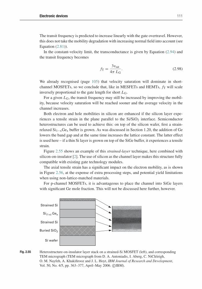
Electronic devices 111
The transit frequency is predicted to increase linearly with the gate overtravel. However,this does not take the mobility degradation with increasing normal field into account (seeEquation (2.81)).
In the constant-velocity limit, the transconductance is given by Equation (2.94) andthe transit frequency becomes
fT = 3vsat
4π LG. (2.98)
We already recognised (page 105) that velocity saturation will dominate in short-channel MOSFETs, so we conclude that, like in MESFETs and HEMTs, fT will scaleinversely proportional to the gate length for short LG.
For a given LG, the transit frequency may still be increased by improving the mobil-ity, because velocity saturation will be reached sooner and the average velocity in thechannel increases.
Both electron and hole mobilities in silicon are enhanced if the silicon layer expe-riences a tensile strain in the plane parallel to the Si/SiO2 interface. Semiconductorheterostructures can be used to achieve this: on top of the silicon wafer, first a strain-relaxed Si1−xGex buffer is grown. As was discussed in Section 1.20, the addition of Gelowers the band gap and at the same time increases the lattice constant. The latter effectis used here – if a thin Si layer is grown on top of the SiGe buffer, it experiences a tensilestrain.
Figure 2.55 shows an example of this strained-layer technique, here combined withsilicon-on-insulator [2]. The use of silicon as the channel layer makes this structure fullycompatible with existing gate technology modules.
The axial tensile strain has a significant impact on the electron mobility, as is shownin Figure 2.56, at the expense of extra processing steps, and potential yield limitationswhen using non-lattice-matched materials.
For p-channel MOSFETs, it is advantageous to place the channel into SiGe layerswith significant Ge mole fraction. This will not be discussed here further, however.
Strained Si
Strained Si
Buried SiO2
Si wafer
Si(1-x) Gex
Fig. 2.55 Heterostructure-on-insulator layer stack on a strained-Si MOSFET (left), and correspondingTEM micrograph (TEM micrograph from D. A. Antoniadis, I. Aberg, C. NiCleirigh,O. M. Nayfeh, A. Khakifirooz and J. L. Hoyt, IBM Journal of Research and Development,Vol. 50, No. 4/5, pp. 363–377, April–May 2006. c©IBM).
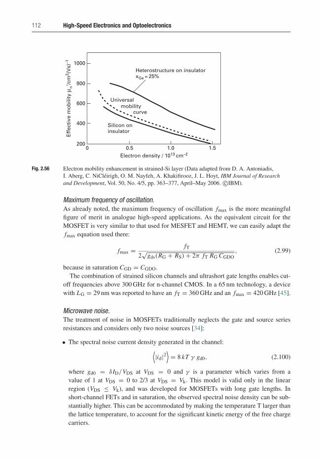
112 High-Speed Electronics and Optoelectronics
0200
400
600
800
1000
0.5 1.0 1.5Electron density / 1013 cm–2
Eff
ecti
ve m
ob
ility
μ ′/
cm2 (
Vs)
–1n
Silicon oninsulator
Universalmobility
curve
Heterostructure on insulatorxGe = 25%
Fig. 2.56 Electron mobility enhancement in strained-Si layer (Data adapted from D. A. Antoniadis,I. Aberg, C. NiCleirigh, O. M. Nayfeh, A. Khakifirooz, J. L. Hoyt, IBM Journal of Researchand Development, Vol. 50, No. 4/5, pp. 363–377, April–May 2006. c©IBM).
Maximum frequency of oscillation.As already noted, the maximum frequency of oscillation fmax is the more meaningfulfigure of merit in analogue high-speed applications. As the equivalent circuit for theMOSFET is very similar to that used for MESFET and HEMT, we can easily adapt thefmax equation used there:
fmax = fT
2√
gds(RG + RS) + 2π fT RG CGDO, (2.99)
because in saturation CGD = CGDO.The combination of strained silicon channels and ultrashort gate lengths enables cut-
off frequencies above 300 GHz for n-channel CMOS. In a 65 nm technology, a devicewith LG = 29 nm was reported to have an fT = 360 GHz and an fmax = 420 GHz [45].
Microwave noise.The treatment of noise in MOSFETs traditionally neglects the gate and source seriesresistances and considers only two noise sources [34]:
• The spectral noise current density generated in the channel:⟨|id|2
⟩= 8 kT γ gd0, (2.100)
where gd0 = δ ID/VDS at VDS = 0 and γ is a parameter which varies from avalue of 1 at VDS = 0 to 2/3 at VDS = Vk. This model is valid only in the linearregion (VDS ≤ Vk), and was developed for MOSFETs with long gate lengths. Inshort-channel FETs and in saturation, the observed spectral noise density can be sub-stantially higher. This can be accommodated by making the temperature T larger thanthe lattice temperature, to account for the significant kinetic energy of the free chargecarriers.
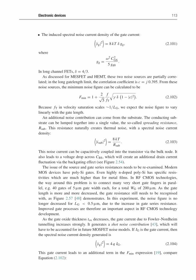
Electronic devices 113
• The induced spectral noise current density of the gate current:⟨|ig|2
⟩= 8 kT δ gg, (2.101)
where
gg = ω2 C2GS
5 gd0.
In long channel FETs, δ = 4/3.As discussed for MESFET and HEMT, these two noise sources are partially corre-
lated; in the long gatelength limit, the correlation coefficient is c = j 0.395. From thesenoise sources, the minimum noise figure can be calculated to be
Fmin = 1 + 2√5
f
fT
√γ δ
(1 − |c|2)
. (2.102)
Because fT in velocity saturation scales ∼1/LG, we expect the noise figure to varylinearly with the gate length.
An additional noise contribution can come from the substrate. The conducting sub-strate can be lumped together into a single value, the so-called spreading resistance,Rsub. This resistance naturally creates thermal noise, with a spectral noise currentdensity: ⟨
|isub|2⟩= 8 kT
Rsub. (2.103)
This noise current can be capacitively coupled into the transistor via the bulk node. Italso leads to a voltage drop across CBS, which will create an additional drain currentfluctuation via the backgating effect (see Figure 2.54).
The issue of the source and gate series resistances needs to be re-examined. ModernMOS devices have poly-Si gates. Even highly n-doped poly-Si has specific resis-tivities which are much higher than for metal films. In RF CMOS technologies,the way around this problem is to connect many very short gate fingers in paral-lel, e.g. 40 gates of 5 μm gate width each, for a total WG of 200 μm. As the gatelength is more and more decreased, the gate resistance still needs to be recognisedwith, as Figure 2.57 [48] demonstrates. In this experiment, the noise figure is nolonger decreased for LG < 0.5 μm, due to the increase in gate series resistance.Improved gate processes are therefore an important aspect in RF CMOS technologydevelopment.
As the gate oxide thickness tox decreases, the gate current due to Fowler–Nordheimtunnelling increases strongly. It generates a shot noise contribution [43], which willhave to be accounted for in future MOSFET noise models. If IG is the gate current, thenthe spectral noise current density generated is⟨
|ig|2⟩= 4 q IG. (2.104)
This gate current leads to an additional term in the Fmin expression [19], compareEquation (2.102):
114 High-Speed Electronics and Optoelectronics
0.10
1
2
3
0.2
f=2 GHz
0.4 0.6 1LG/μm
F min
/dB
Fig. 2.57 Noise figure versus gate length for n-channel MOSFETs (40 fingers of WG = 5 μm each)(M. Saito, M. Ono, R. Fujimoto, H. Tanimoto, N. Ito, T. Yoshitomi, T. Ohguro, H. S. Momoseand H. Iwai, IEEE Transactions on Electron Devices, Vol. ED-45, pp. 737–742, March 1998.c©1998 IEEE).
Fmin = 1 + f
fT
√δγ
5(1 − c2
G) + 2q IGgd0γ
16π2 kT f 2 C2GS
. (2.105)
For low frequencies, the second term under the root dominates and the minimum noisefigure becomes independent of frequency:
Fmin ≈ 1 + 1
gm
√2q IGgd0γ
4 kT. (2.106)
The appearance of a frequency-independent component in Fmin( f ) is a tell-tale sign ofgate-related shot noise.
A gate current due to Fowler–Nordheim tunnelling is expected to vary with thenormal electric field across the gate oxide as
IG ∼ E2y,SiO2
exp
(− φ
32
Ey,SiO2
), (2.107)
where φ is the barrier at the interface. It will therefore be strong function of the gateovertravel VGS − Vth. The occurrence of gate leakage has thus also important impli-cations on the design of low-noise amplifiers using sub-100 nm CMOS technologies,namely in the choice of the bias point.
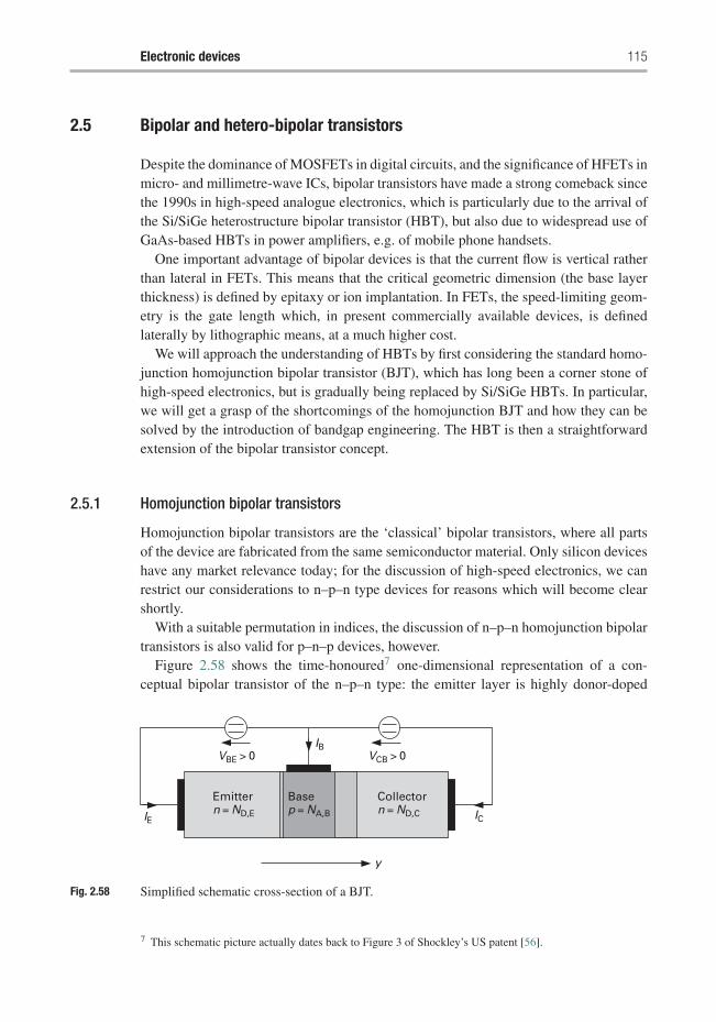
Electronic devices 115
2.5 Bipolar and hetero-bipolar transistors
Despite the dominance of MOSFETs in digital circuits, and the significance of HFETs inmicro- and millimetre-wave ICs, bipolar transistors have made a strong comeback sincethe 1990s in high-speed analogue electronics, which is particularly due to the arrival ofthe Si/SiGe heterostructure bipolar transistor (HBT), but also due to widespread use ofGaAs-based HBTs in power amplifiers, e.g. of mobile phone handsets.
One important advantage of bipolar devices is that the current flow is vertical ratherthan lateral in FETs. This means that the critical geometric dimension (the base layerthickness) is defined by epitaxy or ion implantation. In FETs, the speed-limiting geom-etry is the gate length which, in present commercially available devices, is definedlaterally by lithographic means, at a much higher cost.
We will approach the understanding of HBTs by first considering the standard homo-junction homojunction bipolar transistor (BJT), which has long been a corner stone ofhigh-speed electronics, but is gradually being replaced by Si/SiGe HBTs. In particular,we will get a grasp of the shortcomings of the homojunction BJT and how they can besolved by the introduction of bandgap engineering. The HBT is then a straightforwardextension of the bipolar transistor concept.
2.5.1 Homojunction bipolar transistors
Homojunction bipolar transistors are the ‘classical’ bipolar transistors, where all partsof the device are fabricated from the same semiconductor material. Only silicon deviceshave any market relevance today; for the discussion of high-speed electronics, we canrestrict our considerations to n–p–n type devices for reasons which will become clearshortly.
With a suitable permutation in indices, the discussion of n–p–n homojunction bipolartransistors is also valid for p–n–p devices, however.
Figure 2.58 shows the time-honoured7 one-dimensional representation of a con-ceptual bipolar transistor of the n–p–n type: the emitter layer is highly donor-doped
y
IE IC
IBVBE > 0 VCB > 0
Emittern = ND,E
Collectorn = ND,C
Basep = NA,B
Fig. 2.58 Simplified schematic cross-section of a BJT.
7 This schematic picture actually dates back to Figure 3 of Shockley’s US patent [56].
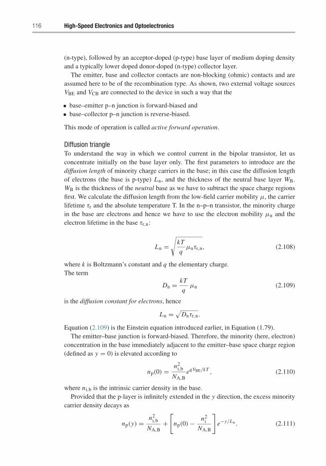
116 High-Speed Electronics and Optoelectronics
(n-type), followed by an acceptor-doped (p-type) base layer of medium doping densityand a typically lower doped donor-doped (n-type) collector layer.
The emitter, base and collector contacts are non-blocking (ohmic) contacts and areassumed here to be of the recombination type. As shown, two external voltage sourcesVBE and VCB are connected to the device in such a way that the
• base–emitter p–n junction is forward-biased and• base–collector p–n junction is reverse-biased.
This mode of operation is called active forward operation.
Diffusion triangleTo understand the way in which we control current in the bipolar transistor, let usconcentrate initially on the base layer only. The first parameters to introduce are thediffusion length of minority charge carriers in the base; in this case the diffusion lengthof electrons (the base is p-type) Ln, and the thickness of the neutral base layer WB.WB is the thickness of the neutral base as we have to subtract the space charge regionsfirst. We calculate the diffusion length from the low-field carrier mobility μ, the carrierlifetime τr and the absolute temperature T. In the n–p–n transistor, the minority chargein the base are electrons and hence we have to use the electron mobility μn and theelectron lifetime in the base τr,n:
Ln =√
kT
qμnτr,n, (2.108)
where k is Boltzmann’s constant and q the elementary charge.The term
Dn = kT
qμn (2.109)
is the diffusion constant for electrons, hence
Ln = √Dnτr,n.
Equation (2.109) is the Einstein equation introduced earlier, in Equation (1.79).The emitter–base junction is forward-biased. Therefore, the minority (here, electron)
concentration in the base immediately adjacent to the emitter–base space charge region(defined as y = 0) is elevated according to
np(0) = n2i,b
NA,BeqVBE/kT , (2.110)
where ni,b is the intrinsic carrier density in the base.Provided that the p-layer is infinitely extended in the y direction, the excess minority
carrier density decays as
np(y) = n2i,b
NA,B+
[np(0) − n2
i
NA,B
]e−y/Ln . (2.111)
Electronic devices 117
np
np(0) = np,0.e
Em
itte
r
Co
llect
or
0 WB
y
VBE/VT
np(WB) = np,0.e
VCB/VT–
Fig. 2.59 Minority carrier concentration np in the base of an n–p–n bipolar transistor, as a function ofcoordinate y perpendicular to the surface.
In the bipolar transistor, however, the base width WB is made much shorter than thediffusion length:8
WB � Ln.
It is instructive to estimate a numeric value for Ln. Both μn and τr,n are strong functionsof doping. Let us assume that for a reasonable base doping concentration, τr,n = 1 μsand μn = 500 cm2(Vs)−1. Then the diffusion length amounts to Ln = 36 μm, which iscertainly much larger than the base width in any microwave bipolar transistor.
The reverse bias across the collector–base junction will cause the minority carrierat the collector side of the neutral base (y = WB) to be significantly smaller than theminority carrier density in the undisturbed semiconductor:
np(WB) = n2i,b
NA,Be−qVCB/kT . (2.112)
Provided that WB � Ln, which is equivalent to neglecting recombination in the base,the distribution of minority carriers in the base as a function of the coordinate y (whichis perpendicular to the surface of the device) is a linear function (see Figure 2.59). Dueto its geometric shape, it is sometimes referred to as the diffusion triangle.
Collector current equationIn the classic bipolar transistor, the current is carried through the base layer by diffusiononly, because the electric field in y direction in the neutral base can be neglected.
We formulate the electron current density flowing through the base layer as adiffusion current:
Jn,B = q Dndnp
dy= q Dn
np(0) − np(WB)
WB≈ q Dn
np(0)
WB, (2.113)
8 The so-called short-base diode condition.
118 High-Speed Electronics and Optoelectronics
because np(0) � np(WB). Dn is the diffusion constant of electrons in the base, whichhas already been defined in Equation (2.109).
Note that due to dnp(y)/dy = const, the current is constant throughout the base. Weobtain the collector current by inserting Equation (2.110) into (2.113) and multiplyingwith the emitter area AE:
IC = q AE Dnn2
ib
WB NA,BeVBE/VT , (2.114)
still considering np(WB) � np(0), i.e. under reverse collector–emitter bias. Withoutthis condition, we obtain
IC = q AE Dnn2
ib
WB NA,B
(eVBE/VT − e−VCB/VT
). (2.115)
The expression in the denominator of Equation (2.115) WB NA,B is the Gummel numberof the base layer, GB. In the above example and also below, we assume that the basedoping concentration is constant across the neutral base. If this is not the case, i.e.NA,B = f (y), we calculate the Gummel number as the integral sheet charge in thebase:
GB =∫ WB
0NA,B(y)dy. (2.116)
Ideal base currentWe will now calculate the ideal base current of a bipolar transistor, i.e. the base currentwithout components due to recombination.
For this, we consider the emitter layer as a short-base diode also: WE � Lp, whereWE is the emitter width and Lp is the diffusion constant of minorities (here, holes) inthe emitter:
Lp = √Dpτr,p, (2.117)
where τr,p is the carrier lifetime of holes in the emitter and
Dp = kT
qμp (2.118)
is the diffusion constant for holes. μp is the hole mobility.Here, the minority carrier density is assumed to be zero at the emitter contact (ideal
recombination contact). The result is a linear dependence of the minority carrier densitypn on y in the emitter (see Figure 2.60).
In analogy to Equation (2.113), we write the hole current in the emitter as a diffusioncurrent:
JpE = q Dpn2
ie
ND,EWEeVBE/VT , (2.119)
where nie is the intrinsic carrier density in the emitter. Multiplication with the emitterarea AE yields the base current:
IB = q Dp AEn2
ie
ND,EWEeVBE/VT . (2.120)
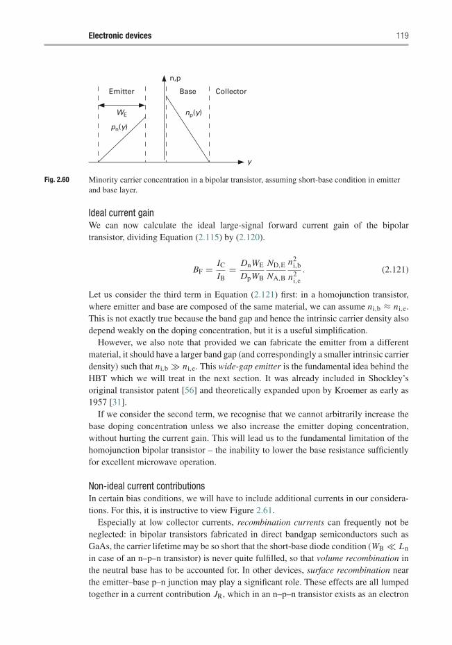
Electronic devices 119
Emitter Base Collector
n,p
y
np(y)
pn(y)
WE
Fig. 2.60 Minority carrier concentration in a bipolar transistor, assuming short-base condition in emitterand base layer.
Ideal current gainWe can now calculate the ideal large-signal forward current gain of the bipolartransistor, dividing Equation (2.115) by (2.120).
BF = IC
IB= DnWE
DpWB
ND,E
NA,B
n2i,b
n2i,e
. (2.121)
Let us consider the third term in Equation (2.121) first: in a homojunction transistor,where emitter and base are composed of the same material, we can assume ni,b ≈ ni,e.This is not exactly true because the band gap and hence the intrinsic carrier density alsodepend weakly on the doping concentration, but it is a useful simplification.
However, we also note that provided we can fabricate the emitter from a differentmaterial, it should have a larger band gap (and correspondingly a smaller intrinsic carrierdensity) such that ni,b � ni,e. This wide-gap emitter is the fundamental idea behind theHBT which we will treat in the next section. It was already included in Shockley’soriginal transistor patent [56] and theoretically expanded upon by Kroemer as early as1957 [31].
If we consider the second term, we recognise that we cannot arbitrarily increase thebase doping concentration unless we also increase the emitter doping concentration,without hurting the current gain. This will lead us to the fundamental limitation of thehomojunction bipolar transistor – the inability to lower the base resistance sufficientlyfor excellent microwave operation.
Non-ideal current contributionsIn certain bias conditions, we will have to include additional currents in our considera-tions. For this, it is instructive to view Figure 2.61.
Especially at low collector currents, recombination currents can frequently not beneglected: in bipolar transistors fabricated in direct bandgap semiconductors such asGaAs, the carrier lifetime may be so short that the short-base diode condition (WB � Ln
in case of an n–p–n transistor) is never quite fulfilled, so that volume recombination inthe neutral base has to be accounted for. In other devices, surface recombination nearthe emitter–base p–n junction may play a significant role. These effects are all lumpedtogether in a current contribution JR, which in an n–p–n transistor exists as an electron
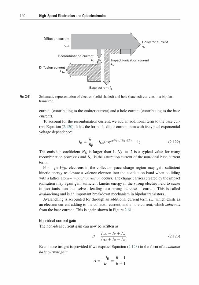
120 High-Speed Electronics and Optoelectronics
Diffusion current
Diffusion currentIpbe
Base current IB
Collector currentICIneb
Impact ionization currentIav
Recombination currentIR
Fig. 2.61 Schematic representation of electron (solid shaded) and hole (hatched) currents in a bipolartransistor.
current (contributing to the emitter current) and a hole current (contributing to the basecurrent).
To account for the recombination current, we add an additional term to the base cur-rent Equation (2.120). It has the form of a diode current term with its typical exponentialvoltage dependence:
IB = IC
BF+ ISR(expq·VBE/(NR·kT ) − 1). (2.122)
The emission coefficient NR is larger than 1. NR = 2 is a typical value for manyrecombination processes and ISR is the saturation current of the non-ideal base currentterm.
For high VCB, electrons in the collector space charge region may gain sufficientkinetic energy to elevate a valence electron into the conduction band when collidingwith a lattice atom – impact ionisation occurs. The charge carriers created by the impactionisation may again gain sufficient kinetic energy in the strong electric field to causeimpact ionisation themselves, leading to a strong increase in current. This is calledavalanching and is an important breakdown mechanism in bipolar transistors.
Avalanching is accounted for through an additional current term Iav, which exists asan electron current adding to the collector current, and a hole current, which subtractsfrom the base current. This is again shown in Figure 2.61.
Non-ideal current gainThe non-ideal current gain can now be written as
B = Ineb − IR + Iav
Ipbe + IR − Iav. (2.123)
Even more insight is provided if we express Equation (2.123) in the form of a commonbase current gain.
A = −IE
IC= B − 1
B + 1
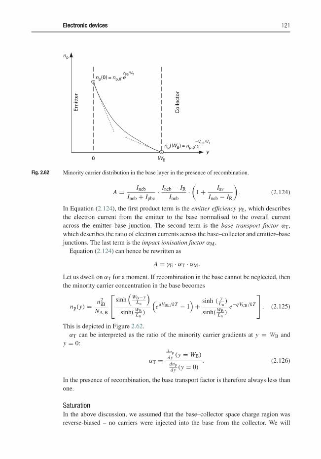
Electronic devices 121
np
np(0) = np,0.e
Em
itte
r
Co
llect
or
0 WB
y
VBE/VT
np(WB) = np,0.e
VCB/VT–
Fig. 2.62 Minority carrier distribution in the base layer in the presence of recombination.
A = Ineb
Ineb + Ipbe· Ineb − IR
Ineb·(
1 + Iav
Ineb − IR
). (2.124)
In Equation (2.124), the first product term is the emitter efficiency γE, which describesthe electron current from the emitter to the base normalised to the overall currentacross the emitter–base junction. The second term is the base transport factor αT,which describes the ratio of electron currents across the base–collector and emitter–basejunctions. The last term is the impact ionisation factor αM.
Equation (2.124) can hence be rewritten as
A = γE · αT · αM.
Let us dwell on αT for a moment. If recombination in the base cannot be neglected, thenthe minority carrier concentration in the base becomes
np(y) = n2iB
NA,B
⎡⎣ sinh(
WB−yLn
)sinh(WB
Ln)
(eqVBE/kT − 1
)+ sinh (
yLn
)
sinh(WBLn
)e−qVCB/kT
⎤⎦ . (2.125)
This is depicted in Figure 2.62.αT can be interpreted as the ratio of the minority carrier gradients at y = WB and
y = 0:
αT =dnpdy (y = WB)
dnpdy (y = 0)
. (2.126)
In the presence of recombination, the base transport factor is therefore always less thanone.
SaturationIn the above discussion, we assumed that the base–collector space charge region wasreverse-biased – no carriers were injected into the base from the collector. We will
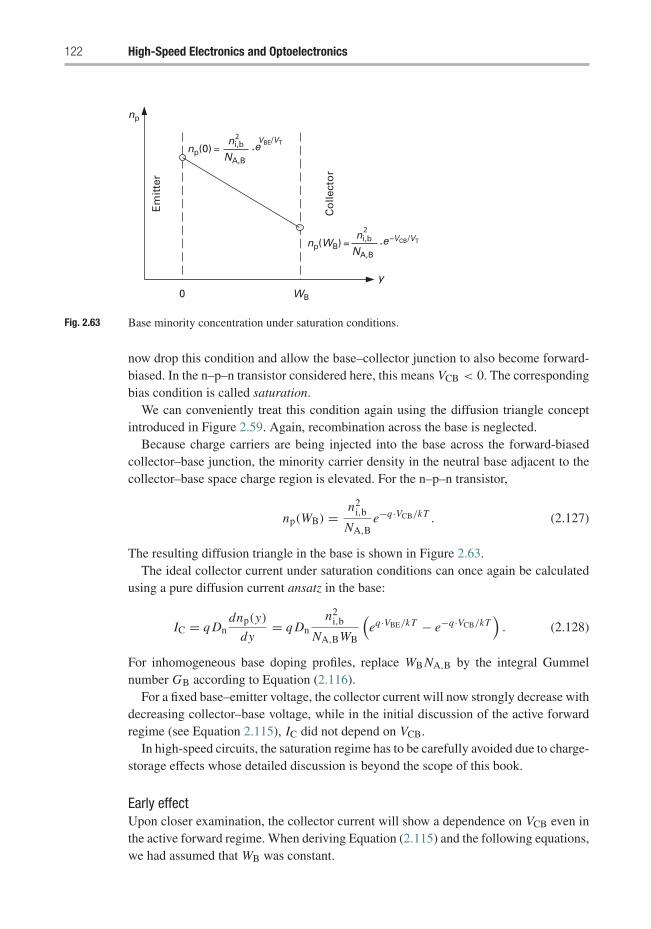
122 High-Speed Electronics and Optoelectronics
np
np(0) =E
mit
ter
Co
llect
or
0 WB
y
VBE/VTni,b
NA,B
2.e
np(WB) = –VCB/VTni,b
NA,B
2
.e
Fig. 2.63 Base minority concentration under saturation conditions.
now drop this condition and allow the base–collector junction to also become forward-biased. In the n–p–n transistor considered here, this means VCB < 0. The correspondingbias condition is called saturation.
We can conveniently treat this condition again using the diffusion triangle conceptintroduced in Figure 2.59. Again, recombination across the base is neglected.
Because charge carriers are being injected into the base across the forward-biasedcollector–base junction, the minority carrier density in the neutral base adjacent to thecollector–base space charge region is elevated. For the n–p–n transistor,
np(WB) = n2i,b
NA,Be−q·VCB/kT . (2.127)
The resulting diffusion triangle in the base is shown in Figure 2.63.The ideal collector current under saturation conditions can once again be calculated
using a pure diffusion current ansatz in the base:
IC = q Dndnp(y)
dy= q Dn
n2i,b
NA,BWB
(eq·VBE/kT − e−q·VCB/kT
). (2.128)
For inhomogeneous base doping profiles, replace WB NA,B by the integral Gummelnumber GB according to Equation (2.116).
For a fixed base–emitter voltage, the collector current will now strongly decrease withdecreasing collector–base voltage, while in the initial discussion of the active forwardregime (see Equation 2.115), IC did not depend on VCB.
In high-speed circuits, the saturation regime has to be carefully avoided due to charge-storage effects whose detailed discussion is beyond the scope of this book.
Early effectUpon closer examination, the collector current will show a dependence on VCB even inthe active forward regime. When deriving Equation (2.115) and the following equations,we had assumed that WB was constant.
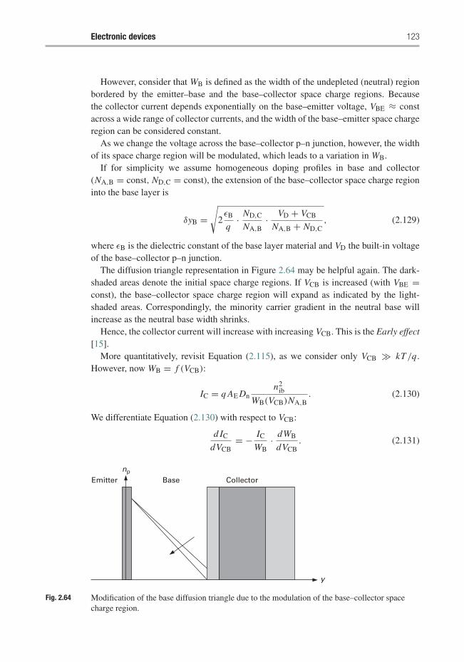
Electronic devices 123
However, consider that WB is defined as the width of the undepleted (neutral) regionbordered by the emitter–base and the base–collector space charge regions. Becausethe collector current depends exponentially on the base–emitter voltage, VBE ≈ constacross a wide range of collector currents, and the width of the base–emitter space chargeregion can be considered constant.
As we change the voltage across the base–collector p–n junction, however, the widthof its space charge region will be modulated, which leads to a variation in WB.
If for simplicity we assume homogeneous doping profiles in base and collector(NA,B = const, ND,C = const), the extension of the base–collector space charge regioninto the base layer is
δyB =√
2εB
q· ND,C
NA,B· VD + VCB
NA,B + ND,C, (2.129)
where εB is the dielectric constant of the base layer material and VD the built-in voltageof the base–collector p–n junction.
The diffusion triangle representation in Figure 2.64 may be helpful again. The dark-shaded areas denote the initial space charge regions. If VCB is increased (with VBE =const), the base–collector space charge region will expand as indicated by the light-shaded areas. Correspondingly, the minority carrier gradient in the neutral base willincrease as the neutral base width shrinks.
Hence, the collector current will increase with increasing VCB. This is the Early effect[15].
More quantitatively, revisit Equation (2.115), as we consider only VCB � kT /q.However, now WB = f (VCB):
IC = q AE Dnn2
ib
WB(VCB)NA,B. (2.130)
We differentiate Equation (2.130) with respect to VCB:
d IC
dVCB= − IC
WB· dWB
dVCB. (2.131)
Emitter Base Collectornp
y
Fig. 2.64 Modification of the base diffusion triangle due to the modulation of the base–collector spacecharge region.
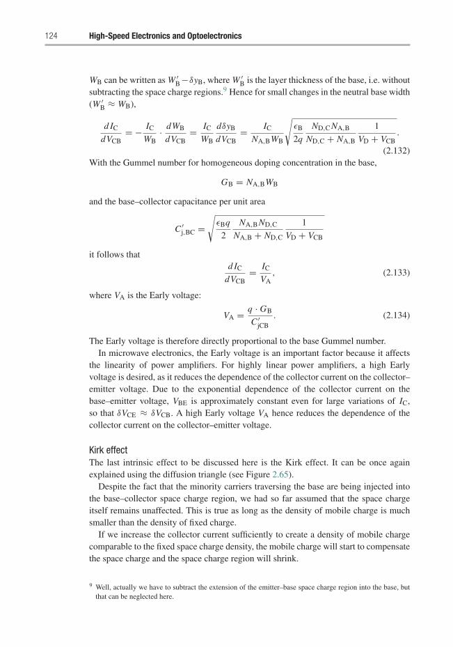
124 High-Speed Electronics and Optoelectronics
WB can be written as W ′B −δyB, where W ′
B is the layer thickness of the base, i.e. withoutsubtracting the space charge regions.9 Hence for small changes in the neutral base width(W ′
B ≈ WB),
d IC
dVCB= − IC
WB· dWB
dVCB= IC
WB
dδyB
dVCB= IC
NA,BWB
√εB
2q
ND,C NA,B
ND,C + NA,B
1
VD + VCB.
(2.132)With the Gummel number for homogeneous doping concentration in the base,
GB = NA,BWB
and the base–collector capacitance per unit area
C ′j,BC =
√εBq
2
NA,B ND,C
NA,B + ND,C
1
VD + VCB
it follows thatd IC
dVCB= IC
VA, (2.133)
where VA is the Early voltage:
VA = q · GB
C ′jCB
. (2.134)
The Early voltage is therefore directly proportional to the base Gummel number.In microwave electronics, the Early voltage is an important factor because it affects
the linearity of power amplifiers. For highly linear power amplifiers, a high Earlyvoltage is desired, as it reduces the dependence of the collector current on the collector–emitter voltage. Due to the exponential dependence of the collector current on thebase–emitter voltage, VBE is approximately constant even for large variations of IC,so that δVCE ≈ δVCB. A high Early voltage VA hence reduces the dependence of thecollector current on the collector–emitter voltage.
Kirk effectThe last intrinsic effect to be discussed here is the Kirk effect. It can be once againexplained using the diffusion triangle (see Figure 2.65).
Despite the fact that the minority carriers traversing the base are being injected intothe base–collector space charge region, we had so far assumed that the space chargeitself remains unaffected. This is true as long as the density of mobile charge is muchsmaller than the density of fixed charge.
If we increase the collector current sufficiently to create a density of mobile chargecomparable to the fixed space charge density, the mobile charge will start to compensatethe space charge and the space charge region will shrink.
9 Well, actually we have to subtract the extension of the emitter–base space charge region into the base, butthat can be neglected here.
Electronic devices 125
y
CollectorBaseEmitter np
Fig. 2.65 Schematic representation of the Kirk effect influence on the diffusion triangle.
If the width of the space charge region decreases, the neutral base zone will expand –this is called base push out. Correspondingly, the minority carrier gradient and with itthe collector current for a given VBE will decrease.
To get an estimate of the collector current necessary to cause the Kirk effect, letus assume that the free charge (electrons in our case) will be accelerated to their driftsaturation velocity vsat immediately after they enter the base–collector space chargeregion. Then the electron density nC corresponding to a collector current density JC is
nC = JC
q · vsat.
If we now require that the fixed ionised donors in the collector of density ND,C shall befully compensated by the mobile charge (nC = ND,C), we find for the critical currentfor the onset of the Kirk effect:
JC,Kirk = q · NDC · vsat. (2.135)
The onset of Kirk effect hence scales proportionally with the collector doping concen-tration.
2.5.2 Small-signal dynamic behaviour
Next, we will discuss the dynamic behaviour of the bipolar transistor for the small-signal case, where the non-linear relationships between the terminal currents and thevoltages can be described as linear relationships between the deviations of these entitiesfrom a given bias point, i.e.
ic = δ IC, ib = δ IB, vbe = δVbe, vce = δVCE.
The forward-biased emitter–base junction will now be described by a conductance:
d(IC + IB)
dVBE= − d IE
dVBE= ge, (2.136)
where ge will be referred to as the dynamic emitter conductance. The minus sign isdue to the convention that all currents (IC, IB, IE) are counted positive flowing into thetransistor.
126 High-Speed Electronics and Optoelectronics
From Equations (2.115), (2.120) and (2.121), we conclude that
IE = − (IC + IB) = −q AE Dnn2
ib
GBeVBE/VT
(1 + 1
B F
)(2.137)
in the active forward regime, neglecting any non-ideal current contributions.Differentiating Equation (2.137) with respect to VBE, we find the dynamic emitter
conductance to be
ge = − IE
VT. (2.138)
It can be written as the dynamic emitter resistance:
re = − VT
IE. (2.139)
The modulation of stored charge in the neutral base results in the diffusion capacitance.In the short-base diode limit, for a homogeneously doped base layer, and if we neglectcarrier injection from the collector into the base (i.e. for VCB sufficiently high), thestored minority charge in the base can be easily calculated, refer again to Figure 2.59:
QB = q AEWB
2
n2ib
NA,BeVBE/VT . (2.140)
Differentiating QB with respect to VBE results in the diffusion capacitance Cd:
Cd = d QB
dVBE= q AE
WB
2
n2ib
NA,B
1
VTeVBE/VT . (2.141)
Considering Equation (2.137) and recalling that in the homogeneously doped case, thebase Gummel number is GB = NA,BWB, we find that Equation (2.141) can be writtenas
Cd = IE
VT
W 2B
2Dn= ge
W 2B
2Dn. (2.142)
The ratio of diffusion capacitance to dynamic emitter conductance is bias-independent(at least in the active forward regime) and is called the base transit time τB:
τB = Cd
ge= W 2
B
2Dn. (2.143)
Recall that Dn = (kT /q)μn Equation (2.109); therefore, the base transit time isinversely proportional to the minority carrier mobility in the base. As the electron mobil-ity μn is significantly larger than the hole mobility μp, in Si as well as the most commoncompound semiconductors, this justifies the restriction of our discussions to n–p–n-typetransistors.
The output conductance is related to the Early effect. We find it by differentiating IC
with respect to VCE:
gce = d IC
dVCE= d IC
dVCB, (2.144)
Electronic devices 127
for constant VBE. Therefore,
gce = IC
VA. (2.145)
The emitter–base and base–collector p–n junctions also present junction capacitanceswhich we have to take into account. The calculation of the junction capacitance can bereduced to the problem of calculating the width of the depletion layer w, because thecapacitance is that of a parallel plate capacitor with area AJ and plate separation w:
CJ = εSAJ
w. (2.146)
The depletion layer width is calculated from Poisson’s equation:
d2�
dy2= −ρ(y)
y, (2.147)
where � is the potential across the junction. A simple analytic solution can be foundassuming that within the space charge region the mobile charge can be neglected com-pared to the fixed charge (i.e. the ionised donor density N+
D (y) on the n side and theionised acceptor density N−
A (y) on the p side), and that within the depletion layer alldoping atoms are ionised, while outside all doping atoms are neutral. The total potentialdifference across the depletion region must be equal to the sum of built-in (or diffusion)voltage VD and the externally applied voltage Vext.
For the simple case of homogeneous doping on both p and n sides (ND(y) =const, NA(y) = const), we obtain
w =√
2εS
q
NA + ND
NA ND(VD + Vext). (2.148)
Note that Vext is defined as a reverse (depleting) voltage here.In active forward operation, the emitter–base diode is forward-biased (Vext = −VBE),
while the base–collector diode is reverse-biased (Vext = VCB). In practical transistors,the emitter–base junction area AE will also be different from the base–collector junctionarea AC, so that we obtain for the n–p–n transistor:
CBE = AE
√q · εS
2
NA,B ND,B
NA,B + ND,E
1
VD − VBEfor VBE < VD (2.149)
CCB = AC
√q · εS
2
NA,B ND,C
NA,B + ND,C
1
VD + VCB. (2.150)
Finally, we have to account for the time lag associated with the transit of free chargecarriers through the base–collector space charge region – the collector transit time.10
The calculation of the collector transit time is not as straightforward as it may seem,as it in principle needs both diffusive (at the base side edge of the space charge region)
10 Because the emitter–base diode is forward-biased, its depletion region is very thin and the associated transittime can be safely neglected.
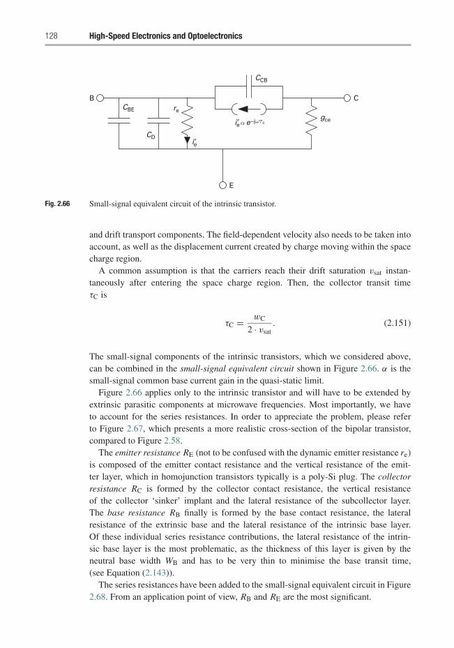
128 High-Speed Electronics and Optoelectronics
B C
E
CBE
CCB
gce
CD
re
i′e
i′e α e–jωτc
Fig. 2.66 Small-signal equivalent circuit of the intrinsic transistor.
and drift transport components. The field-dependent velocity also needs to be taken intoaccount, as well as the displacement current created by charge moving within the spacecharge region.
A common assumption is that the carriers reach their drift saturation vsat instan-taneously after entering the space charge region. Then, the collector transit timeτC is
τC = wC
2 · vsat. (2.151)
The small-signal components of the intrinsic transistors, which we considered above,can be combined in the small-signal equivalent circuit shown in Figure 2.66. α is thesmall-signal common base current gain in the quasi-static limit.
Figure 2.66 applies only to the intrinsic transistor and will have to be extended byextrinsic parasitic components at microwave frequencies. Most importantly, we haveto account for the series resistances. In order to appreciate the problem, please referto Figure 2.67, which presents a more realistic cross-section of the bipolar transistor,compared to Figure 2.58.
The emitter resistance RE (not to be confused with the dynamic emitter resistance re)is composed of the emitter contact resistance and the vertical resistance of the emit-ter layer, which in homojunction transistors typically is a poly-Si plug. The collectorresistance RC is formed by the collector contact resistance, the vertical resistanceof the collector ‘sinker’ implant and the lateral resistance of the subcollector layer.The base resistance RB finally is formed by the base contact resistance, the lateralresistance of the extrinsic base and the lateral resistance of the intrinsic base layer.Of these individual series resistance contributions, the lateral resistance of the intrin-sic base layer is the most problematic, as the thickness of this layer is given by theneutral base width WB and has to be very thin to minimise the base transit time,(see Equation (2.143)).
The series resistances have been added to the small-signal equivalent circuit in Figure2.68. From an application point of view, RB and RE are the most significant.
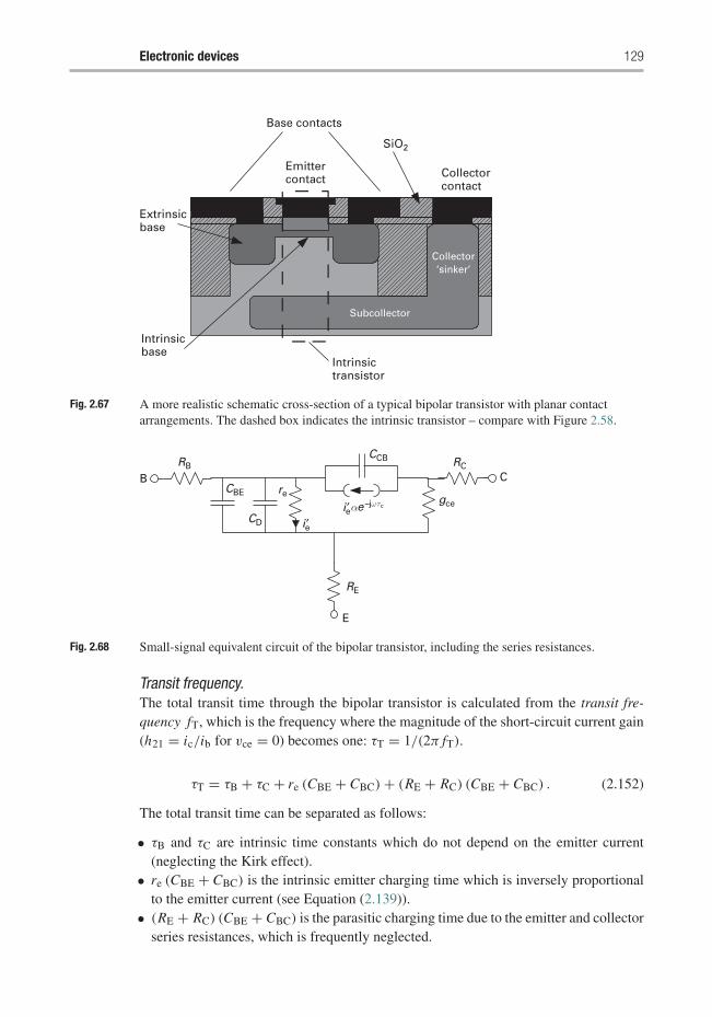
Electronic devices 129
Extrinsicbase
Intrinsicbase
Intrinsictransistor
Collectorcontact
SiO2
Base contacts
Emittercontact
Collector‘sinker’
Subcollector
Fig. 2.67 A more realistic schematic cross-section of a typical bipolar transistor with planar contactarrangements. The dashed box indicates the intrinsic transistor – compare with Figure 2.58.
RB
CBE re
i ′CD
CCB RC
RE
gce
B
e
i ′eαe–jωτc
C
E
Fig. 2.68 Small-signal equivalent circuit of the bipolar transistor, including the series resistances.
Transit frequency.The total transit time through the bipolar transistor is calculated from the transit fre-quency fT, which is the frequency where the magnitude of the short-circuit current gain(h21 = ic/ib for vce = 0) becomes one: τT = 1/(2π fT).
τT = τB + τC + re (CBE + CBC) + (RE + RC) (CBE + CBC) . (2.152)
The total transit time can be separated as follows:
• τB and τC are intrinsic time constants which do not depend on the emitter current(neglecting the Kirk effect).
• re (CBE + CBC) is the intrinsic emitter charging time which is inversely proportionalto the emitter current (see Equation (2.139)).
• (RE + RC) (CBE + CBC) is the parasitic charging time due to the emitter and collectorseries resistances, which is frequently neglected.
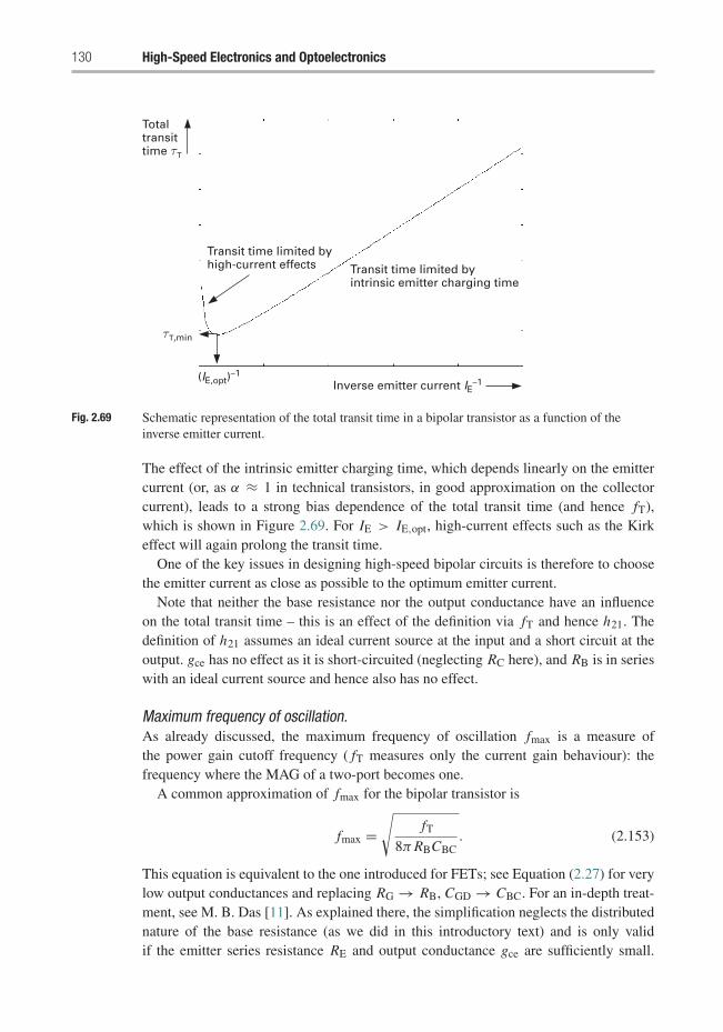
130 High-Speed Electronics and Optoelectronics
(IE,opt)–1
τT,min
Totaltransittime τT
Transit time limited byhigh-current effects Transit time limited by
intrinsic emitter charging time
Inverse emitter current IE–1
Fig. 2.69 Schematic representation of the total transit time in a bipolar transistor as a function of theinverse emitter current.
The effect of the intrinsic emitter charging time, which depends linearly on the emittercurrent (or, as α ≈ 1 in technical transistors, in good approximation on the collectorcurrent), leads to a strong bias dependence of the total transit time (and hence fT),which is shown in Figure 2.69. For IE > IE,opt, high-current effects such as the Kirkeffect will again prolong the transit time.
One of the key issues in designing high-speed bipolar circuits is therefore to choosethe emitter current as close as possible to the optimum emitter current.
Note that neither the base resistance nor the output conductance have an influenceon the total transit time – this is an effect of the definition via fT and hence h21. Thedefinition of h21 assumes an ideal current source at the input and a short circuit at theoutput. gce has no effect as it is short-circuited (neglecting RC here), and RB is in serieswith an ideal current source and hence also has no effect.
Maximum frequency of oscillation.As already discussed, the maximum frequency of oscillation fmax is a measure ofthe power gain cutoff frequency ( fT measures only the current gain behaviour): thefrequency where the MAG of a two-port becomes one.
A common approximation of fmax for the bipolar transistor is
fmax =√
fT
8π RBCBC. (2.153)
This equation is equivalent to the one introduced for FETs; see Equation (2.27) for verylow output conductances and replacing RG → RB, CGD → CBC. For an in-depth treat-ment, see M. B. Das [11]. As explained there, the simplification neglects the distributednature of the base resistance (as we did in this introductory text) and is only validif the emitter series resistance RE and output conductance gce are sufficiently small.
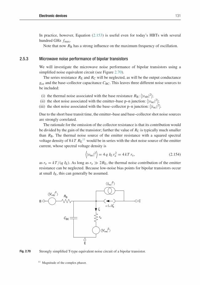
Electronic devices 131
In practice, however, Equation (2.153) is useful even for today’s HBTs with severalhundred GHz fmax.
Note that now RB has a strong influence on the maximum frequency of oscillation.
2.5.3 Microwave noise performance of bipolar transistors
We will investigate the microwave noise performance of bipolar transistors using asimplified noise equivalent circuit (see Figure 2.70).
The series resistance RE and RC will be neglected, as will be the output conductancegce and the base–collector capacitance CBC. This leaves three different noise sources tobe included:
(i) the thermal noise associated with the base resistance RB:⟨|vnb|2
⟩;
(ii) the shot noise associated with the emitter–base p–n junction:⟨|vne|2
⟩;
(iii) the shot noise associated with the base–collector p–n junction:⟨|inc|2
⟩.
Due to the short base transit time, the emitter–base and base–collector shot noise sourcesare strongly correlated.
The rationale for the omission of the collector resistance is that its contribution wouldbe divided by the gain of the transistor; further the value of RC is typically much smallerthan RB. The thermal noise source of the emitter resistance with a squared spectralvoltage density of 8 kT RE
11 would be in series with the shot noise source of the emittercurrent, whose spectral voltage density is⟨
|vne|2⟩= 4 q IE r2
e = 4 kT re, (2.154)
as re = kT /(q IE). As long as re � 2RE, the thermal noise contribution of the emitterresistance can be neglected. Because low-noise bias points for bipolar transistors occurat small IE, this can generally be assumed.
RB
reCBE
i ′ei ′eα (ω )
B
E
C
Vnb2
Vne2
inc2
⟩⟨
⟩⟨
⟩⟨
Fig. 2.70 Strongly simplified T-type equivalent noise circuit of a bipolar transistor.
11 Magnitude of the complex phasor.
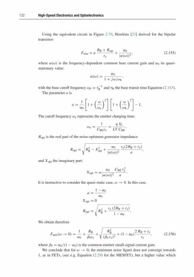
132 High-Speed Electronics and Optoelectronics
Using the equivalent circuit in Figure 2.70, Hawkins [23] derived for the bipolartransistor:
Fmin = aRB + Ropt
re+ α0
|α(ω)|2 , (2.155)
where α(ω) is the frequency-dependent common base current gain and α0 its quasi-stationary value:
α(ω) = α0
1 + jω/ωb.
with the base cutoff frequency ωb = τ−1B and τB the base transit time Equation (2.143).
The parameter a is
a = 1
α0
[1 +
(ω
ωe
)2] [
1 +(
ω
ωb
)2]
− 1.
The cutoff frequency ωe represents the emitter charging time:
ωe = 1
CBEre= q IE
kT CBE.
Ropt is the real part of the noise-optimum generator impedance:
Ropt =√
R2B − X2
opt + α0
|α(ω)|2re(2RB + re)
a,
and Xopt the imaginary part:
Xopt = ωα0
|α(ω)|2CBE r2
e
a.
It is instructive to consider the quasi-static case, ω → 0. In this case,
a = 1 − α0
α0
Xopt = 0
Ropt =√
R2B + re (2RB + re)
1 − α0.
We obtain therefore
Fmin(ω → 0) = 1
α0+ RB
β0re+
√R2
B
(β0 re)2+ (1 − α0)
2 RB + re
re, (2.156)
where β0 = α0/(1 − α0) is the common-emitter small-signal current gain.We conclude that for ω → 0, the minimum noise figure does not converge towards
1, as in FETs, (see e.g. Equation (2.29) for the MESFET), but a higher value which
Electronic devices 133
depends on the current gain and the base resistance. If we further assume smallRB/(β0 re), Equation (2.156) reduces to
Fmin(ω → 0) ≈ 1
α0+
√(1 − α0)
2RB + re
re.
It is obvious that the current gain has a very important influence on the noiseperformance of a bipolar transistor.
Let us now investigate a medium frequency range ωe � ω � ωb. To simplifymatters, we assume an ideal current gain α0 = 1. In this case,
a =(
ω
ωe
)2
Xopt = ωe
ωre
Ropt =√
R2B + 2 RB re
(ωe
ω
)2,
and finally for Fmin(α0 = 1, ωe � ω � ωb):
Fmin = 1 + ω2
ω2e
RB
re+ ω
ωe
√R2
B
r2e
ω2
ω2e
+ 2RB
re. (2.157)
We find that in this case the increase with frequency is determined by the base resistanceRB, which is therefore a very important parameter for the microwave noise behaviourof bipolar transistors.
Equation (2.155) contains an implicit bias dependence via re = VT/IE, whereVT = kT/q , as usual. re also determines fe. As long as IE � VT ω CBE, Fmin
will increase proportionally with increasing IE. For very small IE, however Fmin willincrease inversely proportional to IE. We note that here will be an optimum emitter cur-rent with respect to the noise performance. This current is usually much lower than thecurrent required for optimum fT (Figure 2.69) and hence requires a trade-off betweendevice speed and noise in circuit design. Figure 2.71 shows an example calculation.We note that the optimum emitter current is frequency-dependent and moves to highercurrents with increasing frequency.
An important noise parameter not considered in Hawkins’ theory is the equivalentnoise resistance. It determines the sensitivity of the noise figure on deviations from thenoise-optimum generator impedance. Therefore, a small Rn facilitates circuit design asit makes exact noise match less critical (Section 5.3). Using Hawkins’ equivalent circuit,an expression for Rn was introduced by Pucel and Rohde:
Rn = RB
(D − 1
β0
)+ re
2
{D +
(RB
re
)2
·[
1 − α0 +(
f
fb
)2
+(
f
fe
)2
+(
1
β0−
(f
fb
) (f
fb
))2 ]}. (2.158)
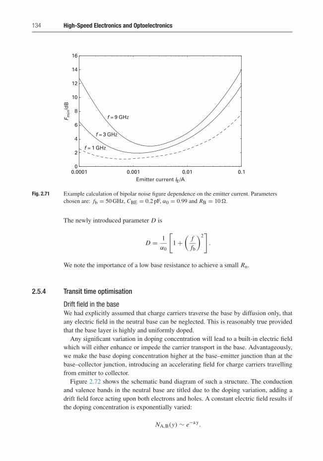
134 High-Speed Electronics and Optoelectronics
0.0001 0.001 0.01 0.1Emitter current IE/A
0
2
4
6
8
10
12
14
16
F min
/dB
f = 9 GHz
f = 3 GHz
f = 1 GHz
Fig. 2.71 Example calculation of bipolar noise figure dependence on the emitter current. Parameterschosen are: fb = 50 GHz, CBE = 0.2 pF, α0 = 0.99 and RB = 10�.
The newly introduced parameter D is
D = 1
α0
[1 +
(f
fb
)2].
We note the importance of a low base resistance to achieve a small Rn.
2.5.4 Transit time optimisation
Drift field in the baseWe had explicitly assumed that charge carriers traverse the base by diffusion only, thatany electric field in the neutral base can be neglected. This is reasonably true providedthat the base layer is highly and uniformly doped.
Any significant variation in doping concentration will lead to a built-in electric fieldwhich will either enhance or impede the carrier transport in the base. Advantageously,we make the base doping concentration higher at the base–emitter junction than at thebase–collector junction, introducing an accelerating field for charge carriers travellingfrom emitter to collector.
Figure 2.72 shows the schematic band diagram of such a structure. The conductionand valence bands in the neutral base are titled due to the doping variation, adding adrift field force acting upon both electrons and holes. A constant electric field results ifthe doping concentration is exponentially varied:
NA,B(y) ∼ e−a y.
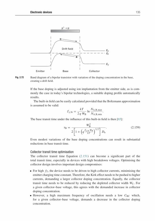
Electronic devices 135
Drift field
Emitter Base Collector
EV
EF
EC
p+ → p
Fig. 2.72 Band diagram of a bipolar transistor with variation of the doping concentration in the base,creating a drift field.
If the base doping is adjusted using ion implantation from the emitter side, as is com-monly the case in today’s bipolar technologies, a suitable doping profile automaticallyresults.
The built-in field can be easily calculated provided that the Boltzmann approximationis assumed to be valid:
Ey,bi = kT
2 q WBln
NA,B,max
NA,B,min.
The base transit time under the influence of this built-in field is then [65]:
τB = W 2B
2
[1 +
(qEy,bi WB
kT
)3/2]
Dn
. (2.159)
Even modest variations of the base doping concentrations can result in substantialreductions in base transit time.
Collector transit time optimisationThe collector transit time Equation (2.151) can become a significant part of thetotal transit time, especially in devices with high breakdown voltages. Optimising thecollector design involves important design compromises:
• For high fT, the device needs to be driven to high collector currents, minimising theemitter charging time constant. Therefore, the Kirk effect needs to be pushed to highercurrents, demanding a larger collector doping concentration. Equally, the collectortransit time needs to be reduced by reducing the depleted collector width WC. Fora given collector–base voltage, this agrees with the demanded increase in collectordoping concentration.
• However, a high maximum frequency of oscillation needs a low CBC which,for a given collector–base voltage, demands a decrease in the collector dopingconcentration.
136 High-Speed Electronics and Optoelectronics
• Equally, an increase in collector–base breakdown voltage needs a decrease in collectordoping concentration and a larger WC.
The link between breakdown voltage and transit frequency is frequently expressed interms of the Johnson limit [17]. To derive the Johnson limit, let us assume that thecollector transit time fully dominates the total transit time. Using Equation (2.151), wefind
fT ≈ 1
2π τC= vsat
π WC→ WC = vsat
π fT.
If Ecrit is the critical field for breakdown and if we assume homogeneous doping in thecollector, the collector–base breakdown voltage (open emitter terminal) is
BVCBO = EcritWC
2.
The product of transit frequency and breakdown voltage will then only depend on thematerial properties Vsat and BVCBO:
fT · BVCBO = Ecritvsat
2π.
The collector–emitter breakdown voltage BVCEO is lower than BVCBO because theimpact ionisation current is amplified by the current gain B when entering the base:
BVCEO = BVCBOm√
B, (2.160)
where m is a parameter which depends on the exact geometry and doping of thetransistor.
We find for the Johnson limit:
fT · BVCEO = Ecritvsat
2π m√
B. (2.161)
For Si, Ecrit ≈ 5 · 105 V cm−1. The drift saturation velocity at room temperature isvsat ≈ 107 cm s−1. Assuming a typical B = 250 and m = 4, we find fT · BVCEO =200 GHz. This is the frequently quoted ‘Johnson Limit’ for silicon bipolar devices. Wereadily recognise from Equation (2.161) that it is not a constant and can be significantlydifferent for other values of B and m.
2.5.5 Heterojunction bipolar transistors
The base design dilemmaIn our discussion of homojunction bipolar transistors, three main parameters withcrucial impact on the high frequency performance were identified:
(i) the base transit time which sets the ‘intrinsic speed’ of the transistors;(ii) the base resistance which affects the maximum frequency of oscillation and the
noise performance;(iii) the current gain which not only influences the noise performance, but also has to
be typically ≥100 to simplify circuit design.
Electronic devices 137
The dilemma is that the base design parameters WB, NA,B influence these parametersin different ways:
• τB ∼ W 2B and increases, albeit weakly, with increasing NA due to the reduction in the
minority carrier mobility;• RB ∼ 1
WB NA,B;
• β ∼ 1WB
ND,ENA,B
.
A transistor with high fT and fmax would therefore have a thin, highly doped base layer.However, the high base doping concentration will decrease the current gain if the emitterdoping concentration cannot be proportionally increased.
On the other hand, there are limits to the increase in emitter doping. The main limi-tation is bandgap narrowing. With increasing doping concentration, the band gap in theemitter will decrease. In silicon,
�EG ≈ 22.5
(ND
1018 cm−3
300 K
T
)0.5
. (2.162)
The decrease in band gap in the emitter will increase the intrinsic carrier concentrationthere (ni∼e−EG/2kT ), which in turn lowers the current gain because the base current dueto injection of holes from the base into the emitter is
JB ∼ n2i,E
ND,E.
We therefore conclude that the base doping concentration cannot be be stronglyincreased while keeping a high current gain. Therefore, thin-base microwave bipolartransistors have a problem with rather high base resistances.
Two approaches can be taken to solve the base design dilemma:
(i) We can increase the carrier velocity in the base so that a target transit frequencycan be met with a larger base width WB. This has been discussed already in thecontext of doping variations in the base layer; we will see further down that theeffect can be achieved much more elegantly using bandgap variations.
(ii) We can search for a way to increase the base doping concentration whilemaintaining a sufficiently high current gain. This we will discuss first.
The wide-gap emitterThe first approach to solving the base design dilemma had already been discussed whenderiving the equation for the maximum current gain, Equation (2.121). It was noted thatit would be advantageous to fabricate the emitter from a material with a lower intrinsiccarrier concentration, ni,E. Because
ni = √NC NVeEG/(2kT ),
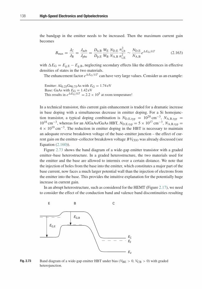
138 High-Speed Electronics and Optoelectronics
the bandgap in the emitter needs to be increased. Then the maximum current gainbecomes
Bmax = JC
JB= Jneb
Jpbe= Dn,B
Dp,E
WE
WB
ND,E
NA,B
n2i,b
n2i,E
∼ ND,E
NA,Be�EG/kT (2.163)
with �EG = Eg,E − Eg,B, neglecting secondary effects like the differences in effectivedensities of states in the two materials.
The enhancement factor e�EG/kT can have very large values. Consider as an example:
Emitter: Al0.25Ga0.75As with EG = 1.74 eVBase: GaAs with EG = 1.42 eVThis results in e�EG/kT = 2.2 × 10⁵ at room temperature!
In a technical transistor, this current gain enhancement is traded for a dramatic increasein base doping with a simultaneous decrease in emitter doping. For a Si homojunc-tion transistor, a typical doping combination is ND,E,typ = 1020 cm−3, NA,B,typ =1018 cm−3, whereas for an AlGaAs/GaAs HBT, ND,E,typ = 5 × 1017 cm−3, NA,B,typ =4 × 1019 cm−3. The reduction in emitter doping in the HBT is necessary to maintainan adequate reverse breakdown voltage of the base–emitter junction – the effect of cur-rent gain on the emitter–collector breakdown voltage BVCEO was already discussed (seeEquation (2.160)).
Figure 2.73 shows the band diagram of a wide-gap emitter transistor with a gradedemitter–base heterostructure. In a graded heterostructure, the two materials used forthe emitter and the base are allowed to intermix over a certain distance. We note thatthe injection of holes from the base into the emitter, which constitutes a major part of thebase current, now faces a much larger potential wall than the injection of electrons fromthe emitter into the base. This provides the intuitive explanation for the potentially hugeincrease in current gain.
In an abrupt heterostructure, such as considered for the HEMT (Figure 2.17), we needto consider the effect of the conduction band and valence band discontinuities resulting
E B C
EC
EG,E
EG,B
EF
EV
Fig. 2.73 Band diagram of a wide-gap emitter HBT under bias (VBE > 0, VCB > 0) with gradedheterojunction.
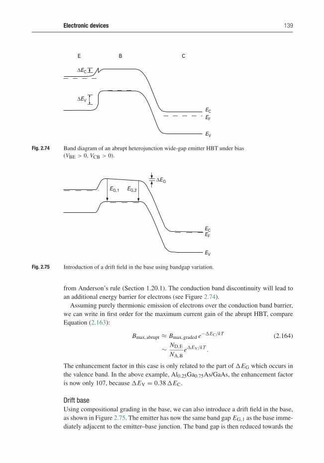
Electronic devices 139
B CE
EC
EF
EV
ΔEC
ΔEV
Fig. 2.74 Band diagram of an abrupt heterojunction wide-gap emitter HBT under bias(VBE > 0, VCB > 0).
ECEF
EV
ΔEG
EG,1 EG,2
Fig. 2.75 Introduction of a drift field in the base using bandgap variation.
from Anderson’s rule (Section 1.20.1). The conduction band discontinuity will lead toan additional energy barrier for electrons (see Figure 2.74).
Assuming purely thermionic emission of electrons over the conduction band barrier,we can write in first order for the maximum current gain of the abrupt HBT, compareEquation (2.163):
Bmax,abrupt ≈ Bmax,graded e−�EC/kT (2.164)
∼ ND,E
NA,Be�EV/kT .
The enhancement factor in this case is only related to the part of �EG which occurs inthe valence band. In the above example, Al0.25Ga0.75As/GaAs, the enhancement factoris now only 107, because �EV = 0.38�EC.
Drift baseUsing compositional grading in the base, we can also introduce a drift field in the base,as shown in Figure 2.75. The emitter has now the same band gap EG,1 as the base imme-diately adjacent to the emitter–base junction. The band gap is then reduced towards the
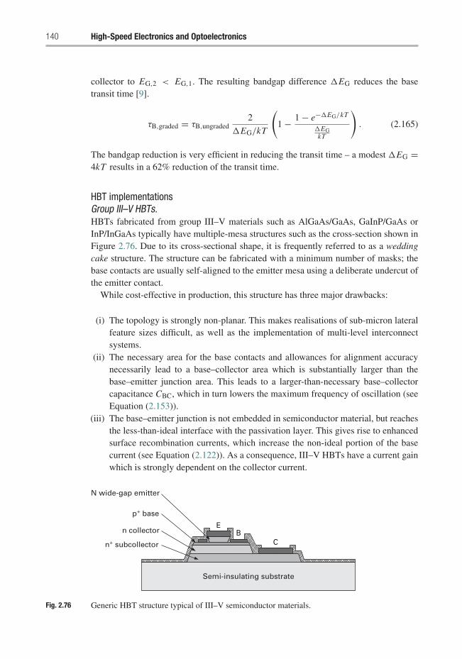
140 High-Speed Electronics and Optoelectronics
collector to EG,2 < EG,1. The resulting bandgap difference �EG reduces the basetransit time [9].
τB,graded = τB,ungraded2
�EG/kT
(1 − 1 − e−�EG/kT
�EGkT
). (2.165)
The bandgap reduction is very efficient in reducing the transit time – a modest �EG =4kT results in a 62% reduction of the transit time.
HBT implementationsGroup III–V HBTs.HBTs fabricated from group III–V materials such as AlGaAs/GaAs, GaInP/GaAs orInP/InGaAs typically have multiple-mesa structures such as the cross-section shown inFigure 2.76. Due to its cross-sectional shape, it is frequently referred to as a weddingcake structure. The structure can be fabricated with a minimum number of masks; thebase contacts are usually self-aligned to the emitter mesa using a deliberate undercut ofthe emitter contact.
While cost-effective in production, this structure has three major drawbacks:
(i) The topology is strongly non-planar. This makes realisations of sub-micron lateralfeature sizes difficult, as well as the implementation of multi-level interconnectsystems.
(ii) The necessary area for the base contacts and allowances for alignment accuracynecessarily lead to a base–collector area which is substantially larger than thebase–emitter junction area. This leads to a larger-than-necessary base–collectorcapacitance CBC, which in turn lowers the maximum frequency of oscillation (seeEquation (2.153)).
(iii) The base–emitter junction is not embedded in semiconductor material, but reachesthe less-than-ideal interface with the passivation layer. This gives rise to enhancedsurface recombination currents, which increase the non-ideal portion of the basecurrent (see Equation (2.122)). As a consequence, III–V HBTs have a current gainwhich is strongly dependent on the collector current.
Semi-insulating substrate
EB
Cn+ subcollector
N wide-gap emitter
p+ base
n collector
Fig. 2.76 Generic HBT structure typical of III–V semiconductor materials.
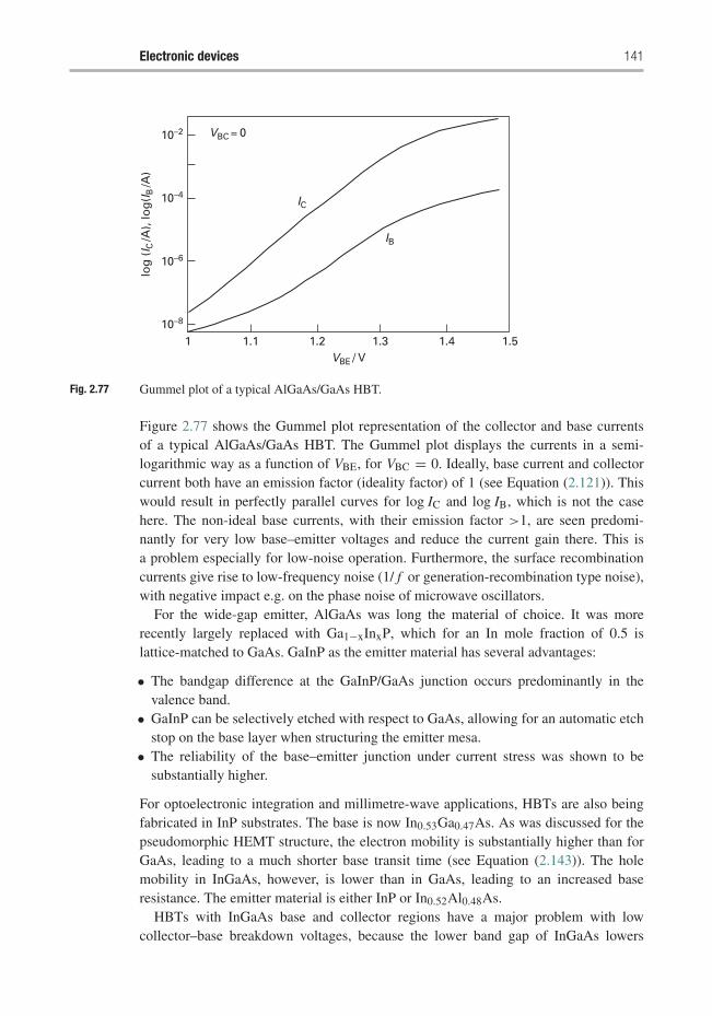
Electronic devices 141
1 1.110–8
10–6
10–4
10–2
1.2 1.3 1.4 1.5VBE / V
VBC = 0
IC
IB
log
(I C
/A),
log
(IB
/A)
Fig. 2.77 Gummel plot of a typical AlGaAs/GaAs HBT.
Figure 2.77 shows the Gummel plot representation of the collector and base currentsof a typical AlGaAs/GaAs HBT. The Gummel plot displays the currents in a semi-logarithmic way as a function of VBE, for VBC = 0. Ideally, base current and collectorcurrent both have an emission factor (ideality factor) of 1 (see Equation (2.121)). Thiswould result in perfectly parallel curves for log IC and log IB, which is not the casehere. The non-ideal base currents, with their emission factor >1, are seen predomi-nantly for very low base–emitter voltages and reduce the current gain there. This isa problem especially for low-noise operation. Furthermore, the surface recombinationcurrents give rise to low-frequency noise (1/ f or generation-recombination type noise),with negative impact e.g. on the phase noise of microwave oscillators.
For the wide-gap emitter, AlGaAs was long the material of choice. It was morerecently largely replaced with Ga1−xInxP, which for an In mole fraction of 0.5 islattice-matched to GaAs. GaInP as the emitter material has several advantages:
• The bandgap difference at the GaInP/GaAs junction occurs predominantly in thevalence band.
• GaInP can be selectively etched with respect to GaAs, allowing for an automatic etchstop on the base layer when structuring the emitter mesa.
• The reliability of the base–emitter junction under current stress was shown to besubstantially higher.
For optoelectronic integration and millimetre-wave applications, HBTs are also beingfabricated in InP substrates. The base is now In0.53Ga0.47As. As was discussed for thepseudomorphic HEMT structure, the electron mobility is substantially higher than forGaAs, leading to a much shorter base transit time (see Equation (2.143)). The holemobility in InGaAs, however, is lower than in GaAs, leading to an increased baseresistance. The emitter material is either InP or In0.52Al0.48As.
HBTs with InGaAs base and collector regions have a major problem with lowcollector–base breakdown voltages, because the lower band gap of InGaAs lowers
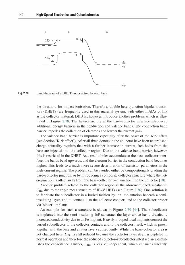
142 High-Speed Electronics and Optoelectronics
ECEF
EV
ΔEC
ΔEV
E B C
+
–
Fig. 2.78 Band diagram of a DHBT under active forward bias.
the threshold for impact ionisation. Therefore, double-heterojunction bipolar transis-tors (DHBTs) are frequently used in this material system, with either InAlAs or InPas the collector material. DHBTs, however, introduce another problem, which is illus-trated in Figure 2.78. The heterostructure at the base–collector interface introducedadditional energy barriers in the conduction and valence bands. The conduction bandbarrier impedes the collection of electrons and lowers the current gain.
The valence band barrier is important especially after the onset of the Kirk effect(see Section ‘Kirk effect’). After all fixed donors in the collector have been neutralised,charge neutrality requires that with a further increase in current, free holes from thebase are injected into the collector region. Due to the valence band barrier, however,this is restricted in the DHBT. As a result, holes accumulate at the base–collector inter-face, the bands bend upwards, and the electron barrier in the conduction band becomeshigher. This leads to a much more severe deterioration of transistor parameters in thehigh-current regime. The problem can be avoided either by compositionally grading thebase–collector junction, or by introducing a composite collector structure where the het-erojunction is offset away from the base–collector p–n junction into the collector [18].
Another problem related to the collector region is the aforementioned substantialCBC due to the triple mesa structure of III–V HBTs (see Figure 2.76). One solution isto fabricate the subcollector in a buried fashion by ion implantation beneath a semi-insulating layer, and to connect it to the collector contacts and to the collector propervia ‘sinker’ implants.
An example for such a structure is shown in Figure 2.79 [44]. The subcollectoris implanted into the semi-insulating InP substrate; the layer above has a drasticallyincreased conductivity due to an Fe implant. Heavily n-doped local implants connect theburied subcollector to the collector contacts and to the collector itself, which is growntogether with the base and emitter layers subsequently. While the base–collector area isnot changed here, CBC is still reduced because the collector layer itself is depleted innormal operation and therefore the reduced collector–subcollector interface area dimin-ishes the capacitance. Further, CBC is less VCE-dependent, which enhances linearity.
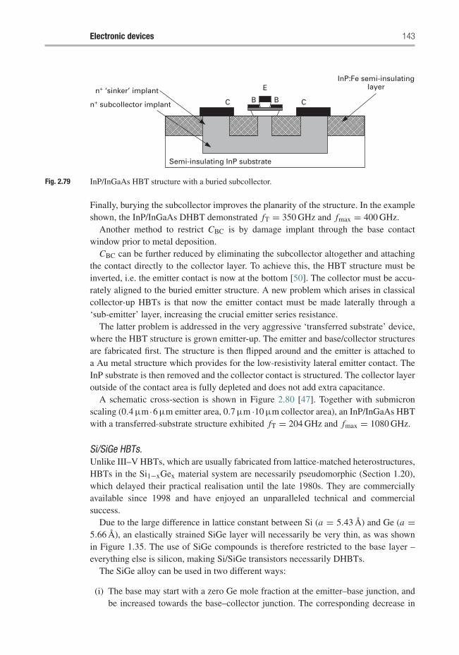
Electronic devices 143
C CB B
E
Semi-insulating InP substrate
InP:Fe semi-insulatinglayer
n+ subcollector implant
n+ ‘sinker’ implant
Fig. 2.79 InP/InGaAs HBT structure with a buried subcollector.
Finally, burying the subcollector improves the planarity of the structure. In the exampleshown, the InP/InGaAs DHBT demonstrated fT = 350 GHz and fmax = 400 GHz.
Another method to restrict CBC is by damage implant through the base contactwindow prior to metal deposition.
CBC can be further reduced by eliminating the subcollector altogether and attachingthe contact directly to the collector layer. To achieve this, the HBT structure must beinverted, i.e. the emitter contact is now at the bottom [50]. The collector must be accu-rately aligned to the buried emitter structure. A new problem which arises in classicalcollector-up HBTs is that now the emitter contact must be made laterally through a‘sub-emitter’ layer, increasing the crucial emitter series resistance.
The latter problem is addressed in the very aggressive ‘transferred substrate’ device,where the HBT structure is grown emitter-up. The emitter and base/collector structuresare fabricated first. The structure is then flipped around and the emitter is attached toa Au metal structure which provides for the low-resistivity lateral emitter contact. TheInP substrate is then removed and the collector contact is structured. The collector layeroutside of the contact area is fully depleted and does not add extra capacitance.
A schematic cross-section is shown in Figure 2.80 [47]. Together with submicronscaling (0.4 μm ·6 μm emitter area, 0.7 μm ·10 μm collector area), an InP/InGaAs HBTwith a transferred-substrate structure exhibited fT = 204 GHz and fmax = 1080 GHz.
Si/SiGe HBTs.Unlike III–V HBTs, which are usually fabricated from lattice-matched heterostructures,HBTs in the Si1−xGex material system are necessarily pseudomorphic (Section 1.20),which delayed their practical realisation until the late 1980s. They are commerciallyavailable since 1998 and have enjoyed an unparalleled technical and commercialsuccess.
Due to the large difference in lattice constant between Si (a = 5.43 A) and Ge (a =5.66 A), an elastically strained SiGe layer will necessarily be very thin, as was shownin Figure 1.35. The use of SiGe compounds is therefore restricted to the base layer –everything else is silicon, making Si/SiGe transistors necessarily DHBTs.
The SiGe alloy can be used in two different ways:
(i) The base may start with a zero Ge mole fraction at the emitter–base junction, andbe increased towards the base–collector junction. The corresponding decrease in
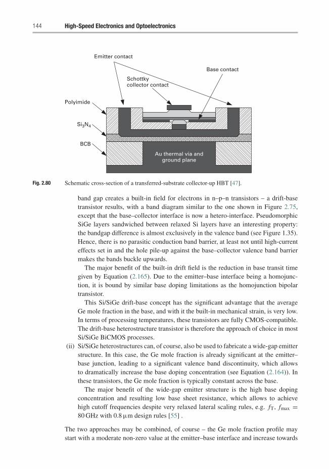
144 High-Speed Electronics and Optoelectronics
Au thermal via andground plane
Base contact
Emitter contact
Schottkycollector contact
Polyimide
BCB
Si3N4
Fig. 2.80 Schematic cross-section of a transferred-substrate collector-up HBT [47].
band gap creates a built-in field for electrons in n–p–n transistors – a drift-basetransistor results, with a band diagram similar to the one shown in Figure 2.75,except that the base–collector interface is now a hetero-interface. PseudomorphicSiGe layers sandwiched between relaxed Si layers have an interesting property:the bandgap difference is almost exclusively in the valence band (see Figure 1.35).Hence, there is no parasitic conduction band barrier, at least not until high-currenteffects set in and the hole pile-up against the base–collector valence band barriermakes the bands buckle upwards.
The major benefit of the built-in drift field is the reduction in base transit timegiven by Equation (2.165). Due to the emitter–base interface being a homojunc-tion, it is bound by similar base doping limitations as the homojunction bipolartransistor.
This Si/SiGe drift-base concept has the significant advantage that the averageGe mole fraction in the base, and with it the built-in mechanical strain, is very low.In terms of processing temperatures, these transistors are fully CMOS-compatible.The drift-base heterostructure transistor is therefore the approach of choice in mostSi/SiGe BiCMOS processes.
(ii) Si/SiGe heterostructures can, of course, also be used to fabricate a wide-gap emitterstructure. In this case, the Ge mole fraction is already significant at the emitter–base junction, leading to a significant valence band discontinuity, which allowsto dramatically increase the base doping concentration (see Equation (2.164)). Inthese transistors, the Ge mole fraction is typically constant across the base.
The major benefit of the wide-gap emitter structure is the high base dopingconcentration and resulting low base sheet resistance, which allows to achievehigh cutoff frequencies despite very relaxed lateral scaling rules, e.g. fT, fmax =80 GHz with 0.8 μm design rules [55] .
The two approaches may be combined, of course – the Ge mole fraction profile maystart with a moderate non-zero value at the emitter–base interface and increase towards
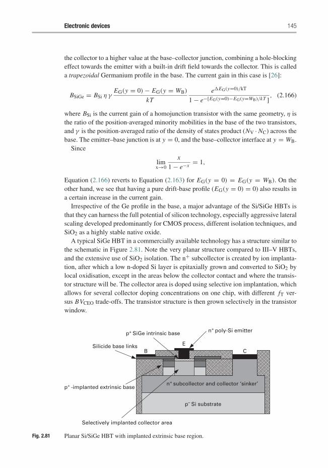
Electronic devices 145
the collector to a higher value at the base–collector junction, combining a hole-blockingeffect towards the emitter with a built-in drift field towards the collector. This is calleda trapezoidal Germanium profile in the base. The current gain in this case is [26]:
BSiGe = BSi η γEG(y = 0) − EG(y = WB)
kT
e�EG(y=0)/kT
1 − e−[EG(y=0)−EG(y=WB)/kT ] , (2.166)
where BSi is the current gain of a homojunction transistor with the same geometry, η isthe ratio of the position-averaged minority mobilities in the base of the two transistors,and γ is the position-averaged ratio of the density of states product (NV · NC) across thebase. The emitter–base junction is at y = 0, and the base–collector interface at y = WB.
Since
limx→0
x
1 − e−x= 1,
Equation (2.166) reverts to Equation (2.163) for EG(y = 0) = EG(y = WB). On theother hand, we see that having a pure drift-base profile (EG(y = 0) = 0) also results ina certain increase in the current gain.
Irrespective of the Ge profile in the base, a major advantage of the Si/SiGe HBTs isthat they can harness the full potential of silicon technology, especially aggressive lateralscaling developed predominantly for CMOS process, different isolation techniques, andSiO2 as a highly stable native oxide.
A typical SiGe HBT in a commercially available technology has a structure similar tothe schematic in Figure 2.81. Note the very planar structure compared to III–V HBTs,and the extensive use of SiO2 isolation. The n+ subcollector is created by ion implanta-tion, after which a low n-doped Si layer is epitaxially grown and converted to SiO2 bylocal oxidisation, except in the areas below the collector contact and where the transis-tor structure will be. The collector area is doped using selective ion implantation, whichallows for several collector doping concentrations on one chip, with different fT ver-sus BVCEO trade-offs. The transistor structure is then grown selectively in the transistorwindow.
p– Si substrate
n+ subcollector and collector ‘sinker’
n+ poly-Si emitterp+ SiGe intrinsic base
p+ -implanted extrinsic base
Selectively implanted collector area
Silicide base linksB
EC
Fig. 2.81 Planar Si/SiGe HBT with implanted extrinsic base region.
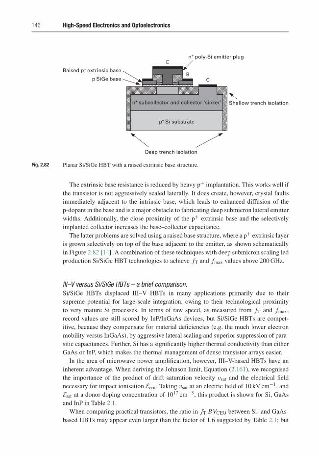
146 High-Speed Electronics and Optoelectronics
p– Si substrate
n+ subcollector and collector ‘sinker’
n+ poly-Si emitter plug
Raised p+ extrinsic base
p SiGe base
E
BC
Deep trench isolation
Shallow trench isolation
Fig. 2.82 Planar Si/SiGe HBT with a raised extrinsic base structure.
The extrinsic base resistance is reduced by heavy p+ implantation. This works well ifthe transistor is not aggressively scaled laterally. It does create, however, crystal faultsimmediately adjacent to the intrinsic base, which leads to enhanced diffusion of thep-dopant in the base and is a major obstacle to fabricating deep submicron lateral emitterwidths. Additionally, the close proximity of the p+ extrinsic base and the selectivelyimplanted collector increases the base–collector capacitance.
The latter problems are solved using a raised base structure, where a p+ extrinsic layeris grown selectively on top of the base adjacent to the emitter, as shown schematicallyin Figure 2.82 [14]. A combination of these techniques with deep submicron scaling ledproduction Si/SiGe HBT technologies to achieve fT and fmax values above 200 GHz.
III–V versus Si/SiGe HBTs – a brief comparison.Si/SiGe HBTs displaced III–V HBTs in many applications primarily due to theirsupreme potential for large-scale integration, owing to their technological proximityto very mature Si processes. In terms of raw speed, as measured from fT and fmax,record values are still scored by InP/InGaAs devices, but Si/SiGe HBTs are compet-itive, because they compensate for material deficiencies (e.g. the much lower electronmobility versus InGaAs), by aggressive lateral scaling and superior suppression of para-sitic capacitances. Further, Si has a significantly higher thermal conductivity than eitherGaAs or InP, which makes the thermal management of dense transistor arrays easier.
In the area of microwave power amplification, however, III–V-based HBTs have aninherent advantage. When deriving the Johnson limit, Equation (2.161), we recognisedthe importance of the product of drift saturation velocity vsat and the electrical fieldnecessary for impact ionisation Ecrit. Taking vsat at an electric field of 10 kV cm−1, andEsat at a donor doping concentration of 1017 cm−3, this product is shown for Si, GaAsand InP in Table 2.1.
When comparing practical transistors, the ratio in fT BVCEO between Si- and GaAs-based HBTs may appear even larger than the factor of 1.6 suggested by Table 2.1; but
Electronic devices 147
Table 2.1 vsat · Ecrit product for Si, GaAsand InP
Si 5,000 GHz VGaAs 8,000 GHz VInP 22,000 GHz V
this is due to the generally lower current gain in the GaAs devices, which increasesBVCEO.
2.5.6 Large-signal modelling
Bipolar transistor models have become increasingly complex. An exhaustive descriptionof popular large-signal formulations is beyond the scope of this book. The following willconcentrate on emphasising the major differences between the models, with respect toactive forward operation of the transistor, quasi-static non-linear equations and avoidingextreme areas of operation.
The Ebers–Moll modelThe Ebers–Moll equivalent circuit model was historically the first compact model ofthe bipolar transistor [16]. It approximates the intrinsic transistor as a network oftwo junction diodes and two current-controlled current sources (see Figure 2.83(a)).The parameter AF is the common-base current gain in forward operation. AR is thecommon-base current gain in reverse operation (emitter and base interchanged), whichis not being considered here. For active forward operation, the base–collector diode isreverse-biased. Further, AR IC is much smaller than the forward current through thebase–emitter diode and can hence be neglected. The resulting simplified equivalentcircuit is shown in Figure 2.83(b).
The emitter current in active forward operation is
IE = −ISBE
(eVBE/(NEVT) − 1
), (2.167)
where ISBE is the base–emitter saturation current, NE the base–emitter ideality factorand VT = kT/q the thermal voltage.
Using the full equivalent circuit, the Ebers–Moll equivalent circuit can account forsaturation (both diodes are forward-biased), but cannot model Early and Kirk effects.Further, the current dependence of the current gain at low VBE can also not be included.
The Gummel–Poon modelAn improved model of the bipolar transistor which is capable of including more ofthe non-ideal effects of bipolar transistors was introduced by Gummel and Poon in1970 [22].
The equivalent circuit (Figure 2.84) uses a voltage-controlled current source for thecollector current – the transistor is seen in common-emitter configuration here. The
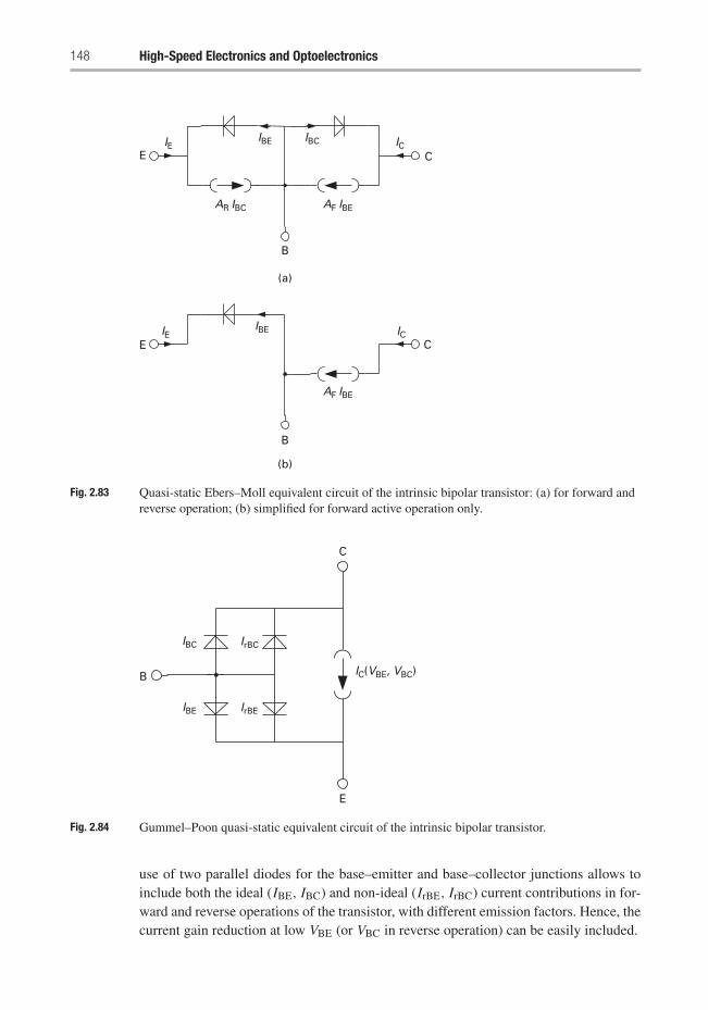
148 High-Speed Electronics and Optoelectronics
(a)
(b)
B
B
C
C
E
E
AR IBC AF IBE
AF IBE
ICIBCIBE
IBEIE IC
IE
Fig. 2.83 Quasi-static Ebers–Moll equivalent circuit of the intrinsic bipolar transistor: (a) for forward andreverse operation; (b) simplified for forward active operation only.
B
C
E
IC(VBE, VBC)
IBC
IBE IrBE
IrBC
Fig. 2.84 Gummel–Poon quasi-static equivalent circuit of the intrinsic bipolar transistor.
use of two parallel diodes for the base–emitter and base–collector junctions allows toinclude both the ideal (IBE, IBC) and non-ideal (IrBE, IrBC) current contributions in for-ward and reverse operations of the transistor, with different emission factors. Hence, thecurrent gain reduction at low VBE (or VBC in reverse operation) can be easily included.
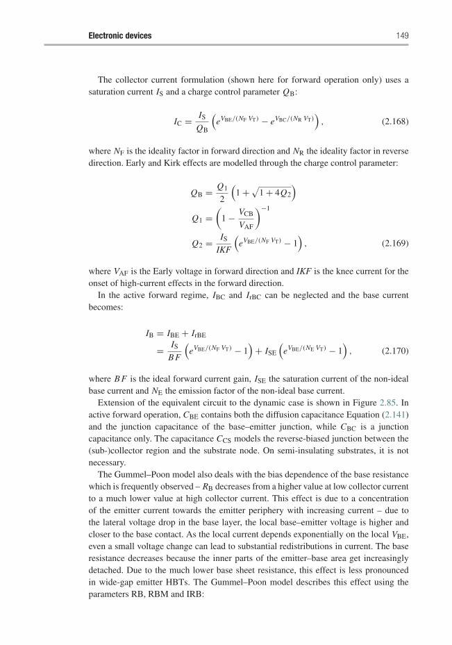
Electronic devices 149
The collector current formulation (shown here for forward operation only) uses asaturation current IS and a charge control parameter QB:
IC = IS
QB
(eVBE/(NF VT) − eVBC/(NR VT)
), (2.168)
where NF is the ideality factor in forward direction and NR the ideality factor in reversedirection. Early and Kirk effects are modelled through the charge control parameter:
QB = Q1
2
(1 + √
1 + 4Q2
)Q1 =
(1 − VCB
VAF
)−1
Q2 = IS
IKF
(eVBE/(NF VT) − 1
), (2.169)
where VAF is the Early voltage in forward direction and IKF is the knee current for theonset of high-current effects in the forward direction.
In the active forward regime, IBC and IrBC can be neglected and the base currentbecomes:
IB = IBE + IrBE
= IS
B F
(eVBE/(NF VT) − 1
)+ ISE
(eVBE/(NE VT) − 1
), (2.170)
where B F is the ideal forward current gain, ISE the saturation current of the non-idealbase current and NE the emission factor of the non-ideal base current.
Extension of the equivalent circuit to the dynamic case is shown in Figure 2.85. Inactive forward operation, CBE contains both the diffusion capacitance Equation (2.141)and the junction capacitance of the base–emitter junction, while CBC is a junctioncapacitance only. The capacitance CCS models the reverse-biased junction between the(sub-)collector region and the substrate node. On semi-insulating substrates, it is notnecessary.
The Gummel–Poon model also deals with the bias dependence of the base resistancewhich is frequently observed – RB decreases from a higher value at low collector currentto a much lower value at high collector current. This effect is due to a concentrationof the emitter current towards the emitter periphery with increasing current – due tothe lateral voltage drop in the base layer, the local base–emitter voltage is higher andcloser to the base contact. As the local current depends exponentially on the local VBE,even a small voltage change can lead to substantial redistributions in current. The baseresistance decreases because the inner parts of the emitter–base area get increasinglydetached. Due to the much lower base sheet resistance, this effect is less pronouncedin wide-gap emitter HBTs. The Gummel–Poon model describes this effect using theparameters RB, RBM and IRB:
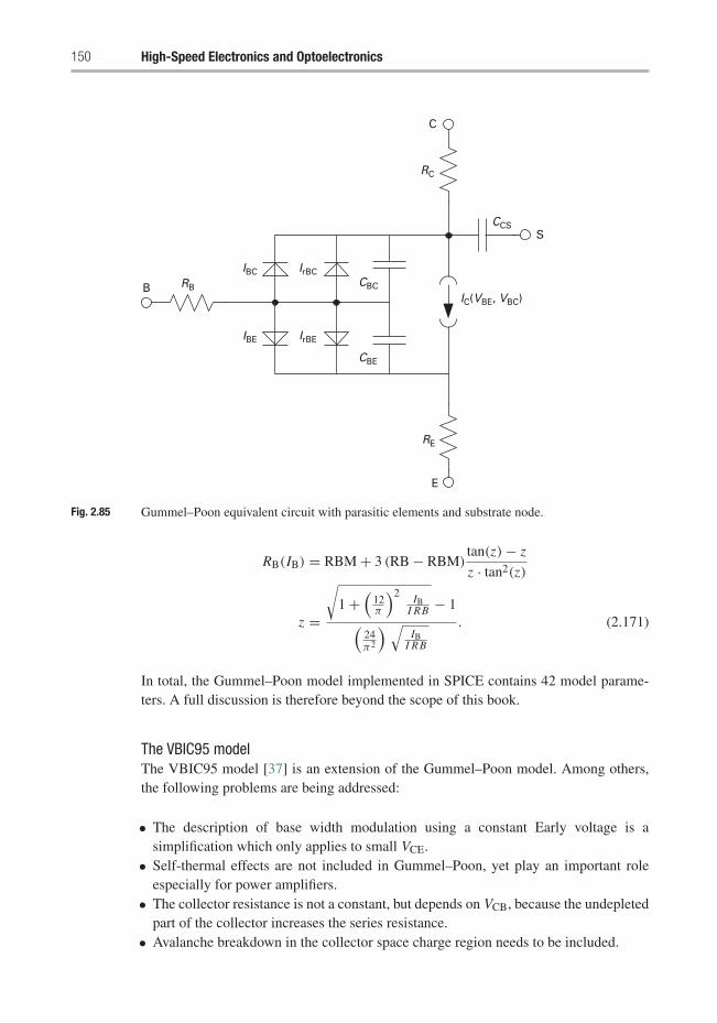
150 High-Speed Electronics and Optoelectronics
B
C
S
E
IBC
IBE
RB
RC
RE
CCS
IrBCCBC
CBE
IrBE
IC(VBE, VBC)
Fig. 2.85 Gummel–Poon equivalent circuit with parasitic elements and substrate node.
RB(IB) = RBM + 3 (RB − RBM)tan(z) − z
z · tan2(z)
z =
√1 +
(12π
)2 IBI R B − 1(
24π2
) √IB
I R B
. (2.171)
In total, the Gummel–Poon model implemented in SPICE contains 42 model parame-ters. A full discussion is therefore beyond the scope of this book.
The VBIC95 modelThe VBIC95 model [37] is an extension of the Gummel–Poon model. Among others,the following problems are being addressed:
• The description of base width modulation using a constant Early voltage is asimplification which only applies to small VCE.
• Self-thermal effects are not included in Gummel–Poon, yet play an important roleespecially for power amplifiers.
• The collector resistance is not a constant, but depends on VCB, because the undepletedpart of the collector increases the series resistance.
• Avalanche breakdown in the collector space charge region needs to be included.
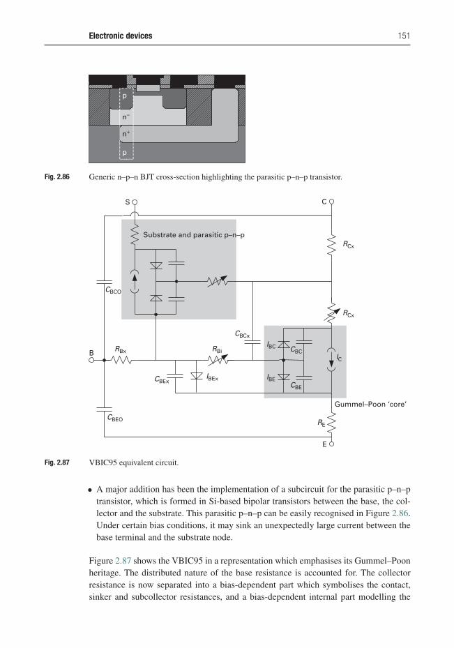
Electronic devices 151
p
p
n–
n+
Fig. 2.86 Generic n–p–n BJT cross-section highlighting the parasitic p–n–p transistor.
S C
B
E
CBCO
CBCx
CBEx
CBEO
IBEx
IC
IBC CBC
RCx
RCx
CBE
RE
IBE
RBx RBi
Substrate and parasitic p–n–p
Gummel–Poon ‘core’
Fig. 2.87 VBIC95 equivalent circuit.
• A major addition has been the implementation of a subcircuit for the parasitic p–n–ptransistor, which is formed in Si-based bipolar transistors between the base, the col-lector and the substrate. This parasitic p–n–p can be easily recognised in Figure 2.86.Under certain bias conditions, it may sink an unexpectedly large current between thebase terminal and the substrate node.
Figure 2.87 shows the VBIC95 in a representation which emphasises its Gummel–Poonheritage. The distributed nature of the base resistance is accounted for. The collectorresistance is now separated into a bias-dependent part which symbolises the contact,sinker and subcollector resistances, and a bias-dependent internal part modelling the
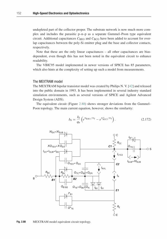
152 High-Speed Electronics and Optoelectronics
undepleted part of the collector proper. The substrate network is now much more com-plex and includes the parasitic p–n–p as a separate Gummel–Poon type equivalentcircuit. Additional capacitances CBEO and CBCO have been added to account for over-lap capacitances between the poly-Si emitter plug and the base and collector contacts,respectively.
Note that these are the only linear capacitances – all other capacitances are bias-dependent, even though this has not been noted in the equivalent circuit to enhancereadability.
The VBIC95 model implemented in newer versions of SPICE has 85 parameters,which also hints at the complexity of setting up such a model from measurements.
The MEXTRAM modelThe MEXTRAM bipolar transistor model was created by Philips N. V. [42] and releasedinto the public domain in 1993. It has been implemented in several industry standardsimulation environments, such as several versions of SPICE and Agilent AdvancedDesign System (ADS).
The equivalent circuit (Figure 2.88) shows stronger deviations from the Gummel–Poon topology. The main current equation, however, shows the similarity:
IN = IS
qb
(eVB2E1/VT − eV ∗
B2C2/VT). (2.172)
B
C
S
E
B1
C1
C2
E1
B2
RBC
RCC
IC1C2
QTS
ISF
IAVL
IN
IB1IB2QB1B2
IsB1
QsTE
QTEX+QEX
IEX+ISUB+IB3
XQTEX+XQEX
XIEX+XISUB
ISUB+XISUB
QTE+QBE+QN
QTC+QBC+QEPIRBV
RE
Fig. 2.88 MEXTRAM model equivalent circuit topology.
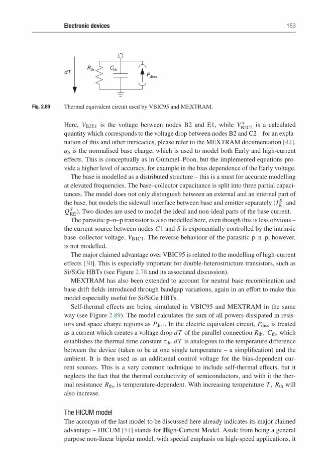
Electronic devices 153
dTRth Cth
Pdiss
Fig. 2.89 Thermal equivalent circuit used by VBIC95 and MEXTRAM.
Here, VB2E1 is the voltage between nodes B2 and E1, while V ∗B2C2 is a calculated
quantity which corresponds to the voltage drop between nodes B2 and C2 – for an expla-nation of this and other intricacies, please refer to the MEXTRAM documentation [42].qb is the normalised base charge, which is used to model both Early and high-currenteffects. This is conceptually as in Gummel–Poon, but the implemented equations pro-vide a higher level of accuracy, for example in the bias dependence of the Early voltage.
The base is modelled as a distributed structure – this is a must for accurate modellingat elevated frequencies. The base–collector capacitance is split into three partial capaci-tances. The model does not only distinguish between an external and an internal part ofthe base, but models the sidewall interface between base and emitter separately (I S
B1 andQS
RE). Two diodes are used to model the ideal and non-ideal parts of the base current.The parasitic p–n–p transistor is also modelled here, even though this is less obvious –
the current source between nodes C1 and S is exponentially controlled by the intrinsicbase–collector voltage, VB1C1. The reverse behaviour of the parasitic p–n–p, however,is not modelled.
The major claimed advantage over VBIC95 is related to the modelling of high-currenteffects [30]. This is especially important for double-heterostructure transistors, such asSi/SiGe HBTs (see Figure 2.78 and its associated discussion).
MEXTRAM has also been extended to account for neutral base recombination andbase drift fields introduced through bandgap variations, again in an effort to make thismodel especially useful for Si/SiGe HBTs.
Self-thermal effects are being simulated in VBIC95 and MEXTRAM in the sameway (see Figure 2.89). The model calculates the sum of all powers dissipated in resis-tors and space charge regions as Pdiss. In the electric equivalent circuit, Pdiss is treatedas a current which creates a voltage drop dT of the parallel connection Rth, Cth, whichestablishes the thermal time constant τth. dT is analogous to the temperature differencebetween the device (taken to be at one single temperature – a simplification) and theambient. It is then used as an additional control voltage for the bias-dependent cur-rent sources. This is a very common technique to include self-thermal effects, but itneglects the fact that the thermal conductivity of semiconductors, and with it the ther-mal resistance Rth, is temperature-dependent. With increasing temperature T , Rth willalso increase.
The HICUM modelThe acronym of the last model to be discussed here already indicates its major claimedadvantage – HICUM [51] stands for High-Current Model. Aside from being a generalpurpose non-linear bipolar model, with special emphasis on high-speed applications, it
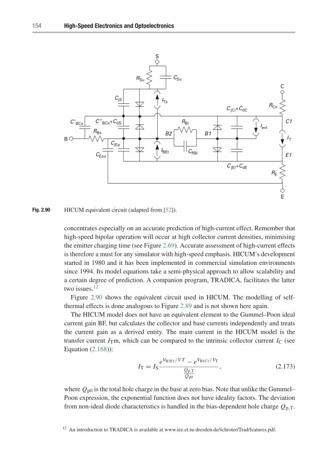
154 High-Speed Electronics and Optoelectronics
BB2 B1
C1
E1
E
C ′′BCx+CdS
C jCi+CdC
C jEi+CdE
CEox
RBx
CjS
RSu CSu
ITs
Iavl
IT
RCx
RBi
S
C
CjEpIBEt CRBi
RE
C ′BCx
Fig. 2.90 HICUM equivalent circuit (adapted from [52]).
concentrates especially on an accurate prediction of high-current effect. Remember thathigh-speed bipolar operation will occur at high collector current densities, minimisingthe emitter charging time (see Figure 2.69). Accurate assessment of high-current effectsis therefore a must for any simulator with high-speed emphasis. HICUM’s developmentstarted in 1980 and it has been implemented in commercial simulation environmentssince 1994. Its model equations take a semi-physical approach to allow scalability anda certain degree of prediction. A companion program, TRADICA, facilitates the lattertwo issues.12
Figure 2.90 shows the equivalent circuit used in HICUM. The modelling of self-thermal effects is done analogous to Figure 2.89 and is not shown here again.
The HICUM model does not have an equivalent element to the Gummel–Poon idealcurrent gain BF, but calculates the collector and base currents independently and treatsthe current gain as a derived entity. The main current in the HICUM model is thetransfer current ITm, which can be compared to the intrinsic collector current IC (seeEquation (2.168)):
IT = ISeVB1E1/V T − eVB1C1/VT
Qp,TQp0
, (2.173)
where Qp0 is the total hole charge in the base at zero bias. Note that unlike the Gummel–Poon expression, the exponential function does not have ideality factors. The deviationfrom non-ideal diode characteristics is handled in the bias-dependent hole charge Qp,T.
12 An introduction to TRADICA is available at www.iee.et.tu-dresden.de/schroter/Trad/features.pdf.
Electronic devices 155
The formulation for Qp,T in HICUM allows to include the effect of strongly varyingintrinsic carrier densities across the base layer, as necessary for the simulation of drift-base HBTs [53]. In the model, this is done through different weighting factors beingapplied to the depletion charges at the base–emitter and base–collector junctions.
The model can also accommodate the hole accumulation at the base–collector hetero-junction, with current gain roll-off and transit time deterioration, as needed in DHBTs[54]. For an in-depth treatment of HICUM parameters, refer to [52].
Differences between BJTs and HBTs relevant to large-signal modellingIn general, the standard bipolar models discussed above are also applicable to HBTs,with appropriately chosen parameters.
An important deviation concerns self-heating effects. In homojunction bipolar tran-sistors, both the collector saturation current and the current gain have positive tem-perature coefficients. The saturation current (see Equation (2.115)) increases becausethe intrinsic carrier concentration in the base depends exponentially on temperature.The current gain is limited by bandgap narrowing in the heavily doped emitter (see e.g.Equation (2.162)). The bandgap narrowing effect has a negative temperature coefficient,which lets the current gain increase with increasing temperature.
In a wide-gap emitter HBT, the saturation current equally has a positive tempera-ture coefficient. The current gain, however, decreases with increasing temperature. Tounderstand this, investigate again Equation (2.163):
Bmax ∼ e�EG/kT
The enhancement factor therefore decreases with increasing temperature, because thevalence band barrier gets less and less efficient.
A frequently observed self-thermal effect in HBTs is the current crush in multi-fingerHBTs (see Figure 2.91). At moderate dissipated powers, all fingers will have approxi-mately the same temperature and the current distribution is equal. With increasing VCE
and under constant base current, the collector current will gradually decrease due to thenegative temperature coefficient of B. However, due to the strongly positive tempera-ture coefficient of the saturation current, a finger which is slightly hotter than the otherswill draw more and more current, deviating it away from the others, and increase itstemperature. This strongly non-linear positive feedback will lead to a situation wherethe hottest finger takes on all the current, increases dramatically in temperature, witha resulting sudden decrease in current gain. This effect cannot be modelled with thestandard bipolar models.
Another important effect which cannot be simulated using the standard models is therapid onset of high-current effects in DHBTs, discussed in the context of Figure 2.78.
A minor effect, but worth mentioning, is that the non-ideal base current, see Equa-tion (2.122), may have a different VBE dependence in HBTs. This is due to space chargeregion recombination associated with the conduction band discontinuity at an abruptemitter–base heterojunction (see Figure 2.74). The potential well on the base side ofthe junction leads to an increased recombination, which depends in turn on the voltageacross the junction.
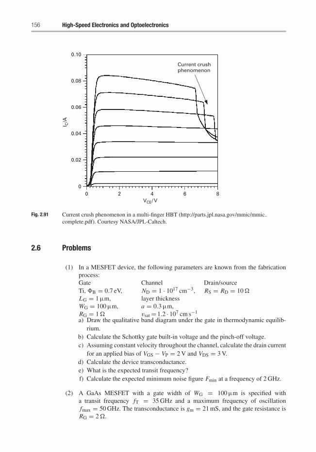
156 High-Speed Electronics and Optoelectronics
Current crushphenomenon
00
0.02
0.04
0.06
0.08
0.10
2 4 6 8VCE/ V
I C/A
Fig. 2.91 Current crush phenomenon in a multi-finger HBT (http://parts.jpl.nasa.gov/mmic/mmiccomplete.pdf). Courtesy NASA/JPL-Caltech.
2.6 Problems
(1) In a MESFET device, the following parameters are known from the fabricationprocess:Gate Channel Drain/sourceTi, �B = 0.7 eV,LG = 1 μm,WG = 100 μm,RG = 1�
ND = 1 · 1017 cm−3,layer thicknessa = 0.3 μm,vsat = 1.2 · 107 cm s−1
RS = RD = 10�
a) Draw the qualitative band diagram under the gate in thermodynamic equilib-rium.
b) Calculate the Schottky gate built-in voltage and the pinch-off voltage.c) Assuming constant velocity throughout the channel, calculate the drain current
for an applied bias of VGS − VP = 2 V and VDS = 3 V.d) Calculate the device transconductance.e) What is the expected transit frequency?f) Calculate the expected minimum noise figure Fmin at a frequency of 2 GHz.
(2) A GaAs MESFET with a gate width of WG = 100 μm is specified witha transit frequency fT = 35 GHz and a maximum frequency of oscillationfmax = 50 GHz. The transconductance is gm = 21 mS, and the gate resistance isRG = 2�.

Electronic devices 157
Estimate the gate-source capacitance and the gate-drain capacitance, assumingthat the output conductance is negligible. Can you provide an estimated value forthe minimum noise figure?
Due to a fabrication error, the gate resistance is increased to 5�. What is theimpact on fT, fmax and Fmin?
(3) Why does a MOSFET require an overlap between the gate and the sourceimplantation region? What does this imply for device capacitances?
(4) In an n-channel MOSFET with a metal gate electrode, the original gate metal isreplaced by a metal with a smaller work function. Explain qualitatively the effecton the threshold voltage.
(5) In a MOSFET technology, the thickness of the field oxide is chosen such thatunder the highest possible voltage between metallisation and substrate, no inver-sion channel can form at the SiO2/Si interface. Considering an Al metallisationwith a work function of 4.1 eV and a bulk doping concentration of NA = 5 ·1017,calculate the minimum thickness of the field oxide, if the maximum voltagebetween Al metallisation and the substrate is 5 V.
(6) A silicon-on-insulator n-channel MOSFET has a p-doped ‘bulk’ layer above theoxide layer with a doping concentration of NA = 2 · 1016 cm−3. The gate isheavily n-doped poly-Si. The gate oxide thickness is 5 nm.
Calculate the thickness of the doped layer such that it will be fully depleted inactive device operation. What is the purpose of the buried oxide layer? Explainits effect(s) on device performance.
(7) In a HEMT, what is the purpose of the spacer layer? Would the device stillfunction without it?
(8) A HEMT device has the following layer structure:Function Composition Thickness Doping concentrationSupply Al0.3Ga0.7As 80 nm ND = 3 · 1017 cm−3
Spacer Al0.3Ga0.7As 5 nm Nominally undopedBuffer GaAs 100 nm NA = 1 · 1015 cm−13
Substrate GaAs 150 μm IntrinsicCalculate the threshold voltage of this device at room temperature.
Let now VGS − Voff = 0.5 V. Calculate the sheet density charge of the 2DEG.
(9) You want to optimise the gain and low-noise behaviour of a HEMT by changingthe position of the gate electrode between source and drain. You observe the bestperformance if the gate is placeda) in the middle between the contactsb) closer to the drain contactc) closer to the source contactOne or none of the statements is true – explain your choice!
(10) Draw the small-signal equivalent circuit of an FET for VDS = 0, making appro-priate simplifications. What is the relationship between CGS and CGD in this biaspoint? Would you expect a noticeable difference between MESFETs and HEMTsin this mode of operation?
158 High-Speed Electronics and Optoelectronics
(11) Explain the two major advantages of a pseudomorphic HEMT structure, com-pared to the classic AlGaAs/GaAs HEMT. How do they relate to fT, fmax andFmin? Is there a potential disadvantage of the lower band gap in the channel?
(12) In order to reduce the series resistance of the gate, FETs (MESFETs, HEMTs andMOSFETs alike) are typically constructed with several gate fingers in parallel.Which effect(s) on device performance will result from this measure? Will thisaffect the transit frequency fT? Explain your answer.
(13) A HEMT technology has fT = 80 GHz and gm = 600 mS mm−1. For a devicewith WG = 2 · 60 m, the gate resistance is measured to be RG = 10�, and theminimum noise figure at 24 GHz is Fmin = 1.7 dB. For a device with WG =6 · 60 μm, what is the expected noise figure at 30 GHz? You may neglect thesource and drain resistances.
(14) Only one of the following answers is correct: in a bipolar transistor in activeforward operation, the base transit time isa) not a function of VCE
b) a weak function of VCE
c) a strong function of VCE.Explain your choice!
(15) Explain the following observations on high-speed bipolar transistors:a) In devices optimised for record fT, the maximum frequency of oscillation is
often quite low, and the breakdown voltage is also low.b) Devices optimised for record fmax often have low fT, higher breakdown
voltage, and need relatively high VCE for optimum operation.c) The latter devices suffer from significant Kirk effect.
(16) In n–p–n bipolar transistors, a drift field for electrons in the base can reduce thebase transit time. This can be done in two ways:(a) introduce a continuously varying material composition;(b) vary the doping concentration in the base.Explain how to achieve a constant field strength in the neutral base using eitherof the two methods.
(17) Note that Si/SiGe HBTs are always double-heterostructure devices. Why?
References
[1] Allam R., Kolanowski C., Theron D., Crosnier Y. (1994). Large signal model for analy-sis and design of HEMT gate mixer. IEEE Microwave Guided Wave Lett. MGWL-4, 12(December), 405–407.
[2] Antoniadis D. A., Aberg I., NiCleirigh C., Nayfeh O. M., Khakifirooz A., Hoyt J. L. (2006).Continuous MOSFET performance increase with device scaling: the role of strain andchannel material innovations. IBM J. Res. & Dev. 50, 4/5 (April–May), 363–377.
Electronic devices 159
[3] Belache A., Vanoverschelde A., Salmer G., Wolny M. (1991). Experimental analysis ofHEMT behavior under low-temperature conditions. IEEE Trans. Electron Devices ED-38, 1(January), 3–13.
[4] Benkhelifa F., Chertouk M., Dammann M., Massler M., Walther H., Weimann G. (2001).High performance metamorphic HEMT with 0.25 μm refractory metal gate on 4” GaAssubstrate. In International Conference on Semiconductor Manufacturing Technology GaAsMANTECH 2001 Digest of papers. Las Vegas, NV: GaAs MANTECH, 230–233. http://www.csmantech.org/Digests/2001/PDF/11_3_Benkhelifa_V2.pdf.
[5] Bourgoin J., Mauger A. (1988). Physical origin of the DX center. Appl. Phys. Lett. 53, 9(August), 749–751.
[6] Cappy A. (1988). Noise modeling and measurement techniques. IEEE Trans. Microw.Theory Tech. MTT-36, 1 (January), 1–10.
[7] Chan Y.-J., Pavlidis D., Razeghi M., Omnes F. (1990). Ga.51In.49P/GaAs HEMT’sexhibiting good electrical performance at cryogenic temperatures. IEEE Trans. ElectronDevices ED-37, 10 (October), 2141–2147.
[8] Cojocaru V. I., Brazil T. J. (1997). Scalable general-purpose model for microwave FET’sincluding DC/AC dispersion effects. IEEE Trans. Microw. Theory Tech. MTT-45, 12(December), 2248–2255.
[9] Cressler J. (2003). http://extenv.jpl.nasa.gov/presentations/SiGe_
HBT_BiCMOS.pdf.[10] Curtice W. (1980). A MESFET model for use in the design of GaAs integrated circuits.
IEEE Trans. Microw. Theory Tech. MTT-28, 5 (May), 448–456.[11] Das M. B. (1988). High-frequency performance limitations of millimeter-wave heterojunc-
tion bipolar transistors. IEEE Trans. Electron Devices ED-35, 5 (May), 604–614.[12] Delagebeaudeuf D., Chevrier I., Laviron M., Delescluse P. (1985). A new relationship
between the Fukui coefficient and optimal current value for low noise operation of fieldeffect transistors. IEEE Electron Device Lett. EDL-6, 9 (September), 444–445.
[13] Dingle R. (1984). New high-speed III–V devices for integrated circuits. IEEE Trans.Electron Devices ED-31, 11 (November), 1662–1667.
[14] Dunn J. S., Ahlgren D. C., Coolbaugh D. D., et al. (2003). Foundation of RF CMOS andSiGe BiCMOS technologies. IBM J. Res.&Dev. 47, 2/3 (February/March), 101–138.
[15] Early J. M. (1952). Effects of space-charge layer widening in junction transistors. Proc.IRE 40, 11 (November), 1401–1406.
[16] Ebers J. J., Moll J. L. (1954). Large-signal behavior of junction transistors. Proc. IRE 42, 12(December), 1761–1772.
[17] Johnson E. O. (1965). Physical limitations on frequency and power parameters of transistors.RCA Rev. 26, 6 (June), 163.
[18] Feygenson A., Ritter D., Hamm R. A., et al. (1992). InGaAs/InP composite collectorheterostructure bipolar transistors. Electron. Lett. 28, 7 (March), 607–609.
[19] Fiegna C. (2003). Analysis of gate shot noise in MOSFETs with ultrathin gate oxides. IEEEElectron Device Lett. EDL-24, 2 (February), 108–110.
[20] Folkes P. A. (1985). Thermal noise measurements in GaAs MESFETs. IEEE ElectronDevice Lett. EDL-6, 12 (December), 620–622.
[21] Fukui H. (1979). Design of microwave GaAs MESFETs for broad-band low noise ampli-fiers. IEEE Trans. Microw. Theory Tech. MTT-27, 7 (July), 643–650.
[22] Gummel H. K., Poon H. C. (1970). An integral charge-control model for bipolar transistors.Bell Syst. Tech. J. 49, 827–852.
160 High-Speed Electronics and Optoelectronics
[23] Hawkins R. J. (1977). Limitations of Nielsen’s and related noise equations applied tomicrowave bipolar transistors and a new expression for the frequency and current dependentnoise figure. Solid-State Electron. 20, 3 (March), 191–196.
[24] Hooge F. N. (1969). 1/f noise is no surface effect. Phys. Lett. A 29, 3 (April), 139–140.
[25] Hsia H., Tang Z., Caruth D., Becher D., Feng M. (1999). Direct ion-implanted 0.12 μmGaAs MESFET with ft of 121 GHz and fmax of 160 GHz. IEEE Electron Device Lett. 20, 5(May), 245–247.
[26] Joseph A., Cressler J. D., Richey D. M., Jaeger R. C., Harame D. L. (1997). Neutral baserecombination and its influence on the temperature dependence of Early voltage and cur-rent gain-Early voltage product in UHV/CVD SiGe heterojunction bipolar transistors. IEEETrans. Electron Devices ED-44, 3 (March), 404–413.
[27] Kallfass I. (2005a). Comprehensive Nonlinear Modelling of Dispersive HeterostructureField Effect Transistors and their MMIC Applications. Ph.D. thesis, Ulm Universitat, Ulm,Germany.
[28] Kallfass I. (2005b). Comprehensive Nonlinear Modelling of Dispersive HeterostructureField Effect Transistors and their MMIC Applications. Ph.D. thesis, Ulm Universitat, Ulm,Germany. Chapter 3.4.1.
[29] Kallfass I., Schumacher H., Brazil T. J. (2006). A unified approach to charge-conservativecapacitance modelling in HEMTs. Microwave and Wireless Components Letters 16, 12(December), 678–680.
[30] Kloosterman W. J. (1996). Comparison of Mextram and the VBIC95 Bipolar TransistorModel. Tech. Rep. NL-UR 034/96, Philips Electronics N. V. http://www.nxp.com/acrobat_download/other/philipsmodels/ur034_96.pdf.
[31] Kroemer H. (1957). Theory of a wide-gap emitter for transistors. Proc. IRE 45, 11(November), 1535–1537.
[32] Ladbrooke P. H. (1985). The theory and practice of the GaAs microwave MESFET. GEC J.Res. 3, 191–200.
[33] Lee K., Shur M., Drummond T., Morkoc H. (1984). Parasitic MESFET in (Al,Ga)As/GaAsmodulation doped FET’s and MODFET characterization. IEEE Trans. Electron DevicesED-31, 1 (January), 29–35.
[34] Lee T. H. (2004). The design of CMOS Radio-Frequency Integrated Circuits. CambridgeUniversity Press.
[35] Lilienfeld J. E. (1930). Method and apparatus for controlling electric currents. USA Patent1,745,175.
[36] Long S. I. (1989). A comparison of the GaAs MESFET and the AlGaAs/GaAs het-erojunction bipolar transistor for power microwave amplification. IEEE Trans. ElectronDevices ED-36, 5 (May), 1274–1279.
[37] McAndrew C. C., Seitchik J. A., Bowers D. F., et al. (1996). VBIC95, the vertical bipolarinter-company model. IEEE J. Solid-State Circ. 31, 10 (October), 1476–1483.
[38] Meyer J. E. (1971). MOS models and circuit simulations. RCA Rev. 32, 3 (March), 42–63.
[39] Mimura T., Hiyamizu S., Fujii T., Nanbu K. (1980). A new field-effect transistor withselectively doped GaAs/n-Alx Ga1−x As heterojunctions. Jp. J. Appl. Phys. 19, 5 (May),L225–L227.
[40] Nakajima S., Otobe K., Kuwata N., Shiga N., Matsuzaki K., Hayashi H. (1990). Pulse-dopedGaAs MESFETs with planar self-aligned gate for MMIC. IEEE MTT-S Int. MicrowaveSymp. Dig. 3, 1081–1084.
Electronic devices 161
[41] Ogura S., F. Codella C., Rovedo N., Shepard J. F., Riseman J. (1982). A half-micron MOS-FET using double implanted LDD. In Int’l Electron Devices Mtg. Proceedings, Vol. 28.Piscataway, NJ: IEEE, 718–722.
[42] Paaschens J. C. J., v. d. Toorn R., Kloosterman W. J. (1995). The Mextram BipolarModel. Tech. Rep. NL-UR 2000/811, Philips Electronics N. V. http://www.nxp.com/acrobat_download/other/philipsmodels/nlur2000811.pdf.
[43] Pailloncy G., Iniquez B., Dambrine G., Danneville F. (2004). Influence of a tunnelinggate current on the noise performance of SOI MOSFETs. In Proceedings 2004 IEEEInternational SOI Conference. Piscataway, NJ: IEEE, 55–57.
[44] Parthasarathy N., Griffith Z., Kadow C. et al. (2006). Collector-pedestal InGaAs/InP DHBTsfabricated in a single-growth, triple-implant process. IEEE Electron Device Lett. EDL-27, 5(May), 313–316.
[45] Post I., Akbar M., Curello G., et al. (2006). A 65 nm CMOS SOC technology featuringstrained silicon transistors for RF applications. In Int’l Electron Devices Mtg. Proceedings.Piscataway, NJ: IEEE, 1–3.
[46] Pucel R. A., Haus H. A., Statz H. (1975). Signal and noise properties of gallium arsenidemicrowave field effect transistors. In Advances in Electronics and Electron Physics,L. Marton, ed. Vol. 38. Academic Press, 195–265.
[47] Rodwell M. J. W., Urteaga M., Mathew T., et al. (2001). Submicron scaling of HBTs. IEEETrans. Electron Devices ED-48, 11 (November), 2606–2624.
[48] Saito M., Ono M., Fujimoto R., et al. (1998). 0.15 μm RF CMOS technology compati-ble with logic CMOS for low-voltage operation. IEEE Trans. Electron Devices ED-45, 3(March), 737–742.
[49] Sakurai T., Newton A. R. (1991). A simple MOSFET model for circuit analysis. IEEE Trans.Electron Devices ED-38, 4 (April), 887–894.
[50] Sato H., Vlcek J. C., Fonstad C. G., Meskoob B., Prasad S. (1990). InGaAs/InAlAs/InPcollector-up microwave heterojunction bipolar transistors. IEEE Electron Device Lett. EDL-11, 10 (October), 457–459.
[51] Schroter M. (2002). Staying current with HICUM. IEEE Circ. Dev. Mag. 18, 3 (May),16–25.
[52] Schroter M. (2007). RF Modeling of Bipolar Transistors with HICUM. http://www.iee.et.tu-dresden.de/˜schroter/Conf/hic_ovw.pdf.
[53] Schroter M., Friedrich M., Rein H.-M. (1993). A generalized integral charge-control rela-tion and its application to compact models for silicon-based HBT’s. IEEE Trans. ElectronDevices ED-40, 11 (November), 2036–2046.
[54] Schroter M., Lee T. Y. (1999). Physics-based minority charge and transit time modeling forbipolar transistors. IEEE Trans. Electron Devices ED-46, 2 (February), 288–300.
[55] Schuppen A., Berntgen J., Maier P., Tortschanoff M., Kraus W., Averweg M. (2001). An80 GHz SiGe production technology. III–V Review 14, 6 (August), 42–46.
[56] Shockley W. (1951). Circuit element utilizing semiconductive material. USA Patent2,569,347.
[57] Shockley W. (1952). A unipolar ‘field effect’ transistor. Proc. IRE 40, 11, 1365–1376.
[58] Statz H., Newman P., Smith I. W., Pucel R. A., Haus H. A. (1987). GaAs FET device andcircuit simulation in SPICE. IEEE Trans. Electron Devices ED-34, 2 (February), 160–169.
[59] Stillman G., Wolfe C., Dimmock J. (1970). Hall coefficient factor for polar mode scatteringin N-type GaAs. J. Phys. Chem. Solids 31, 6, 1199–1204.

162 High-Speed Electronics and Optoelectronics
[60] Sudow M., Andersson K., Billstrom N., et al. (2006). An SiC MESFET-based MMICprocess. IEEE Trans. Microw. Theory Tech. MTT-54, 12 (December), 4072–4078.
[61] Sugli T., Watanabe K., Sugatani S. (2003). Transistor design for 90 nm-generation andbeyond. Fujitsu Sci. Tech. J. 39, 6 (June), 9–22.
[62] van der Ziel A. (1962). Thermal noise in field effect transistors. Proc. IRE 50, 8 (August),1808–1812.
[63] van der Ziel A. (1963). Gate noise in field effect transistors at moderately high frequencies.Proc. IEEE 51, 3 (March), 461–467.
[64] Yngvesson S. (1991). Microwave Semiconductor Devices. Kluwer Academic Publishers.[65] Zeghbroeck B. V. (2004). Principles of Semiconductor Devices. http://ece-www.
colorado.edu/˜bart/book/book/chapter5/pdf/ch5_5.pdf.
3 Optimisation and parameterextraction of circuit models
3.1 Executive summary
Optimised device models are important in the design of electronic devices for specificperformance. They help the designer to predict the behaviour of the device in an ana-logue circuit. However, standard methods of optimisation do not lend themselves tofast computation and may present problems with convergence. The simulated anneal-ing, genetic and structured genetic algorithms are alternative optimisation methods thathelp to solve the convergence problems by avoiding entrapment in local minima of thesolution space. These methods are used for the extraction of the parameters of the equiv-alent circuit model of the device or to construct its neural network model. The neuralnetwork models are black box models that determine device outputs from known inputsafter appropriate weighting values have been calculated. Another method of parame-ter extraction is the semi-analytical procedure that uses an analytic approach togetherwith empirical optimisation methods. Basic expressions and approximations to extractsmall-signal equivalent circuit parameters are developed so that accurate device modelscan be obtained.
3.2 Optimisation of device models
Accurate device models are developed to predict behaviour that is in good agreementwith experimental observations. The optimisation of the model parameters can be con-sidered to be the curve-fitting of the computed device characteristics to experimentaldata. Traditional gradient methods are computationally intensive and there are prob-lems with convergence and entrapment in local minima. Optimisation only involves the“trial” of a number of initial solutions to minimise the error.
Combinatorial optimisation overcomes this problem of entrapment in local minima.To set up the device modelling problem as a combinatorial optimisation problem, thelimits on each parameter are specified. Parameter values are then discretised so that alarge but finite number of solutions is possible. An objective function, also referred toas the cost function is given by
F(Vi) =m∑
j=1
(Mj − M ′j )
2, (3.1)
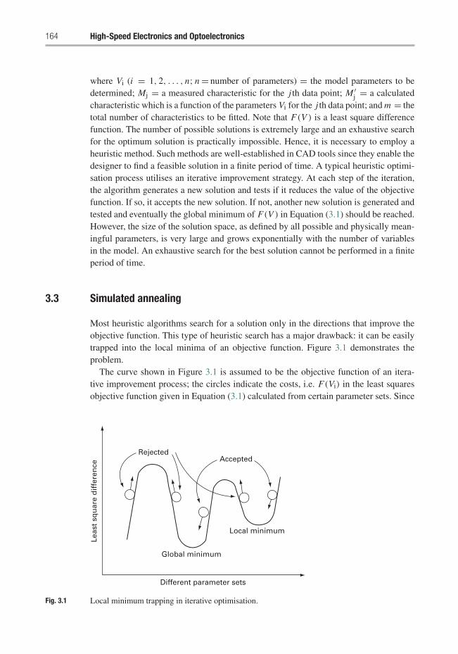
164 High-Speed Electronics and Optoelectronics
where Vi (i = 1, 2, . . . , n; n = number of parameters) = the model parameters to bedetermined; Mj = a measured characteristic for the j th data point; M ′
j = a calculatedcharacteristic which is a function of the parameters Vi for the j th data point; and m = thetotal number of characteristics to be fitted. Note that F(V ) is a least square differencefunction. The number of possible solutions is extremely large and an exhaustive searchfor the optimum solution is practically impossible. Hence, it is necessary to employ aheuristic method. Such methods are well-established in CAD tools since they enable thedesigner to find a feasible solution in a finite period of time. A typical heuristic optimi-sation process utilises an iterative improvement strategy. At each step of the iteration,the algorithm generates a new solution and tests if it reduces the value of the objectivefunction. If so, it accepts the new solution. If not, another new solution is generated andtested and eventually the global minimum of F(V ) in Equation (3.1) should be reached.However, the size of the solution space, as defined by all possible and physically mean-ingful parameters, is very large and grows exponentially with the number of variablesin the model. An exhaustive search for the best solution cannot be performed in a finiteperiod of time.
3.3 Simulated annealing
Most heuristic algorithms search for a solution only in the directions that improve theobjective function. This type of heuristic search has a major drawback: it can be easilytrapped into the local minima of an objective function. Figure 3.1 demonstrates theproblem.
The curve shown in Figure 3.1 is assumed to be the objective function of an itera-tive improvement process; the circles indicate the costs, i.e. F(Vi) in the least squaresobjective function given in Equation (3.1) calculated from certain parameter sets. Since
RejectedAccepted
Local minimum
Global minimum
Different parameter sets
Leas
t sq
uar
e d
iffe
ren
ce
Fig. 3.1 Local minimum trapping in iterative optimisation.
Optimisation and parameter extraction of circuit models 165
a new set of parameters is generated by introducing small modifications to the model,its corresponding location on the curve is most likely to be somewhere near that ofthe original configuration. The traditional iterative improvement algorithms only acceptparameter sets that have reduced the cost. This criterion of set acceptance impliesthat the process can only go downhill into a minimum and any uphill movement isforbidden. Depending on the starting point of the search, it is possible that this mini-mum is only a local minimum of the objective function. This search process generallydoes not have the capability of climbing over a peak of the curve to reach the globalminimum.
The drawback of this process can be overcome by using simulated annealing(SA)[12, 22, 23, 30]. This is a method of finding a near optimal solution for combi-natorial optimisation problems. The SA algorithm has the advantage of asymptoticallyproducing the global optimal solution with a probability of one. This is achieved bymaking the following important modification to conventional heuristic methods. A cost-increasing solution may still be accepted. The probability of acceptance depends on:(1) a parameter called a pseudo-temperature Tk, which is artificially decreased as theiteration proceeds, and (2) the value of
�F(V ) = F(Vk) − F(Vk−i) (3.2)
where Vk and Vk−1 are the values of the parameter vector V at iteration steps k andk − 1. Specifically, a law similar to Boltzmann statistics is used to determine the proba-bility P of accepting a certain cost-increasing solution Vk at the kth iteration step. Theprobability function P is given by
P(Vk, Tk) = exp
[−�F(Vk)
Tk
]. (3.3)
A careful choice of the initial pseudo-temperature T0 and a rule for decreasing thepseudo-temperature T are necessary to save computation time while being able toescape from the local minima. The temperatures are related by the equation
Tk = αTk−1, (3.4)
where α is a constant between 0.8 and 0.95. Its value can be gradually increasedfrom the lowest to the highest value. T0 ≥ 500 is a satisfactory choice for devicemodelling.
At each iteration, new parameter values are generated by first choosing one deviceparameter Vi at random. A user-defined base value Vi−base is multiplied by a randomnumber R, such that 0 ≤ R ≤ 1, and a variation �Vi = RVi−base is introduced into theparameter Vi. The new parameter value so obtained is used in the next iteration unlessit exceeds prescribed limits, in which case it will be set to the maximum or minimumallowable value.
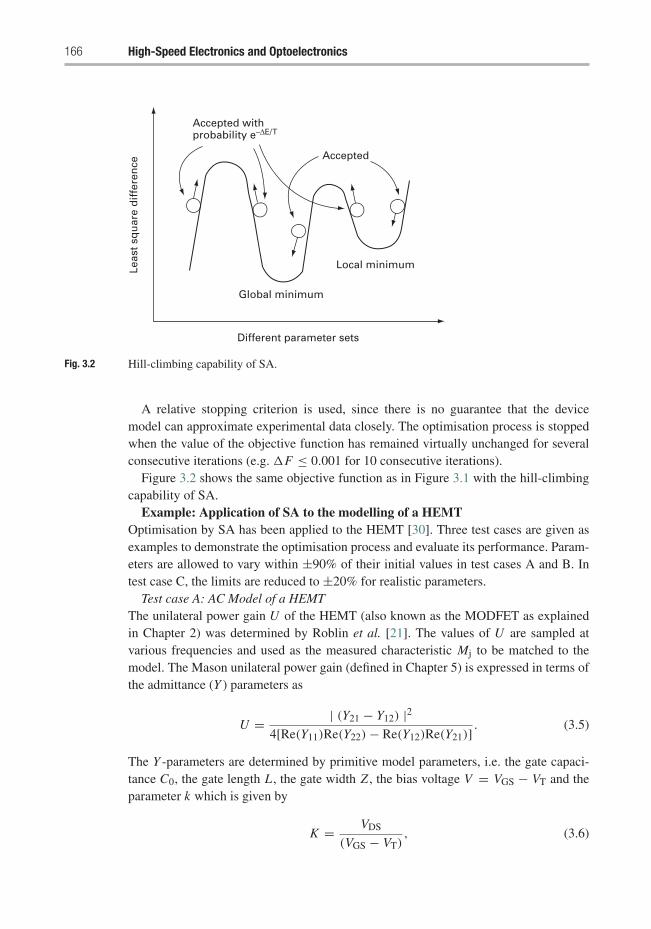
166 High-Speed Electronics and Optoelectronics
Accepted withprobability e–ΔE/T
Accepted
Local minimum
Global minimum
Different parameter sets
Leas
t sq
uar
e d
iffe
ren
ce
Fig. 3.2 Hill-climbing capability of SA.
A relative stopping criterion is used, since there is no guarantee that the devicemodel can approximate experimental data closely. The optimisation process is stoppedwhen the value of the objective function has remained virtually unchanged for severalconsecutive iterations (e.g. �F ≤ 0.001 for 10 consecutive iterations).
Figure 3.2 shows the same objective function as in Figure 3.1 with the hill-climbingcapability of SA.
Example: Application of SA to the modelling of a HEMTOptimisation by SA has been applied to the HEMT [30]. Three test cases are given asexamples to demonstrate the optimisation process and evaluate its performance. Param-eters are allowed to vary within ±90% of their initial values in test cases A and B. Intest case C, the limits are reduced to ±20% for realistic parameters.
Test case A: AC Model of a HEMTThe unilateral power gain U of the HEMT (also known as the MODFET as explainedin Chapter 2) was determined by Roblin et al. [21]. The values of U are sampled atvarious frequencies and used as the measured characteristic Mj to be matched to themodel. The Mason unilateral power gain (defined in Chapter 5) is expressed in terms ofthe admittance (Y ) parameters as
U = | (Y21 − Y12) |24[Re(Y11)Re(Y22) − Re(Y12)Re(Y21)] . (3.5)
The Y -parameters are determined by primitive model parameters, i.e. the gate capaci-tance C0, the gate length L , the gate width Z , the bias voltage V = VGS − VT and theparameter k which is given by
K = VDS
(VGS − VT), (3.6)
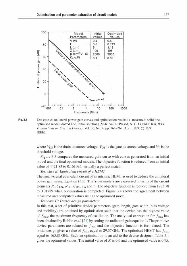
Optimisation and parameter extraction of circuit models 167
.001–20
0
20
40
60
80
100
.01 .1
Initial model gain
Measured and optim
ized model gains
1
ModelParametersV (V) 0.4 0.4
0.7131.1810638000.09
0.6510020000.1
kL (μm)Z (μm)μ (cm2/V – S)C0 (pF)
InitialValues
OptimizedValues
10 100 1000Frequency (GHz)
Un
ilate
ral p
ow
er g
ain
(d
B)
Fig. 3.3 Test case A: unilateral power gain curves and optimisation results [+, measured; solid line,optimised model; dotted line, initial solution] (M-K. Vai, S. Prasad, N. C. Li and F. Kai, IEEETransactions on Electron Devices, Vol. 36, No. 4, pp. 761–762, April 1989. c©1989IEEE).
where VDS is the drain to source voltage, VGS is the gate to source voltage and VT is thethreshold voltage.
Figure 3.3 compares the measured gain curve with curves generated from an initialmodel and the final optimised models. The objective function is reduced from an initialvalue of 4421.83 to 0.161095, virtually a perfect match.
Test case B: Equivalent circuit of a HEMTThe small-signal equivalent circuit of an intrinsic HEMT is used to deduce the unilateralpower gain using Equation (3.5). The Y-parameters are expressed in terms of the circuitelements Ri, CGS, RDS, CDS, gm and τ . The objective function is reduced from 1783.78to 0.01789 when optimisation is completed. Figure 3.4 shows the agreement betweenmeasured and computed values using the optimised model.
Test case C: Device design parametersIn this test, a set of primitive device parameters (gate length, gate width, bias voltageand mobility) are obtained by optimisation such that the device has the highest valueof fmax, the maximum frequency of oscillation. The analytical expression for fmax hasbeen obtained by Roblin et al. [21] by setting the unilateral gain equal to 1. The primitivedevice parameters are related to fmax and the objective function is formulated. Theinitial design gives a value of fmax equal to 29.57 GHz. The optimised HEMT has fmax
equal to 165.81 GHz. Such an optimisation is an aid to the device designer. Table 3.1gives the optimised values. The initial value of K is 0.6 and the optimised value is 0.95.
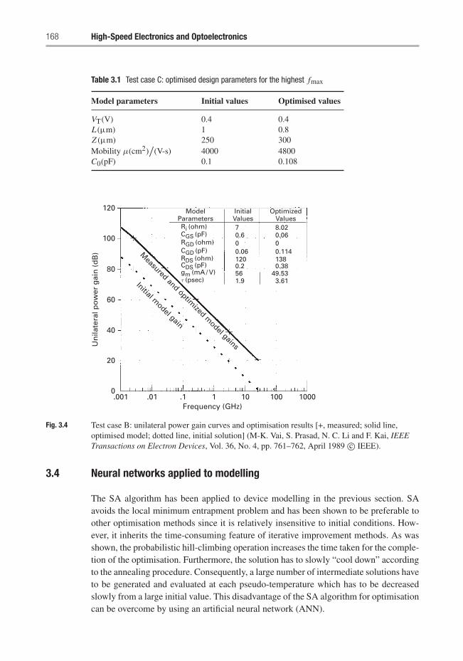
168 High-Speed Electronics and Optoelectronics
Table 3.1 Test case C: optimised design parameters for the highest fmax
Model parameters Initial values Optimised values
VT(V) 0.4 0.4L(μm) 1 0.8Z(μm) 250 300Mobility μ(cm2)
/(V-s) 4000 4800
C0(pF) 0.1 0.108
.0010
20
40
60
80
100
120
.01 .1
Initial model gain
Measured and optim
ized model gains
1
ModelParameters
8.027Ri (ohm)0.060.6CGS (pF)
0.1140.06CGD (pF)
CDS (pF)
00RGD (ohm)
0.380.2138120RDS (ohm)
49.5356gm (mA / V)3.611.9τ (psec)
InitialValues
OptimizedValues
10 100 1000Frequency (GHz)
Un
ilate
ral p
ow
er g
ain
(d
B)
Fig. 3.4 Test case B: unilateral power gain curves and optimisation results [+, measured; solid line,optimised model; dotted line, initial solution] (M-K. Vai, S. Prasad, N. C. Li and F. Kai, IEEETransactions on Electron Devices, Vol. 36, No. 4, pp. 761–762, April 1989 c© IEEE).
3.4 Neural networks applied to modelling
The SA algorithm has been applied to device modelling in the previous section. SAavoids the local minimum entrapment problem and has been shown to be preferable toother optimisation methods since it is relatively insensitive to initial conditions. How-ever, it inherits the time-consuming feature of iterative improvement methods. As wasshown, the probabilistic hill-climbing operation increases the time taken for the comple-tion of the optimisation. Furthermore, the solution has to slowly “cool down” accordingto the annealing procedure. Consequently, a large number of intermediate solutions haveto be generated and evaluated at each pseudo-temperature which has to be decreasedslowly from a large initial value. This disadvantage of the SA algorithm for optimisationcan be overcome by using an artificial neural network (ANN).
Optimisation and parameter extraction of circuit models 169
ANNs are based on the human nervous system which consists of a distribution of neu-rons to carry messages back and forth to the brain. The ANN has been used successfullyin many modelling and optimisation applications in engineering that are particularlyuseful when several tasks are to be performed in parallel and computation rates arerequired to be high [31, 37]. Neural networks are particularly attractive because of theirspeed and accuracy. Hence, neural networks have been developed into an alternativecomputer-aided approach to model and design devices and circuits. Neural networksrepresent a robust modelling approach to predict the behaviour of high-speed devicesand circuits [29]. In comparison with various statistical methods and curve-fittingapproaches for predicting system behaviour, the neural network approach features alearning process which fine tunes neural network parameters to interrelate the variablesbeing modelled. A neural network may be developed to guide the solution generation ofan SA optimisation process. This approach utilises the associative capability of a neuralnetwork to globally and concurrently evaluate the effect of varying all the parameters.When used in place of a physics-oriented device model, a neural network avoids theneed to repeatedly solve the equations that describe the device physics.
Two classes of neural networks are used in modelling:
(i) Multi-layer perceptron neural networks(ii) Recurrent Hopfield neural networks.
Regardless of the neural network architecture selected for an application, it consistsof many processing elements called neurons, each connected to many others. Everyconnection entering a neuron has a weight assigned to it. This weight is used to amplify,attenuate or change the sign of the signal in the incoming connection. The input tothe neural network is a vector of the data to be modelled. Each neuron operates onthe outputs of other neurons according to its transfer function and delivers an outputto other neurons. Often, the transfer function sums the incoming signals to determinethe value of the neuron’s next output signal. The result is an output vector representingsome characteristics associated with the input.
In order to use neural network algorithms, it is necessary to determine an intercon-nection pattern, the weights and the transfer functions. The creation and training of anappropriate neural network for the problem on hand is difficult and time-consuming.However, an appropriately trained neural network provides fast and efficient solutionsthat have shown excellent results for different applications such as the modelling oftransistor behaviour and microwave circuits as well as microwave impedance match-ing [28]. A neural network consists of a set of simultaneous non-linear equations thatare capable of modelling any continuous function when the appropriate weights aredetermined. These networks are pictorially represented as neurons (circles) with inter-connecting nerves (lines). Neural networks are very flexible tools for device modellingbecause they can be adapted to model different devices without change of equations.Adapting a physics-based model to a different physical device may involve a radicalchange of equations. This flexibility gave the impetus to the effort of finding muchbetter ways of applying neural networks to device modelling. However, the problem
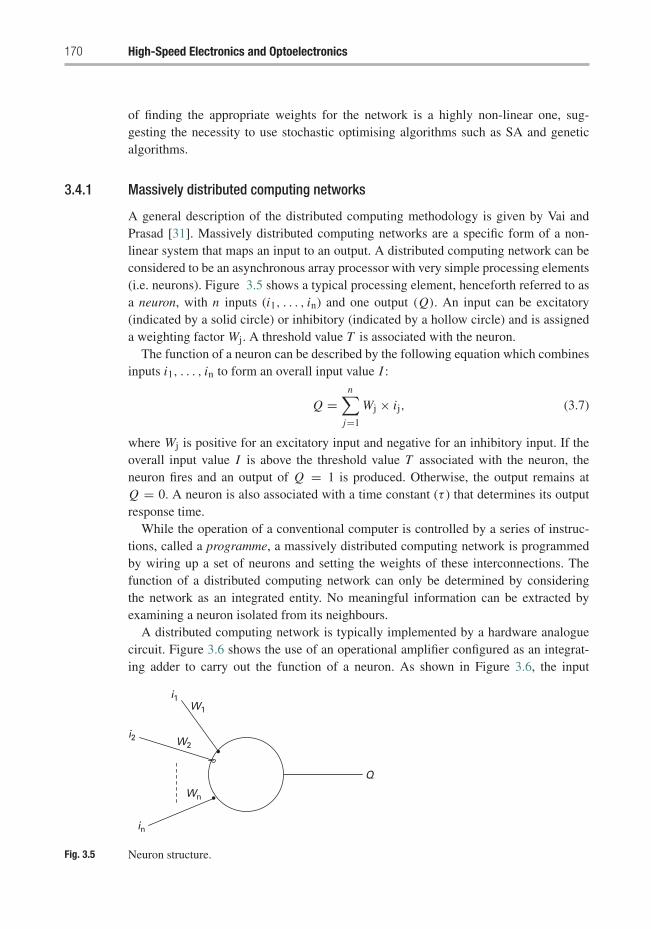
170 High-Speed Electronics and Optoelectronics
of finding the appropriate weights for the network is a highly non-linear one, sug-gesting the necessity to use stochastic optimising algorithms such as SA and geneticalgorithms.
3.4.1 Massively distributed computing networks
A general description of the distributed computing methodology is given by Vai andPrasad [31]. Massively distributed computing networks are a specific form of a non-linear system that maps an input to an output. A distributed computing network can beconsidered to be an asynchronous array processor with very simple processing elements(i.e. neurons). Figure 3.5 shows a typical processing element, henceforth referred to asa neuron, with n inputs (i1, . . . , in) and one output (Q). An input can be excitatory(indicated by a solid circle) or inhibitory (indicated by a hollow circle) and is assigneda weighting factor Wj. A threshold value T is associated with the neuron.
The function of a neuron can be described by the following equation which combinesinputs i1, . . . , in to form an overall input value I :
Q =n∑
j=1
Wj × ij, (3.7)
where Wj is positive for an excitatory input and negative for an inhibitory input. If theoverall input value I is above the threshold value T associated with the neuron, theneuron fires and an output of Q = 1 is produced. Otherwise, the output remains atQ = 0. A neuron is also associated with a time constant (τ ) that determines its outputresponse time.
While the operation of a conventional computer is controlled by a series of instruc-tions, called a programme, a massively distributed computing network is programmedby wiring up a set of neurons and setting the weights of these interconnections. Thefunction of a distributed computing network can only be determined by consideringthe network as an integrated entity. No meaningful information can be extracted byexamining a neuron isolated from its neighbours.
A distributed computing network is typically implemented by a hardware analoguecircuit. Figure 3.6 shows the use of an operational amplifier configured as an integrat-ing adder to carry out the function of a neuron. As shown in Figure 3.6, the input
W1
Q
W2
Wn
i1
i2
in
Fig. 3.5 Neuron structure.
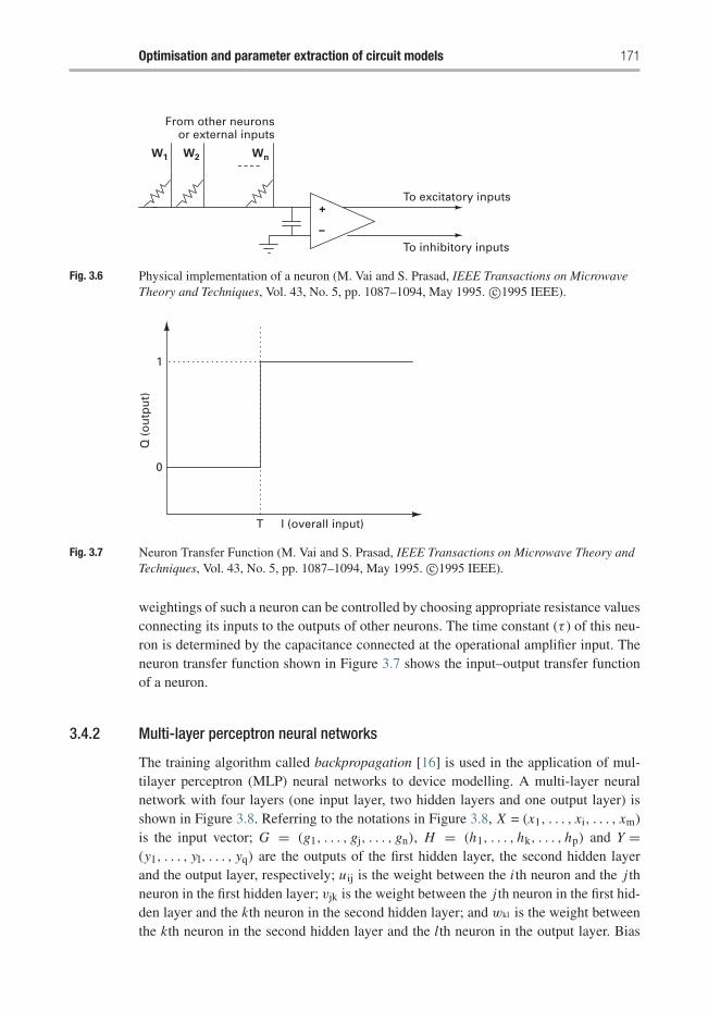
Optimisation and parameter extraction of circuit models 171
W1 W2
From other neuronsor external inputs
To excitatory inputs
To inhibitory inputs
Wn
+
–
Fig. 3.6 Physical implementation of a neuron (M. Vai and S. Prasad, IEEE Transactions on MicrowaveTheory and Techniques, Vol. 43, No. 5, pp. 1087–1094, May 1995. c©1995 IEEE).
1
0
Q (
ou
tpu
t)
I (overall input)T
Fig. 3.7 Neuron Transfer Function (M. Vai and S. Prasad, IEEE Transactions on Microwave Theory andTechniques, Vol. 43, No. 5, pp. 1087–1094, May 1995. c©1995 IEEE).
weightings of such a neuron can be controlled by choosing appropriate resistance valuesconnecting its inputs to the outputs of other neurons. The time constant (τ ) of this neu-ron is determined by the capacitance connected at the operational amplifier input. Theneuron transfer function shown in Figure 3.7 shows the input–output transfer functionof a neuron.
3.4.2 Multi-layer perceptron neural networks
The training algorithm called backpropagation [16] is used in the application of mul-tilayer perceptron (MLP) neural networks to device modelling. A multi-layer neuralnetwork with four layers (one input layer, two hidden layers and one output layer) isshown in Figure 3.8. Referring to the notations in Figure 3.8, X = (x1, . . . , xi, . . . , xm)is the input vector; G = (g1, . . . , gj, . . . , gn), H = (h1, . . . , hk, . . . , hp) and Y =(y1, . . . , yl, . . . , yq) are the outputs of the first hidden layer, the second hidden layerand the output layer, respectively; uij is the weight between the i th neuron and the j thneuron in the first hidden layer; vjk is the weight between the j th neuron in the first hid-den layer and the kth neuron in the second hidden layer; and wkl is the weight betweenthe kth neuron in the second hidden layer and the lth neuron in the output layer. Bias
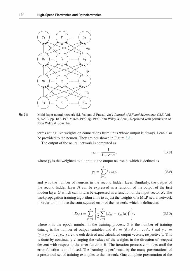
172 High-Speed Electronics and Optoelectronics
y1
h1
g1
x1
yl yq
hphk
gj
xi xm
gn
wkl
vjk
uij
Fig. 3.8 Multi-layer neural network (M. Vai and S Prasad, Int’l Journal of RF and Microwave CAE, Vol.9, No. 3, pp. 187–197, March 1999. c© 1999 John Wiley & Sons). Reprinted with permission ofJohn Wiley & Sons, Inc.
terms acting like weights on connections from units whose output is always 1 can alsobe provided to the neuron. They are not shown in Figure 3.8.
The output of the neural network is computed as
y� = 1
1 + e−γ�, (3.8)
where γ� is the weighted total input to the output neuron �, which is defined as
γ� =p∑
k=1
hkwk�, (3.9)
and p is the number of neurons in the second hidden layer. Similarly, the output ofthe second hidden layer H can be expressed as a function of the output of the firsthidden layer G which can in turn be expressed as a function of the input vector X . Thebackpropagation training algorithm aims to adjust the weights of a MLP neural networkin order to minimise the sum-squared error of the network, which is defined as
E(n) =S∑
m=1
{1
2
q∑l=1
[dml − yml(n)]2
}, (3.10)
where n is the epoch number in the training process, S is the number of trainingdata, q is the number of output variables and dm = (dm1dm2, . . . , dmq) and ym =(ym1 ym2, . . . , ymq) are the mth desired and calculated output vectors, respectively. Thisis done by continually changing the values of the weights in the direction of steepestdescent with respect to the error function E . The iteration process continues until theerror function is minimised. The learning is performed by the many presentations ofa prescribed set of training examples to the network. One complete presentation of the
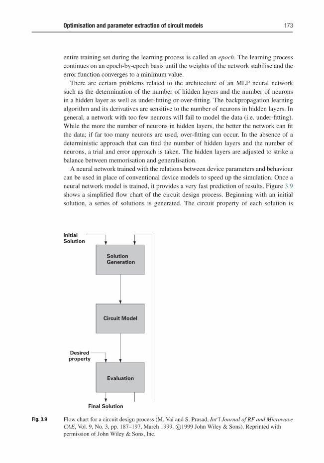
Optimisation and parameter extraction of circuit models 173
entire training set during the learning process is called an epoch. The learning processcontinues on an epoch-by-epoch basis until the weights of the network stabilise and theerror function converges to a minimum value.
There are certain problems related to the architecture of an MLP neural networksuch as the determination of the number of hidden layers and the number of neuronsin a hidden layer as well as under-fitting or over-fitting. The backpropagation learningalgorithm and its derivatives are sensitive to the number of neurons in hidden layers. Ingeneral, a network with too few neurons will fail to model the data (i.e. under-fitting).While the more the number of neurons in hidden layers, the better the network can fitthe data; if far too many neurons are used, over-fitting can occur. In the absence of adeterministic approach that can find the number of hidden layers and the number ofneurons, a trial and error approach is taken. The hidden layers are adjusted to strike abalance between memorisation and generalisation.
A neural network trained with the relations between device parameters and behaviourcan be used in place of conventional device models to speed up the simulation. Once aneural network model is trained, it provides a very fast prediction of results. Figure 3.9shows a simplified flow chart of the circuit design process. Beginning with an initialsolution, a series of solutions is generated. The circuit property of each solution is
InitialSolution
SolutionGeneration
Final Solution
Desiredproperty
Circuit Model
Evaluation
Fig. 3.9 Flow chart for a circuit design process (M. Vai and S. Prasad, Int’l Journal of RF and MicrowaveCAE, Vol. 9, No. 3, pp. 187–197, March 1999. c©1999 John Wiley & Sons). Reprinted withpermission of John Wiley & Sons, Inc.
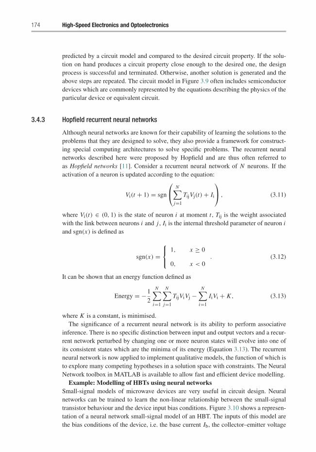
174 High-Speed Electronics and Optoelectronics
predicted by a circuit model and compared to the desired circuit property. If the solu-tion on hand produces a circuit property close enough to the desired one, the designprocess is successful and terminated. Otherwise, another solution is generated and theabove steps are repeated. The circuit model in Figure 3.9 often includes semiconductordevices which are commonly represented by the equations describing the physics of theparticular device or equivalent circuit.
3.4.3 Hopfield recurrent neural networks
Although neural networks are known for their capability of learning the solutions to theproblems that they are designed to solve, they also provide a framework for construct-ing special computing architectures to solve specific problems. The recurrent neuralnetworks described here were proposed by Hopfield and are thus often referred toas Hopfield networks [11]. Consider a recurrent neural network of N neurons. If theactivation of a neuron is updated according to the equation:
Vi(t + 1) = sgn
⎛⎝ N∑j=1
TijVj(t) + Ii
⎞⎠ , (3.11)
where Vi(t) ∈ (0, 1) is the state of neuron i at moment t , Tij is the weight associatedwith the link between neurons i and j , Ii is the internal threshold parameter of neuron iand sgn(x) is defined as
sgn(x) =⎧⎨⎩ 1, x ≥ 0
0, x < 0. (3.12)
It can be shown that an energy function defined as
Energy = −1
2
N∑i=1
N∑j=1
TijViVj −N∑
i=1
IiVi + K , (3.13)
where K is a constant, is minimised.The significance of a recurrent neural network is its ability to perform associative
inference. There is no specific distinction between input and output vectors and a recur-rent network perturbed by changing one or more neuron states will evolve into one ofits consistent states which are the minima of its energy (Equation 3.13). The recurrentneural network is now applied to implement qualitative models, the function of which isto explore many competing hypotheses in a solution space with constraints. The NeuralNetwork toolbox in MATLAB is available to allow fast and efficient device modelling.
Example: Modelling of HBTs using neural networksSmall-signal models of microwave devices are very useful in circuit design. Neuralnetworks can be trained to learn the non-linear relationship between the small-signaltransistor behaviour and the device input bias conditions. Figure 3.10 shows a represen-tation of a neural network small-signal model of an HBT. The inputs of this model arethe bias conditions of the device, i.e. the base current Ib, the collector–emitter voltage
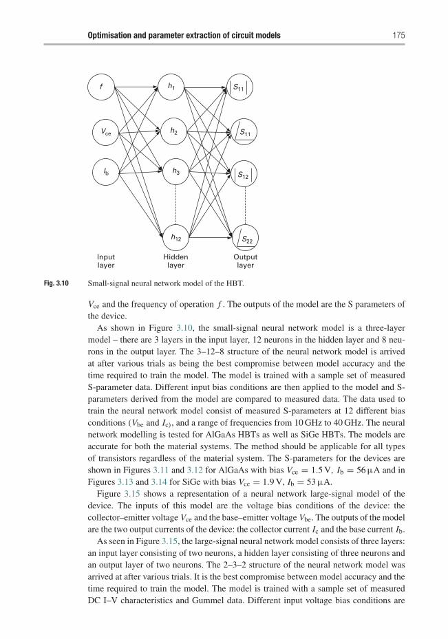
Optimisation and parameter extraction of circuit models 175
Inputlayer
Ib
Vce
h1 S11
S11
S12
S22
h2
h3
h12
f
Outputlayer
Hiddenlayer
Fig. 3.10 Small-signal neural network model of the HBT.
Vce and the frequency of operation f . The outputs of the model are the S parameters ofthe device.
As shown in Figure 3.10, the small-signal neural network model is a three-layermodel – there are 3 layers in the input layer, 12 neurons in the hidden layer and 8 neu-rons in the output layer. The 3–12–8 structure of the neural network model is arrivedat after various trials as being the best compromise between model accuracy and thetime required to train the model. The model is trained with a sample set of measuredS-parameter data. Different input bias conditions are then applied to the model and S-parameters derived from the model are compared to measured data. The data used totrain the neural network model consist of measured S-parameters at 12 different biasconditions (Vbe and Ic), and a range of frequencies from 10 GHz to 40 GHz. The neuralnetwork modelling is tested for AlGaAs HBTs as well as SiGe HBTs. The models areaccurate for both the material systems. The method should be applicable for all typesof transistors regardless of the material system. The S-parameters for the devices areshown in Figures 3.11 and 3.12 for AlGaAs with bias Vce = 1.5 V, Ib = 56 μA and inFigures 3.13 and 3.14 for SiGe with bias Vce = 1.9 V, Ib = 53 μA.
Figure 3.15 shows a representation of a neural network large-signal model of thedevice. The inputs of this model are the voltage bias conditions of the device: thecollector–emitter voltage Vce and the base–emitter voltage Vbe. The outputs of the modelare the two output currents of the device: the collector current Ic and the base current Ib.
As seen in Figure 3.15, the large-signal neural network model consists of three layers:an input layer consisting of two neurons, a hidden layer consisting of three neurons andan output layer of two neurons. The 2–3–2 structure of the neural network model wasarrived at after various trials. It is the best compromise between model accuracy and thetime required to train the model. The model is trained with a sample set of measuredDC I–V characteristics and Gummel data. Different input voltage bias conditions are
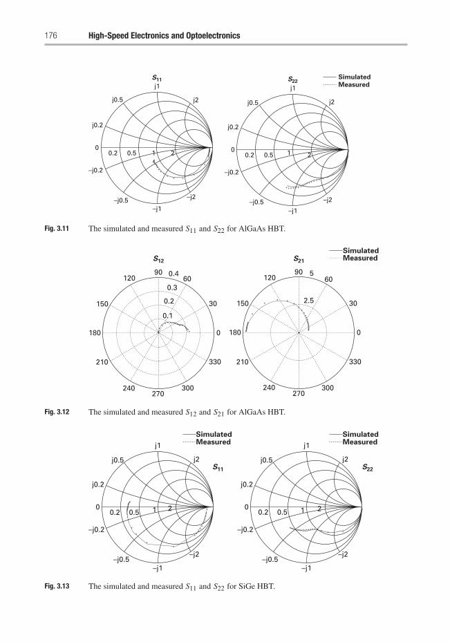
176 High-Speed Electronics and Optoelectronics
j0.5
j0.2
–j0.2
–j0.5 –j2
j1
j2
S11
–j1
0.20
0.5 1 2
j0.5
j0.2
–j0.2
–j0.5 –j2
j1
j2
S22Simulated
Measured
–j1
0.20
0.5 1 2
Fig. 3.11 The simulated and measured S11 and S22 for AlGaAs HBT.
90
S12
0.460
30
0
330
300270
240
210
180
150
12090
S21
5
SimulatedMeasured
2.5
60
30
0
330
300270
240
210
180
150
1200.3
0.2
0.1
Fig. 3.12 The simulated and measured S12 and S21 for AlGaAs HBT.
j0.5
j0.2
–j0.2
–j0.5–j2
j1
j2S11
SimulatedMeasured
–j1
0.20
0.5 1 2 2
j0.5
j0.2
–j0.2
–j0.5–j2
j1
j2S22
SimulatedMeasured
–j1
0.20
0.5 1
Fig. 3.13 The simulated and measured S11 and S22 for SiGe HBT.
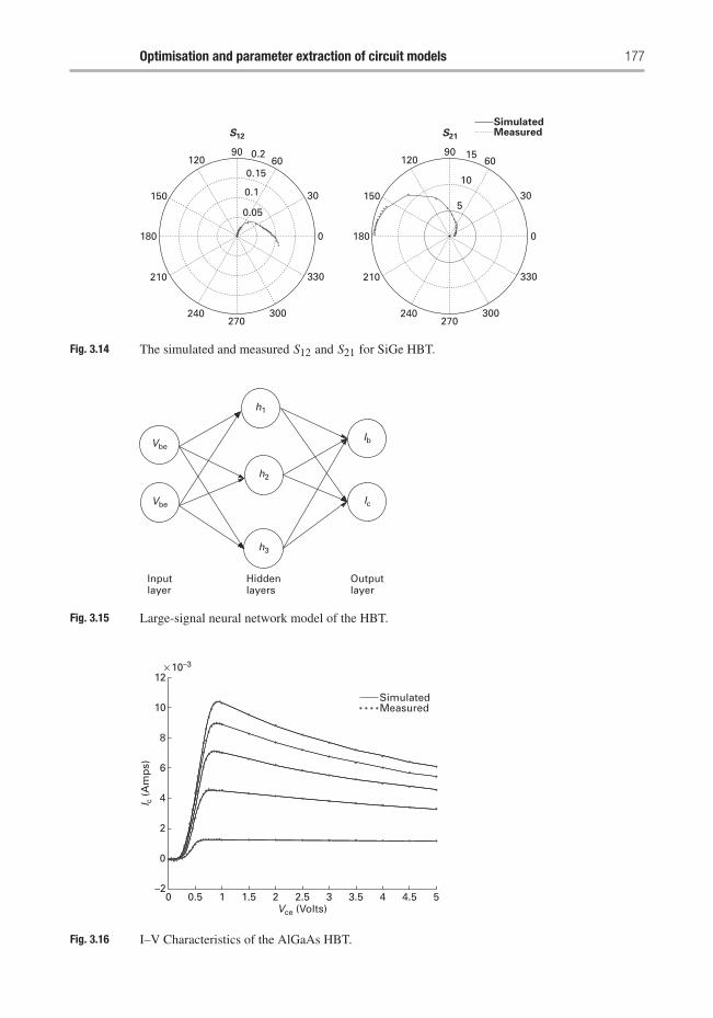
Optimisation and parameter extraction of circuit models 177
90
S12
0.260
30
0
330
300270
240
210
180
150
120
SimulatedMeasured
0.15
0.1
0.05
90
S21
1560
30
0
330
300270
240
210
180
150
120
10
5
Fig. 3.14 The simulated and measured S12 and S21 for SiGe HBT.
Vbe
Vbe
h1
h2
h3
Ib
Ic
Hiddenlayers
Outputlayer
Inputlayer
Fig. 3.15 Large-signal neural network model of the HBT.
12× 10–3
8
6
4
2
–20 0.5 1 1.5 2 2.5
Vce (Volts)
I c (
Am
ps)
3.53 4 4.5 5
0
10SimulatedMeasured
Fig. 3.16 I–V Characteristics of the AlGaAs HBT.
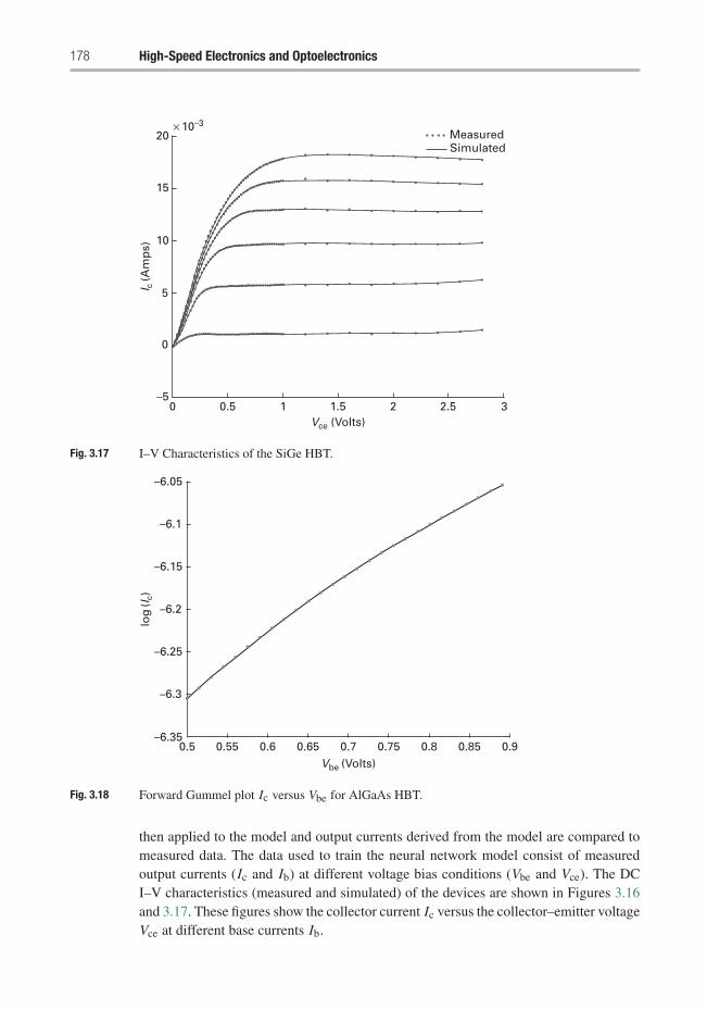
178 High-Speed Electronics and Optoelectronics
20 MeasuredSimulated
× 10–3
10
15
I c (A
mp
s)
5
0
–50 0.5 1 1.5
Vce (Volts)2 2.5 3
Fig. 3.17 I–V Characteristics of the SiGe HBT.
–6.05
–6.1
–6.15
–6.2
log
(Ic)
–6.25
–6.3
–6.350.5 0.55 0.6 0.65 0.7
Vbe (Volts)0.75 0.8 0.85 0.9
Fig. 3.18 Forward Gummel plot Ic versus Vbe for AlGaAs HBT.
then applied to the model and output currents derived from the model are compared tomeasured data. The data used to train the neural network model consist of measuredoutput currents (Ic and Ib) at different voltage bias conditions (Vbe and Vce). The DCI–V characteristics (measured and simulated) of the devices are shown in Figures 3.16and 3.17. These figures show the collector current Ic versus the collector–emitter voltageVce at different base currents Ib.
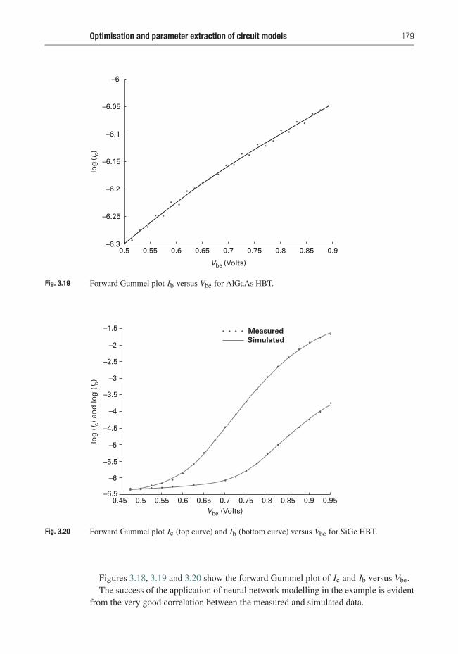
Optimisation and parameter extraction of circuit models 179
–6
–6.05
–6.1
–6.15
log
(Ic)
–6.2
–6.25
–6.30.5 0.55 0.6 0.65 0.7
Vbe (Volts)
0.75 0.8 0.85 0.9
Fig. 3.19 Forward Gummel plot Ib versus Vbe for AlGaAs HBT.
–1.5
–2
–2.5
–3
–3.5
–4
–4.5
–5
–5.5
–6
–6.5
Measured
Simulated
log
(I c
) an
d lo
g (
I b)
0.45 0.550.5 0.6 0.65 0.7Vbe (Volts)
0.75 0.8 0.85 0.9 0.95
Fig. 3.20 Forward Gummel plot Ic (top curve) and Ib (bottom curve) versus Vbe for SiGe HBT.
Figures 3.18, 3.19 and 3.20 show the forward Gummel plot of Ic and Ib versus Vbe.The success of the application of neural network modelling in the example is evident
from the very good correlation between the measured and simulated data.
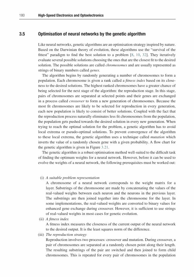
180 High-Speed Electronics and Optoelectronics
3.5 Optimisation of neural networks by the genetic algorithm
Like neural networks, genetic algorithms are an optimisation strategy inspired by nature.Based on the Darwinian theory of evolution, these algorithms use the “survival of thefittest” paradigm to find the best solution to a problem [8, 10, 32]. They iterativelyevaluate several possible solutions choosing the ones that are the closest fit to the desiredsolution. The possible solutions are called chromosomes and are usually represented asstrings of binary numbers called genes.
The algorithm begins by randomly generating a number of chromosomes to form apopulation. Each chromosome is given a rank called a fitness index based on its close-ness to the desired solutions. The highest ranked chromosomes have a greater chance ofbeing selected for the next stage of the algorithm: the reproduction stage. In this stage,pairs of chromosomes are separated at selected points and their genes are exchangedin a process called crossover to form a new generation of chromosomes. Because themost fit chromosomes are likely to be selected for reproduction in every generation,each new population is likely to consist of better solutions. Coupled with the fact thatthe reproduction process naturally eliminates less fit chromosomes from the population,the population gets pushed towards the desired solution in every new generation. Whentrying to reach the optimal solution for the problem, a genetic algorithm has to avoidlocal extrema or pseudo-optimal solutions. To prevent convergence of the algorithmto these local extrema, the genetic algorithm uses a technique called mutation whichinverts the value of a randomly chosen gene with a given probability. A flow chart forthe genetic algorithm is given in Figure 3.21.
The genetic algorithm is a robust optimisation method well-suited to the difficult taskof finding the optimum weights for a neural network. However, before it can be used toevolve the weights of a neural network, the following prerequisites must be worked out:
(i) A suitable problem representationA chromosome of a neural network corresponds to the weight matrix for alayer. Substrings of the chromosome are made by concatenating the values of thereal-valued weights between each neuron and the neurons in the previous layer.The substrings are then joined together into the chromosome for the layer. Insome implementations, the real-valued weights are converted to binary values forenhanced gene exchange during crossover. However, it is sufficient to use stringsof real-valued weights in most cases for genetic evolution.
(ii) A fitness indexA fitness index measures the closeness of the current output of the neural networkto the desired output. It is the least squares norm of the difference.
(iii) The reproduction strategyReproduction involves two processes: crossover and mutation. During crossover, apair of chromosomes are separated at a randomly chosen point along their length.The resulting substrings of the pair are switched and then joined to form childchromosomes. This is repeated for every pair of chromosomes in the population
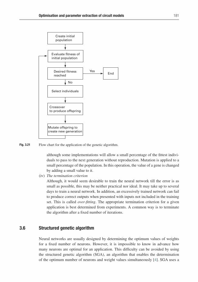
Optimisation and parameter extraction of circuit models 181
Create initialpopulation
Evaluate fitness ofinitial population
EndYes
No
Desired fitnessreached
Select individuals
Crossoverto produce offspring
Mutate offspring tocreate new generation
Fig. 3.21 Flow chart for the application of the genetic algorithm.
although some implementations will allow a small percentage of the fittest indivi-duals to pass to the next generation without reproduction. Mutation is applied to asmall percentage of the population. In this operation, the value of a gene is changedby adding a small value to it.
(iv) The termination criterionAlthough, it would seem desirable to train the neural network till the error is assmall as possible, this may be neither practical nor ideal. It may take up to severaldays to train a neural network. In addition, an excessively trained network can failto produce correct outputs when presented with inputs not included in the trainingset. This is called over-fitting. The appropriate termination criterion for a givenapplication is best determined from experiments. A common way is to terminatethe algorithm after a fixed number of iterations.
3.6 Structured genetic algorithm
Neural networks are usually designed by determining the optimum values of weightsfor a fixed number of neurons. However, it is impossible to know in advance howmany neurons are optimal for an application. This difficulty can be avoided by usingthe structured genetic algorithm (SGA), an algorithm that enables the determinationof the optimum number of neurons and weight values simultaneously [4]. SGA uses a
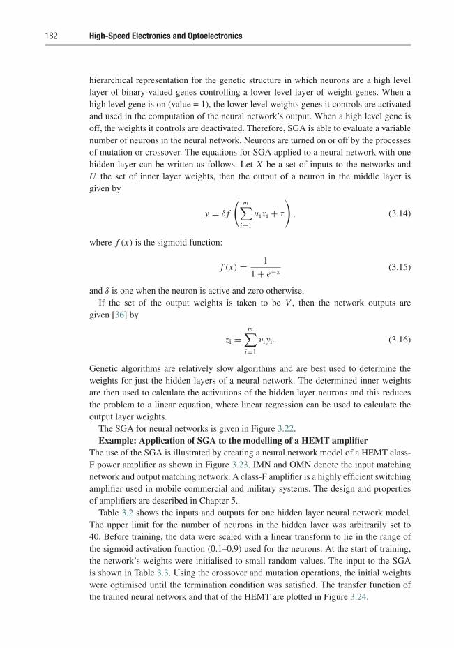
182 High-Speed Electronics and Optoelectronics
hierarchical representation for the genetic structure in which neurons are a high levellayer of binary-valued genes controlling a lower level layer of weight genes. When ahigh level gene is on (value = 1), the lower level weights genes it controls are activatedand used in the computation of the neural network’s output. When a high level gene isoff, the weights it controls are deactivated. Therefore, SGA is able to evaluate a variablenumber of neurons in the neural network. Neurons are turned on or off by the processesof mutation or crossover. The equations for SGA applied to a neural network with onehidden layer can be written as follows. Let X be a set of inputs to the networks andU the set of inner layer weights, then the output of a neuron in the middle layer isgiven by
y = δ f
(m∑
i=1
uixi + τ
), (3.14)
where f (x) is the sigmoid function:
f (x) = 1
1 + e−x (3.15)
and δ is one when the neuron is active and zero otherwise.If the set of the output weights is taken to be V , then the network outputs are
given [36] by
zi =m∑
i=1
vi yi. (3.16)
Genetic algorithms are relatively slow algorithms and are best used to determine theweights for just the hidden layers of a neural network. The determined inner weightsare then used to calculate the activations of the hidden layer neurons and this reducesthe problem to a linear equation, where linear regression can be used to calculate theoutput layer weights.
The SGA for neural networks is given in Figure 3.22.Example: Application of SGA to the modelling of a HEMT amplifier
The use of the SGA is illustrated by creating a neural network model of a HEMT class-F power amplifier as shown in Figure 3.23. IMN and OMN denote the input matchingnetwork and output matching network. A class-F amplifier is a highly efficient switchingamplifier used in mobile commercial and military systems. The design and propertiesof amplifiers are described in Chapter 5.
Table 3.2 shows the inputs and outputs for one hidden layer neural network model.The upper limit for the number of neurons in the hidden layer was arbitrarily set to40. Before training, the data were scaled with a linear transform to lie in the range ofthe sigmoid activation function (0.1–0.9) used for the neurons. At the start of training,the network’s weights were initialised to small random values. The input to the SGAis shown in Table 3.3. Using the crossover and mutation operations, the initial weightswere optimised until the termination condition was satisfied. The transfer function ofthe trained neural network and that of the HEMT are plotted in Figure 3.24.
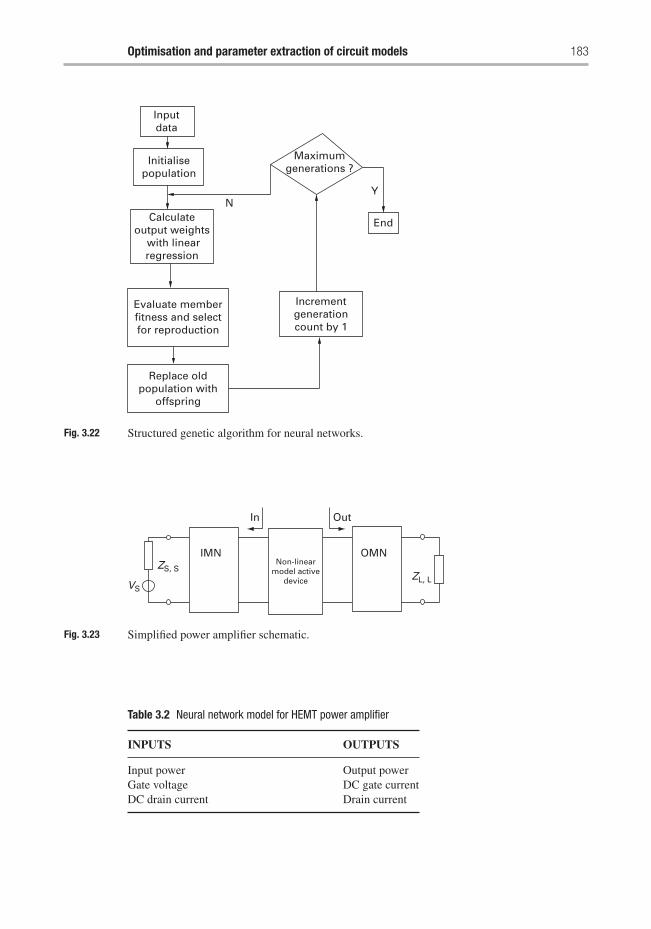
Optimisation and parameter extraction of circuit models 183
Replace oldpopulation with
offspring
Calculateoutput weights
with linearregression
Initialisepopulation
Incrementgenerationcount by 1
Maximumgenerations ?
N
End
Inputdata
Y
Evaluate memberfitness and selectfor reproduction
Fig. 3.22 Structured genetic algorithm for neural networks.
IMN OMNNon-linear
model activedevice
In Out
ZS, SZL, L
VS
Fig. 3.23 Simplified power amplifier schematic.
Table 3.2 Neural network model for HEMT power amplifier
INPUTS OUTPUTS
Input power Output powerGate voltage DC gate currentDC drain current Drain current
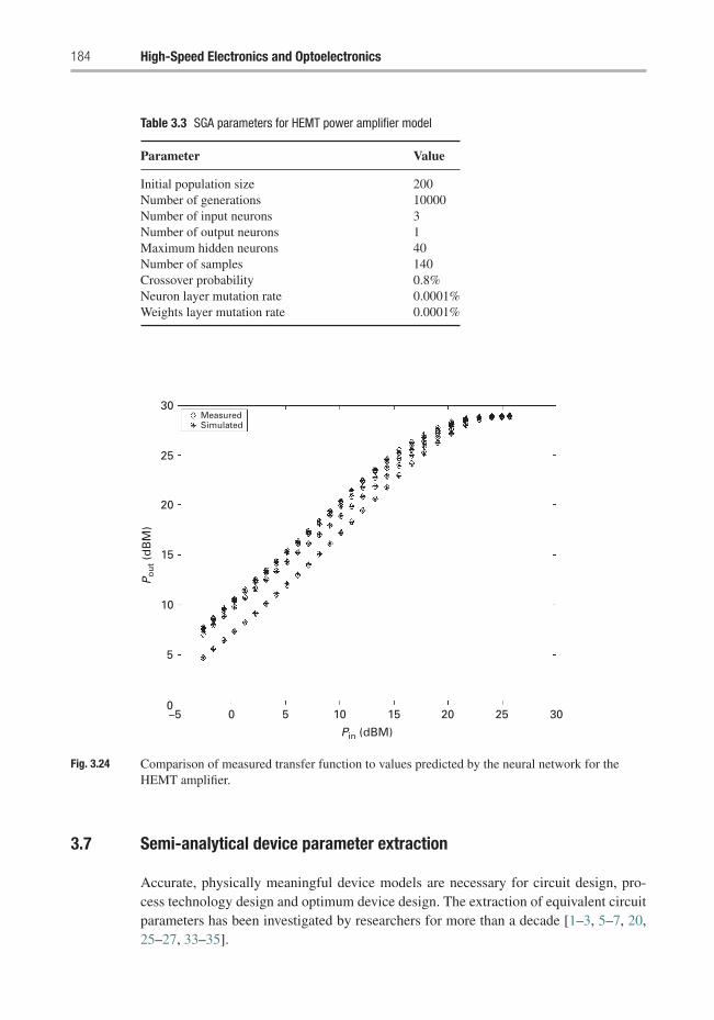
184 High-Speed Electronics and Optoelectronics
Table 3.3 SGA parameters for HEMT power amplifier model
Parameter Value
Initial population size 200Number of generations 10000Number of input neurons 3Number of output neurons 1Maximum hidden neurons 40Number of samples 140Crossover probability 0.8%Neuron layer mutation rate 0.0001%Weights layer mutation rate 0.0001%
30MeasuredSimulated
25
20
15
10
5
0–5 0 5 10 15
Po
ut (
dB
M)
20 25 30
Pin (dBM)
Fig. 3.24 Comparison of measured transfer function to values predicted by the neural network for theHEMT amplifier.
3.7 Semi-analytical device parameter extraction
Accurate, physically meaningful device models are necessary for circuit design, pro-cess technology design and optimum device design. The extraction of equivalent circuitparameters has been investigated by researchers for more than a decade [1–3, 5–7, 20,25–27, 33–35].
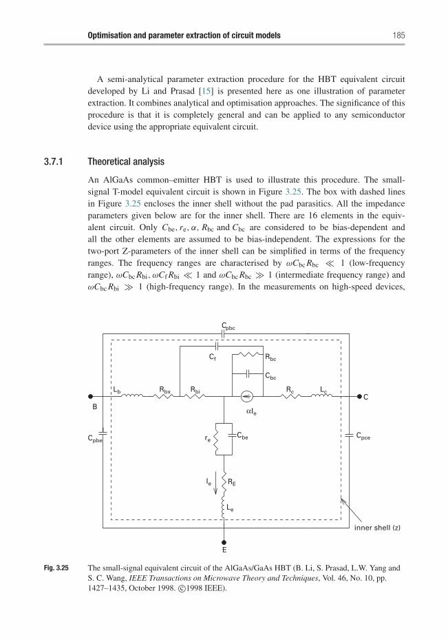
Optimisation and parameter extraction of circuit models 185
A semi-analytical parameter extraction procedure for the HBT equivalent circuitdeveloped by Li and Prasad [15] is presented here as one illustration of parameterextraction. It combines analytical and optimisation approaches. The significance of thisprocedure is that it is completely general and can be applied to any semiconductordevice using the appropriate equivalent circuit.
3.7.1 Theoretical analysis
An AlGaAs common–emitter HBT is used to illustrate this procedure. The small-signal T-model equivalent circuit is shown in Figure 3.25. The box with dashed linesin Figure 3.25 encloses the inner shell without the pad parasitics. All the impedanceparameters given below are for the inner shell. There are 16 elements in the equiv-alent circuit. Only Cbe, re, α, Rbc and Cbc are considered to be bias-dependent andall the other elements are assumed to be bias-independent. The expressions for thetwo-port Z-parameters of the inner shell can be simplified in terms of the frequencyranges. The frequency ranges are characterised by ωCbc Rbc � 1 (low-frequencyrange), ωCbc Rbi, ωCf Rbi � 1 and ωCbc Rbc � 1 (intermediate frequency range) andωCbc Rbi � 1 (high-frequency range). In the measurements on high-speed devices,
Cpce
BC
C
Lb Lc
Cbc
Rbc
αΙe
Rc
pbc
E
RE
Cbere
Ie
RbiRbx
Cf
Cpbe
inner shell (z)
Le
Fig. 3.25 The small-signal equivalent circuit of the AlGaAs/GaAs HBT (B. Li, S. Prasad, L.W. Yang andS. C. Wang, IEEE Transactions on Microwave Theory and Techniques, Vol. 46, No. 10, pp.1427–1435, October 1998. c©1998 IEEE).
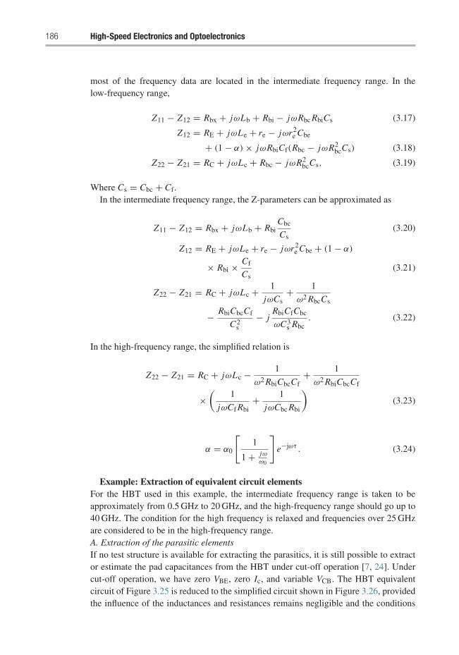
186 High-Speed Electronics and Optoelectronics
most of the frequency data are located in the intermediate frequency range. In thelow-frequency range,
Z11 − Z12 = Rbx + jωLb + Rbi − jωRbc RbiCs (3.17)
Z12 = RE + jωLe + re − jωr2e Cbe
+ (1 − α) × jωRbiCf(Rbc − jωR2bcCs) (3.18)
Z22 − Z21 = RC + jωLc + Rbc − jωR2bcCs, (3.19)
Where Cs = Cbc + Cf.In the intermediate frequency range, the Z-parameters can be approximated as
Z11 − Z12 = Rbx + jωLb + RbiCbc
Cs(3.20)
Z12 = RE + jωLe + re − jωr2e Cbe + (1 − α)
× Rbi × Cf
Cs(3.21)
Z22 − Z21 = RC + jωLc + 1
jωCs+ 1
ω2 RbcCs
− RbiCbcCf
C2s
− jRbiCfCbc
ωC3s Rbc
. (3.22)
In the high-frequency range, the simplified relation is
Z22 − Z21 = RC + jωLc − 1
ω2 RbiCbcCf+ 1
ω2 RbiCbcCf
×(
1
jωCf Rbi+ 1
jωCbc Rbi
)(3.23)
α = α0
[1
1 + jωω0
]e−jωτ . (3.24)
Example: Extraction of equivalent circuit elementsFor the HBT used in this example, the intermediate frequency range is taken to beapproximately from 0.5 GHz to 20 GHz, and the high-frequency range should go up to40 GHz. The condition for the high frequency is relaxed and frequencies over 25 GHzare considered to be in the high-frequency range.A. Extraction of the parasitic elementsIf no test structure is available for extracting the parasitics, it is still possible to extractor estimate the pad capacitances from the HBT under cut-off operation [7, 24]. Undercut-off operation, we have zero VBE, zero Ic, and variable VCB. The HBT equivalentcircuit of Figure 3.25 is reduced to the simplified circuit shown in Figure 3.26, providedthe influence of the inductances and resistances remains negligible and the conditions
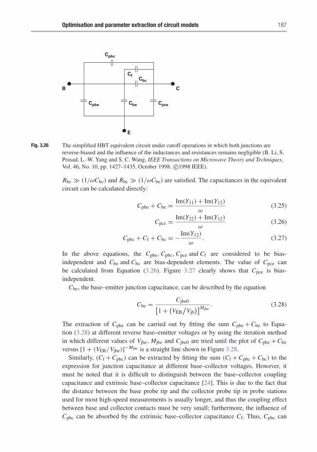
Optimisation and parameter extraction of circuit models 187
Cbc
Cpbe Cbe Cpce
Cf
Cpbc
B C
E
Fig. 3.26 The simplified HBT equivalent circuit under cutoff operations in which both junctions arereverse-biased and the influence of the inductances and resistances remains negligible (B. Li, S.Prasad, L.-W. Yang and S. C. Wang, IEEE Transactions on Microwave Theory and Techniques,Vol. 46, No. 10, pp. 1427–1435, October 1998. c©1998 IEEE).
Rbc � (1/ωCbc) and Rbc � (1/ωCbe) are satisfied. The capacitances in the equivalentcircuit can be calculated directly:
Cpbe + Cbe = Im(Y11) + Im(Y12)
ω(3.25)
Cpce = Im(Y22) + Im(Y12)
ω(3.26)
Cpbc + Cf + Cbc = − Im(Y12)
ω. (3.27)
In the above equations, the Cpbe,Cpbc,Cpce and Cf are considered to be bias-independent and Cbe and Cbc are bias-dependent elements. The value of Cpce canbe calculated from Equation (3.26). Figure 3.27 clearly shows that Cpce is bias-independent.
Cbe, the base–emitter junction capacitance, can be described by the equation
Cbe = Cjbe0[1 + (
VEB/
Vjb)]Mjbe
. (3.28)
The extraction of Cpbe can be carried out by fitting the sum Cpbe + Cbe to Equa-tion (3.28) at different reverse base–emitter voltages or by using the iteration methodin which different values of Vjbe, Mjbe and Cjbe0 are tried until the plot of Cpbe + Cbe
versus [1 + (VEB/Vjbe)]−Mjbe is a straight line shown in Figure 3.28.Similarly, (Cf + Cpbc) can be extracted by fitting the sum (Cf + Cpbc + Cbc) to the
expression for junction capacitance at different base–collector voltages. However, itmust be noted that it is difficult to distinguish between the base–collector couplingcapacitance and extrinsic base–collector capacitance [24]. This is due to the fact thatthe distance between the base probe tip and the collector probe tip in probe stationsused for most high-speed measurements is usually longer, and thus the coupling effectbetween base and collector contacts must be very small; furthermore, the influence ofCpbc can be absorbed by the extrinsic base–collector capacitance Cf. Thus, Cpbc can
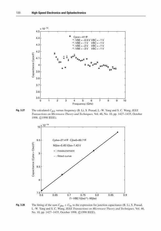
188 High-Speed Electronics and Optoelectronics
0 1 2 3 4 5 6 7 8 9 103.5
3.6
3.7
3.8
3.9
4
4.1
4.2
4.3
4.4
4.5× 10⁻¹⁴
Frequency (GHz)
Cap
acit
ance
Cp
ce(F
)
*: VBE = −0.5 V VBC = −1 V*: VBE = −1 V VBC = −1 V*: VBE = −2 V VBC = −1 V*: VBE = −3 V VBC = −1 V
Cpce = 41 fF
Fig. 3.27 The calculated Cpce versus frequency (B. Li, S. Prasad, L.-W. Yang and S. C. Wang, IEEETransactions on Microwave Theory and Techniques, Vol. 46, No. 10, pp. 1427–1435, October1998. c©1998 IEEE).
0.6 0.65 0.7 0.75 0.8 0.85 0.97.5
8
8.5
9
9.5
10× 10−14
(1−VBE/Vjbe)^(−Mjbe)
Cap
acit
ance
(C
pb
e +
Cb
e)(F
)
Cpbe=27.4 fF Cjbe0=80.7 fF
Mjbe=0.45 Vjbe=1.43 V
* : measurement
− : fitted curve
Fig. 3.28 The fitting of the sum Cpbe + Cbe to the expression for junction capacitance (B. Li, S. Prasad,L.-W. Yang and S. C. Wang, IEEE Transactions on Microwave Theory and Techniques, Vol. 46,No. 10, pp. 1427–1435, October 1998. c©1998 IEEE).
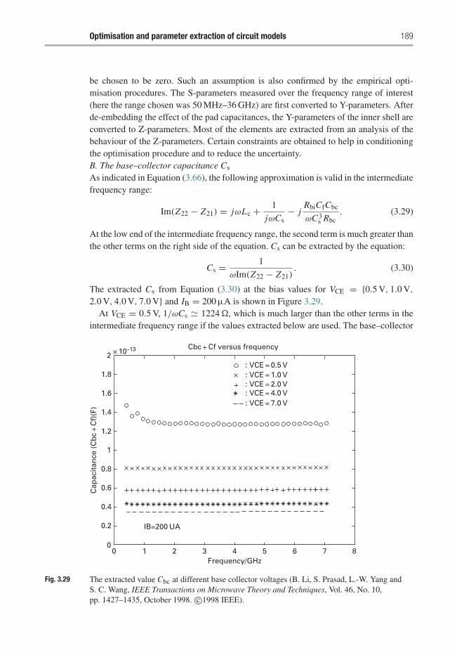
Optimisation and parameter extraction of circuit models 189
be chosen to be zero. Such an assumption is also confirmed by the empirical opti-misation procedures. The S-parameters measured over the frequency range of interest(here the range chosen was 50 MHz–36 GHz) are first converted to Y-parameters. Afterde-embedding the effect of the pad capacitances, the Y-parameters of the inner shell areconverted to Z-parameters. Most of the elements are extracted from an analysis of thebehaviour of the Z-parameters. Certain constraints are obtained to help in conditioningthe optimisation procedure and to reduce the uncertainty.B. The base–collector capacitance Cs
As indicated in Equation (3.66), the following approximation is valid in the intermediatefrequency range:
Im(Z22 − Z21) = jωLc + 1
jωCs− j
RbiCfCbc
ωC3s Rbc
. (3.29)
At the low end of the intermediate frequency range, the second term is much greater thanthe other terms on the right side of the equation. Cs can be extracted by the equation:
Cs = 1
ωIm(Z22 − Z21). (3.30)
The extracted Cs from Equation (3.30) at the bias values for VCE = {0.5 V, 1.0 V,
2.0 V, 4.0 V, 7.0 V} and IB = 200 μA is shown in Figure 3.29.At VCE = 0.5 V, 1/ωCs � 1224�, which is much larger than the other terms in the
intermediate frequency range if the values extracted below are used. The base–collector
2 × 10–13 Cbc + Cf versus frequency
1.8
1.6
1.4
Cap
acit
ance
(C
bc
+ C
f)(F
)
1.2
1
0.8
0.6
0.4
0.2
00 1 2 3 4
Frequency/GHz
IB=200 UA
5 6 7 8
: VCE = 0.5 V: VCE = 1.0 V: VCE = 2.0 V: VCE = 4.0 V: VCE = 7.0 V
Fig. 3.29 The extracted value Cbc at different base collector voltages (B. Li, S. Prasad, L.-W. Yang andS. C. Wang, IEEE Transactions on Microwave Theory and Techniques, Vol. 46, No. 10,pp. 1427–1435, October 1998. c©1998 IEEE).
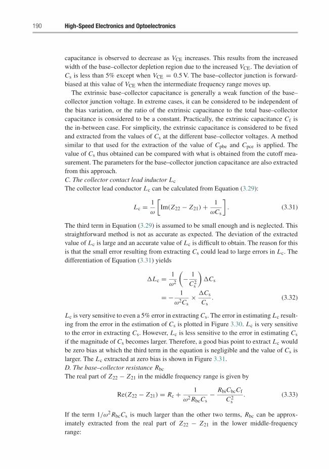
190 High-Speed Electronics and Optoelectronics
capacitance is observed to decrease as VCE increases. This results from the increasedwidth of the base–collector depletion region due to the increased VCE. The deviation ofCs is less than 5% except when VCE = 0.5 V. The base–collector junction is forward-biased at this value of VCE when the intermediate frequency range moves up.
The extrinsic base–collector capacitance is generally a weak function of the base–collector junction voltage. In extreme cases, it can be considered to be independent ofthe bias variation, or the ratio of the extrinsic capacitance to the total base–collectorcapacitance is considered to be a constant. Practically, the extrinsic capacitance Cf isthe in-between case. For simplicity, the extrinsic capacitance is considered to be fixedand extracted from the values of Cs at the different base–collector voltages. A methodsimilar to that used for the extraction of the value of Cpbe and Cpce is applied. Thevalue of Cs thus obtained can be compared with what is obtained from the cutoff mea-surement. The parameters for the base–collector junction capacitance are also extractedfrom this approach.C. The collector contact lead inductor Lc
The collector lead conductor Lc can be calculated from Equation (3.29):
Lc = 1
ω
[Im(Z22 − Z21) + 1
ωCs
]. (3.31)
The third term in Equation (3.29) is assumed to be small enough and is neglected. Thisstraightforward method is not as accurate as expected. The deviation of the extractedvalue of Lc is large and an accurate value of Lc is difficult to obtain. The reason for thisis that the small error resulting from extracting Cs could lead to large errors in Lc. Thedifferentiation of Equation (3.31) yields
�Lc = 1
ω2
(− 1
C2s
)�Cs
= − 1
ω2Cs× �Cs
Cs. (3.32)
Lc is very sensitive to even a 5% error in extracting Cs. The error in estimating Lc result-ing from the error in the estimation of Cs is plotted in Figure 3.30. Lc is very sensitiveto the error in extracting Cs. However, Lc is less sensitive to the error in estimating Cs
if the magnitude of Cs becomes larger. Therefore, a good bias point to extract Lc wouldbe zero bias at which the third term in the equation is negligible and the value of Cs islarger. The Lc extracted at zero bias is shown in Figure 3.31.D. The base–collector resistance Rbc
The real part of Z22 − Z21 in the middle frequency range is given by
Re(Z22 − Z21) = Rc + 1
ω2 RbcCs− RbiCbcCf
C2s
. (3.33)
If the term 1/ω2 RbcCs is much larger than the other two terms, Rbc can be approx-imately extracted from the real part of Z22 − Z21 in the lower middle-frequencyrange:
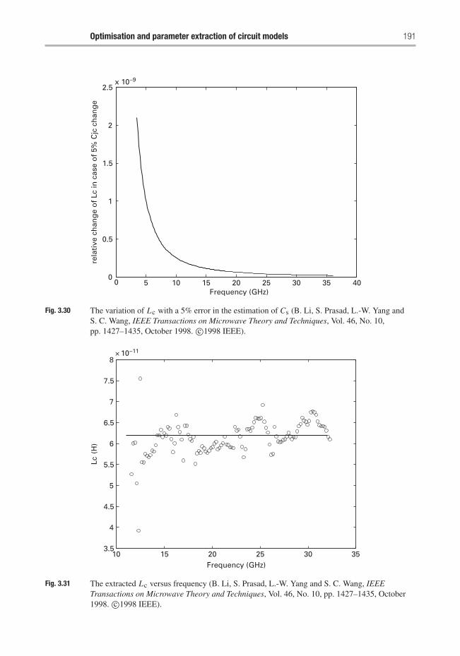
Optimisation and parameter extraction of circuit models 191
0 5 10 15 20 25 30 35 400
0.5
1
1.5
2
2.5x 10⁻⁹
Frequency (GHz)
rela
tive
ch
ang
e o
f Lc
in c
ase
of
5% C
jc c
han
ge
Fig. 3.30 The variation of Lc with a 5% error in the estimation of Cs (B. Li, S. Prasad, L.-W. Yang andS. C. Wang, IEEE Transactions on Microwave Theory and Techniques, Vol. 46, No. 10,pp. 1427–1435, October 1998. c©1998 IEEE).
10 15 20 25 30 353.5
4
4.5
5
5.5
6
6.5
7
7.5
8× 10⁻¹¹
Frequency (GHz)
Lc (
H)
Fig. 3.31 The extracted Lc versus frequency (B. Li, S. Prasad, L.-W. Yang and S. C. Wang, IEEETransactions on Microwave Theory and Techniques, Vol. 46, No. 10, pp. 1427–1435, October1998. c©1998 IEEE).
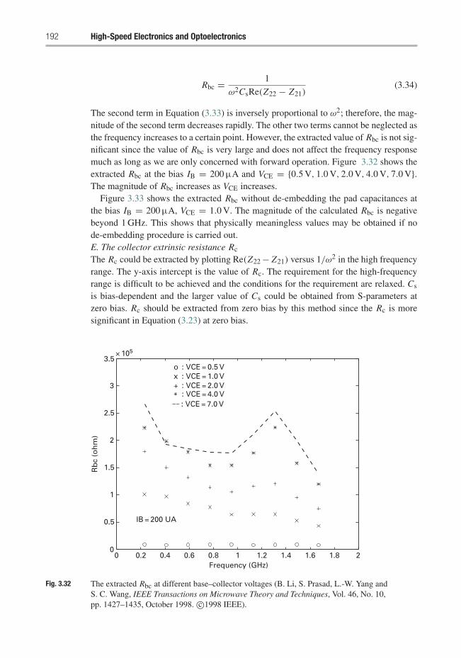
192 High-Speed Electronics and Optoelectronics
Rbc = 1
ω2CsRe(Z22 − Z21)(3.34)
The second term in Equation (3.33) is inversely proportional to ω2; therefore, the mag-nitude of the second term decreases rapidly. The other two terms cannot be neglected asthe frequency increases to a certain point. However, the extracted value of Rbc is not sig-nificant since the value of Rbc is very large and does not affect the frequency responsemuch as long as we are only concerned with forward operation. Figure 3.32 shows theextracted Rbc at the bias IB = 200 μA and VCE = {0.5 V, 1.0 V, 2.0 V, 4.0 V, 7.0 V}.The magnitude of Rbc increases as VCE increases.
Figure 3.33 shows the extracted Rbc without de-embedding the pad capacitances atthe bias IB = 200 μA, VCE = 1.0 V. The magnitude of the calculated Rbc is negativebeyond 1 GHz. This shows that physically meaningless values may be obtained if node-embedding procedure is carried out.E. The collector extrinsic resistance Rc
The Rc could be extracted by plotting Re(Z22 − Z21) versus 1/ω2 in the high frequencyrange. The y-axis intercept is the value of Rc. The requirement for the high-frequencyrange is difficult to be achieved and the conditions for the requirement are relaxed. Cs
is bias-dependent and the larger value of Cs could be obtained from S-parameters atzero bias. Rc should be extracted from zero bias by this method since the Rc is moresignificant in Equation (3.23) at zero bias.
0 0.2 0.4 0.6 0.8 1 1.2 1.4 1.6 1.8 20
0.5
1
1.5
2
2.5
3
3.5× 10⁵
Frequency (GHz)
Rb
c (o
hm
)
IB = 200 UA
: VCE = 7.0 V* : VCE = 4.0 V+ : VCE = 2.0 Vx : VCE = 1.0 Vo : VCE = 0.5 V
Fig. 3.32 The extracted Rbc at different base–collector voltages (B. Li, S. Prasad, L.-W. Yang andS. C. Wang, IEEE Transactions on Microwave Theory and Techniques, Vol. 46, No. 10,pp. 1427–1435, October 1998. c©1998 IEEE).
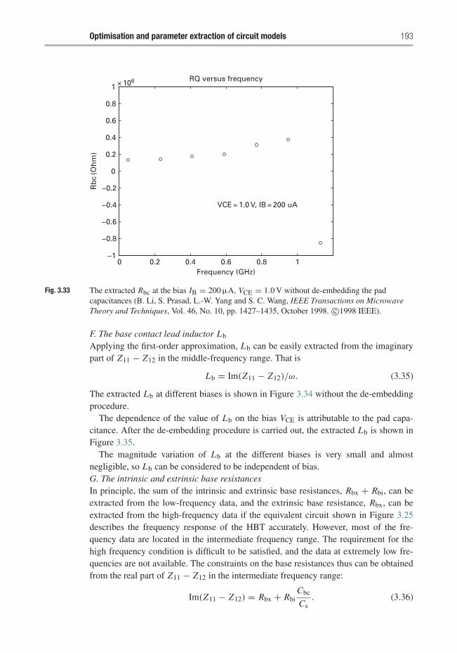
Optimisation and parameter extraction of circuit models 193
0 0.2 0.4 0.6 0.8 1−1
−0.8
−0.6
−0.4
−0.2
0
0.2
0.4
0.6
0.8
1 × 10⁶ RQ versus frequency
VCE = 1.0 V, IB = 200 uA
Frequency (GHz)
Rb
c (O
hm
)
Fig. 3.33 The extracted Rbc at the bias IB = 200 μA, VCE = 1.0 V without de-embedding the padcapacitances (B. Li, S. Prasad, L.-W. Yang and S. C. Wang, IEEE Transactions on MicrowaveTheory and Techniques, Vol. 46, No. 10, pp. 1427–1435, October 1998. c©1998 IEEE).
F. The base contact lead inductor Lb
Applying the first-order approximation, Lb can be easily extracted from the imaginarypart of Z11 − Z12 in the middle-frequency range. That is
Lb = Im(Z11 − Z12)/ω. (3.35)
The extracted Lb at different biases is shown in Figure 3.34 without the de-embeddingprocedure.
The dependence of the value of Lb on the bias VCE is attributable to the pad capa-citance. After the de-embedding procedure is carried out, the extracted Lb is shown inFigure 3.35.
The magnitude variation of Lb at the different biases is very small and almostnegligible, so Lb can be considered to be independent of bias.G. The intrinsic and extrinsic base resistancesIn principle, the sum of the intrinsic and extrinsic base resistances, Rbx + Rbi, can beextracted from the low-frequency data, and the extrinsic base resistance, Rbx, can beextracted from the high-frequency data if the equivalent circuit shown in Figure 3.25describes the frequency response of the HBT accurately. However, most of the fre-quency data are located in the intermediate frequency range. The requirement for thehigh frequency condition is difficult to be satisfied, and the data at extremely low fre-quencies are not available. The constraints on the base resistances thus can be obtainedfrom the real part of Z11 − Z12 in the intermediate frequency range:
Im(Z11 − Z12) = Rbx + RbiCbc
Cs. (3.36)
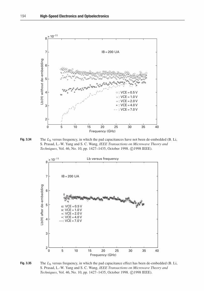
194 High-Speed Electronics and Optoelectronics
8
7
6
5
Lb(H
) w
ith
ou
t d
e–em
bed
din
g
4
3
2
0 5 10 15 20 25 30 35 40Frequency (GHz)
: VCE = 0.5 V: VCE = 1.0 V: VCE = 2.0 V: VCE = 4.0 V: VCE = 7.0 V
× 10–11
IB = 200 UA
Fig. 3.34 The Lb versus frequency, in which the pad capacitances have not been de-embedded (B. Li,S. Prasad, L.-W. Yang and S. C. Wang, IEEE Transactions on Microwave Theory andTechniques, Vol. 46, No. 10, pp. 1427–1435, October 1998. c©1998 IEEE).
0 5 10 15 20 25 30 35 402
3
4
5
6
7
8× 10⁻¹¹ Lb versus frequency
Frequency (GHz)
Lb(H
) af
ter
de–
emb
edd
ing
IB = 200 UA
o: VCE = 0.5 Vx: VCE = 1.0 V+: VCE = 2.0 V*: VCE = 4.0 V
−−: VCE = 7.0 V
Fig. 3.35 The Lb versus frequency, in which the pad capacitance effect has been de-embedded (B. Li,S. Prasad, L.-W. Yang and S. C. Wang, IEEE Transactions on Microwave Theory andTechniques, Vol. 46, No. 10, pp. 1427–1435, October 1998. c©1998 IEEE).
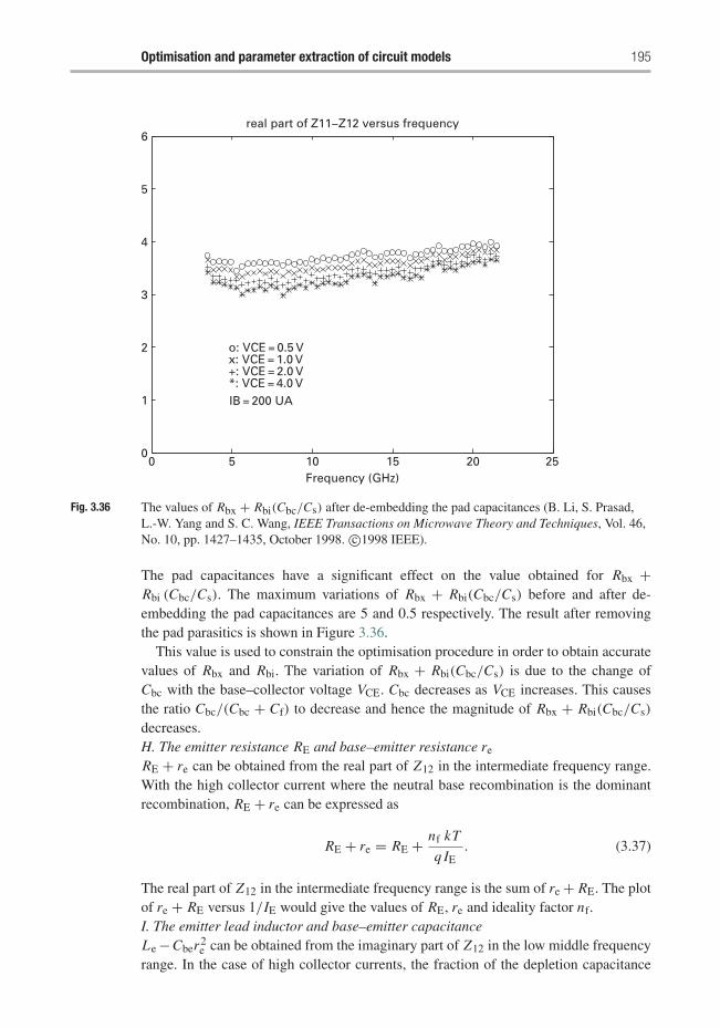
Optimisation and parameter extraction of circuit models 195
0 5 10 15 20 250
1
2
3
4
5
6real part of Z11−Z12 versus frequency
Frequency (GHz)
o: VCE = 0.5 Vx: VCE = 1.0 V+: VCE = 2.0 V*: VCE = 4.0 VIB = 200 UA
Fig. 3.36 The values of Rbx + Rbi(Cbc/Cs) after de-embedding the pad capacitances (B. Li, S. Prasad,L.-W. Yang and S. C. Wang, IEEE Transactions on Microwave Theory and Techniques, Vol. 46,No. 10, pp. 1427–1435, October 1998. c©1998 IEEE).
The pad capacitances have a significant effect on the value obtained for Rbx +Rbi (Cbc/Cs). The maximum variations of Rbx + Rbi(Cbc/Cs) before and after de-embedding the pad capacitances are 5 and 0.5 respectively. The result after removingthe pad parasitics is shown in Figure 3.36.
This value is used to constrain the optimisation procedure in order to obtain accuratevalues of Rbx and Rbi. The variation of Rbx + Rbi(Cbc/Cs) is due to the change ofCbc with the base–collector voltage VCE. Cbc decreases as VCE increases. This causesthe ratio Cbc/(Cbc + Cf) to decrease and hence the magnitude of Rbx + Rbi(Cbc/Cs)
decreases.H. The emitter resistance RE and base–emitter resistance re
RE + re can be obtained from the real part of Z12 in the intermediate frequency range.With the high collector current where the neutral base recombination is the dominantrecombination, RE + re can be expressed as
RE + re = RE + nf kT
q IE. (3.37)
The real part of Z12 in the intermediate frequency range is the sum of re + RE. The plotof re + RE versus 1/IE would give the values of RE, re and ideality factor nf.I. The emitter lead inductor and base–emitter capacitanceLe −Cber2
e can be obtained from the imaginary part of Z12 in the low middle frequencyrange. In the case of high collector currents, the fraction of the depletion capacitance
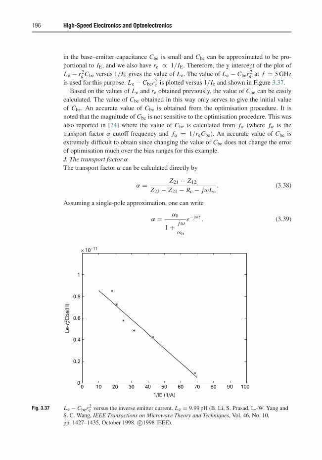
196 High-Speed Electronics and Optoelectronics
in the base–emitter capacitance Cbe is small and Cbe can be approximated to be pro-portional to IE, and we also have re ∝ 1/IE. Therefore, the y intercept of the plot ofLe − r2
e Cbe versus 1/IE gives the value of Le. The value of Le − Cber2e at f = 5 GHz
is used for this purpose. Le − Cber2e is plotted versus 1/Ie and shown in Figure 3.37.
Based on the values of Le and re obtained previously, the value of Cbe can be easilycalculated. The value of Cbe obtained in this way only serves to give the initial valueof Cbe. An accurate value of Cbe is obtained from the optimisation procedure. It isnoted that the magnitude of Cbe is not sensitive to the optimisation procedure. This wasalso reported in [24] where the value of Cbe is calculated from fα (where fα is thetransport factor α cutoff frequency and fα = 1/reCbe). An accurate value of Cbe isextremely difficult to obtain since changing the value of Cbe does not change the errorof optimisation much over the bias ranges for this example.J. The transport factor αThe transport factor α can be calculated directly by
α = Z21 − Z12
Z22 − Z21 − Rc − jωLc. (3.38)
Assuming a single-pole approximation, one can write
α = α0
1 + jω
ωα
e−jωτ , (3.39)
0 10 20 30 40 50 60 70 80 90 1000
0.2
0.4
0.6
0.8
1
× 10−11
1/IE (1/A)
Le-r
eC
be(
H)
2
Fig. 3.37 Le − Cber2e versus the inverse emitter current. Le = 9.99 pH (B. Li, S. Prasad, L.-W. Yang and
S. C. Wang, IEEE Transactions on Microwave Theory and Techniques, Vol. 46, No. 10,pp. 1427–1435, October 1998. c©1998 IEEE).
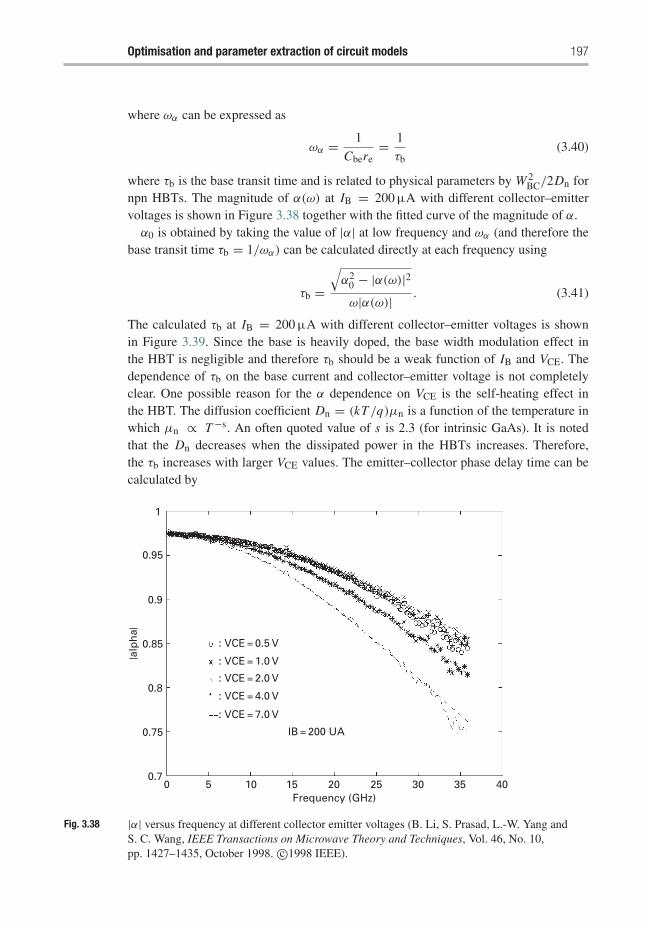
Optimisation and parameter extraction of circuit models 197
where ωα can be expressed as
ωα = 1
Cbere= 1
τb(3.40)
where τb is the base transit time and is related to physical parameters by W 2BC/2Dn for
npn HBTs. The magnitude of α(ω) at IB = 200 μA with different collector–emittervoltages is shown in Figure 3.38 together with the fitted curve of the magnitude of α.
α0 is obtained by taking the value of |α| at low frequency and ωα (and therefore thebase transit time τb = 1/ωα) can be calculated directly at each frequency using
τb =√α2
0 − |α(ω)|2ω|α(ω)| . (3.41)
The calculated τb at IB = 200 μA with different collector–emitter voltages is shownin Figure 3.39. Since the base is heavily doped, the base width modulation effect inthe HBT is negligible and therefore τb should be a weak function of IB and VCE. Thedependence of τb on the base current and collector–emitter voltage is not completelyclear. One possible reason for the α dependence on VCE is the self-heating effect inthe HBT. The diffusion coefficient Dn = (kT /q)μn is a function of the temperature inwhich μn ∝ T −s. An often quoted value of s is 2.3 (for intrinsic GaAs). It is notedthat the Dn decreases when the dissipated power in the HBTs increases. Therefore,the τb increases with larger VCE values. The emitter–collector phase delay time can becalculated by
Frequency (GHz)
: VCE = 0.5 V
1
0.95
0.9
0.8
0.75
0.70 5 10 15 20 25 30 35 40
0.85
: VCE = 1.0 V
: VCE = 2.0 V
: VCE = 4.0 V
: VCE = 7.0 V
IB = 200 UA
alp
ha
Fig. 3.38 |α| versus frequency at different collector emitter voltages (B. Li, S. Prasad, L.-W. Yang andS. C. Wang, IEEE Transactions on Microwave Theory and Techniques, Vol. 46, No. 10,pp. 1427–1435, October 1998. c©1998 IEEE).
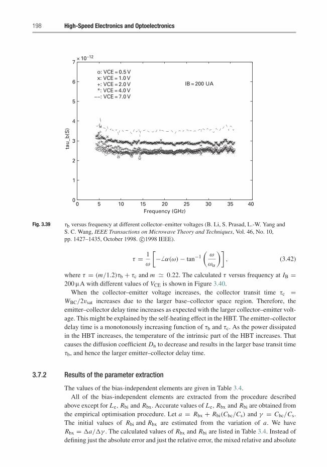
198 High-Speed Electronics and Optoelectronics
0 5 10 15 20 25 30 35 400
1
2
3
4
5
6
7× 10⁻¹²
Frequency (GHz)
tau
_b(S
)o: VCE = 0.5 Vx: VCE = 1.0 V+: VCE = 2.0 V*: VCE = 4.0 V
−−: VCE = 7.0 V
IB = 200 UA
Fig. 3.39 τb versus frequency at different collector–emitter voltages (B. Li, S. Prasad, L.-W. Yang andS. C. Wang, IEEE Transactions on Microwave Theory and Techniques, Vol. 46, No. 10,pp. 1427–1435, October 1998. c©1998 IEEE).
τ = 1
ω
[−� α(ω) − tan−1
(ω
ωα
)], (3.42)
where τ = (m/1.2)τb + τc and m � 0.22. The calculated τ versus frequency at IB =200 μA with different values of VCE is shown in Figure 3.40.
When the collector–emitter voltage increases, the collector transit time τc =WBC/2vsat increases due to the larger base–collector space region. Therefore, theemitter–collector delay time increases as expected with the larger collector–emitter volt-age. This might be explained by the self-heating effect in the HBT. The emitter–collectordelay time is a monotonously increasing function of τb and τc. As the power dissipatedin the HBT increases, the temperature of the intrinsic part of the HBT increases. Thatcauses the diffusion coefficient Dn to decrease and results in the larger base transit timeτb, and hence the larger emitter–collector delay time.
3.7.2 Results of the parameter extraction
The values of the bias-independent elements are given in Table 3.4.All of the bias-independent elements are extracted from the procedure described
above except for Le, Rbi and Rbx. Accurate values of Le, Rbx and Rbi are obtained fromthe empirical optimisation procedure. Let a = Rbx + Rbi(Cbc/Cs) and γ = Cbc/Cs.The initial values of Rbi and Rbx are estimated from the variation of a. We haveRbx = �a/�γ . The calculated values of Rbx and Rbi are listed in Table 3.4. Instead ofdefining just the absolute error and just the relative error, the mixed relative and absolute
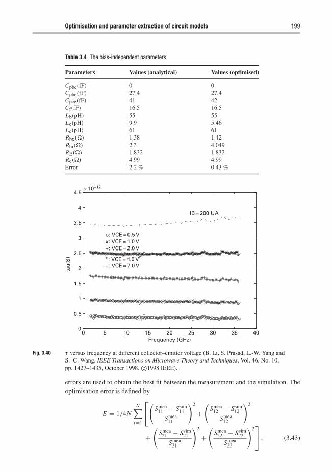
Optimisation and parameter extraction of circuit models 199
Table 3.4 The bias-independent parameters
Parameters Values (analytical) Values (optimised)
Cpbc(fF) 0 0Cpbe(fF) 27.4 27.4Cpce(fF) 41 42Cf(fF) 16.5 16.5Lb(pH) 55 55Le(pH) 9.9 5.46Lc(pH) 61 61Rbx(�) 1.38 1.42Rbi(�) 2.3 4.049RE(�) 1.832 1.832Rc(�) 4.99 4.99Error 2.2 % 0.43 %
0 5 10 15 20 25 30 35 400
0.5
1
1.5
2
2.5
tau
(S)
3
3.5
4
4.5× 10⁻¹²
Frequency (GHz)
IB = 200 UA
o: VCE = 0.5 Vx: VCE = 1.0 V+: VCE = 2.0 V
*: VCE = 4.0 V−−: VCE = 7.0 V
Fig. 3.40 τ versus frequency at different collector–emitter voltage (B. Li, S. Prasad, L.-W. Yang andS. C. Wang, IEEE Transactions on Microwave Theory and Techniques, Vol. 46, No. 10,pp. 1427–1435, October 1998. c©1998 IEEE).
errors are used to obtain the best fit between the measurement and the simulation. Theoptimisation error is defined by
E = 1/4NN∑
i=1
⎡⎣(Smea
11 − Ssim11
Smea11
)2
+(
Smea12 − Ssim
12
Smea12
)2
+(
Smea21 − Ssim
21
Smea21
)2
+(
Smea22 − Ssim
22
Smea22
)2⎤⎦ , (3.43)
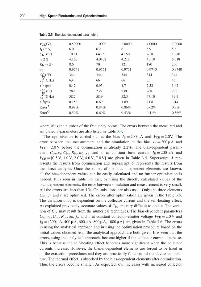
200 High-Speed Electronics and Optoelectronics
Table 3.5 The bias-dependent parameters
VCE(V) 0.50000 1.0000 2.0000 4.0000 7.0000IC(mA) 6.0 6.2 6.1 5.9 5.6Cbc (fF) 109.1 64.75 41.50 26.8 18.70re(�) 4.168 4.0432 4.218 4.518 5.018Rbc(k�) 8.6 70 121 180 200α0 0.9741 0.9751 0.9751 0.9740 0.9740
CAbe(fF) 344 344 344 344 344
f Aα (GHz) 63 66 66 55 45
τA (ps) 0.42 0.95 1.7 2.52 3.42
CObe (fF) 289 238 239 268 293
f Oα (GHz) 58.2 58.9 52.3 47.10 39.9
τO(ps) 0.158 0.69 1.09 2.08 3.14
ErrorA 0.98% 0.84% 0.86% 0.62% 0.9%
ErrorO 0.50% 0.69% 0.43% 0.41% 0.56%
where N is the number of the frequency points. The errors between the measured andsimulated S-parameters are also listed in Table 3.4.
The optimisation is carried out at the bias IB = 200 μA and VCE = 2.0V. Theerror between the measurement and the simulation at the bias IB = 200 μA andVCE = 2.0 V before the optimisation is already 2.2%. The bias-dependent param-eters Cbe, re,Cbc, Rbc, α0, fα and τ at constant base current IB = 200 μA andVCE = {0.5 V, 1.0 V, 2.0 V, 4.0 V, 7.0 V} are given in Table 3.5. Superscript A rep-resents the results from optimisation and superscript O represents the results fromthe direct analysis. Once the values of the bias-independent elements are known,all the bias-dependent values can be easily calculated and no further optimisation isneeded. It is seen in Table 3.5 that, by using the directly calculated values of thebias-dependent elements, the error between simulation and measurement is very small.All the errors are less than 1%. Optimisations are also used. Only the three elementsCbe, fα and τ are optimised. The errors after optimisation are given in the Table 3.5.The variation of re is dependent on the collector current and the self-heating effect.As explained previously, accurate values of Cbe are very difficult to obtain. The varia-tion of Cbe may result from the numerical techniques. The bias-dependent parametersCbe, re,Cbc, Rbc, α0, fα and τ at constant collector–emitter voltage VCE = 2.0 V andIB = {200 μA, 400 μA, 600 μA, 800 μA, 1000 μA} are given in Table 3.6. The errorsin using the analytical approach and in using the optimisation procedure based on theinitial values obtained from the analytical approach are both given. It is seen that theerrors, using the analytical approach, become higher if the collector currents increase.This is because the self-heating effect becomes more significant when the collectorcurrents increase. However, the bias-independent elements are forced to be fixed inall the extraction procedures and they are practically functions of the device tempera-ture. The thermal effect is absorbed by the bias-dependent elements after optimisation.Thus the errors become smaller. As expected, Cbe increases with increased collector
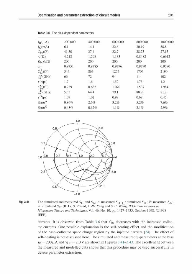
Optimisation and parameter extraction of circuit models 201
Table 3.6 The bias-dependent parameters
IB(μA) 200.000 400.000 600.000 800.000 1000.000IC(mA) 6.1 14.1 22.6 30.19 38.8Cbc(fF) 41.50 37.4 32.7 28.75 27.15re(�) 4.218 1.798 1.133 0.8482 0.6912Rbc(k�) 200 200 200 200 200α0 0.9751 0.9785 0.9796 0.9790 0.9790
CAbe(fF) 344 863 1275 1704 2190
f Aα (GHz) 66 72 94 114 102
τA(ps) 1.7 1.6 1.52 1.73 1.2
CObe(fF) 0.239 0.682 1.070 1.537 1.984
f Oα (GHz) 52.3 64.4 79.1 88.9 81.2
τO(ps) 1.09 1.02 0.98 0.68 0.45
ErrorA 0.86% 2.6% 3.2% 5.2% 7.6%
ErrorO 0.43% 0.62% 1.1% 2.1% 2.9%
0.5
1.0
2.0
5.0
inf5.02.01.00.50.20.00.0
–0.2
–0.5
–1.0
–2.0
–5.0
0.2
Fig. 3.41 The simulated and measured S11 and S22. ◦: measured S11; : simulated S11; ∇: measured S22;�: simulated S22 (B. Li, S. Prasad, L.-W. Yang and S. C. Wang, IEEE Transactions onMicrowave Theory and Techniques, Vol. 46, No. 10, pp. 1427–1435, October 1998. c©1998IEEE).
currents. It is observed from Table 3.6 that Cbc decreases with the increased collec-tor currents. One possible explanation is the self-heating effect and the modificationof the base–collector space charge region by the injected carriers [24]. The effect ofself-heating is not discussed here. The simulated and measured S-parameters at the biasIB = 200 μA and VCE = 2.0 V are shown in Figures 3.41–3.43. The excellent fit betweenthe measured and modelled data shows that this procedure may be used successfully indevice parameter extraction.
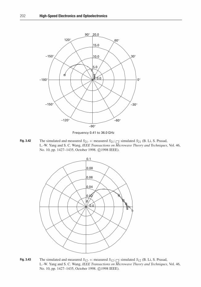
202 High-Speed Electronics and Optoelectronics
120°20.090°
60°
30°
0°
–30°
–60°
–90°
Frequency 0.41 to 36.0 GHz
–120°
–150°
–180°
–150°
15.0
10.0
5.0
0.0
Fig. 3.42 The simulated and measured S21. ◦: measured S21; : simulated S21 (B. Li, S. Prasad,L.-W. Yang and S. C. Wang, IEEE Transactions on Microwave Theory and Techniques, Vol. 46,No. 10, pp. 1427–1435, October 1998. c©1998 IEEE).
0.1
0.08
0.06
0.04
0.02
0.0
Fig. 3.43 The simulated and measured S12. ◦: measured S12; : simulated S12 (B. Li, S. Prasad,L.-W. Yang and S. C. Wang, IEEE Transactions on Microwave Theory and Techniques, Vol. 46,No. 10, pp. 1427–1435, October 1998. c©1998 IEEE).
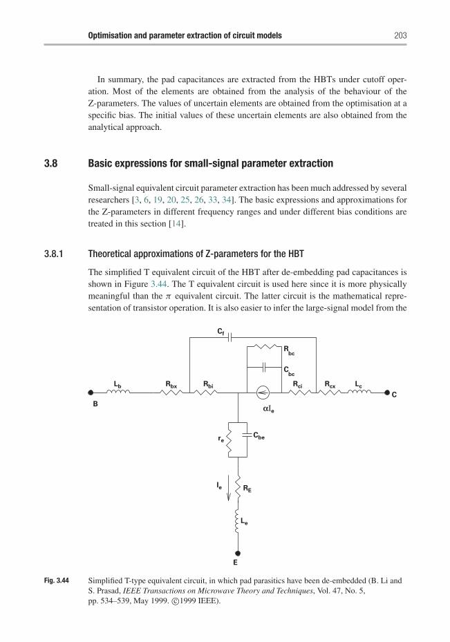
Optimisation and parameter extraction of circuit models 203
In summary, the pad capacitances are extracted from the HBTs under cutoff oper-ation. Most of the elements are obtained from the analysis of the behaviour of theZ-parameters. The values of uncertain elements are obtained from the optimisation at aspecific bias. The initial values of these uncertain elements are also obtained from theanalytical approach.
3.8 Basic expressions for small-signal parameter extraction
Small-signal equivalent circuit parameter extraction has been much addressed by severalresearchers [3, 6, 19, 20, 25, 26, 33, 34]. The basic expressions and approximations forthe Z-parameters in different frequency ranges and under different bias conditions aretreated in this section [14].
3.8.1 Theoretical approximations of Z-parameters for the HBT
The simplified T equivalent circuit of the HBT after de-embedding pad capacitances isshown in Figure 3.44. The T equivalent circuit is used here since it is more physicallymeaningful than the π equivalent circuit. The latter circuit is the mathematical repre-sentation of transistor operation. It is also easier to infer the large-signal model from the
B
C
Lb Lc
C
R
αΙe
E
Le
RE
Cbere
Ie
RbiRbx
Cf
Rci Rcx
bc
bc
Fig. 3.44 Simplified T-type equivalent circuit, in which pad parasitics have been de-embedded (B. Li andS. Prasad, IEEE Transactions on Microwave Theory and Techniques, Vol. 47, No. 5,pp. 534–539, May 1999. c©1999 IEEE).
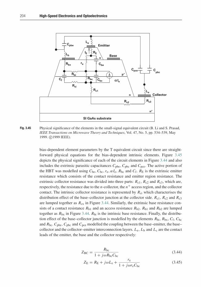
204 High-Speed Electronics and Optoelectronics
Emitter
Base
Collector
SI GaAs substrate
Rc2
Rc1
Rci
Rbi
Rbx Cbe
RE
Cpbe
Cpce C
Le
Le
LbIE
α IeRbc Cbc
pbc
Rc3
Cf
re
n
p+
n
n+
Fig. 3.45 Physical significance of the elements in the small-signal equivalent circuit (B. Li and S. Prasad,IEEE Transactions on Microwave Theory and Techniques, Vol. 47, No. 5, pp. 534–539, May1999. c©1999 IEEE).
bias-dependent element parameters by the T equivalent circuit since there are straight-forward physical equations for the bias-dependent intrinsic elements. Figure 3.45depicts the physical significance of each of the circuit elements in Figure 3.44 and alsoincludes the extrinsic parasitic capacitances Cpbe,Cpbc and Cpce. The active portion ofthe HBT was modelled using Cbe,Cbc, re, α Ie, Rbc and Cf. RE is the extrinsic emitterresistance which consists of the contact resistance and emitter region resistance. Theextrinsic collector resistance was divided into three parts: Rc1, Rc2 and Rc3, which are,respectively, the resistance due to the n-collector, the n+ access region, and the collectorcontact. The intrinsic collector resistance is represented by Rci which characterises thedistribution effect of the base–collector junction at the collector side. Rc1, Rc2 and Rc3
are lumped together as Rcx in Figure 3.44. Similarly, the extrinsic base resistance con-sists of a contact resistance Rb1 and an access resistance Rb2. Rb1 and Rb2 are lumpedtogether as Rbx in Figure 3.44. Rbi is the intrinsic base resistance. Finally, the distribu-tion effect of the base–collector junction is modelled by the elements Rbi, Rbx,Cf,Cbc
and Rbc. Cpbe,Cpbc and Cpce modelled the coupling between the base–emitter, the base–collector and the collector–emitter interconnection layers. Le, Lb and Lc are the contactleads of the emitter, the base and the collector respectively:
ZBC = Rbc
1 + jωRbcCbc(3.44)
ZE = RE + jωLe + re
1 + jωreCbe(3.45)
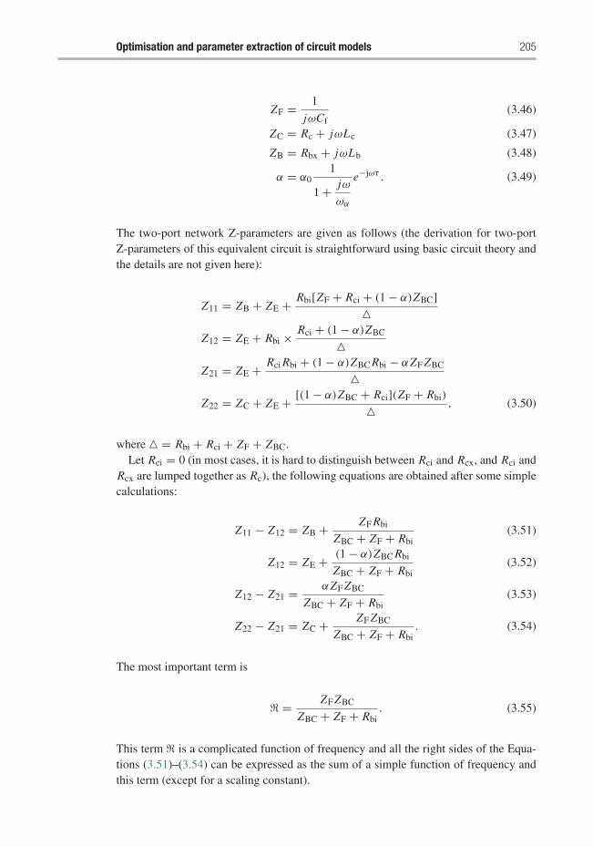
Optimisation and parameter extraction of circuit models 205
ZF = 1
jωCf(3.46)
ZC = Rc + jωLc (3.47)
ZB = Rbx + jωLb (3.48)
α = α01
1 + jω
ωα
e−jωτ . (3.49)
The two-port network Z-parameters are given as follows (the derivation for two-portZ-parameters of this equivalent circuit is straightforward using basic circuit theory andthe details are not given here):
Z11 = ZB + ZE + Rbi[ZF + Rci + (1 − α)ZBC]�
Z12 = ZE + Rbi × Rci + (1 − α)ZBC
�Z21 = ZE + Rci Rbi + (1 − α)ZBC Rbi − αZF ZBC
�Z22 = ZC + ZE + [(1 − α)ZBC + Rci](ZF + Rbi)
� , (3.50)
where � = Rbi + Rci + ZF + ZBC.Let Rci = 0 (in most cases, it is hard to distinguish between Rci and Rcx, and Rci and
Rcx are lumped together as Rc), the following equations are obtained after some simplecalculations:
Z11 − Z12 = ZB + ZF Rbi
ZBC + ZF + Rbi(3.51)
Z12 = ZE + (1 − α)ZBC Rbi
ZBC + ZF + Rbi(3.52)
Z12 − Z21 = αZF ZBC
ZBC + ZF + Rbi(3.53)
Z22 − Z21 = ZC + ZF ZBC
ZBC + ZF + Rbi. (3.54)
The most important term is
� = ZF ZBC
ZBC + ZF + Rbi. (3.55)
This term � is a complicated function of frequency and all the right sides of the Equa-tions (3.51)–(3.54) can be expressed as the sum of a simple function of frequency andthis term (except for a scaling constant).
206 High-Speed Electronics and Optoelectronics
Within the extreme low frequency range in which ωCbc Rbc � 1,
� � ZF ZBC
ZBC + ZF
� Rbc
jω(Cf + Cbc)Rbc + 1
� Rbc − jωR2bcCs, (3.56)
where we have used the assumption Rbc � Rbi and let Cs = Cf + Cbc, since thisis almost always the case in the forward or saturation applications. A typical extremelow frequency can be calculated by using the typical element values. In modern pro-cess technology in which the base resistance and base–collector capacitance have beengreatly reduced, the typical values Cbc � 5 × 10⁻¹⁴ F and Rbc � 5 × 10⁴ �, thereforethe frequency f � 0.1/(2πRbcCbc) = 6.8 MHz. For microwave applications, this typi-cal frequency is very low. Substituting the expression in Equation (3.56) into Equations(3.51), (3.52) and (3.54), the equations reduce to
Z11 − Z12 = Rbx + jωLb + Rbi − jωRbc RbiCs (3.57)
Z12 = RE + jωLe + re − jωr2e Cbe
+ (1 − α) × jωRbiCf(Rbc − jωR2bcCs) (3.58)
Z22 − Z21 = RC + jωLc + Rbc − jωR2bcCs. (3.59)
The base–emitter resistance is small in forward bias and therefore, ZE is approximatedas RE + jωLe + re − jωr2
e Cbe in this analysis. Z12 can be simplified by discarding thehigher-order terms:
Z12 = RE + jωLe + re − jωr2e Cbe + j (1 − α)ωRbi RbcCs. (3.60)
At low frequency, α → αDC → 1. Hence, Z12 is further simplified as
Z12 = RE + jωLe + re − jωr2e Cbe. (3.61)
The intermediate frequency range is characterised by ωCbc Rbi, ωCf Rbi � 1, butωCbc Rbc � 1. The approximation for � is given as
� = ZF ZBC
ZF + ZBC + Rbi
� ZF ZBC
ZF + ZBC×
(1 − Rbi
ZF + ZBC
)(3.62)
�(
1
jωCs+ 1
ω2C2s Rbc
) (1 − jωCfCbc Rbi
Cs
)� 1
jωCs+ 1
ω2C2s Rbc
− RbiCbcCf
C2s
− j RbiCfCbc
ωC3s Rbc
� 1
jωCs+ 1
ω2C2s Rbc
− RbiCbcCf
C2s
, (3.63)
Optimisation and parameter extraction of circuit models 207
where higher-order terms have been discarded. A typical intermediate frequency is cal-culated by using the typical element values. Assume Rbi = 10�, the typical valueof frequency is 0.1/(2πRbiCbc) � 0.64 GHz. The value ωCbc Rbc � 10 appropri-ately justifies the assumption. Substituting the approximation in Equation (3.63) intoEquations (3.51), (3.52) and (3.54), we obtain
Z11 − Z12 = Rbx + jωLb + RbiCbc
Cs− j RbiCf
ωRbcC2s
(3.64)
Z12 = RE + jωLe + re − jωr2e Cbe + (1 − α)Rbi
(Cf
Cs
)(3.65)
Z22 − Z21 = RC + jωLc + 1
jωCs+ 1
ω2 RbcCs− RbiCbcCf
C2s
. (3.66)
As indicated in the above expressions, initially 1/ω2(Cf + Cbc)2 Rbc is much larger than
RbiCbcCf/C2s and Rc. Re(Z22 − Z21), where Re denotes the real part can hence be
used to extract Rbc. With increase of frequency, the second term decreases rapidly andRe(Z22 − Z21) is possible to be negative as described in [20], where the intrinsic baseresistance Rbi is much higher in InP-based HBTs than in GaAs-based HBTs. After thehigher-order terms are discarded, Equations (3.64) and (3.65) are reduced to
Z11 − Z12 = Rbx + jωLb + RbiCbc
Cs(3.67)
Z12 = RE + jωLe + re − jωr2e Cbe (3.68)
The fifth term in Equation (3.65) consists of only a very small fraction of the realpart of Z12; therefore, the approximation is generally reasonable. However, for InP-based HBTs it may account for up to 18% of the real part of Z12 due to the largebase resistance [20]. Self-consistent iterations can be used to correct the approximationerrors [20].
The very high frequency range is defined by ωCbc Rbi, ωCf Rbi � 1
� � ZF ZBC
Rbi× 1
1 + ZF + ZBC
Rbi
� − 1
ω2CbcCf Rbi×
(1 − ZF + ZBC
Rbi
)� − 1
ω2 RbiCbcCf+ 1
ω2 RbiCbcCf
(1
jωCf Rbi+ 1
jωCbc Rbi
). (3.69)
The typical very high frequency is calculated by the values given above:f = 10/(2π RbiCbi)= 63.8 GHz. Since the very high frequency is very hard to reach, wenormally relax the high frequency requirement to above 20 GHz. Substituting Equation(3.69) into Equations (3.51), (3.52) and (3.54), we obtain
Z11 − Z12 = Rbx + jωLb + 1
jωCf+ 1
ω2 RbiCbcCf
(Cbc
Cf + 1
)(3.70)
208 High-Speed Electronics and Optoelectronics
Z12 = RE + jωLe + re − jωr2e Cbe + (1 − α)
jωCbc+ (1 − α)
ω2 RbiCbcCf
(Cf
Cbc+ 1
)(3.71)
Z22 − Z21 = RC + jωLc − 1
ω2 RbiCbcCf+ 1
ω2 RbiCbcCf
(1
jωCf Rbi+ 1
jωCbc Rbi
).
(3.72)
We divide the frequency range into three subdivisions. The boundaries of these threeranges are not strict and highly dependent on the applied biases, process technologyand device design. The magnitudes of Rbc, Rbi,CF,Cbc and re affect the definitions ofthe frequency range. The network analyser is used to measure S-parameters and then theS-parameters are converted to Z-parameters. The lowest frequency of the network anal-yser is about several tenths of MHz. Therefore, S-parameter data at the low frequency(satisfied by the condition ωRbcCs � 1) are not of much use for analysis except in thereverse or deep saturation region.
For the analytical approach to parameter extraction, we clarify that the intermediatefrequency range is below 5 GHz and the high frequency range is greater than 10 GHz.The method of clarifying the frequency range before extracting the element parame-ters is arbitrary; however, the justification needs to be made during the procedure ofparameter extraction.
3.8.2 Z-Parameters at zero bias or ‘cold’ biases
At zero bias (VBE = 0 V and VCE = 0 V) or ‘cold’ bias (VBE = 0 V and IB = 0 A;‘cold’ is adopted from the MESFET modelling techniques), the current gain becomeszero and the device behaves like a passive component. The base–emitter resistance re isalso much larger. The magnitude of this resistance is normally greater than 104 �, whichis within the same order of magnitude as the collector–base resistance. Therefore, theequivalent circuit becomes much simpler and so are the Z-parameters. With α = 0,we have
Z11 − Z12 = ZB + ZF Rbi
ZBC + ZF + Rbi(3.73)
Z12 = Z21 = ZE + ZBC Rbi
ZBC + ZF + Rbi(3.74)
Z22 − Z21 = ZC + ZF ZBC
ZBC + ZF + Rbi. (3.75)
The approximation of the Z-parameters is almost the same as before except for Z12 andZ21. The approximation of ZE in this case will be rather different. The ZE at the lowfrequency range in which ωreCbe0 � 1 is satisfied is given by
ZE � RE + jωLe + re − jωr2e Cbe0. (3.76)
Substituting into Equation (3.74), Z12 can be written as
Z12 � RE + jωLe + re − jωr2e Cbe0 + jωRbiCf(Rbc − jωR2
bcCs). (3.77)
Optimisation and parameter extraction of circuit models 209
For simplicity, higher-order terms can be discarded in the above equation withoutaffecting the accuracy.
When the frequency increases to the point at which ωreCbe0 � 1, ZE is approxi-mated as
ZE = RE + jωLe + 1
jωCbe0+ 1
ω2reC2be
. (3.78)
Actually, the assumption of ωreCbe0, ωRbcCbc0 � 1 and ωCbe0 Rbi, ωCbc0 Rbi � 1 iseasily satisfied in the frequency range of interest; therefore,
Z11 − Z12 = Rbx + jωLb + Cbc
CsRbi (3.79)
Z12 = RE + jωLe + 1
jωCbe0+ 1
ω2reC2be
+ Cf
CsRbi (3.80)
Z22 − Z21 = RC + jωLc + 1
jωCs+ 1
ω2 RbcC2s. (3.81)
In the above equations, the higher-order terms have been discarded for simplicity. If thefrequency increases further and 1/(ωCbe0), 1/(ωCbc0) � Rbi, then Z12 is given by
Z12 = RE + jωLe + 1
jωCbe0+ 1
ω2reC2be
+ 1
jωCbc+ 1
ω2 RbiCbc
(1
Cbc+ 1
Cf
).
(3.82)In the case of both junctions being reverse-biased, the approximation of the Z-parameters might be rather similar to this case at zero bias.
3.8.3 Parameter extraction
The model parameter extractions are based on the assumption that all the extrinsic andparasitic elements are bias-independent and only elements in the intrinsic part of thedevice vary with bias. This also means that the extrinsic and parasitic elements can beextracted by using multiple bias information. Some element values are sensitive to thebias point at which the extraction procedure is carried out.
Since the conditions at the intermediate frequency are easily satisfied in the fre-quency measurement range, we should make the most use of the Z-parameters in theintermediate frequency range. The extraction procedure is shown in Figures 3.46–3.49.The information for extracting the element parameters is overwhelming; hence differentschemes can be developed. The extraction procedure shown here is just one of them. Thesuperscripts used are explained as follows: R represents the real part of the correspond-ing Z-parameters; I the imaginary part; F the forward bias; 0 the zero bias; L the lowfrequency range; M the intermediate frequency range; and H the high frequency range.
From Z11 − Z12, we extract Lb by plotting Im(Z11 − Z12)/ω versus frequency inhigh frequency range. Rbx + Rbi can be obtained from Re(Z11 − Z12) at the extremelow frequency. Rbx might be obtained from Re(Z11 − Z12) at the high frequency. Thedifference will be Rbi.
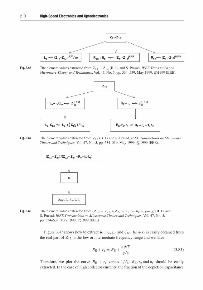
210 High-Speed Electronics and Optoelectronics
(Z11–Z12)I,F,M/ ωLb (Z11–Z12)R,F,LRbx + Rbi Rbx (Z11–Z12)R,F,H
Z11–Z12
Fig. 3.46 The element values extracted from Z11 − Z12 (B. Li and S. Prasad, IEEE Transactions onMicrowave Theory and Techniques, Vol. 47, No. 5, pp. 534–539, May 1999. c©1999 IEEE).
Z12
Le – reCbe 12Z I, F,M
Le, Cbe Le–re Cbe 1/1 E2
RE, re, nf RE + re ~ 1/1E
ZR, F,M12
RE + re
~
Fig. 3.47 The element values extracted from Z12 (B. Li and S. Prasad, IEEE Transactions on MicrowaveTheory and Techniques, Vol. 47, No. 5, pp. 534–539, May 1999. c©1999 IEEE).
α
αDC, τb, τc, τ, fα
(Z12 – Z21)/(Z22 – Z21 – Rc – jω Lc)
Fig. 3.48 The element values extracted from (Z12 − Z21)/(Z22 − Z21 − Rc − jωLc) (B. Li andS. Prasad, IEEE Transactions on Microwave Theory and Techniques, Vol. 47, No. 5,pp. 534–539, May 1999. c©1999 IEEE).
Figure 3.47 shows how to extract RE, re, Le and Cbe. RE + re is easily obtained fromthe real part of Z12 in the low or intermediate frequency range and we have
RE + re = RE + nfkT
q IE. (3.83)
Therefore, we plot the curve RE + re versus 1/IE. RE, re and nf should be easilyextracted. In the case of high collector currents, the fraction of the depletion capacitance
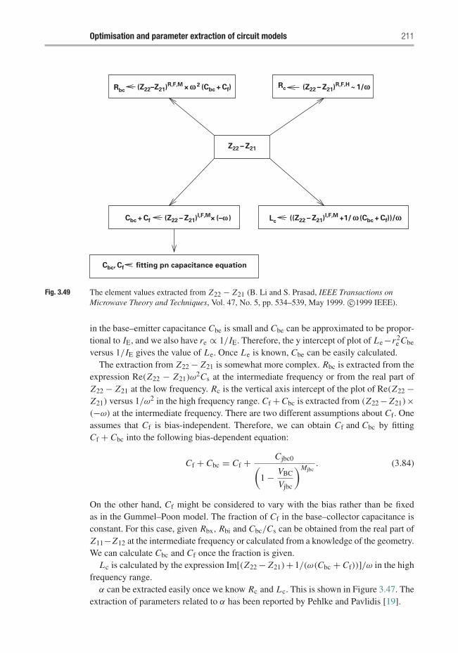
Optimisation and parameter extraction of circuit models 211
Cbc, Cf fitting pn capacitance equation
Rbc(Z22–Z21)R,F,M
× ω 2 (Cbc + Cf)
Rc (Z22 – Z21)R,F,H ~ 1/ω
Z22 – Z21
Cbc + Cf (Z22 – Z21)I,F,M× (–ω ) Lc((Z22 – Z21)I,F,M
+1/ ω (Cbc + Cf))/ω
Fig. 3.49 The element values extracted from Z22 − Z21 (B. Li and S. Prasad, IEEE Transactions onMicrowave Theory and Techniques, Vol. 47, No. 5, pp. 534–539, May 1999. c©1999 IEEE).
in the base–emitter capacitance Cbe is small and Cbe can be approximated to be propor-tional to IE, and we also have re ∝ 1/IE. Therefore, the y intercept of plot of Le −r2
e Cbe
versus 1/IE gives the value of Le. Once Le is known, Cbe can be easily calculated.The extraction from Z22 − Z21 is somewhat more complex. Rbc is extracted from the
expression Re(Z22 − Z21)ω2Cs at the intermediate frequency or from the real part of
Z22 − Z21 at the low frequency. Rc is the vertical axis intercept of the plot of Re(Z22 −Z21) versus 1/ω2 in the high frequency range. Cf + Cbc is extracted from (Z22 − Z21)×(−ω) at the intermediate frequency. There are two different assumptions about Cf. Oneassumes that Cf is bias-independent. Therefore, we can obtain Cf and Cbc by fittingCf + Cbc into the following bias-dependent equation:
Cf + Cbc = Cf + Cjbc0(1 − VBC
Vjbc
)Mjbc. (3.84)
On the other hand, Cf might be considered to vary with the bias rather than be fixedas in the Gummel–Poon model. The fraction of Cf in the base–collector capacitance isconstant. For this case, given Rbx, Rbi and Cbc/Cs can be obtained from the real part ofZ11−Z12 at the intermediate frequency or calculated from a knowledge of the geometry.We can calculate Cbc and Cf once the fraction is given.
Lc is calculated by the expression Im[(Z22 − Z21)+1/(ω(Cbc + Cf))]/ω in the highfrequency range.
α can be extracted easily once we know Rc and Lc. This is shown in Figure 3.47. Theextraction of parameters related to α has been reported by Pehlke and Pavlidis [19].
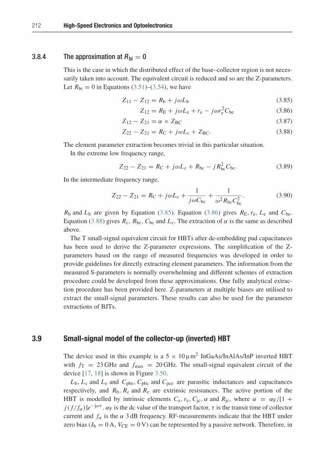
212 High-Speed Electronics and Optoelectronics
3.8.4 The approximation at R bi = 0
This is the case in which the distributed effect of the base–collector region is not neces-sarily taken into account. The equivalent circuit is reduced and so are the Z-parameters.Let Rbi = 0 in Equations (3.51)–(3.54), we have
Z11 − Z12 = Rb + jωLb (3.85)
Z12 = RE + jωLe + re − jωr2e Cbe (3.86)
Z12 − Z21 = α × ZBC (3.87)
Z22 − Z21 = RC + jωLc + ZBC. (3.88)
The element parameter extraction becomes trivial in this particular situation.In the extreme low frequency range,
Z22 − Z21 = RC + jωLc + Rbc − j R2bcCbc. (3.89)
In the intermediate frequency range,
Z22 − Z21 = RC + jωLc + 1
jωCbc+ 1
ω2 RbcC2bc
. (3.90)
Rb and Lb are given by Equation (3.85). Equation (3.86) gives RE, re, Le and Cbe.Equation (3.88) gives Rc, Rbc,Cbc and Lc. The extraction of α is the same as describedabove.
The T small-signal equivalent circuit for HBTs after de-embedding pad capacitanceshas been used to derive the Z-parameter expressions. The simplification of the Z-parameters based on the range of measured frequencies was developed in order toprovide guidelines for directly extracting element parameters. The information from themeasured S-parameters is normally overwhelming and different schemes of extractionprocedure could be developed from these approximations. One fully analytical extrac-tion procedure has been provided here. Z-parameters at multiple biases are utilised toextract the small-signal parameters. These results can also be used for the parameterextractions of BJTs.
3.9 Small-signal model of the collector-up (inverted) HBT
The device used in this example is a 5 × 10 μm2 InGaAs/InAlAs/InP inverted HBTwith fT = 23 GHz and fmax = 20 GHz. The small-signal equivalent circuit of thedevice [17, 18] is shown in Figure 3.50.
Lb, Lc and Le and Cpbe,Cpbc and Cpce are parasitic inductances and capacitancesrespectively, and Rb, Rc and Re are extrinsic resistances. The active portion of theHBT is modelled by intrinsic elements Ce, re,Cjc, α and Rjc, where α = αF/[1 +j ( f/ fα)]e−jωτ . αF is the dc value of the transport factor, τ is the transit time of collectorcurrent and fα is the α 3 dB frequency. RF-measurements indicate that the HBT underzero bias (Ib = 0 A, VCE = 0 V) can be represented by a passive network. Therefore, in
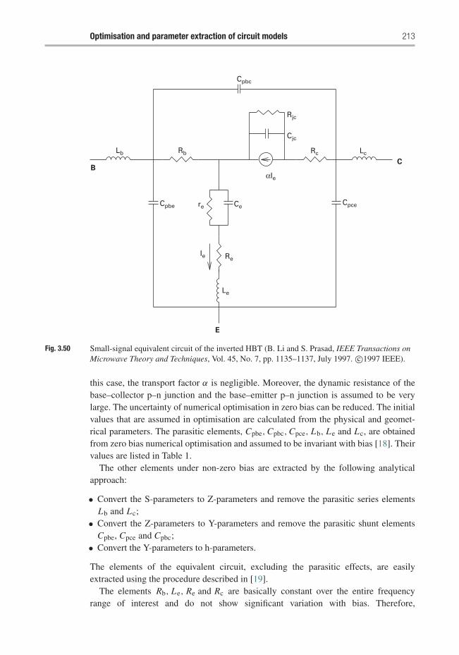
Optimisation and parameter extraction of circuit models 213
BC
E
Cpbc
Lb Lc
Le
Re
Cere
Cjc
Rjc
Rb
CpceCpbe
αIe
Ie
Rc
Fig. 3.50 Small-signal equivalent circuit of the inverted HBT (B. Li and S. Prasad, IEEE Transactions onMicrowave Theory and Techniques, Vol. 45, No. 7, pp. 1135–1137, July 1997. c©1997 IEEE).
this case, the transport factor α is negligible. Moreover, the dynamic resistance of thebase–collector p–n junction and the base–emitter p–n junction is assumed to be verylarge. The uncertainty of numerical optimisation in zero bias can be reduced. The initialvalues that are assumed in optimisation are calculated from the physical and geomet-rical parameters. The parasitic elements, Cpbe,Cpbc,Cpce, Lb, Le and Lc, are obtainedfrom zero bias numerical optimisation and assumed to be invariant with bias [18]. Theirvalues are listed in Table 1.
The other elements under non-zero bias are extracted by the following analyticalapproach:
• Convert the S-parameters to Z-parameters and remove the parasitic series elementsLb and Lc;
• Convert the Z-parameters to Y-parameters and remove the parasitic shunt elementsCpbe, Cpce and Cpbc;
• Convert the Y-parameters to h-parameters.
The elements of the equivalent circuit, excluding the parasitic effects, are easilyextracted using the procedure described in [19].
The elements Rb, Le, Re and Rc are basically constant over the entire frequencyrange of interest and do not show significant variation with bias. Therefore,
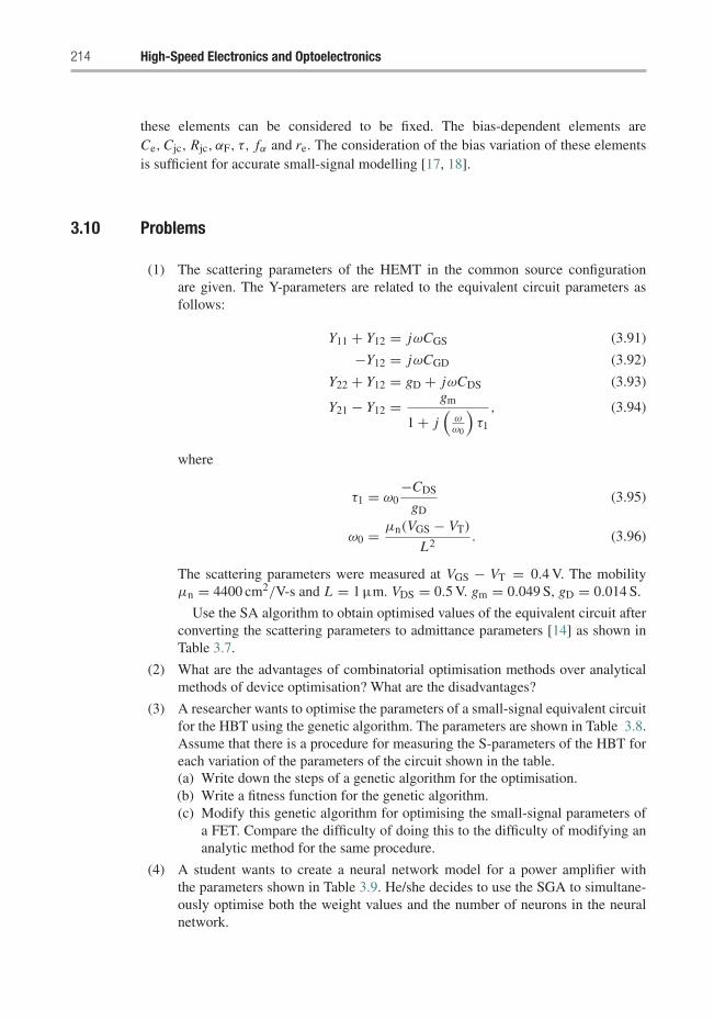
214 High-Speed Electronics and Optoelectronics
these elements can be considered to be fixed. The bias-dependent elements areCe,Cjc, Rjc, αF, τ, fα and re. The consideration of the bias variation of these elementsis sufficient for accurate small-signal modelling [17, 18].
3.10 Problems
(1) The scattering parameters of the HEMT in the common source configurationare given. The Y-parameters are related to the equivalent circuit parameters asfollows:
Y11 + Y12 = jωCGS (3.91)
−Y12 = jωCGD (3.92)
Y22 + Y12 = gD + jωCDS (3.93)
Y21 − Y12 = gm
1 + j(
ωω0
)τ1
, (3.94)
where
τ1 = ω0−CDS
gD(3.95)
ω0 = μn(VGS − VT)
L2. (3.96)
The scattering parameters were measured at VGS − VT = 0.4 V. The mobilityμn = 4400 cm2/V-s and L = 1 μm. VDS = 0.5 V. gm = 0.049 S, gD = 0.014 S.
Use the SA algorithm to obtain optimised values of the equivalent circuit afterconverting the scattering parameters to admittance parameters [14] as shown inTable 3.7.
(2) What are the advantages of combinatorial optimisation methods over analyticalmethods of device optimisation? What are the disadvantages?
(3) A researcher wants to optimise the parameters of a small-signal equivalent circuitfor the HBT using the genetic algorithm. The parameters are shown in Table 3.8.Assume that there is a procedure for measuring the S-parameters of the HBT foreach variation of the parameters of the circuit shown in the table.(a) Write down the steps of a genetic algorithm for the optimisation.(b) Write a fitness function for the genetic algorithm.(c) Modify this genetic algorithm for optimising the small-signal parameters of
a FET. Compare the difficulty of doing this to the difficulty of modifying ananalytic method for the same procedure.
(4) A student wants to create a neural network model for a power amplifier withthe parameters shown in Table 3.9. He/she decides to use the SGA to simultane-ously optimise both the weight values and the number of neurons in the neuralnetwork.
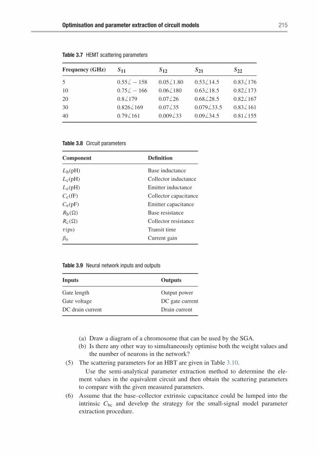
Optimisation and parameter extraction of circuit models 215
Table 3.7 HEMT scattering parameters
Frequency (GHz) S11 S12 S21 S22
5 0.55 � − 158 0.05� 1.80 0.53 � 14.5 0.83� 176
10 0.75 � − 166 0.06� 180 0.63 � 18.5 0.82� 173
20 0.8 � 179 0.07� 26 0.68 � 28.5 0.82� 167
30 0.826 � 169 0.07� 35 0.079� 33.5 0.83 � 161
40 0.79 � 161 0.009� 33 0.09 � 34.5 0.81� 155
Table 3.8 Circuit parameters
Component Definition
Lb(pH) Base inductance
Lc(pH) Collector inductance
Le(pH) Emitter inductance
Cc(fF) Collector capacitance
Ce(pF) Emitter capacitance
Rb(�) Base resistance
Rc(�) Collector resistance
τ (ps) Transit time
βo Current gain
Table 3.9 Neural network inputs and outputs
Inputs Outputs
Gate length Output power
Gate voltage DC gate current
DC drain current Drain current
(a) Draw a diagram of a chromosome that can be used by the SGA.(b) Is there any other way to simultaneously optimise both the weight values and
the number of neurons in the network?(5) The scattering parameters for an HBT are given in Table 3.10.
Use the semi-analytical parameter extraction method to determine the ele-ment values in the equivalent circuit and then obtain the scattering parametersto compare with the given measured parameters.
(6) Assume that the base–collector extrinsic capacitance could be lumped into theintrinsic Cbc and develop the strategy for the small-signal model parameterextraction procedure.
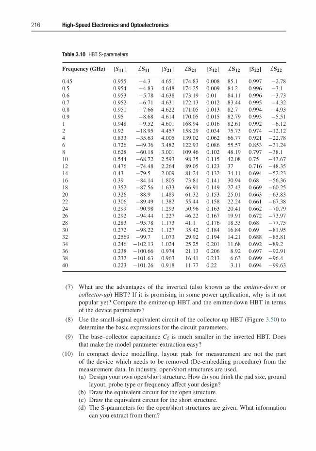
216 High-Speed Electronics and Optoelectronics
Table 3.10 HBT S-parameters
Frequency (GHz) |S11| � S11 |S21| � S21 |S12| � S12 |S22| � S22
0.45 0.955 −4.3 4.651 174.83 0.008 85.1 0.997 −2.780.5 0.954 −4.83 4.648 174.25 0.009 84.2 0.996 −3.10.6 0.953 −5.78 4.638 173.19 0.01 84.11 0.996 −3.730.7 0.952 −6.71 4.631 172.13 0.012 83.44 0.995 −4.320.8 0.951 −7.66 4.622 171.05 0.013 82.7 0.994 −4.930.9 0.95 −8.68 4.614 170.05 0.015 82.79 0.993 −5.511 0.948 −9.52 4.601 168.94 0.016 82.61 0.992 −6.122 0.92 −18.95 4.457 158.29 0.034 75.73 0.974 −12.124 0.833 −35.63 4.005 139.02 0.062 66.77 0.921 −22.786 0.726 −49.36 3.482 122.93 0.086 55.57 0.853 −31.248 0.628 −60.18 3.001 109.46 0.102 48.19 0.797 −38.110 0.544 −68.72 2.593 98.35 0.115 42.08 0.75 −43.6712 0.476 −74.48 2.264 89.05 0.123 37 0.716 −48.3514 0.43 −79.5 2.009 81.24 0.132 34.11 0.694 −52.2316 0.39 −84.14 1.805 73.81 0.141 30.94 0.68 −56.3618 0.352 −87.56 1.633 66.91 0.149 27.43 0.669 −60.2520 0.326 −88.9 1.489 61.32 0.153 25.01 0.663 −63.8322 0.306 −89.49 1.382 55.44 0.158 22.24 0.661 −67.3824 0.299 −90.98 1.293 50.96 0.163 20.41 0.662 −70.7926 0.292 −94.44 1.227 46.22 0.167 19.91 0.672 −73.9728 0.283 −95.78 1.173 41.1 0.176 18.33 0.68 −77.7530 0.272 −98.22 1.127 35.42 0.184 16.84 0.69 −81.9532 0.2569 −99.7 1.073 29.92 0.194 14.21 0.688 −85.8134 0.246 −102.13 1.024 25.25 0.201 11.68 0.692 −89.236 0.238 −100.66 0.974 21.13 0.206 8.92 0.697 −92.9138 0.232 −101.63 0.963 16.41 0.213 6.63 0.699 −96.440 0.223 −101.26 0.918 11.77 0.22 3.11 0.694 −99.63
(7) What are the advantages of the inverted (also known as the emitter-down orcollector-up) HBT? If it is promising in some power application, why is it notpopular yet? Compare the emitter-up HBT and the emitter-down HBT in termsof the device parameters?
(8) Use the small-signal equivalent circuit of the collector-up HBT (Figure 3.50) todetermine the basic expressions for the circuit parameters.
(9) The base–collector capacitance Cf is much smaller in the inverted HBT. Doesthat make the model parameter extraction easy?
(10) In compact device modelling, layout pads for measurement are not the partof the device which needs to be removed (De-embedding procedure) from themeasurement data. In industry, open/short structures are used.(a) Design your own open/short structure. How do you think the pad size, ground
layout, probe type or frequency affect your design?(b) Draw the equivalent circuit for the open structure.(c) Draw the equivalent circuit for the short structure.(d) The S-parameters for the open/short structures are given. What information
can you extract from them?
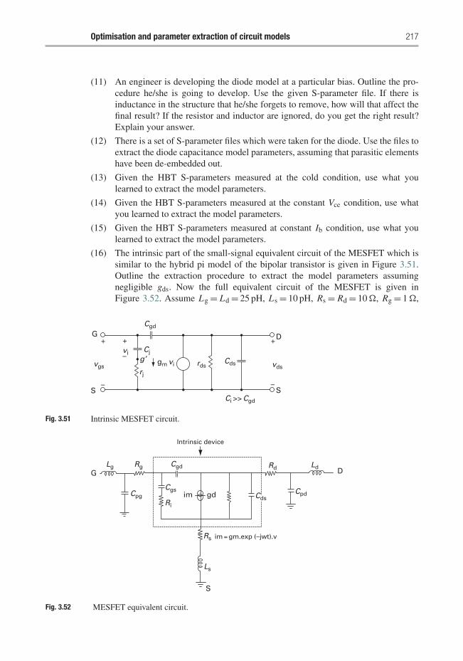
Optimisation and parameter extraction of circuit models 217
(11) An engineer is developing the diode model at a particular bias. Outline the pro-cedure he/she is going to develop. Use the given S-parameter file. If there isinductance in the structure that he/she forgets to remove, how will that affect thefinal result? If the resistor and inductor are ignored, do you get the right result?Explain your answer.
(12) There is a set of S-parameter files which were taken for the diode. Use the files toextract the diode capacitance model parameters, assuming that parasitic elementshave been de-embedded out.
(13) Given the HBT S-parameters measured at the cold condition, use what youlearned to extract the model parameters.
(14) Given the HBT S-parameters measured at the constant Vce condition, use whatyou learned to extract the model parameters.
(15) Given the HBT S-parameters measured at constant Ib condition, use what youlearned to extract the model parameters.
(16) The intrinsic part of the small-signal equivalent circuit of the MESFET which issimilar to the hybrid pi model of the bipolar transistor is given in Figure 3.51.Outline the extraction procedure to extract the model parameters assumingnegligible gds. Now the full equivalent circuit of the MESFET is given inFigure 3.52. Assume Lg = Ld = 25 pH, Ls = 10 pH, Rs = Rd = 10�, Rg = 1�,
G
S
+
–
+
Cgd
D+
–S
vds
vi Cj
gm virj
rdsCds
Ci >> Cgd
g’–vgs
Fig. 3.51 Intrinsic MESFET circuit.
GLg Rg Cgd
Cgs
Ri
im gdCpg
Rs
Ls
S
Cpd
Rd Ld D
Intrinsic device
im = gm.exp (–jwt).v
Cds
Fig. 3.52 MESFET equivalent circuit.
218 High-Speed Electronics and Optoelectronics
Cpg = Cpd = 25 fF and gds = 0 S. Extract the other model parameters based onthe given set of S-parameters.
Note that the necessary data files are available on the Web labelled according to theproblem numbers.
References
[1] Bousnina S., Falt C., Mandeville P., Kouki A. B., Ghannouchi F. M. (2002). An accurateon-wafer deembedding technique with application to HBT devices characterizaion. IEEETrans. Microw. Theory Tech. MTT-50, 2 (February), 420–424.
[2] Bousnina S., Mandeville P., Kouki A. B., Surridge R., Ghannouchi F. M. (2002). Directparameter-extraction method for HBT small signal model. IEEE Trans. Microw. TheoryTech. MTT-50, 2 (February), 529–536.
[3] Costa D., Liu W., Jr. J. S. H. (1991). Direct extraction of the AlGaAs/GaAs heterojunctionbipolar transistor small-signal equivalent circuit. IEEE Trans. Electron Devices ED-38, 9(September), 2018–2024.
[4] Dasgupta D., McGregor D. (1992). SGA: a structured genetic algorithm. Tech. Rep. IKBS-8-92, University of Strathclyde.
[5] Degachi L., Ghannouchi F. M. (2006). Systematic and rigorous extraction method of HBTsmall-signal model parameters. IEEE Trans. Microw. Theory Tech. MTT-54, 2 (February),682–688.
[6] Dvorak M. W., Bolognesi C. (2003). On the accuracy of direct extraction of theheterojunction-bipolar-transistor equivalent-circuit model parameters Cπ , CBC and RE.IEEE Trans. Microw. Theory Tech. MTT-51, 6 (June), 1640–1649.
[7] Gobert Y., Tasker P. J., Bachem K. H. (1997). A physical, yet simple, small-signal equivalentcircuit for the heterojunction bipolar transistor. IEEE Trans. Microw. Theory Tech. MTT-45, 1(January), 149–153.
[8] Goldberg D. (1989). Genetic Algorithms in Search, Optimization and Machine Learning.Addison-Wesley.
[14] Gonzalez G. (1997). Microwave Transistor Amplifiers, Analysis and Design. Prentice Hall.[10] Holland J. H. (1975). Adaptation in Natural and Artificial Systems. University of Michigan
Press.[11] Hopfield J. J. (1984). Neurons with graded response have collective computational proper-
ties like those of two-state neurons. Proc. Nat. Acad. Sci. 81, 10 (May), 3088–3092.[12] Kirkpatrick S., Gelatt C. D. Jr, Vecchi M. P. (1983). Optimization by simulated annealing.
Science 220, 4598 (May), 671–680.[13] Li B., Prasad S. (1997). Harmonic and two-tone intermodulation distortion analyses of the
inverted InGaAs/InAlAs/InP HBT. IEEE Trans. Microw. Theory Tech. MTT-45, 7 (July),1135–1137.
[14] Li B., Prasad S. (1999). Basic expressions and approximations in small-signal parameterextraction for HBT’s. IEEE Trans. Microw. Theory Tech. MTT-47, 5 (May), 534–539.
[15] Li B., Prasad S., Yang L.-W., Wang S. C. (1998). A semianalytical parameter-extraction pro-cedure for HBT equivalent circuit. IEEE Trans. Microw. Theory Tech. MTT-46, 10 (October),1427–1435.
Optimisation and parameter extraction of circuit models 219
[16] Lippmann R. (1987). An introduction to computing with neural nets. IEEE ASSP Mag. 4, 5(April), 4–22.
[17] Meskoob B., Prasad S., Vai M., Fonstad C., Vlcek J. C., Sato H. (1992). A small-signalequivalent circuit for the collector-up InGaAs/InAlAs/InP heterojunction bipolar transistor.IEEE Trans. Electron Devices ED-39, 11 (November), 2629–2632.
[18] Meskoob B., Prasad S., Vai M., Vlcek J. C., Sato H., Fonstad C. G. (1992). Bias-dependence of the intrinsic element values of InGaAs/InAlAs/InP inverted heterojunctionbipolar transistor. IEEE Trans. Microw. Theory Tech. MTT-40, 5 (May), 1012–1014.
[19] Pehlke D. R., Pavlidis D. (1992). Evaluation of the factors determining HBT high frequencyperformance by direct analysis of S-parameter data. IEEE Trans. Microw. Theory Tech. MTT-40, 12 (December), 2367–2373.
[20] Rios J. M. M., Lunardi L. M., Chandrasekhar S., Miyamoto Y. (1997). A self-consistentmethod for complete small-signal extraction of InP-based heterojunction bipolar transistors(HBTs). IEEE Trans. Microw. Theory Tech. MTT-45, 1 (January), 39–45.
[21] Roblin P., Kang S., Ketterson A., Morkoc H. (1987). Analysis of MODFET microwavecharacteristics. IEEE Trans. Electron Devices ED-34, 9 (September), 1919–1927.
[22] Romeo F., Sangiovanni-Vincentelli A. (1987). Probabilistic hill climbing algorithms: prop-erties and applications. In 1985 Chapel Hill Conference on VLSI, H. Fuchs, ed. ComputerScience Press, 671–680.
[23] Rutenbar R. A. (1989). Simulated annealing algorithm: an overview. IEEE Circ. Dev.Mag. 5, 1 (January), 19–26.
[24] Samelis A., Pavlidis D. (1997). DC to high-frequency HBT-model parameter evaluationusing impedance block conditioned optimization. IEEE Trans. Microw. Theory Tech. MTT-45, 6 (June), 886–897.
[25] Schaper U., Holzapfl B. (1995). Analytical parameter extraction of the HBT equivalentcircuit with T-like topology from measured S-parameters. IEEE Trans. Microw. TheoryTech. MTT-40, 3 (March), 493–498.
[26] Sheinman B., Wasige E., Rudolph M., Sidorov V., Cohen S., Ritter D. (2002). A peelingalgorithm for extraction of the HBT small-signal equivalent circuit. IEEE Trans. Microw.Theory Tech. MTT-50, 12 (December), 2804–2810.
[27] Spiegel S. J., Ritter D., Hamm R. A., Feygenson A., Smith P. R. (1995). Extraction of theInP/GaInAs heterojunction bipolar transistor small-signal equivalent circuit. IEEE Trans.Electron Devices ED-42, 6 (June), 1059–1064.
[28] Vai M., Prasad S. (1993). Automatic impedance matching with a neural network. IEEEMicrow. Guided Wave Lett. MGWL-3, 10 (October), 353–354.
[29] Vai M., Prasad S. (1999). Neural networks in microwave circuit design – beyond black-boxmodels. Int. J. RF and Microwave CAE 9, 3 (May), 187–197.
[30] Vai M., Prasad S., Li N., Kai F. (1989). Modeling of microwave semiconductor devices usingsimulated annealing optimization. IEEE Trans. Electron Devices ED-36, 4 (April), 761–762.
[31] Vai M., Prasad S. (1995). Microwave circuit analysis and design by a massively distributedcomputing network. IEEE Trans. Microw. Theory Tech. MTT-43, 5 (May), 1087–1094.
[32] vanRooij A., Jain L. C., Johnson R. P. (1996). Neural Network Training Using GeneticAlgorithms. World Scientific.
[33] Wei C. J., Huang J. C. M. (1995). Direct extraction of equivalent circuit parameters for het-erojunction bipolar transistors. IEEE Trans. Microw. Theory Tech. MTT-43, 9 (September),2035–2039.

220 High-Speed Electronics and Optoelectronics
[34] Willen B., Rohner M., Schnyder I., Jackel H. (2002). Improved automatic parameterextraction of InP-HBT small signal equivalent circuits. IEEE Trans. Microw. TheoryTech. MTT-50, 2 (February), 580–583.
[35] Yang T. -R., Tsai J. M. -L., Ho C. -L., Hu R. (2007). SiGe HBTs small-signal pi modeling.IEEE Trans. Microw. Theory Tech. MTT-55, 7 (July), 1417–1424.
[36] Zaabab A. H., Zhang Q., Nakhla M. (1995). A neural network modeling approach to circuitoptimization and statistical design. IEEE Trans. Microw. Theory Tech. MTT-43, 6 (June),1349–1358.
[37] Zhang Q. -J., Gupta K., Devabhaktuni V. K. (2003). Artificial neural networks for RF andmicrowave design–from theory to practice. IEEE Trans. Microw. Theory Tech. MTT-51, 4(April), 1339–1350.
4 Optoelectronics
4.1 Executive summary
All land line communication systems currently use optical fibres as the channel due totheir very low attenuation, and deployed systems operate up to 40 Gigabits per second(Gbps), with experimental systems at 160 Gbps and higher. These high speed systemsuse very stable sources, usually the distributed feedback lasers, with external modu-lators and very fast detectors. Direct modulation of lasers leads to chirp, caused bythe laser frequency varying when modulated, and therefore is not used in these sys-tems. However, interest remains in high speed lasers for several other applications. Thischapter discusses high speed optoelectronic devices which include light-emitting diodes(LEDs), semiconductor lasers, photoconductors, p–i–n diode photodetectors, avalanchephotodetectors, metal–semiconductor–metal photodetectors, travelling wave photode-tectors and briefly the phototransistor. The physics of the devices are outlined and thenthe parameters that make these devices fast are discussed with specific examples fromthe literature.
4.2 Optical sources
Two types of sources are widely used in optical communication systems, and they arethe LED and the semiconductor laser. LEDs are inherently slow; their response timesare determined by the lifetime of the carriers in the active region, and in most LEDsthis is between 2 ns and 10 ns. Thus, small-signal response of LEDs is of the order of100 MHz, and the large-signal response is smaller than this. Lasers are complex devices,and the response time is determined by the so-called relaxation oscillation frequency,and this is due to the interaction between the photons which have a finite lifetime, whichis a measure of the cavity quality factor, Q, the differential gain of the structure, thelifetime of the carriers and other parameters [1]. Most lasers, when directly modulated,suffer from spectral broadening, and therefore direct modulation is not used for longhaul fibre-optic systems; but when this broadening is not important, direct modulationmay be used.
In this section, the fundamental aspects of LEDs and lasers are discussed, followedby an outline of the different types of lasers. To calculate the response of lasers, the rateequations are introduced and these are solved analytically for the relaxation frequencyfr. A short discussion of the noise mechanisms of lasers follows. A further section isincluded on the very high fr lasers.
222 High-Speed Electronics and Optoelectronics
4.2.1 Preliminaries
The generation of non-thermal light in a semiconductor requires the creation of hole–electron pairs which recombine radiatively to emit photons at the bandgap energy, orimpurity level to valence band energy. The more recent source of light is the intra-band relaxation of electrons from a higher energy level to a lower energy level in theconduction band of a quantum well, to emit photons, and this has resulted in the quan-tum cascade lasers. In both these sources of light, a means of generation of the excesselectron–hole pairs or excitation of the carriers to a higher energy state requires theexpenditure of energy. If this energy is from an electrical source, then this is called elec-trical pumping leading to electroluminescent emission. Alternatively, optical pumpingwith photons of a higher energy than the emitted photons is also a possibility. In thischapter, only electroluminescent sources are considered, and quantum cascade lasersare not discussed.
4.2.2 Light-emitting diodes
The ubiquitous green and red LEDs are fabricated in GaP which is an indirect gap semi-conductor. The impurities of zinc oxide and nitrogen form isoelectronic bands whichgive rise to the red and green emissions, respectively. Other LEDs include the blue GaNdevice, the near infrared GaAs 870 nm device and the InGaAsP 1300 nm and 1550 nmdevices.
The mechanisms that create the LED are based on p–n junctions. A forward-biasedp–n junction injects minority carriers to both sides of the junction, and these diffuseaway from the junction to recombine radiatively and non-radiatively. The radiativerecombination results in emission of photons, with energy hν approximately equal tothe bandgap energy Eg. The recombination is spontaneous, which implies that emissionhas random phase, and the linewidth is of the order of a few kBT, where kB is Boltz-mann’s constant, and T is the temperature in kelvin, and the emission is incoherent. Theinternal quantum efficiency is a measure of how efficiently the injected carriers producelight, since some of them recombine non-radiatively. Define the total recombination rateRtotal, in recombination events per second, as the sum of the radiative recombination rateRrr and the non-radiative recombination rate Rnr. Then, the internal quantum efficiencyis given by the ratio of the radiative recombination rate to the total rate:
ηi = Rrr
Rtotal= Rrr
Rrr + Rnr. (4.1)
However, lifetimes are more easily measured or inferred, and the quantum efficiency isrecast in terms of the lifetimes. The radiative recombination rate is defined as the ratioof the non-equilibrium carrier density N to the radiative lifetime τrr, and similarly, thenon-radiative recombination rate is the ratio of the carrier density N to the non-radiativelifetime τnr, and thus Rrr = N/τrr and Rnr = N/τnr. It follows that the total lifetimeτtotal is given by
1
τtotal= 1
τrr+ 1
τnr. (4.2)
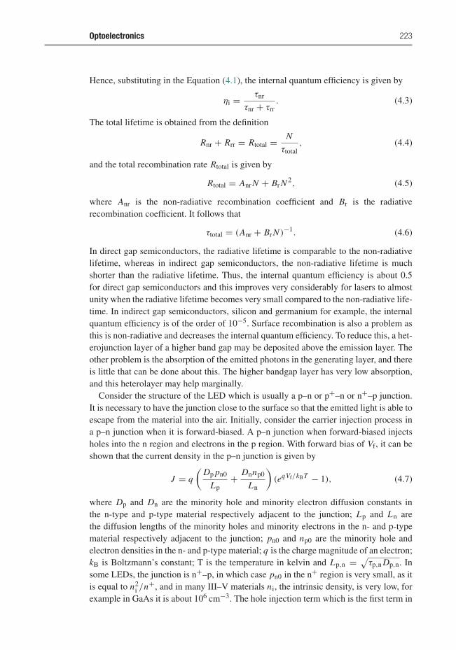
Optoelectronics 223
Hence, substituting in the Equation (4.1), the internal quantum efficiency is given by
ηi = τnr
τnr + τrr. (4.3)
The total lifetime is obtained from the definition
Rnr + Rrr = Rtotal = N
τtotal, (4.4)
and the total recombination rate Rtotal is given by
Rtotal = Anr N + Br N 2, (4.5)
where Anr is the non-radiative recombination coefficient and Br is the radiativerecombination coefficient. It follows that
τtotal = (Anr + Br N )−1. (4.6)
In direct gap semiconductors, the radiative lifetime is comparable to the non-radiativelifetime, whereas in indirect gap semiconductors, the non-radiative lifetime is muchshorter than the radiative lifetime. Thus, the internal quantum efficiency is about 0.5for direct gap semiconductors and this improves very considerably for lasers to almostunity when the radiative lifetime becomes very small compared to the non-radiative life-time. In indirect gap semiconductors, silicon and germanium for example, the internalquantum efficiency is of the order of 10−5. Surface recombination is also a problem asthis is non-radiative and decreases the internal quantum efficiency. To reduce this, a het-erojunction layer of a higher band gap may be deposited above the emission layer. Theother problem is the absorption of the emitted photons in the generating layer, and thereis little that can be done about this. The higher bandgap layer has very low absorption,and this heterolayer may help marginally.
Consider the structure of the LED which is usually a p–n or p+–n or n+–p junction.It is necessary to have the junction close to the surface so that the emitted light is able toescape from the material into the air. Initially, consider the carrier injection process ina p–n junction when it is forward-biased. A p–n junction when forward-biased injectsholes into the n region and electrons in the p region. With forward bias of Vf, it can beshown that the current density in the p–n junction is given by
J = q
(Dp pn0
Lp+ Dnnp0
Ln
)(eqVf/kBT − 1), (4.7)
where Dp and Dn are the minority hole and minority electron diffusion constants inthe n-type and p-type material respectively adjacent to the junction; Lp and Ln arethe diffusion lengths of the minority holes and minority electrons in the n- and p-typematerial respectively adjacent to the junction; pn0 and np0 are the minority hole andelectron densities in the n- and p-type material; q is the charge magnitude of an electron;kB is Boltzmann’s constant; T is the temperature in kelvin and Lp,n = √
τp,n Dp,n. Insome LEDs, the junction is n+–p, in which case pn0 in the n+ region is very small, as itis equal to n2
i /n+, and in many III–V materials ni, the intrinsic density, is very low, forexample in GaAs it is about 106 cm−3. The hole injection term which is the first term in
224 High-Speed Electronics and Optoelectronics
p− type
n+ type
Air
p+ layerContact
d
Fig. 4.1 Sketch of the n+–p junction, with a very thin p+ and the contacts of the LED. Also shown is theeffect of total internal reflection in the escape of light from the p+ layer.
Equation (4.7) is small, and the injection is largely from the n+ region into the p region.Thus, the injection efficiency, which is the ratio of the injected current into the p regionto the total injected current is almost unity due to the fact that the injected current intothe n+ region is much smaller than that injected into the p region. This is the case for thep+–n junction as well, since the minority carrier density in the highly doped region isalways much smaller than that in the lower doped region, and the injection efficiency isassumed to be unity. However, as indicated above, the internal quantum efficiency is ofthe order of 50% for direct gap semiconductors. As the junction temperature rises, thenon-radiative recombination increases and so this figure is typical for room temperaturedevices.
Assuming that the injection is primarily from the n+ side of the n+–p junction intothe p region. The minority electron distribution in the p layer is of the form �ne−z/Ln ,where the z direction is normal to the surface in Figure 4.1, and z is the distance fromthe junction towards the surface. This minority carrier distribution may be shown to beequivalent to np0(eqV/kBT − 1)e−z/Lp . Thus, the radiative recombination is over thisdistribution, and for all practical purposes it can be shown that this is equivalent to anuniform distribution over the distance Ln. Assume that the thickness of the active layeris d, which is assumed to be much larger than the diffusion length Ln. Then, integratingthis distribution ∫ ∞
0�ne−z/Ln dz = �nLn, (4.8)
which shows that �n may be considered uniformly distributed over Ln. The choiceof the upper limit of ∞ is because d � Ln. The lifetimes in GaAs and InGaAsP varyfrom 2 ns to about 10 ns, and mobility of minority carriers of 1000 cm2 (V.s)−1 gives Ln
values of less than 0.5 μm, and the active layer thickness may exceed this value. In thefollowing sections, the tacit assumption is that the minority carrier density is uniformover Ln.
In Figure 4.1, the top p layer has the injected minority carriers recombining to cre-ate the photon source. The spontaneous emission is isotropic and the trajectories of thephotons at the surface to the air region result in total internal reflection when the inci-dence angle exceeds the critical angle. Thus, extraction efficiency of the emission needsto take into account this total internal reflection, when the incidence angle exceeds thecritical angle given by
Optoelectronics 225
θc = sin−1 n0
n2(4.9)
where n0 is the index of air equal to 1 and n2 is the index of the top layer of the LEDthrough which the emitted photons escape. For normal incidence of the photons, thereflection coefficient � is given by
� = n0 − n2
n0 + n2. (4.10)
The fractional transmitted power or the transmissivity (1 − �2) for normal incidence,and is given by
T (0) = 4n0n2
(n0 + n2)2. (4.11)
As the photon angle of incidence varies from the normal to θc, the reflection coefficientchanges, depending on the polarisation, which averages out between the two perpendic-ular and parallel cases for the spontaneous emission, and the transmissivity also changes[7]. The external quantum efficiency is obtained from
ηext = 1
4π
∫ θc
0T (θ)2π sin θdθ. (4.12)
Since the expressions for the transmissivity vary with θ , and are difficult to inte-grate, T (θ) is replaced by T (0). Substituting for T (0) from Equation (4.11) and usingEquation (4.9), the external quantum efficiency becomes
ηext = 1
n2(n0 + n2)2. (4.13)
For a value of n2 of 3.5 and n0 of unity, ηext is of the order of 1.4%, which suggests thatmost of the light generated is trapped inside the device. The presence of a heterojunctionlayer on the top surface, discussed below, complicates this expression as the index ofthis top layer is lower than that of the active layer. An anti-reflection coating on thesurface helps to improve this factor considerably. The obvious method of extractinglight from the p-layer is to place a hemispherical lens, index identical to the p-layer, onthe surface. If there is a hetero-layer, then this needs to modified further. In the case ofthe p layer, the extraction efficiency becomes very high, but the problem is getting asuitable lens with the same index.
The optical power emitted by the LED is given by
Popt = ηintηext(hν)I
q, (4.14)
where I/q is the number of electrons or holes that are injected into the active regionper second; the internal quantum efficiency ηint defines the fraction of them that recom-bine radiatively; and the external quantum efficiency ηext the fraction of the generatedphotons that escape from the active layer. The total quantum efficiency of the LED isa measure of its performance and is the ratio of the output optical power to the input
226 High-Speed Electronics and Optoelectronics
electrical power, which is given as P0 = V0 I , where V0 is the voltage drop across thedevice and the current is given by I . Thus, substituting from Equation (4.14)
ηtotal = ηintηexthν
qV0. (4.15)
Neglecting contact resistance drops, hν ≈ Eg ≈ qV0, where Eg is the band gap ineV, which then makes the total quantum efficiency, which is also the external powerefficiency or the wall plug efficiency:
ηtotal ≈ ηintηext. (4.16)
This is usually less than a few percent, unless other techniques are used to extract thelight more efficiently. Edge-emitting LEDs, discussed below, are therefore much moreefficient. For visible LEDs the luminosity is also an issue [3], but this is not consideredhere.
The responsivity R of the LED is defined as the ratio of the emitted optical power tothe current, and substituting from Equation (4.14), is given by
R = ηintηexthν
q. (4.17)
This is of the order of 0.01 W A−1 for the above values of η unless this becomes muchlarger.
The spectral width of the emission �ν of LEDs is approximately defined by kBT/qhin Hz and peaks at (Eg + kBT/2q)/h [1]. The full width half maximum (FWHM) is∼1.8kBT/qh, and at room temperature (T = 300 K) is about 11 THz. The spectralwidth in wavelength �λ varies as �λ = �ν(λ2/c), and so varies from about 30 nm to90 nm.
Modulation responseThe LED is effectively a n+–p junction, and therefore the usual diode current relation-ship holds, as discussed above:
I = I0(eqV/kBT − 1) (4.18)
To calculate the modulation response, the small-signal behaviour is obtained by initiallybiasing the LED at some bias point, where the current is given by Ib. The carrier lifetimein the active layer determines the modulation rate of these LEDs. If N is the densityof carriers and I is the current that flows into the LED, the following rate equationdetermines the carrier dynamics:
d N
dt= I
qVol− N
τtotal(4.19)
where Vol is the volume of the active region. Under steady-state conditions, the timedependence is zero and at a bias current of Ib, then
Nb = Ibτtotal
qVol, (4.20)
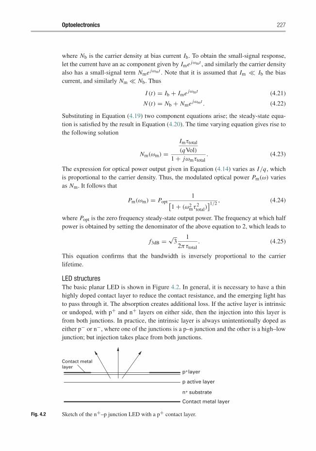
Optoelectronics 227
where Nb is the carrier density at bias current Ib. To obtain the small-signal response,let the current have an ac component given by Ime jωmt , and similarly the carrier densityalso has a small-signal term Nme jωmt . Note that it is assumed that Im � Ib the biascurrent, and similarly Nm � Nb. Thus
I (t) = Ib + Ime jωmt (4.21)
N (t) = Nb + Nme jωmt . (4.22)
Substituting in Equation (4.19) two component equations arise; the steady-state equa-tion is satisfied by the result in Equation (4.20). The time varying equation gives rise tothe following solution
Nm(ωm) =Imτtotal
(qVol)1 + jωmτtotal
. (4.23)
The expression for optical power output given in Equation (4.14) varies as I/q, whichis proportional to the carrier density. Thus, the modulated optical power Pm(ω) variesas Nm. It follows that
Pm(ωm) = Popt1[
1 + (ω2mτ 2
total)]1/2
, (4.24)
where Popt is the zero frequency steady-state output power. The frequency at which halfpower is obtained by setting the denominator of the above equation to 2, which leads to
f3dB = √3
1
2πτtotal. (4.25)
This equation confirms that the bandwidth is inversely proportional to the carrierlifetime.
LED structuresThe basic planar LED is shown in Figure 4.2. In general, it is necessary to have a thinhighly doped contact layer to reduce the contact resistance, and the emerging light hasto pass through it. The absorption creates additional loss. If the active layer is intrinsicor undoped, with p+ and n+ layers on either side, then the injection into this layer isfrom both junctions. In practice, the intrinsic layer is always unintentionally doped aseither p− or n−, where one of the junctions is a p–n junction and the other is a high–lowjunction; but injection takes place from both junctions.
p+layer
p active layer
n+ substrate
Contact metal layer
Contact metallayer
Fig. 4.2 Sketch of the n+–p junction LED with a p+ contact layer.
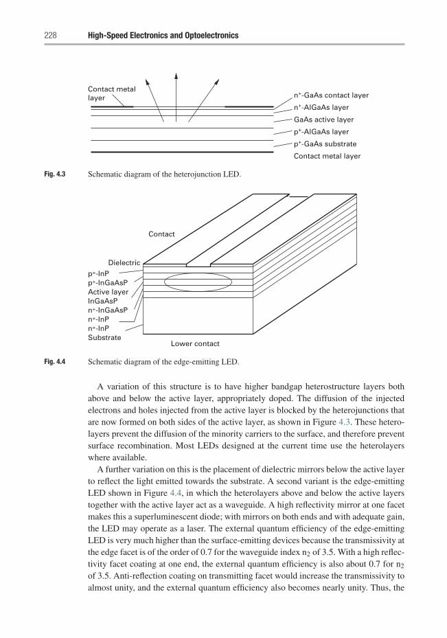
228 High-Speed Electronics and Optoelectronics
Contact metal layer
Contact metallayer n+-GaAs contact layer
n+-AlGaAs layer
GaAs active layer
p+-AlGaAs layer
p+-GaAs substrate
Fig. 4.3 Schematic diagram of the heterojunction LED.
Contact
Dielectricp+-InPp+-InGaAsPActive layerInGaAsPn+-InGaAsPn+-InP n+-InPSubstrate
Lower contact
Fig. 4.4 Schematic diagram of the edge-emitting LED.
A variation of this structure is to have higher bandgap heterostructure layers bothabove and below the active layer, appropriately doped. The diffusion of the injectedelectrons and holes injected from the active layer is blocked by the heterojunctions thatare now formed on both sides of the active layer, as shown in Figure 4.3. These hetero-layers prevent the diffusion of the minority carriers to the surface, and therefore preventsurface recombination. Most LEDs designed at the current time use the heterolayerswhere available.
A further variation on this is the placement of dielectric mirrors below the active layerto reflect the light emitted towards the substrate. A second variant is the edge-emittingLED shown in Figure 4.4, in which the heterolayers above and below the active layerstogether with the active layer act as a waveguide. A high reflectivity mirror at one facetmakes this a superluminescent diode; with mirrors on both ends and with adequate gain,the LED may operate as a laser. The external quantum efficiency of the edge-emittingLED is very much higher than the surface-emitting devices because the transmissivity atthe edge facet is of the order of 0.7 for the waveguide index n2 of 3.5. With a high reflec-tivity facet coating at one end, the external quantum efficiency is also about 0.7 for n2
of 3.5. Anti-reflection coating on transmitting facet would increase the transmissivity toalmost unity, and the external quantum efficiency also becomes nearly unity. Thus, the
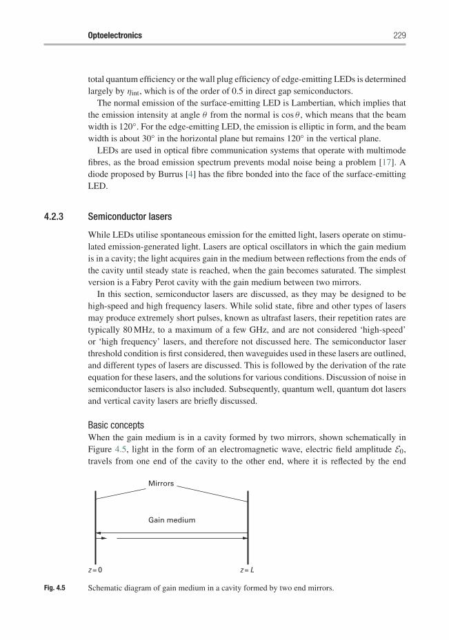
Optoelectronics 229
total quantum efficiency or the wall plug efficiency of edge-emitting LEDs is determinedlargely by ηint, which is of the order of 0.5 in direct gap semiconductors.
The normal emission of the surface-emitting LED is Lambertian, which implies thatthe emission intensity at angle θ from the normal is cos θ , which means that the beamwidth is 120◦. For the edge-emitting LED, the emission is elliptic in form, and the beamwidth is about 30◦ in the horizontal plane but remains 120◦ in the vertical plane.
LEDs are used in optical fibre communication systems that operate with multimodefibres, as the broad emission spectrum prevents modal noise being a problem [17]. Adiode proposed by Burrus [4] has the fibre bonded into the face of the surface-emittingLED.
4.2.3 Semiconductor lasers
While LEDs utilise spontaneous emission for the emitted light, lasers operate on stimu-lated emission-generated light. Lasers are optical oscillators in which the gain mediumis in a cavity; the light acquires gain in the medium between reflections from the ends ofthe cavity until steady state is reached, when the gain becomes saturated. The simplestversion is a Fabry Perot cavity with the gain medium between two mirrors.
In this section, semiconductor lasers are discussed, as they may be designed to behigh-speed and high frequency lasers. While solid state, fibre and other types of lasersmay produce extremely short pulses, known as ultrafast lasers, their repetition rates aretypically 80 MHz, to a maximum of a few GHz, and are not considered ‘high-speed’or ‘high frequency’ lasers, and therefore not discussed here. The semiconductor laserthreshold condition is first considered, then waveguides used in these lasers are outlined,and different types of lasers are discussed. This is followed by the derivation of the rateequation for these lasers, and the solutions for various conditions. Discussion of noise insemiconductor lasers is also included. Subsequently, quantum well, quantum dot lasersand vertical cavity lasers are briefly discussed.
Basic conceptsWhen the gain medium is in a cavity formed by two mirrors, shown schematically inFigure 4.5, light in the form of an electromagnetic wave, electric field amplitude E0,travels from one end of the cavity to the other end, where it is reflected by the end
Gain medium
Mirrors
z = 0 z = L
Fig. 4.5 Schematic diagram of gain medium in a cavity formed by two end mirrors.
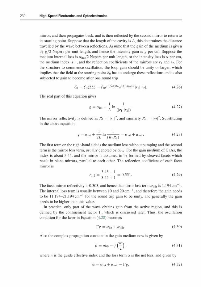
230 High-Speed Electronics and Optoelectronics
mirror, and then propagates back, and is then reflected by the second mirror to return toits starting point. Suppose that the length of the cavity is L , this determines the distancetravelled by the wave between reflections. Assume that the gain of the medium is givenby g/2 Nepers per unit length, and hence the intensity gain is g per cm. Suppose themedium internal loss is αint/2 Nepers per unit length, or the intensity loss is α per cm,the medium index is n, and the reflection coefficients of the mirrors are r1 and r2. Forthe structure to commence oscillation, the loop gain should be unity or larger, whichimplies that the field at the starting point E0 has to undergo these reflections and is alsosubjected to gain to become after one round trip
E0 = E0(2L) = E0e− j2k0nLe(g−αint)L |r1||r2|. (4.26)
The real part of this equation gives
g = αint + 1
Lln
1
(|r1||r2|) . (4.27)
The mirror reflectivity is defined as R1 = |r1|2, and similarly R2 = |r2|2. Substitutingin the above equation,
g = αint + 1
2Lln
1
(R1 R2)= αint + αmir. (4.28)
The first term on the right-hand side is the medium loss without pumping and the secondterm is the mirror loss term, usually denoted by αmir. For the gain medium of GaAs, theindex is about 3.45, and the mirror is assumed to be formed by cleaved facets whichresult in plane mirrors, parallel to each other. The reflection coefficient of each facetmirror is
r1,2 = 3.45 − 1
3.45 + 1= 0.551. (4.29)
The facet mirror reflectivity is 0.303, and hence the mirror loss term αmir is 1.194 cm−1.The internal loss term is usually between 10 and 20 cm−1, and therefore the gain needsto be 11.194–21.194 cm−1 for the round trip gain to be unity, and generally the gainneeds to be higher than this value.
In practice, only part of the wave obtains gain from the active region, and this isdefined by the confinement factor �, which is discussed later. Thus, the oscillationcondition for the laser in Equation (4.28) becomes
�g = αint + αmir. (4.30)
Also the complex propagation constant in the gain medium now is given by
β = nk0 − j(α
2
), (4.31)
where n is the guide effective index and the loss term α is the net loss, and given by
α = αint + αmir − �g. (4.32)
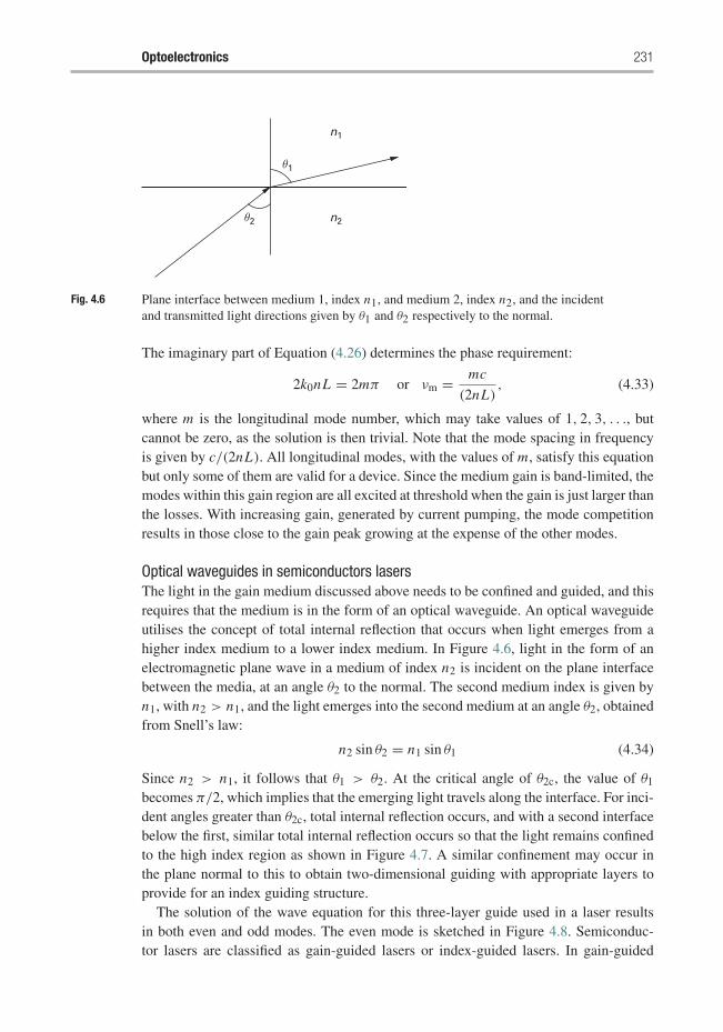
Optoelectronics 231
θ2
θ1
n2
n1
Fig. 4.6 Plane interface between medium 1, index n1, and medium 2, index n2, and the incidentand transmitted light directions given by θ1 and θ2 respectively to the normal.
The imaginary part of Equation (4.26) determines the phase requirement:
2k0nL = 2mπ or νm = mc
(2nL), (4.33)
where m is the longitudinal mode number, which may take values of 1, 2, 3, . . ., butcannot be zero, as the solution is then trivial. Note that the mode spacing in frequencyis given by c/(2nL). All longitudinal modes, with the values of m, satisfy this equationbut only some of them are valid for a device. Since the medium gain is band-limited, themodes within this gain region are all excited at threshold when the gain is just larger thanthe losses. With increasing gain, generated by current pumping, the mode competitionresults in those close to the gain peak growing at the expense of the other modes.
Optical waveguides in semiconductors lasersThe light in the gain medium discussed above needs to be confined and guided, and thisrequires that the medium is in the form of an optical waveguide. An optical waveguideutilises the concept of total internal reflection that occurs when light emerges from ahigher index medium to a lower index medium. In Figure 4.6, light in the form of anelectromagnetic plane wave in a medium of index n2 is incident on the plane interfacebetween the media, at an angle θ2 to the normal. The second medium index is given byn1, with n2 > n1, and the light emerges into the second medium at an angle θ2, obtainedfrom Snell’s law:
n2 sin θ2 = n1 sin θ1 (4.34)
Since n2 > n1, it follows that θ1 > θ2. At the critical angle of θ2c, the value of θ1
becomes π/2, which implies that the emerging light travels along the interface. For inci-dent angles greater than θ2c, total internal reflection occurs, and with a second interfacebelow the first, similar total internal reflection occurs so that the light remains confinedto the high index region as shown in Figure 4.7. A similar confinement may occur inthe plane normal to this to obtain two-dimensional guiding with appropriate layers toprovide for an index guiding structure.
The solution of the wave equation for this three-layer guide used in a laser resultsin both even and odd modes. The even mode is sketched in Figure 4.8. Semiconduc-tor lasers are classified as gain-guided lasers or index-guided lasers. In gain-guided
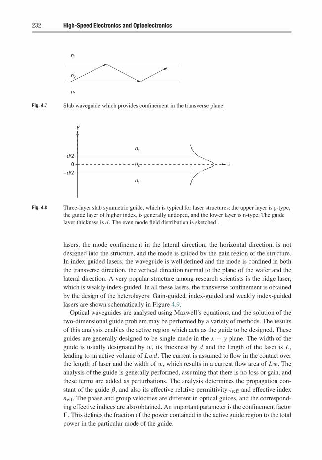
232 High-Speed Electronics and Optoelectronics
n1
n1
n2
Fig. 4.7 Slab waveguide which provides confinement in the transverse plane.
n1
zn2
n1
y
d/2
−d/2
0
Fig. 4.8 Three-layer slab symmetric guide, which is typical for laser structures: the upper layer is p-type,the guide layer of higher index, is generally undoped, and the lower layer is n-type. The guidelayer thickness is d . The even mode field distribution is sketched .
lasers, the mode confinement in the lateral direction, the horizontal direction, is notdesigned into the structure, and the mode is guided by the gain region of the structure.In index-guided lasers, the waveguide is well defined and the mode is confined in boththe transverse direction, the vertical direction normal to the plane of the wafer and thelateral direction. A very popular structure among research scientists is the ridge laser,which is weakly index-guided. In all these lasers, the transverse confinement is obtainedby the design of the heterolayers. Gain-guided, index-guided and weakly index-guidedlasers are shown schematically in Figure 4.9.
Optical waveguides are analysed using Maxwell’s equations, and the solution of thetwo-dimensional guide problem may be performed by a variety of methods. The resultsof this analysis enables the active region which acts as the guide to be designed. Theseguides are generally designed to be single mode in the x − y plane. The width of theguide is usually designated by w, its thickness by d and the length of the laser is L ,leading to an active volume of Lwd . The current is assumed to flow in the contact overthe length of laser and the width of w, which results in a current flow area of Lw. Theanalysis of the guide is generally performed, assuming that there is no loss or gain, andthese terms are added as perturbations. The analysis determines the propagation con-stant of the guide β, and also its effective relative permittivity εreff and effective indexneff. The phase and group velocities are different in optical guides, and the correspond-ing effective indices are also obtained. An important parameter is the confinement factor�. This defines the fraction of the power contained in the active guide region to the totalpower in the particular mode of the guide.
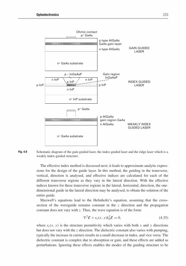
Optoelectronics 233
p InP
Ohmic contactp+ GaAs
p type AlGaAsGaAs gain layer
n type AlGaAs
n+ GaAs substrate
p – InGaAsP
p InP
n InP
n+ InP substrate
p+ GaAs
p AlGaAsgain region GaAsn AlGaAs
n+ GaAs substrate
GAIN GUIDEDLASER
INDEX GUIDEDLASER
WEAKLY INDEXGUIDED LASER
Gain regionInGaAsP
n InPn InP
p InP
Fig. 4.9 Schematic diagram of the gain-guided laser, the index-guided laser and the ridge laser which is aweakly index-guided structure.
The effective index method is discussed next; it leads to approximate analytic expres-sions for the design of the guide layer. In this method, the guiding in the transverse,vertical, direction is analysed, and effective indices are calculated for each of thedifferent transverse regions as they vary in the lateral direction. With the effectiveindices known for these transverse regions in the lateral, horizontal, direction, the one-dimensional guide in the lateral direction may be analysed, to obtain the solution of theentire guide.
Maxwell’s equations lead to the Helmholtz’s equation, assuming that the cross-section of the waveguide remains constant in the z direction and the propagationconstant does not vary with z. Thus, the wave equation is of the form:
∇2E + εr(x, y)k20E = 0, (4.35)
where εr(x, y) is the structure permittivity which varies with both x and y directionsbut does not vary with the z direction. The dielectric constant also varies with pumping,typically the increase in carriers results in a small decrease in index, and vice versa. Thedielectric constant is complex due to absorption or gain, and these effects are added asperturbations. Ignoring these effects enables the modes of the guiding structure to be
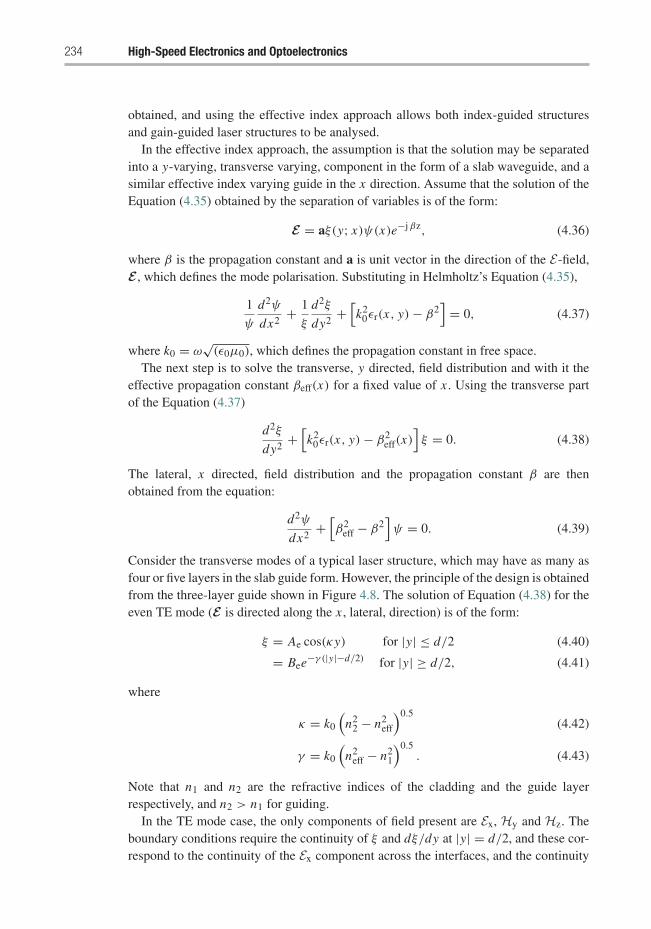
234 High-Speed Electronics and Optoelectronics
obtained, and using the effective index approach allows both index-guided structuresand gain-guided laser structures to be analysed.
In the effective index approach, the assumption is that the solution may be separatedinto a y-varying, transverse varying, component in the form of a slab waveguide, and asimilar effective index varying guide in the x direction. Assume that the solution of theEquation (4.35) obtained by the separation of variables is of the form:
E = aξ(y; x)ψ(x)e−jβz, (4.36)
where β is the propagation constant and a is unit vector in the direction of the E-field,E , which defines the mode polarisation. Substituting in Helmholtz’s Equation (4.35),
1
ψ
d2ψ
dx2+ 1
ξ
d2ξ
dy2+
[k2
0εr(x, y) − β2]
= 0, (4.37)
where k0 = ω√(ε0μ0), which defines the propagation constant in free space.
The next step is to solve the transverse, y directed, field distribution and with it theeffective propagation constant βeff(x) for a fixed value of x . Using the transverse partof the Equation (4.37)
d2ξ
dy2+
[k2
0εr(x, y) − β2eff(x)
]ξ = 0. (4.38)
The lateral, x directed, field distribution and the propagation constant β are thenobtained from the equation:
d2ψ
dx2+
[β2
eff − β2]ψ = 0. (4.39)
Consider the transverse modes of a typical laser structure, which may have as many asfour or five layers in the slab guide form. However, the principle of the design is obtainedfrom the three-layer guide shown in Figure 4.8. The solution of Equation (4.38) for theeven TE mode (E is directed along the x , lateral, direction) is of the form:
ξ = Ae cos(κy) for |y| ≤ d/2 (4.40)
= Bee−γ (|y|−d/2) for |y| ≥ d/2, (4.41)
where
κ = k0
(n2
2 − n2eff
)0.5(4.42)
γ = k0
(n2
eff − n21
)0.5. (4.43)
Note that n1 and n2 are the refractive indices of the cladding and the guide layerrespectively, and n2 > n1 for guiding.
In the TE mode case, the only components of field present are Ex, Hy and Hz. Theboundary conditions require the continuity of ξ and dξ/dy at |y| = d/2, and these cor-respond to the continuity of the Ex component across the interfaces, and the continuity
Optoelectronics 235
of the Hz component across the interfaces, respectively. This leads to the following twoequations:
Ae cos
(κd
2
)= Be (4.44)
and
κAe sin
(κd
2
)= γ Be. (4.45)
Dividing the above two equations,
κ tan
(κd
2
)= γ. (4.46)
The solution of this equation gives the values of βeff from which the effective index isobtained through the relationship βeff = k0neff.
For the odd TE modes, it may be shown that the dispersion relationship becomes
− κ cot
(κd
2
)= γ. (4.47)
This is obtained by setting the initial solution for ξ in Equation (4.40) as sin(κy) insteadof cos(κy).
For the TM modes, the E vector is along the y direction, normal to the interfacesin Figure 4.8. In this case, the only components of fields present are Ey, Hx and Ez.From the Maxwell curl equations, Ez is proportional to dEy/dy. Thus, the boundaryconditions are the continuity of the y component of electric flux across the interfacesand the continuity of Ez across the interfaces. These lead to the following equations forthe even TM modes:
n22 Ae cos
(κd
2
)= n2
1 Be (4.48)
and
κAe sin
(κd
2
)= γ Be. (4.49)
Dividing the above two equations gives the dispersion relationship:
κn21 tan
(κd
2
)= n2
2γ. (4.50)
For the odd TM mode, the dispersion relationship is given by
− κn21 cot
(κd
2
)= n2
1γ. (4.51)
Consider the TE mode solutions, squaring Equations (4.42) and (4.43), and addingresults in
κ2 + γ 2 = k20
(n2
2 − n21
). (4.52)
This is the equation of a circle in the κ−γ plane, and the intersection of the circle withthe curves defined by the Equations (4.46) and (4.47) provides the modal solutions for
236 High-Speed Electronics and Optoelectronics
these equations. Note that multiple solutions are likely to occur as both tan and cot areperiodic functions, and also depending on the parameters of the guide, defined by n1,n2, d and the wavelength which defines k0.
At the cutoff of the guide which implies that the guide is no longer guiding, thenγ = 0. Note that γ may not become negative, as it would imply exponential growthin the cladding region which is non-physical, and therefore the smallest value γ takeszero. When γ = 0, then from Equations (4.46) and (4.47)
κd = pπ, (4.53)
where p is an integer whose even and odd values satisfy Equations (4.46) and (4.47)respectively, corresponding to the even and odd modes. Now let
D = pπ = κd. (4.54)
Now for γ = 0, Equation (4.52) becomes
D = k0
(n2
2 − n21
)0.5d, (4.55)
where D is the normalized guide layer thickness. For a single transverse TE modeguide, this requires D < π . The layer thickness d for a single transverse mode guide isobtained as follows. Setting k0 = 2π/λ in the above Equations gives
d <λ
2
(n2
2 − n21
)−0.5. (4.56)
For GaAs/AlGaAs at 870 nm wavelength, with indices of 3.45 and 3.41, this suggeststhe guide thickness of less than 830 nm. The usual thickness is of the order of 0.2–0.5 μm. If the AlGaAs layer has a higher value of index, closer to that of GaAs, then thethickness of this layer may be larger. For InGaAsP lasers [2], the layer thickness is alsoof the order of 0.2 μm, and in this case the layer thickness needs to be less than 0.48 μm.According to [2], this relationship holds for lasers in the wavelength range 1.1–1.65 μm.The confinement factor in the transverse direction �T is a measure of how much of themode power lies in the guide active region, and is calculated from the equation:
�T =∫ d/2−d/2 ξ
2(y)dy∫ ∞−∞ ξ2(y)dy
. (4.57)
Performing the integration and simplifying, [2] derives this as
�T ∼= D2
(2 + D2). (4.58)
The effective index of the guide in the transverse direction is given as [2]:
n2eff
∼= n21 + �T
(n2
2 − n21
). (4.59)
The lateral modes are next evaluated. The loss of laser structures may be as high as5–10 Np cm−1, and therefore in principle these losses need to be taken into account.However, when pumped, the gain which is typically of the order of 50 Np cm−1 andlarger, allows the guide to become transparent, which implies that the loss is cancelled
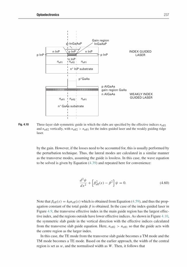
Optoelectronics 237
p InP
p–InGaAsP
p InP n InPn InP
n InP
n+ InP substrate
p+GaAs
p AlGaAsgain region GaAsn AlGaAs
n+ GaAs substrate
INDEX GUIDEDLASER
WEAKLY INDEXGUIDED LASER
neff1 neff1neff2
neff2 neff1neff1
Gain regionInGaAsP
p InP
Fig. 4.10 Three-layer slab symmetric guide in which the slabs are specified by the effective indices neff1and neff2 vertically, with neff2 > neff1 for the index-guided laser and the weakly guiding ridgelaser.
by the gain. However, if the losses need to be accounted for, this is usually performed bythe perturbation technique. Thus, the lateral modes are calculated in a similar manneras the transverse modes, assuming the guide is lossless. In this case, the wave equationto be solved is given by Equation (4.39) and repeated here for convenience:
d2ψ
dx2+
[β2
eff(x) − β2]ψ = 0. (4.60)
Note that βeff(x) = k0neff(x) which is obtained from Equation (4.59), and thus the prop-agation constant of the total guide β is obtained. In the case of the index-guided laser inFigure 4.9, the transverse effective index in the main guide region has the largest effec-tive index, and the regions outside have lower effective indices. As shown in Figure 4.10,the symmetric slab guide in the vertical direction with the effective indices calculatedfrom the transverse slab guide equation. Here, neff2 > neff1 so that the guide acts withthe centre region as the larger index.
In this case, the TE mode from the transverse slab guide becomes a TM mode and theTM mode becomes a TE mode. Based on the earlier approach, the width of the centralregion is set as w, and the normalised width as W . Then, it follows that
238 High-Speed Electronics and Optoelectronics
W = k0
(n2
eff2 − n2eff1
)0.5w (4.61)
and
W = qπ. (4.62)
For the lowest order mode
w <λ
2
(n2
eff2 − n2eff1
)−0.5. (4.63)
In this case, the effective indices take different values, but this provides an indication tothe width of the guide which usually is in the 3 μm region.
The lateral confinement factor �L, following the earlier derivation, is given by
�L = W 2(2 + W 2
) . (4.64)
The waveguide mode refractive index is now given by
n2eff
∼= n2eff1 + �L(n
2eff2 − n2
eff1). (4.65)
The laser confinement factor � is the product of �T and �L and is given by
� = �T�L. (4.66)
The two most important parameters that are obtained from this analysis are the effec-tive index of the guide and the confinement factor. From the effective index, the guidepropagation constant may be obtained.
These results are for the index-guided structures, and the same technique may beused for the weakly guiding ridge structure in Figure 4.9. The analysis of the gain-guided laser is much more complex, and interested readers are referred to the paper byNash [24].
Emission characteristicsThe waveguide which guides the light has facet mirrors on both sides of the device.These may be coated to obtain high reflectivity or to reduce the reflectivity as desired,but generally these facets are uncoated, in which case the reflectivities are equal.
With current pumping, the light intensity against input current is plotted in the L–Icharacteristic as shown schematically in Figure 4.11. Note the different regions of thiscurve: the pre-threshold where the laser output is from spontaneous emission, the thresh-old current at which the device starts to lase, which is the linear region, followed by thesaturation region due to gain saturation. The current into the laser is of the form:
I = wL J, (4.67)
where w is the width of the active region and L is the cavity length. In practice, index-guided lasers in Figure 4.9 have leakage current through the various reverse-biasedjunctions, and should be added to this current expression, but this is ignored in thepresent discussion.
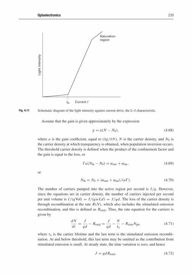
Optoelectronics 239
Lig
ht
inte
nsi
ty
Current IIth
Saturationregion
Fig. 4.11 Schematic diagram of the light intensity against current drive, the L–I characteristic.
Assume that the gain is given approximately by the expression
g = a(N − N0), (4.68)
where a is the gain coefficient, equal to (∂g/∂N ), N is the carrier density, and N0 isthe carrier density at which transparency is obtained, when population inversion occurs.The threshold carrier density is defined when the product of the confinement factor andthe gain is equal to the loss, or
�a(Nth − N0) = αmir + αint, (4.69)
or
Nth = N0 + (αmir + αint)/(a�). (4.70)
The number of carriers pumped into the active region per second is I/q. However,since the equations are in carrier density, the number of carriers injected per secondper unit volume is I/(qVol) = I/(qwLd) = J/qd. The loss of the carrier density isthrough recombination at the rate R(N ), which also includes the stimulated emissionrecombination, and this is defined as Rtotal. Thus, the rate equation for the carriers isgiven by
d N
dt= J
qd− Rtotal = J
qd− N
τe− Rstim Nph, (4.71)
where τe is the carrier lifetime and the last term is the stimulated emission recombi-nation. At and below threshold, this last term may be omitted as the contribution fromstimulated emission is small. At steady state, the time variation is zero, and hence
J = qd Rtotal. (4.72)
240 High-Speed Electronics and Optoelectronics
The stimulated emission recombination rate is Rstim Nph, where Nph is the photondensity and Rstim is defined by
Rstim = c
ng(N ), (4.73)
where g(N ) is the gain defined in Equation (4.68), c/n is the group velocity.From Equations (4.70) and (4.71), the threshold current density is obtained as
Jth = qd Nth
τe(Nth), (4.74)
where, neglecting stimulated emission recombination close to threshold,
1
τe(N )= (Anr + Br N + C N 2), (4.75)
where Anr is non-radiative recombination coefficient, Br is the radiative recombina-tion coefficient and C is the Auger non-radiative recombination coefficient, which isimportant for long wavelength lasers.
When the laser operates beyond threshold, the carrier density is clamped at thethreshold value, and further injection results in conversion into photons by stimulatedemission. Thus, Equation (4.72) may be written as
J = qd Rtotal = qdNth
τe+ qd Rstim Nph. (4.76)
Substituting from Equation (4.73), and replacing g by αint + αmir at threshold,
J − Jth = qdvg(αint + αmir)Nph. (4.77)
The photon density in the cavity depends on the carriers injected into the cavity and thequantum efficiency of the material. However, the photons in the cavity travel at the groupvelocity of the medium vg, and are either absorbed due to internal losses or escape fromthe facets. Thus, the photons have a finite lifetime in the cavity, and the photon lifetimeτp is given by
τp = 1
vg(αmir + αint). (4.78)
The Equation (4.77) becomes
J − Jth = qdNph
τp(4.79)
The relationship between the injected carrier density per second and the photon densityin the cavity is now obtained. The carriers recombine at a rate defined by the carrierlifetime, to produce photons, and this is accounted for by the quantum efficiency of thematerial from Equation (4.3), and the photon density also decays at the photon lifetime.Thus,
ηint(J − Jth)
qd= Nph
τp(4.80)
Optoelectronics 241
or
Nph = ηintτp(J − Jth)
qd. (4.81)
This equation shows that the photon density in the cavity increases linearly with currentdensity above the threshold current density.
The output power per facet is obtained by the product of energy of each photon hν, thephoton loss per facet vgαmir/2, the active laser volume Vol and the photon density Nph:
Pfacet = 1
2hνvgαmirVolNph, (4.82)
where Vol = Lwd . Substituting for Nph
Pfacet = hν
2qηint
αmir
αmir + αintLw(J − Jth). (4.83)
Since I = LwJ , this equation becomes
Pfacet = hν
2qηint
αmir
αmir + αint(I − Ith). (4.84)
Note that the threshold current is obtained from Equation (4.74)
Ith = q Lwd Nth
τe. (4.85)
The total output power Pout = 2Pfacet and the differential (external) quantum efficiencyis given by
ηd =d
(Pout
hν
)d(I − Ith)
q
= ηintαmir
αmir + αint. (4.86)
This is proportional to the slope of the L–I curve. Note that in the laser the ηint needsto take into account the stimulated emission rate. Then, the total recombination ratebecomes
Rtotal = Anr N + Br N 2 + C N 3 + Rstim Nph. (4.87)
The coefficients have been identified in Equation (4.75) except for Rstim, which isthe stimulated emission rate and given in equation (4.73) Thus, the internal quantumefficiency now is given by
ηint = Rrad
Rtotal= Br N 2 + Rstim Nph
Anr N + Br N 2 + C N 3 + Rstim Nph(4.88)
Above threshold, the Rstim Nph dominates and is much larger than the other terms, whichmakes ηint almost unity.
The power efficiency of the laser is given by
ηP = Pout
V I= hν
qV
αmir
(αmir + αint)
(I − Ith)
I, (4.89)
where V is the applied bias in volts.
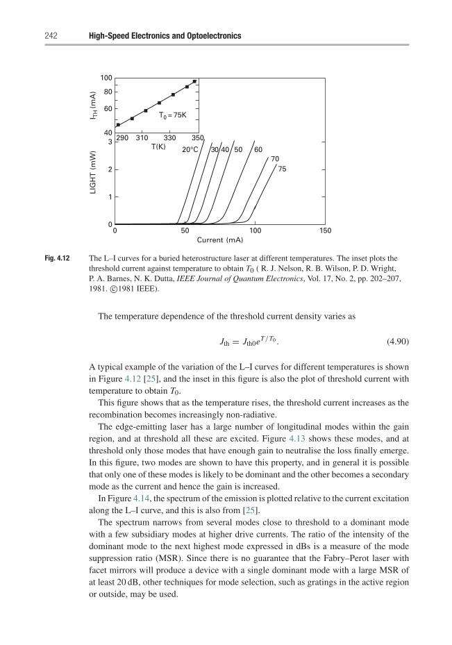
242 High-Speed Electronics and Optoelectronics
5000
1
2
340
60
80
100
T0 = 75K
T(K)290 310 330 350
20°C 30 40 50 6070
75
100Current (mA)
LIG
HT
(m
W)
I TH
(mA
)
150
Fig. 4.12 The L–I curves for a buried heterostructure laser at different temperatures. The inset plots thethreshold current against temperature to obtain T0 ( R. J. Nelson, R. B. Wilson, P. D. Wright,P. A. Barnes, N. K. Dutta, IEEE Journal of Quantum Electronics, Vol. 17, No. 2, pp. 202–207,1981. c©1981 IEEE).
The temperature dependence of the threshold current density varies as
Jth = Jth0eT/T0 . (4.90)
A typical example of the variation of the L–I curves for different temperatures is shownin Figure 4.12 [25], and the inset in this figure is also the plot of threshold current withtemperature to obtain T0.
This figure shows that as the temperature rises, the threshold current increases as therecombination becomes increasingly non-radiative.
The edge-emitting laser has a large number of longitudinal modes within the gainregion, and at threshold all these are excited. Figure 4.13 shows these modes, and atthreshold only those modes that have enough gain to neutralise the loss finally emerge.In this figure, two modes are shown to have this property, and in general it is possiblethat only one of these modes is likely to be dominant and the other becomes a secondarymode as the current and hence the gain is increased.
In Figure 4.14, the spectrum of the emission is plotted relative to the current excitationalong the L–I curve, and this is also from [25].
The spectrum narrows from several modes close to threshold to a dominant modewith a few subsidiary modes at higher drive currents. The ratio of the intensity of thedominant mode to the next highest mode expressed in dBs is a measure of the modesuppression ratio (MSR). Since there is no guarantee that the Fabry–Perot laser withfacet mirrors will produce a device with a single dominant mode with a large MSR ofat least 20 dB, other techniques for mode selection, such as gratings in the active regionor outside, may be used.
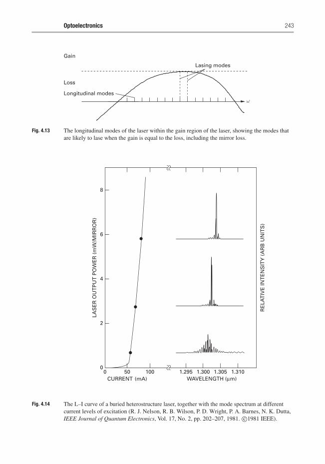
Optoelectronics 243
Loss
Gain
Longitudinal modes
Lasing modes
ω
Fig. 4.13 The longitudinal modes of the laser within the gain region of the laser, showing the modes thatare likely to lase when the gain is equal to the loss, including the mirror loss.
00
2
4
6
8
50 100
RE
LAT
IVE
INT
EN
SIT
Y (
AR
B U
NIT
S)
LAS
ER
OU
TP
UT
PO
WE
R (
mW
/MIR
RO
R)
1.295 1.300 1.305 1.310CURRENT (mA) WAVELENGTH (μm)
Fig. 4.14 The L–I curve of a buried heterostructure laser, together with the mode spectrum at differentcurrent levels of excitation (R. J. Nelson, R. B. Wilson, P. D. Wright, P. A. Barnes, N. K. Dutta,IEEE Journal of Quantum Electronics, Vol. 17, No. 2, pp. 202–207, 1981. c©1981 IEEE).
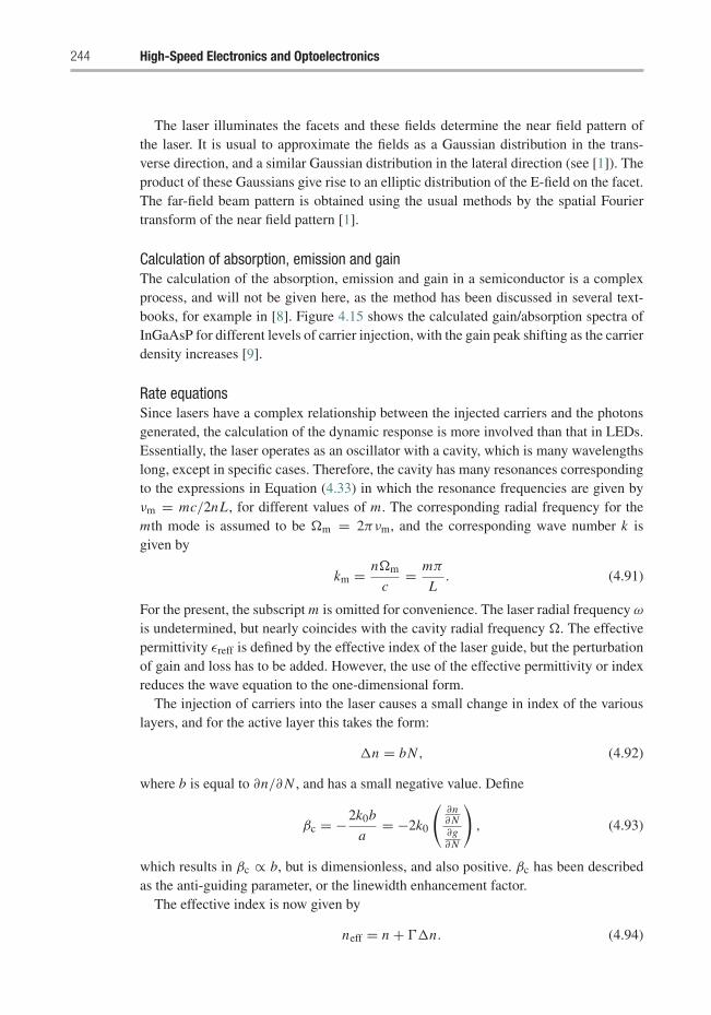
244 High-Speed Electronics and Optoelectronics
The laser illuminates the facets and these fields determine the near field pattern ofthe laser. It is usual to approximate the fields as a Gaussian distribution in the trans-verse direction, and a similar Gaussian distribution in the lateral direction (see [1]). Theproduct of these Gaussians give rise to an elliptic distribution of the E-field on the facet.The far-field beam pattern is obtained using the usual methods by the spatial Fouriertransform of the near field pattern [1].
Calculation of absorption, emission and gainThe calculation of the absorption, emission and gain in a semiconductor is a complexprocess, and will not be given here, as the method has been discussed in several text-books, for example in [8]. Figure 4.15 shows the calculated gain/absorption spectra ofInGaAsP for different levels of carrier injection, with the gain peak shifting as the carrierdensity increases [9].
Rate equationsSince lasers have a complex relationship between the injected carriers and the photonsgenerated, the calculation of the dynamic response is more involved than that in LEDs.Essentially, the laser operates as an oscillator with a cavity, which is many wavelengthslong, except in specific cases. Therefore, the cavity has many resonances correspondingto the expressions in Equation (4.33) in which the resonance frequencies are given byνm = mc/2nL , for different values of m. The corresponding radial frequency for themth mode is assumed to be �m = 2πνm, and the corresponding wave number k isgiven by
km = n�m
c= mπ
L. (4.91)
For the present, the subscript m is omitted for convenience. The laser radial frequency ω
is undetermined, but nearly coincides with the cavity radial frequency �. The effectivepermittivity εreff is defined by the effective index of the laser guide, but the perturbationof gain and loss has to be added. However, the use of the effective permittivity or indexreduces the wave equation to the one-dimensional form.
The injection of carriers into the laser causes a small change in index of the variouslayers, and for the active layer this takes the form:
�n = bN , (4.92)
where b is equal to ∂n/∂N , and has a small negative value. Define
βc = −2k0b
a= −2k0
(∂n∂N∂g∂N
), (4.93)
which results in βc ∝ b, but is dimensionless, and also positive. βc has been describedas the anti-guiding parameter, or the linewidth enhancement factor.
The effective index is now given by
neff = n + ��n. (4.94)
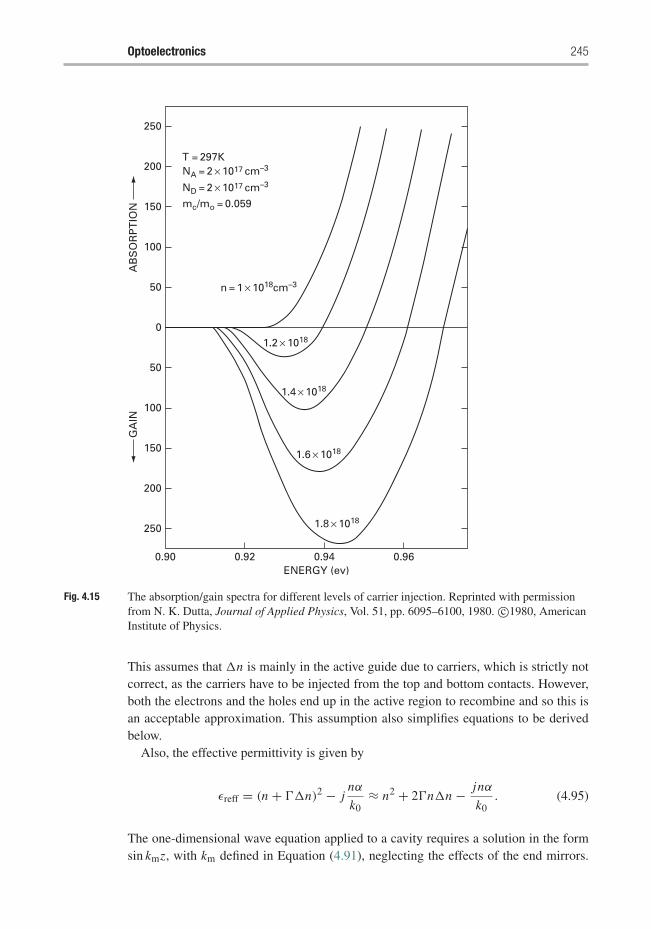
Optoelectronics 245
0.90
250
200
150
100
50
50
100
150
200
250
0
0.92 0.94
1.8 × 10¹⁸
1.6 × 10¹⁸
1.4 × 10¹⁸
1.2 × 10¹⁸
n = 1 × 1018cm–3
mc/mo = 0.059
NA = 2 × 1017 cm–3
ND = 2 × 1017 cm–3
T = 297K
0.96ENERGY (ev)
AB
SO
RP
TIO
NG
AIN
Fig. 4.15 The absorption/gain spectra for different levels of carrier injection. Reprinted with permissionfrom N. K. Dutta, Journal of Applied Physics, Vol. 51, pp. 6095–6100, 1980. c©1980, AmericanInstitute of Physics.
This assumes that �n is mainly in the active guide due to carriers, which is strictly notcorrect, as the carriers have to be injected from the top and bottom contacts. However,both the electrons and the holes end up in the active region to recombine and so this isan acceptable approximation. This assumption also simplifies equations to be derivedbelow.
Also, the effective permittivity is given by
εreff = (n + ��n)2 − jnα
k0≈ n2 + 2�n�n − jnα
k0. (4.95)
The one-dimensional wave equation applied to a cavity requires a solution in the formsin kmz, with km defined in Equation (4.91), neglecting the effects of the end mirrors.
246 High-Speed Electronics and Optoelectronics
The electric field wave equation for the cavity is
d2Edz2
− εreff
c2
d2Edt2
= 0, (4.96)
and the solution is of the form:
E(z, t) =∑
i
sin(k j z)A(t)e jωt , (4.97)
where A(t) is assumed to be slowly varying in time compared to the light wave fre-quency. Assuming this is a single longitudinal mode laser, the summation and thesubscripts i and j are dropped. Substituting this in the wave Equation (4.96) andneglecting the second time derivative of A
− k2A + ω2
c2εreffA − 2 jω
c2εreff
dAdt
= 0. (4.98)
Simplifying with k2 � �2n2/c2:(ω2
c2εreff − �2n2
c2
)A − 2 jω
c2n2 dA
dt= 0. (4.99)
However, since the laser frequency ω is very close to the cavity frequency �, then(ω2 − �2) ≈ 2ω(ω − �). With further simplifications, substituting for εreff fromEquation (4.95), this equation becomes
dAdt
= − jn
ng(ω − �)A − jω
ng
(��n − j
α
2k0
)A, (4.100)
where ng is the group index.Separate this equation into its real and imaginary parts by substituting
A = Ae jφ (4.101)
into (4.100) to obtain for the real and imaginary parts:
d A
dt= − α
2k0A = 1
2vg(�g − αmir − αint)A (4.102)
anddφ
dt= −(ω − �) − ω
ng��n. (4.103)
The rate equations may be written in terms of the photon density Nph and carrier densityN , or in terms of total number of photons and total number of carriers in the laser activevolume, and both these approaches have been used in the literature. In the followingderivations, the total number of photons and carriers in the laser volume are used. Thetotal number of photons in the cavity is obtained from the equation:
S = ε0n2
hν
∫Vol E2dV, (4.104)
and since A2 ∝ S, then multiplying Equation (4.102) by A, this equation becomes
d S
dt= (G − γp)S + Rsp, (4.105)
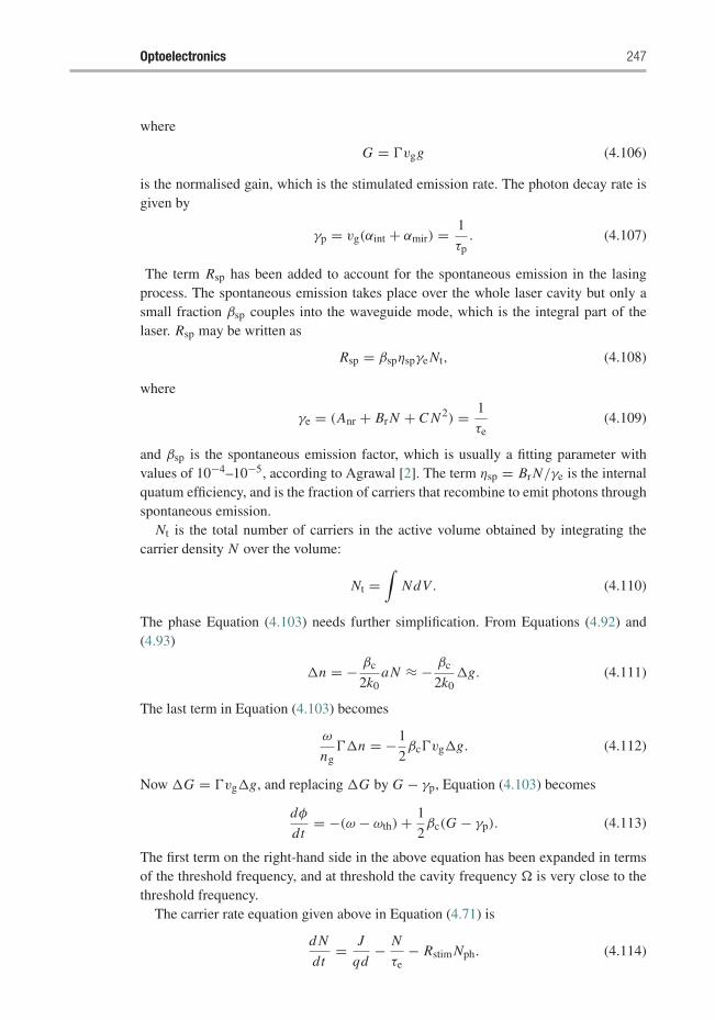
Optoelectronics 247
where
G = �vgg (4.106)
is the normalised gain, which is the stimulated emission rate. The photon decay rate isgiven by
γp = vg(αint + αmir) = 1
τp. (4.107)
The term Rsp has been added to account for the spontaneous emission in the lasingprocess. The spontaneous emission takes place over the whole laser cavity but only asmall fraction βsp couples into the waveguide mode, which is the integral part of thelaser. Rsp may be written as
Rsp = βspηspγe Nt, (4.108)
where
γe = (Anr + Br N + C N 2) = 1
τe(4.109)
and βsp is the spontaneous emission factor, which is usually a fitting parameter withvalues of 10−4–10−5, according to Agrawal [2]. The term ηsp = Br N/γe is the internalquatum efficiency, and is the fraction of carriers that recombine to emit photons throughspontaneous emission.
Nt is the total number of carriers in the active volume obtained by integrating thecarrier density N over the volume:
Nt =∫
NdV . (4.110)
The phase Equation (4.103) needs further simplification. From Equations (4.92) and(4.93)
�n = − βc
2k0aN ≈ − βc
2k0�g. (4.111)
The last term in Equation (4.103) becomes
ω
ng��n = −1
2βc�vg�g. (4.112)
Now �G = �vg�g, and replacing �G by G − γp, Equation (4.103) becomes
dφ
dt= −(ω − ωth) + 1
2βc(G − γp). (4.113)
The first term on the right-hand side in the above equation has been expanded in termsof the threshold frequency, and at threshold the cavity frequency � is very close to thethreshold frequency.
The carrier rate equation given above in Equation (4.71) is
d N
dt= J
qd− N
τe− Rstim Nph. (4.114)
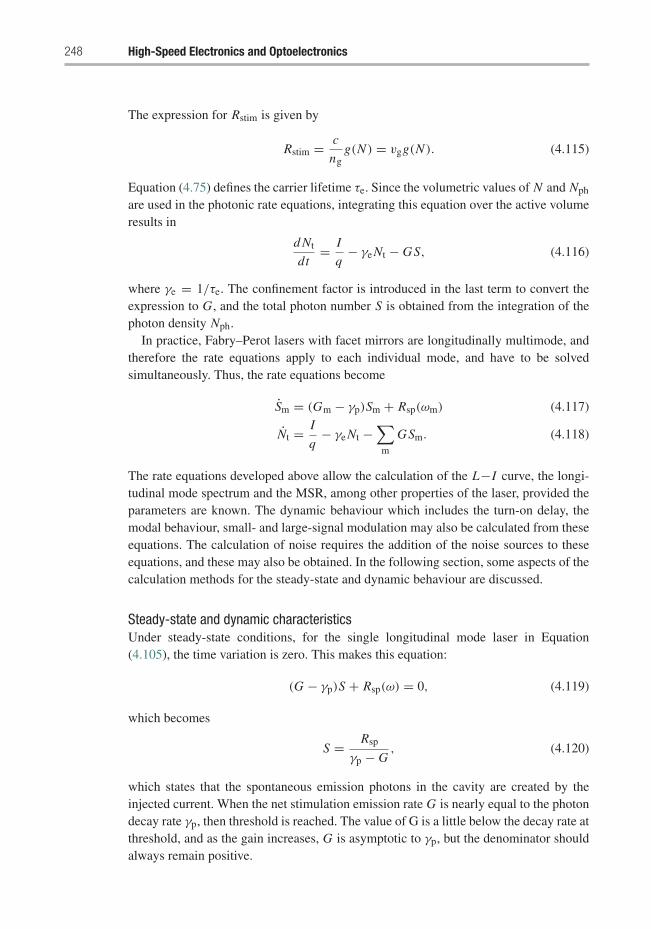
248 High-Speed Electronics and Optoelectronics
The expression for Rstim is given by
Rstim = c
ngg(N ) = vgg(N ). (4.115)
Equation (4.75) defines the carrier lifetime τe. Since the volumetric values of N and Nph
are used in the photonic rate equations, integrating this equation over the active volumeresults in
d Nt
dt= I
q− γe Nt − GS, (4.116)
where γe = 1/τe. The confinement factor is introduced in the last term to convert theexpression to G, and the total photon number S is obtained from the integration of thephoton density Nph.
In practice, Fabry–Perot lasers with facet mirrors are longitudinally multimode, andtherefore the rate equations apply to each individual mode, and have to be solvedsimultaneously. Thus, the rate equations become
Sm = (Gm − γp)Sm + Rsp(ωm) (4.117)
Nt = I
q− γe Nt −
∑m
GSm. (4.118)
The rate equations developed above allow the calculation of the L−I curve, the longi-tudinal mode spectrum and the MSR, among other properties of the laser, provided theparameters are known. The dynamic behaviour which includes the turn-on delay, themodal behaviour, small- and large-signal modulation may also be calculated from theseequations. The calculation of noise requires the addition of the noise sources to theseequations, and these may also be obtained. In the following section, some aspects of thecalculation methods for the steady-state and dynamic behaviour are discussed.
Steady-state and dynamic characteristicsUnder steady-state conditions, for the single longitudinal mode laser in Equation(4.105), the time variation is zero. This makes this equation:
(G − γp)S + Rsp(ω) = 0, (4.119)
which becomes
S = Rsp
γp − G, (4.120)
which states that the spontaneous emission photons in the cavity are created by theinjected current. When the net stimulation emission rate G is nearly equal to the photondecay rate γp, then threshold is reached. The value of G is a little below the decay rate atthreshold, and as the gain increases, G is asymptotic to γp, but the denominator shouldalways remain positive.
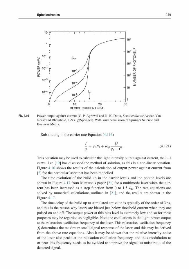
Optoelectronics 249
10DEVICE CURRENT (mA)
PO
WE
R (
mW
)
NU
MB
ER
OF
PH
OT
ON
S, P
20 300
10–4
10–4
10–5Ith
1
10
102
103
104
105
10–3
10–3
βsp
10–2
10–1
1
10
Fig. 4.16 Power output against current (G. P. Agrawal and N. K. Dutta, Semiconductor Lasers, VanNorstrand Rheinhold, 1993. c©Springer). With kind permission of Springer Science andBusiness Media.
Substituting in the carrier rate Equation (4.116)
I
q= γe Nt + Rsp
G
γp − G. (4.121)
This equation may be used to calculate the light intensity output against current, the L–Icurve. Lee [19] has discussed the method of solution, as this is a non-linear equation.Figure 4.16 shows the results of the calculation of output power against current from[2] for the particular laser that has been modelled.
The time evolution of the build up in the carrier levels and the photon levels areshown in Figure 4.17 from Marcuse’s paper [21] for a multimode laser when the cur-rent has been increased as a step function from 0 to 1.5 Ith. The rate equations aresolved by numerical calculations outlined in [21], and the results are shown in theFigure 4.17.
The time delay of the build up to stimulated emission is typically of the order of 3 ns,and this is the reason why lasers are biased just below threshold current when they arepulsed on and off. The output power at this bias level is extremely low and so for mostpurposes may be regarded as negligible. Note the oscillations in the light power outputat the relaxation oscillation frequency of the laser. This relaxation oscillation frequencyfr determines the maximum small-signal response of the laser, and this may be derivedfrom the above rate equations. Also it may be shown that the relative intensity noiseof the laser also peaks at the relaxation oscillation frequency, and thus modulation ator near this frequency needs to be avoided to improve the signal-to-noise ratio of thedetected signal.
250 High-Speed Electronics and Optoelectronics
0
0.2
0.4
0.6
0.8
1.0 L = 250 μm ne(t)
s0(t)
s±2(t) s±3(t)
s±1(t)
2 4t (nsec)
RE
LAT
IVE
UN
ITS
6 8 10
Fig. 4.17 Transient response for a laser in which the current is increased as a step function from 0 to1.5 Ith, showing the carrier density and power in the fundamental mode and other modes(D. Marcuse, T. P. Lee, IEEE Journal of Quantum Electronics Vol. QE-19, No. 9,pp. 1397–1406, 1983. c©1983 IEEE).
This figure shows that the oscillations are damped and in the form of e−(�r±j�r)t ,where �r is the decay rate and �r is the frequency of oscillation, which is the radialrelaxation oscillation frequency in radians s−1.
To calculate the relaxation oscillation frequency, the rate Equations (4.105) and(4.116), repeated here for convenience, are used.
S = (G − γp)S + Rsp (4.122)
Nt = I
q− γe Nt − GS. (4.123)
Consider perturbations to S and Nt given by δS and δNt. Additionally,
G(Nt, S) ∼= G + G NtδNt + GSδS, (4.124)
where G Nt = ∂G/∂Nt and GS = ∂G/∂S. Substituting in the rate equations, separatingthe perturbed terms, results in
δ S = −�SδS +(
G Nt S + ∂Rsp
∂Nt
)δNt (4.125)
δ Nt = �NtδNt − (G + GSS)δS, (4.126)
where
�S = Rsp
S− GSS, (4.127)
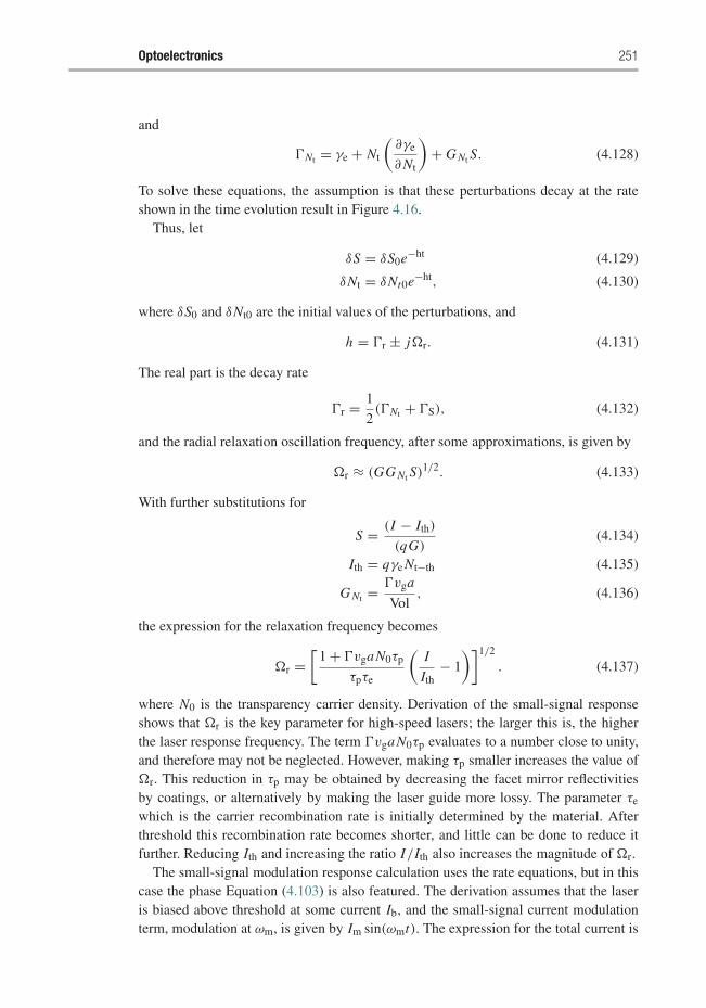
Optoelectronics 251
and
�Nt = γe + Nt
(∂γe
∂Nt
)+ G Nt S. (4.128)
To solve these equations, the assumption is that these perturbations decay at the rateshown in the time evolution result in Figure 4.16.
Thus, let
δS = δS0e−ht (4.129)
δNt = δNt0e−ht, (4.130)
where δS0 and δNt0 are the initial values of the perturbations, and
h = �r ± j�r. (4.131)
The real part is the decay rate
�r = 1
2(�Nt + �S), (4.132)
and the radial relaxation oscillation frequency, after some approximations, is given by
�r ≈ (GG Nt S)1/2. (4.133)
With further substitutions for
S = (I − Ith)
(qG)(4.134)
Ith = qγe Nt−th (4.135)
G Nt = �vga
Vol, (4.136)
the expression for the relaxation frequency becomes
�r =[
1 + �vgaN0τp
τpτe
(I
Ith− 1
)]1/2
. (4.137)
where N0 is the transparency carrier density. Derivation of the small-signal responseshows that �r is the key parameter for high-speed lasers; the larger this is, the higherthe laser response frequency. The term �vgaN0τp evaluates to a number close to unity,and therefore may not be neglected. However, making τp smaller increases the value of�r. This reduction in τp may be obtained by decreasing the facet mirror reflectivitiesby coatings, or alternatively by making the laser guide more lossy. The parameter τe
which is the carrier recombination rate is initially determined by the material. Afterthreshold this recombination rate becomes shorter, and little can be done to reduce itfurther. Reducing Ith and increasing the ratio I/Ith also increases the magnitude of �r.
The small-signal modulation response calculation uses the rate equations, but in thiscase the phase Equation (4.103) is also featured. The derivation assumes that the laseris biased above threshold at some current Ib, and the small-signal current modulationterm, modulation at ωm, is given by Im sin(ωmt). The expression for the total current is
252 High-Speed Electronics and Optoelectronics
I (t) = Ib + Im sin(ωmt), (4.138)
with the assumption that Im � (Ib − Ith), which implies small-signal modulation.The total cavity photons may be written as
S(t) = Sb + Sm sin(ωmt + θm), (4.139)
where Sb is the cavity photons at the bias current of Ib and the second term is thesinusoidal time varying component, with a phase term which usually lags the currentcomponent. The carriers in the cavity have a similar expression given by
Nt(t) = Nt−b + Nt−m sin(ωmt + ξm), (4.140)
with the phase delay ξm, which differs from the photon number delay.Substituting in the rate equations, the solutions for the various small-signal terms
may be obtained. The small-signal photons in the cavity, which is also a measure of theoutput power, may be shown to be
Sm = GNt SIm/q
[(ω2m − �2
r − �2r )
2 + 4ω2m�2
r ]0.5, (4.141)
and the phase lag term for the photons is given by
θm = tan−1(
2�rωm
ω2m − �2
r − �2r
). (4.142)
The modulated cavity photons or equivalently the modulated output light power isalmost constant when ωm � �r, then peaks to a maximum near �r, and falls off forωm > �r. Note that the laser is a forward-biased p–i–n diode, and therefore additionalseries resistance due to contact resistance and parasitic inductance and capacitance fromthe bond wire and pads results in further degradation of the response. This is shown[33] in Figure 4.18. It may be shown that the 3 dB bandwidth is given by [1], assuming�r � �r:
f3dB =√
3�r
2π. (4.143)
When the laser current is modulated, the increase and decrease in the current result inthe laser effective index varying inversely as the current according to Equation (4.92).Thus, the longitudinal mode cavity changes its electrical length since the index changeswith current injection. As the modulation takes place the frequency of emission ofthe laser keeps changing in synchronism with this modulation. Using the phase rateequation, it may be shown that the change in frequency results in a frequency chirpgiven by [1]:
δν(t) = 1
2π
dφ
dt= βc
4π
[G Nt(Nt − Nt−0) − 1
τp
], (4.144)
where βc is the linewidth broadening factor of Equation (4.93) and
Nt−0 =∫
N0dV . (4.145)
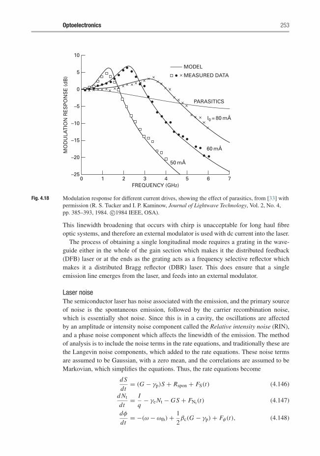
Optoelectronics 253
0–25
–20
–15
–10
MO
DU
LAT
ION
RE
SP
ON
SE
(d
B)
–5
0
5
10
1 2 3FREQUENCY (GHz)
50 mÅ
60 mÅ
I0 = 80 mÅ
PARASITICS
MODEL
MEASURED DATA
4 5 6 7
Fig. 4.18 Modulation response for different current drives, showing the effect of parasitics, from [33] withpermission (R. S. Tucker and I. P. Kaminow, Journal of Lightwave Technology, Vol. 2, No. 4,pp. 385–393, 1984. c©1984 IEEE, OSA).
This linewidth broadening that occurs with chirp is unacceptable for long haul fibreoptic systems, and therefore an external modulator is used with dc current into the laser.
The process of obtaining a single longitudinal mode requires a grating in the wave-guide either in the whole of the gain section which makes it the distributed feedback(DFB) laser or at the ends as the grating acts as a frequency selective reflector whichmakes it a distributed Bragg reflector (DBR) laser. This does ensure that a singleemission line emerges from the laser, and feeds into an external modulator.
Laser noiseThe semiconductor laser has noise associated with the emission, and the primary sourceof noise is the spontaneous emission, followed by the carrier recombination noise,which is essentially shot noise. Since this is in a cavity, the oscillations are affectedby an amplitude or intensity noise component called the Relative intensity noise (RIN),and a phase noise component which affects the linewidth of the emission. The methodof analysis is to include the noise terms in the rate equations, and traditionally these arethe Langevin noise components, which added to the rate equations. These noise termsare assumed to be Gaussian, with a zero mean, and the correlations are assumed to beMarkovian, which simplifies the equations. Thus, the rate equations become
d S
dt= (G − γp)S + Rspon + FS(t) (4.146)
d Nt
dt= I
q− γe Nt − GS + FNt(t) (4.147)
dφ
dt= −(ω − ωth) + 1
2βc(G − γp) + Fφ(t), (4.148)
254 High-Speed Electronics and Optoelectronics
where FS(t), FNt and Fφ(t) are the Langevin noise components. The mean of each ofthese components is zero, but their auto- and cross-correlation terms result in so-calleddiffusion components which have specific values. Thus,
< Fi(t) > = 0 (4.149)
< Fi(t), Fj(t′) > = 2Dijδ(t − t ′) (4.150)
where i, j, k are S, Nt, φ, and it may be shown [2] that the dominant contributionsare from the auto-correlation terms DSS = RspS and Dφφ = Rsp/4S. The method ofsolution is by perturbations of all three variables; these lead to equations which giverise to the auto-correlation factors for the perturbations, and consequently noise spec-tral density is obtained through the Fourier transform. Thus, the spectral density of thephoton number or the light intensity leads to the relative intensity noise. The intensityauto-correlation is given by ASS, and thus
ASS(τ )=<δS(t)δS(t + τ) > S 2, (4.151)
where S is the time average photon intensity and δS = S− S, represents the fluctuations,and hence the noise. Fourier transform of ASS gives the RIN
RIN =∫ ∞
−∞ASS(τ )e
jω tdt, (4.152)
and it may be shown that [2]
RIN = 2Rsp[(�2Nt
+ ω2) + G Nt S2(1 + γe Nt/RspS) − 2�Nt GNt S]
S[(�r − ω)2 + �2
r
] [(�r + ω)2 + �2
r
] . (4.153)
From this expression, the RIN may be plotted as a function of frequency as shown inFigure 4.19 [2]. The RIN peaks at the relaxation oscillation frequency, and therefore itfollows that direct modulation of lasers should not be performed close to fr.
It may also be shown that the signal-to-noise ratio is given by
SNR =(
2�rS
Rsp
)0.5
. (4.154)
Using the phase rate equation with the Langevin noise terms (Equation (4.148)), it maybe shown [2] that the frequency noise spectral density is given by the expression in thefollowing equation. The frequency noise is the phase noise integrated over time:
Aff ∼= Rsp
2S
(1 + β2
c�4r[
(�2r − ω2)2 + (2ω�r)2
]). (4.155)
The above expression shows that the term is flat in the region ω � �r, and similar tothe RIN, it peaks at the relaxation oscillation frequency �r, and then falls off rapidly.
The linewidth fluctuation is obtained by considering the electric field fluctuations, andincluding both the amplitude and phase fluctuations. After considerable simplifications,the FWHM �ω = 2π� f of the line, assumed to be a Lorentzian, is given by [2]
� f = Rsp(1 + β2c )
4πS. (4.156)
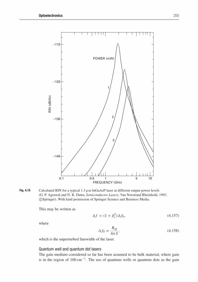
Optoelectronics 255
0.1
–140
–130
RIN
(d
B/H
z)
–120
–110
0.5
2
3
1
POWER (mW)
1 5 10FREQUENCY (GHz)
Fig. 4.19 Calculated RIN for a typical 1.3 μm InGaAsP laser at different output power levels(G. P. Agrawal and N. K. Dutta, Semiconductor Lasers, Van Norstrand Rheinhold, 1993.c©Springer). With kind permission of Springer Science and Business Media.
This may be written as
� f = (1 + β2c )� f0, (4.157)
where
� f0 = Rsp
4πS, (4.158)
which is the unperturbed linewidth of the laser.
Quantum well and quantum dot lasersThe gain medium considered so far has been assumed to be bulk material, where gainis in the region of 100 cm−1. The use of quantum wells or quantum dots as the gain
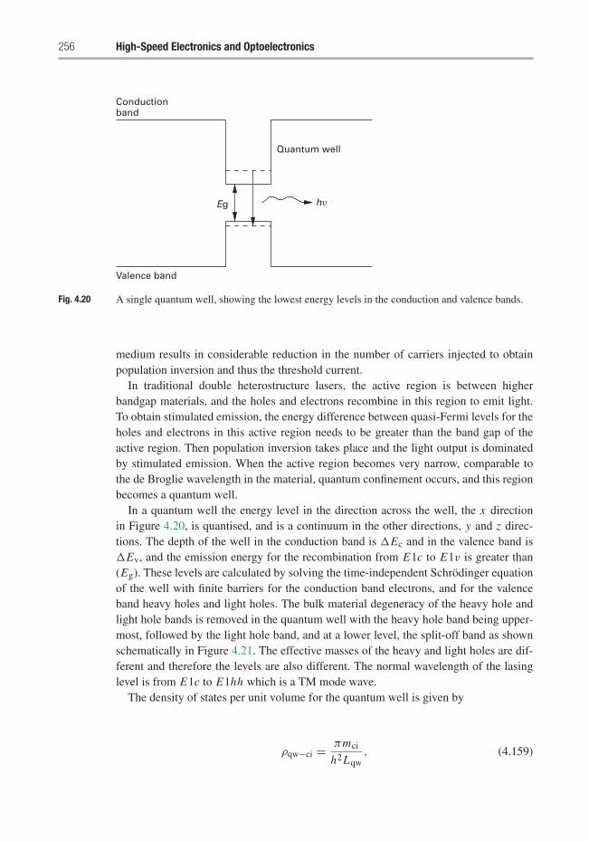
256 High-Speed Electronics and Optoelectronics
Quantum well
Conductionband
Valence band
hvEg
Fig. 4.20 A single quantum well, showing the lowest energy levels in the conduction and valence bands.
medium results in considerable reduction in the number of carriers injected to obtainpopulation inversion and thus the threshold current.
In traditional double heterostructure lasers, the active region is between higherbandgap materials, and the holes and electrons recombine in this region to emit light.To obtain stimulated emission, the energy difference between quasi-Fermi levels for theholes and electrons in this active region needs to be greater than the band gap of theactive region. Then population inversion takes place and the light output is dominatedby stimulated emission. When the active region becomes very narrow, comparable tothe de Broglie wavelength in the material, quantum confinement occurs, and this regionbecomes a quantum well.
In a quantum well the energy level in the direction across the well, the x directionin Figure 4.20, is quantised, and is a continuum in the other directions, y and z direc-tions. The depth of the well in the conduction band is �Ec and in the valence band is�Ev, and the emission energy for the recombination from E1c to E1v is greater than(Eg). These levels are calculated by solving the time-independent Schrodinger equationof the well with finite barriers for the conduction band electrons, and for the valenceband heavy holes and light holes. The bulk material degeneracy of the heavy hole andlight hole bands is removed in the quantum well with the heavy hole band being upper-most, followed by the light hole band, and at a lower level, the split-off band as shownschematically in Figure 4.21. The effective masses of the heavy and light holes are dif-ferent and therefore the levels are also different. The normal wavelength of the lasinglevel is from E1c to E1hh which is a TM mode wave.
The density of states per unit volume for the quantum well is given by
ρqw−ci = πmci
h2Lqw, (4.159)
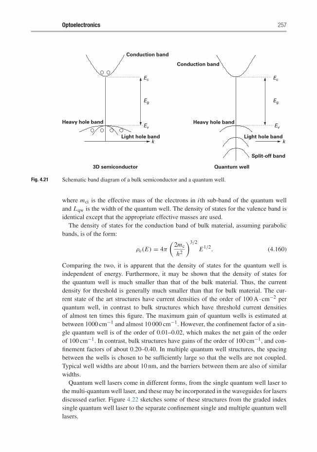
Optoelectronics 257
Conduction band
Ec
Eg
Ev
Ec
Eg
EvHeavy hole band
Light hole bandk
Split-off band
Quantum well3D semiconductor
k
Heavy hole band
Light hole band
Conduction band
Fig. 4.21 Schematic band diagram of a bulk semiconductor and a quantum well.
where mci is the effective mass of the electrons in i th sub-band of the quantum welland Lqw is the width of the quantum well. The density of states for the valence band isidentical except that the appropriate effective masses are used.
The density of states for the conduction band of bulk material, assuming parabolicbands, is of the form:
ρc(E) = 4π
(2mc
h2
)3/2
E1/2. (4.160)
Comparing the two, it is apparent that the density of states for the quantum well isindependent of energy. Furthermore, it may be shown that the density of states forthe quantum well is much smaller than that of the bulk material. Thus, the currentdensity for threshold is generally much smaller than that for bulk material. The cur-rent state of the art structures have current densities of the order of 100 A ·cm−2 perquantum well, in contrast to bulk structures which have threshold current densitiesof almost ten times this figure. The maximum gain of quantum wells is estimated atbetween 1000 cm−1 and almost 10 000 cm−1. However, the confinement factor of a sin-gle quantum well is of the order of 0.01–0.02, which makes the net gain of the orderof 100 cm−1. In contrast, bulk structures have gains of the order of 100 cm−1, and con-finement factors of about 0.20–0.40. In multiple quantum well structures, the spacingbetween the wells is chosen to be sufficiently large so that the wells are not coupled.Typical well widths are about 10 nm, and the barriers between them are also of similarwidths.
Quantum well lasers come in different forms, from the single quantum well laser tothe multi-quantum well laser, and these may be incorporated in the waveguides for lasersdiscussed earlier. Figure 4.22 sketches some of these structures from the graded indexsingle quantum well laser to the separate confinement single and multiple quantum welllasers.
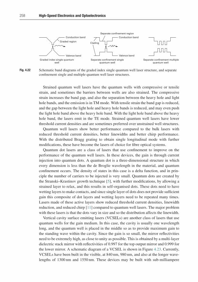
258 High-Speed Electronics and Optoelectronics
Conduction band
Valence band
Graded region
Graded index single quantumwell
Conduction band
Separate confinement region
Valence band
Clading
Separate confinement singlequantum well
Separate confinement multiplequantum well
Fig. 4.22 Schematic band diagrams of the graded index single quantum well laser structure, and separateconfinement single and multiple quantum well laser structures.
Strained quantum well lasers have the quantum wells with compressive or tensilestrain, and sometimes the barriers between wells are also strained. The compressivestrain increases the band gap, and also the separation between the heavy hole and lighthole bands, and the emission is in TM mode. With tensile strain the band gap is reduced,and the gap between the light hole and heavy hole bands is reduced, and may even pushthe light hole band above the heavy hole band. With the light hole band above the heavyhole band, the lasers emit in the TE mode. Strained quantum well lasers have lowerthreshold current densities and are sometimes preferred over unstrained well structures.
Quantum well lasers show better performance compared to the bulk lasers withreduced threshold current densities, better linewidths and better chirp performance.With the distributed Bragg grating to obtain single longitudinal mode with furthermodifications, these have become the lasers of choice for fibre optical systems.
Quantum dot lasers are a class of lasers that use confinement to improve on theperformance of the quantum well lasers. In these devices, the gain is through currentinjection into quantum dots. A quantum dot is a three-dimensional structure in whichevery dimension is less than the de Broglie wavelength in the material, and quantumconfinement occurs. The density of states in this case is a delta function, and in prin-ciple the number of carriers to be injected is very small. Quantum dots are created bythe Stranski–Krastinov growth technique [5], with further modifications, by allowing astrained layer to relax, and this results in self-organised dots. These dots need to havewetting layers to make contacts, and since single layer of dots does not provide sufficientgain this composite of dot layers and wetting layers need to be repeated many times.Lasers made of these active layers show reduced threshold current densities, linewidthreduction, and reduced chirp [11] compared to quantum well lasers. The major problemwith these lasers is that the dots vary in size and so the distribution affects the linewidth.
Vertical cavity surface emitting lasers (VCSELs) are another class of lasers that usequantum wells for the gain medium. In this case, the cavity is usually one wavelengthlong, and the quantum well is placed in the middle so as to provide maximum gain tothe standing wave within the cavity. Since the gain is so small, the mirror reflectivitiesneed to be extremely high, as close to unity as possible. This is obtained by a multi-layerdielectric stack mirror with reflectivities of 0.997 for the top output mirror and 0.999 forthe lower mirror. A schematic diagram of a VCSEL is shown in Figure 4.23. Currently,VCSELs have been built in the visible, at 840 nm, 980 nm, and also at the longer wave-lengths of 1300 nm and 1550 nm. These devices may be built with sub-milliampere
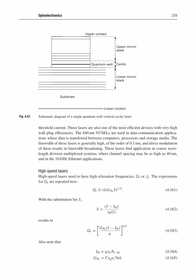
Optoelectronics 259
Cavity
Upper mirrorstack
Lower mirrorstack
Substrate
Quantum well
Upper contact
Lower contact
Fig. 4.23 Schematic diagram of a single quantum well vertical cavity laser.
threshold current. These lasers are also one of the most efficient devices with very highwall plug efficiencies. The 840 nm VCSELs are used in data-communication applica-tions where data is transferred between computers, processors and storage media. Thelinewidth of these lasers is generally high, of the order of 0.1 nm, and direct modulationof these results in linewidth broadening. These lasers find application in coarse wave-length division multiplexed systems, where channel spacing may be as high as 40 nm,and in the 10 GHz Ethernet applications.
High-speed lasersHigh-speed lasers need to have high relaxation frequencies, �r or fr. The expressionsfor �r are repeated here:
�r ∼= (GGNt S)1/2. (4.161)
With the substitution for S,
S = (I − Ith)
(qG)(4.162)
results in
�r =[
GNt(I − Ith)
q
]0.5
. (4.163)
Also note that
Ith = qγe Nt−th (4.164)
GNt = �vga/Vol, (4.165)
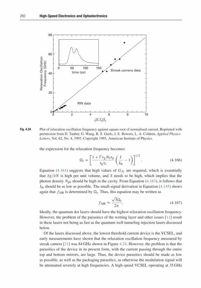
260 High-Speed Electronics and Optoelectronics
00
20
40
0 50 100 150time (ps)
60
80
2 4
RIN data
Streak camera data
Rel
axat
ion
Osc
illat
ion
Freq
uen
cy (
GH
z)
6 8 10
√(I–I t)/I t
Fig. 4.24 Plot of relaxation oscillation frequency against square root of normalised current. Reprinted withpermission from D. Tauber, G. Wang, R. S. Geels, J. E. Bowers, L. A. Coldren, Applied PhysicsLetters, Vol. 62, No. 4, 1993. Copyright 1993, American Institute of Physics.
the expression for the relaxation frequency becomes
�r =[
1 + �vg N0τp
τpτe
(I
Ith− 1
)]1/2
. (4.166)
Equation (4.161) suggests that high values of G Nt are required, which is essentiallythat ∂g/∂N is high per unit volume, and S needs to be high, which implies that thephoton density Nph should be high in the cavity. From Equation (4.163), it follows thatIth should be as low as possible. The small-signal derivation in Equation (4.145) showsagain that f3dB is determined by �r. Thus, this equation may be written as
f3dB ≈√
3�r
2π. (4.167)
Ideally, the quantum dot lasers should have the highest relaxation oscillation frequency.However, the problem of the parasitics of the wetting layer and other issues [11] resultin these lasers not being as fast as the quantum well tunneling injection lasers discussedbelow.
Of the lasers discussed above, the lowest threshold current device is the VCSEL, andearly measurements have shown that the relaxation oscillation frequency measured bystreak camera [31] was 84 GHz shown in Figure 4.24. However, the problem is that theparasitics of the device in its present form, with the current passing through the entiretop and bottom mirrors, are large. Thus, the device parasitics should be made as lowas possible, as well as the packaging parasitics, as otherwise the modulation signal willbe attenuated severely at high frequencies. A high-speed VCSEL operating at 35 GHz
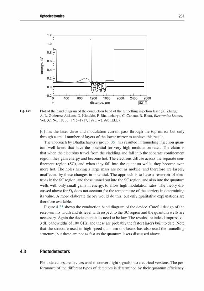
Optoelectronics 261
0–0.2
0.0
0.2
0.4
0.6
0.8
1.0
1.2
400 800 1200 1600 2000 2400 2800distance, μm 821/1a
ener
gy,
eV
Fig. 4.25 Plot of the band diagram of the conduction band of the tunnelling injection laser (X. Zhang,A. L. Gutierrez-Aitkens, D. Klotzkin, P. Bhattacharya, C. Caneau, R. Bhatt, Electronics Letters,Vol. 32, No. 18, pp. 1715–1717, 1996. c©1996 IEEE).
[6] has the laser drive and modulation current pass through the top mirror but onlythrough a small number of layers of the lower mirror to achieve this result.
The approach by Bhattacharya’s group [35] has resulted in tunneling injection quan-tum well lasers that have the potential for very high modulation rates. The claim isthat when the electrons travel from the cladding and fall into the separate confinementregion, they gain energy and become hot. The electrons diffuse across the separate con-finement region (SC), and when they fall into the quantum wells, they become evenmore hot. The holes having a large mass are not as mobile, and therefore are largelyunaffected by these changes in potential. The approach is to have a reservoir of elec-trons in the SC region, and these tunnel out into the SC region, and also into the quantumwells with only small gains in energy, to allow high modulation rates. The theory dis-cussed above for �r does not account for the temperature of the carriers in determiningits value. A more elaborate theory would do this, but only qualitative explanations aretherefore available.
Figure 4.25 shows the conduction band diagram of the device. Careful design of thereservoir, its width and its level with respect to the SC region and the quantum wells arenecessary. Again the device parasitics need to be low. The results are indeed impressive,3 dB bandwidths of 100 GHz, and these are probably the fastest lasers built to date. Notethat the structure used in high-speed quantum dot lasers has also used the tunnellingstructure, but these are not as fast as the quantum lasers discussed above.
4.3 Photodetectors
Photodetectors are devices used to convert light signals into electrical versions. The per-formance of the different types of detectors is determined by their quantum efficiency,
262 High-Speed Electronics and Optoelectronics
their frequency response and responsivity. In this chapter only solid state detectors areconsidered, and the slower detectors are only briefly discussed. The photomultiplier,which is widely used as a sensitive and fast (of the order of 100 MHz) detector, willnot be discussed here. Solid state detectors considered here are the extrinsic kind, inwhich the photon energy is close to the band gap of the semiconductor material usedfor the detector. Intrinsic photodetectors are used for detection of light with energiesbelow the band gap, and depend on deep level traps, or with different energy levelsin a quantum well, but these are not discussed here. In this chapter, the detectors con-sidered are photoconductors, and the junction devices which include the p–i–n diode,the metal–semiconductor–metal (MSM) photodetector and the avalanche photodetec-tor (APD). The photoconductor is a slow device and also noisy, but its simplicity is anattractive feature.
4.3.1 Preliminaries
Consider a semiconductor photodetector which absorbs photons with energies at orabove Eg, the bandgap energy of the semiconductor. Suppose the incident optical poweris given by Pin, and it is assumed that all the incident photons enter the semiconductor.Suppose the photocurrent generated as a result of this incident optical power is given byIp, then the relationship between Pin and Ip is
Ip = R Pin, (4.168)
where R is the responsivity of the photodetector in units of AW−1.The quantum efficiency of the detector η may be defined as ratio of the number of
hole–electron pairs generated to the number of incident photons, and is given by
η =Ip
qPin
hν
= hν
qR. (4.169)
Thus, R may be written as
R = qη
hν= ηλq
hc. (4.170)
Suppose the thickness of the semiconductor is w, and the absorption coefficient is α
Np m−1, then the transmitted optical power escaping from the semiconductor is given by
Ptr = Pine−αw. (4.171)
Thus, the absorbed power is given by
Pabs = Pin − Ptr = Pin(1 − e−αw). (4.172)
Since every absorbed photon creates one hole–electron pair, the quantum efficiency isgiven by
η = Pabs
Pin= (1 − e−αw), (4.173)
which assumes that all the incident photons enter the semiconductor with no reflection.
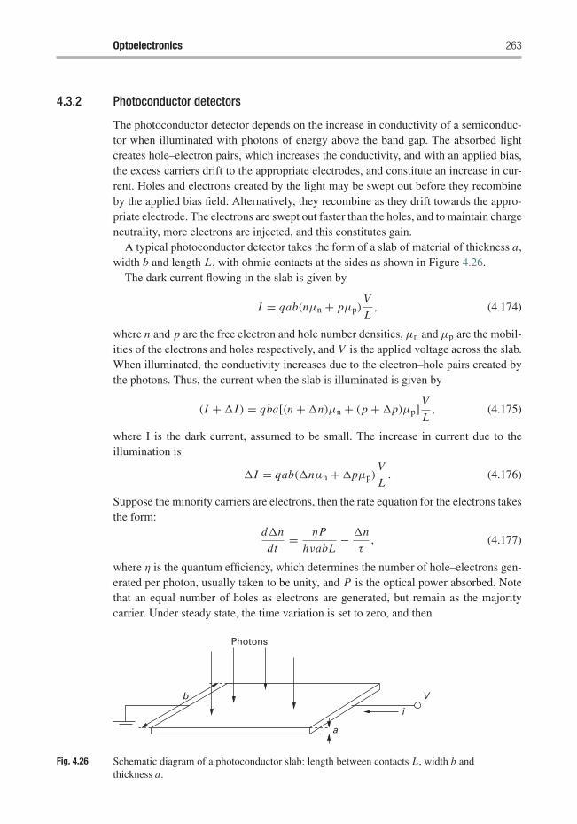
Optoelectronics 263
4.3.2 Photoconductor detectors
The photoconductor detector depends on the increase in conductivity of a semiconduc-tor when illuminated with photons of energy above the band gap. The absorbed lightcreates hole–electron pairs, which increases the conductivity, and with an applied bias,the excess carriers drift to the appropriate electrodes, and constitute an increase in cur-rent. Holes and electrons created by the light may be swept out before they recombineby the applied bias field. Alternatively, they recombine as they drift towards the appro-priate electrode. The electrons are swept out faster than the holes, and to maintain chargeneutrality, more electrons are injected, and this constitutes gain.
A typical photoconductor detector takes the form of a slab of material of thickness a,width b and length L , with ohmic contacts at the sides as shown in Figure 4.26.
The dark current flowing in the slab is given by
I = qab(nμn + pμp)V
L, (4.174)
where n and p are the free electron and hole number densities, μn and μp are the mobil-ities of the electrons and holes respectively, and V is the applied voltage across the slab.When illuminated, the conductivity increases due to the electron–hole pairs created bythe photons. Thus, the current when the slab is illuminated is given by
(I + �I ) = qba[(n + �n)μn + (p + �p)μp] V
L, (4.175)
where I is the dark current, assumed to be small. The increase in current due to theillumination is
�I = qab(�nμn + �pμp)V
L. (4.176)
Suppose the minority carriers are electrons, then the rate equation for the electrons takesthe form:
d�n
dt= ηP
hνabL− �n
τ, (4.177)
where η is the quantum efficiency, which determines the number of hole–electrons gen-erated per photon, usually taken to be unity, and P is the optical power absorbed. Notethat an equal number of holes as electrons are generated, but remain as the majoritycarrier. Under steady state, the time variation is set to zero, and then
V
i
Photons
a
b
Fig. 4.26 Schematic diagram of a photoconductor slab: length between contacts L , width b andthickness a.
264 High-Speed Electronics and Optoelectronics
�n = ηPτ
hνabL. (4.178)
This assumes that the photon-generated hole-electron pairs are in the volume of the slab,and the volume is abL . The electron current due to these excess electrons is given by
�In = q�nμnbaV
L= qηPG
hν, (4.179)
where G is the gain of the device. Substituting for �n from Equation (4.178), G isdefined as
G = μnτV
L2= τ
ttr,n, (4.180)
where the electron transit time ttr,n is given by
ttr,n = L
vn= L
μnE = L2
μnV. (4.181)
In addition to the electrons, adding the motion of the holes results in this equationbecoming
G = (μn + μp)τV
L2= μn + μp
μn
τ
ttr,n. (4.182)
Note that since μh � μn, the expression for gain is that given in Equation (4.180).Making L as small as possible increases the gain and also reduces the response time.
If the carriers are swept out before they recombine, then the electrons reach the ohmiccontact before the holes. To maintain charge neutrality, extra electrons are injected intothe photoconductor. If sweep out of the carriers occurs, then the lifetime is the transittime of the carriers and is given by
ttr,n,p = L
μn,p( V
L
) = L2
μn,pV. (4.183)
Since the mobility of holes is lower than that of electrons, the transit time of electronsis smaller. If μp � μn, then the gain term is dominated by the electron mobility termand in turn the transit time
G = τ
ttr,n. (4.184)
Thus, the photon-induced current from Equation (4.179) becomes
Iph = �In = τ
ttr,n
qηP
hν. (4.185)
In Equation (4.177), the time variation of �n may be as ejωt, and in the small-signal casethe response time varies inversely as (1 + jωτ), which defines the bandwidth. Thus, ifthe optical power is given by
P(ω) = Popt + P1ejωt, (4.186)
then the ac current term is
�Iac = qηP1
hν
τ
ttr,n
1
1 + jωτ. (4.187)
Optoelectronics 265
The rms current magnitude is given by
�Iac,rms = qηP1√2hν
τ
ttr,n
1
(1 + ω2τ 2)1/2. (4.188)
Noise in these detectors is from several sources and these are thermal or Johnson noise,generation-recombination noise, and at low frequencies, the 1/ f flicker noise. If theresistance of the device is Rcond, then the thermal noise current is given by⟨
|ıth|2⟩= 4kBT� f
Rcond, (4.189)
where � f is the bandwidth. The generation-recombination noise term is given by⟨|ıGR|2
⟩= 4qG Io� f
1 + ω2τ 2. (4.190)
where Io = qηPoptG/ωτ . Neglecting the contribution of 1/f noise at low frequencies,the signal-to-noise ratio is given by
S
N= �I 2
ac,rms⟨|ıth|2⟩ + ⟨|ıGR|2 ⟩ (4.191)
= ηP21
8hνPopt� f
[1 + kBT
Gq(1 + ω2τ 2)
1
Rcond Io
]−1
. (4.192)
The noise equivalent power (NEP) is defined as the incident rms optical power requiredto produce a signal-to-noise ratio of unity in a bandwidth of 1 Hz, [3], and the detectivityof a detector is the inverse of NEP or D = (NEP)−1. The normalised detectivity D∗ isdefined as
D∗ = A1/2(� f )1/2
N E P
(cm.Hz1/2 W−1
), (4.193)
where A is the area of the photoconductor on which light is incident. The bandwidthis usually set to 1 Hz, and the reference area is set to 1 cm2. Note that D∗ is usuallyexpressed as D∗(λ, f, 1), where λ is the wavelength of light, f is its frequency ofmodulation, and 1 is the bandwidth in Hz and may be obtained from Equation (4.192).
The structure of these devices may take various forms, including the interdigitatedsurface contact structure shown in Figure 4.27.
4.3.3 P–I–N diodes
Detection of photons with energies at or above the band gap of a semiconductor requiresthat they are absorbed and create hole–electron pairs, and a current be induced due tothis absorption. The depletion layer of a reverse-biased p–n junction of the semicon-ductor causes the holes and electrons to separate and be collected by the appropriatecontact/collection region. The photons entering this device, schematically shown inFigure 4.28, create hole–electron pairs as the light is absorbed, from the top contactregion, through the depletion layer on both sides of the junction and possibly beyond, tothe lower contact region. The fields in the depletion layer are high enough to separate the
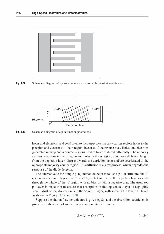
266 High-Speed Electronics and Optoelectronics
Fig. 4.27 Schematic diagram of a photoconductor detector with interdigitated fingers.
p type n type
p+ n+
Depletion layer
Photons
Fig. 4.28 Schematic diagram of a p–n junction photodiode.
holes and electrons, and send them to the respective majority carrier region, holes to thep region and electrons to the n region, because of the reverse bias. Holes and electronsgenerated in the p and n contact regions need to be considered differently. The minoritycarriers, electrons in the p region and holes in the n region, about one diffusion lengthfrom the depletion layer, diffuse towards the depletion layer and are accelerated to theappropriate majority carrier region. This diffusion is a slow process, which degrades theresponse of the diode detector.
The alternative to the simple p–n junction detector is to use a p–i–n structure, the ‘i’region is either an ‘i’ layer or a p− or n− layer. In this device, the depletion layer extendsthrough the whole of the ‘i’ region with no bias or with a negative bias. The usual topp+ layer is made thin to ensure that absorption in the top contact layer is negligiblysmall. Most of the absorption is in the ‘i’ or n− layer, with some in the lower n+ layer,as shown in Figures 4.29 and 4.30.
Suppose the photon flux per unit area is given by φ0, and the absorption coefficient isgiven by α, then the hole–electron generation rate is given by
Gen(z) = φ0αe−αz, (4.194)
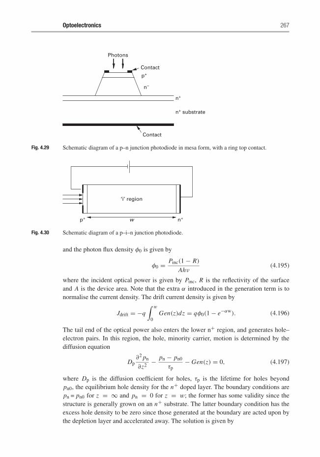
Optoelectronics 267
Photons
p+
n−
n+
n+ substrate
Contact
Contact
Fig. 4.29 Schematic diagram of a p–n junction photodiode in mesa form, with a ring top contact.
p+ n+
‘i’ region
w
Fig. 4.30 Schematic diagram of a p–i–n junction photodiode.
and the photon flux density φ0 is given by
φ0 = Pinc(1 − R)
Ahν(4.195)
where the incident optical power is given by Pinc, R is the reflectivity of the surfaceand A is the device area. Note that the extra α introduced in the generation term is tonormalise the current density. The drift current density is given by
Jdrift = −q∫ w
0Gen(z)dz = qφ0(1 − e−αw). (4.196)
The tail end of the optical power also enters the lower n+ region, and generates hole–electron pairs. In this region, the hole, minority carrier, motion is determined by thediffusion equation
Dp∂2 pn
∂z2− pn − pn0
τp− Gen(z) = 0, (4.197)
where Dp is the diffusion coefficient for holes, τp is the lifetime for holes beyondpn0, the equilibrium hole density for the n+ doped layer. The boundary conditions arepn = pn0 for z = ∞ and pn = 0 for z = w; the former has some validity since thestructure is generally grown on an n+ substrate. The latter boundary condition has theexcess hole density to be zero since those generated at the boundary are acted upon bythe depletion layer and accelerated away. The solution is given by
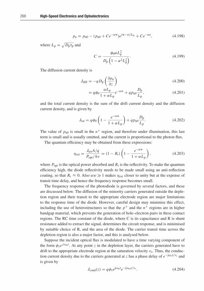
268 High-Speed Electronics and Optoelectronics
pn = pn0 − (pn0 + Ce−αw)e(w−z)/Lp + Ce−αz, (4.198)
where Lp = √Dpτp and
C = φ0αL2p
Dp
(1 − α2L2
p
) . (4.199)
The diffusion current density is
Jdiff = −q Dp
(∂pn
∂z
)(4.200)
= qφ0αLp
1 + αLpe−αw + qpn0
Dp
Lp, (4.201)
and the total current density is the sum of the drift current density and the diffusioncurrent density, and is given by
Jtot = qφ0
(1 − e−αw
1 + αLp
)+ qpn0
Dp
Lp. (4.202)
The value of pn0 is small in the n+ region, and therefore under illumination, this lastterm is small and is usually omitted, and the current is proportional to the photon flux.
The quantum efficiency may be obtained from these expressions:
ηext = Jtot A/q
Popt/hν= (1 − Rr)
(1 − e−αw
1 + αLp
), (4.203)
where Popt is the optical power absorbed and Rr is the reflectivity. To make the quantumefficiency high, the diode reflectivity needs to be made small using an anti-reflectioncoating, so that Rr ≈ 0. Also αw� 1 makes ηext closer to unity but at the expense oftransit time delay, and hence the frequency response becomes small.
The frequency response of the photodiode is governed by several factors, and theseare discussed below. The diffusion of the minority carriers generated outside the deple-tion region and their transit to the appropriate electrode region are major limitationsto the response time of the diode. However, careful design may minimise this effect,including the use of heterostructures so that the p+ and the n+ regions are in higherbandgap material, which prevents the generation of hole–electron pairs in these contactregions. The RC time constant of the diode, where C is its capacitance and R is shuntresistance added to extract the signal, determines the circuit response, and is minimisedby suitable choice of R, and the area of the diode. The carrier transit time across thedepletion region is also a major factor, and this is analysed below.
Suppose the incident optical flux is modulated to have a time varying component ofthe form φ1e jωmt . At any point z in the depletion layer, the carriers generated have todrift to the appropriate electrode region at the saturation velocity vs. Thus, the conduc-tion current density due to the carriers generated at z has a phase delay of e−jωsz/vs andis given by
Jcond(z) = qφ1ejωmte−jωmz/vs . (4.204)
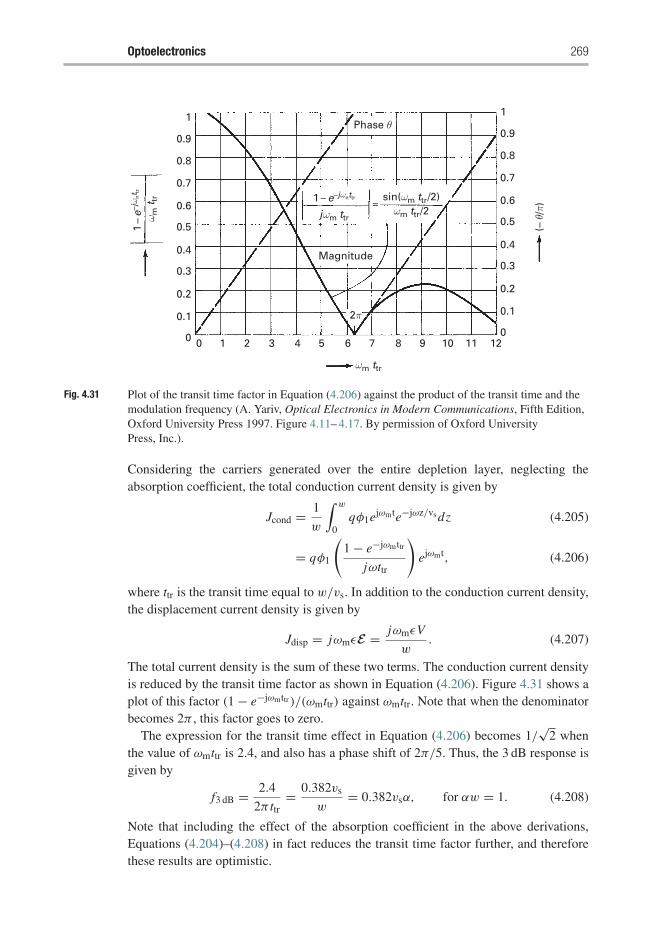
Optoelectronics 269
0 1 2 3 4 5 6
ωm ttr
ω m t t
r
2π
Magnitude
Phase θ
=
(– θ
/π)
1 –
e–jω n
t tr
jωm ttr
1 – e–jωnttr
ωm ttr/2sin(ωm ttr/2)
7 8 9 10 11 120
0.1
0.2
0.3
0.4
0.5
0.6
0.7
0.8
0.9
1
0
0.1
0.2
0.3
0.4
0.5
0.6
0.7
0.8
0.9
1
Fig. 4.31 Plot of the transit time factor in Equation (4.206) against the product of the transit time and themodulation frequency (A. Yariv, Optical Electronics in Modern Communications, Fifth Edition,Oxford University Press 1997. Figure 4.11– 4.17. By permission of Oxford UniversityPress, Inc.).
Considering the carriers generated over the entire depletion layer, neglecting theabsorption coefficient, the total conduction current density is given by
Jcond = 1
w
∫ w
0qφ1ejωmte−jωz/vsdz (4.205)
= qφ1
(1 − e−jωmttr
jωttr
)ejωmt, (4.206)
where ttr is the transit time equal to w/vs. In addition to the conduction current density,the displacement current density is given by
Jdisp = jωmεE = jωmεV
w. (4.207)
The total current density is the sum of these two terms. The conduction current densityis reduced by the transit time factor as shown in Equation (4.206). Figure 4.31 shows aplot of this factor (1 − e−jωmttr)/(ωmttr) against ωmttr. Note that when the denominatorbecomes 2π , this factor goes to zero.
The expression for the transit time effect in Equation (4.206) becomes 1/√
2 whenthe value of ωmttr is 2.4, and also has a phase shift of 2π/5. Thus, the 3 dB response isgiven by
f3 dB = 2.4
2π ttr= 0.382vs
w= 0.382vsα, for αw = 1. (4.208)
Note that including the effect of the absorption coefficient in the above derivations,Equations (4.204)–(4.208) in fact reduces the transit time factor further, and thereforethese results are optimistic.
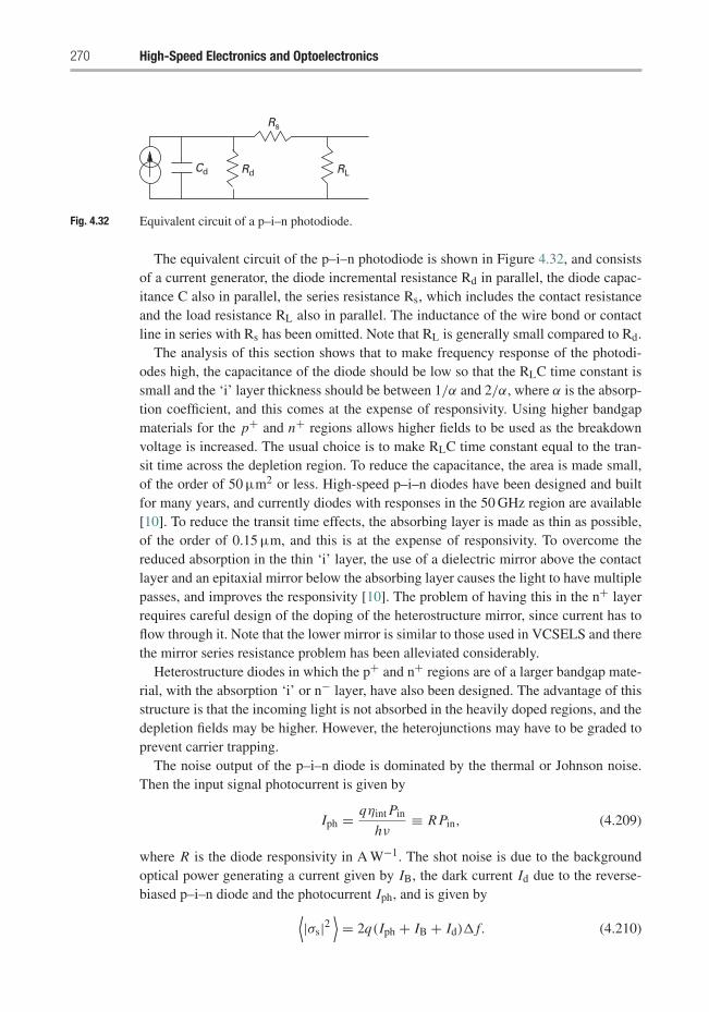
270 High-Speed Electronics and Optoelectronics
Cd Rd
Rs
RL
Fig. 4.32 Equivalent circuit of a p–i–n photodiode.
The equivalent circuit of the p–i–n photodiode is shown in Figure 4.32, and consistsof a current generator, the diode incremental resistance Rd in parallel, the diode capac-itance C also in parallel, the series resistance Rs, which includes the contact resistanceand the load resistance RL also in parallel. The inductance of the wire bond or contactline in series with Rs has been omitted. Note that RL is generally small compared to Rd.
The analysis of this section shows that to make frequency response of the photodi-odes high, the capacitance of the diode should be low so that the RLC time constant issmall and the ‘i’ layer thickness should be between 1/α and 2/α, where α is the absorp-tion coefficient, and this comes at the expense of responsivity. Using higher bandgapmaterials for the p+ and n+ regions allows higher fields to be used as the breakdownvoltage is increased. The usual choice is to make RLC time constant equal to the tran-sit time across the depletion region. To reduce the capacitance, the area is made small,of the order of 50 μm2 or less. High-speed p–i–n diodes have been designed and builtfor many years, and currently diodes with responses in the 50 GHz region are available[10]. To reduce the transit time effects, the absorbing layer is made as thin as possible,of the order of 0.15 μm, and this is at the expense of responsivity. To overcome thereduced absorption in the thin ‘i’ layer, the use of a dielectric mirror above the contactlayer and an epitaxial mirror below the absorbing layer causes the light to have multiplepasses, and improves the responsivity [10]. The problem of having this in the n+ layerrequires careful design of the doping of the heterostructure mirror, since current has toflow through it. Note that the lower mirror is similar to those used in VCSELS and therethe mirror series resistance problem has been alleviated considerably.
Heterostructure diodes in which the p+ and n+ regions are of a larger bandgap mate-rial, with the absorption ‘i’ or n− layer, have also been designed. The advantage of thisstructure is that the incoming light is not absorbed in the heavily doped regions, and thedepletion fields may be higher. However, the heterojunctions may have to be graded toprevent carrier trapping.
The noise output of the p–i–n diode is dominated by the thermal or Johnson noise.Then the input signal photocurrent is given by
Iph = qηint Pin
hν≡ R Pin, (4.209)
where R is the diode responsivity in A W−1. The shot noise is due to the backgroundoptical power generating a current given by IB, the dark current Id due to the reverse-biased p–i–n diode and the photocurrent Iph, and is given by⟨
|σs|2⟩= 2q(Iph + IB + Id)� f. (4.210)
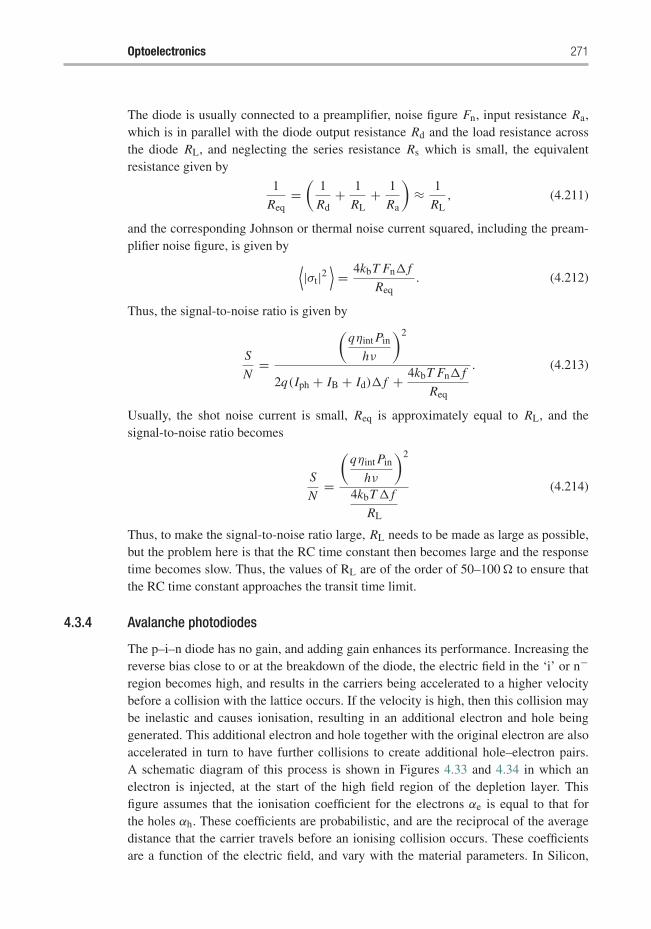
Optoelectronics 271
The diode is usually connected to a preamplifier, noise figure Fn, input resistance Ra,which is in parallel with the diode output resistance Rd and the load resistance acrossthe diode RL, and neglecting the series resistance Rs which is small, the equivalentresistance given by
1
Req=
(1
Rd+ 1
RL+ 1
Ra
)≈ 1
RL, (4.211)
and the corresponding Johnson or thermal noise current squared, including the pream-plifier noise figure, is given by ⟨
|σt|2⟩= 4kbT Fn� f
Req. (4.212)
Thus, the signal-to-noise ratio is given by
S
N=
(qηint Pin
hν
)2
2q(Iph + IB + Id)� f + 4kbT Fn� f
Req
. (4.213)
Usually, the shot noise current is small, Req is approximately equal to RL, and thesignal-to-noise ratio becomes
S
N=
(qηint Pin
hν
)2
4kbT� f
RL
(4.214)
Thus, to make the signal-to-noise ratio large, RL needs to be made as large as possible,but the problem here is that the RC time constant then becomes large and the responsetime becomes slow. Thus, the values of RL are of the order of 50–100� to ensure thatthe RC time constant approaches the transit time limit.
4.3.4 Avalanche photodiodes
The p–i–n diode has no gain, and adding gain enhances its performance. Increasing thereverse bias close to or at the breakdown of the diode, the electric field in the ‘i’ or n−region becomes high, and results in the carriers being accelerated to a higher velocitybefore a collision with the lattice occurs. If the velocity is high, then this collision maybe inelastic and causes ionisation, resulting in an additional electron and hole beinggenerated. This additional electron and hole together with the original electron are alsoaccelerated in turn to have further collisions to create additional hole–electron pairs.A schematic diagram of this process is shown in Figures 4.33 and 4.34 in which anelectron is injected, at the start of the high field region of the depletion layer. Thisfigure assumes that the ionisation coefficient for the electrons αe is equal to that forthe holes αh. These coefficients are probabilistic, and are the reciprocal of the averagedistance that the carrier travels before an ionising collision occurs. These coefficientsare a function of the electric field, and vary with the material parameters. In Silicon,

272 High-Speed Electronics and Optoelectronics
0 wTi
me
E
Fig. 4.33 Schematic diagram of the avalanche process with injection of an electron into the avalancheregion, which after collision creates an additional hole–electron pair, which, together with theoriginal electron, is also accelerated to have further ionising collisions, resulting in additionalhole–electron pairs for each carrier. In this diagram, the ionisation coefficients of the electronsand holes are assumed to be nearly equal.
p+ n+w
x = 0 x = w
‘i’
n−
E
Fig. 4.34 Schematic diagram of the avalanche diode.
αe > αh; but in III–V material, GaAs and InP and others they are almost equal. Thecollisional increase in carriers results in an increase in the current which implies currentgain.
The expression for the ionisation coefficient is given by [3]:
αe,h = α∞ exp
[−
(b
E)m]
. (4.215)
In GaAs, α∞ is ∼1.3 × 106 cm−1, b is 2 × 10⁶ V cm−1 and m is 2. The multiplicationcoefficient or factor M is the ratio of the output current density to the input currentdensity, and may be subdivided for the electron component and the hole component.
Suppose that the total current density in the diode is given by
Jtot = Je(x) + Jh(x), (4.216)
Optoelectronics 273
where Je(x) is the electron current density, Jh(x) is the hole current density and Jtot isa constant at any plane of the diode. The multiplication factors are defined as
Me = Je,out
Je,in= Je(w)
Je(0)(4.217)
for the electron current density, and
Mh = Jh,out
Jh,in= Jh(0)
Jh(w)(4.218)
for the hole current density.Suppose a p–i–n diode with an ‘i’ region is considered, the field across the ‘i’ region
is uniform. Also assume that the ionisation coefficients αe = αh, and are constant atthe fixed electric field in the ‘i’ region, and the width of the avalanching region is w.The holes and electrons are accelerated in opposite directions, and the collisions resultin ionisation and multiplication. Assume that at x = 0, there is only electron injection,hole injection is zero at x = w, and therefore the avalanching is initiated by electrons.In this case, the multiplication factor is given by
M = 1 + αew + (αew)2 + (αew)3 + (αew)4 + · · · (4.219)
= 1
1 − αewfor αew < 1. (4.220)
This final result implies that the multiplication factor goes to ∞ when αew is unity, orthat each carrier has one ionising collision over the distance w.
For the case of the p–i–n, with an n− region instead of the ‘i’ region, the fieldincreases linearly from the n+ region to the p+ region, and the above assumptionsof constant ionisation coefficients no longer hold. The total current density flow-ing in the diode is the sum of the electron current density and the hole currentdensity.
The current densities in the avalanching region satisfy the following equations:
d Je
dx= αe Je + αh Jh + qGen(x) (4.221)
−d Jh
dx= αe Je + αh Jh + qGen(x), (4.222)
where qGen(x) is the optical generation rate. Subtracting these two equations results in
d
dx[Je(x) + Jh(x)] = 0, (4.223)
or
Je(x) + Jh(x) = constant = Jtot. (4.224)
This implies that the current density is a constant at any plane in the diode, as claimedearlier in Equation (4.216). Substituting for Jh from Equation (4.216) by Jtot − Je inEquation (4.221)
d Je
dx− (αe − αh)Je = αh Jtot + qGen(x). (4.225)
274 High-Speed Electronics and Optoelectronics
Consider the case when αe = αh, neglecting the Gen term, this becomes
d Je
dx= αe Jtot, (4.226)
and the solution is
Je(w) = Jtot
∫ w
0αedx + Je(0). (4.227)
Assuming that there is no hole injection at x = w, then Je(w) = Jtot, and this equationbecomes
Je(w) = Je(w)
∫ w
0αedx + Je(0). (4.228)
Dividing by Je(0), this equation becomes
Je(w)
Je(0)= Me = Me
∫ w
0αedx + 1, (4.229)
or
Me = 1
1 − ∫ w
0 αedx. (4.230)
For avalanching, ∫ w
0αedx = 1. (4.231)
When αe �= αh, then Equation (4.225) needs to be solved. This is first-order differentialequation of the form:
dy
dx+ P(x)y = Q(x), (4.232)
and the solution is given by
y =∫ x
0 Q(x ′)e∫ x ′
0 P(x ′′)dx ′′ + y(0)
e∫ x
0 P(x ′)dx ′ . (4.233)
Consider the case of electron injection at x = 0, with Gen(x) = 0 and no hole injectionat x = w, which implies that Jh(w) = 0, and Jtot = Je(w). Following the aboveprocedure, with these boundary conditions, the solution of Equation (4.225) is obtained,and the electron current multiplication factor becomes [8]:
Me = Je(w)
Je(0)= e
∫ w0 (αe−αh)dx ′
1 − ∫ w
0 dx ′αh(x ′)e∫ w
x ′ (αe−αh)dx ′′ . (4.234)
When αe = αh, then this equation becomes, as shown in Equation (4.230)
Me = 1
1 − ∫ w
0 αedx. (4.235)
When the denominator of these multiplication factors is zero, the diode avalanches. Asimilar expression to that in Equation (4.234) may be derived for Mh, if the avalanche
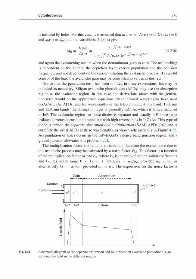
Optoelectronics 275
is initiated by holes. For this case, it is assumed that at x = w, Je(w) = 0, Gen(x) = 0and Jh(0) = Jtot, and the variable is Jh(x) to give
Mh = Jh(w)
Je(0)= e− ∫ w
0 (αe−αh)dx ′
1 − ∫ w
0 dx ′αe(x ′)e− ∫ x ′0 (αe−αh)dx ′′
, (4.236)
and again the avalanching occurs when the denominator goes to zero. The avalanchingis dependent on the field in the depletion layer, carrier population and the collisionfrequency, and not dependent on the carrier initiating the avalanche process. By carefulcontrol of the bias, the avalanche gain may be controlled to values as desired.
Notice that the generation term has been omitted in these expressions, but may beincluded as necessary. Silicon avalanche photodiodes (APDs) may use the absorptionregion as the avalanche region. In this case, the derivations above with the genera-tion term would be the appropriate equations. Near infrared wavelengths have usedGaAs/AlGaAs APDs, and for wavelengths in the telecommunications band, 1300 nmand 1550 nm bands, the absorption layer is generally InGaAs which is lattice-matchedto InP. The avalanche region for these diodes is separate and usually InP, since largeleakage currents occur due to tunneling with high reverse bias in InGaAs. This type ofdiode is termed the separate absorption and multiplication (SAM) APDs [26], and iscurrently the usual APDs at these wavelengths, as shown schematically in Figure 4.35.Accumulation of holes occurs in the InP–InGaAs valence band junction region, and agraded junction alleviates this problem [22].
The multiplication factor is a random variable and therefore the excess noise due tothis avalanche process may be estimated by a noise factor FM. This factor is a functionof the multiplication factor M and kA, where kA is the ratio of the ionisation coefficientsand kA lies in the range 0 < kA < 1. Thus, kA = αh/αe, provided αh < αe, oralternatively kA = αe/αh, provided αe < αh. The expression for the noise factor is
Ele
ctri
c fi
eld
Photons
Contact Contact
n+
AbsorptionGain
n−
InP InGaAs InP
n−p+
InP
Fig. 4.35 Schematic diagram of the separate absorption and multiplication avalanche photodiode, alsoshowing the field in the different regions.
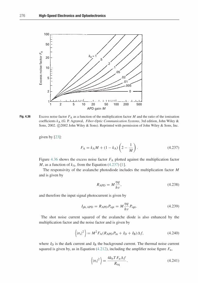
276 High-Speed Electronics and Optoelectronics
100
50
20
10
5
2
11 2 5
kA = 1.5
.2.1
.05
.02.01.005
0
10 20APD gain M
Exc
ess
no
ise
fact
or
F A
50 100 200 500
Fig. 4.36 Excess noise factor FA as a function of the multiplication factor M and the ratio of the ionisationcoefficients kA (G. P. Agrawal, Fiber-Optic Communication Systems, 3rd edition, John Wiley &Sons, 2002. c©2002 John Wiley & Sons). Reprinted with permission of John Wiley & Sons, Inc.
given by [23]:
FA = kA M + (1 − kA)
(2 − 1
M
). (4.237)
Figure 4.36 shows the excess noise factor FA plotted against the multiplication factorM , as a function of kA, from the Equation (4.237) [1].
The responsivity of the avalanche photodiode includes the multiplication factor Mand is given by
RAPD = Mηq
hν, (4.238)
and therefore the input signal photocurrent is given by
Iph,APD = RAPD Popt = Mηq
hνPopt. (4.239)
The shot noise current squared of the avalanche diode is also enhanced by themultiplication factor and the noise factor and is given by⟨
|σs|2⟩= M2 FA(RAPD Pin + ID + IB)� f, (4.240)
where ID is the dark current and IB the background current. The thermal noise currentsquared is given by, as in Equation (4.212), including the amplifier noise figure Fn,⟨
|σt|2⟩= 4kbT Fn� f
Req. (4.241)
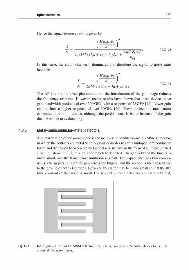
Optoelectronics 277
Hence the signal-to-noise ratio is given by
S
N=
(Mqηint Pin
hν
)2
2q M2 FA(Iph + IB + Id)� f + 4kbT Fn� f
Req
. (4.242)
In this case, the shot noise term dominates and therefore the signal-to-noise ratiobecomes
S
N=
(Mqηint Pin
hν
)2
2q M2 FA(Iph + IB + Id)� f. (4.243)
The APD is the preferred photodiode, but the introduction of the gain stage reducesthe frequency response. However, recent results have shown that these devices havegain bandwidth products of over 300 GHz, with a response of 28 GHz [18]. Lower gainresults show a higher response of over 30 GHz [29]. These devices are much moreexpensive than p–i–n diodes, although the performance is better because of the gainthat arises due to avalanching.
4.3.5 Metal–semiconductor–metal detectors
A planar version of the p–i–n diode is the metal–semiconductor–metal (MSM) detector,in which the contacts are metal Schottky barrier diodes to a thin undoped semiconductorlayer, and the region between the metal contacts, usually in the form of an interdigitatedstructure, shown in Figure 4.37, is completely depleted. The gap between the fingers ismade small, and the transit time limitation is small. The capacitance has two compo-nents: one in parallel with the gap across the fingers, and the second is the capacitanceto the ground of both electrodes. However, this latter may be made small so that the RCtime constant of the diode is small. Consequently, these detectors are extremely fast,
Fig. 4.37 Interdigitated form of the MSM detector, in which the contacts are Schottky diodes to the thinepitaxial absorption layer.
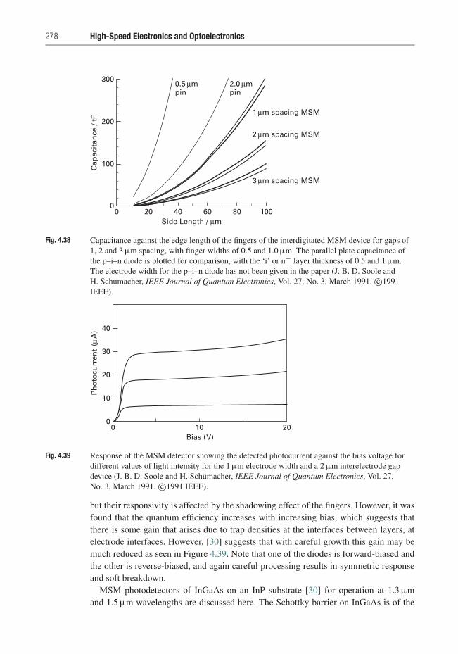
278 High-Speed Electronics and Optoelectronics
00
100
200
300
20 40 60 80 100Side Length / μm
3 μm spacing MSM
2 μm spacing MSM
1 μm spacing MSM
2.0 μmpin
0.5 μmpin
Cap
acit
ance
/ tF
Fig. 4.38 Capacitance against the edge length of the fingers of the interdigitated MSM device for gaps of1, 2 and 3 μm spacing, with finger widths of 0.5 and 1.0 μm. The parallel plate capacitance ofthe p–i–n diode is plotted for comparison, with the ‘i’ or n− layer thickness of 0.5 and 1 μm.The electrode width for the p–i–n diode has not been given in the paper (J. B. D. Soole andH. Schumacher, IEEE Journal of Quantum Electronics, Vol. 27, No. 3, March 1991. c©1991IEEE).
00
10
20
30
40
10 20Bias (V)
Ph
oto
curr
ent
(μA
)
Fig. 4.39 Response of the MSM detector showing the detected photocurrent against the bias voltage fordifferent values of light intensity for the 1 μm electrode width and a 2 μm interelectrode gapdevice (J. B. D. Soole and H. Schumacher, IEEE Journal of Quantum Electronics, Vol. 27,No. 3, March 1991. c©1991 IEEE).
but their responsivity is affected by the shadowing effect of the fingers. However, it wasfound that the quantum efficiency increases with increasing bias, which suggests thatthere is some gain that arises due to trap densities at the interfaces between layers, atelectrode interfaces. However, [30] suggests that with careful growth this gain may bemuch reduced as seen in Figure 4.39. Note that one of the diodes is forward-biased andthe other is reverse-biased, and again careful processing results in symmetric responseand soft breakdown.
MSM photodetectors of InGaAs on an InP substrate [30] for operation at 1.3 μmand 1.5 μm wavelengths are discussed here. The Schottky barrier on InGaAs is of the
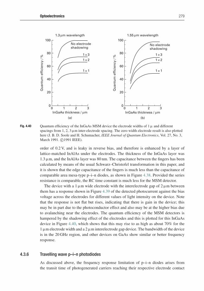
Optoelectronics 279
00
20
40
60
80
100
1 2 3InGaAs thickness / μm
1.3 μm wavelength
Qu
antu
m e
ffic
ien
cy /
%
(a)
No electrodeshadowing
1 × 1
1 × 2
1 × 3
00
20
40
60
80
100
1 2 3InGaAs thickness / μm
1.55 μm wavelength
Qu
antu
m e
ffic
ien
cy /
%(b)
No electrodeshadowing
1 × 1
1 × 2
1 × 3
Fig. 4.40 Quantum efficiency of the InGaAs MSM device the electrode widths of 1 μ and differentspacings from 1, 2, 3 μm inter-electrode spacing. The zero width electrode result is also plottedhere (J. B. D. Soole and H. Schumacher, IEEE Journal of Quantum Electronics, Vol. 27, No. 3,March 1991. c©1991 IEEE).
order of 0.2 V, and is leaky in reverse bias, and therefore is enhanced by a layer oflattice-matched InAlAs under the electrodes. The thickness of the InGaAs layer was1.3 μm, and the InAlAs layer was 80 nm. The capacitance between the fingers has beencalculated by means of the usual Schwarz–Christofel transformation in this paper, andit is shown that the edge capacitance of the fingers is much less than the capacitance ofcomparable area mesa-type p–i–n diodes, as shown in Figure 4.38. Provided the seriesresistance is comparable, the RC time constant is much less for the MSM detector.
The device with a 1 μm wide electrode with the interelectrode gap of 2 μm betweenthem has a response shown in Figure 4.39 of the detected photocurrent against the biasvoltage across the electrodes for different values of light intensity on the device. Notethat the response is not flat but rises, indicating that there is gain in the device; thismay be in part due to the photoconductor effect and also may be at the higher bias dueto avalanching near the electrodes. The quantum efficiency of the MSM detectors ishampered by the shadowing effect of the electrodes and this is plotted for this InGaAsdevice in Figure 4.40, which shows that this may rise to as high as about 70% for the1 μm electrode width and a 2 μm interelectrode gap device. The bandwidth of the deviceis in the 20 GHz region, and other devices on GaAs show similar or better frequencyresponse.
4.3.6 Travelling wave p–i–n photodiodes
As discussed above, the frequency response limitation of p–i–n diodes arises fromthe transit time of photogenerated carriers reaching their respective electrode contact
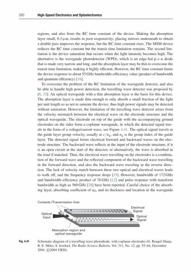
280 High-Speed Electronics and Optoelectronics
regions, and also from the RC time constant of the device. Making the absorptionlayer small, 0.3 μm, results in poor responsivity; placing mirrors underneath to obtaina double pass improves the response, but the RC time constant rises. The MSM devicereduces the RC time constant but the transit time limitation remains. The second lim-itation is the device saturation that occurs when the light intensity becomes high. Thealternative is the waveguide photodetector (WPD), which is an edge-fed p–i–n diodethat is made very narrow and long, and the absorption layer may be thin to overcome thetransit time limitation, making it highly efficient. However, the RC time constant limitsthe device response to about 55 GHz bandwidth–efficiency value (product of bandwidthand quantum efficiency) [16].
To overcome the problem of the RC limitation of the waveguide detector, and alsobe able to handle high power detection, the travelling wave detector was proposed by[8, 32]. An optical waveguide with a thin absorption layer is the basis for this device.The absorption layer is made thin enough to only absorb a small fraction of the lightper unit length so as not to saturate the device, thus high power signals may be detectedwithout saturation. However, the limitation of the travelling wave detector arises fromthe velocity mismatch between the electrical wave on the electrode structure and theoptical waveguide. The electrode on top of the guide with the accompanying groundelectrodes on the sides form a coplanar waveguide, in which the detected signal trav-els in the form of a voltage/current wave, see Figure 4.41. The optical signal travels atthe guide layer group velocity, usually at c/ng, and ng is the group index of the guidelayer. The detected signal forms electrical forward and backward waves on the elec-trode structure. The backward wave reflects at the input of the electrode structure, if itis an open circuit at the start of the detector, or alternatively, the wave is absorbed inthe load if matched. Thus, the electrical wave travelling on the electrodes is a combina-tion of the forward wave and the reflected component of the backward wave travellingin the forward direction, and also the backward wave traveling in the reverse direc-tion. The lack of velocity match between these two optical and electrical waves leadsto walk off, and the frequency response drops [15]. However, bandwidth of 172 GHzand bandwidth–efficiency product of 76 GHz [12] and pulse response with transformbandwidth as high as 560 GHz [28] have been reported. Careful choice of the absorb-ing layer, absorbing coefficient of α0, and its thickness and location in the waveguide
Absorption region andoptical waveguide
OpticalInput
Contacts (Transmission line)
ElectricalSignal
OpticalSignal
Fig. 4.41 Schematic diagram of a travelling wave photodiode, with coplanar electrodes (G. Rengel-Sharp,R. E. Miles, S. Iezekiel, The Radio Science Bulletin, Vol. 311, No. 12, pp. 55–64, December2004. c©2004 URSI).
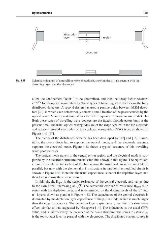
Optoelectronics 281
p
n+
substrate
ni region
absorptionlayer
Fig. 4.42 Schematic diagram of a travelling wave photodiode, showing the p–i–n structure with theabsorbing layer, and the electrodes.
allow the confinement factor � to be determined, and thus the decay factor becomese−α0�z for the optical wave intensity. These types of travelling wave devices are the fullydistributed detectors. A second design has used a passive guide between MSM detec-tors [20], in which each detector only detects a small fraction of the power carried by theoptical wave. Velocity matching allows the 3dB frequency response to rise to 49 GHz.Both these types of travelling wave devices are the fastest photodetectors built at thepresent time. The usual optical waveguides are of the ridge type, with the top electrodeand adjacent ground electrodes of the coplanar waveguide (CPW) type, as shown inFigure 4.41 [27].
The theory of the distributed detector has been developed by [12] and [15]. Essen-tially, the p–i–n diode has to support the optical mode, and the electrode structuresupports the electrical mode. Figure 4.42 shows a typical structure of this travellingwave photodetector.
The optical mode travels in the central p–i–n region, and the electrical mode is sup-ported by the electrode structure transmission line shown in this figure. The equivalentcircuit of the elemental section of the line is now the usual R–L in series and C–G inparallel, but now with the elemental p–i–n structure in parallel; the modified circuit isshown in Figure 4.43. Note that the usual capacitance is that of the depletion layer, andtherefore is across the current source.
In this circuit, Rcpw is the series resistance of the central electrode and varies dueto the skin effect, increasing as
√f . The semiconductor series resistance Rsemi is in
series with the depletion layer, and is determined by the doping levels of the p+ andn+ layers, shown as p and n in Figure 4.42. The capacitance of the central electrode isdominated by the depletion layer capacitance of the p–i–n diode, which is much largerthan the edge capacitance. The depletion layer capacitance gives rise to a slow waveeffect, similar to that suggested by Hasegawa [14]. The inductance is the usual CPWvalue, and is unaffected by the presence of the p–i–n structure. The series resistance Gs
is the top contact layer in parallel with the electrodes. The distributed current source is
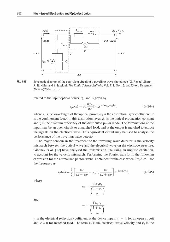
282 High-Speed Electronics and Optoelectronics
Δz
C
YZ
Iph(z)
Rsemi
v(z + Δz,t)
i(z + Δz,t)Rcpw Lcpw
Gs
v(z,t)
i(z,t)
Fig. 4.43 Schematic diagram of the equivalent circuit of a travelling wave photodiode (G. Rengel-Sharp,R. E. Miles and S. Iezekiel, The Radio Science Bulletin, Vol. 311, No. 12, pp. 55–64, December2004. c©2004 URSI).
related to the input optical power Po, and is given by
Iph(z) = Poηqλ
hc�αoe−�αo e− jβoz, (4.244)
where λ is the wavelength of the optical power, αo is the absorption layer coefficient, �is the confinement factor in this absorption layer, βo is the optical propagation constantand η is the quantum efficiency of the distributed p–i–n diode. The terminations at theinput may be an open circuit or a matched load, and at the output is matched to extractthe signals on the electrical wave. This equivalent circuit may be used to analyse theperformance of the travelling wave detector.
The major concern in the treatment of the travelling wave detector is the velocitymismatch between the optical wave and the electrical wave on the electrode structure.Giboney et al. [12] have analysed the transmission line using an impulse excitation,to account for the velocity mismatch. Performing the Fourier transform, the followingexpression for the normalised photocurrent is obtained for the case when �αo� � 1 forthe frequency ω:
ıν(ω) = 1
2
[ωf
ωf − jω+ γ (ω)
ωr
ωr + jω
]e−jω(�/ve), (4.245)
where
ωf = �αove(1 − ve
vo
)and
ωr = �αove(1 + ve
vo
) .
γ is the electrical reflection coefficient at the device input, γ = 1 for an open circuitand γ = 0 for matched load. The term ve is the electrical wave velocity and vo is the
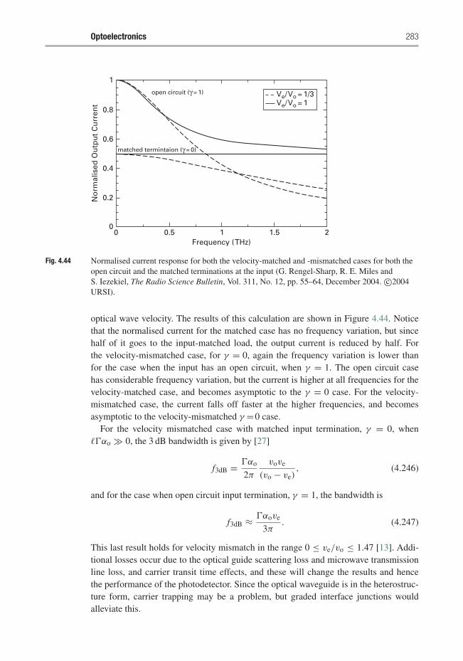
Optoelectronics 283
00
0.2
0.4
0.6
0.8
1
0.5 1 1.5 2Frequency (THz)
No
rmal
ised
Ou
tpu
t C
urr
ent
Ve/Vo = 1/3Ve/Vo = 1
matched termintaion (γ = 0)
open circuit (γ = 1)
Fig. 4.44 Normalised current response for both the velocity-matched and -mismatched cases for both theopen circuit and the matched terminations at the input (G. Rengel-Sharp, R. E. Miles andS. Iezekiel, The Radio Science Bulletin, Vol. 311, No. 12, pp. 55–64, December 2004. c©2004URSI).
optical wave velocity. The results of this calculation are shown in Figure 4.44. Noticethat the normalised current for the matched case has no frequency variation, but sincehalf of it goes to the input-matched load, the output current is reduced by half. Forthe velocity-mismatched case, for γ = 0, again the frequency variation is lower thanfor the case when the input has an open circuit, when γ = 1. The open circuit casehas considerable frequency variation, but the current is higher at all frequencies for thevelocity-matched case, and becomes asymptotic to the γ = 0 case. For the velocity-mismatched case, the current falls off faster at the higher frequencies, and becomesasymptotic to the velocity-mismatched γ =0 case.
For the velocity mismatched case with matched input termination, γ = 0, when��αo � 0, the 3 dB bandwidth is given by [27]
f3dB = �αo
2π
vove
(vo − ve), (4.246)
and for the case when open circuit input termination, γ = 1, the bandwidth is
f3dB ≈ �αove
3π. (4.247)
This last result holds for velocity mismatch in the range 0 ≤ ve/vo ≤ 1.47 [13]. Addi-tional losses occur due to the optical guide scattering loss and microwave transmissionline loss, and carrier transit time effects, and these will change the results and hencethe performance of the photodetector. Since the optical waveguide is in the heterostruc-ture form, carrier trapping may be a problem, but graded interface junctions wouldalleviate this.
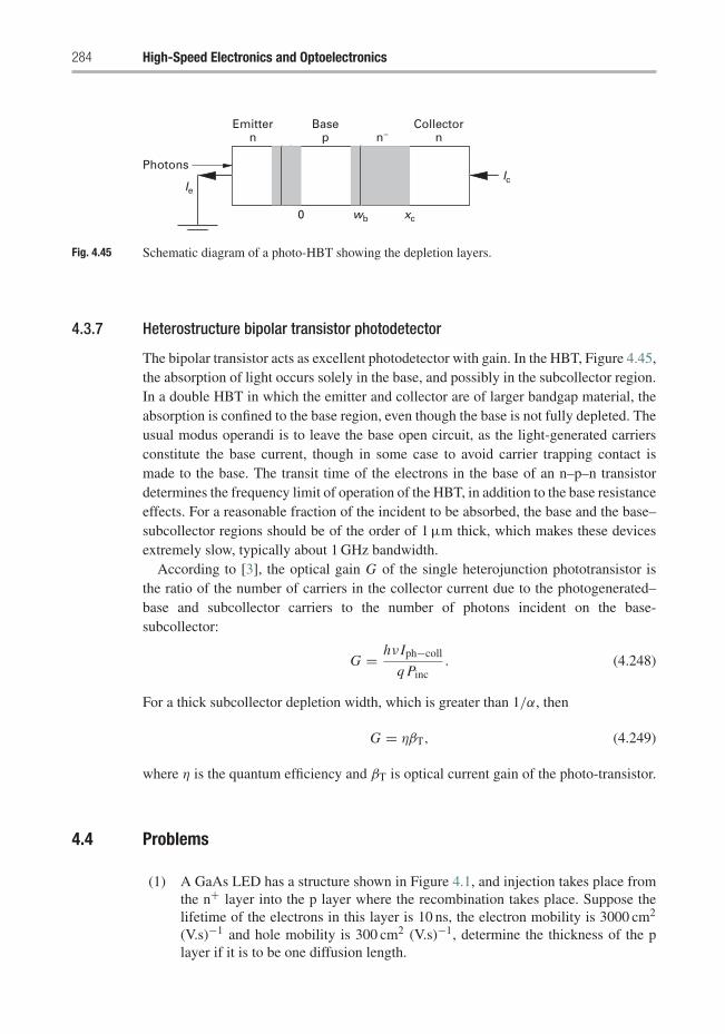
284 High-Speed Electronics and Optoelectronics
Photons
Emittern
Basep
Collectornn−
0 wb xc
IeIc
Fig. 4.45 Schematic diagram of a photo-HBT showing the depletion layers.
4.3.7 Heterostructure bipolar transistor photodetector
The bipolar transistor acts as excellent photodetector with gain. In the HBT, Figure 4.45,the absorption of light occurs solely in the base, and possibly in the subcollector region.In a double HBT in which the emitter and collector are of larger bandgap material, theabsorption is confined to the base region, even though the base is not fully depleted. Theusual modus operandi is to leave the base open circuit, as the light-generated carriersconstitute the base current, though in some case to avoid carrier trapping contact ismade to the base. The transit time of the electrons in the base of an n–p–n transistordetermines the frequency limit of operation of the HBT, in addition to the base resistanceeffects. For a reasonable fraction of the incident to be absorbed, the base and the base–subcollector regions should be of the order of 1 μm thick, which makes these devicesextremely slow, typically about 1 GHz bandwidth.
According to [3], the optical gain G of the single heterojunction phototransistor isthe ratio of the number of carriers in the collector current due to the photogenerated–base and subcollector carriers to the number of photons incident on the base-subcollector:
G = hν Iph−coll
q Pinc. (4.248)
For a thick subcollector depletion width, which is greater than 1/α, then
G = ηβT, (4.249)
where η is the quantum efficiency and βT is optical current gain of the photo-transistor.
4.4 Problems
(1) A GaAs LED has a structure shown in Figure 4.1, and injection takes place fromthe n+ layer into the p layer where the recombination takes place. Suppose thelifetime of the electrons in this layer is 10 ns, the electron mobility is 3000 cm2
(V.s)−1 and hole mobility is 300 cm2 (V.s)−1, determine the thickness of the player if it is to be one diffusion length.
Optoelectronics 285
(2) Calculate, numerically, the correct value of the external quantum efficiency of aLED radiating into air. Assume that the semiconductor index is 3.5, the polari-sation random which implies that half the radiation is perpendicular polarisationand the other half is parallel polarisation. Assume that the transmission coeffi-cient for the perpendicular polarisation from medium 1, index n1, into medium2, index n2, is given by
τ⊥ = 2n1 cos θ1
(n1 cos θ1 + n2 cos θ2),
and the transmission coefficient for parallel polarisation is given by
τ‖ = 2n1 cos θ2
(n2 cos θ1 + n1 cos θ2).
(3) A ridge laser is to operate at 800 nm, with a guide index of 3.41 and claddingindex of 3.43. Determine the maximum thickness and width of the laser wave-guide.
(4) An InGaAsP laser operating at 1300 nm has an effective guide index of 3.4. Whatis the reflectivity of its cleaved facets? Suppose the internal loss is 30 cm−1,what is the photon lifetime, assuming the group index is 3.5? Suppose the laserlength is 300 μm, width 3 μm and thickness of 0.2 μm, the gain coefficient ais 2 × 10⁻¹⁶ cm2, the value of the transparency number density is 1018 cm−3
and carrier lifetime is 1 ns. What is the threshold carrier density and the thresh-old current? What is the relaxation oscillation frequency at twice the thresholdcurrent?
(5) A p–i–n diode receiver at 1300 nm has a preamplifier noise figure of 2 dB. Thesignalling rate is 1 GHz, bandwidth of 100 MHz, the load resistance is 100�,dark current is 1 nA, the diode quantum efficiency is 0.95 and a signal of 5 μWilluminates this diode. Determine the signal-to-noise ratio at the output.
(6) Suppose the p–i–n diode is replaced by an avalanche photodetector, multiplica-tion factor of 10, noise factor of 3, dark current of 10 nA and background currentof 1 nA. This APD is illuminated with 1 μW of optical power; determine thesignal-to-noise ratio.
References
[1] Agrawal G. P. (2002). Fiber-Optic Communication Systems, 3rd edn. John Wiley & Sons.[2] Agrawal G. P., Dutta N. K. (1993). Semiconductor Lasers. Van Norstrand Rheinhold.[3] Bhattacharya P. (1997). Semiconductor Optoelectronic Devices, 2nd edn. Prentice Hall.[4] Burrus C. A., Dawson R. W. (1970). Small-area high-current-density GaAs electrolumi-
nescent diodes and a method of operation for improved degradation characteristics. Appl.Phys. Lett. 17, 3, 97–99.
[5] Chang K. P., Yang S. L., Chuu D. S., Hsiao R. S., Chen J. F. (2005). Characteriza-tion of self-assembled InAs quantum dots with InAlAs/InGaAs strain-reduced layers byphotoluminescence spectroscopy. J. Appl. Phys. 97, 83511–83514.
286 High-Speed Electronics and Optoelectronics
[6] Chang Y.-C., Wang C. S., Coldren L. A. (2007). High-efficiency, high-speed VCSELs with35 Gbit/s error-free operation. Electron. Lett. 43, 19, 1022–1023.
[7] Cheng D. K. (1989). Field and Wave Electromagnetics, 2nd edn. Addison-Wesley.
[8] Chuang S. L. (1995). Physics of Optoelectronic Devices. John Wiley & Sons.
[9] Dutta N. K. (1980). Calculated absorption, emission, and gain in In0.72Ga0.28As0.6P0.4.J. Appl. Phys. 52, 6095–6100.
[10] Effendberger F. J., Joshi A. M. (1996). Ultrafast, dual-depletion region, InGaAs/InP p-i-ndetector. J. Lightw. Technol. 14, 8 (August), 1859–1864.
[11] Fathpour K. P., Mia Z., Bhattacharya P. (2005). High speed quantum dot lasers. J. Phys. D:Appl. Phys. 38, 2103–2111.
[12] Giboney K. S., Nagarajan R. L., Reynolds T. E., et al. (1995). Traveling-wave photodetec-tors with 172-GHz bandwidth and 76-GHGz bandwidth-efficiency product. IEEE PhotonicTechnol. Lett. 7, 4 (April), 412–414.
[13] Giboney K. S., Rodwell M. J. W., Bowers J. E. (1997). Traveling-wave photodetectortheory. IEEE Trans. Microw. Theory Tech. 45, 8 (August), 1310–1319.
[14] Hasegawa H., Furukawa M., Yani H. (1971). Properties of microstrip line on Si-SiO2system. IEEE Trans. Microw. Theory Tech. 19, 11 (November), 869–881.
[15] Hietala V., Vawter G. A., Brennam T. M., Hammons B. E. (1995). Traveling-wavephotodetectors for high-power, large-bandwidth applications. IEEE Trans. Microw. TheoryTech. 43, 9 (September), 2291–2298.
[16] Kato K. (1999). Ultrawide band/high-frequency photodetectors. IEEE Trans. Microw.Theory Tech. 47, 7 (July), 1265–1281.
[17] Keiser G. (2000). Optical Fiber Communications, 2nd edn. McGraw-Hill.
[18] Kinsey G. S., Campbell J. C., Dentai A. G. (2001). Waveguide avalanche photodiode oper-ating at 1.55 μm with a gain-bandwidth product of 320 GHz. IEEE Photonic Technol.Lett. 13, 8 (August), 842–844.
[19] Lee T. P., Burrus C. A., Copeland J. A., Dentai A. G., Marcuse D. (1982). Short cav-ity InGaAsP injection lasers: dependence of mode spectra and single-longitudinal-modepower on cavity length. IEEE J. Quan. Electron. QE-18, 7, 1101–1113.
[20] Lin L. Y., Wu M. C., Itoh T., et al. (1997). High-power high-speed photodetectors –design, analysis, and experimental demonstration. IEEE Trans. Microw. Theory Tech. 45, 8(August), 1320–1331.
[21] Marcuse D., Lee T. P. (1983). On approximate analytical solutions of the rate equa-tions for studying transient spectra of injection lasers. IEEE J. Quan. Electron. QE-19, 9,1101–1113.
[22] Matsushima Y., Sasaki K., Noda Y. (1981). New type InGaAs/InP heterostructureavalanche photodiode with buffer layer. IEEE Electron Device Lett. 2, 7 (July), 179–181.
[23] McIntyre R. J. (1972). The distribution of gains in uniformly multiplying avalancephotodiodes: theory. IEEE Trans. Electron Devices 2, 6 (June), 703–713.
[24] Nash F. R. (1973). Mode guidance of double-heterostructure GaAs lasers. J. Appl.Phys. 44, 10, 4696–4707.
[25] Nelson R. J., Wilson R. B., Wright P. D., Barnes P. A., Dutta N. K. (1981). CW electroop-tical properties of InGaAsP (λ = 1.3 μm) buried-heterostructure lasers. IEEE J. Quan.Electron. QE-17, 2, 202–207.
[26] Nishida K., Taguchi K., Matsumo Y. (1979). InGaAsP heterostructure avalanche photo-diodes with high avalanche gain. Appl. Phys. Lett. 35, 3 (August), 251–253.
Optoelectronics 287
[27] Rengel-Sharp G., Miles R. E., Iezekiel S. (2004). Traveling-wave photodetectors: a review.The Radio Science Bulletin, URSI 311, 12 (December), 54–64.
[28] Shi J.-W., Gan K.-G., Chiu Y.-J., et al. (2001). Metal-semiconductor-metal traveling-wavephotodetectors. IEEE Photonic Technol. Lett. 16, 6 (June), 623–625.
[29] Shi J.-W., Liu Y.-H., Liu C.-W. (2004). Design and analysis of separate-absorption-transport-charge-multiplication traveling-wave avalanche photodetectors. J. Lightw. Tech-nol. 22, 6 (June), 1583–1590.
[30] Soole J. B. D., Schumacher H. (1991). InGaAS metal-semiconductor-metal photodetec-tor for long wavelength optical communications. IEEE J. Quan. Electron. 27, 3 (March),737–752.
[31] Tauber D., Wang G., Geels R. S., Bowers J. E., Coldren L. A. (1993). Large and smallsignal dynamics of vertical cavity surface emitting lasers. Appl. Phys. Lett. 62, 4, 325–327.
[32] Taylor H. F., Ekonoyan O., Park C. S., Choi K. N., Chang K. (1990). Traveling-wavephotodetectors. SPIE Optoelectronics Signal Processing for Phased Array Antennas II,59–63.
[33] Tucker R. S., Kaminow I. P. (1984). High frequency characteristics of directly modu-lated InGaAsP ridge waveguide and buried heterostructure lasers. J. Lightw. Technol. 2, 4,385–393.
[34] Yariv A. (1997). Optical Electronics in Modern Communications, 5th edn. OxfordUniversity Press.
[35] Zhang X., Gutierrez-Aitkens A. L., Klotzkin D., Bhattacharya P., Caneau C., Bhatt R.(1996). 0.98 μm multiquantum well tunnelling injection lasers with ultra–high modulationbandwidths. Electron. Lett. 32, 18, 1715–1717.


Part Two
Circuits

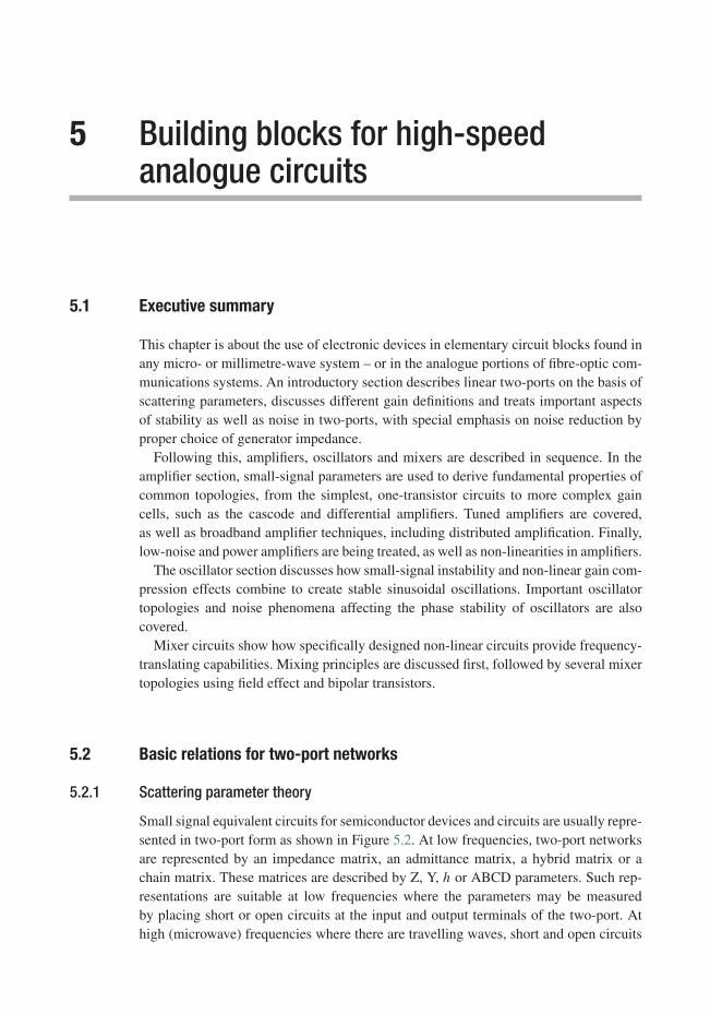
5 Building blocks for high-speedanalogue circuits
5.1 Executive summary
This chapter is about the use of electronic devices in elementary circuit blocks found inany micro- or millimetre-wave system – or in the analogue portions of fibre-optic com-munications systems. An introductory section describes linear two-ports on the basis ofscattering parameters, discusses different gain definitions and treats important aspectsof stability as well as noise in two-ports, with special emphasis on noise reduction byproper choice of generator impedance.
Following this, amplifiers, oscillators and mixers are described in sequence. In theamplifier section, small-signal parameters are used to derive fundamental properties ofcommon topologies, from the simplest, one-transistor circuits to more complex gaincells, such as the cascode and differential amplifiers. Tuned amplifiers are covered,as well as broadband amplifier techniques, including distributed amplification. Finally,low-noise and power amplifiers are being treated, as well as non-linearities in amplifiers.
The oscillator section discusses how small-signal instability and non-linear gain com-pression effects combine to create stable sinusoidal oscillations. Important oscillatortopologies and noise phenomena affecting the phase stability of oscillators are alsocovered.
Mixer circuits show how specifically designed non-linear circuits provide frequency-translating capabilities. Mixing principles are discussed first, followed by several mixertopologies using field effect and bipolar transistors.
5.2 Basic relations for two-port networks
5.2.1 Scattering parameter theory
Small signal equivalent circuits for semiconductor devices and circuits are usually repre-sented in two-port form as shown in Figure 5.2. At low frequencies, two-port networksare represented by an impedance matrix, an admittance matrix, a hybrid matrix or achain matrix. These matrices are described by Z, Y, h or ABCD parameters. Such rep-resentations are suitable at low frequencies where the parameters may be measuredby placing short or open circuits at the input and output terminals of the two-port. Athigh (microwave) frequencies where there are travelling waves, short and open circuits
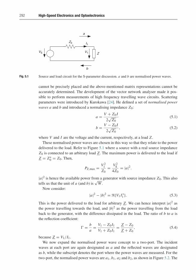
292 High-Speed Electronics and Optoelectronics
b
a
ZV1VS
Z0 I1
Fig. 5.1 Source and load circuit for the S-parameter discussion. a and b are normalised power waves.
cannot be precisely placed and the above-mentioned matrix representations cannot beaccurately determined. The development of the vector network analyser made it pos-sible to perform measurements of high frequency travelling wave circuits. Scatteringparameters were introduced by Kurokawa [24]. He defined a set of normalised powerwaves a and b and introduced a normalising impedance Z0:
a = V + Z0 I
2√
Z0(5.1)
b = V − Z0 I
2√
Z0, (5.2)
where V and I are the voltage and the current, respectively, at a load Z .These normalised power waves are chosen in this way so that they relate to the power
delivered to the load. Refer to Figure 5.1 where a source with a real source impedanceZ0 is connected to an arbitrary load Z . The maximum power is delivered to the load ifZ = Z∗
0 = Z0. Then,
PZ,max = V 21
Z0= V 2
S
4Z0= |a|2.
|a|2 is hence the available power from a generator with source impedance Z0. This alsotells us that the unit of a (and b) is
√W .
Now consider:
|a|2 − |b|2 = �{V1 I ∗1 }. (5.3)
This is the power delivered to the load for arbitrary Z . We can hence interpret |a|2 asthe power travelling towards the load, and |b|2 as the power travelling from the loadback to the generator, with the difference dissipated in the load. The ratio of b to a isthe reflection coefficient:
� = b
a= V1 − Z0 I1
V1 + Z0 I1= Z − Z0
Z + Z0, (5.4)
because Z = V1/I1.We now expand the normalised power wave concept to a two-port. The incident
waves at each port are again designated as a and the reflected waves are designatedas b, while the subscript denotes the port where the power waves are measured. For thetwo-port, the normalised power waves are a1, b1, a2 and b2, as shown in Figure 5.2. The
Building blocks for high-speed analogue circuits 293
Two-port network
Port 1 Port 2
Z0 Z0a1 a2
b2b1
Fig. 5.2 Two-port network embedded in a transmission line with characteristic impedance Z0, withincident waves a1, a2 and reflected waves b1, b2.
scattering parameters are the coefficients of linear equations relating the reflected wavesb to the incident waves a:
b1 = S11a1 + S12a2 (5.5)
b2 = S21a1 + S22a2. (5.6)
The scattering parameters can therefore be expressed as the ratio of two power waves,provided that all the ports are terminated in a non-reflective fashion (a = 0 at all otherports). For a two-port,
S11 = b1
a1|a2=0 (5.7)
S12 = b1
a2|a1=0 (5.8)
S21 = b2
a1|a2=0 (5.9)
S22 = b2
a2|a2=0. (5.10)
These relations can be written in matrix form as follows:(b1
b2
)=
(S11 S12
S21 S22
) (a1
a2
). (5.11)
Let Z0 be the characteristic impedance of the transmission lines connected to ports 1and 2 of the two-port. If port 2 is terminated by Z0, there is no reflection at the load andhence the wave incident at port 2, a2, is zero. Similarly, if port 1 is terminated by Z0
and the stimulus is fed to port 2, a1, is zero. If port 1 is designated to be the input andport 2 the output, then S11 is the input reflection coefficient with Z0 the output, S22
is the output reflection coefficient with the input terminated by Z0, S21 is the forwardtransmission coefficient with Z0 as the output load, and S12 is the reverse transmissioncoefficient with Z0 at the input.
In general, the scattering parameters are complex. The polar form of the scatteringparameter is useful in many applications:
S = | S | exp j θ , (5.12)
where | S | is the magnitude of S and θ is the phase.
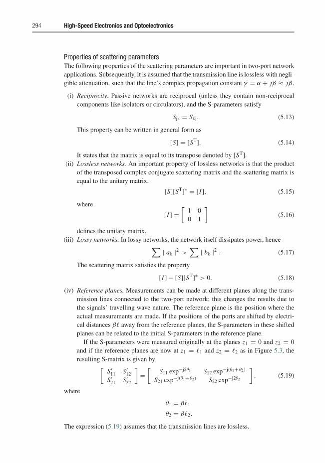
294 High-Speed Electronics and Optoelectronics
Properties of scattering parametersThe following properties of the scattering parameters are important in two-port networkapplications. Subsequently, it is assumed that the transmission line is lossless with negli-gible attenuation, such that the line’s complex propagation constant γ = α + jβ ≈ jβ.
(i) Reciprocity. Passive networks are reciprocal (unless they contain non-reciprocalcomponents like isolators or circulators), and the S-parameters satisfy
Sjk = Skj. (5.13)
This property can be written in general form as
[S] = [ST]. (5.14)
It states that the matrix is equal to its transpose denoted by [ST].(ii) Lossless networks. An important property of lossless networks is that the product
of the transposed complex conjugate scattering matrix and the scattering matrix isequal to the unitary matrix.
[S][ST]∗ = [I ], (5.15)
where
[I ] =[
1 00 1
](5.16)
defines the unitary matrix.(iii) Lossy networks. In lossy networks, the network itself dissipates power, hence∑
| ak |2 >∑
| bk |2 . (5.17)
The scattering matrix satisfies the property
[I ] − [S][ST]∗ > 0. (5.18)
(iv) Reference planes. Measurements can be made at different planes along the trans-mission lines connected to the two-port network; this changes the results due tothe signals’ travelling wave nature. The reference plane is the position where theactual measurements are made. If the positions of the ports are shifted by electri-cal distances β� away from the reference planes, the S-parameters in these shiftedplanes can be related to the initial S-parameters in the reference plane.
If the S-parameters were measured originally at the planes z1 = 0 and z2 = 0and if the reference planes are now at z1 = �1 and z2 = �2 as in Figure 5.3, theresulting S-matrix is given by[
S′11 S′
12S′
21 S′22
]=
[S11 exp−j2θ1 S12 exp−j(θ1+ θ2)
S21 exp−j(θ1+ θ2) S22 exp−j2θ2
], (5.19)
where
θ1 = β�1
θ2 = β�2.
The expression (5.19) assumes that the transmission lines are lossless.
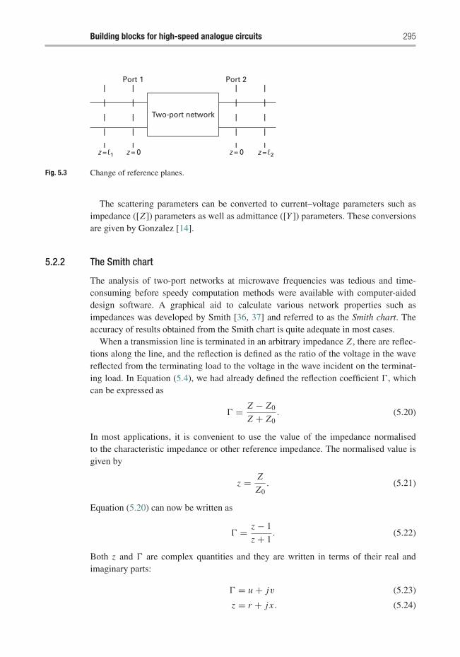
Building blocks for high-speed analogue circuits 295
Two-port network
Port 1 Port 2
z = 1 z = 0 z = 0 z = 2
Fig. 5.3 Change of reference planes.
The scattering parameters can be converted to current–voltage parameters such asimpedance ([Z ]) parameters as well as admittance ([Y ]) parameters. These conversionsare given by Gonzalez [14].
5.2.2 The Smith chart
The analysis of two-port networks at microwave frequencies was tedious and time-consuming before speedy computation methods were available with computer-aideddesign software. A graphical aid to calculate various network properties such asimpedances was developed by Smith [36, 37] and referred to as the Smith chart. Theaccuracy of results obtained from the Smith chart is quite adequate in most cases.
When a transmission line is terminated in an arbitrary impedance Z , there are reflec-tions along the line, and the reflection is defined as the ratio of the voltage in the wavereflected from the terminating load to the voltage in the wave incident on the terminat-ing load. In Equation (5.4), we had already defined the reflection coefficient �, whichcan be expressed as
� = Z − Z0
Z + Z0. (5.20)
In most applications, it is convenient to use the value of the impedance normalisedto the characteristic impedance or other reference impedance. The normalised value isgiven by
z = Z
Z0. (5.21)
Equation (5.20) can now be written as
� = z − 1
z + 1. (5.22)
Both z and � are complex quantities and they are written in terms of their real andimaginary parts:
� = u + jv (5.23)
z = r + j x . (5.24)
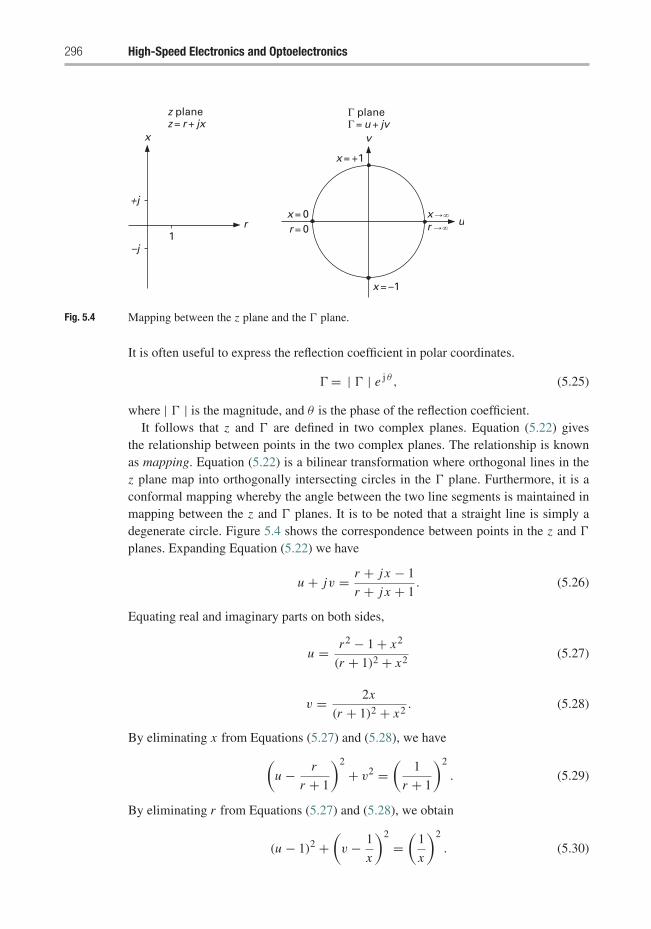
296 High-Speed Electronics and Optoelectronics
z planez = r + jx
Γ planeΓ = u + jv
x = 0r = 0
x = –1
x = +1
r x
x
+j
–j1
r u
v
Fig. 5.4 Mapping between the z plane and the � plane.
It is often useful to express the reflection coefficient in polar coordinates.
� = | � | e j θ , (5.25)
where | � | is the magnitude, and θ is the phase of the reflection coefficient.It follows that z and � are defined in two complex planes. Equation (5.22) gives
the relationship between points in the two complex planes. The relationship is knownas mapping. Equation (5.22) is a bilinear transformation where orthogonal lines in thez plane map into orthogonally intersecting circles in the � plane. Furthermore, it is aconformal mapping whereby the angle between the two line segments is maintained inmapping between the z and � planes. It is to be noted that a straight line is simply adegenerate circle. Figure 5.4 shows the correspondence between points in the z and �
planes. Expanding Equation (5.22) we have
u + jv = r + j x − 1
r + j x + 1. (5.26)
Equating real and imaginary parts on both sides,
u = r2 − 1 + x2
(r + 1)2 + x2(5.27)
v = 2x
(r + 1)2 + x2. (5.28)
By eliminating x from Equations (5.27) and (5.28), we have(u − r
r + 1
)2
+ v2 =(
1
r + 1
)2
. (5.29)
By eliminating r from Equations (5.27) and (5.28), we obtain
(u − 1)2 +(v − 1
x
)2
=(
1
x
)2
. (5.30)
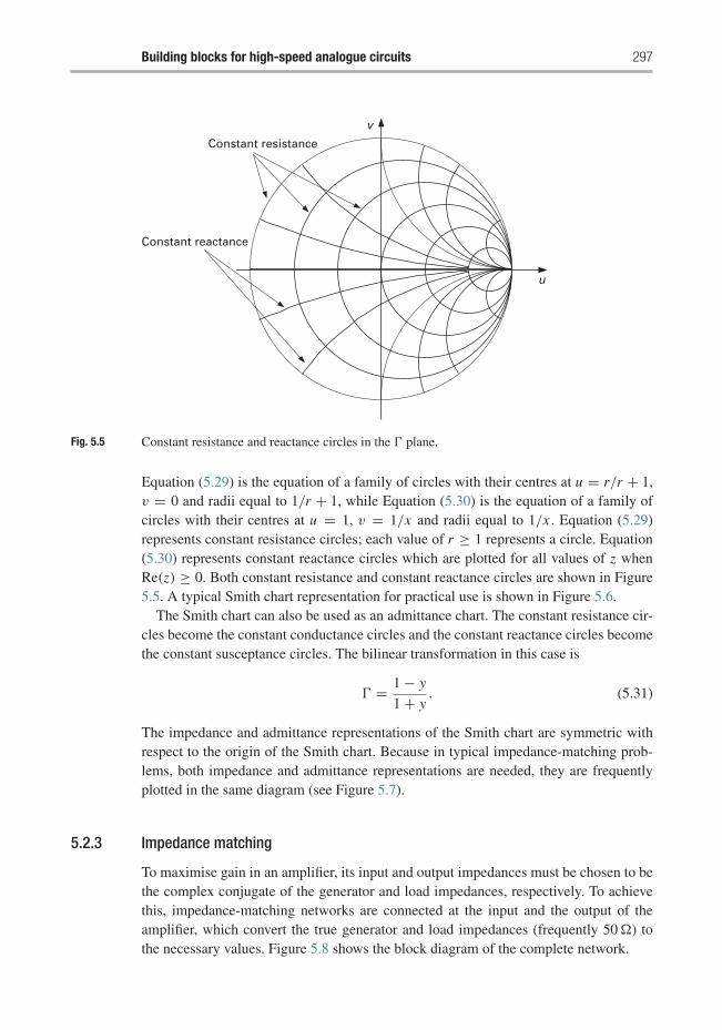
Building blocks for high-speed analogue circuits 297
u
v
Constant resistance
Constant reactance
Fig. 5.5 Constant resistance and reactance circles in the � plane.
Equation (5.29) is the equation of a family of circles with their centres at u = r/r + 1,v = 0 and radii equal to 1/r + 1, while Equation (5.30) is the equation of a family ofcircles with their centres at u = 1, v = 1/x and radii equal to 1/x . Equation (5.29)represents constant resistance circles; each value of r ≥ 1 represents a circle. Equation(5.30) represents constant reactance circles which are plotted for all values of z whenRe(z) ≥ 0. Both constant resistance and constant reactance circles are shown in Figure5.5. A typical Smith chart representation for practical use is shown in Figure 5.6.
The Smith chart can also be used as an admittance chart. The constant resistance cir-cles become the constant conductance circles and the constant reactance circles becomethe constant susceptance circles. The bilinear transformation in this case is
� = 1 − y
1 + y. (5.31)
The impedance and admittance representations of the Smith chart are symmetric withrespect to the origin of the Smith chart. Because in typical impedance-matching prob-lems, both impedance and admittance representations are needed, they are frequentlyplotted in the same diagram (see Figure 5.7).
5.2.3 Impedance matching
To maximise gain in an amplifier, its input and output impedances must be chosen to bethe complex conjugate of the generator and load impedances, respectively. To achievethis, impedance-matching networks are connected at the input and the output of theamplifier, which convert the true generator and load impedances (frequently 50�) tothe necessary values. Figure 5.8 shows the block diagram of the complete network.
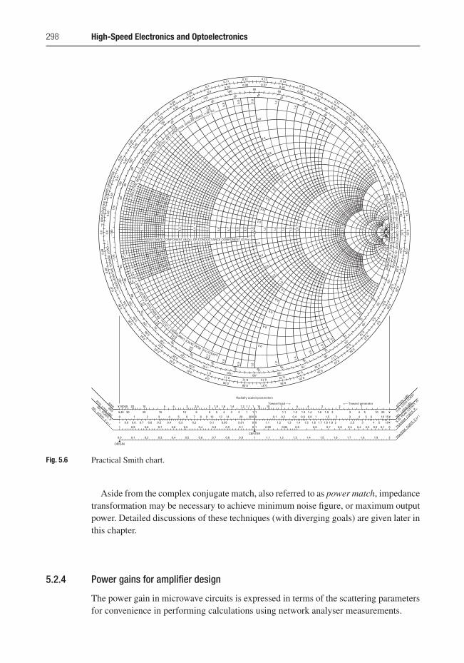
298 High-Speed Electronics and Optoelectronics
0.1
0.1
0.1
0.2
0.2
0.3
0.3
0.4
0.4
0.5
0.5
0.6
0.6
0.7
0.7
0.8
0.8
0.8
0.9
0.9
0.9
1.0
1.0
1.0
1.2
1.2
1.2
1.4
1.4
1.4
1.6
1.6
1.6
1.8
1.8
1.8
2.0
2.0
2.0
3.0
3.0
3.0
4.0
4.0
4.0
5.0
5.0
5.0
10
10
10
20
20
20
50
50
50
0.2
0.2
0.2
0.2
0.4
0.4
0.4
0.4
0.6
0.6
0.6
0.6
0.8
0.8
0.8
0.8
1.0
1.0
1.0
1.0
20–20
30–30
40–40
50
–50
60
–60
70
–70
80
–80
90
–90
100
–100
110
–110
120
–120
130
–130
140
–140
150
–150
160
–160
170
–170
–180
90–9
085
–85
80–8
0
75–7
5
70–7
0
65–6
5
60–6
0
55–5
5
50–5
0
45
–45
40
–40
35
–35
30
–30
25
–25
20
–20
15
–15
10
–10
0.04
0.04
0.05
0.05
0.06
0.06
0.07
0.07
0.08
0.08
0.09
0.09
0.1
0.1
0.11
0.11
0.12
0.12
0.13
0.13
0.14
0.14
0.15
0.15
0.16
0.16
0.17
0.17
0.18
0.18
0.190.19
0.20.2
0.210.21
0.22
0.220.23
0.230.24
0.24
0.25
0.25
0.26
0.26
0.27
0.27
0.28
0.28
0.29
0.29
0.3
0.3
0.31
0.31
0.32
0.32
0.33
0.33
0.34
0.34
0.35
0.35
0.36
0.36
0.37
0.37
0.38
0.38
0.39
0.39
0.4
0.4
0.41
0.41
0.42
0.42
0.43
0.43
0.44
0.44
0.45
0.45
0.46
0.46
0.47
0.47
0.48
0.48
0.49
0.49
0.0
0.0
AN
GLE
OF
TR
AN
SM
ISS
I ON
CO
EFF
ICIEN
TIN
DEG
REES
AN
GLE
OF
REFLEC
TI O
N C
OE
FFICIE
NT
IND
EGR
EES
—> W
AV
ELE
NG
THS
TOW
ARD
GEN
ERAT
OR
—>
<—W
AV
ELEN
GTH
S TO
WA
RDLO
AD
<—
IND
UC
TIVE
REA
CTA
NC
ECO
MPO
NENT
(+j X
/Zo)
, ORCAPACITIVE SUSCEPTANCE (+jB/Yo)
CAPACITIVE REACTANCE COMPONENT(–
jX/Z
o),O
R INDU
CTI
VESU
SCEP
TAN
CE
(–jB
/Yo
)
RESISTANCE COMPONENT (R/Zo), OR CONDUCTANCE COMPONENT (G/Yo)
Radially scaled parameters
Toward load —> <— Toward generator1.11.21.41.61.822.5345102010040
SWR 1¥
12345681015203040
dBS1¥
1234571015 ATTEN. [dB]
1.1 1.2 1.3 1.4 1.6 1.8 2 3 4 5 10 20 S.W. L
OSS COEFF
1 ¥
0 1 2 3 4 5 6 7 8 9 10 12 14 20 30
RTN. LOSS [dB] ¥
0.010.050.10.20.30.40.50.60.70.80.91
RFL. COEFF, P0
0.1 0.2 0.4 0.6 0.8 1 1.5 2 3 4 5 6 10 15 RFL. L
OSS [dB]
¥0
1.1 1.2 1.3 1.4 1.5 1.6 1.7 1.8 1.9 2 2.5 3 4 5 10 S.W. P
EAK (CONST. P
)
0 ¥
0.10.20.30.40.50.60.70.80.91
RFL. COEFF, E or I0 0.99 0.95 0.9 0.8 0.7 0.6 0.5 0.4 0.3 0.2 0.1 0 TRANSM
. COEFF
, P
1
CENTER1 1.1 1.2 1.3 1.4 1.5 1.6 1.7 1.8 1.9 2 TRANSM
. COEFF
, E o
r I
0.0 0.1 0.2 0.3 0.4 0.5 0.6 0.7 0.8 0.9
ORIGIN
0.6
0.2
0.3
0.4
0.5
0.7
Fig. 5.6 Practical Smith chart.
Aside from the complex conjugate match, also referred to as power match, impedancetransformation may be necessary to achieve minimum noise figure, or maximum outputpower. Detailed discussions of these techniques (with diverging goals) are given later inthis chapter.
5.2.4 Power gains for amplifier design
The power gain in microwave circuits is expressed in terms of the scattering parametersfor convenience in performing calculations using network analyser measurements.
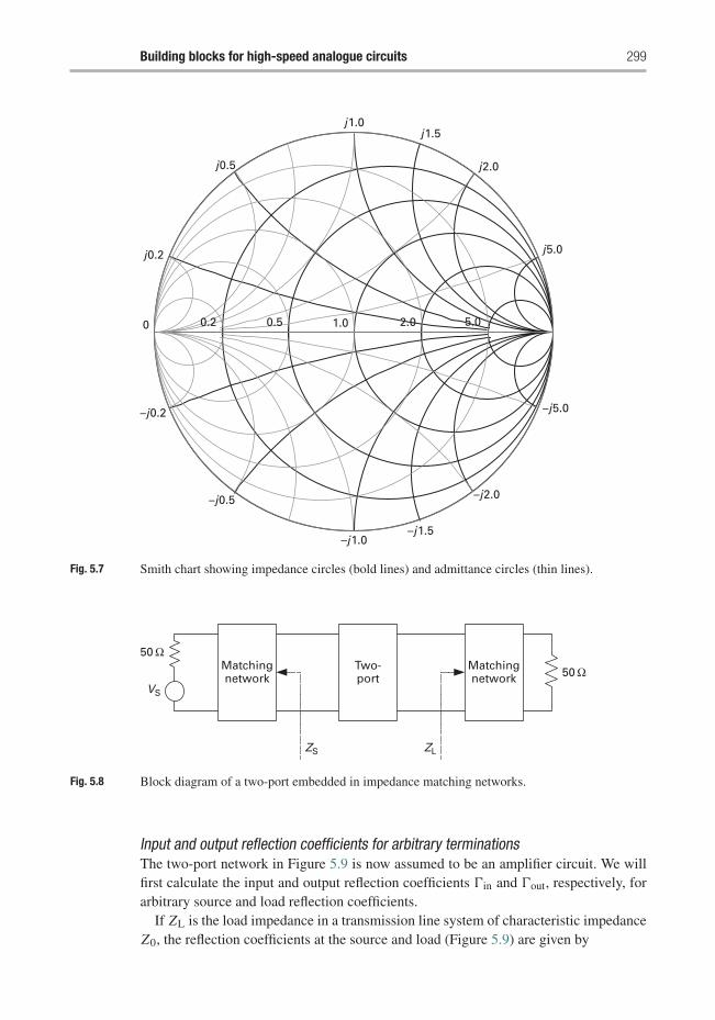
Building blocks for high-speed analogue circuits 299
–j0.5
–j0.2
j0.2
j0.5
j1.0j1.5
j2.0
j5.0
–j5.0
–j2.0
–j1.5–j1.0
0 0.2 0.5 1.0 2.0 5.0
Fig. 5.7 Smith chart showing impedance circles (bold lines) and admittance circles (thin lines).
Matchingnetwork
Matchingnetwork
Two-port
ZS
VS
ZL
50 Ω
50 Ω
Fig. 5.8 Block diagram of a two-port embedded in impedance matching networks.
Input and output reflection coefficients for arbitrary terminationsThe two-port network in Figure 5.9 is now assumed to be an amplifier circuit. We willfirst calculate the input and output reflection coefficients �in and �out, respectively, forarbitrary source and load reflection coefficients.
If ZL is the load impedance in a transmission line system of characteristic impedanceZ0, the reflection coefficients at the source and load (Figure 5.9) are given by
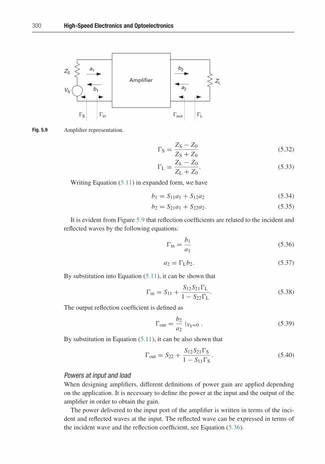
300 High-Speed Electronics and Optoelectronics
Amplifier
b2a1
b1VS
ZS
a2
ZL
ΓLΓin ΓoutΓS
Fig. 5.9 Amplifier representation.
�S = ZS − Z0
ZS + Z0(5.32)
�L = ZL − Z0
ZL + Z0. (5.33)
Writing Equation (5.11) in expanded form, we have
b1 = S11a1 + S12a2 (5.34)
b2 = S21a1 + S22a2. (5.35)
It is evident from Figure 5.9 that reflection coefficients are related to the incident andreflected waves by the following equations:
�in = b1
a1(5.36)
a2 = �Lb2. (5.37)
By substitution into Equation (5.11), it can be shown that
�in = S11 + S12S21�L
1 − S22�L. (5.38)
The output reflection coefficient is defined as
�out = b2
a2|VS=0 . (5.39)
By substitution in Equation (5.11), it can be also shown that
�out = S22 + S12S21�S
1 − S11�S. (5.40)
Powers at input and loadWhen designing amplifiers, different definitions of power gain are applied dependingon the application. It is necessary to define the power at the input and the output of theamplifier in order to obtain the gain.
The power delivered to the input port of the amplifier is written in terms of the inci-dent and reflected waves at the input. The reflected wave can be expressed in terms ofthe incident wave and the reflection coefficient, see Equation (5.36).
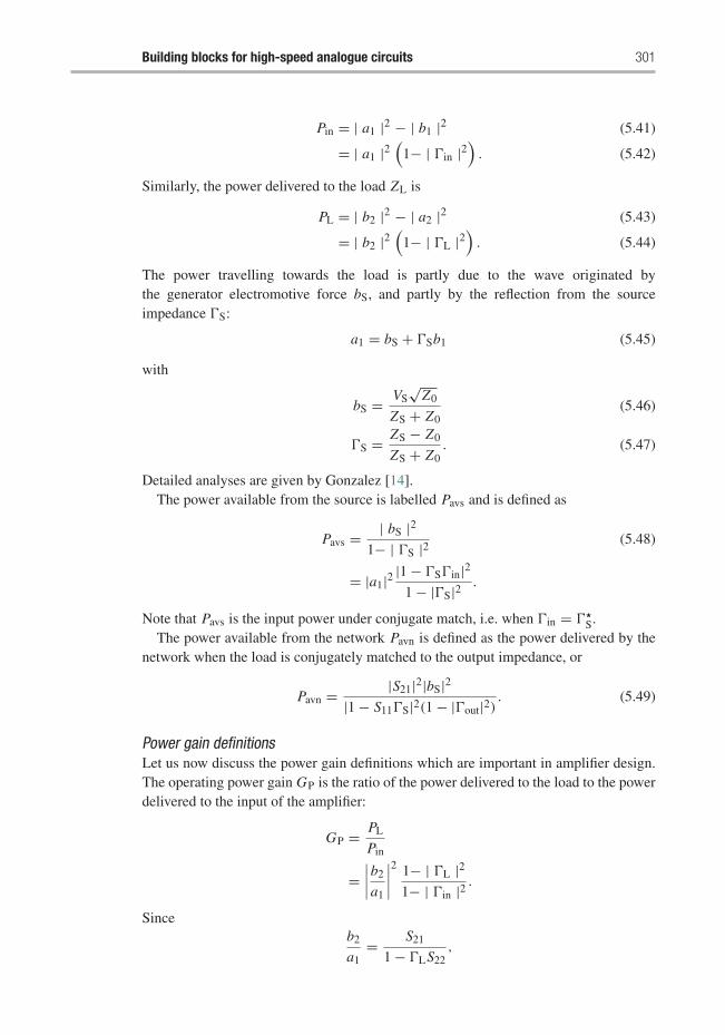
Building blocks for high-speed analogue circuits 301
Pin = | a1 |2 − | b1 |2 (5.41)
= | a1 |2(
1− | �in |2). (5.42)
Similarly, the power delivered to the load ZL is
PL = | b2 |2 − | a2 |2 (5.43)
= | b2 |2(
1− | �L |2). (5.44)
The power travelling towards the load is partly due to the wave originated bythe generator electromotive force bS, and partly by the reflection from the sourceimpedance �S:
a1 = bS + �Sb1 (5.45)
with
bS = VS√
Z0
ZS + Z0(5.46)
�S = ZS − Z0
ZS + Z0. (5.47)
Detailed analyses are given by Gonzalez [14].The power available from the source is labelled Pavs and is defined as
Pavs = | bS |21− | �S |2 (5.48)
= |a1|2 |1 − �S�in|21 − |�S|2 .
Note that Pavs is the input power under conjugate match, i.e. when �in = � S.
The power available from the network Pavn is defined as the power delivered by thenetwork when the load is conjugately matched to the output impedance, or
Pavn = |S21|2|bS|2|1 − S11�S|2(1 − |�out|2) . (5.49)
Power gain definitionsLet us now discuss the power gain definitions which are important in amplifier design.The operating power gain GP is the ratio of the power delivered to the load to the powerdelivered to the input of the amplifier:
GP = PL
Pin
=∣∣∣∣b2
a1
∣∣∣∣2 1− | �L |21− | �in |2 .
Sinceb2
a1= S21
1 − �LS22,
302 High-Speed Electronics and Optoelectronics
and using Equation (5.38), we obtain
GP = |S21|2 1 − |�L|2|1 − �LS22|2 − |S11 − �L�(S)|2 , (5.50)
where �(S) is the determinant of the scattering matrix.The transducer power gain GT is the ratio of the power delivered to the load to the
power available from the source:
GT = PL
Pavs
=∣∣∣∣b2
a1
∣∣∣∣2(1 − |�L|2)(1 − |�S|2)
|1 − �in�S|2
= |S21|2 (1 − |�L|2)(1 − |�S|2)|1 − �LS22 − �S (S11 − �L�(S)) |2 . (5.51)
In the absence of deliberate feedback, the reverse transmission S12 is frequently verysmall and can be neglected. S12 = 0 simplifies the denominator in Equation (5.51) andwe obtain the unilateral transducer power gain
GTU = |S21|2 (1 − |�L|2)(1 − |�S|2)|(1 − S11�L)(1 − S22�S)|2 . (5.52)
The available power gain GA, finally, is the ratio of the available gain from the networkPavn to the available power from the source Pavs:
GA = Pavn
Pavs(5.53)
= |S21|2 1 − |�S|2|1 − S11�S|2(1 − |�out|2)
= |S21|2 1 − |�S|2|1 − S11�S|2 − |S22(1 − S11�S) + S12S21�S|2 ,
using Equation (5.40).
5.2.5 Stability
GA still contains �S as a variable. We know already that the maximum power transferfrom the source to the load occurs for �S = �
in, so this appears to be an optimumchoice. Before we proceed, however, let us again investigate Equation (5.53). If thedenominator becomes zero, the available gain would grow beyond all bounds. Thishappens if
|1 − S11�S| = |S22(1 − S11�S) + S12S21�S|,or, written differently, ∣∣∣∣S22 + S12S21�S
1 − S11�S
∣∣∣∣ = 1 = |�out|,
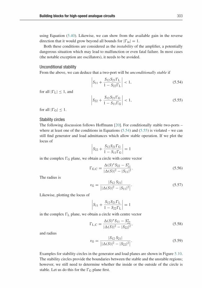
Building blocks for high-speed analogue circuits 303
using Equation (5.40). Likewise, we can show from the available gain in the reversedirection that it would grow beyond all bounds for |�in| = 1.
Both these conditions are considered as the instability of the amplifier, a potentiallydangerous situation which may lead to malfunction or even fatal failure. In most cases(the notable exception are oscillators), it needs to be avoided.
Unconditional stabilityFrom the above, we can deduce that a two-port will be unconditionally stable if∣∣∣∣S11 + S12S21�L
1 − S22�L
∣∣∣∣ < 1, (5.54)
for all |�L| ≤ 1, and ∣∣∣∣S22 + S12S21�G
1 − S11�G
∣∣∣∣ < 1, (5.55)
for all |�G| ≤ 1.
Stability circlesThe following discussion follows Hoffmann [20]. For conditionally stable two-ports –where at least one of the conditions in Equations (5.54) and (5.55) is violated – we canstill find generator and load admittances which allow stable operation. If we plot thelocus of ∣∣∣∣S22 + S12S21�G
1 − S11�G
∣∣∣∣ = 1
in the complex �G plane, we obtain a circle with centre vector
�G,C = �(S)∗S22 − S∗11
|�(S)|2 − |S11|2 . (5.56)
The radius is
rG = |S12 S21|∣∣|�(S)|2 − |S11|2∣∣ . (5.57)
Likewise, plotting the locus of ∣∣∣∣S11 + S12S21�L
1 − S22�L
∣∣∣∣ = 1
in the complex �L plane, we obtain a circle with centre vector
�L,C = �(S)∗S11 − S∗22
|�(S)|2 − |S22|2 , (5.58)
and radius
rG = |S12 S21|∣∣|�(S)|2 − |S22|2∣∣ . (5.59)
Examples for stability circles in the generator and load planes are shown in Figure 5.10.The stability circles provide the boundaries between the stable and the unstable regions;however, we still need to determine whether the inside or the outside of the circle isstable. Let us do this for the �G plane first.
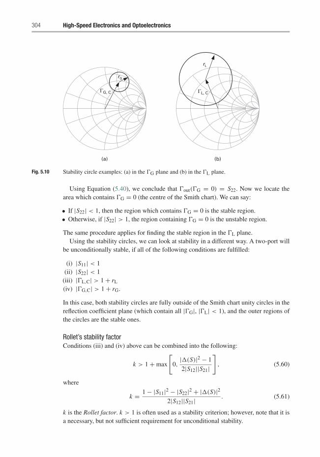
304 High-Speed Electronics and Optoelectronics
(a)
ΓG, C
rG
rL
ΓL, C
(b)
Fig. 5.10 Stability circle examples: (a) in the �G plane and (b) in the �L plane.
Using Equation (5.40), we conclude that �out(�G = 0) = S22. Now we locate thearea which contains �G = 0 (the centre of the Smith chart). We can say:
• If |S22| < 1, then the region which contains �G = 0 is the stable region.• Otherwise, if |S22| > 1, the region containing �G = 0 is the unstable region.
The same procedure applies for finding the stable region in the �L plane.Using the stability circles, we can look at stability in a different way. A two-port will
be unconditionally stable, if all of the following conditions are fulfilled:
(i) |S11| < 1(ii) |S22| < 1
(iii) |�L,C| > 1 + rL
(iv) |�G,C| > 1 + rG.
In this case, both stability circles are fully outside of the Smith chart unity circles in thereflection coefficient plane (which contain all |�G|, |�L| < 1), and the outer regions ofthe circles are the stable ones.
Rollet’s stability factorConditions (iii) and (iv) above can be combined into the following:
k > 1 + max
[0,
|�(S)|2 − 1
2|S12||S21|
], (5.60)
where
k = 1 − |S11|2 − |S22|2 + |�(S)|22|S12||S21| . (5.61)
k is the Rollet factor. k > 1 is often used as a stability criterion; however, note that it isa necessary, but not sufficient requirement for unconditional stability.
Building blocks for high-speed analogue circuits 305
A very common, and potentially fatal, mistake is to assess stability only for theintended frequency of operation. It must be investigated over the full frequency rangewhere instability may conceivably occur – parasitic oscillations at very low frequenciesare extremely common, and instabilities may also increase with increasing frequenciessuch as in cascode amplifiers (see p. 333).
5.2.6 Maximum available gain and maximum stable gain
Let us now reassess the case of an amplifier with simultaneous complex conjugatematch at the input and output ports, i.e. �S = �
in, �L = � out. The available gain
in this case is the maximum available gain and can be written using the Rollet factorEquation (5.61) as
M AG =∣∣∣∣ S21
S12
∣∣∣∣ (k −
√k2 − 1
). (5.62)
Obviously, a real solution exists only if k ≥ 1.For k < 1, the maximum stable gain is frequently quoted. This is the MAG in the
limit of k = 1, which can be obtained by the resistive loading of an otherwise notconditionally stable amplifier:
M SG =∣∣∣∣ S21
S12
∣∣∣∣ . (5.63)
5.2.7 Mason’s unilateral gain
The concept of unilateral gain for a two-port network was first introduced by Mason inhis paper [28], which is now considered a classic. A comprehensive review of the paperand its relevance today is given by Gupta [15].
The unilateral gain is defined as the maximum power gain obtained by a two-portwhen it is made unilateral – unilateralised. A two-port network that includes an activedevice is made unilateral by a lossless and reciprocal four-port network connected toinput and output of the two-port under investigation. This network provides the nec-essary feedback to impose the unilateral condition. Mason’s unilateral gain is not tobe confused with the unilateral transducer power gain GTU, Equation (5.52), whichhad been derived by neglecting the reverse transmission. Here, reverse transmission iseliminated by a unilateralising network.
The unilateral gain is a figure of merit which is intrinsic to the device and henceindependent of the circuit in which the device is placed. The unilateral gain is, therefore,an invariant property of the device. Hence, it can be expressed in terms of the device’ssmall-signal parameters. The scattering parameter representation of U is the most usefulin microwave applications. Ku [23] has given an expression in terms of the S-matrix:
U = | S12 − S21 |2�([I ] − [S∗]T[S]) , (5.64)
306 High-Speed Electronics and Optoelectronics
where [I ] is the identity matrix. U can also be expressed with the help of the stabilityfactor k [15]:
U =
∣∣∣∣( S21
S12
)− 1
∣∣∣∣2
2k
∣∣∣∣ S21
S12
∣∣∣∣ − 2Re
[S21
S12
] . (5.65)
5.2.8 Maximum frequency of oscillation
The maximum frequency of oscillation is a criterion for a device’s ability to amplifypower. Because the maximum power gain at any frequency is obtained by conjugatelymatching the input and output ports, the MAG (see Equation (5.62)) is an obviouschoice. The maximum frequency of oscillation fmax is then the frequency where MAGdrops to unity:
MAG( fmax) = 1. (5.66)
However, we had seen that MAG only exists when Rollet’s stability factor k ≥ 1. Thisraises a practical problem – for many high-performance microwave transistors, k < 1 inthe whole measurement range, and so fmax cannot be determined using Equation (5.66).
Another customary definition therefore makes use of Mason’s unilateral gain U (seeEquation (5.65)), which does not have this limitation. fmax is then understood as thefrequency where U drops to unity:
U ( fmax) = 1. (5.67)
Note, however, that Equations (5.66) and (5.67) will generally not yield the same result,so it is important to check the definition used when comparing fmax values.
5.3 Noise in two-ports
5.3.1 Noise phenomena
Any electronic component exhibits electronic noise, provided that the absolute tempera-ture is T > 0. There are several physical origins, which have been discussed in Chapter2 in the context of active devices, so only a brief summary shall be given here.
Noise occurs in all contexts where carrier motion or carrier density is stochastic:
• As there is always a random thermal motion superimposed on any charge carriermovement, thermal or Johnson noise is omnipresent in all conductors with non-zeroresistance. The rms voltage generated by the thermal noise in a resistor of value Ris Vrms = √
4kT RB, where k is Boltzmann’s constant and B is the measurementbandwidth.
• Emission of charge carriers over energy barriers is equally a stochastic process, andits associated noise mechanism is called shot noise. The rms current generated by acurrent of magnitude I flowing over an energy barrier is Irms = √
2q I B, where q isthe elementary charge and B again the measurement bandwidth.
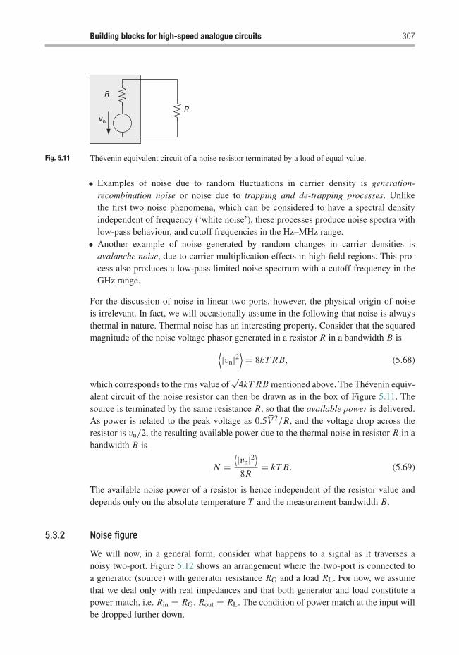
Building blocks for high-speed analogue circuits 307
R
R
vn
Fig. 5.11 Thevenin equivalent circuit of a noise resistor terminated by a load of equal value.
• Examples of noise due to random fluctuations in carrier density is generation-recombination noise or noise due to trapping and de-trapping processes. Unlikethe first two noise phenomena, which can be considered to have a spectral densityindependent of frequency (‘white noise’), these processes produce noise spectra withlow-pass behaviour, and cutoff frequencies in the Hz–MHz range.
• Another example of noise generated by random changes in carrier densities isavalanche noise, due to carrier multiplication effects in high-field regions. This pro-cess also produces a low-pass limited noise spectrum with a cutoff frequency in theGHz range.
For the discussion of noise in linear two-ports, however, the physical origin of noiseis irrelevant. In fact, we will occasionally assume in the following that noise is alwaysthermal in nature. Thermal noise has an interesting property. Consider that the squaredmagnitude of the noise voltage phasor generated in a resistor R in a bandwidth B is⟨
|vn|2⟩= 8kT RB, (5.68)
which corresponds to the rms value of√
4kT RB mentioned above. The Thevenin equiv-alent circuit of the noise resistor can then be drawn as in the box of Figure 5.11. Thesource is terminated by the same resistance R, so that the available power is delivered.As power is related to the peak voltage as 0.5V 2/R, and the voltage drop across theresistor is vn/2, the resulting available power due to the thermal noise in resistor R in abandwidth B is
N =⟨|vn|2
⟩8R
= kT B. (5.69)
The available noise power of a resistor is hence independent of the resistor value anddepends only on the absolute temperature T and the measurement bandwidth B.
5.3.2 Noise figure
We will now, in a general form, consider what happens to a signal as it traverses anoisy two-port. Figure 5.12 shows an arrangement where the two-port is connected toa generator (source) with generator resistance RG and a load RL. For now, we assumethat we deal only with real impedances and that both generator and load constitute apower match, i.e. Rin = RG, Rout = RL. The condition of power match at the input willbe dropped further down.
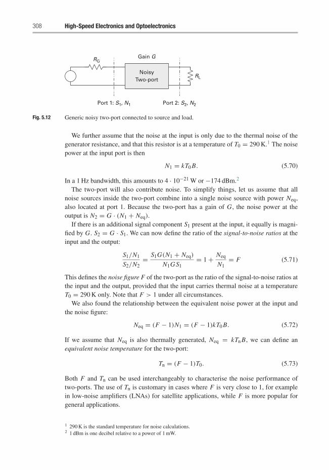
308 High-Speed Electronics and Optoelectronics
RG
RL
Gain G
NoisyTwo-port
Port 1: S1, N1 Port 2: S2, N2
Fig. 5.12 Generic noisy two-port connected to source and load.
We further assume that the noise at the input is only due to the thermal noise of thegenerator resistance, and that this resistor is at a temperature of T0 = 290 K.1 The noisepower at the input port is then
N1 = kT0 B. (5.70)
In a 1 Hz bandwidth, this amounts to 4 · 10−21 W or −174 dBm.2
The two-port will also contribute noise. To simplify things, let us assume that allnoise sources inside the two-port combine into a single noise source with power Neq,also located at port 1. Because the two-port has a gain of G, the noise power at theoutput is N2 = G · (N1 + Neq).
If there is an additional signal component S1 present at the input, it equally is magni-fied by G. S2 = G · S1. We can now define the ratio of the signal-to-noise ratios at theinput and the output:
S1/N1
S2/N2= S1G(N1 + Neq)
N1GS1= 1 + Neq
N1= F (5.71)
This defines the noise figure F of the two-port as the ratio of the signal-to-noise ratios atthe input and the output, provided that the input carries thermal noise at a temperatureT0 = 290 K only. Note that F > 1 under all circumstances.
We also found the relationship between the equivalent noise power at the input andthe noise figure:
Neq = (F − 1)N1 = (F − 1)kT0 B. (5.72)
If we assume that Neq is also thermally generated, Neq = kTn B, we can define anequivalent noise temperature for the two-port:
Tn = (F − 1)T0. (5.73)
Both F and Tn can be used interchangeably to characterise the noise performance oftwo-ports. The use of Tn is customary in cases where F is very close to 1, for examplein low-noise amplifiers (LNAs) for satellite applications, while F is more popular forgeneral applications.
1 290 K is the standard temperature for noise calculations.2 1 dBm is one decibel relative to a power of 1 mW.
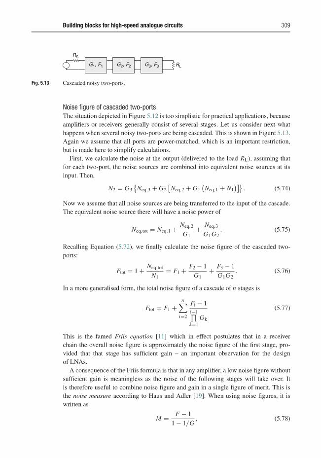
Building blocks for high-speed analogue circuits 309
RS
RLG1, F1 G2, F2 G3, F3
Fig. 5.13 Cascaded noisy two-ports.
Noise figure of cascaded two-portsThe situation depicted in Figure 5.12 is too simplistic for practical applications, becauseamplifiers or receivers generally consist of several stages. Let us consider next whathappens when several noisy two-ports are being cascaded. This is shown in Figure 5.13.Again we assume that all ports are power-matched, which is an important restriction,but is made here to simplify calculations.
First, we calculate the noise at the output (delivered to the load RL), assuming thatfor each two-port, the noise sources are combined into equivalent noise sources at itsinput. Then,
N2 = G3{
Neq,3 + G2[Neq,2 + G1
(Neq,1 + N1
)]}. (5.74)
Now we assume that all noise sources are being transferred to the input of the cascade.The equivalent noise source there will have a noise power of
Neq,tot = Neq,1 + Neq,2
G1+ Neq,3
G1G2. (5.75)
Recalling Equation (5.72), we finally calculate the noise figure of the cascaded two-ports:
Ftot = 1 + Neq,tot
N1= F1 + F2 − 1
G1+ F3 − 1
G1G2. (5.76)
In a more generalised form, the total noise figure of a cascade of n stages is
Ftot = F1 +n∑
i=2
Fi − 1i−1∏k=1
Gk
(5.77)
This is the famed Friis equation [11] which in effect postulates that in a receiverchain the overall noise figure is approximately the noise figure of the first stage, pro-vided that that stage has sufficient gain – an important observation for the designof LNAs.
A consequence of the Friis formula is that in any amplifier, a low noise figure withoutsufficient gain is meaningless as the noise of the following stages will take over. Itis therefore useful to combine noise figure and gain in a single figure of merit. This isthe noise measure according to Haus and Adler [19]. When using noise figures, it iswritten as
M = F − 1
1 − 1/G, (5.78)
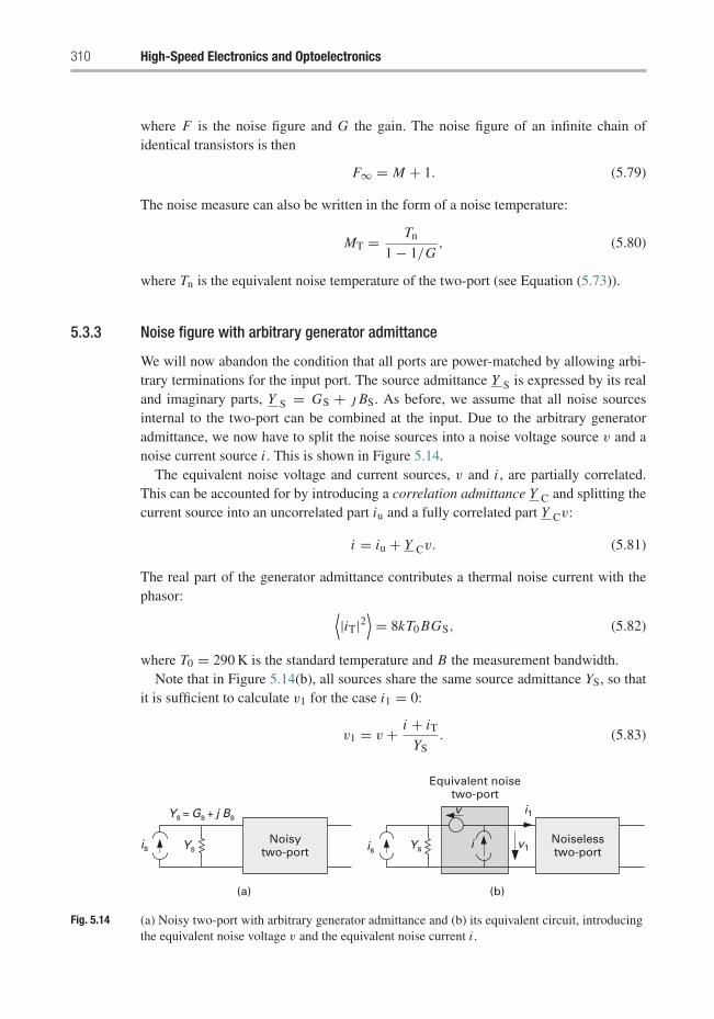
310 High-Speed Electronics and Optoelectronics
where F is the noise figure and G the gain. The noise figure of an infinite chain ofidentical transistors is then
F∞ = M + 1. (5.79)
The noise measure can also be written in the form of a noise temperature:
MT = Tn
1 − 1/G, (5.80)
where Tn is the equivalent noise temperature of the two-port (see Equation (5.73)).
5.3.3 Noise figure with arbitrary generator admittance
We will now abandon the condition that all ports are power-matched by allowing arbi-trary terminations for the input port. The source admittance Y S is expressed by its realand imaginary parts, Y S = GS + j BS. As before, we assume that all noise sourcesinternal to the two-port can be combined at the input. Due to the arbitrary generatoradmittance, we now have to split the noise sources into a noise voltage source v and anoise current source i . This is shown in Figure 5.14.
The equivalent noise voltage and current sources, v and i , are partially correlated.This can be accounted for by introducing a correlation admittance Y C and splitting thecurrent source into an uncorrelated part iu and a fully correlated part Y Cv:
i = iu + Y Cv. (5.81)
The real part of the generator admittance contributes a thermal noise current with thephasor: ⟨
|iT|2⟩= 8kT0 BGS, (5.82)
where T0 = 290 K is the standard temperature and B the measurement bandwidth.Note that in Figure 5.14(b), all sources share the same source admittance YS, so that
it is sufficient to calculate v1 for the case i1 = 0:
v1 = v + i + iT
YS. (5.83)
Noisytwo-port
Noiselesstwo-port
(a) (b)
is is
i1
v1Ys
v
iYs
Ys = Gs + j Bs
Equivalent noisetwo-port
Fig. 5.14 (a) Noisy two-port with arbitrary generator admittance and (b) its equivalent circuit, introducingthe equivalent noise voltage v and the equivalent noise current i .
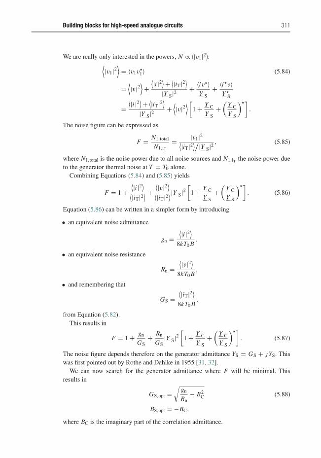
Building blocks for high-speed analogue circuits 311
We are really only interested in the powers, N ∝ ⟨|v1|2⟩:⟨
|v1|2⟩= 〈v1v
1〉 (5.84)
=⟨|v|2
⟩+
⟨|i |2⟩ + ⟨|iT|2⟩|Y S|2 + 〈iv 〉
Y S+ 〈i v〉
Y S
=⟨|i |2⟩ + ⟨|iT|2⟩
|Y S|2 +⟨|v|2
⟩ [1 + Y C
Y S+
(Y C
Y S
) ].
The noise figure can be expressed as
F = N1,total
N1,iT= |v1|2⟨|iT|2⟩/|Y S|2 , (5.85)
where N1,total is the noise power due to all noise sources and N1,iT the noise power dueto the generator thermal noise at T = T0 alone.
Combining Equations (5.84) and (5.85) yields
F = 1 +⟨|i |2⟩⟨|iT|2⟩ +
⟨|v|2⟩⟨|iT|2⟩ |Y S|2[
1 + Y C
Y S+
(Y C
Y S
) ]. (5.86)
Equation (5.86) can be written in a simpler form by introducing
• an equivalent noise admittance
gn =⟨|i |2⟩
8kT0 B,
• an equivalent noise resistance
Rn =⟨|v|2⟩
8kT0 B,
• and remembering that
GS =⟨|iT|2⟩8kT0 B
,
from Equation (5.82).This results in
F = 1 + gn
GS+ Rn
GS|Y S|2
[1 + Y C
Y S+
(Y C
Y S
) ]. (5.87)
The noise figure depends therefore on the generator admittance YS = GS + jYS. Thiswas first pointed out by Rothe and Dahlke in 1955 [31, 32].
We can now search for the generator admittance where F will be minimal. Thisresults in
GS,opt =√
gn
Rn− B2
C (5.88)
BS,opt = −BC,
where BC is the imaginary part of the correlation admittance.
312 High-Speed Electronics and Optoelectronics
Introducing these terms into Equation (5.87), the noise figure can be written asfollows:
F = 1 + 2Rn(GS,opt + GC) + Rn
GS
[(GS − GS,opt)
2 + (BS + BS,opt)2]. (5.89)
For YS = YS,opt, the minimum noise figure is
Fmin = 1 + 2Rn(GS,opt + GC) = 1 + 2Rn
(GC +
√gn
Rn− B2
C
), (5.90)
and therefore finally
F = Fmin + RN
GS
[(GS − GS,opt)
2 + (BS − BS,opt)2]
(5.91)
= Fmin + RN
GS
∣∣∣Y S − Y S,opt
∣∣∣2.
To describe the noise performance of a two-port, we need the following parameters:
• the minimum noise figure Fmin,• the equivalent noise resistance Rn,• the noise-optimised generator admittance Y S,opt.
For microwave applications, it is more customary to work with reflection coefficientsinstead of impedances or admittances. For this, we introduce a normalising admittanceY0, typically 20 mS, and a normalised noise resistance rn = RnY0. Then Equation (5.91)turns into
F = Fmin + 4rn∣∣�S − �S,opt
∣∣2(1 − |�S|2) ∣∣1 + �S,opt
∣∣2, (5.92)
where
�S = Y0 − YS
Y0 + YS.
Plotting F = f (�S) on a Smith chart, the contours of constant F are circles. Anexample is shown in Figure 5.15.
Associated gainThe condition for noise-optimised source reflection coefficient �S = �S,opt is inde-pendent of the power matching conditions derived earlier, �S = �
in. The maximumgain under ‘noise matching’ conditions is therefore smaller than the MAG, whichwould be achieved when input and output of the two-port are conjugately matched.Here, �S = �S,opt and the gain for the conjugately matched output becomes (seeEquation (5.53))
Building blocks for high-speed analogue circuits 313
ΓS,opt
Fig. 5.15 Example for ‘noise circles’ – contours of constant noise figures on the Smith chart.
Gass = 1− | �S,opt |2| 1 − S11�S,opt |2 | S21 |2 1
1− | �out |2 (5.93)
=|S21|2
(1 − ∣∣�S,opt
∣∣2)
∣∣1 − S11�S,opt∣∣2 − ∣∣S22(1 − S11�S,opt) + S12S21�S,opt
∣∣2,
since
�out = S22 + S21S12�S,opt
1 − S11�S,opt.
The available gain under noise matching conditions is called associated gain.
5.4 Transistor amplifiers
5.4.1 A brief historical discourse
Amplifiers are such an integral part of any wireless communication system that we haveto explicitly recall that in the first decades of radio, they were not used at all. It was notbefore the invention of the electron tube triode that amplification of alternating currentsignals became possible. Lee De Forest’s Audion tube (conceived in 1906 and patentedin 1908 [10]) is probably the first example of an amplifying device. It was 24-year-old Edwin Armstrong, the prolific and finally tragic inventor of radio’s early days, who
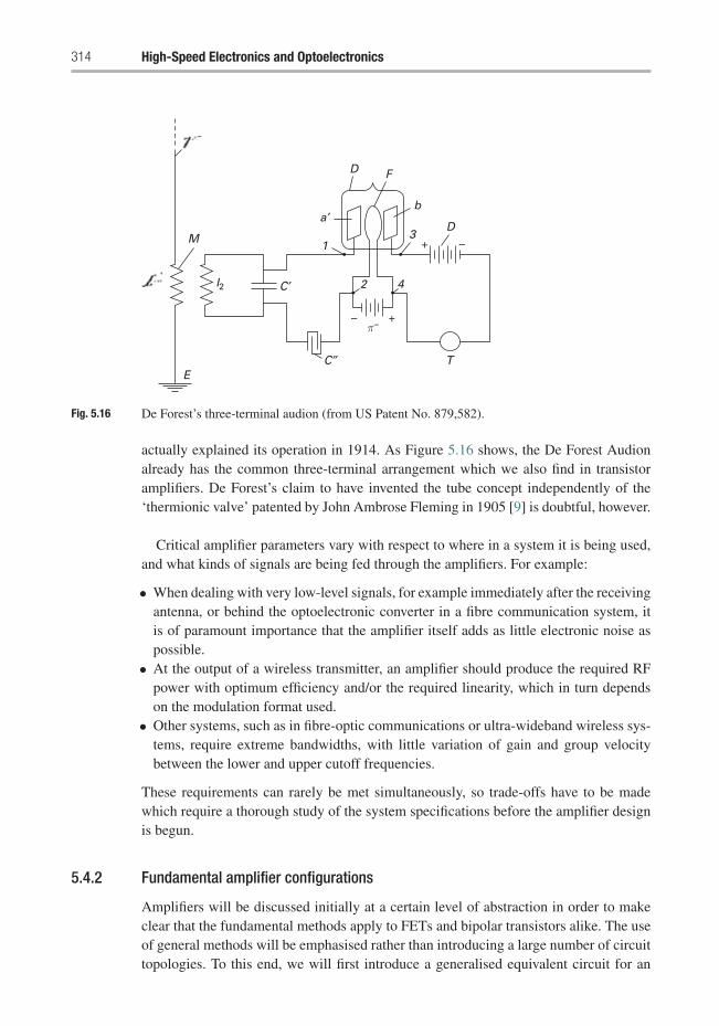
314 High-Speed Electronics and Optoelectronics
M
E
I2 C ′
C″
π–
T
a ′
D F
D
b
3
42
1 +
+–
–
Fig. 5.16 De Forest’s three-terminal audion (from US Patent No. 879,582).
actually explained its operation in 1914. As Figure 5.16 shows, the De Forest Audionalready has the common three-terminal arrangement which we also find in transistoramplifiers. De Forest’s claim to have invented the tube concept independently of the‘thermionic valve’ patented by John Ambrose Fleming in 1905 [9] is doubtful, however.
Critical amplifier parameters vary with respect to where in a system it is being used,and what kinds of signals are being fed through the amplifiers. For example:
• When dealing with very low-level signals, for example immediately after the receivingantenna, or behind the optoelectronic converter in a fibre communication system, itis of paramount importance that the amplifier itself adds as little electronic noise aspossible.
• At the output of a wireless transmitter, an amplifier should produce the required RFpower with optimum efficiency and/or the required linearity, which in turn dependson the modulation format used.
• Other systems, such as in fibre-optic communications or ultra-wideband wireless sys-tems, require extreme bandwidths, with little variation of gain and group velocitybetween the lower and upper cutoff frequencies.
These requirements can rarely be met simultaneously, so trade-offs have to be madewhich require a thorough study of the system specifications before the amplifier designis begun.
5.4.2 Fundamental amplifier configurations
Amplifiers will be discussed initially at a certain level of abstraction in order to makeclear that the fundamental methods apply to FETs and bipolar transistors alike. The useof general methods will be emphasised rather than introducing a large number of circuittopologies. To this end, we will first introduce a generalised equivalent circuit for an
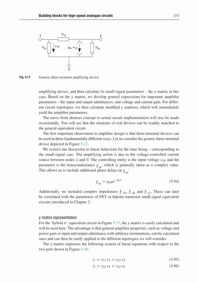
Building blocks for high-speed analogue circuits 315
1 2
0
Y12
Y10 Y20v10 gm v10
Fig. 5.17 Generic three-terminal amplifying device.
amplifying device, and then calculate its small-signal parameters – the y matrix in thiscase. Based on the y matrix, we develop general expressions for important amplifierparameters – the input and output admittances, and voltage and current gain. For differ-ent circuit topologies, we then calculate modified y matrices, which will immediatelyyield the amplifier parameters.
The move from abstract concept to actual circuit implementation will also be madeoccasionally. You will see that the elements of real devices can be readily matched tothe general equivalent circuit.
The first important observation in amplifier design is that three-terminal devices canbe used in three fundamentally different ways. Let us consider the generic three-terminaldevice depicted in Figure 5.17.
We restrict our discussion to linear behaviour for the time being – corresponding tothe small-signal case. The amplifying action is due to the voltage-controlled currentsource between nodes 2 and 0. The controlling entity is the input voltage v10 and theparameter is the transconductance g
m, which is generally taken as a complex value.
This allows us to include additional phase delays in gm
:
gm
= gm0e−jωτ (5.94)
Additionally, we included complex impedances Y 10, Y 20 and Y 12. These can laterbe correlated with the parameters of FET or bipolar transistor small-signal equivalentcircuits introduced in Chapter 2.
y matrix representationFor the ‘hybrid π ’ equivalent circuit in Figure 5.17, the y matrix is easily calculated andwill be used here. The advantage is that general amplifier properties, such as voltage andpower gain or input and output admittance with arbitrary terminations, can be calculatedonce and can then be easily applied to the different topologies we will consider.
The y matrix expresses the following system of linear equations with respect to thetwo-port shown in Figure 5.18:
i1 = y11 v1 + y12 v2 (5.95)
i2 = y21 v1 + y22 v2 (5.96)
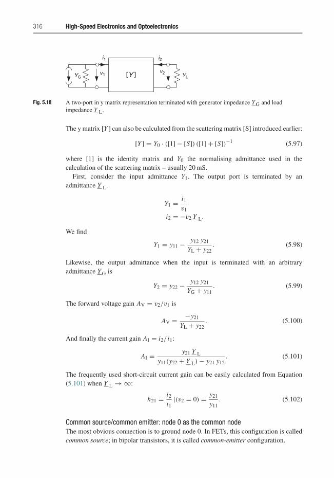
316 High-Speed Electronics and Optoelectronics
[Y ]
i1 i2
v1v2YG YL
Fig. 5.18 A two-port in y matrix representation terminated with generator impedance Y G and loadimpedance Y L.
The y matrix [Y ] can also be calculated from the scattering matrix [S] introduced earlier:
[Y ] = Y0 · ([1] − [S]) ([1] + [S])−1 (5.97)
where [1] is the identity matrix and Y0 the normalising admittance used in thecalculation of the scattering matrix – usually 20 mS.
First, consider the input admittance Y1. The output port is terminated by anadmittance Y L.
Y1 = i1
v1
i2 = −v2 Y L.
We find
Y1 = y11 − y12 y21
YL + y22. (5.98)
Likewise, the output admittance when the input is terminated with an arbitraryadmittance Y G is
Y2 = y22 − y12 y21
YG + y11. (5.99)
The forward voltage gain AV = v2/v1 is
AV = −y21
YL + y22. (5.100)
And finally the current gain AI = i2/ i1:
AI = y21 Y L
y11(y22 + Y L) − y21 y12. (5.101)
The frequently used short-circuit current gain can be easily calculated from Equation(5.101) when Y L → ∞:
h21 = i2
i1|(v2 = 0) = y21
y11. (5.102)
Common source/common emitter: node 0 as the common nodeThe most obvious connection is to ground node 0. In FETs, this configuration is calledcommon source; in bipolar transistors, it is called common-emitter configuration.
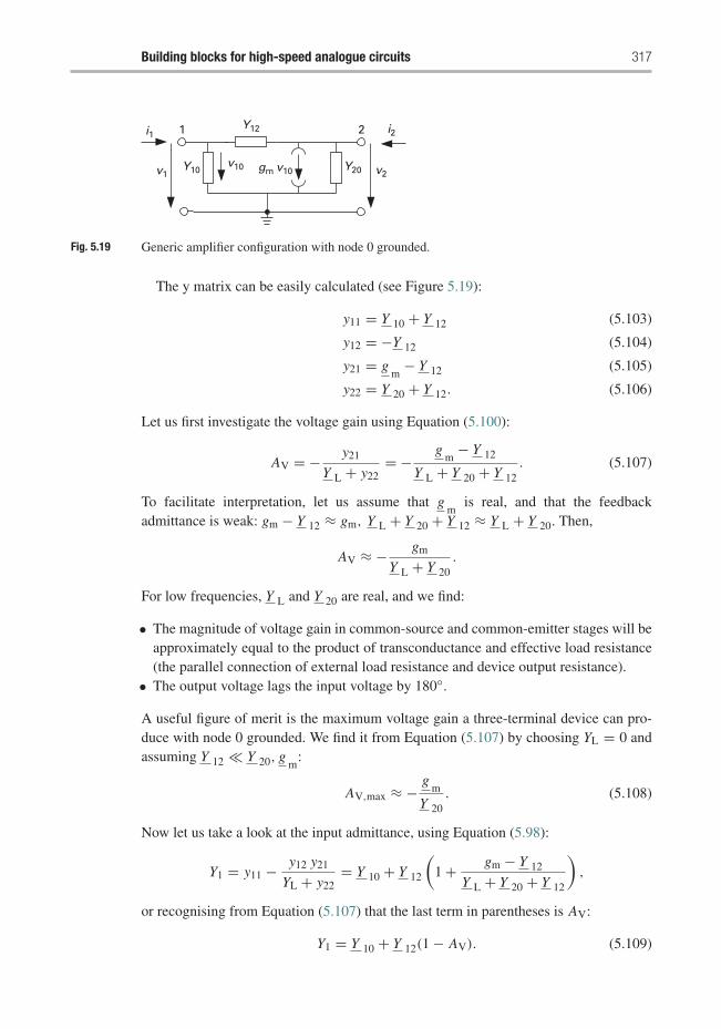
Building blocks for high-speed analogue circuits 317
v1v10 v2
gm v10
i1 i21 2Y12
Y10 Y20
Fig. 5.19 Generic amplifier configuration with node 0 grounded.
The y matrix can be easily calculated (see Figure 5.19):
y11 = Y 10 + Y 12 (5.103)
y12 = −Y 12 (5.104)
y21 = gm
− Y 12 (5.105)
y22 = Y 20 + Y 12. (5.106)
Let us first investigate the voltage gain using Equation (5.100):
AV = − y21
Y L + y22= − g
m− Y 12
Y L + Y 20 + Y 12. (5.107)
To facilitate interpretation, let us assume that gm
is real, and that the feedbackadmittance is weak: gm − Y 12 ≈ gm, Y L + Y 20 + Y 12 ≈ Y L + Y 20. Then,
AV ≈ − gm
Y L + Y 20.
For low frequencies, Y L and Y 20 are real, and we find:
• The magnitude of voltage gain in common-source and common-emitter stages will beapproximately equal to the product of transconductance and effective load resistance(the parallel connection of external load resistance and device output resistance).
• The output voltage lags the input voltage by 180◦.
A useful figure of merit is the maximum voltage gain a three-terminal device can pro-duce with node 0 grounded. We find it from Equation (5.107) by choosing YL = 0 andassuming Y 12 � Y 20, g
m:
AV,max ≈ − gm
Y 20. (5.108)
Now let us take a look at the input admittance, using Equation (5.98):
Y1 = y11 − y12 y21
YL + y22= Y 10 + Y 12
(1 + gm − Y 12
Y L + Y 20 + Y 12
),
or recognising from Equation (5.107) that the last term in parentheses is AV:
Y1 = Y 10 + Y 12(1 − AV). (5.109)
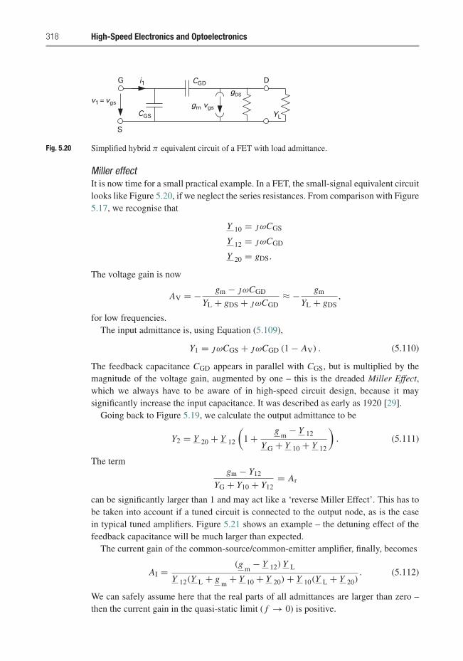
318 High-Speed Electronics and Optoelectronics
v1 = vgs gm vgs
gDS
CGS
CGD
YL
i1G D
S
Fig. 5.20 Simplified hybrid π equivalent circuit of a FET with load admittance.
Miller effectIt is now time for a small practical example. In a FET, the small-signal equivalent circuitlooks like Figure 5.20, if we neglect the series resistances. From comparison with Figure5.17, we recognise that
Y 10 = jωCGS
Y 12 = jωCGD
Y 20 = gDS.
The voltage gain is now
AV = − gm − jωCGD
YL + gDS + jωCGD≈ − gm
YL + gDS,
for low frequencies.The input admittance is, using Equation (5.109),
Y1 = jωCGS + jωCGD (1 − AV) . (5.110)
The feedback capacitance CGD appears in parallel with CGS, but is multiplied by themagnitude of the voltage gain, augmented by one – this is the dreaded Miller Effect,which we always have to be aware of in high-speed circuit design, because it maysignificantly increase the input capacitance. It was described as early as 1920 [29].
Going back to Figure 5.19, we calculate the output admittance to be
Y2 = Y 20 + Y 12
(1 + g
m− Y 12
Y G + Y 10 + Y 12
). (5.111)
The termgm − Y12
YG + Y10 + Y12= Ar
can be significantly larger than 1 and may act like a ‘reverse Miller Effect’. This has tobe taken into account if a tuned circuit is connected to the output node, as is the casein typical tuned amplifiers. Figure 5.21 shows an example – the detuning effect of thefeedback capacitance will be much larger than expected.
The current gain of the common-source/common-emitter amplifier, finally, becomes
AI = (gm
− Y 12) Y L
Y 12(Y L + gm
+ Y 10 + Y 20) + Y 10(Y L + Y 20). (5.112)
We can safely assume here that the real parts of all admittances are larger than zero –then the current gain in the quasi-static limit ( f → 0) is positive.
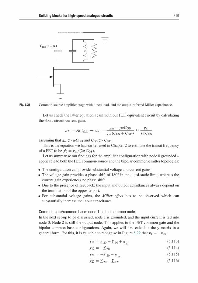
Building blocks for high-speed analogue circuits 319
CGD (1 + Ar)
Fig. 5.21 Common-source amplifier stage with tuned load, and the output-referred Miller capacitance.
Let us check the latter equation again with our FET equivalent circuit by calculatingthe short-circuit current gain:
h21 = AI|(Y L → ∞) = gm − jωCGD
jω(CGS + CGD)≈ gm
jωCGS
assuming that gm � ωCGD and CGS � CGD.This is the equation we had earlier used in Chapter 2 to estimate the transit frequency
of a FET to be fT = gm/(2πCGS).Let us summarise our findings for the amplifier configuration with node 0 grounded –
applicable to both the FET common-source and the bipolar common-emitter topologies:
• The configuration can provide substantial voltage and current gains.• The voltage gain provides a phase shift of 180◦ in the quasi-static limit, whereas the
current gain experiences no phase shift.• Due to the presence of feedback, the input and output admittances always depend on
the termination of the opposite port.• For substantial voltage gains, the Miller effect has to be observed which can
substantially increase the input capacitance.
Common gate/common base: node 1 as the common nodeIn the next set-up to be discussed, node 1 is grounded, and the input current is fed intonode 0. Node 2 is still the output node. This applies to the FET common-gate and thebipolar common-base configurations. Again, we will first calculate the y matrix in ageneral form. For this, it is valuable to recognise in Figure 5.22 that v1 = −v10.
y11 = Y 20 + Y 10 + gm
(5.113)
y12 = −Y 20 (5.114)
y21 = −Y 20 − gm
(5.115)
y22 = Y 20 + Y 12. (5.116)
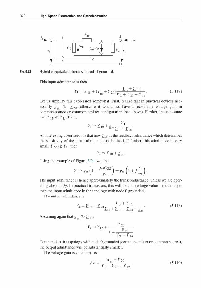
320 High-Speed Electronics and Optoelectronics
1
0
2i1 i2
v1
Y10
Y12
v2Y20gm v10
v10
Fig. 5.22 Hybrid π equivalent circuit with node 1 grounded.
This input admittance is then
Y1 = Y 10 + (gm
+ Y 20)Y L + Y 12
Y L + Y 20 + Y 12. (5.117)
Let us simplify this expression somewhat. First, realise that in practical devices nec-essarily g
m� Y 20, otherwise it would not have a reasonable voltage gain in
common-source or common-emitter configuration (see above). Further, let us assumethat Y 12 � Y L. Then,
Y1 ≈ Y 10 + gm
Y L
Y L + Y 20.
An interesting observation is that now Y 20 is the feedback admittance which determinesthe sensitivity of the input admittance on the load. If further, this admittance is verysmall, Y 20 � Y L, then
Y1 ≈ Y 10 + gm.
Using the example of Figure 5.20, we find
Y1 ≈ gm
(1 + jωCGS
gm
)= gm
(1 + j
ω
ωT
).
The input admittance is hence approximately the transconductance, unless we are oper-ating close to fT. In practical transistors, this will be a quite large value – much largerthan the input admittance in the topology with node 0 grounded.
The output admittance is
Y2 = Y 12 + Y 20Y G + Y 10
Y G + Y 10 + Y 20 + gm
. (5.118)
Assuming again that gm
� Y 20,
Y2 ≈ Y 12 + Y 20
1 + gm
Y G + Y 10
Compared to the topology with node 0 grounded (common emitter or common source),the output admittance will be substantially smaller.
The voltage gain is calculated as
AV = gm
+ Y 20
Y L + Y 20 + Y 12. (5.119)
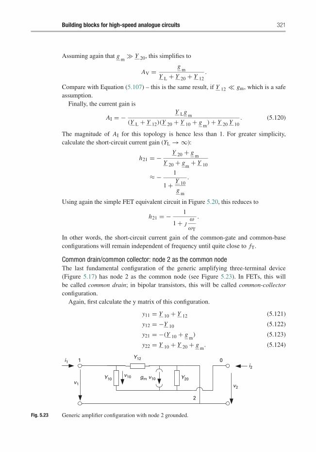
Building blocks for high-speed analogue circuits 321
Assuming again that gm
� Y 20, this simplifies to
AV = gm
Y L + Y 20 + Y 12.
Compare with Equation (5.107) – this is the same result, if Y 12 � gm, which is a safeassumption.
Finally, the current gain is
AI = − Y Lgm
(Y L + Y 12)(Y 20 + Y 10 + gm) + Y 20 Y 10
. (5.120)
The magnitude of AI for this topology is hence less than 1. For greater simplicity,calculate the short-circuit current gain (YL → ∞):
h21 = − Y 20 + gm
Y 20 + gm
+ Y 10
≈ − 1
1 + Y 10
gm
.
Using again the simple FET equivalent circuit in Figure 5.20, this reduces to
h21 = − 1
1 + jω
ωT
.
In other words, the short-circuit current gain of the common-gate and common-baseconfigurations will remain independent of frequency until quite close to fT.
Common drain/common collector: node 2 as the common nodeThe last fundamental configuration of the generic amplifying three-terminal device(Figure 5.17) has node 2 as the common node (see Figure 5.23). In FETs, this willbe called common drain; in bipolar transistors, this will be called common-collectorconfiguration.
Again, first calculate the y matrix of this configuration.
y11 = Y 10 + Y 12 (5.121)
y12 = −Y 10 (5.122)
y21 = −(Y 10 + gm) (5.123)
y22 = Y 10 + Y 20 + gm. (5.124)
1
2
0i1i2
v1 v2
Y10
Y12
Y20v10 gm v10
Fig. 5.23 Generic amplifier configuration with node 2 grounded.
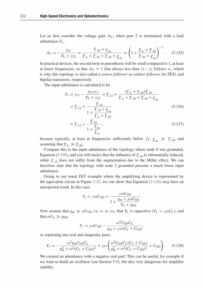
322 High-Speed Electronics and Optoelectronics
Let us first consider the voltage gain AV, when port 2 is terminated with a loadadmittance YL.
AV = − y21
YL + y22= Y 10 + g
m
Y L + Y 10 + Y 20 + gm
=(
1 + Y L + Y 20
Y 10 + gm
)−1
. (5.125)
In practical devices, the second term in parentheses will be small compared to 1, at leastat lower frequencies, so that AV ≈ 1 (but always less than 1) – v2 follows v1, whichis why this topology is also called a source follower or emitter follower for FETs andbipolar transistors, respectively.
The input admittance is calculated to be
Y1 = y11 − y21 y12
YL + y22= Y 12 + (Y L + Y 20)Y 10
Y L + Y 20 + Y 10 + gm
= Y 12 + Y 10
1 + Y 10 + gm
Y L + Y 20
(5.126)
≈ Y 12 + Y 10
1 + gm
Y L
, (5.127)
because typically, at least at frequencies sufficiently below fT, gm
� Y 10, andassuming that Y L � Y 20.
Compare this to the input admittance of the topology where node 0 was grounded,Equation (5.109), and you will notice that the influence of Y 10 is substantially reduced,while Y 12 does not suffer from the augmentation due to the Miller effect. We cantherefore state that the topology with node 2 grounded presents a much lower inputadmittance.
Going to our usual FET example where the amplifying device is represented bythe equivalent circuit in Figure 5.20, we can show that Equation (5.126) may have anunexpected result. In this case,
Y1 = jωCGD + jωCGS
1 + gm + jωCGS
YL + gDS
.
Now assume that gm � ωCGS, i.e. ω � ωT, that YL is capacitive (YL = jωCL), andthat ωCL � gDS.
Y1 = jωCGD − ω2CGSCL
gm + jω(CL + CGS),
or separating into real and imaginary parts,
Y1 = − ω2gmCGSCL
g2m + ω2(CL + CGS)2
+ jω
(ω2CGSCL(CL + CGS)
g2m + ω2(CL + CGS)2
+ CGD
). (5.128)
We created an admittance with a negative real part! This can be useful, for example ifwe want to build an oscillator (see Section 5.5), but also very dangerous for amplifierstability.
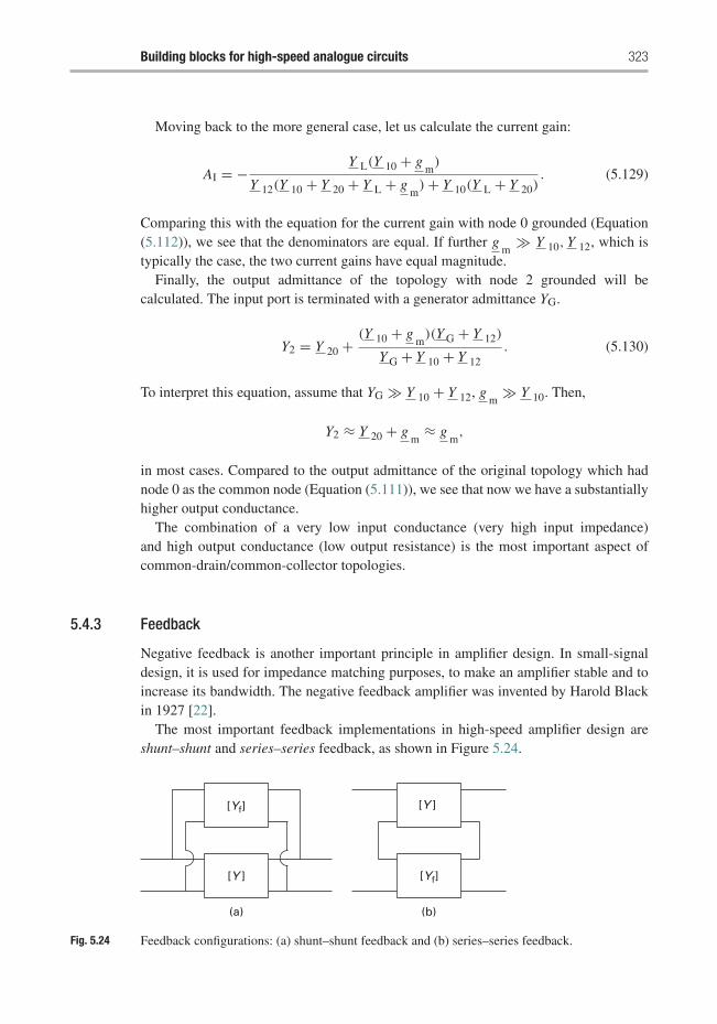
Building blocks for high-speed analogue circuits 323
Moving back to the more general case, let us calculate the current gain:
AI = − Y L(Y 10 + gm)
Y 12(Y 10 + Y 20 + Y L + gm) + Y 10(Y L + Y 20)
. (5.129)
Comparing this with the equation for the current gain with node 0 grounded (Equation(5.112)), we see that the denominators are equal. If further g
m� Y 10, Y 12, which is
typically the case, the two current gains have equal magnitude.Finally, the output admittance of the topology with node 2 grounded will be
calculated. The input port is terminated with a generator admittance YG.
Y2 = Y 20 + (Y 10 + gm)(Y G + Y 12)
Y G + Y 10 + Y 12. (5.130)
To interpret this equation, assume that YG � Y 10 + Y 12, gm
� Y 10. Then,
Y2 ≈ Y 20 + gm
≈ gm,
in most cases. Compared to the output admittance of the original topology which hadnode 0 as the common node (Equation (5.111)), we see that now we have a substantiallyhigher output conductance.
The combination of a very low input conductance (very high input impedance)and high output conductance (low output resistance) is the most important aspect ofcommon-drain/common-collector topologies.
5.4.3 Feedback
Negative feedback is another important principle in amplifier design. In small-signaldesign, it is used for impedance matching purposes, to make an amplifier stable and toincrease its bandwidth. The negative feedback amplifier was invented by Harold Blackin 1927 [22].
The most important feedback implementations in high-speed amplifier design areshunt–shunt and series–series feedback, as shown in Figure 5.24.
[Yf]
[Yf][Y ]
[Y ]
(a) (b)
Fig. 5.24 Feedback configurations: (a) shunt–shunt feedback and (b) series–series feedback.
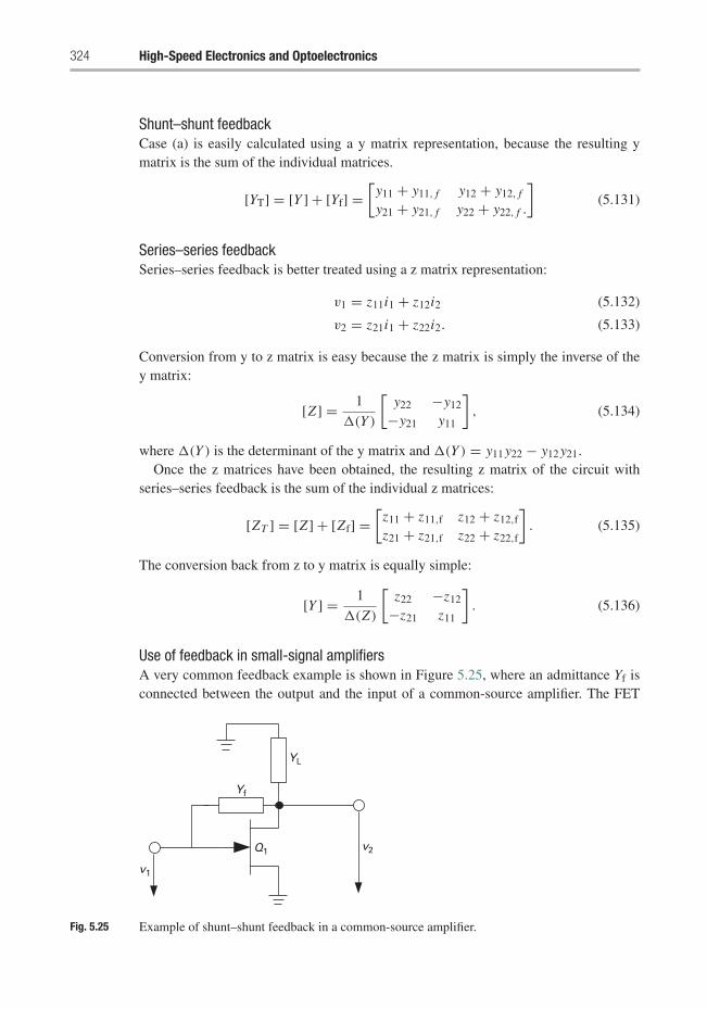
324 High-Speed Electronics and Optoelectronics
Shunt–shunt feedbackCase (a) is easily calculated using a y matrix representation, because the resulting ymatrix is the sum of the individual matrices.
[YT] = [Y ] + [Yf] =[
y11 + y11, f y12 + y12, f
y21 + y21, f y22 + y22, f .
](5.131)
Series–series feedbackSeries–series feedback is better treated using a z matrix representation:
v1 = z11i1 + z12i2 (5.132)
v2 = z21i1 + z22i2. (5.133)
Conversion from y to z matrix is easy because the z matrix is simply the inverse of they matrix:
[Z ] = 1
�(Y )
[y22 −y12
−y21 y11
], (5.134)
where �(Y ) is the determinant of the y matrix and �(Y ) = y11 y22 − y12 y21.Once the z matrices have been obtained, the resulting z matrix of the circuit with
series–series feedback is the sum of the individual z matrices:
[ZT ] = [Z ] + [Zf] =[
z11 + z11,f z12 + z12,f
z21 + z21,f z22 + z22,f
]. (5.135)
The conversion back from z to y matrix is equally simple:
[Y ] = 1
�(Z)
[z22 −z12
−z21 z11
]. (5.136)
Use of feedback in small-signal amplifiersA very common feedback example is shown in Figure 5.25, where an admittance Yf isconnected between the output and the input of a common-source amplifier. The FET
YL
Yf
Q1
v1
v2
Fig. 5.25 Example of shunt–shunt feedback in a common-source amplifier.
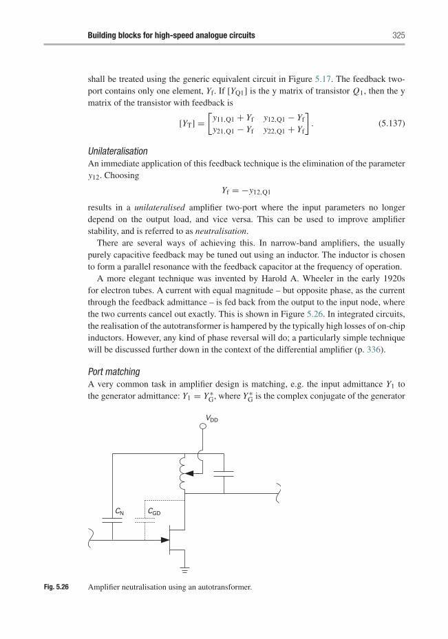
Building blocks for high-speed analogue circuits 325
shall be treated using the generic equivalent circuit in Figure 5.17. The feedback two-port contains only one element, Yf. If [YQ1] is the y matrix of transistor Q1, then the ymatrix of the transistor with feedback is
[YT] =[
y11,Q1 + Yf y12,Q1 − Yf
y21,Q1 − Yf y22,Q1 + Yf
]. (5.137)
UnilateralisationAn immediate application of this feedback technique is the elimination of the parametery12. Choosing
Yf = −y12,Q1
results in a unilateralised amplifier two-port where the input parameters no longerdepend on the output load, and vice versa. This can be used to improve amplifierstability, and is referred to as neutralisation.
There are several ways of achieving this. In narrow-band amplifiers, the usuallypurely capacitive feedback may be tuned out using an inductor. The inductor is chosento form a parallel resonance with the feedback capacitor at the frequency of operation.
A more elegant technique was invented by Harold A. Wheeler in the early 1920sfor electron tubes. A current with equal magnitude – but opposite phase, as the currentthrough the feedback admittance – is fed back from the output to the input node, wherethe two currents cancel out exactly. This is shown in Figure 5.26. In integrated circuits,the realisation of the autotransformer is hampered by the typically high losses of on-chipinductors. However, any kind of phase reversal will do; a particularly simple techniquewill be discussed further down in the context of the differential amplifier (p. 336).
Port matchingA very common task in amplifier design is matching, e.g. the input admittance Y1 tothe generator admittance: Y1 = Y ∗
G, where Y ∗G is the complex conjugate of the generator
VDD
CN CGD
Fig. 5.26 Amplifier neutralisation using an autotransformer.
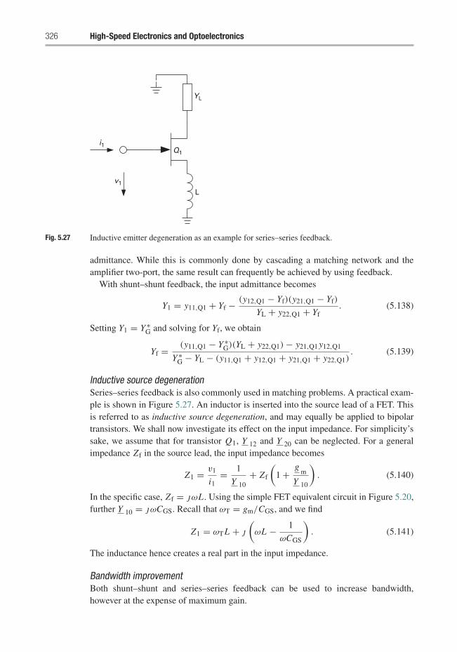
326 High-Speed Electronics and Optoelectronics
YL
i1
v1
Q1
L
Fig. 5.27 Inductive emitter degeneration as an example for series–series feedback.
admittance. While this is commonly done by cascading a matching network and theamplifier two-port, the same result can frequently be achieved by using feedback.
With shunt–shunt feedback, the input admittance becomes
Y1 = y11,Q1 + Yf − (y12,Q1 − Yf)(y21,Q1 − Yf)
YL + y22,Q1 + Yf. (5.138)
Setting Y1 = Y ∗G and solving for Yf, we obtain
Yf = (y11,Q1 − Y ∗G)(YL + y22,Q1) − y21,Q1 y12,Q1
Y ∗G − YL − (y11,Q1 + y12,Q1 + y21,Q1 + y22,Q1)
. (5.139)
Inductive source degenerationSeries–series feedback is also commonly used in matching problems. A practical exam-ple is shown in Figure 5.27. An inductor is inserted into the source lead of a FET. Thisis referred to as inductive source degeneration, and may equally be applied to bipolartransistors. We shall now investigate its effect on the input impedance. For simplicity’ssake, we assume that for transistor Q1, Y 12 and Y 20 can be neglected. For a generalimpedance Zf in the source lead, the input impedance becomes
Z1 = v1
i1= 1
Y 10+ Zf
(1 + g
m
Y 10
). (5.140)
In the specific case, Zf = jωL . Using the simple FET equivalent circuit in Figure 5.20,further Y 10 = jωCGS. Recall that ωT = gm/CGS, and we find
Z1 = ωTL + j
(ωL − 1
ωCGS
). (5.141)
The inductance hence creates a real part in the input impedance.
Bandwidth improvementBoth shunt–shunt and series–series feedback can be used to increase bandwidth,however at the expense of maximum gain.
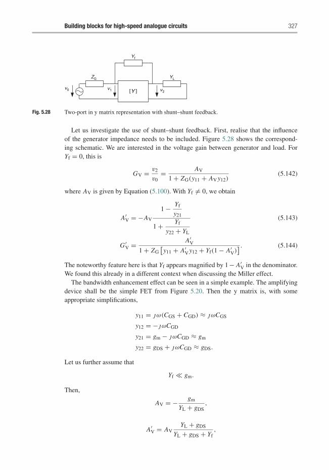
Building blocks for high-speed analogue circuits 327
[Y ]
ZG
v0 v1 v2
YL
Yf
Fig. 5.28 Two-port in y matrix representation with shunt–shunt feedback.
Let us investigate the use of shunt–shunt feedback. First, realise that the influenceof the generator impedance needs to be included. Figure 5.28 shows the correspond-ing schematic. We are interested in the voltage gain between generator and load. ForYf = 0, this is
GV = v2
v0= AV
1 + ZG(y11 + AV y12)(5.142)
where AV is given by Equation (5.100). With Yf �= 0, we obtain
A′V = −AV
1 − Yf
y21
1 + Yf
y22 + YL
(5.143)
G ′V = A′
V
1 + ZG[y11 + A′
V y12 + Yf(1 − A′V)
] . (5.144)
The noteworthy feature here is that Yf appears magnified by 1 − A′V in the denominator.
We found this already in a different context when discussing the Miller effect.The bandwidth enhancement effect can be seen in a simple example. The amplifying
device shall be the simple FET from Figure 5.20. Then the y matrix is, with someappropriate simplifications,
y11 = jω(CGS + CGD) ≈ jωCGS
y12 = −jωCGD
y21 = gm − jωCGD ≈ gm
y22 = gDS + jωCGD ≈ gDS.
Let us further assume that
Yf � gm.
Then,
AV = − gm
YL + gDS,
A′V = AV
YL + gDS
YL + gDS + Yf,
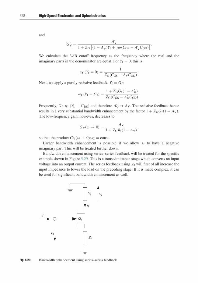
328 High-Speed Electronics and Optoelectronics
and
G ′V = A′
V
1 + ZG[(1 − A′
V)Yf + jω(CGS − A′VCGD)
] .We calculate the 3 dB cutoff frequency as the frequency where the real and theimaginary parts in the denominator are equal. For Yf = 0, this is
ωC(Yf = 0) = 1
ZG(CGS − AVCGD).
Next, we apply a purely resistive feedback, Yf = Gf:
ωC(Yf = Gf) = 1 + ZGGf(1 − A′V)
ZG(CGS − A′VCGD)
.
Frequently, Gf � (YL + GDS) and therefore A′V ≈ AV. The resistive feedback hence
results in a very substantial bandwidth enhancement by the factor 1 + ZGGf(1 − AV).The low-frequency gain, however, decreases to
GV(ω → 0) = AV
1 + ZG Rf(1 − AV),
so that the product GV(ω → 0)ωC = const.Larger bandwidth enhancement is possible if we allow Yf to have a negative
imaginary part. This will be treated further down.Bandwidth enhancement using series–series feedback will be treated for the specific
example shown in Figure 5.29. This is a transadmittance stage which converts an inputvoltage into an output current. The series feedback using Zf will first of all increase theinput impedance to lower the load on the preceding stage. If it is made complex, it canbe used for significant bandwidth enhancement as well.
YL
Q1
Z f
v1
i2
i1
v2
Fig. 5.29 Bandwidth enhancement using series–series feedback.
Building blocks for high-speed analogue circuits 329
The transadmittance of this stage is
Yt = i2
v1= gm
1 + gm Zf
(1 + jω
ωT
) , (5.145)
if the FET is described by the simple equivalent circuit in Figure 5.20, and using ωT =gm/CGS.If now Zf is a parallel RC network,
Zf = Rf
1 + jωRfCf,
and Cf is chosen,
Cf = 1
ωT Rf,
the frequency dependence in YT will disappear:
YT = gm
1 + gm Rf,
at least for this simple equivalent circuit!
5.4.4 Amplifier configurations with two transistors
In the first part of this chapter, we have seen how the fundamental topologies we canrealise with a three-terminal amplifying device have very different properties in termsof input and output admittances, as well as voltage and current gains. Further flexibilityin tailoring amplifier properties is achieved when we combine two of the fundamentaltopologies. We will use generic FETs in order to help visualise the circuits. However, thefundamental concepts apply equally to bipolar transistors – in fact, to any three-terminalamplifying device, as was outlined in the more abstract discussion above.
Common-drain/common-source configurationSuppose that we want to construct a buffer amplifier, which shall impose a minimal loadon a generator, yet also have a significant voltage gain. This can be achieved with thecombination of
• a common-drain stage (node 2 as the common node), providing the high inputimpedance, and
• a common-source stage (node 0 as the common node), providing the voltage gain.
Figure 5.30 shows the schematic of the common-drain/common-source (CD/CS) topo-logy. Q1 is the common-drain transistor, Q2 the common-source transistor, YL is theload admittance and YG the generator admittance.
The two important aspects of this configuration are input admittance and voltage gain,as discussed.
The voltage gain of the second stage is
AV,Q2 = v2
vA≈ − g
m
Y L + Y 20= − gm,Q2
gDS,Q2 + YL,
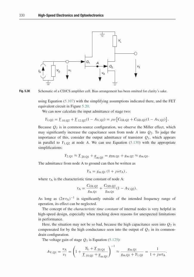
330 High-Speed Electronics and Optoelectronics
YL
v2Q2
Q1 A
vA
v1YGIG
Fig. 5.30 Schematic of a CD/CS amplifier cell. Bias arrangement has been omitted for clarity’s sake.
using Equation (5.107) with the simplifying assumptions indicated there, and the FETequivalent circuit in Figure 5.20.
We can now calculate the input admittance of stage two:
Y1,Q2 = Y 10,Q2 + Y 12,Q2(1 − AV,Q2) = jω[CGS,Q2 + CGD,Q2(1 − AV,Q2)
].
Because Q2 is in common-source configuration, we observe the Miller effect, whichmay significantly increase the capacitance seen from node A into Q2. To judge theimportance of this, consider the output admittance of transistor Q1, which appearsin parallel to Y1,Q2 at node A. We can use Equation (5.130) with the appropriatesimplifications:
Y2,Q1 ≈ Y 20,Q1 + gm,Q1
= gDS,Q1 + gm,Q2 ≈ gm,Q1.
The admittance from node A to ground can then be written as
YA = gm,Q1 (1 + jωτA) ,
where τA is the characteristic time constant of node A:
τA = CGS,Q2
gm,Q1+ CGD,Q2
gm,Q1(1 − AV,Q2).
As long as (2πτA)−1 is significantly outside of the intended frequency range of
operation, its effect can be neglected.The concept of the characteristic time constant of internal nodes is very helpful in
high-speed design, especially when tracking down reasons for unexpected limitationsin performance.
Here, the situation may not be so bad, because the high capacitance seen into Q2 iscompensated for by the high conductance seen into the output of Q1 in its common-drain configuration.
The voltage gain of stage Q1 is Equation (5.125):
AV,Q1 = vA
v1=
(1 + YL + Y 20,Q1
Y 10,Q1 + gm,Q1
)−1
≈ gm,Q1
gm,Q1 + Y1,Q1= 1
1 + jωτA.
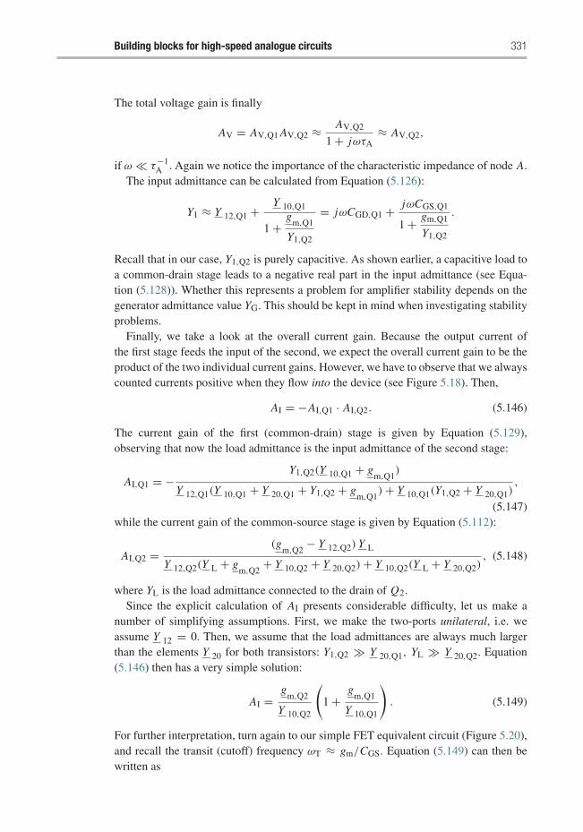
Building blocks for high-speed analogue circuits 331
The total voltage gain is finally
AV = AV,Q1 AV,Q2 ≈ AV,Q2
1 + jωτA≈ AV,Q2,
if ω � τ−1A . Again we notice the importance of the characteristic impedance of node A.
The input admittance can be calculated from Equation (5.126):
Y1 ≈ Y 12,Q1 + Y 10,Q1
1 +g
m,Q1
Y1,Q2
= jωCGD,Q1 + jωCGS,Q1
1 + gm,Q1
Y1,Q2
.
Recall that in our case, Y1,Q2 is purely capacitive. As shown earlier, a capacitive load toa common-drain stage leads to a negative real part in the input admittance (see Equa-tion (5.128)). Whether this represents a problem for amplifier stability depends on thegenerator admittance value YG. This should be kept in mind when investigating stabilityproblems.
Finally, we take a look at the overall current gain. Because the output current ofthe first stage feeds the input of the second, we expect the overall current gain to be theproduct of the two individual current gains. However, we have to observe that we alwayscounted currents positive when they flow into the device (see Figure 5.18). Then,
AI = −AI,Q1 · AI,Q2. (5.146)
The current gain of the first (common-drain) stage is given by Equation (5.129),observing that now the load admittance is the input admittance of the second stage:
AI,Q1 = −Y1,Q2(Y 10,Q1 + g
m,Q1)
Y 12,Q1(Y 10,Q1 + Y 20,Q1 + Y1,Q2 + gm,Q1
) + Y 10,Q1(Y1,Q2 + Y 20,Q1),
(5.147)while the current gain of the common-source stage is given by Equation (5.112):
AI,Q2 =(g
m,Q2− Y 12,Q2) Y L
Y 12,Q2(Y L + gm,Q2
+ Y 10,Q2 + Y 20,Q2) + Y 10,Q2(Y L + Y 20,Q2), (5.148)
where YL is the load admittance connected to the drain of Q2.Since the explicit calculation of AI presents considerable difficulty, let us make a
number of simplifying assumptions. First, we make the two-ports unilateral, i.e. weassume Y 12 = 0. Then, we assume that the load admittances are always much largerthan the elements Y 20 for both transistors: Y1,Q2 � Y 20,Q1, YL � Y 20,Q2. Equation(5.146) then has a very simple solution:
AI =g
m,Q2
Y 10,Q2
(1 +
gm,Q1
Y 10,Q1
). (5.149)
For further interpretation, turn again to our simple FET equivalent circuit (Figure 5.20),and recall the transit (cutoff) frequency ωT ≈ gm/CGS. Equation (5.149) can then bewritten as
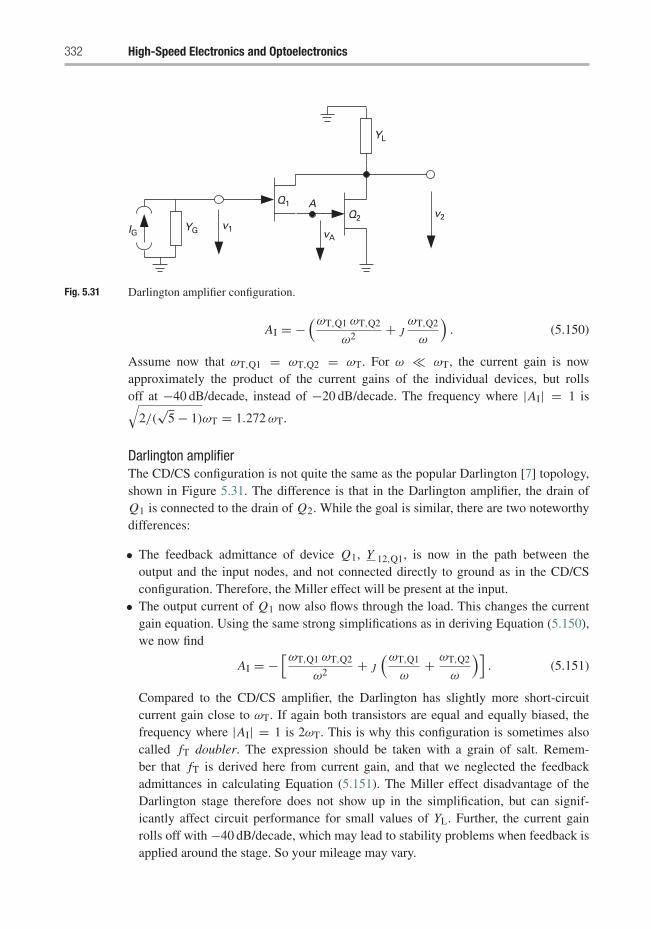
332 High-Speed Electronics and Optoelectronics
YL
v2Q2
Q1 A
vAv1YGIG
Fig. 5.31 Darlington amplifier configuration.
AI = −(ωT,Q1 ωT,Q2
ω2+ j
ωT,Q2
ω
). (5.150)
Assume now that ωT,Q1 = ωT,Q2 = ωT. For ω � ωT, the current gain is nowapproximately the product of the current gains of the individual devices, but rollsoff at −40 dB/decade, instead of −20 dB/decade. The frequency where |AI| = 1 is√
2/(√
5 − 1)ωT = 1.272ωT.
Darlington amplifierThe CD/CS configuration is not quite the same as the popular Darlington [7] topology,shown in Figure 5.31. The difference is that in the Darlington amplifier, the drain ofQ1 is connected to the drain of Q2. While the goal is similar, there are two noteworthydifferences:
• The feedback admittance of device Q1, Y 12,Q1, is now in the path between theoutput and the input nodes, and not connected directly to ground as in the CD/CSconfiguration. Therefore, the Miller effect will be present at the input.
• The output current of Q1 now also flows through the load. This changes the currentgain equation. Using the same strong simplifications as in deriving Equation (5.150),we now find
AI = −[ωT,Q1 ωT,Q2
ω2+ j
(ωT,Q1
ω+ ωT,Q2
ω
)]. (5.151)
Compared to the CD/CS amplifier, the Darlington has slightly more short-circuitcurrent gain close to ωT. If again both transistors are equal and equally biased, thefrequency where |AI| = 1 is 2ωT. This is why this configuration is sometimes alsocalled fT doubler. The expression should be taken with a grain of salt. Remem-ber that fT is derived here from current gain, and that we neglected the feedbackadmittances in calculating Equation (5.151). The Miller effect disadvantage of theDarlington stage therefore does not show up in the simplification, but can signif-icantly affect circuit performance for small values of YL. Further, the current gainrolls off with −40 dB/decade, which may lead to stability problems when feedback isapplied around the stage. So your mileage may vary.
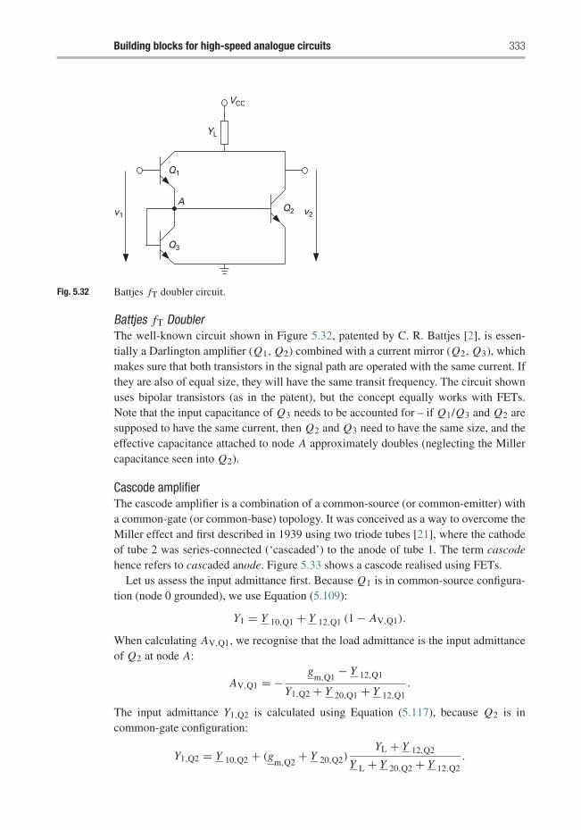
Building blocks for high-speed analogue circuits 333
VCC
YL
Q2
Q3
Q1
Av2v1
Fig. 5.32 Battjes fT doubler circuit.
Battjes fT DoublerThe well-known circuit shown in Figure 5.32, patented by C. R. Battjes [2], is essen-tially a Darlington amplifier (Q1, Q2) combined with a current mirror (Q2, Q3), whichmakes sure that both transistors in the signal path are operated with the same current. Ifthey are also of equal size, they will have the same transit frequency. The circuit shownuses bipolar transistors (as in the patent), but the concept equally works with FETs.Note that the input capacitance of Q3 needs to be accounted for – if Q1/Q3 and Q2 aresupposed to have the same current, then Q2 and Q3 need to have the same size, and theeffective capacitance attached to node A approximately doubles (neglecting the Millercapacitance seen into Q2).
Cascode amplifierThe cascode amplifier is a combination of a common-source (or common-emitter) witha common-gate (or common-base) topology. It was conceived as a way to overcome theMiller effect and first described in 1939 using two triode tubes [21], where the cathodeof tube 2 was series-connected (‘cascaded’) to the anode of tube 1. The term cascodehence refers to cascaded anode. Figure 5.33 shows a cascode realised using FETs.
Let us assess the input admittance first. Because Q1 is in common-source configura-tion (node 0 grounded), we use Equation (5.109):
Y1 = Y 10,Q1 + Y 12,Q1 (1 − AV,Q1).
When calculating AV,Q1, we recognise that the load admittance is the input admittanceof Q2 at node A:
AV,Q1 = −g
m,Q1− Y 12,Q1
Y1,Q2 + Y 20,Q1 + Y 12,Q1.
The input admittance Y1,Q2 is calculated using Equation (5.117), because Q2 is incommon-gate configuration:
Y1,Q2 = Y 10,Q2 + (gm,Q2
+ Y 20,Q2)YL + Y 12,Q2
Y L + Y 20,Q2 + Y 12,Q2.
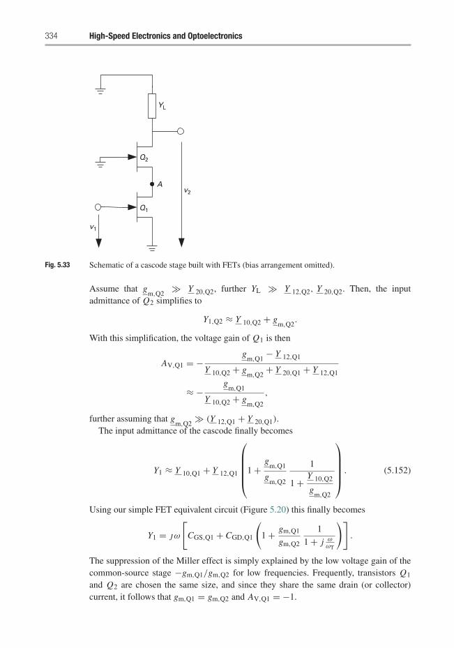
334 High-Speed Electronics and Optoelectronics
YL
v2
v1
Q2
Q1
A
Fig. 5.33 Schematic of a cascode stage built with FETs (bias arrangement omitted).
Assume that gm,Q2
� Y 20,Q2, further YL � Y 12,Q2, Y 20,Q2. Then, the inputadmittance of Q2 simplifies to
Y1,Q2 ≈ Y 10,Q2 + gm,Q2
.
With this simplification, the voltage gain of Q1 is then
AV,Q1 = −g
m,Q1− Y 12,Q1
Y 10,Q2 + gm,Q2
+ Y 20,Q1 + Y 12,Q1
≈ −g
m,Q1
Y 10,Q2 + gm,Q2
,
further assuming that gm,Q2
� (Y 12,Q1 + Y 20,Q1).The input admittance of the cascode finally becomes
Y1 ≈ Y 10,Q1 + Y 12,Q1
⎛⎜⎜⎜⎜⎝1 +g
m,Q1
gm,Q2
1
1 + Y 10,Q2
gm,Q2
⎞⎟⎟⎟⎟⎠ . (5.152)
Using our simple FET equivalent circuit (Figure 5.20) this finally becomes
Y1 = jω
[CGS,Q1 + CGD,Q1
(1 + gm,Q1
gm,Q2
1
1 + j ωωT
)].
The suppression of the Miller effect is simply explained by the low voltage gain of thecommon-source stage −gm,Q1/gm,Q2 for low frequencies. Frequently, transistors Q1
and Q2 are chosen the same size, and since they share the same drain (or collector)current, it follows that gm,Q1 = gm,Q2 and AV,Q1 = −1.
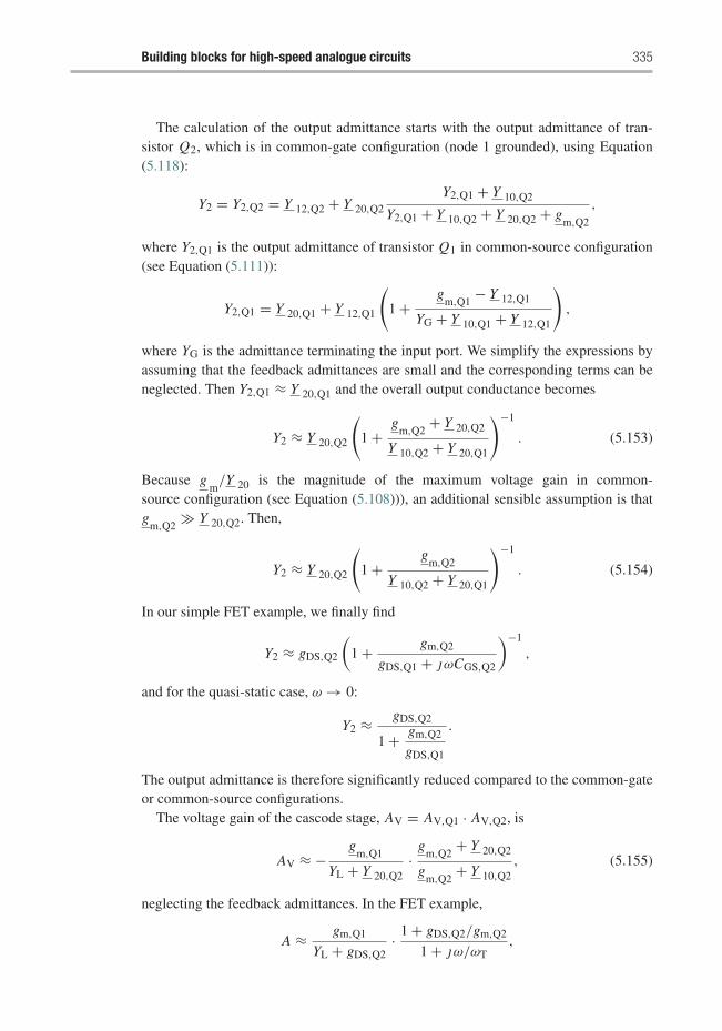
Building blocks for high-speed analogue circuits 335
The calculation of the output admittance starts with the output admittance of tran-sistor Q2, which is in common-gate configuration (node 1 grounded), using Equation(5.118):
Y2 = Y2,Q2 = Y 12,Q2 + Y 20,Q2
Y2,Q1 + Y 10,Q2
Y2,Q1 + Y 10,Q2 + Y 20,Q2 + gm,Q2
,
where Y2,Q1 is the output admittance of transistor Q1 in common-source configuration(see Equation (5.111)):
Y2,Q1 = Y 20,Q1 + Y 12,Q1
(1 +
gm,Q1
− Y 12,Q1
YG + Y 10,Q1 + Y 12,Q1
),
where YG is the admittance terminating the input port. We simplify the expressions byassuming that the feedback admittances are small and the corresponding terms can beneglected. Then Y2,Q1 ≈ Y 20,Q1 and the overall output conductance becomes
Y2 ≈ Y 20,Q2
(1 +
gm,Q2
+ Y 20,Q2
Y 10,Q2 + Y 20,Q1
)−1
. (5.153)
Because gm/Y 20 is the magnitude of the maximum voltage gain in common-
source configuration (see Equation (5.108))), an additional sensible assumption is thatg
m,Q2� Y 20,Q2. Then,
Y2 ≈ Y 20,Q2
(1 +
gm,Q2
Y 10,Q2 + Y 20,Q1
)−1
. (5.154)
In our simple FET example, we finally find
Y2 ≈ gDS,Q2
(1 + gm,Q2
gDS,Q1 + jωCGS,Q2
)−1
,
and for the quasi-static case, ω → 0:
Y2 ≈ gDS,Q2
1 + gm,Q2
gDS,Q1
.
The output admittance is therefore significantly reduced compared to the common-gateor common-source configurations.
The voltage gain of the cascode stage, AV = AV,Q1 · AV,Q2, is
AV ≈ −g
m,Q1
YL + Y 20,Q2·
gm,Q2
+ Y 20,Q2
gm,Q2
+ Y 10,Q2, (5.155)
neglecting the feedback admittances. In the FET example,
A ≈ gm,Q1
YL + gDS,Q2· 1 + gDS,Q2/gm,Q2
1 + jω/ωT,
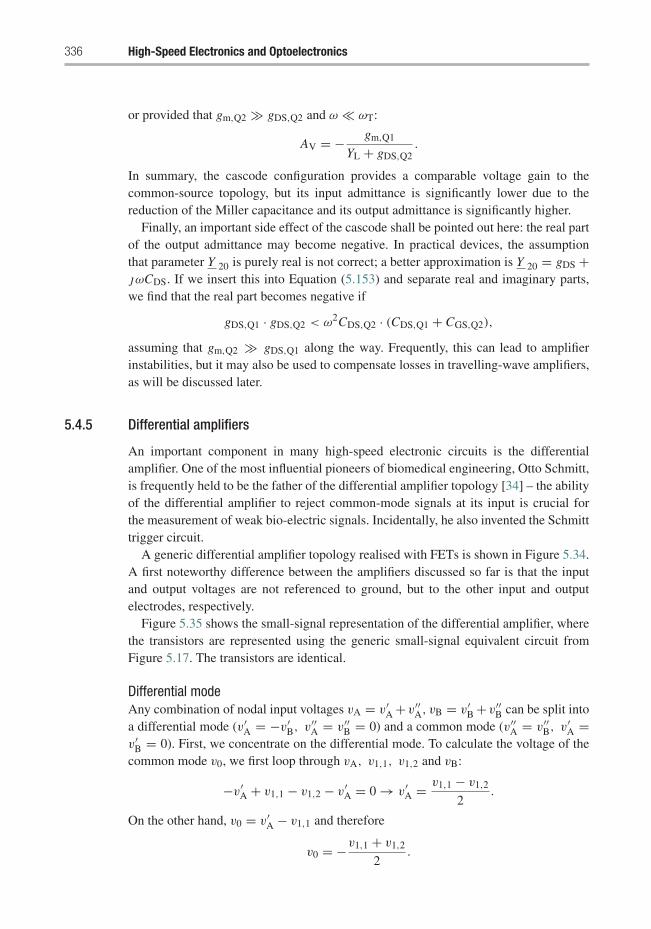
336 High-Speed Electronics and Optoelectronics
or provided that gm,Q2 � gDS,Q2 and ω � ωT:
AV = − gm,Q1
YL + gDS,Q2.
In summary, the cascode configuration provides a comparable voltage gain to thecommon-source topology, but its input admittance is significantly lower due to thereduction of the Miller capacitance and its output admittance is significantly higher.
Finally, an important side effect of the cascode shall be pointed out here: the real partof the output admittance may become negative. In practical devices, the assumptionthat parameter Y 20 is purely real is not correct; a better approximation is Y 20 = gDS +jωCDS. If we insert this into Equation (5.153) and separate real and imaginary parts,we find that the real part becomes negative if
gDS,Q1 · gDS,Q2 < ω2CDS,Q2 · (CDS,Q1 + CGS,Q2),
assuming that gm,Q2 � gDS,Q1 along the way. Frequently, this can lead to amplifierinstabilities, but it may also be used to compensate losses in travelling-wave amplifiers,as will be discussed later.
5.4.5 Differential amplifiers
An important component in many high-speed electronic circuits is the differentialamplifier. One of the most influential pioneers of biomedical engineering, Otto Schmitt,is frequently held to be the father of the differential amplifier topology [34] – the abilityof the differential amplifier to reject common-mode signals at its input is crucial forthe measurement of weak bio-electric signals. Incidentally, he also invented the Schmitttrigger circuit.
A generic differential amplifier topology realised with FETs is shown in Figure 5.34.A first noteworthy difference between the amplifiers discussed so far is that the inputand output voltages are not referenced to ground, but to the other input and outputelectrodes, respectively.
Figure 5.35 shows the small-signal representation of the differential amplifier, wherethe transistors are represented using the generic small-signal equivalent circuit fromFigure 5.17. The transistors are identical.
Differential modeAny combination of nodal input voltages vA = v′
A + v′′A, vB = v′
B + v′′B can be split into
a differential mode (v′A = −v′
B, v′′A = v′′
B = 0) and a common mode (v′′A = v′′
B, v′A =
v′B = 0). First, we concentrate on the differential mode. To calculate the voltage of the
common mode v0, we first loop through vA, v1,1, v1,2 and vB:
−v′A + v1,1 − v1,2 − v′
A = 0 → v′A = v1,1 − v1,2
2.
On the other hand, v0 = v′A − v1,1 and therefore
v0 = −v1,1 + v1,2
2.
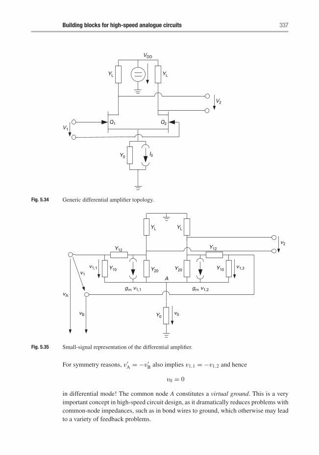
Building blocks for high-speed analogue circuits 337
VDD
YLYL
V2
Q2Q1
Y0I0
V1
Fig. 5.34 Generic differential amplifier topology.
YL YL
Y20
gm v1,1 gm v1,2
Y0
A
Y12
Y10v1,1
v1
vA
vB
Y20
Y12
v2
v1,2Y10
v0
Fig. 5.35 Small-signal representation of the differential amplifier.
For symmetry reasons, v′A = −v′
B also implies v1,1 = −v1,2 and hence
v0 = 0
in differential mode! The common node A constitutes a virtual ground. This is a veryimportant concept in high-speed circuit design, as it dramatically reduces problems withcommon-node impedances, such as in bond wires to ground, which otherwise may leadto a variety of feedback problems.
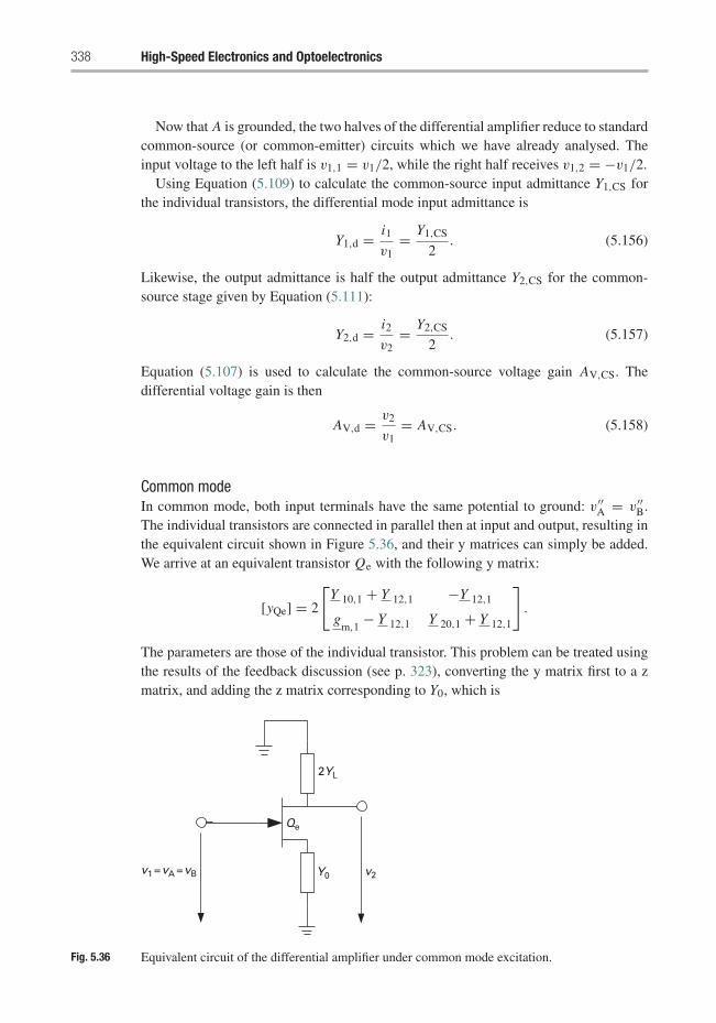
338 High-Speed Electronics and Optoelectronics
Now that A is grounded, the two halves of the differential amplifier reduce to standardcommon-source (or common-emitter) circuits which we have already analysed. Theinput voltage to the left half is v1,1 = v1/2, while the right half receives v1,2 = −v1/2.
Using Equation (5.109) to calculate the common-source input admittance Y1,CS forthe individual transistors, the differential mode input admittance is
Y1,d = i1
v1= Y1,CS
2. (5.156)
Likewise, the output admittance is half the output admittance Y2,CS for the common-source stage given by Equation (5.111):
Y2,d = i2
v2= Y2,CS
2. (5.157)
Equation (5.107) is used to calculate the common-source voltage gain AV,CS. Thedifferential voltage gain is then
AV,d = v2
v1= AV,CS. (5.158)
Common modeIn common mode, both input terminals have the same potential to ground: v′′
A = v′′B.
The individual transistors are connected in parallel then at input and output, resulting inthe equivalent circuit shown in Figure 5.36, and their y matrices can simply be added.We arrive at an equivalent transistor Qe with the following y matrix:
[yQe] = 2
[Y 10,1 + Y 12,1 −Y 12,1
gm,1
− Y 12,1 Y 20,1 + Y 12,1
].
The parameters are those of the individual transistor. This problem can be treated usingthe results of the feedback discussion (see p. 323), converting the y matrix first to a zmatrix, and adding the z matrix corresponding to Y0, which is
2YL
Qe
Y0 v2v1 =vA =vB
Fig. 5.36 Equivalent circuit of the differential amplifier under common mode excitation.
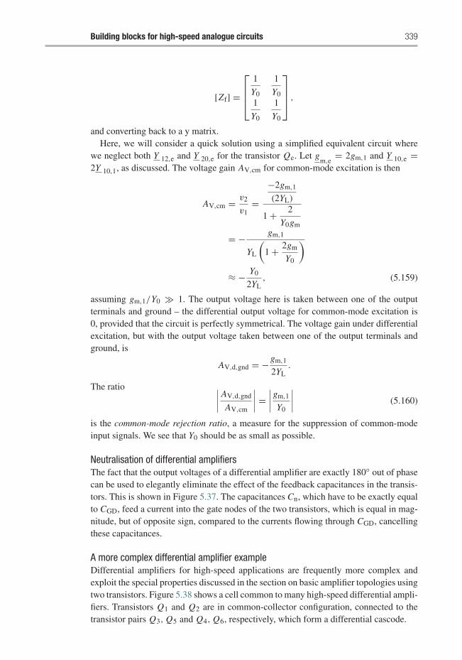
Building blocks for high-speed analogue circuits 339
[Zf] =
⎡⎢⎢⎣1
Y0
1
Y01
Y0
1
Y0
⎤⎥⎥⎦ ,
and converting back to a y matrix.Here, we will consider a quick solution using a simplified equivalent circuit where
we neglect both Y 12,e and Y 20,e for the transistor Qe. Let gm,e
= 2gm,1 and Y 10,e =2Y 10,1, as discussed. The voltage gain AV,cm for common-mode excitation is then
AV,cm = v2
v1=
−2gm,1
(2YL)
1 + 2
Y0gm
= − gm,1
YL
(1 + 2gm
Y0
)≈ − Y0
2YL, (5.159)
assuming gm,1/Y0 � 1. The output voltage here is taken between one of the outputterminals and ground – the differential output voltage for common-mode excitation is0, provided that the circuit is perfectly symmetrical. The voltage gain under differentialexcitation, but with the output voltage taken between one of the output terminals andground, is
AV,d,gnd = −gm,1
2YL.
The ratio ∣∣∣∣ AV,d,gnd
AV,cm
∣∣∣∣ =∣∣∣∣ gm,1
Y0
∣∣∣∣ (5.160)
is the common-mode rejection ratio, a measure for the suppression of common-modeinput signals. We see that Y0 should be as small as possible.
Neutralisation of differential amplifiersThe fact that the output voltages of a differential amplifier are exactly 180◦ out of phasecan be used to elegantly eliminate the effect of the feedback capacitances in the transis-tors. This is shown in Figure 5.37. The capacitances Cn, which have to be exactly equalto CGD, feed a current into the gate nodes of the two transistors, which is equal in mag-nitude, but of opposite sign, compared to the currents flowing through CGD, cancellingthese capacitances.
A more complex differential amplifier exampleDifferential amplifiers for high-speed applications are frequently more complex andexploit the special properties discussed in the section on basic amplifier topologies usingtwo transistors. Figure 5.38 shows a cell common to many high-speed differential ampli-fiers. Transistors Q1 and Q2 are in common-collector configuration, connected to thetransistor pairs Q3, Q5 and Q4, Q6, respectively, which form a differential cascode.
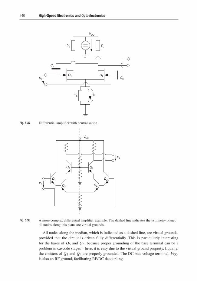
340 High-Speed Electronics and Optoelectronics
VDD
YLYL
Cn
V1
Q1 Q2 Cn
I0Y0
Fig. 5.37 Differential amplifier with neutralisation.
VCC
v1
Q1
Q3
Q5 Q6
Q2
v2
Q4
Fig. 5.38 A more complex differential amplifier example. The dashed line indicates the symmetry plane;all nodes along this plane are virtual grounds.
All nodes along the median, which is indicated as a dashed line, are virtual grounds,provided that the circuit is driven fully differentially. This is particularly interestingfor the bases of Q5 and Q6, because proper grounding of the base terminal can be aproblem in cascode stages – here, it is easy due to the virtual ground property. Equally,the emitters of Q3 and Q4 are properly grounded. The DC bias voltage terminal, VCC,is also an RF ground, facilitating RF/DC decoupling.
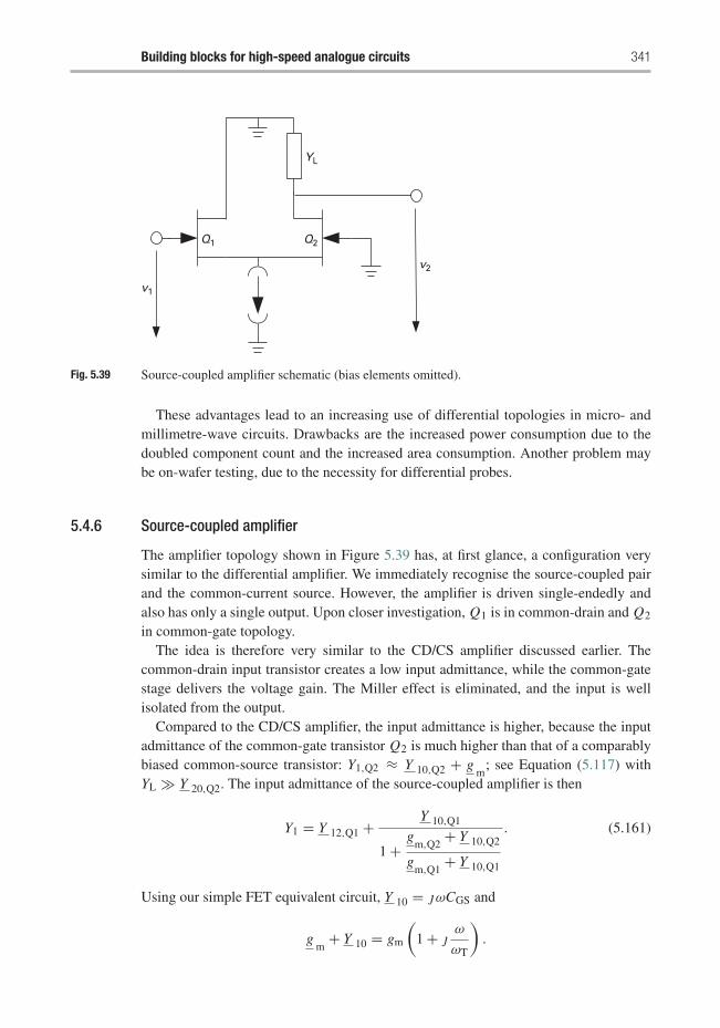
Building blocks for high-speed analogue circuits 341
YL
Q1
v1
v2
Q2
Fig. 5.39 Source-coupled amplifier schematic (bias elements omitted).
These advantages lead to an increasing use of differential topologies in micro- andmillimetre-wave circuits. Drawbacks are the increased power consumption due to thedoubled component count and the increased area consumption. Another problem maybe on-wafer testing, due to the necessity for differential probes.
5.4.6 Source-coupled amplifier
The amplifier topology shown in Figure 5.39 has, at first glance, a configuration verysimilar to the differential amplifier. We immediately recognise the source-coupled pairand the common-current source. However, the amplifier is driven single-endedly andalso has only a single output. Upon closer investigation, Q1 is in common-drain and Q2
in common-gate topology.The idea is therefore very similar to the CD/CS amplifier discussed earlier. The
common-drain input transistor creates a low input admittance, while the common-gatestage delivers the voltage gain. The Miller effect is eliminated, and the input is wellisolated from the output.
Compared to the CD/CS amplifier, the input admittance is higher, because the inputadmittance of the common-gate transistor Q2 is much higher than that of a comparablybiased common-source transistor: Y1,Q2 ≈ Y 10,Q2 + g
m; see Equation (5.117) with
YL � Y 20,Q2. The input admittance of the source-coupled amplifier is then
Y1 = Y 12,Q1 + Y 10,Q1
1 +g
m,Q2+ Y 10,Q2
gm,Q1
+ Y 10,Q1
. (5.161)
Using our simple FET equivalent circuit, Y 10 = jωCGS and
gm
+ Y 10 = gm
(1 + j
ω
ωT
).
342 High-Speed Electronics and Optoelectronics
If the transistors therefore have the same ωT, the input admittance is
Y1 = jω
⎛⎜⎝CGD,Q1 + CGS,Q1
1 + gm,Q2
gm,Q1
⎞⎟⎠ .
It is purely capacitive and does not show the risk of a negative real part, which theCD/CS amplifier had posed.
The circuit can also be compared to the cascode – the source-coupled amplifier hasa lower input admittance, is non-inverting and requires a lower supply voltage than thecascode, but the cascode requires less current, because the current through the common-gate stage is recycled in the common-source transistor.
5.4.7 Tuned amplifiers
Tuned amplifiers are commonly used at micro- and millimetre-wave frequencies whenthe fractional bandwidth is small. The fractional bandwidth is the required opera-tional bandwidth divided by the centre frequency. For example, the 24 GHz license-freeISM band has a total allowed spectral width of 250 MHz, so any amplifier will needsensibly only a fractional bandwidth of 10−2. Other applications, such as emergingultra-wideband sensor and communications standards, will have fractional bandwidthswhich are orders of magnitude larger – the design of amplifiers for such systems will betreated in the next section (p. 350).
A typical tuned amplifier will use three fundamental circuit techniques:
(i) A resonant load – the load admittance goes through a minimum at the frequencyof operation, maximising the voltage gain for a given transconductance.
(ii) Complex conjugate match at the input, ensuring that the available power from thesource is delivered to the amplifier.
(iii) Complex conjugate match at the output, ensuring that the available power from theamplifier is delivered to the load.
For LNAs and power amplifiers, other matching strategies may apply for the input andoutput ports, respectively. These will be treated in the sections on LNA design (p. 365)and power amplifier design (p. 376). For now, we assume that achieving the maximumgain is our objective.
Resonant loadsLet us first investigate the resonant load, using the simple example of Figure 5.40. Theschematic also indicates the generator and the equivalent input admittance of the fol-lowing stage – it is essential to include at least the next-stage input admittance in thecalculations, and due to feedback, the generator admittance will also have an effect,albeit more weakly.
The admittances Y2,Q1 and Y1,Q2 can typically be represented by a conductance inparallel with a capacitive reactance (exception – if the following stage is a common-gate
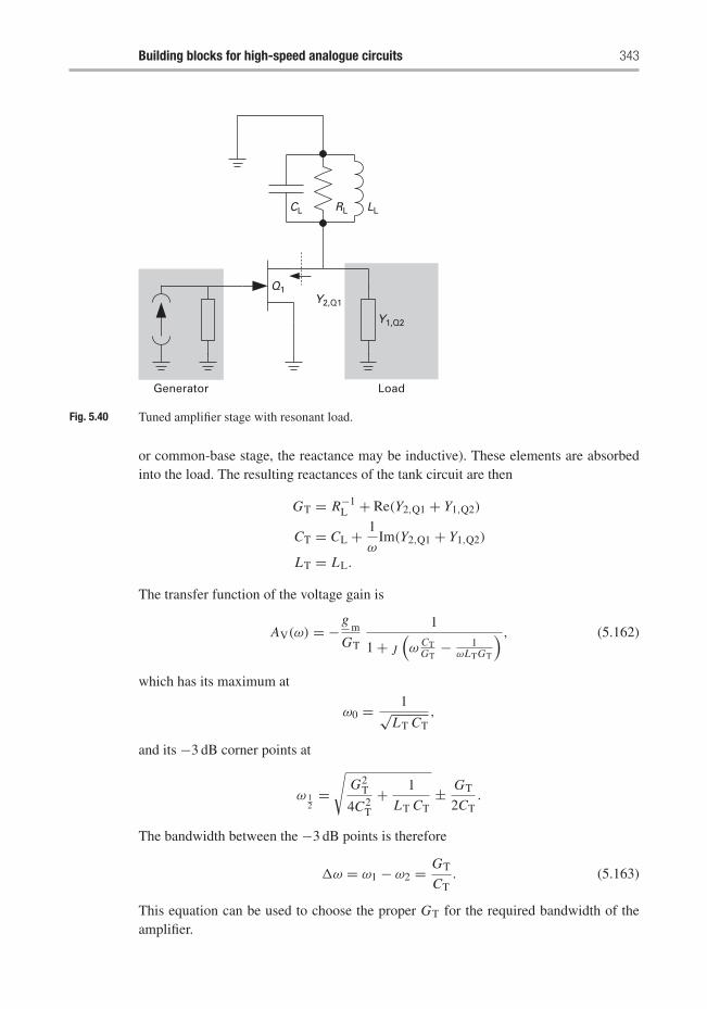
Building blocks for high-speed analogue circuits 343
Generator Load
LLRLCL
Q1Y2,Q1
Y1,Q2
Fig. 5.40 Tuned amplifier stage with resonant load.
or common-base stage, the reactance may be inductive). These elements are absorbedinto the load. The resulting reactances of the tank circuit are then
GT = R−1L + Re(Y2,Q1 + Y1,Q2)
CT = CL + 1
ωIm(Y2,Q1 + Y1,Q2)
LT = LL.
The transfer function of the voltage gain is
AV(ω) = −gm
GT
1
1 + j(ω CT
GT− 1
ωLTGT
) , (5.162)
which has its maximum at
ω0 = 1√LT CT
,
and its −3 dB corner points at
ω 12
=√
G2T
4C2T
+ 1
LT CT± GT
2CT.
The bandwidth between the −3 dB points is therefore
�ω = ω1 − ω2 = GT
CT. (5.163)
This equation can be used to choose the proper GT for the required bandwidth of theamplifier.
344 High-Speed Electronics and Optoelectronics
Using Equations (5.162) and (5.163), we find the product of the voltage gain at ω =ω0 and the −3 dB bandwidth:
− AV(ω0) · �ω = gm
CT, (5.164)
which is interestingly independent of frequency. This is due to simplifying assumptions,of course. In the ansatz for Equation (5.162) we used Equation (5.107) with the assump-tion that g
m� Y 12, hence that feedback is negligible, which is no longer true at very
high frequencies.A tuned tank circuit always bears the risk of amplifier instability. For the common-
source amplifier in the example, we use Equation (5.109) to calculate the inputadmittance of the circuit, using the expression in Equation (5.162) for AV(ω):
Y1 = Y 10 + Y 12
⎧⎨⎩1 + gm
GT
1
1 + j[ω CT
GT− 1
LTGT
]⎫⎬⎭
= Y 10 + Y 12 + Y 12
gm
GT
1 − j[ω CT
GT− 1
ωLTGT
]1 +
[ω CT
GT− 1
ωLTGT
]2.
If, as is usually the case, Y 12 ≈ jωCGD, the third term in the sum has a negative realpart for ω < ω0. The risk of parasitic oscillations increases with increasing peak gain.Neutralisation measures as discussed already (p. 325) may become necessary in suchcases.
Input and output matching networksA common requirement in microwave amplifiers is that input and output admittancesneed to have a predefined value. There are two major reasons for this:
(i) If the input and output admittances are the complex conjugates of the source andload admittances, the source’s available power is transferred to the amplifier, andthe amplifier’s available power is transferred to the load, resulting in the maximumpower gain – this value is called the maximum available gain and will be discussedshortly.
(ii) To avoid standing waves on interconnecting transmission lines, the lines need tobe terminated by their characteristic impedances at least at one end.
The characteristic impedance of a lossless transmission line is real; hence, input and out-put admittances are normally tuned to a purely real value where the circuit will interfacewith a transmission line. For internal nodes, however, this is not necessary – in fact,as we will see in our discussion of broadband amplifier techniques, at internal nodesimpedance matching is often abandoned altogether, in favour of increased bandwidth,but with penalties in power gain.
Because the Smith chart (see p. 295) is the most important tool in solving matchingproblems, we will conduct the matching discussions using scattering parameters.
Building blocks for high-speed analogue circuits 345
Most importantly, we need to translate source and load admittances as well as two-port input and output admittances into reflection coefficients. This is easily done:
� = Y0 − Y
Y0 + Y= Z − Z0
Z + Z0, (5.165)
where Y0 = 1/Z0 is the normalising admittance, which is frequently 20 mS (corre-spondingly Z0 = 50�), but can be chosen arbitrarily.
We have seen that in two-ports which are not unilateral (y12 �= 0, correspond-ingly S12 �= 0), the input admittance depends on the load admittance, and the outputadmittance depends on the source admittance. In general terms and with the two-portexpressed as a scattering matrix, the input (�1) and output (�2) reflection coefficientsare (p. 300)
�1 = S11 + S12S21�L
1 − S22�L(5.166)
�2 = S22 + S12s21�G
1 − S11�G, (5.167)
where �G and �L are the generator and load reflection coefficients, respectively.For simultaneous power match at input and output ports, we need these coupled
equations to be satisfied:
�∗G = S11 + S12S21�L
1 − S22�L
�∗L = S22 + S12S21�G
1 − S11�G,
where �∗ is the complex conjugate of �. Solving these equations for the necessarygenerator and load reflection coefficients �G,m and �L,m, we find
�G,m = C∗1
|C1|
⎛⎝ B1
2|C1| −√
B21
|C1|2 − 1
⎞⎠ , (5.168)
with
B1 = 1 − |S22|2 + |S11|2 − |�(S)|2C1 = S11 − �(S) S∗
22,
where �(S) is the determinant of the scattering matrix. For the load reflectioncoefficients, we find likewise:
�L,m = C∗2
|C2|
⎛⎝ B2
2|C2| −√
B22
|C2|2 − 1
⎞⎠ , (5.169)
with
B2 = 1 − |S11|2 + |S22|2 − |�(S)|2C2 = S22 − �(S) S∗
11.
Simultaneous input and output power match is not always possible, but requires a two-port to be unconditionally stable (see p. 303).
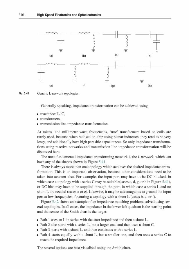
346 High-Speed Electronics and Optoelectronics
(a) (b) (c) (d)
(e) (f) (g) (h)
Fig. 5.41 Generic L network topologies.
Generally speaking, impedance transformation can be achieved using
• reactances L, C,• transformers,• transmission line impedance transformation.
At micro- and millimetre-wave frequencies, ‘true’ transformers based on coils arerarely used, because when realised on-chip using planar inductors, they tend to be verylossy, and additionally have high parasitic capacitances. So only impedance transforma-tions using reactive networks and transmission line impedance transformation will bediscussed here.
The most fundamental impedance transforming network is the L network, which canhave any of the shapes shown in Figure 5.41.
There is always more than one topology which achieves the desired impedance trans-formation. This is an important observation, because other considerations need to betaken into account also. For example, the input port may have to be DC-blocked, inwhich case a topology with a series C may be suitable(cases c, d, g, or h in Figure 5.41),or DC bias may have to be supplied through the port, in which case a series L and noshunt L are needed (cases a or e). Likewise, it may be advantageous to ground the inputport at low frequencies, favouring a topology with a shunt L (cases b, c, or f).
Figure 5.42 shows an example of an impedance matching problem, solved using sev-eral topologies. In all cases, the impedance in the lower left quadrant is the starting pointand the centre of the Smith chart is the target.
• Path 1 uses an L in series with the start impedance and then a shunt L.• Path 2 also starts with a series L, but a larger one, and then uses a shunt C.• Path 3 starts with a shunt L, and then continues with a series L.• Path 4 starts equally with a shunt L, but a smaller one, and then uses a series C to
reach the required impedance.
The several options are best visualised using the Smith chart.
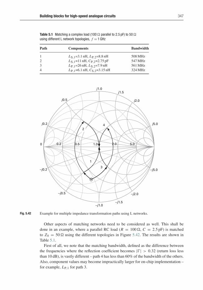
Building blocks for high-speed analogue circuits 347
Table 5.1 Matching a complex load (100� parallel to 2.5 pF) to 50�using different L network topologies, f = 1 GHz
Path Components Bandwidth
1 LS,1=3.1 nH, LP,2=8.8 nH 508 MHz2 LS,1=11 nH, CP,2=2.75 pF 547 MHz3 LP,1=26 nH, LS,2=7.9 nH 561 MHz4 LP,1=6.1 nH, CS,2=3.15 nH 324 MHz
j1.0
j0.5
j0.2
–j0.2
–j0.5
–j1.0–j1.5
–j2.0
–j5.0
0 0.2 0.5 1.0 2.0 5.0
j5.0
j2.0
j1.5
2
1
3
4
Fig. 5.42 Example for multiple impedance transformation paths using L networks.
Other aspects of matching networks need to be considered as well. This shall bedone in an example, where a parallel RC load (R = 100�, C = 2.5 pF) is matchedto Z0 = 50� using the different topologies in Figure 5.42. The results are shown inTable 5.1.
First of all, we note that the matching bandwidth, defined as the difference betweenthe frequencies where the reflection coefficient becomes |�| > 0.32 (return loss lessthan 10 dB), is vastly different – path 4 has less than 60% of the bandwidth of the others.Also, component values may become impractically larger for on-chip implementation –for example, LP,1 for path 3.
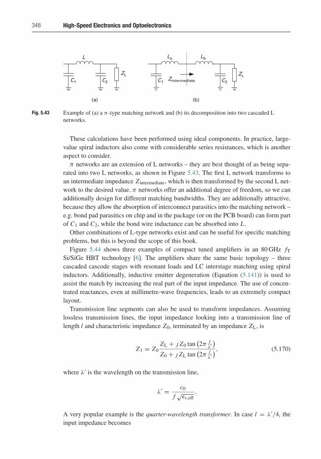
348 High-Speed Electronics and Optoelectronics
L
C1 C2
ZLC1 C2
ZL
La Lb
Zintermediate
(a) (b)
Fig. 5.43 Example of (a) a π -type matching network and (b) its decomposition into two cascaded Lnetworks.
These calculations have been performed using ideal components. In practice, large-value spiral inductors also come with considerable series resistances, which is anotheraspect to consider.
π networks are an extension of L networks – they are best thought of as being sepa-rated into two L networks, as shown in Figure 5.43. The first L network transforms toan intermediate impedance Zintermediate, which is then transformed by the second L net-work to the desired value. π networks offer an additional degree of freedom, so we canadditionally design for different matching bandwidths. They are additionally attractive,because they allow the absorption of interconnect parasitics into the matching network –e.g. bond pad parasitics on chip and in the package (or on the PCB board) can form partof C1 and C2, while the bond wire inductance can be absorbed into L .
Other combinations of L-type networks exist and can be useful for specific matchingproblems, but this is beyond the scope of this book.
Figure 5.44 shows three examples of compact tuned amplifiers in an 80 GHz fT
Si/SiGe HBT technology [6]. The amplifiers share the same basic topology – threecascaded cascode stages with resonant loads and LC interstage matching using spiralinductors. Additionally, inductive emitter degeneration (Equation (5.141)) is used toassist the match by increasing the real part of the input impedance. The use of concen-trated reactances, even at millimetre-wave frequencies, leads to an extremely compactlayout.
Transmission line segments can also be used to transform impedances. Assuminglossless transmission lines, the input impedance looking into a transmission line oflength l and characteristic impedance Z0, terminated by an impedance ZL, is
Z1 = Z0ZL + j Z0 tan
(2π l
λ′)
Z0 + j ZL tan(2π l
λ′) , (5.170)
where λ′ is the wavelength on the transmission line,
λ′ = c0
f√εr,eff
.
A very popular example is the quarter-wavelength transformer. In case l = λ′/4, theinput impedance becomes
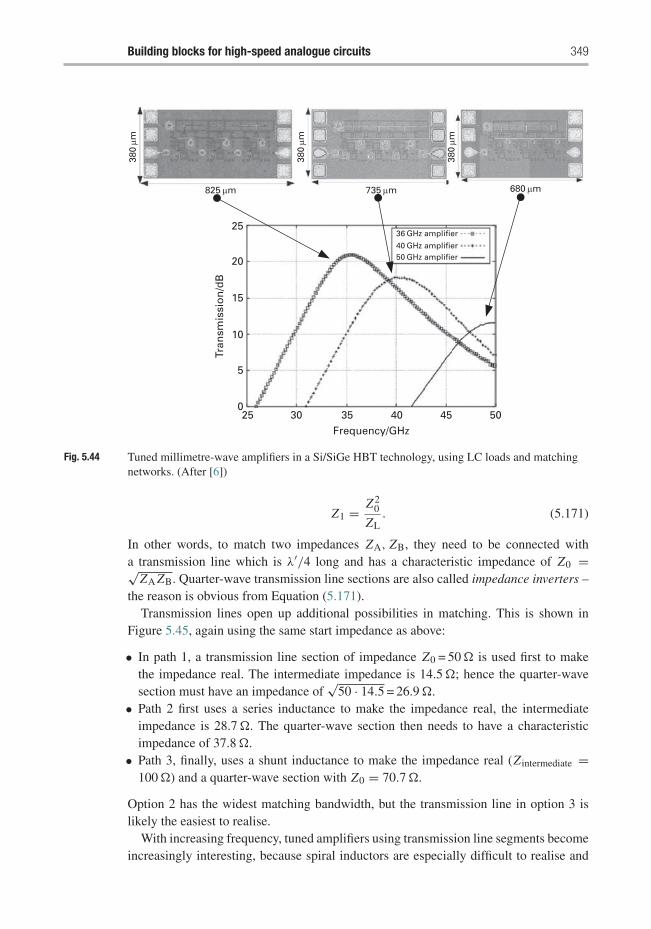
Building blocks for high-speed analogue circuits 349
25
825 µm
380 µm
380 µm
380 µm
735 µm
36 GHz amplifier
40 GHz amplifier50 GHz amplifier
680 µm
20
15
10
5
025 30 35
Frequency/GHz
Tran
smis
sio
n/d
B
40 45 50
Fig. 5.44 Tuned millimetre-wave amplifiers in a Si/SiGe HBT technology, using LC loads and matchingnetworks. (After [6])
Z1 = Z20
ZL. (5.171)
In other words, to match two impedances ZA, ZB, they need to be connected witha transmission line which is λ′/4 long and has a characteristic impedance of Z0 =√
ZA ZB. Quarter-wave transmission line sections are also called impedance inverters –the reason is obvious from Equation (5.171).
Transmission lines open up additional possibilities in matching. This is shown inFigure 5.45, again using the same start impedance as above:
• In path 1, a transmission line section of impedance Z0 = 50� is used first to makethe impedance real. The intermediate impedance is 14.5�; hence the quarter-wavesection must have an impedance of
√50 · 14.5 = 26.9�.
• Path 2 first uses a series inductance to make the impedance real, the intermediateimpedance is 28.7�. The quarter-wave section then needs to have a characteristicimpedance of 37.8�.
• Path 3, finally, uses a shunt inductance to make the impedance real (Z intermediate =100�) and a quarter-wave section with Z0 = 70.7�.
Option 2 has the widest matching bandwidth, but the transmission line in option 3 islikely the easiest to realise.
With increasing frequency, tuned amplifiers using transmission line segments becomeincreasingly interesting, because spiral inductors are especially difficult to realise and
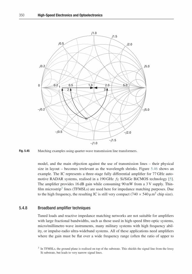
350 High-Speed Electronics and Optoelectronics
j1.0
j0.5
j0.2
–j0.2
–j0.5
–j1.0–j1.5
–j2.0
–j5.0
0 0.2 12 30.5 2.01.0 5.0
j5.0
j2.0
j1.5
Fig. 5.45 Matching examples using quarter-wave transmission line transformers.
model, and the main objection against the use of transmission lines – their physicalsize in layout – becomes irrelevant as the wavelength shrinks. Figure 5.46 shows anexample. The IC represents a three-stage fully differential amplifier for 77 GHz auto-motive RADAR systems, realised in a 190 GHz fT Si/SiGe BiCMOS technology [5].The amplifier provides 16 dB gain while consuming 90 mW from a 3 V supply. Thin-film microstrip3 lines (TFMSLs) are used here for impedance matching purposes. Dueto the high frequency, the resulting IC is still very compact (740 × 540 μm2 chip size).
5.4.8 Broadband amplifier techniques
Tuned loads and reactive impedance matching networks are not suitable for amplifierswith large fractional bandwidths, such as those used in high-speed fibre-optic systems,micro/millimetre-wave instruments, many military systems with high frequency abil-ity, or impulse-radio ultra-wideband systems. All of these applications need amplifierswhere the gain must be flat over a wide frequency range (often the ratio of upper to
3 In TFMSLs, the ground plane is realised on top of the substrate. This shields the signal line from the lossySi substrate, but leads to very narrow signal lines.
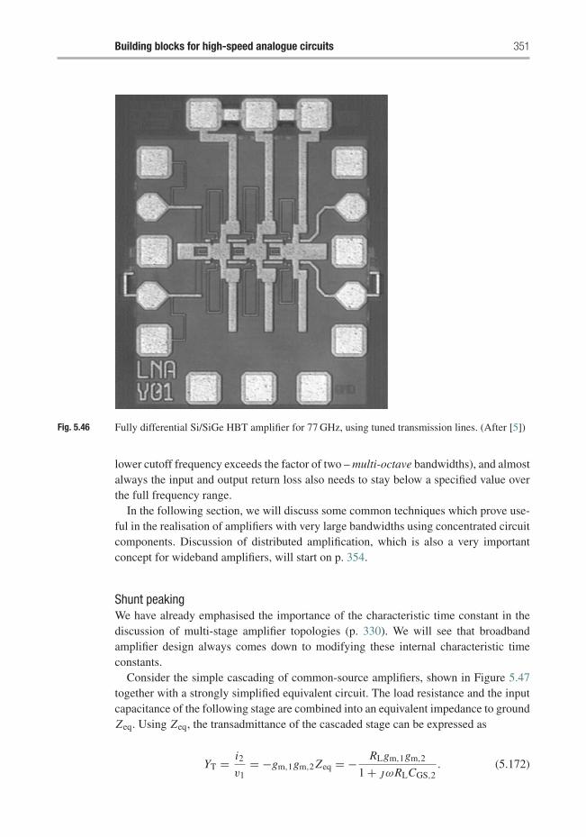
Building blocks for high-speed analogue circuits 351
Fig. 5.46 Fully differential Si/SiGe HBT amplifier for 77 GHz, using tuned transmission lines. (After [5])
lower cutoff frequency exceeds the factor of two – multi-octave bandwidths), and almostalways the input and output return loss also needs to stay below a specified value overthe full frequency range.
In the following section, we will discuss some common techniques which prove use-ful in the realisation of amplifiers with very large bandwidths using concentrated circuitcomponents. Discussion of distributed amplification, which is also a very importantconcept for wideband amplifiers, will start on p. 354.
Shunt peakingWe have already emphasised the importance of the characteristic time constant in thediscussion of multi-stage amplifier topologies (p. 330). We will see that broadbandamplifier design always comes down to modifying these internal characteristic timeconstants.
Consider the simple cascading of common-source amplifiers, shown in Figure 5.47together with a strongly simplified equivalent circuit. The load resistance and the inputcapacitance of the following stage are combined into an equivalent impedance to groundZeq. Using Zeq, the transadmittance of the cascaded stage can be expressed as
YT = i2
v1= −gm,1gm,2 Zeq = − RLgm,1gm,2
1 + jωRLCGS,2. (5.172)
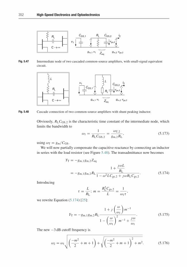
352 High-Speed Electronics and Optoelectronics
RL
v1
CGS,1
gm,1 v1 gm,2 vgs,2Zeq
CGS,2
vgs,2
i2RL
C ∞
Fig. 5.47 Intermediate node of two cascaded common-source amplifiers, with small-signal equivalentcircuit.
LL
RL RL
Zeq
CGS,1
CGS,2i2v1
gm,1 v1 gm,2 vgs,2
vgs,2
C ∞
Fig. 5.48 Cascade connection of two common-source amplifiers with shunt peaking inductor.
Obviously, RLCGS,2 is the characteristic time constant of the intermediate node, whichlimits the bandwidth to
ω1 = 1
RLCGS,2= ωT,2
gm,2 RL, (5.173)
using ωT = gm/CGS.We will now partially compensate the capacitive reactance by connecting an inductor
in series with the load resistor (see Figure 5.48). The transadmittance now becomes
YT = −gm,1gm,2 Zeq
= −gm,1gm,2 RL
1 + jωL
RL
1 − ω2LCgs,2 + jωRLCgs,2. (5.174)
Introducing
τ = L
RL; m = R2
LCgs,2
L= 1
ω1τ,
we rewrite Equation (5.174) [25]:
YT = −gm,1gm,2 RL
1 + j
(ω
ω1
)m−1
1 −(
ω
ω1
)2
m−1 + jω
ω1
. (5.175)
The new −3 dB cutoff frequency is
ω2 = ω1
√√√√(−m2
2+ m + 1
)+
√(−m2
2+ m + 1
)2
+ m2. (5.176)
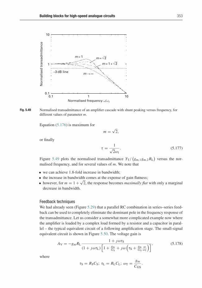
Building blocks for high-speed analogue circuits 353
10
1
0.10.1 1 10
Normalised frequency ω/ω1
–3 dB line m
m = 1
∞
No
rmal
ised
tra
nsa
dm
itta
nce
m = √ 2
m = 1 + √ 2
Fig. 5.49 Normalised transadmittance of an amplifier cascade with shunt peaking versus frequency, fordifferent values of parameter m.
Equation (5.176) is maximum for
m = √2,
or finally
τ = 1√2ω1
. (5.177)
Figure 5.49 plots the normalised transadmittance YT/(gm,1gm,2 RL
)versus the nor-
malised frequency, and for several values of m. We note that
• we can achieve 1.8-fold increase in bandwidth;• the increase in bandwidth comes at the expense of gain flatness;• however, for m = 1 + √
2, the response becomes maximally flat with only a marginaldecrease in bandwidth.
Feedback techniquesWe had already seen (Figure 5.29) that a parallel RC combination in series–series feed-back can be used to completely eliminate the dominant pole in the frequency response ofthe transadmittance. Let us consider a somewhat more complicated example now wherethe amplifier is loaded by a complex load formed by a resistor and a capacitor in paral-lel – the typical equivalent circuit of a following amplification stage. The small-signalequivalent circuit is shown in Figure 5.50. The voltage gain is
AV = −gm RL1 + jωτS
(1 + jωτL)[1 + gm
GS+ jω
(τS + gm
GS
ωωT
)] , (5.178)
where
τS = RSCS; τL = RLCL; ωT = gm
CGS.
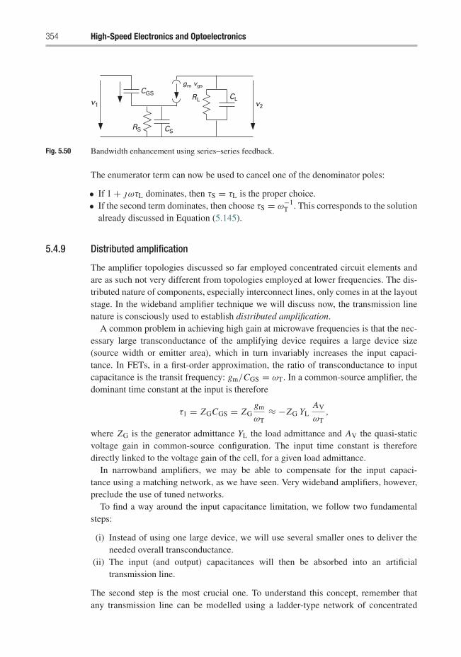
354 High-Speed Electronics and Optoelectronics
CGS
gm vgs
RS CS
v2
RL CLv1
Fig. 5.50 Bandwidth enhancement using series–series feedback.
The enumerator term can now be used to cancel one of the denominator poles:
• If 1 + jωτL dominates, then τS = τL is the proper choice.• If the second term dominates, then choose τS = ω−1
T . This corresponds to the solutionalready discussed in Equation (5.145).
5.4.9 Distributed amplification
The amplifier topologies discussed so far employed concentrated circuit elements andare as such not very different from topologies employed at lower frequencies. The dis-tributed nature of components, especially interconnect lines, only comes in at the layoutstage. In the wideband amplifier technique we will discuss now, the transmission linenature is consciously used to establish distributed amplification.
A common problem in achieving high gain at microwave frequencies is that the nec-essary large transconductance of the amplifying device requires a large device size(source width or emitter area), which in turn invariably increases the input capaci-tance. In FETs, in a first-order approximation, the ratio of transconductance to inputcapacitance is the transit frequency: gm/CGS = ωT. In a common-source amplifier, thedominant time constant at the input is therefore
τ1 = ZGCGS = ZGgm
ωT≈ −ZG YL
AV
ωT,
where ZG is the generator admittance YL the load admittance and AV the quasi-staticvoltage gain in common-source configuration. The input time constant is thereforedirectly linked to the voltage gain of the cell, for a given load admittance.
In narrowband amplifiers, we may be able to compensate for the input capaci-tance using a matching network, as we have seen. Very wideband amplifiers, however,preclude the use of tuned networks.
To find a way around the input capacitance limitation, we follow two fundamentalsteps:
(i) Instead of using one large device, we will use several smaller ones to deliver theneeded overall transconductance.
(ii) The input (and output) capacitances will then be absorbed into an artificialtransmission line.
The second step is the most crucial one. To understand this concept, remember thatany transmission line can be modelled using a ladder-type network of concentrated
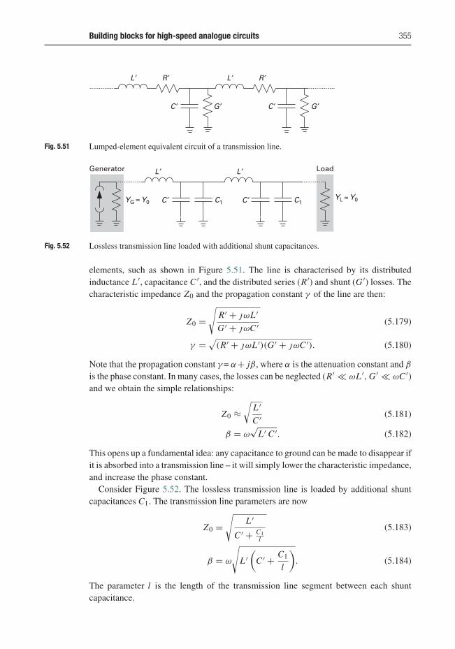
Building blocks for high-speed analogue circuits 355
R ′ L ′ R ′
C ′ C ′G ′ G ′
L ′
Fig. 5.51 Lumped-element equivalent circuit of a transmission line.
Generator Load
YG = Y0YL = Y0C1 C1
L ′ L ′
C ′ C ′
Fig. 5.52 Lossless transmission line loaded with additional shunt capacitances.
elements, such as shown in Figure 5.51. The line is characterised by its distributedinductance L ′, capacitance C ′, and the distributed series (R′) and shunt (G ′) losses. Thecharacteristic impedance Z0 and the propagation constant γ of the line are then:
Z0 =√
R′ + jωL ′G ′ + jωC ′ (5.179)
γ = √(R′ + jωL ′)(G ′ + jωC ′). (5.180)
Note that the propagation constant γ= α+ jβ, where α is the attenuation constant and β
is the phase constant. In many cases, the losses can be neglected (R′ � ωL ′, G ′ � ωC ′)and we obtain the simple relationships:
Z0 ≈√
L ′C ′ (5.181)
β = ω√
L ′ C ′. (5.182)
This opens up a fundamental idea: any capacitance to ground can be made to disappear ifit is absorbed into a transmission line – it will simply lower the characteristic impedance,and increase the phase constant.
Consider Figure 5.52. The lossless transmission line is loaded by additional shuntcapacitances C1. The transmission line parameters are now
Z0 =√
L ′
C ′ + C1l
(5.183)
β = ω
√L ′
(C ′ + C1
l
). (5.184)
The parameter l is the length of the transmission line segment between each shuntcapacitance.
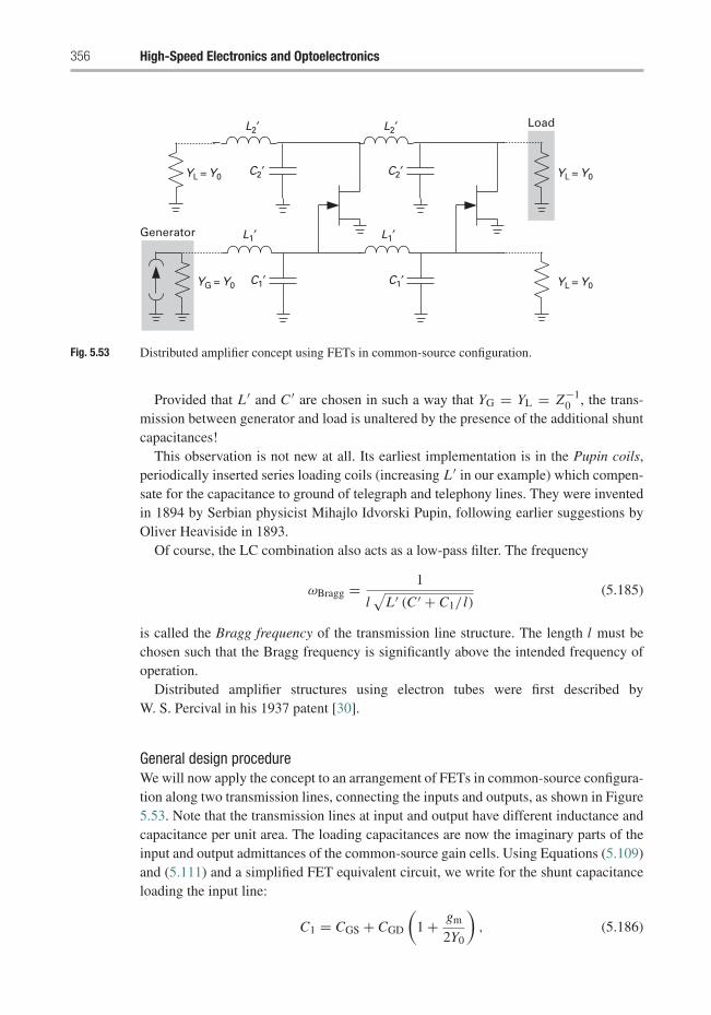
356 High-Speed Electronics and Optoelectronics
YL = Y0
YG = Y0
YL = Y0
YL = Y0
L2′
L1′ L1′
C2′
C1′ C1′
C2′
L2′ Load
Generator
Fig. 5.53 Distributed amplifier concept using FETs in common-source configuration.
Provided that L ′ and C ′ are chosen in such a way that YG = YL = Z−10 , the trans-
mission between generator and load is unaltered by the presence of the additional shuntcapacitances!
This observation is not new at all. Its earliest implementation is in the Pupin coils,periodically inserted series loading coils (increasing L ′ in our example) which compen-sate for the capacitance to ground of telegraph and telephony lines. They were inventedin 1894 by Serbian physicist Mihajlo Idvorski Pupin, following earlier suggestions byOliver Heaviside in 1893.
Of course, the LC combination also acts as a low-pass filter. The frequency
ωBragg = 1
l√
L ′ (C ′ + C1/ l)(5.185)
is called the Bragg frequency of the transmission line structure. The length l must bechosen such that the Bragg frequency is significantly above the intended frequency ofoperation.
Distributed amplifier structures using electron tubes were first described byW. S. Percival in his 1937 patent [30].
General design procedureWe will now apply the concept to an arrangement of FETs in common-source configura-tion along two transmission lines, connecting the inputs and outputs, as shown in Figure5.53. Note that the transmission lines at input and output have different inductance andcapacitance per unit area. The loading capacitances are now the imaginary parts of theinput and output admittances of the common-source gain cells. Using Equations (5.109)and (5.111) and a simplified FET equivalent circuit, we write for the shunt capacitanceloading the input line:
C1 = CGS + CGD
(1 + gm
2Y0
), (5.186)
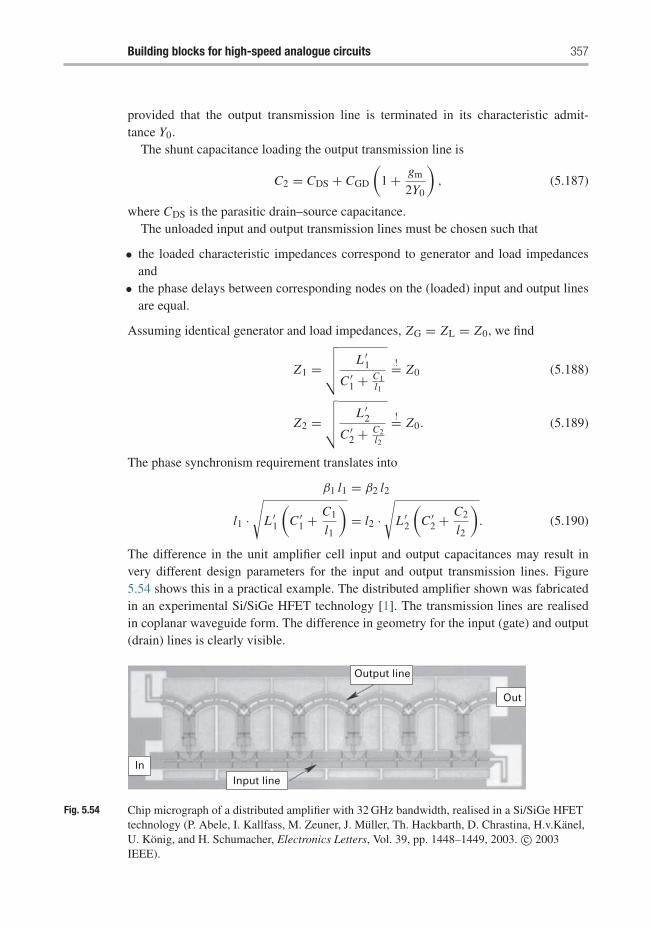
Building blocks for high-speed analogue circuits 357
provided that the output transmission line is terminated in its characteristic admit-tance Y0.
The shunt capacitance loading the output transmission line is
C2 = CDS + CGD
(1 + gm
2Y0
), (5.187)
where CDS is the parasitic drain–source capacitance.The unloaded input and output transmission lines must be chosen such that
• the loaded characteristic impedances correspond to generator and load impedancesand
• the phase delays between corresponding nodes on the (loaded) input and output linesare equal.
Assuming identical generator and load impedances, ZG = ZL = Z0, we find
Z1 =√√√√ L ′
1
C ′1 + C1
l1
!= Z0 (5.188)
Z2 =√√√√ L ′
2
C ′2 + C2
l2
!= Z0. (5.189)
The phase synchronism requirement translates into
β1 l1 = β2 l2
l1 ·√
L ′1
(C ′
1 + C1
l1
)= l2 ·
√L ′
2
(C ′
2 + C2
l2
). (5.190)
The difference in the unit amplifier cell input and output capacitances may result invery different design parameters for the input and output transmission lines. Figure5.54 shows this in a practical example. The distributed amplifier shown was fabricatedin an experimental Si/SiGe HFET technology [1]. The transmission lines are realisedin coplanar waveguide form. The difference in geometry for the input (gate) and output(drain) lines is clearly visible.
InInput line
Output line
Out
Fig. 5.54 Chip micrograph of a distributed amplifier with 32 GHz bandwidth, realised in a Si/SiGe HFETtechnology (P. Abele, I. Kallfass, M. Zeuner, J. Muller, Th. Hackbarth, D. Chrastina, H.v.Kanel,U. Konig, and H. Schumacher, Electronics Letters, Vol. 39, pp. 1448–1449, 2003. c© 2003IEEE).
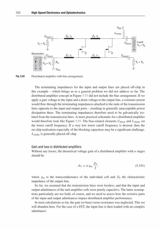
358 High-Speed Electronics and Optoelectronics
Cblock
Cblock
Z2, l2 Z2, l2
Z1, l1 Z1, l1
Lchoke
VDD
Cblock
Cblock
YL = Y0
YL = Y0YL = Y0
YG = Y0RG
VGG
Load
Generator
Fig. 5.55 Distributed amplifier with bias arrangement.
The terminating impedances for the input and output lines are placed off-chip inthis example – which brings us to a general problem we did not address so far. Thedistributed amplifier concept in Figure 5.53 did not include the bias arrangement. If weapply a gate voltage to the input and a drain voltage to the output line, a constant currentwould flow through the terminating impedances attached to the ends of the transmissionlines opposite to the input and output ports – resulting in generally unacceptable powerdissipation there. The terminating impedances therefore need to be galvanically iso-lated from the transmission lines. A more practical schematic for a distributed amplifierwould therefore look like Figure 5.55. The bias-related elements Cblock and Lchoke setthe lower cutoff frequency. If a very low lower cutoff frequency is desired, then theon-chip realisation especially of the blocking capacitors may be a significant challenge.Lchoke is generally placed off-chip.
Gain and loss in distributed amplifiersWithout any losses, the theoretical voltage gain of a distributed amplifier with n stagesshould be
AV = n gmZ0
2, (5.191)
where gm is the transconductance of the individual cell and Z0 the characteristicimpedance of the output line.
So far, we assumed that the transmission lines were lossless, and that the input andoutput admittances of the unit amplifier cells were purely capacitive. The latter assump-tions particularly are too bold, of course, and we need to assess how the resistive partsof the input and output admittances impact distributed amplifier performance.
In most calculations so far, the gate (or base) series resistance was neglected. This wewill abandon here. For the case of a FET, the input line is then loaded with an complexadmittance:
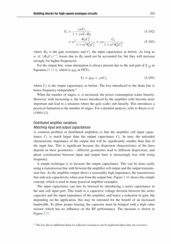
Building blocks for high-speed analogue circuits 359
Y1 = jωC1
1 + jωC1 RG(5.192)
= ω2 RGC21
1 + ω2 R2GC2
1
+ jωC1
1 + ω2 R2GC2
1
, (5.193)
where RG is the gate resistance and C1 the input capacitance as before. As long asω � (RGC1)
−1, losses due to RG need not be accounted for, but they will increasestrongly for higher frequencies.
For the output line, some attenuation is always present due to the real part of Y 20 inEquation (5.111), which is gDS in FETs:
Y2 = gDS + jωC2, (5.194)
where C2 is the output capacitance as before. The loss introduced to the drain line ishence frequency-independent.4
When the number of stages, n, is increased, the power consumption scales linearly.However, with increasing n, the losses introduced by the amplifier cells become moreimportant and lead to a situation where the gain scales sub-linearly. This introduces apractical limitation to the number of stages. For a detailed analysis, refer to Beyer et al.(1984) [4].
Distributed amplifier variationsMatching input and output capacitancesA common problem in distributed amplifiers is that the amplifier cell input capac-itance C1 is much larger than the output capacitance C2. In turn, the unloadedcharacteristic impedance of the output line will be significantly smaller than that ofthe input line. This is significant because the dispersion characteristics of the linesdepend on their geometries – different geometries lead to different dispersions, andphase synchronism between input and output lines is increasingly lost with risingfrequency.
A simple technique is to increase the output capacitance. This can be done easilyusing a transmission line stub between the amplifier cell output and the output transmis-sion line. As the amplifier output shows a reasonably high impedance, the transmissionline stub acts capacitively when seen from the output line. Figure 5.56 shows this simpleconcept, which is used in many practical amplifier examples.
The input capacitance can also be lowered by introducing a series capacitance inthe unit cell input port. This leads to a capacitive voltage division between the seriescapacitor and the input impedance of the amplifier, and hence a reduction in gain, butdepending on the application, this may be tolerated for the benefit of an increasedbandwidth. To allow proper biasing, the capacitor must be bridged with a high-valueresistor which has no influence on the RF performance. The measure is shown inFigure 5.57.
4 The loss due to additional drain (or collector) resistances can be neglected unless they are excessive.
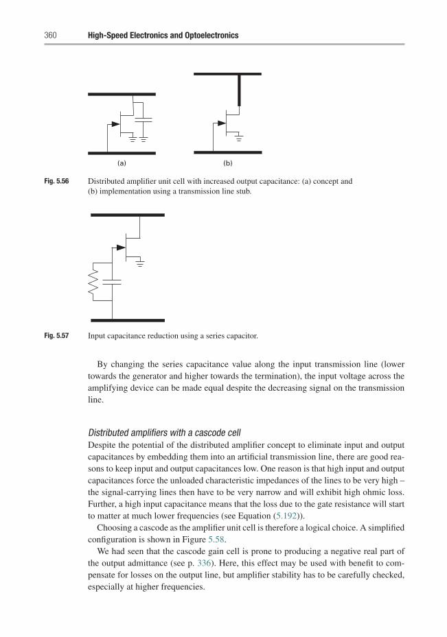
360 High-Speed Electronics and Optoelectronics
(a) (b)
Fig. 5.56 Distributed amplifier unit cell with increased output capacitance: (a) concept and(b) implementation using a transmission line stub.
Fig. 5.57 Input capacitance reduction using a series capacitor.
By changing the series capacitance value along the input transmission line (lowertowards the generator and higher towards the termination), the input voltage across theamplifying device can be made equal despite the decreasing signal on the transmissionline.
Distributed amplifiers with a cascode cellDespite the potential of the distributed amplifier concept to eliminate input and outputcapacitances by embedding them into an artificial transmission line, there are good rea-sons to keep input and output capacitances low. One reason is that high input and outputcapacitances force the unloaded characteristic impedances of the lines to be very high –the signal-carrying lines then have to be very narrow and will exhibit high ohmic loss.Further, a high input capacitance means that the loss due to the gate resistance will startto matter at much lower frequencies (see Equation (5.192)).
Choosing a cascode as the amplifier unit cell is therefore a logical choice. A simplifiedconfiguration is shown in Figure 5.58.
We had seen that the cascode gain cell is prone to producing a negative real part ofthe output admittance (see p. 336). Here, this effect may be used with benefit to com-pensate for losses on the output line, but amplifier stability has to be carefully checked,especially at higher frequencies.
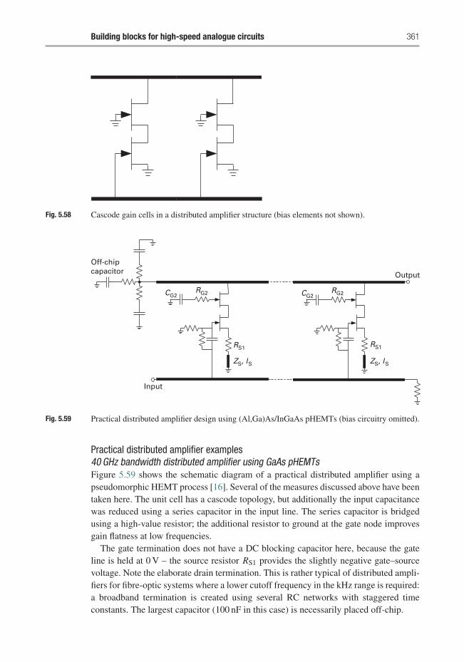
Building blocks for high-speed analogue circuits 361
Fig. 5.58 Cascode gain cells in a distributed amplifier structure (bias elements not shown).
CG2 CG2RG2 RG2
RS1 RS1
ZS, lS ZS, lS
Input
Output
Off-chipcapacitor
Fig. 5.59 Practical distributed amplifier design using (Al,Ga)As/InGaAs pHEMTs (bias circuitry omitted).
Practical distributed amplifier examples40 GHz bandwidth distributed amplifier using GaAs pHEMTsFigure 5.59 shows the schematic diagram of a practical distributed amplifier using apseudomorphic HEMT process [16]. Several of the measures discussed above have beentaken here. The unit cell has a cascode topology, but additionally the input capacitancewas reduced using a series capacitor in the input line. The series capacitor is bridgedusing a high-value resistor; the additional resistor to ground at the gate node improvesgain flatness at low frequencies.
The gate termination does not have a DC blocking capacitor here, because the gateline is held at 0 V – the source resistor RS1 provides the slightly negative gate–sourcevoltage. Note the elaborate drain termination. This is rather typical of distributed ampli-fiers for fibre-optic systems where a lower cutoff frequency in the kHz range is required:a broadband termination is created using several RC networks with staggered timeconstants. The largest capacitor (100 nF in this case) is necessarily placed off-chip.
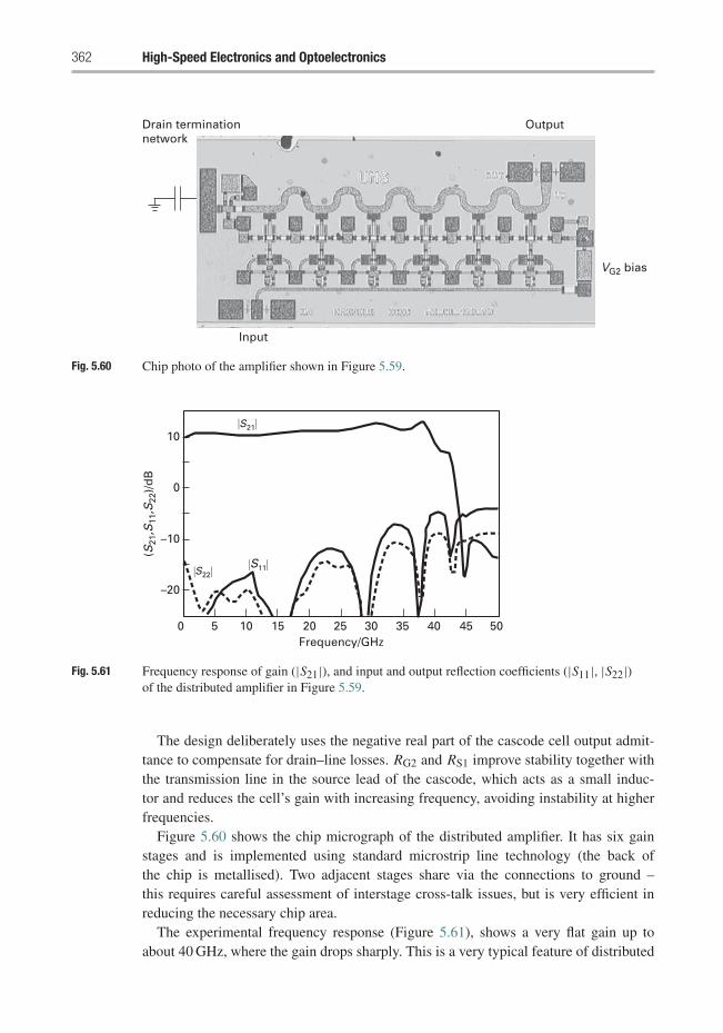
362 High-Speed Electronics and Optoelectronics
Drain terminationnetwork
Input
Output
VG2 bias
Fig. 5.60 Chip photo of the amplifier shown in Figure 5.59.
10
0
–10
–20
0 5 10 15 20Frequency/GHz
25 30 35 40 45 50
(S21
,S11
,S22
)/d
B
S22S11
S21
Fig. 5.61 Frequency response of gain (|S21|), and input and output reflection coefficients (|S11|, |S22|)of the distributed amplifier in Figure 5.59.
The design deliberately uses the negative real part of the cascode cell output admit-tance to compensate for drain–line losses. RG2 and RS1 improve stability together withthe transmission line in the source lead of the cascode, which acts as a small induc-tor and reduces the cell’s gain with increasing frequency, avoiding instability at higherfrequencies.
Figure 5.60 shows the chip micrograph of the distributed amplifier. It has six gainstages and is implemented using standard microstrip line technology (the back ofthe chip is metallised). Two adjacent stages share via the connections to ground –this requires careful assessment of interstage cross-talk issues, but is very efficient inreducing the necessary chip area.
The experimental frequency response (Figure 5.61), shows a very flat gain up toabout 40 GHz, where the gain drops sharply. This is a very typical feature of distributed
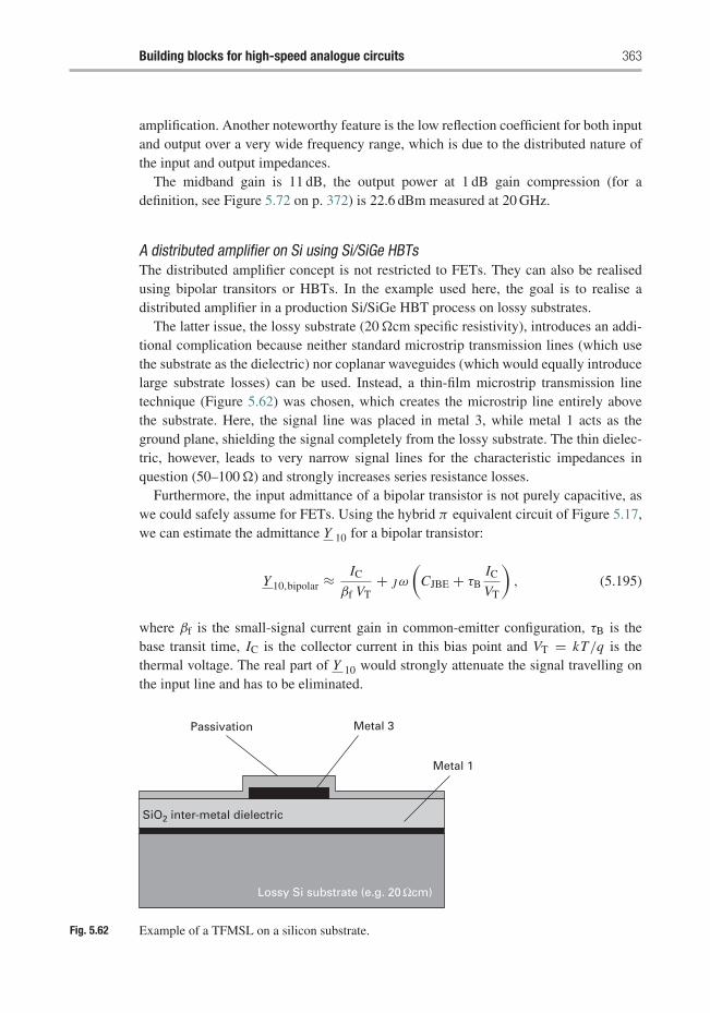
Building blocks for high-speed analogue circuits 363
amplification. Another noteworthy feature is the low reflection coefficient for both inputand output over a very wide frequency range, which is due to the distributed nature ofthe input and output impedances.
The midband gain is 11 dB, the output power at 1 dB gain compression (for adefinition, see Figure 5.72 on p. 372) is 22.6 dBm measured at 20 GHz.
A distributed amplifier on Si using Si/SiGe HBTsThe distributed amplifier concept is not restricted to FETs. They can also be realisedusing bipolar transitors or HBTs. In the example used here, the goal is to realise adistributed amplifier in a production Si/SiGe HBT process on lossy substrates.
The latter issue, the lossy substrate (20�cm specific resistivity), introduces an addi-tional complication because neither standard microstrip transmission lines (which usethe substrate as the dielectric) nor coplanar waveguides (which would equally introducelarge substrate losses) can be used. Instead, a thin-film microstrip transmission linetechnique (Figure 5.62) was chosen, which creates the microstrip line entirely abovethe substrate. Here, the signal line was placed in metal 3, while metal 1 acts as theground plane, shielding the signal completely from the lossy substrate. The thin dielec-tric, however, leads to very narrow signal lines for the characteristic impedances inquestion (50–100�) and strongly increases series resistance losses.
Furthermore, the input admittance of a bipolar transistor is not purely capacitive, aswe could safely assume for FETs. Using the hybrid π equivalent circuit of Figure 5.17,we can estimate the admittance Y 10 for a bipolar transistor:
Y 10,bipolar ≈ IC
βf VT+ jω
(CJBE + τB
IC
VT
), (5.195)
where βf is the small-signal current gain in common-emitter configuration, τB is thebase transit time, IC is the collector current in this bias point and VT = kT/q is thethermal voltage. The real part of Y 10 would strongly attenuate the signal travelling onthe input line and has to be eliminated.
Passivation Metal 3
Metal 1
SiO2 inter-metal dielectric
Lossy Si substrate (e.g. 20 Ωcm)
Fig. 5.62 Example of a TFMSL on a silicon substrate.
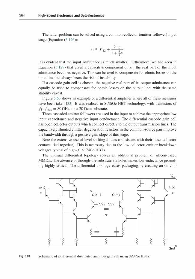
364 High-Speed Electronics and Optoelectronics
The latter problem can be solved using a common-collector (emitter follower) inputstage (Equation (5.126)):
Y1 ≈ Y 12 + Y 10
1 + gm
YL
.
It is evident that the input admittance is much smaller. Furthermore, we had seen inEquation (5.128) that given a capacitive component of YL, the real part of the inputadmittance becomes negative. This can be used to compensate for ohmic losses on theinput line, but always bears the risk of instability.
If a cascode gain cell is chosen, the negative real part of its output admittance canequally be used to compensate for ohmic losses on the output line, with the samestability caveat.
Figure 5.63 shows an example of a differential amplifier where all of these measureshave been taken [33]. It was realised in Si/SiGe HBT technology, with transistors offT, fmax = 80 GHz, on a 20�cm substrate.
Three cascaded emitter followers are used in the input to achieve the appropriate lowinput capacitance and negative input conductance. The differential cascode gain cellhas open collector outputs which connect directly to the output transmission lines. Thecapacitively shunted emitter degeneration resistors in the common-source pair improvethe bandwidth through a positive gain slope of this stage.
Note the extensive use of level shifting diodes (transistors with their base–collectorcontacts tied together). This is necessary due to the low collector–emitter breakdownvoltages typical of high- fT Si/SiGe HBTs.
The unusual differential topology solves an additional problem of silicon-basedMMICs: The absence of through-the-substrate via holes makes low-inductance ground-ing highly critical. The differential topology eases packaging by creating an on-chip
In(+)
Out(–) Out(+)
In(–)
Gnd
VCC
Fig. 5.63 Schematic of a differential distributed amplifier gain cell using Si/SiGe HBTs.
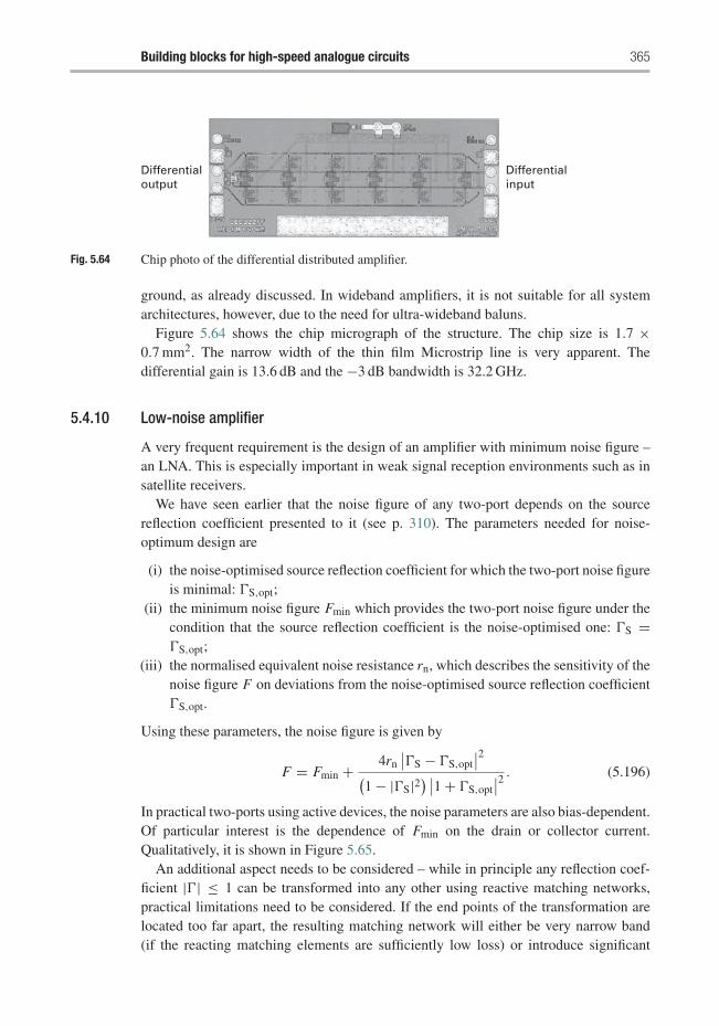
Building blocks for high-speed analogue circuits 365
Differentialoutput
Differentialinput
Fig. 5.64 Chip photo of the differential distributed amplifier.
ground, as already discussed. In wideband amplifiers, it is not suitable for all systemarchitectures, however, due to the need for ultra-wideband baluns.
Figure 5.64 shows the chip micrograph of the structure. The chip size is 1.7 ×0.7 mm2. The narrow width of the thin film Microstrip line is very apparent. Thedifferential gain is 13.6 dB and the −3 dB bandwidth is 32.2 GHz.
5.4.10 Low-noise amplifier
A very frequent requirement is the design of an amplifier with minimum noise figure –an LNA. This is especially important in weak signal reception environments such as insatellite receivers.
We have seen earlier that the noise figure of any two-port depends on the sourcereflection coefficient presented to it (see p. 310). The parameters needed for noise-optimum design are
(i) the noise-optimised source reflection coefficient for which the two-port noise figureis minimal: �S,opt;
(ii) the minimum noise figure Fmin which provides the two-port noise figure under thecondition that the source reflection coefficient is the noise-optimised one: �S =�S,opt;
(iii) the normalised equivalent noise resistance rn, which describes the sensitivity of thenoise figure F on deviations from the noise-optimised source reflection coefficient�S,opt.
Using these parameters, the noise figure is given by
F = Fmin + 4rn∣∣�S − �S,opt
∣∣2(1 − |�S|2) ∣∣1 + �S,opt
∣∣2. (5.196)
In practical two-ports using active devices, the noise parameters are also bias-dependent.Of particular interest is the dependence of Fmin on the drain or collector current.Qualitatively, it is shown in Figure 5.65.
An additional aspect needs to be considered – while in principle any reflection coef-ficient |�| ≤ 1 can be transformed into any other using reactive matching networks,practical limitations need to be considered. If the end points of the transformation arelocated too far apart, the resulting matching network will either be very narrow band(if the reacting matching elements are sufficiently low loss) or introduce significant
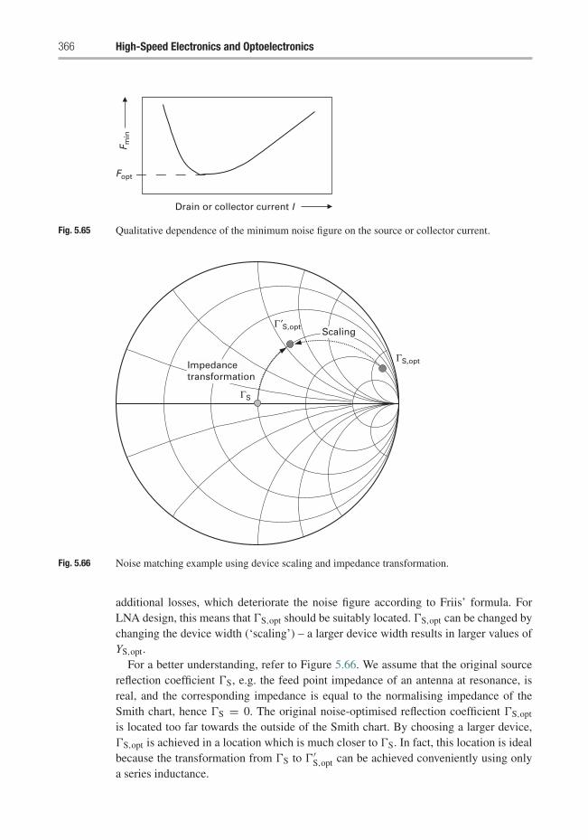
366 High-Speed Electronics and Optoelectronics
Fopt
Drain or collector current I
F min
Fig. 5.65 Qualitative dependence of the minimum noise figure on the source or collector current.
Impedancetransformation
ScalingΓ′S,opt
ΓS,opt
ΓS
Fig. 5.66 Noise matching example using device scaling and impedance transformation.
additional losses, which deteriorate the noise figure according to Friis’ formula. ForLNA design, this means that �S,opt should be suitably located. �S,opt can be changed bychanging the device width (‘scaling’) – a larger device width results in larger values ofYS,opt.
For a better understanding, refer to Figure 5.66. We assume that the original sourcereflection coefficient �S, e.g. the feed point impedance of an antenna at resonance, isreal, and the corresponding impedance is equal to the normalising impedance of theSmith chart, hence �S = 0. The original noise-optimised reflection coefficient �S,opt
is located too far towards the outside of the Smith chart. By choosing a larger device,�S,opt is achieved in a location which is much closer to �S. In fact, this location is idealbecause the transformation from �S to �′
S,opt can be achieved conveniently using onlya series inductance.
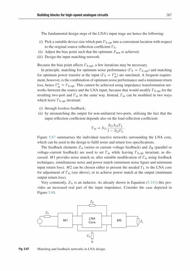
Building blocks for high-speed analogue circuits 367
The fundamental design steps of the LNA’s input stage are hence the following:
(i) Pick a suitable device size which puts �S,opt into a convenient location with respectto the original source reflection coefficient �S.
(ii) Adjust the bias point such that the optimum Fmin is achieved.(iii) Design the input matching network.
Because the bias point affects �S,opt, a few iterations may be necessary.In principle, matching for optimum noise performance (�S = �S,opt) and matching
for optimum power transfer at the input (�S = � in) are unrelated. A frequent require-
ment, however, is the combination of optimum noise performance and a minimum returnloss, hence �
in ≈ �S,opt. This cannot be achieved using impedance transformation net-works between the source and the LNA input, because that would modify �S,opt for theresulting two-port and �in in the same way. Instead, �in can be modified in two wayswhich leave �S,opt invariant:
(i) through lossless feedback;(ii) by mismatching the output for non-unilateral two-ports, utilising the fact that the
input reflection coefficient depends also on the load reflection coefficient:
�in = S11S21S12�L
1 − S22�L.
Figure 5.67 summarises the individual reactive networks surrounding the LNA core,which can be used in the design to fulfil noise and return loss specifications.
The feedback elements ZA (series or current–voltage feedback) and ZB (parallel orvoltage–current feedback) are used to set �in while leaving �S,opt invariant, as dis-cussed. M1 provides noise match or, after suitable modification of �in using feedbacktechniques, simultaneous noise and power match (minimum noise figure and minimuminput return loss). M2 can be chosen either to present the needed �L to the LNA corefor adjustment of �in (see above), or to achieve power match at the output (minimumoutput return loss).
Very commonly, ZA is an inductor. As already shown in Equation (5.141) this pro-vides an increased real part of the input impedance. Consider the case depicted inFigure 5.68.
Z S
Z B
Z A
Z LM1 M2
LNACore
Fig. 5.67 Matching and feedback networks in LNA design.
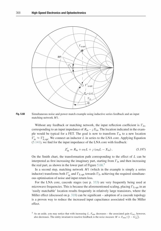
368 High-Speed Electronics and Optoelectronics
M1
Γs,opt
Γ*s,opt
Γin
ZA = jωL
Γs
Fig. 5.68 Simultaneous noise and power match example using inductive series feedback and an inputmatching network M1.
Without any feedback or matching network, the input reflection coefficient is �in,corresponding to an input impedance of Rin −j X in. The location indicated in the exam-ple would be typical for a FET. The goal is now to transform �in to a new location�′
in ≈ � S,opt. We connect an inductor L in series to the LNA core. Applying Equation
(5.141), we find for the input impedance of the LNA core with feedback:
Z ′in = Rin + ωTL + j (ω0L − X in) . (5.197)
On the Smith chart, the transformation path corresponding to the effect of L can beinterpreted as first increasing the imaginary part, starting from �in and then increasingthe real part, as shown in the lower part of Figure 5.68.5
In a second step, matching network M1 (which in the example is simply a seriesinductor) transforms both �′
in and �S,opt towards �S, achieving the required simultane-ous optimisation of noise and input return loss.
For the LNA core, cascode stages (see p. 333) are very frequently being used atmicrowave frequencies. This is because the aforementioned scaling, placing �S,opt in an‘easily matchable’ location results frequently in relatively large transistors, where theMiller effect (discussed on p. 318) can be significant – adoption of a cascode topologyis a proven way to reduce the increased input capacitance associated with the Millereffect.
5 As an aside, you may notice that with increasing L , Fmin decreases – the associated gain Gass, however,also decreases. The entity invariant to reactive feedback is the noise measure M = Fmin/
(1 − G−1
ass
).
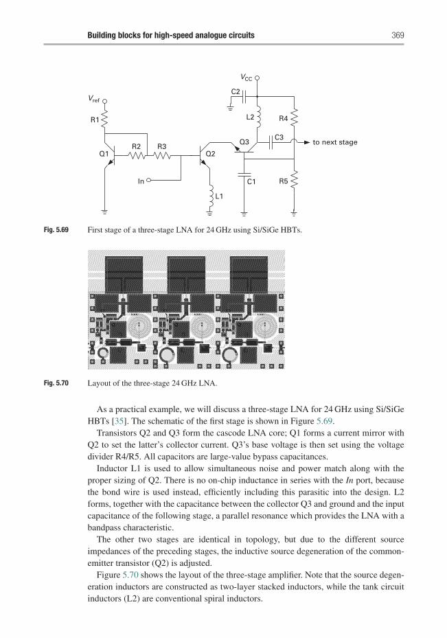
Building blocks for high-speed analogue circuits 369
Vref
VCC
R1
R2 R3Q1 Q2
Q3
L2 R4
C3to next stage
C1 R5
L1
C2
In
Fig. 5.69 First stage of a three-stage LNA for 24 GHz using Si/SiGe HBTs.
Fig. 5.70 Layout of the three-stage 24 GHz LNA.
As a practical example, we will discuss a three-stage LNA for 24 GHz using Si/SiGeHBTs [35]. The schematic of the first stage is shown in Figure 5.69.
Transistors Q2 and Q3 form the cascode LNA core; Q1 forms a current mirror withQ2 to set the latter’s collector current. Q3’s base voltage is then set using the voltagedivider R4/R5. All capacitors are large-value bypass capacitances.
Inductor L1 is used to allow simultaneous noise and power match along with theproper sizing of Q2. There is no on-chip inductance in series with the In port, becausethe bond wire is used instead, efficiently including this parasitic into the design. L2forms, together with the capacitance between the collector Q3 and ground and the inputcapacitance of the following stage, a parallel resonance which provides the LNA with abandpass characteristic.
The other two stages are identical in topology, but due to the different sourceimpedances of the preceding stages, the inductive source degeneration of the common-emitter transistor (Q2) is adjusted.
Figure 5.70 shows the layout of the three-stage amplifier. Note that the source degen-eration inductors are constructed as two-layer stacked inductors, while the tank circuitinductors (L2) are conventional spiral inductors.
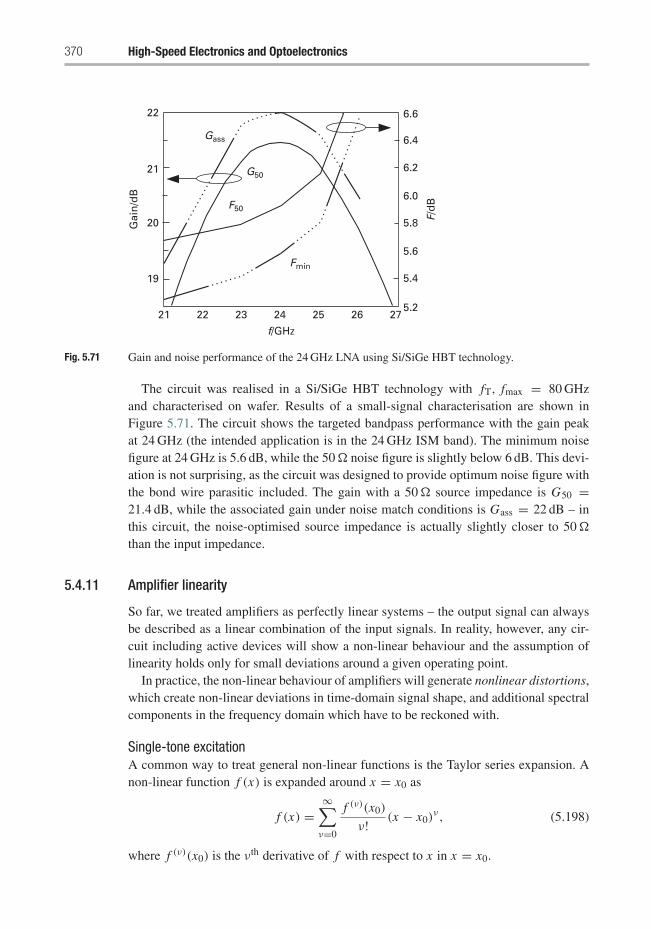
370 High-Speed Electronics and Optoelectronics
22 6.6
6.4
6.2
6.0
5.8
5.6
5.4
5.2
21
20
Gass
G50
F50
Fmin
19
21 22 23
Gai
n/d
B
f/GHz
F/d
B
24 25 26 27
Fig. 5.71 Gain and noise performance of the 24 GHz LNA using Si/SiGe HBT technology.
The circuit was realised in a Si/SiGe HBT technology with fT, fmax = 80 GHzand characterised on wafer. Results of a small-signal characterisation are shown inFigure 5.71. The circuit shows the targeted bandpass performance with the gain peakat 24 GHz (the intended application is in the 24 GHz ISM band). The minimum noisefigure at 24 GHz is 5.6 dB, while the 50� noise figure is slightly below 6 dB. This devi-ation is not surprising, as the circuit was designed to provide optimum noise figure withthe bond wire parasitic included. The gain with a 50� source impedance is G50 =21.4 dB, while the associated gain under noise match conditions is Gass = 22 dB – inthis circuit, the noise-optimised source impedance is actually slightly closer to 50�
than the input impedance.
5.4.11 Amplifier linearity
So far, we treated amplifiers as perfectly linear systems – the output signal can alwaysbe described as a linear combination of the input signals. In reality, however, any cir-cuit including active devices will show a non-linear behaviour and the assumption oflinearity holds only for small deviations around a given operating point.
In practice, the non-linear behaviour of amplifiers will generate nonlinear distortions,which create non-linear deviations in time-domain signal shape, and additional spectralcomponents in the frequency domain which have to be reckoned with.
Single-tone excitationA common way to treat general non-linear functions is the Taylor series expansion. Anon-linear function f (x) is expanded around x = x0 as
f (x) =∞∑ν=0
f (ν)(x0)
ν! (x − x0)ν, (5.198)
where f (ν)(x0) is the νth derivative of f with respect to x in x = x0.
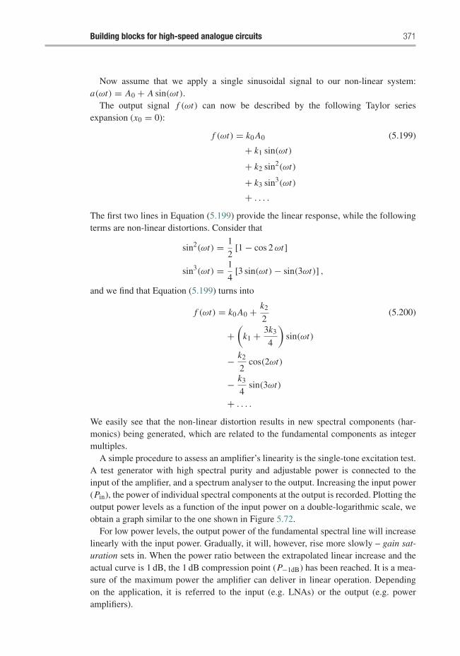
Building blocks for high-speed analogue circuits 371
Now assume that we apply a single sinusoidal signal to our non-linear system:a(ωt) = A0 + A sin(ωt).
The output signal f (ωt) can now be described by the following Taylor seriesexpansion (x0 = 0):
f (ωt) = k0 A0 (5.199)
+ k1 sin(ωt)
+ k2 sin2(ωt)
+ k3 sin3(ωt)
+ . . . .
The first two lines in Equation (5.199) provide the linear response, while the followingterms are non-linear distortions. Consider that
sin2(ωt) = 1
2[1 − cos 2ωt]
sin3(ωt) = 1
4[3 sin(ωt) − sin(3ωt)] ,
and we find that Equation (5.199) turns into
f (ωt) = k0 A0 + k2
2(5.200)
+(
k1 + 3k3
4
)sin(ωt)
− k2
2cos(2ωt)
− k3
4sin(3ωt)
+ . . . .
We easily see that the non-linear distortion results in new spectral components (har-monics) being generated, which are related to the fundamental components as integermultiples.
A simple procedure to assess an amplifier’s linearity is the single-tone excitation test.A test generator with high spectral purity and adjustable power is connected to theinput of the amplifier, and a spectrum analyser to the output. Increasing the input power(Pin), the power of individual spectral components at the output is recorded. Plotting theoutput power levels as a function of the input power on a double-logarithmic scale, weobtain a graph similar to the one shown in Figure 5.72.
For low power levels, the output power of the fundamental spectral line will increaselinearly with the input power. Gradually, it will, however, rise more slowly – gain sat-uration sets in. When the power ratio between the extrapolated linear increase and theactual curve is 1 dB, the 1 dB compression point (P−1dB) has been reached. It is a mea-sure of the maximum power the amplifier can deliver in linear operation. Dependingon the application, it is referred to the input (e.g. LNAs) or the output (e.g. poweramplifiers).
372 High-Speed Electronics and Optoelectronics
log
10(P
ou
t)
log10(Pin)
Fundamental
1 dB compressionpoint
2nd orderharmonic
3rd orderharmonic
1 dB
Single-tonesecond-orderintercept point
Single-tonethird-orderintercept point
Fig. 5.72 Single-tone excitation test of an amplifier, showing definitions for the 1 dB compression,second-order intercept and third-order intercept points.
The spectral power at the second harmonic increases twice as fast as the fundamentalpower, before it also shows saturation. Extrapolating the curve at low input powers, wefind the single-tone second-order intercept point at the point where the extrapolationintersects the extrapolated fundamental power.
The spectral power at the third harmonic increases three times as fast as the fun-damental power. Its extrapolation intersects the extrapolated fundamental power at thesingle-tone third-order intercept point.
The intercept points can also be referred to the input or the output, depending on theapplication.
In many applications where the operational bandwidth is only a small fraction of thecarrier frequency, the generation of harmonics is not necessarily a problem, because theycan easily be removed by filtering. For example, frequency modulated (FM) transmittersare operated under strongly non-linear conditions (class C, see p. 377), and the resultingharmonics in the output signal are simply removed by low-pass filtering.
Two-tone excitationAn FM signal is a particularly simple example of modulation, because the resultingsignal has only a single spectral component (which varies in frequency, but that is irrel-evant here). Most modulated signals, however, consist of many spectral componentswhich are present at the amplifier input simultaneously.
To understand what amplifier non-linearity will do to these signals, let us construct asimple experiment, where the input signal is formed by two spectral components (at ω1
and ω2) of equal amplitude, applied to the input of the amplifier. The output is connectedto a spectrum analyser again. The corresponding block diagram is shown in Figure 5.73.
Again, the test generators need to have very high spectral purity.
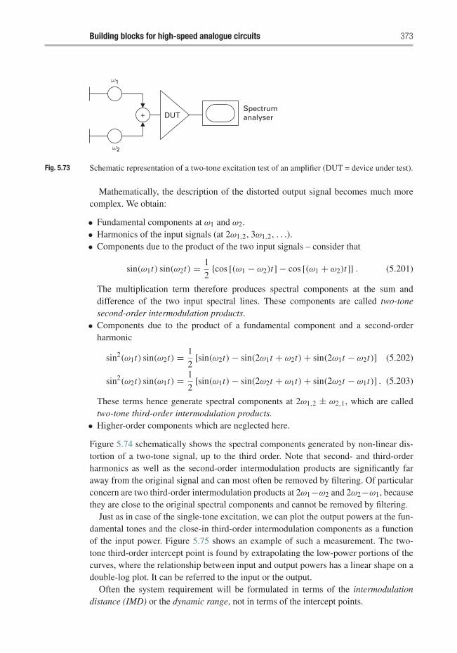
Building blocks for high-speed analogue circuits 373
DUTSpectrumanalyser+
ω1
ω2
Fig. 5.73 Schematic representation of a two-tone excitation test of an amplifier (DUT = device under test).
Mathematically, the description of the distorted output signal becomes much morecomplex. We obtain:
• Fundamental components at ω1 and ω2.• Harmonics of the input signals (at 2ω1,2, 3ω1,2, . . .).• Components due to the product of the two input signals – consider that
sin(ω1t) sin(ω2t) = 1
2{cos [(ω1 − ω2)t] − cos [(ω1 + ω2)t]} . (5.201)
The multiplication term therefore produces spectral components at the sum anddifference of the two input spectral lines. These components are called two-tonesecond-order intermodulation products.
• Components due to the product of a fundamental component and a second-orderharmonic
sin2(ω1t) sin(ω2t) = 1
2[sin(ω2t) − sin(2ω1t + ω2t) + sin(2ω1t − ω2t)] (5.202)
sin2(ω2t) sin(ω1t) = 1
2[sin(ω1t) − sin(2ω2t + ω1t) + sin(2ω2t − ω1t)] . (5.203)
These terms hence generate spectral components at 2ω1,2 ± ω2,1, which are calledtwo-tone third-order intermodulation products.
• Higher-order components which are neglected here.
Figure 5.74 schematically shows the spectral components generated by non-linear dis-tortion of a two-tone signal, up to the third order. Note that second- and third-orderharmonics as well as the second-order intermodulation products are significantly faraway from the original signal and can most often be removed by filtering. Of particularconcern are two third-order intermodulation products at 2ω1−ω2 and 2ω2−ω1, becausethey are close to the original spectral components and cannot be removed by filtering.
Just as in case of the single-tone excitation, we can plot the output powers at the fun-damental tones and the close-in third-order intermodulation components as a functionof the input power. Figure 5.75 shows an example of such a measurement. The two-tone third-order intercept point is found by extrapolating the low-power portions of thecurves, where the relationship between input and output powers has a linear shape on adouble-log plot. It can be referred to the input or the output.
Often the system requirement will be formulated in terms of the intermodulationdistance (IMD) or the dynamic range, not in terms of the intercept points.
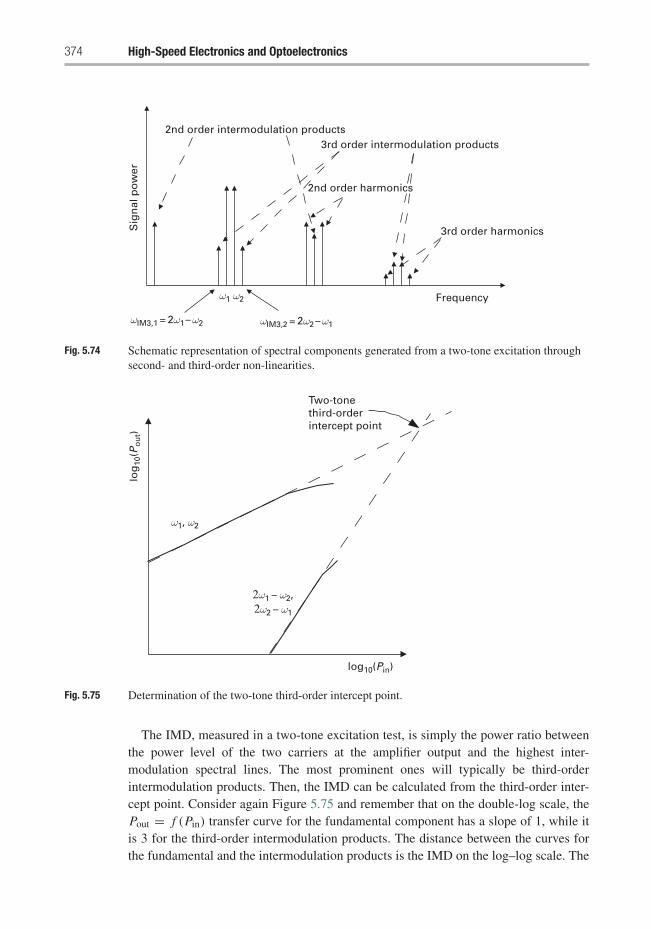
374 High-Speed Electronics and Optoelectronics
2nd order intermodulation products3rd order intermodulation products
2nd order harmonics
Sig
nal
po
wer
3rd order harmonics
Frequencyω1 ω2
ωIM3,2 = 2ω2– ω1ωIM3,1 = 2ω1– ω2
Fig. 5.74 Schematic representation of spectral components generated from a two-tone excitation throughsecond- and third-order non-linearities.
log
10(P
ou
t)
log10(Pin)
Two-tonethird-orderintercept point
ω1, ω2
2ω1 – ω2,2ω2 – ω1
Fig. 5.75 Determination of the two-tone third-order intercept point.
The IMD, measured in a two-tone excitation test, is simply the power ratio betweenthe power level of the two carriers at the amplifier output and the highest inter-modulation spectral lines. The most prominent ones will typically be third-orderintermodulation products. Then, the IMD can be calculated from the third-order inter-cept point. Consider again Figure 5.75 and remember that on the double-log scale, thePout = f (Pin) transfer curve for the fundamental component has a slope of 1, while itis 3 for the third-order intermodulation products. The distance between the curves forthe fundamental and the intermodulation products is the IMD on the log–log scale. The
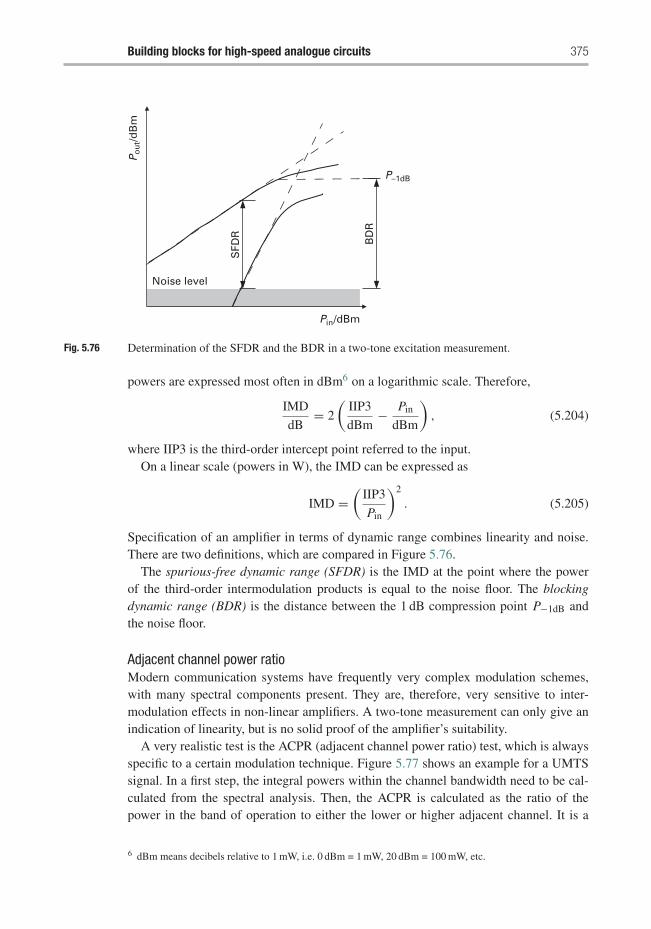
Building blocks for high-speed analogue circuits 375
Po
ut/d
Bm
Pin/dBm
P–1dB
Noise level
SFD
R
BD
R
Fig. 5.76 Determination of the SFDR and the BDR in a two-tone excitation measurement.
powers are expressed most often in dBm6 on a logarithmic scale. Therefore,
IMD
dB= 2
(IIP3
dBm− Pin
dBm
), (5.204)
where IIP3 is the third-order intercept point referred to the input.On a linear scale (powers in W), the IMD can be expressed as
IMD =(
IIP3
Pin
)2
. (5.205)
Specification of an amplifier in terms of dynamic range combines linearity and noise.There are two definitions, which are compared in Figure 5.76.
The spurious-free dynamic range (SFDR) is the IMD at the point where the powerof the third-order intermodulation products is equal to the noise floor. The blockingdynamic range (BDR) is the distance between the 1 dB compression point P−1dB andthe noise floor.
Adjacent channel power ratioModern communication systems have frequently very complex modulation schemes,with many spectral components present. They are, therefore, very sensitive to inter-modulation effects in non-linear amplifiers. A two-tone measurement can only give anindication of linearity, but is no solid proof of the amplifier’s suitability.
A very realistic test is the ACPR (adjacent channel power ratio) test, which is alwaysspecific to a certain modulation technique. Figure 5.77 shows an example for a UMTSsignal. In a first step, the integral powers within the channel bandwidth need to be cal-culated from the spectral analysis. Then, the ACPR is calculated as the ratio of thepower in the band of operation to either the lower or higher adjacent channel. It is a
6 dBm means decibels relative to 1 mW, i.e. 0 dBm = 1 mW, 20 dBm = 100 mW, etc.
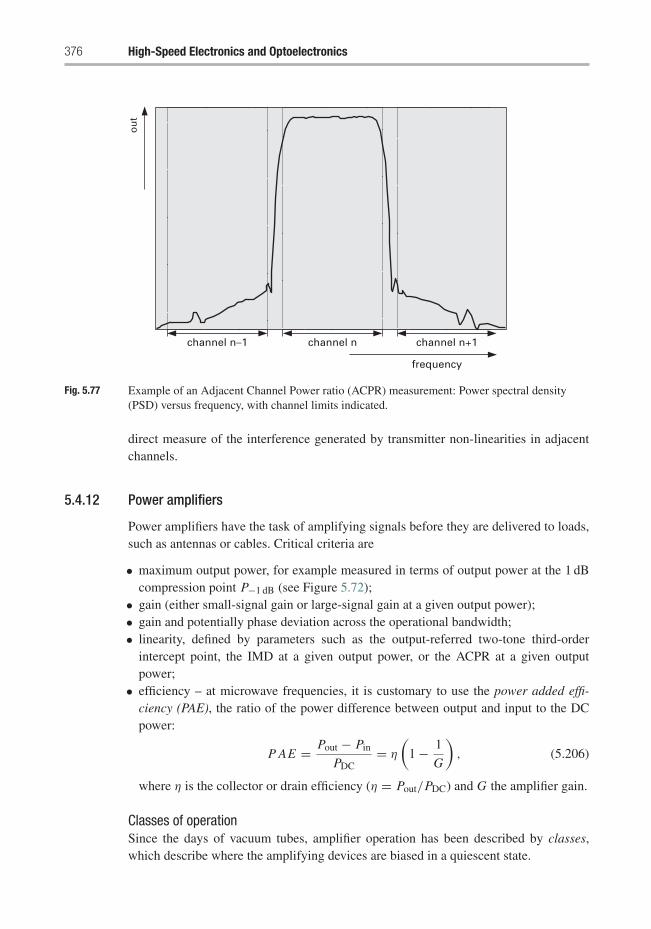
376 High-Speed Electronics and Optoelectronics
channel n–1
ou
t
channel n channel n+1
frequency
Fig. 5.77 Example of an Adjacent Channel Power ratio (ACPR) measurement: Power spectral density(PSD) versus frequency, with channel limits indicated.
direct measure of the interference generated by transmitter non-linearities in adjacentchannels.
5.4.12 Power amplifiers
Power amplifiers have the task of amplifying signals before they are delivered to loads,such as antennas or cables. Critical criteria are
• maximum output power, for example measured in terms of output power at the 1 dBcompression point P−1 dB (see Figure 5.72);
• gain (either small-signal gain or large-signal gain at a given output power);• gain and potentially phase deviation across the operational bandwidth;• linearity, defined by parameters such as the output-referred two-tone third-order
intercept point, the IMD at a given output power, or the ACPR at a given outputpower;
• efficiency – at microwave frequencies, it is customary to use the power added effi-ciency (PAE), the ratio of the power difference between output and input to the DCpower:
P AE = Pout − Pin
PDC= η
(1 − 1
G
), (5.206)
where η is the collector or drain efficiency (η = Pout/PDC) and G the amplifier gain.
Classes of operationSince the days of vacuum tubes, amplifier operation has been described by classes,which describe where the amplifying devices are biased in a quiescent state.
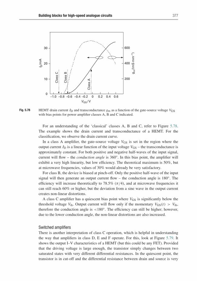
Building blocks for high-speed analogue circuits 377
30
20
10
Cla
ss C
Cla
ss B
Cla
ss A
I D/m
A
0–1.0 –0.8 –0.6 –0.4 –0.2
VGS / V0 0.2 0.4 0.6
600
400
200
gm
/(m
S m
m–1
)
Fig. 5.78 HEMT drain current ID and transconductance gm as a function of the gate-source voltage VGSwith bias points for power amplifier classes A, B and C indicated.
For an understanding of the ‘classical’ classes A, B and C, refer to Figure 5.78.The example shows the drain current and transconductance of a HEMT. For theclassification, we observe the drain current curve.
In a class A amplifier, the gate-source voltage VGS is set in the region where theoutput current ID is a linear function of the input voltage VGS – the transconductance isapproximately constant. For both positive and negative half-waves of the input signal,current will flow – the conduction angle is 360◦. In this bias point, the amplifier willexhibit a very high linearity, but low efficiency. The theoretical maximum is 50%, butat microwave frequencies, values of 30% would already be very satisfactory.
For class B, the device is biased at pinch-off. Only the positive half-wave of the inputsignal will then generate an output current flow – the conduction angle is 180◦. Theefficiency will increase theoretically to 78.5% (π/4), and at microwave frequencies itcan still reach 60% or higher, but the deviation from a sine wave in the output currentcreates non-linear distortions.
A class C amplifier has a quiescent bias point where VGS is significantly below thethreshold voltage Vth. Output current will flow only if the momentary VGS(t) > Vth,therefore the conduction angle is <180◦. The efficiency can still be higher; however,due to the lower conduction angle, the non-linear distortions are also increased.
Switched amplifiersThere is another interpretation of class C operation, which is helpful in understandingthe way that amplifiers in class D, E and F operate. For this, look at Figure 5.79. Itshows the output I–V characteristics of a HEMT (but this could be any FET). Providedthat the driving voltage is large enough, the transistor simply changes between twosaturated states with very different differential resistances. In the quiescent point, thetransistor is in cut-off and the differential resistance between drain and source is very
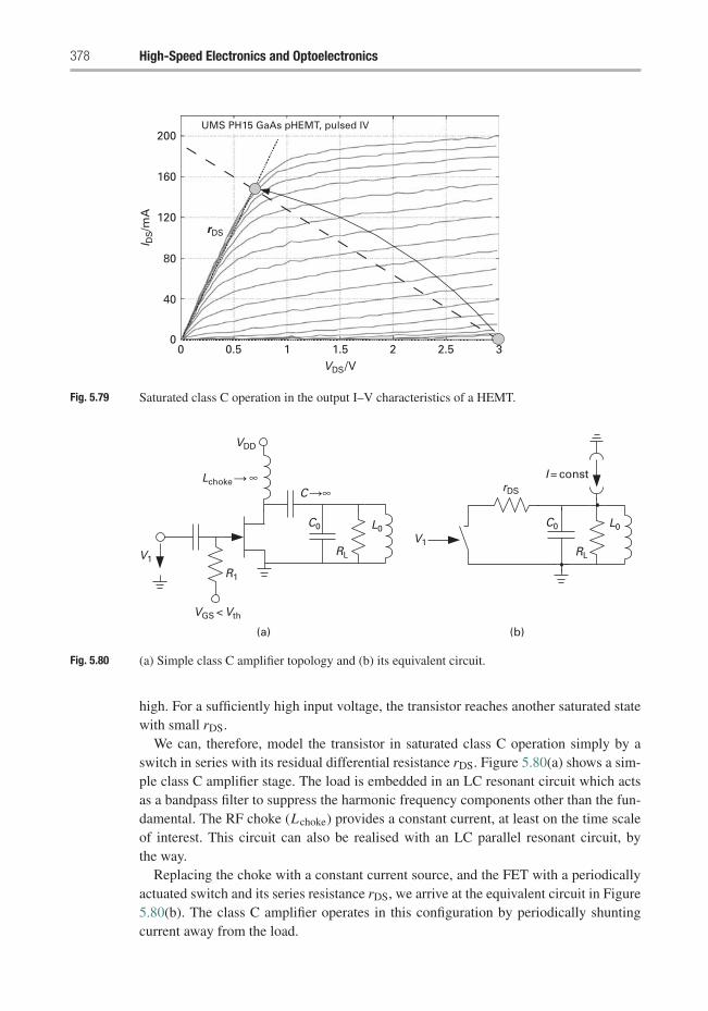
378 High-Speed Electronics and Optoelectronics
200UMS PH15 GaAs pHEMT, pulsed IV
160
120rDS
80
40
00 0.5 1 1.5
VDS/V2 2.5 3
I DS/m
A
Fig. 5.79 Saturated class C operation in the output I–V characteristics of a HEMT.
(a) (b)
rDS
C0 L0
RL
I = const
V1
VDD
V1
R1
RL
L0C0
VGS < Vth
LchokeC
∞∞
Fig. 5.80 (a) Simple class C amplifier topology and (b) its equivalent circuit.
high. For a sufficiently high input voltage, the transistor reaches another saturated statewith small rDS.
We can, therefore, model the transistor in saturated class C operation simply by aswitch in series with its residual differential resistance rDS. Figure 5.80(a) shows a sim-ple class C amplifier stage. The load is embedded in an LC resonant circuit which actsas a bandpass filter to suppress the harmonic frequency components other than the fun-damental. The RF choke (Lchoke) provides a constant current, at least on the time scaleof interest. This circuit can also be realised with an LC parallel resonant circuit, bythe way.
Replacing the choke with a constant current source, and the FET with a periodicallyactuated switch and its series resistance rDS, we arrive at the equivalent circuit in Figure5.80(b). The class C amplifier operates in this configuration by periodically shuntingcurrent away from the load.
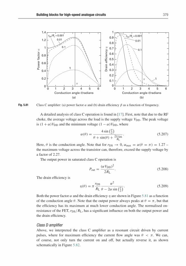
Building blocks for high-speed analogue circuits 379
1.4rDs/RL = 0.001 rDs/RL = 0.001
0.01 0.01
0.10.1
1
0.9
0.8
0.7
0.6
0.5
0.4
0.3
0.2
0.1
0
1.2
1
0.8
0.6
0.4
0.2
00 1 2
Conduction angle θ/radians
(a) (b)
Conduction angle θ/radians
Po
wer
fac
tor
α
Dra
in e
ffic
ien
cy η
3 4
1
1
5 6 0 1 2 3 4 5 6
ππ
Fig. 5.81 Class C amplifier: (a) power factor α and (b) drain efficiency β as a function of frequency.
A detailed analysis of class C operation is found in [17]. First, note that due to the RFchoke, the average voltage across the load is the supply voltage VDD. The peak voltageis (1 + α)VDD and the minimum voltage (1 − α)VDD, where
α(θ) = 4 sin(θ2
)θ + sin(θ) + 2πrDS
RL
. (5.207)
Here, θ is the conduction angle. Note that for rDS → 0, αmax = α(θ = π) = 1.27 –the maximum voltage across the transistor can, therefore, exceed the supply voltage bya factor of 2.27.
The output power in saturated class C operation is
Pout = (αVDD)2
2RL. (5.208)
The drain efficiency is
η(θ) = πrDS
RL
α2
θ − 2α sin(θ2
) . (5.209)
Both the power factor α and the drain efficiency η are shown in Figure 5.81 as a functionof the conduction angle θ . Note that the output power always peaks at θ = π , but thatthe efficiency has its maximum at much lower conduction angle. The normalised on-resistance of the FET, rDS/RL, has a significant influence on both the output power andthe drain efficiency.
Class D amplifierAbove, we interpreted the class C amplifier as a resonant circuit driven by currentpulses, where for maximum efficiency the current flow angle was θ < π . We can,of course, not only turn the current on and off, but actually reverse it, as shownschematically in Figure 5.82.
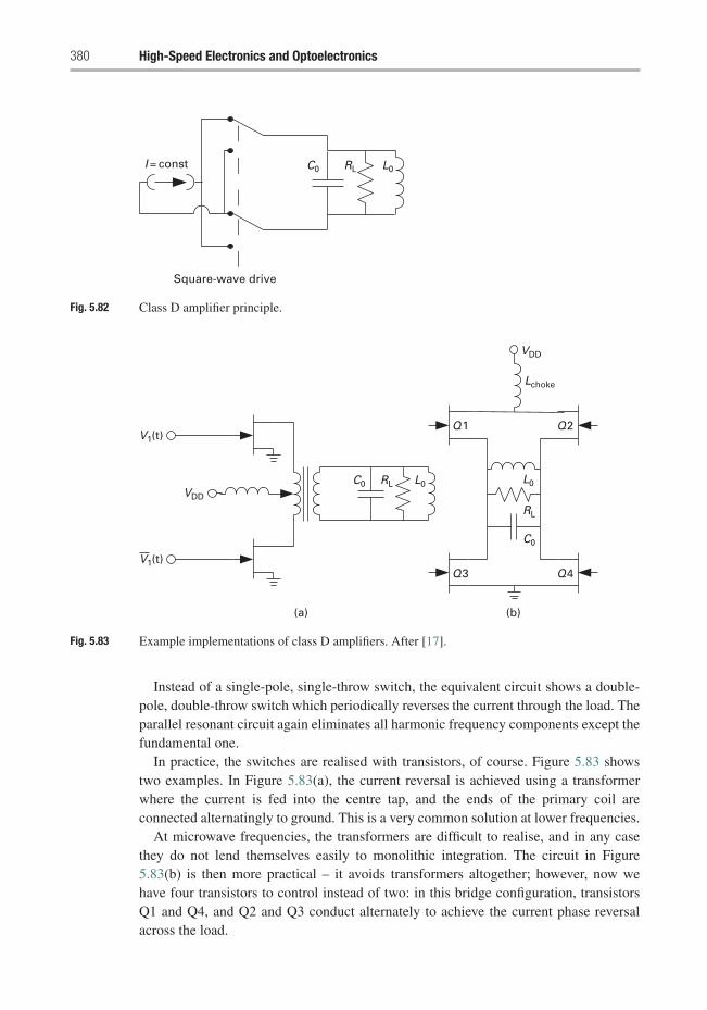
380 High-Speed Electronics and Optoelectronics
I = const
Square-wave drive
RLC0 L0
Fig. 5.82 Class D amplifier principle.
(b)(a)
V1(t)
V1(t)
C0 RL L0
Q3
C0
RL
L0
Q4
Q1 Q2
VDD
Lchoke
VDD
Fig. 5.83 Example implementations of class D amplifiers. After [17].
Instead of a single-pole, single-throw switch, the equivalent circuit shows a double-pole, double-throw switch which periodically reverses the current through the load. Theparallel resonant circuit again eliminates all harmonic frequency components except thefundamental one.
In practice, the switches are realised with transistors, of course. Figure 5.83 showstwo examples. In Figure 5.83(a), the current reversal is achieved using a transformerwhere the current is fed into the centre tap, and the ends of the primary coil areconnected alternatingly to ground. This is a very common solution at lower frequencies.
At microwave frequencies, the transformers are difficult to realise, and in any casethey do not lend themselves easily to monolithic integration. The circuit in Figure5.83(b) is then more practical – it avoids transformers altogether; however, now wehave four transistors to control instead of two: in this bridge configuration, transistorsQ1 and Q4, and Q2 and Q3 conduct alternately to achieve the current phase reversalacross the load.
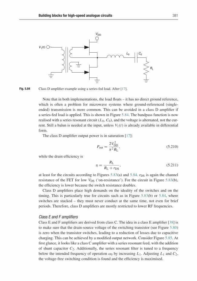
Building blocks for high-speed analogue circuits 381
C0L0
RL
VDD
V1(t)
Fig. 5.84 Class D amplifier example using a series-fed load. After [17].
Note that in both implementations, the load floats – it has no direct ground reference,which is often a problem for microwave systems where ground-referenced (single-ended) transmission is more common. This can be avoided in a class D amplifier ifa series-fed load is applied. This is shown in Figure 5.84. The bandpass function is nowrealised with a series resonant circuit (L0,C0), and the voltage is alternated, not the cur-rent. Still a balun is needed at the input, unless V1(t) is already available in differentialform.
The class D amplifier output power is in saturation [17]:
Pout = 2V 2DD
π2 RL, (5.210)
while the drain efficiency is
η = RL
RL + rDS, (5.211)
at least for the circuits according to Figures 5.83(a) and 5.84. rDS is again the channelresistance of the FET for low VDS (‘on-resistance’). For the circuit in Figure 5.83(b),the efficiency is lower because the switch resistance doubles.
Class D amplifiers place high demands on the ideality of the switches and on thetiming. This is particularly true for circuits such as in Figure 5.83(b) or 5.84, whereswitches are stacked – they must never conduct at the same time, not even for briefperiods. Therefore, class D amplifiers are mostly restricted to lower RF frequencies.
Class E and F amplifiersClass E and F amplifiers are derived from class C. The idea in a class E amplifier [38] isto make sure that the drain-source voltage of the switching transistor (see Figure 5.80)is zero when the transistor switches, leading to a reduction of losses due to capacitivecharging. This can be achieved by a modified output network. Consider Figure 5.85. Atfirst glance, it looks like a class C amplifier with a series resonant feed, with the additionof shunt capacitor C2. Additionally, the series resonant filter is tuned to a frequencybelow the intended frequency of operation ω0 by increasing L1. Adjusting L1 and C2,the voltage-free switching condition is found and the efficiency is maximised.
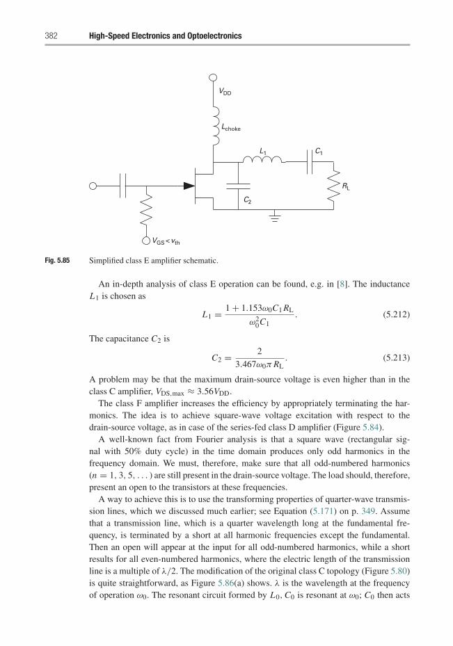
382 High-Speed Electronics and Optoelectronics
VDD
Lchoke
L1 C1
C2
VGS <vth
RL
Fig. 5.85 Simplified class E amplifier schematic.
An in-depth analysis of class E operation can be found, e.g. in [8]. The inductanceL1 is chosen as
L1 = 1 + 1.153ω0C1 RL
ω20C1
. (5.212)
The capacitance C2 is
C2 = 2
3.467ω0π RL. (5.213)
A problem may be that the maximum drain-source voltage is even higher than in theclass C amplifier, VDS,max ≈ 3.56VDD.
The class F amplifier increases the efficiency by appropriately terminating the har-monics. The idea is to achieve square-wave voltage excitation with respect to thedrain-source voltage, as in case of the series-fed class D amplifier (Figure 5.84).
A well-known fact from Fourier analysis is that a square wave (rectangular sig-nal with 50% duty cycle) in the time domain produces only odd harmonics in thefrequency domain. We must, therefore, make sure that all odd-numbered harmonics(n = 1, 3, 5, . . . ) are still present in the drain-source voltage. The load should, therefore,present an open to the transistors at these frequencies.
A way to achieve this is to use the transforming properties of quarter-wave transmis-sion lines, which we discussed much earlier; see Equation (5.171) on p. 349. Assumethat a transmission line, which is a quarter wavelength long at the fundamental fre-quency, is terminated by a short at all harmonic frequencies except the fundamental.Then an open will appear at the input for all odd-numbered harmonics, while a shortresults for all even-numbered harmonics, where the electric length of the transmissionline is a multiple of λ/2. The modification of the original class C topology (Figure 5.80)is quite straightforward, as Figure 5.86(a) shows. λ is the wavelength at the frequencyof operation ω0. The resonant circuit formed by L0,C0 is resonant at ω0; C0 then acts
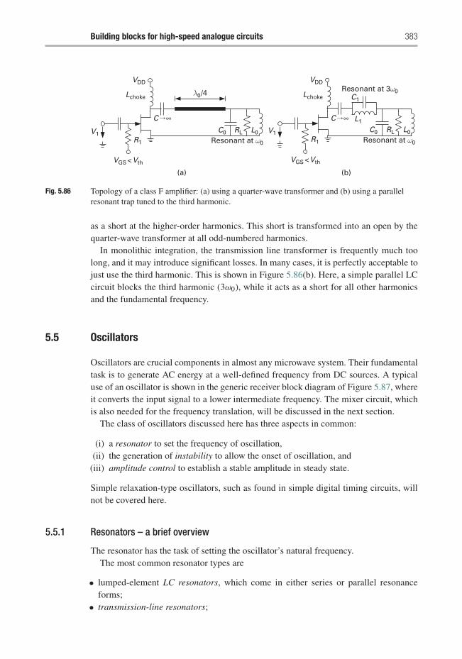
Building blocks for high-speed analogue circuits 383
(a)
V1R1
C0 RL
C1
C0 RL L0
L1
L0 V1R1Resonant at ω0 Resonant at ω0
Resonant at 3ω0
VDD
Lchoke
VDD
Lchokeλ0/4
C ∞ C ∞
(b)
VGS <Vth VGS <Vth
Fig. 5.86 Topology of a class F amplifier: (a) using a quarter-wave transformer and (b) using a parallelresonant trap tuned to the third harmonic.
as a short at the higher-order harmonics. This short is transformed into an open by thequarter-wave transformer at all odd-numbered harmonics.
In monolithic integration, the transmission line transformer is frequently much toolong, and it may introduce significant losses. In many cases, it is perfectly acceptable tojust use the third harmonic. This is shown in Figure 5.86(b). Here, a simple parallel LCcircuit blocks the third harmonic (3ω0), while it acts as a short for all other harmonicsand the fundamental frequency.
5.5 Oscillators
Oscillators are crucial components in almost any microwave system. Their fundamentaltask is to generate AC energy at a well-defined frequency from DC sources. A typicaluse of an oscillator is shown in the generic receiver block diagram of Figure 5.87, whereit converts the input signal to a lower intermediate frequency. The mixer circuit, whichis also needed for the frequency translation, will be discussed in the next section.
The class of oscillators discussed here has three aspects in common:
(i) a resonator to set the frequency of oscillation,(ii) the generation of instability to allow the onset of oscillation, and
(iii) amplitude control to establish a stable amplitude in steady state.
Simple relaxation-type oscillators, such as found in simple digital timing circuits, willnot be covered here.
5.5.1 Resonators – a brief overview
The resonator has the task of setting the oscillator’s natural frequency.The most common resonator types are
• lumped-element LC resonators, which come in either series or parallel resonanceforms;
• transmission-line resonators;
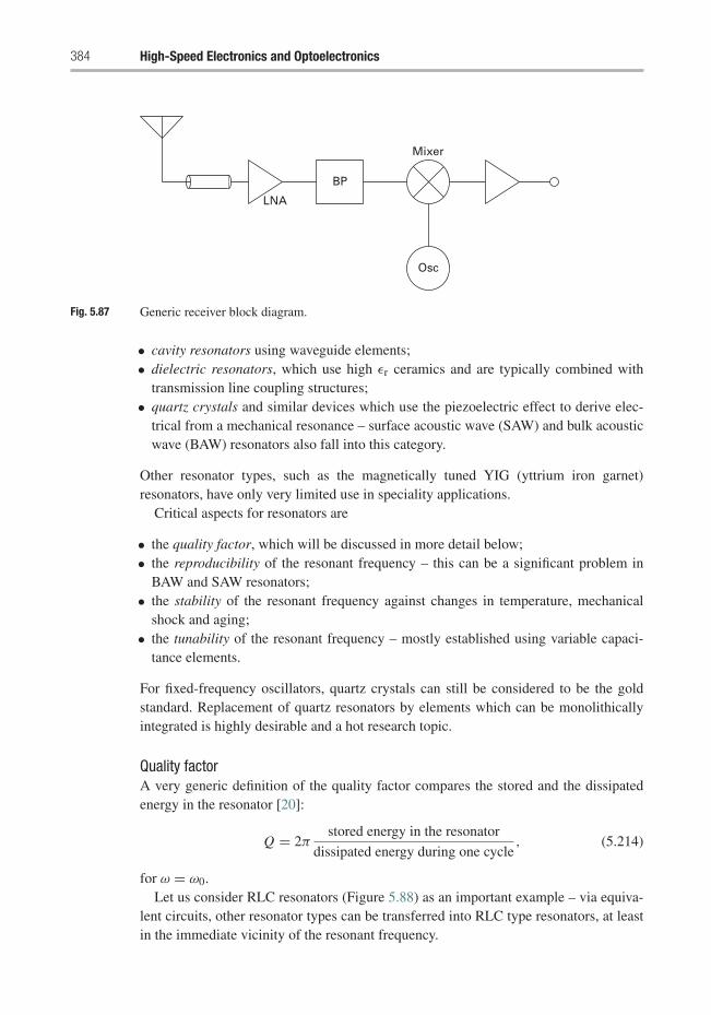
384 High-Speed Electronics and Optoelectronics
LNA
BP
Osc
Mixer
Fig. 5.87 Generic receiver block diagram.
• cavity resonators using waveguide elements;• dielectric resonators, which use high εr ceramics and are typically combined with
transmission line coupling structures;• quartz crystals and similar devices which use the piezoelectric effect to derive elec-
trical from a mechanical resonance – surface acoustic wave (SAW) and bulk acousticwave (BAW) resonators also fall into this category.
Other resonator types, such as the magnetically tuned YIG (yttrium iron garnet)resonators, have only very limited use in speciality applications.
Critical aspects for resonators are
• the quality factor, which will be discussed in more detail below;• the reproducibility of the resonant frequency – this can be a significant problem in
BAW and SAW resonators;• the stability of the resonant frequency against changes in temperature, mechanical
shock and aging;• the tunability of the resonant frequency – mostly established using variable capaci-
tance elements.
For fixed-frequency oscillators, quartz crystals can still be considered to be the goldstandard. Replacement of quartz resonators by elements which can be monolithicallyintegrated is highly desirable and a hot research topic.
Quality factorA very generic definition of the quality factor compares the stored and the dissipatedenergy in the resonator [20]:
Q = 2πstored energy in the resonator
dissipated energy during one cycle, (5.214)
for ω = ω0.Let us consider RLC resonators (Figure 5.88) as an important example – via equiva-
lent circuits, other resonator types can be transferred into RLC type resonators, at leastin the immediate vicinity of the resonant frequency.
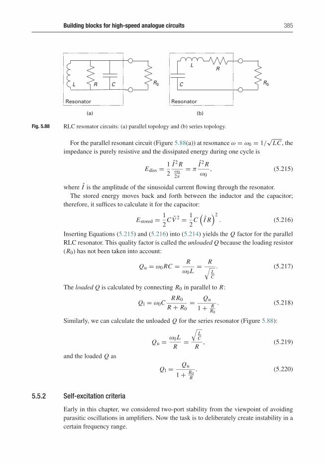
Building blocks for high-speed analogue circuits 385
R
(a) (b)
L
LR
C CR0 R0
Resonator Resonator
Fig. 5.88 RLC resonator circuits: (a) parallel topology and (b) series topology.
For the parallel resonant circuit (Figure 5.88(a)) at resonance ω = ω0 = 1/√
LC , theimpedance is purely resistive and the dissipated energy during one cycle is
Ediss = 1
2
I 2 Rω02π
= πI 2 R
ω0, (5.215)
where I is the amplitude of the sinusoidal current flowing through the resonator.The stored energy moves back and forth between the inductor and the capacitor;
therefore, it suffices to calculate it for the capacitor:
Estored = 1
2CV 2 = 1
2C
(I R
)2. (5.216)
Inserting Equations (5.215) and (5.216) into (5.214) yields the Q factor for the parallelRLC resonator. This quality factor is called the unloaded Q because the loading resistor(R0) has not been taken into account:
Qu = ω0 RC = R
ω0L= R√
LC
. (5.217)
The loaded Q is calculated by connecting R0 in parallel to R:
Ql = ω0CR R0
R + R0= Qu
1 + RR0
. (5.218)
Similarly, we can calculate the unloaded Q for the series resonator (Figure 5.88):
Qu = ω0L
R=
√LC
R, (5.219)
and the loaded Q as
Ql = Qu
1 + R0R
. (5.220)
5.5.2 Self-excitation criteria
Early in this chapter, we considered two-port stability from the viewpoint of avoidingparasitic oscillations in amplifiers. Now the task is to deliberately create instability in acertain frequency range.
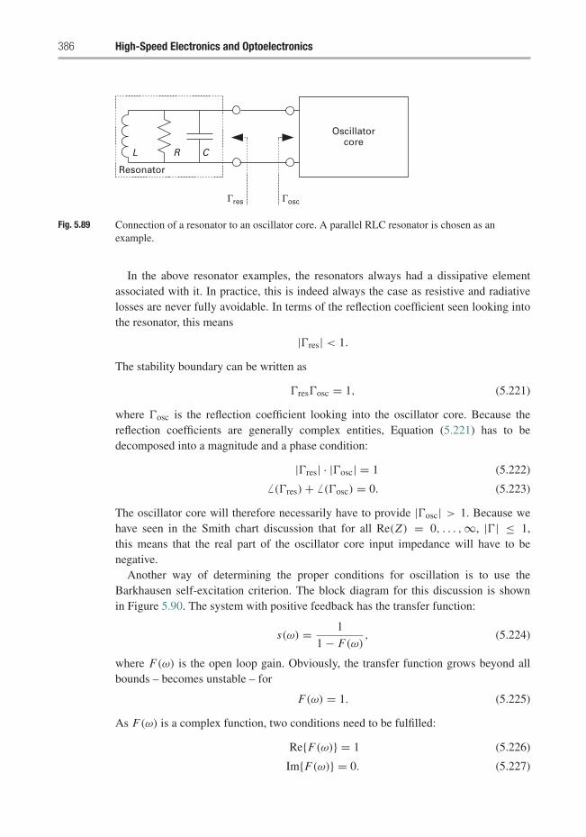
386 High-Speed Electronics and Optoelectronics
RL C
Γres Γosc
Oscillatorcore
Resonator
Fig. 5.89 Connection of a resonator to an oscillator core. A parallel RLC resonator is chosen as anexample.
In the above resonator examples, the resonators always had a dissipative elementassociated with it. In practice, this is indeed always the case as resistive and radiativelosses are never fully avoidable. In terms of the reflection coefficient seen looking intothe resonator, this means
|�res| < 1.
The stability boundary can be written as
�res�osc = 1, (5.221)
where �osc is the reflection coefficient looking into the oscillator core. Because thereflection coefficients are generally complex entities, Equation (5.221) has to bedecomposed into a magnitude and a phase condition:
|�res| · |�osc| = 1 (5.222)
� (�res) + � (�osc) = 0. (5.223)
The oscillator core will therefore necessarily have to provide |�osc| > 1. Because wehave seen in the Smith chart discussion that for all Re(Z) = 0, . . . ,∞, |�| ≤ 1,this means that the real part of the oscillator core input impedance will have to benegative.
Another way of determining the proper conditions for oscillation is to use theBarkhausen self-excitation criterion. The block diagram for this discussion is shownin Figure 5.90. The system with positive feedback has the transfer function:
s(ω) = 1
1 − F(ω), (5.224)
where F(ω) is the open loop gain. Obviously, the transfer function grows beyond allbounds – becomes unstable – for
F(ω) = 1. (5.225)
As F(ω) is a complex function, two conditions need to be fulfilled:
Re{F(ω)} = 1 (5.226)
Im{F(ω)} = 0. (5.227)
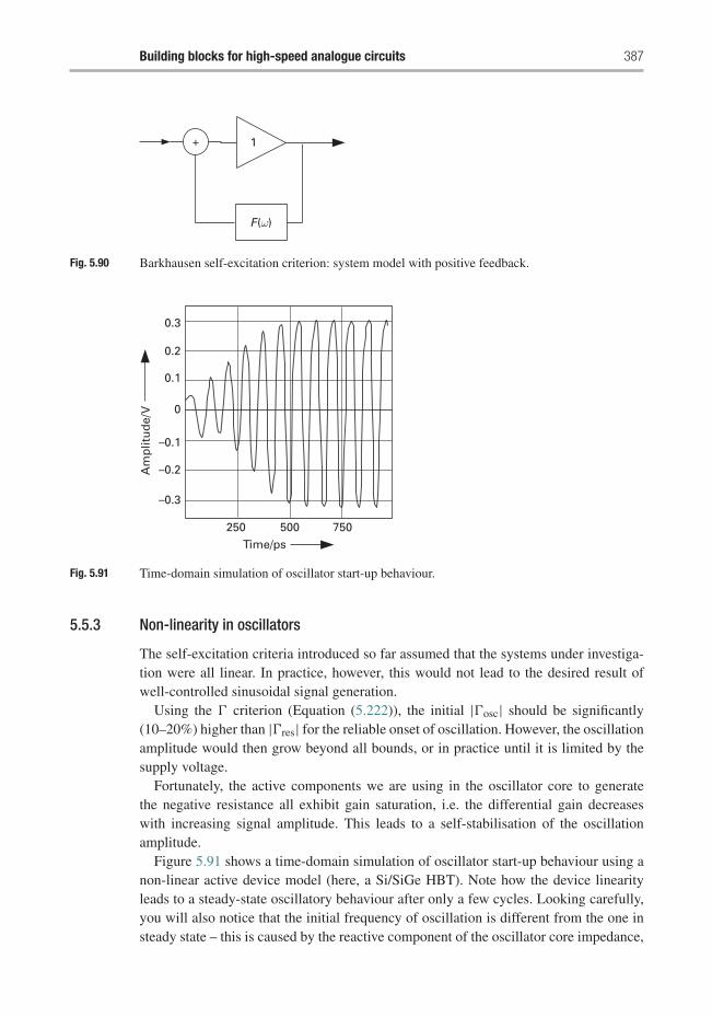
Building blocks for high-speed analogue circuits 387
F(ω)
1+
Fig. 5.90 Barkhausen self-excitation criterion: system model with positive feedback.
0.3
0.2
0.1
–0.1
–0.2
–0.3
250 500 750Time/ps
Am
plit
ud
e/V 0
Fig. 5.91 Time-domain simulation of oscillator start-up behaviour.
5.5.3 Non-linearity in oscillators
The self-excitation criteria introduced so far assumed that the systems under investiga-tion were all linear. In practice, however, this would not lead to the desired result ofwell-controlled sinusoidal signal generation.
Using the � criterion (Equation (5.222)), the initial |�osc| should be significantly(10–20%) higher than |�res| for the reliable onset of oscillation. However, the oscillationamplitude would then grow beyond all bounds, or in practice until it is limited by thesupply voltage.
Fortunately, the active components we are using in the oscillator core to generatethe negative resistance all exhibit gain saturation, i.e. the differential gain decreaseswith increasing signal amplitude. This leads to a self-stabilisation of the oscillationamplitude.
Figure 5.91 shows a time-domain simulation of oscillator start-up behaviour using anon-linear active device model (here, a Si/SiGe HBT). Note how the device linearityleads to a steady-state oscillatory behaviour after only a few cycles. Looking carefully,you will also notice that the initial frequency of oscillation is different from the one insteady state – this is caused by the reactive component of the oscillator core impedance,
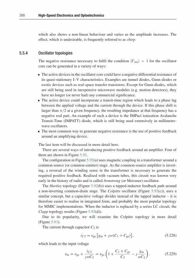
388 High-Speed Electronics and Optoelectronics
which also shows a non-linear behaviour and varies as the amplitude increases. Theeffect, which is undesirable, is frequently referred to as chirp.
5.5.4 Oscillator topologies
The negative resistance necessary to fulfil the condition |�osc| > 1 for the oscillatorcore can be generated in a variety of ways:
• The active devices in the oscillator core could have a negative differential resistance ofits quasi-stationary I–V characteristics. Examples are tunnel diodes, Gunn diodes orexotic devices such as real-space transfer transistors. Except for Gunn diodes, whichare still being used in inexpensive microwave modules (e.g. motion detectors), theyhave no longer (or never had) any commercial significance.
• The active device could incorporate a transit-time region which leads to a phase lagbetween the applied voltage and the current through the device. If this phase shift islarger than π/2 at a given frequency, the resulting impedance at that frequency has anegative real part. An example of such a device is the IMPact ionization AvalancheTransit-Time (IMPATT) diode, which is still being used extensively in millimetre-wave oscillators.
• The most common way to generate negative resistance is the use of positive feedbackaround an amplifying device.
The last item will be discussed in more detail here.There are several ways of introducing positive feedback around an amplifier. Four of
them are shown in Figure 5.92.The configuration in Figure 5.92(a) uses magnetic coupling in a transformer around a
common-source (or common-emitter) stage. As the common-source amplifier is invert-ing, a reversal of the winding sense in the transformer is necessary to generate therequired positive feedback. Realised with vacuum tubes, this circuit was known veryearly in the history of radio and is called Armstrong (or Meissner) oscillator.
The Hartley topology (Figure 5.92(b)) uses a tapped-inductor feedback path arounda non-inverting common-drain stage. The Colpitts oscillator (Figure 5.92(c)), uses asimilar concept, but a capacitive voltage divider instead of the tapped inductor – it istherefore easier to realise in integrated form, and probably the most popular topologyfor MMIC implementations. When the inductor is replaced by a series LC circuit, theClapp topology results (Figure 5.92(d)).
Due to its popularity, we will examine the Colpitts topology in more detail(Figure 5.93).
The current through capacitor C2 is
iC2 = vgs[gm + jω(C1 + Cgs)
], (5.228)
which leads to the input voltage
vin = vgs + iC2
jωC2= vgs
(1 + C1 + Cgs
C2− j
gm
ωC2
). (5.229)
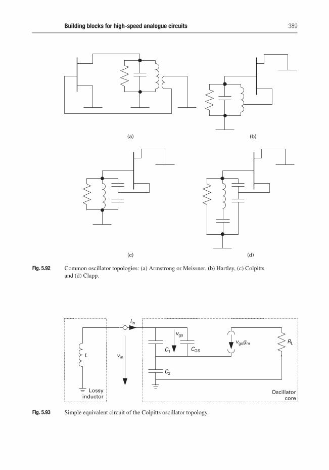
Building blocks for high-speed analogue circuits 389
(a) (b)
(c) (d)
Fig. 5.92 Common oscillator topologies: (a) Armstrong or Meissner, (b) Hartley, (c) Colpittsand (d) Clapp.
L vin
iin
vgs
vgsgm RL
C1
C2
CGS
Lossyinductor
Oscillatorcore
Fig. 5.93 Simple equivalent circuit of the Colpitts oscillator topology.
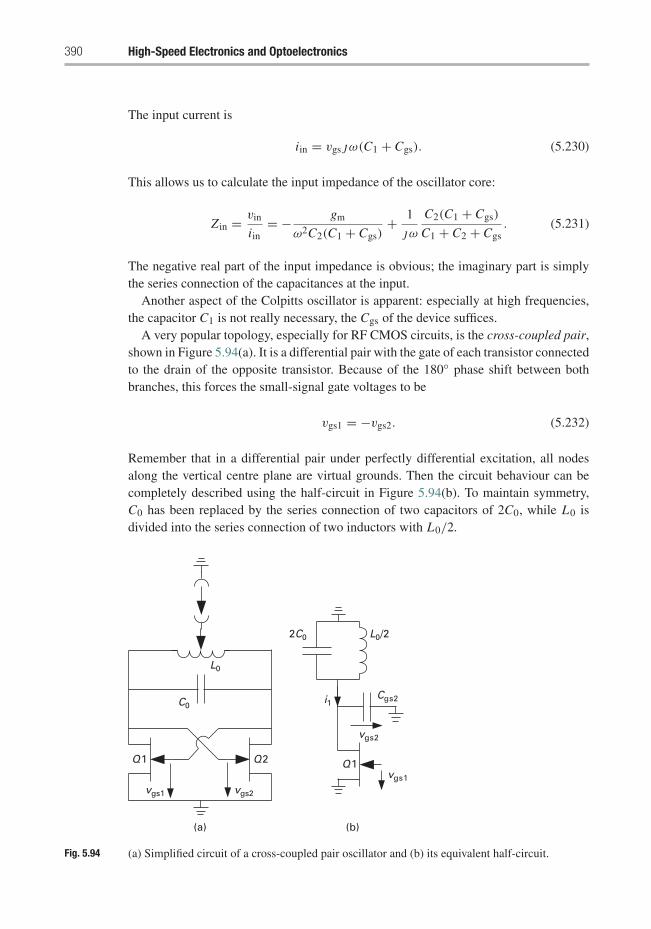
390 High-Speed Electronics and Optoelectronics
The input current is
iin = vgsjω(C1 + Cgs). (5.230)
This allows us to calculate the input impedance of the oscillator core:
Z in = vin
iin= − gm
ω2C2(C1 + Cgs)+ 1
jω
C2(C1 + Cgs)
C1 + C2 + Cgs. (5.231)
The negative real part of the input impedance is obvious; the imaginary part is simplythe series connection of the capacitances at the input.
Another aspect of the Colpitts oscillator is apparent: especially at high frequencies,the capacitor C1 is not really necessary, the Cgs of the device suffices.
A very popular topology, especially for RF CMOS circuits, is the cross-coupled pair,shown in Figure 5.94(a). It is a differential pair with the gate of each transistor connectedto the drain of the opposite transistor. Because of the 180◦ phase shift between bothbranches, this forces the small-signal gate voltages to be
vgs1 = −vgs2. (5.232)
Remember that in a differential pair under perfectly differential excitation, all nodesalong the vertical centre plane are virtual grounds. Then the circuit behaviour can becompletely described using the half-circuit in Figure 5.94(b). To maintain symmetry,C0 has been replaced by the series connection of two capacitors of 2C0, while L0 isdivided into the series connection of two inductors with L0/2.
C0
L0
Q2Q1
vgs1 vgs2
(a) (b)
2C0 L0/2
Cgs2i1
vgs2
vgs1
Q1
Fig. 5.94 (a) Simplified circuit of a cross-coupled pair oscillator and (b) its equivalent half-circuit.
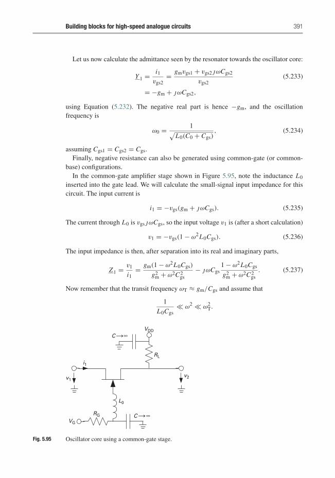
Building blocks for high-speed analogue circuits 391
Let us now calculate the admittance seen by the resonator towards the oscillator core:
Y 1 = i1
vgs2= gmvgs1 + vgs2jωCgs2
vgs2(5.233)
= −gm + jωCgs2,
using Equation (5.232). The negative real part is hence −gm, and the oscillationfrequency is
ω0 = 1√L0(C0 + Cgs)
, (5.234)
assuming Cgs1 = Cgs2 = Cgs.Finally, negative resistance can also be generated using common-gate (or common-
base) configurations.In the common-gate amplifier stage shown in Figure 5.95, note the inductance L0
inserted into the gate lead. We will calculate the small-signal input impedance for thiscircuit. The input current is
i1 = −vgs(gm + jωCgs). (5.235)
The current through L0 is vgsjωCgs, so the input voltage v1 is (after a short calculation)
v1 = −vgs(1 − ω2L0Cgs). (5.236)
The input impedance is then, after separation into its real and imaginary parts,
Z1 = v1
i1= gm(1 − ω2L0Cgs)
g2m + ω2C2
gs− jωCgs
1 − ω2L0Cgs
g2m + ω2C2
gs. (5.237)
Now remember that the transit frequency ωT ≈ gm/Cgs and assume that
1
L0Cgs� ω2 � ω2
T.
VDD
RL
L0
RGVG
v1
i1
v2
C ∞
C ∞
Fig. 5.95 Oscillator core using a common-gate stage.
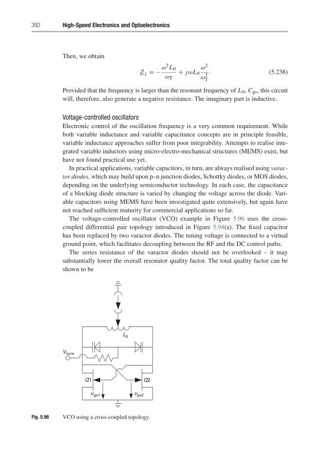
392 High-Speed Electronics and Optoelectronics
Then, we obtain
Z1 = −ω2L0
ωT+ jωL0
ω2
ω2T
. (5.238)
Provided that the frequency is larger than the resonant frequency of L0,Cgs, this circuitwill, therefore, also generate a negative resistance. The imaginary part is inductive.
Voltage-controlled oscillatorsElectronic control of the oscillation frequency is a very common requirement. Whileboth variable inductance and variable capacitance concepts are in principle feasible,variable inductance approaches suffer from poor integrability. Attempts to realise inte-grated variable inductors using micro-electro-mechanical structures (MEMS) exist, buthave not found practical use yet.
In practical applications, variable capacitors, in turn, are always realised using varac-tor diodes, which may build upon p–n junction diodes, Schottky diodes, or MOS diodes,depending on the underlying semiconductor technology. In each case, the capacitanceof a blocking diode structure is varied by changing the voltage across the diode. Vari-able capacitors using MEMS have been investigated quite extensively, but again havenot reached sufficient maturity for commercial applications so far.
The voltage-controlled oscillator (VCO) example in Figure 5.96 uses the cross-coupled differential pair topology introduced in Figure 5.94(a). The fixed capacitorhas been replaced by two varactor diodes. The tuning voltage is connected to a virtualground point, which facilitates decoupling between the RF and the DC control paths.
The series resistance of the varactor diodes should not be overlooked – it maysubstantially lower the overall resonator quality factor. The total quality factor can beshown to be
L0
Vtune
vgs1 vgs2
Q1 Q2
Fig. 5.96 VCO using a cross-coupled topology.
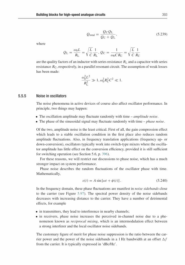
Building blocks for high-speed analogue circuits 393
Qtotal = QC QL
QC + QL, (5.239)
where
QL = ω0L
RL=
√L
C
1
RL, QC = 1
ω0C RC=
√L
C
1
RC
are the quality factors of an inductor with series resistance RL and a capacitor with seriesresistance RC, respectively, in a parallel resonant circuit. The assumption of weak losseshas been made:
ω20 L2
R2L
� 1, ω20 R2
CC2 � 1.
5.5.5 Noise in oscillators
The noise phenomena in active devices of course also affect oscillator performance. Inprinciple, two things may happen:
• The oscillation amplitude may fluctuate randomly with time – amplitude noise.• The phase of the sinusoidal signal may fluctuate randomly with time – phase noise.
Of the two, amplitude noise is the least critical. First of all, the gain compression effectwhich leads to a stable oscillation condition in the first place also reduces randomamplitude fluctuations. Also, in frequency translation applications (frequency up- ordown-conversion), oscillators typically work into switch-type mixers where the oscilla-tor amplitude has little effect on the conversion efficiency, provided it is still sufficientfor switching operation (see Section 5.6, p. 396).
For these reasons, we will restrict our discussions to phase noise, which has a muchstronger impact on system performance.
Phase noise describes the random fluctuations of the oscillator phase with time.Mathematically,
s(t) = A sin [ωt + φ(t)] . (5.240)
In the frequency domain, these phase fluctuations are manifest in noise sidebands closeto the carrier (see Figure 5.97). The spectral power density of the noise sidebandsdecreases with increasing distance to the carrier. They have a number of detrimentaleffects, for example
• in transmitters, they lead to interference in nearby channels;• in receivers, phase noise increases the perceived in-channel noise due to a phe-
nomenon known as reciprocal mixing, which is an intermodulation effect betweena strong interferer and the local oscillator noise sidebands.
The customary figure of merit for phase noise suppression is the ratio between the car-rier power and the power of the noise sidebands in a 1 Hz bandwidth at an offset � ffrom the carrier. It is typically expressed in ‘dBc/Hz’.
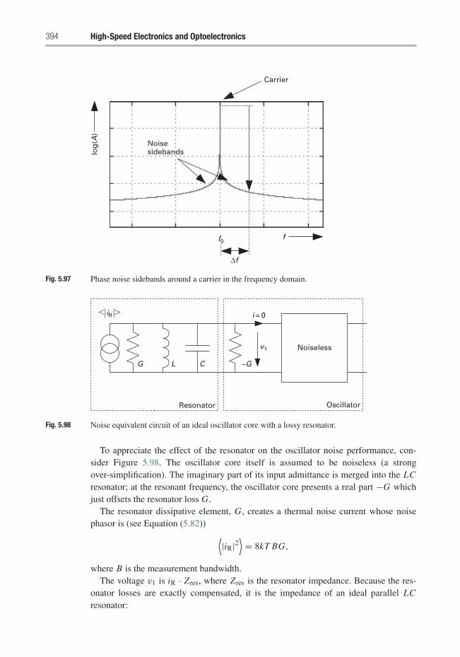
394 High-Speed Electronics and Optoelectronics
Carrier
Noisesidebandslo
g(A
)
Δf
f0f
Fig. 5.97 Phase noise sidebands around a carrier in the frequency domain.
C –G
v1
iR i = 0
LG
Resonator Oscillator
Noiseless
Fig. 5.98 Noise equivalent circuit of an ideal oscillator core with a lossy resonator.
To appreciate the effect of the resonator on the oscillator noise performance, con-sider Figure 5.98. The oscillator core itself is assumed to be noiseless (a strongover-simplification). The imaginary part of its input admittance is merged into the LCresonator; at the resonant frequency, the oscillator core presents a real part −G whichjust offsets the resonator loss G.
The resonator dissipative element, G, creates a thermal noise current whose noisephasor is (see Equation (5.82)) ⟨
|iR|2⟩= 8kT BG,
where B is the measurement bandwidth.The voltage v1 is iR · Zres, where Zres is the resonator impedance. Because the res-
onator losses are exactly compensated, it is the impedance of an ideal parallel LCresonator:
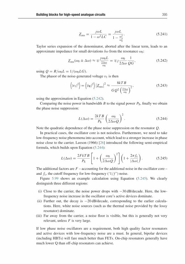
Building blocks for high-speed analogue circuits 395
Z res = jωL
1 − ω2LC= jωL
1 − ω2
ω20
. (5.241)
Taylor series expansion of the denominator, aborted after the linear term, leads to anapproximate impedance for small deviations δω from the resonance ω0:
Z res(ω0 ± �ω) ≈ ∓jω0L2�ωω0
= ∓jω0
2�ω
1
QG, (5.242)
using Q = R/ω0L = 1/(ω0LG).The phasor of the noise-generated voltage v1 is then⟨
|v1|2⟩=
⟨|iR|2
⟩ ∣∣Z res
∣∣2 ≈ 8kT B
G Q2(
2�ωω0
)2, (5.243)
using the approximation in Equation (5.242).Comparing the noise power in bandwidth B to the signal power PS, finally we obtain
the phase noise suppression:
L(�ω) = 2kT B
PS
(ω0
2�ωQ
)2
. (5.244)
Note the quadratic dependence of the phase noise suppression on the resonator Q.In practical cases, the oscillator core is not noiseless. Furthermore, we need to take
low-frequency noise phenomena into account, which lead to a stronger increase in phasenoise close to the carrier. Leeson (1966) [26] introduced the following semi-empiricalformula, which builds upon Equation (5.244):
L(�ω) = 2FkT B
PS
[1 +
(ω0
2�ωQ
)2] (
1 + 2π fc
|�ω|). (5.245)
The additional factors are F – accounting for the additional noise in the oscillator core –and fc, the cutoff frequency for low-frequency (‘1/ f ’) noise.
Figure 5.99 shows an example calculation using Equation (5.245). We clearlydistinguish three different regions:
(i) Close to the carrier, the noise power drops with −30 dB/decade. Here, the low-frequency noise increase in the oscillator core’s active devices dominate.
(ii) Further out, the decay is −20 dB/decade, corresponding to the earlier calcula-tions. Here, white noise sources (such as the thermal noise provided by the lossyresonator) dominate.
(iii) Far away from the carrier, a noise floor is visible, but this is generally not veryrelevant, unless F is very large.
If low phase noise oscillators are a requirement, both high quality factor resonatorsand active devices with low-frequency noise are a must. In general, bipolar devices(including HBTs) will fare much better than FETs. On-chip resonators generally havemuch lower Q than off-chip resonators can achieve.
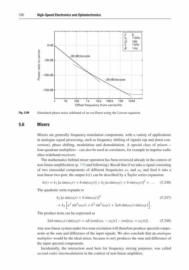
396 High-Speed Electronics and Optoelectronics
0 dB
–50 dB–30 dB/decade
–20 dB/decade
F 81 GHzf0
1 kHzfc
100Q
1 HzB
–100 dB
–150 dB
1 10 100 1 k 10 kOffset frequency from carrier/Hz
100 k 1 M 10 M
Po
wer
rat
io t
o c
arri
er
Fig. 5.99 Simulated phase noise sideband of an oscillator using the Leeson equation.
5.6 Mixers
Mixers are generally frequency-translation components, with a variety of applicationsin analogue signal processing, such as frequency shifting of signals (up and down con-version), phase shifting, modulation and demodulation. A special class of mixers –four-quadrant multipliers – can also be used in correlators, for example in impulse-radioultra-wideband receivers.
The mathematics behind mixer operation has been reviewed already in the context ofnon-linear amplification (p. 370 and following). Recall that if we take a signal consistingof two sinusoidal components of different frequencies ω1 and ω2 and feed it into anon-linear two-port, the output h(t) can be described by a Taylor series expansion:
h(t) = k1 [a sin(ω1t) + b sin(ω2t)] + k2 [a sin(ω2t) + b sin(ω2t)]2 + . . . (5.246)
The quadratic term expands to
k2 [a sin(ω2t) + b sin(ω2t)]2 (5.247)
= k2
[a2 sin2(ω1t) + b2 sin2(ω2t) + 2ab sin(ω1t) sin(ω2t)
].
The product term can be expressed as
2ab sin(ω1t) sin(ω2t) = ab {cos[(ω1 − ω2)t] − cos[(ω1 + ω2)t]} . (5.248)
Any non-linear system under two-tone excitation will therefore produce spectral compo-nents at the sum and difference of the input signals. We also conclude that an analoguemultiplier would be the ideal mixer, because it only produces the sum and difference ofthe input spectral components.
Incidentally, the interaction used here for frequency mixing purposes, was calledsecond-order intermodulation in the context of non-linear amplifiers.
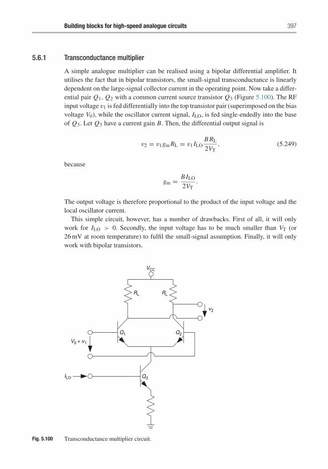
Building blocks for high-speed analogue circuits 397
5.6.1 Transconductance multiplier
A simple analogue multiplier can be realised using a bipolar differential amplifier. Itutilises the fact that in bipolar transistors, the small-signal transconductance is linearlydependent on the large-signal collector current in the operating point. Now take a differ-ential pair Q1, Q2 with a common current source transistor Q3 (Figure 5.100). The RFinput voltage v1 is fed differentially into the top transistor pair (superimposed on the biasvoltage V0), while the oscillator current signal, ILO, is fed single-endedly into the baseof Q3. Let Q3 have a current gain B. Then, the differential output signal is
v2 = v1gm RL = v1 ILOB RL
2VT, (5.249)
because
gm = B ILO
2VT.
The output voltage is therefore proportional to the product of the input voltage and thelocal oscillator current.
This simple circuit, however, has a number of drawbacks. First of all, it will onlywork for ILO > 0. Secondly, the input voltage has to be much smaller than VT (or26 mV at room temperature) to fulfil the small-signal assumption. Finally, it will onlywork with bipolar transistors.
RL RL
v2
Q1
Q3
V0 + v1
ILO
Q2
VCC
Fig. 5.100 Transconductance multiplier circuit.
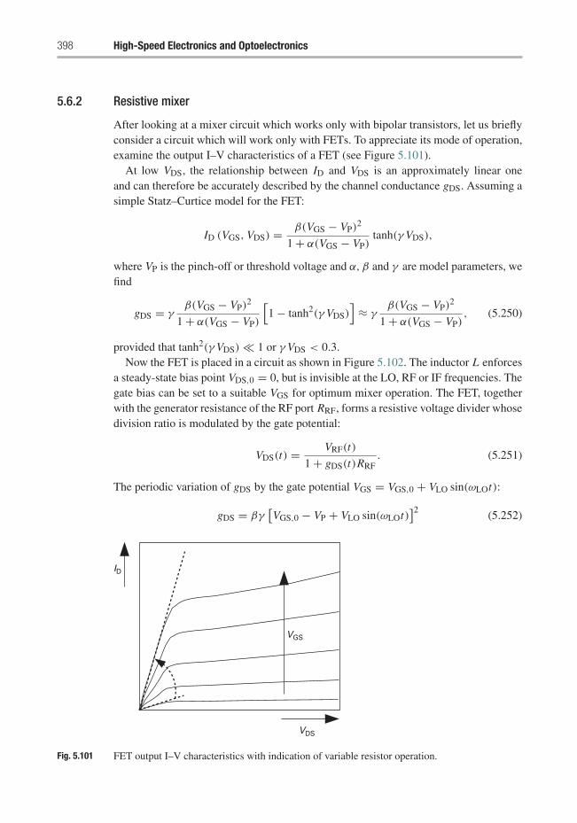
398 High-Speed Electronics and Optoelectronics
5.6.2 Resistive mixer
After looking at a mixer circuit which works only with bipolar transistors, let us brieflyconsider a circuit which will work only with FETs. To appreciate its mode of operation,examine the output I–V characteristics of a FET (see Figure 5.101).
At low VDS, the relationship between ID and VDS is an approximately linear oneand can therefore be accurately described by the channel conductance gDS. Assuming asimple Statz–Curtice model for the FET:
ID (VGS, VDS) = β(VGS − VP)2
1 + α(VGS − VP)tanh(γ VDS),
where VP is the pinch-off or threshold voltage and α, β and γ are model parameters, wefind
gDS = γβ(VGS − VP)
2
1 + α(VGS − VP)
[1 − tanh2(γ VDS)
]≈ γ
β(VGS − VP)2
1 + α(VGS − VP), (5.250)
provided that tanh2(γ VDS) � 1 or γ VDS < 0.3.Now the FET is placed in a circuit as shown in Figure 5.102. The inductor L enforces
a steady-state bias point VDS,0 = 0, but is invisible at the LO, RF or IF frequencies. Thegate bias can be set to a suitable VGS for optimum mixer operation. The FET, togetherwith the generator resistance of the RF port RRF, forms a resistive voltage divider whosedivision ratio is modulated by the gate potential:
VDS(t) = VRF(t)
1 + gDS(t)RRF. (5.251)
The periodic variation of gDS by the gate potential VGS = VGS,0 + VLO sin(ωLOt):
gDS = βγ[VGS,0 − VP + VLO sin(ωLOt)
]2 (5.252)
ID
VDS
VGS
Fig. 5.101 FET output I–V characteristics with indication of variable resistor operation.
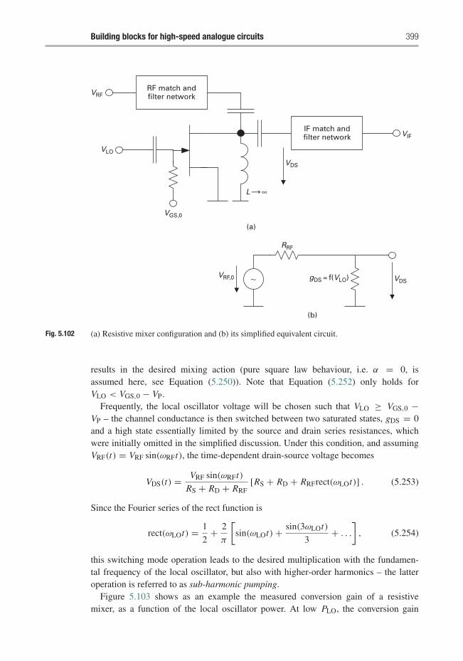
Building blocks for high-speed analogue circuits 399
RF match andfilter network
IF match andfilter network
(a)
(b)
VLO
VGS,0
VRF
VIF
VDS
RRF
gDS = f(VLO) VDSVRF,0
L ∞
Fig. 5.102 (a) Resistive mixer configuration and (b) its simplified equivalent circuit.
results in the desired mixing action (pure square law behaviour, i.e. α = 0, isassumed here, see Equation (5.250)). Note that Equation (5.252) only holds forVLO < VGS,0 − VP.
Frequently, the local oscillator voltage will be chosen such that VLO ≥ VGS,0 −VP – the channel conductance is then switched between two saturated states, gDS = 0and a high state essentially limited by the source and drain series resistances, whichwere initially omitted in the simplified discussion. Under this condition, and assumingVRF(t) = VRF sin(ωRFt), the time-dependent drain-source voltage becomes
VDS(t) = VRF sin(ωRFt)
RS + RD + RRF[RS + RD + RRFrect(ωLOt)] . (5.253)
Since the Fourier series of the rect function is
rect(ωLOt) = 1
2+ 2
π
[sin(ωLOt) + sin(3ωLOt)
3+ . . .
], (5.254)
this switching mode operation leads to the desired multiplication with the fundamen-tal frequency of the local oscillator, but also with higher-order harmonics – the latteroperation is referred to as sub-harmonic pumping.
Figure 5.103 shows as an example the measured conversion gain of a resistivemixer, as a function of the local oscillator power. At low PLO, the conversion gain
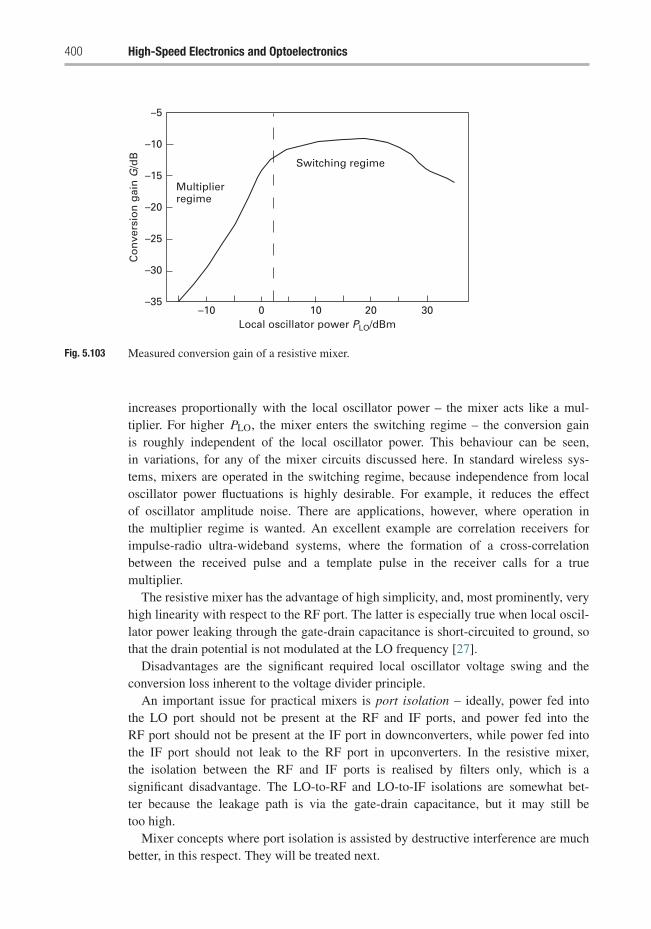
400 High-Speed Electronics and Optoelectronics
–5
–10
–15
–20
–25
–30
–35–10 0 10 20 30
Local oscillator power PLO/dBm
Switching regime
Multiplierregime
Co
nve
rsio
n g
ain
G/d
B
Fig. 5.103 Measured conversion gain of a resistive mixer.
increases proportionally with the local oscillator power – the mixer acts like a mul-tiplier. For higher PLO, the mixer enters the switching regime – the conversion gainis roughly independent of the local oscillator power. This behaviour can be seen,in variations, for any of the mixer circuits discussed here. In standard wireless sys-tems, mixers are operated in the switching regime, because independence from localoscillator power fluctuations is highly desirable. For example, it reduces the effectof oscillator amplitude noise. There are applications, however, where operation inthe multiplier regime is wanted. An excellent example are correlation receivers forimpulse-radio ultra-wideband systems, where the formation of a cross-correlationbetween the received pulse and a template pulse in the receiver calls for a truemultiplier.
The resistive mixer has the advantage of high simplicity, and, most prominently, veryhigh linearity with respect to the RF port. The latter is especially true when local oscil-lator power leaking through the gate-drain capacitance is short-circuited to ground, sothat the drain potential is not modulated at the LO frequency [27].
Disadvantages are the significant required local oscillator voltage swing and theconversion loss inherent to the voltage divider principle.
An important issue for practical mixers is port isolation – ideally, power fed intothe LO port should not be present at the RF and IF ports, and power fed into theRF port should not be present at the IF port in downconverters, while power fed intothe IF port should not leak to the RF port in upconverters. In the resistive mixer,the isolation between the RF and IF ports is realised by filters only, which is asignificant disadvantage. The LO-to-RF and LO-to-IF isolations are somewhat bet-ter because the leakage path is via the gate-drain capacitance, but it may still betoo high.
Mixer concepts where port isolation is assisted by destructive interference are muchbetter, in this respect. They will be treated next.
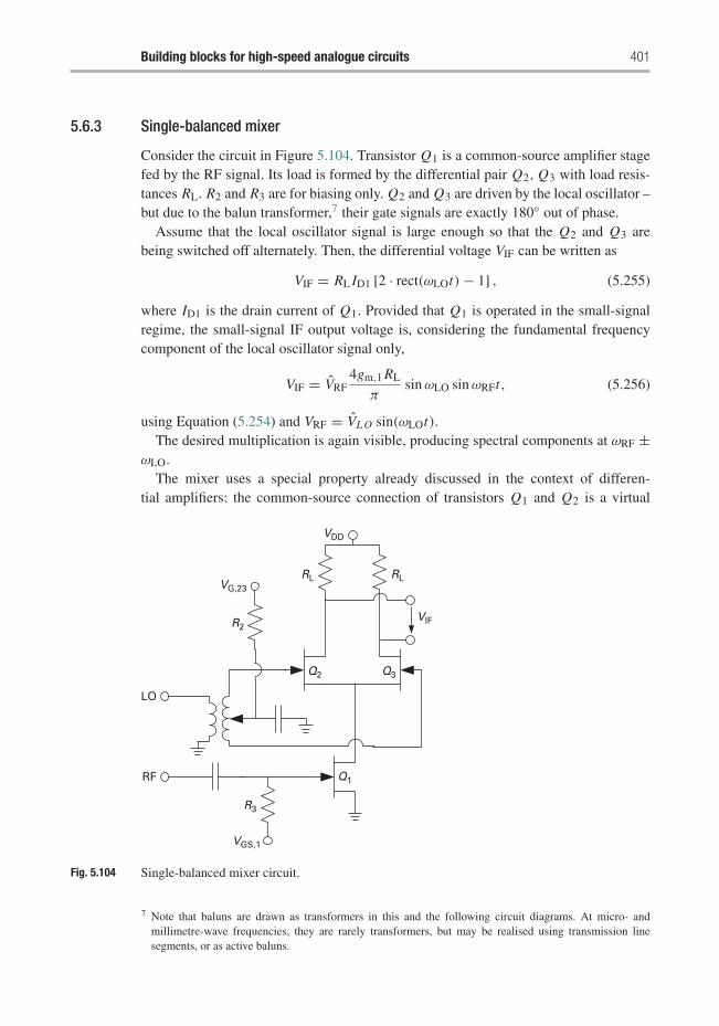
Building blocks for high-speed analogue circuits 401
5.6.3 Single-balanced mixer
Consider the circuit in Figure 5.104. Transistor Q1 is a common-source amplifier stagefed by the RF signal. Its load is formed by the differential pair Q2, Q3 with load resis-tances RL. R2 and R3 are for biasing only. Q2 and Q3 are driven by the local oscillator –but due to the balun transformer,7 their gate signals are exactly 180◦ out of phase.
Assume that the local oscillator signal is large enough so that the Q2 and Q3 arebeing switched off alternately. Then, the differential voltage VIF can be written as
VIF = RL ID1 [2 · rect(ωLOt) − 1] , (5.255)
where ID1 is the drain current of Q1. Provided that Q1 is operated in the small-signalregime, the small-signal IF output voltage is, considering the fundamental frequencycomponent of the local oscillator signal only,
VIF = VRF4gm,1 RL
πsinωLO sinωRFt, (5.256)
using Equation (5.254) and VRF = VL O sin(ωLOt).The desired multiplication is again visible, producing spectral components at ωRF ±
ωLO.The mixer uses a special property already discussed in the context of differen-
tial amplifiers: the common-source connection of transistors Q1 and Q2 is a virtual
RL RL
VIF
VDD
VG,23
R2
Q2
Q1
R3
VGS,1
LO
RF
Q3
Fig. 5.104 Single-balanced mixer circuit.
7 Note that baluns are drawn as transformers in this and the following circuit diagrams. At micro- andmillimetre-wave frequencies, they are rarely transformers, but may be realised using transmission linesegments, or as active baluns.
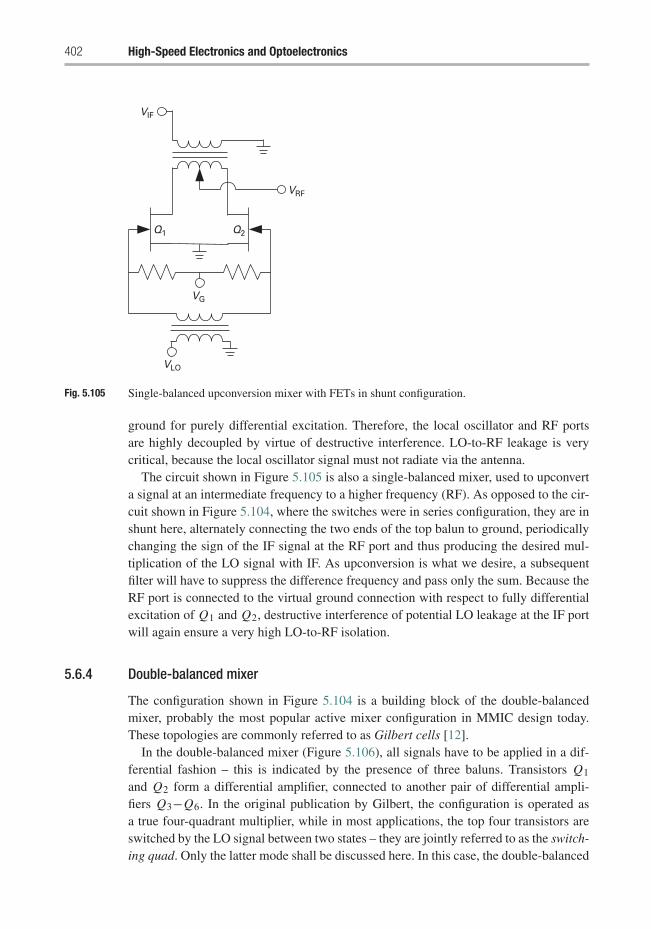
402 High-Speed Electronics and Optoelectronics
VIF
VRF
Q1 Q2
VG
VLO
Fig. 5.105 Single-balanced upconversion mixer with FETs in shunt configuration.
ground for purely differential excitation. Therefore, the local oscillator and RF portsare highly decoupled by virtue of destructive interference. LO-to-RF leakage is verycritical, because the local oscillator signal must not radiate via the antenna.
The circuit shown in Figure 5.105 is also a single-balanced mixer, used to upconverta signal at an intermediate frequency to a higher frequency (RF). As opposed to the cir-cuit shown in Figure 5.104, where the switches were in series configuration, they are inshunt here, alternately connecting the two ends of the top balun to ground, periodicallychanging the sign of the IF signal at the RF port and thus producing the desired mul-tiplication of the LO signal with IF. As upconversion is what we desire, a subsequentfilter will have to suppress the difference frequency and pass only the sum. Because theRF port is connected to the virtual ground connection with respect to fully differentialexcitation of Q1 and Q2, destructive interference of potential LO leakage at the IF portwill again ensure a very high LO-to-RF isolation.
5.6.4 Double-balanced mixer
The configuration shown in Figure 5.104 is a building block of the double-balancedmixer, probably the most popular active mixer configuration in MMIC design today.These topologies are commonly referred to as Gilbert cells [12].
In the double-balanced mixer (Figure 5.106), all signals have to be applied in a dif-ferential fashion – this is indicated by the presence of three baluns. Transistors Q1
and Q2 form a differential amplifier, connected to another pair of differential ampli-fiers Q3−Q6. In the original publication by Gilbert, the configuration is operated asa true four-quadrant multiplier, while in most applications, the top four transistors areswitched by the LO signal between two states – they are jointly referred to as the switch-ing quad. Only the latter mode shall be discussed here. In this case, the double-balanced
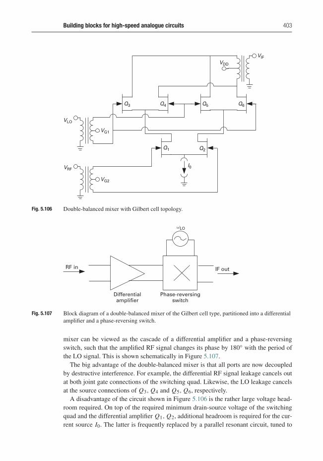
Building blocks for high-speed analogue circuits 403
Q3
VLO
VG1
VG2
Q1 Q2
I0VRF
Q4 Q5 Q6
VDD
VIF
Fig. 5.106 Double-balanced mixer with Gilbert cell topology.
Differentialamplifier
Phase-reversingswitch
IF out
ωLO
RF in
Fig. 5.107 Block diagram of a double-balanced mixer of the Gilbert cell type, partitioned into a differentialamplifier and a phase-reversing switch.
mixer can be viewed as the cascade of a differential amplifier and a phase-reversingswitch, such that the amplified RF signal changes its phase by 180◦ with the period ofthe LO signal. This is shown schematically in Figure 5.107.
The big advantage of the double-balanced mixer is that all ports are now decoupledby destructive interference. For example, the differential RF signal leakage cancels outat both joint gate connections of the switching quad. Likewise, the LO leakage cancelsat the source connections of Q3, Q4 and Q5, Q6, respectively.
A disadvantage of the circuit shown in Figure 5.106 is the rather large voltage head-room required. On top of the required minimum drain-source voltage of the switchingquad and the differential amplifier Q1, Q2, additional headroom is required for the cur-rent source I0. The latter is frequently replaced by a parallel resonant circuit, tuned to
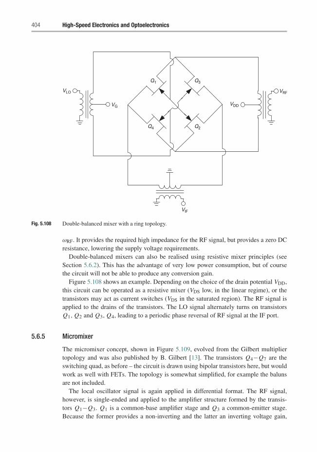
404 High-Speed Electronics and Optoelectronics
VRF
VDD
VIF
Q3Q1
Q2Q4
VG
VLO
Fig. 5.108 Double-balanced mixer with a ring topology.
ωRF. It provides the required high impedance for the RF signal, but provides a zero DCresistance, lowering the supply voltage requirements.
Double-balanced mixers can also be realised using resistive mixer principles (seeSection 5.6.2). This has the advantage of very low power consumption, but of coursethe circuit will not be able to produce any conversion gain.
Figure 5.108 shows an example. Depending on the choice of the drain potential VDD,this circuit can be operated as a resistive mixer (VDS low, in the linear regime), or thetransistors may act as current switches (VDS in the saturated region). The RF signal isapplied to the drains of the transistors. The LO signal alternately turns on transistorsQ1, Q2 and Q3, Q4, leading to a periodic phase reversal of RF signal at the IF port.
5.6.5 Micromixer
The micromixer concept, shown in Figure 5.109, evolved from the Gilbert multipliertopology and was also published by B. Gilbert [13]. The transistors Q4−Q7 are theswitching quad, as before – the circuit is drawn using bipolar transistors here, but wouldwork as well with FETs. The topology is somewhat simplified, for example the balunsare not included.
The local oscillator signal is again applied in differential format. The RF signal,however, is single-ended and applied to the amplifier structure formed by the transis-tors Q1−Q3. Q1 is a common-base amplifier stage and Q3 a common-emitter stage.Because the former provides a non-inverting and the latter an inverting voltage gain,
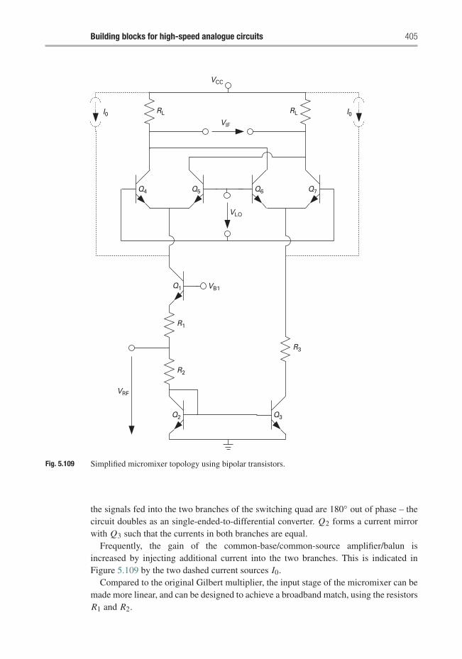
Building blocks for high-speed analogue circuits 405
VCC
RL RL I0I0
Q4 Q5 Q6 Q7
VLO
Q1 VB1
R1
R2
VRF
Q2 Q3
R3
VIF
Fig. 5.109 Simplified micromixer topology using bipolar transistors.
the signals fed into the two branches of the switching quad are 180◦ out of phase – thecircuit doubles as an single-ended-to-differential converter. Q2 forms a current mirrorwith Q3 such that the currents in both branches are equal.
Frequently, the gain of the common-base/common-source amplifier/balun isincreased by injecting additional current into the two branches. This is indicated inFigure 5.109 by the two dashed current sources I0.
Compared to the original Gilbert multiplier, the input stage of the micromixer can bemade more linear, and can be designed to achieve a broadband match, using the resistorsR1 and R2.
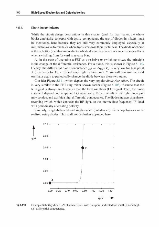
406 High-Speed Electronics and Optoelectronics
5.6.6 Diode-based mixers
While the circuit design descriptions in this chapter (and, for that matter, the wholebook) emphasise concepts with active components, the use of diodes in mixers mustbe mentioned here because they are still very commonly employed, especially atmillimetre-wave frequencies where transistors lose their usefulness. The diode of choiceis the Schottky (metal–semiconductor) diode due to the absence of carrier storage effectswhen switching from forward to reverse bias.
As in the case of operating a FET as a resistive or switching mixer, the principleis the change of the differential resistance. For a diode, this is shown in Figure 5.110.Clearly, the differential diode conductance gD = d ID/dVD is very low for bias pointA (or equally for VD < 0) and very high for bias point B. We will now use the localoscillator again to periodically change the diode between these two states.
Consider Figure 5.111, which depicts the very popular diode ring mixer. The circuitis very similar to the FET ring mixer shown earlier (Figure 5.108). Assume that theRF signal is always much smaller than the local oscillator (LO) signal. Then, the diodestate will depend on the applied LO signal only. Either the left or the right diode pairmay conduct and exhibit a high differential conductance. The diode ring acts as a phase-reversing switch, which connects the RF signal to the intermediate frequency (IF) loadwith periodically alternating polarity.
Similarly, single-balanced and single-ended (unbalanced) mixer topologies can berealised using diodes. This shall not be further expanded here.
ID/A
0.10
0.08
0.06
0.04
0.02
0.00
0.00 0.20
A
B
0.40 0.60 0.80 1.00 1.20 1.40
VD/V
Fig. 5.110 Example Schottky diode I–V characteristics, with bias point indicated for small (A) and high(B) differential conductance.
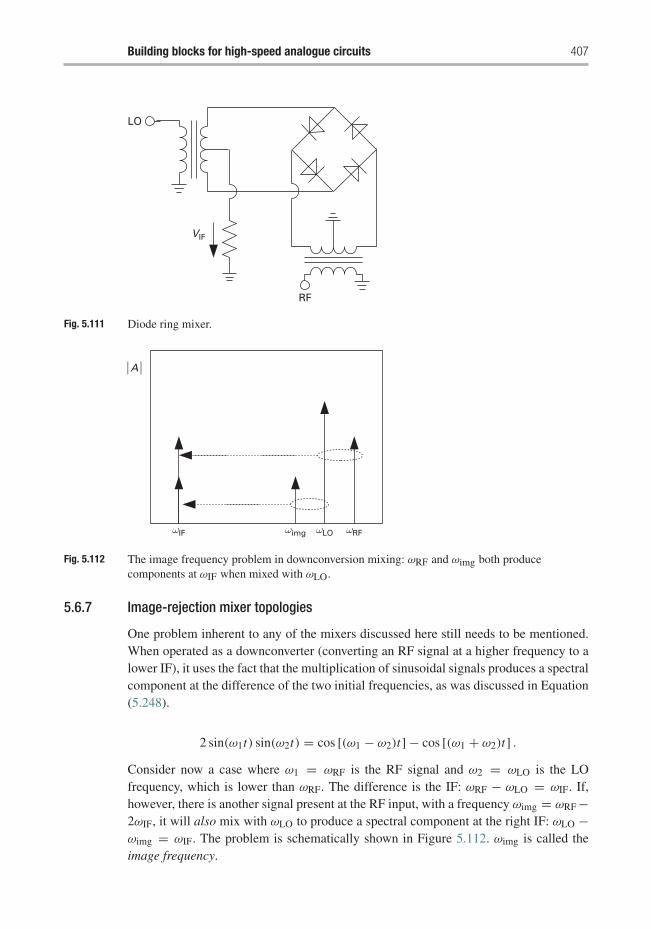
Building blocks for high-speed analogue circuits 407
LO
RF
VIF
Fig. 5.111 Diode ring mixer.
A
ωIF ωimg ωLO ωRF
Fig. 5.112 The image frequency problem in downconversion mixing: ωRF and ωimg both producecomponents at ωIF when mixed with ωLO.
5.6.7 Image-rejection mixer topologies
One problem inherent to any of the mixers discussed here still needs to be mentioned.When operated as a downconverter (converting an RF signal at a higher frequency to alower IF), it uses the fact that the multiplication of sinusoidal signals produces a spectralcomponent at the difference of the two initial frequencies, as was discussed in Equation(5.248).
2 sin(ω1t) sin(ω2t) = cos [(ω1 − ω2)t] − cos [(ω1 + ω2)t] .
Consider now a case where ω1 = ωRF is the RF signal and ω2 = ωLO is the LOfrequency, which is lower than ωRF. The difference is the IF: ωRF − ωLO = ωIF. If,however, there is another signal present at the RF input, with a frequency ωimg = ωRF −2ωIF, it will also mix with ωLO to produce a spectral component at the right IF: ωLO −ωimg = ωIF. The problem is schematically shown in Figure 5.112. ωimg is called theimage frequency.
408 High-Speed Electronics and Optoelectronics
The signal at the image frequency will now overlay the downconverted RF sig-nal and in most cases cause unacceptable interference. The most common way toavoid this is to make sure, by appropriate filtering, that no signal is in fact present atωimg.
In upconversion mixers, the image problem also applies. Upconverting a signal atωIF by means of an LO at a higher frequency ωRF results in two spectral components atωLO ± ωIF. Again, one of these components will have to be suppressed, classically byfiltering.
However, in modern receiver and transmitter concepts, there is a trend to lower IFswhere digital/analogue conversion can be achieved very inexpensively. Consequently,the frequency distance 2ωIF between the desired signal and the image is getting smaller,requiring very rigid filtering. The necessary filter qualities are rarely possible on chip,which is another significant drawback, as off-chip filters are costly in production andassembly.
A more convenient solution is the use of an image-rejection mixer. The image-rejection mixer topology can use any of the fundamental mixer circuits we discussed.
The block diagram shown in Figure 5.113 shows a possible implementation for adownconversion mixer. At the input, two signals shall be present, at the RF and imagefrequencies:
ωRF = ωLO + ωIF, ωimg = ωLO − ωIF
The signal is split into two signals with equal amplitude, but 90◦ phase shift (in quadra-ture). We assume that this can be done equally for the RF and the image signals – thisis a good assumption because the concept is especially important if RF and image sig-nals are located in close spectral proximity and cannot be separated easily by filtering.For simplicity, we assume also that both RF and image signals are sinusoidal with anamplitude of 1.
The oscillator signal, at ωLO, shall also have an amplitude of 1. It is split into twosignals with equal amplitude and phase.
B
A
g ′1(t)g1(t)
g2(t)
ωLOωRF, ωimg
g ′2(t)
0°/–90°0°
–90°
Fig. 5.113 Block diagram of an image reject mixer.
Building blocks for high-speed analogue circuits 409
Let us first consider the RF signal only (the image signal is turned off). The signal atthe output of the top mixer is
g1(t) = 1
4sin(ωRFt) sin(ωLOt)
= 1
8{cos[(ωRF − ωLO)t] − cos[(ωRF + ωLO)t]} .
The high frequency component at ωRF + ωLO is easily suppressed in the low-pass filter(LP). After the low-pass filter in the upper branch,
g′1(t) = 1
8cos[(ωRF − ωLO)t] = 1
8cos(ωIFt) = 1
8sin
(ωIFt + π
2
). (5.257)
In the lower branch, the RF signal is delayed by −π/2.Using sin(ωRF − π/2) = − cos(ωRFt), we obtain at the output of the bottom
mixer:
g2(t) = −1
4cos(ωRFt) sin(ωLOt)
= −1
8[sin(ωRF + ωLO)t − sin(ωRF − ωLO)t] .
The high frequency component is removed in the low-pass filter:
g′2(t) = 1
8sin(ωIFt). (5.258)
The four-port at the right of the block diagram in Figure 5.113 is a 90◦ hybrid cou-pler. Signals fed into the inputs emerge at outputs A and B with equal amplitude, butthe signal entering at the top experiences an additional −π/2 phase shift at output B,while the signal entering at the bottom experiences an additional phase shift of −π/2 atoutput B.
Using Equations (5.257) and (5.258), we then find at A:
1
8
[sin
(ωIFt + π
2
)+ sin
(ωIFt − π
2
)]= 0.
At B:
1
8[sin(ωIFt) + sin(ωIFt)] = 1
4sin(ωIFt).
The IF signal due to the wanted (RF) signal hence only appears at output B.Let us consider the image frequency, which is below ωLO such that ωIF = ωLO−ωimg.
Using sin(−α) = − sinα and cos(−α) = cosα, we find at the output of the upperlow-pass filter:
g′1(t) = −1
8sin
(ωIFt − π
2
), (5.259)
while at the output of the lower low-pass filter:
g′2(t) = −1
8sin(ωIFt). (5.260)
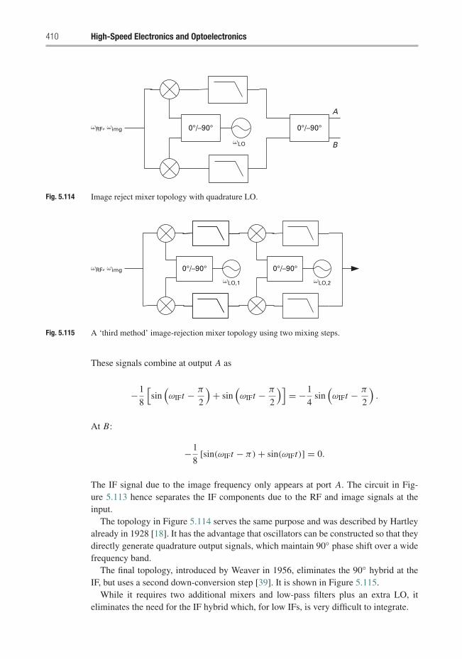
410 High-Speed Electronics and Optoelectronics
B
A
ωLO
ωRF, ωimg 0°/–90°0°/–90°
Fig. 5.114 Image reject mixer topology with quadrature LO.
ωLO,1 ωLO,2
ωRF, ωimg 0°/–90°0°/–90°
Fig. 5.115 A ‘third method’ image-rejection mixer topology using two mixing steps.
These signals combine at output A as
−1
8
[sin
(ωIFt − π
2
)+ sin
(ωIFt − π
2
)]= −1
4sin
(ωIFt − π
2
).
At B:
−1
8[sin(ωIFt − π) + sin(ωIFt)] = 0.
The IF signal due to the image frequency only appears at port A. The circuit in Fig-ure 5.113 hence separates the IF components due to the RF and image signals at theinput.
The topology in Figure 5.114 serves the same purpose and was described by Hartleyalready in 1928 [18]. It has the advantage that oscillators can be constructed so that theydirectly generate quadrature output signals, which maintain 90◦ phase shift over a widefrequency band.
The final topology, introduced by Weaver in 1956, eliminates the 90◦ hybrid at theIF, but uses a second down-conversion step [39]. It is shown in Figure 5.115.
While it requires two additional mixers and low-pass filters plus an extra LO, iteliminates the need for the IF hybrid which, for low IFs, is very difficult to integrate.
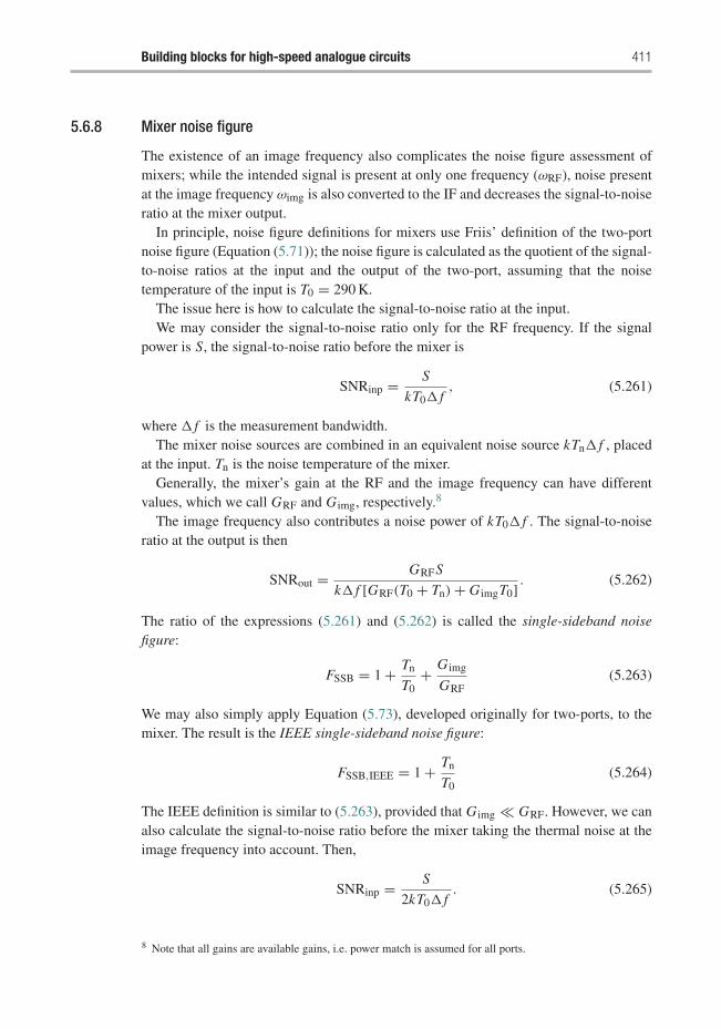
Building blocks for high-speed analogue circuits 411
5.6.8 Mixer noise figure
The existence of an image frequency also complicates the noise figure assessment ofmixers; while the intended signal is present at only one frequency (ωRF), noise presentat the image frequency ωimg is also converted to the IF and decreases the signal-to-noiseratio at the mixer output.
In principle, noise figure definitions for mixers use Friis’ definition of the two-portnoise figure (Equation (5.71)); the noise figure is calculated as the quotient of the signal-to-noise ratios at the input and the output of the two-port, assuming that the noisetemperature of the input is T0 = 290 K.
The issue here is how to calculate the signal-to-noise ratio at the input.We may consider the signal-to-noise ratio only for the RF frequency. If the signal
power is S, the signal-to-noise ratio before the mixer is
SNRinp = S
kT0� f, (5.261)
where � f is the measurement bandwidth.The mixer noise sources are combined in an equivalent noise source kTn� f , placed
at the input. Tn is the noise temperature of the mixer.Generally, the mixer’s gain at the RF and the image frequency can have different
values, which we call GRF and G img, respectively.8
The image frequency also contributes a noise power of kT0� f . The signal-to-noiseratio at the output is then
SNRout = GRFS
k� f [GRF(T0 + Tn) + G imgT0] . (5.262)
The ratio of the expressions (5.261) and (5.262) is called the single-sideband noisefigure:
FSSB = 1 + Tn
T0+ G img
GRF(5.263)
We may also simply apply Equation (5.73), developed originally for two-ports, to themixer. The result is the IEEE single-sideband noise figure:
FSSB,IEEE = 1 + Tn
T0(5.264)
The IEEE definition is similar to (5.263), provided that G img � GRF. However, we canalso calculate the signal-to-noise ratio before the mixer taking the thermal noise at theimage frequency into account. Then,
SNRinp = S
2kT0� f. (5.265)
8 Note that all gains are available gains, i.e. power match is assumed for all ports.
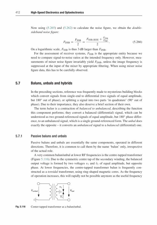
412 High-Speed Electronics and Optoelectronics
Now using (5.265) and (5.262) to calculate the noise figure, we obtain the double-sideband noise figure:
FDSB = FSSB
2= FSSB,IEEE + Gimg
GRF
2. (5.266)
On a logarithmic scale, FSSB is thus 3 dB larger than FDSB.For the assessment of receiver systems, FSSB is the appropriate entity because we
need to compare signal-to-noise ratios at the intended frequency only. However, mea-surements of mixer noise figure invariably yield FDSB, unless the image frequency issuppressed at the input of the mixer by appropriate filtering. When using mixer noisefigure data, this has to be carefully observed.
5.7 Baluns, unbals and hybrids
In the preceding sections, reference was frequently made to mysterious building blockswhich convert signals from single-end to differential (two signals of equal amplitude,but 180◦ out of phase), or splitting a signal into two parts ‘in quadrature’ (90◦ out ofphase). Due to their importance, they also deserve a brief section of their own.
The term balun is a contraction of balanced to unbalanced, describing the functionthis component performs; they convert a balanced (differential) signal, which can beunderstood as two ground-referenced signals of equal amplitude, but 180◦ phase differ-ence, to an unbalanced signal, which is a single ground-referenced form. The unbal doesexactly the opposite – it converts an unbalanced signal to a balanced (differential) one.
5.7.1 Passive baluns and unbals
Passive baluns and unbals are essentially the same components, operated in differentdirections. Therefore, it is common to call them by the name ‘balun’ only, irrespectiveof the actual role.
A very common balun/unbal at lower RF frequencies is the centre-tapped transformer(Figure 5.116). Due to the symmetric centre tap of the secondary winding, the balancedoutput voltage is formed by two voltages v1 and v1 of equal amplitude, but oppositephase. At lower frequencies, the centre-tapped transformer balun is frequently con-structed as a toroidal transformer, using ring-shaped magnetic cores. As the frequencyof operation increases, this will rapidly not be possible anymore as the useful frequency
Vunbal Vbal
v1
v1
Fig. 5.116 Center-tapped transformer as a balun/unbal.
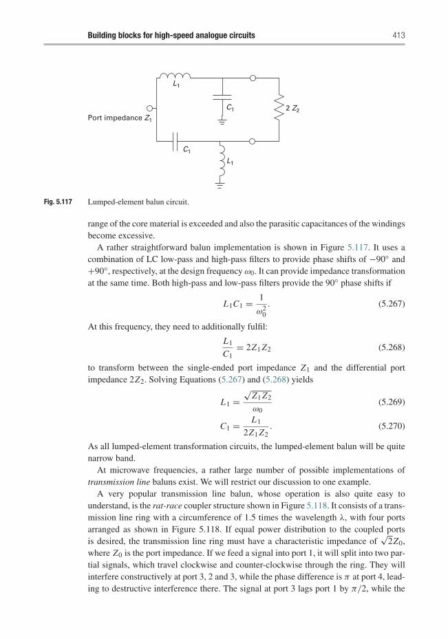
Building blocks for high-speed analogue circuits 413
Port impedance Z1
2 Z2
L1
L1
C1
C1
Fig. 5.117 Lumped-element balun circuit.
range of the core material is exceeded and also the parasitic capacitances of the windingsbecome excessive.
A rather straightforward balun implementation is shown in Figure 5.117. It uses acombination of LC low-pass and high-pass filters to provide phase shifts of −90◦ and+90◦, respectively, at the design frequency ω0. It can provide impedance transformationat the same time. Both high-pass and low-pass filters provide the 90◦ phase shifts if
L1C1 = 1
ω20
. (5.267)
At this frequency, they need to additionally fulfil:
L1
C1= 2Z1 Z2 (5.268)
to transform between the single-ended port impedance Z1 and the differential portimpedance 2Z2. Solving Equations (5.267) and (5.268) yields
L1 =√
Z1 Z2
ω0(5.269)
C1 = L1
2Z1 Z2. (5.270)
As all lumped-element transformation circuits, the lumped-element balun will be quitenarrow band.
At microwave frequencies, a rather large number of possible implementations oftransmission line baluns exist. We will restrict our discussion to one example.
A very popular transmission line balun, whose operation is also quite easy tounderstand, is the rat-race coupler structure shown in Figure 5.118. It consists of a trans-mission line ring with a circumference of 1.5 times the wavelength λ, with four portsarranged as shown in Figure 5.118. If equal power distribution to the coupled portsis desired, the transmission line ring must have a characteristic impedance of
√2Z0,
where Z0 is the port impedance. If we feed a signal into port 1, it will split into two par-tial signals, which travel clockwise and counter-clockwise through the ring. They willinterfere constructively at port 3, 2 and 3, while the phase difference is π at port 4, lead-ing to destructive interference there. The signal at port 3 lags port 1 by π/2, while the
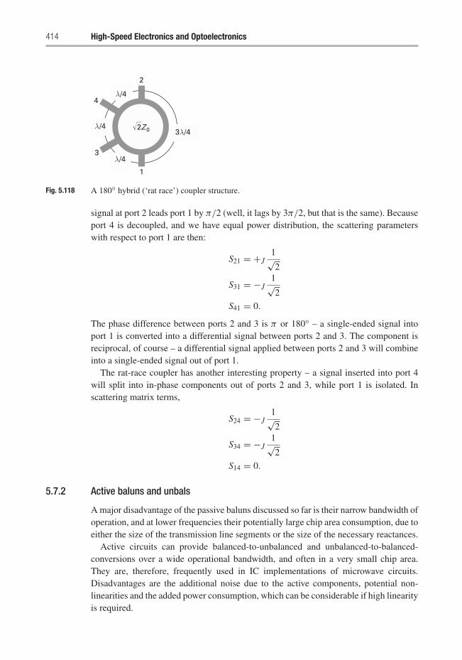
414 High-Speed Electronics and Optoelectronics
2
1
λ /4
λ /4
λ /4
3λ /42Z0
4
3
Fig. 5.118 A 180◦ hybrid (‘rat race’) coupler structure.
signal at port 2 leads port 1 by π/2 (well, it lags by 3π/2, but that is the same). Becauseport 4 is decoupled, and we have equal power distribution, the scattering parameterswith respect to port 1 are then:
S21 = +j1√2
S31 = −j1√2
S41 = 0.
The phase difference between ports 2 and 3 is π or 180◦ – a single-ended signal intoport 1 is converted into a differential signal between ports 2 and 3. The component isreciprocal, of course – a differential signal applied between ports 2 and 3 will combineinto a single-ended signal out of port 1.
The rat-race coupler has another interesting property – a signal inserted into port 4will split into in-phase components out of ports 2 and 3, while port 1 is isolated. Inscattering matrix terms,
S24 = −j1√2
S34 = −j1√2
S14 = 0.
5.7.2 Active baluns and unbals
A major disadvantage of the passive baluns discussed so far is their narrow bandwidth ofoperation, and at lower frequencies their potentially large chip area consumption, due toeither the size of the transmission line segments or the size of the necessary reactances.
Active circuits can provide balanced-to-unbalanced and unbalanced-to-balanced-conversions over a wide operational bandwidth, and often in a very small chip area.They are, therefore, frequently used in IC implementations of microwave circuits.Disadvantages are the additional noise due to the active components, potential non-linearities and the added power consumption, which can be considerable if high linearityis required.
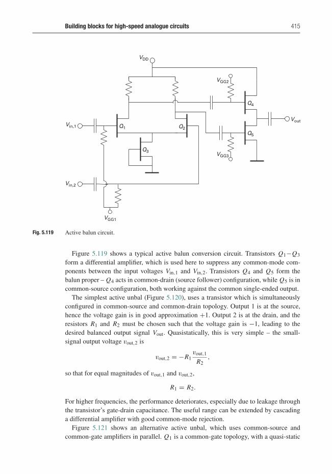
Building blocks for high-speed analogue circuits 415
VDD
Q1Vin,1
Vin,2
VGG1
VGG3
VGG2
Vout
Q3
Q2
Q4
Q5
Fig. 5.119 Active balun circuit.
Figure 5.119 shows a typical active balun conversion circuit. Transistors Q1−Q3
form a differential amplifier, which is used here to suppress any common-mode com-ponents between the input voltages Vin,1 and Vin,2. Transistors Q4 and Q5 form thebalun proper – Q4 acts in common-drain (source follower) configuration, while Q5 is incommon-source configuration, both working against the common single-ended output.
The simplest active unbal (Figure 5.120), uses a transistor which is simultaneouslyconfigured in common-source and common-drain topology. Output 1 is at the source,hence the voltage gain is in good approximation +1. Output 2 is at the drain, and theresistors R1 and R2 must be chosen such that the voltage gain is −1, leading to thedesired balanced output signal Vout. Quasistatically, this is very simple – the small-signal output voltage vout,2 is
vout,2 = −R1vout,1
R2,
so that for equal magnitudes of vout,1 and vout,2,
R1 = R2.
For higher frequencies, the performance deteriorates, especially due to leakage throughthe transistor’s gate-drain capacitance. The useful range can be extended by cascadinga differential amplifier with good common-mode rejection.
Figure 5.121 shows an alternative active unbal, which uses common-source andcommon-gate amplifiers in parallel. Q1 is a common-gate topology, with a quasi-static
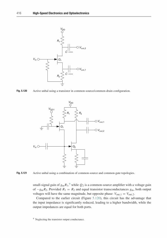
416 High-Speed Electronics and Optoelectronics
VDD
Vin
R1
Q1
R2
Vout,2
Vout,1
C ∞
C ∞
Fig. 5.120 Active unbal using a transistor in common-source/common-drain configuration.
VDD
VGG1
Q1
Q2
R1 R2
Vout,1
Vout,2
Vin
Fig. 5.121 Active unbal using a combination of common-source and common-gate topologies.
small-signal gain of gm R1,9 while Q2 is a common-source amplifier with a voltage gainof −gm R2. Provided R1 = R2 and equal transistor transconductances gm, both outputvoltages will have the same magnitude, but opposite phase: Vout,1 = Vout,2.
Compared to the earlier circuit (Figure 5.120), this circuit has the advantage thatthe input impedance is significantly reduced, leading to a higher bandwidth, while theoutput impedances are equal for both ports.
9 Neglecting the transistor output conductance.
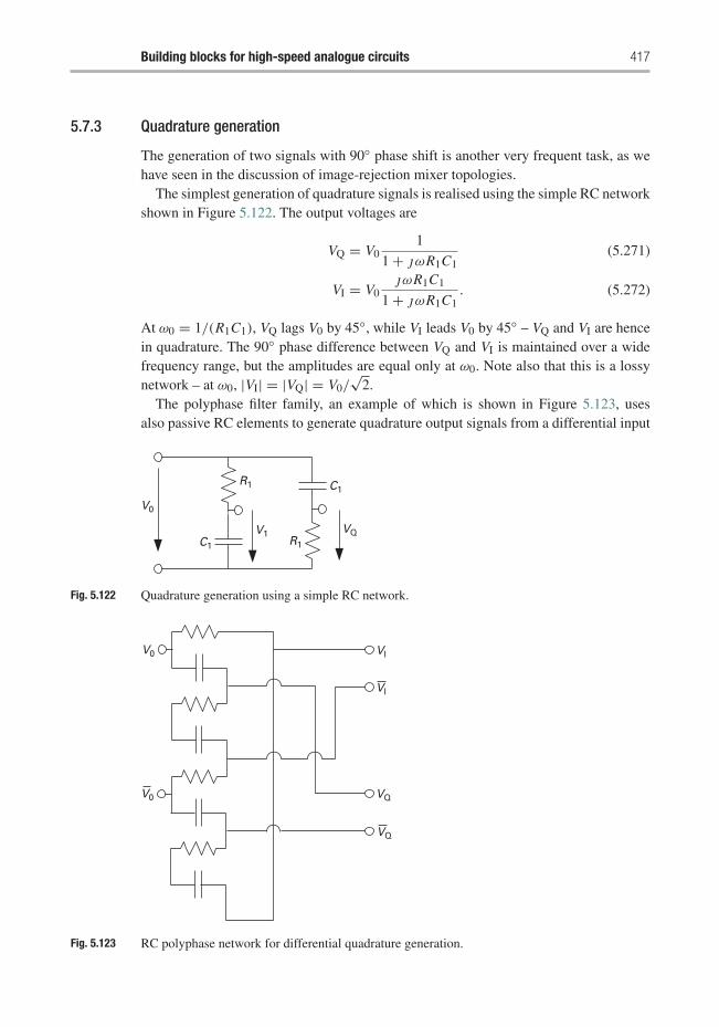
Building blocks for high-speed analogue circuits 417
5.7.3 Quadrature generation
The generation of two signals with 90◦ phase shift is another very frequent task, as wehave seen in the discussion of image-rejection mixer topologies.
The simplest generation of quadrature signals is realised using the simple RC networkshown in Figure 5.122. The output voltages are
VQ = V01
1 + jωR1C1(5.271)
VI = V0jωR1C1
1 + jωR1C1. (5.272)
At ω0 = 1/(R1C1), VQ lags V0 by 45◦, while VI leads V0 by 45◦ – VQ and VI are hencein quadrature. The 90◦ phase difference between VQ and VI is maintained over a widefrequency range, but the amplitudes are equal only at ω0. Note also that this is a lossynetwork – at ω0, |VI| = |VQ| = V0/
√2.
The polyphase filter family, an example of which is shown in Figure 5.123, usesalso passive RC elements to generate quadrature output signals from a differential input
V0
C1
R1
R1
V1
C1
VQ
Fig. 5.122 Quadrature generation using a simple RC network.
V0 VI
VQ
VI
VQ
V0
Fig. 5.123 RC polyphase network for differential quadrature generation.
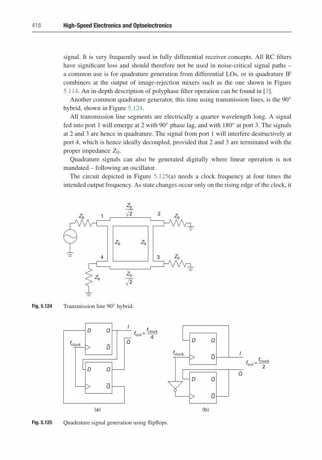
418 High-Speed Electronics and Optoelectronics
signal. It is very frequently used in fully differential receiver concepts. All RC filtershave significant loss and should therefore not be used in noise-critical signal paths –a common use is for quadrature generation from differential LOs, or in quadrature IFcombiners at the output of image-rejection mixers such as the one shown in Figure5.114. An in-depth description of polyphase filter operation can be found in [3].
Another common quadrature generator, this time using transmission lines, is the 90◦hybrid, shown in Figure 5.124.
All transmission line segments are electrically a quarter wavelength long. A signalfed into port 1 will emerge at 2 with 90◦ phase lag, and with 180◦ at port 3. The signalsat 2 and 3 are hence in quadrature. The signal from port 1 will interfere destructively atport 4, which is hence ideally decoupled, provided that 2 and 3 are terminated with theproper impedance Z0.
Quadrature signals can also be generated digitally where linear operation is notmandated – following an oscillator.
The circuit depicted in Figure 5.125(a) needs a clock frequency at four times theintended output frequency. As state changes occur only on the rising edge of the clock, it
Z0
Z0
Z0
Z0
Z0
Z0 Z0
2
Z0
2
21
4 3
Fig. 5.124 Transmission line 90◦ hybrid.
Q
(a) (b)
Q
Q
IQ
Q
QD
D
Q
Q
Q
D
D
fclock
fclock
fout =fclock
4
I
Q
fout =fclock
2
Fig. 5.125 Quadrature signal generation using flipflops.
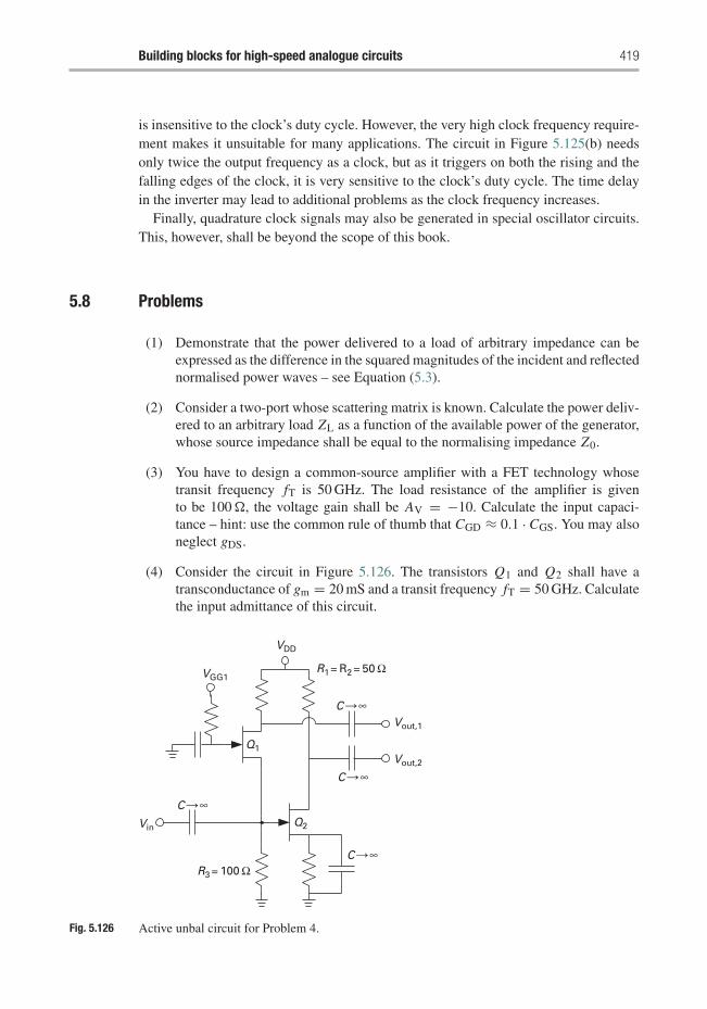
Building blocks for high-speed analogue circuits 419
is insensitive to the clock’s duty cycle. However, the very high clock frequency require-ment makes it unsuitable for many applications. The circuit in Figure 5.125(b) needsonly twice the output frequency as a clock, but as it triggers on both the rising and thefalling edges of the clock, it is very sensitive to the clock’s duty cycle. The time delayin the inverter may lead to additional problems as the clock frequency increases.
Finally, quadrature clock signals may also be generated in special oscillator circuits.This, however, shall be beyond the scope of this book.
5.8 Problems
(1) Demonstrate that the power delivered to a load of arbitrary impedance can beexpressed as the difference in the squared magnitudes of the incident and reflectednormalised power waves – see Equation (5.3).
(2) Consider a two-port whose scattering matrix is known. Calculate the power deliv-ered to an arbitrary load ZL as a function of the available power of the generator,whose source impedance shall be equal to the normalising impedance Z0.
(3) You have to design a common-source amplifier with a FET technology whosetransit frequency fT is 50 GHz. The load resistance of the amplifier is givento be 100�, the voltage gain shall be AV = −10. Calculate the input capaci-tance – hint: use the common rule of thumb that CGD ≈ 0.1 · CGS. You may alsoneglect gDS.
(4) Consider the circuit in Figure 5.126. The transistors Q1 and Q2 shall have atransconductance of gm = 20 mS and a transit frequency fT = 50 GHz. Calculatethe input admittance of this circuit.
VDD
R1 = R2 = 50 Ω
R3 = 100 Ω
Vout,1
Vout,2
VGG1
Vin
C
Q1
Q2
∞
C ∞
C ∞
C ∞
Fig. 5.126 Active unbal circuit for Problem 4.
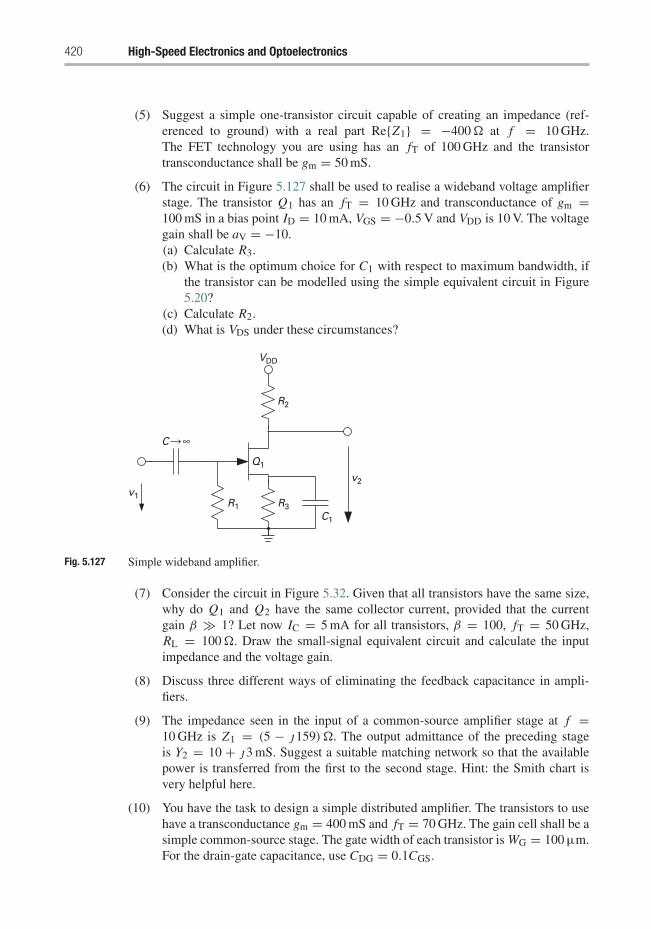
420 High-Speed Electronics and Optoelectronics
(5) Suggest a simple one-transistor circuit capable of creating an impedance (ref-erenced to ground) with a real part Re{Z1} = −400� at f = 10 GHz.The FET technology you are using has an fT of 100 GHz and the transistortransconductance shall be gm = 50 mS.
(6) The circuit in Figure 5.127 shall be used to realise a wideband voltage amplifierstage. The transistor Q1 has an fT = 10 GHz and transconductance of gm =100 mS in a bias point ID = 10 mA, VGS = −0.5 V and VDD is 10 V. The voltagegain shall be aV = −10.(a) Calculate R3.(b) What is the optimum choice for C1 with respect to maximum bandwidth, if
the transistor can be modelled using the simple equivalent circuit in Figure5.20?
(c) Calculate R2.(d) What is VDS under these circumstances?
VDD
R2
v2v1
C1
Q1
R3R1
C ∞
Fig. 5.127 Simple wideband amplifier.
(7) Consider the circuit in Figure 5.32. Given that all transistors have the same size,why do Q1 and Q2 have the same collector current, provided that the currentgain β � 1? Let now IC = 5 mA for all transistors, β = 100, fT = 50 GHz,RL = 100�. Draw the small-signal equivalent circuit and calculate the inputimpedance and the voltage gain.
(8) Discuss three different ways of eliminating the feedback capacitance in ampli-fiers.
(9) The impedance seen in the input of a common-source amplifier stage at f =10 GHz is Z1 = (5 − j159)�. The output admittance of the preceding stageis Y2 = 10 + j3 mS. Suggest a suitable matching network so that the availablepower is transferred from the first to the second stage. Hint: the Smith chart isvery helpful here.
(10) You have the task to design a simple distributed amplifier. The transistors to usehave a transconductance gm = 400 mS and fT = 70 GHz. The gain cell shall be asimple common-source stage. The gate width of each transistor is WG = 100 μm.For the drain-gate capacitance, use CDG = 0.1CGS.
Building blocks for high-speed analogue circuits 421
The unloaded gate line has a characteristic impedance Zu = 80� and aninductance per unit length of L ′ = 0.8 nH mm−1.
Calculate the necessary length of the gate line segments so that the character-istic impedance of the loaded gate line is 50�. The drain line shall equally havethis impedance.
(11) In the schematic in Figure 5.63, identify the function of each of the transistorsshown. What is the purpose of the RC combination attached to the emitters oftwo of the transistors?
(12) A communications system can tolerate a minimum third-order intermodulationdistance of 60 dB; the maximum input power is −20 dBm. What is the necessaryinput-referred third-order intercept point?
(13) Explain why a high resonator quality factor is especially important in oscillatorusing active devices with little low-frequency noise, such as Si/SiGe HBTs.
(14) Show how the Hartley image reject topology (Figure 5.114) achieves separationof the signal and image frequencies to output A and B.
References
[1] Abele P., Kallfass I., Zeuner M. et al. (2003). 32 GHz MMIC distributed amplifier based onn-channel SiGe MODFETs. Electron. Lett. 39, 1448–1449.
[2] Battjes C. R. (1980). Monolithic wideband amplifier. USA Patent 4, 236, 119.[3] Behbahani F., Kishigami Y., Leete J., Abidi A. (2001). CMOS mixers and polyphase filters
for large image rejection. IEEE J. Solid-State Circ. 36, 873–887.[4] Beyer J., Prasad S. N., Becker R., Nordman J., Hohenwarter G. (1984). MESFET distributed
amplifier design guidelines. IEEE Trans. Microw. Theory Tech. MTT-32, 268–275.[5] Chartier S., Schleicher B., Korndorfer F., Glisic S., Fischer G., Schumacher H. (2007). A
fully integrated fully differential low-noise amplifier for short range automotive radar usinga SiGe:C BiCMOS technology. In Proc. 2nd European Microwave IC Conference (EuMIC),Munich, Germany, 8–10 October, 2007.
[6] Chartier S., Sonmez E., Schumacher H. (2006). Millimeter-wave amplifiers using a 0.8 μmSi/SiGe HBT technology. In Proc. Silicon Monolithic Integrated Circuits in RF Systems,San Diego, CA, 18–20 January 2006. IEEE.
[7] Darlington S. (1953). Semiconductor translating device. USA Patent 2, 663, 806.[8] Ellinger F. (2007). Radio Frequency Integrated Circuits and Technologies, 1st edn. Springer.[9] Fleming J. A. (1905). Instrument for converting alternating electric currents into continuous
currents. USA Patent 803, 684.[10] Forest L. D. (1908). Space telegraphy. USA Patent 879, 532.[11] Friis H. T. (1944). Noise figure of radio receivers. Proc. IRE 32, 7, 419–422.[12] Gilbert B. (1968). A precise four-quadrant multiplier with subnanosecond response. IEEE
J. Solid-State Circ. 3, 365–373.[13] Gilbert B. (1997). The Micromixer: a highly linear variant of the Gilbert mixer using a
bisymmetric class-AB input stage. IEEE J. Solid-State Circ. 32, 1412–1423.[14] Gonzalez G. (1997). Microwave Transistor Amplifiers, Analysis and Design. Prentice Hall.
422 High-Speed Electronics and Optoelectronics
[15] Gupta M. S. (1992). Power gain in feedback amplifiers, a classic revisited. IEEE Trans.Microw. Theory Tech. MTT-40, 5 (May), 864–879.
[16] Hafele M., Trasser A., Beilenhoff K., Schumacher H. (2005). A GaAs distributed amplifierwith an output voltage of 8.5 Vpp for 40 Gb/s modulators. Proc. 13th GAAS Symposium,Paris, France, 3–4 October 2005, 345–348.
[17] Hagen J. B. (1996). Radio-Frequency Electronics, 1st edn. Cambridge University Press.[18] Hartley R. V. L. (1928). Modulation system. USA Patent 1, 666, 206.[19] Haus H., Adler R. (1958). Optimum noise performance of linear amplifiers. Proc. IRE 46,
1519–1533.[20] Hoffmann M. (1997). Hochfrequenztechnik, 1st edn. Springer Berlin Heidelberg.[21] Hunt F., Hickman R. (1939). On electronic voltage stabilizers. Rev. Sci. Instrum. 10, 1
(January), 6–21.[22] Kline R. (1993). Harold Black and the negative-feedback amplifier. IEEE Contr. Syst.
Mag. 13, 4, 82–85.[23] Ku W. H. (1966). Unilateral gain and stability criteria of active two ports in terms of
scattering parameters. Proc. IEEE 54, 11 (November), 1617–1618.[24] Kurokawa K. (1965). Power waves and the scattering matrix. IEEE Trans. Microw. Theory
Tech. MTT-13, 3 (March), 194–202.[25] Lee T. H. (1997). The Design of CMOS Radio-Frequency Integrated Circuits, 1st edn.
Cambridge University Press, 181.[26] Leeson D. (1966). A simple model for feedback oscillator noise spectrum. Proc. IEEE 54,
329–330.[27] Maas S. A. (1987). A GaAs MESFET mixer with very low intermodulation. IEEE Trans.
Microw. Theory Tech. MTT-35, 425–429.[28] Mason S. J. (1954). Power gain in feedback amplifiers. Trans. IRE, Prof. Group on Circ.
Theory CT-1, 2 (June), 20–25.[29] Miller J. (1920). Dependence of the input impedance of a three-electrode vacuum tube upon
the load in the plate circuit. Scientific Papers of the Bureau of Standards 15 (351), 367–385.[30] Percival W. S. (1937). Thermionic valve circuits. Britain Patent 460, 562.[31] Rothe H., Dahlke W. (1955). Theorie rauschender Vierpole. AEU 9, 117–121.[32] Rothe H., Dahlke W. (1956). Theory of noisy fourpoles. Proc. IRE 44, 811–815.[33] Schick C., Feger T., Sonmez E., Schad K., Trasser A., Schumacher H. (2005). Broadband
Si/SiGe HBT amplifier concepts for 40 GBit/s fibreoptic communication systems. In Proc.35th European Microwave Conf., Paris, France, October 2005.
[34] Schmitt O. (1937). A simple differential amplifier. Rev. Sci. Inst. 8, 4 (April), 126–127.[35] Schumacher H., Abele P., Sonmez E., Schad K., Trasser A. (2003). Low-cost circuit
solutions for micro- and millimeter-wave systems using commercially available SiGe tech-nologies. In Proc. 1st International SiGe Technology and Device Meeting, Nagoya, Japan,14–17 January 2003.
[36] Smith P. H. (1931). Transmission line calculator. Electronics 12, 1 (January), 29–31.[37] Smith P. H. (1944). An improved transmission line calculator. Electronics 17, 1 (January),
130.[38] Sokal N., Sokal A. (1975). Class E – a new class of high-efficiency tuned single-ended
switching power amplifiers. IEEE J. Solid-State Circ. 10, 3 (June), 168–176.[39] Weaver D. (1956). A third method of generation and detection of single-sideband signals.
Proc. IRE 44, 1703–1705.

Index
absorption/gain spectra, 245absorption processes, 21–24acceptor, 19ACPR, see adjacent channel power ratio (ACPR)active baluns and unbals, 414–416active forward operation, 116adjacent channel power ratio (ACPR), 375–376amplifier configurations
common drain/common collector, 321–323common gate/common base, 319–321common source/common emitter, 316–318Miller effect, 318with two transistors, 329–336
Battjes fT doubler, 333cascode amplifier, 333–336common-drain/common-source, 329–332Darlington amplifier, 332–333
y matrix representation, 315–318amplifier linearity, 370–376
adjacent channel power ratio, 375–376single-tone excitation, 370–372two-tone excitation, 372–375
ANN, see artificial neural networks (ANN)anti-guiding parameter, 244APD, see avalanche photodiodes (APDs)arbitrary terminations, 299–300Armstrong oscillator, 388artificial neural networks (ANN), 168–169associated gain, 312atomic bonding, 8
covalent bonding, 8–9atomic physics, 9
Bohr model, 10–11photoelectric effects, 9–10
avalanche photodiodes (APDs), 275, 276input signal photocurrent for, 276ionisation coefficient, 272–273multiplication factors, 273–274optical generation rate, 273(SAM) separate absorption and multiplication,
275avalanching, 120
bandgap energy, 222, 262band line-up, 38–39bandwidth
enhancement, 328improvement, 326–329
base design dilemma, 136–137base push out, 125base resistance, 128base transit time, 126base transport factor, 121Battjes fT doubler, 333bipolar and hetero-bipolar transistors, 115
heterojunctionbase design dilemma, 136–137drift base, 139–140HBT implementations, 140–143III–V versus Si/SiGe HBTs, 146–147Si/SiGe HBTs, 143–146wide-gap emitter, 137–139
homojunction, 115–116collector current equation, 117–118diffusion triangle, 116–117Early effect, 122–124ideal base current, 118–119ideal current gain, 119Kirk effect, 124–125non-ideal current contributions, 119–120non-ideal current gain, 120–121saturation, 121–122
large-signal modelling, 147BJTs and HBTs, 155–156Ebers–Moll model, 147Gummel–Poon model, 147–150MEXTRAM model, 152–153VBIC95 model, 150
microwave noise performance of bipolartransistors, 131–134
small-signal dynamic behaviour, 125–129maximum frequency of oscillation, 130–131transit frequency, 129–130
transit time optimisationcollector transit time optimisation, 135–136drift field in base, 134–135
bipolar junction transistors (BJT), 46BJT, see bipolar junction transistors (BJT)BJTs and HBTs, 155–156Bloch theorem, 16body-centred cubic lattice (BCC), 6Bohr formulation, 11Bohr model, 10–11Boltzmann’s constant, 222Bragg frequency, 356

424 Index
broadband amplifier techniques, 350–354feedback techniques, 353–354shunt peaking, 351–353
building blocks for high-speed analogue circuits,291
baluns, unbals and hybridsactive baluns and unbals, 414–416passive baluns and unbals, 412–414quadrature generation, 417–419
mixers, 396diode-based, 406–407double-balanced, 402–404image-rejection mixer topologies, 407–410micromixer, 404–405noise figure, 411–412resistive, 398–400single-balanced, 401–402transconductance multiplier, 397
oscillators, 383noise, 393–396non-linearity in oscillators, 387–388oscillator topologies, 388–392resonators, 383–385self-excitation criteria, 385–387
transistor amplifiers, 313–314broadband amplifier techniques, 350–354configurations, 314–323configurations with two transistors, 329–336differential, 336–341distributed amplification, 354–365feedback, 323–329linearity, 370–376low-noise, 365–370power, 376–383source-coupled, 341–342tuned, 342–350
two-port networks, basic relations forimpedance matching, 297–298Mason’s unilateral gain, 305–306maximum available gain and maximum stable
gain, 305maximum frequency of oscillation, 306power gains for amplifier design, 298–302scattering parameter theory, 291–295Smith chart, 295–297stability, 302–305
built-in potential, 32bulk semiconductor, 257Burrus diode, 229
CAD modelling of HEMTs, 88MESFET versus HEMT, 91–92non-linear capacitance equations, 90–91static current equations, 88–90
carrier confinement, 36carrier lifetime, 226, 240–241, 248carrier transport in semiconductors, 29
diffusion current, 29drift current, 29
cascodeamplifier, 333–336topology, 368
cavity photons, 252–253channel, 46channel length modulation, 103channel noise, 63COBRA current equation, 89collector
current equation, 117–118resistance, 128transit time optimisation, 134–136
common-collector configuration, 321common-drain configuration, 321
common-source configuration, 329–332common-emitter configuration, 316common source configuration, 316confinement configuration, 230, 232, 236, 238, 239,
248, 257conformal mapping, 296constant-velocity approximation, 51–55constant-velocity model, 52–53cost function, 163–164Coulomb scattering, 67–69covalent bonding, 3, 8–9critical thickness, 39crystal directions, 7
and planes, 6–8crystal structure, 5–6current continuity, 50current–voltage characteristics, 33–34
dark current flowing in slab, 263Darlington amplifier, 332–333de Broglie relation, 11–12density of states, 3, 19, 20, 35, 36depletion, 30
approximation, 30capacitance, 33layer width, 32–33
device model optimisation, 163–164diamond, 8differential amplifiers, 336–341
common mode, 338–339differential mode, 336–338neutralisation of, 339
diffusion components, 254diffusion current, 29diffusion triangle, 116–117diode-based mixers, 406–407diode responsivity, 270direct and indirect semiconductors, 20
absorption processes, 21–24exciton absorption, 24–25
direct bandgap semiconductors, 20

Building blocks for high-speed analogue circuits 425
distributed amplification, 354–365amplifiers with cascode cell, 360–361amplifier variations, 359–360gain and loss in amplifiers, 358–359general design procedure, 356–358using Si/SiGe HBTs, 363–365
distributed Bragg reflector (DBR) lasers,253
distributed feedback (DFB) laser, 253donor, 19double-balanced mixer, 402–404drain current, 50–51, 100–101
backgating, 102constant-mobility model, 101–102non-ideal effects in short-channel MOSFETs,
102–105velocity saturation, 105–106
drift base, 139–140drift current, 29
density, 268drift field in base, 134–135drift saturation velocity, 52
Ebers–Moll model, 147edge-emitting LED, 228electrical pumping, 222electrons
and hole distribution, 19–20in semiconductor, 16
electrostatic theory, 67emission coefficient, 120emitter efficiency, 121emitter follower, see source followerepoch, 173exciton absorption, 24–25external power efficiency, 226extrinsic semiconductors, 18–19
Fabry–Perot lasers, 248face-centred cubic lattice (FCC), 6facet mirror reflectivity, 230Fermi–Dirac distribution, 16fitness index, 180–181flat-band, 99FM signal, 372forward-biased emitter–base
junction, 125free electron, 16fT doubler, 332
GaAs MESFET, 48gain coefficient, 239–240gain-guided lasers, 231–233gain saturation sets, 371gate length, 49gate width, 49generation-recombination noise, 265
gradual channel approximation, 49Gummel–Poon model, 147–150
Hawkins’ theory, 133HBT, see heterojunction bipolar transistors (HBT)Heisenberg uncertainty principle, 12heterojunction bipolar transistors (HBT)
base design dilemma, 46, 136–137drift base, 139–140III–V versus Si/SiGe HBTs, 146–147implementations, 140–143Si/SiGe HBTs, 143–146wide-gap emitter, 137–139
heterojunction LED, 228heterostructures, 35–37
band diagrams, 37–38band line-up, 38–39constructing heterostructure band diagrams,
37–38lattice mismatch, 39–40
heterostructure bipolar transistor photodetector, 284HICUM model, 153–155high electron mobility, 80high electron mobility transistor (HEMT), 67
CAD modelling, 88MESFET versus HEMT, 91–92non-linear capacitance equations, 90–91static current equations, 88–90
charge control, 69–74, 69–75channel current – constant mobility, 75–77channel current – constant velocity, 77–78
Coulomb scattering, 67–69high electron mobility, 80non-ideal behaviour, 80–83
trapping effects, 83–85small-signal parameters, 78–79structural variations, 85
metamorphic, 87–88pseudomorphic structure, 86–87pulse-doped structure, 85–86
high-speed lasers, 259–261separate confinement (SC) region, 261tunnelling injection laser, 261
hill-climbing capability of SA, 166homojunction bipolar transistors, 115–116
collector current equation, 117–118diffusion triangle, 116–117Early effect, 122–124ideal base current, 118–119ideal current gain, 119Kirk effect, 124–125non-ideal current contributions, 119–120non-ideal current gain, 120–121saturation, 121–122
Hopfield recurrent neural networksenergy function, 174HBTs modelling of, 174–177

426 Index
image frequency, 407image-rejection mixer topologies, 407–410impedance inverters, 349impedance matching, 297–298index-guided lasers, 231–233indirect gap semiconductors, 223inductive source degeneration, 326input signal photocurrent, 270internal quantum efficiency, 225–226intrinsic and extrinsic base resistances, 193–195intrinsic semiconductors, 18ionic bonding, 8ion-implanted MESFET, 53
JFET, see junction field effect transistor (JFET)Johnson noise, 265, 306junction field effect transistor (JFET), 47
Kirchhoff’s law, 50Kirk effect, 124–125knee voltage, 51Kronig–Penney model, 16–17
carriers in semiconductors, 18effective mass, 17–18
Langevin components, 254large-signal CAD model, 55–56
capacitance model, 56–57parasitic circuit elements, 57–58
laser noise, 253–255lattice, 5lattice constant, 5lattice mismatch, 39–40LED, see light-emitting diodes (LED)L–I curve, 242–244, 249light-emitting diodes (LED)
carrier dynamics for, 226mechanisms for, 222modulation response, 226–227n+–p junction, 223–224, 226–227optical power and, 225recombination rate, 222–223reflection coefficient, 225responsivity of, 226structure of, 227–229usage of, 229
light inversion, 98Lilienfeld’s FET concept, 47linear regime, 51linewidth broadening factor, 252–253linewidth enhancement factor, see anti-guiding
parameterlocal minimum trapping, 164lossless networks, 294lossy networks, 294low-frequency noise, 64low-noise amplifier, 365–370
mapping, 296Mason’s unilateral gain, 305–306massively distributed computing networks,
170–171maximum available gain, 344
and maximum stable gain, 305maximum frequency of oscillation, 112, 130–131,
306Meissner oscillator, see Armstrong oscillatorMESFET, 46–50
constant-velocity approximation, 51–55drain current, 50–51large-signal CAD model, 55–56
capacitance model, 56–57parasitic circuit elements, 57–58
noise performance, 62low-frequency noise, 64microwave noise, 62–64
small-signal equivalent circuit, 58–61versus large-signal model, 58maximum frequency of oscillation, 61transit frequency, 60–61
in third millennium, 64–66Metal-oxide-semiconductor field effect transistors
(MOSFET), see MOSFETmetal-semiconductor field effect transistor
(MESFET), see MESFETmetal–semiconductor–metal detectors, 277
capacitance of, 278quantum efficiency, 279
metamorphic HEMT, 87metastable region, 42MEXTRAM model, 152–153micromixer, 404–405microwave noise, 62–64, 112–114
performance of bipolar transistors,131–134
Miller capacitance, 58Miller effect, 318Miller indices, 7mirror reflectivity, 230mixer noise figure, 411–412mixers, 396
diode-based, 406–407double-balanced, 402–404image-rejection mixer topologies, 407–410micromixer, 404–405noise figure, 411–412resistive, 398–400single-balanced, 401–402transconductance multiplier, 397
mode suppression ratio (MSR), 242modulated cavity photons, 252modulated optical power, 227modulation response, 226–227MOS diode operation, 97–100

Building blocks for high-speed analogue circuits 427
MOSFET, 46MOS (metal oxide-semiconductor) diode, 96multiacronym device (MAD), 80multi-layer perceptron (MLP) neural networks, 171
backpropagation, 171–173circuit design process, flow chart for, 173epoch, 173
neural networks and modelling, 168–179ANN, 168–169classes of, 169Hopfield recurrent neural networks, 174–179massively distributed computing networks,
170–171multi-layer perceptron neural networks,
171–174neuron, 169
physical implementation of, 171structure of, 170
neural networks by genetic algorithm, optimisationof, 180
chromosomes and genes, 180crossover, 180–181fitness index, 180flow chart for application of, 181HBT
I–V characteristics of, 177–178large-signal neural network model of, 177
mutation, 180over-fitting, 181
neurons, 169–171Neuron Transfer Function, 171noise, 393–396
noise in two-portsfigure, 307–309figure with arbitrary generator admittance,
310–313phenomena, 306–307
noise equivalent power (NEP), 265noise figure, 307–313
with arbitrary generator admittance,310–312
of cascaded two-ports, 309–310noise in two-ports
noise figure, 307–309noise figure with arbitrary generator admittance,
310–312noise phenomena, 306–307
noise performance, 62low-frequency noise, 64microwave noise, 62–64
noise phenomena, 306–307non-linearity in oscillators, 387–388non-radiative recombination coefficient, 240normalised detectivity, 265n+–p junction, 223–224, 226–227
optical generation rate, 273optical sources, 221
light-emitting diodes, 222–229preliminaries, 222semiconductor lasers optical waveguides,
231–239Optimisation and parameter extraction of circuit
modelsdevice models, 163–164neural networks applied to modelling, 168–170
Hopfield recurrent neural networks, 174–179massively distributed computing networks,
170–171multi-layer perceptron neural networks,
171–174neural networks by genetic algorithm, 180–184semi-analytical device parameter extraction
analysis, 184–198parameter extraction results, 198–203
simulated annealing, 164–168small-signal model of the collector-up (inverted)
HBT, 212–214small-signal parameter extraction, 209–211
Z-parameters at zero bias, 208–209Z-parameters for HBT, theoretical
approximations, 203–208structured genetic algorithm, 181–184
oscillation frequency, 392oscillators, 383
noise, 393–396non-linearity in oscillators, 387–388oscillator topologies, 388–393resonators, 383–385self-excitation criteria, 385–388
oscillator topologies, 388–393over-fitting, 181
parasitic elements extraction of,186–189
passive baluns and unbals, 412–414photoconductor detector, 263, 266
generation-recombination noise, 265with interdigitated fingers, 266noise equivalent power (NEP), 265normalised detectivity, 265photoconductor slab, 263signal-to-noise ratio, 265
photodetectors, 261–262avalanche photodiodes, 271–277heterostructure bipolar transistor photodetector,
284metal–semiconductor–metal detectors, 277–279photoconductor detector, 263–265P–I–N diodes, 265–271responsivity of, 262travelling wave p–i–n photodiodes, 279–283
photoelectric effects, 9–10

428 Index
photon density, 240photon flux density, 267photon lifetime, 240–241photons, 9pinch-off voltage, 50–51P-I-N diodes, 265–271
conduction current density, 268–269diffusion current density, 268drift current density, 267–268
p-i-n junction photodiode, 267equivalent circuit of, 270
Planck’s constant, 9, 10p–n junction(s), 30–31, 222
under bias, 33built-in potential, 32current–voltage characteristics, 33–34depletion capacitance, 33depletion layer width, 32–33photodiode, 267
Poisson’s equation, 54polycrystalline solids, 5poly-Si plug, 128port isolation, 400port matching, 325–326power amplifiers, 376–383
class D amplifier, 379–381class E and F amplifiers, 381–383classes of operation, 376–377switched amplifiers, 377–379
power gainsfor amplifier design, 298–301definitions, 301–302
power output against current, 249powers at input and load, 300–301probability and uncertainty principle, 12–13propagation constant, 230pseudomorphic HEMT structure, 86–87pseudo-temperature, 165pulse-doped HEMT, 85–86pulse-doped MESFET, 53
quadrature generation, 417–418quanta, 9quantum dot lasers, 255–261quantum mechanics, 12
probability and uncertainty principle, 12–13wave equation, 13–15
quantum welllasers, 229, 255–259, 261and quantum dot lasers, 258–261
radial relaxation oscillation frequency, 250radiative recombination, 20
coefficient, 223, 240rate, 222
radio frequency MOSFETs, 95–96drain current, 100–101
backgating, 102constant-mobility model, 101–102non-ideal effects in short-channel MOSFETs,
102–104velocity saturation, 105–106
large-signal modelling, 106–109MOS diode operation, 97–100small-signal model and RF performance,
109–110maximum frequency of oscillation, 112microwave noise, 112–114transit frequency, 110–112
structure, 96reciprocal mixing, 393reciprocity, 294recombination rate, 222–223, 241reference planes, 294–295relative intensity noise (RIN), 253relaxation frequency, 251relaxation oscillation frequency, 221, 249–251, 254,
260–261resistive mixer, 398–404resonators, 383–385
quality factor, 384–385ridge laser, 232–233, 237Rollet factor, 304, 305
SA, see simulated annealing (SA)SAM, see separate absorption and multiplication
(SAM)saturated regime, 51saturation, 122scattering parameter theory, 291–295Schottky diode, 34–35, 49Schrodinger wave equation, 14second medium index, 231second-order intermodulation, 396self-excitation criteria, 385–386semi-analytical device parameter extraction
equivalent circuit elements, extraction ofbase–collector capacitance, 189–190base–collector resistance, 190–192base contact lead inductor, 193collector contact lead inductor, 190collector extrinsic resistance, 192–193emitter lead inductor and base–emitter
capacitance, 195–196emitter resistance and base–emitter resistance,
195intrinsic and extrinsic base resistances,
193–195parasitic elements extraction of, 186–189transport factor, 196–198
parameter extraction results, 198, 201–202bias-dependent parameters, 200–201bias-independent parameters, 199optimisation error, 199–200

Building blocks for high-speed analogue circuits 429
semiconductorsband diagrams, 22carriers in, 18elemental and binary compound, 4in equilibrium
electron and hole distribution, 19–20extrinsic, 18–19intrinsic, 18
materials, 4in periodic table, 4recombination and radiation in, 25–26
spontaneous and stimulated emission, 26–28ternary and quaternary, 4
semiconductor heterostructures, central designprinciple of, 40
semiconductor lasers, 229absorption, emission and gain, calculation of, 244classification, 231–232concepts of, 229–231confinement factor, 230–231emission characteristics of, 238
carrier lifetime, 240gain coefficient, 239–240L–I curves, 242photon lifetime, 240–241
high-speed lasers, 259–261laser noise, 253–255mirror reflectivity, 230optical waveguides in, 231–238quantum well and quantum dot lasers, 255–259rate equations, 244–248steady-state and dynamic characteristics, 248–253
cavity photons, 252–253linewidth broadening factor, 252–253power output against current, 249radial relaxation oscillation frequency, 250,
251separate absorption and multiplication (SAM), 275separate confinement (SC) region, 261series–series feedback, 324Shockley–Read–Hall recombination, 26short-base diode condition, 117shunt–shunt feedback, 324signal-to-noise ratio, 265, 271silicon–germanium heterostructures, 40–43simulated annealing (SA), 164
hill-climbing capability of, 166modelling of HEMT, application of, 166–168pseudo-temperature, 165
single-balanced mixer, 401–402single quantum well vertical cavity laser, 259single-sideband noise figure, 411single-tone excitation, 370–371Si/SiGe HBTs, 143–146III–V versus Si/SiGe HBTs, 146–147slab waveguide, 232
small-signal amplifiers, 324–325small-signal dynamic behaviour, 125–129
maximum frequency of oscillation, 130–131transit frequency, 129–130
small-signal equivalent circuit, 58–61versus large-signal model, 58maximum frequency of oscillation, 61transit frequency, 60–61
small-signal model and RF performance, 109–110small-signal model of the collector-up (inverted)
HBT, 212–214small-signal parameter extraction, expressions
approximation at Rbi = 0, 212parameter extraction, 209–211Z-parameters
for HBT, theoretical approximations, 203–208at zero bias, 208–209
small-signal photons in cavity, 252–253Smith chart, 295–297solids, types of, 5source-coupled amplifier, 341–342source follower, 322space charge region, 30spontaneous emission, 26–28
factor, 247spreading resistance, 113stability, 308–305
circles, 303–305Rollet’s stability factor, 304–305unconditional, 303
statistical mechanicsFermi–Dirac distribution, 16free electron, 16
stimulated emission, 26–28stimulated transition, 27strong inversion, 98structured genetic algorithm (SGA)
modelling of HEMT amplifier, application of, 182parameters for, 184
for neural networks, 183simplified power amplifier schematic, 183
supply layer, 75surface-emitting LED, 229surface recombination, 223
thermal noise, see Johnson noisethree-layer slab symmetric guide, 232, 237threshold current density, 240total cavity photons, 252transconductance multiplier, 397transistor amplifiers, 313–314
broadband amplifier techniques, 350–354configurations, 314–323configurations with two transistors, 329–336differential amplifiers, 336–341distributed amplification, 354–365feedback, 323–326

430 Index
transistor amplifiers (cont.)linearity, 370–376low-noise amplifier, 365–370power amplifiers, 376–383source-coupled amplifier, 341–342tuned amplifiers, 342–350
transit frequency, 60–61, 110–112, 129–130transit time optimisation
collector, 135–136drift field in base, 134–135
transmission line, 382–383transport factor α, 196–198transverse electric field, 24trapezoidal Germanium profile, 145trapping effects, 83–85travelling wave p–i–n photodiodes
with coplanar electrodes, 280equivalent circuit of, 282and p–i–n structure, 281–282velocity mismatch, 282–283waveguide photodetector (WPD), 280
tuned amplifiers, 342–350input and output matching networks, 344–350resonant loads, 342–344
tunnelling injection laser, 261two-dimensional electron gas (2DEG), 70two-port networks, basic relations for
impedance matching, 297–298Mason’s unilateral gain, 305–306maximum available gain and maximum stable
gain, 305maximum frequency of oscillation, 306
power gains for amplifier design, 298–299scattering parameter theory, 291–295Smith chart, 295–303stability, 302–305
two-tone excitation, 372–375two-tone second-order intermodulation products,
373two-tone third-order intermodulation products, 373
ultrafast lasers, 229under bias, 33unilateral gain, 305unilateralisation, 325unloaded Q, 385
VBIC95 model, 150Vertical cavity surface emitting lasers (VCSELs),
258, 259, 270virtual ground, 337
wall plug efficiency, see external power efficiencywave equation, 13–15waveguide mode refractive index, 238waveguide photodetector (WPD), 280wide-gap emitter, 137–139WPD, see waveguide photodetector (WPD)
zero-gap configuration, 39Z-parameters
for HBT, theoretical approximations, 203–208at zero bias, 208–209