Embed Size (px)
Citation preview

High speed DSP and A to D
in an Ice Radar logging application.
by
Andrew K. Brocklesby, B.Eng.
( ;..~~ tc=:a.vu'\..~tk.j
Submitted in fulfilment of the requirements
for the degree of
Master of Engineering Science
University of Tasmania
June, 1999

Declaration
This thesis contains no material which has been accepted for a
degree or diploma by the University or any other institution, except by
way of background information and duly acknowledged in the Thesis,
and to the best of my knowledge and belief no material previously
published or written by another person except where due
acknowledgement is made in the text of the Thesis.
Andrew K. Brocklesby
Authority of access
This thesis may be available for loan and limited copying in accordance
with the Copyright Act 1968.
Andrew K. Brocklesby
2

S76 Helicopter and author, Antarctica.
3
Abstract
For some time the Glaciology section of the Australian Antarctic Division has
operated a land-based radar to measure the depth of glacial ice in Antarctica. The
radar was mounted on a sled and towed around the Lambert glacier by bulldozer at
5km per hour. High power radio frequency pulses are transmitted down into the
glacial ice, propagate through the ice and reflect off the bedrock below. The
reflected pulses are picked up by a receiver, amplified and passed on to a signal
processing section. The waveforms from the signal processing section are logged
and displayed. The time taken from pulse transmission to detection, which is
proportional to ice depth, may then be obtained. Signal averaging capabilities were
required to improve the system signal to noise ratio and enable ice depths of over
3km to be observed. The ground based display and logging system used a digital
oscilloscope with signal averaging capabilities to digitise and process incoming
radar return echoes. Up to 256 radar return echo waveforms were averaged, the
result being displayed and downloaded to an IBM PC via an 1EEE488 link. Future
ice depth measurements will involve airborne operations increasing the travelling
speed from 5km per hour to 180km per hour. This speed increase will require
greater data rates of the display, and logging system. In addition the airborne
antenna, being carried by a helicopter, is physically smaller than the antenna
mounted on the 60 tonne overland system. A smaller antenna leads to smaller
antenna effective area, which in turn reduces the radar range. The high-speed digital
signal processor (DSP) and high-speed analogue to digital converter (A to D) circuit
board forms part of the ice radar display and logging system, replacing the slower
digital oscilloscope system. The DSP will have sufficient speed to keep pace with
the data rates required for airborne operation and provide improved signal
processing power to compensate for reduced radar antenna gain.
As no suitable 'off the shelf' product was found the new system would utilise a
custom designed high-speed DSP and high-speed A to D converter electronic circuit
board. This document concerns the design of a high-speed DSP and A to D circuit
board for an ice radar application.
4

Table of contents Abstract 4
Chapter 1 Introduction 8
1.1 Description 8
1.2 Background Information 8
1.3 Function of the DSP and A to D 10
Chapter 2 Ice Radar System Design Information 14
2.1 Ice Radar System Performance Information 14
2.2 Mechanical Characteristics 15
Chapter 3 Methods 16
3.1 Purchased DSP System Versus In-house
Designed System 16
3.2 Requirements of an In-house Designed DSP
and A to D Board 17
3.3 Design Methods 17
3.3.1 The DSP Design Method 17
3.3.2 Fabrication 18
3.3.3 DSP to PC Interface 18
3.3.4 A to D Section 19
3.3.5 Software 19
Chapter 4 DSP and A to D System Design 21
4.1 DSP and A to D System 21
4.1.1 Technology 21
5

4.1.2 The DSP Section 21
4.1.2.1 The DSP IC 24
4.1.2.2 Interfacing to the ADSP21020 25
4.1.2.3 DSP External Memory Requirements 27
4.2 DSP to Piggyback Board Interface 28
4.3 DSP to PC ISA Bus Interface. 30
4.4 A to D Piggyback Board Interface 35
4.5 A to D Converter System 35
4.6 Front End Anti Aliasing Filter 38
4.7 Designing High Speed Logic Circuits 39
4.8 The 21020 DSP Software 47
4.9 The System Implementation for the Ice Radar 47
4.9.1 Signal Processing 47
4.9.2 Transfer of Data to the PC 48
4.9.3 Front End Anti Aliasing Filter 48
4.9.4 A to D for the Radar Application 49
Chapter 5 Circuit Design 57
5.1 Component Choice 57
5.1.1 IC Components 57
5.1.2 Decoupling Capacitors and Inductors 57
5.1.3 Glue Logic 58
5.2 DSP Circuit Design 61
5.2.1 DSP Memory 69
5.2.2 DSP to PC FIFO 72
5.2.3 DSP System Clocks 75
5.2.4 DSP Bus Latches and Buffers. 75
5.2.5 DSP Glue Logic 84
6

5.3 The DSP PCB 85
5.4 DSP to Piggyback Board Interface. 89
5.5 A to D Converter 90
5.5.1 A to D Anti Aliasing Filter 90
5.5.2 A to D 1 92
5.5.3 A to D 1 PCB 104
5.5.4 A to D 2 107
5.5.5 A to D 2 PCB 114
Chapter 6 Construction and Testing 116
Chapter 7 Radar Logging Project 120
7.1 Radar System Set-up 119
7.2 DSP Logging Software 119
7.3 PC Logging Software 131
7.4 Radar Results and Example of Collected Data 134
Chapter 8 Summary 140
References 142
Attachments 143
7

Chapter 1 Introduction.
1.1 Description
This document concerns the development of a high-speed digital signal
processor (DSP) and analogue to digital converter (A to D) circuit
board. This board was produced in response to the requirement for an
airborne ice radar system, used to measure the depth of glacial ice.
1.2 Background information
For some time the Glaciology section of the Australian Antarctic
Division has operated a land-based radar to measure the depth of glacial
ice in Antarctica. The radar was mounted on a sled and towed around
the Lambert glacier by bulldozer at 5km per hour.
Snow Antenna
A vehicle =I I= Ice surface
Transrnited RE pulse
Reflected pulse
Bedrock
Figure 1.1. Sled mounted radar.
8

Chapter 1 Introduction
High power radio frequency (RF) pulses are transmitted down into the
glacial ice, propagate through the ice and reflect off the bedrock below.
The reflected pulses are picked up by a receiver, amplified and passed
on to a signal processing section. The waveforms from the signal
processing section are logged and displayed. The time taken from pulse
transmission to detection, which is proportional to ice depth, may then
be obtained. See Australian Antarctic Division Technical Note 12:
Radar Ice Sounding at 100MHz. by I. Bird, B. Morton and A. Robinson
and Radio-Glaciology by V.V. Bogorodsky, C.R.Bentley. P.E.
Gudmandsen.
The figure 1.2 below shows a block diagram of the radar system.
Display and logging
VAntenna
Receiver Transrniter
Control
Figure 1.2. Block diagram of the Ice Radar system.
9

Chapter I Introduction
The 1990/95 ground based display and logging system used a digital
oscilloscope with signal averaging capabilities to digitise and process
incoming radar return echoes. Up to 256 waveforms were averaged,
the result being displayed and downloaded to an IBM PC via an
1EEE488 link. Signal averaging capabilities were required to improve
the system signal to noise ratio, refer Radar Handbook by M Skolnik,
Information, Transmission, Modulation and Noise by M. Schwartz.
Using signal averaging, depths of over 3km where observed. The
paper, Ice Radar Digital Recording, Data processing and Results from
the Lambert Glacier Basin Traverses, M. Higham et al gives a
description of the Antarctic Division ice radar expeditions 1990 to
1995. Subsequent work will involve an airborne ice radar system.
(Refer ANARE Helicopter Operations handbook for details on airborne
operations.)
1.3 Function of the DSP and A to D
Airborne operations increase the travelling speed from 5km per hour to
180km per hour, which demands greater data rates of the display, and
logging system. In addition the airborne antenna, being carried by a
helicopter, is physically smaller than the antenna mounted on the 60
tonne overland system. A smaller antenna leads to smaller antenna
effective area, which in turn reduces the radar range. Refer to Radar
Handbook by M. Skolnik.
The high speed DSP and A to D circuit board forms part of the display
and logging section, replacing the slower digital oscilloscope system.
The DSP will have sufficient speed to keep pace with the data rates
10

Chapter 1 Introduction
required for airborne operation and provide signal processing power to
increase the radar system signal to noise ratio.
The High speed A to D and DSP board will provide the following
essential functions for radar operation:
• digitise the incoming ice radar return echoes.
• provide signal processing on the return echoes.
• interface directly with the existing ice radar and IBM PC logging
platform.
• carry out the above functions at sufficient speed to allow full speed
airborne operations.
• improve signal processing capabilities to compensate for reduced
radar antenna gain.
The DSP and A to D will have performance in excess of that required
for the ice radar in an effort to anticipate future A to D and DSP
requirements.
A survey of ice radars, in particular the waveform processing section,
was carried out.
Both the Chinese Polar Research Institute and the Russian Polar
Research Institute ice radar logging systems use a film recording
method similar to that used in the 1975 Australian Antarctic Division
ice radar, Bird et al. The radar return echo intensity modulates the x
scan of a cathode ray tube display. The display is continuously
photographed by a slow moving 35mm film. Several ice radar return
echoes illuminated the same area on the film; the film therefore
integrates these return echoes. Integrating return echoes in this manor
11

Chapter 1 Introduction
increases the system signal to noise ratio. Refer to Australian Antarctic
Division Technical Note 12: Radar Ice Sounding at 100MHz. by I. Bird
et al. Several examples of the film recording method can be found in
Radio-Glaciology by V.V. Bogorodsky et al. The Antarctic Division
replaced this system with a digital oscilloscope method in 1990 as
described above. Refer to Ice Radar Recording, Data processing and
Results from the Lambert Glacier Basin Traverses. Higham, et al.
The British Antarctic Survey (BAS) airborne ice radar digital system
digitised radar return echoes using a digitising card with an ISA bus
interface. The digitised data was passed to a processing card via the
ISA bus. The processed data was then passed to a host computer via an
Ethernet link. Refer to Description of British Antarctic Survey (BAS)
Ice radar, 1996, System by Hugh Corr. Data throughput was limited by
the digitiser to processor ISA bus link. This system was also large and
expensive. The British Antarctic survey system is flown in a Twin
Otter aeroplane.
The German Institute for Polar Research ice radar digital system records
digitised radar return echoes directly to Exabyte data tapes. The
operation is controlled by a 68000 and transputer microprocessor
system. Radar return echo data is post-processed, requiring the storage
of large amounts of raw data. This system was to be replaced by a
storage oscilloscope method. The ice radar measured ice depth of less
than 2km. See Description of German Institute for Polar Research Ice
radar System by Dr Ludwig Hempel. Again the German system was
relatively large and expensive. The German system is flown in a
Dornier D0228 aeroplane, a large aircraft.
The University of British Columbia ice radar, designed to find ice
depths of up to 1 km, recorded its ice radar return echo data directly onto
12

Chapter I Introduction
storage tape without processing. Narod, B.B. and Clarke, G.K.C.,
1994. Miniature high-power impulse transmitter for radio-echo
sounding, J. Glac., 40(134), p.190-194. This system was small and
compact but lacked the data rates and processing capabilities required.
The Australian Antarctic Division aircraft would be a S76 helicopter
with future work possibly carried out in the smaller Squirrel helicopter.
See ANARE Helicopter Operations Handbook. Both helicopters have
less equipment room than the British and German aircraft.
It was decided to investigate the possibility of obtaining a smaller
cheaper and less complicated high-speed digital system than those
discussed above.
13

Chapter 2 Ice Radar System Design
Information
2.1 Ice Radar System Performance Information.
The high speed DSP and A to D board is designed primarily for the ice
radar but where possible should have sufficient performance for other
possible applications within the Antarctic Division.
The ice radar airborne system has the following performance
requirements:
• Ice depth, GPS position and barometric pressure information is
required every 50m travelled by the helicopter. The helicopter
cruises at a speed of 180km per hour or 50m/s leading to an ice
radar logging rate of once per second.
• The minimum ice depth resolution is 10m. The speed of
electromagnetic radiation in ice is approximately 170m/ps, 10m
travel through ice will therefore take 69ns.
• The maximum ice depth is 5km. For 5km ice depth the transmitted
pulse will take 59ius to return to the radar receiver.
• An operator will monitor the processed radar return echoes, the GPS
position and pressure measurements during the flight
• The operator may choose the logging period, the number of
waveforms to be processed per log, the number of samples per
waveform and the A to D rate
14

Chapter 2 Radar System Design Information
• The DSP system will take into account future Antarctic Division
requirements were possible
• The IBM PCs have an ISA bus interface with a transfer rate of
approximately 500kb/s
• The radar pulse repetition rate is 10kHz, i.e. 0.1ms period.
2.2 Mechanical Characteristics
As the space within the helicopter is limited the DSP and A to D system
should take up minimal space. Placing the board within the logging and
display PC will minimise system space requirements and provide
physical protection for the board. The existing IBM PCs have extended
ISA bus slots. One slot is allocated for the DSP and A to D board,
dictating the real estate available. Low temperature design will not be
necessary as the radar system will be powered on at least half an hour
before use, allowing the electronics to warm up above OC. All
equipment installed in a helicopter is required to conform to Civil
Aviation Authority regulations.
15

Chapter 3 Methods
3.1 Purchased DSP system versus in-house designed system
Initially it was hoped that a commercially available DSP and A to D
system could be purchased. A survey of "off the shelf' DSP and A to
D PC plug in cards was made. Although many DSP cards and A to D
cards exist, matching the A to D speed and DSP requirements on a
single board proved difficult. Most DSP cards have slow speed A to
D's associated with them (aimed at the audio market) or have digital
interfaces requiring an additional A to D board. A two board (A to D
board and DSP board) system has severe cost, system complexity and
possibly higher data transfer overheads. Many of the boards had
suitable DSPs but had timing overheads associated with transfer of data
from the A to D to the DSP and from the DSP to the PC.
As no suitable product was found it was decided to produce an in house
designed board. This has the following advantages:
• there will be no reliance on third party suppliers
• the board can be customised directly to our needs
• after the initial R and D costs the cost of in house produced boards
are favourable
• software and hardware compatibility is guaranteed.
16

Chapter3 Methods
3.2 Requirements of an in-house designed DSP and A to D board
The requirements of the DSP for the radar system are outlined in section
1.3. A DSP system that fulfils those requirements and have a general-
purpose nature would have the following characteristics:
• high-speed computation.
• be programmable
• high A to D to DSP transfer rates.
• high DSP to PC transfer rates.
• be able to accommodate varying A to D requirements.
• the board would have an IBM PC ISA bus interface
3.3 Design methods
3.3.1 The DSP design method.
As the DSP algorithms may vary a programmable rather than a
dedicated fixed algorithm solution was chosen. This leads to the choice
of a DSP chip or programmable state machine as opposed to fixed
discrete computational units. Programmable state machines were
considered but did not have significant advantages over the DSP chip
solutions and had real estate disadvantages. A DSP integrated circuit
(IC) solution was therefore chosen.
17

Chapter3 Methods
3.3.2 Fabrication
The DSP and A to D system would utilise surface mount IC technology
where possible to achieve maximum component densities. Reworking
high-density surface mount components becomes extremely difficult
with a high pin count device. A major requirement was the need to
avoid hardware reworking. The printed circuit boards are very
expensive and the high-speed nature of the design along with wide
buses precludes rough printed circuit board (PCB) modifications. By
using a DSP chip and in-circuit programmable logic (ISP) minor errors
in design could be rectified in software without the need for a second
expensive printed circuit board. Considerable thought was given to the
inputs and outputs of the programmable logic devices in an attempt to
anticipate any requirements arising at a later date. This led to some
redundancy in the ISP device 10 but was at an acceptable minimum.
The A to D section involves analogue design where the physical layout
of the PCB may affect the design performance. The performance of the
analogue design cannot be truly evaluated until it is built and tested.
This leads to a high probability that a second PCB design may be
needed. The cost and time for this second PCB was included in the
time and money budget.
3.3.3 DSP to PC interface
The DSP was to be programmed and controlled via the PC. The PC
would need to write data to program memory and data memory, be
interrupted by the DSP and have data transferred to it without slowing
18

Chapter3 Methods
the DSP. The DSP would need to have interrupt facilities from the PC
and be able to receive and send data without incurring speed penalties.
A two way signalling process would be required.
3.3.4 A to D section
The A to D section would be on a piggyback board, allowing for
different piggyback boards to be used with the same DSP. See figure
3.1 below.
Piggy Back Board
/DSP Board
Figure 3.1. Piggyback system
The A to D section would need to send data to the DSP at a sufficient
rate to ensure full speed DSP operation.
3.3.5 Software
The DSP algorithms would be written in assembler rather than a higher
level language to obtain speed efficient code. With assembly language
programs the designer has full control over the DSP operation making
it possible to create faster run time code than with a higher level
1 1 1
1 1
\i/
\:1
19

Chapter3 Methods
program. Analog Devices also recommends assembly language
programs for speed critical operations and supply many speed efficient
assembly program routines such as FFTs etc. See Analog Devices
ADSP-21000 Applications Handbook, Volume 1. C programs could be
considered for larger programs but would depend on the speed
optimisation abilities of the compiler. The PC logging and control
software would be written in C for speed (compared to other high level
languages) and its ubiquitousness.
20
•••• ■••

Chapter 4. DSP and A to D System Design.
4.1 DSP and A to D system
The DSP and A to D system would have the following characteristics:
• The DSP board would be designed using a programmable DSP IC
• The DSP would be programmed via the IBM PC
• The A to D would be built on an interchangeable "front end" A to D
Piggyback board.
4.1.1 Technology
Market survey shows most DSP utilise TTL compatible technology.
A single technology will reduce the system complexity, therefore where
possible TTL compatible technology would be chosen.
4.1.2 The DSP section.
The DSP design is dependent on the DSP IC chosen. The choice of IC
depends on the processing speed required, the dynamic range and often
on the type of algorithm to be computed. Many manufacturers quote
benchmarks for speed but those benchmarks can often be tailored to a
particular IC. Although the processor clock speed is important it is not
the definitive reference for speed. A high-speed processor has the
following characteristics:
21

Chapter4 DSP and A to D System Design
• able to sustain single cycle instructions such as multiply and
accumulate.
• efficiently access data to sustain single cycle instructions.
• effect zero program looping overheads.
• maintain circular data buffers.
• have sufficiently large dynamic range to avoid overflows.
Once the hardware characteristics of the IC are taken into account some
practical aspect of design are considered:
• cost, not only of the DSP chip but the cost of support products such
as an emulator, software emulators and software support. As we did
not intend to go into production the cost of the IC was not a major
consideration.
• support availability.
• hardware availability.
A market survey revealed that most manufacturers were concentrating
on 32 bit wide, fixed point, data bus DSP IC development. The fastest
DSPs available were therefore 32 bit. For the ice radar application the
DSP will process 8 bit A to D data. Averaging 1024 waveforms will
require an 18 bit wide (255 x 1024) data bus, a 32 bit data bus will
therefore meet ice radar requirements. For these reasons a 32 bit fixed
point DSP was chosen.
A survey of the large number of manufacturers led to a comparison
between Texas instruments and Analog devices DSP ICs.
22

Chapter4 DSP and A to D System Design
The final two processors under scrutiny were the Texas instruments
TMS320C30 and the Analog devices ADSP21020. The survey lead to
the following comparisons:
• Both are capable of 32 bit fixed point and floating point operations.
The 21020 is capable of 40 bit floating point operations.
• The 21020 can generate interrupts on ALU overflows and other
operations whereas the C30 requires a conditional branch.
• The two computational architectures are different. The 21020
architecture is much more versatile than the C30, particularly with
the barrel shifter.
• Comparison of the processor instructions shows the C30 functions
are at best a subset of the 21020.
• The 21020 program sequencing and external memory accessing was
superior to the C30. In each case the C30 had higher overheads
resulting in slower overall computational times.
• Analog devices produces a few bench mark comparisons of the
21020 and the C30. In the benchmarks investigated the 21020 is
significantly faster overall than the C30.
Refer also to Analog Devices . Application Note AN-235,
Considerations for Selecting a DSP Processor.
The 21020 was chosen on the basis of its superior performance and
prompt reply from an easily accessible help line.
23

PROGRAM SEQUENCER TIMER
> DMD
FLAGS I@>
PMA
DMA
PMD
DMA BUS 32
PMD BUS 48
BUS CONNECT DMD BUS 40
Chapter4 DSP and A to D System Design
4.1.2.1 The DSP IC
Figure 4.1 below shows a block diagram of the ADSP21020.
CACHE JTAG TEST & MEMORY EMULATION
32 x 48
REGISTER FILE
16 x 40
FLOATING & FIXED-POINT MULTIPUER, FIXED-POINT
ACCUMULATOR
32-BIT BARREL SHIFTER
I I
FLOATING-POINT & AXED-POINT
ALU
Figure 4.1. Block diagram of the ADSP21020.
The 21020 has a Harvard architecture, Le. a separate program and data
bus. It is capable of simultaneous, single cycle, program memory
access, data memory access and arithmetic operations. It also has
internal program memory cache. This allows the program memory to be
used for data storage without reducing processor speeds. The user
manual gives a detailed discussion of the 21020 architecture.
24

48 4
WE ADDR
DATA
SELECTS OE
DATA -MEMORY
DMRD PMWR OMWR P?dA DMA
PM0 DMI)
ADS P-21020 PMTS DMTS PMPAGE 041PAGE
PMACK DMACK a. a. 61,00
g [1,
CLKIN RESET flit03-0
PMG1-0 . DM534 FMK? .
SELECTS 'OE
PERIPHERALS
ACK
ADDR DATA
t t Is
SELECTS OE PROGRAM
MEMORY WE ADDR
DATA
-44
24
2.
Chapter4 DSP and A to D System Design
4.1.2.2 Interfacing to the ADSP21020
Figure 4.2 below shows a basic system configuration.
Figure 4.2. Basic system configuration.
The ADSP21020 data sheet gives a full pin description. The 21020
has the following to support system interfacing:
• The external memory interface supports memory mapped
peripherals. Memory mapped select pins, DMSO-3 and PMSO-1,
can be used as chip selects for the corresponding memory mapped
peripheral. The memory map position of these select pins are
software programmable.
• Bus request, BR, and bus grant, BG, signals. If an external
processor wishes to gain control of the memory busses it asserts BR.
25
AIL
13AT:
FROG ME.: F2 F
Analogue Interface
6 FC
Fr. OP
PIGGYBACK
FF PC
I TERFAC FIFO
DSP DATA MEMORY DSP DSP PROGRAMMEMORY
lgTERFACE
Chapter4 DSP and A to D System Design
On receiving a BR the 21020 puts the memory busses and control
pins in a high impedance state. It then asserts BG to indicate it is no
longer driving the memory busses.
• 4 bi-directional flag pins allowing single bit signalling between the
21020 and peripherals.
• 4 DSP hardware interrupts.
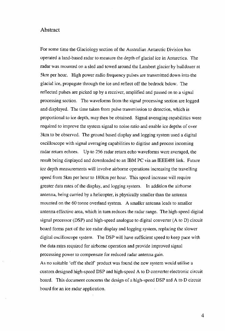
Figure 4.3 below shows the 21020 signalling interface for our system.
ISA BUS
Figure 4.3. ADSP21020 system signal interface.
The DSP interfaces to program and data memory, an A to D piggyback
board including an A to D FIFO and the PC ISA bus including a PC
FIFO.
26

Chapter4 DSP and A to D System Design
The DSP interrupts are connected to the FIFO full flags, FF, on the A to
D piggyback board and the PC interface. Connecting the FIFO full
flags to an interrupt alerts the DSP if data is being lost due to either the
DSP not emptying the A to D data fast enough or the PC not reading
DSP data fast enough. The interfaces will now be discussed in greater
detail.
4.1.2.3 DSP external memory requirements
The 21020 requires separate program and data memory. The data and
program memory address range is 4G words and 16M words
respectively. A survey of the high speed static RAM IC market
revealed the 128k by 8 bit wide configuration to be an industry
standard. Several manufacturers supported pin for pin compatible
products. The assembly language ice radar data logging programs
initially written were of the order of 10k bytes. Two 6k word waveform
samples are stored in memory for the logging programs. This led to the
conclusion that 128k words of program and data memory would be
sufficient.
The DSP program memory is connected to PC interface transceivers and
RAM. These transceivers are used for DSP and PC data interfacing.
The DSP data memory is connected to the A to D FIFO output, the PC
interface FIFO input, RAM and the PC interface transceivers. These
transceivers are used for DSP and PC data interfacing.
27

Chapter4 DSP and A to D System Design
Figure 4.4 below shows the memory bus interfaces and memory select
pin usage.
DSP
1st GRAM . . DATA . M .E.M.L.,h2r
P N141 :BUS - • PMSO OMSO DIvist BUS DMS2 3
DATA MEMORY BUS PROGRAM
MEMORY BUS
I ER F: :D FIFO RAM
PC
Figure 4.4. DSP memory bus connections.
The DSP is able to read data from, and download data to, the PC ISA
bus via its program and data memory busses.
The FIFO's facilitate high-speed asynchronous transfer of blocks of
data to and from the DSP.
4.2 DSP to Piggy back board interface
Three separate power supplies are sent to the piggyback board, a +5v
digital supply, a +8v analogue supply and a —8v analogue supply. The
+5v digital power supply is taken directly from the ISA bus. The +12v
and - 12v supply from the ISA bus are filtered and regulated down to 8v
to present a clean supply for analogue applications. Two physically
A / 771
28

Chapter4 DSP and A to D System Design
separate grounds are routed to the piggyback board one for analogue
applications and one for digital.
The signals routed to the piggyback board from the DSP were chosen
to give the interface a high degree of versatility.
The Piggyback board is data memory mapped via the data memory
select 3 (DMS3) line and data memory address lines 0 to 16 from the
DSP. The table below shows the complete set of signals to the
piggyback board.
Signal interface to the piggyback board.
CLK1 DSP clock
DMACK
Data memory acknowledge signal
DMS3
Data memory select 3 line
DMA 0-16
Data memory address
DMD 8-39
DMW
DMR
IRQ3
IRQ2
FLAG2
FLAG3
TIMEXP
RESET
Data memory data
Data memory write strobe
Data memory read strobe
Interrupt request
Interrupt request
Flag (bi-directional)
Flag (bi-directional)
Counter time out signal from the DSP.
Reset signal from PC.
29
Chapter4 DSP and A to D System Design
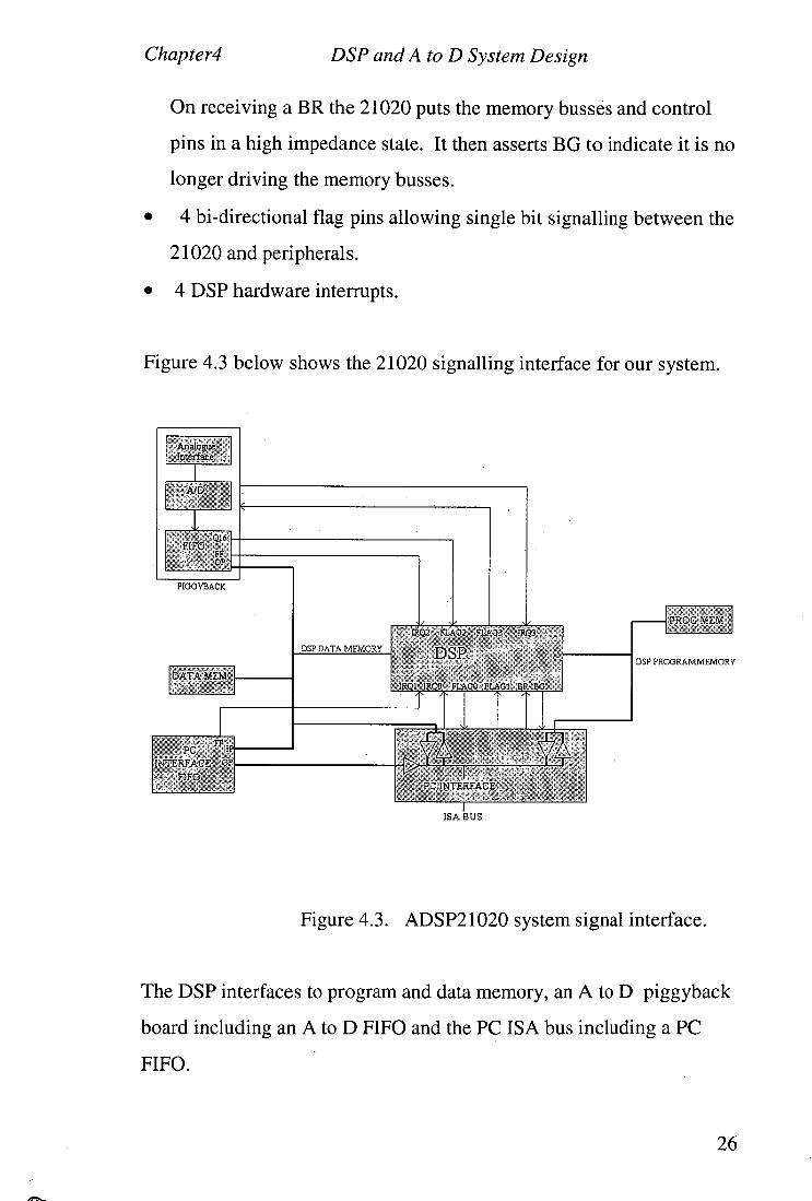
4.3 DSP to PC ISA bus interface.
The DSP to PC interface is shown in figures 4.3 and 4.4 above.
The DSP card is given PC ISA bus 10 addresses 300 hex to 31F hex,
reserved by IBM for users. See PC Instrumentation for the 90s, Boston
Technology and PC programmers Bible, P Norton. The ISA bus data
width is 16 bits on even addresses or 8 bits on odd and even addresses.
The PC controls the DSP board operation by downloading instruction
words and data to the DSP board. Communication between the PC and
DSP can be polled or interrupt driven.
Data can be passed between the PC and DSP via four avenues:
1. The PC FIFO connected to the data memory bus. Data is written
to the FIFO from the DSP at full speed. The PC reads the FIFO via the
ISA bus. The two operations are asynchronous.
2. Via transceivers connected to the data memory bus. The DSP
and PC can latch data into, and read from, the data memory bus
transceivers. The two operations are asynchronous.
3. Via transceivers connected to the program memory bus. The DSP
and PC can latch data into, and read from, the program memory bus
transceivers. The two operations are asynchronous
4. The PC writes and reads data directly to and from program
memory. The PC gains control of the DSP memory busses via the DSP
BR and BG signals as described below.
To write to the DSP program memory RAM the PC first sends a BR
signal. The DSP responds by tristating its memory bus pins and asserts
30

Chapter4 DSP and A to D System Design
BG. On receipt of the BG signal the PC downloads the 17-bit program
memory address and program memory select PMS0 to the PC interface
ISP logic device. See figure 4.5 below.
DSP.,
Pi- oitat11
Program
48
data memory
data memory PCTI F memory addre s address
32
Program memory data
data memory data
17 address lines plus PMSO
16 16 16 16 16 16
162646 I
tranieiver tsjj etv!, or oatiselye: ,
atilseivcr 162952
trans orer 162 52'
trans yer
tilt,: PC L. 1 S logc
16
ISA bus
Figure 4.5. DSP to PC interface.
The PMSO and upper address bit, bit 16, are latched into one of two
memory address bus transceivers. The lower 16 bit of the memory
address, bit 0 to 15, can be supplied by the PC direct or generated in the
1048 ISP logic device. Generating the lower 16 bits of the address
within the ISP logic device reduces the number of PC to DSP board
data transfers. If a block of data is to be transferred the lower 16 bits of
the address can be supplied by a counter within the ISP device that is
incremented after each write to RAM. Thus given a start address and
number of memory locations, a block of contiguous RAM locations can
31

Chapter4 DSP and A to D System Design
be written without the PC supplying each RAM address location. The
48 bit program memory data is written, 16 bits at a time, to 3 latches
connected to program memory data lines. A write strobe is provided via
the ISA bus. Reading the RAM is similar, except the 48-bit word is
provided from the DSP program memory RAM. See figure 4.5. In this
way the DSP program and data coefficients can be downloaded to the
program memory and verified. The DSP data memory RAM cannot be
accessed directly by the PC. Data can be placed in DSP data memory
by transferring it from the data memory bus transceivers or by
transferring from the DSP program memory, each requiring the
intervention of the DSP.
FLAG 0 and 1 are used for communication between the DSP and PC.
FLAG 0 may be used to interrupt the PC via the PC IRQ15 hardware
interrupt line (allocated to the DSP board by the user) or its status read
for polling operations. When used to interrupt the PC, FLAG 0 sets a
flip-flop within the PC interface ISP logic device. The output of this
flip-flop controls the state of the PC IRQ15 signal. The PC interrupt
routine must reset this flip-flop. The PC drives DSP interrupt IRQ 0.
DSP interrupt IRQ 1 is driven by the PC FIFO full signal to alert the
DSP that the PC is not reading the FIFO fast enough.
DSP set-up and control signals from the PC are stored in one of two
latches within the PC interface 1048 ISP device. Status signals from the
DSP board are passed to the ISA bus via the PC interface ISP device.
The table below shows the function of each bit in the control latches
and status buffer.
32

Chapter4 DSP and A to D System Design
Control latch 1
bit Function
0 Drives DSP BR signal (active low)\
1 Drives DSP FLAG 1 input
2 Interrupt DSP via IRQO
3 Resets PC FIFO
Control latch 2
bit Function
1 Software reset DSP (active low)
3 DSP FLAG 0 to PC mode, when set to 1 FLAG 0 causes PC
interrupt
Status buffer
Bit State of signal
0 BG
1 DSP FLAG 0
2 PC FIFO empty flag
3 DSP Timexp signal
The ISA bus 10 space map is shown below.
Address PC Operation Comments
(hex)
300 Read PMD bits 0-15 PC takes control of
DSP bus
33

Chapter4 DSP and A to D System Design
301
302 Read PMD bits 16 - 31
PC takes control of
DSP bus
303 _ 304 Read PMD bits 32- 47
PC takes control of
DSP bus
305
306 Read PC FIFO data
307
308 Read DSP data memory bits 8 - 23
309
30A Read DSP data memory bits 24 - 39
30B
30C
30D
30E Read DSP status latch
30F
310 Write 16-bit program memory address word
311 Reset DSP
312 write PMD 0=15
313 Write to control latch 1
314 write PMD 16-31
315 write to control latch 2
316 write PMD 32-47
317 Output a PMW from PC
318
319
31A
34

Chapter4 DSP and A to D System Design
31B reset PC IRQ latch
31C write DMD bits 8-23
31D Latch program memory address bit 16 and PMSO from PC
31E write DMD bits 24-39
31F
4.4 A to D piggy back board interface
Refer to figure 4.3 on page 26 and figure 4.4 on page 28. DMS3 and
data memory address 0 to 16 are used to memory map the A to D
piggyback board. Control data is up loaded to the A to D using the
upper 16 bits of the data memory data bus and the A to D output is
downloaded to the DSP on the lower 16 bits. The A to D FIFO full
signal is routed to DSP IRQ2 alerting the DSP if it is not keeping up
with data flow from the A to D - piggyback board. FLAG2 and FLAG3
are used to communicate with the A to D piggyback board. FLAG2 is
connected to bit 16 of the A to D, 18 bit wide, FIFO output. This bit
originates in the A to D logic and can be used to tag A to D data, (see
section 4.9.4). FLAG 3 is routed to the A to D control logic and may
be used to initiate the start of an A to D sequence. IRQ3 is derived
from the A to D logic to facilitate interrupt of the DSP by the A to D
operation.
4.5 A to D converter system
The digitising oscilloscope used in the original land based ice radar
system digitised to 8 bits. The new A to D system will also digitise to 8
35

Chapter4 DSP and A to D System Design
bits. (The user can alter the ice radar base band amplifier gain thereby
changing the system dynamic range).
The minimum sampling frequency for any design is the Nyquist
frequency. One problem with sampling close to the Nyquist frequency
is that it puts a heavy demand on the front end anti aliasing filter, the
input filter to the A to D. The ideal filter has very sharp cut-off at the
Nyquist frequency, that is, the wanted signal frequencies below the
Nyquist are un-attenuated and the unwanted frequencies above the
Nyquist rejected. To achieve a practical filter with these characteristics
would be extremely difficult. The project would become a filter project.
A poor filter with a poor role off and sufficient attenuation at the
Nyquist frequency will attenuate the wanted frequencies, distorting the
signal. Sampling at a rate greater than twice the highest signal
frequency of interest, i.e. over sampling, relaxes the filter requirements.
(See discussion in section 4.6). In addition, a signal digitised at the
Nyquist rate could not be displayed immediately and give a true
representation of what the A to D "saw". For example, sampling a sine
wave, with an A to D converting at this sine waves Nyquist frequency,
then displaying the A to D output would show a square wave not a sine
wave without further processing. As the sampling frequency is
increased the fidelity of the displayed sign wave is increased. The
disadvantage of over sampling is that more memory is required to store
the "extra" samples.
The A to D speed was chosen to be as fast as possible without the need
to go to special technologies. The faster the speed the more
applications the A to D could encompass. The highest speed solid
state A to D converters use ECL technology. An ECL device was not
chosen for the following reasons:
36
Chapter4 DSP and A to D System Design
• An ECL A to D would mean mixing logic technologies, leading to
greater system complexity.
• As the DSP is TTL compatible ECL to TTL converters would be
required which in turn require additional PCB real estate. The
market is spars on these ECL to TTL converters as most modern
designs use custom ECL to TTL devices, an expensive process.
• The ECL devices would require their own —5.2v power supply.
• A survey of TTL compatible A to Ds revealed that sufficiently fast
TTL A to Ds were available.
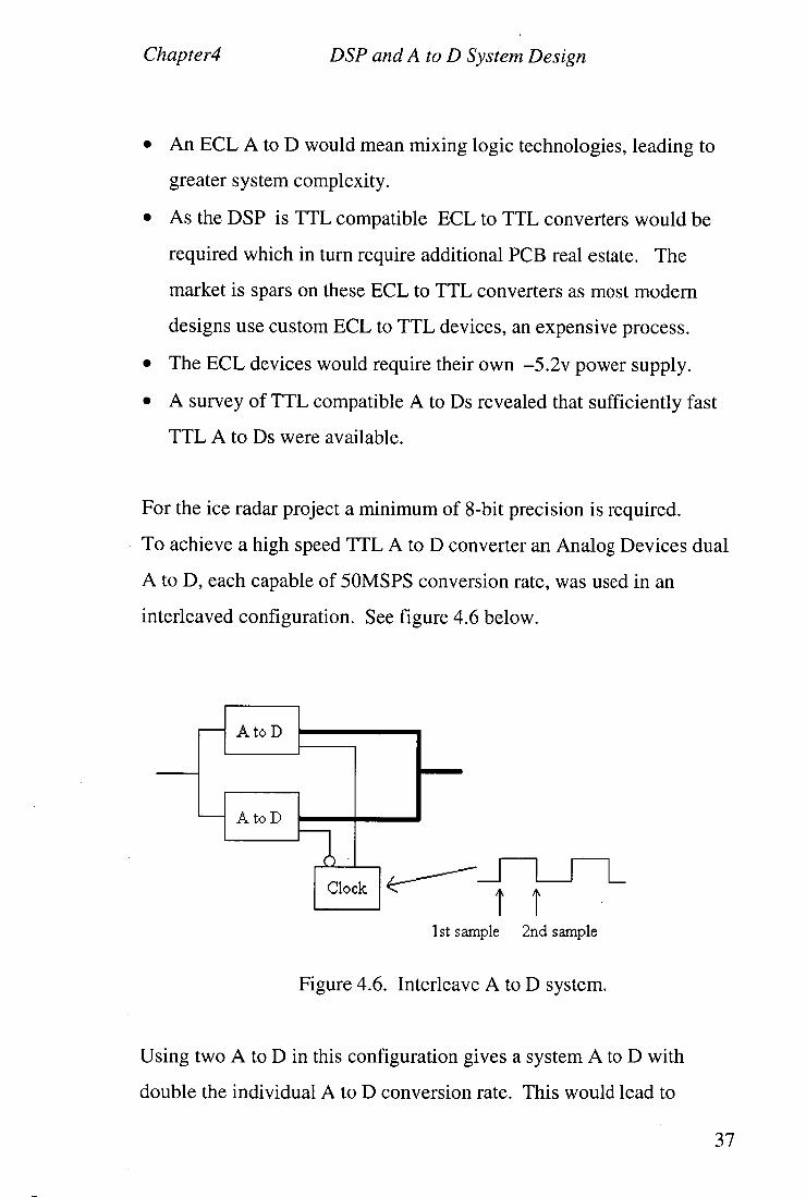
For the ice radar project a minimum of 8-bit precision is required.
To achieve a high speed TTL A to D converter an Analog Devices dual
A to D, each capable of 50MSPS conversion rate, was used in an
interleaved configuration. See figure 4.6 below.
to D
.A. to D
0
Clock I 1st sample 2nd sample
Figure 4.6. Interleave A to D system.
Using two A to D in this configuration gives a system A to D with
double the individual A to D conversion rate. This would lead to
37

Chapter4 DSP and A to D System Design
100MSPS A to D while still having a 50MHz A to D clock and TTL
components. Although two A to D converters are used the additional
PCB real estate required is minimal as the two A to D and a voltage
reference are in the same IC package. This system had some
unexpected results and was replaced by a non interlaced system. See
later discussion in chapter 6.
4.6 Front end A to D anti aliasing filter.
An active front end anti aliasing filter was chosen to minimise the real
estate required. The number of poles of the filter would be dictated by
the A to D speed and the space available for it. An anti aliasing filter is
required to attenuate frequencies above the Nyquist frequency to below
the least significant bit (lsb) of the A to D. An anti aliasing filter for a
100MSPS 8 bit A to D would therefore require an attenuation of at least
256 or 48.2dB at 50MHz.
Any practical filter will distort the signal it is filtering. The type of
filter chosen, and the degree of distortion introduced, depends on the
signal characteristics being measured. The design must take into
account the effect of the filter transient and phase response, as well as
frequency response, on the signal. Refer to chapter 2 in 'Electronic
Filter Design Handbook' by Williams and Taylor.
The slope of the filter frequency response in the stop-band will depend
on the filter type and the number of poles of the filter. We may
consider the 3dB point of a low pass filter as being the upper boundary
of the pass-band. The A to D sampling rate and accuracy determines
the Nyquist point in the stop band. The 3dB point is found by
38
Chapter4 DSP and A to D System Design
'working back' from this point in the stop-band. For example: A five
pole Bessel low pass filter would give 50dB attenuation at 50MHz
satisfying the Nyquist requirements for an 8 bit 100MSPS A to D.
Working backwards the 3dB attenuation point, the pass-band limit,
would be 10Mhz. Notice that the 100 MSPS A to D would be said to
over sample a 10MHz signal. Over sampling reduces the requirements
of the anti aliasing filter.
4.7 Designing high speed logic circuits
Most electronic engineers are familiar with the techniques used in slow
speed (below 10MHz) digital design such as with LS technology.
Much of the design consists of a system approach were building blocks
are linked together. The designer thinks in terms of fixed propagation
delays and clean well-behaved signals that give a good binary model.
Voltage and currents are usually thought of only in terms of power
supply requirements. With high-speed logic, design techniques
normally associated with high-speed analogue and RF design have to be
applied. Transmission line effects, distributed (PCB) components etc,
have to be taken into account. For example, at low frequencies to
create a short between two pins a piece of wire is placed between the
pins. At high frequencies the same wire may appear as an inductor and
not function as a short, the designer has to take the physical properties
of the wire into account. The first point to establish in a high
frequency design is how high a frequency do we need to consider.
Consider the experiment where a flip-flop is clocked at a rate of Fc i ock
and has an input toggling randomly between 0 and 1. The flip-flop
39

—IP T 10 - 90
LV
4.-
1 --...„..
, Maximum slope equals 'i
0
f 1•10.- 90
Chapter4 DSP and A to D System Design
output rise and fall times are less than 1% of the clock period. The flip-
flop output is now input to a spectrum analyser to reveal its spectral
power density. Its spectrum would look like that shown in figure 4.7
below.
Clock rate Knee frequency
- 20 dB/decade straight slope continues up to knee frequency
Expected signa l amplitude in dBV
11111111111111113PAM11111 11111111111111•111
11111111111151111111111iii>""111111111111111111111111 IIMP211111111111
'1311■INN
1111111111111 111111111b6, 1211111111MI
—80 1111111111A 1111111111111111 11111111111111
- 100 IMWAIII al 111111111111 0 1
—20
10 100 1000
Frequency. relative to clock rate At knee
.frequency, spectrum is 6.8 dB belOw straight slope
:NOS appear multiples of the
• clock rate
10-90% rise or fall time in this example is 1/100 of clock period
Figure 4.7. Power spectrum of a random digital waveform.
The spectrum nulls at multiples of the clock frequency and has a —
20dB/decade slope up until the frequency, Fknee . Beyond Fknee the
40

Chapter4 DSP and A to D System Design
spectrum rolls off much faster. The knee frequency, Fknee, is related to
the rise and fall times of the signal not the clock rate. At Fkn„ the
spectral amplitude is down by half, (6dB). A circuit with a frequency
response up to Fknee will pass a digital signal with minimal distortion.
Frequency responses above Fknee of a circuit will have minimal effect on
the processing of a digital signal. Fknee is therefore considered the
upper frequency in a high speed design.
The above discussion shows that not only are low propagation delay
devices considered high speed devices but devices with fast rise and fall
times. The highest frequency of interest may be taken as:
Fknee = 0.5/Tr, where Tr is the rise or fall time.
This can be used to give a guide for the high frequencies involved in the
design.
Typical rise and fall times for the 21020 read and write strobes are
about ins depending on load capacitance. This yields a Fkn„ frequency
of about 500MHz. To obtain a good low distortion digital model the
circuit components, including the PCB, must have a favourable
frequency response up to 500MHz.
The next problem is to decide at what point do we need to consider a
PCB track a transmission line. To do this we need to calculate the
effective length of the fastest signals. The effective length of a digital
signal is the length of conductor required for a signal to traverse the
logic levels. See figure 4.8 on the next page.
41

2 nS
3 ns
:All. points on the lumped line react together
n3 1..ns
.0 .n,S
ns
77,•••—, •
r--
3 ;OS
1)is1ributect., tithe ,.reacis difjerentlY, at different points
a US 3 Time
Chapter4 DSP and A to D System Design
Figure 4.8. "Snapshot" in time of a digital signal voltage on
a transmission line.
42

Chapter4 DSP and A to D System Design
The effective length, L, is given by
L = Tr/D
Tr = rise time
D = Propagation delay (the inverse of propagation velocity)
D is proportional to the square route of the PCB dielectric and can be
obtained from the PCB manufacturer. For a ins rise time and a
propagation delay of 180ps/inch (dielectric constant of 4.5) the
effective length, L, is about 5.5inches. For a track length greater than
5.5 inches the rising edge of a pulse will be seen to propagate along the
track, the potential is not uniform at all points on the track. At these
lengths voltage reflections and therefore transmission line properties
will need to be considered. At track lengths much shorter than
5.5inches, say 1 inch, the voltage can be considered as uniform along
the track. In this case the track does not need to be considered a
transmission line.
Not only do the signal tracks need to be considered but the ground
returns also. If a ground path is poor voltage differences will exist
along the ground. For example, if a narrow track is used as a ground
return it may be inductive. Fast changes in current will cause a voltage
difference along this track. For high-speed work a large solid ground
plane is preferable. Note that high-speed signals follow the path of
least inductance not least resistance. A low inductance path is as
important as a low resistance path.
The final point to consider is cross-talk caused by mutual inductance
and mutual capacitance. By ensuring there is enough physical
43

Chapter4 DSP and A to D System Design
separation between signal carriers and considering the signal timing,
cross-talk problems can be eliminated. The amount of cross-talk
introduced may be determined if the mutual capacitance and mutual
inductance between tracks, IC legs and components is known. The
difficulty is that both these quantities cannot be calculated until the
layout is at least near completion (by which time its too late). The rule
of thumb is to use the amount of PCB space available and determine the
cross-talk empirically if need be. (Some PCB layout techniques are
still considered art-work). A discussion of cross-talk is given in 'High
Speed Digital Design, A Handbook of Black Magic' by Johnson and
Graham.
When high speed digital signal timings are determined the load
capacitance of a signal must be estimated. At high speeds the rise and
fall times of a signal are of a significant length to affect timing
requirements. For example, in writing to RAM the address hold from
end of write may be Ons. If the address line capacative load is
significantly less than that of the write strobe, the address lines switch
much faster. See figure 4.9 on the next page.
44

Chapter4 DSP and A to D System Design
Equal loads
I Positbye holdtime —r:›1
DM ADD-\\
Unequal loads
DMWR
—DI holdtime
DM ADD
Figure 4.9. Example of the effect of capacative loading on
timing.
This being the case the address hold time is violated. The 21020 data
sheets specify rise, fall and output delay times for a given load
capacitance. PCB layout and system topology will effect load
capacitance.
The above discussion can be condensed into the following as far as
high-speed TTL and CMOS designs are concerned:
• Signal tracks greater than 1 inch (25mm) are to be considered as
transmission lines. This means that incorrectly terminated signal
Dmv,R
45

Chapter4 DSP and A to D System Design
lines will cause ringing, overshoot and undershoot. These will
introduce signal distortion. Undershoot may cause device damage.
• Currents flowing through a poor ground will cause potential
differences between the grounds of different devices. Resistance
will cause DC power currents to introduce a ground potential
difference. Inductance will cause potential difference in grounds
when rapidly changing currents pass through them.
• Adjacent signals may couple together creating cross-talk.
• Propagation delays may cause significant timing changes. For
example keeping the track lengths in a data bus fixed and changing
the length of the write strobe line will change the timing between
them.
• Device timings is load dependent, i.e. changing the load capacitance
will change the switching times. The 21020 data sheets give
output timing versus load capacitance graphs. The 21020 Users
Manual, section 9, page 27, gives an example of the effects of
uneven memory bus loading.
Most of these effects can be accommodated with careful topology and
PCB layout. The PCB layout is as important part as any other part of
the hardware design.
46

Chapter4 DSP and A to D System Design
4.8 The 21020 DSP software.
The 21020 has a large and powerful instruction set. See ADSP21020
Users manual for full details. Efficient use of the 21020 architecture
greatly speeds up the system processing power. Efficient code is
organised to take advantage of the 21020 parallel operations and
hardware capabilities. For example a multiply, an addition, a move of
data from program memory to a register, increment of a data pointer and
a move of data from data memory to register can take place in one clock
cycle. The user must organise the code to make use of these parallel
facilities.
Assembly code gives greatest control over the DSP operation and
therefore generates the fastest possible programs. Section 7.2 gives an
example of 21020 assembly code. This example, the DSP radar logging
program, shows many of the 21020s features and strengths.
4.9 The system implementation for the ice radar.
4.9.1 Signal processing.
In order to increase the ice radar system signal to noise ratio the number
of return echo waveforms to average was increased from 256 (the
maximum number possible with the existing digital oscilloscope
system) to 1024. An ice radar return echo waveform could be up to
60s long (as noted in section 2.1). This leads to 6000 samples per
waveform at an A to D sampling rate of 100MSPS. The clock period of
the ADSP21020 is 33ns. To average 1024 waveforms at 6000 samples
47

Chapter4 DSP and A to D System Design
per waveform in less than 1 second, 4 DSP clock periods per sample
would be available (leading to a total DSP processing time of
approximately 0.8s).
4.9.2 Transfer of data to the PC
The PC ISA bus can transfer 500kb per second and can be 8 or 16 bit
wide. See PC Instrumentation for the 90s. Boston Technology. The
averaged waveform from the DSP would be limited to 16 bit data,
therefore one 6000 point averaged waveform would take approximately
24ms to transfer to the PC. The transfer of data to the PC does not
require the DSP intervention if the PC FIFO is used.
4.9.3 Front end anti aliasing filter
The filter would need to have a linear phase change response to
preserve the shape of a radar pulse. A 5 pole Bessel filter (chosen for
its phase characteristics) would give 50dB attenuation at 50MHz
satisfying the Nyquist requirements for an 8 bit A to D. The 3dB
bandwidth would be 10Mhz. This would pass a low fidelity pulse with
a width of 100ns and high fidelity pulse of width 200ns.
48

Return Echo
A to D output :111FAINNESI
Chapter4 DSP and A to D System Design
4.9.4 A to D for the radar application
To display a reasonable fidelity pulse without signal processing at least
10 samples of the pulse would be required. 100MSPS A to D would
give reasonable display of a 100ns pulse and a high fidelity display of a
200ns pulse without post processing. For a 5km radar range the system,
sampling at 100MSPS, would need to sample 6000 points starting as the
radar transmits. A slower sampling option is available to reduce the
data storage requirements when using longer radar pulse widths. The
radar provides a trigger pulse, the rising edge of which occurs just
before the radar transmits its RF pulse. The A to D may start sampling
on the rising edge of the trigger pulse. (For versatility a choice of A to
D triggering mechanism is available, an external trigger, the DSPs
TIMEXP signal or the DSP FLAG3 signal). To ensure data
synchronisation the digitised radar return echo waveform is tagged at a
known point, for example at the first sample of the waveform, see figure
4.10 below.
Trigger _I I
Tag
Figure 4.10. Example of radar return echo tagging.
49

Chapter4 DSP and A to D System Design
For the transfer of data from the A to D to the DSP, FLAG2 is tagged,
that is, FLAG2 is set high when the first sample of the waveform is
transferred to the DSP. FLAG2 may then be used in a conditional
instruction to ensure synchronisation without incurring overheads, such
as additional lines of code to test a data bit. For example the following
program will repeat the 'DO' loop, codel to code4, until FLAG 2 input
goes high.
DO label UNTIL FLAG2_IN;
codel;
code2;
code3;
label: code4;
A counter clocked by the A to D sampling clock would be used to
determine the number of samples recorded.
Two A to Ds systems were considered for this design. The first uses the
interleaved system discussed in section 4.5 and was later replaced by a
second non interleaved system. See discussion on chapter 6.
A to D 1
The first A to D system utilised the Analog Devices AD9058 dual A to
D, each capable of 50MSPS conversion rate, in an interleaved
configuration. See figures 4.11 and 4.12 on the next page.
50

Chapter4 DSP and A to D System Design
CLKIN
FIFC
L1 L:T OLK
Analog in 16 DMD8-2
CLK B FLAG2
IRQ2
DMD8-39
RST CLK A
AD Clock
TRIG 7 TAG
ELS: FIFO read wnte control DMD23-39
FLAG3 IRQ3
Figure 4.11. Block diagram of dual A to D system.
CLK A
Data out A XXZZMKXXXXAQ<
CLK B .= C.= A
Data out B
latched A
latched B
YAVA AYYA
CLK A
A and B data input to FIFO
Figure 4.12. Timing diagram for dual A to D system.
51

Chapter4 DSP and A to D System Design
The two A to D encode pins are driven 180 out of phase effectively
giving a sample every 1/2 clock period. A 50MHz clock is used to give
a 100MSPS A to D system. The advantages of this system over a direct
100MSPS sampling rate being:
• a slower clock speed simplifying the design timing constraints,
• TTL component use,
• the layout of a PCB containing a 50MHz clock is simpler than a
layout containing a 100MHz clock
• A 100MHz system is generally more complex than a 50MHz system.
The two 8 bit A to D outputs are paralleled to form a 16-bit word that is
stored in the 18 bit wide A to D FIFO at bits 0 to 15.
This A to D system operates as follows: On system start up the A to D
board is reset. On receipt of a radar transmit trigger a 12 bit down
counter (allowing for up to 2 x 4k A to D samples) is loaded with the
number of A to D samples to be stored for the input waveform.
A corresponding tag bit is stored in the FIFO, at bit 16, to mark the
trigger point data. The same clock that drives the A to D clocks the
counter. As the counter counts down the FIFO fills. When the counter
reaches zero the counter halts and the FIFO stops filling. On receiving
a FLAG3 signal from the DSP the counter is able to reload on the
receipt of another radar trigger signal. In this manner the DSP is able to
request another radar waveform using FLAG 3. The DSP reads the
FIFO and is alerted to the start of a new waveform via FLAG2
connected to FIFO output bit 16. The tag is placed on the FLAG2
signal not a memory data line; this enables the FLAG test instructions
52
Chapter4 DSP and A to D System Design
(discussed above) of the 21020 to be used. The tag may also cause a
DSP interrupt, via DSP IRQ 2 that may be masked if not required.
The A to D requirements are loaded in the upper 16 bits of the data
memory data bus as: -
DMD24 to DMD33 Number of samples required. This
number is used to load the upper 10 bits
of a 12 bit down counter the lower 2
• bits are set to 0 on the load.
DMD 34 Tag mode
DMD35,36 Trigger mode
DMD37 Sampling rate
DMD38 Logic reset
DMD39 A to D FIFO reset.
This system gave some unanticipated results when used with signal
averaging. This is discussed later chapter 6. New higher speed TTL A
to D converters, FIFOs and clock driver circuits entered the market
allowing a true 100MSPS A to D with TTL technology to be designed.
The dual A to D, AD9058, system was therefore replaced.
53

SOLI SELECT
FIFO
DA 0 - 7
DB 0 -
DO - 7
A TOD : . LATCHI LAT cl-rj
CLK MO WRITE Eli
21.1!,2
ITT
CONTROL
Chapter4 DSP and A to D System Design
AtoD 2
The second A to D used a true 100MSPS A to D IC, the Analog
Devices AD9012. See block diagram figure 4.13 below.
Figure 4.13. Block diagram of true 100MSPS A to D system.
The A to D control system is similar to the first interleaved A to D
system. The A to D output data rate was slowed to half speed by
paralleling two 8 bit A to D outputs. The 16 bit word containing the
54

Chapter4 DSP and A to D System Design
two A to D outputs is stored in the 18 bit wide FIFO. See block
diagram above and timing diagram figure 4.14 below.
X 2 X 3 X 4 X
X 1 X 2 X 3 X
2
DATA STORED 1N FIFO (16 BIT WIDE')
Figure 4.14. Timing diagram of 100MSPS A to D system.
The counter containing the number of samples is now 13 bits
(maximum of 8k samples) due to the use of a single A to D. The board
now contains a 100MHz A to D clock, increasing the speed
complexities. The main impacts of the faster clock being the tighter
restrictions on the control ISP logic 2032 and transmission line effects
of the high speed clock. The A to D requirements are loaded in the
upper 16 bits of the data memory data bus as: -
DMD24 - DMD34
DMD 34
number of samples required. This number is
used to load the upper 10 bits of a 13 bit
counter the lower 3 bits are set to zero on
load.
Tag mode
CLK
AD OP
L2 EN
Li OP
L2 OP
FFWEN
3 0
2
55

Chapter4 DSP and A to D System Design
DMD35,36 Trigger mode
DMD37 Sampling rate
DMD38 Logic reset
DMD39 A to D FIFO reset.
56

Chapter 5. Circuit Design.
5.1 Component choice.
5.1.1 IC components
The digital devices are all TTL compatible were possible. Surface
mount components are used to minimise PCB real estate requirements.
5.1.2 Decoupling capacitors and inductors
Low effective series resistance (ESR) capacitors are mandatory along
with the selection of capacitor materials and component values to
ensure all noise frequencies of interest are suppressed. Typically for
each IC a 1nF and 0.11ff npo type capacitor is used for decoupling.
Type npo capacitors were chosen for their high frequency
characteristics. Every capacitor will have series resonance
characteristics. A lower capacitance value capacitor will resonate at a
higher frequency than a higher capacitance value capacitor. Above the
capacitor resonant frequency the capacitor behaves inductively and is a
poor decoupler. The 0.1g values will decouple lower frequencies and
the 1nF capacitors will decouple higher frequencies. The IC lead
inductance also helps decouple most of the ICs internally generated
high frequency noise. A PCB power and ground plane form an
excellent decoupling capacitor. The power to the board is filtered with
low impedance special polymer 4117 and 101..t electrolytic capacitors and
`lossy' ferrites.
57

Chapter 5 Circuit Design
5.1.3 Glue logic.
The glue logic chosen was in-circuit programmable logic, (ISPL). The
greatest problem with prototyping is the removal and addition of
surface mount ICs. Using in-circuit programmable logic would enable
the IC to be reprogrammed without being removed. There are a number
of producers of in circuit programmable logic, each manufacturer tends
to specialise in a particular area such as size, power or speed. Our first
priority was for speed, the second non-volatile programming, the third
density and fourth cost. The Lattice semiconductor devices were the
fastest (comparable to the standard advanced Schotky speeds), were
EEROM based and had reasonably high densities. There were a wide
range of programming choices, with a wide range of costs. (Lattice
could provide a budget programming version for $2000, compared to
Xilink $5000).
The ISP logic devices used are manufactured by Lattice and were
chosen on the basis of speed and programming software costs. These
devices are programmed using the Lattice development software (pDS).
The logic devices can be optimised for routing efficiency or speed. The
devices were roughly routed first to ensure the pin selection was valid
and the required logic would "fit". The pin allocations could then be
fixed and the PCB sent for manufacture while the logic software was
being completed. Refer to Lattice user manual for detailed
descriptions.
Two Lattice ISP devices were used the 1048 and the 2032.
58

"MODE/NC
'101/IN 0 "S03/IN 1
GOE 0
wog 1/0 10 110 11
I/0 12
I/O 14 u0 15
110 0 . 1101 If0 2 VO 3
1/04 I/0 "OS I/O 7
E EB
=M
R 11
T51.
1111 3
130E
6 NE
110
111;
I Inp
ut B
us
IOu
tput
Rout
ing P
ool (O
RP) 1
‘.—
— —
—
=L'—
>
0 —
—
—
_ C
LK
I LK I
.4 -
;at
CLK
2
Out
put R
outin
g Po
ol (
OR
P) I
Inpu
t Bus
11151411
11.11J
IIIfO
MR
filit
tLill
Er -- 0 /3 °
-u Global Routing Pool
(GRP)
11031 1/0 30 110 29 1/0 28
(/021 11026 I/0 25, 110 24 (/023 (/0 22 1/0 11020
Chapter 5 Circuit Design
The lattice ISP2032 logic device.
This device is small in density but has very high speed, comparable to
AS TTL. Figure 5.1 below shows a representation of the device logic.
Notes: 4Y1 and RESET are multiplexed on the same pin
**IspLS1 2032 only
yo rl .
Ut1y2
coseki4prmac
Figure 5.1. 2032 ISP functional block diagram.
Each of the blocks AO to A7 represents a generic logic block (GLB).
The logic block description is shown pictorially in figure 5.2 on the
next page.
59

3 + 4 (Shared) Prs and XOR
03
To ,I4L Global
Routing Pool and Output Routing
01 pod
Chapter 5
Inputs From Global Routing Pool
Dedicated Inputs
14 15 te 17
Circuit Design
Product Term Sharing Array 01 2 3 4 5 6 7 8 9 10 11 12 13 p Regimen
mummummliannimman•* 11111111111111111111111111111111111111MINIUMM-41tAII0 1111111111111111111111111111MIIIIMMIUNIMOrtr Ili 111111111111111111111111111111MIUMUIMMINIal IIIIIIIIIIIIIIIIIIIIIIIIMMUMIUMMILD M IMIIIIIIIMMININIUM111111111110-471-- IMIUMUNIMIMMIMMIUMIM:011" mi. ddill INININIONIUMMINIMIUMIIIII•ON IIIIIIIIIIIIIIMMINIIIMUNIUMIMMI MUNIMUSIUMMIIIIMIUMMIMIIVTLIWIN mumummummumusumwAr
nmumumnummunmummeoripm 111111111111111111101111111IMIMIMMEN" IIIIIIIIIMMIUMINUM111111111111111111,-M■ ll M11111111111111111111111111111111111111111fill mumennummummuummon uniummummunummunuan
memummunnumunmumnitir tommummmummumumorrie
PT Reset
Global RESET
CLK 0 CLK 1 — CLK 2
P.T Clock
PT Output Enable
To Output " Enable Mux
AND Array
Control Functions
MUX
MUX
Figure 5.2. Example GLB configuration.
This block has 17 inputs and 4 outputs. The example configuration of
the block above shows that the output product terms can be summed
with other product terms, exclusive ORed with other product terms or
simply output without addition logic. The global routing pool (figure
5.1) can route any input to any output. The outputs from the logic
blocks can be routed to any of the 10 blocks, TOO to 1031, via the
output routing pool (figure 5.1). Similarly the inputs from the JO
blocks can be routed to the global routing pool. The JO blocks can be
configured as inputs, outputs or bi-directional with tristate control.
The output routing pool and the product term sharing arrays may be
bypassed for high-speed operation.
60

Chapter 5 Circuit Design
The main problems associated with the ISP logic design was getting the
logic to 'fit' into the device while having control over the device
routing. The routing of the device effects the logic timing. For
example, if the term A+B+C+D+E is required the first four terms
could be produced by one GLB by simply ORing the terms A to D. The
ORed output would then be ORed with E. This would create two GLB
timing delays. By creating !A.!B.!C.!D.!E in one GLB and inverting
the result on the 10 block one GLB timing delay is introduced leading
to a faster logic solution.
The ISP 1048 logic device.
The 1048 device is slower than the 2032 but contains much more logic.
Its architecture is similar to the 2032 but contains forty-eight GLB's and
9610s.
5.2 DSP circuit design.
The DSP circuit diagrams are shown in figures 5.3 to 5.9 on pages 62
to 68. A discussion of the main sections of the circuit follows.
61

Figure 5.3 DSP C
ircuit Part 1
Circuit Design
11276
3 1
1122
U(9
--
VPM
WR)
-17E3E
D
(.2
.C1141X
EN
! PerrE
"
I T
M
2 sr Er
r!
ME
AM
EM
EM
• M
EM
ME
MM
EM
mEammmonm
MIN
AM
ME
MM
A
MIK
AM
EM
EM
M
ME
MO
MM
EM
B
111111121•1
PhIV/R PlA
RD
PM
AD
7 5
P741.) 2 P A
D 6
(2
34) 22 9 P A
13 0
10
PM
All II
VC
C
PMA7
PM!.?
onA5 IN
A°
PMAS
PMA4
PMAS
PMA1
20E •
21011 2CLKAB"
201 222. 2133 224
•205 ■—
=
1103628
33 P
MS0
2
MAD
315
VD
136 P A
O 1
1
PSIA
D .9
M
AI/ IP
O
'MA
D 1
31
AL1
013 PM
AD
9 2
4
740021162676
•2c111139 33?
AB
25
42 PM
AI 2
PMA1
PM
AI4
36 P60912 ('M
AID
/
P /
1952C4
.4
95,„
'11R MS.“
,MArn
.2.0
15
SD
II
C.
VCC.
T
CIE
TESI-
002SAD
J-1
4'6520631.1
SPARE
2032 0032906 P032SAB P6.52003
9299999992922
. 229992929 2
....
,0221qa 1952025
P05,0
E1
065241X
2
PII1
UP
IJ20
1DIR
tax,n • IC
I BAB
IS
U27C
1?R(1_9_
, 2
Ill
2114 BS
A7
ON
D
10
: • :
sl 11 Cr
1,2
76
71
AO

Figure 5.4 DSP C
ircuit Part 2
DM
RD
DM
WR
SO
ID >
DM
060-)
00,6040 311
I mu
<3=C
P
0900390.001
1 300 005
13MA14
12 13611113
\
11900.16 1361,2
II 10
oo 04
DM
I/9 \
—Tr--------
41 —
\ '
310 \
DM
A13
\
DM
, 9 8
. A3 .
I.4
D2
0,
' - 17
113Mr014 N
il--
b7------ \•4D12 n=
o1..,
\
131.1A7 \
13M35
7 6 A3
• 133 I
D6608
\
I 104011
\
13M0?
\
DM
, 5
27
A6
•A7
\
DM
AIO
\
DM
A 0
26 21
\
050011 N
D
MA°
25 4 AI 2 All •
A01
\
013464 \
DM
A!
28 3 \
DM
A6
\
DAIA2
31 2
30
SOD
000
0
.„
MM
7
MO2
MM
S
90*00 21
600.10 25 M
A16 4
9
015
90002 3
1
MAO
30 ------Tr-
tyr
wtT
0.11111
06 09
A10 •
Al5
Als
13 M
DR
12 U
7
1. 500: :
0 0
3101 N
0505000 N
M
A4
10
178 \
MAI
9 A2
19 13/107 N
A7
669.600
26 M
3161 23
.
MAIO
23
2:
•."
r••°' 3
•
VcC
M
000 31
\M
AI
AN
0.06
2.0
Circuit Design 0141022 131311317 061:020 069000 06100
DM
D16
lIMbO
S 1100121
N. \
0131.416 11 \
DM
Al2
10
\060005 9
\
DM
A9 8
\
DM
A7 7
\
10405 6
\
DM
A3 5
\
116108 22 \
DM
AIO
26 \ 0
64.6
0303
\D
MA11 25
\1113.0
4
\1061, 2
8
\13 1401
\136106 31
614 02
0.4 D
I 05
05
A6
06
A7
•no
•Aa .
:A9 • • A10 All
613 N
C
1311030 U
MW
, N
0111/2
2 \
DM
R29 N
M
1:=
\
346=
\
0611224 N
D
MD
28 \
VC
C
2 6
VCc
Oka
13 0
60006
1111:019 \ \ ,
141117 —
172-2
-407.1
\ 0
8 D
M1
00
3'.
00
PM
00
0'\
2
0 1
54
10
00
N
20 P
M000N
VCC
VCC
13 059035 PM
D36
15 0
65004'.
IS 064005'.
18 PA
ID39
19 0591132 N
20 0
34037 \
21 1
04014
VCC
10
13 P341/46 1441347 \
15 P
MD
43
17 P
ASLM
O
18 P
M1342 \
104344 \
20 M
IM
I \
21 P
MIO
40N
VCC
UiC15
47°T
11—
C16
C17
(14—C111
1]—C19
11—
C20
—L
C21 41I—
C2.2 —
I—C23
421—C24
JC25
'IL
C26
i—C27
11—
CM
i—
C29
X1j—
C30
T
_L
aot-al 470p
0.0
1-0
.1U
lcu 4
70,j_
co
0.01-011.11„
/
7014
,9 0.01-0.11.11„
./C1L
cs,
aot-naj, 4
70
11„
0.01-0.11.11„47L
,0.0
1-0
.11a„ ■
170pLc6,
0.0 4
0.0 0.01-0.
C31 C3
C13 C37
—L-
T
0'
4,1
1,6 a
ol .11,9
4
,11_,A0 7
T
r+C
T
10
1T 15
401000
T
T
_L
VC
C
1-1°
Circuit Design
T T
00.1-0.11.21„ 4
70,1
Le,,
—1— T
00.1
-0 1
1.....1
„, ic
o
T
aluL
e67 alu
icw
0.113„, a
nicn 411
alt1L
cu 01a ,75 a
tuL
c„, oata,, al
olio
.
T T T T T T T T T T T T T T T T
Figure 5.5 DSP C
ircuit Part 3
Cl
10%.
112
RI
VC
C
3
U1
rP c7
WW
ISEU
2
d 5-68t E36k641
5
VCC
101,0
00 )
•PM
S0".)
114.81
PMI)20
SI 00)21
P3 3.863172
02 PM
. ,
WPC
.
FLAG
O
IIZM
E13.
Md
MIN
A
MO
V =1■
ZM■
01
wtz
.14,-,-
11;reo
P8613. 172
PMD
III
P11114 D
MD
:D
MD
4
•
"•1/1107 •
,D7608.
40MD
11::.:
030213::: . :
DM
D15
016016 D
MD
II : . 1314018 :::.• D
RID
I9 D
MD
20 D
AW
N
DM
D2'
D261323 D
MG
24 D141725 1310326 D
MD
24 D
MD
D
1124030 D
AM
N • •
°M
OD
135/033
DM
D35
0161336 • D
I61337.. : 135M
38 • •
117,1P1
:DM
A
DM
A,
:DM
A,
4)NIA
4 61.437 D
MA.
:DM
AL
.13241A10• , 'D
RIA
l2:•: ••
DM
AI41.•: .D
MA15.:::
DM
AIS
'D
MA17.
,DM
A13
.DM
AI9
DM
A20
DM
AD
•D
MA22
DRIA23
MID
] PM
DI.
00400 0000
364803 33400
Ps9
)10
M
GM
4141/12 1 PRI1245 1640016 086010 Ph4D
18 P761:119 P6020
1.74721 LAD
D
001023.
724132A P1111)2)
PMD
I7 001020
: P/61330 PM
D31
" 664033 PM
DM
664039 02016
000037 0161/38
•.•PMD
3S,
PM0I1
PMD
4.2 PM
1)43.
P51111.5
0700
PMA2
PMA.7
' PMA5
•PMA7
PAW
. M
IA/0
PM
AII '
PMAI1:
41.1.11.1 N
AP
O:
.606 024020
DM
AD
•D
MA26
PA
PP
. M
AP
. 'M
ar
P113/0 :D
MA?)
PMA21
ItEM
' ESZID
• .113105g8
ii a3
VCC
VCC
4, D
M.
451.641,1121
DM
S0 • •1
DM
51
Circuit Design C
rN't
VCC
3
2 CLK
IN
(2•=
j
PAS
5
8 TV,
10 M
I
12 IM
O
ON
H
3
1■_2.L-■
■IJM
SM
IN
DM
D7
CI
■3D
RI
■)1
3iitM
M2
t...2
1=
%M
=6■
ZM
W
k
.MD
20 CA
S■
MM
S■
486012 126
MM
EU
MO
RIN
w
mm
r.masM
N
D11036
10
%Im
mam
eo
4011
• • • _
WM
ID
ZIM
MItIU
NI
11■1
1;M
3M
UM
_
NE111111111111 • •
1(:S
49
• 14■
EzaKE■lum
• • ■
monnonahm
aanwrox...
41■
Imam
moroill
DM
RD
MS2
31151
314.-6-(
1* ..03.0233.)
ILAG
___3_01E1D
FLAGI
PLACA,
11.616
l'PLSO
-4-M
st
PMRD
1,4w0
•-C:O
§Z3
(11,1E)0,
TIM
INP
2401 M
OO
Figure 5.6 DSP C
ircuit Part 4

Chapter 5 Circuit Design
Figure 5.7. DSP C
ircuit Part 5 1"Ir
12 TEST • VCYQ
GM) GM)
22 28 32
2 13
ON)) 1.1
66
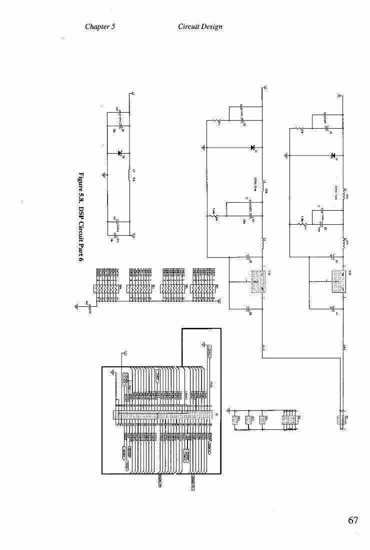
HI
1 2—
36 D
MACS
133540 •
—51
19 D
NIAI
' D
MA:
IMIA
1 334104
D
MAS
5 6 41
3364.43 D
MA
DM
AIO
DM
A11
7 42
MAO
D
AI
1/15615
44 D
i II
113E1M114
45 D
MRD
11112111101,
DM
AI6
46
47
1366433 17m
6m
/
48 D
MD
9 /
DM
DIO
/
06408 14 15
49
50 D
NID
060233
/
DM
DI2
/
DM
DI7
16 I7
51 52
DM
D14
pmnn
13911321
DM
DI6
18 19
Si
D3070
1,341318 \
UN
IX,
•D
MIPI3
20 21
SS D
NID
19 D
MD
32 22
7 D
mD
15 D
MD
37
DN
ID39
23 24
DM
D72
DM
DM
DM
OM
23
26 SO
61
DIA
DM
I7M
1110 061028
D
M7723
27 28
MO
21 06 4024
DM
1D29
29 DM6326
31 66
411I-1111.4•111•112 121k
68 69 70
3364430:3433:1
'
015 2
v
AXIA
L I.u
u
01
1 ohm
=CAP,
0E6
U26
VCC
RP1
D
MD
13 1
6
DKr. 2
15
MIM
ED
1100=
ES
0101
/..ED
041010=
12
MIM
S,
8132 D
OO
M
I U
MW
2
96020
IND
I6 6
41023
DM
1319 8
so, D
MD
32 I
IIM035 2
34031 4
IA11/39 D
MD
M 6
061026 7
631339 8
DPI
WIN
0:MD
741:1 :
DO
ID30 I
0•3
1 2
iM
ED
2 3
190
^8 4
DM
DI
6 13011306 7 03020 8
10351
AXIA
L I2mm
=SEAM
Circuit Design
Figure 5.8. DSP C
ircuit Part 6

L JIE
J 3! i
rm13
dSa
'6'S
Circuit Design Chapter 5
11117' P444 :14- MWOMMMEMIMUMMMMMM
WUM'e 8
/ / /
NN\N\N\N \s. NN NN,ANNs.\\NNNNN\\
5
m CU
1))1111 W'OUWWWriall EMFIRRRMFMM
E.:minimum 14,1,14111-4 2
UtIU 2=U..11,
ODE RESET
• SC1
Cs
L.
3
3
0 0
EriMn g...ggtV't g
r. 87,5 U 8,
3 6 .6
J Amemiammi • 1tmo
PA.V.M.V2. E6:gRiERE m - a
1111111 MNAMMMXM EJFERldhltnt•
32
tr3
VIO!5P.!: HiEWEE
V(
Bfl IC
30
•g•6 'CP
30 33 39
59
6
5
_...-.-
2Al
2E11 2A
2 . •
:282 2A
! 283
: 2A
4 28
4: 2A1. . :: •
::::: zes 2*6
226 2.47
237,
268 208
1 , 7: •
.
';:. .:7
:::1
ZO
ICAD
2CI A
8A
1*2 82
7*3. 7
83
1A4
• • • -1134
1A6
• •
- ... i
@ ,
1 ,
gambailmo
5 464-
GOD :GNU
_
:
GNU
.GtED
C,.ND 22 Cc CC :OND
CND . .
WO .. .
' """Si&RV8E 'Sg
. ...
M '
2A1 227 282
2*3 283
2A4
. 284
765 •
2A6
• ::.: 38
6
^-._ aga
8M, 'F-VITTTE
A 2
DA • BC
: A IC
G.
aei ttgLtgg
2
35
35 50 2
O7.
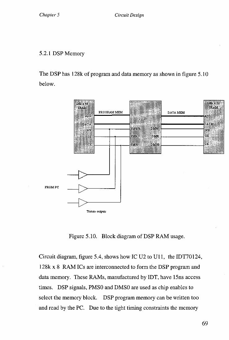
mac snA2:.,T
PRO GRAL!
12% *3Z SP_A31
ADD
DATA
WR
!OE
CE:
'111.121:1
P/111TP. BMW
P1 1R DNER
D1,4Sn
DATA MEM
FROM PC
Chapter 5 Circuit Design
5.2.1 DSP Memory
The DSP has 128k of program and data memory as shown in figure 5.10
below.
Tristate °Inputs
Figure 5.10. Block diagram of DSP RAM usage.
Circuit diagram, figure 5.4, shows how IC U2 to Ull, the IDT70124,
128k x 8 RAM ICs are interconnected to form the DSP program and
data memory. These RAMs, manufactured by IDT, have 15ns access
times. DSP signals, PMSO and DMSO are used as chip enables to
select the memory block. DSP program memory can be written too
and read by the PC. Due to the tight timing constraints the memory
69

--C.,
--C..
Chapter 5 Circuit Design
read and write pulses from the DSP cannot be gated, as the introduced
timing delays would be unacceptable, see timing diagram, figure 5.11
below.
DSP MEMORY READ
31]NS PERIOD
CLKIN
ADDRESS / SELECT -----X
I 0 MIN_m_
RD I
13 MIN —C=■
—.C. II MAX
DATA IN REQUIRED
-=zI-- 17 MAX
1 1 1
RAM DATA OP ** XX
a 7 MAX iff 0 - 5
0 15 MAX -
DSP MEMORY WRITE
SONS PERIOD
ADDRESS /SELECT ----)(
I 3 lYilli,
18 NM
15 MIN 8 MN ..)—
I a -1 MU -1 MEN
DATA PROM 21020 ----‹ >-----
_. 13M110 ---I
8 MIN a A' m a I- ..
-ms--e■ 5 MIR
RAM DATA RQUIRE/CENT >------
12 ball
Figure 5.11. DSP memory timing requirements.
WR I -C...
, 70

Chapter 5 Circuit Design
Notice that the DSP address hold time after WR high is 0 min. The
RAM requires a hold time of Ons. Therefore the WR pulse cannot be
gated. Careful layout will ensure the write to hold time is not violated.
Also the write pulse width is 15ns min. The logic can switch in 0 to
5.5ns. The RAM requires a pulse width of 12ns. Therefore if the high
to low and visa-versa switching times are not symmetrical the write
pulse can possibly be shortened below 12ns. For RAM read operation
the RAM read strobe high to RAM output tristated time could be 5ns
max and gating the read strobe could take 5.5ns leading to a strobe to
RAM tristate time of 10.5ns. The strobe signal could go low again in
9ns. Other devices attached to the data pins could go low impedance in
ins leading to a short circuit time of 0.5ns. This period although small
may cause "spikes" which may in turn cause some error in the circuit.
It is important to note that, although these spikes are of short time
interval compared to RAM write operations for example, they may
cause some RAM operation. The RAM (and other) timings are given to
guarantee a particular operation, it does not mean that pulses outside
these specifications will not cause a RAM operation. Therefore as the
DSP memory bus can be tristated with a bus request signal, BR, the
PMWR signal from the PC is sent via a tristatable transceiver, see
figure 4.14. The active PMWR, PMSO and PMRD signal is provided
by the device not tristated. The extra load of the tristated gate is
acceptable and layout minimises the effects of extra PCB tracks. Notice
in the write timing that the data hold after the DSP write strobe is de-
asserted states -1 minimum. The Ram requires a hold time of Ons. The
DSP does not change the data but tristates the data pins. The hold times
are met as the data is held longer by the RAM chip capacitances. E.g.
71

Chapter 5 Circuit Design
For a 2p load at 10[tA leakage current the voltage would droop by 0.5v
in 0.1 us. 1011A is a typical leakage current and 2p is 1/4 of maximum
capacitive load for one RAM pin.
The memory bus control signals have pull up resistors to ensure they
are de-asserted when the bus is tristated and are in a defined logic state.
The pull-ups are placed at the end of the long tracks. This lowers the
load resistance at the end of the track and improves matching and noise
immunity. The memory read and write lines are terminated using an
AC biased terminating resistor. The 21020 does not have sufficient DC
drive to drive the resistor direct (DC coupled). The capacitor is made
large to make the RC time constant large compared to the clock period.
The resistor is at the approximate impedance of the PCB track.
5.2.2 DSP to PC FIFO
The DSP and PC has a FIFO data interface as shown in the block
diagram, figure 5.12, on the next page.
72

Chapter 5 Circuit Design
21020 PC FIFO
DATA
CLE EN
DATA
NV ,P DNIS1
CLKIN
PPE..
Clock Driver
4 4P
Cig,( 33IVIHZ
Figure 5.12. PC FIFO system diagram.
To obtain the high speeds required a synchronous FIFO is used. The
FIFO is driven in a similar manner to a register. Data is input to the
FIFO when the write enable signal is active and the write clock is
strobed. Data is output when the read enable is active and the read
clock strobed. The FIFO used is the IDT 72265, IC U13 in figure 5.8.
The FIFO is 32k deep by 18 bits wide chosen for its speed and depth. It
is written too by the DSP and read by the PC. (See 72265 data sheet for
detailed information). Figure 5.13 on the next page shows the FIFO
timings required.
73

Chapter 5 Circuit Design
21020 CLKIN
21020 DATA OUT
DMS1— 14.5 MAX
>2 . 5
6 (30-24) t:
ZVIN 31 8<
WR
WR + DMS1
FIFO CLK
5 MA3C "E)--
1 6 MAX
26 max
2.4
Figure 5.13. PC FIFO timing requirements.
The FIFO write clock input is driven by a time shifted copy of the DSP
clock, see section 5.2.3. (The DSP clock timing is not on the 21020
data sheet but can be obtained from Analog devices on request. The
timings used cannot be derived by summing other timings as stated by
Analog Devices). The FIFO write enable, WEN, signal is derived from
DMS1 and DMWR by the 2032 in circuit programmable logic device,
IC U12. See timing waveform WR + DMS1 in figure 5.13 above.
The PC reads the PC FIFO and drives the FIFO output. The FIFO read
enable signal, PCFFEN, is derived from the decoded ISA bus 10
address. The FIFO read clock is derived from the decoded ISA bus 10
address and the ISA bus 10 read signal, IOR. The FIFO output enable
is derived from the decoded ISA bus JO address and the 10 read signal.
The timing for the PC read operations are relatively slow and are
74

Chapter 5 Circuit Design
generated within the 1048 ISP logic devise, U22. The FIFO read and
write functions are independent thus the DSP does not have to wait
while the PC accesses the FIFO data. The FIFO Full flag is connected
to the DSP interrupt 4, IRQ4, to signal that the PC is not emptying the
FIFO fast enough. The DSP may then, if necessary, signal the PC to let
it know that it is not keeping up. The FIFO empty flag is used as a
status signal to the PC to let the PC know if the FIFO is empty.
5.2.3 DSP system clocks
Figure 5.6 shows the DSP clock generator circuit. An oscillator IC,
U23, generates the DSP system clock frequency. It provides the
reference for the clock driver IC, U24. This IC is a phase locked loop
system and can output multiple clocks with varying phase differences.
Four clocks are generated, for the PC FIFO, data memory latch, 2032
ISP device and piggyback board. The production of multiple clocks is
useful for clock distribution and signal timing. The outputs can be 50
ohm terminated for transmission line driving to ensure a "clean" clock.
5.2.4 DSP bus latches and buffers.
The DSP can communicate with the PC via the program memory RAM,
the PC FIFO and transceivers. Transceivers are utilised as these
devices can be configured as latches or buffers, have high drive
capability, are 16 bit wide, have high density packages and are high
75
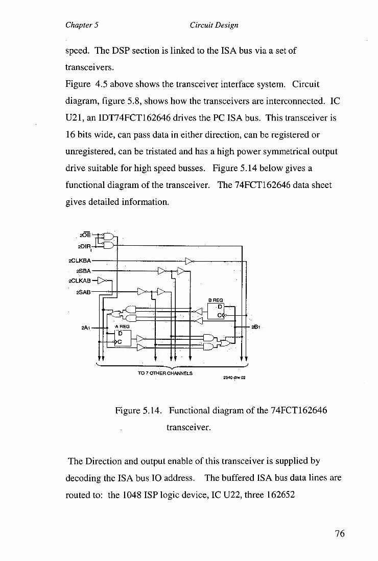
Chapter 5 Circuit Design
speed. The DSP section is linked to the ISA bus via a set of
transceivers.
Figure 4.5 above shows the transceiver interface system. Circuit
diagram, figure 5.8, shows how the transceivers are interconnected. IC
U21, an IDT74FCT162646 drives the PC ISA bus. This transceiver is
16 bits wide, can pass data in either direction, can be registered or
unregistered, can be tristated and has a high power symmetrical output
drive suitable for high speed busses. Figure 5.14 below gives a
functional diagram of the transceiver. The 74FCT162646 data sheet
gives detailed information.
TO 7 OTHER CHANNELS 2540 drw 02
Figure 5.14. Functional diagram of the 74FCT162646
transceiver.
The Direction and output enable of this transceiver is supplied by
decoding the ISA bus 10 address. The buffered ISA bus data lines are
routed to: the 1048 ISP logic device, IC U22, three 162652
76
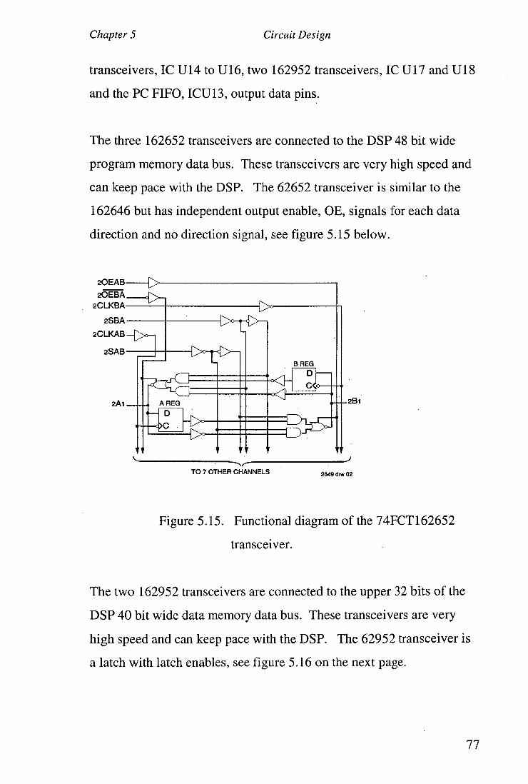
Chapter 5 Circuit Design
transceivers, IC U14 to U16, two 162952 transceivers, IC U17 and U18
and the PC FIFO, ICU13, output data pins.
The three 162652 transceivers are connected to the DSP 48 bit wide
program memory data bus. These transceivers are very high speed and
can keep pace with the DSP. The 62652 transceiver is similar to the
162646 but has independent output enable, OE, signals for each data
direction and no direction signal, see figure 5.15 below.
20EAB
20EBA
2CLKBA
2SBA 2CLKAB-
2SAB > >- B REG
2A1 2B1 A REG
D c.,>C
TO 7 OTHER CHANNELS 2549 drw 02
Figure 5.15. Functional diagram of the 74FCT162652
transceiver.
The two 162952 transceivers are connected to the upper 32 bits of the
DSP 40 bit wide data memory data bus. These transceivers are very
high speed and can keep pace with the DSP. The 62952 transceiver is
a latch with latch enables, see figure 5.16 on the next page.
77

Chapter 5 Circuit Design
2CEBA °I> 2CLKBA
20EAB --of> 2CEAB °I>
2CLKAB
20EBA ci>
2A1 2B1
CE
TO 7 OTHER CHANNELS •
2515 chw 02
Figure 5.16. Functional diagram of the 74FCT162952
transceiver.
The transceiver functions are controlled by the 1048 and DSP 2032 ISP
devices as shown in figure 5.17 on the next page and noted in section
4.3. A more detailed description of the ISP to transceiver interconnect
will be given in section 5.2.5.
78

Mk 4
,
1 ."
.
1..A1 :14
,.. rl Po ■ I
I Al C
H
''''% Lk
I
..C-
LXIC
.1{ 2 (.2-;IN
TItR
0712
OffM
....,,,,
i_ I ',COM
1048 ISP logic device 111111111 1 1
Circuit Design
PM D
ATA D
M D
ATA
DSP CU(
Ili•O
Figure 5.17 Block diagram of ISP logic interconect
g
ISA bus address and control ISA bus data
I

tr.)
The DSP to transceiver high speed link is shown in the block diagram,
Figure 5. 18. DSP to transceiver block diagram.
Using the transceivers the DSP can communicate with the PC while
running at full speed and have data and code written to its program
memory by the PC.
The operations involving the transceivers are as follows :
0.
figure 5. 18 below.

11 MAX •1 MIH
.
1.10 .5NS
I 1 5-9.5
0 .5rs to long but. accept
ADDRESS / SELECT
I 0 EH
RD
DATA IN REQUIRED 11 MAX I 5.5 MAX
—4> I <3—
<,TS
GATED RD
LATCH 0/P
131
Chapter 5 Circuit Design
• DSP data memory bus read of 162952. The OE is formed by gating
DMS2 and DMRD in the 2032 ISP. The timing diagram is shown
in figure 5.19 below.
Data read by 21020 Program memory 162652 and data memory 162952
301TS PERIOD
Figure 5.19. Read of 162952 transceiver by 21020.
• DSP data memory bus write to 162952. The latch enable signal is
formed by gating data memory write strobe, DMWR and data
memory select 2, DMS2. The latch is clocked by a phase changed
copy of the system clock. This ensures that the set up and hold
times are guaranteed. See timing diagram figure 5.20 on the next
page.
81
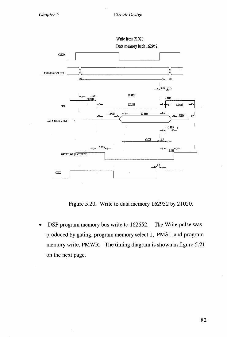
Chapter 5 Circuit Design
Write from 21020 Data memory latch 162952
CLKIN
ADDRESS /SELECT --X
WR
18 MIN 3 MIN
15MIN
73.25 - 7.75
1 0 MIN
8 MIN
DATA FROM 21020
-1 MIN -.CI- 13 MIN 5MIN
-1 MIN *
-4>- 5.5NS -cp- 5.511S
GATED WR (LATCH EN)
CLK2
Figure 5.20. Write to data memory 162952 by 21020.
• DSP program memory bus write to 162652. The Write pulse was
produced by gating, program memory select 1, PMS1, and program
memory write, PMWR. The timing diagram is shown in figure 5.21
on the next page.
82

ADDRESS /SELECT --X
I 0 MIN
44.- 8 MIN
55NS 5 NS
-=z-
CLKIN
-3.25- 7.75
18 MIN 3 MIN
15MIN WE
-1 MIN 13 MIN
DATA FROM 21020
GATED PMWR AND PMS1 AS LATCH CLK
-1 MIN *
6MIN -2 5
5MIN
Chapter 5 Circuit Design
Write from 21020 Program memory latch 162652
* This is the time to high impedance state
Figure 5.21. Write to data memory transceiver 162652 by
21020.
Notice that the data hold time may be 6.5ns worse case into the 21020
data output tristated period. The data hold time is satisfied by the
decay time of the data lines being long enough. Throughout the design
it must be noted that 21020 data sheet timings are given for specific
loads. These loads are not known until the circuit is built. This leads
to some uncertainty at the design stage and the designer must make a
worse case estimate. 162652 are used rather than 162952 because of
83
Chapter 5 Circuit Design
their non-registered transmission option allowing direct read from
program memory by the PC.
• PC read from and write to DSP program memory. The PC first
gains control of the DSP memory busses by sending a BR signal.
The DSP responds by tristating its memory bus pins and asserts BG.
On receipt of the BG signal the PC downloads a PMSO signal and
upper address bit, bit16, to transceiver U19, via the ISP1048 (see
discussion in 5.2.3), were it is latched. The lower 16 bit of the
memory address, bit 0 to 15, are passed to the program memory
address bus, via the ISP1048, to transceiver U20. The 48 bit data is
written, 16 bits at a time, to 3 transceiver latches, U14, U15 and
U16, connected to the program memory data lines. A write strobe is
provided via the ISA bus. Reading the RAM is similar, except the
48-bit word is provided from the RAM.
5.2.5 DSP glue logic
Figure 5.17, page 79, shows a block diagram of the ISP logic device
interconnect. The 1048 acts as an interface to the ISA bus control
signals. Its functions are:
• Decode the ISA bus JO addresses
• Buffer control signals from the DSP and PC FIFO
• Control transceiver operation
• Latch DSP board control signal
• Provide program memory address. The lower 16 bit of the program
memory address are latched or may be provided by a counter. (This
84
Signal Signal
Ground: lower
Dielectric
Ground power
Chapter 5 Circuit Design
option is not implemented but has space allocated for future
requirements).
The ISP2032 provides the high speed logic required by the DSP related
operations.
5.3 The DSP PCB
The DSP board is laid out as a high-speed digital board. It is an 8-layer
board including a +5v power and ground plane. Power and ground to
the ICs are considered first. Good signal routing is of no use to a
poorly supplied high-speed device. Power is connected from the power
planes to the IC by large vias placed close to the IC power pins to
reduce impedance. Next the high speed signals are laid out. The high-
speed digital signals are considered transmission lines. The PCB tracks
and power planes form microstrip and stripline transmission lines, see
figure 5.22 below.
Micro strip Stripline
Figure 5.22. Cross section of PCB transmission line.
85

k Ilh. I H lot. Cu; t - 0.0016"
Willial1111 gulroalac'rr. ori.7 1111Milial 011111111111111111
Dielectric _ 1...-
Thickness, h.._
WIIIIIIIMIN•1116, 0.100" — MEM 11•111MN IMIIIII011111111111111111■...._ 1111113111111111117.111111 0 6 '
-.mu IIIIIII 0.030" — 0.0015
I 50 60 70 80 90 100 110
LINE WIDTH (MILS)
140
130
130
110
100
90
80 2, IMPEDANCE 7,
(OHMS) 60
50
40
30
20
10
0
IIIIII I i lot. Cu; G-10 Materla ; er = 4 7 _ Spacing Separation Between Strip
Line Ground Plane and —
Spacing 1111
hh... 0.060"
1 -glar:MIEM
N.11■11q' c. - ---. " illoistiv 11112:41.-qMPII■ 0.01 0' lirre•fiftr
0.013" 0.020"
910 15 20 25 30 35 40 45 60 55 60 65 70 75
140
130
100
80 2, IMPEDANCE
(OHMS) 60
40
20
0 10 30 30 40
120
100
80
60
40
20
0
— 1 os. — Surface _G-10
Cu: IIIIIIII
Material; Conductors.
t .. 0.0016"
e r ■ 47
Die Thickness,
ec ric h-,---'-
1 0.016" 0.030
- 0.060"
---- 0100"
10 20 30 40 50 60 70 80 90 100 110
LINE WIDTH (MILS)
1 os. Cu; G-10 Material; • . 4.'1 FA 2 Spacing -Separation Between St ip Line end Ground Plane j
41 ppr
AI A 0010" AMR 0.013' r0020" Wan MN VAIPM Mil=
KilIMP2 No mazy 1170.111111103 111111■211111=
....i. MEE%
Ill'afillM" •.'w
0 .......
15 20 25 30 35 40 45 60 65 60 65 70 75
• LINE WIDTH (MILS)
CAPACITANCE/ FT (pF)
160
150
CAPACITANCE (pF)
140
130
120
110
100
90
80
70
60
60
40
30
20
Chapter 5 Circuit Design
The impedance of the transmission line can be calculated from the
dielectric thickness, thickness of the signal track copper and width of
the signal track. The dielectric and copper thickness' can be supplied
by the PCB manufacturer. Figure 5.23 below shows graphs of
transmission line impedance and capacitance.
Impedance versus Line Width and Dielectric Thickness for Mie *strip Lines Impedance versus Wire Width and Spacing for Strip Lines
LINE WIDTH (MILS)
Capacitance versus Line Width and Dielectric Thickness for Mierostrip Lines Capacitance versus Line Width and Spacing for Strip Lines
Figure 5.23. An excerpt from the `MECL system design
handbook' by Motorola.
86

Chapter 5 Circuit Design
The impedance does not need to be known exactly as the signal
reflections need to be minimised not expunged. Graphical techniques
are adequate for this. See figure 5.23 above. The narrower the track
widths the higher the transmission line impedance. Standard
manufacturing techniques for PCBs limit the minimum track widths to
8mil. (Thinner tracks are available but at increased cost). This leads to
impedances of the order of 100 ohms. Long lines are terminated at the
end of the line were possible to reduce reflections. The transmission
lines are continuous and do not change PCB layer. This reduces
reflections caused by discontinuities in the tracks. Some reflections are
inevitable due to discontinuities but are minimised by careful routing.
When a signal is routed to many loads, one continuous transmission line
is employed. The loads are connected to the transmission line by short
stubs, see figure 5.24 below.
(.2.1.
Short stub.'
li 1 High impedance input 1
Transmition line
Figure 5.24. Example of multi-load transmission line.
Where possible vias are used only at the source or load point of a
transmission line. When placing decoupling capacitors the path of the ----------, supply current needs to be considered. Surface mount decoupling
87

Ground plane assumed
1- I- It
To VCC
Chapter 5 Circuit Design
capacitors are placed under or close to the IC they are decoupling. The
capacitor positioning is important and is shown in figure 5.25 below.
A Double sided placement Single sided placement
Figure 5.25. Decoupling capacitor positioning.
The preferred placing is on the reverse side of the board under the IC.
Figure 5.25A. For single sided placement the capacitor should be
placed at the power entry point. Figure 5.25E and F. When using
capacitors of different values and types in close proximity to one
another it is possible for the two capacitors to interact with one another.
With different frequency responses, the two capacitors will respond
with different timings to voltage spikes with a result being an
instantaneous difference in internal voltages between the two
capacitors. The two capacitors can then begin oscillating as they pass
charge between each other. Capacitors of different values and types
must not be placed in close proximity to each other. Figure 5.25C and
D. After the transmission lines are laid out and the decoupling
capacitors placed the slower ISA bus signals are routed. Transmission
line effects are ignored for these slower signals. The area under the
piggyback board is kept free of digital signals were possible to
eliminate cross-talk to the piggyback board which may contain low
88

Chapter 5 Circuit Design
noise analogue signals. The DSP PCB file is on the attached floppy and
can be viewed using Protel PCB design software.
5.4 DSP to piggyback board interface.
The piggyback board is mounted onto the main DSP board by square
pin header connectors. See figure 5.26 below.
Header Pins
Figure 5.26. Header pins.
These connectors are not designed for high-speed transmission line
connections. If placed mid way along a transmission line they will
cause a large discontinuity and are therefore placed at the end of the
transmission line. The headers were chosen for their ease of purchase
and cost. Although not ideal, by keeping the PCB track distances from
the header pins on the piggyback board to the connecting components
short (less than 25mm) this connector will suffice. (A similar
89

Chapter 5 Circuit Design
technique is used for the PC PCI bus connectors). True transmission
line connectors are very expensive and difficult to obtain. Pull up
resistors on the control strobes are also placed close to this connector to
form a crude transmission line terminator.
The board is supplied with a digital +5v power supply and a +8v and -
8v supply derived from the ISA bus +12v and - 12v supply. These 12v
supplies are noisy and are therefore filtered and regulated to 8v.
5.5 The A to D Converter
Two A to D converters were designed. The second was designed after
testing of the first revealed some unexpected results. These results will
be discussed in chapter 6.
5.5.1 A to D anti alias ing filter
The PCB real estate available and the type of signal to be filtered
dictates the characteristics of the filter chosen. For the ice radar project,
were the signal is a pulse, a filter with good transient behaviour is
required to minimise distortion of the pulse. A Bessel filter is selected
for its linear phase characteristics. A 5 pole Bessel filter would give
50dB attenuation at 50MHz satisfying the Nyquist requirements for an
8 bit A to D. The 3dB bandwidth would be 10Mhz, wide enough to
retain the fidelity of a 200ns pulse and pass a recognisable 100ns pulse.
(Refer to Information, Transmission, Modulation and noise by
90

Chapter 5 Circuit Design
Schwartz). An active filter was chosen to reduce the PCB space
required. Figure 5.27 below shows a 5 pole anti-aliasing filter.
-^"...^-
,
Figure 5.27. Active 5 pole filter.
High speed OP amps were required. Although several Opamps exist
with gain bandwidths of the order of 50 to 75MHz this is not
necessarily sufficient for our filter. The characteristics required are:
• High gain at the highest frequency of interest
• Low phase shifts at highest frequency of interest
• High input impedance at the highest frequency of interest
• Low output impedance at the highest frequency of interest
• Fast transient response
• Low drift
The analogue 5 th order Bessel input filter stage, input amplifier and A to
D driver was implemented using the AD8001 current feedback
amplifier, chosen for their high bandwidth, low distortion, high drive
91

Chapter 5 Circuit Design
capability and fast transient response, see AD8001 data sheet. The
filter capacitors are npo ceramic capacitors suitable for high frequency
circuits with sufficient temperature and long term stability. Figure 5.28,
page 93, shows the anti aliasing filter. The layout is particularly critical
as discussed in the A to D PCB section 5.5.3.
5.5.2 A to D 1
Figure 4.11, on page 51, gives a block diagram of this A to D system
and the schematic diagram is shown in figures 5.28 to 5.31 on pages 93
to 96. This design is based around the Analog devices 9058 dual A to
D. The 9058 was chosen as the dual A to D and onboard voltage
reference in one IC package simplified the design. The +8v and -8v
analogue power supplies are regulated down to 5v for the A to D. The
two levels of regulation, from 12v to 8v on the DSP board followed by
8v to 5 volt on the A to D board, provide a clean analogue power
supply. Care is taken to isolate the A to D digital and analogue power
supplies. Decoupling for the A to D is a priority and the decoupling
capacitors are placed as close to the A to D IC power supply pins as
possible. Three npo type capacitor values are chosen to decouple the IC
0.111F, 1nF and 100pF to ensure noise at all frequencies is suppressed.
The A to D inputs need to be driven by a low distortion amplifier with
high drive capability. The Analog Devices AD8001 current feedback
amplifier was chosen to drive the A to D input (as for the analogue 5 th
order Bessel input anti aliasing filter stage and board input amplifier).
The feedback resistor for the AD8001 OPamps is place directly under
the IC and connected directly to the IC pins to ensure that there are no
92
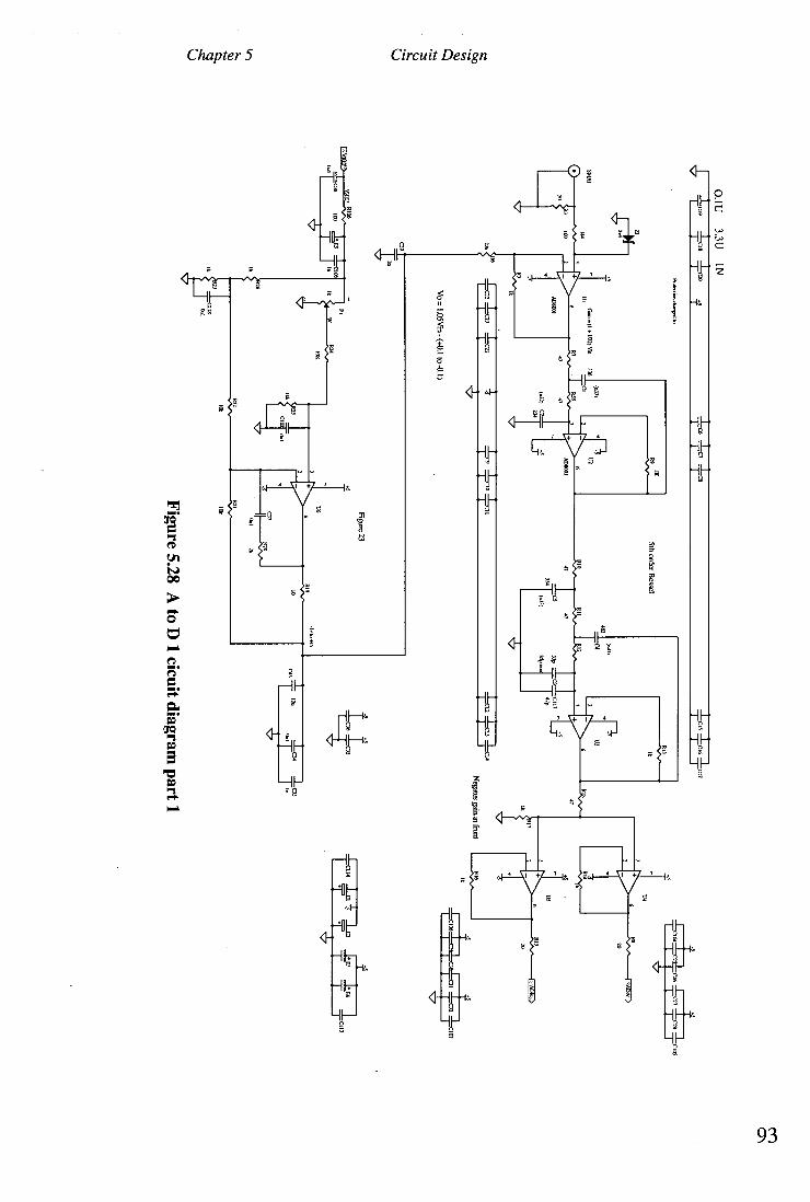
—
U6
0.1
U 3
.3U
IN
1216
.3 lk
Ic,,, IT
T T
T
Circuit Design
Vo = 1.05Vin - (+0.1 to -0.1)
.1,0
+1,
RI9
.1 10k
---C118
T - Figure 5.28 A
to D 1 cicuit diagram
part 1
+`19 -+`'' + 020 Prom.. ch
aoped
Zr
Gain
• (I, NZ V
II U
l
6 R7
0.8001
AD8001
1.2
1
230 .3
RI
22kc
Tj—m
T—Le" 4.T
•si"
SM
AI
—Lco =j
C16—Lco
T T
5th order Besse]
(.7)
.3 --
)C4 2
RIO
RI2
•7 47
--123
33,
34 /7p
(+33)
85p U
s
RI! lk
Figure 23
—1-02
—1
-03
T T T
Negates gain at front

VO
r
Circuit Design
SN1A2
RIO
03) V
S/S
.
50
CLK+12
CLIC-23
eiPP
r—r■ 1133
130
Ri @
.1$30T
2
I 131.01)
V!:
Li
Q 7 RES
016
R105 FF
50
CO
N1
ODD
II
V-CLIZO,3
„
220
—4- 2
20
-
0130 1
1111914
OD
E
(104
RES,
1303431 42
111,3130 41
1301428 40
0)1342) 34
000)23 33
1101424 000329 3
4
1303426 3
3
114 285.
2136 .287
!DI&
M
IXAB
2SAB
162616
90:
St 1110135 111)0432 001.433 131)3137 003434 13D0439 33D
M38
B133130
47 • 106
. -4-3
10.0
114 IE
LICAB
MBA:
18AB
1A1 . 1A2
1A3 1A4
1A6 1A7 1A13
vcc. VCC
VCC
50
111)15137 15
B10436 16
WM
17
1103135 18
01)1434 19
130,433 20
001,432 21
BD
M31 2
2
—009-7
/3—
111)3176 26
],„„, 013147.5
27 .
1011
LSBO
E
31 003424
02
II
U
12.
BD
9
am
8 R
EN
KM
' 6
1026 5
500SC
4 3002 1303430
•017.4
43 130130M
29/0128
.101 1
1022 42
7-11
••• x121 R
81-
1020 FL)
1019 D
MS3
1018 38 M
SBCIX
1017 7
1SPRST 8016
60 R
EIS
61
58
2.5
)437 U10
VC
msaccx
1041315 104032
104037 0
05,0
04
17,011)013 b140
0/41)31 031030 1)011)28
21 1731024 1314029 D
/01026
=IMO
—
301313)! 9
5
U19
MX
' Figure 5.29. A
to D 1 cicuit diagram
part 2 sox
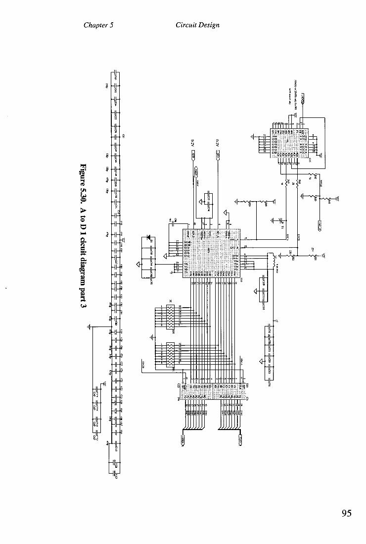
91
Dos 97
3:
HiEgNi >inM;
°GNI, ONO GNU GNI) GNT)
21
Chapter 5 Circuit Design
EN
36
11111'"
I0I; 2110 01210
PP: gg
GNI9
GAD VCC97 ] 9
1ST
a75.V704.0 VCCN.
8 8
•11 IL
ilH4—L6—HH
Figure 5.30. A to D
1 cicuit diagram part 3
a-
p4 auue6, sge Sde6bUUE ,,51
zussua 24,S4b445
95

S .M
v.
1,18
11■5
£26 E12
lu • 100u
U17
4•5
S.M. IND
=.1
- -C112 OUI
_±
.E13
1E
10
Circuit Design
sic
DM
03
1 2
6
DM
D28 2
7
DM
D25 2
8
DM
O29 2
9
—.1
7lig
ED
Z1
2
I t
UI
11';'1171-XS--eY
)
• 38 bM
A1
41 D
M11
42 212866
S
43
0,111
DMD11
1
DM
S3 D
MD
23 0611132 014037
DM
DIO
D
MI
1 DM
D1 1
DM
A6
DMAO
DM
A15 1
D 126
ilMD
tIlSttI
0 1
0
44 D
MVA
,_z_b_l_
Li.p,m1111.
,‘,,,,„
AS
DM
. M
A13
H01
Figure 5.31. A to D 1 cicuit diagram
part 4
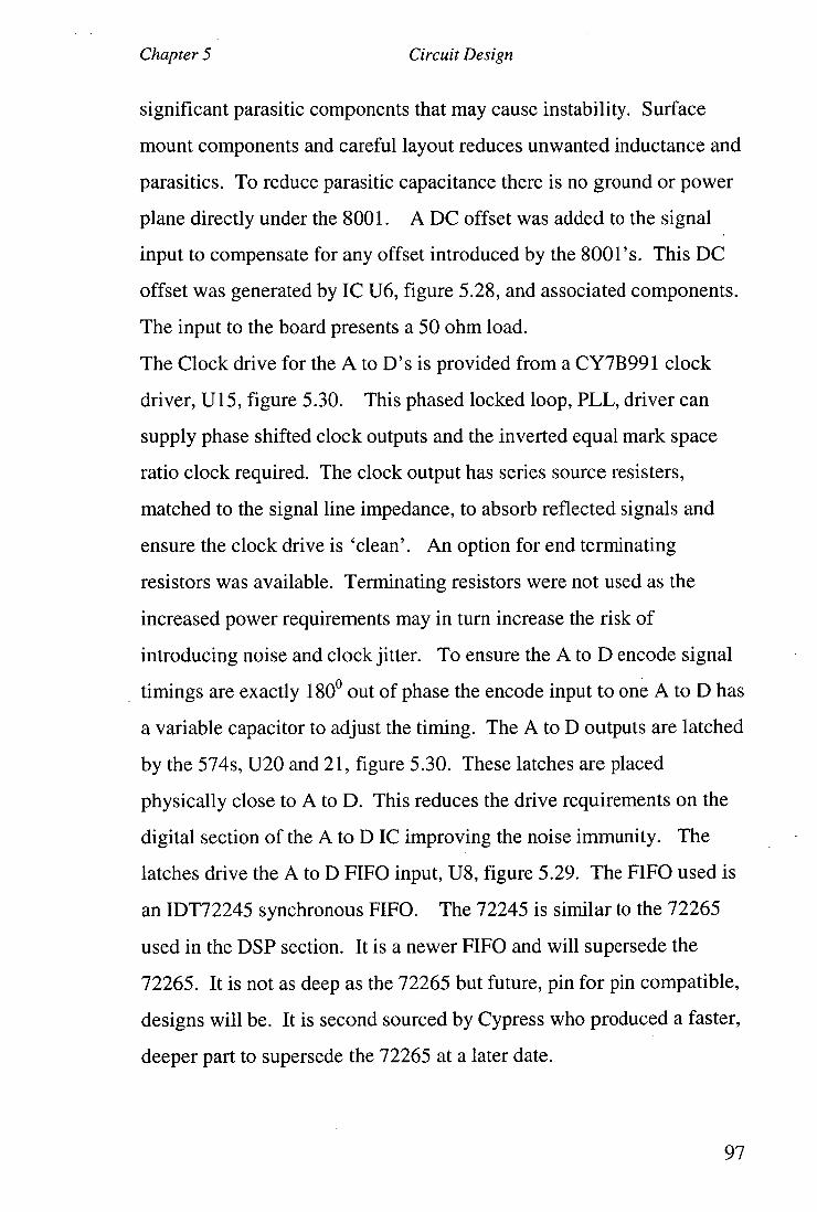
Chapter 5 Circuit Design
significant parasitic components that may cause instability. Surface
mount components and careful layout reduces unwanted inductance and
parasitics. To reduce parasitic capacitance there is no ground or power
plane directly under the 8001. A DC offset was added to the signal
input to compensate for any offset introduced by the 8001's. This DC
offset was generated by IC U6, figure 5.28, and associated components.
The input to the board presents a 50 ohm load.
The Clock drive for the A to D's is provided from a CY7B991 clock
driver, U15, figure 5.30. This phased locked loop, PLL, driver can
supply phase shifted clock outputs and the inverted equal mark space
ratio clock required. The clock output has series source resisters,
matched to the signal line impedance, to absorb reflected signals and
ensure the clock drive is 'clean'. An option for end terminating
resistors was available. Terminating resistors were not used as the
increased power requirements may in turn increase the risk of
introducing noise and clock jitter. To ensure the A to D encode signal
timings are exactly 180 ° out of phase the encode input to one A to D has
a variable capacitor to adjust the timing. The A to D outputs are latched
by the 574s, U20 and 21, figure 5.30. These latches are placed
physically close to A to D. This reduces the drive requirements on the
digital section of the A to D IC improving the noise immunity. The
latches drive the A to D FIFO input, U8, figure 5.29. The FIFO used is
an IDT72245 synchronous FIFO. The 72245 is similar to the 72265
used in the DSP section. It is a newer FIFO and will supersede the
72265. It is not as deep as the 72265 but future, pin for pin compatible,
designs will be. It is second sourced by Cypress who produced a faster,
deeper part to supersede the 72265 at a later date.
97

Chapter 5 Circuit Design
The FIFO is reset by the DSP using the DSP data line, DMD39. The
FIFO write clock is provided from the 991 PLL clock driver. The
FIFO write enable, WEN, is derived in the A to D board 2032 ISP logic
device. The WEN signal is active when the 12 bit counter within the
2032 is counting down. On reaching zero WEN goes inactive
preventing further write to the FIFO. (See discussion in section 4.9.4).
The 12 bit counter within the 2032 can be loaded thus initiating another
FIFO write sequence. The load is inhibited until the DSP toggles
FLAG3, indicating it is ready for another set of samples. On receipt of
a trigger from the radar the counter is loaded. As the radar trigger is
asynchronous to the A to D and DSP it may repeat before the required
number of A to D samples are gained. The radar triggers are therefore
inhibited from generating another load until FLAG3 is again toggled.
See A to D sample operation discussion below.
The 9058 A to D clock is derived from a 50MHz oscillator, U14, figure
5.29. The 50MHz clock is fed into the 2032 where it is divided by two
to produce a 25MHz A to D clock option. The DSP FLAG3, the radar
trigger and the A to D clock are asynchronous. All signals within the
2032 are 'synced up' to the selected A to D clock. By syncing
everything to the A to D clock timing errors due to coincident signals
etc are omitted. The FLAG3 signal may be high for 33ns, the DSP
clock period, whereas the 25MHz A to D clock option has a 4Ons
period. The FLAG3 signal is therefore "stretched" to ensure it is
'captured' by the slower A to D clock. To do this the FLAG3 signal,
routed to the 2032, is first synced up to the 50MHz clock negative edge.
The synced signal is then 'stretched' and synced to the A to D clock
rising edge, see figure 4.32 on the next page.
98

Chapter 5 Circuit Design
2Ons
50M CLK
FLAG3
I
3Ons
Clocked FLAG3 I I
I
2Ons FLAG3_
I
Clocked FLAG3_ 2Ons
I
FLG3
50M CLK -------
A to D clock
\ 25M_CLK
Figure 4.32. "Stretching" and synchronisation of FLAG3.
The A to D operation is controlled by the 2032 ISP logic device, U12,
figure 5.29. The logic equation listings for this 2032 are given in the
attachments. The logic control operation is based around a 12 bit
synchronous down counter. Refer to block diagram of the control logic,
figure 5.33 on the next page.
99

REN, LSBOE
MSB
CLK
DM
WR
tr) D
MS3
DM
RD
RADAR TRIG
T3
YO YO
BLO
CK
BDM
38 Y
O—
>
FLG 3,
1 FLAG3 _
Fl,G3
FLAG3_
FLAG3
/50M_clk
/50M clk
Y
O—
A to D CLK
DMD 24 to 33
WE
N
EDG
E
50M
BDM
37
YO
BDM
38
Figure 5.33. 2032 A to D
1 control logic

Chapter 5 Circuit Design
This counter may be reset, loaded and count enabled. The signal WEN
generated by the counter is high when the counter has counted down to
zero, (it is similar to the ripple counter output, RCO, in some counter
ICs). WEN is inverted and drives the A to D FIFO write enable input.
Thus, the FIFO stores data when the counter is counting down. On
receipt of a radar transmit trigger signal a pulse one A to D clock period
wide, EDGE, is formed from the rising edge of the trigger signal. This
EDGE signal causes the down counter to load and count down. WEN is
fed back to inhibit further active EDGE signals being generated thereby
inhibiting further loads until the counter has counted down to zero. A
further counter load is also inhibited by a BLOCK signal, see figure
5.33 on the previous page. BLOCK is generated from the EDGE signal.
To initiate another sampling period the DSP sends FLAG3 high. The
BLOCK signal is cleared by FLG3, generated from FLAG3 rising edge.
If the counter has reached zero (WEN is high) and BLOCK is cleared
(via FLAG3) a radar trigger will cause the counter to load and a new set
of waveform samples is stored in the A to D FIFO.
This operation is shown in figure 5.34 below
Ato D_CLK
TRIO
EDGE BLOCK
LD
Block inhibits second load
Ato D_CLK
TRIG
EDGE
FLAO3
BLOCK LD
Flag3 clears block
Figure 5.34. A to D 1 ISP2032 control function.
101

Chapter 5 Circuit Design
In the first attempt to create this control logic FLAG3 was not synced to
the A to D clock. On testing the system 'extra' samples were taken for
some waveforms, for example: if 128 samples per waveform was
chosen, at random, a waveform with greater than 128 samples would
appear. The reason is that if BLOCK was cleared and a FLAG3 signal
arrived coincident with an EDGE signal the counter would load but
BLOCK would not be set. The counter would count down and the next
radar trigger would cause a second, unwanted, load to take place.
Syncing FLAG3 with the A to D clock ensured that a BLOCK signal
would accompany every counter load.
The terms within the logic expressions for the counter are rather large.
Care has to be taken to ensure that the delays through the ISP 2032
GLB cells do not add up and violate timing restrictions. Excessive
daisy chaining of GLBs to obtain the logic would cause unacceptably
large timing delays. Trying to pass large numbers of signals between
GLBs causes routing problems. The design is a compromise between
the two.
The tag signal is selectable and can be either the WEN signal or the
counter load signal. Using the counter load places a tag on the first
sample of the waveform stored. The tag generated from the load signal
is 'stretch' to create a DSP interrupt signal if required. The DSP
samples interrupt and FLAG signals on the rising edge of its clock,
stretching ensure the DSP 'sees' the interrupt.
102

LOGIC
020
DATA FF
BE
c14
CLK 12:1).cLIC REN
AD LATCH CLK
PPL Clock Driver
AD FF CLK OgC 33MHZ
DM§3
CLKIN
Chapter 5 Circuit Design
The DSP reads the FIFO data via transceiver, U9 in figure 5.29, a
162652. Figure 5.35 below shows a block diagram of the A to D FIFO
read system.
Figure 5.35 Block diagram of the A to D FIFO read
system.
The FIFO read clock and transceiver is driven by a time-shifted version
of the DSP clock. The FIFO read enable and transceiver output enable
are formed from the DSP DMS3 and DMRD signals. Figure 5.36 on
the next page shows the A to D FIFO read system timing.
103

Chapter 5 Circuit Design
DSP CLKIN
12- 18
21020 REQ'D DATA IN 4.5 5.5
DMS3 1.5
-ej 13 93
DMRD - 1
DMRD+DMS3 26 2/Ax
(AD FIFO REN) 2.4
DMRD
LOGIC OP 5.5 MAX I IDIA.X
I 4MAX U9 TO OP ENABLED --drAx
10.5MPJC 9.5 MAX
A to D FIFO CLK
A to D FIFO OP
U9 CLK
FLAG2 OP
Figure 5.36. A to D FIFO read system timing.
5.5.3 A to D 1 PCB.
The PCB layout is an integral part of the design process. Often a
circuit has to be modified due to PCB constraints. For example a filter
response is defined by a lumped capacitor value plus an amount due to
stray capacitance. This stray capacitance is a function of the PCB
layout. Due to the high speeds involved the A to D circuits may include
"components" that are not present on the circuit diagram, but are
present because of the physical properties of the circuit board. A
ground plane is mandatory to negate introduced PCB 'components'.
Two grounds are used, one for digital, one for analogue. The ground
PCB connections are made through multiple pins to reduce impedance.
One of the problems with A to D PCB layout is that the digital section
is capable of injecting noise into the analogue section. The best noise
104

Chapter 5 Circuit Design
reduction technique for reducing this noise injection is physical
separation. The analogue signals are physically separated from the
digital section of the board as far as possible. The A to D is treated as
an analogue component. Often the A to D data sheets suggest joining
the digital and analogue grounds at the A to D. In many systems this is
not practical. What the manufacturer is saying is that the ground for the
A to D needs to be as good as possible. The A to D has digital and
analogue sections kept separate within the IC to avoid coupling of
digital signals into the analogue section. Noise from the digital ground
will be capacitively coupled to the analogue ground within the IC. A
poor external digital ground will cause more digital noise to be
capacitively coupled to the analogue ground. Figure 5.37 below shows
a representation of the A to D silicon layout.
+vd
TAP d
;CAP CA;
AID at adtuctord (votrcrcat
jiy C"
Analog rdAtt LLI, r; C771,1
Noisy digital E _c
a.' analogue d= digtal fri VOCKT0111
Id
Figure 5.37. A to D converter showing the digital and analog
sections.
105

Chapter 5 Circuit Design
Rapidly changing digital currents at F in figure 5.37 will cause a
voltage that will couple into point E of the analogue circuit through the
stray capacitance. There is also about 0.2pF of capacitance between
the IC legs. Therefore the digital and analogue grounds are joined
together externally with minimum lead lengths to reduce extra
impedance. Any extra impedance at the digital ground will cause more
digital noise to develop at point E, coupling more noise into the
analogue circuit. Digital noise from the digital section of the A to D is
introduced onto the analogue ground but is minimised by ensuring the
A to D does not drive large fan outs. Surface mount capacitors are
located next to the supply pins. Ferrite beads are also used to isolate
power supplies.
The A to D clock is grounded to the digital ground. For A to D
accuracy's greater than 8 bits the analogue ground would be used. This
would reduce the phase noise of the clock and improve the SNR. The A
to D clock is well decoupled and placed in a less noisy section of the
digital ground. Separate analogue and digital power supplies are used.
In the digital section transmission line techniques are employed in the
PCB to control track impedances and reduce ringing etc. The area on
the DSP motherboard under the piggyback board is free of high speed
digital signals and is shielded by power and power planes on the
piggyback board to reduce cross-talk from the DSP board. Where
possible multiple power and ground pins are used on the digital
connector. Ground pins physically separate some digital signals in an
effort to reduce cross-talk. The analogue power and ground connectors
are separated from the digital power and ground connectors. The digital
signals from the DSP are kept to a minimum length to reduce
transmission line effects. A four-layer board is used. One layer is
106

Chapter 5 Circuit Design
dedicated to ground. The power supply takes large portions of the other
planes. See ad.pcb on the attached floppy disk. Throughout the design
careful consideration to the return path currents is adhered too ensuring
that large transient currents do not flow through the ground plane near
sensitive areas. On the analogue section large single vias are used to
connect power to reduce impedance and eliminate current loops.
5.5.4 A to D 2
The second A to D circuit uses a single A to D, the AD9012, capable of
100MSPS conversion rates. Section 4.5 outlines the system design.
Figures 5.38 to 5.41 on pages 108 to 111 show the schematic diagram.
The DSP interface is unchanged. The AD9012 requires an external
voltage reference. This was produced from a low noise voltage
reference, the Analog Devices REF43, IC U52, figure 5.41. This
reference is filtered and conditioned to be in the —2v range required for
the AD9012. An 0P27 OPamp was chosen for the reference
conditioning. The 0P27 is a general purpose OPamp with good long
term and temperature drift characteristics. The A to D clock is
produced by a PLL frequency doubler, the MC88915, driven by a
50MHz crystal oscillator, IC U14, and the 33MHz DSP clock see figure
5.41. The clock to be doubled is selectable within the MC88915 PLL
IC. Figure 4.13, page 54, shows the method used to reduce the A to
D output data clocking rate. The data clocking rate is halved and the
data word width is doubled, thus the data rate is retained. The logic
functions are again supplied by the 2032 ISP logic device. The logic
equation listings for this 2032 are given in the attachments.
107

Chapter 5 Circuit Design
F2
(V0-
01 - u
TASO
I =°A
r,
Figure 5.38. A to D
2 circuit diagram. Part 1.
;2
108

Ilr 5g ,Ag ,1” al@n sssr
MUM MUM OE= MEM! MUM MEM ME=
55
LI 48
52 51
11;2 1133
LBS
iN5
21.14250
1114220 1 TU
B' .150n
!S
AD
35 50 22
A.- vtv 7.7.WS ..
UHI16
2 3 5 D
MD
19
32
L4F IS
- 4k4Ltt
Chapter 5 Circuit Design
MN 0341)
VMS. —fr-
"SQ . P.Q .O.V-Z V"'
L
° r 5
go5U Eg E-
ItIVW:=M cft
NWP N mf.
OND GNU ,CC ,ND 3 OND CC
.4 q
LILLU 4
rff- 8
109

Vout = 5(rt+r2)/r2
L1
'M IS
O
Dl
Figure 5.40. A to D 2 circuit diagram
. Part 3.
•E
l/
Ils
5
HU
I
CLIO
111
EZI727C 113
1____4AC_OC D
MA
S
DM
A.,
4
7 38
DM
AI
39
40 D
MA
,
I) D
MA
S
3
42 D
MA
) IM
O
['M
AU
7
DM
A1
D
13.515
10
43 0
EM
ERIED D
MA
16 131.13
O
MD
IO
13 1
r-
48
IA
.
1210011 D
MIR
I
12
1.1
7
15 16
SO
I 0
.15
D
NID
I4 D
MD
I7
17 2
001022
D
10.'15;23
2"
1 55
120.5 D
.33
D 5
03
1
22 23
17
DM
DI9
!R
AID
S D
IA033
DM
D
61 1
1.
1101025
77
28
DM
D27
DM
D24
HM
O
.11
12
6
vcc IR
Q
65
T10411211 =
=S*I0=
01.
G.
69
Circuit Design
.,‘:133412111.39R
2 -3A2
15
GU
I
1E
19
Tio
0109 IGGE
RESI
EIG
•145
T1
u5
—
C3I TO
ul
USI
1318 S
.M N
D
ID
Ills 012
I,
• I.
=CH
O
Ou
S.M
ISO
—■
U17
v S. SA D
ID
El I
▪1u3

Chapter 5
Circuit Design
111

Chapter 5 Circuit Design
The logic control is based around a 13 bit synchronous down counter
(allowing 8k samples per waveform) as shown in figure 5.42 on the
next page. The radar trigger and FLAG signals are synced up to the A
to D clock, (100MHz or 66MHz). As this clock is faster than the DSP
clock the input signal did not need to be stretched, however this means
the output signals to the DSP do. The time period for the A to D logic
functions when using the 100MHz A to D clock is now lOns, thus as
the 2032 propagation through the device is 5.5ns, only one level of
GLB cascading is allowed. This second A to D board design was able
to take advantage of a new fast, deep FIFO, the Cypress CY7C4265, a
16k x 18 with lOns access time. Figure 4.13, page 54, gives a block
diagram of the A to D system and 5.43 below shows the A to D FIFO
write timing.
IONS 5NS
CLK
AD OP
Li OP
L2 EN
L2 OP
FFWEN
3 4
1.5 - 3.7
2 3
- 5.5 LATCH SET UP = 2NS MIN HOLD = 0 MIN
2
- 5 5
FIFO SET UP =4N5 MIN HOLD = I MIN
Figure 5.43 A to D latch and FIFO write timing.
112

DM
WR
DM
S3
DM
RD
Figure 5.42. 2032 A to D
2 control logic
Circuit Design
10
RN
, LSB
OE
MS
BC
LK
YO
YO

Chapter 5 Circuit Design
5.5.5 A to D 2 PCB
The layout constraints for the 9012 circuit were similar to the 9058
design. There was the added complexity of the 100MHz clock, whose
track length was necessarily longer than the 50MHz clock in the
previous design. This signal is terminated at the end of the 100MHz
clock transmission line to minimise reflections near the A to D.
114

Chapter 6. Construction and Testing.
One of the problems with high-speed circuits is how to measure and
observe what is happening on the signal lines. For example, at slow
speed a normal oscilloscope probe could be placed on a digital write
strobe and the operator would have confidence that what he saw on the
CRO screen was a good representation of what was happening on the
track. With high-speed signals this is not the case. Any significant
capacitance or inductance of the probe would severely distort the signal
to be measured. A typical probe has a capacitance of about 10pF and a
long, inductive, earth lead as well as relatively slow rise and fall times.
The 10pF probe capacitance alone may stop a circuit from working by
inserting it. Special low capacitance FET input probes are required.
These probes have sub pF input capacitance and very fast rise and fall
times. Two such probes were purchased for used with a Tektronix TDS
1GSPS digital oscilloscope. A Tektronix 3001GPX logic analyser was
also used. This analyser can sample using its internal clock at 1GSPS.
Once the measuring equipment is acquired the next problem is
connecting it to the physically small devices. Surface mount IC clips
are very expensive so small flying leads were soldered to the IC legs
and the measuring equipment connected to theses flying leads. These
methods gave a good enough approximation of the circuit operation
being measured. A crude technique for detecting periodic pulsed
digital signals is using a normal oscilloscope probe and connecting the
earth to the probe to form a loop. This acts as an antenna and can detect
changing digital signals when placed in close proximity to them.
115

Chapter 6 Construction and Testing
The DSP board was populated and tested piecemeal. First the ISA bus
interface was placed and tested, followed by the RAM and finally the
DSP. At each stage a short test program was written and the response
of the DSP board observed. A list of test programs is given in the
attachments. To test the ISA bus interface
the ISA bus transceivers and 1048 were placed on the PCB and a short
PC test program exercised the ISA bus lines while the response was
monitored. After verifying the 1048 and transceiver operation the
RAM and 2032 were added and a short PC test program exercised the
ISA bus lines and DSP memory busses and control lines. The final
stage was the insertion of the DSP itself. Short PC and DSP test
programs were written and the response of the DSP board monitored.
The programmable logic devices were reprogrammed in circuit as
necessary reducing the need for PCB modifications. To avoid any bus
contentions while programming the ISP logic devices, the DSP is
placed in IDLE mode. This mode tristates the DSP memory bus pins
and halts processor operation. The ISP device JO pins are tristated and
pulled high by internal 100k pull-ups when being programmed. All
pins going to device output enable, OE, pins were pulled high by
external resistors to avoid bus conflicts. Before downloading the DSP
programs, program memory RAM is first filled with zeros. This is done
as the first few memory locations in the DSP are reserved by Analog
Devices. Anything other than 0, equivalent to a NOP instruction, in
these locations causes the DSP to crash.
The A to D board was built up in a similar piecemeal manor. The
analogue filter section was tested separately with a network analyser. The
A to D output is read in to the PC via the DSP board.
116

Chapter 6 Construction and Testing
To test the A to D and DSP system a signal generator and oscilloscope
was used. The signal generator output a narrow pulse to simulate the
radar return echoes. The oscilloscope was used to view the signal going
into the A to D in order to compare it with the signal displayed on the
PC monitor. As the generator signal amplitude was reduced the number
of waveforms stacked (averaged) was increased. With sufficient
number of waveforms stacked the signal into the A to D could still be
seen even though it was well below the amplitude of a single A to D bit,
i.e. a signal of 2mV could clearly be seen even though the quantisation
levels of the A to D is 8mv. When using the dual A to D 9058 board,
the two stacked waveforms formed from each A to D output had a dc
offset between them and had different amplitudes. No amount of circuit
modification could remove these differences. The reason is discussed
below.
Noise is associated with the A to D signal input as shown in figure 6.1
below.
Signal
8mv level quantis ation
level
Figure 6.1. Diagram of signal and associated noise.
117

Chapter 6 Construction and Testing
For a fixed signal the absolute voltage will vary due to the noise on
the signal. From the figure it can be seen that a quantisation threshold
can be passed due to noise. The closer the signal is to the quantisation
level the more crossings will take place. Therefore the number of
quantisation threshold crossings is proportional to the voltage level;
therefore a representation of the signal below the quantisation level is
possible when many samples are stacked. The reason that the stacked
outputs from each A to D within the 9058 produced different
waveforms is that the local noise around each A to D is different due to
the physical differences within the A to D. This led to different A to D
outputs. It may be useful to go below the bit level to see a
representation of the signal. The 'double' image would be confusing
therefore a different A to D system was designed using the 9012.
The AD9012 gave similar results but as only one A to D is used there is
no offsets between adjacent samples.
118

Chapter 7 Radar Logging Project.
7.1 Radar system set-up
The DSP system was designed to process and record return echo
information from an ice radar. This ice radar was flown in a helicopter
over the Lambert glacier in Antarctica. The radar return echo output, a
zero to -2 volt signal is input to the A to D and DSP system. The DSP
averages together several waveforms to increase the signal to noise ratio.
The improvement in signal to noise ratio is proportional to the square root
of the number of waveforms averaged. As there is no additional
information gained from dividing the summed waveforms by the number
of waveforms summed, the waveforms are simply added, i.e. stacked. The
stacked waveform is output to the PC and displayed on the PC monitor
along with UPS positional and barometer pressure information. The DSP
stacking pr6gram is downloaded to the DSP from the PC. The user can
interact with the system operation to select the number of waveforms
averaged, the number of samples per waveform, the logging period, and
the A to D conversion rate.
7.2 The DSP logging software
The aim of the DSP program is to average, or more correctly stack, up to
1024 return radar echo waveforms in less than lsecond. The discussion
below highlights sections of the program to demonstrate some of the DSPs
powers. The program, logger.asm, is shown attached starting at page 161
and is on the accompanying floppy disk.
119

Chapter 7 Radar Logging Project
This DSP program was written in assembly language to obtain speed
efficient code. Assembly language programs run faster than higher level
programs and the designer has full control over the DSP operation.
Analog Devices, the DSP IC manufacturer, recommends assembly
language for speed critical applications and has a list of speed optimised
functions available. (A 'C' compiler is available if required from Analog
Devices). The DSP program reads digitised radar return echo waveforms
from the A to D piggyback board and stacks them together. The DSP
reads the data memory transceiver latches, loaded from the PC, to obtain
set-up information for the logging operation. The 32 bit word in the data
memory transceiver latches contain the number of waveforms to average,
the A to D clock speed and number of samples to be taken per waveform.
The number of samples per waveform and A to D clock speed are passed
to the A to D board in the upper 16 bits of the 32 bit data memory. This
data is latched on the A to D piggyback board and used to set-up the A to
D operation.
The DSP stacking program consists of four main sections:
1. Set up the DSP and A to D board
2. Grab the first waveform
3. Stack the first and following waveforms
4. Add the final waveform to the stacked waveform and output the
results to the PC FIFO.
If only two waveforms are to be stacked section 3 is jumped. If no
waveforms are stacked, i.e. simply display one waveform, the program
120

Chapter 7 Radar Logging Project
jumps to a separate program that simply outputs the A to D FIFO contents
to the PC.
These sections are now discussed in greater detail.
As mentioned above the first section sets up the DSP registers and A to D
control ready for the main section of the program. The DSP has two data
address generators, DAGs, one for program memory one for data memory.
The DAGs maintain pointers into memory allowing the processor to
address memory indirectly. Each DAG can keep track of up to eight
address pointers to memory. (Chapter 4 of the 21020 users manual). The
DAGs are initialised in the set-up section as shown in the example below.
i0=atod;
m0=0; -
10=0;
b0=atod;
The register i0 points to memory location `atod', the memory mapped A to
D board, m0 contains the increment value for advancing the pointer set to
zero as i0 is to continually point at the A to D board, b0 holds the base
address of a circular buffer and 10 holds the number of locations in the
circular buffer. In our example above circular buffering is not used
therefore 10 is set to zero. In the instruction:
RO = DM(i0,m0);
121

Chapter 7 Radar Logging Project
register RO is loaded with the data pointed to by i0. Pointer i0 is initialised
to point to the data memory mapped A to D FIFO. After each access the
pointer, i0, is incremented (by the data memory DAG) by an amount mO.
In this case m0 is equal to zero thus i0 always points to the A to D FIFO.
The second section of the program causes the DSP to grab the initial
waveform to be stacked and places it in an array in program memory. A
start code, OxFC, Ox 10, OxFC, OxFC is written to the PC FIFO. This marks
the start of the stacked (averaged) waveform for the PC. If the system is
placed in a noisy environment it is possible that a FIFO be corrupted (e.g. a
spike causing an extra write). The FIFO may eventually fill with bad data.
The PC therefore checks for the start of waveform code to validate the
data. To instruct the A to D to grab a waveform FLAG3 is toggled.
BIT SET ASTAT FLG3;
BIT CLR ASTAT FLG3;
(ASTAT is a control register in the DSP).
The A to D FIFO is then read and FLAG 2 checked for the A to D start of
waveform tag, (generated in the A to D logic).
DO checkl UNTIL FLAG2;
RO = DM(i0,m0);
Checkl: R3 = RD AND OxFF;
The above code forms a loop that is repeated until FLAG2 is found to be
active. The 21020 has a three level instruction pipeline, fetch, decode and
execute. The processor tests the loop termination condition (in our case
FLAG2 high) before the end of the loop so that the next fetch either exits
122

Chapter 7 Radar Logging Project
the loop or returns to the top based on the test result. The condition is
tested when the instruction two locations before the last instruction in the
loop is executed. In the example code below the condition is tested when
code2 is executed.
DO label UNTIL FLAG2_IN;
code 1;
code2;
code3;
label: code4;
code5:
Depending on the test result either the code5 or the codel instruction is
fetched. Short loops (as in our logging loop) terminate in a special way.
For a two instruction loop the condition is checked during the last
instruction. If the condition is true during the last instruction the loop exits
after one more loop pass. If the condition is true during the first
instruction two more loop passes occur before the loop exit. In our
logging code example:
DO checkl UNTIL FLAG2;
RD = DM(i0,m0);
• Checkl: R3 = RD AND OxFF;
next;
FLAG2 becomes active when RU is loaded and the exits as follows:
DO checkl UNTIL FLAG2;
RD = DM(i0,m0); FLAG2 becomes active
Checkl : R3 = RD AND OxFF; FLAG2 tests true
123,

Chapter 7 Radar Logging Project
RO = DM(i0,m0);
R3 = RO AND OxFF ;
next ;
The first two samples held in RO are therefore lost, being overwritten by
the next A to D read. This is acceptable as it is consistent and, due to the
radar trigger positioning, the first two samples occur before the radar
transmits. No radar echo waveform information is therefore lost.
The A to D output data is held in the lower 16 bits of the 32 bit data
memory and consists of two A to D eight-bit bytes. See figure 7.1 below.
FIFO output
bit16 bit 15 bit 8 bit 7
bit 0 FLAG2 Second A to D output or upper byte First A to D output or lower byte
Figure 7.1. Position of A to D data in DSP data memory word.
Register R3 is loaded with the first byte (bits 0 - 7) i.e. one A to D output
by ANDing the 16 bit FIFO output, held in RO, with FF hex.
On finding the tag active, which corresponds to the first sample of the
waveform, the DSP exits the loop (as described above) and reads in the
waveform samples from the A to D. See code below.
LCNTR=R13, do firstl until lce;
R5 = FEXT RO BY R7,RO=DM(i0,m0), PM(i9,m9)=R3;
firstl: R3=R0 AND OxFF, PM(i9,m9)=R5;
124

Chapter 7 Radar Logging Project
The first line, LCNTR= , sets up the loop. The loop is counter based,
the counter being implemented in hardware within the 21020. As this loop
is counter based the 21020 can exit the loop without overheads provided
the loop is executed at least twice. If the loop is executed less than twice
the 21020 inserts two NOP (no operation) instructions. See 21020 user
manual, program sequencing, chapter 3.
Register R13 holds the number of loops to be executed (equal to the half
number of samples in the waveform, half because each A to D FIFO word
has two samples) minus 999. (The minimum number of samples
requested by the PC is 3000). This first line, LCNTR= ....., is a one clock
cycle loop overhead. The last line of the loop is labelled first 1. The loop
is 'shortened' by 999 in order to toggle FLAG3 thereby requesting another
waveform before the present one has been processed. In doing this the
DSP will have the next waveform available when it has processed the
present waveform and will not have to halt operations until a new
waveform is received. Remember the radar is asynchronous to the DSP
and the period between waveforms is 0.1ms, (section 2). If the waveform
is grabbed immediately after toggling FLAG3 the A to D FIFO is deep
enough to store the new incoming waveform and the remainder of the
previous waveform. If the waveform is not grabbed immediately (waiting
for a radar trigger) the DSP is not slowed down as it is still processing a
waveform. In the second line of the loop five operations are executed in
parallel in one instruction clock cycle:
• The second A to D byte, (bits 8 to 15), is extracted from register RO
using the DSP barrel shifter, FEXT RD BY R7.
• RO is loaded with the new, two byte, A to D outputs, RO =DM (±0 , m0 ) .
125

Chapter 7 Radar Logging Project
• Register R3 (containing the A to D lower byte) is placed in program
memory, PM ( 9 , m9 ) =R3.
• The program and data memory pointers are incremented by the DAGs.
The area in program memory used for data storage is pointed to by i9.
The program memory DAG controls the pointer i9. 19 is incremented by
an amount m9, in this case set to one, after the access. The pointer is
therefore incremented and points to the next location in program memory.
Program memory is used to store the A to D data in the loop thus freeing
up the data memory and allowing two memory operations to execute in
parallel. Once in a loop the program can execute the loop using the
program memory cache within the 21020. Notice that RO is read on the
first half DSP clock cycle and written too in the second half DSP clock
cycle.
In the final line the new lower A to D byte is stored in R3 and the extracted
upper A to D byte (held in R5) is stored in program memory.
FLAG3 is toggles after this first loop.
The remainder of the waveform is now emptied from the A to D FIFO
(which may now be filling also) by the loop code shown below.
LCNTR=995, do secoundl until ice;
R5 = FEXT RO BY R7, RO=DM(i0,m0), PM(i9,m9)=R3;
secoundl: R3=R0 AND R6, PM(i9,m9)=R5;
In this manor the A to D output bytes are stored in a program memory
array.
This second section code above is shown in figure 7.2 pictorially on the
next page.
126

Loop R5=FEXTROBYR7, start RO = DM(i0,m0)
PM(i9,m9) = R3;
Loop R3 = RO AND OxFF end PM(i9,m9) = R 5
R3, 5
Second A to D -RO, R3
sl 57 s6 55 s4 53 s2
First A to D
te° sO
. 9 Program memory array
Chapter 7 Radar Logging Project
CODE FIFO output
RO = DM(i0,m0) First A to DI Second A to D
> RO
R3 = RO AND OxFF
i9
Figure 7.2. Pseudo code for second section of DSP code showing data
movement.
The third section is slightly more complicated. A new waveform is
grabbed and stacked with previously stacked waveforms. The new sample
is simply added to the sum of the other samples taken at the same point on
the waveform.
This section consists of a nested inner and outer loop. The inner loop is
concerned with the stacking of the new sample and is iterated for each
sample of the waveform. The outer loop is executed for the number of
waveforms to be stacked.
Pointer i8 and i9 are initialised to point to the beginning of the program
memory data array containing the waveform. See figure 7.3 on the next
page.
127

sO sl s2 53 34 s5 s6 57 A
Chapter 7
Radar Logging Project
Program memory array
pointer i8 pointer i9
Figure 7.3. Diagram of program memory array showing data
The A to D FIFO is read and FLAG 2 checked for the A to D start of
waveform tag as described previously. The program is shown below.
DO check2 UNTIL FLAG2_IN;
RO=DM(i0,m0);
check2: R3=R0 AND OxFF;
R1=PM(18,m8);
The above code forms a loop that is repeated until FLAG2 is found to be
active. The A to D FIFO output is grabbed and the first A to D byte placed
in R3. R1 is loaded with the contents of the first memory location of the
stacked waveform array, pointed to by i8 and i8 is incremented.
Once the start of waveform is found the program enters the main loop:
LCNTR=R13, do main until ice;
R4=R3+R1, R1=PM(i8,m8);
R5 = FEXT RU BY R7, RO=DM(i0,m0),PM(i9,m9)=R4;
R4=R5+R1, R1=PM(i8,m8);
main: R3=R0 AND R6, PM(i9,m9)=R4;
128

Chapter 7 Radar Logging Project
The first line above sets up the loop, the code repeating when the line
labelled 'main' is executed. The second line adds the low A to D byte
held in R3 to the sum array held in R1 and places the result in R4. The
next sum along the waveform is then placed in Rl. Notice that R1 is
read on the first half clock cycle and written to in the second half. In
the next line, the upper byte from the A to D is extracted from the 32 bit
data memory word, a new A to D word is grabbed and placed in RO and
the result of the previous sum placed in program memory, pointed to by
i9. As stated, i8 and i9 are initially set equal and point to the data
storage area in program memory. Before the loop is entered i8 is used
to read the program memory. This means that within the loop i8 points
to a memory location one step ahead of i9. 19 places the new sum in
memory while i8 get the previous sum.
The final two lines add the A to D high byte, held in R5, to the old
waveform sum array, held in R1, retrieves the next waveform sum in the
array and places it in R1, places the new A to D low byte in R3 and
stores the result, held in R4, in the program memory array. Again each
line in the program takes 1 clock cycles and shows how parallel
operations take place.
The third section program is shown pictorially in figure 7.4 on the next
page.
129

RU First A to D Second A to D FIFO output
R3
Program memory array
R4 = R3 + RI, RI
s2 53 54 A
R5 = FEXT R7 RU = DM(i0,m0)
PM(i9,m9) = R4
First A to D Second A to D R5,
R4 = R5 + R1, R4 = R5 + R1, R1 R1 = PM(i8,m8)
loop R3 = RU + OxFF, R3, R4 end PM(i9,m9) = R4
Program memory array
sO s5 s6 s7
Chapter 7 Radar Logging Project
CODE
RU = DM(i0,m0)
R3 = RO AND OxFF
R1 =PM(i8,m8)
Loop R4 = R3 + R1 start R1 =PM(i8,m8)
Figure 7.4. Pseudo code for third section of DSP code showing
data movement.
Section four of the program adds the last waveform to be stacked in a
similar manner as section three but this time the result is passed to the
PC FIFO.
The outer loop in the program simply repeats the inner loop for the
number of waveforms to be stacked.
130

Chapter 7 Radar Logging Project
The program discussion above shows some of the power of the 21020
i.e. simultaneous program execution from program memory cache, data
memory access, program memory access, computational unit operation
and loop control functions all in a single DSP clock cycle. The DSP
operation timing is determined by counting the number of DSP clock
periods. (The software simulator provides the number of cycles for
each stage of the program).
7.3 PC logging software
An IBM PC controls the DSP and A to D operation. The PC was used
as the logging platform and the radar user interface. The DSO
operating system was chosen above a Windows operating system for the
following reasons:
• The application was for a real-time logging operation. One program
was required to run continuously until halted by the user.
Multitasking the logging application with other programs may cause
logging system timing problems.
• It is much easier to write programs under DOS that control PC
hardware, such as JO ports, than with Windows.
• DOS programs require less system resources, such as memory and
generally run faster then Windows programs.
• Multitasking was not required.
For the ice radar logging system positional and pressure information is
logged along with the return ice radar echoes. For positional
information a Trimble GPS receiver with a RS232 interface was
131

Chapter 7 Radar Logging Project
utilised. This unit outputs positional information in a binary format
once per second. The barometer also has a RS232 interface and outputs
pressure measurements in an ASCII format once per second. These
two instruments were connected to the two RS232 ports of the PC.
The logging software, written in C, controlled the PC and DSP
operation. The PC onboard clocks were used to control logging and
display rates. As this was a real time application data logging was of
primary importance. Data was displayed for the user to monitor and
control the radar operation. The logged data was post-processed to
obtain ice depths.
The timing of the DSP operations could be calculated knowing the
number of DSP clock cycles required to complete the DSP program. As
the maximum DSP program time was calculated to be less than one
second the PC could pole the DSP and expect a new stacked waveform
at least once a second. DSP FLAGO was poled by the PC at the
logging period selected by the user. Polling was chosen over interrupts
for simplicity. The DSP can interrupt the PC and the PC could interrupt
the DSP if error conditions occurred.
The receipt of RS232 data from the GPS or barometer caused an
interrupt of the PC that responded by storing and displaying the data.
The PC interrupt routines are kept small as large interrupt routines take
too much time off the PC system causing the PC to crash.
Each waveform received from the DSP was from 3000 to 6000 samples
long. As the screen for the display was only 600 points wide two
display choices were available, a compressed version where groups of
samples were averaged together and a display of a section of the
waveform.
132

Chapter 7 Radar Logging Project
To start the logging program the user simply enters "logger" from the
command prompt. On entry to the PC logging software the user can
enter a filename of up to four letters long. A count is appended to this
filename along with a .dat extension. When the logging file gets to
1Mbytes in size the file is closed and a new file is opened with the same
four letters but the count is incremented. For example, wattO.dat,
watt 1 .dat, watt3.dat etc. This way the files didn't get two large and
could be transported by floppy disk if necessary. If a file count of 9999
is reached a default file of zzzz is started. It is unlikely in this
application that 9999 files of the same name is required. After selecting
the file name the user can enter header information which gives some
information on the file. E.g. Lambert glacier from Davis base. The
PC time and date and the header is logged once per file. The number of
samples per waveform, the number of waveforms stacked, the logging
period and sampling rate are entered by the user. This information is
also logged along with GPS position and time and air pressure for each
waveform.
Typically the radar was run for about 3 hours the time being limited by
helicopter logistics. Number of samples per waveform was usually set
to 3000, leading to 178 waveforms per 1 Mbyte file and about 65M of
data per run. The data was transferred to a removable hard disk (a Jazz
drive) after each flight.
The data collected was 'played back', using software written in C, to
test the data collected. The format of the playback software is similar to
the logging software. On entry to the playback software the operator
enters the data file to be viewed, e.g. wattO.dat. PC time and date of the
logging run is displayed along with a list of display options for the
133

Chapter 7 Radar Logging Project
header and waveform information. Once a waveform is displayed the
ice depth can be obtained by placing a cursor at the bedrock echo point.
Most crashes during the writing of the PC programs were caused by
one of two methods:
1. interrupts taking too much time off the system, for example an
interrupt 'hogging' the PC while the PC system needs to refresh PC
DRAM.
2. The amount of memory allocated to data arrays in the C program
was not large enough. As the program exceeded the memory
allocated to an array it would then overwrite the next location it
came too. This would cause program or system memory to be
overwritten causing a crash.
The logging and playback software programs, logger.c and retrieve.c
and their executables are in the attached floppy. Both logging and
retrieve software can be run from the floppy disk drive for inspection.
7.4 Radar results and example data
The ice radar was run successfully on the 1997/8 Australian Antarctic
Division expedition to the Lambert Glacier region. The return echoes
showed a bedrock reflection in ice as deep as 4km.
The picture, figure 7.5 on the next page, shows an example ice radar
return echo.
134

Strong ice surface return echo saturates the receive amplifier
Initial radar transmit pulse saturates the receive amplifier
70000
63000
56000
40000
42000
35000
28000
21000
14000
7000
0
0
mphtu /I CE TOP
'vkf
,ample
Internal ice layers relections
400 800 1200 1E100 2000 2400 2800 /3200
Receive amplifier comes out of Bedrock reflection saturation
Chapter 7
Radar Logging Project
Figure 7.5. An example ice radar return echo.
The Y axis has stacked waveform amplitude and the X axis has the
sample number (equivalent to time and therefore depth).
As the radar transmits the radar receivers are saturated and can take
several micro seconds to come out of saturation. The transmitted pulse
hits the ice surface, is partially reflected and as sufficient energy is
reflected the receiver again saturates. It is important that the receiver be
given time to come out of saturation after the radar transmission as the
ice surface is the ice depth reference point. The operator must ensure
the helicopter pilot is flying at sufficient height to allow the receiver to
come out of saturation after radar transmission. The transmitted pulse
propagates through the ice and is partially reflected at internal ice layer
boundaries, producing the internal peaks as shown in figure 7.5. The
pulse propagates as far as the ice-bedrock boundary and is reflected
causing a relatively strong peak. The strength of the bedrock return
135

Chapter 7 Radar Logging Project
echo is a function of, not only depth, but also ice temperature, ice
layering and other ice effects. Some external noise does enter the radar
system but this was not unexpected, as a modern helicopter tends to
generate significant amounts of EM noise caused by HF and RF
communication systems, motors, digital systems, etc. This noise shows
up as dc drifts and ac noise on the radar return echoes. The operator
'fine tunes' the system during the flight: shallow ice (11(m) gives strong
return echoes therefore fewer waveforms are stacked and fewer samples
are required to capture the bedrock echo. Remember that the DSP
output is limited to 16 bits. Stacking fewer waveforms will ensure the
DSP does not 'saturate' (limit at FFFF hex) and lose internal ice layer
reflections. As discerning bedrock echoes is a priority as the ice depth
increases the number of waveforms stacked is increased to improve
system signal to noise ratio.
Figure 7.6 on the next page shows several waveforms displayed
together to give a bedrock profile. The Y axis has the sample number
(equivalent to time and therefore depth) and the X axis has the
waveform number. 145 waveforms are shown, representing about 3
minutes flight. These radar echoes were obtained on the deepest section
of the glacier. The bottom echo cannot always be seen, but as shown is
not necessarily due to ice depth. 1024 radar return echoes are stacked
to produce each waveform.
136

-- ire!. _
;iii i iiiiltittrAilihrglifilliii,Viii I) te , klittaiklitartifittrithigiViitiPtheiritifil Triiiiii,74-4;
IP -i-'. -- -, -... i - e ■ -
I HirtifillilliTtaiffillf111:11111111011111Tiffittilillaillitainitigillfitiliiii111111011MOINCEMIIIIIIMIIIIIIM 111E711111 I 1 ill i il I I 1111111M 111111ZEINI11 1 I 111111411i1111111 1111111111111 I ill I
11 1 ,
Chapter 7 Radar Logging Project
FILE: CAlce_tadai1Perns75.dat: VERTICAL PROFILEdavis pcsn3
14 29
43
72
87
101
130
145
FILE: C:5oe_iada4Pcms75.dat: VERTICAL PROFILEdavis pcm): 121:0Q-,
0 8 17 28 44 52 81 70 79 es
IIIMICURIBMINERISSMORIUMOMISEINANTONSTM-27111 MENEMNUMMIUMEMffiftlifilnatillailittififillEHUMEIREM r HMEMENNIMM/EMENIBMBERIMMINIUMWEIMMAINI 11111111MMUSIMI IHROMIIMMUNIOHOMMUUMERMIMISIUM
itiffillitIMUNOMMEMENEUMIUMIUMMIN IMMO 11011111 IMIISIMMUIMMIMIMIIMULIM MEM
3873
3883
4093
Figure 7.6. Ice radar bedrock profile. Full waveforms and zoomed-in
section.
The greatest depth is at waveform 21. Notice that the return bedrock
echo is stronger than the echo at waveform 25, a shallower section.
After waveform 72 the user has chosen to reduce the number of samples
recorded per waveform. The ac ripple and dc drift noise can also be
seen.
Figure 7.7 on the next page shows a typical bedrock profile where the
depth is approximately 1.5km. Here only 128 radar return echoes are
stacked to produce each waveform.
0
0
400
1200
1500
2400
2800
3200
3800
4000
MEIE
1992
2202
2412
2022
2832
3043
3253
3483
137

Chapter 7
Radar Logging Project
çrçc
5.; f?‘>:"13•31.:;":?..;;:te. :4.1.14- A! :4: 1 y's.;17;1:
1%. till "tit difk fall:111 11;4131:116-firdifidi t ft 01 N I Uhl ilia
;4; zetv :4 .7; *1- • ;4' - t ri ;, :;;; . — -ma a ,cerriir-.P., PPP)
71:1;j■ -t;:ert7
• .4.44041;,1
111111 1.11:11111,01riTilikililititigiiiiiilli on 41 1 Mi. ( eft •A• I r̀ 11111116 1‘11111111:411 titioaft t AO 101011111111 11111110110
111111 11111111111111111011111111 III 111)1111111111111111111111111111111 lUll[Iillllllhllll1lIIIlI (1111001111111111110111111111111111111
Figure 7.7. Ice radar bedrock profile.
The ice radar return stacked echoes, stored in files PCMS75.dat and
PCMS25.dat, may be viewed with the playback software, retrive.exe.
These files are on the attached floppy disk.
0 0
300
600
900
1200
1500
1800
16
33
60
67
84
100
117 134
161
168
138

Chapter 8 Summary
High speed DSP and A to D can be used effectively in real time logging
applications. The DSP can interface to different piggyback boards for
different interface applications such as high accuracy A to D, digital JO
and D to A. The ISA bus can be used to transfer data from the DSP to
a PC platform without incurring DSP speed penalties.
The DSP and PC markets have moved on with larger DSP ICs
becoming available and the PC PCI bus looking like superseding the
ISA bus. The latest DSP microprocessor from Analog Devices, the
21060 has all the functions of the ADSP21020 but incorporates on
board RAM and interfacing hardware suitable for multiprocessor
applications. Improvements in the DSP market have tended towards
using multiple processors to increase data computation rates. The same
techniques as discussed above can be utilised with these new devices
and standards to create new designs.
139

A to D
1SP 2032 (-ID
ADSP21020 DSP
ISP 1040 PLD
Piggyback board
RAM
High Speed DSP and A to D Board
High speed DSP and A to D board as used in the ice radar
logging application.
140

References
Narod, B.B. and Clarke, G.K.C., 1994. Miniature high-power impulse
transmitter for radio-echo sounding, J. Glac., 40(134), p.190-194.
Radio-Glaciology. V.V. Bogorodsky, C.R.Bentley. P.E.Gudmandsen.
Description of British Antarctic Survey (BAS) Ice radar System.
Hugh Corr
Description of German Institute for Polar Research Ice radar System.
Dr Ludwig Hempel.
Ice Radar Recording, Data processing and Results from the Lambert
Glacier Basin Traverses. Higham, Reynolds, Brocklesby and Allison.
Terra Antartic, 1995, 2(1) 23-32.
Australian Antarctic Division Technical Note 12: Radar Ice Sounding
at 100MHz. I. Bird, B. Morton and A. Robinson.
Radar Handbook. M Skolnik.
ANARE Helicopter Operations Handbook
ADSP 21020 Users manual. Analog Devices
ADSP21020 data sheet. Analog Devices
Analog Devices Application Note AN-235
MECL system design handbook. Motorola
High Speed Digital Design, A Handbook of Black Magic.
Johnson and Graham.
Electronic Filter Design Handbook. Williams and Taylor.
Information, Transmission, Modulation and Noise. M. Schwartz
ADSP-210XX_ Applications Handbook. Analog Devices.
The IBM PC From the Inside Out. M. Sargent and R.L. Shoemaker.
PC programmers Bible. P. Norton.
PC Intern System Programming. M. Tischer.
141

PC Instrumentation for the 90s. Boston Technology.
Analog Devices Application Seminar Notes. Analog Devices.
Lattice Semiconductor application notes and data book. Lattice
Semiconductor
Attachments Logger.0 PC logging program source codes on floppy disk
Retrieve.exe PC ice radar playback program executable on floppy disk
egavga.bgi graphics driver on floppy disk
Retrieve.0 PC ice radar playback program source code on floppy disk
Logger.asm DSP logging software printout and on floppy disk
pcms75.dat Ice Radar sample data on floppy disk
Protel PCB files on floppy disk
PLD logic equations
List of test programs
142
PLD logic equations.
******DSP 2032 cell equations**********************
GLB Al
CELL EQUATIONS:
BOG = BG_;
GLB A2
CELL EQUATIONS:
NOTBG = (!BGG) # (!BG_);
BG = (BOG) # (BG_);
GLB A3
CELL EQUATIONS:
DLCE = (DMS2 & BG) # (NOTBG) # (DMWR & BG);
DLOE = (DMRD & BG) # (DMS2 & BO) # (NOTBG);
FFWEN = (NOTBG) # (DMWR & BG) # (DMS I & BG);
GLB A7
CELL EQUATIONS:
PLWR = (PMWR & BO) # (NOTBG) # (PMS 1 & BG);
PLOE = (R & NOTBG) # (!PMRD & !PMS I & BG);
**** PC interface 1048 cell equations ******************
GLB A2
CELL EQUATIONS:
• IRQ.D = FLGOP_CTL;
IRQ.PTCLK = FLAGO;
IRQ.RE = IRQRST;
143

GLB A4
CELL EQUATIONS:
R = AO & Al & A2 & !A3 & A4 & BOARD;
SPARE = RESDRV;
GLB A5
CELL EQUATIONS:
PSAB = VCC;
PSBA = OUTO;
POE3 = !IOR & !AO & !Al & A2 & !A3 & !A4 & BOARD;
GLB A6
CELL EQUATIONS:
PW2 = !IOW & !AO & !Al & A2 & !A3 & A4 & BOARD;
PWI = !IOW & !AO & Al & !A2 & !A3 & A4 & BOARD;
POE I = !IOR & !AO & !Al & !A2 & !A3 & !A4 & BOARD;
GLB A7
CELL EQUATIONS:
OUTO_ = OUTO;
GLB A5_part
CELL EQUATIONS:
PW3 = !IOW & !AO & A I &A2 & !A3 & A4 & BOARD;
GLB A6_part 1
CELL EQUATIONS:
POE2 = !IOR & !AO & Al & !A2 & !A3 & !A4 & BOARD;
GLB BO
CELL EQUATIONS:
IN3_ = IN3;
IN2_ = IN2;
144

IN1_= IN!;
INO_ = INO;
GLB B 1
CELL EQUATIONS:
1-1.RST.D = IN3_;
FFRST.PTCLK = !(!IOW & AO & Al & !A2 & !A3 & A4 & BOARD);
DSPIRQ.D = IN2_;
DSPIRQ.PTCLK = !(!IOW & AO & Al & !A2 & !A3 & A4 & BOARD);
FLAG1.D = IN1_;
FLAG1.PTCLK = !(!IOW & AO & Al & !A2 & !A3 & A4 & BOARD);
GLB B2
CELL EQUATIONS:
S0_1.D = IN1_;
S0_1.PTCLK = !(!IOW & AO & !Al & A2 & !A3 & A4 & BOARD);
FIFO_CTL.D = INO_;
FIFO_CTL.PTCLK = !(!IOW & AO & !Al & A2 & !A3 & A4 & BOARD);
SFT_RST.D = IN2_;
SFT_RST.PTCLK = !(!IOW & AO & !Al & A2 & !A3 & A4 & BOARD);
SO.D = IN1_;
SO.PTCLK = !(!IOW & AO & !Al & A2 & !A3 & A4 & BOARD);
GLB B3
CELL EQUATIONS:
DOE = !AO & Al & A2 & A3 & !A4 & !A5 & !A6 & !A7 & A8 & A9 & !AEN;
GLB B4
CELL EQUATIONS:
B12.D = IN12_;
B12.PTCLK = !(!IOW & !AO & !AI & !A2 & !A3 & A4 & BOARD);
B13.D = IN13_;
B13.PTCLK = !(!IOW & !AO & !A1 & !A2 & !A3 & A4 & BOARD);
B14.D = IN14_;
B14.PTCLK = !(!IOW & !AO & !A1 & !A2 & !A3 & A4 & BOARD);
145

B 15.D = IN15_;
B 15.PTCLK = !(!IOW & !AO & !A1 & !A2 & !A3 & A4 & BOARD);
GLB B5
CELL EQUATIONS:
B8.D = IN8_;
B8.PTCLK = !(!IOW & !AO & !Ai & !A2 & !A3 & A4 & BOARD);
B9.D = IN9_;
B9.PTCLK = !(!IOW & !AO & !Al & !A2 & !A3 & A4 & BOARD);
B 10.D = IN10_;
B 10.PTCLK = !(!IOW & !AO & !A1 & !A2 & !A3 & A4 & BOARD);
BUD =INII_;
B 1 1 .PTCLK = !(!IOW & !AO & !A1 & !A2 & !A3 & A4 & BOARD);
GLB B6,
CELL EQUATIONS:
BO.D = INO_;
BO.PTCLK = !(!IOW & !AO & !Al & !A2 & !A3 & A4 & BOARD);
B 1.D = INI_;
B I .PTCLK = !(!IOW & !AO & !Ai & !A2 & !A3 & A4 & BOARD);
B2.D = IN2_;
B2.PTCLK = !(!IOW & !AO & !A1 & !A2 & !A3 & A4 & BOARD);
B3.D = IN3_;
B3.PTCLK = !(!IOW & !AO & !A1 & !A2 & !A3 & A4 & BOARD);
GLB B7
CELL EQUATIONS:
B7.D = IN7_;
B7.PTCLK = !(!IOW & !AO & !Al & !A2 & !A3 & A4 & BOARD_1);
B6.D = IN6_;
B6.PTCLK = !(!IOW & !AO & !Ai & !A2 & !A3 & A4 & BOARD_1);
B5.D = IN5_;
B5.PTCLK = !( !IOW & !AO & !Ai & !A2 & !A3 & A4 & BOARD_1);
B4.D = IN4_;
B4.PTCLK = !(!IOW & !AO & !Ai & !A2 & !A3 & A4 & BOARD_1);
146

GLB B l_part I
CELL EQUATIONS:
BR.D = INO_;
BR.PTCLK = !(!IOW & AO & Al & !A2 & !A3 & A4 & BOARD);
GLB B2_part I
CELL EQUATIONS:
FLGOP_CTL.D = IN3_;
FLGOP_CTL.PTCLK = !(!IOW & AO & !Al & A2 & !A3 & A4 & BOARD);
GLB CO
CELL EQUATIONS:
DRQ = !A1 & !A2 & A3 & A4 & BOARD & AO;
1016 = !AO & !A5 & !A6 & !A7 & A8 & A9 & !AEN;
GLB C 1
CELL EQUATIONS:
DIRIO = !A4;
OEIO = (!A5 & !A6 & !A7 & A8 & A9 & !AEN & A4) # (!IOR & BOARD & !A4);
GLB C2
CELL EQUATIONS:
IN4_ = IN4;
GLB C3
CELL EQUATIONS:
IN11_=INII;
INIO_ = INIO;
IN9_ = IN9;
IN8_ = IN8;
GLB C4
147

CELL EQUATIONS:
IN15_ = IN15;
IN14_ = 1N14;
INl3_ = IN13;
IN12_ = IN12;
GLB C5
CELL EQUATIONS:
BOARD_1 = !A5 & !A6 & !A7 & A8 & A9 & !AEN;
BOARD = !A5 & !A6 & !A7 & A8 & A9 & !AEN;
GLB C6
CELL EQUATIONS:
FFCNTRST.D = IN4_;
FFCNTRST.PTCLK = !(!IOW & AO & Al & !A2 & !A3 & A4 & BOARD_1);
GLB C7
CELL EQUATIONS:
IRQRST = ( !IOW & AO & Al & !A2 & A3 & A4 & BOARD) # (RESDRV);
GLB CO_part1,
CELL EQUATIONS:
NOWS = VCC;
GLB C2_part1
CELL EQUATIONS:
IN7_ = IN7;
IN6_ = IN6;
IN5_ = IN5;
GLB DO
CELL EQUATIONS:
148

CLK = !AO & Al & !A2 & !A3 & A4 & BOARD & !BALE_;
CD= !AO & Al & !A2 & A3 & A4 & BOARD;
EN = !AO & !Al & A2 & !A3 & !A4 & BOARD;
GLB D1
CELL EQUATIONS:
BALE_ = BALE;
GLB D7
CELL EQUATIONS:
PMWR = !OUTO & !IOW & AO & Al & A2 & !A3 & A4 & BOARD;
ADD_W = !IOW & AO & !Al & A2 & A3 & A4 & BOARD;
PMRD = ( !OUTO & !IOR & !AO & !Al & !A3 & !A4 & BOARD) # (!OUTO & !IOR & !AO
& Al & !A2 & !A3 & !A4 & BOARD);
GLB EO
CELL EQUATIONS:
ADD3 = (!SO & Q3) # (SO & B3);
ADD2 = (!SO & Q2) # (SO & B2);
ADD1 = (!SO &Q1)#(S0 &BE);
ADDO = (!SO & QO) # (SO & BO);
GLB El
CELL EQUATIONS:
ADD7 = (!SO & Q7) # (SO & B7);
ADD6 = (!SO & Q6) # (SO & B6);
ADDS = (!SO & Q5) # (SO & B5);
ADD4 = (!SO & Q4) # (SO & B4);
GLB E2
CELL EQUATIONS:
ADD11=(!SO&Q11)#(SO&B11);
149

ADD 10 = (!SO & Q10) # (SO & B10);
ADD9 = (!SO & Q9) # (SO & B9);
ADD8 = (!SO & Q8) # (SO & B8);
GLB E3
CELL EQUATIONS:
ADD 15 = (!SO & Q15) # (SO & B15);
ADD14 = (!SO & Q14) # (SO & B14);
GLB E4
CELL EQUATIONS:
Q3.D = (Q2.Q & Q 1 .Q & Q0.Q & EN) $$ (Q3.Q);
Q3.CLK = CLK;
Q3.RE = CD;
Q2.D = (Q I .Q & Q0.Q & EN) $$ (Q2.Q);
Q2.CLK = CLK;
Q2.RE = CD;
Q 1 .D = (Q0.Q & EN) $$ (Q .Q);
Q I .CLK = CLK;
Q 1 .RE = CD;
Q0.D = (Q0.Q) $$ (EN);
Q0.CLK = CLK;
Q0.RE = CD;
GLB E5
CELL EQUATIONS:
Q7.D = (Q6.Q & Q5.Q & Q4.Q & Q3 & Q2 & Q1 & QO & EN) $$ (Q7.Q);
Q7.CLK = CLK;
Q7.RE = CD;
Q6.D = (Q5.Q & Q4.Q & Q3 & Q2 & Q 1 & QO & EN) $$ (Q6.Q);
Q6.CLK = CLK;
Q6.RE = CD;
Q5.D = (Q4.Q & Q3 & Q2 & Q I & QO & EN) $$ (Q5.Q);
Q5.CLK = CLK;
Q5.RE = CD;
Q4.D = (Q3 & Q2 & QI & QO & EN) $$ (Q4.Q);
150

Q4.CLK = CLK;
Q4.RE = CD;
GLB E6
CELL EQUATIONS:
Q11.D=(Q10.Q&Q9.Q&Q8.Q&Q7&Q6&Q5&Q4 &Q3&Q2&Q1 &QO&EN)
$$ (Q1 1.Q);
Q11.CLK = CLK;
Q I I.RE = CD;
Q10.D = (Q9.Q & Q8.Q & Q7 & Q6 & Q5 & Q4 & Q3 & Q2 & Q1 & QO & EN) $$
(Q10.Q);
Q 10.CLK = CLK;
Q10.RE = CD;
Q9.D = (Q8.Q & Q7 & Q6 & Q5 & Q4 & Q3 & Q2 & QI & QO & EN) $$ (Q9.Q);
Q9.CLK = CLK;
Q9.RE = CD;
Q8.D = (Q7 & Q6 & Q5 & Q4 & Q3 & Q2 & Q1 & QO & EN) $$ (Q8.Q);
Q8.CLK = CLK;
Q8.RE = CD;
GLB E7
CELL EQUATIONS:
Q15.D=(Q14.Q&Q13.Q&Q12.Q&Q11 &Q1O&Q9&Q8 &Q7 &Q6 &Q5 &Q4 &
Q3 & Q2 & Qi & QO & EN) $$ (Q15.Q);
Q15.CLK = CLK;
Q15.RE = CD;
Q14.D=(Q13.Q&Q12.Q&QI1&Q10&Q9&Q8&Q7&Q6&Q5&Q4&Q3&Q2
&Q1 & QO & EN) $$ (Q14.Q);
Q14.CLK = CLK;
Q14.RE = CD;
Q13.D=(Q12.Q&QII&Q1O&Q9&Q8&Q7&Q6&Q5&Q4&Q3&Q2&QI&
QO & EN) $$ (Q13.Q);
Q13.CLK = CLK;
Q13.RE = CD;
Q12.D=(Q11 &Q1O&Q9&Q8&Q7&Q6&Q5&Q4&Q3&Q2&Q1 &QO&EN)
$$ (Q12.Q);
Q12.CLK = CLK;
151

Q12.RE = CD;
GLB E3_part1
CELL EQUATIONS:
ADD12 = (!80_1 & Q12) # (80_1 & B12);
ADD13 = (!80_1 & Q13) # (80_1 & B13);
GLB FO
CELL EQUATIONS:
OUT3 = BG;
OUT2 = 1,1-EF;
OUT! = FLAGO;
OUTO = BG;
GLB Fl
CELL EQUATIONS:
OUT7 = BG;
OUT6 = EFC;
OUT5 = EFB;
OUT4 = EFA;
GLB F2
CELL EQUATIONS:
OUT11 = BG;
OUTIO = BG;
OUT9 = BG;
OUT8 = BG;
GLB F3
CELL EQUATIONS:
OUT15 = BG;
OUT14 = BO;
OUT 13 = BG;
OUTI2 = BG;
152

GLB F4
CELL EQUATIONS:
DW2 = !IOW & !AO & Al & A2 & A3 & A4 & BOARD;
DW 1 = !IOW & !AO & !Al & A2 & A3 & A4 & BOARD;
DOE2 = !IOR & !AO & Al & !A2 & A3 & !A4 & BOARD;
DOE 1 = !IOR & !AO & !A1 & !A2 & A3 & !A4 & BOARD;
GLB F5
CELL EQUATIONS:
PCFFCLK_ 1 = (!DAK & !FIFO_CTL & !IOR) # (FIFO_CTL & !IOR & !AO & Al & A2 &
!A3 & !A4 & BOARD);
PCFFEN = (!DAK & !FIFO_CTL) # (FIFO_CTL & !AO & Al & A2 & !A3 & !A4 &
BOARD);
PCFFCLK = ( !DAK & !FIFO_CTL & !IOR) # (FIFO_CTL & !IOR & !AO & Al & A2 &
!A3 & !A4 & BOARD);
GLB F6
CELL EQUATIONS:
EFA.D = (EFB.Q & EFA.Q & EFC.Q & !1-±F) # (!EFA.Q & # (EFA.Q &
EFA.PTCLK = PCFFCLK;
EFA.RE = FFCNTRST;
EFB.D = !((!EFB.Q & !EFA.Q) # (!EFB.Q & 1-1-±,F) # (EFB.Q & EFA.Q & !EFC.Q &
!FFEF));
EFB .PTCLK = PCFFCLK;
EFB.RE = FFCNTRST;
EFC.D = (EFB.Q & EFA.Q & !I-1±F) # (EFC.Q);
EFC.PTCLK = PCFFCLK;
EFC.RE = FFCNTRST;
GLB F7
CELL EQUATIONS:
DCE2 = !BALE & !AO & Al & A2 & A3 & A4 & BOARD;
DCE I = !BALE & !AO & !Al & A2 & A3 & A4 & BOARD;
PCFFOE = (!DAK & !FIFO_CTL & !IOR) # (FIFO_CTL & !IOR & !AO & Al & A2 & !A3
153

& !A4 & BOARD);
GLB F7_part1
CELL EQUATIONS:
DSP_RST = SFT_RST & !RESDRV;
********* A to D 1 2032 cell equations *********************
GLB AO
CELL EQUATIONS:
WEN = !Q9.Q & !Q10.Q & !Q11.Q & CO & !Q8;
Q9.D = (Q9.Q & !LD) $$ ((BDM31 & LD) # (Q11.Q & CO & !Q8 & ID) #
(Q10.Q & CO & !Q8 & !LD) # (Q9.Q & CO & !Q8 & !LD));
Q9.CLK = I_CLK;
Q9.RE = BDM38;
Q10.D = (Q10.Q & ID) $$ ((!Q9.Q & Q11.Q & CO & !Q8 & !LD) #
(!Q9.Q & Q1O.Q & CO & !Q8 & ID) # (BDM32 & LD));
Q10.CLK = I_CLK;
Q10.RE = BDM38;
Q11.D = (Q11.Q & ID) $$ ((!Q9.Q & !Q10.Q & Q11.Q & CO & !Q8 & !LD) #
(BDM33 & LD));
Q11.CLK = I_CLK;
Q11.RE= BDM38;
GLB Al
CELL EQUATIONS:
Q4.D = (Q4.Q & !LD) $$ ((!QO & !Q1 & !Q2 & !Q3 & !WEN & !LD) #
(BDM26 & LD));
Q4.CLK = I_CLK;
Q4.RE = BDM38;
Q5.D = (Q5.Q & !LD) $$ ((!Q4.Q & !QO & !Ql & !Q2 & !Q3 & !WEN & !LD) #
(BDM27 & LD));
Q5.CLK = I_CLK;
154

Q5.RE = BDM38;
Q6.D = (Q6.Q & !LD) $$
((!Q4.Q & !Q5.Q & !QO & !Q1 & !Q2 & !Q3 & !WEN & !LD) #
(BDM28 & LD));
Q6.CLK = I_CLK;
Q6.RE = BDM38;
Q7.D = Q7.Q & !LD) $$ ((!Q4.Q & !Q5.Q & !Q6.Q & !QO & !Q1 & !Q2 & !Q3 & !WEN
& !LD) # (BDM29 & LD));
Q7.CLK = I_CLK;
Q7.RE = BDM38;
GLB A2
CELL EQUATIONS:
Q0.D = (Q0.Q & !LD) $$ (!WEN & !LD);
Q0.CLK = I_CLK;
Q0.RE = BDM38;
Q 1 .D = (Q 1 .Q & !LD) $$ (!Q0.Q & !WEN & !LD);
Q 1 .CLK = I_CLK;
Q 1 .RE = BDM38;
Q2.D = (Q2.Q & !LD) $$ ((!Q0.Q & !Q I .Q & !WEN & !LD) # (BDM24 & LD));
Q2.CLK = I_CLK;
Q2.RE = BDM38;
Q3.D = (Q3.Q & !LD) $$ ((!Q0.Q & !Q 1.Q & !Q2.Q & !WEN & !LD) # (BDM25 &
LD));
Q3.CLK = I_CLK;
Q3.RE = BDM38;
GLB A3
CELL EQUATIONS:
EDGE = T3 & !T2 & WEN;
!LSBOE = !DMRD & !DMS3;
Q8.D = (Q8.Q & !LD) $$ ((CO & !WEN & !LD) # (B DM30 & LD));
Q8.CLK = I_CLK;
Q8.RE = BDM38; -
FLG3.D = FLG_3;
FLG3.CLK = I_CLK;
FLG3.RE = BDM38;
155
GLB A4
CELL EQUATIONS:
!FLG_3 = !FLAG3_.Q & !FLAG3_.Q;
!MSBCLK = !DMWR & !DMS3;
FLAG3_.D = FLAG3;
FLAG3_.PTCLK = !OSC50;
FLAG3_.D = FLAG3_.Q;
FLAG3 .PTCLK = !OSC50;
GLB A5
CELL EQUATIONS:
BLOCK.D = (!FLG3 & EDGE) # (!FLG3 & BDM38) # (BLOCK.Q & !FLG3);
BLOCK.CLK = I_CLK;
T3.D = TRIG;
T3.CLK = I_CLK;
T2.D = T3.Q;
T2.CLK = I_CLK;
LD = !BLOCK.Q & !FLG3 & EDGE;
GLB A6
CELL EQUATIONS:
ADCLK = (BDM37 & OSC50) # (0SC25.Q & !BDM37);
0SC25.D = !0SC25.Q;
0SC25.PTCLK =OSC50;
TAGIRQ = (!WEN & !BDM34) # (!TAG_ & !TAG & BDM34);
R GLB A7
CELL EQUATIONS:
TAG.D = LD;
TAG.CLK = I_CLK;
CO = !QO & !QI & !Q2 & !Q3 & !Q4 & !Q5 & !Q6 & !Q7;
!REN = !DMRD & !DMS3;
TAG_D = TAG.Q;
TAG_CLK = I_CLK;
156

*****A to D 2 2032 cell equations***********
GLB AO
CELL EQUATIONS:
FFEN.D = QO;
FFEN.CLK = I_CL K;
Q9.D = (Q9.Q & !LD & !B DM38) $$ ((!Q8 & !CO2 & CO & !LD & !BDM38) #
(B DM30 & LD & !BDM38));
Q9.CLK = I_CLK;
Q10.D = (Q 10.Q & !LD & !BDM38) $$ ((!Q9.Q & !Q8 & !CO2 & CO & !LD & !BDM38)
# (BDM3 1 & LD & !BDM3 8));
Q 10.CLK = I_CLK;
Q1 I.D = (Q 1 1.Q & !LD & !BDM38) $$ ((!Q9.Q & !Q 10.Q & !Q8 & !CO2 & CO & !LD &
!BDM38) # (BDM32 & LD & !BDM3 8));
Q1 LCLK = I_CLK;
GLB Al
CELL EQUATIONS:
Q4.D = (Q4.Q & !LD & !BDM38) $$ (( !QO & !Q1 & !Q2 & !Q3 & !CO & !LD &
!BDM38) # (!QO & !Q1 & !Q2 & !Q3 & !CO2 & !LD & !BDM38) # (BDM25 & LD &
!BDM38));
Q4.CLK = I_CLK;
Q5.D = (Q5.Q & !LD & !BDM38) $$ ((!Q4.Q & !QO & !Q1 & !Q2 & !Q3 & !CO & !LD &
!BDM38) # (!Q4.Q & !QO & !Q 1 & !Q2 & !Q3 & !CO2 & !LD & !BDM38) # (BDM26 & LD &
!BDM38));
Q5 .CLK = I_CLK;
Q6.D = (Q6.Q & !LD & !BDM38) $$
((!Q4.Q & !Q5.Q & !QO & !Q1 & !Q2 & !Q3 & !CO & !LD & !BDM38) #
(!Q4.Q & !Q5.Q & !QO & !Q 1 & !Q2 & !Q3 & !CO2 & !LD & !BDM38) #
(BDM27 & LD & !BDM38));
Q6.CLK = I_CLK;
Q7.D = (Q7.Q & !LD & !BDM38) $$
((!Q4.Q & !Q5.Q & !Q6.Q & !QO & !Q 1 & !Q2 & !Q3 & !CO & !LD & !BDM38) #
(!Q4.Q & !Q5.Q & !Q6.Q & !QO & !Q 1 & !Q2 & !Q3 & !CO2 & !LD & !BDM38) #
157

(BDM28 & LD & !BDM38));
Q7.CLK = I_CLK;
GLB A2
CELL EQUATIONS:
Q0.D = (Q0.Q & !LD & !BDM38) $$ ((!CO2 & !LD & !BDM38) # (!CO & !LD &
!BDM38));
Q0.CLK = I_CLK;
Q 1 .D = (Q 1.Q & !LD & !BDM38) $$ ((!Q0.Q & !CO2 & !LD & !BDM38) #
(!Q0.Q & !CO & !LD & !BDM38));
QI.CLK = I_CLK;
Q2.D = (Q2.Q & !LD & !BDM38) $$ ((!Q0.Q & !Q 1.Q & !CM & !LD & !BDM38) #
(!Q0.Q & !Q 1.Q & !CO & !LD & !BDM38));
Q2.CLK = I_CLK;
Q3.D = (Q3.Q & !LD & !BDM38) WQO.Q & !Q 1.Q & !Q2.Q & !CO & !LD &
!BDM38) # (!Q0.Q & !Q 1.Q & !Q2.Q & !CO2 & !LD & !BDM38) # (BDM24 & LD &
!BDM38));
Q3.CLK = I_CLK;
GLB A3
CELL EQUATIONS:
EDGE.D = T3 & !T2 & CO2 & CO;
EDGE.CLK = I_CLK;
!LSBOE = !DMRD & !DMS3;
Q8.D = (Q8.Q & !LD & !BDM38) $$ ((!CO2 & CO & !LD & !BDM38) # (BDM29 & LD
& !BDM38));
Q8.CLK = I_CLK;
Q12.D = (Q 1 2.Q & !LD & !BDM38) $$
((!Q8.Q & !Q9 & !Q 10 & !Q 1 1 & !CO2 & CO & !LD & !BDM38) #
(BDM33 & LD & !BDM38));
Q 12.CLK = I_CLK;
GLB A4
CELL EQUATIONS:
CO = !QO & !Q1 & !Q2 & !Q3 & !Q4 & !Q5 & !Q6 & !Q7;
!MSBCLK = !DMWR & !DMS3;
158

FLG3.D = FLAG3;
FLG3.CLK = I_CLK;
GLB A5
CELL EQUATIONS:
BLOCK.D = (!FLG3 & EDGE) # (!FLG3 & BDM38) # (BLOCK.Q & !FLG3);
BLOCK.CLK = I_CLK;
T3.D = TRIG;
T3.CLK = I_CLK;
T2.D = T3.Q;
T2.CLK = I_CLK;
LD = !BLOCK.Q & !FLG3 & EDGE;
GLB A6
CELL EQUATIONS:
TAG_.D = TAG.Q;
TAG_.CLK = I_CLK;
TAG.D = LD;
TAG.CLK = I_CLK;
TAG .D= TAG_;
TAG .CLK = I_CLK;
TAGIRQ = (!TAG _.Q & !TAG_.Q & !TAG.Q & !TAG__ & BDM34) # (CO2 & CO &
!BDM34);
GLB A7
CELL EQUATIONS:
TAG .D = TAG_;
TAG .CLK = I_CLK;
• CO2= !Q8 & !Q9 & !QI0 & !QI I & !Q12;
!REN = !DMRD & !DMS3;
159

Test Programs
DWNLD.0 Downloads a program to DSP
NOPIDL.0 Downloads DSP idle program.
IOTST2.0 Used to set 10 lines to test 1048
PCIOTST.0 Used to exercise JO lines.
PCPMDS.0 Exercises ISA bus 10. DSP held reset and BR asserted
PMFLE2.0 Downloads a DSP file entered from command line
PMTST4.0 Downloads a DSP file with NOPS downloaded
PM_DM2.0 Downloads program and looks at DM latch as well as PM latch (with
test7).
1-1-1ST.0 Used to test FIFO.
MEZTST.0 Used to test piggyback board
INT.0 Used to test PC interrupt by DSP
DSPINT.0 Tests interrupt to DSP.
testl.asm Adds 2 numbers (2, 3) from PM and ops to PM latch
test2.asm Adds 2 numbers from (2, 3) PM and ops to PM
test3.asm Adds 2 numbers from PM (4, 7) and ops to PM latch
test4.asm Ops 2 numbers from PM to DM reads back add and op result to PM latch
test5.asm Ops 2 numbers from PM to DM reads back add and op result to PM latch
test6.asm Ops 2 numbers from PM to DM reads back add and op result to PM latch
and DM latch
test7.asm Ops 2 numbers from PM to DM reads back, adds and op result to PM
latch and left shifted version to DM latch. (0x01020304, 0x05060708).
answer 0608 °AOC, CI01418
test8.asm Out puts first, second then first number to FIFO
test9.asm Out puts first, second and third number to FIFO (abcd, ef12, 0000).
test10.asm Toggles flag°.
testll.asm Tests mezzanine AD.
idle.asm sets DSP in IDLE.
test15.asm tests IRQO .
160

ADSP21020 DSP logging program
/* AD and SIGNAL AVERAGING *1
1************ *************************** ********* *************1
/* *1
/* ADSP21020 assembler program to drive A to D and average/stack *1
/* radar digitised waveforms. *1
/* *1
1********************************* ****************** ***********1
.SEGMENT /PM pm_code;
#include "def21020.h"
/************************* set-up *********************************/
begin: pmwait=0x0021;
dmwait=0x8421;
BIT SET mode2 FLG30; /* Set flag3 as op */
BIT CLR ASTAT FLG3; /* flag3 = 0 */
BIT SET mode2 FLGOO; /* Set flag() as op */
BIT CLR ASTAT FLGO; /* flag° = 0 */
BIT CLR mode2 TIMEN; /* disable timer */
i2=dio; /* i2 = data memory to PC latch */
m2=0;
12=0;
b2=dio;
i0=atod; /* set up DAGI_O for control op */
m0=0; /* i0 = piggyback */
10=0; /* needs to be set to 0 to avoid circular buffering */
b0=atod;
161

il=doutff; /*ii = DSP to PC FIFO */
m1=0;
11=0;
b 1 =doutff;
/* -set up constants */
R6=OXFF;
R7=0X208;
R12=0x80000000;
R13=0x40000000;
R3=2;
R9=999;
/* read PC instructions and reset the A to D controls */
R15 =DM(dio);
R14 =R15 OR R13;
DM( i0,m0)=R14;
R14 =R14 OR R12;
DM(i0,m0)=R14;
R14 =R15 OR R12;
DM(i0,m0)=R14;
R I 1=0x30;
/* Read PC corium latch. set up AD = (0,0, ad set-up) */
/* R13 = 40000000, R14 = 01,adsetup
/* clear fifo & 2032 */
/* R12 = 80000000, R14= 11,adsetup
/* release fifo clear */
/* R14 = 10,adsetup */
/* release 2032 clear */
/* message 3. PC not keeping up */
/* extract number of samples (min 2500) per waveform info */
/* from R15 (= PC instructions) */
R12 = FEXT R15 BY 16:10;
R12=LSHIFT R12 BY 2;
R13 = R12 - R9;
R9=4;
RIO = R12 - R9;
R12=LSHIFT R12 BY 1;
/* number of samples for DSP routine
/* number of samples/2 */
/* number of samples/2 - 999*/
/* number of samples/2 - 4 */
/* R12 = 12 bit number of samples
i8=pmdata; /* set PM pointer to PM data area */
m8=I;
18=6200; /* maximum number of samples = maximum loop size*/
b8=pmdata;
i9=pmdata; /* i8 and i9 are the same PM memory locations */
162

m9=1;
19=6200; /* max number of samples */
b9=pmdata;
R9 = 0x1-1-.1-1•;
/* extract number of waveforms to average/stack */
R8 = R15 AND R9; /* number of waveforms, gives DMD 7 - 23 */
R8 = R8 - R3; /* Number of waveforms - 2*/
IF LT JUMP noave; /* 1 - 2 = -1 If no averaging */
/* required jump to no averaging program */
/* delay for Clock driver PPL */
LCNTR = 100000;
DO delay UNTIL LCE;
flop;
flop;
flop;
delay: flop;
/******************** end of set up ************************/
/******* toggle flag 3 for first waveform
tm_start: BIT SET ASTAT FLG3;
BIT CLR ASTAT FLG3;
log_loop: DM(il,m1) = Ox 10; /* Output averaged waveforms start code to pcff */
DM(il,m1) = Oxfc;
DM(il,m1)= Ox10;
DM(il,m1) = Oxfc;
/************** get first waveform *******************************/
163

i9=b9; /* maximum number of samples = maximum loop size*/
i8=b8; /* maximum number of samples = maximum loop size*/
DO check1 UNTIL FLAG2_IN; /* Look for Flag 2 set = start of waveform. */
/*flag2 is tested as per user man pg 3:17 */
/*pipeline effect on short loops. */
/*Also sampling Flag in */
RO=DM(i0,m0); /* input a to d data 2 lots in 1 word*/
check I: R3=R0 AND R6; /* R6 = OxFF, separated lower a to d */
LCNTR=R13, do first I until Ice;
/* R13 = number of samples / 2 -999 */
R5 = FEXT RO BY R7, RO=DM(i0,m0), PM(i9,m9)=R3;
/* extract upper 8 bits = a to d output upper*/
first 1: R3=R0 AND R6, PM(i9,m9)=R5;
BIT SET ASTAT FLG3; /* toggle flag for next waveform */
BIT CLR ASTAT FLG3; /* before finished getting this one */
LCNTR=995, do secoundl until Ice; /* 1 (lost) + 1 + nosamples/2 -999 + (999-4) */
R5 = FEXT RO BY R7, RO=DM(i0,m0), PM(i9,m9)=R3;
secoundl: R3=R0 AND R6, PM(i9,m9)=R5;
R5 = FEXT RO BY R7;
PM(i9,m9)=R5;
/***************** end of get first waveform
/***************** middle waveforms get and average
RO = R8 - 1; /* see if no averages is two */
IF LT jump last;
LCNTR=R8, DO outer_loop UNTIL LCE; /* R8 = (no waveforms - 2). */
/* start of outer loop
i9=b9; /* set i9 to start of array */
164

i8=b8; /* set i8 to start of array */
DO check2 UNTIL FLAG2_IN;
RO=DM(i0,m0);
check2: R3=R0 AND R6;
R1=PM(i8,m8);
LCNTR=RI3, do main until Ice;
R4=R3+R1, R I=PM(i8,m8);
R5 = FEXT RO BY R7, RO=DM(i0,m0), PM(i9,m9)=R4;
R4=R5+R1, R1=PM(i8,m8);
main: R3=R0 AND R6, PM(i9,m9)=R4;
BIT SET ASTAT FLG3; /* toggle flag for next */
BIT CLR ASTAT FLG3;
LCNTR=995, do rest until Ice;
R4=R3+R 1 , RI=PM(i8,m8);
R5 = FEXT RO BY R7, RO=DM(i0,m0), PM(i9,m9)=R4;
R4=R5+R I , R I =PM(i8,m8);
rest: R3=R0 AND R6, PM(i9,m9)=R4;
R4=R3+RI, R I =PM(i8,m8);
R5 = FEXT RO BY R7, PM(i9,m9)=R4;
R4=R5+R I ;
outer_loop: PM(i9,m9)=R4;
/*** This is the end of the averaging of the middle waveforms to the others */
/* The bit below does the last waveform to be averaged, */
/* its the same as above but result is op to PCff */
last: i9=b9; /* set 19 to start of array */
i8=b8; /* set i8 to start of array */
DO check3 UNTIL FLAG2_IN; /* flag2 is tested on */
RO=DM(i0,m0); /* the fetch cycle i.e. 3 cycles before end*/
check3: R3=R0 AND R6;
165

R1=PM(i8,m8);
LCNTR=R10, do last3 until Ice; /* number of samples/2 - 4*/
R4=R3+R1, RI=PM(i8,m8);
R12 = R4-R9;
IF GE R4 = R9; /*Limit output to 16 bits i.e. Ox1-1-14*/
R5 = FEXT RO BY R7, DM(il,m1)=R4;
R4=R5+R1, RO=DM(i0,m0), R1=PM(i8,m8);
RI2 = R4-R9;
IF GE R4 = R9;
last3: R3=R0 AND R6, DM(il,m1)=R4;
R4=R3+R1, RI=PM(i8,m8);
RI2 = R4-R9;
IF GE R4 = R9;
R5 = FEXT RO BY R7, DM(il,m1)=R4;
R4=R5+Rl;
R12 = R4-R9;
IF GE R4 = R9;
DM(il,m 1 )=R4; /* output to PC FIFO */
DM(il,m1) = Ox00; /* end code */
DM(il,m1) = Ox00;
IF NOT FLAG I_IN DM(i2,m2) = RI 1;
/* R11 = 3, message that the DSP ready to do next waveform but PC hasn't read */
/* FIFO yet (since it didn't set flag! to 0) so do something */
/*wait for PC to set FLAG I = ready for interrupt */
/*continuous loop, PC can interrupt to break the loop/
DO waite_loopl UNTIL FLAG1_IN;
waite_loop I: NOP;
BIT SET ASTAT FLGO; /* interrupt PC */
166

DO waite_loop2 UNTIL NOT FLAG UN;
/*wait for PC to download to DM latch and clear FLAG1*/
waite_loop2: NOP; /*continuous loop, PC can interrupt to break the loop/
BIT CLR ASTAT FLGO; /* When pc OP's flagl clear flag() as PC can read it */
/* toggle flag for first waveform of new average */
/* Here because pc is involved above and may delay */
/*things therefore wont get latest waveform */
BIT SET ASTAT FLG3;
BIT CLR ASTAT FLG3;
JUMP log_loop;
/****************** . single waveform ****************************/
noave: R9=995;
R13=R13 + R9;
BIT SET ASTAT FLG3;
BIT CLR ASTAT FLG3;
log_loop2: DM(i 1 ,m1) = Ox 10;
DM(i 1 ,m1) = Oxfc;
DM(il,m1) = Ox10;
DM(il,m1)= Oxfc;
/* waveforms start code to pcff */
i9=b9;
i8=b8;
DO this UNTIL FLAG2_IN; /* flag2 is tested as per user man pg 3:17 */
R0=DM(i0,m0);
this: R3=R0 AND R6;
LCNTR=R13, do that until Ice;
R5 = FEXT RO BY R7, RO=DM(i0,m0);
DM(il,m1)=R3;
that: R3=R0 AND R6, DM(il,m1)=R5;
167

R5 = FEXT RO BY R7;
DM(i 1,m 1)=R3 ;
DM(i 1 ,m 1)=R5 ;
DM(i 1,m 1) = Ox00;
DM(i 1,m 1) = Ox00; /* end code = 0,0 */
IF NOT FLAG LIN DM(i2,m2) = R11;
/* Rll = 3, message that the DSP ready to do next waveform but PC hasnt read */
/* FIFO yet (since it didn't set flagl to 0) so do something */
DO waite Joop3 UNTIL FLAG LIN;
waite_loop3: NOP; /*continuous loop, PC can interrupt to break the loop'/
BIT SET ASTAT FLGO;
DO waite_loop4 UNTIL NOT FLAGLIN;
waite_loop4: NOP; /*continuous loop, PC can interrupt to break the loop/
BIT CLR ASTAT FLGO; /* When pc OP's flagl clear flag° as PC can read it */
BIT SET ASTAT FLG3;
BIT CLR ASTAT FLG3;
JUMP log_loop2;
.ENDSEG;
.SEGMENT /PM rst_svc;
jump begin;
.ENDSEG;
.SEGMENT /PM tmzl_svc;
168

jump tm_start;
.ENDSEG;
.SEGMENT /PM pm_data;
.VAR pmdata[6200];
.ENDSEG;
.SEGMENT /DM dm_pcfifo;
.PORT doutff;
.ENDSEG;
.SEGMENT /DM dm_mezanine;
.PORT atod;
.ENDSEG;
.SEGMENT /DM dm_latch;
.PORT dio;
.ENDSEG;
169