Embed Size (px)
Citation preview
1
High Speed ADC
Prepared by:Mina AdelOmar Hassan El SayadGehad HeshamOmar Mohsen
Supervised by:Dr. Mohamed Abd El Ghany
2
• High Speed Digital Design
• Analog to Digital Converter
• A Dual Mode 7-Bit A/D Converter in 0.25 micron digital CMOS
• 6 Bit 2.5GS/s Flash ADC using Comparator Redundancy for Low Power in
90 nm CMOS
Outline

3
High Speed Digital Design
4
• High speed digital design in contrast to digital design which has lower
speed. Emphasize the behavior of passive circuit elements
• These passive circuits’ elements may include wires, circuit board and
integrated circuit package that make up a digital product.
• At low speed passive circuits elements are just part of product packaging
• At high speed they directly affect electrical performance
Background
5
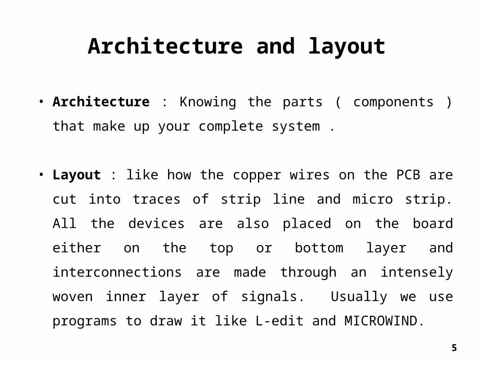
Architecture and layout
• Architecture : Knowing the parts ( components ) that make up your
complete system .
• Layout : like how the copper wires on the PCB are cut into traces of strip
line and micro strip. All the devices are also placed on the board either
on the top or bottom layer and interconnections are made through an
intensely woven inner layer of signals. Usually we use programs to draw
it like L-edit and MICROWIND.
6
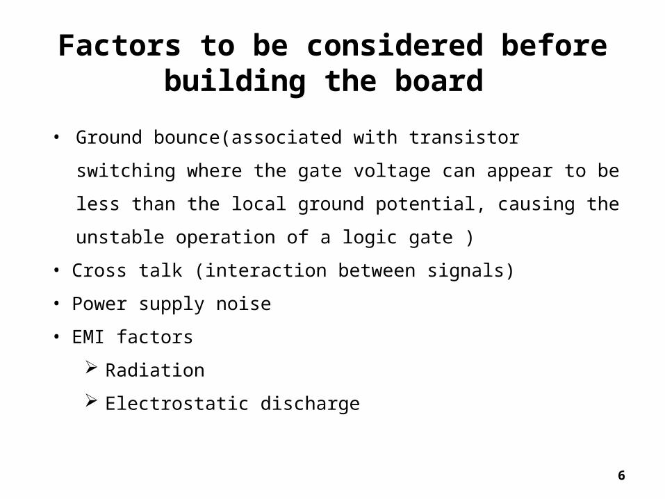
Factors to be considered before building the board
• Ground bounce(associated with transistor switching where the gate
voltage can appear to be less than the local ground potential, causing
the unstable operation of a logic gate )
• Cross talk (interaction between signals)
• Power supply noise
• EMI factors
Radiation
Electrostatic discharge
7
• Signals in high speed design are electrical in nature and consist of current
flowing through the wires. The following principles of mutual inductance,
mutual capacitance will affect the response, quality of the electrical signal
when it flows through a copper trace wire.
8
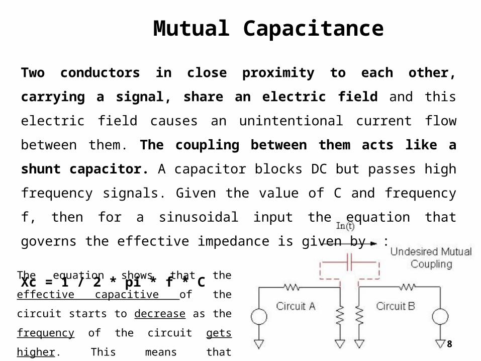
Mutual Capacitance
Two conductors in close proximity to each other, carrying a signal, share an
electric field and this electric field causes an unintentional current flow
between them. The coupling between them acts like a shunt capacitor. A
capacitor blocks DC but passes high frequency signals. Given the value of C and
frequency f, then for a sinusoidal input the equation that governs the effective
impedance is given by :
Xc = 1 / 2 * pi * f * C
The equation shows that the effective capacitive
of the circuit starts to decrease as the frequency
of the circuit gets higher. This means that
capacitors start becoming more like short circuits
at higher frequencies .
9
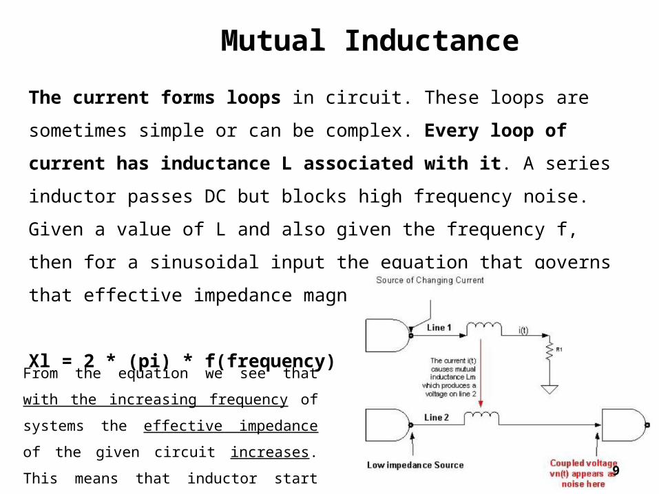
Mutual Inductance
The current forms loops in circuit. These loops are sometimes simple or can be
complex. Every loop of current has inductance L associated with it. A series
inductor passes DC but blocks high frequency noise.
Given a value of L and also given the frequency f, then for a sinusoidal input the
equation that governs that effective impedance magnitude is given by:
Xl = 2 * (pi) * f(frequency) * L
From the equation we see that with the
increasing frequency of systems the effective
impedance of the given circuit increases. This
means that inductor start becoming more like
open circuits at higher frequencies.
10
• These properties can help us find the effective capacitance or inductance
present in a circuit due to mutual inductance and capacitance. These are
the parasitic elements involved in a circuit and they have the ability to
destroy a good frequency response.
11
Current Loops
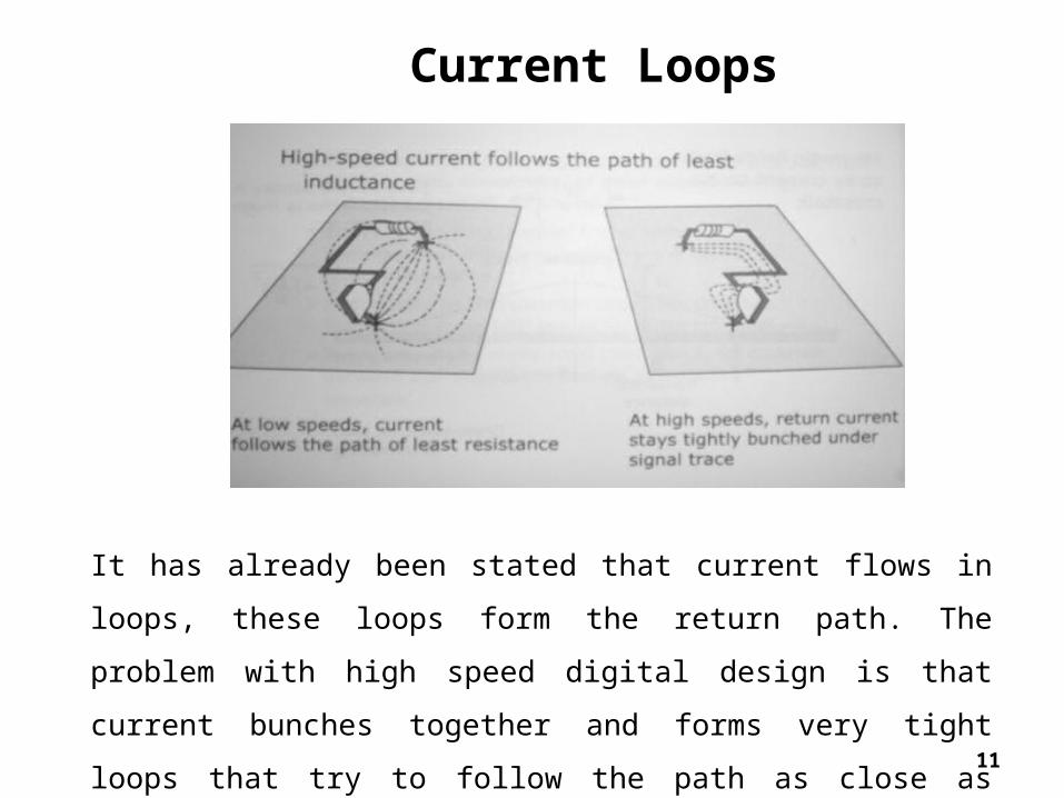
It has already been stated that current flows in loops, these loops form the
return path. The problem with high speed digital design is that current
bunches together and forms very tight loops that try to follow the path as
close as possible
12
Characteristic impedance
• Characteristic impedance is one of the properties of transmission lines.
• Characteristic impedance is the ratio of voltage to current in a transmission
line.
• In theory a perfectly matched transmission line will be devoid of any
reflections from the far end and thereby will not have any reflected signal
causing an addition or subtraction to the original signal at the near end and
so on.
• Reflections on a transmission line can be avoided by using terminations to
the transmission line.
• The most popular terminations used in the digital logic are either end
termination or series termination.
13
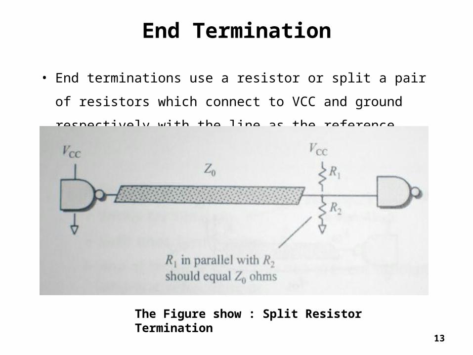
End Termination
• End terminations use a resistor or split a pair of resistors which connect
to VCC and ground respectively with the line as the reference point.
The Figure show : Split Resistor Termination
14
Series Termination
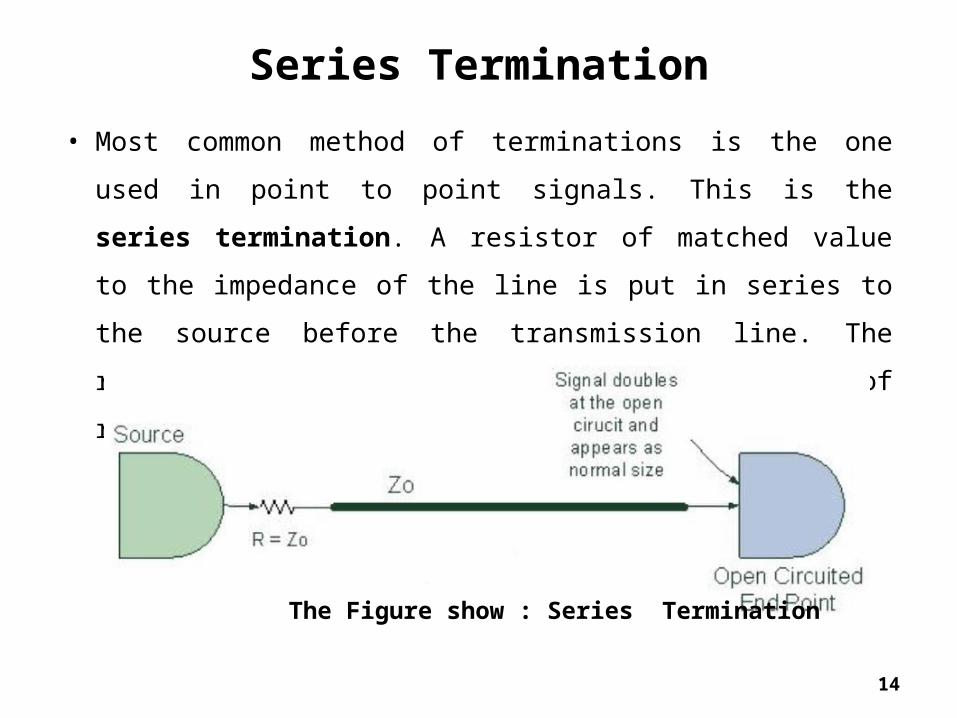
• Most common method of terminations is the one used in point to point
signals. This is the series termination. A resistor of matched value to the
impedance of the line is put in series to the source before the
transmission line. The resistor accomplishes the cancellation of
reflections
The Figure show : Series Termination

15
Analog to Digital Converter
16
Introduction
• ADC = Analog-Digital-Converter
• Conversion of audio signals (mobile micro, digital music
records, ...)
• Conversion of video signals (cameras, frame grabber, ...)
17
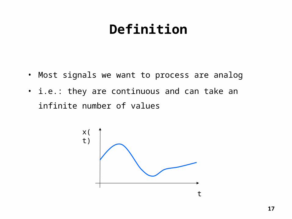
• Most signals we want to process are analog
• i.e.: they are continuous and can take an infinite number of values
x(t)
t
Definition
18
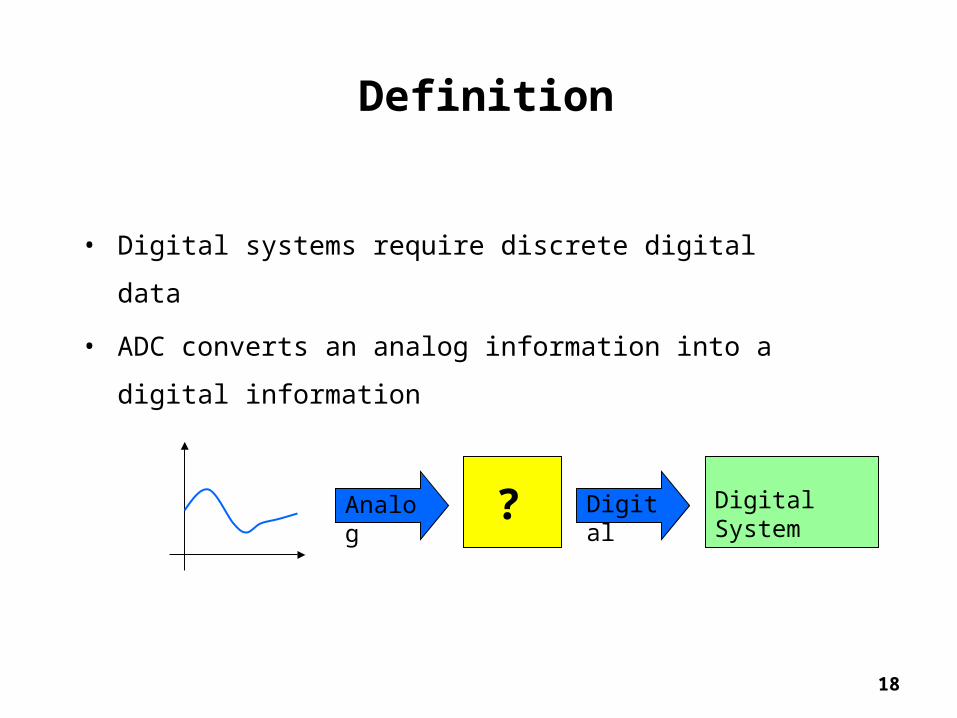
• Digital systems require discrete digital data
• ADC converts an analog information into a digital information
Digital System?Analog Digital
Definition
19
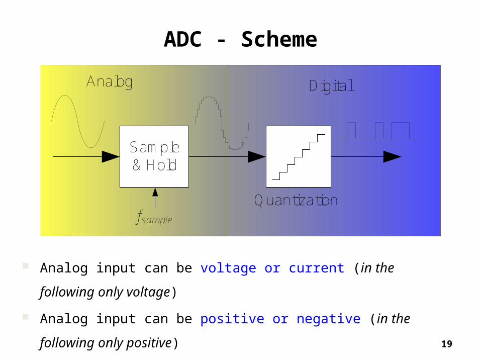
ADC - Scheme
Sample & Hold
Quantizationfsample
Analog Digital
Analog input can be voltage or current (in the following only voltage)
Analog input can be positive or negative (in the following only positive)
20
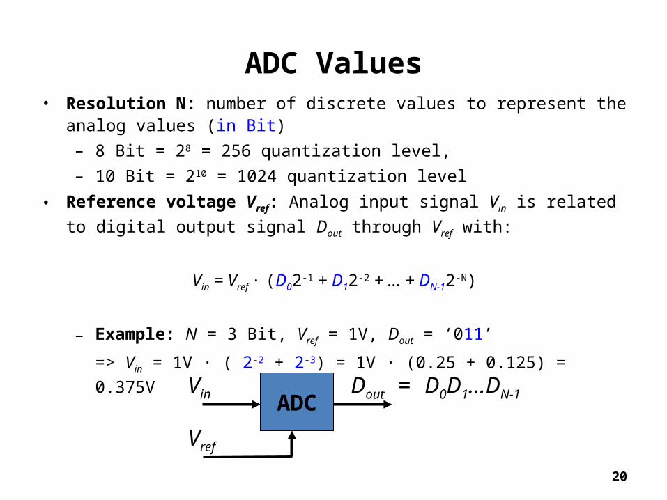
ADC Values• Resolution N: number of discrete values to represent the analog values (in Bit)
– 8 Bit = 28 = 256 quantization level, – 10 Bit = 210 = 1024 quantization level
• Reference voltage Vref: Analog input signal Vin is related to digital output signal Dout through Vref with:
Vin = Vref · (D02-1 + D12-2 + … + DN-12-N)
– Example: N = 3 Bit, Vref = 1V, Dout = ‘011’
=> Vin = 1V · ( 2-2 + 2-3) = 1V · (0.25 + 0.125) = 0.375V
ADCVin Dout = D0D1…DN-1
Vref
21
ADC Values
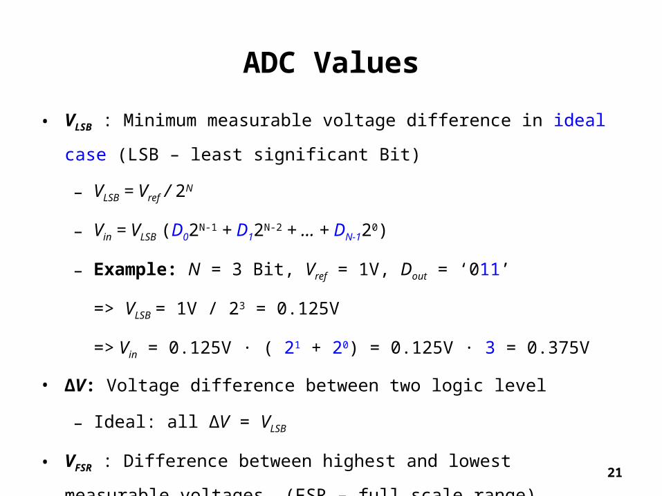
• VLSB : Minimum measurable voltage difference in ideal case (LSB – least
significant Bit)
– VLSB = Vref / 2N
– Vin = VLSB (D02N-1 + D12N-2 + … + DN-120)
– Example: N = 3 Bit, Vref = 1V, Dout = ‘011’
=> VLSB = 1V / 23 = 0.125V
=> Vin = 0.125V · ( 21 + 20) = 0.125V · 3 = 0.375V
• ΔV: Voltage difference between two logic level
– Ideal: all ΔV = VLSB
• VFSR : Difference between highest and lowest measurable voltages (FSR – full
scale range)
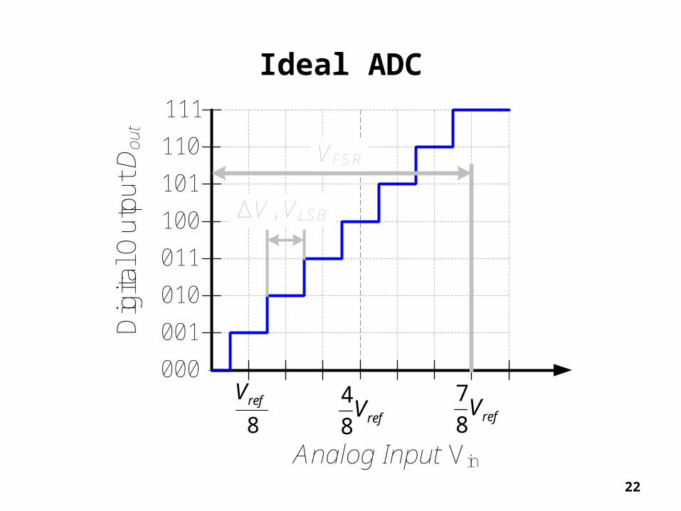
22
Ideal ADC
000
001
010
011
100
101
110
111
8refV
Dig
ital O
utpu
t Dou
t
Analog Input Vin
7
8 refV4
8 refV
ΔV, VLSB
VFSR
23
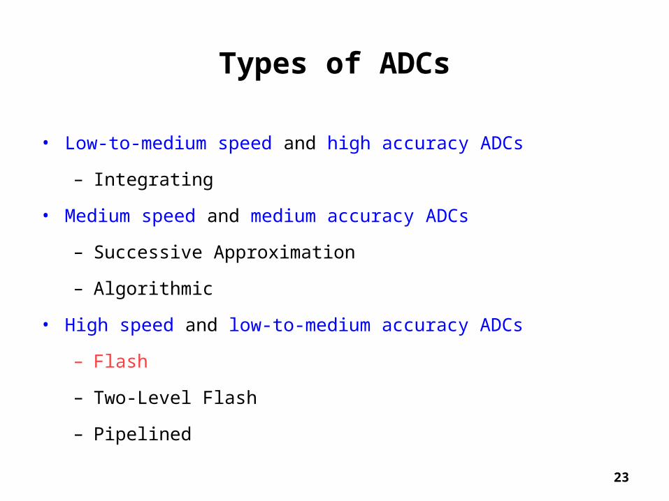
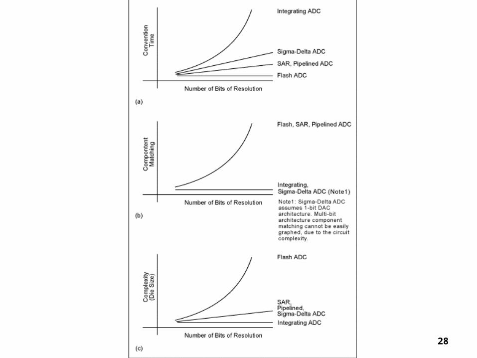
Types of ADCs
• Low-to-medium speed and high accuracy ADCs
– Integrating
• Medium speed and medium accuracy ADCs
– Successive Approximation
– Algorithmic
• High speed and low-to-medium accuracy ADCs
– Flash
– Two-Level Flash
– Pipelined
24
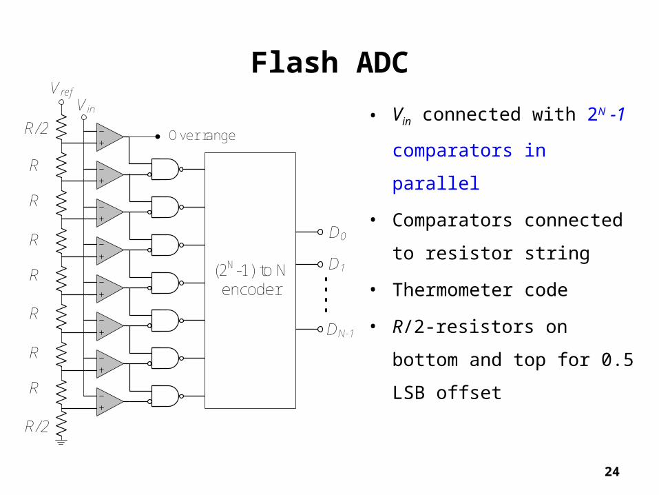
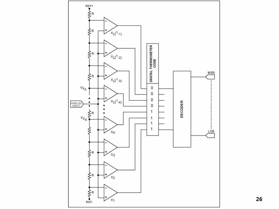
Flash ADC
• Vin connected with 2N -1
comparators in parallel
• Comparators connected to
resistor string
• Thermometer code
• R/2-resistors on bottom and top
for 0.5 LSB offset
Vin
Vref
Over range
D0
D1
DN-1
(2N-1) to N encoder
R/2
R
R/2
R
R
R
R
R
R
25
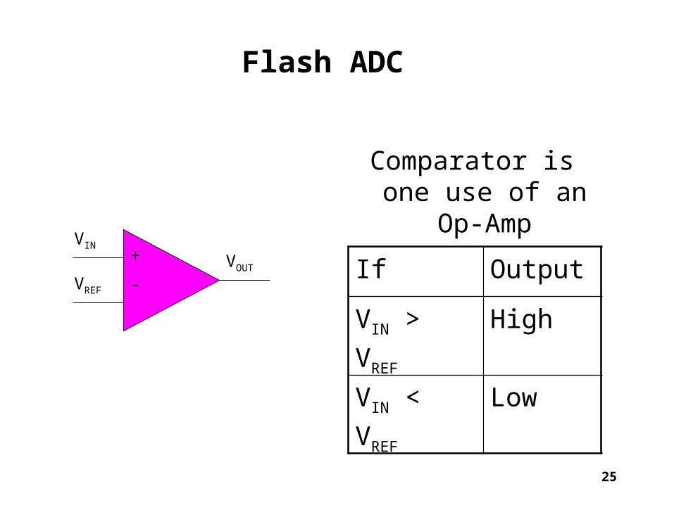
Comparator is one use of an Op-Amp
+
-
VIN
VREF
VOUT If Output
VIN > VREF High
VIN < VREF Low
Flash ADC
26
27
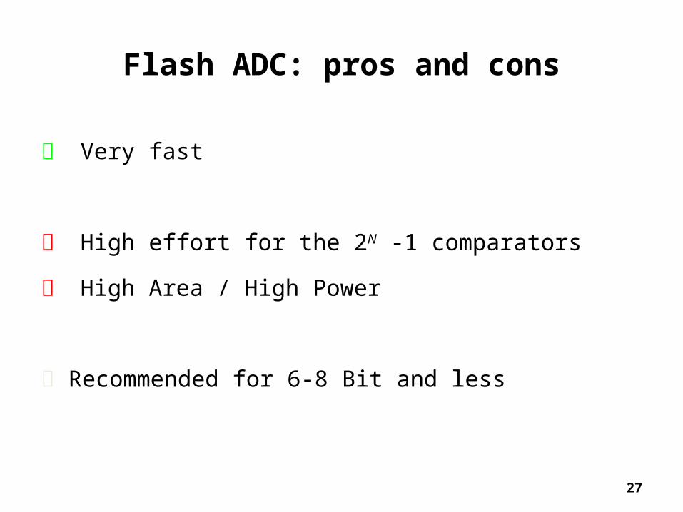
Flash ADC: pros and cons
Very fast
High effort for the 2N -1 comparators
High Area / High Power
Recommended for 6-8 Bit and less
28
29
A Dual Mode 7-Bit A/D Converter in 0.25 micron digital CMOS
30
Introduction
• Used in hard disk drive read channels
• It has 2 modes
– 6-bit resolution at full speed
– 7-bit more accurate mode operating at lower speed
• CMOS Technology : 0.25 um
• Speed :
– up to 700 MSamples/s in the 6-bit
– up to 200 MSamples/s in the 7-bit
• Area : 0.45 sq. mm
• Power consumption : less than 187m W
31
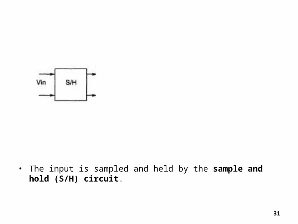
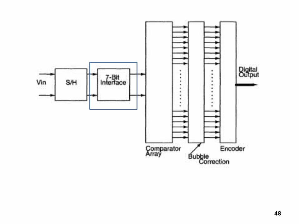
• The input is sampled and held by the sample and hold (S/H) circuit.
32
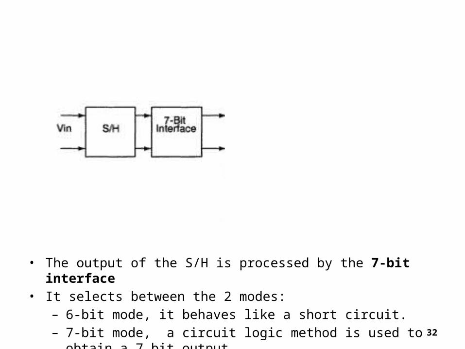
• The output of the S/H is processed by the 7-bit interface • It selects between the 2 modes:
– 6-bit mode, it behaves like a short circuit. – 7-bit mode, a circuit logic method is used to obtain a 7 bit output
33
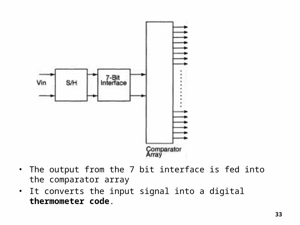
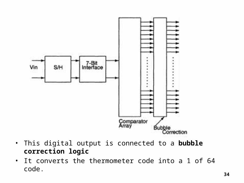
• The output from the 7 bit interface is fed into the comparator array• It converts the input signal into a digital thermometer code.
34
• This digital output is connected to a bubble correction logic • It converts the thermometer code into a 1 of 64 code.
35
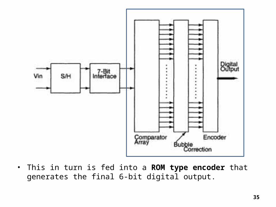
• This in turn is fed into a ROM type encoder that generates the final 6-bit digital output.
36
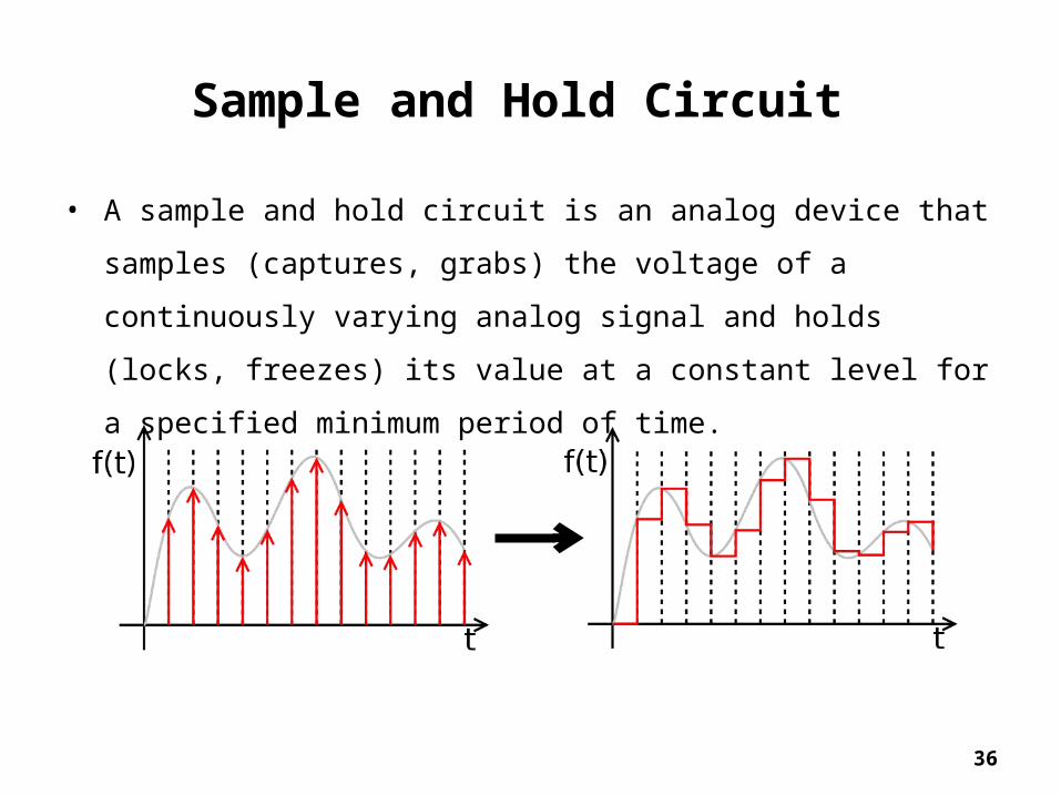
Sample and Hold Circuit
• A sample and hold circuit is an analog device that samples (captures,
grabs) the voltage of a continuously varying analog signal and holds (locks,
freezes) its value at a constant level for a specified minimum period of
time.
37
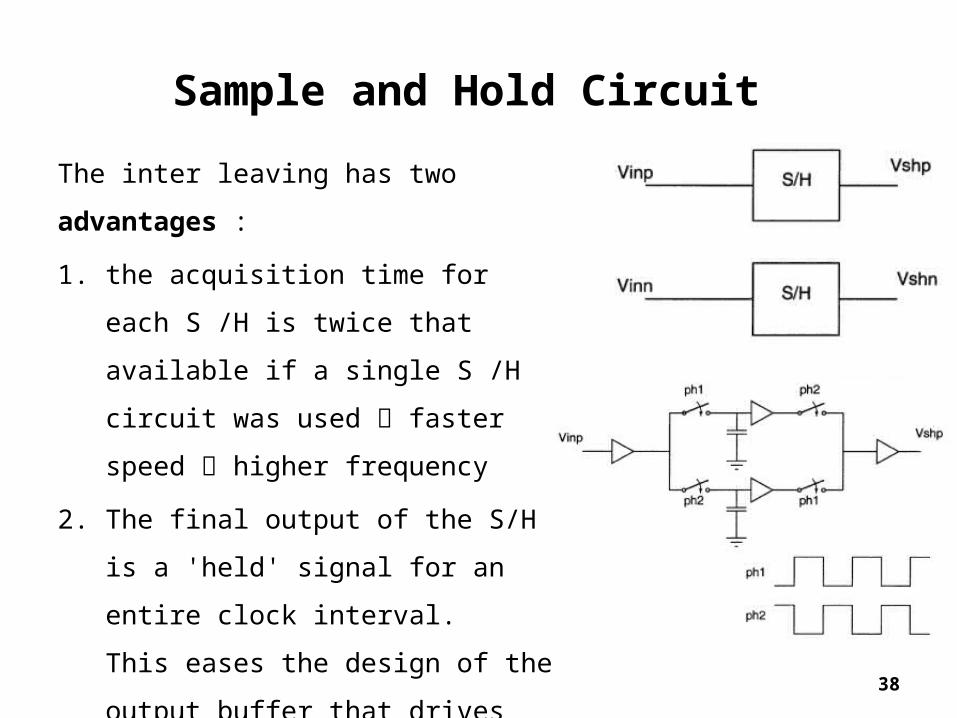
Sample and Hold Circuit
• It employs a pseudo-differential architecture made of two single ended
S/H circuits
• An important feature, it uses two inter-leaved S /H circuits operating at
half the sampling frequency:
1. The input signal is first buffered by an input buffer before being fed
into the two interleaved paths.
2. The two inter-leaved outputs are recombined using a set of pass
gates.
3. The re-combined signal is fed into a common output buffer that
drives the comparator array.
38
Sample and Hold Circuit
The inter leaving has two advantages :
1. the acquisition time for each S /H is twice
that available if a single S /H circuit was
used faster speed higher frequency
2. The final output of the S/H is a 'held'
signal for an entire clock interval.
This eases the design of the output buffer
that drives the comparator array.
The disadvantage with inter-leaving is the
mismatch between the two channels
39
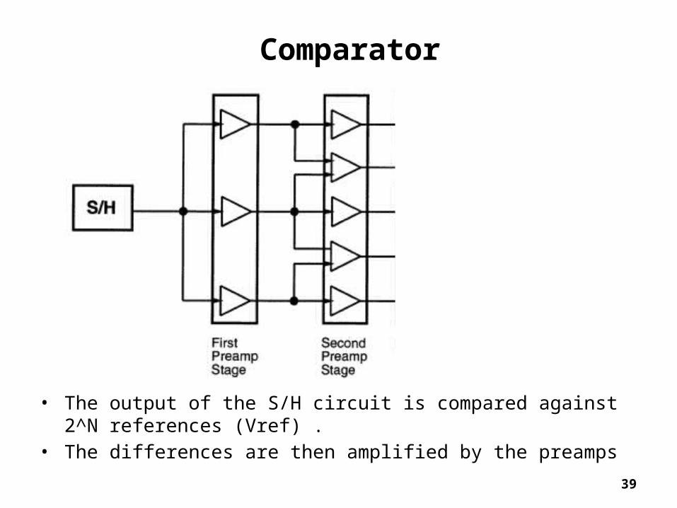
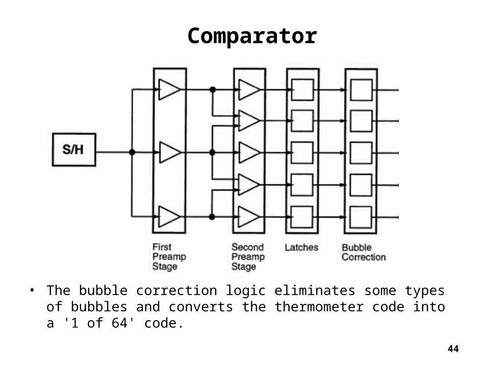
• The output of the S/H circuit is compared against 2^N references (Vref) .• The differences are then amplified by the preamps
Comparator
40
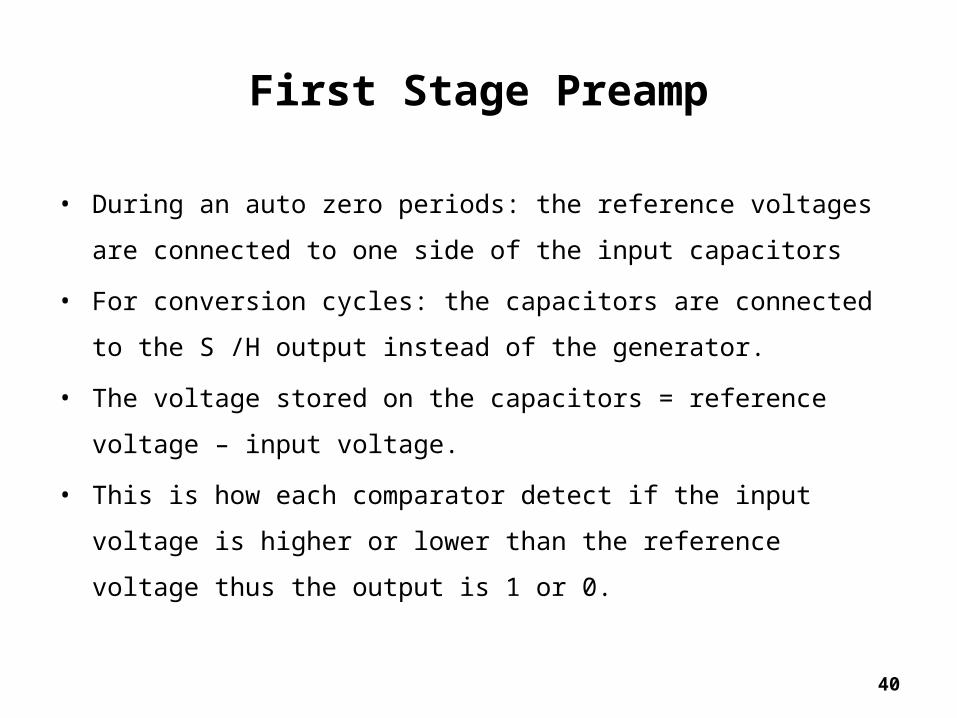
First Stage Preamp
• During an auto zero periods: the reference voltages are connected to one
side of the input capacitors
• For conversion cycles: the capacitors are connected to the S /H output
instead of the generator.
• The voltage stored on the capacitors = reference voltage – input voltage.
• This is how each comparator detect if the input voltage is higher or lower
than the reference voltage thus the output is 1 or 0.
41
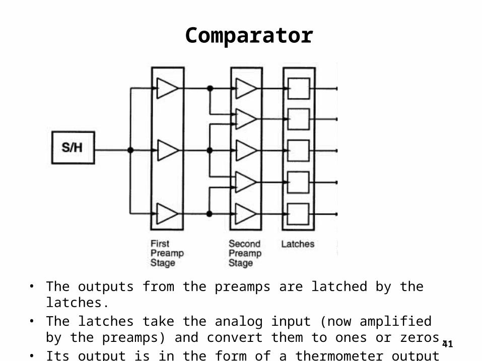
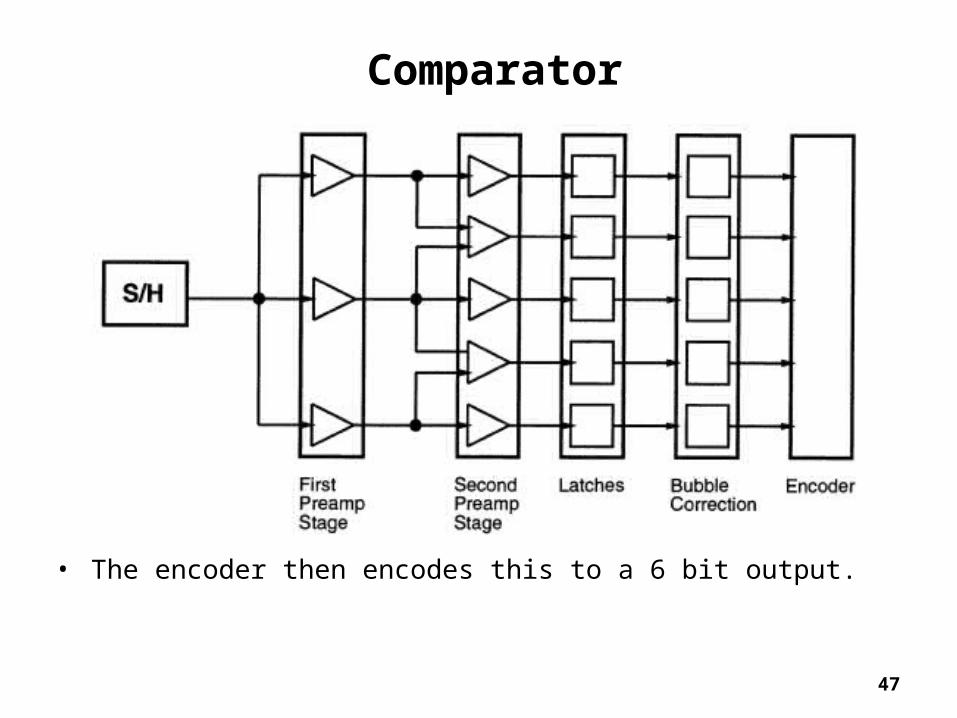
• The outputs from the preamps are latched by the latches.• The latches take the analog input (now amplified by the preamps) and
convert them to ones or zeros. • Its output is in the form of a thermometer output
Comparator
42
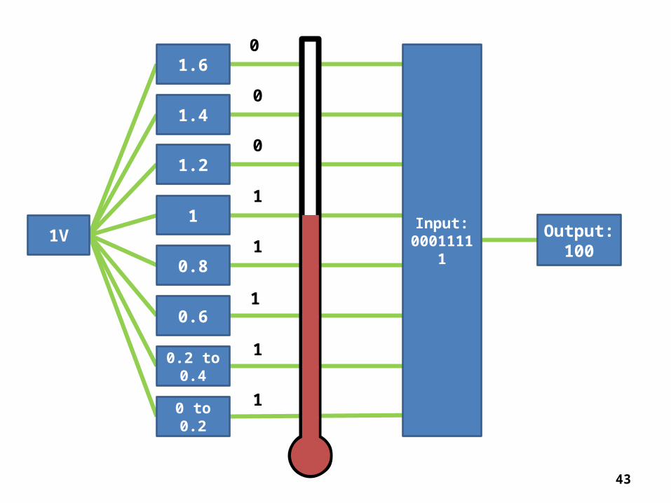
Explanation : Thermometer output
• The input voltage is compared with all reference voltages from down to up
– If input voltage > Vref output = 1
– If input voltage < Vref output = 0
• A series of ones is obtained until the reference voltage value is higher than
the input voltage which result zero outputs.
• The encoder’s binary output is equal to the order of the last reference
step with output 1 , also equal to total numbers of ones – 1
• It looks like a thermometer tube: Its liquid level increases gradually from
down to up until it reaches a stable value
43
1.4
1.2
1
0.8
1.6
0.6
0.2 to 0.4
0 to 0.2
Input:00011111
Output:100
1V
1
1
1
1
1
0
0
0
44
• The bubble correction logic eliminates some types of bubbles and converts the thermometer code into a '1 of 64' code.
Comparator
45
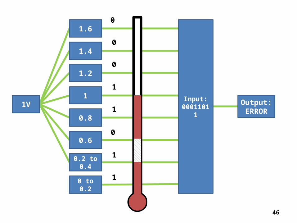
Explanation : Bubble error (sparkles)
• An error can occur in the thermometer output when we receive a zero in
the middle of the ones series due to a wrong output from the comparator
• This is called the bubble error (sparkle). It is like an air bubble gap in the
middle of our thermometer liquid.
• This can be fixed by an error correction circuit that have multiple methods
to detect any incorrect outputs in the middle of the thermometer output
and fix it
46
1.4
1.2
1
0.8
1.6
0.6
0.2 to 0.4
0 to 0.2
Input:00011011
Output:ERROR
1V
1
1
0
1
1
0
0
0
47
• The encoder then encodes this to a 6 bit output.
Comparator
48
49
Operation of the 7-bit mode (Dual Mode)
• 7-bit operation is achieved here using a two step technique
• First step: a 6-bit A/D conversion performed with an analog voltage =
input voltage + ½ LSB.
• The LSB from this operation is stored in a 1-bit memory element D.
• Second step: a normal 6-bit A/D conversion performed without adding the
½ LSB to the input.
• The 7th bit is obtained by Xor-ing the new LSB with the previous saved one
50
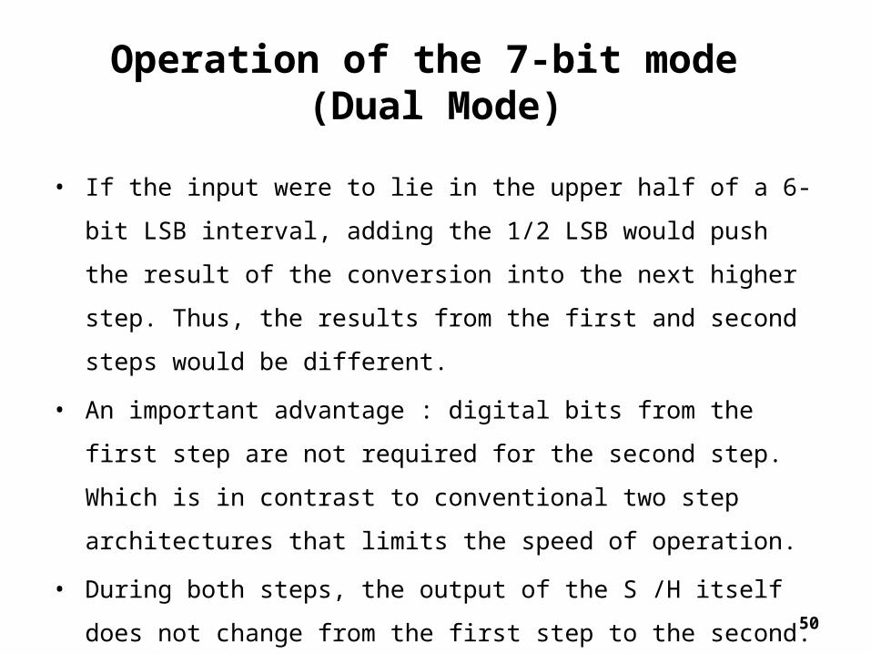
Operation of the 7-bit mode (Dual Mode)
• If the input were to lie in the upper half of a 6-bit LSB interval, adding the
1/2 LSB would push the result of the conversion into the next higher step.
Thus, the results from the first and second steps would be different.
• An important advantage : digital bits from the first step are not required
for the second step. Which is in contrast to conventional two step
architectures that limits the speed of operation.
• During both steps, the output of the S /H itself does not change from the
first step to the second.
51
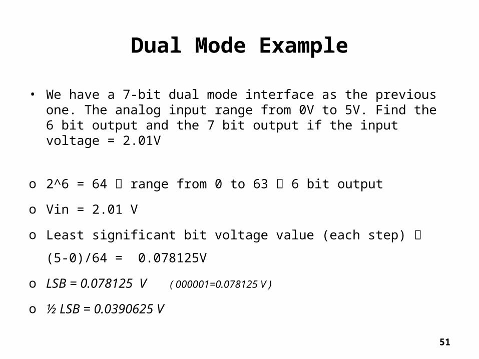
Dual Mode Example
• We have a 7-bit dual mode interface as the previous one. The analog input range from 0V to 5V. Find the 6 bit output and the 7 bit output if the input voltage = 2.01V
o 2^6 = 64 range from 0 to 63 6 bit output
o Vin = 2.01 V
o Least significant bit voltage value (each step) (5-0)/64 = 0.078125V
o LSB = 0.078125 V ( 000001=0.078125 V )
o ½ LSB = 0.0390625 V
52
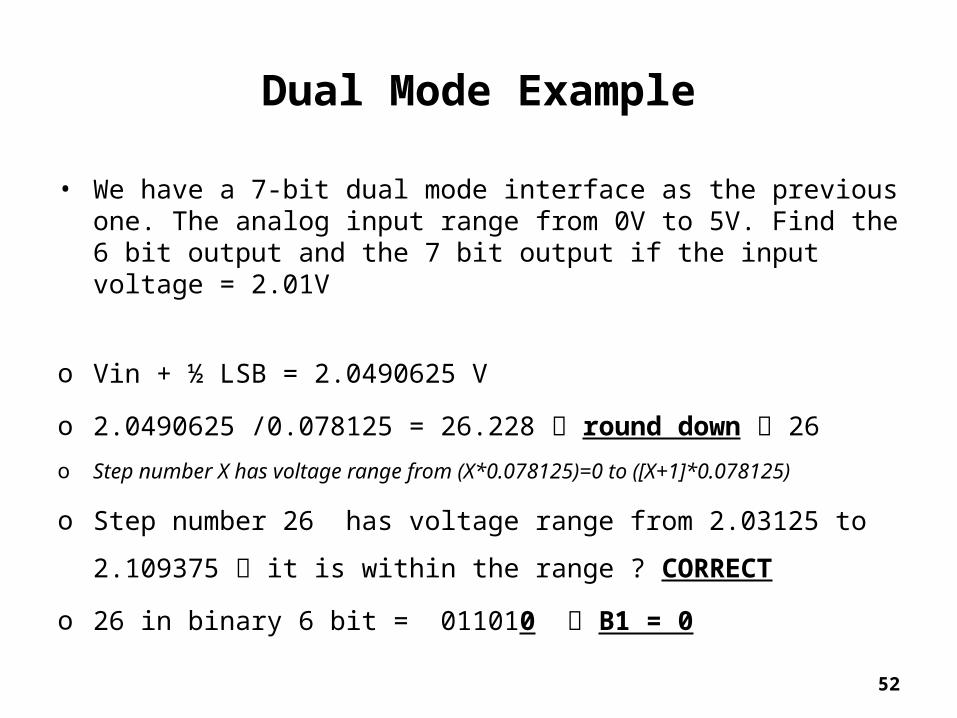
Dual Mode Example
• We have a 7-bit dual mode interface as the previous one. The analog input range from 0V to 5V. Find the 6 bit output and the 7 bit output if the input voltage = 2.01V
o Vin + ½ LSB = 2.0490625 V
o 2.0490625 /0.078125 = 26.228 round down 26
o Step number X has voltage range from (X*0.078125)=0 to ([X+1]*0.078125)
o Step number 26 has voltage range from 2.03125 to 2.109375 it is within
the range ? CORRECT
o 26 in binary 6 bit = 011010 B1 = 0
53
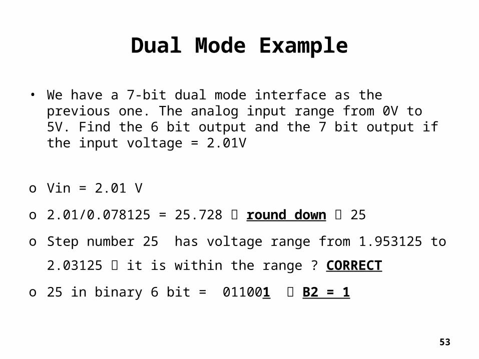
Dual Mode Example
• We have a 7-bit dual mode interface as the previous one. The analog input range from 0V to 5V. Find the 6 bit output and the 7 bit output if the input voltage = 2.01V
o Vin = 2.01 V
o 2.01/0.078125 = 25.728 round down 25
o Step number 25 has voltage range from 1.953125 to 2.03125 it is within
the range ? CORRECT
o 25 in binary 6 bit = 011001 B2 = 1
54
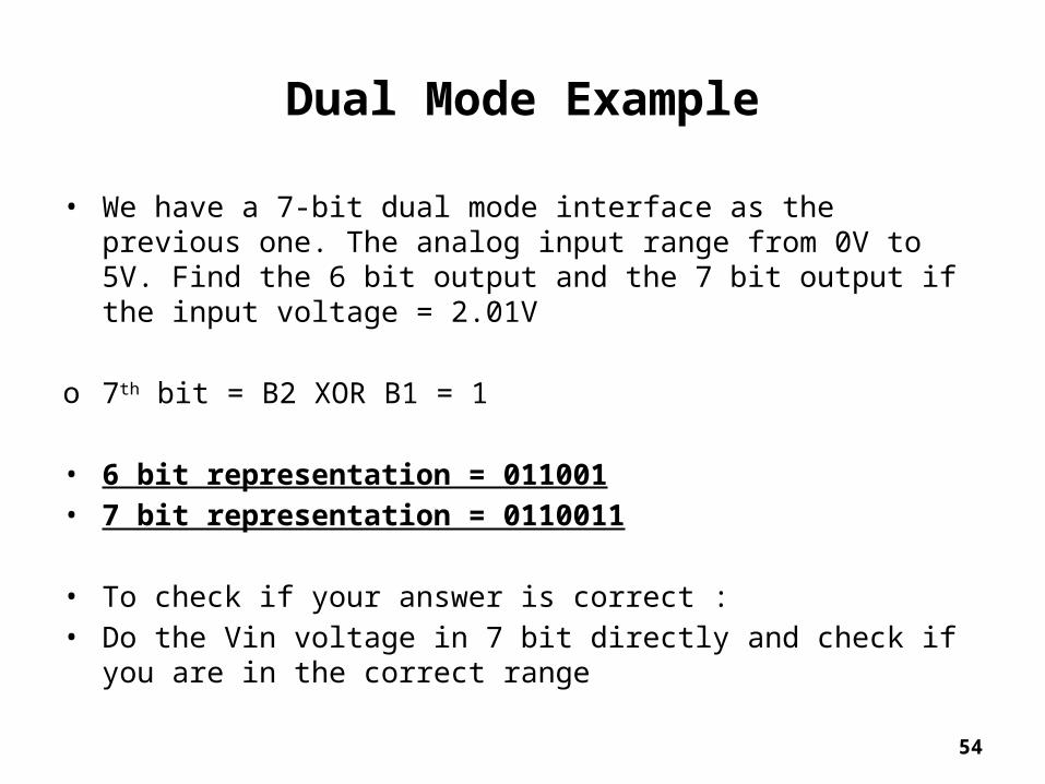
Dual Mode Example
• We have a 7-bit dual mode interface as the previous one. The analog input range from 0V to 5V. Find the 6 bit output and the 7 bit output if the input voltage = 2.01V
o 7th bit = B2 XOR B1 = 1
• 6 bit representation = 011001• 7 bit representation = 0110011
• To check if your answer is correct :• Do the Vin voltage in 7 bit directly and check if you are in the correct
range
55
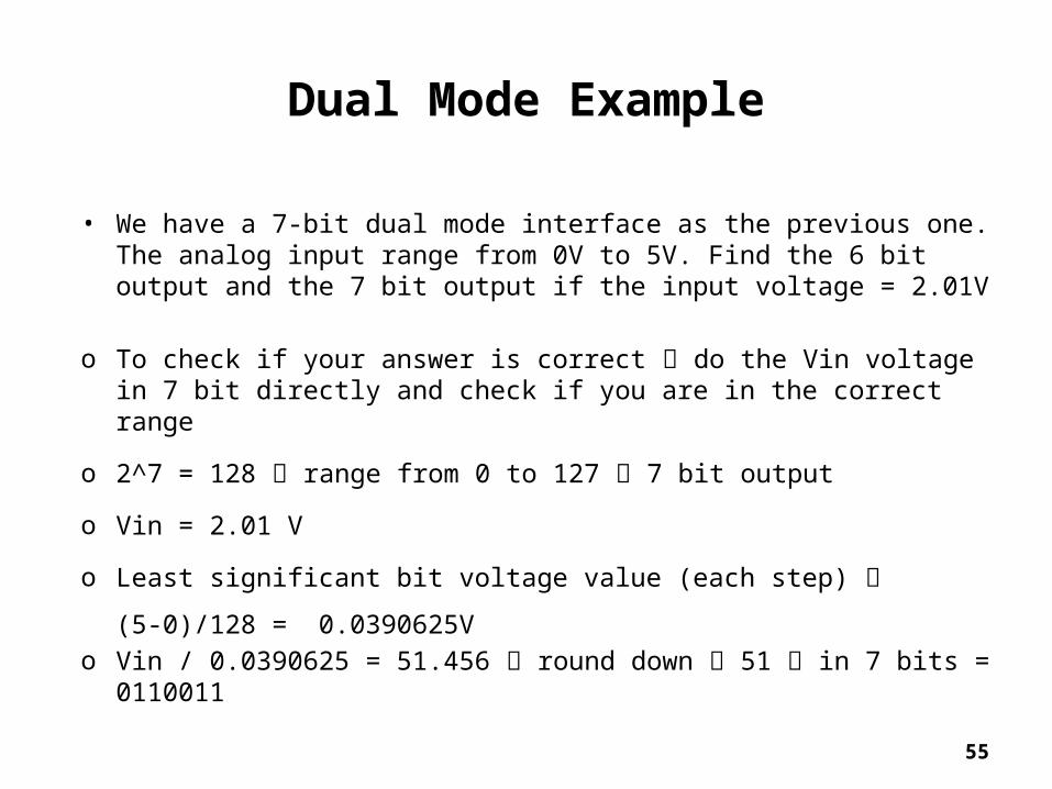
Dual Mode Example
• We have a 7-bit dual mode interface as the previous one. The analog input range from 0V to 5V. Find the 6 bit output and the 7 bit output if the input voltage = 2.01V
o To check if your answer is correct do the Vin voltage in 7 bit directly and check if you are in the correct range
o 2^7 = 128 range from 0 to 127 7 bit output
o Vin = 2.01 V
o Least significant bit voltage value (each step) (5-0)/128 = 0.0390625Vo Vin / 0.0390625 = 51.456 round down 51 in 7 bits = 0110011
56
6 Bit 2.5GS/s Flash ADC using Comparator Redundancy for Low
Power in 90 nm CMOS
57
Aim Of this Paper
• Utilize Comparator Redundancy to avoid traditional power , speed and
accuracy trade offs
• Redundancy removes the need to control comparator offsets
58
Main Advantage of Comparator Redundancy
• As the mismatch induced comparator offsets will get worse with scaling,
using comparator redundancy is a mean for taking full advantage of
decreased feature sizes in future CMOS processes, with higher speeds and
lower power dissipation.
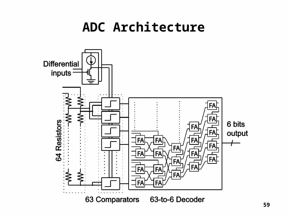
59
ADC Architecture
60
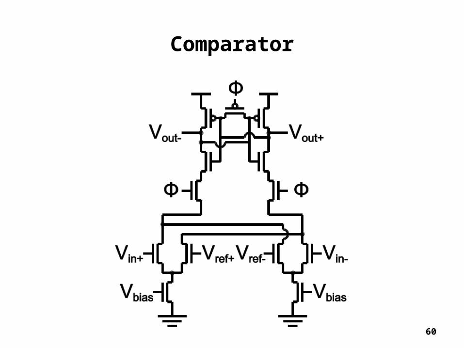
Comparator
61
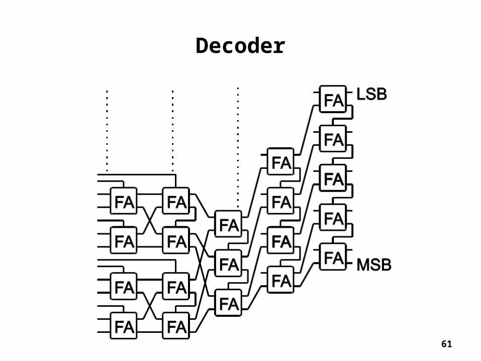
Decoder
62
Calibration
• We can control trip point externally to calibrate the ADC for 4
bits
• Select the number of comparators required for 4 bits by
making distance between trip points of each neighbouring
comparator pair constant
63
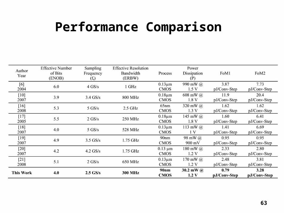
Performance Comparison
64
Conclusion
• Only trade off between speed and power
• The result of 2.5 GS/s 4 bit ADC dissipates 30.2 mW of power
65
• Q1: explain mutual inductor and mutual capacitance principle ?
• Q2: explain how to over come reflectance of transmission ?
• Q3: state the factors that need to be considered before building on
design board.
• Q4: explain current loop principle and state the difference in its direction
in high and low speed digital design .
Questions
66
• Q5: What is the basic function of an S/H block in any circuit with analog
input
• Q6: What is a bubble error (sparkles) and where it occurs ?
• Q7:Why did he use Wallace to design encoder?
• Q8:Find V (least significant bit) , N=3 bits, Voltage range from 0V to 3V
Questions
67
Questions
• Q9:Find V (least significant bit) , N=4 bits, Voltage range from 0V to 3V
• Q10:After solving Q8 and Q9 which one is better in terms of Resolution?
and why ?
• Q11: If the comparator is balanced the trip point is
a) shifted towards negative input
b) shifted towards positive input
c) equal
d) none of the above
68
References
1. “High Speed Digital Design”, Two Days of Black Magic with Dr. Howard Johnson,
presentation manual, HSDD 2007 V .13
2. “High Speed Digital Design: A Handbook of Black Magic”, Dr. Howard Johnson,
Prentice Hall publications .
3. “Why Johnny Can’t Design a High-Speed Digital System” , by Dr. Howard Johnson.
4. ”High Speed Digital Design Principles “, Sathish Venkataramani , January 2009 .
5. Nagaraj, K., et al. "A Dual Mode 700 MSamples/s 6-bit, 200MSamples/s 7-bit A/D
Converter in 0.25 Micron Digital CMOS." Analog Circuit Design. Springer US, 2000.
25-45.
6. ”A 6 bit 2.5 GS/s Flash ADC using Comparator Redundancy for Low Power in ‐ ‐
90nm CMOS,“ in Analog Integrated Circuits and Signal Processing, Volume 64,
Issue 3, pp. 215 - 222, August 2010.