Embed Size (px)
Citation preview

1JULY 2019
DSC 3241/15
7054L
Features◆◆◆◆◆ High-speed access
– Commercial: 20ns (max.)◆◆◆◆◆ Low-power operation
– IDT7054LActive: 750mW (typ.)Standby: 1.5mW (typ.)
◆◆◆◆◆ True FourPort memory cells which allow simultaneousaccess of the same memory locations
◆◆◆◆◆ Fully asynchronous operation from each of the four ports:P1, P2, P3, and P4
◆◆◆◆◆ TTL-compatible; single 5V (±10%) power supply◆◆◆◆◆ Available in 128 pin Thin Quad Flatpack package◆◆◆◆◆ Green parts available, see ordering information
DescriptionThe IDT7054 is a high-speed 4K x 8 FourPort™ Static RAM designed
to be used in systems where multiple access into a common RAM isrequired. This FourPort Static RAM offers increased system performancein multiprocessor systems that have a need to communicate in real time andalso offers added benefit for high-speed systems in which multiple accessis required in the same cycle.
The IDT7054 is also designed to be used in systems where on-chiphardware port arbitration is not needed. This part lends itself to thosesystems which cannot tolerate wait states or are designed to be able toexternally arbitrated or withstand contention when all ports simulta-neously access the same FourPort RAM location.
The IDT7054 provides four independent ports with separate control,address, and I/O pins that permit independent, asynchronous access for
Functional Block Diagram
HIGH-SPEED4K x 8 FourPortTM
STATIC RAM
MEMORYARRAY
COLUMNI/O
PORT 1ADDRESSDECODE
LOGIC
PORT 2ADDRESSDECODE
LOGIC
COLUMNI/O
COLUMNI/O
PORT 4ADDRESSDECODE
LOGIC
PORT 3ADDRESSDECODE
LOGIC
COLUMNI/O
R/WP1
I/O0P1-I/O7P1
CEP1
OEP1
A0P1 - A11P1
R/WP2
CEP2
OEP2
3241 drw 01
I/O0P2-I/O7P2
A0P2 - A11P2
R/WP4
I/O0P4-I/O7P4
CEP4
OEP4
A0P4 - A11P4
R/WP3CEP3
OEP3
I/O0P3-I/O7P3
A0P3 - A11P3

6.42
7054LHigh-Speed 4K x 8 FourPort™ Static RAM Industrial and Commercial Temperature Range
2
NOTES:1. All VCC pins must be connected to the power supply.2. All GND pins must be connected to the ground supply.3. Package body is approximately 14mm x 20mm x 1.4mm.4. This package code is used to reference the package diagram.5. This text does not indicate orientation of the actual part-marking.
1234567891011121314151617181920212223242526272829303132333435363738
1021011009998979695949392
90898887868584838281807978777675747372
706968676665
91
71
IDT7054PRFPKG128(4)
128-Pin TQFPTop View(5)
3241 drw 03
39 40 41 42 43 44 45 46 47 48 49 50 51 52 53 54 55 56 57 58 59 60 61 62 63 64
128
127
126
125
124
123
122
121
120
119
118
117
116
115
114
113
112
111
110
109
108
107
106
105
104
103
.
CEP2
OEP2
N/CN/CN/CN/CN/C
A0P1
A1P1
A2P1
A3P1
A4P1
A5P1
A6P1
A10P1
VCC
A7P1
A8P1
A9P1
A11P1
CEP1
R/WP1
OEP1
N/CN/CN/CN/CN/CN/C
I/O0P1
I/O1P1
I/O2P1
I/O3P1
GNDI/O4P1
I/O5P1
I/O6P1
I/O7P1
N/C
VC
CI/O
0P2
I/O1P
2I/O
2P2
GN
DI/O
3P2
I/O4P
2I/O
5P2
VC
CI/O
6P2
I/O7P
2N
/CI/0
0P3
I/O1P
3V
CC
I/O2P
3I/O
3P3
I/O4P
3G
ND
I/O5P
3I/O
6P3
I/O7P
3N
/CV
CC
I/O0P
4
CEP3
R/WP3
N/CN/CN/CN/CN/CA0P4
A1P4
A2P4
A3P4
A4P4
A5P4
A6P4
A10P4
GNDA7P4
A8P4
A9P4
A11P4
CEP4
R/WP4
OEP4
N/CN/CN/CN/CN/CGNDN/CI/O7P4
I/O6P4
I/O5P4
GNDI/O4P4
I/O3P4
I/O2P4
I/O1P4
R/W
P2
A11
P2
A9P
2A
8P2
A7P
2A
10P
2A
6P2
A5P
2A
4P2
A3P
2A
2P2
A1P
2A
0P2
A0P
3A
1P3
A2P
3A
3P3
A4P
3A
5P3
A6P
3A
10P
3A
7P3
A8P
3A
9P3
A11
P3
OE
P3
INDEX
07/09/19
reads or writes to any location in memory. It is the user’s responsibility toensure data integrity when simultaneously accessing the same memorylocation from all ports. An automatic power down feature, controlled byCE, permits the on-chip circuitry of each port to enter a very low powerstandby power mode.
Pin Configuration(1,2,3)
Fabricated using CMOS high-performance technology, this FourPortSRAM typically operates on only 750mW of power.
The IDT7054 is packaged in a 128-pin Thin Quad Flatpack (TQFP).

6.42
7054LHigh-Speed 4K x 8 FourPort™ Static RAM Industrial and Commercial Temperature Range
3
Pin Configurations(1,2)
NOTES:1. All VCC pins must be connected to the power supply.2. All GND pins must be connected to the ground supply.
Absolute Maximum Ratings(1)
NOTES:1. Stresses greater than those listed under ABSOLUTE MAXIMUM RATINGS may
cause permanent damage to the device. This is a stress rating only andfunctional operation of the device at these or any other conditions above thoseindicated in the operational sections of this specification is not implied. Exposureto absolute maximum rating conditions for extended periods may affectreliability.
2. VTERM must not exceed Vcc + 10% for more than 25% of the cycle time or 10nsmaximum, and is limited to < 20mA for the period of VTERM > VCC + 10%.
NOTES:1. VIL > -1.5V for pulse width less than 10ns.2. VTERM must not exceed Vcc + 10%.
Recommended DC OperatingConditions
Maximum Operating Temperatureand Supply Voltage(1)
NOTES:1. This parameter is determined by device characterization but is not production
tested.2. 3dV references the interpolated capacitance when the input and the output
signals switch from 0V to 3V or from 3V to 0V.
Capacitance(1)
(TA = +25°C, f = 1.0MHz) TQFP ONLY
NOTES:1. This is the parameter TA. This is the "instant on" case temperature.
Symbol Pin Name
A0 P1 - A11 P1 Address Lines - Port 1
A0 P2 - A11 P2 Address Lines - Port 2
A0 P3 - A11 P3 Address Lines - Port 3
A0 P4 - A11 P4 Address Lines - Port 4
I/O0 P1 - I/O7 P1 Data I/O - Port 1
I/O0 P2 - I/O7 P2 Data I/O - Port 2
I/O0 P3 - I/O7 P3 Data I/O - Port 3
I/O0 P4 - I/O7 P4 Data I/O - Port 4
R/W P1 Read/Write - Port 1
R/W P2 Read/Write - Port 2
R/W P3 Read/Write - Port 3
R/W P4 Read/Write - Port 4
GND Ground
CE P1 Chip Enab le - Port 1
CE P2 Chip Enab le - Port 2
CE P3 Chip Enab le - Port 3
CE P4 Chip Enab le - Port 4
OE P1 Output Enable - Port 1
OE P2 Output Enable - Port 2
OE P3 Output Enable - Port 3
OE P4 Output Enable - Port 4
VCC Power
3241 tbl 01
Symbol Parameter Min. Typ. Max. Unit
VCC Supply Voltage 4.5 5.0 5.5 V
GND Ground 0 0 0 V
VIH Input High Voltage 2.2 ____ 6.0(2) V
VIL Input Low Voltage -0.5(1) ____ 0.8 V3241 tbl 02
Symbol Parameter Conditions(2) Max. Unit
CIN Input Capacitance VIN = 0V 9 pF
COUT OutputCapacitance
VOUT = 0V 10 pF
3241 tbl 03
GradeAmbient
Temperature GND Vcc
Commercial 0°C to +70°C 0V 5.0V + 10%
Industrial -40°C to +85°C 0V 5.0V + 10%
3241 tbl 04
Symbol Rating Commercial& Industrial
Unit
VTERM(2) Terminal Voltagewith Respectto GND
-0.5 to +7.0 V
TBIAS TemperatureUnder Bias
-55 to +125 oC
TSTG StorageTemperature
-65 to +150 oC
IOUT DC Output Current 50 mA3241 tbl 05

6.42
7054LHigh-Speed 4K x 8 FourPort™ Static RAM Industrial and Commercial Temperature Range
4
NOTES:1. 'X' in part number indicates power rating (S or L).2. VCC = 5V, TA = +25°C and are not production tested.3. f = 0 means no address or control lines change.4. At f = fMAX, address and control lines (except Output Enable) are cycling at the maximum frequency read cycle of 1/tRC, and using “AC Test Conditions” of input
levels of GND to 3V.5. For the case of one port, divide the appropriate current above by four.
DC Electrical Characteristics Over the OperatingTemperature and Supply Voltage Range(1,5) (VCC = 5.0V ± 10%)
NOTE:1. At Vcc < 2.0V input leakages are undefined.
DC Electrical Characteristics Over the OperatingTemperature and Supply Voltage Range (VCC = 5.0V ± 10%)
Symbol Parameter Test Conditions
7054S 7054L
UnitMin. Max. Min. Max.
|ILI| Input Leakage Current(1) VCC = 5.5V, VIN = 0V to VCC ___ 10 ___ 5 µA
|ILO| Output Leakage Current CE = VIH, VOUT = 0V to VCC ___ 10 ___ 5 µA
VOL Output Low Voltage IOL = 4mA ___ 0.4 ___ 0.4 V
VOH Output High Voltage IOH = -4mA 2.4 ___ 2.4 ___ V
2674 tbl 07
Symbol Parameter Condition
7054X20Com'l Only
7054X25Com'l & Ind
7054X35Com'l Only
UnitVersion TYP.(2) Max. TYP.(2) Max. TYP.(2) Max.
ICC1 Operating PowerSupply Current(All Ports Active)
CE = VILOutputs Disabledf = 0(3)
COM'L. SL
150150
300250
150150
300250
150150
300250
mA
IND. SL
____
____
____
____150150
360300
150150
360300
mA
ICC2 Dynamic OperatingCurrent(All Ports Active)
CE = VILOutputs Disabledf = fMAX(4)
COM'L. SL
240210
370325
225195
350305
210180
335290
mA
IND. SL
____
____
____
____225195
400340
210180
395330
mA
ISB Standby Current(All Ports - TTL LevelInputs)
CE = VIHf = fMAX(4)
COM'L. SL
7060
9580
6050
8570
4035
7560
mA
IND. SL
____
____
____
____6050
11585
4035
11080
mA
ISB1 Full Standby Current(All Ports - AllCMOS Level Inputs)
All PortsCE > VCC - 0.2VVIN > VCC - 0.2V orVIN < 0.2V, f = 0(3)
COM'L. SL
1.50.3
151.5
1.50.3
151.5
1.50.3
151.5
mA
IND. SL
____
____
____
____1.50.3
304.5
1.50.3
304.5
mA
3241 tbl 06
6.42
7054LHigh-Speed 4K x 8 FourPort™ Static RAM Industrial and Commercial Temperature Range
5
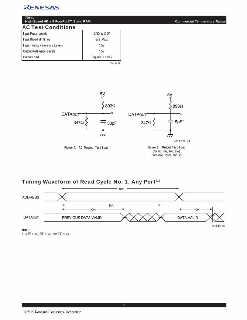
Timing Waveform of Read Cycle No. 1, Any Port(1)
NOTE:1. R/W = VIH, OE = VIL, and CE = VIL.
AC Test Conditions
Figure 1. AC Output Test Load Figure 2. Output Test Load(for tLZ, tHZ, tWZ, tOW)
*Including scope and jig
Input Pulse LevelsInput Rise/Fall TimesInput Timing Reference LevelsOutput Reference LevelsOutput Load
GND to 3.0V3ns Max.
1.5V1.5V
Figures 1 and 23241 tbl 08
DATAOUT
347Ω
893Ω
30pF
5V
3241 drw 04
DATAOUT
347Ω
893Ω
5pF*
5V
,
3241 drw 05
tAA
tOH tOH
DATAOUT
ADDRESS
tRC
DATA VALIDPREVIOUS DATA VALID

6.42
7054LHigh-Speed 4K x 8 FourPort™ Static RAM Industrial and Commercial Temperature Range
6
Timing Waveform of Read Cycle No. 2, Any Port(1, 2)
NOTES:1. R/W = VIH for Read Cycles.2. Addresses valid prior to or coincident with CE transition LOW.
AC Electrical Characteristics Over theOperating Temperature and Supply Voltage(3)
NOTES:1. Transition is measured 0mV from Low or High-impedance voltage with the Output Test Load (Figure 2).2. This parameter is guaranteed by device characterization but is not production tested.3. 'X' in part number indicates power rating (S or L).
7054X20Com'l Only
7054X25Com'l & Ind
7054X35Com'l Only
Symbol Parameter Min. Max. Min. Max. Min. Max. Unit
READ CYCLE
tRC Read Cycle Time 20 ____ 25 ____ 35 ____ ns
tAA Address Access Time ____ 20 ____ 25 ____ 35 ns
tACE Chip Enable Access Time ____ 20 ____ 25 ____ 35 ns
tAOE Output Enable Access Time ____ 10 ____ 15 ____ 25 ns
tOH Output Hold from Address Change 0 ____ 0 ____ 0 ____ ns
tLZ Output Low-Z Time(1,2) 5 ____ 5 ____ 5 ____ ns
tHZ Output High-Z Time(1,2) ____ 12 ____ 15 ____ 15 ns
tPU Chip Enable to Power Up Time(2) 0 ____ 0 ____ 0 ____ ns
tPD Chip Disable to Power Down Time(2) ____ 20 ____ 25 ____ 35 ns
3241 tbl 09
3241 drw 06
tAOE
tLZ tHZ
DATAOUT
CE
tACE
VALID DATA
OE
CURRENTICC
ISB
tPU
50%
tLZ
tPD
50%
tHZ

6.42
7054LHigh-Speed 4K x 8 FourPort™ Static RAM Industrial and Commercial Temperature Range
7
AC Electrical Characteristics Over theOperating Temperature and Supply Voltage(5)
NOTES:1. Transition is measured 0mV from Low or High-impedance voltage with the Output Test Load (Figure 2).2. This parameter is guaranteed by device characterization but is not production tested.3. If OE = VIL during a R/W controlled write cycle, the write pulse width must be the larger of tWP or (tWZ + tDW) to allow the I/O drivers to turn off data to be placed on
the bus for the required tDW. If OE = VIH during an R/W controlled write cycle, this requirement does not apply and the write pulse can be as short as the specifiedtWP. Specified for OE = VIH (refer to “Timing Waveform of Write Cycle”, Note 8).
4. Port-to-port delay through RAM cells from writing port to reading port, refer to “Timing Waveform of Write with Port-to-Port Read”.5. 'X' in part number indicates power rating.
7054X20Com'l Only
7054X25Com'l & Ind
7054X35Com'l Only
Symbol Parameter Min. Max. Min. Max. Min. Max. Unit
WRITE CYCLE
tWC Write Cycle Time 20 ____ 25 ____ 35 ____ ns
tEW Chip Enable to End-of-Write 15 ____ 20 ____ 30 ____ ns
tAW Address Valid to End-of-Write 15 ____ 20 ____ 30 ____ ns
tAS Address Set-up Time 0 ____ 0 ____ 0 ____ ns
tWP Write Pulse Width(3) 15 ____ 20 ____ 30 ____ ns
tWR Write Recovery Time 0 ____ 0 ____ 0 ____ ns
tDW Data Valid to End-of-Write 15 ____ 15 20 ____ ns
tHZ Output High-Z Time(1,2) ____ 15 ____ 15 ____ 15 ns
tDH Data Hold Time 0 ____ 0 ____ 0 ____ ns
tWZ Write Enable to Output in High-Z(1,2) ____ 12 ____ 15 ____ 15 ns
tOW Output Active from End-of-Write(1,2) 0 ____ 0 ____ 0 ____ ns
tWDD Write Pulse to Data Delay(4) ____ 35 ____ 45 ____ 55 ns
tDDD Write Data Valid to Read Data Delay(4) ____ 30 ____ 35 ____ 45 ns
3241 tbl 10

6.42
7054LHigh-Speed 4K x 8 FourPort™ Static RAM Industrial and Commercial Temperature Range
8
CE
3241 drw 08
tAW
tAS tWR
tDW
DATAIN
ADDRESS
tWC
R/W
tEW
tDH
(6) (2) (3)
Timing Waveform of Write Cycle No. 1, R/W Controlled Timing(5,8)
Timing Waveform of Write Cycle No. 2, CE Controlled Timing(1,5)
NOTES:1. R/W or CE = VIH during all address transitions.2. A write occurs during the overlap (tEW or tWP) of a CE = VIL and a R/W = VIL.3. tWR is measured from the earlier of CE or R/W = VIH to the end of write cycle.4. During this period, the I/O pins are in the output state, and input signals must not be applied.5. If the CE LOW transition occurs simultaneously with or after the R/W = VIL transition, the outputs remain in the High-impedance state.6. Timing depends on which enable signal is asserted last, CE or R/W.7. Transition is measured 0mV from Low or High-impedance voltage with the Output Test Load (Figure 2). This parameter is guaranteed but is not production tested.8. If OE = VIL during a R/W controlled write cycle, the write pulse width must be the larger of tWP or (tWZ + tDW) to allow the I/O drivers to turn off data to be placed
on the bus for the required tDW. If OE = VIH during an R/W controlled write cycle, this requirement does not apply and the write pulse can be as short as thespecified tWP.
CE
3241 drw 07
tAW
tAS
tWR
tDW
DATAIN
ADDRESS
tWC
R/W
tWP
DATAOUT
tWZ (7)
(4) (4)
(2)
tOW
OE
(7)tHZtLZ
(7)tHZ
(6)
(3)
tDH

6.42
7054LHigh-Speed 4K x 8 FourPort™ Static RAM Industrial and Commercial Temperature Range
9
Timing Waveform of Write with Port-to-Port Read(1, 2)
Functional DescriptionThe IDT7054 provides four ports with separate control, address, and
I/O pins that permit independent access for reads or writes to any locationin memory. These devices have an automatic power down featurecontrolled by CE. The CE controls on-chip power down circuitry that permits the respective port to go into standby mode when not selected(CE = VIH). When a port is enabled, access to the entire memory arrayis permitted. Each port has its own Output Enable control (OE). In the readmode, the port’s OE turns on the output drivers when set LOW. READ/WRITE conditions are illustrated in the table.
Table I – Read/Write Control
NOTES:1. "H" = VIH, "L" = VIL, "X" = Don’t Care, "Z "= High Impedance2. For valid write operation, no more than one port can write to the same address
location at the same time.
3241 drw 09
ADDR"A"
tWC
DATA"B"
MATCH
tWP
R/W"A"
DATAIN"A"
ADDR"B"
tDH
VALID
MATCH
VALID
tDDD
tWDD
tDW
NOTES:1. OE = VIL for the reading ports.2. All timing is the same for left and right ports. Port "A" may be either of the four ports and Port "B" is any other port.
Any Port(1)
R/W CE OE D0-7 Function
X H X Z Port Deselected: Power-Down
X H X Z CEP1=CEP2=CEP3=CEP4=VIHPower Down Mode ISB or ISB1
L L X DATAIN Data on port written into memory(2)
H L L DATAOUT Data in memory output on port
X X H Z Outputs Disabled
3241 tbl 11

6.42
7054LHigh-Speed 4K x 8 FourPort™ Static RAM Industrial and Commercial Temperature Range
10
Ordering Information
NOTES:LEAD FINISH (SnPb) parts are Obsolete. Product Discontinuation Notice - PDN# SP-17-02
A
Power
999
Speed
A
Package
A
Process/Temperature
Range
Blank Commercial (0°C to +70°C)
PRF 128-Pin Thin Quad Plastic Flatpack (PKG128)
20
XXXX
DeviceType
Speed in nanoseconds
3241 drw 10
L Low Power
7054 32K (4K x 8) FourPort RAM
Commercial Only
Blank8
TrayTape and Reel
G Green
A A
Note that information regarding recently obsoleted parts are included in this datasheet for customer convenience.
Ordering InformationSpeed
(ns) Orderable Part ID Pkg.Code
Pkg.Type
Temp.Grade
20 7054L20PRFG PKG128 TQFP C
7054L20PRFG8 PKG128 TQFP C

6.42
7054LHigh-Speed 4K x 8 FourPort™ Static RAM Industrial and Commercial Temperature Range
11
The IDT logo is a registered trademark of Integrated Device Technology, Inc.
CORPORATE HEADQUARTERS for SALES: for Tech Support:6024 Silver Creek Valley Road 800-345-7015 or 408-284-8200 408-284-2794San Jose, CA 95138 fax: 408-284-2775 [email protected]
www.idt.com
01/18/99: Initiated datasheet document historyConverted to new formatCosmetic typographical correctionsAdded additional notes to pin configurations
06/04/99: Changed drawing formatPage 1 Corrected DSC number
09/01/99: Removed Preliminary11/10/99: Replaced IDT logo05/23/00: Page 4 Increased storage temperature parameter
Clarified TA parameterPage 5 DC Electrical parameters–changed wording from "open" to "disabled"Changed ±200mV to 0mV in notes
10/22/01: Page 2 & 3 Added date revision for pin configurationsPage 5, 7 & 8 Added Industrial temp to column heading for 25ns speed to DC & AC Electrical CharacteristicsPage 11 Added Industrial temp offering to 25ns ordering informationPage 4, 5, 7 & 8 Removed Industrial temp footnote from all tablesPage 6 Changed 5ns to 3ns in AC Test Conditions tablePage 1 & 11 Replaced TM logo with ® logo
02/20/15: Page 1 Added green availability to featuresPage 2 Removed IDT in reference to fabricationPage 2 2V battery backup for Low-power versions are no longer offeredPage 2,3 & 10 The package code PK128-1 changed to PK128 to match standard package codesPage 10 Added Tape and Reel and Green to Ordering InformationPages 1-10 Removed all military data including the G108 pin configuration, changed table headings and ordering information
to indicate that there is no longer a military offering for this 7054 deviceProduct Discontinuation Notice - PDN# SP-17-02Last time buy expires June 15, 2018Pages 1 & 10 Deleted obsolete Commercial 25/35ns and Industrial 25ns speed gradesPages 1 & 10 Removed standard product offering and Industrial speed grade offeringPages 2 & 10 Updated package code PK128 to PKG128Page 10 Added Orderable Part Information
07/02/18:
Datasheet Document History
07/11/19:
Corporate HeadquartersTOYOSU FORESIA, 3-2-24 Toyosu,Koto-ku, Tokyo 135-0061, Japanwww.renesas.com
Contact InformationFor further information on a product, technology, the most up-to-date version of a document, or your nearest sales office, please visit:www.renesas.com/contact/
TrademarksRenesas and the Renesas logo are trademarks of Renesas Electronics Corporation. All trademarks and registered trademarks are the property of their respective owners.
IMPORTANT NOTICE AND DISCLAIMER
RENESAS ELECTRONICS CORPORATION AND ITS SUBSIDIARIES (“RENESAS”) PROVIDES TECHNICAL SPECIFICATIONS AND RELIABILITY DATA (INCLUDING DATASHEETS), DESIGN RESOURCES (INCLUDING REFERENCE DESIGNS), APPLICATION OR OTHER DESIGN ADVICE, WEB TOOLS, SAFETY INFORMATION, AND OTHER RESOURCES “AS IS” AND WITH ALL FAULTS, AND DISCLAIMS ALL WARRANTIES, EXPRESS OR IMPLIED, INCLUDING, WITHOUT LIMITATION, ANY IMPLIED WARRANTIES OF MERCHANTABILITY, FITNESS FOR A PARTICULAR PURPOSE, OR NON-INFRINGEMENT OF THIRD PARTY INTELLECTUAL PROPERTY RIGHTS.
These resources are intended for developers skilled in the art designing with Renesas products. You are solely responsible for (1) selecting the appropriate products for your application, (2) designing, validating, and testing your application, and (3) ensuring your application meets applicable standards, and any other safety, security, or other requirements. These resources are subject to change without notice. Renesas grants you permission to use these resources only for development of an application that uses Renesas products. Other reproduction or use of these resources is strictly prohibited. No license is granted to any other Renesas intellectual property or to any third party intellectual property. Renesas disclaims responsibility for, and you will fully indemnify Renesas and its representatives against, any claims, damages, costs, losses, or liabilities arising out of your use of these resources. Renesas' products are provided only subject to Renesas' Terms and Conditions of Sale or other applicable terms agreed to in writing. No use of any Renesas resources expands or otherwise alters any applicable warranties or warranty disclaimers for these products.
(Rev.1.0 Mar 2020)
© 2020 Renesas Electronics Corporation. All rights reserved.