Embed Size (px)
Citation preview
July 2016 DocID12320 Rev 8 1/19
This is information on a product in full production. www.st.com
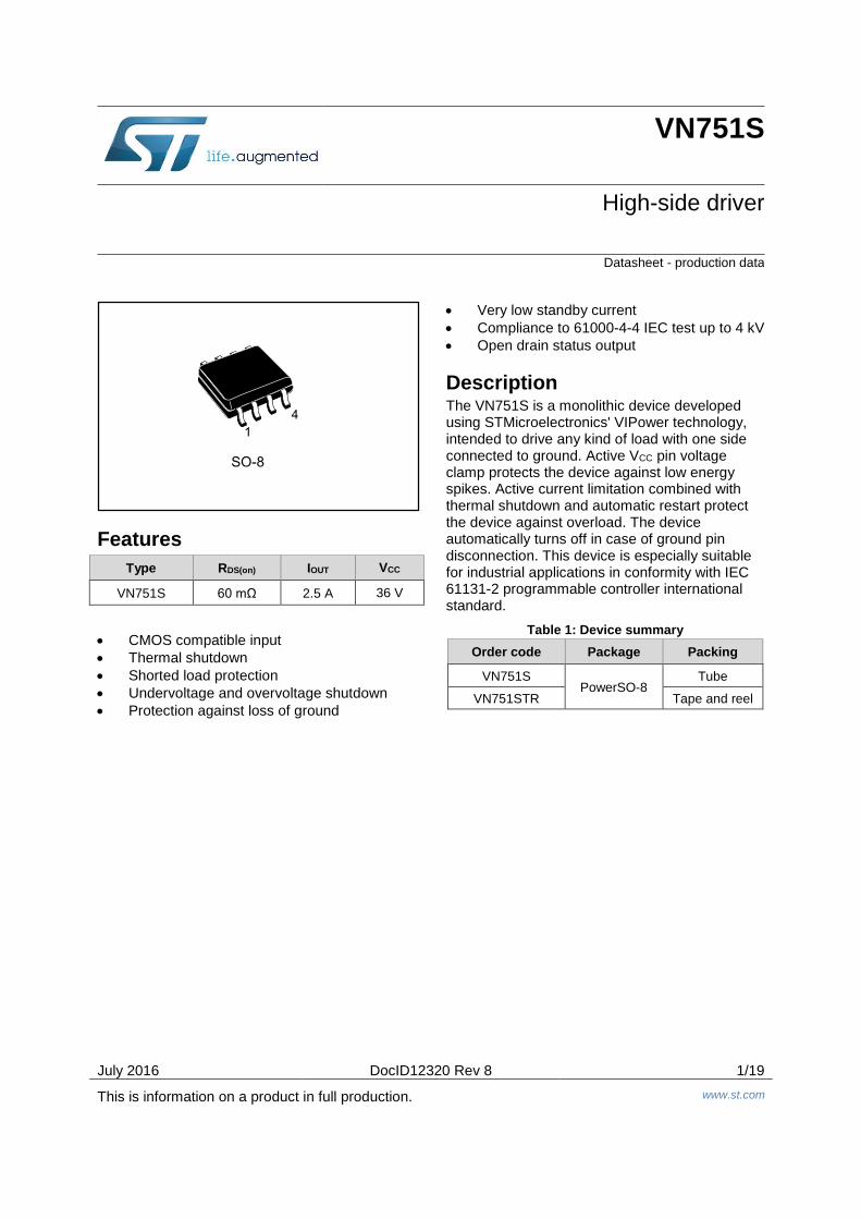
VN751S
High-side driver
Datasheet - production data
Features
Type RDS(on) IOUT VCC
VN751S 60 mΩ 2.5 A 36 V
CMOS compatible input
Thermal shutdown
Shorted load protection
Undervoltage and overvoltage shutdown
Protection against loss of ground
Very low standby current
Compliance to 61000-4-4 IEC test up to 4 kV
Open drain status output
Description The VN751S is a monolithic device developed using STMicroelectronics' VIPower technology, intended to drive any kind of load with one side connected to ground. Active VCC pin voltage clamp protects the device against low energy spikes. Active current limitation combined with thermal shutdown and automatic restart protect the device against overload. The device automatically turns off in case of ground pin disconnection. This device is especially suitable for industrial applications in conformity with IEC 61131-2 programmable controller international standard.
Table 1: Device summary
Order code Package Packing
VN751S PowerSO-8
Tube
VN751STR Tape and reel
Contents VN751S
2/19 DocID12320 Rev 8
Contents
1 Block diagram .................................................................................. 5
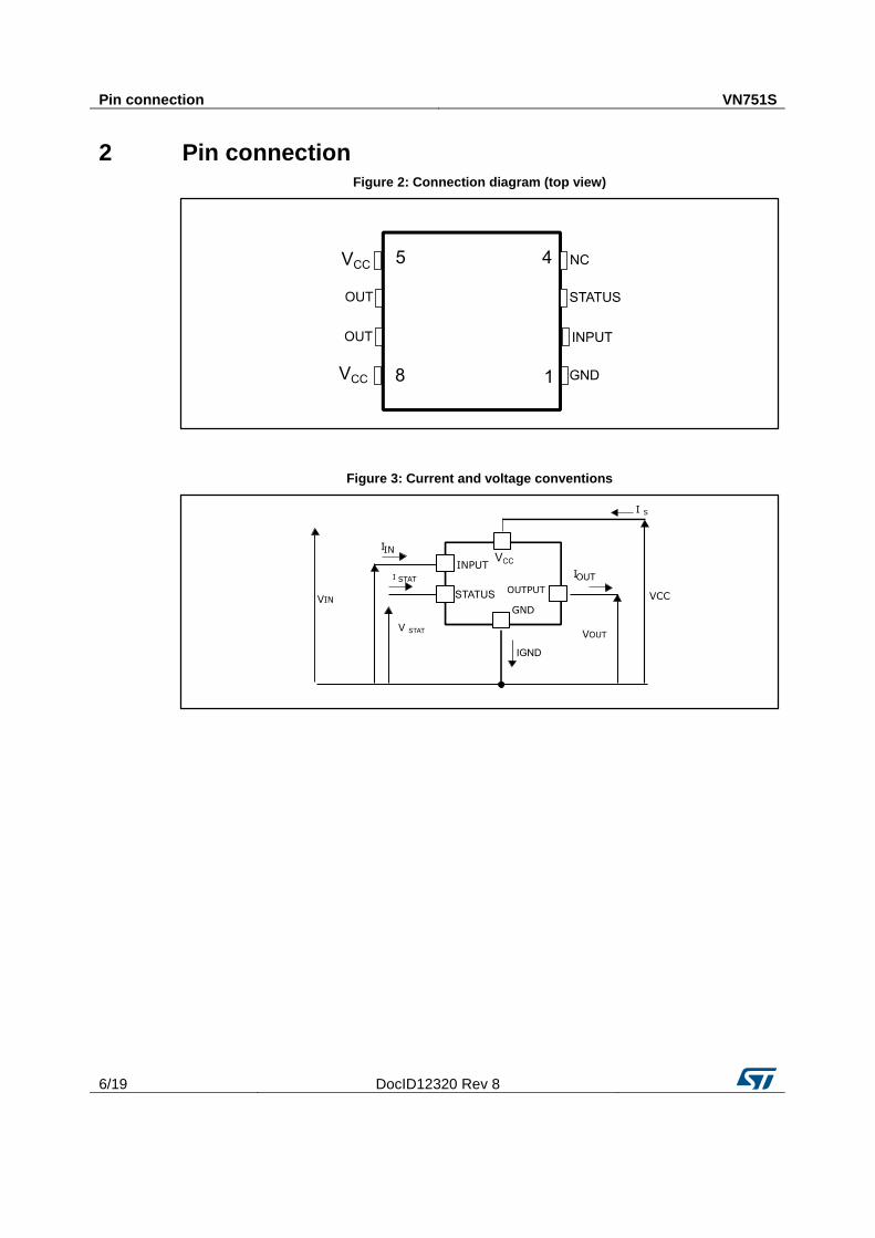
2 Pin connection ................................................................................. 6
3 Maximum ratings ............................................................................. 7
4 Electrical characteristics ................................................................ 8
5 Test circuits ................................................................................... 10
6 Switching time waveforms and truth table .................................. 11
7 Application schematic .................................................................. 13
8 Reverse polarity protection .......................................................... 14
9 Package information ..................................................................... 15
9.1 SO-8 package information .............................................................. 15
9.2 SO-8 packing information ................................................................ 16
10 Revision history ............................................................................ 18
VN751S List of tables
DocID12320 Rev 8 3/19
List of tables
Table 1: Device summary ........................................................................................................................... 1 Table 2: Absolute maximum ratings ........................................................................................................... 7 Table 3: Thermal data ................................................................................................................................. 7 Table 4: Power section ............................................................................................................................... 8 Table 5: Switching (VCC = 24 V) .................................................................................................................. 8 Table 6: Input pin ........................................................................................................................................ 8 Table 7: Status pin ...................................................................................................................................... 9 Table 8: Protection ...................................................................................................................................... 9 Table 9: Truth table ................................................................................................................................... 11 Table 10: SO-8 package mechanical data................................................................................................ 15 Table 11: SO-8 tape and reel mechanical data ........................................................................................ 17 Table 12: Document revision history ........................................................................................................ 18
List of figures VN751S
4/19 DocID12320 Rev 8
List of figures
Figure 1: Block diagram .............................................................................................................................. 5 Figure 2: Connection diagram (top view) .................................................................................................... 6 Figure 3: Current and voltage conventions ................................................................................................. 6 Figure 4: Peak short-circuit current ........................................................................................................... 10 Figure 5: Avalanche energy test circuit ..................................................................................................... 10 Figure 6: Switching time waveforms ......................................................................................................... 11 Figure 7: Waveforms ................................................................................................................................. 12 Figure 8: Application schematic ................................................................................................................ 13 Figure 9: Reverse polarity protection ........................................................................................................ 14 Figure 10: SO-8 package outline .............................................................................................................. 15 Figure 11: SO-8 package recommended footprint ................................................................................... 16 Figure 12: SO-8 tape and reel dimensions ............................................................................................... 16
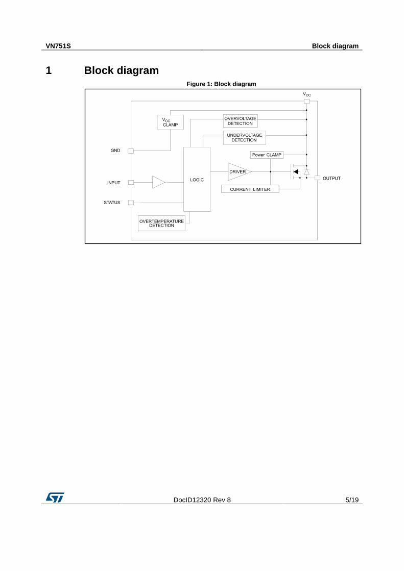
VN751S Block diagram
DocID12320 Rev 8 5/19
1 Block diagram Figure 1: Block diagram
Pin connection VN751S
6/19 DocID12320 Rev 8
2 Pin connection Figure 2: Connection diagram (top view)
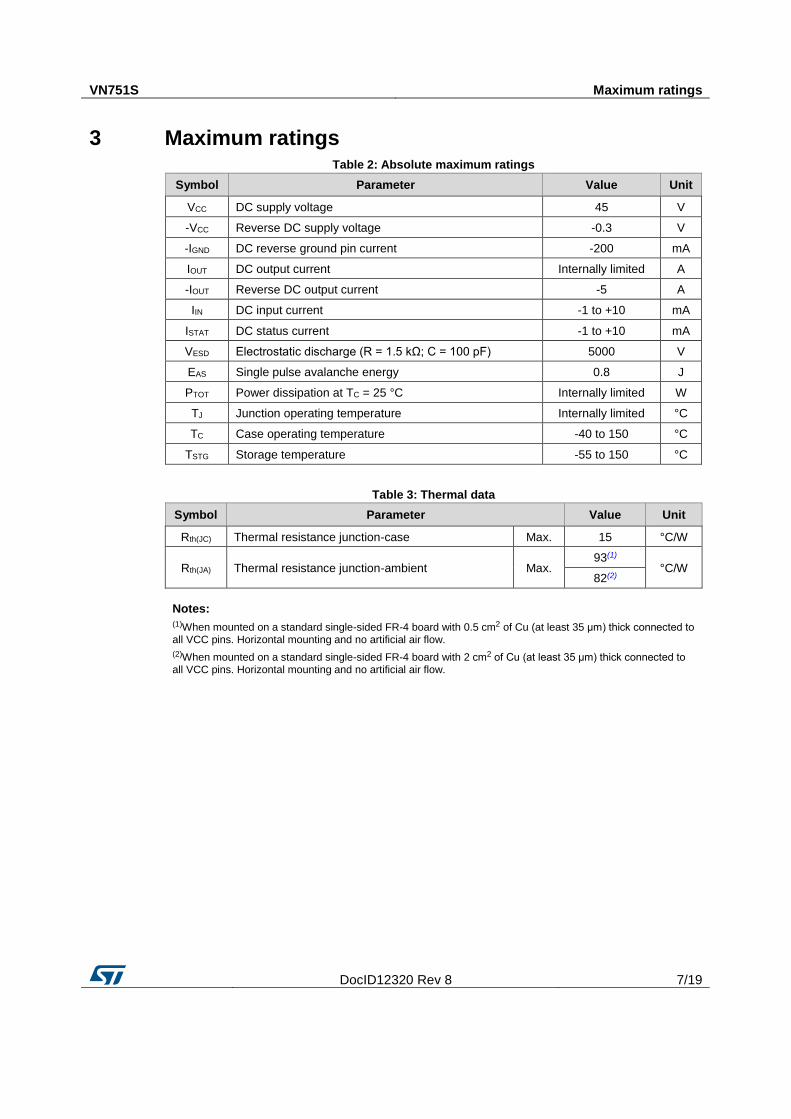
Figure 3: Current and voltage conventions
VN751S Maximum ratings
DocID12320 Rev 8 7/19
3 Maximum ratings Table 2: Absolute maximum ratings
Symbol Parameter Value Unit
VCC DC supply voltage 45 V
-VCC Reverse DC supply voltage -0.3 V
-IGND DC reverse ground pin current -200 mA
IOUT DC output current Internally limited A
-IOUT Reverse DC output current -5 A
IIN DC input current -1 to +10 mA
ISTAT DC status current -1 to +10 mA
VESD Electrostatic discharge (R = 1.5 kΩ; C = 100 pF) 5000 V
EAS Single pulse avalanche energy 0.8 J
PTOT Power dissipation at TC = 25 °C Internally limited W
TJ Junction operating temperature Internally limited °C
TC Case operating temperature -40 to 150 °C
TSTG Storage temperature -55 to 150 °C
Table 3: Thermal data
Symbol Parameter Value Unit
Rth(JC) Thermal resistance junction-case Max. 15 °C/W
Rth(JA) Thermal resistance junction-ambient Max. 93(1)
°C/W 82(2)
Notes:
(1)When mounted on a standard single-sided FR-4 board with 0.5 cm2 of Cu (at least 35 μm) thick connected to all VCC pins. Horizontal mounting and no artificial air flow. (2)When mounted on a standard single-sided FR-4 board with 2 cm2 of Cu (at least 35 μm) thick connected to all VCC pins. Horizontal mounting and no artificial air flow.
Electrical characteristics VN751S
8/19 DocID12320 Rev 8
4 Electrical characteristics
8 V < VCC < 36 V; -40 °C < TJ < 125 °C; unless otherwise specified
Table 4: Power section
Symbol Parameter Test conditions Min. Typ. Max. Unit
VCC Supply voltage
5.5
36 V
RDS(on) On-state
resistance
IOUT = 2 A at TJ = 25 °C
60 mΩ
IOUT = 2 A
180
IS(1) Supply current
Off-state, VCC = 24 V, TJ = 25 °C
10 20 µA
On-state, VCC = 24 V, TJ = 25 °C
3.5
mA
On-state, VCC = 24 V,
TJ = 100 °C 3.8 mA
VUSD Undervoltage
shutdown 3 4 5.5 V
VOV Overvoltage
shutdown 36
V
IL(off) Off-state output
current VIN = VOUT = 0 V 0
10 µA
Notes:
(1)Status: floating
Table 5: Switching (VCC = 24 V)
Symbol Parameter Test conditions Min. Typ. Max. Unit
td(ON) Turn-on delay time RL = 12 Ω from VIN rising
edge to VOUT = 2.4 V 12
µs
td(OFF) Turn-off delay time of
output current
RL = 12 Ω from VIN falling
edge to VOUT = 21.6 V 35
µs
dVOUT/dt
(on)
Turn -on voltage
slope
RL = 12 Ω from VOUT = 2.4 V
to VOUT = 19.2 V 0.80
V/µs
dVOUT/dt
(off)
Turn -off voltage
slope
RL = 12 Ω from VOUT = 21.6 V
to VOUT = 2.4 V 0.30
Table 6: Input pin
Symbol Parameter Test conditions Min. Typ. Max. Unit
VIL Input low level
1.25 V
IIL Low level input current VIN = 1.25 V 1
µA
VIH Input high level
3.25
V
IIH High level input current VIN = 3.25 V
10 µA
Vhyst Input hysteresis voltage
0.5
V
IIN Input current VIN = VCC = 5 V
10 µA
VICL Input clamp voltage IIN = 1 mA
6 6.8
8 V IIN = -1 mA -0.7
VN751S Electrical characteristics
DocID12320 Rev 8 9/19
Table 7: Status pin
Symbol Parameter Test conditions Min. Typ. Max. Unit
VSTAT Status low output
voltage ISTAT = 1.6 mA
0.5 V
ILSTAT Status leakage
current Normal operation; VSTAT = 5 V
10 µA
CSTAT Status pin input
capacitance Normal operation; VSTAT = 5 V
100 V
IIH High level input
current VIN = 3.25 V
10 µA
VSCL Status clamp
voltage
ISTAT = 1 mA 6 6.8 8 V
ISTAT = -1 mA
-0.7
Table 8: Protection
Symbol Parameter Test conditions Min. Typ. Max. Unit
Vdemag Turn-off output
clamp voltage RL =12 Ω; L = 6 mH VCC -47 VCC -52 VCC -57 V
TTSD Shutdown
temperature 150 175 200 °C
Ilim Current
limitation
VCC = 24 V; RLOAD =
10 mΩ, t = 0.4 ms 2.7
6.0 A
Thyst Thermal
hysteresis 7 20
°C
TR Reset
temperature 135
°C
Test circuits VN751S
10/19 DocID12320 Rev 8
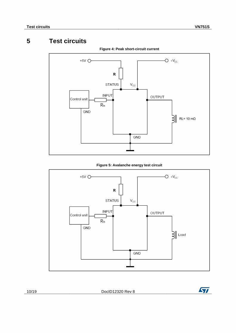
5 Test circuits Figure 4: Peak short-circuit current
Figure 5: Avalanche energy test circuit
VN751S Switching time waveforms and truth table
DocID12320 Rev 8 11/19
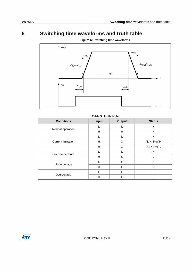
6 Switching time waveforms and truth table Figure 6: Switching time waveforms
Table 9: Truth table
Conditions Input Output Status
Normal operation L L H
H H H
Current limitation
L L H
H X (TJ < TTSD)H
H X (TJ > TTSD)L
Overtemperature L L H
H L L
Undervoltage L L X
H L X
Overvoltage L L H
H L H
Switching time waveforms and truth table VN751S
12/19 DocID12320 Rev 8
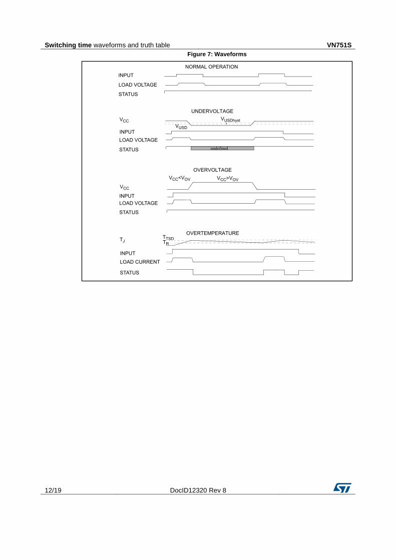
Figure 7: Waveforms
VN751S Application schematic
DocID12320 Rev 8 13/19
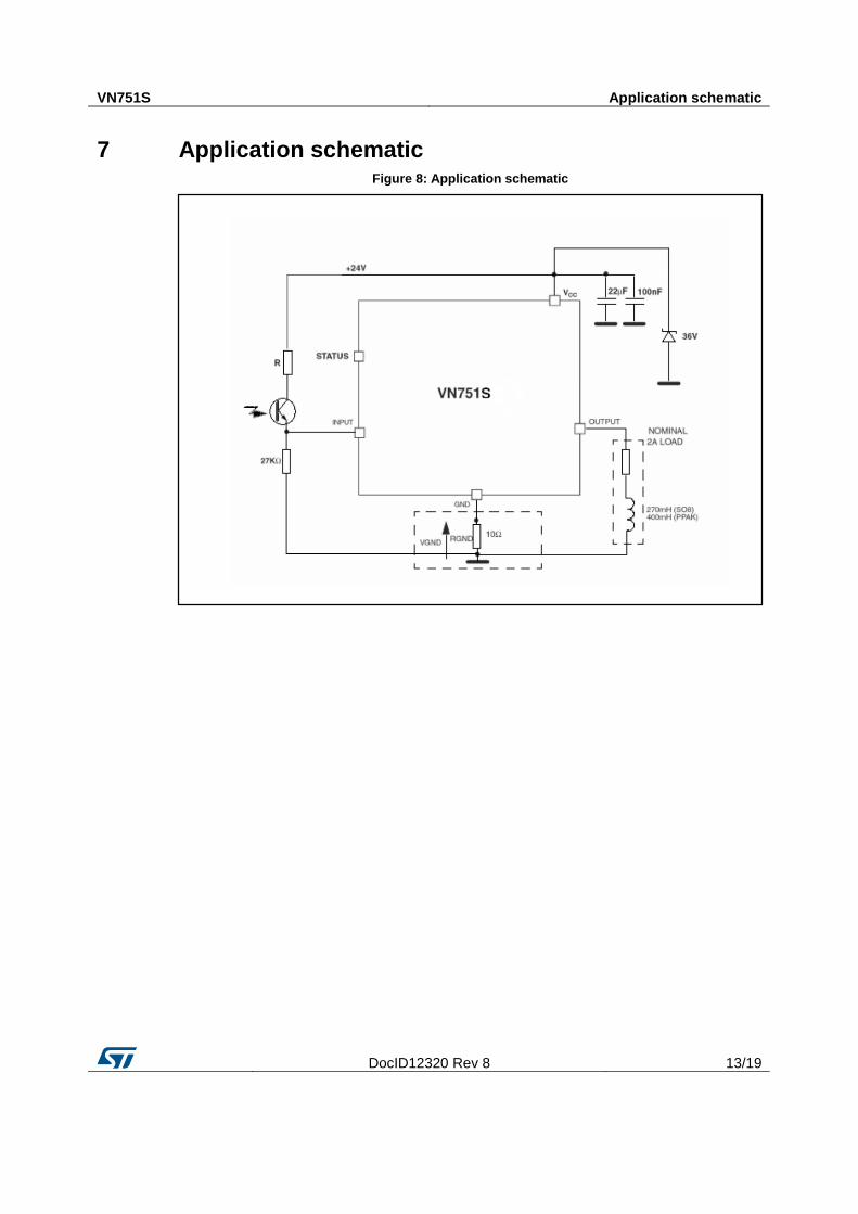
7 Application schematic Figure 8: Application schematic
Reverse polarity protection VN751S
14/19 DocID12320 Rev 8
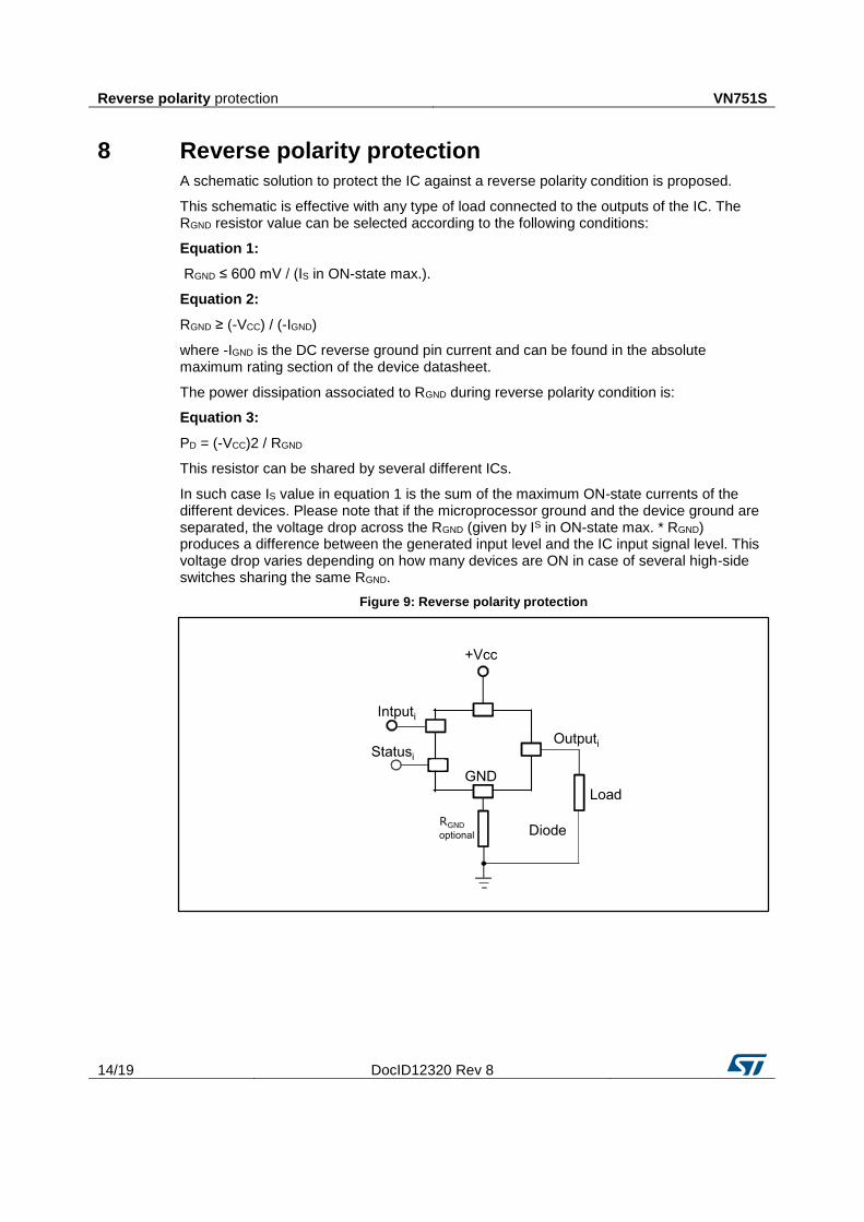
8 Reverse polarity protection
A schematic solution to protect the IC against a reverse polarity condition is proposed.
This schematic is effective with any type of load connected to the outputs of the IC. The RGND resistor value can be selected according to the following conditions:
Equation 1:
RGND ≤ 600 mV / (IS in ON-state max.).
Equation 2:
RGND ≥ (-VCC) / (-IGND)
where -IGND is the DC reverse ground pin current and can be found in the absolute maximum rating section of the device datasheet.
The power dissipation associated to RGND during reverse polarity condition is:
Equation 3:
PD = (-VCC)2 / RGND
This resistor can be shared by several different ICs.
In such case IS value in equation 1 is the sum of the maximum ON-state currents of the different devices. Please note that if the microprocessor ground and the device ground are separated, the voltage drop across the RGND (given by IS in ON-state max. * RGND) produces a difference between the generated input level and the IC input signal level. This voltage drop varies depending on how many devices are ON in case of several high-side switches sharing the same RGND.
Figure 9: Reverse polarity protection
VN751S Package information
DocID12320 Rev 8 15/19
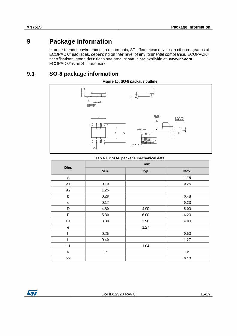
9 Package information
In order to meet environmental requirements, ST offers these devices in different grades of ECOPACK® packages, depending on their level of environmental compliance. ECOPACK® specifications, grade definitions and product status are available at: www.st.com. ECOPACK® is an ST trademark.
9.1 SO-8 package information
Figure 10: SO-8 package outline
Table 10: SO-8 package mechanical data
Dim. mm
Min. Typ. Max.
A
1.75
A1 0.10
0.25
A2 1.25
b 0.28
0.48
c 0.17
0.23
D 4.80 4.90 5.00
E 5.80 6.00 6.20
E1 3.80 3.90 4.00
e
1.27
h 0.25
0.50
L 0.40
1.27
L1
1.04
k 0°
8°
ccc
0.10
Package information VN751S
16/19 DocID12320 Rev 8
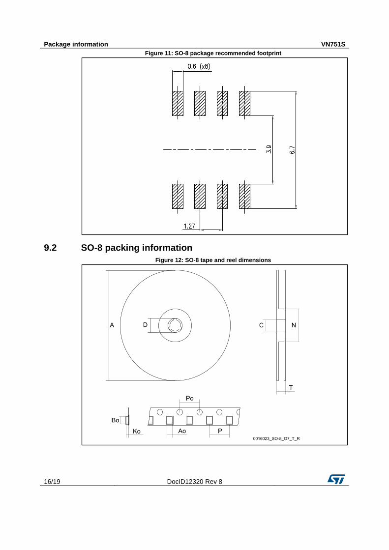
Figure 11: SO-8 package recommended footprint
9.2 SO-8 packing information
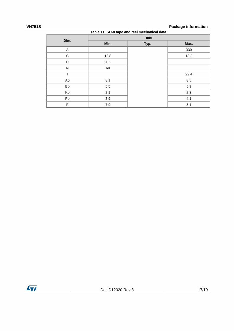
Figure 12: SO-8 tape and reel dimensions
VN751S Package information
DocID12320 Rev 8 17/19
Table 11: SO-8 tape and reel mechanical data
Dim. mm
Min. Typ. Max.
A
330
C 12.8 13.2
D 20.2
N 60
T
22.4
Ao 8.1 8.5
Bo 5.5 5.9
Ko 2.1 2.3
Po 3.9 4.1
P 7.9 8.1
Revision history VN751S
18/19 DocID12320 Rev 8
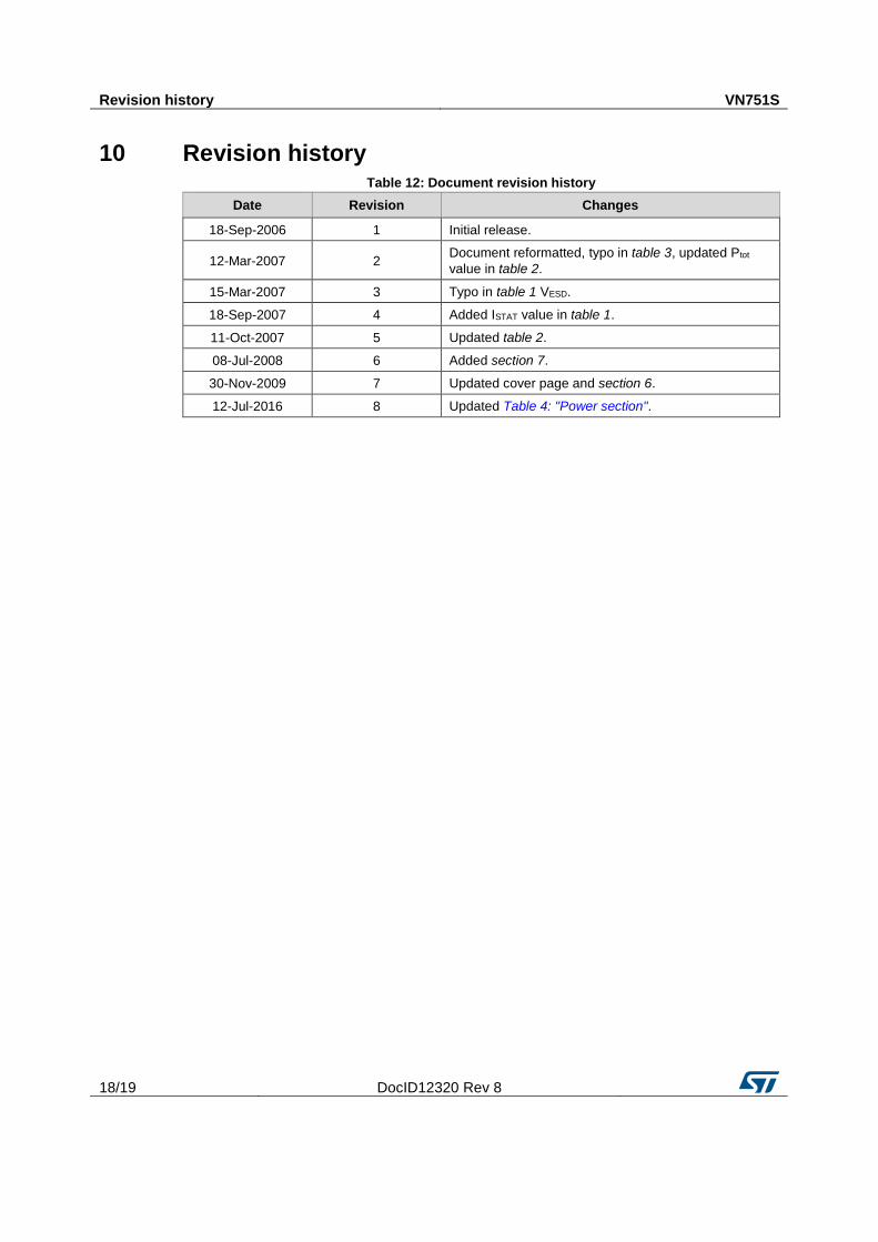
10 Revision history Table 12: Document revision history
Date Revision Changes
18-Sep-2006 1 Initial release.
12-Mar-2007 2 Document reformatted, typo in table 3, updated Ptot
value in table 2.
15-Mar-2007 3 Typo in table 1 VESD.
18-Sep-2007 4 Added ISTAT value in table 1.
11-Oct-2007 5 Updated table 2.
08-Jul-2008 6 Added section 7.
30-Nov-2009 7 Updated cover page and section 6.
12-Jul-2016 8 Updated Table 4: "Power section".
VN751S
DocID12320 Rev 8 19/19
IMPORTANT NOTICE – PLEASE READ CAREFULLY
STMicroelectronics NV and its subsidiaries (“ST”) reserve the right to make changes, corrections, enhancements, modifications, and improvements to ST products and/or to this document at any time without notice. Purchasers should obtain the latest relevant information on ST products before placing orders. ST products are sold pursuant to ST’s terms and conditions of sale in place at the time of order acknowledgement.
Purchasers are solely responsible for the choice, selection, and use of ST products and ST assumes no liability for application assistance or the design of Purchasers’ products.
No license, express or implied, to any intellectual property right is granted by ST herein.
Resale of ST products with provisions different from the information set forth herein shall void any warranty granted by ST for such product.
ST and the ST logo are trademarks of ST. All other product or service names are the property of their respective owners.
Information in this document supersedes and replaces information previously supplied in any prior versions of this document.
© 2016 STMicroelectronics – All rights reserved