Embed Size (px)
Citation preview
High Resolution Time-to-digital Conversion Circuitfor HgCdTe APD Detector at 77Kzhang qi wen ( [email protected] )
Shanghai Institute of Technology Physics,Chinese Academy of SicencesChen Honglei
Shanghai Institute of Technology physics,chinese academy of sciencesDing Ruijun
shanghai institute of technology physics,chinese academy of sciences
Research Article
Keywords: HgCdTe APD, time-to-digital converter circuit, Vernier delay line, Nonlinearity
Posted Date: February 8th, 2021
DOI: https://doi.org/10.21203/rs.3.rs-161259/v1
License: This work is licensed under a Creative Commons Attribution 4.0 International License. Read Full License
High resolution time-to-digital conversion circuit for HgCdTe
APD detector at 77K
Zhang Qiwen1,2,Chen Honglei1,Ding Ruijun1*
(1. Key Laboratory of Infrared Imaging Materials and Detectors,Shanghai Institute of Technology
Physics,Chinese Academy of Sciences,Shanghai 200083,China;
2. University of Chinese Academy of Sciences,Beijing 100049,China)
E-mail addresses:[email protected](QW Zhang), [email protected](RJ Ding)
Abstract:HgCdTe avalanche photodiode (APD) is a frontier research on infrared focal plane
technology, High-precision time stamp readout circuit is the basis of the APD focal plane at 77 K, which
directly affects APD infrared focal plane performance. Time-to-digital conversion circuit (TDC) is one of
the methods to achieve high-precision time stamping. Based on the analysis of MOSFET at low
temperature, our design a vernier TDC circuit, which uses a synchronous counter to quantize an integer
multiple of the period to achieve a coarse count of 6 bits; The on-chip PLL multiplied high-frequency clock
has high-precision and high PVT characteristics, using it to quantify the part that is less than one clock
cycle to achieve a fine-count of 6 bits output. The circuit adopts standard CMOS process tape out, our
circuit works at a master-frequency of 120 MHz. At 77 K, the circuit test can distinguish the time resolution
of 236.280 ps. The DNL is within -0.54~0.71 LSB, and INL is within -1.32~1.21 LSB.
Key words: HgCdTe APD; time-to-digital converter circuit; Vernier delay line; Nonlinearity
1 Introduction
The mercury cadmium telluride avalanche photodiode (HgCdTe APD) detector is a new type of
detector developed in recent years (A Roga lsk et al. 2009;Lu et al. 2011). Compared with other material
detectors, it has very high gain in linear mode (J. Beck et al.), ranging from tens to hundreds of times. At
the same time, it has low excessive noise and high sensitivity, which can achieve single photon detection;
Moreover, in the active and passive mode, it can obtain the intensity information and time information of
the target object simultaneously, to realize real-time three-dimensional detection.
In the three-dimensional imaging ranging, The HgCdTe APD readout circuit (E.Allen.2012) converts
optical signals into electrical signals and then outputs it. the TDC (Luo 2014) in the analog-to-digital
conversion is an important part of the readout circuit. It converts the analog signal carrying time
information into a digital signal, achieve the quantification of time information, and its resolution will
determine the minimum time that can be distinguished (Feng 2010).
At present, the reports on the focal plane HgCdTe APD readout circuit at low temperature are mainly
concentrated in the French SOFRADIR company and US DRS company. For example, the French
SOFRADIR company reported that the resolution of 100 ps can be achieved under the form of CTIA
structure with two negative feedback capacitors at 77 K (Rothman, J et al. 2016). RAYTHEON company
reported to achieve 300 ps resolution under 77 K conditions (Jack, Michael, et al. 2011); There are few
domestic researches in this filed. Among them, Southeast University used the delay chain phase-locked
loop structure to achieve 1 ns accuracy at room temperature. Because of the single delay chain, it is limited
by the resolution of a single delay gate (Zheng et al. 2017).
Based on the advantages of HgCdTe APD working at 77K, study the TDC structure of the readout
circuit at low temperature to achieve high-precision time resolution. Our design uses a vernier-type double
delay line TDC structure, so that the delay resolution is not affected by the delay of a single gate, At the
same time, the delay unit bias voltage is externally connected to achieve voltage selection. The tape-out
uses the CSMC 0.5 um 2P3M process, and at 77 K the test results can distinguish the time resolution of
236.28 ps, power consumption is 14.459 mW.
2 Detector noise analysis
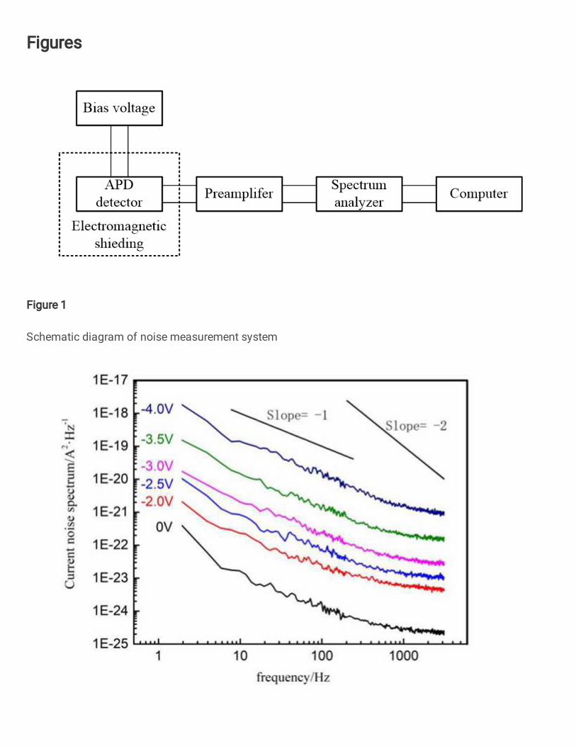
The detector noise is mainly composed of three parts: 1/f noise, generation-composite noise, and white
noise. This paper first analyzes the noise of the HgCdTe APD detector, the noise test system is based on
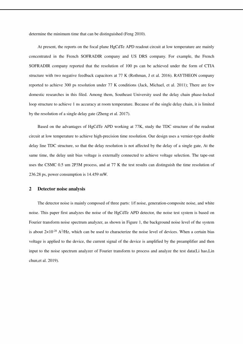
Fourier transform noise spectrum analyzer, as shown in Figure 1, the background noise level of the system
is about 2×10-28 A2/Hz, which can be used to characterize the noise level of devices. When a certain bias
voltage is applied to the device, the current signal of the device is amplified by the preamplifier and then
input to the noise spectrum analyzer of Fourier transform to process and analyze the test data(Li hao,Lin
chun,et al. 2019).
APD detector
PreampliferSpectrum analyzer
Computer
Bias voltage
Electromagnetic shieding
Fig. 1 Schematic diagram of noise measurement system
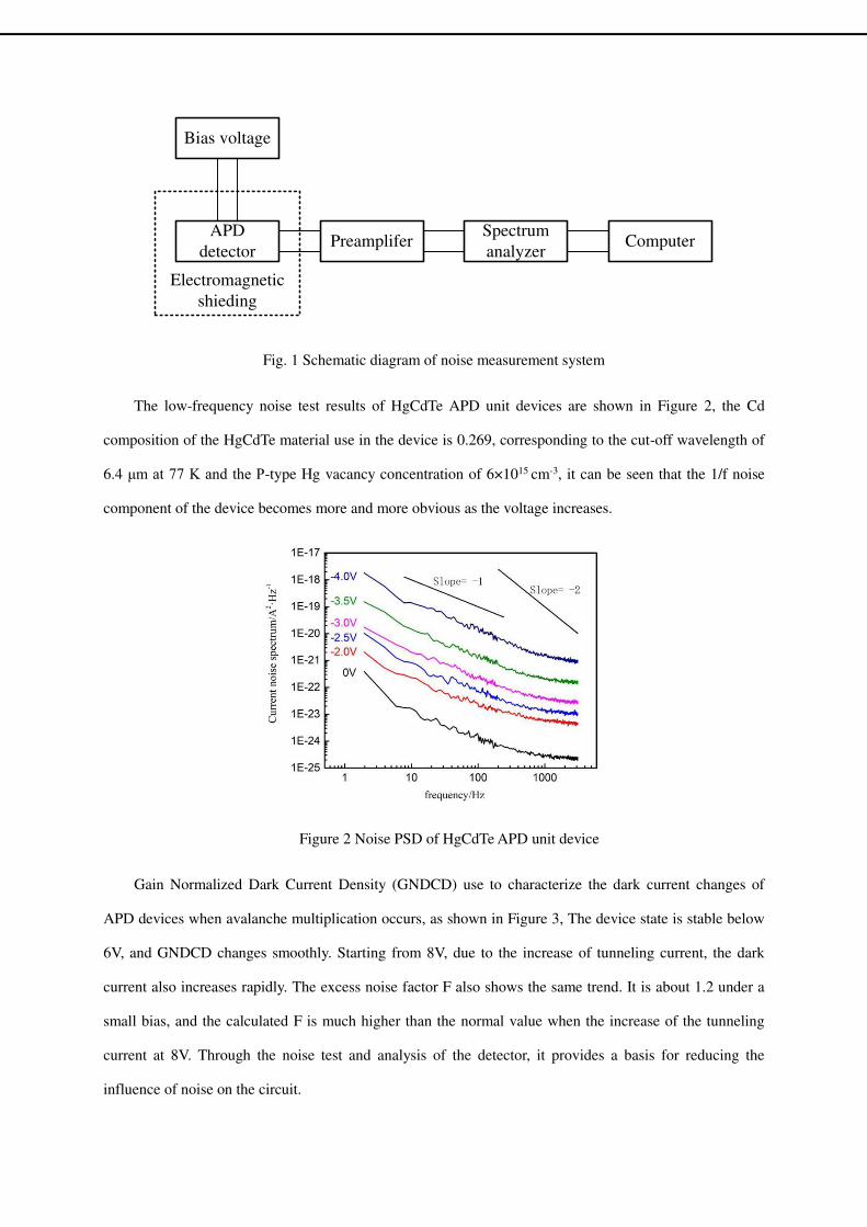
The low-frequency noise test results of HgCdTe APD unit devices are shown in Figure 2, the Cd
composition of the HgCdTe material use in the device is 0.269, corresponding to the cut-off wavelength of
6.4 μm at 77 K and the P-type Hg vacancy concentration of 6×1015 cm-3, it can be seen that the 1/f noise
component of the device becomes more and more obvious as the voltage increases.
Figure 2 Noise PSD of HgCdTe APD unit device
Gain Normalized Dark Current Density (GNDCD) use to characterize the dark current changes of
APD devices when avalanche multiplication occurs, as shown in Figure 3, The device state is stable below
6V, and GNDCD changes smoothly. Starting from 8V, due to the increase of tunneling current, the dark
current also increases rapidly. The excess noise factor F also shows the same trend. It is about 1.2 under a
small bias, and the calculated F is much higher than the normal value when the increase of the tunneling
current at 8V. Through the noise test and analysis of the detector, it provides a basis for reducing the
influence of noise on the circuit.
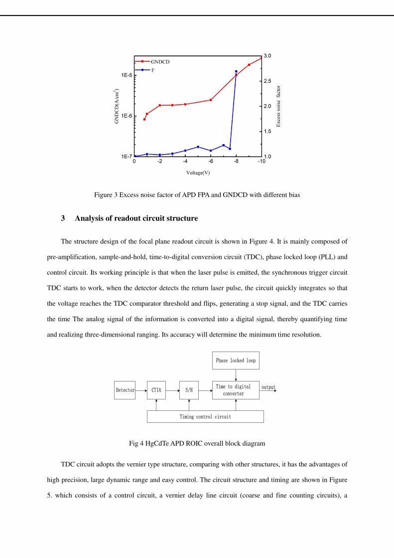
Figure 3 Excess noise factor of APD FPA and GNDCD with different bias
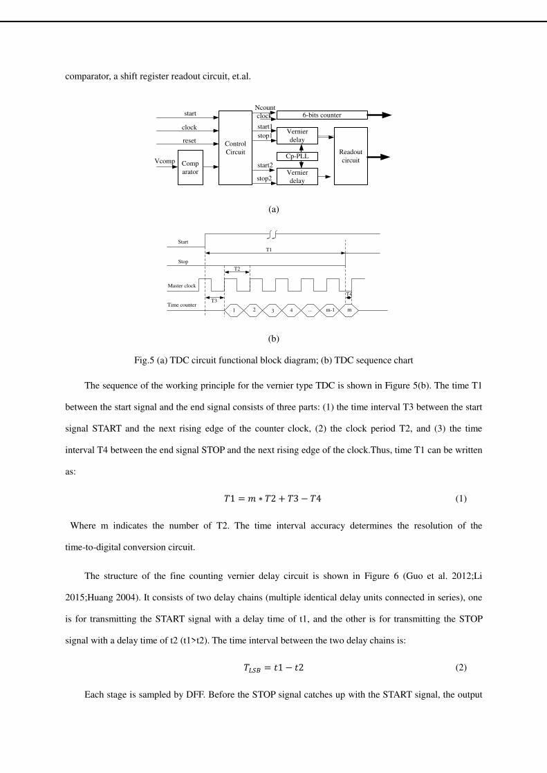
3 Analysis of readout circuit structure
The structure design of the focal plane readout circuit is shown in Figure 4. It is mainly composed of
pre-amplification, sample-and-hold, time-to-digital conversion circuit (TDC), phase locked loop (PLL) and
control circuit. Its working principle is that when the laser pulse is emitted, the synchronous trigger circuit
TDC starts to work, when the detector detects the return laser pulse, the circuit quickly integrates so that
the voltage reaches the TDC comparator threshold and flips, generating a stop signal, and the TDC carries
the time The analog signal of the information is converted into a digital signal, thereby quantifying time
and realizing three-dimensional ranging. Its accuracy will determine the minimum time resolution.
Detector CTIA S/HTime to digital
converter
Timing control circuit
output
Phase locked loop
Fig 4 HgCdTe APD ROIC overall block diagram
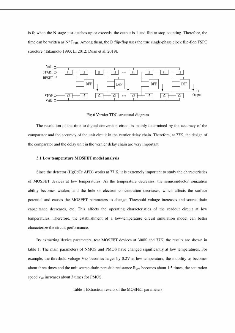
TDC circuit adopts the vernier type structure, comparing with other structures, it has the advantages of
high precision, large dynamic range and easy control. The circuit structure and timing are shown in Figure
5. which consists of a control circuit, a vernier delay line circuit (coarse and fine counting circuits), a
comparator, a shift register readout circuit, et.al.
Vernierdelay
Comparator
Control Circuit
6-bits counter
Vernierdelay
Cp-PLLReadout circuit
clockNcount
start1
stop1
start2
stop2
start
Vcomp
clock
reset
(a)
Start
Stop
Master clock
Time counter1 2 3 4 m-1 m...
T1
T2
T3T4
(b)
Fig.5 (a) TDC circuit functional block diagram; (b) TDC sequence chart
The sequence of the working principle for the vernier type TDC is shown in Figure 5(b). The time T1
between the start signal and the end signal consists of three parts: (1) the time interval T3 between the start
signal START and the next rising edge of the counter clock, (2) the clock period T2, and (3) the time
interval T4 between the end signal STOP and the next rising edge of the clock.Thus, time T1 can be written
as:
𝑇1 = 𝑚 ∗ 𝑇2 + 𝑇3 − 𝑇4 (1)
Where m indicates the number of T2. The time interval accuracy determines the resolution of the
time-to-digital conversion circuit.
The structure of the fine counting vernier delay circuit is shown in Figure 6 (Guo et al. 2012;Li
2015;Huang 2004). It consists of two delay chains (multiple identical delay units connected in series), one
is for transmitting the START signal with a delay time of t1, and the other is for transmitting the STOP
signal with a delay time of t2 (t1>t2). The time interval between the two delay chains is:
𝑇𝐿𝑆𝐵 = 𝑡1 − 𝑡2 (2)
Each stage is sampled by DFF. Before the STOP signal catches up with the START signal, the output
is 0; when the N stage just catches up or exceeds, the output is 1 and flip to stop counting. Therefore, the
time can be written as N*TLSB. Among them, the D flip-flop uses the true single-phase clock flip-flop TSPC
structure (Takamoto 1993; Li 2012; Duan et al. 2019).
t1
DFF
t2
t1 t1 t1 t1 t1 t1 t1
t2 t2 t2 t2 t2 t2 t2
DFF DFF DFF
Vtrl1
START
RESET
STOPVrtl2
Output
Fig.6 Vernier TDC structural diagram
The resolution of the time-to-digital conversion circuit is mainly determined by the accuracy of the
comparator and the accuracy of the unit circuit in the vernier delay chain. Therefore, at 77K, the design of
the comparator and the delay unit in the vernier delay chain are very important.
3.1 Low temperature MOSFET model analysis
Since the detector (HgCdTe APD) works at 77 K, it is extremely important to study the characteristics
of MOSFET devices at low temperatures. As the temperature decreases, the semiconductor ionization
ability becomes weaker, and the hole or electron concentration decreases, which affects the surface
potential and causes the MOSFET parameters to change: Threshold voltage increases and source-drain
capacitance decreases, etc. This affects the operating characteristics of the readout circuit at low
temperatures. Therefore, the establishment of a low-temperature circuit simulation model can better
characterize the circuit performance.
By extracting device parameters, test MOSFET devices at 300K and 77K, the results are shown in
table 1. The main parameters of NMOS and PMOS have changed significantly at low temperatures. For
example, the threshold voltage Vth0 becomes larger by 0.2V at low temperature; the mobility μ0 becomes
about three times and the unit source-drain parasitic resistance Rdsw becomes about 1.5 times; the saturation
speed vsat increases about 3 times for PMOS.
Table 1 Extraction results of the MOSFET parameters
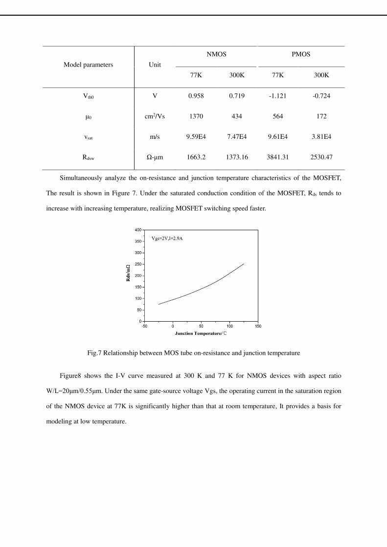
Model parameters Unit
NMOS PMOS
77K 300K 77K 300K
Vth0 V 0.958 0.719 -1.121 -0.724
μ0 cm2/Vs 1370 434 564 172
vsat m/s 9.59E4 7.47E4 9.61E4 3.81E4
Rdsw Ω-μm 1663.2 1373.16 3841.31 2530.47
Simultaneously analyze the on-resistance and junction temperature characteristics of the MOSFET,
The result is shown in Figure 7. Under the saturated conduction condition of the MOSFET, Rds tends to
increase with increasing temperature, realizing MOSFET switching speed faster.
Fig.7 Relationship between MOS tube on-resistance and junction temperature
Figure8 shows the I-V curve measured at 300 K and 77 K for NMOS devices with aspect ratio
W/L=20μm/0.55μm. Under the same gate-source voltage Vgs, the operating current in the saturation region
of the NMOS device at 77K is significantly higher than that at room temperature, It provides a basis for
modeling at low temperature.
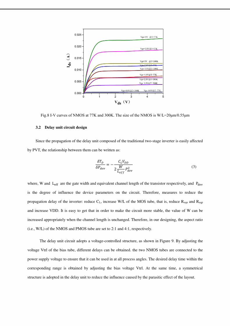
Fig.8 I-V curves of NMOS at 77K and 300K. The size of the NMOS is W/L=20μm/0.55μm
3.2 Delay unit circuit design
Since the propagation of the delay unit composed of the traditional two-stage inverter is easily affected
by PVT, the relationship between them can be written as:
𝛿𝑇𝐷𝛿𝑃𝑑𝑒𝑣 = − 𝐶𝐿𝑉𝐷𝐷2 𝑊𝐿𝑒𝑓𝑓 𝑃𝑑𝑒𝑣2
(3)
where, W and Leff are the gate width and equivalent channel length of the transistor respectively, and Pdev
is the degree of influence the device parameters on the circuit. Therefore, measures to reduce the
propagation delay of the inverter: reduce CL, increase W/L of the MOS tube, that is, reduce Reqn and Reqp
and increase VDD. It is easy to get that in order to make the circuit more stable, the value of W can be
increased appropriately when the channel length is unchanged. Therefore, in our designing, the aspect ratio
(i.e., W/L) of the NMOS and PMOS tube are set to 2:1 and 4:1, respectively.
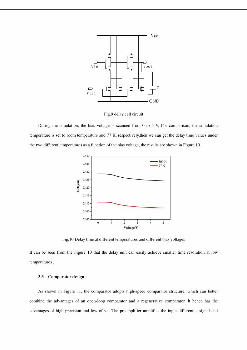
The delay unit circuit adopts a voltage-controlled structure, as shown in Figure 9. By adjusting the
voltage Vtrl of the bias tube, different delays can be obtained. the two NMOS tubes are connected to the
power supply voltage to ensure that it can be used in at all process angles. The desired delay time within the
corresponding range is obtained by adjusting the bias voltage Vtrl. At the same time, a symmetrical
structure is adopted in the delay unit to reduce the influence caused by the parasitic effect of the layout.
VDD
GND
Vtrl
Vin Vout
C
Fig.9 delay cell circuit
During the simulation, the bias voltage is scanned from 0 to 5 V, For comparison, the simulation
temperature is set to room temperature and 77 K, respectively,then we can get the delay time values under
the two different temperatures as a function of the bias voltage, the results are shown in Figure 10.
Fig.10 Delay time at different temperatures and different bias voltages
It can be seen from the Figure 10 that the delay unit can easily achieve smaller time resolution at low
temperatures .
3.3 Comparator design
As shown in Figure 11, the comparator adopts high-speed comparator structure, which can better
combine the advantages of an open-loop comparator and a regenerative comparator. It hence has the
advantages of high precision and low offset. The preamplifier amplifies the input differential signal and
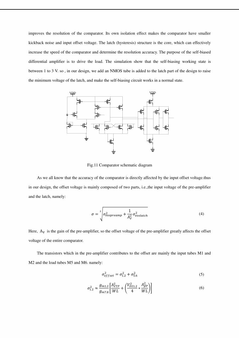
improves the resolution of the comparator. Its own isolation effect makes the comparator have smaller
kickback noise and input offset voltage. The latch (hysteresis) structure is the core, which can effectively
increase the speed of the comparator and determine the resolution accuracy. The purpose of the self-biased
differential amplifier is to drive the load. The simulation show that the self-biasing working state is
between 1 to 3 V. so , in our design, we add an NMOS tube is added to the latch part of the design to raise
the minimum voltage of the latch, and make the self-biasing circuit works in a normal state.
VDD
VDD
Fig.11 Comparator schematic diagram
As we all know that the accuracy of the comparator is directly affected by the input offset voltage.thus
in our design, the offset voltage is mainly composed of two parts, i.e.,the input voltage of the pre-amplifier
and the latch, namely:
𝜎 = √𝜎𝑣𝑜𝑠𝑝𝑟𝑒𝑎𝑚𝑝2 + 1𝐴𝑉2 𝜎𝑣𝑜𝑠𝑙𝑎𝑡𝑐ℎ22 (4)
Here, AV is the gain of the pre-amplifier, so the offset voltage of the pre-amplifier greatly affects the offset
voltage of the entire comparator.
The transistors which in the pre-amplifier contributes to the offset are mainly the input tubes M1 and
M2 and the load tubes M5 and M6. namely:
𝜎𝑜𝑓𝑓𝑠𝑒𝑡2 = 𝜎1.22 + 𝜎5.62 (5)
𝜎1.22 ≈ 𝑔𝑚1.2𝑔𝑚7.8 [𝐴𝑉𝑇𝑃2𝑊𝐿 + (𝑉𝐷𝑆1.224 ∗ 𝐴𝛽𝑃2𝑊𝐿)] (6)
σ5.62 ≈ AVTN2WL + (VDS5.624 ∗ AβN2WL ) (7)
Where AVTN and AVTP are the threshold voltage offset factor of the process model, AβN and AβP are
the offset of the process factor. It can be seen from the formula that with increasing the tube size the
effect of the imbalance can be reduced.
Usually increasing the gain of the amplifier can also reduce the offset noise. Since the gain bandwidth
product is a constant, and in order to ensure that the bandwidth of the comparator is above 100 MHz, the
gain of the pre-amplifier stage in the design cannot be too large, so the gain is designed to be 6.02 dB in the
circuit.
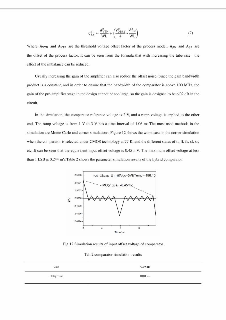
In the simulation, the comparator reference voltage is 2 V, and a ramp voltage is applied to the other
end. The ramp voltage is from 1 V to 3 V has a time interval of 1.06 ms.The most used methods in the
simulation are Monte Carlo and corner simulations. Figure 12 shows the worst case in the corner simulation
when the comparator is selected under CMOS technology at 77 K, and the different states of tt, ff, fs, sf, ss,
etc..It can be seen that the equivalent input offset voltage is 0.45 mV. The maximum offset voltage at less
than 1 LSB is 0.244 mV.Table 2 shows the parameter simulation results of the hybrid comparator.
Fig.12 Simulation results of input offset voltage of comparator
Tab.2 comparator simulation results
Gain 77.99 dB
Delay Time 10.01 ns
Resolution 12 bits
Noise 7.621v/sqrt(Hz)@1MHz
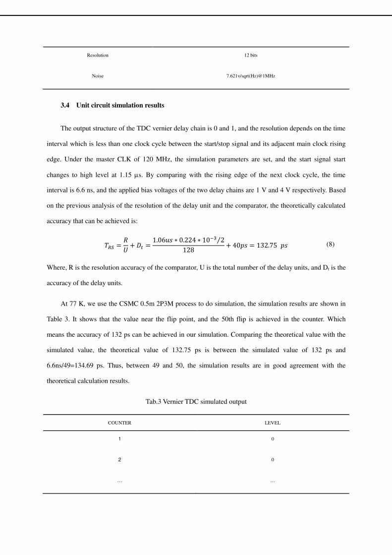
3.4 Unit circuit simulation results
The output structure of the TDC vernier delay chain is 0 and 1, and the resolution depends on the time
interval which is less than one clock cycle between the start/stop signal and its adjacent main clock rising
edge. Under the master CLK of 120 MHz, the simulation parameters are set, and the start signal start
changes to high level at 1.15 s. By comparing with the rising edge of the next clock cycle, the time
interval is 6.6 ns, and the applied bias voltages of the two delay chains are 1 V and 4 V respectively. Based
on the previous analysis of the resolution of the delay unit and the comparator, the theoretically calculated
accuracy that can be achieved is:
𝑇𝑅𝑆 = 𝑅𝑈 + 𝐷𝑡 = 1.06𝑢𝑠 ∗ 0.224 ∗ 10−3 2⁄128 + 40𝑝𝑠 = 132.75 𝑝𝑠 (8)
Where, R is the resolution accuracy of the comparator, U is the total number of the delay units, and Dt is the
accuracy of the delay units.
At 77 K, we use the CSMC 0.5m 2P3M process to do simulation, the simulation results are shown in
Table 3. It shows that the value near the flip point, and the 50th flip is achieved in the counter. Which
means the accuracy of 132 ps can be achieved in our simulation. Comparing the theoretical value with the
simulated value, the theoretical value of 132.75 ps is between the simulated value of 132 ps and
6.6ns/49=134.69 ps. Thus, between 49 and 50, the simulation results are in good agreement with the
theoretical calculation results.
Tab.3 Vernier TDC simulated output
COUNTER LEVEL
1 0
2 0
… …
49 0
50 1
51 1
… …
128 1
4 Experimental results
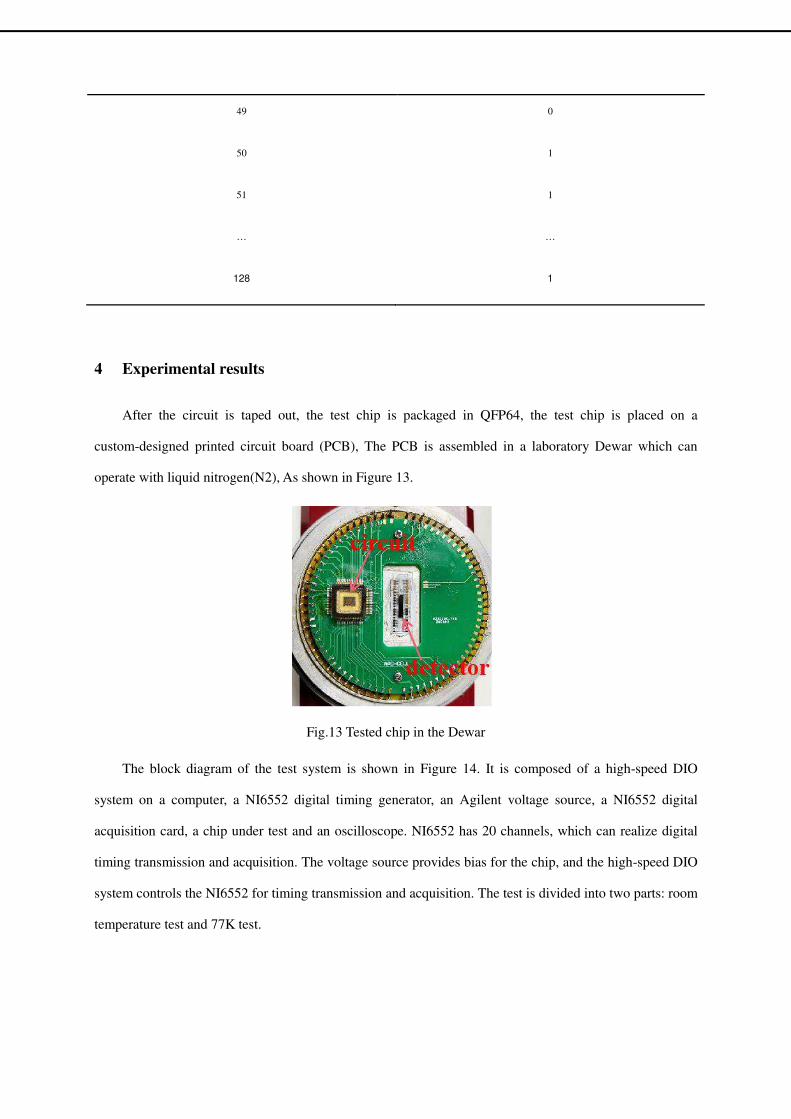
After the circuit is taped out, the test chip is packaged in QFP64, the test chip is placed on a
custom-designed printed circuit board (PCB), The PCB is assembled in a laboratory Dewar which can
operate with liquid nitrogen(N2), As shown in Figure 13.
Fig.13 Tested chip in the Dewar
The block diagram of the test system is shown in Figure 14. It is composed of a high-speed DIO
system on a computer, a NI6552 digital timing generator, an Agilent voltage source, a NI6552 digital
acquisition card, a chip under test and an oscilloscope. NI6552 has 20 channels, which can realize digital
timing transmission and acquisition. The voltage source provides bias for the chip, and the high-speed DIO
system controls the NI6552 for timing transmission and acquisition. The test is divided into two parts: room
temperature test and 77K test.
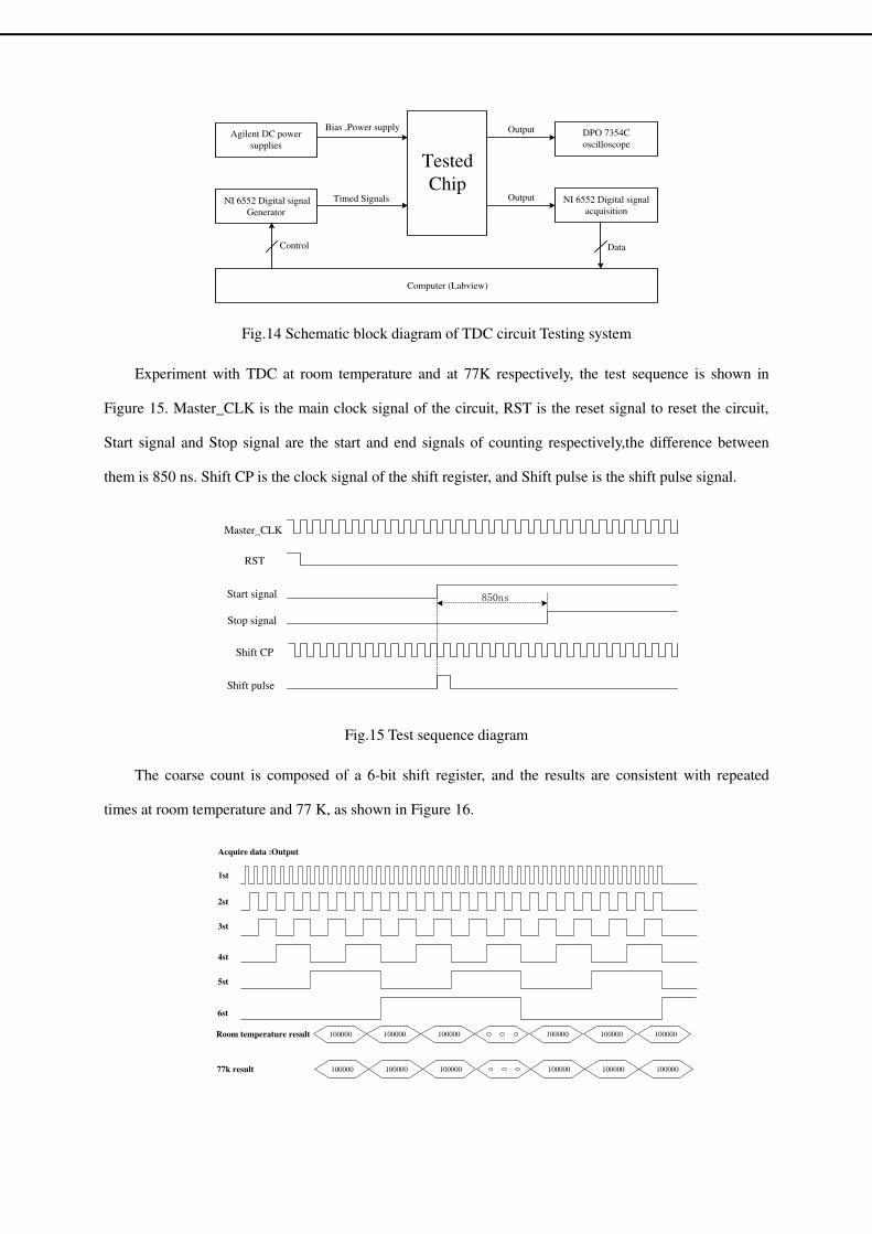
NI 6552 Digital signal Generator
Agilent DC power supplies
Tested Chip
Computer (Labview)
NI 6552 Digital signal acquisition
DPO 7354C oscilloscope
Bias ,Power supply
Timed Signals Output
Output
Control Data
Fig.14 Schematic block diagram of TDC circuit Testing system
Experiment with TDC at room temperature and at 77K respectively, the test sequence is shown in
Figure 15. Master_CLK is the main clock signal of the circuit, RST is the reset signal to reset the circuit,
Start signal and Stop signal are the start and end signals of counting respectively,the difference between
them is 850 ns. Shift CP is the clock signal of the shift register, and Shift pulse is the shift pulse signal.
Master_CLK
RST
Start signal
Stop signal
Shift CP
Shift pulse
850ns
Fig.15 Test sequence diagram
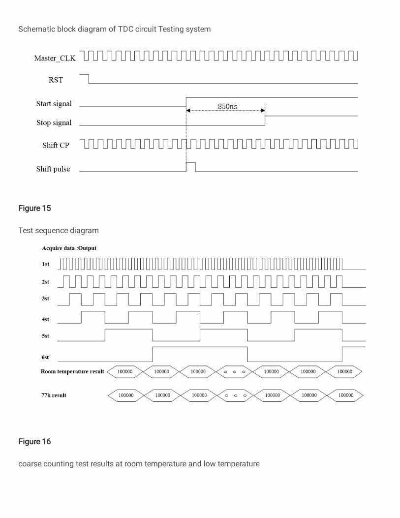
The coarse count is composed of a 6-bit shift register, and the results are consistent with repeated
times at room temperature and 77 K, as shown in Figure 16.
100000 100000 100000 100000 100000 100000
100000 100000 100000 100000 100000 100000
Room temperature result
77k result
1st
2st
3st
4st
5st
6st
Acquire data :Output
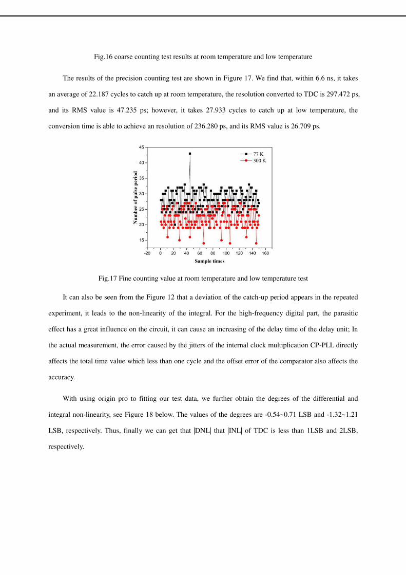
Fig.16 coarse counting test results at room temperature and low temperature
The results of the precision counting test are shown in Figure 17. We find that, within 6.6 ns, it takes
an average of 22.187 cycles to catch up at room temperature, the resolution converted to TDC is 297.472 ps,
and its RMS value is 47.235 ps; however, it takes 27.933 cycles to catch up at low temperature, the
conversion time is able to achieve an resolution of 236.280 ps, and its RMS value is 26.709 ps.
Fig.17 Fine counting value at room temperature and low temperature test
It can also be seen from the Figure 12 that a deviation of the catch-up period appears in the repeated
experiment, it leads to the non-linearity of the integral. For the high-frequency digital part, the parasitic
effect has a great influence on the circuit, it can cause an increasing of the delay time of the delay unit; In
the actual measurement, the error caused by the jitters of the internal clock multiplication CP-PLL directly
affects the total time value which less than one cycle and the offset error of the comparator also affects the
accuracy.
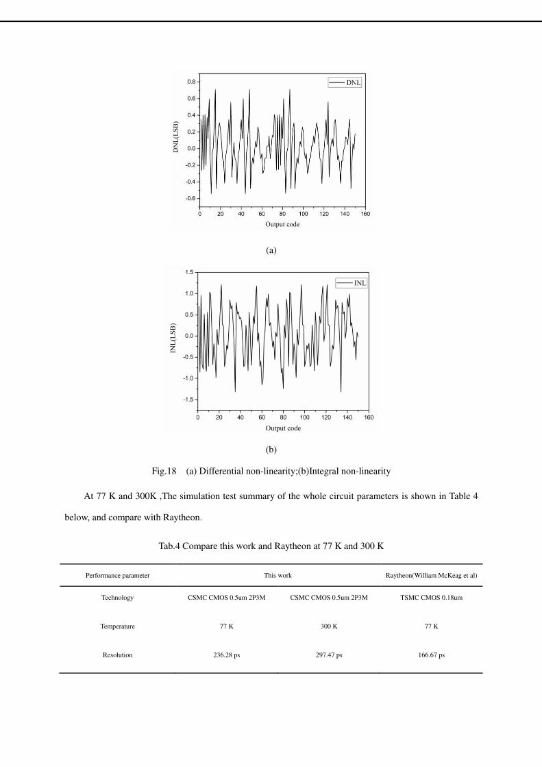
With using origin pro to fitting our test data, we further obtain the degrees of the differential and
integral non-linearity, see Figure 18 below. The values of the degrees are -0.54~0.71 LSB and -1.32~1.21
LSB, respectively. Thus, finally we can get that |DNL| that |INL| of TDC is less than 1LSB and 2LSB,
respectively.
(a)
(b)
Fig.18 (a) Differential non-linearity;(b)Integral non-linearity
At 77 K and 300K ,The simulation test summary of the whole circuit parameters is shown in Table 4
below, and compare with Raytheon.
Tab.4 Compare this work and Raytheon at 77 K and 300 K
Performance parameter This work Raytheon(William McKeag et al)
Technology CSMC CMOS 0.5um 2P3M CSMC CMOS 0.5um 2P3M TSMC CMOS 0.18um
Temperature
Resolution
77 K
236.28 ps
300 K
297.47 ps
77 K
166.67 ps
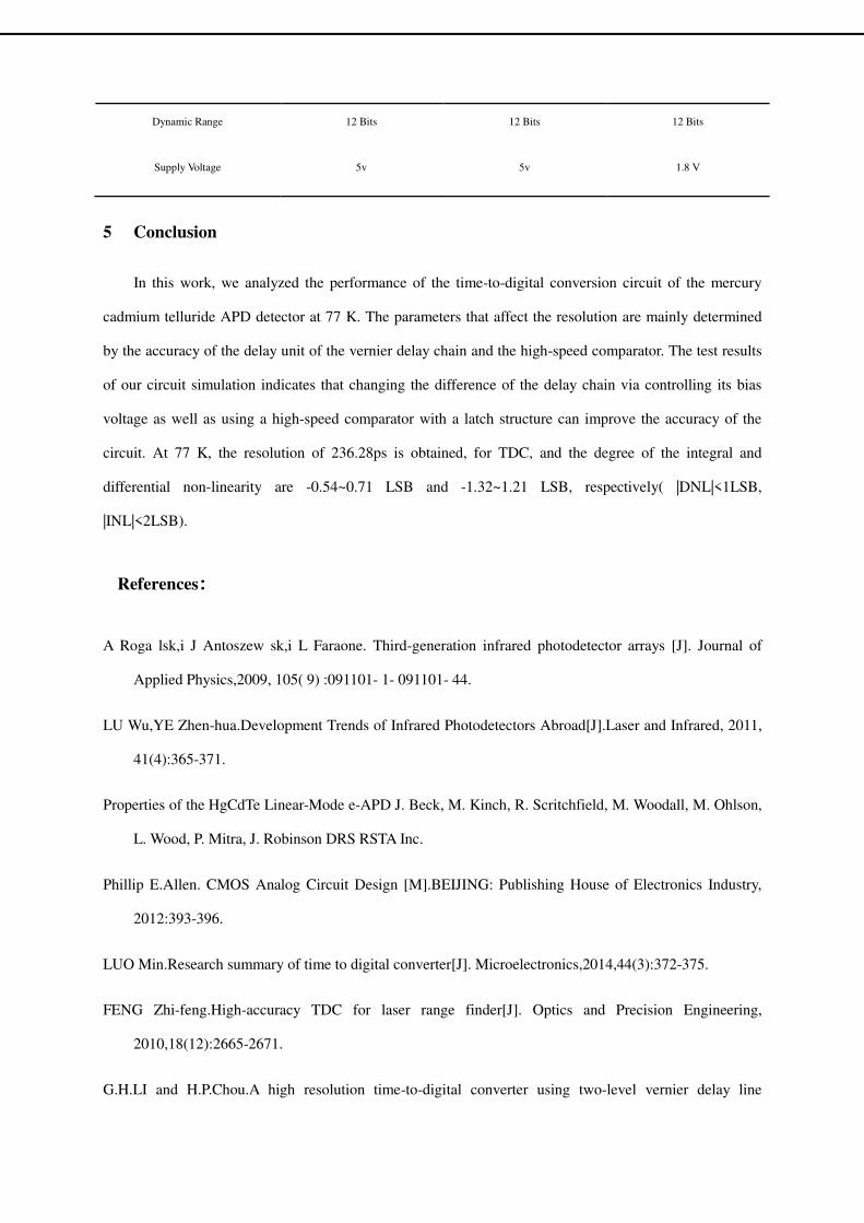
Dynamic Range 12 Bits 12 Bits 12 Bits
Supply Voltage 5v 5v 1.8 V
5 Conclusion
In this work, we analyzed the performance of the time-to-digital conversion circuit of the mercury
cadmium telluride APD detector at 77 K. The parameters that affect the resolution are mainly determined
by the accuracy of the delay unit of the vernier delay chain and the high-speed comparator. The test results
of our circuit simulation indicates that changing the difference of the delay chain via controlling its bias
voltage as well as using a high-speed comparator with a latch structure can improve the accuracy of the
circuit. At 77 K, the resolution of 236.28ps is obtained, for TDC, and the degree of the integral and
differential non-linearity are -0.54~0.71 LSB and -1.32~1.21 LSB, respectively( |DNL|<1LSB,
|INL|<2LSB).
References:
A Roga lsk,i J Antoszew sk,i L Faraone. Third-generation infrared photodetector arrays [J]. Journal of
Applied Physics,2009, 105( 9) :091101- 1- 091101- 44.
LU Wu,YE Zhen-hua.Development Trends of Infrared Photodetectors Abroad[J].Laser and Infrared, 2011,
41(4):365-371.
Properties of the HgCdTe Linear-Mode e-APD J. Beck, M. Kinch, R. Scritchfield, M. Woodall, M. Ohlson,
L. Wood, P. Mitra, J. Robinson DRS RSTA Inc.
Phillip E.Allen. CMOS Analog Circuit Design [M].BEIJING: Publishing House of Electronics Industry,
2012:393-396.
LUO Min.Research summary of time to digital converter[J]. Microelectronics,2014,44(3):372-375.
FENG Zhi-feng.High-accuracy TDC for laser range finder[J]. Optics and Precision Engineering,
2010,18(12):2665-2671.
G.H.LI and H.P.Chou.A high resolution time-to-digital converter using two-level vernier delay line
technique[J].IEEE, 2007:276-280.
Rothman, J., de Borniol, E., Gravrand, O., Kern, P., Feautrier, P., et al. MCT APD focal plane arrays for
astronomy at CEA-LETI[J].SPIE Astronomical Telescopes, 2016, 99150B:1-12.
Jack, Michael, et al. HgCdTe APD-based linear-mode photon counting components and ladar receivers[J].
Proc. SPIE 2011, Advanced Photon Counting Techniques V, 8300: 80330M-1:80330M-18; doi:
10.1117/12.888134.
Li hao,Lin chun,et al. HgCdTe avalanche photodiode FPA[J]. JOURNAL OF INFRARED AND
MILLIMETER WAVES,2019,38(5):587-590. doi:10.11972/j.issn.1001-9014.2019.05.007.
Lixia Zheng,Huan Hu,Ziqing Weng.Compact Active Quenching Circuit for Single-Photon Avalanche
Diodes Arrays.Journal of circuits,Systems,and Computers.
Jian Guo and Sameer Sonkusale. 22-bit 110ps Time-Interpolated Time-to-Digital Converter [J].IEEE,
2012,:3166-3169.
LI Qian-feng.Design and Implementation of time-to-digital converter in 0.18um CMOS technology[D],
Nanjing:Southeast University,2015.
HUANG Zhen.Research on Receiving Circuit and Timing Method of Pulse Laser Ranging[D], Hangzhou:
Zhejiang University, 2004.
Takamoto WATANABE.A CMOS Time-to-Digital Converter LSI with Half-Nanosecond Resolution Using
a Ring Gate Delay Line [J]. IEICE TRANS.ELECTRON, 1993,E76-C(12):1774-1779.
LI Gen.Design of TDC based on delay locked loop[D], Harbin:Harbin Institute of Technology,2012.
Jiangkun Duan,Maliang Liu.A 15ps resolution time-to-digital converter with on-chip PLL counting for
LiDAR multi-object sensors [N]. Microelectronics Journal,2019-09-12(92).
Deng Xuguang. Low-temperature MOSFET model and parameter extraction based on BSIM3[J]. Infrared
and Laser Engineering,2013,43(09):1051-1054.

William McKeag, Tricia Veeder, Jinxue Wang, and Michael Jack. New Developments in HgCdTe
APDs and LADAR Receivers[J].Infrared Technology and Applications,2011,8012(30):1-13. doi:
10.1117/12.888099.
Figures
Figure 1
Schematic diagram of noise measurement system
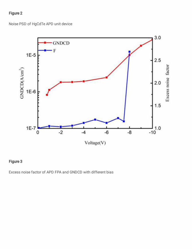
Figure 2
Noise PSD of HgCdTe APD unit device
Figure 3
Excess noise factor of APD FPA and GNDCD with different bias
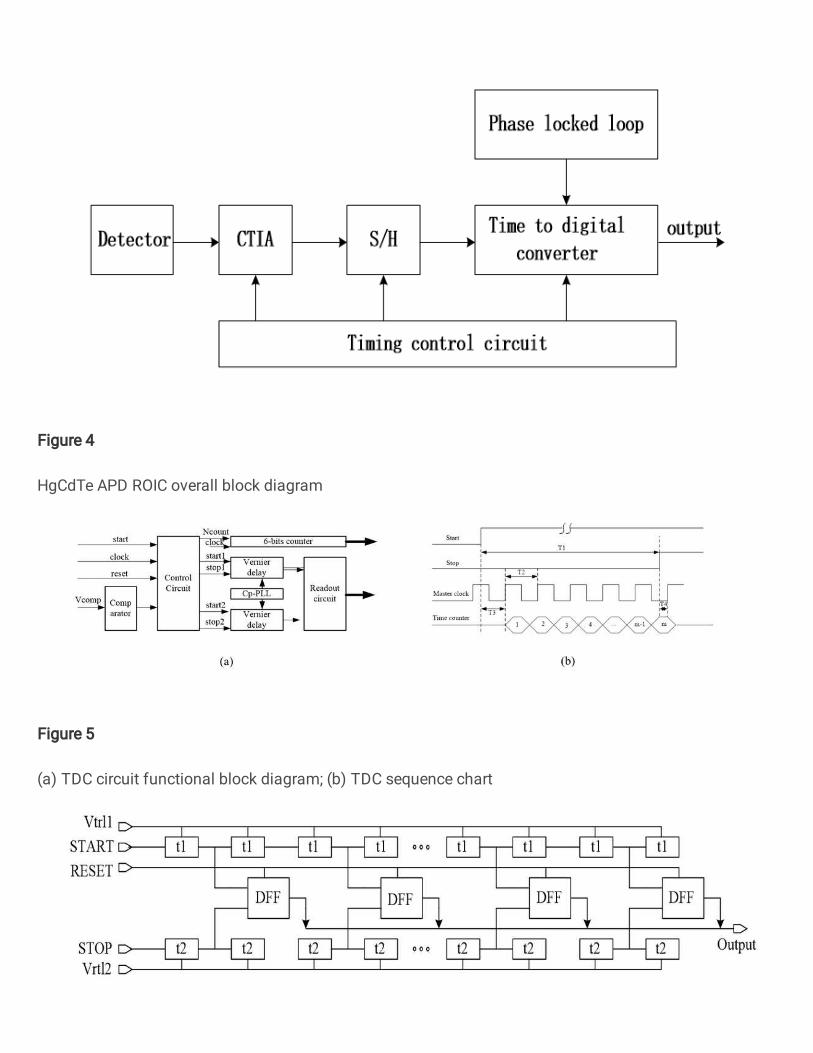
Figure 4
HgCdTe APD ROIC overall block diagram
Figure 5
(a) TDC circuit functional block diagram; (b) TDC sequence chart
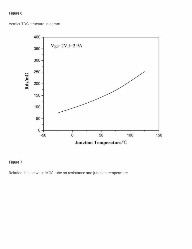
Figure 6
Vernier TDC structural diagram
Figure 7
Relationship between MOS tube on-resistance and junction temperature
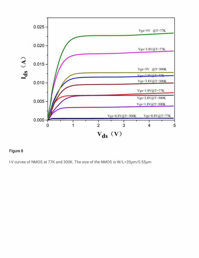
Figure 8
I-V curves of NMOS at 77K and 300K. The size of the NMOS is W/L=20μm/0.55μm
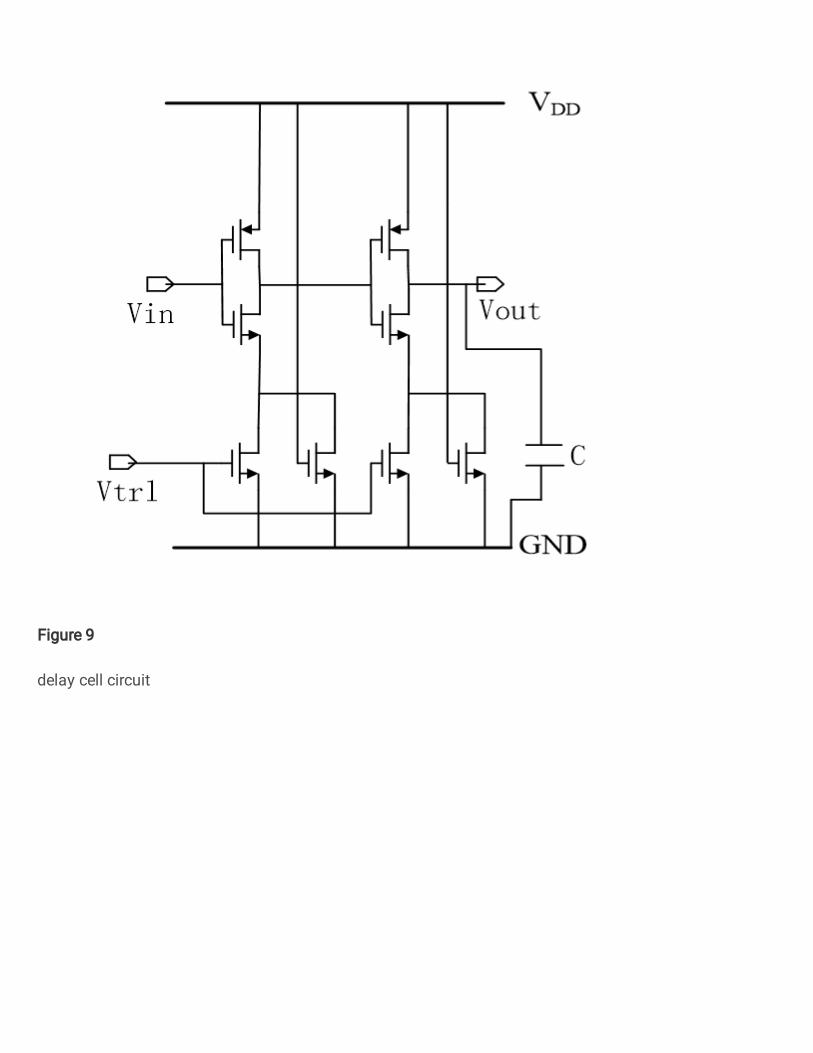
Figure 9
delay cell circuit
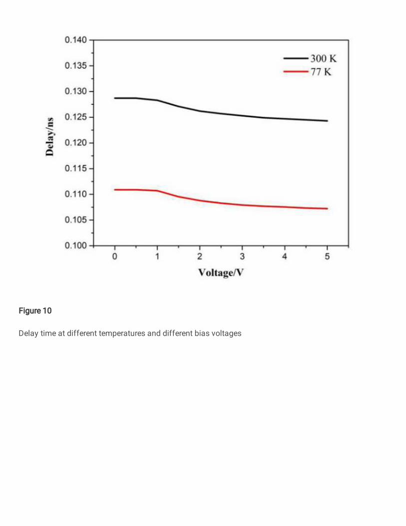
Figure 10
Delay time at different temperatures and different bias voltages
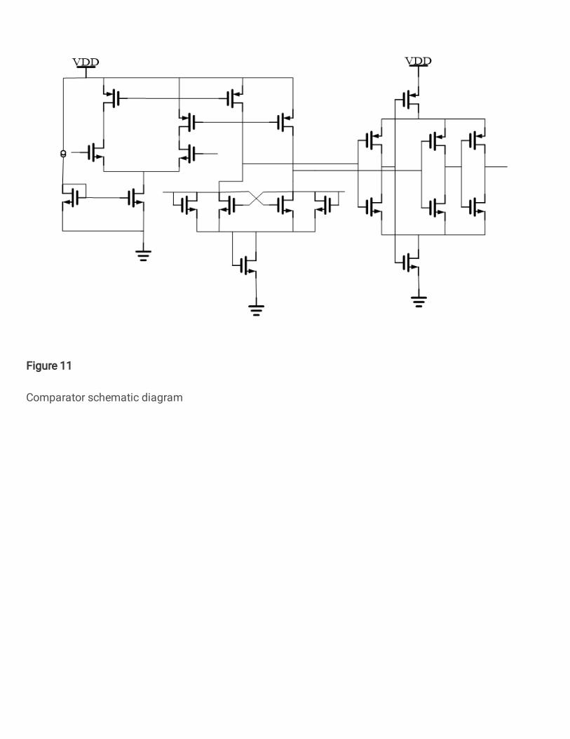
Figure 11
Comparator schematic diagram
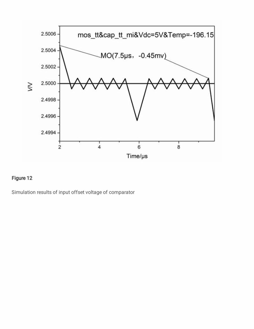
Figure 12
Simulation results of input offset voltage of comparator
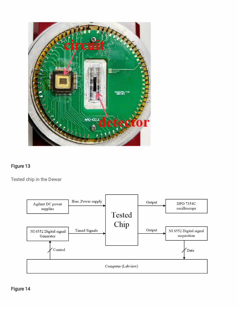
Figure 13
Tested chip in the Dewar
Figure 14
Schematic block diagram of TDC circuit Testing system
Figure 15
Test sequence diagram
Figure 16
coarse counting test results at room temperature and low temperature
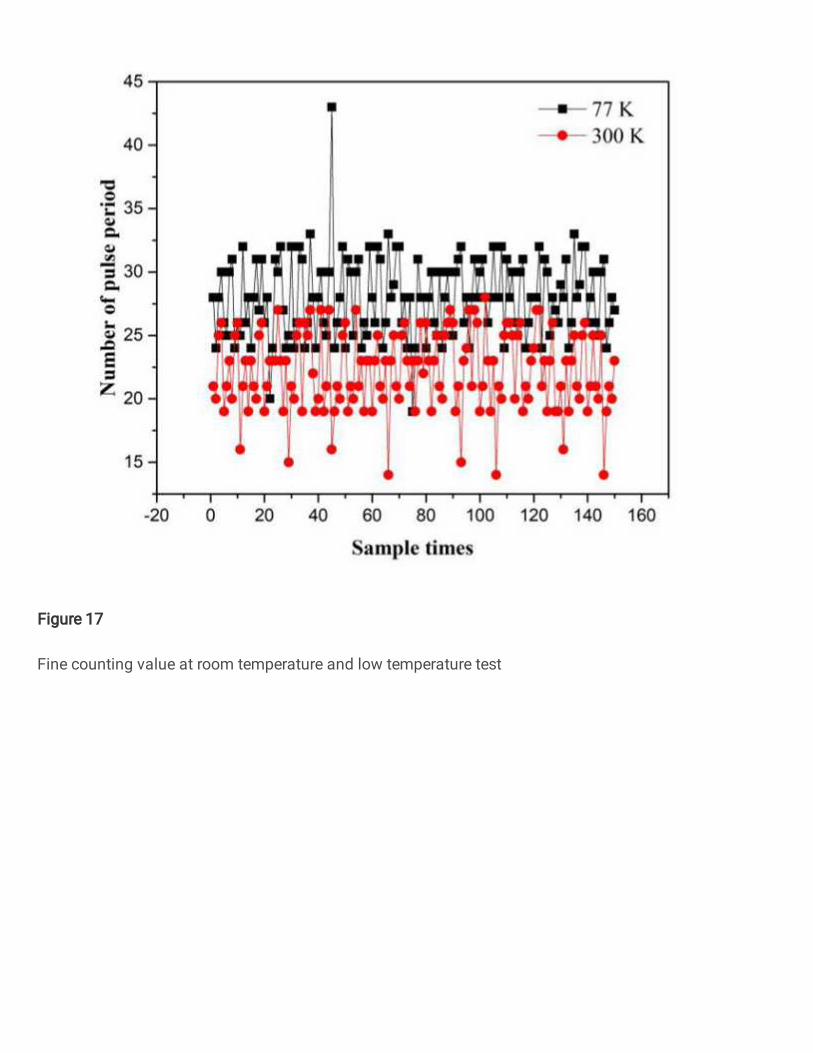
Figure 17
Fine counting value at room temperature and low temperature test
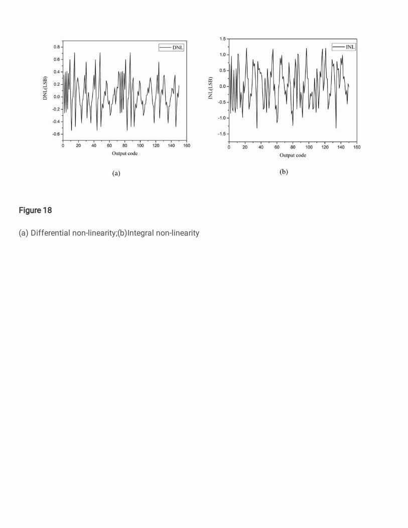
Figure 18
(a) Differential non-linearity;(b)Integral non-linearity