Embed Size (px)
Citation preview

High-resolution Sensing Sheet for Structural-health Monitoring via Scalable Interfacing of Flexible Electronics with High-performance ICs
Yingzhe Hu, Warren Rieutort-Louis, Josue Sanz-Robinson, Katherine Song, James C. Sturm, Sigurd Wagner, Naveen Verma
Princeton University, Princeton, NJ
Abstract
Early-stage damage detection for buildings and bridges requires continuously sensing and assessing strain over large surfaces, yet with centimeter-scale resolution. To achieve this, we present a sensing sheet that combines high-performance ICs with flexible electronics, allowing bonding to such surfaces. The flexible electronics integrates thin-film strain gauges and amorphoussilicon control circuits, patterned on a poly imide sheet that can potentially span large areas. Non-contact links couple digital and analog signals to the ICs, allowing many ICs to be introduced via low-cost sheet lamination for energy-efficient readout and computation over a large number of sensors. Communication between distributed ICs is achieved by transceivers that exploit low-loss interconnects patterned on the polyimide sheet; the transceivers self-calibrate to the interconnect impedance to maximize transmit SNR. The system achieves multi-channel strain readout with sensitivity of 18J1'strainRMs at an energy per measurement of 270nJ, while the communication energy is 12.8pJ/3.3pJ per bit (Tx/Rx) over 7.5m.
System Approach
Large-area electronics (LAE) is based on processing thin films at low temperatures. This allows a broad range of materials to be used for creating diverse transducers on large (>lDm2 ) , conformal substrates [1,2] . Although, thin-film transistors (TFTs) are also possible (using organics, amorphous-silicon (a-Si:H), metal-oxides, etc.) , these have orders of magnitude lower performance and energy efficiency than crystalline silicon ICs. Fig. 1 shows the proposed sensor-network-on-foil concept, aimed at achieving scalable sensing and high-performance computation, by extensively combining ICs with a flexible LAE sheet. The IC-to-LAE interfaces pose the primary limitation to system scalability. To overcome this, non-contact coupling is employed. Inductive and capacitive antennas are patterned on both the LAE sheet and on the flex-tape packaging of the ICs. We achieve assembly via sheet lamination, with typical adhesive thickness <lDOj.lm; this enables proximity coupling with low energy.
Large-area flexible sheet for high-resolution sensing
Silicon ICs for highpe"onnance readout and computation
• • •
Large-area
Fig. 1. Scalable sensor-network-on-foil system concept.
To substantially reduce the total number of signals required from the ICs, the LAE sheet integrates TFT-based control and access circuits that enable sequential access to individual strain
978-1-4673-0849-6112/$31.00 ©2012 IEEE
sensors in the array. The ICs integrate instrumentation and signal-generation circuits for access control, AC biasing, and readout over the sensor array. For communication over the distributed sheet, the ICs use transceivers that exploit low-loss, large-area interconnects. The interconnect impedance substantially affects the energy and SNR of communication; the transmitters thus self-calibrate to the resonant point of the interconnect, which is difficult to otherwise predict in a large-scale sheet.
Thin-film LAE Circuits for Sensor-array Control Fig. 2 shows the fully passive LAE circuits. Just four signals
are required from the IC for both power and control, to sequentially access the individual sensors. We fabricate the circuits using a-Si:H [3] (this is currently the most stable LAE semiconductor). The mobility (rv1cm2/Vs) and unipolar (n-channel) nature is similar to other LAE technologies (e.g., organics, oxides, etc.) , making the topologies transferrable.
Fig. 2. Thin-film LAE circuits for access control of multiple sensors.
While the IC operates at 1.2V, the LAE circuits need over 6V for reasonable performance. The inductive interfaces, which require AC-modulated IC control signals, can provide voltage step-up. This, however, increases the power of the IC power amplifiers and/or requires high-Q inductors. Though thin-film diodes (TFDs) have been reported [4] , we develop a-Si:H Schottky TFDs for low-voltage drop and good rectification characteristics, to demodulate the IC signals (measured I-V and capacitance curves are shown in Fig. 2) . In the full-wave rectifier configuration shown, the AC current through the TFD capacitances is cancelled since the inputs oscillate in counter phase. This enables rectification of high frequencies. The interfaces use a frequency of 2MHz, yielding a quality factor of 126 for 2cm planar inductors.
The scanning elements form a chain that uses 3-phase control, with SCANl-3 asserted in round-robin manner. The Nth scanning element receives a precharge signal (PRE) from the N-2 element and a reset signal (RST) from the N+1 element to control an nFET pass device (the first two elements are precharged by GRST). The sensor enable signals (EN <i» are thus asserted one-at-a-time down the chain. Since only nFETs can readily be created using a-Si:H, capacitive bootstrapping is used on the pass device to preserve the 6V logic level throughout the circuit (this is achieved using the low-voltage-drop Schottky TFDs).
Instrumentation Circuits for Sensor Readout Fig. 3 shows the multi-sensor readout circuit. Thin-film re
sistive strain gauges, calibrated for aluminum beams and having
2012 Symposium on VLSI Circuits Digest of Technical Papers 120
standardized resistance of 1kO, are used. Large access TFTs, which are controlled by the scanning circuits, gate the AC biasing signal (VL2 = 0.6VAM p ) , which is provided by the IC over an inductive interface. The IC's PA operates in class-C mode, rather than class-D, since the power required is relatively low for practical values of the frequency (5MHz) and the patterned inductors (3.5j.lH) (higher frequencies are limited by the parasitics of the access TFTs, and larger inductors are limited by physical size). The PA's duty cycle is optimized to 20%, yielding a measured efficiency of 82%. The AC-modulated sensor signal is then acquired through a capacitive interface (this results in reduced loading on the sensor bridge). Demodulation and readout is then performed via a synchronous GM-C integrator. Synchronization requires that the PA have proper phase, which is thus achieved via a tunable delay line. The GM stage demodulates the sensor signal for integration by a low-power op-amp. Demodulation at the GM stage output mitigates l/f noise and helps reject error signals of orthogonal phase that originate from admittance mismatches in the branches of the sensor bridge.
tt-I,:=�II---r+--EN<1>
TFT access t--+----'- ·--'swifches (WIL=
. •
60IX!J1ml6iJm)
6:, d55fJ· ···
A
---·f-c- r ' ft:.1. -I;:=�II---r+--IEN<N>
C)irn '-.
�l� i � l� v, s· i 5' � t-+----',...
Fig. 3. Multi-sensor readout circuit for thin-film resistive
strain-gauge bridges.
Transceiver for Macro-range Communication Fig. 4 shows the transceiver for communication over dis
tributed ICs. Previous efforts to exploit large-area interconnects have used pulsed signals and have been limited by the interconnect impedance [5] . For strong coupling over the non-contact links, we use AC signaling with on-off keying. The severe and unpredictable interconnect impedance is overcome using an 8-bit digitally-controlled oscillator (DCO) to self-tune the transmitter carrier frequency to the resonant point of the full interconnect network. The local receiver self-senses the transmitted signal, allowing a DCO code to be selected via a gradient descent algorithm to result in the largest amplitude (a measured DCO sweep is shown). To recover digital data, the receiver uses a preamplifier and peak-detector, each biased with 3j.lA. Synchronization and multiple access between transceivers can be achieved by digital-baseband processing (not included on chip).
Ie Rx
3pFT 3�A\�··�·················.1·· oi� v f-c §-l g.
Peak- 3�A :3 ! :3 detector Pre-amplifier �; �
Fig. 4. Transceiver circuits for communication over distributed ICs
using large-area interconnects.
978-1-4673-0849-6112/$31.00 ©2012 IEEE
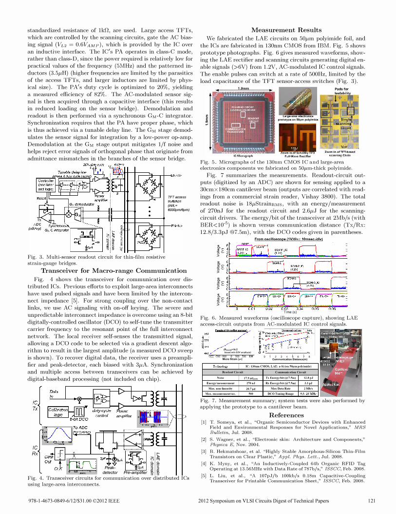
Measurement Results We fabricated the LAE circuits on 50j.lm polyimide foil, and
the ICs are fabricated in 130nm CMOS from IBM. Fig. 5 shows prototype photographs. Fig. 6 gives measured waveforms, showing the LAE rectifier and scanning circuits generating digital enable signals (>6V) from 1.2V, AC-modulated IC control signals. The enable pulses can switch at a rate of 500Hz, limited by the load capacitance of the TFT sensor-access switches (Fig. 3).
Fig. 5. Micrographs of the 130nm CMOS IC and large-area
electronics components we fabricated on 50J-im-thick polyimide.
Fig. 7 summarizes the measurements. Readout-circuit outputs (digitized by an ADC) are shown for sensing applied to a 30cm x 180cm cantilever beam (outputs are correlated with readings from a commercial strain reader, Vishay 3800). The total readout noise is 18j.lStrainRMs, with an energy/measurement of 270nJ for the readout circuit and 2.6j.lJ for the scanningcircuit drivers. The energy /bit of the transceiver at 2Mb/s (with BER<1O-5) is shown versus communication distance (Tx/Rx: 12.8/3.3pJ @7.5m), with the DCO codes given in parentheses.
From oscilloscope (1V/div." 10msec.Jdiv)
F> � l ®iK:a--;RST_IC CAN
SCANUC 0 � (5 - 2 (1 . 2V) (1.2V)
> o��. ���������������
I � � l � ca---�C
:��_IC D �
I � � t Cd----�C�3_IC D � s l �N<1> • EN<2>
.
EN<3> EN<.4> EN<5> EN<6>
i§�� > O._&d�� .. ���������������� .. _ o 0 .01 0.02 0.03 0.04 0.05 O.OS Time (s)
Fig. 6. Measured waveforms (oscilloscope capture) , showing LAE
access-circuit outputs from AC-modulated IC control signals. Raadoyllthln_fI!m ,ansor)
(RC ........ E·1kQ biased with O.6V amplitude)
-3 - 00 -100 a 100 00 MicroStraln(�)
"" o 1 2 3 4 5 6 7 8
Communication Distance(m)
Tt"chnolog) IC: 13011111 CMOS, LAE: I'I-Si (0115°11111 polyimid(')
Rl'lUloul Cin'uil Comlllunil'l'IlitJn Cin'uil
Noise 17.911£R.\IS Tx Ellergy/hit (@7.!i1l1) 12.8pJ
[nerg.'"lIII(,I'ISUH'II1(,Uf 270nJ R:t [n('rg�"bit(@7.5111) 3.3 pJ
Ml'lx.non-lineal'ity 20.711£ Max Datll Rate 2 !\1b/s
l\1HX.III(,IISUH'IIIt"lIt/sl'C. 500 DCO Tuning Rangl'
Fig. 7. Measurement summary; system tests were also performed by
applying the prototype to a cantilever beam.
References [1] T. Someya, et aI., "Organic Semiconductor Devices with Enhanced
Field and Environmental Responses for Novel Applications," MRS Bulletin, Jul. 2008.
[2] S. Wagner, et aI., "Electronic skin: Architecture and Components," Physica E, Nov. 2004.
[3] B. Hekmatshoar, et al. "Highly Stable Amorphous-Silicon Thin-Film
Transistors on Clear Plastic," Appl. Phys. Lett., Jul. 2008.
[4] K. Myny, et aI., "An Inductively-Coupled 64b Organic RFID Tag Operating at 13.56MHz with Data Rate of 787b/s," ISSCC, Feb. 2008.
[5] L. Liu, et aI., "A 107pJ/b 100kb/s 0.18m Capacitive-Coupling Transceiver for Printable Communication Sheet," ISSCC, Feb. 2008.
2012 Symposium on VLSI Circuits Digest of Technical Papers 121