Embed Size (px)
Citation preview

High-Resolution Imaging of Single Fluorescent Molecules with the Optical Near-Field of a Metal TipH. G. Frey, S. Witt, K. Felderer, and R. Guckenberger, Phys. Rev. Lett.
93, 200801 (2004). Marc McGuiganJournal ClubMonday, April 10, 2006

Outline
Introduction Near Field Microscopy Purpose
Experimental Setup Sample Preparation Results Data Model Conclusion

Beating the Diffraction Limit
NAd
2min
mvisibled 5.02.0min
Alternatives
•Scanning Tunneling Microscope
•Atomic Force Microscope
•Scanning Electron Microscope
•Transmission Electron Microscope
Why use visible light?
•Contrast
•Easier Sample Preparation

History
1928 – Synge Idea (1)
Strong light source behind thin metal film 100 nm diameter hole to illuminate biological sample Sample less than 100 nm away from source Discusses ideas in letters to Albert Einstein
(2)
1972 – E. A. Ash and G. Nicholls (3)
Passed microwaves (3 cm) through 1.5 mm aperture Scanned over grating and were able to resolve 0.5 mm
lines and 0.5 mm gaps in grating 1984
Pohl, Denk, Duerig (IBM) (SNOM) Lewis group (Cornell) (NSOM) Subwavelength aperture at apex of sharp transparent
probe tip that is coated with metal
Diagram Source: Molecular Expressions Optical Microscopy Primer, http://micro.magnet.fsu.edu/primer/index.html
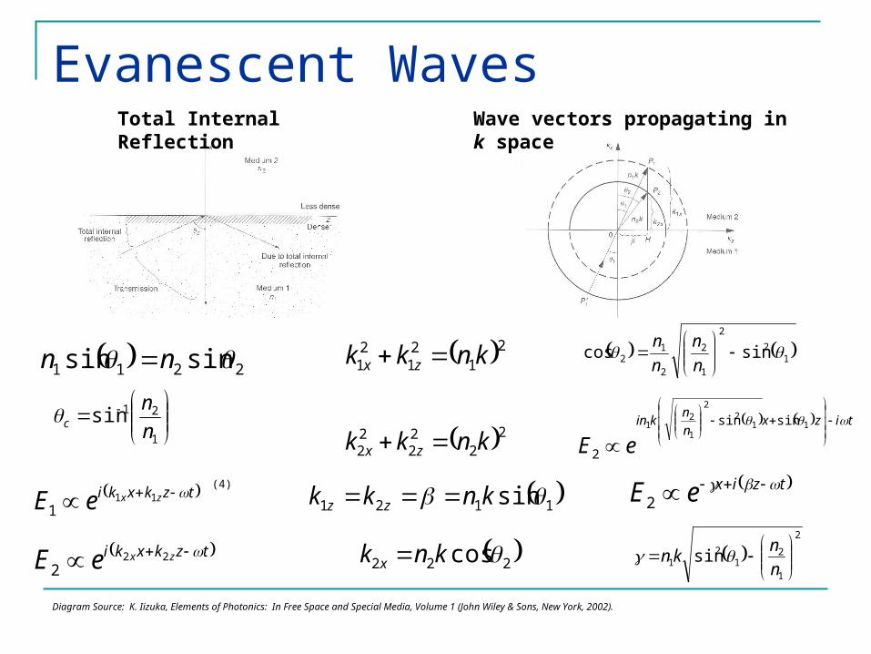
Evanescent Waves
2211 sinsin nn
1
21sinn
nc
tzkxki zxeE 111
tzkxki zxeE 222
2121
21 knkk zx
2222
22 knkk zx
1121 sin knkk zz
222 cos knk x
12
2
1
2
2
12 sincos
n
n
n
n
tizxn
nkin
eE
11
22
1
21 sinsin
2
tzixeE 2
2
1
21
21 sin
n
nkn
Diagram Source: K. Iizuka, Elements of Photonics: In Free Space and Special Media, Volume 1 (John Wiley & Sons, New York, 2002).
(4)
Total Internal Reflection
Wave vectors propagating in k space

Evanescent Waves
222 nkkk zx
dmzm 2
md
kzm
22
2 2
m
dkxn
To satisfy boundary conditions:
This can be re-written as:
The value of kxn is imaginary for high values of m and the waves are evanescent waves
Diagram Source: K. Iizuka, Elements of Photonics: In Free Space and Special Media, Volume 1 (John Wiley & Sons, New York, 2002).
2
cd
Above dc kx is always imaginary and all the waves in x are evanescent waves.
Evanescent Waves on a Corrugated Metal Surface
Evanescent Waves on an Array of Metal Pins
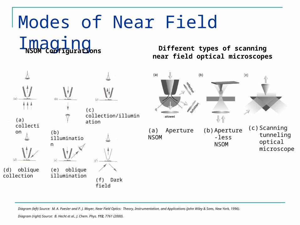
Modes of Near Field Imaging
(a) Aperture NSOM
(b) Aperture-less NSOM
(c) Scanning tunneling optical microscope
Different types of scanning near field optical microscopes
NSOM Configurations
(a) collection
(b) illumination
(c) collection/illumination
(d) oblique collection
(e) oblique illumination
(f) Dark field
Diagram (left) Source: M. A. Paesler and P. J. Moyer, Near Field Optics: Theory, Instrumentation, and Applications (John Wiley & Sons, New York, 1996).
Diagram (right) Source: B. Hecht et al., J. Chem. Phys. 112, 7761 (2000).

NSOM SetupStandard NSOM Setup(a)
Illumination
(b) Collection and Redistribution
(c) Detection
Tips (5)
•Heating and pulling method - Optical fiber is heated with CO2 laser and pulled on both sides of heated area
•Chemical etching method - Hydrofluoric acid used to etch glass fiber
•Fiber coated with metal
•Nanoparticle (Tip Enhanced)
Diagram (left) Source: B. Hecht et al., J. Chem. Phys. 112, 7761 (2000).
Diagram (right) Source: Molecular Expressions Optical Microscopy Primer, http://micro.magnet.fsu.edu/primer/index.html
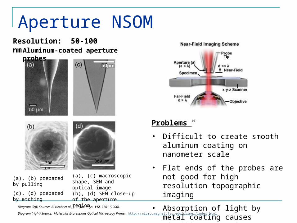
Aperture NSOMResolution: 50-100 nm
Problems (6)
• Difficult to create smooth aluminum coating on nanometer scale
• Flat ends of the probes are not good for high resolution topographic imaging
• Absorption of light by metal coating causes significant heating
Aluminum-coated aperture probes
(a), (b) prepared by pulling
(c), (d) prepared by etching
300 nm 300 nm
(a), (c) macroscopic shape, SEM and optical image(b), (d) SEM close-up of the aperture region
Diagram (left) Source: B. Hecht et al., J. Chem. Phys. 112, 7761 (2000).
Diagram (right) Source: Molecular Expressions Optical Microscopy Primer, http://micro.magnet.fsu.edu/primer/index.html

Tip-Enhanced NSOM
Resolution: 10-20 nm Causes for Enhanced Electric
Field: (7)
•Electrostatic lightning rod effect (depends on geometry)
•Surface plasmon resonances (depend on excitation wavelength and geometry)
Induced surface charge density in metal probe
Left: Incident wave polarized perpendicular to tip axis
Right: Incident wave polarized along tip axis
Need large near field enhancement so the signal can be detected in the far field
The incident field should be polarized along the tip axis to maximize field enhancement
Schematic of experimental setup for tip-enhanced near field
Diagram (left) Source: A. Hartschuh, M. R. Beversluis, A. Bouhelier, and L. Novotny, Phil. Trans. R. Soc. Lond. A. 362, 807 (2004). (7)
Diagram (right) Source: L. Novotny, R. X. Bian, and X. S. Xie, Phys. Rev. Lett. 79, 645 (1997). (8)
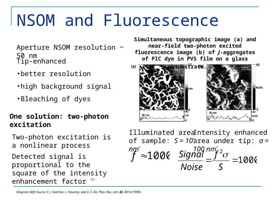
NSOM and Fluorescence
1000f
Aperture NSOM resolution ~ 50 nmTip-enhanced
•better resolution
•high background signal
•Bleaching of dyes
One solution: two-photon excitation
Two-photon excitation is a nonlinear process
Detected signal is proportional to the square of the intensity enhancement factor (6)
Illuminated area of sample: S = 105 nm2
Intensity enhanced area under tip: σ = 100 nm2
10002
S
f
Noise
Signal
Simultaneous topographic image (a) and near-field two-photon excited
fluorescence image (b) of J-aggregates of
PIC dye in PVS film on a glass substrate.
Diagram (left) Source: E. J. Sanchez, L. Novotny, and X. S. Xie, Phys. Rev. Lett. 82, 4014 (1999).

Purpose
Interest: “investigation of self-fluorescing or fluorescence labeled macromolecules at the single molecule level.”
Challenge: combine optical and topographical resolution of NSOM with fluorophore sensitivity
Results: “highly resolved optical imaging of single dyes” “high-resolution topographs”

“tip-on-aperture” probe
Thin optical fiber in etching solution (10)
Tip covered with Cr (for adhesion) then 200 nm Au for contrast in SEM
Focus electron beam of SEM on the center of the aperture
Electron-beam-deposited tip (EBD) formed (7 s, 8 kV)
3.5 nm Cr and 33 nm Al deposited by evaporation at 45o
Drawing of “tip-on-aperture probe with the DNA sample.
SEM images of a “tip-on-aperture” probe
(a) Before metallization
Diagram (left) Source: H. G. Frey, F. Keilmann, A. Kriele, and R. Guckenberger, Appl. Phys. Lett. 81, 5030 (2002).
(b) After metallization
Experimental Setup
Light Source: argon laser (514 nm) Light coupled to glass fiber onto the sample Light transmitted through the sample and collected by
objective (0.95 NA) on inverse light microscope Light filtered by 550 nm long pass filter Signal detected by APD Sample scanned ~ 1 micron per second Scanned at constant distance with shear force feedback Polarization of incident laser light adjusted to optimize
S/N 1/3 of probes provide good fluorescence results
Sample Preparation
DNA Cy-3 fluorophores covalently bound to the
termini of DNA Samples prepared in a polymerase chain
reaction (PCR) Mica Sheets
20 μl of 400 mM NiCl2 solution in water 2 min later – solution bottled off and 30 μl drop
of DNA (with Cy-3 label) solution applied to the sheet
10 min later – washed in ultrapure water and dried with nitrogen

Results
200 nm
25 nm25 nm
Fitted tip radius: 12 nm
Fluorescence image of single Cy-3 dye molecules, which appear mostly
as double maxima.
FWHM = 10 nm
Zoomed image of a dye molecule together with a section along the line (three lines average).
Enlarged image of a bleaching event from one scan line (oriented vertically) to the next one.
25 nm25 nm

Data Model
•Dye molecule excitation proportional to squared field component parallel to dipole moment
•They believe that the field from the aperture light does not substantially influence the experiment aperturetip EE 10
•Dye dipoles oriented vertically experience maximum excitation directly below the tip
•Inclined dyes display asymmetric peaks
•Vertical dye under the tip displays a circular structure
•Dye oriented in sample plane displays two symmetric maxima

Data Model
Software: MATHLAB 6.5 (Mathworks)
Classical Mirror Image Calculation Neglected:
Retroaction of dye dipole on tip dipole
Retardation effects Emission in direction of objective
used to calculate final signal
01
30
3
Im23
1 En
qcd
iAl 0.157.44
56.2mica
Lifetime without mirror
Quantum yield
Index of refraction of medium with dipole
•Fit Parameters
•X, Y position of dye
•3D orientation of dye
•Normalization factor for dye brightness and local background
•Parameters assumed constant
•Tip radius
•Tip-sample distance
•Quantum efficiency = 0.3

Results with Data Model
Measurements
Patterns calculated with parameters fitted to the measurements
Tilt angle: 0o Tilt angle: 68o
Tilt angle: 49o
Tilt angle: 20o
Tilt angle: 14o
Image size: 117 nm
Fitted tip radius: 22nm
•Tip-dye distance (calculated): 1 nm
•Tip-dye distance (approach curve): 2-3 nm
•Why the discrepancy?
•Treatment of quenching effects neglects contributions with a stronger dependence on distance becoming important within 5 nm
•Tip apex flatter than a sphere
•Moon-like and ring-like patterns due to strong quenching effects when tip-dye distance below 3 nm
•As tip-dye distance increases central minimum decreases in size
•Total number of photon counts per pattern decreased by factor of 2 when tip-dye distance increases by 5 nm
Fluorescence patterns of differently tilted dye molecules.

Results
Fitted tip radius: 12 nm
Analyzed dye molecules
Note: A fitted parabola has been subtracted from each scan line to flatten the data
(a) Topography together with calculated positions of analyzed dye molecules
(c) Positions of dye molecules in (a) with tilt angles (upper number) and azimuth angles (lower numbers) from first approximation fits in (d)
(b) Fluorescence image
200 nm
(d) First approximation fits
Green: Good fits
Yellow: Problematic fits
DNA with Cy-3 labeled termini on mica and corresponding
data modeling.
Accuracy in dye positions: 0.5 nm standard deviation
Azimuth angle accurate to 5o
Accuracy of tilt angle better than 10o
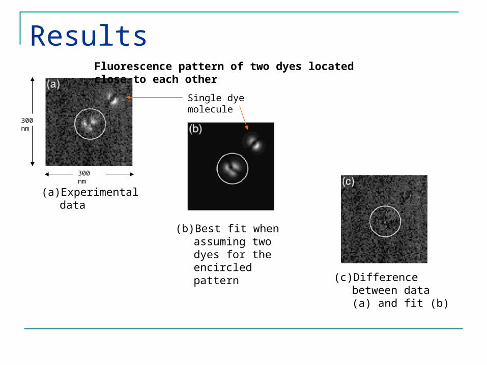
ResultsFluorescence pattern of two dyes located close to each other
300 nm
300 nm
(a) Experimental data
(b) Best fit when assuming two dyes for the encircled pattern
(c) Difference between data (a) and fit (b)
Single dye molecule

Conclusion
Results Near-field optical image of single
fluorescent dye molecules at high resolution High resolution topographic image of dye
molecules Improvements
Optimize tip-aperture geometry to allow plasmon resonance Vary tip length Change material
Sharpen the metal tip to improve resolution

References
1. B. Hecht et al., J. Chem. Phys. 112, 7761 (2000).2. M. A. Paesler and P. J. Moyer, Near Field Optics: Theory,
Instrumentation, and Applications (John Wiley & Sons, New York, 1996).
3. Molecular Expressions Optical Microscopy Primer, http://micro.magnet.fsu.edu/primer/index.html
4. K. Iizuka, Elements of Photonics: In Free Space and Special Media, Volume 1 (John Wiley & Sons, New York, 2002).
5. P. N. Prasad, Nanophotonics (John Wiley & Sons, Hoboken, 2004).6. E. J. Sanchez, L. Novotny, and X. S. Xie, Phys. Rev. Lett. 82, 4014
(1999).7. A. Hartschuh, M. R. Beversluis, A. Bouhelier, and L. Novotny, Phil.
Trans. R. Soc. Lond. A. 362, 807 (2004).8. L. Novotny, R. X. Bian, and X. S. Xie, Phys. Rev. Lett. 79, 645 (1997).9. N. Anderson, A. Bouhelier, L. Novotny, J. Opt. A. 8, S227 (2006). 10. H. G. Frey, F. Keilmann, A. Kriele, and R. Guckenberger, Appl. Phys.
Lett. 81, 5030 (2002).