Embed Size (px)
Citation preview

GQM1555C2D4R5CB01_ (0402, C0G:EIA, 4.5pF, DC200V)_: packaging code Reference Sheet
1.Scope
2.MURATA Part NO. System(Ex.)
3. Type & Dimensions
(Unit:mm)
4.Rated value
5.Package
Product specifications in this catalog are as of Jun.3,2017,and are subject to change or obsolescence without notice.
Please consult the approval sheet before ordering.
Please read rating and !Cautions first.
0.3 min.
(1)-1 L
1.0±0.05
(1)-2 W
0.5±0.05
e
High Q and High Power Chip Multilayer Ceramic Capacitors for General Purpose
mark
(4)
Rated
Voltage
Packaging Unit
DC 200 V
Temp. Range
(Ref.Temp.)
(8) Packaging
Temp. coeff
or Cap. Change
This product specification is applied to High Q and High Power Chip Multilayer Ceramic Capacitors used for General Electronic equipment.
(2) T
0.5±0.05
-55 to 125 °C0±30 ppm/°C25 to 125 °C
(25 °C)
(6)
Capacitance
Tolerance
4.5 pF
Specifications and Test
Methods
(Operating
Temp. Range)
±0.25 pF
(3) Temperature Characteristics
(Public STD Code):C0G(EIA)
g
0.15 to 0.35
(5) Nominal
Capacitance
Jf330mm Reel
PAPER W8P250000 pcs./Reel
Df180mm Reel
PAPER W8P210000 pcs./Reel
Wf180mm Reel
PAPER W8P120000 pcs./Reel
(1)L/WDimensions
(2)T Dimensions
(3)Temperature Characteristics
(4)Rated Voltage
(5)Nominal Capacitance
(6)Capacitance Tolerance
(8)Packaging Code(7)Murata’s Control
Code
GQM 15 5 5C 2D 4R5 C B01 D
GQM1555C2D4R5CB01-01 1

1 Rated Voltage Shown in Rated value. The rated voltage is defined as the maximum voltage
which may be applied continuously to the capacitor.
When AC voltage is superimposed on DC voltage,
VP-P
or VO-P
, whichever is larger, should be maintained
within the rated voltage range.
2 Appearance No defects or abnormalities. Visual inspection.
3 Dimension Within the specified dimensions. Using Measuring instrument of dimension.
4 Voltage proof No defects or abnormalities. Measurement Point : Between the terminations
Applied Time : 1s to 5 s
Charge/discharge current : 50mA max.
Test Voltage :
5 Insulation Resistance(I.R.) More than 10,000MΩ Measurement Point : Between the terminations
Measurement Voltage : DC Rated Voltage
Charging Time : 2 min
Charge/discharge current : 50mA max.
Measurement Temperature : Room Temperature
6 Capacitance Shown in Rated value. Measurement Temperature : Room Temperature
7 Q 30pF and over : Q≧1400
30pF and below : Q≧800+20C
C:Nominal Capacitance(pF)
8 Temperature Characteristics Nominal values of the temperature coefficient is shown in The capacitance change should be measured after 5 min
of Capacitance Rated value. at each specified temp. stage.
But,the Capacitance Change under 25℃ is shown in Table A. Capacitance value as a reference is the value in step 3.
Capacitance Drift The capacitance drift is calculated by dividing the differences
Within +/-0.2% or +/-0.05pF between the maximum and minimum measured values in the
(Whichever is larger.) step 1,3 and 5 by the cap. value in step 3.
9 Adhesive Strength No removal of the terminations or other defect Solder the capacitor on the test substrate shown in Fig.3.
of Termination should occur.
Applied Force : 5N
Holding Time : 10+/-1s
Applied Direction : In parallel with the test substrate and vertical with
the capacitor side.
10 Vibration Appearance No defects or abnormalities. Solder the capacitor on the test substrate shown in Fig.3.
Capacitance Within the specified initial value. Kind of Vibration : A simple harmonic motion
10Hz to 55Hz to 10Hz (1min)
Q Within the specified initial value. Total amplitude : 1.5mm
This motion should be applied for a period of 2h in each 3 mutually
perpendicular directions(total of 6h).
11 Substrate Appearance No defects or abnormalities. Solder the capacitor on the test substrate shown in Fig.1.
Bending test
Capacitance Within +/-5% or +/-0.5pF Pressurization method : Shown in Fig.2
Change (Whichever is larger) Flexure : 1mm
Holding Time : 5+/-1s
Soldering Method : Reflow soldering
12 Solderability 95% of the terminations is to be soldered evenly and continuously. Test Method : Solder bath method
Flux Solution of rosin ethanol 25(mass)%
Preheat : 80℃ to 120℃ for 10s to 30s
Solder : Sn-3.0Ag-0.5Cu
Solder Temp. : 245+/-5℃
Immersion time : 2+/-0.5s
■ Specifications and Test Methods
No Item SpecificationTest Method
(Ref. Standard:JIS C 5101, IEC60384)
Capacitance Frequency Voltage
C≦1000pF 1.0+/-0.1MHz 0.5 to 5.0Vrms
Step Temperature(C)
1 Reference Temp.+/-2
2 Min. Operating Temp.+/-3
3 Reference Temp.+/-2
4 Max. Operating Temp.+/-3
5 Reference Temp.+/-2
Rated Voltage Test Voltage
100V 300% of Rated Voltage
200V 250% of Rated Voltage
JEMCNS-02795A 2

13 Resistance to Appearance No defects or abnormalities. Test Method : Solder bath method
Soldering Heat Solder : Sn-3.0Ag-0.5Cu
Capacitance Within +/-2.5% or +/- 0.25pF Solder Temp. : 270+/-5℃
Change (Whichever is larger) Immersion time : 10+/-0.5s
Q Within the specified initial value. Exposure Time : 24+/-2h
Preheat : 120℃ to 150℃ for 1 min
I.R. Within the specified initial value.
Voltage proof No defects.
14 Temperature Appearance No defects or abnormalities. Solder the capacitor on the test substrate shown in Fig.3.
Sudden Change
Capacitance Within +/-2.5% or +/- 0.25pF Perform the 5 cycles according to the four heat treatments
Change (Whichever is larger) shown in the following table.
Q Within the specified initial value.
I.R. Within the specified initial value.
Voltage proof No defects.
Exposure Time : 24+/-2h
15 High Appearance No defects or abnormalities. Solder the capacitor on the test substrate shown in Fig.3.
Temperature
High Humidity Capacitance Within +/-7.5% or +/- 0.75pF Test Temperature : 40+/-2℃
(Steady) Change (Whichever is larger) Test Humidity : 90%RH to 95%RH
Q 30pF and over : Q≧200 Test Time : 500+/-12h
30pF and below : Q≧100+10C/3 Applied Voltage : DC Rated Voltage
C:Nominal Capacitance(pF) Charge/discharge current : 50mA max.
I.R. More than 500MΩ Exposure Time : 24+/-2h
16 Durability Appearance No defects or abnormalities. Solder the capacitor on the test substrate shown in Fig.3.
Capacitance Within +/-3% or +/- 0.3pF Test Temperature : Max. Operating Temp. +/-3℃
Change (Whichever is larger) Test Time : 1000+/-12h
Q 30pF and over : Q≧350 Applied Voltage : 200% of the rated voltage
10pF and over , 30pF and below : Q≧275+5C/2 Charge/discharge current : 50mA max.
10pF and below : Q≧200+10C Exposure Time : 24+/-2h
C:Nominal Capacitance (pF)
I.R. More than 1,000MΩ
No Item SpecificationTest Method
(Ref. Standard:JIS C 5101, IEC60384)
Step Temp.(C) Time (min)
1 Min.Operating Temp.+0/-3 30+/-3
2 Room Temp. 2 to 3
3 Max.Operating Temp.+3/-0 30+/-3
4 Room Temp 2 to 3
Table A
Char. Capacitance Change from 25C (%)
-55℃ -30℃ -10℃
Max. Min. Max. Min. Max. Min. 5C 0.58 -0.24 0.40 -0.17 0.25 -0.11
JEMCNS-02795A 3
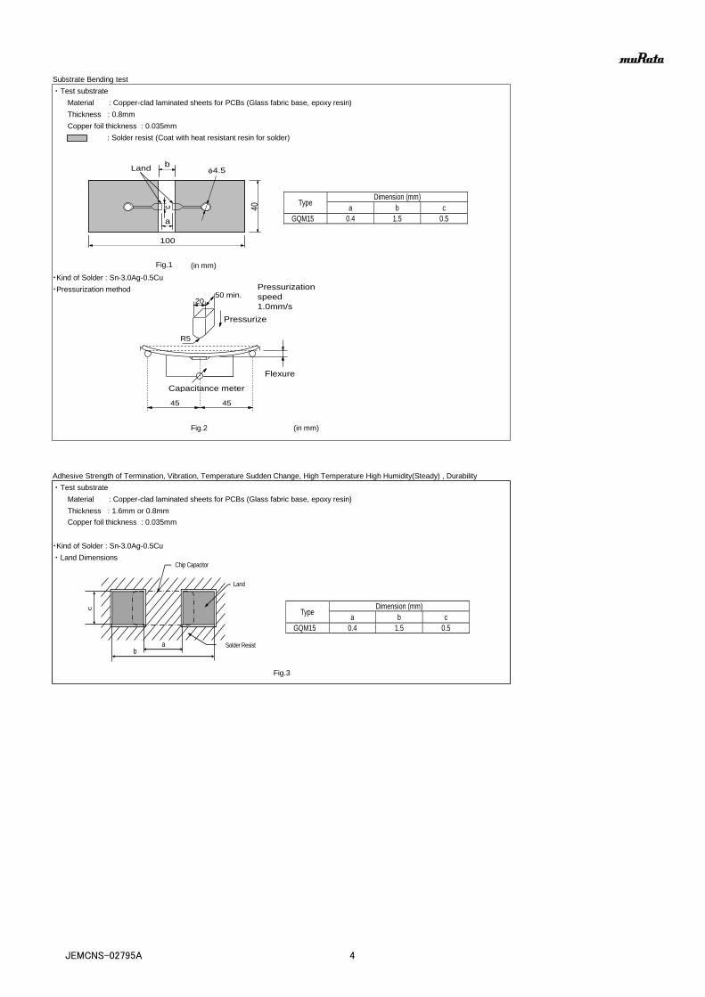
Substrate Bending test
・Test substrate
Material : Copper-clad laminated sheets for PCBs (Glass fabric base, epoxy resin)
Thickness : 0.8mm
Copper foil thickness : 0.035mm
: Solder resist (Coat with heat resistant resin for solder)
Fig.1 (in mm)
・Kind of Solder : Sn-3.0Ag-0.5Cu
・Pressurization method
Fig.2 (in mm)
Adhesive Strength of Termination, Vibration, Temperature Sudden Change, High Temperature High Humidity(Steady) , Durability
・Test substrate
Material : Copper-clad laminated sheets for PCBs (Glass fabric base, epoxy resin)
Thickness : 1.6mm or 0.8mm
Copper foil thickness : 0.035mm
・Kind of Solder : Sn-3.0Ag-0.5Cu
・Land Dimensions
Fig.3
*2
4.0±0.1
8.0±
0.3
3.5±
0.05
0.05以下
*1φ1.5+0.1-0
A
t
*1,2:2.0±0.05
1.75
±0.
1
B
100
40
a
c
b Land f4.5
c
c
b a Solder Resist
Chip Capacitor
Land
45 45 Flexure
Capacitance meter
Pressurization
speed
1.0mm/s
Support
Capacitor Pressurize
45 45
R5
20 50 min.
Type Dimension (mm)
a b c
GQM15 0.4 1.5 0.5
Type Dimension (mm)
a b c
GQM15 0.4 1.5 0.5
JEMCNS-02795A 4

1.Tape Carrier Packaging(Packaging Code:D/E/W/L/J/F/K)
1.1 Minimum Quantity(pcs./reel)
1.2 Dimensions of Tape
(1)GQM15 <Paper Tape W8P2 CODE:D/E/J/F> (in mm)
5*3 Nominal value
(2)GQM15 <Paper Tape W8P1 CODE:W) (in mm)
5*3 Nominal value
0.8 max.GQM15 1.0±0.05 0.5±0.05 0.5±0.05 0.65 1.15
0.8 max.
TypeDimensions (Chip)
A *3 B *3 tL W T
GQM15 1.0±0.05 0.5±0.05 0.5±0.05 0.65 1.15
TypeDimensions (Chip)
A *3 B *3 tL W T
GQM22 1000 4000
GQM21(LWT Dimensions Tolerance:±0.15) 4000
GQM21(LWT Dimensions Tolerance:±0.1) 4000 10000
GQM188 4000 10000
GQM187 4000
Code:L Code:J/F Code:K
GQM15 10000(W8P2) 20000(W8P1) 50000(W8P2)
PACKAGING
GQM Type
Type
φ180mm reel φ330mm reel
Paper Tape Plastic Tape Paper Tape Plastic Tape
Code:D/E Code:W
*1,*2:2.0±0.05
*2
4.0±0.1
8.0±
0.3
3.5±
0.05
0.05以下
*1φ1.5+0.1-0
A
t
*1,2:2.0±0.05
1.75
±0.
1
B
4.0±0.1
*1 φ1.5
+0.1 -0 1.
75±0.1
8.0±
0.3
3.5±
0.05
A
B
t
*2
0.05 max.
1.0±0.05
4.0±0.1
φ1.5 +0.1 -0 1.
75±0.1
8.0±
0.3
3.5±
0.05
A
B
t
1.0±0.05
JEMCNP-01900C 5

(3)GQM18/GQM21 <Paper Tape CODE:D/E/J/F> (in mm)
L W T
7 1.6±0.15 0.8±0.15 0.7±0.18 1.6±0.1 0.8±0.1 0.8±0.1
2.0±0.1 1.25±0.1 0.85±0.12.0±0.15 1.25±0.15 0.85±0.15
(4)GQM22 <Plastic Tape CODE:L/K>
L W T
GQM22 M 2.8±0.5 2.8±0.4 1.15±0.2 2.8* 3.5* 2.5 max.
*3 Nominal value
TypeDimensions (Chip)
A B t
GQM18 1.05±0.10 1.85±0.101.15 max.
GQM21 9 1.55±0.15 2.30±0.15
PACKAGING
GQM Type
TypeDimensions (Chip)
A B t
4.0±0.1 4.0±0.1
2.0±0.05 φ1.5
+0.1 -0
1.75±
0.1
8.0±
0.3
3.5±
0.05
t
A
B
8.0±
0.3
4.0±0.1
3.5±
0.05
1.75±0.
1
A
B
t
2.0±0.1
φ1.5 +0.1 -0
4.0±0.1
0.25±0.1
JEMCNP-01900C 6

PACKAGING
GQM Type
図 1 チップ詰め状態
( 単位: mm)
φ21±0.8
10±1.5
16.5 max.
Top Tape : Thickness 0.06
Feeding Hole :As specified in 1.2.
Hole for Chip : As specified in 1.2.
Base Tape : As specified in 1.2.
Bottom Tape :Thickness 0.05
(Only a bottom tape existence )
φ180+0/-
3.0
φ330±2.0
φ50 m
in.
φ13±0.5
2.0±0.5
Chip
(in mm) Fig.1 Package Chips
Fig.2 Dimensions of Reel
Fig.3 Taping Diagram
JEMCNP-01900C 7

1.3 Tapes for capacitors are wound clockwise shown in Fig.3. (The sprocket holes are to the right as the tape is pulled toward the user.)
1.4 Part of the leader and part of the vacant section are attached as follows.(in mm)
1.5 Accumulate pitch : 10 of sprocket holes pitch = 40±0.3mm
1.6 Chip in the tape is enclosed by top tape and bottom tape as shown in Fig.1.
1.7 The top tape and base tape are not attached at the end of the tape for a minimum of 5 pitches.
1.8 There are no jointing for top tape and bottom tape.
1.9 There are no fuzz in the cavity.
1.10 Break down force of top tape : 5N min. Break down force of bottom tape : 5N min. (Only a bottom tape existence )
1.11 Reel is made by resin and appeaser and dimension is shown in Fig 2. There are possibly to change the material and dimension due to some impairment.
1.12 Peeling off force : 0.1N to 0.6N in the direction as shown below.
1.13 Label that show the customer part number, our part number, our company name, inspection number and quantity, will be put in outside of reel.
PACKAGING
GQM Type
図 1 チップ詰め状態
( 単位: mm)
Tail vacant Section Chip-mounting Unit Leader vacant Section
Leader Unit
(Top Tape only)
Direction of Feed
160 min. 190 min. 210 min.
図 1 チップ詰め状態
( 単位: mm)
165~180° Top tape
JEMCNP-01900C 8
Caution
■Limitation of Applications Please contact us before using our products for the applications listed below which require especially high reliability for the prevention of defects which might directly cause damage to the third party's life, body or property.
①Aircraft equipment ②Aerospace equipment ③Undersea equipment ④Power plant control equipment
⑤Medical equipment ⑥Transportation equipment(vehicles,trains,ships,etc.) ⑦Traffic signal equipment
⑧Disaster prevention / crime prevention equipment ⑨Data-processing equipment
⑩Application of similar complexity and/or reliability requirements to the applications listed in the above.
■Storage and Operation condition
1. The performance of chip multilayer ceramic capacitors may be affected by the storage conditions.
1-1. Store the capacitors in the following conditions:
Room Temperature of +5℃ to +40℃ and a Relative Humidity of 20% to 70%.
(1) High temperature and humidity conditions may accelerate the deterioration of solderability due to oxidation
of the terminal electrodes and deterioration of taping/packaging performance.
Therefore, maintain the appropriate storage temperature and humidity.
(2) Prolonged storage may cause oxidation of the electrodes and deterioration of the packaging materials.
If more than six months have elapsed since delivery, check the mounting before use.
If more than one year has elapsed since delivery, also check the solderability before use.
Even if the storage period is short, do not exceed the specified atmospheric conditions.
(3) Store the capacitors in the original packaging without opening the smallest packing unit.
Do not exceed the above atmospheric conditions for any length of time.
1-2. Corrosive gas can react with the termination (external) electrodes or lead wires of capacitors, and result
in poor solderability. Do not store the capacitors in an atmosphere consisting of corrosive gas (e.g.,hydrogen
sulfide, sulfur dioxide, chlorine, ammonia gas etc.).
1-3. Due to moisture condensation caused by rapid humidity changes, or the photochemical change caused
by direct sunlight on the terminal electrodes and/or the resin/epoxy coatings, the solderability and
electrical performance may deteriorate. Do not store capacitors under direct sunlight or in high huimidity
conditions
■Rating
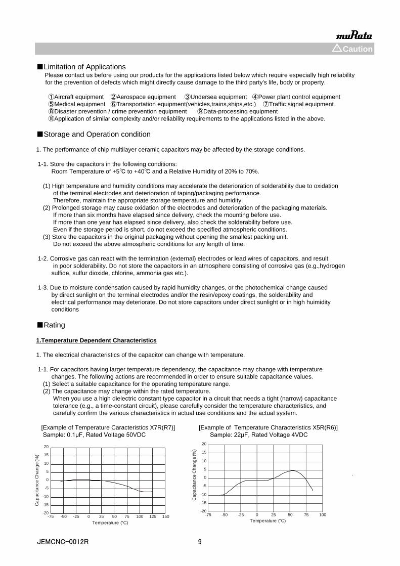
1.Temperature Dependent Characteristics
1. The electrical characteristics of the capacitor can change with temperature.
1-1. For capacitors having larger temperature dependency, the capacitance may change with temperature
changes. The following actions are recommended in order to ensure suitable capacitance values.
(1) Select a suitable capacitance for the operating temperature range.
(2) The capacitance may change within the rated temperature.
When you use a high dielectric constant type capacitor in a circuit that needs a tight (narrow) capacitance
tolerance (e.g., a time-constant circuit), please carefully consider the temperature characteristics, and
carefully confirm the various characteristics in actual use conditions and the actual system.
[Example of Temperature Caracteristics X7R(R7)] [Example of Temperature Characteristics X5R(R6)]
Sample: 0.1μF, Rated Voltage 50VDC Sample: 22μF, Rated Voltage 4VDC
!
-20
-10
-15
-5
5
0
10
15
20
Temperature ( C)
-75 -50 -25 0 25 50 75 100 125 150
Ca
pa
cita
nce
Ch
an
ge (%
)
-20
-10
-15
-5
5
0
10
15
20
Temperature ( C)
-75 -50 -25 0 25 50 75 100
Ca
pa
cita
nce
Ch
an
ge (%
)
JEMCNC-0012R 9
2.Measurement of Capacitance
1. Measure capacitance with the voltage and frequency specified in the product specifications.
1-1. The output voltage of the measuring equipment may decrease occasionally when capacitance is high.
Please confirm whether a prescribed measured voltage is impressed to the capacitor.
1-2. The capacitance values of high dielectric constant type capacitors change depending on the AC voltage applied.
Please consider the AC voltage characteristics when selecting a capacitor to be used in a AC circuit.
3.Applied Voltage
1. Do not apply a voltage to the capacitor that exceeds the rated voltage as called out in the specifications.
1-1. Applied voltage between the terminals of a capacitor shall be less than or equal to the rated voltage.
(1) When AC voltage is superimposed on DC voltage, the zero-to-peak voltage shall not exceed the rated DC voltage.
When AC voltage or pulse voltage is applied, the peak-to-peak voltage shall not exceed the rated DC voltage.
(2) Abnormal voltages (surge voltage, static electricity, pulse voltage, etc.) shall not exceed the rated DC voltage.
Typical Voltage Applied to the DC capacitor
DC Voltage DC Voltage+AC AC Voltage Pulse Voltage
(E:Maximum possible applied voltage.)
1-2. Influence of over voltage
Over voltage that is applied to the capacitor may result in an electrical short circuit caused by the breakdown
of the internal dielectric layers .
The time duration until breakdown depends on the applied voltage and the ambient temperature.
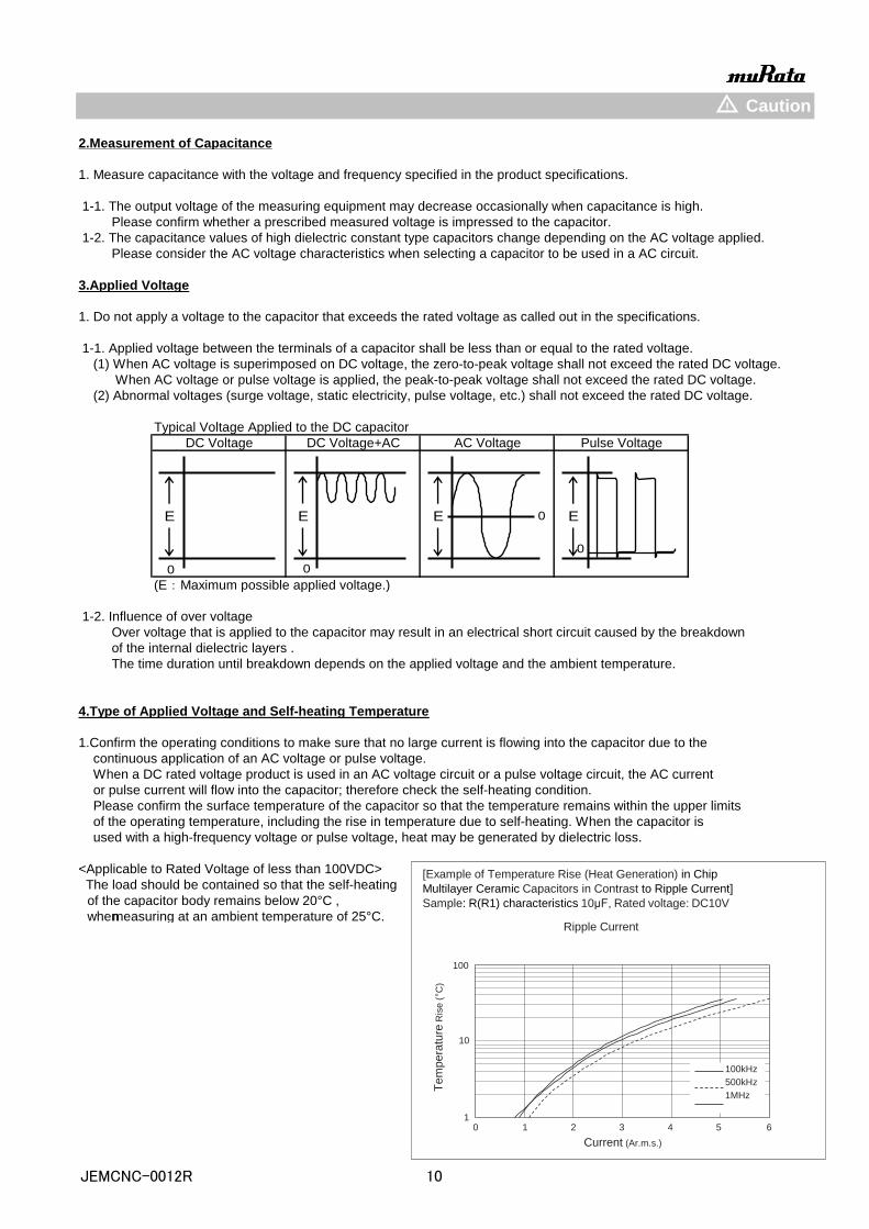
4.Type of Applied Voltage and Self-heating Temperature
1.Confirm the operating conditions to make sure that no large current is flowing into the capacitor due to the
continuous application of an AC voltage or pulse voltage.
When a DC rated voltage product is used in an AC voltage circuit or a pulse voltage circuit, the AC current
or pulse current will flow into the capacitor; therefore check the self-heating condition.
Please confirm the surface temperature of the capacitor so that the temperature remains within the upper limits
of the operating temperature, including the rise in temperature due to self-heating. When the capacitor is
used with a high-frequency voltage or pulse voltage, heat may be generated by dielectric loss.
<Applicable to Rated Voltage of less than 100VDC>
The load should be contained so that the self-heating
of the capacitor body remains below 20°C ,
when measuring at an ambient temperature of 25°C.
Caution!
1
10
100
0 1 2 3
Current (Ar.m.s.)
4 5 6
Te
mpera
ture
Ris
e ( C
)
[Example of Temperature Rise (Heat Generation) in Chip
Multilayer Ceramic Capacitors in Contrast to Ripple Current]
Sample: R(R1) characteristics 10μF, Rated voltage: DC10V
Ripple Current
100kHz
500kHz
1MHz
E E E E
0 0
0
0
JEMCNC-0012R 10

5. DC Voltage and AC Voltage Characteristic
1. The capacitance value of a high dielectric constant type
capacitor changes depending on the DC voltage applied.
Please consider the DC voltage characteristics when a
capacitor is selected for use in a DC circuit.
1-1. The capacitance of ceramic capacitors may change
sharply depending on the applied voltage. (See figure)
Please confirm the following in order to secure the
capacitance.
(1) Determine whether the capacitance change caused
by the applied voltage is within the allowed range .
(2) In the DC voltage characteristics, the rate of
capacitance change becomes larger as voltage
increases, even if the applied voltage is below
the rated voltage. When a high dielectric constant
type capacitor is used in a circuit that requires a
tight (narrow) capacitance tolerance (e.g., a time
constant circuit), please carefully consider the
voltage characteristics, and confirm the various
characteristics in the actual operating conditions
of the system.
2. The capacitance values of high dielectric
constant type capacitors changes depending
on the AC voltage applied.
Please consider the AC voltage characteristics
when selecting a capacitor to be used in a
AC circuit.
6. Capacitance Aging
[ Example of Change Over Time (Aging characteristics) ]
1. The high dielectric constant type capacitors
have an Aging characteristic in which the capacitance
value decreases with the passage of time.
When you use a high dielectric constant type
capacitors in a circuit that needs a tight (narrow)
capacitance tolerance (e.g., a time-constant circuit),
please carefully consider the characteristics
of these capacitors, such as their aging, voltage,
and temperature characteristics. In addition,
check capacitors using your actual appliances
at the intended environment and operating conditions.
7.Vibration and Shock
1. Please confirm the kind of vibration and/or shock, its condition, and any generation of resonance.
Please mount the capacitor so as not to generate resonance, and do not allow any impact on the terminals.
2. Mechanical shock due to being dropped may cause damage or
a crack in the dielectric material of the capacitor.
Do not use a dropped capacitor because the quality and reliability
may be deteriorated.
3. When printed circuit boards are piled up or handled, the corner
of another printed circuit board
should not be allowed to hit the capacitor in order to avoid
a crack or other damage to the capacitor.
Caution
-100
-80
-60
-40
-20
0
20
0 10 20 30
DC Voltage (V)
40 50
[Example of DC Voltage Characteristics]
Sample: X7R(R7) Characteristics 0.1μF, Rated Voltage 50VDC
Capacitance C
hange (
%)
0 0.5 1
AC Voltage (Vr.m.s.)
1.5 2
[Example of AC Voltage Characteristics]
Sample: X7R(R7) Characteristics 10μF, Rated Voltage 6.3VDC
Capacitance C
hange (
%) 30
20
10
0
-10
-20
-30
-40
-50
-60
Floor
Crack
Mounting printed circuit board
Crack
!
20
10
0
-10
-20
-30
-40
10 100 1000 10000
Time(h)
Cap
acita
nce
Cha
nge(
%)
C0G(5C)
X7R(R7)
X5R(R6)
JEMCNC-0012R 11

■Soldering and Mounting
1.Mounting Position
1. Confirm the best mounting position and direction that minimizes the stress imposed on the capacitor during flexing
or bending the printed circuit board.
1-1.Choose a mounting position that minimizes the stress imposed on the chip during flexing or bending of the board.
[Component Direction]
Locate chip horizontal to the
direction in which stress acts.
(Bad Example) (Good Example)
[Chip Mounting Close to Board Separation Point]
It is effective to implement the following measures, to reduce stress in separating the board.
It is best to implement all of the following three measures; however, implement as many measures as possible
to reduce stress.
Stress Level
(1) Turn the mounting direction of the component parallel to the board separation surface. A > D *1
(2) Add slits in the board separation part. A > B
(3) Keep the mounting position of the component away from the board separation surface. A > C
*1 A > D is valid when stress is added vertically to the perforation as with Hand Separation.
If a Cutting Disc is used, stress will be diagonal to the PCB, therefore A > D is invalid.
[Mounting Capacitors Near Screw Holes]
When a capacitor is mounted near a screw hole, it may be affected by the board deflection that occurs during
the tightening of the screw. Mount the capacitor in a position as far away from the screw holes as possible.
2.Information before Mounting
1. Do not re-use capacitors that were removed from the equipment.
2. Confirm capacitance characteristics under actual applied voltage.
3. Confirm the mechanical stress under actual process and equipment use.
4. Confirm the rated capacitance, rated voltage and other electrical characteristics before assembly.
5. Prior to use, confirm the solderability of capacitors that were in long-term storage.
6. Prior to measuring capacitance, carry out a heat treatment for capacitors that were in long-term storage.
7.The use of Sn-Zn based solder will deteriorate the reliability of the MLCC.
Please contact our sales representative or product engineers on the use of Sn-Zn based solder in advance.
Caution
Contents of Measures
Screw HoleRecommended
!
①
② ③ 1C 1B
1A
Perforation
Slit
A
B
C
D
①
1A
JEMCNC-0012R 12

3.Maintenance of the Mounting (pick and place) Machine
1. Make sure that the following excessive forces are not applied to the capacitors.
Check the mounting in the actual device under actual use conditions ahead of time.
1-1. In mounting the capacitors on the printed circuit board, any bending force against them shall be kept
to a minimum to prevent them from any damage or cracking. Please take into account the following precautions
and recommendations for use in your process.
(1) Adjust the lowest position of the pickup nozzle so as not to bend the printed circuit board.
[Incorrect]
[Correct]
2.Dirt particles and dust accumulated in the suction nozzle and suction mechanism prevent the nozzle from
moving smoothly. This creates excessive force on the capacitor during mounting, causing cracked chips.
Also, the locating claw, when worn out, imposes uneven forces on the chip when positioning, causing cracked chips.
The suction nozzle and the locating claw must be maintained, checked and replaced periodically.
Caution!
Board Guide
Board
Suction Nozzle
Deflection
Support Pin
JEMCNC-0012R 13

4-1.Reflow Soldering
1. When sudden heat is applied to the components, the [Standard Conditions for Reflow Soldering]
mechanical strength of the components will decrease
because a sudden temperature change causes
deformation inside the components. In order to prevent
mechanical damage to the components, preheating is
required for both the components and the PCB.
Preheating conditions are shown in table 1. It is required to
keep the temperature differential between the solder and
the components surface (ΔT) as small as possible.
2. When components are immersed in solvent after mounting,
be sure to maintain the temperature difference (ΔT)
between the component and the solvent within the range
shown in the table 1.
[Allowable Reflow Soldering Temperature and Time]
Table 1
Series
GQM
GQM
In the case of repeated soldering, the accumulated
Recommended Conditions soldering time must be within the range shown above.
Lead Free Solder: Sn-3.0Ag-0.5Cu
3. When a capacitor is mounted at a temperature lower than the peak reflow temperature recommended by the
solder manufacturer, the following quality problems can occur. Consider factors such as the placement of
peripheral components and the reflow temperature setting to prevent the capacitor’s reflow temperature from
dropping below the peak temperature specified. Be sure to evaluate the mounting situation beforehand and
verify that none of the following problems occur.
・Drop in solder wettability
・Solder voids
・Possible occurrence of whiskering
・Drop in bonding strength
・Drop in self-alignment properties
・Possible occurrence of tombstones and/or shifting on the land patterns of the circuit board
4. Optimum Solder Amount for Reflow Soldering
4-1. Overly thick application of solder paste results in a excessive solder fillet height.
This makes the chip more susceptible to mechanical and thermal stress on the board and may cause the chips to crack.
4-2. Too little solder paste results in a lack of adhesive strength on the termination, which may result in chips breaking loose
from the PCB.
4-3. Please confirm that solder has been applied smoothly to the termination.
Make sure not to impose any abnormal mechanical shocks to the PCB.
Lead Free Solder
Peak Temperature 240 to 260℃
Atmosphere Air or N2
Inverting the PCB
Caution
Chip Dimension(L/W) Code Temperature Differential
15/18/21 ΔT≦190℃
22 ΔT≦130℃
!
Temperature(℃)
Peak Temperature
Soldering
Gradual
Cooling
Preheating
ΔT
60-120 seconds 30-60 seconds Time
190℃ 170℃ 150℃
220℃
Sol
derin
g Te
mpe
ratu
re(℃
)
Soldering Time(s)
280
270
260
250
240
230
220 0 30 60 120 90
JEMCNC-0012R 14
4-2.Flow Soldering
1. Do not apply flow soldering to chips not listed in Table 2. [Standard Conditions for Flow Soldering]
Table 2
Series
GQM
(Except for Temperature Characteristics:5G(X8G))
2. When sudden heat is applied to the components, the
mechanical strength of the components will decrease
because a sudden temperature change causes
deformation inside the components. In order to prevent
mechanical damage to the components, preheating is
required for both of the components and the PCB.
Preheating conditions are shown in table 2. It is required to [Allowable Flow Soldering Temperature and Time]
keep the temperature differential between the solder and
the components surface (ΔT) as low as possible.
3. Excessively long soldering time or high soldering
temperature can result in leaching of the terminations,
causing poor adhesion or a reduction in capacitance value
due to loss of contact between the inner electrodes and terminations.
4. When components are immersed in solvent after mounting,
be sure to maintain the temperature differential (ΔT)
between the component and solvent within the range
shown in the table 2. In the case of repeated soldering, the accumulated
soldering time must be within the range shown above.
Recommended Conditions
Lead Free Solder: Sn-3.0Ag-0.5Cu
5. Optimum Solder Amount for Flow Soldering
5-1. The top of the solder fillet should be lower than the
thickness of the components. If the solder amount is
excessive, the risk of cracking is higher during
board bending or any other stressful condition.
Preheating Peak Temperature 100 to 120℃
Soldering Peak Temperature 250 to 260℃
Atmosphere Air or N2
Caution
Chip Dimension(L/W) Code Temperature Differential
18/21 ΔT≦150℃
Lead Free Solder
!
Sold
erin
g m
pera
ture
(℃)
Soldering Time(s)
280
270
260
250
240
230
220 0 10 20 40 30
Temperature(℃) Soldering
Peak Temperature
Preheating Peak Temperature
30-90 seconds
Preheating
5 seconds max. Time
Gradual Cooling
Soldering
ΔT
Up to Chip Thickness
Adhesive in section
JEMCNC-0012R 15
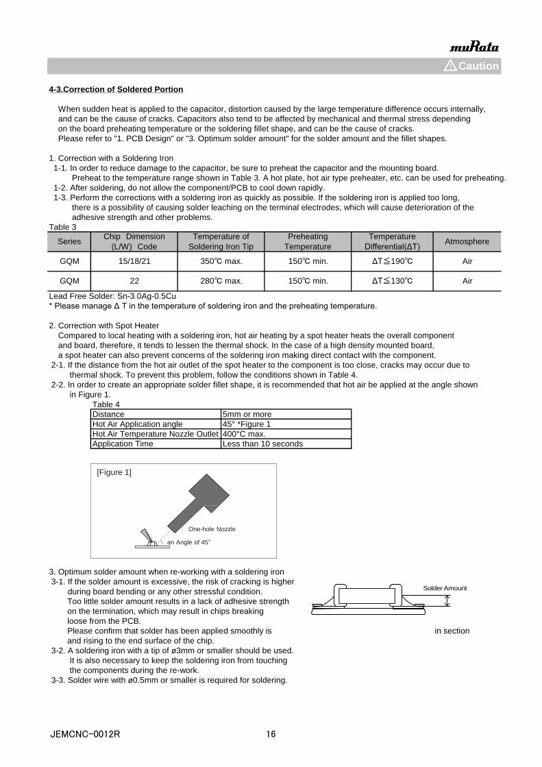
4-3.Correction of Soldered Portion
When sudden heat is applied to the capacitor, distortion caused by the large temperature difference occurs internally,
and can be the cause of cracks. Capacitors also tend to be affected by mechanical and thermal stress depending
on the board preheating temperature or the soldering fillet shape, and can be the cause of cracks.
Please refer to "1. PCB Design" or "3. Optimum solder amount" for the solder amount and the fillet shapes.
1. Correction with a Soldering Iron
1-1. In order to reduce damage to the capacitor, be sure to preheat the capacitor and the mounting board.
Preheat to the temperature range shown in Table 3. A hot plate, hot air type preheater, etc. can be used for preheating.
1-2. After soldering, do not allow the component/PCB to cool down rapidly.
1-3. Perform the corrections with a soldering iron as quickly as possible. If the soldering iron is applied too long,
there is a possibility of causing solder leaching on the terminal electrodes, which will cause deterioration of the
adhesive strength and other problems.
Table 3
Lead Free Solder: Sn-3.0Ag-0.5Cu
* Please manage Δ T in the temperature of soldering iron and the preheating temperature.
2. Correction with Spot Heater
Compared to local heating with a soldering iron, hot air heating by a spot heater heats the overall component
and board, therefore, it tends to lessen the thermal shock. In the case of a high density mounted board,
a spot heater can also prevent concerns of the soldering iron making direct contact with the component.
2-1. If the distance from the hot air outlet of the spot heater to the component is too close, cracks may occur due to
thermal shock. To prevent this problem, follow the conditions shown in Table 4.
2-2. In order to create an appropriate solder fillet shape, it is recommended that hot air be applied at the angle shown
in Figure 1.
Table 4
Distance 5mm or more
Hot Air Application angle 45° *Figure 1
Hot Air Temperature Nozzle Outlet 400°C max.
Application Time Less than 10 seconds
3. Optimum solder amount when re-working with a soldering iron
3-1. If the solder amount is excessive, the risk of cracking is higher
during board bending or any other stressful condition.
Too little solder amount results in a lack of adhesive strength
on the termination, which may result in chips breaking
loose from the PCB.
Please confirm that solder has been applied smoothly is in section
and rising to the end surface of the chip.
3-2. A soldering iron with a tip of ø3mm or smaller should be used.
It is also necessary to keep the soldering iron from touching
the components during the re-work.
3-3. Solder wire with ø0.5mm or smaller is required for soldering.
GQM 22 280℃ max. 150℃ min. ΔT≦130℃ Air
GQM 15/18/21 350℃ max. 150℃ min. ΔT≦190℃ Air
Caution
SeriesChip Dimension
(L/W) Code
Temperature of
Soldering Iron Tip
Preheating
Temperature
Temperature
Differential(ΔT)Atmosphere
!
One-hole Nozzle
an Angle of 45
[Figure 1]
Solder Amount
JEMCNC-0012R 16

5.Washing
Excessive ultrasonic oscillation during cleaning can cause the PCBs to resonate, resulting in cracked chips
or broken solder joints. Before starting your production process, test your cleaning equipment / process to insure
it does not degrade the capacitors.
6.Electrical Test on Printed Circuit Board
1. Confirm position of the support pin or specific jig, when inspecting the electrical performance of a
capacitor after mounting on the printed circuit board.
1-1. Avoid bending the printed circuit board by the pressure of a test-probe, etc.
The thrusting force of the test probe can flex the PCB, resulting in cracked chips or open solder
joints. Provide support pins on the back side of the PCB to prevent warping or flexing.
Install support pins as close to the test-probe as possible.
1-2. Avoid vibration of the board by shock when a test -probe contacts a printed circuit board.
[Not Recommended] [Recommended]
7.Printed Circuit Board Cropping
1. After mounting a capacitor on a printed circuit board, do not apply any stress to the capacitor that
caused bending or twisting the board.
1-1. In cropping the board, the stress as shown may cause the capacitor to crack.
Cracked capacitors may cause deterioration of the insulation resistance, and result in a short.
Avoid this type of stress to a capacitor.
[Bending] [Twisting]
2. Check the cropping method for the printed circuit board in advance.
2-1. Printed circuit board cropping shall be carried out by using a jig or an apparatus (Disc separator, router
type separator, etc.) to prevent the mechanical stress that can occur to the board.
* When a board separation jig or disc separator is used, if the following precautions are not observed,
a large board deflection stress will occur and the capacitors may crack.
Use router type separator if at all possible.
Notes
Hand and nipper
separation apply a high
level of stress.
Use another method.
· Board handling
· Board bending direction
· Layout of capacitors
· Board handling
· Layout of slits
· Design of V groove
· Arrangement of blades
· Controlling blade life
Board handling
Level of stress on board High Medium Medium Low
Recommended × △* △* ◯
Caution
Board Separation MethodHand Separation
Nipper Separation(1) Board Separation Jig
Board Separation Apparatus
2) Disc Separator 3) Router Type Separator
!
Peeling
Test-probe
Support Pin
Test-probe
①
1A
JEMCNC-0012R 17
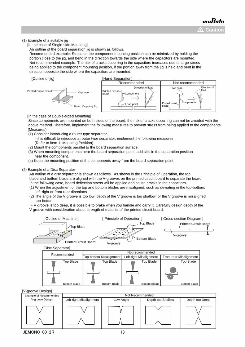
(1) Example of a suitable jig
[In the case of Single-side Mounting]
An outline of the board separation jig is shown as follows.
Recommended example: Stress on the component mounting position can be minimized by holding the
portion close to the jig, and bend in the direction towards the side where the capacitors are mounted.
Not recommended example: The risk of cracks occurring in the capacitors increases due to large stress
being applied to the component mounting position, if the portion away from the jig is held and bent in the
direction opposite the side where the capacitors are mounted.
[Outline of jig] [Hand Separation]
[In the case of Double-sided Mounting]
Since components are mounted on both sides of the board, the risk of cracks occurring can not be avoided with the
above method. Therefore, implement the following measures to prevent stress from being applied to the components.
(Measures)
(1) Consider introducing a router type separator.
If it is difficult to introduce a router type separator, implement the following measures.
(Refer to item 1. Mounting Position)
(2) Mount the components parallel to the board separation surface.
(3) When mounting components near the board separation point, add slits in the separation position
near the component.
(4) Keep the mounting position of the components away from the board separation point.
(2) Example of a Disc Separator
An outline of a disc separator is shown as follows. As shown in the Principle of Operation, the top
blade and bottom blade are aligned with the V-grooves on the printed circuit board to separate the board.
In the following case, board deflection stress will be applied and cause cracks in the capacitors.
(1) When the adjustment of the top and bottom blades are misaligned, such as deviating in the top-bottom,
left-right or front-rear directions
(2) The angle of the V groove is too low, depth of the V groove is too shallow, or the V groove is misaligned
top-bottom
IF V groove is too deep, it is possible to brake when you handle and carry it. Carefully design depth of the
V groove with consideration about strength of material of the printed circuit board.
[ Outline of Machine ] [ Principle of Operation ] [ Cross-section Diagram ]
[Disc Separator]
Top Blade Top Blade Top Blade Top Blade
Bottom Blade Bottom Blade Bottom Blade Bottom Blade
[V-groove Design]
Example of Recommended
V-groove Design
Not Recommended
Left-right Misalignment Low-Angle Depth too Shallow Depth too Deep
Caution
Recommended Not recommended
RecommendedNot recommended
Top-bottom Misalignment Left-right Misalignment Front-rear Misalignment
Printed Circuit Board
Top Blade
V-groove
Bottom Blade
Top Blade Printed Circuit Board
V-groove
!
Board Cropping Jig
V-groovePrinted Circuit Board
Printed circuit board
Components
Load point
Direction of load
Printed circuit board
Components
Load point
Direction of load
JEMCNC-0012R 18

(3) Example of Router Type Separator
The router type separator performs cutting by a router
rotating at a high speed. Since the board does not
bend in the cutting process, stress on the board can
be suppressed during board separation.
When attaching or removing boards to/from the router type
separator, carefully handle the boards to prevent bending.
8. Assembly
1. Handling
If a board mounted with capacitors is held with one hand, the board may bend.
Firmly hold the edges of the board with both hands when handling.
If a board mounted with capacitors is dropped, cracks may occur in the capacitors.
Do not use dropped boards, as there is a possibility that the quality of the capacitors may be impaired.
2. Attachment of Other Components
2-1. Mounting of Other Components
Pay attention to the following items, when mounting other components on the back side of the board after
capacitors have been mounted on the opposite side.
When the bottom dead point of the suction nozzle is set too low, board deflection stress may be applied
to the capacitors on the back side (bottom side), and cracks may occur in the capacitors.
· After the board is straightened, set the bottom dead point of the nozzle on the upper surface of the board.
· Periodically check and adjust the bottom dead point.
2-2. Inserting Components with Leads into Boards
When inserting components (transformers, IC, etc.) into boards, bending the board may cause cracks in the
capacitors or cracks in the solder. Pay attention to the following.
· Increase the size of the holes to insert the leads, to reduce the stress on the board during insertion.
· Fix the board with support pins or a dedicated jig before insertion.
· Support below the board so that the board does not bend. When using support pins on the board,
periodically confirm that there is no difference in the height of each support pin.
2-3. Attaching/Removing Sockets and/or connectors
The board may bend when a socket and/or connector are attached or removed.
Plan the work so that the board does not bend when a socket and/or connector are attached or removed.
2-4. Tightening Screws
The board may be bent, when tightening screws, etc. during the attachment of the board to a shield or
chassis. Pay attention to the following items before performing the work.
· Plan the work to prevent the board from bending.
· Use a torque screwdriver, to prevent over-tightening of the screws.
· The board may bend after mounting by reflow soldering, etc. Please note, as stress may be applied
to the chips by forcibly flattening the board when tightening the screws.
Caution!
Suction Nozzle
Component with Leads
Socket
Screwdriver
[ Outline Drawing ] Router
JEMCNC-0012R 19

■ Others
1. Under Operation of Equipment
1-1. Do not touch a capacitor directly with bare hands during operation in order to avoid the danger of an electric shock.
1-2. Do not allow the terminals of a capacitor to come in contact with any conductive objects (short-circuit).
Do not expose a capacitor to a conductive liquid, inducing any acid or alkali solutions.
1-3. Confirm the environment in which the equipment will operate is under the specified conditions.
Do not use the equipment under the following environments.
(1) Being spattered with water or oil.
(2) Being exposed to direct sunlight.
(3) Being exposed to ozone, ultraviolet rays, or radiation.
(4) Being exposed to toxic gas (e.g., hydrogen sulfide, sulfur dioxide, chlorine, ammonia gas etc.)
(5) Any vibrations or mechanical shocks exceeding the specified limits.
(6) Moisture condensing environments.
1-4. Use damp proof countermeasures if using under any conditions that can cause condensation.
2. Others
2-1. In an Emergency
(1) If the equipment should generate smoke, fire, or smell, immediately turn off or unplug the equipment.
If the equipment is not turned off or unplugged, the hazards may be worsened by supplying continuous power.
(2) In this type of situation, do not allow face and hands to come in contact with the capacitor or burns may be caused
by the capacitor's high temperature.
2-2. Disposal of waste
When capacitors are disposed of, they must be burned or buried by an industrial waste vendor with the appropriate
licenses.
2-3. Circuit Design
(1) Addition of Fail Safe Function
Capacitors that are cracked by dropping or bending of the board may cause deterioration of the
insulation resistance, and result in a short. If the circuit being used may cause an electrical shock,
smoke or fire when a capacitor is shorted, be sure to install fail-safe functions, such as a fuse,
to prevent secondary accidents.
(2) This series are not safety standard certified products.
2-4. Remarks
Failure to follow the cautions may result, worst case, in a short circuit and smoking when the product is used.
The above notices are for standard applications and conditions. Contact us when the products are used in special
mounting conditions.
Select optimum conditions for operation as they determine the reliability of the product after assembly.
The data herein are given in typical values, not guaranteed ratings.
Caution!
JEMCNC-0012R 20

■ Rating
1.Operating Temperature
1. The operating temperature limit depends on the capacitor.
1-1. Do not apply temperatures exceeding the maximum operating temperature.
It is necessary to select a capacitor with a suitable rated temperature that will cover the operating temperature range.
It is also necessary to consider the temperature distribution in equipment and the seasonal temperature variable
factor.
1-2. Consider the self-heating factor of the capacitor
The surface temperature of the capacitor shall not exceed the maximum operating temperature including self-heating.
2.Atmosphere Surroundings (gaseous and liquid)
1. Restriction on the operating environment of capacitors.
1-1. Capacitors, when used in the above, unsuitable, operating environments may deteriorate due to the corrosion
of the terminations and the penetration of moisture into the capacitor.
1-2. The same phenomenon as the above may occur when the electrodes or terminals of the capacitor are subject
to moisture condensation.
1-3. The deterioration of characteristics and insulation resistance due to the oxidization or corrosion of terminal
electrodes may result in breakdown when the capacitor is exposed to corrosive or volatile gases or solvents
for long periods of time.
3.Piezo-electric Phenomenon
1. When using high dielectric constant type capacitors in AC or pulse circuits, the capacitor itself vibrates
at specific frequencies and noise may be generated.
Moreover, when the mechanical vibration or shock is added to capacitor, noise may occur.
Notice
JEMCNC-0012R 21

■Soldering and Mounting
1.PCB Design
1. Notice for Pattern Forms
1-1. Unlike leaded components, chip components are susceptible to flexing stresses since they are mounted
directly on the substrate.
They are also more sensitive to mechanical and thermal stresses than leaded components.
Excess solder fillet height can multiply these stresses and cause chip cracking.
When designing substrates, take land patterns and dimensions into consideration to eliminate the possibility
of excess solder fillet height.
1-2. There is a possibility of chip cracking caused by PCB expansion/contraction with heat, because stress
on a chip is different depending on PCB material and structure.When the thermal expansion coefficient
greatly differs between the board used for mounting and the chip,it will cause cracking of the chip due to
the thermal expansion and contraction. When capacitors are mounted on a fluorine resin printed circuit
board or on a single-layered glass epoxy board, it may also cause cracking of the chip for the same reason.
Pattern Forms
in section in section
in section in section
in section in section
Placing of Leaded
Components
after Chip Component
Lateral Mounting
Notice
Prohibited Correct
Placing Close to Chassis
Placing of Chip
Components
and Leaded
Components
Chassis
Solder (ground)
Electrode Pattern
Solder Resist
Lead Wire
Solder Resist
Lead Wire Soldering Iron
Solder Resist
ソルダレジスト
Solder Resist
JEMCNC-0012R 22

2. Land Dimensions
Please confirm the suitable land dimension by
evaluating of the actual SET / PCB.
Table 1 Flow Soldering Method
Flow soldering can only be used for products with a chip size of 1.6x0.8mm to 2.0x1.25mm.
Resistance to PCB bending stress may be improved by designing the “a” dimension with solder resist. (in mm)
Table 2 Reflow Soldering Method
1.0×0.5
( ±0.05)
1.6×0.8
( ±0.10)
1.6×0.8
(±0.15)
(in mm)
GQM 22 2.8×2.8 2.2 to 2.5 0.8 to 1.0 1.9 to 2.3
0.7 to 0.8 0.8 to 1.0
GQM 21 2.0×1.25 1.0 to 1.2 0.6 to 0.7 0.8 to 1.1
GQM 18
0.6 to 0.8 0.6 to 0.7 0.6 to 0.8
0.7 to 0.9
GQM 15 0.3 to 0.5 0.35 to 0.45 0.4 to 0.6
SeriesChip Dimension
(L/W) Code
Chip(L×W)
(Dimensions
Tolerance)
a b c
GQM 21 2.0×1.25 1.0 to 1.2 0.9 to 1.0 0.8 to 1.1
GQM 18 1.6×0.8 0.6 to 1.0 0.8 to 0.9 0.6 to 0.8
Notice
SeriesChip Dimension
(L/W) CodeChip(L×W) a b c
c
b a Solder Resist
Chip Capacitor
Land
JEMCNC-0012R 23
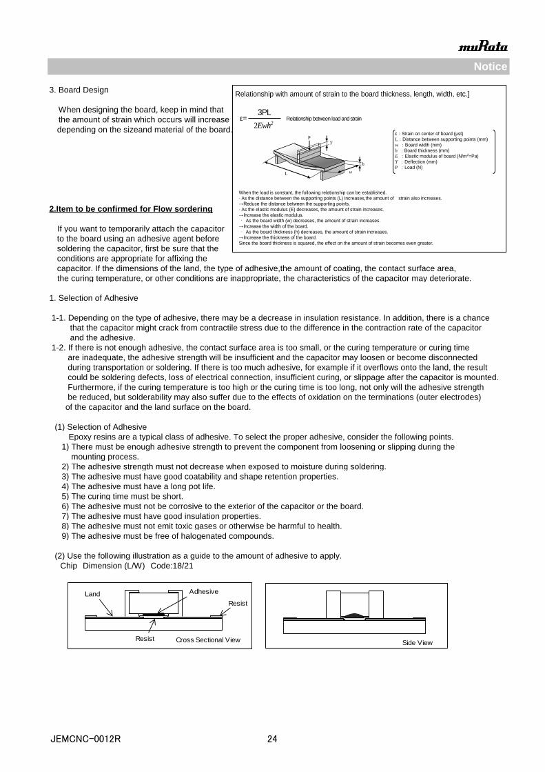
3. Board Design
When designing the board, keep in mind that
the amount of strain which occurs will increase
depending on the sizeand material of the board.
2.Item to be confirmed for Flow sordering
If you want to temporarily attach the capacitor
to the board using an adhesive agent before
soldering the capacitor, first be sure that the
conditions are appropriate for affixing the
capacitor. If the dimensions of the land, the type of adhesive,the amount of coating, the contact surface area,
the curing temperature, or other conditions are inappropriate, the characteristics of the capacitor may deteriorate.
1. Selection of Adhesive
1-1. Depending on the type of adhesive, there may be a decrease in insulation resistance. In addition, there is a chance
that the capacitor might crack from contractile stress due to the difference in the contraction rate of the capacitor
and the adhesive.
1-2. If there is not enough adhesive, the contact surface area is too small, or the curing temperature or curing time
are inadequate, the adhesive strength will be insufficient and the capacitor may loosen or become disconnected
during transportation or soldering. If there is too much adhesive, for example if it overflows onto the land, the result
could be soldering defects, loss of electrical connection, insufficient curing, or slippage after the capacitor is mounted.
Furthermore, if the curing temperature is too high or the curing time is too long, not only will the adhesive strength
be reduced, but solderability may also suffer due to the effects of oxidation on the terminations (outer electrodes)
of the capacitor and the land surface on the board.
(1) Selection of Adhesive
Epoxy resins are a typical class of adhesive. To select the proper adhesive, consider the following points.
1) There must be enough adhesive strength to prevent the component from loosening or slipping during the
mounting process.
2) The adhesive strength must not decrease when exposed to moisture during soldering.
3) The adhesive must have good coatability and shape retention properties.
4) The adhesive must have a long pot life.
5) The curing time must be short.
6) The adhesive must not be corrosive to the exterior of the capacitor or the board.
7) The adhesive must have good insulation properties.
8) The adhesive must not emit toxic gases or otherwise be harmful to health.
9) The adhesive must be free of halogenated compounds.
(2) Use the following illustration as a guide to the amount of adhesive to apply.
Chip Dimension (L/W) Code:18/21
Notice
Relationship with amount of strain to the board thickness, length, width, etc.]
ε= 3PL
2Ewh2 Relationship between load and strain
When the load is constant, the following relationship can be established. · As the distance between the supporting points (L) increases,the amount of strain also increases. →Reduce the distance between the supporting points. · As the elastic modulus (E) decreases, the amount of strain increases. →Increase the elastic modulus. · As the board width (w) decreases, the amount of strain increases. →Increase the width of the board. · As the board thickness (h) decreases, the amount of strain increases. →Increase the thickness of the board. Since the board thickness is squared, the effect on the amount of strain becomes even greater.
ε:Strain on center of board (μst) L:Distance between supporting points (mm) w :Board width (mm) h :Board thickness (mm) E :Elastic modulus of board (N/m2=Pa) Y :Deflection (mm) P :Load (N)
Y P
h
w L
Land
Resist
Adhesive
Cross Sectional View
Resist
Side View
JEMCNC-0012R 24

2.Flux
2-1. An excessive amount of flux generates a large quantity of flux gas, which can cause a deterioration of solderability,
so apply flux thinly and evenly throughout. (A foaming system is generally used for flow solderring.)
2-2. Flux containing too high a percentage of halide may cause corrosion of the terminations unless there is
sufficient cleaning. Use flux with a halide content of 0.1% max.
2-3. Do not use strong acidic flux.
2-4. Do not use water-soluble flux.*
(*Water-soluble flux can be defined as non-rosin type flux including wash-type flux and non-wash-type flux.)
3.Leaching of the terminations
Set temperature and time to ensure that leaching of the
terminations does not exceed 25% of the chip end
area as a single chip (full length of the edge A-B-C-D
shown at right) and 25% of the length A-B shown as mounted on substrate.
3.Reflow soldering
The halogen system substance and organic acid are included in solder paste, and a chip corrodes
by this kind of solder paste.
Do not use strong acid flux.
Do not use water-soluble flux.*
(*Water-soluble flux can be defined as non-rosin type flux including wash-type flux and non-wash-type flux.)
4.Washing
1. Please evaluate the capacitor using actual cleaning equipment and conditions to confirm the quality,
and select the solvent for cleaning.
2. Unsuitable cleaning solvent may leave residual flux or other foreign substances, causing deterioration of
electrical characteristics and the reliability of the capacitors.
3. Select the proper cleaning conditions.
3-1. Improper cleaning conditions (excessive or insufficient) may result in the deterioration of the performance
of the capacitors.
5.Coating
1. A crack may be caused in the capacitor due to the stress of the thermal contraction of the resin during curing process.
The stress is affected by the amount of resin and curing contraction. Select a resin with low curing contraction.
The difference in the thermal expansion coefficient between a coating resin or a molding resin and the capacitor
may cause the destruction and deterioration of the capacitor such as a crack or peeling, and lead to the deterioration
of insulation resistance or dielectric breakdown.
Select a resin for which the thermal expansion coefficient is as close to that of the capacitor as possible.
A silicone resin can be used as an under-coating to buffer against the stress.
2. Select a resin that is less hygroscopic.
Using hygroscopic resins under high humidity conditions may cause the deterioration of the insulation resistance
of a capacitor. An epoxy resin can be used as a less hygroscopic resin.
3.The halogen system substance and organic acid are included in coating material, and a chip corrodes
by the kind of Coating material. Do not use strong acid type.
Notice
A
BD
CTermination (Outer Electrode)
[As a Single Chip]
[As Mounted on Substrate]
A
B
JEMCNC-0012R 25

■ Others1.Transportation
1. The performance of a capacitor may be affected by the conditions during transportation.
1-1. The capacitors shall be protected against excessive temperature, humidity and mechanical force during transportation.
(1) Climatic condition
・ low air temperature : -40℃ ・ change of temperature air/air : -25℃/+25℃ ・ low air pressure : 30 kPa
・ change of air pressure : 6 kPa/min.
(2) Mechanical condition
Transportation shall be done in such a way that the boxes are not deformed and forces are not directly passed
on to the inner packaging.
1-2. Do not apply excessive vibration, shock, or pressure to the capacitor.
(1) When excessive mechanical shock or pressure is applied to a capacitor, chipping or cracking may occur
in the ceramic body of the capacitor.
(2) When the sharp edge of an air driver, a soldering iron, tweezers, a chassis, etc. impacts strongly on the surface
of the capacitor, the capacitor may crack and short-circuit.
1-3. Do not use a capacitor to which excessive shock was applied by dropping etc.
A capacitor dropped accidentally during processing may be damaged.
2.Characteristics Evaluation in the Actual System
1. Evaluate the capacitor in the actual system,to confirm that there is no problem with the performance and specification
values in a finished product before using.
2. Since a voltage dependency and temperature dependency exists in the capacitance of high dielectric type ceramic
capacitors, the capacitance may change depending on the operating conditions in the actual system.
Therefore,be sure to evaluate the various characteristics, such as the leakage current and noise absorptivity,
which will affect the capacitance value of the capacitor.
3. In addition,voltages exceeding the predetermined surge may be applied to the capacitor by the inductance in
the actual system. Evaluate the surge resistance in the actual system as required.
Notice
JEMCNC-0012R 26
NOTE
1.Please make sure that your product has been evaluated in view of your specifications with our
product being mounted to your product.
2.Your are requested not to use our product deviating from this product specification.
3.We consider it not appropriate to include any terms and conditions with regard to the business
transaction in the product specifications, drawings or other technical documents. Therefore,
if your technical documents as above include such terms and conditions such as warranty clause,
product liability clause, or intellectual property infringement liability clause, they will be deemed to
be invalid.
!
JEMCNC-0012R 27

Mouser Electronics
Authorized Distributor
Click to View Pricing, Inventory, Delivery & Lifecycle Information: Murata:
GQM1555C2D4R5CB01D