Embed Size (px)
Citation preview
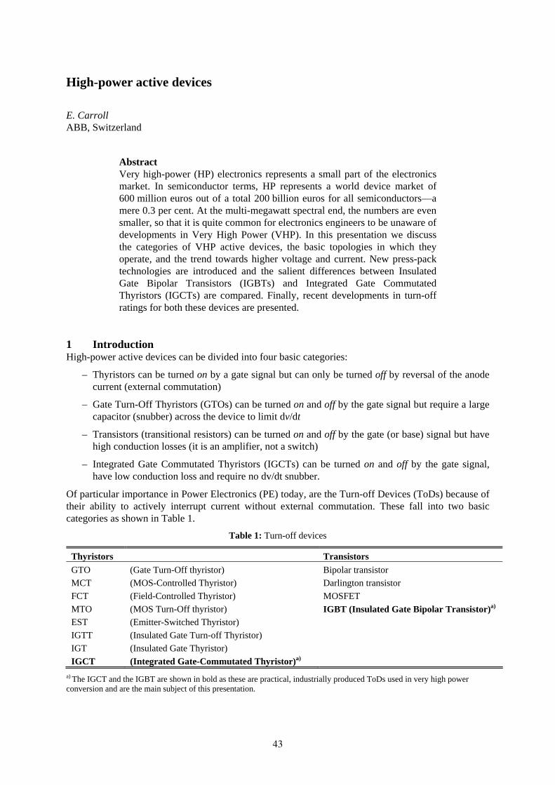
High-power active devices
E. Carroll ABB, Switzerland
Abstract Very high-power (HP) electronics represents a small part of the electronics market. In semiconductor terms, HP represents a world device market of 600 million euros out of a total 200 billion euros for all semiconductors—a mere 0.3 per cent. At the multi-megawatt spectral end, the numbers are even smaller, so that it is quite common for electronics engineers to be unaware of developments in Very High Power (VHP). In this presentation we discuss the categories of VHP active devices, the basic topologies in which they operate, and the trend towards higher voltage and current. New press-pack technologies are introduced and the salient differences between Insulated Gate Bipolar Transistors (IGBTs) and Integrated Gate Commutated Thyristors (IGCTs) are compared. Finally, recent developments in turn-off ratings for both these devices are presented.
1 Introduction High-power active devices can be divided into four basic categories:
– Thyristors can be turned on by a gate signal but can only be turned off by reversal of the anode current (external commutation)
– Gate Turn-Off Thyristors (GTOs) can be turned on and off by the gate signal but require a large capacitor (snubber) across the device to limit dv/dt
– Transistors (transitional resistors) can be turned on and off by the gate (or base) signal but have high conduction losses (it is an amplifier, not a switch)
– Integrated Gate Commutated Thyristors (IGCTs) can be turned on and off by the gate signal, have low conduction loss and require no dv/dt snubber.
Of particular importance in Power Electronics (PE) today, are the Turn-off Devices (ToDs) because of their ability to actively interrupt current without external commutation. These fall into two basic categories as shown in Table 1.
Table 1: Turn-off devices
Thyristors Transistors GTO (Gate Turn-Off thyristor) Bipolar transistor MCT (MOS-Controlled Thyristor) Darlington transistor FCT (Field-Controlled Thyristor) MOSFET MTO (MOS Turn-Off thyristor) IGBT (Insulated Gate Bipolar Transistor)a)
EST (Emitter-Switched Thyristor) IGTT (Insulated Gate Turn-off Thyristor) IGT (Insulated Gate Thyristor) IGCT (Integrated Gate-Commutated Thyristor)a)
a) The IGCT and the IGBT are shown in bold as these are practical, industrially produced ToDs used in very high power conversion and are the main subject of this presentation.
43
ToDs allow all the basic functions of power electronics to be realized; these include
– inverters voltage source (VSI) current source (CSI)
– choppers buck regulators boost regulators
– active rectifiers.
All these functions require complementary (fast) diodes in anti-parallel (for VSIs) or in series (for VSIs) or in a separate function (for choppers).
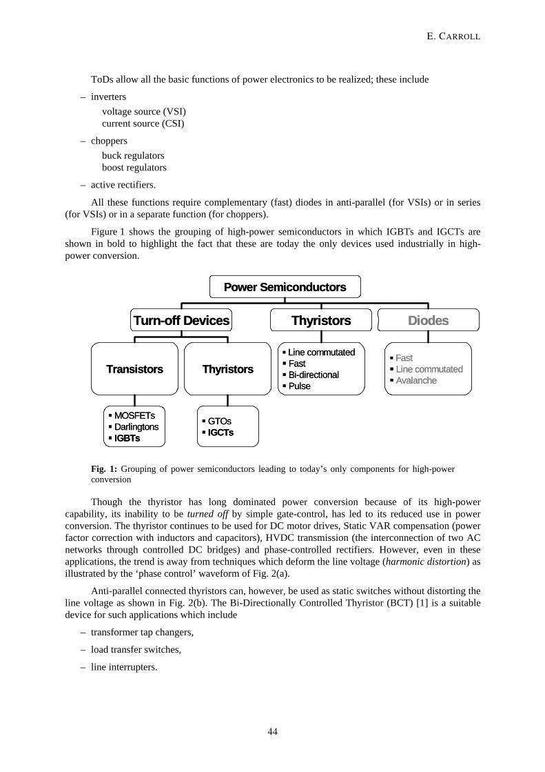
Figure 1 shows the grouping of high-power semiconductors in which IGBTs and IGCTs are shown in bold to highlight the fact that these are today the only devices used industrially in high-power conversion.
Power Semiconductors
Turn-off Devices Thyristors Diodes
Transistors ThyristorsLine commutatedFastBi-directionalPulse
FastLine commutatedAvalanche
MOSFETsDarlingtonsIGBTs
GTOsIGCTs
Power Semiconductors
Turn-off Devices Thyristors Diodes
Transistors ThyristorsLine commutatedFastBi-directionalPulse
FastLine commutatedAvalanche
MOSFETsDarlingtonsIGBTs
GTOsIGCTs
Fig. 1: Grouping of power semiconductors leading to today’s only components for high-power conversion
Though the thyristor has long dominated power conversion because of its high-power capability, its inability to be turned off by simple gate-control, has led to its reduced use in power conversion. The thyristor continues to be used for DC motor drives, Static VAR compensation (power factor correction with inductors and capacitors), HVDC transmission (the interconnection of two AC networks through controlled DC bridges) and phase-controlled rectifiers. However, even in these applications, the trend is away from techniques which deform the line voltage (harmonic distortion) as illustrated by the ‘phase control’ waveform of Fig. 2(a).
Anti-parallel connected thyristors can, however, be used as static switches without distorting the line voltage as shown in Fig. 2(b). The Bi-Directionally Controlled Thyristor (BCT) [1] is a suitable device for such applications which include
– transformer tap changers,
– load transfer switches,
– line interrupters.
E. CARROLL
44

V
t
V
t
Fig. 2(a): Phase control of AC line voltage causes harmonic distortion
Fig. 2(b): Zero-voltage turn-on is used for AC switching with thyristors and causes no distortion
2 The growth of high-power electronics The use of high-power turn-off devices has grown rapidly in the last 20 years. This is the result of two synergetic trends:
– the greater need for PE
– the availability of new semiconductor technologies.
The need itself has had four components:
– improved process control, e.g., for steel production
– improved power quality, e.g., for semiconductor production
– energy saving, e.g., efficient motor control
– energy trading, e.g., redirection of power flow in response to spot-market rates.
Figure 3 shows the growth of energy consumption in equivalent millions of barrels of oil per day, as well as that part of the energy consumed as electricity. The growing percentage of energy consumed as electricity is an indication for the growth of electronics through which this power increasingly flows. It shows that by 2020
– energy consumption will double
– electrification of end-consumption will quintuple.
Today, only 15% of electricity flows via electronics, and Medium Voltage (MV) conversion has only been economically possible in the last 10 years following the arrival of ToDs with high current and high voltage ratings (thousands of volts and amperes). The consequence is that power conversion at MV levels is set to grow at a faster rate than at low voltage levels.
(The low-voltage network covers the range from 110 V to 690 V. MOSFETs and low-voltage IGBTs are typically used in this area and have been for over 20 years. The MV network ranges from 3.3 kV and goes to 13.8 kV and beyond. For this network, HV semiconductors are needed with ratings from 3.3 to 6.5 and perhaps 10 kV.)
HIGH-POWER ACTIVE DEVICES
45

57 100200
397
2
630
147
3%6%
15%37%
0.1
0
1
10
100
1000
1940
1950
1960
1970
1980
1990
2000
2010
2020
2030
Mill
ions
of B
arre
ls/D
ay
total energyelectrification% electrification
Source :Mitsubishi Electric
57 100200
397
2
630
147
3%6%
15%37%
0.1
0
1
10
100
1000
1940
1950
1960
1970
1980
1990
2000
2010
2020
2030
Mill
ions
of B
arre
ls/D
ay
total energyelectrification% electrification
Source :Mitsubishi Electric
Fig. 3: World energy consumption drives the growing need for power electronics
3 Self-commutated inverters Inverters are the basis of today’s power conversions and they exist in many topologies. As explained in the introduction, only two semiconductors are candidates for modern HP conversion and one comes from the transistor family (the IGBT) while the other comes from the thyristor family (the IGCT). Two VSI topologies will be used to illustrate the fundamental differences between these two device types. In Figs. 4(a) and 4(b), an IGBT and an IGCT inverter are shown. Since the IGBT is a transistor, it can behave as an amplifier during its transition from off to on. In so doing, it can control the speed at which the current in the free-wheel diode is forced to zero (inevitably becoming negative in the process). This commutation speed is critical, as an excessive speed will cause the diodes to fail while a slow commutation will generate losses (‘turn-on loss’). Figure 4(a) illustrates that no inductance is needed for this commutation thanks to the amplifier-like properties of the IGBTs. Figure 4(b), by contrast, shows that the IGCT, being a thyristor and behaving like a switch, allows no commutation control and hence requires an external inductance to avoid diode recovery failure.
The allowable rate of commutation is determined by the diode’s ‘ruggedness’ since a fast commutation leads to a reverse recovery current (IRR in Fig. 5) which at high DC voltage results in high instantaneous power which could lead to diode failure. In the case of Fig. 4(a), energy is dissipated in the IGBT whereas in the case of Fig. 4(b), this energy is stored in the inductance L and is subsequently dissipated in resistance R.
S5S3S1
S6S2 S4
VDC
FWD1 S5S3S1
S6S2 S4
VDC
FWD1
VR
S3
S4
S5
S6
S1
S2
Ls
L
Cclamp
Dclamp
R
FWD6Clamp circuit
VR
S3
S4
S5
S6
S1
S2
Ls
L
Cclamp
Dclamp
R
FWD6Clamp circuit
Fig. 4(a): IGBT inverter Fig. 4(b): IGCT inverter
E. CARROLL
46
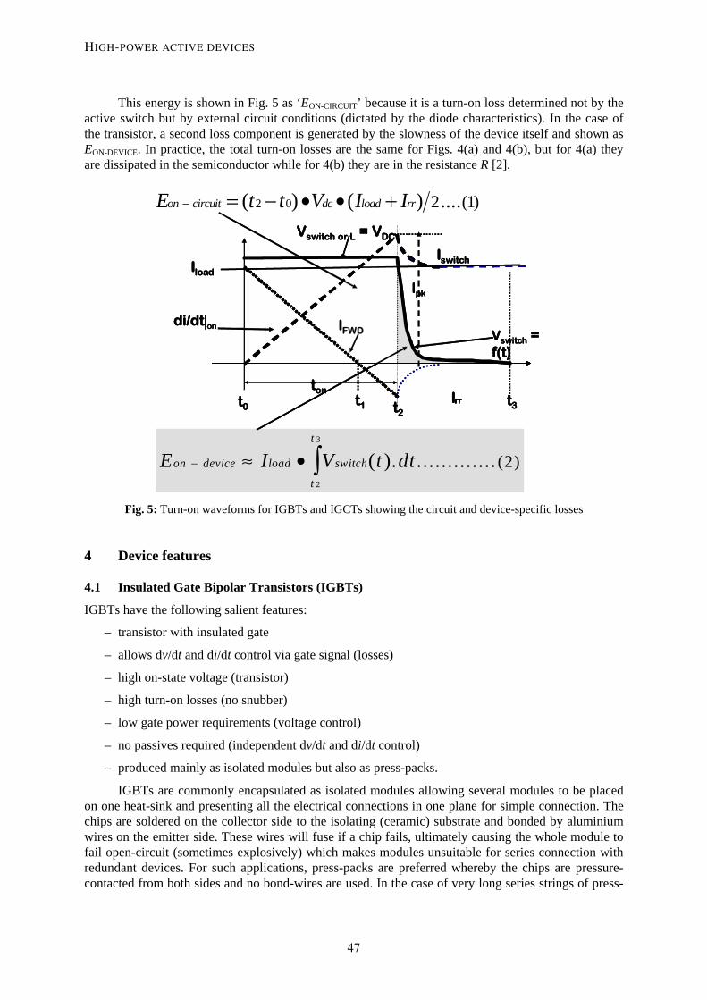
This energy is shown in Fig. 5 as ‘EON-CIRCUIT’ because it is a turn-on loss determined not by the active switch but by external circuit conditions (dictated by the diode characteristics). In the case of the transistor, a second loss component is generated by the slowness of the device itself and shown as EON-DEVICE. In practice, the total turn-on losses are the same for Figs. 4(a) and 4(b), but for 4(a) they are dissipated in the semiconductor while for 4(b) they are in the resistance R [2].
E I V t dton device load switch
t
t
− ≈ • ∫2
3
2( ). ............. ( )
E t t V I Ion circuit dc load rr− = − • • +( ) ( ) ....( )2 0 2 1
Iload
Iswitch
IFWD
t0 t3
di/dt|on
Irr
Ipk
ton
Vswitch or L = VDC
t1
Vswitch = f(t)
t2
E I V t dton device load switch
t
t
− ≈ • ∫2
3
2( ). ............. ( )
E t t V I Ion circuit dc load rr− = − • • +( ) ( ) ....( )2 0 2 1
Iload
Iswitch
IFWD
t0 t3
di/dt|on
IrrIrr
Ipk
ton
Vswitch or L = VDC
t1
Vswitch = f(t)
t2
Fig. 5: Turn-on waveforms for IGBTs and IGCTs showing the circuit and device-specific losses
4 Device features
4.1 Insulated Gate Bipolar Transistors (IGBTs)
IGBTs have the following salient features:
– transistor with insulated gate
– allows dv/dt and di/dt control via gate signal (losses)
– high on-state voltage (transistor)
– high turn-on losses (no snubber)
– low gate power requirements (voltage control)
– no passives required (independent dv/dt and di/dt control)
– produced mainly as isolated modules but also as press-packs.
IGBTs are commonly encapsulated as isolated modules allowing several modules to be placed on one heat-sink and presenting all the electrical connections in one plane for simple connection. The chips are soldered on the collector side to the isolating (ceramic) substrate and bonded by aluminium wires on the emitter side. These wires will fuse if a chip fails, ultimately causing the whole module to fail open-circuit (sometimes explosively) which makes modules unsuitable for series connection with redundant devices. For such applications, press-packs are preferred whereby the chips are pressure-contacted from both sides and no bond-wires are used. In the case of very long series strings of press-
HIGH-POWER ACTIVE DEVICES
47

packs, involving many devices and heat-sinks, special press-packs have been developed using individual spring-contacts to ensure a correct and uniform pressure on each individual chip [3]. Both housing technologies are shown in Figs. 6(a) and 6(b). Figure 6(c) shows the sectional view of an advanced press-pack design using individually sprung chips allowing uniform chip pressure even in long stacks, while Fig. 6(d) illustrates a conventional IGBT press-pack with direct chip contacts requiring extremely accurate stack assembly.
Fig. 6(a): Standard isolated IGBT module Fig. 6(b): IGCT press-pack (ABB StakPak™)
base-platesilicon chip
spring washer packcurrent bypass
sub-module frame(polymeric)
module outer frame(fibreglass reinforced polymer)module lid
(copper)
silicon gel
Δx
copper
copper
molybdenum
siliconchip
ceramicinert gas
close-up
Fig. 6(c): Sectional view of ABB StakPak™ showing individual spring contacts
Fig. 6(d): Sectional view of conventional IGBT press-pack
Figure 7 shows a long IGBT press-pack stack as used in an HVDC VSI converter. Here, 20 devices and 21 heatsinks are pressed together. The picture illustrates the difficulty of achieving uniform pressure on each chip in view of the cumulative inhomogeneities resulting from mechanical tolerances.
Using conventional IGBT press-packs in long stacks would require very tight mechanical tolerances to ensure identical force on each chip in each housing:
– on assembly
– over time
– with temperature cycling
– with shock and vibration.
E. CARROLL
48

Fig. 7: An HVDC valve for a VSI. Each valve contains 20 IGBT press-packs and many valves may be series connected for a typical high-voltage DC transmission system.
4.2 Integrated Gate-Commutated Thyristors (IGCTs)
IGCTs have the following salient features:
– thyristor with integrated gate unit
– low on-state voltage (thyristor)
– low turn-on losses (turn-on snubber)
– no explosive failures [fault current limitation by circuit – see Fig. 4(b)]
– produced as press-packs only.
IGCTs are the newest of the high-power devices and are less well known since they are recent and used at power levels of about 300 kW and upwards to about 100 MW (with series connection) [4]. Figure 8 illustrates the principle of operation. In conduction, the device is a thyristor and the gate-unit a forward-biasing current source. At turn-off, the gate-unit becomes a reverse-biasing voltage source, which quickly commutates the entire current from the cathode to the gate thus turning the device into a pnp transistor with an open base. The resulting waveform can be seen in Fig. 9 and is similar to that of an IGBT turn-off.
P
N
P
N
Anode
Cathode
Gate
IAK
IGK
P
N
P
N
Anode
Cathode
Gate
- VGK
VAK
Conducting Thyristor Blocking Transistor
Fig. 8: Principle of operation of Integrated Gate-Commutated Thyristor (IGCT)
HIGH-POWER ACTIVE DEVICES
49

4
1
Ia (kA)
Vdm
Tj = 90°C
Itgq
4
3
2
1
0
-10
-20
Vg (V)
2
3
0
anode voltage Vd
anode current Ia
gate voltage Vg
thyristor transistorx
starts to block
Vd (kV)
2015 3025 35 t (μ s)
4
1
Ia (kA)
Vdm
Tj = 90°C
Itgq
4
3
2
1
0
-10
-20
Vg (V)
2
3
0
anode voltage Vd
anode current Ia
gate voltage Vg
thyristor transistorx
starts to block
Vd (kV)
2015 3025 35 t (μ s) Fig. 9: Turn-off waveform of an IGCT
Figure 10 shows a typical 91 mm IGCT and Fig. 11 shows the internal construction of the GCT itself.
visible LEDindicators
Status Feedback Command Signal
optical fibre connectors
power supply connection
all copper housing
GCT
IGCT visible LEDindicators
Status Feedback Command Signal
optical fibre connectors
power supply connection
all copper housing
visible LEDindicators
Status Feedback Command Signal
optical fibre connectors
power supply connection
all copper housing
GCT
IGCT
Fig. 10: Integrated Gate-Commutated Thyristor (IGCT) showing the semiconductor part (GCT)
Fig. 11: Open GCT showing a reverse-conducting wafer (diode in the middle)
As already mentioned, the IGCT has no turn-on speed control and therefore requires an external di/dt controlling inductance. It also has no direct dv/dt control at turn-off although this can be adjusted by ‘life-time control’ (adjustment of the carrier lifetime, typically by irradiation). Figure 12 shows the effect of three different levels of lifetime control on three, otherwise identical, IGCTs and shows the different rates of voltage rise. Low dv/dt produces less ElectroMagnetic Interference (EMI) but inevitably generates higher losses [5].
E. CARROLL
50

As with the IGBT, the IGCT is inherently fast switching as illustrated by Fig. 13 which shows 25 kHz burst-mode operation. Its frequency limitation is determined principally by its losses (akin to the IGBT) such that the burst of Fig. 13 lasts only for 10 pulses at full rating.
0
1000
2000
3000
4000
6 8 10 12 14
t [μs]
I A, V
AK, [
A, V
]medium lifetimelow lifetimehigh lifetime
IA
VAK
0
1000
2000
3000
4000
6 8 10 12 14
t [μs]
I A, V
AK, [
A, V
]medium lifetimelow lifetimehigh lifetime
IA
VAK
Fig. 12: Effect of different irradiation levels on turn-off dv/dt
0
500
1000
1500
2000
2500
3000
3500
4000
4500
5000
0.E+00 2.E-04 4.E-04 6.E-04 8.E-04 1.E-03
time (s)
Ano
de v
olta
ge a
nd c
urre
nt (V
, A)
vI
Fig. 13: Burst mode operation of 4.5 kV/4 kA IGCT VDC START = 3.5 kV, VDM PEAK = 4.5 kV, ITGQ PEAK = 4 kA, TJ START = 25°C, a = 0.5
5 Device trends
5.1 IGBTs
The main development thrust today for IGBTs is
– higher voltages (up to 6.5 kV)
– higher Safe Operating Area (SOA)
– softer (controlled) switching characteristics
– lower conduction losses (either with trench or enhanced planar technology)
– over-voltage self-protection (as for existing short-circuit protection).
Figures 14 and 15 show the smooth switching characteristics under nominal conditions for 3.3 kV IGBT and diode chips. These ‘soft’ switching waveforms display no abrupt changes which avoids voltage spikes and EMI even in inductive environments.
HIGH-POWER ACTIVE DEVICES
51
-20
-10
0
10
20
30
40
50
60
70
80
90
100
110
Time [250 nsec/div]
Ic (
A),
Vge
(V
-400
-200
0
200
400
600
800
1000
1200
1400
1600
1800
2000
2200
Vce (V
)
Vge
Vce
Ic
-150
-125
-100
-75
-50
-25
0
25
50
75
100
125
150
Time [250 nsec/div]
IF (A
)
0
200
400
600
800
1000
1200
1400
1600
1800
2000
2200
2400
VR
(V)
VRIF
Fig. 14: IGBT Turn-off: VCC = 1800 V, IC = 50 A, RGOFF = 33 Ω, LS = 2.4 mH, TJ = 125°C
Fig. 15: Diode Turn-off: VCC = 1800 V, IC = 50 A, RGOFF = 33 Ω, LS = 2.4 mH, TJ = 125°C
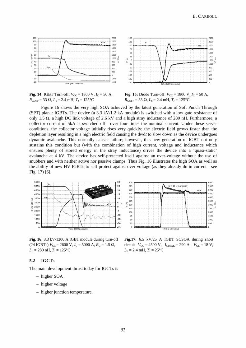
Figure 16 shows the very high SOA achieved by the latest generation of Soft Punch Through (SPT) planar IGBTs. The device (a 3.3 kV/1.2 kA module) is switched with a low gate resistance of only 1.5 Ω, a high DC link voltage of 2.6 kV and a high stray inductance of 280 nH. Furthermore, a collector current of 5kA is switched off—over four times the nominal current. Under these server conditions, the collector voltage initially rises very quickly; the electric field grows faster than the depletion layer resulting in a high electric field causing the dv/dt to slow down as the device undergoes dynamic avalanche. This normally causes failure; however, this new generation of IGBT not only sustains this condition but (with the combination of high current, voltage and inductance which ensures plenty of stored energy in the stray inductance) drives the device into a ‘quasi-static’ avalanche at 4 kV. The device has self-protected itself against an over-voltage without the use of snubbers and with neither active nor passive clamps. Thus Fig. 16 illustrates the high SOA as well as the ability of new HV IGBTs to self-protect against over-voltage (as they already do in current—see Fig. 17) [6].
0
25
50
75
100
125
150
175
200
225
250
275
300
Time [2 usec/div]
Ic (A
)
0
500
1000
1500
2000
2500
3000
3500
4000
4500
5000
5500
6000
Vce (V
)
Ic > 10 x Inominal
Vce
Fig. 16: 3.3 kV/1200 A IGBT module during turn-off (24 IGBTs) VCC = 2600 V, IC = 5000 A, RG = 1.5 Ω, LS = 280 nH, TJ = 125°C
Fig.17: 6.5 kV/25 A IGBT SCSOA during short circuit VCC = 4500 V, ICPEAK = 290 A, VGE = 18 V, LS = 2.4 mH, TJ = 25°C
5.2 IGCTs
The main development thrust today for IGCTs is
– higher SOA
– higher voltage
– higher junction temperature.
E. CARROLL
52

Figure 18 shows two IGCT wafers: a 91 mm asymmetric device and a 38 mm reverse-conducting device.
Fig. 18: A 91 mm asymmetric GCT wafer compared with a 38 mm reverse-conducting wafer
Today’s IGCTs operate at an SOA of about 200–250 kW/cm2 (the larger the wafer, the lower the average power density). The next generation will operate at 400 kW/cm2 for large devices and perhaps as much as 1 MW/cm2 for small ones. Figure 19 shows a developmental 4.5 kV IGCT (derived from the 4 kA device of Figs. 10 and 11 using recent SOA enhancing techniques) switching 6.5 kA instead of the usual 4 kA against 2.8 kV. Such improved devices will be in volume production within two years [7].
Figure 20 shows an experimental 10 kV IGCT operating at 250 kW/cm2. SOA enhancing techniques can also be applied to this device but its future will depend more on diode developments at this voltage level [8].
0
1000
2000
3000
4000
5000
6000
7000
1 3 5 7 9
t [μs]
V AK,
I T [V
. A]
-25
-20
-15
-10
-5
0
5V G
K [V]
Fig. 19: Developmental 91 mm/4.5 kV IGCT with improved GU and silicon design, allowing 50% SOA improvement
HIGH-POWER ACTIVE DEVICES
53
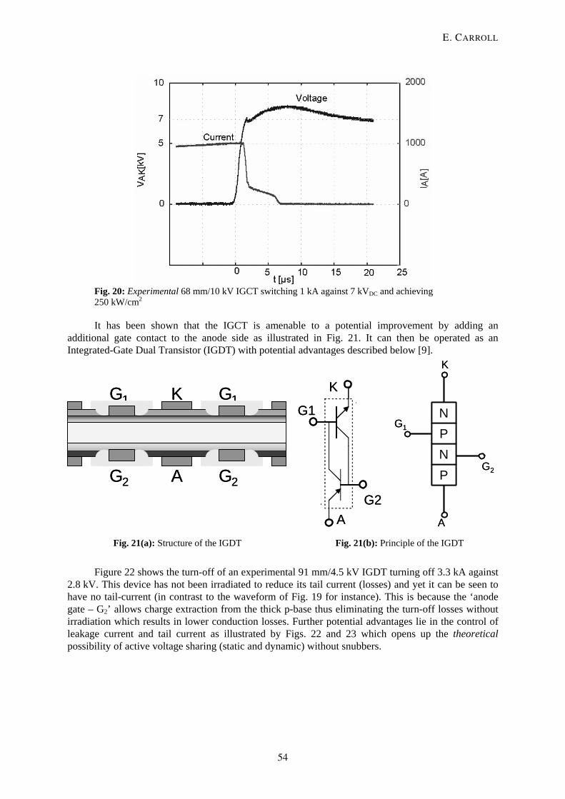
Fig. 20: Experimental 68 mm/10 kV IGCT switching 1 kA against 7 kVDC and achieving 250 kW/cm2
It has been shown that the IGCT is amenable to a potential improvement by adding an additional gate contact to the anode side as illustrated in Fig. 21. It can then be operated as an Integrated-Gate Dual Transistor (IGDT) with potential advantages described below [9].
K
A
G1
G2
G1
G2
K
A
G1
G2
G1
G2
A
K
G1
G2A
K
G1
G2
G1
G2PNPN
K
A
G1
G2PNPN
K
A
Fig. 21(a): Structure of the IGDT Fig. 21(b): Principle of the IGDT
Figure 22 shows the turn-off of an experimental 91 mm/4.5 kV IGDT turning off 3.3 kA against 2.8 kV. This device has not been irradiated to reduce its tail current (losses) and yet it can be seen to have no tail-current (in contrast to the waveform of Fig. 19 for instance). This is because the ‘anode gate – G2’ allows charge extraction from the thick p-base thus eliminating the turn-off losses without irradiation which results in lower conduction losses. Further potential advantages lie in the control of leakage current and tail current as illustrated by Figs. 22 and 23 which opens up the theoretical possibility of active voltage sharing (static and dynamic) without snubbers.
E. CARROLL
54

(V DC = 2800 V)
0
20
40
60
80
100
120
140
75 100 125 150 175
T J (°C)
I D(m
A)
anode gate floating(no bias)
anode gate with 20V reverse biased
140°C
(V DC = 2800 V)(V DC = 2800 V)
0
20
40
60
80
100
120
140
75 100 125 150 175
T J (°C)
I D(m
A)
anode gate floating(no bias)
anode gate with 20V reverse biased
140°C
VGK= -20V, TJ = 25°C
05
101520253035
0 5 10 15 20 25IGA Anode gate current [mA]
500V1000V1500V2000V2400V
I D- a
n od e
l eak
age
c urr
ent [
mA
]
VGK= -20V, TJ = 25°C
05
101520253035
0 5 10 15 20 25IGA Anode gate current [mA]
500V1000V1500V2000V2400V
I D- a
n od e
l eak
age
c urr
ent [
mA
]
Fig. 22(a): IGDT leakage current reduction by anode gate control
Fig. 22(b): IGDT leakage current increase by anode gate control
IDUT2 V1 VG1 VG2
0.0
0.2
0.4
0.6
0.8
1.0
kA
0.0
0.5
1.0
1.5
2.0
2.5
kV
1.4
1.6
1.8
2.0
2.2
2.4V
300 320 340
µs
IDUT2 V1 VG1 VG2
0.0
0.2
0.4
0.6
0.8
1.0
kA
0.0
0.5
1.0
1.5
2.0
2.5
kV
1.4
1.6
1.8
2.0
2.2
2.4V
300 320 340
µs
IDUT2 V1 VG1 VG2
0.0
0.2
0.4
0.6
0.8
1.0
kA
0.0
0.5
1.0
1.5
2.0
2.5
kV
1.4
1.6
1.8
2.0
2.2
2.4V
300 320 340
µs Fig. 23(a): IGDT tail current increase by anode gate control
Fig. 23(b): IGDT tail current delayed increase by anode gate control
Finally, an (as yet) untested feature lies in the possibility of firing both gates simultaneously at turn-on, leading to a high-voltage device capable of extremely high di/dt and peak current for pulsed-power applications such as thyratron replacement.
6 Conclusions For high-power conversion, only two devices are available today:
– IGBTs
– IGCTs.
HIGH-POWER ACTIVE DEVICES
55
Safe Operating Area is increasing from 250 kW/cm2 to 1 MW/cm2. New high SOA IGCTs will be in production soon.
IGBTs are now capable of voltage self-protection as they were, traditionally, capable of current self-protection (i.e., fault current limitation). These devices are already in production.
The 10 kV IGCT has been demonstrated as has the IGDT, but both devices await business opportunities and development resources.
References [1] K. Thomas, B. Backlund, O. Toker and B. Thorvaldsson, The Bidirectional Control Thyristor
(BCT), PCIM 1998, Nuremberg. [2] E. Carroll and N. Galster, IGBT or IGCT: considerations for very high power applications,
Forum Européen des Semiconducteurs de Puissance, Clamart, 22 October 1997. [3] S. Eicher, M. Rahimo, E. Tsyplakov, D. Schneider, A. Kopta, U. Schlapbach and E. Carroll,
4.5 kV press pack IGBT designed for ruggedness and reliability, IAS 2004, Seattle. [4] P. Steimer, H. Grüning, J. Werninger and D. Schröder, State-of-the-art verification of the hard
driven GTO inverter development for a 100 MVA intertie, PESC 1996, Baveno. [5] Th. Stiasny, B. Oedegard and E. Carroll, Lifetime engineering for the next generation of
application-specific IGCTs, Controls & Drives, London, March 2001. [6] M. Rahimo, A. Kopta, R. Schnell, U. Schlapbach, R. Zehringer and S. Linder, 2.5 kV–6.5 kV
industry standard IGBT modules setting a new benchmark in SOA capability, PCIM 2004, Nuremberg.
[7] Th. Stiasny, P. Streit, M. Lüscher and M. Frecker, Large-area IGCTs with improved SOA, PCIM 2004, Nuremberg.
[8] S. Tschirley, S. Bernet, E. Carroll, P. Streit and P. Steimer, Design and characteristics of low on-state voltage and fast switching 10 kV IGCTs, PCIM 2004, Nuremberg.
[9] O. Apeldoorn, P. Steimer, P. Streit, E. Carroll and A. Weber, The Integrated Gate Dual-Transistor (IGDT), PCIM 2002, Nuremberg.
E. CARROLL
56


![Combined Active and Reactive Power Control of …...between the active and reactive power controller, and the active and reactive power is controlled separately [4]–[6]. For active](https://img.pdfslide.us/doc/110x75/5f8976bf86fad96530766f8b/combined-active-and-reactive-power-control-of-between-the-active-and-reactive.jpg)