Embed Size (px)
Citation preview
COM
MUNIC
ATIO
N
www.advmat.de
1166
High-Performance Polymer-Small Molecule BlendOrganic Transistors
By Richard Hamilton,* Jeremy Smith, Simon Ogier, Martin Heeney,
John E. Anthony, Iain McCulloch, Janos Veres, Donal D. C. Bradley, and
Thomas D. Anthopoulos*
[*] Dr. R. Hamilton, Prof. I. McCullochDepartment of Chemistry, Imperial College LondonSouth Kensington, SW7 2AZ (UK)E-mail: [email protected]
Dr. T. D. Anthopoulos, J. Smith, Prof. D. D. C. BradleyDepartment of Physics, Imperial College LondonSouth Kensington, SW7 2AZ (UK)E-mail: [email protected]
Dr. S. OgierUKPETEC, NETPark, SedgefieldCounty Durham TS21 3FD (UK)
Dr. M. HeeneyDepartment of Materials, Queen Mary, University of LondonMile End Road, E1 4NS (UK)
Dr. J. E. AnthonyDepartment of Chemistry, University of KentuckyLexington, KY 40506-0055 (USA)
Dr. J. VeresEastman Kodak, 1999 Lake AvenueRochester, NY 146500 (USA)
DOI: 10.1002/adma.200801725
� 2009 WILEY-VCH Verlag Gmb
Solution-deposited alternatives to amorphous silicon have beenpursued commercially for over a decade.[1–3] Introduction of aneconomically viable technology that enables large area flexibledisplays[4,5] as well as ubiquitous cheap electronics such asradio-frequency identification tags[6,7] is expected to be highlydisruptive to the silicon-dominated market.[8,9] Solution-deposited semiconducting organic small molecules[10–14] andpolymers[15–17] are viable approaches that promise to meet thechallenge. To date, small molecules have provided the highestheadline field-effect mobilities,[18,19] but device-to-device varia-tion due to morphology anisotropies makes large area depositionvia printing difficult,[20,21] while the high solubility of smallmolecules makes finding orthogonal solvents for further solutionprocessing a considerable constraint. Polymers, however,demonstrate excellent device uniformity[22] and solution rheology,which makes them good candidates for large area printing,[5] buthave not yet demonstrated the high mobility to make them trulyuseful in commercial devices.[23]
Combining the high mobility of crystalline small moleculeswith the device uniformity of polymers is very attractive and hasbeen approached in a number of ways. These include increasingthe crystallinity of a polymer such as poly-3-hexylthiophene(P3HT)[16] by introducing more rigid units into the polymerback-bone reducing conformational freedom and creatingregiosymmetric monomers. Polymer-small molecule blends have
previously been investigated[24,25] in an attempt to produceambipolar devices but rather than enhancing performance, theblending in these investigations appeared to diminish the peakelectron and hole mobility of each component. Using a blend ofsmall molecules and polymer to enhance the performance andimprove deposition has been described in the patent litera-ture.[26,27] By blending a soluble, highly crystalline p-type smallmolecule organic semiconductor (OSC) with an inert orfield-effect active polymer significant enhancement in perfor-mance is claimed.
Here, two acene semiconductors first described by Anthonyand co-workers, 6,13-bis(triisopropylsilylethynyl) pentacene (TIPS-pentacene)[28] and 2,8-difluoro-5,11-bis(triethylsilylethynyl)an-thradithiophene (diF-TESADT)[18,29] (Fig. 1), are blended withboth inert and semiconducting polymers with the expectation thatpeak device performance will be maintained while deviceuniformity is improved. OTFTs fabricated from soluble blendsof polymer and small molecule are deposited using spin-coating,which we will show causes vertical-phase separation of the twocomponents. The small molecule migrates to the exposedinterface, allowing large crystals to form within the channelregion of the device.
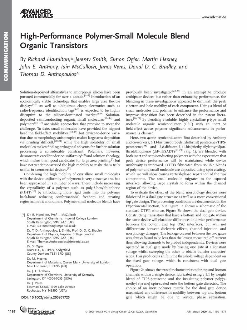
To evaluate the effect of the blend morphology devices werefabricated in a dual gate structure as well as a more conventionaltop gate design. The processing conditions are documented in theExperimental section, but Figure 1c shows a schematic of thestandard OTFT, whereas Figure 2b shows the dual gate device.Constructing transistors that have a bottom and top gate withinthe same device will elucidate differences in device performancebetween the bottom and top OSC interfaces, but will notdifferentiate between dielectric effects, channel injection, andmorphology changes. The leakage current between the two gateswas always found to be less than the lowest measured off currentthus allowing channels to be probed independently. Devices wereoperated in dual gate mode by biasing one gate at a constantvoltage whilst sweeping the other to obtain transfer character-istics. This produced a shift in the threshold voltage dependent onthe fixed gate voltage, which is consistent with dual gateoperation.
Figure 2a shows the transfer characteristics for top and bottomchannels within a single device, fabricated using a 1:1 by weightblend of TIPS-pentacene and the insulating polymer poly(a-methyl styrene) spin-coated onto the bottom gate dielectric. Thechoice of an inert polymer matrix for the dual gate devicemaximized any difference in mobility between top and bottomgate which might be due to vertical phase separation.
H & Co. KGaA, Weinheim Adv. Mater. 2009, 21, 1166–1171
COM
MUNIC
ATIO
N
www.advmat.de
Figure 1. Chemical structures of a) diF-TESADT and b) TIPS-pentacene.c) A schematic diagram of the standard device structure (PFBT¼penta-pentafluorobenzene thiol).
Figure 2. Dual gate device using a TIPS-pentacene:poly(a-methyl styrene)blend: a) transfer curves for the separate channels and b) a schematic ofthe device structure (PFBT¼ pentafluorobenzene thiol).
Adv. Mater. 2009, 21, 1166–1171 � 2009 WILEY-VCH Verlag G
Uniform semiconductor film formation was observed, whilst thesaturation mobility of holes within the bottom channel was(0.10� 0.05) cm2V�1 s�1 increasing to (0.5� 0.1) cm2V�1 s�1 inthe top channel. Moving from bottom to top gate also showed animprovement in on/off current ratios, reduced hysteresis andthreshold voltage shifts from greater than þ10V to between –5Vand –10V. Processing issues, described in the Experimentalsection, forced the use of different dielectric materials for thebottom and top channel, which could account for the difference inperformance seen. However, devices were analyzed by a DSIMStechnique (results below) which indicate a higher concentrationof TIPS-pentacene in the top-channel. The maximum mobilityachieved using TIPS-pentacene:poly(a-methyl styrene) in atop-gate-only device was found to be 0.69 cm2V�1 s�1, which isonly slightly higher than measured in the dual gate transistorsshowing that the altered structure does not adversely affect the topchannel operation.
In order to make an improvement in the mobility a change ofpolymer matrix was carried out. It is suggested that lateral phasesegregation of TIPS-pentacene and poly(a-methyl styrene) causesa reduction in the effective channel width and thus a lowering ofthe measured mobility for devices based on insulating polymers.Replacing poly(a-methyl styrene) with the amorphous p-typepolymer poly(triarylamine) (PTAA) increases carrier mobilitybetween crystalline pentacene-rich regions and improves theperformance of the OTFT.
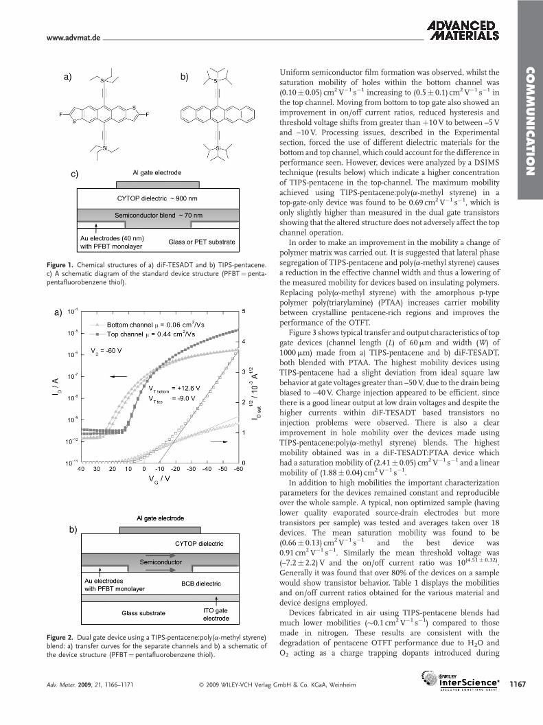
Figure 3 shows typical transfer and output characteristics of topgate devices (channel length (L) of 60mm and width (W) of1000mm) made from a) TIPS-pentacene and b) diF-TESADT,both blended with PTAA. The highest mobility devices usingTIPS-pentacene had a slight deviation from ideal square lawbehavior at gate voltages greater than –50V, due to the drain beingbiased to –40V. Charge injection appeared to be efficient, sincethere is a good linear output at low drain voltages and despite thehigher currents within diF-TESADT based transistors noinjection problems were observed. There is also a clearimprovement in hole mobility over the devices made usingTIPS-pentacene:poly(a-methyl styrene) blends. The highestmobility obtained was in a diF-TESADT:PTAA device whichhad a saturation mobility of (2.41� 0.05) cm2V�1 s�1 and a linearmobility of (1.88� 0.04) cm2V�1 s�1.
In addition to high mobilities the important characterizationparameters for the devices remained constant and reproducibleover the whole sample. A typical, non optimized sample (havinglower quality evaporated source-drain electrodes but moretransistors per sample) was tested and averages taken over 18devices. The mean saturation mobility was found to be(0.66� 0.13) cm2V�1 s�1 and the best device was0.91 cm2V�1 s�1. Similarly the mean threshold voltage was(–7.2� 2.2) V and the on/off current ratio was 10(4.51� 0.32).Generally it was found that over 80% of the devices on a samplewould show transistor behavior. Table 1 displays the mobilitiesand on/off current ratios obtained for the various material anddevice designs employed.
Devices fabricated in air using TIPS-pentacene blends hadmuch lower mobilities (�0.1 cm2V�1 s�1) compared to thosemade in nitrogen. These results are consistent with thedegradation of pentacene OTFT performance due to H2O andO2 acting as a charge trapping dopants introduced during
mbH & Co. KGaA, Weinheim 1167
COM
MUNIC
ATIO
N
www.advmat.de
Figure 3. Transfer and output curves of typical a) TIPS-pentacene and b) diF-TESADT blendtransistors with saturation mobilities of �1 cm2 V�1 s�1 and >2 cm2 V�1 s�1, respectively.
1168
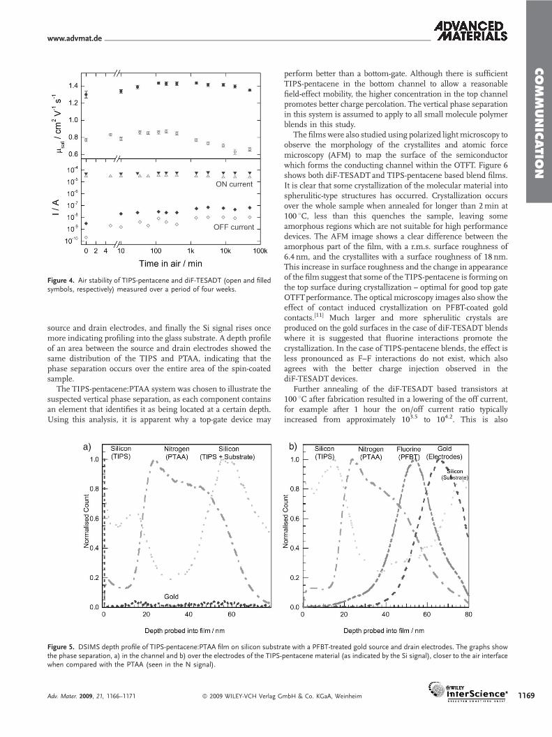
annealing of the semiconductor layer.[30] However, after fabrica-tion in nitrogen, exposure to air resulted in only a slow reductionin device performance since the permeability of CYTOP to H2Oand O2 is low. Figure 4 shows how the mobility as well as on andoff currents varied over a period of four weeks for a diF-TESADTand a TIPS-pentacene transistor. The TIPS-pentacene blendshowed a slight drop in mobility after several hours while
Table 1. Summary of the mobilities and on/off current ratios obtained for the various material and d
TIPS-pentacene:
poly(a-methyl styrene)
TIPS-pentacene: poly(a-methyl styrene)
Architecture DUAL GATE TOP GATE
Channel Bottom Top Top
msat [cm2 V–1 s–1] 0.10� 0.05 0.5� 0.1 0.7
mlin [cm2 V–1 s–1] – – 0.6
ION/IOFF 104.1 104.8 105.3
� 2009 WILEY-VCH Verlag GmbH & Co. KGaA, Weinheim
diF-TESADT blend transistors showedexcellent stability and maintained a satura-tion mobility above 1.2 cm2V�1 s�1 for theentire test. There was a gradual decrease inthe on/off ratio due to increasing offcurrent as bulk conduction in the channelbecame more significant.
The lower performance of the bottomgate in the dual gate device can beattributed to two effects. Firstly, there willbe a larger number of charge trapping siteson the BCB-semiconductor interface due tothe oxygen plasma treatment creating polargroups on the surface. Secondly, we believethat there is vertical separation of compo-nents within the semiconductor layer.During film formation phase separationof the polymer and the small molecularmaterial occurs, and there is preferentialcrystallization of the TIPS-pentacene (ordiF-TESADT) at the top semiconductorinterface. This therefore increases thefraction of molecular solid within theconducting channel of the transistor inthe top gate configuration.
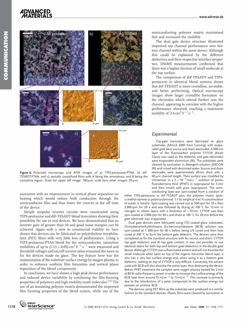
Vertical profiling of the device structureby dynamic secondary ion mass spectro-metry (DSIMS) was used to confirm thedistribution of the blend components. Csion bombardment was used to slowlysputter material from the film, and theresulting ejected ion species measured bymass spectrometer. Figure 5 shows the firstsignal to rise is the Si from the silyl groupon the TIPS-pentacene molecule. Thenitrogen signal (from the PTAA) can beseen to rise to a maximum approximately20–30nm beneath the top surface. Whenscanned over the channel (a) the Si signal isseen to rise at a probed depth of ca. 50 nmindicating the glass substrate. When
scanned over the electrodes (b) the fluorine peak indicates theposition of the self-assembled monolayer of pentafluorobenzenethiol (PFBT). The broadening in the F peak (which is amonomolecular layer <1 nm thick) is due to a combination ofa variable rate of etch for different materials in the layer and aslight spread in the energy density of the Cs ion beam. The goldsignal rises immediately afterwards as the profiling reached the
evice designs employed.
TIPS-pentacene: PTAA diF-TESADT: PTAA
TOP GATE TOP GATE
Top Top
1.1 2.41
0.7 1.88
105.2 104.2
Adv. Mater. 2009, 21, 1166–1171
COM
MUNIC
ATIO
N
www.advmat.de
Figure 4. Air stability of TIPS-pentacene and diF-TESADT (open and filledsymbols, respectively) measured over a period of four weeks.
source and drain electrodes, and finally the Si signal rises oncemore indicating profiling into the glass substrate. A depth profileof an area between the source and drain electrodes showed thesame distribution of the TIPS and PTAA, indicating that thephase separation occurs over the entire area of the spin-coatedsample.
The TIPS-pentacene:PTAA system was chosen to illustrate thesuspected vertical phase separation, as each component containsan element that identifies it as being located at a certain depth.Using this analysis, it is apparent why a top-gate device may
Figure 5. DSIMS depth profile of TIPS-pentacene:PTAA film on silicon substrthe phase separation, a) in the channel and b) over the electrodes of the TIPS-when compared with the PTAA (seen in the N signal).
Adv. Mater. 2009, 21, 1166–1171 � 2009 WILEY-VCH Verlag G
perform better than a bottom-gate. Although there is sufficientTIPS-pentacene in the bottom channel to allow a reasonablefield-effect mobility, the higher concentration in the top channelpromotes better charge percolation. The vertical phase separationin this system is assumed to apply to all small molecule polymerblends in this study.
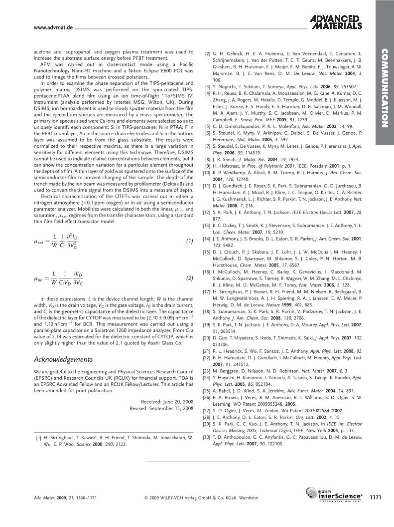
The films were also studied using polarized light microscopy toobserve the morphology of the crystallites and atomic forcemicroscopy (AFM) to map the surface of the semiconductorwhich forms the conducting channel within the OTFT. Figure 6shows both diF-TESADT and TIPS-pentacene based blend films.It is clear that some crystallization of the molecular material intospherulitic-type structures has occurred. Crystallization occursover the whole sample when annealed for longer than 2min at100 8C, less than this quenches the sample, leaving someamorphous regions which are not suitable for high performancedevices. The AFM image shows a clear difference between theamorphous part of the film, with a r.m.s. surface roughness of6.4 nm, and the crystallites with a surface roughness of 18 nm.This increase in surface roughness and the change in appearanceof the film suggest that some of the TIPS-pentacene is forming onthe top surface during crystallization – optimal for good top gateOTFTperformance. The optical microscopy images also show theeffect of contact induced crystallization on PFBT-coated goldcontacts.[11] Much larger and more spherulitic crystals areproduced on the gold surfaces in the case of diF-TESADT blendswhere it is suggested that fluorine interactions promote thecrystallization. In the case of TIPS-pentacene blends, the effect isless pronounced as F–F interactions do not exist, which alsoagrees with the better charge injection observed in thediF-TESADT devices.
Further annealing of the diF-TESADT based transistors at100 8C after fabrication resulted in a lowering of the off current,for example after 1 hour the on/off current ratio typicallyincreased from approximately 103.5 to 104.2. This is also
ate with a PFBT-treated gold source and drain electrodes. The graphs showpentacene material (as indicated by the Si signal), closer to the air interface
mbH & Co. KGaA, Weinheim 1169
COM
MUNIC
ATIO
N
www.advmat.de
Figure 6. Polarized microscopy and AFM images of a) TIPS-pentacene:PTAA, b) diF-TESADT:PTAA, and c) partially crystallized films with A being the amorphous and B being thecrystalline region. Scale bar upper left image: 100mm, scale bars other images: 50mm.
1170
consistent with an improvement in vertical phase separation onheating which would reduce bulk conduction through thesemiconductor film and thus lower the current in the off stateof the device.
Simple unipolar inverter circuits were constructed usingTIPS-pentacene and diF-TESADT blend transistors showing theirpossibility for use in real devices. We have demonstrated that aninverter gain of greater than 10 and good noise margins can beachieved. Again with a view to commercial viability we haveshown that devices can be fabricated on poly(ethylene terephtha-late) (PET) films with very little loss of performance. Using aTIPS-pentacene:PTAA blend for the semiconductor, saturationmobilities of up to (1.13� 0.05) cm2V�1 s�1 were measured andthreshold voltages and on/off current ratios remained the same asfor the devices made on glass. The key feature here was themaximization of the substrate surface energy by oxygen plasma inorder to enhance uniform film formation and vertical phaseseparation of the blend components.
In conclusion, we have shown a high peak device performanceand reduced device variability by combining the film-formingproperties of polymers and highmobility small molecules.[11] Theuse of an insulating polymer matrix demonstrated the improvedfilm forming properties of the blend system, while use of the
� 2009 WILEY-VCH Verlag GmbH & Co. KGaA, Weinhe
semiconducting polymer matrix maintainedthis and increased the mobility.
The dual gate device structure illustratedimproved top channel performance over bot-tom channel within the same device. Althoughthis could be explained by the differentdielectrics and their respective interface proper-ties, DSIMS measurements confirmed thatthere was a higher fraction of small molecule atthe top surface.
The comparison of diF-TESADT and TIPS-pentacene in identical blend systems showsthat diF-TESADT is more crystalline, air-stable,and better performing. Optical microscopyimages show larger crystallite formation onthe electrodes which extend further into thechannel, appearing to correlate with the higherperformance observed, reaching a maximummobility of 2.4 cm2V�1 s�1.
Experimental
Top-gate transistors were fabricated on glasssubstrates (EAGLE 2000 from Corning) with evapo-rated gold (Au) source and drain electrodes. A 900 nmlayer of the fluorocarbon polymer CYTOP (AsahiGlass) was used as the dielectric and gate electrodeswere evaporated aluminium (Al). The substrates werecleaned by sonication in detergent solution (DECON90) and rinsed with deionized water. Source and drainelectrodes were approximately 40 nm thick with a60mm channel length. Their surface was modified byimmersion in a 5� 10�3mol L�1 solution of penta-fluorobenzene thiol (PFBT) in isopropanol for 5minand then rinsed with pure isopropanol. The semi-conducting layer was spin-coated from a solution of
either TIPS-pentacene or diF-TESADT plus the polymer matrix (poly-a-methyl-styrene or polytriarylamine) 1:1 by weight at 4 wt % concentrationof solids in tetralin. Spin-coating was carried out at 500 rpm for 10 s then2 000 rpm for 20 s and was followed by drying at 100 8C for 15min innitrogen to obtain layers with a thickness of �70 nm. CYTOP was thenspin-coated at 2 000 rpm for 60 s and dried at 100 8C for 20min before thegate electrode was evaporated.
Dual gate devices were fabricated using ITO coated glass substrates.Divinyltetramethyldisiloxane bis-benzocyclobutane (BCB) solution wasspin-coated at 1 500 rpm for 60 s before being UV cured and then heatcured at 300 8C to form the bottom gate dielectric. The devices were thencompleted as for the standard structure with Au source and drain, CYTOPtop gate dielectric and Al top gate contact. It was not possible to useidentical layers for both top and bottom gate dielectrics in the double gatedevice. Although CYTOP uses a fluorinated solvent and will not dissolve thesmall molecule when spun on top of the organic transistor blend layer, italso has a very low surface energy and, when using it as a bottom gatedielectric, wetting on top of CYTOP is very difficult. Conversely, the solventused with BCB will also dissolve the active layer, thus destroying the device.Before PFBT treatment the samples were oxygen plasma treated for 2minat 80W radio-frequency power in order to increase the surface energy of theBCB layer from around 35mJm�2 to 73mJm�2. This increase is primarilydue to the introduction of a polar component to the surface energy notpresent on pristine BCB.
The devices using PET films as the substrate were produced in a similarfashion to the standard devices. Plastic films were cleaned by sonication in
im Adv. Mater. 2009, 21, 1166–1171
COM
MUNIC
ATIO
N
www.advmat.de
acetone and isopropanol, and oxygen plasma treatment was used toincrease the substrate surface energy before PFBT treatment.
AFM was carried out in close-contact mode using a PacificNanotechnology Nano-R2 machine and a Nikon Eclipse E600 POL wasused to image the films between crossed polarizers.
In order to examine the phase separation of the TIPS-pentacene andpolymer matrix, DSIMS was performed on the spin-coated TIPS-pentacene:PTAA blend film using an ion time-of-flight ‘‘ToFSIMS IV’instrument (analysis performed by Intertek MSG, Wilton, UK). DuringDSIMS, ion bombardment is used to slowly sputter material from the filmand the ejected ion species are measured by a mass spectrometer. Theprimary ion species used were Cs ions and elements were selected so as touniquely identify each component: Si in TIPS-pentacene; N in PTAA; F inthe PFBTmonolayer; Au in the source-drain electrodes and Si in the bottomlayer was assumed to be from the glass substrate. The results werenormalized to their respective maxima, as there is a large variation insensitivity for different elements using this technique. Therefore, DSIMScannot be used to indicate relative concentrations between elements, but itcan show the concentration variation for a particular element throughoutthe depth of a film. A thin layer of gold was sputtered onto the surface of thesemiconductor film to prevent charging of the sample. The depth of thetrenchmade by the ion beamwasmeasured by profilometer (Dektak 8) andused to convert the time signal from the DSIMS into a measure of depth.
Electrical characterization of the OTFTs was carried out in either anitrogen atmosphere (<0.1 ppm oxygen) or in air using a semiconductorparameter analyzer. Mobilities were calculated in both the linear, mlin, andsaturation,msat, regimes from the transfer characteristics, using a standardthin film field-effect transistor model:
msat ¼L
W
1
Ci
@2ID@V2
G
(1)
mlin ¼L
W
1
CiVD
@ID@VG
(2)
In these expressions, L is the device channel length, W is the channelwidth, VD is the drain voltage, VG is the gate voltage, ID is the drain current,and Ci is the geometric capacitance of the dielectric layer. The capacitanceof the dielectric layer for CYTOP was measured to be (2.10� 0.09) nFcm�2
and 1.12 nFcm�2 for BCB. This measurement was carried out using aparallel-plate capacitor on a Solartron 1260 impedance analyzer. From Ci avalue of 2.14 was estimated for the dielectric constant of CYTOP, which isonly slightly higher than the value of 2.1 quoted by Asahi Glass Co.
Acknowledgements
We are grateful to the Engineering and Physical Sciences Research Council(EPSRC) and Research Councils UK (RCUK) for financial support. TDA isan EPSRC Advanced Fellow and an RCUK Fellow/Lecturer. This article hasbeen amended for print publication.
Received: June 20, 2008
Revised: September 15, 2008
[1] H. Sirringhaus, T. Kawase, R. H. Friend, T. Shimoda, M. Inbasekaran, W.
Wu, E. P. Woo, Science 2000, 290, 2123.
Adv. Mater. 2009, 21, 1166–1171 � 2009 WILEY-VCH Verlag G
[2] G. H. Gelinck, H. E. A. Huitema, E. Van Veenendaal, E. Cantatore, L.
Schrijnemakers, J. Van der Putten, T. C. T. Geuns, M. Beenhakkers, J. B.
Giesbers, B. H. Huisman, E. J. Meijer, E. M. Benito, F. J. Touwslager, A. W.
Marsman, B. J. E. Van Rens, D. M. De Leeuw, Nat. Mater. 2004, 3,
106.
[3] Y. Noguchi, T. Sekitani, T. Someya, Appl. Phys. Lett. 2006, 89, 253507.
[4] R. H. Reuss, B. R. Chalamala, A. Moussessian, M. G. Kane, A. Kumar, D. C.
Zhang, J. A. Rogers, M. Hatalis, D. Temple, G. Moddel, B. J. Eliasson, M. J.
Estes, J. Kunze, E. S. Handy, E. S. Harmon, D. B. Salzman, J. M. Woodall,
M. A. Alam, J. Y. Murthy, S. C. Jacobsen, M. Olivier, D. Markus, P. M.
Campbell, E. Snow, Proc. IEEE 2005, 93, 1239.
[5] C. D. Dimitrakopoulos, P. R. L. Malenfant, Adv. Mater. 2002, 14, 99.
[6] S. Steudel, K. Myny, V. Arkhipov, C. Deibel, S. De Vusser, J. Genoe, P.
Heremans, Nat. Mater. 2005, 4, 597.
[7] S. Steudel, S. De Vusser, K. Myny, M. Lenes, J. Genoe, P. Heremans, J. Appl.
Phys. 2006, 99, 114519.
[8] J. R. Sheats, J. Mater. Res. 2004, 19, 1974.
[9] H. Hofstraat, in Proc. of Polytronic 2001, IEEE, Potsdam 2001, p. 1.
[10] K. P. Weidkamp, A. Afzali, R. M. Tromp, R. J. Hamers, J. Am. Chem. Soc.
2004, 126, 12740.
[11] D. J. Gundlach, J. E. Royer, S. K. Park, S. Subramanian, O. D. Jurchescu, B.
H. Hamadani, A. J. Moad, R. J. Kline, L. C. Teague, O. Kirillov, C. A. Richter,
J. G. Kushmerick, L. J. Richter, S. R. Parkin, T. N. Jackson, J. E. Anthony,Nat.
Mater. 2008, 7, 216.
[12] S. K. Park, J. E. Anthony, T. N. Jackson, IEEE Electron Device Lett. 2007, 28,
877.
[13] K. C. Dickey, T. J. Smith, K. J. Stevenson, S. Subramanian, J. E. Anthony, Y. L.
Loo, Chem. Mater. 2007, 19, 5210.
[14] J. E. Anthony, J. S. Brooks, D. L. Eaton, S. R. Parkin, J. Am. Chem. Soc. 2001,
123, 9482.
[15] D. J. Crouch, P. J. Skabara, J. E. Lohr, J. J. W. McDouall, M. Heeney, I.
McCulloch, D. Sparrowe, M. Shkunov, S. J. Coles, P. N. Horton, M. B.
Hursthouse, Chem. Mater. 2005, 17, 6567.
[16] I. McCulloch, M. Heeney, C. Bailey, K. Genevicius, I. Macdonald, M.
Shkunov, D. Sparrowe, S. Tierney, R. Wagner, W. M. Zhang, M. L. Chabinyc,
R. J. Kline, M. D. McGehee, M. F. Toney, Nat. Mater. 2006, 5, 328.
[17] H. Sirringhaus, P. J. Brown, R. H. Friend, M. M. Nielsen, K. Bechgaard, B.
M. W. Langeveld-Voss, A. J. H. Spiering, R. A. J. Janssen, E. W. Meijer, P.
Herwig, D. M. de Leeuw, Nature 1999, 401, 685.
[18] S. Subramanian, S. K. Park, S. R. Parkin, V. Podzorov, T. N. Jackson, J. E.
Anthony, J. Am. Chem. Soc. 2008, 130, 2706.
[19] S. K. Park, T. N. Jackson, J. E. Anthony, D. A. Mourey, Appl. Phys. Lett. 2007,
91, 063514.
[20] D. Guo, T. Miyadera, S. Ikeda, T. Shimada, K. Saiki, J. Appl. Phys. 2007, 102,
023706.
[21] R. L. Headrick, S. Wo, F. Sansoz, J. E. Anthony, Appl. Phys. Lett. 2008, 92.
[22] B. H. Hamadani, D. J. Gundlach, I. McCulloch, M. Heeney, Appl. Phys. Lett.
2007, 91, 243512.
[23] M. Berggren, D. Nilsson, N. D. Robinson, Nat. Mater. 2007, 6, 3.
[24] Y. Hayashi, H. Kanamori, I. Yamada, A. Takasu, S. Takagi, K. Kaneko, Appl.
Phys. Lett. 2005, 86, 052104.
[25] A. Babel, J. D. Wind, S. A. Jenekhe, Adv. Funct. Mater. 2004, 14, 891.
[26] B. A. Brown, J. Veres, R. M. Anemian, R. T. Williams, S. D. Ogier, S. W.
Leeming, WO Patent 2005055248, 2005.
[27] S. D. Ogier, J. Veres, M. Zeidan, Wo Patent 2007082584, 2007.
[28] J. E. Anthony, D. L. Eaton, S. R. Parkin, Org. Lett. 2002, 4, 15.
[29] S. K. Park, C. C. Kuo, J. E. Anthony, T. N. Jackson, in IEEE Int. Electron
Devices Meeting 2005, Technical Digest, IEEE, New York 2005, p. 113.
[30] T. D. Anthopoulos, G. C. Anyfantis, G. C. Papavassiliou, D. M. de Leeuw,
Appl. Phys. Lett. 2007, 90, 122105.
mbH & Co. KGaA, Weinheim 1171


![[Chapter III] Basic Knowledge of Discrete Semiconductor ......transistors (IGBTs) Power transistors (2SAxx,2SBxx,2SCxx,2SDxx, TTAxx,TTBxx,TTCxx,TTDxx) Types of Transistors Transistors](https://img.pdfslide.us/doc/110x75/5e766014341a1a707d5f4c34/chapter-iii-basic-knowledge-of-discrete-semiconductor-transistors-igbts.jpg)
![arXiv:0912.4106v1 [cond-mat.mtrl-sci] 21 Dec 2009 · PDF fileCalculating the trap density of states in organic field-effect transistors ... sistor including organic small molecule](https://img.pdfslide.us/doc/110x75/5a87bca57f8b9aa5408e1d59/arxiv09124106v1-cond-matmtrl-sci-21-dec-2009-the-trap-density-of-states-in.jpg)