Embed Size (px)
Citation preview

R
High Performance Multi-Port Memory Controller
Application Note
XAPP535 (v1.1) December 10, 2004
ARCHIVED APPLICATION NOTE - NOT SUPPORTED FOR NEW DESIGNS

High Performance Multi-Port Memory Controller www.xilinx.com XAPP535 (v1.1) December 10, 2004
"Xilinx" and the Xilinx logo shown above are registered trademarks of Xilinx, Inc. Any rights not expressly granted herein are reserved.
CoolRunner, RocketChips, Rocket IP, Spartan, StateBENCH, StateCAD, Virtex, XACT, XC2064, XC3090, XC4005, and XC5210 are registered trademarks of Xilinx, Inc.
The shadow X shown above is a trademark of Xilinx, Inc.
ACE Controller, ACE Flash, A.K.A. Speed, Alliance Series, AllianceCORE, Bencher, ChipScope, Configurable Logic Cell, CORE Generator, CoreLINX, Dual Block, EZTag, Fast CLK, Fast CONNECT, Fast FLASH, FastMap, Fast Zero Power, Foundation, Gigabit Speeds...and Beyond!, HardWire, HDL Bencher, IRL, J Drive, JBits, LCA, LogiBLOX, Logic Cell, LogiCORE, LogicProfessor, MicroBlaze, MicroVia, MultiLINX, NanoBlaze, PicoBlaze, PLUSASM, PowerGuide, PowerMaze, QPro, Real-PCI, RocketIO, SelectIO, SelectRAM, SelectRAM+, Silicon Xpresso, Smartguide, Smart-IP, SmartSearch, SMARTswitch, System ACE, Testbench In A Minute, TrueMap, UIM, VectorMaze, VersaBlock, VersaRing, Virtex-II Pro, Virtex-II EasyPath, Wave Table, WebFITTER, WebPACK, WebPOWERED, XABEL, XACT-Floorplanner, XACT-Performance, XACTstep Advanced, XACTstep Foundry, XAM, XAPP, X-BLOX +, XC designated products, XChecker, XDM, XEPLD, Xilinx Foundation Series, Xilinx XDTV, Xinfo, XSI, XtremeDSP and ZERO+ are trademarks of Xilinx, Inc.
The Programmable Logic Company is a service mark of Xilinx, Inc.
All other trademarks are the property of their respective owners.
Xilinx, Inc. does not assume any liability arising out of the application or use of any product described or shown herein; nor does it convey any license under its patents, copyrights, or maskwork rights or any rights of others. Xilinx, Inc. reserves the right to make changes, at any time, in order to improve reliability, function or design and to supply the best product possible. Xilinx, Inc. will not assume responsibility for the use of any circuitry described herein other than circuitry entirely embodied in its products. Xilinx provides any design, code, or information shown or described herein "as is." By providing the design, code, or information as one possible implementation of a feature, application, or standard, Xilinx makes no representation that such implementation is free from any claims of infringement. You are responsible for obtaining any rights you may require for your implementation. Xilinx expressly disclaims any warranty whatsoever with respect to the adequacy of any such implementation, including but not limited to any warranties or representations that the implementation is free from claims of infringement, as well as any implied warranties of merchantability or fitness for a particular purpose. Xilinx, Inc. devices and products are protected under U.S. Patents. Other U.S. and foreign patents pending. Xilinx, Inc. does not represent that devices shown or products described herein are free from patent infringement or from any other third party right. Xilinx, Inc. assumes no obligation to correct any errors contained herein or to advise any user of this text of any correction if such be made. Xilinx, Inc. will not assume any liability for the accuracy or correctness of any engineering or software support or assistance provided to a user.
Xilinx products are not intended for use in life support appliances, devices, or systems. Use of a Xilinx product in such applications without the written consent of the appropriate Xilinx officer is prohibited.
The contents of this manual are owned and copyrighted by Xilinx. Copyright 1994-2004 Xilinx, Inc. All Rights Reserved. Except as stated herein, none of the material may be copied, reproduced, distributed, republished, downloaded, displayed, posted, or transmitted in any form or by any means including, but not limited to, electronic, mechanical, photocopying, recording, or otherwise, without the prior written consent of Xilinx. Any unauthorized use of any material contained in this manual may violate copyright laws, trademark laws, the laws of privacy and publicity, and communications regulations and statutes.
High Performance Multi-Port Memory Controller XAPP535 (v1.1) December 10, 2004
The following table shows the revision history for this document..
R
Version Revision
06/04/04 1.0 Initial Xilinx release.
12/10/04 1.1 Copyediting and formatting done for compliance with Xilinx standards.
ARCHIVED APPLICATION NOTE - NOT SUPPORTED FOR NEW DESIGNS

High Performance Multi-Port Memory Controller www.xilinx.com 3XAPP535 (v1.1) December 10, 2004
Preface: About This DocumentDocument Contents . . . . . . . . . . . . . . . . . . . . . . . . . . . . . . . . . . . . . . . . . . . . . . . . . . . . . . . . . . 7
Additional Resources . . . . . . . . . . . . . . . . . . . . . . . . . . . . . . . . . . . . . . . . . . . . . . . . . . . . . . . . 7
Typographical Conventions . . . . . . . . . . . . . . . . . . . . . . . . . . . . . . . . . . . . . . . . . . . . . . . . . . 8
Chapter 1: IntroductionOverview . . . . . . . . . . . . . . . . . . . . . . . . . . . . . . . . . . . . . . . . . . . . . . . . . . . . . . . . . . . . . . . . . . . 10
Performance Levels . . . . . . . . . . . . . . . . . . . . . . . . . . . . . . . . . . . . . . . . . . . . . . . . . . . . . . . . . 12
Chapter 2: Reference SystemsGigabit Loopback Reference System. . . . . . . . . . . . . . . . . . . . . . . . . . . . . . . . . . . . . . . . . 15
Introduction . . . . . . . . . . . . . . . . . . . . . . . . . . . . . . . . . . . . . . . . . . . . . . . . . . . . . . . . . . . . . 15Hardware . . . . . . . . . . . . . . . . . . . . . . . . . . . . . . . . . . . . . . . . . . . . . . . . . . . . . . . . . . . . . . . 15
IP Version and Source . . . . . . . . . . . . . . . . . . . . . . . . . . . . . . . . . . . . . . . . . . . . . . . . . . . . . 21Simulation and Verification . . . . . . . . . . . . . . . . . . . . . . . . . . . . . . . . . . . . . . . . . . . . . . . . 22
Synthesis and Implementation . . . . . . . . . . . . . . . . . . . . . . . . . . . . . . . . . . . . . . . . . . . . . . 23Design Flow Environment . . . . . . . . . . . . . . . . . . . . . . . . . . . . . . . . . . . . . . . . . . . . . . . . . 23
Memory Map . . . . . . . . . . . . . . . . . . . . . . . . . . . . . . . . . . . . . . . . . . . . . . . . . . . . . . . . . . . . 24ML300 Specific Registers. . . . . . . . . . . . . . . . . . . . . . . . . . . . . . . . . . . . . . . . . . . . . . . . . . . 25
GSRD Dual TFT Reference System . . . . . . . . . . . . . . . . . . . . . . . . . . . . . . . . . . . . . . . . . . 27
Introduction . . . . . . . . . . . . . . . . . . . . . . . . . . . . . . . . . . . . . . . . . . . . . . . . . . . . . . . . . . . . . 27Hardware . . . . . . . . . . . . . . . . . . . . . . . . . . . . . . . . . . . . . . . . . . . . . . . . . . . . . . . . . . . . . . . 27
IP Version and Source . . . . . . . . . . . . . . . . . . . . . . . . . . . . . . . . . . . . . . . . . . . . . . . . . . . . . 33Simulation and Verification . . . . . . . . . . . . . . . . . . . . . . . . . . . . . . . . . . . . . . . . . . . . . . . . 34
Synthesis and Implementation . . . . . . . . . . . . . . . . . . . . . . . . . . . . . . . . . . . . . . . . . . . . . . 35Design Flow Environment . . . . . . . . . . . . . . . . . . . . . . . . . . . . . . . . . . . . . . . . . . . . . . . . . 35
Memory Map . . . . . . . . . . . . . . . . . . . . . . . . . . . . . . . . . . . . . . . . . . . . . . . . . . . . . . . . . . . . 36ML300-Specific Registers . . . . . . . . . . . . . . . . . . . . . . . . . . . . . . . . . . . . . . . . . . . . . . . . . . 37
Chapter 3: Hardware Data Sheets for Elements Used in the GSRDMulti-Port Memory Controller (MPMC) . . . . . . . . . . . . . . . . . . . . . . . . . . . . . . . . . . . . . 39
Overview . . . . . . . . . . . . . . . . . . . . . . . . . . . . . . . . . . . . . . . . . . . . . . . . . . . . . . . . . . . . . . . . 39
Features . . . . . . . . . . . . . . . . . . . . . . . . . . . . . . . . . . . . . . . . . . . . . . . . . . . . . . . . . . . . . . . . . 39Related Documentation . . . . . . . . . . . . . . . . . . . . . . . . . . . . . . . . . . . . . . . . . . . . . . . . . . . . 39
High-Level Block Diagram . . . . . . . . . . . . . . . . . . . . . . . . . . . . . . . . . . . . . . . . . . . . . . . . . 40
Table of Contents
ARCHIVED APPLICATION NOTE - NOT SUPPORTED FOR NEW DESIGNS
4 www.xilinx.com High Performance Multi-Port Memory ControllerXAPP535 (v1.1) December 10, 2004
R
Hardware . . . . . . . . . . . . . . . . . . . . . . . . . . . . . . . . . . . . . . . . . . . . . . . . . . . . . . . . . . . . . . . 40Timing Diagrams . . . . . . . . . . . . . . . . . . . . . . . . . . . . . . . . . . . . . . . . . . . . . . . . . . . . . . . . . 49
Simulation and Verification . . . . . . . . . . . . . . . . . . . . . . . . . . . . . . . . . . . . . . . . . . . . . . . . 59Using the MPMC in a System . . . . . . . . . . . . . . . . . . . . . . . . . . . . . . . . . . . . . . . . . . . . . . 59
Module Port Interface . . . . . . . . . . . . . . . . . . . . . . . . . . . . . . . . . . . . . . . . . . . . . . . . . . . . . 60
Communication Direct Memory Access Controller (CDMAC) . . . . . . . . . . . . . . . . 62Overview . . . . . . . . . . . . . . . . . . . . . . . . . . . . . . . . . . . . . . . . . . . . . . . . . . . . . . . . . . . . . . . . 62
Features . . . . . . . . . . . . . . . . . . . . . . . . . . . . . . . . . . . . . . . . . . . . . . . . . . . . . . . . . . . . . . . . . 62Related Documents . . . . . . . . . . . . . . . . . . . . . . . . . . . . . . . . . . . . . . . . . . . . . . . . . . . . . . . 62
High-Level Block Diagram . . . . . . . . . . . . . . . . . . . . . . . . . . . . . . . . . . . . . . . . . . . . . . . . . 63Theory of Operation . . . . . . . . . . . . . . . . . . . . . . . . . . . . . . . . . . . . . . . . . . . . . . . . . . . . . . 64
Hardware . . . . . . . . . . . . . . . . . . . . . . . . . . . . . . . . . . . . . . . . . . . . . . . . . . . . . . . . . . . . . . . 77Timing Diagrams . . . . . . . . . . . . . . . . . . . . . . . . . . . . . . . . . . . . . . . . . . . . . . . . . . . . . . . . 103
Simulation and Verification . . . . . . . . . . . . . . . . . . . . . . . . . . . . . . . . . . . . . . . . . . . . . . . 112Directory Structure . . . . . . . . . . . . . . . . . . . . . . . . . . . . . . . . . . . . . . . . . . . . . . . . . . . . . . 114
Using the CDMAC in a System . . . . . . . . . . . . . . . . . . . . . . . . . . . . . . . . . . . . . . . . . . . . 115Software . . . . . . . . . . . . . . . . . . . . . . . . . . . . . . . . . . . . . . . . . . . . . . . . . . . . . . . . . . . . . . . . 115
Module Port Interface . . . . . . . . . . . . . . . . . . . . . . . . . . . . . . . . . . . . . . . . . . . . . . . . . . . . 116
PLB to MPMC Personality Module . . . . . . . . . . . . . . . . . . . . . . . . . . . . . . . . . . . . . . . . . 119Overview . . . . . . . . . . . . . . . . . . . . . . . . . . . . . . . . . . . . . . . . . . . . . . . . . . . . . . . . . . . . . . . 119
Features . . . . . . . . . . . . . . . . . . . . . . . . . . . . . . . . . . . . . . . . . . . . . . . . . . . . . . . . . . . . . . . . 119Related Documents . . . . . . . . . . . . . . . . . . . . . . . . . . . . . . . . . . . . . . . . . . . . . . . . . . . . . . 119
High-Level Block Diagram . . . . . . . . . . . . . . . . . . . . . . . . . . . . . . . . . . . . . . . . . . . . . . . . 119Hardware . . . . . . . . . . . . . . . . . . . . . . . . . . . . . . . . . . . . . . . . . . . . . . . . . . . . . . . . . . . . . . 119
Simulation and Verification . . . . . . . . . . . . . . . . . . . . . . . . . . . . . . . . . . . . . . . . . . . . . . . 121Module Port Interface . . . . . . . . . . . . . . . . . . . . . . . . . . . . . . . . . . . . . . . . . . . . . . . . . . . . 121
DCR to OPB Bridge . . . . . . . . . . . . . . . . . . . . . . . . . . . . . . . . . . . . . . . . . . . . . . . . . . . . . . . . 124
Overview . . . . . . . . . . . . . . . . . . . . . . . . . . . . . . . . . . . . . . . . . . . . . . . . . . . . . . . . . . . . . . . 124Features . . . . . . . . . . . . . . . . . . . . . . . . . . . . . . . . . . . . . . . . . . . . . . . . . . . . . . . . . . . . . . . . 124
Related Documents . . . . . . . . . . . . . . . . . . . . . . . . . . . . . . . . . . . . . . . . . . . . . . . . . . . . . . 124High-Level Block Diagram . . . . . . . . . . . . . . . . . . . . . . . . . . . . . . . . . . . . . . . . . . . . . . . . 125
Hardware . . . . . . . . . . . . . . . . . . . . . . . . . . . . . . . . . . . . . . . . . . . . . . . . . . . . . . . . . . . . . . 126Module Port Interface . . . . . . . . . . . . . . . . . . . . . . . . . . . . . . . . . . . . . . . . . . . . . . . . . . . . 127
LocalLink TFT Controller . . . . . . . . . . . . . . . . . . . . . . . . . . . . . . . . . . . . . . . . . . . . . . . . . . 128
Overview . . . . . . . . . . . . . . . . . . . . . . . . . . . . . . . . . . . . . . . . . . . . . . . . . . . . . . . . . . . . . . . 128Features . . . . . . . . . . . . . . . . . . . . . . . . . . . . . . . . . . . . . . . . . . . . . . . . . . . . . . . . . . . . . . . . 128
Related Documents . . . . . . . . . . . . . . . . . . . . . . . . . . . . . . . . . . . . . . . . . . . . . . . . . . . . . . 128High-Level Block Diagram . . . . . . . . . . . . . . . . . . . . . . . . . . . . . . . . . . . . . . . . . . . . . . . . 128
Hardware . . . . . . . . . . . . . . . . . . . . . . . . . . . . . . . . . . . . . . . . . . . . . . . . . . . . . . . . . . . . . . 129Simulation and Verification . . . . . . . . . . . . . . . . . . . . . . . . . . . . . . . . . . . . . . . . . . . . . . . 130
LocalLink TFT Controller Pixel Organization . . . . . . . . . . . . . . . . . . . . . . . . . . . . . . . . 132Module Port Interface . . . . . . . . . . . . . . . . . . . . . . . . . . . . . . . . . . . . . . . . . . . . . . . . . . . . 135
ARCHIVED APPLICATION NOTE - NOT SUPPORTED FOR NEW DESIGNS

High Performance Multi-Port Memory Controller www.xilinx.com 5XAPP535 (v1.1) December 10, 2004
R
LocalLink Data Generator . . . . . . . . . . . . . . . . . . . . . . . . . . . . . . . . . . . . . . . . . . . . . . . . . . 137Overview . . . . . . . . . . . . . . . . . . . . . . . . . . . . . . . . . . . . . . . . . . . . . . . . . . . . . . . . . . . . . . . 137
Features . . . . . . . . . . . . . . . . . . . . . . . . . . . . . . . . . . . . . . . . . . . . . . . . . . . . . . . . . . . . . . . . 137Related Documents . . . . . . . . . . . . . . . . . . . . . . . . . . . . . . . . . . . . . . . . . . . . . . . . . . . . . . 137
High-Level Block Diagram . . . . . . . . . . . . . . . . . . . . . . . . . . . . . . . . . . . . . . . . . . . . . . . . 137Hardware . . . . . . . . . . . . . . . . . . . . . . . . . . . . . . . . . . . . . . . . . . . . . . . . . . . . . . . . . . . . . . 138
Simulation and Verification . . . . . . . . . . . . . . . . . . . . . . . . . . . . . . . . . . . . . . . . . . . . . . . 150Directory Structure . . . . . . . . . . . . . . . . . . . . . . . . . . . . . . . . . . . . . . . . . . . . . . . . . . . . . . 150
Using the LocalLink Data Generator . . . . . . . . . . . . . . . . . . . . . . . . . . . . . . . . . . . . . . . 151Module Port Interface . . . . . . . . . . . . . . . . . . . . . . . . . . . . . . . . . . . . . . . . . . . . . . . . . . . . 151
EDK Cores . . . . . . . . . . . . . . . . . . . . . . . . . . . . . . . . . . . . . . . . . . . . . . . . . . . . . . . . . . . . . . 152
Chapter 4: Software Models for Elements Contained in the GSRDCDMAC Software Model . . . . . . . . . . . . . . . . . . . . . . . . . . . . . . . . . . . . . . . . . . . . . . . . . . 153
CDMAC DMA Descriptor Model . . . . . . . . . . . . . . . . . . . . . . . . . . . . . . . . . . . . . . . . . . 153CDMAC Programming Model . . . . . . . . . . . . . . . . . . . . . . . . . . . . . . . . . . . . . . . . . . . . . 154
CDMAC Register Definitions . . . . . . . . . . . . . . . . . . . . . . . . . . . . . . . . . . . . . . . . . . . . . . 155
LocalLink Data Generator Software Model . . . . . . . . . . . . . . . . . . . . . . . . . . . . . . . . . 160LocalLink Data Generator Programming Model . . . . . . . . . . . . . . . . . . . . . . . . . . . . . 160
LocalLink Data Generator Register Definitions . . . . . . . . . . . . . . . . . . . . . . . . . . . . . . 160
Chapter 5: Software Applications Contained in the GSRDStand-Alone Software . . . . . . . . . . . . . . . . . . . . . . . . . . . . . . . . . . . . . . . . . . . . . . . . . . . . . . 165
Overview . . . . . . . . . . . . . . . . . . . . . . . . . . . . . . . . . . . . . . . . . . . . . . . . . . . . . . . . . . . . . . . 165Data Generator TFT Tests . . . . . . . . . . . . . . . . . . . . . . . . . . . . . . . . . . . . . . . . . . . . . . . . . 165
CDMAC Verification Tests . . . . . . . . . . . . . . . . . . . . . . . . . . . . . . . . . . . . . . . . . . . . . . . . 169GSRD Verification Test . . . . . . . . . . . . . . . . . . . . . . . . . . . . . . . . . . . . . . . . . . . . . . . . . . . 176
Loopback Reference System Verification Tests . . . . . . . . . . . . . . . . . . . . . . . . . . . . . . . 181Performance Metrics . . . . . . . . . . . . . . . . . . . . . . . . . . . . . . . . . . . . . . . . . . . . . . . . . . . . . 184
Linux Device Driver. . . . . . . . . . . . . . . . . . . . . . . . . . . . . . . . . . . . . . . . . . . . . . . . . . . . . . . . 188
LwIP . . . . . . . . . . . . . . . . . . . . . . . . . . . . . . . . . . . . . . . . . . . . . . . . . . . . . . . . . . . . . . . . . . . . . . . 188
Chapter 6: Building the GSRD Under EDKSupported Features . . . . . . . . . . . . . . . . . . . . . . . . . . . . . . . . . . . . . . . . . . . . . . . . . . . . . . . . 189
ARCHIVED APPLICATION NOTE - NOT SUPPORTED FOR NEW DESIGNS

6 www.xilinx.com High Performance Multi-Port Memory ControllerXAPP535 (v1.1) December 10, 2004
R
ARCHIVED APPLICATION NOTE - NOT SUPPORTED FOR NEW DESIGNS

High Performance Multi-Port Memory Controller www.xilinx.com 7XAPP535 (v1.1) December 10, 2004
R
Preface
About This Document
This application note introduces two key technologies from the Gigabit System Reference Design (GSRD): the Multi-Port Memory Controller (MPMC) which allows multiple entities to directly access memory, bypassing a system bus; and the Communication Direct Memory Access Controller (CDMAC) which works with the MPMC to provide multiple channels of Direct Memory Access (DMA) for communication style devices.
Document ContentsThis document contains the following chapters:
• Chapter 1, “Introduction” provides an overview of the Multi-Port Memory Controller (MPMC).
• Chapter 2, “Reference Systems” covers two of the three systems that are provided: the Dual TFT Controller Reference System, and the Loopback Reference System. Features and functionality unique to each of these systems are described in detail.
• Chapter 3, “Hardware Data Sheets for Elements Used in the GSRD” contains all of the datasheets for each of the hardware elements present in the reference systems. This includes the MPMC and CDMAC, as well as many other ancillary hardware IPs that are used to make demonstrable systems.
• Chapter 4, “Software Models for Elements Contained in the GSRD” provides an overview of the software models for the major cores that are provided with the GSRD. This includes documentation for the software model of the CDMAC, and the LocalLink Data Generator.
• Chapter 5, “Software Applications Contained in the GSRD” provides an overview of the software that is provided with the GSRD. This includes the CDMAC Verification Tests, Performance Metrics, Data Generator Tests, and demonstration applications. Additional demonstration applications and related documentation are shipped with the ZIP file.
• Chapter 6, “Building the GSRD Under EDK” provides some assistance in using the Xilinx Embedded Development Kit (EDK) to build the various reference systems, run simulations, create bitstreams and run applications on real hardware (using the Xilinx ML300 Evaluation Platform). This chapter assumes the reader is familiar with EDK.
Additional ResourcesTo search the database of silicon and software questions and answers, or to create a technical support case in WebCase, visit the following Xilinx website:
http://www.xilinx.com/support
ARCHIVED APPLICATION NOTE - NOT SUPPORTED FOR NEW DESIGNS
8 www.xilinx.com High Performance Multi-Port Memory ControllerXAPP535 (v1.1) December 10, 2004
Preface: About This DocumentR
Typographical ConventionsThe following typographical conventions are used in this document:
Convention Meaning or Use Example
Italic font
References to other documentsSee the ML300 User Guide for more information.
Emphasis in textThe address (F) is asserted after clock event 2.
Underlined Text Indicates a link to a web page. http://www.xilinx.com/gsrd
ARCHIVED APPLICATION NOTE - NOT SUPPORTED FOR NEW DESIGNS

High Performance Multi-Port Memory Controller www.xilinx.com 9XAPP535 (v1.1) December 10, 2004
R
Chapter 1
Introduction
Modern systems require vast amounts of data bandwidth. Requirements for the processing subsystem and movement of gigabits per second of data between peripherals and memory, make up the bulk of this bandwidth demand. Most systems try to offload the processing subsystem so that it does not try to produce or consume the data. Rather, the processing subsystem acts more like a traffic cop to control the flow of the data from point to point. In many systems, the processing subsystem controls the flow of this data by setting up a Direct Memory Access (DMA) engine to move the data.
The problem with many modern systems is that the processing subsystem and DMA engine(s) must vie for access to the same memory resources via a system bus. This system bus causes the performance of the system to be limited to the performance of the bus. The memory subsystem is often capable of much more data bandwidth, but is limited by the slower processor subsystem bus.
The Gigabit System Reference Design (GSRD), described in XAPP536, demonstrates a variety of technologies surrounding the movement of data within a system using Xilinx Virtex-II Pro™ series Field Programmable Gate Arrays (FPGAs). The GSRD begins with the premise that the memory subsystem is capable of more data bandwidth than the processor subsystem bus can deliver. From this premise, an architecture is derived that offers more data bandwidth than is available in traditional on-chip bus-based systems.
This application note introduces two key technologies from the GSRD: the Multi-Port Memory Controller (MPMC) which allows multiple entities to directly access memory, bypassing a system bus; and the Communication Direct Memory Access Controller (CDMAC) which works with the MPMC to provide multiple channels of DMA for communication style devices. The LocalLink Gigabit Ethernet Media Access Controller (GMAC) peripheral, which provides Gigabit Ethernet access across a LocalLink interface instead of a bus-based interface, is described in detail in XAPP536.
Two of the GSRD's key technologies, the MPMC and CDMAC, are described in detail in this chapter. The third key technology, the LocalLink GMAC peripheral, is described in XAPP536. The package of files provided with this document provides three different reference systems that are pre-built to demonstrate various aspects of the three key elements. The main GSRD system shows the instantiation of all three elements: MPMC, CDMAC, and GMAC peripheral. In addition, this system contains a data generator and a TFT Display controller that are used to demonstrate the amount of data that can be pulled from the memory while the IBM PPC405 central processing unit (CPU) contained in the Virtex-II Pro device consumes its bandwidth.
This system can boot the Linux operating system and run applications across the Gigabit Ethernet link. The two remaining systems are designed to illustrate high bandwidth data movement and verification of the infrastructure. All three of the reference system designs are to be used as a springboard for further development of high data bandwidth systems. Hardware and software source code is provided for most modules, and all systems have been built and verified using the Xilinx ML300 Evaluation Platform, ISE FPGA tools, and the Xilinx Embedded Design Kit (EDK).
ARCHIVED APPLICATION NOTE - NOT SUPPORTED FOR NEW DESIGNS

10 www.xilinx.com High Performance Multi-Port Memory ControllerXAPP535 (v1.1) December 10, 2004
Chapter 1: IntroductionR
OverviewThis Gigabit System Reference Design consists of the three main elements: MPMC, CDMAC, and GMAC Peripheral. The MPMC is a quadruple port memory controller used to provide memory access for the PPC405 and four DMA engines to double data rate (DDR) SDRAM. DDR memory is used because it provides substantial burst data bandwidth over most competing memory technologies. While the MPMC was designed with DDR in mind, its actual implementation could be adopted to differing memory technologies. The PPC405 CPU is a Harvard architecture CPU, therefore it provides separate Processor Local Bus (PLB) ports for the instruction and data side processor local bus. The GSRD connects the I and D ports to two of the ports on the MPMC, and reserves the other two ports for up to four channels of DMA using the bolt-on CDMAC. The main advantage of the MPMC is that it can simultaneously arbitrate all four ports with a priori knowledge to most efficiently use the DDR memory. In contrast, an on-chip bus-based system must serially arbitrate for access to the bus, let alone access to the memory. Since the MPMC has specialized knowledge about what each port is talking too, it can make optimizations that minimize the latency for getting data back to each port.
Figure 1-1 illustrates the limitations between shared PLB-based systems and those built with the MPMC technology. In a shared bus-based system (such as PLB), the available CPU bandwidth is adversely affected as DMA bandwidth increases.
The MPMC system can sustain a much larger draw down of DMA bandwidth before the CPU sees a loss in performance. The area between the two curves is where the MPMC differentiates itself. MPMC illustrates that it permits substantially more DMA bandwidth
Figure 1-1: CPU Availability vs. DMA Bandwidth
X535_01_113004
0%
10%
20%
30%
40%
50%
60%
70%
80%
90%
100%
0 0.5 1 1.5 2 2.5
GSRD CPU vs DMA Performance
DMA Bandwidth (Gbit / Sec)
CP
U A
vaila
bilit
y
3 3
ARCHIVED APPLICATION NOTE - NOT SUPPORTED FOR NEW DESIGNS

High Performance Multi-Port Memory Controller www.xilinx.com 11XAPP535 (v1.1) December 10, 2004
OverviewR
while the CPU is still highly available. When more DMA bandwidth is demanded in a shared bus system, the system bus becomes the limiting factor, and the CPU's availability rapidly diminishes.
Another key element of the GSRD is the CDMAC. It is called a 'Communication' DMA Controller because it is focused on talking to full duplex communication devices, such as the GMAC peripheral. The CDMAC is built to use two ports of the MPMC, and provides two full duplex channels of DMA via four independent DMA engines. The CDMAC thus consists of two transmit and two receive DMA engines. These four engines vie for access to the DDR memory via the MPMC. The CDMAC is tightly coupled to the MPMC so that it can be smaller and more agile than other types of DMA controllers. One of the major advantages of such tight coupling is that the MPMC can be designed to take advantage of the fact that it knows two of its ports are talking to DMA. This provides a priori knowledge about how to best control the DDR memory and how to pull as much bandwidth from it as possible. For example, whereas the PPC405 can only request accesses of 32 bytes at a time from the DDR memory, the CDMAC requests 128 bytes of data at a time. This provides huge gains in bandwidth because the DDR memory spends more of its time in the data phase than in the control phase.
The last key element to the GSRD is the LocalLink GMAC peripheral. This peripheral is different from other gigabit Ethernet peripherals because it does not use an on-chip bus to communicate its data. Rather, it uses the Xilinx LocalLink interface. LocalLink is a very lightweight interface for communication devices that provides a simple protocol to transfer data unidirectionally. Full duplex communication devices such as the GMAC peripheral consume two LocalLink interfaces. The major advantage of using LocalLink over an on-chip bus is that it vastly simplifies the logic requirements for the peripheral, and allows the peripheral to run at a higher clock rate. The GMAC peripheral thus becomes tightly coupled to the memory subsystem, bypassing the traditional bottlenecks of the on-chip bus. Another advantage of the LocalLink interface to the GMAC peripheral is the freedom to add intelligent processing agents to the pipeline.
The GMAC peripheral contains two additional features that greatly enhance the performance of Ethernet-based systems: Transport Layer (UDP and TCP) checksum offload, and filtering of bad or truncated frames. The checksum offload logic has a significant effect on overall system performance because it places in hardware a task that is normally completed by the CPU. This is one example of an intelligent processing agent added to the LocalLink interface. Since the hardware automatically calculates the incoming and outgoing checksums, the CPU is now free to do other things. More importantly, when the CPU is calculating checksums, the Ethernet link must wait for the CPU to complete its calculation, which directly affects the effective line rate of the Ethernet link. Similarly, the hardware contains packet-filtering logic that discards bad or truncated packets. This hardware prevents the CPU from having to determine that the packet was bad or truncated -- again offering the CPU more opportunity to do other things.
Figure 1-2 shows a typical system implemented using the three key technologies outlined above. In this example, the MPMC is connected to the PPC405 CPU and the CDMAC. The CDMAC is in turn connected to three LocalLink devices. One of the devices is a full-duplex device and the other two are half-duplex devices, one in each direction. The PPC405 uses the Device Control Register (DCR) bus to talk to some additional devices such as the interrupt controller and UART, as well as control the CDMAC and LocalLink devices. This example is intended only to illustrate the basic architecture of the system. It is very possible to build systems wherein the D-side PLB of the PPC405 is shared in a standard PLB system, and/or where some other high-speed device(s) is connected to the CDMAC.
ARCHIVED APPLICATION NOTE - NOT SUPPORTED FOR NEW DESIGNS

12 www.xilinx.com High Performance Multi-Port Memory ControllerXAPP535 (v1.1) December 10, 2004
Chapter 1: IntroductionR
Performance LevelsIt is natural to inquire as to the performance levels that are sustainable under the GSRD. This is a challenging question to address because it depends greatly upon the needs of the system. For example, a system running a Real Time Operating System (RTOS) might have substantially less performance than a system running a stand-alone software application. What is not obvious is how much impact the software running on the system can have. The GSRD was designed originally to address the needs of a hardware system to obtain very high bandwidth. However, in systems that can take advantage of such high bandwidth, there is a substantial burden on software to 'keep up' with the advantages provided by the hardware.
The GSRD provides three points of view to consider this question: A full Linux implementation, including Gigabit Ethernet driver; lwIP, a simple TCP/IP stack freely
Figure 1-2: Typical GSRD System using MPMC and CDMAC
LocalLinkFull Duplex
DataConsumer
DDR SDRAM
PPC405
DCR
ISPLB
DSPLB
Loca
lLin
k
Loca
lLin
k
Loca
lLin
k
Loca
lLin
k
DCR2OPB
LocalLinkRx Device
LocalLinkTx Device
DualGPIO
DCR2OPB
UARTLite
Pushbuttonsand LEDs XCVR
DB9
MPMC
PLB Port Interface PLB Port InterfaceCDMAC
Port 0 Port 1 Port 2 Port 3
Rx0 Tx0 Rx1 Tx1
ML300 Evaluation Platform
FPGA
X535_02_113004
ARCHIVED APPLICATION NOTE - NOT SUPPORTED FOR NEW DESIGNS

High Performance Multi-Port Memory Controller www.xilinx.com 13XAPP535 (v1.1) December 10, 2004
Performance LevelsR
available, and a few stand-alone applications which exercise the ports to the fullest degree possible. Using each of these applications, customers can evaluate the relative performance of each style of use. Generally, the result is that if the CPU can keep the CDMAC well fed with DMA descriptors, then large quantities of data can be moved by the CDMAC per unit time. However, in many instances, the size of data being moved is such that the CPU spends all of its time managing the CDMAC instead of doing other useful things. These applications help to explore the boundaries of performance that exist in various styles of use that systems typically employ.
Table 1-1 is provided to summarize the performance that can be obtained with the GSRD, as shipped with this document. Five comparisons are made. The first two use the Gigabit Serial Reference System (GSRS) the operation of Linux and a lightweight TCP/IP stack running on top of the gigabit Ethernet hardware. These two data points provide insight into the relative performance of the gigabit Ethernet link. The last three comparisons use each of the three reference systems in order to provide performance metrics when all four ports are being used. The Loopback design metric seeks to show the maximum practical performance that is possible when the communication devices process as much data as the memory is capable of providing. The GSRD Verification Test design metric uses the GSRS and broadcasts video data from a data generator to memory, from memory across the gigabit Ethernet link back into memory, and from memory to the TFT display on the Xilinx ML300 Evaluation Platform. The Dual TFT design metric provides performance data when there are two data generators in the system, and two TFTs moving independent video data across the four CDMAC engines. Whereas the first three metrics only utilize two of the four CDMAC engines, the last three metrics provide differing levels of performance as the CDMAC engines' data rates are increased. This permits the study of the effect the DMA overhead has on the CPUs availability.
Table 1-1: GSRD Measured Performance Capabilities
Test Tx0 Data Rate Rx0 Data Rate Tx1 Data Rate Rx1 Data Rate CPU Availability
Linux, NetPerf, 9 KB 0 0 510 Mb/sec 280 Mb/sec 20%
Loopback High Speed
GSRD TFT Echo 643,606,522 bps 712,882,538 bps 999,426,901 bps 938,275,284 bps 77%
Dual TFT Moves
ARCHIVED APPLICATION NOTE - NOT SUPPORTED FOR NEW DESIGNS

14 www.xilinx.com High Performance Multi-Port Memory ControllerXAPP535 (v1.1) December 10, 2004
Chapter 1: IntroductionR
ARCHIVED APPLICATION NOTE - NOT SUPPORTED FOR NEW DESIGNS

High Performance Multi-Port Memory Controller www.xilinx.com 15XAPP535 (v1.1) December 10, 2004
R
Chapter 2
Reference Systems
Gigabit Loopback Reference System
IntroductionThe Gigabit Loopback System Reference Design (GSRD) demonstrates a system utilizing high bandwidth devices that move large amounts of data using DMA transactions and high-speed memory. The system incorporates a Multi-Port Memory Controller (MPMC) and a Communications Direct Memory Access Controller (CDMAC) as the infrastructure to move large amounts of data while providing sufficient memory bandwidth for the CPU and other peripherals. A Loopback Module redirects data on the transmit paths back to the receive paths with variable latencies. The Loopback Module is connected to the CDMAC in the system to assist in system testing and performance analysis. This system is a demonstration and development vehicle for high bandwidth Virtex-II Pro systems such as those using RocketIO™ Multi-Gigabit Transceivers (MGTs) or other data intensive applications.
This document describes the contents of the reference system and provides information about how the system is organized, implemented, and verified. The information presented introduces many aspects of the reference system, but refer to additional specific documentation for more detailed information about the software, tools, peripherals, interface protocols, and capabilities of the FPGA.
Hardware
Overview
Figure 2-1 provides a high-level view of the hardware contents of the system. This design demonstrates a system built around the MPMC coupled with 32-bit DDR SDRAM memory. A dual engine CDMAC connects to two ports of the MPMC. The instruction and data side PPC405 ports connect to the other two MPMC ports via PLB-to-MPMC Interface modules. Four separate point-to-point LocalLink buses connect the CDMAC to the Loopback Module. LocalLink is a protocol specification optimized for high-performance communications applications such as gigabit Ethernet.
Lower performance devices such as the UART, interrupt controller, and GPIOs are attached to the CPU's DCR bus. DCR is an IBM CoreConnect bus primarily used with control and status registers where simplicity is desired. Refer to the DCR CoreConnect Architecture Specifications for more information. The use of DCR for peripherals reduces the loading on the high-performance MPMC ports while minimizing FPGA resource utilization since large bus bridges can be avoided.
ARCHIVED APPLICATION NOTE - NOT SUPPORTED FOR NEW DESIGNS

16 www.xilinx.com High Performance Multi-Port Memory ControllerXAPP535 (v1.1) December 10, 2004
Chapter 2: Reference SystemsR
The hardware devices used in this design are described in more detail in the Processor IP User Guide, available at http://www.xilinx.com/ise/embedded/proc_ip_ref_guide.pdf, and in Chapter 3, “Hardware Data Sheets for Elements Used in the GSRD”.
MPMC
The MPMC allows the 32-bit DDR SDRAM memory resource to be shared over four independent interface ports. These ports each permit full read and write access from the CDMAC and PPC405. Each MPMC port is implemented as a direct point-to-point connection rather than a shared bus, thus permitting higher performance and not requiring additional bus arbiters.
Figure 2-1: GSRD Loopback Reference System Block Diagram
Loopback
DDR SDRAM
PPC405
DCR
ISPLB
DSPLB
Loca
lLin
k
Loca
lLin
k
Loca
lLin
k
Loca
lLin
k
DCR2OPB
DualGPIO
DCR2OPB
UARTLite
Pushbuttonsand LEDs XCVR
DB9
MPMC
PLB Port Interface PLB Port InterfaceCDMAC
Port 0 Port 1 Port 2 Port 3
Rx0 Tx0 Rx1 Tx1
ML300 Evaluation Platform
FPGA
X535_03_113004
ARCHIVED APPLICATION NOTE - NOT SUPPORTED FOR NEW DESIGNS
High Performance Multi-Port Memory Controller www.xilinx.com 17XAPP535 (v1.1) December 10, 2004
Gigabit Loopback Reference SystemR
Other highlights of the MPMC include:
• Independent read and write data FIFOs for each port
• Highly efficient block RAM-based state machines
• Pipelined control, data, and arbitration logic
Two MPMC ports are connected to the two PLB ports of the PPC405 via PLB to MPMC Interface modules. The PLB to MPMC Interfaces translate transactions from the Instruction and Data side PLB ports of the PPC405 into MPMC transactions. It handles all the necessary handshaking signals and clock synchronization between the PLB and MPMC interfaces. The remaining two MPMC ports attach to the quad engine CDMAC. This permits the CDMAC to manage the flow of two bidirectional streams of data to and from memory.
Since all four ports of the MPMC access a common shared memory resource, data transfers between the CPU and the CDMAC are coordinated through the MPMC. For example, each one can read or write to a common location in memory and stay coordinated using interrupts and DCR. This removes the need for a direct communications path between the CPU and the CDMAC. This architecture helps to reduce FPGA resources and improve system performance.
CDMAC
The CDMAC manages the flow of data between peripherals and memory. It supports variable packet sizes and can transfer data to unaligned memory addresses (byte resolution). CDMAC control and status registers are accessible by the CPU via DCR interface. Using DCR frees up the high-speed ports to only be used for data transfer and not for control. The CDMAC also has the ability to read a linked list of DMA transfer descriptors directly from memory, and it can generate interrupts based on the completion of a task or the detection of an error. Therefore, the CPU can set up a chain of DMA descriptors of memory and then command the CDMAC to autonomously transfer the data according to the descriptors. This frees up CPU resources for other tasks.
The CDMAC is configured so that the LocalLink Data Generators and LocalLink TFT Controllers do not generate errors when the DMA engine reaches a descriptor with the “completed” bit set.
LocalLink Devices
LocalLink is a protocol specification for a point-to-point connection infrastructure optimized for communications applications. The protocol supports flow control from the source or destination side of the data transfer. It also includes additional control signals to mark the start and end of frames and data payloads. Consult the LocalLink Specification for more information.
Each CDMAC engine controls a separate LocalLink transmit and receive path. Both CDMAC engines connect to the Loopback Module. The Loopback Module takes the data from the transmit path and sends it back along the receive path. The returned data can go back to the same CDMAC engine or can be cross-coupled to the other CDMAC engine. It can also insert varying amounts of delay to the data being sent back. The amount of the delay is programmable by the CPU via DCR commands. The delay can be set to different fixed values or with a pseudo-random set of delays.
ARCHIVED APPLICATION NOTE - NOT SUPPORTED FOR NEW DESIGNS

18 www.xilinx.com High Performance Multi-Port Memory ControllerXAPP535 (v1.1) December 10, 2004
Chapter 2: Reference SystemsR
DCR
The DCR offers a very simple interface protocol and is used to access control and status registers in various devices. It allows for register access to various devices without loading down the On-Chip Peripheral Bus (OPB) and PLB interfaces. Since DCR devices are generally accessed infrequently and do not have high-performance requirements, they are used throughout the reference design for functions, such as error status registers, interrupt controllers, and device initialization logic.
The CPU contains a DCR master interface that is accessed through special Move To DCR and Move From DCR instructions. Since DCR devices are not memory mapped and their access is treated as a privileged instruction, take care in SW to properly access DCR devices. The DCR specification requires that the DCR master and slave clocks be synchronous to each other and related in frequency by an integer multiple. It is important to be aware of the clock domains of each of the DCR devices to ensure proper functionality.
Control/status registers in the CDMAC and Loopback Module are all accessed via DCR. In addition there are three peripherals on DCR: Uartlite, a dual GPIO controller, and the interrupt controller. Since the Uartlite and GPIO are natively OPB devices, a simple DCR to OPB interface bridge is added. This DCR to OPB interface is extremely compact and only implements the minimum necessary functionality to talk to these devices.
Using the DCR rather than the memory mapped PLB to communicate with peripherals reduces loading on the high-speed paths to allow for greater system performance. Since peripheral and control/status registers are accessed relatively infrequently and are lower bandwidth devices, it is appropriate to use DCR. Using DCR also lessens the need for bus bridges that can be complex or would introduce greater latency.
Interrupts
The CPU also contains two interrupt pins, one for critical interrupt requests, and the other for non-critical interrupts. An interrupt controller for non-critical interrupts is controlled through the DCR. It allows multiple edge or level sensitive interrupts from peripherals to be OR'ed together back to the CPU. It also provides the ability for bitwise masking of individual interrupts. Table 2-1 and Table 2-2 summarize the connections from the IP to the interrupt controller.
Table 2-1: GSRD Loopback Reference System
MSB
LSB
31 30 29 28 27 26 25 24 23 22 21 20 19 18 17 16 15 14 13 12 11 10 9 8 7 6 5 4 3 2 1 0
RESERVED
CD
MA
C I
NT
UA
RT
Lit
e IN
T
Table 2-2: List of IP Connections to the Interrupt Controller
Bit Description
[1]CDMAC_INT: The CDMAC INT pin is tied to this INTC input.
The CDMAC INT pin is active high level triggered
[0]UARTLite_INT: The UARTLite INT pin is tied to this INTC input.
The UARTLite INT pin is rising edge triggered
ARCHIVED APPLICATION NOTE - NOT SUPPORTED FOR NEW DESIGNS
High Performance Multi-Port Memory Controller www.xilinx.com 19XAPP535 (v1.1) December 10, 2004
Gigabit Loopback Reference SystemR
Clock/Reset Distribution
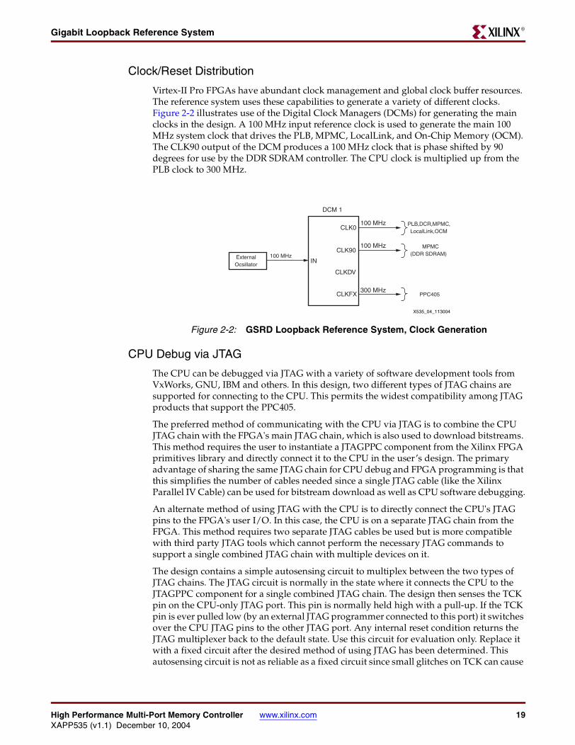
Virtex-II Pro FPGAs have abundant clock management and global clock buffer resources. The reference system uses these capabilities to generate a variety of different clocks. Figure 2-2 illustrates use of the Digital Clock Managers (DCMs) for generating the main clocks in the design. A 100 MHz input reference clock is used to generate the main 100 MHz system clock that drives the PLB, MPMC, LocalLink, and On-Chip Memory (OCM). The CLK90 output of the DCM produces a 100 MHz clock that is phase shifted by 90 degrees for use by the DDR SDRAM controller. The CPU clock is multiplied up from the PLB clock to 300 MHz.
CPU Debug via JTAG
The CPU can be debugged via JTAG with a variety of software development tools from VxWorks, GNU, IBM and others. In this design, two different types of JTAG chains are supported for connecting to the CPU. This permits the widest compatibility among JTAG products that support the PPC405.
The preferred method of communicating with the CPU via JTAG is to combine the CPU JTAG chain with the FPGA's main JTAG chain, which is also used to download bitstreams. This method requires the user to instantiate a JTAGPPC component from the Xilinx FPGA primitives library and directly connect it to the CPU in the user’s design. The primary advantage of sharing the same JTAG chain for CPU debug and FPGA programming is that this simplifies the number of cables needed since a single JTAG cable (like the Xilinx Parallel IV Cable) can be used for bitstream download as well as CPU software debugging.
An alternate method of using JTAG with the CPU is to directly connect the CPU's JTAG pins to the FPGA's user I/O. In this case, the CPU is on a separate JTAG chain from the FPGA. This method requires two separate JTAG cables be used but is more compatible with third party JTAG tools which cannot perform the necessary JTAG commands to support a single combined JTAG chain with multiple devices on it.
The design contains a simple autosensing circuit to multiplex between the two types of JTAG chains. The JTAG circuit is normally in the state where it connects the CPU to the JTAGPPC component for a single combined JTAG chain. The design then senses the TCK pin on the CPU-only JTAG port. This pin is normally held high with a pull-up. If the TCK pin is ever pulled low (by an external JTAG programmer connected to this port) it switches over the CPU JTAG pins to the other JTAG port. Any internal reset condition returns the JTAG multiplexer back to the default state. Use this circuit for evaluation only. Replace it with a fixed circuit after the desired method of using JTAG has been determined. This autosensing circuit is not as reliable as a fixed circuit since small glitches on TCK can cause
Figure 2-2: GSRD Loopback Reference System, Clock Generation
CLK0
DCM 1
CLK90
CLKDV
CLKFX
IN
100 MHz
100 MHz
300 MHzPPC405
PLB,DCR,MPMC,LocalLink,OCM
MPMC(DDR SDRAM)100 MHzExternal
Ocsillator
X535_04_113004
ARCHIVED APPLICATION NOTE - NOT SUPPORTED FOR NEW DESIGNS

20 www.xilinx.com High Performance Multi-Port Memory ControllerXAPP535 (v1.1) December 10, 2004
Chapter 2: Reference SystemsR
a false detection. In addition, the JTAG switching circuit can prevent System ACE (described later) from functioning correctly because System ACE relies on using the combined JTAG chain to talk to the CPU. If using System ACE with the autosensing circuit present, connect any external JTAG programmer to the CPU-only JTAG port until after System ACE download is complete.
Other Devices
In addition to the MPMC, LocalLink, and DCR devices, the system contains 16KB Instruction-Side and 16KB Data-Side OCM modules. The OCM consists of block RAMs directly connected to the CPU. They allow the CPU fast access to memory and are useful for providing instructions or data directly to the CPU, bypassing the cache. Refer to the OCM documentation for information about applications and design information.
ARCHIVED APPLICATION NOTE - NOT SUPPORTED FOR NEW DESIGNS

High Performance Multi-Port Memory Controller www.xilinx.com 21XAPP535 (v1.1) December 10, 2004
Gigabit Loopback Reference SystemR
IP Version and SourceTable 2-3 summarizes the list of IP cores making up the reference system. The table shows the hardware version number of each IP core used in the design. The table also lists whether the source of the IP is from the EDK installation or whether it is reference IP in the local library directory.
Table 2-3: IP Cores in the GSRD Loopback Reference System
Hardware IP Version Source
bram_block 1.00.a Local EDK Installation
cdmac 1.00.a “gsrd_lib” Library
clk_rst_startup 1.00.a Local “pcores” Directory
dcr_intc 1.00.b Local EDK Installation
dcr_v29 1.00.a Local EDK Installation
dcr2opb_bridge 1.00.a “gsrd_lib” Library
dsbram_if_cntlr 2.00.a Local EDK Installation
dsocm_v10 1.00.b Local EDK Installation
isbram_if_cntlr 2.00.a Local EDK Installation
isocm_v10 1.00.b Local EDK Installation
ll_loopback 1.00.a “gsrd_lib” Library
misc 1.00.a Local “pcores” Directory
mpmc 1.00.a “gsrd_lib” Library
my_jtag_logic 1.00.a Local “pcores” Directory
opb_gpio 2.00.a Local EDK Installation
opb_uartlite 1.00.b Local EDK Installation
opb_v20 1.10.b Local EDK Installation
plb_m1s1 1.00.a “gsrd_lib” Library
plb_mpmc_if 1.00.a “gsrd_lib” Library
ppc_trace 1.00.a Local “pcores” Directory
ppc405 2.00.c Local EDK Installation
ARCHIVED APPLICATION NOTE - NOT SUPPORTED FOR NEW DESIGNS

22 www.xilinx.com High Performance Multi-Port Memory ControllerXAPP535 (v1.1) December 10, 2004
Chapter 2: Reference SystemsR
Simulation and Verification
Simulation Overview
For simulation, the main testbench module (testbench.v) instantiates the FPGA (system.v) as the device under test and includes behavioral models for the FPGA to interact with. In addition to behavioral models for memory devices, clock oscillators, and external peripherals, the testbench also instantiates a CoreConnect bus monitor to observe the DCR bus for protocol violations. The testbench can also preload some of the memories in the system for purposes such as loading software for the CPU to execute. The user can modify the sim_params.v file to customize various simulation options. These options include message display options, maximum simulation time, and clock frequency. The user should edit this file to reflect personal simulation preferences.
SWIFT and BFM CPU Models
The reference design demonstrates two different simulation methods to help verify designs using the PPC405 CPU. One method uses a full simulation model of the CPU based on the actual silicon. The second method employs Bus Functional Models (BFMs) to generate processor bus cycles from a command scripting language. These two methods offer different trade-offs between behavior in real hardware, ease of generating bus cycles, and the amount of real time to simulate a given clock cycle.
A SWIFT model can be used to simulate the CPU executing software instructions. In this scenario, the executable binary images of the software are preloaded into memory from which the CPU can boot up and run the code. Though this is a relatively slow way to exercise the design, it more accurately reflects the actual behavior of the system.
The SWIFT model is most useful for helping to bring up software and for correlating behavior in real hardware with simulation results. The reference design demonstrates the SWIFT model simulation flow, by allowing the user to write a C program that is compiled into an executable binary file. This executable (in ELF format) is then converted into block RAM initialization commands using a tool called Data2MEM. (The Data2MEM can also generate memory files for the Verilog command readmemh to use to initialize external DDR memory.)
When a simulation begins and reset is released, the CPU SWIFT model fetches the instructions from block RAM (which is mapped to the boot vector) and begins running the program. The user can then observe the bus cycles generated by the CPU or any other signal in the design. For debugging purposes, the values of the CPU’s internal program counter, general-purpose registers, and special-purpose registers are available for display during simulation.
Generating a desired sequence of bus operations from the CPU can require a lot of software setup or simulation time. For early hardware bring-up or IP development, use a BFM to speed up simulation cycles and avoid having to write software. A model of the CPU is available in which two PLB master BFMs and one DCR BFM are instantiated to drive the CPU's PLB/DCR ports. The CoreConnect toolkits contain these BFMs and allow the user to generate bus operations by writing a script written in the Bus Functional Language (BFL). The reference design provides a sample BFL script that exercises many of the peripherals in the system. For more information, see the CoreConnect Toolkit documentation.
Since the CPU SWIFT model and BFM model both have the same set of port interfaces, users can switch between the two simulation methods by compiling the appropriate set of files without having to modify the system’s design source files. Users, however, might need to modify their testbenches to take into account which model is being used.
ARCHIVED APPLICATION NOTE - NOT SUPPORTED FOR NEW DESIGNS

High Performance Multi-Port Memory Controller www.xilinx.com 23XAPP535 (v1.1) December 10, 2004
Gigabit Loopback Reference SystemR
Behavioral Models
The reference design includes some behavioral models to help exercise the devices and peripherals in the FPGA. Many of these models are freely available from various manufacturers and include interface protocol-checking features. The behavioral models and features included in the reference design are:
• DDR memory models for testing the memory controllers
− These models can also be preloaded with data for simulations
• Pull-ups connected to the GPIO for reading and driving outputs without getting unknown values
• Terminal interface connected to the UARTs for sending and receiving serial data
− The terminal allows a user to interact with the simulation in real time
− Characters sent out by the UARTs are displayed on a terminal while characters typed into the terminal program are serialized and sent to the UARTs
− A simple file I/O mechanism passes data between the hardware simulator and the terminal program
Synthesis and ImplementationThe reference design can be synthesized and placed/routed into a Virtex-II Pro FPGA under the EDK tools. In particular, the ML300 board is targeted (although the design can be adapted to other boards). A basic set of timing constraints for the design is provided to allow the design to pass place and route.
Design Flow EnvironmentThe EDK provides an environment to help manage the design flow including simulation, synthesis, implementation, and software compilation. EDK offers a GUI or command line interface to run these tools as part of the design flow. Consult the EDK documentation for more information.
ARCHIVED APPLICATION NOTE - NOT SUPPORTED FOR NEW DESIGNS

24 www.xilinx.com High Performance Multi-Port Memory ControllerXAPP535 (v1.1) December 10, 2004
Chapter 2: Reference SystemsR
Memory MapTable 2-4 and Table 2-5 show the default location of the system devices as defined in the system.mhs file and the location of the DCR devices.
Table 2-4: CPU-Connected DCR Device Map
DeviceAddress Boundaries
SizeUpper Lower
UART lite 0x007 0x000 32B
Dual GPIO 0x00B 0x008 16B
Data Generator 0x017 0x010 32B
TFT Controller 0x081 0x080 8B
Built-In ISOCM Controller 0x103 0x100 16B
Loopback Module 0x127 0x120 8B
CDMAC 0x17F 0x140 256B
Built-In DSOCM Controller 0x203 0x200 16B
INTC 0x3F7 0x3F0 32B
Table 2-5: Memory Map
DeviceAddress Boundaries
Size CommentUpper Lower
DDR SDRAM 0x07FFFFFF 0x00000000 128MB
DDR SDRAM Shadow Memory 0x0FFFFFFF 0x08000000 128MBShadow memory allows TFT video memory to be accessed as an uncached region.
Data Side OCM Space 0xFE003FFF 0xFE000000 16KB16KB address spaces wraps over 16MB region of 0xFE000000 to 0xFEFFFFFF
Instruction Side OCM Space 0xFFFFFFFF 0xFFFFC000 16KB16KB address spaces wraps over 16MB region of 0xFF000000 to 0xFFFFFFFF
ARCHIVED APPLICATION NOTE - NOT SUPPORTED FOR NEW DESIGNS

High Performance Multi-Port Memory Controller www.xilinx.com 25XAPP535 (v1.1) December 10, 2004
Gigabit Loopback Reference SystemR
ML300 Specific RegistersThe design also contains a number of register bits to control various items on the ML300 such as the buttons and LEDs. The 32-bit GPIO pins on the ML300 are controlled with a standard set of GPIO registers at DCR Address 0x002. See the Processor IP User Guide, available at http://www.xilinx.com/ise/embedded/proc_ip_ref_guide.pdf, for more information about the GPIO. Table 2-6, Table 2-7, Table 2-8 and Table 2-9 contain information about LEDS, pushbuttons, control and status registers specific to the ML300 implementation of design.
Table 2-6: ML300 Game/Button Register
MSB
LSB
0 1 2 3 4 5 6 7 8 9 10 11 12 13 14 15 16 17 18 19 20 21 22 23 24 25 26 27 28 29 30 31
DCR_BASE + 0x00
RE
SER
VE
D
LE
FT_G
AM
E_SW
_LEF
T
LE
FT_G
AM
E_S
W_T
OP
LE
FT_G
AM
E_S
W_R
IGH
T
LE
FT_G
AM
E_SW
_BO
TT
OM
LE
FT_T
OP
_PU
SHB
UT
TO
N
LE
FT_M
ID_P
USH
BU
TT
ON
LE
FT_B
OT
TO
M_P
USH
BU
TT
ON
RE
SER
VE
D
RIG
HT
_GA
ME
_SW
_LE
FT
RIG
HT
_GA
ME
_SW
_TO
P
RIG
HT
_GA
ME
_SW
_RIG
HT
RIG
HT
_GA
ME
_SW
_BO
TT
OM
RIG
HT
_TO
P_P
USH
BUT
TON
RIG
HT
_MID
_PU
SHB
UT
TO
N
RIG
HT
_BO
TT
OM
_PU
SHB
UT
TO
N
LE
D -
YE
LL
OW
, DS4
2, T
OP,
BIT
15
LE
D -
YE
LL
OW
, DS4
3, T
OP,
BIT
14
LE
D -
YE
LL
OW
, DS4
4, T
OP,
BIT
13
LE
D -
YE
LL
OW
, DS4
5, T
OP,
BIT
12
LE
D -
YE
LL
OW
, DS4
6, T
OP,
BIT
11
LE
D -
YE
LL
OW
, DS4
7, T
OP,
BIT
10
LE
D -
YE
LL
OW
, DS4
8, T
OP,
BIT
9
LE
D -
YE
LL
OW
, DS4
9, T
OP,
BIT
8
LE
D -
BL
UE
, DS5
9, L
EFT
, BIT
8
LE
D -
GR
EEN
, DS5
9, L
EFT
, BIT
7
LE
D -
GR
EEN
, DS5
9, L
EFT
, BIT
6
LE
D -
GR
EEN
, DS5
9, L
EFT
, BIT
5
LE
D -
BL
UE
, DS5
9, R
IGH
T, B
IT3
LE
D -
GR
EE
N, D
S59,
RIG
HT,
BIT
2
LE
D -
GR
EE
N, D
S59,
RIG
HT,
BIT
1
LE
D -
GR
EE
N, D
S59,
RIG
HT,
BIT
0
Table 2-7: LED Register Map
Bit Description
DCR Address 0x008
[0] RESERVED: read-only
[1]LEFT_GAME_SW_LEFT: read-only
Left Game switch of ML300, left pushbutton. 1 = pushed
[2]LEFT_GAME_SW_TOP: read-only
Left Game switch of ML300, top pushbutton. 1 = pushed
[3]LEFT_GAME_SW_RIGHT: read-only
Left Game switch of ML300, right pushbutton. 1 = pushed
[4]LEFT_GAME_SW_BOTTOM: read-only
Left Game switch of ML300, bottom pushbutton. 1 = pushed
[5]LEFT_TOP_PUSHBUTTON: read-only
Left side PB of ML300, top pushbutton. 1 = pushed
[6]LEFT_MID_PUSHBUTTON: read-only
Left side PB of ML300, mid pushbutton. 1 = pushed
[7]LEFT_BOTTOM_PUSHBUTTON: read-only
Left side PB of ML300, bottom pushbutton. 1 = pushed
[8] RESERVED: read-only
[9]RIGHT_GAME_SW_LEFT: read-only
Right Game switch of ML300, left pushbutton. 1 = pushed
[10]RIGHT_GAME_SW_TOP: read-only
Right Game switch of ML300, top pushbutton. 1 = pushed
ARCHIVED APPLICATION NOTE - NOT SUPPORTED FOR NEW DESIGNS

26 www.xilinx.com High Performance Multi-Port Memory ControllerXAPP535 (v1.1) December 10, 2004
Chapter 2: Reference SystemsR
[11]RIGHT_GAME_SW_RIGHT: read-only
Right Game switch of ML300, right pushbutton. 1 = pushed
[12]RIGHT_GAME_SW_BOTTOM: read-only
Right Game switch of ML300, bottom pushbutton. 1 = pushed
[13]RIGHT_TOP_PUSHBUTTON: read-only
Right side PB of ML300, top pushbutton. 1 = pushed
[14]RIGHT_MID_PUSHBUTTON: read-only
Right side PB of ML300, mid pushbutton. 1 = pushed
[15]RIGHT_BOTTOM_PUSHBUTTON: read-only
Right side PB of ML300, bottom pushbutton. 1 = pushed
[16:31]LEDs: read-write
Left, Top and Right side LEDs on ML300, 1 = LED on]
Table 2-7: LED Register Map (Continued)
Bit Description
Table 2-8: ML300 Control Register
MSB
LSB
0 1 2 3 4 5 6 7 8 9 10 11 12 13 14 15 16 17 18 19 20 21 22 23 24 25 26 27 28 29 30 31
PLB
ER
RO
R C
LE
AR
RE
SER
VE
D
BL
UE
IL
LU
MIN
AT
ED
LE
Ds
RESERVED
SOFTWARE POWERDOWN
DCR_BASE + 0x01
WR
ITE
0 H
ER
E T
O P
WR
DO
WN
WR
ITE
0 H
ER
E T
O P
WR
DO
WN
WR
ITE
0 H
ER
E T
O P
WR
DO
WN
WR
ITE
0 H
ER
E T
O P
WR
DO
WN
WR
ITE
1 H
ER
E T
O P
WR
DO
WN
WR
ITE
1 H
ER
E T
O P
WR
DO
WN
WR
ITE
1 H
ER
E T
O P
WR
DO
WN
WR
ITE
1 H
ER
E T
O P
WR
DO
WN
WR
ITE
1 H
ER
E T
O P
WR
DO
WN
WR
ITE
1 H
ER
E T
O P
WR
DO
WN
WR
ITE
1 H
ER
E T
O P
WR
DO
WN
WR
ITE
1 H
ER
E T
O P
WR
DO
WN
Table 2-9: ML300 Control Register Map
Bit Description Default Value
DCR Address 0x009
[0]PLB ERROR CLEAR: write-only
Writing a “1” to this bit clears the PLB Error LED on ML300. This bit must then be written with a “0” to re-enable the PLB Error LED
[1:2] RESERVED: read-only
[3]
BLUE ILLUMINATION LEDs: write-only
The blue illumination LEDs on ML300 are normally turned on when the system reset has initially completed and all DCMs have been locked. This bit permits software to turn on or off the blue illumination LEDs after this system reset. Writing a “0” turns off the LEDs while writing a “1” turns them on
[4:19] RESERVED: read-only
[20:31]SOFTWARE POWERDOWN: write-only
Writing the hex value 0x0FF as in “off” causes the ML300 to power itself down. The 0x0FF value must be held for about 1-2 seconds before ML300 powers down.
0x000
ARCHIVED APPLICATION NOTE - NOT SUPPORTED FOR NEW DESIGNS

High Performance Multi-Port Memory Controller www.xilinx.com 27XAPP535 (v1.1) December 10, 2004
GSRD Dual TFT Reference SystemR
GSRD Dual TFT Reference System
IntroductionThe GSRD Dual TFT Reference System demonstrates a system utilizing high bandwidth devices that move large amounts of data using DMA transactions and high-speed memory. The system incorporates an MPMC and a CDMAC as the infrastructure to move large amounts of data while providing sufficient memory bandwidth for the CPU and other peripherals. Two LocalLink Data Generators and two LocalLink TFT Controllers are connected to the CDMAC in the system to assist in system testing and performance analysis. This system is a demonstration and development vehicle for high bandwidth Virtex-II Pro systems such as those using RocketIO MGTs or other data intensive applications.
This section describes the contents of the Reference System and provides information about how the system is organized, implemented, and verified. The information presented introduces many aspects of the Dual TFT Reference System, but refer to additional specific documentation for more detailed information about the software, tools, peripherals, interface protocols, and capabilities of the FPGA.
Hardware
Overview
Figure 2-3 provides a high-level view of the hardware contents of the system. This design demonstrates a system built around the MPMC coupled with 32-bit DDR SDRAM memory. A dual engine CDMAC connects to two ports of the MPMC. The instruction and data side PPC405 ports connect to the other two MPMC ports via PLB-to-MPMC Interface modules. Four separate point-to-point LocalLink buses connect the CDMAC to two LocalLink Data Generators and two LocalLink TFT Controllers. LocalLink is a protocol specification optimized for high-performance communications applications such as gigabit Ethernet.
Lower performance devices such as the UART, interrupt controller, and GPIOs are attached to the CPU's DCR bus. DCR is an IBM CoreConnect bus primarily used with control and status registers where simplicity is desired. Refer to the DCR CoreConnect Architecture Specifications for more information. Using DCR for peripherals reduces the loading on the high-performance MPMC ports while minimizing FPGA resource utilization since large bus bridges can be avoided.
The hardware devices used in this design are also described in more detail in the Processor IP User Guide, available at http://www.xilinx.com/ise/embedded/proc_ip_ref_guide.pdf, and in Chapter 3, “Hardware Data Sheets for Elements Used in the GSRD”.
ARCHIVED APPLICATION NOTE - NOT SUPPORTED FOR NEW DESIGNS

28 www.xilinx.com High Performance Multi-Port Memory ControllerXAPP535 (v1.1) December 10, 2004
Chapter 2: Reference SystemsR
MPMC
The MPMC allows the 32-bit DDR SDRAM memory resource to be shared over four independent interface ports. These ports each permit full read and write access from the CDMAC and PPC405. Each MPMC port is implemented as a direct point-to-point connection rather than a shared bus, thus permitting higher performance and not requiring additional bus arbiters.
Other highlights of the MPMC include:
• Independent read and write data FIFOs for each port
• Highly efficient block RAM-based state machines
• Pipelined control, data, and arbitration logic
Figure 2-3: GSRD Dual TFT Reference System Block Diagram
DDR SDRAM
PPC405
DCR
ISPLB
DSPLB
Loca
lLin
k
Loca
lLin
k
Loca
lLin
k
Loca
lLin
k
DCR2OPB
LocalLinkData
Generator
LocalLinkData
Generator
LocalLinkTFT
Controller
LocalLinkTFT
Controller
DualGPIO
DCR2OPB
UARTLite
Pushbuttonsand LEDs XCVR
DB9
MPMC
PLB Port Interface PLB Port InterfaceCDMAC
Port 0 Port 1 Port 2 Port 3
Rx0 Tx0 Rx1 Tx1
ML300 Evaluation Platform
FPGA
X535_05_113004
ARCHIVED APPLICATION NOTE - NOT SUPPORTED FOR NEW DESIGNS

High Performance Multi-Port Memory Controller www.xilinx.com 29XAPP535 (v1.1) December 10, 2004
GSRD Dual TFT Reference SystemR
Two MPMC ports are connected to the two PLB ports of the PPC405 via PLB to MPMC Interface modules. The PLB to MPMC Interfaces translate transactions from the Instruction and Data side PLB ports of the PPC405 into MPMC transactions. It handles all the necessary handshaking signals and clock synchronization between the PLB and MPMC interfaces. The remaining two MPMC ports attach to the quad engine CDMAC. This permits the CDMAC to manage the flow of two bidirectional streams of data to and from memory.
Since all four ports of the MPMC access a common shared memory resource, data transfers between the CPU and the CDMAC are coordinated through the MPMC. For example, each one can read or write to a common location in memory and stay coordinated using interrupts and DCR commands. This removes the need for a direct communications path between the CPU and the CDMAC. This architecture helps to reduce FPGA resources and improve system performance.
CDMAC
The CDMAC manages the flow of data between peripherals and memory. It supports variable packet sizes and can transfer data to unaligned memory addresses (byte resolution). CDMAC control and status registers are accessible by the CPU via DCR interface. The use of DCR frees up the high-speed ports to only be used for data transfer and not for control. The CDMAC also has the ability to read a linked list of DMA transfer descriptors directly from memory, and it can generate interrupts based on the completion of a task or the detection of an error. Therefore, the CPU can set up a chain of DMA descriptors in memory and then command the CDMAC to autonomously transfer the data according to the descriptors. This frees up CPU resources for other tasks.
The CDMAC engines in this reference design are configured so that the LocalLink Data Generators and LocalLink TFT Controllers do not generate errors when the DMA engine reaches a descriptor with the “completed” bit set.
LocalLink Devices
LocalLink is a protocol specification for a point-to-point connection infrastructure optimized for communications applications. The protocol supports flow control from the source or destination side of the data transfer. It also includes additional control signals to mark the start and end of frames and data payloads. Consult the LocalLink Specification for more information.
Each CDMAC engine controls a separate LocalLink transmit and receive path. One CDMAC engine attaches to a LocalLink Data Generator and LocalLink TFT Controller. The other engine connects to a second LocalLink Data Generator and a second LocalLink TFT Controller.
Since the ML300 board (where this reference design is implemented) has only one TFT display, the user must select which display to view using the buttons on the boards. The TFT output signals from the two TFT Controllers are sent to a multiplexer so that the user can select which TFT controller’s output to view. Pressing button SW12 on the ML300 selects TFT Controller 0 while pushing button SW19 selects TFT Controller 1 for display.
DCR
The DCR offers a very simple interface protocol for accessing control and status registers in various devices. It allows for register access to various devices without loading down the OPB and PLB interfaces. Since DCR devices are generally accessed infrequently and do not have high-performance requirements, they are used throughout the reference design for functions, such as error status registers, interrupt controllers, and device initialization logic.
ARCHIVED APPLICATION NOTE - NOT SUPPORTED FOR NEW DESIGNS

30 www.xilinx.com High Performance Multi-Port Memory ControllerXAPP535 (v1.1) December 10, 2004
Chapter 2: Reference SystemsR
The CPU contains a DCR master interface that is accessed through special Move To DCR and Move From DCR instructions. Since DCR devices are not memory mapped and their access is treated as a privileged instruction, take care in SW to properly access DCR devices. The DCR specification requires that the DCR master and slave clocks be synchronous to each other and related in frequency by an integer multiple. It is important to be aware of the clock domains of each of the DCR devices to ensure proper functionality.
Control/status registers in the CDMAC, LocalLink Data Generator, and LocalLink TFT Controller are all accessed via DCR. In addition there are three peripherals on DCR: Uartlite, a dual GPIO controller, and the interrupt controller. The Uartlite and GPIO are natively OPB devices, so a simple DCR to OPB interface bridge is included. This DCR to OPB interface is extremely compact and only implements the minimum necessary functionality to talk to these devices.
Using the DCR rather than the memory mapped PLB to communicate with peripherals reduces loading on high-speed paths to allow for greater system performance. The use of DCR is appropriate because peripheral and control/status registers are accessed relatively infrequently and are lower bandwidth devices. Using DCR also lessens the need for bus bridges that might be complex or would introduce greater latency.
Interrupts
The CPU contains two interrupt pins, one for critical interrupt requests, and the other for non-critical interrupts. A DCR-based Interrupt Controller (INTC) peripheral is connected to the non-critical interrupts of the PPC405. It allows multiple edge or level sensitive interrupts from peripherals to be OR'ed together back to the CPU. It also provides the ability for bitwise masking of individual interrupts.
Table 2-10: GSRD Dual TFT Reference System
MSB
LSB
31 30 29 28 27 26 25 24 23 22 21 20 19 18 17 16 15 14 13 12 11 10 9 8 7 6 5 4 3 2 1 0
RESERVED
CD
MA
C IN
T
UA
RT
Lite
IN
TTable 2-11: List of IP Connections to the Interrupt Controller
Bit Description Default Value
[1]CDMAC_INT: The CDMAC INT pin is tied to this INTC input.
The CDMAC INT pin is active high level triggered
[0]UARTLite_INT: The UARTLite INT pin is tied to this INTC input.
The UARTLite INT pin is rising edge triggered
ARCHIVED APPLICATION NOTE - NOT SUPPORTED FOR NEW DESIGNS

High Performance Multi-Port Memory Controller www.xilinx.com 31XAPP535 (v1.1) December 10, 2004
GSRD Dual TFT Reference SystemR
Clock/Reset Distribution
Virtex-II Pro FPGAs have abundant clock management and global clock buffer resources. The reference system uses these capabilities to generate a variety of different clocks. Figure 2-4 illustrates the use of the DCMs for generating the main clocks in the design. A 100 MHz input reference clock is used to generate the main 100 MHz system clock that drives the PLB, MPMC, LocalLink, and OCM. The CLK90 output of the DCM produces a 100 MHz clock that is phase shifted by 90 degrees for use by the DDR SDRAM controller. The main 100 MHz clock is divided down by four to create a 25 MHz TFT video clock. The CPU clock is multiplied up from the PLB clock to 300 MHz.
CPU Debug via JTAG
The CPU can be debugged via JTAG with a variety of software development tools from VxWorks, GNU, IBM and others. In this design, two different types of JTAG chains are supported for connecting to the CPU. This permits the widest compatibility among JTAG products that support the PPC405.
The preferred method of communicating with the CPU via JTAG is to combine the CPU JTAG chain with the FPGA's main JTAG chain, which is also used to download bitstreams. This method requires the user to instantiate a JTAGPPC component from the Xilinx FPGA primitives library and directly connect it to the CPU in the user’s design. The primary advantage of sharing the same JTAG chain for CPU debug and FPGA programming is that a single JTAG cable (like the Xilinx Parallel IV Cable) can be used for bitstream download as well as CPU software debugging.
An alternate method of using JTAG with the CPU is to directly connect the CPU’s JTAG pins to the FPGA's user I/O. In this case, the CPU is on a separate JTAG chain from the FPGA. This method requires two separate JTAG cables be used but is more compatible with third party JTAG tools which cannot perform the necessary JTAG commands to support a single combined JTAG chain with multiple devices on it.
The design contains a simple autosensing circuit to multiplex between the two types of JTAG chains. The JTAG circuit is normally in the state where it connects the CPU to the JTAGPPC component for a single combined JTAG chain. The design then senses the TCK pin on the CPU-only JTAG port. This pin is normally held high with a pull-up. If the TCK pin is ever pulled low (by an external JTAG programmer connected to this port) it switches over the CPU JTAG pins to the other JTAG port. Any internal reset condition returns the JTAG multiplexer back to the default state. Use this circuit for evaluation only. Replace it with a fixed circuit after the desired method of using JTAG has been determined. This autosensing circuit is not as reliable as a fixed circuit since small glitches on TCK can cause a false detection. In addition, the JTAG switching circuit can prevent System ACE
Figure 2-4: GSRD Dual TFT Reference System Clock Generation
CLK0
DCM 1
CLK90
CLKDV
CLKFX
IN
100 MHz
100 MHz
25 MHz
300 MHzPPC405
TFT
PLB,DCR,MPMC,LocalLink,OCM
MPMC(DDR SDRAM)100 MHzExternal
Ocsillator
X535_06_113004
ARCHIVED APPLICATION NOTE - NOT SUPPORTED FOR NEW DESIGNS
32 www.xilinx.com High Performance Multi-Port Memory ControllerXAPP535 (v1.1) December 10, 2004
Chapter 2: Reference SystemsR
(described later) from functioning correctly because System ACE relies on using the combined JTAG chain to talk to the CPU. If using System ACE with the autosensing circuit present, do not connect any external JTAG programmer to the CPU-only JTAG port until after System ACE download is complete.
Other Devices
In addition to the MPMC, LocalLink, and DCR devices, the system contains 16KB Instruction-Side and 16KB Data-Side OCM modules. The OCM consists of block RAMs directly connected to the CPU. They allow the CPU fast access to memory and are useful for providing instructions or data directly to the CPU, bypassing the cache. Refer to the OCM documentation for information about applications and design information.
ARCHIVED APPLICATION NOTE - NOT SUPPORTED FOR NEW DESIGNS

High Performance Multi-Port Memory Controller www.xilinx.com 33XAPP535 (v1.1) December 10, 2004
GSRD Dual TFT Reference SystemR
IP Version and SourceTable 2-12 summarizes the list of IP cores making up the reference system. The table shows the hardware version number of each IP core used in the design. The table also lists whether the source of the IP is from the EDK installation or whether it is reference IP in the local library directory.
Table 2-12: IP Cores in the Dual TFT Reference System
Hardware IP Version Source
bram_block 1.00.a Local EDK Installation
cdmac 1.00.a “gsrd_lib” Library
clk_rst_startup 1.00.a Local “pcores” Directory
dcr_intc 1.00.b Local EDK Installation
dcr_v29 1.00.a Local EDK Installation
dcr2opb_bridge 1.00.a “gsrd_lib” Library
dsbram_if_cntlr 2.00.a Local EDK Installation
dsocm_v10 1.00.b Local EDK Installation
isbram_if_cntlr 2.00.a Local EDK Installation
isocm_v10 1.00.b Local EDK Installation
ll_data_gen 1.00.a “gsrd_lib” Library
ll_tft_cntlr 1.00.a “gsrd_lib” Library
misc 1.00.a Local “pcores” Directory
mpmc 1.00.a “gsrd_lib” Library
my_jtag_logic 1.00.a Local “pcores” Directory
opb_gpio 2.00.a Local EDK Installation
opb_uartlite 1.00.b Local EDK Installation
opb_v20 1.10.b Local EDK Installation
plb_m1s1 1.00.a “gsrd_lib” Library
plb_mpmc_if 1.00.a “gsrd_lib” Library
ppc_trace 1.00.a Local “pcores” Directory
ppc405 2.00.c Local EDK Installation
ARCHIVED APPLICATION NOTE - NOT SUPPORTED FOR NEW DESIGNS

34 www.xilinx.com High Performance Multi-Port Memory ControllerXAPP535 (v1.1) December 10, 2004
Chapter 2: Reference SystemsR
Simulation and Verification
Simulation Overview
For simulation, the main testbench module (testbench.v) instantiates the FPGA (system.v) as the device under test and includes behavioral models for the FPGA to interact with. In addition to behavioral models for memory devices, clock oscillators, and external peripherals, the testbench also instantiates a CoreConnect bus monitor to observe the DCR bus for protocol violations. The testbench can also preload some of the memories in the system for purposes such as loading software for the CPU to execute. The user can modify the sim_params.v file to customize various simulation options. These options include message display options, maximum simulation time, and clock frequency. The user should edit this file to reflect personal simulation preferences.
SWIFT and BFM CPU Models
The reference design demonstrates two different simulation methods to help verify designs using the PPC405 CPU. One method uses a full simulation model of the CPU based on the actual silicon. The second method employs BFMs to generate processor bus cycles from a command scripting language. These two methods offer different trade-offs between behavior in real hardware, ease of generating bus cycles, and the amount of real time to simulate a given clock cycle.
A SWIFT model can be used to simulate the CPU executing software instructions. In this scenario, the executable binary images of the software are preloaded into memory from which the CPU can boot up and run the code. Though this is a relatively slow way to exercise the design, it more accurately reflects the actual behavior of the system.
The SWIFT model is most useful for helping to bring up software and for correlating behavior in real hardware with simulation results. The reference design demonstrates the SWIFT model simulation flow, by allowing the user to write a C program that is compiled into an executable binary file. This executable (in ELF format) is then converted into block RAM initialization commands using a tool called Data2MEM. (The Data2MEM can also generate memory files for the Verilog command readmemh, which can initialize external DDR memory.)
When a simulation begins and reset is released, the CPU SWIFT model fetches the instructions from block RAM (the first instruction is mapped to the boot vector) and begins running the program. The user can then observe bus cycles generated by the CPU or any other signal in the design. For debugging purposes, the values of the CPU's internal program counter, general-purpose registers, and special-purpose registers are available for display during simulation.
Generating a desired sequence of bus operations from the CPU can require a lot of software setup or simulation time. For early hardware bring-up or IP development, use a BFM to speed up simulation cycles and avoid having to write software. A model of the CPU is available in which two PLB master BFMs and one DCR BFM are instantiated to drive the CPU's PLB/DCR ports. These BFMs are in the CoreConnect toolkits and allow the user to generate bus operations by writing a script written in the BFL. The reference design provides a sample BFL script that exercises many of the peripherals in the system. Refer to the CoreConnect Toolkit documentation for more information.
Since the CPU SWIFT model and BFM model both have the same set of port interfaces, users can switch between the two simulation methods by compiling the appropriate set of files without having to modify the system’s design source files. Users might need to modify their testbenches to take into account which model is being used.
ARCHIVED APPLICATION NOTE - NOT SUPPORTED FOR NEW DESIGNS

High Performance Multi-Port Memory Controller www.xilinx.com 35XAPP535 (v1.1) December 10, 2004
GSRD Dual TFT Reference SystemR
Behavioral Models
The reference design includes some behavioral models to help exercise the devices and peripherals in the FPGA. Many of these models are freely available from various manufacturers and include interface protocol-checking features. The behavioral models and features included in the reference design are:
• DDR memory models for testing the memory controllers
− These models can also be preloaded with data for simulations
• Pull-ups connected to the GPIO for reading and driving outputs without getting unknown values
• Terminal interface connected to the UARTs for sending and receiving serial data
− The terminal allows a user to interact with the simulation in real time
− Characters sent out by the UARTs are displayed on a terminal while characters typed into the terminal program are serialized and sent to the UARTs
• A simple file I/O mechanism passes data between the hardware simulator and the terminal program
Synthesis and ImplementationThe reference design can be synthesized and placed/routed into a Virtex-II Pro FPGA under the EDK tools. In particular, the ML300 board is targeted (although the design can be adapted to other boards). A basic set of timing constraints for the design is provided to allow the design to pass place and route.
Design Flow EnvironmentThe EDK provides an environment to help manage the design flow including simulation, synthesis, implementation, and software compilation. EDK offers a GUI or command line interface to run these tools as part of the design flow. Consult the EDK documentation for more information.
ARCHIVED APPLICATION NOTE - NOT SUPPORTED FOR NEW DESIGNS

36 www.xilinx.com High Performance Multi-Port Memory ControllerXAPP535 (v1.1) December 10, 2004
Chapter 2: Reference SystemsR
Memory MapThis section diagrams the system memory map. It also documents the location of the DCR devices. The memory map reflects the default location of the system devices as defined in the system.mhs file. See Table 2-13 and Table 2-14.
Table 2-13: CPU-Connected DCR Device Map
DeviceAddress Boundaries
SizeUpper Lower
UART lite 0x007 0x000 32B
Dual GPIO 0x00B 0x008 16B
Data Generator 0 0x017 0x010 32B
Data Generator 1 0x027 0x020 32B
TFT Controller 0 0x081 0x080 8B
TFT Controller 1 0x085 0x084 8B
Built-In ISOCM Controller 0x103 0x100 16B
CDMAC 0x17F 0x140 256B
Built-In DSOCM Controller 0x203 0x200 16B
INTC 0x3F7 0x3F0 32B
Table 2-14: Memory Map
DeviceAddress Boundaries
Size CommentUpper Lower
DDR SDRAM 0x07FFFFFF 0x00000000 128MB
DDR SDRAM Shadow Memory 0x0FFFFFFF 0x08000000 128MBShadow memory allows TFT video memory to be accessed as an uncached region.
Data Side OCM Space 0xFE003FFF 0xFE000000 16KB16KB address spaces wraps over 16MB region of 0xFE000000 to 0xFEFFFFFF
Instruction Side OCM Space 0xFFFFFFFF 0xFFFFC000 16KB16KB address spaces wraps over 16MB region of 0xFF000000 to 0xFFFFFFFF
ARCHIVED APPLICATION NOTE - NOT SUPPORTED FOR NEW DESIGNS

High Performance Multi-Port Memory Controller www.xilinx.com 37XAPP535 (v1.1) December 10, 2004
GSRD Dual TFT Reference SystemR
ML300-Specific RegistersThe design also contains a number of register bits to control various items on the ML300, such as buttons and LEDs. The 32-bit GPIO pins on the ML300 are controlled with a standard set of GPIO registers at DCR Address 0x00A. See the Processor IP User Guide, available at http://www.xilinx.com/ise/embedded/proc_ip_ref_guide.pdf, for more information about the GPIO. Table 2-15, Table 2-16, Table 2-17, and Table 2-18 contain information about control and status registers specific to the ML300 implementation of the design.
Table 2-15: ML300 Game/Button Register
MSB
LSB
0 1 2 3 4 5 6 7 8 9 10 11 12 13 14 15 16 17 18 19 20 21 22 23 24 25 26 27 28 29 30 31
DCR_BASE + 0x00
RE
SER
VE
D
LE
FT_G
AM
E_S
W_L
EFT
LE
FT_G
AM
E_S
W_T
OP
LE
FT_G
AM
E_S
W_R
IGH
T
LE
FT_G
AM
E_S
W_B
OT
TO
M
LE
FT_T
OP
_PU
SHB
UT
TO
N
LE
FT_M
ID_P
USH
BU
TT
ON
LEFT
_BO
TTO
M_P
USH
BUT
TO
N
RE
SER
VE
D
RIG
HT
_GA
ME
_SW
_LE
FT
RIG
HT
_GA
ME
_SW
_TO
P
RIG
HT
_GA
ME
_SW
_RIG
HT
RIG
HT
_GA
ME
_SW
_BO
TT
OM
RIG
HT
_TO
P_PU
SHB
UT
TO
N
RIG
HT
_MID
_PU
SHB
UT
TO
N
RIG
HT
_BO
TTO
M_P
USH
BU
TTO
N
LE
D -
YE
LL
OW
, DS4
2, T
OP,
BIT
15
LE
D -
YE
LL
OW
, DS4
3, T
OP,
BIT
14
LE
D -
YE
LL
OW
, DS4
4, T
OP,
BIT
13
LE
D -
YE
LL
OW
, DS4
5, T
OP,
BIT
12
LE
D -
YE
LL
OW
, DS4
6, T
OP,
BIT
11
LE
D -
YE
LL
OW
, DS4
7, T
OP,
BIT
10
LE
D -
YE
LL
OW
, DS4
8, T
OP,
BIT
9
LE
D -
YE
LL
OW
, DS4
9, T
OP,
BIT
8
LED
- B
LU
E, D
S59,
LE
FT, B
IT8
LED
- G
REE
N, D
S59,
LE
FT, B
IT7
LED
- G
REE
N, D
S59,
LE
FT, B
IT6
LED
- G
REE
N, D
S59,
LE
FT, B
IT5
LE
D -
BL
UE
, DS5
9, R
IGH
T, B
IT3
LE
D -
GR
EE
N, D
S59,
RIG
HT,
BIT
2
LE
D -
GR
EE
N,D
S59,
RIG
HT,
BIT
1
LE
D -
GR
EE
N, D
S59,
RIG
HT,
BIT
0
Table 2-16: LED Register Map
Bit Description
DCR Address 0x008
[0] RESERVED: read-only
[1]LEFT_GAME_SW_LEFT: read-only
Left Game switch of ML300, left pushbutton. 1 = pushed
[2]LEFT_GAME_SW_TOP: read-only
Left Game switch of ML300, top pushbutton. 1 = pushed
[3]LEFT_GAME_SW_RIGHT: read-only
Left Game switch of ML300, right pushbutton. 1 = pushed
[4]LEFT_GAME_SW_BOTTOM: read-only
Left Game switch of ML300, bottom pushbutton. 1 = pushed
[5]LEFT_TOP_PUSHBUTTON: read-only
Left side PB of ML300, top pushbutton. 1 = pushed
[6]LEFT_MID_PUSHBUTTON: read-only
Left side PB of ML300, mid pushbutton. 1 = pushed
[7]LEFT_BOTTOM_PUSHBUTTON: read-only
Left side PB of ML300, bottom pushbutton. 1 = pushed
[8] RESERVED: read-only
[9]RIGHT_GAME_SW_LEFT: read-only
Right Game switch of ML300, left pushbutton. 1 = pushed
[10]RIGHT_GAME_SW_TOP: read-only
Right Game switch of ML300, top pushbutton. 1 = pushed
ARCHIVED APPLICATION NOTE - NOT SUPPORTED FOR NEW DESIGNS

38 www.xilinx.com High Performance Multi-Port Memory ControllerXAPP535 (v1.1) December 10, 2004
Chapter 2: Reference SystemsR
[11]RIGHT_GAME_SW_RIGHT: read-only
Right Game switch of ML300, right pushbutton. 1 = pushed
[12]RIGHT_GAME_SW_BOTTOM: read-only
Right Game switch of ML300, bottom pushbutton. 1 = pushed
[13]RIGHT_TOP_PUSHBUTTON: read-only
Right side PB of ML300, top pushbutton. 1 = pushed
[14]RIGHT_MID_PUSHBUTTON: read-only
Right side PB of ML300, mid pushbutton. 1 = pushed
[15]RIGHT_BOTTOM_PUSHBUTTON: read-only
Right side PB of ML300, bottom pushbutton. 1 = pushed
[16:31]LEDs: read-write
Left, Top and Right side LEDs on ML300, 1 = LED on]
Table 2-16: LED Register Map (Continued)
Bit Description
Table 2-17: ML300 Control Register
MSB
LSB
0 1 2 3 4 5 6 7 8 9 10 11 12 13 14 15 16 17 18 19 20 21 22 23 24 25 26 27 28 29 30 31
PLB
ER
RO
R C
LE
AR
RE
SER
VE
D
BL
UE
IL
LU
MIN
AT
ED
LE
Ds
RESERVED
SOFTWARE POWERDOWN
DCR_BASE + 0x01
WR
ITE
0 H
ER
E T
O P
WR
DO
WN
WR
ITE
0 H
ER
E T
O P
WR
DO
WN
WR
ITE
0 H
ER
E T
O P
WR
DO
WN
WR
ITE
0 H
ER
E T
O P
WR
DO
WN
WR
ITE
1 H
ER
E T
O P
WR
DO
WN
WR
ITE
1 H
ER
E T
O P
WR
DO
WN
WR
ITE
1 H
ER
E T
O P
WR
DO
WN
WR
ITE
1 H
ER
E T
O P
WR
DO
WN
WR
ITE
1 H
ER
E T
O P
WR
DO
WN
WR
ITE
1 H
ER
E T
O P
WR
DO
WN
WR
ITE
1 H
ER
E T
O P
WR
DO
WN
WR
ITE
1 H
ER
E T
O P
WR
DO
WN
Table 2-18: ML300 Control Register Map
Bit Description Default Value
DCR Address 0x009
[0]PLB ERROR CLEAR: write-only
Writing a “1” to this bit clears the PLB Error LED on ML300. This bit must then be written with a “0” to re-enable the PLB Error LED
[1:2] RESERVED: read-only
[3]
BLUE ILLUMINATION LEDs: write-only
The blue illumination LEDs on ML300 are normally turned on when the system reset has initially completed and all DCMs have been locked. This bit permits software to turn on or off the blue illumination LEDs after this system reset. Writing a “0” turns off the LEDs while writing a “1” turns them on
[4:19] RESERVED: read-only
[20:31]SOFTWARE POWERDOWN: write-only
Writing the hex value 0x0FF as in “off” causes the ML300 to power itself down. The 0x0FF value must be held for about 1-2 seconds before ML300 powers down.
0x000
ARCHIVED APPLICATION NOTE - NOT SUPPORTED FOR NEW DESIGNS

High Performance Multi-Port Memory Controller www.xilinx.com 39XAPP535 (v1.1) December 10, 2004
R
Chapter 3
Hardware Data Sheets for Elements Used in the GSRD
Multi-Port Memory Controller (MPMC)
OverviewThe MPMC is a quad-port DDR SDRAM memory controller that significantly increases the bandwidth usage of the DDR SDRAM by reducing arbitration time and allowing transaction overlap. This core uses a 32-bit data path and operates at 200 MHz DDR (100 MHz system clock). The MPMC was tested using the Xilinx ML300 Evaluation Platform, and the Xilinx ML310 Embedded Development Platform. The reference systems that use the MPMC are illustrated in Chapter 2, “Reference Systems,” and in XAPP536 “Gigabit System Reference Design.”
Features• Quad Port Interfaces for 64-bit data
• Interface to 32-bit DDR SDRAM with 100 MHz Clock (200 MHz Data Rate)
• Direct connection to the CDMAC
• Each Port Interface uses a personality module to configure the Port’s type
• Port personality modules for CDMAC and PLB
• Extensive test benches and simulations to allow easier user modification
Related Documentation• Infineon's 256-Mbit DDR SDRAMs
• Xilinx ML300 Evaluation Platform
• Xilinx ML310 Embedded Development Platform
ARCHIVED APPLICATION NOTE - NOT SUPPORTED FOR NEW DESIGNS

40 www.xilinx.com High Performance Multi-Port Memory ControllerXAPP535 (v1.1) December 10, 2004
Chapter 3: Hardware Data Sheets for Elements Used in the GSRDR
High-Level Block DiagramFigure 3-1 illustrates a high-level block diagram of how the MPMC is built. The MPMC has one interface to DDR SDRAM and four port interfaces. The port interfaces can individually be connected to personality modules such as the PLB to MPMC Interface. Inside the MPMC are eight main modules: the four port interfaces, the data path, address path, port arbitration, and DDR memory control logic.
HardwareAs described above, there are four major elements in the MPMC: the address path, data path, control path, and the arbiter. Figure 3-2 shows the top-level block diagram. Table 3-3 through Table 3-5 describe the I/O signals. Each main element is constructed as independently as possible, so that they can be easily modified. The “MPMC Address Path,” “MPMC Data Path,” “MPMC Control Path,” and “MPMC Port Arbiter,” sections describe each block in more detail.
Figure 3-1: MPMC High-Level Block Diagram
PORT 0
DO DI C ADDR
PORT 1
DO DI C ADDR
PORT 2
DO DI C ADDR
PORT 3
DO DI C ADDR
PORTARBITRATION
DDR MEMORYCONTROL LOGIC
DATAPATH
ADDRPATH
DDR SDRAM INTERFACE PINS
PORT INTERFACES X535_07_113004
ARCHIVED APPLICATION NOTE - NOT SUPPORTED FOR NEW DESIGNS

High Performance Multi-Port Memory Controller www.xilinx.com 41XAPP535 (v1.1) December 10, 2004
Multi-Port Memory Controller (MPMC)R
Figure 3-2: MPMC Top Level Diagram
Address Path
Control Path
Data Path
Arbiter
DDR_CKE_O
DDR_Cas_O
DDR_Cs_O
DDR_We_O
DDR_Dqs_O
DDR_Dqs_T
DDR_Dq_I
DDR_Dq_O
DDR_Dq_T
DDR_BE_I
DDR_BE_O
DDR_BE_T
DD
R Interface
DDR_BA
DDR_A
Port Interface
BA
_final_CE
Addr_C
E
col_CL8
col_cnt_ld
col_cnt_enbl
col_sel
mode_on
mode_reg_on
A10_set
A10_reset
mode_reg_A
8
Px_A
ddrDetect
Px_portsel_addr
Px_A
ddr_CE
Px_Addr
Px_Addr
Px_Addr_Req
Px_RNW
Px_Size
Px_AddrAck
Px_rdDataAck_Pos
Px_rdDataAck_Neg
Px_rdDataRdy
Px_rdComp
Px_wrDataAck_Pos
Px_wrDataAck_Neg
Px_wrComp
Px_wr_fifo_busy
Px_rd_fifo_busy
Px_wr_fifo_full_Pos
Px_wr_fifo_full_Neg
Px_rdWdAddr_Pos
Px_rdWdAddr_Neg
Px_rd_rst
BA_final_CE
Addr_CE
DDR_mode_set
DDR_mode_complete
BI_AR
BI_WW
BI_WR
BI_CL4W
BI_CL4R
BI_CL8W
BI_CL8R
BI_B16W
BI_B16R
BI_Complete
portsel_data
wrData_pop_last
rdData_push_last
wrD
ata_CE
rdData_C
E
wrD
ata_TS
wrD
ata_TS
_CE
wrD
ata_set
wrD
ata_TS
_set
wrD
ata_pop
rdData_push
Px_portsel_data
Px_rdD
ata_Push_P
os
Px_rdD
ata_Push_N
eg
Px_w
rData_P
op_Neg
Px_wr_rst
Px_rd_rst
Px_rdData_Pos
Px_rdData_Neg
Px_wrData_Pos
Px_wrData_Neg
Px_wrDataBE_Pos
Px_wrDataBE_Neg
Px_wrDataAck_Pos
Px_wrDataAck_Neg
Px_rdDataAck_Pos
Px_rdDataAck_Neg
X535_08_113004
ARCHIVED APPLICATION NOTE - NOT SUPPORTED FOR NEW DESIGNS

42 www.xilinx.com High Performance Multi-Port Memory ControllerXAPP535 (v1.1) December 10, 2004
Chapter 3: Hardware Data Sheets for Elements Used in the GSRDR
The MPMC contains four ports. Each port has a simple memory interface that it presents. Modules can be added to these ports to affect the style of bus interface that the application requires. For example, the reference systems ship with the MPMC PLB interface, which is replicated and used to tie the MPMC directly to the PPC405 CPU that is contained in Virtex-II Pro FPGAs. In the case of the reference systems contained in this application note, Port 0 of the MPMC is tied to the ISPLB and Port 1 is tied to the DSPLB of the PPC405.
The MPMC can be integrated with another important element: the CDMAC. The CDMAC is an additional bolt-in element to the MPMC that provides for very high bandwidth data movement. The CDMAC contains four independent DMA engines. The CDMAC utilizes two ports on the MPMC to gain access to the memory. This allows the CDMAC to have a TX and RX DMA engine per port to the MPMC. Importantly, the CDMAC is very tightly coupled to the MPMC expressly because the MPMC can utilize the knowledge of which DMA transaction occurs next in the arbitration of the next DDR memory cycle. This tight coupling results in a very impressive amount of available DMA bandwidth, while still permitting the PPC405 CPU to have highly available access to the memory.
The MPMC structure uses some novel approaches in order to increase speed of operation, and decrease the area required to implement the MPMC. For example, a block RAM is used to implement a powerful state machine that controls the DDR SDRAM. This state machine can be easily updated using the tools that are provided with this application note. In another example, the built-in port arbiter can be easily modified to suit a particular application or performance requirement.
MPMC Address Path
Figure 3-3 shows the address path logic.
Four 32-bit addresses are provided to the address path through the four port interfaces, represented by Px_Addr. The control path and arbiter provide inputs to multiplex and register these addresses to the DDR. There are three pipeline stages in the address path. The first stage allows the arbiter to immediately acknowledge an address request if the
Figure 3-3: MPMC Address Path Block Diagram
Px_AddrPx_AddrAck
Sys_clk
D QCE
X535_09_121004
D QCE
DDR_BA
DDR_A
SelectPort
extractbank
address
extractrow/coladdress
DDRInitialization
Logic
DDRInitialization
Logic
Addr_CESys_clk 370
Middle_CESys_clk
D QCE
R
S
D QCE
R
S
DDRInitialization
Logic
13
Sys_clk 270Bank Addr_CE
2
250
1
2
3
P0
P1
P2
P3
{Px_Addr[26:3],Ob0}25
ARCHIVED APPLICATION NOTE - NOT SUPPORTED FOR NEW DESIGNS

High Performance Multi-Port Memory Controller www.xilinx.com 43XAPP535 (v1.1) December 10, 2004
Multi-Port Memory Controller (MPMC)R
port is not busy. The second stage allows the control path to select which port is active and frees the pipeline so another address request can be accepted from the port. The third stage contains information about the burst length to which the DDR SDRAM is configured. A counter is used to increment the row address as needed. In addition, this stage allows the initialization sequence to set or reset particular bits in the address and moves the address back by 90 degrees to improve timing at the DDR pins.
Note: (Important) Currently the MPMC always acknowledges the requests for service, even if the request is not for the MPMC. It is the Port Interface’s responsibility to only send valid address requests to the MPMC.
MPMC Data Path
Figure 3-4 shows the data path logic. Each port has independent 64-bit read/write data buses, which are implemented as two 32-bit buses. The first 32-bit word of data is represented by Px_aaData_Pos, the second word by Px_aaData_Neg, where aa is either rd or wr. This data is qualified with a data acknowledge signal, Px_aaDataAck_bbb, where bbb is either Pos or Neg.
For writes, a peripheral pushes each 32-bit data block into a 32-bit by 16 deep FIFO with the assertion of the corresponding data acknowledge. As there is a FIFO for both the Pos data and the Neg data, the FIFOs for each port can hold a total of 128 bytes, which is also the size of the largest burst transfer. The control path is responsible for sending control signals to activate a particular port, pop the data out of the FIFOs, and send the data and byte enables to the DDR pins at the appropriate time. Note that the byte enables are actually data masks and therefore the personality module should invert the byte enables to support this convention.
Figure 3-4: MPMC Data Path Logic Block Diagram
X535_10_113004
DDR_DQ
36
Sys_clk
D Q D Q
PortSelectlogic
0
1
2
3
P0
P1
P2
P3
Sys_clk
D Q 0
1
2
3
P0
P1
P2
P3
D Q
Sys_clk
D Q
Sys_clk 180
Q
Sys_clk
Sys_clk 180
D0
D1
CLK0
CLK1
Q
Sys_clk
Sys_clk 180
D0
D1
CLK0
CLK1
threestatelogic
36
36Px_wrData_Pos
Px_wrDataBE_Pos
Px_wrDataAck_Pos
Sys_clk
DI
BEI
PUSH
D0
BEO
POP
32
4
poplogic
36Px_wrData_Neg
Px_wrDataBE_Neg
Px_wrDataAck_Neg
Sys_clk
DI
BEI
PUSH
D0
BEO
POP
32
4
poplogic
PortSelectlogic
Px_rdData_Neg
Px_rdDataAck_Neg
Sys_clk
DO
POP
DI
PUSH
pushlogic
Px_rdData_Pos
Px_rdDataAck_Pos
Sys_clk
DO
POP
DI
PUSH
pushlogic
Sys_clk
DQ32
32
Sys_clk270
DQ
Sys_clk90
DQ
32
4
32
4
DDR_BE
32
4
32
3232-bit X 16 deep FIFO
32-bit X 16 deep FIFO
36-bit X 16 deep FIFO
36-bit X 16 deep FIFO
Rea
d da
ta p
ath
Writ
e da
ta p
ath
ARCHIVED APPLICATION NOTE - NOT SUPPORTED FOR NEW DESIGNS
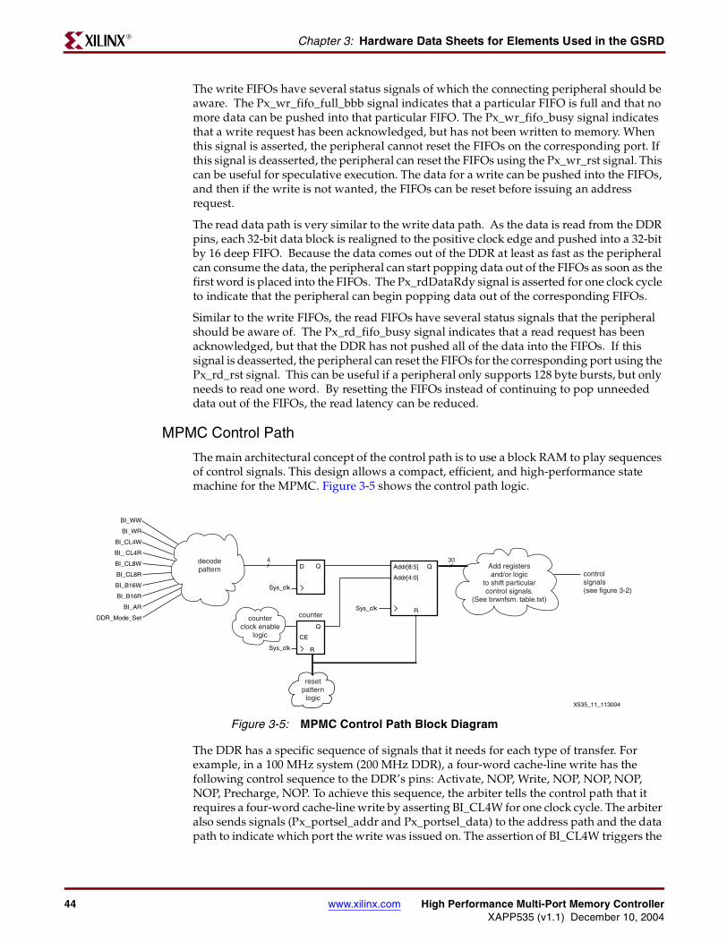
44 www.xilinx.com High Performance Multi-Port Memory ControllerXAPP535 (v1.1) December 10, 2004
Chapter 3: Hardware Data Sheets for Elements Used in the GSRDR
The write FIFOs have several status signals of which the connecting peripheral should be aware. The Px_wr_fifo_full_bbb signal indicates that a particular FIFO is full and that no more data can be pushed into that particular FIFO. The Px_wr_fifo_busy signal indicates that a write request has been acknowledged, but has not been written to memory. When this signal is asserted, the peripheral cannot reset the FIFOs on the corresponding port. If this signal is deasserted, the peripheral can reset the FIFOs using the Px_wr_rst signal. This can be useful for speculative execution. The data for a write can be pushed into the FIFOs, and then if the write is not wanted, the FIFOs can be reset before issuing an address request.
The read data path is very similar to the write data path. As the data is read from the DDR pins, each 32-bit data block is realigned to the positive clock edge and pushed into a 32-bit by 16 deep FIFO. Because the data comes out of the DDR at least as fast as the peripheral can consume the data, the peripheral can start popping data out of the FIFOs as soon as the first word is placed into the FIFOs. The Px_rdDataRdy signal is asserted for one clock cycle to indicate that the peripheral can begin popping data out of the corresponding FIFOs.
Similar to the write FIFOs, the read FIFOs have several status signals that the peripheral should be aware of. The Px_rd_fifo_busy signal indicates that a read request has been acknowledged, but that the DDR has not pushed all of the data into the FIFOs. If this signal is deasserted, the peripheral can reset the FIFOs for the corresponding port using the Px_rd_rst signal. This can be useful if a peripheral only supports 128 byte bursts, but only needs to read one word. By resetting the FIFOs instead of continuing to pop unneeded data out of the FIFOs, the read latency can be reduced.
MPMC Control Path
The main architectural concept of the control path is to use a block RAM to play sequences of control signals. This design allows a compact, efficient, and high-performance state machine for the MPMC. Figure 3-5 shows the control path logic.
The DDR has a specific sequence of signals that it needs for each type of transfer. For example, in a 100 MHz system (200 MHz DDR), a four-word cache-line write has the following control sequence to the DDR’s pins: Activate, NOP, Write, NOP, NOP, NOP, NOP, Precharge, NOP. To achieve this sequence, the arbiter tells the control path that it requires a four-word cache-line write by asserting BI_CL4W for one clock cycle. The arbiter also sends signals (Px_portsel_addr and Px_portsel_data) to the address path and the data path to indicate which port the write was issued on. The assertion of BI_CL4W triggers the
Figure 3-5: MPMC Control Path Block Diagram
X535_11_113004
Add registersand/or logic
to shift particularcontrol signals.
(See brwnfsm. table.txt)
decodepattern
BI_WW
BI_WR
BI_CL4W
BI_ CL4R
BI_CL8W
BI_CL8R
BI_B16W
BI_B16R
BI_AR
DDR_Mode_Set
Sys_clk
D Q4
controlsignals(see figure 3-2)
Sys_clk
Q
CE
R
resetpatternlogic
counterclock enable
logic
Addr[8:5]
Addr[4:0]
Q30
Sys_clk Rcounter
ARCHIVED APPLICATION NOTE - NOT SUPPORTED FOR NEW DESIGNS

High Performance Multi-Port Memory Controller www.xilinx.com 45XAPP535 (v1.1) December 10, 2004
Multi-Port Memory Controller (MPMC)R
correct sequence to be played by the controller. Outputs are sent to the address path, data path, arbiter, and DDR. To reduce the latency, some of these outputs can go through a set of registers to delay the signal rather than increasing the length of the sequence by placing the delay in the sequence. A completed signal (BI_Complete) is asserted as soon as the system permits another request from the arbiter. This allows the system to remove a cycle or two of latency each time the arbiter has a secondary request using pipelining techniques.
The block RAM is initialized through init strings for simulation and synthesis. A simple C program (gen_bram_fsm_init.c) converts a text file (bram_fsm_table.txt) into block RAM init strings for simulation and synthesis. After compiling the C program, run build_bram_init to produce the init strings. Then, copy the init strings into mpmc_ctl_path.v.
Optional: User Compilation of the Block RAM FSM
The Finite State Machine (FSM) for the MPMC can be easily modified by the system designer should the need arise. This step requires access to a C compiler that supports STDIO, such as gcc. The following steps are not required unless there is a need to change the MPMC FSM. The directions assume the use of gcc.
Locate the directory containing the mpmc<version> directory. For example, C:\EDK\gsrd\edk_libs\gsrd_lib\pcores\mpmc<version>. CD to this directory, and then to test\bin\bram_scripts. The directory contains the following files:
bram_fsm.defparambram_fsm.xcpropsbram_fsm.xstbram_fsm_table.txtbuild_bram_init
The bram_fsm_table.txt file can be edited to create the FSM inside the block RAM. A snippet of that file is reproduced below. The format of the file is set up to represent up to 16 patterns of 32 Data Signal Patterns with up to 32 control signals. The values listed in the Data Signal Pattern (horizontals) are the state of the Control Signals (vertical) during the indicated state (0 to 31). To effect a change in the FSM, the system designer must compile a small C program and then run a script to create the intermediate files, which XST requires to properly build the FSM into the block RAM.
To compile the C source file:
1. cd to the test\bin\bram_scripts\bin directory, if not already there.
2. Type gcc - o gen_bram_fsm_init gen_bram_fsm_init.c
3. Type cd ..
4. Type build_bram_init
This creates the following:
bram_fsm.defparamsbram_fsm.xcpropsbram_fsm.xst
5. Copy these three files into the hdl\verilog\mpmc_ctl_path.v file as follows:
− Open files bram_fsm.xxxx file and search for the contents of the ̀ defparam in mpmc_ctl_path.v.
− Replace the existing `defparam contents in mpmc_ctl_path.v with those from the new files.
ARCHIVED APPLICATION NOTE - NOT SUPPORTED FOR NEW DESIGNS
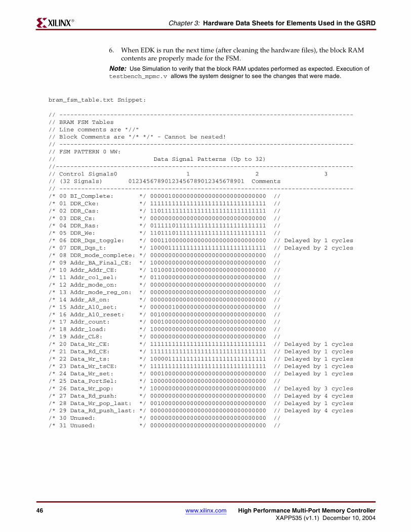
46 www.xilinx.com High Performance Multi-Port Memory ControllerXAPP535 (v1.1) December 10, 2004
Chapter 3: Hardware Data Sheets for Elements Used in the GSRDR
6. When EDK is run the next time (after cleaning the hardware files), the block RAM contents are properly made for the FSM.
Note: Use Simulation to verify that the block RAM updates performed as expected. Execution of testbench_mpmc.v allows the system designer to see the changes that were made.
bram_fsm_table.txt Snippet:
// ---------------------------------------------------------------------------------// BRAM FSM Tables// Line comments are "//"// Block Comments are "/* */" - Cannot be nested!// ---------------------------------------------------------------------------------// FSM PATTERN 0 WW:// Data Signal Patterns (Up to 32) //----------------------------------------------------------------------------------// Control Signals0 1 2 3// (32 Signals) 01234567890123456789012345678901 Comments// ---------------------------------------------------------------------------------/* 00 BI_Complete: */ 00000100000000000000000000000000 ///* 01 DDR_Cke: */ 11111111111111111111111111111111 ///* 02 DDR_Cas: */ 11011111111111111111111111111111 ///* 03 DDR_Cs: */ 00000000000000000000000000000000 ///* 04 DDR_Ras: */ 01111101111111111111111111111111 ///* 05 DDR_We: */ 11011101111111111111111111111111 ///* 06 DDR_Dqs_toggle: */ 00011000000000000000000000000000 // Delayed by 1 cycles/* 07 DDR_Dqs_t: */ 10000111111111111111111111111111 // Delayed by 2 cycles/* 08 DDR_mode_complete: */ 00000000000000000000000000000000 ///* 09 Addr_BA_Final_CE: */ 10000000000000000000000000000000 ///* 10 Addr_Addr_CE: */ 10100010000000000000000000000000 ///* 11 Addr_col_sel: */ 01100000000000000000000000000000 ///* 12 Addr_mode_on: */ 00000000000000000000000000000000 ///* 13 Addr_mode_reg_on: */ 00000000000000000000000000000000 ///* 14 Addr_A8_on: */ 00000000000000000000000000000000 ///* 15 Addr_A10_set: */ 00000010000000000000000000000000 ///* 16 Addr_A10_reset: */ 00100000000000000000000000000000 ///* 17 Addr_count: */ 00010000000000000000000000000000 ///* 18 Addr_load: */ 10000000000000000000000000000000 ///* 19 Addr_CL8: */ 00000000000000000000000000000000 ///* 20 Data_Wr_CE: */ 11111111111111111111111111111111 // Delayed by 1 cycles/* 21 Data_Rd_CE: */ 11111111111111111111111111111111 // Delayed by 1 cycles/* 22 Data_Wr_ts: */ 10000111111111111111111111111111 // Delayed by 1 cycles/* 23 Data_Wr_tsCE: */ 11111111111111111111111111111111 // Delayed by 1 cycles/* 24 Data_Wr_set: */ 00010000000000000000000000000000 // Delayed by 1 cycles/* 25 Data_PortSel: */ 10000000000000000000000000000000 ///* 26 Data_Wr_pop: */ 10000000000000000000000000000000 // Delayed by 3 cycles/* 27 Data_Rd_push: */ 00000000000000000000000000000000 // Delayed by 4 cycles/* 28 Data_Wr_pop_last: */ 00100000000000000000000000000000 // Delayed by 1 cycles/* 29 Data_Rd_push_last: */ 00000000000000000000000000000000 // Delayed by 4 cycles/* 30 Unused: */ 00000000000000000000000000000000 ///* 31 Unused: */ 00000000000000000000000000000000 //
ARCHIVED APPLICATION NOTE - NOT SUPPORTED FOR NEW DESIGNS
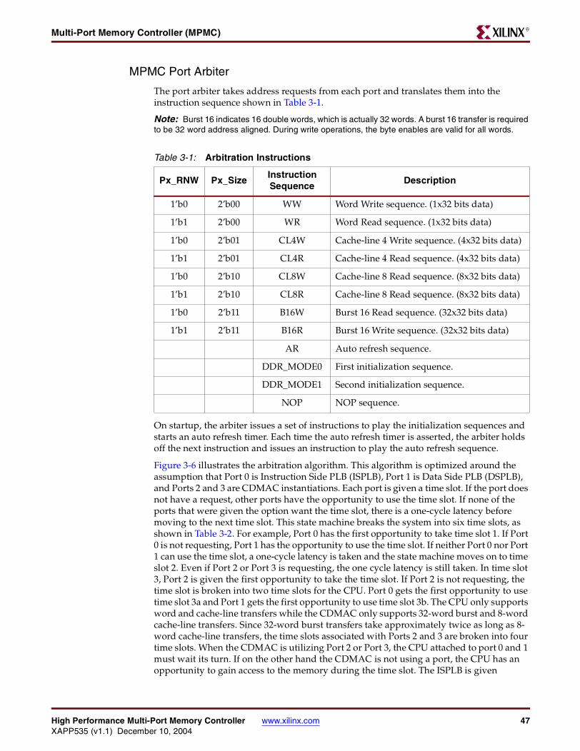
High Performance Multi-Port Memory Controller www.xilinx.com 47XAPP535 (v1.1) December 10, 2004
Multi-Port Memory Controller (MPMC)R
MPMC Port Arbiter
The port arbiter takes address requests from each port and translates them into the instruction sequence shown in Table 3-1.
Note: Burst 16 indicates 16 double words, which is actually 32 words. A burst 16 transfer is required to be 32 word address aligned. During write operations, the byte enables are valid for all words.
On startup, the arbiter issues a set of instructions to play the initialization sequences and starts an auto refresh timer. Each time the auto refresh timer is asserted, the arbiter holds off the next instruction and issues an instruction to play the auto refresh sequence.
Figure 3-6 illustrates the arbitration algorithm. This algorithm is optimized around the assumption that Port 0 is Instruction Side PLB (ISPLB), Port 1 is Data Side PLB (DSPLB), and Ports 2 and 3 are CDMAC instantiations. Each port is given a time slot. If the port does not have a request, other ports have the opportunity to use the time slot. If none of the ports that were given the option want the time slot, there is a one-cycle latency before moving to the next time slot. This state machine breaks the system into six time slots, as shown in Table 3-2. For example, Port 0 has the first opportunity to take time slot 1. If Port 0 is not requesting, Port 1 has the opportunity to use the time slot. If neither Port 0 nor Port 1 can use the time slot, a one-cycle latency is taken and the state machine moves on to time slot 2. Even if Port 2 or Port 3 is requesting, the one cycle latency is still taken. In time slot 3, Port 2 is given the first opportunity to take the time slot. If Port 2 is not requesting, the time slot is broken into two time slots for the CPU. Port 0 gets the first opportunity to use time slot 3a and Port 1 gets the first opportunity to use time slot 3b. The CPU only supports word and cache-line transfers while the CDMAC only supports 32-word burst and 8-word cache-line transfers. Since 32-word burst transfers take approximately twice as long as 8-word cache-line transfers, the time slots associated with Ports 2 and 3 are broken into four time slots. When the CDMAC is utilizing Port 2 or Port 3, the CPU attached to port 0 and 1 must wait its turn. If on the other hand the CDMAC is not using a port, the CPU has an opportunity to gain access to the memory during the time slot. The ISPLB is given
Table 3-1: Arbitration Instructions
Px_RNW Px_SizeInstruction Sequence
Description
1’b0 2’b00 WW Word Write sequence. (1x32 bits data)
1’b1 2’b00 WR Word Read sequence. (1x32 bits data)
1’b0 2’b01 CL4W Cache-line 4 Write sequence. (4x32 bits data)
1’b1 2’b01 CL4R Cache-line 4 Read sequence. (4x32 bits data)
1’b0 2’b10 CL8W Cache-line 8 Read sequence. (8x32 bits data)
1’b1 2’b10 CL8R Cache-line 8 Read sequence. (8x32 bits data)
1’b0 2’b11 B16W Burst 16 Read sequence. (32x32 bits data)
1’b1 2’b11 B16R Burst 16 Write sequence. (32x32 bits data)
AR Auto refresh sequence.
DDR_MODE0 First initialization sequence.
DDR_MODE1 Second initialization sequence.
NOP NOP sequence.
ARCHIVED APPLICATION NOTE - NOT SUPPORTED FOR NEW DESIGNS

48 www.xilinx.com High Performance Multi-Port Memory ControllerXAPP535 (v1.1) December 10, 2004
Chapter 3: Hardware Data Sheets for Elements Used in the GSRDR
preferential access, since the CPU typically would prefer instruction fetch. This is why time slots 3 and 4 are broken into 2 time slots and given to the CPU if the CDMAC does not want to use the time slot. For different applications, this table and state machine can be modified to meet the needs of the system.
In addition to the arbitration algorithm, the ways in which the requests are acknowledged reduce the latency of the system. The first request on each port is acknowledged immediately with a combinational acknowledge. If there is a second request, the system checks if there is room in the FIFOs for the second request and acknowledge the request on the next cycle. Up to three instructions can be in the FIFO at once.
The arbiter is also in control of the read word address signals to the peripheral. There signals tell the peripheral which word is being read out of the FIFOs. For example, if a read request is issued for a cache line transfer at address 0x1C, Px_rdData_Pos will present data in the following order: 0x18, 0x10, 0x08, 0x00. Px_rdData_Neg will present data in the following order: 0x1C, 0x14, 0x0C, 0x04. Px_RdWdAdd_Pos will present values in the following sequence: 0x6, 0x4, 0x2, 0x0. Px_RdWdAdd_Neg will present values in the following sequence: 0x7, 0x5, 0x3, 0x1.
Table 3-2: Arbitration Algorithm
Time Slot
1 2 3a 3b 4a 4b
Priority 1 P0 P1 P2 P3
2 P1 P0 P0 P1 P0 P1
3 P1 P0 P1 P0
Figure 3-6: MPMC Arbitration State Machine
Initialization Start
Time Slot 1 Time Slot 2 Stall Time Slot 3a
Time Slot 4b Stall Time Slot 4a Stall Time Slot 3b
Stall
Stall Stall
sys_rstddr_mode_set
ts1 assert cond
ts1 assertcond
ts3b assertcond
complete ts2 assertcond
complete
complete
completets4a.1 assert cond &&
ts4a.1 assert cond
ts4b assert cond
(ts4a.2 assert cond ||ts4a.3 assert cond)
complete
ddr_mode_complete
ts4b
ass
ert c
ond
ts3a.1 assert cond
ts3a
ass
ert c
ond
ts3a.1 assert cond &&(ts3a.2 assert cond ||ts3a.3 assert cond)
ts2 assert cond
ts4a assert cond ts3b assert cond X535_12_113004
ARCHIVED APPLICATION NOTE - NOT SUPPORTED FOR NEW DESIGNS
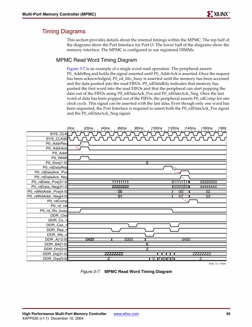
High Performance Multi-Port Memory Controller www.xilinx.com 49XAPP535 (v1.1) December 10, 2004
Multi-Port Memory Controller (MPMC)R
Timing DiagramsThis section provides details about the internal timings within the MPMC. The top half of the diagrams show the Port Interface for Port O. The lower half of the diagrams show the memory interface. The MPMC is configured to use registered DIMMs.
MPMC Read Word Timing Diagram
Figure 3-7 is an example of a single word read operation. The peripheral asserts P0_AddrReq and holds the signal asserted until P0_AddrAck is asserted. Once the request has been acknowledged, P0_rd_fifo_busy is asserted until the memory has been accessed and the data pushed into the read FIFOs. P0_rdDataRdy indicates that memory has pushed the first word into the read FIFOs and that the peripheral can start popping the data out of the FIFOs using P0_rdDataAck_Pos and P0_rdDataAck_Neg. Once the last word of data has been popped out of the FIFOs, the peripheral asserts P0_rdComp for one clock cycle. This signal can be asserted with the last data. Even though only one word has been requested, the Port Interface is required to assert both the P0_rdDataAck_Pos signal and the P0_rdDataAck_Neg signal.
Figure 3-7: MPMC Read Word Timing Diagram
X535_13_113004
0ns 20ns 40ns 60ns 80ns 100ns 120ns 140ns 160ns 180n
SYS_CLKSYS_CLK90P0_AddrReqP0_AddrAck
P0_AddrP0_RNW
P0_Size[1:0]P0_rdDataRdy
P0_rdDataAck_PosP0_rdDataAck_Neg
P0_rdData_Pos[31:0]P0_rdData_Neg[31:0]
P0_rdWdAddr_Pos[4:0]P0_rdWdAddr_Neg[4:0]
P0_rdCompP0_rd_rst
P0_rd_fifo_busyDDR_Cke
DDR_Cs_nDDR_Cas_nDDR_Ras_nDDR_We_n
DDR_A[12:0]DDR_BA[1:0]DDR_Dm[3:0]
DDR_Dq[31:0]DDR_Dqs[3:0]
00
1111111111111111 11111111 333333332222222222222222 22222222 44444444
0000 00 020101 01 03
04000400 0000 040000ZZ
ZZZZZZZZZZZZZZZZ ZZZZZZZZZZ 0 F 0 F 0 Z
ARCHIVED APPLICATION NOTE - NOT SUPPORTED FOR NEW DESIGNS
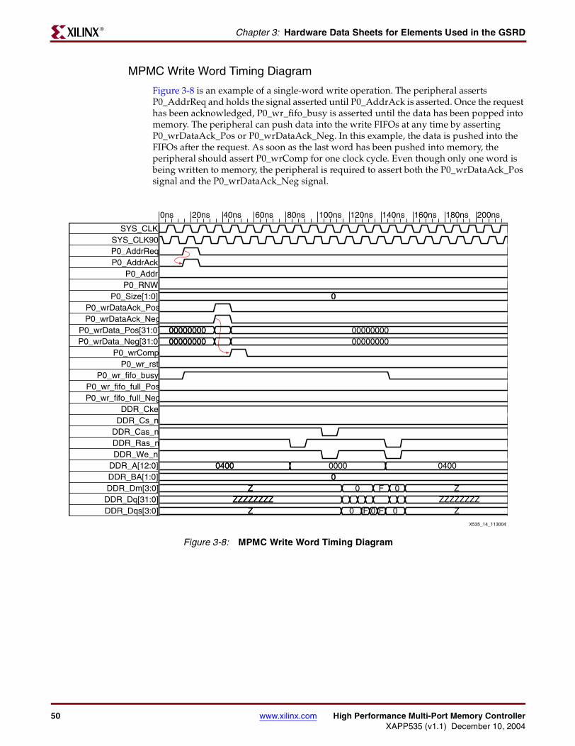
50 www.xilinx.com High Performance Multi-Port Memory ControllerXAPP535 (v1.1) December 10, 2004
Chapter 3: Hardware Data Sheets for Elements Used in the GSRDR
MPMC Write Word Timing Diagram
Figure 3-8 is an example of a single-word write operation. The peripheral asserts P0_AddrReq and holds the signal asserted until P0_AddrAck is asserted. Once the request has been acknowledged, P0_wr_fifo_busy is asserted until the data has been popped into memory. The peripheral can push data into the write FIFOs at any time by asserting P0_wrDataAck_Pos or P0_wrDataAck_Neg. In this example, the data is pushed into the FIFOs after the request. As soon as the last word has been pushed into memory, the peripheral should assert P0_wrComp for one clock cycle. Even though only one word is being written to memory, the peripheral is required to assert both the P0_wrDataAck_Pos signal and the P0_wrDataAck_Neg signal.
Figure 3-8: MPMC Write Word Timing Diagram
X535_14_113004
0ns 20ns 40ns 60ns 80ns 100ns 120ns 140ns 160ns 180ns 200ns
SYS_CLKSYS_CLK90P0_AddrReqP0_AddrAck
P0_AddrP0_RNW
P0_Size[1:0]P0_wrDataAck_PosP0_wrDataAck_Neg
P0_wrData_Pos[31:0]P0_wrData_Neg[31:0]
P0_wrCompP0_wr_rst
P0_wr_fifo_busyP0_wr_fifo_full_PosP0_wr_fifo_full_Neg
DDR_CkeDDR_Cs_n
DDR_Cas_nDDR_Ras_nDDR_We_n
DDR_A[12:0]DDR_BA[1:0]DDR_Dm[3:0]
DDR_Dq[31:0]DDR_Dqs[3:0]
00
0000000000000000 000000000000000000000000 00000000
04000400 0000 040000
ZZ 0 F 0 ZZZZZZZZZZZZZZZZZ ZZZZZZZZ
ZZ 0 F 0 F 0 Z
ARCHIVED APPLICATION NOTE - NOT SUPPORTED FOR NEW DESIGNS
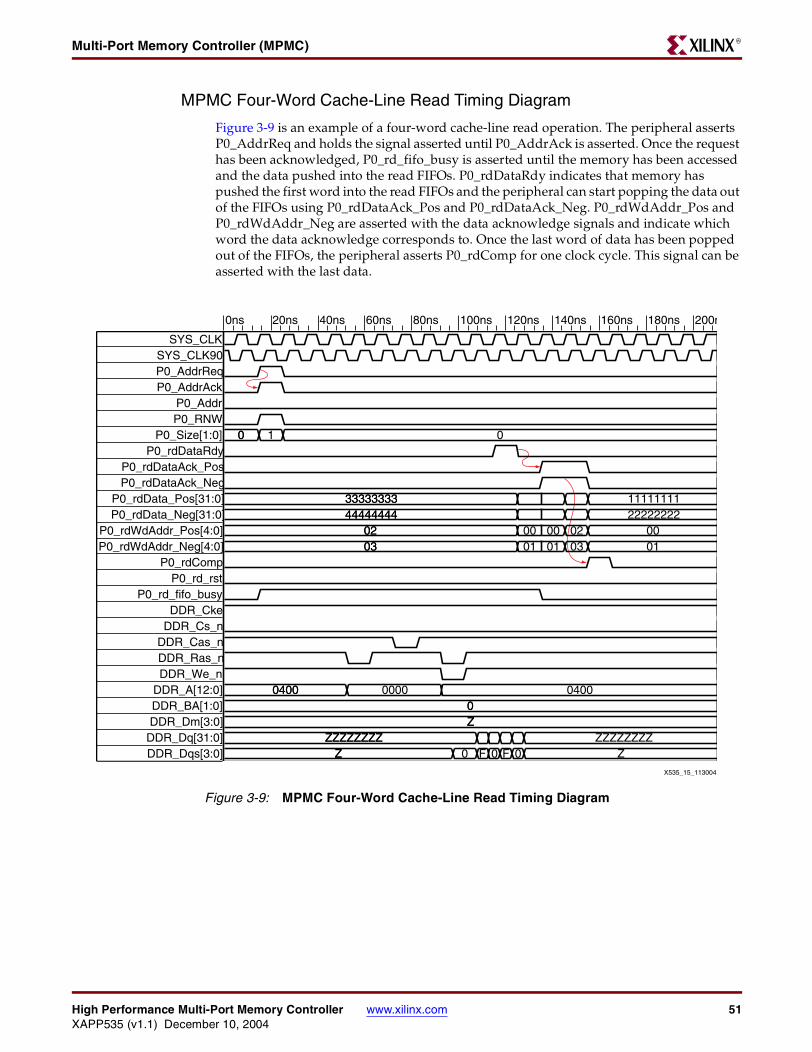
High Performance Multi-Port Memory Controller www.xilinx.com 51XAPP535 (v1.1) December 10, 2004
Multi-Port Memory Controller (MPMC)R
MPMC Four-Word Cache-Line Read Timing Diagram
Figure 3-9 is an example of a four-word cache-line read operation. The peripheral asserts P0_AddrReq and holds the signal asserted until P0_AddrAck is asserted. Once the request has been acknowledged, P0_rd_fifo_busy is asserted until the memory has been accessed and the data pushed into the read FIFOs. P0_rdDataRdy indicates that memory has pushed the first word into the read FIFOs and the peripheral can start popping the data out of the FIFOs using P0_rdDataAck_Pos and P0_rdDataAck_Neg. P0_rdWdAddr_Pos and P0_rdWdAddr_Neg are asserted with the data acknowledge signals and indicate which word the data acknowledge corresponds to. Once the last word of data has been popped out of the FIFOs, the peripheral asserts P0_rdComp for one clock cycle. This signal can be asserted with the last data.
Figure 3-9: MPMC Four-Word Cache-Line Read Timing Diagram
X535_15_113004
0ns 20ns 40ns 60ns 80ns 100ns 120ns 140ns 160ns 180ns 200n
SYS_CLKSYS_CLK90P0_AddrReqP0_AddrAck
P0_AddrP0_RNW
P0_Size[1:0]P0_rdDataRdy
P0_rdDataAck_PosP0_rdDataAck_Neg
P0_rdData_Pos[31:0]P0_rdData_Neg[31:0]
P0_rdWdAddr_Pos[4:0]P0_rdWdAddr_Neg[4:0]
P0_rdCompP0_rd_rst
P0_rd_fifo_busyDDR_Cke
DDR_Cs_nDDR_Cas_nDDR_Ras_nDDR_We_n
DDR_A[12:0]DDR_BA[1:0]DDR_Dm[3:0]
DDR_Dq[31:0]DDR_Dqs[3:0]
00 1 0
3333333333333333 111111114444444444444444 22222222
0202 00 00 02 000303 01 01 03 01
04000400 0000 040000ZZ
ZZZZZZZZZZZZZZZZ ZZZZZZZZZZ 0 F 0 F 0 Z
ARCHIVED APPLICATION NOTE - NOT SUPPORTED FOR NEW DESIGNS
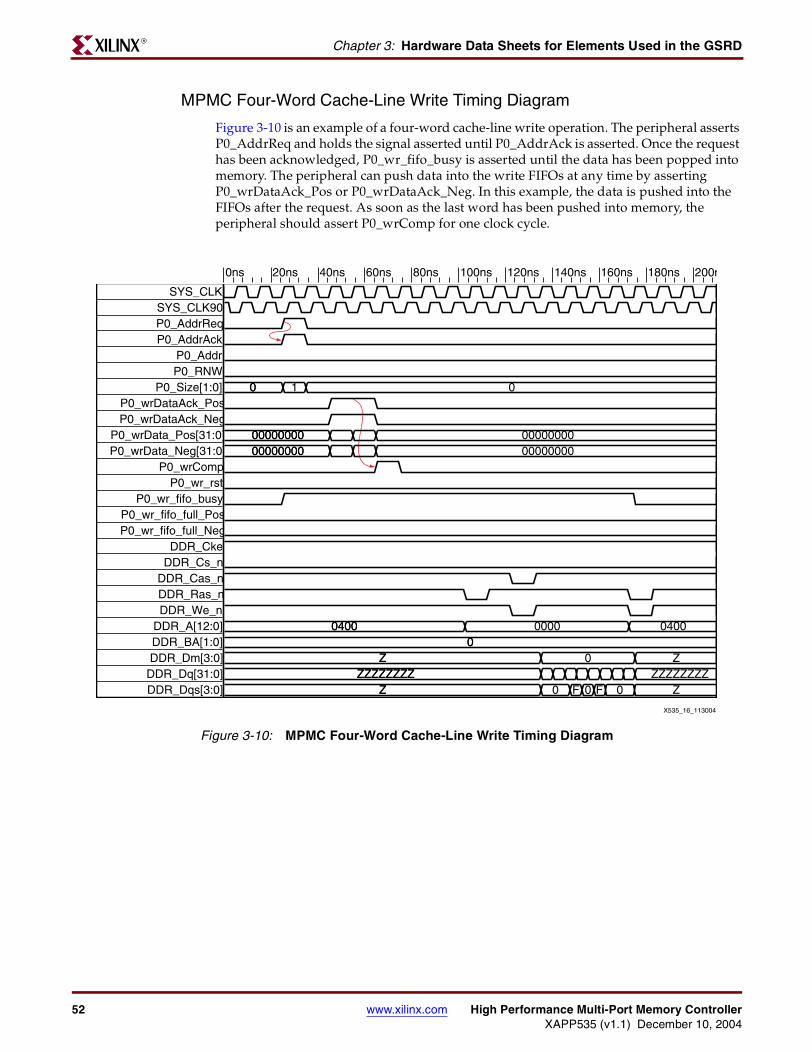
52 www.xilinx.com High Performance Multi-Port Memory ControllerXAPP535 (v1.1) December 10, 2004
Chapter 3: Hardware Data Sheets for Elements Used in the GSRDR
MPMC Four-Word Cache-Line Write Timing Diagram
Figure 3-10 is an example of a four-word cache-line write operation. The peripheral asserts P0_AddrReq and holds the signal asserted until P0_AddrAck is asserted. Once the request has been acknowledged, P0_wr_fifo_busy is asserted until the data has been popped into memory. The peripheral can push data into the write FIFOs at any time by asserting P0_wrDataAck_Pos or P0_wrDataAck_Neg. In this example, the data is pushed into the FIFOs after the request. As soon as the last word has been pushed into memory, the peripheral should assert P0_wrComp for one clock cycle.
Figure 3-10: MPMC Four-Word Cache-Line Write Timing Diagram
X535_16_113004
0ns 20ns 40ns 60ns 80ns 100ns 120ns 140ns 160ns 180ns 200n
SYS_CLKSYS_CLK90P0_AddrReqP0_AddrAck
P0_AddrP0_RNW
P0_Size[1:0]P0_wrDataAck_PosP0_wrDataAck_Neg
P0_wrData_Pos[31:0]P0_wrData_Neg[31:0]
P0_wrCompP0_wr_rst
P0_wr_fifo_busyP0_wr_fifo_full_PosP0_wr_fifo_full_Neg
DDR_CkeDDR_Cs_n
DDR_Cas_nDDR_Ras_nDDR_We_n
DDR_A[12:0]DDR_BA[1:0]DDR_Dm[3:0]
DDR_Dq[31:0]DDR_Dqs[3:0]
00 1 0
0000000000000000 000000000000000000000000 00000000
04000400 0000 040000
ZZ 0 ZZZZZZZZZZZZZZZZZ ZZZZZZZZ
ZZ 0 F 0 F 0 Z
ARCHIVED APPLICATION NOTE - NOT SUPPORTED FOR NEW DESIGNS

High Performance Multi-Port Memory Controller www.xilinx.com 53XAPP535 (v1.1) December 10, 2004
Multi-Port Memory Controller (MPMC)R
MPMC 8-Word Cache-Line Read Timing Diagram
Figure 3-11 is an example of an 8-word cache-line read operation. The peripheral asserts P0_AddrReq and holds the signal asserted until P0_AddrAck is asserted. Once the request has been acknowledged, P0_rd_fifo_busy is asserted until the memory has been accessed and the data pushed into the read FIFOs. P0_rdDataRdy indicates that memory has pushed the first word into the read FIFOs and the peripheral can start popping the data out of the FIFOs using P0_rdDataAck_Pos and P0_rdDataAck_Neg. P0_rdWdAddr_Pos and P0_rdWdAddr_Neg are asserted with the data acknowledge signals and indicate which word the data acknowledge corresponds to. Once the last word of data has been popped out of the FIFOs, the peripheral asserts P0_rdComp for one clock cycle. This signal can be asserted with the last data.
Figure 3-11: MPMC 8-Word Cache-Line Read Timing Diagram
X535_17_113004
0ns 20ns 40ns 60ns 80ns 100ns 120ns 140ns 160ns 180ns 200ns 220
SYS_CLKSYS_CLK90P0_AddrReqP0_AddrAck
P0_AddrP0_RNW
P0_Size[1:0]P0_rdDataRdy
P0_rdDataAck_PosP0_rdDataAck_Neg
P0_rdData_Pos[31:0]P0_rdData_Neg[31:0]
P0_rdWdAddr_Pos[4:0]P0_rdWdAddr_Neg[4:0]
P0_rdCompP0_rd_rst
P0_rd_fifo_busyDDR_Cke
DDR_Cs_nDDR_Cas_nDDR_Ras_nDDR_We_n
DDR_A[12:0]DDR_BA[1:0]DDR_Dm[3:0]
DDR_Dq[31:0]DDR_Dqs[3:0]
00 2 0
1111111111111111 111111112222222222222222 22222222
0000 00 02 04 06 000101 01 03 05 07 01
04000400 0000 0004 040000ZZ
ZZZZZZZZZZZZZZZZ ZZZZZZZZZZ 0 F 0 F 0 F 0 F 0 Z
ARCHIVED APPLICATION NOTE - NOT SUPPORTED FOR NEW DESIGNS

54 www.xilinx.com High Performance Multi-Port Memory ControllerXAPP535 (v1.1) December 10, 2004
Chapter 3: Hardware Data Sheets for Elements Used in the GSRDR
MPMC 8-Word Cache-Line Write Timing Diagram
Figure 3-12 is an example of an 8-word cache-line write operation. The peripheral asserts P0_AddrReq and holds the signal asserted until P0_AddrAck is asserted. Once the request has been acknowledged, P0_wr_fifo_busy is asserted until the data has been popped into memory. The peripheral can push data into the write FIFOs at any time by asserting P0_wrDataAck_Pos or P0_wrDataAck_Neg. In this example, the data is pushed into the FIFOs after the request. As soon as the last word has been pushed into memory, the peripheral should assert P0_wrComp for one clock cycle.
Figure 3-12: MPMC 8-Word Cache-Line Write Timing Diagram
X535_18_113004
0ns 50ns 100ns 150ns 200ns 250ns
SYS_CLKSYS_CLK90P0_AddrReqP0_AddrAck
P0_AddrP0_RNW
P0_Size[1:0]P0_wrDataAck_PosP0_wrDataAck_Neg
P0_wrData_Pos[31:0]P0_wrData_Neg[31:0]
P0_wrCompP0_wr_rst
P0_wr_fifo_busyP0_wr_fifo_full_PosP0_wr_fifo_full_Neg
DDR_CkeDDR_Cs_n
DDR_Cas_nDDR_Ras_nDDR_We_n
DDR_A[12:0]DDR_BA[1:0]DDR_Dm[3:0]
DDR_Dq[31:0]DDR_Dqs[3:0]
00 2 0
0000000000000000 000000000000000000000000 00000000
04000400 0000 0004 040000
ZZ 0 ZZZZZZZZZZZZZZZZZ ZZZZZZZZ
ZZ 0 F 0 F 0 F0 F 0 Z
ARCHIVED APPLICATION NOTE - NOT SUPPORTED FOR NEW DESIGNS

High Performance Multi-Port Memory Controller www.xilinx.com 55XAPP535 (v1.1) December 10, 2004
Multi-Port Memory Controller (MPMC)R
MPMC 32-Word Burst Read Timing Diagram
Figure 3-13 is an example of a 32-word burst read operation. The peripheral asserts P0_AddrReq and holds the signal asserted until P0_AddrAck is asserted. Once the request has been acknowledged, P0_rd_fifo_busy is asserted until the memory has been accessed and the data pushed into the read FIFOs. P0_rdDataRdy indicates that memory has pushed the first word into the read FIFOs and the peripheral can start popping the data out of the FIFOs using P0_rdDataAck_Pos and P0_rdDataAck_Neg. As the peripheral is required to issue requests that are 32-word address aligned, the data comes out of the memory in order. P0_rdWdAddr_Pos and P0_rdWdAddr_Neg are not used in this case and can contain invalid data. Once the last word of data has been popped out of the FIFOs, the peripheral asserts P0_rdComp for one clock cycle. This signal can be asserted with the last data.
Figure 3-13: MPMC 32-Word Burst Read Timing Diagram
X535_19_113004
0ns 50ns 100ns 150ns 200ns 250ns 300ns 35
SYS_CLKSYS_CLK90P0_AddrReqP0_AddrAck
P0_AddrP0_RNW
P0_Size[1:0]P0_rdDataRdy
P0_rdDataAck_PosP0_rdDataAck_Neg
P0_rdData_Pos[31:0]P0_rdData_Neg[31:0]
P0_rdWdAddr_Pos[4:0]P0_rdWdAddr_Neg[4:0]
P0_rdCompP0_rd_rst
P0_rd_fifo_busyDDR_Cke
DDR_Cs_nDDR_Cas_nDDR_Ras_nDDR_We_n
DDR_A[12:0]DDR_BA[1:0]DDR_Dm[3:0]
DDR_Dq[31:0]DDR_Dqs[3:0]
00 3 0
1111111111111111 111111112222222222222222 22222222
0000 00020406080A 0C0E00020406080A0C0E 000101 01030507090B 0D0F01030507090B0D0F 01
04000400 0000 00040008000C001000140018001C 040000ZZ
ZZZZZZZZZZZZZZZZ ZZZZZZZZZZ 0 F0F0F0F0F0F0F0F0F0F0F0F0F0F0F0F0 Z
ARCHIVED APPLICATION NOTE - NOT SUPPORTED FOR NEW DESIGNS

56 www.xilinx.com High Performance Multi-Port Memory ControllerXAPP535 (v1.1) December 10, 2004
Chapter 3: Hardware Data Sheets for Elements Used in the GSRDR
MPMC 32-Word Burst Write Timing Diagram
Figure 3-14 is an example of a 32-word burst write operation. The peripheral asserts P0_AddrReq and holds the signal asserted until P0_AddrAck is asserted. Once the request has been acknowledged, P0_wr_fifo_busy is asserted until the data has been popped into memory. The peripheral can push data into the write FIFOs at any time by asserting P0_wrDataAck_Pos or P0_wrDataAck_Neg. In this example, the data is pushed into the FIFOs after the request. As soon as the last word has been pushed into memory, the peripheral should assert P0_wrComp for one clock cycle.
Figure 3-14: MPMC 32-Word Burst Write Timing Diagram
X535_20_113004
0ns 50ns 100ns 150ns 200ns 250ns 300ns 350ns 400ns 450ns 500n
SYS_CLKSYS_CLK90P0_AddrReqP0_AddrAck
P0_AddrP0_RNW
P0_Size[1:0]P0_wrDataAck_PosP0_wrDataAck_Neg
P0_wrData_Pos[31:0]P0_wrData_Neg[31:0]
P0_wrCompP0_wr_rst
P0_wr_fifo_busyP0_wr_fifo_full_PosP0_wr_fifo_full_Neg
DDR_CkeDDR_Cs_n
DDR_Cas_nDDR_Ras_nDDR_We_n
DDR_A[12:0]DDR_BA[1:0]DDR_Dm[3:0]
DDR_Dq[31:0]DDR_Dqs[3:0]
00 3 0
0000000000000000 000000000000000000000000 00000000
04000400 0000 0004 0008 000C 0010 0014 0018 001C 040000
ZZ 0 ZZZZZZZZZZZZZZZZZ ZZZZZZZZ
ZZ 0 F0F0F0F0F0F0F0F0F0F0F0F0F0F0F0F 0 Z
ARCHIVED APPLICATION NOTE - NOT SUPPORTED FOR NEW DESIGNS

High Performance Multi-Port Memory Controller www.xilinx.com 57XAPP535 (v1.1) December 10, 2004
Multi-Port Memory Controller (MPMC)R
MPMC Pipelined 8-Word Cache-Line Read Timing Diagram
Figure 3-15 is an example of two pipelined, 8-word cache-line read operations. The peripheral asserts P0_AddrReq and holds the signal asserted until P0_AddrAck is asserted. Because a second read is desired, the peripheral continues to assert P0_AddrReq until P0_AddrAck is asserted a second time. Once the first request has been acknowledged, P0_rd_fifo_busy is asserted until the memory has been accessed and the data pushed into the read FIFOs. Because there is a second read pending, P0_rd_fifo_busy is not deasserted until the data for the second read has been pushed into the FIFOs. P0_rdDataRdy is asserted for each read operation and indicates that memory has pushed the first word of the operation into the read FIFOs. At this point, the peripheral can start popping the data out of the FIFOs using P0_rdDataAck_Pos and P0_rdDataAck_Neg. P0_rdWdAddr_Pos and P0_rdWdAddr_Neg are asserted with the data acknowledge signals and indicate which word of the operation the data corresponds to. Once the last word of data for each operation has been popped out of the FIFOs, the peripheral asserts P0_rdComp for one clock cycle. This signal can be asserted with the last data.
Figure 3-15: MPMC Pipelined 8-Word Cache-Line Read Timing Diagram
X535_21_113004
0ns 50ns 100ns 150ns 200ns 250ns
SYS_CLKSYS_CLK90P0_AddrReqP0_AddrAck
P0_AddrP0_RNW
P0_Size[1:0]P0_rdDataRdy
P0_rdDataAck_PosP0_rdDataAck_Neg
P0_rdData_Pos[31:0]P0_rdData_Neg[31:0]
P0_rdWdAddr_Pos[4:0]P0_rdWdAddr_Neg[4:0]
P0_rdCompP0_rd_rst
P0_rd_fifo_busyDDR_Cke
DDR_Cs_nDDR_Cas_nDDR_Ras_nDDR_We_n
DDR_A[12:0]DDR_BA[1:0]DDR_Dm[3:0]
DDR_Dq[31:0]DDR_Dqs[3:0]
00 2 0
1111111111111111 99999999 232323232222222222222222 AAAAAAAA 34343434
0000 00 00 02 04 06 08 00 00 02 04 06 000101 01 01 03 05 07 09 01 01 03 05 07 01
04000400 0000 0004 0400 0000 0004 040000ZZ
ZZZZZZZZZZZZZZZZ ZZZZZZZZ ZZZZZZZZZZ 0 F 0 F0 F 0 F0 Z 0 F0 F 0 F0 F 0 Z
ARCHIVED APPLICATION NOTE - NOT SUPPORTED FOR NEW DESIGNS

58 www.xilinx.com High Performance Multi-Port Memory ControllerXAPP535 (v1.1) December 10, 2004
Chapter 3: Hardware Data Sheets for Elements Used in the GSRDR
MPMC Pipelined 8-Word Cache-Line Write Timing Diagram
Figure 3-16 is an example of two, pipelined 8-word cache-line write operations. The peripheral asserts P0_AddrReq and holds the signal asserted until P0_AddrAck is asserted. The peripheral continues to assert P0_AddrReq until P0_AddrAck is asserted a second time because a second write is desired. Once the request has been acknowledged, P0_wr_fifo_busy is asserted until the data has been popped into memory. There is a second write pending, so P0_wr_fifo_busy is not deasserted until the data for the second write has also been popped into memory. The peripheral can push data into the write FIFOs at any time by asserting P0_wrDataAck_Pos or P0_wrDataAck_Neg. In this example, the data is pushed into the FIFOs after each request. As soon as the last word has been pushed into memory, the peripheral should assert P0_wrComp for one clock cycle.
Figure 3-16: MPMC Pipelined 8-Word Cache-Line Write Timing Diagram
X535_22_113004
0ns 50ns 100ns 150ns 200ns 250ns 300ns 350n
SYS_CLKSYS_CLK90P0_AddrReqP0_AddrAck
P0_AddrP0_RNW
P0_Size[1:0]P0_wrDataAck_PosP0_wrDataAck_Neg
P0_wrData_Pos[31:0]P0_wrData_Neg[31:0]
P0_wrCompP0_wr_rst
P0_wr_fifo_busyP0_wr_fifo_full_PosP0_wr_fifo_full_Neg
DDR_CkeDDR_Cs_n
DDR_Cas_nDDR_Ras_nDDR_We_n
DDR_A[12:0]DDR_BA[1:0]DDR_Dm[3:0]
DDR_Dq[31:0]DDR_Dqs[3:0]
00 2 0
0000000000000000 00000000 000000000000000000000000 00000000 00000000
04000400 0000 0004 0400 0000 0004 040000
ZZ 0 Z 0 ZZZZZZZZZZZZZZZZZ ZZZZZZZZ ZZZZZZZZ
ZZ 0 F0F0F0F 0 Z 0 F0F0F0F 0 Z
ARCHIVED APPLICATION NOTE - NOT SUPPORTED FOR NEW DESIGNS

High Performance Multi-Port Memory Controller www.xilinx.com 59XAPP535 (v1.1) December 10, 2004
Multi-Port Memory Controller (MPMC)R
Simulation and VerificationThere are four testbenches associated with the MPMC: one for the address path; one for the data path; one for the arbiter; and one top-level testbench that contains all four components. These testbenches are very useful for regression testing.
Each testbench default has an associated shell script (in the mpmc<version>/test/bin directory) that runs the test. If applicable, the scripts allow the user to specify a random number seed and the number of cycles for the test to run. If an error occurs, the simulation prints out an error message and pause.
The reference systems also contain a complete simulation environment so that C source code can be compiled, and simulated in the system. Refer to Chapter 2, “Reference Systems,” for more information on the provided reference systems, and their simulation environment.
Address Path Testbench
On each clock cycle, the address path testbench sets the inputs to random values and checks that the outputs are generated correctly.
Data Path Testbench
The data path testbench runs through a sequence of inputs and checks that the outputs are generated correctly.
Arbiter Testbench
The arbiter testbench models how each of the inputs might be generated. The default configuration provides random delays on the inputs.
Top-Level Testbench
The top-level testbench combines the address path, control path, data path, and arbiter. It uses a DDR memory model and models the behavior of the ports through state machines. As read instructions are issued, the data in the memory model is compared against the expected results. The state machines default to provide random instructions for each port, however they can be modified to provide a specific sequence of instructions.
Using the MPMC in a SystemTo use the MPMC in a real system, the user needs to interface to a DDR SDRAM and create four port interfaces. The I/O’s are described in Table 3-3 through Table 3-5. Sample timing diagrams are shown in Figure 3-7 through Figure 3-16. The ports are modeled after IBM’s Core Connect PLB specification, however the optimizations detailed in this section need to be handled by the peripheral or a personality model. The only operations that are permitted are: single word, four-word cache-line, 8-word cache-line, and 32-word bursts. See Table 3-1 for definitions of these operations. The bursts are required to be 32-word address aligned. In all cases, byte enables are valid for each word. The peripheral is also responsible for handling aborts. The peripheral has the option of pushing data into the FIFOs early. This is accomplished by asserting the write data acknowledge signals before the address request is issued.
The data interface is 64-bits wide, but is divided into two 32-bit wide buses. If the data bus on the peripheral is also 64 bits, the first 32 bits are connected to the Pos data bus and the second 32 bits are connected to the Neg data bus. The same is true of the byte enables and the read word address. The data acknowledges should be tied together. If the peripheral is 32-bits wide, the first word of data should be connected to the Pos data bus, the second word to the Neg data bus. In this case, the data acknowledges are separate.
ARCHIVED APPLICATION NOTE - NOT SUPPORTED FOR NEW DESIGNS

60 www.xilinx.com High Performance Multi-Port Memory ControllerXAPP535 (v1.1) December 10, 2004
Chapter 3: Hardware Data Sheets for Elements Used in the GSRDR
The Port Interface has some extra signals that allow the peripheral to be more efficient. The arbiter sends signals to the peripheral indicating whether there is data in the FIFOs and whether a channel is busy. The read and write resets can be used when a channel is not busy. In the case of a read FIFO, after the read data ready signal is asserted, and there are no requests in the queue, the user has the option of popping data out of the FIFO or resetting the FIFO with the read reset. This could be useful to a user if the peripheral only does burst transfers, but only the first word of the burst is needed. The reset eliminates the need for the peripheral to pop the other 31 words out of the FIFOs before another transfer is allowed. For writes, the user can push data into the FIFOs early. However, if the peripheral decides that the data should not be written to memory, the peripheral can assert the write reset once the channel is no longer busy.
Module Port Interface
Table 3-3: MPMC DDR SDRAM I/Os (per the Infineon DDR SDRAM Specification)
Signal I/O Description
DDR_Cke_O Output Clock Enable.
DDR_Cs_O Output Chip Select.
DDR_Cas_O OutputCommand Input. (See the Infineon DDR SDRAM specification.)
DDR_Ras_O OutputCommand Input. (See the Infineon DDR SDRAM specification.)
DDR_We_O OutputCommand Input. (See the Infineon DDR SDRAM specification.)
DDR_A[12:0] Output Address.
DDR_BA[1:0] Output Bank Address.
DDR_BE_I[3:0] Input Data mask input.
DDR_BE_O[3:0] Output Data mask output.
DDR_BE_T[3:0] Output Data mask three-state select.
DDR_Dq_I[31:0] Input Write data input.
DDR_Dq_O[31:0] Output Read data output.
DDR_Dq_T[31 :0] Output Data three-state select.
DDR_Dqs_I[3 :0] Input Write data strobe input.
DDR_Dqs_O[3:0] Output Read data strobe output.
DDR_Dqs_T[3 :0] Output Data strobe three-state select.
Table 3-4: MPMC System Signals
Signal I/O Description
SYS_CLK Input System Clock.
SYS_CLK90 Input System Clock, phase shifted by 90 degrees.
SYS_CLK180 Input System Clock, phase shifted by 180 degrees.
SYS_CLK270 Input System Clock, phase shifted by 270 degrees.
SYS_RST Input System Reset.
ARCHIVED APPLICATION NOTE - NOT SUPPORTED FOR NEW DESIGNS

High Performance Multi-Port Memory Controller www.xilinx.com 61XAPP535 (v1.1) December 10, 2004
Multi-Port Memory Controller (MPMC)R
Table 3-5: MPMC Port Interface Signals (replicated for each of the four ports)
Signal I/O Description
Px_AddrReq InputAddress request. If there is no secondary request, must be deasserted the clock cycle after the address acknowledge.
Px_Addr[31:0] Input Address. Valid during address request.
Px_RNW InputWrite==1’b0Read==1’b1Valid during Address Request.
Px_Size[1:0] Input
Word==2’b00Cache Line 4==2’b01Cache Line 8==2’b10Burst==2’b11Valid during Address Request.
Px_AddrAck Output Acknowledge for address request. Valid for one clock cycle.
Px_rdComp InputIndicates all data has been popped out of the read FIFOs for a given address request. Valid for one clock cycle.
Px_rdDataAck_Neg Input Read data acknowledge for Neg data bus. Valid for one clock cycle.
Px_rdDataAck_Pos Input Read data acknowledge for Pos data bus. Valid for one clock cycle.
Px_rdData_Neg[31:0] OutputNeg read data bus. Data is popped out of the read FIFO when negative clock phase read data acknowledge is asserted.
Px_rdData_Pos[31 :0] OutputPos read data bus. Data is popped out of the read FIFO when positive clock phase read data acknowledge is asserted.
Px_rdData_Rdy OutputOne cycle pulse indicates that data can be pulled out of the read FIFO for a given read address request.
Px_rdWdAddr_Neg[4:0] Output Indicates word to which the Neg data bus read data acknowledge corresponds.
Px_rdWdAddr_Pos[4:0] Output Indicates word to which the Pos data bus read data acknowledge corresponds.
Px_wrComp InputIndicates all data has been pushed into the write FIFOs for a given address request. Valid for one clock cycle.
Px_wrData_Neg[31:0] InputNeg write data bus. Data is pushed into the write FIFO when Neg write data acknowledge is asserted.
Px_wrData_Pos[31:0] InputPos write data bus. Data is pushed into the write FIFO when Pos write data acknowledge is asserted.
Px_wrDataAck_Neg Input Write data acknowledge for Neg data bus. Valid for one clock cycle.
Px_wrDataAck_Pos Input Write data acknowledge for Pos data bus. Valid for one clock cycle.
Px_wrDataBE_Neg[3:0] InputNeg write data bus data masks. Data is pushed into FIFO when Neg write data acknowledge is asserted.
Px_wrDataBE_Pos[3:0] InputPos write data bus data masks. Data is pushed into FIFO when Pos write data acknowledge is asserted.
Px_rd_rst Input Read reset. Can only be asserted while read FIFOs are not busy.
Px_rd_fifo_busy Output Indicates data is being read from memory and pushed into the FIFOs.
Px_wr_rst Input Write reset. Can only be asserted while write FIFOs are not busy.
Px_wr_fifo_busy Output Indicates data is being popped out of the FIFOs and written to memory.
Px_wr_fifo_full_Neg Output Indicates a Neg write data acknowledge cannot be asserted on the next clock cycle.
Px_wr_fifo_full_Pos Output Indicates a Pos write data acknowledge cannot be asserted on the next clock cycle.
Arb_Sync OutputIndicates that the arbitration state machine is in the first clock cycle of time slot 1. See the “MPMC Port Arbiter” section.
ARCHIVED APPLICATION NOTE - NOT SUPPORTED FOR NEW DESIGNS
62 www.xilinx.com High Performance Multi-Port Memory ControllerXAPP535 (v1.1) December 10, 2004
Chapter 3: Hardware Data Sheets for Elements Used in the GSRDR
Communication Direct Memory Access Controller (CDMAC)
OverviewThe CDMAC is designed to provide high-performance DMA for streaming data. Many communication systems utilize point-to-point interconnections because the data is unidirectional, and requires little protocol. The CDMAC provides two channels of receive data and two channels of transmit data. This permits two full duplex communication devices to have data movement via DMA. The CDMAC uses four LocalLink interfaces to communicate with up to four devices. The back end of the CDMAC is designed to connect to two ports of the MPMC. The MPMC interface is sufficiently generic that the CDMAC could be used stand-alone for other applications. The CDMAC also uses the IBM CoreConnect DCR bus for command and status control.
Features• 128-Byte Bursts from memory for data get / put, 32-Byte Bursts for gathering DMA
descriptors
• Four Channels of DMA controlling four LocalLink interfaces, two for transmit, two for receive
• Direct plug in to the Multi-Port MPMC
• Interruptible and stoppable DMA engines on per descriptor basis
• DMA engines broadcast application specific data across the LocalLink interfaces
• Intelligent engine arbitration built in
• Software error detection for DMA transactions
• Simple software use model
• Low FPGA device area overhead
• Designed to be extensible to eight engines without software change
Related DocumentsThe following documents provide additional information:
• LocalLink Specification
• IBM CoreConnect™ Device Control Register Bus: Architecture Specification
ARCHIVED APPLICATION NOTE - NOT SUPPORTED FOR NEW DESIGNS

High Performance Multi-Port Memory Controller www.xilinx.com 63XAPP535 (v1.1) December 10, 2004
Communication Direct Memory Access Controller (CDMAC)R
High-Level Block DiagramFigure 3-17 illustrates a high-level block diagram of how the CDMAC is built. The CDMAC utilizes two MPMC Port Interfaces, four LocalLink interfaces, and a DCR Interface (not shown). The two MPMC Port Interfaces connect the CDMAC into the MPMC's personality module interface. The four LocalLink interfaces provide two full duplex LocalLink devices access to the CDMAC. There are two Tx LocalLink interfaces and two Rx LocalLink interfaces. The DCR Interface allows the CPU to interact with the CDMAC for initiating DMA processes or status gathering.
The CDMAC is designed to greatly simplify the software requirements for DMA operations. Many unique features have been provided to simplify the software device driver, and to reduce the requirement of CPU interactions. While DMA itself relieves the CPU of having to move data, and thus increase the effective CPU availability, the CDMAC further streamlines this process by offering the CPU easy control and access to DMA operations. The CDMAC has configurable options at instantiation time so that the system designer can choose whether the DMA descriptors must be scrubbed by the CPU before the CDMAC reuses it. Scrubbing of DMA descriptors is the process of updating the fields of the descriptor so that they can be reused by the CDMAC. For example, the LocalLink TFT controller is a continuously active repetitive device. It does not require that the CPU service the DMA engine, once it has been set up. In contrast, the LocalLink GMAC Peripheral requires that the CPU scrub the DMA descriptors before they are reused. By providing control over these kinds of areas, the CDMAC is designed to maximize the amount of CPU that is left over for processing elements other than the DMA engines. This leads to a non-obvious substantial benefit in CPU performance.
The CDMAC is designed to connect to Communication devices. It is not intended to be a generic DMA controller. As such, it does not provide nor need an address interface. Instead, it uses a streaming data centric interface. This interface is typical of full duplex communication systems. The GMAC peripheral is an example of a typical full duplex communication system. The GMAC peripheral must be capable of simultaneous
Figure 3-17: CDMAC High-Level Block Diagram
X535_23_113004
TX0LocalLinkInterface
RX0LocalLinkInterface
TX1LocalLinkInterface
RX1LocalLinkInterface
TXLocalLinkInterface
RXLocalLinkInterface
TXLocalLinkInterface
RXLocalLinkInterface
To Multi Port Memory Controller (MPMC)
MPMC Port Interface MPMC Port Interface
CDMAC Engines and Control Logic
ARCHIVED APPLICATION NOTE - NOT SUPPORTED FOR NEW DESIGNS

64 www.xilinx.com High Performance Multi-Port Memory ControllerXAPP535 (v1.1) December 10, 2004
Chapter 3: Hardware Data Sheets for Elements Used in the GSRDR
transmission and reception of data. It uses a unidirectional streaming data bus from GMAC peripheral to CDMAC for receive while using a unidirectional streaming data bus in the opposite direction for transmit. They do not provide any form of address; they simply provide data and a context of the data that allows the data to be properly framed.
One important advantage of the CDMAC architecture is that intelligent processing can be added between the CDMAC and the LocalLink device. Consider the case where a core is built that has various processing capabilities. These capabilities can be added via LocalLink to LocalLink interfaces and inserted in an appropriate order between the CDMAC and the final LocalLink device. This permits system designers to choose how much area they were willing to pay in order to affect a specific level of performance. If more performance is needed, more processing blocks can be instantiated. These blocks are generic because they simply speak the LocalLink protocol.
Theory of Operation
Communication DMA
Modern communication systems typically rely upon unidirectional data transport mechanisms. These unidirectional links allow for streaming data to be sent across standardized interfaces. Typical systems have line cards, which are aggregated together to form a large amount of streaming data. Often this data has to be contextually switched between various points in order to route the data between its origin and its destination. Between these route points, the data is often aggregated into very fast data streams. The CDMAC is designed to directly assist in the movement of this type of data.
Communication DMA then is about moving large quantities of data between the demarcation point and main system memory in a processor-based system. The Communication DMA does not imply that the processor consumes the data. In fact, in some systems, the processor never touches the data, but the data is consumed by another DMA device instead. In high-data-bandwidth systems, the processor generally handles only the administrative functions, such as set up and tear down, rather than be actively involved with the data.
The CDMAC provides an interface between the MPMC and four independent channels of DMA using LocalLink interface. Figure 3-17 shows the high-level diagram view of the CDMAC, and illustrates the four LocalLink interfaces and two port interfaces to the MPMC. The CDMAC provides two channels of transmit and two channels of receive. Each channel uses the Xilinx DS230 LocalLink Interface specification. These four LocalLink interfaces are on one side of the CDMAC, while two MPMC port interfaces are contained on the other.
Two LocalLink interfaces are matched as a full duplex link per port. That is, each MPMC port has attached a single transmit and single receive DMA engine with corresponding Rx and TX LocalLink devices.
ARCHIVED APPLICATION NOTE - NOT SUPPORTED FOR NEW DESIGNS

High Performance Multi-Port Memory Controller www.xilinx.com 65XAPP535 (v1.1) December 10, 2004
Communication Direct Memory Access Controller (CDMAC)R
Figure 3-18 introduces a simplified block diagram that illustrates the major functional elements of the CDMAC. See the “CDMAC Architecture” section for more information on the internals of the CDMAC.
The CDMAC offers a wide variety of features to augment communication style interfaces. Communication style interfaces differ from classical DMA because they provide structural control over the data. For example, a communication system typically needs to packetize its data in order to allow for transmission and reception errors. In classical DMA there is no need to packetize the data because the device being DMA'd to/from is directly consuming the data and errors are effectively impossible. The CDMAC differs from classical DMA controllers primarily because it supports the notion of packetized data. However, the CDMAC also offers other important mechanisms that make communication systems easier to implement.
The CDMAC provides for the ability to dynamically control the context of each engine through the DMA descriptors. These descriptors do not just provide the buffer context. They also provide control context by interrupts, halting the engine, and indication of CDMAC status. Further, the descriptors offer the ability to transmit and receive application unique data across the LocalLink interfaces and directly to and from the descriptors. These features provide for substantially simpler software interfaces, and less processor intervention to support the DMA transactions.
Figure 3-18: CDMAC Top Level Block Diagram
X535_24_113004
RX0LL
TX0LL
RX1LL
TX1LL
CDMAC Top
CDMACWrapper
CPU
INT
DCR Interface
LocalLinkPeripherals
Port Interface / MPMC
Data Path Control Path DCR
Port 2 Port 3
ARCHIVED APPLICATION NOTE - NOT SUPPORTED FOR NEW DESIGNS
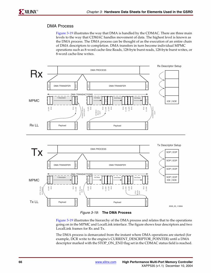
66 www.xilinx.com High Performance Multi-Port Memory ControllerXAPP535 (v1.1) December 10, 2004
Chapter 3: Hardware Data Sheets for Elements Used in the GSRDR
DMA Process
Figure 3-19 illustrates the way that DMA is handled by the CDMAC. There are three main levels to the way that CDMAC handles movement of data. The highest level is known as the DMA process. The DMA process can be thought of as the execution of an entire chain of DMA descriptors to completion. DMA transfers in turn become individual MPMC operations such as 8-word cache-line Reads, 128-byte burst reads, 128-byte burst writes, or 8-word cache-line writes.
Figure 3-19 illustrates the hierarchy of the DMA process and relates that to the operations going on in the MPMC and LocalLink interface. The figure shows four descriptors and two LocalLink frames for Rx and Tx.
The DMA process is demarcated from the instant where DMA operations are started (for example, DCR write to the engine's CURRENT_DESCRIPTOR_POINTER) until a DMA descriptor marked with the STOP_ON_END flag set in the CDMAC status field is reached.
Figure 3-19: The DMA Process
DMA PROCESS
DMA TRANSFER DMA TRANSFER
SO
F
SO
F
EO
F
EO
F
CL
8R
CD
MA
C
Ma
rks
SO
P
CL
8R
CL
8W
SO
P/E
OP
SO
P
Payload
He
ad
er
Fo
ote
r
Payload
He
ad
er
Fo
ote
r
Rx LL
Tx LL
Payload
He
ad
er
Fo
ote
r
CL
8R
CL
8W
CL
8R
CL
8W
EO
P
Payload
He
ad
er
Fo
ote
r
MPMC1 Descriptor 1st Desc 2nd Desc 3rd Desc
DMA TRANSACTIONS
B3
2
B3
2
CL
8R
CL
8W
SO
P/E
OP
MPMC1 Descriptor
B3
2
B3
2
Rx Descriptor Setup
Tx Descriptor Setup
B3
2
B3
2
B3
2
B3
2
B3
2
B3
2
CL
8R
CL
8W
SO
P
CL
8R
CL
8W
CL
8R
CL
8W
EO
P
1st Desc 2nd Desc 3rd Desc
B3
2
B3
2
B3
2
B3
2
B3
2
B3
2
SOP | EOP
SOP | EOP
SOP | EOP
SOP | EOPIOE | SOE
IOE | SOE
DMA PROCESS
DMA TRANSFER DMA TRANSFER
SO
F
SO
F
EO
F
EO
F
Rx
TxC
DM
AC
Ma
rks
EO
PCL
8W
CD
MA
C M
ark
s
SO
P/E
OP
DMA TRANSACTIONS
CP
U M
ark
s
SO
P
CP
U M
ark
s
SO
P/E
OP
CP
U
Ma
rks
EO
P
X535_25_113004
ARCHIVED APPLICATION NOTE - NOT SUPPORTED FOR NEW DESIGNS

High Performance Multi-Port Memory Controller www.xilinx.com 67XAPP535 (v1.1) December 10, 2004
Communication Direct Memory Access Controller (CDMAC)R
The DMA transfer is demarcated by the descriptor(s), which contain a START_OF_PACKET and END_OF_PACKET, and thus represent one LocalLink Header, Payload, and Footer. For Rx, the START_OF_PACKET and END_OF_PACKET come from the LocalLink SOF, EOF signals and are written back into the descriptor(s) as the DMA transactions complete. This is in contrast with Tx, where in START_OF_PACKET and END_OF_PACKET are set by the CPU and control when the LocalLink interface issues the SOF / EOF signals.
The DMA transactions are individual MPMC operations such as 8-word cache-line write (CL8W), 8-word cache-line read (CL8R), 128-byte burst write (B32W) and 128-byte burst read (B32R). When put together, these comprise the individual pieces of a DMA transfer. DMA transactions are atomic units: once a DMA transaction begins on the MPMC, both the MPMC and CDMAC are locked together until the MPMC completes the memory operation.
Figure 3-19 shows how Rx and Tx differ in handling the LocalLink framing flags. During Tx, the START_OF_PACKET and END_OF_PACKET flags in the descriptors are used to send the SOF and EOF signals across the LocalLink interface. In contrast, during Rx operations these flags are actually set by the LocalLink interface, and are written back into the descriptor once the descriptor has been successfully processed. In the three descriptor Rx case the START_OF_PACKET flag is set in the first descriptor during its CL8W writeback while the END_OF_PACKET flag is set in the last (for example, third) descriptor during its CL8W writeback. Rx descriptors must always have their START_OF_PACKET and END_OF_PACKET flags cleared prior to the onset of DMA operations, or the CDMAC responds improperly. This is one of the elements that must be addressed during CDMAC scrubbing operations.
The conclusion of the DMA process is also shown in Figure 3-19. To end a DMA process, the CDMAC engine must encounter a descriptor with the STOP_ON_END flag set. The very last descriptors of both the Rx and Tx examples show this bit being set. The CDMAC processes DMA descriptors continually until it reaches a descriptor with the STOP_ON_END flag set. This descriptor executes to completion, and then the CDMAC engine stops in an orderly fashion. In the example, the INT_ON_END flag is also set in the descriptor. After the CDMAC engine has executed this descriptor to completion, it sets the appropriate bit in the CDMAC Interrupt Status Register, and generates a CDMAC_INT, if enabled.
Figure 3-20 shows a simple example of how a DMA process progresses for a Tx DMA engine. DMA Process #1 is the entirety of all operations performed. In this case, three separate descriptors are used for the DMA process. The first two descriptors demarcate the first packet of data to be transmitted across the LocalLink interface. The third descriptor demarcates an entire packet within a single descriptor. The first two descriptors make up the first DMA transfer, and the last descriptor makes up the second DMA transfer. This figure graphically shows that a DMA transfer is the movement of a packet of data across the LocalLink interface, regardless of how many descriptors it takes to declare the packet. Finally note that each box represents a separate DMA transactions. DMA transactions are memory operations to the MPMC. In this example, three types of DMA transactions are performed: 8-word reads, 32-word reads, and 8-word writes. Each time the MPMC must do a memory operation, a DMA transaction is considered to have been performed. The number of DMA transactions is always at least three for a DMA transfer. This is because there is always a reading of the descriptor, at least one transfer of data, and a writing of the descriptor. There can be many more DMA transactions as dictated by the buffer size field of the descriptor modulo 128 bytes.
ARCHIVED APPLICATION NOTE - NOT SUPPORTED FOR NEW DESIGNS

68 www.xilinx.com High Performance Multi-Port Memory ControllerXAPP535 (v1.1) December 10, 2004
Chapter 3: Hardware Data Sheets for Elements Used in the GSRDR
Figure 3-20: CDMAC Illustration of Tx Engine Flow
RD
C
L8
R
Tx
D
B1
6R
Tx
D
B1
6R
Tx
D
B1
6R
Tx
D
B1
6R
WD
C
L8
W
RD
C
L8
R
Tx
D
B1
6R
Tx
D
B1
6R
Tx
D
B1
6R
Tx
D
B1
6R
WD
C
L8
W
RD
C
L8
R
Tx
D
B1
6R
Tx
D
B1
6R
Tx
D
B1
6R
Tx
D
B1
6R
WD
C
L8
W
DMA DESCRIPTOR #1 DMA DESCRIPTOR #2 DMA DESCRIPTOR #3
SO
P
EO
P
SO
P &
EO
P &
ST
OP
_O
N_
EN
D
CO
MP
LET
ED
CO
MP
LET
ED
CO
MP
LET
ED
DMA TRANSFER #1 DMA TRANSFER #2
DMA PROCESS #1
Where:RD - Read DescriptorTxD - Transmit DataWD - Write DescriptorCL8R - 8 word cache line readCL8W - 8 word cache line writeB16R - 16 doubleword burst read
X535_26_113004
DM
A T
rans
actio
n
DM
A T
rans
actio
n
DM
A T
rans
actio
n
DM
A T
rans
actio
n
DM
A T
rans
actio
n
DM
A T
rans
actio
n
DM
A T
rans
actio
n
DM
A T
rans
actio
n
DM
A T
rans
actio
n
DM
A T
rans
actio
n
DM
A T
rans
actio
n
DM
A T
rans
actio
n
DM
A T
rans
actio
n
DM
A T
rans
actio
n
DM
A T
rans
actio
n
DM
A T
rans
actio
n
DM
A T
rans
actio
n
DM
A T
rans
actio
n
ARCHIVED APPLICATION NOTE - NOT SUPPORTED FOR NEW DESIGNS

High Performance Multi-Port Memory Controller www.xilinx.com 69XAPP535 (v1.1) December 10, 2004
Communication Direct Memory Access Controller (CDMAC)R
DMA Descriptor Model
The CDMAC is controlled by DMA descriptors. The DMA descriptors are initialized by the CPU prior to starting the DMA engine. The current implementation of the CDMAC contains four independent engines that can be simultaneously processing four different DMA descriptors or chains of DMA descriptors. Figure 3-21 illustrates the DMA descriptor model. The software use model and register model for CDMAC are contained in “CDMAC Software Model.”
The DMA descriptor must be 8-word aligned in its base address. This is required so that the CDMAC does not have to be inordinately complex and large. Generally, this does not place a large burden on software developers, so long as they are aware of the limitation up front.
The descriptor uses eight words. The first three are used exclusively by the CDMAC while the forth word contains some CDMAC information. The final words are designed to be used by the application that is using the particular CDMAC engine. The first word contains a pointer to the next descriptor. This allows the CDMAC to continue to run until the pointer is either NULL or the engine has otherwise been instructed to stop. The second word in the descriptor contains a byte-aligned address, which points to the location of the data buffer to be moved. The third word in the descriptor contains the number of bytes to move. In the fourth word, the upper byte is used to house control and status information for the CDMAC, see Figure 3-22. The last three bytes of the fourth word, and the last three words are made available to the application, and are broadcast over the LocalLink interface at appropriate times.
An important detail about the APPLICATION DEFINED fields: They are only broadcast down the LocalLink interface during the first Tx Descriptor that sets the SOP bit on the LocalLink interface. Subsequent descriptors in the same LocalLink payload do not have the fields sent because they do not cause a LocalLink header operation. Similarly, for Rx, the APPLICATION DEFINED fields are only written back to the last DMA descriptor that was in process with the LocalLink interface encountered and EOP. If the Rx was made up of several descriptors for that LocalLInk payload, only the last descriptor gets the fields updated.
Figure 3-21: CDMAC DMA Descriptor Model
X535_27_113004
Application Defined
Application Defined
Application Defined
0 31
0x00
0x04
0x08
0x0C
0x10
0x14
0x18 Application Defined
BUFFER LENGTH
BUFFER ADDRESS
NEXT DESCRIPTOR POINTER
0x1C
0
1
2
3
4
5
6
7
STATUS
Application Defined
DATA BUFFER
POINTER MUST BE8 WORD ALIGNED!
32-b
it W
ord
Cou
nt
Byt
e O
ffset
MS
B
LSB
BU
FF
ER
LE
NG
TH
ARCHIVED APPLICATION NOTE - NOT SUPPORTED FOR NEW DESIGNS

70 www.xilinx.com High Performance Multi-Port Memory ControllerXAPP535 (v1.1) December 10, 2004
Chapter 3: Hardware Data Sheets for Elements Used in the GSRDR
The descriptor's STATUS field is shown in Figure 3-22. This field contains two main parts: the CDMAC STATUS field, and an APPLICATION DEFINED field. The STATUS field provides the CDMAC with inputs during the read of the descriptor to know what to do. Similarly, when the descriptor is written back to memory upon completion, certain bits are updated. Not all bits are read during DMA transaction descriptor read, nor are all bits updated during DMA transaction descriptor writes.
The two CDMAC_START_OF_PACKET and CDMAC_END_OF_PACKET bits are used to help frame the LocalLink interface. There use differs from Rx to Tx. The bits are set by the LocalLink interface when the descriptor is in use for Rx. The bits are set by the CPU during Tx operations to control the LocalLink interface. The START_OF_PACKET is used to indicate the LocalLink interface initiates a header for this transaction. Similarly, the END_OF_PACKET bit is used to indicate the LocalLink interface initiates a footer for this transaction. The bits can be mixed and matched. For example, in Tx, three descriptors might be defined to communicate a full payload of data across the LocalLink interface. The first descriptor would be marked START_OF_PACKET, the second neither, and the third marked as END_OF_PACKET. This allows the chaining of non-contiguous data buffers into an apparently contiguous data payload across the LocalLink interface.
When set in the descriptor, the CDMAC_INT_ON_END bit causes the CDMAC to generate a CPU interrupt, and sets the appropriate interrupt flag in the INTERRUPT register. The interrupt is sent to the CPU only if the MIE bit is set in the INTERRUPT register, and the CDMAC has completed all the data move specified by the descriptor.
When set in the descriptor, the CDMAC_STOP_ON_END bit causes the CDMAC to stop DMA operations upon the successful completion of the current descriptor. This stop allows the CDMAC to be brought to an orderly halt and restarted by the CPU when appropriate. The CDMAC_INT_ON_END and CDMAC_STOP_ON_END bits can be mixed and matched together to effect the best operation that software can contextually require.
The CDMAC_COMPLETED bit is written back to the descriptor upon the successful completion of the DMA transfer specified by that descriptor. This
Figure 3-22: CDMAC Descriptor, STATUS field
MS
B
LS
B
25 26 27 2821 22 23 2417 18 19 2013 14 15 1612 29 30 318 9 10 114 5 6 70 1 2 3
DESCRIPTOR_Base + 0x0C
APPLICATION DEFINED
CD
MA
C_
INT
_O
N_
EN
D
CD
MA
C_
ST
OP
_O
N_
EN
D
CD
MA
C_
CO
MP
LET
ED
CD
MA
C_
ST
AR
T_
OF
_P
AC
KE
T
CD
MA
C_
EN
D_
OF
_P
AC
KE
T
CD
MA
C_
EN
GIN
E_
BU
SY
RE
SE
RV
ED
CD
MA
C_
ER
RO
R
CDMAC DESCRIPTOR STATUS FIELD
STATUS FIELD APPLICATION DEFINED FIELDX535_28_113004
ARCHIVED APPLICATION NOTE - NOT SUPPORTED FOR NEW DESIGNS
High Performance Multi-Port Memory Controller www.xilinx.com 71XAPP535 (v1.1) December 10, 2004
Communication Direct Memory Access Controller (CDMAC)R
Tx Descriptor Operations
To start Tx operations, the CPU writes a pointer to the first descriptor in the chain to the CURRENT DESCRIPTOR POINTER register. The CDMAC begins by reading the descriptor that is pointed at by its CURRENT DESCRIPTOR POINTER register. During the read of the descriptor, the CDMAC memorizes the data in the first four words, and passes all 8 words from the descriptor to the LocalLink interface, if the descriptor was marked START_OF_PACKET. Only when the START_OF_PACKET is marked in the descriptor can the CDMAC create a LocalLink header on the LocalLink interface.
Figure 3-24 shows an example of how the LocalLink interface works while Figure 3-23 shows an example of how Tx descriptors might be chained together. In the case of these examples, the DMA descriptors are set such that a single descriptor corresponds to a single LocalLink Payload transfer, including header, payload and footer.
The STATUS field and APPLICATION DEFINED fields are broadcast during the header portion of the LocalLink transaction. These fields are placed on the LocalLink interface only when the descriptor had the START_OF_PACKET set in the STATUS field.
Once the LocalLink header phase has completed, The CDMAC transfers the data pointed to by the BUFFER ADDRESS from memory to the LocalLink interface as data during the payload phase. The CDMAC continues to transfer data and count down the BUFFER LENGTH field to zero, and then attempts to get the next descriptor. If the Next Descriptor Pointer field is null (for example, 0x00000000), then the DMA engine stops. If it is non-zero, and a STOP_ON_END has not been issued in the current descriptor, then the CDMAC transfers the contents of the NEXT DESCRIPTOR POINTER register into the CURRENT DESCRIPTOR POINTER register. The act of transfer reinitializes the CDMAC to go fetch the descriptor pointed by CURRENT DESCRIPTOR POINTER. It can be thought of as the CPU writing the CURRENT DESCRIPTOR POINTER again to initiate the CDMAC. The DMA process continues until the CDMAC encounters a NULL pointer in the NEXT DESCRIPTOR POINTER, or a STOP_ON_END in the STATUS field.
Rx Descriptor Operations
The Rx operation is very similar to the Tx. It begins by reading the descriptor pointed at by the CURRENT DESCRIPTOR POINTER. During the read of the descriptor, the CDMAC memorizes the data in the first four words, but does NOT send it down the LocalLink interface during the header. This is because LocalLink is a unidirectional interface, and the data is 'pointing' in the wrong direction. The CDMAC only receives data from the Rx LocalLink device. While the header time is maintained across the LocalLink interface, there is no valid data contained.
The CDMAC exits the header with the Rx LocalLink device issues a SOP signal. The CDMAC then receives data from the LocalLink interface during the payload phase and stores the data to memory at the addressed pointed to by the BUFFER ADDRESS. This process continues until one of two things happens: An EOP is received indicating the end of the payload, or the BUFFER LENGTH decrements to zero. If the BUFFER LENGTH decrements to zero, an error has occurred and the CDMAC halts operations.
Once the EOP is received, the CDMAC begins to receive the footer. The footer contains the APPLICATION DEFINED fields, which are then written back to the memory, along with the current STATUS. It is very important to note that only the descriptor that has the END_OF_PACKET bit marked has valid data in the APPLICATION DEFINED section of the descriptor. It is also useful to note that the CDMAC does not overwrite the STATUS and APPLICATION DEFINED sections of other descriptors that is not marked END_OF_PACKET. This could be useful for internal device driver storage if it can be guaranteed that the descriptor not get an EOP.
ARCHIVED APPLICATION NOTE - NOT SUPPORTED FOR NEW DESIGNS
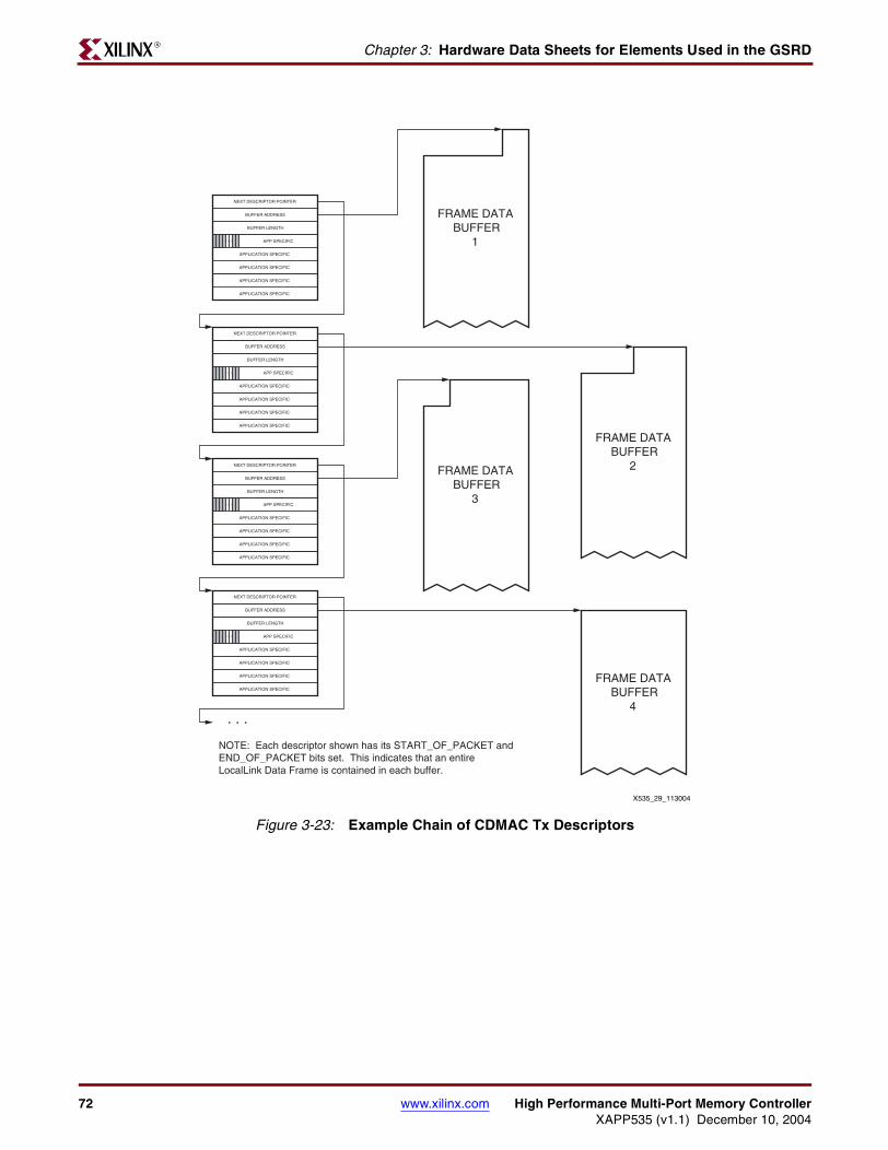
72 www.xilinx.com High Performance Multi-Port Memory ControllerXAPP535 (v1.1) December 10, 2004
Chapter 3: Hardware Data Sheets for Elements Used in the GSRDR
Figure 3-23: Example Chain of CDMAC Tx Descriptors
X535_29_113004
FRAME DATA BUFFER
2
FRAME DATABUFFER
4. . .
FRAME DATA BUFFER
1
FRAME DATA BUFFER
3
NOTE: Each descriptor shown has its START_OF_PACKET andEND_OF_PACKET bits set. This indicates that an entireLocalLink Data Frame is contained in each buffer.
BUFFER LENGTH
BUFFER ADDRESS
NEXT DESCRIPTOR POINTER
APPLICATION SPECIFIC
APPLICATION SPECIFIC
APPLICATION SPECIFIC
APP SPECIFIC
APPLICATION SPECIFIC
1 1
BUFFER LENGTH
BUFFER ADDRESS
NEXT DESCRIPTOR POINTER
APPLICATION SPECIFIC
APPLICATION SPECIFIC
APPLICATION SPECIFIC
APP SPECIFIC
APPLICATION SPECIFIC
1 1
BUFFER LENGTH
BUFFER ADDRESS
NEXT DESCRIPTOR POINTER
APPLICATION SPECIFIC
APPLICATION SPECIFIC
APPLICATION SPECIFIC
APP SPECIFIC
APPLICATION SPECIFIC
1 1
BUFFER LENGTH
BUFFER ADDRESS
NEXT DESCRIPTOR POINTER
APPLICATION SPECIFIC
APPLICATION SPECIFIC
APPLICATION SPECIFIC
APP SPECIFIC
APPLICATION SPECIFIC
1 1
ARCHIVED APPLICATION NOTE - NOT SUPPORTED FOR NEW DESIGNS

High Performance Multi-Port Memory Controller www.xilinx.com 73XAPP535 (v1.1) December 10, 2004
Communication Direct Memory Access Controller (CDMAC)R
LocalLink Interface Usage
The CDMAC has four DMA engines. Each DMA engine is associated with a LocalLink interface. Two of the DMA engines are used for transmit, and two are used for receive. A single transmit DMA engine is paired up with a single receive DMA engine to form a full duplex communication channel. There are two full duplex communication channels in the CDMAC. Each full duplex communication challenge occupies a single MPMC port. This is why the current CDMAC uses two of the MPMC ports. See Figure 3-17 and Figure 3-18 for simplified CDMAC structure diagrams.
Figure 3-25 shows an example of the CDMAC Tx DMA engine’s LocalLink Tx interface. This interface provides read data from the CDMAC. One important aspect of the communication style of DMA is that is depends upon the use of streaming data interfaces. As such, it has no address context. The data simply is transferred across the interface when both sides agree (via RDY signals) that it is time to do so.
The LocalLink interface provides for the ability to transmit encapsulated data. The data itself is embedded in a 'package' that has a header and a footer. The START_OF_FRAME signal initiates the header of the package. Between the time this signal starts, and the time the START_OF_PAYLOAD signal occurs, the header of the package is being transmitted. Between the START_OF_PAYLOAD and END_OF_PAYLOAD signal, the data of the package is being transmitted. Finally, all information transmitted between the END_OF_PAYLOAD and END_OF_FRAME signal delete constitutes a header. In this way, the LocalLink interface permits the encapsulation of data content into a standardized package.
Figure 3-24: CDMAC LocalLink Interface General Purpose Example
X535_30_113004
FIRST CDMAC DESCRIPTOR ...
...
...
...
...
...
...
...
...
...
DATADATA
... ...
LAST CDMAC DESCRIPTOR
CLK
EOF_N
EOP_N
DST_RDY_N
SRC_RDY_N
D[ 31 : 0]
SOP_N
SOF_N
REM[ 3: 0] ... ...
...
...
...
...
LocalLink Header LocalLink Payload LocalLink Footer
ARCHIVED APPLICATION NOTE - NOT SUPPORTED FOR NEW DESIGNS
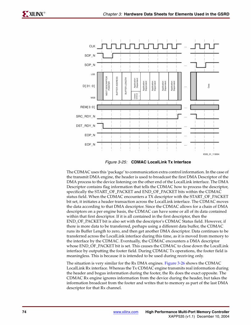
74 www.xilinx.com High Performance Multi-Port Memory ControllerXAPP535 (v1.1) December 10, 2004
Chapter 3: Hardware Data Sheets for Elements Used in the GSRDR
The CDMAC uses this ‘package’ to communication extra control information. In the case of the transmit DMA engine, the header is used to broadcast the first DMA Descriptor of the DMA process to the device listening on the other end of the LocalLink interface. The DMA Descriptor contains flag information that tells the CDMAC how to process the descriptor, specifically the START_OF_PACKET and END_OF_PACKET bits within the CDMAC status field. When the CDMAC encounters a TX descriptor with the START_OF_PACKET bit set, it initiates a header transaction across the LocalLink interface. The CDMAC moves the data according to that DMA descriptor. Since the CDMAC allows for a chain of DMA descriptors on a per engine basis, the CDMAC can have some or all of its data contained within that first descriptor. If it is all contained in the first descriptor, then the END_OF_PACKET bit is also set with the descriptor's CDMAC Status field. However, if there is more data to be transferred, perhaps using a different data buffer, the CDMAC runs its Buffer Length to zero, and then get another DMA descriptor. Data continues to be transferred across the LocalLink interface during this time, as it is moved from memory to the interface by the CDMAC. Eventually, the CDMAC encounters a DMA descriptor whose END_OF_PACKET bit is set. This causes the CDMAC to close down the LocalLink interface by outputting the footer field. During CDMAC Tx operations, the footer field is meaningless. This is because it is intended to be used during receiving only.
The situation is very similar for the Rx DMA engines. Figure 3-26 shows the CDMAC LocalLink Rx interface. Whereas the Tx CDMAC engine transmits real information during the header and bogus information during the footer, the Rx does the exact opposite. The CDMAC Rx engine ignores information from the device during the header, but takes the information broadcast from the footer and writes that to memory as part of the last DMA descriptor for that Rx channel.
Figure 3-25: CDMAC LocalLink Tx Interface
X535_31_113004
CLK
EOF_N
EOP_N
DST_RDY_N
SRC_RDY_N
D[ 31 : 0]
SOP_N
SOF_N
REM[ 3: 0]
MSB
LSB
...
...
...
...
...
...
...
...
NE
XT
DE
SC
RIP
TOR
PO
INT
ER
BU
FF
ER
AD
DR
ES
S
BU
FF
ER
LE
NG
TH
App
licat
ion
Dep
ende
nt
App
licat
ion
Dep
ende
nt
App
licat
ion
Dep
ende
nt
App
licat
ion
Dep
ende
nt
App
licat
ion
Dep
ende
nt
Dat
a
CD
MA
CS
TAT
US
ARCHIVED APPLICATION NOTE - NOT SUPPORTED FOR NEW DESIGNS

High Performance Multi-Port Memory Controller www.xilinx.com 75XAPP535 (v1.1) December 10, 2004
Communication Direct Memory Access Controller (CDMAC)R
The Tx and Rx engines use the DMA descriptors in slightly different ways. If there is a chain of DMA descriptors for Tx, then only the first DMA descriptor in that chain is broadcasted as header across the LocalLink interface until a DMA descriptor is encountered which contains a END_OF_PACKET flag, wherein the process repeats. In contrast, when there is a chain of Rx descriptors, the current DMA descriptor has its application dependant data written from the information contained when a footer is broadcasted. The Tx DMA engine controls when the Tx LocalLink interface sees headers and footers by the START_OF_PACKET and END_OF PACKET flags. In contrast, the Rx LocalLink interface controls when the Rx DMA engine marks these flags in the current DMA descriptors it is processing. When the Rx Engine is told that an END_OF_PACKET has occurred, it also updates the contents of the DMA descriptor with the footer information into the application-defined areas.
Figure 3-26: CDMAC LocalLink Rx Interface
X535_32_113004
CLK
EOF_N
EOP_N
DST_RDY_N
SRC_RDY_N
D[ 31 : 0]
SOP_N
SOF_N
REM [ 3: 0]
MSB
LSB
...
...
...
...
...
...
...
...
DAT
A
NE
XT
DE
SC
RIP
TOR
PO
INT
ER
BU
FF
ER
AD
DR
ES
S
BU
FF
ER
LE
NG
TH
App
licat
ion
Dep
ende
nt
App
licat
ion
Dep
ende
nt
App
licat
ion
Dep
ende
nt
App
licat
ion
Dep
ende
nt
App
licat
ion
Dep
ende
nt
CD
MA
CS
TAT
US
ARCHIVED APPLICATION NOTE - NOT SUPPORTED FOR NEW DESIGNS

76 www.xilinx.com High Performance Multi-Port Memory ControllerXAPP535 (v1.1) December 10, 2004
Chapter 3: Hardware Data Sheets for Elements Used in the GSRDR
Shared Resources
In order to conserve FPGA resources, the CDMAC uses an implementation technique to share resources. The "registers" for the CDMAC from DCR base address 0x00 to 0x0F are not real registers. Rather they are entries into a LUT RAM that is organized as 16 deep by 32 bits wide. This forms a register file as illustrated in Figure 3-27. The register file would consume an enormous number of flip-flops unless implemented as LUT RAM. The whole register file only consumes 16 LUTs. The problem with these kinds of structure is that the LUT RAM cannot access every ‘register’ simultaneously.
The CDMAC logic gets around the problem of simultaneous access by temporally sharing the outputs of the LUT RAM as needed. This arrangement is particularly favorable for the CDMAC since actual usage of the register file is predictable. To accomplish this, a register file arbiter (see Figure 3-46) was created that allows the CDMAC to determine which DMA engine gains access to the reg file, and manages the contents of the two sets of Address and Length counters. One set of counters is used by Rx0 and Tx0 engines while the other set of counters is used by Rx1 and Tx1.
The CDMAC architecture allows for the extension of up to four more ports within the same address space. To do this, one would need to add another reg file, two more sets of counters, and modify the register file arbiter to accommodate the new sets of registers.
It should be noted that the CDMAC Status Registers, along with the CDMAC Interrupt Register are implemented as regular flip-flop based registers. There is no way to use LUT RAM for these because their bitwise contents are dynamically changeable, and must be made simultaneously readable across the DCR bus at any time.
Figure 3-27: CDMAC Resource Sharing
AddressCounter
LengthCounter
AddressCounter
LengthCounter
TX0_RX0_Address
TX0_RX0_Length
TX1_RX1_Address
TX1_RX1_Length
Register FileRAM16X32S
RegFileDataIn
RegFileDataOut
0
1
2
3
0
1
RegFileArbiter
X535_33_113004
ARCHIVED APPLICATION NOTE - NOT SUPPORTED FOR NEW DESIGNS

High Performance Multi-Port Memory Controller www.xilinx.com 77XAPP535 (v1.1) December 10, 2004
Communication Direct Memory Access Controller (CDMAC)R
Hardware
CDMAC Architecture
The CDMAC is designed in a modular fashion. It is designed to bolt between the MPMC and LocalLink devices. Figure 3-28 illustrates the basic functional diagram of the CDMAC. The CDMAC is composed of seven effective elements. The MPMC Port Interfaces are used to connect to the MPMC. Similarly, LocalLink interfaces are used to connect the producers and consumers of data to the CDMAC. The remaining block contains the main CDMAC Engines and control logic. Because the CDMAC is a complex device, it is illustrated in a variety of differing manners to assist in understanding its construction and modification.
Figure 3-29 shows the top-level module block diagram that illustrates how the source code is constructed. This diagram assists in understanding the source code, and how it can be modified to fit the individual needs of system designers.
Figure 3-28: CDMAC Functional Diagram
X535_34_113004
TX0LocalLinkInterface
RX0LocalLinkInterface
TX1LocalLinkInterface
RX1LocalLinkInterface
TXLocalLinkInterface
RXLocalLinkInterface
TXLocalLinkInterface
RXLocalLinkInterface
To Multi Port Memory Controller (MPMC)
MPMC Port Interface MPMC Port Interface
CDMAC Engines and Control Logic
ARCHIVED APPLICATION NOTE - NOT SUPPORTED FOR NEW DESIGNS

78 www.xilinx.com High Performance Multi-Port Memory ControllerXAPP535 (v1.1) December 10, 2004
Chapter 3: Hardware Data Sheets for Elements Used in the GSRDR
The CDMAC consists of four independent DMA engines that share a common set of registers. The CDMAC is divided into two ports, wherein each port contains a Rx and Tx DMA engine. The Rx and Tx DMA engines share a structure that permits each engine to have fair and arbitrated access to its respective port. The Ports then in turn arbit no such word in dictionaries for access to the MPMC via their individual port interfaces.
Each DMA engine is connected to a unidirectional LocalLink interface. The LocalLink interface permits a streaming data device to be connected to the CDMAC. Where a device requires full-duplex operation, it uses both the Rx and Tx LocalLink interfaces. Each LocalLink interface is configured to allow for the transmission and reception of data from the CDMAC descriptors for that DMA engine, though the Rx and Tx differ in how they do this.
Top Level Functionality
Figure 3-30 illustrates the basic operational aspects of the CDMAC. One of the main concepts of the CDMAC is to use the smallest FPGA area possible. The CDMAC does this by not replicating the traditional counters that exist in most other DMA controllers. Instead, the CDMAC shares a central register file with a smaller set of counters. This same principle can be used to extend the CDMAC to add more engines.
Figure 3-29: CDMAC Top Level Module Block Diagram
cdmac_cntl.vcdmac_datapath.vcdmac.v
X535_35_113004
RX0LL
TX0LL
TX1LL
TX1LL
CDMACTop Level
CPU
CDMAC_INT
LocalLink Devices
MPMC
CP
U In
terf
ace
DCR I/F Data Path Control Path
Port 2 Port 3
ARCHIVED APPLICATION NOTE - NOT SUPPORTED FOR NEW DESIGNS

High Performance Multi-Port Memory Controller www.xilinx.com 79XAPP535 (v1.1) December 10, 2004
Communication Direct Memory Access Controller (CDMAC)R
Figure 3-30: CDMAC Basic Architecture, not including control
X535_36_113004
Sel_Data_src
DCR_WrDBus
P0_rdData_Pos
P0_rdData_Neg
P0_rdData_Pos
P0_wrData_Pos
P0_wrData_Neg
P1_wrData_Pos
P1_wrData_Neg
P0_rdData_Neg
Sel_P0_rdData_Pos
Sel_P0_rdData_Pos
Sel_AddrLen
Address 0
Length 0
Address 0
Address 1
Length 0
Length 1
DCR_RdDBus
TX0_Shifter_Out
TX0_Status
RX0_Status
Get_Status0
RX0_Shifter_In
TX1_Status
RX1_Status
Get_Status1
RX1_Shifter_In
TX1_Shifter_Out
Address 1
Length 1
2
2
2
4
4
0
1
2
3
0
1
2
3
0
1
2
3
0
2
3
0
2
3
0
1
0
10
1
RegisterFile
AddressCounter
LengthCounter
LengthCounter
AddressCounter
StatusRegisters
TX0 ByteShifter
TX1 ByteShifter
RX1 ByteShifter
RX1 ByteShifter
Sel_Status_Reg
Sel_DCR_RdDBus
ARCHIVED APPLICATION NOTE - NOT SUPPORTED FOR NEW DESIGNS
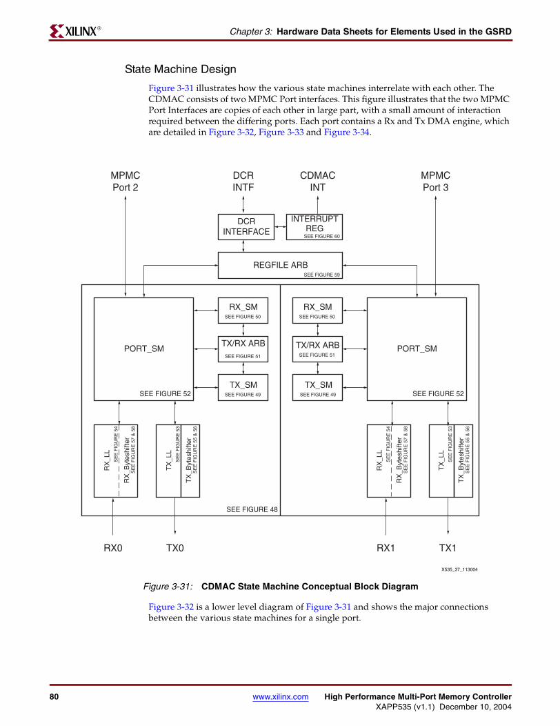
80 www.xilinx.com High Performance Multi-Port Memory ControllerXAPP535 (v1.1) December 10, 2004
Chapter 3: Hardware Data Sheets for Elements Used in the GSRDR
State Machine Design
Figure 3-31 illustrates how the various state machines interrelate with each other. The CDMAC consists of two MPMC Port interfaces. This figure illustrates that the two MPMC Port Interfaces are copies of each other in large part, with a small amount of interaction required between the differing ports. Each port contains a Rx and Tx DMA engine, which are detailed in Figure 3-32, Figure 3-33 and Figure 3-34.
Figure 3-32 is a lower level diagram of Figure 3-31 and shows the major connections between the various state machines for a single port.
Figure 3-31: CDMAC State Machine Conceptual Block Diagram
X535_37_113004
PORT_SMTX/RX ARB
TX_SM
_RX SM
TX0RX0
REGFILE ARB
DCR INTERFACE
INTERRUPT REG
PORT_SMTX/RX ARB
TX_SM
_RX SM
TX1RX1
MPMCPort 2
MPMCPort 3
DCR INTF
CDMACINT
SEE FIGURE 48
SEE FIGURE 52 SEE FIGURE 52 SEE FIGURE 49
SEE FIGURE 50
SEE FIGURE 51
SEE FIGURE 50
SEE FIGURE 51
SEE FIGURE 49
SEE FIGURE 59
SEE FIGURE 60
SE
E F
IGU
RE
54
SE
E F
IGU
RE
57
& 5
8
RX
_LL
RX
_Byt
eshi
fter
SE
E F
IGU
RE
53
SE
E F
IGU
RE
55
& 5
6
TX
_LL
TX
_Byt
eshi
fter
SE
E F
IGU
RE
54
SE
E F
IGU
RE
57
& 5
8
RX
_LL
RX
_Byt
eshi
fter
SE
E F
IGU
RE
53
SE
E F
IGU
RE
55
& 5
6
TX
_LL
TX
_Byt
eshi
fter
ARCHIVED APPLICATION NOTE - NOT SUPPORTED FOR NEW DESIGNS

High Performance Multi-Port Memory Controller www.xilinx.com 81XAPP535 (v1.1) December 10, 2004
Communication Direct Memory Access Controller (CDMAC)R
Figure 3-32: CDMAC Relationship of State Machines to each Other (per port)
TX SM
TX/RX ARB
TX LLTX BYTE SHIFTER RX LL
TX
_R
ea
d_
De
sc_
Do
ne
RX SM
REGFILE ARB
PORT SM
DCR INTRFACED
MA
_C
on
tin
ue
DM
A_
St o
p
Wr i
t e_
Cu
r r_
Pt r
_T
x
Tx
_R
eq
_T
yp
e
Rx
_R
eq
_T
yp
e[ 1
| 2&
I n_
Pa
ylo
ad
| 3]
RX
_R
eq
d_
De
sc_
Do
ne
DM
A_
Co
nt i
nu
e
DM
A_
St o
p
Wr i
t e_
Cu
r r_
Pt r
_R
xP
xR_
Re
qu
est
Px
R_
Gra
nt
Px
R_
Bu
sy
Px
W_
Re
qu
es
t
PxW
_G
ran
t
Px
W_
Bu
sy
Detect_Null_PtrDetect_StopOnEnd
Detect_Null_PtrDetect_StopOnEnd
AddrReqAddrAckAddress
rdDataRdyRNWSIZE
rd/wrDataAck_Pos/NegrdData_BE_Pos/Neg
Rd/WrCompRd/WrRst
Fifo_Busy/FullAddress/Length
CL
8R
CL
8W
B1
6W
B1
6R
Tx
_G
o
CS[RX]
CS[TX]
Tx
_G
o
Re
q_
Ac
k
Tim
e_
Ou
t
RX
x_
Ge
t_S
tatu
sR
Xx
_F
oo
ter
RX
x_
Pa
ylo
ad
RX
x_
La
stB
urs
tR
Xx
_F
r is
tBu
rst
RX
x_
Su
mR
Xx
_A
dd
ress
RX
x_
CL
8C
om
pR
Xx
_C
L8
St a
r tR
Xx
_B
16
Co
mp
RX
x_
B1
6S
tar t
RX
x_
LL
Sta
r t
Da
ta_
Px
_w
rDa
taB
E_
Po
s_N
eg
Da
ta_
Px_
wrD
ata
Ack
_P
os_
Ne
g
CE
_P
os/
Ne
g
SO
F/S
OP
/EO
P/E
OF
/RE
M
RX
x_D
st_
Rd
yR
Xx
_S
rc_
Rd
y
TX
x_
Src
_R
dy
TX
x_D
st_
Rd
y
TX
x_
He
ad
er
TX
x_
Re
ad
_D
esc
_D
on
e
TX
x_
Sta
r t_
Of_
Pa
ylo
ad
TX
x_
Sta
rt_
Of_
Fra
me
TX
x_
En
dO
fPa
ck
et
TX
x_
La
stB
urs
t
TX
x_
Su
m
TX
x_
Sta
r t
TX
x_
Da
taD
on
e
TX
x_
Ad
dre
ss
TX
x_
By
te_
Re
g_
CE
By
teS
el0
/ 1/ 2
/ 3
Da
ta_
Px
_rd
Da
taA
ct_
Po
s/ N
eg
SO
F/S
OP
/EO
P/E
OF
/RE
M
TX
x_D
st_
Rd
y
PLBFIFO
MPMC
CounterDatapath
PL
BF
IFO
MP
MC
Da
tap
ath
By
tes
hif
t
Da
tap
ath
Ad
dre
ssC
ou
nte
r
PL
BF
IFO
MP
MC
Da
tap
ath
By
tes
hif
t
DATAPATH DATA
PATH
TX
_W
rite
_D
esc
_D
on
e
RX
_W
r it e
_D
esc
_D
on
e
TX
x_
Src
_R
dy
TX
x_D
st_
Rd
y
RX
x_D
st_
Rd
y
RX
x_
Src
_R
dy
TXx_Trigger_EOP
Data_TXx_Src_Rdy
TX LL INTERFACE RX LL INTERFACE
IDL
EG
ET
_D
ES
C
GE
T_
PU
T_
DA
TA
PU
T_
DE
SC
IDL
EG
ET
_D
ES
C
GE
T_
PU
T_
DA
TA
PU
T_
DE
SC
SEE FIGURE 49 SEE FIGURE 50
SEE FIGURE 51
SEE FIGURE 52
SEE FIGURE 53 SEE FIGURE 54 & 57 & 58SEE FIGURE 55 & 56
SEE FIGURE 59
1/2 OF FIGURE 47 X535_38_113004
ARCHIVED APPLICATION NOTE - NOT SUPPORTED FOR NEW DESIGNS
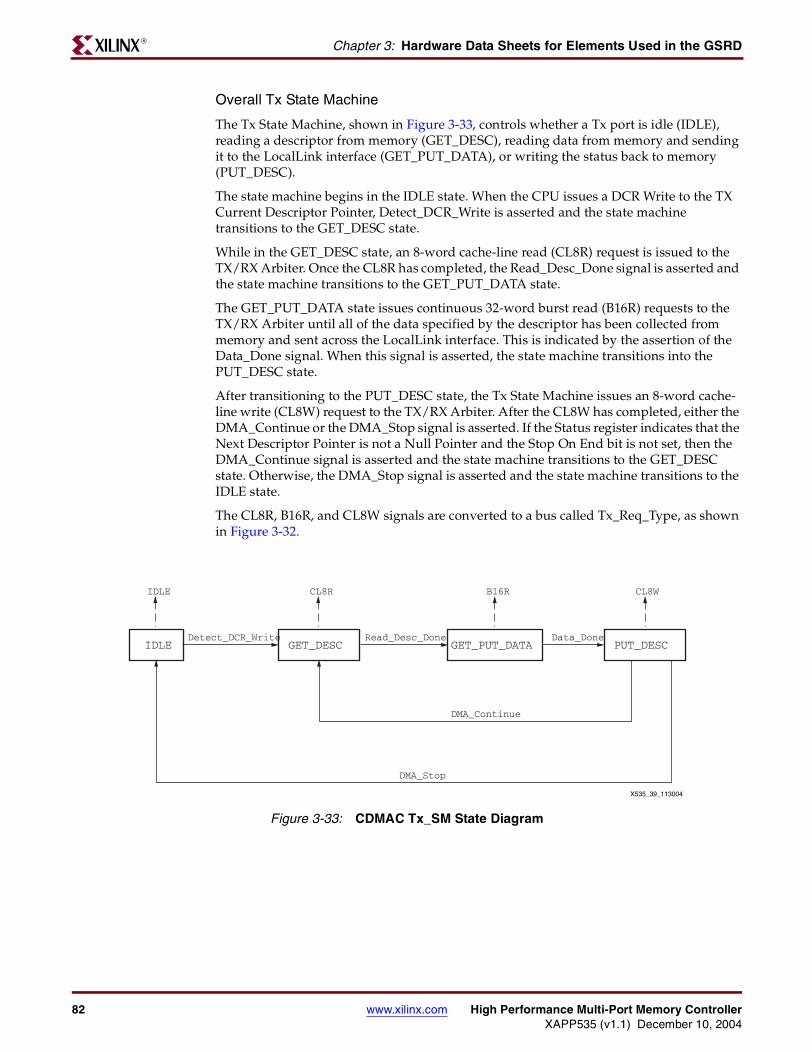
82 www.xilinx.com High Performance Multi-Port Memory ControllerXAPP535 (v1.1) December 10, 2004
Chapter 3: Hardware Data Sheets for Elements Used in the GSRDR
Overall Tx State Machine
The Tx State Machine, shown in Figure 3-33, controls whether a Tx port is idle (IDLE), reading a descriptor from memory (GET_DESC), reading data from memory and sending it to the LocalLink interface (GET_PUT_DATA), or writing the status back to memory (PUT_DESC).
The state machine begins in the IDLE state. When the CPU issues a DCR Write to the TX Current Descriptor Pointer, Detect_DCR_Write is asserted and the state machine transitions to the GET_DESC state.
While in the GET_DESC state, an 8-word cache-line read (CL8R) request is issued to the TX/RX Arbiter. Once the CL8R has completed, the Read_Desc_Done signal is asserted and the state machine transitions to the GET_PUT_DATA state.
The GET_PUT_DATA state issues continuous 32-word burst read (B16R) requests to the TX/RX Arbiter until all of the data specified by the descriptor has been collected from memory and sent across the LocalLink interface. This is indicated by the assertion of the Data_Done signal. When this signal is asserted, the state machine transitions into the PUT_DESC state.
After transitioning to the PUT_DESC state, the Tx State Machine issues an 8-word cache-line write (CL8W) request to the TX/RX Arbiter. After the CL8W has completed, either the DMA_Continue or the DMA_Stop signal is asserted. If the Status register indicates that the Next Descriptor Pointer is not a Null Pointer and the Stop On End bit is not set, then the DMA_Continue signal is asserted and the state machine transitions to the GET_DESC state. Otherwise, the DMA_Stop signal is asserted and the state machine transitions to the IDLE state.
The CL8R, B16R, and CL8W signals are converted to a bus called Tx_Req_Type, as shown in Figure 3-32.
Figure 3-33: CDMAC Tx_SM State Diagram
X535_39_113004
IDLE GET_DESC GET_PUT_DATA PUT_DESCDetect_DCR_Write Read_Desc_Done Data_Done
DMA_Continue
DMA_Stop
IDLE CL8R B16R CL8W
ARCHIVED APPLICATION NOTE - NOT SUPPORTED FOR NEW DESIGNS

High Performance Multi-Port Memory Controller www.xilinx.com 83XAPP535 (v1.1) December 10, 2004
Communication Direct Memory Access Controller (CDMAC)R
Overall Rx State Machine
The Rx State Machine, shown in Figure 3-34, controls whether a Rx port is idle (IDLE), reading a descriptor from memory (GET_DESC), collecting data from the LocalLink interface and writing the data to memory (GET_PUT_DATA), or writing the status and application defined data back to memory (PUT_DESC).
The state machine begins in the IDLE state. When the CPU issues a DCR Write to the RX Current Descriptor Pointer, Detect_DCR_Write is asserted and the state machine transitions to the GET_DESC state.
While in the GET_DESC state, an 8-word cache-line read (CL8R) request is issued to the TX/RX Arbiter. Once the CL8R has completed, the Read_Desc_Done signal is asserted and the state machine transitions to the GET_PUT_DATA state.
The GET_PUT_DATA state issues continuous 32-word burst write (B16W) requests to the TX/RX Arbiter until all of the data specified by the descriptor has been collected from the LocalLink interface and written to memory. This is indicated by the assertion of the Data_Done signal. When this signal is asserted, the state machine transitions into the PUT_DESC state.
After transitioning to the PUT_DESC state, the Rx State Machine issues an 8-word cache-line write (CL8W) request to the TX/RX Arbiter. After the CL8W has completed, either the DMA_Continue or the DMA_Stop signal is asserted. If the Status register indicates that the Next Descriptor Pointer is not a Null Pointer and the Stop On End bit is not set, then the DMA_Continue signal is asserted and the state machine transitions to the GET_DESC state. Otherwise the DMA_Stop signal is asserted and the state machine transitions to the IDLE state.
The CL8R, B16W, and CL8W signals are converted to a bus called Rx_Req_Type, as shown in Figure 3-32.
Arbitration State Machine for Overall Rx and Tx State Machines
Figure 3-35 shows the logic for the Arbitration state machine for the Overall Rx and Tx state machines (TX/RX ARB). The Overall Rx and Tx state machines assert request signals to the arbiter through the Tx_Req and Rx_Req signals. These signals are the same signals as Tx_Req_Type and Rx_Req_Type described in the Overall Tx State Machine and Overall Rx State Machine sections.
Figure 3-34: CDMAC Rx_SM State Diagram
X535_40_113004
IDLE GET_DESC GET_PUT_DATA PUT_DESCDetect_DCR_Write Read_Desc_Done Data_Done
DMA_Continue
DMA_Stop
IDLE CL8R B16R CL8W
ARCHIVED APPLICATION NOTE - NOT SUPPORTED FOR NEW DESIGNS
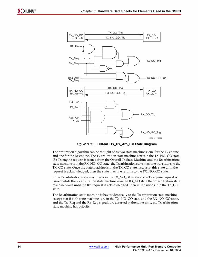
84 www.xilinx.com High Performance Multi-Port Memory ControllerXAPP535 (v1.1) December 10, 2004
Chapter 3: Hardware Data Sheets for Elements Used in the GSRDR
The arbitration algorithm can be thought of as two state machines: one for the Tx engine and one for the Rx engine. The Tx arbitration state machine starts in the TX_NO_GO state. If a Tx engine request is issued from the Overall Tx State Machine and the Rx arbitrations state machine is in the RX_NO_GO state, the Tx arbitration state machine transitions to the TX_GO state. Once the state machine is in the TX_GO state it stays in this state until the request is acknowledged, then the state machine returns to the TX_NO_GO state.
If the Tx arbitration state machine is in the TX_NO_GO state and a Tx engine request is issued while the Rx arbitration state machine is in the RX_GO state the Tx arbitration state machine waits until the Rx Request is acknowledged, then it transitions into the TX_GO state.
The Rx arbitration state machine behaves identically to the Tx arbitration state machine, except that if both state machines are in the TX_NO_GO state and the RX_NO_GO state, and the Tx_Req and the Rx_Req signals are asserted at the same time, the Tx arbitration state machine has priority.
Figure 3-35: CDMAC Tx_Rx_Arb_SM State Diagram
TX_NO_GOTX_Go = 0
TX_GOTX_Go = 1
TX_GO_Trig
RX_Go
TX_Req
RX_Req
TX_ReqReq_Ack
TX_GO_Trig
TX_NO_GO_Trig
TX_NO_GO_Trig
RX_NO_GORX_Go = 0
RX_GORX_Go = 1
RX_GO_Trig
RX_NO_GO_Trig
RX_GO_Trig
RX_Req
TX_Req
Req_AckTX_Go
RX_NO_GO_Trig
X535_41_113004
ARCHIVED APPLICATION NOTE - NOT SUPPORTED FOR NEW DESIGNS

High Performance Multi-Port Memory Controller www.xilinx.com 85XAPP535 (v1.1) December 10, 2004
Communication Direct Memory Access Controller (CDMAC)R
Port State Machine
The Port State Machine is the main control for the CDMAC and is shown in Figure 3-36. The Port State Machine contains two state machines that closely interact with each other due to resource sharing of the register file. The Read State Machine executes descriptor read transactions and Tx burst read transactions. The Write State Machine executes descriptor write transactions and Rx burst write transactions.
Read State Machine
The Read State Machine begins in the IDLE state. As soon as the TX/RX Arbiter issues an 8-word cache-line read (CL8R) request or a 32-word burst read (B16R) request, the Read State Machine enters the REQ_SETUP state.
While the Read State Machine is in the REQ_SETUP state, the state machine requests access to the register file to read the Buffer Address and Buffer Length registers. Once access has been granted, the state machine transitions into the SETUP state.
The buffer address and buffer length counters are loaded from the register file while the Read State Machine is in the SETUP state. If the buffer address is invalid, an error is generated and the Read State Machine returns to the IDLE state. If there is no error once the counters are loaded, the Read State Machine transitions to the WAIT_ADDRACK state.
The WAIT_ADDRACK state issues either a CL8R request or a B16R read request. Once the request has been acknowledged, the Read State Machine transitions to one of two states. The first state, WAIT_RDDATARDY_CL8R, is for CL8Rs and asserts control signals to read a descriptor. The second state, REQ_STORE, is for B16Rs and asserts control signals to read data from memory that are transmitted over the LocalLink interface.
Figure 3-36: CDMAC Port_SM State Diagram
IDLE REQ_SETUP SETUP WAIT_ADDRACK WAIT_RDDATARDY_CL8R REQ_READ_DESC
TX_PIPELINE_EMPTY TX_ACTIVE STORE REQ_STORE READ_DESCREAD_DESC_SR
READ_DESC_FINISHREAD_DESC_EMPTYIDLE
CL8R | B16R RegFile Grant TCCL8R &AddrAck
RdDataRdy
RegFile_Grant
TC & RdPop
RdPop
RdCompDst_Rdy
B16R &AddrAck
RegFile_GrantTC
Data_Done_Detect
Dst_Rdy
Detect_Addr_Err
IDLE RX_ACTIVE REQ_SETUP SETUP WAIT_ADDRACK REQ_STORE STORE
IDLEREQ_PRESETUP PRESETUP
WRITE_DESC
UPDATE_PNTR2UPDATE_PNTRREQ_UPDATE_PNTR
CL8W & ~(TXNRX |~RX_Footer
RX_Data_Done
RegFile_Grant TC
B16W &AddrAck
RegFile_Grant
TC
CLKRegFile_Grant
CLK
TCB16W &
RX_Payload
RegFile_Grant
WRITE SM
READ SM
X535_42_113004
CL8W (TXNRX |~RX_Footer
Detect_Addr_Err CL8W & AddrAck
WrComp
ARCHIVED APPLICATION NOTE - NOT SUPPORTED FOR NEW DESIGNS

86 www.xilinx.com High Performance Multi-Port Memory ControllerXAPP535 (v1.1) December 10, 2004
Chapter 3: Hardware Data Sheets for Elements Used in the GSRDR
If the Read State Machine is reading a descriptor, the state machine transitions out of the WAIT_ADDRACK state and into the WAIT_RDDATARDY_CL8R state after the Port interface has acknowledged the CL8R request.
Once the Read State Machine is in the WAIT_RDDATARDY_CL8R state, it waits until the Port interface asserts the RdDataRdy signal. This signal indicates that data is available on the Port interface and that the CDMAC can pop data out of the MPMC's Read FIFOs on every clock cycle following the assertion of RdDataRdy. The state machine then transitions into the REQ_READ_DESC state.
While in the REQ_READ_DESC state, the state machine requests access to the register file. Once access has been granted, the state machine transitions into the READ_DESC state.
The READ_DESC state pops the Next Descriptor Pointer, the Buffer Address, and the Buffer Length out of the MPMC's Read FIFOs. This data is placed into the register file and the Read State Machine transitions to the READ_DESC_SR. The data is also sent across the LocalLink interface as Header data.
The READ_DESC_SR state pops the Status register value out of the MPMC's Read FIFOs. Once this data has been stored in the status register, the Read State machine transitions to the READ_DESC_FINISH state.
Once in the READ_DESC_FINISH state, the last four words of data pop out of the MPMC's Read FIFOs. This data is ignored. When the Port interface issues the RdComp signal, the Read State Machine transitions to the READ_DESC_EMPTY state.
The READ_DESC_EMPTY state waits for the LocalLink interface to be ready to receive data from the CDMAC. Once the Dst_Rdy signal is received from the LocalLink interface, the Read State Machine transitions into the IDLE state.
If the Read State Machine is in the WAIT_ADDRACK state and is reading data to be transmitted over the LocalLink interface, the state machine transitions out of the WAIT_ADDRACK state and into the REQ_STORE state after the Port interface acknowledges the B16R request.
While in the REQ_STORE state, the state machine requests access to the register file. Once access has been granted, the state machine transitions into the STORE state.
Once in the STORE state, the Buffer Address and Buffer Length registers are updated with the Buffer Address and the Buffer Length to be used in the next transaction. The Buffer Address is incremented by the number of bytes that read from memory on this transaction. The Buffer Length is decremented by the number of bytes that are read from memory on this transaction. After these registers have been updated, the Read State Machine transitions to the TX_ACTIVE state.
In the TX_ACTIVE state, data is read from memory and sent to the Tx Byteshifter. Once all of the Data pops out of the MPMC's Read FIFOs or the MPMC's Read FIFOs have been reset, the Read State Machine transitions to the TX_PIPELINE_EMPTY state.
The Read State Machine transitions from the TX_PIPELINE_EMPTY state to the IDLE state once the last word of data has been acknowledged on the LocalLink interface.
Write State Machine
The Write State Machine is very similar to the read state machine. The Write State Machine begins in the IDLE state. Depending on the type of request being issued from the TX/RX Arbiter, the Write State Machine transitions into one of three states. If the TX/RX Arbiter is issuing a CL8W request and either the request is for the TX engine or the RX LocalLink interface is not in the Footer state, the state machine transitions into the WRITE_DESC state. If the TX/RX Arbiter is issuing a CL8W request, and the request is for the RX engine,
ARCHIVED APPLICATION NOTE - NOT SUPPORTED FOR NEW DESIGNS

High Performance Multi-Port Memory Controller www.xilinx.com 87XAPP535 (v1.1) December 10, 2004
Communication Direct Memory Access Controller (CDMAC)R
and the RX engine is in the Footer state, the state machine transitions into the RX_ACTIVE state. If the TX/RX Arbiter is issuing a B16W request and the RX engine is in the Payload state, the state machine transitions to the REQ_PRESETUP state.
If the Write State Machine transitions from the IDLE state to the WRITE_DESC state, the state machine waits for 8 words of descriptor data to be pushed into the MPMC's Write FIFOs, then the state machine transitions into the REQ_SETUP state.
If the Write State Machine transitions from the IDLE state to the REQ_PRESETUP state, the state machine requests access to the register file. Once access has been granted, the state machine transitions into the PRESETUP state.
While in the PRESETUP state, the Buffer Address and the Buffer Length counters are loaded with the contents of the register file. Once these counters are loaded, the Write State Machine transitions to the RX_ACTIVE state.
If the Write State Machine transitions from the IDLE state or the PRESETUP state to the RX_ACTIVE state, the state machine waits for Payload or Footer data from the Rx LocalLink interface to be pushed into the MPMC's Write FIFOs, then the state machine transitions into the REQ_SETUP state. If Footer data is being pushed into the MPMC's Write FIFOs, the data or the byte enables are modified as specified in the “Rx LocalLink and Byteshifter” section.
The REQ_SETUP staterequests access to the register files. Once access is granted, the Write State Machine transitions into the SETUP state.
While in the SETUP state, the Status register is updated, then the Write State Machine transitions into the WAIT_ADDRACK state.
A write request is issued on the Port interface when the Write State Machine is in the WAIT_ADDRACK state. Once the request has been acknowledged, the state machine transitions to one of two states. If the request was a B16W request, the state machine transitions to the REQ_STORE state. If the request was a CL8 request, the state machine transitions to the REQ_UPDATE_PNTR state.
If the Write State Machine transitioned from the WAIT_ADDRACK state into the REQ_STORE state, the state machine requests access to the register file. Once access has been granted, the state machinetransitions into the STORE state.
While in the STORE state, the Buffer Address and Buffer Length registers are updated with the Buffer Address and Buffer Length to be used in the next transaction. After these registers are updated, the Write State Machine transitions into the IDLE state.
If the Write State Machine transitioned from the WAIT_ADDRACK state into the REQ_UPDATE_PNTR state, the state machine requests access to the register file. Once access has been granted, the state machine transitions into the UPDATE_PNTR state.
While in the UPDATE_PNTR state, the Next Descriptor Pointer register is read from the register file, then the Write State Machine transitions into the UPDATE_PNTR2 state.
In the UPDATE_PNTR2 state, the Next Descriptor Pointer is written to the Current Descriptor Pointer register, then the Write State Machine transitions into the IDLE state.
ARCHIVED APPLICATION NOTE - NOT SUPPORTED FOR NEW DESIGNS

88 www.xilinx.com High Performance Multi-Port Memory ControllerXAPP535 (v1.1) December 10, 2004
Chapter 3: Hardware Data Sheets for Elements Used in the GSRDR
Tx LocalLink and Byteshifter
The Tx LocalLink and Byteshifter Logic take data from the appropriate place in memory and move the data across the LocalLink interface. This concept is shown in Figure 3-37. In this example, the CDMAC reads the descriptor at address p to p+1C and sends it to the LocalLink as the header. The payload is 136 bytes and starts at address m+79. The Tx Byteshifter sends data acknowledges to the memory controller while keeping the Src_Rdy signal to the LocalLink deasserted, because address m+79 is not 32-word aligned. Data from address m to m+78 are discarded. Data is offset by 78 bytes, so the first byte of data occurs on the second byte location on the posedge of the DDR SDRAM. The Tx Byteshifter takes the posedge (x 0 1 2) and negedge (3 4 5 6), which are both present at the time, recombines them to form a new, correctly shifted, word (0 1 2 3), and sends it over the LocalLink as the payload. At the end of the first 32-word burst read (B16R), 3 bytes are left over and kept in the Byteshifter. When the second burst occurs, those 3 bytes are combined with the first byte of the second burst and sent over LocalLink. This happens again between the second burst and third burst. On the last word of the payload the Rem signal is set to indicate which bytes of the word are valid. Rem is 0x0 in this example to indicate all 4 bytes are valid. After byte n+1 is sent, the FIFOs in MPMC, which hold all 32 words of the burst, are reset to avoid extra data acknowledge. For Tx transfer, the footer is not used. The status bits are written back to the descriptor's status field.
Tx Byteshifter Logic
The Tx Byteshifter Block Diagram is shown in Figure 3-38. It has two stages. In the first stage two 32-bit data, one from the posedge of the DDR SDRAM (rdData_Pos) and one from the negedge (rdData_Neg), are fed into fTWIST from the FIFOs in the MPMC. fTWIST forms a new word Port_RdData by multiplexing each byte from either the rdData_Pos or rdData_Neg, depending on the offset represented by StartOffset. fTWIST is able to produce a new word every clock cycle because both rdData_Pos and rdData_Neg
Figure 3-37: CDMAC Tx Byteshift Example
X535_43_113004
HeaderPayload
Footerarbitrary length
(ignored)33 words + 2 bytes =134 bytes
8 words
MSB
LSB
32 Word burst8-word
cache line 32 Word burst 32 Word burst
Mem
ory
Spa
ce
4-B
ytes
p p+1C
m+
00
m+
79Stu
ff da
tain
to F
IFO
s
Stu
ff da
tain
to F
IFO
s
Loca
lLin
k D
ata
for
1 fr
ame
0
0
1
1
2
2
3
3m
+80
m+
7Cm
+78
m+
104
m+
100
m+
FC
n+1
n+1
n
n
ARCHIVED APPLICATION NOTE - NOT SUPPORTED FOR NEW DESIGNS

High Performance Multi-Port Memory Controller www.xilinx.com 89XAPP535 (v1.1) December 10, 2004
Communication Direct Memory Access Controller (CDMAC)R
last 2 clock cycles. For example, if StartOffset is 1 when bytes 4-7 become present on rdData_Neg, bytes 0-3 would have already been present on rdData_Pos for 1 cycle. At this point Sel_Px_rdData_Pos becomes 0b0111. The pattern 0b0111 indicates that the first byte is taken from the first byte from rdData_Neg and rest from rdData_Pos to form (4 1 2 3). One clock later, rdData_Pos refreshes to the next value and Sel_Px_rdData_Pos becomes 0b1000. The pattern 0b1000 indicates that the first byte is taken from the first byte from rdData_Pos and rest from rdData_Neg to form (8 5 6 7). In the second stage, the Byte_Selx signals are produced to reorder the bytes in Port_RdData to form the final word.
In this example, the vector Byte_Sel[0-3] display values of 0 3 2 1 respectively. This configuration of Byte_Sel vectors swap the first byte with the last 3 bytes to form (1 2 3 4) and (5 6 7 8). Byte_Reg_CE clock enable the registers at the appropriate time. For the first burst, Byte_Reg_CE is 0xF until the last word. For the last word, Byte_Reg_CE is used to hold the left over bytes from the current burst in the registers by disabling clock(s) to the register(s). For example, if StartOffset is 1 and rdData_Neg=0x4567 is the last word of the burst, Byte_Reg_CE[3:0] is 0x0001. In this case the last 3 bytes (567) is held in the registers until the next burst starts. On the second burst, the first byte is loaded into the register enabled by Byte_Reg_CE[0], then Byte_Reg_CE returns to 0xF again until the last word of that burst.
Figure 3-38: CDMAC Tx Byteshifter Block Diagram
LocalLinkRX DEVICE
MPMC DATA PATH
Port_RdData[31:24]
Byte_Sel0 2
0
1
2
3
Port_TX_Out[7:0]D
CE
Q
Byte_Reg_CE[0]
Port_RdData[23:16]
Port_RdData[15:8]
Port_RdData[7:0]
Byte_Sel1 2
0
1
2
3
D
CE
Q
Byte_Reg_CE[1]
Byte_Sel2 2
0
1
2
3
Port_TX_Out[23:16]D
CE
Q
Byte_Reg_CE[2]
Byte_Sel3 2
0
1
2
3
D
CE
Q
Byte_Reg_CE[3]
Port_TX_Out[15:8]
Port_TX_Out[31:24]
TX
By
tesh
ifte
r C
on
tro
l
SRL16 FIFO
SRL16 FIFO
SRL16 FIFO
SRL16 FIFO
SRL16 FIFO
SRL16 FIFO
SRL16 FIFO
SRL16 FIFO
Q1
Q2
INFF_DDR
Q1
Q2
INFF_DDR
Q1
Q2
INFF_DDR
Q1
Q2
INFF_DDR
D
CE
Q32
CDMAC TX BYTESHIFTER
32
32
rdData_Pos
rdData_Neg φTWIST
Sel_Px_rdData_Pos
4
φTWIST EXAMPLE
rdData_Pos
rdData_Neg
Port_RdData
StartOffset
StartOffset = 1
4567
B90A
0123 890A
85674123
BCDE
Each digit represents position of1 byte of data
Byte Shifting
0 1 2 3
Data[31:0]Byte_Selx
0
1
2
3
0 1 2 3
0 1 2
0 1
0
3
2 3
1 2 3
Data_Out[31:0]
LSB MSB
LSB
MSB
LSB
MSB
Byte 0
Byte 1
Byte 2
Byte 3
Byte 4
Byte 5
Byte 6
Byte 7
Port_TX_Out 56781234
X535_44_113004
ARCHIVED APPLICATION NOTE - NOT SUPPORTED FOR NEW DESIGNS

90 www.xilinx.com High Performance Multi-Port Memory ControllerXAPP535 (v1.1) December 10, 2004
Chapter 3: Hardware Data Sheets for Elements Used in the GSRDR
Tx Byteshifter State Diagram
The Tx Byteshifter State Machine generates StartOffset, Byte_Reg_CE, Byte_Selx, Src_Rdy, and RdDataPop signals to control the Tx Byteshifter Data Path, part of the LocalLink signals, and rdDataAcks to the memory. StartOffset controls the number of bytes to be shifted. It is set to the last 3 bits of the memory initially, but is changed at the end of every burst to account for the left-over bytes. Byte_Reg_CE is a 4-bit clock enable to the registers in the data path. It is multiplexed by the bytes being held in the byteshifter during a burst transition, as shown in Figure 3-39. Byte_Selx control the multiplexers that are responsible for reordering the bytes coming out of fTWIST, as shown in Figure 3-38. Src_Rdy indicates to LocalLink that the data is valid. Src_Rdy is asserted during the burst but deasserted while in the discard stage, the between descriptors stage, and the between bursts stage. RdDataPop generates rdDataAck, which is used to acknowledge data read from memory. rdDataAck_Pos and rdDataAck_Neg are asserted alternately. RdDataPop is asserted at the same time as Src_Rdy. RdDataPop is also asserted in the discard stage to pop out invalid data.
Tx Byteshifter State Machine starts in IDLE state. When a “Start” signal is given by the Port State Machine, it goes into the discard stage and pops off data until it is at the current address. Using the example in Figure 3-37, the first 30 words of the first burst is discarded. The state machine then moves to the START state if there is at least one complete word left in the burst or to the STARTFINISH state if not. In our example, it moves to the START state since we have a complete word ([0 1 2 3]). From the START state, it can either go to the PROCESS state or FINISH state depending on if there is at least one more word of data. In our example, it goes to FINISH state directly since we don't have a second complete word of data. In the STARTFINISH or FINISH state, it saves the left over bytes by setting Byte_Reg_CE to disable clock(s) to the register(s) holding those bytes. From either STARTFINISH or FINISH it can go to BTWN_BURST state or BTWN_DESC state or IDLE state depending on whether there is another burst for the same descriptor or current descriptor is finished and engine is moving on to the next descriptor in the chain or there is no more bursts and no more descriptors, respectively. In all three states, counters are reset. For our example, it goes to the BTWN_BURST state since we are still in the first descriptor. If in BTWN_BURST, it goes to EXTRA to update BurstLengthCount, then go to START state again. If in BTWN_DESC, it returns to DISCARD state.
Refer to Figure 3-39 for detailed information on each state and their inputs & outputs.
Figure 3-39: CDMAC Tx_Byte_Shifter_SM State Diagram
X535_45_113004
DISCARD START STARTFINISH FINISH
IDLE BTWN_DESC EXTRA BTWN_BURST
PROCESS0123
BytesHolding
1111011100110001
DestReady
Byte_Reg_CE
See TableFig. 54
Byte_SelxStartOffset
ARCHIVED APPLICATION NOTE - NOT SUPPORTED FOR NEW DESIGNS

High Performance Multi-Port Memory Controller www.xilinx.com 91XAPP535 (v1.1) December 10, 2004
Communication Direct Memory Access Controller (CDMAC)R
Table 3-6: CDMAC Tx_Byte_Shifter_SM State Diagram Description
STATEPREVIOUS
STATEDESCRIPTION INPUT STIMULUS RESULTANT OUTPUT INTERNAL OPERATIONS
IDLE (C)
INITIAL
Initializes values
RST RdDataPop = 0Src_Rdy = 0StartOffset = 0Used to generate Byte_SelxBytesHolding = 0Track bytes left over from previous burst. Used to generate Byte_Reg_CE
BurstLengthCount = 128 - Address[1:0]Total bytes need to be transferred in this burst
STARTFINISH EndOfPacket
from Port SM. No more descriptors in the chainFINISH
DISCARD
IDLEPop off invalid data from current burst until beginning of address
StartPort SM gives permission for burst 16 read from MPMC
@CLK RdDataPop=1Pop off invalid dataSrc_Rdy = 0NOT Ready signal to LL DEVICE
StartOffset=Address[2:0]Control Byteshifter Multiplexers
DiscardDone = (PopCount == Address[6:2]-1)Signals end of discarding@CLK BurstLengthCount -= 4Update BurstLengthCount@DiscardDone BurstLengthCount -= BytesNeeded BytesNeeded = 4 – Bytesholding Adjust for leftover bytes from previous burst
BTWN_DESC
StartOffset = Address[2:0]-BytesHoldingAdjust for leftover bytes
START
DISCARD Leftover data+current data more than 1 word. Process 1st word of data
DiscardDone
encounter 1st valid and complete word of current descriptor
@DestReady RdDataPop=1 Pop off 1 word of dataSrc_Rdy = 1Ready signal to LocalLink DEVICE BytesHolding=0Reset BytesHolding
@CLK BurstLengthCount -= 4 Update BurstLengthCount
EXTRA CLK
STARTFINISH
DISCARD
Leftover data+current data less than 1 word. Save this data
Length0StartLength0Start = (BurstLengthCount<= BytesNeeded)Leftover data+current data less than 1 word
@DestReady RdDataPop=1Pop off 1 word of dataSrc_Rdy = 1 (if BurstLengthCount=0)Ready signal to LocalLink DEVICE BytesHolding = case(NextState): IDLE: 0; BTWN_BURST: -StartOffset; BTWN_DESC: BurstLengthCount Adjust BytesHolding according to next state
Rem = Case(BurstLengthCount):0: 0b00001: 0b01112: 0b00113: 0b0001
EXTRA
PROCESS START Process data until last word
~Length0MiddleLength0Middle = (BurstLengthCount<=4)More than 1 word of data exist
@DestReady RdDataPop=1Pop off dataSrc_Rdy = 1Ready signal to LocalLink DEVICE
BurstLengthCount-=4 @CLKUpdate BurstLengthCount
FINISH
START
Process last complete word of the burst if exists. Save remaining bytes to be combined with first few byte(s) of next burst
Length0MiddleHave reached the last word of the burst
@DestReady RdDataPop=1 Pop off last word of dataSrc_Rdy = 1 (if BurstLengthCount=0)Ready signal to LocalLink DEVICE BytesHolding = case(NextState): IDLE: 0; BTWN_BURST: -StartOffset; BTWN_DESC: BurstLengthCount Adjust BytesHolding according to next state
Rem=case(BurstLengthCount):0: 0b00001: 0b01112: 0b00113: 0b0001
PROCESS
BTWN_BURST (A)
STARTFINISH
Still more data to be transferred in current descriptor. Prepare for another burst. Resetting counters.
~LastBurstLength0Middle = (BurstLengthCount<=4)More than 1 word of data exist
RdDataPop = 0Src_Rdy = 0
BurstLengthCount = 128Reset BurstLengthCount
FINISH
EXTRA BTWN_BURST
Update BurstLengthCount to combine with left over data from last burst
StartPort SM gives permission for burst 16 read from MPMC
RdDataPop = 0Src_Rdy = 0
BurstLengthCount -= BytesNeededBytesNeeded = 4 – Bytesholding Adjust for leftover bytes from previous burst
BTWN_DESC (B)
STARTFINISH
More descriptors to process. resetting values. Similar to IDLE
~EndOfPacketStill more descriptors in the chain
RdDataPop = 0Src_Rdy = 0
BurstLengthCount = 128 address[1:0]Total bytes need to be transferred in this burstFINISH
ARCHIVED APPLICATION NOTE - NOT SUPPORTED FOR NEW DESIGNS

92 www.xilinx.com High Performance Multi-Port Memory ControllerXAPP535 (v1.1) December 10, 2004
Chapter 3: Hardware Data Sheets for Elements Used in the GSRDR
LocalLink Tx State Machine
The LocalLink Tx State Machine shown in Figure 3-40 represents the steps to transfer data from the memory to the LocalLink as directed by the descriptor. From the IDLE state, the Port State Machine instructs the LocalLink Tx interface to issue a Start of Frame. When the Dst_Rdy signal is asserted by the LocalLink device the LL Tx State Machine goes into the HEADER state to transfer a CacheLine-8 read of the descriptor to the LocalLink as the header. When Port State Machine issues a Read_Desc_Done signal, LL Tx State goes in to PAYLOADSTART and issue a Start of Payload signal. It immediately goes to either the PAYLOAD state if there is more than one word of payload, or to PAYLOADEND if not. From PAYLOAD state, when it reaches the last word, the Tx Byteshifter issues a Trigger_EOP signal that brings it to the PAYLOADEND state. A End of Payload is issued then it goes directly to the FRAMEEND state since there is no footer in Tx transfer. A End of Frame is issue in the FRAMEEND state then it goes back to the IDLE state.
Figure 3-40: CDMAC Tx_LL_SM State Diagram
X535_46_113004
IDLE FRAMESTART HEADER PAYLOADSTART
PAYLOADPAYLOADENDFRAMEEND
Start_Of_Frame Payload_Start
Payload_Done
Payload_Done & Src_Rdy & Dst_Rdy
SOF SOP
EOPEOF
S
R
Q
Src_Rdy_i
Data_Src_Rdy
IDEL & Start_Of_Frame
HEADER & Read_Desc_Done
Src_Rdy
PAYLOADSTART | PAYLOAD | PAYLOADEND
0
1
FRAMEEND
Src_Rdy_i
Src_Rdy &Dst_rdy
Src_Rdy &Dst_rdy
Src_Rdy &Dst_rdy
Src_Rdy &Dst_rdy
ARCHIVED APPLICATION NOTE - NOT SUPPORTED FOR NEW DESIGNS

High Performance Multi-Port Memory Controller www.xilinx.com 93XAPP535 (v1.1) December 10, 2004
Communication Direct Memory Access Controller (CDMAC)R
Rx LocalLink and Byteshifter
The LocalLink and Byteshifter Rx Logic receive data from the LocalLink interface and move the data to the appropriate place in memory. This concept is shown in Figure 3-41. The CDMAC always ignores the Rx LocalLink Header. The Payload is processed by the Rx Byteshifter and pushed into the MPMC’s Write FIFOs. In this example, the Payload is 147 bytes. The data is pushed into the FIFOs in bursts of 32-words (B16W). Data is stuffed into the FIFOs from address m through address m+0x75 because the Payload is written to address m+0x76, which is a not a 32-word aligned address. When these bytes are written to memory, the byte enables are turned off. Ten bytes of Payload data are pushed into the FIFOs after this data has been stuffed into the FIFOs. In the second B16W, all of the data is valid. In the last B16W, only nine bytes need to be written to memory. This means that the remaining 119 bytes need to be stuffed into the FIFOs at the end of the burst. After the Payload has been processed, the Footer is processed and written to memory at address p. The CDMAC changes the first three words' byte enables to prevent the Next Descriptor Pointer, the Buffer Address, and the Buffer Length from being overwritten.
Figure 3-41: CDMAC Rx Byte Shift Example
X535_47_113004
Header Payload Footer
arbitrary length(ignored)
37 words147 bytes
8 words
Stuff datainto FIFOs
MSB
LSB
32 Word burst 32 Word burst8-word
cache line
Stuff datainto FIFOs
mLo
calL
ink
Dat
afo
r 1
fram
e
p p+1C
32 Word burst
Mem
ory
Spa
ce n+1
n+1
n+2
n+2
n
n
0
0
1
1
2
2
3
3
m+
74
m+
76
m+
78m
+7c
m+
80
m+
FC
m+
100
m+
104
m+
108
ARCHIVED APPLICATION NOTE - NOT SUPPORTED FOR NEW DESIGNS

94 www.xilinx.com High Performance Multi-Port Memory ControllerXAPP535 (v1.1) December 10, 2004
Chapter 3: Hardware Data Sheets for Elements Used in the GSRDR
Rx Byteshifter Logic
The Rx Byteshifter Data Path shown in Figure 3-42 is controlled by three signals: First_offset, Pos_CE, and Neg_CE. The First_offset signal is 3-bits wide and represents the number of bytes the LocalLink Data needs to be shifted by, and is used as select bits to the Rx Byteshifter's Data Path Multiplexers. For example, if First_offset is set to 0x6, the first two bytes of the LocalLink data is presented to the last two bytes of the WrDataBus_Pos register and to the last two bytes of the WrDataBus_Neg register. The last two bytes of the LocalLink Data is presented to the first two bytes of the WrDataBus_Pos register and to the first two bytes of the WrDataBus_Neg register. If Pos_CE is asserted while First_offset is set to 0x6, the clock enables on the last two bytes of the WrDataBus_Neg register and the first two bytes of the WrDataBus_Pos register are asserted. Similarly, if Neg_CE is asserted while First_offset is set to 0x6, the clock enables on the last two bytes of the WrDataBus_Pos register and the first two bytes of the WrDataBus_Neg register are asserted.
Figure 3-42: CDMAC Rx Byte Shifter Block Diagram
X535_48_113004
Rx_DataIn[31:24]
WrDataBus_Pos[31:24]D
CE
Q
Rx_DataIn[23:16]
Rx_DataIn[15:8]
Rx_DataIn[7:0]
D
CE
Q
D
CE
Q
0
3
2
1
1
0
3
2
2
1
0
3
3
2
1
0
0
3
2
1
1
0
3
2
2
1
0
3
3
2
1
0
WrDataBus_Pos[23:16]
WrDataBus_Pos[15:8]
D
CE
Q WrDataBus_Pos[7:0]
D
CE
Q
D
CE
Q
D
CE
Q
D
CE
Q
First_offset
WrDataBus_Neg[31:24]
WrDataBus_Neg[23:16]
WrDataBus_Neg[15:8]
WrDataBus_Neg[7:0]
CombinationalLogic
RXByteshifter
ControlCE_Pos
CE_Neg wrdatabus_ce_pos
wrdatabus_ce_neg
4
4
[3]
[2]
[1]
[0]
[3]
[2]
[1]
[0]
3
Combinational Logic
0 1 2 3 4 5 6 7
WrDataBus_Pos WrDataBus_NegFirst_offset
[2:0]
0
1
2
3
4
5
6
7
wrdatabus_ce_pos
wrdatabus_ce_neg
D
CE
Q32
LocalLinkRX DEVICE
SRL16FIFO
SRL16FIFO
SRL16FIFO
SRL16FIFO
SRL16FIFO
SRL16FIFO
SRL16FIFO
SRL16FIFO
D1
D2
OUTFF_DDR
DDR_DO[31:24]
D1
D2
OUTFF_DDR
DDR_DO[23:16]
D1
D2
OUTFF_DDR
DDR_DO[15:8]
D1
D2
OUTFF_DDR
DDR_DO[7:0]
MPMC DATA PATHCDMAC RX BYTESHIFTER
8
8
8
8
8
8
8
8
8
8
8
8
POS
POS
POS
POS
POS
POS
POS
P
P
POS
POS
NEG
NEG
NEG
N
N
NEG
NEG
NEG
NEG
NEG
NEG
NEG
POS
ARCHIVED APPLICATION NOTE - NOT SUPPORTED FOR NEW DESIGNS

High Performance Multi-Port Memory Controller www.xilinx.com 95XAPP535 (v1.1) December 10, 2004
Communication Direct Memory Access Controller (CDMAC)R
To use this data path efficiently, First_offset should be held constant while Pos_CE and Neg_CE are asserted on opposite clock cycles.
Using the example in Figure 3-41 where the address offset is 0x76 and the length is set to 0d147: (This implies that First_offset is set to 0x6)
• Stuff 28 words of data into the MPMC's Write FIFOs by asserting WrDataAck_Pos and WrDataAck_Neg on alternating clock cycles. WrDataBE_Pos and WrDataBE_Neg should be set to 0b1111.
• In clock cycle N+1, the WrDataAck_Pos signal to the MPMC should be asserted with WrDataBE_Pos set to 0b1111. Pos_CE should be asserted. Two bytes of data are clock enabled into WrDataBus_Neg and two bytes of data are clock enabled into WrDataBus_Pos.
• In clock cycle N+2, the WrDataAck_Neg signal should be asserted with WrDataBE_Neg set to 0b1100. The last two bytes of WrDataBus_Neg are valid from clock cycle N+1. At the same time, Neg_CE should be asserted to clock enable two bytes into WrDataBus_Pos and two bytes into WrDataBus_Neg.
• In clock cycle N+3, the WrDataAck_Pos signal should be asserted with WrDataBE_Pos set to 0b0000. The first two bytes of WrDaBus_Pos is valid from clock cycle N+1 and the last two bytes of data are valid from clock cycle N+2. Pos_CE should also be asserted in this clock cycle to continue collecting data from the LocalLink interface.
• This should continue until there is no more data, or until First_offset needs to change.
• In clock cycle M, the WrDataAck_Neg signal should be asserted with WrDataBE_Neg set to 0b0000. Neg_CE does not need to be asserted, as all data has been collected from the LocalLink interface.
• In clock cycle M+1, the WrDataAck_Pos signal should be asserted with WrDataBE_Pos set to 0b0111. Pos_CE does not need to be asserted.
• Stuff 29 words of data into the MPMC's Write FIFOs by asserting WrDataAck_Neg and WrDataAck_Pos on alternating clock cycles. WrDataBE_Pos and WrDataBE_Neg should be set to 0b1111.
Rx Byteshifter State Diagram
In the case of the CDMAC, the First_offset signal is a 3-bit number representing the number of bytes that the LocalLink Data needs to be shifted by before it is pushed into the MPMC's Write FIFOs. This value is simply the three least significant bytes (LSBs) in the descriptor's Buffer Address. The First_offset signal must be valid when the Port State Machine issues a B16W request or an CL8W request.
Pos_CE is used to push even words from the Rx LocalLink interface into the Rx Byteshifter. The First_offset signal is used as select bits to the Rx Byteshifter's Data Path Multiplexers. Combinational logic is used to clock enable the correct registers so that the data from the Rx LocalLink interface is placed into the correct location in memory. Similarly, Neg_CE is used to push odd words from the Rx LocalLink interface into the Rx Byteshifter. The word numbering starts at 0, which is the first word of the Payload, and is reset to 0 again at the first word of the Footer. Pos_CE and Neg_CE are asserted for every Payload and Footer word that is received from the LocalLink interface. The Rx Byteshifter Control State Machine represents the way Pos_CE and Neg_CE are generated and is shown in Figure 3-43.
ARCHIVED APPLICATION NOTE - NOT SUPPORTED FOR NEW DESIGNS

96 www.xilinx.com High Performance Multi-Port Memory ControllerXAPP535 (v1.1) December 10, 2004
Chapter 3: Hardware Data Sheets for Elements Used in the GSRDR
Initially, the Rx Byteshifter Control State Machine starts in the “IDLE” state. When the CDMAC is ready to push Payload data into the MPMC, the Port State Machine instructs the Rx Byteshifter Control Logic to transition to the “In Header” state and to start pushing data from the LocalLink interface through the Rx Byteshifter. Each time Src_Rdy and Dst_Rdy are asserted together, data is pushed into the Rx Byteshifter and the Rx Byteshifter Control State Machine toggles between the “Shift Pos Data” state and the “Shift Neg Data state”. All 32-word burst transfers to the MPMC must be 32-word address aligned, so data can be stuffed into the MPMC's Write FIFOs with the byte enables deasserted. This only needs to occur at the beginning of the Payload or at the end of the Payload. See Figure 3-41. If data needs to be stuffed into the FIFOs, data is processed by the Rx Byteshifter, which also causes the Rx Byteshifter State Machine to toggle between the “Shift Pos Data” state and the “Shift Neg Data” state. Once the descriptor’s Buffer Length has reached 0 bytes and the last word has been pushed into the MPMC's Write FIFOs, the Byteshifter Control State Machine transitions back to the “IDLE” state.
Two exceptions to the above description occur when the Port State Machine instructs the Rx Byteshifter Control Logic to push Footer data into the FIFOs instead of the Payload data described above. First, because the address is always aligned, data never needs to be stuffed into the FIFOs. Second, exactly eight words of data are pushed into the FIFOs.
The Write Control Logic going to the MPMC parallels the Rx Byteshifter Logic. There are four signals that go to the MPMC: WrDataAck_Pos, WrDataAck_Neg, WrDataBE_Pos, and
Figure 3-43: CDMAC LocalLink and Byteshifter Diagram
X535_49_113004
IDLEwriteback_descriptor or first_burst_of_descriptor Shift Pos
DataShift Neg
Data
[(In Payload or In Footer) and (SrcRdy and DstRdy) or stuff_fifos)]
Last word and [(In Payload or In Footer) and (SrcRdy and DstRdy) or stuff_fifos)]
[(In Payload or In Footer) and (SrcRdy and DstRdy) or stuff_fifos)]
Table 3-7: CDMAC LocalLink and Byteshifter Diagram Description
STATEPREVIOUS
STATEDESCRIPTION INPUT STIMULUS RESULTANT OUTPUT
IDLEInitial Wait’s for 32-word burst
write request or for 8-word cache-line write request.
Pos_CE = 0Neg_CE = 0Shift Neg Data
Shift Pos Data
IDLEInstructs even words from the LocalLink interface to
be pushed into the RX Byte Shifters.
byte_shift_ce_pos
byte_shift_ce_pos =
Even Word Data Valid on the LocalLink interface and (In Header or
In Footer)
Pos_CE = byte_shift_ce_posNeg_CE = 0Shift Neg Data
Shift Neg Data Shift Pos Data
Instructs odd words from the LocalLink interface to
be pushed into the RX Byte Shifters.
byte_shift_ce_neg
byte_shift_ce_neg =
Even Word Data Valid on the LocalLink interface and (In Header or
In Footer)
Pos_CE = 0Neg_CE = byte_shift_ce_neg
ARCHIVED APPLICATION NOTE - NOT SUPPORTED FOR NEW DESIGNS
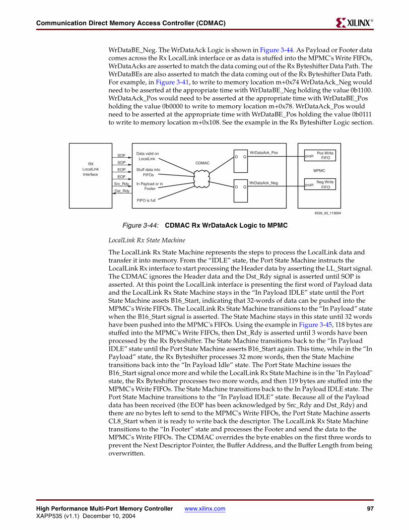
High Performance Multi-Port Memory Controller www.xilinx.com 97XAPP535 (v1.1) December 10, 2004
Communication Direct Memory Access Controller (CDMAC)R
WrDataBE_Neg. The WrDataAck Logic is shown in Figure 3-44. As Payload or Footer data comes across the Rx LocalLink interface or as data is stuffed into the MPMC's Write FIFOs, WrDataAcks are asserted to match the data coming out of the Rx Byteshifter Data Path. The WrDataBEs are also asserted to match the data coming out of the Rx Byteshifter Data Path. For example, in Figure 3-41, to write to memory location m+0x74 WrDataAck_Neg would need to be asserted at the appropriate time with WrDataBE_Neg holding the value 0b1100. WrDataAck_Pos would need to be asserted at the appropriate time with WrDataBE_Pos holding the value 0b0000 to write to memory location m+0x78. WrDataAck_Pos would need to be asserted at the appropriate time with WrDataBE_Pos holding the value 0b0111 to write to memory location m+0x108. See the example in the Rx Byteshifter Logic section.
LocalLink Rx State Machine
The LocalLink Rx State Machine represents the steps to process the LocalLink data and transfer it into memory. From the “IDLE” state, the Port State Machine instructs the LocalLink Rx interface to start processing the Header data by asserting the LL_Start signal. The CDMAC ignores the Header data and the Dst_Rdy signal is asserted until SOP is asserted. At this point the LocalLink interface is presenting the first word of Payload data and the LocalLink Rx State Machine stays in the “In Payload IDLE” state until the Port State Machine assets B16_Start, indicating that 32-words of data can be pushed into the MPMC's Write FIFOs. The LocalLink Rx State Machine transitions to the “In Payload” state when the B16_Start signal is asserted. The State Machine stays in this state until 32 words have been pushed into the MPMC's FIFOs. Using the example in Figure 3-45, 118 bytes are stuffed into the MPMC's Write FIFOs, then Dst_Rdy is asserted until 3 words have been processed by the Rx Byteshifter. The State Machine transitions back to the “In Payload IDLE” state until the Port State Machine asserts B16_Start again. This time, while in the “In Payload” state, the Rx Byteshifter processes 32 more words, then the State Machine transitions back into the “In Payload Idle” state. The Port State Machine issues the B16_Start signal once more and while the LocalLink Rx State Machine is in the "In Payload" state, the Rx Byteshifter processes two more words, and then 119 bytes are stuffed into the MPMC's Write FIFOs. The State Machine transitions back to the In Payload IDLE state. The Port State Machine transitions to the “In Payload IDLE” state. Because all of the Payload data has been received (the EOP has been acknowledged by Src_Rdy and Dst_Rdy) and there are no bytes left to send to the MPMC's Write FIFOs, the Port State Machine asserts CL8_Start when it is ready to write back the descriptor. The LocalLink Rx State Machine transitions to the “In Footer” state and processes the Footer and send the data to the MPMC's Write FIFOs. The CDMAC overrides the byte enables on the first three words to prevent the Next Descriptor Pointer, the Buffer Address, and the Buffer Length from being overwritten.
Figure 3-44: CDMAC Rx WrDataAck Logic to MPMC
D QWrDataAck_Pos
WrDataAck_Neg
CDMAC
Data valid onLocalLink
Stuff data intoFIFOs
FIFO is full
pushPos Write
FIFO
pushNeg Write
FIFO
MPMC
In Payload or inFooter
SOF
SOP
EOP
EOF
Src_Rdy
Dst_Rdy
RXLocalLinkInterface
X535_50_113004
D Q
ARCHIVED APPLICATION NOTE - NOT SUPPORTED FOR NEW DESIGNS

98 www.xilinx.com High Performance Multi-Port Memory ControllerXAPP535 (v1.1) December 10, 2004
Chapter 3: Hardware Data Sheets for Elements Used in the GSRDR
Regfile Arbiter State MachineThe register file can be accessed by the DCR interface and each of the four engines. The DCR interface issues DCR requests and the Port State Machine issues requests for TX0, RX0, TX1, and RX1. The Regfile Arbiter grants 1 of the 5 at a given time. The state diagram shown in Figure 3-46 represents a conceptual overview of the Regfile Arbiter Logic. The DCR interface always has priority access to the register file because the duration of DCR access is relatively short. If only one request is issued, it is granted as soon as Regfile is not busy. If DCR and the Port State Machine both issue requests, DCR is granted access when Regfile is not busy. If only Port State Machine issues requests, one of the engines is granted access based on which engine was granted last time.
In the case when DCR is not issuing a request, Regfile Arbiter arbitrates between the four engines as shown in the four interlocked circles in Figure 3-46. “Prev” holds the value of the last grant, defaulted to P1W at reset. The four engines have circular priority in the order [P0R, P1R, P0W, P1W]. For example, if P1W was granted last time (default), then for the next grant, P0R has priority over P1R, P1R over P0W, and P0W over P1W. If P0R was granted last time, then the new priority queue becomes [P1R, P0W, P1W, P0R].In the case when DCR does issue a request, DCR has priority over all four engines and is granted access. However, the previous grant is still in effect, which means that when DCR finishes and does not issue a new request, the arbiter returns to arbitration of the four engines based on the last engine granted. For example, if P1R was the last grant and all four engines issue requests plus the DCR, DCR gets the next grant, followed by P0W since the priority queue at this time is [P0W, P1W, P0R, P1R].
Figure 3-45: CDMAC Rx LocalLink State Machine & Dst_Rdy Logic
CDMAC Rx Engine
Neg FIFO Full
LL_SOF_n
LL_SOP_n
LL_EOP_nLL_EOF_n
LL_Src_Rdy_n
LL_Dst_Rdy_n
LocalLinkRx Device
Pos FIFO Full
MPMC
LL_D
Pos Word Neededand Pos FIFOs not full
Neg Word Neededand Neg FIFOs not full
32 word burst or 8-word cache-line xferhas been requested
In Header
Stuffing FIFOs
Dst_Rdy_n
IDLE In HeaderIn Payload
IDLEIn Payload
In FooterIn Footer
IDLE
LL_Start SOPB16_Start
B16_Comp
EOFrecieved & BytesLeftover == 0
CL8_Start
EOF & Src_Rdy_n &
Dst_Rdy_n
X535_51_113004
ARCHIVED APPLICATION NOTE - NOT SUPPORTED FOR NEW DESIGNS

High Performance Multi-Port Memory Controller www.xilinx.com 99XAPP535 (v1.1) December 10, 2004
Communication Direct Memory Access Controller (CDMAC)R
Figure 3-46: CDMAC Regfile_Arb_SM State Diagram
X535_52_113004
DCR_Request
Regfile_BusyFree_for_Ports
S
RQ
DCR_Request
Regfile_Busy
RST
DCR_Grant
QD
CE
4P0R_Grant
P0W_Grant
P1R_Grant
P1W_Grant
Prev4
MSB
LSB
P1WGrant
P0RGrant
P1RGrant
P0WGrant
P0R_Request
P0W_Request
P0R_Request &~(P1R_Request|P0W_Request)
P1R_Request &~(P1W_Request|P0R_Request)
Regfile_Busy = DCR_Busy | P0R_Busy | P0W_Busy | P1R_Busy | P1W_Busy |DCR_Grant | P0R_Grant | P0W_Grant | P1R_Grant | P1W_Grant
DCRGrant
DCR_Request
~DCR_Request
P1W
_Req
uest
P1R
_Req
uest
P0W
_Req
uest
&(P
OR
_Req
uest
| P
1R_R
eque
st)
P0R
_Req
uest
&(P
Ow
_Req
uest
| P
1W_R
eque
st)
P0R_R
eque
st & ~
P1W_R
eque
st
P0W_R
eque
st & ~
P1R_R
eque
st
P1R_Request & ~P0W_Request
PIW_R
eque
st & ~
POW_R
eque
st
ARCHIVED APPLICATION NOTE - NOT SUPPORTED FOR NEW DESIGNS

100 www.xilinx.com High Performance Multi-Port Memory ControllerXAPP535 (v1.1) December 10, 2004
Chapter 3: Hardware Data Sheets for Elements Used in the GSRDR
Status Register Logic
The CDMAC Status Register uses bits 0 through 6 to configure the CDMAC Engine and send status information. Bit 7 is reserved, and the other 24 bits are used for application-defined data. The logic to generate the Status Register bits is shown in Figure 3-47.
The ERROR bit is set whenever one or more of the error conditions occur. It can only be reset by a system or channel reset. Refer to the list of known issues. The error conditions are as follows:
• The CPU issues a DCR Write to the Current Descriptor Pointer while the BUSY bit is set.
• The Current Descriptor Pointer points to an invalid location in memory.
• The Next Descriptor Pointer points to an invalid location in memory.
• The Engine attempts to read or write from an invalid location in memory.
• Completed error checking is enabled and the COMPLETED bit is set in the descriptor that is being read.
Figure 3-47: CDMAC Status Register
X535_53_113004
S
R
Q
Detect_Busy_WrDetect_Curr_Ptr_ErrDetect_Nxt_Ptr_ErrDetect_Addr_ErrDetect_Completed_Err
RST
CHANNEL_RST_o
ERROR
QD
CE R
DI[1] / DI[2]INT_ON_END /STOP_ON_END
DCR_CE
Mem_CE
RST
S
RQ
D
CE
DI[3] / DI[4] / DI[5]
DCR_CE
Mem_CE
RST
COMPLETED /START_OF_PACKET /END_OF_PACKET
Set_Completed / Set_Start_Of_Packet / Set_End_Of_Packet
S
R
QRSTCHANNEL_RSTERRORDetect_StopDetect_Null_Ptr
CHANNEL_BUSY
Write_Curr_Ptr
DI[0:31]
Bit Position 0 31
MSB LSBDI from CDMAC CONTROLPATH
ARCHIVED APPLICATION NOTE - NOT SUPPORTED FOR NEW DESIGNS

High Performance Multi-Port Memory Controller www.xilinx.com 101XAPP535 (v1.1) December 10, 2004
Communication Direct Memory Access Controller (CDMAC)R
The INT_ON_END (Interrupt On End) bit is clock enabled into the status register during a DCR Write to the status register or while the CDMAC is reading the status register of the descriptor from memory.
The STOP_ON_END bit is clock enabled into the status register during a DCR Write to the status register or while the CDMAC is reading the status register of the descriptor from memory.
The COMPLETED bit is set whenever all of the data for the descriptor has been processed. This occurs before the descriptor is written back to memory. The COMPLETED bit is clock enabled into the status register during a DCR Write to the status register or while the CDMAC is reading the status register of the descriptor from memory.
On an RX Engine, the START_OF_PACKET bit is set whenever the LocalLink interface receives the Start Of Payload (SOP) signal. The START_OF_PACKET bit is clock enabled into the status register during a DCR Write to the status register or while the CDMAC is reading the status register of the descriptor from memory for both TX and RX Engines.
On an RX Engine, the END_OF_PACKET bit is set whenever the LocalLink interface receives the End Of Payload (EOP) signal. The END_OF_PACKET bit is clock enabled into the status register during a DCR Write to the status register or while the CDMAC is reading the status register of the descriptor from memory for both TX and RX Engines.
The CHANNEL_BUSY bit is set whenever the CPU issues a DCR Write to the Current Descriptor Pointer. The CHANNEL_RST bit is reset under the following conditions:
• System or Channel Reset. Refer to the list of known issues in root directory of ZIP file.
• The ERROR bit is set.
• The descriptor has been processed and the STOP_ON_END bit is set.
• The descriptor has been processed and the Next Descriptor Pointer contains the Null Pointer.
ARCHIVED APPLICATION NOTE - NOT SUPPORTED FOR NEW DESIGNS
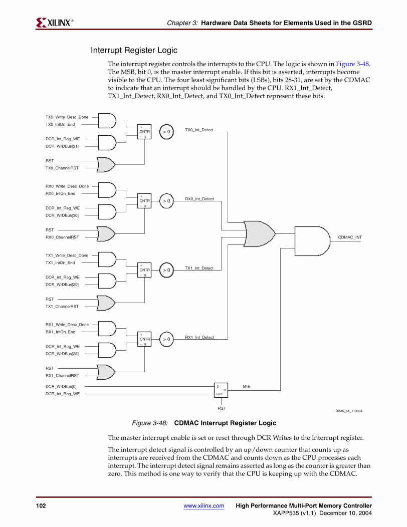
102 www.xilinx.com High Performance Multi-Port Memory ControllerXAPP535 (v1.1) December 10, 2004
Chapter 3: Hardware Data Sheets for Elements Used in the GSRDR
Interrupt Register Logic
The interrupt register controls the interrupts to the CPU. The logic is shown in Figure 3-48. The MSB, bit 0, is the master interrupt enable. If this bit is asserted, interrupts become visible to the CPU. The four least significant bits (LSBs), bits 28-31, are set by the CDMAC to indicate that an interrupt should be handled by the CPU. RX1_Int_Detect, TX1_Int_Detect, RX0_Int_Detect, and TX0_Int_Detect represent these bits.
The master interrupt enable is set or reset through DCR Writes to the Interrupt register.
The interrupt detect signal is controlled by an up/down counter that counts up as interrupts are received from the CDMAC and counts down as the CPU processes each interrupt. The interrupt detect signal remains asserted as long as the counter is greater than zero. This method is one way to verify that the CPU is keeping up with the CDMAC.
Figure 3-48: CDMAC Interrupt Register Logic
X535_54_113004
+
-CNTR
R
TX0_Write_Desc_Done
TX0_IntOn_End
DCR_Int_Reg_WE
DCR_WrDBus[31]
RST
TX0_ChannelRST
> 0 TX0_Int_Detect
+
-CNTR
R
RX0_Write_Desc_Done
RX0_IntOn_End
DCR_Int_Reg_WE
DCR_WrDBus[30]
RST
RX0_ChannelRST
> 0 RX0_Int_Detect
+
-CNTR
R
TX1_Write_Desc_Done
TX1_IntOn_End
DCR_Int_Reg_WE
DCR_WrDBus[29]
RST
TX1_ChannelRST
> 0 TX1_Int_Detect
+
-CNTR
R
RX1_Write_Desc_Done
RX1_IntOn_End
DCR_Int_Reg_WE
DCR_WrDBus[28]
RST
RX1_ChannelRST
> 0 RX1_Int_Detect
QD
CER
DCR_WrDBus[0]
DCR_Int_Reg_WE
RST
CDMAC_INT
MIE
ARCHIVED APPLICATION NOTE - NOT SUPPORTED FOR NEW DESIGNS

High Performance Multi-Port Memory Controller www.xilinx.com 103XAPP535 (v1.1) December 10, 2004
Communication Direct Memory Access Controller (CDMAC)R
The CDMAC issues an interrupt if an engine has written back a descriptor and the descriptor's INT_ON_END bit was asserted. If this happens on the TX0 Engine, bit 31 of the Interrupt Register is set. The CPU acknowledges the interrupt on the TX0 engine by issuing a DCR Write to the Interrupt register, writing a logical '1' to bit 31.
Timing DiagramsThe timing diagrams in this section illustrate essential CDMAC functionality. Together these timing diagrams demonstrate DCR Writes, Port Read and Writes for bursts and cache-lines, and Tx and Rx Byteshifter operation. The first timing diagram shows a DMA Process. The following two timing diagrams break the process down into individual DMA transfers. The following two diagrams show Tx and Rx Byteshifting. The final diagram shows the way that descriptors are written back in the case of a two-descriptor chain.
CDMAC TX0 DMA Process Timing Diagram
Figure 3-49 is an example of a TX0 DMA process.
Figure 3-49: CDMAC TX0 DMA Process Timing Diagram
0ns 100ns 800ns 90 8.2us 8.3us 8.6us 8.7us 8.8us
DCR_Write
DCR_Ack
DCR_ABus[9:0]
DCR_DBusIn[31:0]
TX0_Busy
TX0_Completed
TX0_INT
P0_AddrReq
P0_AddrAck
P0_Addr[31:0]
P0_Size[1:0]
P0_RNW
P0_wrDataAck_Pos
P0_wrDataAck_Neg
P0_rdDataAck_Pos
P0_rdDataAck_Neg
003003 001 002 020 000 003 02F
00000100 00000000 80000001
0000000000000000 00000180 00001080 00001400 00000000
22 3 2 2
DCR write to clear interruptWrite current descriptor pointer to start engine
TX0 current descriptor pointer is at DCR address 3
Descriptor address in memory
Read descriptor
At address 100
Start B16 transfer
B16 read at address 1000
3 = B16 Request
Engine is busy
Interrupt
Completed processing data
Write back status to descriptor
Write RequestRead Request
X535_55_113004
ARCHIVED APPLICATION NOTE - NOT SUPPORTED FOR NEW DESIGNS
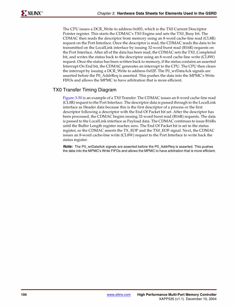
104 www.xilinx.com High Performance Multi-Port Memory ControllerXAPP535 (v1.1) December 10, 2004
Chapter 3: Hardware Data Sheets for Elements Used in the GSRDR
The CPU issues a DCR_Write to address 0x003, which is the TX0 Current Descriptor Pointer register. This starts the CDMAC's TX0 Engine and sets the TX0_Busy bit. The CDMAC then reads the descriptor from memory using an 8-word cache-line read (CL8R) request on the Port Interface. Once the descriptor is read, the CDMAC reads the data to be transmitted on the LocalLink interface by issuing 32-word burst read (B16R) requests on the Port Interface. After all of the data has been read, the CDMAC sets the TX0_Completed bit, and writes the status back to the descriptor using an 8-word cache-line write (CL8W) request. Once the status has been written back to memory, if the status contains an asserted Interrupt On End bit, the CDMAC generates an interrupt to the CPU. The CPU then clears the interrupt by issuing a DCR_Write to address 0x02F. The P0_wrDataAck signals are asserted before the P0_AddrReq is asserted. This pushes the data into the MPMC's Write FIFOs and allows the MPMC to have arbitration that is more efficient.
TX0 Transfer Timing Diagram
Figure 3-50 is an example of a TX0 Transfer. The CDMAC issues an 8-word cache-line read (CL8R) request to the Port Interface. The descriptor data is passed through to the LocalLink interface as Header data because this is the first descriptor of a process or the first descriptor following a descriptor with the End Of Packet bit set. After the descriptor has been processed, the CDMAC begins issuing 32-word burst read (B16R) requests. The data is passed to the LocalLink interface as Payload data. The CDMAC continues to issue B16Rs until the Buffer Length register reaches zero. The End Of Packet bit is set in the status register, so the CDMAC asserts the TX_EOP and the TX0_EOF signal. Next, the CDMAC issues an 8-word cache-line write (CL8W) request to the Port Interface to write back the status register.
Note: The P0_wrDataAck signals are asserted before the P0_AddrReq is asserted. This pushes the data into the MPMC's Write FIFOs and allows the MPMC to have arbitration that is more efficient.
ARCHIVED APPLICATION NOTE - NOT SUPPORTED FOR NEW DESIGNS

High Performance Multi-Port Memory Controller www.xilinx.com 105XAPP535 (v1.1) December 10, 2004
Communication Direct Memory Access Controller (CDMAC)R
RX0 Transfer Timing Diagram
Figure 3-51 is an example of a RX0 Transfer. The CDMAC issues an 8-word cache-line read (CL8R) request to the Port Interface. After the descriptor has been read and the RX LocalLink interface is in the Payload state, the CDMAC instructs the RX LocalLink interface to begin collecting Payload data from the RX LocalLink interface and writing it to memory. If the RX0_SOP signal is asserted, the Start Of Packet bit is set in the status register. If the RX0_EOP signal is asserted, the End Of Packet bit is set in the status register. To process the Payload data, the CDMAC issues 32-word burst write (B16W) requests until all Payload data has been written to memory, or until the Buffer Length register reaches 0. In this example all of the Payload data has been received, as indicated by RX0_EOP.
Figure 3-50: TX0 Transfer Timing Diagram
0ns 600ns 700ns 1.8us 8.0us 8.1us 8.2us 8.3us
P0_AddrReq
P0_AddrAck
P0_Addr[31:0]
P0_Size[1:0]
P0_RNW
P0_wrDataAck_Pos
P0_wrDataAck_Neg
P0_wrDataBE_Pos[3:0]
P0_wrDataBE_Neg[3:0]
P0_wrData_Pos[31:0]
P0_wrData_Neg[31:0]
P0_rdDataAck_Pos
P0_rdDataAck_Neg
P0_rdData_Pos[31:0]
P0_rdData_Neg[31:0]
TX0_SOF
TX0_SOP
TX0_EOP
TX0_EOF
TX0_Src_Rdy
TX0_Dst_Rdy
TX0_D[31:0]
TX0_Rem[3:0]
00000100 00000180 00001080 00001400 00000000
22 3 2 2
F
FF 7 F
XXXXXXXX
XXXXXXXXXXXXXXXX XXXXXXXX
0000000000000000 00000000 00000140 00010203 000000F9 00000101
0000000000000000 00001000 00000000 00001004 04050607 000000FA 00000102
0000000000000000 0000000000000140 00010203 00000101
0
Request CL8 read of request Request B16R for payload Clear interrupt
Header data acks
Header data
Start of Frame
Valid header data (active low) Valid payload data
End of Payload
End of Frame
Start of Payload
Byte enable for status byte
Write back footer data
X535_56_113004
ARCHIVED APPLICATION NOTE - NOT SUPPORTED FOR NEW DESIGNS

106 www.xilinx.com High Performance Multi-Port Memory ControllerXAPP535 (v1.1) December 10, 2004
Chapter 3: Hardware Data Sheets for Elements Used in the GSRDR
Because there is no more Payload data to process, the CDMAC instructs the RX LocalLink interface to collect Footer data and write the status and the application data back to memory using an 8-word cache-line write (CL8W) request to the Port Interface. The P0_wrDataAck signals are asserted before the P0_AddrReq is asserted. This pushes the data into the MPMC's Write FIFOs and allows the MPMC to have arbitration that is more efficient.
Figure 3-51: RX0 Transfer Timing Diagram
0ns 100ns 1.0us 1.1us 1. 13.2us 13.3us 13.4us 13.5us 13.6us 13.7us 13.8us
P0_AddrReq
P0_AddrAck
P0_Addr[31:0]
P0_Size[1:0]
P0_RNW
P0_wrDataAck_Pos
P0_wrDataAck_Neg
P0_wrDataBE_Pos[3:0]
P0_wrDataBE_Neg[3:0]
P0_wrData_Pos[31:0]
P0_wrData_Neg[31:0]
P0_rdDataAck_Pos
P0_rdDataAck_Neg
P0_rdData_Pos[31:0]
P0_rdData_Neg[31:0]
RX0_SOF
RX0_SOP
RX0_EOP
RX0_EOF
RX0_Src_Rdy
RX0_Dst_Rdy
RX0_D[31:0]
RX0_Rem[3:0]
00000580 00001000 00003B2A 00003BAA 00000000
22 3 3 2
FF 0 F 0 3 F 8 0 F
FF 0 F 0 3 F 0 F
XXXXXXXXXXXXXXXX F87CFAF0 00000000
XXXXXXXXXXXXXXXX A050FAA8 F078FAF8 00000A00
0000000000000000 00000000 00000000
0000000000000000 00001000 000031A7 000032F1
FA000000FA000000 00000000 FA000000
0
Request CL8 read of descriptor
Byte enable (diable) to RAM
Start of Frame
Start of Payload
End of Payload
End of Frame
Write back footer data
Clear INT
Footer BE
X535_57_113004
ARCHIVED APPLICATION NOTE - NOT SUPPORTED FOR NEW DESIGNS

High Performance Multi-Port Memory Controller www.xilinx.com 107XAPP535 (v1.1) December 10, 2004
Communication Direct Memory Access Controller (CDMAC)R
TX0 Byteshifter Timing Diagram
Figure 3-52 is an example of the TX0 Byteshifter. A descriptor has already been read by the CDMAC. The Buffer Address register was set to 0x1079. This sets the 3-bit StartOffset signal to 0x1. In this diagram,0 the first and second 32-word burst read (B16R) transactions are shown. The first 120 bytes are ignored on P0_rdData_Pos and P0_rdData_Neg. The cycle that the 122nd byte is valid on P0_rdData_Pos, the last 3 bytes of P0_rdData_Pos is placed in the last 3 bytes of Port_RdData, as indicated by Set_Px_rdData_Pos. All 4 bytes of Port_RdData are clock enabled into Port_TX_Out by asserting all 4 bytes of Byte_Reg_CE. The Byte_Sel signals move the Port_RdData bytes into the correct location. On the cycle that the 125th byte is valid, the first byte of P0_rdDataNeg is placed in the first byte of Port_RdData. Again, all 4 bytes are clock enabled into Port_TX_Out by asserting Byte_Reg_CE. Port_TX_Out now contains the last 3 bytes of P0_rdData_Pos and the first byte of P0_rdData_Neg in the correct order: 0x01020304. Port_TX_Out is passed on to the LocalLink interface by asserting the TX0_Src_Rdy signal. The leftover 3 bytes from P0_rdDataNeg are stored by clock enabling them into Port_TX_Out and deasseting the last 3 bytes of Byte_Reg_CE. These bits are deasserted until the P0_rdDataAck_Pos is asserted for second B16R. The 3 left-over bytes from the first B16R and the first byte from the second B16R are passed on to the LocalLink interface by asserting the TX0_Src_Rdy Signal. The Byte_Reg_CE begins clock enabling all four bytes of Port_RdData as it becomes available. This data is passed on to the LocalLink interface.
ARCHIVED APPLICATION NOTE - NOT SUPPORTED FOR NEW DESIGNS

108 www.xilinx.com High Performance Multi-Port Memory ControllerXAPP535 (v1.1) December 10, 2004
Chapter 3: Hardware Data Sheets for Elements Used in the GSRDR
Figure 3-52: TX0 Byteshifter Timing Diagram
0ns 20ns 40n 1.06us 1.08u 1.36us 1.38us 1.40us 1.86us 1.88us 1.90us
P0_AddrReq
P0_AddrAck
P0_Addr[31:0]
P0_Size[1:0]
P0_RNW
P0_wrDataAck_Pos
P0_wrDataAck_Neg
P0_wrDataBE_Pos[3:0]
P0_wrDataBE_Neg[3:0]
P0_wrData_Pos[31:0]
P0_wrData_Neg[31:0]
P0_rdDataAck_Pos
P0_rdDataAck_Neg
P0_rdData_Pos[31:0]
P0_rdData_Neg[31:0]
Port_RdData[31:0]
Port_TX_Out[31:0]
Byte_Sel0[1:0]
Byte_Sel1[1:0]
Byte_Sel2[1:0]
Byte_Sel3[1:0]
Byte_Reg_CE[3:0]
CS[3:0]
StartOffset[2:0]
TX0_SOF
TX0_SOP
TX0_EOP
TX0_EOF
TX0_Src_Rdy
TX0_Dst_Rdy
TX0_D[31:0]
TX0_Rem[3:0]
0000018000000180 00001000 000010F9 00001179
22 3 2 2
F
FF
XXXXXXXX
XXXXXXXXXXXXXXXX
0000014000000140 00010203 08090A0B 00010203 08090A0B 10111213
0000100400001004 04050607 0C0D0E0F 0000001E 04050607 0C0D0E0F 14151617
0000014000000140 00010203 04010203 08090A0B 080D0E0F
0000014000000140 00010203 00001D00 01020304 05060708
33 0
22 3
11 2
00 1
FF F F 0 F 1 F
00 1 2 4 5 7 2 3
00 1
0000014000000140 00010203 00001D00 01020304 05060708
0
B16R request
Start of Payload
1st valid word 2nd valid word
2nd B16R1st B16R
Discarding first 0x78 bytes
Data NOT valid in discard stage
Bytes [0 1 2 3] on posedge of DDR RAM
Bytes [4 5 6 7] on negedge of DDR RAM
Recombine data from posedge and negedge to form [4 1 2 3]
Indicates valid bytes
Offset of 1: starting at second byte
Reorder byte positions to form final word [1 2 3 4]
Byte_Selx control muxes for byte reordering
1st burst ends, waiting for 2nd burst
X535_58_113004
ARCHIVED APPLICATION NOTE - NOT SUPPORTED FOR NEW DESIGNS

High Performance Multi-Port Memory Controller www.xilinx.com 109XAPP535 (v1.1) December 10, 2004
Communication Direct Memory Access Controller (CDMAC)R
RX0 Byteshifter Timing Diagram
Figure 3-53 is an example of the RX0 Byteshifter. A descriptor has already been read by the CDMAC. The buffer address was set to 0x3076. This sets the 3-bit First_offset signal to 0x6. In this diagram, the first and part of the second 32-word burst write (B16W) transactions are shown. The CDMAC stuffs 112 bytes of data into the MPMC's FIFOs by asserting P0_wrDataAck_Pos and P0_wrDataAck_Neg with the byte enables (P0_wrDataBE_Pos and P0_wrDataBE_Neg) deasserted.
Four bytes of LocalLink Payload data is collected and shifted by six bytes by asserting CE_Pos. Because the offset is by six bytes, P0_wrDataAck_Pos is asserted with the byte enable signals deasserted. P0_wrDataAck_Neg is asserted with the last two byte-enable signals asserted. From this point on, all byte enables are asserted until the LocalLink interface indicates that there is no more Payload data, as specified by RX0_EOP, or until the number of bytes specified by Buffer Length register have been written to memory. The LocalLink interface stalls between B16W requests by deasserting RX0_Dst_Rdy. When the CDMAC instructs the Byteshifter to execute a B16W, the data is pushed into the MPMC's Write FIFOs before the P0_AddrReq is asserted.
ARCHIVED APPLICATION NOTE - NOT SUPPORTED FOR NEW DESIGNS
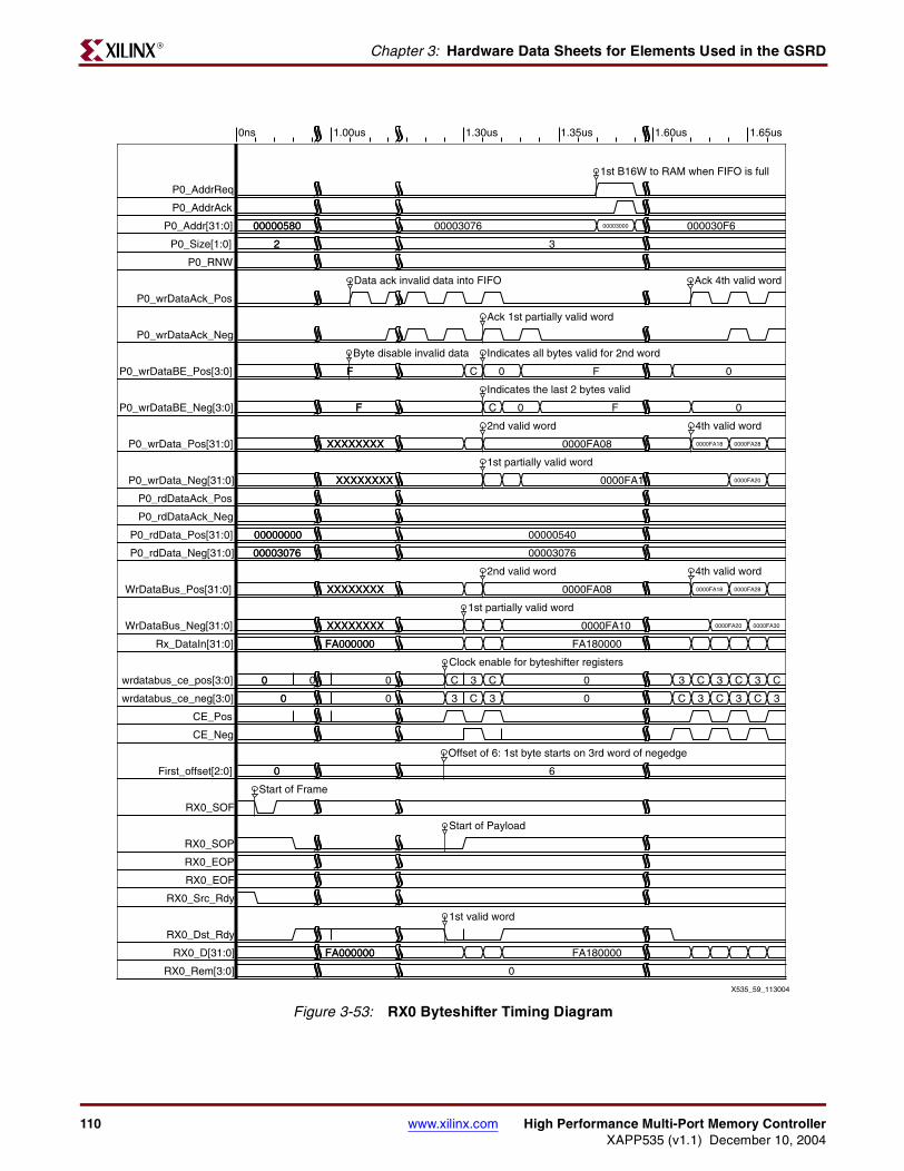
110 www.xilinx.com High Performance Multi-Port Memory ControllerXAPP535 (v1.1) December 10, 2004
Chapter 3: Hardware Data Sheets for Elements Used in the GSRDR
Figure 3-53: RX0 Byteshifter Timing Diagram
0ns 1.00us 1.30us 1.35us 1.60us 1.65us
P0_AddrReq
P0_AddrAck
P0_Addr[31:0]
P0_Size[1:0]
P0_RNW
P0_wrDataAck_Pos
P0_wrDataAck_Neg
P0_wrDataBE_Pos[3:0]
P0_wrDataBE_Neg[3:0]
P0_wrData_Pos[31:0]
P0_wrData_Neg[31:0]
P0_rdDataAck_Pos
P0_rdDataAck_Neg
P0_rdData_Pos[31:0]
P0_rdData_Neg[31:0]
WrDataBus_Pos[31:0]
WrDataBus_Neg[31:0]
Rx_DataIn[31:0]
wrdatabus_ce_pos[3:0]
wrdatabus_ce_neg[3:0]
CE_Pos
CE_Neg
First_offset[2:0]
RX0_SOF
RX0_SOP
RX0_EOP
RX0_EOF
RX0_Src_Rdy
RX0_Dst_Rdy
RX0_D[31:0]
RX0_Rem[3:0]
0000058000000580 00003076 00003000 000030F6
22 3
FF C 0 F 0
FF C 0 F 0
XXXXXXXXXXXXXXXX 0000FA08 0000FA18 0000FA28
XXXXXXXXXXXXXXXX 0000FA10 0000FA20
0000000000000000 00000540
0000307600003076 00003076
XXXXXXXXXXXXXXXX 0000FA08 0000FA18 0000FA28
XXXXXXXXXXXXXXXX 0000FA10 0000FA20 0000FA30
FA000000FA000000 FA180000
00 0 0 C 3 C 0 3 C 3 C 3 C
00 0 3 C 3 0 C 3 C 3 C 3
00 6
FA000000FA000000 FA180000
0
Start of Frame
Start of Payload
1st valid word
Data ack invalid data into FIFO
Byte disable invalid data
Ack 1st partially valid word
Indicates the last 2 bytes valid
1st partially valid word
1st B16W to RAM when FIFO is full
2nd valid word
Indicates all bytes valid for 2nd word
1st partially valid word
2nd valid word
Clock enable for byteshifter registers
Ack 4th valid word
4th valid word
4th valid word
Offset of 6: 1st byte starts on 3rd word of negedge
X535_59_113004
ARCHIVED APPLICATION NOTE - NOT SUPPORTED FOR NEW DESIGNS
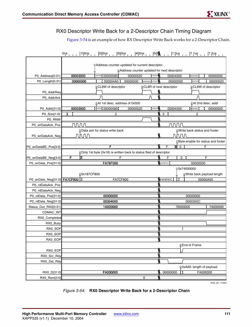
High Performance Multi-Port Memory Controller www.xilinx.com 111XAPP535 (v1.1) December 10, 2004
Communication Direct Memory Access Controller (CDMAC)R
RX0 Descriptor Write Back for a 2-Descriptor Chain Timing Diagram
Figure 3-54 is an example of how RX Descriptor Write Back works for a 2-Descriptor Chain.
Figure 3-54: RX0 Descriptor Write Back for a 2-Descriptor Chain
0ns 100ns 200ns 300ns 400ns 500 7.0us 7.1us 7.2us
P0_Address[0:31]
P0_Length[0:31]
P0_AddrReq
P0_AddrAck
P0_Addr[31:0]
P0_Size[1:0]
P0_RNW
P0_wrDataAck_Pos
P0_wrDataAck_Neg
P0_wrDataBE_Pos[3:0]
P0_wrDataBE_Neg[3:0]
P0_wrData_Pos[31:0]
P0_wrData_Neg[31:0]
P0_rdDataAck_Pos
P0_rdDataAck_Neg
P0_rdData_Pos[31:0]
P0_rdData_Neg[31:0]
Status_Out_RX0[0:31]
CDMAC_INT
RX0_Completed
RX0_Busy
RX0_SOF
RX0_SOP
RX0_EOP
RX0_EOF
RX0_Src_Rdy
RX0_Dst_Rdy
RX0_D[31:0]
RX0_Rem[3:0]
0000350000003500 00000500 00000580 00000520 000005A0 00004500 00000520 00000000
0000000000000000 000004A0 00000500 00000520 000004A0 00000500 00000000 00000520
0000350000003500 00000500 00000580 00000520 000005A0 00004500 00000520 00000000
33 2 3 2
FF F 8 0 F
FF 7 F F 0 F
FA78F000FA78F000 FAF0F078 00000000
FA7CF800FA7CF800 FA7CF800 FAF8F87C 00000A00
0000000000000000 00000000
0000400000004000 0000355C
1A0000001A000000 76000000 74000000
FA000000FA000000 00000000 FA000000
0
0x187CF800
Only 1st byte (0x18) is written back to status flied of descriptor
Data ack for status write back
CL8W of descriptor
At 1st desc. address of 0x500
Address counter updated for next descriptor
CL8R of next descriptor
Byte-enable for status and footer
Write back status and footer
End of Frame
Write back payload length
CL8W of descriptor
At 2nd desc. addr
0xA00: length of payload
Address counter updated for current descriptor
0x74000000
X535_60_113004
ARCHIVED APPLICATION NOTE - NOT SUPPORTED FOR NEW DESIGNS
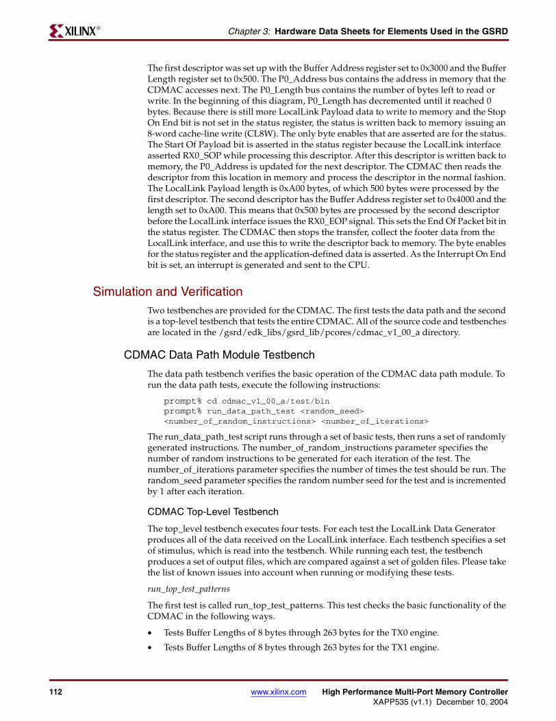
112 www.xilinx.com High Performance Multi-Port Memory ControllerXAPP535 (v1.1) December 10, 2004
Chapter 3: Hardware Data Sheets for Elements Used in the GSRDR
The first descriptor was set up with the Buffer Address register set to 0x3000 and the Buffer Length register set to 0x500. The P0_Address bus contains the address in memory that the CDMAC accesses next. The P0_Length bus contains the number of bytes left to read or write. In the beginning of this diagram, P0_Length has decremented until it reached 0 bytes. Because there is still more LocalLink Payload data to write to memory and the Stop On End bit is not set in the status register, the status is written back to memory issuing an 8-word cache-line write (CL8W). The only byte enables that are asserted are for the status. The Start Of Payload bit is asserted in the status register because the LocalLink interface asserted RX0_SOP while processing this descriptor. After this descriptor is written back to memory, the P0_Address is updated for the next descriptor. The CDMAC then reads the descriptor from this location in memory and process the descriptor in the normal fashion. The LocalLink Payload length is 0xA00 bytes, of which 500 bytes were processed by the first descriptor. The second descriptor has the Buffer Address register set to 0x4000 and the length set to 0xA00. This means that 0x500 bytes are processed by the second descriptor before the LocalLink interface issues the RX0_EOP signal. This sets the End Of Packet bit in the status register. The CDMAC then stops the transfer, collect the footer data from the LocalLink interface, and use this to write the descriptor back to memory. The byte enables for the status register and the application-defined data is asserted. As the Interrupt On End bit is set, an interrupt is generated and sent to the CPU.
Simulation and VerificationTwo testbenches are provided for the CDMAC. The first tests the data path and the second is a top-level testbench that tests the entire CDMAC. All of the source code and testbenches are located in the /gsrd/edk_libs/gsrd_lib/pcores/cdmac_v1_00_a directory.
CDMAC Data Path Module Testbench
The data path testbench verifies the basic operation of the CDMAC data path module. To run the data path tests, execute the following instructions:
prompt% cd cdmac_v1_00_a/test/binprompt% run_data_path_test <random_seed> <number_of_random_instructions> <number_of_iterations>
The run_data_path_test script runs through a set of basic tests, then runs a set of randomly generated instructions. The number_of_random_instructions parameter specifies the number of random instructions to be generated for each iteration of the test. The number_of_iterations parameter specifies the number of times the test should be run. The random_seed parameter specifies the random number seed for the test and is incremented by 1 after each iteration.
CDMAC Top-Level Testbench
The top_level testbench executes four tests. For each test the LocalLink Data Generator produces all of the data received on the LocalLink interface. Each testbench specifies a set of stimulus, which is read into the testbench. While running each test, the testbench produces a set of output files, which are compared against a set of golden files. Please take the list of known issues into account when running or modifying these tests.
run_top_test_patterns
The first test is called run_top_test_patterns. This test checks the basic functionality of the CDMAC in the following ways.
• Tests Buffer Lengths of 8 bytes through 263 bytes for the TX0 engine.
• Tests Buffer Lengths of 8 bytes through 263 bytes for the TX1 engine.
ARCHIVED APPLICATION NOTE - NOT SUPPORTED FOR NEW DESIGNS

High Performance Multi-Port Memory Controller www.xilinx.com 113XAPP535 (v1.1) December 10, 2004
Communication Direct Memory Access Controller (CDMAC)R
• Test Buffer Addresses with offsets of 0 bytes through 256 bytes for the TX0 engine.
• Test Buffer Addresses with offsets of 0 bytes through 256 bytes for the TX1 engine.
• Tests Buffer Addresses with offsets of 0 bytes through 256 bytes and Buffer Lengths of 0xA00, 0xA01, or 0xAFF for the RX0 engine.
• Tests Buffer Addresses with offsets of 0 bytes through 256 bytes and Buffer Lengths of 0xA00, 0xA01, or 0xAFF for the RX1 engine.
To run this test, execute the following instructions:
prompt% cd cdmac_v1_00_a/test/bin
prompt% run_top_test_patterns
run_top_test
The second test, run_top_test, generates a set of random instructions as stimulus.
To run this test, execute the following instructions:
prompt% cd cdmac_v1_00_a/test/binprompt% run_top_test test <random_seed> <number_of_random_instructions_tx0> <number_of_random_instructions_tx1> <number_of_random_instructions_rx0> <number_of_random_instructions_rx1> <number_of_iterations>
The run_top_test script tests a set of randomly generated instructions.
The number_of_random_instructions parameters specify the number of random instructions to be generated on each engine for each iteration of the test.
The number_of_iterations parameter specifies the number of times the test should be run.
The random_seed parameter specifies the random number seed for the test and is incremented by 1 after each iteration.
run_top_test_byte
The third test, run_top_test_byte, is similar to run_top_test. Instead of randomly generating a set of instructions as stimulus, this test allows exact instructions to be specified.
To run this test, edit cdmac_v1_00_a/test/bin/top_mem_byte.txt to specify descriptor and memory contents, then edit cdmac_v1_00_a/test/bin/top_TX0_inst_byte.txt to specify the instructions, and execute the following instructions:
prompt% cd cdmac_v1_00_a/test/bin prompt% run_top_test test_byte
run_top_test_timer
The fourth test, run_top_test_timer, is similar to run_top_test. Instead of randomly generating a set of instructions as stimulus, this test allows the exact stimulus to be specified at every clock cycle.
To run this test, edit cdmac_v1_00_a/hdl/verilog/testbench_CDMAC_timer.v with the desired instructions, and execute the following instructions:
prompt% cd cdmac_v1_00_a/test/bin prompt% run_top_test test_timer
ARCHIVED APPLICATION NOTE - NOT SUPPORTED FOR NEW DESIGNS

114 www.xilinx.com High Performance Multi-Port Memory ControllerXAPP535 (v1.1) December 10, 2004
Chapter 3: Hardware Data Sheets for Elements Used in the GSRDR
Directory Structuredata
o cdmac_v2_1_0.mpdo cdmac_v2_1_0.pao
hdlo verilog
cdmac.vcdmac_cntl.vcdmac_datapath.v
testo bin
data_path_check_file.txtgen_color_bar_tx_check.plgen_data_path_inst.plgen_data_path_stimulus.plgen_data_path_stimuls_check.plgen_top_inst.plgen_top_stimulus.plgen_top_test_patterns.plgen_top_test_patterns_rx_mem_check.plgen_top_tx_check.plgen_top_tx_stimulus.plprocess_data_path_check_files.plprocess_top_mem_files.plprocess_top_test_patterns_mem_files.plprocess_top_tx_check_files.plrun_color_bar_tx_checkrun_data_path_testrun_top_testrun_top_test_atomicrun_top_test_byterun_top_test_patternsrun_top_test_timertop_mem.txttop_payload2.txtdata_path_sim
func_simo compile_ver.fo func_sim_defs.vo mti_sim.do
top_atomic_simfunc_sim
o compile_ver.fo func_sim_defs.vo mti_sim.do
top_byte_simfunc_sim
o compile_ver.fo func_sim_defs.vo mti_sim.do
top_patterns_simfunc_sim
o compile_ver.fo func_sim_defs.vo mti_sim.do
top_simfunc_sim
o compile_ver.f
ARCHIVED APPLICATION NOTE - NOT SUPPORTED FOR NEW DESIGNS
High Performance Multi-Port Memory Controller www.xilinx.com 115XAPP535 (v1.1) December 10, 2004
Communication Direct Memory Access Controller (CDMAC)R
o func_sim_defs.vo mti_sim.do
top_timer_simfunc_sim
o compile_ver.fo func_sim_defs.vo mti_sim.do
o func_simwave_data_path.dowave_top.do
o hdlverilog
ll_data_gen.vmpmc_fifo_4.vmpmc_fifo_32.vmpmc_fifo_32_be.vmpmc_fifo_32_rdcntr.vmpmc_fifo_rdcntr.vtestbench_CDMAC_data_path.vtestbench_CDMAC_timer.vtestbench_CDMAC_top.v
Using the CDMAC in a SystemThe CDMAC is normally instanciated along with the MPMC. The reference systems provided with this application note show how it is connected and used. By examining the contents of the hardware source files, simulation, and test software that is provided, one can better understand the functionality of the CDMAC and how it is used.
There are many methods of use for the CDMAC. Each method depends upon what the CDMAC is connected to, and what the data rate requirements are. The provided reference systems show a typical example of a video application wherein the CDMAC is connected to a set of video devices that are streaming in data. In XAPP536, “Gigabit System Reference Design,” the CDMAC illustrates a typical Ethernet communication system.
The DMA engines contained in the CDMAC are independent of one another. This allows the software that is manipulating the DMA descriptors to not have to know about other channels. This is a very important facility for device driver development. The features currently provided in the CDMAC are designed to help further offload the CPUs required load to manage DMA traffic. The preferred methods of operation (as the CDMAC is currently implemented) are best observed when analyzing the stand-alone software applications that are provided with this application note. These are documented in Chapter 5, “Software Applications Contained in the GSRD.”
SoftwareSee the “CDMAC Software Model” for Programmer's Model and Register usage of the CDMAC.
ARCHIVED APPLICATION NOTE - NOT SUPPORTED FOR NEW DESIGNS
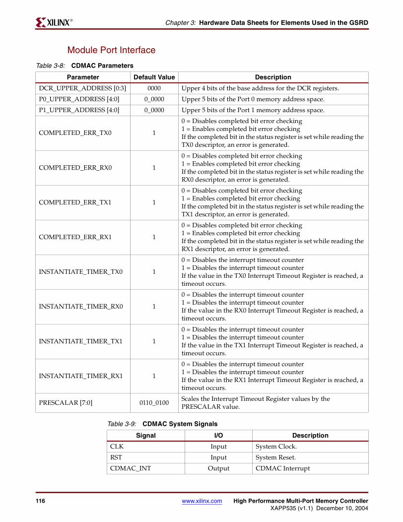
116 www.xilinx.com High Performance Multi-Port Memory ControllerXAPP535 (v1.1) December 10, 2004
Chapter 3: Hardware Data Sheets for Elements Used in the GSRDR
Module Port Interface
Table 3-8: CDMAC Parameters
Parameter Default Value Description
DCR_UPPER_ADDRESS [0:3] 0000 Upper 4 bits of the base address for the DCR registers.
P0_UPPER_ADDRESS [4:0] 0_0000 Upper 5 bits of the Port 0 memory address space.
P1_UPPER_ADDRESS [4:0] 0_0000 Upper 5 bits of the Port 1 memory address space.
COMPLETED_ERR_TX0 1
0 = Disables completed bit error checking 1 = Enables completed bit error checkingIf the completed bit in the status register is set while reading the TX0 descriptor, an error is generated.
COMPLETED_ERR_RX0 1
0 = Disables completed bit error checking 1 = Enables completed bit error checkingIf the completed bit in the status register is set while reading the RX0 descriptor, an error is generated.
COMPLETED_ERR_TX1 1
0 = Disables completed bit error checking 1 = Enables completed bit error checkingIf the completed bit in the status register is set while reading the TX1 descriptor, an error is generated.
COMPLETED_ERR_RX1 1
0 = Disables completed bit error checking 1 = Enables completed bit error checkingIf the completed bit in the status register is set while reading the RX1 descriptor, an error is generated.
INSTANTIATE_TIMER_TX0 1
0 = Disables the interrupt timeout counter 1 = Disables the interrupt timeout counterIf the value in the TX0 Interrupt Timeout Register is reached, a timeout occurs.
INSTANTIATE_TIMER_RX0 1
0 = Disables the interrupt timeout counter 1 = Disables the interrupt timeout counterIf the value in the RX0 Interrupt Timeout Register is reached, a timeout occurs.
INSTANTIATE_TIMER_TX1 1
0 = Disables the interrupt timeout counter 1 = Disables the interrupt timeout counterIf the value in the TX1 Interrupt Timeout Register is reached, a timeout occurs.
INSTANTIATE_TIMER_RX1 1
0 = Disables the interrupt timeout counter 1 = Disables the interrupt timeout counterIf the value in the RX1 Interrupt Timeout Register is reached, a timeout occurs.
PRESCALAR [7:0] 0110_0100Scales the Interrupt Timeout Register values by the PRESCALAR value.
Table 3-9: CDMAC System Signals
Signal I/O Description
CLK Input System Clock.
RST Input System Reset.
CDMAC_INT Output CDMAC Interrupt
ARCHIVED APPLICATION NOTE - NOT SUPPORTED FOR NEW DESIGNS

High Performance Multi-Port Memory Controller www.xilinx.com 117XAPP535 (v1.1) December 10, 2004
Communication Direct Memory Access Controller (CDMAC)R
Table 3-10: CDMAC DCR Signals
Signal I/O Description
DCR_ABus [0:9] Input Address bus
DCR_DBusIn [0 :31] Input Write data bus
DCR_Write Input Write request
DCR_Read Input Read request
DCR_Ack Output Write/Read acknowledge
DCR_DBusOut [0:31] Output Read data bus
Table 3-11: CDMAC Port Interface Signals
Signal I/O Description
Px_AddrReq Output Port X Address Request
Px_AddrAck InputPort X Address Acknowledge
Valid for one clock cycle
Px_Addr [31:0] OutputPort X Address
Valid during Address Request
Px_RNW Output
0 = Port X Write
1 = Port X Read
Valid during Address Request
Px_Size [1:0] Output
00 = Port X Single-Word Transfer
01 = Port X 4-Word Cache-Line Transfer
10 = Port X 8-Word Cache-Line Transfer
11 = Port X 32-Word Burst Transfer
Px_rdData_Rdy InputIndicates that data for a particular request on Port X is ready. Valid for one clock cycle.
Px_rdData_Pos [31:0] Input Port X Read Data (first word out of memory)
Px_rdData_Neg [31:0] Input Port X Read Data (second word out of memory)
Px_rdWdAddr_Pos [4:0] InputPx_Address + Px_rdWdAddr_Pos = Address for Px_rdData_Pos. Only valid during single-word and cache-line transfers.
Px_rdWdAddr_Neg[4:0] InputPx_Address + Px_rdWdAddr_Neg = Address for Px_rdData_Neg. Only valid during single-word and cache-line transfers.
Px_rdDataAck_Pos OutputIndicates CDMAC has consumed Px_rdData_Pos and that the connecting device should output the next word of data. Valid for one clock cycle.
Px_rdDataAck_Neg OutputIndicates CDMAC has consumed Px_rdData_Neg and that the connecting device should output the next word of data. Valid for one clock cycle.
Px_rdComp OutputIndicates that all data for a particular request on Port X has been consumed by the CDMAC.
Px_rd_fifo_busy Input Indicates that the CDMAC is not allowed to assert Px_rd_rst.
Px_rd_rst OutputCan be asserted when Px_rd_fifo_busy is not asserted and the CDMAC does not need more data from a particular transfer.
ARCHIVED APPLICATION NOTE - NOT SUPPORTED FOR NEW DESIGNS

118 www.xilinx.com High Performance Multi-Port Memory ControllerXAPP535 (v1.1) December 10, 2004
Chapter 3: Hardware Data Sheets for Elements Used in the GSRDR
Px_wrData_Pos [31:0] Output Port X Write Data (first word out of memory)
Px_wrData_Neg [31:0] Output Port X Write Data (second word out of memory)
Px_wrDataBE_Pos [3:0] Output Byte Enables for Px_wrData_Pos. Active Low.
Px_wrDataBE_Neg[3:0] Output Byte Enables for Px_wrData_Neg. Active Low.
Px_wrDataAck_Pos OutputIndicates CDMAC has valid data on Px_wrData_Pos. Can be asserted only while Px_wr_fifo_full_Pos is not asserted. Valid for one clock cycle.
Px_wrDataAck_Neg OutputIndicates CDMAC has valid data on Px_wrData_Neg. Can be asserted only while Px_wr_fifo_full_Neg is not asserted. Valid for one clock cycle.
Px_wrComp OutputIndicates that all data for a particular request on Port X has been sent out of the CDMAC.
Px_wr_fifo_busy Input Indicates that the CDMAC is not allowed to assert Px_wr_rst
Px_wr_fifo_full_Pos Input Indicates that Px_wrDataAck_Pos is not allowed to be asserted.
Px_wr_fifo_full_Neg Input Indicates that Px_wrDataAck_Neg is not allowed to be asserted.
Px_wr_rst OutputIf the CDMAC asserts Px_wrDataAck’s early (before issuing a request), the CDMAC can assert Px_wr_rst to clear the data so that it is not written to memory. This can only be asserted while Px_wr_fifo_busy is not asserted.
Table 3-11: CDMAC Port Interface Signals (Continued)
Signal I/O Description
Table 3-12: CDMAC LocalLink Signals
Signal I/O Description
TXn_D[31:0] Output TXn Data bus. Valid while TXn_Src_Rdy and TXn_Dst_Rdy are asserted.
TXn_Rem[3:0] Output TXn remainder. Data mask for last word of header, payload, or footer.
TXn_SOF Output TXn start of frame. Active low.
TXn_EOF Output TXn end of frame. Active low.
TXn_SOP Output TXn start of payload. Active low.
TXn_EOP Output TXn end of payload. Active low.
TXn_Src_Rdy OutputTXn source ready. Active low. Indicates CDMAC has valid data on the TXn LocalLink outputs.
TXn_Dst_Rdy InputTXn Destination ready. Active low. Indicates connecting device is ready to receive data.
RXn_D[31:0] Input RXn Data bus. Valid while RXn_Src_Rdy and RXn_Dst_Rdy are asserted.
RXn_Rem[3:0] Input RXn remainder. Data mask for last word of header, payload, or footer.
RXn_SOF Input RXn start of frame. Active low.
RXn_EOF Input RXn end of frame. Active low.
RXn_SOP Input RXn start of payload. Active low.
RXn_EOP Input RXn end of payload. Active low.
RXn_Src_Rdy InputRXn source ready. Active low. Indicates connecting device has valid data on the RXn LocalLink outputs.
RXn_Dst_Rdy Output RXn Destination ready. Active low. Indicates CDMAC is ready to receive data.
ARCHIVED APPLICATION NOTE - NOT SUPPORTED FOR NEW DESIGNS

High Performance Multi-Port Memory Controller www.xilinx.com 119XAPP535 (v1.1) December 10, 2004
PLB to MPMC Personality ModuleR
PLB to MPMC Personality Module
OverviewThe PLB to MPMC Personality Module is designed to connect a standard CoreConnect PLB Master device to the MPMC’s Port Interface. It implements the necessary slave PLB logic and buffering to support the subset of PLB transactions commonly used by PLB masters. The PLB to MPMC Personality Module is designed for high-performance applications where low latency and high throughput are desired.
Features• 64-bit PLB master interface
• Supports single data beat or cacheline PLB data transfers (4 or 8 words)
• Supports pipelined read transactions for improved performance of back-to-back reads
Related DocumentsThe IBM CoreConnect™ 64-Bit Processor Local Bus: Architecture Specification provides additional information.
High-Level Block DiagramFigure 3-55 shows the high-level block diagram for the PLB to MPMC Personality Module. This module translates PLB Master requests into MPMC Port Interface requests.
Hardware
Architecture
Figure 3-55 shows a high-level block diagram of the design. Pipeline registers buffer address, read data, and write data paths between the PLB and MPMC Ports. The pipeline registers add an additional latency cycle but help to allow for higher throughputs. The control logic contains simple logic, a FIFO, and counters for managing the flow of data, reporting errors, and generating the necessary sequence of signal handshaking. The design assumes that the MPMC and PLB interfaces run off the same system clock.
The MPMC PLB Interface is designed to translate standard PLB memory transactions into equivalent MPMC transactions. The PLB transactions supported are 4 and 8 word cacheline transfers and single data beat (non-burst) transfers. These transactions are supported by a number of PLB masters including the PPC405. Transfer qualifiers other than Mn_RNW and Mn_size are ignored (for example: Mn_compress, Mn_guarded, Mn_Ordered).
PLB transactions are immediately acknowledged by the control logic unless it is busy processing a previous transaction. Once a transaction is acknowledged on the PLB side, the address (Port_Addr), read /write flag (Port_RNW) and size (Port_Size) information are pipelined and presented to the MPMC along with the Port_AddrReq signal asserted. The signal latch_plb_xfer_qual controls this pipeline register. Once the MPMC responds with Port_AddrAck, the control logic issues the necessary sequence of control signals to perform the corresponding data transfer. Since PLB transactions are immediately acknowledged and then forwarded to the MPMC, the Mn_abort signal has a limited
ARCHIVED APPLICATION NOTE - NOT SUPPORTED FOR NEW DESIGNS

120 www.xilinx.com High Performance Multi-Port Memory ControllerXAPP535 (v1.1) December 10, 2004
Chapter 3: Hardware Data Sheets for Elements Used in the GSRDR
window in which the PLB master can assert it before the transaction is accepted. This reduces the ability of the PLB master to cancel unneeded transactions late into a data transfer, but allows the MPMC to operate more efficiently and at higher clock rates since combinatorial bypass paths associated with abort handling logic can be removed.
Since the MPMC contains FIFOs to hold write data and write byte enables, the PLB MPMC interface supports posted write (for example “fire and forget”) transactions. This allows write transactions to be buffered and completed on the PLB side before the data has been written to memory. The advantage of posted writes is that the PLB master is then free to begin the next transaction, thus reducing latency. The control logic contains counters that help generate the necessary sequence of PLB_MnWrDAck, Port_wrDataAck, and Port_wrComp signals to pipeline the write data and byte enables into the MPMC. Pipeline registers also handle the process of splitting the 64 bit PLB write data into two 32-bit buses with requisite positive and negative edge clocking.
The 32-bit positive and negative edge clocked read data from the MPMC is pipelined and reassembled into the single 64-bit PLB data path. Once the MPMC signals that read data is available by asserting Port_rdDataRdy, counters in the control logic handle the sequencing of Port_rdDataAck, Port_rdComp, and PLB_MnRdDAck signals to pull data out of the
Figure 3-55: PLB to MPMC Personality Module High-Level Block Diagram
X535_61_113004
CE
Mn_size[0:1]Mn_RNWMn_Abus[0:31]
Port_Size[1:0]Port_RNW
Port_Addr[31:0]
Control Logic
latc
h_pl
b_xf
er_q
ual
Mn_abortMn_request
PL B_MnAddrAckPLB_MnWrDAck
Port_AddrReqPort_AddrAck
Port_wrDataAck_Pos/Neg
Port_wrComp
Port_wrDataBE_Pos[3:0]
Mn_BE[0:7]
0xFF
0x00
Port_wrDataBE_Neg[3:0]
Port_wrData_Pos[31:0]
Port_wrData_Neg[31:0]
CEMn_wrDBus[0:63]
Port_rdData_Pos/Neg[31:0]PLB_Mn_rdDBus[0:63]Port_rdWdAddr_Pos/Neg[3:0]PL B_Mn_rdWdAddr[0:3]
PL B_MnRdDAck
Port_rdDataAck_Pos/Neg
Port_rdComp
Port_rdDataRdy
PL B_MnBusyPLB_MnErr
PLBPort
MPMCPort
ARCHIVED APPLICATION NOTE - NOT SUPPORTED FOR NEW DESIGNS

High Performance Multi-Port Memory Controller www.xilinx.com 121XAPP535 (v1.1) December 10, 2004
PLB to MPMC Personality ModuleR
MPMC's FIFOs and send them to the PLB master. In order to better support transaction pipelining of back to back read transfers, FIFOs in the control logic can queue up to two outstanding PLB read transactions. This FIFO is unwound as the MPMC signals Port_rdDataRdy to begin completion of each of the queued read transactions. The effect of pipelined read transactions is to reduce their effective latency and free up the PLB master to issue subsequent transactions. Target-word-first PLB cacheline reads are also supported.
The PLB MPMC interface has the ability to signal address errors in case the PLB master issues a request to an address not serviced by the MPMC. In the case of an address error, the transaction is completed using a "dummy" or placeholder transaction to the MPMC but with the PLB_MnErr flag being asserted. This allows the normal control logic to be used to generate the correct number of read or write data acknowledges thus reducing the amount of additional error handling logic. The only difference is that PLB_MnErr is asserted as well. Since reads from the MPMC have no side effects, the use of a dummy read transaction does not effect data in memory. For writes causing address errors, all byte enables are disabled so that the dummy write has no effect on memory. Address errors are detected using an address comparator configured via the module's parameters.
Simulation and VerificationA stand-alone testbench is provided with the design to demonstrate the functionality of the PLB MPMC interface in a small test environment. The testbench executes a number of PLB side read/write transactions while behavioral logic in the testbench emulates the expected behavior of the MPMC at its Port Interface.
After writing data on PLB, it is read back and compared against what was written. Any data comparison errors are reported. The PLB master that performs reads and writes comes from the CoreConnect Toolkit and is controlled by a script file. Refer to the README.txt file located in the design files under the test directory.
Module Port Interface
Table 3-13: PLB to MPMC Interface Parameters
Name Default Description
C_BASE_ADDR 0x0000000032-bit PLB base address, must be aligned on an address boundary equal to the decoder size specified below.
C_ADDR_MASK 0xF8000000
Address Decoder Mask Bits:
0x0000_0000 => 4GB 0x8000_0000 => 2GB
C000_0000 => 1GB
E000_0000 => 512MB
F000_0000 => 256MB F800_0000 => 128MB
…
Table 3-14: PLB to MPMC Global Signals
Name Direction Description
CLK Input System Clock
RESET Input System Reset
ARCHIVED APPLICATION NOTE - NOT SUPPORTED FOR NEW DESIGNS

122 www.xilinx.com High Performance Multi-Port Memory ControllerXAPP535 (v1.1) December 10, 2004
Chapter 3: Hardware Data Sheets for Elements Used in the GSRDR
Table 3-15: PLB to MPMC Port Interface Signals
Name Direction Description
Port_Addr [31:0] Output Address
Port_AddrAck Input Address Acknowledge
Port_AddrReq Output Address Request
Port_rdComp Output Read Complete
Port_rdData_Neg [31:0] Input Read Data, Negative Clock Edge
Port_rdData_Pos [31:0] Input Read Data, Positive Clock Edge
Port_rdDataAck_Neg Output Read Data Acknowledge, Negative Clock Edge
Port_rdDataAck_Pos Output Read Data Acknowledge, Positive Clock Edge
Port_rdDataRdy Input Read Data Ready
Port_rdWdAddr_Neg[4:0] Input Read Word Address, Negative Clock Edge
Port_rdWdAddr_Pos[4:0] Input Read Word Address, Positive Clock Edge
Port_RNW Output Read/Not Write
Port_Size[1:0] Output Size
Port_wrComp Output Write Complete
Port_wrData_Neg[31:0] Output Write Data, Negative Clock Edge
Port_wrData_Pos[31:0] Output Write Data, Positive Clock Edge
Port_wrDataAck_Neg Output Write Data Acknowledge, Negative Clock Edge
Port_wrDataAck_Pos Output Write Data Acknowledge, Positive Clock Edge
Port_wrDataBE_Neg[3:0] Output Write Data Byte Enables, Negative Clock Edge
Port_wrDataBE_Pos[3:0] Output Write Data Byte Enables, Positive Clock Edge
ARCHIVED APPLICATION NOTE - NOT SUPPORTED FOR NEW DESIGNS

High Performance Multi-Port Memory Controller www.xilinx.com 123XAPP535 (v1.1) December 10, 2004
PLB to MPMC Personality ModuleR
Table 3-16: PLB to MPMC, PLB Interface Signals
Name Direction Description
Mn_abort Input Master abort bus request indicator
Mn_ABus [0:31] Input Master address bus
Mn_BE [0:7] Input Master byte enables
Mn_busLock Input Master bus lock*
Mn_compress Input Master compressed data transfer indicator*
Mn_guarded Input Master guarded transfer indicator*
Mn_lockErr Input Master lock error indicator*
Mn_msize [0:1] Input Master data bus size*
Mn_ordered Input Master synchronize transfer indicator*
Mn_priority [0:1] Input Master bus request priority*
Mn_rdBurst Input Master burst read transfer indicator*
Mn_request Input Master bus request
Mn_RNW Input Master read/not write
Mn_size[0:3] Input Master transfer size
Mn_type [0:2] Input Master transfer type*
Mn_wrBurst Input Master burst write transfer indicator*
Mn_wrDBus [0:63] Input Master write data bus
PLB_MnAddrAck Output PLB master address acknowledge
PLB_MnBusy Output PLB master slave busy indicator
PLB_MnErr Output PLB master slave error indicator
PLB_MnRdBTerm Output PLB master terminate read burst indicator*
PLB_MnRdDAck Output PLB master read data acknowledge
PLB_MnRdDBus [0:63] Output PLB master read data bus
PLB_MnRdWdAddr[0:3] Output PLB master read word address
PLB_MnRearbitrate Output PLB master bus rearbitrate indicator*
PLB_Mnssize [0:1] Output PLB slave data bus size*
PLB_MnWrBTerm Output PLB master terminate write burst indicator*
PLB_MnWrDAck Output PLB master write data acknowledge
Notes: 1. * Denotes PLB port signal defined in the PLB Specification, but is either unused or tied to a constant inside this module.
ARCHIVED APPLICATION NOTE - NOT SUPPORTED FOR NEW DESIGNS

124 www.xilinx.com High Performance Multi-Port Memory ControllerXAPP535 (v1.1) December 10, 2004
Chapter 3: Hardware Data Sheets for Elements Used in the GSRDR
DCR to OPB Bridge
OverviewThe DCR to OPB Interface translates DCR transactions to OPB transactions. It allows simple OPB devices to be easily connected to the DCR interface of the PPC405 or other DCR master thus eliminating the need for more complex full-featured bus bridges. This document describes a "Lite" or simplified implementation of this design that only supports basic OPB devices that conform to various transaction restrictions. In particular, only 32-bit, fixed latency OPB transactions are supported. Many commonly used OPB devices such as UARTs, GPIOs, and Interrupt Controllers are compatible with the DCR to OPB Interface module.
Features• 32-bit DCR slave interface
• Direct connection to a 32-bit OPB slave without an OPB arbiter
• Configurable address decode and address offset
Related DocumentsThe following documents provide additional information
• IBM CoreConnect™ 64-Bit On-Chip Peripheral Bus: Architecture Specifications
• IBM CoreConnect™ 32-Bit Device Control Register Bus: Architecture Specifications
ARCHIVED APPLICATION NOTE - NOT SUPPORTED FOR NEW DESIGNS

High Performance Multi-Port Memory Controller www.xilinx.com 125XAPP535 (v1.1) December 10, 2004
DCR to OPB BridgeR
High-Level Block DiagramFigure 3-56 shows the high-level block diagram for the DCR to OPB bridge. This module translates the DCR bus into an OPB master so that OPB slave peripherals can be easily hooked up. The DCR to OPB Bridge is used in the reference systems to connect the OPB UART Lite and OPB GPIO peripherals. It is also possible to simply build native DCR based peripherals, rather than use this bridge. However the use of the bridge allows connection of commonly available OPB peripherals. The bridge itself consumes very little FPGA area (~40 slices).
Figure 3-56: DCR to OPB Bridge High-Level Block Diagram
X535_62_113004
ControlLogic
DCR Side OPB Side
DCR_DBusOut
Sl_DBus
M_DBus
M_Select
Sl_retry
Sl_xferAck
Sl_errAck
AddressComparator
DCR_Ack
DCR_Write
DCR_DBusIn
M_RNWDCR_Read
M_ABusDCR_ABus
DCR to OPBAddress Offset
ARCHIVED APPLICATION NOTE - NOT SUPPORTED FOR NEW DESIGNS

126 www.xilinx.com High Performance Multi-Port Memory ControllerXAPP535 (v1.1) December 10, 2004
Chapter 3: Hardware Data Sheets for Elements Used in the GSRDR
Hardware
Architecture
Figure 3-56 shows a high-level block diagram of the design. Pipeline registers buffer address, read data, and write data paths between the DCR and OPB Interface Ports. The pipeline registers add an additional latency cycle in each direction but help to allow for higher throughputs and improved timing. The control logic contains simple logic for managing the flow of data and generating the necessary sequence of signal handshaking. The design assumes that the DCR and OPB interfaces run off the same system clock.
The DCR to OPB Interface is designed to translate standard DCR transactions into equivalent OPB transactions. The control logic decodes the DCR address during the rising edge of DCR_Read or DCR_Write and initiates the OPB transaction if there is an address comparator match. Once an OPB transaction is acknowledged, the DCR transaction is then acknowledged and any necessary data is returned. In the transaction is destined for another DCR device (address comparator miss) a multiplexer on the DCR_DBusOut path allows DCR data to be bypassed through to the other device. In order to keep the logic simple and to account for feature differences between the two buses, there are some restrictions on the behavior of the attached OPB device that are described below.
The DCR specification permits only 32-bit data transfers with no provisions for byte enables. Therefore, only full words can be read or written to the OPB slave device. OPB slaves requiring 1, 2, or 3 byte transfers are not supported.
A DCR master initiating a DCR transaction must receive a response within 16 DCR clock cycles (or 64 CPU clock cycles for the PPC405). This requires that the OPB slave be able to acknowledge the OPB transaction within a window of time sufficient to take into account two cycles of pipeline delay through the bridge in additional to any pipeline delays present in the DCR chain itself. OPB slave devices that use the OPB timeout suppress signal or have long acknowledge delays are not compatible.
The concept of retry or bus error is not part of the DCR specification. Therefore, an OPB slave device response of Sl_retry or Sl_errAck is be communicated back to the DCR master as such. These signals are treated the same as the normal transaction acknowledge with Sl_xferAck.
A parameterizeable interface allows the user to specify the range of DCR addresses to be decoded and acknowledged by the DCR to OPB Interface. The DCR address decoder must be a power of 2 in size with the address aligned on that power of 2 boundary. In addition to the DCR address decode, a two's complement offset value can be specified to translate the DCR address to an OPB address. Since the DCR address space is limited to 1024 words, the user should be careful to use relatively small addressing windows for the OPB devices.
Generally, a separate DCR to OPB Bridge should be used for each OPB slave device to be attached to the DCR chain. This arrangement provides the most flexibility for setting up narrow addressing windows and different OPB address offsets. However, if multiple OPB slaves occupy a small enough range of addresses, it is possible for the OPB slaves to share a single DCR to OPB Interface. To do so, simply OR together the "sl_*" signals from the OPB slaves and connect the output of the OR logic to the corresponding signals of the DCR to OPB Interface.
ARCHIVED APPLICATION NOTE - NOT SUPPORTED FOR NEW DESIGNS

High Performance Multi-Port Memory Controller www.xilinx.com 127XAPP535 (v1.1) December 10, 2004
DCR to OPB BridgeR
Module Port Interface
Table 3-17: DCR to OPB Bridge Parameters
Name Default Description
C_DCR_BASE_ADDR[0:9] 0x00010-bit DCR base address, must be aligned on an address boundary equal to the decoder size specified below.
C_DCR_ADDR_MASK[0:9] 0x3F8
DCR Address Decoder Mask Bits:0x000 => 1K Words (4 KB)0x200 => 512 Words (2 KB)…0x3F8 => 8 Words (32 Bytes)0x3FC => 4 Words (16 Bytes)0x3FE => 2 Words (8 Bytes)0x3FF => 1 Word (4 Bytes)
C_OFFSET[0:31] 0x00000000Twos complement address offset to translate from DCR address to OPB address.
Table 3-18: DCR to OPB Bridge Global Signals
Name Direction Description
RST Input System Reset
SYS_dcrClk Input DCR Clock
Table 3-19: DCR to OPB Bridge DCR Interface Signals
Name Direction Description
DCR_ABus[0:9] Input DCR Address Bus
DCR_Ack Output DCR Acknowledge
DCR_DbusIn[0:31] Input DCR Data Bus In
DCR_DBusOut[0:31] Output DCR Data Bus Out
DCR_Read Input DCR Read Strobe
DCR_Write Input DCR Write Strobe
Table 3-20: DCR to OPB Bridge, OPB Interface Signals
Name Direction Description
M_ABus [0:31] Output Master address bus
M_BE [0:3] Output Master byte enables (Tied off to constant 0xF)
M_DBus [0:31] Output Master write data bus
M_RNW Output Master read not write
M_select Output Master bus request
M_seqAddr Output Master sequential address (Tied off to constant 0)
Sl_DBus [0:31] Input Slave read data bus
Sl_errAck Input Slave error acknowledge
Sl_retry Input Slave bus cycle retry
Sl_xferAck Input Slave transfer acknowledge
ARCHIVED APPLICATION NOTE - NOT SUPPORTED FOR NEW DESIGNS

128 www.xilinx.com High Performance Multi-Port Memory ControllerXAPP535 (v1.1) December 10, 2004
Chapter 3: Hardware Data Sheets for Elements Used in the GSRDR
LocalLink TFT Controller
OverviewThe LocalLink TFT LCD Controller is a hardware display controller for a 640x480 resolution VGA screen. It is capable of showing up to 256K colors and is designed for the NEC TFT Color LCD Module NL6448BC20-08 that is mounted on the Xilinx ML300 board. The design contains a LocalLink interface that receives data from the Communications Direct Memory Access Controller (CDMAC) and displays the data onto the TFT screen. The design also contains a Device Control Register (DCR) interface used for configuring the controller.
Features• 32-bit DCR slave interface for control registers
• 32-bit LocalLink interface for receiving pixel data
• Support for asynchronous LocalLink and TFT clocks
Related DocumentsThe following documents provide additional information:
• LocalLink Specification
• NEC TFT Color LCD Module: NL6448BC20-08
High-Level Block DiagramFigure 3-57 illustrates the high-level block diagram for the LocalLink TFT Controller. The LocalLink TFT Controller has three main elements: A LocalLink Rx Interface, a 1-kbit x18-bit FIFO, and a Back End TFT Interface Logic block. These three items together allow the CDMAC to output Video data onto the TFT screen of an ML300 Evaluation Platform.
Figure 3-57: LocalLink TFT Controller High-Level Block Diagram
X535_63_113004
Green Data
TFT Clock Domain PLB Clock Domain
6
Local Li nkInterface
Logic
6 Blue Data
6 Red Data1 kB
x18 bit
FIFO
Back EndTFT
InterfaceLogic
Green Data6
6 Blue Data
6 Red Data
FIFO ReadVideoSignals
toTFT
Display
FIFO Write
LocalLi nkPixelData
FIFO FULL
ARCHIVED APPLICATION NOTE - NOT SUPPORTED FOR NEW DESIGNS

High Performance Multi-Port Memory Controller www.xilinx.com 129XAPP535 (v1.1) December 10, 2004
LocalLink TFT ControllerR
Hardware
Architecture
Figure 3-57 shows a high-level block diagram of the design. The LocalLink TFT LCD Controller has a LocalLink interface that receives pixel data from an external data source. The pixel data is stored in an internal FIFO buffer and then sent out to the TFT display with the necessary timing to correctly display the image. The video memory is arranged so that each RGB pixel is represented by a 32-bit word in memory (See “Video Memory” section). As each line interval begins, data is fetched from the FIFO, pipelined, and then displayed. This process repeats continuously over every line and frame to be displayed on the 640x480 VGA TFT screen.
The back-end logic driving the TFT display operates in the same clock domain as the video clock. It reads out data from the FIFO and transmits the pixel data to the TFT. The back-end logic automatically handles the timing of all the video synchronization signals including back porch and front porch blanking. See Figure 3-58 and Figure 3-59 for more information on the video timing.
The LocalLink TFT LCD Controller allows for the LocalLink clock and TFT video clocks to be asynchronous to each other. Special logic allows control signals to be passed between asynchronous LocalLink and TFT clock domains. A dual port BRAM is used in the FIFO to pass video data between the two clock domains.
It is important to design the system so that there is sufficient bandwidth between the LocalLink TFT LCD Controller and the CDMAC to meet the video bandwidth requirements of the TFT. Furthermore, there must be enough available bandwidth left over for the rest of the system. If more bandwidth is needed for the rest of the system, the TFT clock frequency can be reduced. However, reducing the TFT clock frequency also lowers the refresh rate of the screen. This can lead to a noticeable flicker on the screen if the TFT clock is too slow.
The LocalLink interface logic accepts any available LocalLink data presented to it. Any non-payload data is discarded. The TFT Controller should only be sent a full 32-bit word of data at a time. It is not designed to accept 1 to 3 byte data transfers. If the FIFO feeding data to the backend logic becomes full, the LocalLink signal DST_RDY_N is asserted to throttle the flow of data.
A DCR interface allows the display to be rotated by 180 degrees, turned off, or reset under software control. When the display is turned off, a black screen is displayed and the back end logic does not read any data from the FIFO. However, LocalLink data can be written into the FIFO when the display is off. By default, on power-on or system reset the TFT display starts out in the off setting. The TFT should not be turned on until there is sufficient data sent to it that the FIFO would not run empty. The display becomes misaligned if the FIFO becomes empty.
ARCHIVED APPLICATION NOTE - NOT SUPPORTED FOR NEW DESIGNS

130 www.xilinx.com High Performance Multi-Port Memory ControllerXAPP535 (v1.1) December 10, 2004
Chapter 3: Hardware Data Sheets for Elements Used in the GSRDR
Simulation and VerificationA stand-alone testbench is provided with the design to demonstrate the functionality of LocalLink TFT LCD Controller in a small test environment. The testbench emulates a LocalLink source sending an incrementing binary data pattern to the TFT Controller. The testbench also generates DCR commands to start up the TFT. It then checks that the data sent to the external TFT display matches the data it received from LocalLink. Refer to the README.txt file located in the design files under the test directory.
Figure 3-58: LocalLink TFT Controller Video Horizontal Timing Diagram
D (0,Y)
thp = 96 TFT Clocksthb = 48 TFT ClocksDE = 640 TFT Clocksthf = 16 TFT Clocks
thp
1 12
thb thf640CLK (Fixed)
1CLK
Invalid Invalid
Hsync
CLK
DER0 to R5G0 to G5B0 to B5
D (1,Y) D (639,Y)
th = 800 TFT Clocks (Horizontal)
Hsync
thp = 96 TFT Clocks
th
thp
X535_64_113004
ARCHIVED APPLICATION NOTE - NOT SUPPORTED FOR NEW DESIGNS

High Performance Multi-Port Memory Controller www.xilinx.com 131XAPP535 (v1.1) December 10, 2004
LocalLink TFT ControllerR
Figure 3-59: LocalLink TFT Controller Video Vertical Timing Diagram
D(0,Y)
tvp = 2 h_syncstvb = 31 h_syncsDE = 640 TFT Clockstvf = 12 h_syncs
tvp
1
D(X,Y)D(X,0) D(X,479)
12 3
tvb tvf480H (Fixed)
1H
Invalid Invalid
Invalid Invalid
Note: X = 0 to 639
Vsync
DER0 to R5G0 to G5B0 to B5
R0 to R5G0 to G5B0 to B5
Hsync
D(1,Y) D(639,Y)D(638,Y)D(X,Y)
DE
Display period is 480 h_syncs
tvp = 2 h_syncstv = 525 h_syncs (Vertical)
Vsync
Display period is 480 h_syncs
tv
tvp
X535_65_113004
ARCHIVED APPLICATION NOTE - NOT SUPPORTED FOR NEW DESIGNS

132 www.xilinx.com High Performance Multi-Port Memory ControllerXAPP535 (v1.1) December 10, 2004
Chapter 3: Hardware Data Sheets for Elements Used in the GSRDR
LocalLink TFT Controller Pixel Organization
Video Memory
Each 32-bit word of pixel data is encoded according to the following table. Data should be sent to the TFT controller in order from leftmost pixel to rightmost pixel for each line. The lines should be sent from top to bottom.
Table 3-21: LocalLink TFT Controller Pixel Color Encoding
MSB
LSB
31 30 29 28 27 26 25 24 23 22 21 20 19 18 17 16 15 14 13 12 11 10 9 8 7 6 5 4 3 2 1 0
- RED - GREEN - BLUE -
Table 3-22: LocalLink TFT Controller
Bit Description
[31:24] Undefined: Read as 0x0000
[23:18] RED: Red Pixel Data
0b000000 = darkest
0b111111 = brightest
access: read/write
default value: undefined
[17:16] Undefined: Read as 0
[15:10] GREEN: Green Pixel Data
0b000000 = darkest
0b111111 = brightest
access: read/write
default value: undefined
[9:8] Undefined: Read as 0
[7:2] BLUE: Blue Pixel Data
0b000000 = darkest
0b111111 = brightest
access: read/write
default value: undefined
[1:0] Undefined: Read as 0
ARCHIVED APPLICATION NOTE - NOT SUPPORTED FOR NEW DESIGNS
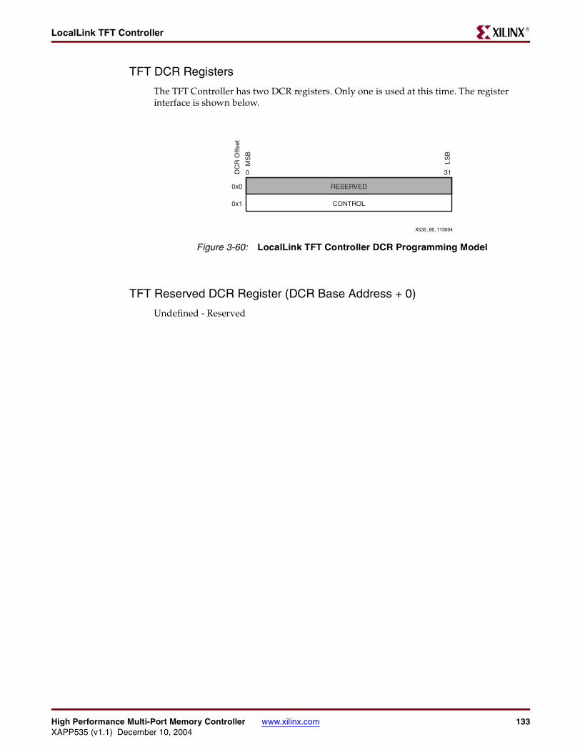
High Performance Multi-Port Memory Controller www.xilinx.com 133XAPP535 (v1.1) December 10, 2004
LocalLink TFT ControllerR
TFT DCR Registers
The TFT Controller has two DCR registers. Only one is used at this time. The register interface is shown below.
TFT Reserved DCR Register (DCR Base Address + 0)
Undefined - Reserved
Figure 3-60: LocalLink TFT Controller DCR Programming Model
X535_66_113004
RESERVED0x0
CONTROL0x1
0 31DC
R O
ffset
MS
B
LSB
ARCHIVED APPLICATION NOTE - NOT SUPPORTED FOR NEW DESIGNS

134 www.xilinx.com High Performance Multi-Port Memory ControllerXAPP535 (v1.1) December 10, 2004
Chapter 3: Hardware Data Sheets for Elements Used in the GSRDR
TFT Control Register (DCR Base Address + 1)
* The intention of the reset bit is to allow the CDMAC to be stopped and restarted or to allow the TFT to recover from a misaligned state due to the FIFO becoming empty. During soft reset, the TFT enable bit should be turned off before releasing the soft reset. Pixel Data can then be sent to pre-fill the data FIFO before enabling the TFT and starting up the backend logic. The process resynchronizes the Pixel data to the correct screen location and resume normal operation.
Table 3-23: LocalLink TFT Controller
DC
R O
ffset
MSB
LSB
0 1 2 3 4 5 6 7 8 9 10 11 12 13 14 15 16 17 18 19 20 21 22 23 24 25 26 27 28 29 30 31
1
RST RESERVED
DP
S
EN
Table 3-24: Control Register Definition
Bit Description
DCR Base Address +1
[0] RST: TFT Reset*
0 = Normal running operation
1 = TFT Controller soft reset
When set, the data FIFO is cleared and all logic is held in reset. This bit must be written back to 0 by software to leave the reset state.
Note: this reset bit does not affect the other control bits
access: read/write
default value: 0
[1:29] RESERVED: Read as 0
30 DPS: Display scan direction
0 = Sets the display to use normal scan direction
1 = Sets the display to use a reverse scan direction
access: read/write
default value: 0 (Normal scan direction)
[15:10] EN: TFT Enable
0 = Disable TFT Display
1 = Normal Operation
NOTE: When disabled, a black is displayed and LocalLink read xfers are disabled.
access: read/write
default value: 0 (TFT Disabled)
ARCHIVED APPLICATION NOTE - NOT SUPPORTED FOR NEW DESIGNS

High Performance Multi-Port Memory Controller www.xilinx.com 135XAPP535 (v1.1) December 10, 2004
LocalLink TFT ControllerR
Module Port Interface
Table 3-25: LocalLink TFT Controller Parameters
Name Default Description
C_DCR_BASEADDR N/ABase address of DCR control registers. Must be aligned on an even DCR address boundary (least significant bit = 0)
C_DCR_HIGHADDR N/AUpper address boundary, must be set to value of C_DCR_BASEADDR + 1
C_DPS_INIT 1
Initial Reset State of DPS control bit:
0 = DPS output bit resets to 0.
This initializes the display to use a normal scan direction.
1 = DPS output bit resets to 1.
This initializes the display to use a reverse scan direction (rotates screen 180 degrees).
Table 3-26: LocalLink TFT Controller Global Signals
Name Direction Description
SYS_dcrClk Input DCR System Clock
SYS_tftClk Input TFT Video Clock
CLK Input LocalLink Clock
RESET Input System Reset
Table 3-27: LocalLink TFT Controller External I/Os
Name Direction Description
TFT_LCD_HSYNC Output Horizontal Sync (Negative Polarity)
TFT_LCD_VSYNC Output Vertical Sync (Negative Polarity)
TFT_LCD_DE Output Data Enable
TFT_LCD_CLK Output Video Clock
TFT_LCD_DPS Output Selection of Scan Direction
TFT_LCD_R[5:0] Output Red Pixel Data
TFT_LCD_G[5:0] Output Green Pixel Data
TFT_LCD_B[5:0] Output Blue Pixel Data
ARCHIVED APPLICATION NOTE - NOT SUPPORTED FOR NEW DESIGNS

136 www.xilinx.com High Performance Multi-Port Memory ControllerXAPP535 (v1.1) December 10, 2004
Chapter 3: Hardware Data Sheets for Elements Used in the GSRDR
Table 3-28: LocalLink TFT Controler, LocalLink interface Signals
Name Direction Description
DIN [31:0] Input Data
REM [3:0] Input Remainder
SOF_N Input Start of Frame
SOP_N Input Start of Payload
EOP_N Input End of Payload
EOF_N Input End of Frame
SRC_RDY_N Input Source Ready
DST_RDY_N Output Destination Ready
Table 3-29: LocalLink TFT Controller DCR Slave Signals
Name Direction Description
DCR_ABus[0:9] Input DCR Address Bus
DCR_DBusIn[0:31] Input DCR Data Bus In
DCR_Read Input DCR Read Strobe
DCR_Write Input DCR Write Strobe
DCR_Ack Output DCR Acknowledge
DCR_DbusOut[0:31] Output DCR Data Bus Out
ARCHIVED APPLICATION NOTE - NOT SUPPORTED FOR NEW DESIGNS

High Performance Multi-Port Memory Controller www.xilinx.com 137XAPP535 (v1.1) December 10, 2004
LocalLink Data GeneratorR
LocalLink Data Generator
OverviewThe LocalLink Data Generator is a module developed to send known data to the receive portion of the CDMAC via an Rx LocalLink interface. The CDMAC receives the data and places it in the memory specified by the DMA descriptor(s). The data generated is a colorbar pattern for a VGA (640x480) sized TFT video display. The default pattern is shown in Figure 3-62. The upper half of the TFT displays 20 patterns of vertical bars of various colors that gradient from black to a particular color. The lower half of the TFT then switches the gradient from the particular color to black. Figure 3-61 shows the top-level block diagram for the LocalLink Data Generator.
Features• 32-bit DCR slave interface for control registers• 32-bit LocalLink interface for sending generated data
Related DocumentsThe following documents provide additional information:• IBM CoreConnect™ 32-Bit Device Control Register Bus: Architecture Specification
• LocalLink Specification
High-Level Block DiagramFigure 3-61 illustrates the high-level block diagram for the LocalLink Data Generator. The Data Generator logic block generates pixels according to the settings of the DCR Color Registers. The default pattern is shown in Figure 3-62. Once the data has been generated, it is sent across the LocalLink interface. The optional DCR Interface allows the CPU to configure color patterns, and control over the speed of the LocalLink interface. This is useful for generating system level performance metrics by slowing down the data rate across the LocalLink interface to emulate slower speed devices.
Figure 3-61: LocalLink Data Generator High-Level Block Diagram
X535_67_113004
CLK
DCR_WriteDCR_Read
DCR_ABusDCR_DBusIn
DCR_Ack
DCR_DBusOut
LL_Src_Rdy_n
LL_SOF_nLL_SOP_nLL_EOP_nLL_EOF_n
LL_DataLL_Rem
LL_Dst_Rdy_n
RESET
Data GeneratorLogic
DCR InterfaceLogic
LocalLink Data Generator
LocalLink InterfaceLogic
ARCHIVED APPLICATION NOTE - NOT SUPPORTED FOR NEW DESIGNS

138 www.xilinx.com High Performance Multi-Port Memory ControllerXAPP535 (v1.1) December 10, 2004
Chapter 3: Hardware Data Sheets for Elements Used in the GSRDR
Hardware
Introduction
The LocalLink Data Generator is designed to output data to the CDMAC attached to the other end of the LocalLink interface. Figure 3-61 shows a block diagram of LocalLink Data Generator internals. There are three main elements: Data Generator Logic, DCR Interface Logic, and LocalLink interface Logic. These are further described in the following sections.
Figure 3-62 shows the default pattern that the LocalLink Data Generator produces. This is a 640 pixel x 480 line at 32-bits per pixel.
The Data Generator Logic is the heart of the module and produces the pattern of data. The data it generates is sent across the LocalLink interface so that it can be received by the CDMAC. The Data Generator Logic produces a VGA screen worth of data, or 640 pixels by 480 lines of 32-bit pixels. The form of the data across the 32-bit LocalLink interface is as 0xAARRGGBB, where AA is a constant 0xAA, RR is the 8 bit red color value, GG is the 8 bit green color value, and BB is the 8 bit blue color value. The ML300 VGA display only uses the upper six bits of each colors data. The actual data patterns produced by the Data Generator Logic are controllable in software via the DCR Interface.
The DCR Interface Logic provides a programmatic way to alter LocalLink Data Generator behavior. It has two main purposes: the alteration of color data and control of the LocalLink data rate. The first is used to allow the CPU to modify the colorbar patterns generated, and therefore see differing frames of data. The latter is used to set up performance metrics for the entire MPMC / CDMAC system. For example, the CPU can
Figure 3-62: LocalLink Data Generator Default Color Bar Pattern
X535_68_113004
ARCHIVED APPLICATION NOTE - NOT SUPPORTED FOR NEW DESIGNS

High Performance Multi-Port Memory Controller www.xilinx.com 139XAPP535 (v1.1) December 10, 2004
LocalLink Data GeneratorR
set up specific or variable numbers of clocks that the LocalLink interface waits between sending data.
The LocalLink interface logic provides the connection to the CDMAC. The LocalLink interface initiates a single frame of LocalLink data per line of video data, including the LocalLink Header, Payload, and Footer. It communicates to the Data Generator Logic to get the data, and is controlled by the DCR Interface Logic for data transmission speed control. The Data Generator for each video field sends 480 LocalLink frames of data.
Figure 4-1 through Table 4-20 in Chapter 4, “Software Models for Elements Contained in the GSRD” describes the DCR registers that control the generation of colorbar data as well as the performance of the system. Table 3-30 describes the parameters of the system, while Table 3-31 through Table 3-33 describe the LocalLink Data Generator's port interfaces.
Data Generator Logic
Figure 3-63 illustrates a VGA screen of data and how the data is constructed by the Data Generator. For example, the screen is split into two sections of 240 lines each. The top section has its patterns start at black and then gradiate to a maximum color. The bottom section has its patterns start at the maximum color and then gradiate to black. Each pattern has its own gradient, which runs between black and a maximum color in 32 steps. The maximum color for each pattern can be specified using the Colorbar Pattern Control Registers shown in Figure 4-3. Each gradient step represents a single pixel, and therefore each gradient change corresponds to a single pixel of video data. Each pixel of video data is broadcast across the LocalLink interface.
Figure 3-63: LocalLink Data Generator, Complete Pattern Generation Diagram
PA
TT
ER
N_
00
PA
TT
ER
N_
01
PA
TT
ER
N_
02
PA
TT
ER
N_
03
PA
TT
ER
N_
04
PA
TT
ER
N_
05
PA
TT
ER
N_
06
PA
TT
ER
N_
07
PA
TT
ER
N_
08
PA
TT
ER
N_
09
PA
TT
ER
N_
10
PA
TT
ER
N_
11
PA
TT
ER
N_
12
PA
TT
ER
N_
13
PA
TT
ER
N_
14
PA
TT
ER
N_
15
PA
TT
ER
N_
16
PA
TT
ER
N_
17
PA
TT
ER
N_
18
PA
TT
ER
N_
19
BIT31
BIT30
BIT29
BIT28
BIT27
BIT26
BIT25
BIT24
BIT23
BIT22
BIT21
BIT20
BIT19
BIT18
BIT17
BIT16
BIT15
BIT14
BIT13
BIT12
PIXEL0
PIXEL240
PIXEL639
LINE 0
LINE 240
bla
ck
ma
xP
AT
TE
RN
_0
0
PA
TT
ER
N_
01
PA
TT
ER
N_
02
PA
TT
ER
N_
03
PA
TT
ER
N_
04
PA
TT
ER
N_
05
PA
TT
ER
N_
06
PA
TT
ER
N_
07
PA
TT
ER
N_
08
PA
TT
ER
N_
09
PA
TT
ER
N_
10
PA
TT
ER
N_
11
PA
TT
ER
N_
12
PA
TT
ER
N_
13
PA
TT
ER
N_
14
PA
TT
ER
N_
15
PA
TT
ER
N_
16
PA
TT
ER
N_
17
PA
TT
ER
N_
18
PA
TT
ER
N_
19
BIT31
BIT30
BIT29
BIT28
BIT27
BIT26
BIT25
BIT24
BIT23
BIT22
BIT21
BIT20
BIT19
BIT18
BIT17
BIT16
BIT15
BIT14
BIT13
BIT12
LINE 479
bla
ck
ma
x
X535_69_113004
ARCHIVED APPLICATION NOTE - NOT SUPPORTED FOR NEW DESIGNS
140 www.xilinx.com High Performance Multi-Port Memory ControllerXAPP535 (v1.1) December 10, 2004
Chapter 3: Hardware Data Sheets for Elements Used in the GSRDR
Note in Figure 3-62 and Figure 3-63 that the top half and bottom half are mirror images of each other with respect to the pattern. That is within any given pattern, the top half of the data goes from black on the left to maximum color on the right whereas the bottom half goes from maximum color on the left to black on the right. The data content is identical for both top and bottom half of the data frame, but simply flipped on end. This results in the pleasing picture shown in Figure 3-62.
Figure 3-64 shows how the Data Generation Logic works. A 5-bit counter generates a 32-pattern incrementing or decrementing number. This 5-bit value, called word_cnt is fed into a shifter that generates an 8-bit output from the incoming 5-bit count value. The position of the 5-bit word_cnt within the 8-bit output is controlled by shift_by_xxx signals. Each color replicates this shifter and produces an 8-bit output that is eventually merged into a 32-bit LocalLink data word, with the prior described format.
The 32 values of word_cnt ultimately produce one of the patterns illustrated above in Figure 3-63. To produce all 20 patterns, a RAM is used to store the value of the shift_by_xxx. See Figure 3-64 and Figure 3-65 for illustration of how the pixel data is generated. Currently, the design stores two bits per color to allow for up to four possible shifts of word_cnt to produce the pixel data. This allows the brightness of any given color to vary from black to black, 25%, 50% or 100%. There is a need to have a black output from the Red, Green or Blue outputs so that colors can be made which do not require one or more of the primary colors. For example, cyan contains Green and Blue, but no Red.
The upper bits of col_cnt are used to address the RAM and read out the shift_by_xxx values. The upper five bits of col_cnt act as the pattern 'address' to indicate which pattern the Data Generator is on currently. By walking through 32 pixels using word_cnt, each pattern can be sent across the LocalLink interface. An entire payload for the LocalLink interface is comprised of 20 patterns, or a single line of video data.
The Data Generator Logic also monitors the number of payloads that are being sent. Every 240 LocalLink frames (240 video lines) the Data Generator switches word_cnt from incrementing to decrementing. When the Data Generator starts, word_cnt runs from black to maximum color (incrementing), but when 240 payloads go by, word_cnt switches to decrementing and the video data runs from maximum color to black. Thus, the images shown in Figure 3-62 and Figure 3-63 are visible.
ARCHIVED APPLICATION NOTE - NOT SUPPORTED FOR NEW DESIGNS
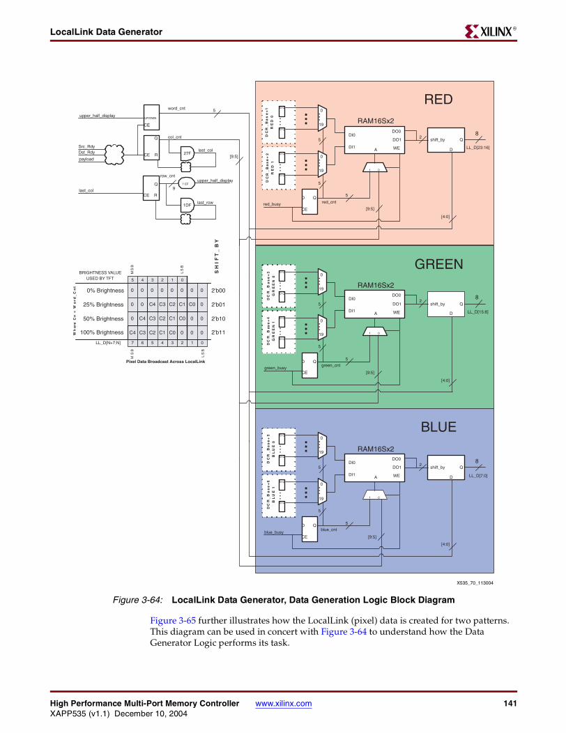
High Performance Multi-Port Memory Controller www.xilinx.com 141XAPP535 (v1.1) December 10, 2004
LocalLink Data GeneratorR
Figure 3-65 further illustrates how the LocalLink (pixel) data is created for two patterns. This diagram can be used in concert with Figure 3-64 to understand how the Data Generator Logic performs its task.
Figure 3-64: LocalLink Data Generator, Data Generation Logic Block Diagram
27F
D Q
D Q
DC
R_
Ba
se
+1
RE
D 0
RAM16Sx2
DI0
DI1
DO1
DO0
WE
D Q
CEred_busy
shift_by
D
Q8
… … …
19
0
D Q
D Q
DC
R_
Ba
se
+2
RE
D 1
… … …
19
0
A
CE
Q
CE R
Q
CE R
row_cnt
[9:5]
upper_half_display
last_col
upper_half_display? EF
last_row
col_cnt
last_col
Src_RdyDst_Rdy
payload
[4:0]
LL_D[23:16]
1 0
word_cnt
95
5
5
[9:5]
5
red_cnt
2
UP/DWN
D Q
D Q
DC
R_
Ba
se
+3
GR
EE
N 0
RAM16Sx2
DI0
DI1
DO1
DO0
WE
D Q
CEgreen_busy
shift_by
D
Q
8
… … …
19
0
D Q
D Q
DC
R_
Ba
se
+4
GR
EE
N 1
… … …
19
0
A
[4:0]
LL_D[15:8]
1 0
5
5
[9:5]
5
green_cnt
2
D Q
D Q
DC
R_
Ba
se
+5
BL
UE
0
RAM16Sx2
DI0
DI1
DO1
DO0
WE
D Q
CEblue_busy
shift_by
D
Q8
… … …
19
0
D Q
D Q
DC
R_
Ba
se
+6
BL
UE
1
… … …
19
0
A
[4:0]
LL_D[7:0]
1 0
5
5
[9:5]
5
blue_cnt
2
Wh
ere
Cn
= W
or
d_
Cn
t
MS
B
3 07 6 5 4LL_D[N+7:N]
3 2 1 05 4
BRIGHTNESS VALUEUSED BY TFT
LS
B
LS
B
0 0 0 0 0 0 0 0
0 0 C4 C3 C2 C1 C0 0
00 C4 C3 C2 C1 C0 0
0 0C4 C3 C2 C1 C0 0
Pixel Data Broadcast Across LocalLink
SH
IF
T_
BY
2'b00
2'b01
2'b10
2'b11
0% Brightness
25% Brightness
50% Brightness
100% Brightness
2 1
MS
B
RED
GREEN
BLUE
1DF
X535_70_113004
ARCHIVED APPLICATION NOTE - NOT SUPPORTED FOR NEW DESIGNS

142 www.xilinx.com High Performance Multi-Port Memory ControllerXAPP535 (v1.1) December 10, 2004
Chapter 3: Hardware Data Sheets for Elements Used in the GSRDR
The LocalLink Data Generator contains preloaded values for the max color of each of the twenty patterns. These values are stored in the Data Generator Color Pattern Control Registers (see Figure 4-3). Two bits are used for each color, and these bits become the shift_by_xxx. The six registers and the RAM are all initialized to the values contained in Figure 3-64, though these initial values can be set by the parameters defined in Table 3-30.
The other part of Figure 3-64 describes how the CPU can update each patternby writing to the Colorbar Pattern Control Registers. The act of writing to these DCR registers initiates an update to the RAM. Each color has two independent Colorbar Pattern Control Registers. There are also independent RAMs for each color. A simple arbiter prevents LocalLink access while the DCR update is in progress. The DCR write to any of the six registers results in a “go” signal for the appropriate color to start a counter that counts from 0 to 19. The counter connects to a multiplexer that pulls the appropriate bit from the
Figure 3-65: LocalLink Data Generator Pixel Data Creation
Wh
ere
Cn
= W
ord
_C
nt
MS
B
19 1623 22 21 20LL_D[ ]
3 2 1 05 4
BRIGHTNESS VALUEUSED BY TFT
LS
B
LS
B
0 0 0 0 0 0 0 0
0 0 C4 C3 C2 C1 C0 0
00 C4 C3 C2 C1 C0 0
0 0C4 C3 C2 C1 C0 0
Pixel Data Broadcast Across LocalLink
SH
IF
T_
BY
_R
ED
2'b00
2'b01
2'b10
2'b11
0% Brightness
25% Brightness
50% Brightness
100% Brightness
18 17
MS
B
MS
B
11 815 14 13 12
3 2 1 05 4
LS
B
0 0 0 0 0 0 0 0
0 0 C4 C3 C2 C1 C0 0
00 C4 C3 C2 C1 C0 0
0 0C4 C3 C2 C1 C0 0
SH
IF
T_
BY
_G
RN
2'b00
2'b01
2'b10
2'b11
10 9
MS
B
3 07 6 5 4
3 2 1 05 4
LS
B
0 0 0 0 0 0 0 0
0 0 C4 C3 C2 C1 C0 0
00 C4 C3 C2 C1 C0 0
0 0C4 C3 C2 C1 C0 0
SH
IF
T_
BY
_B
LU
2'b00
2'b01
2'b10
2'b11
2 1
LS
B
Pixel Data Broadcast Across LocalLink
MS
B
LS
B
Pixel Data Broadcast Across LocalLink
MS
B
SHIFT_BY_RED for PATTERN_nn
SHIFT_BY_GRN for PATTERN_nn
SHIFT_BY_BLU for PATTERN_nn
0x
AA
red
grn
blu
MSB (31)
LSB(0)
Lo
ca
lLin
k D
AT
A
C0
C1
C2
C3
C4
WO
RD
_C
NT
0x
AA
red
grn
blu
0x
AA
red
grn
blu
0x
AA
red
grn
blu
0x
AA
red
grn
blu
0x
AA
red
grn
blu
0x
AA
red
grn
blu
0x
AA
red
grn
blu
0x
AA
red
grn
blu
0x
AA
red
grn
blu
0x
AA
red
grn
blu
0x
AA
red
grn
blu
0x
AA
red
grn
blu
0x
AA
red
grn
blu
0x
AA
red
grn
blu
0x
AA
red
grn
blu
0x
AA
red
grn
blu
0x
AA
red
grn
blu
0x
AA
red
grn
blu
0x
AA
red
grn
blu
0x
AA
red
grn
blu
0x
AA
red
grn
blu
0x
AA
red
grn
blu
0x
AA
red
grn
blu
0x
AA
red
grn
blu
0x
AA
red
grn
blu
0x
AA
red
grn
blu
0x
AA
red
grn
blu
0x
AA
red
grn
blu
0x
AA
red
grn
blu
0x
AA
red
grn
blu
0x
AA
red
grn
blu
SH
IF
T_
BY SHIFT_BY_RED for PATTERN_nn+1
SHIFT_BY_GRN for PATTERN_nn+1
SHIFT_BY_BLU for PATTERN_nn+1
0x
AA
red
grn
blu
0x
AA
red
grn
blu
0x
AA
red
grn
blu
0x
AA
red
grn
blu
0x
AA
red
grn
blu
0x
AA
red
grn
blu
0x
AA
red
grn
blu
0x
AA
red
grn
blu
0x
AA
red
grn
blu
0x
AA
red
grn
blu
0x
AA
red
grn
blu
0x
AA
red
grn
blu
0x
AA
red
grn
blu
0x
AA
red
grn
blu
0x
AA
red
grn
blu
0x
AA
red
grn
blu
0x
AA
red
grn
blu
0x
AA
red
grn
blu
0x
AA
red
grn
blu
0x
AA
red
grn
blu
0x
AA
red
grn
blu
0x
AA
red
grn
blu
0x
AA
red
grn
blu
0x
AA
red
grn
blu
0x
AA
red
grn
blu
0x
AA
red
grn
blu
0x
AA
red
grn
blu
0x
AA
red
grn
blu
0x
AA
red
grn
blu
0x
AA
red
grn
blu
0x
AA
red
grn
blu
0x
AA
red
grn
blu
BLUE PIXEL VALUES
25262728 21222324 17181920 13141516 12293031 891011 4567 0123
USEFUL BLU VALUES
GREEN PIXEL VALUES
USEFUL GRN VALUES
RED PIXEL VALUES
USEFUL RED VALUES
STATIC VALUE = 0xAA
N+
00
N+
01
N+
02
N+
03
N+
04
N+
05
N+
06
N+
07
N+
08
N+
09
N+
10
N+
11
N+
12
N+
13
N+
14
N+
15
N+
16
N+
17
N+
18
N+
19
N+
20
N+
21
N+
22
N+
23
N+
24
N+
25
N+
26
N+
27
N+
28
N+
29
N+
30
N+
31
N+
32
N+
33
N+
34
N+
35
N+
36
N+
37
N+
38
N+
39
N+
40
N+
41
N+
42
N+
43
N+
44
N+
45
N+
46
N+
47
N+
48
N+
49
N+
50
N+
51
N+
52
N+
53
N+
54
N+
55
N+
56
N+
57
N+
58
N+
59
N+
60
N+
61
N+
62
N+
63
PIXEL DATA BROADCAST ACROSS LocalLink
PER PIXEL LocalLink DATA
X535_71_113004
ARCHIVED APPLICATION NOTE - NOT SUPPORTED FOR NEW DESIGNS

High Performance Multi-Port Memory Controller www.xilinx.com 143XAPP535 (v1.1) December 10, 2004
LocalLink Data GeneratorR
Colorbar Pattern Control Register and sends it to the DIx of the RAM. Simultaneously, the multiplexer in front of the address of the RAM takes the count value for its address. Since the CE to the counter is used for the WE to the RAM, all 20 locations in the RAM can be updated by the 20 entries in the Colorbar Pattern Control Registers. Only one color is updated at a time, where each DCR write initiates a rewrite to the appropriate color RAM.
Figure 3-66 is a logic diagram for data generation. This shows the actual logic illustrated in the block diagram of Figure 3-64. Both figures show the three main counters. The row counter counts the number of video lines and is reset once 480 lines have been sent through the LocalLink interface. The column counter counts the number of pixels in a line and is reset after 640 words have been sent. The word counter counts the number of pixels for the width of each pattern and is reset after 32 words (pixels) have been sent.
Figure 3-66: LocalLink Data Generator, Color Generation Logic Diagram
D Q
LD
Up/Down
CE
CR
Src_Rdy
Dst_Rdy
Src_Rdy
Dst_Rdy
EOF
5
word_cntr
11_sm==Payload
5'h1F
= = 0
= = 5'h1F
shiftleft
shiftleft
shiftright
word_cnt5
5
5
5
5
sys_rst
color_bar_rst EOF
Src_Rdy
Dst_Rdy
red_out8
grn_out8
blu_out8
shift_by_red
shift_by_blu
shift_by_grn
Q
CE
D
CR
= = 10'h27F
sys_rst
color_bar_rst
col_cnt
col_cntr10
Q
CE
D
CR = =9'h1DF
sys_rst
color_bar_rst
row_cnt
row_cntr9
<= 9'hEF
= =9'hEF9
9
9
D Q
LD
Up/Down
CE
CR
Src_Rdy
Dst_Rdy
Src_Rdy
Dst_Rdy
EOF
5
word_cntr
11_sm==Payload
5'h1F
= = 0
= = 5'h1F
shiftleft
shiftleft
shiftright
word_cnt5
5
5
5
5
sys_rst
color_bar_rst EOF
Src_Rdy
Dst_Rdy
X535_72_113004
red_out8
grn_out8
blu_out8
shift_by_red
shift_by_blu
shift_by_grn
Q
CE
D
CR
= = 10'h27F
sys_rst
color_bar_rst
col_cnt
col_cntr10
Q
CE
D
CR = =9'h1DF
sys_rst
color_bar_rst
row_cnt
row_cntr9
<= 9'hEF
= =9'hEF9
9
9
ARCHIVED APPLICATION NOTE - NOT SUPPORTED FOR NEW DESIGNS

144 www.xilinx.com High Performance Multi-Port Memory ControllerXAPP535 (v1.1) December 10, 2004
Chapter 3: Hardware Data Sheets for Elements Used in the GSRDR
The word counter produces the gradient for each color bar. If the row counter is less than 240, the counter starts at 0 and counts to 31. If the row counter is greater than or equal to 240, the counter starts at 31 and counts down to 0. The upper bits of the column counter address the RAMs to produce a shift value for each color. If the shift value is zero, the color is set to 0, otherwise the word count value is be shifted by the amount indicated by the RAM's output.
Whenever the color registers are written, RAMs are updated with the color register values. When these RAMs are addressed, a shift value is produced to result in maximum value for a particular color. The maximum value for the color is either off, 25% on, 50% on, or 100% on. For example, the defaults for Color Bar Pattern 17 are dcr_red1[14]==0, dcr_red0[14]==1, dcr_grn1[14]==1, dcr_grn0[14]==1, dcr_blu1[14]==1, dcr_blu0[14]==0. This implies that the 5-bit counter value for the red portion is shifted to the left by 1 (25% on), the green counter value is shifted to the left by 3 (100% on), and the blue counter value is shifted to the left by 2 (50% on). See the tables contained in Figure 3-64 and Figure 3-65 for more detail.
DCR Interface Logic
The DCR interface allows the user to provide configuration parameters and to observe status registers. Figure 3-67 shows a block diagram of the DCR Interface Logic. Figure 3-68 shows a more detailed logic diagram of the DCR interface including the LocalLink src_rdy delay logic. Figure 3-69 illustrates how the reset circuitry and one-third of the Data Generator Color Pattern Control Registers (red in this example) operate.
DRC Logic Block Diagram
The DCR registers bitmaps are described in Table 4-10 through Table 4-20.
ARCHIVED APPLICATION NOTE - NOT SUPPORTED FOR NEW DESIGNS

High Performance Multi-Port Memory Controller www.xilinx.com 145XAPP535 (v1.1) December 10, 2004
LocalLink Data GeneratorR
Figure 3-67: LocalLink Data Generator, DCR Logic Block Diagram
D Q
CE
D Q
CE
DCR_D1
DCR_write
DCR_ABus
15
20
32
32
32 DCR_DO
DCR_READ
DCR_WRITE
DCR_ABusDCR_ACK
D Q
CE
20
D Q
CE
20
D Q
CE
20
D Q
CE
20
D Q
CE
20
D Q
CE
32
D Q
CE
32
0
1
2
3
4
5
6
7
8
D Q
CE
29
32
10
D Q
CE
Control 0
[0:2,16:23,28:31]
Data GenRed 0
[12:31]
Data GenRed 1
[12:31]
Data GenGreen 0
[12:31]
Data GenGreen 1
[12:31]
Data GenBlue 0
[12:31]
Data GenBlue 1
[12:31]
DCR_TIMER_MAX
[0:31]
[0:31]
DCR_TIMER_MISS
[30:31]
Control 1
X535_73_113004
ARCHIVED APPLICATION NOTE - NOT SUPPORTED FOR NEW DESIGNS

146 www.xilinx.com High Performance Multi-Port Memory ControllerXAPP535 (v1.1) December 10, 2004
Chapter 3: Hardware Data Sheets for Elements Used in the GSRDR
DCR Logic - Registers, DCR_TIMER_MISS and DCR_TIMER_MAX
Figure 3-68: LocalLink Data Generator, DCR Interface Logic
D Q
C R
D Q
C R
D Q
C R
DCR_DBusIn
decode
D
CE
Q
C R
dcr_ce
sys_rst
color_bar_rst
[DCR_Registers]
dcr_pn dcr_red0 dcr_red1 dcr_grn0 dcr_grn1 dcr_blu0 dcr_blu1 dcr_timer_max
Logic is replicatedfor the followingregisters:
D Q
C R
DCR_Write
DCR_ABus
DCR_DBusIn
{1'h1,color_bar_rst2,30'h3FFFFFFF}dcr_status
0
1
dcr_ce
D Q
C
D
CE
LDQ
C R
dcr_timer_missdcr_ce
sys_rst
color_bar_rst
line_finished
==dcr_timer_maxD
CE
Q
C R
==32'hFFFFFFFF
timer_rst
timer_cntr
>=dcr_timer_max
D QC R
S
D Q
C R
S
EOF
Src_Rdy
Dst_Rdy
timer_done
sys_rst
color_bar_rst
timer_rst
pn_on_timerline_finished
timer_rst
D Q
C
0
1
dcr_pn
dcr_red0
dcr_red1
dcr_grn0
dcr_grn1
dcr_blu0
dcr_blu1
dcr_timer_max
dcr_timer_miss
dcr_status
D Q
CDCR_ABus[6:9]
dcr_valid
DCR_DBusIn
DCR_DBus_Out
D Q
C
DCR_Read
D Q
C
DCR_ABus
D Q
C
DCR_Write
D Q
C
D Q
C
DCR_Read
DCR_Ack
decodeD Q
C
0
1
2
3
4
5
6
7
8
9
X535_74_113004
ARCHIVED APPLICATION NOTE - NOT SUPPORTED FOR NEW DESIGNS

High Performance Multi-Port Memory Controller www.xilinx.com 147XAPP535 (v1.1) December 10, 2004
LocalLink Data GeneratorR
DCR Color Pattern Control Writing Logic
DCR Control 0 Register
DCR Register 0 controls the source ready signal (Src_Rdy) across the LocalLink interface. If the length select and the pattern select are off, Src_Rdy is asserted every cycle after the engine is turned on. This means that data is transferred from the LocalLink Data Generator until the CDMAC Dst_Rdy signal goes invalid.
DCR Control 0 gives two enable bits that affect the Src_Rdy signal. The two enables are DG_LENGTH_ENBL and DG_PATTERN_ENBL. Only one of the enables should be turned on at a time, or the system can behave unpredictably.
If the length select (DG_LENGTH_ENBL) is turned on, the four-bit length field (DG_LENGTH) is used to determine the percentage of time Src_Rdy should be asserted. Src_Rdy is never asserted if DG_LENGTH is set to 0. An LFSR is used to generate four bit pseudo-random numbers. Whenever the number is less than DG_LENGTH, Src_Rdy is asserted.
The pattern select (DG_PATTERN_ENBL) turns on the eight-bit pattern ID (DG_PATTERN). Currently there is only one pattern supported. If DG_PATTERN is set to 0x00000001, Src_Rdy is asserted every other clock cycle. If any other pattern is selected, Src_Rdy is asserted every clock cycle.
Figure 3-69: LocalLink Data Generator, Reset and DCR Color Register Write Logic
sys_rst
DCR_Write
DCR_ABus
ll_sm==Idle
dcr_status[30]
color_bar_rst2
red_go
red_go
red_cnt
cntr
red_busy
Q
CR
S
Q
CR
S
sys_rst
color_bar_rst
QD
C
QD
C
decodeR
Q
C
S
sys_rstcolor_bar_rst
R
Q
C
S
sys_rstcolor_bar_rst
R
QD
C
CE
sys_rstcolor_bar_rst
== 5'h1F
Note: This design is typical forred (red), green (grn), and blue (blu).
X535_75_113004
ARCHIVED APPLICATION NOTE - NOT SUPPORTED FOR NEW DESIGNS

148 www.xilinx.com High Performance Multi-Port Memory ControllerXAPP535 (v1.1) December 10, 2004
Chapter 3: Hardware Data Sheets for Elements Used in the GSRDR
DCR Control 0 also enables the ability to monitor the amount of time the LocalLink interfaces spends in a frame. If the line timer select (DG_LINE_TIMER_ENBL) is on, the system monitors the number of clock cycles it takes to output one line (640 pixels) of data. If the amount of time exceeds the value contained in the Data Generator DCR Timer Max Register, DCR register 7, the Data Generator DCR Timer Miss Register, and DCR register 8 is increased by one.
DCR Colorbar Pattern Control Registers
The Colorbar Pattern Control Registers are described in greater detail in the “Data Generator Logic,” and “DCR Colorbar Pattern Control Registers” sections.
DCR Timer Max and Timer Miss Registers
The LocalLink Data Generator has a built-in performance metric function that allows the system designer to specify a time period within which the Data Generator has to output a frame of data (for example, 640 pixels). There are three components, an enable bit, a register to set the detection limit, and a counter to count how many times the time period has been exceeded. The enable bit is contained in Control 0, as the DG_LINE_TIMER_ENBL bit. The DCR Timer Max register contains a 32-bit value that is compared against the number of clocks since the frame began sending. The DCR Timer Miss register counts the number of times that the number of clocks since the frame began exceeds the value of the DCR Timer Max register.
The performance metric is used primarily to identify if the CDMAC has not been able to keep up with the data demands of the LocalLink Data Generator. This is a subjective measurement because the Max value can be set to anything. For example, if the max value is set at 32, the DCR Timer Miss register always increments. A realistic bare minimum is to assume that the CPU wants the ISPLB and DSPLB ports to MPMC, and that the other port attached to the MPMC is also in full use by the CDMAC. This means that the remaining MPMC port for the LocalLink Data Generator can have access all the time during its time slot. See “Multi-Port Memory Controller (MPMC)” for more information. If the Rx CDMAC engine is the only engine for this port, then a specific maximum data rate can be established. Setting the DCR Timer Max register below that value results in errant counts in the DCR Timer Miss register.
DCR Control 1 Register
DCR Register 9 is the Control 1 register. DATA_GEN_ENBL is the on/off switch for the Data Generator. A one written to this bit causes the Data Generator to begin outputting data. Once DATA_GEN_ENBL is written as a zero, the engine finishes the current line in progress, and then go into the idle state until the engine is turned on again.
DATA_GEN_RST, when set to a one, resets the LocalLink Data Generator. As in the case of turning off the Data Generator, the line in progress completes, and then the Data Generator resets. DATA_GEN_RST is negated after the reset has been executed. The reset logic is shown in Figure 3-69.
LocalLink Interface Logic
The LocalLink interface Logic is shown in Figure 3-70. The LocalLink Data Generator displays 480 lines of data where each line has a header, payload, and footer. The header is a one-clock cycle placeholder. The payload is 640 words of data, where each word has the format: 0xAARRGGBB. 0xAA is an eight-bit parameter into the LocalLink Data Generator (C_upper_byte). The user can find this value useful for debugging purposes. 0xRR represents the red color bits, 0xGG represents the green color bits, and 0xBB represents the blue color bits. The footer is eight words, where the first 7 words are set to 0 and the last
ARCHIVED APPLICATION NOTE - NOT SUPPORTED FOR NEW DESIGNS

High Performance Multi-Port Memory Controller www.xilinx.com 149XAPP535 (v1.1) December 10, 2004
LocalLink Data GeneratorR
word contains the number of words in the payload. These values are described further in “Data Generator Logic.”
Src_Rdy is asserted according to how it was configured by the Data Generator Control 0 register. Src_Rdy is held off by the Data Generator whenever the Colorbar Pattern Control Registers are written to by DCR, and remains inactive until the RAM has been updated.
Note: A full colorbar pattern update requires six DCR writes, and prolongs the amount of time that Src_Rdy is deasserted, if done one right after the other.
Figure 3-70: LocalLink Data Generator, LocalLink interface Logic
QD
C
0
1
0
1
Src_Rdy
sys_rst
color_bar_rst
red_busy
grn_busy
blu_busy
line_finished
pn_pattern==8'h1
pn_pattern_on
src_rdy_rn<pn_length
pn_on_length
sys_rst
color_bar_rst
color_bar_on
ll_sm==Idle
Src_Rdy
Dst_Rdy
SOF
sys_rst
color_bar_rst
ll_sm==Payload
col_cnt==10'h0
SOP
sys_rst
color_bar_rst
ll_sm==Payload
col_cnt==10'h27F
EOP
sys_rst
color_bar_rst
ll_sm==Footer
footer_cnt==3'h7
EOF
0
1
0
1
{C_upper_byte,red_out,grn_out,blu_out}
footer_cnt==3'h7
payload_cntll_sm==Footer
D Rem
Idle Header
Footer Payload
sys_rstcolor_bar_on & Src_Rdy
Src_R
dy & D
st_Rdy
Src_Rdy & Dst_Rdy & col_cnt==10'h27F
& S
rc_R
dy &
Dst
_Rdy
color
_bar
_on
& foot
er_c
nt==
3'h7
& Src
_Rdy
& D
st_Rdy
& Dst_Rdy
colo
r_ba
r_on
& fo
oter
_cnt
==
3'h7
QD
C
CE
R
Src_Rdy
Dst_Rdy
ll_sm==payload
sys_rst
color_bar_rst
SOF
payload_cnt
QD
C
CE
R
Src_Rdy
Dst_Rdy
ll_sm==Footer
footer_cnt
sys_rst
color_bar_rst
X535_76_113004
ARCHIVED APPLICATION NOTE - NOT SUPPORTED FOR NEW DESIGNS

150 www.xilinx.com High Performance Multi-Port Memory ControllerXAPP535 (v1.1) December 10, 2004
Chapter 3: Hardware Data Sheets for Elements Used in the GSRDR
Simulation and VerificationThe testbench for the Data Generator provides stimulus for the LocalLink interface and the DCR Interface.
For the LocalLink interface, the testbench randomly asserts Dst_Rdy.
A Perl script generates a text file with a series of read and write requests to the DCR Interface. The testbench iterates through these instructions, placing a random amount of delay between each instruction.
As the testbench runs, data is written to a text file. Whenever data is transmitted across the LocalLink interface, a tag is printed on whether the data is header data (H), payload data (P), or footer data (F). This tag is followed by the data in hexadecimal format. Whenever a DCR Write occurs, the tag D is printed to the text file, followed by the DCR Address in hexadecimal format, and then by the data in binary format. After the testbench has completed, a Perl script processes the text file to verify that the correct data was sent to the LocalLink interfaceinterface.
A shell script (run_ll_data_gen_test) is used to run the testbench and verify operation.
Directory Structure Data
o ll_gata_gen_v2_1_0.mpdo ll_data_gen_v2_1_0.pao
hdlo verilog
ll_data_gen.vtest
o binflow_ll_data_gen.cfggen_dcr_stimulus.plgen_ll_data_gen_check.plrun_ll_data_gen_test
o func_simtestbench.dowave_ll_data_gen.do
o hdlverilogtestbench.v
ARCHIVED APPLICATION NOTE - NOT SUPPORTED FOR NEW DESIGNS

High Performance Multi-Port Memory Controller www.xilinx.com 151XAPP535 (v1.1) December 10, 2004
LocalLink Data GeneratorR
Using the LocalLink Data GeneratorTo use the LocalLink Data Generator, the user needs to connect the module to a DCR Bus and a Rx LocalLink interface. Table 3-30 describes the parameters, while Table 3-31 through Table 3-33 gives a description of the I/Os of the LocalLink Data Generator, and Table 4-10 through Table 4-20 gives a description of the DCR Registers. The DCR Bus can be tied off if the user does not want to change the colors or the performance of the engine. Upon power on, the LocalLink Data Generator defaults to on. The LocalLink interface is described in the “LocalLink Interface Logic.” The user can write to the DCR registers to change the colors and performance of the engine, as described in “DCR Interface Logic.”
Module Port Interface
Table 3-30: LocalLink Data Generator Parameters
Parameter NameWidth
(In Bits)Default Value Description
C_upper_byte 8 1111_1010
Color is represented in 24-bit RRGGBB format, but stored in a 32-bit register. C_upper_byte is the upper 8 bits.
C_dcr_base_addr 6 00_0000 Base address for DCR registers
C_color_pattern_red0 32 0000_0000_0000_1001_1110_0111_1101_1001Upper bits of color bar pattern for red. (Default value for DCR register 1.)
C_color_pattern_red1 32 0000_0000_0000_1110_0110_0001_1101_1001Lower bits of color bar pattern for red. (Default value for DCR register 2.)
C_color_pattern_grn0 32 0000_0000_0000_1110_1011_1010_1110_1010Upper bits of color bar pattern for green. (Default value for DCR register 3.)
C_color_pattern_grn1 32 0000_0000_0000_1011_1100_1010_0110_1010Lower bits of color bar pattern for green. (Default value for DCR register 4.)
C_color_pattern_blu0 32 0000_0000_0000_1111_0101_1101_0111_0100Upper bits of color bar pattern for blue. (Default value for DCR register 5.)
C_color_pattern_blu1 32 0000_0000_0000_0101_1011_0100_0111_0100Lower bits of color bar pattern for blue. (Default value for DCR register 6.)
Table 3-31: LocalLink Data Generator System Signals
Signal I/O Description
CLK Input System Clock.
RST Input System Reset.
ARCHIVED APPLICATION NOTE - NOT SUPPORTED FOR NEW DESIGNS

152 www.xilinx.com High Performance Multi-Port Memory ControllerXAPP535 (v1.1) December 10, 2004
Chapter 3: Hardware Data Sheets for Elements Used in the GSRDR
EDK CoresThe following cores are shipped as part of the standard Xilinx Embedded Development Kit. Refer to the documentation provided with EDK for information on these cores:
• PPC405
• isocm
• isbram_if_cntlr
• bram_block
• dsocm
• dsbram_if_cntlr
• dcr_intc
• uartlite
Table 3-32: LocalLink Data Generator DCR Signals
Signal I/O Description
DCR_ABus[0:9] Input Address bus.
DCR_DBusIn[0 :31] Input Write data bus.
DCR_Write Input Write request.
DCR_Read Input Read request.
DCR_Ack Output Write/Read acknowledge.
DCR_DBusOut[0:31] Output Read data bus.
Table 3-33: Summary of LocalLink Data Generator LocalLink I/Os
Signal I/O Description
D[31:0] OutputData bus. Valid while Src_Rdy and Dst_Rdy are asserted.
Rem[3:0] OutputRemainder. Data mask for last word of header, payload, or footer. In this system, Rem = 0b0000.
SOF Output Start of frame. Active low.
EOF Output End of frame. Active low.
SOP Output Start of payload. Active low.
EOP Output End of payload. Active low.
Src_Rdy OutputSource ready. Active low. Indicates data generator has valid data on the LocalLink outputs.
Dst_Rdy InputDestination ready. Active low. Indicates connecting device is ready to receive data.
ARCHIVED APPLICATION NOTE - NOT SUPPORTED FOR NEW DESIGNS

High Performance Multi-Port Memory Controller www.xilinx.com 153XAPP535 (v1.1) December 10, 2004
R
Chapter 4
Software Models for Elements Contained in the GSRD
This chapter discusses the following software models for elements contained in the GSRD:
• CDMAC
• LocalLink Data Generator
A third software model, GMAC, is described in the Linux Device Driver chapter of XAPP536, “Gigabit System Reference Design.”
CDMAC Software ModelThe following sections detail the CDMAC software model, including the overall programming model, as well as register definitions.
CDMAC DMA Descriptor ModelSee the “DMA Descriptor Model” in the “Communication Direct Memory Access Controller (CDMAC)” section for a detailed description of the way DMA decriptors are used.
ARCHIVED APPLICATION NOTE - NOT SUPPORTED FOR NEW DESIGNS
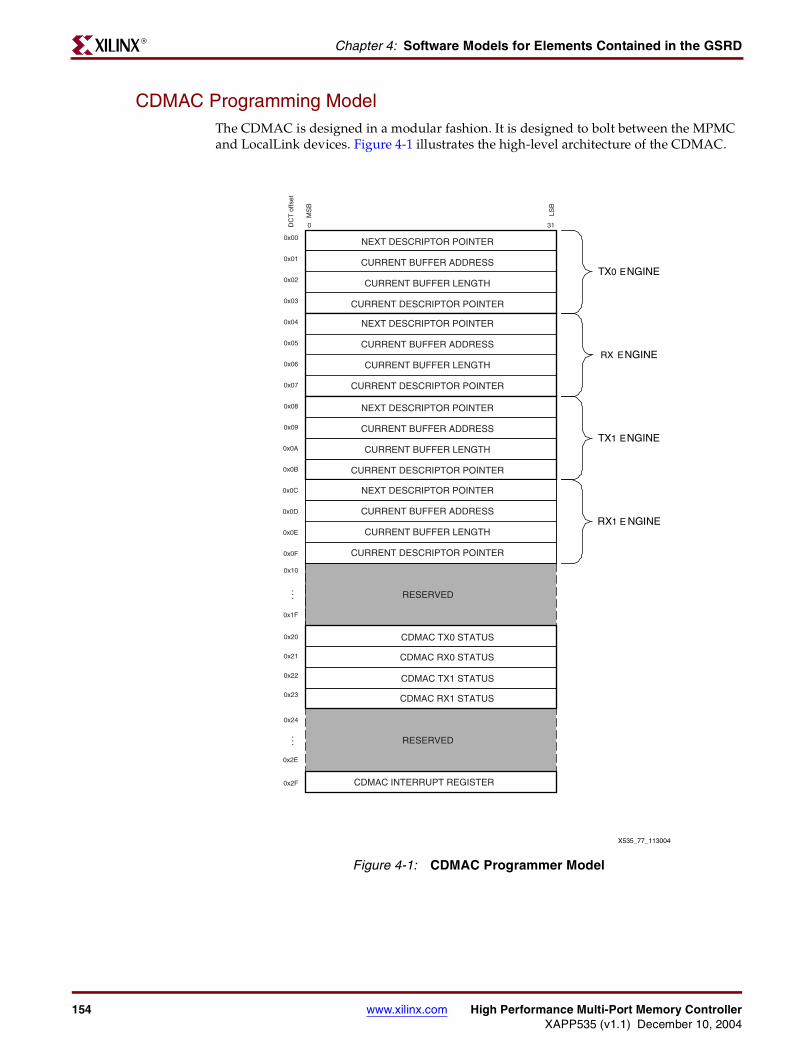
154 www.xilinx.com High Performance Multi-Port Memory ControllerXAPP535 (v1.1) December 10, 2004
Chapter 4: Software Models for Elements Contained in the GSRDR
CDMAC Programming ModelThe CDMAC is designed in a modular fashion. It is designed to bolt between the MPMC and LocalLink devices. Figure 4-1 illustrates the high-level architecture of the CDMAC.
Figure 4-1: CDMAC Programmer Model
X535_77_113004
TX0 ENGINE
RX ENGINE
TX1 ENGINE
RX1 E NGINE
0x00
0x01
0x02
0x03
0x04
0x05
0x06
0x07
0x08
0x09
0x0A
0x0B
0x0C
0x0D
0x0E
0x0F
0x10
0x1F
0x20
0x21
0x22
0x23
0x24
0x2E
0x2F
DC
T o
ffset
MS
B
LSB
0 31
. . .
. . .
NEXT DESCRIPTOR POINTER
CURRENT BUFFER ADDRESS
CURRENT BUFFER LENGTH
CURRENT DESCRIPTOR POINTER
NEXT DESCRIPTOR POINTER
CURRENT BUFFER ADDRESS
CURRENT BUFFER LENGTH
CURRENT DESCRIPTOR POINTER
NEXT DESCRIPTOR POINTER
CURRENT BUFFER ADDRESS
CURRENT BUFFER LENGTH
CURRENT DESCRIPTOR POINTER
NEXT DESCRIPTOR POINTER
CURRENT BUFFER ADDRESS
CURRENT BUFFER LENGTH
CURRENT DESCRIPTOR POINTER
CDMAC INTERRUPT REGISTER
CDMAC TX0 STATUS
CDMAC RX0 STATUS
CDMAC TX1 STATUS
CDMAC RX1 STATUS
RESERVED
RESERVED
ARCHIVED APPLICATION NOTE - NOT SUPPORTED FOR NEW DESIGNS

High Performance Multi-Port Memory Controller www.xilinx.com 155XAPP535 (v1.1) December 10, 2004
CDMAC Software ModelR
CDMAC Register DefinitionsThe following pages detail the bitmaps of each register. There are four total DMA engines, and each has the same register set. The only exception is the Interrupt Register that all four DMA engines share.
CDMAC Next Descriptor Pointer Register
The NEXT_DESCRIPTOR_POINTER_REGISTER is loaded from the value contained in the NEXT_DESCRIPTOR_POINTER field in the currently pointed to descriptor. This value is kept in the respective CDMAC register until the CDMAC has completed all DMA transactions within the DMA transfer (reference Figure 3-19). After all DMA transactions are complete, the current descriptor is complete, and the CDMAC_COMPLETED bit is set in the STATUS_REGISTER. The current descriptor is then written to update the STATUS field within the descriptor. After this, the CDMAC evaluates the address contained in the NEXT_DESCRIPTOR_POINTER_REGISTER.
• If a Null (0x00000000) is contained in the NEXT_DESCRIPTOR_POINTER_REG then CDMAC engine stops processing descriptors
• If the address contained in the NEXT_DESCRIPTOR_POINTER_REGISTER is not 8-word aligned, or reaches beyond the range of available memory, the CDMAC halts processing and sets the CDMAC_ERROR bit in the STATUS_REGISTER.
• If the NEXT_DESCRIPTOR_POINTER_REGISTER contains a valid address, then the contents are moved to the CURRENT_DESCRIPTOR_REGISTER. This movement causes the CDMAC to begin another DMA transaction.
CDMAC Current Address Register
The CURRENT_ADDRESS_REGISTER maintains the contents of the address in memory where the DMA operation is conducted next. This value is originally loaded into the CDMAC when the descriptor is read by the CDMAC. Once set by the current descriptor, the CDMAC then occasionally transfers this value to an internal Address Counter that
Table 4-1: Next Descriptor Pointer Register (DCR_Base + 0x00, 0x04, 0x08, 0x0C)
MSB
LSB
0 1 2 3 4 5 6 7 8 9 10 11 12 13 14 15 16 17 18 19 20 21 22 23 24 25 26 27 28 29 30 31
ADDRESS
Table 4-2: CDMAC Next Descriptor Pointer Register Bitmap
Bit Description
[0:31]Address: 8 word aligned pointer to the next descriptor in the chain.
If Null (0x0), DMA engine stops processing descriptors
Table 4-3: Current Address Register (DCR_Base + 0x01, 0x05, 0x09, 0x0D)
MSB
LSB
0 1 2 3 4 5 6 7 8 9 10 11 12 13 14 15 16 17 18 19 20 21 22 23 24 25 26 27 28 29 30 31
ADDRESS
ARCHIVED APPLICATION NOTE - NOT SUPPORTED FOR NEW DESIGNS
156 www.xilinx.com High Performance Multi-Port Memory ControllerXAPP535 (v1.1) December 10, 2004
Chapter 4: Software Models for Elements Contained in the GSRDR
then updates the value for each DMA transaction completed. Upon termination of the transaction, the CDMAC overwrites the value of the CURRENT_ADDRESS_REGISTER with the last value of the Address Counter. This process continues repeatedly until the CDMAC has completed the current descriptor. The reason for this mechanism is so the CDMAC can maintain multiple temporal channels of DMA at a substantially reduced hardware cost. Software can find this mechanism useful for identifying where in a DMA operation the CDMAC is, however t is not recommended that software use the CURRENT_ADDRESS_REGISTER for this purpose as it dynamically changes.
CDMAC Current Length Register
The CURRENT_LENGTH_REGISTER maintains the contents of the remaining length of the data to be transferred by the CDMAC. The value is originally loaded into the CDMAC when the descriptor is read by the CDMAC. Once set by the current descriptor, the CDMAC then occasionally transfers this value to an internal Length Counter, which then updates the value for each DMA transaction completed. Upon termination of the transaction, the DMAC overwrites the value of the CURRENT_LENGTH_REGISTER with the last value of the internal Length Counter. This process continues repeatedly until the CDMAC has completed the current descriptor. The reason for this mechanism is so the CDMAC can maintain multiple temporal channels of DMA at a substantially reduced hardware cost. However, software can find this mechanism useful for identifying where in a DMA operation the CDMAC is. It is not recommended that software avail itself of this.
CDMAC Current Descriptor Pointer Register
The CURRENT_DESCRIPTOR_POINTER_REGISTER maintains the pointer to the descriptor that is currently being processed. The value was set either by the CPU when it first initiated a DMA operation, or is copied from the NEXT_DESCRIPTOR_POINTER_REGISTER upon completion of the prior descriptor. This value is maintained by the CDMAC as a pointer so that the CDMAC can update the descriptor's STATUS and APPLICATION_DEPENDENT fields once the descriptor has been fully processed.
Table 4-4: Current Length Register (DCR_Base + 0x02, 0x06, 0x0A, 0x0E)
MSB
LSB
0 1 2 3 4 5 6 7 8 9 10 11 12 13 14 15 16 17 18 19 20 21 22 23 24 25 26 27 28 29 30 31
RESERVED 24-BIT LENGTH
Table 4-5: Current Descriptor Pointer Register (DCR_Base + 0x03, 0x07, 0x0B, 0x0F)
MSB
LSB
0 1 2 3 4 5 6 7 8 9 10 11 12 13 14 15 16 17 18 19 20 21 22 23 24 25 26 27 28 29 30 31
ADDRESS
ARCHIVED APPLICATION NOTE - NOT SUPPORTED FOR NEW DESIGNS

High Performance Multi-Port Memory Controller www.xilinx.com 157XAPP535 (v1.1) December 10, 2004
CDMAC Software ModelR
CDMAC Status Register
Table 4-6: CDMAC Status Registers (DCR_Base + 0x20, 0x21, 0x22, 0x23)
MSB
LSB
0 1 2 3 4 5 6 7 8 9 10 11 12 13 14 15 16 17 18 19 20 21 22 23 24 25 26 27 28 29 30 31
CD
MA
C_E
RR
OR
CD
MA
C_I
NT
_ON
_EN
D
CD
MA
C_S
TO
P_O
N_E
ND
CD
MA
C_C
OM
PL
ET
ED
CD
MA
C_S
TAR
T_O
F_PA
CK
ET
CD
MA
C_E
ND
_OF_
PAC
KE
T
CD
MA
C_E
NG
INE
_BU
SY
RESERVED
Table 4-7: CDMAC Status Register Bitmap
Bit Description
[0]
CDMAC_ERROR: When set (e.g. = 1) indicates the CDMAC encountered an error.The CDMAC sets this bit in the STATUS field of the descriptor. This bit, when set, indicates one of five possible errors, all of which are caused by SW issues. They are: Completed Error - CDMAC encountered a descriptor where the completed bit was already set prior to use; Buffer Address Error - CDMAC buffer address was not in range of memory; Next Descriptor Pointer Error - CDMAC found that the Next Descriptor Pointer was not 8 byte aligned; Current Descriptor Pointer Error - CDMAC found that the Current Descriptor Pointer was not 8 byte aligned; Busy Write Error - The CPU attempted to write to the Current Descriptor Pointer register when the CDMAC was busy. In all cases, an error results in halting the CDMAC channel and setting the interrupt for that channel. If the CDMAC Interrupt Register has the Master Interrupt Enable bit set, the CPU receives an interrupt when an error is encountered.
[1]
CDMAC_INT_ON_END: When set (e.g. = 1) forces the CDMAC to interrupt the CPU when the descriptor is completed.The CPU sets this bit in the STATUS field of the descriptor. The bit is then read into the CDMAC_STATUS_REGISTER as each descriptor is processed. If the bit is set in any given descriptor, the CDMAC generates an interrupt to the CPU. Note that CDMAC_STOP_ON_END and CDMAC_INT_ON_END are independent of each other. As such the CDMAC can be made to do any of four possible operations: Halt upon completion of current descriptor without interrupt, halt upon completion of current descriptor with interrupt, Interrupt upon completion of current descriptor while beginning to process the next descriptor (if there is one), or simply begin to process the next descriptor (if there is one).
[2]
CDMAC_STOP_ON_END: When set (e.g. = 1) forces the CDMAC to halt operations when the descriptor is completed.The CPU sets this bit in the STATUS field of the descriptor. The bit is then read into the CDMAC_STATUS_REGISTER as each descriptor is processed. If the bit is set in any given descriptor, the CDMAC halts processing any further descriptors for that channel. It will NOT generate an interrupt to the CPU unless explicitly told to do so by the CDMAC_INT_ON_END bit being set in the same descriptor. Note that CDMAC_STOP_ON_END and CDMAC_INT_ON_END are independent of each other. As such, the CDMAC can be made to do any of four possible operations: Halt upon completion of current descriptor without interrupt, halt upon completion of current descriptor with interrupt, interrupt upon completion of the current descriptor while beginning to process the next descriptor (if there is one), or simply begin to process the next descriptor (if there is one).
ARCHIVED APPLICATION NOTE - NOT SUPPORTED FOR NEW DESIGNS
158 www.xilinx.com High Performance Multi-Port Memory ControllerXAPP535 (v1.1) December 10, 2004
Chapter 4: Software Models for Elements Contained in the GSRDR
[3]
CDMAC_COMPLETED: When set (e.g. = 1) indicates that the CDMAC has transferred all data defined by the current descriptor.The CDMAC sets this bit upon completing the transaction associated with the descriptor. In the case of a transmit operation from memory (for example, READs), the CDMAC transfers data until the length field specified in the descriptor is zero, and then set this bit. In the case of a receive operation to memory (for example, WRITEs), the CDMAC sets this bit upon transferring data in the descriptor until the length is zero, OR, when it receives an END_OF_PACKET indicated from the CDMAC interface. Note that since the receive buffers are typically larger than the size of received data, the length field in the descriptor will NOT specify how much data was actually received. Please see the CDMAC interface specification for more details on how length is established.
NOTE: For software to properly utilize the CDMAC_COMPLETED feature, it must clear the bit in the descriptor prior to initiating CDMAC transactions based upon this descriptor. The CDMAC only sets this bit. It resets only upon hardware reset.
[4]
CDMAC_START_OF_PACKET: When set (e.g. = 1) indicates that the current descriptor is the start of the packet.The CDMAC sets this bit upon completing the transaction associated with this descriptor. In the case of a transmit operation from memory (for example, READs). Therefore CDMAC_START_OF_PACKET is set by the CPU in the descriptor to indicate to the CDMAC that this is the first descriptor of the packet to be transmitted.CDMAC RX0 and RX1 Engines perform receive operations to memory (for example, WRITEs). Therefore CDMAC_START_OF_PACKET is set by the CDMAC in the descriptor to indicate to the CPU that this is the first descriptor of the packet being received.
[5]
CDMAC_END_OF_PACKET: When set (e.g. = 1) indicates that the current descriptor is the final one of the packet.CDMAC TX0 and TX1 Engines perform transmit operations from memory (for example, READs). Therefore CDMAC_END_OF_PACKET is set by the CPU in the descriptor to indicate to the CDMAC that this is the last descriptor of the packet being transmitted.CDMAC RX0 and RX1 Engines perform receive operations to memory (for example, WRITEs). Therefore CDMAC_END_OF_PACKET is set by the CDMAC in the descriptor to indicate to the CPU that this is the last descriptor of the packet being received.
[6]
CDMAC_CHANNEL_BUSY: When set (e.g. = 1) indicates that the CDMAC channel is busy processing DMA operations.The CDMAC_CHANNEL_BUSY bits tell software when the CDMAC is busy with the appropriate channel. In general, software should not disturb the CDMAC when the busy bit is set. It is permissible for software to read the status registers when the CDMAC is busy, but it is unwise to write to any of the channels registers while that channel is busy. The CDMAC Interrupt register can be read at any time while any or all channels are busy. Note that CDMAC_CHANNEL_BUSY does NOT tell the software where the CDMAC is in processing the current descriptor. That information can be obtained by reading the CURRENT_LENGTH register for the appropriate channel.
[7:31] RESERVED:
Table 4-7: CDMAC Status Register Bitmap (Continued)
Bit Description
ARCHIVED APPLICATION NOTE - NOT SUPPORTED FOR NEW DESIGNS

High Performance Multi-Port Memory Controller www.xilinx.com 159XAPP535 (v1.1) December 10, 2004
CDMAC Software ModelR
CDMAC Interrupt Register
Table 4-8: CDMAC Interrupt Register (DCR_Base + 0x2F)
MSB
LSB
0 1 2 3 4 5 6 7 8 9 10 11 12 13 14 15 16 17 18 19 20 21 22 23 24 25 26 27 28 29 30 31
MIE
RESERVED
RX
1_IN
T
TX
1_IN
T
RX
0_IN
T
TX
0_IN
T
Table 4-9: CDMAC Interrupt Register Bitmap
Bit Description
[0]
Master Interrupt Enable: When set (e.g. = 1) indicates that the CDMAC is enabled to generate interrupts to the CPU.The Master Interrupt Enable (MIE) is used to enable and disable the CDMACs interrupt pin. If the MIE is set to a 1, then the CDMAC generates a HIGH level (1) on the INT pin whenever any of the interrupt sources have a valid interrupt. If the MIE is cleared to a 0, the CDMAC always leaves the INT pin set at a LOW level (0), regardless of any pending internal interrupts. Note that the MIE permits software to choose between polled mode of operation and interrupt driven.
[1:27] Reserved:
[28]
RX1_INT: When set (e.g. = 1) indicates that the CDMAC channel is requesting interrupt service from the CPU.This bit reflects the RX1 channel's request for service. This channel independently requests access to the CPU. The 4 channel interrupt bits are OR'd together and then AND'd with the Master Interrupt Enable (MIE) to produce the INT pin. If the MIE is disabled, each of these bits can still be read from this register in polled mode.This bit is a set/reset Flip-flop. Acknowledging an interrupt on the RX1 channel is accomplished by writing a 1 to this bit. Note that this mechanism assures that interrups cannot be lost, and permits multiple channels to be simultaneously acknowledged, if desired.
[29]
TX1_INT: When set (e.g. = 1) indicates that the CDMAC channel is requesting interrupt service from the CPU.This bit reflects the TX1 channel's request for service. This channel independently requests access to the CPU. The 4 channel interrupt bits are OR'd together and then AND'd with the Master Interrupt Enable (MIE) to produce the INT pin. If the MIE is disabled, each of these bits can still be read from this register in polled mode.This bit is a set/reset Flip-flop. Acknowledging an interrupt on the TX1 channel is accomplished by writing a 1 to this bit. Note that this mechanism assures that interrups cannot be lost, and permits multiple channels to be simultaneously acknowledged, if desired.
[30]
RX0_INT: When set (e.g. = 1) indicates that the CDMAC channel is requesting interrupt service from the CPU.This bit reflects the RX0 channel's request for service. This channel independently requests access to the CPU. The 4 channel interrupt bits are OR'd together and then AND'd with the Master Interrupt Enable (MIE) to produce the INT pin. If the MIE is disabled, each of these bits can still be read from this register in polled mode.This bit is a set/reset Flip-flop. Acknowledging an interrupt on the RX0 channel is accomplished by writing a 1 to this bit. Note that this mechanism assures that interrups cannot be lost, and permits multiple channels to be simultaneously acknowledged, if desired.
[31]
TX0_INT: When set (e.g. = 1) indicates that the CDMAC channel is requesting interrupt service from the CPU.This bit reflects the TX0 channel's request for service. This channel independently requests access to the CPU. The 4 channel interrupt bits are OR'd together and then AND'd with the Master Interrupt Enable (MIE) to produce the INT pin. If the MIE is disabled, each of these bits can still be read from this register in polled mode.This bit is a set/reset Flip-flop. Acknowledging an interrupt on the TX0 channel is accomplished by writing a 1 to this bit. Note that this mechanism assures that interrups cannot be lost, and permits multiple channels to be simultaneously acknowledged, if desired.
ARCHIVED APPLICATION NOTE - NOT SUPPORTED FOR NEW DESIGNS

160 www.xilinx.com High Performance Multi-Port Memory ControllerXAPP535 (v1.1) December 10, 2004
Chapter 4: Software Models for Elements Contained in the GSRDR
LocalLink Data Generator Software ModelThe following sections detail the LocalLink Data Generator software model, including the overall programming model, as well as register definitions.
LocalLink Data Generator Programming ModelThe LocalLink Data Generator defines 16 DCR register locations. Only 10 are used at this time. Figure 4-2 shows the register interface.
LocalLink Data Generator Register DefinitionsThe following sections detail the definitions of registers in the LocalLink Data Generator. These registers are provided for access to the Data Generator to control the color of patterns being generated as well as alter how the LocalLink interface performs. The use of these registers is optional. The default values of the registers guarantee a color bar pattern, as shown in Figure 3-62, and the fastest possible LocalLink interface.
Figure 4-2: LocalLink Data Generator Programming Model
RESERVED
COLORBAR PATTERN CONTROL GREEN 0
COLORBAR PATTERN CONTOL RED 1
CONTROL 0
0 31
0x00
0x01
0x02
0x03
0x04
0x05
0x06
0x07
DC
R O
ffs
et
MS
B
LS
B
COLORBAR PATERN CONTROL RED 0 SETRED
SET
GRN
DCR_TIMER_MAX
COLORBAR PATTERN CONTROL BLUE 1
COLORBAR PATTERN CONTROL GREEN 1
COLORBAR PATTERN CONTROL BLUE 0
DCR_TIMER_MISS
CONTROL 1
SETBLUE
0x08
0x09
0x0A
0x0B
0x0C
0x0D
0x0E
0x0F
X535_78_113004
ARCHIVED APPLICATION NOTE - NOT SUPPORTED FOR NEW DESIGNS

High Performance Multi-Port Memory Controller www.xilinx.com 161XAPP535 (v1.1) December 10, 2004
LocalLink Data Generator Software ModelR
LocalLink Data Generator Control 0 Register
Table 4-10: LocalLink Data Generator Control 0 Register (DCR_Base + 0x00)
MSB
LSB
0 1 2 3 4 5 6 7 8 9 10 11 12 13 14 15 16 17 18 19 20 21 22 23 24 25 26 27 28 29 30 31
DG
-LE
NG
TH
_EN
BL
DG
_PA
TT
ER
N_E
NB
L
DG
_LIN
E_T
IME
R_E
NB
L
RESERVED DG_PATTERN_VALUE
RE
SER
VE
D
DG
_SR
C_R
DY
_LE
NG
TH
Table 4-11: LocalLink Data Generator Control 0 Register Bitmap
Bit Description
[0]
DG_LENGTH_ENBL:
1 = Enable random assertion of Src_Rdy
0 = Disable random assertion of Src_Rdy
When set, the DG_SRC_RDY_LENGTH field is used to determine the percentage of time Src_Rdy is asserted.
[1]
DG_PATTERN_ENBL:
1 = Enable Src_Rdy to be asserted in a specified pattern
0 = Disable Src_Rdy to be asserted in a specified pattern
When set, the DG_PATTERN_VALUE field is used to determine how Src_Rdy is asserted.
[2]
DG_LINE_TIMER_ENBL:
1 = Enable Data Generator DCR_TIMER_MAX register
0 = Disable Data Generator DCR_TIMER_MAX register
When set, the Data Generator DCR_TIMER_MAX register is enabled.
[3:15] RESERVED:
[16:23]
DG_PATTERN_VALUE:
This field specifies a pattern for Src_Rdy.
Pattern 0x01: Src_Rdy is asserted every other clock cycle.
All other pattern values assert Src_Rdy on every clock cycle.
[24:27] RESERVED:
[28:31]
DG_SRC_RDY_LENGTH:
This field specifies the percentage of time Src_Rdy should be asserted.
0xF indicates that Src_Rdy is asserted 100% of the time.
ARCHIVED APPLICATION NOTE - NOT SUPPORTED FOR NEW DESIGNS

162 www.xilinx.com High Performance Multi-Port Memory ControllerXAPP535 (v1.1) December 10, 2004
Chapter 4: Software Models for Elements Contained in the GSRDR
LocalLink Data Generator Colorbar Pattern Control Registers
These six registers control how data is generated by the LocalLink Data Generator. The default value for each register is shown in Table 4-13. The six registers control 20 patterns. Each pattern is 32 pixels across. PATTERN_00 is the leftmost pattern of 32 pixels, and PATTERN_19 is the rightmost pattern. Figure 3-63 illustrates the way the Data Generator creates its frames of data. The frame of data fits on a VGA display (640 pixels by 480 lines). A color picture of the default output is shown in Figure 3-62.
Figure 4-3: Data Generator Colorbar Pattern Control Registers
25 26 27 2821 22 23 2417 18 19 2013 14 15 1612 29 30 318 9 10 114 5 6 70 1 2 3
RESERVED
RESERVED
DCR _ Base
+ 0x 01
+ 0x 02
RESERVED
RESERVED
+ 0x 01
+ 0x 02
RESERVED
RESERVED
+ 0x 01
+ 0x 02
Data Generator Colorbar Pattern Control RegistersDCR_Base + 0x01, 0x02, 0x03, 0x04, 0x05, 0x06
X535_79_113004
MS
B
LSB
LSB
LSB
LSB
LSB
LSB
LSB
LSB
LSB
LSB
LSB
LSB
LSB
LSB
LSB
LSB
LSB
LSB
LSB
LSB
LSB
MS
B
MS
B
MS
B
MS
B
MS
B
MS
B
MS
B
MS
B
MS
B
MS
B
MS
B
MS
B
MS
B
MS
B
MS
B
MS
B
MS
B
MS
B
MS
B
MS
B
MS
B
MS
B
MS
B
MS
B
MS
B
MS
B
MS
B
MS
B
MS
B
MS
B
MS
B
MS
B
MS
B
MS
B
MS
B
MS
B
MS
B
MS
B
MS
B
MS
B
MS
B
MS
B
MS
B
MS
B
MS
B
MS
B
MS
B
MS
B
MS
B
MS
B
MS
B
MS
B
MS
B
MS
B
MS
B
MS
B
MS
B
MS
B
MS
B
MS
B
LSB
LSB
LSB
LSB
LSB
LSB
LSB
LSB
LSB
LSB
LSB
LSB
LSB
LSB
LSB
LSB
LSB
LSB
LSB
LSB
LSB
LSB
LSB
LSB
LSB
LSB
LSB
LSB
LSB
LSB
LSB
LSB
LSB
LSB
LSB
LSB
LSB
LSB
LSB
LSB
RED
GRN
BLUE
PA
TT
ER
N_1
9
PA
TT
ER
N_1
8
PA
TT
ER
N_1
7
PA
TT
ER
N_1
6
PA
TT
ER
N_1
5
PA
TT
ER
N_1
4
PA
TT
ER
N_1
3
PA
TT
ER
N_1
2
PA
TT
ER
N_1
1
PA
TT
ER
N_1
0
PA
TT
ER
N_0
9
PA
TT
ER
N_0
8
PA
TT
ER
N_0
7
PA
TT
ER
N_0
6
PA
TT
ER
N_0
5
PA
TT
ER
N_0
4
PA
TT
ER
N_0
3
PA
TT
ER
N_0
2
PA
TT
ER
N_0
1
PA
TT
ER
N_0
0
Table 4-12: Data Generator Colorbar Pattern Control Registers Bitmaps
Bit Description
[0:11] RESERVED:
[12:31]
PATTERN_nn:
Twenty patterns are represented by these six registers. They are organized vertically across the registers such that a single bit position in any given register represents a specific pattern number across the six registers. Note that the first two registers make up the RED portion, the next two the GREEN portion, and the last two the BLUE portion.
Table 4-13: LocalLink Data Generator Color Pattern Register Default Values
DCR_Base Default Value
+ 0x01 0x000E61D9
+ 0x02 0x0009E7D9
+ 0x03 0x000BCA6A
+ 0x04 0x000EBAEA
+ 0x05 0x0005B474
+ 0x06 0x000F5D74
ARCHIVED APPLICATION NOTE - NOT SUPPORTED FOR NEW DESIGNS

High Performance Multi-Port Memory Controller www.xilinx.com 163XAPP535 (v1.1) December 10, 2004
LocalLink Data Generator Software ModelR
Since this mechanism is used for each primary color, (Red, Green and Blue), it is possible to have six bits worth of color, or 32 unique "max" colors.
Each bit position specifies a particular pattern. Each pattern decodes into a 32-bit number represented by 0xAARRGGBB, where 0xAA is set as a hardware default, 0xRR is the red portion of a color, 0xGG is the green portion of a color, and 0xBB is the blue portion of a color. DCR_Base + 0x01 and DCR_Base + 0x02 specify 0xRR, DCR_Base + 0x03 and DCR_Base + 0x04 specify 0xGG, and DCR_Base + 0x05 and DCR_Base + 0x06 specify 0xBB. The decode of a particular color bar bit pattern to 0xRR is shown in Table 4-14. The decode values for 0xGG and 0xBB are identical to 0xRR.
Each color bar bit pattern is used to generate 32 words of data. One LocalLink frame is generated by 640 words of data, or 20 patterns. In the first 240 frames, the first word of each color bar is 0xAA000000. In each successive word, the data gradients to 0xAARRGGBB, incrementing each word by the increment value listed in Table 4-14. In the second set of 240 frames, the first word of each color bar is 0xAARRGGBB. In each successive word, the data gradients to 0xAA000000, decrementing each word by the increment value listed in Table 4-14.
Table 4-14: LocalLink Data Generator Decode of a Particular Color Bar Bit Pattern to 0xRR
DCR_Base + 0x02 DCR_Base + 0x01 0xRR Increment Value
0 0 0x00 0x00
0 1 0x3E 0x02
1 0 0x7C 0x04
1 1 0xF8 0x08
ARCHIVED APPLICATION NOTE - NOT SUPPORTED FOR NEW DESIGNS

164 www.xilinx.com High Performance Multi-Port Memory ControllerXAPP535 (v1.1) December 10, 2004
Chapter 4: Software Models for Elements Contained in the GSRDR
LocalLink Data Generator DCR Timer Max
LocalLink Data Generator DCR Timer Miss
LocalLink Data Generator Control 1 Register
Table 4-15: LocalLink Data Generator DCR Timer Max Register (DCR_Base + 0x07)
MSB
LSB
0 1 2 3 4 5 6 7 8 9 10 11 12 13 14 15 16 17 18 19 20 21 22 23 24 25 26 27 28 29 30 31
TIMER VALUE (Defaults to 1736 integer)
Table 4-16: LocalLink Data Generator DCR Timer Max Register Bitmaps
Bit Description
[0:31]Address: 8 word aligned pointer to the next descriptor in the chain.
If Null (0x0), DMA engine stops processing descriptors
Table 4-17: LocalLink Data Generator DCR Timer Miss (DCR_Base + 0x08)
MSB
LSB
0 1 2 3 4 5 6 7 8 9 10 11 12 13 14 15 16 17 18 19 20 21 22 23 24 25 26 27 28 29 30 31
# OF TIMES DCR_TIMER HAS MISSED (DEFAULT = 0X0)
Table 4-18: LocalLink Data Generator DCR Timer Miss Register Bitmap
Bit Description
[0:31]Address: 8 word aligned pointer to the next descriptor in the chain.
If Null (0x0), DMA engine stops processing descriptors
Table 4-19: LocalLink Data Generator Control 1 Register (DCR_Base +0x09)
MSB
LSB
0 1 2 3 4 5 6 7 8 9 10 11 12 13 14 15 16 17 18 19 20 21 22 23 24 25 26 27 28 29 30 31
RESERVED
DA
TA_G
EN
_RST
DA
TA_G
EN
_EN
BL
Table 4-20: LocalLink Data Generator Control 1 Register Bitmap
Bit Description Default Value
[0:31]Address: 8 word aligned pointer to the next descriptor in the chain.
If Null (0x0), DMA engine stops processing descriptors
ARCHIVED APPLICATION NOTE - NOT SUPPORTED FOR NEW DESIGNS

High Performance Multi-Port Memory Controller www.xilinx.com 165XAPP535 (v1.1) December 10, 2004
R
Chapter 5
Software Applications Contained in the GSRD
Stand-Alone Software
OverviewThe following applications are designed to test and demonstrate the functionality of the GSRD and all of its components. These tests are implemented with stand-alone, low-level software running on the embedded PowerPC™ 405 (PPC405). The tests use all three of the provided reference systems: GSRD, Dual TFT, and Loopback. All three reference systems are included in the zip file for this application note. The Dual TFT Reference System instantiates two LocalLink Data Generators and two LocalLink TFT Controller peripherals. This reference system is used with the “Data Generator TFT Tests,” and the “CDMAC Verification Tests.” The GSRD reference system instantiates a LocalLink TFT Controller peripheral, a LocalLink Data Generator, and a LocalLink GMAC Peripheral. This reference system is used for the “GSRD Verification Test.” The Loopback Reference System contains a simple LocalLink Loopback module that talks to all four CDMAC LocalLink ports. This reference system is used by the “Loopback Reference System Verification Tests.” For additional information about the Dual TFT and Loopback reference systems, see Chapter 2, “Reference Systems.” For additional information about the GSRD reference system, see XAPP536, “Gigabit System Reference Design.”
Data Generator TFT TestsThe Data Generator / TFT Tests are designed to illustrate basic hardware and software functionality using the Dual TFT reference system. This reference system contains two LocalLink data generators and two LocalLink TFT controllers. These tests allow the system designer to see the CDMAC moving data between each data generator and the TFT display on an ML300 Evaluation Platform. Through the push of a single button, the user can switch between which LocalLink TFT controller is driving the TFT display.
There are two styles of tests included with this application note. The first style is for hardware, and uses a single descriptor per line of TFT. Each CDMAC engine uses 480 descriptors, since there are 480 lines of display in the VGA TFT contained on ML300. The second style of test is for simulation. This style uses a single descriptor per CDMAC engine. Using a single descriptor, the simulation time to try out differing combinations becomes much more reasonable. While simulation can be performed using either style of code, the single descriptor per engine is much more simulation friendly.
Two main classes of devices can be connected to the CDMAC. One class of devices runs a continual data stream through the CDMAC, typically at a fixed rate. This is typical of the LocalLink TFT Controller or LocalLink Data Generator. These devices require a constant
ARCHIVED APPLICATION NOTE - NOT SUPPORTED FOR NEW DESIGNS
166 www.xilinx.com High Performance Multi-Port Memory ControllerXAPP535 (v1.1) December 10, 2004
Chapter 5: Software Applications Contained in the GSRDR
stream of data over a specified amount of time. The other class of device emits data in a non-deterministic way, such as the LocalLink Gigabit Ethernet MAC Peripheral that gets or sends data when data is available.
The class of device attached to the CDMAC is important because it affects how software has to handle the device. Consider the LocalLink TFT Controller, for example. This device pulls a VGA size video frame (640x480x32bits) of data 60 times a second. It does this repeatedly until the TFT display is no longer required. The CDMAC can be set up via descriptors to build any organization of frame buffer for the TFT that the software engineer desires. In the examples presented here, the descriptors are typically set up one per TFT line, therefore 480 descriptors are used. In most systems, the CDMAC would move data contained in a descriptor, and then mark that descriptor completed. This allows the CPU to know that the CDMAC has successfully executed the data move contained in the descriptor. The CPU can mark any descriptor so an interrupt to the CPU is generated when the CDMAC has completed that descriptor. This is important so that the CPU can 'scrub' the descriptor(s) and reuse them. TFT class device descriptors are setup once by the CPU, and the CPU never touches them again. There is no real reason to change the descriptors because the TFT uses a circular buffer, and thus there is no need to generate any interrupts. If there is no interrupt overhead, the CPU is free to execute other tasks.
Other devices can require the descriptors to be 'scrubbed'. There are several things that might have to happen in each descriptor depending upon what the CPU intends to do. For example, in the simplest cases, the CPU only reads the descriptor's STATUS field to verify the DMA transfer completed, then unmarks the COMPLETED bit so it is ready for use by the CDMAC again. In the case of Rx CDMAC devices, the CPU might have to read the descriptor's status field to identify the packet using the START_OF_PACKET and END_OF_PACKET bits. The scrubbing in this case likely involves clearing these bits, along with the COMPLETED bit in the descriptor's STATUS field. In some instances, the CPU can choose to alter the descriptor's buffer address and length fields as well. Any of these processes are referred to as scrubbing the descriptor. Scrubbing a descriptor is best done during an interrupt. Generally, it is best to accumulate a few completed descriptors before scrubbing. For example, in the 480-descriptor-per-engine tests listed below, and illustrated in Figure 5-1, the INT_ON_END bit is set in the 240th and 480th descriptors. This allows the CPU to scrub one half of the descriptors while the CDMAC is processing the other half.
The CDMAC normally error checks to verify that a descriptor already used by the CDMAC is not reused unless the CPU has marked the descriptor's COMPLETED bit back to a '0'. This ensures synchronization between the CPU and CDMAC so that wrong data is not sent or collected. The CDMAC hardware can bet set on a per-LocalLink-DMA-engine basis to ignore the COMPLETED bit in the current descriptor in memory, and continue. For devices like the LocalLink TFT Controller, it makes sense to ignore the COMPLETED bit so no CPU interrupt overhead is wasted. In contrast, the LocalLink Gigabit Ethernet MAC needs to check for this to avoid any software synchronization errors.
The Data Generator / TFT Tests have two differing modes that they can be run in: with or without CDMAC descriptor scrubbing. Once the LocalLink TFT Controller and LocalLink Data Generator peripherals have started, they cannot wait for the CPU to scrub descriptors. They 'lose' data if this happens, and funny artifacts can show up on the TFT screen on ML300. Both peripherals are designed to work with a ring of descriptors that continuously loops over the same memory buffer, so scrubbing their status field is not required if the error-on-completed-bit feature is disabled (COMPLETED_ERR_TXn = 0 and/or COMPLETED_ERR_RXn = 0). See the “Completed Bit Errors” section. Scrubbing can be enabled to create a system that performs similar to what a real system would have to. See the “LocalLink TFT Controller” and “LocalLink Data Generator” sections for additional information.
ARCHIVED APPLICATION NOTE - NOT SUPPORTED FOR NEW DESIGNS
High Performance Multi-Port Memory Controller www.xilinx.com 167XAPP535 (v1.1) December 10, 2004
Stand-Alone SoftwareR
The mode is selected by uncommenting the #define NOSCRUBS 1 from the main.c file.
When NOSCRUBS is defined:
• The handler is called but it does not scrub the descriptor that caused the interrupt
• A Scrubs counter is incremented
• The invoked interrupt is cleared
When NOSCRUBS is NOT defined:
• The interrupt handler scrubs the proper descriptor by setting "stop on end" and "int on end" in the correct CDMAC Status register
Both Data Generator tests for multiple descriptors displays a meter on the front GPIO2 LEDs. This meter is a visual indication of how much time is being spent outside of the interrupt handler. The LEDs are an accumulation of the time spent in 'main' and out of the interrupt handler. The higher the number of LEDs lit, the better performance the CPU has. Software Engineers are encouraged to rebuild the code with both options in order to visualize the effect that scrubbing has on overall CPU performance.
480 Descriptors / Engine - Dual TFTs Reference System
(All four Engines in use, hardware only)
This test uses a single descriptor per line of TFT data. Since the ML300 TFT display is VGA resolution, it consists of 640 pixels by 480 lines. Each pixel is 32 bits, though only 18 bits are used. See Table 3-21 and Table 3-22 for more details on the organization of the data for the TFT display. Since each pixel is 4 bytes, and there are 640 pixels in a line, there is a total of 2560 bytes in one TFT line. This test thus consists of 480 descriptors of 2560 bytes each. Since there are four 'video' devices, (two LocalLink TFT Controller and two LocalLink Data Generators), this test use 480 * 4 or 1920 descriptors, 480 per each DMA engine.
This test is for use only with hardware, since it takes a very long time to simulate the C code which generates the descriptors for each engine. The code sets up each Rx and Tx engine with 480 descriptors, where each descriptor describes the size of one TFT line - 2560 bytes. Each TFT screen is a combination of different colors sent by the LocalLink Data Generator. GPIO buttons allow the user to change the method that is used to display colorbar data. INT_ON_END is set halfway through the descriptor chain and again at the last descriptor as illustrated in Figure 5-1.
ARCHIVED APPLICATION NOTE - NOT SUPPORTED FOR NEW DESIGNS

168 www.xilinx.com High Performance Multi-Port Memory ControllerXAPP535 (v1.1) December 10, 2004
Chapter 5: Software Applications Contained in the GSRDR
The top GPIO buttons (SW6 for TFT1, and SW13 for TFT2) enable color bar scrolling based on a PIT timer interval. The PIT timer is set to occur two times a second. The screen continues scrolling to the right until SW9 or SW16 is pressed, which resets TFT1 and TFT2 to their original configuration. Buttons SW8 and SW15 manually advance the color bar pattern. When scrubbing is enabled, the descriptors for half of the screen are scrubbed by the handler when an interrupt occurs. The processing by all engines should never catch up to the CPU scrubbing. If the scrubber ever comes across a descriptor that has not been completed, it prints a message to the UART with the status of the engine; for example:
ERROR: Tx0 descriptor not completed! Tx0 status: 0x1234567
By default, a performance LED meter is enabled. As mentioned above, select this feature by setting the constant PERFORMANCE_LED_METER. The meter is a simple counter that counts the length of time between interrupts, using the time base register. (See time base driver information in the EDK OS and Libraries Reference Guide, available online at http://www.xilinx.com/ise/embedded/edk_libs_ref_guide.pdf.) The length and intensity of the resulting string of LEDs gives a relative measurement of how often interrupts are occurring and how much of the CPU's time is being used.
A message can be sent to the UART, which displays the number of clock cycles spent in the interrupt handler as well as the number of cycles spent outside the interrupt handler. This is helpful in generating the performance data below in the Performance Metrics section, this feature is selected by setting the constant PERFORMANCE_MESSAGE. An example of a performance message:
625273 CPU Clock Cycles312390 Interrupt Handler Clock Cycles
Figure 5-1: Descriptor Organization for Dual TFT Stand-alone Software
Tx Descriptors
2560 Bytes | SOP/EOP 0
239
479
2560 Bytes | SOP/EOP
...
2560 Bytes | SOP/EOP/INT
2560 Bytes | SOP/EOP/INT
Data Buffer 0
Data Buffer 479
...
Rx Descriptors
2560 Bytes0
239
479
2560 Bytes
...
2560 Bytes | INT
2560 Bytes | INT
...
Memory
X535_80_113004
ARCHIVED APPLICATION NOTE - NOT SUPPORTED FOR NEW DESIGNS

High Performance Multi-Port Memory Controller www.xilinx.com 169XAPP535 (v1.1) December 10, 2004
Stand-Alone SoftwareR
1 Descriptor / Engine (Simulation & Hardware)
This test is similar to the 480 descriptor test described above, but uses a single statically declared descriptor per CDMAC engine: Tx0, Rx0, Tx1, and Rx1. Thus, four statically declared descriptors are used in this program. Each descriptor points to a data buffer which is the size of one TFT line - 2560 bytes. Having a small number of statically declared descriptors in the program allows for quicker simulation, since the C code is no longer creating 1920 descriptors as in the 480 descriptor tests.
This test is designed to run on the Dual TFT reference system with the error-on-completed-bit feature disabled (COMPLETED_ERR_TXn = 0 and/or COMPLETED_ERR_RXn = 0). It also runs on the GSRD reference system, but only one of the TFT controllers is available to display results. The test can also be run on the Loopback reference systems, with the results only visible in simulation.
In this test Tx0 and Rx0 write to and read from one data buffer, while Tx1 and Rx1 communicate with a different data buffer. The result in both cases is a solid color bar pattern on both TFT peripherals.
CDMAC Verification TestsThe tests in this section verify the functionality of the CDMAC when errors or incorrect operation occurs. Many of the errors being tested for could be common mistakes made by software when setting up and modifying descriptors or activating the CDMAC engines. In each test, a specific invalid situation is being created to generate different types of errors. These tests are important to verify the functionality of the CDMAC and to illustrate usage of tools that are available to help the software developer troubleshoot and debug the behavior of the CDMAC.
Figure 5-2: Single CDMAC Descriptor Tests
Tx Descriptors
Next Descriptor Pointer
Buffer Address
Length: 2560 Bytes
SOP/EOP Application Dependent
Application Dependent
Application Dependent
Application Dependent
Application Dependent
Next Descriptor Pointer
Buffer Address
Length: 2560 Bytes
0x00 Application Dependent
Application Dependent
Application Dependent
Application Dependent
Application Dependent
Rx Descriptors
Memory
X535_81_113004
ARCHIVED APPLICATION NOTE - NOT SUPPORTED FOR NEW DESIGNS

170 www.xilinx.com High Performance Multi-Port Memory ControllerXAPP535 (v1.1) December 10, 2004
Chapter 5: Software Applications Contained in the GSRDR
All of the CDMAC Verification Tests should run properly on all of the included Reference Designs, except for a few cases that are listed in known issues. In addition, the Completed Bit error test only runs properly when a given engine has the error_on_completed_bit feature enabled. For example, the GSRD reference system includes a LocalLink Data Generator and LocalLink TFT Controller which both have the error_on_completed_bit feature disabled, as well as a LocalLink GMAC Peripheral which has the error_on_completed_bit enabled. Therefore, the LEDs corresponding to the GMAC Peripheral will light (Tx1, Rx1) and the LEDs for the TFT and Data Generator will not (Tx0, Rx0).
The ML300 LEDs specified in Table 5-1 and Table 5-2 indicate errors.
Table 5-1: GPIO2 / TEST Green LEDs on ML300 Board, Below TFT Display
MSB
LSB
31 30 29 28 27 26 25 24 23 22 21 20 19 18 17 16 15 14 13 12 11 10 9 8 7 6 5 4 3 2 1 0
UNUSED
RX
1
TX
1
RX
0
TX
0
Table 5-2: ML300 LEDs & Register Bit Positions
Bit Description
[31:4] Unused: LEDs remain OFF
3
RX1: Error LED
OFF = Error has not occurred for Rx1
ON = Error has occurred for Rx1
default value: OFF
2
TX1: Error LED
OFF = Error has not occurred for Tx1
ON = Error has occurred for Tx1
default value: OFF
1
RX0: Error LED
OFF = Error has not occurred for Rx0
ON = Error has occurred for Rx0
default value: OFF
0
TX0: Error LED
OFF = Error has not occurred for Tx0
ON = Error has occurred for Tx0
default value: OFF
ARCHIVED APPLICATION NOTE - NOT SUPPORTED FOR NEW DESIGNS
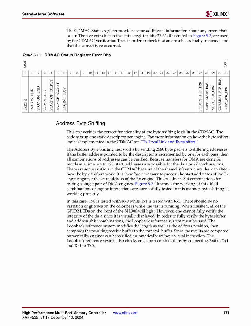
High Performance Multi-Port Memory Controller www.xilinx.com 171XAPP535 (v1.1) December 10, 2004
Stand-Alone SoftwareR
The CDMAC Status register provides some additional information about any errors that occur. The five extra bits in the status register, bits 27-31, illustrated in Figure 5-3, are used by the CDMAC Verification Tests in order to check that an error has actually occurred, and that the correct type occurred.
Address Byte Shifting
This test verifies the correct functionality of the byte shifting logic in the CDMAC. The code sets up one static descriptor per engine. For more information on how the byte shifter logic is implemented in the CDMAC see “Tx LocalLink and Byteshifter.”
The Address Byte Shifting Test works by sending 2560 byte packets to differing addresses. If the buffer address pointed to by the descriptor is incremented by one for each pass, then all combinations of addresses can be verified. Because transfers for DMA are done 32 words at a time, up to 128 'start' addresses are possible for the data or 27 combinations. There are some artifacts in the CDMAC because of the shared infrastructure that can affect how the byte shifters work. It is therefore necessary to precess the start addresses of the Tx engine against the start address of the Rx engine. This results in 214 combinations for testing a single pair of DMA engines. Figure 5-3 illustrates the working of this. If all combinations of engine interactions are successfully tested in this manner, byte shifting is working properly.
In this case, Tx0 is tested with Rx0 while Tx1 is tested with Rx1. There should be no variation or glitches on the color bars while the test is running. When finished, all of the GPIO2 LEDs on the front of the ML300 will light. However, one cannot fully verify the integrity of the data since it is visually displayed. In order to fully verify the byte shifter and address shift combinations, the Loopback reference system must be used. The Loopback reference system modifies the length as well as the address position, then compares the resulting receive buffer to the transmit buffer. Since the results are compared numerically, engines can be verified automatically without visual inspection. The Loopback reference system also checks cross-port combinations by connecting Rx0 to Tx1 and Rx1 to Tx0.
Table 5-3: CDMAC Status Register Error Bits
MSB
LSB
0 1 2 3 4 5 6 7 8 9 10 11 12 13 14 15 16 17 18 19 20 21 22 23 24 25 26 27 28 29 30 31
ER
RO
R
INT
_ON
_EN
D
STO
P_O
N_E
ND
CO
MP
LE
TE
D
STA
RT
_OF_
PAC
KE
T
EN
D_O
F_PA
CK
ET
EN
GIN
E_B
USY
CO
MP
LE
TE
D_E
RR
BU
FF_A
DD
R_E
RR
NE
XT
_PT
R_E
RR
CU
RR
EN
T_P
TR
_ER
R
BU
SY_W
R_E
RR
ARCHIVED APPLICATION NOTE - NOT SUPPORTED FOR NEW DESIGNS

172 www.xilinx.com High Performance Multi-Port Memory ControllerXAPP535 (v1.1) December 10, 2004
Chapter 5: Software Applications Contained in the GSRDR
Out of Address Range Errors - Direct
If the Buffer Address field in a descriptor is ever set to an invalid memory location, the CDMAC engine stops processing and generates a Buffer Address Error on its corresponding status register. With one descriptor per engine, this code sets each descriptor's buffer address to a value that is out of range, see Table 5-3. Each of the four LEDs listed in Table 5-1 and Table 5-2 should light when its corresponding engine displays a Buffer Address Error.
Figure 5-3: Address Shifting Example
RX0
214 = 16384Combinations
214 = 16384Combinations
TX1 RX1TX0
Buffer Address Buffer Address + 1 Buffer Address + 2 Buffer Address + 128
...
X535_82_113004
Figure 5-4: Buffer Address Error when Buffer Address Out of Range
Error: Invalid Address
Memory
Buffer Address:Invalid Address
Next Descriptor Pointer
Buffer Length
DMA Descriptor
CDMACStatus Application Dependent
Application Dependent
Application Dependent
Application Dependent
Application Dependent
X535_83_113004
ARCHIVED APPLICATION NOTE - NOT SUPPORTED FOR NEW DESIGNS

High Performance Multi-Port Memory Controller www.xilinx.com 173XAPP535 (v1.1) December 10, 2004
Stand-Alone SoftwareR
Out of Address Range Errors - Buffer Length is Too LargeIf the Buffer Length field is long enough to cause a CDMAC engine to process data outside of valid memory space, the CDMAC engine stops processing and generates a Buffer Address Error on its corresponding status register. With one descriptor per engine, this code sets each descriptor's buffer address to a proper value near the end of memory space, but sets the length field such that when the engine processes a descriptor it runs out of valid memory space, see Figure 5-5. Each of the four LEDs listed in Table 5-1 and Table 5-2 should light when its corresponding engine displays a Buffer Address Error.
Completed Bit Errors
A Completed Bit Error occurs when a CDMAC engine encounters a descriptor that has already been marked as completed. If a set of descriptors is being processed by a CDMAC engine and the completed bit is detected, as in Figure 5-6, it stops processing and generates a Completed Bit Error on its corresponding status register. For each engine the code points a single descriptor to itself and does not set interrupt or stop bits, so the engine loops forever on that one descriptor. If interrupts do not occur and a handler is not scrubbing the status bits each engine shows a Completed Bit Error and stops as soon the descriptor has been processed once. Each of the four LEDs listed in Table 5-1 and Table 5-2 should light when its corresponding engine displays a Completed Bit Error.
Figure 5-5: Buffer Address Error When Buffer Address Increments Out of Range
Error: Invalid Address
Memory
Buffer Address:Valid Address
Next Descriptor Pointer
Buffer Length: Too Large
DMA Descriptor
CDMACStatus Application Dependent
Application Dependent
Application Dependent
Application Dependent
Application Dependent
X535_84_113004
Figure 5-6: CDMAC Completed Bit Errors
SOP/EOP
SOP/EOP
SOP/EOP/Complete
SOP/EOP/Complete
SOP/EOP/INT/Complete
Error: Descriptor alreadymarked as complete whenDMA engine reads descriptor.
DMA Descriptors
......
X535_85_113004
ARCHIVED APPLICATION NOTE - NOT SUPPORTED FOR NEW DESIGNS

174 www.xilinx.com High Performance Multi-Port Memory ControllerXAPP535 (v1.1) December 10, 2004
Chapter 5: Software Applications Contained in the GSRDR
Next Pointer ErrorsIf the Next Descriptor Pointer field in a descriptor is ever set to an invalid memory location, the CDMAC engine stops processing and generates a Next Pointer Error on its corresponding status register. This test sets up one static descriptor for each engine. Then sets the Next Descriptor pointer for each engine to an invalid memory addresses, as in Figure 5-7. This stops each engine and generates next pointer errors that shows up on their respective LEDs shown in Table 5-1 and Table 5-2.
Current Pointer Errors
The Current Descriptor Pointer is used to start a CDMAC engine, as well as display where the engine stopped processing data. If the Current Descriptor Pointer field in a CDMAC DCR register is ever set to an invalid memory location, the CDMAC engine stops processing and generates a Current Pointer Error on its corresponding status register. This test sets up one static descriptor for each engine. Then sets the Current Descriptor Pointer for each engine to an invalid memory addresses, shown in Figure 5-8. This stops each engine and generates current pointer errors that show up on their respective LEDs shown in Table 5-1 and Table 5-2.
Figure 5-7: CDMAC Next Pointer Errors
Error: Invalid Pointer
Memory
Buffer Address
Buffer Length
Invalid Next Descriptor Pointer
DMA Descriptor
CDMACStatus Application Dependent
Application Dependent
Application Dependent
Application Dependent
Application Dependent
X535_86_113004
Figure 5-8: CDMAC Current Pointer Errors
CDMAC DCR Registerper DMA Engine
Error: Invalid Pointer
Memory
Next Descriptor Pointer
Current Buffer Address
Current Buffer Length
Current Descriptor Pointer
X535_87_113004
ARCHIVED APPLICATION NOTE - NOT SUPPORTED FOR NEW DESIGNS
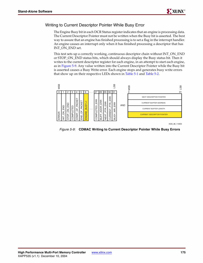
High Performance Multi-Port Memory Controller www.xilinx.com 175XAPP535 (v1.1) December 10, 2004
Stand-Alone SoftwareR
Writing to Current Descriptor Pointer While Busy Error
The Engine Busy bit in each DCR Status register indicates that an engine is processing data. The Current Descriptor Pointer must not be written when the Busy bit is asserted. The best way to assure that an engine has finished processing is to set a flag in the interrupt handler. An engine causes an interrupt only when it has finished processing a descriptor that has INT_ON_END set.
This test sets up a correctly working, continuous descriptor chain without INT_ON_END or STOP_ON_END status bits, which should always display the Busy status bit. Then it writes to the current descriptor register for each engine, in an attempt to start each engine, as in Figure 5-9. Any value written into the Current Descriptor Pointer while the Busy bit is asserted causes a Busy Write error. Each engine stops and generates busy write errors that show up on their respective LEDs shown in Table 5-1 and Table 5-2.
Figure 5-9: CDMAC Writing to Current Descriptor Pointer While Busy Errors
X535_88_113004
0 1 2 3 4 5 6 27 28 29 30 31
ER
RO
R
INT
_ON
_EN
D
STO
P_O
N_E
ND
CO
MP
LET
ED
STA
RT
_OF
_PA
CK
ET
EN
D_O
F_P
AC
KE
T
EN
GIN
E_B
US
Y=
1
CO
MP
LET
ED
_ER
R
BU
FF
_AD
DR
_ER
R
NE
XT
_PT
R_E
RR
CU
RR
EN
T_P
TR
_ER
R
BU
SY
_WR
_ER
RLS
B
MS
B
LSB
MS
B
. . .
. . .AND
0 31
NEXT DESCRIPTOR POINTER
CURRENT BUFFER ADDRESS
CURRENT BUFFER LENGTH
CURRENT DESCRIPTOR POINTER
ARCHIVED APPLICATION NOTE - NOT SUPPORTED FOR NEW DESIGNS

176 www.xilinx.com High Performance Multi-Port Memory ControllerXAPP535 (v1.1) December 10, 2004
Chapter 5: Software Applications Contained in the GSRDR
GSRD Verification TestThis software application uses all four CDMAC engines to transfer lines of TFT data from the Data Generator through the GMAC Peripheral and Fiber-Optic loopback connector to the TFT display. This model is a better representation of usage of the GMAC Peripheral in a real life embedded system. Reads and writes occur simultaneously on all four engines and all the peripherals are continuously working.
As illustrated in Figure 5-10, the CDMAC engines transfer a color bar pattern:
1. from the Data Generator (full TFT lines of pixels, 2560 bytes per packet)
2. to a memory buffer
3. to the Tx GMAC (half TFT lines of pixels, 1280 bytes per packet)
4. to a fiber loopback terminator
5. to the Rx GMAC (half TFT lines of pixels, 1280 bytes per packet)
6. to a second memory buffer
7. to the TFT (half TFT lines of pixels, 1280 bytes per packet)
Rx0 uses 480 descriptors, while Tx0 and Rx1 engines use 960 descriptors. Tx1 uses 960 header descriptors and 960 payload descriptors. Each engine has a set of descriptors configured to define its functionality, as shown in Figure 5-11. Each set of descriptors is set up in a ring, the last descriptor points to the first.
Figure 5-10: GSRD Verification Test Software Block Diagram
RX0 TX1 RX1 TX0
BufferTX
BufferRX
DataGenerator
TFT
GMACPeripheral RXTX
Fiber
X535_89_113004
ARCHIVED APPLICATION NOTE - NOT SUPPORTED FOR NEW DESIGNS

High Performance Multi-Port Memory Controller www.xilinx.com 177XAPP535 (v1.1) December 10, 2004
Stand-Alone SoftwareR
Engine Rx0
This engine reads data from the LocalLink Data generator and places it into a DDR buffer, Buffer TX. Each packet received is 2560 bytes long, which corresponds to a line of 640 pixels on the TFT screen. Every descriptor has START_OF_PACKET and END_OF_PACKET set to specify one packet per descriptor. INT_ON_END is set at the halfway point of the descriptor chain, and at the last descriptor
Engine Tx1
This engine takes data from the same buffer used by Rx0, Buffer TX, and writes it to the GMAC. Two sets of descriptors are used, header descriptors and payload descriptors. Each packet consists of one header and one payload descriptor. Each header descriptor is 14 bytes long and points to a buffer of Ethernet header data. Every header descriptor has the START_OF_PACKET status bit set. Each payload descriptor is 1280 bytes long, exactly half of the size of a full TFT line. Every payload descriptor has END_OF_PACKET set to terminate the packet. INT_ON_END is set on the payload descriptor at the halfway point of the descriptor chain, and at the last descriptor. STOP_ON_END is set for the last descriptor in the payload chain. The engine stops at the end of every frame transferred and is re-started when the interrupt handler finishes scrubbing the status bits for the second half of the header and payload descriptors. The engine is re-started using a semaphore mechanism implemented inside an infinite while loop in the main function.
Engine Rx1
This engine reads data received from the GMAC and places it into a DDR buffer, Buffer RX. Each packet received is 1294 bytes long, which corresponds to a half line of pixels on the TFT screen plus a 14 byte Ethernet header. Every descriptor has START_OF_PACKET and END_OF_PACKET set to specify one packet per descriptor. INT_ON_END is set at the halfway point of the descriptor chain, and at the last descriptor. STOP_ON_END is set for the last descriptor in the payload chain. The engine stops at the end of every frame received and is re-started when the interrupt handler finishes scrubbing the status bits for the second half of the descriptors. The engine is re-started using a semaphore mechanism implemented inside an infinite while loop in the main function.
Figure 5-11: GSRD Verification Test CDMAC Descriptor Setup
Rx0 Descriptors
2560 Bytes | SOP/EOP
...
2560 Bytes | SOP/EOP/IOE
2560 Bytes | SOP/EOP
2560 Bytes | SOP/EOP/IOE
...
0 0
959
480
479 479
Tx1 Header Descriptors
14 Bytes | SOP
14 Bytes | SOP
...
Tx1 Payload Descriptors
1280 Bytes | EOP
......
1280 Bytes | EOP/IOE
1280 Bytes | EOP/IOE/SOE
1280 Bytes | EOP
1294 Bytes | SOP/EOP
......
1294 Bytes | EOP/IOE
1294 | SOP/EOP/IOE/SOE
1294 Bytes | EOP
Rx1 Descriptors Tx0 Descriptors
1280 Bytes | SOP/EOP
......
1280 Bytes | SOP/EOP/IOE
1280 Bytes | SOP/EOP/IOE
1280 Bytes | SOP/EOP
X535_90_113004
ARCHIVED APPLICATION NOTE - NOT SUPPORTED FOR NEW DESIGNS
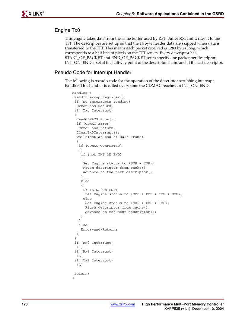
178 www.xilinx.com High Performance Multi-Port Memory ControllerXAPP535 (v1.1) December 10, 2004
Chapter 5: Software Applications Contained in the GSRDR
Engine Tx0
This engine takes data from the same buffer used by Rx1, Buffer RX, and writes it to the TFT. The descriptors are set up so that the 14 byte header data are skipped when data is transferred to the TFT. This means each packet received is 1280 bytes long, which corresponds to a half line of pixels on the TFT screen. Every descriptor has START_OF_PACKET and END_OF_PACKET set to specify one packet per descriptor. INT_ON_END is set at the halfway point of the descriptor chain, and at the last descriptor.
Pseudo Code for Interrupt Handler
The following is pseudo code for the operation of the descriptor scrubbing interrupt handler. This handler is called every time the CDMAC reaches an INT_ON_END.
Handler { ReadInterruptRegister(); if (No Interrupts Pending) Error-and-Return; if (Tx0 Interrupt) { ReadCDMACStatus(); if (CDMAC Error) Error and Return; ClearTx0Interrupt(); while(Not at end of Half Frame) { if (CDMAC_COMPLETED} { if (not INT_ON_END) { Set Engine status to (SOP + EOP); Flush descriptor from cache(); Advance to the next descriptor(); } else { if (STOP_ON_END) Set Engine status to (SOP + EOP + IOE + SOE); else Set Engine status to (SOP + EOP + IOE); Flush descriptor from cache(); Advance to the next descriptor(); } } else Error-and-Return; } } if (Rx0 Interrupt) {…} if (Rx1 Interrupt) {…} if (Tx1 Interrupt) {…}
return;}
ARCHIVED APPLICATION NOTE - NOT SUPPORTED FOR NEW DESIGNS

High Performance Multi-Port Memory Controller www.xilinx.com 179XAPP535 (v1.1) December 10, 2004
Stand-Alone SoftwareR
First, an error check is performed to confirm that a pending interrupt exists for a CDMAC engine. The pending engine interrupts are then serviced by their respective If blocks.
Inside the If blocks another error check occurs to verify that the CDMAC engine is not reporting an error. Then the pending interrupt is immediately cleared. The If block continues inside of a while loop until the entire half screen of descriptors has been scrubbed. Tx engines are scrubbed by writing START_OF_PACKET and END_OF_PACKET to the CDMAC status register. The exceptions to that rule occur when the current packet has STOP_ON_END or INT_ON_END set, in which case those bits would also be set. When the descriptors are written to, they must be immediately flushed from data cache using the XCache_FlushDCacheLine() function from xcache_l.h. The current pointer advances to the next descriptor following each status scrub.
The omitted engines use essentially the same algorithm with the following exceptions:
• Rx0 and Rx1 do not have START_OF_PACKET and END_OF_PACKET set
• Rx1 and Tx1 set a semaphore flag within the STOP_ON_END If statement.
• Tx1 has an extra If statement to differentiate between header and payload descriptors
Figure 5-12 is a flow chart of the main loop. Figure 5-13 shows the flow chart for the entire interrupt handler routine.
The results should be a solid color bar pattern on the TFT. The row of LEDs below the TFT also displays a value that is a relative measurement of the amount of time spent inside the
Figure 5-12: GSRD Verification Test Software Flow Chart
Initialize GlobalsInitialize CachesCreate Static Descriptors
If Tx1 Flagis Set
Initialize BuffersInitialize Headers
Turn On Rx0
Turn On Rx1
Turn On Tx1
Turn On Tx0
Turn On TFT on Tx0
Initialize LEDsInitialize InterruptsSet Up MDIO, PCS in GMAC
Restart Tx1Reset Tx1 Flag
If Rx1 Flagis Set
Restart Rx1Reset Rx1 Flag
X535_91_113004
ARCHIVED APPLICATION NOTE - NOT SUPPORTED FOR NEW DESIGNS

180 www.xilinx.com High Performance Multi-Port Memory ControllerXAPP535 (v1.1) December 10, 2004
Chapter 5: Software Applications Contained in the GSRDR
main loop between interrupts. The number of LEDs lit reflects a counter that increments by one each time the main while loop repeats. The value is displayed at the very top of the interrupt handler and reset at the very bottom of the interrupt handler. If results differ, check the Known Issues section in the release for information regarding this application.
Figure 5-13: GSRD Verification Test Software Interrupt Handler Routine Flow Chart
Clear Rx1Interrupt
If StatusCompleted
False
If NotINT_ON_END
Scrub Status=0Flush Cache
True
False
TrueScrub SOE/IOE
Scrub IOE
Flush CacheIf Status
STOP_ON_END
Read Interrupt Register
If No PendingInterrupt
If Tx0 Interrupt
If Rx0 Interrupt
If Rx1 Interrupt
If Tx1 Interrupt
If StatusCompleted
If NotINT_ON_END
If Status ErrorClear Tx0 Interrupt
Scrub SPP/EOPFlush Cache
Clear Rx0Interrupt
Scrub SPP/EOP/IOEFlush Cache
Return
True
True
Return
TrueTrue
If StatusCompleted
False
False
False
False
True
True
If NotINT_ON_END
Scrub Status=0Flush Cache
True
False
False
True
If Status Error
Return
Return
True
False
If Status Error
Return
True
If Status Error
Scrub SOE/IOE
Scrub IOE
Flush CacheIf Status
STOP_ON_END
True
Clear Tx1Interrupt
If NotINT_ON_END
If StatusCompleted
If StatusSTOP_ON_END
Flush Cache
Scrub SOP
Scrub SOP
Scrub EOP
Scrub EOP/IOE/SOE
Scrub SOP
Scrub EOP/IOE
If StatusSOP
True
False
If StatusSOP
True
False
If StatusSOP
True
False
X535_92_113004
ARCHIVED APPLICATION NOTE - NOT SUPPORTED FOR NEW DESIGNS

High Performance Multi-Port Memory Controller www.xilinx.com 181XAPP535 (v1.1) December 10, 2004
Stand-Alone SoftwareR
Loopback Reference System Verification TestsThe Gigabit Loopback Reference System connects CDMAC Tx engines to CDMAC Rx engines to allow complete verification of the byte shifter. The error_on_completed_bit feature is enabled for all engines in this design so descriptors must always be scrubbed before they are processed.
CDMAC Loopback Verification Test
There are 128 possible byte organizations when transferring data in a 32 word burst format. Position the first byte anywhere within the burst 32 (128 bytes), and the last byte anywhere after the first byte within the burst 32. The positioning of the first byte depends on the "Buffer Address" field in any given descriptor and the last byte depends on a combination of the "Buffer Address" and the "Buffer Length" field. By assigning 7 bits to each field (for 128 positions) we can use a 14 bit number to represent a combination of "Buffer Address" and "Buffer Length". By testing all combinations of this number with descriptors, all the possible byte positions and lengths are tested in a given engine. It is important to verify that the Byte Shifters and CDMAC logic are 100% tested for all combinations of possible address and lengths.
This test generates an array with all possible combinations of the address and length offsets. This array contains all 214 = 16384 combinations. The top 7 bits (MSB) are the address offset and the bottom 7 bits (LSB) are the length offset. Figure 5-14 illustrates this organization. Each CDMAC engine is assigned a unique array. Each array is randomly shuffled so that each array appears random relative to the other arrays. It is important to verify that no dependencies exist within the CDMAC address, length, and byte shift logic. This kind of testing is often overlooked during DMA engine development. Errors of this kind in hardware can lead to bugs that are very difficult to identify.
Once the random arrays of address and length offsets are generated, the test iterates through the array by generating CDMAC descriptors based on the offset values. The CDMAC engines are started, and each Tx engine transmits its data to a corresponding Rx engine. When a Rx engine completes, it sets an 'end' flag that tells the software to begin comparing the receive data to the expected transmitted data. The test then compares the payload that was sent to the payload that was received. If an error is found, an error is printed on UART1 of ML300, and the program exits with an error code of 1. (UART1 is set for 38400/8/n/1).
When the comparison is complete, the software checks to see if it has reached the final entry in the array. If not, it increments the index to the arrays, generates new descriptors, and restarts the CDMAC engines. The code then clears the 'end' flag so that the process can continue until all elements in the array have been processed. When all elements in the array have been processed, the software sets a 'complete' flag. It is important to know when all four CDMAC engines have completed all possible combinations. There are two 'complete' flags, one for the Tx0-Rx0 pair, and another for the Tx1-Rx1 pair. When both 'complete' flags are set, the software reshuffles the arrays into differing random patterns. The CDMAC engines are restarted, and the entire process repeats. A pass counter is
Figure 5-14: CDMAC Loopback Offset Buffer Organization
Address Offset Length
MSB7 bits = 0-127 7 bits = 0-127
LSB
X535_93_113004
ARCHIVED APPLICATION NOTE - NOT SUPPORTED FOR NEW DESIGNS

182 www.xilinx.com High Performance Multi-Port Memory ControllerXAPP535 (v1.1) December 10, 2004
Chapter 5: Software Applications Contained in the GSRDR
displayed on the top yellow GPIO1 LEDs of ML300 and output to UART1. See Figure 5-15 for arrangement of ML300 resources including LED locations.
Figure 5-16 illustrates the operation of the Loopback Verification Test.
Figure 5-15: ML300 Evaluation Platform LED Layout for Loopback Verification Test
Pass Counter LEDs
TFT
Yellow (LSB)(MSB) 815
Port 0 IterationCounter LEDs
Port 1 IterationCounter LEDs
(LSB)(MSB) 015
Green
1631
X535_94_113004
ARCHIVED APPLICATION NOTE - NOT SUPPORTED FOR NEW DESIGNS

High Performance Multi-Port Memory Controller www.xilinx.com 183XAPP535 (v1.1) December 10, 2004
Stand-Alone SoftwareR
CDMAC One Descriptor Loopback Verification Test
With one descriptor per channel, this test simply transfers a data buffer from the Tx engines to the Rx engines, then compares the resulting buffer with the original buffer. The test does not change the address or lengths, nor does it have any loops. The simplicity of this test makes it easy to simulate. If the comparison ever fails, an error message prints to the UART.
An example message:
Rx0 Rata is not correct at 0x12345678, should be: 0xFFFFFFFF, received: 0xFFFFFFFA
Upon successful completion of data transfer for each Rx engine, as noted by the comparison "good" flags, a success message prints to the UART. After the message is printed, the "good" flags are reset and the CDMAC engines are restarted.
Figure 5-16: Loopback Verification Test Software Flow Chart
False
True
Good
RandomizeOffset Arrays
Generate Descriptors from Randomized Arrays. Separate Port 1 and Port 0 calls.
Randomize Offset Arrays
Reset Complete Flags
Generate Descriptorsfrom Randomized Arrays.Separate Port 0 andPort 1 calls.
Start CDMAC Engines
Rx0End Flag
CompareData Buf
Increment OffsetCounter. GenerateDescriptors for Port 0.Display on left half LEDs
Start Port 0CDMAC Engines
Print Error Return 1 Set Rx0 Complete Flag
Reset Rx0 End Flag
At end ofOffset Buf
Print UART Pass ResultsReset Complete Flagsand Descriptor Indexes
Increment PassCounter. Display on topLEDs
False
Bad True
False
False
True
True
Good
Rx1End Flag
Rx0 andRx1 Complete
Flags
CompareData Buf
Increment OffsetCounter. GenerateDescriptors for Port 1.Display on right half LEDs
Start Port 1CDMAC Engines
Print Error Return 1 Set Rx1 Complete Flag
Reset Rx1 End Flag
At end ofOffset Buf
False
Bad True
Start CDMAC Engines
X535_95_113004
ARCHIVED APPLICATION NOTE - NOT SUPPORTED FOR NEW DESIGNS

184 www.xilinx.com High Performance Multi-Port Memory ControllerXAPP535 (v1.1) December 10, 2004
Chapter 5: Software Applications Contained in the GSRDR
Performance MetricsUsing the xtime library and a few counters within the interrupt handler and other code, the GSRD Verification Test is able to measure the amount of time spent in the interrupt routine, the amount of time spent in the main loop, and the number of interrupts serviced per CDMAC engine. The counters provide information to know how many times each CDMAC engine has scrubbed its descriptors. Since it is known how long the program ran, and how much data each engine has moved, it is possible to measure the performance of the entire GSRD reference system.
CPU Performance Measurement
The XTime_GetTime() function in the xtime_l.h library returns the total number of processor cycles that have occurred up until that function call. The value returned reflects the 64-bit time base counter inside the PowerPC core. (See the EDK OS and Libraries Reference Guide, available online at http://www.xilinx.com/ise/embedded/edk_libs_ref_guide.pdf..)
XTime_GetTime is called upon entry and exit to the interrupt handler. The difference is calculated to achieve the time spent in the interrupt handler vs. time spent in the main while loop. Two variables are used to communicate the total time: Time_CPU_Only and Time_INT_Only. These two variables added together represent the total time spent in the code (in CPU clock ticks). The ratio of these two variables allows the measurement of CPU time available versus CPU time spent processing interrupts for the CDMAC.
Remaining CPU Time Available = Time spent in main loop / Total duration of execution
As the number of INT_ON_END instances within each set of descriptors increases, or coalesces, the percentage of time available to the processor outside of the interrupt handler changes as illustrated in Figure 5-17.
Table 5-4: Example CPU Availability Over a 120 Second Test
Time_CPU_Only 25,055,441,967
Tme_INT_Only 11,043,249,478
% CPU Time Available 69%
% of CPU spent for CDMAC 31%
ARCHIVED APPLICATION NOTE - NOT SUPPORTED FOR NEW DESIGNS

High Performance Multi-Port Memory Controller www.xilinx.com 185XAPP535 (v1.1) December 10, 2004
Stand-Alone SoftwareR
CDMAC Performance Measurement
A counter is incremented each time a half screen worth of descriptors is successfully scrubbed. Each engine has one counter associated with it. Since the amount of data sent per half screen is a known value, the rate at which each CDMAC engine transfers data can be calculated.
bytes per frame = x pixels * y pixels * bytes per pixel
data bytes transferred = bytes per frame * number of frames
descriptor bytes transferred = number of descriptors * 32 bytes per descriptor * 2 descriptors per transaction * number of interrupts per measured time
Bytes per second = (Data bytes transferred + Descriptor bytes transferred) / measured time
Figure 5-17: CPU Performance vs Interrupts
X535_96_113004
% of CPU Av ailabilit y v s. Interrupts per Descr ip tor Set
0%
10%
20%
30%
40%
50%
60%
70%
80%
90%
100%
1 2 4 6 8 10 12 14 16
Interr upts per Descriptor Set
% o
f C
PU
Tim
e A
vai
lab
le
120 Second Run
Table 5-5: Example of a 120-second test where all four engines are being scrubbed
TX0 Bytes per second 80,672,768
RX0 Bytes per second 89,284,608
TX1 Bytes per second 122,635,776
TX1 Bytes per second 114,757,632
TOTAL BYTES / SEC 407,350,784
Bits per second 3,258,806,272
ARCHIVED APPLICATION NOTE - NOT SUPPORTED FOR NEW DESIGNS

186 www.xilinx.com High Performance Multi-Port Memory ControllerXAPP535 (v1.1) December 10, 2004
Chapter 5: Software Applications Contained in the GSRDR
Testing Result Example From the GSRD
Table 5-6 lists the resultant data from a 120-second run of the GMAC verification test.
Table 5-6: Performance Metric Testing Results From the GSRD
Comment Scrub all ports
Design GSRD
SW gmac_echo_int_tft
INPUTS
OSC Freq (Hz) 100000000
Measured Time (sec) 120
# TX0 (TFT) Scrubs* 14324
# RX0 (DG) Scrubs* 16608
# TX1 (GigE TX or TFT2) Scrubs* 20376
# RX1 (GigE Rx or DG2) Scrubs* 20376
Time_CPU_Only 25,055,441,967
Tme_INT_Only 11,043,249,478
# TX0 Descriptors 960
# RX0 Descriptors 480
# TX1 Descriptors 1920
# RX1 Descriptors 960
TOTALS
INTS
TX0 Interrupts per second 119.3666667
RX0 Interrupts per second 138.4
TX1 Interrupts per second 169.8
RX1 Interrupts per second 169.8
TOTAL INTERRUPTS / SEC 597.3666667
DATA
TX0 Bytes per second 80,672,768
RX0 Bytes per second 89,284,608
TX1 Bytes per second 122,635,776
TX1 Bytes per second 114,757,632
TOTAL BYTES / SEC 407,350,784
Bits per second 3,258,806,272
% CPU Time Available 69%
% of CPU spent for CDMAC 31%
ARCHIVED APPLICATION NOTE - NOT SUPPORTED FOR NEW DESIGNS

High Performance Multi-Port Memory Controller www.xilinx.com 187XAPP535 (v1.1) December 10, 2004
Stand-Alone SoftwareR
Data Calculations
TFT CALCS
x pixels 640
y pixels 480
bytes/pixel 4
bytes/frame 1228800
frames/sec 55.55555556
# of Ints 14324
# of Ints / Sec 119.3666667
# Frames 7162
Calc frames / sec 59.68333333
Bytes moved in descriptors 880066560
Bytes moved in Data 8800665600
Total # bytes moved by CDMAC 9680732160
TX0 Bytes per second 80672768
DATA GENERATOR CALCS
x pixels 640
y pixels 480
bytes / pixel 4
bytes / frame 1228800
# of Ints 16608
# of Ints / Sec 138.4
# frames 8304
Calc Frames / sec 69.2
Bytes moved in descriptors 510197760
Bytes moved in Data 10203955200
Total # bytes moved by CDMAC 10714152960
RX0 Bytes per second 89284608
GigE TX Calcs
# of Ints 20376
# of Ints / Sec 169.8
Bytes moved in descriptors 2040791040
Data Bytes / Descriptor 1280
Eth Header Bytes / Descriptor 16
Bytes moved in Data 12675502080
Table 5-6: Performance Metric Testing Results From the GSRD (Continued)
ARCHIVED APPLICATION NOTE - NOT SUPPORTED FOR NEW DESIGNS

188 www.xilinx.com High Performance Multi-Port Memory ControllerXAPP535 (v1.1) December 10, 2004
Chapter 5: Software Applications Contained in the GSRDR
Linux Device DriverSee the chapter covering the Linux Device Driver in XAPP536, “Gigabit System Reference Design.”
LwIPSee the chapter covering LwIP in XAPP536, “Gigabit System Reference Design.”
Total # bytes moved by CDMAC 14716293120
TX1 Bytes per second 122635776
gbit / sec 981086208
GigE RX Calcs
# of Ints 20376
# of Ints / Sec 169.8
Bytes moved in descriptors 1251901440
Data Bytes / Descriptor 1280
Eth Header Bytes / Descriptor 0
Bytes moved in Data 12519014400
Total # bytes moved by CDMAC 13770915840
TX1 Bytes per second 114757632
gbit / sec 918061056
Table 5-6: Performance Metric Testing Results From the GSRD (Continued)
ARCHIVED APPLICATION NOTE - NOT SUPPORTED FOR NEW DESIGNS

High Performance Multi-Port Memory Controller www.xilinx.com 189XAPP535 (v1.1) December 10, 2004
R
Chapter 6
Building the GSRD Under EDK
Supported FeaturesThe GSRD (without alteration) supports only some EDK features for specific EDA tools and hardware platforms.
The edk_instructions.pdf file contained in the zip file contains instructions for building the GSRD under EDK.
Table 6-1: Supported features
Feature Supported Limitations
Behavioral Simulation Yes ModelSim only
Structural Simulation Yes ModelSim only
Timing Simulation No
FPGA Implementation Yes ML300
Download Yes ML300
ACE File Generation Yes ML300
ARCHIVED APPLICATION NOTE - NOT SUPPORTED FOR NEW DESIGNS

190 www.xilinx.com High Performance Multi-Port Memory ControllerXAPP535 (v1.1) December 10, 2004
Chapter 6: Building the GSRD Under EDKR
ARCHIVED APPLICATION NOTE - NOT SUPPORTED FOR NEW DESIGNS