Embed Size (px)
Citation preview

General DescriptionThe MAX4230–MAX4234 single/dual/quad, high-output-drive CMOS op amps feature 200mA of peak outputcurrent, rail-to-rail input, and output capability from asingle 2.7V to 5.5V supply. These amplifiers exhibit ahigh slew rate of 10V/µs and a gain-bandwidth product(GBWP) of 10MHz. The MAX4230–MAX4234 can drivetypical headset levels (32Ω), as well as bias an RFpower amplifier (PA) in wireless handset applications.
The MAX4230 comes in a tiny 5-pin SC70 package andthe MAX4231, single with shutdown, is offered in the 6-pin SC70 package. The dual op-amp MAX4233 isoffered in the space-saving 10-bump chip-scale pack-age (UCSP™), providing the smallest footprint area fora dual op amp with shutdown.
These op amps are designed to be part of the PA con-trol circuitry, biasing RF PAs in wireless headsets. TheMAX4231/MAX4233 offer a SHDN feature that drivesthe output low. This ensures that the RF PA is fully dis-abled when needed, preventing unconverted signals tothe RF antenna.
The MAX4230 family offers low offsets, wide bandwidth,and high-output drive in a tiny 2.1mm x 2.0mm space-saving SC70 package. These parts are offered over theautomotive temperature range (-40°C to +125°C).
ApplicationsRF PA Biasing Controls in Handset Applications
Portable/Battery-Powered Audio Applications
Portable Headphone Speaker Drivers (32Ω)
Audio Hands-Free Car Phones (Kits)
Laptop/Notebook Computers/TFT Panels
Sound Ports/Cards
Set-Top Boxes
Digital-to-Analog Converter Buffers
Transformer/Line Drivers
Motor Drivers
Features♦ 30mA Output Drive Capability
♦ Rail-to-Rail Input and Output
♦ 1.1mA Supply Current per Amplifier
♦ 2.7V to 5.5V Single-Supply Operation
♦ 10MHz Gain-Bandwidth Product
♦ High Slew Rate: 10V/µs
♦ 100dB Voltage Gain (RL = 100kΩ)
♦ 85dB Power-Supply Rejection Ratio
♦ No Phase Reversal for Overdriven Inputs
♦ Unity-Gain Stable for Capacitive Loads to 780pF
♦ Low-Power Shutdown Mode Reduces SupplyCurrent to <1µA
♦ Available in 5-Pin SC70 Package (MAX4230)
♦ Available in 10-Bump UCSP Package (MAX4233)
MA
X4
23
0–M
AX
42
34
High-Output-Drive, 10MHz, 10V/µs, Rail-to-Rail I/O Op Amps with Shutdown in SC70
________________________________________________________________ Maxim Integrated Products 1
19-2164; Rev 6; 1/06
Ordering Information continued at end of data sheet.
For pricing, delivery, and ordering information, please contact Maxim/Dallas Direct! at 1-888-629-4642, or visit Maxim’s website at www.maxim-ic.com.
Selector Guide appears at end of data sheet.Pin Configurations appear at end of data sheet.
UCSP is a trademark of Maxim Integrated Products, Inc.
Ordering Information
PART TEMP RANGE PIN-PACKAGE
TOP M ARK
MAX4230AXK-T -40°C to +125°C 5 SC70-5 ACS
MAX4230AUK-T -40°C to +125°C 5 SOT23-5 ABZZ
MAX4231AXT-T -40°C to +125°C 6 SC70-6 ABA
MAX4231AUT-T -40°C to +125°C 6 SOT23-6 AAUV
Typical Operating Circuit
MAX4231
DAC
PA2.7V TO 5.5V
RISO
ANTENNA
IOUT = 30mA
CLOAD
C
R RF
SHDN

MA
X4
23
0–M
AX
42
34
High-Output-Drive, 10MHz, 10V/µs, Rail-to-Rail I/O Op Amps with Shutdown in SC70
2 _______________________________________________________________________________________
ABSOLUTE MAXIMUM RATINGS
Stresses beyond those listed under “Absolute Maximum Ratings” may cause permanent damage to the device. These are stress ratings only, and functionaloperation of the device at these or any other conditions beyond those indicated in the operational sections of the specifications is not implied. Exposure toabsolute maximum rating conditions for extended periods may affect device reliability.
Supply Voltage (VDD to VSS) ....................................................6VAll Other Pins ....................................(VSS - 0.3V) + (VDD + 0.3V)Output Short-Circuit Duration to VDD or VSS (Note 1) ................10sContinuous Power Dissipation (TA = +70°C)
5-Pin SC70 (derate 3.1mW/°C above +70°C)..............247mW5-Pin SOT23 (derate 7.1mW/°C above +70°C)............571mW6-Pin SC70 (derate 3.1mW/°C above +70°C)..............245mW6-Pin SOT23 (derate 8.7mW/°C above +70°C) ...........696mW8-Pin SOT23 (derate 8.9mW/°C above +70°C) ...........714mW
8-Pin µMAX® (derate 4.5mW/°C above +70°C) ..........362mW10-Pin µMAX (derate 5.6mW/°C above +70°C) ..........444mW10-Bump UCSP (derate 6.1mW/°C above +70°C) .....484mW10-Pin TDFN (derate 24.4mW°C above +70°C) ........1951mW14-Pin SO (derate 8.3mW/°C above +70°C) ...............667mW
Operating Temperature Range .........................-40°C to +125°CJunction Temperature ......................................................+150°CStorage Temperature Range .............................-65°C to +150°CLead Temperature (soldering, 10s) .................................+300°C
Note 1: Package power dissipation should also be observed.
PARAMETER SYMBOL CONDITIONS MIN TYP MAX UNITS
Operating Supply Voltage Range VDD Inferred from PSRR test 2.7 5.5 V
Input Offset Voltage VOS 0.85 ±6 mV
Input Bias Current IB VCM = VSS to VDD 50 pA
Input Offset Current IOS VCM = VSS to VDD 50 pA
Input Resistance RIN 1000 MΩ
Common-Mode Input VoltageRange
VCM Inferred from CMRR test VSS VDD V
Common-Mode Rejection Ratio CMRR VSS < VCM < VDD 52 70 dB
Power-Supply Rejection Ratio PSRR VDD = 2.7V to 5.5V 73 85 dB
Shutdown Output Impedance ROUT V SHDN = 0V (Note 3) 10 ΩOutput Voltage in Shutdown VOUT(SHDN) V SHDN = 0V, RL = 200Ω (Note 3) 68 120 mV
RL = 100kΩ 100
RL = 2kΩ 85 98Large-Signal Voltage Gain AVOLVSS + 0.20V < VOUT< VDD - 0.20V
RL = 200Ω 74 80
dB
VDD - VOH 400 500RL = 32Ω
VOL - VSS 360 500
VDD - VOH 80 120RL = 200Ω
VOL - VSS 70 120
VDD - VOH 8 14
Output Voltage Swing VOUT
RL = 2kΩVOL - VSS 7 14
mV
VDD = 2.7V, VIN = ±100mV 70Output Source/Sink Current IOUT
VDD = 5V, VIN = ±100mV 200mA
VDD - VOH 128 200IL = 10mA VDD = 2.7V
VOL - VSS 112 175
VDD - VOH 240 320Output Voltage
IL = 30mA VDD = 5VVOL - VSS 224 300
mV
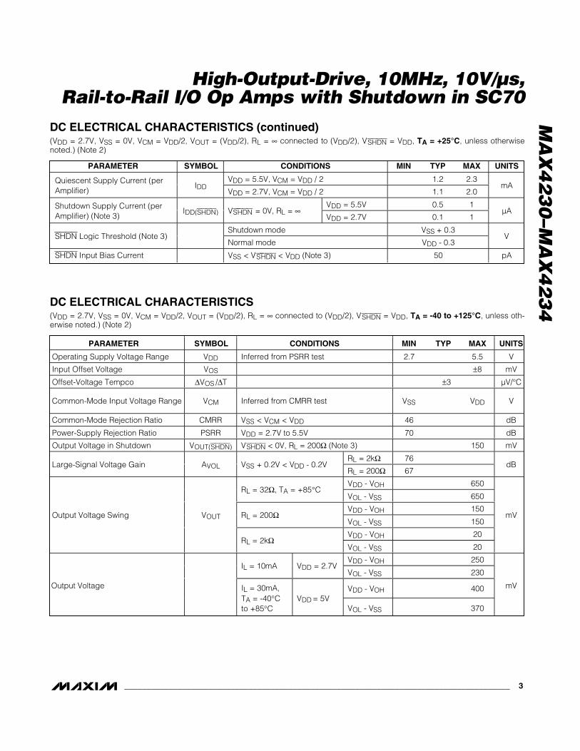
DC ELECTRICAL CHARACTERISTICS(VDD = 2.7V, VSS = 0V, VCM = VDD/2, VOUT = (VDD/2), RL = ∞ connected to (VDD/2), VSHDN = VDD, TA = +25°C, unless otherwisenoted.) (Note 2)
µMAX is a registered trademark of Maxim Integrated Products, Inc.
MA
X4
23
0–M
AX
42
34
High-Output-Drive, 10MHz, 10V/µs, Rail-to-Rail I/O Op Amps with Shutdown in SC70
_______________________________________________________________________________________ 3
PARAMETER SYMBOL CONDITIONS MIN TYP MAX UNITS
VDD = 5.5V, VCM = VDD / 2 1.2 2.3Quiescent Supply Current (perAmplifier)
IDDVDD = 2.7V, VCM = VDD / 2 1.1 2.0
mA
VDD = 5.5V 0.5 1Shutdown Supply Current (perAmplifier) (Note 3)
IDD(SHDN) V S HDN = 0V, RL = ∞VDD = 2.7V 0.1 1
µA
Shutdown mode VSS + 0.3SHDN Logic Threshold (Note 3)
Normal mode VDD - 0.3V
SHDN Input Bias Current VSS < V S HDN < VDD (Note 3) 50 pA
PARAMETER SYMBOL CONDITIONS MIN TYP MAX UNITS
Operating Supply Voltage Range VDD Inferred from PSRR test 2.7 5.5 V
Input Offset Voltage VOS ±8 mV
Offset-Voltage Tempco ∆VOS /∆T ±3 µV/°C
Common-Mode Input Voltage Range VCM Inferred from CMRR test VSS VDD V
Common-Mode Rejection Ratio CMRR VSS < VCM < VDD 46 dB
Power-Supply Rejection Ratio PSRR VDD = 2.7V to 5.5V 70 dB
Output Voltage in Shutdown VOUT(SHDN) V SHDN < 0V, RL = 200Ω (Note 3) 150 mV
RL = 2kΩ 76Large-Signal Voltage Gain AVOL VSS + 0.2V < VDD - 0.2V
RL = 200Ω 67dB
VDD - VOH 650RL = 32Ω, TA = +85°C
VOL - VSS 650
VDD - VOH 150RL = 200Ω
VOL - VSS 150
VDD - VOH 20
Output Voltage Swing VOUT
RL = 2kΩVOL - VSS 20
mV
VDD - VOH 250IL = 10mA VDD = 2.7V
VOL - VSS 230
VDD - VOH 400Output Voltage IL = 30mA,TA = -40°Cto +85°C
VDD = 5VVOL - VSS 370
mV
DC ELECTRICAL CHARACTERISTICS (continued)(VDD = 2.7V, VSS = 0V, VCM = VDD/2, VOUT = (VDD/2), RL = ∞ connected to (VDD/2), VSHDN = VDD, TA = +25°C, unless otherwisenoted.) (Note 2)
DC ELECTRICAL CHARACTERISTICS(VDD = 2.7V, VSS = 0V, VCM = VDD/2, VOUT = (VDD/2), RL = ∞ connected to (VDD/2), VSHDN = VDD, TA = -40 to +125°C, unless oth-erwise noted.) (Note 2)
MA
X4
23
0–M
AX
42
34
High-Output-Drive, 10MHz, 10V/µs, Rail-to-Rail I/O Op Amps with Shutdown in SC70
4 _______________________________________________________________________________________
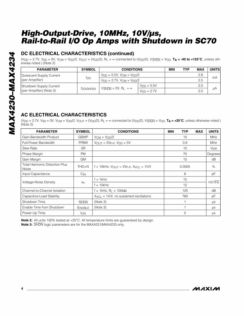
PARAMETER SYMBOL CONDITIONS MIN TYP MAX UNITS
Gain-Bandwidth Product GBWP VCM = VDD/2 10 MHz
Full-Power Bandwidth FPBW VOUT = 2VP-P, VDD = 5V 0.8 MHz
Slew Rate SR 10 V/µs
Phase Margin PM 70 Degrees
Gain Margin GM 15 dB
Total Harmonic Distortion PlusNoise
THD+N f = 10kHz, VOUT = 2VP-P, AVCL = 1V/V 0.0005 %
Input Capacitance CIN 8 pF
f = 1kHz 15Voltage-Noise Density en
f = 10kHz 12nV/√Hz
Channel-to-Channel Isolation f = 1kHz, RL = 100kΩ 125 dB
Capacitive-Load Stability AVCL = 1V/V, no sustained oscillations 780 pF
Shutdown Time tSHDN (Note 3) 1 µs
Enable Time from Shutdown tENABLE (Note 3) 1 µs
Power-Up Time tON 5 µs
Note 2: All units 100% tested at +25°C. All temperature limits are guaranteed by design.Note 3: SHDN logic parameters are for the MAX4231/MAX4233 only.
PARAMETER SYMBOL CONDITIONS MIN TYP MAX UNITS
VDD = 5.5V, VCM = VDD/2 2.8Quiescent Supply Current(per Amplifier)
IDDVDD = 2.7V, VCM = VDD/2 2.5
mA
VDD = 5.5V 2.0Shutdown Supply Current(per Amplifier) (Note 3)
IDD(SHDN) V SHDN < 0V, RL = ∞VDD = 2.7V 2.0
µA
DC ELECTRICAL CHARACTERISTICS (continued)(VDD = 2.7V, VSS = 0V, VCM = VDD/2, VOUT = (VDD/2), RL = ∞ connected to (VDD/2), VSHDN = VDD, TA = -40 to +125°C, unless oth-erwise noted.) (Note 2)
AC ELECTRICAL CHARACTERISTICS(VDD = 2.7V, VSS = 0V, VCM = VDD/2, VOUT = (VDD/2), RL = ∞ connected to (VDD/2), VSHDN = VDD, TA = +25°C, unless otherwise noted.)(Note 2)

MA
X4
23
0–M
AX
42
34
High-Output-Drive, 10MHz, 10V/µs, Rail-to-Rail I/O Op Amps with Shutdown in SC70
_______________________________________________________________________________________ 5
GAIN AND PHASE vs. FREQUENCY
FREQUENCY (Hz)0.01k 10k 100k 1M 10M0.1k 1k 100M
GAIN
(dB)
70
-30
-20
-10
0
10
20
30
60
50
40
-180
PHAS
E (D
EGRE
ES)
120
-150
-120
-90
-60
-30
0
90
60
30
MAX4230 toc01
AV = 1000V/V
GAIN AND PHASE vs. FREQUENCY(CL = 250pF)
FREQUENCY (Hz)0.01k 10k 100k 1M 10M0.1k 1k 100M
GAIN
(dB)
70
-30
-20
-10
0
10
20
30
60
50
40
-180
PHAS
E (D
EGRE
ES)
120
-150
-120
-90
-60
-30
0
90
60
30
MAX4230 toc02
AV = 1000V/VCL = 250pF
0
0.4
0.2
0.8
0.6
1.2
1.0
1.4
1.8
1.6
2.0
-40 0 20 40-20 60 80 100 120
SUPPLY CURRENT vs. TEMPERATURE
MAX
4230
toc0
5
TEMPERATURE (°C)
SUPP
LY C
URRE
NT (m
A)
POWER-SUPPLY REJECTION RATIOvs. FREQUENCY
FREQUENCY (Hz)0.01k 10k 100k 1M0.1k 1k 10M
MAX
4230
toc0
3
PSRR
(dB)
0
-100
-90
-80
-70
-60
-50
-40
-10
-20
-30
AV = 1V/V
1000
100
10
1
0.1
0.011k 100k 1M10k 10M
OUTPUT IMPEDANCE vs. FREQUENCY
MAX
4230
toc0
4
FREQUENCY (Hz)
OUTP
UT IM
PEDA
NCE
(Ω)
AV = 1V/V
50
60
70
80
90
100
110
-40 0-20 20 40 60 80 100 120
MAX
4230
toc0
6
TEMPERATURE (°C)
SUPP
LY C
URRE
NT (n
A)
SUPPLY CURRENT vs. TEMPERATURE(SHDN = LOW)
SHDN = VSS
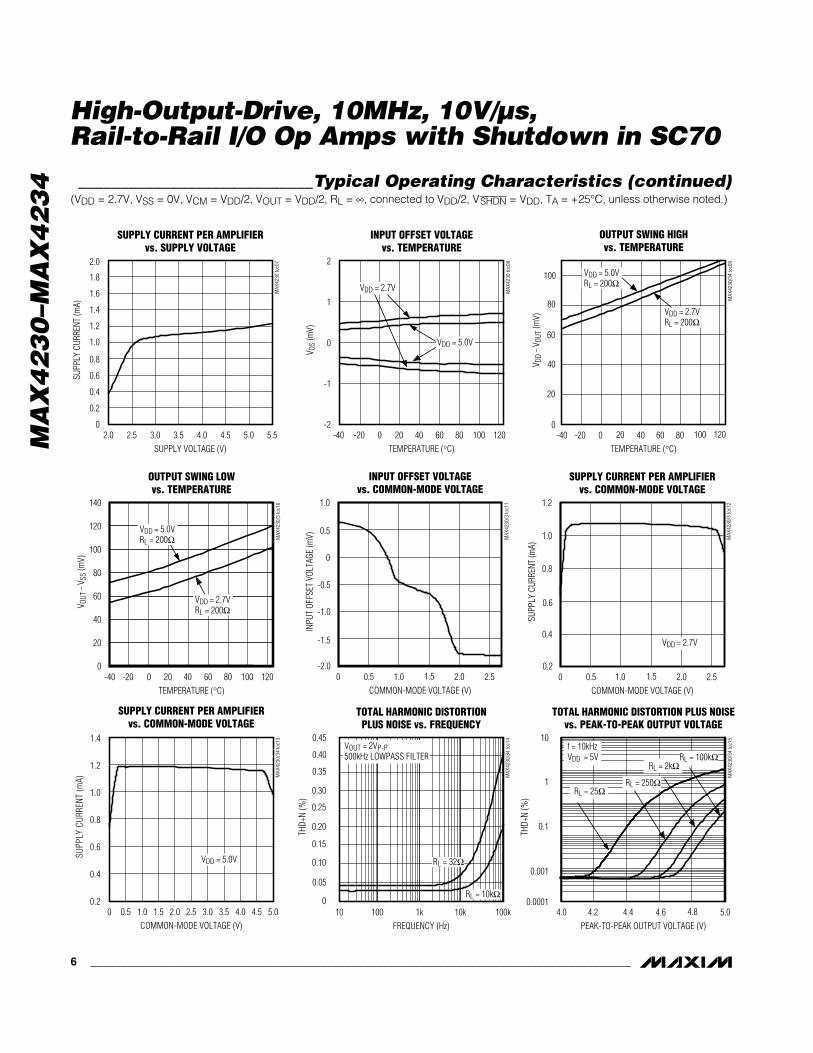
__________________________________________Typical Operating Characteristics(VDD = 2.7V, VSS = 0V, VCM = VDD/2, VOUT = VDD/2, RL = ∞, connected to VDD/2, VSHDN = VDD, TA = +25°C, unless otherwise noted.)
MA
X4
23
0–M
AX
42
34
High-Output-Drive, 10MHz, 10V/µs, Rail-to-Rail I/O Op Amps with Shutdown in SC70
6 _______________________________________________________________________________________
0
0.6
0.4
0.2
1.0
0.8
1.8
1.6
1.4
1.2
2.0
2.0 2.5 3.0 3.5 4.0 4.5 5.0 5.5
MAX
4230
toc0
7
SUPPLY VOLTAGE (V)
SUPP
LY C
URRE
NT (m
A)
SUPPLY CURRENT PER AMPLIFIERvs. SUPPLY VOLTAGE
-40 0-20 20 40 60 80 100 120
MAX
4230
toc0
8
TEMPERATURE (°C)
-2
-1
0
1
2
V OS
(mV)
INPUT OFFSET VOLTAGEvs. TEMPERATURE
VDD = 5.0V
VDD = 2.7V
0
20
40
60
80
100
-40 0-20 20 40 60 80 100 120
OUTPUT SWING HIGHvs. TEMPERATURE
MAX
4230
/34
toc0
9
TEMPERATURE (°C)
V DD
- VOU
T (m
V) VDD = 2.7VRL = 200Ω
VDD = 5.0VRL = 200Ω
0
40
20
80
60
120
100
140
-40 0 20-20 40 60 80 100 120
OUTPUT SWING LOWvs. TEMPERATURE
MAX
4230
/3 to
c10
TEMPERATURE (°C)
V OUT
- V S
S (m
V)
VDD = 2.7VRL = 200Ω
VDD = 5.0VRL = 200Ω
0.2
0.8
0.6
0.4
1.0
1.2
1.4
0 2.01.50.5 1.0 2.5 3.0 3.5 4.0 4.5 5.0
SUPPLY CURRENT PER AMPLIFIERvs. COMMON-MODE VOLTAGE
MAX
4230
/34
toc1
3
COMMON-MODE VOLTAGE (V)
SUPP
LY C
URRE
NT (m
A)
VDD = 5.0V
-2.0
-1.0
-1.5
-0.5
0.5
0
1.0
0 0.5 1.0 1.5 2.0 2.5
INPUT OFFSET VOLTAGEvs. COMMON-MODE VOLTAGE
MAX
4230
/3 to
c11
COMMON-MODE VOLTAGE (V)
INPU
T OF
FSET
VOL
TAGE
(mV)
0.2
0.6
0.4
1.0
0.8
1.2
0 0.5 1.0 1.5 2.0 2.5
SUPPLY CURRENT PER AMPLIFIERvs. COMMON-MODE VOLTAGE
MAX
4230
/3 to
c12
COMMON-MODE VOLTAGE (V)
SUPP
LY C
URRE
NT (m
A)
VDD = 2.7V
0.45
10 100 1k 10k 100k
TOTAL HARMONIC DISTORTIONPLUS NOISE vs. FREQUENCY
0.05
MAX
4230
/34
toc1
4
FREQUENCY (Hz)
THD+
N (%
)
0.15
0.25
0.35
0.30
0.20
0.10
0
0.40
RL = 32Ω
VOUT = 2VP-P500kHz LOWPASS FILTER
RL = 10kΩ
TOTAL HARMONIC DISTORTION PLUS NOISEvs. PEAK-TO-PEAK OUTPUT VOLTAGE
MAX
4230
/34
toc1
5
PEAK-TO-PEAK OUTPUT VOLTAGE (V)
THD+
N (%
)
10
0.00014.0 4.2 4.6 5.0
0.001
0.1
1
4.4 4.8
RL = 2kΩ
RL = 250ΩRL = 25Ω
RL = 100kΩf = 10kHzVDD = 5V
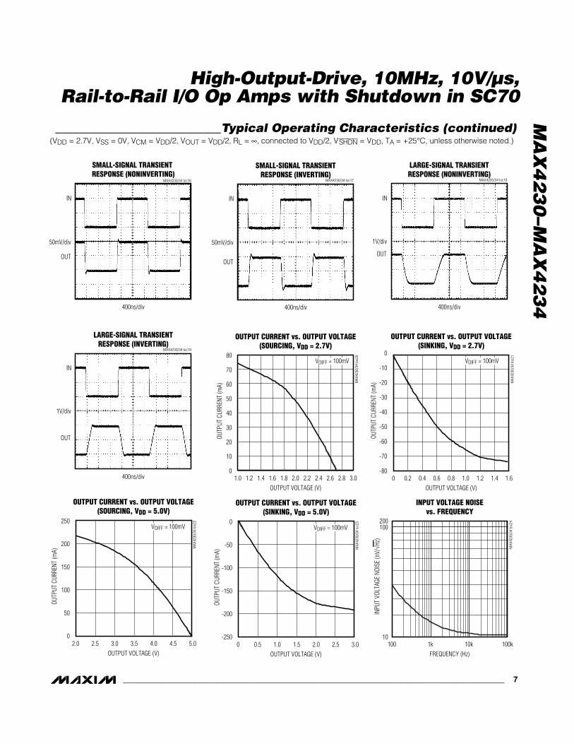
____________________________Typical Operating Characteristics (continued)(VDD = 2.7V, VSS = 0V, VCM = VDD/2, VOUT = VDD/2, RL = ∞, connected to VDD/2, VSHDN = VDD, TA = +25°C, unless otherwise noted.)
MA
X4
23
0–M
AX
42
34
High-Output-Drive, 10MHz, 10V/µs, Rail-to-Rail I/O Op Amps with Shutdown in SC70
_______________________________________________________________________________________ 7
400ns/div
SMALL-SIGNAL TRANSIENT RESPONSE (NONINVERTING)
IN
50mV/div
MAX4230/34 toc16
OUT
400ns/div
SMALL-SIGNAL TRANSIENTRESPONSE (INVERTING)
IN
50mV/div
MAX4230/34 toc17
OUT
400ns/div
LARGE-SIGNAL TRANSIENTRESPONSE (NONINVERTING)
IN
1V/div
MAX4230/34 toc18
OUT
400ns/div
LARGE-SIGNAL TRANSIENTRESPONSE (INVERTING)
IN
1V/div
MAX4230/34 toc19
OUT
0
50
150
100
200
250
2.0 3.02.5 3.5 4.0 4.5 5.0
OUTPUT CURRENT vs. OUTPUT VOLTAGE(SOURCING, VDD = 5.0V)
MAX
4230
/34
toc2
2
OUTPUT VOLTAGE (V)
OUTP
UT C
URRE
NT (m
A)
VDIFF = 100mV
0
20
10
30
60
70
50
40
80
1.0 1.4 1.6 1.8 2.01.2 2.2 2.4 2.6 2.8 3.0
OUTPUT CURRENT vs. OUTPUT VOLTAGE(SOURCING, VDD = 2.7V)
MAX
4230
/34
toc2
0
OUTPUT VOLTAGE (V)
OUTP
UT C
URRE
NT (m
A)
VDIFF = 100mV
-80
-60
-70
-40
-50
-30
-20
-10
0
0 0.4 0.60.2 0.8 1.0 1.2 1.4 1.6
OUTPUT CURRENT vs. OUTPUT VOLTAGE(SINKING, VDD = 2.7V)
MAX
4230
/34
toc2
1
OUTPUT VOLTAGE (V)
OUTP
UT C
URRE
NT (m
A)
VDIFF = 100mV
-250
-200
-100
-150
-50
0
0 1.00.5 1.5 2.0 2.5 3.0
OUTPUT CURRENT vs. OUTPUT VOLTAGE(SINKING, VDD = 5.0V)
MAX
4230
/34
toc2
3
OUTPUT VOLTAGE (V)
OUTP
UT C
URRE
NT (m
A)
VDIFF = 100mV200100
10100 10k 100k
FREQUENCY (Hz)
INPU
T VO
LTAG
E NO
ISE
(nV/
√Hz)
1k
INPUT VOLTAGE NOISEvs. FREQUENCY
MAX
4230
/34
toc2
4
____________________________Typical Operating Characteristics (continued)(VDD = 2.7V, VSS = 0V, VCM = VDD/2, VOUT = VDD/2, RL = ∞, connected to VDD/2, VSHDN = VDD, TA = +25°C, unless otherwise noted.)
MA
X4
23
0–M
AX
42
34
Detailed DescriptionRail-to-Rail Input Stage
The MAX4230–MAX4234 CMOS operational amplifiershave parallel-connected n- and p-channel differentialinput stages that combine to accept a common-moderange extending to both supply rails. The n-channelstage is active for common-mode input voltages typi-cally greater than (VSS + 1.2V), and the p-channelstage is active for common-mode input voltages typi-cally less than (VDD - 1.2V).
Applications InformationPackage Power Dissipation
Warning: Due to the high output current drive, this opamp can exceed the absolute maximum power-dissi-pation rating. As a general rule, as long as the peak cur-rent is less than or equal to 40mA, the maximum package
power dissipation is not exceeded for any of the packagetypes offered. There are some exceptions to this rule,however. The absolute maximum power-dissipation ratingof each package should always be verified using the fol-lowing equations. The equation below gives an approxi-mation of the package power dissipation:
where:
VRMS = RMS voltage from VDD to VOUT when sourcingcurrent and RMS voltage from VOUT to VSS when sink-ing current.
IRMS = RMS current flowing out of or into the op ampand the load.
θ = phase difference between the voltage and the cur-rent. For resistive loads, COS θ = 1.
P V I COS IC DISS RMS RMS( ) ≅ θ
High-Output-Drive, 10MHz, 10V/µs, Rail-to-Rail I/O Op Amps with Shutdown in SC70
8 _______________________________________________________________________________________
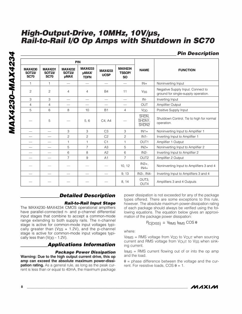
PIN
M AX42 30 SOT 23 /SC7 0
M AX42 31 SOT 23 /SC7 0
M AX42 32 SOT 23 /µ M A X
M A X4 2 3 3µ M A X/T D FN
M AX42 33 U CSP
M AX42 34 T SSOP/
SO
NAME FUNCTION
1 1 — — — — IN+ Noninverting Input
2 2 4 4 B4 11 VSSNegative Supply Input. Connect toground for single-supply operation.
3 3 — — — — IN- Inverting Input
4 4 — — — — OUT Amplifier Output
5 6 8 10 B1 4 VDD Positive Supply Input
— 5 — 5, 6 C4, A4 —SHDN,
SHDN1,SHDN2
Shutdown Control. Tie to high for normaloperation.
— — 3 3 C3 3 IN1+ Noninverting Input to Amplifier 1
— — 2 2 C2 2 IN1- Inverting Input to Amplifier 1
— — 1 1 C1 1 OUT1 Amplifier 1 Output
— — 5 7 A3 5 IN2+ Noninverting Input to Amplifier 2
— — 6 8 A2 6 IN2- Inverting Input to Amplifier 2
— — 7 9 A1 7 OUT2 Amplifier 2 Output
— — — — — 10, 12IN3+,IN4+
Noninverting Input to Amplifiers 3 and 4
— — — — — 9, 13 IN3-, IN4- Inverting Input to Amplifiers 3 and 4
— — — — — 8, 14OUT3,OUT4
Amplifiers 3 and 4 Outputs
Pin Description
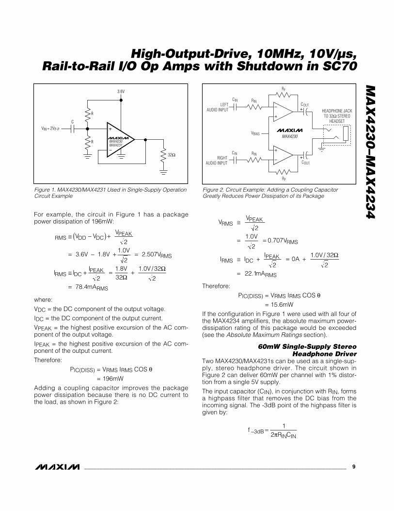
For example, the circuit in Figure 1 has a packagepower dissipation of 196mW:
where:
VDC = the DC component of the output voltage.
IDC = the DC component of the output current.
VPEAK = the highest positive excursion of the AC com-ponent of the output voltage.
IPEAK = the highest positive excursion of the AC com-ponent of the output current.
Therefore:
PIC(DISS) = VRMS IRMS COS θ= 196mW
Adding a coupling capacitor improves the packagepower dissipation because there is no DC current tothe load, as shown in Figure 2:
Therefore:
PIC(DISS) = VRMS IRMS COS θ= 15.6mW
If the configuration in Figure 1 were used with all four ofthe MAX4234 amplifiers, the absolute maximum power-dissipation rating of this package would be exceeded(see the Absolute Maximum Ratings section).
60mW Single-Supply Stereo Headphone Driver
Two MAX4230/MAX4231s can be used as a single-sup-ply, stereo headphone driver. The circuit shown inFigure 2 can deliver 60mW per channel with 1% distor-tion from a single 5V supply.
The input capacitor (CIN), in conjunction with RIN, formsa highpass filter that removes the DC bias from theincoming signal. The -3dB point of the highpass filter isgiven by:
fR CdB
IN IN− =3
12π
V
I + I
2
RMS
RMSPEAK
≅
= =
≅ = +
=
.
.
. /
.
V
VV
I AV
mA
PEAK
RMS
DC
RMS
21 0
20 707
01 0 32
222 1
Ω
RMS DD DC
RMSPEAK
V V
I + I
2
≅ −( ) +
= − + =
≅ = +
=
. . .
.
.
. /
.
V
V VV
V
IV V
mA
PEAK
RMS
DC
RMS
2
3 6 1 81 0
22 507
1 832
1 0 32
278 4
ΩΩ
MA
X4
23
0–M
AX
42
34
High-Output-Drive, 10MHz, 10V/µs, Rail-to-Rail I/O Op Amps with Shutdown in SC70
_______________________________________________________________________________________ 9
RIGHTAUDIO INPUT
LEFTAUDIO INPUT
CIN
CIN RIN
RIN
RF
COUT
VBIAS
COUT
HEADPHONE JACKTO 32Ω STEREO
HEADSET
RF
MAX4230
Figure 2. Circuit Example: Adding a Coupling CapacitorGreatly Reduces Power Dissipation of its Package
3.6V
VIN = 2VP-P
R
C
32Ω
R
MAX4230MAX4231
Figure 1. MAX4230/MAX4231 Used in Single-Supply OperationCircuit Example
MA
X4
23
0–M
AX
42
34
Choose gain-setting resistors RIN and RF according tothe amount of desired gain, keeping in mind the maxi-mum output amplitude. The output coupling capacitor,COUT, blocks the DC component of the amplifier out-put, preventing DC current flowing to the load. The out-put capacitor and the load impedance form a highpassfiler with the -3dB point determined by:
For a 32Ω load, a 100µF aluminum electrolytic capaci-tor gives a low-frequency pole at 50Hz.
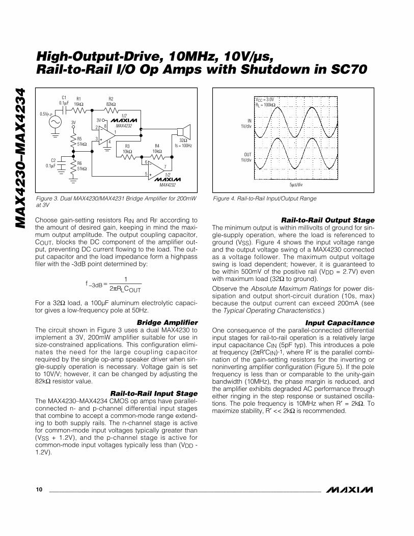
Bridge AmplifierThe circuit shown in Figure 3 uses a dual MAX4230 toimplement a 3V, 200mW amplifier suitable for use insize-constrained applications. This configuration elimi-nates the need for the large coupling capacitorrequired by the single op-amp speaker driver when sin-gle-supply operation is necessary. Voltage gain is setto 10V/V; however, it can be changed by adjusting the82kΩ resistor value.
Rail-to-Rail Input StageThe MAX4230–MAX4234 CMOS op amps have parallel-connected n- and p-channel differential input stagesthat combine to accept a common-mode range extend-ing to both supply rails. The n-channel stage is activefor common-mode input voltages typically greater than(VSS + 1.2V), and the p-channel stage is active forcommon-mode input voltages typically less than (VDD -1.2V).
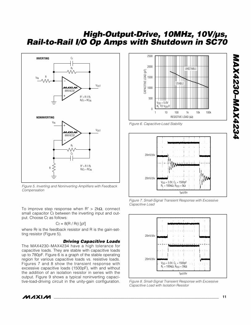
Rail-to-Rail Output Stage The minimum output is within millivolts of ground for sin-gle-supply operation, where the load is referenced toground (VSS). Figure 4 shows the input voltage rangeand the output voltage swing of a MAX4230 connectedas a voltage follower. The maximum output voltageswing is load dependent; however, it is guaranteed tobe within 500mV of the positive rail (VDD = 2.7V) evenwith maximum load (32Ω to ground).
Observe the Absolute Maximum Ratings for power dis-sipation and output short-circuit duration (10s, max)because the output current can exceed 200mA (seethe Typical Operating Characteristics.)
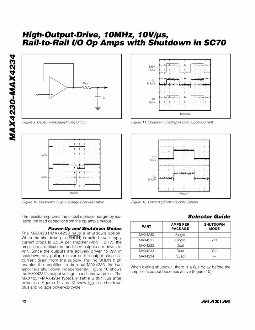
Input CapacitanceOne consequence of the parallel-connected differentialinput stages for rail-to-rail operation is a relatively largeinput capacitance CIN (5pF typ). This introduces a poleat frequency (2πR′CIN)-1, where R′ is the parallel combi-nation of the gain-setting resistors for the inverting ornoninverting amplifier configuration (Figure 5). If the polefrequency is less than or comparable to the unity-gainbandwidth (10MHz), the phase margin is reduced, andthe amplifier exhibits degraded AC performance througheither ringing in the step response or sustained oscilla-tions. The pole frequency is 10MHz when R′ = 2kΩ. Tomaximize stability, R′ << 2kΩ is recommended.
fR CdB
L OUT− =3
12π
High-Output-Drive, 10MHz, 10V/µs, Rail-to-Rail I/O Op Amps with Shutdown in SC70
10 ______________________________________________________________________________________
Figure 4. Rail-to-Rail Input/Output RangeFigure 3. Dual MAX4230/MAX4231 Bridge Amplifier for 200mWat 3V
1
67
5
2 83V3V
34
MAX4232
1/2
MAX4232
1/2
0.5VP-P
R551kΩ
R116kΩ
R282kΩ
R410kΩ
32Ωfs = 100HzR3
10kΩ
R651kΩ
C20.1µF
C10.1µF
IN1V/div
OUT1V/div
5µs/div
VCC = 3.0VRL = 100kΩ
To improve step response when R′ > 2kΩ, connectsmall capacitor Cf between the inverting input and out-put. Choose Cf as follows:
Cf = 8(R / Rf) [pf]
where Rf is the feedback resistor and R is the gain-set-ting resistor (Figure 5).
Driving Capacitive LoadsThe MAX4230–MAX4234 have a high tolerance forcapacitive loads. They are stable with capacitive loadsup to 780pF. Figure 6 is a graph of the stable operatingregion for various capacitive loads vs. resistive loads.Figures 7 and 8 show the transient response withexcessive capacitive loads (1500pF), with and withoutthe addition of an isolation resistor in series with theoutput. Figure 9 shows a typical noninverting capaci-tive-load-driving circuit in the unity-gain configuration.
MA
X4
23
0–M
AX
42
34
High-Output-Drive, 10MHz, 10V/µs, Rail-to-Rail I/O Op Amps with Shutdown in SC70
______________________________________________________________________________________ 11
MAX4230
VIN
VOUT
R′ = R || RfRfCf = RCIN
Rf
Cf
R
INVERTING
MAX4230
VIN
VOUT
R′ = R || RfRfCf = RCIN
Rf
R
Cf
NONINVERTING
Figure 5. Inverting and Noninverting Amplifiers with FeedbackCompensation
0
500
1500
1000
2000
2500
1 10010 1k 10k 100kRESISTIVE LOAD (Ω)
CAPA
CITI
VE L
OAD
(pF)
VDD = 5.0VRL TO VDD/2
STABLE
UNSTABLE
Figure 6. Capacitive-Load Stability
1µs/div
20mV/div
20mV/divVDD = 3.0V, CL = 1500pFRL = 100kΩ, RISO = 39Ω
Figure 8. Small-Signal Transient Response with ExcessiveCapacitive Load with Isolation Resistor
1µs/div
20mV/div
20mV/divVDD = 3.0V, CL = 1500pFRL = 100kΩ, RISO = 0Ω
Figure 7. Small-Signal Transient Response with ExcessiveCapacitive Load
MA
X4
23
0–M
AX
42
34
The resistor improves the circuit’s phase margin by iso-lating the load capacitor from the op amp’s output.
Power-Up and Shutdown ModesThe MAX4231/MAX4233 have a shutdown option.When the shutdown pin (SHDN) is pulled low, supplycurrent drops to 0.5µA per amplifier (VDD = 2.7V), theamplifiers are disabled, and their outputs are driven toVSS. Since the outputs are actively driven to VSS inshutdown, any pullup resistor on the output causes acurrent drain from the supply. Pulling SHDN highenables the amplifier. In the dual MAX4233, the twoamplifiers shut down independently. Figure 10 showsthe MAX4231’s output voltage to a shutdown pulse. TheMAX4231–MAX4234 typically settle within 5µs afterpower-up. Figures 11 and 12 show IDD to a shutdownplus and voltage power-up cycle.
When exiting shutdown, there is a 6µs delay before theamplifier’s output becomes active (Figure 10).
High-Output-Drive, 10MHz, 10V/µs, Rail-to-Rail I/O Op Amps with Shutdown in SC70
12 ______________________________________________________________________________________
RISO
CL
Figure 9. Capacitive-Load-Driving Circuit
100µs/div
SHDN2V/div
IDD1mA/div
OUT2V/div
Figure 11. Shutdown Enable/Disable Supply Current
40µs/div
VDD2V/div
IDD1mA/div
Figure 12. Power-Up/Down Supply Current
4µs/div
1V/div
1V/div
Figure 10. Shutdown Output Voltage Enable/Disable
Selector GuideAMPS PERPACKAGE
SHUTDOWNMODE
MAX4230 Single —
MAX4231 Single Yes
PART
MAX4232 Dual —
MAX4233 Dual Yes
MAX4234 Quad —
MA
X4
23
0–M
AX
42
34
High-Output-Drive, 10MHz, 10V/µs, Rail-to-Rail I/O Op Amps with Shutdown in SC70
______________________________________________________________________________________ 13
Pin ConfigurationsTOP VIEW
IN2-
IN2+VSS
1
2
8
7
VDD
OUT2IN1-
IN1+
OUT1
SOT23/µMAX
3
4
6
5
MAX4232
1
2
3
4
5
10
9
8
7
6
VDD
OUT2
IN2-
IN2+VSS
IN1+
IN1-
OUT1
MAX4233
µMAX
SHDN2SHDN1
VSS
OUTIN-
1 6 VDD
5
IN+
SC70/SOT23
2
3 4
SHDN
MAX4231
14
13
12
11
10
9
8
1
2
3
4
5
6
7
OUT4
IN4-
IN4+
VSSVDD
IN1+
IN1-
OUT1
MAX4234
IN3+
IN3-
OUT3OUT2
IN2-
IN2+
TSSOP/SO
VSS
OUTIN-
1 5 VDDIN+
MAX4230
SOT23/SC70
2
3 4
OUT1
VDD
OUT2
IN1-
IN2-
IN1+
IN2+
VSS
SHDN1
SHDN2
UCSP
MAX4233
V SS
V DD
OUT1
IN1-
IN1+
OUT2
IN2-
IN2+
SHDN
2
TDFNTDFN EXPOSED PAD CONNECTED TO VSS
MAX4233
SHDN
1
1 2 3 4 5
678910
1 2 3 4
A
B
C
Power Supplies and LayoutThe MAX4230–MAX4234 can operate from a single2.7V to 5.5V supply, or from dual ±1.35V to ±2.5V sup-plies. For single-supply operation, bypass the powersupply with a 0.1µF ceramic capacitor. For dual-supplyoperation, bypass each supply to ground. Good layoutimproves performance by decreasing the amount ofstray capacitance at the op amps’ inputs and outputs.Decrease stray capacitance by placing external com-ponents close to the op amps’ pins, minimizing traceand lead lengths.
Ordering Information (continued)
PART TEMP RANGE PIN-PACKAGE
TOP M ARK
MAX4232AKA-T -40°C to +125°C 8 SOT23-8 AAKW
MAX4232AUA -40°C to +125°C 8 µMAX —
MAX4233AUB -40°C to +125°C 10 µMAX —
MAX4233ABC-T -40°C to +125°C 10 UCSP-10 ABE
MAX4233ATB+T -40°C to +125°C 10 TDFN-EP* +AQH
MAX4234AUD -40°C to +125°C 14 TSSOP —
MAX4234ASD -40°C to +125°C 14 SO —
Chip InformationMAX4230 TRANSISTOR COUNT: 230MAX4231 TRANSISTOR COUNT: 230MAX4232 TRANSISTOR COUNT: 462MAX4233 TRANSISTOR COUNT: 462MAX4234 TRANSISTOR COUNT: 924
*EP = Exposed paddle.
MA
X4
23
0–M
AX
42
34
High-Output-Drive, 10MHz, 10V/µs, Rail-to-Rail I/O Op Amps with Shutdown in SC70
14 ______________________________________________________________________________________
SC
70, 5
L.E
PS
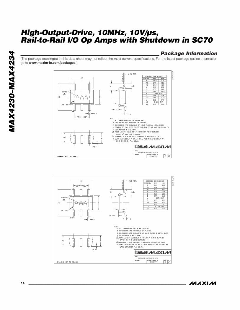
PACKAGE OUTLINE, 5L SC70
21-0076 11
C
SC
70, 6
L.E
PS
PACKAGE OUTLINE, 6L SC70
21-0077 11
C
Package Information(The package drawing(s) in this data sheet may not reflect the most current specifications. For the latest package outline informationgo to www.maxim-ic.com/packages.)

MA
X4
23
0–M
AX
42
34
High-Output-Drive, 10MHz, 10V/µs, Rail-to-Rail I/O Op Amps with Shutdown in SC70
______________________________________________________________________________________ 15
SO
T-23
5L
.EP
S
E1
121-0057
PACKAGE OUTLINE, SOT-23, 5L
6LS
OT.
EP
S
PACKAGE OUTLINE, SOT 6L BODY
21-0058 11
G
Package Information (continued)(The package drawing(s) in this data sheet may not reflect the most current specifications. For the latest package outline informationgo to www.maxim-ic.com/packages.)

MA
X4
23
0–M
AX
42
34
High-Output-Drive, 10MHz, 10V/µs, Rail-to-Rail I/O Op Amps with Shutdown in SC70
16 ______________________________________________________________________________________
8LU
MA
XD
.EP
S
PACKAGE OUTLINE, 8L uMAX/uSOP
11
21-0036 JREV.DOCUMENT CONTROL NO.APPROVAL
PROPRIETARY INFORMATION
TITLE:
MAX0.043
0.006
0.014
0.120
0.120
0.198
0.026
0.007
0.037
0.0207 BSC
0.0256 BSC
A2 A1
ce
b
A
L
FRONT VIEW SIDE VIEW
E H
0.6±0.1
0.6±0.1
Ø0.50±0.1
1
TOP VIEW
D
8
A2 0.030
BOTTOM VIEW
16°
S
b
L
HE
De
c
0°
0.010
0.116
0.116
0.188
0.016
0.005
84X S
INCHES
-
A1
A
MIN
0.002
0.950.75
0.5250 BSC
0.25 0.36
2.95 3.05
2.95 3.05
4.78
0.41
0.65 BSC
5.03
0.66
6°0°
0.13 0.18
MAXMIN
MILLIMETERS
- 1.10
0.05 0.15
α
α
DIM
Package Information (continued)(The package drawing(s) in this data sheet may not reflect the most current specifications. For the latest package outline informationgo to www.maxim-ic.com/packages.)
SO
T23,
8L
.EP
S
REV.DOCUMENT CONTROL NO.APPROVAL
PROPRIETARY INFORMATION
TITLE:
3.002.60EC E1E
BETWEEN 0.08mm AND 0.15mm FROM LEAD TIP.8. MEETS JEDEC MO178.
8∞
0.60
1.75
0.30
L2
0∞e1
e
L
1.50E1
0.65 BSC.
1.95 REF.
0.25 BSC.
GAUGE PLANE
SEATING PLANE C
C
L
PIN 1I.D. DOT
(SEE NOTE 6)
LC
LC
A2
e1
D
DETAIL "A"
5. COPLANARITY 4 MILS. MAX.
NOTE:
7. SOLDER THICKNESS MEASURED AT FLAT SECTION OF LEAD
6. PIN 1 I.D. DOT IS 0.3 MM ÿ MIN. LOCATED ABOVE PIN 1.
4. PACKAGE OUTLINE INCLUSIVE OF SOLDER PLATING.
3. PACKAGE OUTLINE EXCLUSIVE OF MOLD FLASH & METAL BURR.
HEEL OF THE LEAD PARALLEL TO SEATING PLANE C.2. FOOT LENGTH MEASURED FROM LEAD TIP TO UPPER RADIUS OF
1. ALL DIMENSIONS ARE IN MILLIMETERS.
L2
L
A1A
0.45
1.30
0.15
1.45
MAX
0.28b
0.90A2
0.00A1
0.90A
MINSYMBOL
3.00
0.20
2.80D
0.09C
SEE DETAIL "A"
LCb e
D 121-00781
PACKAGE OUTLINE, SOT-23, 8L BODY
0
0
MA
X4
23
0–M
AX
42
34
High-Output-Drive, 10MHz, 10V/µs, Rail-to-Rail I/O Op Amps with Shutdown in SC70
______________________________________________________________________________________ 17
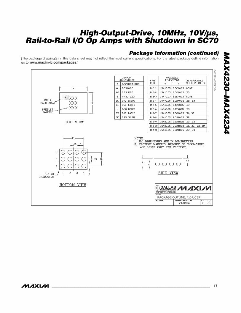
Package Information (continued)(The package drawing(s) in this data sheet may not reflect the most current specifications. For the latest package outline informationgo to www.maxim-ic.com/packages.)
12L,
UC
SP
4x3
.EP
S
F1
121-0104
PACKAGE OUTLINE, 4x3 UCSP

Maxim cannot assume responsibility for use of any circuitry other than circuitry entirely embodied in a Maxim product. No circuit patent licenses areimplied. Maxim reserves the right to change the circuitry and specifications without notice at any time.
18 __________________Maxim Integrated Products, 120 San Gabriel Drive, Sunnyvale, CA 94086 (408) 737-7600
© 2006 Maxim Integrated Products Printed USA is a registered trademark of Maxim Integrated Products, Inc.
MA
X4
23
0–M
AX
42
34
High-Output-Drive, 10MHz, 10V/µs, Rail-to-Rail I/O Op Amps with Shutdown in SC70
Package Information (continued)(The package drawing(s) in this data sheet may not reflect the most current specifications. For the latest package outline informationgo to www.maxim-ic.com/packages.)
6, 8
, &10
L, D
FN T
HIN
.EP
S
LC LC
PIN 1INDEX AREA
D
E
L
e
LA
e
E2
N
G1
221-0137
PACKAGE OUTLINE, 6,8,10 & 14L,TDFN, EXPOSED PAD, 3x3x0.80 mm
-DRAWING NOT TO SCALE-
k
e
[(N/2)-1] x eREF.
PIN 1 ID
0.35x0.35
DETAIL A
b
D2
A2
A1
COMMON DIMENSIONS
SYMBOL MIN. MAX.
A 0.70 0.80
D 2.90 3.10
E 2.90 3.10
A1 0.00 0.05
L 0.20 0.40
PKG. CODE N D2 E2 e JEDEC SPEC b [(N/2)-1] x e
PACKAGE VARIATIONS
0.25 MIN.k
A2 0.20 REF.
2.30±0.101.50±0.106T633-1 0.95 BSC MO229 / WEEA 1.90 REF0.40±0.05
1.95 REF0.30±0.050.65 BSC2.30±0.108T833-1
2.00 REF0.25±0.050.50 BSC2.30±0.1010T1033-1
2.40 REF0.20±0.05- - - - 0.40 BSC1.70±0.10 2.30±0.1014T1433-1
1.50±0.10
1.50±0.10
MO229 / WEEC
MO229 / WEED-3
0.40 BSC - - - - 0.20±0.05 2.40 REFT1433-2 14 2.30±0.101.70±0.10
T633-2 6 1.50±0.10 2.30±0.10 0.95 BSC MO229 / WEEA 0.40±0.05 1.90 REF
T833-2 8 1.50±0.10 2.30±0.10 0.65 BSC MO229 / WEEC 0.30±0.05 1.95 REF
T833-3 8 1.50±0.10 2.30±0.10 0.65 BSC MO229 / WEEC 0.30±0.05 1.95 REF
-DRAWING NOT TO SCALE- G2
221-0137
PACKAGE OUTLINE, 6,8,10 & 14L,TDFN, EXPOSED PAD, 3x3x0.80 mm
DOWNBONDSALLOWED
NO
NO
NO
NO
YES
NO
YES
NO


![Lecture 17 - Eulerian-Granular Model Applied …bakker.org/dartmouth06/engs150/17-egm.pdfµs =max [µs,coll +µs,kin ,µs, frict] 2, 2 sin I P s s frict ϕ µ = Plastic regime: frictional](https://img.pdfslide.us/doc/110x75/5e6eefe3cdf08e489e5306f0/lecture-17-eulerian-granular-model-applied-s-max-scoll-skin-s-frict.jpg)