Embed Size (px)
Citation preview

IEEE TRANSACTIONS ON VEHICULAR TECHNOLOGY, VOL. 54, NO. 1, JANUARY 2005 33
High-Gain and Wide-Band Single-Layer PatchAntenna for Wireless Communications
Chi-Lun Mak, Member, IEEE, Hang Wong, Member, IEEE, and Kwai-Man Luk, Fellow, IEEE
Abstract—A technique employing the use of parallel feeds isapplied to the recently proposed -probe coupled patch antennadesign. By employing only two -probes, with proper separa-tion, for feeding one single patch, a twin- -probe coupled patchantenna is designed with both high-gain (10 dBi) and wide-band[25%, standing wave radio (SWR) 1 5] characteristics. Inaddition, the 1-dB-gain bandwidth is around 26%, which coversthe impedance bandwidth. Furthermore, a noticeable suppressionof cross-polarization radiation is observed. Simulation results arein good agreement with those noteworthy characteristics obtainedfrom experiments. The proposed antenna is suitable for modernmobile communication applications.
Index Terms—High-gain antenna, -probe, low cross-polariza-tion, wide-band antenna.
I. INTRODUCTION
I T IS well known that patch antennas offer many advantages,such as low profile, light weight, conformability, etc. How-
ever, conventional patch antennas have major weaknesses ofnarrow bandwidth and low gain [1]. Generally, both the band-width and gain will increase with substrate thickness (up to cer-tain limit), but decrease with increasing dielectric constant [2],[3]. Indeed, there are many different methods proposed in theliterature to tackle the narrow-bandwidth problem [4]–[12] orthe low-gain limitation [13]–[16], but not for both weaknessestogether. Furthermore, a low-profile single patch antenna, whichis simultaneously high in gain and wide in bandwidth, does notappear to be available yet.
One common method for bandwidth enhancement is usingparasitic patches, either in co-planar [5]–[7] or stacked geometry[8], and such a design can yield a bandwidth up to around 25%[standing wave radio (SWR) ]. However, no noticeable im-provement in gain was seen. On the other hand, although the gaincan be improved to around 10 dBi (estimated) [15] by enlargingthe separation between the driven patch and the stacked parasiticpatch to approximate , the tradeoff is narrow in bandwidth,around 2%-3%. The gain can also be increased in co-planargeometry by placing the parasitic patches adjacent to the fedpatch to form an array [16], but its gain bandwidth is not wideenough for most applications. Besides, the major disadvantageof using parasitic elements is an unfavorably large antenna size.
Manuscript received November 27, 2003; revised June 8, 2004 and September11, 2004. The work of K.-M. Luk was supported by The Croucher Foundation,Hong Kong, through a Croucher Senior Research Fellowship. The review of thispaper was coordinated by Dr. R. Janaswamy.
The authors are with the Department of Electronic Engineering, CityUniversity of Hong Kong, Kowloon, Hong Kong (e-mail: [email protected];[email protected]; [email protected]).
Digital Object Identifier 10.1109/TVT.2004.838899
Another popular method for bandwidth enhancement is byemploying a coaxial probe to feed a slotted patch on an electri-cally thick substrate (0.08–0.1 ) of low dielectric constant [9],[10]. The achievable bandwidth can be 30% (SWR ) with again around 6–8 dBi within the operating bandwidth.
In this paper, based on the idea of using parallel feeds [17],we propose a simple twin-feed structure with two inphased
-probes [11] to further enhance the gain to 10 dBi while main-taining the wide-band performance. In addition, the achieved1-dB-gain-bandwidth is also wide enough to cover the oper-ating bandwidth. Both measurement and simulation results willbe presented.
II. TWIN -PROBE COUPLED PATCH ANTENNA
The idea of the proposed feed structure is designated as a twin-feed design. A prototype designed at , with two in-phased -probes, is fabricated as shown in Fig. 1. A copper patchhas thickness of 0.3 mm , width 44 mm ,and length 22 mm . The aspect ratio of thepatch is equal to 2.0. The patch is supported by two small cubicfoam spacers of thickness 6 mm . Thefundamental mode of the patch is simultaneously ex-cited by the two inphased -shaped probes (with probe radius
0.5 mm), which are separated by 28.6 mm andconnected to the microstrip feed network mounted on the otherside of the ground plane. The simple T-shaped power divider isetched on a Duriod substrate with 2.33 and thickness of1.5748 mm (0.062 in). The square ground plane has side length of100 mm . The two -shaped probes have the same sizeof vertical arm =4.5 mm and horizontal arm 12mm . From Fig. 1(b), they have zero inset distance (i.e.,
) with respect to the patch. The characteristic impedanceof the feed line are and , with line widthof 4.877 and 1.41 mm, respectively. A SubMiniature Version A(SMA) launcher is connected to the end of the feed line.
III. MEASUREMENT AND SIMULATION RESULTS
A. Experiments
In order to demonstrate the effectiveness of the proposedtwin-feed design, another prototype is fabricated for compar-ison, which is identical to the proposed antenna except that onlyone -probe is used instead. With zero inset distanceagain, the arm lengths of this single -probe are slightlyadjusted ( 3.5 mm and =8 mm) for the best impedancematching. The performances of the two prototypes are mea-sured by an HP8510-C Network Analyzer, a compact rangewith ORBIT/FR MiDAS Far-Field Antenna Measurement and
0018-9545/$20.00 © 2005 IEEE

34 IEEE TRANSACTIONS ON VEHICULAR TECHNOLOGY, VOL. 54, NO. 1, JANUARY 2005
Fig. 1. Geometry of twin-L-probe coupled patch antenna. (a) Perspective and (b) side views.
Fig. 2. Measured results of SWR and gain of both prototypes.
Analysis System (Horsham, PA). As for the gain measurement,a NARDA-643 standard gain horn is used.
Fig. 2 shows comparisons of the measured results of gainand SWR of both prototypes. As seen from the SWR curves,
both antennas have wide impedance bandwidth of 25% (SWR) from 4.42 to 5.7 GHz. From the gain curves, it is
obvious to see that the proposed antenna has a better gain of10 dBi, which is stable across the operating bandwidth with

MAK et al.: HIGH-GAIN AND WIDE-BAND SINGLE-LAYER PATCH ANTENNA FOR WIRELESS COMMUNICATIONS 35
TABLE ICOMPARISONS OF THE MEASURED RESULTS BETWEEN THE TWO PROTOTYPES
Fig. 3. Measured radiation patterns at 4.5, 5.0, and 5.6 GHz of (a) the single-L-probe coupled patch antenna and (b) the twin-L-probe coupled patch antenna.
1-dB-gain bandwidth of 26%. Comparing with the maximumgain of the single- -probe coupled patch of 8 dBi, there is anabout 2.0-dB improvement. The improvement is much moresignificant at the upper region, 5–5.7 GHz, of the operating
band, an approximately 3–6-dB difference in gain is observed.The increase in gain is mainly due to the effective suppressionof cross-polar radiation. The measured results are tabulated inTable I.
36 IEEE TRANSACTIONS ON VEHICULAR TECHNOLOGY, VOL. 54, NO. 1, JANUARY 2005
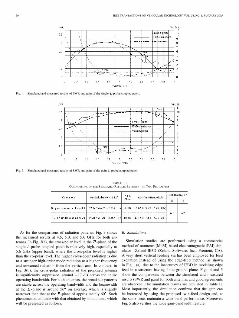
Fig. 4. Simulated and measured results of SWR and gain of the single-L-probe coupled patch.
Fig. 5. Simulated and measured results of SWR and gain of the twin-L-probe coupled patch.
TABLE IICOMPARISONS OF THE SIMULATED RESULTS BETWEEN THE TWO PROTOTYPES
As for the comparisons of radiation patterns, Fig. 3 showsthe measured results at 4.5, 5.0, and 5.6 GHz for both an-tennas. In Fig. 3(a), the cross-polar level in the -plane of thesingle- -probe coupled patch is relatively high, especially at5.6 GHz (upper band), where the cross-polar level is higherthan the co-polar level. The higher cross-polar radiation is dueto a stronger high-order mode radiation at a higher frequencyand unwanted radiation from the vertical arm. In contrast, inFig. 3(b), the cross-polar radiation of the proposed antennais significantly suppressed, around 17 dB across the entireoperating bandwidth. For both antennas, the broadside patternsare stable across the operating bandwidth and the beamwidthat the -plane is around 56 on average, which is slightlynarrower than that at the -plane of approximately 60 . Suchphenomenon coincide with that obtained by simulations, whichwill be presented as follows.
B. Simulations
Simulation studies are performed using a commercialmethod-of-moments (MoM)-based electromagnetic (EM) sim-ulator—Zeland-IE3D (Zeland Software, Inc., Fremont, CA).A very short vertical feeding via has been employed for feedexcitation instead of using the edge-feed method, as shownin Fig. 1(a), due to the inaccuracy of IE3D in modeling edgefeed in a structure having finite ground plane. Figs. 4 and 5show the comparisons between the simulated and measuredresults (SWR and gain) for both antennas and good agreementsare observed. The simulation results are tabulated in Table II.Most importantly, the simulation confirms that the gain canbe increased by using the proposed twin-feed design and, atthe same time, maintain a wide-band performance. Moreover,Fig. 5 also verifies the wide gain-bandwidth feature.

MAK et al.: HIGH-GAIN AND WIDE-BAND SINGLE-LAYER PATCH ANTENNA FOR WIRELESS COMMUNICATIONS 37
Fig. 6. Simulated radiation patterns at 4.5, 5.0, and 5.6 GHz of (a) the single-L-probe fed patch antenna and (b) the twin-L-probe coupled patch antenna.
Fig. 6 presents simulated radiation patterns of both antennasat 4.5, 5.0, and 5.6 GHz. In comparison with the measured pat-terns, as shown in Fig. 3, good agreements are observed again, es-pecially the stable and quite symmetric patterns at both principleplanes across the operating bandwidth. In addition, the simulatedpatterns verify the beamwidth at the -plane is slightly narrowerthan that at the -plane. Furthermore, in Figs. 3(b) and 6(b), thesimulation verifies that the cross-polar level in the -plane issuppressed significantly by the proposed design.
IV. PARAMETRIC STUDIES
In order to investigate the effects of various parameterson the performance of the proposed antenna, especially the
aspect ratio and the probe-to-probe separation , wehave performed parametric studies using the IE3D simulator,which are believed to be efficient and convenient. Throughoutthe studies, infinite ground-plane, air-substrate, zero-thicknessmetallic layers are assumed for relatively fast computations.Therefore, there are bit differences in simulation models whencompared with that used for the actual antenna (Fig. 1), asdiscussed in Section III-B. Another discrepancy is that thefeed line on the air substrate is now located on the same sideas the patch, above the infinite ground plane. At this moment,edge feed can be employed in the simulations, since infiniteground plane is being used. The obtained results are useful inproviding design guideline for antenna designers. Throughoutthe simulation studies, two parameters are kept constant, which

38 IEEE TRANSACTIONS ON VEHICULAR TECHNOLOGY, VOL. 54, NO. 1, JANUARY 2005
Fig. 7. Parametric studies: simulated results of maximum gain versus S=W .
TABLE IIIPARAMETRIC STUDIES: SUMMARY OF THE SIMULATED GAIN OF THE PROPOSED DESIGN WITH DIFFERENT PATCH WIDTHS
Fig. 8. Parametric studies: simulated results of maximum cross-polar level versus S=W .
are 22 mm and 6 mm. In addition, parameters such as, , , and are slightly adjusted, if necessary, to maintain
the wide impedance bandwidth characteristic.
A. Antenna Gain
By employing the proposed twin-coupling design, especiallyfor a wider patch with , we find that without re-ducing the impedance bandwidth, there are noticeable improve-ments in gain as well as the gain bandwidth. Fig. 7 describesthe maximum gain verses for different patch width .We can see the maximum gain of a patch is achieved when isaround 0.5 W–0.7 W. Moreover, the wider the patch width ,the higher the maximum gain can be achieved. Table III sum-marizes such observations. However, the tradeoff of using widerpatch will be a higher cross-polar radiation level are discussedlater.
B. Cross-Polar Radiation
Fig. 8 shows the maximum value of cross-polar level, in the-plane at 5 GHz, with different values of . It is obvious to
see that a wider patch will give a higher cross-polar level. Fur-thermore, for each patch employing the proposed design (i.e.,
), the lowest cross-polar level can be achieved whenequals half-wavelength. For example, when 44 mm, thelowest cross-polar level of 27.72 dB occurs when 0.68 W(i.e., 30 mm), which is half-wavelength of 5 GHz. Table IVsummaries such noticeable results.
Fig. 9 shows the maximum value of the cross-polar level fordifferent across frequency of patch with 44 mm. In thisfigure, a local minimum is clearly observed at the lower band;for example, for the curve of 0.75 W (33 mm), the minimais find at frequency about 4.5 GHz, so .Such phenomenon becomes less obvious for smaller than 0.68W, but suppression in cross-polar level can still be observed.It is important to notice that although we can have sharp localminima of cross-polar level in the lower region of the operatingbandwidth, the tradeoff is a relative higher level in the upper re-gion. Therefore, we need to optimize the overall performance bychoosing an appropriate value of . In addition to the goals ofhigh gain and wideband, we have chosen one set of parameters,
44 mm and 28.6 mm =0.65),for real performance testing. The experiments were already dis-cussed in Section II with measurement results shown in Sec-tion III.

MAK et al.: HIGH-GAIN AND WIDE-BAND SINGLE-LAYER PATCH ANTENNA FOR WIRELESS COMMUNICATIONS 39
TABLE IVPARAMETRIC STUDIES: SUMMARY OF THE SIMULATED RESULTS OF THE CROSS-POLAR LEVEL OF THE PROPOSED DESIGN
Fig. 9. Parametric studies: simulated results of maximum cross-polar level versus frequency.
V. DISCUSSIONS
The proposed twin- -coupled structure can simultaneouslytackle the narrow-bandwidth and low-gain problems of patchantenna for the following reasons. First, as the two in-phased
-probes excite the same mode for radiation, the higher-order modes of , , etc., excited by each probe, willcancel each other due to their opposite directions. The end-firehigher-order mode is weakly excited, since the positionsof the two probes are located near the -field minimum of thismode. Other end-fire higher-order modes are insignificant astheir resonant frequencies are further away. Second, due to thearray effect, the radiation contributed by the vertical parts of thetwo -probes will interact each other. When they are suitablyseparated, the cross-polarization at angles close to the broadsidedirection of the patch can be significantly suppressed. Hence,the antenna gain can be effectively improved across the oper-ating bandwidth. Third, the twin-feed structure allows a widepatch to be well excited and, along with the thick substrate withlow dielectric constant, high antenna gain is definitely expected.Finally, the -probe coupling technique [11], [12] can easilyprovide the important wide-band performance.
VI. CONCLUSION
A dual-feed technique is introduced to the wide-band -probecoupled patch antenna to further enhance its performance. Theproposed design, namely a twin- -probe coupled patch antenna,is a one-layered single patch with simultaneously high-gain andwide-band features. High gain of 10 dBi is achieved across thewide operating band of 25% (SWR ) since the 1-dB-gainbandwidth is 26%. Measured results have been verified by a se-ries of simulation studies. Parametric studies have also been per-formed using Zealand-IE3D, effects of varying the aspect ratio
and probe-to-probe distance have been investigated in details,which can provide design guideline for antenna designers. An-tenna array can be designed using the proposed antenna elementto further increase the gain, which is suitable for mobile com-munication applications such as base station antenna and otherhigh-gain antenna designs.
ACKNOWLEDGMENT
The authors would like to thank the anonymous reviewersof this manuscript for their constructive comments andsuggestions.
REFERENCES
[1] J. R. James and P. S. Hall, “Characteristics of microstrip patch antennasand some methods of improving frequency agility and bandwidth,” inHandbook of Microstrip Antennas. London, U.K.: Peregrinus, 1989,ch. 3.
[2] I. J. Bahl and P. Bhartia, Microstrip Antennas. Norwood, MA: ArtechHouse, 1980.
[3] E. Chang, S. A. Long, and W. F. Richards, “Experimental investigationof electrically thick rectangular microstrip antennas,” IEEE Trans. An-tennas Propag., vol. AP-34, no. 6, pp. 767–772, Jun. 1986.
[4] D. M. Pozar and B. Kaufman, “Increasing the bandwidth of a microstripantenna by proximity coupling,” Electron. Lett., vol. 23, pp. 368–369,1987.
[5] C. Wood, “Improved bandwidth of microstrip antennas using parasiticelements,” Proc. IEE—Microw., Antennas, Propagat., vol. 127, pp.231–234, 1980.
[6] G. Kumar and K. C. Gupta, “Nonradiating edges and four edgesgap-coupled multiple resonator broad-band microstrip antennas,” IEEETrans. Antennas Propag., vol. AP-33, no. 2, pp. 173–178, Feb. 1985.
[7] T. M. Au, K. F. Tong, and K. M. Luk, “Characteristics of aperture-cou-pled coplanar microstrip subarrays,” in Proc. IEE—Microw., Antennas,Propagat., vol. 144, 1997, pp. 137–140.
[8] R. B. Waterhouse, “Design of probe-fed stacked patches,” IEEE Trans.Antennas Propag., vol. 47, no. 11, pp. 1780–1784, Nov. 1999.
[9] P. S. Hall, “Probe compensation in thick microstrip patches,” Electron.Lett., vol. 23, pp. 606–607, 1987.

40 IEEE TRANSACTIONS ON VEHICULAR TECHNOLOGY, VOL. 54, NO. 1, JANUARY 2005
[10] K. F. Lee, K. M. Luk, K. F. Tong, S. M. Shum, T. Huynh, and R. Q. Lee,“Experimental and simulation studies of the coaxially fed U-slot rectan-gular patch antenna,” in Proc. IEE—Microw., Antennas, Propagat., vol.144, 1997, pp. 354–358.
[11] K. M. Luk, C. L. Mak, Y. L. Chow, and K. F. Lee, “Broadband microstrippatch antenna,” Electron. Lett., vol. 34, pp. 1442–1443, 1998.
[12] C. L. Mak, K. M. Luk, and K. F. Lee, “Experimental study of a microstrippatch antenna with anL-shaped probe,” IEEE Trans. Antennas Propag.,vol. 48, no. 5, pp. 777–783, May 2000.
[13] H. Y. Yang and N. G. Alexopoulous, “Gain enhancement methods forprinted circuit antennas through multiple superstrates,” IEEE Trans. An-tennas Propag., vol. AP-35, no. 7, pp. 860–863, Jul. 1987.
[14] , “Generation of nearly hemispherical and high gain azimuthallysymmetric patterns with printed circuit antennas,” IEEE Trans. AntennasPropag., vol. AP-35, no. 8, pp. 972–977, Aug. 1987.
[15] R. Q. Lee and K. F. Lee, “Experimental study of the two-layer electro-magnetically coupled rectangular patch antenna,” IEEE Trans. AntennasPropag., vol. 38, no. 8, pp. 1298–1302, Aug. 1990.
[16] R. Q. Lee, R. Acosta, and K. F. Lee, “Radiation characteristics ofmicrostrip arrays with parasitic elements,” Electron. Lett., vol. 23, pp.835–837, 1987.
[17] R. E. Munson, “Conformal microstrip antennas and microstrip phasedarrays,” IEEE Trans. Antennas Propag., vol. AP-22, no. 1, pp. 74–78,Jan. 1974.
Chi-Lun Mak (M’02) was born in Hong Kong in1974. He received the B.Eng. (first class honors) andPh.D. degrees in electronic engineering from the CityUniversity of Hong Kong, Hong Kong, in 1997 and2001, respectively.
He visited the Department of Electrical Engi-neering, City University of Hong Kong, in thesummer of 1999 as a Visiting Research Scholar. Hewas a Research Assistant/Senior Research Assistantwith the Wireless Communications Research Centre(RCW), University of Missouri, from 2000 to 2001.
He joined the Technical Services Division (TSD), Hong Kong Police Force,as a Police Inspector (Specialist—Radio Frequency) in 2001. In late 2002, hemoved back to the Department of Electronic Engineering, City University ofHong Kong, as a Research Fellow. He has been an Antenna Engineer withthe Hong Kong Applied Science and Technology Research Institute CompanyLimited (ASTRI) since September 2004. He has authored one book chapterin Microstrip Antennas, Broadband in an Encyclopedia of RF and MicrowaveEngineering, edited by K. Chang (Wiley: New York, in press), 13 journalarticles, and 15 conference papers. He holds two patents on an invention fromtwo countries, including the United States and China. His research interestsinclude the design of microstrip and planar antennas, microwave theory, andapplied electromagnetics.
Dr. Mak currently is the Treasurer and Web Master of the IEEE (HongKong) AP/MTT joint chapter. He was the Technical Program Chairman ofthe 4th/5th IEEE (Hong Kong) AP/MTT Post-Graduate Conference in 2003(Hong Kong)/2004(Macau). He won two First Prizes including in the IEEE(Region 10) and the IEEE (Hong Kong) Postgraduate Student Paper Contest for1999. He also received the Sir Edward Youde Memorial Fellowship in 2000,presented by the Sir Edward Youde Memorial Fund Council, Hong Kong. Heis also listed in Marquis Who’s Who in the World.
Hang Wong (M’02) received the B.Eng. and M.Phil.degrees in electronic engineering from the City Uni-versity of Hong Kong, Hong Kong, in 1999 and 2002,respectively, where he is currently working towardthe Ph.D. degree.
Since June 2002, he has been an Assistant Engi-neer with the Wireless Communications ResearchCentre, City University of Hong Kong, and has beenresponsible for patch antenna design.
Mr. Wong won a Certificate of Merit at the 2001Postgraduate Conference presented by the IEEE
Hong Kong Section Joint Chapter on MTT/AP/LEOS. He was awarded thesecond prize in the 2002 Postgraduate Student Paper Content presented by theIEEE Hong Kong chapter and was awarded the Outstanding Research ThesisAward from the City University of Hong Kong in 2002.
Kwai-Man Luk (M’79–SM’94–F’03) was born andeducated in Hong Kong. He received the B.Sc. degreein engineering and the Ph.D. degree in electrical en-gineering from The University of Hong Kong, HongKong, in 1981 and 1985, respectively.
He joined the Department of Electronic Engi-neering, City University of Hong Kong, in 1985as a Lecturer. Two years later, he moved to theDepartment of Electronic Engineering, The ChineseUniversity of Hong Kong, where he spent four years.He returned to the City University of Hong Kong
in 1992 and he currently is a Chair Professor and Head of the Department ofElectronic Engineering. He has successfully supervised over ten Ph.D. students.Most have achieved their distinguished careers in Hong Kong, Singapore,Japan, and the United States. He is the author of one edited book, five researchbook chapters, over 200 journal papers, and 140 conference papers. He wasrecently awarded one U.S. patent and five Chinese patents on the designof a wide-band patch antenna with an L-shaped probe. His recent researchinterests include the design of patch, planar, and dielectric resonator antennas;microwave and antenna measurements; and computational electromagnetics.
Dr. Luk was the Technical Program Chairperson of the Progress in Electro-magnetics Research Symposium (PIERS’97), held in Hong Kong in January1997, and the General Vice-Chairperson of the 1997 Asia-Pacific MicrowaveConference, held in Hong Kong in December 1997. He received an interna-tional best paper award, the Japan Microwave Prize, at the 1994 Asia Pacific Mi-crowave Conference, held in Chiba, Japan, in December 1994. He was awardedthe very competitive Croucher Foundation Senior Research Fellow in HongKong in 2000. He received the Applied Research Excellence Award from theCity University of Hong Kong in 2001. He is a Fellow of the Chinese Instituteof Electronics; a Fellow of the Institution of Electrical Engineers (IEE), U.K.;and a Member of the Electromagnetics Academy, U.S.


![Gain Enhancement of Rectangular Microstrip Patch Antenna ... SPECIAL...Illustration of a patch antenna [4]. In most applications, it is required to design an antenna with high gain](https://img.pdfslide.us/doc/110x75/6041bcb849cb3d371875f64a/gain-enhancement-of-rectangular-microstrip-patch-antenna-special-illustration.jpg)