Embed Size (px)
Citation preview

HIGH GAIN AND PHASE MARGIN CMOS OPERATIONAL AMPLIFIER DESIGNS
NEHA ARORA1, SHALU MALIK
2, PRASHANT SINGH
3 & NARENDRA BAHADUR SINGH
4
4Chief Scientist, MEMS, MS & RF ICS Design, Central Electronics Engineering
Research Institute (CSIR-CEERI), Pilani, India
3Senior Project Fellow at CSIR-CEERI, Pilani, India
1,2M.Tech (VLSI Design) Trainees at CSIR-CEERI Pilani from Banasthali University, India
ABSTRACT
The paper presents the designs of high gain and phase margin low power cmos operational amplifiers near 200nm
Technology, since it is a fundamental building block in all analogue integrated circuits. Up to the third order operational
amplifier’s designs are presented in this paper, including the design of a fully differential folded cascode configuration
with all the transistors are operating in saturation region in all configurations. The designs are carried out in parallel based
on higher order model of operational amplifier and its circuit simulation in spice using Hspice model parameters. The mos
transistor’s parameters’ optimizations were carried out to achieve the best performance of the operational amplifier near to
200nm Technology. The simulation results of the spice agree with the results of calculated parameters of the amplifier’s
mathematical models.
KEYWORDS: CMOS, OTA, Operational Amplifier, Analog Integrated Circuits
INTRODUCTION
The challenge in the design of op amps is the scaling down of the supply voltage and transistor channel length
with each generation of CMOS technologies. As CMOS technology continues to evolve, the supply voltages are decreasing
while at the same time, the transistor threshold voltages are remaining relatively constant. The decrease in the inherent gain
of the nano-CMOS transistors is also of great concern.
Traditional techniques for achieving high gain by vertically stacking (i.e. cascoding) transistors becomes less
useful in sub-100nm processes. Horizontal cascading (multi-stage) must be used in order to realize op-amps in low supply
voltage processes [3]. Obtaining high gain from an op-amp is of great importance. The first challenge in providing high
gain is the small supply voltage which limits the cascade topology to have enough output voltage swing.
Therefore the use of this topology in output stage is not suitable [4]. The second problem in the deep submicron
process is small transistor’s output resistance. In order to increase this resistance one should decrease the bias current of
transistor which in turn reduces the speed. Another solution to overcome to the problem is implementing gain boosting [5]
to enhance gain in a high speed circuit. To achieve high gain, at least, two cascaded stages are required. Modern high
performance analog integrated circuits make use of fully differential signal paths. Op-amps having differential input as
well as differential output are referred to as fully differential op-amp. Common Feedback circuit is added with fully
differential op-amp to provide the common mode output voltage [6].
THEORY
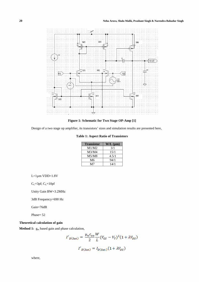
Equivalent Circuit of a two stage operational amplifier is shown in figure 1.
International Journal of Electrical and Electronics
Engineering Research (IJEEER)
ISSN 2250-155X
Vol. 3, Issue 2, Jun 2013, 19-28
© TJPRC Pvt. Ltd.
© TJPRC Pvt. Ltd.,
© TJPRC Pvt. Ltd.,
20 Neha Arora, Shalu Malik, Prashant Singh & Narendra Bahadur Singh
Figure 1: Schematic for Two Stage OP-Amp [1]
Design of a two stage op amplifier, its transistors’ sizes and simulation results are presented here,
Table 1: Aspect Ratio of Transistors
Transistor W/L (µm)
M1/M2 3/1
M3/M4 15/1
M5/M8 4.5/1
M6 94/1
M7 14/1
L=1µm VDD=1.8V
CC=3pf; CL=10pf
Unity Gain BW=3.2MHz
3dB Frequency=690 Hz
Gain=76dB
Phase= 52
Theoretical calculation of gain
Method 1: gm based gain and phase calculation,
where,

High Gain and Phase Margin CMOS Operational Amplifier Designs 21
μn = 259.530 * 10-4
m2/V s (Mobility for NMOS ) Cox= εox / tox= 8.57*10
-3 F/m
2
μp = 109.976 * 10-4
m2/V s (Mobility for NMOS ) εox = 3.97 *8.854 *10
-12 F/m
tox=4.1 *10-9
m
(1)
𝜆 can be calculated by using Eqn. (1). The calculated values of 𝜆 are shown in table 1.
(2)
g m can be calculated using Equation (2) ,
by using the calculated values of 𝜆 and gm, gain can be calculated using following formula:
calculated value of gain using eqn. (1) and eqn. (2) is, Av = 68.61dB
Method 2
gds based gain and phase calculations,
(4)
(5)
can be calculated using Eqn.(4) and gm can be calculated using Eqn.(2)[1]. The calculated values of 𝜆 and gm
are shown in table 2.
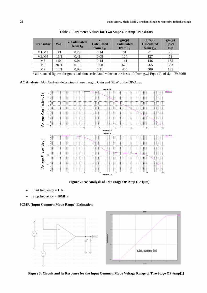
22 Neha Arora, Shalu Malik, Prashant Singh & Narendra Bahadur Singh
Table 2: Parameter Values for Two Stage OP-Amp Transistors
Transistor W/L λ Calculated
from ID
λ
Calculated
from gDS
gm(μ)
Calculated
from ID
gm(μ)
Calculated
from gDS
gm(μ)
Spice
O/p
M1/M2 3/1 0.29 0.14 91 81 76
M3/M4 15/1 0.41 0.08 104 127 78
M5 4.5/1 0.04 0.14 141 146 135
M6 94/1 0.18 0.08 678 765 503
M7 14/1 0.03 0.11 450 400 135
* all rounded figures for gm calculations calculated value on the basis of (from gDS) Eqn. (2), of 79.60dB
AC Analysis: AC- Analysis determines Phase margin, Gain and GBW of the OP-Amp.
Figure 2: Ac Analysis of Two Stage OP Amp (L=1µm)
Start frequency = 1Hz
Stop frequency = 10MHz
ICMR (Input Common Mode Range) Estimation
Figure 3: Circuit and its Response for the Input Common Mode Voltage Range of Two Stage OP-Amp[1]
High Gain and Phase Margin CMOS Operational Amplifier Designs 23
The unity gain configuration is useful for measuring or simulating ICMR. For this, a dc transfer sweep is plotted
and the linear part of the transfer curve where the slope is unity corresponds to the input common mode voltage range.
Calculated value of ICMR is 0.75-1.46V[1].
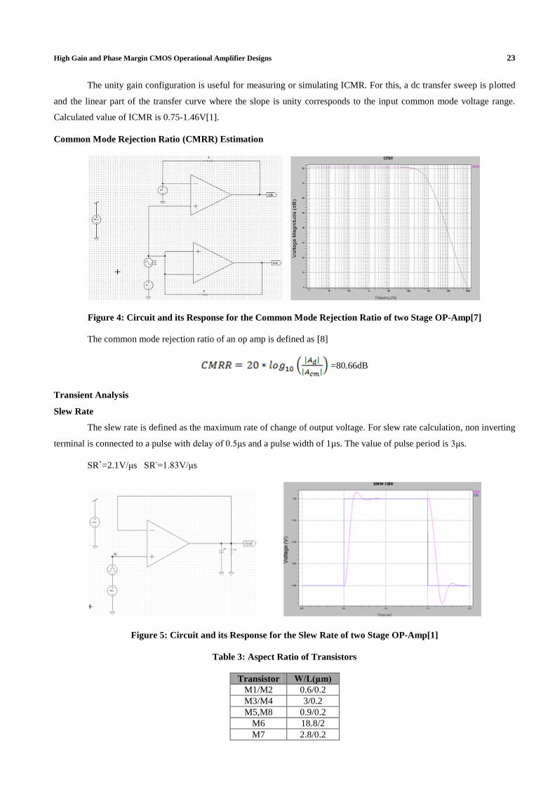
Common Mode Rejection Ratio (CMRR) Estimation
Figure 4: Circuit and its Response for the Common Mode Rejection Ratio of two Stage OP-Amp[7]
The common mode rejection ratio of an op amp is defined as [8]
=80.66dB
Transient Analysis
Slew Rate
The slew rate is defined as the maximum rate of change of output voltage. For slew rate calculation, non inverting
terminal is connected to a pulse with delay of 0.5μs and a pulse width of 1µs. The value of pulse period is 3μs.
SR+=2.1V/μs SR
-=1.83V/μs
Figure 5: Circuit and its Response for the Slew Rate of two Stage OP-Amp[1]
Table 3: Aspect Ratio of Transistors
Transistor W/L(μm)
M1/M2 0.6/0.2
M3/M4 3/0.2
M5,M8 0.9/0.2
M6 18.8/2
M7 2.8/0.2
24 Neha Arora, Shalu Malik, Prashant Singh & Narendra Bahadur Singh
The Two Stage OP Amp for L=0.2µm
Unity Gain BW=3.27MHz
3dB Frequency= 6 kHz
Gain(simulation)=53.20dB
Phase= 59.42
Gain (calculated) =52.52dB
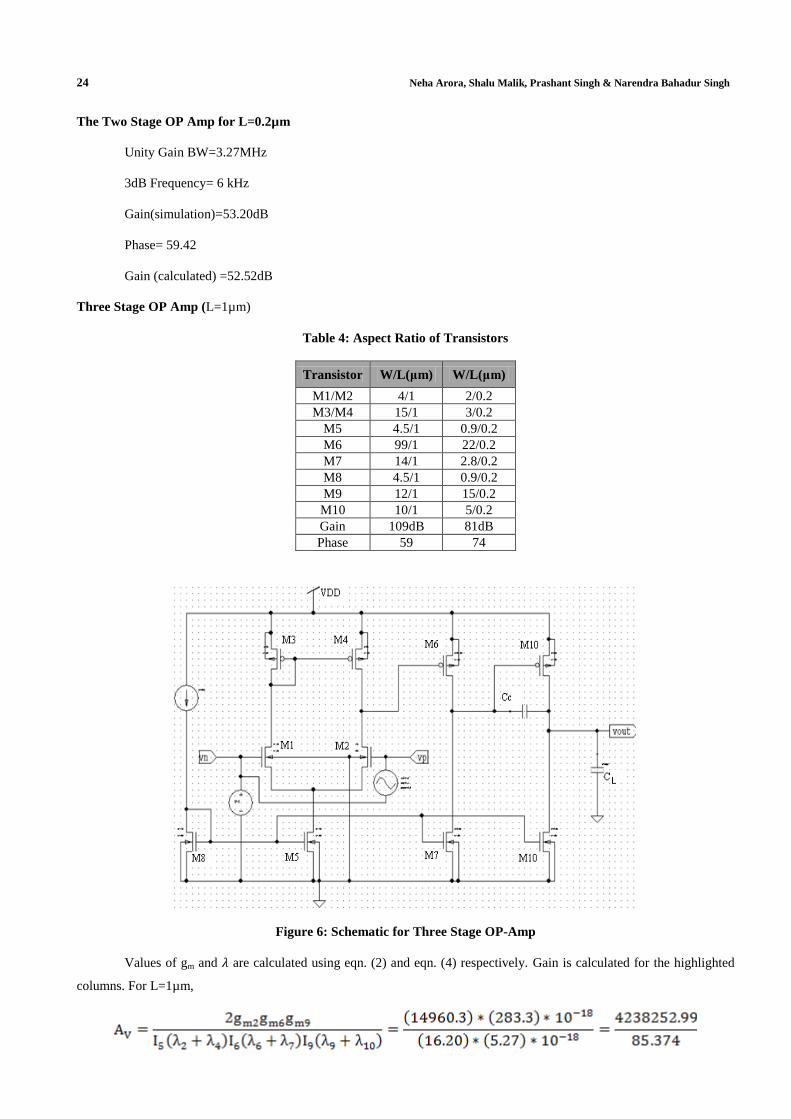
Three Stage OP Amp (L=1µm)
Table 4: Aspect Ratio of Transistors
Transistor W/L(μm) W/L(μm)
M1/M2 4/1 2/0.2
M3/M4 15/1 3/0.2
M5 4.5/1 0.9/0.2
M6 99/1 22/0.2
M7 14/1 2.8/0.2
M8 4.5/1 0.9/0.2
M9 12/1 15/0.2
M10 10/1 5/0.2
Gain 109dB 81dB
Phase 59 74
Figure 6: Schematic for Three Stage OP-Amp
Values of gm and 𝜆 are calculated using eqn. (2) and eqn. (4) respectively. Gain is calculated for the highlighted
columns. For L=1µm,
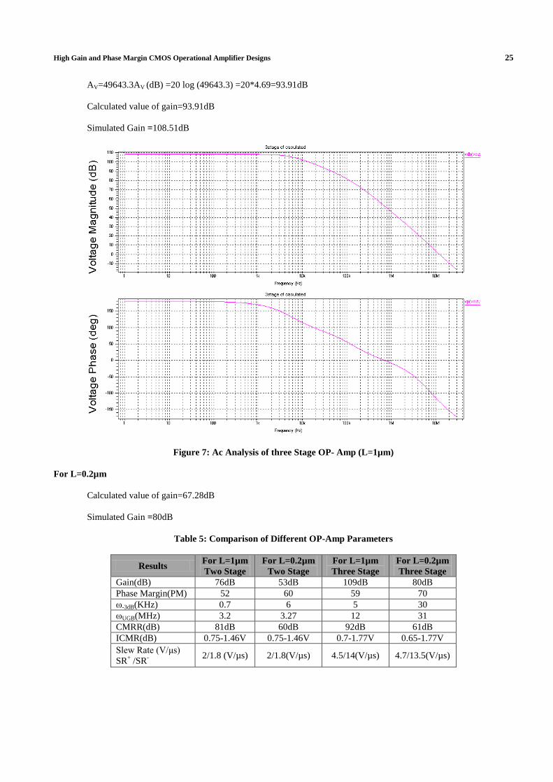
High Gain and Phase Margin CMOS Operational Amplifier Designs 25
AV=49643.3AV (dB) =20 log (49643.3) =20*4.69=93.91dB
Calculated value of gain=93.91dB
Simulated Gain =108.51dB
Figure 7: Ac Analysis of three Stage OP- Amp (L=1µm)
For L=0.2µm
Calculated value of gain=67.28dB
Simulated Gain =80dB
Table 5: Comparison of Different OP-Amp Parameters
Results For L=1µm
Two Stage
For L=0.2µm
Two Stage
For L=1µm
Three Stage
For L=0.2µm
Three Stage
Gain(dB) 76dB 53dB 109dB 80dB
Phase Margin(PM) 52 60 59 70
ω-3dB(KHz) 0.7 6 5 30
ωUGB(MHz) 3.2 3.27 12 31
CMRR(dB) 81dB 60dB 92dB 61dB
ICMR(dB) 0.75-1.46V 0.75-1.46V 0.7-1.77V 0.65-1.77V
Slew Rate (V/μs)
SR+ /SR
-
2/1.8 (V/µs) 2/1.8(V/µs) 4.5/14(V/µs) 4.7/13.5(V/µs)
26 Neha Arora, Shalu Malik, Prashant Singh & Narendra Bahadur Singh
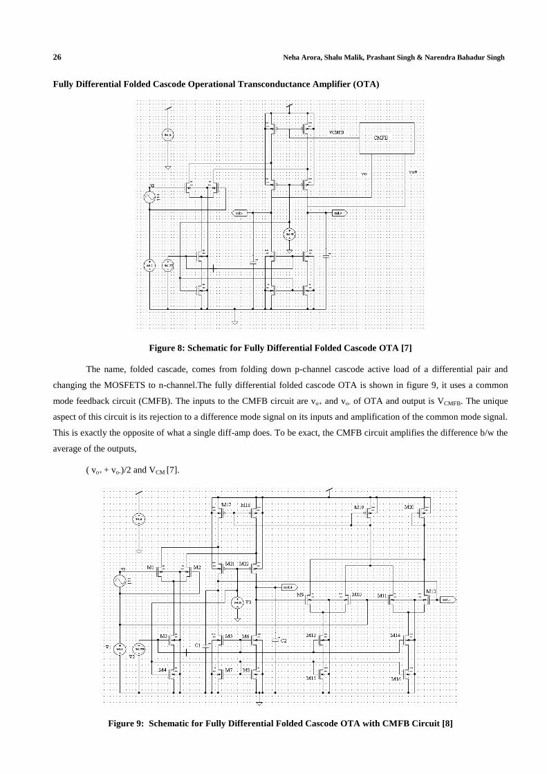
Fully Differential Folded Cascode Operational Transconductance Amplifier (OTA)
Figure 8: Schematic for Fully Differential Folded Cascode OTA [7]
The name, folded cascade, comes from folding down p-channel cascode active load of a differential pair and
changing the MOSFETS to n-channel.The fully differential folded cascode OTA is shown in figure 9, it uses a common
mode feedback circuit (CMFB). The inputs to the CMFB circuit are vo+ and vo- of OTA and output is VCMFB. The unique
aspect of this circuit is its rejection to a difference mode signal on its inputs and amplification of the common mode signal.
This is exactly the opposite of what a single diff-amp does. To be exact, the CMFB circuit amplifies the difference b/w the
average of the outputs,
( vo+ + vo-)/2 and VCM [7].
Figure 9: Schematic for Fully Differential Folded Cascode OTA with CMFB Circuit [8]
High Gain and Phase Margin CMOS Operational Amplifier Designs 27
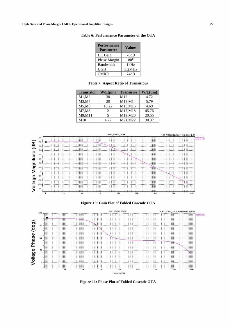
Table 6: Performance Parameter of the OTA
Performance
Parameter Values
DC Gain 70dB
Phase Margin 88⁰ Bandwidth 1kHz
UGB 3.2MHz
CMRR 74dB
Table 7: Aspect Ratio of Transistors
Transistor W/L(µm) Transistor W/L(µm)
M1,M2 30 M12 4.72
M3,M4 20 M13,M14 5.79
M5,M6 10.22 M15,M16 4.69
M7,M8 2 M17,M18 45.76
M9,M11 5 M19,M20 20.55
M10 4.72 M21,M22 30.37
Figure 10: Gain Plot of Folded Cascode OTA
Figure 11: Phase Plot of Folded Cascode OTA
28 Neha Arora, Shalu Malik, Prashant Singh & Narendra Bahadur Singh
CONCLUSIONS
In this paper the mos transistor’s parameters’ optimization are carried out to achieve the best performance of the
operational amplifier near to 200nm Technology for second and third order amplifier including the design of a fully
differential folded cascode configuration with all the transistors are operating in saturation region. Gm and Gds based
calculations were carried out in the physical model to calculate gain and phase of the second and third orders amplifiers
and it’s results are also compared with the spice simulation results, as presented in various tables. The open loop gain is
76dB for two stage, 109dB for three stage and 70dB for cascode configuration, based on simulated output frequency
response for 1.8V dc supply voltage. In this paper trade off curves are computed for the characteristics such as Gain, PM,
UGB, ICMR, CMRR, Slew Rate etc.
REFERENCES
1. P. Allen and D. Holberg “CMOS Analog Circuit Design”, International 2nd Edition. Oxford University Press,
2009.
2. B. Razavi, “Design of Analog CMOS Integrated Circuits”, New York: Mc Graw-Hill, 2001.
3. http://cmosedu.com/jbaker/papers/talks/Multistage_Opamp_Presentation.pdf
4. Mohammad Mojtaba Sheikholeslami, Abbas Golmakani, Khalil Mafinezhad, “Design of a Low-Voltage, Low-
Power, Two-Stage Amplifier in 0.18μm CMOS Process”, International Journal of Academic Research in Applied
Science1(4): 9-15, 2012.
5. Bult K., Geelen G. J. G. M., "A fast-settling CMOS op amp for SC circuits with 90-dB DC gain", IEEE Journal of
Solid-State Circuits, Vol.25, pp. 1379-1384, Dec. 1990.
6. Keneth R. Laker, Willey M.C.Sansen,”Design of Analog Integrated Circuits and Systems”, McGraw- Hill.
7. R.J. Baker,”CMOS Circuit Design, Layout and Simulation”, Wiley-Interscience, 2004.
8. A.S. Sedra and K.C.Smith, ”Microelectronics Circuits Theory and Applications”, Fifth Edition. Oxford University
Press, 2009.