Embed Size (px)
Citation preview


HIGH FREQUENCYTECHNIQUESAn Introduction to RF and MicrowaveEngineering
Joseph F. WhiteJFW Technology, Inc.
A John Wiley & Sons, Inc. publication


HIGH FREQUENCYTECHNIQUES

HIGH FREQUENCYTECHNIQUESAn Introduction to RF and MicrowaveEngineering
Joseph F. WhiteJFW Technology, Inc.
A John Wiley & Sons, Inc. publication

Copyright 6 2004 by John Wiley & Sons, Inc. All rights reserved.
Published by John Wiley & Sons, Inc., Hoboken, New Jersey.
Published simultaneously in Canada.
No part of this publication may be reproduced, stored in a retrieval system, or transmitted in any
form or by any means, electronic, mechanical, photocopying, recording, scanning, or otherwise,
except as permitted under Section 107 or 108 of the 1976 United States Copyright Act, without
either the prior written permission of the Publisher, or authorization through payment of the
appropriate per-copy fee to the Copyright Clearance Center, Inc., 222 Rosewood Drive, Danvers,
MA 01923, 978-750-8400, fax 978-646-8600, or on the web at www.copyright.com. Requests to
the Publisher for permission should be addressed to the Permissions Department, John Wiley &
Sons, Inc., 111 River Street, Hoboken, NJ 07030, (201) 748-6011, fax (201) 748-6008.
Limit of Liability/Disclaimer of Warranty: While the publisher and author have used their best
e¤orts in preparing this book, they make no representations or warranties with respect to the
accuracy or completeness of the contents of this book and specifically disclaim any implied
warranties of merchantability or fitness for a particular purpose. No warranty may be created or
extended by sales representatives or written sales materials. The advice and strategies contained
herein may not be suitable for your situation. You should consult with a professional where
appropriate. Neither the publisher nor author shall be liable for any loss of profit or any other
commercial damages, including but not limited to special, incidental, consequential, or other
damages.
For general information on our other products and services please contact our Customer Care
Department within the U.S. at 877-762-2974, outside the U.S. at 317-572-3993 or fax 317-572-
4002.
Wiley also publishes its books in a variety of electronic formats. Some content that appears in
print, however, may not be available in electronic format.
Library of Congress Cataloging-in-Publication Data:
White, Joseph F., 1938–
High frequency techniques : an introduction to RF and microwave engineering /
Joseph F. White.
p. cm.
Includes bibliographical references and index.
ISBN 0-471-45591-1 (Cloth)
1. Microwave circuits. 2. Radio circuits. I. Title.
TK7876.W4897 2004
621.384 012—dc21 2003010753
Printed in the United States of America.
10 9 8 7 6 5 4 3 2 1

to Christopher


CONTENTS
Preface xv
Acknowledgments xxi
1 Introduction 1
1.1 Beginning of Wireless 1 1.2 Current Radio Spectrum 4 1.3 Conventions Used in This Text 8
Sections 8 Equations 8 Figures 8 Exercises 8 Symbols 8 Prefixes 10 Fonts 10
1.4 Vectors and Coordinates 11 1.5 General Constants and Useful Conversions 14
2 Review of AC Analysis and Network Simulation 16
2.1 Basic Circuit Elements 16
The Resistor 16 Ohm’s Law 18 The Inductor 19 The Capacitor 20
2.2 Kirchho¤ ’s Laws 22 2.3 Alternating Current (AC) Analysis 23
Ohm’s Law in Complex Form 26
2.4 Voltage and Current Phasors 26 2.5 Impedance 28
Estimating Reactance 28 Addition of Series Impedances 29
2.6 Admittance 30
Admittance Definition 30
vii

viii CONTENTS
Addition of Parallel Admittances 30 The Product over the Sum 32
2.7 LLFPB Networks 33 2.8 Decibels, dBW, and dBm 33
Logarithms (Logs) 33 Multiplying by Adding Logs 34 Dividing by Subtracting Logs 34 Zero Powers 34 Bel Scale 34 Decibel Scale 35 Decibels—Relative Measures 35 Absolute Power Levels—dBm and dBW 37 Decibel Power Scales 38
2.9 Power Transfer 38
Calculating Power Transfer 38 Maximum Power Transfer 39
2.10 Specifying Loss 40
Insertion Loss 40 Transducer Loss 41 Loss Due to Series Impedance 42 Loss Due to Shunt Admittance 43 Loss in Terms of Scattering Parameters 44
2.11 Real RLC Models 44
Resistor with Parasitics 44 Inductor with Parasitics 44 Capacitor with Parasitics 44
2.12 Designing LC Elements 46
Lumped Coils 46 High m Inductor Cores—the Hysteresis Curve 47 Estimating Wire Inductance 48 Parallel Plate Capacitors 49
2.13 Skin E¤ect 51 2.14 Network Simulation 53
3 LC Resonance and Matching Networks 59
3.1 LC Resonance 59 3.2 Series Circuit Quality Factors 60
Q of Inductors and Capacitors 60 QE , External Q 61 QL, Loaded Q 62
3.3 Parallel Circuit Quality Factors 62 3.4 Coupled Resonators 63

CONTENTS ix
Direct Coupled Resonators 63 Lightly Coupled Resonators 63
3.5 Q Matching 67
Low to High Resistance 67 Broadbanding the Q Matching Method 70 High to Low Resistance 71
4 Distributed Circuit Design 78
4.1 Transmission Lines 78 4.2 Wavelength in a Dielectric 81 4.3 Pulses on Transmission Lines 82 4.4 Incident and Reflected Waves 83 4.5 Reflection Coe‰cient 85 4.6 Return Loss 86 4.7 Mismatch Loss 86 4.8 Mismatch Error 87 4.9 The Telegrapher Equations 91 4.10 Transmission Line Wave Equations 92 4.11 Wave Propagation 94 4.12 Phase and Group Velocities 97 4.13 Reflection Coe‰cient and Impedance 100 4.14 Impedance Transformation Equation 101 4.15 Impedance Matching with One Transmission Line 108 4.16 Fano’s (and Bode’s) Limit 109
Type A Mismatched Loads 109 Type B Mismatched Loads 112 Impedance Transformation Not Included 113
5 The Smith Chart 119
5.1 Basis of the Smith Chart 119 5.2 Drawing the Smith Chart 124 5.3 Admittance on the Smith Chart 130 5.4 Tuning a Mismatched Load 132 5.5 Slotted Line Impedance Measurement 135 5.6 VSWR ¼ r 139 5.7 Negative Resistance Smith Chart 140 5.8 Navigating the Smith Chart 140 5.9 Smith Chart Software 141 5.10 Estimating Bandwidth on the Smith Chart 147 5.11 Approximate Tuning May Be Better 148 5.12 Frequency Contours on the Smith Chart 150 5.13 Using the Smith Chart without Transmission Lines 150 5.14 Constant Q Circles 151 5.15 Transmission Line Lumped Circuit Equivalent 153

x CONTENTS
6 Matrix Analysis
6.16.26.36.46.56.6
Matrix AlgebraZ and Y MatricesReciprocityThe ABCD MatrixThe Scattering MatrixThe Transmission Matrix
7 Electromagnetic Fields and Waves
7.17.27.37.47.57.67.77.87.97.107.117.127.13
7.147.157.167.177.187.197.207.217.227.237.247.257.26
Vector Force FieldsE and H FieldsElectric Field EMagnetic Flux DensityVector Cross ProductElectrostatics and Gauss’s LawVector Dot Product and DivergenceStatic Potential Function and the GradientDivergence of the ~BB FieldAmpere’s Law
Maxwell’s Four EquationsAuxiliary Relations and DefinitionsVisualizing Maxwell’s Equations
General Waveguide SolutionWaveguides TypesRectangular Waveguide FieldApplying Boundary Conditions
Vector CurlFaraday’s Law of InductionMaxwell’s Equations
Primary Vector OperationsThe LaplacianVector and Scalar IdentitiesFree Charge within a ConductorSkin E¤ectConductor Internal ImpedanceThe Wave EquationThe Helmholtz EquationsPlane Propagating WavesPoynting’s TheoremWave PolarizationEH Fields on Transmission LinesWaveguides
161
161 164 166 167 172 177
183
183 185 185 187 188 193 194 196 200 201 202 208 209
209 210 211
214 215 218 219 221 224 227 229 230 233 236 240 246
246 250 251 252
Propagation Constants and Waveguide Modes 253

7.27 Fourier Series and Green’s Functions 261
7.28 Higher Order Modes in Circuits 269 7.29 Vector Potential 271 7.30 Retarded Potentials 274 7.31 Potential Functions in the Sinusoidal Case 275 7.32 Antennas 275
7.33 Path Loss 2907.34 Electromagnetic (EM) Simulation 294
CONTENTS xi
Characteristic Wave Impedance for Waveguides 256 Phase and Group Velocities 257 TE and TM Mode Summary for Rectangular Waveguide 257
Fourier Series 261 Green’s Functions 263
Short Straight Wire Antenna 275279280280283284285286288
Radiation Resistance Radiation Pattern Half-Wavelength Dipole Antenna Gain Antenna E¤ective Area Monopole Antenna Aperture Antennas Phased Arrays
3078 Directional Couplers
8.1 Wavelength Comparable Dimensions 307 8.2 The Backward Wave Coupler 307 8.3 Even- and Odd-Mode Analysis 309 8.4 Reflectively Terminated 3-dB Coupler 320 8.5 Coupler Specifications 323 8.6 Measurements Using Directional Couplers 325 8.7 Network Analyzer Impedance Measurements 326 8.8 Two-Port Scattering Measurements 327 8.9 Branch Line Coupler 327 8.10 Hybrid Ring (Rat Race) Coupler 330 8.11 Wilkinson Divider 330
9 Filter Design 335
9.1 Voltage Transfer Function 335 9.2 Low-Pass Prototype 336 9.3 Butterworth or Maximally Flat Filter 337 9.4 Denormalizing the Prototype Response 339 9.5 High-Pass Filters 343 9.6 Bandpass Filters 345

xii CONTENTS
Bandstop FiltersChebyshev FiltersPhase and Group DelayFilter QDiplexer FiltersTop-Coupled Bandpass FiltersElliptic FiltersDistributed FiltersThe Richards TransformationKuroda’s IdentitiesMumford’s Maximally Flat Stub FiltersFilter Design with the OptimizerStatistical Design and Yield Analysis
Unilateral Design
Amplifier StabilityK FactorTransducer GainUnilateral Gain DesignUnilateral Gain Circles
Simultaneous Conjugate Match DesignVarious Gain DefinitionsOperating Gain Design
10.10 Available Gain Design10.11 Noise in Systems
10.12 Low-Noise Amplifiers
Gain SaturationIntermodulation Distortion
9.79.89.99.109.119.129.139.149.159.169.179.189.19
Using Standard Part ValuesThe Normal DistributionOther Distributions
10 Transistor Amplifier Design
10.1
10.210.310.410.510.6
10.710.810.9
Evaluating S ParametersTransistor BiasingEvaluating RF Performance
Input Gain CirclesOutput Gain Circles
Thermal Noise LimitOther Noise SourcesNoise Figure of a Two-Port NetworkNoise Factor of a CascadeNoise Temperature
10.13 Amplifier Nonlinearity
349 351 356 361 364 367 369 370 374 379 381 384 385
385 386 391
399
399
399 400 403
405 409 413 416 422
422 424
428 430 433 437 442
442 444 445 447 448
450 455
455 456

CONTENTS xiii
10.14 Broadbanding with Feedback 460 10.15 Cascading Amplifier Stages 466 10.16 Amplifier Design Summary 468
Appendices
A. Symbols and Units 474
B. Complex Mathematics 478
C. Diameter and Resistance of Annealed Copper Wire by Gauge Size 483
D. Properties of Some Materials 485
E. Standard Rectangular Waveguides 486
Index 487


PREFACE
This book is written for the undergraduate or graduate student who wishes topursue a career in radio-frequency (RF) and microwave engineering. Today’sengineer must use the computer as a design tool to be competitive. This textpresumes that the student has access to a computer and network simulationsoftware, but the book can be used without them. In either event, this text willprepare the student for the modern engineering environment in which thecomputer is a tool of daily use.
The computer is used in two ways. First, it performs laborious calculationsbased on a defined procedure and a set of circuit element values. This is themajor use of network simulation, and it is employed throughout this book toshow how each network that is described performs over a frequency range. Thesecond way is like the first except that the computer varies the element valueseither to approach a desired performance goal (optimization) or to show thevariation in performance when a quantity of circuits is built using parts whosevalues vary from piece to piece (yield prediction).
In the second use, the computer is like a thousand monkeys who, it was oncepostulated, if taught to type, would eventually type all of the world’s great lit-erature including an index to the work. But, it was further postulated, they alsowould type every possible wrong version, incorrect indices included. Today, theengineer’s task is to obtain the useful outputs of the computer based on a fun-damental understanding of the underlying principles. Within this text, thecomputer is used as a tool of, not a substitute for, design. This book empha-sizes fundamental concepts, engineering techniques, and the regular and intel-ligent use of the computer as a computational aid.
Within this presentation of theoretical material, computer-generated exam-ples provide insight into the basic performance, bandwidth, and manufacturingyield of RF and microwave networks. This facilitates the evaluation of classicalcircuit designs and their limitations. However, in modern engineering, rarely isa classical circuit design used in its standard form, although that was necessar-ily the practice before the availability of personal computers and simulationsoftware. Rather, today the classical design is a point of embarkation fromwhich a specific design is tailored to immediate design needs. The presence ofthe classical design remains important because it serves as a starting point todefine what specifications might reasonably be expected as optimizer goals forthe simulation. E¤ectively, it ‘‘gets the thousand monkeys started on the rightpage.’’
xv

xvi PREFACE
This book contains a review of wireless history and engineering funda-mentals including complex numbers, alternating-current theory, and the loga-rithmic basis of decibels. All of the text is written in a simple and informalmanner so that the presentation of concepts is easy to follow. Many derivationsshow intermediate steps not usually included in textbooks because the intentis to enlighten, not test, more than need be, the mathematical prowess of thereader. This book also contains exercises that do not have a black or whiteanswer. Exercise questions are asked that require consideration beyond what iscovered in the text. This is intentional. It is done to introduce the reader towhat happens in the practical realm of engineering.
The reader is cautioned not to interpret the review material and easy read-ability of this text for a lack of conceptual rigor or thoroughness. As the readerwill soon determine, the chapters of this book actually are more encompassingof theoretical concepts and advanced engineering techniques than those of mostintroductory microwave texts. But the emphasis is on practical technique. Forexample, the reader will be surprised that, based merely on Q and the complexnumber conversion between impedance and admittance, a technique called Q
matching is developed that is familiar to few engineering professionals.The emphasis of this book is how design challenges would be attacked in a
real engineering environment. Some designs, such as distributed filters, are bestperformed either with proprietary software programs or with the thousand-monkey approach (optimization), but the emphasis is in providing the monkeyswith a promising start.
The style of this textbook is derived from a hands-on industrial course thatthe author has been teaching for some time. In it the student builds on thecomputer the circuits that are presented, designing them to specifications andverifying how they perform with frequency. This approach quickly builds de-sign confidence in the student. The exercises presented draw from this experi-ence, and they employ the network simulator to reveal both circuit perfor-mance and the student’s mastery of it. The following paragraphs summarize themajor subjects covered.
Chapter 1 contains a review of the origins of wireless transmission. The earlyand persistent e¤orts of Guglielmo Marconi in developing radio is an inspira-tion to engineers today.
Chapter 2 is an engineering review of alternating-current analysis usingcomplex notation (in Appendix B), impedances and decibel, dBm, and dBWmeasures with the aim of solidifying these basic concepts. Intuitive level profi-ciency in these fundamentals is as important to microwave and RF engineeringas touch typewriting is to e‰cient writing. Practical realizations of circuit ele-ments are described, including resistors, inductors, and capacitors and theirequivalent circuits with parasitic elements. The parasitic reactances of theseelements seriously limit their use at high frequencies, and the engineer does wellto know these limits and how they come about.
Chapter 3 treats resonators and how their bandwidth is influenced by Q.Based upon the Q ratio of reactance to resistance and the conversion between

PREFACE xvii
series and shunt impedances, the scheme called Q matching is derived. Thisenables the engineer to design a LC matching network in a few, simply re-membered steps.
Chapter 4 introduces distributed circuits based on transmission lines andtheir properties. This is the beginning of microwave design theory. Importantideas such as wavelength, voltage standing-wave ratio (VSWR), reflections, re-turn loss, mismatch loss, and mismatch error are presented. These are followedby slotted line measurements and the derivation of the telegrapher and trans-mission line equations. Phase and group velocity concepts and reflection co-e‰cient related to impedance and distributed matching are introduced. Thetransmission line impedance transformation equation is derived and applied tospecial cases of easy applicability. Fano’s limit is presented. It is an importantrestriction on the capacity for matching over a frequency band and was derivedin terms of reflection coe‰cient.
Chapter 5 is devoted to the basis and use of the Smith chart, the sine qua non
for microwave engineers. The Smith chart a¤ords a window into the workingsof transmission lines, rendering their very complex impedance transformationbehavior clearly understandable with a single diagram. This presentation re-veals how the function of the Smith chart in handling impedance transforma-tion arises out of the constant magnitude of the reflection coe‰cient along alossless line, that the chart is merely the reflection coe‰cient plane, a principleoften overlooked. Navigating the chart using impedance, admittance, reflectioncoe‰cient, and Q circles is presented. Matching to complex load impedances,estimating VSWR bandwidth, and developing equivalent circuits are amongthe illustrated techniques.
Chapter 6 is a presentation of matrix algebra and definitions for the Z, Y,ABCD, S, and T matrices. Matrix use underlies most circuit derivations andmeasurement techniques. This chapter demonstrates how and when to use thedi¤erent matrices and their limitations. For example, it shows how to employthe ABCD matrix to derive remarkably general equivalent circuits in just a fewsteps, such as the lumped equivalent circuit of a transmission line and a per-fectly matched, variable attenuator.
Chapter 7 is a very broad presentation of electromagnetic (EM) field theorytailored to the needs of the microwave and RF engineer. It begins with thephysics and the defining experiments that led to the formulation of Maxwell’sequations, which are then used to derive fundamental results throughout thechapter. This includes the famous wave equation, from which Maxwell wasfirst led to conclude that light and electromagnetic fields were one and thesame.
Throughout this book, techniques are introduced as needed. This is particu-larly true in this chapter. Vector mathematics are presented including the gra-dient, dot product, cross product, divergence, curl, and Laplacian as they arerequired to describe EM field properties and relationships. This direct applica-bility of the vector operations helps to promote a physical understanding ofthem as well as the electromagnetic field relationships they are used to describe.

xviii PREFACE
The depth of Chapter 7 is unusual for an introductory text. It extends fromthe most basic of concepts to quite advanced applications. Skin e¤ect, intrinsicimpedance of conductors, Poynting’s theorem, wave polarization, the deriva-tion of coaxial transmission line and rectangular waveguide propagating fields,Fourier series and Green’s functions, higher order modes in circuits, vectorpotential, antennas, and radio system path loss are developed in mathematicaldetail.
Under the best of circumstances, field theory is di‰cult to master. To ac-commodate this wide range of electromagnetic topics, the mathematical deri-vations are uncommonly complete, including many intermediate steps oftenomitted but necessary for e‰cient reading and more rapid understanding of theprinciples.
Chapter 7 concludes with an important use of the computer to perform EMfield simulation of distributed circuits. This is shown to provide greater designaccuracy than can be obtained with conventional, ideal distributed models.
Chapter 8 treats directional couplers, an important ingredient of microwavemeasurements and systems. This chapter shows how couplers are analyzed andused. It introduces the even- and odd-mode analysis method, which is demon-strated by an analysis of the backward wave coupler. The results, rarely foundso thoroughly described in any reference, describe an astounding device. Thebackward wave coupler has perfect match, infinite isolation, and exactly 90�
phase split at all frequencies. Cohn’s reentrant geometry, used to achieve a 3-dBbackward wave, 5-to-1 bandwidth coupler is presented. The uses of couplers aspower dividers, reflection phase shifter networks, and as impedance measuringelements in network analyzers are also discussed.
Chapter 9 shows the reader how to design filters beginning with low-passprototypes having maximally flat (Butterworth), equal-ripple (Chebyshev), andnear constant delay (Bessel) characteristics. The classic techniques for scalingthese filters to high-pass, bandpass, and bandstop filters are provided. The ef-fect of filter Q on insertion loss is demonstrated. The elliptic filter, having equalstopband ripple, is introduced. Identical resonator filters using top couplingare described as a means to extend the practical frequency range of lumped-element designs.
Half-wave transmission line resonators are used to introduce distributed fil-ters. The Richards transformation and Kuroda’s identities are presented as ameans of translating lumped-element designs to distributed filters. Mumford’squarter-wave stub filters are presented and shown to be a suitable basis forsimulation software optimization of equal-ripple and other passband filters.Kuroda’s identities are presented in terms of transmission lines rather than thecustomary, but vague, ‘‘unit elements,’’ simplifying their adoption. This per-mits students to understand and use Kuroda’s identities immediately, evenproving their validity as one of the exercises.
Chapter 9 is concluded with a treatment of manufacturing yield illustratedusing a filter circuit. A special method of integrating the Gaussian, or normalcurve, is presented showing how the ‘‘one-sigma’’ specification is used to de-

PREFACE xix
termine component and circuit yield. The evaluation of the yield of a practicalfilter circuit using the network simulator is presented. In this process specifica-tions are applied to the circuit and its performance analyzed assuming it isfabricated using a random sample (Monte Carlo analysis) of normally distrib-uted components. The resulting yield from 500 circuits so ‘‘built’’ is deter-mined, showing how the e¤ects of component tolerances and specifications onproduction yields can be determined even before any materials are procured orassembled.
Chapter 10 is applied to transistor amplifiers. The key to amplifier design isthe stabilizing and matching of the transistor to its source and load environ-ment, but this must be performed by taking the whole frequency range overwhich the device has gain into account, a massive calculation task if performedmanually. This is handled using S parameters and the network simulator as adesign tool. Constant gain and noise figure circles on the Smith chart are de-scribed and their design use demonstrated with actual transistor parameters.
The principal design methods including unilateral gain, operating gain,available gain, simultaneously matched, and low noise amplifier techniques aredescribed and demonstrated with available transistor S parameters. Specialamplifier topics are presented, including unilateral figure of merit, nonlineare¤ects, gain saturation, third-order intercept, spurious free dynamic range, andnoise limits. The e¤ects of VSWR interaction with cascaded amplifier stages aredemonstrated and the use of negative feedback to reduce the VSWR interactionand to design well-matched, broadband amplifiers is shown.
The intent of including so much theoretical and practical material in thistext is to provide an immediate familiarity with a wide variety of circuits, theircapabilities and limitations, and the means to design them. This permits theengineer to proceed directly to a practical circuit design without the dauntingtask of researching the material in multiple library references. These topics areillustrated with recommendations on how to use computer optimizations intel-ligently to direct the computer to search for circuits whose performance is real-
istically achievable.One could spend years in the microwave engineering practice and not gain
experience with this broad a spectrum of topics. The student who reads thisbook and completes its exercises, in my experience, will be unusually wellqualified to embark on a microwave and RF engineering career.
Comments and corrections from readers are welcome.
Joseph F. [email protected]


ACKNOWLEDGMENTS
The Smith chart symbolized on the cover and employed within this text is re-produced through the courtesy of Anita Smith, owner of Analog InstrumentCompany, Box 950, New Providence, New Jersey 07974. I am happy to ac-knowledge the late Phillip Smith for this remarkable tool, arguably the mostprofound insight of the microwave field. Numerous Smith chart matching so-lutions were performed using the software program WinSmith available fromNoble Publishing Co., Norcross, Georgia 30071.
All of the circuit simulations have been performed using the Genesys soft-ware suite provided through the courtesy of Randall Rhea, founder of Eagle-ware Inc, Norcross, Georgia 30071. My thanks also go to the members of theEagleware on-line support team, whose assistance improved the many simula-tion examples that appear in this text.
My gratitude to Dr. Les Besser who encouraged me to begin microwaveteaching and shared with me many RF and microwave facts and design meth-ods. I also thank Gerald DiPiazza for his patience and help in critical fieldtheory development in this text.
I gratefully acknowledge Dr. Peter Rizzi, my colleague and friend, who pa-tiently read the manuscript and made numerous suggestions to improve itsreadability, usefulness, and accuracy. He directly contributed the portions onnoise and noise temperature. Dr. Rizzi is the author of Microwave Engineering
and Passive Circuits, an important, widely used text that is referenced exten-sively in these notes. He is a professor of microwaves who is loved by his stu-dents. No one but I can appreciate the magnitude of his contributions.
Anyone who has written a book knows how much patience his spouse re-quires. My thanks and love to Eloise.
THE AUTHOR
Joseph White is an instructor and consultant in the RF and microwave com-munity, also known as the ‘‘wireless’’ industry.
He received the BS EE degree from Case Institute of Technology, the MSEE degree from Northeastern University and the Ph.D. degree from theElectrical Engineering Department of Rensselaer Polytechnic Institute withspecialty in electrophysics and engaged in semiconductor engineering at M/A-
xxi

xxii ACKNOWLEDGMENTS
COM Inc, Burlington, Massachusetts, for 25 years. He holds several micro-wave patents.
He received the IEEE Microwave Theory and Techniques Society’s annualApplication Award for his ‘‘Contributions to Phased Array Antennas.’’
He also wrote Microwave Semiconductor Engineering, a textbook in its thirdprinting since 1977.
He has taught courses on RF and microwave engineering at both the intro-ductory and advanced engineering levels. He has lectured in the United Statesand internationally on microwave subjects for more than 30 years.
He has been a technical editor of microwave magazines for over 20 years,including the Microwave Journal and Applied Microwave and Wireless.
He has served as a reviewer for the IEEE Transactions on Microwave Theory
and Techniques. He is a Fellow of the IEEE and a member of the Eta Kappa
Nu and Sigma Xi honorary fraternities.Questions, corrections and comments about this book are welcome. Please
e-mail them to the author at [email protected].

CHAPTER 1
Introduction
1.1 BEGINNING OF WIRELESS
WIRELESS TELEGRAPHY—At a time when relations are strained betweenSpain and this country, nothing could be more welcome than a practical methodof carrying on electrical communication between distant points on land, and be-tween ships at sea, without any prearranged connection between the two points.During the last year Guglielmo Marconi, an Italian student, developed a systemof wireless telegraphy able to transmit intelligible Morse signals to a distance ofover ten miles. It has been left, however, for an American inventor to design anapparatus suitable to the requirements of wireless telegraphy in this country. Aftermonths of experimenting, Mr. W. J. Clarke, of the United States Electrical SupplyCompany, has designed a complete wireless telegraphy apparatus that will prob-ably come rapidly into use.
—Scientific American April, 1898
This announcement appeared near the beginning of radio technology. Web-ster’s dictionary [1] lists over 150 definitions that begin with the word radio, thefirst being:
1a. . . . the transmission and reception of electric impulses or signals by means ofelectromagnetic waves without a connecting wire (includes wireless, television andradar).
This remains today the real definition of wireless and, equivalently, radio. To-day the uses of radio communication include not only the broadcast of soundthrough amplitude modulation (AM) and frequency modulation (FM) radioand video through television, but also a broad collection of radio applications,cordless telephones, cell phones, TV, and VCR remotes, automobile remotedoor locks, garage door openers, and so on.
There is some question about who actually invented radio as a communica-
High Frequency Techniques: An Introduction to RF and Microwave Engineering, By Joseph F. White. ISBN 0-471-45591-1 6 2004 John Wiley & Sons, Inc.
1

2 INTRODUCTION
tive method. Mahlon Loomis, a dentist, experimented with wireless telegraphyusing wires supported by kites and a galvanometer to sense the changes in cur-rent flow in a second wire when the ground connection of the first was inter-rupted. He received a patent in 1873 for this system [2].
James Clerk Maxwell [3], more about Maxwell’s equations later, predictedthe propagation of electromagnetic waves through a vacuum in about 1862.Nathan Stubblefield, a Kentucky farmer and sometimes telephone repairman,demonstrated wireless telephony as early as 1892, but to only one man, and in1902 to a group [2].
Alexander Popov is said to have ‘‘utilized his equipment to obtain informa-tion for a study of atmospheric electricity . . . On 7 May 1895, in a lecture be-fore the Russian Physicist Society of St. Petersburg, he stated he had trans-mitted and received signals at an intervening distance of 600 yards’’ [4]. In 1888Heinrich Hertz conducted an experimental demonstration in a classroom atKarlsruhe Polytechnic in Berlin of the generation and detection of the prop-agating electromagnetic waves predicted by Maxwell [2].
Sir Oliver Lodge, a professor at Liverpool University was experimentingwith wireless telegraphy in 1888, and he patented a system in 1897. Marconipurchased his patent in 1911 [2].
In the public mind Guglielmo Marconi enjoys the most credit for ‘‘invent-ing’’ radio. He was awarded patents for it; therefore, the Patent O‰ce believedthat he had made radio-related inventions. However, the U.S. Navy report [4]states
Marconi can scarcely be called an inventor. His contribution was more in thefields of applied research and engineering development. He possessed a verypractical business acumen, and he was not hampered by the same driving urge todo fundamental research, which had caused Lodge and Popo¤ to procrastinate inthe development of a commercial radio system.
This is perhaps the most accurate description of Marconi’s role in develop-ing radio technology, a new communication medium. Nikola Tesla had earlierpatents, although the focus of his work appears to have been directed to thetransmission of power rather than to communication via radio waves. Tesla,well known for his Tesla coil that generated high voltages, actually detectedsignals consisting of noise bursts, resulting from the large atmospheric electricaldischarges he originated, that had traveled completely around the earth. In1943 the U.S. Supreme Court ruled that Marconi’s patents were invalid dueto Tesla’s prior descriptions, but by that time both Marconi and Tesla weredeceased [2].
From its beginnings around 1900, radio moved out to fill many communi-cative voids. In 1962 George Southworth, a well-known researcher in the fieldof microwaves, wrote a book about his 40 years of experience in the field[5, p. 1]. He begins:

--
3BEGINNING OF WIRELESS
One of the more spectacular technical developments of our age has been radio.Beginning about the turn of the century with ship-to-shore telegraphy, radio hasbeen extended through the years to intercontinental telegraphy, to broadcasting,to radio astronomy and to satellite communications.
Today, after an additional 40 years, Southworth could make a much longerlist of radio applications. It would include garage door openers, global posi-tioning satellites, cellular telephones, wireless computer networks, and radarapplications such as speed measurement, ship and aircraft guidance, militarysurveillance, weapon directing, air tra‰c control, and automobile anticollisionsystems. The frequency spectrum for practical wireless devices has expanded aswell. Amplitude modulated radio begins at 535 kHz and television remotecontrols extend into the infrared.
The advance of wireless applications is not complete and probably never willbe. Certainly the last decade has seen an explosive growth in applications. Andthe quantities of systems has been extraordinary, too. Witness the adoption ofthe cellular telephone, which today rivals the wired telephone in numbers ofapplications.
Sending signals over telegraph wires formed the basis for the early wirelesstechnology to follow. Using the Current International Morse code charactersfor the early Morse code message transmitted over the first telegraph wires, thefirst message inaugurating service between Baltimore and Washington, D.C., in1843, would have looked like
.-- .... .- - .... .- - .... --. --- -.. .-- .-. --- ..- --. .... - ..--..W h a t h a t h G o d w r o u g h t ?
Most of the full code cipher is shown in Figure 1.1-1. Morse code remainsuseful, although fewer individuals can interpret it on the fly. A distress signalusing the code in Figure 1.1-1 can be sent using a transmitting radio or even aflashlight. Marconi’s early wireless transmissions used pulse code modulation,
A .- K -.- U ..- 5 ..... , (COMMA) --..--B -... L .-.. V ...- 6 -.... . (PERIOD) .-.-.-C -.-. M W .-- 7 --... ? ..--..D -.. N -. X -..- 8 ---.. ; -.-.-.E . O --- Y -.-- 9 ----. : ---...F ..-. P .--. Z --.. 0----- ’ (APOSTROPHE) .----.G --. Q --.- 1 .---- - (HYPHEN) -....-H .... R .-. 2 ..--- / (slash) -..-.I .. S ... 3 ...-- ( or ) PARENTHESIS -.--.-J .--- T - 4 ....- UNDERLINE ..--.-
Figure 1.1-1 International Morse Code remains a standard for distress signals, S.O.S.is ( ... --- ... ) (English Characters, [1]). Derived from the work of Samuel Morse (1791–
1872).
4 INTRODUCTION
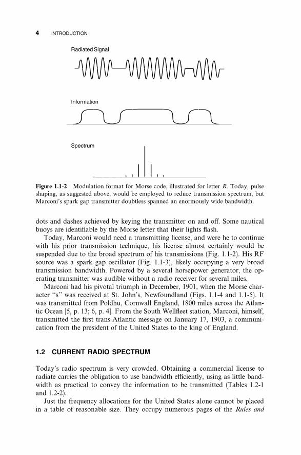
Figure 1.1-2 Modulation format for Morse code, illustrated for letter R. Today, pulseshaping, as suggested above, would be employed to reduce transmission spectrum, butMarconi’s spark gap transmitter doubtless spanned an enormously wide bandwidth.
dots and dashes achieved by keying the transmitter on and o¤. Some nauticalbuoys are identifiable by the Morse letter that their lights flash.
Today, Marconi would need a transmitting license, and were he to continuewith his prior transmission technique, his license almost certainly would besuspended due to the broad spectrum of his transmissions (Fig. 1.1-2). His RFsource was a spark gap oscillator (Fig. 1.1-3), likely occupying a very broadtransmission bandwidth. Powered by a several horsepower generator, the op-erating transmitter was audible without a radio receiver for several miles.
Marconi had his pivotal triumph in December, 1901, when the Morse char-acter ‘‘s’’ was received at St. John’s, Newfoundland (Figs. 1.1-4 and 1.1-5). Itwas transmitted from Poldhu, Cornwall England, 1800 miles across the Atlan-tic Ocean [5, p. 13; 6, p. 4]. From the South Wellfleet station, Marconi, himself,transmitted the first trans-Atlantic message on January 17, 1903, a communi-cation from the president of the United States to the king of England.
1.2 CURRENT RADIO SPECTRUM
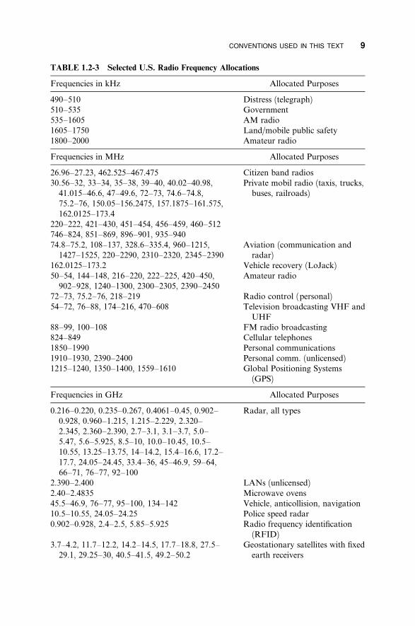
Today’s radio spectrum is very crowded. Obtaining a commercial license toradiate carries the obligation to use bandwidth e‰ciently, using as little band-width as practical to convey the information to be transmitted (Tables 1.2-1and 1.2-2).
Just the frequency allocations for the United States alone cannot be placedin a table of reasonable size. They occupy numerous pages of the Rules and

5CURRENT RADIO SPECTRUM
Figure 1.1-3 Joel Earl Hudson standing by Marconi’s spark gap transmitter in 1907.(Photo courtesy of Cape Cod National Seashore.)
Regulations of the Federal Communications Commission, and have hundreds offootnotes. Since frequent changes are made in the rules and regulations, thelatest issue always should be consulted [7, p. 1.8; 8].
As can be seen from Table 1.2-3, radio amateurs today enjoy many fre-quency allocations. This is due to the history of their pioneering e¤orts, partic-
Figure 1.1-4 Prime power for Marconi’s South Wellfleet transmitter. (Photo courtesy of
Cape Cod National Seashore.)
6 INTRODUCTION
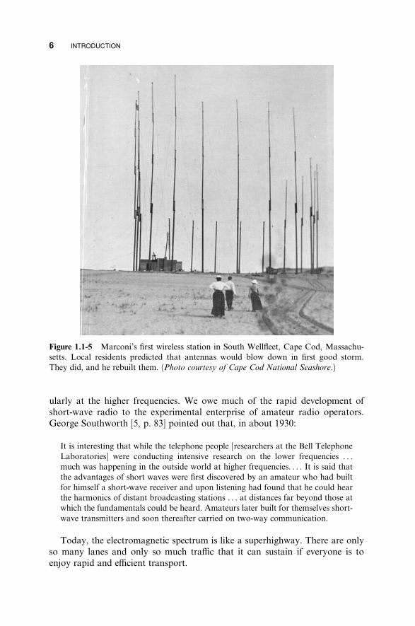
Figure 1.1-5 Marconi’s first wireless station in South Wellfleet, Cape Cod, Massachu-setts. Local residents predicted that antennas would blow down in first good storm.They did, and he rebuilt them. (Photo courtesy of Cape Cod National Seashore.)
ularly at the higher frequencies. We owe much of the rapid development ofshort-wave radio to the experimental enterprise of amateur radio operators.George Southworth [5, p. 83] pointed out that, in about 1930:
It is interesting that while the telephone people [researchers at the Bell TelephoneLaboratories] were conducting intensive research on the lower frequencies . . .much was happening in the outside world at higher frequencies. . . . It is said thatthe advantages of short waves were first discovered by an amateur who had builtfor himself a short-wave receiver and upon listening had found that he could hearthe harmonics of distant broadcasting stations . . . at distances far beyond those atwhich the fundamentals could be heard. Amateurs later built for themselves short-wave transmitters and soon thereafter carried on two-way communication.
Today, the electromagnetic spectrum is like a superhighway. There are onlyso many lanes and only so much tra‰c that it can sustain if everyone is toenjoy rapid and e‰cient transport.

7CURRENT RADIO SPECTRUM
Figure 1.1-6 Guglielmo Marconi (left) received the Nobel Prize for his wireless com-munication work. He is shown in a 1901 photo with assistant George Kemp shortlyafter a successful wireless transmission test. (Photo courtesy of Marconi, Ltd., UK.)
The simultaneous functioning of the intricate grid of radiation allocations,only a part of which are shown in Table 1.2-3, depend upon each user occupy-ing his or her precise frequency, modulation format, bandwidth, and e¤ectiveradiated power and, furthermore, not intruding on other frequency bands bygenerating spurious signals with his or her equipment. This is the task andchallenge of today’s high frequency engineering.
TABLE 1.2-1 General Frequency Band Designations
f l Band Description
30–300 Hz 104–103 km ELF Extremely low frequency300–3000 Hz 103–102 km VF Voice frequency3–30 kHz 100–10 km VLF Very low frequency30–300 kHz 10–1 km LF Low frequency0.3–3 MHz 1–0.1 km MF Medium frequency3–30 MHz 100–10 m HF High frequency30–300 MHz 10–1 m VHF Very high frequency300–3000 MHz 100–10 cm UHF Ultra-high frequency3–30 GHz 10–1 cm SHF Superhigh frequency30–300 GHz 10–1 mm EHF Extremely high frequency
(millimeter waves)
Source: From Reference [7, Section 1].

8 INTRODUCTION
TABLE 1.2-2 Microwave Letter Bands
f (GHz) Letter Band Designation
1–2 L band2–4 S band4–8 C band8–12.4 X band12.4–18 Ku band18–26.5 K band26.5–40 Ka band
Source: From Reference [9, p. 123].
1.3 CONVENTIONS USED IN THIS TEXT
This section lists the notational conventions used throughout this text.
Sections
Sections use a decimal number. To the left of the decimal is the chapter numberand to the right is the section number. Thus, 7.10 refers to the tenth section inChapter 7.
Equations
Equations have a number sequence that restarts in each section. Therefore, areference to (7.15-4) is directed to the fourth equation in Section 7.15.
Figures
Figure and table numbering also restarts in each section. Therefore, a referenceto Figure 7.24-2 relates to the second figure in Section 7.24.
Exercises
The exercises at the end of each chapter are numbered according to the sectionto which they most closely relate. For example, the exercise numbered E3.5-1 isthe first exercise relating to the material in Section 3.5. Material contained inprior sections also may be needed to complete the exercise.
Symbols
The principal symbols used in this text and the quantities that they representare listed in Appendix A. For example, c refers to the velocity of electromag-netic propagation in free space, while v refers to the velocity of propagation in
9CONVENTIONS USED IN THIS TEXT
TABLE 1.2-3 Selected U.S. Radio Frequency Allocations
Frequencies in kHz Allocated Purposes
490–510 Distress (telegraph)510–535 Government535–1605 AM radio1605–1750 Land/mobile public safety1800–2000 Amateur radio
Frequencies in MHz Allocated Purposes
26.96–27.23, 462.525–467.475 Citizen band radios30.56–32, 33–34, 35–38, 39–40, 40.02–40.98, Private mobil radio (taxis, trucks,41.015–46.6, 47–49.6, 72–73, 74.6–74.8, buses, railroads)75.2–76, 150.05–156.2475, 157.1875–161.575,162.0125–173.4
220–222, 421–430, 451–454, 456–459, 460–512746–824, 851–869, 896–901, 935–94074.8–75.2, 108–137, 328.6–335.4, 960–1215, Aviation (communication and1427–1525, 220–2290, 2310–2320, 2345–2390 radar)
162.0125–173.2 Vehicle recovery (LoJack)50–54, 144–148, 216–220, 222–225, 420–450, Amateur radio902–928, 1240–1300, 2300–2305, 2390–2450
72–73, 75.2–76, 218–219 Radio control (personal)54–72, 76–88, 174–216, 470–608 Television broadcasting VHF and
UHF88–99, 100–108 FM radio broadcasting824–849 Cellular telephones1850–1990 Personal communications1910–1930, 2390–2400 Personal comm. (unlicensed)1215–1240, 1350–1400, 1559–1610 Global Positioning Systems
(GPS)
Frequencies in GHz Allocated Purposes
0.216–0.220, 0.235–0.267, 0.4061–0.45, 0.902–0.928, 0.960–1.215, 1.215–2.229, 2.320–2.345, 2.360–2.390, 2.7–3.1, 3.1–3.7, 5.0–5.47, 5.6–5.925, 8.5–10, 10.0–10.45, 10.5–10.55, 13.25–13.75, 14–14.2, 15.4–16.6, 17.2–17.7, 24.05–24.45, 33.4–36, 45–46.9, 59–64,66–71, 76–77, 92–100
2.390–2.4002.40–2.483545.5–46.9, 76–77, 95–100, 134–14210.5–10.55, 24.05–24.250.902–0.928, 2.4–2.5, 5.85–5.925
3.7–4.2, 11.7–12.2, 14.2–14.5, 17.7–18.8, 27.5–29.1, 29.25–30, 40.5–41.5, 49.2–50.2
Radar, all types
LANs (unlicensed)Microwave ovensVehicle, anticollision, navigationPolice speed radarRadio frequency identification(RFID)
Geostationary satellites with fixedearth receivers

10 INTRODUCTION
TABLE 1.2-3 (Continued)
Frequencies in GHz Allocated Purposes
1.610–1626.5, 2.4835–2.5, 5.091–5.25, 6.7– Nongeostationary satellites, mo-7.075, 15.43–15.63 bile receivers (big LEO, global
phones)0.04066–0.0407, 902–928, 2450–2500, 5.725– Unlicensed industrial, scientific,5.875, 24–24.25, 59–59.9, 60–64, 71.5–72, and medical communication103.5–104, 116.5–117, 122–123, 126.5–127, devices152.5–153, 244–246
3.3–3.5, 5.65–5.925, 10–10.5, 24–24.25, 47– Amateur radio47.2
6.425–6.525, 12.7–13.25, 19.26–19.7, 31–31.3 Cable television relay27.5–29.5 Local multipoint TV distribution12.2–12.7, 24.75–25.05, 25.05–25.25 Direct broadcast TV (from satel-
lites)0.928–0.929, 0.932–0.935, 0.941–0.960, 1.850– Fixed microwave (public and pri-1.990, 2.11–2.20, 2.450–2.690, 3.7–4.2, vate)5.925–6.875, 10.55–10.68, 10.7–13.25, 14.2–14.4, 17.7–19.7, 21.2–23.6, 27.55–29.5, 31–31.3, 38.6–40
a medium for which the relative dielectric and permeability constants may begreater than unity.
Prefixes
Except where noted otherwise, this text uses the International System of Units(SI). Standard prefixes are listed in Table 1.3-1.
Fonts
The font types used throughout this text to connote variable types are listed inTable 1.3-2. Combinations of these representational styles are used to conveythe dual nature of some variables. For example, in Maxwell’s equation
~‘ �DD ¼ r
~DD is written in regular type because the equation applies to all time waveforms,~not just sinusoidal variations, and DD is also a vector quantity. On the other
hand, the Helmholtz equation is written
‘2~ ~EE þ k2EE ¼ 0

VECTORS AND COORDINATES 11
TABLE 1.3-1 Standard Prefixes
Prefix Abbreviation Factor
tera T 1012
giga G 109
mega M 106
kilo k 103
hecto h 102
deka da 10deci d 10�1
centi c 10�2
milli m 10�3
micro m 10�6
nano n 10�9
pico p 10�12
femto f 10�15
atto 10�18
~using italic type for the variable EE because this equation only applies for sinus-~oidal time variations, and therefore the components of the vector EE are phasor
quantities.Throughout this text, except where otherwise noted, the magnitudes of sinu-
soidal waveforms ðV ; I ;E;D;H;BÞ are peak values. To obtain root-mean-ffiffiffi square (rms) values, divide these values by
p2.
1.4 VECTORS AND COORDINATES
General vector representations are three dimensional. They can be described byany three-dimensional, orthogonal coordinate system in which each coordinatedirection is at right angles to the other two. Unless otherwise specified, rectan-
TABLE 1.3-2 Fonts Used in This Text to Identify Variable Types
Variable Type Font Examples
DC or general time-varying Regular type V; I;H;E;B;Dfunction (not sinusoidal)
Explicit general time variation Regular type, lower- vðtÞ; iðtÞcase
Explicit sinusoidal time variation Italic type, lowercase vðtÞ; iðtÞPhasors, impedance, admittance, Italic type V ; I ;H;E;B;D;Z;Ygeneral functions, and vari- f ðxÞ; gðyÞ; x; y; z;~xx; ~yy;~zzables, unit vectors ���������!
Vectors Arrow above ~EE; ~HH;~BB;~DD; ~EE; ~HH; ~BB; ~DDNormalized parameters Lowercase z ¼ Z=Z0, y ¼ Y=Y0
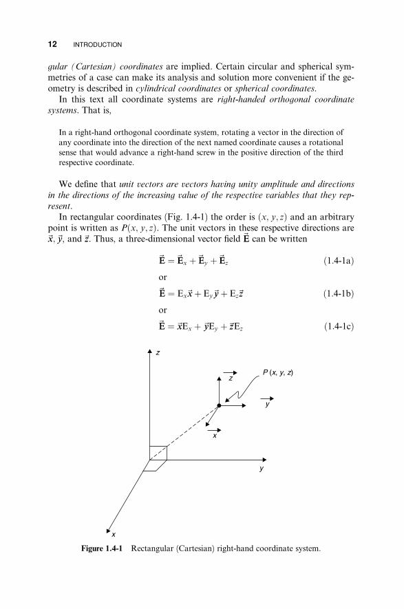
12 INTRODUCTION
gular (Cartesian) coordinates are implied. Certain circular and spherical sym-metries of a case can make its analysis and solution more convenient if the ge-ometry is described in cylindrical coordinates or spherical coordinates.
In this text all coordinate systems are right-handed orthogonal coordinate
systems. That is,
In a right-hand orthogonal coordinate system, rotating a vector in the direction ofany coordinate into the direction of the next named coordinate causes a rotationalsense that would advance a right-hand screw in the positive direction of the thirdrespective coordinate.
We define that unit vectors are vectors having unity amplitude and directions
in the directions of the increasing value of the respective variables that they rep-
resent.In rectangular coordinates (Fig. 1.4-1) the order is ðx; y; zÞ and an arbitrary
point is written as Pðx; y; zÞ. The unit vectors in these respective directions arexx; ~ zz. Thus, a three-dimensional vector field ~~ yy, and~ EE can be written
~ ~ ~ ~EE ¼ EEx þ EEy þ EEz ð1:4-1aÞor
~ ~ yyþ EzzzEE ¼ Exxxþ Ey~ ~ ð1:4-1bÞor
~EE ¼~ yyEy þ~xxEx þ ~ zzEz ð1:4-1cÞ
Figure 1.4-1 Rectangular (Cartesian) right-hand coordinate system.

VECTORS AND COORDINATES 13
Generally, the format of (1.4-1c) is used in this text. In the language of vectormathematics, rotating a unit vector~ yy isxx in the direction of another unit vector ~
xx into ~ xx� ~called crossing ~ yy, and this is written as ~ yy. This is a specific exampleof the vector cross product. The vector cross product can be applied to any twovectors having any magnitudes and relative orientations; but, in general, wemust take into account the product of their magnitudes and the angle betweenthem, as will be shown more specifically for the vector cross product in Chapter
xx; ~ zz form a right-hand orthogonal set of7. For present purposes, since ~ yy, and ~ unit vectors, we can express the right-handedness of their coordinate system by requiring that the following cross product relations apply:
xx� ~ zz~ yy ¼~ ð1:4-2aÞyy�~ xx~ zz ¼~ ð1:4-2bÞzz�~ yy~ xx ¼ ~ ð1:4-2cÞ
Notice that the vector cross product yields a new vector that is orthogonal to the
plane of the crossed vectors and in a direction that would be taken by the advance
of a right-hand screw when the first vector is crossed into the second.Also notice that for a right-hand coordinate system any coordinate unit vector
can be crossed into the next named coordinate vector to yield the direction of
positive increase of the remaining coordinate, beginning with any coordinate. Forexample ðx; y; zÞ, ðy; z; xÞ, or ðz; x; yÞ all satisfy the right-hand advancing rule,as specified by (1.4-2a) to (1.4-2c).
The cylindrical coordinate system is shown in Figure 1.4-2. The order ofcoordinate listing is ðr;j; zÞ and the unit vectors are~ jj, and ~rr;~ zz, which satisfy
Figure 1.4-2 Cylindrical right-hand coordinate system.

14 INTRODUCTION
Figure 1.4-3 Spherical right-hand coordinate system.
the same sequential cross-product rules as do rectangular coordinates, namely~ jj ¼~ jj�~ rr, and~ rr ¼~rr�~ zz,~ zz ¼~ zz�~ jj.
The spherical coordinate system is shown in Figure 1.4-3. The order of co-rr; yy, and~ordinate listing is ðr; y;jÞ and the unit vectors are~~ jj, which satisfy the
jj�~ ~sequential cross-product rules ~ ~ jj, yy�~ rr, and ~ rr ¼ yy. Note thatrr� yy ¼~ ~ jj ¼~this r is not the same as the r used in cylindrical coordinates.
1.5 GENERAL CONSTANTS AND USEFUL CONVERSIONS
There are several values of physical constants, conversion factors, and identitiesuseful to the practice of microwave engineering. For ready reference, a selec-tion of them is printed on the inside covers of this text.
REFERENCES
1. Webster’s Third New International Dictionary, G. & C. Meriam Co Springfield,Massachusetts, 1976. Copy of the International Morse Code, including special char-
acters. See Morse code.
2. Don Bishop, ‘‘Who invented radio?’’ RF Design, February, 2002, p. 10.
3. James Clerk Maxwell, Electricity and Magnetism, 3rd ed., Oxford, 1892, Part II.
4. United States Navy, History of Communications—Electronics in the United States
Navy, U.S. Government Printing O‰ce, Washington, DC, 1963.
5. George C. Southworth, Forty Years of Radio Research, Gordon and Breach, NewYork, 1962.

REFERENCES 15
6. Deryck Henley, Radio Receiver History and Instructions, Flights of Fancy, Lea-mington Spa, Warks England, 2000. This reference is the set of instructions providedwith a modern crystal radio kit.
7. Reference Data for Radio Engineers, 5th ed., Howard W. Sams, New York, 1974.New editions are available.
8. Bennet Z. Kobb, RF Design Delivers for Design Engineers . . . from 30 MHz to 300GHz, March 2000. Published in RF Design magazine.
9. George W. Stimson, Introduction to Airborne Radar, Hughes Aircraft Company, ElSegundo, CA, 1983.

CHAPTER 2
Review of AC Analysis andNetwork Simulation
Alternating current (AC) circuit analysis is the basis for the high frequencytechniques that are covered in subsequent chapters and the subject of this text.It is assumed that all readers already have been introduced to AC analysis.However, it has been the author’s teaching experience that a review is usuallyappreciated because it provides an opportunity to put into perspective the fun-damentals needed for the fluent application of AC analysis, a skill essential tothe high frequency engineer.
The AC analysis makes use of complex numbers to calculate and keep trackof the relative magnitudes and phases of voltages and currents. For this reason,a summary of complex mathematics is included in Appendix B. One whocomfortably reads this chapter and Appendix B can follow the remainder ofthis book. The properties of complex equations, such as the bilinear transfor-mation that defines the Smith chart, were developed by mathematicians prob-ably without any practical application considerations [1].
2.1 BASIC CIRCUIT ELEMENTS
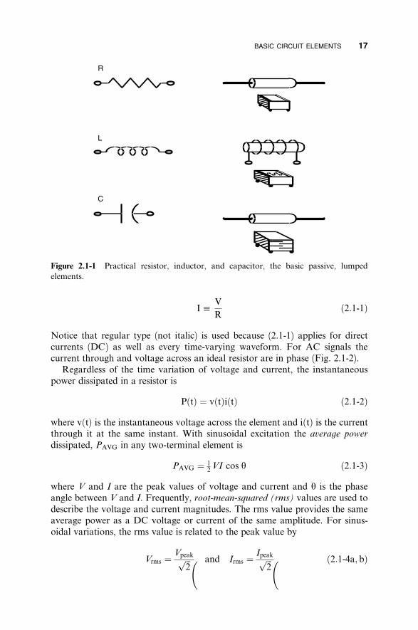
The basic building blocks of electric circuits are the resistor R, the inductorL, and the capacitor C (Fig. 2.1-1). At high frequencies these elements do notbehave as pure R, L, and C components but have additional resistances andreactances called parasitics. More about parasitics later in the chapter.
The Resistor
The resistor passes a current I equal to the applied voltage divided by its resis-
tance. This can be considered a definition of the resistor. Mathematically, this iswritten
High Frequency Techniques: An Introduction to RF and Microwave Engineering, By Joseph F. White. ISBN 0-471-45591-1 6 2004 John Wiley & Sons, Inc.
16
BASIC CIRCUIT ELEMENTS 17
Figure 2.1-1 Practical resistor, inductor, and capacitor, the basic passive, lumpedelements.
VI1 ð2:1-1Þ
R
Notice that regular type (not italic) is used because (2.1-1) applies for directcurrents (DC) as well as every time-varying waveform. For AC signals thecurrent through and voltage across an ideal resistor are in phase (Fig. 2.1-2).
Regardless of the time variation of voltage and current, the instantaneouspower dissipated in a resistor is
PðtÞ ¼ vðtÞiðtÞ ð2:1-2Þ
where vðtÞ is the instantaneous voltage across the element and iðtÞ is the currentthrough it at the same instant. With sinusoidal excitation the average power
dissipated, PAVG in any two-terminal element is
PAVG ¼ 1VI cos y ð2:1-3Þ2
where V and I are the peak values of voltage and current and y is the phaseangle between V and I. Frequently, root-mean-squared (rms) values are used todescribe the voltage and current magnitudes. The rms value provides the sameaverage power as a DC voltage or current of the same amplitude. For sinus-oidal variations, the rms value is related to the peak value by
Vpeak IpeakVrms ¼ p
2ffiffiffi and Irms ¼ p
2ffiffiffi ð2:1-4a; bÞ

18 REVIEW OF AC ANALYSIS AND NETWORK SIMULATION
Figure 2.1-2 Ideal resistor R has AC voltage V and current I in phase.
and
PAVG ¼ VrmsIrms cos y ð2:1-5Þ
Note that, according to our convention, the variables are in italic type to indi-cate that the time waveform is sinusoidal. For an ideal resistor, y ¼ 0� and theinstantaneous power dissipated in the resistor is equal to the product vðtÞiðtÞ.Throughout this text, except where otherwise specified, peak values are used for
voltage, current, and field amplitudes.
Ohm’s Law
Ohm’s law applies to all voltage waveforms across a resistor, and states thatcurrent through a resistor is directly proportional to the applied voltage and in-
versely proportional to its resistance:
vi ¼ ð2:1-6Þ
R
where v is in volts, R in ohms, and i in amperes.

BASIC CIRCUIT ELEMENTS 19
Ohm’s law is a linear relationship (current is proportional only to the firstpower of voltage) and is valid for all voltage and current levels that do notchange the value of resistance. It does not apply, for example, at very highvoltages that cause an arc over of the resistor and/or high currents that causethe resistor to change its value due to overheating.
The Inductor
In contrast to the resistor, the ideal inductor L, cannot dissipate power. Thegeneral relationship between voltage across and current through it is
diðtÞvðtÞ ¼ L ð2:1-7Þ
dt
The instantaneous current through the inductor is obtained by integratingð viðtÞ ¼ vðtÞ dt ð2:1-8Þ
0
The amount of energy, UL, stored in an inductor is equal to the time integral ofthe power applied to it, vðtÞ � iðtÞ, to establish a current i in it from an initialcondition at which iðt ¼ 0Þ ¼ 0:
ð t ð t dðiÞUL ¼ vðtÞ � iðtÞ dt ¼ L � iðtÞ dt ð2:1-9Þ
dt0 0
which, on integrating, gives the instantaneous energy stored as
UL ¼ 1 L½iðtÞ�2 ð2:1-10Þ2
Current through the inductor for all waveforms is proportional to the integralof the applied voltage. With a sinusoidally applied voltage, vðtÞ ¼ V0 cos ot,the current I is obtained by integration, noting that the constant of integra-tion corresponds to a DC term that can be neglected for an AC solution (Fig.2.1-3). Thus,
ð 1 V0 sin ot
I ¼ V0 cos ot dt ¼ ð2:1-11ÞL oL
From Ohm’s law current divided by voltage has the dimensions of ohms,therefore oL must have the dimensions of ‘‘ohms.’’ This will be used shortlyin the definition of complex impedance. There is no power dissipated in aninductor. For AC excitation, the phase angle, y, between voltage and current is�90� and the power dissipated, PDiss, is given by
PDiss ¼ 1 jV j jI j cos y ¼ 0 ð2:1-12Þ2

20 REVIEW OF AC ANALYSIS AND NETWORK SIMULATION
Figure 2.1-3 Sinusoidal current I through inductor lags voltage V by 90�.
The Capacitor
Like the inductor, the capacitor, C, cannot dissipate power. Rather it storescharge and, in so doing, stores energy. By definition, the capacitance C isdefined as the ratio of instantaneous charge q to the instantaneous voltage vðtÞat which the charge is stored:
qC1 ð2:1-13Þ
vðtÞWith a current into the capacitor the stored charge increases. The time rate ofchange of q is equal to this current. Multiplying both sides of (2.1-13) by v andthen di¤erentiating with respect to t give
qq qvðtÞ¼ iðtÞ ¼ C ð2:1-14Þqt qt

BASIC CIRCUIT ELEMENTS 21
Figure 2.1-4 Ideal capacitor C is also a dissipationless component. For sinusoidalexcitation, current I leads applied voltage V by 90�.
Integrating with respect to t gives
ð 1
vðtÞ ¼ i dt ð2:1-15ÞC
When a direct current is passed into a capacitor, the voltage across the ca-pacitor’s terminals ‘‘integrates’’ the direct current flow from the time when thecapacitor had zero volts (Fig. 2.1-4). The capacitor does not dissipate power,but rather stores energy. The energy storage can be considered the presence ofcharge in a potential field or the establishment of an electric field between thecapacitor plates. For an initially uncharged capacitor, vð0Þ ¼ 0, the integralwith respect to time of the instantaneous power delivered to the capacitor,vðtÞ � iðtÞ, is the stored energy UC in the capacitor when it is charged to a
22 REVIEW OF AC ANALYSIS AND NETWORK SIMULATION
voltage V:
ð ð v v dvUC ¼ vðtÞiðtÞ dt ¼ C vðtÞ dt ð2:1-16Þ
dt
which, upon integrating, gives the instantaneous stored energy as
UC ¼ 1C½vðtÞ�2 ð2:1-17Þ
0 0
2
This result does not depend upon the voltage or current waveforms used tostore the charge. When a sinusoidal voltage is applied, the current waveform isalso sinusoidal and advanced by 90�:
vðtÞ ¼ V0 cos ot ð2:1-18ÞqvðtÞ
iðtÞ ¼ C ¼ �V0oC sin ot ð2:1-19Þqt
From (2.1-19) it follows that 1=oC has the dimensions of ohms, as did oL.These facts prompt the definition of complex impedance, to be discussedshortly.
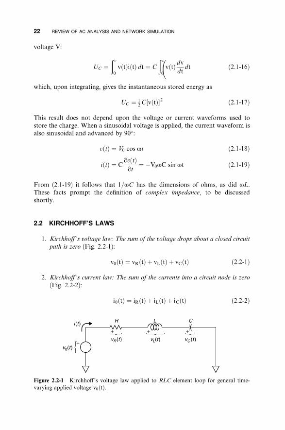
2.2 KIRCHHOFF’S LAWS
1. Kirchho¤ ’s voltage law: The sum of the voltage drops about a closed circuit
path is zero (Fig. 2.2-1):
v0ðtÞ ¼ vRðtÞ þ vLðtÞ þ vCðtÞ ð2:2-1Þ
2. Kirchho¤ ’s current law: The sum of the currents into a circuit node is zero
(Fig. 2.2-2):
i0ðtÞ ¼ iRðtÞ þ iLðtÞ þ iCðtÞ ð2:2-2Þ
Figure 2.2-1 Kirchho¤ ’s voltage law applied to RLC element loop for general time-varying applied voltage v0ðtÞ.

ALTERNATING CURRENT (AC) ANALYSIS 23
Figure 2.2-2 Kirchho¤ ’s current law applied to node for general time-varying currenti0ðtÞ.
Kirchho¤ ’s laws apply instantaneously for all waveforms. For the series circuitof Figure 2.2-1, the applied voltage is equal to the voltage drops across thethree element types. The current is continuous in the loop. Using the voltage–current relations of (2.1-6), (2.1-7), and (2.1-15) gives
ð di 1
v0ðtÞ ¼ Riþ L i dt ð2:2-3Þdt
þC
2.3 ALTERNATING CURRENT (AC) ANALYSIS
In electrical engineering it would be nice to have the complete solution in timefor vðtÞ and iðtÞ whenever a circuit is analyzed in order that both the transientand steady-state behavior would be available. However, we usually find thatthe steady-state behavior of circuits with sinusoidal excitation is adequate,particularly since it can be obtained with much greater computational econ-omy, as will be seen shortly. If a sinusoidal voltage or current excitation isapplied to a network consisting of linear R, L, and C elements the resultingcurrents and voltages usually approach steady-state sinusoidal waveformswithin a few RF cycles. Circuits having very high Q, to be discussed in the nextchapter, require longer times, so some judgment is necessary regarding thetransient e¤ects in AC networks.
Nevertheless, ignoring transient e¤ects and accepting a steady-state solutionfor an AC network is usually su‰cient. Referring to (2.2-3), we notice thatintegral and di¤erential expressions occur in the network equation due to thepresence of L and C elements. However, the steady-state voltage and currentsolutions of the network are comprised solely of sinusoidal functions at a com-mon frequency because all integrals and derivatives of sinusoidal functions are
also sinusoidal functions at the same frequency (but displaced in phase byG90�).For example, if we apply a voltage
vðtÞ ¼ V0 cos ot ð2:3-1Þ

� �
� � � �
� � � �
� � � �
24 REVIEW OF AC ANALYSIS AND NETWORK SIMULATION
to the network in Figure 2.2-1, the resulting current eventually will approach the
steady-state waveform
iðtÞ ¼ I0 cosðot� jÞ ð2:3-2Þ
The steady-state solution that we seek is to solve for I0 and j in terms of V0.Substituting this assumed solution into (2.2-3) and performing the indicateddi¤erentiation and integration gives
1V0 cos ot ¼ I0 R cosðot� jÞ � oL sinðot� jÞ þ sinðot� jÞ ð2:3-3Þ
oC
This equation applies for all time t after su‰cient time has passed to allowtransients to die out (since we ignored the constant of integration associatedwith the third term). In particular, consider the time for which ot ¼ p=2 ¼ 90�.Then, recognizing that cosð90� � jÞ ¼ sin j and sinð90� � jÞ ¼ cos j, (2.3-3)becomes
10 ¼ I0 R sin j� oL� cos j ð2:3-4aÞ
oC
and solving for j,
oL� 1=oCtan j ¼ ð2:3-4bÞ
R
oL� 1=oCj ¼ tan�1 ð2:3-4cÞ
R
If we substitute t ¼ 0 into (2.3-3) and recognize that the value for j in (2.3-4c)allows determination of cos j and sin j, the result is
1V0 ¼ I0 R cos jþ oL� sin j
oC
V0I0 ¼ ð2:3-5Þ
R cos jþ ½oL� 1=oC � sin j
V0¼qffiffiffiffiffiffiffiffiffiffiffiffiffiffiffiffiffiffiffiffiffiffiffiffiffiffiffiffiffiffiffiffiffiffiffiffiffiffiffiffiffi R2 þ ½oL� 1=oC �2
The expression in the denominator has the value of the hypotenuse of a righttriangle, as shown graphically in Figure 2.3-1.

� �
ALTERNATING CURRENT (AC) ANALYSIS 25
Figure 2.3-1 Orthogonal relationship between resistance R and reactance X in AC cir-cuit. Note that if X is positive, j is positive, which means that I lags V, consistent with(2.3-2).
The final expression of (2.3-5) appears to be in the form of Ohm’s law withresistance replaced by a quantity that includes the ‘‘impeding’’ e¤ects of L andC on current flow. Also, (2.3-4c) shows how L and C a¤ect the phase relationbetween v and i. Both of these e¤ects can be accounted for by defining a com-
plex impedance Z.The complex impedance Z of a series RLC combination has a real part equal
to the resistance R and an imaginary part equal to j times the net reactance,
X ¼ ðoL� 1=oCÞ. Thus,
1Z ¼ Rþ jX ¼ Rþ j oL� ¼ jZjJj ð2:3-6aÞ
oC
where sffiffiffiffiffiffiffiffiffiffiffiffiffiffiffiffiffiffiffiffiffiffiffiffiffiffiffiffiffiffiffiffiffiffiffiffiffiffiffi � �21jZj ¼ R2 þ oL� ð2:3-6bÞoC
�1 oL� 1=oCj ¼ tan ð2:3-6cÞ
R
and o ¼ 2pf where f is the operating frequency in hertz.The foregoing solution to (2.3-6) required considerable mathematical ma-
nipulation, particularly in view of the fact that only the magnitude I0 and phasej were unknown. We already knew that the form of iðtÞ would be a sinusoidwith time variation ot. Clearly, an extension of Ohm’s law to render the sameresults directly would o¤er a profound improvement in the e‰ciency of RLCcircuit analysis.

26 REVIEW OF AC ANALYSIS AND NETWORK SIMULATION
Figure 2.3-2 Voltage and current phasorsfor solution to network in Figure 2.2-1where vðtÞ ¼ V0 cos ot.
Ohm’s Law in Complex Form
Ohm’s law for AC circuits can be written in complex form as
VI ¼ ð2:3-7Þ
Z
where V and I are complex quantities called phasors and Z is the AC imped-ance defined in (2.3-6a).
As can be seen in Figure 2.3-2, the voltage and current are now representedby complex quantities, having real and imaginary parts. They are vectors inthe complex plane. However, since electric and magnetic fields are three-dimensional vectors in space, to avoid confusing voltage and current quantitieswith fields in space, the Institute of Electrical and Electronic Engineers (IEEE)
recommends using the term phasor for the complex representations of V and I, as
well as for the complex representations of sinusoidally varying field magnitudes.This convention will be assumed throughout this text, except where specificallynoted otherwise. A review of complex mathematics is given in Appendix B.
2.4 VOLTAGE AND CURRENT PHASORS
The application of complex numbers to RLC circuit analysis is to represent thesinusoidal voltage vðtÞ by a phasor voltage V and the resulting current iðtÞ bya phasor current I. These phasor quantities are complex numbers, having realand imaginary parts. Complex voltage and current phasors are mathematical
artifices that do not exist in reality. They are vectors in the complex plane thatare useful in analyzing AC circuits. Phasors do not rotate; they are fixedposition vectors whose purpose is to indicate the magnitude and phase of thesinusoidal waveforms that they represent.
However, if they were rotated counterclockwise in the complex plane at therate of o radians per second (while maintaining their angular separation, j)
VOLTAGE AND CURRENT PHASORS 27
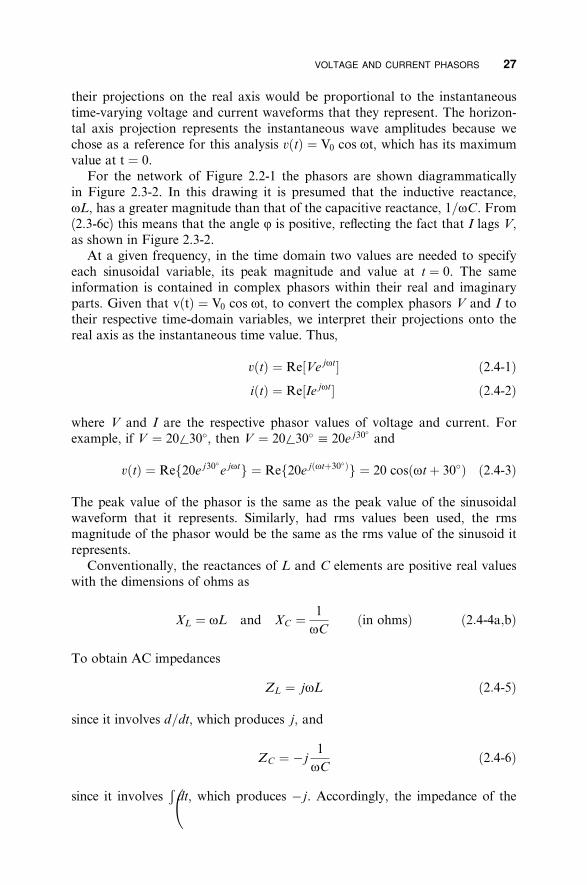
their projections on the real axis would be proportional to the instantaneoustime-varying voltage and current waveforms that they represent. The horizon-tal axis projection represents the instantaneous wave amplitudes because wechose as a reference for this analysis vðtÞ ¼ V0 cos ot, which has its maximumvalue at t ¼ 0.
For the network of Figure 2.2-1 the phasors are shown diagrammaticallyin Figure 2.3-2. In this drawing it is presumed that the inductive reactance,oL, has a greater magnitude than that of the capacitive reactance, 1=oC. From(2.3-6c) this means that the angle j is positive, reflecting the fact that I lags V,as shown in Figure 2.3-2.
At a given frequency, in the time domain two values are needed to specifyeach sinusoidal variable, its peak magnitude and value at t ¼ 0. The sameinformation is contained in complex phasors within their real and imaginaryparts. Given that vðtÞ ¼ V0 cos ot, to convert the complex phasors V and I totheir respective time-domain variables, we interpret their projections onto thereal axis as the instantaneous time value. Thus,
vðtÞ ¼ Re½Ve jot� ð2:4-1ÞiðtÞ ¼ Re½Ie jot� ð2:4-2Þ
where V and I are the respective phasor values of voltage and current. Forexample, if V ¼ 20J30�, then V ¼ 20J30� 1 20e j30� and
jotvðtÞ ¼ Ref20e j30�e g ¼ Ref20e jðotþ30�Þg ¼ 20 cosðotþ 30�Þ ð2:4-3Þ
The peak value of the phasor is the same as the peak value of the sinusoidalwaveform that it represents. Similarly, had rms values been used, the rmsmagnitude of the phasor would be the same as the rms value of the sinusoid itrepresents.
Conventionally, the reactances of L and C elements are positive real valueswith the dimensions of ohms as
1XL ¼ oL and XC ¼ ðin ohmsÞ ð2:4-4a;bÞ
oC
To obtain AC impedances
ZL ¼ joL ð2:4-5Þ
since it involves d=dt, which produces j, and
1ZC ¼ � j ð2:4-6Þ
oCÐ since it involves dt, which produces � j. Accordingly, the impedance of the

� � 28 REVIEW OF AC ANALYSIS AND NETWORK SIMULATION
series RLC circuit in Figure 2.2-1 is written
1Z ¼ Rþ jðXL � XCÞ ¼ Rþ j oL� ð2:4-7Þ
oC
Kirchho¤ ’s voltage and current laws also apply to the phasor forms of V and I.With these definitions and the rules for complex number manipulation, cir-
cuits of arbitrary complexity can be analyzed in the phasor domain to solve forthe relationships between voltage and currents at any given frequency in a net-work of linear elements. Then (2.4-1) and (2.4-2) can be used if the instanta-neous time functions are required.
2.5 IMPEDANCE
Estimating Reactance
The reactance of an inductor, L, is oL, and the reactance of a capacitor, C, is
1=oC. Reactances have the dimensions of ohms.A practicing RF and microwave engineer should be able to estimate the
reactances of inductors and capacitors quickly. This need arises, for example,in order to assess their e¤ects on a circuit, the realizability of a proposed tuningmethod or for a variety of other design and analysis purposes.
Memorization of two reactance values and a simple scaling method permitsthese estimates to be made mentally, yielding a close approximation, evenwithout a calculator. The reactance of an inductor, L, is given by
XL ¼ oL where o ¼ 2pf ð2:5-1Þ
At 1 GHz the reactance magnitude of a 1-nH inductor is 6.28 W. Therefore, thereactance of any other inductor at any other frequency is given by
XL ¼ 6:28 fL ð f in gigahertz;L in nanohenriesÞ ð2:5-2Þ
By remembering the 6.28 W/(nH-GHz) scale factor, other inductive reactancevalues are quickly estimated. For example, a 3-nH inductor at 500 MHz has areactance
XL ¼ ð6:28Þð0:5Þð3Þ ¼ 9:42 W ð2:5-3Þ
Similarly, the reactance of a capacitor, C, is given by
1 159XC ¼ ¼ ð f in gigahertz;C in picofaradsÞ ð2:5-4Þ
oC fC
Thus, remembering that 1 pF yields 159 W at 1 GHz allows other capacitive

IMPEDANCE 29
reactance values to be estimated. For example, a 2-picofarad (pF) capacitorhas a reactance at 3 GHz of
159 WXC ¼ ¼ 26:5 W ð2:5-5Þð2Þð3Þ
Of course, one must also remember that inductive reactance is directly propor-
tional to f and L while capacitive reactance is inversely proportional to f and
C. In this way, memorizing the 1-GHz reactances of a 1-nH inductor and 1-pFcapacitor allows simple scaling of other values.
XL ¼ 6:28fL ðWÞ ð2:5-6ÞXC ¼ 159=fC ðWÞ ð2:5-7Þ
where f is in GHz, L in nH, and C in pF. Note that the reactances requirea preceding j factor to become impedances. Thus, oL is the reactance of aninductor, L, while joL is its impedance. Similarly, 1=oC is the reactance of acapacitor, while � j=oC is its impedance.
Addition of Series Impedances
Practical circuits may have very complex interconnections. To analyze them, itis necessary to be able to combine multiple impedance and admittance valuesto find equivalent, overall values.
The total impedance of elements in series is obtained by adding their real and
imaginary parts, respectively.
Referring to Figure 2.5-1, if
Z1 ¼ aþ jb and Z2 ¼ cþ jd ð2:5-8Þ
then,
ZT ¼ Z1 þ Z2 ¼ ðaþ cÞ þ jðbþ dÞ ð2:5-9Þ
For example, if
Z1 ¼ 5þ j9 W and Z2 ¼ 3� j15 W
Figure 2.5-1 Series addition of impedances, ZT ¼ Z1 þ Z2.

30 REVIEW OF AC ANALYSIS AND NETWORK SIMULATION
then
Z1 þ Z2 ¼ ð5þ 3Þ Wþ jð9� 15Þ W ¼ 8� j6 W
2.6 ADMITTANCE
Admittance Definition
The admittance Y is the complex reciprocal of impedance Z. Its unit is expressedeither as the siemen or the mho (which is ‘‘ohm’’ spelled backward) and itssymbol is the Greek capital omega written upside down ð WÞ:
Y ¼ 1=Z ¼ G þ jB ð2:6-1Þ
where G is the conductance and B is the susceptance of Y.The susceptance of an inductor is
1 1BL ¼ ¼ ð2:6-2Þ
XL oL
and the admittance of an inductor is
1 1 � j� jBL ¼ ¼ ¼ ð2:6-3ÞjXL joL oL
Similarly, the susceptance of a capacitor is
1 1BC ¼ ¼ ¼ oC ð2:6-4Þ
XC 1=oC
and the admittance of a capacitor is
1 1jBC ¼ ¼ ¼ joC ð2:6-5Þ� jXC � j=oC
Addition of Parallel Admittances
The total admittance of elements in parallel is obtained by adding the real and
imaginary parts of their admittances, respectively.Frequently, one is given the impedances of elements that are in parallel. To
determine the total admittance, find the equivalent admittances of each elementand add them together. The reader is cautioned that one cannot form theadmittance simply by adding together the reciprocals of the resistance andreactance parts of an impedance. Rather, it is necessary to find the complex

ADMITTANCE 31
Figure 2.6-1 Parallel addition of admittances, YT ¼ Y1 þ Y2.
reciprocal of the impedance, which is the equivalent admittance. Thus, if theelement values are expressed initially in impedance, first convert to admittance,then perform the addition of real and imaginary parts (Fig. 2.6-1).
1 1ZT ¼
YT
¼Y1 þ Y2
ð2:6-6Þ
Ohm’s law for AC circuits can also be written in terms of admittance,
I ¼ VY ð2:6-7Þ
where, as before, V and I are phasor quantities and Y is admittance.For example, suppose we wish to find the total equivalent impedance, ZT , of
a pair of elements in parallel given their individual impedances, Z1 and Z2 (Fig.2.6-2).
Assume that Z1 ¼ 5þ j8 W and Z2 ¼ 3� j5 W. The first step is to convertthese to polar form:
Z1 ¼ 9:43J58� W and Z2 ¼ 5:83J�59:0� W
Then find their equivalent admitances (the complex reciprocals):
Y1 ¼ 1=Z1 ¼ 0:106J�58�
W
and Y2 ¼ 1=Z2 ¼ 0:172J59�
W
Next convert to rectangular form.
Figure 2.6-2 Parallel admittance combination example.

32 REVIEW OF AC ANALYSIS AND NETWORK SIMULATION
Y1 ¼ 0:056� j0:090
W
Y2 ¼ 0:089þ j0:147
W
Add the real and imaginary parts, respectively:
YT ¼ Y1 þ Y2 ¼ 0:145þ j0:057
To find ZT , convert YT to polar form:
W
ZT ¼ 1=YT ¼ 1=ð0:156J21:46�Þ W¼ 6:41J�21:46� W
¼ 5:97� j2:35 W
The Product over the Sum
Generally, to combine impedances in parallel one must first convert them toadmittances, add the admittances together to form the total admittance, thenconvert this admittance to an impedance value, as was just demonstrated.However, when only two parallel elements are to be combined (or two admit-tances in series) a short cut results by forming the product over the sum. The
total impedance of two parallel impedances equals the product of the individual
impedances divided by their sum.The validity of this rule can be shown by performing the combination in
general terms and observing the result:
YT ¼ Y1 þ Y2
1 1 1¼Z1
þZT Z2 ð2:6-8Þ
Z1Z2 ¼ ZTðZ1 þ Z2ÞZ1Z2
ZT ¼Z1 þ Z2
Using the values in the previous example, Z1 ¼ 5þ j8 W and Z2 ¼ 3� j5 W,
ð9:43J58�Þð5:83J�59�ÞZT ¼ W
8þ j3
55J�1�¼ ¼ 6:44J�21:56� W8:54J20:56�
¼ 5:99� j2:37 W
The same procedure applies for finding the total admittance of two admittancesin series. Specifically, form their product and divide by their sum.

DECIBELS, dBW, AND dBm 33
2.7 LLFPB NETWORKS
Up until now, the networks that we have described are composed of LLFPBelements to which AC analysis can be applied directly. The acronym for thesenetworks derives from the following list of their properties. Namely, they
L: are small compared to a wavelength (lumped).
L: respond linearly to excitations (linear).
F: are of finite value (finite).
P: do not generate power (passive).
B: have the same behavior for currents in either direction (bilateral).
Thus, they are called lumped, linear, passive, finite, bilateral (LLFPB) elements.We shall describe additional means to evaluate networks that do not satisfy allof these criteria. For example, circuits whose dimensions are large compared toa wavelength do not satisfy the lumped criterion. Circuits containing transistorsare neither passive nor bilateral.
2.8 DECIBELS, dBW, AND dBm
Logarithms (Logs)
In wireless engineering, radio signals may be transmitted over miles of distancewith substantial diminution of their signal strengths. Then they may be ampli-fied by factors of thousands or millions of times so that their information canbe heard in an audio speaker, viewed on a television screen, or employed in adigital processor. To handle the large signal ratios involved, it is easier to rep-resent them as powers of 10 (logarithms). This measure employs the decibel
scale. It is insightful to review some mathematical background when applyingthe decibel measures that will be described shortly.
The logarithm of Y to the base X is the power L to which X must be raised to
give Y. Thus,
Y ¼ X L ð2:8-1Þ
For example, if we choose base 10, then X ¼ 10 and
Y ¼ 10L
Table 2.8-1 lists sample values of base 10 logarithms.
TABLE 2.8-1 Selected Values of Y and L for Base 10 Logarithms
Y 1000 100 20 10 2 1 1/2 1/10 1/20 0.01 0.001Y 103 102 101:3 101 100:3 100 10�0:3 10�1 10�1:3 10�2 10�3
L 3 2 1.3 1 0.3 0 �0.3 �1 �1.3 �2 �3

34 REVIEW OF AC ANALYSIS AND NETWORK SIMULATION
Multiplying by Adding Logs
To multiply numbers having the same base, write down the base and add their
logs. For example,
10� 1000 ¼ ð101Þð103Þ ¼ 101þ3 ¼ 104 ¼ 10;000
and
100� 2� 5 ¼ ð102Þð100:3Þð100:7Þ ¼ 103 ¼ 1000
Dividing by Subtracting Logs
To divide two numbers having the same base, write down the base and subtract
the exponent of the denominator from the exponent of the numerator. Forexample, 103=102 ¼ 103�2 ¼ 101 ¼ 10.
Zero Powers
Any number divided by itself, except zero, must equal unity. Regardless of thebase, use of logarithms must produce this same result. As a consequence it fol-lows that: The zero power of any number, except zero, is 1. For example,
10=10 ¼ 101�1 ¼ 100 ¼ 1
17=17 ¼ 171�1 ¼ 170 ¼ 1
459=459 ¼ 4591�1 ¼ 4590 ¼ 1
Bel Scale
The convenience of multiplying by adding logarithms as well as representingvery large numbers by their logarithms first prompted the use of the Bel scale
(named after its originator), which was simply the logarithm to the base 10of the number. This proper name remains embedded in the present decibel
nomenclature.
Y ðin belsÞ ¼ log10ðYÞ ð2:8-2Þ
Accordingly,
100 ðin belsÞ ¼ 2 bel
10 ðin belsÞ ¼ 1 bel
2 ðin belsÞ ¼ 0:3 bel
1 ðin belsÞ ¼ 0 bel

DECIBELS, dBW, AND dBm 35
1 ðin belsÞ ¼ �0:3 bel2
1 ðin belsÞ ¼ �1 bel10
Decibel Scale
The Bel scale was quickly recognized as a useful innovation, but its steps wereinconveniently large, an increase of 1 bel being a factor of 10. This objectionwas accommodated by a transition to the decibel (dB) scale.
Electrical engineers took a further step. Inherently, bels and decibels aresimply means of expressing ratios between similar quantities. However, inelectrical engineering, decibels are defined to be the ratio of two values of elec-
trical power:
P=P0 ðin decibelsÞ ¼ 10 logðP=P0) ð2:8-3Þ
where, henceforth in this text, ‘‘log’’ shall represent the logarithm to the base 10and ‘‘ln’’ shall represent the logarithm to the base e. Because power is propor-tional to the square of voltage (whether rms or peak), the ratio of two voltages
or currents referenced to the same impedance level is defined as
V=V0 ðin decibelsÞ ¼ 20 logðV=V0Þ ð2:8-4Þ
Obviously, the decibel value is just 10 times the Bel scale. Thus, a factor of 10in power is 10 dB, a factor of 2 is 3 dB (more precisely 3.01 dB), and the valueof unity remains 0 dB.
In using decibels, one need only memorize the logarithms of numbers be-tween 1 and 10. In fact, for most purposes, knowing the values correspondingto 0.5, 1, 2, 3, and 10 dB is usually su‰cient for most estimating purposes(Table 2.8-2).
Often one can deduce the decibel value of a number from the decibel valuesknown for other quantities. For example, since 2� 5 ¼ 10, and since the factor2 corresponds to 3 dB, and the factor 10 is 10 dB, it follows that the factor5 corresponds to 10 dB� 3 dB ¼ 7 dB. Similarly, if one remembers that thefactor 1.2 corresponds to about 0.8 dB, then the factor 1:2� 1:2 ¼ 1:22 ¼ 1:44corresponds to about 0.8 dBþ 0.8 dB ¼ 1.6 dB.
Decibels—Relative Measures
For the system example in Figure 2.8-1, using numeric multiplication wecalculate
POUT=PIN ¼ 0:8� 20� 0:5 ¼ 8
With decibel multiplication (adding logs), the same result is obtained as

36 REVIEW OF AC ANALYSIS AND NETWORK SIMULATION
TABLE 2.8-2 Selected Logarithms and Decibel Values
P=P0 V=V0 logðP=P0Þ dBa
0.01 0.1 �2 �200.1 0.316 �1 �100.5 0.707 �0.3 �31 1 0 01.05 1.025 0.021 0.211.1 1.05 0.041 0.411.12 1.06 0.05 0.51.2 1.10 0.08 0.81.26 1.12 0.10 11.58 1.26 0.2 22 1.414 0.3 32.51 1.58 0.4 43.16 1.78 0.5 54 2 0.6 65 2.24 0.7 76.3 2.5 0.8 88 2.82 0.9 910 3.16 1 10
adB ¼ 10 logðP=P0Þ and 20 logðV=V0Þ.
follows:
POUT=PIN ¼ �1 dBþ 13 dB� 3 dB ¼ 9 dB
POUT=PIN ¼ 9 dB
POUT=PIN ¼ antilogð0:9Þ ¼ 8
Due to rounding o¤ the values of the logarithms, we may obtain a slight dif-ference in the answers by the numeric and decibel calculation methods. How-ever, su‰cient accuracy always can be obtained by using more decimal placesfor the log values, but for most planning purposes carrying values to within 0.1dB provides enough accuracy for estimating.
Decibels are dimensionless because each is proportional to the logarithm ofthe ratio of two numbers. When decibels are used with dimensioned quantities,such as watts or milliwatts, both quantities in the ratio must have the same units.
Figure 2.8-1 Subsystem design calculation using numeric and decibel methods.

DECIBELS, dBW, AND dBm 37
Thus, for the gain of a power amplifier we might write:
Gain ¼ POUT ðwattsÞ=PIN ðwattsÞ¼ 8 W=1 W
¼ 8
Gain ðdBÞ ¼ 10 logð8Þ ¼ 9 dB
Absolute Power Levels—dBm and dBW
Because the decibel scale is so useful, it has become common practice to use itto represent absolute power levels. This is done by the simple step of referencingto a standard power level, either 1 W (dBW) or 1 mW (dBm) (Table 2.8-3).
These absolute power references are defined as:
dBW ¼ 10 log½P ðwattsÞ=1 W� ðreferenced to 1 WÞ ð2:8-5ÞdBm ¼ 10 log½P ðwattsÞ=ð0:001 WÞ� ðreferenced to 1 mWÞ ð2:8-6ÞdBm ¼ 10 log½P ðmWÞ=ð1 mWÞ�
Thus, 10 W (10,000 mW) can be expressed as þ10 dBW or þ40 dBm. One-tenth of a watt can be expressed as �10 dBW or þ20 dBm.
TABLE 2.8-3 Power Levels in dBW and dBm
dBm dBW Power Power (W)
�120 �150 1 fW 10�15
�90 �120 1 pW 10�12
�60 �90 1 nW 10�9
�30 �60 1 mW 10�6
�3 �33 0.5 mW 0.5� 10�3
0 �30 1 mW 10�3
þ10þ20þ30þ33þ37þ40þ50þ60þ70þ80þ90þ100þ110þ120
�20�10
0þ3þ7þ10þ20þ30þ40þ50þ60þ70þ80þ90
10 mW100 mW1 W2 W5 W10 W100 W1 kW10 kW100 kW1 MW10 MW100 MW1 GW
10�2
10�1
12510102
103
104
105
106
107
108
109

38 REVIEW OF AC ANALYSIS AND NETWORK SIMULATION
Customarily the sign is stated explicitly in dBW and dBm specifications tominimize the chance of misinterpretation. For example, one would say that 2 Wis ‘‘plus 3 dBW.’’
Decibel Power Scales
Notice that this enormous power range can be represented in decibel nota-tion simply as 240 dB, but to represent it numerically the ratio of thehighest to the lowest power in the table would be expressed as the ratio1,000,000,000,000,000,000,000,000 to 1!
2.9 POWER TRANSFER
Calculating Power Transfer
We saw in (2.1-2) that the instantaneous flow of power is given by
Pinstantaneous ¼ vi ð2:9-1Þ
where v and i are the instantaneous voltage and current. However, this powerflow may represent the power that is dissipated, often considered the real powerflow, and power that flows to store energy in an inductor or capacitor, whichwe call the imaginary power. Real power flow is dissipated or, if v and i applyto antenna terminals, is radiated into space. The imaginary power flow in anAC circuit flows back and forth as the inductors and capacitors cycle frompeak-to-zero energy storage conditions. When applied to an antenna, imagi-nary power flow goes into energy storage in the near fields of the antenna.
Usually we are more interested in real power flow in a system design. In theAC case, the real power is given by (2.1-3). This is rewritten below as the peakand average power flow that will be understood to mean dissipated or radiatedpower in the remainder of this text. Thus
PPeak ¼ VI cos y ð2:9-2ÞPAv ¼ 1VI cos y ð2:9-3Þ2
The expressions can be used throughout this text, since voltage, current, andfield values usually are specified in terms of their AC zero-to-peak values as, forexample, an AC voltage is written vðtÞ ¼ V0 sin ot.
It is useful to be able to express the real power values directly in terms of thecomplex phasors related to them without having to determine y explicitly. Todo this consider voltage and current phasors V and I shown in Figure 2.9-1.
To find the peak real power transfer, we wish to calculate
PPeak ¼ jV j jI j cos y ð2:9-4Þ

POWER TRANSFER 39
Figure 2.9-1 Voltage and current phasors used for power calculation.
where y ¼ a� b. By taking the complex product of V and the complex conju-gate of I ; I �, the subtraction of the angles a� b produces the di¤erence y. Thentaking the real part of the complex product yields the necessary multiplicationby cos y. Thus,
PPeak ¼ ReðVI �Þ ¼ jV j jI j cos y ð2:9-5ÞPAv ¼ 1 ReðVI �Þ ¼ 1 jV j jI j cos y ð2:9-6Þ2 2
~ ~These expressions, and their extensions to EE and HH fields, will prove very usefulin deriving expressions for propagating power in waveguides and free space.
Maximum Power Transfer
The schematic diagram in Figure 2.9-2 represents an AC voltage source withinternal impedance ZG connected to a load impedance ZL. In general, both ZG
and ZL can be complex (each can have nonzero real and imaginary parts).To determine the relationship between generator and load impedances for
maximum power transfer, we first note that the maximum power will be deliv-ered to the load when jXG ¼ � jXL, since any net reactive impedance in the
Figure 2.9-2 Maximum power transfer from generator to load.

40 REVIEW OF AC ANALYSIS AND NETWORK SIMULATION
loop would reduce the magnitude of I and with it the power delivered to theload.
The peak power (since, in our convention, VA is a peak voltage amplitude),PL, delivered to the load is then
ð2VAÞ2PL ¼ I 2RL ¼ RL ð2:9-7ÞðRG þ RLÞ2
and therefore
qPL ðRG þ RLÞ2 � RLð2RG þ 2RLÞ ð2:9-8ÞqRL
¼ 4VA2
ðRG þ RLÞ4
Now set the numerator equal to zero to establish the condition for the maxi-mum value of PL (the zero slope of PL versus RL):
G þ 2RGRL þ R2 � 2RGRL � 2R20 ¼ R2L L ð2:9-9Þ
R2 ¼ R2 RG ¼ RLG L
Thus, the maximum power transfer occurs when the load impedance is set equal
to the complex conjugate of the generator impedance. That is,
ZL ¼ Z � ð2:9-10ÞG
The maximum peak power available to be delivered to the load is
ð2:9-11ÞPA ¼ VA2=RG
Usually, at microwave frequencies a generator with real impedance, Z0, isassumed. Then the maximum available peak power becomes
ð2:9-12ÞPA ¼ VA2=Z0
and this will be delivered to the Z0 load. The symbol VA is called the available
voltage from the generator, not because it is the largest voltage available tothe load (which would occur if Z0 is replaced with an open circuit) but becauseVA is the voltage available to the load under the condition of maximum power
transfer.
2.10 SPECIFYING LOSS
Insertion Loss
We have seen in the preceding section that maximum power transfer occursbetween generator and load when their impedances are the complex conjugatesof one another. In practice, one rarely knows the equivalent impedance of a

SPECIFYING LOSS 41
Figure 2.10-1 Insertion loss measurement.
microwave test source. Yet one of the most common measurements is that ofinsertion loss, consisting of the following procedure.
A generator with source impedance ZG is connected to a load ZL (Fig.2.10-1a), and the power delivered to the load is found to be PL1. Next, a two-port network is interposed between generator and load (Fig. 2.10-1b) and thepower delivered to the load found to be PL2. The insertion loss (IL) is defined as
PL2IL ¼
PL1 ð2:10-1ÞPL2
IL ¼ 10 log ðin decibelsÞPL1
The reader can see the problem with this procedure. The value of IL is stronglydependent upon the values of ZG and ZL. Without knowing these values thee¤ect of inserting a two-port network cannot be predicted accurately.
If the two port is a passive network, one might expect that the insertion losscould range from 0 dB (no loss) to some finite loss (a positive decibel value).But this is not necessarily so. For example, if the load is 25 W and the generatorimpedance is 50 W, installing a two port that is a low-loss transformer mightincrease the power delivered to the load, resulting in a negative decibel lossvalue, or power gain, and this would be obtained with a passive two-portnetwork.
Transducer Loss
The prospect of ‘‘gain’’ and the lack of defined source and load impedances ofthe insertion loss method led to the specification of an alternate measurementcalled transducer loss (TL). It is defined as
PATL ¼
PL ð2:10-2ÞPA
TL ¼ 10 log ðin decibelsÞPL
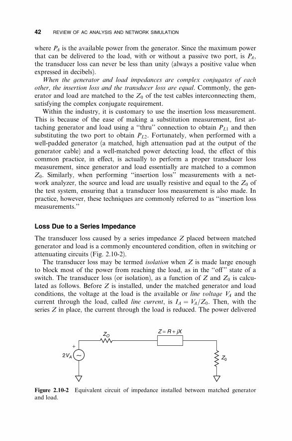
42 REVIEW OF AC ANALYSIS AND NETWORK SIMULATION
where PA is the available power from the generator. Since the maximum powerthat can be delivered to the load, with or without a passive two port, is PA,the transducer loss can never be less than unity (always a positive value whenexpressed in decibels).
When the generator and load impedances are complex conjugates of each
other, the insertion loss and the transducer loss are equal. Commonly, the gen-erator and load are matched to the Z0 of the test cables interconnecting them,satisfying the complex conjugate requirement.
Within the industry, it is customary to use the insertion loss measurement.This is because of the ease of making a substitution measurement, first at-taching generator and load using a ‘‘thru’’ connection to obtain PL1 and thensubstituting the two port to obtain PL2. Fortunately, when performed with awell-padded generator (a matched, high attenuation pad at the output of thegenerator cable) and a well-matched power detecting load, the e¤ect of thiscommon practice, in e¤ect, is actually to perform a proper transducer lossmeasurement, since generator and load essentially are matched to a commonZ0. Similarly, when performing ‘‘insertion loss’’ measurements with a net-work analyzer, the source and load are usually resistive and equal to the Z0 ofthe test system, ensuring that a transducer loss measurement is also made. Inpractice, however, these techniques are commonly referred to as ‘‘insertion lossmeasurements.’’
Loss Due to a Series Impedance
The transducer loss caused by a series impedance Z placed between matchedgenerator and load is a commonly encountered condition, often in switching orattenuating circuits (Fig. 2.10-2).
The transducer loss may be termed isolation when Z is made large enoughto block most of the power from reaching the load, as in the ‘‘o¤ ’’ state of aswitch. The transducer loss (or isolation), as a function of Z and Z0 is calcu-lated as follows. Before Z is installed, under the matched generator and loadconditions, the voltage at the load is the available or line voltage VA and thecurrent through the load, called line current, is IA ¼ VA=Z0. Then, with theseries Z in place, the current through the load is reduced. The power delivered
Figure 2.10-2 Equivalent circuit of impedance installed between matched generatorand load.

� �
SPECIFYING LOSS 43
to the load is proportional to the square of the load current. Thus,
PA ¼ VA2=Z0 V 2=Z0 j2Z0 þ Zj2
TL ¼ ¼ A ¼2PL I 2Z0 ½ð2VAÞ2= �Z0 ð2Z0Þ2j2Z0 þ Zj
¼ 1þ Z
2Z0
2
ð2:10-3Þ
Since Z=Z0 is the normalized impedance, z ¼ rþ jx, the transducer loss (orisolation) can be written
TL ¼2 2r¼ 1þ rþ
4þ jxj2
4ð2:10-4Þz
1þ2
For example, if 5 W resistance is placed between a 50-W source and a 50-Wload, the transducer loss is
1 5TL ¼ 1þ 5 � �2 ¼ 1:10 ¼ 0:42 dB50 þ 4 50
This might represent the ‘‘on state’’ (forward bias) of a series PIN diode in-stalled in the transmission line to provide switching. When the diode’s biasstate is switched (to reverse bias), it might be represented as 0.2 pF capacitancein the ‘‘o¤ state.’’ The transducer isolation at, say, 500 MHz, for which thediode’s reactance is 1590 W, is
TL ¼ 1þ 1 15904
2 ¼ 254 ¼ 24 dB50
Loss Due to a Shunt Admittance
Another common transducer loss example is that of a shunt-connected admit-tance between matched generator and load (Fig. 2.10-3). An analysis similar tothat used for the series Z gives
TL ¼ 1þ2 2g¼ 1þ gþ
4þ jbj2
4ð2:10-5Þy
2
Figure 2.10-3 Equivalent circuit used with admittance transducer loss formula.

44 REVIEW OF AC ANALYSIS AND NETWORK SIMULATION
in which the normalized admittance is
y ¼ Y ¼ G þ jB ¼ gþ jb ð2:10-6ÞY0 Y0
Loss in Terms of Scattering Parameters
When using a circuit simulator, transducer loss is obtained by calculating thesquare of the magnitude of the scattering parameter, S21, since for passive net-works jS21ja 1 the transducer loss (or isolation) as a function of S21 is
TL ¼ jS21j�2
¼ �20 logjS21j ðin decibelsÞ ð2:10-7Þ
where the negative signs has been added so that the loss ratio is equal to orgreater than unity and a positive number when expressed in decibels. The S
parameters are described in Chapter 5.
2.11 REAL RLC MODELS
Resistor with Parasitics
Real resistors have series inductance L and shunt capacitance C. These un-intended elements are called parasitic elements or simply parasitics. For a stan-dard carbon resistor these elements (typically L ¼ 5 nH and C ¼ 1 pF) havenegligible e¤ects at 10 MHz, but at 1 GHz their presence causes the resistancevalue to be changed profoundly. Figure 2.11-1 shows their e¤ects on a 50-Wresistor with frequency. At resonance, a little over 1.5 GHz, the resistance hasdoubled in value.
Inductor with Parasitics
A real inductor L has some series resistance R and some shunt capacitance C.Consider a 20-nH inductor with Q ¼ 60 at 500 MHz (R ¼ 1 W). Also assume ashunt capacitance of 0.5 pF. The behavior with frequency is as shown in Figure2.11-2. The inductor goes through parallel resonance, fR, at about 1.6 GHz. Itapproximates a linear inductor only up to about 600 MHz (about 40% of fR).Above fR its net reactance actually is capacitive!
Capacitor with Parasitics
Similarly, capacitors also have parasitic inductance, capacitance, and resis-tance. For the capacitor, a four-element model is required to provide an accu-

REAL RLC MODELS 45
Figure 2.11-1 Frequency behavior of 50-W resistor with 5-nH-series-inductance and1-pF-parallel-capacitance parasitics.
IM[Z
P]
RE
[ZIN
]
60 R and jX
50
40
30
20
10
0
600
400
200
0
−200
−400
−600
R R = 1 ohm
C C = 1 pF
1
1 1 4 0(1)
0
L L = 20 nH R
jX
RjX
0 250 500 750 1000 1250
IM[ZP]
1500
RE[ZIN]
Freq (MHz)
Figure 2.11-2 Frequency behavior of 20-nH inductor having parasitic shunt capaci-tance of 1 pF.

� �
46 REVIEW OF AC ANALYSIS AND NETWORK SIMULATION
Figure 2.11-3 Reactance and impedance magnitude of 20-pF capacitor with 5-nH-series inductance and 1-pF parallel capacitance parasitics.
rate simulation over a wide frequency range (Fig. 2.11-3). Notice that thecircuit goes through series resonance ð jX ¼ 0Þ at about 500 MHz and throughparallel resonance ð jX ¼ yÞ at about 2.3 GHz.
2.12 DESIGNING LC ELEMENTS
Lumped Coils
The inductance of a single-layer, air core coil (Fig. 2.12-1), which can bewound on a cardboard or wood cylindrical mandrel, is given by Wheeler [2]:
2
L ¼ n2r ðmHÞ ð2:12-1Þ
9rþ 10l
where n is the number of turns, r ¼ D=2 is the radius of the coil, and l is itslength, both in inches. In this formula the wire thickness from which the coil isformed is assumed to be small compared to the turns’ spacing.
For example, suppose that it is desired to make an RF choke for an in-tegrated circuit module. There is enough space for a 150-mil-long coil having10 turns of 36-gauge wire (5 mil diameter) about a 25-mil-diameter form. What

� �
DESIGNING LC ELEMENTS 47
Figure 2.12-1 An ‘‘air core’’ coil wound on anonmetallic form.
is L?
0:01252L ¼ ð10Þ2 ¼ 0:0097 mH ¼ 9:7 nH
9ð0:0125Þ þ 10ð0:150ÞHighest Q generally results when the coil diameter D ¼ 2r is approximatelyequal to its length. Then (2.12-1) can be written
n2DL ¼ ðmHÞ ð2:12-2Þ
58
Solving for n, rffiffiffiffiffiffiffiffiffi 58L
n ¼ ð2:12-3ÞD
For example, suppose we wish to make a high-Q RF choke for use in a radio3transmitter having 200 nH (0.20 mH) of inductance and wound as a 8-in.-
diameter coil on a nonmagnetic form. How many turns are required if wechoose l ¼ D? rffiffiffiffiffiffiffiffiffiffiffiffiffiffiffiffiffiffiffi
ð58Þð0:2Þn ¼ ¼ 5:56 turns
0:375
High m Inductor Cores—the Hysteresis Curve
If a coil or transformer is wound on a high-permeability material core ðmR g 1Þ,such as ferrite material, the magnetic spins of the atoms of the material can bealigned with the applied H field, yielding a much higher flux density, B. Thiscan produce a much higher inductance for a given coil size.
However, the e¤ect is complicated by the factors illustrated in Figure 2.12-2.Starting with an initially unmagnetized core, we experience the behavior thatoriginates at the~B HH axes’ origin. The~B–~ BB increases very rapidly, having a slopeof mEFF ¼ m0mR. Then, as all of the core’s atoms align with the applied ~HH field,
~ ~saturation occurs at BBSAT and thereafter BB increases with applied ~HH at m0 slope.~When the HH field is removed, many of the core’s atoms remain aligned,
~leaving ~BBREM. As HH is cycled positively and negatively, a hysteresis curve (a

48 REVIEW OF AC ANALYSIS AND NETWORK SIMULATION
Figure 2.12-2 Use of magnetic core material can greatly increase flux density for given~magnetic field ð~BB ¼ m0mRHHÞ.
curve having memory) is traced. The area within the curve is proportional tothe AC losses when the coil is sinusoidally excited. Suppliers of inductorshaving high-permeability cores specify a maximum current for the coil’s use.This is not an indication of the coil’s power-handling capability, but rather themaximum current for which the coil provides its small signal inductance(operates below BSAT). The hysteresis curve is also a function of temperature,and the coil’s specification includes an indication of the highest temperature atwhich the coil’s inductance specification is met. Above a critical temperatureTC the spins of the material’s atoms do not align with the applied H field, andthe e¤ective permeability is only m0.
Estimating Wire Inductance
There are numerous formulas given for the inductance of an isolated straightwire. These are approximations, having an implicit assumption about thenature of the return current path (Fig. 2.12-3). An inductance determination
requires a closed path just as the current in the coil requires a closed path. Theinductance of a truly isolated straight wire is as undefined as the sound of onehand clapping! An exact relation (7.25-17) exists for the high frequency induc-tance per unit length of a coaxial cable. The high frequency approximation as-sumes that the~ HH fields are contained between the conductors and do notEE and ~
penetrate the conductors appreciably.
m0mR bL ¼ ln H=m ð2:12-4Þ
2p a
bL ¼ 5:08 ln nH=in: ð2:12-5Þ
a

DESIGNING LC ELEMENTS 49
Figure 2.12-3 Inductance of isolated wire can be approached by that of coaxial linewhose outer conductor is made very large.
where mR ¼ 1 for all nonmagnetic insulators. If we assume b is very large com-pared to a, then the calculated value for L approximates that of a straight wirewith far removed return path.
For example, if b=a ¼ 7
LA10 nH=in: ð2:12-6Þ
This is a reasonable approximation for the inductance of thin wires elevatedabove ground planes in microstrip circuits.
Note, however, that if we assume a value of b ¼ 50a, the value for lnðb=aÞdoubles, and the inductance becomes 20 nH/in., also a value in the vicinity ofthose measured for real circuits in which the thin wire is well above the groundplane. The point to observe from the formula for the inductance of coaxial lineis that the inductance continues to increase as the outer conductor diameter is
increased, that is, as the return path for the inductive current is further removedfrom the center conductor ‘‘wire.’’ It is a common but incorrect practice to
speak of the inductance of an ‘‘isolated’’ straight wire. The better procedure is toapproximate the inductance of a wire by the known inductance per unit lengthof an appropriately similar transmission line.
Parallel Plate Capacitors
The capacitance C of a parallel plate capacitor (Fig. 2.12-4) having plate areaA separation d, and relative dielectric constant eR is given by
AC ¼ e0eR ð2:12-7Þ
d

50 REVIEW OF AC ANALYSIS AND NETWORK SIMULATION
Figure 2.12-4 Parallel plate capacitor.
where
10�9
e0 ¼ F=m ð2:12-8Þ36p
is the permittivity of free space. These expressions neglect the E field fringing atthe edges of the capacitor. With fringing the capacitance is larger depending onthe plate area-to-separation aspect ratio.
For engineering work, a more convenient format to estimate the parallelplate capacitance is [3, Appendix A]
AC ¼ e0eR
d
A¼ eRð0:0885Þ pF=cmd
A¼ eRð0:225Þ pF=in: ð2:12-9a;b;cÞd
For example, suppose that we wish to construct an RF blocking capacitor. We
have space for a 0.5-in.-diameter capacitor and will use 1-mil Mylar tape having
a relative dielectric constant of 3 [3, Appendix B] as the plate separation dielec-
tric. What will be the value of C?
ð3:14Þð0:252ÞC ¼ ð3Þð0:225Þ ¼ 132 pF
0:001
This capacitor would have a reactance of only 1.2 W at 1 GHz, a reasonably
small impedance in a 50 W system.

SKIN EFFECT 51
2.13 SKIN EFFECT
An important consideration in the design of circuits is that the e¤ective resis-tance of conductors increases considerably at high frequencies. This is due toskin e¤ect, which is a result of the crowding of current densities near conductorsurfaces. This is analyzed in Section 7.18.
At any point, current flows in accordance with the incremental (or ‘‘point’’)form of Ohm’s law, namely
~JJ ¼ s~EE ð2:13-1Þ~where JJ (A/m2) is the current density, ~EE (V/m) is the electric field at the point,
and s (
W
/m) is the conductivity of the material. This equation applies for anytime variations. At high frequencies (sinusoidal excitations) Maxwell’s equa-tions play a special role in analyzing the e¤ects in a conductor. The sinusoidally
~varying electric field EE produces a sinusoidally varying current density ~JJ, which~in turn produces a sinusoidally varying HH field, which in turn produces an
opposing electric field. More about Maxwell’s equations in Chapter 7. The net~result is that the EE field in the conductor falls o¤ rapidly with depth from the
surface, and with it so does the current density [4, p. 234; 5, p. 43] (Fig. 2.13-1).The current density in the conductor is
JJ ¼ ~~ JJ0e�z=dS ð2:13-2Þ
where the skin depth is
1dS ¼pffiffiffiffiffiffiffiffiffiffiffi ð2:13-3Þ
pf ms
~Figure 2.13-1 Fall-o¤ of electric field EE and current density ~JJ with distance from sur-face in skin depth units.

52 REVIEW OF AC ANALYSIS AND NETWORK SIMULATION
and f ¼ frequency (Hz), m ¼ 4p� 10�7 (H/m) for nonmagnetic materials, ands ¼ 6:17� 107
W
/m for silver.At a frequency of 1 GHz, the skin depth in silver is calculated as
1dS ¼ ffiffiffiffiffiffiffiffiffiffiffiffiffiffiffiffiffiffiffiffiffiffiffiffiffiffiffiffiffiffiffiffiffiffiffiffiffiffiffiffiffiffiffiffiffiffiffiffiffiffiffiffiffiffiffiffiffiffiffiffiffiffiffiffiffiffiffiffiffiffiffiffiffiffiffiffiffiffiffiffiffiffiffiffiffiffiffiffiffiffiffiffiffiffiffiffiffiffiffiffiffiffiffiffiffiffiffiffi
¼
p2:03� 10�6 m
Thus, a silver conductor has a skin depth at 1 GHz of only 2 mm or about 0.1mil! Since copper has about 90% the conductivity of silver, its skin depth isonly 5% greater than that of silver, or about 2.1 mm at 1 GHz.
The term skin depth should not be misinterpreted. Current does flow below
the skin depth, but its density at this depth is reduced to 1/e (about 37%) of itssurface value. At 10 skin depths (about 1 mil in silver or copper) the currentdensity would be reduced to 1/22,026 of its surface value!
For calculation purposes, it turns out that when the skin depth is small, the
AC resistance of a conductor has the same value that it would have if all the
current were carried in a material depth equal to the skin depth [5, p. 45].For round wire the AC resistance, RAC, is determined by the cross section of
a hollow tube having a wire diameter D and a thickness equal to the skin depth,dS (Fig. 2.13-2). This can be compared with the direct current (DC) resistanceRDC for which the entire cross section of the wire is e¤ective:
lRAC ¼ ð2:13-4Þ
pDdSs
lRDC ¼ ð2:13-5Þ
pðD2=4Þs
ð3:14Þð109 HzÞð4Þð3:14Þð10�7 H=mÞð6:17Þð107 W
=mÞ
Figure 2.13-2 Skin depth region for solid round wire.

NETWORK SIMULATION 53
The ratio of the AC-to-DC resistance is
RAC ¼ D ð2:13-6ÞRDC 4dS
Thus, a 30-gauge (10-mil-diameter) hookup wire used in a circuit at 1 GHz has
RAC D ð0:010 in:� 0:0254 m=in:Þ¼ ¼ ¼ 32RDC 4dS 4ð2� 10�6 mÞ
The DC resistance of this wire is only 0.1 W/ft, but its resistance at 1 GHz is3.2 W/ft, a factor of 32 greater.
2.14 NETWORK SIMULATION
Using complex circuit analysis, it is possible to analyze any network to deter-mine its performance as, for example, how much of an applied signal passesthrough the network to a specified load and what input impedance the networkpresents to a specified source. However, the application of complex mathemat-ics is di‰cult for all but the simplest of networks, much more so if the analysisis to be conducted over numerous frequencies. Over the years, methods of sim-plifying the analysis were devised. These included filter theory (Chapter 9) andthe Smith chart (Chapter 5). However, use of such techniques is generally lim-ited to networks having specific circuit element values and relationships. Forexample, filter theory defines precisely the relationship of the circuit values toone another. The Smith chart is useful when the transmission line has uniformcharacteristic impedance.
Beginning in the 1960s computer programs became available for which avariable topology network could be specified and the network’s performancecalculated over a band of frequencies. These programs have been refined to ahigh degree, usually operate on a personal computer, and are generally termednetwork simulators. A sample network simulator screen is shown in Figure2.14-1 using the Genesys software. The initial screen shown allows specificationof a network. One selects components, such as resistors, inductors, capacitors,transmission lines, and so forth, from the toolbar above the workspace anddrags them to the desired location in the schematic. Then double clicking on thecomponent gives a submenu in which the component name and value can bespecified. The sample network in Figure 2.14-1 was created in this manner. Theprogram provides input and outputs whose impedances can be specified. Thesedefault to 50 W if no other values are specified.
Once the circuit is specified, selection of the outputs (a left menu option inFig. 2.14-1) provides options for di¤erent kinds of outputs, such as rectangularor polar plots, a Smith chart format, an antenna plot, a three-dimensional plot,and so forth. It also allows specification of the functional output such as S11 or

54 REVIEW OF AC ANALYSIS AND NETWORK SIMULATION
Figure 2.14-1 Inputting circuit to network simulator.
voltage standing wave ratio (VSWR) (to show reflection properties), the mag-nitude of S21 (for insertion loss) and phase of S21 to show transmission phase,and other functions. S parameters are described in Section 6.5. The insertionloss jS21j of the circuit in Figure 2.14-1 over the bandwidth 0 to 2 GHz isshown in Figure 2.14-2.
Even this simple graph would take hours or days to calculate manually. Inthis particular execution the insertion loss was calculated at 201 di¤erent fre-quencies, and each dot in the plot represents a separate calculation. However,the generation of the graph appeared almost instantaneously, since the personalcomputer on which it was performed can perform millions of calculations persecond.
A tuning feature of modern network simulators causes the performance to berecalculated when the value of a given component is varied. This can be donemanually or automatically. The automatic mode is termed optimization. Forexample, when the program varies the values of C1 and C2 and is directed toachieve a value of jS21j ¼ 0 at 1 GHz, the result is that shown in Figure 2.14-3.In this program, the variable nature of these components is denoted by theleading question mark before their values in Figure 2.14-1.
To achieve this optimization, the software varies each component whosevalue is allowed to be changed in a random manner and calculates the resulting

NETWORK SIMULATION 55
Figure 2.14-2 Insertion loss versus frequency for circuit shown in Figure 2.14-1.
performance, in this case the magnitude of S21. If the change results in perfor-mance closer to the desired value, the change is retained and another adjustablecomponent’s value is changed. This process is repeated, usually millions oftimes, until the desired result is obtained. In this example, the optimization wasterminated after a few seconds because zero insertion loss cannot be obtaineddue to the finite value of R1, whose value was not allowed to vary. Usually,such an optimization procedure would be wholly impractical to perform bymanual calculation methods.
Simulation software has become an indispensable engineering tool. How-ever, the termination just described exemplifies the need for human interactionwith the computer. The computer does not appreciate that zero loss is un-obtainable in a network having finite resistance, and the optimization routinewould have continued indefinitely if left unattended.
Another application of varying element values is to perform a yield analysis
of a circuit by which circuit element values are allowed to vary in accordancewith a given distribution, such as a Gaussian distribution. The program builds aspecified number of circuits to determine what the yield of circuits would be to

56 REVIEW OF AC ANALYSIS AND NETWORK SIMULATION
Figure 2.14-3 Result of optimizing values of C1 and C2 to minimize insertion loss at1 GHz.
some required specification when the component parts have values with thatstatistical distribution. This analysis is demonstrated in Section 9.19.
For the most rigorous evaluation of networks electromagnetic simulation
(called EM simulation) is performed, by which the electric and magnetic fieldssurrounding a circuit are computed and from them the circuit performance.This is demonstrated in Section 7.34.

EXERCISES 57
The use of network simulation is especially important in transistor amplifierdesign. Most simulation programs contain a library of available transistors.The program can input a transistor’s S parameter table and analyze the per-formance of a circuit containing the transistor (see Chapter 10 for examples).This permits stability and gain analyses at all frequencies over which the tran-sistor has gain, a process that is essential to modern amplifier design.
These features of network simulation software have become essential to theconduct of e‰cient RF and microwave design. Each software package hasits own format and features, but most simulation software available todayperforms at least the functions described. Throughout this text, networksimulation is used to demonstrate the principles discussed, and network simu-lation exercises are provided to permit the reader to gain proficiency in thesetechniques.
REFERENCES
1. Kenneth S. Miller, Advanced Complex Calculus, Harper & Brothers, New York,1960. An old reference, much too advanced for our purposes, but its development of the
bilinear transformation is fundamental to the Smith chart.
2. H. A. Wheeler, ‘‘Inductance formulas for circular and square coils,’’ Proc. IEEE, vol.75, no. 2, 1982, pp. 256–257.
3. Joseph F. White, Microwave Semiconductor Engineering, Noble Publishing, NorcrossGA 1995. Extensive treatment of PIN diodes and their switching and phase shifting
applications.
4. Simon Ramo and John R. Whinnery, Fields and Waves in Modern Radio, Wiley,New York, 1944, 1953 (later revised with a third author, Van Duzer). This is a classic
introductory text describing fields and Maxwell’s equations.
5. Peter A. Rizzi, Microwave Engineering, Passive Circuits, Prentice-Hall, EnglewoodCli¤s, NJ, 1988. Excellent microwave engineering textbook covering theory and design
of transmission lines, couplers, filters, and numerous other passive devices.
EXERCISES
E2.4-1 Four alternating currents at the same frequency have their referencedirections into a common node. They are represented by:
i1ðtÞ ¼ 10 cosðotþ 36:9�Þ AI2 ¼ 14:1J315� A
I3 ¼ 20J126:9� A
I4 ¼ 13:4J243:4� A
What is the total current (amplitude and phase) into the node?

58 REVIEW OF AC ANALYSIS AND NETWORK SIMULATION
E2.5-1 Realizing that you understand AC circuits, your friend asks for yourhelp. He wishes to install a central air conditioner in his home. Theunit requires V ¼ 220 V AC rms at 60 Hz with a steady-state runningcurrent of I ¼ 50 A rms. The maximum running current his wiringcan provide is 40 A rms. You note that the machine develops 10horsepower (1 hp ¼ 746 W) and that it is nearly 100% e‰cient.
a. What is the power factor of the machine ðpower factor ¼ cos y,where y is the phase angle between V and I )?
b. Assuming the machine’s motor presents an inductive load, whatimpedance Z does this machine present to the power line?
c. What is the capacitance C of a capacitor connected in parallelwith this machine that would make the power factor unity? Whatsteady-state rms current must it sustain?
d. What total steady-state, rms current would the machine draw withthis capacitor installed in parallel?
E2.9-1 A 500-W load is to be connected to a 50-W transmission line tomatch load terminate it at 500 MHz. However, the hookup wire has5 nH of series inductance. How can this be tuned such that the netreactance in series with the 50-W load is zero at 500 MHz?
E2.10-1 Show that the insertion loss (or isolation) of a normalized admit-tance, y ¼ gþ jb, mounted in shunt with a matched generator (Fig-ure 2.10-3) and load of Z0 ¼ 1 is given by
IL ¼ 1þ y
2
2 ¼ 1þ gþ g2
4þ jbj2
4
E2.12-1 It is proposed to realize the tuning capacitor of Exercise 2.9-1 as apair of circular parallel plates separated by 1 mil of double-sided tapehaving a dielectric constant of 3. What should the diameter D of theplates be made to realize the required capacitance?
E2.12-2 A circuit designer requires a high Q small volume coil of L ¼ 50 nHto be formed on a wood mandrel of 0.125-in. diameter using #30gauge copper wire having a diameter of 0.010 in. (10 mil).
a. How many turns of wire are required?
b. What is the length of the wire required (not counting the endsused for hook-up)?
E2.13-1 Derive an expression for the Q of the coil in E2.12-2 in terms of itsdimensions, wire conductivity, and frequency, taking skin e¤ect intoaccount. Then, using this expression, solve for the Q at 10, 100, and1000 MHz.

CHAPTER 3
LC Resonance and Matching Networks
3.1 LC RESONANCE
When the reactance magnitudes of L and C are equal, the pair resonates. Atresonance the net reactance of a series-connected LC circuit is zero (a shortcircuit), and the net susceptance of a parallel-connected LC circuit is zero andthe net reactance is infinite (an open circuit).
The resonant frequency is obtained by equating the magnitudes of the re-actances of the L and C elements. Since their impedances are of opposite signs,the net reactance is zero for a series circuit or infinity for a parallel circuit,resulting in resonance at o0:
1o0L ¼
o0Cð3:1-1Þ
1o0 ¼ ffiffiffiffiffiffiffi p
LCð3:1-2Þ
o ¼ 2pf ð3:1-3Þ1
f0 ¼2p
ffiffiffiffiffiffiffi pLC
ð3:1-4Þ
The resonance solution can be obtained graphically. Given an 80-nH inductor,the reactance magnitude is 5 W at 10 MHz. Draw a line through this valuehaving an upward slope and passing through successive 5’s on each decade oflog–log graph paper (Fig. 3.1-1). Next, suppose the capacitor to resonate whenit has 0.32 pF, or a 5000-W-reactance magnitude at 100 MHz. Similarly, draw aline through this point having a downward slope, and passing through succes-sive 5’s. The intersection of the two lines defines the resonant frequency, seen tobe 1 GHz for this example.
High Frequency Techniques: An Introduction to RF and Microwave Engineering, By Joseph F. White. ISBN 0-471-45591-1 6 2004 John Wiley & Sons, Inc.
59

60 LC RESONANCE AND MATCHING NETWORKS
Figure 3.1-1 L and C reactance chart for determining resonance.
3.2 SERIES CIRCUIT QUALITY FACTORS
Q of Inductors and Capacitors
The quality factor Q of an inductor or capacitor is the ratio of its reactancemagnitude to its resistance (Fig. 3.2-1). For an inductor,
XL oLQ ¼ ¼ ð3:2-1Þ
RL RL
and for a capacitor,
XC 1Q ¼ ¼ ð3:2-2Þ
RC oCRC

SERIES CIRCUIT QUALITY FACTORS 61
Figure 3.2-1 L and C models for QU definition.
When a series resonant circuit is formed from a LC pair, one can define aQ for the circuit at the resonant frequency o0. Called the unloaded Q;QU , itrelates the energy stored in the reactive elements to the power loss in the re-sistive elements and, hence, is a measure of the quality of the resonator, itself.Thus,
QU ¼ o0L
RL þ RC
¼ 1
o0CðRL þ RCÞ ð3:2-3Þ
QE , External Q
Even when a resonator is formed from an ideal, lossless LC pair, there is powerdissipation when it is connected to external loads (Fig. 3.2-2). This dissipationa¤ects the sharpness of the resonant response, which depends upon the ratio ofthe amount of energy stored in the capacitor or inductor relative to that dissi-pated in the external load or loads.
Under these conditions, the external quality factor QE is the ratio of the
magnitude of the reactance of either the L or C at resonance to the total external
resistance:
o0L 1QE ¼ ¼ ð3:2-4Þ
Z0 þ Z0 o0CðZ0 þ Z0Þ
Figure 3.2-2 Series equivalent circuit of LC resonator with dissipation only in the ex-ternal loads (QE model).

62 LC RESONANCE AND MATCHING NETWORKS
Figure 3.2-3 QL includes the e¤ect of resonator resistances and external load.
QL, Loaded Q
The loaded quality factor QL is the ratio of the magnitude of the reactance of
either reactor at resonance to the total circuit resistance (Fig. 3.2-3). In the caseof a doubly match-terminated resonator, that is, one having a source resistanceZ0 and a load impedance Z0, the total external resistance is 2Z0:
o0L 1QL ¼ ¼ ð3:2-5Þ
Z0 þ Z0 þ RL þ RC o0C0ðZ0 þ Z0 þ RL þ RCÞ
From (3.2-3), (3.2-4), and (3.2-5), it follows that
1 1 1¼QE
þ ð3:2-6ÞQL QU
Thus, it is seen that the three Q factors add reciprocally. Equivalently, theproduct over the sum method can be used to calculate QL from QU and QE :
QUQEQL ¼ ð3:2-7Þ
QU þQE
3.3 PARALLEL CIRCUIT QUALITY FACTORS
The dual of the circuit of Figure 3.2-3 is that shown in Figure 3.3-1 in whichthe resonator consists of shunt-connected elements. For the shunt equivalentcircuits the Q’s are defined as the ratio of the susceptance of either the L or theC to the appropriate conductances, which are, for the inductor,
BL 1Q ¼ ¼ ð3:3-1Þ
GL oLGL
and for the capacitor
BC oCQ ¼ ¼ ð3:3-2Þ
GL GL
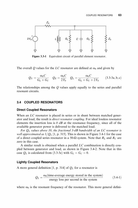
COUPLED RESONATORS 63
Figure 3.3-1 Equivalent circuit of parallel element resonator.
The overall Q values for the LC resonator are defined at o0 and given by
o0C o0C o0CQU ¼ QE ¼ QL ¼ ð3:3-3a; b; cÞ
GL þ GC 2Y0 GL þ GC þ 2Y0
The relationships among the Q values apply equally to the series and parallelresonant circuits.
3.4 COUPLED RESONATORS
Direct Coupled Resonators
When an LC resonator is placed in series or in shunt between matched gener-ator and load, the result is direct resonator coupling. For ideal lossless resonatorelements the insertion loss is 0 dB at the resonance frequency, since all of theavailable generator power is delivered to the matched load.
For QL values above 10, the fractional 3-dB bandwidth of an LC resonator is
well approximated as 1=QL [1, p. 315]. This is shown in Figure 3.4-1 for the caseof a direct coupled series resonator in a 50-W system. Note that RL and RC arezero in this case.
A similar result is obtained when a parallel LC combination is directly cou-pled between generator and load, as shown in Figure 3.4-2. Note that in thiscase QL is calculated from (3.3-3c) with GL ¼ GC ¼ 0.
Lightly Coupled Resonators
A more general definition [1, p. 314] of QL for a resonator is
o0ðtime-average energy stored in the systemÞQL ¼ ð3:4-1Þ
energy loss per second in the system
where o0 is the resonant frequency of the resonator. This more general defini-

64 LC RESONANCE AND MATCHING NETWORKS
Figure 3.4-1 Resonant LC with QL ¼ 5. Note that QL ¼ 500=ð50þ 50Þ ¼ 5 andtherefore the 3-dB bandwidth is f0=QL ¼ 1000=5 ¼ 200 MHz.
Figure 3.4-2 Shunt LC resonator mounted between 50-W source and load. The 3-dBbandwidth is 200 MHz, about 1000 MHz center frequency for a loaded Q ¼ 5.

COUPLED RESONATORS 65
tion has the advantage that it can be applied to any type of resonator, includingcavity and dielectric resonators. As with the lumped element model, the frac-tional 3-dB bandwidth remains a good approximation to the reciprocal of theloaded Q when QL ¼ 10 or more.
The series and shunt resonators shown in the previous two examples aredirectly coupled. That is, either the current through the series resonator is thesame as that through the load or the voltage across the parallel resonator is thesame as that across the load. Consequently, to achieve a high QL the reactancemagnitudes of the series elements at resonance must be relatively high com-pared to the load impedance. In a parallel circuit the magnitude of the shuntsusceptance of each element at resonance must be correspondingly higher thanthe load conductance.
Practically, direct coupling constrains the amount of energy that can bestored in the LC resonator relative to that which is dissipated in the load be-cause it is di‰cult to realize large ratios between resonator and load impedancemagnitudes. For example, to obtain the modest QL of 5 at 1 GHz in the previ-ous example with a load impedance of 50 W required that the reactance of theshunt inductance be 5 W, resulting in a very low inductance value of 0.8 nH.
If, instead, the resonator is only lightly coupled to the generator and load,the voltage across and the current through the L and C elements is theoreticallyunlimited. This can permit a much higher loaded Q, as the following exampledemonstrates. Of course, real resonators have finite losses, and therefore the QL
is not unlimited in practice, but the following lossless example (Fig. 3.4-3)serves to illustrate the principles of the lightly coupled resonator.
Paradoxically, the lighter the coupling the higher the stored energy in the res-
onator. For comparison we first consider a direct coupled parallel resonatorwith resonant frequency of 1000 MHz, L ¼ 3:18 nH and C ¼ 7:95 pF. Directlycoupled in a 50-W system, this results in a loaded Q of only 1.25, so low thatthe actual 3-dB bandwidth, as determined from circuit simulation, is about 800MHz.
Next, the same resonator is coupled to generator and load through 1.16-pFcapacitors, as shown in the schematic in Figure 3.4-3. The resulting 3-dBbandwidth is only 100 MHz. Some retuning of the resonator’s capacitor from7.95 to 5.911 pF was required because the capacitive coupling reactance in-creases the total capacitance of the circuit and would lower the resonant fre-quency if uncompensated. This configuration is called a top-C coupled parallel
resonator filter [2, p. 155]. Notice that the resonator’s inductor is 3.18 nH, fourtimes as large as, and more practically realizable than, the 0.8 nH of the pre-ceding 200-MHz direct coupled, shunt resonator example.
Physically, the action of the network can be visualized by considering whatoccurs when the generator is first turned on. This is a transient condition, notcovered by our steady-state AC analysis. Due to the light coupling only a smallamount of energy enters the resonator. The peak voltage across the capacitordoes not build up as rapidly as it would with direct coupling because energymust enter through the high impedance of the coupling capacitor. Hence it may

Figure
3.4-3
Perform
ance
comparisonofdirectandlightcouplingofLC
resonatorbetweenmatched
generatorandload.
66

Q MATCHING 67
take several RF cycles for the steady-state AC voltage to become establishedacross the resonator.
The voltage increases, from cycle to cycle, until it is su‰cient to block fur-ther energy increase from the generator. Since the network is symmetric in thiscase, in the steady state energy flows out of the resonator to the load at thesame rate that it enters from the generator. For this ideal, lossless LC casethere is no insertion loss at the resonant frequency. The higher the reactance ofthe coupling capacitors, the greater the resonator voltage (to block furtherpower from entering) and the greater the stored energy in the resonant LC.This results in a higher QL and a narrower 3-dB bandwidth.
Why did the loaded Q of the lightly coupled resonator circuit increase by afactor of 8 relative to that of the directly coupled resonator having the sameLC elements? We can infer that the energy stored in the coupled resonator alsoincreased by a factor of about 8. This energy storage in a parallel LC resonatoris proportional to the square of the voltage across it [1, pp. 314–315]. Clearly,the voltage across the top coupled resonator must have increased relative to theline voltage VA of the direct coupled case.
This must be true because the same power reaches the load in both cases, yetfor the top coupled circuit the load current must be driven through not only the50 W load resistance but the series 1.16 pF capacitance as well, an additional�j137 W at 1 GHz. The impedance of capacitor and load is ð50� j137Þ W, andits magnitude is 146 W, requiring a voltage increase of 146/50 or 2.92. Thecorresponding energy storage increase in the LC resonator of the top coupledcase is therefore a factor of 2.922 for a factor of 8.5, approximately equal to theobserved 3-dB bandwidth decrease by a factor of 8.
3.5 Q MATCHING
A very useful method for accomplishing resistive impedance transformation ata given frequency is that of the LC network in which one element, either aninductor or a capacitor, is placed in series or parallel with the load to be trans-formed and the remaining element is made the opposite kind and placed, re-spectively, in parallel or series with the combination. Interestingly, the mathe-matical development of this matching technique arises from the formula forconverting a series impedance to its parallel equivalent, or vice versa. To dem-onstrate the method and its basis, we review the series-to-parallel equivalent
circuit transformation (Fig. 3.5-1).
Low to High Resistance
For this development, it is illustrative to derive the equivalence between Z andY by first expressing Z in terms of its Q. As will be seen, this leads to a lumpedcircuit resistance transformation [3, p. 35]. In this exercise, we simply refer tothe quality factor of Z as Q. We derive the result starting with a positive

68 LC RESONANCE AND MATCHING NETWORKS
Figure 3.5-1 Series-to-parallel equivalent circuits.
imaginary value for Z, but the derivation is similar if begun with a negative imaginary value:
Z ¼ RS þ jXð3:5-1Þ
Z ¼ RSð1þ jQÞ
Y ¼ 1 ¼ 1 � 1� jQ
Z RSð1þ jQÞ 1� jQ
Y ¼ 1� jQ
RSð1þQ2Þð3:5-2Þ
Y ¼ G � jB
1G ¼
RSð1þQ2Þ ð3:5-3Þ
B ¼ Q
RSð1þQ2Þ ð3:5-4Þ
Converting the parallel admittance terms into parallel resistance RP and paral-lel reactance XP,
RP ¼ RSð1þQ2Þ ð3:5-5ÞRSð1þQ2Þ
XP ¼ ð3:5-6ÞQ
The important point to notice is that the parallel equivalent circuit of a series
impedance has a resistance value that is higher than the series value by the factor
ð1þQ2Þ. This suggests that resonating the reactance in the parallel equivalentcircuit [4, p. 120] yields a lumped circuit, resistance transforming method. Totransform a low resistance to one of higher resistance, add su‰cient series re-
actance to bring the parallel equivalent resistance to the value desired, and then
resonate the resulting circuit by adding an appropriate parallel susceptance.
Generally, the purpose in transforming a resistive load to a di¤erent valueis to match the load to a circuit of di¤erent source impedance. This method

Q MATCHING 69
can be called LC matching (because opposite reactor types must be used), Lmatching (because of the L orientation of the reactors), or Q matching [5] (be-cause the Q is chosen based on the transformation ratio).
In the remainder of this text we will call the method Q matching. As anexample, suppose we wish to transform 5 to 50 W at 1 GHz. This requires thatwe increase the resistance by a factor of 10. Accordingly
1þQ2 ¼ 10
Q ¼ 3
Since we wish to increase resistance, add a series reactor, say L1 (either L or Ccould be used), to the 5-W resistor. Examination of (3.5-5) and (3.5-6) showsthat the parallel equivalent circuit has the same Q as the series circuit. For ex-ample, if the series circuit consisted of a resistor and an inductor, its Q is givenby
oL XLQ ¼ ¼
RS RS
The Q of a parallel LC circuit is
BLQ ¼
G
By substituting the values for BL and G from (3.5-5) and (3.5-6), we obtain
BL RP RSð1þQ2ÞQ ¼ ¼ ¼ ¼ Q
G XP RSð1þQ2Þ=Q
which demonstrates that the series and parallel LR circuits have the same Q.We expect this result since the series and parallel circuits are equivalent andtherefore must have the same quality factor.
Given this condition, the reactance of L2 in the parallel equivalent circuitcan be written down immediately. It must have a parallel reactance of 50=Q ¼16:7 W because in the parallel circuit the reactance magnitude is the resistancedivided by the Q.
Next, add a capacitive reactance of equal magnitude to parallel resonate thecircuit. The resulting net admittance is 0.02
W
, or 50 W impedance at 1 GHz,the frequency at which the match is performed. Notice that in the Q matching
method, the two reactors are always of opposite type (Fig. 3.5-2). This is becausethe final circuit is resonated to remove any net reactance or susceptance. In thepresent example, when these reactances are converted to their corresponding L
and C values, the actual Q matched circuit is shown in Figure 3.5-3. Noticethat the resistance peaks just above 1000 MHz. This circuit might be made to
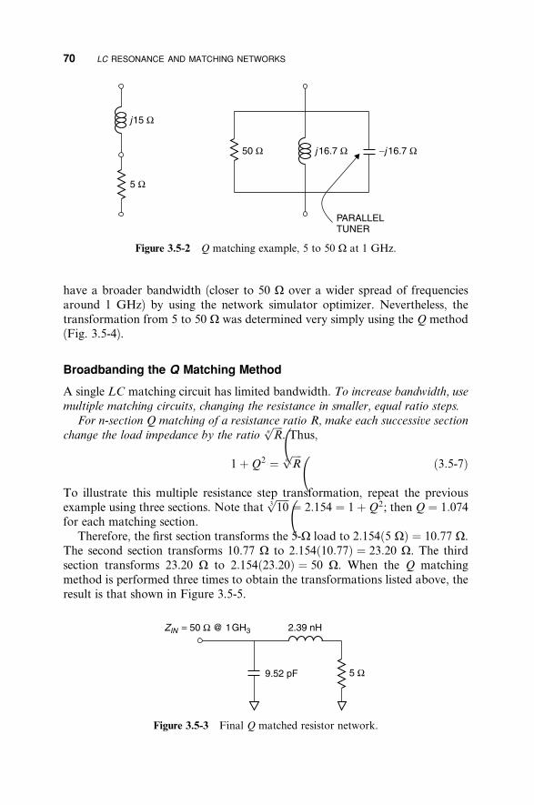
70 LC RESONANCE AND MATCHING NETWORKS
Figure 3.5-2 Q matching example, 5 to 50 W at 1 GHz.
have a broader bandwidth (closer to 50 W over a wider spread of frequenciesaround 1 GHz) by using the network simulator optimizer. Nevertheless, thetransformation from 5 to 50 W was determined very simply using the Q method(Fig. 3.5-4).
Broadbanding the Q Matching Method
A single LC matching circuit has limited bandwidth. To increase bandwidth, use
multiple matching circuits, changing the resistance in smaller, equal ratio steps.
For n-section Q matching of a resistance ratio R, make each successive sectionffiffiffiffi nchange the load impedance by the ratiopR. Thus,
1þQ2 ¼pffiffiffiffi nR ð3:5-7Þ
To illustrate this multiple resistance step transformation, repeat the previouspffiffiffiffiffi example using three sections. Note that 3 10 ¼ 2:154 ¼ 1þQ2; then Q ¼ 1:074for each matching section.
Therefore, the first section transforms the 5-W load to 2:154ð5 WÞ ¼ 10:77 W.The second section transforms 10.77 W to 2:154ð10:77Þ ¼ 23:20 W. The thirdsection transforms 23.20 W to 2:154ð23:20Þ ¼ 50 W. When the Q matchingmethod is performed three times to obtain the transformations listed above, theresult is that shown in Figure 3.5-5.
Figure 3.5-3 Final Q matched resistor network.

Q MATCHING 71
Figure 3.5-4 Frequency response of Q transformation network from 5 to 50 W.
Notice that with the three-section matching network, the bandwidth is muchgreater. The input resistance R is within 5 of 50 W from 800 to 1250 MHz, andthe imaginary part, jX , is very near zero over the same range. This is a muchbroader bandwidth than the 970 to 1100 MHz bandwidth (Fig. 3.5-4) overwhich the single-stage matching yielded within 5 of 50 W for the real part and amuch larger series reactance.
High to Low Resistance
If the resistance of a load is higher than desired, the same Q matching method
can be used except that a shunt reactor is used as the first transformation ele-
ment.
The same equivalent circuits and circuit element relations given in Figure3.5-1 are employed, but in this case the transformation is from right to left, thatis, from the parallel equivalent to the series equivalent circuit. We demonstratethis with a load circuit consisting of a 250-W resistor in series with a 0.7958-pFcapacitor (�j200 W at 1 GHz). This example also demonstrates how to absorbthe existing series reactance. We wish to transform this impedance to 50 W at1 GHz.
The ð250� j200Þ-W load is shown in Figure 3.5-6a. Since the 250-W real partexceeds the desired 50 W, a parallel circuit is needed to use the Q transforma-tion approach. The first step is to transform this series circuit to its parallel
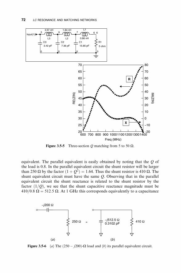
72 LC RESONANCE AND MATCHING NETWORKS
Figure 3.5-5 Three-section Q matching from 5 to 50 W.
equivalent. The parallel equivalent is easily obtained by noting that the Q ofthe load is 0.8. In the parallel equivalent circuit the shunt resistor will be largerthan 250 W by the factor ð1þQ2Þ ¼ 1:64. Thus the shunt resistor is 410 W. Theshunt equivalent circuit must have the same Q. Observing that in the parallelequivalent circuit the shunt reactance is related to the shunt resistor by thefactor ð1=QÞ, we see that the shunt capacitive reactance magnitude must be410=0:8 W ¼ 512:5 W. At 1 GHz this corresponds equivalently to a capacitance
Figure 3.5-6 (a) The ð250� j200Þ-W load and (b) its parallel equivalent circuit.

Q MATCHING 73
Figure 3.5-7 Equivalent circuit of load after the addition of 0.7304 pF capacitor.
of 0.3102 pF. Note that the nature of the reactance is unchanged between the
series and parallel equivalent circuits. In this case, the reactance is capacitive.Next, the task is to transform 410 to 50 W. This is a ratio of 8.2. Therefore,
1þQ2 ¼ 8:2 and Q ¼ 2:6833. The large number of decimal places is carried toshow that the method produces an arbitrarily accurate result if executed withsu‰cient precision. In order to change the Q of the parallel equivalent circuitin Figure 3.5-6b, we add shunt capacitance to produce a total shunt reactanceof 410 W=2:6833 ¼ 152:80 W. This corresponds to a total capacitance of 1.0406pF. Since 0.3102 pF is already available, only an additional 0.7304 pF need beadded, as shown in Figure 3.5-7a. In this way the original 200 W reactance hasbeen absorbed within the Q matching circuit.
The series equivalent circuit (Fig. 3.5-7b) has the required 50 W resistance.The magnitude of the series reactance must have the same Q of the parallelcircuit, in this case Q ¼ 2:6833. The resulting capacitive reactance magnitude is50 W� 2:6833 ¼ 134:17 W. The reactance type is unchanged by expressing thecircuit in series format; hence, the reactance is capacitive, as shown in Figure3.5-7b.
The final step is to resonate the �j134:7 W with a series inductor (21.353nH) of þj134:7 W to obtain the desired 50 W real input impedance. The result-ing circuit and its performance with frequency is shown in Figure 3.5-8.
This tuning could have been performed equally well, with the same Q
values, by using a shunt inductor as the first tuning element. The inductivesusceptance would be larger than that of the capacitor actually used, since itwould be required to neutralize the extant capacitive susceptance already inplace and then to provide the necessary susceptance magnitude required. Butthis would not change the required Q of 2.6833. With this procedure, the sec-ond tuning element would have been a capacitor instead of an inductor.
In some circuit applications having a series capacitor could be advantageousas a ‘‘DC block’’ to prevent bias currents from passing to the signal terminal.In other circuits the presence of a series inductor to conduct bias current mightbe useful. The availability of two di¤erent circuit topologies for Q matching is a
design advantage.
As was demonstrated, the Q matching method is not limited to transforminga pure load resistance. The load can be complex. This method of tuning of

74 LC RESONANCE AND MATCHING NETWORKS
Figure 3.5-8 Circuit to tune ð250� j200Þ-W load to 50 W at 1 GHz.
using one series reactor and one shunt reactor can transform any lossy imped-ance to any resistance. This distinction about the load being lossy is necessarybecause, using lossless L and C elements, a lossless load cannot be transformed
into a lossy one, nor vice versa.In practice the range of transformations is limited by the fact that the tuning
reactors do not have zero resistance and they have parasitic inductances andcapacitances. Nevertheless, the typically realizable range and e‰ciency of tun-ing in practical circuits makes this Q matching technique a valuable designtool.
REFERENCES
1. Robert E. Collin, Foundations for Microwave Engineering, McGraw-Hill, New York,1966. This is an excellent and very fundamental treatment of microwave engineering
topics.
2. Randall W. Rhea, HF Filter Design and Computer Simulation, Noble Publishing,Atlanta, GA, 1994. This book is must reading for the filter designer. It contains an
excellent introduction to filter theory with numerous examples of both lumped element
and distributed filters. It includes practical e¤ects such as coil winding and the element
Q’s that are practically realizable.
3. Chris Bowick, RF Circuit Design, Butterworth-Heinemann, Woburn, MA, 1982. Thisis a very readable and practical design guide to filter design and matching circuits.
4. Guillermo Gonzalez, Microwave Transistor Amplifiers, Analysis and Design, 2nd ed.,Prentice-Hall, Upper Saddle River, NJ, 1984. An excellent engineering reference for
transistor amplifier design.
5. Pieter L. D. Abrie, Q-Match: Lumped-Element Impedance Matching Software and
User’s Guide, Artech House, Norwood, MA, 2000.

EXERCISES 75
EXERCISES
Note. For exercises requiring the use of a network simulator, plot the magnitude
of S21 in decibels for insertion loss and the magnitude of S11 in decibels for return
loss. For a definition of S parameters, see Section 6.5 and for a return loss defi-
nition see Section 4.6.
E3.2-1 Use a network simulator to find the loaded Q of an 80-nH inductorhaving 5 W of series resistance and a 0.032-pF capacitor having 50,000W of parallel resistance when the two are connected in series and usedas a resonator in a doubly match-terminated 50-W line.
E3.2-2 Use a network simulator to design a dual resonator, top-C couplednetwork to provide a 3-dB bandwidth of 100 MHz and a center fre-quency of 1000 MHz. Start with the circuit values shown below, keepL1 and L2 fixed, and maintain symmetry with respect to the input andoutput ports of 50 W. Vary C1, C2, and C3 to obtain a 3-dB band-width of 100 MHz.
a. How does the frequency response compare with that of the singleresonator, lightly coupled circuit of Figure 3.4-3?
b. What roles do the respective capacitors C1, C2, and C3 play in thefrequency response of this network?
c. What points does this exercise demonstrate?
E3.2-3 If the inductors for the circuit in E3.2-2 are realized using a straightlength of copper wire 0.025-in. diameter (22 gauge) and the conduc-tivity of copper is 5:8� 107
W
/m:
a. What wire length is needed for the 3.18-nH inductors, assuming thewire is well removed from ground?
b. What is the inductor’s resistance at 1000 MHz?
c. What is the inductor’s Q at 1000 MHz.
d. How does this a¤ect the resonant frequency insertion loss of thenetwork?

76 LC RESONANCE AND MATCHING NETWORKS
e. What can you say about the practicality of this network as a radiofilter?
E3.5-1 Use a network simulator to design a LC matching network to match a5-W resistor to 50 W at 1 GHz. Do not use the optimizer. Hint. Start
with a series inductor L1 near the 5-W resistor and try to get the real
part of the admittance at node 3 to be 0.02
W
, then parallel resonate the
input with C1.
E3.5-2 a. Repeat E3.5-1 but this time use the Q matching method and trans-form 10 to 50 W.
b. Use a circuit simulator to compare the return loss versus frequencyof this circuit with that used to transform 5 to 50 W in E3.5-1.
c. Was this manual calculation easier than the computer-aided solu-tion used for E3.5-1?
d. How do the bandwidths of the transformations from 5 to 50 andfrom 10 to 50 W compare? Why is one narrower?
E3.5-3 A semiconductor manufacturer has hired you as a consultant. Hewants to build a power transistor for 2-GHz applications and expectsthat it will have an input equivalent circuit consisting of 4 W in parallelwith 80 pF. He has been told that a LC network can be designed totune any impedance to 50 W, so he believes that his proposed transis-tor equivalent circuit should be all right.
a. What are the values for L1 and C2 of the tuner?

EXERCISES 77
b. Examine the frequency behavior of the tuned circuit using a circuitsimulator.
c. Comment on the practicality of this tuning arrangement.
E3.5-4 a. Use the Q matching method to design an 800-MHz LC matchingcircuit to match a transistor having 10 W input resistance in serieswith 0.8 nH of lead inductance to a 50-W source.
b. Use a circuit simulator and determine: How wide is the 20-dB-return-loss bandwidth? How wide is the 10-dB-return-loss band-width?
E3.5-5 a. For the application of E3.5-4, design a two-stage matching net-work.
b. Compare the performance of this circuit with that of the previoussingle-stage matching design. How much bandwidth improvementis obtained?
E3.5-6 Use the network simulator with the optimizer, varying all four ele-ments of the two-stage tuner developed in E3.5-5. Set as an objectivethe achievement of a return loss of less than �20 dB (the magnitude ofS11 < �20 dB) from 600 to 1000 MHz.

CHAPTER 4
Distributed Circuits
4.1 TRANSMISSION LINES
A single inch of wire can have 10 nH of inductance, an impedance of þ j63 Wat 1 GHz. Interconnecting circuit parts with uncontrolled wire lengths wouldlead to large, unwanted reactances. It would also lead to unpredictable circuitbehavior because circuit components having transmission paths larger thanabout one tenth of a wavelength impart not only reactive changes but resistivetransformations in impedance as well.
Today, with computer assistance, it is possible to analyze circuits havingnearly arbitrary geometry, and therefore any hookup wire lengths theoreticallycan be handled analytically. Nevertheless, it is inadvisable to use irregulartransmission line geometries except when there is a specific good reason fordoing so.
In the early 1930s computers were not available to analyze circuits, and itwas necessary that engineers confine transmission circuit designs to simple,regular cross sections in order that performance could be predicted. These werecalled uniform transmission lines, and they permitted more predictable behaviorfor distributed circuits.
Even today, for distributed circuits, wherein the lengths of the transmission
paths are appreciable compared to the operating wavelength, it is generally ad-visable to interconnect circuits and circuit parts with uniform transmissionlines. Unless a transmission line is kept uniform in cross section, its e¤ect onthe circuit becomes impractically di‰cult to compute by hand, and it is equallydi‰cult to gain insight into how the circuit works.
A transmission line is a set of conductors that are long compared to a wave-
length (generally considered to be >l=10) and have a uniform cross section
along their length for which a characteristic impedance Z0 can be defined.
In this chapter we first describe without proof the behavior of signals ontransmission lines in order to provide a perspective of their operation. Laterthese transmission line circuit behaviors are derived analytically.
High Frequency Techniques: An Introduction to RF and Microwave Engineering, By Joseph F. White. ISBN 0-471-45591-1 6 2004 John Wiley & Sons, Inc.
78

TRANSMISSION LINES 79
Figure 4.1-1 Balanced, two-wire, lossless transmission line with generator and loadconnections and the equivalent circuit.
The lumped circuit model for a lossless, balanced, uniform transmission lineis shown in Figure 4.1-1. In the equivalent circuit, L is the inductance/unit
length and C is the capacitance/unit length of the uniform transmission line. Forthe lossless case the characteristic impedance Z0 of the line is given byrffiffiffiffi
LZ0 ¼ ðWÞ ð4:1-1Þ
C
where Z0 is defined as the ratio of voltage-to-current for a traveling wave in
either direction. For the lossless line Z0 is independent of frequency, a fact thatis most important for broadband matching. When a transmission line is termi-
nated in its characteristic impedance ðZ0Þ, no reflections occur. That is, all powertraveling toward the load is absorbed at the load, and none is reflected backtoward the generator. There are other ways to accomplish total absorption of atraveling wave by the load, and we shall examine them as matching techniques.
The transmission line shown in Figure 4.1-2 is an example of a balanced line
because both of its conductors have the same impedance to ground. For thisreason stray voltage and currents induced onto either conductor of the linefrom interfering sources tend to be identical on both conductors, producingcommon mode voltage on the conductors and canceling insofar as the signal isconcerned. The signal voltage is the di¤erence in potential between the twoconductors, and accordingly is called the di¤erential mode voltage.
A balanced line example is the twisted pair phone line. The twist is added tofurther ensure that the two lines have identical impedances to ground, and,consequently, noise pickup is almost entirely in the common mode. This noiseis not induced onto the signals carried by the conductors since the signals areimpressed on the line in the di¤erential mode.
Another example of a two-wire balanced transmission line is the twin lead
used between an outside roof antenna and a TV set. Its geometry yields acharacteristic impedance of about 300 W, more closely matching that of thesource impedance of television antennas. Its balanced nature provides the samenoise immunity to such sources as automobile ignitions, motors, and other
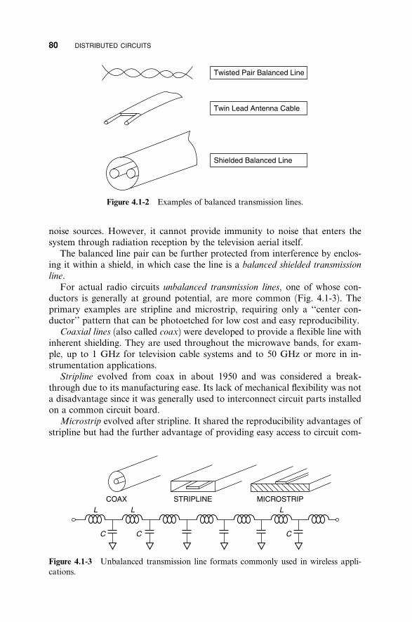
80 DISTRIBUTED CIRCUITS
Figure 4.1-2 Examples of balanced transmission lines.
noise sources. However, it cannot provide immunity to noise that enters thesystem through radiation reception by the television aerial itself.
The balanced line pair can be further protected from interference by enclos-ing it within a shield, in which case the line is a balanced shielded transmission
line.For actual radio circuits unbalanced transmission lines, one of whose con-
ductors is generally at ground potential, are more common (Fig. 4.1-3). Theprimary examples are stripline and microstrip, requiring only a ‘‘center con-ductor’’ pattern that can be photoetched for low cost and easy reproducibility.
Coaxial lines (also called coax) were developed to provide a flexible line withinherent shielding. They are used throughout the microwave bands, for exam-ple, up to 1 GHz for television cable systems and to 50 GHz or more in in-strumentation applications.
Stripline evolved from coax in about 1950 and was considered a break-through due to its manufacturing ease. Its lack of mechanical flexibility was nota disadvantage since it was generally used to interconnect circuit parts installedon a common circuit board.
Microstrip evolved after stripline. It shared the reproducibility advantages ofstripline but had the further advantage of providing easy access to circuit com-
Figure 4.1-3 Unbalanced transmission line formats commonly used in wireless appli-cations.

WAVELENGTH IN A DIELECTRIC 81
ponents since there was no upper ground plane to get in the way of componentinstallation and tuning. However, microstrip’s format usually results in an in-
homogeneous dielectric medium, that is, a di¤ering dielectric media for variousportions of the transmission line’s cross section. This occurs because microstripis usually implemented as a conductor pattern on a dielectric material with airdielectric above the transmission line patterns.
As frequency increases, the capacitance between center conductor andground causes an increasingly larger percentage of the energy to propagatewithin the dielectric, resulting in a greater signal delay for higher frequenciesthan for lower frequencies. This variation in signal delay with frequency dis-torts wideband signals because their various frequency components experiencedi¤ering transmission delays through the inhomogeneous transmission linemedium.
4.2 WAVELENGTH IN A DIELECTRIC
The wavelength is the distance a sinusoid propagates in its period. Wavelength isreduced in proportion to the square root of the dielectric constant eR of thepropagating medium, since the speed of propagation is reduced in that pro-portion (Fig. 4.2-1). For a nonmagnetic dielectric
l0l ¼ pffiffiffiffiffiffi ð4:2-1aÞ
eR
cv ¼ pffiffiffiffiffiffi ð4:2-1bÞ
eR
f l ¼ v ð4:2-1cÞf l0 ¼ c ð4:2-1dÞ
Figure 4.2-1 E¤ect of dielectric material is to decrease propagation speed, and with it,wavelength.

82 DISTRIBUTED CIRCUITS
where l0 is the free space wavelength, c is the velocity of light in free spaceð2:9979� 108 m=sÞ, and l is the wavelength in the dielectric medium.
Typical transmission line dielectrics range from pure Teflon with relativedielectric constant, eR ¼ 2:03, to alumina (Al2O3) with eR ¼ 10. Sapphire is thesingle-crystalline form of alumina and is an ideal, albeit expensive, microwavedielectric. Ceramic materials are available with relative dielectric constants upto 100 for use as primary resonators for oscillator circuits. Pure water has adielectric constant of 81 [1] at RF and microwave frequencies.
Teflon material has very low dissipative loss and is a primary choice formicrowave circuit boards. However, in pure form, it both expands and coldflows substantially with temperature and therefore is usually reinforced withembedded glass fibers for dimensional stability. The glass often is woven into acloth fabric for reinforcing printed circuit (PC) boards. The presence of glassfibers increases the dielectric constant, and, if the fibers have a particular aver-age orientation, as occurs with woven fabrics, the result is a dielectric constantthat is a function of direction in the dielectric. Such a material is called an ani-
sotropic dielectric.To overcome the directional variation of dielectric constant the dielectric is
sometimes reinforced using small, randomly oriented glass fibers (microfibers),making it uniform in all directions. A popular microfiber circuit board materialis Rogers Duroid.
4.3 PULSES ON TRANSMISSION LINES
The concept of reflections on transmission lines can be visualized by consider-ing the reaction of an open-circuited transmission line when a voltage pulse issent down it.
Consider a voltage pulse applied to a lossless transmission line. The pulsepropagates at the speed of light in a transmission line with air or vacuum sur-rounding the conductors or propagates at reduced speed if the line is embeddedwithin a higher dielectric constant medium. For a lossless line, the pulse prop-agates along the line, as depicted in sketches 1 to 4 in Figure 4.3-1, its voltageundiminished with distance since there are assumed to be no dissipative orradiative losses. Associated with the voltage wave is a current wave. The ratioof voltage to current is Z0.
In this theoretical idealization, on reaching the open-circuited end, all of theincident energy must be reflected since it can neither be radiated nor storedthere. Of course, on a real open-circuited transmission line, some dissipativeand radiative losses would occur, but we ignore them in this example.
Since all of the power of the pulse must be reflected at the open end of theline, the situation is equivalent to the introduction of a reverse-going pulse thatis otherwise identical to the incident pulse. At the open circuit the current mustbe zero. To satisfy this condition, the reflected current must be directed oppo-site to the incident current. This requires that the associated reflected voltage

INCIDENT AND REFLECTED WAVES 83
Figure 4.3-1 Pulse on lossless transmission line and its reflection from the open-circuited end.
have the same polarity as the incident voltage, which results in a doubling ofthe voltage at the end of the line.
The total voltage on the line is equal to the sum of the incident and reverse-going pulses (sketches 4 to 7 of Fig. 4.3-1). Since the reflected voltage wave hasthe same amplitude as the incident wave, reflection from an open-circuit termi-
nated line produces a doubling of the voltage at the end of the line as the voltages
of the incident and reflected waves add together. The current at the end of theline is the sum of an incident current pulse and an equal magnitude but oppo-sitely directed reflected current pulse, resulting in a net current of zero. Wewould expect this at an open-circuit termination.
After reflection at the open-circuit end of the line, the pulse travels backtoward its source. At the source the pulse could again reflect if the sourceimpedance is not equal to the line’s characteristic impedance Z0. This pulseexample is useful in demonstrating physically how the doubling of voltageoccurs at the open-circuit termination of a transmission line. Similar reasoningshows that the current at a short-circuit termination of the transmission lineproduces a doubling of current at the line’s end and a zero voltage.
4.4 INCIDENT AND REFLECTED WAVES
Just as pulses on a transmission line that is open circuited produce a doublingof the incident voltage, so also do continuous sine waves when applied to thesame transmission line termination condition.

84 DISTRIBUTED CIRCUITS
Figure 4.4-1 (a) Incident and reflected sine waves on open-circuit terminated line and(b) the peak voltage magnitude as function of position x on the line.
In this case, however, the sine wave, of voltage VI , is continuously applied atthe source end. The reflected voltage VR, an identical sine wave propagatingback toward the generator, combines with it to produce a standing-wave pat-
tern, creating voltage maxima when VI and VR are in phase and minima whenthey are out of phase (Fig. 4.4-1). The peak voltage magnitude of the standing-wave pattern is shown in Figure 4.4-1b. The maxima and minima are separated
by a half wavelength due to the doubling of their relative velocities resulting from
their opposite directions of travel.In general, the net voltage at any point on the line is the result of the phasor
addition of VI and VR at that point. Note that the amplitude of the standing-wave pattern is not a sine wave. It is the envelope of the peak AC voltage as afunction of distance along the line. Such voltage (and the associated current)standing waves are analogous to those of waves in water that reflect from aseawall or other reflecting obstacle. In this example of a lossless line terminatedin an open circuit, the peak voltage is 2VA and the minimum voltage is zero. Atthe voltage nulls the current is 2IA where IA ¼ VA=Z0. This will be seen fromthe analysis of transmission lines to follow.

REFLECTION COEFFICIENT 85
4.5 REFLECTION COEFFICIENT
In the open-circuit load, lossless line case, the magnitudes of incident and re-flected voltages are equal, and at the ‘‘load’’ end of the line they are in phase.This produces the voltage doubling there. But for arbitrary loads, VI and VR
are neither equal in magnitude nor do they have the same phase. We define acomplex reflection coe‰cient at any point, x, on the line as
VRðxÞGðxÞ ¼ ¼ rJj ð4:5-1Þ
VI ðxÞ
where VR and VI are reflected and incident phasor voltages, respectively.On a lossless line the respective magnitudes of VI and VR do not change, thus
the magnitude of the reflection coe‰cient, r, does not change either. Only theangle j changes as the two waves travel by each other in opposite directions; jdepends upon the relative phases of VR and VI at the load as well as the elec-trical distance from the load.
For example, returning to the open-circuited case in Figure 4.4-1, since¼ 0�, VLOAD-INC þ VLOAD-REF ¼ 2, a voltage peak occurs at the load.jLOAD
On the other hand, if there is a short circuit at the load, the total voltage at theend of the line must be zero. Then jLOAD ¼ 180�, VLOAD-INC þ VLOAD-REF ¼ 0,and there is a voltage null at the load position.
In general, a line is terminated in some complex load, and the incident andreflected voltages have neither the same magnitudes nor are they precisely in orout of phase at the line’s terminus. The magnitudes of the voltage peak and nullvalues are
VMAX ¼ VIncidentð1þ rÞ ð4:5-2aÞ
VMIN ¼ VIncidentð1� rÞ ð4:5-2bÞ
where r is the ratio of the magnitude of the reflected wave to that of the inci-dent wave. One of the earliest microwave measurement techniques consists ofcutting a narrow longitudinal slot in a transmission line and moving a rectify-ing diode along the line to determine jVMAXj and jVMINj as well as the loca-tions of these maximum and minimum voltages relative to the load position.This is called a slotted line measurement. Prior to the development of thenetwork analyzer (about 1965) this was the only practical way to measure mi-crowave impedance. Special microwave oscillators having a 1-kHz amplitudemodulation were used in conjunction with standing-wave ratio (SWR) meters,consisting of tuned and calibrated 1-kHz amplifiers, to make the measurementmore sensitive and precise. The ratio of the maximum and minimum voltageamplitudes was and continues to be called the voltage standing-wave ratio, orVSWR, sometimes just SWR:

86 DISTRIBUTED CIRCUITS
VSWR ¼ jVMAXjjVMINj ¼
1þ r
1� rð4:5-3aÞ
and conversely
VSWR � 1r ¼ ð4:5-3bÞ
VSWR þ 1
4.6 RETURN LOSS
Relative to the incident power, return loss is the fraction of power returned from
the load:
Return loss ¼ r2 ðfractionÞ ¼ 20 log r ðdBÞ ð4:6-1Þ
Within the industry, VSWR and return loss are used as alternative means forspecifying match, even though the slotted line is rarely if ever used for mea-surements. A perfect match of the load to the transmission line occurs when
ZL ¼ Z0 ð4:6-2Þ
This condition produces no reflected wave, hence r ¼ 0 and VSWR ¼ 1. Thenall incident power is absorbed in the load; no power is reflected, and, whenexpressed in decibels, the return loss is �y.
4.7 MISMATCH LOSS
Relative to the incident power, mismatch loss is the fraction of power absorbed
(not returned) from the load:
Mismatch loss ¼ 1� r2 ðfractionÞ ¼ 10 logð1� r2Þ ðdBÞ ð4:7-1Þ
In fractional form, return loss and mismatch loss sum to unity. Care should betaken to study these definitions. It is a common error to confuse them. Table4.7-1 lists values of return loss and mismatch loss for various values of thereflection coe‰cient, r.
As an example, if the VSWR of a load is 1.5, r is 0.2, return loss is 0.04, andmismatch loss is 0.96. This means that the load absorbs 96% of the incidentpower and 4% is reflected. In decibels, the return loss is 14 dB and the mis-match loss is 0.18 dB. Notice that the minus sign for the losses in decibels isdropped conversationally because it is implied in the term ‘‘loss.’’ However,when using a network simulator, losses in decibels must be entered as negative
quantities.

MISMATCH ERROR 87
TABLE 4.7-1 Relationships Among Reflection Coe‰cient Magnitude, r, VSWR,
Return Loss and Mismatch Loss
VSWR Return Mismatch Mismatch
r
1þ r
1� r
Return LossFraction r2
Loss (dB)20 log r
Loss Fraction1� r2
Loss (dB)10 logð1� r2Þ
0 1.0 0 �y 1.0 00.01 1.02 0.0001 �40.0 0.9999 �0.00040.02 1.04 0.0004 �34.0 0.9996 �0.00170.05 1.11 0.0025 �26.0 0.9975 �0.0110.10 1.22 0.01 �20.0 0.99 �0.0440.15 1.35 0.0225 �16.5 0.9775 �0.0990.2 1.5 0.04 �14.0 0.96 �0.180.3 1.86 0.09 �10.5 0.91 �0.410.33 2 0.11 �9.6 0.89 �0.500.4 2.3 0.16 �8.0 0.84 �0.760.5 3 0.25 �6.0 0.75 �1.250.6 4 0.36 �4.4 0.64 �1.940.7 5.7 0.49 �3.1 0.51 �2.920.707 5.8 0.50 �3.01 0.50 �3.010.8 9 0.64 �1.94 0.36 �4.440.9 19 0.81 �0.92 0.19 �7.211.0 y 1.00 0.0 0.0 �y
4.8 MISMATCH ERROR
In Sections 4.6 and 4.7 return loss and mismatch loss were defined in termsof reflections at a mismatched load. However, these terms also can be appliedto the input of a two-port network terminated by a matched or mismatchedload. For example, a reactance connected in shunt with an otherwise match-terminated transmission line produces a reflection. For this circuit return lossand mismatch loss can be calculated.
Now, if there are two or more sources of reflection on the line (Fig. 4.8-1),the resulting reflections can combine to produce an overall reflection that de-pends not only upon the individual reflections but their reflective interactions as
Figure 4.8-1 Interaction between two reflecting networks separated by transmissionline length.

88 DISTRIBUTED CIRCUITS
well. To evaluate this combination, suppose two circuits, having G1 and G2
complex reflection coe‰cients are interconnected by a lossless transmission lineof electrical length y. For this discussion it is assumed that generator and loadare matched to each other and to the characteristic impedance of the line, inthis case normalized to Z0 ¼ 1.
Due to the multiple reflections between them and their spacing, the obstacleswill interact in a manner that causes their total insertion loss to vary. The lossof the combination may be higher or lower than their simple loss, that is, thesum of their individual mismatch losses that would be measured when they areseparately connected between generator and load.
The amount by which the actual loss di¤ers from the simple loss is called themismatch error, usually expressed in decibels. The term mismatch error arisesbecause, if we ignore their interaction and estimate their combined loss to betheir simple loss, we would encounter an error equal to this mismatch errorvalue. To analyze this reflection interaction it is useful to define the transmis-
sion coe‰cient T.At the point of reflection on a transmission line, we defined an incident
voltage VI and a reflected voltage VR. The phasor sum of these two voltages isthe total voltage VT . This is the voltage on the line at the point of reflection:
VT ¼ VI þ VR ð4:8-1Þ
The transmission coe‰cient T is the ratio of VT to VI , just as the reflectioncoe‰cient G is the ratio of VR to VI . Then it follows that
T ¼ 1þ G ð4:8-2Þ
where both T and G are complex numbers. Note that T can be greater thanunity. In fact, this occurs at the end of an open-circuited transmission line atwhich G ¼ 1 and T ¼ 2.
The situation when two sources of reflection exist on a transmission line isshown in Figure 4.8-2. An incident voltage V1 ¼ 1 encounters the first obstacleand the voltage at the first obstacle is T1. This voltage proceeds on toward thesecond obstacle. When T1 reaches the second obstacle, it is further a¤ected. In
Figure 4.8-2 The reflection interaction between two circuits separated by lossless linelength [1, p 407].
MISMATCH ERROR 89
the absence of reflections between the obstacles, the resulting voltage at thesecond obstacle would be V2 (expected). This voltage launches a wave travelingtoward the load as
V2 ðexpectedÞ ¼ T1T2e�jQ ð4:8-3Þ
The ‘‘expected’’ insertion loss (IL), or simple loss, of the two obstacles, ne-glecting their reflective interactions, would be the sum of their individual mis-match losses or
�1IL ðexpectedÞ ¼ 20 logjT1j�1 þ 20 logjT2j ð4:8-4Þ
where the negative exponents are used in order that IL is a positive numberwhen expressed in decibels.
However, when T1 reaches the second obstacle, a part of its energy is re-flected by it. This reflected wave travels back toward the first obstacle at whicha third reflection occurs. The process continues in a manner similar to that ofthe multiple reflections occurring between facing, partially reflecting mirrors,creating an infinite series of reflections and re-reflections.
The initial waves and the multiple reflections are as described in Figure4.8-2. Each time the reflections make a round trip between obstacles, they gainan additional phase change of e�2jy as well as the factor G1G2. Each such roundtrip path adds another term to the expression for the V2 wave traveling towardthe load. The result is an infinite series of terms:
V2 ¼ T1T2e�jy½1þ G1G2e
�2jy þ ðG1G2e�2jyÞ2 þ � � � � ð4:8-5Þ
V1
The magnitude of the quantity outside the brackets, jT1T2j, is the simple lossratio. The quantity inside the square brackets, 1þ G1G2e
�2jy þ ðG1G2e�2jyÞ2 þ
� � � , is the e¤ect of the reflective interaction between the two obstacles on thetransmission line. Fortunately, this infinite series has a closed form [2, pp. 2–3],namely
131þ xþ x2 þ x þ � � � ¼ for jxj < 1 ð4:8-6Þ1� x
Because jG1G2e�2jyj < 1 for passive obstacles, (4.8-5) reduces to
V2 ¼ T1T2e�jy½1þ G1G2e
�2jy��1 ð4:8-7ÞV1
Since insertion loss is IL ¼ 20 logjV1=V2j, the actual insertion loss for the cir-cuit in Figure 4.8-2 is
�1IL ðactualÞ ¼ 20 logjT1j�1 þ 20 logjT2j þ jMEj ðdBÞ ð4:8-8Þ

90 DISTRIBUTED CIRCUITS
where ME is called the mismatch error and given by
ME ¼ 20 log10j1� G1G2e�j2yj ðdBÞ ð4:8-9Þ
The mismatch error can either increase or decrease the base insertion loss of thetwo obstacles. The extreme values for ME are given, respectively, by using theþ and � options. That is,
ME ðextreme valuesÞ ¼ 20 log½1G r1r2� ð4:8-10Þ
where r1 and r2 are the magnitudes of the reflection coe‰cients.The larger the product of the reflection coe‰cients, the larger the mismatch
error, and accordingly the larger the spread between maximum and minimummismatch loss values. Customarily, it is usually the extreme mismatch error
values that are called the mismatch errors because they are the error limits thatcan be experienced by ignoring the interaction of two reflections spaced along atransmission line. Notice that the mismatch error occurs between each pair of
obstacles. If there are three obstacles spaced along a transmission line, there canbe two separate mismatch errors.
A mismatch error can occur between a practical generator (or measurementsystem) and the reflections of a device under test if the generator is not perfectlymatched to the transmission line. Mismatch errors also occur between con-nectors when neither has a unity VSWR and/or when one or more imperfectlymatched connectors interact with an imperfectly matched device to which theyare attached. In summary a mismatch error can arise whenever two causes of
reflection are spaced along a transmission system.Mismatch errors are especially large with cascaded reactive filters because
these circuits accomplish their filtering action by reflecting power in the stop-band. For example, suppose that two reactive filters are connected in cascade,each having 20 dB of isolation (when installed between matched source andload) at a frequency we wish to block. We would expect, neglecting reflectiveinteraction, to obtain 40 dB of isolation in the stopband, the sum of the sepa-rate isolation values of the two filters. However, to provide 20 dB of isolationreactively, each filter must have r ¼ 0:995, or r2 ¼ 0:99. For the pair of filtersthe mismatch error limits are
MEþ ¼ 20 logð1þ 0:99Þ ¼ þ6 dB ð4:8-11aÞME� ¼ 20 logð1� 0:99Þ ¼ �40 dB ð4:8-11bÞ
In the first case, MEþ has the same sign as the base losses. Thus, under idealspacing of the filters, we can obtain 46 dB of stopband isolation. This is 6 dBgreater isolation than expected from the simple addition of the individual iso-lation values. However, in the second case, ME�, which occurs with the leastoptimal spacing, placing two lossless, reactive 20-dB filters in cascade may yield

THE TELEGRAPHER EQUATIONS 91
0 dB of total attenuation. Nor is this unfavorable spacing unlikely since thestopband may represent a very wide frequency bandwidth over which the leastfavorable electrical spacing is likely to occur at various stopband frequencies.
Of course, real filters, even if designed as reactive networks, have finite loss,and the observation of 0 dB loss for a pair of them is a limiting, but unreal-izable condition. Nevertheless, the calculation shown above suggests that asubstantial reduction in isolation from that expected when ignoring VSWR in-teraction is readily possible, dependent upon their electrical spacing at eachstopband frequency.
Interestingly, there is another way of treating an interacting pair of mis-matches using their VSWR values [3, Example 4.5, 8]. The overall VSWR dueto a pair of dissipationless mismatches having individual VSWR values SWR1
and SWR2 (where SWR1 > SWR2) that are referenced to and separated by alength of lossless Z0 line can range from SWR1=SWR2 to ðSWR1ÞðSWR2Þ.
Applying this to the previous example, for a reactive filter providing 20 dBof isolation, 1=ð1� r2Þ ¼ 100, therefore r ¼ 0:994987 and the correspondingSWR1 ¼ SWR2 ¼ 397:997487. Since the VSWRs are equal, SWR1=SWR2 ¼ 1and their minimum insertion loss is 0 dB. The maximum VSWR ¼ ð397:99Þ2 ¼158;402. The corresponding r ¼ 0:999987. The return loss is 1=ð1� r2Þ ¼39;601 ¼ 45:98 dB, which probably agrees with the prior estimates of 0 and 46dB within the accuracy of the significant figures carried in the calculations.
4.9 THE TELEGRAPHER EQUATIONS
To establish a mathematical basis for the analysis of transmission lines, weshall use a uniform line equivalent circuit that includes line losses, as shown inFigure 4.9-1. Note that, while the series elements are shown only in the upperconductor, this equivalent circuit is applicable to both balanced and unbal-anced transmission lines. Also, this analysis applies to any waveforms thatpropagate on the transmission line, not just sinusoidal excitations.
In this equivalent circuit R;L;G, and C are, respectively, the series resis-tance, series inductance, shunt conductance, and shunt capacitance per unit
Figure 4.9-1 Equivalent circuit, including losses, for infinitesimally short length ofuniform transmission line.

92 DISTRIBUTED CIRCUITS
length of the transmission line. The small section of transmission line can beanalyzed by applying Kirchho¤ ’s laws and taking the llimit as this circuitlength tends to zero to obtain the di¤erential equations for the circuit [4, p. 23].Kirchho¤ ’s voltage law requires that the sum of the voltages about a closedloop is zero. Thus
qiðx; tÞvðx; tÞ � RDx iðx; tÞ � LDx � vðxþ Dx; tÞ ¼ 0 ð4:9-1Þ
qt
Similarly, applying Kirchho¤ ’s current law, which requires that the sum of thecurrents into a circuit node be zero, gives
iðx; tÞ � GDx vðxþ Dx; tÞ � C Dxqvðxþ Dx; tÞ � iðxþ Dx; tÞ ¼ 0 ð4:9-2Þ
qt
For the above two equations, divide all terms by Dx and let Dx ! 0. Note thatas Dx ! 0
vðxþ Dx; tÞ ! vðx; tÞiðxþ Dx; tÞ ! iðx; tÞ
Also,
vðxþ Dx; tÞ � vðx; tÞ qvðx; tÞ!Dx qt
iðxþ Dx; tÞ � iðx; tÞ qiðx; tÞ!Dx qt
The resulting di¤erential equations in (4.9-3) are the time-domain form of thetransmission line equations and are called the telegrapher equations, presum-ably because their initial use was in the analysis and design of long telegraphlines:
qvðx; tÞ qiðx; tÞ¼ �Riðx; tÞ � L ð4:9-3aÞqx qt
qiðx; tÞ qvðx; tÞ¼ �Gvðx; tÞ � C ð4:9-3bÞqx qt
4.10 TRANSMISSION LINE WAVE EQUATIONS
These telegrapher equations apply for any time-varying vðx; tÞ and iðx; tÞ on thetransmission line. In the steady-state sinusoidally excited case, they reduce to

TRANSMISSION LINE WAVE EQUATIONS 93
dVðxÞ ¼ �ðRþ joLÞIðxÞ ð4:10-1aÞdx
dIðxÞ ¼ �ðG þ joCÞVðxÞ ð4:10-1bÞdx
in which R;L;G, and C are per unit length and VðxÞ and IðxÞ are the phasorforms of vðx; tÞ and iðx; tÞ, whose time variation is implicit. These two equa-tions can be solved simultaneously to yield two equations, one a function ofonly V and the other a function of only I . To do so, for example, di¤erentiatethe second equation with respect to x to get
d 2IðxÞ dVðxÞ¼ �ðG þ joCÞdx2 dx
or
dVðxÞ 1 d 2IðxÞ¼ � ð4:10-2Þdx G þ joC dx2
Then substitute this value for dVðxÞ=dx into (4.10-1a).
d 2IðxÞ � ðRþ joLÞðG þ joCÞIðxÞ ¼ 0dx2
or
d 2IðxÞ � g2IðxÞ ¼ 0 ð4:10-3aÞdx2
Using the same procedure, (4.10-1b) yields
d 2VðxÞ � g2VðxÞ ¼ 0 ð4:10-3bÞdx2
in which we define pffiffiffiffiffiffiffiffiffiffiffiffiffiffiffiffiffiffiffiffiffiffiffiffiffiffiffiffiffiffiffiffiffiffiffiffiffiffiffiffiffiffiffiffi g1 ðRþ joLÞðG þ joCÞ ð4:10-4Þ
Solving di¤erential equations involves removing the di¤erentials (integrating)by guessing or recognizing the solution from prior di¤erentiation experience.The only functions that are unchanged after double di¤erentiation are the ex-ponentials, eGgx. (A close possibility would have been sin gx, however, twicedi¤erentiating sin gx would give minus sin gx.) A second-order di¤erentialequation such as this should have two independent solutions. In this case the

94 DISTRIBUTED CIRCUITS
two solutions correspond to the two values for the G sign, they are
d 2egx �gxgx¼ g2e and
d 2e ¼ g2e�gx
dx2 dx2
Accordingly, the sum of these two solutions represents the complete solution toeither (4.10-3a) or (4.10-3b).
VðxÞ ¼ VIe�gx þ VRe
þgx ð4:10-5aÞIðxÞ ¼ II e
�gx � IReþgx ð4:10-5bÞ
where g is the propagation constant for the voltage and current waves. Use ofthe negative sign before IR in (4.10-5b) results in the same value for the reflec-tion coe‰cient for I as for V . Physically the two terms in each equation corre-spond to waves propagating, respectively, in the þx and �x directions. Thesetwo equations are called the wave equations for a uniform transmission line.
4.11 WAVE PROPAGATION
The terms with negative exponents (such as VIe�gx) correspond to a wave
propagating in the þx direction, from left to right in Figure 4.9-1. Since thegenerator is attached at the left and the load at the right in Figure 4.9-1, thiscorresponds to an incident wave, hence the subscript I . Similarly, the positiveexponent terms (such as VRe
þgx) correspond to a wave traveling in the �x di-rection and represent a reflected wave in our convention. These use the sub-script R.
The total voltage at any x location on the line is the phasor sum of the inci-dent and reflected voltages, VðxÞ ¼ VI ðxÞ þ VRðxÞ and IðxÞ ¼ II ðxÞ � IRðxÞ.We can cast the relationship between VðxÞ and IðxÞ into the format of imped-ance by resorting to their interrelation expressed in either (4.10-1a) or (4.10-1b).For example, invoking (4.10-1a) and substituting into it the value for VðxÞgiven by (4.10-5a) gives
dðVIe�gx þ VRe
þgxÞ1 dVðxÞ 1IðxÞ ¼ � ¼ �
Rþ joL dx Rþ joL dx ð4:11-1ÞIðxÞ ¼ g ðVIe
�gx � VReþgxÞ
Rþ joL
From this we see that the current, IðxÞ has terms that are of the same form asthose of the voltage VðxÞ, but there is a negative sign between them. This isbecause the current convention for reflected waves reverses while that for vol-tages does not.

WAVE PROPAGATION 95
The factor ðRþ joLÞ=g has the dimensions of impedance and is called thecharacteristic impedance Z0 of the transmission line. It can be rewritten as
Rþ joL Rþ joLZ0 ¼ ¼pffiffiffiffiffiffiffiffiffiffiffiffiffiffiffiffiffiffiffiffiffiffiffiffiffiffiffiffiffiffiffiffiffiffiffiffiffiffiffiffiffiffiffiffi
g ðRþ joLÞðG þ joCÞsffiffiffiffiffiffiffiffiffiffiffiffiffiffiffiffiffiffiffi ð4:11-2ÞRþ joL
Z0 ¼G þ joC
With this definition, the equation for IðxÞ has exactly the form of Ohm’s law,noting that the minus sign between terms accounts for the reversal of currentdirection for a reflected wave. In other words, Z0 is the ratio of the respective
voltage to current of waves traveling in either direction:
VIIðxÞ ¼ II ðxÞ � IRðxÞ ¼ e�gx � VR
eþgx ð4:11-3ÞZ0 Z0
Notice that for a lossy line, for which R and G are nonzero, the characteris-tic impedance is a complex quantity that varies with frequency. However, forthe lossless line, the characteristic impedance is a constant, independent of fre-
quency and given by rffiffiffiffi L
Z0 ¼ ð4:11-4ÞC
For high frequency, low-loss transmission lines, (4.11-4) is a good approxima-tion, since oLgR and oCgG. For a transmission line with loss, the propa-gation constant g is a complex quantity. Conventionally this is written with realand imaginary parts as
pffiffiffiffiffiffiffiffiffiffiffiffiffiffiffiffiffiffiffiffiffiffiffiffiffiffiffiffiffiffiffiffiffiffiffiffiffiffiffiffiffiffiffiffi g ¼ aþ jb ¼ ðRþ joLÞðG þ joCÞ ð4:11-5Þ
where a and b are, respectively, the attenuation and phase constants of thetransmission line with units of reciprocal length. The real term, a, is responsiblefor loss and is expressed in nepers/unit length; and the imaginary quantity, b, isresponsible for phase change and is expressed in radians/unit length.
For a transmission line having loss, both the incident and reflected wavesdiminish in amplitude as they travel along the line due to dissipative and/orradiative losses. For an incident wave the amplitude diminishes with x accord-ing to the factor e�ax. For example, if a were 0.1 nepers/meter, then a wavetraveling 1 m would have its amplitude decreased by the factor e�0:1 ¼ 0:9.That is, the voltage of the traveling wave would be reduced by 10%. Sincepower is proportional to the square of the voltage, the power loss would beabout 19% or 0.8686 dB for this 1-m length of line.

96 DISTRIBUTED CIRCUITS
Notice that this example describes the conversion between loss in nepers anddecibels, namely Loss ðdBÞ ¼ 8:686 loss ðnepersÞ, conversely Loss ðnepersÞ ¼0:115 loss ðdBÞ. These conversions are listed in the inside cover summaries forconvenient reference.
As noted, the imaginary portion of the propagation constant b produces aphase change in the wave as a function of distance. It has the dimensions ofradians/unit length or, optionally, degrees/unit length. An any instant of time,with time frozen so to speak, a snapshot of the voltage amplitude along the lineof the incident wave (assuming there is no reflected wave for this example)would be a sinusoid. The distance between adjacent wave crests, or betweenadjacent troughs, or between any other similar pair of corresponding points ofthe wave sinusoid is the wavelength l. Since the sinusoid completes a cycle in2p radians, it follows that
2pb ¼ radians=unit length ð4:11-6aÞ
l
360�b ¼ degrees=unit length ð4:11-6bÞ
l
For the lossless line,
a ¼ 0 ð4:11-7aÞpffiffiffiffiffiffiffi
b ¼ o LC ð4:11-7bÞ
Usually one does not know explicitly the distributed L and C values for atransmission line. Conventionally, the transmission line Z0 is provided, alongwith the e¤ective relative dielectric constant eR of the line. Therefore, it is moreconvenient to determine electrical length by first determining the wavelength onthe line, finding the fraction of a wavelength of the circuit in question, andmultiplying either by 2p for length in radians or by 360� to obtain electricallength in degrees. This is demonstrated by the following example.
Electrical length can be expressed in either radians or degrees. For example,consider a 6 in. length ðx ¼ 6 in:Þ of coaxial cable having a polyethylene insu-lator between its inner and outer conductors, for which the relative dielectricconstant is 2.26. What is the cable’s electrical length y at 1 GHz? Since thewavelength in free space for a 1-GHz sinusoid is 11.8 in.,
x x ffiffiffiffiffi 360� ¼ 6 in: ffiffiffiffiffiffiffiffiffi 360� ¼ 275� ð4:11-8Þl 11:8 in:=
p2:26
y ¼ bx ¼ 360� ¼l0=
peR
Since 2p radians corresponds to 360�, the electrical length in radians is
y ¼ 275�6:28 ¼ 4:80 rad ð4:11-9Þ360�

PHASE AND GROUP VELOCITIES 97
Notice that it was not necessary to determine b explicitly. However, since thewavelength in the cable at 1 GHz is 7.85 in., then
360�b ¼ ¼ 45:9�=in: at 1 GHz ð4:11-10Þ
7:85 in:
Note from (4.11-7b) that b is frequency dependent. In a nondispersive trans-mission media (for which electrical length is proportional to frequency), b isdirectly proportional to frequency. Thus, at 1.2 GHz the same cable wouldhave a propagation constant of
1:2 GHzb ¼ 45:9�=in: ¼ 55:1�=in: at 1:2 GHz ð4:11-11Þ
1 GHz
and the same 6-in. cable would have an electrical length of 330� or 5.76 rad at1.2 GHz.
4.12 PHASE AND GROUP VELOCITIES
The incident wave, traveling from the generator toward the load, is, from(4.10-5a)
¼ VIe�gx ð4:12-1ÞVðxÞIncident
in which VI is a phasor with implicit sinusoidal time variation. Written ex-plicitly
axvðxÞI ¼ Re½VIe�gxe jot� ¼ Ce� cosðot� bxþ jÞ ð4:12-2Þ
where C is a constant amplitude factor and j is the initial phase of the wave att ¼ x ¼ 0. This is interpreted as a sinusoidal wave propagating in the þx di-rection with an exponential attenuation due to the factor a. The phase constantb is given in (4.11-6), namely, b ¼ 2p=l. A similar equation can be written forthe reflected wave that travels back toward the generator in the �x direction.The voltage vðx; tÞ has a constant phase forI
otbx ¼ ot or x ¼ ð4:12-3Þ
b
Therefore, a constant phase point on the traveling wave moves at a phase
velocity given by dx=dt or
ovP ¼ ð4:12-4Þ
b

98 DISTRIBUTED CIRCUITS
Thus, the voltage on the transmission line for either an incident or reflectedwave varies as [4, pp. 45–46]
e jðot�bxÞ ¼ e joðt�x=vPÞ ð4:12-5Þ
Any periodic function of time can be represented as a sum of sinusoidal wavesusing a Fourier analysis (see Section 7.27). If vP is the same for all of them,then their addition will faithfully reproduce along the line the temporal waveshape at the input, only delayed by the time of propagation x=vP. This is thepffiffiffiffiffiffiffi case for a lossless transmission line having g ¼ jb ¼ o LC for which
1vP ¼ pffiffiffiffiffiffiffi ð4:12-6Þ
LC
For lossless transverse electromagnetic (TEM) mode transmission lines, thevelocity at which a constant phase, vP, moves on the line and the velocity atwhich a packet of information, such as a modulation envelope, moves, vG, areidentical and simply equal to the velocity of propagation, v.
This produces a convenient means for determining the characteristic imped-ance of the TEM mode for a lossless line. Sincerffiffiffiffi
LZ0 ¼
C
and
1v ¼ p ffiffiffiffiffiffiffi
LC
Therefore,
1Z0 ¼ ð4:12-7Þ
vC
This equation provides a convenient expression for determining the character-istic impedance of a TEM mode, lossless transmission line if its distributedcapacitance and velocity of propagation are known.
However, for transmission lines having losses and for waveguides vP doesvary with frequency, dispersion occurs, and the signal waveform at the inputwill be distorted as its separate frequency components travel along the line atdi¤erent velocities. If the dispersion is significant, it may not be meaningful tospeak of a single propagation delay for a signal waveform. However, if thedispersion is moderate over the signal frequency bandwidth, an approximategroup velocity vG can be defined [4]. To determine its value, suppose that an
PHASE AND GROUP VELOCITIES 99
incident voltage wave, v1, consists of two frequencies that are traveling on theline, one lower and one higher in frequency than o0, respectively, having acombined value at x ¼ 0 given by
vI ðx ¼ 0; tÞ ¼ A½sinðo0 � doÞtþ sinðo0 þ doÞt� ð4:12-8Þ
Then, at a general point x on the line
vI ðx; tÞ ¼ Afsin½ðo0 � doÞt� ðb0 � dbÞx� þ sin½ðo0 þ doÞt� ðb0 þ dbÞx�g
in which b is assumed to be a function of o and hence is the reason for thedi¤erential db. Rearranging terms in the arguments gives
vI ðx; tÞ ¼ Afsin½ðo0t� b0xÞ � ðdo t� db xÞ� þ sin½ðo0t� b0xÞþ ðdo t� db xÞ�gð4:12-9Þ
Next, recognizing that the two sine terms are of the form sinðA� BÞ andsinðAþ BÞ, expanding them and simplifying gives
vI ðx; tÞ ¼ 2A cosðdo t� db xÞ sinðo0t� b0xÞ ð4:12-10Þ
This reveals that the total voltage on the line corresponds to a high frequencysinusoid varying at ot rate whose amplitude is modulated by
cos½ðdoÞt� ðdbÞx�
which varies with both time and distance. The modulation, itself, has theproperties of a traveling wave. A constant phase of the modulation occurs for
ðdoÞt ¼ ðdbÞx ð4:12-11Þ
from which a group velocity, vG ¼ x=t, can be defined as
dovG ¼ ð4:12-12Þ
db
This can be related to the phase velocity vP ¼ o=b as follows:
do do 1 1vG ¼ ¼ ¼ ¼
2db dðo=vPÞ ðd=doÞðo=vPÞ ½vP � oðdvP=doÞ�=vP ð4:12-13ÞvP
vG ¼1� ðo=vPÞðdvP=doÞ
This result was derived for only two frequencies, but using similar reasoning itcan be argued that a signal comprising many individual frequencies will travelwith an envelope velocity approximately equal to vG, if the dispersion is not
100 DISTRIBUTED CIRCUITS
too great. However, this will not be true for lines having large dispersion, butin those cases it is inappropriate to assign any velocity to such a modulationbecause its shape would be changing so rapidly as it propagates. The conceptof group velocity also is not meaningful when dvP=do is positive, a situationcalled anomalous dispersion, [4, p. 48] because then, as can be seen from(4.12-13) group velocity would appear to be infinite or negative.
4.13 REFLECTION COEFFICIENT AND IMPEDANCE
We can evaluate the reflection coe‰cient in terms of the load impedance bydividing (4.10-5a) by (4.11-3). For this evaluation let us choose x ¼ 0 at theload, then at the load location the exponential functions equal one and the loadimpedance ZL is given by
Vð0Þ VI þ VR 1þ VR=VIZL ¼ ¼ Z0 ¼ Z0 ð4:13-1Þ
Ið0Þ VI � VR 1� VR=VI
where VI and VR are phasor quantities. But GðxÞ ¼ VRðxÞ=VI ðxÞ is the defini-tion of the reflection coe‰cient and therefore
1þ GLZL ¼ Z0 ð4:13-2Þ
1� GL
where, in general, G and GL are complex numbers. Equivalently,
ZL � Z0 Y0 � YLGL ¼ ¼ ð4:13-3Þ
ZL þ Z0 Y0 þ YL
where Y0 ¼ 1=Z0. From this we see that there will be no reflected wave ifZL ¼ Z0, that is, when the load impedance is equal to the characteristic im-pedance of the line. Under this condition, all of the power incident on the linewill be absorbed in the load.
Since the choice of x ¼ 0 is arbitrary, (4.13-2) must apply for any x. It fol-lows that
1þ GðxÞZðxÞ ¼ Z0 ð4:13-4Þ
1� GðxÞ
and
ZðxÞ � Z0 Y0 � YðxÞGðxÞ ¼ ¼ ð4:13-5Þ
ZðxÞ þ Z0 Y0 þ YðxÞ
for all x.

�
� �
� �
� �
IMPEDANCE TRANSFORMATION EQUATION 101
4.14 IMPEDANCE TRANSFORMATION EQUATION
One of the most common tasks in microwave engineering is the determinationof how a load impedance ZL is transformed to a new input impedance ZIN by alength of uniform transmission line of characteristic impedance Z0 and electri-cal length y (Fig. 4.14-1).
To simplify this derivation, we assume that the line length is lossless. Withthe choice of x ¼ 0 at the load, the input to the line is at x ¼ �l, and the inputimpedance there is
e jbl þ GLe�jbl�
Vðx ¼ �lÞZIN ¼ Zðx ¼ �lÞ ¼ ¼ Z0 ð4:14-1Þ
e jbl � GLe�jblIðx ¼ �lÞNow substitute GL ¼ ðZL � Z0Þ=ðZL þ Z0Þ, bl ¼ y, the identities e jbl ¼cos bl þ j sin bl and e�jbl ¼ cos bl � j sin bl into (4.14-1), and remove cancel-ing terms to get
2ZL cos yþ j2Z0 sin yZIN ¼ Z0
2Z0 cos yþ j2ZL sin y� � ð4:14-2ÞZL þ jZ0 tan y
ZIN ¼ Z0Z0 þ jZL tan y
Similar reasoning can be used to evaluate the input impedance when the trans-mission line has finite losses. The result is
ZL þ Z0 tanh glZIN ¼ Z0 ð4:14-3Þ
Z0 þ ZL tanh gl
This is one of the most important equations in microwave engineering andis called the impedance transformation equation. Remarkably, (4.14-2) and(4.14-3) have exactly the same format when derived in terms of admittance. Forthe lossless line
YL þ jY0 tan yYIN ¼ Y0 ð4:14-4Þ
Y0 þ jYL tan y
Figure 4.14-1 Equivalent circuit of lossless uniform transmission line of electricallength y and characteristic impedance Z0 terminated in impedance ZL.
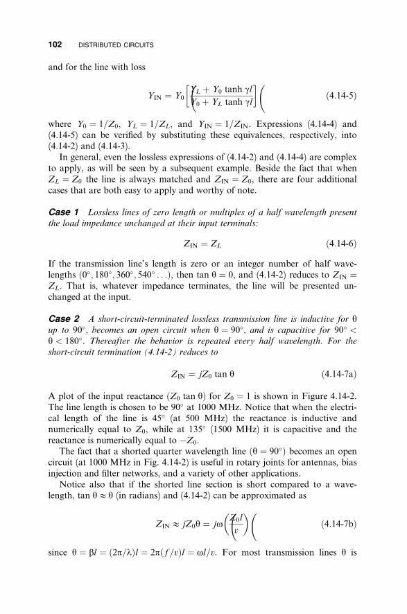
� �
� �
102 DISTRIBUTED CIRCUITS
and for the line with loss
YL þ Y0 tanh glYIN ¼ Y0 ð4:14-5Þ
Y0 þ YL tanh gl
where Y0 ¼ 1=Z0, YL ¼ 1=ZL, and YIN ¼ 1=ZIN. Expressions (4.14-4) and(4.14-5) can be verified by substituting these equivalences, respectively, into(4.14-2) and (4.14-3).
In general, even the lossless expressions of (4.14-2) and (4.14-4) are complexto apply, as will be seen by a subsequent example. Beside the fact that whenZL ¼ Z0 the line is always matched and ZIN ¼ Z0, there are four additionalcases that are both easy to apply and worthy of note.
Case 1 Lossless lines of zero length or multiples of a half wavelength present
the load impedance unchanged at their input terminals:
ZIN ¼ ZL ð4:14-6Þ
If the transmission line’s length is zero or an integer number of half wave-lengths ð0�; 180�; 360�; 540� . . .Þ, then tan y ¼ 0, and (4.14-2) reduces to ZIN ¼ZL. That is, whatever impedance terminates, the line will be presented un-changed at the input.
Case 2 A short-circuit-terminated lossless transmission line is inductive for yup to 90�, becomes an open circuit when y ¼ 90�, and is capacitive for 90� <y < 180�. Thereafter the behavior is repeated every half wavelength. For the
short-circuit termination (4.14-2) reduces to
ZIN ¼ jZ0 tan y ð4:14-7aÞ
A plot of the input reactance ðZ0 tan yÞ for Z0 ¼ 1 is shown in Figure 4.14-2.The line length is chosen to be 90� at 1000 MHz. Notice that when the electri-cal length of the line is 45� (at 500 MHz) the reactance is inductive andnumerically equal to Z0, while at 135� (1500 MHz) it is capacitive and thereactance is numerically equal to �Z0.
The fact that a shorted quarter wavelength line ðy ¼ 90�Þ becomes an opencircuit (at 1000 MHz in Fig. 4.14-2) is useful in rotary joints for antennas, biasinjection and filter networks, and a variety of other applications.
Notice also that if the shorted line section is short compared to a wave-length, tan yAy (in radians) and (4.14-2) can be approximated as
Z0lZINA jZ0y ¼ jo ð4:14-7bÞ
v
since y ¼ bl ¼ ð2p=lÞl ¼ 2pð f =vÞl ¼ ol=v. For most transmission lines y is

IMPEDANCE TRANSFORMATION EQUATION 103
Figure 4.14-2 Reactance of lossless short-circuited transmission line versus frequency(y ¼ 90� at 1 GHz).
linearly proportional to frequency, as is the impedance of an inductor, Z ¼joL. Therefore a short length of short-circuited terminated transmission line be-
haves as an inductor of value
Z0lLEFFA
yZ0 ¼ ðya 0:53 radÞ ð4:14-7cÞo v
For example, if a 1-cm length of Z0 ¼ 120 W, air coax line is terminated in ashort:
Z0l 120ð1 cmÞLEFFA ¼ ¼ 4 nH
v 3� 1010 cm=s
Since 1 cmA0:4 in:, the inductance of a high impedance air-dielectric lineis approximately equal to 10 nH/in., the approximation presented earlier in(2.12-6).
The approximation (4.14-7c) also applies to a short length of Z0 trans-mission line terminated in a load ZL provided that its characteristic imped-ance Z0 g jZLj, as can be verified by applying this condition and tan yAy in(4.14-2).
The approximation tan yAy occurs frequently and has an error magni-tude of less than 10% for values of y up to 0.524 rad (30�). A radian is
1360�=2pA57:3�. Thus 0.5 rad is nearly 12 of a wavelength. The values of y and

104 DISTRIBUTED CIRCUITS
TABLE 4.14-1 Approximating tan y by Its Argument y (in radians)
y (deg) 0 10 20 25 30y (rad) 0 0.175 0.349 0.436 0.524tan y 0 0.176 0.364 0.466 0.577Error in tan yAy 0 �0.6% �4.1% �6.4% �9.1%
tan y are compared in Table 4.14-1 along with the size of the error in using thisapproximation, showing that the error magnitude is less than 10% at y ¼ 30�
and diminishes rapidly for lesser values of y.
Case 3 An open-circuit terminated lossless transmission line is capacitive
for y up to 90�, becomes a short circuit when y ¼ 90�, and is inductive for
90� < y < 180�. Thereafter the behavior is repeated every half wavelength. Thus,from (4.14-4) with YL ¼ 0
YIN ¼ jY0 tan y or ZIN ¼ �jZ0 cot y ð4:14-8aÞ
This is plotted in Figure 4.14-3. Notice that the input reactance magnitude iscapacitive and equal to �Z0 when the line is 45� long (500 MHz). For y ¼ 90�
(1000 MHz in Fig. 4.14-3) the open-circuit load is transformed to a short cir-cuit at the input. It is inductive and equal to Z0 when 135� long (1500 MHz).The input repeats every half wavelength after 180�. The facility for trans-forming an open circuit to a short circuit is equally useful in a variety of mi-crowave circuits.
Figure 4.14-3 Normalized reactance of lossless open-circuited transmission line versusfrequency (electrical length ¼ 90� at 1 GHz).

IMPEDANCE TRANSFORMATION EQUATION 105
By using similar reasoning to that applied to a short section of a shortedtransmission line, and again applying the approximation tan yAy for smallvalues of y, a short section of open-circuited transmission line has a capacitiveadmittance given by
YINA jY0y ð4:14-8bÞ
Since BC ¼ oC and y ¼ ol=v, the equivalent capacitance is
CEFFAy ¼ l ðya 0:53 radÞ ð4:14-8cÞ
oZ0 Z0v
and a reactance of
1 Z0A ð4:14-8dÞoC y
For example, a section of 25-W line that is 20� long at 1 GHz has an equivalentcapacitance of
0:35 radCEFFA ¼ 2:2 pF
6:28� 1� 109 Hz� 25 W
Its reactance XC at 1 GHz is
1 25 WA ¼ 71 W
oCEFF 0:35
If a short length of Y0 line is connected to a load of admittance YL, it behavesas a shunt capacitance approximated by (4.14-8c) provided that jYLjfY0
ði:e:; jZLjgZ0Þ and tan yAy.
Case 4 The normalized input impedance to a quarter wavelength long trans-
mission line is the reciprocal of the normalized load impedance.When the transmission line is a quarter wavelength long, y ¼ 90�, and the
input impedance to the line is
Z0ZIN ¼ Z0 ð4:14-9Þ
ZL
Normalizing to Z0 (dividing all impedances by Z0),
1zIN ¼ ð4:14-10Þ
zL

106 DISTRIBUTED CIRCUITS
For this reason a quarter wavelength line is often called an impedance inverter.Notice that the normalized input impedance is equal to the normalized loadadmittance, that is,
1zIN ¼ ¼ yL ð4:14-11Þ
zL
where the normalized admittance yL ¼ YL=Y0 and Y0 ¼ 1=Z0.Later we will see that this property allows us to convert between admittance
and impedance using the Smith chart. Notice also that this impedance invertingproperty occurs not only for quarter wavelength length lines but for line lengthsthat are any odd multiple of a quarter wavelength ðl=4; 3l=4; 5l=4; . . .Þ.
In general, to transform any resistive load RL to a desired input resistanceRIN, one need only select a quarter wave line section having a Z0 that satisfiespffiffiffiffiffiffiffiffiffiffiffiffiffiffi
Z0 ¼ RINRL ð4:14-12Þ
As an example of the resistive transformation of a 90� line length, consider a50-W, quarter wavelength, transmission line terminated in 25 W. From (4.14-9)the input resistance is
Z0 50ZIN ¼ Z0 ¼ 50 ¼ 100 W ð4:14-13Þ
ZL 25
Thus, the 25-W resistive load has been ‘‘transformed’’ to an input resistance of100 W at 1 GHz, and the variation of the input impedance with frequency forthis case is shown in Figure 4.14-4.
It is a common but ill-advised practice to refer to the quarter wavelengthtransmission line as a quarter wave transformer because the inversion propertycan be used to transform a resistive load of one value to an input resistance ofanother value at a single frequency. However, this practice should be avoided.It is better to visualize it as a quarter wave impedance inverter, recognizing thateven that property is limited to a single frequency of operation.
The inversion changes the real parts of the load, but in addition the sign ofthe imaginary part is also reversed, turning an impedance with an inductivepart into one with a capacitive part or vice versa. For example, if in the priorcase, rather than a purely resistive load of 25 W, we had instead a load ofð25þ j25Þ W, the input impedance becomes
Z0 50 50 25� j25ZIN ¼ Z0 ¼ 50 ¼ 50
ZL 25þ j25 25þ j25 25� j25
ð2500Þð25� j25Þ¼ ¼ ð50� j50Þ W ð4:14-14Þ625þ 625
Notice that the transformation ratio of the real part is now 2 instead of the4 obtained with a purely resistive load. Equally noteworthy, notice that theimaginary part of the input impedance is capacitive whereas the load’s imagi-

IMPEDANCE TRANSFORMATION EQUATION 107
Figure 4.14-4 Variation of input impedance with frequency when 50-W ‘‘impedanceinverter’’ is used to match load of 25 W to input resistance of 100 W at 1 GHz.
nary part was inductive! Thus the action of the quarter wavelength transmission
line is quite di¤erent from that of an ideal impedance transformer, which simplymultiplies any impedance by a constant factor.
Also, an ideal transformer, which is well approximated at low frequencies bya pair of magnetically coupled wire windings, has a fixed impedance transfor-
mation ratio that is frequency independent. On the other hand, the impedancetransforming property of a quarter wave line section only approximates a con-stant transformation ratio for resistive loads and only over a narrow bandwidthcentered at the design frequency as shown in Figure 4.14-4. Despite these limi-tations, the quarter wavelength line section has considerable practical utility forits transforming properties.
The preceding four special transmission line cases demonstrate the insight tobe gained by application of the input impedance formula of (4.14-2). This for-mula is key to transmission line analyses. However, for complex load valuesand arbitrary line lengths, the formula can be quite tedious to apply. As anexample, suppose that we wish to find the input impedance to a 50-W line thatis 50� long and terminated in a load impedance of ð25þ j30Þ W (Fig. 4.14-5).

� �
108 DISTRIBUTED CIRCUITS
Figure 4.14-5 Example of determination of input impedance to length of 50-W trans-mission line terminated in a complex impedance of ð25þ j30Þ W.
Applying (4.14-2) gives
ZL þ jZ0 tan y 25þ j30þ j50 tan 50�ZIN ¼ Z0 ¼ 50
Z0 þ jZL tan y 50þ jð25þ j30Þ tan 50�
25þ jð30þ 59:6Þ 25þ j89:6¼ 50 ¼ 5050� 35:8þ j29:8 �14:2þ j29:8pffiffiffiffiffiffiffiffiffiffiffiffiffiffiffiffiffiffiffiffiffiffiffi 625þ 8027J74:4� 93:0J74:4�
¼ 50 pffiffiffiffiffiffiffiffiffiffiffiffiffiffiffiffiffiffiffiffiffi ¼ 50 202þ 888J64:5� 33:0J64:5�
¼ 141J10� ¼ ð139þ j24Þ W ð4:14-15Þ
Notice that the 25-W real part of the load has been transformed to 139 W andthat the þj30-W imaginary part of the load has been transformed to j24-W.From this it can be seen that, in general, the impedance transformation proper-
ties of a simple transmission line can be quite complex.It is tedious to perform this calculation and very easy to make a mathemat-
ical error while doing so, thereby obtaining an erroneous result. Also, the cal-culation must be re-performed for each frequency of evaluation.
It would be a considerable challenge to predict, using only (4.14-2), how ZIN
varies with y as it is varied over, say, 0� to 180�. This evaluation would requirecharting ZIN for numerous y values using the laborious calculation methoddescribed in (4.14-15). It was for this reason that Phillip Smith found an el-egant graphical solution to determine input impedance, the subject of the nextchapter.
4.15 IMPEDANCE MATCHING WITH ONE TRANSMISSION LINE
In the previous section it was shown that a length of transmission line cantransform a real load resistance to one of a di¤erent value. Accordingly, onemight ask whether any complex load impedance ZL ¼ RL þ jXL can be con-

� �
FANO’S (AND BODE’S) LIMIT 109
Figure 4.15-1 Conjugately matching complex load impedance ZL to a generator im-pedance ZG, using only transmission line of characteristic impedance Z0 and electricallength y.
jugately matched to any other complex source impedance, ZG ¼ RG þ jXG,merely by proper selection of a line length of the appropriate Z0 and electricallength y. The following derivation (refer to Figure 4.15-1) yields the conditionsunder which this can be achieved.
From (4.14-2) with ZIN set equal to the complex conjugate of ZG,
ZIN ¼ RG � jXG ¼ Z0ZL þ jZ0 tan y ð4:15-1ÞZ0 þ jZL tan y
Next, set the real and imaginary parts of this equation separately equal to eachother and solve for Z0 and y. Note that � jXG was used in the equation in orderthat ZIN will be the complex conjugate of ZG:sffiffiffiffiffiffiffiffiffiffiffiffiffiffiffiffiffiffiffiffiffiffiffiffiffiffiffiffiffiffiffiffiffiffiffiffiffiffiffiffiffiffiffiffiffiffiffiffiffiffiffiffiffiffiffiffiffiffiffiffiffiffi
RLðR2G L þ X 2Þ
Z0 ¼ G þ X 2Þ � RGðR2L ð4:15-2Þ
RG � RL
Z0ðRL � RGÞy ¼ tan�1 ð4:15-3Þ
RLXG � RGXL
The above equations are always mathematically valid, however, a practicalsolution exists only when the solution for Z0 is a real and finite number.
4.16 FANO’S (AND BODE’S) LIMIT
Type A Mismatched Loads
Over a given bandwidth there is a definite limit to how well one can tune amismatched termination. The most well known are called Fano’s limits. Fanoderived these interesting and useful results within a thesis project [5].

�
110 DISTRIBUTED CIRCUITS
Figure 4.16-1 Fano’s type A mismatched loads [5, 6].
One of Fano’s two integral equation limits applies to what he described astype A mismatched loads (Fig. 4.16-1). It is
ð � � y �1� po0ln� � doa ð4:16-1Þ�G Q0
where the reflection coe‰cient G is referenced to ZG and the real part of ZG isR, the same as the load resistance R in Figure 4.16-1.
Basically, (4.16-1) states that no matter what matching circuit is used, thearea under the lnð1=GÞ curve cannot exceed the value po0=Q. Given this limit,we would usually prefer that GMIN would be obtained over our specified band-width, o1 � o2, and then that G be unity for all other frequencies. This idealmatching requirement is shown in Figure 4.16-2.
In practice, of course, the matching behavior described in Figure 4.16-2 canonly be approximated using real tuning circuits, but the ideal limit serves as aninsightful restriction on how well a circuit can be tuned over a given band-width.
If we assume that the reflection coe‰cient is a constant equal to its mini-mum value in the passband, then the integral for the type A mismatched loadsreduces to a constant multiplied by the frequency interval:
ð � � � � y �1� �1� ln� � do ¼ ðo2 � o1Þ ln� � ð4:16-2Þ� �G��G0
where o1 is the frequency (in radians/second) at the lower band edge and o2 is

� � � �
FANO’S (AND BODE’S) LIMIT 111
Figure 4.16-2 Idealized GMIN match in the passband and total reflection ðGMIN ¼ 1Þ atall other frequencies [5, 6].
the upper band edge. We also define
Center frequency ¼ o0 ¼ pffiffiffiffiffiffiffiffiffiffiffi o1o2 ð4:16-3Þ
and
o2 � o1Fractional bandwidth ¼ Do ¼ ð4:16-4Þ
o0
Then for the type A mismatched load, assuming that a minimum and constantvalue of reflection coe‰cient, GMIN, could be obtained throughout the pass-band o1 � o2
� 1 � po0ðo2 � o1Þ ln a ð4:16-5Þ� � QLGMIN
Equivalently,
jGMINjb e�po0=Qðo2�o1Þ ¼ e�ðp=QÞð f0=Df Þ ð4:16-6Þ
where f0 ¼ o0=2p and Df ¼ ðo2 � o1Þ=2p.For example, assume there is a type A circuit consisting of a 50-W load re-
sistor in parallel with a 10-pF capacitor to be matched to a 50-W generator overthe 700- to 1100-MHz band. Notice that 10 pF presents a large susceptancein parallel with the 50-W load at the geometric center of this frequency band,877.5 MHz. In reactance terms, at 877.5 MHz this is a capacitive reactance ofonly 18.1 W!

112 DISTRIBUTED CIRCUITS
The minimum reflection coe‰cient magnitude, jGMINj, that we can expect toaverage over the band is found as follows.
First, calculate Q; f0, and Df :
pffiffiffiffiffiffiffiffiffiffiffiffiffiffiffiffiffiffiffiffiffiffiffiffiffi f0 ¼ ð700Þð1100Þ MHz ¼ 877:5 MHz
159XC ¼ ¼ 18:1 Wð10 pFÞð0:8775 GHzÞ
R 50 WQ ¼ ¼ ¼ 2:76
XC 18:1 W
D f ¼ 700� 1100 ¼ 400 MHz
Then
jGMINjb eð�p=QÞð f0=Df Þ ¼ eð�3:14=2:76Þð877:5=400Þ ¼ e�2:5 ¼ 0:082 ð4:16-7Þ
and the corresponding minimum average VSWR is
1þ jGMINj ¼ 1þ 0:082VSWRMIN ¼ ¼ 1:18 ð4:16-8Þ
1� jGMINj 1� 0:082
To examine this case, a 10-element ladder network was used as a matchingnetwork [10, Sec. 5.3]. The element values were selected arbitrarily, 10 nH forinductors and 10 pF for capacitors, and the circuit optimized using a networksimulator. The simulation goal was set equal to a 1.2 maximum VSWR overthe 700 to 1100 MHz bandwidth. The result, obtained once the optimizationappeared to produce little further improvement, is shown in Figure 4.16-3. Anaverage VSWR of about 1.3 was obtained over the 700 to 1100 MHz band-width, comparing moderately well with the theoretical limit of 1.18.
Type B Mismatched Loads
Similar reasoning can be used with Fano’s type B mismatched loads (Fig.4.16-4), for which Fano’s integral limit is
ð � � y 1 �1� Qln� � doa ð4:16-9Þ
0�G� po0o2
The limits for both type A and type B mismatched loads are commonly at-tributed to Fano [5]; however, Fano, himself, credits the limit for the type Acircuits to Bode [7]. Whatever their origin, the limits give a useful insight intothe problem of broadband matching.
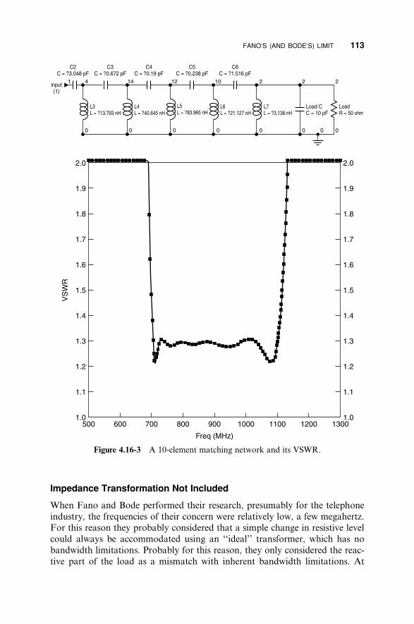
FANO’S (AND BODE’S) LIMIT 113
Figure 4.16-3 A 10-element matching network and its VSWR.
Impedance Transformation Not Included
When Fano and Bode performed their research, presumably for the telephoneindustry, the frequencies of their concern were relatively low, a few megahertz.For this reason they probably considered that a simple change in resistive levelcould always be accommodated using an ‘‘ideal’’ transformer, which has nobandwidth limitations. Probably for this reason, they only considered the reac-tive part of the load as a mismatch with inherent bandwidth limitations. At

114 DISTRIBUTED CIRCUITS
Figure 4.16-4 Fano’s type B mismatched loads [5, 6].
microwave frequencies the construction of a transformer that approximatesfrequency-independent behavior is not as practical. Thus, the usefulness ofFano’s limits at microwave frequencies are mainly confined to those cases forwhich the load has the correct resistive value ðR ¼ ZGÞ but has some series orshunt reactance that must be tuned using a matching network.
REFERENCES
1. Joseph F. White, Microwave Semiconductor Engineering, Noble Publishing, Nor-cross GA, 1995. Extensive treatment of PIN diodes and their switching and phase
shifting applications. Also includes fundamentals of microwave circuits.
2. L. B. W. Jolley, Summation of Series, 2nd rev. ed., Dover, New York, 1961.
3. Peter A. Rizzi, Microwave Engineering, Passive Circuits, Prentice-Hall, EnglewoodCli¤s, NJ, 1988. Excellent microwave engineering textbook covering theory and de-
sign of transmission lines, couplers, filters, and numerous other passive devices.
4. Simon Ramo and John R. Whinnery, Fields and Waves in Modern Radio, Wiley,New York, 1944, and 1953. This is a classic introductory text describing electro-
magnetic fields and Maxwell’s equations.
5. R. M. Fano, ‘‘Theoretical limitations on the broad-band matching of arbitrary im-pedances,’’ Journal of the Franklin Institute, Vol. 249, 1950, p. 57. Also see his doc-
toral thesis from the Massachusetts Institute of Technology (1947) and Technical
Report No. 41, Massachusetts Institute of Technology, Research Laboratory of Elec-
tronics.
6. Theodore Grosch, Small Signal Microwave Amplifier Design, Noble Publishing,Norcross, GA, 1999. A thorough derivation of all of the important formulas for tran-

EXERCISES 115
sistor amplifier design and evaluation, based on the S parameters of the transistor and
the circuit that surrounds it.
7. H. W. Bode, ‘‘A method of impedance correction,’’ Bell System Technical Journal,Vol. IX, October 1930, Sections 10.7 and 10.8, pp. 794–835.
8. Theodore Saad (Ed.), The Microwave Engineer’s Handbook, Vols. I and II, HorizonHouse Microwave (now Artech Books, Canton, Massachusetts) 1971. An excellent
collection of graphs and charts useful in microwave engineering.
9. Simon Ramo, John R. Whinnery, and Theodore Van Duzer, Fields and Waves in
Communication Electronics, 3rd ed., Wiley, New York, 1994. This is the updated
version of [4].
10. Devendrak K. Misra, Radio Frequency and Microwave Communication Circuits,Wiley, New York, 2001. This is a well-written communication text and reference.
EXERCISES
E4.1-1 A manufacturer of PIN switching diodes proposes to make a broad-band switch module consisting of a PIN diode in shunt with a 50-Wtransmission line. When the diode is reverse biased, it appears as a0.5-pF capacitor in shunt with the transmission line and is to passsignals with minimum reflection.
He suggests to you that if the hookup wires (from the top of thediode to the center conductor of the line and shown as L1 and L2above) are designed to have inductance values to satisfy
rffiffiffiffi L
Z0 ¼ ¼ 50 WC
the module will be electrically indistinguishable from a length of50-W line and consequently will provide matched transmission at allfrequencies.
a. What should the hookup wire inductances (L=2 each) be made tosatisfy the above relation?
b. Is it correct that this will provide an infinitely broadband trans-mission match?

116 DISTRIBUTED CIRCUITS
c. Test your answer on a network simulator over the bandwidth 0 to10 GHz.
E4.1-2 A 50-W air dielectric coaxial transmission line has an inner diameterof the outer conductor equal to 0.500 in. and a center conductor di-ameter of 0.217 in. What is its distributed capacitance per inch?
E4.4-1 A voltage wave with 100-V peak amplitude is incident on a trans-mission line extending in the z direction. When it reaches the load,one quarter of its power is reflected back toward the generator whichis matched to the line.
a. What is the peak voltage on the line between generator and load?
b. What is the minimum voltage on the line between generator andload?
c. Sketch the manner in which the incident and reflected waves addand subtract along the line as z changes for a fixed time t.
E4.5-1 a. What is the magnitude of the reflection coe‰cient in E4.4-1?
b. What is the VSWR?
E4.5-2 A friend has just purchased a boat containing a marine radio. Theradio has a built-in VSWR meter that indicates that the antenna hasa VSWR of 3 to 1.
a. How much does this reduce the radiated power of the transmitterrelative to that which would be radiated with a perfectly matchedantenna?
b. What would you advise to tune the radio to the antenna?
E4.8-1 Show that for a susceptance jB connected in shunt with an otherwisematched transmission line of characteristic impedance Z0, the mag-nitude of the transmission coe‰cient T is less than unity for allvalues of B.
E4.8-2 You wish to send the output of a 500-MHz signal source to anotherbuilding via a 50-W coaxial cable. The cable loss is 10 dB. whichmust be compensated by adding an amplifier at the output of thesource. When connected to the 50-W cable, the source sees the cableas a reflection with VSWR ¼ 10 (equivalently, the source outputVSWR is 10), and you have a 20-dB amplifier with input VSWR of20 to 1 referenced to 50 W. Neglecting other system interactions:
a. What will be the mismatch error in connecting this amplifier tothe source?
b. Will it overcome the 10-dB cable loss in all cases?
E4.11-1 Show that the real part of the propagation constant, a, can be ap-proximated for a low-loss transmission line having R ohms/unitlength and no shunt conductance by

EXERCISES 117
RaA
2Z0
E4.11-2 Use the result you derived in Exercise 4.11-1 to estimate the loss indecibels at 1 GHz for 100 ft of JAN Type RG 224/U coaxial cablehaving a copper inner conductor of 0.106 in. diameter ðd1Þ and acopper outer conductor with 0.370 in. diameter ðd2Þ. Assume the re-sistivity for copper is 1:72� 10�8 W-m (then conductivity, s ¼ 5:8�107
W
/m) and neglect the conduction losses through the dielectric.Hint: Assume an equivalent current flow within one skin depth on the
conductor surfaces.
E4.14-1 Beginning with (14.4-2) verify that
� � YIN ¼ Y0
YL þ jY0 tan y
Y0 þ jYL tan y
E4.14-2 Show that a short length of Z0 transmission line terminated by a loadZL can be approximated as a series inductance LEFFAZ0y=o whenZ0 g jZLj.
E4.14-3 A ham radio friend has purchased a 52-MHz transmitter withmatched impedance antenna, both 50 W. He wishes to install the an-tenna on his roof and the transmitter in his study, a separation dis-tance of about 25 ft. Unfortunately, he only has a 75-W cable tomake the hookup. The relative dielectric constant of the cable’s di-electric is 2.8. Is there any way that he can retain the very goodmatch between transmitter and antenna using this cable?
E4.14-4 A resourceful engineer found a way to connect a 12.5-W load to a50-W generator without reflection when provided only with a spool of50-W cable. How did he do it?
E4.14-5 An error was made in the design of an integrated circuit narrow-bandamplifier with the result that its input impedance is ð50� j50Þ Winstead of 50 W. Your company mounts the integrated chip on a‘‘motherboard’’ printed circuit inside a housing with 50-W con-nectors. Vibration specifications preclude installing a lumped coilat the input to tune the amplifier. You propose to print a section of150-W transmission line on the motherboard in cascade between thechip and input connector, reasoning that it will appear inductive andhelp to tune the mismatch. Specifications require an input VSWR ofno more than 1.2.
a. What is the VSWR before this tuning?
b. How long should you make the 150-W line (in degrees or wave-lengths)?

118 DISTRIBUTED CIRCUITS
c. What is the VSWR after the proposed tuning? Does it meet theobjective of a VSWR ¼ 1.2 maximum?
E4.14-6 An engineer has a coil of coaxial cable and needs to determine itsdielectric material for a thermal analysis. He has been told that thedielectric material is either Teflon ðeR ¼ 2:03Þ or polyetheleneðeR ¼ 2:26Þ. He forms a line section D ¼ 1 m long, and he places ashort circuit at its load end. Then he connects the open end to aslotted line and examines the input impedance using a variable fre-quency generator. He finds that it has its first resonance (a short cir-cuit at the input) at 105.28 MHz. Can you say what the dielectricmaterial is?
E4.15-1 Can you find a 50-W perfectly matched input solution to E4.14-6 us-ing a properly chosen Z0 and electrical length? If so, what are thevalues?
E4.15-2 A load impedance of 10þ j10 W is to be matched to a 50-W genera-tor. Can this be done using only a section of transmission line incascade with the load? What is its Z0 and electrical length y?
E4.16-1 An available power amplifier design is being considered for an ap-plication requiring that the input VSWR not exceed 1.5 over the 1700to 2100 MHz band. The amplifier, however, has an input resistanceof 50 W that is shunted by 10 pF capacitance and presently does notmeet this specification.
a. What is f0 for the 1700 to 2100 MHz bandwidth?
b. What is the Q of this capacitively loaded input circuit?
c. What is Fano’s limit for the least VSWR obtainable over the 1700to 2100 MHz bandwidth?
d. What value of input shunting inductance will parallel resonate the10 pF. Use a network simulator to determine over what band-width the 1.5 VSWR can be achieved with this single shunt L ele-ment. Does this meet the amplifier requirement?
e. Using as many as six tuning elements and the network simulatoroptimizer, find a matching network that provides as low a VSWRover the 1700 to 2100 MHz bandwidth as you can achieve. Doesit meet the maximum 1.5 VSWR over the 1.7 to 2.1 GHz band-width?

� �
CHAPTER 5
The Smith Chart
5.1 BASIS OF THE SMITH CHART
Knowledge of the basis and use of the Smith chart, a graphical presentationof the reflection coe‰cient with normalized impedance as a parameter overlay,is a sine qua non for the microwave engineer. Originally created as an aid todetermining the input impedance to a transmission line, the Smith chart hasbecome a universal aid to the design of matching circuits and to the display ofmeasured data.
In the 1930s, when Phillip Smith [1–3] invented the graphical solution thatfacilitated the determination of how impedances were transformed by lengthsof transmission lines, digital computers were unavailable to engineers. Engi-neers employed graphing strategies to gain insight into the variations producedby the independent variables of complex formulas. However, such insight wasnot forthcoming by attempting directly to graph the input impedance formula(4.14-2), repeated below, for a transmission line.
ZL þ jZ0 tan yZIN ¼ Z0 ð5:1-1Þ
Z0 þ jZL tan y
The key to obtaining insight into this transformation was to recognize that,although impedance varies in a complex manner as one moves away from theload along a lossless transmission line, reflection coe‰cient variation is quite
simple! In traveling from the load to the generator along a lossless line, only the
angle of the reflection coe‰cient changes, not its magnitude (Fig. 5.1-1).The reflection coe‰cient is the complex ratio of the reflected to the incident
voltage waves. The total voltage on the line consists of the incident, VI , and thereflected, VR, voltages:
VðxÞ ¼ VIe�jbx þ VRe
þjbx
ð5:1-2ÞVðxÞ ¼ VIe
�jy þ VReþjy
GðxÞ ¼ VRðxÞ ¼ rJj� ð5:1-3ÞVI ðxÞ
High Frequency Techniques: An Introduction to RF and Microwave Engineering, By Joseph F. White. ISBN 0-471-45591-1 6 2004 John Wiley & Sons, Inc.
119

120 THE SMITH CHART
Figure 5.1-1 Moving from the load to generator on lossless transmission line, reflectioncoe‰cient changes in phase only because the amplitudes of incident voltage VI and thereflected voltage VR do not change.
where VRðxÞ ¼ VReþjy, VI ðxÞ ¼ VIe
�jy, and VRð0Þ=VI ð0Þ ¼ GLoad. Choosingx ¼ 0 at the load and moving an electrical distance y toward the generatorfrom the load causes the reflected wave VR to have a negative change of phase,equal to y, relative to its phase at the load. The incident wave VI has a positivechange of phase equal to y, but the incident voltage is in the denominator,hence
G ¼ GLe�2jy ð5:1-4Þ
Moving an electrical distance y from the load, the reflection coe‰cient argument
is reduced by �2y.This is a key relationship. We will make use of it frequently as we use re-
flection coe‰cient change to determine the input impedance of a transmissionline.
If the relationships of (4.13-4) and (4.13-5) are normalized to Z0 (all im-pedances divided by Z0), GðxÞ and zðxÞ ¼ ZðxÞ=Z0 are related by
1þ GðxÞzðxÞ ¼ ð5:1-5Þ
1� GðxÞzðxÞ � 1
GðxÞ ¼ ð5:1-6ÞzðxÞ þ 1
Both of these equations are bilinear transformations [4, p. 202]. That is, they areof the form
Azþ Bw ¼ ð5:1-7Þ
CzþD

BASIS OF THE SMITH CHART 121
where w and z are complex variables and A;B;C, and D are complex constantssatisfying
D ¼ AD� BC0 0 ð5:1-8Þ
The bilinear transformation is a one-to-one mapping that has been well studiedin the theory of complex functions. In the case of (5.1-5) and (5.1-6) this meansthat: Every point in the zðxÞ plane corresponds to a unique point in the GðxÞplane, and vice versa.
To illustrate this z and G correspondence, consider the example of the loadimpedance ð25þ j30Þ W terminating the 50� long, 50-W line described in Fig-ure 4.14-5 and evaluated in (4.14-13). Normalized, this impedance and thecorresponding reflection coe‰cient at the load are
zL ¼ 0:5þ j0:6 ð5:1-9Þ
GL ¼ zL � 1 ¼ 0:5þ j0:6� 1 ¼ 0:48J108� ð5:1-10ÞzL þ 1 0:5þ j0:6þ 1
Let us now determine the impedance at a point 50 electrical degrees from theload. To do so we decrease the angle of the reflection coe‰cient by twice theelectrical length ð50�Þ of the transmission line, or 100�, to obtain the reflectioncoe‰cient at an electrical distance y ¼ 50� from the load:
Gy ¼ GLe�2jy ¼ 0:48Jð108� � 100�Þ ¼ 0:48J8� ð5:1-11Þ
The corresponding normalized impedance is
1þ 0:475þ j0:07 ¼ 2:76þ j0:48zy ¼ 1þ Gy ¼ ð5:1-12Þ1� Gy 1� 0:475� j0:07
Zy ¼ zyð50 WÞ ¼ ð138þ j24Þ W ð5:1-13Þ
These results are plotted in the G plane diagram in Figure 5.1-2.Our strategy has succeeded. The load impedance 25þ j30 W was normalized
to the 50-W transmission line and the corresponding reflection coe‰cient de-termined ðGL ¼ 0:48J108�Þ. This reflection coe‰cient was transformed alongthe 50� long line by preserving its magnitude (0.48) and reducing its angleð108�Þ by twice the electrical length of the line ð100�Þ. The resulting reflectioncoe‰cient ðGL ¼ 0:48J8�Þ was used to calculate the normalized impedanceðzy ¼ 2:76þ j0:48Þ at the input to the line, and this value, when unnormalizedto 50 W, gives the input impedance Zy ¼ ð138þ j24Þ W. This is close to thevalue of ð139þ j24Þ W obtained for the same example in (4.14-13) by using theimpedance transformation formula. The small di¤erence in the real part islikely due to round-o¤ error. Notice that we are able to treat the electrical dis-

122 THE SMITH CHART
Figure 5.1-2 The G plane representation of load impedance zL normalized to 50 W andtransformed through a 50� length of 50-W transmission line.
tance of the line to the load, y, as a positive quantity, since the clockwise rota-tion of G takes its sign into account.
While successful, our strategy of using the simple rotation of G to calculatethe impedance transformation of a load by a line length has not resulted in anyreal economy of computational e¤ort due to the need to perform the complextransformations from z to G (5.1-6) and then from G to z (5.1-5).
However, we note that once a z plane point is mapped into the G plane it is
done once and for all, since the z and G points have a one-to-one correspon-dence (Fig. 5.1-3). Thus, plotting normalized impedance values in the G planein advance would permit entering the G unit circle directly with a normalizedload impedance value and, after performing the required 2y clockwise rotation,reading the corresponding normalized input impedance to the line. This is thebasis of the Smith chart.
However, performing this translation of the z to the G plane poses someobvious problems. First, the flags used to identify the corresponding z and Gpoints take up so much room on the G chart that it would be impractical toshow a su‰cient number of them to permit accurate plotting of z. Second, thez plane is semi-infinite for passive loads, corresponding to all impedances forwhich rb 0; hence an unduly large sheet of paper would be required to ac-

BASIS OF THE SMITH CHART 123
Figure 5.1-3 Mapping discrete impedance points from normalized z plane to G planeunder the transformation G ¼ ðz� 1Þ=ðzþ 1Þ.
commodate large impedances in the z plane. We note, however, that no suchproblem exists in the G plane, wherein all passive loads must yield a jGja 1,thereby fitting neatly within the unit circle.
This latter observation raises an interesting philosophical question. How canthe points of a semi-infinite area (the right half of the z plane) be mapped into afinite area within the jGja 1 circle? The answer is similar to that of the ques-tion: ‘‘How many angels can dance on the head of a pin?’’ The answer is: ‘‘Allthe angels can, because angels do not require any space.’’ Similarly, impedancepoints, no matter how many of them, take up no area and therefore can bemapped from any area into any other area.
The solution to the two problems stated above lies in finding a means ofmapping not individual points but contours from the z plane to the G plane.When we use the z plane, we find the intersection of the r ¼ const and x ¼const lines for the particular impedance at hand. Once these contours aremapped onto the G plane (the Smith chart), we can enter the G plane directly,using the normalized load impedance on a line; and, after the required clock-wise rotation, can read directly the corresponding normalized input impedanceat that point on the line. No complex calculations would be required to per-form the input impedance calculation of (5.1-1).
In summary, Philip Smith’s first important idea in developing the Smithchart was recognizing that reflection coe‰cient rather than impedance shouldbe used to track movement on a transmission line. The second important ideawas the mapping of r ¼ const and x ¼ const contours in the z plane to the Gplane. The G plane with this mapping of normalized impedance is called theSmith chart.

� �
124 THE SMITH CHART
5.2 DRAWING THE SMITH CHART
The normalized, passive impedance Smith chart is the polar plot of jGja 1 with
an overlay of r ¼ const and x ¼ const contours that relate G to z. Normalizingthe Smith chart allows its use with any characteristic impedance transmissionline. Alternatively, one can draw a Smith chart for use with a given absolutevalue of Z0, such as 50 W.
The normalized, passive impedance Smith chart consists of constant resis-tance and reactance contours mapped from the z to the G plane according tothe function
z� 1G ¼
zþ 1where z ¼ rþ jx; rb 0; �ya xaþy ð5:2-1Þ
The mapping function of (5.2-1) is a bilinear transformation, which has fourproperties important to the drawing of the Smith chart [4]. These are:
1. The semi-infinite right half of the z plane (for rb 0) is mapped into the
jGja 1 unit circle. (Note that the left half of the z plane for which r < 0would map into the semi-infinite area outside of the jGj > 1 circle, thenegative resistance domain.)
2. The transformation maps circles into circles, with straight lines being con-sidered circles of infinite radius and points being circles of zero radius.
3. The mapping is conformal (angle preserving). Contours in the z plane thatare orthogonal to each other will map into contours in the G plane thatlikewise are orthogonal to each other.
4. The mapping is analytic. Therefore, continuous contours in the z planeare mapped into continuous contours in the G plane.
Usually the reflection coe‰cient G is expressed in polar form as re jj or rJj;however, it is di‰cult to recognize the equation of a circle in this format unlessthe circle’s center lies at the origin. Therefore, to demonstrate this mapping, weexpress G in its Cartesian format, G ¼ e jj ¼ uþ jv, retaining the same coordi-nate center for both polar and Cartesian representations.
The relationships between polar and rectangular coordinates are, from polarto rectangular
u ¼ r cos j ð5:2-2aÞv ¼ r sin j ð5:2-2bÞ
and from rectangular to polar pffiffiffiffiffiffiffiffiffiffiffiffiffiffiffi r ¼ u2 þ v2 ð5:2-3aÞ
j ¼ tan�1 v ð5:2-3bÞu

� � �
DRAWING THE SMITH CHART 125
Because a complex function such as G ¼ uþ jv has two parts, real and imagi-nary, as does its complex independent variable, z ¼ rþ jx, it is not possible tograph GðzÞ versus z in a single plane as we would the real variable f ðxÞ versusx. Instead we will show how a contour in the z plane, such as r ¼ 2, is mapped
into a corresponding contour in the G plane.In this mapping task, we wish to set r ¼ const for one set of contours and
then x ¼ const for the other, orthogonal, set of contours to be drawn in the Gplane. To do this it proves convenient to use the relation that gives z as afunction of G. In this way z can be set either to a constant r or jx and theexpression solved for the G rectangular coordinates. Thus,
1þ Gz ¼ ð5:2-4Þ
1� G
where z and G continue to be functions of position x on the transmission line(not to be confused with normalized reactance, x).
The relation (5.2-4) can be rewritten as
rþ jx ¼ 1þ re jj 1� re�jj�
ð5:2-5Þ�jj1� re jj 1� re
Carrying out the indicated multiplication to remove the complex quantities�jj ¼from the denominator and noting that e jj � e�jj ¼ 2j sin j and e jj þ e
2 cos j we obtain
21� r2 þ 2jr sin j 1� u2 � v þ 2jv¼ ð5:2-6Þrþ jx ¼1þ r2 � 2r cos j 1þ u2 þ v2 � 2u
This complex equation requires that separately both the real and imaginaryparts of each side of the equation be equal to each other. Equating the realparts,
21� u2 � vr ¼ ð5:2-7Þ
1þ u2 þ v2 � 2u
We know from the properties of the bilinear transformation that (5.2-7) mustbe the equation of a circle in the G ¼ uþ jv plane for r ¼ const. But it requiressome algebraic manipulation [5, p. 75] to cast (5.2-7) into the easily recogniz-able expression for a circle with center at u1 þ jv1 and radius a, namely theformat
2ðu� u1Þ2 þ ðv� v1Þ2 ¼ a ð5:2-8Þ
To do so, rewrite (5.2-7) as

126 THE SMITH CHART
2rð1þ u2 þ v2 � 2uÞ ¼ 1� u2 � v
u2ðrþ 1Þ � 2urþ ðr� 1Þ þ v2ðrþ 1Þ ¼ 0
u2 � 2ur r� 1 rþ 1
rþ 1þrþ 1 rþ 1
þ v2 ¼ 0
� �2 � �2r 1
u� ð5:2-9Þrþ 1
þ v2 ¼rþ 1
The last form of (5.2-9) is the recognizable expression for a circle in the G planewith center at
ru ¼ jv ¼ 0
rþ 1
and radius equal to 1=ðrþ 1Þ. For example, the contour r ¼ 1 in the z plane ismapped into a circle having radius 0.5 and center at u ¼ 0:5, jv ¼ 0, as shownin Figure 5.2-1.
At this point in the mapping, we note that all impedance values having r ¼ 1as a real part must lie on the r ¼ 1 circle in the G plane. We do not yet knowhow to place specific impedances, on this circle, since we have not yet devel-oped the orthogonal x contours for the G plane. In a limited sense, we candeduce that G ¼ 0 when z ¼ 1þ j0, and that accordingly this impedance pointmust be the one at which the r ¼ 1 circle passes through the origin, since the
Figure 5.2-1 Contour r ¼ 1 in z plane is mapped into corresponding contour in G
plane.

DRAWING THE SMITH CHART 127
Figure 5.2-2 Constant-resistance lines of z plane map into circles tangent at u ¼ 1,jv ¼ 0 in G plane and centered on real axis.
corresponding reflection coe‰cient magnitude must be zero. We can also saythat at u ¼ 1, jv ¼ 0, G ¼ þ1 (an open circuit), and so this must correspond tothe z ¼ 1G jy point.
As additional contours are plotted, the constant r lines in the z plane mapinto circles that are tangent to each other at the u ¼ 1, jv ¼ 0 point in the Gplane, as shown in Figure 5.2-2.
Next, we map the orthogonal x ¼ const contours into the G plane. To do so,equate the imaginary parts on both sides of (5.2-6) to obtain
2vx ¼ ð5:2-10Þ
1þ u2 þ v2 � 2u
This is manipulated as
2v 1 1u2 � 2uþ 1þ v2 �
xþ
2¼
2x x� �2 � �21 1ðu� 1Þ2 þ v� ¼ ð5:2-11Þx x
For x equal to a constant, this is the equation of a circle with center at u ¼ 1,jv ¼ j=x and radius equal to 1=x. When contours are mapped for x ¼ �2;�1;�0:5; 0;þ0:5; 1, and 2, the results give partial circles within the jGja 1unity circle of the G plane. The circles can be extended beyond this region, butthe corresponding impedances have negative real parts, and our interest for

128 THE SMITH CHART
Figure 5.2-3 Constant-reactance x lines of z plane map into circles in G plane, but onlyportions of circles fall within the unit circle, corresponding to passive impedances.
now is the Smith chart for use with passive impedances only, that is, for reflec-tion coe‰cients no greater than unity. More about negative resistance Smithcharts later.
The contours in the G plane shown in Figures 5.2-2 and 5.2-3 form orthog-onal sets, mapping the z ¼ rþ jx values into the reflection coe‰cient plane, aswe desired. Notice that, while the contours are circular, at their intersectionstheir lines are at right angles (orthogonal) to each other. When both sets ofcontours (r ¼ const and x ¼ const) are combined, the result is the skeletal formof the Smith chart shown in Figure 5.2-4.
Notice that positive reactances (inductances) lie in the upper half and nega-
tive reactances (capacitances) in the lower half of the Smith chart (as was true inthe z plane).
The diagram of Figure 5.2-4 is very comprehensible because it shows theevolution of the Smith chart by presenting all of the necessary coordinates andscales. However, if the Smith chart is to be used graphically, as was the originalintent, it must contain many more impedance contours in order that impedancecan be read more precisely. For this reason the conventional format for theSmith chart is as shown in Figure 5.2-5.
Because so many r and x contours are required for a Smith chart that isto be used graphically to determine impedance transformations on transmis-sion lines, there is insu‰cient space within the jGj ¼ 1 circle to print explicitscales for the magnitude of reflection coe‰cient, even though reflection coe‰-
cient is the basis of the Smith chart. Also, the j is not used ahead of reactiveimpedances or susceptive admittances.
That the Smith chart fundamentally is a plot of reflection coe‰cient isemphasized here because it is not uncommon for individuals to become quite

DRAWING THE SMITH CHART 129
Figure 5.2-4 Smith chart showing both impedance contours r and jx as well as jGjcontours and G’s angle j in 90� segments.
adept at using the Smith chart to transform impedances yet forget, or neverhave been aware of, the fact that the Smith chart is just a polar plot of reflec-tion coe‰cient with impedance and/or admittance overlays.
Knowing this fact, it is easy to answer many other questions about trans-mission lines, such as what is the voltage magnitude at a given position x on theline. It is simply VI j1þ GðxÞj where G is readily read for any specified point onthe chart.
To facilitate the determination of reflection coe‰cient and other importanttransmission line parameters, there are radial scales printed at the bottom ofthe chart. These are used in combination with a pair of dividers to determine themagnitude of the reflection coe‰cient. Only the linear reflection coe‰cient mag-nitude scale, r, is necessary, since the angle of G can be read from the degreesscale on the periphery of the Smith chart. The other parameters, return loss,mismatch loss, and other values are readily determined, given r; but for con-venience separate radial scales for these values are also printed below the chart.
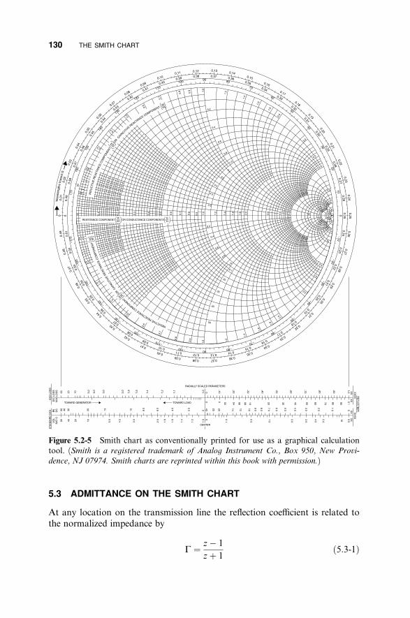
5.3 ADMITTANCE ON THE SMITH CHART
At any location on the transmission line the reflection coe‰cient is related tothe normalized impedance by
G ¼ z� 1
zþ 1ð5:3-1Þ
Figure 5.2-5 Smith chart as conventionally printed for use as a graphical calculationtool. (Smith is a registered trademark of Analog Instrument Co., Box 950, New Provi-
dence, NJ 07974. Smith charts are reprinted within this book with permission.)
130 THE SMITH CHART

ADMITTANCE ON THE SMITH CHART 131
Since normalized admittance y is just the reciprocal of normalized impedance z,
1=y� 1 1� yG ¼ ¼ ð5:3-2Þ
1=yþ 1 1þ y
where the bilinear transformation in (5.3-2) is simply the negative of the trans-formation in (5.3-1). That is, the reflection coe‰cient plot as a function of y is
identical to that of z except for a rotation within the G plane of 180�. When theadmittance coordinates for constant conductance g and constant susceptance bare plotted in the G plane, the result is the admittance version of the Smithchart, shown in Figure 5.3-1.
This plot is identical to that of the impedance plot in Figure 5.2-4 except fora 180� rotation about the center of the chart. All of the rules for transformingimpedance along a line length apply equally to admittances. With normalizedadmittances, the rotation moving from the load toward the generator remains
clockwise, as it was for impedances.
Figure 5.3-1 Smith chart with normalized admittance coordinates.

132 THE SMITH CHART
Inductors have positive reactance but negative susceptance. Capacitors havenegative susceptance but positive susceptance with the result that the upper halfof the Smith chart is always inductive and the lower half is always capacitive.
Due to the mirror symmetry of the impedance and admittance Smith charts,one could create an admittance Smith chart merely by rotating an impedancechart through 180�. In fact, for many years the practice was to consider that thenormalized coordinates in Figure 5.2-5 could be defined to be either admittanceor impedance, and the ‘‘standard’’ chart shown in Figure 5.2-5 was, and oftencurrently is, labeled ‘‘impedance or admittance coordinates.’’
The problem with defining these coordinates as admittance is that the angleof the reflection coe‰cient is in error by 180�, and this must be corrected wheninterpreting the ‘‘standard’’ Smith chart as an admittance Smith chart. Anotherproblem is that this practice is more prone to errors, since it is easy to forgethow the coordinates are presently defined, particularly since conversions be-tween admittance and impedance frequently must be made in the solution of aproblem.
The modern and preferred procedure is to print both normalized impedanceand admittance contours on the same Smith chart, overlaying the coordinatesderived in Figures 5.2-4 and 5.3-1, so that one can read directly at any givenpoint either value without resort to crossing or rotating the chart. The resultingSmith chart, having both impedance and admittance contours, is shown inFigure 5.3-2.
To aid the graphical use of this chart, it is usually printed in two colors, forexample, red for normalized impedance and blue for normalized admittance.Even so, as a graphical tool it is di‰cult to use. Fortunately, today there aresoftware versions of the Smith chart for use on a personal computer. Fewercontours need be drawn because the computer allows entry onto the chart atthe exact value of load impedance or admittance, creates the traces of trans-mission line and other transformations, and displays the exact value of inputimpedance or admittance, as will be seen. Furthermore, either impedance oradmittance contours or both can be displayed as desired. This will be demon-strated in the examples to follow.
5.4 TUNING A MISMATCHED LOAD
Originally, the Smith chart was developed to facilitate the determination ofload mismatch and the requisite tuning that would match it to the characteristicimpedance of the transmission line. While the chart has other useful applica-tions, this load tuning remains a principal application of the Smith chart.
Movement along a lossless line corresponds to a contour having a constantreflection coe‰cient magnitude, r, and thus a constant radial distance from thecenter of the Smith chart, that is, a circle with center at the center of the chart.The angle, j, of the reflection coe‰cient, G ¼ re jj ¼ rJj, changes at twice therate of movement along the line because it is the ratio of an incident and a

reflected wave, each of whose arguments change by an amount equal to themovement and their angles are additive in taking their ratio. Movement from
the load toward the generator on the Smith chart is clockwise.
To facilitate the computation of movements, the Smith chart has threeperipheral scales. The innermost scale gives degrees of the angle of G, a totalof 360� for the full circle. The outer two scales are labeled ‘‘wavelengthstoward the generator’’ and ‘‘wavelengths toward the load.’’ These two scales gothrough one-half wavelength for the full circle, thereby taking into account thatthe reflection angle changes by twice the angle of movement along the trans-mission line. This movement is demonstrated in the following example.
Figure 5.3-2 Smith chart with simultaneous impedance and admittance contours.
TUNING A MISMATCHED LOAD 133

For this example, we return to the case of Figure 4.14-5 consisting of að25þ j30Þ-W load at the end of a 50� long section of 50-W transmission line.Normalizing the load impedance to 50 W, it becomes 0:5þ j0:6. This is shownas point A in Figure 5.4-1.
To determine the arc length movement on the Smith chart, we note thattraveling 50� along the line toward the generator results in a reflection coe‰-cient angle change of �100� (clockwise rotation) to point B, at which we read anormalized impedance of 2:8þ j0:5. Unnormalized (multiplying both parts by50 W) this is ð140þ j25Þ W, reasonably close to the value of 139þ j24 calcu-lated in (4.14-15), given the graphical accuracy of the Smith chart, an analoginstrument. Note the economy of e¤ort with which this result is obtained rela-tive to the solution with the input impedance formula.
As an alternative to the determination of the arc length movement on theSmith chart, we can use the ‘‘wavelengths toward generator’’ scale. Traveling50� on the line toward the generator results in a clockwise movement on
Figure 5.4-1 A ð25þ j30Þ-W load (point A) on 50-W line with tuning to match it to50 W (point D).
134 THE SMITH CHART

SLOTTED-LINE IMPEDANCE MEASUREMENT 135
the chart by 50�=360� ¼ 0:139 wavelengths. This dimension is shown in Figure5.4-1 and results in the same travel from point A to point B.
From Figure 5.4-1 the value of the Smith chart is evident. The extendedcircular contour (shown dashed) at a constant radial distance from the center ofthe Smith chart reveals all of the normalized impedance values that would beencountered if the transmission line were extended to a half wavelength orlonger.
Specifically, we see that, if the transmission line is lengthened until the re-flection coe‰cient angle is �61� (point C) the normalized input impedance willbe 1:0� j1:1 (50 W� j55 W when unnormalized). At point C the total changein reflection coe‰cient angle measured from point A is �169�, correspondingto a total transmission line length of 84:5�. To reach point C we must add anadditional 34:5� of 50-W line, corresponding to a clockwise movement on thechart of an additional 0.096 wavelengths. At point C the insertion of an in-ductive reactance of 1.1 (55 W unnormalized) in series with the line cancels thecapacitive reactance and moves the normalized input impedance to 1 (50 Wunnormalized) at point D, thereby matching the load to the transmission line.
This example demonstrates that not only does the Smith chart facilitate the
calculation of the input impedance to a line terminated in a mismatched load, it
also readily reveals how the mismatch can be tuned to yield a matched input.This tuning method is not unique. Actually, there are an infinite number of
possible tuning approaches that can be determined with the skillful use of theSmith chart. By continuing clockwise on the dotted circular arc, an additional0.27 wavelength, between points C and A, respectively, of Figure 5.4-1, we canobserve the remainder of the wide range of normalized impedance values thatwould have been encountered on the transmission line had the electrical length,y, been varied from 0� to 180�. The total excursion is 0.5 wavelength, afterwhich we are returned to the starting impedance. This duplicate of the loadimpedance occurs every half wavelength multiple from the load along a losslessline, as was noted in Section 4.14.
In the current example, the real part of the normalized input impedancevaries between 0.33 and 3, a 9-to-1 ratio. The imaginary part varies between� j1:2 and þ j1:2. Using only the input impedance formula, these conclusions,obvious with the Smith chart, would have been very laborious to reach. Forthis reason the Smith chart is a universal presentational format for microwavemeasurements, usually a direct data output option for network analyzer meas-urements and network simulation software.
5.5 SLOTTED-LINE IMPEDANCE MEASUREMENT
From the 1930s to the 1950s, before network analyzers were available, theslotted line was used to measure microwave impedance. Even today, VSWR,the data value obtained with a slotted line, continues to be a common termused to describe the tolerance of impedance matching.

136 THE SMITH CHART
The slotted-line measurement was e¤ected by cutting a nonradiating slotalong the direction of propagation in a coaxial or waveguide transmission lineand sliding a rectifying detector diode along the slot to sample the rectifiedtime-average voltage amplitude as a function of position along the line. Thisfixture was called a slotted line. The ratio of the maximum to minimum voltage
values is the voltage standing-wave ratio, or VSWR. The VSWR coupled withthe location of the associated voltage minimum (null ) could be used to deter-mine the load impedance ZL. The following example demonstrates this pro-cedure.
First, a short circuit is connected at the end of the transmission line priorto connecting the load (Fig. 5.5-1a), and the positions of the resulting voltageminima, or nulls, recorded. These null locations are equivalent to the electricalposition of the load plane. The rectified voltage amplitude varies sharply withposition near a null (Fig. 5.5-1a), yielding the most precise measurement of theequivalent load positions. The distance between two successive minima is one-
half wavelength at the operating frequency, providing a means of determiningthe actual operating frequency of the generator. Each set of VSWR and null
data is taken at a single microwave frequency. To obtain data for a band offrequencies, the measurement must be re-performed at each frequency of eval-uation.
For example, suppose that, with the short circuit installed, nulls are foundat 2; 4:95, and 7.90 in. along the slotted line. The distance between minima is ahalf wavelength, therefore
l ¼ 2ð4:95 in:� 2:00 in:Þ ¼ 5:90 in: ð5:5-1Þ
If the slotted line has air dielectric, as is usually the case to permit unimpededprobe movement,
11:8 in:f0 ¼ 1000 MHz ¼ 2000 MHz ð5:5-2Þ
5:9 in:
This demonstrates that the slotted line provides a means of frequency determi-
nation.The locations of the voltage minima can be considered equivalent to the
electrical position of the load plane, repeating at half wavelength intervals.Next, the load is attached and the rectified voltage measurements yield
VMAX ¼ 1:5 units and VMIN ¼ 0:5 units (the actual voltage scale is unim-portant) with null positions at 2.59 and 5.54 in. From these data
VMAX 1:5VSWR ¼ ¼ ¼ 3 ð5:5-3Þ
VMIN 0:5
VSWR � 1 3� 1r ¼ ¼ ¼ 0:5 ð5:5-4Þ
VSWR þ 1 3þ 1

SLOTTED-LINE IMPEDANCE MEASUREMENT 137
Figure 5.5-1 (a) Schematic diagram of slotted-line measurement with short-circuit ter-mination and rectified standing-wave voltage with distance. (b) Rectified voltage withan unknown load ZL.
The null with load in place is located a distance D ¼ 7:90 in:� 5:54 in: ¼ 2:36in: toward the generator from the load plane. To locate the normalized loadimpedance we convert this distance to wavelengths.
2:36 in:D ¼ ¼ 0:40 wavelength ð5:5-5Þ
5:90 in:=wavelength

On the Smith chart a half wavelength of travel on the transmission line pro-duces a 360� change in the argument of the reflection coe‰cient:
0:5l of travel on line ) 360� around chart ð5:5-6ÞTherefore, in degrees
D ¼ 0:4l360�
0:5l
� �¼ 288� ð5:5-7Þ
The circumferential scales on the Smith chart read both in degrees of reflectioncoe‰cient angle and in wavelengths. Starting from the short-circuit pointðz ¼ 0;j ¼ 180�Þ the distance D is shown plotted in the Smith chart of Figure5.5-2. Note that the 288� ð0:4lÞ arc is drawn counterclockwise toward the load
Figure 5.5-2 Smith chart used to compute normalized load impedance from slotted-linemeasurements. (Smith chart reproduced through the courtesy of Analog Instrument Co.,
Box 950, New Providence, NJ 07974.)
138 THE SMITH CHART

VSWRF r 139
since this is the direction from the load minimum to the plane of the load inquestion.
The angle of the reflection coe‰cient at the load is read directly from theperipheral scale on the Smith chart as
j ¼ 108� ð5:5-8Þ
and hence
GL ¼ rJj ¼ 0:5J108� ð5:5-9Þ
At this point the normalized load impedance can be read directly from thechart or calculated from
1þ GLzL ¼ ¼ 1þ 0:5J108� ¼ 0:5þ j0:6 ð5:5-10Þ
1� GL 1� 0:5J108�
Unnormalized this is ð25þ j30Þ W, the value used in the example of Figure4.14-5.
Often the di‰cult part of the slotted-line measurement is deciding in whichdirection to rotate on the Smith chart from the null position obtained with theload in place. It may help to remember that if the load impedance were knownand plotted on the Smith chart, one would make a negative angle rotation(clockwise from the load toward the generator) to the position of the minimumimpedance (the G180� axis of the chart). Therefore, to travel from the nulltoward the load rotate counterclockwise on the Smith chart.
The reader will notice from this example, in which the VSWR is 3, that theconstant reflection coe‰cient circle intersects the r ¼ 3 circle on the 0� axis ofthe Smith chart. The circle always intersects the r circle at the value of VSWR,as will be demonstrated in the next section.
5.6 VSWRF r
When a constant magnitude reflection coe‰cient circle of radius greater thanzero is drawn on the Smith chart, it intersects the horizontal axis of the chart attwo points, r and 1=r. In the case of a matched load, r ¼ 0, the circle has zeroradius, and the two intersections coalesce into one point, the center of the chartat which r ¼ 1, x ¼ 0.
For the intersection for which r > 1, z ¼ rþ j0, the reflection coe‰cient hasa real value given by
z� 1 r� 1G ¼ ¼ r ¼ ð5:6-1Þ
zþ 1 rþ 1

140 THE SMITH CHART
The corresponding VSWR is
1þ r ¼ rþ 1þ r� 1VSWR ¼ ¼ r ð5:6-2Þ
1� r rþ 1� rþ 1
For this reason the VSWR for any normalized load impedance can be obtained
by drawing the constant r circle through it. The VSWR is numerically equal to
the resistance value r, corresponding to the circle’s intercept with the horizontal
Smith chart axis for which r > 1.
5.7 NEGATIVE RESISTANCE SMITH CHART
The area that is outside the unit circle of the Smith chart corresponds toreflection coe‰cient magnitudes greater than one, the negative resistance andconductance domain. The resistance circles defined by (5.2-9) can be plotted fornegative values of r, and the circles for constant reactance can be extendedoutside the r ¼ 1 circle. For ra 3:16 (a reflection gain of 10 dB) the result isthat shown in Figure 5.7-1. The example of impedance ZIN=Z0 and admittanceYIN=Y0 shown on this standard chart is consistent with identifying the admit-tance of a point on a 180� diametrically opposite location. However, as wasnoted earlier, the chart can and should be drawn with simultaneously valid Z
and Y coordinates in the format of Figure 5.3-2.Unlike the passive impedance/admittance domain of the Smith chart, the
negative resistance domain is unbounded. A new chart must be drawn for eachmaximum anticipated value of r.
The negative resistance domain of the Smith chart (where r > 1) is definedby the same equations used for the passive Smith chart. This negative resistancedomain is useful, for example, to describe reflection amplifiers and to plot thestability circles for transistor amplifiers. However, for most matching designs,the area within the passive impedance Smith chart is su‰cient and our match-ing examples are confined to this area.
5.8 NAVIGATING THE SMITH CHART
For lossless matching, two principal paths, or contours, on the Smith chart areemployed. These are
1. Constant radius contours for movement along a transmission line and
2. Constant resistance (or conductance) contours for the addition of re-actance (or susceptance)
Movement on constant reactance (or susceptance) circles is also possible butimplies the addition of resistance (or conductance), consequently lossy match-

NAVIGATING THE SMITH CHART 141
Figure 5.7-1 Smith chart extended to include the negative resistance/conductancedomain out to a reflection coe‰cient magnitude of 3.16. This is sometimes called the‘‘compressed Smith chart.’’ (Negative impedance Smith chart reproduced through the
courtesy of Analog Instrument Co., Box 950, New Providence, NJ 07974.)
ing. Lossy matching has its place, as for very broadband matching, but it isusually avoided in favor of lossless matching.
If the load on a transmission line contains no resistance or conductance, (1)the load can absorb no power, (2) the reflected and incident waves have thesame magnitude, (3) the reflection coe‰cient magnitude is unity ðr ¼ 1Þ, and(4) G traces the rim of the passive Smith chart, traversing every reactance (andsusceptance) from � jy to þ jy in a transmission line travel of one-half wave-length. This means that open- or short-circuited transmission lines, or stubs,can be used as reactive/susceptive tuning elements.
The next example demonstrates these Smith chart contours and stub match-ing. A 100-W load is connected in series with a 1-pF capacitor. The result-ing impedance at 1 GHz of ð100� j159Þ W is to be connected to the end of a50-W transmission line using wire leads having a total of 10 nH of inductance

(þ j63 W at 1 GHz). The resulting load is to be matched to 50 W using a shunttuning stub. The stub may be either open or short circuit terminated. The typeof stub termination, the length of the stub, and its location on the main line isto be determined to match this load to 50 W (Fig. 5.8-1).
The matching is carried out in the following steps:
1. The reference impedance of the Smith chart is defined to be 50 W (thechart is normalized to 50 W).
Figure 5.8-1 Procedure to match ð100� j159Þ-W load with a þj63-W series inductanceto 50 W using a length of 50-W line and a short-circuited 50-W shunt stub.
142 THE SMITH CHART

NAVIGATING THE SMITH CHART 143
2. The load impedance ð100� j159Þ W is divided by 50 W to normalize it,giving 2� j3:2 (to the accuracy consistent with the graphical process).This is point A in Figure 4.8-1.
3. The þ j63-W series inductance has a normalized value of þ j1:3. This isadded to the load impedance by traveling along the constant resistance
circle ðr ¼ 2Þ to the reactance intercept � j1:9. The initial load (point A)is in the lower half of the Smith chart since its reactance is capacitive.Adding the series inductance causes an upward movement, toward theinductive upper half of the chart, to point B.
4. Drawing a clockwise, constant reflection coe‰cient magnitude arc inter-sects the unity conductance circle at point C. This point is important. Wewish to add a shunt stub. The shunt addition requires the use of admit-tance coordinates, hence intercept on the unity conductance circle.
Using the wavelength scale of the chart’s periphery, we determine thatthe starting point B is at 0:292l and that the g ¼ 1 intersection, point C,is at 0:425l. The distance traveled is 0:425l� 0:292l ¼ 0:133l, or 48�.This is the distance from the load at which the shunt tuning stub is to beconnected. The length of line between load and stub is 48�. This is not tobe confused with the angular change in G, which is �2ð48�Þ ¼ �96�.
5. At point C the normalized admittance is read from the chart to be1þ j1:5. To obtain a match, add a normalized susceptance of �1:5thereby traveling on the g ¼ 1 circle to the center of the chart, point D,completing the match.
6. Short-circuited or open-circuited transmission lines can be used as tuningelements of any desired reactance. We have previously seen that suchstubs are described by (4.14-7a) and (4.14-8a), but the Smith chart allowstheir reactances or susceptances to be read directly. We are free to useany characteristic impedance stub. Suppose for this example that wechoose Z0 ¼ 50 W.
Then the same Smith chart normalization applies, and we can performthis calculation on the chart used to determine the matching requirement.To obtain the required � j1:5 susceptance (an inductance) we begin witha shorted stub at the y ¼ y location (point E) on the Smith chart andtravel clockwise along the chart’s periphery to the required inductive sus-ceptance at point F . This requires a stub length of 0:0955l, or about34:4�. It is emphasized that this is a side calculation and this travel is notpart of the original contour from A to D.
Shorted stubs are inductive when their length is less than a quarterwavelength. An open-circuited, 50-W stub could be used, but its lengthwould be a quarter wavelength longer (0:3455l instead of 0:0955l).Consequently, its frequency sensitivity would be nearly four times greaterthan that of the shorted stub.

144 THE SMITH CHART
Finally, the same Smith chart can be used even if the tuning stub impedanceis di¤erent from 50 W. For example, suppose a 100-W stub is used, then
YSTUB ¼ � j1:5ð0:02 W
ySTUB ðnormalized to 100 WÞ ¼
Þ ¼ � j0:03
� j0:03
0:01
W
¼ � j3
This is point G in Figure 5.8-1 and corresponds to a stub length of about 0:05l.Notice that for this side calculation the Smith chart is normalized to 100 W.This is a shorter stub and would take up much less space in the circuit layout,both because it is half the length of the 50-W stub and because 100-W stubs havemuch narrower width, hence can be ‘‘serpentined’’ more easily. Shorter stubsalso can have less frequency variation, however, both the 50- and 100-W stubsof this example are so short that their susceptances would not vary much morerapidly than inversely with frequency.
The completed circuit with 50-W stub is shown in Figure 5.8-2 along withits VSWR performance, referenced to 50 W. Errors in round o¤ and graphicalinaccuracies make the result slightly o¤ of a perfect 1.00 VSWR and the fre-quency of best match slightly above the design value of 1000 MHz. This resultgreatly improves the e‰ciency of power transmission to the load, as indicatedbelow.
When the arc described by points B and C is extended to the 0� axis of theSmith chart, it intersects it at about r ¼ 4:2. Therefore, the VSWR of the load,
Figure 5.8-2 VSWR performance of stub tuned load.

SMITH CHART SOFTWARE 145
including its series inductance, is 4.2. The reflection coe‰cient r is 0.62. This isread using the auxiliary scale (not shown in the figure) at the bottom of thestandard Smith chart sheet or calculated from VSWR and (4.5-3b).
Without the stub tuning, the return loss (fraction of power returned to thegenerator) of the load before tuning would have been
RL ¼ r2 � 100% ¼ 38% ð5:8-1Þ
Thus the mismatch loss is 62%, which corresponds to a mismatch loss of2.1 dB. With the stub tuning, the VSWR is below 1.1 and r is below 0.05 fromð990� 1020Þ MHz. The corresponding return loss is less than 0.3%. Thisimprovement in e‰ciency, easily designed using the Smith chart, is obtainedmerely by printing a side stub on the transmission line and grounding it.
5.9 SMITH CHART SOFTWARE
Although the procedures for using the Smith chart as a graphical tool are fairlysimple, it is easy to err by rotating in the wrong direction, misreading thecoordinate values or trying to match using the incorrect circle. To minimizeerrors, remember to: Rotate to the r ¼ 1 circle when adding a series reactance
and rotate to the g ¼ 1 circle when adding a shunt susceptance.
Furthermore, the accuracy of the procedure is limited by the graphical pro-cess itself. Finally, the Smith chart with both impedance and admittance coor-dinates is a crowded format that is di‰cult to read.
These problems are considerably lessened through the use of Smith chart
software written for the personal computer. The following examples are illus-trated using one such program called winSmith [6].
For example, given a load of ð25þ j30Þ W at 2000 MHz terminating a 50-Wtransmission line, it is desired to match this load to 50 W using a tuning elementconnected in shunt with the transmission line at an appropriate distance fromthe load on the generator side. What is the electrical spacing, element type, andvalue for this tuning element?
This load point is entered as ð25þ j30Þ W directly into the program alongwith the reference impedance for the chart. The program automatically locatesimpedances on the chart given the reference impedance so there is no need fornormalization by the user. The parameters of the cursor-selected point (x inFig. 5.9-1) are listed in the upper right corner of the display. The units of Z andY are ohms and mhos, respectively. The S term is S11 with magnitude in deci-bels and angle in degrees (S parameters are discussed in 6.4). The term G
stands for gamma ðGÞ, the reflection coe‰cient, listed here as 0:49J108�. Thisis a more precise value than the 0:5J108� value that we read graphically fromthe Smith chart in the earlier example. The corresponding VSWR, listed as‘‘V ’’ in the display, is 2.89, again a more accurate value than the 3.0 valuepreviously read graphically from the chart.

146 THE SMITH CHART
Figure 5.9-1 Personal computer display of Smith chart showing ð25þ j30Þ-W load on50-W transmission line. (Produced using winSmith software [6].)
A selection of pull-down components in the upper left of the display allowsthe construction of a cascade circuit layout of various topologies. The resultingSmith chart contour is automatically computed and displayed for the circuitchosen and the variable values entered.
Both impedance (dark lines) and admittance (light lines) coordinates areshown. Recall that the location of the load is the same using this Smith chartformat, whether the load is expressed in impedance or admittance coordinates.Unlike the graphical Smith chart, the software displayed Smith chart is notnormalized, since the value of Z0 is also entered. The impedance and admit-tance are read directly in ohms and mhos, respectively.
The tuning procedure is simplified further by selecting for display only thedesired coordinates, impedance, or admittance appropriate to the currentmovement being made on the chart. We wish to move along the 50-W line, aconstant reflection coe‰cient magnitude, from the load (now relabeled point Ain Fig. 5.9-2) to the intersection with the 0.02-
W
conductance circle (point B).Here the addition of an appropriate shunt susceptance will match the input tothe line to 50 W (0.02
W
). The admittance at point B lies in the lower half of theSmith chart, and therefore its imaginary part corresponds to a capacitor (posi-tive susceptance). It is essential to keep in mind that the lower half of the Smith

ESTIMATING BANDWIDTH ON THE SMITH CHART 147
WW
Figure 5.9-2 Smith chart used to determine shunt tuning of the ð25þ j30Þ-W load on aZ0 ¼ 50 W transmission line.
chart is capacitive, and the upper half is inductive, whether expressed as imped-ance or admittance.
From the Smith chart, the 50-W line length required to move from point A tothe unity conductance circle (point B) is 114� ð0:32lÞ. Notice that this results ina clockwise rotation of �228� on the Smith chart. From the cursor reading (notvisible in this view), the admittance at point B was read to be ð0:02þ j0:022Þ. The addition of a 3.54-nH shunt inductor (having susceptance of � j0:022
at 2 GHz) moves the contour to point C, tuning the load to 50 W, as shown inFigure 5.9-2.
5.10 ESTIMATING BANDWIDTH ON THE SMITH CHART
Each contour on the Smith chart applies at a single frequency. However, ameasure of the bandwidth of a particular tuning procedure can be obtainedby adding a contour at each band edge. Suppose that we are interested in thebandwidth 1800 to 2200 MHz for the previous example, shown plotted in Fig-ure 5.9-2. Adding these band edge contours yields the results in Figure 5.10-1.The load has been modeled as a 25-W resistor in series with a 2.39-nH inductor(þ j30 W at 2000 MHz) in order to simulate the frequency variation of the load.

148 THE SMITH CHART
Figure 5.10-1 Smith chart contours for 1800 MHz (point D), 2000 (point C), and 2200MHz (point E) for the previous tuning example.
Notice that the contours for 1800 MHz (terminating at point D) and 2200MHz (terminating at point E) show large variations in the angle for the trans-mission line section. This is because the line length changes byG11:4� at theseband edges. This change is further amplified because on the Smith chart theangular change is doubled to G22:8�. Using the cursor, the VSWR values atthe end of these excursions were 1.94 at 1800 MHz and 1.96 at 2200 MHz. Theresulting mismatch loss is about 0.5 dB.
5.11 APPROXIMATE TUNING MAY BE BETTER
The engineer who first learns matching with the Smith chart is inclined to tryfor a ‘‘perfect match’’ at the design center frequency, on the assumption thatthis will also give the best performance over a given bandwidth. But this as-sumption is not necessarily valid. In some cases an approximate solution at thecenter frequency may give better overall performance. In addition, settling fora reasonably ‘‘close match’’ at the center frequency might be obtainable usingmore economical tuning elements, while actually providing a better overallmatch throughout the required frequency bandwidth. The following exampleillustrates such a case.
Referring to Figure 5.9-1, we see that the ð25þ j30Þ W starting impedance(point A) lies close to but is not on the unity conductance circle. At this point

APPROXIMATE TUNING MAY BE BETTER 149
Figure 5.11-1 Result of tuning the ð25þ j30Þ-W load in an approximate manner at f0using a parallel capacitor.
the admittance is ð0:0164� j0:197Þ W
. If a capacitor is added in shunt with theload (point A) having a susceptance of þ j0:0197must have a capacitance of 1.56 pF. The resulting total admittance at point A
Wð� j50:8 WÞ at 2000 MHz, it
would be 0.0164
W
(61 W real), corresponding to a 1.22 VSWR in a 50-W sys-tem. With this approximate tuning at the center frequency, the three frequencycontours are as shown in Figure 5.11-1.
With this tuning the VSWR values are 1.15, 1.22, and 1.42 at 1800, 2000,and 2200 MHz, respectively. The highest mismatch loss in the band, at 2200MHz, is only 0.13 dB, much better than was obtained when the load was per-fectly matched at 2000 MHz using the transmission line and shunt inductor.
This example further exemplifies the advantage of the Smith chart. Theopportunity for approximate tuning was evident when the load was shown withadmitttance coordinates on the Smith chart. The example demonstrates twopoints about matching.
First, a broader band match usually can be obtained when the tuning is per-
formed close to the load. Second, accepting an approximate match at the center
frequency may result in a better average match over the operating band.

150 THE SMITH CHART
5.12 FREQUENCY CONTOURS ON THE SMITH CHART
If the points in Figures 5.10-1 and 5.11-1 that describe low to high frequencyimpedances for the same location in the circuit are connected with a line, theycan be seen to describe a clockwise arc. This is always the case, a consequenceof Foster’s reactance theorem.
Foster’s reactance theorem states that the reactive portion of impedances and
the susceptive portion of admittances increase positively as frequency increases.
Impedances and admittances on the Smith chart trace clockwise arcs as fre-
quency is increased.
Often the swept frequency response of a network analyzer is presented on aSmith chart display without frequency labels. The clockwise increase with fre-quency is a ready means of identifying the low and high frequency ends of thedisplay trace.
5.13 USING THE SMITH CHART WITHOUT TRANSMISSION LINES
Notice that in the preceding example there were no transformations alongtransmission lines (constant reflection coe‰cient magnitude arcs). The VSWRvalues were calculated as those which would be incurred if the load and itstuner were connected to a 50-W line.
The Smith chart can be used without transmission lines, even though it wasdeveloped as an aid to transforming impedances along them. It is an orthogo-nal set of resistance and reactance contours (or conductance and susceptancecontours). It is especially useful for performing matching calculations becauseevery passive impedance or admittance, including those with infinite magni-tudes, can be plotted within the unit circle enclosed by the jGja 1 Smith chart.This is not true of a rectangular impedance or admittance chart for any givenscale factor, whose dimensions increase without bound with the magnitudes ofthe impedance and admittance components to be plotted.
When using the Smith chart without an associated transmission line, weare free to select arbitrarily its reference impedance, the Z0 impedance to whichall others are normalized. For the best graphical accuracy it is desirable toselect the reference impedance near the geometric mean between the largest andsmallest impedance values to be plotted.
For example, consider the Q matching example of Figure 3.5-2. We desiredto Q match a 5-W resistor to 50 W at 1 GHz. To demonstrate how this match-ing could have been performed using the Smith chart instead of the Q matchingmethod, we start by selecting the reference impedance of the chart arbitrarily tobe 25 W. The 5 W resistance is first plotted on the Smith chart (point A) and avalue of series inductance added to bring the contour to the intersection withthe G ¼ 0:02
W
conductance circle (point B), as shown in Figure 5.13-1.At this point the cursor indicates a susceptance of � j0:06
W
. In reactancethis is þ j16:7 W, which is resonated at 1 GHz using a capacitor of 9.54 pF.

CONSTANT Q CIRCLES 151
Figure 5.13-1 Smith chart used for LC matching without any transmission line refer-ences.
When this value is added, the contour extends to point C, the R ¼ 50 W valueon the 25 W reference impedance Smith chart. These tuning elements arethe same as those derived earlier using the Q matching procedure (see Figure3.5-2).
5.14 CONSTANT Q CIRCLES
In a Cartesian-type impedance plane the contours of constant Q are definedby the straight lines X ¼ QR, where X is the reactance and R the resistance ofa series impedance. We saw that the Smith chart is produced by a bilateraltransformation having the property that circles are transformed into circles,straight lines being cases of circles of infinite radius. Thus we expect that con-stant Q lines drawn in the Smith chart ðGÞ plane will be circular or straightlines. This is the case. When the Q ¼ 3 circles are drawn in the Smith chart ofthe previous example, the result is that shown in Figure 5.14-1.
Recall that Q ¼ 3 as a condition of the Q matching procedure used in Figure3.5-2. Given this Q value, the 5- to 50-W transformation could be performed onthe Smith chart by finding the intersections with the Q ¼ 3 circles.
When Q matching is used, consisting of reactances, which alternate in type(L or C) and in topology (series/parallel), adhering to a low Q value ensuresbroad bandwidth. When viewed on the Smith chart the matching contour

remains close to the horizontal ðX ¼ 0Þ axis for low Q values. In the broad-band matching example of Figure 3.5-5, the Q was reduced to 1.074. When thisexample is plotted on the Smith chart, the result is that shown in Figure 5.14-2.
Notice that the Q circles are symmetric with respect to the x ¼ 0 axis of theSmith chart. This suggests that the dual of this matching circuit, consisting of aseries capacitor connected to the 5-W load, followed by a shunt inductor andalternating C and L elements thereafter would produce the same result. This isthe case, as shown in Figure 5.14-3.
The element values shown in Figure 5.14-3 were found graphically byextending the contour segment for each tuning element addition to intersectalternately the Q ¼ 1:074 circle and the horizontal axis. As such, they are
Figure 5.14-1 Smith chart of previous example with Q ¼ 3 circles.
Figure 5.14-2 Broadband LC matching circuit plotted on Smith chart with 25 W refer-ence impedance.
152 THE SMITH CHART

TRANSMISSION LINE LUMPED CIRCUIT EQUIVALENT 153
Figure 5.14-3 Dual of broadband tuning circuit derived graphically using lowerQ ¼ 1:074 circle.
approximate. The final circuit obtained using these approximate values trans-forms 5 to 49.5 W. With more careful graphical techniques, a closer approxi-mation to 50 W could be obtained, but the associated VSWR of 1.01 of thisresult would be su‰cient for practically all applications.
5.15 TRANSMISSION LINE LUMPED CIRCUIT EQUIVALENT
Often the properties of a uniform transmission line section are desired butspace does not permit the use of an actual section of line. An example is therealization of the branch line hybrid coupler (covered in Section 8.9) usinglumped elements. In such cases a lumped equivalent circuit for a transmissionline section is useful. The equivalent circuit is only equivalent at one frequency,but the approximation over a modest bandwidth is adequate for many appli-cations.
As an example, suppose that we wish to simulate a 90� length of 50-W lineusing an LCL tee circuit at 1 GHz (Fig. 5.15-1). What are the element valuesfor the equivalent circuit?

We recognize that any length of 50-W transmission line presents an inputimpedance of 50 W when the line is terminated in 50 W. After some experi-mentation on the Smith chart, we find that, starting with a load of 50 W (andnormalizing the chart to this value), there are any number of L and C reactancecombinations that will yield 50 W input impedance. A set of five combinationsis shown in Table 5.15-1.
It might seem that this Smith chart application has failed since it does notprovide a unique circuit solution, but this is not so. We have only required thatthe circuit deliver 50 W to the input when the load is 50 W, but any 50-W line
length does so; and the Smith chart results properly indicate that numerousequivalent circuits exist for line sections of various lengths. To determine the
Figure 5.15-1 Combinations 1 and 5 yielding 50-W input for LCL tee circuit.
TABLE 5.15-1 Sets of L and C Values Yielding 50 W Input to Tee Circuit
Combination 1 2 3 4 5
XL 25 35 50 75 100XC �63 �53 �50 �54.1 �62.6L 3.98 nH 5.57 nH 7.96 nH 11.94 nH 15.92 nHC 2.52 pF 3.0 pF 3.18 pF 2.94 pF 2.54 pF
154 THE SMITH CHART

TRANSMISSION LINE LUMPED CIRCUIT EQUIVALENT 155
Figure 5.15-2 Smith chart plot of tee circuit with short-circuit load.
equivalent circuit specifically for a 90� long, 50-W line section, we must addanother condition that relates input and output impedances unique to a 90�
long, 50-W line section. One such combination is a short-circuit load, which istransformed to an open circuit by a 90� line section as indicated by (4.14-7a).Among the test cases of Table 5.15-1, we find that case 3 yields this result, asshown in Figure 5.15-2.
Initially, we locate the short circuit at point A. Adding a series reactance ofþ50 W takes the contour to point B. Note that this is the z ¼ 0þ j1 point onthe chart normalized to 50 W. Next we must use admittance since the capacitorof the tee circuit is a shunt element. However, the contour remains on the pe-riphery of the Smith chart because both the r ¼ 0 and the g ¼ 0 circles lie onthe jGj ¼ 1 circle. To reach the horizontal axis we must add a normalizedcapacitive susceptance of þ1. Notice that this brings us to the infinite imped-ance, point C, on the Smith chart, regardless of the value of the remainingseries inductor. However, this second inductor is necessary since only the caseslisted in Table 5.15-1 give a matched 50-W input when the circuit is loaded with50 W. Given this result, it is now clear why the capacitive and inductive re-actances must be equal; they must be parallel resonant in order that the input

156 THE SMITH CHART
Figure 5.15-3 The circuit and Smith chart contour of the three-element, tee sectionequivalent circuit of a 90� long, 50-W transmission line at 1 GHz.
will be an open circuit when the output of the tee circuit is short circuited.While this is now obvious, the Smith chart revealed this fact graphically.
As a test of this equivalent circuit, consider another pair of load and inputimpedances. We noted earlier that a quarter-wave transmission line behaves asan impedance inverter. For example, when terminated in 25 W, the 90� sectionof a 50-W line presents 100 W at its input terminals. The tee circuit must providethe same transformation if it is to be equivalent.
We begin at point A (Fig. 5.15-3), which represents the 25-W load on aSmith chart normalized to 50 W. Adding a series inductor follows a constantresistance circle to point B. Adding a shunt capacitor follows a constant con-ductance circle to point C. Then adding a series inductor of the same value asused between points A and B follows a constant resistance contour to point D,the 100 W required input resistance value.
This three-element tee equivalent of a transmission line section can be ana-lyzed exactly using the ABCD matrix approach of the next chapter. However,the matrix solution is more di‰cult to apply for a five-element equivalentcircuit, as might be employed to achieve a broader bandwidth of operation.

The five-element model was designed using the Smith chart, maintaining circuitsymmetry (end two elements are equal to each other, as are the second andfourth elements) and requiring that a 25-W load result in a 100-W input. Afteranother cut-and-try process on the Smith chart, the symmetric five-elementcircuit and its contour shown in Figure 5.15-4 was obtained. The results areapproximate, but as will be seen, the match is quite close to 1.00 at the centerfrequency.
Notice that the contour is just inside a Q ¼ 1:2 circle drawn on the chart,while the contour for the three-element circuit is just inside the Q ¼ 2 circle.Due to the lower Q of the five-element circuit we would expect broader band-width for it, and this is the case as can be seen in Figure 5.15-5. For thesesimulations the input VSWR is referenced to 100 W in order to indicate thedeviation of ZIN from the required 100-W value.
These examples show that the Smith chart can be employed to designmatching networks having considerable complexity, which might otherwisemake them more di‰cult to design by purely analytical means. The examples
Figure 5.15-4 Smith chart determination of symmetric five-element circuit that isequivalent to a 90�, 50-W transmission line at 1 GHz.
TRANSMISSION LINE LUMPED CIRCUIT EQUIVALENT 157

158 THE SMITH CHART
Figure 5.15-5 Performance comparison of three-element and five-element transmissionline equivalent circuits designed graphically using the Smith chart.
also are intended to demonstrate that what can be obtained using the Smithchart is only limited by the imagination and skill of its user.
REFERENCES
1. Phillip H. Smith, ‘‘A transmission line calculator,’’ Electronics, Vol. 12, No. 1, 1939,p. 29. Smith’s original paper describing what became known as the ‘‘Smith chart.’’
2. Phillip H. Smith, ‘‘An improved transmission line calculator,’’ Electronics, Vol. 17,No. 1, 1944, p. 130. Refinements to Smith’s original paper.
3. Phillip H. Smith, Electronic Applications of the Smith chart, Noble Publishing, Nor-cross, GA, 1995. This is Smith’s original book on the Smith chart, first published by
McGraw-Hill in 1969 with the assistance of Kay Electric.
4. Kenneth S. Miller, Advanced Complex Calculus, Harper & Brothers, New York,1960. An old reference, much too advanced for our purposes, but its development of the
properties of the bilinear transformation is fundamental to the realizability of the Smith
chart.

EXERCISES 159
5. Chris Bowick, RF Circuit Design, Butterworth-Heinemann, Woburn, MA, 1982. Thisis a very readable and practical design guide to filter design and matching circuits.
6. winSmith 2.0, Noble Publishing, Norcross, GA, 1995, 1998. A personal computer
software program for performing Smith chart computations. Mention this textbook for
a courtesy discount.
EXERCISES
E5.1-1 Derive an analytic expression for the input admittance YIN to a loss-less, Z0 transmission line that is y degrees long and terminated in anadmittance YL.
E5.3-1 Derive in terms of Y0 and electrical length, y, expressions for thesusceptance of (a) open-circuited lossless transmission lines and (b)short-circuited lossless lines.
E5.3-2 A 50-W transmission line has a matched generator with availableaverage power of 100 W. What is the voltage 45� from the load if theload is ð50þ j50Þ W?
E5.4-1 A 50-W microstrip transmission line has a load of ð50� j50Þ W thatis to be matched using a shunt 50-W, open-circuit terminated stub.Since this method of tuning can be ‘‘printed’’ on the board and re-quires no ‘‘via’’ to connect it to ground, it is expected to be the mosteconomical, reproducible, and vibration-resistant tuning method. As-sume the load impedance is constant over the bandwidth.
a. Use the Smith chart to determine the location and electrical lengthof the stub needed for the matching.
b. Use the Smith chart to determine the VSWR at the edges of aG10% bandwidth.
E5.4-2 Can you find a 50-W perfectly matched input solution to the problemin E5.4-1 using a properly chosen Z0 and electrical length? If so,what are the values?
E5.4-3 A transistor has an input, which consists of 25 W shunted by 6.4 pF.Use the Smith chart to design a matching network to 50 W at 1 GHzusing only a 50-W transmission line and an open-circuited 50-W shuntstub.
E5.4-4 Can you find a way to tune the amplifier input of E5.4-2 using onlytransmission lines that have a lower VSWR over the 900 to 1100MHz bandwidth?
E5.6-1 What are the maximum and minimum resistances that will be seenalong a 50-W transmission line having a length of at least one-halfwavelength and a load VSWR of 3?

160 THE SMITH CHART
E5.11-1 A patch antenna at 850 MHz is measured to have an impedance ofð5� j25Þ W. Use the Smith chart to design a matching network to50 W as well as you can (using an approximate method is acceptable)using two in-line (cascaded) transmission line sections of appropriatecharacteristic impedances.
E5.11-2 Repeat Exercise 5.11-1, this time using lumped elements and the Q
matching method.
E5.11-3 Repeat Exercise 5.11-2, this time using only a cascade section of a50-W line and an open-circuited, shunt 50-W line stub. Use the Smithchart to determine the length of the shunt stub and its location on themain line.
E5.11-4 Use a network simulator to compare the bandwidths for �20-dBreturn loss for the solutions that you obtained for Exercises 5.11-1,5.11-2, and 5.11-3.
E5.11-5 a. Can you find a way to tune the load in E5.4-1 using an approxi-mate method that would satisfy the requirement for an all printedmatching network and give a VSWR over the band no higherthan that achieved in the solution of E5.4-1.
b. Explain why this matching method gives lower VSWR over theoperating bandwidth.
E5.14-1 Only two reactive elements are needed to conjugately match anycomplex impedance load to any complex impedance generator. Dem-onstrate that there is an unlimited number of matching networkspossible by using 6 to 10 reactive elements (L’s and C’s) to transform10 to 50 W. Use a ‘‘random walk’’ on the Smith chart that starts at10 W and eventually, within 6 to 10 elements, ‘‘arrives’’ at 50 W.
E5.14-2 a. Estimate the Q of a single LC matching network needed to trans-form 7 to 50 W at 1000 MHz.
b. Draw Q circles on the Smith chart and use them as a guide todesign a matching network consisting of a series L and a shunt C.
c. Change the reactances of the two tuning elements to what theybecome at 900 and 1100 MHz. Plot their respective contours onthe Smith chart. They will not quite transform to 50 W but tosome other impedances. What are the VSWR values at these im-pedances (at therefore at 900 and 1100 MHz)?
E5.14-3 Repeat E5.14-2, but this time use a three-section (six-element) tuner.Does this give a better match (lower VSWR) over the 900 to 1100MHz bandwidth?

� � � � � �
� � � � � � � �
CHAPTER 6
Matrix Analysis
6.1 MATRIX ALGEBRA
For our purposes, a matrix is an ordered array of the coe‰cients of a set of
linear simultaneous equations. For example, a linear equation in two variables,x and y, describes a line in the xy plane. Two such equations describe two lines.If the lines are not parallel and one does lie on top of the other, they willintersect. The intersection corresponds to a common solution for x and y thatsatisfies both equations:
a11xþ a12 y ¼ a13 ð6:1-1aÞa21xþ a22 y ¼ a23 ð6:1-1bÞ
In matrix notation these equations are written
a11 a12 x a13¼ ð6:1-2Þa21 a22 y a23
The rules for matrix manipulation allow us to recover from (6.1-2) the sameinformation contained in (6.1-1a,b). To multiply an n� n square matrix A by
an n� 1 column matrix B, form the resultant column matrix C whose respective
elements j are equal to the sum of the products of the jth row of A by the corre-
sponding column elements of B.
Explicitly this rule is demonstrated for a 2� 2 matrix multiplying a 2� 1matrix as
a11 a12 b1 ða11b1 þ a12b2Þ a13¼ ¼ ð6:1-3Þa21 a22 b2 ða21b1 þ a22b2Þ a23
To multiply a square matrix by another square matrix the rule is: Multiplying
an n� n matrix by another n� n matrix produces an n� n product matrix whose
High Frequency Techniques: An Introduction to RF and Microwave Engineering, By Joseph F. White. ISBN 0-471-45591-1 6 2004 John Wiley & Sons, Inc.
161

� � � � � �
� � � � � �
� � � � � �
� � � � �
162 MATRIX ANALYSIS
ij terms are the sum of the products obtained by multiplying each element in the
ith row of the first matrix by the corresponding elements in the jth column of the
second matrix.
For example, multiplying a 2� 2 by another 2� 2 matrix yields
a11 a12 b11 b12 ða11b11 þ a12b21Þ ða11b12 þ a12b22Þ¼ ð6:1-4Þa21 a22 b21 b22 ða21b11 þ a22b21Þ ða21b12 þ a22b22Þ
We also define that two matrices are equal to each other if every element of the
first is equal to the corresponding element of the second.
Given these rules, (6.1-3) is equivalent to (6.1-1a,b) where in this case b1 ¼ x
and b2 ¼ y. Some additional rules are: To add two matrices together, form the
sum matrix whose elements are the sum of the respective elements of the two
matrices. Thus
a11 a12 þ b11 b12 ¼ ða11 þ b11Þ ða12 þ b12Þ ð6:1-5Þa21 a22 b21 b22 ða21 þ b21Þ ða22 þ b22Þ
Similarly, to subtract a matrix B from matrix A, form the resulting matrix C
whose elements are cij ¼ aij � bij for all i and j. Thus
a11 a12 b11 b12 ða11 � b11Þ ða12 � b12Þ� ¼ ð6:1-6Þa21 a22 b21 b22 ða21 � b21Þ ða22 � b22Þ
If two simultaneous equations have a common solution, we could find it alge-braically by solving one equation in terms of one unknown and then substitut-ing this value into the other equation to solve for the remaining unknown.Similar manipulations would allow the simultaneous solution of n-independentequations in n unknowns.
However, the use of matrix notation and its rules allows us to formalize thissolution to a simple procedure called Cramer’s rule [1]. Before describing therule we must first define the value of the determinant, (pronounced ‘‘del’’).
For a 2� 2 matrix, the value of del is obtained by cross multiplying termsbeginning with the first product at the upper left and subtracting the secondcross product as shown below:
� a11 a12D ¼ � � ¼ a11a22 � a12a21 ð6:1-7Þ
a21 a22
If the simultaneous equations have a common solution,
D0 0
Given the nonzero value for D, Cramer’s rule can be applied to the solution of

� � � � � � � � � � � � � �
� � � � � � � � � � �
MATRIX ALGEBRA 163
(6.1-1a,b) as
� a13 a12
a23 a22x ¼ ð6:1-8aÞ
D� a12 a13
a21 a23y ¼ ð6:1-8bÞ
D
in which the determinants in the numerators of x and y are evaluated in thesame manner described for the del in (6.1-6).
For matrices larger than 2� 2, we must use a reduction process, successivelyreducing the size of the starting matrix by evaluating minors and cofactors. The
minor of an element with subscript ij in a determinant is the determinant that
results when the ith row and the jth column are deleted.
For example, the minor of the a11 element of the 3� 3 matrix is
� a11 a12 a13� � � a22 a23Minor of a11 in a21 a22 a23 � ¼ � � ð6:1-9Þ� � a32 a33
a31 a32 a33
The cofactor is the minor with the appropriate algebraic sign. The determinant
is equal to the sum of the products of the elements of any row or column by their
respective cofactors, where the cofactor of the element in the ith row and the jth
column is ð�1Þiþjtimes its minor.
Thus, the evaluation of the determinant of a 3� 3 matrix first proceeds byreducing the value of del to three terms, each containing a 2� 2 matrix, whosenumeric value is obtained by forming the diagonal products with appropriatesigns, as shown below:
� � a11� a12 a13 � � � � � � �
D ¼ a21� � � � a22 a23
� � � � ¼ a11a22
a32
� � � a23
a33
� � � � a12a21
a31
� � � a23
a33
� � �þ a13a21
a31
� � � a22
a32
� � � a31 a32 a33
¼ a11ða22a33 � a32a23Þ � a12ða21a33 � a31a23Þ þ a13ða21a32 � a31a22Þ ð6:1-10Þ
Notice that the negative sign of the second term results because the sum of thesubscripts of a12 is odd, hence the negative sign.
With this basis, Cramer’s rule can be stated formally as: Given a nonzero
n� n determinant D of the coe‰cients of a set of n simultaneous linear equations,
the common solution for the ith unknown is equal to the fraction of two determi-
nants having a denominator equal to D and a numerator determinant obtained by
replacing the ith column of D with the ai;nþ1 values of the equation set.

� � � � � � � �
164 MATRIX ANALYSIS
For example, consider a two-equation set of the form
a11xþ a12y ¼ a13 ð6:1-11aÞa21xþ a22y ¼ a23 ð6:1-11bÞ
with specific coe‰cients
x� y ¼ 0 ð6:1-12aÞ2xþ y ¼ 6 ð6:1-12bÞ
First, note that the determinant for the equation set is not equal to zero:
D ¼ 1� ð�2Þ ¼ 3 ð6:1-13Þ
Therefore the equations have a common, nontrivial solution.Next, using Cramer’s rule, the simultaneous solution of the two equations is
obtained as
� 0 �1 � � 6 1 � 1 � 0� ð�1Þ � 6x ¼ ¼ ¼ 2 ð6:1-14Þ
D 3� 1 0 � � 2 6 � 1 � 6� 2 � 0y ¼ ¼ ¼ 2 ð6:1-15Þ
D 3
The reader can verify that the solution x ¼ 2, y ¼ 2 satisfies both equations,and that graphing the straight lines that they represent reveals that their com-mon solution (intersection) is at ð2; 2Þ in the xy plane.
While the rules given for the evaluation of determinants and the applicationof Cramer’s rule apply for any size determinant, most of our applications canbe accommodated with no more than a 3� 3 determinant.
6.2 Z AND Y MATRICES
A two-port network has two ports, each having a pair of terminals. The be-
havior of a linear two-port network can be described entirely at one frequency by
a pair of equations, any of whose terms may be complex. One of several suchequation descriptions employs the Z matrix or impedance parameters (Fig.6.2-1).
The equations that define the circuit’s behavior are
V1 ¼ Z11I1 þ Z12I2 ð6:2-1ÞV2 ¼ Z21I1 þ Z22I2 ð6:2-2Þ

� � � � � � � �
� � � � � �
� � � � � � � �
Z AND Y MATRICES 165
Figure 6.2-1 Voltage and current conventions for Z and Y matrices.
where V and I are phasor quantities. The Z parameter values are found bysolving circuit equations for the various ratios of network voltages and cur-rents. Thus,
� V1 � � V2 �V1 V2Z11 ¼ � Z12 ¼ � Z21 ¼ � Z22 ¼ �I1 I2¼0 I1 I2¼0I2 I1¼0 I2 I1¼0
ð6:2-3ÞAs can be seen from (6.2-3), to measure the Z parameters requires that open
circuits be placed at the input and output terminals at various times. This may beundesirable to do with microwave networks, but if the Z parameters can bederived analytically, this poses no problem.
Expressed in matrix notation,� � � �� � V1 ¼ Z11 Z12 I1 ð6:2-4ÞV2 Z21 Z22 I2
The definition of the Z matrix can be applied to a network having an arbitrarynumber of ports, the requirement being a separate independent equation relat-ing the voltage at every port to the currents at all of the ports. Thus, an N-portnetwork requires an N �N matrix representation.
One can also write an admittance matrix based on Kirchho¤ ’s node equa-tions. The nodal format of the Y matrix is the basis of the nodal analysis for-mat used extensively in network analysis and simulation software, such as theGenesys program employed for the examples in this text.
The admittance parameters, or Y matrix, use the same voltage and currentconventions (Fig. 6.1-1) that are employed to define the Z matrix:
I1 Y11 Y12 V1¼ ð6:2-5ÞI2 Y21 Y22 V2
and the elements are defined in a manner similar to that used to define the Z
matrix elements, that is
� I1 � � I2 �I1 I2Y11 ¼ � Y12 ¼ � Y21 ¼ � Y22 ¼ �V1 V2¼0 V1 V2¼0V2 V1¼0 V2 V1¼0
ð6:2-6Þ

166 MATRIX ANALYSIS
Figure 6.2-2 Series and parallel network combinations represented by Z and Y matrixadditions [5, p. 190].
Notice that the Y parameters are the dual of the Z parameters in every manner.Impedance is replaced by admittance, currents and voltages are interchanged,and the elements are evaluated using a zero voltage at a terminal (a short cir-cuit) rather than the zero current (open circuit) used to evaluate the Z matrixelements.
The impedance matrix, and its dual, the admittance matrix, have the inter-esting and very useful properties that the overall matrix of a series or parallelcombination of circuits can be obtained by adding together the correspondingelements, respectively, of the Z or Y matrices. This is shown schematically be-low for pairs of two ports, but the result can be applied to arbitrarily extensiveseries hookups for Z parameter circuits or parallel hookups for Y parametercircuits.
The relationships in Figure 6.2-2 demonstrate the value of using matrix no-tation. It facilitates the recognition of identities that might not be so evidentwere only the underlying simultaneous equations employed.
6.3 RECIPROCITY
A network is reciprocal if a zero impedance source and a zero impedance amme-
ter can be placed at any locations in a network and their positions interchanged
without changing the ammeter reading [3, p. 544]. This is a general relationshipattributed to Lorentz and is derived in the general case by applying Maxwell’sequations to a general isotropic medium [4, Sec. 1.9]. The conditions for the

THE ABCD MATRIX 167
evaluation of the Zij and Zji matrix elements is equivalent to the Lorentz ex-periment of interchanging generator and ammeter. All of the circuits in Figure6.4-3 are reciprocal [3, p. 544].
Accordingly, as a consequence of reciprocity, for the Z matrix description ofa reciprocal network
Z12 ¼ Z21 ð6:3-1Þ
and for the Y matrix,
Y12 ¼ Y21 ð6:3-2Þ
Basically, reciprocity results with network elements that are linear and bilat-eral, that is, they have the same behavior for currents flowing in either direc-tion. Invoking reciprocity is a powerful tool that provides an additional rela-tionship useful in the analysis of circuits and electromagnetic field cases. It iscustomarily applied to show that characteristics of transmitting antennas applyequally to receiving antennas and vice versa.
6.4 THE ABCD MATRIX
The ABCD parameters, or ABCD matrix, are similar to the Z and Y param-eters but with three important di¤erences [5, pp. 187–188; 2, Sec. 11.08]. First, theABCD matrix is defined only for a two-port network. Second, the output currentdirection exits the network. Third, the dependent and independent variables aremixed, each containing both a voltage and a current (Fig. 6.4-1). The result isthat the outputs of the network, V2 and I2, have the same directions and defi-nitions as the inputs of a following network. For this reason ABCD matrices
can be multiplied together to form the overall matrix of a cascade of circuits.Because of this property the ABCD matrix is also called the chain matrix.
The defining equations for the ABCD parameters are
V1 ¼ AV2 þ BI2 ð6:4-1ÞI1 ¼ CV2 þDI2 ð6:4-2Þ
in which the A;B;C, and D parameters are evaluated using the relationships in
Figure 6.4-1 Defining voltage and current conventions used for the ABCD matrix.

168 MATRIX ANALYSIS
(6.4-3) and noting that I2 ¼ 0 corresponds to an open-circuit termination andV2 ¼ 0 corresponds to a short-circuit termination:
� � � � A ¼ V1 � � B ¼ V1 � � C ¼ I1 � � D ¼ I1 � � ð6:4-3Þ
V2� I2¼0 I2
� V2¼0 V2
� I2¼0 I2
� V2¼0
As is true of the elements of the Z and Y matrices, the A;B;C, and D coe‰-cients may be complex quantities. The ABCD matrices for commonly encoun-tered two-port networks are listed in Figure 6.4-2 and can be verified using(6.4-3).
Figure 6.4-2 ABCD matrices for common circuit elements.

¼ �� � � � � �
� �
THE ABCD MATRIX 169
Figure 6.4-3 Cascaded circuits can be represented by a new circuit whose ABCD pa-rameters are the result of matrix multiplying the ABCDs of the individual circuits.
Remarkably, the modest library of elements and their ABCD matricesshown in Figure 6.4-2 su‰ces to permit the calculation of numerous practicalRF and microwave cascaded networks. The principal advantage of the ABCD
parameters is the fact that the overall matrix representation of a cascade ofcircuits, ABCDT , can be formed by matrix multiplying their individual ABCDmatrices. This is shown schematically in Figure 6.4-3.
The required matrix multiplication is
AT BT A1 B1 A2 B2
CT DT C1 D1 C2 D2
¼ ðA1A2 þ B1C2Þ ðA1B2 þ B1D2Þ ð6:4-4ÞðC1A2 þD1C2Þ ðC1B2 þD1D2Þ
The matrix multiplication defined by (6.4-4) is not commutative. That is,½ABCD�1 � ½ABCD� is not necessarily equal to ½ABCD� � ½ABCD�1. There-2 2
fore, care must be exercised to preserve the order of the matrix multiplicationsof the cascaded circuits shown in Figure 6.4-3 and defined by (6.4-4). When acascade of more than two networks is encountered, a good procedure to find the
overall ABCD matrix is to begin by combining the two networks nearest to the
load. Then that result is combined with the next nearest network to the load.The process can be repeated until the ABCD matrix for an arbitrarily longcascade is obtained.
By dividing (6.4-1) by (6.4-2) we obtain an expression for the input imped-ance, ZIN, to the network in terms of the load impedance, ZL, as follows:
AV2 þ BI2 ¼ AðV2=I2Þ þ BZIN ¼
CV2 þDI2 CðV2=I2Þ þD
¼ AZL þ B ð6:4-5ÞCZL þD
The insertion loss and insertion phase of a two-port network are readily deter-mined from its ABCD matrix. Since these values are referenced to the volt-age of the generator, VG, rather than V1, it is useful to find the total matrix,ABCDT , of the network that comprises both the two port as well as the im-pedance of the generator, ZG. This is diagrammed in Figure 6.4-3. This overall

� �
170 MATRIX ANALYSIS
Figure 6.4-4 The ABCD matrix of a two-port and the generator impedance is used tocompute insertion loss and insertion phase.
matrix is shown in Figure 6.4-4 and is calculated as follows:
� � � �� � � � AT
CT
BT
DT
¼ 1
0
ZG
1
A B
C D¼ ðAþ CZGÞ ðBþDZGÞ
C Dð6:4-6Þ
Applying (6.4-1),
2VG ¼ ATV2 þ BTI2 ¼ ATV2 þ BTV2
ZL
2VG
V2¼ AT þ BT
ZL
2VG
V2¼ Aþ CZG þ B
ZL
þDZG
ZL
This expression can be used to find the insertion loss and insertion phase re-sulting when a network described by the matrix, ABCD, is inserted between agenerator, ZG, and load ZL. When ZG ¼ ZL ¼ Z0 ¼ a real quantity, and sincethe maximum power deliverable to the load is
PA ¼ VG2=Z0
then the transducer loss and insertion loss (IL) of a two-port network definedby its ABCD matrix are the same and equal to [2, p. 187]
� �2 � �2�VG� 1 � B � IL ¼ � ¼ � Aþ
Z0þ CZ0 þD� ðZL ¼ Z0 ¼ realÞ ð6:4-7Þ�V2
� �4
Under these conditions the initial phases of VG and VL (more precisely the re-spective arguments of their phasor representations) are the same and can bedefined as the reference phase, 0�. The change in the argument of the voltage at

� �
¼ � �� � � � � � � � � � � � � � � � � �
THE ABCD MATRIX 171
the load incurred by inserting the ABCD network is that of the ratio of VG=V2.It is called the insertion phase, jI , of the ABCD network and given by
jI ¼ tan�1 ImðAþ B=Z0 þ CZ0 þDÞ ð6:4-8ÞReðAþ B=Z0 þ CZ0 þDÞ
Note that a positive value of jI indicates a phase delay through the two-portnetwork while a negative value indicates a phase advance.
All of the circuits shown in Figure 6.4-2 are reciprocal. If the network ispassive and reciprocal [3, p. 534],
AD� BC ¼ 1 ð6:4-9Þ
and if the network is symmetrical with respect to its input and output ports[3, p. 534]
A ¼ D ð6:4-10Þ
As a further example in the use of the ABCD matrix, suppose that an in-tegrated circuit requires a quarter wavelength transmission line. If there is in-su‰cient space for the line itself, its behavior can be mimicked at one frequency
by an equivalent lumped element Pi circuit containing two capacitors and aninductor (Fig. 6.4-5).
The series impedance jXL of the inductance L is joL and the shunt admit-tance jBC of each capacitance C is joC. To find the overall matrix for thiscircuit, ABCDPi find the respective ABCD matrices for the elements (Fig. 6.4-2)and perform successive multiplication of them beginning at the load end [5,p. 189]:
APi BPi 1 0 1 jXL 1 0
CPi DPi jBC 1 0 1 jBC 1
APi BPi 1 0 ð1� BCXLÞ jXL¼ � ð6:4-11ÞCPi DPi jBC 1 jBC 1
APi BPi ð1� BCXLÞ jXL¼CPi DPi jBCð2� BCXLÞ ð1� BCXLÞ
Comparing ABCDPi matrix with that of a lossless transmission line of Z0 im-
Figure 6.4-5 Pi circuit used to simulate a90� transmission line.

172 MATRIX ANALYSIS
pedance and y electrical length (Fig. 6.4-2) equivalence requires that
APi ¼ cos y ¼ 1� BCXL ð6:4-12Þ
However, for a 90� line section, cos y ¼ 0, and therefore
1XL ¼ ð6:4-13Þ
BC
Next solve for B=C for the lossless line length and equate it to the same quo-tient for the Pi circuit, yielding
BPi XL¼ Z0 ¼ Z02 ¼ ð6:4-14Þ
CPi Y0 2BC � B2XLC
and for the case of the 90� line length, for which XL ¼ 1=BC , (6.4-14) reducesto
1XL ¼ ¼ Z0 ð6:4-15Þ
BC
For example, a 50-W 90� long line section can be simulated as a pair of shunt50-W capacitive reactances and a series 50-W inductor. The broad utility of thisderivation is that it allows the synthesis of any line length and any impedance.The usefulness of the ABCD matrix representation can be appreciated by con-sidering the additional computational labor that would have been required toderive this very general result by other means.
6.5 THE SCATTERING MATRIX
The Z;Y , and ABCD matrices are useful at low frequencies and for provinggeneral analytical results. However, they can be inconvenient to apply tomicrowave measurements of devices because they require application of short-and open-circuit terminations for evaluation. In addition, it is not practical tomeasure discrete voltages and currents at high frequencies. Instead, it is rela-tively easy to measure traveling waves through the use of directional couplers.
For these reasons, the common practice to evaluate the behavior of a mul-tiport network is to use incident waves as excitations at each port and to mea-sure the resulting exiting waves [5, p. 541]. The exiting waves are called re-
flected waves. In actuality, the wave exiting a given port may be the result of anincident wave at another port, and therefore more properly might be called atransmitted wave, but this is not the practice. The waves that impinge on thenetwork are called incident waves and those that exit are called reflected waves,regardless of how they come about.

THE SCATTERING MATRIX 173
Figure 6.5-1 Defining conventions for the incident, a, and reflected, b, waves.
The incident waves are designated as ai and the reflected waves are des-ignated as bi where i is the number of the port. Both the a and b waves are
phasors, having both magnitude and phase at the specified terminals of the net-
work port. The wave directions and terminal planes are shown schematically inFigure 6.5-1 for a two-port network; however, the convention can be applied toa network with any number of ports, and the ports need not all be of the same
type! For example, a network might have a coaxial line port, a waveguide port,and a balanced transmission line port.
For each port the incident and reflected waves are defined in terms of the
characteristic impedance of the transmission line connected to that port. Thewave dimensions are such that when an a or b wave is multiplied by its respec-tive complex conjugate the resulting product has the dimensions of power:
pffiffiffiffiffiffiffiViIai ¼pffiffiffiffiffiffiffi ¼ IiI Z0i ð6:5-1Þ
Z0i pffiffiffiffiffiffiffiViRbi ¼pffiffiffiffiffiffiffi ¼ IiR Z0i ð6:5-2Þ
Z0i
The I subscript stands for incident wave, and the R for reflected wave, and Z0i
is the characteristic impedance of the transmission line connected to the ithport of the network. Note that a; b;V , and I are phasors and their phases arespecified relative to their respective network ports.
Often the a and b waves are loosely called power waves, but this practice ismisleading and should be avoided because the power associated with each wave
is equal to the magnitude of the square of its amplitude. It is more precise torecognize that they are traveling waves having amplitudes and phases just as doincident voltages and currents.
By using a and b waves, a linear network can be characterized by a set ofsimultaneous equations describing the reflected waves from each port in termsof the incident waves at all of the ports. The constants that characterize thenetwork under these conditions are called S parameters.

174 MATRIX ANALYSIS
For example, for a two-port network, the b wave leaving port 1 is the phasorsum of a wave reflected from the input port ðS11a1Þ plus a wave that passedthrough the two-port from port 2 ðS12a2Þ:
b1 ¼ S11a1 þ S12a2 ð6:5-3Þ
Similarly
b2 ¼ S21a1 þ S22a2 ð6:5-4Þ
This descriptive approach can be applied to a network with an arbitrary num-ber of ports. An independent equation is needed for each port. The S param-eters can be expressed in matrix format, yielding a square, n� n matrix, wheren is the number of network ports. For the two ports the matrix format is
� � � �� � b1 ¼ S11 S12 a1 ð6:5-5Þb2 S21 S22 a2
Each of the S parameters has its own physical significance. For example, sup-pose that the S parameters apply to a transistor that is embedded in a matched50-W system. Then S11 corresponds to the reflection coe‰cient at the input portwhen the output is match terminated ða2 ¼ 0Þ. Similarly, S22 is the reflectioncoe‰cient at the output port when the input is match terminated ða1 ¼ 0Þ.Parameter S12 is the feedback to the input from any wave entering port 2, suchas a wave reflection from the load; and S21 is the amplification (or loss ifjS21j < 1) of the input wave amplitude as it travels through the transistor toport 2. Accordingly, jS21j2 ¼ S21S
�21 is the power gain of the transistor (or loss
if jS21j < 1). These interpretations apply not only to this transistor example butto any linear two-port network to which the S parameters are applied. Thisseparation of the functions of the parameters is especially useful. For example,consider the S parameter file for the 2N6679 transistor shown in Table 6.5-1.
Merely by examining this file, most of the device performance characteristicscan be read directly. For example, at 100 MHz the voltage gain jS21j is 38.6. Atthis frequency the power gain with 50-W source and load is 38:62 ¼ 1490, or 32dB. With 50-W source and load, the gain of the transistor drops to unity, 0 dB,at 6.5 GHz. However, with proper matching networks the device can providemore than unity gain at 6.5 GHz, since some of the power is being reflected atthe input and output ports.
For example, at 100 MHz, the input reflection coe‰cient magnitude is 0.6.This means that the input return loss is 36%, which corresponds to a mismatchloss of 1.9 dB. Similarly, the output return loss is 69%, which corresponds to amismatch loss of 5.1 dB. This means that with proper tuning, the transistorcould provide 1:9þ 38:6þ 5:1 ¼ 45:6 dB total gain at 100 MHz. We also notethat the feedback term, S12, is low at 100 MHz, which, as we will see later, hasencouraging implications for stability at this frequency.

� � � � � � � �
THE SCATTERING MATRIX 175
TABLE 6.5-1 S Parameter File for the Motorola 2N667A Bipolar Transistora
! 2N6679A.S2P! 2N6679! VCE ¼ 15 V; IC ¼ 25 mA
# GHZ S MA R 50
! S-PARAMETER DATA
0.1 0.60 �76 38.6 141 0.01 55 0.83 �200.5 0.67 �158 12.7 95 0.02 40 0.50 �271 0.68 �178 6.6 77 0.03 53 0.46 �321.5 0.68 170 4.4 64 0.04 54 0.47 �412 0.69 162 3.4 54 0.05 54 0.47 �502.5 0.69 154 2.7 42 0.06 55 0.49 �593 0.69 146 1.3 31 0.07 55 0.53 �703.5 0.69 138 1.9 21 0.08 54 0.55 �794 0.69 131 1.7 11 0.09 51 0.57 �894.5 0.69 123 1.5 1 0.10 49 0.59 �975 0.69 114 1.4 �9 0.12 44 0.62 �1065.5 0.69 106 1.2 �19 0.14 39 0.64 �1136 0.69 98 1.1 �28 0.15 33 0.68 �1226.5 0.69 90 1.0 �37 0.17 31 0.69 �130
aBy convention the columns contain left to right: f ðGHzÞ, jS11j, argðS11Þ, jS21j, argðS21Þ, jS12j,argðS12Þ, jS22j, argðS22Þ [6].
The appeal of S parameters is apparent in that all of this information isdirectly manifest from the S parameter data table. For microwave applications,especially transistor characterization, the S parameters are particularly desir-able because their evaluation does not require short- or open-circuit termina-
tions. Instead matched loads are placed at the input or output ports and eitherthe transmission or reflection coe‰cients is measured. The individual S pa-rameters are evaluated using these relationships:
� b1 � � b2 �b1 b2S11 ¼ � S12 ¼ � S21 ¼ � S22 ¼ � ð6:5-6Þ
a1 a2¼0 a1 a2¼0a2 a1¼0 a2 a1¼0
where ai ¼ 0 denotes a matched load at port i:All excitations, a waves, are incident traveling waves, easily measured using
directional couplers. Similarly, all exiting waves, b waves, are traveling waves inthe opposite direction, also readily measured using directional couplers. Moreabout directional couplers and measurements in Chapter 8.

�
176 MATRIX ANALYSIS
If the network is reciprocal [3, p. 544] (which a transistor is not), then
Sij ¼ Sji ð6:5-7Þ
The S parameters are complex quantities, having phase angles that correspondto the respective network port reference planes used in their measurement. Yetanother convenience of S parameters is that a change of reference planes far-ther away from the network by an electrical distance y degrees results in only a
negative argument change in the S parameter. For movement closer to the net-
work the argument change is positive. For diagonal elements, a movement awayfrom the network gives
newsnn ¼ snne�j2Qn ð6:5-8Þ
and for o¤-diagonal elements a movement away from the network gives
new �jðymþynÞsmn ¼ smne ð6:5-9Þ
where the m and n subscripts correspond to the respective m and n referenceplane movements. This feature of S parameters allows convenient networkdeembedding in which the S parameters of a network can be easily inferred,even when the measurements were made using reference planes that were re-mote from the actual network ports as, for example, when a device is measuredin a test fixture. That is, the S parameters are most convenient for measurements,
since a change of reference planes is easily calculated by adjusting only the S
parameter phase angles. This reference plane shifting is an option built intomost network analyzers.
For example, suppose we wish to extend the reference planes an additional10� from the input port and an extra 15� from the output. The new matrix, interms of the original S parameters, becomes
�j20� �j25� � s11e s12e ð6:5-10Þ�j25� �j30�s21e s22e New
Similarly, by reversing the signs in the exponential factors, we can remove linelengths that may have separated an actual device, such as a transistor from thetest ports of a test fixture, a process called deembedding.
Since the net input power to a lossless network must equal the net outputpower, it is possible to show that certain relationships hold for the S param-eters of a lossless network [3, p. 544]. For example, for a lossless network, the
sum of the squares of the magnitudes of the S parameters of any column is unity:
N
jSnij2 ¼ 1 ð6:5-11Þn¼1
Xwhere i is any column from 1 to N for a N �N matrix.

THE TRANSMISSION MATRIX 177
This is easily proved. Consider, for example, a lossless two-port networkthat we excite at port 1 with one unit of power and place a matched load atport 2. The total power into the lossless network must equal the total powerthat emerges, or
2ja1 j ¼ 1 ¼ jb12j þ jb22j ¼ jS211j þ jS2 j ð6:5-12Þ21
This argument can be used by successive application of power to any port withmatched loads at the other ports. It applies to a lossless network having anynumber of ports. For a lossless two-port network this means that
jS11j2 þ jS21j2 ¼ 1 ð6:5-13ÞjS12j2 þ jS22j2 ¼ 1 ð6:5-14Þ
It is also true that for a lossless network, the sum of the products of the elements
of any column by the complex conjugates of the corresponding elements of an-
other column is zero:
N
SnaS� ¼ 0 a0 b ð6:5-15Þ
X nb
n¼1
A matrix whose elements satisfy (6.5-11) and (6.5-15) is called a unitary matrix
[7, p. 175]. If the network is reciprocal, then Sij ¼ Sji and (6.5-11) and (6.5-15)also apply to rows. Applying this to a lossless two-port network,
S11S�
22 ¼ 0 ð6:5-16Þ12 þ S21S�
Because of their numerous advantages, S parameters are standard output for-mat options for nearly all microwave measurements.
However, the advantages of S parameters come at a price. Unlike Z;Y , andABCD parameters, whose values are independent of the measurement system,the evaluation of S parameters is dependent upon the characteristic impedances(port reference impedances) of the transmission lines connected to their ports.The S parameters are only valid when employed with the reference impedances
used for their measurement. Usually this is 50 W. For example, given 50-W S
parameters for a transistor, they cannot be used directly for an amplifier designintended for 75 W characteristic impedance. While a mathematical conversioncould be performed, common practice is to remeasure the transistor using a75-W characteristic impedance network analyzer.
6.6 THE TRANSMISSION MATRIX
Since the a waves used with the S parameters are directed inward and the b
waves outward, the overall S matrix of a cascade of two ports cannot be

� � � � � �
� �
178 MATRIX ANALYSIS
formed by matrix multiplication of the S matrices of the elements of the cas-cade. However, a and b waves can be rearranged in the defining equations toovercome this limitation. The resultant matrix is known as the wave transmis-
sion matrix, or T matrix. The T matrix uses the same definitions for the a and b
waves shown in Figure 6.5-1.As was true of the ABCD matrix, the T matrix achieves its cascading attri-
bute merely by redefining the input and output equation format so that it iscompatible with cascade multiplication. One such T matrix definition is
b1 T11 T12 a2¼ ð6:6-1Þa1 T21 T22 b2
in which the a and b waves have the same definitions as previously. The neces-sary changes of direction of the waves is accommodated in the signs of therespective T parameters. The T matrices can be cascade multiplied in the samemanner used for ABCD matrices.
Since measurements are commonly made using S parameters only, con-versions between T and S matrices are useful. The equivalences, assumingZ01 ¼ Z02, are [3, p. 548]: 0
s12s21 � s11s22 s111
T11
T21
� T12
T22
� ¼B B B @
s21
�s22
s21
s21
1
s21
C C C A ðZ01 ¼ Z02Þ ð6:6-2Þ
and
0 1 T12 T11T22 � T12T21CBT22 T22s11 s12 B C¼B C ðZ01 ¼ Z02Þ ð6:6-3Þ
s21 s22 1@ A�T21
T22 T22
Reciprocity requires that [5]
S12 ¼ S21 ð6:6-4Þand equivalently,
T11T22 � T12T21 ¼ 1 ð6:6-5Þ
Care must be taken in the use of the conversions in (6.6-2) and (6.6-3) sincethey are based on the defining relations in (6.6-1). There are other definingrelationships used for the transmission matrix for which di¤erent conversionformulas must be used.

EXERCISES 179
REFERENCES
1. George B. Thomas, Jr., Calculus and Analytic Geometry, Addison-Wesley, Cam-bridge, MA, 1953. This is a classic calculus textbook.
2. Simon Ramo and John R. Whinnery, Fields and Waves in Modern Radio, Wiley,New York, 1944, 1953 (later revised with a third author, Van Duzer). This is a classic
introductory text describing fields and Maxwell’s equations.
3. Peter A. Rizzi, Microwave Engineering, Passive Circuits, Prentice-Hall, EnglewoodCli¤s, NJ, 1988. Excellent microwave engineering textbook covering theory and design
of transmission lines, couplers, filters, and numerous other passive devices.
4. Robert E. Collin, Field Theory of Guided Waves, McGraw-Hill, New York, 1960.
5. Joseph F. White, Microwave Semiconductor Engineering, Noble Publishing, NorcrossGA, 1995. Extensive treatment of PIN diodes and their switching and phase shifting
applications. Also includes many fundamental treatments of microwave circuits.
6. S Parameter Directory, within the Genesys network simulator software, Eagleware,630 Pinnacle Court, Norcross, GA 30071 circa 2000.
7. Robert E. Collin, Foundations of Microwave Engineering, McGraw-Hill, New York,1966. Collin is a superb theoretician. This textbook gives a fundamental and precise
introduction to microwave engineering.
EXERCISES
E6.2-1 Show that the Z parameters for a two-port network consisting of alength of lossless transmission line of characteristic impedance Z0 andelectrical length y are
� � � � Z11 Z12 ¼ �jZ0 cot y jZ0 csc y
Z211 Z22 jZ0 csc y �jZ0 cot y
E6.2-2 Derive an expression for the input impedance ZIN to a two-port net-work in terms of its Z parameters. How does this derivation comparein di‰culty to that of (6.4-5) for use with the ABCD matrix?
E6.2-3 Use the Z parameters you verified in E6.2-1 along with the input im-pedance formula you derived in E6.2-2 to show that the input imped-ance ZIN to the network is always Z0 when the network consists of aZ0 transmission line of any length, y, terminated in Z0.
E6.4-1 a. Design a Pi circuit of the form shown in E6.4-2 so that it is equiv-alent at 1 GHz to a 90� length of 50-W transmission line. Then usea network simulator to answer.
b. What is the bandwidth of a maximum insertion loss of 0.1 dB?
c. Over what bandwidth is the insertion phase shift, j, within 10� forthe two circuits?

180 MATRIX ANALYSIS
d. The group delay for the line section is 0.25 ns (a quarter period at1 GHz). Over what bandwidth does the Pi circuit have a group de-lay ð�qj=qoÞ that is within 10% of this value (within 0.025 ns of0.25 ns)?
E6.4-2 Design a Pi circuit variable attenuator in the format shown in thefigure below.
a. Solve for the relationship of R2 in terms of R1 such that the at-tenuator is matched to a Z0 load.
b. From the results of your analysis, are there any restrictions on thevalues of R1 or R2?
E6.4-3 a. Derive an expression for the attenuation (insertion loss) of the Piattenuator circuit of E6.4-2. Hint: Use the formula for insertionloss in terms of the ABCD parameters.
b. Find the numeric values for R1=Z0 and R2=Z0 to obtain 10 dB ofinsertion loss.
E6.4-4 A lumped element phase shifter consists of switching between the low-pass and high-pass networks shown in the figure below. Note that thevalues are normalized to Z0 ¼ Y0 ¼ 1.
a. Calculate the overall matrix, ABCDT , for the three-element net-work treating the shunt elements as jb and the series element as jx,where the signs of x and b can be plus or minus (same matrix willapply to both networks).
b. Find the relation between x and b to obtain a match ðZIN ¼Z0 ¼ 1Þ in general jb and jx terms applicable to either network.
c. Find the values of x and b for each network that provide a match.
d. Find the values of x and b that give �90� of transmission phasethrough the low-pass network and þ90� through the high-pass net-work. (Then switching between these two circuits will provide aphase shift of 180�.)
e. Use a network simulator to determine the bandwidth over whicheach circuit has an input VSWR < 1.2 (or a return loss < 20 dB).

EXERCISES 181
E6.4-5 a. Find the overall matrix for the three-element, loaded-line network,ABCDT , shown in the figure below.
b. Use the result to find an equivalent length of transmission line ofYE characteristic admittance and yE electrical length which repre-sents the three-element network. Hint: To do this, compare theABCDT with the ABCD matrix of a uniform line of YE admittanceand yE electrical length.
c. Use the result in part (b) to find the electrical spacing, y, thatmatches two similar lossless discontinuities (each represented as ashunt susceptance, GjB) on a transmission line (ZIN ¼ Z0 whenZL ¼ Z0). Assume the line, source, and load impedances are Z0
(characteristic admittance Y0 ¼ 1=Z0). Express the result in termsof normalized susceptance,Gb (normalized to Y0).
E6.4-6 It is proposed to make a phase trimmer for a 50-W cable that consistsof a pair of capacitive screws spaced a quarter wavelength apart. Thisis called a transmission phase shifter.
a. Use the equivalent line length formulation of E6.4-5 to determinethe maximum amount of capacitance each screw must have toprovide an insertion phase tuning range of 0� to 11� at 1 GHz.
b. Use a network simulator to determine the bandwidth over whichthe circuit is well matched (VSWR < 1.10) if the design center fre-quency is 1 GHz and the tuning capacitors are adjusted to providethe maximum ‘‘line lengthening’’ of þ11�.
c. Suppose that a long cascade of these circuits is formed, eachloaded-line network beginning at the output of the preceding one.

182 MATRIX ANALYSIS
What would be the maximum VSWR of the cascade? Hint: Findthe YE of the cascade.
E6.5-1 a. Determine the S parameters for a lossless 50-W transmission linehaving an electrical length, y, and located between Z0 load and Z0
source.
b. How does this solution compare with that obtained for the Z pa-rameters of a lossless line in E6.2-2? What di¤erences would therebe in using these two di¤erent network representations for a lengthof transmission line?
E6.5-2 Find the S matrix for a series inductor of 7.96 nH at 1 GHz and ref-erenced to 50-W.
E6.5-3 Verify the S matrix that you obtained in E6.5-2 is unitary, as it shouldbe for a lossless circuit.
E6.5-4 How does the insertion loss of the series inductor network calcu-lated in E6.5-2 using the S matrix compare with that for a seriesimpedance given by (2.10-4)? Assume matched generator and loadðZG ¼ ZL ¼ Z0Þ.

CHAPTER 7
Electromagnetic Fields and Waves
7.1 VECTOR FORCE FIELDS
Phenomena by which noncontact forces can be exerted from a distance arecalled vector force fields. From our earliest experiences, we are familiar with thenoncontacting force of gravity. On the Earth’s surface it is essentially a con-stant downward force. More precisely, the gravitational vector force field canbe described as the force of gravity F between any two masses m1 and m2 is
attractive, directly proportional to their product and inversely proportional to the
square of the distance between them and directed along the radius line r connect-
ing their centers of mass:
m1m2G~FF ¼ ~ ð7:1-1Þrr2r
where~ FFrr is a unit vector in the r direction. For this expression a positive force ~
is attractive.Based upon Earth-borne and celestial observations, it is believed that (7.1-1)
is applicable to all masses throughout the universe. It can be applied on themoon or any other location. Of course, gravitational forces from every star,planet, moon, asteroid, and every other mass in the universe exert a forcecomponent on us; but the Earth exerts so much larger a force that we canneglect the others with only small errors. The gravity field and its mathematicalexpression in (7.1-1) is an empirically developed primary concept. It cannot bederived from more fundamental principles (Fig. 7.1-1).
~We cannot see the force field, FF , due to gravity: but since its e¤ect is a dailyexperience, the gravity field seems intuitively obvious to most individuals. Fewpersons claim not to understand gravity because it is an invisible force.
In the same manner the presence and behavior of equally invisible electric
and magnetic fields, or simply EH fields, must be intuitively familiar to theinsightful RF and microwave engineer. Their presence is experienced in varying
High Frequency Techniques: An Introduction to RF and Microwave Engineering, By Joseph F. White. ISBN 0-471-45591-1 6 2004 John Wiley & Sons, Inc.
183

184 ELECTROMAGNETIC FIELDS AND WAVES
Figure 7.1-1 Earth’s noncontacting forcefield, gravity.
degrees within all circuits and throughout all spaces, even extending through-out the entire known universe. Gravity and electromagnetic waves have incommon that they are the only known wave phenomena that can propagatethrough a vacuum. However, gravity ‘‘waves,’’ that is, a time-varying changein the gravitational force have not yet been observed, the di‰culty being that achange of mass is required to produce them. Since this requires the destructionor creation of matter, gravity waves have not been and probably never will be-come practical for routine communicative purposes.
~ ~The EE and HH fields, however, are eminently practical for communication,since their creation requires merely the separation of electrical charges or thecreation of electric currents, both being stimuli that are easy to arrange. Likegravity, behaviors of ~ HH fields conform to empirically developed laws.EE and ~
These are summarized by Maxwell’s equations, which he formulated fromvarious empirical observations made by others [1, Chapters 1 and 2]. Theseequations were integrated into a unified theory of electromagnetism to giveprecise mathematical expressions to Gauss’s laws for electric and magneticfields, Faraday’s law (with Lenz’s law) of induction, and Ampere’s law, withdisplacement current added by Maxwell.
Using his equations James Clerk Maxwell proved mathematically that elec-tromagnetic waves could propagate through a nonconducting medium at thespeed of light. He formulated his unified theory in about 1862 [2, p. 73], buthis equations were more numerous at that time. It remained for Oliver Heavi-side [3] to reduce them to the four equations, as we now know them. Maxwellhad stated that ‘‘we have strong reason to conclude that light itself is an electro-
magnetic disturbance in the form of waves.’’ Later, Heinrich Hertz verifiedMaxwell’s theory of electromagnetic waves, but the ideas were not widelyaccepted.
It took time to displace the erroneous but commonly held view that the

ELECTRIC FIELD E 185
transmission of visible light required a ‘‘luminiferous aether’’ that pervadedall space and material. It had no weight but elastic properties to permit it topropagate the disturbance that light waves represented (as the elasticity of adrum’s head allows the disturbance caused by striking it with a drumstick topropagate across the membrane).
Faraday had speculated upon this possibility [that light was a form of electricwave] several years earlier [than Maxwell’s similar conclusion], and had pointedout that whereas one infinite and all-pervasive imponderable aether is a severestrain upon one’s imagination, belief in two co-existent, infinite, all-pervasive, andimponderable aethers, one for light and one for electricity, is simply beyond thelimits of credulity. Therefore he suspected, on this basis alone, that light is anelectric phenomenon [4, p. 112].
Usually Maxwell’s equations are introduced on a mathematical basis. Sincethey describe three-dimensional field quantities, this requires a knowledge ofvector mathematics which, when studied separately, can be complex and mayseem to be arbitrary in definition. In our treatment EH fields will be introducedthrough the definitions, applications, and experiments by which they were firstdiscovered. Within this context we shall introduce, as needed, the vector mathe-matics required to describe them. The author believes that this approach pro-vides a more intuitive understanding, not only of the behavior of EH fields andwaves but also of the fundamentals of vector mathematics needed to describeand analyze them.
7.2 E AND H FIELDS
~Wireless transmission occurs by means of propagating ~EE and HH fields, or elec-tromagnetic waves. Electromagnetic waves—comprising radio, microwave, mil-
limeter waves, infrared, visible light, ultraviolet and X rays—are the only practi-
cal means of propagating energy and thereby communicating through a vacuum.
Electromagnetic waves are as fundamental to radio as the Big Bang is to~ ~the origin of the known universe. The EE (electric) and HH (magnetic) fields are
vector force fields, having both magnitude and direction at every point. They can
be static (non-time-varying), but for propagating applications they must vary in
time, and when employed for communication this variation usually is sinusoidal
or can be approximated by a sum of sinusoidal components.
7.3 ELECTRIC FIELD E
~The electric field EE at a given position is the magnitude and direction of the force~ ~FF which is experienced by a unit positive charge q when it is exposed to the EE
field at that position:

186 ELECTROMAGNETIC FIELDS AND WAVES
~FF~EE ¼ ð7:3-1Þq
~In the MKS system, FF is in newtons, q is in coulombs, and ~EE is in newtons/coulomb (or equivalently, volts/meter).
Electrostatically, the force between two charges is expressed by Coulomb’s
law. It is analogous to the gravitational force between two masses. Coulomb’slaw states that the force exerted on a point charge q due to another pointcharge q1 is directly proportional to the product qq1 and inversely proportionalto the square of the distance r between them. That is,
FF ¼ qq1~ ~ ð7:3-2Þrr4per2
where e ¼ e0eR, e0 is a constant (see inside cover for value), eR is a function ofthe dielectric material, and ~rr is a unit vector along the line between the two
~charges and directed away from q. Thus, a positive value of FF is a force ofrepulsion while a negative value indicates an attractive force. It follows from(7.3-1) that the electric field due to a point charge q1 is given by
~ q1EE ¼ ~ ð7:3-3Þrr4per2
For example, suppose a 9-V battery is connected to a vertically oriented ca-pacitor with parallel plates 1 cm apart in a vacuum. Since the ~EE field can bepresumed uniform between the plates, its integral with respect to distance,
~E� d ¼ V, is potential energy or voltage. The EE field will be 9 V/cm or 900V/m. Then suppose that a single electron is placed on the lower plate andreleased [5, Vol. 2, pp. 420–421].
What is the ratio of the gravitational force on the electron compared to the
force of the electric field?
Electronic charge ¼ e ¼ 1:60� 10�19 C
Electronic mass ¼ 9:1� 10�31 kg
Felectric ¼ eE
¼ ð1:6� 10�19 CÞ � ð0:9� 103 N=CÞ ¼ 1:4� 10�16 N ð7:3-4ÞFgravity ¼ mg
¼ ð9:1� 10�31 kgÞ � ð9:8 N=kgÞ ¼ 8:9� 10�30 N ð7:3-5Þ
The ratio of the electric to gravitational forces is
Fe 1:4� 10�16
¼ 1:6� 1013¼ ð7:3-6Þ8:9� 10�30Fg

MAGNETIC FLUX DENSITY 187
Thus, the gravitational force, even in this fairly mild electric field, is negligiblecompared to the electric force.
Starting from rest, to what vertical speed will the electron accelerate before it
strikes the opposite plate?
F eEAcceleration ¼ a ¼ ¼
m m
ð1:60� 10�19 CÞ � ð0:9� 103 N=CÞ 2¼ ¼ 1:6� 1014 m=s ð7:3-7Þ9:1� 10�31 kg
The velocity after being accelerated through a distance x is
ffiffiffiffiffiffiffiffi Velocity ¼
p2axqffiffiffiffiffiffiffiffiffiffiffiffiffiffiffiffiffiffiffiffiffiffiffiffiffiffiffiffiffiffiffiffiffiffiffiffiffiffiffiffiffiffiffiffiffiffiffiffiffiffiffiffiffiffiffiffiffiffiffiffiffiffiffiffiffi
2¼ ð2� 1:6� 1014 m=s Þ � 10�2 m ¼ 1:8� 106 m=s
¼ 6� 106 ft=s ¼ 8;530;000 mph! ð7:3-8Þ
How long will it take for the electron to traverse the 1 cm distance?
v 1:8� 106 m=st ¼ ¼ ¼ 1:1� 10�8 s ¼ 11 ns ð7:3-9Þ
a 1:6� 1014 m=s2
7.4 MAGNETIC FLUX DENSITY
For magnetic force problems we use the flux density vector ~BB to calculate the~ ~magnitude and direction of the force. For homogenous media BB and HH are
related by a constant. In the case of magnetic forces acting upon a charge, thesituation is more complex than that of electric field forces. This is becausethe magnetic force on a charge only acts when the charge is moving relative to the
field and then the direction of the force is at right angles to the plane that con-
tains the field and the charge’s velocity vectors (Fig. 7.4-1).~The magnetic induction (BB field) is one weber/m2 (one Tesla) when one cou-
lomb of charge, moving with a perpendicular component of velocity of one m/s
(vv sin j) experiences a force of one newton.~The condition of maximum force on the moving charge occurs when the
charge’s velocity ~ BB field. However, invv is oriented exactly 90� relative to the ~
general, the charge’s velocity is at an angle j relative to the ~BB field and themagnitude of the force ~FF is given by
F ¼ qvB sin j ð7:4-1Þ~where FF is a force in the plane orthogonal to the plane of ~ BB and in thevv and ~

188 ELECTROMAGNETIC FIELDS AND WAVES
BB and~ FFFigure 7.4-1 Vectors ~ vv lie in a plane that is orthogonal to the resulting force ~
on the moving charge q.
direction of a right-hand screw’s advance when~ BB through thevv is rotated into ~
smaller angle j between~ Bvv and~B.~The expression in (7.4-1) relates the magnitudes of the vectors FF;~ BBvv, and ~
but further explanation is necessary to convey their relative directions. For thissituation the definition of the vector cross product proves useful.
7.5 VECTOR CROSS PRODUCT
~ ~ ~ ~The vector cross product, (pronounced ‘‘AA cross BB’’) of two vectors AA and BB is~equal to a third vector CC whose magnitude is equal to the product of the magni-
~ ~tudes of AA;BB and the sine of the angle j between them and whose direction is~ ~perpendicular to the plane of AA and BB with a positive sense defined as that of the
~ ~advance of a right-hand screw were AA to be rotated into BB through the smaller
angle between them:
~ ~ ~AA� BB1CC ð7:5-1Þ
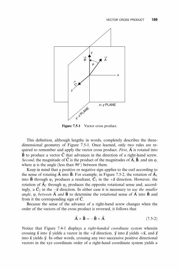
VECTOR CROSS PRODUCT 189
Figure 7.5-1 Vector cross product.
This definition, although lengthy in words, completely describes the three-dimensional geometry of Figure 7.5-1. Once learned, only two rules are re-
~quired to remember and apply the vector cross product. First, AA is rotated into~ ~BB to produce a vector CC that advances in the direction of a right-hand screw.
~ ~CC is the product of the magnitudes of AA;BSecond, the magnitude of ~ B, and sin j,where j is the angle (less than 90�) between them.
Keep in mind that a positive or negative sign applies to the curl according to~the sense of rotating AA into~B ~B. For example, in Figure 7.5-2, the rotation of AA1
~into ~ ~BB through j1 produces a resultant, CC1 in the þzz direction. However, the~rotation of AA2 through j2 produces the opposite rotational sense and, accord-
~ ~ingly, a CC2 in the �zz direction. In either case it is necessary to use the smaller~ ~ ~angle, j, between AA and BB to determine the rotational sense of AA into ~BB and
from it the corresponding sign of ~CC.Because the sense of the advance of a right-hand screw changes when the
order of the vectors of the cross product is reversed, it follows that
~ ~ ~AA� BB ¼ �BB� ~AA ð7:5-2Þ
Notice that Figure 7.4-1 displays a right-handed coordinate system whereinxx into ~ ~ yy into ~ ~ zzcrossing ~ yy yields a vector in the þzz direction, ~ zz yields þxx, and ~
into~ yxx yields ~y. In other words, crossing any two successive positive directionalvectors in the xyz coordinate order of a right-hand coordinate system yields a

190 ELECTROMAGNETIC FIELDS AND WAVES
Figure 7.5-2 Direction (sign) of ~ AA into~CC changes with the sense of rotation of ~ BB.
cross product in the positive direction of the third. It is best to use a right-handcoordinate system to avoid errors in calculating the cross product. Stated invector notation [6, pp. 88–89],
~xx� ~yy ¼~zz ¼ �~yy�~xx ð7:5-3aÞ~yy�~zz ¼~xx ¼ �~zz� ~yy ð7:5-3bÞ~zz�~xx ¼ ~yy ¼ �~xx�~zz ð7:5-3cÞ~xx�~xx ¼ ~yy� ~yy ¼~zz�~zz ¼ 0 ð7:5-3dÞ
xx; ~ zz are unit vectors in the respective positive directions of thewhere ~ yy, and ~~x; y, and z coordinate directions. If the vectors AA and~BB are expressed in terms
of their rectangular coordinates in this right-hand system,
~ ~ xxþAy~ ~ xxþ By~ ~AA� BB ¼ ðAx~ yyþAzzzÞ � ðBx~ yyþ BzzzÞ ð7:5-4Þ~ xx; ~ zz directions, andwhere Ax;Ay, and Az are the components of AA in the~ yy, and~
similarly with Bx;By, and Bz. The cross product of (7.5-4) would be expected to~produce nine terms, since each component of AA is crossed separately into each
~component of ~BB. However, vector components of AA which have the same cor-~responding directions as components of BB produce a zero cross product accord-
ing to (7.5-3d), so only six terms are nonzero. By observing the cross products

VECTOR CROSS PRODUCT 191
in (7.5-3a,b, and c), (7.5-4) can be expanded explicitly as
~ ~ ~ yyþ ðAxBy �AyBxÞzzAA� BB ¼ ðAyBz �AzByÞxxþ ðAzBx �AxBzÞ~ ~ ð7:5-5Þ
A short-hand method for writing and remembering (7.5-5) is the solution to thedeterminant � �
~xx� � ~yy ~zz � � ~AA�~BB ¼ Ax
� � Ay Az� � ð7:5-6Þ� �
Bx� By Bz
� Expressions (7.5-5) and (7.5-6) produce the same result. Given the definition
of the vector cross product, the force on a moving charge can be written verytersely yet in a manner than conveys all of the relationships between the mag-
FF;~ Bv, and~nitudes and directions of ~ v B.~If a charge q has velocity v that is at right angles to the magnetic field BB, the
force on the moving charge q is given as
~ ~~FFmagnetic ¼ qvv� BB ð7:5-7ÞSome useful conversions for the units of magnetic flux,~BB, are
Wb ðWeberÞ1 T ðTeslaÞ ¼ 10;000 G ðGaussÞ ¼ 1
2m
N ðNewtonÞ N ðNewtonÞ¼ 1 ¼ 1 ð7:5-8ÞC ðCoulombÞ �m=s Am ðAmpereÞ
For example, an electron moving at 1� 106 ms/s at right angles to a 1-T mag-netic field would experience a force given by
Fmagnetic ¼ 1:6� 10�19 C� 1� 106 m=s� 1N ¼ 1:6� 10�13 N ð7:5-9Þ
C�m=s
The force of gravity on the same electron is
Fgravity ¼ mg ¼ 9:1� 10�31 kg� 9:8 N=kg ¼ 8:9� 10�30 N ð7:5-10Þ
Again, the gravitational force is negligible. Notice that the magnetic force is1000 times as great as the electric force calculated for the electric field example,given this 1-T field strength. One tesla is a strong magnetic field.
When a charged particle enters at right angles to a magnetic field at a con-stant velocity, its orbit is a circle [5, Vol. 2, p. 561]. The circular electron orbitis the basis of the magnetron microwave tube [7, p. 41; 8, p. 321]. Even in the1940s magnetrons were capable of 100 kW of peak power for short pulses of amicrosecond or less. These high pulsed power levels were orders of magnitudegreater than those achievable with prior tube types and made practical thedevelopment of tactical radars during the latter part of World War II.

192 ELECTROMAGNETIC FIELDS AND WAVES
Figure 7.5-3 Positive charge with v speed~ ~enters a BB field (crosses indicate BB field
direction is ‘‘into the paper’’) at pointJ and has its path turned into a circularorbit (curving to points K and L) with aradius R. The magnetic force ~FF is alwaysdirected toward the circular orbit’s centerand is equal and opposite to the particle’scentrifugal force.
The centrifugal force of a particle traveling in a circular orbit of radius R
(Fig. 7.5-3) is
2mvFcentrifugal ¼ ð7:5-11Þ
R
Equating this to the magnetic force gives [5, Vol. 2, p. 561]
2vqvB ¼ m ð7:5-12Þ
R
and thus,
mvR ¼ ð7:5-13Þ
Bq
In addition to the magnetron tube, this method of orbiting a charged parti-cle also is employed in the cyclotron particle accelerator and in mass spectro-graphs to analyze ionized samples—the radii of whose orbits are directly pro-portional to the particle’s mass and hence its atomic element number.
As an example, suppose that an electron enters a magnetic field of flux den-BB ¼ 2� 10�4 T (2 G) traveling in a direction that is at right angles to ~sity ~ BB
with a velocity of 1� 106 m/s:
mv ð9:1� 10�31 kgÞ � ð1� 106 m=sÞR ¼ ¼ ¼ 2:85 cm ¼ 1:12 in: ð7:5-14Þ
Bq ð2� 10�4 TÞ � ð1:6� 10�19 CÞ

ELECTROSTATICS AND GAUSS’S LAW 193
Figure 7.6-1 Induced charges on a dielectric inserted between the plates of a capacitorreduce the electric field within the dielectric.
7.6 ELECTROSTATICS AND GAUSS’S LAW
The magnitude of the electric field ~EE depends upon the medium in which it isimmersed [5, Vol. 2, p. 478]. For example, when a dielectric material is placedbetween the charged plates of a capacitor, induced charges in the dielectric
~ ~cause the EE field lines to terminate on them, reducing the EE field within thedielectric if the capacitor is open circuited (Fig. 7.6-1). If a constant voltageis applied the voltage source will supply additional charge to the capacitor tobuild up to the original ~EE field and voltage between the plates.
The electric field at a distance r from a fixed point charge q is given by(7.3-3) and repeated here (Fig. 7.6-2):
~ qEE ¼ ~ ð7:6-1Þrr
4pe0eRr2
Figure 7.6-2 Coulomb observed that the electric field at a radial distance r from a pointcharge q is proportional to q and inversely proportional to the square of r. The fielddirection points away from a positive charge (to repel a like positive charge) and inwardtoward a negative charge (to attract an opposite, positive charge).

194 ELECTROMAGNETIC FIELDS AND WAVES
~Figure 7.6-3 Arbitrary volume encloses a charge, q. The resulting DD vector field exitsthe volume radially over the closed surface S. Incrementally, the surface is divided into!dS areas having a surface normal direction dS at angle y to the vector field ~DD.
This observation can be written without specifying the dielectric environ-ment in which the charge is found by defining a companion vector, electric flux
~density DD as
~ ~ ~ qDD ¼ eEE ¼ e0eREE ¼ ~ ð7:6-2Þrr
4pr2
~The reason for defining DD is that the e¤ect of induced charge in the dielectricis absorbed in eR and therefore the right-hand side (7.6-2) is only required toaccount for free charge. A more general observation that is suggested by thespherical geometry of Figure 7.6-2 is known as Gauss’s law.
Gauss’s law states that for any closed surface containing a total fixed charge q,~the product of the emerging DD field magnitude normal to each infinitesimally!
small area dSN, summed over the entire containing surface, S, is equal to the total
charge q contained within the surface (Fig. 7.6-3). A mathematical expression ofthis statement is provided in the next section.
7.7 VECTOR DOT PRODUCT AND DIVERGENCE
To describe the mathematical process that Gauss’s law requires, we assign!a vector, d , to the surface that is always normal to and has the magnitude dSof a small area of the surface at each point on the surface. It has a directiondefined as positive when directed toward the outside of the volume contained

VECTOR DOT PRODUCT AND DIVERGENCE 195
~by the surface. The vector field DD (Fig. 7.6-3) resulting from charge q is afunction of the x; y; z position on the surface S. Then, everywhere on the sur-face S we form the product
!~Vector product ¼ jDDj jdSj cos y ð7:7-1Þ! !~ ~where y is the angle between DD and d . Note that when DD and dS point in
opposite directions the cos y is negative. In this way, the vector product in(7.7-1) produces both magnitude and sign. The product described by (7.7-1)occurs regularly in physical situations and has a formal vector mathematicaldefinition called the dot product.
~ ~ ~ ~The vector dot product, AA � BB (read as ‘‘A dot B’’) of two vectors AA and BB~separated by an angle y is formed by multiplying the magnitude of AA times the
~magnitude of BB times the cosine of the angle between them to produce a scalar
quantity having the sign of cos y:
~ ~ xxþAy~ ~ xxþ Byyyþ BzzzÞ ð7:7-2ÞAA � BB ¼ ðAx~ yyþAzzzÞ � ðBx~ ~ ~
xx; ~ zz are unit vectors in the positive directions ofin which, as previously, ~ yy, and~the x; y, and z axes, respectively, of a right-hand coordinate system. As wastrue of the cross product, some of the multiplication terms described by (7.7-2)
~are zero. In particular, when each component of AA is dot multiplied by the~three components of BB, only like-directed components produce a nonzero
product. Furthermore, since the Ai and Bi components (for i ¼ x; y; z) arein exactly the same direction, the cosine of the angle between them is unity.Accordingly, (7.7-2) reduces to
~ ~AA � BB ¼ AxBx þAyBy þAzBz ð7:7-3Þ
Note that, unlike the vector cross product which produces a new vector, the dotproduct produces a scalar quantity.
In terms of the dot product, Gauss’s law can be stated in integral form as
þ !~DD � dS ¼ q ð7:7-4ÞS
Taking the limit as the volume enclosed by S tends to zero, this equation can be~used to define the divergence of the vector DD.
~ ~The divergence ‘ � ~AA (pronounced ‘‘del dot AA’’) of a vector field AA from a!~closed surface S is equal to the dot product of AA with a vector dS at the surface
having a magnitude equal to the surface area at the location of evaluation, a
direction that is orthogonal to the surface, and a sign that is positive when the
surface vector points outside the volume enclosed by the surface.

‘ � ~
‘ �~
‘ �~
‘ �~
‘ � ~
196 ELECTROMAGNETIC FIELDS AND WAVES
Written in di¤erential form this is Þ !~AA � dSAA1 lim S ð7:7-5Þ
DV!0 DV
The divergence can be calculated for any vector field. Using the divergence,Gauss’s law can be written in di¤erential form as
DD ¼ r ð7:7-6Þ
where r is the volume charge density at the location at which ~DD is evaluated. If(7.7-6) is integrated over any given volume [6, p. 71]
ð ð DD dV ¼ r dV ð7:7-7Þ
V V
and then, replacing the right side by its equivalent from Gauss’s law
ð ð !D ~D dV ¼ DD � dS ð7:7-8Þ
V S
This result has been obtained from a consideration of the ~DD field; however, it is~a general result that applies to any vector AA, and is called the divergence theo-
rem (and sometimes Gauss’s theorem).~The divergence theorem: For any continuous vector function of space, AA, the
~integral of the divergence of AA over any volume completely enclosed by surface S!~is equal to the integral of AA � dS over the whole surface S.
ð ð !A ~A dV ¼ AA � dS ð7:7-9Þ
V S
Like the dot product the divergence produces a scalar result. The divergence of~a vector AA ¼ AxxxþAy~ ~~ yyþAzzz can be evaluated using
‘ � ~ qAx þ q q
AA ¼ Ay þ Az ð7:7-10Þqx qy qz
7.8 STATIC POTENTIAL FUNCTION AND THE GRADIENT
In an electrostatic region, in which charges are fixed, each coordinate pointðx; y; zÞ has an associated static potential energy, Fðx; y; zÞ for a point chargerelative to some reference. The potential energy of a test charge in a region ofelectrostatic potential energy is analogous to a skier who has potential energy

STATIC POTENTIAL FUNCTION AND THE GRADIENT 197
for each elevated location on a mountain relative to the base of the mountainor to some other location defined as a reference at which his potential energy isdefined to be zero.
The energy which must be expended to move a unit positive charge fromlocation 1 to some di¤erent location 2 is given by [6, p. 73]
ð2 !~F2 �F1 ¼ � EE � dl ð7:8-1Þ1
The negative sign occurs because a positive ~EE field produces a force that tendsto move a positive charge from the higher potential to the lower one. To move
~in the direction opposite to the force field (EE field), we must do work (provideenergy) rather than recover it. Only a di¤erence in potential is important; thezero potential reference can be selected arbitrarily.
In an electrostatic system, having no moving charges (currents) or changing
magnetic fields, the potential is the same as voltage. However, we reserve theterm voltage for later to describe the combined e¤ects of electrostatic chargedistributions as well as changing magnetic fields.
The potential energy in a region due to the presence of electrostatic (fixed)~charges and their resulting EE fields has a single value at every location inde-
pendent of how that location is approached. Thus, it follows that the integralof ~EE about any closed path in the region must be zero. The same is true of agravitational field around which any closed path (in which you return to thestarting point) produces no change in potential energy. Similarly, there is nonet energy change in moving a given charge about a closed path in an electro-
~static ~EE field. This means that the EE field is conservative. Practically, there maybe some energy lost to friction (resistance) in moving charge about a system,but no di¤erence in potential energy results in completing a closed path within a
conservative field.Mathematically this is stated
þ !~EE � dl ¼ 0 ð7:8-2Þ
Suppose that we wish to determine the potential at point P due to a charge q1located at a point Q1 (Fig. 7.8-1).
Setting the zero potential at infinity, the work done to move a unit testcharge from infinity to the point P is equal to the work integral
ðP ðP~ q1 dr q1
F1 ¼ � EE cos y dl ¼ � ¼ ð7:8-3Þ4per2 4per1y y
in which the equivalence cos y dl ¼ dr has been recognized, the value for ~EE hasbeen substituted from (7.8-1), and r1 is the distance from point Q1 to P. The

198 ELECTROMAGNETIC FIELDS AND WAVES
Figure 7.8-1 A work integration path topoint P in a field of discrete charges q1 atposition Q1, q2 at Q2, q3 at Q3 and q4 at Q4
[6, p. 72, with permission].
total potential at P due to a collection of n charges is
nq1F ¼4per2
þ � � � ¼ qi ð7:8-4Þ4per1
þ q2X
4perii¼1
If, instead of discrete charges, we have a charge density distribution,ð 1 r dV
F ¼ ð7:8-5Þ4p V ere0r
which defines the static potential function F. The volume charge density r isa function of position. The constant of integration in (7.8-5) is used to set thezero potential point. If this point is made infinitely far away, the constant iszero.
The e¤ect of individual charges or a charge distribution can be taken intoaccount using F. This involves only scalar calculations, the advantage gainedby defining the scalar potential function. From F we will be able to calculate ~EEvery easily. On the other hand, determining ~EE directly requires that we sum thethree directional components of the ~EE field due to each charge source, or use athree-dimensional integration for a charge density. This direct approach wouldresult in a much more complex calculation.
Once F is determined, the ~EE field at any location is given by the gradient ofF;‘F. The gradient of a function is the rate of change of the function per unit
distance in three mutually orthogonal directions. In rectangular coordinates it is
qF qF qF‘F ¼~
qxþ ~
qyþ~ ð7:8-6Þxx yy zz
qz
~EE ¼ �‘F ð7:8-7Þ
The gradient operates on a scalar function and produces a vector function (Fig.7.8-2). Note that~EE is the negative of the gradient of F [the reason is given below

STATIC POTENTIAL FUNCTION AND THE GRADIENT 199
Figure 7.8-2 The ski mountain, with gradient(slope), ‘z.
(7.8-1)]. The gradient can be used with any scalar function; it is not limited tothe static potential function defined in this section. For example, consider thefunction representing an idealized ski mountain:
2z ¼ 1000� 100x2 � 100y ð7:8-8Þ
where x; y, and z are in meters, z is the height of the mountain, Gx are thenorth–south directions, andGy are the east–west directions.
If the mountain in Figure 7.8-2 is truncated in any xy plane [z ¼ constant,the section formed is a circle x2 þ y2 ¼ ð1000� zÞ=100], and therefore thefunction of (7.8-7) has cylindrical symmetry with respect to z. As a conse-quence, the fall line of the mountain is the same in any direction (north, south,east, west, or any intermediate direction). At the very top, 1000 m, the slope ofthe mountain is zero. A skier might just balance there without being drawndownward. However, a movement of 1 m in any direction would result in adrop of 100 m, and at 1 m the slope is 200 m/m. The slope becomes eversteeper with increasing values of x and/or y, as one descends the mountain.The exact slope and its vector direction at any x; y; z point on the mountain isgiven by
‘z ¼ ð�200xÞxxþ ð�200yÞyy~ ~ ð7:8-9Þ
where x and y must satisfy (7.8-7) to be points on the surface of the mountain.Notice that the gradient is independent of the height of the mountain, depend-ing only on the slope at the location ðx; y; zÞ on the mountain’s surface.
The ski mountain example, z ¼ f ðx; yÞ, was chosen in order to depict thegradient graphically. However, a static potential function, F, in general would

200 ELECTROMAGNETIC FIELDS AND WAVES
be a function of x; y, and z. That is, F ¼ Fðx; y; zÞ, and the resultant gradientis three dimensional, as indicated by (7.8-6).
7.9 DIVERGENCE OF THE B FIELD
Previously, we related the electric flux density and the permittivity (dielectric~ ~ ~constant) e, to the electric field EE such that DD ¼ eEE. Similarly, it is useful
~HH that is related to the magnetic flux density Bto define the magnetic field ~ B by aproperty of the magnetic medium, the magnetic permeability m. The reason for
~ ~defining two variables, ~ H, is that ~BB and H BB has zero divergence, while HH doesnot. The two variables allow the ‘‘Amperian’’ currents (spins) of the moleculesof magnetic materials to be accounted for by mR, and then the right-hand sideof Ampere’s law does not include these Amperian currents. Ampere’s law isdiscussed in the next section. Finally, the normal component of the~BB field doesnot change across a magnetic material boundary, while that of the ~HH field may:
~ ~BB ¼ mHH ð7:9-1Þ~ ~Thus the electric and magnetic flux densities are DD and BB, respectively, and the
~ ~electric and magnetic fields are EE and HH, respectively. For homogeneous (uni-form) and isotropic media (wherein the electric and magnetic properties are thesame for all directions and locations) both e and m are constants.
~Unlike the electric flux density DD, which has as its vector sources dis-~crete charges, q, there are no point sources for the magnetic flux density BB (Fig.
~7.9-1). Stated another way, the divergence of BB is zero:
Figure 7.9-1 Divergence of the ~BB field is zero, illustrated using an idealized sketch ofthe Earth’s magnetic field.

AMPERE’S LAW 201
‘ � B ¼ 0 ð7:9-2Þ~Under static conditions the BB field lines, when extended su‰ciently, form
closed contours.
7.10 AMPERE’S LAW
Just as Gauss’s law related electric flux density to contained charge, similarly,Ampere’s law relates magnetic field to current.
~Ampere’s law states that the line integral of the HH field parallel to the line
defining a closed path is equal to the current I enclosed by the path:
þ !~HH � dl ¼ I ð7:10-1Þ
For the geometry shown in Figure 7.10-1, consisting of a circle coaxial with aconductor carrying current I, symmetry requires that the Hj is independent ofj. Since dl ¼ r dj, integration around the closed circular path, from j ¼ 0 toj ¼ 2p, leads to
I2prHj ¼ I or Hj ¼ ð7:10-2Þ
2pr
Figure 7.10-1 Closed curve defined about a current-carrying conductor (current I is inthe þz direction).

� � �
202 ELECTROMAGNETIC FIELDS AND WAVES
This is a static relation. Both Hj and I are constant (DC) values that areassumed to have been in place for ‘‘an infinite period of time.’’ The e¤ects oftime-varying fields and currents will be discussed later.
7.11 VECTOR CURL
Figure 7.10-1 describes a situation wherein the integration of the force field (~HHin this case) around a closed path is not zero. This phenomenon occurs often inthe physical world, for example, in the rotational force of a tornado. Thus theintegral around the closed path represents the rotational component of thefield. This concept can be defined at a point by taking the limit as the path and
~its enclosed area tend to zero (become infinitesimal). For a given vector field AA,~this mathematical operation is known as the curl of AA ( pronounced ‘‘del cross
~ ~AA’’ or the ‘‘curl of AA’’) and is written as ‘� ~AA.~The curl of a vector AA at a point i is equal to the limit as DSi ! 0 of the line!~integral of AA � dl about a path enclosing surface Si:Þ !~AA � dl~½curl AA�i 1‘� ~AA1 lim ð7:11-1Þ
DSi!0 DSi
This curl is a general vector identity and can be applied to any vector field.The curl of a vector field is also a vector field. The curl can be envisioned by
~imagining that the AA field represents a wind or water force on a paddle wheelplaced in the field [4, Chapter 2]. For example, if a paddle wheel with its rota-tional axis oriented in the z direction is placed in the xy plane in Figure 7.11-1!~and if the line integral of AA � dl is positive for the closed path shown, then thepaddle wheel would rotate counterclockwise when viewed from above on theþz axis, as shown.
The paddle wheel test is not as whimsical as it first appears. It might seemthat the curl of a vector is simply a measure of its circulation, but this is not so.It is possible to have a field that forms circles, yet whose curl is zero, as will beshown by the coaxial line example later in this section.
The components of the curl can be calculated separately. For example, inrectangular coordinates the z component of the curl is calculated using thegeometry of Figure 7.11-1 [6, pp. 96–97] for a surface with sides dx and dy:þ !~AA � dl ¼ dyAyjxþdx � dxAxjyþdy � dyAyjx þ dxAxj ð7:11-2Þy
In the limit as the surface defined by dx and dy tends to zero
qAxAxjyþdy ¼ Axjy þ dy � and Ayjxþdx ¼ Ayjx þ dx
qAy �� ð7:11-3a,bÞqy � y qx � x
Then

� � � � � �
‘� ~ � � � ~ ~ ~ � � � � � �
VECTOR CURL 203
~Figure 7.11-1 Determination of the z component of the curl of a vector AA [6, p. 96]with paddle wheel model [4, p. 24, reprinted with permissions].
þ � � ~ ! qAy qAxAA � dl ¼ � dx dy ð7:11-4Þ
qx qy
and applying the definition of the curl gives the z-directed component as! Þ ! � � ~AA � dl~ ¼ ~ zzð‘� AAÞz direction zz ¼ qAy � qAx~ ð7:11-5Þ
dx dy qx qy
In like fashion the x- and y-directed components of the curl can be evaluated toproduce
qAx qAz‘� ~ xxþ � ~ zzAA ¼ qAz � qAy
~ yyþ qAy � qAx~ ð7:11-6Þ
qy qz qz qx qx qy
The curl can be written using the shorthand format of the determinant as
xx yy zz� q q q � AA ¼ ð7:11-7Þ� qx qy qz �� � Az
�Ax Ay

‘� ~ ~
204 ELECTROMAGNETIC FIELDS AND WAVES
Expressions (7.11-6) and (7.11-7) produce the same result. Using the curl thedi¤erential form of Ampere’s law is written:
~qDDHH ¼ JJC þ ð7:11-8Þ
qt
~ ~where JJC is the conduction current density and qDD=qt is the displacement current
density at the location at which the curl is taken. The displacement current isdue to a changing electric field, as, for example, the current that flows betweenthe plates of a capacitor when it is charging or discharging. The displacement
~current is present with any time-varying DD field. When a sinusoidally varying~voltage is applied to a capacitor, the changing DD field between the capacitor
plates produces the AC displacement current density between the plates.While the definition of the curl has some similarities to the divergence, the
two operations are very di¤erent in that taking the divergence of a vector field
produces a scalar value while taking the curl of a vector field produces another
vector field. Also, the curl is a di¤erential relationship that applies at a point
in space. The significance of this point relationship can be appreciated from thefollowing example.
~Suppose that it is desired to find the HH field within the coaxial pair of con-ductors shown in Figure 7.11-2 [6, p. 94]. Further assume that I is a DC cur-rent. Because of the cylindrical symmetry, Hj is independent of j; and thisallows easy application of Ampere’s law. We have two forms for Ampere’s law,the line integral relation of (7.10-1) and the point relation of (7.11-8). The line
Figure 7.11-2 Magnetic field Hj about a current-carrying wire, and the result extendedto the space within a coaxial transmission line.

‘� ~
� � � � � �
VECTOR CURL 205
Figure 7.11-3 Cross section of the coaxial line.
integral format requires specification of the total current within the closed con-
tour while the point format requires the current density at the point at which ~HHis to be computed. Suppose the point format is used to calculate Hj within thecenter conductor, that is, for ra a (Fig. 7.11-3).
Under DC current excitation, I is uniformly distributed over the area of thecenter conductor, and the current density has only a conduction componentgiven by
IJC ¼ ð7:11-9Þ
pa2
Applying (7.11-8),
~IIHH ¼ ð7:11-10Þ
pa2
Expressing (7.11-10) in cylindrical coordinates (vector operators in various co-ordinates are provided in Section 7.14) gives
~1 qHz qHj qHr qHz 1 qðrHjÞ 1 qHr II‘� ~ rr jj zzHH ¼~
r qj� þ~ � þ~ � ¼
pa2qz qz qr r qr r qj
ð7:11-11Þ
In this example, I has only a z component. Thus, equating the z-directed termsin (7.11-14) and noting that, due to symmetry, there can only be a j component

206 ELECTROMAGNETIC FIELDS AND WAVES
of ~HH gives
1 qðrHjÞ I¼r qr pa2 ð7:11-12ÞqðrHjÞ I¼ r
qr pa2
and integrating gives
I r2rHj ¼
pa2 2
IHj ¼
2pa2r for 0a ra a ð7:11-13Þ
~To calculate the value of HH in the space between the conductors we cannotapply the curl expression because the current in this region is zero. This wouldseem to be a contradiction to what has been studied thus far. Specifically, weknow that there is an Hj between the conductors and this field closes on itself,forming circles, suggesting a finite value of curl. Resolving these two dilemmasis important to understanding the curl and the point form of Ampere’s law asexpressed by (7.11-8).
First, the value of Hj was evaluated previously from the line integral formof Ampere’s law for an axially directed current in (7.11-2). The result repeatedhere is
IHj ¼ for a < r < b ð7:11-14Þ
2pr
Although there is a finite value for Hj between the conductors, the value of thecurl in this region must be zero, since there is no current density there. To seethat the curl is zero, consider that only the fifth term on the left side of (7.11-11)could be nonzero since there is only an Hj component and it has only an rvariation. But this term is
1 qðrHjÞHH ¼~ ð7:11-15Þ‘� ~ rr
r qr
and substituting in the value for Hj gives
1 qðrHjÞ 1 qðrðI=2prÞÞ¼ ¼ 0 ð7:11-16Þr qr r qr
Thus, even though there is an ~HH field between the conductors, its value cannotbe found using the di¤erential form of Ampere’s law.

Next, consider the second apparent dilemma: the ~HH field as sketched in Fig-ure 7.11-2 closes on itself and appears to have a finite value of curl. Actually,the curl is zero, as was shown by (7.11-16). To arrive at this conclusion inanother way, use the line integral method of evaluating the curl about theclosed path ABCD shown in Figure 7.11-4. The radial sides of the path, BCand DA produce no contribution to the integral of ~HH � dl since there is only acircumferential ~HH field component Hj. The contributions to the circumferentialportions of the path, AB and CD, produce
Hj � dl ¼ H1r1 Dj�H2r2 Dj ¼ DjI
2pr1r1 � I
2pr2r2
� �¼ 0 ð7:11-17Þ
Thus, it can be seen that the curvature of the H field and closure on itself does
not always imply a finite value of curl. In this case, the variation of Hj with r isjust su‰cient to cancel the curl. Analogously, if a test paddle wheel with rota-tional axis in the z direction is placed between the conductors, it would notrotate were the ~HH field replaced with a wind current pressure having the samer variation. It might move with the field following a circular orbit about thecenter conductor, but it would not rotate about its own axis.
To compete the analysis of the Hj in the coaxial line cross section, considerthe range r > c. Applying (7.10-1),
Figure 7.11-4 Closed-path integration to evaluate the curl of H between coaxial con-ductors.
VECTOR CURL 207

208 ELECTROMAGNETIC FIELDS AND WAVES
Figure 7.11-5 Magnitude H field of the coaxial conductor set as a function of theradius.
þ !~HHj � dl ¼ I� I ¼ 0 ð7:11-18Þ
Hj ¼ 0 for r > c ð7:11-19Þ
The field outside the outer conductor is zero because the net current within iszero, a positive current on the center conductor and an equal and oppositecurrent returning on the outer conductor. The field as a function of r is shownin Figure 7.11-5.
7.12 FARADAY’S LAW OF INDUCTION
Faraday’s law of induction states that a time-varying magnetic flux passing
through a surface produces a voltage around the perimeter of the surface equal to
the surface integral of the changing flux through the surface. The polarity of the
induced voltage is such as to establish a current to resist the change of magnetic
flux: þ ð ~! qBB !~EE � dl ¼ � � dS ð7:12-1ÞS qt
Independently, Lenz duplicated many of Faraday’s and Ampere’s discoveries.Lenz is credited with the law for determining the polarity of the voltage in-duced by a changing magnetic field. When Faraday’s law is written in di¤er-
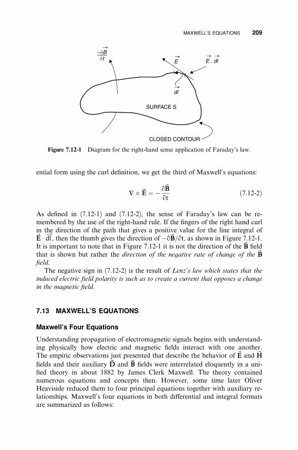
MAXWELL’S EQUATIONS 209
Figure 7.12-1 Diagram for the right-hand sense application of Faraday’s law.
ential form using the curl definition, we get the third of Maxwell’s equations:
~qBB~‘� EE ¼ � ð7:12-2Þqt
As defined in (7.12-1) and (7.12-2), the sense of Faraday’s law can be re-membered by the use of the right-hand rule. If the fingers of the right hand curlin the direction of the path that gives a positive value for the line integral of!~ ~EE � dl , then the thumb gives the direction of �qBB=qt, as shown in Figure 7.12-1.It is important to note that in Figure 7.12-1 it is not the direction of the~BB field
~that is shown but rather the direction of the negative rate of change of the BBfield.
The negative sign in (7.12-2) is the result of Lenz’s law which states that the
induced electric field polarity is such as to create a current that opposes a change
in the magnetic field.
7.13 MAXWELL’S EQUATIONS
Maxwell’s Four Equations
Understanding propagation of electromagnetic signals begins with understand-ing physically how electric and magnetic fields interact with one another.The empiric observations just presented that describe the behavior of ~E HHE and ~
~fields and their auxiliary DD and ~BB fields were interrelated eloquently in a uni-fied theory in about 1882 by James Clerk Maxwell. The theory containednumerous equations and concepts then. However, some time later OliverHeaviside reduced them to four principal equations together with auxiliary re-lationships. Maxwell’s four equations in both di¤erential and integral formatsare summarized as follows:

‘� ~ ~
210 ELECTROMAGNETIC FIELDS AND WAVES
~1. The divergence of the DD field equals the volume charge density. This isGauss’s law:
~‘ �DD ¼ r ð7:13-1aÞþ ð !~DD � dS ¼ r dv ð7:13-1bÞS V
~2. The divergence of the BB field is zero:
~‘ � BB ¼ 0 ð7:13-2aÞþ !~BB � dS ¼ 0 ð7:13-2bÞS
~3. The curl of the EE field is equal to minus the time rate of change of the
magnetic flux density:
~qBB~‘� EE ¼ � ð7:13-3aÞqtþ ð ~! qBB !~EE � dl ¼ � � dS ð7:13-3bÞS qt
~4. The curl of the HH field equals the combined conduction and displacement
current densities:
~qDDHH ¼ JJC þ ð7:13-4aÞ
qtþ þ ~! ! ! qDD !~HH � dl ¼ JC � dS þþ
� dS ð7:13-4bÞS S qt
Auxiliary Relations and Definitions
To Maxwell’s famous four equations must be added definitions and auxiliaryrelations to complete the experimental evidence unified by Maxwell. These are:
The Force Law This applies to a charge q moving at velocity ~vv in a region
having both electric field ~ BEE and magnetic flux density~B:
~ ~ff ¼ q½EEþ~ ~vv� BB� ð7:13-5Þ
Ohm’s Law and the Definition of Conduction Current Density The point formof Ohm’s law is
~ ~JJC ¼ sE E ð7:13-6Þ

‘ �~ ~
MAXWELL’S EQUATIONS 211
~where JJC is the current density (in amperes/square meter), s is the conductivityof the material (in mhos/meter), and E is the electric field (in volts/meter).
Convection Current Density The definition of convection current density is
~ ~JJCV 1 rvvr ð7:13-7Þ
where~vvr is the velocity at which the volume charge density r is moving [6, Sec.4.06].
Permittivity (Dielectric Constant) The definition of permittivity (dielectricconstant) is defined by
~ ~ ~DD1 eEE ¼ e0eREE ð7:13-8Þ
where e0 ¼ 8:854186� 10�12 ðA10�9=36pÞ farads per meter is the permittivityof free space and eR is the relative dielectric constant used to account for thee¤ects of atomic and molecular dipoles of various materials.
Permeability The definition of permeability is defined within
~ ~ ~BB ¼ mHH ¼ m0mRHH ð7:13-9Þ
where m0 ¼ 4p� 10�7 H/m and mR is the relative permeability used to accountfor the magnetic dipole moments of atoms within various materials.
In general m and e can be tensor quantities, whose values vary with positionand direction. For example, a specialty of microwave engineering is the designof artificial (anisotropic) dielectrics [9, Chapter 12], in which metal strips areembedded in an otherwise homogeneous dielectric to produce a compositedielectric having very di¤erent relative dielectric constants for di¤erent appliedelectric field directions. Similarly, microwave ferrite materials [10, Sec. 6.6]exhibit quite di¤erent relative permeabilities with direction when immersedwithin a strong biasing magnetic field. However, for many engineering pur-poses m and e can be treated as simple scalar constants.
Visualizing Maxwell’s Equations
To review, consider the first of Maxwell’s equations:
DD ¼ r or ‘ � eEE ¼ r ð7:13-10Þ~This equation states that the ‘‘divergence’’ of the flux density DD is equal to the
charge density in the volume from which the ~ DDDD field is emanating. When the ~
field lines exhibit a net departure (divergence) from any volume (even a micro-scopic one), there is a net positive electric charge inside. Vice versa, if the lines

212 ELECTROMAGNETIC FIELDS AND WAVES
~Figure 7.13-1 Divergence of the EE field is proportional to the contained charge density,and its direction is related to the sign of the net charge, as shown.
enter the volume, there is a net negative charge inside. Departing lines meanthat a positive charge outside the volume will experience a force that repels itfrom the volume. That makes sense since like charges repel. The ~EE field is pro-
~portional to the DD field and the ~EE field emerges or enters a volume in propor-tion to the net positive or negative charge within, respectively, as shown inFigure 7.13-1.
Next consider Maxwell’s second equation:
~‘ � BB ¼ 0 ð7:13-11ÞThis equation simply indicates that the B field has no divergence (Fig. 7.13-2).This means that the ~BB field lines are continuous throughout space, they do notoriginate anywhere, and they always close on themselves. For homogeneous
~ ~regions, the HH field lines also close on themselves, being proportional to BB.~BB ¼ mHThat is,~ H.
Because the~BB field is continuous, even through a boundary dividing regions~of di¤erent permeability, it follows that the HH field cannot be continuous
through the permeability boundary. Its field strength must reflect the ratio ofpermeabilities in the two regions, as shown in Figure 7.13-3:
~ m1 ~HH2 ¼ HH1 ð7:13-12Þm2
The third of Maxwell’s equations introduces the curl concept, the amount ofcirculation of a vector field:
~qBB~‘� EE ¼ � ð7:13-13Þqt
This says that a changing ~ EE field at right angles. The ~BB field induces an ~ EE fieldcloses on itself in a closed loop or curl. This is the incremental form of Far-

‘� ~ ~
MAXWELL’S EQUATIONS 213
Figure 7.13-2 Bar magnet, illustrating thatsince the divergence of the ~BB field is zero, thefield lines, when su‰ciently extended, alwaysclose on themselves.
aday’s law, which says that the voltage induced in a loop is proportional to thetime rate of change of the magnetic field within the loop and (Lenz’s law) ofsuch a polarity as to oppose the change in the~BB field.
The applications of this phenomenon are widespread, including transformersfor power distribution and the coils used to generate high voltages for the sparkplugs of gasoline engines. We shall see that this and the next equation areresponsible for the propagation of radio waves, the essence of wireless signalpropagation.
~The fourth, and last, of Maxwell’s equations, states that the curl of the HHfield is proportional to the enclosed current:
~qDDHH ¼ JJC þ ð7:13-14Þ
qt
~Figure 7.13-3 While the BB lines have zero diver-~gence (are always continuous), the HH lines change
across a boundary to account for a change in perme-ability from one region to the next.
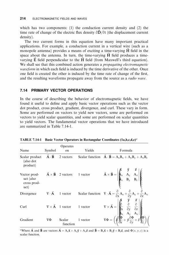
214 ELECTROMAGNETIC FIELDS AND WAVES
which has two components: (1) the conduction current density and (2) the~time rate of change of the electric flux density qDD=qt (the displacement current
density).The two current forms in this equation have many important practical
applications. For example, a conduction current in a vertical wire (such as a~monopole antenna) provides a means of exciting a time-varying HH field in the
~space about the antenna. In turn, the time-varying HH field produces a time-~ ~varying EE field perpendicular to the HH field (from Maxwell’s third equation).
We shall see that this combined action generates a propagating electromagnetic
waveform in which each field is induced by the time derivative of the other. Onceone field is created the other is induced by the time rate of change of the first,and the resulting waveforms propagate away from the source as a radio wave.
7.14 PRIMARY VECTOR OPERATIONS
In the course of describing the behavior of electromagnetic fields, we havefound it useful to define and apply basic vector operations such as the vectordot product, cross product, gradient, divergence, and curl. These vary in form.Some are performed on vectors to yield new vectors, some are performed onvectors to yield scalar quantities, and some are performed on scalar quantitiesto yield vectors. The fundamental vector operations that we have introducedare summarized in Table 7.14-1.
TABLE 7.14-1 Basic Vector Operators in Rectangular Coordinates (1a,b,c,d,e)a
OperatesName Symbol on Yields Formula
Scalar product(also dot
~AA �~BB 2 vectors Scalar function ~AA �~BB ¼ AxBx þAyBy þAzBz
product) � � ~xx� ~yy ~zz � � �
Vector prod- ~AA�~BB 2 vectors 1 vector ~AA�~BB ¼ Ax� � Ay Az
� � uct (also Bx
� By Bz�
cross prod-uct)
Divergence ‘ � ~AA 1 vector Scalar function ‘ � ~AA ¼ q
qxAx þ q
qyAy þ q
qzAz� �
~xx� � ~yy ~zz � � Curl ‘� ~AA 1 vector 1 vector ‘� ~AA ¼ q� � q q � �
qx� � qy qz � � Ax� � Ay Az
� � Gradient ‘F Scalar
function1 vector ‘F ¼ ~xx
qF
qxþ ~yy
qF
qyþ~zz
qF
qz
~ ~aWhere AA and ~ ~ ~ ~ BB ¼ Bxxxþ Byyyþ BzzBB are vectors AA ¼ AxxxþAyyyþAzzz and ~ ~ ~ ~z, and Fðx; y; zÞ is ascalar function.

THE LAPLACIAN 215
The use of vector operations is simplified by using coordinate systems thatexploit the symmetry of the application. In addition to rectangular coordinates,cylindrical and spherical coordinates are often useful. Rather than convert theapplication to rectangular coordinates, it is more convenient to carry out thevector operations directly in the coordinate system of choice. The vector oper-ations are listed below in cylindrical and spherical coordinates.
Cylindrical Coordinates
‘F ¼~rrqF
qrþ~jj
1
r
qF
qjþ~zz
qF
qzð7:14-1aÞ
‘ � ~AA ¼ 1
r
qðrArÞq~rr
þ 1
r
qAj
qjþ qAz
qzð7:14-1bÞ
� � � � � � ‘� ~AA ¼~rr
1
r
qAz
qj� qAj
qzþ~jj
qAr
qz� qAz
qrþ~zz
1
r
qðrAjÞqr
� 1
r
qAr
qjð7:14-1cÞ
Spherical Coordinates
‘F ¼~rrqF
qrþ~yy
1
r
qF
qyþ~jj
1
r sin y
qF
qyð7:14-2aÞ
‘ �A ¼ 1
r2q
qrðr2ArÞ þ 1
r sin y
q
qyðsin yAyÞ þ 1
r sin y
qAj
qjð7:14-2bÞ
� � � � ‘� ~AA ¼~rr
1
r sin y
q
qyðAj sin yÞ � qAy
qjþ~yy
1
r
1
sin y
qAr
qj� q
qrðrAjÞ� �
þ~jj1
r
q
qrðrAyÞ � qAr
qyð7:14-2cÞ
7.15 THE LAPLACIAN
After applying an operation from Table 7.14-1, it is often useful to apply thesame or another operation to the result. One of the most important is the Lap-lacian. It occurs so often that it is considered a separate operator. This operatorhas two definitions, one for operation on a scalar function and one for opera-tion on a vector field. When applied to a scalar function Fðx; y; zÞ, the Laplacianis equal to the divergence of the gradient. Its value is the sum of the secondpartial derivatives with respect to x; y, and z of F. This can be evaluated byfirst evaluating the gradient of F and then finding the divergence. The result [4,p. 30] is:
Rectangular Coordinates
‘2F ¼ ‘ � ‘F ¼ q2Fþ q2Fþ q2F ð7:15-1aÞqy2qx2 qz2

� �
� � � �
216 ELECTROMAGNETIC FIELDS AND WAVES
Cylindrical Coordinates
‘2F ¼ 1 q qF þ 1 q2F qF2
r ð7:15-1bÞ2 qj2
þqz2r qr qr r
Spherical Coordinates
‘2F ¼ 1 q 2 qF þ 1 q qF 1 q2Fr sin y ð7:15-1cÞ
2r qr qr r2 sin y qy qyþr2 sin2 y qj2
Recall that the electric field ~EE is the negative of the gradient of the potential~function ðEE ¼ �‘FÞ and that the divergence of the static electric field (in the
~absence of changing BB field) is equal to the charge density divided by the~dielectric constant ð‘ � EE ¼ r=eÞ, thus
‘2F ¼ � r ð7:15-2Þe
This relationship is called Poisson’s equation. It applies to a region of spacecontaining a charge density, r. In a region that is free of charge:
‘2F ¼ 0 ð7:15-3Þ
This relationship is called Laplace’s equation. One might ask: If there is nocharge, how can there be an electrostatic potential, and accordingly, a need forLaplace’s equation? Consider the diagram in Figure 7.15-1.
In region 1 the contained charge results in a finite value of divergence of the~EE field from the region, and Poisson’s equation applies. In region 2 there is no
Figure 7.15-1 Poisson’s equation applies in a region containing a charge density(region 1), while Laplace’s equation is defined in a region without charge (region 2).

� � � �
� � � � � � � � � � � �
THE LAPLACIAN 217
charge; the ~ EE field due to theEE field divergence is zero. However, there is an ~
charge in the adjacent region 1, and Poisson’s equation for region 2 thereforereduces to that of Laplace.
When the Laplacian is applied to a vector field, the result is a vector [4,p. 30]:
‘2~ ~ yAA ¼ ‘2ðx yAy þ~xAx þ ~ zAz zÞ ð7:15-4Þ
in which the ‘2 operator is defined in rectangular coordinates to be
2 2 2
‘2 ¼ q q q2þ
2þ ð7:15-5Þ
qx qy qz2
Care must be taken that the entire ‘2 operator is applied fully to each compo-~nent of AA. Explicitly,
Rectangular Coordinates ! ! 2 2 2 2
AA ¼~q Ax þ q Ax þ q2Ax þ ~
q Ay þ q2Ay þ q Ay‘2~ xx yy
qy2 qx2qx2 qz2 qy2 qz2 ! 2 2q Az q2Az q Az
zzþ~ þ þ ð7:15-6Þqy2qx2 qz2
Cylindrical Coordinates
Ar AjAA ¼~ ‘2Ar� 2 qAj � þ~ zz½‘2Az� ð7:15-7Þ‘2~ rr j ‘2Ajþ 2 qAr � þ~
r2 qj r2j
r2 qj r2
where
� 2
‘2 ¼ 1 q�
q þ 1 q2 qr
r qr qr r2 qj2þqz2
Spherical Coordinates
‘2~ 2 qAyrrAA¼~ ‘2Ar � Ar þ cot yAy þ csc y
qAj
r2 qjþ
qy
~ 1 2 qAjþ yy ‘2Ay � 2csc yAy � 2
qAr2 cot y csc y
r qyþ
qj
1 2 qAyþ~jj ‘2Aj �r2
csc yAj � 2 csc yqAr � 2 cot y csc y ð7:15-8Þqj qj

� � �
218 ELECTROMAGNETIC FIELDS AND WAVES
where
‘2 ¼ 1 q�
2 q þ 1 q q 1 q2r sin y
2r qr qr r2 sin y qy qyþr2 sin2 y qj2
7.16 VECTOR AND SCALAR IDENTITIES
The Laplacian operators of the previous section result from the successive ap-plication of operators. The scalar and vector forms of the Laplacian are con-sidered operators, themselves. In addition to the Laplacian, there are numerousother such multiple operations that can be defined and found to be useful.When applied in general form, they become operational identities. Many ofthem may appear to have no obvious physical significance, but these identitiesnevertheless prove useful in deriving certain electromagnetic results, just as thetrigonometric identity sin2 yþ cos2 y ¼ 1 finds numerous applications.
An example of a multiple operation that does have clear physical signifi-cance is obtained in first taking the gradient of a scalar function and then tak-ing the curl of the result. Previously, we noted that the value of a scalar func-tion Fðx; y; zÞ is dependent only on the coordinates ðx; y; zÞ and not on howthat point is reached. It follows that the gradient always describes a conservative
vector function, that is to say, the line integral of the gradient about any closedpath is zero. Since the gradient is a vector function, we can operate on it to findits curl. But since the curl is the line integral of a vector about a closed path, thecurl of the gradient will always be zero. Put simply, ‘‘a field that is the gradient
of something has no curl’’ [4, p. 29]:
Curl of gradient of F ¼ ‘� gradient F ¼ ‘� ‘F ¼ 0 ð7:16-1Þ
for any scalar function F from which the gradient is derived. This identity hasthe physical significance of describing how closed-path integrals of conservativefunctions are zero. The validity of (7.16-1) can be verified by evaluating thegradient of a function and then finding its curl, which leads to equal andopposite partial derivatives. This equality will prove useful in the derivation ofthe wave equation.
A second equality obtained by successive vector operations is that ‘‘a field
that is the curl of something has no divergence’’ [4, p. 29]:
Divergence of curl ¼ ‘ � ‘� ~AA ¼ 0 ð7:16-2Þ~ ~ ~ ~ ~where AA is any vector field AA ¼ AxxxþAyyyþAzzz. The basic vector operations
previously defined were independent of the coordinate system employed. Forexample, the divergence was defined as the limit of the integral of a vectoremerging orthogonal to the surface of a volume as the volume contained by thesurface was shrunk to zero. In the previous section, the vector Laplacian was

‘ � ‘� ~
FREE CHARGE WITHIN A CONDUCTOR 219
TABLE 7.16-1 Vector Identities
‘ðFþCÞ ¼ ‘Fþ ‘C~ ~ ~‘ � ðAAþ BBÞ ¼ ‘ � ~AAþ ‘ � BB~ ~ ~‘� ðAAþ BBÞ ¼ ‘� ~AAþ ‘� BB
‘ðFCÞ ¼ F‘CþC‘F
‘ � ðC~ AA � ‘CþC‘ � ~AAÞ ¼ ~ AA~ ~ ~‘ � ðAA� BBÞ ¼~ AA� ~BB � ‘� ~ AA � ‘� BB
‘� ðF~ AAþF‘� ~AAÞ ¼ ‘F� ~ AA‘ � ‘F ¼ ‘2F
AA ¼ 0‘� ‘F ¼ 0
AA ¼ ‘ð‘ � ~ AA‘� ‘� ~ AAÞ � ‘2~
~ ~ ~ ~CCÞ ¼~ ~ CCÞ � ~AA� ðBB� ~ BBðAA � ~ CCðAA � BBÞ
(7.16-4)(7.16-5)(7.16-6)(7.16-7)(7.16-8)(7.16-9)(7.16-10)(7.16-11)(7.16-12)(7.16-13)(7.16-14)
(7.16-15)
Source: From Ramo and Whinnery [6, p. 114]; reprinted with
permission.
defined in three coordinate systems: rectangular, cylindrical, and spherical.Mathematicians do not like to have a fundamental definition dependent upon acoordinate system. To circumvent this impasse, an alternate definition for thevector Laplacian that can be applied to any coordinate system is [6, p. 111, and4, p. 30]:
‘2~AA1‘ð‘ �AÞ � ‘� ‘�A ð7:16-3Þ
This is an identity. Even so, it would appear to be totally esoteric. Remarkably,however, it is employed in several important proofs, as will be seen in the suc-ceeding sections. Its validity can be demonstrated by showing that the left andright sides of (7.16-3) both give the same result when expressed in rectangularcoordinates. Since both the divergence and the curl of the curl are both ex-pressible in any orthogonal coordinate system, the vector Laplacian can be
considered to be defined by (7.16-3) making the definition independent of thecoordinate system.
Several vector identities resulting from successive vector operations are listedin Table 7.16-1. They can be verified by performing the indicated operationsthat their equations represent.
7.17 FREE CHARGE WITHIN A CONDUCTOR
The derivation of the charge distribution in a conductor is a practical exampleof the application of Maxwell’s equations and Ohm’s law [6, Sec. 6.03]. Sup-pose that a quantity of free charge having a volume density r is somehowintroduced into a conductor. We solve for its distribution by beginning withOhm’s law for the current density:

‘� ~ ~
220 ELECTROMAGNETIC FIELDS AND WAVES
~ ~JJ ¼ sEE ð7:17-1Þ
where s is the conductivity of the conductor, and the regular type font indicatesthat (7.17-1) applies to all time variations. When this value of ~JJ is substitutedinto Maxwell’s fourth equation the result is
~qDDHH ¼ sEEþ ð7:17-2Þ
qt
Now take the divergence of both sides of (7.17-2) and note that the divergenceof the curl of any vector field is zero:
s qð‘ �~DDÞHH ¼ ‘ �~0 ¼ ‘ � ‘� ~ DDþ ð7:17-3Þ
e qt
From Maxwell’s first equation ‘ �~DD ¼ r, where r in this case is the free chargedensity, allowing (7.17-3) to be written as
s qrrþ ¼ 0 ð7:17-4Þ
e qt
The function that is unchanged by di¤erentiation is the exponential, and there-fore the solution to (7.17-4) is
rðtÞ ¼ r0e�ðs=eÞt ð7:17-5Þ
This means that any free charge density within a conductor decays exponen-tially in time with a time constant s=e. Since we have not provided for a meansby which the charge can be annihilated, it follows that it must flow to the sur-face of the conductor. The time constant for copper, assuming the dielectricconstant of free space within copper, would be
s 5:8� 107
W
=m¼ ¼ 7 ms ð7:17-6Þe 8:6� 10�12 F=m
It is not practical to measure the relative dielectric constant of materials havinghigh conductivity, such as copper. However, to the extent that the dielectricconstant of copper exceeds that of free space, the time constant would be evenshorter. Thus, we can conclude that free charge does not linger within a con-ductor. This makes sense physically. If there were a cloud of charge within aconductor, all of the individual charges would repel one another. Since theconductivity is high, they would move as far apart and as rapidly as possible,taking up positions on the surface when they could go no further. On the sur-face we could expect that they would distribute themselves in a manner thatmaximizes their average separation distances from one another.

‘� ~ ~
SKIN EFFECT 221
Another way of estimating the quality of a conductor for sinusoidal currentsis to write Maxwell’s fourth equation in its phasor form
~qDD~ ~‘�HH ¼ ~JJC þ ¼ EEðsþ joeÞ ð7:17-7Þqt
In a good conductor the displacement current is negligible compared to theconduction current, and this requires that
sgoe ð7:17-8Þ
Again, since it is impractical to measure the dielectric constant of conductors,let us suppose that for most conductors eR is no greater than 10. Further sup-pose that we wish (7.17-8) to be satisfied by a factor of 100 before we will con-sider the material a ‘‘good conductor.’’ Then a conductor is ‘‘good’’ up to amaximum frequency, fmax, given by
sfmax a ð7:17-9Þ
2pð100Þð10Þe0
Applying this criterion to copper, having s ¼ 5:8� 107
W=m gives
5:8� 107fmax a ¼ 1� 1015 Hz
2pð103Þ8:854� 10�12
a 1000 GHz ðfor copperÞ ð7:17-10Þ
Conductors satisfying (7.17-9) are called good conductors because for a givenapplied electric field or voltage the conduction current is much greater than thedisplacement current.
7.18 SKIN EFFECT
The phenomenon of skin e¤ect, by which the current is crowded toward thesurface of conductors at high frequencies, was introduced in Section 2.13. Itsmathematical derivation [6, Sec. 6.04] provides another example of the appli-cation of Maxwell’s equations, and the resultant conclusion is an insight intothe current distribution within a conductor. Having shown that the displace-ment current is negligible compared to the conduction current in a good con-ductor, Maxwell’s fourth equation can be written for the region within a con-ductor as
HH ¼ sEE ð7:18-1Þ

222 ELECTROMAGNETIC FIELDS AND WAVES
Taking the curl of both sides, and applying the identity (7.16-3),
~‘� ‘� ~ HHÞ � ‘2~HH ¼ ‘ð‘ � ~ HH ¼ sð‘� EEÞ ð7:18-2Þ
Recognizing that the divergence of ~ EE is related toHH is zero and that the curl of ~~HH through Maxwell’s third equation gives
~qHH‘2~HH ¼ sm ð7:18-3Þ
qt
~That this same relationship applies to the EE field can be shown by beginningwith Maxwell’s third equation, taking the curl of both sides and noting that thedisplacement current is negligible to get
~qEE~ ~‘� ‘� EE ¼ ‘ð‘ � EEÞ � ‘2~ qHHÞ ¼ �ms ð7:18-4ÞEE ¼ �m ð‘� ~
qt qt
We showed in the previous section that free charge does not remain in a goodconductor; hence the divergence of ~EE is zero, and then (7.18-4) can be writtenas
~qEE‘2~EE ¼ ms ð7:18-5Þ
qt
~ ~Since JJ ¼ sEE, it follows that
~qJJ‘2~JJ ¼ ms ð7:18-6Þ
qt
Equations (7.18-1) to (7.18-6) apply for all time variations; however, we areusually interested in the sinusoidal case. Then (7.18-3), (7.18-5), and (7.18-6)can be rewritten in phasor form, respectively, as
‘2~ ~HH ¼ josmHH ð7:18-7Þ‘2~ ~EE ¼ josmEE ð7:18-8Þ‘2~ ~ ð7:18-9ÞJJ ¼ josmJJ
We find the solution to this equation format by solving for the current dis-tribution in an infinitely thick conductor in the x > 0 direction, although it willbe seen shortly that all of the interesting distribution of current occurs in a verythin layer near the surface of this conductor. Referring to Figure 7.18-1, sup-pose that there is a current sheet directed in the þz direction and extending

SKIN EFFECT 223
Figure 7.18-1 Infinitely thick conductor in the x > 0 direction having a uniform cur-!rent sheet Jz in the yz plane moving in the þz direction. (After Ramo and Whinnery, 6,p. 237, with permission.)
uniformly in the þy and �y directions. In other words, there is a uniform,infinite sheet of current in the yz plane that is moving in the þz direction.
Since the current has no y or z variations by assumption, its Laplacian issimply
d 2Jz ¼ jomsJz ¼ K 2Jz ð7:18-10Þdx2
where Jz is the magnitude of ~JJ in the z direction andpffiffi j
pffiffi jpffiffiffiffiffiffiffiffiffiffiffiffiffipffiffiffiffiffiffiffiffiffi
K ¼ oms ¼ 2pf ms ð7:18-11Þ
Note that
pffiffi j ¼ ð1J90�Þ1=2 ¼ 1J45� ¼ 1þffiffiffi j ð7:18-12Þp
2
and therefore pffiffiffiffiffiffiffiffiffiffiffi K ¼ ð1þ jÞ pf ms ðmeters�1Þ ð7:18-13Þ
Since the constant K has the dimensions of reciprocal meters, it is preferable tocast it in reciprocal form, resulting in
1þ jK ¼ ðmeters�1Þ ð7:18-14Þ
dS

� �
224 ELECTROMAGNETIC FIELDS AND WAVES
where dS is defined as the skin depth and given by
1dS ¼pffiffiffiffiffiffiffiffiffiffiffi ðmetersÞ ð7:18-15Þ
pf ms
In general, the di¤erential equation (7.18-10) has two independent exponentialsolutions, namely
~ ¼ Ae�Kx þ BeþKxJJz ð7:18-16Þ
However, the positive exponential term cannot apply practically, else currentdensity would increase to infinity with þx. Therefore B must equal zero for thissituation. Also, A can be set equal to the current density, J0, at the surface ofthe conductor at which x ¼ 0, then
�jðx=dSÞJz ¼ J0e�x=dS e ð7:18-17Þ
This result indicates that the magnitude of the current density falls o¤ expo-nentially with distance from the surface, reaching 1=e of its surface value whenx ¼ dS. For good conductors dS is an extremely short distance at RF andmicrowave frequencies. For example, when evaluated for copper at 1 GHz(2.13-4) dS is only 2.1 mm. At 25 mm/mil, this is less than 0.1 mil.
The term skin depth can be misleading, implying that all current flows withinthe skin depth. This, of course, is not true. In a conductor with finite conduc-tivity, current penetrates to arbitrary depths. However, practically speaking, ina depth of only three times the skin depth, the current density is only 5% of itssurface value.
7.19 CONDUCTOR INTERNAL IMPEDANCE
From the expression of 7.18-17 it can be seen that not only is there a fall o¤ incurrent density from the conductor surface, there is also a lagging phase in thecurrent relative to the surface value. Since the electric field and current are inphase at the surface, this means that the current density below the surface hasan inductive reactance e¤ect. It also means that the total current flow lags theapplied electric surface field on the conductor, and that accordingly the con-ductor has an e¤ective internal impedance. We can examine this e¤ect by eval-uating the total complex current Jz as follows [6, Sec. 6.06]. The conductor’sinternal impedance for a unit length and unit width is equal to the ratio of thevoltage at the surface divided by the total current per unit width, IW :ð ð � y y
J0e�ð1þjÞðx=dSÞ d �ð1þjÞðx=dSÞ� yIW ¼ Jz dx ¼ dx ¼ �J0 e
1þ j0 0 0
dS¼ J0 ð7:19-1Þ1þ j

CONDUCTOR INTERNAL IMPEDANCE 225
The electric field at the surface is related to the current density by
J0Ezðx ¼ 0Þ ¼ ð7:19-2Þ
s
and for a unit length of the conductor the voltage Vz has the same numericvalue. The internal impedance of the conductor is then
Vzðx ¼ 0Þ 1 1ZS ¼ ¼
sdSþ j
sdSð7:19-3Þ
IW
This impedance can be seen to have the form of a resistance in series with aninductance:
Zs ¼ Rs þ joLi ð7:19-4Þ
where
1Rs ¼ ð7:19-5Þ
sdS
and
1oLi ¼ ¼ Rs ð7:19-6Þ
sdS
The value Zs is called the internal impedance of the conductor to distinguishit from impedances calculated from fields external to the conductors. Formany high frequency applications, the internal impedance is neglected, as, forexample, when computing the characteristic impedance of a transmission linewherein a lossless model is usually used for the transmission line conductors.However, a more exact model would include the internal impedance.
The results of (7.19-4), (7.19-5), and (7.19-6) indicate that:
1. The surface resistance per square (per unit length and unit width, whereany unit may be used), Rs, of a conductor is that which would be foundfrom the material’s conductivity and by assuming that all current flows
uniformly in a depth of material equal to the skin depth. This interestingfact may be what leads the inexperienced to believe incorrectly that nocurrent flows below the skin depth.
2. The internal reactance of a conductor equals the surface resistance Rs at
all frequencies.
It is interesting to compare the internal conductor impedance (Fig. 7.19-1)with the distributed reactance of, say, a 50-W coaxial cable. The inductance per
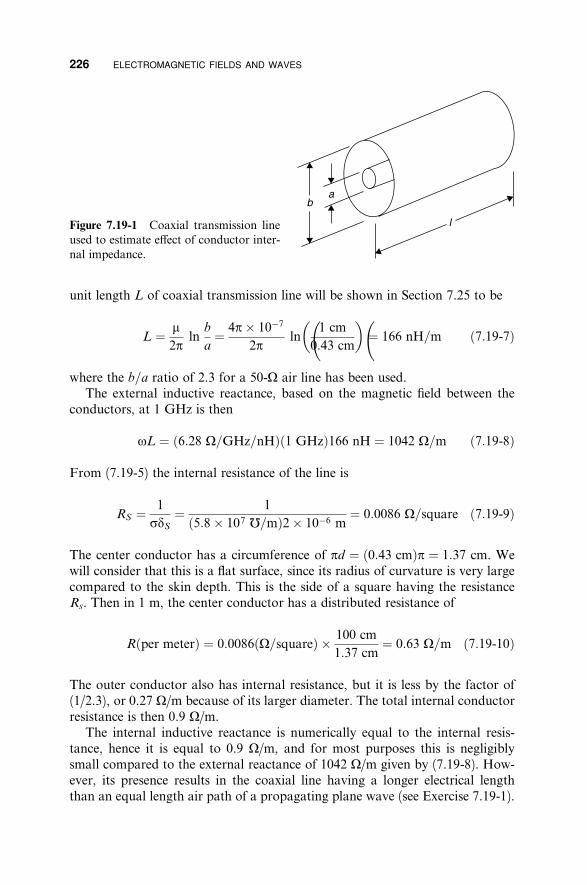
�
226 ELECTROMAGNETIC FIELDS AND WAVES
Figure 7.19-1 Coaxial transmission lineused to estimate e¤ect of conductor inter-nal impedance.
unit length L of coaxial transmission line will be shown in Section 7.25 to be
m b 4p� 10�7�
1 cmL ¼ ln ¼ ln ¼ 166 nH=m ð7:19-7Þ
2p a 2p 0:43 cm
where the b=a ratio of 2.3 for a 50-W air line has been used.The external inductive reactance, based on the magnetic field between the
conductors, at 1 GHz is then
oL ¼ ð6:28 W=GHz=nHÞð1 GHzÞ166 nH ¼ 1042 W=m ð7:19-8Þ
From (7.19-5) the internal resistance of the line is
1 1RS ¼ ¼
sdS ð5:8� 107
W ¼ 0:0086 W=square ð7:19-9Þ=mÞ2� 10�6 m
The center conductor has a circumference of pd ¼ ð0:43 cmÞp ¼ 1:37 cm. Wewill consider that this is a flat surface, since its radius of curvature is very largecompared to the skin depth. This is the side of a square having the resistanceRs. Then in 1 m, the center conductor has a distributed resistance of
100 cmRðper meterÞ ¼ 0:0086ðW=squareÞ � ¼ 0:63 W=m ð7:19-10Þ
1:37 cm
The outer conductor also has internal resistance, but it is less by the factor of(1/2.3), or 0.27 W/m because of its larger diameter. The total internal conductorresistance is then 0.9 W/m.
The internal inductive reactance is numerically equal to the internal resis-tance, hence it is equal to 0.9 W/m, and for most purposes this is negligiblysmall compared to the external reactance of 1042 W/m given by (7.19-8). How-ever, its presence results in the coaxial line having a longer electrical lengththan an equal length air path of a propagating plane wave (see Exercise 7.19-1).

‘� ~
THE WAVE EQUATION 227
In general, the average power loss per unit area of a conductor, PCL, is equalto the product of the surface resistivity Rs and the square of the rms current perunit width, IW . Thus,
PCL ¼ RsjIW j2 ð7:19-11Þ
This is a more general expression that can be used to find the conductor lossesin cables, waveguides, and cavities.
7.20 THE WAVE EQUATION
To demonstrate that~ HH fields can propagate in free space (more preciselyEE and ~
in a charge-free, nonconducting region) we begin with Maxwell’s third equa-tion:
~qBB~‘� EE ¼ � ð7:20-1Þqt
~To eliminate ~B, take the curl of both sides, noting that ~B BB ¼ mHH and that thecurl and time derivative can be taken in any order:
~qBB qð‘� ~HHÞ~‘� ‘� EE ¼ �‘� ¼ �m ð7:20-2Þqt qt
Next, Maxwell’s fourth equation applied to any region devoid of conductioncurrents is
~ ~qDD qEEHH ¼ ¼ e ð7:20-3Þ
qt qt
Substituting this into (7.20-2),
2~q EE~‘� ‘� EEþ me ¼ 0 ð7:20-4Þqt2
Next, apply the vector identity (7.16-3)
AA ¼ ‘ð‘ � ~ AA‘� ‘� ~ AAÞ � ‘2~
~and since for any charge-free region, ‘ � EE ¼ 0, it follows that
2~q EE‘2~EE� me ¼ 0 ð7:20-5Þ
qt2

228 ELECTROMAGNETIC FIELDS AND WAVES
Figure 7.20-1 Electrical disturbance propagating in the þz direction.
This is the wave equation. As expressed, it applies in three dimensions. Inorder to examine this result, let us consider the case for which ~ xx-EE has only an~directed component and only a z variation. For this example (7.20-5) becomes
2q Ex q2Ex� me ¼ 0 ð7:20-6Þqz2 qt2
This equation describes a propagating wave. It is satisfied by any function ofthe form [6, p. 273, also 10, p. 26]
Eþ ¼ fðz� vtÞ ð7:20-7Þx
which describes a disturbance propagating in the þz direction (Fig. 7.20-1),since at the velocity v the quantity z� vt is a constant when z and t bothincrease together, resulting in a constant value of Eþ moving at velocity v inx
the þz direction with increasing t.Since (7.20-6) is a second-order di¤erential equation, it has two independent
solutions. The second solution is a function f ðzþ vtÞ that propagates in the �z
direction:
E� ¼ f ðzþ vtÞ ð7:20-8Þx
With either solution, when the indicated di¤erentiations are applied to (7.20-6),the result is
f 00 þ v2mef 00 ¼ 0 ð7:20-9Þ
which requires that the velocity of propagation is
1 1v ¼ ffiffiffiffiffiffi ¼ pffiffiffiffiffiffiffiffipffiffiffiffiffiffiffiffiffiffi ð7:20-10Þp
me mrer m0e0

THE HELMHOLTZ EQUATIONS 229
For free space, m and er are unity. Thereforer
1v ¼ c ¼rffiffiffiffiffiffiffiffiffiffiffiffiffiffiffiffiffiffiffiffiffiffiffiffiffiffiffiffiffiffiffiffiffiffiffiffiffiffiffiffiffiffiffiffiffiffiffiffiffiffiffiffiffiffi A3� 108
m
H 1 s4p� 10�7 � 10�9 F
m 36p m
One can imagine Maxwell’s excitement on concluding that electromagneticwaves propagated at 300,000 km/s, which he understood to be the approximatespeed of light. This probably contributed to his surmise ‘‘we have strong reason
to conclude that light itself is an electromagnetic disturbance in the form of
waves.’’ (James Clerk Maxwell circa 1863) [1, p. 4].Using the same approach, the electric field can be eliminated from Max-
~well’s third and fourth equations with the result that the HH field satisfies thesame format as (7.20-5), namely
2~q HH‘2~HH� me ¼ 0 ð7:20-11Þ
qt2
~Rather than re-solve the wave equation for the HH field, it is usually more con-venient to solve for either the ~E ~E or HH field and find the other using the appro-priate Maxwell third or fourth curl equation.
7.21 THE HELMHOLTZ EQUATIONS
~ ~Thus far, the wave equation expressed in terms of EE (7.20-5) or HH (7.20-11)applies to any time-varying ‘‘electrical disturbance,’’ as the generalized wave-form sketch of Fig. 7.20-1 describes. However, usually we are interested insinusoidally varying signals having the implicit time variation e jot. Since eachdi¤erentiation with respect to t produces a factor jo, the phasor form of thewave equation can be written immediately as
‘2~ ~EE þ o2meEE ¼ 0 ð7:21-1Þor
EE þ k2~‘2~ EE ¼ 0 ð7:21-2Þand
HH þ k2~‘2~ HH ¼ 0 ð7:21-3Þwhere
ffiffiffiffiffiffi 2pf 2pk1o
pme ¼ ¼ ð7:21-4Þ
v l
1 cv ¼ pffiffiffiffiffiffiffiffiffiffiffiffiffiffiffiffiffiffiffiffi ¼ pffiffiffiffiffiffiffiffi ð7:21-5Þ
mRm0eRe0 mrer

230 ELECTROMAGNETIC FIELDS AND WAVES
Equations (7.21-2) and (7.21-3) are called the Helmholtz equations. Note thatfor uniform plane waves in an unbounded propagating medium k is the propa-gation constant, v is the velocity of propagation, and l is the wavelength. Forfree space propagation, in which m ¼ m0 and e ¼ e0, the propagation constant,propagation velocity, and wavelength are denoted k0; c, and l0, respectively.The Helmholtz equations are more convenient to use when the fields havesinusoidal variation.
7.22 PLANE PROPAGATING WAVES
Returning to waves having arbitrary time dependence, suppose we have planewaves that are propagating in the þz and/or �z directions, but have no varia-tions in the x or y directions (Fig. 7.22-1). Then q=qx ¼ q=qy ¼ 0; and apply-ing Maxwell’s third equation produces
� � ~xx� ~yy ~zz � � �
‘�~EE ¼ �mq~HH ¼ 0
� � 0q � � ð7:22-1Þ
qt � � qz � � Ex�
Ey Ez�
~ ~Note that for this plane wave case, although the EE and HH fields have no variation
with respect to x or y, there can be Ex;Ey;Hx, and Hy field components. Equat-ing the separate vector components on each side of (7.22-1),
~Figure 7.22-1 Plane wave having ~EE and HH fields only in the xy plane and propagationin the þz direction.

PLANE PROPAGATING WAVES 231
qEy qHx� ¼ �m ð7:22-2Þqz qt
qEx qHy¼ �m ð7:22-3Þqz qt
qHz0 ¼ �m ð7:22-4Þ
qt
Similarly, from Maxwell’s fourth equation
� � ~xx� ~yy ~zz � � �
‘�H ¼ eqE ¼ � � 0 0
q � � ð7:22-5Þqt � � qz � �
Hx�
Hy Hz�
Again, equating vector components on each side of the equation,
qHy qEx� ¼ e ð7:22-6Þqz qt
qHx qEy¼ e ð7:22-7Þqz qt
qEz0 ¼ e ð7:22-8Þ
qt
~We first notice, from (7.22-4) and (7.22-8), that the z components of ~EE and HHmust be zero, except for a possible time invariant term, but that is of no interestin the case of propagation. Therefore, the time-varying electric and magneticfields are transverse to the directions (þz and �z) of propagation; and the planewave is said to be a transverse electromagnetic (TEM) wave.
We also notice that di¤erentiating (7.22-3) with respect to z and (7.22-6)with respect to t, and substituting the value for q2Hy=qt qz into (7.22-3) yieldsthe one-dimensional wave equation previously derived:
2q Ex q2Ex� me ¼ 0 ð7:22-9Þqz2 qt2
We denote the fields that propagate in the þz direction as Hþ and Eþ. Specifi-cally, we can relate Hþ and Eþ to each other [6, p. 278] using (7.22-3). Fromy x
(7.22-3) we conclude that Hþ and Eþ have the same functional relationship andy x
di¤er at most by a constant factor (as well as integration constants which donot vary with z or t, and can be ignored for propagating waves).
We have noted that Eþ ¼ fðz� vtÞ. This can be recast as Eþ ¼ gðt� z=vÞ.x x pffiffiffiffiffiffi Then on di¤erentiating Eþ with respect to z and noting that v ¼ 1= me,x
232 ELECTROMAGNETIC FIELDS AND WAVES
(7.22-3) can be written
� rffiffiffi � � qHþ
1 qEþ¼ 1 1
g 0� t� z ey ¼ � x ¼ g 0 t� z ð7:22-10Þ
qt m qz m v v m v
Since Hy and Ex have the same functional form, we can integrate (7.22-10) toget
rffiffiffi Hþ ¼ m
Eþ ð7:22-11Þy xe
Eþ ¼ hHþ ð7:22-12Þx y
where
rffiffiffi rffiffiffiffiffiffiffiffiffi m m0mrh ¼ ¼ ð7:22-13Þe e0er
~ ~Since EE is in volts/meter and HH is expressible in amperes/meter, h has thedimension of ohms. The factor h occurs frequently as a proportionality con-
~stant between ~EE and HH propagating fields and is called the intrinsic impedance
of the propagating medium. Its reciprocal 1=h is called the intrinsic admittance.In free space vffiffiffiffiffiffiffiffiffiffiffiffiffiffiffiffiffiffiffiffiffiffiffiffiffiffiffiffiffiffiffiffi rffiffiffiffiffi u
m0 u4p� 10�7 H=mh0 ¼ Au A120p WA377 W ð7:22-14Þ
e0 t 10�9 F=m
36p
A plane wave propagating in either the þz or �z direction can have an Ex
component, an Ey component, or both. We determined the relationship of(7.22-14) by beginning with (7.22-3). Using similar reasoning and beginningwith (7.22-2) yields [6, p. 279]
Eþ ¼ �hHþ ð7:22-15Þy x
Thus, for plane waves traveling in the þz direction
Eþ Eþx ¼ � y ¼ h ð7:22-16Þ
Hþ Hþy x
Similar reasoning for waves propagating in the �z direction shows that
E� E�
Hx� ¼ � y ¼ �h ð7:22-17Þ
H�y x
�
POYNTING’S THEOREM 233
The relations (7.22-16) and (7.22-17) reveal that
~ ~1. EE and HH are orthogonal to one another in plane propagating waves.~2. The instantaneous value of EE is always h times the instantaneous value
~of HH for each orthogonal pair of wave components (when propagating in
unbounded media).~3. The cross product EE� ~HH always points in the direction of propagation.
Later we will formalize this result as Poynting’s theorem.~ ~4. The relationships between the transverse EE and HH fields of the TEM plane
wave apply for any electrical disturbance, regardless of its functional rela-
tionship with time.
For example, the electric field might be an electromagnetic pulse created bya nuclear detonation. Applying a plane wave approximation to the resulting
wave when it is su‰ciently far from the source of the disturbance, the ~ HHEE and ~
fields propagate with their amplitudes related by the intrinsic impedance.Thus far, this treatment of plane waves applies for any time variation. To
~determine the solution for ~EE and HH in terms of propagation in the þz or �zdirections, it would be necessary to substitute the actual form of the time vari-ation into the wave equations and solve for the fields. However, usually we areinterested in a sinusoidal time variation, in which case the Helmholtz equationscan be applied. Thus the fields for the plane wave case can be written in vectorphasor form, namely
EE ¼ EEþ �jkz þ ~T e
þjkz~ ~T e EE� ð7:22-18Þ
~ ~Te
~Te
þjkzHH ¼ HHþ �jkz þH H ð7:22-19Þ
where
E�T THþ ¼ Eþ
and H� ¼ �T h T h
where ET and HT are the description of the electric and magnetic fields, re-spectively, in the plane transverse to the direction of propagation. The termsin (7.22-18) and (7.22-19) with superscript ‘‘þ’’ represent waves propagatingin the þz direction, and those with the superscript ‘‘�’’ represent waves prop-agating in the �z direction.
7.23 POYNTING’S THEOREM
We now return to the general time variation case to derive Poynting’s theorem.~As the ~EE and HH fields propagate through space, they carry power. Actually, it

234 ELECTROMAGNETIC FIELDS AND WAVES
Figure 7.23-1 Poynting’s vector represents the power density/unit area radiated out ofa closed surface containing a source of propagation.
is impossible to launch a perfectly plane wave because this would require afield that was uniform in, say, the xy plane and extending infinitely far in theþx;�x;þy, and �y directions. However, a directional antenna approximates a
plane wave over some aperture, the larger the aperture dimensions compared tothe transmitted wavelength, the more directive (plane-wave-like) the beam andthe more gradually it diverges.
Although a practically launched wave that is propagating far from its source~can be approximated as a plane wave for the purpose of relating the ~EE and HH
field components, its wave front actually tends to assume a spherical shape,spreading out so that the amount of power crossing a given area, say, onesquare meter, becomes less and less with increasing distance from the trans-mitter. The power density, in watts per square meter, approaches an inversesquare law function of distance when measured far from the source thatlaunched the wave (Fig. 7.23-1).
We shall demonstrate that the amount of power passing through a givensurface area S of space is given by Poynting’s vector. This is the cross product
~of the ~EE and HH fields. The cross product is the magnitudes of the fields multi-plied by the sine of the angle between them. But for a wave propagating inspace, the ~ HH fields are already orthogonal to one another, so their powerEE and ~
cross product is simply the product of their amplitudes [6, p. 275].In this analysis the ~ HH fields are their actual instantaneous values, andEE and ~
the power that they convey is the instantaneous power flow regardless of theirfunctional time variation. Later, when applying Poynting’s theorem to sinus-oidal fields, rms values can be used to determine average power flow.
Poynting’s theorem states that the power flow propagating out of a closed
surface S is equal to the integral over the surface of the real part of Poynting’s~ EE� ~vector, PP ¼~ HH, where P;E, and H are time-varying functions:
ð !~Power flowj ¼ PP � dS ð7:23-1ÞSS

POYNTING’S THEOREM 235
To prove this theorem, we employ the vector identity (7.16-9) into which wehave substituted the ~ HH fields:EE and ~
~ ~ ~‘ � ðEE� ~ HH � ‘� EE� EE � ‘� ~HHÞ ¼ ~ HH ð7:23-2Þ~Next, we substitute values for ‘� EE and ‘� ~HH from Maxwell’s third and
fourth equations:
~ ~qBB qDD~ ~ ~ ~ ~‘ � ðEE� ~HHÞ ¼ �HH � � EE � � EE � JJc ð7:23-3Þqt qt
If e and m are constant over the volume of interest,
~ ~qDD 1 qðeEE2Þ~EE � ¼ ð7:23-4Þqt 2 qt
and
~ ~qBB 1 qðmHH2Þ~HH � ¼ ð7:23-5Þqt 2 qt
Substituting these values into (7.23-3) and integrating over the volume con-tained by the closed surface S, " # ð ð ~ ~1 qðmHH2Þ 1 qðeEE2Þ~ ~ ~� ‘ � ðEE� ~HHÞ dV ¼ � þ � þ EE � JJc dV ð7:23-6Þ
2 qt 2 qtV V
Applying the divergence theorem," # ð ð 2~ ~! 1 qðmHH Þ 1 qðeEE2Þ~ ~ ~� ðEE �HHÞ � dS ¼ � þ � þ EE � ~ dV ð7:23-7ÞJJcS V 2 qt 2 qt
The negative sign on the left side means that instead of diverging from thevolume V, the energy is entering V. This is consistent with the reasoning thatfollows.
The first term on the right side has the dimensions of energy per unit vol-ume, henrys� amperes2=m3. When integrated with respect to volume, this isthe same form, even to the factor of 1
2 , of the energy stored in an inductor,specifically LI2/2. As such, this term represents, after integration, the increasein stored magnetic energy per unit time (power inflow) in volume V resultingfrom the inflow (negative divergence) of Poynting’s vector. Similarly, the sec-ond term having the dimensions farads� voltage2=m3 also has the dimensionsof energy and is equivalent to the energy storage of a capacitor, CV2/2, havingunit volume. This term represents the increase in stored electric energy per unittime (power inflow).

�
236 ELECTROMAGNETIC FIELDS AND WAVES
The third term has the dimensions of power dissipated voltage � current=m3
and represents, after integration, the amount of power being dissipated withinthe volume V. Alternatively, if there are mobile charges in V, this term repre-
~sents the power which increases their motion or, if~EE � JJ is negative, it representsthe power contributed by their deceleration [6, p. 275].
All of the net power inflow and dissipation represented on the right side of(7.23-7) comes from the inflow of Poynting’s vector. Reversing the sign of thispower flow gives the rate at which energy is leaving V, that is the power flowout of V.
ð !~Power flowj ¼ PP � dS where ~ EE� ~PP ¼~ HH ð7:23-8ÞSS
This is Poynting’s theorem—the result that we wished to show. Note that P is apower density (watts/meter2).
~EE and HPoynting’s theorem applies for any time-varying ~ H, regardless of theform of time variation (it need not be sinusoidal). Poynting’s theorem gives the
~instantaneous power flow when instantaneous values are used for the EE and~HH fields.
For sinusoidally varying fields, the average power flow density can be deter-mined using the phasor forms for ~ HEE and ~H, specifically
~ ~ ~PPAv ¼ 1 ReðEE �HH�Þ ð7:23-9Þ
2
~ ~where * represents the complex conjugate. The imaginary part of ðEE �HH Þrepresents the ebb and flow of reactive power density through the surface S.
7.24 WAVE POLARIZATION
The electromagnetic wave propagation described in Section 7.22 (Fig. 7.22-3) is~ ~known as a linear or plane-polarized wave, since the EE and HH fields each lie
along an unchanging direction in the plane transverse to the direction of prop-agation. For example, an electric field oriented in the x direction and prop-agating in the þz direction has a full period of variation in one wavelength at agiven instant of time (Fig. 7.24-1).
The orthogonal magnetic field, in this example in the y direction, has thesame pattern along the z axis (Fig. 7.24-2).
The combination of any two or more linearly polarized waves of the samefrequency that are in phase and propagating in the same direction results ina linearly polarized wave. Figure 7.24-3 depicts the case of two orthogonal
~ ~waves, represented by EEx and EEy, that are in phase and of equal amplitude.~ ~The resultant wave, EER, is oriented at 45� to both ~EEx and EEy.

WAVE POLARIZATION 237
Figure 7.24-1 Amplitude of Ex at an instant in time for a wave propagating in the þzdirection. A sinusoid is shown for illustration, but the wave equation applies for all timevariations [1, p. 32].
Thus, if
~ ~x yxE0 cosðot� kzÞ and EEy ¼ ~EEx ¼~ yE0 cosðot� kzÞ ð7:24-1Þwhere k ¼ 2p=l is the propagation constant of waves traveling in the þz
~ EEx þ ~direction. Then, defining EER 1 ~ EEy, the resultant electric field is given by
~EERðxxþ ~~ yyÞE0 cosðot� kzÞ ð7:24-2Þffiffiffi which is simply a vector having the peak magnitude
p2E0 and a direction that
is always at an angle of 45� from the x or y axes (Fig. 7.24-4).Suppose that instead of two in-phase field components, we excite two space
orthogonal components of electric field that have equal amplitudes but are 90�
out of phase with each other.
Figure 7.24-2 Orthogonal E and H fields of the wave in Figure 7.24-1 [1, p. 32].

238 ELECTROMAGNETIC FIELDS AND WAVES
Figure 7.24-3 Sum of two in-phase, linearly polarized waves is also a linearly polarizedwave.
In this case
~ ~x yxE0 cosðot� kzÞ and EEy ¼ ~EEx ¼~ yE0 sinðot� kzÞ ð7:24-3Þ
At z ¼ 0 for instance,
~EER ¼~ yxE0 cos otþ ~x yE0 sin ot ð7:24-4Þ
Figure 7.24-4 Circularly polarized plane wave has a constant amplitude when projectedonto the plane normal to its direction of propagation.
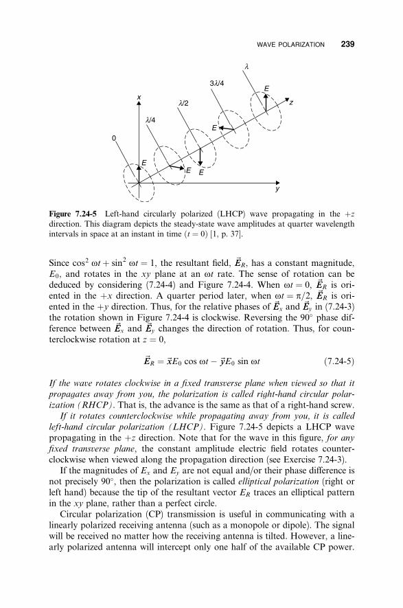
WAVE POLARIZATION 239
Figure 7.24-5 Left-hand circularly polarized (LHCP) wave propagating in the þz
direction. This diagram depicts the steady-state wave amplitudes at quarter wavelengthintervals in space at an instant in time ðt ¼ 0Þ [1, p. 37].
~Since cos2 otþ sin2 ot ¼ 1, the resultant field, EER, has a constant magnitude,E0, and rotates in the xy plane at an ot rate. The sense of rotation can be
~deduced by considering (7.24-4) and Figure 7.24-4. When ot ¼ 0, EER is ori-~ented in the þx direction. A quarter period later, when ot ¼ p=2, EER is ori-
~ ~ented in the þy direction. Thus, for the relative phases of EEx and EEy in (7.24-3)the rotation shown in Figure 7.24-4 is clockwise. Reversing the 90� phase dif-
~ ~ference between EEx and EEy changes the direction of rotation. Thus, for coun-terclockwise rotation at z ¼ 0,
~EER ¼~ yxE0 cos ot� ~x yE0 sin ot ð7:24-5Þ
If the wave rotates clockwise in a fixed transverse plane when viewed so that it
propagates away from you, the polarization is called right-hand circular polar-
ization (RHCP). That is, the advance is the same as that of a right-hand screw.If it rotates counterclockwise while propagating away from you, it is called
left-hand circular polarization (LHCP). Figure 7.24-5 depicts a LHCP wavepropagating in the þz direction. Note that for the wave in this figure, for anyfixed transverse plane, the constant amplitude electric field rotates counter-clockwise when viewed along the propagation direction (see Exercise 7.24-3).
If the magnitudes of Ex and Ey are not equal and/or their phase di¤erence isnot precisely 90�, then the polarization is called elliptical polarization (right orleft hand) because the tip of the resultant vector ER traces an elliptical patternin the xy plane, rather than a perfect circle.
Circular polarization (CP) transmission is useful in communicating with alinearly polarized receiving antenna (such as a monopole or dipole). The signalwill be received no matter how the receiving antenna is tilted. However, a line-arly polarized antenna will intercept only one half of the available CP power.

All of the power can be recovered only by using a CP antenna of the samesense as is received. Since the directional sense of propagation is reversed onviewing a wave leaving the transmitter and the same wave arriving at thereceiver, if a RHCP antenna was used for transmission, a LHCP antenna mustbe used for reception.
7.25 EH FIELDS ON TRANSMISSION LINES
Once an electromagnetic wave is launched into space, it diverges and its fieldstrength diminishes due to the spreading out of its power density. This e¤ectcan be diminished by using a guiding structure which sets up boundary con-ditions that reduce the wave’s spreading, such as two conductors forming atransmission line. Because it reduces a propagating wave’s spreading, a two-wire transmission line could be considered a form of waveguide. However, theterm waveguide is generally used to describe hollow pipes or solid dielectricsused for electromagnetic transmission. These terms are not used consistently inthe industry, and there are exceptions, such as coplanar waveguide, a variationof stripline or microstrip.
For the two-wire line (Fig. 7.25-1) the fields and currents are considerablyconstrained to travel axially along the line. However, some energy is lost due to
Figure 7.25-1 A two-wire transmission line and its ~EE (solid lines) and ~HH (dashed lines)fields. (After Skilling, 4, p. 160, with permission.)
240 ELECTROMAGNETIC FIELDS AND WAVES

EH FIELDS ON TRANSMISSION LINES 241
Figure 7.25-2 Coaxial transmission line with cylindrical coordinates r;j, and z. Notethat a is the radius of the inner conductor and b is the radius of the outer conductor.
radiation or leakage of the fields surrounding the line. The principal modeis TEM (transverse electromagnetic), which means that both the electric andmagnetic fields are always and everywhere transverse to the direction of prop-
agation. Note that the~ HH fieldEE field lines terminate on the conductors, and the ~
lines are orthogonal to the ~EE lines, as shown in Figure 7.25-2. Both fields fringeoutward without limit in the plane transverse to the direction of propagation.
The radiation that leaks from the two-wire line can be reduced to negligiblevalues by causing one conductor to surround the other, as is done with thecoaxial transmission line. The shielding would be total if the outer conductorcould have zero resistivity; but, even with finite resistivity, for all practicalpurposes the shielding is complete when the outer conductor is a solid metalcylinder of any practical thickness. For analysis we will assume perfect con-ductors, that is, having infinite conductivity. The following analysis determines
~ ~the EE and HH fields in the insulating region of the coaxial transmission line(between the conductors). From this can be derived expressions for the distri-buted capacitance C and inductance L of the line as well as its characteristicimpedance Z0.
For this transmission line, as for most lines, there are di¤erent field patternsby which energy can be propagated. Each is called a mode of the transmissionline or waveguide. In general, the mode which can propagate at the lowest fre-quency is called the dominant mode. Transmission lines having two separateconductors can propagate all frequencies, theoretically from direct current tolight frequencies in the lowest order, or dominant, mode. However, at somefrequency, propagation in more than one mode becomes possible, and this isundesirable. Therefore, it is good practice to operate the transmission line atfrequencies below the lowest frequency at which the first higher-order modeabove the dominant mode can propagate. This is known as the cuto¤ frequency
of the mode.

242 ELECTROMAGNETIC FIELDS AND WAVES
Thus far, we have presented fields and field relationships in rectangularcoordinates. However, various symmetries favor the use of other coordinatesystems. The most common orthogonal systems are rectangular (also calledCartesian), cylindrical, and spherical. The coaxial transmission line is mosteasily analyzed using cylindrical coordinates.
To evaluate the fields of the dominant TEM mode we note that by definition~both the ~EE and HH fields have components only in the plane transverse to the
propagation directions, þz and �z. This means that their z-directed compo-nents are zero. Since this mode ‘‘propagates’’ at DC (zero frequency), it is pos-sible to evaluate the fields using a static analysis. To solve for the electric field[1, p. 21], apply Gauss’s law assuming that there is a charge, þQ, on the centerconductor and an equal and opposite charge, �Q, on the outer conductor ofa coaxial line of unit length. Since this is a per-unit-length analysis, we mayignore any fringing fields at the ends of the portion of the line used for analysis.
For any cylindrical surface of radius r defined between the conductors,a < r < b, ðL ð2p
Q ¼ ejEjr dj dz ð7:25-1Þ0 0
where L is unity, since the analysis is on a per-unit length of transmission linebasis. Noting that ~EE is independent of z and, due to symmetry, independent ofj, the integration produces
QQ ¼ eErð2prÞ or Er ¼ ð7:25-2Þ
2per
~which is the magnitude of the radial EE field between the conductors (Fig.7.25-3). The ~EE field is the gradient of a scalar function that we will identify asthe voltage V having zero potential (voltage) on the outer conductor.
Figure 7.25-3 The ~EE field of the TEM modein coaxial line.
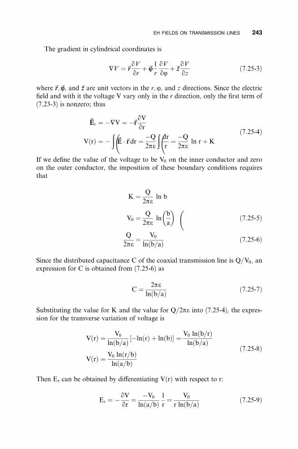
� �
EH FIELDS ON TRANSMISSION LINES 243
The gradient in cylindrical coordinates is
qV 1 qV qV ‘V ¼~ þ~ ~ ð7:25-3Þrr zz
qrjjr qj
þqz
rr;~ zz are unit vectors in the r;j, and z directions. Since the electricwhere~ jj, and~ field and with it the voltage V vary only in the r direction, only the first term of (7.23-3) is nonzero; thus
~EEr ¼ �‘V ¼ �~rr qVð qr ð ð7:25-4ÞVðrÞ ¼ � ~EE �~rr dr ¼ �Q
2pe
dr
r¼ �Q
2peln rþK
If we define the value of the voltage to be V0 on the inner conductor and zeroon the outer conductor, the imposition of these boundary conditions requiresthat
QK ¼ ln b
2pe
Q bV0 ¼ ln ð7:25-5Þ
2pe a
Q V0¼ ð7:25-6Þ2pe lnðb=aÞ
Since the distributed capacitance C of the coaxial transmission line is Q=V0, anexpression for C is obtained from (7.25-6) as
2peC ¼ ð7:25-7Þ
lnðb=aÞ
Substituting the value for K and the value for Q=2pe into (7.25-4), the expres-sion for the transverse variation of voltage is
V0 V0 lnðb=rÞVðrÞ ¼ ½�lnðrÞ þ lnðbÞ� ¼
lnðb=aÞ lnðb=aÞð7:25-8Þ
V0 lnðr=bÞVðrÞ ¼
lnða=bÞ
Then Er can be obtained by di¤erentiating VðrÞ with respect to r:
qV �V0 1 V0Er ¼ � ¼ ¼ ð7:25-9Þ
qr lnða=bÞ r r lnðb=aÞ

where the negative sign in (7.25-9) was eliminated by interchanging the numer-ator and denominator of the ln expression. Up to this point the expressionsapply for any time variation. Usually coaxial lines are used to transmit sinus-oidal signals, in which case ~EE must also satisfy the Helmholtz equation, andtherefore have a variation with z of the form e�jkz. The phasor form of Er
becomes
Er ¼ V0
r lnðb=aÞ e�jkz ð7:25-10Þ
Next, we will obtain an expression for the magnetic field between the con-ductors. The magnetic field lines are concentric with the center conductor asshown in Figure 7.25-4. Its value is determined by using the integral form ofMaxwell’s fourth equation:
þ~HH � dl!¼
ðS
~JJ � dS! þðS
q~DD
qt� dS!
The axial qD=qt term is zero since E and D have no z component. The integralof the current density is just the total current I0 that flows in the þz directionon the inner conductor and the �z direction on the outer conductor (as is re-quired for the ~HH field to be zero outside the coaxial line). Then, since the lineintegral of ~HH is just its magnitude times the circumferential path, the magneticfield for aa ra b is obtained from
2prHj ¼ I0
Thus
Hj ¼ I02pr
ð7:25-11Þ
Equation (7.25-11) is valid for both DC and AC fields. For sinusoidal varia-
Figure 7.25-4 Magnetic field lines H andthe current distribution I0 for the TEMmode in coaxial line.
244 ELECTROMAGNETIC FIELDS AND WAVES

EH FIELDS ON TRANSMISSION LINES 245
+
− −
−
− −
− −
−
+
+ +
+
+
+
+
−J
Er
Er
HQ
HQ
y
r
z
x2 + y
2
√
+J
x
Figure 7.25-5 Coaxial line with transverse E and H fields and axial current density J.
tions, the phasor form of Hj includes the propagation factor e�jkz. Thus,
Hj ¼ I0e�jkz ð7:25-12Þ
2pr
For purposes of illustration the current lines in Figure 7.25-5 are shown asfilaments into the paper (þz direction) on the center conductor and out of thepaper on the inside of the outer conductor. In actuality, however, the currentsare distributed uniformly throughout cross sections of the conductors for DCcurrents and in uniform sheets near the inner surfaces (due to skin e¤ect) of theconductors for high frequency AC currents.
The ratio V0=I0 ¼ Z0 is defined as the characteristic impedance of the trans-mission line. This can be evaluated using (7.25-9) and (7.25-11) with the result
Z0 ¼ V0
I0¼ Er
Hj
lnðb=aÞ2p
ð7:25-13Þ
ffiffiffiffiffiffiffiffi pNext, if the value for the intrinsic impedance h ¼ m=e is substituted for theratio of the orthogonal fields Er and Hj,rffiffiffi
1 m bZ0 ¼ ln ð7:25-14Þ
2p e a

246 ELECTROMAGNETIC FIELDS AND WAVES pffiffiffiffiffiffiffiffiffiffiffiffi Substituting the values m ¼ m m0, e ¼ ere0, and m0=e0A120p givesr rffiffiffiffiffi � �
m brZ0A60 ln ð7:25-15Þer a
Previously in (7.25-7) we determined the distributed capacitance C of the trans-mission line. From (4.11-4) the corresponding distributed inductance is relatedto Z0 and C by rffiffiffiffi
LZ0 ¼ ð7:25-16Þ
C
Substituting C from (7.25-7) and Z0 from (7.25-14) into (7.25-16), L is deter-mined to be
m bL ¼ ln ð7:25-17Þ
2p a
~It is interesting to note that we only proved that the ratio of the orthogonal EE~and HH fields of a propagating wave was equal to h under the conditions that
these fields had no variation in the plane transverse to propagation. Althoughthe Er and Hj fields for the coaxial line are functions of r, their ratio is equal tothe intrinsic impedance h of the insulating region between the conductors. Thiscan be verified by the execution of Exercise 7.25-3.
These derivations demonstrate how Maxwell’s equations can be used to solvefor the properties of transmission lines. While the principles are the same for alltransmission lines, closed-form analytic expressions for the fields about theconductors of various lines such as stripline, microstrip, and coplanar wave-guide are much more di‰cult to formulate that those for coaxial line, one ofthe few transmission line formats permitting a simple and exact solution. Inmany cases, a complete analytic approximation is not practical, and elec-tromagnetic (EM) simulation is required to obtain characteristic impedanceand other transmission line parameters of su‰cient precision for engineeringpurposes.
7.26 WAVEGUIDES
General Waveguide Solution
The solution for the fields in waveguides (conducting hollow pipes) is di¤erentthan the solutions for a free space plane wave or a multiconductor transmissionline. This is because a TEM wave cannot propagate within a hollow pipe thatlacks an axial conductor to carry current, as is available, for example, in acoaxial line. The argument is that a transverse electric field that has a nonzero

WAVEGUIDES 247
curl requires an axial magnetic field. Alternatively, a transverse magnetic fieldwould require either an axial conduction current (which cannot exist since thereis no center conductor) or a changing axial electric field. The outcome is thatwaveguides support transverse electric (TE) and transverse magnetic (TM)
modes of propagation but not a TEM mode.We will solve for the fields of the dominant mode of rectangular waveguide
since this is the type most commonly used. The method, described by Ramoand Whinnery [6, Chapters 8 and 9] and attributed by them to Schelkuno¤ [11],is su‰ciently general that it allows solution of the various modes in all types
~ ~of waveguides. The derivation of the EE and HH fields is begun by expandingMaxwell’s third and fourth equations, as was done for the plane wave case, but
~ ~in this case we do not assume that the EE and HH fields have no x or y variations,as was assumed for the propagating plane wave case.
On the other hand, we will assume a sinusoidal time variation of the fieldssince this is the way in which waveguides are used. Indeed, as will be shown,waveguides exhibit a cuto¤ frequency, below which propagation cannot occur.It should also be noted that even above the cuto¤ frequency, waveguides aredispersive. That is, they do not have constant propagation delay versus fre-quency. Consequently, waveguides cannot propagate absolutely distortion-free
representations of arbitrary electrical disturbances, as can a free space planewave or the TEM wave in a two or more conductor transmission line.
Waveguides have only a single conductor, and for this reason the transverseelectrical field cannot be derived from a static potential function, as was donefor the coaxial line. This is because no static potential di¤erence can existwithin a charge-free, completely enclosed conductor. Unlike the TEM modefor multiconductor transmission lines, the currents in the waveguide wallshave transverse as well as longitudinal components. Waveguides do not haveuniquely identifiable voltages and currents associated with propagation, andtherefore waveguides have no uniquely defined characteristic impedance. As analternative, a characteristic wave impedance can be defined for waveguide as
~ ~the ratio of the orthogonal EE to HH fields in the transverse plane. However, aswe shall see in the study of Green’s functions, an absolute impedance forwaveguide can be defined under certain conditions.
It will be shown that the characteristic wave impedance of waveguide isapproximately equal to the intrinsic impedance of free space, about 377 W, forfrequencies su‰ciently above the cuto¤ frequency. The fact that waveguideshave broad conducting walls results in relatively low ohmic losses. Further-more, waveguides require no dielectric to support their structure, hence air di-electric is practical, with negligible dielectric loss. Finally, since waveguidepropagation is totally enclosed, there is no radiative loss. As a result, wave-guides usually provide the lowest loss practical transmission media for guidedwaves. Their low loss as well as their high power capacity are principal reasonsfor their use. In addition to being an e‰cient transmission medium, they findconsiderable use in the construction of high Q resonator elements, couplers,and power dividers.

248 ELECTROMAGNETIC FIELDS AND WAVES
We will assume lossless conditions and begin the analysis of waveguides byexpanding Maxwell’s third and fourth equations, assuming a z dependence ofe�gz for waves traveling in the þz direction and eþgz for those traveling in the�z direction. A real value for g means wave attenuation, while an imaginaryvalue for g means lossless propagation.
~The following analysis assumes e jot time dependence. Taking the curl of EE!~and of HH, noting that JC ¼ 0 in a source-free region, performing di¤erentia-tion with respect to time by multiplying by jo, and di¤erentiation with respectto z by multiplying by �g (for þz-directed waves) gives
� � � � ~xx� ~yy ~zz � ~xx� ~yy ~zz � � � � �
‘� ~EE ¼ � q~BB ¼ q� � q q � � ‘� ~HH ¼ q~DD ¼ q� � q q � � qt qx� � qy qz � � qt qx� � qy qz � �
Ex� Ey Ez
� Ex� Ey Ez
� For þz-directed propagation, the phasor forms of the above equations become
qEz�jomHx ¼qy
þ gEy ð7:26-1aÞ
qEz�jomHy ¼ � � gEx ð7:26-1bÞqx
qEy qEx�jomHz ¼ � ð7:26-1cÞqx qy
qHzjoeEx ¼ þ gHy ð7:26-1dÞ
qy
qHzjoeEy ¼ � � gHx ð7:26-1eÞ
qx
qHy qHxjoeEz ¼ � ð7:26-1fÞ
qx qy
[Equations (7.26-1a) to (7.26-1b) from Ramo and Whinnery, 6, p. 316, reprintedwith permission.]
For all of the equations in (7.26-1) and in the following derivation,Ex;Ey;Ez;Hx;Hy, and Hz are functions only of x and y. To recover the timeand z dependence, multiply by eð jot�gzÞ for waves traveling in the þz directionand take the real part thereof. For waves traveling in the �z direction replace�gz with þgz.
With diligent algebraic application, the relations given in (7.26-1) can bemanipulated to give Hx;Hy;Ex, and Ey in terms of Ez and Hz. For example,the first equation in (7.26-2) is obtained by solving (7.26-1a) for Ey and sub-stituting this value into (7.26-1e). Also note that k2 ¼ o2me, as was previouslydefined. Then, for þz-directed propagation:

WAVEGUIDES 249
� � Hx ¼ 1
g2 þ k2joe
qEz
qy� g
qHz
qx� � ð7:26-2aÞ
Hy ¼ � 1
g2 þ k2joe
qEz
qxþ g
qHz
qy� � ð7:26-2bÞ
Ex ¼ � 1
g2 þ k2� gqEz
qxþ jom
qHz
qy � ð7:26-2cÞ
Ey ¼ 1
g2 þ k2�g
qEz
qyþ jom
qHz
qxð7:26-2dÞ
ffiffiffiffiffiffi where k ¼ o
pme. [Equations (7.26-2a) to (7.26-2d) from Ramo and Whinnery,
6, p. 317, reprinted with permission.] Note that in this derivation, k is not the
propagation constant. The equations of (7.26-2) apply to all transmission linesand waveguides since they have been derived directly from Maxwell’s equationswithout any limiting assumptions, other than a sinusoidal time variation. Inaddition, the electric and magnetic fields must also satisfy the Helmholtz equa-tions. Therefore,
‘2~ EE ‘2~ HHEE ¼ �k2~ and HH ¼ �k2~ ð7:26-3a,bÞ
The operator ‘2 is three dimensional and can be separated dimensionally. Thus
2~‘2~ ~EE ¼ ‘2 EE þ q EE ð7:26-4Þxy qz2
2~‘2~ ~HH ¼ ‘2 HH þ q HH ð7:26-5Þxy qz2
The second term is due to the axial field variation along the waveguide, and ithas the assumed functional description e�gz in the þz direction. Thus
2~q EE 2~¼ g EE ð7:26-6Þqz2
2~q HH ¼ g2~ ð7:26-7ÞHHqz2
Substituting this format into (7.26-3a) and (7.26-3b) gives
‘2 ~ ~EE ¼ �ðg2 þ k2ÞEE ð7:26-8Þxy
‘2 ~ ~HH ¼ �ðg2 þ k2ÞHH ð7:26-9Þxy
~Some various waveguide types are shown in Figure 7.26-1 along with the EE
field of their dominant mode, the mode that propagates at the lowest frequency.

The above equations will be used to determine the propagation characteristicsof rectangular waveguide.
Waveguide Types
The parallel-plate waveguide is simple in form and propagates at all frequen-cies, even direct current. Since it is a two-conductor line, it also can be classedas a transmission line. In principle, it does not radiate because ~EE � ~HH is only inthe z direction. However, any imperfections or discontinuities in its construc-tion can result in energy leakage. Thus, in practice, it can have radiation loss.
Figure 7.26-1 Waveguide types and the cross-sectional E field pattern of the dominantmode: (a) parallel-plate waveguide, (b) circular waveguide, and (c) rectangular wave-guide.
250 ELECTROMAGNETIC FIELDS AND WAVES

WAVEGUIDES 251
Also, some means must be provided to support the conductors for air dielectricoperation since there are no sides.
The round waveguide shown in (Fig. 7.26-1b) also can be fabricated simply.In fact, copper water pipe of suitable diameter would serve nicely. The dis-advantage of this waveguide is that the polarization of the electric field, shownvertically in Figure 7.26-1b, can rotate as the wave propagates due to irregu-larities in the waveguide. As a result, when the wave reaches the end of thewaveguide, a vertically polarized receptor may not be able to intercept all, oreven any, of its energy. The rectangular waveguide overcomes these disadvan-tages and therefore is the most commonly used. The method of solution followsthat of Ramo and Whinnery [6].
Rectangular Waveguide Fields
Rectangular waveguide is commonly used in microwave applications andtherefore will be the subject of our analysis. Equations (7.26-8) and (7.26-9) areto be satisfied by all of the field components in the waveguide. We have alreadynoted that either TE or TM modes can exist in the waveguide but not TEM
~ ~modes. Furthermore, we have related the transverse EE and HH fields to the axial~ ~EE and HH fields by the equations in (7.26-2). Thus, it is only necessary to solvefor the axial field component for a mode class, TE or TM, and then the trans-verse fields can be determined from the axial field. Let us consider the TE
~ ~modes that have an axial HH field but no axial EE field. Applying (7.26-9) to theHz component of the field,
2 q Hz‘2 Hz ¼ q Hz þ
2
¼ �k2Hz ð7:26-10Þxy cqy2qx2
2where k2 ¼ g þ k2 and k2 ¼ o2me. Equation (7.26-10) is a partial di¤erentialc
equation that can be solved by the method of separation of variables. To do sowe assume it has a solution of the form
Hz ¼ f ðxÞgðyÞ ð7:26-11Þ
The functions f ðxÞ and gðyÞ describe the field dependency in the plane trans-verse to the direction of propagation, where f ðxÞ is only a function of x andgðyÞ is only a function of y. In the transverse ðxyÞ plane the solution is of theform
Hz ¼ fg ð7:26-12Þ
in which the z variation is implicit. Substituting this into (7.26-10) and per-forming the indicated di¤erentiations give

252 ELECTROMAGNETIC FIELDS AND WAVES
f 00gþ fg 00 ¼ �k2 fgc
f 00 00 ð7:26-13Þþ g ¼ �k2
f g c
where the double prime indicates the second derivative. Since f and g can bevaried independently, each of the terms on the left side of (7.26-13) must equala constant. There are various forms for the solution of (7.26-13) dependingupon whether the ratios are negative, positive, or one negative and one positive[6, p. 355]. If both ratios are assumed to be negative, then we can assign themthe values k2 and k2 such thatx y
f 00
f¼ �k2
x ð7:26-14Þ
g 00
g¼ �k2
y ð7:26-15Þ
The solutions for positive values of k2 and ky2 are sinusoids:x
f ðxÞ ¼ C1 cos kxxþ C2 sin kxx ð7:26-16ÞgðyÞ ¼ C3 cos ky yþ C4 sin ky y ð7:26-17Þ
and from (7.26-13)
2k2 þ k2 ¼ k2 ¼ g þ o2me ð7:26-18Þx y c
There are also solutions in terms of sinh and cosh functions if the ratios arepositive, but for present purposes the sinusoidal solutions su‰ce.
Applying Boundary Conditions
For the rectangular waveguide the electric field tangential to a conductingwaveguide wall must be zero. Therefore, Ex ¼ 0 at x ¼ 0 and a and Ey ¼ 0 aty ¼ 0 and b. Since, for the TE waves, Ez ¼ 0, and, referring to (7.26-2c) and(7.26-2d), since Ey and Ex are proportional to qHz=qy and qHz=qx, respec-tively, it follows that
qHz qHz¼ 0 at x ¼ 0; a and ¼ 0 at y ¼ 0; b ð7:26-19a,bÞqx qy
The boundary conditions at x ¼ 0 and y ¼ 0 require that only the cosine termsin (7.26-16) and (7.26-17) can apply. We will use the remaining boundary con-ditions at x ¼ a and y ¼ b shortly. Thus
Hz ¼ H0 cos kxx cos ky y ð7:26-20Þ

WAVEGUIDES 253
where H0 is an amplitude constant. Applying (7.26-2a) thru (7.26-2d) and rec-ognizing that Ez ¼ 0,
gkxHx ¼ H0 sin kxx cos ky y ð7:26-21Þ
k2c
gkyHy ¼ H0 cos kxx sin ky y ð7:26-22Þ
k2c
jomkyEx ¼ H0 cos kxx sin ky y ð7:26-23Þ
k2c
�jomkxEy ¼ H0 sin kxx cos ky y ð7:26-24Þ
k2c
2 2where k2 ¼ g þ k2 and k2 ¼ o me.c
Propagation Constants and Waveguide Modes
The boundary conditions that Ey ¼ 0 at x ¼ a and Ex ¼ 0 at y ¼ b in (7.26-24)and (7.26-23) require, respectively, that
mp npkx ¼ and ky ¼ ð7:26-25a,bÞ
a b
where m and n are integers (0; 1; 2; 3 . . .), both of which cannot be zero simul-taneously, that denote the mode number. More about modes shortly. Thensffiffiffiffiffiffiffiffiffiffiffiffiffiffiffiffiffiffiffiffiffiffiffiffiffiffiffiffiffiffiffiffiffi qffiffiffiffiffiffiffiffiffiffiffiffiffiffiffiffi � �2 � �2
npðkcÞm;n ¼ kx2 þ ky
2 ¼ mp þ ð7:26-26Þa b
For lossless propagation
g ¼ aþ jb ð7:26-27aÞ
must be imaginary. Thus, since
g2 ¼ kc2 � k2 ð7:26-27bÞqffiffiffiffiffiffiffiffiffiffiffiffiffiffiffiffi qffiffiffiffiffiffiffiffiffiffiffiffiffiffiffiffiffiffiffiffiffiffiffiffiffiffiffiffiffi
g ¼ jb ¼ k2 � k2 ¼ k2 � ð2pf Þ2me ð7:26-27cÞc c
For propagation to occur the quantity under the square root must be negative,or sffiffiffiffiffiffiffiffiffiffiffiffiffiffiffiffiffiffiffiffiffiffiffiffiffiffiffiffiffiffiffiffiffi � �2 � �2
kc 1 mp npf > pffiffiffiffiffiffi ¼
2ppffiffiffiffiffiffi þ ð7:26-28Þ
2p me me a b

254 ELECTROMAGNETIC FIELDS AND WAVES
Since the operating wavelength at frequency f is l ¼ 1=fpffiffiffiffiffiffi
, the conditionmeat which (7.26-28) is just satisfied corresponds to the cuto¤ wavelength and isgiven by
2p 1lC ¼ ¼qffiffiffiffiffiffiffiffiffiffiffiffiffiffiffiffiffiffiffiffiffiffiffiffiffiffiffiffiffiffiffiffiffiffiffiffiffiffiffi ð7:26-29Þ
kc ðm=2aÞ2 þ ðn=2bÞ2
Because fclc ¼ v ¼ 1=pffiffiffiffiffiffi me, a cuto¤ frequency can be defined as
v c 1fc ¼ ¼
lcpffiffiffiffiffiffiffiffi ð7:26-30Þ
lc mrer
Thus when f < fc (or l > lc), the waveguide does not propagate in that mode.Since rectangular waveguide is made with a > b, and since m and n cannotboth be zero simultaneously, the longest free space wavelength for propagationin rectangular waveguide applies to the TE10 mode (m ¼ 1 and n ¼ 0) given by
¼ 2a ð7:26-31ÞðlCÞ10
Substituting kx ¼ mp=a, ky ¼ np=b, g2 þ k2 ¼ k2, and g ¼ jb for propagatingc
waves into (7.26-21) through (7.26-24) gives the transverse field components as
jom np mpx npyEx ¼ H0 cos sin ð7:26-32Þ
k2 b a bc
�jom mp mpx npyEy ¼ H0 sin cos ð7:26-33Þ
k2 a a bc
jb mp mpx npyHx ¼ H0 sin cos ð7:26-34Þ
k2 a a bc
jb np mpx npyHy ¼ H0 cos sin ð7:26-35Þ
k2 b a bc
Note that Hz is given by (7.26-20). Generally, a rectangular waveguide is op-erated in the dominant mode, the mode that propagates at the lowest frequency.This is the TE10 mode whose cuto¤ wavelength is 2a. For the TEm0 modesEx ¼ 0 and Ey has a sinusoidal variation in amplitude across the x dimensionof the waveguide. The amplitude patterns for the TE10;TE20, and TE30 modesare shown in Figure 7.26-2.
Similarly, for the TE0n modes Ey ¼ 0 and the Ex field component variessinusoidally in the y direction as shown in Figure 7.26-3. Field patterns foradditional TE and TM modes can be found in [6].
It should be noted that (7.26-20) through (7.26-24) and (7.26-32) through(7.26-35) do not contain the implicit e�jðot�bzÞ factor. To obtain the actual field

WAVEGUIDES 255
Figure 7.26-2 Electric field magnitude patterns of the TE10;TE20, and TE30 modes.
components as a function of z and t, one must reinsert this e�jðot�bzÞ factor andthen take the real part thereof. For example,
omkx mpx npyEyðx; y; z; tÞ ¼ H0 sin cos cosðot� bzÞ ð7:26-36Þ
k2 a bc
�bkx mpx npyHxðx; y; z; tÞ ¼ H0 sin cos cosðot� bzÞ ð7:26-37Þ
k2 a bc
Note that Ey and Hx are in phase for all values of t and z and the minus sign~ ~preceding Hx. Thus EE �HH yields real power flow and it is in the þz direction.
Usually, it is undesirable to have the waveguide capable of propagation inmore than one mode because energy in the dominant mode might be coupledto a higher order mode, one having a shorter cuto¤ wavelength, and then thatenergy may not be recoverable by the mode launchers and receptors used at theends of the transmission system. Even if the launchers could recover the higherorder mode, the various modes travel at di¤erent phase velocities, as will beseen, and di¤erent modes would not usually combine in phase.
In short, the best practice is usually to operate in the frequency range forwhich only one mode, the dominant mode, can propagate. Standard waveguideshave a ratio of width to height of at least 2. Thus, the next higher propagatingmode, the TE20, would have a cuto¤ wavelength of a, yielding an operatingbandwidth ratio of 2 to 1 for the dominant TE10 mode only. However, opera-tion very near to cuto¤ is impractical, and so practically the operating band-width is about 1.5 to 1. For example, WR-90 waveguide has a recommendedoperating band of 8.2 to 12.4 GHz. See Appendix E.
The modes that do not propagate are called evanescent modes, evanescentmeaning ‘‘vanishing.’’ Their propagation constant is real, and this corresponds
Figure 7.26-3 Electric field magnitude of the TE01 mode (for which lc ¼ 2b).

256 ELECTROMAGNETIC FIELDS AND WAVES
to an attenuating wave amplitude with distance from the site at which they areexcited. Irregularities and obstacles in the waveguide serve to excite the fieldpatterns of higher order modes; and, while a waveguide operated only in thedominant mode frequency range may not propagate them, evanescent modesand their resulting fields, which decrease reactively from their excitation sites,store energy, causing them to appear as reactive circuit elements in the wave-guide.
Although we expressed the cuto¤ of the waveguide relative to the operatingwavelength l, the wavelength of propagation inside the waveguide, lg, is con-siderably longer than the operating wavelength. This is particularly true as lapproaches the cuto¤ wavelength lc. This is shown by
2p 2plg ¼ ¼qffiffiffiffiffiffiffiffiffiffiffiffiffiffiffiffiffiffiffiffiffiffiffiffiffiffiffiffiffi ð7:26-38Þ
b ð2pf Þ2me� kc2
Since the operating wavelength is related to frequency by f l ¼ 1=pffiffiffiffiffiffi
andmesince, from (7.26-29) lckc ¼ 2p, (7.26-38) can be rewritten as
l llg ¼qffiffiffiffiffiffiffiffiffiffiffiffiffiffiffiffiffiffiffiffiffiffiffiffi ¼qffiffiffiffiffiffiffiffiffiffiffiffiffiffiffiffiffiffiffiffiffiffiffi ð7:26-39Þ
1� ðl=lcÞ2 1� ð fc=f Þ2
Note that for an air-filled waveguide, m ¼ er ¼ 1 and l ¼ l0 ¼ c=f .r
Characteristic Wave Impedance for Waveguides
The ratio of voltage to current for a traveling wave is Z0, the characteristicimpedance of the transmission line. However, a waveguide does not haveunique terminals at which voltage and current can be specified and measured.
~ ~On the other hand, the ratio of the transverse EE and HH fields is unique and isdefined as the characteristic wave impedance, as was the case for a plane wavepropagating in an unbounded medium. In that case, it was shown that the im-pffiffiffiffiffiffiffiffi pedance was frequency independent and equal to h ¼ m=e. In waveguide, thisratio approaches h for frequencies well above cuto¤ but changes rapidly nearcuto¤ with the same functionality as the guide wavelength in (7.26-39).
~ ~We find the transverse EE and HH fields from (7.26-21) through (7.26-24) anddefine the characteristic wave impedance for the TE modes as
Ex Ey jomZTE ¼ ¼ � ¼ ð7:26-40Þ
Hy Hx gpffiffiffiffiffiffiffiffiffiffiffiffiffiffiffiffi Substituting g ¼ j k2 � k2, k ¼ 2p=l, kc ¼ 2p=lc, and om ¼ kh, (7.26-40)c
can be rewritten as
h hZTE ¼qffiffiffiffiffiffiffiffiffiffiffiffiffiffiffiffiffiffiffiffiffiffiffiffiffi ¼qffiffiffiffiffiffiffiffiffiffiffiffiffiffiffiffiffiffiffiffiffiffiffiffiffi ð7:26-41aÞ
1� ðl=lCÞ2 1� ð fC=f Þ2
WAVEGUIDES 257pffiffiffiffiffiffiffiffi pffiffiffiffiffiffiffiffiffiffiffi pffiffiffiffiffiffiffiffiffiffiffi where h ¼ m=eA120p mr=erA377 mr=er W. By a similar analysis one canobtain the characteristic wave impedance for the TM waves, namelysffiffiffiffiffiffiffiffiffiffiffiffiffiffiffiffiffiffiffiffiffiffi sffiffiffiffiffiffiffiffiffiffiffiffiffiffiffiffiffiffiffiffiffiffi � �2 � �2
l fCZTM ¼ h 1� ¼ h 1� ð7:26-41bÞ
lC f
Note that both ZTE and ZTM are real only for frequencies above cuto¤ð f > fCÞ.
Phase and Group Velocities
Waveguide shows high dispersion near the cuto¤ frequency. However, pulsedsignals on microwave carrier frequencies propagated through waveguides arenot likely to have significant distortion since the relative bandwidths are usuallyfairly small and waveguide paths usually are fairly short, for example, about100 ft to ascend a communication tower. The definitions and expressions forphase velocity and group velocity are as follows:
o 1Phase velocity ¼ vP 1 ¼ qffiffiffiffiffiffiffiffiffiffiffiffiffiffiffiffiffiffiffiffiffiffiffiffiffi ð7:26-42Þ
b pffiffiffiffiffiffi me 1� ð fC=f Þ2qffiffiffiffiffiffiffiffiffiffiffiffiffiffiffiffiffiffiffiffiffiffiffiffiffi
qo 1� ð fC=f Þ2Group velocity ¼ vg 1 ¼ pffiffiffiffiffiffi ð7:26-43Þ
qb me
From (7.26-43) it is seen that group velocity, the speed at which informationpropagates, is slower than the speed of light in the medium, v ¼ 1=
pffiffiffiffiffiffi me ¼pffiffiffiffiffiffiffiffi
c= m er, ever more so as the operating frequency approaches the cuto¤ fre-r
quency of the waveguide. The phase velocity is correspondingly faster. Thisviolates no relativity constraints, since no physical matter (or information)travels at this speed, only a steady-state constant-phase wave front.
TE and TM Mode Summary for Rectangular Waveguide
The same technique just used to solve for the TE modes can be applied tosolve for the fields and related parameters of TM modes. The results can becast into the format shown below using the various equivalences covered in theTE mode development [after Ramo and Whinnery, 6, Sec. 9.03, reprinted withpermission].
TEmn Modes
mpx npyHz ¼ H0 cos cos ð7:26-44aÞ
a b
np mpxEx ¼ jh
fH0 cos sin
npy ð7:26-44bÞbkc fC a b
� � � �
258 ELECTROMAGNETIC FIELDS AND WAVES
mp f mpx npyEy ¼ �jh H0 sin cos ð7:26-44cÞ
akc fC a b
EyHx ¼ � ð7:26-44dÞ
ZTE
ExHy ¼ ð7:26-44eÞ
ZTE
2p 1lC ¼ ¼qffiffiffiffiffiffiffiffiffiffiffiffiffiffiffiffiffiffiffiffiffiffiffiffiffiffiffiffiffiffiffiffiffiffiffiffiffiffiffi ð7:26-44fÞ
2kc ðm=2aÞ2 þ ðn=2bÞwhere sffiffiffiffiffiffiffiffiffiffiffiffiffiffiffiffiffiffiffiffiffiffiffiffiffiffiffiffiffiffiffiffiffi rffiffiffi � �2 � �2
m mp np hh ¼ kc ¼ þ ZTE ¼qffiffiffiffiffiffiffiffiffiffiffiffiffiffiffiffiffiffiffiffiffiffiffiffiffi
e a b1� ðl=lCÞ2
TMmn Modes
mpx npyEz ¼ E0 sin sin ð7:26-45aÞ
a b
np mpxHx ¼ j
fE0 sin cos
npy ð7:26-45bÞbhkc fC a b
mp mpxHy ¼ �j
fE0 cos sin
npy ð7:26-45cÞahkc fC
Ex ¼ ZTMHy
Ey ¼ �ZTMHx
2p 1
a b
ð7:26-45dÞð7:26-45eÞ
lC ¼ ¼qffiffiffiffiffiffiffiffiffiffiffiffiffiffiffiffiffiffiffiffiffiffiffiffiffiffiffiffiffiffiffiffiffiffiffiffiffiffiffi ð7:26-45fÞ2kc ðm=2aÞ2 þ ðn=2bÞ
where sffiffiffiffiffiffiffiffiffiffiffiffiffiffiffiffiffiffiffiffiffiffiffiffiffiffiffiffiffiffiffiffiffi rffiffiffi � �2 � �2 qffiffiffiffiffiffiffiffiffiffiffiffiffiffiffiffiffiffiffiffiffiffiffiffiffi mp np
h ¼ mkc ¼ þ ZTM ¼ h 1� ðl=lCÞ2
e a b
TE10 Mode For the TE10 mode, m ¼ 1, n ¼ 0, and lC ¼ 2a. The resultant~ ~expressions for the EE and HH fields of the TE10 mode are obtained from the
general expressions of (44):
pxEy ¼ E0 sin ð7:26-46Þ
a
E0 pxHx ¼ � sin ð7:26-47Þ
ZTE a

� � WAVEGUIDES 259
jE0 l pxHz ¼ cos ð7:26-48Þ
h 2a a
Ex ¼ Hy ¼ 0 ð7:26-49Þl
lg ¼qffiffiffiffiffiffiffiffiffiffiffiffiffiffiffiffiffiffiffiffiffiffiffiffi ð7:26-50Þ1� ðl=2aÞ2
hZTE ¼qffiffiffiffiffiffiffiffiffiffiffiffiffiffiffiffiffiffiffiffiffiffiffiffi ð7:26-51Þ
1� ðl=2aÞ2
vvp ¼qffiffiffiffiffiffiffiffiffiffiffiffiffiffiffiffiffiffiffiffiffiffiffiffi ð7:26-52Þ
1� ðl=2aÞ2qffiffiffiffiffiffiffiffiffiffiffiffiffiffiffiffiffiffiffiffiffiffiffiffi vg ¼ v 1� ðl=2aÞ2 ð7:26-53Þlc ¼ 2a ð7:26-54Þ
1fc ¼
2apffiffiffiffiffiffi ð7:26-55Þme
pffiffiffiffiffiffiffiffiffiffiffi me ¼ c=
pffiffiffiffiffiffiffiffi where hA377 mr=er W and v ¼ 1=
pffiffiffiffiffiffi mrer.
The field pattern of the TE10 mode can be seen in Figure 7.26-4 to move asa packet, one guide wavelength long. To obtain a complete expression for thefield pattern, reinsert the e jðot�bzÞ factor and take the real part of the resultusing (7.26-46), (7.26-47), and (7.26-48). For example,
pxEyðx; z; tÞ ¼ E0 sin cosðot� bzÞ ð7:26-56Þ
a
The pattern shown in Figure 7.26-4 is for t ¼ 0. The Ey and Hx field compo-nents are in phase, as is necessary for real power flow. Their cross product,Poynting’s vector, gives the power density flow in the waveguide’s cross section.Integration over the cross-sectional area of the waveguide yields an expressionfor the total power flow. The conducting waveguide walls constrain the fieldsto within the hollow waveguide pipe. They do so with a current distributionthat confines the fields within the waveguide walls, rather than radiating intothe surrounding space. The current distribution can be obtained from the fieldcomponents within the waveguide using Maxwell’s fourth equation.
The conduction current distribution on the inside walls of the waveguide aredepicted in Figure 7.26-5. Notice that for the instant of time shown, the cur-rents converge at a point lg=4 from the left end of the guide. At this point thecurrents continue into the space within the waveguide as displacement currents.
~ ~Note also that at this point and time, EE is zero but qEE=qt is a maximum as the

260 ELECTROMAGNETIC FIELDS AND WAVES
Figure 7.26-4 E and H fields of the TE10 mode in rectangular waveguide.
wave propagates. This is true for all sinusoids, namely that when the amplitude~is zero, its derivative is maximum. A maximum qEE=qt corresponds to a maxi-
mum displacement current.Keep in mind that while the fields and currents are shown as discrete lines
in Figures 7.26-4 and 7.26-5 for purposes of illustration, they actually are con-tinuously variable sine functions.
Figure 7.26-5 Current distribution on the inside walls of the waveguide for the TE10
mode. [After Ramo and Whinnery, 6, p. 370, with permission.]

� �
FOURIER SERIES AND GREEN’S FUNCTIONS 261
7.27 FOURIER SERIES AND GREEN’S FUNCTIONS
Fourier Series
A function can be approximated over an interval by a constant value plus acollection of harmonically related sine and cosine terms:
y yX Xf ðxÞ ¼ a0 þ an cos nxþ bn sin nx ð7:27-1Þ
n¼1 n¼1
where
ð 1 p
a0 ¼ f ðxÞ dx ð7:27-2Þ2p �pð1 p
an ¼ f ðxÞ cos nx dx ð7:27-3Þp �pð 1 p
bn ¼ f ðxÞ sin nx dx ð7:27-4Þp �p
This equivalence is termed a Fourier series representation [2, Sec. 7.11], and thestatement that the equivalent Fourier series can be found is called the Fourier
theorem. By judicious choice of the origin x ¼ 0, it may be found that thefunction has even symmetry, f ðxÞ ¼ f ð�xÞ, in which case the series has onlycosine terms. Or, if it has odd symmetry, f ðxÞ ¼ � f ð�xÞ, the series hasonly sine terms. In general, the Fourier series only represents f ðxÞ over the in-terval 0a xaL unless f ðxÞ is periodic with period L for all x, that is,f ðxÞ ¼ f ðx� LÞ for all x, in which case the series represents f ðxÞ for all x.
As an example, consider the function
f ðtÞ ¼ A ð7:27-5Þfor
0a taT ð7:27-6Þ
where A is a constant (Fig. 7.27-1). This function has a Fourier series repre-sentation:
4A pt 1 3pt 1 5pt 1 7ptf ðtÞ ¼ sin
Tþ sin þ sin þ sin þ � � � ð7:27-7Þ
p 3 T 5 T 7 T
in which the independent variable, x, in (7.27-1) has been set equal to pt=T inorder to match the half period of the sine wave with the interval T over which

262 ELECTROMAGNETIC FIELDS AND WAVES
Figure 7.27-1 Representation of a rectangular waveform by the first two terms of aFourier series.

FOURIER SERIES AND GREEN’S FUNCTIONS 263
Figure 7.27-2 Periodicity of the function, g1 þ g2, shown in Figure 7.27-1.
the function is defined. An approximation, g1 þ g2, to the result in (7.27-7)using just the first two terms of the series is shown in Figure 7.27-1. The useof more terms would produce a better approximation. This can be seen in Fig-ure 7.27-1. The first term, g1 shown in Figure 7.27-1b, is not as good a repre-sentation of f ðtÞ as is the sum of the first two terms, g1 þ g2 shown in Figure7.27-1d. Notice that outside of the interval 0a taT the series representationis periodic with a period of 2T (Fig. 7.27-2), even though the function f ðtÞ maynot be defined outside the range of 0a taT . Also note that the functiong1 þ g2 shown in Figure 7.27-2 is an odd function, having been formed fromsine terms.
Green’s Functions
Green’s functions perform a role similar to that of the Fourier series by de-scribing the fields in waveguides and other structures having distinct allowedmodes. Such distinct modes are called eigenmodes. The separate terms of theGreen’s function series are the allowed modes. With the Fourier series we werefree to select frequency components that were periodic over any interval de-sired, although selecting the period of the fundamental sine wave can simplifythe analysis. Since the Green’s functions incorporate the eigenvalue mode solu-tions to the geometry in question, their periodicity is predetermined by the formof those modes. Also, Green’s functions are written in terms of di¤erentialforms of excitation of the modes, such as a current filament.
The use of a Green’s function is best demonstrated by an example. In thisexample the Green’s function is used to relate the magnitude of the dominantTE10 mode in the waveguide to the current on a thin post installed between thewaveguide’s broad walls. To simplify the analysis we approximate the behavior

264 ELECTROMAGNETIC FIELDS AND WAVES
Figure 7.27-3 Thin post with a small gap into which adiode can be installed in rectangular waveguide.
of the post by a thin metal strip (Fig. 7.27-3). Often it is desired to connect aswitching PIN diode or microwave source Gunn diode within a gap in the post,thereby coupling the diode to the power that propagates in the waveguide.
The following problem arises: since the waveguide has no uniquely definedcharacteristic impedance, it is not possible to calculate what impedance is pre-sented to the diode when it is installed in series with the post. In this applicationexample, we will use the Green function to relate the current on the post that isinduced by an incident TE10 mode wave in the waveguide, and from this inferwhat absolute characteristic impedance Zg should be defined for the wave-guide. Given this Zg definition, the load impedance presented to the diode canbe calculated with the customary transmission line theory.
In the previous section we solved for the TE and TM modes in rectangularwaveguides. These modes are the eigenvalue field solutions for the waveguide.Any electric field distribution in the rectangular waveguide must be represent-able as a series summation of either the TEmn or the TMmn modes or both sincethese are the only field patterns that are allowed by the waveguide’s bound-ary conditions. For the rectangular waveguide, these fields are expressed by(7.26-44) and (7.26-45).
Green’s functions are written in terms of the field modes that can exist in aregion as functions of the primary excitations that can bring them into being,such as an electric field or current distribution in a waveguide. As an example,consider a filamentary unit current in a rectangular waveguide flowing in avertical metal strip in the waveguide (Fig. 7.27-4).
Such a current filament excites an infinite number of TEm0 modes in thewaveguide, and the resulting electric field Ey everywhere in the waveguide(at any x; z position) is related to the unit current filament at location ðx ; z 0Þaccording to [9, Sec. 5.6]
0 X 1 mpx mpx 0�gmjz�z 0jEy ¼ Gðx; z : x ; z 0Þ ¼ jom0
y
sin sin e ð7:27-8Þa gm a a
m¼1
where qffiffiffiffiffiffiffiffiffiffiffiffiffiffiffiffiffiffiffiffiffiffiffiffiffiffiffiffiffiffiffiffiffiffiffiffiffiffiffi gm ¼ ðmp=aÞ2 � ð2p=lÞ2 ð7:27-9Þ
0and Gðx; z : x ; z 0Þ is the Green’s function for a uniform current filament at
0

0
FOURIER SERIES AND GREEN’S FUNCTIONS 265
Figure 7.27-4 Vertical current filament serves as an excitation source for rectangularwaveguide TEm0 modes.
ðx ; z 0Þ. It is an expression for all of the TE10 modes in rectangular waveguides0that are excited by a unit current filament located at ðx ; z 0Þ.
The time dependence, e jot, is assumed. Note that in (7.27-8), because of themagnitude sign in the exponential, the modes excited by the current filamentpropagate equally in both the þz and �z directions away from the filament.The expression for the peak value of Ey in (7.27-8) is for a unit current filament,having a magnitude of one ampere peak. The Ey response is linear; thus, if a 2A current is applied, the value for Ey would be doubled. Term Ey is expressedin (7.27-8) as a summation of the TEm0 modes of the waveguide since these arethe only modes excited by a vertical (y-directed) current filament. If there weremore than one current filament, the total Ey at any location ðx; zÞ is foundby superimposing, or integrating, the current distribution of all such currentfilaments. Needless to say, this general formulation quickly could become toocomplex for solution; however, in the example to follow, we assume all of the
0current is located at one ðx ; z 0Þ location. Notice that in (7.27-8) the primed0coordinates ðx ; z 0Þ are the locations of current filaments and the unprimed
ðx; zÞ are the locations at which the resulting Ey is evaluated.A filamentary current in the waveguide is like a radiating antenna. A free
space, vertically directed wire antenna, analyzed later in Section 7.32, can ra-diate power in any aximuthal direction. However, this ‘‘waveguide current an-
0tenna’’ located at ðx ; z 0Þ is constrained by the waveguide to propagate energyonly in the þz and �z directions and only in the TE10 mode, since we assumethat the waveguide is operated in the dominant mode frequency range. Notethat a current filament having no y variation in the waveguide can only exciteTEm0 modes, as (7.27-8) indicates.
In this example, the thin post (Fig. 7.27-3) is approximated by the strip ge-ometry in Figure 7.27-4 because the strip exists at a single z 0 location. For thinposts this is a reasonable approximation. The procedure for determining Zg isas follows [12]. Assume that there is a TE10 mode wave defined by (7.27-10)

� �
266 ELECTROMAGNETIC FIELDS AND WAVES
and propagating in the þz direction and incident on the conducting strip. Thekey to defining Zg is to relate the magnitude of this current, I , on the strip to agiven amount of power incident in the TE10 mode. The incident TE10 wave isdescribed as
EIN ¼ E0 sinðpx=aÞe�g1z ð7:27-10Þ
where a is the waveguide width and g1 is defined in (7.27-9). When this incidentwave impinges on the strip, the tangential electric field on the strip must be zerosince we assume it to be perfectly conducting. As a consequence, this incidentwave induces a current distribution, JyðxÞ, on the strip. The current distributionexcites an infinite number of TEm0 modes, the sum of whose fields exactlycancel the incident TE10 electric field on the surface of the strip. All of theinduced TEm0 modes so induced, except the TE10, are evanescent since weassume that the waveguide is being operated in the dominant mode frequencyrange. The evanescent modes a¤ect the energy storage in the vicinity of thestrip obstacle, and accordingly its normalized reactance, jx, but for now onlythe scattered (reflected) TE10 dominant mode component need be evaluated.This scattered (reflected) dominant mode, ER, is the propagating TE10 wavethat is reflected by the strip. It is defined in (7.27-11) and evaluated using(7.27-8). For this example we assume that the waveguide is air filled and there-fore e ¼ e0, m ¼ m0, and l ¼ l0. Then
g1zER ¼ GE0 sinðpx=aÞe ð7:27-11Þð dþt�jom0ER ¼ JyðxÞ sinðpx=aÞ dx ð7:27-12Þag1 d�t
where G ¼ ER=EIN is the complex reflection coe‰cient of the strip to the inci-dent TE10 wave. For the narrow strip assumed JyðxÞAJ0 ¼ constant. ThenJ02t ¼ I , the peak current induced on the strip. Integrating (7.27-12) under thecondition that tf a gives
�jom0 pdER ¼ jI j sin ð7:27-13Þ
ag1 a
And, since for a lossless waveguide operated in the dominant propagatingmode
2pg1 ¼ jb1 ¼ j ð7:27-14Þ
lg
where lg is the guide wavelength of the dominant mode, and
rffiffiffiffiffi c 1 m0 1
om0 ¼ 2pf m0 ¼ 2pm0 ¼ 2pm0 pffiffiffiffiffiffiffiffiffiffi ¼ 2p ð7:27-15Þl0 l0 m0e0 e0 l0

FOURIER SERIES AND GREEN’S FUNCTIONS 267
Using these equivalences (7.25-13) can be rewritten as
rffiffiffiffiffi � � ER ¼ �jI j m0 lg pd
sin ð7:27-16Þa e0 l0 a
Notice that ER is negative, 180� out of phase with EIN, as must be true, sincethe reflected wave’s polarity must be opposite that of the incident wave in orderto contribute, together with higher order excited modes, to the cancellation ofthe incident field on the surface of the conducting strip.
When Poynting’s theorem is applied to the incident TE10 wave, its peakpropagating power P is related to its peak amplitude E0 bysffiffiffiffiffiffiffiffiffiffiffiffiffiffiffiffiffiffiffiffiffiffiffi rffiffiffiffiffi
2P lg m0E0 ¼ ð7:27-17Þab l0 e0
Since the reflection coe‰cient G is just the complex ratio ER=EI , (7.27-17) canbe written sffiffiffiffiffiffiffiffiffiffiffiffiffiffiffiffiffiffiffiffiffiffiffi rffiffiffiffiffi
jERj ¼ jGj 2P lg m0 ð7:27-18Þab l0 e0
Equating the expressions for ER in (7.27-16) and (7.27-18), squaring, multi-plying both sides of the result by 2, and simplifying gives
� rffiffiffiffiffi � �� pdjI j2 2
b m0 lgsin2 ¼ 4PjGj2 ð7:27-19Þ
a e0 l0 a
Alternatively, from circuit theory a reactance exposed to an incident peakpower P and producing the reflection coe‰cient G when connected across a Zg
transmission line (Fig. 7.27-5) has a peak current I passing through it accord-ing to
2jI j2Zg ¼ 4PjGj ð7:27-20Þ
Comparing (7.27-19) and (7.27-20), it follows that the appropriate value ofwaveguide impedance to produce the same current on the thin strip or post fora given incident power is
rffiffiffiffiffi � � Zg ¼ 2
b m0 lgsin2 pd ð7:27-21Þ
a e0 l0 a
The resulting equivalent circuit for a device placed within a gap, AB, in thewaveguide post is that shown in Figure 7.27-6. Note that if the post is placed inthe center of the waveguide

268 ELECTROMAGNETIC FIELDS AND WAVES
Figure 7.27-5 Equivalent circuit of the waveguide with conducting thin vertical strip(or post).
rffiffiffiffiffi b m0 lg
Zg ¼ 2 ð7:27-22Þa e0 l0
It is interesting to note that this definition for Zg, which is based on the postcurrent and the TE10 mode incident power, is the same value that would beobtained were Zg defined in terms of the TE10 voltage across the waveguide atthe location of the post and the propagating power associated with the TE10
mode. In fact, (7.27-22) is the commonly defined voltage-power waveguide im-
pedance definition. But this definition could not have been advanced a prioribecause, with the post present, the voltage across the waveguide at the post loca-
tion is zero.This application of the Green function, which required the evaluation of
only one term, has produced a very useful analytical result, allowing the abso-lute equivalent circuit for the post in a waveguide of Figure 7.27-6. The abso-lute impedance of the post, jX ¼ jxðZgÞ, can be found by determining x eitherby measurement of or from an analysis of the stored energy of the evanescentfields [13, Sec. 5.11]. The complete circuit, which usually includes a resonantcavity instead of matched load terminations, can then be analyzed using trans-
Figure 7.27-6 Equivalent circuit for a device location, AB, in the gap of a waveguidepost with absolute impedance values.

mission line theory as described in Chapters 4 and 5. Post coupling of semi-conductor devices to the waveguide is a common application, and this equiva-lent circuit allows calculation of the absolute load impedance seen at the deviceterminals AB.
7.28 HIGHER ORDER MODES IN CIRCUITS
Many engineers have little direct application for waveguides. Circuits, particu-larly integrated circuits, are small and high frequency interconnections betweenthem usually are made with coaxial transmission lines. Nevertheless, under-standing waveguides helps to diagnose problems in circuits that otherwisemight seem unexplainable. For example, consider the common situation shownin Figure 7.28-1 in which a circuit board is installed in a metal box.
The rectangular metal box forms a waveguide at frequencies for which itswidth a is at least l0=2. If its length in the other lateral dimension is lg=2, itforms a resonator in the TE10 waveguide mode and has a high Q resonance atsome frequency fR. This is especially problematical if the circuit must operateor can oscillate (has gain) at fR. Energy can couple to the resonator via the
Figure 7.28-1 Circuit housed in a metal box and the TE10 waveguide mode resonancefield magnitude (side view).
HIGHER ORDER MODES IN CIRCUITS 269
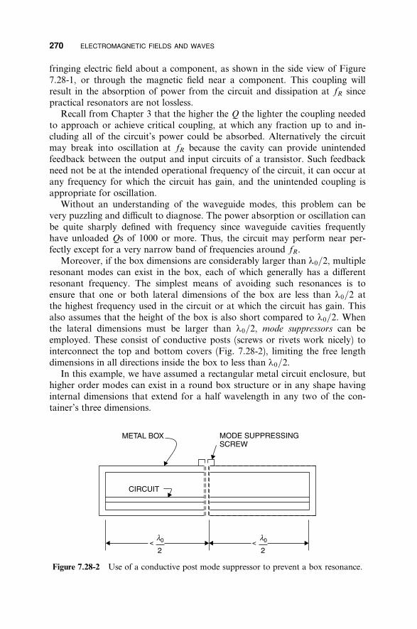
270 ELECTROMAGNETIC FIELDS AND WAVES
fringing electric field about a component, as shown in the side view of Figure7.28-1, or through the magnetic field near a component. This coupling willresult in the absorption of power from the circuit and dissipation at fR sincepractical resonators are not lossless.
Recall from Chapter 3 that the higher the Q the lighter the coupling neededto approach or achieve critical coupling, at which any fraction up to and in-cluding all of the circuit’s power could be absorbed. Alternatively the circuitmay break into oscillation at fR because the cavity can provide unintendedfeedback between the output and input circuits of a transistor. Such feedbackneed not be at the intended operational frequency of the circuit, it can occur atany frequency for which the circuit has gain, and the unintended coupling isappropriate for oscillation.
Without an understanding of the waveguide modes, this problem can bevery puzzling and di‰cult to diagnose. The power absorption or oscillation canbe quite sharply defined with frequency since waveguide cavities frequentlyhave unloaded Qs of 1000 or more. Thus, the circuit may perform near per-fectly except for a very narrow band of frequencies around fR.
Moreover, if the box dimensions are considerably larger than l0=2, multipleresonant modes can exist in the box, each of which generally has a di¤erentresonant frequency. The simplest means of avoiding such resonances is toensure that one or both lateral dimensions of the box are less than l0=2 atthe highest frequency used in the circuit or at which the circuit has gain. Thisalso assumes that the height of the box is also short compared to l0=2. Whenthe lateral dimensions must be larger than l0=2, mode suppressors can beemployed. These consist of conductive posts (screws or rivets work nicely) tointerconnect the top and bottom covers (Fig. 7.28-2), limiting the free lengthdimensions in all directions inside the box to less than l0=2.
In this example, we have assumed a rectangular metal circuit enclosure, buthigher order modes can exist in a round box structure or in any shape havinginternal dimensions that extend for a half wavelength in any two of the con-tainer’s three dimensions.
Figure 7.28-2 Use of a conductive post mode suppressor to prevent a box resonance.
VECTOR POTENTIAL 271
7.29 VECTOR POTENTIAL
We demonstrated in Section 7.8 that the static~EE field could be derived from thestatic scalar potential function. This scalar potential was an intermediate calcu-lation whose value was determined by the integration of a charge distributionover a volume. Once determined, the potential function facilitated determina-tion of the~EE field using the gradient function, a derivative process. This processgenerally poses a simpler task than that of the vector integration that wouldotherwise be necessary to construct the ~EE field directly from a charge distribu-tion.
The scalar potential has obvious physical significance, as the ski slopemountain example demonstrated, and it greatly facilitates the determination ofelectric field by use of the gradient vector. The success of the scalar potentialtechnique leads to the reasoning that another function might be defined tofacilitate determination of the~BB field as well as the time-varying portion of the~EE field [6, Chapter 4]. It will be seen that this can be done by defining a vector
potential. Unlike the scalar potential, the physical significance of the vectorpotential is not apparent. It is a mathematical artifice. Nevertheless, it doesresult in a useful method for routinizing the calculation of the~BB field.
Although Maxwell’s equations eloquently describe the physics of electro-magnetics, they are not the most convenient format for the solution of somereal field situations, such as antennas. It will be seen from the following defini-tion of the vector potential and its use in evaluating the short wire antennain Section 7.32 that the use of the vector potential neatly derives the near andfar fields of the antenna, even taking into account the propagation phase delaybetween the received signal and its current source.
The newly initiated to electromagnetics may feel overburdened with con-cepts already, and this feeling is not unjustified, given the complexity of vectormathematics and mastery of concepts necessary to reach this point. It is a littleknown fact that Maxwell’s unified field theory originally was expressed inabout 20 equations and included potential functions. Oliver Heaviside elimi-nated the potential functions and reduced the equations to the now well-known4 equations [3]. Heaviside was a brilliant, self-taught mathematician andphysicist. It was Heaviside who formulated the telegrapher equations that tookdistributed inductance of transmission lines into account for the first time.Earlier analyses of transmission lines only included resistance and capacitance.If he had not had such an acerbic personality, it is likely that we would bereferring to Heaviside’s equations instead of Maxwell’s. It is therefore note-worthy that no less a theoretician than the brilliant Heaviside is said to havehated the notion of potential functions.
Indeed, few practicing microwave engineers are comfortable enough withthe vector potential to employ it. Nevertheless, the vector potential is a conceptnot much more di‰cult to apply than the scalar potential already studied. Itsformat as a vector field has the same form as the distributed current densitythat produces the~BB field, so no new vector visualization is required.

272 ELECTROMAGNETIC FIELDS AND WAVES
We begin with a general definition of the vector potential as a three-~dimensional vector field, A BB field. Since the diver-A, whose curl is equal to the ~
~gence of the ~BB field is zero in all cases, the divergence of AA can be defined sub-~sequently in a manner that relates AA to the time-varying~EE field. In this way the
~ ~suitably defined AA allows the determination of both the EE and ~BB fields usingonly di¤erential processes, not integrals. To this end we define ~AA to satisfy
~BB1‘� ~AA ð7:29-1Þ
~ ~Then applying Maxwell’s third equation, ‘� EE ¼ �qBB=qt, we can rewrite(7.29-1) as
qð‘� ~AAÞ~‘� EE ¼ �qt" #
~qAA~‘� EEþ ¼ 0 ð7:29-2Þqt
since the time derivative and curl can be taken in any order. The curl of thequantity in brackets is zero, therefore the quantity can be defined as the gradi-ent of a scalar function, F, more precisely, the negative of the gradient in orderto be consistent with the earlier definition of the scalar potential F in Section7.8. Thus,
~qAA~EEþ 1�‘F ð7:29-3Þqt
Equivalently,
~qAA~EE ¼ �‘F � ð7:29-4Þqt
The dynamic scalar potential F defined in (7.29-3) is similar to the static po-tential function, but they are not the same. The static scalar potential appliesto fixed charges. In this section F is a dynamic scalar potential and applies tomoving charges. Generally, no confusion results between the two cases since agiven application usually involves either static or moving charge. For example,in propagation situations the presence of fixed charge is of no consequencesince the DC fields so created do not propagate. Furthermore, in the event thatboth static and dynamic charge distributions are of interest, their resultingfields can be added together by superposition if the medium is linear.
Although no assumptions have been made about the medium thus far,potential functions are most useful in linear, isotropic (same behavior in alldirections), and homogeneous (uniformity throughout space) media. Accord-

‘� ~
‘� ‘� ~� �
�
� �
‘ � ~
VECTOR POTENTIAL 273
ingly, in using potential functions we assume that m and e are scalars of con-stant value throughout the volume of analysis.
With (7.29-1) and (7.29-4) the~ EE fields are completely specified. Next,BB and ~~let us find expressions for F and AA that will allow their determination from
their primary sources, moving charges, or currents. To this end substitute (7.29-~4) into Maxwell’s first equation, ‘ � EE ¼ r=e, to obtain
r�‘2F� q ð‘ � ~AAÞ ¼ ð7:29-5Þdt e
!CHH ¼ J ~þ qDD=qt, and noting that
~AA ¼ mH‘� ~ H, " # Applying Maxwell’s fourth equation,
2~AAqFAA ¼ mJ
!C þ me � q ð7:29-6Þ‘
qt2qt
AA ¼ ‘ð‘ � ~ AA to (7.29-6) givesApplying the vector identity ‘� ‘� ~ AAÞ � ‘2~
2~AAqF!C‘ð‘ � ~ AA ¼ mJAAÞ � ‘2~ � me‘
q� me ð7:29-7Þqt2qt
~We have not used the option of defining the divergence of AA, an action that will~serve to define AA uniquely. Accordingly, we define the divergence to satisfy
qFAA1�me ð7:29-8Þ
qt
This allows (7.29-5) and (7.29-7) to be written as
q2F r‘2F� me ¼ � ð7:29-9Þ
qt2 e
2~q AA‘2~ ~AA� me ¼ �mJJC ð7:29-10Þ
qt2
The expressions of (7.29-9) and (7.29-10) are the basis for the integral expres-~ ~sions by which F and AA are evaluated. Once F and AA are evaluated, ~ EEBB and ~
can be derived from the scalar and vector potentials using derivative processes,the vector curl being a derivative operation. These results are summarized in(7.29-11) and (7.29-12):
~ ~BB ¼ mHH ¼ ‘� ~AA ð7:29-11Þ~qAA~EE ¼ �‘F� ð7:29-12Þqt
274 ELECTROMAGNETIC FIELDS AND WAVES
The dynamic scalar potential is evaluated using an integral expression similarto that employed with the static scalar potential, namely
ð r dV
F ¼ ð7:29-13Þ4perV
Using similar reasoning, the vector potential for the static or steady-state cases
can be evaluated using a volume integral of its current density sources:
ð !JC dV~AA ¼ m ð7:29-14Þ4prV
In both (7.29-1) and (7.29-2) the volume V includes all of the respective mobile!charge density r and current density JC . Even so, these two equations can onlybe used for steady-state not transient time variation cases because they do notrecognize the propagation delay between the sources and the points at whichthe potentials are evaluated. This limitation is accommodated using the retard-ed potentials discussed in the next section.
7.30 RETARDED POTENTIALS
~The corresponding solutions for F and AA in transient time-varying cases musttake propagation delays into account. This is done by replacing (7.29-13) and(7.29-14) with (7.30-1) and (7.30-2), respectively [6, p. 199]:
ð dV½r�t�ðr=vÞ
F ¼ ð7:30-1Þ4perVð !½ JC dV�t�ðr=vÞ~AA ¼ m ð7:30-2Þ
4prV
ffiffiffiffiffiffi in which v ¼ 1=
pme; v ¼ cA3� 108 m/s in free space. For example, in
(7.30-1) the quantity F to be evaluated at point P that is a distance r fromcharge r is to use the value of r present at time t� ðr=vÞ. In this way the timenecessary for the e¤ect of r to propagate to P is taken into account. The e¤ectffiffiffiffiffiffi travels at velocity v ¼ 1=
pme, the velocity of the plane wave evaluated in
~7.22. The same provision for propagation is made in the evaluation of AA using(7.30-2).
Because of this retardation e¤ect, the potentials evaluated by (7.30-1) and(7.30-2) are called retarded potentials because their arrival is retarded by thetime of propagation.

� �
ANTENNAS 275
7.31 POTENTIAL FUNCTIONS IN THE SINUSOIDAL CASE
For the case of sinusoidal excitations, one is usually interested in the steady-state values of the fields. Therefore, the propagation time from the source to apoint a distance r away can be fully accounted for by a phase delay kr, wherek ¼ o=v is the propagation constant. Given this assumption, the followinganalysis shows that the expression for ~EE in (7.29-12) can be written exclusively
~in terms of AA. To derive this new expression take the gradient of both sides of(7.29-8) to obtain
~ q‘ð‘ � AAÞ ¼ �me ‘F ð7:31-1Þ
qt
Since time di¤erentiation and the gradient can be taken in any order, and sinceq=qt ¼ jo for sinusoidal excitations,
~‘ð‘ � AAÞ jo ~‘F ¼ � ¼ ‘ð‘ � AAÞ ð7:31-2Þjome k2
where k ¼ opffiffiffiffiffiffi me is the propagation constant in the medium. Then, substitut-
~ ~ing (7.31-2) into (7.29-12), the expressions for BB and EE for the sinusoidal casebecome
~ ~BB ¼ ‘� AA ð7:31-3Þ1~ ~ ~EE ¼ � jo ‘ð‘ � AAÞ þ AA ð7:31-4Þk2
~ ~ ~where AA;BB, and EE are in phasor form. This result is very useful for antennapattern analysis, as will be seen in the next section.
7.32 ANTENNAS
Short Straight Wire Antenna
Consider a short wire antenna that is excited by a sinusoidal current I0. The~current excites the base of the antenna creating a surrounding HH field whose
~time rate of change induces an orthogonal EE field. The pair of sinusoidallyvarying fields store energy as well as propagate it.
The simple geometry in Figure 7.32-1 belies the complexity of the resultingelectromagnetic field analysis of the short wire antenna, as will be seen from thefollowing analysis. However, the approach is straightforward, and its execution
~provides an example of the use of the vector potential AA and the determination~ ~of EE and HH fields at an arbitrary distance from an antenna [6, Sec. 12.05].

276 ELECTROMAGNETIC FIELDS AND WAVES
Figure 7.32-1 Geometry for analysis of the short straight wire antenna. [6, pg 497 Re-printed with permission]
The procedural convenience of using the vector potential can be appreciatedin this analysis of the short straight wire antenna excited by a sinusoidal currentphasor II~00, for which the factor e jot is implicit. The expression (7.30-2) for
~ ~evaluating AA indicates that each di¤erential current contributes a part of AA thatis in the same direction as that current element. In other words, in this example
~of the short wire, since II~00 points only in the z direction, so must AA. The fact~that the vector potential has the same vector form as the currents that excite EE
~and HH fields underlies its usefulness.For this analysis we assume that the length h and the diameter of the short
straight wire antenna are very small compared to the operating wavelength,hence there is negligible change of phase in II~00 over its length and diameter. The
~integration for AA produces, for any point Q at radius r from the antenna, gives
~AA ¼~zzAz ð7:32-1Þ
Az ¼ mhI0
e�jðor=vÞ ð7:32-2Þ4pr
~To evaluate AA as a function of the radial distance r from the current source, it isbest to express it in spherical coordinates as
Ar ¼ Az cos y ¼ mI0h
e�jkr cos y ð7:32-3Þ4pr
Ay ¼ �Az sin y ¼ �mI0h
e�jkr sin y ð7:32-4Þ4pr

� � � � � �
� �
� � �
� �
ANTENNAS 277
where Ar and Ay are the components of Az in the ~ ~rr and yy directions, respec-tively, and the medium propagation constant k is given by
o pffiffiffiffiffiffi 2pk ¼ ¼ o me ¼ ð7:32-5Þ
v l
Notice that, due to the symmetry of this case, all q=qj � 0, and there is noAj component. The utility of the vector potential can now be appreciated byobserving that the integration needed to evaluate it results in a vector having
~the same direction as the current that produces it. To evaluate HH, note that~when the curl of AA is evaluated for this case in spherical coordinates only the j
component is nonzero. Thus, using (7.29-1)
1~ ~HH ¼ ‘� AAm
jj jj~ ! 1 ~ q qAr 1 ~ mhI0 �jkr sin yHH ¼ Hj ¼ ðrAyÞ � ¼ �ð� jkÞe�jkr sin yþ 1e
m r qr qy m r 4p r
1!jjhI0
e�jkr jk þ sin y ð7:32-6ÞHj ¼ ~4p r r2
~Next find EE using (7.31-4) which is repeated below:
1 ~ ~E ¼ � jo ‘ð‘ � AAÞ þ AA ð7:32-7Þk2
~ ~To evaluate EE, first calculate ‘ � AA, noting that Aj ¼ 0:
1 q~‘ � AA ¼ ðr2ArÞ þ 1 q ðsin yAyÞr2 qr r sin y qy
mI0h cos y q~‘ � AA ¼ ðre�jkrÞ � e�jkr q ðsin2 yÞ�
ð7:32-8Þ4p r2 qr r2 sin y qy
~ �mI0h jk 1‘ � AA ¼
4p rþr2
e�jkr cos y
~Since ‘ � AA is not a function of j,( ~ ~1 1 qð‘ � AAÞ ~1 qð‘ � AAÞ~‘ð‘ � AAÞ ¼ ~ þ yy
)rr
k2 k2 qr r qy
�mI0h� � �jkr
� q jke�jkr e¼ ~
k24prr cos y þ
qr r r2
e�jkr� jk 1 qðcos yÞ~þ yy þ ð7:32-9Þ
2r r r qy
� � � � � �
� �
� �
� � � �
278 ELECTROMAGNETIC FIELDS AND WAVES
Performing the indicated steps and simplifying gives� � � � � � 1 �mI0h
~ �jkr k2 2jk 2 � yye�jkr jk 1~‘ð‘ � AAÞ ¼k24p
rr cos ye � � ~2þ sin y
2 3 3k2 r r r r r
ð7:32-10Þ
Next substitute (7.32-10), (7.32-3), and (7.32-4) into (7.32-7) to get (7.32-11),(7.32-12), and (7.32-13):
mI0h k2 2jk 2Er ¼ jo
k24pe�jkr cos y �
2� � k2 cos y
3r r r r
2jk 2¼ � jomI0h
e�jkr2þ cos y ð7:32-11Þ
3k24p r r pffiffiffiffiffiffiffiffi 2Recognizing that k2 ¼ o me and h ¼ m=e, (7.32-11) can be written
2h 2jEr ¼ I
40
p
he�jkr
r2�oer3
cos y ð7:32-12Þ
Similarly,
h jom �jEy ¼ I0h
e�jkr2þ þ sin y ð7:32-13Þ
4p r r oer3
~ ~Again noting that AA has no j component and no j variation, the HH field isobtained as
1 1 1 q 1 qAr~ ~ jjHH ¼ ð‘� AAÞ ¼ ~ ðrAyÞ �m m r qr r qy
jk 1Hj ¼ I0h
e�jkr þ sin y ð7:32-14Þ4p r r2
Certainly, the development of expressions (7.32-12), (7.32-13), and (7.32-14),while straightforward, is mathematically tedious. But once expressed, they re-veal the field behavior of the short antenna quite handily. First, the terms in1=r2 and 1=r3 fall o¤ rapidly for large r, leaving the 1=r terms.
The 1=r terms of Ey and Hj are in phase with and orthogonal to each other,~hence they give peak propagating power density equal to Poynting’s vector PPD.
Their ratio, Ey=Hj ¼ h, is the same as that for the plane propagating wave~analyzed in Section 7.18. Taking their directions into account, yy�~ rr, thejj ¼~
power propagates in the~rr direction, away from the antenna. The peak prop-agating power density is given by
~ ~ ~ rEr yHj ¼~ 2PPD ¼ EE �HH
� ¼~ rrhjHjj2 watts=meter ð7:32-15Þ

ANTENNAS 279
~ ~where hA377 W for free space. Since peak values are used for the EE and HH
fields, the time-average power flow is equal to one half the peak value of ~PPD, or� �2kI0h~ rrPPDðrÞ ¼~
1h sin y watts=meter2 ð7:32-16Þ
2 4pr
where h and r are in meters and k is in (meters)�1. The total propagating poweracross a spherical surface of radius r is
ð ð! ð 2p p
~P ¼ PPD � dS ¼ PDr2 sin y dy dj
S 0 0� �2ð pkI0hP ¼ ph sin3 y dy ð7:32-17Þ
4p 0ÐSince
psin3 y dy ¼ 4
3, and for free space hA120p W, and k ¼ 2p=l0, (17) re-0
duces to
� �2P ¼ 40p2I0
2 hwatts ð7:32-18Þ
l0
which is the total power radiated out of a sphere of radius r. Note that while Pis independent of r, the power density PD is inversely proportional to r2.
Radiation Resistance
The radiation resistance of an antenna is defined as the resistance that woulddissipate the same power as is radiated by the antenna when supplied with thesame current. For the short, straight wire antenna radiating into free space
� �21I 2RR ¼ 40p2I 2
h02 0 l0� �2h
RR ¼ 80p2 ohms ð7:32-19Þl0
For example, a 1-in.-long antenna at 1 GHz would have a radiation resistanceof � �2
1 in:RR ¼ 80p2 W ¼ 5:7 W ð7:32-20Þ
11:8 in:
By itself, 5.7 W would be a large mismatch on a 50-W feed line; however, themismatch is exacerbated further by the fact that there is a large reactance inseries with the radiation resistance. Calculation of the reactance is more di‰-

280 ELECTROMAGNETIC FIELDS AND WAVES
Figure 7.32-2 Radiation pattern of a dipole antenna.
cult because it is a volume integral over all space. One cannot use the integrallimits r ¼ 0;y because the fields have a singularity at r ¼ 0. Rather the inte-gration must extend from the actual surface of the antenna to r ¼ y. Whileradiation resistance is not a sensitive function of the diameter of the wireantenna, the reactance is very sensitive to the diameter because very thin wireshave much stronger surrounding fields.
Radiation Pattern
The short wire antenna just analyzed (Fig. 7.32-1) is a dipole because the‘‘horizon’’ plane bisects its vertical axis. Since, by assumption, there is noground plane nearby, it radiates equally above and below the horizontal plane
~ ~ðy ¼ 90�Þ, and the EEy and HHj fields both vary as sin y. Thus, the radiatedpower is maximum in the horizontal plane and is zero in the vertical direction,or zenith, as shown in Figure 7.32-2.
The radiation is maximum at right angles to the wire antenna in the azimuthdirection (on the horizon). The pattern is circularly symmetric about the an-tenna’s axis. The pattern shown in Figure 7.32-2 is an elevation plane cut. Thispattern applies when the antenna is located well above the earth, which wouldserve as a ground plane. In three dimensions the pattern resembles a bagel witha very small center hole (Fig. 7.32-3).
Half-Wavelength Dipole
Since the radiation resistance for a short monopole is very low, most wireantennas are made longer, but then the ‘‘short’’ approximation no longer holds,and a new analysis must be made, this time assuming a current distribution

which is sinusoidal and goes to zero at the open ends. For the half-wave dipole,for which l ¼ l=4 (Fig. 7.32-4), the electric field ~EEy is found by integrating thefield contributions from infinitesimal lengths of straight antennas of the typejust covered and assuming a sinusoidal current distribution with the maximumIm at the dipole’s center feed point. The result of this analysis [6, Sec. 12.7] isthat for the center-fed half-wavelength dipole antenna,
Figure 7.32-3 Sketch of three-dimensional radiation pattern of short wire dipoleantenna [after Balanis, 15, Fig. 4.3j, with permission].
Figure 7.32-4 Center-fed dipole antenna.
ANTENNAS 281

� � �
282 ELECTROMAGNETIC FIELDS AND WAVES
60Im cos½ðp=2Þ cos y�jEyj ¼ volts=meter ð7:32-21Þr sin y
15I 2 cos½ðp=2Þ cos y��2PDðrÞ ¼ m watts=meter2 ð7:32-22Þ
pr2 sin y
RR ¼ 73:09 W ð7:32-23Þ
where Im is the maximum current, presumed equal to the value at the centerfeed point. The driving point impedance is nearly equal to the radiation resis-tance of 73 W since the antenna is nearly resonant when its length is l=2. In-terestingly, the half-wavelength dipole and the short wire antenna have nearlythe same radiation patterns [6, Secs. 12.05 to 12.07]. However, the short wireantenna is much more di‰cult to drive because of its low impedance and highreactance.
A practical problem arises when it is necessary to interconnect the half-wavedipole antenna to a transmitter whose output port is an unbalanced transmis-sion connector or transmission line, such as coax. The antenna requires abalanced feed at terminals AB in Figure 7.32-5. That is, both of the AB termi-nals are to be separated from ground by the same impedance. A coaxial outputconnector or a coaxial cable used to interconnect transmitter and antenna is anunbalanced transmission system. However, this problem is easily corrected byusing a balun. On transmission, the balun converts the unbalanced line fromthe transmitter to the balanced format of the antenna, as shown in Figure7.32-5. It does this by creating an infinite impedance to ground at point C byvirtue of the quarter wavelength collar attached to the end of the coaxial line.The balun’s operation is reciprocal. On receiving a signal, the balun convertsthe balanced format of the antenna to the unbalanced format of the receiver.The function of the balun is limited in bandwidth by the quarter wavelengthrequirement of the collar.
Figure 7.32-5 Balun used to connect a co-axial cable to a balanced, half-wavelengthdipole antenna.

� �
ANTENNAS 283
Antenna Gain
For a given radiated power an antenna that radiates more power in certaindirections and less in others, as all practical antennas do, can place more powerat a receiver than would an isotropic radiator that distributes the same inputpower uniformly over a spherical surface. Actually, it is impossible to build aperfectly isotropic radiator, but the concept is useful for defining the perfor-mance of practical antennas.
The power density delivered in a given direction by a practical antennacompared to what would be delivered by an isotropic radiator is called antenna
gain. It is expressed in dBi, for decibels above (or below, if negative) the levelthat would be achieved with an isotropic radiator. Gain can be defined in anydirection, but customarily, unless otherwise noted, it is defined for the directionin which the antenna radiates the greatest power density. For the short wire an-tenna the maximum radiated power density occurs on the horizon ðsin2 y ¼ 1Þand has the value
� �21 kI0h
PD;max ¼ 1hjHjj2 ¼ h
2 2 4pr
where Hj is the radiated component of the H field at r. Then, since k ¼ 2p=l0
and hA120p W, this reduces to
h2I02
PD;maxA15p ð7:32-24Þl0 r2
Since the surface area of a sphere at radius r is equal to 4pr2, an isotropicradiator produces a power density at radius r of
h I 2� �2h2PD; i ¼
4p
1
r2I
202
RR ¼8p
1
r2I0280p
� �2¼ 10p 0
2ð7:32-25Þ
l0 r l0
Dividing (7.32-24) by (7.32-25), the gain of the short dipole antenna is [6,p. 504]
PD;maxGshort dipole ¼ ¼ 1:5 ¼ 1:76 dB ð7:32-26Þ
PD; i
Using the same method, the gain of the half-wavelength dipole antenna is
Ghalf wavelength dipole ¼ 1:64 ¼ 2:14 dB ð7:32-27Þ
It should be noted, however, that although the short dipole and the half-wavelength dipole have nearly identical radiation patterns and gains, the half-

284 ELECTROMAGNETIC FIELDS AND WAVES
wavelength dipole is much easier to excite due to its higher radiation resistanceand its near zero reactance.
Antenna Effective Area
In calculating the overall loss between transmitter and receiver, we need toknow the e¤ective area AE of the receiving antenna. Aperture antennas suchas dishes and waveguide horns have an e¤ective signal capture area that isapproximately equal to their physical area in the direction of the received ortransmitted signal, but even the small wire antenna, whose physical area is in-finitesimal, has an appreciable e¤ective area. This e¤ective area is related to itsgain.
The fact that receiving antennas have varying gains and hence capture rela-tively more or less power is treated by considering that the power they capturefrom the radiation field is proportional to their respective e¤ective areas [6, p.560, and 14, Sec. 11.12]. But the received power is also proportional to the gainof the receiving antenna. Therefore, it follows that there is a proportionalityconstant relating gain G to e¤ective area AE . Once this factor is found for any
one receiving antenna, the same factor can be applied to all receiving antennas.Furthermore, the network between transmitter and receiver terminals, includ-ing the free-space propagation medium, is linear and reciprocal. Accordingly,what applies to all transmitting antennas, by reciprocity, applies to all receivingantennas.
To determine the proportionality factor between gain and e¤ective area, weuse as a receiving antenna the short wire dipole previously evaluated. We definethat the power delivered to the receiver terminals by the receiving antenna isgiven by
Prec 1PDAE ð7:32-28Þ
where Prec is the power delivered to the receiver connected to the receivingantenna, PD is the power density (in watts/meter2) of the wave incident on thereceiving antenna and AE is the e¤ective area of the receiving antenna.
In the vicinity of the receiving antenna, PD is related to the rms electric fieldstrength E parallel to the antenna by
E2 E2
PD ¼ ¼ ð7:32-29Þh 120p
where h is the impedance of free space. The available power absorbed in amatched load connected to the receiving antenna is given by
V 2 ðEhÞ2Prec ¼ OC ¼ ð7:32-30Þ
4RR 4RR
where RR is the radiation resistance of the receiving antenna given by (7.32-19).

ANTENNAS 285
It might seem that the factor of 4 should not appear in the denominatorin (7.32-30), that instead the full voltage Eh delivers power to the resistanceRR; but this is not so. The transmitter, its antenna, the free-space propagationpath,and the receiving antenna taken together represent a linear network. Thevoltage Eh induced at the receiving antenna terminals is an ‘‘open-circuit volt-age’’ that exists in the absence of the receiving antenna or when the receiving
antenna terminals are open circuited, that is, when the incident radiation is not‘‘loaded.’’ When the RR matched load is applied, the voltage at the receivingantenna terminals drops to half its open-circuit value, and the power deliveredto the load at the receiver terminals is that given by (7.32-30). Substituting thevalue for RR from (7.32-19) into (7.32-30) gives
l2 l2ðEhÞ2Prec ¼ 0 ¼ E2 0 ð7:32-31Þ
4 80p2h2 320p2
Solving (7.32-28) for AE and substituting the values for PD from (7.32-29) andPrec from (7.32-31) into it,
E2l2 120p 3 l2 l2 30 ¼ 0AE ¼ Prec ¼ 0 ¼ ð7:32-32ÞPD 320p2 E2 8 p 4p 2
But from (7.32-26) the gain of the short dipole antenna is G ¼ 1:5 ¼ 32 , there-
fore (7.32-32) can be written
l2
AE ¼ 0 G ð7:32-33Þ4p
Monopole Antenna
The fact that the dipole antenna radiates into the lower hemisphere as well asthe upper hemisphere is a disadvantage for terrestrial communications sincemost receptors are on a line with the horizon or above it. Consequently, themonopole antenna with ground (Fig. 7.32-6) has the advantage of an additional3 dB of gain compared to the dipole because it radiates all of its power intoonly the upper hemisphere. The monopole antenna is often called a whip an-
tenna because it was often used for very high frequency (VHF) police radiosand connected to the rear bumper of an automobile. The ‘‘whip action’’ re-sulted as the car accelerated and decelerated. Due to its symmetry with thehalf-wavelength dipole, its driving point impedance is one half that of thedipole.
For the quarter-wave monopole antenna
Rr ¼ 36:5 W ð7:32-34ÞGmax ¼ 3:28 ¼ 5:16 dB ð7:32-35Þ

286 ELECTROMAGNETIC FIELDS AND WAVES
Figure 7.32-6 Monopole antenna with ground plane.
It should be noted that the presence of a good ground plane is as important
to achieving this gain improvement as the antenna. For example, with a smallhand-held monopole, the radiation pattern is likely to be that of the short wireantenna, radiating both above and below the horizon plane that contains theantenna, unless that plane coincides with a good earth ground plane at the fre-quency of operation. Large AM broadcast antennas are examples of monopoleantenna applications. Their monopole function is usually ensured by installingground radials at the base of the antenna, consisting of wires that run radiallyin all directions from the base of the antenna. Their lengths in the earth arecomparable to the antenna’s height. The conventional automobile antennaconsisting of a straight wire mast also may approximate the monopole, ach-ieving conducting ground plane by means of the sheet metal of the automobilenear the aerial’s base.
Aperture Antennas
The larger the area of an equiphase front created by an antenna the less thepropagating beam, called the main beam, radiated by it will diverge, hence thegreater its ‘‘gain’’ in its preferred propagation direction, and the more powerit can place on a target receptor compared to an isotropic radiator transmit-ting the same power. By reciprocity, the same comments apply to the receivingantenna.
It was shown that the e¤ective area of an antenna is directly proportional toits maximum gain in what is usually termed the main beam or bore site direc-tion, the direction orthogonal to the equiphase plane of the antenna. The termbore site derives from the practice of installing a small telescope on high gainantennas as an aid to aiming them in the desired direction. For most aperture

ANTENNAS 287
Figure 7.32-7 Aperture antennas.
antennas (Fig. 7.32-7) the area of the aperture would be approximately thee¤ective area if the antenna were uniformly illuminated, that is, if it radiated auniform power density over its entire aperture.
However, uniform illumination is often undesirable because it results in an~ ~abrupt discontinuity in the EE and HH fields near the edges of the antenna. This
in turn results in auxiliary radiation patterns, called sidelobes that are separatefrom and radiate in di¤erent directions than that of the main beam. Sidelobeswaste power and therefore correspond to signal loss. Often they are even moreobjectionable because they may intercept spurious signals that interfere withthe desired reception. To minimize sidelobe strengths, an illumination taper isemployed whereby the field strength is maximum near the center of the aper-ture and diminishes near the periphery.
Since the illumination taper requires that not all of the aperture is energizedto the fullest, the result is that the e¤ective area of the antenna is correspond-ingly less than its physical cross-sectional aperture, ACS (the area projected inthe propagation direction). In fact, any reduction in the signal strength over theaperture reduces the antenna’s e¤ective area, and with it the main beam gain.Nevertheless, this may be more desirable than encountering interfering signalsthrough sidelobes. Other causes of aperture reduction include dielectric coversto protect the antenna, called radomes, surface irregularities such as roughnessor actual holes made in the antenna surface to reduce its weight or wind resis-tance and structural supports of the feed horn.
Equation (7.32-33) can be rewritten as
4pG ¼ AE ð7:32-36Þ
l20
To account for an e¤ective area AE less than the actual cross-sectional area ACS
of the antenna, a factor to relate them is defined according to
AE ¼ eAPACS ð7:32-37Þ

288 ELECTROMAGNETIC FIELDS AND WAVES
where eAP is the aperture e‰ciency and 0a eAP a 1 [15, Sec. 12.5.3]. Asalready noted, the aperture e‰ciency can be less than unity for a variety ofreasons.
Phased Arrays
Antennas used for point-to-point communications are fixed in position. Theseinclude terrestrial communication link applications and Earth to synchronous-satellite communications. Those used for scanning generally are moved me-chanically to cover a given surveillance area, as for radio ranging and detec-tion, or radar, applications. However, antennas that can scan electronicallywithout need of mechanical motion have appeal in applications for whichmechanical slewing is either too slow or impractical, as in some satellite-borneapplications or for tracking rapidly moving radar targets such as missiles. Forthese applications the electronically scanned phased array antenna may be em-ployed (Fig. 7.32-8).
The phased array antenna uses small-aperture radiating elements that, be-cause of their small area, necessarily and desirably have a wide radiation pat-
Figure 7.32-8 Schematic diagram of a phased array antenna using elements with timedelay to scan the radiated beam.

ANTENNAS 289
tern in the bore site direction of the array. A one-dimensional, linear array isshown in Figure 7.32-8 for illustration of the principles, but phased arrays moreusually are two dimensional. Steering is accomplished by adjusting the phase ofthe signals applied to each element so that the aggregate equiphase wave front
representing the summation of the fields of all of the elements is in a plane at anangle skewed from the bore-site direction. This is called the phased array scan
angle. In Figure 7.32-8 the steering shown uses time delay rather than phase
shift. When time delay is used, the scan angle is independent of frequency, andthe antenna can be used with arbitrarily wide bandwidth, subject to the limitsof the radiating elements. The amount of delay, tN (in wavelengths) requiredfor the Nth linear element is given by
tN ¼ NS sin y ð7:32-38Þ
where S is the spacing between elements (in wavelengths) and y is the scan an-gle. For two-dimensional scanning of an M �N array, in azimuth and eleva-
tion, (7.32-38) must be applied separately for both directions and the resultstotaled for the delay tMN to be applied to the MNth element. The elementspacing is usually about one-half wavelength since radiating elements neces-sarily occupy about this minimum dimension on a side. Furthermore, widerspacing would give rise to grating lobes, spurious radiation beams for which thewider spacing permits redundant equiphase planes at large scan angles. Notethat in Figure 7.32-8 the delay is shown as a fixed line length for purposes ofillustration. Array scanning requires that variable delay be selectable. Also notethat one wavelength of transmission line produces one period (ot ¼ 360�,where t ¼ T) of time delay.
For large phased array antennas whose apertures are many wavelengthsacross, the use of time-delay steering is impractical to apply to each element.For example, consider a square antenna 10 wavelengths on a side with half-wavelength spacing between elements in azimuth and elevation directions. Thisantenna would have 400 elements and from (7.32-33) up to 31 dB of gain in thebore site direction, neglecting losses and sidelobes and assuming an illumina-tion e‰ciency of 100%. Phased arrays usually are limited to aboutG45� steer-ing. This limit is imposed by the beamwidth of the subelements as well as thefact that for larger steering angles the array’s projected area would be too smallreducing its gain too much. But to accomplish 45� steering for this examplearray, the time delay required of the edge elements for each scanning directionwould be, from (7.32-38), equal to 14:14l. For two-dimensional scanning this isdoubled and therefore a delay of 28:28l would be required.
Time delay is usually arranged using electronic switches that provide discretedelay steps. Thus a given required delay is managed only approximately, andthere is a delay error equal to as much as one half the smallest switched step, ordelay quantization. To provide for continuous scan angle steering of this sizeantenna, a delay quantization of 0:125l might be employed corresponding to aphase error of no more than G0:0625l or G22:5�, one half the smallest delay

290 ELECTROMAGNETIC FIELDS AND WAVES
step. Then time-delay devices capable of delay adjustment from about 0:125lto 28l in 0:125l steps (corresponding to 45� phase steps) would be required.Thus a control device having steps of 0:125l, 0:25l, 0:5l, 1:0l, 2:0l, 4:0l, 8:0l,and 16l is needed. This would be termed an 8-bit time-delay device providingcontrol to 31:875l in 0:125l steps.
Such a device is di‰cult to build. These delay lines, being several wave-lengths long at the center frequency, have multiple resonances within the oper-ating bandwidth. This is because diodes are characterized by a high reactance(small capacitance) in their ‘‘o¤ state.’’ A long line with small capacitors ateach end becomes a high-Q resonator. When the line is long enough, it is cer-tain to have resonant frequencies in the operating band of the antenna, and atthese resonances high absorption of the signal power occurs. When the switchesdo not turn o¤ the long line completely. Even without the resonances, highinsertion loss can be expected due to the long line lengths to be switched andthe losses of a cascade of switches required to select them.
For these reasons, phase shift rather than time delay is usually applied toeach element. The required phase shift is obtained by computing the time delayrequired at the center frequency of operation and subtracting integer multiplesof 2p. For example, the most remote element of the 20l by 20l array for a 45�
scan in both azimuth and elevation would require 28:28l of delay. This couldsimulated using a phase shift corresponding to 0:28l or 100�. In turn, the phaseshifters also would be realized in binary form. A 4-bit phase shifter would pro-vide 0� to 337:5�. In the phase domain 360� is equivalent to 0� of control in22:5� steps. The nearest step to 100� is 90�, and this would be selected. The factthat phase shift control is only correct at the frequency for which the time-delay-to-phase-shift conversion is made means that the radiated antenna beamwill squint o¤ the intended scan angle as the frequency of operation departsfrom this center frequency.
Unlike mechanically scanned antennas, phased array antennas have reducede¤ective area, consequently less gain, as they are steered o¤ the bore site direc-tion because their projected area in the scanned direction is correspondinglyless.
Because of these considerations and other complexities not described, large-aperture phased array antennas are employed only when their motionless, high-speed scanning properties are deemed essential. However, small apertures ofa few wavelengths in diameter may prove practical in some communicationapplications.
7.33 PATH LOSS
Although Maxwell’s equations are fundamental to radio engineering, their ap-~ ~plication requires an analytic description of the EE and HH fields, and this can be
quite complex as was seen for the short wire antenna analysis. However, somepropagation problems can be solved with a much simpler approach once the

PATH LOSS 291
principles of wave propagation are appreciated. One of these is the path loss
calculation, which is the determination of how much power reaches a radio re-ceiver from a distant transmitter. In fact, the path loss calculation is usuallyone of the first in the design of a radio communication system.
Previously we introduced the isotropic radiator assumption. The isotropicradiator is defined to be a 0 dB gain antenna, and the power radiated from it iscalled the e¤ective isotropic radiated power (EIRP). As was noted earlier, it isimpossible to build an isotropic radiator, but the concept is useful for calculat-ing how much power would be available at a distance were one to have beenemployed. Then it is a simple matter to adjust the isotropic result so obtainedto that which applies given the relative gains of the actual antennas used fortransmission and reception. The isotropic antenna uniformly ‘‘paints’’ the sur-
face of a sphere having a radius equal to the distance R between transmitter and
receiver.
Figure 7.33-1 depicts a transmitter at the center of a sphere of radius R. If thetransmitter power PT is radiated by an isotropic antenna, then, since the sur-face area of a sphere is 4pR2, the power density at R is PT=4pR
2. If the iso-tropic antenna is replaced by a transmitting antenna of gain GT , then thepower density in the direction of its maximum intensity (the direction of itsmain beam) is given by
PTPD ¼ GT ð7:33-1Þ
4pr2
If a receiving antenna at distance R is oriented to accept maximum power from
Figure 7.33-1 E¤ect of power reduction as a result of spreading out isotropically(painting an imaginary sphere) at a distance R from the transmitter.

292 ELECTROMAGNETIC FIELDS AND WAVES
this direction (it is aimed at the transmitter), the power it will receive is
PTPR ¼ AEGT ð7:33-2Þ
4pR2
where AE is the e¤ective capture area of the receiving antenna. Note that PR isactually the available power at the terminals of the receiving antenna. Applying(7.32-33) this can be written
� �2l0
PR ¼ GTGRPT ð7:33-3Þ4pR
Usually the radio system engineer is interested in determining the loss betweenthe terminals of the transmitting antenna and those of the receiving antenna.This is called the path loss. For this purpose (7.33-3) can be cast in an insertionloss format as
� �2 � �2PT 4pR 1 16p2 R
ILPATH ¼ ¼ ¼ ð7:33-4ÞPR l0 GTGR GTGR l0
Note that numeric values (not dB) must be used for GT and GR and that thesame length units must be used for AE ;R, and l0 in (7.33-1) to (7.33-4).
As an example, consider the case of a 1-W, 900-MHz cellular telephonetransmitter radiating its signal with a circularly polarized antenna having again factor of 1.64 above isotropic. The receiving monopole antenna on theexterior of an automobile is vertically polarized and has a gain factor of 3.28.The automobile is 3 miles from the transmitter, and there is a line-of-sighttransmission path. What is the path loss between transmitter and receiver?
First note that since the receiving antenna is linearly polarized it can captureonly half of the circularly polarized power incident upon it. To take this intoaccount, the gain of the receiving antenna is reduced by one half to 1.64.
Substituting the system values into (7.33-4) yields
� �2 � 16p2 R 16p2 3� 1610
�2ILPATH ¼ ¼ ¼ 1:23� 1010 ¼ 101 dB
GTGR l0 ð1:64Þð1:64Þ 0:33
since 1 mile ¼ 1610 m and l0 ¼ 0:33 m at 900 MHz. Note that since PT ¼ 1W ¼ 1000 mW ¼ 30 dBm, PR ¼ 30 dBm� 101 dB ¼ �71 dBm.
The path loss calculation is only a first step in the design of a radio com-munication link. Implicit in the path loss calculation is the assumption that thetransmitter and receiver are on a line-of-sight with each other, that is, that thereare no intervening obstacles. For real radio systems (Fig. 7.33-2), this is rarelythe case. Buildings, foliage, hills, and other obstacles occupy the propagationpath.

PATH LOSS 293
Figure 7.33-2 Cellular radio system depicting cell-to-mobile and mobile-to-cell trans-missions. For illustration, a dipole antenna is depicted at the base station, but custom-arily a circularly polarized antenna is employed.
For a cellular telephone communication system there is almost never anunobstructed path. The transmitted signal may undergo several reflections onits roundabout path to the receiver, and the strongest signal reaching thereceiver may actually be coming from a direction opposite that of the trans-mitting antenna. The resultant signal may arrive at the receiver as the phasoraddition of several separate signals with random phases, resulting from multi-ple paths, a process called multipathing.
When this occurs, the signals combine with random phases at the receiver.Often, multiple signals result in a combined signal lower than any of itsconstituents, a process called Rayleigh fading. Rayleigh was a physicist who,among other accomplishments, formulated the distribution associated withrandom events. To overcome deep fades, a cellular base station may switchbetween di¤erent antennas (diversity switching) to create a more favorableaddition of the multipath signals at the receiver. This can occur hundreds orthousands of times during a cellular conversation conducted between the cellsite and a moving automobile containing the cellular system client.
In specifying a communication system, once the minimum detectable signal
level is determined (more about this in Chapter 10), the minimum requiredtransmitter power can be determined. However, a transmitted power well be-yond that required by the path loss calculation is generally specified in order tocreate a system margin and a more robust communication link. The system
margin can overcome the obstacles to delivering a detectable signal much of the
time, but never always. The greater the system margin, the less the probability

294 ELECTROMAGNETIC FIELDS AND WAVES
that the communication link will prove to be unacceptable, and the greater thepercentage of time that the link will operate satisfactorily. However, no matterhow great the allowance, there will always be some probability, however small,that a su‰ciently deep fade will be encountered to render the link unusable forsome period of time or at all times in some locations. Cellular telephone usersoperating from moving vehicles experience drop-outs regularly and can attest tothis fact. Wireless communication links are never completely reliable.
7.34 ELECTROMAGNETIC (EM) SIMULATION
When AC analysis is used to evaluate a component, we assume that it behavesaccording to its equivalent circuit model. However, this is an idealization. Realcircuits have physical sizes that often are appreciable compared to the operat-ing wavelength, causing a change of voltage and current over their dimensions.This is not included in the equivalent circuit used by a circuit simulator or inthe manual application of AC analysis. The resulting circuit performance esti-mates are based on this idealization; consequently, they will contain someerrors as a result. Sometimes the error is quite significant, as the followingexample demonstrates.
Suppose that we wish to employ a 25 W characteristic impedance, open-circuited shunt stub on a 50-W transmission line as a filter. The filter is to blockthe second harmonic of a 1920-MHz cellular system transmitter, so that thespurious requirements of its radio license will not be violated. Therefore, it isdesired that the open-circuited stub presents a short circuit (or very low im-pedance) to the transmission line at 3840 MHz. The stub’s length is to bechosen equal to 90� at 3840 MHz, resulting in a short circuit across the 50-Wline and blocking the transmission of spurious power at 3840 MHz.
Using an ideal equivalent circuit, the open-circuited stub is modeled asshown in Figure 7.34-1, in which the 57:5� line lengths on either side of the stubcorrespond to 50-W line sections used later in the EM simulation modeling.These lengths have no e¤ect on the stub’s insertion loss performance. The cal-culated performance using a circuit simulator is shown in Figure 7.34-2, from
Figure 7.34-1 Ideal electrical schematicof an open-circuited, 25 W, shunt stub ona 50-W transmission line.

ELECTROMAGNETIC (EM) SIMULATION 295
Figure 7.34-2 Calculated response of an open-circuited 25-W stub obtained using idealelectrical schematic.
which it is seen that 40 dB or more of isolation can be obtained over a 50-MHzbandwidth.
To build this circuit it is necessary to create a circuit pattern. The determi-nation of the geometry is accomplished by determining the width of a 50-Wtransmission line and a 25-W stub. We also require determination of the wave-length on the stub at the operating frequency in the medium in which the stubswill be realized. Using the Genesys auxiliary program TLINE and selecting adesign medium consisting of a microstrip line having a 0.031-thick substratewith dielectric constant 2.22, the wavelength at 3840 MHz (at which we wantthe stub to block transmission) is 2.165 in. (5.50 cm) and the width of a 25-Wstub is 240 mils (0.240 in. or 61 mm) (Fig. 7.34-3).
The width of a 50-W line in this medium is 93 mils (0.093 in. or 2.36 mm).The wavelength at 3840 MHz is 2.5506 inches on the 50-W line, considerablydi¤erent that the wavelength at the same frequency on the 25-W stub. This is aconsequence of the nonhomogeneous nature of microstrip line. Were striplineused, the wavelength would be the same for both impedances.
When we attempt to draw the center conductor pattern layout for this cir-cuit, some questions arise, such as: Where does the stub begin? Does it begin at

296 ELECTROMAGNETIC FIELDS AND WAVES
Figure 7.34-3 Calculated dimensions and wavelength for a 25-W microstrip line using0.031-in.-thick substrate with relative dielectric of 2.22.
the edge of the 50-W main transmission line, or should one measure from thecenter line of the 50-W line? Should an allowance be made for the fringingelectric field at the end of the stub, the e¤ect of which would make the electricallength of the stub appear longer?
To answer these questions experimentally, as was the practice prior to theavailability of EM simulation, it was customary to build and test the stub,usually with various geometries, and then to deduce design rules that could beused to approximate the behavior of future designs. The availability of electro-magnetic simulators (EM simulators) eliminates the need for time-consumingmodel building by permitting the experimental ‘‘construction and test of thecircuit’’ on the computer.
The detail in Figure 7.34-4 represents dimensioning using the edge of thetransmission line as the beginning of the stub and no length allowance for anyfringing electric field at the open-circuited end of the stub. The 25-W stub im-pedance requires a 0.240-in.-wide line. At 3840 MHz the wavelength of 2.165in. results in 0.541 in. for a quarter wavelength stub. Notice that the width ofthe stub is nearly half its length! The horizontal conductor at the top is a 50-Wline and has a 0.093-in. width.
The EM simulation grid used in Figure 7.34-4 is 20 mils square. It is over~ ~this granularity that the EE and HH fields of adjacent cells, measuring 0:020�

ELECTROMAGNETIC (EM) SIMULATION 297
Figure 7.34-4 Layout of the 25-W, open-circuited shunt stub used for EM simulation.A theoretical perfectly conducting ‘‘box’’ containing the circuit measures 0.720 in. wideby 0.900 in. high is assumed in the simulation. The analysis also assumes a perfectlyconducting box cover separated by 0.150 in. of air above the circuit. The simulation grid
shown is 20-by-20 mils.
0:020� 0:020 in. are forced to be continuous by the simulator. Basically, the~ ~simulation software begins by assuming starting values for the EE and HH fields,
~matching the boundary conditions that require that the tangential EE field and~the normal HH field on conductors must be zero. Then the program determines
~ ~the EE and HH fields within each 20 mil3 cell and checks the continuity of thefields on the cell boundaries from cell to cell.
Usually the initially assumed values for the fields are in error, and the com-puter must guess a modified set of field values in all of the cells and retry thesolution. This process is repeated until the combined errors are below a toler-ance set by the software, and satisfactory agreement is obtained for the fieldcontinuity at all cell-shared boundaries. Using a cell size of (0.020 in.)3 in a boxsize of 0:720� 0:900� 0:180 in.3 results in 36� 45� 9 grids or 14,580 cells foreach evaluation frequency. For each calculation vector field calculations mustbe performed and fields on the boundaries of all adjacent cells matched.
This is a formidable task, even for a computer capable of millions of math-ematical operations per second. A typical execution analysis for this model can

298 ELECTROMAGNETIC FIELDS AND WAVES
take several minutes to converge to a satisfactory field distribution throughoutthe box containing the circuit, and this process must be redone at each evalua-tion frequency, in the case of this example for 101 frequencies between 3000and 4000 MHz.
The final result, once the fields su‰ciently match on the cell boundaries,permits an evaluation of the fields at the input and output ports of the network.These fields are used to calculate the voltages and currents at the ports whenmatched source and loads are connected to them. From these voltage and cur-rent values, the scattering parameters of the network are calculated for eachfrequency of evaluation. Given the scattering matrix, the performance of thestub when embedded in a transmission line network is easily calculated usingthe network simulator portion of the software.
The EM simulation results are shown in Figure 7.34-5 and compared withthe initial circuit simulation response. As can be seen, there is a significant dif-ference in the two simulations. Since this stub was to form part of a filter in a1920-MHz cellular system to remove the second harmonic at 3820 MHz, thediscrepancy shown in Figure 7.34-5 suggests that a design based upon only a
Figure 7.34-5 Comparison of EM and electrical schematic performance simulations.

REFERENCES 299
network simulation would likely prove inadequate, necessitating additional ex-perimental trials. However, with the EM simulation a design likely to be usableafter the first design iteration would much more likely be obtained.
In this case, the error in using only an electrical schematic to model the filterwould result in a stub resonance error of about 240 MHz at 3800 MHz, a 6%error. While this is a small percentage, it results in a di¤erence in the null depthof 30 dB at the stub’s stopband center, demonstrating the usefulness of elec-tromagnetic simulation.
REFERENCES
1. Peter A. Rizzi, Microwave Engineering, Passive Circuits, Prentice-Hall, EnglewoodCli¤s, NJ, 1988. Excellent microwave engineering textbook covering theory and de-
sign of transmission lines, couplers, filters, and numerous other passive devices.
2. Simon Ramo, John R. Whinnery, and Theodore Van Duzer, Fields and Waves in
Communication Electronics, 3rd ed., Wiley, New York, 1994. This is a revision of
[6].
3. Paul J. Nahian, Oliver Heaviside: Sage in Solitude, IEEE Press, New York, 1988.
4. Hugh Hildreth Skilling, Fundamentals of Electric Waves, Wiley, New York, 1942.This is a superbly written text on field theory, with many well-illustrated drawings of
fields and vector functions.
5. Sears and Zemansky, University Physics, Vols. 1 and 2, Addison-Wesley, Reading,MA, 1956.
6. Simon Ramo and John R. Whinnery, Fields and Waves in Modern Radio, Wiley,New York, 1944, 1953 (later revised with a third author, Van Duzer, in 1965, 2nded., 1984, and 3rd ed., 1994). This is a classic introductory text describing fields and
Maxwell’s equations.
7. George B. Collins, Microwave Magnetrons, Radiation Laboratory Series, McGraw-Hill, New York, 1948.
8. Jerome L. Altman, Microwave Circuits, D. van Nostrand Company, Inc., Princeton,NJ, 1964.
9. Robert E. Collin, Field Theory of Guided Waves, McGraw-Hill, New York, 1960.Collin is a master of field theory as is demonstrated by this summary work.
10. Robert E. Collin, Foundations of Microwave Engineering, McGraw-Hill, New York,1966.
11. S. A. Schelkuno¤, ‘‘The electromagnetic theory of coaxial transmission lines andcylindrical shields,’’ Bell System Technical Journal, Vol. 13, October, 1934, pp. 532–579.
12. Joseph F. White, ‘‘Simplified theory for post coupling Gunn diodes to waveguide,’’IEEE MTT Trans., Vol. MTT-20, No. 6, June, 1972, pp. 372–378.
13. N. Marcuvitz, Waveguide Handbook, Vol. 10 of the Radiation Laboratory Series,McGraw-Hill, New York, 1951.

300 ELECTROMAGNETIC FIELDS AND WAVES
14. Edward C. Jordan and Keith G. Balmain, Electromagnetic Waves and Radiating
Systems, 2nd ed., Prentice-Hall, Englewood Cli¤s, NJ, 1968, Section 11.12.
15. Constantine A. Balanis, Antenna Theory—Analysis and Design, 2nd ed., Wiley,New York, 1997.
EXERCISES
E7.3-1 a. Find the electric field due to an isolated charge of 1 electron at adistance of 1 m in free space.
b. How many electrons would be required to provide an electric fieldof 1 V/m at this same distance?
E7.3-2 Assume that there are exactly 1023 atoms/cm3 of solid copper metal.(a) What is the size of the side of a copper cube large enough toprovide the charge in Exercise 7.3-1b if every copper atom is ionizedby gaining one electron? (b) What is the electric field if each copperatom gives up one electron?
E7.3-3 An electric dipole consists of two point charges, þq and �q, spaced adistance 2d apart along the x axis. The midpoint between them is atx ¼ 0. Show that for xg d, the E field along the x axis is inverselyproportional to x3.
E7.4-1 A television set with a screen height of 0.5 m has a 525-line picture. Itis turned on and has a beam accelerating voltage of V ¼ 20,000 V.Once the electron beam passes the accelerating electric field, its ve-locity, v (assume v is in the �z direction), is constant and given bypffiffiffiffiffiffiffiffiffiffiffiffiffiffiffi v ¼ 2eV=m where m and e are, respectively, the mass and chargeof the electron. When the beam is undeflected, the spot appears at thecenter of the screen. The distance from the electron gun to the screenis 0.7 m. A long wire carrying 10 A (assume this is in the þz direc-tion) of peak AC current is located under the TV. It is 0.5 m belowthe beam and parallel to it.
a. In which direction will the beam be deflected when the current istraveling in the þz direction?
b. What will be the peak-to-peak deflection of the beam due to theAC current?
c. The viewable height of the screen is 0.5 m. The picture consists of525 lines. Will the deflection caused by the 10-A AC current benoticeable?
d. If the deflection is noticeable, comment on how frequently thisoccurrence might be expected.

EXERCISES 301
E7.5-1 A large farm field is in the shape of a parallelogram. Two adjacentsides are defined by the vectors:
~AA ¼ ð3000 ftÞ~EEþ ð4000 ftÞ~NN and ~BB ¼ ð10;000 ftÞ~EE
where the directions are ~EE ¼ east and ~NN ¼ north. Use the vectorcross product to determine how many acres of land are contained inthe field. Note that 1 acre ¼ 44,000 ft2.
E7.7-1 a. A coaxial transmission line consists of an inner conductor ofradius a and an outer conductor of radius b. Between these con-ductors is a dielectric having a relative dielectric constant of eR.Derive an expression for the capacitance per unit length of thisline.
b. A certain model of this transmission line has an inner conductordiameter of 1 cm and an outer conductor inside diameter of 3.35cm, with a relative dielectric constant between the conductors of2.1. What is the capacitance per unit length of this transmissionline?
E7.7-2 The energy stored in an electric field is given by
ð UE ¼ e0eR
2 V
jEj2 dV
and for a capacitor it is also given by
UE ¼ 12 CV
2
Show that both of these expressions give the same result for UE for aunit length of coaxial line L, where C is the capacitance/unit lengthexamined in E7.7-1.
E7.8-1 A static electric potential function exists in a region described by aðx; y; zÞ coordinate system. The function is
F ¼ 3x3 þ 5ðy2 � yÞ þ 17zþ 6 volts
Calculate the amount of energy required to move an electron fromthe origin to the point (4; 5; 2).
E7.8-2 What is the gradient of the potential function
F ¼ 3x3 þ 5ðy2 � yÞ þ 17zþ 6 volts
at the point (4; 5; 2)?

302 ELECTROMAGNETIC FIELDS AND WAVES
E7.10-1 Two straight parallel conductors are a distance D apart and carrycurrents þI and �I, respectively, ‘‘into and out of the paper.’’ Findan expression for and graph the magnitude of the total H field in theplane of the paper as a function of position between and outside ofthe linear interval containing the conductors.
E7.11-1 Find the curl of the vector field
~ 3 2~ ~ ~AA ¼ ðy2zÞxxþ ðx yÞyyþ ðz xyÞzz
E7.12-1 The circular path shown encloses a uniform magnetic field into thepage. The radius of the path is r ¼ 0:2 m and the magnetic flux den-
~sity is given by BB ¼ 20ð1� e�tÞ teslas, where t is in seconds. (a) Cal-culate V and I at t ¼ 1 s. (b) Graph B and V for 0 < t < 4 s.
E7.14-1 From Ampere’s law, the H field surrounding a wire carrying a DCcurrent I is given by (7.10-2). Find the curl of H as a function of r forr > a, the radial distance from the center of the conductor. Assumethe conductor is a straight vertically oriented cylinder of radius a.
E7.14-2 Solve for the curl of H inside the conductor of E7.14-1 as a functionof r for 0 < ra a.
E7.15-1 Find the Laplacian for a potential function that has cylindrical sym-metry and is proportional to ln r, by first evaluating the gradientand then taking its divergence. Interpret the result and describe whatgeometry could produce this potential.
E7.16-1 It is said that Maxwell’s four equations can be reduced to two, sincethe first two can be derived from the last two. Show that this is so.Hint: Start by taking the divergence of the last two equations.
E7.16-2 Using rectangular coordinates show that the defining equation forthe vector Laplacian is, in fact, an identity. This identity is key tonumerous field derivations, including the proof that plane waves canpropagate in free space:
‘2~AA ¼ ‘ð‘ � ~AAÞ � ‘� ‘� ~AA where ~AA ¼ Ax~xxþAy~yyþAz~zz

EXERCISES 303
E7.17-1 The graphite form of carbon has about the lowest conductivity of thematerials used as conductors, with sA7� 104
W
/m. Applying thecriterion of (7.17-9), up to what frequency would graphite be con-sidered a ‘‘good conductor.’’
E7.18-1 Create a table showing skin depth in decade frequency incrementsfrom 1 to 100,000 MHz for copper, aluminum, brass, and stainlesssteel (0.1 C, 18 Cr, 8 Ni, balance Fe). Use as respective resistivityvalues 1.72, 2.62, 3.9, and 90� 10�6 W-cm. Then graph your resultson log-log paper. Note that all of these metals are nonmagnetic.
E7.19-1 The manufacturer of a measuring system requires a precise time de-lay for 0.5-ms-long pulses and uses a temperature controlled, 150-mlong air dielectric copper coaxial line of 50 W impedance as the delaypath for the pulses. Small dielectric beads support the center con-ductor at various intervals, but the e¤ective relative dielectricconstant is approximately unity. The inner conductor diameter is0.43 cm and the outer conductor has an inside diameter of 1 cm(same as the example in Section 7.19). The pulse generator and loadare matched to the coaxial line at both respective ends.
The manufacturer has hired you as a consultant to advise on theelectrical e¤ects, if any, of replacing the copper coaxial cable withone made of aluminum because it is less expensive. In this replace-ment it is proposed that the dielectric and cross-sectional dimensionsas well as the length of the line would be unchanged.
a. Estimate the ohmic insertion loss of the copper and aluminumcables at 1 GHz.
b. Estimate the electrical length of each cable relative to a path hav-ing the same dielectric constant and physical length at 1 GHz.
c. What assumptions and approximations did you make in arrivingat your recommendations?
E7.23-1 Suppose that we radiate a sinusoidal signal into free space having~fairly constant ~EE and HH fields over a 1 m2 area with a power density
~of 1 W/m2 at some distance from the antenna. What is the EE fieldstrength of this wave? Hint: Assume we can use an analogy with cir-cuit theory by which P ¼ V 2=Z0.A
E7.23-2 A sinusoidally varying Ey and Hj set of fields (using spherical coor-dinates) is radiated uniformly in all directions (isotropically). Showwhat the expressions for Ey and Hj must be as functions of time t
and distance r from the transmitter. Assume that the transmitter is anideal point source of radiation and that the ratio of Ey and Hj fieldsis the same as that for plane wave propagation.
E7.24-1 Show that a vertically polarized field can be represented as the sumof judiciously chosen RHCP and LHCP fields.

304 ELECTROMAGNETIC FIELDS AND WAVES
E7.24-2 Find the equations of a LHCP field and a RHCP field that combineto produce a linearly polarized field oriented at an angle a from the xaxis (the vertical direction).
E7.24-3 For the left-hand polarized wave described in Figure 7.24-5:
a. Verify that E is in the negative y direction at z ¼ 3l=4 when t ¼ 0.
b. What is the direction of E at z ¼ 3l=4 when t ¼ T=4?
c. Sketch the wave in the xy plane for z ¼ 3l=4 and t increasingfrom 0 to T/4.
E7.25-1 Solve for the characteristic impedance of coaxial line, deriving theresult in (7.25-15) using (7.25-7) for the distributed C of the line andderiving the distributed L of the line based on the stored magneticenergy of the line related to L by UM ¼ 1
2 LI20 ¼ 1
2 mÐ V H2 dV where
I0 is the peak line current and H is the magnetic field.
E7.25-2 Use Poynting’s vector to calculate the average power flow along acoaxial transmission line having the form shown in Figure 7.25-2.Assume sinusoidal excitation and use the phasor forms of ~EE and ~HH.
E7.25-3 Verify that the ratio of Er to Hj for the TEM mode in coaxial line ish ¼ ffiffiffiffiffiffiffiffi
m=ep
. Use the phasor form of Maxwell’s third equation (Far-aday’s law). Note that for the TEM mode, k ¼ o
ffiffiffiffiffiffipme.
E7.25-4 Prove that the propagation constant for a sinusoidal wave on a co-axial transmission line is k ¼ o
ffiffiffiffiffiffipme. Hint: Begin with the wave
equation (7.21-1), assume that k has the value sought and verify thatthe equation produces an identity.
E7.26-1 Find the approximate characteristic impedance of the parallel-platetransmission line shown in Figure 7.26-1a, assuming that the line islossless and that wg d (hence, all fields are uniform and confined tothe space between the plates).
E7.26-2 Use Poynting’s theorem to derive an expression for the averagepower flow in an air-filled rectangular waveguide operating in theTE10 mode.
E7.26-3 An air-filled rectangular waveguide is operated in the TE10 mode. Itsdimensions are a ¼ 2:25 cm and b ¼ 1 cm.
a. Calculate the cuto¤ frequency of the TE10 mode.
b. Which mode has the next lowest cuto¤ frequency?
c. Repeat part (a) for a dielectric filled rectangular waveguide filledwith a nonmagnetic dielectric having er ¼ 2:0.
E7.26-4 In general, the propagation constant for waveguide is g ¼ aþ jb. Ifg is real, then g ¼ a ¼ an attenuation constant (in nepers/unitlength). The dimensions of an air-filled rectangular waveguide are

EXERCISES 305
a ¼ 4:0 cm and b ¼ 2:0 cm. Calculate the attenuation constant indecibels/centimeter at 2.5 GHz, assuming TE10 mode operation.
E7.26-5 For most transmission line circuits, the usable bandwidth is related tothe frequency sensitivity of the line’s electrical length, y ¼ 2pl=l forTEM lines, and y ¼ 2pl=lg for waveguides. The average time re-quired for a group of frequencies to transverse a network is called thegroup delay and is equal to dy=do. To avoid distortion of signalscomprising a band of frequencies, all frequencies should traverse thenetwork in the same time (i.e., the same delay for all frequencies, ordy=do ¼ a constant, independent of f ).
a. Derive expressions for dy=do in both the TEM and TE10 cases.
b. Calculate dy=do at 7.5 GHz and at 12.0 GHz for air-filled coaxialline.
c. Repeat (b) for air-filled rectangular waveguide with a ¼ 2:25 cmand b ¼ 1:0 cm, assuming operation in the TE10 mode.
d. Compare the results of parts (b) and (c) at the two frequencies.
E7.27-1 A slender cylindrical 20-W resistor is mounted across a very narrowheight, air-filled, rectangular waveguide on its centerline. The wave-guide width is a ¼ 5 cm and its height is b ¼ 0:5 cm.
a. Calculate the insertion loss caused by the resistor at 4 GHz whenthe generator and load are matched to the impedance Zg of thewaveguide.
b. Calculate the insertion loss when the centerline of the resistor is0.5 cm from the narrow wall of the waveguide.
E7.27-2 Use transmission line theory (Chapter 4) to verify (7.27-20).
E7.28-1 A manufacturer has designed an intrusion alarm circuit to operate at10.525 GHz. The network is realized as an integrated circuit chipthat measures only 0:25� 0:25 in. The manufacturer wishes to installit in a standard metal ‘‘can’’ measuring 0:625� 0:625� 0:125 in.(internal dimensions). The circuit contains transistors having gain upto 18 GHz. Is higher order moding in the circuit enclosure possible?
E7.29-1 A steady DC current exists in a short, straight, thin conductor lo-cated at the origin of the right-hand coordinate system ðx; y; zÞ. Theconductor is in the z direction. Ignore the fact that this short DCcurrent with no return path cannot exist in practice.
a. Sketch the geometry, identifying the rectangular and sphericalcoordinates.
~b. Find the vector potential AA resulting from this current and expressit in spherical coordinates ðr; y;jÞ.
~c. Find the HH field components and express them in spherical coor-dinates.

306 ELECTROMAGNETIC FIELDS AND WAVES
E7.32-1 In the development of (7.32-16) only the terms varying as (1/r) in Ey
and Hj were used to form Poynting’s vector. However, there wereother terms in both Ey and Hj. Show that including them would notchange the result.
E7.32-2 Three short wire antennas of height h are spaced a quarter wave-length apart on the z axis and oriented in the þz direction. Thecenter antenna’s midpoint is at z ¼ 0. The sinusoidal excitation cur-rent in the center antenna is twice as large as the current in each ofthe other two antennas (currents are 1:2:1).
a. Sketch the antenna array. Then derive an expression for jEyj inthe far field for the three-element array. Assume the radii fromeach antenna element to the far-field point are approximatelyparallel and hence that the angles ðyÞ of these radii measured fromthe z axis are approximately equal to each other. However, dotake into account the phase di¤erences due to the di¤erences inpath length from the elements to the far-field point (this is neces-sary to describe the antenna pattern).
b. With power density P proportional to jEyj2, calculate P/PM aty ¼ 0; p=6; p=4; p=3, and p=2 where y is the cylindrical coordinateangle and PM is the relative power at y ¼ p=2 (on the horizon).Express your answers both numerically and in decibels.
c. Estimate from your calculations the 3-dB beam width of this arrayantenna.
E7.33-1 A 10-GHz point-to-point digital communication link is to be estab-lished between downtown Boston and the suburb of Lexington. TheBoston antenna will be on the top of a 60-story building and theLexington antenna will be about 100 ft high, resulting in a ‘‘line-of-sight path’’ of 25 miles. Dish antennas 2 ft in diameter will beemployed at both sites. A system power margin of 40 dB is judgednecessary to accommodate added path loss due to rain and snow andto provide a low bit error rate (BER). How much power must beradiated if the minimum detectable signal strength for the modula-tion to be used is –90 dBm? Assume the dish antennas are 50% e‰-cient.
E7.34-1 Use a network simulator to plot the insertion loss/isolation of thesingle open-circuited stub used as the example in Section 7.34.
a. What is the insertion loss of this filter at 1920 MHz?
b. Use a pair of identical stubs spaced appropriately to reduce theinsertion loss to less than 1.0 dB from 1900 to 1940 MHz.
c. Use an EM simulator to design the actual layout of this two-stubfilter and plot the results over frequency from 1000 to 5000 MHz.

CHAPTER 8
Directional Couplers
8.1 WAVELENGTH COMPARABLE DIMENSIONS
The fact that circuit dimensions are comparable to the operating wavelength isused to advantage in the design of circuits that couple energy according to itsdirection of propagation. These are called directional couplers.
An example is the waveguide multihole coupler shown in Figure 8.1-1. Itsoperation can be appreciated by noting that a wave incident at port 1 exits atport 4 with a portion of the incident power exiting at port 3. However, nopower exits at port 2 because the separate waves that pass through the couplingholes have a di¤erential path length of lg=2 and arrive with equal amplitudesbut 180� out of phase at port 2. This is an example of forward coupling becausethe coupled wave travels in the same direction as the incident wave at port 1.
The directivity just described varies with frequency because the physicalseparation of the coupling holes must be related to the wavelength. This cou-pler type can be made broadband by using not two but many coupling holes,varying their coupling (hole size) according to an optimal distribution, say abinomial or Chebyshev distribution. More about mathematical distributions inChapter 9 on filters. Using similar reasoning, it can be seen that a wave enter-ing at port 4 will exit at port 1 with a coupled portion exiting at port 2.
This coupler example shows how a simple measurement system can be ar-ranged. A detector placed at port 3 samples the incident wave while a detectorplaced at port 2 samples the wave reflected of a load connected to port 4. Theratio of these two waves is the reflection coe‰cient of the load at port 4. This isthe basis of the network analyzer. More about network analyzers later in thischapter.
8.2 THE BACKWARD WAVE COUPLER
Placing two transmission lines in parallel and close together so that energypropagating on one is coupled to the other can form a transmission line cou-
High Frequency Techniques: An Introduction to RF and Microwave Engineering, By Joseph F. White. ISBN 0-471-45591-1 6 2004 John Wiley & Sons, Inc.
307

pler. Intuitively, one would think that the coupled energy should travel in thesame direction as does that on the coupled line, but this is not so. The coupled
power travels backward, and therefore this coupler is called a backward wave
coupler (Fig. 8.2-1).This TEM mode backward wave coupler provides maximum coupling when
the electrical length y of the coupled lines is 90�. When the cross-sectional di-mensions of the coupler are properly chosen, power entering port 1 exits atports 2 and 4, with no energy exiting at port 3. Furthermore, the device pres-ents a matched load at input port 1 and a 90� phase di¤erence between thesignals emerging from ports 2 and 4 at all frequencies! This coupler is inherentlybroadband yielding up to an octave bandwidth (the highest frequency twicethat of the lowest), as will be seen. Further increases in bandwidth can be
Figure 8.1-1 Cross-sectional view of a two-hole waveguide directional coupler.
Figure 8.2-1 The TEM backward wave coupler: (a) top view and (b) cross section.
308 DIRECTIONAL COUPLERS

EVEN- AND ODD-MODE ANALYSIS 309
achieved by using cascaded 90� coupling sections and choosing their couplingcharacteristics appropriately [1, Sec. 8.3 and 2].
8.3 EVEN- AND ODD-MODE ANALYSIS
Remarkably, all of the progress that we have made so far in analyzing trans-mission lines, including analysis aided by the Smith chart, has not provided any
Figure 8.3-1 Even- (a) and odd-mode (b) excitations of the TEM coupled lines.
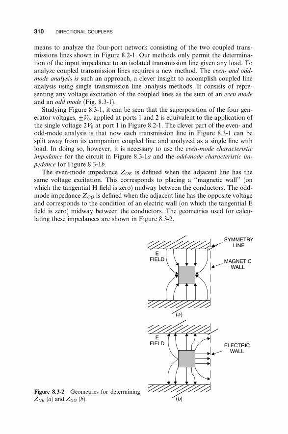
310 DIRECTIONAL COUPLERS
means to analyze the four-port network consisting of the two coupled trans-missions lines shown in Figure 8.2-1. Our methods only permit the determina-tion of the input impedance to an isolated transmission line given any load. Toanalyze coupled transmission lines requires a new method. The even- and odd-
mode analysis is such an approach, a clever insight to accomplish coupled lineanalysis using single transmission line analysis methods. It consists of repre-senting any voltage excitation of the coupled lines as the sum of an even mode
and an odd mode (Fig. 8.3-1).Studying Figure 8.3-1, it can be seen that the superposition of the four gen-
erator voltages,GV0, applied at ports 1 and 2 is equivalent to the application ofthe single voltage 2V0 at port 1 in Figure 8.2-1. The clever part of the even- andodd-mode analysis is that now each transmission line in Figure 8.3-1 can besplit away from its companion coupled line and analyzed as a single line withload. In doing so, however, it is necessary to use the even-mode characteristic
impedance for the circuit in Figure 8.3-1a and the odd-mode characteristic im-
pedance for Figure 8.3-1b.The even-mode impedance ZOE is defined when the adjacent line has the
same voltage excitation. This corresponds to placing a ‘‘magnetic wall’’ (onwhich the tangential H field is zero) midway between the conductors. The odd-mode impedance ZOO is defined when the adjacent line has the opposite voltageand corresponds to the condition of an electric wall (on which the tangential Efield is zero) midway between the conductors. The geometries used for calcu-lating these impedances are shown in Figure 8.3-2.
Figure 8.3-2 Geometries for determiningZOE (a) and ZOO (b).

EVEN- AND ODD-MODE ANALYSIS 311
Figure 8.3-3 Software outputs showing the ZOE and ZOO and other parameters re-quired for a 3-dB backward wave coupler. Obtained using Eagleware TLine.
These impedances are found in the same manner as was used to deter-mine the characteristic impedance of coaxial line in Section 7.25, albeit withsomewhat more mathematical complexity because the geometry is not as sim-ple as that of coaxial line. The even- and odd-mode method dates to the 1950swhen the ZOE and ZOO impedances were tabulated for various coupler cross-sectional geometries, but the current method for determining them is to usesoftware. A sample software is shown in Figure 8.3-3 for the geometry to beused for a 3-dB coupler for which ZOE ¼ 120 W and ZOO ¼ 20:8 W.
Why this choice of even- and odd-mode impedances yields a 3-dB couplerwill be evident once the analysis of the coupler is completed. The analysismethod [3, Chapter 6] will be demonstrated by solving for the voltages at thecoupler’s ports 1, 2, 3, and 4 given a generator voltage of þ2V0 with Z0 loadsas shown in Figure 8.2-1. We begin by determining the reflection coe‰cients atports 1 and 2 for the even and odd mode excitations of Figure 8.3-1. Theequivalent circuit used for the individual excitation analysis is shown in Figure8.3-4.

312 DIRECTIONAL COUPLERS
Figure 8.3-4 Circuit used to compute the input reflection coe‰cients to even- and odd-mode excitations.
The single-mode equivalent circuit in Figure 8.3-4 has input port A andoutput port B to distinguish these terminals from those of the coupler in Figure8.2-1. The characteristic impedance of the line is ZOE for the even-mode calcu-lation and �V0 and ZOO for the odd mode. Notice that Z0 is not a match ter-mination for either the ZOE or the ZOO transmission line.
Given these procedures, the input impedance seen at A for the even mode isfound from the input impedance formula (4.14-2):
Z0 þ jZOE tan yZAE ¼ ZOE ð8:3-1Þ
ZOE þ jZ0 tan y
and the reflection coe‰cient at A is
ZAE � Z0GE ¼ ð8:3-2Þ
ZAE þ Z0
Substituting (8.3-1) into (8.3-2) and simplifying gives
j½Z2 � Z2� tan yGE ¼ OE 0 ð8:3-3Þ
2Z0ZOE þ j½Z2 � tan yOE þ Z02
Similarly, for the odd excitation,
j½Z2 � Z2� tan yGO ¼ OO 0 ð8:3-4Þ
2Z0ZOO þ j½Z2 � tan yOO þ Z02
The total reflected voltage at port 1 for the circuit of Figure 8.2-1 is the sum ofthe even and odd reflection voltages given by
V0 V0V1R ¼ GE þ GO ð8:3-5Þ
2 2

� �
� �
EVEN- AND ODD-MODE ANALYSIS 313
At port 2, the even- and odd-mode voltages are of opposite polarity. Therefore,
V0 V0V2 ¼ GE � GO ð8:3-6Þ
2 2
Substituting (8.3-3) and (8.3-4) into (8.3-5) and (8.3-6) gives a result for V1R
(using the plus sign option in (8.3-7) and V2 by using the minus sign option:
V0 V0 V1R;2 ¼ GE G GO
2 2
NG
V1R;2 ¼ A
DA
V0 ð j tan yÞðZ2 � Z2Þ½2Z0ZOO þ ð j tan yÞðZ2 Þ�OE 0 OO þ Z02
2 Gð j tan yÞðZ2 � Z2Þ½2Z0ZOE þ ð j tan yÞðZ2 Þ�¼ OO 0 OE þ Z02
OE þ Z02Þ�½2Z0ZOO þ ð j tan yÞðZ2 Þ�½2Z0ZOE þ ð j tan yÞðZ2
OO þ Z02
ð8:3-7Þ
The denominator, DA, is nonzero for all y and for all finite Z0, ZOE , and ZOO.Furthermore, when ZOE and ZOO are selected to satisfypffiffiffiffiffiffiffiffiffiffiffiffiffiffiffiffiffiffi
Z0 ¼ ZOEZOO ð8:3-8Þ
the even-mode numerator, NAþ, is identically equal to zero for all y. This means
that the coupler will be matched to Z0 at input port 1 at all frequencies when(8.3-8) is satisfied. This is a remarkable result, doubly so in view of the alge-braic complexity with which the early researchers [4] of this coupler had tocope.
After algebraic manipulation, the value of V2 ¼ N�=DA can be writtenA
ZOE � ZOOð j sin yÞZOE þ ZOO
V2 ¼ V0 ð8:3-9Þ2Z0 cos y
ZOE þ ZOO
þ j sin y
and when the coupling length is 90�, (8.3-9) reduces to
ZOE � ZOOV2 ¼ V0 ð8:3-10Þ
ZOE þ ZOO
This suggests the definition of a voltage coupling coe‰cient k defined as
ZOE � ZOOk ¼ ð8:3-11Þ
ZOE þ ZOO

� � � �
314 DIRECTIONAL COUPLERS
and the coupling in decibels is
Coupling ðdBÞ ¼ �20 log k ð8:3-12Þ
where the negative sign is used so that the coupling is positive when expressedin decibels.
When (8.3-8) and (8.3-11) are substituted into (8.3-9), the expression for V2
becomes
jk sin yV2 ¼ V0 pffiffiffiffiffiffiffiffiffiffiffiffiffiffi ð8:3-13Þ
1� k2 cos yþ j sin y ffiffiffi If a 50-W, 3-dB coupler (at y ¼ 90�) is required, k ¼ 1=
p2, since V2
2=Z0 ¼k2V 2=Z0 ¼ 1V0
2=Z0, where V 2=Z0 is the available power from port 1. Sub-0 2 0
stituting this value of k into (8.3-11) and applying the match criterion of (8.3-8)gives the values ZOE ¼ 120:19 W and ZOO ¼ 20:8 W for a 3-dB, 50-W couplerthat were stated without proof earlier.
Now it remains to calculate the V3 and V4 for the coupler in Figure 8.3-1 tocomplete the analysis. We use the ABCD matrix method and include both thesource and load impedances (Fig. 8.3-5).
For the even mode the ABCD matrix cascade is
� � � �� �� � A B ¼ 1 Z0 cos y jZOE sin y 1 0
C D E 0 1 jYOE sin y cos y Y0 1
Performing the indicated matrix multiplications and simplifying, this becomes
A B ¼ 2 cos yþ j sin yðY0ZOE þ Z0YOEÞ jZOE sin yþ Z0 cos y
C D E jYOE sin yþ cos y cos yð8:3-14Þ
If this network is excited by a voltage V0 (Fig. 8.3-2a) and the output current is
Figure 8.3-5 Circuit used to calculate the output voltages V3 and V4 at ports 3 and 4 ofthe coupler in Figure 8.2-1.

EVEN- AND ODD-MODE ANALYSIS 315
zero (since we included the load in the ABCD network) the output voltage is
V0 V0VBE ¼ ¼ ð8:3-15Þ
AE 2 cos yþ ð j sin yÞðY0ZOE þ Z0YOEÞ
Similarly, since the odd excitation corresponds to the application of V0, at port1 of the coupler and the use of odd-mode impedances,
V0 V0VBO ¼ ¼ ð8:3-16Þ
AO 2 cos yþ ð j sin yÞðY0ZOO þ Z0YOOÞ
The output voltages at ports 3 and 4 that we seek are given by
V3 ¼ VBE � VBO ð8:3-17aÞV4 ¼ VBE þ VBO ð8:3-17bÞ
Combining (8.3-15) and (8.3-16), the optional plus sign gives V3 and the minussign gives V4. Thus,
NG
VBEGVBO ¼ B
DB
2 cos yþð j sin yÞðY0ZOOþZ0YOOÞG2 cos yþð j sin yÞðY0ZOE þZ0YOEÞ¼ V0 ½2 cos yþð j sin yÞðY0ZOE þZ0YOEÞ�½2 cos yþð j sin yÞðY0ZOO þZ0YOOÞ�ð8:3-18Þ
where (8.3-17a) is the minus option and (8.3-17b) is the plus option. For finiteZ0, ZOE , and ZOO, the denominator DB is nonzero for all y; and, when thematching condition (8.3-8) is substituted into the N� expression of (8.3-18), theB
result is identically zero for all y. Thus the voltage V3 is identically zero for all
frequencies! For this backward wave coupler, port 2 is the intended coupledport and port 3 is the isolated port. No power exits port 3 when power isapplied to port 1 for any frequency and for any coupling coe‰cient k!
To complete the analysis of the backward wave coupler, we determine thedirect voltage V4 output. This is obtained by using the plus sign option in(8.3-18). When this is taken and a common factor taken from numerator anddenominator, the result is
2V0V4 ¼ pffiffiffiffiffiffiffiffiffiffiffiffiffiffiffiffiffiffiffiffi pffiffiffiffiffiffiffiffiffiffiffiffiffiffiffiffiffiffiffiffi ð8:3-19Þ
2 cos yþ ð j sin yÞ½ ZOE=ZOO þ ZOO=ZOE �
Then imposition of the matching condition (8.3-8) and the coupling coe‰cientdefinition (8.3-11) allows this expression to be written as

316 DIRECTIONAL COUPLERS
p ffiffiffiffiffiffiffiffiffiffiffiffiffiffi 1� k2
V4 ¼ V0 p ffiffiffiffiffiffiffiffiffiffiffiffiffiffi ð8:3-20Þ1� k2 cos yþ j sin y
Notice that when the coupling length is 90�, from (8.3-13) and (8.3-20), V2 ¼ffiffiffi V4 ¼ V0=
p2 and exactly one half of the incident power, V 2=Z0 exits the two0
ports 1 and 4. This makes sense because the coupling is 3 dB and no power isreflected and none exits the decoupled port 3. Of course, practical couplershave mismatches at the ports that degrade this ideal performance. Nevertheless,the backward wave TEM coupler of this analysis is a frequently used compo-nent for its broadband performance. The coupling varies with frequency, hav-ing maximum coupling (Fig. 8.3-6) when the coupled line length is an oddmultiple of 90�. Thus, the performance is repeated in the frequency domain at
Figure 8.3-6 Direct power and coupled power of the backward wave coupler calculatedusing Genesys simulator.

EVEN- AND ODD-MODE ANALYSIS 317
the third, fifth, seventh, and so forth harmonics. The simulated performance ofa 3-dB coupler with air dielectric (l=4 ¼ 50 mm) is shown in Figure 8.3-6.
In designing a coupler for a given amount of coupling, it is convenient toexpress the even- and odd-mode impedances in terms of the desired couplingcoe‰cient. This is done by solving (8.3-8) and (8.3-9) for ZOE and ZOO:rffiffiffiffiffiffiffiffiffiffiffi
1þ kZOE ¼ Z0 ð8:3-21Þ
1� krffiffiffiffiffiffiffiffiffiffiffi 1� k
ZOO ¼ Z0 ð8:3-22Þ1þ k
For a given coupling tolerance, a broader bandwidth can be obtained byovercoupling at the center frequency. For example, if a center frequency cou-pling of 2.7 dB is chosen, k ¼ 0:724 and (8.3-21) and (8.3-22) yield ZOE ¼125 W and ZOO ¼ 20 W. For this design the variation of coupling is within 0.3dB of 3.0 dB from 1000 to 2000 MHz, an octave bandwidth, as shown inFigure 8.3-7.
Figure 8.3-7 A �2.7 dB, over coupled, backward wave coupler.

318 DIRECTIONAL COUPLERS
Figure 8.3-8 Hybrid coil with ports de-fined for comparison with the backwardwave coupler.
The remarkable performance of the homogeneous (same dielectric constantfor even and odd modes) TEM backward wave coupler can be summarized asfollows:
1. The coupler is matched ðV1 ¼ V0Þ at all frequencies!2. The directivity is infinite ðV3 ¼ 0Þ at all frequencies!3. The direct ðV4Þ and coupled ðV2Þ voltages are exactly 90� out of phase at
all frequencies!
4. The magnitude of the coupled output voltage relative to the input voltageis k ¼ ðZOE � ZOOÞ=ðZOE þ ZOOÞ.
When designed such that the coupled and direct waves are equal, or nearlyso, it is also called a hybrid coupler [5, p. 280]. This nomenclature may havebeen derived from the hybrid coil (Fig. 8.3-8) used widely in lower frequencytelephone systems [6, p. 282]. When properly terminated, the hybrid coil hasthe property that a signal at 1 divides evenly between ports 2 and 4, and there isno output at 3. A signal at 2 also divides between 1 and 3 with no output at 4,and so forth. The 3 dB backward coupler has performance similar to the hybridcoil, but it also has a 90� phase shift between the two equal outputs whereas thehybrid coil does not.
The single quarter-wave coupler provides up to an octave (2/1) bandwidthfor about 3 dBG 0.4 dB of coupling. Considerably broader bandwidth can beobtained by cascading odd numbers of coupling sections. A 5/1 bandwidthwith 3 dBG 0.4 dB can be obtained by cascading three sections having 12.64,1.28, and 12.64 dB coupling, respectively. This three-section coupler is de-scribed in a classic paper by Seymour Cohn [2]. The simulated performance ofan air dielectric version of the model that he built is shown in Figure 8.3-9.
To achieve the very tight coupling in the center coupler Cohn invented atransmission line format called a reentrant section. It consists of a pair of con-

EVEN- AND ODD-MODE ANALYSIS 319
Figure 8.3-9 Performance of a three-section coupler cascade [2].
ductors, A and B, embedded as separate coaxial lines within an ungrounded(electrically ‘‘floating’’) intermediate conductor C that is suspended within anouter conductor D, as shown in Figure 8.3-10. The intermediate conductor Cmight seem to shield A and B from each other. However, C is not grounded,and its presence increases the distributed capacitance between A and B and,with it, their coupling to each other.
For the reentrant section
ZOE ¼ Z02 þ 2Z01 ð8:3-23Þ
ZOO ¼ Z02 ð8:3-24Þ
where Z01 is the characteristic impedance of a solid conductor having the sameouter dimensions as the intermediate conductor C, within the outer conductorD; and Z02 is the characteristic impedance of A (or B) within the coaxial regioninside C.
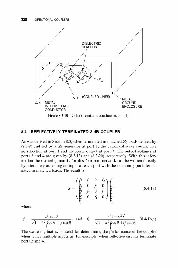
320 DIRECTIONAL COUPLERS
Figure 8.3-10 Cohn’s reentrant coupling section [2].
8.4 REFLECTIVELY TERMINATED 3-dB COUPLER
As was derived in Section 8.3, when terminated in matched Z0 loads defined by(8.3-8) and fed by a Z0 generator at port 1, the backward wave coupler hasno reflection at port 1 and no power output at port 3. The output voltages atports 2 and 4 are given by (8.3-13) and (8.3-20), respectively. With this infor-mation the scattering matrix for this four-port network can be written directlyby alternately assuming an input at each port with the remaining ports termi-nated in matched loads. The result is
0 1 0 f1 0 f2
S ¼ f1B B B 0 f2 0 C C C ð8:4-1aÞ
0
f2
@ f2
0
0
f1
f1
0
A where
f1 ¼ jk sin yffiffiffiffiffiffiffiffiffiffiffiffiffiffi 1� k2
pcos yþ j sin y
and f2 ¼ffiffiffiffiffiffiffiffiffiffiffiffiffiffi 1� k2
pffiffiffiffiffiffiffiffiffiffiffiffiffiffi 1� k2
pcos yþ j sin y
ð8:4-1b,cÞ
The scattering matrix is useful for determining the performance of the couplerwhen it has multiple inputs as, for example, when reflective circuits terminateports 2 and 4.

REFLECTIVELY TERMINATED 3-dB COUPLER 321
Figure 8.4-1 The 3-dB backward wave coupler with symmetric reflecting terminationson ports 2 and 4.
A frequent application consists of employing a 3-dB coupler to convert asymmetric pair of reflective circuits into a transmission network. This need mayarise, for example, when it is necessary to design a diode phase shifter. Thesymmetric reflective terminations are connected to the direct arm (port 4) andcoupled arm (port 2) of the coupler. Because of their equal amplitude and 90�
phase di¤erence for each pass through the coupler, when the energy is reflectedback into the coupler (Fig. 8.4-1), it emerges from the normally decoupledport 3.
This process requires that the complex reflection coe‰cients at ports 2 and 4are identical, or
G2 ¼ G4 ¼ G ð8:4-3Þ
With an input at port 1, symmetric reflections at ports 2 and 4, and a matchedZ0 load at port 3, the scattering matrix equations for the network are
0 1 0 1 0 1 0 1 0 1 b1 0 f1 0 f2 a1 0 f1 0 f2 a1
b2B B B C C C¼ f1
B B B 0 f2 0 C C C � a2B B B C C C¼ f1
B B B 0 f2 0 C C C � Gf1a1B B B C C C
b3
b4
@ A 0
f2
@ f2
0
0
f1
f1
0
A a3
a4
@ A 0
f2
@ f2
0
0
f1
f1
0
A 0
Gf2a1
@ A ð8:4-2a,b,c,dÞ
The reflection coe‰cient at input port 1 is found from (8.4-2a), specifically
b1 ¼ f1Gf1a1 þ f2Gf2a1 ð8:4-5Þ

322 DIRECTIONAL COUPLERS
and the input reflection coe‰cient is
b1 1� k2ð1þ sin2 yÞG1 ¼ ¼ Gð f 2 þ f 2Þ ¼ G pffiffiffiffiffiffiffiffiffiffiffiffiffiffi2a1
1 ½ 1� k2 cos yþ j sin y�2 ð8:4-6Þffiffiffi
From (8.4-4) it can be seen that when y ¼ 90� and k ¼ 1=p2 (for 3-dB cou-
pling), then G1 ¼ 0, and the input port is matched. From (8.4-2c)
b3 ¼ f2G f1a1 þ f1Gf2a1 ð8:4-7Þ
This can be written as
jð2k sin yÞp ffiffiffiffiffiffiffiffiffiffiffiffiffiffi 1� k2
b3 ¼ a1Gp ffiffiffiffiffiffiffiffiffiffiffiffiffiffi ð8:4-8Þ1� k2 cos yþ j sin y
ffiffiffi We note from (8.4-8) that when y ¼ 90� and k ¼ 1=
p2, and jGj ¼ 1, the
output wave b3 ¼ Ga1. That is, when symmetric, totally reflecting circuits areconnected to ports 2 and 4 of a 3-dB coupler, the output wave equals the inputin amplitude but is changed by the angle of the reflection coe‰cient of the re-flective terminations at ports 2 and 4. This is what is desired in a phase shiftercircuit.
As frequency is varied, the value of y varies, and the power split of the cou-pler is no longer exactly 3 dB, as is required for a perfect match at the inputwith symmetric reflections at ports 2 and 4. As a result, some power is reflectedat port 1 and a corresponding insertion loss is experienced in the transmissionfrom port 1 to port 3. Despite this fact, the reflection coe‰cient at port 1 re-mains fairly low due to the fact that the waves reflected back into the coupler atports 2 and 4 remain 90� out of phase with one another at all frequencies andhence combine 180� out of phase at port 1.
The input VSWR at port 1 and the transmission loss from port 1 to port 3 isshown in Figure 8.4-2 for a coupler with center frequency at 1500 MHz andsymmetric, totally reflecting circuits at ports 2 and 4. The VSWR is 1.1 or lessfrom 1100 to 1900 MHz, a bandwidth of 800 MHz. Notice that for TEM de-
vices whose bandwidth depends upon line lengths, the center frequency f0 is the
arithmetic mean of the band edge frequencies.
The matched performance at port 1 with symmetric reflections at the 3-dBports can be obtained with other types of 3-dB, 90� couplers such as the branchline coupler and the hybrid ring coupler (or rat race coupler) fitted with an extra90� line length. The principles of these couplers will be covered shortly. How-ever, these devices do not maintain the 90� phase di¤erence at all frequenciesfor the signals emerging from their coupled and direct ports and do not achieveas broad a bandwidth in the reflection mode as that of the backward wavehybrid.

COUPLER SPECIFICATIONS 323
Figure 8.4-2 Input VSWR for a reflectively terminated �2.7-dB backward wave, hy-brid coupler.
8.5 COUPLER SPECIFICATIONS
In the practical construction of a hybrid coupler, the region of the coupled linescan be constructed in a nearly ideal realization; however, it is necessary tomake transitions from the ends of the coupled lines in order to attach con-nectors at the ports. It is at these transitions that significant reflections occur ina practical coupler, causing the operation of the coupler to depart from theideal performance previously described.
Consider the coupler in Figure 8.5-1. Power PI enters the coupler at port 1.Ideally, the desired coupled power PC exits at port 2, and the remaining powerPL exits at port 4. However, due to coupler imperfections some power, PD,exits at port 3 (the ‘‘decoupled’’ port). Furthermore, some power, PR, is re-flected at the input port.
The parameters of couplers are defined as numbers greater than unity so thatthe values are positive when expressed in decibels [1, p. 369].

� �
� �
� �
� �
� �
324 DIRECTIONAL COUPLERS
Figure 8.5-1 Practical directional coupler has return loss and finite directivity.
The coupling (in decibels) is defined as
PICoupling ¼ 10 log
PC
The directivity (in decibels) is defined as
PCDirectivity ¼ 10 log
PD
The isolation (in decibels) is defined as
PIIsolation ¼ 10 log
PD
Note that when expressed in decibels the isolation is equal to the coupling plusthe directivity.
The return loss (in decibels) is defined as
PIReturn loss ¼ 10 log
PR
The insertion loss* (in decibels), which includes the diversion of coupled power,is
PIInsertion loss ¼ 10 log
PL
*Some manufacturers may subtract the coupled power from insertion loss ratings, defining the in-
sertion loss as the amount of power loss to reflection and absorption in the coupler.

� �
MEASUREMENTS USING DIRECTIONAL COUPLERS 325
Note that in a symmetrically constructed coupler the same imperfectionsthat give rise to reflections at the input also produce the undesired leakage atthe directive port.
In a symmetric coupler the return loss equals the directivity. For example, asymmetric coupler having 20-dB directivity has a return loss of 20 dB as well.This corresponds to a VSWR of 1.22.
8.6 MEASUREMENTS USING DIRECTIONAL COUPLERS
Suppose we wish to use a directional coupler to determine the VSWR of a de-vice under test (DUT) (Fig. 8.6-1). Consider the signals emanating from thecoupler’s measurement port. First, there is a voltage wave proportional to thedesired measurement rL. But then there is also an error voltage wave D dueto the directivity. It is to be emphasized that D is a voltage wave (not power);
we can only use superposition for linear quantities (voltage, current, a and b
waves, etc.) Accordingly, there is a wave resulting from the interaction of thesource and load reflections. This wave is the result of an infinite number of re-reflections. But this infinite series converges, as we’ve seen previously:
rSrL þ ðrSrLÞ2 þ ðrSrLÞ3 þ � � � ¼ rSrL ð8:6-1Þ1� rSrL
We ignore the phases of the measured and error waves since we want toknow the worst-case limits when the error waves either add or subtract fromthe measured rL wave.
The total (combined) error wave can have magnitudes between
ET ¼ total error wave magnitude ¼GD 1þ rSrL ð8:6-2Þ1� rSrL
Say that the coupler has 20-dB directivity, that the VSWR of the source is 1.3,that the VSWR of the coupler input is 1.22, and that the load we wish to mea-sure actually has a VSWR of 1.25. Then D ¼ 0:1, rS ¼ 0:13, and rL ¼ 0:11.
Figure 8.6-1 Measurement of the reflection coe‰cient of a device under test (DUT)using a backward wave coupler. Two error waves are also shown.

� � 326 DIRECTIONAL COUPLERS
Then the error wave can be
ð0:13Þð0:11ÞET ¼Gð0:1Þ 1þ ¼Gð0:1Þ½1:015� ¼G0:10 ð8:6-3Þ
1� ð0:13Þð0:11ÞThis wave can combine in any phase with that of GL, whose magnitude is 0.11.The resulting measured magnitude of GL will be within
0:01ameasured rL a 0:21 ð8:6-4ÞThe corresponding values for measured VSWR are
1:02aVSWRMEAS a 1:53 ð8:6-5ÞThis is insu‰cient accuracy for practical measurements. To circumvent this
inaccuracy, the same coupler can be used in a network analyzer system, whosecomputer determines the error waves (phase and magnitude) during the cali-bration part of the measurement (when precision short circuit, open circuit andmatched loads are connected) and then subtracts these error phasors from theactual measurements at each test frequency. This is described in the next section.
8.7 NETWORK ANALYZER IMPEDANCE MEASUREMENTS
Network analyzers (Fig. 8.7-1) measure both impedance (by measuring reflec-tion coe‰cient at any port) and scattering parameters (insertion loss and inser-
Figure 8.7-1 Network analyzer in the impedance measurement mode (after Gupta [7],reprinted with permission).

BRANCH LINE COUPLER 327
tion phase to any port). Impedance measurement is based on the direct mea-surement of reflection coe‰cient, the complex ratio of the reflected and incidentwaves of a terminating impedance. The incident and reflected waves are sepa-rated using directional couplers. The outputs of the couplers are fed to a har-monic frequency converter (mixer), which translates the test frequency to afixed frequency near 300 kHz [7, pp. 114–115]. Usually an autotuning localoscillator and two identical mixers are used for this purpose. The mixing pro-cess preserves amplitude and phase information that are readily measurable atlow frequency. The reflected wave vector, normalized to the incident wave (andcorrected for coupler errors), can be displayed on a CRT (cathode ray tube)screen with a Smith chart overlay for direct determination of normalized im-pedance.
8.8 TWO-PORT SCATTERING MEASUREMENTS
The network analyzer (Fig. 8.8-1) contains microwave switches of high preci-sion (good reproducibility and low VSWR). Using the switches the procedureto measure Snm is [7, p. 115]:
1. Connect a source to port m and a matched load to port n. These twoports are connected to a network analyzer via two directional couplers asshown in Figure 8.8-1.
2. Terminate all other ports in matched loads so that all other a’s (incidentwave amplitudes) are zero.
3. The network analyzer provides the complex value of Snm in terms of am-plitude and phase (for n0m, i.e., a two-port measurement).
Figure 8.8-1 Network analyzer in the two-port measurement mode used to determine Sparameters.
8.9 BRANCH LINE COUPLER
Over a narrow bandwidth, the performance of the 3-dB backward wave hybridcoupler can be obtained with the branch line coupler. This consists of four 90�
transmission lines connected together in a square. It has the form of a 50-W line

328 DIRECTIONAL COUPLERS
Figure 8.9-1 Equivalent circuit and performance of the 3-dB branch line coupler.

BRANCH LINE COUPLER 329ffiffiffi loaded at 90� intervals by 35.35-W (more precisely, 50=
p2) stubs that are in-
terconnected at their ends with another 50-W line. The ‘‘stub ends’’ form the 3-dB ports. Like the backward wave hybrid, a 90� phase di¤erence occurs be-tween these two equal outputs, but for the branch line coupler this occurs onlyat the center frequency.
(2)
Figure 8.10-1 Circuit and performance of 3-dB hybrid ring coupler when realized in ahomogeneous TEM transmission line format.

330 DIRECTIONAL COUPLERS
When power enters at port 1 (Fig. 8.9-1), it divides evenly between ports 2and 3. At the center frequency, port 4 is isolated when match loads are placedat ports 2 and 3.
This coupler has the constructional advantage that it lies entirely in onecenter conductor plane, hence it is easy to print or incorporate within an in-tegrated circuit. However, this coupler is fairly narrowband, usually havingonly about a 10% bandwidth. Furthermore, the 35.35-W lines are wide relativeto their 90� length at microwave frequencies, making it hard to distinguishwhere those lines end and the 50-W lines begin, the problem encountered withthe stub filter in Section 7.34. Accordingly, the branch line coupler is a candi-date for EM simulation.
8.10 HYBRID RING COUPLER
The disadvantage of the branch line coupler is the need to make 35-W lines.Their low impedance line sections make the junctions so large it is di‰cult toestimate where one 90� line section ends and the next begins, necessitatingconsiderable trial and error or EM simulation to realize a satisfactorily per-forming design.
The hybrid ring coupler, also called the rat race coupler, actually requires1.5 wavelengths of transmission line (one section is 270� long), but it is easier toffiffiffi realize because the lines are 70.7 W (more precisely Z0
p2), quite narrow, and
consequently their electrical lengths are more easily predicted. While this cou-pler is called the hybrid ring, the name is misleading, since its 3-dB ports are180� out of phase rather than 90� (Fig. 8.10-1). The hybrid ring coupler can berealized in a TEM transmission line format or in a waveguide. In a waveguide,its circular chamber is likely the basis for the ‘‘rat race’’ name.
Remarkably, for a given VSWR specification the rat race usually is broaderband than the branch line coupler. Although its 3-dB outputs are 180� out ofphase rather than 90�, a 90� phase di¤erence in its �3-dB outputs can be ob-tained simply by adding a 90� length of 50-W line to one of the 3-dB outputs.The 90� phase di¤erence between 3-dB outputs is necessary if the coupler is tobe used in a reflection transmission circuit, as for a phase shifter.
8.11 WILKINSON POWER DIVIDER
An equal-phase output, 3-dB divider can be obtained by transforming two50-W loads to 100 W and connecting them in parallel to an input 50-W line(Fig. 8.11-1). When the output ports are bridged with a 100-W resistor, the re-sult is a power divider whose output ports are matched and perfectly isolated atthe design frequency [1, Sec. 8.2]. The resulting circuit is called a Wilkinson
power divider (Fig. 8.11-2). To the extent that the output loads at 2 and 3 are

WILKINSON POWER DIVIDER 331
Figure 8.11-1 Wilkinson power divider provides two in-phase, 3-dB outputs and someisolation of the input from asymmetrical.
Figure 8.11-2 Performance of the Wilkinson power divider.

332 DIRECTIONAL COUPLERS
asymmetric, their reflections are absorbed by the 100-W resistor. When theloads are symmetric, no power will be absorbed in this resistor.
Another advantage of the Wilkinson divider is that very broad bandwidthcan be obtained by using multiple section transformers (quarter-wave line sec-tions) to transform the 50-W loads to 100-W inputs that, when paralleled, givean input impedance of 50 W. [4]
REFERENCES
1. Peter A. Rizzi, Microwave Engineering, Passive Circuits, Prentice-Hall, EnglewoodCli¤s, NJ, 1988. Fundamental microwave engineering textbook covering theory and
design of transmission lines, couplers, filters, and numerous other passive devices.
2. Seymour Cohn, ‘‘The Re-Entrant Cross Section and Wide-Band 3-dB Hybrid Cou-plers,’’ IEEE Transactions on Microwave Theory and Techniques, MTT-11, July,1963, pp. 254–258.
3. Joseph F. White, Microwave Semiconductor Engineering, Noble Publishing, NorcrossGA. Extensive treatment of PIN diodes and their switching and phase shifting appli-
cations. Also includes fundamentals of microwave circuits.
4. Matthei, Young, and Jones, Microwave Filters, Impedance Matching Networks, and
Coupling Structures, McGraw-Hill, New York, 1964 (now also available from ArtechHouse, Norwood, MA). This is considered the Bible of the filter world.
5. Fred E. Gardiol, Introduction to Microwaves, Artech House, Norwood, MA, 1984.This is a good text on microwaves, containing many practical experimental setups.
6. Robert E. Collin, Foundations of Microwave Engineering, McGraw-Hill, New York,1966. Collin is a superb theoretician.
7. K. C. Gupta, Microwaves, Halsted Press, Wiley, New York, 1978. Easily readable
introduction to microwave engineering. Originally published in India.
EXERCISES
E8.3-1 Derive the expressions (8.3-23) and (8.3-24) for ZOE and ZOO of thebackward wave coupler in terms of the characteristic impedance Z0
and the voltage coupling coe‰cient k, beginning with (8.3-8) and(8.3-11).
E8.3-2 a. What even and odd impedances are needed to form a 50-W, 15-dBcoupler? Hint: The result from E8.3-1 is helpful.
b. What is the physical length of the coupling region if the relativedielectric constant throughout the insulating region surroundingthe coupled lines is 2.1?
E8.3-3 Verify that the numerator NþA in (8.3-7) is zero given the matching
condition of (8.3-8).

EXERCISES 333
E8.3-4 Derive the expression for the straight-through voltage V4 of thebackward coupler (8.3-20) beginning with (8.3-18) and using theconditions of (8.3-8) and (8.3-11).
E8.4-1 a. Determine the coupling coe‰cient k for a 50-W, backward wavecoupler that when used with perfectly reflecting short circuits onits coupled and direct arms will have a perfect input match atf0 � 0:3f0 and at f0 þ 0:3f0 where f0 ¼ 1000 MHz is its centerfrequency (at which the coupling region is 90� long).
b. What is the center frequency coupling value (in decibels) of thecoupler?
c. What are ZOE and ZOO for this coupler?
d. What is the VSWR at the input at 1000 MHz?
e. Model the circuit on a network simulator and verify your pre-dicted values.
E8.4-2 a. Use a network simulator to model a 3-dB backward wave couplerwith open circuits on its direct and coupled arms (ports 2 and 4)and center frequency of 1 GHz (at which the coupled line length is90�). Plot the input VSWR (at port 1) from 500 to 1500 MHz.
b. Repeat (a) with short-circuit terminations on ports 2 and 4 insteadof open circuits.
c. Using a network simulator, plot the transmission phase (ang[S31])over the 500- to 1500-MHz band of the circuits in (a) and (b) andshow that the di¤erence (phase shift obtained by switching froman open to a short circuit on ports 2 and 4) is equal to 180� over afrequency band of 10% or more. This is an example of a trans-mission phase shifter obtained by converting variable reflectionangle terminations into a two-port network using a 3-dB coupler.
d. Plot the insertion loss of the circuits in (a) and (d) over the 500- to1500-MHz bandwidth. With what minimum e‰ciency, in percentof incident power, do the circuits in (a) and (b) convert reflectingterminations into a transmission circuit over the 700- to 1300-MHz bandwidth?
e. Show the VSWR of the cascade connection of the circuits in (a)and (b) over the 500- to 1500-MHz bandwidth.
E8.5-1 A symmetrically designed backward wave coupler has 30 dB of di-rectivity at its center frequency. What is its input VSWR at this fre-quency.
E8.6-1 An engineering team at your microwave components company pro-poses to design a dedicated test setup to measure products having aVSWR of 1.25 at a single frequency. They propose to build a couplerand tune it for low VSWR and high directivity at a single test fre-quency. The source available has a VSWR of 1.3. It is necessary to

334 DIRECTIONAL COUPLERS
measure an actual VSWR value of 1.25 as being between 1.23 and1.27.
a. What coupler directivity is required?
b. What is the corresponding input VSWR of the coupler?
c. Is this measurement setup practically achievable?
E8.9-1 a. Use a circuit simulator to model the branch line 3-dB coupler withopen circuits at its 3 dB ports. What is its bandwidth for a maxi-mum input VSWR ¼ 1.2 (20 dB return loss)?
b. Repeat (a) but place short circuits on the two 3-dB ports. What isthe bandwidth for VSWR ¼ 1.2 or less?
c. Next, cascade two of the circuits used in (a) and interconnect themwith a 50-W line that is 600 long at 1 GHz. What is the 1.2 maxi-mum VSWR bandwidth of the cascade? How does this comparewith the similar experiment of exercise E8.4-2e?
E8.10-1 Repeat Exercise 8.9-1 this time using the TEM mode hybrid ring (ratrace) coupler.
a. How does the VSWR bandwidth compare to that of the branchline?
b. When you cascade two circuits, how does the performance com-pare with the cascaded branch line couplers?
E8.11-1 The Wilkinson power divider shown in Figure 8.11-1 uses singlequarter-wave inverters to transform the 50-W loads to 100 W at its teejunction.
a. Design new inverters with a center frequency of 1000 MHz havingthree cascaded 90� line sections to obtain broader bandwidth.What are the characteristic impedance values for the three linesections? Hint: Use the constant ratio step method used in themultisection Q matching.
b. Use a network simulator to plot the VSWR of your divider andcompare it to that of the single inverter mode over the 0- to 2000-MHz frequency interval. Model your design using a network sim-ulator. How broad a �20 dB return loss bandwidth can you get?
c. Based on the single inverter design shown in Figure 8.11-1, selectthe values of the three bridging resistors to be used in your designand use the network simulator to plot the isolation obtained overthe 0- to 2000-MHz band with your choices. Hint: Guess startingvalues for the three resistors and then use the optimizer of thenetwork simulator with a goal of 30-dB minimum isolation be-tween the output ports from 500 to 1500 MHz.

CHAPTER 9
Filter Design
9.1 VOLTAGE TRANSFER FUNCTION
In the specification and design of filters we are interested in the ratio of thesinusoidal voltage at the load, VL, relative to that of the generator, VG, asa function of frequency. Classical filter theory begins with LLFPB (lumped,linear, finite, passive, and bilateral) elements. These designs can be extended tohigh frequencies at which distributed elements are employed having resonances,such as reactively terminated transmission lines with zero and infinite inputimpedance values.
In Section 2.9 we proved that maximum power is transferred between agenerator and load when the impedance of the generator, ZG, is related to theimpedance of the load, ZL, by ZG ¼ Z �. In our treatment of filters we considerL
only cases in which the source and load impedances are both real. ThenZG ¼ RG and ZL ¼ RL as shown in Figure 9.1-1. Under these conditions[1, pp. 11–13], the available voltage Vavail is defined as the voltage across the load
when all of the available power from the generator is transferred to the load.
When source and load have di¤erent resistancesrffiffiffiffiffiffiffi RL VG
Vavail ¼ ð9:1-1ÞRG 2
Dividing both sides by VL, rffiffiffiffiffiffiffi Vavail 1 RL VG¼ ð9:1-2ÞVL 2 RG VL
The voltage transmission coe‰cient t is defined asrffiffiffiffiffiffiffi VL RG VG
t ¼ ¼ 2 ð9:1-3ÞVavail RL VL
High Frequency Techniques: An Introduction to RF and Microwave Engineering, By Joseph F. White. ISBN 0-471-45591-1 6 2004 John Wiley & Sons, Inc.
335
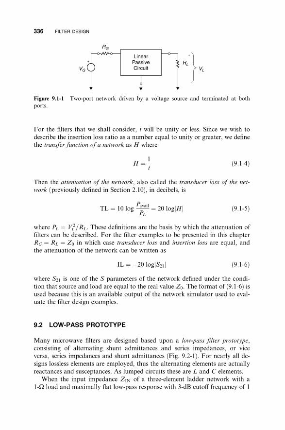
336 FILTER DESIGN
Figure 9.1-1 Two-port network driven by a voltage source and terminated at bothports.
For the filters that we shall consider, t will be unity or less. Since we wish todescribe the insertion loss ratio as a number equal to unity or greater, we definethe transfer function of a network as H where
1H ¼ ð9:1-4Þ
t
Then the attenuation of the network, also called the transducer loss of the net-
work (previously defined in Section 2.10), in decibels, is
PavailTL ¼ 10 log ¼ 20 logjHj ð9:1-5Þ
PL
where PL ¼ V 2=RL. These definitions are the basis by which the attenuation ofL
filters can be described. For the filter examples to be presented in this chapterRG ¼ RL ¼ Z0 in which case transducer loss and insertion loss are equal, andthe attenuation of the network can be written as
IL ¼ �20 logjS21j ð9:1-6Þ
where S21 is one of the S parameters of the network defined under the condi-tion that source and load are equal to the real value Z0. The format of (9.1-6) isused because this is an available output of the network simulator used to eval-uate the filter design examples.
9.2 LOW-PASS PROTOTYPE
Many microwave filters are designed based upon a low-pass filter prototype,consisting of alternating shunt admittances and series impedances, or viceversa, series impedances and shunt admittances (Fig. 9.2-1). For nearly all de-signs lossless elements are employed, thus the alternating elements are actuallyreactances and susceptances. As lumped circuits these are L and C elements.
When the input impedance ZIN of a three-element ladder network with a1-W load and maximally flat low-pass response with 3-dB cuto¤ frequency of 1

BUTTERWORTH OR MAXIMALLY FLAT FILTER 337
Figure 9.2-1 Filter prototype ladder network, synthesized by continued fraction ex-pansion. Shunt elements are susceptances and series elements are reactances. A resistivetermination loads the network.
rad/s is written as a fractional expansion, it takes the form [1, p. 26]
1ZIN ¼
1ð9:2-1Þ
sþ1
2sþsþ 1
where s ¼ sþ jo is used to express the transfer function of the filter. The cor-responding values for the elements of the three-element ladder network are
Y3 ¼ 1s C3 ¼ 1 F ð9:2-1aÞZ2 ¼ 2s L2 ¼ 2 H ð9:2-1bÞY1 ¼ 1s C1 ¼ 1 F ð9:2-1cÞ
This example defines an N ¼ 3, low-pass filter.In a similar fashion the element values for filters having 2 to N elements can
be determined. The element values are called g values because the filter can beinitiated with either a series L or a shunt C to which alternating elements areadded. Thus the same set of g values for an N element filter can be used foreither of two designs, depending upon whether one begins with a series or ashunt element. Thus, starting with a series inductor, the g1 value is its induc-tance in henrys, while starting with a shunt capacitor requires interpretingthe g1 value as the capacitance in farads. Thereafter the elements of the filteralternate both in kind (inductance or capacitance) and in topology (series orshunt).
9.3 BUTTERWORTH OR MAXIMALLY FLAT FILTER
The maximally flat low-pass prototype filter is called a Butterworth response. Ithas the attributes that the transducer loss and all of its derivatives are zero at
zero frequency; hence it provides maximum flatness.

TABLE9.3-1
gValues
forButterworthLow-Pass
PrototypeFilter
Ng1
g2
g3
g4
g5
g6
g7
g8
g9
g10
g11
21.4142
1.4142
1 3
1.0000
2.0000
1.0000
1 4
0.7654
1.8478
1.8478
0.7654
5
0.6180
1.6180
2.0000
1.6180
6
0.5176
1.4142
1.9318
1.9318
7
0.4450
1.2470
1.8019
2.0000
8
0.3902
1.1111
1.6629
1.9616
9
0.3473
1.0000
1.5321
1.8794
10
0.3129
0.9080
1.4142
1.7820
1 0.6180
11.4142
0.5176
11.8019
1.2470
0.4450
11.9616
1.6629
1.1111
0.3902
12.0000
1.8794
1.5321
1.0000
0.3473
11.9754
1.9754
1.7820
1.4142
0.9080
0.3129
1
Source:
After
Rhea
[1,p.47].Usedwithpermission.
338

BUTTERWORTH OR MAXIMALLY FLAT FILTER 339
This is because it is a mathematical fact that if two polynomials of order N
have N points in common they are identical. Consequently, if by alternate meanswe find a filter function having a zero value and zero derivatives at zero fre-quency, we can be confident that it is the one and only such solution, the But-terworth.
The order N of a filter is equal to the number of poles and zeros in its trans-
mission response. In the stopband of a filter N determines how rapidly the iso-lation increases after the cuto¤ frequency (it increases at 6N dB/octave). In thepassband N equals the number of derivatives of the response characteristic.This a¤ects the flatness of the passband response or, in the case of the Cheby-shev response to be described, the number of ripples in the passband.
For a lumped-element filter, N is equal to the number of nontrivial elements in
the filter network. Nontrivial elements are those which alternate in type between
L and C elements. In a filter, nontrivial L and C elements each produce a pole at
zero frequency and a zero at infinite frequency or vice versa.
Trivial elements are those that can be combined without changing the re-sponse. For example, two capacitors in series or in parallel count as only onenontrivial element because they could be replaced by a single capacitor havingan appropriately defined value. Similarly, two inductors in series or parallelalso would count as only one nontrivial element.
In a filter network a resonator consisting of one L in series or in parallel with
one C element counts as two nontrivial elements. Such a resonator produces a
pole or zero in the filter response at a finite frequency.
The low-pass prototype Butterworth filter response is obtained by havingalternating L and C elements with the values listed in Table 9.3-1, normalizedto 1 W and having a cuto¤ frequency (3 dB loss) of 1 rad/s. Notice that there isan additional g value listed for each filter type. For example, for N ¼ 2 there isa g3 value listed. This is the value of the load with which the filter delivers itsresponse. The generator impedance in these tables is always assumed to be aunity resistance. Note that the gi values in the prototype filter tables correspond
to the value of series reactance or shunt susceptance of the respective lumped
elements at the cuto¤ frequency fC . For the prototype filter circuit fC is 1 rad/s.All Butterworth filters have a unity load, but we shall see that for certain
filters a nonunity load would be required to obtain the specified response(Fig. 9.3-1). Since there is no practical way to build an ideal transformer totransform a Z0 load to another real value at all frequencies simultaneously, wewill avoid filter design examples requiring unequal source and load resistances,except in the special case of diplexer filters.
9.4 DENORMALIZING THE PROTOTYPE RESPONSE
Of course, we do not want a 1-W filter with cuto¤ at 1 rad/s (0.16 Hz). There-fore, we scale both the impedance and frequency of the filter by adjusting the L

340 FILTER DESIGN
Figure 9.3-1 Either of these networks yields the same Butterworth low-pass responseinto a unity load.
and C values. Since the reactance of an inductor is
Xi ¼ oLi ð9:4-1Þ
it follows that to obtain a series impedance at our desired characteristic im-pedance Z0 and cuto¤ frequency fC , we must multiply the prototype gi value sothat
Li ¼ giZ0
2pfCð9:4-2Þ
Similarly, since the reactance of a capacitor is
1Xi ¼
oCi
ð9:4-3Þ
then the corresponding value of Ci for our Z0; fC and gi is
Ci ¼ gi ð9:4-4ÞZ02pfC
In these filter design examples Z0 is the impedance of the system. Later, if alumped-element filter is used in a high frequency network, the Z0 impedance ofsource and load will be presented to the filter when the filter is connected tothem using transmission lines of Z0 characteristic impedance.
As a filter design example, suppose that we wish to design a low-pass But-terworth filter with 3-dB cuto¤ at 1 GHz and Z0 ¼ 50 W. The g values are
g1 ¼ 1:000 ð9:4-5aÞg2 ¼ 2:000 ð9:4-5bÞg3 ¼ 1:000 ð9:4-5cÞ

DENORMALIZING THE PROTOTYPE RESPONSE 341
Figure 9.4-1 Three-element Butterworth low-pass filter with 3-dB cuto¤ at 1 GHz andZ0 ¼ 50 W.
Furthermore, let’s say that we want the filter to be in the p configuration, hav-ing a C as the first (shunt) element. Then
1:000C1 ¼ C3 ¼ ¼ 3:18 pF ð9:4-6a,bÞð50Þð2pÞð1� 109Þ
ð2:000Þð50ÞL2 ¼ ¼ 15:92 nH ð9:4-6cÞð2pÞð1� 109Þ
The filter, scaled to our frequency and impedance, is shown in Figure 9.4-1.In the network simulation of the circuit in Figure 9.4-1 the implicit source
and load impedances are 50 W in the specifications of input port (1) and outputport (2). The response of the filter in Figure 9.4-1 is shown in Figure 9.4-2.
In Figure 9.4-2 the lower curve uses the left y axis coordinates (expandedinsertion loss), and the upper curve uses the right y axis (to show isolation),where the terms insertion loss (commonly used to describe transducer loss) andisolation are selected to describe the intended passband and stopband of thefilter, respectively. Note that the insertion loss is 3 dB at 1 GHz as predicted.
Next, note that the isolation at 2 GHz is 18 dB and that the isolation at4 GHz is 36 dB, an increase of 18 dB/octave. This also is expected for a three-element filter for which the isolation increases by 6N dB/octave, or 18 dB/octave. Had we used a five-element filter, the isolation would have increased by30 dB/octave.
Filters made with lossless L and C elements achieve their frequency selectiveattenuation by reflecting power. For the low-pass Butterworth example theinsertion loss at 1 GHz is 3 dB. This means that the reflected power is 50% ofthat which is incident. The corresponding reflection coe‰cient magnitude is0.707 and the VSWR is 5.82. Figure 9.4-3 shows the VSWR of this low-passfilter example.
It should be emphasized that because reactive filters have high reflectioncoe‰cients their performance can be changed if they are interconnected with

342 FILTER DESIGN
Figure 9.4-2 Insertion loss/isolation of the three-element low-pass filter with 1 GHz,3-dB cuto¤, and 50 W impedance.
other networks that also have appreciable reflections. The reflection interac-tion or mismatch error, as described in Section 4.7, can dramatically change theinsertion loss performance from that expected using filter design theory. Forexample, suppose two of the three-element Butterworth low-pass filters as de-scribed in the preceding example are cascaded with a 60� long interconnecting
Figure 9.4-3 VSWR of the three-element Butterworth low-pass filter.

HIGH-PASS FILTERS 343
Figure 9.4-4 Two of the three-element Butterworth low-pass filters cascaded with a 60�
long 50-W transmission line between them.
length of 50-W transmission line between them. The resulting insertion losswith frequency is shown in Figure 9.4-4.
From Figure 9.4-2 we might have expected about 8 dB of isolation fromeach filter at 1.4 GHz. However, with this spacing the reflective interactions ofthe two filters cause a canceling of their separate reflective attenuations, result-ing in no net attenuation for the cascade at 1.4 GHz. For this reason, it is notsu‰cient to design a reactive filter without also considering the environment in
which it will be used.
9.5 HIGH-PASS FILTERS
To design a highpass filter:
1. Begin with the low-pass prototype, replacing all C’s with L’s and all L’swith C’s, respectively.
2. Invert all gi values.
3. Denormalize the resulting high-pass prototype C’s and L’s using
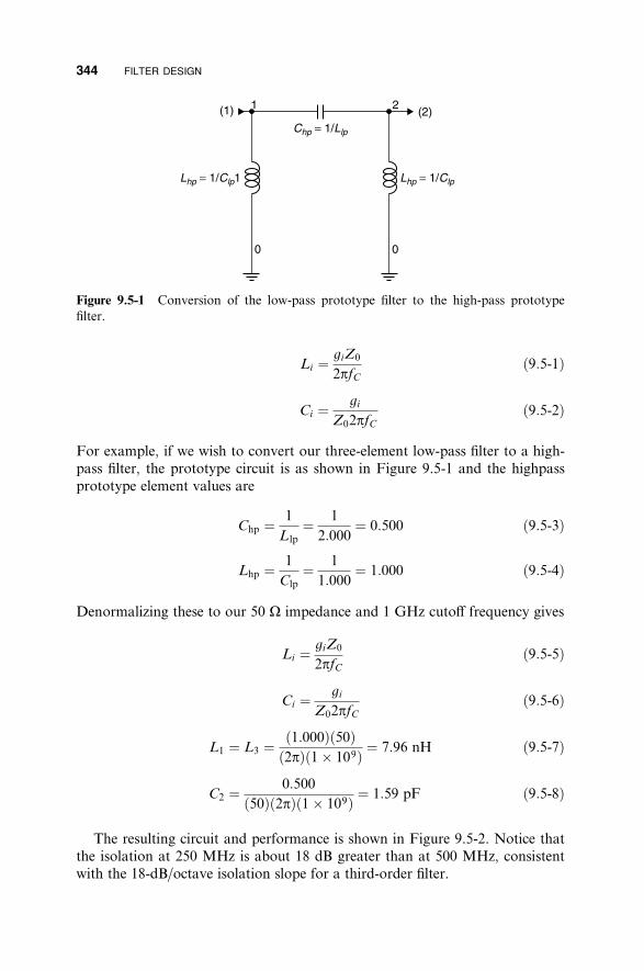
344 FILTER DESIGN
(1) 1
0
2
Chp = 1/ Llp
Lhp = 1/ Clp1
(2)
0
Lhp = 1/ Clp
Figure 9.5-1 Conversion of the low-pass prototype filter to the high-pass prototypefilter.
Li ¼ giZ0
2pfCð9:5-1Þ
Ci ¼ gi
Z02pfCð9:5-2Þ
For example, if we wish to convert our three-element low-pass filter to a high-pass filter, the prototype circuit is as shown in Figure 9.5-1 and the highpassprototype element values are
1 1Chp ¼ ¼ ¼ 0:500 ð9:5-3Þ
Llp 2:000
1 1Lhp ¼ ¼ ¼ 1:000 ð9:5-4Þ
Clp 1:000
Denormalizing these to our 50 W impedance and 1 GHz cuto¤ frequency gives
Li ¼ giZ0 ð9:5-5Þ2pfC
giCi ¼ ð9:5-6Þ
Z02pfC
ð1:000Þð50ÞL1 ¼ L3 ¼ ¼ 7:96 nH ð9:5-7Þð2pÞð1� 109Þ
0:500C2 ¼ ¼ 1:59 pF ð9:5-8Þð50Þð2pÞð1� 109Þ
The resulting circuit and performance is shown in Figure 9.5-2. Notice thatthe isolation at 250 MHz is about 18 dB greater than at 500 MHz, consistentwith the 18-dB/octave isolation slope for a third-order filter.

BANDPASS FILTERS 345
Figure 9.5-2 Loss/isolation of the high-pass filter.
9.6 BANDPASS FILTERS
Lumped-element bandpass and bandstop filters can be designed by startingwith the low-pass and high-pass prototypes presented in the preceding sections.It is also possible to design transmission equivalents to these filters usingRichard’s transformation and Kuroda’s identities [2, Sec. 9.5]. We will coverthese topics shortly. For these reasons the low-pass and high-pass prototypesare important beyond their immediate importance as lumped-element filters.This and the following sections will concentrate on the lumped-element filters,which are common in high frequency applications. Their use extends well into

346 FILTER DESIGN
Figure 9.6-1 Transformation relations to convert the low-pass prototype filter to abandpass prototype filter.
the microwave frequency bands as integrated circuit techniques allow realiza-tion of the small values of L and C that they require.
To design a bandpass filter starting with a low-pass prototype [1, p. 146](Fig. 9.6-1):
1. Define the following:
fl ¼ lower 3-dB cuto¤ frequency ð9:6-1Þfu ¼ upper 3-dB cuto¤ frequency ð9:6-2Þf0 ¼ geometric center frequencypffiffiffiffiffiffiffiffi f0 ¼ fl fu ð9:6-3Þ
BW ¼ fu � fl ¼ absolute bandwidth ð9:6-4ÞBW
bw ¼ ¼ fractional bandwidth ð9:6-5Þf0
Percentage bandwidth ¼ 100%ðbwÞ ð9:6-6Þ
2. Replace each series inductor with a series capacitor and series inductorresonator.
3. Replace each shunt capacitor with a shunt capacitor and parallel shuntinductor resonator.
4. Create the prototype (normalized) bandpass filter, assigning its elementsthe values shown below.

BANDPASS FILTERS 347
Transformed shunt elements:
Cbp-shunt ¼ Clp
bwð9:6-7Þ
1Lbp-shunt ¼
Cbp-shuntð9:6-8Þ
Transformed series elements:
Lbp-series ¼ Llp
bwð9:6-9Þ
1Cbp-series ¼
Lbp-seriesð9:6-10Þ
5. Denormalize all elements to obtain the final filter design. Note: Use f0 inplace of fc. Thus,
giZ0Li ¼ ð9:6-11Þ
2pf0gi
Ci ¼ ð9:6-12ÞZ02pf0
We now design a bandpass example based on our previous three-elementlow-pass prototype (Fig. 9.6-2). Suppose we wish a 3-dB passband from 800 to1200 MHz. Then, BW ¼ 400 MHz andpffiffiffiffiffiffiffiffiffiffiffiffiffiffiffiffiffiffiffiffiffiffiffiffiffi
f0 ¼ ð800Þð1200Þ ¼ 979:8 MHz
bw ¼ 400=979:8 ¼ 0:4082
Figure 9.6-2 Schematic for the transition from low-pass to band-pass filter prototype.

348 FILTER DESIGN
Figure 9.6-3 Denormalized bandpass filter schematic.
First, performing the prototype (normalized circuit) conversion:
c1 ¼ c3 ¼ clp 1:000¼ ¼ 2:4498bw 0:4082
1 1l1 ¼ l3 ¼ ¼ ¼ 0:4082
c1 2:4498
llp 2:000l2 ¼ ¼ ¼ 4:8996
bw 0:4082
1 1c2 ¼ ¼ ¼ 0:2041
l2 4:8996
where the lowercase letters designate the impedance and frequency normalizedprototype filter. Next, denormalize the circuit (Fig. 9.6-3).
c1 2:4498C1 ¼ C3 ¼ ¼ ¼ 7:9628 pF
Z02pf0 ð50Þð2pÞð979:8� 106Þl1Z0 ð0:4082Þð50Þ
L1 ¼ L3 ¼ ¼ ¼ 3:315 nH2pf0 ð2pÞð979:8� 106Þ
l2Z0 ð4:8996Þð50ÞL2 ¼ ¼ ¼ 39:7936 nH
2pf0 ð2pÞð979:8� 106Þ c2 0:2041
C2 ¼ ¼ ¼ 0:66306 pFZ02pf0 ð50Þð2pÞð979:8� 106Þ
The performance of this design can be seen in Figure 9.6-4, which shows theexpanded insertion loss on the left y axis and the isolation on the right y axis.The 3-dB bandwidth extends from 800 to 1200 MHz, as was intended by de-sign. Also note the steep isolation ‘‘skirts’’ of the performance plot. At 500 and2000 MHz, for frequencies that are an octave removed from the center fre-quency of about 1000 MHz, the isolation is nearly 36 dB. This is appropriatefor a N ¼ 6 filter, the number of nontrivial elements in the circuit of Figure

BANDSTOP FILTERS 349
Figure 9.6-4 Calculated loss/isolation of the denormalized bandpass filter.
9.6-3. A consequence of scaling a bandpass filter from a low-pass prototype isthat the order, N, of the filter is doubled.
9.7 BANDSTOP FILTERS
The design procedure for bandstop filters is similar to that of bandpass filters.However, for the bandstop filters the series resonant circuits are in shunt withthe transmission line and the parallel resonant circuits are in series (Fig. 9.7-1).
The shunt resonator elements are found from [1, p. 151]
1Lbs-shunt ¼
Clpbwð9:7-1Þ
1Cbs-shunt ¼
Lbs-shuntð9:7-2Þ
and the series resonator elements are found as
1Cbs-series ¼
Llpbwð9:7-3Þ
1Lbs-series ¼
Cbs-seriesð9:7-4Þ

350 FILTER DESIGN
Figure 9.7-1 Developing a bandstop filter from the low-pass prototype.
Following our three-element filter examples, suppose we wish to design abandstop filter with stopband from 800 to 1200 MHz. The steps are as follows.Using (9.7-1) to (9.7-4),
1 1l1 ¼ l3 ¼ ¼ ¼ 2:4498
clpbw ð1:000Þð0:4082Þ1 1
c1 ¼ c3 ¼ ¼ ¼ 0:4082l1 2:4498
1 1c2 ¼ ¼ ¼ 1:2249
llpbw ð2:000Þð0:4082Þ1 1
l2 ¼ ¼ ¼ 0:8164c2 1:2249
After computing the values of the normalized bandstop prototype from (9.7-1)to (9.7-4), the elements are denormalized, in the manner used for the bandpassfilter. Denormalizing,
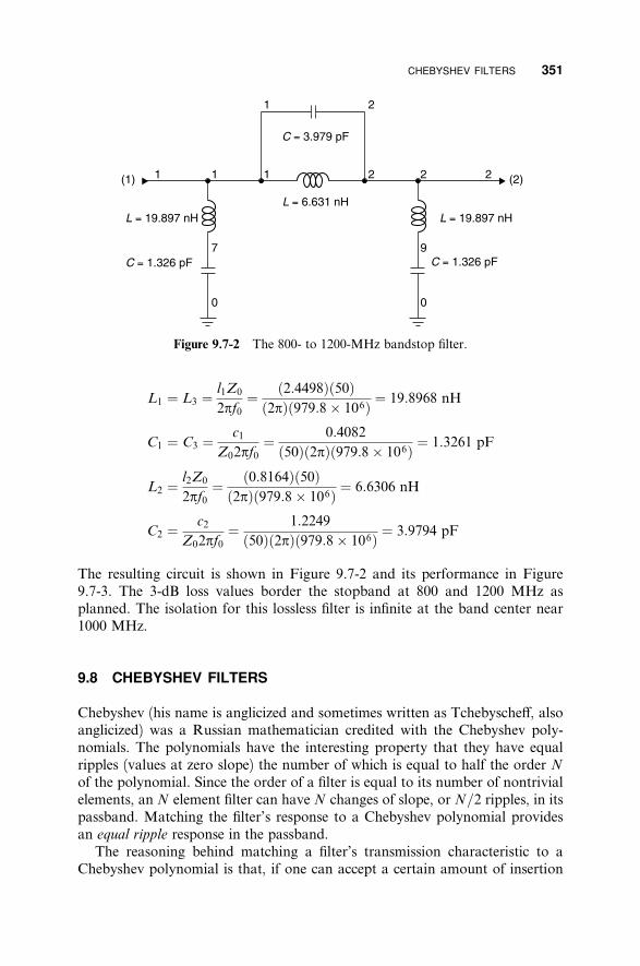
CHEBYSHEV FILTERS 351
Figure 9.7-2 The 800- to 1200-MHz bandstop filter.
l1Z0 ð2:4498Þð50ÞL1 ¼ L3 ¼ ¼ ¼ 19:8968 nH
2pf0 ð2pÞð979:8� 106Þc1 0:4082
C1 ¼ C3 ¼ ¼ ¼ 1:3261 pFZ02pf0 ð50Þð2pÞð979:8� 106Þ
l2Z0 ð0:8164Þð50ÞL2 ¼ ¼ ¼ 6:6306 nH
2pf0 ð2pÞð979:8� 106Þ c2 1:2249
C2 ¼ ¼ ¼ 3:9794 pFZ02pf0 ð50Þð2pÞð979:8� 106Þ
The resulting circuit is shown in Figure 9.7-2 and its performance in Figure9.7-3. The 3-dB loss values border the stopband at 800 and 1200 MHz asplanned. The isolation for this lossless filter is infinite at the band center near1000 MHz.
9.8 CHEBYSHEV FILTERS
Chebyshev (his name is anglicized and sometimes written as Tchebysche¤, alsoanglicized) was a Russian mathematician credited with the Chebyshev poly-nomials. The polynomials have the interesting property that they have equalripples (values at zero slope) the number of which is equal to half the order Nof the polynomial. Since the order of a filter is equal to its number of nontrivialelements, an N element filter can have N changes of slope, or N=2 ripples, in itspassband. Matching the filter’s response to a Chebyshev polynomial providesan equal ripple response in the passband.
The reasoning behind matching a filter’s transmission characteristic to aChebyshev polynomial is that, if one can accept a certain amount of insertion

352 FILTER DESIGN
Figure 9.7-3 Calculated loss/isolation of the 800- to 1200-MHz bandstop filter.
loss at the band edges of a filter, perhaps that same loss allowance could betolerated anywhere within the passband. If this is acceptable, then, for a givenwidth passband, the Chebyshev filter response yields a lower peak value ofpassband loss or a wider bandwidth for the same peak passband loss.
However, to design Chebyshev filters, we require a separate table of proto-
type values for each value of maximum ripple. Another consequence of the lossripple is that even-order Chebyshev filters cannot have equal source and load
resistances. This is because the even-order filters must have a mismatch at zerofrequency, and this can only occur if source and load resistances are corre-spondingly di¤erent. Designing filters that are only odd-order circumvents thisproblem; source and load can have equal impedances.
For the filter tables, it is assumed that the source impedance, gð0Þ, is unity,and the last value in the table for a given order filter is the magnitude of therequired load resistance. We confine our examples to those having unity loadresistance.
Given these distinctions, the design of Chebyshev filters proceeds exactly aspresented for the Butterworth designs. Tables 9.8-1 to 9.8-5 give the normalizedlow-pass prototype values. Transformations to high-pass, bandpass, and band-stop filters proceed as previously described. There are other sources for Che-byshev filter tables; however, these tables by Rhea are especially convenient touse because the g values yield filters having a cuto¤ frequency at the maximumripple value rather than at the 3-dB loss frequency.

TABLE9.8-1
Chebyshev
0.01-dBEqualRipple
(RLF
26.4
dB)
Ng1
g2
g3
g4
g5
g6
g7
g8
g9
g10
g11
20.4489
0.4078
0.9085
3
0.6292
0.9703
0.6292
1 4
0.7129
1.2004
1.3213
0.6476
5
0.7563
1.3049
1.5773
1.3049
6
0.7814
1.3600
1.6897
1.5350
7
0.7970
1.3924
1.7481
1.6331
8
0.8073
1.4131
1.7824
1.6833
9
0.8145
1.4271
1.8044
1.7125
10
0.8197
1.4370
1.8193
1.7311
0.9085
0.7563
11.4970
0.7098
0.9085
1.7481
1.3924
0.7970
11.8529
1.6193
1.5555
0.7334
0.9085
1.9058
1.7125
1.8044
1.4271
0.8145
11.9362
1.7590
1.9055
1.6528
1.5817
0.7446
1
Source:
After
Rhea
[1,pp.48–49].Usedwithpermission.
TABLE9.8-2
Chebyshev
0.0432-dBEqualRipple
(RLF
20dB)
Ng1
g2
g3
g4
g5
g6
g7
g8
g9
g10
g11
20.6648
0.5445
0.8190
3
0.8516
1.1032
0.8516
1 4
0.9314
1.2920
1.5775
0.7628
5
0.9714
1.3721
1.8014
1.3721
6
0.9940
1.4131
1.8933
1.5506
7
1.0080
1.4368
1.9398
1.6220
8
1.0171
1.4518
1.9667
1.6574
9
1.0235
1.4619
1.9837
1.6778
10
1.0281
1.4690
1.9952
1.6906
0.8190
0.9714
11.7253
0.8141
0.8190
1.9398
1.4368
1.0080
12.0237
1.6107
1.7726
0.8330
0.8190
2.0649
1.6778
1.9837
1.4619
1.0235
12.0882
1.7102
2.0642
1.6341
1.7936
0.8420
0.8190
Source:
After
Rhea
[1,pp.48–49].Usedwithpermission.
353

TABLE9.8-3
Chebyshev
0.10-dBEqualRipple
(RLF
16.4
dB)
Ng1
g2
g3
g4
g5
g6
g7
g8
g9
g10
g11
20.8431
0.6220
0.7378
3
1.0316
1.1474
1.0316
1 4
1.1088
1.3062
1.7704
0.8181
5
1.1468
1.3712
1.9750
1.3712
6
1.1681
1.4040
2.0562
1.5171
7
1.1812
1.4228
2.0967
1.5734
8
1.1898
1.4346
2.1199
1.6010
9
1.1957
1.4426
2.1346
1.6187
10
1.2000
1.4482
2.1445
1.6266
0.7378
1.1468
11.9029
0.8618
0.7378
2.0967
1.4228
1.1812
12.1700
1.5641
1.9445
0.8778
0.7378
2.2054
1.6167
2.1346
1.4426
1.1957
12.2254
1.6419
2.2046
1.5822
1.9629
0.8853
0.7378
Source:
After
Rhea
[1,pp.48–49].Usedwithpermission.
TABLE9.8-4
Chebyshev
0.20-dBEqualRipple
(RLF
13.5
dB)
Ng1
g2
g3
g4
g5
g6
g7
g8
g9
g10
g11
21.0379
0.6746
0.6499
3
1.2276
1.1525
1.2276
1 4
1.3029
1.2844
1.9762
0.8468
5
1.3395
1.3370
2.1661
1.3370
6
1.3598
1.3632
2.2395
1.4556
7
1.3723
1.3782
2.2757
1.5002
8
1.3804
1.3876
2.2964
1.5218
9
1.3861
1.3939
2.3094
1.5340
10
1.3901
1.3983
2.3181
1.5417
0.6499
1.3395
12.0974
0.8838
0.6499
2.2757
1.3782
1.3723
12.3414
1.4925
2.1349
0.8972
0.6499
2.3728
1.5340
2.3094
1.3939
1.3861
12.3905
1.5537
2.3720
1.5066
2.1514
0.9035
0.6499
Source:
After
Rhea
[1,pp.48–49].Usedwithpermission.
354
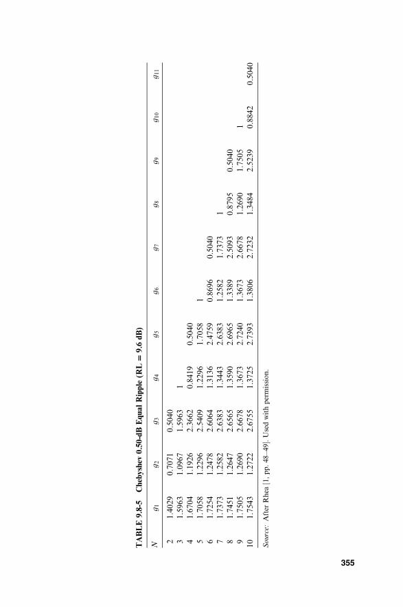
TABLE9.8-5
Chebyshev
0.50-dBEqualRipple
(RLF
9.6
dB)
Ng1
g2
g3
g4
g5
g6
g7
g8
g9
g10
g11
21.4029
0.7071
0.5040
3
1.5963
1.0967
1.5963
1 4
1.6704
1.1926
2.3662
0.8419
5
1.7058
1.2296
2.5409
1.2296
6
1.7254
1.2478
2.6064
1.3136
7
1.7373
1.2582
2.6383
1.3443
8
1.7451
1.2647
2.6565
1.3590
9
1.7505
1.2690
2.6678
1.3673
10
1.7543
1.2722
2.6755
1.3725
0.5040
1.7058
12.4759
0.8696
0.5040
2.6383
1.2582
1.7373
12.6965
1.3389
2.5093
0.8795
0.5040
2.7240
1.3673
2.6678
1.2690
1.7505
12.7393
1.3806
2.7232
1.3484
2.5239
0.8842
0.5040
Source:
After
Rhea
[1,pp.48–49].Usedwithpermission.
355

356 FILTER DESIGN
Figure 9.8-1 Comparison of element values for Butterworth and Chebyshev filters. (a)Three-section 50-W Butterworth low-pass filter with fC ¼ 1 GHz. (b) Three-section,50-W, 0.5-dB ripple, Chebyshev low-pass filter with fC ¼ 1 GHz.
As an example, a 50-W, three-section, 0.2-dB ripple Chebyshev low-passfilter is designed using the procedure described for the low-pass Butterworthfilter. The circuit is shown in Figure 9.8-1 and its performance compared to thethree-element Butterworth low-pass filter in Figure 9.8-2.
Notice that the Chebyshev filter has a maximum loss up to 1 GHz of only0.5 dB, while the Butterworth filter has 3.0-dB loss at 1 GHz. Also, the Che-byshev filter has a steeper slope outside the passband, yielding slightly greaterisolation at frequencies above the passband.
9.9 PHASE AND GROUP DELAY
Previously, we described the transfer function H of the network. In the filterperformance described up to now, we have been concerned only with theamplitude of the transfer function versus frequency. Usually, this is the pre-dominant characteristic that comes to mind when considering filters.
However, in communication systems the variation of phase shift with fre-quency through a network becomes of importance when the signal bandwidthis large, as when rapid rise time pulses or video information is transmitted.Then the phase variation with frequency through the network also must becontrolled.
The phase delay j (or phase shift) through a network is just the argument(angle) of the complex transfer function H. Any network having reactive ele-ments produces a delay in the signal propagation with time [1, pp. 34–36].
If a network passes all frequencies with equal amplitude attenuation and a
transmission phase j that increases linearly with frequency, the signal will be

PHASE AND GROUP DELAY 357
Figure 9.8-2 Calculated loss comparison of Butterworth and 0.5-dB-ripple Chebyshevlow-pass filters.
delayed and level shifted but not distorted. The phase delay of a network is
jtp ¼
oð9:9-1Þ
and the group delay is
td ¼ � qj ð9:9-2Þqo
The group delay (also called envelope delay) is related to the time required forthe envelope of a signal to transverse the network. These characteristics wereintroduced in Section 4.12 through phase and group velocities.
Unfortunately, good frequency selectivity and constant group delay aremutually exclusive in the passive ladder networks we have been considering.Signal distortion occurs when di¤erent frequency components of the compositesignal are unequally delayed. This di¤erence is called di¤erential delay. Di¤er-ential group delay is the absolute di¤erence in the group delay at two specifiedfrequencies. It will be seen that the more frequency selective the filter network,the greater the di¤erential delay within the passband. A class of filters thatminimizes this distortion is the Bessel filter. Table 9.9-1 lists the Bessel g valuesfor this response.

TABLE9.9-1
BesselPrototypeFiltergValues
a
Ng1
g2
g3
g4
g5
g6
g7
g8
g9
g10
g11
20.5755
2.1478
1 3
0.3374
0.9705
2.2034
1 4
0.2334
0.6725
1.0815
2.2404
5
0.1743
0.5072
0.8040
1.1110
6
0.1365
0.4002
0.6392
0.8538
7
0.1106
0.3259
0.5249
0.7020
8
0.0919
0.2719
0.4409
0.5936
9
0.0780
0.2313
0.3770
0.5108
10
0.0672
0.1998
0.3270
0.4454
1 2.2582
11.1126
2.2645
10.8690
1.1052
2.2659
10.7303
0.8695
1.0956
2.2656
10.6306
0.7407
0.8639
1.0863
2.2649
10.5528
0.6493
0.7420
0.8561
1.0781
2.2641
1
Source:
After
Rhea
[1,p.49].Usedwithpermission.
aCuto¤frequency
loss
¼3dBandsourceresistance
¼1:0.
TABLE9.9-2
BesselEqual-Ripple
Phase
Error0:05�FiltergValues
a
Ng1
g2
g3
g4
g5
g6
g7
g8
g9
g10
g11
20.6480
2.1085
1 3
0.4328
0.0427
2.2542
1 4
0.3363
0.7963
1.1428
2.2459
5
0.2751
0.6541
0.8892
1.1034
6
0.2374
0.5662
0.7578
0.8760
7
0.2085
0.4999
0.6653
0.7521
8
0.1891
0.4543
0.6031
0.6750
9
0.1718
0.4146
0.5498
0.6132
10
0.1601
0.3867
0.5125
0.5702
1 2.2873
11.1163
2.2448
10.8749
1.0671
2.2845
10.7590
0.8427
1.0901
2.2415
10.6774
0.7252
0.8450
1.0447
2.2834
10.6243
0.6557
0.7319
0.8178
1.0767
2.2387
1
Source:
After
Rhea
[1,p.50].Usedwithpermission.
aCuto¤frequency
loss
¼3dB,sourceresistance
¼1:0.
358

TABLE9.9-3
BesselEqual-Ripple
Phase
Error0:5�FiltergValues
a
Ng1
g2
g3
g4
g5
g6
g7
g8
g9
g10
g11
20.8245
1.9800
1 3
0.5534
1.0218
2.4250
1 4
0.4526
0.7967
1.2669
2.0504
5
0.3658
0.6768
0.9513
1.0113
6
0.3313
0.5984
0.8390
0.7964
7
0.2876
0.5332
0.7142
0.6988
8
0.2718
0.4999
0.6800
0.6312
9
0.2347
0.4493
0.5914
0.5747
10
0.2359
0.4369
0.5887
0.5428
1 2.4446
11.2734
2.0111
10.9219
0.9600
2.4404
10.8498
0.7447
1.3174
1.9626
10.7027
0.6552
0.8944
0.9255
2.4332
10.7034
0.5827
0.8720
0.6869
1.4317
1.8431
1
Source:
Rhea
[1,p.50].Usedwithpermission.
aA
a¼
3dB,Gð0Þ¼
1:0.
359

360 FILTER DESIGN
Figure 9.9-1 Bessel 50-W, low-pass filter with 3-dB cuto¤ at 1 GHz.
In addition to the pure Bessel prototype, additional tables provide an ‘‘equalphase ripple’’ in the transmission phase similar to the Chebyshev designs, whichprovide equal loss ripple in the passband attenuation. Allowing increasingphase ripple in the passband improves the rejection band performance of theBessel filter. Tables 9.9-2 and 9.9-3 for 0.05� and 0.5� equal-ripple phase errorgive the g values for these filters.
Constructing our three-element filter using the Bessel response yields thecircuit shown in Figure 9.9-1 and the performance shown in Figure 9.9-2. Notethat the filter is not symmetric, as were the Butterworth and Chebyshev filters.
Viewing only amplitude response, one might consider the Bessel filter to beso inferior, even to the Butterworth filter, as to warrant no further consider-
Figure 9.9-2 Bessel low-pass filter compared in amplitude response to Butterworth andChebyshev filters of the same order.

FILTER Q 361
Figure 9.9-3 Group delay (in nanoseconds) comparison of Bessel, Chebyshev, andButterworth filters, all having three sections and 1 GHz cuto¤ frequency.
ation. However, considering the group delay performance reveals a consider-able advantage of the Bessel design.
The Bessel low-pass filter has nearly constant group delay up to 1000 MHz,its 3-dB cuto¤ frequency. The Chebyshev has a nearly 2 to 1 variation in groupdelay to its 0.5-dB cuto¤, and the Butterworth has an intermediate value ofgroup delay over the 0 to 1000 MHz band (Fig. 9.9-3). These data confirm thatthe greater the selectivity, the greater the delay variation and the greater the po-
tential signal distortion.
9.10 FILTER Q
To illustrate filter types, we have reviewed only lossless representations. Realfilters, of course, must be made with components having finite Q. The e¤ect offinite Q components on filter insertion loss in the passband is greatest in thosehaving the most frequency selectivity. The e¤ect of finite Q can be seen in theChebyshev low-pass filter shown in Figure 9.10-1. Both the L and C compo-nents are assumed to have the Q value listed.
In the case of the three-section Chebyshev low-pass filter, the lossless com-ponent assumption (actually Q ¼ 1,000,000 is the Genesys default if Q is notspecified) yields the expected 0.5-dB insertion loss over the passband of 0 to1000 MHz. However, setting all circuit elements to have Q ¼ 50 increases the

362 FILTER DESIGN
Figure 9.10-1 E¤ect of finite Q circuit elements on the performance of the Chebyshev0.5-dB ripple, 1 GHz cuto¤ frequency filter.
loss at the cuto¤ frequency of 1000 MHz to about 1 dB. Further reducing ele-ment Q to 10 results in about 3.5 dB of insertion loss at 1000 MHz, as seen inFigure 9.10-1.
However, this example should not be considered a reference scale of thepassband loss increase when circuit Q is 50 or 10. The change in passband lossdepends upon the selectivity of the filter as well.
Figure 9.10-2 shows a five-section Chebyshev filter having 0.1 dB pass-band ripple for the bandwidth 175 to 225 MHz. Its insertion loss response issimulated using Q ¼ 1,000,000 for all element values. This is shown in Figure9.10-3.
Next, the filter shown in Figure 9.10-2 has its element Q changed to 50. Theresulting performance is shown in Figure 9.10-4. A change of scale was madebecause the center frequency loss increased by 5 dB. Notice that not only hasthe center frequency loss increased by 5 dB, but the loss increase near the band

FILTER Q 363
Figure 9.10-2 Five-section 0.1-dB-ripple Chebyshev bandpass filter for 175 to 225MHz.
edges is much more, about 8 dB, resulting in a severe change in the passbandshape. This filter design is not intended as representing a filter whose executionis practical, but rather to show that the e¤ect of Q on passband loss depends onthe selectivity of the filter, itself.
This design example has very sharp passband skirts, theoretically. But real-izing such a design would require very low loss elements. Also note that theelements used in this simulation did not have parasitic inductance and capaci-tances, as discussed in Section 2.11. Inclusion of parasitics would make thisdesign even less practical to realize. The point of this example is that it isimportant to check proposed filter designs using realistic models for their ele-ments.
Figure 9.10-3 Calculated loss/isolation of five-section Chebyshev filter when L and C
elements have QU ¼ 1,000,000.

364 FILTER DESIGN
Figure 9.10-4 Calculated loss/isolation of the Chebyshev filter when elements haveQ ¼ 50.
9.11 DIPLEXER FILTERS
A frequency diplexer is a network that connects two networks that operate atdi¤erent frequencies to a common terminal. For example, two radios operatingat di¤erent frequency bands could be connected to a common antenna using afrequency diplexer. One commonly used realization of a frequency diplexerconsists of two complementary filters connected to a tee junction. One filter is ahigh pass and the other a low pass. For the diplexer function, both filters havethe same 3-dB cuto¤ frequency. Frequencies above the cuto¤ are directed alongone side of the tee junction; frequencies below the cuto¤ are directed along theother side of the tee junction.
The two filters are designed using the singly terminated method by whichthe tee end of the filter is designed for an infinite load impedance for the high-pass arm and a zero load impedance for the low-pass arm. Although it is notintuitively apparent, when two such filters are connected together it is foundthat a match is seen at all frequencies at the input to the tee. The input imped-ance of the two filters, Rin, is made equal to the desired system impedance, inthis case 50 W.
The tables given in Sections 9.3, 9.8 and 9.9 for Butterworth, Chebyshev,and Bessel filter designs are for doubly terminated filters, i.e., those having

DIPLEXER FILTERS 365
Figure 9.11-1 Singly terminated low-pass Butterworth filter with 3-dB cuto¤ frequencyof 12.5 MHz.
the same characteristic impedance at both ports, therefore cannot be used forthis design. Singly terminated designs are available with software, such as theFILTER program within the Genesys software suite.
Suppose we wish to build a diplexer having a 3-dB cuto¤ (transition fre-quency) of 12.5 MHz. This might be used to connect two radios to a commonantenna, with one radio operating below 10 MHz and the other operatingabove 16 MHz. The two singly terminated designs realized using the FILTERsoftware are shown in Figures 9.11-1 and 9.11-2. Notice that input port 1 iswell matched. The return loss is between 50 and 60 dB and the signal input atport 1 is routed smoothly between ports 2 and 3 according to the frequency.Notice also that this is a means of providing filtering one port of which port 1 ismatched at all frequencies.
When the two filters are connected together at their respective zero and infi-nite impedance ports the resulting diplexer shown in Fig. 9.11-3 is obtained.
Figure 9.11-2 Singly terminated high-pass Butterworth filter with 3-dB cuto¤ fre-quency of 12.5 MHz.

366 FILTER DESIGN
Figure 9.11-3 Frequency diplexer having matched transmission at all frequencies fromits common port.
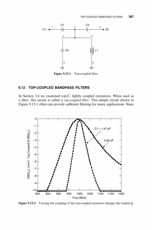
TOP-COUPLED BANDPASS FILTERS 367
Figure 9.12-1 Top-coupled filter.
9.12 TOP-COUPLED BANDPASS FILTERS
In Section 3.4 we examined top-C, lightly coupled resonators. When used asa filter, this circuit is called a top-coupled filter. This simple circuit shown inFigure 9.12-1 often can provide su‰cient filtering for many applications. Since
Figure 9.12-2 Varying the coupling of the top-coupled resonator changes the loaded Q.
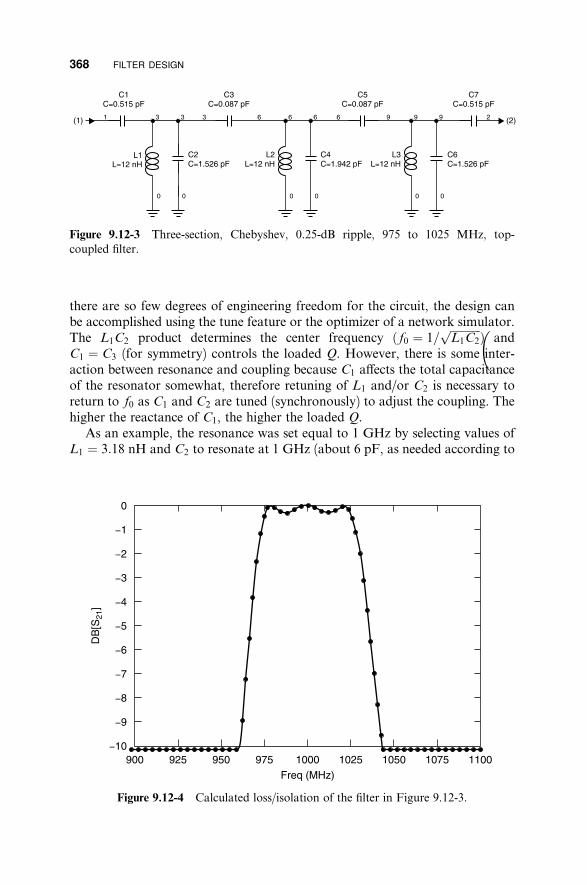
368 FILTER DESIGN
Figure 9.12-3 Three-section, Chebyshev, 0.25-dB ripple, 975 to 1025 MHz, top-coupled filter.
there are so few degrees of engineering freedom for the circuit, the design canbe accomplished using the tune feature or the optimizer of a network simulator.The L1C2 product determines the center frequency ð f0 ¼ 1=
pffiffiffiffiffiffiffiffiffiffiffi Þ andL1C2
C1 ¼ C3 (for symmetry) controls the loaded Q. However, there is some inter-action between resonance and coupling because C1 a¤ects the total capacitanceof the resonator somewhat, therefore retuning of L1 and/or C2 is necessary toreturn to f0 as C1 and C2 are tuned (synchronously) to adjust the coupling. Thehigher the reactance of C1, the higher the loaded Q.
As an example, the resonance was set equal to 1 GHz by selecting values ofL1 ¼ 3:18 nH and C2 to resonate at 1 GHz (about 6 pF, as needed according to
Figure 9.12-4 Calculated loss/isolation of the filter in Figure 9.12-3.

ELLIPTIC FILTERS 369
the coupling). If placed directly in parallel with a 50-W source and 50-W load,the resonator would have a loaded Q of nearly unity and a very broad 3-dBbandwidth. Using a coupling capacitance of C1 ¼ C3 ¼ 0:82 pF, the 3-dBbandwidth is 50 MHz with f0 loss of 0.3 dB. This is equivalent to QL ¼ 20 asshown in Figure 9.12-2. To accomplish the same QL with direct coupling wouldrequire that the inductance be reduced by a factor of 20, or L2 ¼ 0:2 nH, a veryimpractically small value. Increasing the coupling capacitors to 1.47 pF gives a3-dB bandwidth of 150 MHz with f0 loss of 0.1 dB.
The coupling that results in 0-dB insertion loss at f0 is called critical cou-pling. For this simple circuit, critical coupling and the desired 3-dB bandwidthmay not be accomplished simultaneously. More selectivity can be obtainedusing multiple resonators. A three-section, Chebyshev filter with 0.25 dB rippleover the 975 to 1025 MHz bandwidth is shown in Figure 9.12-3 and its lossperformance shown in Figure 9.12-4. Notice that the resonators have 12-nHinductors, more practical to realize than those which would be necessary for adirect coupled resonator.
9.13 ELLIPTIC FILTERS
Just as it is desirable to place a ripple response in the passband, there can beadvantages to having equal isolation ripple in the stopband. This can makepossible a more rapid increase of isolation with frequency at the passband edge.Filters having a ripple in the stopband can be realized using elliptic filter de-signs.
While the sharp increase in isolation just outside the passband can be veryadvantageous for some applications, it comes at the price of reduced isolation at
frequencies considerably higher than the filter’s cuto¤ frequency.We will compare the performance of a Chebyshev 0.5-dB- (passband) ripple,
five-section, 1-GHz low-pass filter with a comparably designed elliptic filterdesigned for the same cuto¤. The straight Chebyshev filter is shown in Figure9.13-1.
The elliptic filter, designed using the Genesys SFILTER software, to similarspecifications, is shown in Figure 9.13-2. Notice that the stopband attenuationdrops more rapidly just above the 1 GHz cuto¤ frequency, due to the parallelresonant series elements, but that the maximum isolation is only 48 dB, even atfrequencies far from cuto¤. This limit on the isolation is the performance trade-o¤ for the more rapid isolation increase near the cuto¤ frequency.
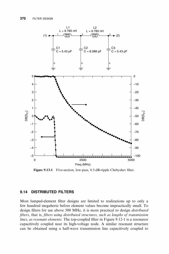
370 FILTER DESIGN
Figure 9.13-1 Five-section, low-pass, 0.5-dB-ripple Chebyshev filter.
9.14 DISTRIBUTED FILTERS
Most lumped-element filter designs are limited to realizations up to only afew hundred megahertz before element values become impractically small. Todesign filters for use above 500 MHz, it is more practical to design distributed
filters, that is, filters using distributed structures, such as lengths of transmission
lines, as resonant elements. The top-coupled filter in Figure 9.12-1 is a resonatorcapacitively coupled near its high-voltage node. A similar resonant structurecan be obtained using a half-wave transmission line capacitively coupled to

DISTRIBUTED FILTERS 371
Figure 9.13-2 Five-section, low-pass elliptic filter.
generator and load, as shown in Figure 9.14-1 and its loss performance isshown in Figure 9.14-2.
The half-wave resonator stores energy in the form of standing waves withvoltage maxima at its two ends. Thus, the capacitive coupling shown is electri-cally similar to that of the top-coupled filter previously described. The 3-dBbandwidth of this example filter is only 8 MHz with f0 ¼ 1000 MHz, yieldingan e¤ective QL ¼ 125. Yet the resonator consists of only a length of 50-Wtransmission line, an easily realized structure. The coupling capacitors might berealized as gaps in the transmission line and designed either using an EM sim-

372 FILTER DESIGN
Figure 9.14-1 End-coupled, half-wave resonator filter.
Figure 9.14-2 Calculated loss/isolation of the half-wave filter shown in Figure 9.14-1.
Figure 9.14-3 Recurring passbands of the half-wave resonator filter.

DISTRIBUTED FILTERS 373
Figure 9.14-4 Three-section, half-wave resonator filter with f0 ¼ 1 GHz designed usingthe optimizer of the network simulator.
ulator or empirically, but once designed, could be reproduced by means of theprinting process used to form the transmission line circuitry.
The circuit was modeled using a network simulator, and the resonator’slength was adjusted in conjunction with the adjustment of the coupling ca-pacitors, C1 and C2, to return the resonance to 1 GHz. As with the lumped-element, top-coupled filter, the coupling capacitors lower the resonant fre-quency; so readjustment of the line length was needed to return f0 to 1 GHz.Notice that the isolation is greater than 20 dB at 960 and 1040 MHz. On theother hand, transmission line filters of which this is an example have recurringpassbands, in this case roughly at integer multiples of f0, as shown in Figure9.14-3.
As with lumped filters, multiple half-wave resonators can be used. Figure9.14-4 shows a three-resonator circuit designed using the optimizer of the net-work simulator. Initial values of 180� at 1 GHz and 50 W were selected for the
Figure 9.14-5 Calculated loss/isolation of the filter described in Figure 9.14-4.
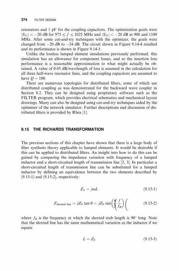
� �
374 FILTER DESIGN
resonators and 1 pF for the coupling capacitors. The optimization goals werejS11j < �20 dB for 975a f a 1025 MHz and jS21j < �20 dB at 900 and 1100MHz. After some cut-and-try techniques with the optimizer, the goals werechanged from �20 dB to �24 dB. The circuit shown in Figure 9.14-4 resultedand its performance is shown in Figure 9.14-5.
Unlike the lossless lumped element simulations previously performed, thissimulation has an allowance for component losses, and so the insertion lossperformance is a reasonable approximation to what might actually be ob-tained. A value of 0.05 dB/wavelength of loss is assumed in the calculation forall three half-wave resonator lines, and the coupling capacitors are assumed tohave Q ¼ 100.
There are numerous topologies for distributed filters, some of which usedistributed coupling as was demonstrated for the backward wave coupler inSection 8.2. They can be designed using proprietary software such as theFILTER program, which provides electrical schematics and mechanical layoutdrawings. Many can also be designed using cut-and-try techniques aided by theoptimizer of the network simulator. Further descriptions and discussion of dis-tributed filters is provided by Rhea [1].
9.15 THE RICHARDS TRANSFORMATION
The previous sections of this chapter have shown that there is a large body offilter synthesis theory applicable to lumped elements. It would be desirable ifthis can be applied to distributed filters. An insight into how to do this can begained by comparing the impedance variation with frequency of a lumpedinductor and a short-circuited length of transmission line [2, 3]. In particular ashort-circuited length of transmission line can be substituted for a lumpedinductor by defining an equivalence between the two elements described by(9.15-1) and (9.15-2), respectively:
ZL ¼ joL ð9:15-1Þ
p fZshorted line ¼ jZ0 tan y ¼ jZ0 tan ð9:15-2Þ
2 fR
where fR is the frequency at which the shorted stub length is 90� long. Notethat the shorted line has the same mathematical variation as the inductor if weequate
L ¼ Z0 ð9:15-3Þ

� �
� �
THE RICHARDS TRANSFORMATION 375
Figure 9.15-1 With the Richards transfor-mation, inductors are replaced by short-circuited transmission lines and capacitors byopen-circuited transmission lines.
where L is in henrys and Z0 in ohms, and define a new frequency variable, W,according to
p fjW ¼ j tan ð9:15-4Þ
2 fR
The expression in (9.15-4) is the Richards frequency transformation (Fig.9.15-1).
Under this same transformation the behavior of an open-circuited transmis-sion line is mathematically equivalent to that of a capacitor:
YC ¼ joC ð9:15-5Þ
p fYopen-circuited line ¼ jY0 tan y ¼ jY0 tan ð9:15-6Þ
2 fR
The mathematical equivalence that we propose does not mean that an in-ductor’s reactance has the same frequency variation as a shorted line, or thata capacitor’s reactance variation is the same as that of an open-circuited line,except in the new frequency domain defined by (9.15-4).
As an example of this equivalence, we will design a three-element, low-pass,Chebyshev filter with 0.5-dB ripple, fC ¼ 1 GHz and stub resonant frequencyfR ¼ 1:4 GHz. Notice that fR is an additional degree of freedom in the dis-tributed circuit design. In the low-pass prototype fR ¼ y.
Since this is a Chebyshev 0.5-dB ripple design, the loss at 1 GHz will be0.5 dB and will not exceed this value between 0 and 1 GHz. For this example,we use the tee circuit. The gi values, from Table 9.8-5 are
gi ¼ 1:5963 1:0967 1:5963 1:000 ðloadÞ

� �
376 FILTER DESIGN
Figure 9.15-2 The 0.5-dB ripple, 50-W, Chebyshev low-pass filter.
The corresponding lumped-element tee circuit is obtained by frequency andimpedance scaling the gi values using (9.4-2) and (9.4-4) as shown in Figure9.15-2 along with its frequency response.
Recall from Section 9.4 that the gi values are the respective series reactancesand shunt susceptances of the filter elements at fC . This means that the shortedtransmission line Z01 that replaces a series inductor must have a reactance at fCof
g1Z0 ¼ Z01WC
where
p 1:0 GHzWC ¼ tan ¼ 2:08
2 1:4 GHz
Then
g1Z0 1:5963ð50 WÞZ01 ¼ Z03 ¼ ¼ ¼ 38:4 W
WC 2:08
Similarly, the open-circuited stub Y02 that replaces a shunt capacitor in thelow-pass prototype filter must have a susceptance at fC given by
g2Y0 ¼ g2 ¼ Y02WCZ0
from which
g2 1:0967Y02 ¼ ¼ ¼ 0:01050
Z0WC ð50 WÞ2:08
W
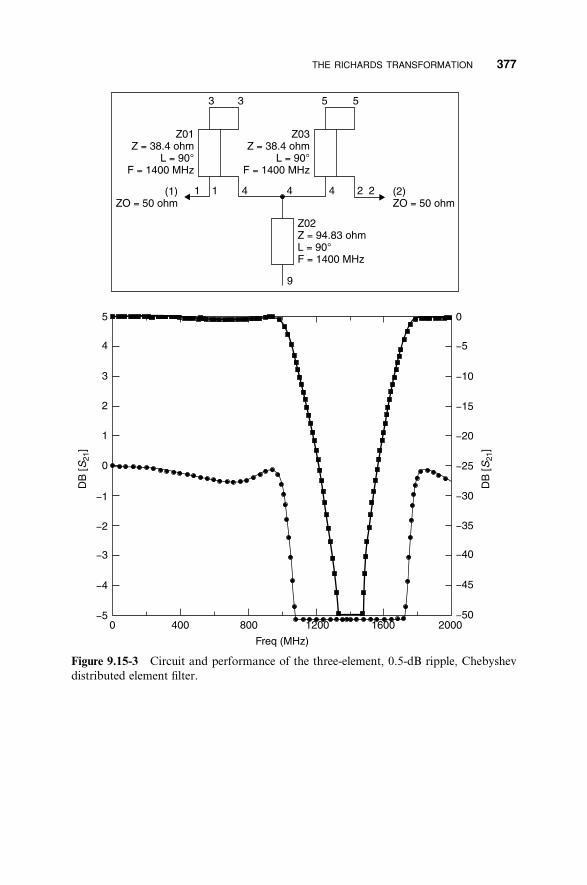
THE RICHARDS TRANSFORMATION 377
Figure 9.15-3 Circuit and performance of the three-element, 0.5-dB ripple, Chebyshevdistributed element filter.

378 FILTER DESIGN
Figure 9.15-4 Extended frequency plot of the distributed filter of Figure 9.15-3.
and
1Z02 ¼
Y02¼ 94:83 W
This circuit and its performance is shown in Figure 9.15-3.Notice that the frequency translation has shrunk the frequency domain of
the low-pass prototype circuit of Figure 9.15-1 from 0a f ay to the new Wdomain for which 0a f a fR. That is, while the entire frequency response ofthe low-pass lumped-element circuit extended from zero to infinity in fre-quency, that loss performance region has been condensed into the range fromzero to fR, the resonant frequency of the stubs in the distributed filter. At thesame time the transformation has introduced a new realm of circuit behaviorbeyond fR. In this new domain the loss performance is repeated, mirrorlike,about fR thereby creating a bandstop filter response. In a similar fashion, abandpass filter could be created based on the design of a high-pass lumped-element filter.
The stopband of the new distributed filter extends equally on either side offR out to fC . Thus the stopband is 1.0 to 1.8 GHz. Since the filter’s perfor-mance is defined by transmission line lengths, the center frequency of the stop-
band is the arithmetic mean, 1.4 GHz, of its fC band edge frequencies, 1.0 and
1.8 GHz. Also, since this is a distributed element filter using quarter-wave res-onators, its performance recurs at odd integer multiples of fR ð fR; 3fR; 5fR; . . .Þ,as shown in Figure 9.15-4.
This distributed filter can be realized in coaxial transmission line by embed-ding the two short-circuit terminated stubs within the center conductor of themain transmission line, as shown in Figure 9.15-5.

9.16 KURODA’S IDENTITIES
The circuit of Figure 9.15-5 can be realized in coaxial transmission line but notin microstrip or stripline, as would often be desirable, due to the necessity forseries short-circuited stubs. Kuroda’s identities of the first kind (Fig. 9.16-1) al-
Figure 9.15-5 Cross-sectional sketch of a coaxial line realization of the distributedbandpass filter with series stubs embedded within the center conductor of the main line.
Figure 9.16-1 Kuroda’s identities of the first kind applied to transmission lines:(a) ZC ¼ nZ0 and YE ¼ ðn� 1Þ=nZ0 where n ¼ 1þ Z1=Z0. (b) ZC ¼ Z0=n and ZE ¼ððn� 1Þ=nÞZ0 where n ¼ 1þ Y1Z0.
KURODA’S IDENTITIES 379

380 FILTER DESIGN
low the replacement of a series-shorted stub and a cascade Z0 line with a shuntopen-circuited stub and a di¤erent cascade line, and vice versa [2, 4]. Note thatall lines have the same electrical length, y. Given this requirement and the for-mulas in Figure 9.16-1, the Kuroda equivalences apply at all frequencies.
Notice that the series-shorted stub must be combined with a section of Z0
line before the equivalence with an open-circuited shunt stub can be made. Theaddition to the input and output of sections of Z0 transmission line has noe¤ect on the VSWR or insertion loss of the filter, but it does cause the trans-formed filter to have added electrical length, which may be significant in someapplications. The circuits otherwise are equivalent.
We transform the distributed filter of Figure 9.15-3 to one using all shuntstubs using Kuroda’s identity in Figure 9.16-1a to transform the series short-circuited stubs to shunt open-circuited stubs. In this filter Z01 ¼ Z03 ¼ 38:4 W.
Figure 9.16-2 Circuit and performance of the Chebyshev filter transformed to an allshunt stub format.
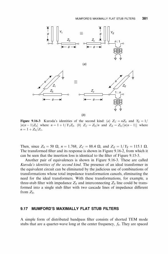
MUMFORD’S MAXIMALLY FLAT STUB FILTERS 381
Figure 9.16-3 Kuroda’s identities of the second kind: (a) ZC ¼ nZ0 and YE ¼ 1=½nðn� 1ÞZ0� where n ¼ 1þ 1=Y1Z0. (b) ZC ¼ Z0=n and ZE ¼ Z0=½nðn� 1Þ� wheren ¼ 1þ Z0=Z1.
Then, since Z0 ¼ 50 W, n ¼ 1:768, ZC ¼ 88:4 W, and ZE ¼ 1=YE ¼ 115:1 W.The transformed filter and its response is shown in Figure 9.16-2, from which itcan be seen that the insertion loss is identical to the filter of Figure 9.15-3.
Another pair of equivalences is shown in Figure 9.16-3. These are calledKuroda’s identities of the second kind. The presence of an ideal transformer inthe equivalent circuit can be eliminated by the judicious use of combinations oftransformations whose total impedance transformation cancels, eliminating theneed for the ideal transformers. With these transformations, for example, athree-stub filter with impedance Z0 and interconnecting Z0 line could be trans-formed into a single stub filter with two cascade lines of impedance di¤erentfrom Z0.
9.17 MUMFORD’S MAXIMALLY FLAT STUB FILTERS
A simple form of distributed bandpass filter consists of shorted TEM modestubs that are a quarter-wave long at the center frequency, f0. They are spaced

382 FILTER DESIGN
TABLE 9.17-1 Normalized Stub Admittances for
Mumford’s Quarter-Wave Shorted Stub Filters [5]
(a) Three-Stub Filters
10 log K3 k1 k2
�12.728 0.100 0.200�0.944 0.300 0.600þ5.460þ10.138þ15.560þ21.156þ27.604þ31.904þ35.563
0.5000.7001.0001.4002.0002.5003.000
1.0001.4002.0002.8004.0005.0006.000
(b) Four-Stub Filters
10 log K4 k1 k2
�5.170 0.100 0.292þ3.253þ13.329þ25.668þ35.909þ44.873þ56.734
0.2000.4000.8001.3001.9003.000
0.5711.1092.1413.3954.8777.568
(c) Five-Stub Filters
10 log K5 k1 k2 k3
þ3.452þ13.577þ20.523þ26.002þ30.601þ38.160þ44.324þ54.172þ66.970þ77.874
0.1000.2000.3000.4000.5000.7000.9001.3002.0002.800
0.3660.6941.0051.3041.5962.1662.7243.8195.7027.829
0.5320.9891.4101.8082.1932.9333.6485.0387.40310.058
Source: From [5].
at quarter-wave intervals along the TEM mode main transmission line path.Mumford [5] analyzed this filter type for the maximally flat (Butterworth)transmission response and created tables of values for the characteristic admit-tances of the stubs relative to that of the main line. The stub admittances nor-
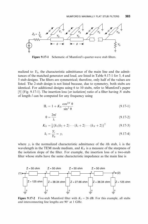
MUMFORD’S MAXIMALLY FLAT STUB FILTERS 383
Figure 9.17-1 Schematic of Mumford’s quarter-wave stub filters.
malized to Y0, the characteristic admitttance of the main line and the admit-tances of the matched generator and load, are listed in Table 9.17-1 for 3, 4 and5 stub designs. The filters are symmetrical; therefore, only half of the values arelisted. The 2-stub design is not listed because, due to symmetry, both stubs areidentical. For additional designs using 6 to 10 stubs, refer to Mumford’s paper[5] (Fig. 9.17-1). The insertion loss (or isolation) ratio of a filter having N stubsof length l can be computed for any frequency using
2Ncos yIL ¼ 1þ KN ð9:17-1Þ
sin2 y
2ply ¼ ð9:17-2Þ
l
KN ¼ 1 fk1ðk2 þ 2Þ � � � ðki þ 2Þ � � � ðkN þ 2Þg2 ð9:17-3Þ4
Yiki ¼ ¼ yi ð9:17-4Þ
Y0
where yi is the normalized characteristic admittance of the ith stub, l is thewavelength in the TEM mode medium, and KN is a measure of the steepness ofthe isolation slope of the filter. For example, the insertion loss of a two-stubfilter whose stubs have the same characteristic impedance as the main line is
Figure 9.17-2 Five-stub Mumford filter with K5 ¼ 26 dB. For this example, all stubsand interconnecting line lengths are 90� at 1 GHz.

384 FILTER DESIGN
Figure 9.17-3 Calculated insertion loss of the filter in Figure 9.17-2.
9 cos4 yIL ¼ 1þ ð9:17-5Þ
4 sin2 y
As a filter design example, consider the five-stub model for which K5 ¼26 dB in Table 9.17-1(c). When this filter is designed for Z0 ¼ 50 W the stubimpedances are as shown in Figure 9.17-2, and the performance when the stubsand their spacings are 90� at 1 GHz is shown in Figure 9.17-3. The stub im-pedance values are practical for realization in microstrip or stripline.
9.18 FILTER DESIGN WITH THE OPTIMIZER
Prior to the ready availability of computers, designers were constrained to em-ploy established techniques to design filters and other circuits. Random chang-ing of variables or cut-and-try tuning in the lab could quickly become imprac-tically laborious. Presently, however, even the most basic personal computercan perform thousands of insertion loss evaluations (or other calculations) persecond for circuits having 10 or more elements and can be directed throughoptimizer software to vary the element values to better satisfy a set of perfor-mance goals. In principle, any of the filters discussed thus far in this chapter

FILTER DESIGN WITH THE OPTIMIZER 385
Figure 9.18-1 An 800- to 1200-MHz equal-ripple bandpass filter designed using thenetwork simulator optimizer beginning with the Butterworth filter of Figure 9.18-2.
could have been determined using the optimizer of a network simulator, givenan initial circuit of the correct topology.
However, with a completely random search and no good starting point, theoptimizer may not converge on the desired solution, and some knowledge offilter performance is required merely to specify an initial circuit topology forthe optimization. Furthermore, without prior knowledge of what is achievable,

386 FILTER DESIGN
it is di‰cult to know what goals are realistic. This is why a study of basic filterdesigns remains useful. Each di¤erent filter type can serve as a starting pointfrom which a design tailored to the application at hand can be optimized.
As an example, consider the five-stub filter described in Figure 9.18-2. Sup-pose that a passband from 800 to 1200 MHz is required, within which a 0.5-dBmaximum insertion loss is acceptable, and that outside of this bandwidth it isdesirable to have as much insertion loss (isolation) as possible. Further, sup-pose that the filter is to be symmetric with respect to input and output, that themain line impedance is to remain 50 W, and that the stub lengths and spacingswill be 90� at the center frequency of 1 GHz. This leaves only three designvariables, the characteristic impedances of the first three stubs.
An optimization was performed with this circuit using as initial goals thatS21 > �0:5 dB from 800 to 1200 MHz and S21 < �20 dB at 600 and 1400MHz. This goal was reached by the optimizer almost immediately and there-fore was judged to be too easily achieved. After a few additional optimizerexecutions, it was found that the isolation value could be reduced to <�40 dBat 625 and 1375 MHz. Note that goals must be entered as negative decibels.Optimizers do not recognize that ‘‘loss’’ implies a negative sign.
The resulting circuit and performance are shown in Figure 9.18-1. The iso-lation is greater than 25 dB only 100 MHz outside of this broad passband of800 to 1200 MHz. The resulting loss characteristic is a reasonably close ap-proximation to a 0.5-dB equal-ripple Chebyshev filter, even though the circuitoptimization began with a Butterworth filter design. The 7- and 10-W charac-teristic impedance stubs required by this design would not be realized in mi-crostrip, but the design might be practical in a coaxial transmission line format.
9.19 STATISTICAL DESIGN AND YIELD ANALYSIS
Using Standard Part Values
In the initial design of a component or system, element values are chosen toprovide exactly the performance that is desired. However, in practice, circuitsare generally fabricated using standard component values. For example, sup-pose that a Butterworth low-pass filter with a 3-dB cuto¤ frequency of 100MHz is required. The theoretical solution for this filter is shown in Figure9.19-1.
In checking for the availability of standard parts (Table 9.19-1) that can beprovided with aG10% element value tolerance, it is found that standard valuesinclude 47, 56, 150, and 180. Substituting the nearest values to those shown inFigure 9.19-1 leads to the filter shown in Figure 9.19-2.
The adoption of the nearest standard part values to the design has increasedthe loss at the 100 MHz cuto¤ frequency from 3.0 to 3.6 dB. The markers onthe graph of Figure 9.19-2 indicate that the filter has less than 1 dB of insertionloss up to 86 MHz and greater than 20 dB of isolation above 156 MHz.
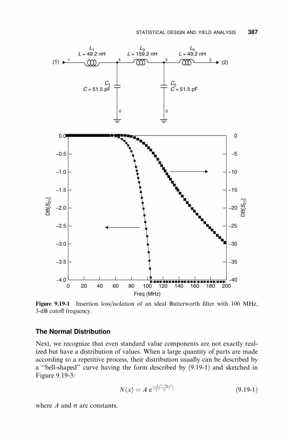
�
STATISTICAL DESIGN AND YIELD ANALYSIS 387
Figure 9.19-1 Insertion loss/isolation of an ideal Butterworth filter with 100 MHz,3-dB cuto¤ frequency.
The Normal Distribution
Next, we recognize that even standard value components are not exactly real-ized but have a distribution of values. When a large quantity of parts are madeaccording to a repetitive process, their distribution usually can be described bya ‘‘bell-shaped’’ curve having the form described by (9.19-1) and sketched inFigure 9.19-3:
2 sNðxÞ ¼ A e ½�1ðx�x0Þ2 ð9:19-1Þ
where A and s are constants.

388 FILTER DESIGN
TABLE 9.19-1 U.S. Standard C83.2a
Part Tolerance G5% G10% G20%
Step Multiplier 101=24 ¼ 1:10 101=12 ¼ 1:21 101=6 ¼ 1:47 10 10 10 11 12 12 13 15 15 15 16 18 18 20 22 22 22 24 27 27 30 33 33 33 36 39 39 43 47 47 47 51 56 56 62 68 68 68 75 82 82 91 100 100 100
aSmaller or larger values use decimal multiplication of the values for the separateG5%,G10%, and
G20% series values [8].
The distribution in Figure 9.19-3 is so frequently encountered that it is calledthe normal distribution. It describes the likely density of parts, NðxÞ, distributedabout a center value x0. It is also called a Gaussian distribution about a nominalvalue. The expression in (9.19-1) is a continuous quantity; therefore, it can onlybe applied with good approximation when the quantity of parts is large. Theconstant s defines the width of the curve. When jx� x0j ¼ s the density NðxÞis about 60% of its peak value. The constant A is evaluated such that the den-sity of parts integrated over all possible values is equal to N, the total numberof parts. That is,
ð ðy y½�1ðx�x0Þ2 � dx2 sN1 NðxÞ dx ¼ A e ð9:19-2Þ
0 0
In order to separate this characteristic function from the actual quantity of

�
STATISTICAL DESIGN AND YIELD ANALYSIS 389
Figure 9.19-2 Low-pass filter realized using standard part values.
parts, the practice is to express NðxÞ as a product of the total number of partsand the probability factor, jðxÞ. With this definition
NðxÞ ¼ NjðxÞ ð9:19-3Þ
where
2 sjðxÞ ¼ C e ½�1ðx�x0Þ2 ð9:19-4Þ

390 FILTER DESIGN
Figure 9.19-3 Normal distribution of parts, also called a Gaussian distribution.
Since jðxÞ is a probability factor, its value is bounded by
0ajðxÞa 1 ð9:19-5Þ
That is, the probability of an event lies somewhere between zero (when theevent has no chance of occurring) and unity (when the event is a certainty).Suppose that these statistics are to represent a manufacturing lot of capacitorsbeing made with an intended standard value of 47 pF. Then, theoretically, therange of part values is all positive values for x, and the constant, C, must bedefined to satisfy ð ðy y
ðx�x0Þ2 � dx2 sjðxÞ dx1 1 ¼ C e ½�1 ð9:19-6Þ
0 0
Imposition of the condition in (9.19-6) will also satisfy that of (9.19-5). Theintegration in (9.19-6) required to evaluate C is tricky [7, Chapter 8, Sec. 10].To perform the integration, express the integral with either of two dummyvariables, x and y: ð ðy y
�x2=2I ¼ e dx ¼ e�y2=2 dy ð9:19-7Þ�y �y
The integration is carried out from �y to þy because in general the proba-bility function might have values for both negative and positive values of x.Squaring I and using both the x and y variable forms of (9.19-7) givesð ðy y
�ðx2þy2Þ=2I 2 ¼ e dx dy ð9:19-8Þ�y �y
The integration in (9.19-8) corresponds to integrating the function e�ðx2þy2Þ=2
over the entire xy plane. Expressing (9.19-8) in polar coordinates, the samefunction and area of integration can be rewritten as

�
STATISTICAL DESIGN AND YIELD ANALYSIS 391
ð ð � �ð2p y y 2�r2=2I 2 ¼ e r dr dy ¼ 2p e�r2=2 d
r ¼ 2p ð9:19-9Þ0 0 0 2
Hence, ðy ffiffiffiffiffiffi �x2
I ¼ e =2 dx ¼p2p ð9:19-10Þ
�y pffiffiffiffiffiffiffiffiffiffi and the constant C in (9.19-6) must be equal to ð1=sÞ 1=2p so that the nor-mal, or Gaussian, probability function satisfies (9.19-6). The probability func-tion is then defined by (9.19-11) and plotted in Figure 9.19-4:rffiffiffiffiffiffi
1 ðx�x0Þ2 �2 sjðxÞ ¼ 1
e ½�1 ð9:19-11Þ
s 2p
and the density of parts NðxÞ in terms of the total number of parts N is givenby rffiffiffiffiffiffi
1 ðx�x0Þ2 �2 sNðxÞ ¼ NjðxÞ ¼ N
e ½�1 ð9:19-12Þ
s 2p
Given a su‰ciently large N for applying statistics (say, a number of capaci-tors), the number of capacitors NSPEC having a specified value (such as the ca-pacitance value being within x1 a xa x2) is given by
rffiffiffiffiffiffi ð ð x2 1 ½�1 x�x0Þ2NSPEC ¼ N jðxÞ dx ¼ N x2
e 2ð
s dx ð9:19-13Þs 2p x1x1
The indefinite integral in (9.19-12) does not have a known analytic solution.The number of in-specification parts can be estimated by performing a graph-ical integration of the curve in Figure 9.19-4, below which the number ofsquares contained within �3sa xaþ3s is approximately 240.
For example, suppose that a manufacturer makes 1000 capacitors intendedto have a standard value of 47 pF. However, due to an error in the process, thedistribution is centered at 52 pF ðx0 ¼ 52 pFÞ, with s ¼ 0:096x0 ¼ 5 pF. Howmany parts will meet a specification of 47 pFG 5 pF (a G10.6% tolerance)?The distribution is shown in Figure 9.19-5. The shaded area represents the us-able parts that meet the capacitance specification, a little less than one half ofthose produced.
Other Distributions
While the normal distribution is the most common for part manufacture, manyfactors can influence the distributional outcome. One should not assume thatparts obtained with a G tolerance can be accurately represented by a normal
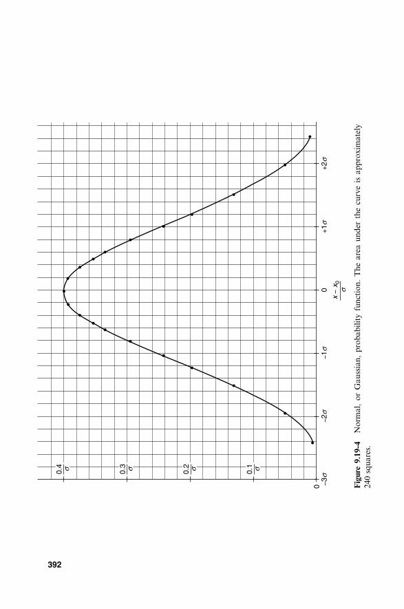
Figure
9.19-4
Norm
al,orGaussian,probabilityfunction.Theareaunder
thecurveis
approxim
ately
240squares.
392

distribution centered on their nominal value. As was seen from the previousexample, even when the normal distribution does apply, its center value, x0, maynot be the nominal value for that part because the manufacturer’s process maynot be su‰ciently controlled to center the distribution on the part value desired.
Even when the distribution is centered properly on the nominal value, partsdelivered to aG20% tolerance will not necessarily be represented by a normal
Figure 9.19-5 Normal distribution of capacitors centered at 52 pF with one sigma ¼5 pF and the quantity that meet a 47-pFG 5 pF specification (shaded area).
Figure 9.19-6 Gaussian (normal) distribution showing how the center values might beremoved to leave a depleted normal distribution.
STATISTICAL DESIGN AND YIELD ANALYSIS 393
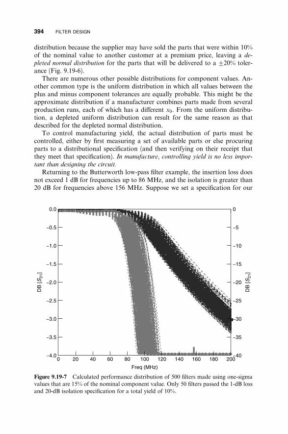
394 FILTER DESIGN
distribution because the supplier may have sold the parts that were within 10%of the nominal value to another customer at a premium price, leaving a de-
pleted normal distribution for the parts that will be delivered to aG20% toler-ance (Fig. 9.19-6).
There are numerous other possible distributions for component values. An-other common type is the uniform distribution in which all values between theplus and minus component tolerances are equally probable. This might be theapproximate distribution if a manufacturer combines parts made from severalproduction runs, each of which has a di¤erent x0. From the uniform distribu-tion, a depleted uniform distribution can result for the same reason as thatdescribed for the depleted normal distribution.
To control manufacturing yield, the actual distribution of parts must becontrolled, either by first measuring a set of available parts or else procuringparts to a distributional specification (and then verifying on their receipt thatthey meet that specification). In manufacture, controlling yield is no less impor-
tant than designing the circuit.
Returning to the Butterworth low-pass filter example, the insertion loss doesnot exceed 1 dB for frequencies up to 86 MHz, and the isolation is greater than20 dB for frequencies above 156 MHz. Suppose we set a specification for our
Figure 9.19-7 Calculated performance distribution of 500 filters made using one-sigmavalues that are 15% of the nominal component value. Only 50 filters passed the 1-dB lossand 20-dB isolation specification for a total yield of 10%.

STATISTICAL DESIGN AND YIELD ANALYSIS 395
Figure 9.19-8 Distribution of Butterworth filter performance when the componentshave normal distributions with a one-sigma value that is 5% of the nominal componentvalue. A total of 60 units passed the 1-dB-loss and 20-dB-isolation specification for ayield of 12%.
filter that the loss must be below 1.0 dB up to 86 MHz and the isolation mustbe greater than 20 dB above 156 MHz.
Further, assume for this example that all components have a normal dis-tribution of values with a one sigma equal to 15% of the nominal value. Theresulting performance of 500 filters ‘‘built’’ using these parts is shown in Figure9.19-7.
Of course, the specifications could be relaxed to allow more filters to pass.Alternatively, components could be procured with a tighter distribution. If theone-sigma value is reduced to 5% of the nominal value, the resulting distribu-tion is that shown in Figure 9.19-8.
While the spread is much tighter than for the 15% one sigma, the yield in-creased to only 59 units, a 12% yield. If the specification limits are relieved torequire less than 1 dB of loss up to 80 MHz and greater than 20 dB of isolationat 170 MHz and above, and if the one-sigma tolerance is made 10%, then 473units meet the specifications, for a yield of nearly 94.6%. Clearly, both thespecifications and the control of parts are crucial to the achievement of highyields.

396 FILTER DESIGN
REFERENCES
1. Randall W. Rhea, HF Filter Design and Computer Simulation, Noble Publishing,Atlanta, GA, 1994. This book is must reading for the filter designer. It contains an
excellent introduction to filter theory with numerous examples of both lumped element
and distributed filters. It includes practical e¤ects such as coil winding and the element
Q’s that are practically realizable.
2. Peter A. Rizzi, Microwave Engineering, Passive Circuits, Prentice-Hall, EnglewoodCli¤s, NJ, 1988. Excellent microwave engineering textbook covering theory and design
of transmission lines, couplers, filters, and numerous other passive devices.
3. P. I. Richards, ‘‘Resistor-Transmission Line Circuits,’’ Proceedings of the Institute of
Radio Engineers (IRE), Vol. 36, February, 1948, pp. 217–220.
4. Ralph Levy, ‘‘A general equivalent circuit transformation for distributed networks,’’IEEE Transactions on Circuit Theory, CT-12, September 1965, pp. 457–458.
5. W. W. Mumford, ‘‘Tables of stub admittances for maximally flat filters using shortedquarter wave stubs,’’ IEEE Transactions on Microwave Theory and Techniques, Vol.MTT-13 No. 5, September 1965, pp. 695–696.
6. Matthei, Young, and Jones, Microwave Filters, Impedance Matching Networks, and
Coupling Structures, McGraw-Hill, New York, 1964 (now also available from ArtechHouse, Norwood, Massachusetts). Often called the Bible of the filter world.
7. I. S. Sokolniko¤ and R. M. Redhe¤er, Mathematics of Physics and Modern En-
gineering, McGraw-Hill, New York, 1958.
8. Howard W. Sams & Co., Reference Data for Radio Engineers, 5th ed., Howard W.Sams & Co., 1974.
EXERCISES
E9.4-1 a. Design a 50-W, five-element, lumped-element, Butterworth low-pass filter with a 3-dB cuto¤ at 1000 MHz to take out the har-monics in a cellular phone transmitter. Use a series L as the firstelement.
b. How much attenuation would you expect for the second harmonicof an 850-MHz signal?
c. Suppose we need at least 40-dB attenuation of the second har-monic of 850 MHz. What can you do to achieve this and alsominimize passband insertion loss?
d. Prove your results using a circuit simulator.
e. If the system bandwidth is 825 to 875 MHz and you wish toeliminate the second harmonic, which could be between 1650 and1750 MHz, what changes would you make to the filter to mini-mize its loss in the passband and maximize its isolation to thesecond-harmonic band?
E9.5-1 a. Convert the filter you designed in E9.4-1 into a high-pass filter ofthe same type and cuto¤ frequency.

EXERCISES 397
b. Examine your result using a circuit simulator (create a new sche-matic to analyze this circuit).
c. Are the elements as easy to realize?
E9.8-1 A 50-W, 0.0432-dB ripple (20 dB return loss), Chebyshev three-section bandpass filter with 0.0432-dB band edge frequencies of 700and 1000 MHz is required.
a. What is f0?
b. What is the fractional bandwidth?
c. What are the low-pass gi values?
d. What are the actual L and C values of the filter?
e. Plot the loss versus frequency performance using a network simu-lator.
f. What is the order of the filter?
g. At what rate does the isolation increase in decibels/octave?
h. What is the e¤ect if inductors have a Q of 50 and capacitors havea Q of 100?
i. What would you say is the highest practical frequency at which afilter of this type can be built?
E9.8-2 a. Design a Chebyshev 0.0432-dB ripple (20-dB return loss) band-pass filter in the same manner used for E9.8-1 but for a passbandof only 800 to 900 MHz.
b. Verify the design using a network simulator.
c. What can you say about the relative practicality of the requiredcomponents for this filter versus the 700- to 1000-MHz filter de-signed in E9.8-1? What do you believe causes the added di‰culty?
d. Use the circuit simulator to determine the passband insertion losswhen the filter is realized using capacitor Q’s of 100 and inductorQ’s of 50.
E9.14-1 a. Repeat the design of the 800- to 900-MHz, 0.0432-dB ripple(20-dB return loss), Chebyshev bandpass filter, but this time real-ize it as a microstrip end-coupled (half-wavelength resonator)filter with a 0.031-in.-thick substrate of dielectric constant 2.22.Hint: Use a filter program if you have one. If not, use a networksimulator and begin with three, 50-W, half-wavelength resonatorsend-coupled by capacitors. Use the optimizer to hold loss to0.0432-dB in the passband. Make the line lengths and capacitorvalues adjustable in the optimization.
b. Can you get the same loss performance as the lumped-element filter?
c. Can you get the same isolation performance?
d. Compare the practicality of building this filter with the lumped-element filter.

398 FILTER DESIGN
E9.15-1 The Richards transformation is to be used to design a three-stubbandstop filter with fR ¼ 1:30 GHz and a 3-dB bandwidth of 600MHz (i.e., fC ¼ 1 GHz).
a. Base the design on a three-element tee configuration Butter-worth low-pass filter. Determine the characteristic impedances ofthe series-connected shorted stubs, ZSS, and the shunt-connectedopen-circuited stub, ZOC. Also calculate the stub lengths l. As-sume a 50-W system impedance ðZ0 ¼ 50 WÞ and air dielectric.Make sketches of the equivalent circuit of the lumped-element andstub filters showing element values.
b. Plot the loss/isolation versus frequency response from 1 to 2 GHz.Verify that the 3-dB bandwidth is 600 MHz. What is the 20-dBbandwidth?
E9.16-1 Use the appropriate Kuroda identity to convert the distributed teefilter design of E9.15-1 to a three shunt-connected open-circuit stubfilter with the same performance.
a. Calculate the characteristic impedance of the end stubs ZES andthe interconnection lines Z01.
b. Plot the loss versus frequency response of the shunt stub filter andcompare it to that of the tee configuration filter of E9.15-1.
E9.16-2 Prove the equivalence of Kuroda’s identity in Figure 9.16-1a. Hint: Iftwo circuits have identical behavior, they must have the same ABCDmatrix.
E9.19-1 a. Make a scaled sketch of the distribution curve for a manufactur-ing run of 1000 resistors having a center of distribution value,x0 ¼ 68 W, and a standard deviation, s ¼ 5 W.
b. Use your drawing to estimate the number of resistors that willmeet aG5% tolerance (say,G3:5 W) about 68 W.

CHAPTER 10
Transistor Amplifier Design
10.1 UNILATERAL DESIGN
Evaluating S Parameters
The design of a transistor amplifier is the creation of a circuit environment inwhich a selected transistor performs as closely as possible to a set of designobjectives. The circuit designer may have no influence over the transistor’sparameters. These are established by its geometry, quality of manufacture, andsemiconductor physics. Usually the circuit designer selects a transistor from acatalog, guided by and limited to the properties described by its S parameters.
To the circuit designer the transistor is a two-port network described by atable of S parameters taken over the entire frequency domain over which it hasgain. After the bias and heat sinking needs of the transistor have been satisfied,the RF design proceeds using the S parameters. At this point it is of no conse-quence whether the device is a bipolar or field-e¤ect transistor (FET) or anyother device whose S parameters suggest the prospect of gain.
As was shown in Chapter 6, when the source and load impedances are thesame as those used to determine the S parameters, the magnitude of S21 is theratio of the outgoing wave b2 to the incoming wave a1. Hence it is equivalent tothe voltage or current gain of the amplifier. Similarly, the magnitude of thesquare of S21 is equal to the power gain.
As an example, suppose it is desired to design an amplifier to operate at1 GHz with 50-W source and load impedances, and that it is desirable to ob-tain as much gain as practical at 1 GHz. On reviewing tables of S parametersprovided in a catalog or in an electronic file within a circuit simulator, sup-pose that the Motorola 2N6679A bipolar transistor is selected for the amplifierdesign. Its S parameters are shown in the standard format in Table 10.1-1.
We see that the magnitude of S21 is 6.6 at 1 GHz. Then the basic gain,without tuning, in a 50-W system is
G ¼ 20 logjS21j ¼ 20 log 6:6 ¼ 16:4 dB ð10:1-1Þ
High Frequency Techniques: An Introduction to RF and Microwave Engineering, By Joseph F. White. ISBN 0-471-45591-1 6 2004 John Wiley & Sons, Inc.
399

400 TRANSISTOR AMPLIFIER DESIGN
TABLE 10.1-1 The S Parameter File for the Motorola 2N667A Bipolar Transistora
! 2N6679A.S2P! 2N6679! VCE ¼ 15 V; IC ¼ 25 mA
# GHZ S MA R 50
! S-PARAMETER DATA
0.1 0.60 �76 38.6 141 0.01 55 0.83 �200.5 0.67 �158 12.7 95 0.02 40 0.50 �271 0.68 �178 6.6 77 0.03 53 0.46 �321.5 0.68 170 4.4 64 0.04 54 0.47 �412 0.69 162 3.4 54 0.05 54 0.47 �502.5 0.69 154 2.7 42 0.06 55 0.49 �593 0.69 146 1.3 31 0.07 55 0.53 �703.5 0.69 138 1.9 21 0.08 54 0.55 �794 0.69 131 1.7 11 0.09 51 0.57 �894.5 0.69 123 1.5 1 0.10 49 0.59 �975 0.69 114 1.4 �9 0.12 44 0.62 �1065.5 0.69 106 1.2 �19 0.14 39 0.64 �1136 0.69 98 1.1 �28 0.15 33 0.68 �1226.5 0.69 90 1.0 �37 0.17 31 0.69 �130
Source: From the Genesys S parameter directory.
aBy convention the columns contain left to right: freq (in GHz), S11;S21;S12;S22, where each S
parameter is contained in two columns, the first is the magnitude (numeric, not decibel) and the
second is the phase angle in degrees.
Transistor Biasing
At this point suppose that we consider this to be desirable performance. It isnecessary to design a bias circuit [1, pp. 273–283]. For the bias a 20-V source isselected, since the S parameter file indicates the performance was obtained witha 15-V bias between collector and emitter. From the transistor data, we see thatthe performance was obtained with VCE ¼ 15 V and IC ¼ 25 mA. The DCcurrent gain b ¼ IC=IB is not listed in the S parameter file, but on contactingthe manufacturer, suppose that at room temperature b ¼ 40. Then a suitablebiasing network is as shown in Figure 10.1-1.
The resistor values are calculated as follows. A base current of 0.63 mA isrequired (25 mA/40). But we want a shunt path to carry about 5 times thisvalue, say 3 mA, so that when the 15-V level falls, the base current will fallnearly proportionately. Since the transistor is a silicon NPN, the base emitterjunction is a silicon diode. Hence it will have a voltage drop at turn-on of about0.75 V. The emitter-base shunting resistor is calculated as:
0:75 VR3 ¼ ¼ 250 W ð10:1-2Þ
3 mA

UNILATERAL DESIGN 401
Figure 10.1-1 Bias circuit for the2N6679A transistor.
Next,
15 V� 0:75 VR2 ¼ ¼ 3925 W ð10:1-3Þ
3:63 mA
Finally,
20 V� 15 VR1 ¼ ¼ 175 W ð10:1-4Þ
28:6 mA
In practice, the closest values of standard resistors may be used. This biascircuit tends to self-compensate. As temperature increases, the base currentincreases for a given VBE . However, this causes an increase in IC , causing alarger voltage drop in R1, reducing VBE .
By themselves, the resistors R2 and R3 are large compared to the 50-W RFimpedance level at the input. However, their parasitics may cause them to placean excessive load on the RF circuit. Furthermore, it is undesirable to have RFsignals present in the bias circuit since this may cause undesired RF radiation.Therefore, circuitry to isolate the bias from the RF signals is employed, as, forexample, that shown in Figure 10.1-2.
Basically the bias isolation circuitry presents a high RF impedance from thetransistor terminals to those of the bias circuitry. This can be accomplishedusing discrete components (Fig. 10.1-2a). For the present 1 GHz, 50-W ampli-fier example isolating elements of L ¼ 100 nH and C ¼ 100 pF might beemployed. When space permits, the isolating elements can be ‘‘printed’’ as dis-tributed elements along with the RF circuit. The transmission lines shown aremade a quarter wavelength long at the RF center frequency of the amplifier.For the 50 W amplifier example, the high impedance lines made ZH ¼ 150 W,and the low impedance lines made ZL ¼ 25 W.
The bias isolating networks are crucially important in amplifier design andshould not be given short shrift in the design e¤ort. As we shall later discuss,transistors may have gain well above the design bandwidth. In the present

402 TRANSISTOR AMPLIFIER DESIGN
Figure 10.1-2 Transistor with bias isolation components: (a) discrete bias isolation and(b) distributed bias isolation.
1-GHz amplifier example, it can be seen from Table 10.1-1 that the transistorhas gain above 5 GHz. Therefore, it could break into oscillation given certainout-of-band impedance loading.
The single-stage bias circuits shown in Figure 10.1-2 have only single highimpedance and low impedance elements for isolation. They are shown forillustration of the bias isolating methods and are not presented as adequatedesigns for all applications. Where practical, multistage bias isolation is prefer-able as shown in Figure 10.1-3.
An informal measure of the e¤ectiveness of the distributed bias structure isto bring a screwdriver tip near the open-circuit ends of the bias flags (the open-circuited ends of the low-impedance line sections) while measuring the outputpower of the amplifier. A significant power change experienced when so prob-ing the end of the second bias flag, ZL2, indicates the bias circuit may be reso-nant at the wrong frequency or that more isolating stages are required.

UNILATERAL DESIGN 403
Figure 10.1-3 Two-stage bias isolating circuits: (a) discrete and (b) distributed.
Evaluating RF Performance
Most circuit simulators can accept the S parameter table to provide an analysisover frequency, interpolating the data to calculate the circuit behavior betweenfrequencies for which S parameter data are available. The circuit evaluationcould be performed with bias elements, but we will assume in this text thatsu‰cient bias isolation is achieved, and only the RF circuit will be shown forpurposes of illustration. However, when the amplifier design is critical, as foran integrated circuit, it is wise to include the bias circuit and any peripheralcircuit elements on the broadband simulation of the amplifier. The gain of thepresent example, using the 2N6679A transistor, is shown in Figure 10.1-4. Aswill be common in this text, the impedance of the input and output ports is 50 Wunless otherwise noted.
At this point, if this performance is satisfactory, the electrical portion of theamplifier design is complete. On the other hand, on examining the input andoutput reflection coe‰cients, S11 and S22, respectively, in Table 10.1-1, it can

404 TRANSISTOR AMPLIFIER DESIGN
Figure 10.1-4 Amplifier consisting of a biased Motorola 2N6679A silicon bipolartransistor with 50-W source and load terminations.
be seen that a good amount of power is lost to reflection at the input and mis-match at the output. At 1 GHz
jS11j ¼ 0:68
Input mismatch loss ¼ 1� jS11j2 ¼ 1� 0:682 ¼ 0:54 ð10:1-5Þ¼ 10 logð1� jS11j2Þ ¼ �2:7 dB
jS22j ¼ 0:46
Output mismatch loss ¼ 1� jS22j2 ¼ 1� 0:462 ¼ 0:79 ð10:1-6Þ¼ 10 logð1� jS22j2Þ ¼ �1:0 dB

AMPLIFIER STABILITY 405
These mismatch losses correspond to 46% power loss at the input and 21%at the output. Therefore, by matching input and output, we could have up to3.7 dB of additional gain and have a matched circuit at input and output aswell.
10.2 AMPLIFIER STABILITY
Thus far, even if we are satisfied with the performance obtained by installing atransistor in the same impedances in which it was measured, there is a pointthat we have not considered. We have treated the transistor as if it were a uni-
lateral device. Put in other words, we have assumed that signals pass from theinput to the output, but not in the reverse direction.
Making the unilateral assumption is equivalent to assuming that S12 is zero.The S12 parameter provides the feedback term by which power from the outputcircuit (which is relatively high due to the transistor’s amplification) can feedback to the input. When it does so, it may combine with reflections alreadypresent at the input to produce an e¤ective S11 whose magnitude exceeds unity.
This corresponds to reflection gain, and a transistor amplifier that can ex-perience this gain, is termed conditionally unstable, the condition being cer-tain combination(s) of load impedance, S12 and S11, that could produce self-oscillation (instability).
In the current 2N6679A example, the magnitudes of S11 and S22 of thetransistor are less than one for all frequencies. This means that the transistor isstable when embedded between 50-W source and load (Fig. 10.2-1). That is, itwill not oscillate in the 50-W input/output environment. However, this wouldnot be generally considered su‰cient within the industry. Rather, the expecta-tion is that a properly designed (stabilized) amplifier will not oscillate no matter
Figure 10.2-1 An S parameter represented network embedded between source and loadof general complex reflection coe‰cients.

what passive source and load impedances are presented to it, including short or
open circuits of any phase.
Because the S12 of practical transistors is not zero, a signal path exists fromthe output (where power levels are higher due to the device’s gain) to the input.It is possible that for certain values of load GL;GIN can exceed unity, turningthe circuit into a reflection amplifier at the input. Similarly, certain values of GSat the input might cause GOUT to exceed unity magnitude. When either or bothof these conditions can occur, at any frequency, the circuit is said to be onlyconditionally stable or equivalently, potentially unstable.
The boundary line between stable and unstable operation at the input is thejGINj ¼ 1 circle centered at the origin of the Smith chart. The contour of valuesfor GL (also a circle) that produces a unity magnitude reflection coe‰cient atthe input is called the input stability circle. This is shown in Figure 10.2-2 forthe 2N6679A transistor. Keep in mind that the input stability circle represents a
set of load reflection coe‰cients that cause the input reflection coe‰cient tohave a unity magnitude. Also note that the input stability circle represents aboundary, on one side of which jGINj < 1 resulting in load impedances that
Figure 10.2-2 Load instability circle for the Motorola 2N6679A transistor at 1 GHz.
406 TRANSISTOR AMPLIFIER DESIGN

AMPLIFIER STABILITY 407
result in stable operation and on the other side of which jGINj > 1, corre-sponding to load impedances that produce potential instability.
The GL values are related to the GIN values according to (10.2-1), called amapping function because it maps a GIN contour into a GL contour [2, pp.140–145]. This function maps the jGINj ¼ 1 into a GL contour, in this case acircle, to a circle:
GIN � S11GL ¼ where D ¼ S11S22 � S12S21 ð10:2-1Þ
S22GIN � D
Inserting the condition jGINj ¼ 1 into the above equation creates a mapping ofthe jGINj ¼ 1 circle into the input stability circle in the GL plane with center at
CL ¼ S �22 � D�S11
jS22j2 � jDj2 ð10:2-2Þ
and a radius of � � RL ¼ S12S21
jS22j2 � jDj2� � � �
� � � � ð10:2-3Þ
The input stability circle for the 2N6679A untuned amplifier at 1 GHz, isshown in Figure 10.2-2.
The input stability circle is also called the load instability circle because itdescribes the GL values that border on causing instability, that is, which resultin jGINj ¼ 1. Henceforth, we will refer to the input stability circle as the load
instability circle because this places the focus on the load impedances that causeinstability.
The circle intersects and intrudes into the unity radius area of the Smithchart. This means that the transistor is potentially unstable for certain passiveload impedances bounded by the circle. Note, again, that the circle is theboundary of the unstable impedances. Since it is only the boundary, when wefirst plot the circle we do not know whether the unstable load impedances arethose inside the circle or outside of the circle. Of course, in the example inFigure 10.2-2 it would seem highly likely that the unstable points are inside thecircle since most of the circle is in the negative resistance domain of the Smithchart. However, there are instances in which the entire circle may lie within theunity radius, passive impedance portion of the Smith chart. Therefore, somemeans for determining which side of the boundary represents the unstable im-pedances is needed. The determination is facilitated by the availability of the Sparameters, which apply with a known load, usually 50 W. To determine
whether the unstable load impedances are inside or outside the circle, consider the
‘‘easy point’’ S11.We know from the S parameter file for the 2N5579A transistor that when
the transistor is loaded with 50 W, the center of the Smith chart, jS11j < 1.

408 TRANSISTOR AMPLIFIER DESIGN
Therefore, the center of the Smith chart is a stable load point. Since the centerof the Smith chart is outside the load instability circle, it follows that in thiscase all points outside the circle are stable, and that the points inside the circlein Figure 10.2-2 are the unstable loads.
From Figure 10.2-2 it can be seen that high inductive load impedances at theoutput can cause instability (at the input). Also, notice that points outside theG ¼ 1 circle correspond to loads with negative resistance. These do not concernus because any amplifier can be made unstable by subjecting it to an appropri-ate source or load impedance with a negative real part. Amplifier stability only
requires that the circuit be stable with passive input and output reflection coe‰-
cients, that is, passive source and load impedances.
Next consider the source reflection coe‰cients that cause jGOUTj ¼ 1. Therelation of GS to GOUT is given by [2, p. 142]
S22 � DGOUTGS ¼ ð10:2-4Þ
1� S11GOUT
In a similar fashion, this can be used to map the jGOUTj ¼ 1 circle onto the GSplane. This maps as a circle with center at
CS ¼ S �11 � D�S22
jS11j2 � jDj2 ð10:2-5Þ
and radius � � RS ¼ S12S21
jS11j2 � jDj2� � � �
� � � � ð10:2-6Þ
Plotting this for our transistor at 1 GHz gives the left circle outside the Smithchart in Figure 10.2-3.
The output stability circle is also called the source instability circle because itrepresents GS values that cause instability in the input circuit. Henceforth we
will call it the source instability circle. Once again, we know that the pointswithin the output stability circle are the unstable ones because, from the S
parameters of the transistor, jS22j < 1 with a 50-W termination on the input.Notice that the output circuit may become unstable ðjGOUTj > 1Þ when theinput sees low source impedances.
What do these circles mean? If we attempt to get more gain from the tran-sistor by adding matching circuits to the input and output, they must not pres-ent those impedances which would cause instability. In fact, even if we acceptthe transistor as it is and specify that only 50-W loads should be applied, if thesource or load is removed and there is a transmission line whose length trans-forms an open circuit to one of the unstable impedances, the circuit may oscil-late. In other words, the circuit will be potentially unstable.

Thus far, in our examples of stability circles, we have only examined thetransistor’s behavior at 1 GHz. But, for an amplifier to be unconditionally sta-ble, it must be so at all frequencies. To assure this requires that it be found tobe unconditionally stable at all frequencies for which the transistor has morethan unity gain. The resulting source and load instability circles are two separate
families of circles (Fig. 10.2-4).
10.3 K FACTOR
Since the stability circles can be calculated directly from the S parameters, itwould seem possible that stability could be determined from the S parametersthemselves, without need for the elaborate graphical construction of the stabil-ity circles, and this is so. We define the stability factor K as [2, p. 145]
K ¼ 1� jS11j2 � jS22j2 þ jDj22jS12S21j ð10:3-1Þ
where
Figure 10.2-3 Source instability circle (at left) and load instability circle (at right) forthe 2N6679A transistor at 1 GHz.
K FACTOR 409

jDj2 ¼ jS11S22 � S12S21j2 ð10:3-2Þ
The amplifier is unconditionally stable provided that
K > 1 and jDj2 < 1 ð10:3-3a,bÞ
Equivalently [3, p. 324], the amplifier is unconditionally stable if
K > 1 and B1 > 0 ð10:3-4a,bÞ
where
B1 ¼ 1þ jS11j2 � jS22j2 � jDj2 > 0 ð10:3-5Þ
Figure 10.2-4 Source and load instability circles for a band of frequencies from 100 to6500 MHz.
410 TRANSISTOR AMPLIFIER DESIGN

TABLE 10.3-1 Sta
Transistor
bility Criteria for 2N6679A
K FACTOR 411
Freq (MHz) K B1
0 0.195 0.203500 0.684 1.1531000 0.875 1.231500 0.964 1.2192000 0.962 1.2312500 0.972 1.2053000 1.755 1.1193500 0.913 1.1174000 0.863 1.0864500 0.842 1.0515000 0.663 1.0095500 0.611 0.9756000 0.526 0.9026500 0.498 0.879
Applying this test to the 2N6679A transistor and using the Genesys program tocalculate K and B1 gives the results in Table 10.3-1.
Thus we see that the transistor is potentially unstable at 1 GHz, as had al-ready been deduced from the input and output stability circles. It is also po-tentially unstable at other frequencies. However, the source and load instabilitycircles provide insight into what can be done to make the transistor uncondi-tionally stable. Notice that the source instability circles indicate that low im-pedances at the input cause instability. This suggests that a resistance placedin series with the base lead can reduce the intersection of the source insta-bility circles with the jGja 1 circle. This will reduce gain. However, since de-vice instability usually peaks at low frequencies (at which the transistor has thehighest gain), the resistor can be shunted with a capacitor to minimize its e¤ectnear 1 GHz. One such stabilizing circuit is shown in Figure 10.3-1.
This measure almost removed all instabilities. It moved both the source andload instability circles away from the jGj ¼ 1 (passive Smith chart) portion ofthe reflection coe‰cient plane (Fig. 10.3-2). Rather than add more resistance tothe base lead, it is often found to be more e¤ective to add some damping to theoutput. Corrections to the input stability tend to help the output stability, andvice versa.
Examining the load instability circles reveals that high output load imped-ances cause instability. To counter this, add shunt resistance at the output, butplace it at the end of a 90� line at 1 GHz to minimize its e¤ect at 1 GHz. Theaddition of shunt resistance limits how large the load impedance can be, mini-mizing the likelihood that a high impedance that can cause instability will beencountered at the output.

This addition to the output circuit has unconditionally stabilized the deviceover the 100- to 2000-MHz range, in which it previously was potentially un-stable (Table 10.3-2). From the K factor calculations it can be seen that the lowfrequency end is especially well stabilized. This is important because S param-eter data below 100 MHz were not included in the S parameter file.
The resulting gain of the 2N6679A with the stabilizing elements is shown inFigure 10.3-3. Notice that, in comparing this gain with that of the unstabilizedtransistor in Figure 10.1-4, we have sacrificed only about 0.6 dB of gain at 1GHz, dropping from 16.4 dB to about 15.8 dB at this frequency.
Figure 10.3-1 Revised instability circles when series resistance is placed in the base leadof the 2N6679A transistor.
412 TRANSISTOR AMPLIFIER DESIGN

We have reduced the low frequency gain even more, but this is of no con-cern. In fact, it is a benefit. Gain outside the desired bandwidth is a liability be-
cause it can cause instabilities. We are now in a position to match the input andoutput of the transistor to realize additional gain.
10.4 TRANSDUCER GAIN
We have seen that the S parameters are a valuable aid both for collecting datafor a transistor and then using the data to predict performance and design anamplifier circuit. Unfortunately, unlike Z;Y , or ABCD parameters, the values
of S parameters depend not only upon the properties of the transistor but also
upon the source and load circuits used to measure them. This is because theymeasure transmitted and reflected waves, and these depend upon both thetransistor and the source and load used to test it.
Figure 10.3-2 Source and load instability circles for the 2N6679A with stabilizing cir-cuits in the input and outputs.
TRANSDUCER GAIN 413

414 TRANSISTOR AMPLIFIER DESIGN
TABLE 10.3-2 Calculated K Factor for Stabilized
2N6679A Transistor
Freq (MHz) K B1
1 100 6.093 0.812 200 2.008 0.8753 300 1.237 0.9654 400 1.074 1.0765 500 1.221 1.1866 600 1.081 1.2167 700 1.02 1.238 800 1.015 1.2329 900 1.059 1.22410 1000 1.165 1.20411 1100 1.173 1.16212 1200 1.222 1.10513 1300 1.34 1.03114 1400 1.608 0.93415 1500 2.339 0.81716 1600 5.172 0.70917 1700 18.87 0.71218 1800 5.059 0.92519 1900 2.247 1.18420 2000 1.608 1.328
Note that the concepts of a reflection coe‰cient and traveling waves can be
used even if there are no actual transmission lines at the device ports (Fig.10.4-1). One might expect that the input reflection coe‰cient, GIN, would sim-ply be equal to S11, and that GOUT ¼ S22. However, because of feedback thesemust be corrected [1, p. 214]:
S12S21GL S12S21GSGIN ¼ S11 þ and GOUT ¼ S22 þ ð10:4-1a,bÞ
1� S22GL 1� S11GS
The general transducer gain of a two-port network having S21 and S12
values, whether it is a transistor or not, is
power delivered to loadGT ¼ ð10:4-2Þ
power available from the source
PLOAD 1� jGSj2 1� jGLj2GT ¼ ¼
2PAVAIL j1� GINGSj2jS21j2 j1� S22GLj
1� jGSj2 1� jGLj2¼ ð10:4-3a,bÞ2j1� S11GSj2
jS21j2 j1� GOUTGLj

TRANSDUCER GAIN 415
Figure 10.3-3 Gain of stabilized 2N6679A transistor.
Figure 10.4-1 Diagram of input and output reflection coe‰cients.

416 TRANSISTOR AMPLIFIER DESIGN
Figure 10.5-1 Input and output reflection coe‰cients for the unilateral gain assumption.
10.5 UNILATERAL GAIN DESIGN
The transducer gain expressions of (10.4-3) are too complex for manual design.To e¤ect an approximate gain solution, let us ignore the feedback, that is,assume that S12 ¼ 0. If an amplifier has no feedback, signals pass oneway through it. Accordingly, this is called the unilateral gain assumption (Fig.10.5-1).
If S12 ¼ 0, then GIN ¼ S11 and GOUT ¼ S22. Furthermore, if S12 ¼ 0 thetransducer gain becomes [1, p. 228]
1� jGSj2 1� jGLj2GTU ¼
2ð10:5-1Þj1� S11GSj2
jS21j2 j1� S22GLj
This can be considered as three separate gain factors (Fig. 10.5-2):
GTU ¼ GSG0GL ð10:5-2Þ
in which
GS ¼ 1� jGSj2j1� S11GSj2
G0 ¼ jS21j2 GL ¼ 1� jGLj2j1� S22GLj2
ð10:5-3a,b,cÞ
Figure 10.5-2 Three-stage, unilateral gain design model for which S12 ¼ 0.

UNILATERAL GAIN DESIGN 417
The unilateral gain expressions of (10.5-3) apply for any GS and GL. To max-imize GS, we select
GS ¼ S � ð10:5-4Þ11
Then
1� jGSj2 1� jS11j2 1GS-MAX ¼ ¼ ¼ ð10:5-5Þj1� S11GSj2 ð1� jS11j2Þ2 1� jS11j2
Similarly, to maximize GL, we select
GL ¼ S � ð10:5-6Þ22
and then
1GL-MAX ¼ ð10:5-7Þ
1� jS22j2
Therefore, under the unilateral assumption, S12 ¼ 0, the maximum gain to beobtained from a transistor is
1GTU-MAX ¼
2ð10:5-8Þ
1� j1
S11j2jS21j2
1� jS22j
The overall gain (in decibels) to be obtained is then
GTUðdBÞ ¼ GSðdBÞ þ G0ðdBÞ þ GLðdBÞ ð10:5-9Þ
in which we recognize that GS and GL are the gains (or losses) to be obtainedby matching (or deliberately further mismatching) the input and output cir-cuits, respectively. Of course, there is an error in the gain calculations of(10.5-8) and (10.5-9) if, in the actual transistor, S12 0 0. In that case the truegain GT is related to the calculated unilateral gain GTU by [1, p. 239]
1 GT 1< < ð10:5-10Þð1þUÞ2 GTU ð1�UÞ2
where
jS11j jS21j jS12j jS22jU ¼ ð10:5-11Þ
2ð1� jS11j2Þð1� jS22j ÞThe value of U varies with frequency because of its dependence on the S
parameters, and it is called the unilateral figure of merit. For the 2N6679A,

418 TRANSISTOR AMPLIFIER DESIGN
applying the S parameter values at 1 GHz from Table 10.1-1, U is calcu-lated as
ð0:68Þð6:6Þð0:03Þð0:46ÞU ¼ ¼ 0:146 ð10:5-12Þð1� 0:682Þð1� 0:462Þ
1 1
ð1�UÞ2 ¼ ð1� 0:146Þ2 ¼ 1:37 ¼ þ1:37 dB ð10:5-13Þ
1 1¼ ¼ 0:76 ¼ �1:18 dB ð10:5-14Þð1þUÞ2 ð1þ 0:146Þ2
From this it can be seen that the unilateral gain approximation can be used forthe 2N6679A at 1 GHz with an error somewhat greater thanG1 dB. To obtainthe ‘‘maximum gain’’ using the unilateral gain design, we transform the 50-Wsource to ZS ¼ Z �
OUT. From theIN, and the 50-W load is transformed to ZL ¼ Z �
S parameters,
1þ S11 1þ S22zIN ¼ and zOUT ¼ ð10:5-15Þ
1� S11 1� S22
To unnormalize,
ZIN ¼ zINZ0 and ZOUT ¼ zOUTZ0 ð10:5-16Þ
Since we have modified the S parameters by adding the stabilizing compo-nents, we must use revised S parameters for the stabilized 2N6679A transistor.This would be a laborious task but is easy and straightforward using the net-work simulator software. The revised S parameters are shown in Table 10.5-1.The corresponding input and output impedances are shown in Table 10.5-2.
There are numerous methods by which the amplifier can be matched. As anexample, the Q matching method can be employed (Fig. 10.5-3). Since theinput impedance at 1 GHz is
ZIN ¼ ð10:43� j7:238Þ W ð10:5-17Þ
it is necessary to transform the 50-W source to Z �IN. Thus,
TABLE 10.5-1 Revised S Parameters at 1 GHz for
Stabilized 2N6679A Transistor Amplifier
Magnitude Angle (deg)
S11 0.661 �162.8S21 6.25 83.23S12 0.028 59.23S22 0.414 �31.86

UNILATERAL GAIN DESIGN 419
TABLE 10.5-2 Input and Output Impedances for
Stabilized 2N6679A Amplifier
ZIN ZOUT
ð10:43� j7:238Þ W ð88:493� j46:646Þ W
ZS ¼ ð10:43þ j7:238Þ W ð10:5-18Þ
We begin by transforming the 50-W source to 10.43 W:
50
10:43¼ 4:794 ¼ 1þQ2
ð10:5-19ÞQ ¼ 1:948
Since the transformation from 50 W is to a lower resistance, we begin with ashunt reactance in parallel with the 50 W.
We have selected a shunt inductor rather than a capacitor because the finaltransformed value for ZS has an inductive part. For a Q of 1.948, the reactanceof L1 is þ25.667 W. This can be provided using an L1 given by
25:667 WL1 ¼ ¼ 4:09 nH ð10:5-20Þ
6:28 W=nH
The series equivalent circuit on the right has the required 10.43-W real part and,because the circuit Q is unchanged, a þj20:32-W reactive part. However, werequire a þ7.238-W reactance, hence we must tune out part of this reactanceusing a series capacitor C2. The reactance magnitude of C2 is 20:32� 7:24 ¼13:08 W. This is provided by a capacitor C2 with the value
159C2 ¼ ¼ 12:16 pF ð10:5-21Þ
13:08
The resulting circuit and performance are shown in Figure 10.5-4.Notice that with the input tuning the gain, S21, is about 18.4 dB at 1 GHz,
compared with about 15.9 dB for the stabilized transistor alone, a gain im-
Figure 10.5-3 Transforming the 50-W source to 10.43 W using the Q matching method.

420 TRANSISTOR AMPLIFIER DESIGN
Figure 10.5-4 S21 and S11 of the stabilized 2N6679A with unilaterally matched input.
provement of 2.5 dB. This is consistent with the result to be expected in tuningthe 2.5-dB mismatch loss of the stabilized transistor, having an S11 magnitudeof 0.661 (Table 10.5-1). Keep in mind that this S21 is the gain of the overalltwo-port network in Figure 10.5-4.
Also from Table 10.5-1, jS22j ¼ 0:414. This means that 17% of the power is

UNILATERAL GAIN DESIGN 421
being lost due to the output mismatch. If this were recovered, the gain couldincrease by another 0.8 dB. To tune the output port, the output impedance at1 GHz is seen from Table 10.5-2 to be ð88:493� j46:646Þ W.
The 50-W load is to be transformed to the complex conjugate of this value or
ZL ¼ ð88:493þ j46:646Þ W ð10:5-22Þ
Using the Q matching method, and starting at the load, we first transform 50 to88.493 W for which, arbitrarily, a series inductance L2 is chosen (Fig. 10.5-5).The resistive transformation ratio is 88.493/50 for which the required Q is0.877 and L2 is 6.99 nH. The parallel equivalent circuit consists of the desired88.493 W resistance shunted by a parallel inductive reactance of 88:493=0:877 ¼
Figure 10.5-5 The 2N6679A transistor stabilized and unilaterally input and outputtuned.

422 TRANSISTOR AMPLIFIER DESIGN
100:86 W. This is parallel resonated at 1 GHz by a capacitance C2 of 1.576 pF.An additional reactive impedance of þj46:646 W is required to transform the50-W load to the ZL given in (10.5-22), and this is achieved with a series in-ductance L3 of 7.43 nH. The stabilized 2N6977A with unilaterally tuned inputand output is shown in Figure 10.5-5 along with its performance.
The gain when both input and output are matched is 20 dB at 1 GHz. Thisis within 1 dB of the 19.2-dB maximum gain expected. Recall that the unilat-eral figure of merit analysis indicated that the error in gain estimate could bebetween �1.18 and þ1.37 dB. The 20-dB gain is an increase over the inputmatched case (Fig. 10.5-4) of 1.6 dB. This is more than the 0.8 dB expectedimprovement. Also, both the input and output are imperfectly matched as canbe seen from the plots of S11 and S22 in Figure 10.5-5. These inaccuracies are tobe expected in the unilateral gain method, when the transistor’s internal feed-back S12 is ignored.
10.6 UNILATERAL GAIN CIRCLES
Input Gain Circles
Sometimes we do not wish to obtain all of the gain available. Instead, we maywish a lower gain level or we may wish to know how much gain can be ob-tained with a given impedance source or load. For these applications, constantunilateral gain circles are useful. We have already seen that the unilateral gaincan be represented as three gain factors as expressed in (10.5-3a,b,c).
Previously, we were concerned with matching the input and/or output to-tally to realize fully GS and/or GL. But what if we want to obtain only a partialamount of GS or GL or even to detune one of them to obtain a lower value ofgain? This is quite practical. We simply do not quite match either the input orthe output, or both, as perfectly as we might.
This process is described by impedance circles on the Smith chart for inputand output loads that produce the same gain at various decibel levels belowthe maximum obtainable gain. When the input gain circles are plotted on theSmith chart [1, pp. 230–231], they have centers given by
GSS�
Cgs ¼ 11 ð10:6-1Þ1� jS11j2ð1� GsÞ
with corresponding radii
pffiffiffiffiffiffiffiffiffiffiffiffiffiffi 1� Gsð1� jS11j2Þ
rgs ¼ ð10:6-2Þ1� jS11j2ð1� GsÞ
in which the gain values ðGSÞ are numeric power ratios (not decibels).

Consider the input gain circles described by (10.6-1) and (10.6-2). For eachvalue of gain GS, including negative decibel values (corresponding to less gainthan is achieved with 50-W source and load), a circle can be plotted on theSmith chart (Fig. 10.6-1) with center at Cgs and radius rgs. The circle havingzero radius corresponds to matching the input and, as can be seen, this pointcorresponds to zs ¼ 0:21þ j0:14, the value of ZS given in Table 10.5-2 whennormalized to 50 W. Given that the magnitude of S11 for the stabilized2N6679A is 0.661 (Table 10.5-1), the maximum gain addition, GS, is 2.5 dB.
Figure 10.6-1 Circles of zs impedance values (normalized to 50 W) that provideconstant gain. Center point ðzs ¼ 0:21þ j0:14Þ corresponds to tuning input and adds2.5-dB unilateral gain to the untuned but stabilized 2N6679 transistor. Remaining cir-cles provide 1, 2, 3, 4, 5, and 6 dB less gain, respectively.
UNILATERAL GAIN CIRCLES 423

424 TRANSISTOR AMPLIFIER DESIGN
The circles drawn about this point in Figure 10.6-1 are for lesser gains by 1, 2,3, 4, 5, and 6 dB, respectively.
Notice that applying a source impedance of 50 W results in a reduction fromthe maximum GS gain of �2.5 dB, as would be expected. The circles cor-responding to 3, 4, 5, and 6 dB less gain correspond to the application of zSimpedances that ‘‘detune’’ the transistor from the gain it would have were a50-W source impedance used. The family of gain circles in Figure 10.6-1 arealso useful as a means of estimating the change of gain to be expected should asource impedance other than that intended be applied.
Output Gain Circles
Similarly, at the output, the constant gain circles have centers at
GLS�
CgL ¼ 22 ð10:6-3Þ1� jS22j2ð1� GLÞ
with radii pffiffiffiffiffiffiffiffiffiffiffiffiffiffiffi1� GLð1� jS22j2Þ
rgL ¼ ð10:6-4Þ1� jS22j2ð1� GLÞ
in which the gain values ðGLÞ are numeric power ratios (not decibels). Whenthese circles are plotted about the normalized load impedance zL that providesbest tuning of the output of the stabilized 2N6679A, the results are as shownin Figure 10.6-2. Notice that the �1-dB gain circle includes the origin of theSmith chart. In other words, that there is less than 1 dB gain di¤erence betweenplacing a match at the output versus using a 50-W load. This is expected. Themagnitude of S22 at 1 GHz is 0.414, which corresponds to a mismatch loss ofonly 0.8 dB.
Figures (10.6-1) and (10.6-2) permit the ready determination that the uni-lateral gain improvement to be expected from tuning both the input and outputis 2:5 dBþ 0:8 dB ¼ 3:2 dB. Of course, the caution applies that the total uni-lateral gain estimates for this transistor, from (10.5-13) and (10.5-14) at 1 GHzhave a tolerance of �1.18 and þ1.37 dB, respectively.
An advantage of designing to less than the fullest gain available is that wehave a range of input and output matching impedances from which to choose.For example, suppose that we can accept 1 dB less gain at the input. Thendesigning ZS (zS, normalized to be precise) to be anywhere on the �1-dB circlein Figure 10.6-1 will su‰ce. For our convenience, choose the point on the circleat which zS ¼ 0:50 (purely resistive), corresponding to a ZS of ð0:50Þð50 WÞ ¼25 W. This can be accommodated by a quarter-wave inverter of characteristicimpedance ZT given by

ZT ¼ffiffiffiffiffiffiffiffiffiffiffiffiZSZ0
p¼
ffiffiffiffiffiffiffiffiffiffiffiffiffiffiffiffiffiffiffiffiffiffiffiffiffiffiffiffið50 WÞð25 WÞ
p¼ 35:36 W
Similarly, choose the zL ¼ 0:90 point on the �1-dB circle for the output inFigure 10.6-2. This load can be realized using a 90� line (inverter) of ZT ¼47:43 W. The resulting circuit and performance is shown in Figure 10.6-3. Itcan be seen that neither the input nor the output is well matched, S11 and S22
having values of �5.5 and �7 dB, respectively, at 1 GHz. The gain at 1 GHz is17.2 dB. This is 2 dB below the maximum unilateral gain of 19.2 dB, remark-ably close given the accuracy of the unilateral estimate.
Making gain adjustments to the design is especially easy when the imped-ance inverter matching has been employed. We simply choose another real
Figure 10.6-2 Constant unilateral gain circles for the output of the stabilized 2N6679Atransistor. Circles about optimum value are 1; 2; 3; 4; 5, and 6 dB lower in gain, respec-tively.
UNILATERAL GAIN CIRCLES 425

426 TRANSISTOR AMPLIFIER DESIGN
Figure 10.6-3 Unilateral design of the stabilized 2N6679A at 1 GHz for 1 dB less gainat input and 1 dB less at the output relative to maximum gain.
impedance on the gain circle desired and change the quarter-wave inverter’scharacteristic impedance.
Suppose that we wish to achieve a gain that is 0.5 dB below that which wasobtained using the �2-dB design in Figure 10.6-2. We will e¤ect this 0.5-dBreduction by adjusting the input source impedance. From the input plot of

UNILATERAL GAIN CIRCLES 427
Figure 10.6-4 Gain reduction of about 0.5 dB made by changing the characteristicimpedance of the input impedance inverter.
unilateral gain circles, we see that, between the �1- and �2-dB circles in Figure10.6-1, a reduction of 1 dB occurs between zS ¼ 0:5 and zS ¼ 0:83. We select amidpoint zS ¼ 0:67. Then ZS ¼ 33:5 W, for which we need an inverter withcharacteristic impedance of 40.77 W. The result is shown in Figure 10.6-4. Thegain at 1 GHz is 16.7 dB, 0.5 dB less than that of the previous value of 17.2 dB.
428 TRANSISTOR AMPLIFIER DESIGN
10.7 SIMULTANEOUS CONJUGATE MATCH DESIGN
The unilateral gain design was intended to simplify amplifier design by provid-ing an approximate solution, ignoring feedback in the transistor and with it theinteraction of source and load impedances. However, the need to design forstability required the addition of input and/or output circuitry with the conse-quent need to perform arduous complex calculations of stability circles. Fur-thermore, addition of the stabilizing circuitry also required recalculation of theS parameters of the stabilized transistor. The result is that the design of a stableamplifier, even using the unilateral design method is too complex for hand cal-culation. A circuit simulator or other software aid is needed to perform theconsiderable design labor of RF and microwave amplifier design.
The unilateral design method is also useful for providing initial insight intothe various roles played by the input and output loads placed on the transistor.In fact, selection of these impedances constitutes the only RF circuit designoptions after the choice of a candidate transistor. Given that suitable computeraid is necessary for comprehensive amplifier design, and having observed thee¤ects of load interactions with the unilateral design, there is no further reasonto ignore the feedback term S12. Rather it is appropriate to include it from thestart in any amplifier design.
The inaccuracies encountered by applying the unilateral design demonstratethat the feedback term, S12, causes the value of the input impedance requiredfor a perfect match to be a¤ected by the load impedance and vice versa. Itmight seem that finding a simultaneous set of source and load impedances tomatch input and output perfectly would require an endless series of cut-and-trydesigns to arrive at the optimum set of ZS and ZL. But this is not the case.
For an unconditionally stable transistor (or an unstable one that has beenstabilized), it is possible to find a simultaneous conjugate match solution yield-ing an amplifier design for which the input and output ports are perfectly andsimultaneously matched to the load and source. This approach accurately takesthe feedback due to S12 into account. This can be accomplished at any fre-quency for which S parameters of a stable or stabilized transistor are avail-able and provides the maximum stable gain (MSG ) of which the transistor iscapable.
The solution [2, pp. 146–147] for the reflection coe‰cient GSM to be pre-sented by the source to the stable (or stabilized) transistor is2 qffiffiffiffiffiffiffiffiffiffiffiffiffiffiffiffiffiffiffiffiffiffiffiffi 3 6 B1 G B1
2 � 4jC1j2 7GSM ¼ C1
�4 2jC1j2
5 ð10:7-1Þ
where
2C1 ¼ S11 � DS � B1 ¼ 1þ jS11j2 � jS22j � jDj2 D ¼ S11S22 � S12S2122
ð10:7-2a,b,cÞ

SIMULTANEOUS CONJUGATE MATCH DESIGN 429
At the output port, the simultaneous match load GLM is given by2 qffiffiffiffiffiffiffiffiffiffiffiffiffiffiffiffiffiffiffiffiffiffiffiffi 3 6 B2 G B22 � 4jC2j2 7
GLM ¼ C2�4
2jC2j25
where
2C2 ¼ S22 � DS � B2 ¼ 1� jS11j2 þ jS22j � jDj2 D ¼ S11S22 � S12S2111
ð10:7-3a,b,cÞ
For an unconditionally stable transistor, the minus signs (where the optionis G) in the above expressions produce the useful results. When providedwith GSM and GLM terminations, the transistor has its maximum gain [2, pp.157–158], GT ;max:
2 2ð1� jGSMj2ÞjS21j ð1� jGLMj ÞGT ;max ¼ ð10:7-4Þjð1� S11GSMÞð1� S22GLMÞ � S12S21GSMGLMj2
Interestingly, this gain expression, after some complex algebra, also can bewritten as
pffiffiffiffiffiffiffiffiffiffiffiffiffiffiffi GT ;max ¼ jS21j ½K � K 2 � 1� ð10:7-5ÞjS12j
where K previously has been defined in (10.3-1). When K < 1, the two-portnetwork is potentially unstable. At a given frequency, the maximum stable gain
is a figure of merit for a transistor. However, it should be noted that whenproviding this gain it borders on being conditionally unstable. The maximumstable gain occurs when K ¼ 1. Then,
jS21jMSG ¼ ð10:7-6ÞjS12j
The MSG is easily calculated from the S parameters, and transistor suppliersare fond of citing the MSG for their transistors because it gives the highestapplicable gain for the device. However, if operated with this gain, the devicemay be on the threshold of oscillation. Practical amplifier designers must backaway from this gain by a safe margin to ensure stability.
The computations of GSM and GLM or the corresponding source impedanceZSM and load impedance ZLM are complex. However, these calculations can beperformed using network simulation software. For the stabilized 2N6679Atransistor, the results in impedance form are given in Table 10.7-1.
The simultaneous conjugate match impedances ZSM and ZLM are those thatmust be presented to the transistor at source and load, respectively. One does

430 TRANSISTOR AMPLIFIER DESIGN
TABLE 10.7-1 Simultaneous Match Input and Output Impedances for Stabilized
2N6679A Transistor
Freq. (MHz) ZSM (W) ZLM (W)
90010001100
2:879þ j8:4464:144þ j6:3358:872þ j4:838
59:433þ j154:12954:355þ j117:56435:046þ j100:924
Figure 10.7-1 Simultaneous conjugate match design for the stabilized 2N6679A.
VARIOUS GAIN DEFINITIONS 431
not form the complex conjugates of these impedances. Notice that they aresimilar but certainly not identical to the ZS and ZL values used for the unilat-eral gain design.
Unilateral design at 1 GHz:
ZS ¼ 10:494þ j9:796 W and ZL ¼ 88:493þ j46:646
Simultaneous match design at 1 GHz:
ZSM ¼ 4:144þ j6:335 W and ZLM ¼ 54:355þ j117:564
As an example of the application of the simultaneous match design to the sta-bilized 2N6679A transistor, the Q matching method of transforming the 50-Wsource and load to the required transistor load impedances will be used. Theresulting circuit and performance is shown in Figure 10.7-1. It can be seen thatthe input and output matches, S11 and S22, show return loss of 40 dB at 1 GHz,essentially perfect input and output matches. The gain is 21.1 dB at 1 GHz.
The expected gain can be found from the magnitudes of S21 and S12 alongwith the K factor. At this frequency, the stabilized 2N6679 has jS21j ¼ 6:25,jS12j ¼ 0:028, and K ¼ 1:151. Then applying (10.7-5),
pffiffiffiffiffiffiffiffiffiffiffiffiffiffi pffiffiffiffiffiffiffiffiffiffiffiffiffiffiffiffiffiffiffiffiffi 6:25GT ;max ¼ jS21j ½K � K 2 � 1� ¼ ½1:151� 1:1512 � 1� ¼ 129:7¼ 21:1 dBjS12j 0:028
This agrees with the value obtained from the circuit simulation of Figure10.7-1.
10.8 VARIOUS GAIN DEFINITIONS
For the 50-W loaded amplifier, for the unilateral amplifier designs, and for thesimultaneous conjugate match design, we used the transducer gain (GT) defi-nition. For a network described by S parameters, there are two other com-monly used gain definitions [1, p. 213], the operating gain (GP) and the avail-
able gain (GA), special cases derived from the transducer gain (Fig. 10.8-1):
GT ¼ PL
PAVS¼ power delivered to the load
power available from the sourceð10:8-1Þ
GP ¼ PL
PIN¼ power delivered to the load
power delivered to the networkð10:8-2Þ
GA ¼ PAVN
PAVS¼ power available from the network
power available from the sourceð10:8-3Þ

432 TRANSISTOR AMPLIFIER DESIGN
Figure 10.8-1 Gain terms.
where
2PIN ¼ 1ja1j2 � 1jb1j and PAVS ¼ PIN ðwhen GIN ¼ GS
�Þ ð10:8-4a,bÞ2 2
2 PL ¼ 1jb2j2 � 1ja2j and PAVN ¼ PL ðwhen GL ¼ G� Þ ð10:8-5a,bÞ2 2 OUT
The three gain definitions can be expressed in terms of the S parameters andthe reflection coe‰cients of the network, source and load [1, 2].
Transducer gain:
GT ¼ PL
PAVS¼ 1� jGSj2
j1� GINGSj2jS21j2 1� jGLj2
j1� S22GLj2ð10:8-6Þ
or
GT ¼ PL
PAVS¼ 1� jGSj2
j1� S11GSj2jS21j2 1� jGLj2
j1� GOUTGLj2ð10:8-7Þ
Operating gain:
GP ¼ PL
PIN¼ 1
1� jGINj2jS21j2 1� jGLj2
j1� S22GLj2ð10:8-8Þ
Available gain:
GA ¼ PAVN
PAVS¼ 1� jGSj2
j1� S11GSj2jS21j2 1� jGLj2
j1� S22GLj2ð10:8-9Þ

OPERATING GAIN DESIGN 433
where
S12S21GL S12S21GSGIN ¼ S11 þ and GOUT ¼ S22 þ ð10:8-10a,bÞ
1� S22GL 1� S11GS
10.9 OPERATING GAIN DESIGN
The operating gain design is used with a matched source and optional load. Thedesign is exact, and S12 is not neglected. The operating gain procedure consistsof selecting a GL from constant gain circles (to be presented shortly) and thenfinding the corresponding input match GS.
The operating gain method is particularly useful in the case of power am-plifiers, for which a specific load impedance for the transistor is often requiredfor maximum power output. The load ZL is typically specified by the manu-facturer that was found empirically to yield the highest power output for thedevice at a specified frequency. Other applications for this method arise inwhich the ZL is predetermined, perhaps by the input impedance of a subse-quent filter.
Unlike the unilateral gain and simultaneous conjugate match designs, theoperating gain method can be used with potentially unstable networks. However,if the amplifier is not unconditionally stable, care must be taken that the chosenZS and ZL values do not lie within or too near the impedances that cause po-tential instability. Furthermore, if the design is applied with a potentially un-stable network, there will be no safeguard against the network oscillating whenthe designed ZS and/or ZL may be absent, as might occur when the intendedsource or load is disconnected. Therefore, while the operating gain method canbe used with potentially unstable networks, good engineering practice suggeststhat one first make the network unconditionally stable, if this can be donewithin the amplifier’s performance requirements.
The operating gain can be rewritten as [1, pp. 247–248]
GP ¼ jS21j2gP ð10:9-1Þ
where
GP 1� jGLj2gP ¼ ¼
2 2ð10:9-2ÞjS21j2 1� jS11j2 þ jGLj ðjS22j � jDj2Þ � 2 ReðGLC2Þ
and
D ¼ S11S22 � S12S21 ð10:9-3ÞC2 ¼ S22 � DS � ð10:9-4Þ11

434 TRANSISTOR AMPLIFIER DESIGN
These relations yield circles in the GL plane (the Smith chart) having constantgain. The circles are described by
jGL � CPj ¼ rP ð10:9-5Þ
where the center of the circle CP is located at
gPC�
CP ¼ 2 ð10:9-6Þ21þ gPðjS22j2 � jDj Þ
and the radius of the circle is
2½1� 2K jS12S21jgP þ jS12S21j g2 �1=2 ð10:9-7ÞrP ¼2
P
j1þ gPðjS22j2 � jDj Þj
The procedure to design to a given transducer power gain, GT ¼ GP, is:
1. For a given GP, plot the center and radius of the gain circle on the Smithchart.
2. Select a desired GL (or equivalently, zL).
3. For the particular GL, maximum power is obtained by matching the inputaccording to
GS ¼ G� ð10:9-8ÞIN
where
S12S21GLGIN ¼ S11 þ ð10:9-9Þ
1� S22GL
These steps are laborious if performed by hand. Alternatively, they can beaccomplished using the network simulator. Constant gain circles in incrementsof �1;�2;�3;�4;�5, and �6 dB below the optimum load GM (which gives thesimultaneous conjugate match) are shown in Figure 10.9-1. These have beencalculated for the 2N6679A transistor alone—without its stabilizing elements.
Notice that the load instability circle (the innermost circle) lies partiallywithin the jGja 1 circle of the Smith chart (shaded region). The network sim-ulator does this to indicate that these are unstable load impedances to beavoided in the selection of GL. Suppose a point on the �1-dB circle is selectedcorresponding to the normalized impedance zL ¼ 1þ j1:6.
This means that we must load the transistor with an unnormalized imped-ance of ð50þ j80Þ W. This choice is convenient since the 50-W resistive part isalready included in the matched termination. The reactance is provided by an

inductor
L1 ¼ 80 W
6:28 W=nH¼ 12:74 nH
The resulting circuit is shown in Figure 10.9-2.Next, we determine the input impedance ZIN required for the �1-dB gain,
using the network simulator for the calculation (Table 10.9-1). The requiredsource impedance is the complex conjugate of ZIN, thus ZS ¼ Z �
IN ¼ ð4:133þ
Figure 10.9-1 Operating gain circles for the unstabilized 2N6679A transistor at �1;�2;�3;�4;�5, and �6 dB below simultaneous conjugate match gain. Also shown is theload instability circle (shaded).
OPERATING GAIN DESIGN 435

436 TRANSISTOR AMPLIFIER DESIGN
Figure 10.9-2 The 2N6679A with a load from the �1-dB operating gain circle.
j1:448Þ W. We can use a quarter-wave impedance inverter to obtain the realpart. Its characteristic impedance ZT is
pffiffiffiffiffiffiffiffiffiffiffiffiffiffiffiffiffiffiffiffiffiffiffiffiffiffiffiffiffiffiffiffiffiffi ZT ¼ ð4:133 WÞð50 WÞ ¼ 14:38 W
The required reactive part of ZS can be obtained with a series inductance L2:
1:448 WL2 ¼ ¼ 0:23 nH
6:28 W=nH
The complete circuit and performance is shown in Figure 10.9-3. The gain at1 GHz is 22.4 dB, higher than that obtained when input and output werematched with the stabilized 2N6679A circuit. As expected the input circuit ismatched, jS11j ¼ �40 dB, but the output is not matched, and this mismatchresults in a 23% power loss or about 1.1 dB. However, to obtain this additionalgain would require selection of a load quite near those that cause instability.
This operating gain result might appear to be preferable to the simultaneousconjugate match and unilateral designs performed earlier. It has more gain at1 GHz, and also has far more gain below 1 GHz, should that prove desirable.However, this design did not provide unconditional stability, as was providedby the earlier designs. Rechecking the K and B1 values we find (Table 10.9-2)that the amplifier we have designed is potentially unstable from 100 to 1500MHz. Checking the instability circles (Fig. 10.9-4) confirms this fact.
However, the amplifier will be stable if 50-W source and loads are used sincenone of the input and output instability circles includes the origin of the Smithchart.
TABLE 10.9-1 Input Impedance of Circuit in Figure
10.9-2
Frequency (MHz) Re[ZIN] (W) Im[ZIN] (W)
1000 4.133 �1.448

AVAILABLE GAIN DESIGN 437
Figure 10.9-3 Schematic and performance of the completed amplifier designed usingthe operating gain method.
10.10 AVAILABLE GAIN DESIGN
The available gain design uses an optional source impedance and a matched load.This method is the complement of the operating gain. The source impedance ZS
is selected, and then the output is matched to the corresponding ZOUT, making
ZL ¼ Z �OUT. Otherwise, the procedure is the same.
Equivalently, in terms of reflection coe‰cients, with the available gain ap-
proach, the source reflection coe‰cient GS is selected and then the output is
matched, making GL ¼ G�OUT.

438 TRANSISTOR AMPLIFIER DESIGN
TABLE 10.9-2 K and B1 Factors for Operating Gain
Design
Frequency (MHz) K B1
100 0.265 0.570200 0.317 0.724300 0.377 0.785400 0.474 0.812500 0.685 0.825600 0.683 0.640700 0.696 0.390800 0.728 0.072900 0.784 �0.1801000 0.877 0.1341100 0.874 0.5911200 0.880 1.0051300 0.897 1.1631400 0.924 1.1831500 0.966 1.151
Using the 2N6679A transistor for an example, the process is begun by se-lecting ZS on an available gain circle (Fig. 10.10-1).
In this case the circles are symmetric with respect to the real axis facili-tating selection of a purely real source impedance. On the �1-dB circle the realaxis intercept is zS ¼ 0:16. Then ZS ¼ ð50 WÞð0:16Þ ¼ 8 W (Fig. 10.10-2). Aquarter-wave impedance inverter can transform the 50-W source to the requiredZS when it has the characteristic impedance, ZT , given by
pffiffiffiffiffiffiffiffiffiffiffiffiffiffiffiffiffiffiffiffiffiffiffiffiffi ZT ¼ ð50 WÞð8 WÞ ¼ 20 W
The circuit then becomes as shown in Figure 10.10-2.Next we determine ZOUT and conjugately match to it (Table 10.10-1).
Matching to the complex conjugate,
ZL ¼ ð59:919þ j118:348Þ W
To obtain this ZL, we use a quarter-wave impedance inverter to obtain the realpart and then a series inductor for the imaginary part:
pffiffiffiffiffiffiffiffiffiffiffiffiffiffiffiffiffiffiffiffiffiffiffiffiffiffiffiffiffiffiffiffiffiffiffiffi ZT2 ¼ ð59:919 WÞð50 WÞ ¼ 54:74 W
and the reactive part is obtained by an inductance L2, having the value

L2 ¼ 118:348 W
6:28 W=nH¼ 18:85 nH
The �1-dB available gain circuit design is shown in Figure 10.10-3.The gain at 1 GHz is the same for the available gain amplifier as for the
operating gain design performed previously, 22.4 dB. We would expect thissince both were designed to be 1 dB below the simultaneous conjugate matchedgain. Also, the nonmatched input port has a return loss of �6.2 dB, also similarto the operating gain result. Also, like the operating gain amplifier, the avail-able gain design is potentially unstable. The K and B1 values are shown inTable 10.10-2.
Figure 10.9-4 Input and output instability circles (100 to 1500 MHz) for the operatinggain designed amplifier. The network is seen to be stable only when loaded with sourceand load impedances near the center of the Smith chart.
AVAILABLE GAIN DESIGN 439
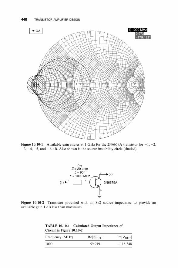
Figure 10.10-1 Available gain circles at 1 GHz for the 2N6679A transistor for �1;�2;�3;�4;�5, and �6 dB. Also shown is the source instability circle (shaded).
Figure 10.10-2 Transistor provided with an 8-W source impedance to provide anavailable gain 1 dB less than maximum.
TABLE 10.10-1 Calculated Output Impedance of
Circuit in Figure 10.10-2
Frequency (MHz) Re[ZOUT] Im[ZOUT]
1000 59.919 �118.348
440 TRANSISTOR AMPLIFIER DESIGN
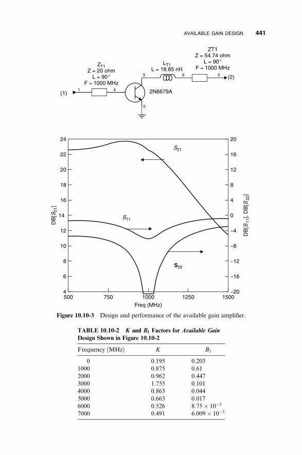
AVAILABLE GAIN DESIGN 441
Figure 10.10-3 Design and performance of the available gain amplifier.
TABLE 10.10-2 K and B1 Factors for Available GainDesign Shown in Figure 10.10-2
Frequency (MHz) K B1
0 0.195 0.2031000 0.875 0.612000 0.962 0.4473000 1.755 0.1014000 0.863 0.0445000 0.663 0.0176000 0.526 8:75� 10�3
7000 0.491 6:009� 10�3

Finally, as with the operating gain design, the available gain design requiresloads near the center of the Smith chart (Fig. 10.10-4) to be stable.
10.11 NOISE IN SYSTEMS
Thermal Noise Limit
One might wonder why it is a concern what the path loss of a radio signal iswhen amplification can be inexpensively added to an arbitrary degree, raising
Figure 10.10-4 Input and output instability circles for the available gain amplifierdesign of Figure 10.10-3.
442 TRANSISTOR AMPLIFIER DESIGN

NOISE IN SYSTEMS 443
any signal, no matter how weak, to a comfortable listening level. The answer isin the thermal noise limit.
An important and unavoidable source of noise in electronic systems is ther-mal noise, whose power level is proportional to absolute temperature. Thisthermal noise is also known as Johnson noise. It is white noise because its densityis frequency independent over much of the electromagnetic spectrum. The open-circuit noise voltage across a resistance R has a zero time average value and amean-squared value of [2, Chapter 8]
hjej2i ¼ 4kTRB ð10:11-1Þ
where e ¼ mean-squared value of the noise voltage
h i ¼ mean value of the quantity inside over time
k ¼ Boltzmann’s constant ¼ 1:38044� 10�23 J/K¼ 8:63� 10�5 eV/K
T ¼ absolute temperature (K)
R ¼ resistance of the noise source, and
B ¼ bandwidth (in Hz) over which the noise is measured
From the equation for available power from a voltage source, the availablenoise power to a network is e2=4R. It follows that the spectral power density ofthermal noise is
PN ¼ kTB ðin wattsÞ ð10:11-2Þ
Notice that thermal noise power (Fig. 10.11-1) is independent of resistance
(or source impedance)! At room temperature (290 K, 20�C, or 68�F) the noisepower in a 1 Hz bandwidth is
PN ¼ ð1:38044� 10�23 J=KÞð290 KÞð1 HzÞ¼ ð1:4 dB� 230 dBþ 24:6 dBÞ W=Hz
¼ �204 dBW=Hz
¼ �174 dBm=Hz ð10:11-3Þ
For example, in an AMPS (Advanced Mobile Phone System) signal band-width of 30 kHz, the thermal noise at 290 K is
30 kHz ¼ 30;000 Hz ¼ þ44:8 Hz ðdBÞPN ¼ �174 dBm=Hzþ 44:8 Hz ðdBÞ ¼ �129:2 dBm
For a standard television channel, having a 6 MHz bandwidth, the noise is

444 TRANSISTOR AMPLIFIER DESIGN
Figure 10.11-1 Thermal noise power available from a resistor.
6 MHz ¼ 6;000;000 Hz ¼ þ67:8 dB
PN ¼ �174 dBm=Hzþ 67:8 Hz ðdBÞ ¼ �106:2 dBm
Therefore, other things being equal, a stronger signal must be received fortelevision reception than for voice communication since the broader bandwidthrequired for television contains more thermal noise. Spread spectrum signals,which artificially employ more bandwidth than the signal information requires,are a special case. Spread spectrum signals can be received below the noisefloor [4].
Other Noise Sources
There are other sources of noise, but the thermal noise is unavoidable andserves as a baseline for the noise to be expected. Some other sources of noiseinclude [5, Sec. 27]:
Flicker noise (also known as 1=f noise), in amplifiers at low frequencies(below 50 kHz) [1, p. 79]
Man-made noise (auto ignitions, sparking motors, etc.)
Atmospheric noise (lightning)
Precipitation static (caused by rain, hail, snow)
Galactic noise (exoatmospheric noises, e.g., the sun)
Carrier noise, caused by the discrete nature of charge carriers in diodes,transistors, and tubes

NOISE IN SYSTEMS 445
Despite the number of additional noise sources beyond thermal noise, most
radio system performances estimates are based on limitations imposed only by
thermal noise. The apparent reasoning for this is that other noise sources arenot always prevalent, and when they are, may be compensated by the systemmargin. The noise margin is the di¤erence between the thermal noise floor andthe anticipated signal strength at the receiver under ideal (usually line of sight)transmission conditions. A portion of the noise margin is required to compen-sate for the signal losses attendant with multiple bounces around buildings andother obstacles.
Noise Figure of a Two-Port Network
The noise factor F of a linear two-port network is the ratio of the available noise
power at its output, PNO, divided by the product of the available noise power at its
input, PNI , times the network’s numeric gain G. Thus,
PNO PNOF ¼ ¼ ð10:11-4Þ
PNIG PNI
where PNO is the output noise power referred to the input terminals, that is,the output noise power divided by the gain G. An equivalent statement is:Noise factor F is the ratio of the signal/noise power at the input to the signal/
noise power at the output.
When expressed in decibels the noise power ratio is called the noise figure,
NF:
Noise figure ¼ NF ¼ 10 log F ð10:11-5ÞSince F is a function of PNI , it does not uniquely characterize the noise perfor-mance of the two-port network. For example, if a very high noise temperature is
used at the input in the determination of F, it will tend to swamp out the noise
introduced by the two-port network, resulting in a lower measured noise factor or
noise figure.
To overcome the uncertainty in the specification of the noise factor or noisefigure of a two-port network, the Institute of Electrical and Electronics En-
gineers (IEEE) has standardized the definition by specifying PNI as the noise
available from a resistor at 290 K. Thus
PNI 1 kT0B where T0 ¼ 290 K ð17�C or 62:6�FÞ ð10:11-6Þ
Accordingly, for noise factor measurements, one must use
kT0 ¼ 4� 10�21 W=Hz ð10:11-7Þ
and the standard noise factor becomes
PNOF ¼ ð10:11-8Þ
kT0B

446 TRANSISTOR AMPLIFIER DESIGN
Figure 10.11-2 Calculation of amplifier noise factor F by referring all noise sources tothe input of the amplifier.
where PNO ¼ PNO=G is the total output noise power referred to the input portwhen the input signal channel is terminated by a resistor at temperature T0.
As an example, consider an amplifier with a gain of 20 dB and a bandwidthof 5 MHz. Assume that the output noise power generated by the amplifier in its5 MHz bandwidth is GPNG ¼ �83 dBm, where PNG is the noise generated bythe amplifier, referred to the input port. The noise figure (Fig. 10.11-2) of theamplifier is calculated as
kT0B ¼ ð4� 10�21 W=HzÞð5� 106 HzÞ ¼ 2� 10�14 W
PNGG ¼ 5� 10�12 W
Since the two noise sources are uncorrelated, their power values can be added,thus
PNO ¼ 100ð2� 10�14 WÞ þ 5� 10�12 W ¼ 7� 10�12 W
PNO ¼ 7� 10�14 W
PNO 7� 10�14 WF ¼ ¼ ¼ 3:5 ðor 5:4 dBÞ
kT0B 2� 10�14 W
Note that both noise sources can be referred to the input port. Thus
PNO ¼ kT0Bþ PNG
total output noise ðreferred to the inputÞF ¼ ð10:11-9Þ
thermal noise at input
PNG¼ kT0Bþ PNG ¼ 1þkT0B kT0B

NOISE IN SYSTEMS 447
Figure 10.11-3 Noise factor for a cascade of two ports, each with its own noise factorFi and gain Gi.
Noise Factor of a Cascade
When separate networks are cascaded each having its own gain Gi and noisefactor Fi, all networks add noise to the signal that travels through them, but thecontribution to the overall noise factor from succeeding networks is reducedwhen previous stages have amplified the signal (Fig. 10.11-3). The overall noisefactor is calculated using
F2 � 1 F3 � 1 Fi � 1FCascade ¼ F1 þ þ þ � � � þ
G1G2 � � �Gi�1þ � � � ð10:11-10Þ
G1 G1G2
Note that the calculation in (10.11-10) must be performed using the numeric
value for gain as well as noise factor F, not NF (in decibels). The implicationsof this simple cascade noise figure formula can be considerable in real systemdesigns.
The noise factor of a matched lossy two-port network is
F ¼ L ð10:11-11Þwhere L is the insertion loss factor of the two-port network. This relationassumes that the physical temperature of the loss element is approximatelyequal to T0 ¼ 290 K. It has a gain equal to the reciprocal of its loss ratio, or
G ¼ 1=L ð10:11-12Þ
For example, a matched two-port network at 290 K having 3 dB of dissipativeloss has a loss ratio L ¼ 2, and this is also its noise factor, F ¼ 2. The gain is1 ¼ 0:5.2
As a system noise figure example, consider the block diagram of a satellitereceiver system in Figure 10.11-4. Suppose that the system has an outdoor dish
Figure 10.11-4 Block diagram of a satellite receiver front end.

448 TRANSISTOR AMPLIFIER DESIGN
antenna pointed at a satellite, and that, to place the receiver electronics in-doors, a cable (with 3-dB loss) from the antenna into the building is used. Thesystem has a bandpass filter (with 2-dB loss) to eliminate out-of-band noise,and a low-noise amplifier with a gain of 15 dB and noise figure of only 1.0 dB.Finally, the low-noise amplifier is followed by a high gain amplifier, having20 dB of gain and noise figure of 2.0 dB. The noise figure of the system is foundas follows.
The noise factor of the cascade in Figure 10.11-4 is found using (10.11-10):
0:58 0:26 0:58FCascade ¼ 2:00þ
0:5þ ð0:5Þð0:63Þ þ ð0:5Þð0:63Þð31:6Þ
¼ 4:04 ðor 6:06 dBÞ
This is a very high value, given the low noise figure of the first amplifier. Eventhough we used a low-noise amplifier with a noise figure of only 1.0 dB, ourfront-end noise figure is 6 dB. After some consideration, the low-noise andsecond-stage amplifiers are located in the antenna feed and their output cabledinto the building. The new system block diagram is shown in Figure 10.11-5.
Figure 10.11-5 Revised satellite receiver front end.
For the revised circuit the noise factor is calculated as
0:58 1:00 0:58FCascade ¼ 1:26þ
31:6þ ð31:6Þð100Þ þ ð31:6Þð100Þð0:5Þ
¼ 1:28 ðor 1:07 dBÞ
This revised design has a noise figure that is nearly 5 dB less. Accordingly, asatellite dish antenna with one-third the area, or a little over half the diameter,can be used, yielding the same signal-to-noise ratio.
Noise Temperature
As an alternative to specifying the noise figure of a linear two-port network,one can equivalently specify the e¤ective noise temperature Te (Fig. 10.11-6).This method directly characterizes the noise generated by the two port net-work, PNG, in terms of an equivalent amount of thermal noise produced by a

NOISE IN SYSTEMS 449
Figure 10.11-6 Use of noise temperature Te as an alternative to noise factor.
resistor at the temperature Te. The equivalence is established using the pre-viously derived equation for noise factor F :
F ¼ 1þ PNG
kT0B¼ 1þ kTeB
kT0B¼ 1þ Te
T0ð10:11-13Þ
or conversely
Te ¼ ðF � 1ÞT0 ð10:11-14Þ
It is important to note that Te is not the physical temperature of the two-portnetwork, but merely a way of characterizing its noisiness.
For example, if NF ¼ 6 dB, F ¼ 4 and Te ¼ 3� 290 ¼ 870 K. The noisetemperature of a cascade of networks can be found in a manner similar to thatused for noise factor. If each two-port network has an equivalent noise tem-perature Tei, the cascade has an overall noise temperature Te-Cascade given by
Te2 Te3 TeiTe-Cascade ¼ Te1 þ þ
G1G2þ � � � þ ð10:11-15Þ
G1 G1G2 � � �Gi�1
For the previous satellite system the total noise temperature can be calcu-lated using the respective e¤ective noise temperatures of the components. Thesevalues are calculated using the noise factor values defined previously and theconversion formula:

450 TRANSISTOR AMPLIFIER DESIGN
TeF ¼ 1þ or Te ¼ ðF � 1ÞT0
T0
Using this relation, the e¤ective noise temperatures of the component two portsare: The LNA (75.4 K), the second-stage amp (168.2 K), the cable (290 K), andthe bandpass filter (168.2 K). Applying (10.11-13) gives
168:2 290 168:2Te-Cascade ¼ 75:4þ
31:6þ ð31:6Þð100Þ þ ð31:6Þð100Þð0:5Þ
¼ 75:4þ 5:32þ 0:09þ 0:11
¼ 80:9 K
Converting this 80.9 K e¤ective noise temperature to noise factor F ,
Te 80:9F ¼ 1þ ¼ 1þ ¼ 1:28
T0 290
Expressed in decibels, the noise figure (NF) is then 1.07 dB, as we calculatedpreviously.
10.12 LOW-NOISE AMPLIFIERS
Transistors require an optimum source reflection coe‰cient, GOPT, or equiv-alently an optimum source impedance, ZOPT, at their input in order to deliverlowest noise factor, FMIN. Since source reflection coe‰cient (or equivalently,source impedance) is specified, the available gain design method is used for low-
noise amplifiers. If the source is not equal to GOPT, then the actual noise factorF of the amplifier is given by [2, Sec. 9.2]
Rn jGS � GOPTj ð10:12-1Þ2
F ¼ FMIN þZ0 ð1� jGSj2Þj1þ GOPTj
where Rn is the correlation resistance and Z0 is the characteristic impedance of
the system in which GOPT is measured. The values of FMIN;GOPT, and Rn arespecified by the manufacturer for each test frequency. The values of GS thatprovide a constant noise factor value F form circles on the Smith chart, just asconstant-gain loci are circles on the Smith chart. Given FMIN;GOPT, and Rn,these circles can be plotted for various values of F in excess of FMIN for a giventransistor and frequency. The circles [2] have centers at
GOPTc ¼ ð10:12-2Þ
N þ 1

LOW-NOISE AMPLIFIERS 451
and radii
r ¼ffiffiffiffiffiffiffiffiffiffiffiffiffiffiffiffiffiffiffiffiffiffiffiffiffiffiffiffiffiffiffiffiffiffiffiffiffiffiffiffiffiffiffiffi N½N þ ð1� jGOPTj2Þ�
q N þ 1
ð10:12-3Þ
where
Z0ðF � FMINÞj1þ GOPTj2N ¼ ð10:12-4Þ
4Rn
As an example, consider the design of an amplifier to operate at 2000 MHz. Toobtain a low noise figure, a gallium arsenide field-e¤ect transistor (FET),model NE67300, is selected, S and noise parameters for which are shown inTable 10.12-1 [6]. The data for the unpackaged device (transistor chip) are usedfor this example.
TABLE 10.12-1 Fifty-Ohm System S and Noise Parameters for NE67300 Low-Noise
Transistora
! FILENAME: NE67300.S2P! NEC PART NUMBER: NE67300! BIAS CONDITIONS VDS ¼ 3 V, IDS ¼ 10 mA# GHz S MA R 50! S-Parameter DATA2 0.95 �26 3.79 161 0.04 79 0.59 �134 0.89 �50 3.26 141 0.06 66 0.58 �246 0.82 �70 2.83 126 0.08 56 0.54 �338 0.78 �88 2.55 114 0.09 51 0.50 �4210 0.73 �102 2.21 104 0.10 48 0.47 �4812 0.71 �114 2.16 93 0.10 43 0.45 �5514 0.71 �122 2.11 90 0.11 44 0.47 �6216 0.67 �128 1.92 76 0.11 43 0.49 �6418 0.66 �140 1.81 63 0.11 40 0.52 �70! NOISE PARAMETERS1 0.30 0.90 17 0.652 0.35 0.84 40 0.574 0.40 0.72 79 0.486 0.55 0.62 112 0.398 0.80 0.56 143 0.3310 1.1 0.50 168 0.2812 1.4 0.46 �165 0.2414 1.7 0.43 �140 0.2016 2.0 0.40 �112 0.1818 2.5 0.40 �84 0.16
aNoise parameters are (left to right): freq (GHz), FMIN (dB), Mag½GOPT�; angle½GOPT�, and ðRn=Z0Þ.

452 TRANSISTOR AMPLIFIER DESIGN
Figure 10.12-1 Performance of the NE67300 with frequency.
The gain ðS21Þ, minimum noise figure, NFMIN and actual noise figure, NFwhen no matching is provided are shown in Figure 10.12-1. It can be seen thatwithout the necessary circuitry to present GOPT to the input, the transistor has amuch higher noise figure than the minimum of which it is capable. At 2 GHz,NF ¼ 2:0 dB while NFMIN ¼ 0:4 dB.
From the calculated data in Figure 10.12-1 it is evident that an amplifierbuilt using the NE67300 could yield a noise figure as low as 0.4 dB at 2 GHz.However, the device is potentially unstable over the 2 to 18 GHz bandwidth, asseen from the values of K and B1 in Figure 10.12-2.
Therefore, before embarking on the amplifier design, we will add some cir-cuit elements to improve the stability conditions. Often it is found that use ofan inductor in series with the common lead, in this case the drain, producesnegative feedback that improves stability, tends to make GOPT and G1M (thesource reflection coe‰cient for maximum gain) move closer to each other, anddoes not materially increase NFMIN. Figure 10.12-3 shows the result of using a1-nH inductor for this purpose.
The drain lead inductor has improved the stability in that the K factor ismuch closer to unity over a broad portion of the gainful bandwidth of thetransistor. This has been obtained at the expense of gain; however, some ofthe gain loss can be recovered by tuning the output. Since the circuit is not yet

LOW-NOISE AMPLIFIERS 453
Figure 10.12-2 Stability values K and B1 for the NE67300.
fully stabilized, particularly at the operating frequency of 2 GHz, we add someresistive damping to the output of the transistor. Placing resistive elements inthe input circuit would more seriously reduce NFMIN. Figure 10.12-4 shows theresults of adding a series RC (R ¼ 300 W and C ¼ 10 pF) circuit across theoutput to provide increasing damping with frequency.
It can be seen that the transistor is almost stable over the entire bandwidthfor which it has gain. It is not always necessary to obtain unconditional stabil-
Figure 10.12-3 Stability factors with a 1-nH drain inductor.

454 TRANSISTOR AMPLIFIER DESIGN
Figure 10.12-4 Amplifier performance with drain inductor and collector RC networkfor stability.
ity for a low-noise amplifier because its source and load impedances usually arewell controlled and not subject to variation. However, this example shows howstability can be improved without sacrificing much of NFMIN. For the circuit ofFigure 10.12-4, NFMIN is only 0.5 dB. The new value of GOPT for this networkis 0:785J41:4�. The corresponding impedance, ZOPT ¼ ð43:9þ j118:4Þ W, andthe constant NF circles are shown in Figure 10.12-5.
It can be seen from Figure 10.12-5 that the GOPT and G1M source reflectionsare fairly close to each other. Nevertheless, it would require a sacrifice of 0.5 dBin noise figure to match to G1M ; therefore, we will transform the 50-W sourceto ZOPT. This is done by first transforming 50 W to the required 43.9 W usingan impedance inverter of 46.85 W, and then adding a series inductor of9.43 nH. With this change in the input circuit, the input impedance lookinginto the output is ZIN2 ¼ ð162:1� j75:54Þ W. To transform the 50-W load tothe complex conjugate of ZIN2, we first transform 50 to 162.1 W using an im-pedance inverter of 90� W and add an inductor of 5.86 nH. The final low-noiseamplifier circuit and performance are shown in Figure 10.12-6. The completedlow-noise amplifier circuit has 13.1 dB of gain and a noise figure of 0.5 dB at2 GHz.

10.13 AMPLIFIER NONLINEARITY
Gain Saturation
There is no widely accepted definition for the linearity of a network. Indeed,the appropriate definition of nonlinear e¤ects depends upon the network char-acteristics of concern. For an amplifier, one might wish to know at what powerlevel the output ceases to increase in direct proportion to the input signal. Forthis the 1 dB compression definition is useful. When a voltage vðtÞ is applied tothe input of an amplifier, an output voltage v0ðtÞ appears at the output of theamplifier given by [2, p. 246]
v0ðtÞ ¼ a0 þ a1vðtÞ þ a2v2ðtÞ þ a3v
3ðtÞ þ � � � þ anvnðtÞ ð10:13-1Þ
When the input voltage is small (10.13-1) can be approximated as
v0ðtÞAa1vðtÞ ð10:13-2Þ
and the amplifier’s output is very nearly a constant times the input voltage,with voltage gain a1. As the input voltage is increased, the remaining terms in(10.13-1) become significant and the amplifier displays a nonlinear response.When the coe‰cients ai in (10.13-1) are evaluated for practical amplifiers, it isfound that the sign of a2 is negative, and this is the term responsible for satu-ration and the 1-dB compression.
The 1-dB compression point, P1-dB C , is defined as the output power at which
the output power of the network is 1 dB less than it would have been had its input
to output characteristic remained linear (Fig. 10.13-1). This definition can be
Figure 10.12-5 Constant NF circles for the amplifier in Figure 10.12-4. Circles are for�0:25;�0:5;�1;�1:5;�2;�2:5;�3, and �6 dB below NFMIN ¼ 0:5 dB.
AMPLIFIER NONLINEARITY 455

456 TRANSISTOR AMPLIFIER DESIGN
Figure 10.12-6 Final low-noise amplifier and its performance.
applied to any network. It is useful to determine up to what power levels do theperformance parameters of the amplifier designs presented thus far remainreasonably linear. Beyond the 1-dB compression point, as input power to theamplifier is further increased, the output power reaches a maximum saturated
power output, PSAT.
Intermodulation Distortion
Well below the 1-dB compression point the amplifier’s nonlinearities generateharmonics of the input signal as well as mixing products if two or more input

AMPLIFIER NONLINEARITY 457
Figure 10.13-1 The 1-dB compression point, P1-dB C :
signals are applied simultaneously. Simple harmonics of the input frequency,f0, occur at 2f0; 3f0; 4f0, and so forth. Since these are multiples of the input fre-quency and since typical communication systems have bandwidths of no morethat 10 or 20%, these harmonics can be filtered from the output. Hence, theyare of minimal concern. However, intermodulation terms cannot be so dis-regarded.
The two-tone test consists of applying two closely spaced, equal amplitudefrequencies, f1 and f2, to a nonlinear network. The output of the networkcontains frequency components at DC, f1; f2; 2f1; 2f2; ð2f1 � f2Þ; ð2f2 � f1Þ; 3f1;3f2, and so forth, an infinite number of these multiplying and mixing products.However, the products ð2f1 � f2Þ and ð2f2 � f1Þ are the most troublesome be-cause they occur within the bandwidth of the system (Fig. 10.13-2) and cannotbe removed by filtering. Other mixing products of higher order also appear inthe passband but, because of their higher orders, have less amplitudes than thethird-order products ð2f1 � f2Þ and ð2f2 � f1Þ.
In the language of mixing, the fundamental applied frequencies f1 and f2 aretermed first-order signals. In this nomenclature the frequencies ð2f1 � f2Þ andð2f2 � f1Þ are third-order mixing products. This is because their generation re-quires that one of the input frequencies be doubled (a second-order process) andthen that frequency mixed with the other input frequency (a third-order pro-cess). Accordingly, the solution to avoiding intermodulation products is tooperate the network at a su‰ciently low input power that third-order productshave negligible amplitudes, that is, amplitudes at the level of the backgroundnoise or noise floor.
To identify this power range, we use the fact that, as input power is in-creased, at some input threshold harmonics of the fundamental appear and then

458 TRANSISTOR AMPLIFIER DESIGN
Figure 10.13-2 Frequency spectrum showing principal multiplying and mixing prod-ucts when two closely spaced frequencies, f1 and f2, are applied to a nonlinear network(the two-tone test).
increase at a slope equal to their respective harmonic numbers (Fig. 10.13-3). Tomeasure this e¤ect a spectrum analyzer is connected to the output of the net-work. As input power at f0 reaches a power level PA the second harmonic, 2f0,is seen to rise above the noise level. Thereafter, for each 1-dB increase in thelevel of f0, the second harmonic, 2f0, increases by 2 dB. With a further increaseof the input signal level to PB, it is found that the third harmonic, 3f0, appearsabove the noise and thereafter grows by 3 dB for each 1-dB increase in the levelof input power at f0. In short, the harmonics grow with a slope equal to their
harmonic number.The levels PA and PB are di¤erent for di¤erent networks, but the slopes at
which the harmonics increase are analytically and experimentally found to benearly equal to the harmonic number. A method for determining the powerrange over which noticeable third-order distortion occurs is based on theseobservations. The third-order intercept, P3, is the output power level at whichthe extended third-order harmonic slope meets that of the fundamental. At thisoutput power the ratio of the third-order harmonic to the fundamental theo-retically would be 0 dB. Descending from this power level, for each 1-dB de-crease in the power of f0, all third-order products decrease by 3 dB.
Of course, operation at P3 is impossible since the network’s output powerusually saturates below this level. In fact, it can be shown both experimentallyand analytically using the first three terms in (10.13-1) that the third-order in-tercept is approximately 10 dB above the 1-dB compression point [1, p. 363].However, P3 serves as a convenient power reference for derating the network to
a level that reduces the third-order product to a negligible value. Due to their

AMPLIFIER NONLINEARITY 459
Figure 10.13-3 Growth of harmonics as a function of input power.
3-to-1 ratio, reducing the input power by one-third of the distance in decibelsfrom the noise floor to P3 causes the third harmonic to drop to the noise level(Fig. 10.13-4). The corresponding output power range for f0 is called [1, Sec.4.7] the spurious-free dynamic range (SFDR) and given by
SFDR ðdBÞ ¼ 2½P3 � PNOISE�3
¼ 2½P3 þ 174 dBm� 10 log BW ðdBÞ3
�NF ðdBÞ � G ðdBÞ� ð10:13-3Þ
where
P3 ¼ third-order intercept ðdBmÞBW ¼ amplifier bandwidth ðHzÞNF ¼ amplifier noise figure ðdBÞG ¼ amplifier gain ðdBÞ
For example, an amplifier having 25 dB of gain, a noise figure of 4 dB, abandwidth of 10 MHz, and a 1-dB compression point at 1 W has a SFDR

460 TRANSISTOR AMPLIFIER DESIGN
Figure 10.13-4 Determining the spurious-free dynamic range (SFDR).
calculated as
SFDR ðdBÞ ¼ 2½ð30 dBmþ 10 dBÞ þ 174 dBm� 10 log 107 � 4 dB� 25 dB�3
¼ 77 dB
Sometimes it is desirable to take into account the fact that the minimum de-tectable signal SMIN is somewhat above the noise level, and to adjust the usefuldynamic range of the amplifier accordingly [2, p. 363]. To distinguish this rangefrom that defined in (10.13-3) we define the useful dynamic range (UDR) as
UDR ðdBÞ ¼ 2½P3 þ 174 dBm� 10 log BW ðdBÞ3
�NF ðdBÞ � G ðdBÞ � SMIN ðdBmÞ� ð10:13-4Þwhere
SMIN ¼ minimum detectable signal ðdBmÞIt can be seen that the useful dynamic range is smaller than the SFDR by anamount equal to the minimum detectable signal.
10.14 BROADBANDING WITH FEEDBACK
In general, the S21 gain of a transistor falls o¤ with frequency. If we want anamplifier which has fairly constant gain over a broad bandwidth, a broadband

BROADBANDING WITH FEEDBACK 461
amplifier, then we must arrange the transistor’s input and output circuits tofavor the high end of the band and, possibly, to increase the mismatch at thelow end of the band.
There is no closed-form solution to this task. Some very clever engineeringhas been applied to the problem, but ultimately a certain amount of creativityand guesswork is required to obtain good results. This is a perfect applicationfor computerized assisted guessing, customarily called optimization. Usually,one stabilizes the transistor first. Then, to create a design starting point, theunilateral design is used, neglecting the feedback term S12. Then matching net-works are designed using optimization to tailor the input and output gains toobtain a broadband result.
We will try a di¤erent tack by using feedback. This example uses the HPAT415868 bipolar transistor, having the S parameter data shown in Table10.14-1.
It is a good idea to look at the file to be sure there are no typographicalerrors in it (there is one here, a missing decimal point for the 700-MHz data).Customarily, there is no data for zero frequency since the network analyzerused for measurements does not operate at DC. The network simulator willinterpolate the data to zero frequency, but this is a mathematical interpolation.
TABLE 10.14-1 S Parameter File for HP AT 415868 Transistor
!AT-41586!S-PARAMETERS at Vce ¼ 8 V Ic ¼ 25 mA. LAST UPDATED 08-03-92
# ghz s ma r 50
0.100 0.64 �61 39.4 154 0.014 64 0.82 �240.200 0.59 �101 28.7 169 0.022 53 0.64 �350.300 0.56 �125 21.4 124 0.026 49 0.53 �380.400 0.55 �140 17.0 111 0.030 49 0.47 �390.500 0.54 �151 14.0 104 0.033 50 0.43 �380.600 0.54 �159 11.7 97 0.036 52 0.40 �380.700 0.54 �166 10.1 91 0.039 53 0.40 �370.800 0.54 �171 8.9 86 0.042 55 0.38 �370.900 0.54 �176 7.9 81 0.045 56 0.37 �371.000 0.55 177 7.2 77 0.048 57 0.36 �371.500 0.57 164 4.8 64 0.064 59 0.34 �422.000 0.57 152 3.6 55 0.080 57 0.32 �492.500 0.60 141 2.9 44 0.100 55 0.31 �583.000 0.62 132 2.4 34 0.120 52 0.31 �683.500 0.64 124 2.1 24 0.140 49 0.31 �804.000 0.67 116 1.9 18 0.180 45 0.32 �944.500 0.70 109 1.6 9 0.160 45 0.30 �1095.000 0.73 102 1.5 1 0.170 42 0.30 �1235.500 0.77 96 1.3 �7 0.190 38 0.32 �1386.000 0.76 90 1.2 �14 0.200 33 0.35 �152

462 TRANSISTOR AMPLIFIER DESIGN
TABLE 10.14-2 Edited S Parameter File for the HP AT41586
!AT-41586!S-PARAMETERS at Vce ¼ 8 V Ic ¼ 25 mA. LAST UPDATED 08-03-92
# ghz s ma r 50
0.000 0.70 �40 45 180 0.010 75 0.90 �100.100 0.64 �61 39.4 154 0.014 64 0.82 �240.200 0.59 �101 28.7 169 0.022 53 0.64 �350.300 0.56 �125 21.4 124 0.026 49 0.53 �380.400 0.55 �140 17.0 111 0.030 49 0.47 �390.500 0.54 �151 14.0 104 0.033 50 0.43 �380.600 0.54 �159 11.7 97 0.036 52 0.40 �380.700 0.54 �166 10.1 91 0.039 53 0.40 �370.800 0.54 �171 8.9 86 0.042 55 0.38 �370.900 0.54 �176 7.9 81 0.045 56 0.37 �371.000 0.55 177 7.2 77 0.048 57 0.36 �371.500 0.57 164 4.8 64 0.064 59 0.34 �422.000 0.57 152 3.6 55 0.080 57 0.32 �492.500 0.60 141 2.9 44 0.100 55 0.31 �583.000 0.62 132 2.4 34 0.120 52 0.31 �683.500 0.64 124 2.1 24 0.140 49 0.31 �804.000 0.67 116 1.9 18 0.180 45 0.32 �944.500 0.70 109 1.6 9 0.160 45 0.30 �1095.000 0.73 102 1.5 1 0.170 42 0.30 �1235.500 0.77 96 1.3 �7 0.190 38 0.32 �1386.000 0.76 90 1.2 �14 0.200 33 0.35 �152
We know that the phase angle for zero frequency is 180� (perfect negativefeedback), so it is best to modify the file accordingly. The corrected and revisedfile is shown in Table 10.14-2. With these parameters the calculated stabilitydata are shown in Figure 10.14-1. The transistor is potentially unstable overmost of the 0 to 6000 MHz band; however, K is nearly equal to unity overmuch of the band.
The input and output stability circles for 1 GHz are shown in Figure10.14-2. The device is nearly stable at 1 GHz except for very low impedancespresented to the input circuit. Therefore, we will add a low value of resistancein series with the base lead.
Examining the S21 parameter in Table 10.14-2 reveals that the gain with50-W source and load varies from 31.9 dB at 100 MHz to 17.1 dB at 1000MHz. Suppose that we wish the amplifier to have a flat gain characteristic from50 to 1050 MHz. This bandwidth encompasses the entire VHF and UHF tele-vision transmission bands. To design the amplifier we will use negative feed-back, more feedback at low frequencies than at high frequencies.
Feedback from the collector to base is negative. To favor high frequencieswe will interconnect these leads with a series RL circuit. An impedance in the

BROADBANDING WITH FEEDBACK 463
Figure 10.14-1 Stability and gain of the HP AT415868 bipolar transistor.
emitter to ground path also provides negative feedback. To favor high fre-quencies we will use a parallel RC network there. Using this circuit with nom-inal values, the result is that shown in Figure 10.14-3. Prior to optimization theperformance does not look promising with respect to the design goals.
Next the circuit of Figure 10.14-3 was optimized using the network simula-tor, with performance goals of Mag½S21� ¼ 15 dB, K > 1:1 and B1 > 0:1. Thequestion marks ahead of the element values indicate that the optimizer is
Figure 10.14-2 Input stability circle for HP AT415 at 1 GHz (output stability circledoes not intersect unity Smith chart).

464 TRANSISTOR AMPLIFIER DESIGN
Figure 10.14-3 Amplifier circuit and performance with feedback element values priorto optimization.
allowed to vary that value. Relative weightings (W ) of the errors used inthe simulator optimization were unity for all variables except K , for whichW ¼ 10. This causes an error of 0.1 in K is to be considered equally with a gainerror of 1 dB by the optimizer. Note that the 15 dB goal for the gain was setbelow the minimum gain of 17.1 dB established from the S parameter data.
Starting with nominal initial component values shown in Figure 10.14-3, the

BROADBANDING WITH FEEDBACK 465
Figure 10.14-4 Final circuit and performance of the 50- to 1000-MHz amplifier usingfeedback and the 415858b transistor.
network simulator optimized the circuit, and the results are shown in Figure10.14-4. The capacitance C1 can be eliminated because the optimized value isnear zero. The gain is within 0.4 dB of 15 dB over the 50 to 1050 MHz band.The stability factor K was 1.1 or greater and B1 was greater than 0.1 over thewhole gainful range of the transistor, from 0 to 6000 MHz. Probably less gain

466 TRANSISTOR AMPLIFIER DESIGN
variation and/or a wider bandwidth could be obtained, but this result is re-markable for the fact that only four components (not counting C1) were used toachieve the result and their function had to include unconditionally stabilizingthe transistor over the 0 to 6000 MHz frequency range.
In an initial optimization trial a gain goal of 16 dB was set. This gain wasobtained with even smaller variation with frequency, but the resulting amplifierwas potentially unstable ðK < 1Þ over most of the 0 to 6000 MHz bandwidth.Reducing the gain goal to 15 dB did not yield a stable amplifier until theweighting of K was increased from 1 to 10, emphasizing the importance of thisgoal. From this it can be seen that fairly narrow margins exist around theachievable goals with a particular transistor and its circuit. Setting goals withinthe margins is a crucial part of the optimization.
10.15 CASCADING AMPLIFIER STAGES
When two amplifiers having the circuit of Figure 10.14-4 are cascaded, theirgains add without very much mismatch error, and the resulting gain is within1 dB of 30 dB from 50 to 1100 MHz, as shown in Figure 10.15-1. This is unusualand occurs because the S11 and S22 magnitudes (Fig. 10.15-2) of each amplifiersection are fairly small, especially S11. When either the input or output of asingle-stage amplifier is well matched, the cascade combination of two of themwill have low mismatch interaction. The feedback method of broadbandingprovides a better match than does broadbanding by reflecting unwanted gain.
For example, suppose that we had applied the same set of goals to optimizethe circuit shown in Figure 10.15-2. Its performance after optimization is alsoshown in Figure 10.15-2.
This circuit o¤ers nearly the same gain flatness over the 50 to 1050 MHz
bandwidth and also is unconditionally stable from 0 to 6000 MHz. However,the input and output mismatches, S11 and S22, of this circuit are greater thanthose of the feedback optimized circuit of Figure 10.15-1; consequently, whentwo of these stages are cascaded together, as shown in Figure 10.15-3, a largervariation of gain, almostG3 dB over the 50 to 1050 MHz band, occurs due tothe mismatch error (Section 4.8).
Designing broadband amplifiers and cascaded amplifier stages does requireguesswork, or optimizing. However, certain strategies are useful in this pur-suit. First, since transistor gain diminishes as frequency increases, circuitry thatfavors the passage of higher frequencies (series capacitors and shunt inductors)is more likely to give uniform gain with frequency.
Circuits which flatten gain using feedback may provide lower S11 and S22
values, minimizing the mismatch error when the circuits are cascaded or usedwith other reflective components, such as reactive filters. Finally, S11 and S22
can be made part of the optimization goals. If either S11 or S22 has a smallvalue, then two such circuits cascaded will have a relatively low mismatcherror.

CASCADING AMPLIFIER STAGES 467
Figure 10.15-1 Two amplifiers cascaded.

468 TRANSISTOR AMPLIFIER DESIGN
Figure 10.15-2 Alternate 50- to 1050-MHz amplifier design using the 415858b tran-sistor.
10.16 AMPLIFIER DESIGN SUMMARY
For most amplifier designs the choices amount to what input and output im-pedance environments will be presented to the transistor over all of the fre-quency range for which it has gain. One must balance the need for gain againstthe requirements for unconditional stability since an amplifier that breaks intooscillation is not only useless, it is a liability. Inevitably, the design choices leadto amplifier networks that do not present a match to either the input or output

AMPLIFIER DESIGN SUMMARY 469
Figure 10.15-3 Gain of the cascade combination of two of the circuit shown in Figure10.15-2.
transmission lines. If the remainder of the system also has high mismatches,such as would be true if reactive filters are connected to the amplifier, the per-formance will not be predictable unless those networks are modeled along withthe amplifier. Many points have been covered in this chapter, but in the endsome artistry is required of the amplifier designer to balance all of the desiredamplifier attributes with the relatively few degrees of design freedom available.

470 TRANSISTOR AMPLIFIER DESIGN
REFERENCES
1. Guillermo Gonzalez, Microwave Transistor Amplifiers, Analysis and Design, 2nd ed.,Prentice-Hall, Upper Saddle River, NJ, 1984. An excellent engineering reference for
transistor amplifier design.
2. Theodore Grosch, Small Signal Microwave Amplifier Design, Noble Publishing,Norcross, GA, 1999. The author presents a thorough derivation of all of the important
formulas for transistor amplifier design and evaluation, based on the S parameters of
the transistor and the circuit, which surrounds it.
3. Genesys 7 Reference Manual, Eagleware, Norcross, GA, 1986–2000. This is the ref-
erence manual for the CAD program used as a network simulator for the examples of
this text. Note that early versions of this manual have an error in the equation for B1 on
page 324. Use the corrected expression (10.3-5) given in this text.
4. Joseph F. White, ‘‘What is CDMA?’’ Applied Microwave & Wireless, Fall, 1993, pp.5–8. A simplified presentation of the CDMA format.
5. Reference Data for Radio Engineers, 5th ed., Howard W. Sams & Co., New York,1974. Newer editions are available. This is a classic reference for useful radio data.
6. California Eastern Laboratories (CEL), RF and Microwave Semiconductors (theCD), Selection Guide and Design Parameter Library, CEL, Santa Clara, CA, 1999–2000. This is the CD of the CEL catalog and contains data for thousands of transistors,
both bipolar and FET. In addition, there are very well written application notes de-
scribing transistor amplifier design. All of this is provided free of charge.
EXERCISES
E10.3-1 a. Using the S parameter table below, calculate the K and B1 fac-tors for the 2N6603A transistor at 1 GHz.
b. What can you conclude from these values?
Freq (GHz) S11 S21 S12 S22
0.1 0.69 �30 12.16 160 0.03 72 0.95 160.2 0.65 �61 11.03 143 0.05 59 0.84 310.5 0.63 �122 7.05 111 0.07 36 0.56 541 0.64 �158 4.13 88 0.09 28 0.39 682 0.65 170 2.14 61 0.11 29 0.33 91
E10.5-1 a. Calculate the unilateral gain figure of merit for the 2N6603Atransistor.
b. What does this figure of merit indicate about the accuracy of es-timating the gain of the transistor as 20 logjS21j?
E10.5-2 a. Estimate the GS;G0, and GL gains at 1000 MHz of the 2N6603Atransistor based on its S parameters.

EXERCISES 471
b. What is the total estimated unilateral gain if source and load aretransformed to S � and S �
21, respectively?11
E10.5-3 a. Verify the G0 gain for the 2N6603A using a network simulatorand plot gain, K and B1 over the frequency of the S parameters.
b. Match the input at 1 GHz to the untuned transistor’s ZIN. Byhow much did the gain increase at 1 GHz?
c. Next add matching to the output, matching to the untuned tran-sistor’s ZOUT.
d. How well matched are the resulting S11 and S22?
e. How close is the total gain at 1 GHz to the sum GS þ G0 þ GL?
f. Is the total gain ‘‘error’’ within the bounds predicted by the uni-lateral figure of merit calculated in E10.5-1?
E10.7-1 a. Use the network simulator to determine the input and outputimpedances ZSM and ZLM to be presented to the 2N6603A for asimultaneous conjugate match at 1 GHz.
b. Would the simulator provide the required ZSM and ZLM imped-ances? Interpret this result.
E10.7-2 a. Examine the input stability of the 2N6603A by plotting the inputstability circle on the Smith chart (use a network simulator todo this if available) and determine a series resistance value atthe input, which will unconditionally stabilize the transistor at1000 MHz.
b. Using this circuit find the ZSM and ZLM impedances.
c. Add the matching circuits for ZSM and ZLM to the stabilizedschematic.
d. Plot the gain and S11 and S22 for the conjugately matched circuit.
e. Is this what you expected?
f. What performance compromise have you made?
g. Is your design unconditionally stable at all frequencies?
E10.7-3 a. Stabilize the 2N6603A transistor at all frequencies for which thetransistor has gain, including DC. Modify the S parameter file tocorrect the DC S parameters so that the argument of S21 is 180�
and its magnitude (b) is appropriate to DC. Extrapolate its bfrom the RF S21 parameters.
b. Recalculate ZSM and ZLM at 1 GHz and redesign the amplifierto use these values.
c. What is your final performance?
d. What performance compromise have you made for uncondi-tional stability at all frequencies?
e. Was your stabilizing technique the most e‰cient possible?

472 TRANSISTOR AMPLIFIER DESIGN
E10.9 a. Design an amplifier using the operating gain method and theMotorola 2N66l79A bipolar transistor to have 20 dB of gain at1 GHz. The S parameters are listed in Table 10.1-1. For this ex-ercise, the circuit need only be stable at 1 GHz using the sourceand load impedances you employ to obtain the 20 dB of gain.
b. Plot S21;S11, and S22 of the resulting circuit over the bandwidthfor which S parameters are given.
E10.12-1 a. Design a low-noise amplifier for use at 850 MHz using the HPAT30511 (S and noise parameters in table below). Obtain asmuch gain as you can, consistent with a noise figure of no morethan 0.5 dB.
b. Plot gain and noise figure from 600 to 1100 MHz.
!AT-30511!S and NOISE PARAMETERS at Vce ¼ 2.7 V Ic ¼ 1 mA.
# ghz s ma r 500.1 0.97 �5 3.50 175 0.01 86 0.999 �20.5 0.95 �23 3.38 156 0.05 74 0.96 �130.9 0.86 �39 3.20 139 0.08 63 0.93 �231 0.84 �43 3.10 135 0.08 60 0.92 �251.5 0.72 �63 2.80 115 0.11 49 0.85 �341.8 0.65 �73 2.60 105 0.12 43 0.82 �382 0.61 �80 2.53 99 0.13 40 0.79 �41!Noise Parameters0.5 0.3 0.96 10 1.490.9 0.4 0.92 19 1.331.8 0.9 0.83 43 0.98
E10.13-1 a. You are testing a newly designed amplifier that has a 1-dB noisefigure and 20 dB of small signal gain using a spectrum analyzerat its output. The output bandwidth is limited by an integralfilter to 800 to 1000 MHz. You observe that with a 900-MHzinput signal of varying amplitude the third harmonic (at 2700MHz) is just discernible near the noise level when the outputpower of the fundamental is 0.1 mW (�10 dBm). What is thethird-order intercept for this amplifier–filter network?
b. What is the spurious-free dynamic range (SFDR) of this net-work?
E10.14-1 a. Design a broadband amplifier to operate from 50 to 1000 MHz(the entire television band) using the 2N6603A transistor. Startusing a circuit unconditionally stabilized over the 0 to 2000 MHzband. Hint: Use the stabilized transistor circuit developed in

EXERCISES 473
E10.7-3 as a starting point. Add L-C networks to the input andoutput for matching and use an optimizer. Try for a flat 10 dB ofgain from 50 to 1000 MHz and add the requirement that K > 1:1and B1 > 0:1 for 0 to 2000 MHz (the whole range for which wehave S parameters).
b. Plot the gain, K and B1 over the 0 to 2000 MHz bandwidth.
E10.15-1 a. Cascade two copies of the broadband amplifier designed inE10.14-1 and plot the combined gain from 0 to 2000 MHz,combining the paralleled capacitors at the interconnection of thetwo stages.
b. Use the optimizer to design a 20-dB flat gain amplifier from 50 to1000 MHz. Also require unconditional stability from 0 to 2000MHz (the whole range for which we have S parameters).
c. How well matched is the cascade amplifier?
d. Could you have accomplished the same result but with betterinput and output VSWR? How would you alter the circuit toaccomplish this?
e. Alter the circuit and see if you can obtain a maximum return lossat the input and output of �15 dB while maintaining stabilityand fairly flat 20-dB gain over 50 to 1000 MHz.

APPENDIX A
Symbols and Units
This appendix lists the principal symbols used in this book in two groups,roman and Greek characters. The listing may not include symbols used in briefdescriptions and derivations or standard symbols such as e; j; p, and so forth.Where applicable the standard international (SI) unit is listed along with itsabbreviation. The general notational conventions used in the text (to connotegeneral or sinusoidal time variation, vector, and normalized quantities) as wellas coordinate systems are described in Section 1.3.
Standard InternationalSymbol Quantity Unit and Abbreviation
Roman Characters
~AA Three-dimensional Dimensions of vector quantity
~AAvector ¼ Ax~xxþ Ay~yyþ Az~zz
Vector potential(e.g., volts/meter for ~EE)
A;B;C;D ABCD matrix elements A and D are dimensionless, B isin ohms (W), C in mhos (
W
)AC Antenna capture area Meters2 (m2)AEFF Antenna e¤ective area Meters2 (m2)ak Incident wave at port k, used Watts1=2 (W1=2)
with S matrixB Magnetic flux density Webers/meter2 (W/m2) or teslas
(T)B AC susceptance Mhos (
W
)b Normalized susceptance Dimensionlessbk Scattered wave from port k, Watts1=2 (W1=2)
used with S matrixC Capacitance Farads (F)c Velocity of light in a vacuum Meters/second (m/s)D Electric flux density Coulombs/meter2 (C/m2)d Distance from load end of Meters (m)
transmission line
High Frequency Techniques: An Introduction to RF and Microwave Engineering, By Joseph F. White. ISBN 0-471-45591-1 6 2004 John Wiley & Sons, Inc.
474

SYMBOLS AND UNITS 475
Standard InternationalSymbol Quantity Unit and Abbreviation
E Electric field intensity Volts/meter (V/m)e Charge on the electron Coulombs (C)F Force Newtons (N)f AC frequency Hertz (Hz)fC Cuto¤ frequency Hertz (Hz)f0 Design center frequency Hertz (Hz)fR Self-resonant frequency due to Hertz (Hz)
parasitics of a lumped R, L,or C
W
G Conductance Mhos ( )g Normalized conductance DimensionlessG Gain Dimensionlessagk Normalized elements values of Dimensionless
low-pass filterg 0k Normalized elements of high- Dimensionless
pass filterH Magnetic field intensity Amperes/meter (A/m)I; I Electric current Amperes (A)IL Insertion loss or isolation DimensionlessaJ; Jk
Current densityWave number ¼ o
ffiffiffiffiffipme ¼ 2p=l
Amperes/meter2 (A/m2)Meter�1 (m�1)
kC Coupling coe‰cient of a direc- Dimensionlesstional coupler
kT Transmission coe‰cient of a Dimensionlessdirectional coupler
L Inductance Henry (or henries) (H)l Length, usually of a transmis- Meters (m)
sion lineln Natural logarithm (base e) Dimensionlesslog Common logarithm (base 10) DimensionlessM Magnetization Amperes/meter (A/m)n Transformer turns ratio DimensionlessP Power Watts (W)PA Available generator power Watts (W)Q Circuit quality DimensionlessQU ;QL;QE Unloaded, loaded, and exter- Dimensionless
nal Qs of a resonatorq Electric charge Coulombs (C)R Resistance Ohms (W)r Normalized resistance Dimensionless~rr,~yy, and ~jj Unit vectors in the r, y, and j Dimensionless
directions of spherical coor-dinate system
~rr, ~jj, and~zz Unit vectors in the r, j, and z Dimensionlessdirections of cylindrical co-ordinate system

476 SYMBOLS AND UNITS
Standard InternationalSymbol Quantity Unit and Abbreviation
Meters2 (m2) Dimensionless Dimensionless
Seconds (s) Dimensionless
Dimensionless
Dimensionless
Seconds (s) Dimensionless Dimensionlessa Joules (J) Joules (J) Joules (J) Volts (V) Meters/second (m/s) Meters/second (m/s)
Meters/second (m/s) Meters/second (m/s) Ohms (W) Dimensionless
Dimensionless
S Surface areaSWR or VSWR Standing-wave ratioSnn;Smn Scattering coe‰cient at port n
or between ports mn
T Period of an AC signalT Transmission coe‰cient of a
networkTn Chebyshev polynomial of
order nT11;T12;T21;T22 Elements of the transmission
matrixt Timetan d Dielectric loss tangentTL Transducer loss (or gain)U EnergyUE Stored electric energyUM Stored magnetic energyV Electric potential or voltagev Velocityv EM wave velocity in an un-
bounded mediumð¼ c=
pffiffiffiffiffiffiffiffiffiffiffi mReRÞ
vg Group velocityvp Phase velocityX AC reactancexx; ~ zz~ yy;~ Unit vectors in the x, y, and z
directions of rectangular co-ordinate system
x Normalized reactance
W
W
W
Y AC admittance Mhos ( ))
)
Y0 Transmission line characteris- Mhos (tic admittance
Y matrix element Mhos (yijZ AC impedance Ohms (W)ZOE Even mode impedance of cou- Ohms (W)
pled line pairZOO Odd mode impedance of cou- Ohms (WÞ
pled line pairZTE Wave impedance of TE mode Ohms (WÞZTM Wave impedance of TM mode Ohms (WÞzij Z matrix element Ohms (WÞ
Greek Symbols
a Attenuation constant Nepers/meter (Np/m) or decibels/meter (dB/m)

SYMBOLS AND UNITS 477
Standard InternationalSymbol Quantity Unit and Abbreviation
aC Attenuation constant asso- Nepers/meter (Np/m) or decibels/ciated with conductors meter (dB/m)
aD Attenuation constant asso- Nepers/meter (Np/m) or decibels/ciated with dielectrics meter (dB/m)
b Phase constant Radian/meter (rad/m) or degrees/meter (�/m)
g Propagation constant Meters�1 (m�1)G Reflection coe‰cient DimensionlessGG Generator reflection coe‰cient DimensionlessGL Load reflection coe‰cient DimensionlessdS Skin depth Meters (m)e0 Permittivity of free space Farads/meter (F/m)eR Relative permittivity factor or Dimensionless
dielectric constant
e Permittivity ð¼ e0eRÞ Farads/meter (F/m)h Intrinsic impedance of an un- Ohms (WÞ
bounded mediumy Electrical length ð¼ blÞ of a Radians (rad) or degrees (�)
transmission liney Power factor angle (between Radians (rad) or degrees (�)
voltage and current)l0 Wavelength in free space Meters (m)l Wavelength in an unbounded
medium ð¼ l0=ffiffiffiffiffiffiffiffiffiffiffi mReR
p ÞMeters (m)
lC Cuto¤ wavelength Meters (m)lG Guide wavelength Meters (m)m0 Permeability of free space Henries/meter (H/m)mR Relative permeability Dimensionlessm Permeability ð¼ mRm0Þ Henries/meter (H/m)r Resistivity Ohm-meters (W-m)r Charge density Coulombs/meter3 (C/m3)s Conductivity Mhos/meter (
W
/m)o Radian frequency Radians/second (rad/s)
aThe quantity is dimensionless, however, the numeric value may be expressed in decibels (dB).

APPENDIX B
COMPLEX MATHEMATICS
THE IMAGINARY NUMBER
Complex numbers, having a real and imaginary part, probably arose out of apurely mathematical exploration of the description of what would happen ifthere were a square root of �1. Since this seemed unreal, mathematicians calledthis the imaginary number, denoted as i, thus
pffiffiffiffiffiffiffi i ¼ �1 ðB:1Þ
Mathematicians evolved a complete set of operations about how complex
numbers [1], having real and imaginary parts, would behave, probably withoutregard to any practical application such a number system might have.
This peculiar inquiry was to have a profound e¤ect on electrical engineering.Many circuit applications involved finding the voltage and currents resultingwhen a sinusoidally varying excitation was applied to a network. When a sin-usoid is applied to a linear network consisting of RLC elements, all resultingvoltages and currents are sinusoidal at the same frequency. This meant that, atmost, the analysis of a network involved finding the magnitude and phase ofthe resulting sinusoidal response. The rules established by mathematicians forcomplex numbers proved to be perfect for analyzing alternating current (AC)circuits.
Electrical engineers customarily use the letter i to represent electric current.Therefore, for electrical engineering purposes, the imaginary number was as-signed the symbol j, thus
pffiffiffiffiffiffiffi j ¼ �1 ðB:2Þ
The mathematics of complex numbers is extensive [1], but for AC analysis, weneed only consider the basic complex number functions: addition, subtraction,multiplication, and division, the rectangular and polar formats, and forming thecomplex conjugate.
High Frequency Techniques: An Introduction to RF and Microwave Engineering, By Joseph F. White. ISBN 0-471-45591-1 6 2004 John Wiley & Sons, Inc.
478
RECTANGULAR TO POLAR CONVERSION 479
First, a complex number can be expressed in rectangular form as
Z ¼ aþ jb ðB:3Þ
COMPLEX ADDITION
To add two complex numbers, use either rectangular form and add their real and
imaginary parts together, respectively:
ðaþ jbÞ þ ðcþ jdÞ ¼ ðaþ cÞ þ jðbþ dÞ ðB:4Þ
For example:
ð3þ j9Þ þ ð4þ j2Þ ¼ 7þ j11
ð3þ j9Þ þ ð4� j2Þ ¼ 7þ j7
ð3þ j9Þ þ ð�4þ j13Þ ¼ �1þ j22
ð�3� j9Þ þ ð4� j5Þ ¼ 1� j14
COMPLEX SUBTRACTION
To subtract one complex number from another, use their rectangular form and
subtract their real and imaginary parts, respectively:
ðaþ jbÞ � ðcþ jdÞ ¼ ða� cÞ þ jðb� dÞ ðB:5Þ
For example,
ð3þ j9Þ � ð4þ j2Þ ¼ �1þ j7
ð3þ j9Þ � ð4� j2Þ ¼ �1þ j11
ð3þ j9Þ � ð�4þ j13Þ ¼ 7� j4
ð�3� j9Þ � ð4� j5Þ ¼ �7� j4
For multiplication or division, the complex number is best converted into polar
form.
RECTANGULAR TO POLAR CONVERSION
The complex number has real and imaginary parts orthogonal to each other. Itcan be visualized as a vector. However, in electrical engineering electric and

480 COMPLEX MATHEMATICS
Figure B.1 Vector representation of a complex number Z in the complex plane.
magnetic fields are vector quantities. In order to di¤erentiate complex quanti-ties representing voltage, current, or field magnitudes from spatial field vectors,the Institute of Electrical and Electronics Engineers (IEEE) suggests that thecomplex number representing a sinusoidal quantity be termed a phasor. Thiswill be the special term used to describe the two-dimensional complex number.Think of the complex number as having a real part x along the horizontal axis
and an imaginary part of magnitude y along the j axis (Fig. B.1).Let
Z ¼ xþ jy ¼ aþ jb ðB:6Þ
Since, in this case, x ¼ a and y ¼ b, and applying the Pythagorean formula, thepolar form of Z is Z ¼ rJy, this is formed as
qffiffiffiffiffiffiffiffiffiffiffiffiffiffiffiffiffiffiffi b
Z ¼ aþ jb ¼ ða2 þ b2ÞJtan�1 ¼ rJy ðB:7Þa
where r is the magnitude and y is the angle of Z. For example,qffiffiffiffiffiffiffiffiffiffiffiffiffiffiffiffiffiffiffi Z ¼ 4þ j3 ¼ ð42 þ 32ÞJtan�1 3 ¼ 5J37� ðB:8Þ4
POLAR TO RECTANGULAR CONVERSION
To convert from polar to rectangular form (Fig. B.2):
Z ¼ rJy ¼ ðr cos yÞ þ jðr sin yÞ ðB:9Þ
For example,
Z ¼ 5J37� ¼ ð5 cos 37�Þ þ jð5 sin 37�Þ ¼ 4þ j3 ðB:10Þ

COMPLEX DIVISION 481
Figure B.2 Conversion between polar and rectangular forms of a complex number, Z.
COMPLEX MULTIPLICATION
To multiply two complex numbers convert them to polar format; then multiply
their magnitudes and add their angles, respectively:
Z1Z2 ¼ ðr1Jy1Þðr2Jy2Þ ¼ ðr1r2ÞJðy1 þ y2Þ ðB:11Þ
For example,
ð3þ j4Þð5� j8Þ ¼ ð5J53�Þð9:43J�56�Þ¼ 47:15J�3� ðB:12Þ
COMPLEX DIVISION
To divide two complex numbers, use polar format; then divide the magnitude of
the numerator by the magnitude of the denominator and subtract the angle of the
Figure B.3 Complex conjugate of Z.

482 COMPLEX MATHEMATICS
denominator from the angle of the numerator:
Z1 r1Jy1 r1¼ ¼ Jðy1 � y2Þ ðB:13ÞZ2 r2Jy2 r2
For example,
ð3þ j4Þ=ð5� j8Þ ¼ ð5J53�Þ=ð9:43J�56�Þ¼ 0:53J109� ðB:14Þ
FORMING THE COMPLEX CONJUGATE
The complex conjugate Z � of a complex number Z (Fig. B.3) is formed bychanging the sign of the imaginary part (in the rectangular form) or changingthe sign of the angle (in the polar form):
Z ¼ aþ jb ¼ rJy
Z � ¼ a� jb ¼ rJ�y ðB:15Þ
For example,
Z ¼ 4þ j3 ¼ 5J37� and Z � ¼ 4� j3 ¼ 5J�37� ðB:16Þ
REFERENCE
1. Kenneth S. Miller, Advanced Complex Calculus, Harper & Brothers, New York,1960. An old reference, much too advanced for our purposes, but its development of the
bilinear transformation is fundamental to the Smith chart.

APPENDIX C
Diameter and Resistance of AnnealedCopper Wire by Gauge Size
DC ResistanceAWG Wire Diameter Diameter at 20�C, 68�F Weight WeightB & S Gauge (mils) (mm) per 100 ft (W) (lb/100 ft) (g/100 ft)
0000 460.0 116.8 0.00490 64.05 29,053000 409.6 104.0 0.00618 50.78 23,03500 364.8 92.66 0.00779 40.28 18,2720 324.9 82.52 0.00982 31.95 14,4931 289.3 73.48 0.01239 25.33 11,4912 257.6 65.43 0.01563 20.09 9,1113 229.4 58.27 0.01971 15.93 7,2254 204.3 51.89 0.0248 12.63 5,7315 181.9 46.20 0.0313 10.02 4,5436 162.0 41.15 0.0395 7.944 3,6037 144.3 36.65 0.0498 6.303 2,8598 128.5 32.64 0.0628 4.998 2,2679 114.4 29.06 0.0792 3.961 1,79710 101.9 25.88 0.0999 3.143 1,42611 90.74 23.05 0.126 2.492 1,13012 80.81 20.53 0.159 1.977 896.613 71.96 18.28 0.200 1.567 711.014 64.08 16.28 0.253 1.243 563.815 57.07 14.50 0.318 0.9859 447.216 50.82 12.91 0.402 0.7818 354.617 45.26 11.50 0.506 0.6201 281.318 40.30 10.24 0.639 0.4916 223.019 35.89 9.116 0.805 0.3899 176.920 31.96 8.118 1.02 0.3092 140.221 28.46 7.229 1.28 0.2452 111.222 25.35 6.439 1.61 0.1945 88.2323 22.57 5.733 2.04 0.1542 69.94
High Frequency Techniques: An Introduction to RF and Microwave Engineering, By Joseph F. White. ISBN 0-471-45591-1 6 2004 John Wiley & Sons, Inc.
483
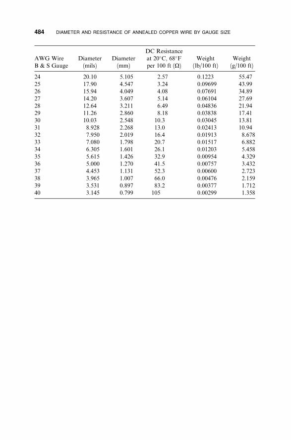
484 DIAMETER AND RESISTANCE OF ANNEALED COPPER WIRE BY GAUGE SIZE
DC ResistanceAWG Wire Diameter Diameter at 20�C, 68�F Weight WeightB & S Gauge (mils) (mm) per 100 ft (W) (lb/100 ft) (g/100 ft)
24 20.10 5.105 2.57 0.1223 55.4725 17.90 4.547 3.24 0.09699 43.9926 15.94 4.049 4.08 0.07691 34.8927 14.20 3.607 5.14 0.06104 27.6928 12.64 3.211 6.49 0.04836 21.9429 11.26 2.860 8.18 0.03838 17.4130 10.03 2.548 10.3 0.03045 13.8131 8.928 2.268 13.0 0.02413 10.9432 7.950 2.019 16.4 0.01913 8.67833 7.080 1.798 20.7 0.01517 6.88234 6.305 1.601 26.1 0.01203 5.45835 5.615 1.426 32.9 0.00954 4.32936 5.000 1.270 41.5 0.00757 3.43237 4.453 1.131 52.3 0.00600 2.72338 3.965 1.007 66.0 0.00476 2.15939 3.531 0.897 83.2 0.00377 1.71240 3.145 0.799 105 0.00299 1.358

APPENDIX D
Properties of Some Materials
Specific Thermal Linear Expan. Relative
Density Heat Resistivity Coe‰cient Dielectric Resistivity
Material (g/cm3) (cal./g��C) (�C�cm/W) (�10�6/�C) Constant (�10�6 W�cm)
Aluminum 2.70 0.226 0.46 22.9 2.65
Alumina (Al2O3) 5.41 9.8
Boron-nitride 2.20 3.15
Brass (66 Cu 34 Zn) 0.9 0.85 39
Carbon 2.2 0.165 0.15 1375
Copper 8.96 0.092 0.25 16.5 1.67
Glass 4–6
Gold 19.3 0.03 0.34 14.2 2.4
Indium 7.31 4.2 33 8.37
Iron (99.99%) 7.87 0.108 1.3 11.7 9.7
Lead 11.34 0.03 2.9 28.7 20.6
Mercury 113.55 0.33 12 98
Mylar 1040 3
Nylon 482 3
Oil (transil) 2.2
Paper (royal gray) 3
Platinum 21.45 0.177 1.45 8.9 11
Polyethylene 304 2.3
Polystyrene 965 70 2.55
Quartz (SiO2) 7–15 3.78
Rexolite (1422) 2.53
Silicon 2.4 0.176 1.2 4.2 11.8
Silver 10.49 0.056 0.25 18.9 1.59
Sodium chloride 5.9
Teflon pure 482 100, variable 2.03
Tin 7.3 0.054 1.6 23 11
Titanium 4.5 0.142 8.5 42
Tungsten 19.3 0.034 0.5 4.3 5.6
Water 20�C (distilled) 1.00 1.00 160 80
Zinc 7.14 0.09 0.9 17–39 6
High Frequency Techniques: An Introduction to RF and Microwave Engineering, By Joseph F. White. ISBN 0-471-45591-1 6 2004 John Wiley & Sons, Inc.
485
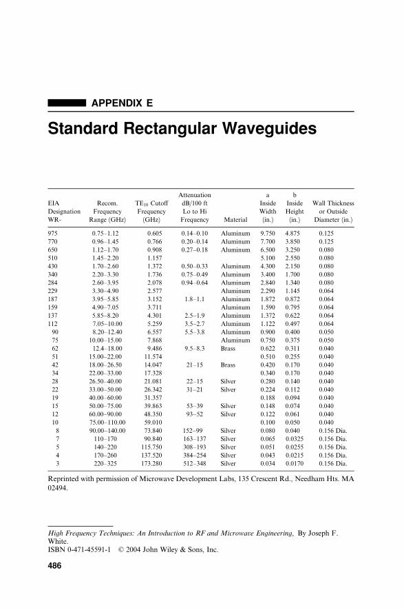
APPENDIX E
Standard Rectangular Waveguides
Attenuation a b
EIA Recom. TE10 Cuto¤ dB/100 ft Inside Inside Wall Thickness
Designation Frequency Frequency Lo to Hi Width Height or Outside
WR- Range (GHz) (GHz) Frequency Material (in.) (in.) Diameter (in.)
975 0.75–1.12 0.605 0.14–0.10 Aluminum 9.750 4.875 0.125
770 0.96–1.45 0.766 0.20–0.14 Aluminum 7.700 3.850 0.125
650 1.12–1.70 0.908 0.27–0.18 Aluminum 6.500 3.250 0.080
510 1.45–2.20 1.157 5.100 2.550 0.080
430 1.70–2.60 1.372 0.50–0.33 Aluminum 4.300 2.150 0.080
340 2.20–3.30 1.736 0.75–0.49 Aluminum 3.400 1.700 0.080
284 2.60–3.95 2.078 0.94–0.64 Aluminum 2.840 1.340 0.080
229 3.30–4.90 2.577 Aluminum 2.290 1.145 0.064
187 3.95–5.85 3.152 1.8–1.1 Aluminum 1.872 0.872 0.064
159 4.90–7.05 3.711 Aluminum 1.590 0.795 0.064
137 5.85–8.20 4.301 2.5–1.9 Aluminum 1.372 0.622 0.064
112 7.05–10.00 5.259 3.5–2.7 Aluminum 1.122 0.497 0.064
90 8.20–12.40 6.557 5.5–3.8 Aluminum 0.900 0.400 0.050
75 10.00–15.00 7.868 Aluminum 0.750 0.375 0.050
62 12.4–18.00 9.486 9.5–8.3 Brass 0.622 0.311 0.040
51 15.00–22.00 11.574 0.510 0.255 0.040
42 18.00–26.50 14.047 21–15 Brass 0.420 0.170 0.040
34 22.00–33.00 17.328 0.340 0.170 0.040
28 26.50–40.00 21.081 22–15 Silver 0.280 0.140 0.040
22 33.00–50.00 26.342 31–21 Silver 0.224 0.112 0.040
19 40.00–60.00 31.357 0.188 0.094 0.040
15 50.00–75.00 39.863 53–39 Silver 0.148 0.074 0.040
12 60.00–90.00 48.350 93–52 Silver 0.122 0.061 0.040
10 75.00–110.00 59.010 0.100 0.050 0.040
8 90.00–140.00 73.840 152–99 Silver 0.080 0.040 0.156 Dia.
7 110–170 90.840 163–137 Silver 0.065 0.0325 0.156 Dia.
5 140–220 115.750 308–193 Silver 0.051 0.0255 0.156 Dia.
4 170–260 137.520 384–254 Silver 0.043 0.0215 0.156 Dia.
3 220–325 173.280 512–348 Silver 0.034 0.0170 0.156 Dia.
Reprinted with permission of Microwave Development Labs, 135 Crescent Rd., Needham Hts. MA
02494.
High Frequency Techniques: An Introduction to RF and Microwave Engineering, By Joseph F. White. ISBN 0-471-45591-1 6 2004 John Wiley & Sons, Inc.
486

INDEX
A, vector potential (see Vector)ABCD matrix cascading networks, 167 for common elements, 168 input impedance of two-port, 169 insertion loss of network, 170 passive and reciprocal criterion, 171 using to calculate input impedance, 169 using to calculate insertion phase, 171 voltage-current definition, 167
Abrie, Pieter L. D., 74 AC resistance (see Skin e¤ect), 23–26 Admittance, Y conversion to Z, 32 intrinsic (of unbounded space), 1/h, 232 matrix (Y parameters) adding parallel networks, 166 definition, 165 reciprocity, 167
Advanced Mobile Phone System (AMPS), 443
Alternating current (AC) analysis, Chap. 2, 16
Altman, Jerome L., 299 Amplifier available gain design description, 437 example, 438–442 gain circles, 440 source and load, 438 usable with potentially unstable
networks, 442 broadbanding using feedback, 461 using frequency selective networks,
460–461 using optimization, 463
cascading stages, 466–468design summary, 468–470feedbackbroadbanding, 460 design, 462 parameter, S12, 405
gain and S21, 399 circles available gain, 440 operating gain, 435 reflection, 405 unilateral gain, 422–428
definitions, various, 430–433maximum available (MAG), 429
input reflection coe‰cient, 408 low noise, 450–455 design example, 451–455 equivalent noise resistance, Rn, 450 optimum input reflection coe‰cient,
GOPT, 450 optimum source impedance, 450 minimum noise factor, FMIN, 450 noise factor related to input and
output reflection coe‰cients,450
noise circles, 455 resistance, 451 stabilizing, 452–453 transistor parameter table, 451
maximum stable gain, MSG, 429 nonlinearity, 455–460 gain saturation, 455–456 intermodulation distortion, 456–460 noise floor, 460 spurious-free dynamic range, SFDR,
459–460
High Frequency Techniques: An Introduction to RF and Microwave Engineering, By Joseph F. White. ISBN 0-471-45591-1 6 2004 John Wiley & Sons, Inc.
487

488 INDEX
nonlinearity (Continued) third order intercept, 458 useful dynamic range, 460
operating gain design, 433–437 description, 433 design procedure, 434 example, 434–437 gain circles, 435 source and load, 433 usable with potentially unstable
networks, 433 output reflection coe‰cient, 407 potential instability, 405–409 power gain, 414 simultaneous conjugate match design,
428–430 S parameters, (defined, 172–177), 175,
399, 462 stability, 405–413
boundary, 406–407 circles on Smith chart, 406, 409, 410,
412, 413, 439, 442 conditional (potentially unstable),
405–407 criterion, 405, 408–409 easy points, 407 design examples, 411–413, 452 K factor, 409–413 load instability (input stability) circle,
406–407source instability (output stability)
circle, 408–409unconditional stability definition, 405 methods to obtain, 411, 460–463
transducer gain, 413–416transistor types and S parameters (see
Transistor)unilateral design method, 416–428
example, 418–422 feedback assumption (S12 ¼ 0), 405,
416 figure of merit, 417 gain circles, 422–428 gain factors, 416
Admittance, Y definition, 30 conversion to Z, 32 matrix, 165–166 normalized, 43 parallel addition, 30
Alternating current (AC) phase, 24 steady state analysis, 23–26
Alumina (Al2O3) substrate, 82, 485 Ampere, Andre M., 184, 208 Ampere’s law application of, 244 as line integral, 201 di¤erential form, 204
Analog Instruments, xxi Anisotropic media, 211 Antenna aperture antennas, 286–288 aperture e‰ciency, 288 arrays, phased, (see Antenna, phased
array) balun, 282 bore site direction, 286 dipole, 275–282 diversity switching, 293 e¤ective (capture) area, 292 defined, 284 related to actual area, 287 related to gain, 285, 287
elevation plane cut, 280 gain, 283 ground plane, 280, 286 half-wave dipole, 280–282 horn, 287 illumination taper, 287 isotropic (radiator), 283, 291 main beam, 286 monopole, 285–286 parabolic reflector, 287 patch array, 287 path loss, 292 pattern (radiation) of a dipole, 280, 281 phased array, 288–290 corporate feed for, 288 e¤ective (projected) area, 290 grating lobes, 289 scan angle, 288 squint, 290 time delay for steering, 289 use of phase shift for steering, 289 wave front, 289
radiation resistance, 279 radome, 287 Rayleigh fading, 293 reciprocity, on transmission and
reception, 284 short (straight wire) dipole analysis,
275–282 sidelobe, 287 waveguide horn, 287 with load impedance, 285
Applications, RF and microwave

cellular telephone, 292–294path loss, 290–294
Attenuation (loss)of coaxial line, (see Exercises 4.11-1
and 2) of filters (See Filters, attenuation) of series Z on Z0 line, 42 of shunt Y on Z0 line, 43 of transmission lines, 95 of two-port network, (using ABCD
matrix, 170), (using S matrix,174)
Auxiliary relationships (see Maxwell’sequations)
Available gain amplifier design (seeAmplifier)
Available power of generator, 40 Available voltage, 40 AWG (American Wire Gauge), 483–484
B field (see Flux, magnetic density) Backward wave coupler, 307–320 Balanced transmission line, 79 Balanis, Constantine A., 300 Balun, 282 Bandpass Filter (See Filters) Bandstop Filter (See Filters) Bandwidth all frequency attenuator, matched pi, E6.4-2 frequency diplexer, 364–367 Kuroda’s identities, 379 matched load on lossless line, 79, 102 90� phase split, input match and
infinite directivity of backward wave coupler, 308, 313, 315, 318
octave or greater multi-octave, cascaded couplers, 318 octave, power split of backward
wave coupler, 308, 317 Bel scale, 34 (also see Decibels) Bessel response (see Filters) Besser, Les, xxi Bias flag, 402 Bias network for transistor, 400–402 Bilateral circuits, 33 Bilinear transformation (complex), (see
Smith Chart)Binomial response (See Filters,
Butterworth) Bishop, Don, 14 Bode, H. W., 115 Boltzmann’s constant, 443
INDEX 489
Boundary conditions at a conductor, 253 of magnetic materials, 213
Bowick, Chris, 74, 159 Branch line coupler, 327–330 Butterworth response (see Filters)
Calculus formulas (inside cover) California Eastern Laboratories (CEL),
470 Capacitance coupled resonators, 319 of coaxial line, 243 of open-circuited transmission line, 105 parallel plate formula, 49 Q, 60 reactance of formula, 25, 27, 28 graphing, 60
Capture area, antenna (see Antenna, e¤ective area)
Cartesian coordinates, 12 Cascaded networks (see Matrix,
cascading) C band, 8 Cellular radio (see Radio, cellular) Chain (ABCD) matrix (see Matrix,
ABCD) Charge (see Electric charge) Characteristic admittance, Y0, 102 Characteristic impedance definition, 79, 95 of coaxial line, 245 of unbounded medium (h, intrinsic
impedance), 232 of waveguide related to EH fields, 256, 258 related to vertical current, 267
related to capacitance and velocity ofpropagation, 98
Circular polarization (see Polarization) Circuits ABCD matrices for, 168 attenuator, matched pi, (see Exercise
6.4-2) basic elements, 16–22 cascading (see Matrix, ABCD
parameters, T parameters) duality, 166 even-and-odd mode analysis, 309–316 four-port (directional coupler), 321 insertion loss (see Loss) insertion phase (see Phase)

490 INDEX
Circuits (Continued) linear, 33 lumped, 33 phase shifter, lumped (see Exercise
6.4-4) pi (p)
attenuator, matched, (see Exercise 6.4-2)
five-element transmission line equivalent, 158
three-element transmission line equivalent, 153
reciprocity, 166 tee, 340 two-port, 167
Circuit elementscapacitor
admittance of, 30 as an open-circuited transmission
line, 104 equivalent circuit with parasitics,
44 parallel plate formula, 49–50 reactance of, 28
inductor admittance of, 30 as a shorted transmission line, 103 as a straight wire, 49 as a wound coil, 47 equivalent circuit with parastics,
44 hysteresis, 47 reactance of, 28
resistor equivalent circuit with parasitics, 44 transformation using Q matching
method, 67–74Coaxial transmission line capacitance, 243 characteristic impedance, 245 electric field in, 242 external inductance of, 246 magnetic field in, 244
Cohn, Seymour B., 318 Collin, Robert E., 74, 179, 299 Collins, George B., 199 Comb-line filter (see Filters) Communication, point-to-point (see Path
loss)Complementary filters (see Filter)Complex impedance (see Impedance)Complex numbermapping, 121–130mathematics (Appendix B), 478–482
Complex (imaginary) power (seePoynting’s theorem)
Conductance, 30 Conductivity (s), 51–52, 485 Conductor, ‘‘good,’’ 221 Conjugates, complex, 481 Copper conductivity, 485 Coordinates, orthogonal definitions cylindrical, 13 rectangular (Cartesian), 11–12 spherical, 14
Coulomb, Charles A. de, 193 law, 186
Coupled linesbackward wave coupler, 307–320even and odd mode analysis of, 309–
320 Couplers (see Directional couplers) Cramer’s rule (see Matrix) Critical coupling of resonators (see
Resonant circuits)Cross product definition, 188 of E and H propagating fields (see
Poynting’s theorem)Curl of a vector field, 202 of E field, 209 of H field, 204
Current conduction, 204 convection density, 211 density, 204 displacement, 204 distribution in a conductor, 205 flow in waveguide walls, 260 into a node, 23 on an antenna, 276, 281 magnetic field of, 201, 204, 205, 244
Cuto¤ frequency and wavelength ofwaveguide, (see Rectangularwaveguide)
Cuto¤ frequency of filters (see Filter type)
Decibels basis and use of, 33 in milliwatts (dBm), 37 in watts (dBW), 37
Deembedding (see Matrix) D field, see Flux, electric density Determinant (D), 162 Dielectric anisotropic, 82, 211

constant, 81 inhomogeneous, 81
Diode phase shifter circuit using hybrid coupler, 321–323, 330
DiPiazza, Gerald, xxi Diplexer, frequency (see Filters, diplexer) Directional couplers applied to network analyzers, 307 backward waveanalysis of, 309–316cascaded sections (for broadband),
318–320 characteristic impedance, Z0, 313 conditions for 3 dB coupling, 314 coupling coe‰cient, k, 313 coupled output voltage, V2, 313 direct output voltage, V4, 315 even and odd mode impedances related to coupling, 313–314related to Z0, 313
isolation, 315 ninety-degree phase split, 308,
318 reentrant configuration (for tight
coupling), 320 S matrix for, 320–321 VSWR (match), 308, 318 when used with reflecting
terminations, 323 ZOE and ZOO in terms of coupling
and Z0, 317 branch line configuration, 328 performance graph, 328 output port phase di¤erence, 329
coupling definition, 324 directivity definition, 324 errors in using for measurement, 325–
326 multi-hole, waveguide, 307–308 hybrid coil, 318 isolation definition, 324 rat race (hybrid ring) configuration, 329 performance graph, 329 obtaining quadrature (90�) outputs,
330 return loss definition, 324 return loss and isolation equivalence,
325 specifying, 324 using for two-port measurements directional property, 307 error analysis, 325–326
INDEX 491
network analyzer application, 326–327
wavelength comparable dimensions, 307 Wilkinson divider configuration, 331 performance graph, 331
Dispersion anomalous, 100 due to inhomogeneous transmission
line, 81 in waveguide, 247
Displacement current (see Current) Dissipative loss (see Loss) Distortion (see Intermodulation
distortion)Distributed Circuits, 78 (Chapter 4)Divergenceof a vector field, 194–196 of D field, 196 of B field, 201
Divergence theorem, 196 Dividerfrequency (diplexer), 363–367Wilkinson, 330–332
Dominant mode (see Modes) Dot product, of vectors, 194–195 Duality, (see Circuits) Duroid½TM�, 82
E (see Electric field) Eagleware Inc, xxi Electric charge and the divergence theorem, 195 density, 196 due to point source, 193 force of, 186 on an electron, 186
Electric energy, 22 Electric field, 185–187 and Lenz’s law, 209 and Faraday’s law, 209 conservative static, 197 curl of, 209 definition, 185 evaluated from vector potential, 273 gradient of, 198 in coaxial line, 244 in dielectrics, 193 in plane wave propagation, 233 in rectangular waveguide, 257–260 of a point charge, 186
Electric flux density (D field), 194 Electric potential (voltage), 196

299
492 INDEX
Electric susceptibility (e ¼ e0eR), 186 Electromagnetic (EM) simulation, 294–
example using 90� stub, 294–298 grid based analysis, 296–297
Electromagnetic spectrum including light, 229 U.S. frequency allocations, 9–10
Electromagnetic propagationE�H (See Vector, Poynting)in coaxial line, 242–246intrinsic impedance (see Impedance)in unbounded media (see Wave,
propagation)in waveguide, 249, 254, 257–260
ELF (extremely low frequency), 7 Elliptic polarization (see Polarization) Energy (see Electric energy, Magnetic
energy) Equivalent noise resistance (see Amplifier,
low noise) Even and odd mode analysis, 309–320 even mode impedance, ZOE,
(definition), 310 odd mode impedance, ZOO,
(definition), 310 software to determine ZOE and ZOO, 311
External Q (see Quality factor) EHF (extremely high frequency), 7
Fano’s limit application example, 113 inapplicability to impedance change,
113–114type A and B circuits, 109–113
Fano, R. M., 114 Faraday, Michael, 185, 208 Faraday’s law of induction di¤erential form, 209, 213 line integral form, 208 right-hand rule, 209
Feedback (see Amplifier) Field e¤ect transistor (FET), 451 Filter attenuation
definition, 336 6N dB/octave, 339, 341, 344
bandpass, 345–349 bandstop, 349–352 Bessell response, 357–361 Butterworth response, 337 Chebyshev response, 351–357 complementary (diplexer), 364
critical coupling, 369 delay di¤erential, 357 group (envelope), 357 phase, 357 with Bessel filter, 357–361
denormalizing prototype response,339–343 (also see frequency andimpedance scaling below)
diplexer, frequency, 364–366 distributed, 370–386 elliptic response, 369–371 frequency and impedance scaling, 340,
344, 347, 349–351 g values, scaling to L and C, 340 group (envelope) delay, 357 highpass, 343–345 Kuroda’s identities, 379–381 lowpass, 339–343 mismatch error for cascaded sections,
87–90, 342–343Mumford’s quarter wave stub type,
381–384normal distribution with part tolerances
(see Filter, statistical design) nontrivial elements, 339 optimizing from classical designs, 384–
386 phase and group delay of, 356 poles and zeros, 339 polynomial rule, 339 prototype, lowpass, 336 Q e¤ect on insertion loss, 361–364 Richards’ transformation, 374–378 skirt selectivity, 339, 341, 344 statistical design of, 385–395 top coupled, 367–369 transducer loss, 336 trivial elements, 339 voltage transfer function, H, 336
Fluxelectric density, D, 194 divergence of, 196 in Maxwell’s equations, 211
magnetic density, B, 187 evaluated from vector potential, 273 divergence of, 200–201 in Faraday’s law of induction, 208
Foster’s reactance theorem, 150 Force on a charge due to E field, 185–186 due to B field, 187
Fourier analysis, 98, 261

series and theorem, 261 Four-port networks directional couplers (see Couplers) S parameter representation, 320
Frequency bandsband designations, 7–8U.S. frequency allocations, 9–10
Frequency scaling in filter design, (seeFilters)
Frequently used relations (inside cover)
Gain amplifier (see Amplifier) antenna, 283 insertion (gain or loss), 40–44 transducer, 41–42
Gauge, American wire (AWG), 484 Gauss, Karl Friedrich, 184 law for electric fields, 194 law for magnetic fields (‘ � B ¼ 0), 201 theorem (also divergence theorem),
196 Gaussian distribution, 388 Generator, matching, 39–40 Genesys (network simulation software),
xxi, 43, 470 Gonzalez, Guillermo, 74, 470 Good conductor (see Conductor) Gradient, 198 Gravitational field, 183 Green’s functions (eigenmodes), 263–269 Grosch, Theodore, 114, 470 Group delay, 99 Group velocity, 99 Guided waves (see Coaxial transmission
line and Rectangular waveguide)
H, magnetic field curl of, 204 in Ampere’s law, 201 in coaxial line between conductors, 206, 208 within a conductor, 206, 208
in Maxwell’s equations, 211–213 Harmonic distortion (see Intermodulation
distortion) Heaviside, Oliver, 184, 209, 271 Helmholtz equations, 229 Henley, Deryck, 15 Hertz, Heinrich, 2, 184 Hertzian dipole (short wire) antenna, 276 HF (high frequency), 7
INDEX 493
Higher order modes (see Rectangularwaveguide, modes)
Highpass filters (see Filters) Homogeneous media, 272 Hybrid coil (see Directional couplers) Hybrid coupler (see Directional couplers) Hybrid ring (see Directional couplers) Hysteresis (see Inductor)
Identities, calculus and vector (insidecover)
Impedance, (Z) adding in series, 28 characteristic in terms of v and C, 98 of coaxial line, 245 of general transmission line, 79, 95 of unbounded medium (see
Impedance, intrinsic)of waveguide, 247
complex, 23–28 conjugate, 40 conversion to Y, 30, (Q method) 68 definition, 25 even-mode, 310 input to transmission line, 108, 119 internal to conductors, 224–227 intrinsic (h, characteristic impedance of
unbounded space), 232 inverter (90� transmission line), 105–
108 matching a mismatched transmission line load,
132 broadbanding, 70–71 Fano’s limit, 109–114 for maximum power, 39 Q method, 67–69, 421 using a single transmission line, 108–
109 using Smith chart, 132 with 90� transmission line inverter,
105–108matrix ABCD parameters, 167–172 adding networks in series, 166 adding networks in parallel, 166 algebra, 161–164 cascading networks, 167 cofactor, 163 Cramer’s rule, 162 definition, 161 determinant (D), 162

105
494 INDEX
Impedance, (Z) (Continued) minor, 163 S parameters, 172–177 T parameters, 177–178 Y parameters, 165 Z parameters, 164–165
normalized, 43, 120 of short circuit terminated line, 103 of open circuit terminated line, 104–
of match terminated line, 79, 102 parallel addition (product over sum),
32 reactance scaling (estimating) formulas,
29 series addition, 29 slotted line measurement of, 135–139 transformation equation (for a
transmission line), 101 Incident waves on multi-port network, (see Matrix, S
parameters) on transmission line, 173
Ideal transformer, 107, 168 Induced field, 209 Inductance, L energy storage in, 19, 46 in LC resonator, 59–60 in lumped circuit, 22–23 of coaxial line, 48, 246 of internal reactance, 225 of shorted transmission line, 103 of straight wire, 48 of wire coil, 47 Q, 60 reactance of
graphing, 60 formula, 25, 27, 28
Inhomogeneous dielectric, 81 transmission line, 80–81
Input admittance formula (for transmission
line), 101–102 impedance formula (for transmission
line), 101, 107–108, 119 reflection coe‰cient, 405 stability circles (of transistor), (see
Amplifier) waves (ai) into multi-port, 173
Insertion loss (see Loss) Institute of Electrical and Electronics
Engineers (IEEE), 26, 445, 480
Intermodulation distortion definition of orders, 457 minimum detectable signal, 460 mixing products, 457 noise floor, 459 rate of increase with order, 457–458 spurious-free dynamic range (SFDR),
459 third order intercept, 458 two tone test, 457 useful dynamic range (UDR), 460
Internal impedance of conductors (see Impedance)
International Morse Code, 3 Intrinsic impedance (see Impedance) Isolation (see Loss) Isotropic media, 272
Jolley, L. B. W., 114 Jordan, Edward C. and Balmain, Keith
G., 300 Junction e¤ects, 296
K, Ka and Ku bands, 8 K factor (see Amplifier stability) Kirchho¤ ’s laws current, 22, 92 voltage, 22, 92
Kobb, Bennet Z., 15 Kuroda’s identities (see Filter)
Laplacian scalar (divergence of the gradient),
215 vector (see Vector)
L band, 8 Lenz, H. F. E., 184, 208 Lenz’s law, 209 Levy, Ralph, 396 LF (low frequency), 7 Linear polarization (see Polarization) Linear simultaneous equations (matrix
solution), 161 Light, velocity of, 229 Line integral of electric field, 208 of magnetic field, 201
LLFPB network (see Network) Loaded Q (Quality factor) Load reflection coe‰cient, 405 Lodge, Sir Oliver, 2

Logarithm (see Decibels) Loomis, Mahlon, 2 Lorentz, 166–167 Loss (sometimes called Isolation) bandwidth related to Q, 63 insertion, 40 in terms of ABCD, 170 in terms of S21, 174 mismatch, 86 of series impedance, 42 of shunt admittance, 43 return, 86 transducer (loss or gain), 41 of filter, 336 of series Z, 43 of shunt Y, 43
Lossless circuit assumption applied, 64– 66, 79, 83, 85, 88, 98, 101–106, 109, 119, 134, 136, 139, 142, 147–149, 151–158, 240–246, 248–260, 264–269, 275–280, 294–299, 307–332, 335–361, 363–394, 399–469
Lowpassfilter (see Filter)prototype (see Filter)
LLFPB networks, 33 Lorentz, 166 Lumped circuits (see Circuits)
Magnetic energy, 19 Magnetic field, H curl of, 204 due to current (Ampere’s law), 201 flux density (B), 187 force on moving charge, 187 permeability, 200
Magnetization (B) hysteresis curve, 47 remanence, 47 saturation, 47
Marconi, Guglielmo, xvi, 1–7 Marcuvitz, N., 299 Matching (see Impedance matching) Material properties (Appendix D), 485 Matrix ABCD, 167–172 addition and subtraction, 162, 166 algebra, 161–164 cascading ABCD parameters, 167 T parameters, 178
cofactor of, 163
INDEX 495
conversion, S to T and T to S, 178 Cramer’s rule (solution of linear
simultaneous equations), 163– 164
deembedding using S parameters,176
definition, 161 determinant of (D), 162 equality condition, 162 minor of, 163 multiplication of, 161–162 reducing the order of, 163 S, 172–177 deembedding by reference plane
shifting, 176 dependence on measurement port
impedances, 177 incident and reflected waves, 173 lossless conditions, 176–177 reciprocity condition, 176 transistor parameters, 175 unitary condition, 177
T (wave transmission parameters),177–178
Y, 165 Z, 164
Matthei, Young, and Jones, 396 Maximum available gain (MAG), (see
Amplifier, gain) Maximum available power (see
Impedance matching) Maxwell’s equations, 210 application of, 166, 184, 221, 227, 230,
244, 248, 273 auxiliary relations, 210–211 related to light transmission, 229 visualizing, 211–214
Maxwell, James Clerk, 2, 3, 14, 209, 229, 271
Measurements (see Directional couplers,applied to network analyzers;Scattering matrix, transistormeasurements; Slotted linemeasurements)
MF (medium frequency), 7 Microstrip (see Transmission line) Miller, Kenneth S., 57, 158, 482 Minimum noise factor (see Amplifier, low
noise) Mismatch error, 87–90 Mismatch loss (see Loss) Misra, Devendrak K., 115 MKS (meter-kilogram-second) units,
474–477
496 INDEX
Modesdominant
in circular waveguide, 250 in coaxial line, 245 in open two-wire line, 240 in parallel-plate waveguide, 250 in rectangular waveguide (see
Rectangular waveguide, modes) higher order in circuits, and means to
suppress, 255 higher order in waveguide (see
Rectangular waveguide, modes) Morse Code, 3 Mumford, William W., 381, 382, 396
Nahian, Paul J., 299 Negative resistance (see Smith chart) Neper conversion to dB, 96 (also on inside
cover) definition, 95
Network analyzer, 326–327 dual, 166 LLFPB, 33, 335 optimization, 54 simulation, 53 tuning, 54 yield analysis, 55, 385
Network analyzer, 326–327Newton’s law, 186–187Nonreciprocal (not bilateral) network,
33 Normal distribution (see Gaussian
distribution) Normalized admittance, 44 frequency, 339 impedance, 43, 339
Noise in systems, 442–450 atmospheric, 444 bandwidth, 443 calculation of, 443–446 carrier, 444 correlation (equivalent) noise
resistance, transistor, 450 factor
description, 445 of a network cascade, 447–448
figure, 445–447 flicker, 444 floor, 459 galactic, 444
IEEE measurement standard, 445 low noise amplifier (see Amplifier) man-made, 444 measurement, 445 of cascaded circuits, 447 power, 443 precipitation, 444 referred to input port, 446 resistance, 443 shot, 444 sources of, 444 temperature absolute, 443 as a specification, 448–450
thermal (Johnson, white), 442–444 voltage, 443
Odd mode impedance (see Even and oddmode analysis)
Ohm’s law di¤erential form, 210, 220 for a resistor, 18 for an impedance, 26
Open circuited line impedance (seeImpedance)
Operating gain amplifier design (seeAmplifier)
Operating transistor bias (see Transistor)Optimization using the computerby tuning, 54 description, 54 for amplifier broadbanding, 460–468 for filter design, 384–386 requiring intervention, 55 using weighting (W), 464–466
Optimum reflection coe‰cient (GOPT),(see Amplifier, low noise)
Orthogonal functions circularly polarized fields, 238 E and H propagating fields, 233 Green’s functions, 263 harmonically related sinusoids (Fourier
series), 261 waveguide modes, 257–258
Oscillation (see Amplifier, potential instability)
Outgoing (reflected) waves, 173 Output impedance (of transistor), 418 stability circles (of transistor), (see
Amplifier) waves (bi), 173
Output reflection coe‰cient, 405

Parabolic reflector antenna, 287 Parallelplate capacitor, 49–50resonant circuit, 59, 62–66
Parasitic elements, 16 for capacitor, 45 for inductor, 44 for resistor, 44
Passband (see Filters) Parallel plate waveguide, 250 Parameters (see Matrix) Path loss, 292 Penetration depth of current (see Skin
e¤ect)Permeability general, 200, 211 of free space, 211 relative, 211
Permittivity general, 200, 211 of free space, (see value on inside
cover), 50, 211 relative, 81, 200, 211
Phase velocity, 97 Phasor notation, 11, 26 Physical constants and parameters table
(inside cover)Pi network (see Circuits)Plane conductor internal inductance,
224–225 Plane wave propagation, 230–233 Poisson equation, 216 Polar form of complex numbers to
rectangular, 480 Polarization circular, 237–239 elliptical, 239 linear, 236
Popov, Alexander, 2 Potential electrostatic, F, 196 retarded, 274 vector (A), 271–275
Potential instability (see Amplifier)Powercombiners and dividers (see Directional
couplers) gain (see Amplifier, gain) real and imaginary, 38 transfer, 39
Poynting’s theorem application, 267 complex (imaginary) power, 236 derivation, 233–236
INDEX 497
vector, 236 Practicalcapacitor, 44–46inductor, 44–45resistor, 44–45
Propagationconstant, definition, 94, 96 in rectangular waveguide, 258–259 in unbounded media, 229–230 on two conductor transmission line,
94 Helmholtz equations, 229–230 in unbounded media (plane waves),
230–233 in waveguides, 251–260 on coaxial line, 241–246 wave equation, 227–229
Properties of materials (Appendix D),485
Prototype lowpass filter (see Filter) Pulse propagating on transmission line,
82–83
Q contours (see Smith chart) Q matching (see Impedance, matching) Quality factor, Q, 60 external, 61 for parallel RLC circuit, 62 for series RLC circuit, 61 loaded, 62 unloaded, 60
Quarter-wave inverter, 105–108
Radar, 288 Radian, 95 Radiation resistance (see Antenna) Radio cellular telephone, 292–294 diversity switching, 293 multipathing, 293 system, 293 EIRP (e¤ective isotropic radiated
power), 291 minimum detectable signal, 293 point-to-point (path loss), 290–292 noise floor (kT0B), 445–446 Rayleigh fading (multipathing), 293 spectrum, 4, 7–8 system (transmitted power) margin,
293 system path loss, 293
Radio frequency coil or choke (RFC), 46

498 INDEX
Ramo, Simon (see Ramo and Whinnery)Ramo and Whinnery (subsequently with
Van Duzer), 15, 114, 115, 179, 248, 249, 251, 257, 260, 276, 299, 316
Rat race coupler (see Directionalcouplers)
Rayleigh fading, 293 Reactance, 28 Reciprocity (see Antenna or Circuits) Rectangular conversion to polar, 479–480 form of complex numbers, 480
Rectangular waveguide absolute impedance derivation for
coupling post, 265–268 boundary conditions, 252 cuto¤ frequency and wavelength, 254 characteristic impedance definitions
E-H field ratio based TE modes, 256 TM modes, 257
post current based (voltage-power),267
E-H fields for TE10 mode, 258–259 group velocity, 257 guide wavelength, 256 modes
dominant, 254 higher order, 255, 269–270 numbering, 253 phase velocity, 257 sketch of TE10, TE20, and TE30 E
fields sketch of TE01 E field, 255 sketch of TE10 wall currents, 260 standard sizes (Appendix E), 486 TE and TM summary, 257–258 transverse fields (all modes), 254
phase and group velocities, 257 solution for current induced by TE10
on a vertical post, 263 standard waveguide sizes and
characteristics, 486 Reference Data for Radio Engineers, 15 Reference plane(s) movement by S parameter argument,
176 of load, 137
Reflected current, 83 power, 86 voltage, 83 wave, 84
Reflection coe‰cient (G) argument change on transmission line,
120 as a function of normalized
transmission line impedance, 120
definition, 85 in terms of load impedance, 100 of load, 120 of source (generator), 405 on transmission line, 120 reflected wave, 84 related to line impedance, 100 related to load impedance, 100 related to S parameters (S11;S22), 175 related to VSWR, 86
Reflection loss (see Loss)Resistance definition, 18 feedback (see Amplifier) radiation (see Antenna) skin e¤ect (see Skin e¤ect)
Resistor as circuit element, 18, 22–23 high frequency model of, 44
Resistivity of conductors, 485 Responses (Bessel, Butterworth, elliptic,
Chebyshev), (see Filters) Resonant circuits bandwidth, 63 direct coupled, 63–65 lightly coupled, 63–65 parallel, 59, 62–67 Q (see Quality factor) series, 61–62, 64
Retarded potentials (see Vector potential) RF bypass (or blocking) capacitor, 50 Return loss (see Loss) Rhea, Randall, xxi, 74, 352–355, 374 Richards, P. I., 396 Richard’s transformation (see Filter) Ripple (Chebyshev, equal, in filter), 351–
357 Rizzi, Peter, xxi, 15, 179, 299 Rogers Duroid, 82 Rollet stability factor (K), 409 Rotary joint, 102
Saad, Theodore, 115 Sams, Howard W. & Co., 395, 470 Saturation magnetization (BSAT), 48 S band, 8 Scalar product (see Vector operations)

Scaling frequency and impedance (seeFilters, also Impedance)
Scattering matrix (S parameters)changing reference planes, 176conversion to T matrix, 178definition, 174–175dependence on source and load, 177for backward wave coupler, 320for lossless networks (unitary
requirement), 177 for reciprocal networks, 176 incident and reflected waves definition, 172–173power, 173
interpreting Sij values, 174transistor measurements, 400, 451, 462
Schelkuno¤, S. A., 299Sears and Zemansky, 299Second order harmonicdistortion, 456–457 filtering, 457 gain saturation, 457 slope, 459
Separation of variables, integral equationsolution, 251
Series impedance in transmission line, 43Series inductance, transmission-line
approximation, 102Shot noise (see Noise)SHF (super high frequency), 7Shunt admittance in transmission line, 43Silverconductivity, 52resistivity, 485
Simultaneous conjugate match design (seeAmplifier)
Sinusoidal waves on transmission lines,83–84
Skilling, Hugh Hildreth, 240, 299Skin e¤ectbasis, 221–224 equivalent AC resistance, 52 penetration depth, 51 formula, 51, 224 in copper, 52, 224 in silver, 52
Skirt selectivity (see Filters) Shorted line impedance (see Impedance) Slotted line measurements, 135–139 Smith, Anita, xxi Smith Chart (Chapter 5), 119 admittance coordinates, Y, 130–132approximate tuning may give broader
bandwidth, 148–149
INDEX 499
basis of, 122–123bilinear transformation of, 120, 124,
131characteristic impedance of, 124constant Q contoursdrawing, 151–152using to design broadband networks,
153constant reactance (x or b) contours,
127–128constant resistance (r or g) contours,
125–127constant reflection magnitude contours,
129, 134construction of (r and x mapping),
125–128degree scale for reflection coe‰cient,
129, 133derivation of transformation equations
(drawing the circles), 124–128estimating tuning bandwidth, 147–148frequency contours of Z and Y
(increasing clockwise), 150impedance coordinates, Z, 130lower half is capacitive, 132, 146–147navigation on, 140negative resistance region, 140–141normalizing and unnormalizing Z and
Y, 124, 134plotting reflection coe‰cient, 128–129reading rotation direction from load,
131, 133–134reading VSWR (VSWR ¼ r), 139–140skeletal form, 128–129slotted line impedance measurement,
135–139software format of, 145, 159standard graphical formatimpedance coordinates, 132 impedance and admittance
coordinates, 133totally reflective loads, 141tuning a mismatched load, 132–135,
141–145upper half is inductive, 132, 147using without transmission lines
(arbitrary Z0), 150–151using to find lumped equivalent circuit
of transmission line, 153–158VSWR ¼ r, 139–140with both impedance and admittance
coordinates, 132–133wavelength scale, 133–134winSmith software for, 145–146, 148

500 INDEX
Smith, Phillip, xxi, 108, 119, 123, 158 Sokolniko¤ and Redhe¤er, 396 Source impedance and reflection
coe‰cient, 405 Southworth, George, 2–3, 14 Spread spectrum signals, 444 S parameters (see Scattering matrix) Stability (see Amplifier) Stability factor (K), 409–413 Standard International Units (MKS),
474–477 Standing wave ratio (SWR), (see VSWR) Standing wave on transmission line, 84 Static (scalar) potential function, 196–200 Statistical design and yield analysis, 386–
395 filter production example (500 unit),
394–395 normal distribution, 386–391 normal (Gaussian) curve, 392 standard part values, 386–388 typical distribution curves, 393
Standard Rectangular Waveguides (Appendix E), 486
Steady-state voltages and currents, 24 Stimson, George W., 15 Stripline (see Transmission line) Stub (see Impedance, of short circuit or
open circuited transmission line) Stubblefield, Nathan, 2 Superposition principle (see Circuits,
even-and-odd mode analysis) Susceptance, 30 Symbols and Units (Appendix A), 474–
477
Talor series expansion, 455 Tangent, approximation by angle, 104 TE and TM modes (see Rectangular
waveguide) Tee circuit (see Circuits) TeflonTM, 82 Telegrapher equations, 91–92 Temperature, absolute, 443 TEM waves (see Transmission line,
coaxial) Tensor quantities, 211 Thermal noise (see Noise) Third order intercept point (see
Intermodulation distortion) Thomas, George B., 179 Three-port network (see Circuits) Total reflection, 83–84
Transducer loss or gain (see Loss) Transfer of power (see Impedance,
matching) Transformer ideal, 107 ‘‘quarter-wave’’ (impedance inverter),
106 Transforming impedances (see Impedance
matching) Transistor (also see Amplifier) beta, b, 400 bipolar (BJT) bias circuit, 399–402 low noise, 461–462 S parameters editing file, 461 2N6679A, 400, 404–406, 423, 425 AT 415868, 461–462
interpreting S parameter data, 400 low noise field e¤ect (FET),
NE67300.S2P, 451 S parameters, 399
Transmission coe‰cient (T ), 88 Transmission line balanced, 79–80 coaxial characteristic impedance, 245–246 distributed capacitance, 243 distributed inductance, 246 E-H fields, 242, 244 form, 80, 241
di¤erential mode voltage, 79 equations, 92–94 inhomogeneous, 81 matching, 79 microstrip, 80 mode definition, 241 dominant, 241 higher order, 241 cuto¤ frequency of, 241
pi circuit equivalent five-element, 158 three-element, 156
pulse excitation of, 82 radiation from, 241 reflection on, 85 slotted, for measurements, 85 stripline, 80 twin lead (two parallel wire) fields on, 240 form, 79
twisted pair, 79 unbalanced, 80

uniform, 78 VSWR, 86 waveguide (see Rectangular waveguide)
Transmission matrix (T parameters) cascading, 178 definition, 178 in terms of S parameters, 178
Traveling waves, 83 Two-port networks (also see Circuits) cascading, 167, 178 matrix representations (see Matrix) noise of, 445 parameter conversion (S to T ), 178
Two-stage amplifier (see Amplifier,cascading stages)
Types of noise (see Noise)
Unbalanced transmission lines, 80 Unconditional stability (see Amplifier) UHF (ultra high frequency), 7 Unilateral amplifier design (see Amplifier) Unilateral figure of merit (see Amplifier) Unloaded Q (see Quality factor) Unitary matrix, 177 United States Navy, 14 Units (standard MKS), 474–477 Unit vectors, 12 Unstable amplifier (see Amplifier,
stability)
Van Duzer, Theodore (see Ramo andWhinnery)
Variable attenuator (see Circuits)Vectorbasic operator summary in cylindrical coordinates, 215 in rectangular coordinates, 214 in spherical coordinates, 215
curl calculation, 202–208, 214 closed path does not imply curl, 207 definition, 202 of gradient (¼ 0), 218
cross product, 188, 214 definition of E field, 185 divergence, 194–196, 214 divergence of curl (¼ 0), 218 dot product (scalar product), 194, 214 gradient of a scalar function, 198, 214 identities, 219 Laplacian (vector) rectangular coordinate definition, 217
INDEX 501
definition (general), 219 potential definition, 272 general expressions for B and E
fields, 273 sinusoidal expressions for B and E
fields, 275 retarded, 274
product (cross product), 12 successive operators, 215–219 unit, 12
Velocity of propagation application, 98 value for light in a vacuum, 229, also
see inside coverVF (voice frequency), VLF (very low
frequency), and VHF (very high frequency), 7
Voltage available from source, 40, 335 drop around loop, 22 on a transmission line, 129 transmission coe‰cient for filters, t, 335 on transmission line, T, 88
VSWR defined, 86 read from Smith chart r circle related to reflection coe‰cient, 86 sketch of on transmission line, 84 used with slotted line, 85 with a pair of reflectors on a
transmission line, 91
Wave equation, 228 impedance (see Impedance, intrinsic) incident, for S parameters, ai, 173 in rectangular waveguide (see
Rectangular waveguide) in unbounded media, free space,
(radio), 214 polarization circular (right- and left-hand), 238 elliptical, 238 linear, 236
propagation electromagnetic, 185, 214, 228 plane propagating, 230 Poynting’s theorem and vector (see
Poynting’s theorem) propagation constant, k, 229–230
reflected, for S parameters, b, 173

502 INDEX
Wave (Continued)relation to light, 229velocity of propagation, 228–229
Waveguide (see Rectangular waveguide)Waveguide horn (see Antenna)Waveguide modes (see Rectangular
waveguide)Waves (see Propagation)Wave impedance (see Impedance,
intrinsic)Wavelength (definition), 81in free space, 81in a dielectric, 81in waveguide (see Rectangular
waveguide)Webster’s International Dictionary, 14Wheeler, H. A., 46, 57Whinnery, John R. (see Ramo and
Whinnery)White, Eloise, xxiWhite, Joseph, xxi (biography), 114, 179,
299, 470White noise (see Noise, thermal)
winSmith (Smith Chart software), xxi,144–145, 159
Wide band matching (see Impedance,matching, broadband)
Wilkinson divider (see Directionalcouplers)
Wire, copper by gauge size (Appendix C),483–484
Wire inductance approximation (seeInductance, straight wire)
Wound coil (see Circuit elements,inductor)
X band, 8
Yield analysis, 55, 386–395Y matrix (see admittance matrix)
Z matrix (see impedance matrix)

� �
FREQUENTLY USED RELATIONS
Reactances
XL ¼ oL ¼ 2pfL: At 1 GHz; 1 nH has þ6:28 W
�1 �1XC ¼
oC¼
2pfC: At 1 GHz; 1 pF has �159 W
Wavelength
At 1 GHz l0 ¼ 30 cmA11:8 in:
Series–Parallel Equivalent Circuits
Transmission Lines
ZL þ jZ0 tan y zL þ j tan y ZIN ZLZIN ¼ Z0 zIN ¼ zIN ¼ zL ¼
Z0 þ jZL tan y 1þ jzL tan y Z0 Z0
VRðxÞ ZðxÞ � Z0 z� 1 Y0 � Y ðxÞ 1� yGðxÞ ¼ rJj ¼ ¼ ¼ ¼ ¼
VI ðxÞ ZðxÞ þ Z0 zþ 1 Y0 þ Y ðxÞ 1þ y
1þ GðxÞZðxÞ ¼ Z0
1� GðxÞVSWR � 1 1þ r
r ¼ VSWR ¼VSWR þ 1 1� r
Return loss ¼ r2 ¼ 20 log r (dB);
Mismatch loss ¼ 1� r2 ¼ 10 logð1� r2Þ (dB)1
Mismatch error ðmax & min valuesÞ ¼ 20 log ð1G r1r2Þ

� ¼� � � � � �
~ ~ � � � � � � � �
�
‘ � ~
2D2 Matrix Multiplication
a11 a12 b11 b12 a11b11 þ a12b21 a11b12 þ a12b22
a21 a22 b21 b22 a21b11 þ a22b21 a21b12 þ a22b22
Noise Factor F and Noise Figure NF
SNRIN PNoise OUT TEF ¼ ¼ ¼ 1þ where PNoise IN ¼ kT0B and T0 ¼ 290 K
SNROUT GPNoise IN T0
F2 � 1 F3 � 1 FN � 1FCASCADE ¼ F1 þ þ þ � � � þ NF ¼ 10 log F
G1 G1G2 G1G2G3 . . .GN�1
Spurious-Free Dynamic Range
SFDR ðdBÞ ¼ 2 ½P3ðdBmÞ þ 174 dBm� 10 log B� GðdBÞ �NFðdBÞ�3
Maxwell’s Equationsþ ð !~1. ‘ �~DD ¼ r DD � dS ¼ r dvS vþ !~ ~2. ‘ � BB ¼ 0 BB � dS ¼ 0S þ ð ~ ~qBB ! qBB !~ ~3. ‘� EE ¼ � EE � dl ¼ � � dS
qt S qtþ þ~ ~qDD ! ! qDD !HH ¼~ ~ ~4. ‘� ~ JJC þ HH � dl ¼ JJ � dS þ
þ� dS
qt S S qt~ ~ ~ ~ ~ ~ ~ ~~DD ¼ eEE BB ¼ mHH JJ ¼ sEE FF ¼ qvv� BB
Vector Operations (Rectangular Coordinates)Dot product:
~ ~AA � BB ¼ AxBx þAyBy þAzBz
Cross product:
~ ~ ~� xx yy zz
AA� BB ¼ �Ax Ay Az � � Bx�By Bz
¼~ yyðAzBx � BzAxÞ þ~xxðAyBz � ByAzÞ þ~ zzðAxBy � BxAyÞ
Divergence:
q q qAA ¼ Ax þ Ay þ Az
qx qy qz

� � � � � � � �
� � � � � � � Curl:
~ ~ ~� xx yy zz
‘� ~ � q q q � qAz qAy qAx qAz qAxAA ¼ � � ¼~ � þ~ � þ~
qAy �xx yy zz� qx qy qz � qy qz qz qx qx qy�Ax�Ay Az
Gradient:
qF qF qF‘F ¼~
qxþ~ ~xx yy
qyþ zz
qz
Scalar Laplacian
2 q F q2F‘2F ¼ ‘ � ‘F ¼ q Fþ
2
þqy2qx2 qz2
Vector Laplacian ! ! 2 2 2 2
‘2~ xx yyAA ¼~q Ax þ q2Ax þ q Ax þ~
q Ay þ q2Ay þ q Ay
qy2 qx2qx2 qz2 qy2 qz2 ! 2 2q Az q2Az q Az
zzþ~ þ þqy2qx2 qz2
Physical Constants and Parameter Values
Description Symbol and Value
Vacuum permittivity e0 ¼ 8:854� 10�12 F/mA10�9=36p F/m
Vacuum permeability m0 ¼ 4p� 10�7 H/mVacuum speed of light c ¼ 1=
pffiffiffiffiffiffiffiffiffi m0e0
¼ 2:998� 108 m/sA3:00� 108 m/sA11:8 in./ns
Boltzmann’s constant k ¼ 1:380� 10�23 J/KElectronic charge e ¼ 1:602� 10�19 CElectron volt e ¼ 1:602� 10�19 JElectron rest mass m0 ¼ 9:11� 10�31 kgPlanck’s constant h ¼ 6:62517� 10�34 J�sCopper conductivity s ¼ 5:80� 107
W
/mValue of Pi p ¼ 3:14159Radian ¼ 360�=2p ¼ 57:29578�A57:3�
Loss (decibels) ¼ 8:686 loss (nepers)Loss (nepers) ¼ 0:115 loss (decibels)

Calculus
Identities
y ¼ ax dy=dx ¼ aaxy ¼ eax dy=dx ¼ ae
y ¼ sin ax dy=dx ¼ a cos ax
y ¼ sinh u dy=dx ¼ cosh u du=dx
y ¼ uv dy=dx ¼ v du=dxþ u dv=dx
y ¼ xn dy=dx ¼ nxn�1
y ¼ ln x dy=dx ¼ 1=x
y ¼ cos ax dy=dx ¼ �a sin ax
y ¼ cosh u dy=dx ¼ sinh u du=dx
v du=dx� u dv=dxy ¼ u=v dy=dx ¼
2v
1 3¼ 1þ xþ x2 þ x þ � � � jxj < 11� x
�xÞ xsinh x ¼ 1 ðex � e cosh x ¼ 1 ðe þ e�xÞ2 2
sinh x cosh xtanh x ¼ coth x ¼
cosh x sinh x
sin2 xþ cos2 ¼ 1
sinðAþ BÞ ¼ sin A cos Bþ cos A sin B
cosðAþ BÞ ¼ cos A cos B� sin A sin B
e jx ¼ cos xþ j sin x
‘ðFþCÞ ¼ ‘Fþ ‘C~ ~BBÞ ¼ ‘� AAþ ‘� ~‘� ðAAþ ~ BB
~ ~ ~‘ � ðCAAÞ ¼ AA � ‘CþC‘ � AA~ ~ ~‘� ðFAAÞ ¼ ‘F� AAþF‘� AA
~‘ � ‘� AA ¼ 0~ ~‘� ‘� AA ¼ ‘ð‘ � AAÞ � ‘2~AA
cosh2 x� sinh2 x ¼ 1
sinðA� BÞ ¼ sin A cos B� cos A sin B
cosðA� BÞ ¼ cos A cos Bþ sin A sin B
e�jx ¼ cos x� j sin x
~ ~BBÞ ¼ ‘ � AAþ ‘ � ~‘ � ðAAþ ~ BB
‘ðFCÞ ¼ F‘CþC‘F~ ~ ~BBÞ ¼ ~ BB‘ � ðAA� ~ BB � ‘� AA� AA � ‘� ~
‘ � ‘F ¼ ‘2F
‘� ‘F ¼ 0 ~ ~ ~ ~CCÞ ¼ ~ CCÞ � ~ BBÞAA� ðBB� ~ BBðAA � ~ CCðAA � ~