Embed Size (px)
Citation preview

PAGE 1
High Frequency Planar Magnetics for Power Conversion
IEEE APEC 2017Tampa, Florida
Prof. W. G. Hurley ([email protected])National University of Ireland, Galway
Associate Prof. Z. Ouyang ([email protected]) Technical University of Denmark (DTU)

PAGE 2
Outline
Magnetics Basics Introduction (WGH) Transformer Design High Frequency Effects in the Winding
Analytical Models for Planar Magnetics (WGH)
Planar Magnetics – Fundamentals (ZO)
Planar Magnetic Components Integration (ZO)

3Power Electronics Research Centre, NUI Galway
Magnetics Basics

Laws of Electromagnetism
4Power Electronics Research Centre, NUI Galway
Ampere’s Law Faraday’s Law
H l Ni de Ndt
B H 0r
)t(

Losses in Magnetic Components
5Power Electronics Research Centre, NUI Galway
Copper losses
Core losses
Hysteresis loss
Eddy current loss
Skin effect loss
Proximity effect loss

Core Loss
6Power Electronics Research Centre, NUI Galway
Hysteresis loss in a ferromagnetic material Eddy current loss in a ferromagnetic material
maxfe cP K f B
Hysteresis loss is the area inside the B-H loop Eddy current loss is reduced by laminations

Ferromagnetic Materials
7Power Electronics Research Centre, NUI Galway
(a) Hard magnetic materials (b) Soft magnetic materials

Soft Magnetic Materials
8Power Electronics Research Centre, NUI Galway
The magnetic and operating properties of some soft magnetic materials
Materials Ferrites Nanocrystalline Amorphous Si Iron Ni-Fe(Permalloy)
Powdered iron
Model TDK P40 VIROPERM 500F
METGLAS 2605
AK Oriented M-4
MAGNETICS PERMALLOY
80
MICROMET-ALS 35μ
Permeability, μi
1500-4000 15000 10,000-150, 000
5,000-10,000 20,000 3-550
Bpeak, T 0.45-0.81 1.2 1.56 2.0 0.82 0.6-1.3
ρ, μΩm 6.5×10⁶ 1.15 1.3 0.51 0.57 106
Curie temp. Tc, 。C 215 600 399 746 460 665
Ploss60 mW/ cm3 at
0.1T/50kHz588 mW/cm3 at 0.3T/100kHz
72 m W/cm3 at 0.2T/25kHz
2.295-30.6mW/cm3
at 1.5T/50Hz
192.28mW/cm3
at 0.2T/5kHz
126-315mW/cm3 at
0.1T/10kHz

Core Shapes
9Power Electronics Research Centre, NUI Galway
Toroid core PQ core Pot core RS/DS core RM core
EP core
EE core EI core ER core EFD core ETD core
U coreUR core C core Planar core

Core Loss Density vs Frequency
10Power Electronics Research Centre, NUI Galway

11Power Electronics Research Centre, NUI Galway
Transformer Design

Basic Equations
12Power Electronics Research Centre, NUI Galway
Kv =4.44 for a sinewave=4.00 for a squarewave
Voltage equation
Power equation
rms max max
m v m
kV f N B A K f N B AT
rmsVkv
v
k kKf
T
where
Vrms: the rms value of the applied voltage<v>: the average value of the applied voltageKv: voltage waveform factork: the form factorf: the frequency of the applied voltageT: the period of the applied voltage: the interval from the point where the flux
density is zero to the point where it is at itsmaximum valuekf: the core stacking factorJo: the current density in each winding
maxVA v o f u pK fB J k k A

Transformer Losses
13Power Electronics Research Centre, NUI Galway
Winding losses
Total resistive losses
is window utilization factor
is volume of the windings
Core losses
Typical layout of a transformer
22 wi
cu1
wi
( )ni o
wi
N MLT J AP RIA
2
cu w w u oP V k J
wi1
n
ii
u
a
N Ak
W
w aV MLT W
fe max=V
c cP K f B
secp a c
A W AWindowarea cross tional area

Losses Optimization
14Power Electronics Research Centre, NUI Galway
Winding losses
Total losses
Core losses
At a given operation frequency,
The minimum losses occur when
2
cu 2 2
max max
VAw w u
v f u p
aP V kK fB k k A f B
fe max max= c cP V K f B bf B
2 2 m
m
aP bf Bf B
1
max2 3
max max
2 0P a bf BB f B
cu fe2P P
15Power Electronics Research Centre, NUI Galway
2 2 mm
aP bf Bf B
Losses Optimization
1/67 12 7 12 2/37/12 1/12
12 122/3 1/12 7/12
[ ]2( 2) [ ] [ ] VA
v uto
w c c
K khk TB fk k K
8/74/7 VA2 1
pu v o
Ak T K fB K
For h=10 W/m2 ºC, kc=5.6, kw=10, kt=40, ρ=1.72 x 10⁻⁸ Ω-m, Kθ=48.224 x 10³.
1/8 1/8
1 12 2
to
w u p u p
hk T TJ Kk k A k A

Design Methodology
16Power Electronics Research Centre, NUI Galway
Specifications : ∑VA,K,f,ku,ΔT
Select Material : Bsat,ρc,Kc,α,β
Calculate Bo
AcWaMLTm
Bo < Bsat
Yes No
Calculate Ap
Select Ap
Calculate Api
Select Api+1
Calculate Turns
Calculate Jo
Select Wires
Calculate Copper Loss
Calculate Core Loss
AcWa
MLTm
Calculate High Frequency LossesSelect Ap
Bmax ≤ Bsat
Calculate Efficiency, η

17Power Electronics Research Centre, NUI Galway
Push-pull Converter TransformerCircuit Waveforms
2oI
2oI

18Power Electronics Research Centre, NUI Galway
Push-pull Converter Transformer
Input 36 72 V
Output 24 V, 12.5 A
Frequency, f 50 kHz
Temperature Rise, ∆T 35 ºC
Ambient Temperature, Ta 45 ºC
Kc 9.12
1.24
2.0
Bsat 0.4 T
Design specifications Core data: EPCOS N67 Mn-Zn
fe c mP K f B
Core loss

19Power Electronics Research Centre, NUI Galway
Push-pull Converter Transformer
Calculations:
(4) Optimum Ap
The optimum flux density is less than Bsat
2/3
1/12 7/122/3 8 1.24
1/6
(10)(40)(35)2 (1.72 10 )(10)(0.4) (5.6)(9.12)(50 000)
(4.88)(50000)(1.0)(0.4). 0.126T935
oB
8/7
8 4
3
2(935) 10 2.693cm(4.88)(50000)(0.126)(1.0)(0.4)(48.2 10 ) (0.4)(35)p
A
(3) VA ratings of the windings (24+1) 12.5 312.5 W
oP
1 1 122 2 2 2
1 0.672 (312.5) 9350.67
o o o oo
pp ps
P P P P DVA Pk k D

ETD44 Core Data
20Power Electronics Research Centre, NUI Galway
Ac 1.73 cm2
Wa 2.78 cm2
Ap 4.81 cm4
Vc 17.70 cm3
kf 1.0
ku 0.4
MLT 7.77 cm
20 1.72 -cm
20 0.00393

21Power Electronics Research Centre, NUI Galway
Push-pull Converter Transformer
Calculations:
Standard 0.1×30 mm copper foil with a dc resistance of 5.8 mΩ/m @ 20ºC meets this requirement or a 2 mm diameter wire.
(6) Wire size
Primary windings:
3 6 2
888
1 35 1(48.2 10 ) 2.620 10 A/m2 2(0.4) (4.81 10 )o t
u p
TJ Kk A
/ 2 312.5 / 2 7.5 A(0.707)(29.5)
op
pp p
PIk V
= = =
2/ 2.863 mmw p oA I J= = Skin depth at 50 kHz = 0.295 mm

22Power Electronics Research Centre, NUI Galway
High Frequency Effects in the Windings

Design Issues for High Frequency
23Power Electronics Research Centre, NUI Galway
High frequency winding loss
Core loss: Steinmetz equation, iGSE.
Parasitic parameters: leakage inductance, stray capacitance
Proximity effect
I I I I
H0
Primary SecondaryH1
Core Eddy currents
Skin effect
2r
Jz
Eddy current
r
Fringing effect
Gap
Core
Ohm loss

Skin Effect Factor
24Power Electronics Research Centre, NUI Galway
Eddy currents in a circular conductor
0.599 (f = 1 kHz for 2.5 mm. diam. Cu wire)Or
1.89 (f = 10 kHz for 2.5 mm. diam.
Cu wire)
Or
5.99 (f = 100 kHz for 2.5 mm.
diam. Cu wire)
Or
18.9 (f = 1 MHz for 2.5 mm.
diam. Cu wire)
Or
Z
O
JJ
Outerradius
Outerradius
Wire axis( )
Current distribution in a circular conductor
Current distribution
Eddy currents
B(r)
I
ir
iφik
rro
B(r)
B(r)

Skin Effect
25Power Electronics Research Centre, NUI Galway
Current distribution in a circular conductor Rac/Rdc due to the skin effect
The ac resistance is proportional to the square root of frequency at very high frequencies.
ac
dc
RR
0 Ratio of Radius to Depht of Penetrationr
1f
4ac
4dc
1 248 0.8
oo
o
rRr
R r

Proximity Effect
26Power Electronics Research Centre, NUI Galway
Transformer cross-section with current density distribution
Proximity effect factor for sinusoidalexcitation

Proximity Effect
27Power Electronics Research Centre, NUI Galway
Transformer cross-section with current density distribution
As the number of layers p increase there is a substantial increase in the ac resistance for a given layer thickness d and frequency f.
0.1 1 101
10
100
1000
ac
dc
RR
p=10p=8
p=6
p=4p=3
p=2
p=1
24ac
dc
5 11 where( =45
)prox
R p dR
1f
Rac/Rdc due to the proximity effect

Porosity Factor
28Power Electronics Research Centre, NUI Galway
Porosity factor for foils and round conductors
A round conductor of diameter D is equivalent to a square conductor of side length
4d D
wwf
D d d d d
N
1
2
ws
1h 2h
s s sThe porosity factor
Ndw
The effective conductivityw
1
wf

Proximity Effect: arbitrary waveform
29Power Electronics Research Centre, NUI Galway
An arbitrary periodic current waveform may be represented by its Fourier series
dc1
ˆ( ) cos ( )n n
ni t I I n t
The total power loss due to all the harmonics
2 2
dc dc dc ,rms1
( )prox n n
nP R I R I
so
2 2dc ,rms
eff 12
dc rms2
2 2 4 2 2dc ,rms ,rms
1 12
rms
( )
5 145
prox n nn
n nn n
I IRR I
pI I n I
I
2 24 2 45 1 5 11 1
45)
45(pro nx n
p p n
=n
n o
d dn n
1f

Proximity Effect
30Power Electronics Research Centre, NUI Galway
dc1
ˆ( ) cos ( )n nn
i t I I n t
1
( ) ˆ ' - sin ( )n nn
di t I nI n tdt
2 2 2rms dc ,rms
1n
nI I I
2 2 2 2rms ,rms
1' n
nI n I
22 2 4 2 2
dc ,rms ,rmseff 1 1
2dc rms
222 4 rms
rms
2rms
224 rms
rms
5 145
'5 145
'5 1145
n nn n
pI I n IRR I
IpI
I
IpI
=o
d
effR
R
Reff
d
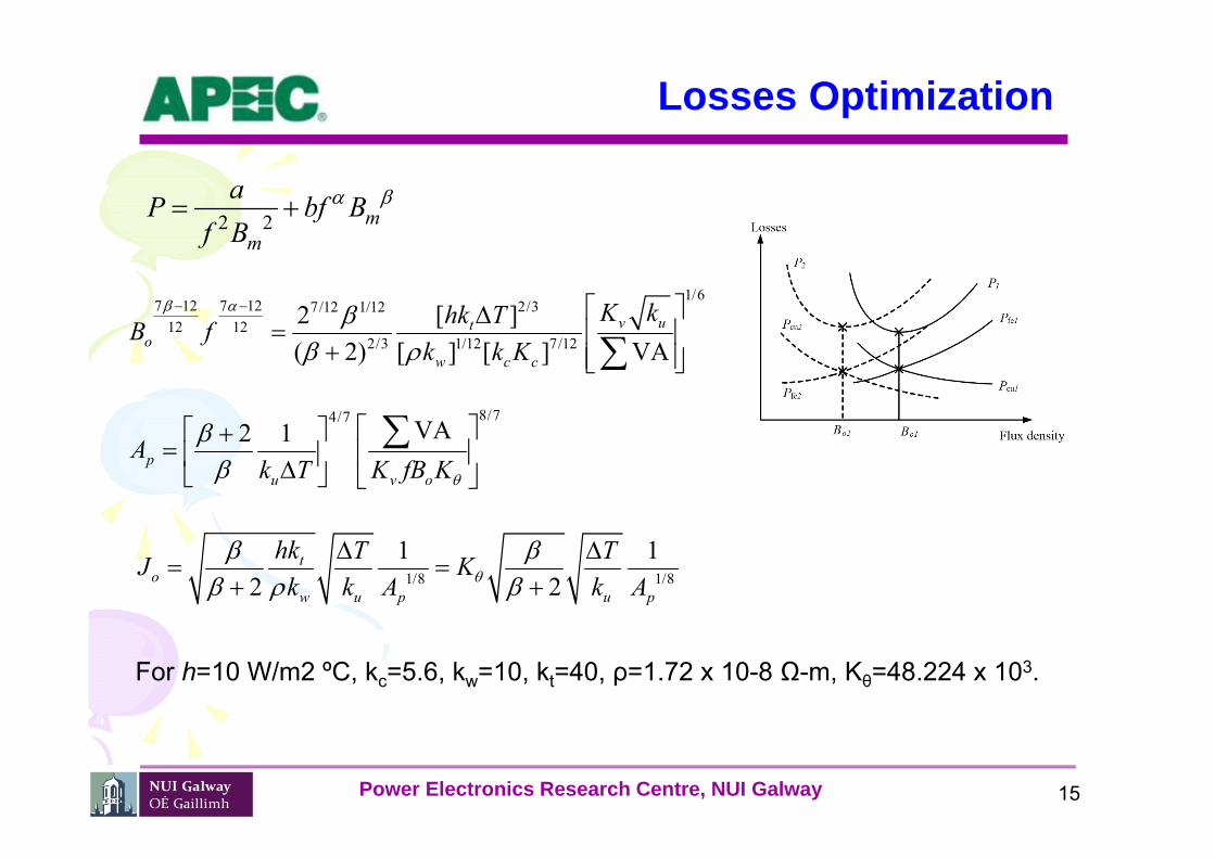
Optimum Thickness
31
The optimum value of ∆
rms
2
rms
155 1opt
Idipdt
Finally
4
opt
113
eff
dc
RR
Power Electronics Research Centre, NUI Galway
opt
43
eff
dc
RR

Optimum Winding Thickness: Pushpull
32Power Electronics Research Centre, NUI Galway
2 2
4 4
opt 2 2
8 (8)(0.025)0.67 (0.025)3 3 0.3342
(5 1)15 [(5)(6) 1] /15
r rt tDT T
p
Optimum layer ∆
Skin depth
0 3
66 66 0.295(50 10 )
mmf
Optimum layer thickness
opt opt(0.3342)(0.295) 0.1 mm
od
rms
2
rms
155 1 'opt
Ip I

Optimum Winding Thickness: Pushpull
33Power Electronics Research Centre, NUI Galway
Effective ac resistance: foil
AC resistance of round conductor
eff
dc
4 1.33
RR
ac
dc 0
1.00.25 (0.5) 0.25 (0.5)( ) 1.950.295
oR rR
Round versus foil conductor
Could replace solid wire with stranded Litz wire
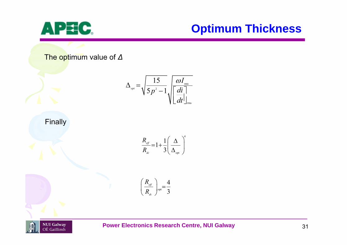
Litz Wire
34Power Electronics Research Centre, NUI Galway
Sullivan C. R., Zhang R. Y., “Analytical Model for Effects of Twisting on Litz-wire Losses”, IEEE 15th Workshop on Control and Modelling for Power Electronics, (COMPEL), pp. 1-10. 2014
• Litz wire reduces the window utilisation factor, core may be 30% larger for same temperature rise
• Use strands with diameter less than δ/4• Proximity effect occurs at strand level when wire is twisted• Twisting cancels proximity effect at bundle level
Avoid with radial and angular transposition
Avoid with radial transposition, simple twisting
Negligible

Litz Wire: skin effect
35Power Electronics Research Centre, NUI Galway
Acero J., Lope I., Burdio J.M., Carretero C., Alonso R., “Loss Analysis of Multistranded Twisted Wires by Usinf 3D-FEA Simulation”, IEEE 15th Workshop on Control and Modelling for Power Electronics, (COMPEL), pp. 1-6, 2014
• Skin effect acts like a solid conductor at the bundle level• Use strands with diameter less than δ/4

Litz Wire: proximity effect
36Power Electronics Research Centre, NUI Galway
Acero J., Lope I., Burdio J.M., Carretero C., Alonso R., “Loss Analysis of Multistranded Twisted Wires by Usinf 3D-FEA Simulation”, IEEE 15th Workshop on Control and Modelling for Power Electronics, (COMPEL), pp. 1-6, 2014
• Proximity effect occurs at strand level when wire is twisted• Twisting cancels proximity effect at bundle level

Interleaving the Windings
37Power Electronics Research Centre, NUI Galway
Current density distributionbefore interleaving
Current density distributionafter interleaving
2 22 2 2 4 22 1 2 14.4
3 3
é ùæ ö æ öê ú÷ ÷ç ç= + + + =÷ ÷ç çê ú÷ ÷ç çè ø è øê úë ûå J
Current density distributionbefore interleaving in FEA
Current density distributionafter interleaving in FEA

Fringing (Magnetic Field)
38Power Electronics Research Centre, NUI Galway
Gap in the centre leg Gap in the outer leg
Frequency: 100kHz Core: Magnetics® port core

Fringing (Flux)
39Power Electronics Research Centre, NUI Galway
Gap in the centre leg Gap in the outer leg
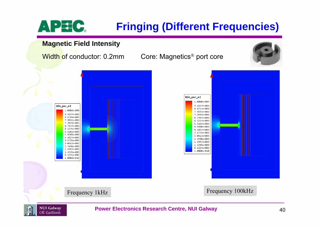
Fringing (Different Frequencies)
40Power Electronics Research Centre, NUI Galway
Frequency 1kHz Frequency 100kHz
Width of conductor: 0.2mm Core: Magnetics® port core
Magnetic Field Intensity

Fringing (Different Frequencies)
41Power Electronics Research Centre, NUI Galway
Frequency 1kHz Frequency 100kHz
Magnetic Flux

Fringing (Different Frequencies)
42Power Electronics Research Centre, NUI Galway
Frequency 1kHz Frequency 100kHz
Current Density
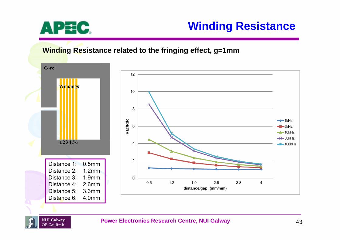
Winding Resistance
43Power Electronics Research Centre, NUI Galway
Winding Resistance related to the fringing effect, g=1mm
Distance 1: 0.5mmDistance 2: 1.2mmDistance 3: 1.9mmDistance 4: 2.6mmDistance 5: 3.3mmDistance 6: 4.0mm
0
2
4
6
8
10
12
0.5 1.2 1.9 2.6 3.3 4
Rac
/Rdc
distance/gap (mm/mm)
1kHz5kHz10kHz50kHz100kHz

Analytical Models for Planar Magnetics
44

Advantages
Low profile — planar magnetic components has a lower profile that their wire wound counterparts due to the fabrication process;
Automation — it is difficult to automate the winding of conventional inductors and transformers, the processes used in planar magnetics are based on advanced computer aided manufacturing techniques. Suitable for SMT
High power densities — planar inductors and transformers are spread out and this gives them a bigger surface-to-volume ratio than conventional components, this enhances the thermal performance;
Predictable parasitics — with planar magnetics, the windings are precise and consistent, yielding magnetic designs with highly controllable and predictable characteristic parameters.
45
Disadvantages
Turns — the number of turns in planar device tends to be limited by the manufacturing process;
Footprint — larger footprint compared with its conventional counterpart;
Capacitance — interlayer capacitance introduces resonance at high frequencies;
Trade-off — between magnetic core area and winding window area;between the path length versus the mean length of a turn.
46

Discrete PCB Magnetics
A typical planar transformer with an E-I core
47

Integrated PCB Magnetics
PCB integrated magnetic toroidal transformer
48

Thick Film Devices: Photoplots
Photoplots of conducting layers Masks for dielectric layers
Screen generation
49
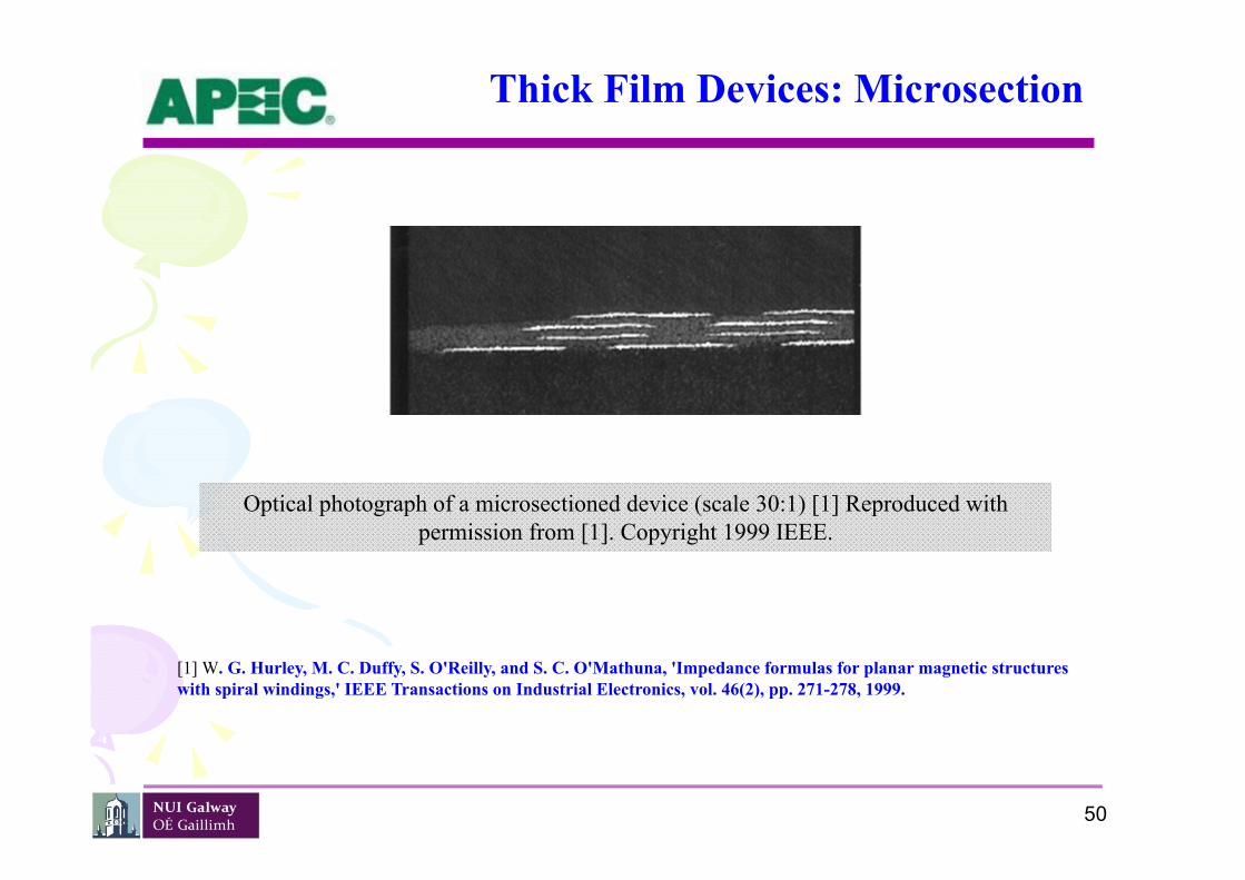
Thick Film Devices: Microsection
Optical photograph of a microsectioned device (scale 30:1) [1] Reproduced with permission from [1]. Copyright 1999 IEEE.
[1] W. G. Hurley, M. C. Duffy, S. O'Reilly, and S. C. O'Mathuna, 'Impedance formulas for planar magnetic structures with spiral windings,' IEEE Transactions on Industrial Electronics, vol. 46(2), pp. 271-278, 1999.
50

Low Temperature Co-fired Ceramics
LTCC Process flow
51

Silicon Integrated Microinductor
Silicon integrated microinductor: (a) Top view. Reproduced with permission from [1].Copyright 2008 IEEE, (b) Cross-section. Reproduced with permission from [2]. Copyright 2005 IEEE
[1] W. Ningning, T. O'Donnell, R. Meere, F. M. F. Rhen, S. Roy, and S. C. O'Mathuna, 'Thin-Film-Integrated Power Inductor on Si and Its Performance in an 8-MHz Buck Converter,' IEEE Transactions on Magnetics, vol. 44(11), pp. 4096-4099, 2008.[2] S. C. O. Mathuna, T. O'Donnell, W. Ningning, and K. Rinne, 'Magnetics on silicon: an enabling technology for power supply on chip,' IEEE Transactions on Power Electronics, vol. 20(3), pp. 585-592, 2005.
52

Thin Film Devices: Microfabrication
Microfabrication process flow for an inductor
53

Technology Comparison
Technology Frequency(Typical)
Power(Typical)
Inductance(Typical)
Size(Typical)
PCB magnetics 20 KHz ~ 2 MHz 1 W ~ 5 kW 10 µH ~ 10 mH 100 mm2 ~
100’s cm2
Thick Film < 10 MHz < 10 W 1 µH ~ 1 mH < 1 cm2
LTCC 200 KHz ~ 10 MHz < 10W 1 µH ~ 1 mH < 1cm2
Thin Film > 10 MHz < 1W 10’s ~ 100’s nH < 10mm2
54

Advantages and Disadvantages
Technology Integration method Advantages Disadvantage
PCB
Discrete core on laminated structure or integrated core in
laminated structureParallel or sequential process
Low costMultilayer structure
Thick copperHigh current
High inductance
Low resolution (line width 100µm)
Relatively low frequency
Thick Film
Screen printed on sintered ceramic
Sequential build up of multiple layers
Low costDifficult to form
Long process time and low yield due to
sequential build-up
LTCCScreen printed on green tapesParallel multilayer and final
cofired structure
Parallel layer processHigh layer countsModule reliability
Cofireability of materials
Thin Film Sequential build up of lithographically defined layers
Precision value (line width 5µm)High tolerance
High component densityHigh frequency
Low inductanceEquipment costly
Limited selection on film materials/ material
compatibility
55

Planar Transformer
56

Spiral Coil in Air
Circular concentric filaments in air
2
0
2 [(1 ) ( ) ( )]2fM ar K f E f
f 22
4( )arfa rz
K(f): complete elliptic integrals of the first kindE(f): complete elliptic integrals of the second kind
57

Mutual Inductance of Planar Coils
Solve with MATLAB
- | |012 2 1 2 1 1 20
2 21 2
1 1
( , ) ( , ) ( , )ln ln
k zS S Q dkkr kr ka ka kh kh eMr a
h h r a
0 0( ) ( )( , ) kx kyJ JS kx kyk
1 22
2( , ) cosh cosh 2 2 2
2 1 0,kh
x y x y h hQ kx ky k k zk
eh z x y hk k
Planar coils of rectangular cross-section
[1] W G Hurley, M C Duffy, J Zhang, I Lope, B Kunz, W H Wölfle, , “A Unified Approach to the Calculation of Self and Mutual Inductance for Coaxial Coils in Air”, IEEE Trans. on Power Electronics, vol. 30, no.11, pp. 6155–6162, November 2015.
58
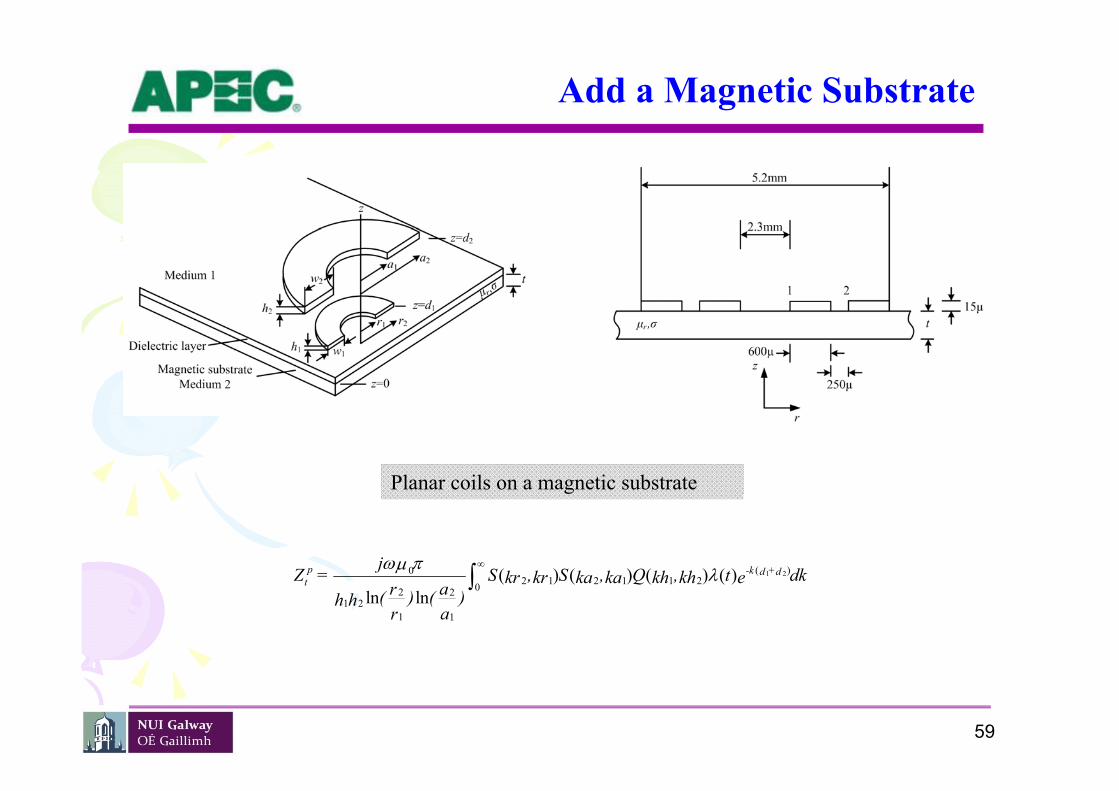
Add a Magnetic Substrate
Planar coils on a magnetic substrate
1 2( )02 1 2 1 1 202 2
1 21 1
( ) ( ) ( ) ( )ln ln
p -k +d dt
jZ = S , S , Q , t dkkr kr ka ka kh kh ear( ) ( )h h
ar
59

Effect of Permeability and Thickness
Enhancement of inductance with magnetic substrate: (a) as a function of μr, (b) as a function of t.
60

Effect of Frequency
Self impendence of a planar coil on a finite substrate: (a) inductance, (b) resistance.
21 2 2 1
21 2
2 ( ) ( ) cosh[ ( )]( )1 ( ) ( )
ks
ks
t t e k d dgt t e
61

Sandwich Structure
Planar coils in a sandwich structure
02 1 2 1 1 202 2
1 21 1
( , ) ( , )[ ( ) ( )] ( , )ln( ) ln( )
ps
jZ S kr kr S ka ka f g Q kh kh dk
r ah hr a
1 2 1 2( ) ( )1 2
21 2
( ) ( )( )1 ( ) ( )
k d d k d d
ks
t e t eft t e
21 2 2 1
21 2
2 ( ) ( ) cosh[ ( )]( )1 ( ) ( )
ks
ks
t t e k d dgt t e
62

Separation and Frequency
Inductance as a function of substrate separation; L1=17.14nH.
63

References
64Power Electronics Research Centre, NUI Galway
[1] C. P. Steinmetz, 'On the law of hysteresis,' Proceedings of the IEEE, vol. 72(2), pp. 197-221, 1984.[2] W. G. Hurley and M. C. Duffy, 'Calculation of self and mutual impedances in planar magnetic structures,' IEEE Transactions on
Magnetics, vol. 31(4), pp. 2416-2422, 1995.[3] J. C. Maxwell, A Treatise on Electricity and Magnetism. Oxford: Clarendon Press, 1881.[4] A. Gray, Absolute Measurements in Electricity and Magnetism. London: MacMillan, 1893.[5] T. R. Lyle, Philosophical Transactions of the Royal Society of London. Series A, Containing Papers of a Mathematical or Physical
Character. London: The Royal Society, 1914.[6] H. B. Dwight, 'Some New Formulas for Reactance Coils,' Transactions of the American Institute of Electrical Engineers, vol. XXXVIII(2),
pp. 1675-1696, 1919.[7] F. W. Grover, Inductance Calculations: Working Formulas and Tables. New York: Dover Publications Inc., 2004.[8] K. Venkatachalam, C. R. Sullivan, T. Abdallah, and H. Tacca, 'Accurate prediction of ferrite core loss with nonsinusoidal waveforms using
only Steinmetz parameters,' in Proceedings of IEEE Workshop on Computers in Power Electronics, COMPEL, 2002, pp. 36-41.[9] W. H. McAdams, Heat Transmission 3rd edn. New York: McGraw-Hill, 1954.[10] F. Judd and D. Kressler, 'Design optimization of small low-frequency power transformers,' IEEE Transactions on Magnetics, vol. 13(4), pp.
1058-1069, 1977.[11] C. W. T. McLyman, Transformer and Inductor Design Handbook, 3rd edn. New York: Marcel Dekker Inc., 2004.[12] J. G. Kassakian, M. F. Schlecht, and G. C. Verghese, Principles of Power Electronics (Addison-Wesley Series in Electrical Engineering).
Reading, MA: Prentice Hall, 1991.[13] W. G. Hurley, D. J. Wilcox, and P. S. McNamara, 'Calculation of short circuit impedance and leakage impedance in transformer windings,'
in Proceedings of the IEEE Power Electronics Specialists Conference, PESC, 1991, pp. 651-658.[14] W. G. Hurley and D. J. Wilcox, 'Calculation of leakage inductance in transformer windings,' IEEE Transactions on Power Electronics, vol.
9(1), pp. 121-126, 1994.[15] W. G. Hurley, W. H. Wolfle, and J. G. Breslin, 'Optimized transformer design: inclusive of high-frequency effects,' IEEE Transactions on
Power Electronics, vol. 13(4), pp. 651-659, 1998.[16] C. P. Steinmetz, 'On the law of hysteresis,' Proceedings of the IEEE, vol. 72(2), pp. 197-221, 1984.[17] K. Venkatachalam, C. R. Sullivan, T. Abdallah, and H. Tacca, 'Accurate prediction of ferrite core loss with nonsinusoidal waveforms using
only Steinmetz parameters,' in Proceedings of IEEE Workshop on Computers in Power Electronics, COMPEL, 2002, pp. 36-41.[18] J. Muhlethaler, J. Biela, J. W. Kolar, and A. Ecklebe, 'Core Losses Under the DC Bias Condition Based on Steinmetz Parameters,' IEEE
Transactions on Power Electronics, vol. 27(2), pp. 953-963, 2012.[19] E. C. Snelling, Soft Ferrites: Properties and Applications, 2nd edn. London: Butterworths, 1988.[20] W. G. Hurley, D. J. Wilcox, and P. S. McNamara, 'Calculation of short circuit impedance and leakage impedance in transformer windings,'
in Proceedings of the IEEE Power Electronics Specialists Conference, PESC, 1991, pp. 651-658.

PAGE 65
Planar Magnetics – Fundamentals

PAGE 66
Introduction
With rapidly increased frequencies, magnetics become VERY important factor to achieve high-efficiency and high-power-density converter.

PAGE 67
Advantages
Low profile: the height of a planar magnetic core is typically 25% to 50% the height of its wire-woundcounterpart.

PAGE 68
Advantages
Good thermal characteristic: planar cores essentially have a higher surface area to volume ratio than conventional magnetic cores.

PAGE 69
Advantages
Ease of manufacturability and cost reduction: automation process and computer aided.
Modularity: no extra connections are required
Photos are from Google

PAGE 70
Advantages
Predictable parasitics: windings manufactured by PCB machines are more precise and consistent, resulting in magnetic designs with highly controllable and predictable parasitic parameters
Ease of implementation on interleaved windings: multi-layer PCBs allow for a interconnection between arbitrary layers.

PAGE 71
In typical planar transformers, most of external flux (leakage flux) is parallel to the surface of the conductors
Eddy Current Effect

PAGE 72
High Frequency Resistance
Modelling ac resistance in planar transformer is the same with traditional one-dimensional Dowell’s analysis:
where ε is the ratio of the conductor thickness to the skin depth. p is the number of layers
2sinh 2 sin 2 2( 1) sinh sin cosh 2 cos2 3 cosh cos
ac
dc
R pR
effR
R
Note: “radial current distribution” in planar structures may affect the dc resistance, but no effect on the ratio of ac resistance to dc resistance.
[Ref.]: W. G. Hurley, E. Gath, and J. G. Breslin, “Optimizing the AC resistance of multilayer transformer windings with arbitrary current waveforms,” IEEE Trans. Power Electron., vol. 15, no. 2, pp. 369–376, Mar. 2000.

PAGE 73
Fringing Effect

PAGE 74
Fringing Effect

PAGE 75
Parallel Windings High current applications
Currents may not be equally distributed in the paralleled winding layers
Case 1 Case 2 Case 3

PAGE 76
Parallel Windings
[ref. 13]At low frequency, “parallel effect losses” or ”circulating currents losses” dominates
At high frequency, eddy current effect losses dominate.
[Ref.]: W. Chen, Y.-P. Yan, Y.-Q. Hu, and Q. Lu, “Model and design of PCB parallel winding for planartransformer,” IEEE Trans. Magn., vol. 39, no. 5, pp. 3202–3204, Sep. 2003.

PAGE 77
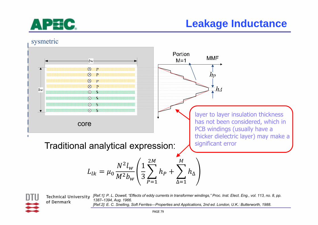
Leakage Inductance
Leakage energy stored in each elementary layer:
Leakage inductance is simply dependent on the energy stored in core window area:
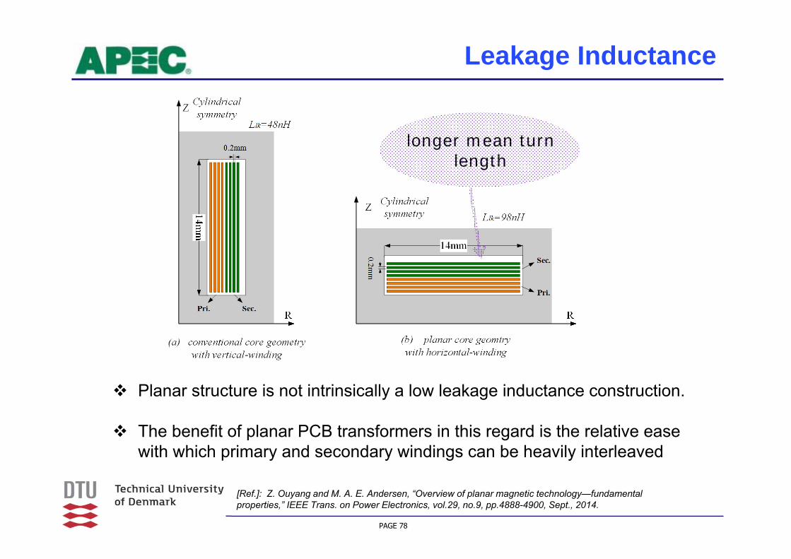
PAGE 78
longer mean turn length
Planar structure is not intrinsically a low leakage inductance construction.
The benefit of planar PCB transformers in this regard is the relative ease with which primary and secondary windings can be heavily interleaved
Leakage Inductance
[Ref.]: Z. Ouyang and M. A. E. Andersen, “Overview of planar magnetic technology—fundamental properties,” IEEE Trans. on Power Electronics, vol.29, no.9, pp.4888-4900, Sept., 2014.
PAGE 79
Traditional analytical expression:
13 ∆
∆
[Ref.1]: P. L. Dowell, “Effects of eddy currents in transformer windings,” Proc. Inst. Elect. Eng., vol. 113, no. 8, pp. 1387–1394, Aug. 1966.[Ref.2]: E. C. Snelling, Soft Ferrites—Properties and Applications, 2nd ed. London, U.K.: Butterworth, 1988.
layer to layer insulation thickness has not been considered, which in PCB windings (usually have a thicker dielectric layer) may make a significant error
Leakage Inductance

PAGE 80
Leakage Inductance
Leakage Inductance is frequency dependent
[Ref.1]: Z. Ouyang, J. Zhang, and W. G. Hurley, “Calculation of leakage inductance for high frequency transformers,” IEEE Trans. on Power Electronics, vol.30, no.10, pp.5769-5775, Oct. 2015[Ref.2]: J. Zhang, “Analysis and design of high frequency gapped transformers and planar transformers in LLC resonant converters”, PhD thesis, National University of Ireland, 2015

PAGE 81
Leakage Inductance
“radial current distribution” due to high aspect ratio of width to height of a section, bw/hw.

PAGE 82
∙ ∙ ∙ 2 1 4 1
∙ 12 ∙ γsinh
The energy stored in the primary/secondary winding is:
where, sinh 2 2
cosh ∙ sinh ∙
12 ∙ ∙ ∙ , ∙ 2 ∙
∙ ∙
∙ ∙
6∙ 1 2 1 ∙ 1 2 1
The energy stored in the dielectric layer is:
Leakage Inductance
New model for planar transformer leakage inductance:

PAGE 83
∙ ∙
3
2 1γsinh
4 12nγsinh
2 1 ∙1
1
Giving an example that has only one turn in each layer, the turns
ratio is defined, and all windings’ thickness are the same
( , then the total leakage inductance is:
Leakage Inductance
not applicable to complex interleaved cases such as primary and secondary windings on the same layer where 2-D consideration may be needed.

PAGE 84
Leakage Inductance
without the consideration of layer to layer insulation
without the consideration of radial current distribution
New model calculation

PAGE 85
Leakage Inductance
Reduce the number of turns. (core saturation and higher core loss)
Reduce the thickness of conductors and insulators. (high winding resistance and high interwinding capacitance)
Reduce the mean turn length.
Increase the window width. (high interwinding capacitance)
Interleaving winding arrangement.
[Ref.]: Z. Ouyang, O. C. Thomsen and M. A. E. Andersen, “Optimal design and tradeoff analysis of planar transformer in high-power dc–dc converters,” IEEE Trans. on Ind. Electronics, vol.59, no.7, pp.2800-2810, July, 2012.
Small Leakage Inductance is expected in most of power converters

PAGE 86
Leakage Inductance
Insertion of magnetic shunt (f.x. ferrite polymer composites FPC)
Higher Leakage Inductance is expected in resonant converterssuch as LLC, DAB etc.
[Ref.]: J. Zhang, Z. Ouyang, M. C. Duffy, M. A. E. Andersen and W. G. Hurley, "Leakage inductance calculation for planar transformers with a magnetic shunt," IEEE Transactions on Industry Applications, vol.50, no.6, pp.4107-4112, Nov.-Dec. 2014
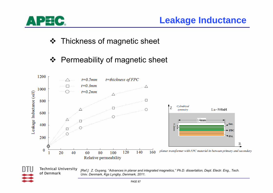
PAGE 87
Thickness of magnetic sheet
Permeability of magnetic sheet
Leakage Inductance
[Ref.]: Z. Ouyang, ‘‘Advances in planar and integrated magnetics,’’ Ph.D. dissertation, Dept. Electr. Eng., Tech. Univ. Denmark, Kgs Lyngby, Denmark, 2011.

PAGE 88
MMF method Reluctance method
[Ref.]: J. Zhang, Z. Ouyang, M. C. Duffy, M. A. E. Andersen and W. G. Hurley, "Leakage inductance calculation for planar transformers with a magnetic shunt," IEEE Transactions on Industry Applications, vol.50, no.6, pp.4107-4112, Nov.-Dec. 2014
Leakage Inductance

PAGE 89
Reluctance method provides a betterprediction
[Ref.]: J. Zhang, Z. Ouyang, M. C. Duffy, M. A. E. Andersen and W. G. Hurley, "Leakage inductance calculation for planar transformers with a magnetic shunt," IEEE Transactions on Industry Applications, vol.50, no.6, pp.4107-4112, Nov.-Dec. 2014
Leakage Inductance

PAGE 90
Fractional turn
Leakage Inductance
Higher Leakage Inductance is expected in resonant converterssuch as LLC, DAB etc.

PAGE 91
Winding Capacitance
Cpo, Cso are self-capacitances of the primary and the secondary windings, respectively.
Cpso is the mutual capacitance between the two windings.

PAGE 92
U-type winding scheme
Low
High
Winding Capacitance
Electric field energy distribution

PAGE 93
Winding Capacitance
Z-type winding scheme
Low
High
Electric field energy distribution

PAGE 94
Due to a higher ratio of the width to the thickness of the conductors (intrinsic property of PCB magnetics), C1 is much lower than C0. So, vertical winding scheme leads to a lower electric potential energy.
High
Low
Easier implementation in PCB
Winding Capacitance

PAGE 95
Interleaved Winding
Reduce the ac winding resistance; (not for the flyback converter)
Reduce the leakage inductance;
Increase the interwinding capacitance.
[Ref.]: Z. Ouyang, O. C. Thomsen and M. A. E. Andersen, “Optimal design and tradeoff analysis of planar transformer in high-power dc–dc converters,” IEEE Trans. on Ind. Electronics, vol.59, no.7, pp.2800-2810, July, 2012.

PAGE 96
Interleaved Winding
High Low

PAGE 97
High Low
Interleaved Winding

PAGE 98
Interleaved Winding

PAGE 99
Interleaved Winding

PAGE 100
Planar Magnetic Components Integration

PAGE 101
Introduction
functional devices integration, in which discrete magnetic devices with different functions are assembled as one integrated magnetic device.
Mixing the functions of transformers and inductors in:
• Current doubler rectifiers
• LLC resonant converters
• Integrated EMI filters etc.
PAGE 102
Major advantage:
Smaller size
higher power efficiency
lower core loss (spark interest into the light load
conditions with the integrated magnetics)
It is often used in applications where space is highly restricted such as computer systems, data center, automotive electrical systems and space applications.
Introduction

PAGE 103
Classification
Magnetic core sharing ( Only the core is shared, and the windings are not shared )

PAGE 104
Classification
Both winding and magnetic core sharing(Fully integration)

PAGE 105
Coupled Integration
The magnetic field produced by one coil passes through the other coil, changing their effective inductances due to the mutual relationship:
Coupled Inductors
Multi-winding transformers
…
many advantages,… but can NOT be applied in all circuit topologies

PAGE 106
Decoupled Integration
The magnetic field produced by one coil does not pass through the other coil or cancel in the other coil.
can be used in nearly all circuit topologies due to their independent operation behaviors

PAGE 107
Decoupling Methods
Shared low core reluctance path
Flux cancellation

PAGE 108
Orthogonal flux path
Decoupling Methods
[Ref.]: Z. Ouyang, M. A. E. Andersen and Z. Zhang, “An integrated magnetics component,” PCT/EP2012/067422, published no.: WO 2013037696 A1, Sept., 2011.

PAGE 109
Integrated transformer (FQIT)
Four Quadrants Integrated Transformer
[Ref.]: Z. Ouyang, Z. Zhang, M. A. E. Andersen and O. C. Thomsen, “Fourquadrants integrated transformers for dual-input isolated dc-dc converters,” IEEE Trans. on Power Electron. vol.27, no.6, pp.2697-2702, June 2012

PAGE 110
wide input range simple control and communication high reliability low overall system cost efficient thermal management compact packaging
Four Quadrants Integrated Transformer
half size of transformer
[Ref.]: Z. Ouyang and M. A. E. Andersen, “Three-port DC-DC converter with new integrated transformer for DC Distribution Systems,” in the 2014 international power electronics conference-PCIM Asia, Shanghai, June, 2014.
effic
ienc
y
Pout (W)

PAGE 111
Magnetic Reluctance Modeling
11 IN 22 IN
1R 2R
cR
21
2N
2I
1I
1N
1
21
RN cR
N 21
2
21
RN
1N 2N1
1R 2
1R
cR1
1
11 IN 22 IN
2
duality transformation rules
For a practical interest that the magnetic and electrical circuits interact
Applying reluctance-resistance analogy

PAGE 112
Gyrator-Capacitor Modeling
Energy interchange between windings and cores
Understand energy relations and dynamics in the context of power electronics
[Ref.]: G. Sen, Z. Ouyang, O. C. Thomsen, M. A. E. Andersen and L. Møller, “Integrated current balancingtransformer for primary parallel isolated boost converter,” in Proc. EPE, Birmingham, U.K, Sept. 2011.
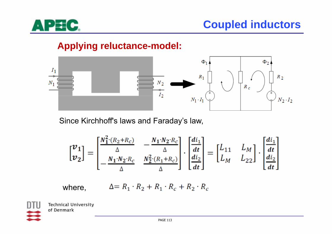
PAGE 113
Coupled inductors
Since Kirchhoff's laws and Faraday’s law,
where,
Applying reluctance-model:

PAGE 114
Coupling coefficient:
R2 >> Rc R2 =2*Rc R2 << Rc
( assuming N1 =N2 )
Coupled inductors

PAGE 115
[ref.]: P.‐L. Wong, Q.‐Q. Wu, P. Xu, B. Yang, and F. C. Lee, “Investigating coupling inductors in the interleaving QSW VRM,” in Proc. IEEE Appl. Power Electron. Conf. Expo., 2000, pp. 973–978.
Coupled inductors
Effective inductances are dependent of circuit operation

PAGE 116
Integrated magnetics is actually an “open” technology, and may create “innovation” ideas.
Summary
PAGE 117
Integrated magnetics has advantages less number of components, smaller size, and potentially higher power efficiency.
Integrated magnetics are not all advantageous. The main issue is to produce unwanted parasitic capacitances among the inductive elements, and a limited power capability.
Must understand the principle of circuit operation.
New geometry core may create something interesting.
Summary

PAGE 118
Conclusion and Trends

PAGE 119
Planar magnetics still gain its popularity due to low profile and easy manufacture
Planar magnetics towards very high frequency (so-called micro-inductor/transformer) would be interesting. Accurate 2D/3D models are emergency
High frequency magnetic materials are emergency
New winding and core geometries may create something innovative

PAGE 120