Embed Size (px)
Citation preview
ARTICLE
Received 11 Aug 2014 | Accepted 11 Nov 2014 | Published 19 Dec 2014
High electron mobility in thin films formed viasupersonic impact deposition of nanocrystalssynthesized in nonthermal plasmasElijah Thimsen1, Melissa Johnson2, Xin Zhang2, Andrew J. Wagner2, K. Andre Mkhoyan2, Uwe R. Kortshagen3
& Eray S. Aydil2
Thin films comprising semiconductor nanocrystals are emerging for applications in electronic
and optoelectronic devices including light emitting diodes and solar cells. Achieving high
charge carrier mobility in these films requires the identification and elimination of electronic
traps on the nanocrystal surfaces. Herein, we show that in films comprising ZnO
nanocrystals, an electron acceptor trap related to the presence of OH on the surface limits
the conductivity. ZnO nanocrystal films were synthesized using a nonthermal plasma from
diethyl zinc and oxygen and deposited by inertial impaction onto a variety of substrates.
Surprisingly, coating the ZnO nanocrystals with a few nanometres of Al2O3 using atomic layer
deposition decreased the film resistivity by seven orders of magnitude to values as low as
0.12O cm. Electron mobility as high as 3 cm2 V� 1 s� 1 was observed in films comprising
annealed ZnO nanocrystals coated with Al2O3.
DOI: 10.1038/ncomms6822
1 Department of Energy, Environmental and Chemical Engineering, Washington University, Saint Louis, Missouri 63130, USA. 2 Department of ChemicalEngineering and Materials Science, University of Minnesota, Minneapolis, Minnesota 55455, USA. 3 Department of Mechanical Engineering, Universityof Minnesota, Minneapolis, Minnesota 55455, USA. Correspondence and requests for materials should be addressed to E.T.(email: [email protected]).
NATURE COMMUNICATIONS | 5:5822 | DOI: 10.1038/ncomms6822 | www.nature.com/naturecommunications 1
& 2014 Macmillan Publishers Limited. All rights reserved.
Controlling charge carrier concentration and mobility inthin films comprising semiconductor nanocrystals is vitalfor optoelectronic applications. The goal is to achieve the
highest possible mobilities with rational control over the majoritycarrier concentration through doping. While exquisite controlover nanocrystal size and size distribution has been achieved incolloidal nanocrystal synthesis, both doping1 and achieving highmobility in thin films made from these nanocrystals have beenchallenging. Frequently used synthesis methods for makingcolloidal nanocrystal leave their surfaces covered with longorganic ligands. When thin films are cast from colloidaldispersions of these nanocrystals, the ligands act as insulatingbarriers and impede charge transport. The nanocrystals can bebrought closer together to improve the charge carrier mobilities,either by removing the long-chain ligands or by exchanging themfor shorter ones2. The presence of electronic surface traps,particularly prevalent in films without surface ligands, alsoreduces charge mobility. Gating and moving the Fermi levelabove the trap levels, in films comprising n-type nanocrystals, canfill these traps and increase the charge mobility significantly (ashigh as 27 cm2 V� 1 s� 1; refs 3–6). However, gating cannot beused in some important applications such as thin film solar cellsand transparent conducting films. Recently, infiltration of thespace between the nanocrystals with a coating using atomic layerdeposition (ALD) has been shown to be an effective approach forimproving the electronic properties of colloidal nanocrystal films.For example, Pourett et al.7 improved the charge mobility inphotodetectors made from colloidal CdSe quantum dot films to0.01–0.1 cm2 V� 1 s� 1 by infiltrating the pores with ALD ZnO,while Liu et al.8 achieved 6–8 cm2 V� 1 s� 1 field effect mobilitiesin transistors made from PbSe nanocrystals infiltrated with ALDAl2O3. It is important to note that in all these studies, the effect oftraps was eliminated by gating, and the reported mobilities aremeasured in field effect transistors.
In the following, we describe a method for making highmobility (E3 cm2 V� 1 s� 1) thin films comprising ZnO nano-crystals synthesized in the gas phase using a nonthermal plasmawithout ever exposing them to a solvent or surface passivatingligands. While ZnO films comprising nanocrystals have beenmade9–12, achieving high electron mobility without gating hasbeen elusive. We form thin films comprising these nanocrystalsby supersonic expansion and subsequent impaction of the plasmaeffluent containing the nanocrystals onto suitable substrates. Thesurfaces of these plasma-synthesized nanocrystals are nominallybare (that is, no ligands) such that the nanocrystals are abuttedagainst each other in thin films formed by supersonic impaction.We show that electronic traps on nanocrystal surfaces can beeliminated in a second process by coating with Al2O3 depositedby ALD. The effectiveness of this strategy is demonstrated in acase study of transparent conducting ZnO.
ResultsNanocrystal deposition. Zinc oxide nanocrystals were synthe-sized in the two-stage plasma reactor13,14 illustrated inSupplementary Fig. 1. The first stage is a nonthermal plasmamaintained in a glass tube using radiofrequency electric field: thenanocrystals nucleate and grow in this stage. A slit-shaped nozzle(0.8� 15 mm) that generates supersonic expansion of theparticle-laden gas separates this synthesis stage from the secondstage where the substrates to be coated are placed. Experimentaldetails are described in the Methods section. Briefly, ZnOnanocrystals were synthesized from diethyl zinc (DEZ) vapourand oxygen (O2) gas in argon plasma. The DEZ and oxygenwere fed in the stoichiometric molar ratio (O2:DEZ¼ 7:1)necessary for complete oxidation of DEZ to ZnO, CO2 and
H2O. The ZnO nanocrystals synthesized in the plasma werecarried to the second stage by the gas flow, which achievessupersonic speeds upon expansion through the slit. The ZnOnanocrystals form a high velocity (100 m s� 1) particle beam withdimensions slightly larger than the expansion slit and areeventually deposited by inertial impaction onto the substrateimmediately downstream of the slit15. The substrates were movedback and forth under this beam in a perpendicular direction tothe long axis of the slit in a reciprocating motion to simulate aroll-to-roll deposition process. For a given set of flow rates andpressures, the deposition rate depends on the translationalvelocity and the stroke length; but under typical conditions, thedeposition rate was 33 nm s� 1. This is already two to three ordersof magnitude higher than the typical deposition rates achieved bysputtering (0.1–1 nm s� 1) and much higher deposition rates(100–1,000 nm s� 1) are possible by automation. Deposition ratesas high as 200 nm s� 1 have shown no ostensible change in thematerial quality, but the thickness becomes difficult to controlreproducibly using manual scanning. Films were deposited onsilicon substrates for most characterization experiments but glasssubstrates were used for electrical and ultraviolet–visible–nearinfrared (ultraviolet–vis–NIR) transmission measurements. TheZnO nanocrystal films discussed here are 0.4 to 1.0 mm thick.Some films were also annealed at 340 �C in H2, which increasesthe crystallite size (vide infra). Some of the as-deposited andannealed films were also coated with Al2O3 or Al-doped ZnOusing ALD. Remarkable differences in the electrical properties ofthese films are discussed below.
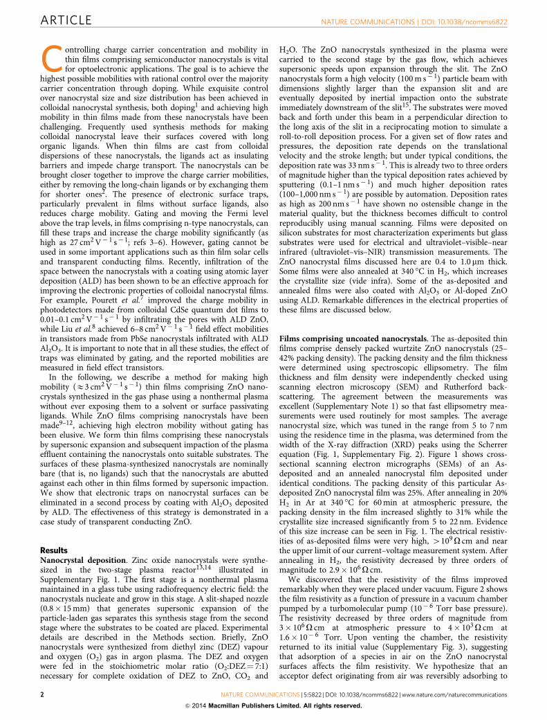
Films comprising uncoated nanocrystals. The as-deposited thinfilms comprise densely packed wurtzite ZnO nanocrystals (25–42% packing density). The packing density and the film thicknesswere determined using spectroscopic ellipsometry. The filmthickness and film density were independently checked usingscanning electron microscopy (SEM) and Rutherford back-scattering. The agreement between the measurements wasexcellent (Supplementary Note 1) so that fast ellipsometry mea-surements were used routinely for most samples. The averagenanocrystal size, which was tuned in the range from 5 to 7 nmusing the residence time in the plasma, was determined from thewidth of the X-ray diffraction (XRD) peaks using the Scherrerequation (Fig. 1, Supplementary Fig. 2). Figure 1 shows cross-sectional scanning electron micrographs (SEMs) of an As-deposited and an annealed nanocrystal film deposited underidentical conditions. The packing density of this particular As-deposited ZnO nanocrystal film was 25%. After annealing in 20%H2 in Ar at 340 �C for 60 min at atmospheric pressure, thepacking density in the film increased slightly to 31% while thecrystallite size increased significantly from 5 to 22 nm. Evidenceof this size increase can be seen in Fig. 1. The electrical resistiv-ities of as-deposited films were very high, 4109O cm and nearthe upper limit of our current–voltage measurement system. Afterannealing in H2, the resistivity decreased by three orders ofmagnitude to 2.9� 106O cm.
We discovered that the resistivity of the films improvedremarkably when they were placed under vacuum. Figure 2 showsthe film resistivity as a function of pressure in a vacuum chamberpumped by a turbomolecular pump (10� 6 Torr base pressure).The resistivity decreased by three orders of magnitude from3� 106O cm at atmospheric pressure to 4� 103O cm at1.6� 10� 6 Torr. Upon venting the chamber, the resistivityreturned to its initial value (Supplementary Fig. 3), suggestingthat adsorption of a species in air on the ZnO nanocrystalsurfaces affects the film resistivity. We hypothesize that anacceptor defect originating from air was reversibly adsorbing to
ARTICLE NATURE COMMUNICATIONS | DOI: 10.1038/ncomms6822
2 NATURE COMMUNICATIONS | 5:5822 | DOI: 10.1038/ncomms6822 | www.nature.com/naturecommunications
& 2014 Macmillan Publishers Limited. All rights reserved.
the surface and increasing the resistivity of the ZnO nanocrystalfilms by trapping electrons and reducing the carrier density. Closeexamination of Fig. 2 suggests that the ZnO nanocrystal surfacecoverage of the acceptor remained high and the surface remainedapproximately saturated until the pressure began to drop belowB0.1 Torr. The steep slope of the data in Fig. 2 at 10� 6 Torrsuggests that if the pressure were lowered even further, theresistivity would have continued to drop. Clearly, the cause forthe high resistivity of the ZnO nanocrystal films, when measuredunder ambient conditions, is an adsorbate originating from airwhose identity and chemical origin will be proposed shortly.
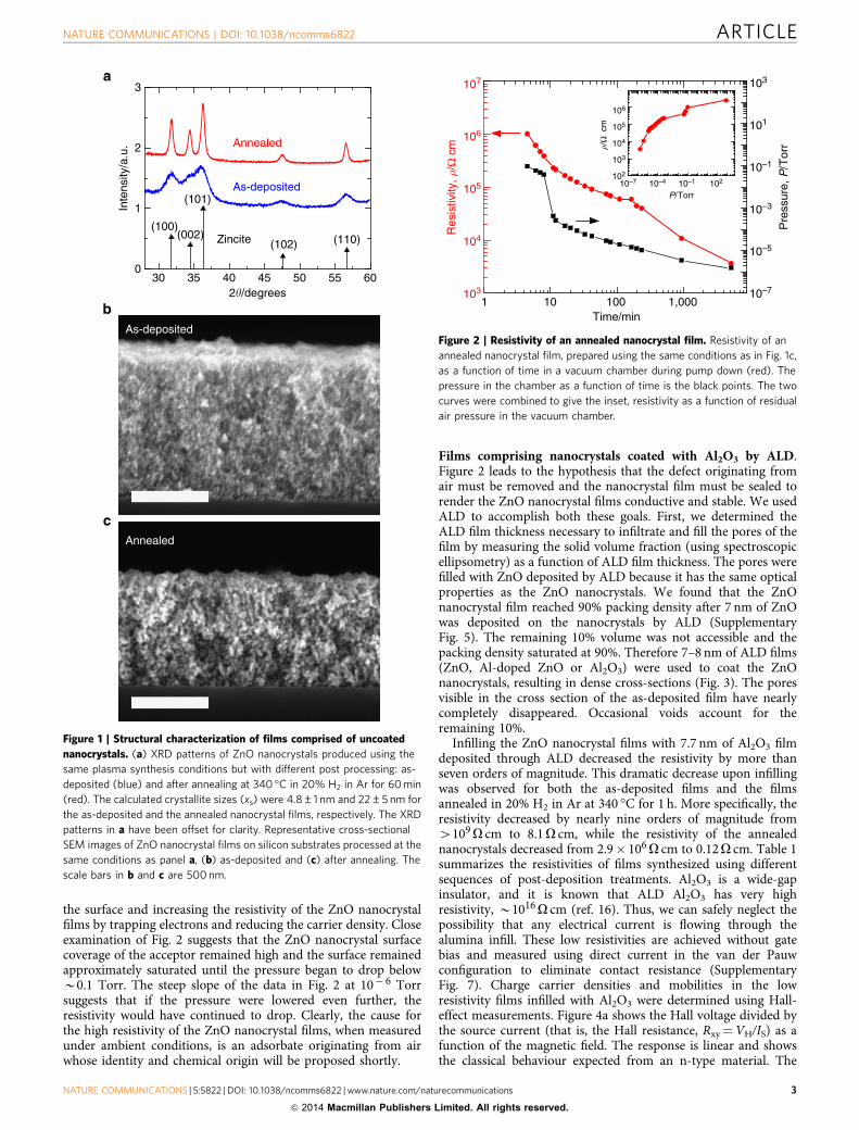
Films comprising nanocrystals coated with Al2O3 by ALD.Figure 2 leads to the hypothesis that the defect originating fromair must be removed and the nanocrystal film must be sealed torender the ZnO nanocrystal films conductive and stable. We usedALD to accomplish both these goals. First, we determined theALD film thickness necessary to infiltrate and fill the pores of thefilm by measuring the solid volume fraction (using spectroscopicellipsometry) as a function of ALD film thickness. The pores werefilled with ZnO deposited by ALD because it has the same opticalproperties as the ZnO nanocrystals. We found that the ZnOnanocrystal film reached 90% packing density after 7 nm of ZnOwas deposited on the nanocrystals by ALD (SupplementaryFig. 5). The remaining 10% volume was not accessible and thepacking density saturated at 90%. Therefore 7–8 nm of ALD films(ZnO, Al-doped ZnO or Al2O3) were used to coat the ZnOnanocrystals, resulting in dense cross-sections (Fig. 3). The poresvisible in the cross section of the as-deposited film have nearlycompletely disappeared. Occasional voids account for theremaining 10%.
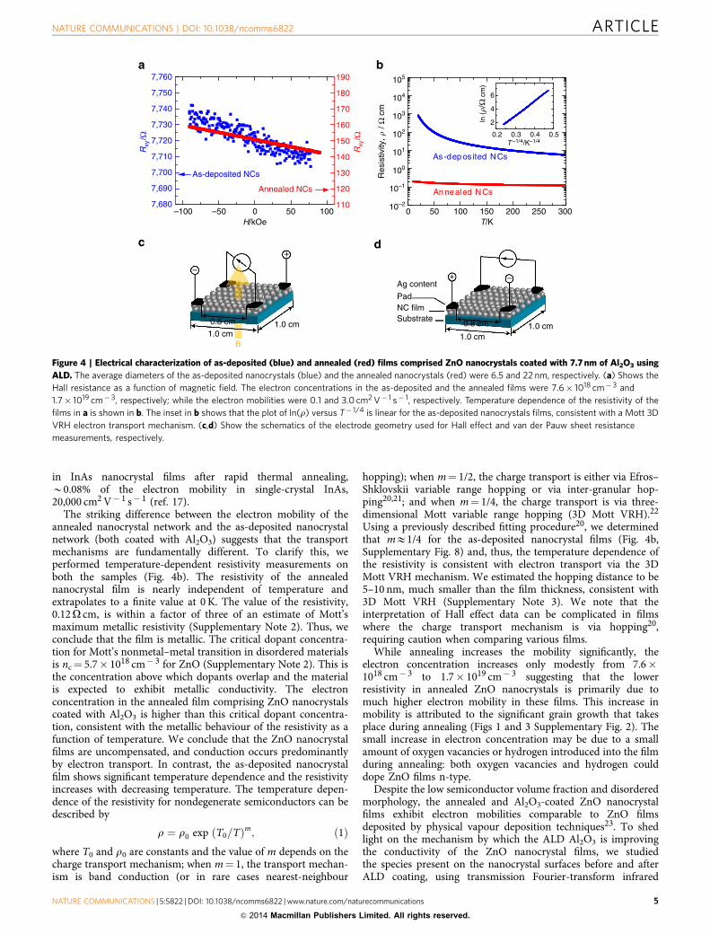
Infilling the ZnO nanocrystal films with 7.7 nm of Al2O3 filmdeposited through ALD decreased the resistivity by more thanseven orders of magnitude. This dramatic decrease upon infillingwas observed for both the as-deposited films and the filmsannealed in 20% H2 in Ar at 340 �C for 1 h. More specifically, theresistivity decreased by nearly nine orders of magnitude from4109O cm to 8.1O cm, while the resistivity of the annealednanocrystals decreased from 2.9� 106O cm to 0.12O cm. Table 1summarizes the resistivities of films synthesized using differentsequences of post-deposition treatments. Al2O3 is a wide-gapinsulator, and it is known that ALD Al2O3 has very highresistivity, B1016O cm (ref. 16). Thus, we can safely neglect thepossibility that any electrical current is flowing through thealumina infill. These low resistivities are achieved without gatebias and measured using direct current in the van der Pauwconfiguration to eliminate contact resistance (SupplementaryFig. 7). Charge carrier densities and mobilities in the lowresistivity films infilled with Al2O3 were determined using Hall-effect measurements. Figure 4a shows the Hall voltage divided bythe source current (that is, the Hall resistance, Rxy¼VH/IS) as afunction of the magnetic field. The response is linear and showsthe classical behaviour expected from an n-type material. The
30 35 40
As-deposited
Annealed
45 50 55 600
1
2
3
(100)(002)
(101)
(102) (110)Zincite
Inte
nsity
/a.u
.
2�/degrees
Annealed
As-deposited
Figure 1 | Structural characterization of films comprised of uncoated
nanocrystals. (a) XRD patterns of ZnO nanocrystals produced using the
same plasma synthesis conditions but with different post processing: as-
deposited (blue) and after annealing at 340 �C in 20% H2 in Ar for 60 min
(red). The calculated crystallite sizes (xs) were 4.8±1 nm and 22±5 nm for
the as-deposited and the annealed nanocrystal films, respectively. The XRD
patterns in a have been offset for clarity. Representative cross-sectional
SEM images of ZnO nanocrystal films on silicon substrates processed at the
same conditions as panel a, (b) as-deposited and (c) after annealing. The
scale bars in b and c are 500 nm.
1 10 100 1,000
107
106
105
104
103 10–7
10–5
10–3
10–1
101
103
10210–7102
103
104
106
105
10–4 10–1
Res
istiv
ity, �
/Ω c
m
Time/min
Pre
ssur
e, P
/Tor
r�/Ω
cm
P/Torr
Figure 2 | Resistivity of an annealed nanocrystal film. Resistivity of an
annealed nanocrystal film, prepared using the same conditions as in Fig. 1c,
as a function of time in a vacuum chamber during pump down (red). The
pressure in the chamber as a function of time is the black points. The two
curves were combined to give the inset, resistivity as a function of residual
air pressure in the vacuum chamber.
NATURE COMMUNICATIONS | DOI: 10.1038/ncomms6822 ARTICLE
NATURE COMMUNICATIONS | 5:5822 | DOI: 10.1038/ncomms6822 | www.nature.com/naturecommunications 3
& 2014 Macmillan Publishers Limited. All rights reserved.
electron mobility in as-deposited ZnO nanocrystal film infilledwith Al2O3 was 0.1 cm2 V� 1 s� 1. We caution that such a lowvalue for the mobility means it is probably unreliable. Forexample, considering the electron effective mass in ZnO is 0.3me,a mobility of 0.1 cm2 V� 1 s� 1 results in a mean free path ofB4 pm. Considering the radius of Zn2þ to be 60 pm, such ashort mean free path is difficult to interpret physically. Morelikely the Hall effect has been suppressed because of a hoppingelectron transport mechanism (see below) for the as-depositedZnO nanocrystals. When the nanocrystal films are annealed inhydrogen before infilling with Al2O3, the electron mobility ismuch higher and increases by a factor of 30 to 3.0 cm2 V� 1 s� 1.
This mobility is remarkably high and comparable to electronmobilities in ZnO films deposited by ALD (see below). In fact, theelectron mobility is 2% of the values reported for single-crystalZnO (150 cm2 V� 1 s� 1; ref. 17) and comparable to the electronmobilities in other semiconductor nanocrystal films. For example,Choi et al.18 measured a field effect electron mobility of20 cm2 V� 1 s� 1 in annealed CdSe nanocrystal films, B3% ofthe electron mobility in single-crystal CdSe (660 cm2 V� 1 s� 1;ref. 17). Even without annealing, the electron mobility of the ZnOnanocrystal film, 0.1 cm2 V� 1 s� 1, is 0.07% of the single-crystalmobility; comparable to a recent measurement by Jang et al.19,who reported Hall-effect electron mobilities of 16 cm2 V� 1 s� 1
Figure 3 | Cross-sectional SEM images. Cross-sectional SEM images of as-deposited ZnO nanocrystals on a silicon substrate (a) before and (b) after the
nanocrystals have been coated with 7.2 nm of Al2O3 using ALD. Annealed ZnO nanocrystals on a silicon substrate before (c) and after (d) coating with
7.7 nm of ALD Al2O3 using ALD. (e) Shows a high angle annular dark field scanning transmission electron microscope (STEM) image of annealed ZnO
nanocrystals coated with 7.7 nm Al2O3, corresponding to d. (f) Shows a STEM X-ray energy dispersion spectroscopy map of zinc (green) and aluminium
(red) distribution in the area defined by the box in e. The scale bars in a–d are 500 nm, and e is 15 nm.
Table 1 | The properties of films comprising ZnO- and Al2O3-coated ZnO nanocrystals.
Film ALD coating dfilm (lm) xs (nm) /ZnO (%) q (O cm) ne (cm� 3) le (cm2 V� 1 s� 1)
As-deposited ZnO None 0.48 6.5±1 34 4109 — —Annealed ZnO None 0.77 27±5 33 2.9� 106 — —As-deposited ZnO 7.7 nm Al2O3 0.48 6.5±1 34 8.1� 100 7.6� 1018 0.1Annealed ZnO 7.7 nm Al2O3 0.63 24±3 31 1.2� 10� 1 1.7� 1019 3.0ALD control ZnO None 0.99 5.1±1 26 4109 — —
ALD, atomic layer deposition; dfilm, film thickness; fZnO, ZnO volume fraction; ne, electron concentration determined from the Hall effect measurements; me, mobility calculated from the resistivity and theelectron concentration; r, resistivity; xs, crystallite size obtained from the width of the XRD peak using the Scherrer formula.The film labelled ‘ALD control’ experienced identical conditions as the as-deposited ZnO nanocrystal film coated with 7.7 nm of Al2O3 using ALD, except that the ALD precursors were not fed into thechamber (that is, the substrate coated with the nanocrystal film was placed in the ALD chamber for the same amount of time and at the same temperature but no Al2O3 was deposited).
ARTICLE NATURE COMMUNICATIONS | DOI: 10.1038/ncomms6822
4 NATURE COMMUNICATIONS | 5:5822 | DOI: 10.1038/ncomms6822 | www.nature.com/naturecommunications
& 2014 Macmillan Publishers Limited. All rights reserved.
in InAs nanocrystal films after rapid thermal annealing,B0.08% of the electron mobility in single-crystal InAs,20,000 cm2 V� 1 s� 1 (ref. 17).
The striking difference between the electron mobility of theannealed nanocrystal network and the as-deposited nanocrystalnetwork (both coated with Al2O3) suggests that the transportmechanisms are fundamentally different. To clarify this, weperformed temperature-dependent resistivity measurements onboth the samples (Fig. 4b). The resistivity of the annealednanocrystal film is nearly independent of temperature andextrapolates to a finite value at 0 K. The value of the resistivity,0.12O cm, is within a factor of three of an estimate of Mott’smaximum metallic resistivity (Supplementary Note 2). Thus, weconclude that the film is metallic. The critical dopant concentra-tion for Mott’s nonmetal–metal transition in disordered materialsis nc¼ 5.7� 1018 cm� 3 for ZnO (Supplementary Note 2). This isthe concentration above which dopants overlap and the materialis expected to exhibit metallic conductivity. The electronconcentration in the annealed film comprising ZnO nanocrystalscoated with Al2O3 is higher than this critical dopant concentra-tion, consistent with the metallic behaviour of the resistivity as afunction of temperature. We conclude that the ZnO nanocrystalfilms are uncompensated, and conduction occurs predominantlyby electron transport. In contrast, the as-deposited nanocrystalfilm shows significant temperature dependence and the resistivityincreases with decreasing temperature. The temperature depen-dence of the resistivity for nondegenerate semiconductors can bedescribed by
r ¼ r0 exp T0=Tð Þm; ð1Þwhere T0 and r0 are constants and the value of m depends on thecharge transport mechanism; when m¼ 1, the transport mechan-ism is band conduction (or in rare cases nearest-neighbour
hopping); when m¼ 1/2, the charge transport is either via Efros–Shklovskii variable range hopping or via inter-granular hop-ping20,21; and when m¼ 1/4, the charge transport is via three-dimensional Mott variable range hopping (3D Mott VRH).22
Using a previously described fitting procedure20, we determinedthat mE1/4 for the as-deposited nanocrystal films (Fig. 4b,Supplementary Fig. 8) and, thus, the temperature dependence ofthe resistivity is consistent with electron transport via the 3DMott VRH mechanism. We estimated the hopping distance to be5–10 nm, much smaller than the film thickness, consistent with3D Mott VRH (Supplementary Note 3). We note that theinterpretation of Hall effect data can be complicated in filmswhere the charge transport mechanism is via hopping20,requiring caution when comparing various films.
While annealing increases the mobility significantly, theelectron concentration increases only modestly from 7.6�1018 cm� 3 to 1.7� 1019 cm� 3 suggesting that the lowerresistivity in annealed ZnO nanocrystals is primarily due tomuch higher electron mobility in these films. This increase inmobility is attributed to the significant grain growth that takesplace during annealing (Figs 1 and 3 Supplementary Fig. 2). Thesmall increase in electron concentration may be due to a smallamount of oxygen vacancies or hydrogen introduced into the filmduring annealing: both oxygen vacancies and hydrogen coulddope ZnO films n-type.
Despite the low semiconductor volume fraction and disorderedmorphology, the annealed and Al2O3-coated ZnO nanocrystalfilms exhibit electron mobilities comparable to ZnO filmsdeposited by physical vapour deposition techniques23. To shedlight on the mechanism by which the ALD Al2O3 is improvingthe conductivity of the ZnO nanocrystal films, we studiedthe species present on the nanocrystal surfaces before and afterALD coating, using transmission Fourier-transform infrared
0 50 100 150
Ag content
PadNC filmSubstrate
0.8 cm0.8 cm
1.0 cm1.0 cm1.0 cm1.0 cm
B
––
+
+
200 250 30010–2
10–1
100
101
102
103
104
105
As -depos ited NCs
An nealed NCs
2
4
6
50 1007,680
7,690
7,700
7,710
7,720
7,730
7,740
7,750
7,760
110
120
130
140
150
160
170
180
190
Res
istiv
ity, �
/ Ω
cm
Rxy
/Ω
Rxy
/Ω
–100 –50 0H/kOe
Annealed NCs
As-deposited NCs
ln (�/
Ω c
m)
T –1/4/K–1/40.2 0.3 0.4 0.5
T/K
Figure 4 | Electrical characterization of as-deposited (blue) and annealed (red) films comprised ZnO nanocrystals coated with 7.7 nm of Al2O3 using
ALD. The average diameters of the as-deposited nanocrystals (blue) and the annealed nanocrystals (red) were 6.5 and 22 nm, respectively. (a) Shows the
Hall resistance as a function of magnetic field. The electron concentrations in the as-deposited and the annealed films were 7.6� 1018 cm� 3 and
1.7� 1019 cm� 3, respectively; while the electron mobilities were 0.1 and 3.0 cm2 V� 1 s� 1, respectively. Temperature dependence of the resistivity of the
films in a is shown in b. The inset in b shows that the plot of ln(r) versus T� 1/4 is linear for the as-deposited nanocrystals films, consistent with a Mott 3D
VRH electron transport mechanism. (c,d) Show the schematics of the electrode geometry used for Hall effect and van der Pauw sheet resistance
measurements, respectively.
NATURE COMMUNICATIONS | DOI: 10.1038/ncomms6822 ARTICLE
NATURE COMMUNICATIONS | 5:5822 | DOI: 10.1038/ncomms6822 | www.nature.com/naturecommunications 5
& 2014 Macmillan Publishers Limited. All rights reserved.
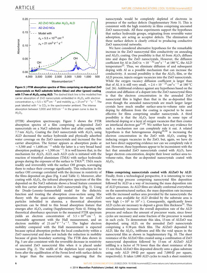
(FTIR) absorption spectroscopy. Figure 5 shows the FTIRabsorption spectra of a film comprising as-deposited ZnOnanocrystals on a NaCl substrate before and after coating with7.7 nm Al2O3. Coating the ZnO nanocrystals with Al2O3 usingALD decreased the surface hydroxide and physically adsorbedwater coverage on the ZnO nanocrystals and increased the freecarrier absorption. The former appears as absorption peaks atB3,500 and B1,600 cm� 1 while the latter is a very broad bandabsorption peaking at B1,500 cm� 1. It is well known that, in themechanism for Al2O3 ALD, each ALD cycle is initiated with thereaction of trimethyl aluminium (TMA) with surface hydroxidegroups during the exposure of the surface to TMA24. TMA reactsreadily and irreversibly with the surface OH groups, scavengingthem to reduce their coverage significantly. This reduction in thesurface OH coverage correlated with the decrease in resistivity ofthe films deposited on glass (Fig. 4 and Table 1). Moreover, aftercoating with Al2O3, the infrared absorption spectrum of the filmdeposited on the NaCl substrate shows a broad feature consistentwith free carrier absorption in ZnO nanocrystals (Fig. 5). Usingthe Drude–Lorentz–Sommerfield model for the dielectricfunction and treating the absorption cross-section using Mietheory with the quasi-static approximation for small ZnOparticles imbedded in alumina, a theoretical absorptionspectrum can be fitted to this broad absorption feature thatemerges after Al2O3 coating (Supplementary Note 4). Fitting thetheoretical absorbance spectrum to the measured FTIR spectrumyields an electron concentration of 5.5� 1019 cm� 3, inreasonable agreement with the Hall measurement, and anelectron mobility of 21 cm2 V� 1 s� 1. The higher electronmobility compared with the Hall measurement is expectedbecause optical absorption probes the local conductivity within aZnO nanocrystal and does not include the reduction in mobilitybecause of grain boundary scattering. The FTIR data shown inFig. 5 are also consistent with the reversible decrease in resistivityof uncoated ZnO nanocrystal film when it is placed undervacuum (Fig. 2). The width of the depletion layer expected toform after the equilibration of the Fermi level with surface defectsis larger than the nanocrystal size, suggesting that the
nanocrystals would be completely depleted of electrons inpresence of the surface defects (Supplementary Note 5). This isconsistent with the high resistivity in films comprising uncoatedZnO nanocrystals. All these experiments support the hypothesesthat surface hydroxide groups, originating from reversible wateradsorption, are acting as acceptor defects. The elimination ofthese surface defects is clearly critical to producing conductiveZnO nanocrystal networks.
We have considered alternative hypotheses for the remarkableincrease in the ZnO nanocrystal film conductivity on annealingand Al2O3 coating. One possibility is that Al from Al2O3 diffusesinto and dopes the ZnO nanocrystals. However, the diffusioncoefficient for Al in ZnO is B10� 32 cm2 s� 1 at 180 �C, the ALDtemperature25. Thus, we eliminate diffusion of and subsequentdoping with Al as a possible mechanism that can increase theconductivity. A second possibility is that the Al2O3 film, or theALD process, injects oxygen vacancies into the ZnO nanocrystals.While the oxygen vacancy diffusion coefficient is larger thanthat of Al, it is still very small, B2.4� 10� 25 cm2 s� 1 at 180 �C(ref. 26). Additional evidence against any hypotheses based on thecreation and diffusion of a dopant into the ZnO nanocrystal filmsis that the electron concentration in the annealed ZnOnanocrystal film is higher than that in the as-deposited filmeven though the annealed nanocrystals are much larger: largercrystals have much smaller surface-area-to-volume ratio anddoping by diffusion from the coating is expected to be mosteffective for films comprising smaller nanocrystals. A thirdpossibility is that the Al2O3 layer results in some type ofinterfacial doping or a layer of oxygen vacancies that then createsan interfacial electron gas27,28. We neither have any evidence forsuch a mechanism nor can completely rule it out. A relatedhypothesis is that heterogeneous doping29,30 is increasing theelectron concentration in the ZnO with Al2O3 coating byinducing oxygen vacancies in the ZnO, but, again, we have donot have direct supporting evidence nor can we completely rule itout. However, these hypotheses appear to be inconsistent with thefact that annealed ZnO nanocrystals coated with Al2O3 havelarger electron concentration, despite their lower surface-area-to-volume-ratio, than the as-deposited nanocrystals coated withAl2O3.
Films comprising nanocrystals coated with Al:ZnO by ALD.Finally, from a technological perspective, it is interesting to viewthe two-step process comprising nanocrystal film depositionfollowed by ALD as a way of increasing the mass deposition rateof ALD processes. As ALD films are ideally conformal everywhereon the nanostructured surface, the mass deposition rate increaseswith the increased surface area provided by the nanocrystals: thesurface area available for ALD divided by the substrate area isvery high (B102 to 103� ). Consequently, significantly fewerALD cycles are necessary to deposit a given film thickness31. Thissimultaneously increases the overall deposition rate of the ALDprocess and reduces the amount of precursor waste, since fewercycles are necessary and some fraction of the precursor is wastedin each cycle. To demonstrate this idea, 15 nm of Al:ZnO wasdeposited, using ALD, on the annealed ZnO nanocrystalscomprising a 0.38 mm thick film. The Al:ZnO deposited byALD, like the Al2O3, infiltrates and fills the void spaces in thenanocrystal film as shown in Supplementary Fig. 10. The sheetresistance of the Al:ZnO film created using a combination of ZnOnanocrystal deposition followed by 15 nm of Al:ZnO ALDinfilling is a factor of 70 lower than the sheet resistance of the15-nm thick Al:ZnO film deposited directly onto a glass substrateusing only ALD (99O per square and 7,000O per square,respectively). It takes 1,000 ALD cycles to reach a sheet resistivity
0.20
0.10
Abs
orba
nce
0.05
0.00
0.15
Wavenumber/cm–1
4,000 3,500 3,000 2,500 2,000 1,500
OH
OH*
AD ZnO NCs after Al2O3 ALD
AD ZnO NCs
Model with
ne = 5.5 × 1019 cm–3
�e = 21 cm2 V–1 s–1
1,000 500
Figure 5 | FTIR absorption spectra of films comprising as-deposited ZnO
nanocrystals on NaCl substrate before (blue) and after (green) coating
with 7.7 nm of Al2O3 using ALD. The dashed black line is the modelled free
carrier absorption of ZnO nanocrystals embedded in Al2O3 with electron
concentration ne¼ 5.5� 1019 cm� 3 and mobility me¼ 21 cm2 V� 1 s� 1. The
peak labelled with * is CO2 in the spectrometer ambient. The intense
absorption between 1,000 and 500 cm� 1 in the green curve is due to
Al2O3.
ARTICLE NATURE COMMUNICATIONS | DOI: 10.1038/ncomms6822
6 NATURE COMMUNICATIONS | 5:5822 | DOI: 10.1038/ncomms6822 | www.nature.com/naturecommunications
& 2014 Macmillan Publishers Limited. All rights reserved.
similar to that achieved using a combination of ZnO nanocrystaldeposition followed by 15 nm of Al:ZnO ALD, which requiresonly 100 cycles. The resistivity of ZnO nanocrystal film coatedwith 15 nm of Al:ZnO is similar to that of the Al:ZnO filmdeposited directly on glass, but the former was made using afactor of 10 fewer cycles (Table 2). All the Al:ZnO films are moreresistive than Sn:In2O3, but the advantage of ZnO-based materialsis that zinc is much less expensive and more abundant thanindium. All the films were transparent in the visible region of thespectrum (Supplementary Figs 9 and 11).
DiscussionIn conclusion, a nonthermal plasma-based gas-phase approach todepositing thin films comprising ZnO nanocrystals was demon-strated. Nanocrystals synthesized in the plasma are accelerated bysupersonic expansion of the plasma effluent and deposited onsuitable substrates by impaction without exposure to solvents.Annealing 5 nm ZnO nanocrystals in 20% hydrogen in argon at340 �C resulted in grain growth to 22 nm and a small decrease inresistivity. Coating the ZnO nanocrystals with 7 to 8 nm of Al2O3
decreases the resistivity by seven orders of magnitude. Thisdecrease is observed both for as-deposited and annealednanocrystals. Films comprising nanocrystals coated with Al2O3
are n-type with an electron mobility of 0.1 cm2 V� 1 s� 1 and3.0 cm2 V� 1 s� 1 for as-deposited and annealed ZnO nanocrys-tals, respectively. Ultrasensitivity of the resistivity to ambient airand FTIR measurements support the hypothesis that OH on thesurface act as an electron trap. Reaction with TMA during ALD ofAl2O3 on the ZnO nanocrystals removes these OH traps.Moreover, the Al2O3 coating prevents subsequent adsorptionfrom the ambient. Transparent conducting thin films comprisingZnO nanocrystals coated with Al:ZnO using ALD had similarresistivity and transparency to Al:ZnO films deposited directly onglass using only ALD, but the former required an order ofmagnitude fewer cycles.
MethodsPlasma synthesis. Supplementary Figure 1 shows the schematic of the two-stageprocess used to deposit the films comprising ZnO nanocrystals. The two stages areseparated by a slit that expands the gases from the first stage into the second stagesupersonically. The nanocrystals are synthesized in the nonthermal plasmamaintained in a 10 0 glass tube (0.750 0 inner diameter), which comprises the firststage. Diethyl zinc (DEZ, Sigma-Aldrich, Saint Louis, MO), and molecular oxygen(O2) were used as the Zn precursor and the oxygen source, respectively. The flowrates of all the gases were controlled with mass flow controllers (MKS 1179 seriesand Edwards model 825 series B). The DEZ, a volatile liquid at room temperature,was fed into the plasma using a bubbler and Ar as the carrier gas. The DEZ flowrate was determined from the flow rate of argon into the DEZ bubbler, the DEZvapour pressure at the bubbler temperature (298 K), the total bubbler pressure(80 Torr) measured using a capacitance manometer (Baratron model 727A, MKS,Andover, MA), the ideal gas law and the law of mass conservation. The DEZ- andO2-containing streams were fed into the plasma separately. The DEZ carried byargon was injected through the side port while the oxygen diluted in argon was fedinto the plasma through the top port (Supplementary Fig. 1). The flow rates ofDEZ, Ar and DEZ, O2 and Ar, and O2 were FDEZ¼ 4 s.c.c.m., FAr,DEZ¼ 20 s.c.c.m.,FO2¼ 30 s.c.c.m., FAr,O2¼ 250 s.c.c.m., respectively, where s.c.c.m. is the volumetric
flow rate in cm3 min� 1 at 273 K and 1 atm. Mass flow rate can be calculated fromthe volumetric flow rate at standard conditions and the process conditions usingthe ideal gas law. The pressure in the plasma (P1, that is, in the first stage) was 3.6Torr for most of the experiments in the article, but was raised to 5.6 Torr tosynthesize the as-deposited ZnO nanocrystals discussed in Figs 4 and 5 as well as inTable 1; the increase in pressure was necessary to increase the residence time and,therefore, the crystallite diameter, dp, from dp¼ 5 nm at 3.6 Torr to dp¼ 6.5 nm at5.6 Torr. The residence time to synthesize the 5 and 6.5 nm nanocrystals were B27and 42 ms, respectively. The plasma was generated and maintained by applying aradiofrequency electric field at 13.56 MHz, through a custom impedance matchingnetwork, to a copper ring electrode wrapped around the top port (SupplementaryFig. 1) just above the zone where the DEZ-containing and O2-containing streamsare mixed (hereafter referred to as the mixing zone). The quick disconnect fittingforming the vacuum seal above the deposition stage chamber (that is, the secondstage) is the closest grounded surface to the powered electrode and thus served asthe ground electrode. The plasma extended B10 cm downstream of the mixingzone. Approximately 30 cm downstream of the mixing zone was a rectangular slit-shaped orifice with a cross-sectional area of 0.8� 15 mm. As mentioned earlier,two different orifices were used that had the same cross-sectional dimensions butdifferent lengths in the direction of flow. The orifice for a plasma pressure of3.6 Torr (5 nm particles) was 2 mm long, and, for a plasma pressure of 5.6 Torr(6.5 nm particles), the orifice was 10 mm long. The deposition stage downstreamwas a chamber evacuated by a Leybold Turbovac 1000C turbo pump. The pressurein the second stage was P2¼ 14� 10� 3 Torr. Thus, the ratio of the pressureupstream of the slit to the pressure downstream of the slit (P1/P2) was either 257 or400, depending on the upstream pressure (P1¼ 3.6 Torr or 5.6 Torr, respectively).At these ratios, the flow through the slit was choked and the gas underwentsupersonic expansion downstream of the slit where the particle beam forms. In thedeposition chamber (that is, the second stage), the substrates were mounted to apush-rod (CRPP-1, MDC vacuum, Hayward, CA) and moved back and forth underthe particle beam in a reciprocating motion to simulate a roll-to-roll process. Thefrequency of the reciprocating motion was B1 Hz, and the stroke length wasB4 cm. In a typical experiment, films were deposited on two substrates simulta-neously, one polished silicon and the other Corning Eagle XG borosilicate glass(MTI Corporation, Richmond, CA). Each substrate was B1� 1 cm2. The films onglass substrates were used for electrical and ultraviolet–vis–NIR transmissionspectroscopy characterization while the films on the silicon substrates wereused for XRD, spectroscopic ellipsometry and electron microscopy. The filmswere deposited on NaCl substrates for characterization with FTIR transmissionspectroscopy.
Annealing. Some films were annealed before ALD in a tube furnace in 500 s.c.c.m.of 20% H2 and 80% Ar gas flow. During annealing, the substrates coated with thenanocrystal films were placed in a 10 0 outer diameter quartz tube inserted withinthe tube furnace at room temperature. First, the tube was purged for 30 min atroom temperature to remove the air within the tube volume. Then, the power tothe heater was turned on and the furnace temperature increased to 340 �C over aperiod of B25 min. This temperature was maintained under flowing gas for60 min. At the end of this period, the power was turned off and the furnace wasallowed to cool at the natural cooling rate of the system. The substrates coated withthe films were removed once the furnace temperature decreased below 40 �C, whichtook B3 h.
Atomic layer deposition. A commercial reactor (Savannah S200, CambridgeNanotech/Ultratech, Waltham, MA) was used for ALD. All depositions wereconducted at 180 �C. Before precursor pulsing, the films comprising ZnO nano-crystals were allowed to outgas for 2,000 s at 0.5 Torr (also the deposition pressure)in nitrogen gas flowing over the film at 20 s.c.c.m. Nitrogen was also used as thecarrier gas during deposition. TMA was used as the aluminium source and DEZwas the zinc source. Each ALD cycle for all depositions in this article consisted of0.1 s H2O pulse followed by 30 s purge and 0.1 s metal–organic precursor (DEZ orTMA) pulse followed by 30 s purge. These steps were repeated periodically todeposit the desired film thickness. For doping ZnO with Al (that is, Al:ZnO
Table 2 | Comparison of the sheet resistance, Rs, and resistivity of films comprising ZnO nanocrystals coated with Al:ZnO usingALD (rows 1,2) and Al:ZnO films deposited directly on glass substrates with ALD (rows 3,4).
Film No. of ALD cycles dfilm (lm) Rs (X per square) q (X cm) ne (cm� 3) le (cm2 V� 1 s� 1)
As-deposited ZnO 100 0.56 1,100 6.5� 10� 2 2.4� 1019 4.0Annealed ZnO 100 0.38 99 3.7� 10� 3 1.9� 1020 9.0Al:ZnO film by ALD 100 0.015 7,000 1.0� 10� 2 — —Al:ZnO film by ALD 1,000 0.165 67 1.1� 10� 3 2.6� 1020 23.2Commercial Sn:In2O3 — 0.190 6.8 1.3� 10�4 — —
ALD, atomic layer deposition; dfilm, film thickness; ne, electron concentration determined from the Hall effect measurements; me, mobility calculated from the resistivity and the electron concentration; r,resistivity.
NATURE COMMUNICATIONS | DOI: 10.1038/ncomms6822 ARTICLE
NATURE COMMUNICATIONS | 5:5822 | DOI: 10.1038/ncomms6822 | www.nature.com/naturecommunications 7
& 2014 Macmillan Publishers Limited. All rights reserved.
deposition), the super-cycle strategy was used16,32. One super-cycle consisted of 19cycles of ZnO followed by one cycle of Al2O3. The 15 nm Al:ZnO film wasdeposited using five super-cycles, which results in a total of 100 ALD cycles. Thesubstrates with the films were removed from the reactor after coating and allowedto cool in air.
Structural characterization. The films on silicon were characterized by a varietyof techniques. Film thickness and ZnO volume fraction were measured usingspectroscopic ellipsometry (J. A. Woollam M44). The Bruggeman effective mediumapproximation was used to model the optical properties of film and to extract theZnO volume fraction and film thickness. The film was assumed to be comprised ofZnO and voids. The spectra were fit in the wavelength region between 450 and750 nm where no size effects on the optical constants of ZnO are expected and thenanocrystal film is transparent. In select experiments, the areal atomic densitymeasured by spectroscopic ellipsometry (that is, film thickness � ZnO volumefraction) was compared with that measured by Rutherford backscattering, and thetwo measurements were found to be in excellent agreement for ZnO volumefractions greater than B1% (Supplementary Fig. 4). X-ray diffraction (Cu Ka)from the films was collected using a beryllium area detector in a Bruker D8 Dis-cover diffractometer. The crystallite size was determined from the full-width-at-half maximum of the XRD peaks after subtracting the instrumental broadening,and then using the Scherrer equation. Films were examined using SEM in a JEOL6700 FEG SEM operating at 5 keV accelerating voltage. The silicon substrates withnanocrystal films were cleaved and mounted on the sample holder such that thesubstrate surface onto which the nanocrystals were deposited was parallel to theelectron beam for cross-sectional imaging. Ultraviolet–vis–NIR spectroscopy wascarried out in a Cary 5000 (Agilent Technologies, Santa Clara, CA) in transmissionmode using the transmission of a blank glass substrate for the baseline. FTIRspectra were collected in a Nicolet Magna IR 550 (Thermo Scientific, Madison, WI)in transmission mode using an uncoated bare NaCl substrate as the background.The sample compartment was allowed to purge for 2.5 min with dry and CO2-scrubbed air before acquiring data.
Resistivity measurements. The electrical resistivity measurements were carriedout in a cryomicroprobe station (Janis Research, Wilmington, MA) with the probesconnected to an Agilent 4155C semiconductor parameter analyzer. The probestation was equipped with a turbo pump for pressure-dependent measurements,which was used in select experiments. All reported resistivity values were measuredat room temperature and pressure, unless otherwise stated (for example, Figs 2 and4b). Silver electrodes, 500 nm in thickness, were deposited on top of the nanocrystalthin films by thermal evaporation at a rate of 2 nm s� 1. For low resistivity samples,the van der Pauw electrode configuration was used to measure the sheet resistance.For high resistivity samples, the electrode configuration was two parallel stripes(1.0� 0.1 cm) each at the opposite edges of the 1� 1 cm2 glass substrate.
Temperature-dependent resistivity measurements were done using soldered Incontacts to evaporated Ag contact pads in a four-wire van der Pauw configuration.Measurement was made using direct current excitation. The temperature of thesample was controlled using a Janis close-cycle refrigerator. Extensive checks weremade at several temperatures during the experiment to ensure ohmic behaviour,account for contact resistance and minimize joule heating.
Transmission electron microscopy. Electron-transparent specimens (depositedon Si substrate) for cross-section TEM were prepared by the small-angle cleavingtechnique. This technique relies on thinning a crystallographic substrate to thepoint that it can be fractured along non-preferred crystallographic plane at ashallow to an easy-cleave plane resulting in a long, thin wedge whose tip is electrontransparent33. Bulk samples were cleaved to smaller than 1 cm2 and bonded film-side down to a parallel polishing fixture using CrystalBond 509. The samples werethinned to lo100 mm using an Allied Multiprep and 30 mm diamond lapping film.The sample was oriented in the polishing direction such that scratches were alignedB10� from the easy-cleave [110] direction. Using a metal ruler and diamondscribe, deep scratches were created along the polishing direction B1 mm apart.The sample was removed from the polishing fixture using acetone and placed in apetri dish containing a glass slide. Using tweezers, the specimen was carefullycleaved along the scratches using the tweezers and edge of the glass slide. Thesepieces were then cleaved again along the easy-cleave plane using the tweezers andedge of the glass slide. Samples having a sharp tip were mounted to slot-type MoTEM grids using MBond 510 epoxy.
Cross-section high-angle annular dark field scanning transmission electronmicroscopy (HAADF-STEM) micrographs and energy dispersive X-rayspectroscopy (EDX) maps were acquired in an aberration-corrected FEI Titan 60-300 (S)TEM equipped with an Analytical SuperTwin pole piece and SuperX EDXdetector operating at 300 kV and having a STEM convergence angle of 30 mrad,150 pA probe current and 58.5 mrad HAADF inner angle. EDX maps wereacquired using the Bruker Esprit software with a 612 by 612 pixel frame, 55 msecpixel dwell time and 23 frames for a total acquisition time of 475 s. EDX net countmaps of the Zn Ka and Al Ka peaks were generated using the Esprit software withelemental consideration of zinc, aluminium, oxygen, silicon, carbon and copper.
Trace silicon and carbon peaks are a result of the silicon substrate and specimencontamination, respectively, while copper is a result of the TEM grid.
Hall measurements. Hall measurements on films comprising ZnO nanocrystalscoated with Al2O3 were conducted at 300 K in a Quantum Design PhysicalProperties Measurement System equipped with a 9 T superconducting magnet.Electrical contact to the films was made with In on Ag contact pads evaporatedonto the sample in the van der Pauw configuration. Current–voltage characteristicswere measured with a Keithley 220 programmable current source and a Keithley2000 multimeter to measure voltage. In all the cases, extensive checks were made toensure ohmic behaviour, account for contact resistance and minimize joule heating.
Hall measurements on the AZO-coated nanocrystal films were also carried outat 300 K utilizing an electromagnet up to a 0.6 T field. These films were contactedwith In contacts, again in the van der Pauw configuration, and current–voltagecharacteristics were measured using alternating current techniques (16 Hz).
References1. Norris, D. J., Efros, A. L. & Erwin, S. C. Doped nanocrystals. Science 319,
1776–1779 (2008).2. Kovalenko, M. V., Scheele, M. & Talapin, D. V. Colloidal nanocrystals with
molecular metal chalcogenide surface ligands. Science 324, 1417–1420 (2009).3. Lee, J.-S., Kovalenko, M. V., Huang, J., Chung, D. S. & Talapin, D. V. Band-like
transport, high electron mobility and high photoconductivity in all-inorganicnanocrystal arrays. Nat. Nanotech. 6, 348–352 (2011).
4. Liu, Y. et al. Dependence of carrier mobility on nanocrystal size and ligandlength in PbSe nanocrystal solids. Nano Lett. 10, 1960–1969 (2010).
5. Kang, M. S., Sahu, A., Norris, D. J. & Frisbie, C. D. Size-dependent electricaltransport in CdSe nanocrystal thin films. Nano Lett. 10, 3727–3732 (2010).
6. Yu, D., Wang, C. J. & Guyot-Sionnest, P. n-Type conducting CdSe nanocrystalsolids. Science 300, 1277–1280 (2003).
7. Pourret, A., Guyot-Sionnest, P. & Elam, J. W. Atomic layer deposition of ZnOin quantum dot thin films. Adv. Mater. 21, 232–235 (2009).
8. Liu, Y. et al. PbSe quantum dot field-effect transistors with air-stable electronmobilities above 7 cm2 V� 1 s� 1. Nano Lett. 13, 1578–1587 (2013).
9. Ong, B. S., Li, C. S., Li, Y. N., Wu, Y. L. & Loutfy, R. Stable, solution-processed,high-mobility ZnO thin-film transistors. J. Am. Chem. Soc. 129, 2750–2751(2007).
10. Morfa, A. J., Kirkwood, N., Karg, M., Singh, T. B. & Mulvaney, P. Effectof defects on the behavior of ZnO nanoparticle FETs. J. Phys. Chem. C 115,8312–8315 (2011).
11. Morfa, A. J. et al. Fabrication of ZnO thin films from nanocrystal inks. J. Phys.Chem. C 114, 19815–19821 (2010).
12. Yu, S. H. et al. In/Ga-free, inkjet-printed charge transfer doping for solution-processed ZnO. ACS Appl. Mater. Interfaces 5, 9765–9769 (2013).
13. Mangolini, L., Thimsen, E. & Kortshagen, U. High-yield plasma synthesis ofluminescent silicon nanocrystals. Nano Lett. 5, 655–659 (2005).
14. Felbier, P. et al. Highly luminescent ZnO quantum dots made in a nonthermalplasma. Adv. Funct. Mater. 24, 1988–1993 (2014).
15. Rao, N. P. et al. Hypersonic plasma particle deposition of nanostructuredsilicon and silicon carbide. J. Aerosol Sci. 29, 707–720 (1998).
16. Elam, J. W., Routkevitch, D. & George, S. M. Properties of ZnO/Al2O3 alloyfilms grown using atomic layer deposition techniques. J. Electrochem. Soc. 150,G339–G347 (2003).
17. Madelung, O. Semiconductors—Basic Data 2nd rev. edn (Springer, 1996).18. Choi, J. H. et al. Bandlike transport in strongly coupled and doped quantum
dot solids: a route to high-performance thin-film electronics. Nano Lett. 12,2631–2638 (2012).
19. Jang, J., Liu, W., Son, J. S. & Talapin, D. V. Temperature-dependent Hall andfield-effect mobility in strongly coupled all-inorganic nanocrystal arrays. NanoLett. 14, 653–662 (2014).
20. Zhang, X. et al. Crossover from nanoscopic intergranular hopping toconventional charge transport in pyrite thin films. ACS Nano 7, 2781–2789(2013).
21. Zhang, J. & Shklovskii, B. I. Density of states and conductivity of a granularmetal or an array of quantum dots. Phys. Rev. B 70, 115317 (2004).
22. Liu, H., Pourret, A. & Guyot-Sionnest, P. Mott and Efros-Shklovskii variablerange hopping in CdSe quantum dots films. ACS Nano 4, 5211–5216 (2010).
23. Cho, H. J. et al. The effect of annealing on Al-doped ZnO films deposited by RFmagnetron sputtering method for transparent electrodes. Thin Solid Films 518,2941–2944 (2010).
24. Elam, J. W. & George, S. M. Growth of ZnO/Al2O3 alloy films using atomiclayer deposition techniques. Chem. Mater. 15, 1020–1028 (2003).
25. Norman, V. J. The diffusion of aluminium and gallium in zinc oxide. Aust. J.Chem. 22, 325–329 (1969).
26. Robin, R., Cooper, A. R. & Heuer, A. H. Application of a nondestructivesingle-spectrum proton activation technique to study oxygen diffusion in zincoxide. J. Appl. Phys. 44, 3770–3777 (1973).
ARTICLE NATURE COMMUNICATIONS | DOI: 10.1038/ncomms6822
8 NATURE COMMUNICATIONS | 5:5822 | DOI: 10.1038/ncomms6822 | www.nature.com/naturecommunications
& 2014 Macmillan Publishers Limited. All rights reserved.
27. Lee, S. W., Liu, Y. Q., Heo, J. & Gordon, R. G. Creation and control oftwo-dimensional electron gas using Al-Based amorphous oxides/SrTiO3
heterostructures grown by atomic layer deposition. Nano Lett. 12, 4775–4783(2012).
28. Chen, Y. Z. et al. Metallic and insulating interfaces of amorphous SrTiO3-basedoxide heterostructures. Nano Lett. 11, 3774–3778 (2011).
29. Maier, J. Heterogeneous doping of silver bromide (AgBr-Al2O3). Mater. Res.Bull. 20, 383–392 (1985).
30. Maier, J. Ionic conduction in space charge regions. Prog. Solid State Chem. 23,171–263 (1995).
31. Thimsen, E. (Invited) Atomic layer deposition of multicomponent metalsulfides applied to thin film photovoltaics. ESC Trans. 58, 95–104 (2013).
32. Wu, Y. et al. Electrical transport and Al doping efficiency in nanoscale ZnOfilms prepared by atomic layer deposition. J. Appl. Phys. 114, 024308 (2013).
33. Walck, S. D. & McCaffrey, J. P. The small angle cleavage technique applied tocoatings and thin films. Thin Solid Films 308-309, 399–405 (1997).
AcknowledgementsWe thank C. Leighton for valuable discussions about this work. This work was supportedpartially by the UMN MRSEC Program of the National Science Foundation under AwardNumbers DMR-0819885 and DMR-1420013 and by BASF SE. X.Z. was supported byNational Science Foundation Award Number DMR-1309642. Parts of this work were
carried out in the Characterization Facility, University of Minnesota, which receivespartial support from NSF through the MRSEC program.
Author contributionsE.T. conceived and executed most of the experiments. M.J. performed Hall effect mea-surements and analysed the results. X.Z. performed temperature-dependent resistivitymeasurements and analysed the results. A.J.W. performed scanning transmissionelectron microscopy and elemental mapping. E.T. and E.S.A. wrote the manuscript.All the authors participated in the discussion and interpretation of data, read themanuscript and provided input.
Additional informationSupplementary Information accompanies this paper at http://www.nature.com/naturecommunications
Competing financial interests: The authors declare no competing financial interests.
Reprints and permission information is available online at http://npg.nature.com/reprintsandpermissions/
How to cite this article: Thimsen, E. et al. High electron mobility in thin films formedvia supersonic impact deposition of nanocrystals synthesized in nonthermal plasmas.Nat. Commun. 5:5822 doi: 10.1038/ncomms6822 (2014).
NATURE COMMUNICATIONS | DOI: 10.1038/ncomms6822 ARTICLE
NATURE COMMUNICATIONS | 5:5822 | DOI: 10.1038/ncomms6822 | www.nature.com/naturecommunications 9
& 2014 Macmillan Publishers Limited. All rights reserved.
![Journal of Power Sourceswaiting/publication/2-long...infiltrated anode. For example, a rapid power degradation of a MS-SOFC with infiltrated Ni catalysts was found at 700 #C [9].Our](https://img.pdfslide.us/doc/110x75/5ea3e38dbc5ba4612d184824/journal-of-power-sources-waitingpublication2-long-iniltrated-anode-for-example.jpg)