Embed Size (px)
Citation preview
HIGH-EFFICIENCY SWITCHED-MODE POW ER
AMPLIFIER USING GALLIUM NITRIDE ON SILICON
HEMT TECHNOLOGY
ByHarpreet Panesar
A thesis
presented to Carleton University
in partial fulfilment of the
thesis requirement for the degree of
MASTER OF APPLIED SCIENCE
in
ELECTRICAL ENGINEERING
Ottawa, Ontario, Canada
© Harpreet S. Panesar, 2007
Reproduced with permission of the copyright owner. Further reproduction prohibited without permission.

1*1 Library and Archives Canada
Published Heritage Branch
Bibliotheque et Archives Canada
Direction du Patrimoine de I'edition
395 Wellington Street Ottawa ON K1A 0N4 Canada
395, rue Wellington Ottawa ON K1A 0N4 Canada
Your file Votre reference ISBN: 978-0-494-33664-9 Our file Notre reference ISBN: 978-0-494-33664-9
NOTICE:The author has granted a nonexclusive license allowing Library and Archives Canada to reproduce, publish, archive, preserve, conserve, communicate to the public by telecommunication or on the Internet, loan, distribute and sell theses worldwide, for commercial or noncommercial purposes, in microform, paper, electronic and/or any other formats.
AVIS:L'auteur a accorde une licence non exclusive permettant a la Bibliotheque et Archives Canada de reproduire, publier, archiver, sauvegarder, conserver, transmettre au public par telecommunication ou par I'lnternet, preter, distribuer et vendre des theses partout dans le monde, a des fins commerciales ou autres, sur support microforme, papier, electronique et/ou autres formats.
The author retains copyright ownership and moral rights in this thesis. Neither the thesis nor substantial extracts from it may be printed or otherwise reproduced without the author's permission.
L'auteur conserve la propriete du droit d'auteur et des droits moraux qui protege cette these.Ni la these ni des extraits substantiels de celle-ci ne doivent etre imprimes ou autrement reproduits sans son autorisation.
In compliance with the Canadian Privacy Act some supporting forms may have been removed from this thesis.
While these forms may be included in the document page count, their removal does not represent any loss of content from the thesis.
Conformement a la loi canadienne sur la protection de la vie privee, quelques formulaires secondaires ont ete enleves de cette these.
Bien que ces formulaires aient inclus dans la pagination, il n'y aura aucun contenu manquant.
i * i
CanadaReproduced with permission of the copyright owner. Further reproduction prohibited without permission.
Abstract
The continuing trend toward greater capacity and higher data rates in wireless commu
nication systems places increasing demands on the radio frequency (RF) power provided
by base station transm itters. Conventional RF power amplifiers (PAs) in use today have
poor operating efficiencies and require considerable additional power and volume for heat
removal. Research on more efficient PA technology is therefore im portant to the growth
of the wireless industry.
This thesis investigates high-efficiency switched-mode microwave power amplification
using a new transistor technology, the Gallium Nitride on Silicon High Electron Mobility
Transistor (GaN-on-Si HEMT), which promises to deliver high output power levels at
lower cost than the alternative GaN-on-SiC technology. The principles of power devices
and power amplification modes axe discussed. A new large-signal equivalent model is
developed for a 2 mm GaN-on-Si HEMT over the 0 GHz - 20 GHz range, based on
measured data. The chosen EEsof GaAs nonlinear HEMT model reproduces the GaN
transistor’s behavior reasonably well over a large range of bias conditions, signal levels,
and frequencies, although several param eter assumptions are made. Based on this model,
the design, optimization, fabrication and testing of a 3.5 GHz, 1 W, Class E power
ii
Reproduced with permission of the copyright owner. Further reproduction prohibited without permission.

amplifier proceeds. The PA design is successful, with measurements revealing a gain of
10.7 dB, w ith an output power of 942 mW, and a power-added efficiency of 40.4%.
This work shows the suitability of lower cost GaN-on-Si transistor technology for
switched-mode microwave power amplifiers with possible applications in WiMAX base
stations. It is recommended tha t further device modeling and other switched-mode am
plifier topologies be investigated.
iii
Reproduced with permission of the copyright owner. Further reproduction prohibited without permission.

Acknowledgements
Although this thesis represents my own contribution to science, this work would not have
been possible without the guidance and support of many people.
I would like to express my deepest gratitude to my thesis supervisors, Professor Langis
Roy and Professor Tom Smy, for their support and patience throughout this project. I
would also like to thank Steven McGarry; his expertise and seemingly boundless technical
knowledge have contributed a great deal to the success of this work.
I am grateful to the many organizations, including Nitronex Corporation (Durham,
N.C.), the Department of Mechanical and Aerospace Engineering at Carleton University
(Ottawa, ON), the Communications Research Centre (Ottawa, ON), and Nortel (Ottawa,
ON), for their contributions in all aspects of this project.
It has been a privilege sharing this experience with my friends and fellow graduate stu
dents, Charles Berndt, Steven Penney, Celine Fletcher, Daniel Olsiewski, Peter Chyurlia,
Fiona Shearer, and Justin Abbott. I thank Janice Yu and Mike Sowka for the many
fruitful discussions in the final months of manuscript preparation.
I owe thanks to my family for their unwavering support and understanding over the
course of my academic career.
iv
Reproduced with permission of the copyright owner. Further reproduction prohibited without permission.

Table of Contents
Abstract ii
Acknowledgem ents iv
Table o f Contents v
List of Tables vii
List of Figures viii
1 Introduction 11.1 M otivation ..................................................................................................................... 11.2 Thesis O b jec tiv es ....................................................................................................... 51.3 Research P a r tn e rsh ip ................................................................................................. 51.4 Dissertation Outline ................................................................................................. 6
2 Technology R eview 82.1 Conventional MOSFETs and H E M T s ................................................................... 82.2 Comparison with Wide Bandgap H E M T s............................................................ 10
3 Microwave Power Amplifiers 143.1 On Power, Bandwidth, and L in e a r i ty .................................................................. 143.2 Conventional Power A m plifiers.......................................... 153.3 Class E Switched-Mode Power A m p lif ie r ........................................................... 22
3.3.1 Idealized A nalysis .......................................................................................... 233.3.2 The Class E Concept at GHz Frequencies............................................... 29
3.4 S ta b i l i ty ........................................................................................................................ 313.5 Previous Work and Proposed Amplifier Specifications..................................... 323.6 S u m m a r y ..................................................................................................................... 33
4 Gallium N itride High Electron M obility Transistor Nonlinear M odel 364.1 The Nitronex GaN-on-Si H E M T ............................................................................. 384.2 EEsof 2 mm Nonlinear HEMT M o d e l.................................................................. 39
v
Reproduced with permission of the copyright owner. Further reproduction prohibited without permission.
4.2.1 Drain-Source Current M o d e l....................................................................... 414.2.2 Dispersion M o d e l........................................................................................... 41
Charge T r a p p in g .......................................................................................... 41Self-H eating .................................................................................................... 42
4.2.3 Gate and O utput Charge M o d e ls ............................................................. 434.2.4 Gate Forward Conduction and Breakdown M o d e l ................................. 43
4.3 Transistor Characterization .................................................................................... 444.3.1 Extrinsic P a ra m e te rs .................................................................................... 454.3.2 Drain-Source Current and T ransconductance......................................... 494.3.3 Gate Forward C o n d u c tio n .......................................................................... 534.3.4 Gate and O utput C ap ac itan ce .................................................................... 54
4.4 Model Verification .................................................................................................... 604.5 S u m m a r y .................................................................................................................... 66
5 Class E G aN-on-Si Microwave Power Amplifier 685.1 Ideal Class E Power A m p lif ie r............................................................................... TO5.2 The Class E Load N etw ork...................................................................................... 73
5.2.1 Lumped Element A n a ly s is ........................................................................... 745.2.2 Microstrip Transmission Line Im p lem e n ta tio n ...................................... 81
5.3 Input Matching N e tw o rk ......................................................................................... 825.4 Bias Insertion Network and S t a b i l i t y ................................................................... 89
5.4.1 Power Supply Decoupling ........................................................................... 935.4.2 RF Loading and Oscillation S u p p re ss io n ................................................ 945.4.3 Protection and S ta b i l i t y .............................................................................. 965.4.4 Complete Circuit S im ulation ....................................................................... 97
5.5 Thermal Considerations ......................................................................................... 995.6 Simulated and Measured Results ......................................................................... 995.7 S u m m a r y .......................................................................................................................106
6 Conclusions and Future Work 108
Appendix A Agilent EEHEM T 2 mm G aN-on-Si Nonlinear M odel 111
References 112
vi
Reproduced with permission of the copyright owner. Further reproduction prohibited without permission.
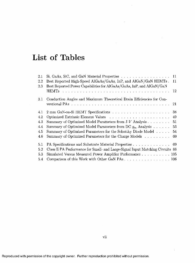
List of Tables
2.1 Si, GaAs, SiC, and GaN Material P ro p e r t ie s .................................................... 112.2 Best Reported High-Speed AlGaAs/GaAs, InP, and AlGaN/GaN HEMTs . 112.3 Best Reported Power Capabilities for AlGaAs/GaAs, InP, and AlGaN/ GaN
H E M T s ........................................................................................................................ 12
3.1 Conduction Angles and Maximum Theoretical Drain Efficiencies for Conventional P A s .............................................................................................................. 21
4.1 2 mm GaN-on-Si HEMT S pecifications............................................................... 384.2 Optimized Extrinsic Element Values .................................................................. 494.3 Summary of Optimized Model Param eters from I -V A nalysis.................. 514.4 Summary of Optimized Model Param eters from DC gm A n a ly s is ........... 534.5 Summary of Optimized Param eters for the Schottky Diode M o d e l ........ 544.6 Summary of Optimized Param eters for the Charge M o d e ls ..................... 60
5.1 PA Specifications and Substrate Material P ro p ertie s ....................................... 695.2 Class E PA Performance for Small- and Large-Signal Input Matching Circuits 885.3 Simulated Versus Measured Power Amplifier Perform ance................................1055.4 Comparison of this Work with Other GaN P A s ....................................................106
vii
Reproduced with permission of the copyright owner. Further reproduction prohibited without permission.

List of Figures
2.1 AlGaN/GaN HEMT Physical S tru c tu re ............................................................... 10
3.1 Conventional PA Load-Lines and Drain Current Profiles .............................. 163.2 Generic Power Amplifier M o d e l ............................................................................. 173.3 Generic Power Amplifier Voltage and Current W aveform s.............................. 183.4 Ideal Class E PA M o d e l .......................................................................................... 243.5 Ideal Class E PA Voltage and Current w a v e fo rm s ........................................... 25
4.1 Top-Level Layout of the Nitronex 2 mm GaN-on-Si H E M T ........................... 384.2 Agilent EEsof HEMT Nonlinear Model S ch em atic ........................................... 404.3 HEMT Small-Signal M o d el....................................................................................... 454.4 Gate Region of a HEMT W hen Vds — 0 V ......................................................... 454.5 Measured 5ft { Z n } vs. at 1 GHz for Vds = 0 V ............................................... 464.6 Symbolic Form of Extrinsic Z -Param eters............................................................ 474.7 Imaginary Parts of Z n , Zi%, and Z 22 vs. F re q u e n c y ........................................ 484.8 Extrinsic Parameters Extracted from Small-Signal Model Optimization . . 494.9 Pulsed Current-Voltage C h arac te ris tic s ............................................................... 504.10 Pulsed DC gm Measurement at Vds = 20 V ......................................................... 524.11 Forward Gate-Source Current Measurement ..................................................... 544.12 Input Capacitance {Cn) vs. Vg s ............................................................................. 564.13 Input Capacitance {Cn) vs. Vds ............................................................................. 574.14 Gate-Drain Capacitance in Saturation (Cgdaat) vs. Vg s ..................................... 584.15 O utput Capacitance (Cdso) vs. VdS ...................................................................... 594.16 Modeled vs. Measured comparison of Ids vs. V d s ............................................... 614.17 Measured and Simulated DC gm and Ids w.r.t. Vgs ........................................ 634.18 Simulated/M easured S-Parameter Response for Vds = 20 V and Vgs = — 1 V 644.19 Sim ulated/M easured Model D e v ia tio n s ............................................................... 644.20 Simulated/M easured GaN Schottky Diode C h a rac te ris tic .............................. 654.21 3.5 GHz Class A Measured Load Pull Contours of the 2 mm GaN HEMT . 66
5.1 System Level Diagram of a Class E PA M o d u le ............................................... 695.2 Original Class E PA Schematic ............................................................................. 705.3 Simulated Voltages and Currents of an Ideal Class E Power Amplifier . . . 72
viii
Reproduced with permission of the copyright owner. Further reproduction prohibited without permission.
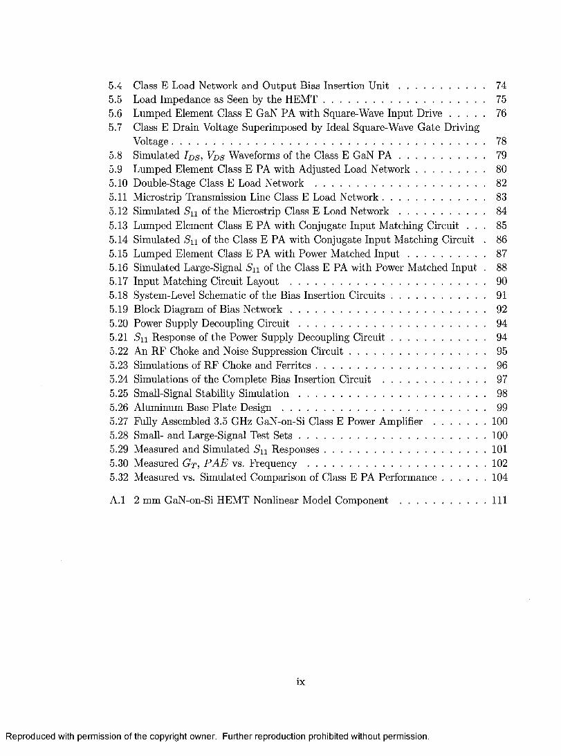
5.4 Class E Load Network and O utput Bias Insertion U n i t .................................. 745.5 Load Impedance as Seen by the H E M T ............................................................... 755.6 Lumped Element Class E GaN PA with Square-Wave Input D r iv e 765.7 Class E Drain Voltage Superimposed by Ideal Square-Wave Gate Driving
V oltage........................................................................................................................... 785.8 Simulated I d s , Vds Waveforms of the Class E GaN P A .................................. 795.9 Lumped Element Class E PA with Adjusted Load N e tw o rk ............................... 805.10 Double-Stage Class E Load Network ................................................................... 825.11 Microstrip Transmission Line Class E Load N etw ork........................................ 835.12 Simulated S u of the Microstrip Class E Load N e tw o rk .................................. 845.13 Lumped Element Class E PA with Conjugate Input Matching Circuit . . . 855.14 Simulated S u of the Class E PA with Conjugate Input Matching Circuit . 865.15 Lumped Element Class E PA with Power Matched I n p u t ...................................875.16 Simulated Large-Signal S u of the Class E PA with Power Matched Input . 885.17 Input Matching Circuit Layout ............................................................................. 905.18 System-Level Schematic of the Bias Insertion C irc u its ..................................... 915.19 Block Diagram of Bias N e tw o rk ............................................................................. 925.20 Power Supply Decoupling C i r c u i t ......................................................................... 945.21 S u Response of the Power Supply Decoupling C irc u it ..................................... 945.22 An RF Choke and Noise Suppression C irc u i t ..................................................... 955.23 Simulations of RF Choke and F e rr ite s ................................................................... 965.24 Simulations of the Complete Bias Insertion Circuit ........................................ 975.25 Small-Signal Stability S im u la t io n ......................................................................... 985.26 Aluminum Base Plate D e s ig n ................................................................................ 995.27 Fully Assembled 3.5 GHz GaN-on-Si Class E Power A m p lif ie r .......................1005.28 Small- and Large-Signal Test S e t s ............................................................................1005.29 Measured and Simulated S u R esponses..................................................................1015.30 Measured G t, P A E v s . F re q u e n c y .........................................................................1025.32 Measured vs. Simulated Comparison of Class E PA P erform ance................... 104
A .l 2 mm GaN-on-Si HEMT Nonlinear Model Component .................................... I l l
ix
Reproduced with permission of the copyright owner. Further reproduction prohibited without permission.

Chapter 1
Introduction
In efforts to reduce microwave communication transm itter cost while meeting stringent ef
ficiency and power requirements, microwave designers are looking towards gallium nitride
(GaN) as a potential replacement for today’s heavily taxed silicon (Si)-based microwave
base station systems. This work addresses the pressing need for power amplifiers (PAs)
to cost-effectively support emerging broadband, high frequency applications.
This chapter presents the motivation for pursuing high efficiency power amplification
along with thesis objectives and an outline of the remaining chapters. The work in
this thesis was made possible through a research partnership with Nitronex Corporation,
Durham N.C. A short introduction into the nature of this partnership is also given.
1.1 M otivation
As wireless technology advances and society becomes increasingly familiarized with the
myriad of potential wireless services, microwave systems designers are faced with the
challenging task of building the foundation to support continually increasing commercial,
1
Reproduced with permission of the copyright owner. Further reproduction prohibited without permission.
2
military, and consumer demands.
Broadband (6 Mbps and greater) internet access, for example, is primarily available
through Transmission Level 1 (T l), Digital Subscriber Line (DSL), or cable-modern con
nections [1]. The availability of telecommunication services in any country depends on
many economic factors, such as population density, availability of service providers, and
potential for profit. While broadband services may be available in large m etropolitan
centres and small cities, rural areas and developing countries lack the wireline backbone
th a t is commonplace in many areas. The cost of building optical fiber- or cable-based
infrastructure is impossibly high in places where it is non-existent, and service providers
do not see significant return-on-investment for wireline implementation, leaving many
communities without broadband access [2].
The WiMAX (Worldwide Interoperability for Microwave Access) broadband initia
tive is based on the IEEE 802.16 family of standards. Established in 2001, the WiMAX
Forum is the driving force behind its vision to provide broadband multimedia access to
any wireless terminal, anywhere, at any time. W ith a range of up to fifty kilometers,
WiMAX is a point-to-multipoint standardized wireless networking solution supporting
licensed and unlicensed frequency bands from 2 to 11 GHz for non-line-of-sight (NLOS)
operation, and from 10 to 66 GHz for line-of-sight (LOS) transmission [3]. Once fully de
ployed, WiMAX will serve a variety of applications, including th a t of providing relatively
affordable broadband coverage to underserved communities and developing countries.
Technological advances, such as those ushered in by WiMAX technology, promise to
offer more and more broadband services to the end-user. This increased functionality has
Reproduced with permission of the copyright owner. Further reproduction prohibited without permission.

3
thus far been made possible by stretching the limits of existing solid-state power amplifiers
in applications such as cellular base station and satellite transponders, or by using bulky
traveling wave tube amplifiers in radar and navigation systems [4,5]. All of this has been
done without significant reduction in component size (in the case of the vacuum tube) or
improvements in transm itter efficiency (for solid-state implementations) and complexity,
making the power amplifier the most expensive component in any radio front-end [6,7].
Power amplifiers are used in a wide variety of applications from smart weapons systems
in the military sector to wireless local area networks (WLANs) and automotive radar in the
commercial and consumer markets. In their current state, however, many high frequency
power amplifiers lose up to ninety percent of their applied DC power as heat, leading to
low DC-RF conversion efficiency [5]. This problem of converting DC power to useful RF
energy is further exacerbated by emerging broadband air interface standards th a t require
low signal distortion at high power levels. Consequently, designers are forced to build
inefficient power combined amplifiers or implement additional digital circuitry in order to
minimize adjacent-channel spillover to conserve valuable spectrum space.
At the heart of many of these power amplifiers is the laterally-diffused metal-oxide
semiconductor field-effect transistor (LDMOSFET). While the LDMOSFET PA does well
w ith voice and da ta transmission, it requires complex linearization schemes in order to
meet linearity, efficiency, and output power specifications [7,8]. The continued migration
towards high frequency spectrum space has recently put the LDM OSFET’s capabilities
into question. Although high frequency operation can, indeed, be attained with gallium
arsenide (GaAs), indium phosphide (InP), or silicon germanium (SiGe) amplifiers, their
Reproduced with permission of the copyright owner. Further reproduction prohibited without permission.

4
usefulness is limited to primarily the low power, low voltage regimes [5]. These solutions
are costly and can only temporarily address a limited range of applications before the
entire RF infrastructure must be revamped at the transistor level. In this regard, GaN has
recently seen international attention as a front runner in many electronic systems [9-11].
GaN belongs to the family of wide bandgap semiconductors, which includes silicon
carbide (SiC) and diamond. The nature of these materials gives them the ability to sup
port high supply voltages, translating into highly efficient (DC-RF conversion efficiencies
greater than 50%), high power (greater than 1 W) generation. Since bulk GaN substrates
are not available, GaN could historically only be grown on either SiC or sapphire sub
strates. Although sapphire is a low-cost solution, its high therm al impedance makes it
less attractive than SiC for power applications. Of the wide bandgap semiconductors,
only SiC and diamond are available in bulk format; they exhibit superior properties for
high-frequency (greater than 1 GHz), high-power operation, but are difficult and expen
sive to produce, and yield small substrates th a t are full of intrinsic defects. Silicon is
still the champion when it comes to highly refined substrates; it is more thermally con
ductive than GaAs and its relative m aturity allows it to be produced in large diameters
and high quantities. Fortunately, recent advances in semiconductor processing technology
have allowed the growth of GaN high electron-mobility transistors (HEMTs) on low cost
Si substrates [12].
If the ultim ate goal is to continue to provide reliable wireless services to the end user
at a reasonable cost, then the benefits of low-cost GaN-on-Si devices must be exploited.
It is the quest for high-efficiency power amplification th a t has provided the inspiration to
Reproduced with permission of the copyright owner. Further reproduction prohibited without permission.
5
study switched-mode Class E GaN-based microwave power amplifiers in this work.
1.2 T hesis O bjectives
This thesis revisits the decades-old high-efficiency switched-mode Class E PA [13]. W ith
some modifications, the Class E approach is applied for the first time to a GaN-on-Si
power amplifier circuit for operation in the WiMAX (IEEE 802.16-2004) band at 3.5
GHz. Linearity and wide bandwidth are critical design issues in many applications but,
as applied to the Class E topology, are outside the scope of this work as per the dis
cussion in Chapter 3. More appropriately then, this thesis endeavors to demonstrate
a high-efficiency narrow-band GaN-on-Si Class E power amplifier. In support of this
objective, a measurement-based nonlinear model is developed and verified, along with
an examination of both conventional and switched-mode power amplifier topologies. A
technology comparison between GaN and competing technologies is given in Chapter 2.
1.3 R esearch Partnership
Nitronex Corporation, based out of Durham, North Carolina, is a world leader in the
wireless communications industry. A spin-off from the College of Engineering at North
Carolina State University in the mid-1990s, today Nitronex has become a pioneer in de
veloping low-cost, high-performance, GaN-on-Si power transistors for emerging telecom
munications markets.
In 2004, Nitronex and the Departm ent of Electronics at Carleton University engaged
in a collaborative research program to investigate the performance of GaN-on-Si HEMTs
Reproduced with permission of the copyright owner. Further reproduction prohibited without permission.

6
in Class E switched-mode power amplifiers. Nitronex generously supplied several test
structures to make this project a success.
1.4 D issertation O utline
The remainder of this thesis expands upon the motivation and objectives discussed in
the preceding sections, ultim ately leading to a full hardware implementation of a Class E
power amplifier. But to appreciate the hardware, one must fully understand the device
technology, the theory th a t governs its operation, and the necessary design steps taken to
reach the end goal.
Chapter 2 shows how GaN-based power transistors compare against other, more es
tablished device technologies. A comparison is done between m aterial properties, cut-off
frequencies, and power capability.
Chapter 3 presents standard microwave power amplifier theory with special attention
given to the operation of the Class E power amplifier. Practical limitations of switched-
mode power amplifiers operating at GHz frequencies are discussed. An explanation of
stability, both in the small-signal regime and in the context of nonlinear power amplifiers,
is also given. The chapter concludes with a summary of recent work in Class E power
amplifiers along with proposed specifications for the design in Chapter 5
Chapter 4 delves into the nonlinear model of the GaN HEMT on which the PA in
Chapter 5 is based. All aspects of the measurement-based device model are covered first,
followed by complete small- and large-signal transistor characterization of the GaN device.
A simulated versus measured comparison is done to validate the model.
Reproduced with permission of the copyright owner. Further reproduction prohibited without permission.
Chapter 5 presents a fully functional, 3.5 GHz high-efficiency Class E power amplifier.
Starting with idealized lumped-element simulations, the design moves forward through
practical aspects, and ends with a physically realizable microstrip implementation. One
of the key aspects to the design is ensuring th a t the method of bias insertion does not
compromise performance. A detailed design of input and output bias circuits, complete
w ith oscillation suppression, power supply decoupling, and failure protection circuitry, is
presented. And finally, when dealing with appreciable power levels, therm al effects are
inevitable, so a heat-sink design is also shown to directly remove heat from the GaN
device. The complete design is fabricated, assembled, and dem onstrated at the end of the
chapter.
The conclusions of this thesis are given in Chapter 6. Given the proliferation of
wide bandgap semiconductors such as GaN, recommendations for continuing research
into switched-mode PA topologies are also provided.
Reproduced with permission of the copyright owner. Further reproduction prohibited without permission.
Chapter 2
Technology Review
Microwave transistor technology has evolved over the years from the basic metal-semiconductor
field-effect transistor (MESFET) in the 1950s to current high-performance III-V (GaAs
and InP) and wide bandgap (AIN, SiC, and AlGaN) HEMTs. This chapter explores
device technology for its usefulness in high frequency, power systems.
2.1 C onventional M O SFE T s and H E M T s
III-V HEMTs offer high frequency performance, but suffer from low power densities in
comparison to emerging wide bandgap technology. The Si LDMOSFET supports higher
breakdown voltages and is an established technology used in most modern base station
microwave power amplifiers. Beyond about 3 GHz however, high parasitic capacitance
puts the usefulness of LDMOSFETs in base station systems into question.
Until about 1980, typical HEMTs consisted of the AlGaAs/GaAs heterostructure. The
two-dimensional electron gas (2DEG), which is the defining feature of HEMT structures,
offers high carrier mobilities, but th a t alone is not enough to qualify a device with superior
8
Reproduced with permission of the copyright owner. Further reproduction prohibited without permission.

9
microwave performance. The AlGaAs/GaAs heterostructure does not have a large enough
conduction band offset to allow good electron confinement with high 2DEG sheet charge
density (ns). These are the qualities necessary for high-frequency operation.
The deficiencies of the AlGaAs/GaAs heterojunction led to advancements in material
systems with larger conduction band offsets, such as lattice-matched heterostructures on
InP with InGaAs channel layers, to facilitate higher frequency operation. Heterostructures
incorporating InGaAs channel layers have conduction band offsets as high as 0.66 eV
compared to only 0.22 eV for GaAs. The result is th a t InP devices can support n s and
low-field carrier mobilities (po) two to three times higher than conventional GaAs HEMTs,
allowing them to a tta in record cut-off frequencies ( /y s ) and maximum frequencies of
oscillation ( /moxs) of 340 GHz and 600 GHz, respectively [14].
In addition to frequency performance of microwave devices, power capability is also an
im portant figure of merit. Reports have shown a 2 GHz, 240 W, four-stage power amplifier
using AlGaAs/GaAs HEMTs [15]. Power amplifiers using InP devices show reduced
output power levels by a factor of least two at comparable frequencies. Si LDMOSFETs
currently hold the largest marketshare in commercial base station power amplifiers. They
are a low-cost technology offering high output power and breakdown voltage up 3 GHz.
Typical drain-source breakdown voltages are in the 20 V to 40 V range, with /y and f max
anywhere between 5 GHz and 15 GHz. Single Si LDMOSFETs with up to 220 W of
output power at 2 GHz have been reported in the literature [8]. There is a clear trade-off
between speed and breakdown voltage: as gate length becomes smaller to achieve higher
/y , the physical space between the gate and drain becomes shorter, requiring the device
Reproduced with permission of the copyright owner. Further reproduction prohibited without permission.
10
to support a larger gate-drain electric field.
2.2 C om parison w ith W ide B andgap H E M T s
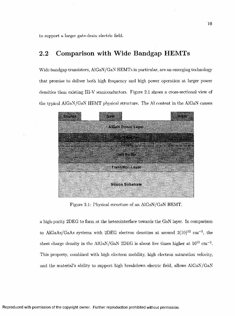
Wide bandgap transistors, AlGaN/GaN HEMTs in particular, are an emerging technology
th a t promise to deliver both high frequency and high power operation at larger power
densities than existing III-V semiconductors. Figure 2.1 shows a cross-sectional view of
the typical AlGaN/ GaN HEMT physical structure. The A1 content in the AlGaN causes
AIGaN Donor Layer
Transition Layer
Silicon Substrate
Figure 2.1: Physical structure of an AlGaN/GaN HEMT.
a high-purity 2DEG to form at the heterointerface towards the GaN layer. In comparison
to AlGaAs/GaAs systems with 2DEG electron densities at around 2(10)12 cm-2 , the
sheet charge density in the AlGaN/GaN 2DEG is about five times higher at 1013 cm-2 .
This property, combined with high electron mobility, high electron saturation velocity,
and the m aterial’s ability to support high breakdown electric field, allows AlGaN/GaN
Reproduced with permission of the copyright owner. Further reproduction prohibited without permission.
11
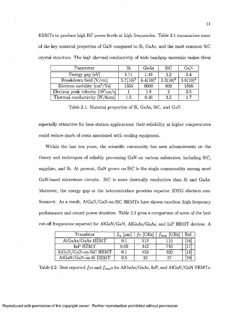
HEMTs to produce high RF power levels at high frequencies. Table 2.1 summarizes some
of the key material properties of GaN compared to Si, GaAs, and the most common SiC
crystal structure. The high therm al conductivity of wide bandgap materials makes them
Param eter Si GaAs SiC GaNEnergy gap [eV] 1.11 1.43 3.2 3.4
Breakdown field [V/ cm] 5.7(10)5 6.4(10)5 3.3(10)e 3.8(10)6Electron mobility cm2/Vs] 1350 6000 800 1600
Electron peak velocity [107cm/s] 1 1.8 2 2.5Thermal conductivity [W/Kcm] 1.5 0.46 3.5 1.7
Table 2.1: M aterial properties of Si, GaAs, SiC, and GaN
especially attractive for base station applications; their reliability at higher tem peratures
could reduce much of costs associated with cooling equipment.
W ithin the last ten years, the scientific community has seen advancements on the
theory and techniques of reliably processing GaN on various substrates, including SiC,
sapphire, and Si. At present, GaN grown on SiC is the single commonality among most
GaN-based microwave circuits. SiC is more thermally conductive than Si and GaAs.
Moreover, the energy gap at the heterointerface provides superior 2DEG electron con
finement. As a result, AlGaN/GaN-on-SiC HEMTs have shown excellent high frequency
performance and record power densities. Table 2.2 gives a comparison of some of the best
cut-off frequencies reported for AlGaN/GaN, AlGaAs/GaAs, and InP HEMT devices. A
Transistor L g [pm] S t [G H z] fm a x [GHz] Ref.AlGaAs/GaAs HEMT 0.1 113 110 [16]
InP HEMT 0.05 343 740 [17]AlGaN/GaN-on-SiC HEMT 0.1 153 230 [18]AlGaN/GaN-on-Si HEMT 0.5 32 27 [19]
Table 2.2: Best reported f Ts and f maxS for AlGaAs/GaAs, InP, and AlGaN/GaN HEMTs.
Reproduced with permission of the copyright owner. Further reproduction prohibited without permission.
12
novel technique is used, where an InGaN intermediate layer is grown on top of the GaN
buffer layer on SiC, to enhance electron confinement in the 2DEG, which effectively in
creases the f x and f max to record levels of 153 GHz and 230 GHz, respectively [18]. In
spite of the advances made in fabricating GaN-based devices on Si, GaN-on-SiC HEMTs
still offer comparatively superior high-speed performance but at a much higher cost.
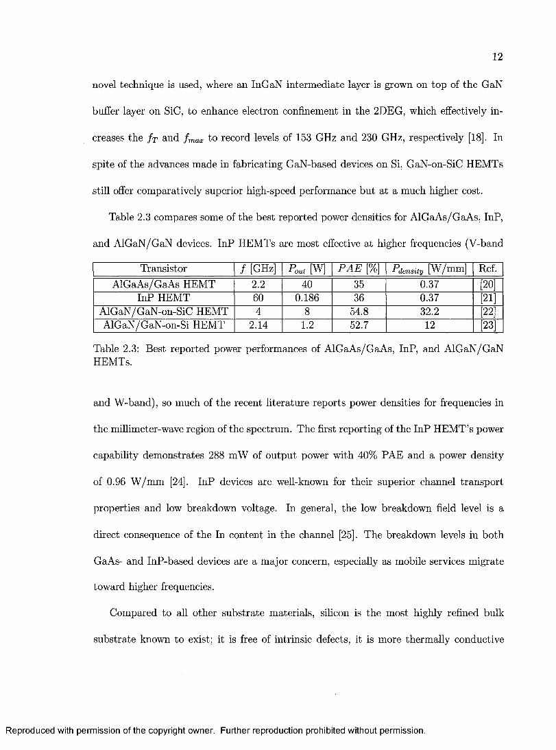
Table 2.3 compares some of the best reported power densities for AlGaAs/GaAs, InP,
and AlGaN/GaN devices. InP HEMTs are most effective at higher frequencies (V-band
Transistor / [GHz] Pout [W] P A E [%] Pdensity [W/mm] Ref.AlGaAs/GaAs HEMT 2.2 40 35 0.37 [20]
InP HEMT 60 0.186 36 0.37 [21]AlGaN/GaN-on-SiC HEMT 4 8 54.8 32.2 [22]AlGaN/GaN-on-Si HEMT 2.14 1.2 52.7 12 [23]
Table 2.3: Best reported power performances of AlGaAs/GaAs, InP, and AlGaN/GaN HEMTs.
and W -band), so much of the recent literature reports power densities for frequencies in
the millimeter-wave region of the spectrum. The first reporting of the InP HEM T’s power
capability demonstrates 288 mW of output power with 40% PAE and a power density
of 0.96 W /m m [24]. InP devices are well-known for their superior channel transport
properties and low breakdown voltage. In general, the low breakdown field level is a
direct consequence of the In content in the channel [25]. The breakdown levels in both
GaAs- and InP-based devices are a major concern, especially as mobile services migrate
toward higher frequencies.
Compared to all other substrate materials, silicon is the most highly refined bulk
substrate known to exist; it is free of intrinsic defects, it is more thermally conductive
Reproduced with permission of the copyright owner. Further reproduction prohibited without permission.

than GaAs, and it is lower in cost than both SiC and GaAs. W ith f Ts above 30 GHz,
GaN-on-Si HEMTs are still an attractive solution, both in terms of performance and cost,
to meet the power and efficiency needs of next-generation microwave base station systems.
Reproduced with permission of the copyright owner. Further reproduction prohibited without permission.

Chapter 3
Microwave Power Amplifiers
Power amplifiers generally exist in either the current source mode, where the transistor
serves as a high-impedance current source, or the switched mode, where the transistor
acts as an on/off switch. This chapter aims to illustrate the major differences between
conventional (eg. Class A, Class AB, Class B, and Class C) PAs and the Class E switched-
mode topology. In doing so, generalized analyses of both current source and Class E
amplifiers are presented accounting for device parasitics th a t impose practical limits on
performance. Small- and large-signal stability concepts are discussed. The chapter con
cludes w ith a brief examination of prior art in dem onstrated Class E PAs in AlGaN/ GaN
HEMT technology. Power amplifier specifications, th a t form the basis for the subsequent
chapters, are outlined as well.
3.1 On Power, B andw idth , and Linearity
Several well respected texts make reference to power amplifiers th a t transm it low, medium,
or high power, but in a vaguely defined way [26,27]. The same ambiguity is also commonly
14
Reproduced with permission of the copyright owner. Further reproduction prohibited without permission.
15
found with respect to narrowband and wideband operation. In the context of this thesis,
“narrowband” implies th a t the frequency bandwidth is less than one octave and “low
frequencies” are in the L-band or lower. “Low power” refers to RF output powers below
500 mW, power amplifiers th a t transm it in the range from 0.5 W to 1 W are categorized
as medium power, and high power amplifiers are those tha t produce RF power levels in
excess of 1 W.
All large-signal power amplifiers, whether operating in the current-source mode or
switched mode, exhibit nonlinear behaviour. This holds true, even for the familiar Class
A topology, whose operation is quasi-linear, at best [26]. Linearity is, by definition, a
measure of how well the amplitude of the output signal corresponds to tha t of the input
signal, where the output amplitude is greater than the input amplitude by a factor equal
to the gain of the power amplifier. As discussed in Section 3.3, Class E power amplifiers,
in their basic form and by nature of their design, are inherently nonlinear and theoretically
achieve 100% drain efficiency. Linearity or linearization schemes are outside the scope of
this work and are not discussed in any detail here.
3.2 C onventional Power A m plifiers
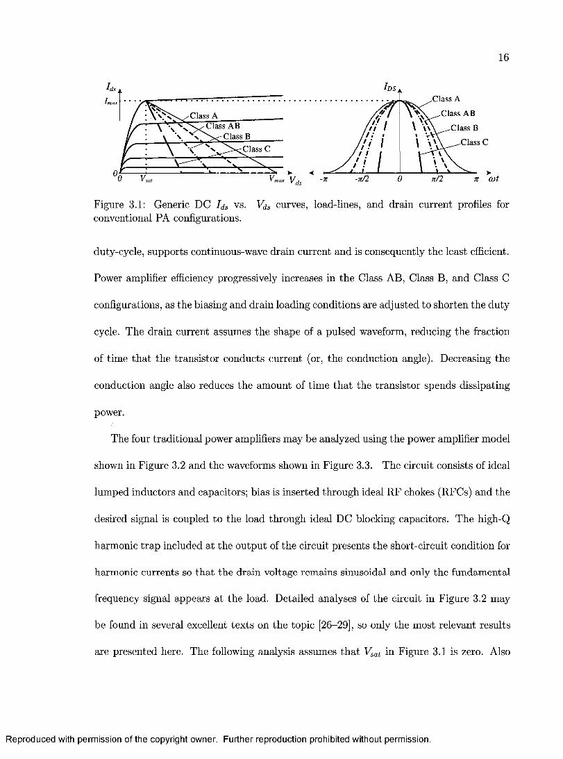
Traditional power amplifiers are classed according to the fraction of the signal’s natural
period tha t the transistor conducts current. Figure 3.1 shows a generic set of DC Ids vs.
Vds curves superimposed by load-lines for the four main conventional PA classes. Also
shown are the corresponding drain current segments illustrating how the drain current
waveform is shaped by the class of operation. The Class A power amplifier, with its 100%
Reproduced with permission of the copyright owner. Further reproduction prohibited without permission.
16
D S
Class A
Class ABClassClass AB “V - Class B
Class B
Class CClass C
-n/2 n/2- K
Figure 3.1: Generic DC Ids vs. Vds curves, load-lines, and drain current profiles for conventional PA configurations.
duty-cycle, supports continuous-wave drain current and is consequently the least efficient.
Power amplifier efficiency progressively increases in the Class AB, Class B, and Class C
configurations, as the biasing and drain loading conditions are adjusted to shorten the duty
cycle. The drain current assumes the shape of a pulsed waveform, reducing the fraction
of time th a t the transistor conducts current (or, the conduction angle). Decreasing the
conduction angle also reduces the amount of time th a t the transistor spends dissipating
power.
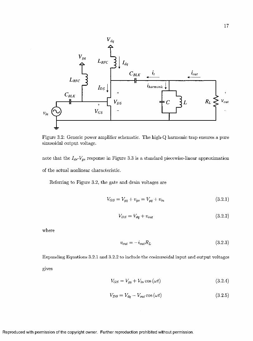
The four traditional power amplifiers may be analyzed using the power amplifier model
shown in Figure 3.2 and the waveforms shown in Figure 3.3. The circuit consists of ideal
lumped inductors and capacitors; bias is inserted through ideal RF chokes (RFCs) and the
desired signal is coupled to the load through ideal DC blocking capacitors. The high-Q
harmonic trap included at the output of the circuit presents the short-circuit condition for
harmonic currents so tha t the drain voltage remains sinusoidal and only the fundamental
frequency signal appears at the load. Detailed analyses of the circuit in Figure 3.2 may
be found in several excellent texts on the topic [26-29], so only the most relevant results
are presented here. The following analysis assumes th a t Vsat in Figure 3.1 is zero. Also
Reproduced with permission of the copyright owner. Further reproduction prohibited without permission.
17
Vdq
RFC
outBLK
iharmonic |I d s
b l k
=r CDS
in
Figure 3.2: Generic power amplifier schematic. The high-Q harmonic trap ensures a pure sinusoidal output voltage.
note tha t the Ids-Vgs response in Figure 3.3 is a standard piecewise-linear approximation
of the actual nonlinear characteristic.
Referring to Figure 3.2, the gate and drain voltages are
Vgs = Vgg T v gs = Vgg T v in (3.2.1)
Vd s ~ Vdq + Vout (3.2.2)
where
^out — Lint (3.2.3)
Expanding Equations 3.2.1 and 3.2.2 to include the cosinusoidal input and output voltages
gives
VGs = Vgq + Vin cos (cut) (3.2.4)
VDS = Vdq - Vout cos (out) (3.2.5)
Reproduced with permission of the copyright owner. Further reproduction prohibited without permission.
18
D S
3n 4n cot
D S
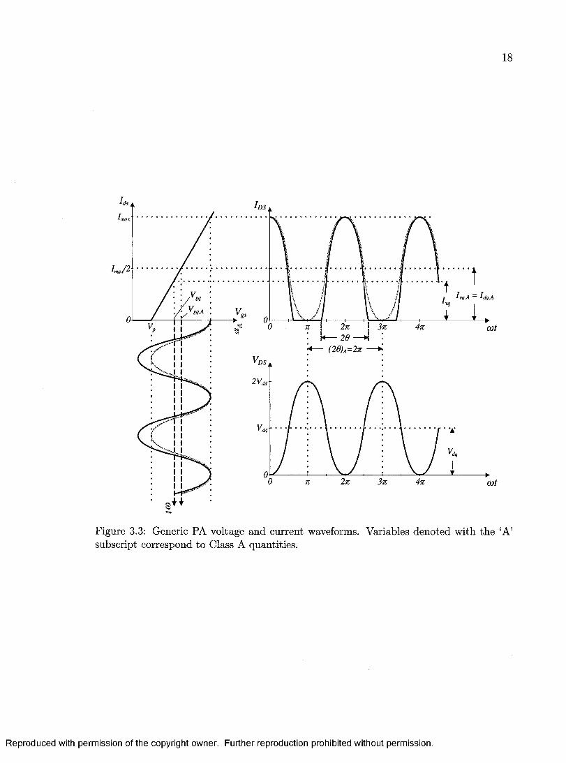
3k cot
Figure 3.3: Generic PA voltage and current waveforms. Variables denoted w ith the ‘A ’ subscript correspond to Class A quantities.
Reproduced with permission of the copyright owner. Further reproduction prohibited without permission.
The drain bias current in Figure 3.3 has been defined as a fictitious v irtual current, Ivq,
in order to simplify the drain current derivation. As shown in Figure 3.3, as Ivq is lowered
beyond the level required for Class A operation, the cycle over which conduction occurs
(29) decreases (hence, the pulsed shape). Drain current is therefore defined to be nonzero
only over the region of conduction:
Note th a t Idq is the actual DC current drawn from the drain power supply. Indeed, I (iq
decreases as I vq decreases but I (iq is the average current required from the power supply
for pulsed current operation, whereas I vq is simply an offset so the drain current shown
in Equation 3.2.6 and Figure 3.3 can be expressed as a DC component superimposed by
a perfect sinusoid. Only in the special case of a continuously conducting Class A power
amplifier (where the conduction angle is 2n), is the virtual bias current equivalent to I fjq-
It follows then, th a t mathematically, the to tal drain current, I d s , is
where the DC and fundamental components, J0 and i i , respectively, are functions of the
conduction angle:
Ivq + lout COS (cot) - 6 ^ (Jjt < 9
0 9 < 2n — 6(3.2.6)
The virtual bias current can be derived using Equation 3.2.6 and by setting I ds to zero
when out = 9:
Ivq lout COS 9 (3.2.7)
I ds = Io + h cos (tut) + / 2 cos (2 cat) + / 3 cos (3 cot) + . . . (3.2.8)
Iq — (sin 9 — 9 cos 9)7r
(3.2.9)
Reproduced with permission of the copyright owner. Further reproduction prohibited without permission.
20
I x = ^ _ Sin cos 0) (3.2.10)7r
The well-known expression for drain efficiency ( D E ) is easily obtained by taking the ratio
of the DC and RF power levels (P0 and P i, respectively) obtained using Equations 3.2.9
and 3.2.10. The DC output power, the power at the fundamental, and the drain efficiency
can be w ritten as
Po = h ^ . ( s m 0 - e c o a 6 ) (3.2.11)7T
P 1 = IoutJ o u t ( g _ s ing cosfl) (3.2.12)2tt
^ ^ 1 Vout 0 — sin 9 cos 6 „ .
( 3 ' 2 ' 1 3 )
where, in the ideal case, Vout = Another measure of efficiency, the power-added
efficiency (P A E ), factors the gain of the PA into the calculation:
P A E = Pl ~ „ AVS (3.2.14)Po
where P a v s is the power available from the source.
It is clear from the above analysis tha t, not only is the Class A power amplifier the
least efficient (D E max A = 50%), but it has zero efficiency when no input power is applied.
The other current source topologies attem pt to increase power amplifier efficiency by
reducing the conduction angle and modifying the loading conditions such th a t DC power
is dissipated in the transistor only during conduction. In contrast to the high linearity
and gain offered by the Class A power amplifier, the pulsed current topologies require
larger input drive signals forcing the degradation of both gain and linearity for higher
efficiency levels. Table 3.1 shows the conduction angles and the theoretical maximum
drain efficiencies for the conventional amplifiers discussed so far.
Reproduced with permission of the copyright owner. Further reproduction prohibited without permission.
21
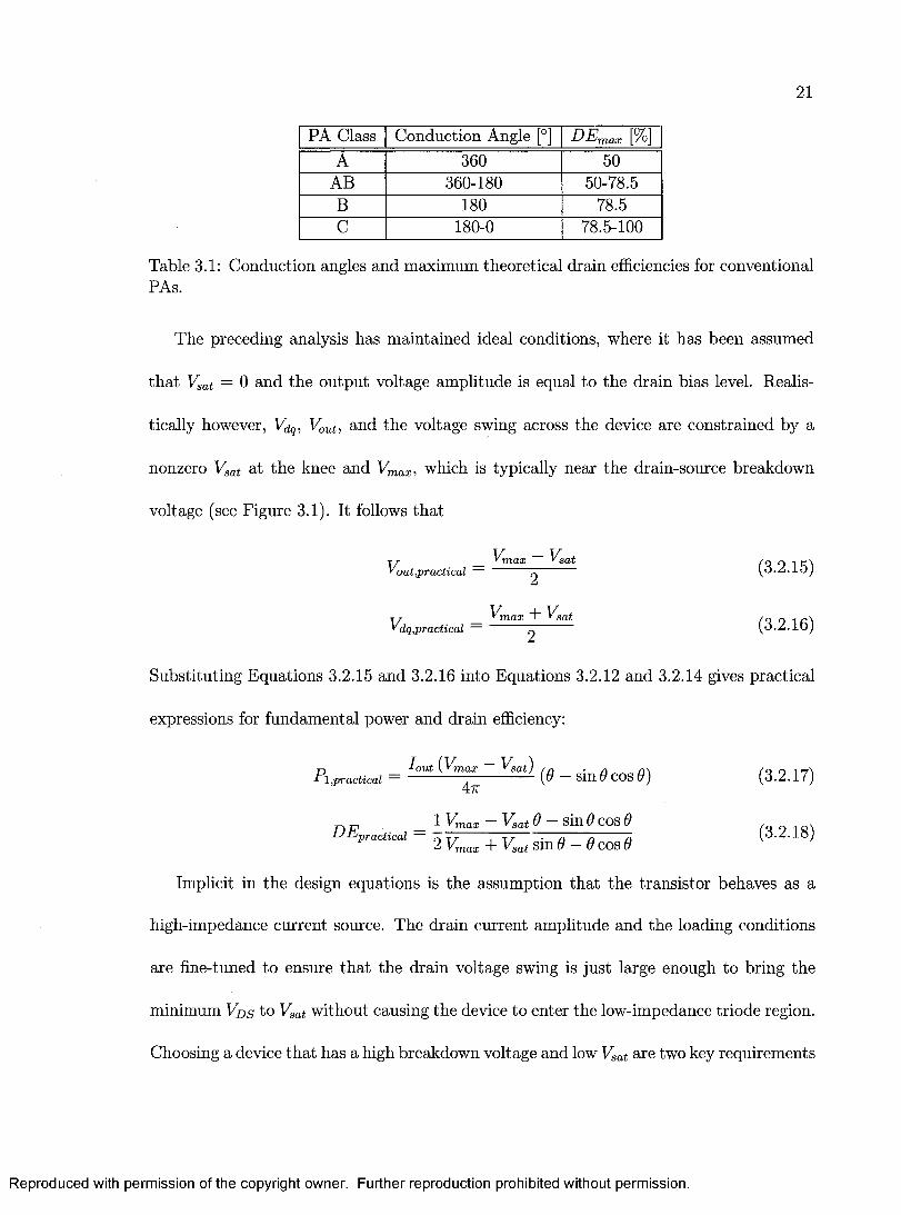
PA Class Conduction Angle [°] D E max [%]A 360 50
AB 360-180 50-78.5B 180 78.5C 180-0 78.5-100
Table 3.1: Conduction angles and maximum theoretical drain efficiencies for conventional PAs.
The preceding analysis has maintained ideal conditions, where it has been assumed
th a t Vsat = 0 and the output voltage amplitude is equal to the drain bias level. Realis
tically however, Vdq, Vout, and the voltage swing across the device are constrained by a
nonzero Vsat at the knee and Vmax, which is typically near the drain-source breakdown
voltage (see Figure 3.1). It follows th a t
Vmax Vsat ^out,practical — yo.Z.LO)
Vmax T Vsat /o o i a \dq,practical — to.Z.iOj
Substituting Equations 3.2.15 and 3.2.16 into Equations 3.2.12 and 3.2.14 gives practical
expressions for fundamental power and drain efficiency:
PI lout (Vmax Vsat) r n , n n \ / 0 n 1 r r \1,practical — Z (y sin$COS0) (3.2.17)47r
j-, jti______ _ 1 Vnax Vsat 0 sin 0 COS 6 /o o 1 cOU n p r a c t i c a l O T / l T / r - a a a2 V n a x T Vsat sin 0 0 COS 0
Implicit in the design equations is the assumption tha t the transistor behaves as a
high-impedance current source. The drain current amplitude and the loading conditions
are fine-tuned to ensure th a t the drain voltage swing is just large enough to bring the
minimum Vd s to Vsat without causing the device to enter the low-impedance triode region.
Choosing a device tha t has a high breakdown voltage and low Vsat are two key requirements
Reproduced with permission of the copyright owner. Further reproduction prohibited without permission.

22
for medium to high power, high efficiency operation. Regardless of which current source
amplifier topology is chosen, Vsat will always be a major source of power dissipation in
the device. Also, factors such as device heating influence practical efficiencies: in some
cases, up to ten times more DC power goes into a system than the RF level received at
the transm itting antenna [30].
3.3 Class E Sw itched-M ode Power A m plifier
The Class E switched mode power amplifier, originally conceived by the Sokals [31],
operates under the premise th a t the transistor behaves as a discrete on/off switch with
ideally zero on-state and infinite off-state resistances. Figure 3.4 shows an ideal Class E
PA circuit. The circuit is essentially a power converter, whose fundamental output signal
amplitude is determined by the drain bias supply voltage and the load resistance. The
output signal is only weakly correlated to the input signal in th a t the input drive must be
large enough to adequately switch the transistor between the fully on and fully off states.
Variable envelope input signals, such as those used in amplitude modulated or single
side-band broadcasting, cannot be used with the expectation th a t the information in the
envelope will be maintained at the output. This limitation forces a constant-envelope
output signal making the amplifier nonlinear, as discussed in Section 3.3.1. Proper load
network design at the output of the transistor prohibits the simultaneous occurrence of
high voltage and high current, allowing the amplifier to operate with 100% theoretical
drain efficiency.
Reproduced with permission of the copyright owner. Further reproduction prohibited without permission.
23
Much of the published work on the Class E mode assumes ideal transistor switch
ing conditions and carries these assumptions through to design and implementation [32].
While there exist active devices th a t approximate switching behaviour quite well at fre
quencies below 1 GHz, nonlinear models must be used at higher frequencies where tran
sistors no longer behave as simple switches. This chapter starts with the basic theory
behind the original Class E circuit assuming ideal conditions and ends with a discussion
on practical issues th a t degrade amplifier performance at microwave frequencies.
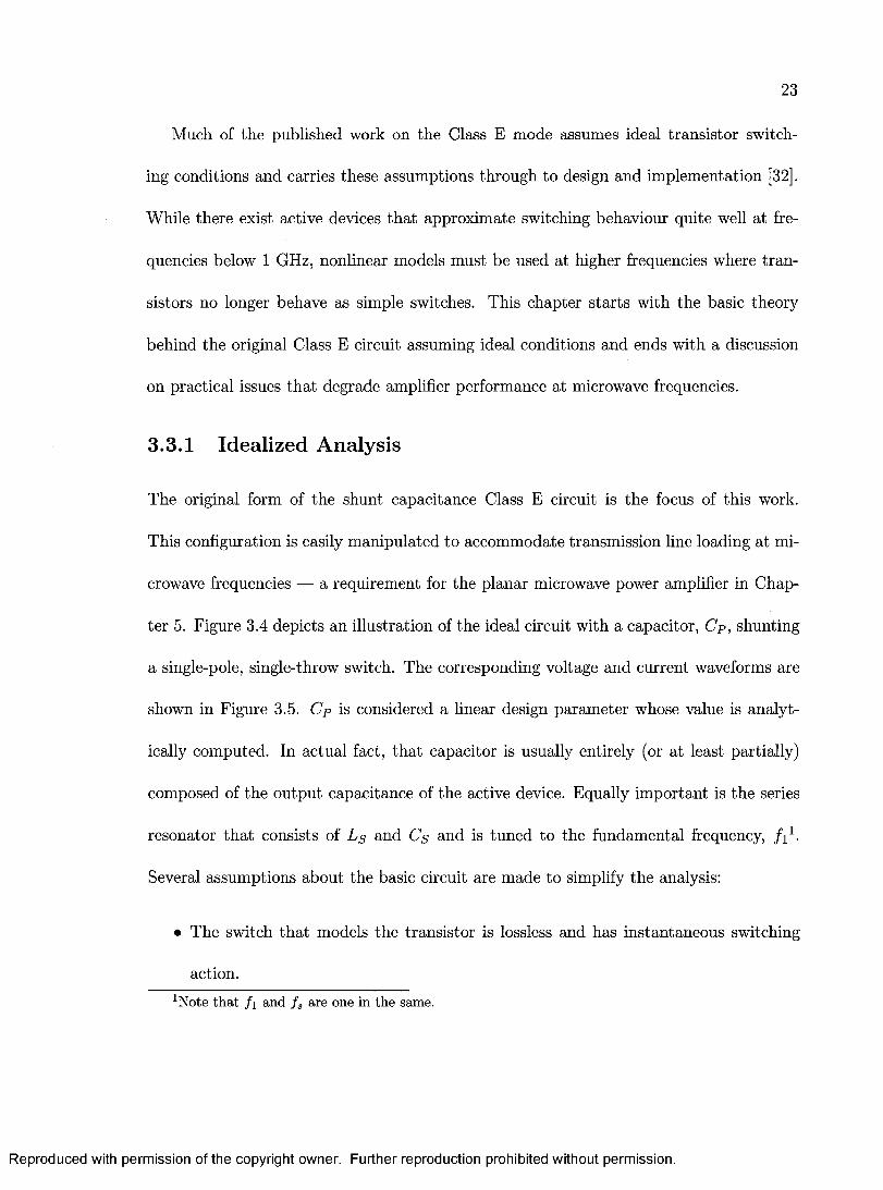
3.3.1 Idealized Analysis
The original form of the shunt capacitance Class E circuit is the focus of this work.
This configuration is easily manipulated to accommodate transmission line loading at mi
crowave frequencies — a requirement for the planar microwave power amplifier in Chap
ter 5. Figure 3.4 depicts an illustration of the ideal circuit with a capacitor, Cp, shunting
a single-pole, single-throw switch. The corresponding voltage and current waveforms are
shown in Figure 3.5. Cp is considered a linear design param eter whose value is analyt
ically computed. In actual fact, th a t capacitor is usually entirely (or at least partially)
composed of the output capacitance of the active device. Equally im portant is the series
resonator th a t consists of L$ and C\s and is tuned to the fundamental frequency, / i 1.
Several assumptions about the basic circuit are made to simplify the analysis:
• The switch th a t models the transistor is lossless and has instantaneous switching
action.
1N ote that / i and f s are one in the same.
Reproduced with permission of the copyright owner. Further reproduction prohibited without permission.
24
Vdq
Figure 3.4: Ideal Class E power amplifier circuit. The ideal single-pole, single-throw switch transitions states at the switching frequency, f s. The PA generates RF output power also at f s.
• The inductor through which the DC bias is supplied is lossless and has a reactance
th a t is high enough to not load the circuit and to disallow any variations in DC
current.
• The series resonant circuit has a sufficiently high Q-factor to force a sinusoidal
output current at the fundamental (or switching) frequency.
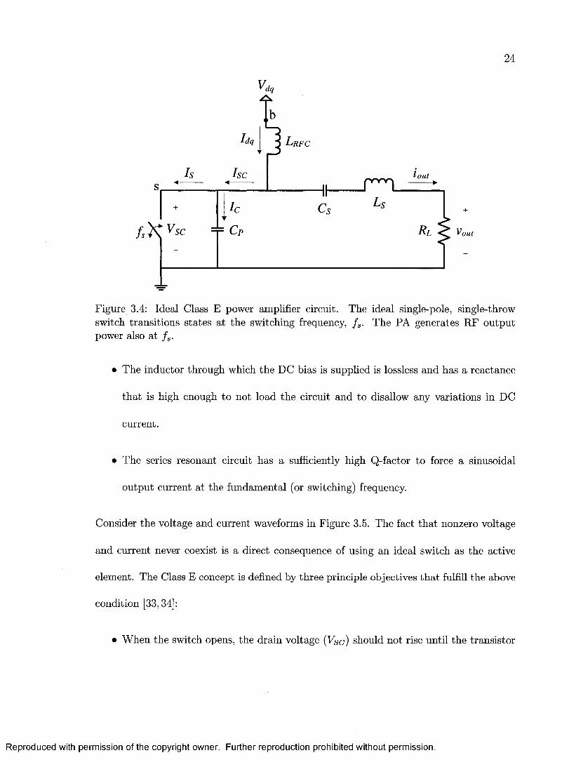
Consider the voltage and current waveforms in Figure 3.5. The fact th a t nonzero voltage
and current never coexist is a direct consequence of using an ideal switch as the active
element. The Class E concept is defined by three principle objectives th a t fulfill the above
condition [33,34]:
• W hen the switch opens, the drain voltage (V sc) should not rise until the transistor
Reproduced with permission of the copyright owner. Further reproduction prohibited without permission.
25
Switch Switch Switch SwitchClosed : Open :— — :
Closed Open■M*
‘ON’ OFF’
cotC A
cot
,max
2w- it
Figure 3.5: Ideal Class E PA voltage and current waveforms
Reproduced with permission of the copyright owner. Further reproduction prohibited without permission.

26
is completely off (Is = 0 A)2
• When the switch closes, the drain voltage (Use) should be zero before the drain
current begins to rise.
• When the switch closes, the slope of the drain voltage should be zero.
In his paper [34], Raab concludes th a t optimal Class E operation is achieved with a 50%
duty cycle switching period and re-affirms Sokal’s th ird principle objective listed above.
Under these conditions, the load network must provide a phase shift (</?) of approximately
—32° to the output current. He represents this phase shift as a fictitious reactance (that
turns out to be inductive), whose value is simply the difference in reactances of the
inductor and capacitor in the resonant circuit. The analysis th a t follows is loosely based
on [34]; a slightly different approach is presented in [35].
The circuit analysis, referring to Figure 3.4, continues with the foresight th a t the
output current waveform is nominally phase shifted. Then the current through the switch-
capacitor combination is
Isa = h , - Imt sin M + f ) (3.3.1)
keeping in mind th a t ISc flows through the switch when it is closed and through Cp when
it is open. The voltage at node ‘s’ is determined by the charging of Cp when the switch
is off:
(3.3.2)
2For th e purpose of the ideal circuit explanation, drain voltage is denoted V s c and drain current is
I s - These sym bols are replaced w ith transistor quantities in subsequent chapters
Reproduced with permission of the copyright owner. Further reproduction prohibited without permission.
27
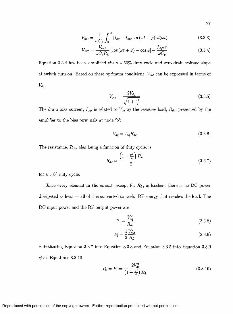
1 f utVsc = —p r / [hq ~ lout sin {ut + <p)} d(ut) (3.3.3)
MOp J o
V sc = -7 7 % "- tcos + ¥>) “ cos ¥>] + -^F T (3.3.4)(JOpiXj) Ct Op
Equation 3.3.4 has been simplified given a 50% duty cycle and zero drain voltage slope
at switch tu rn on. Based on these optimum conditions, Vmt can be expressed in terms of
Vdq,
Vout - (3.3.5)\A+?
The drain bias current, Idq, is related to Vdq by the resistive load, R dc, presented by the
amplifier to the bias terminals at node ‘b ’:
Vdq = IdqRdc (3.3.6)
The resistance, Rdc, also being a function of duty cycle, is
_ M ) R lRdc = y (3.3.7)
for a 50% duty cycle.
Since every element in the circuit, except for R l , is lossless, there is no DC power
dissipated as heat — all of it is converted to useful RF energy th a t reaches the load. The
DC input power and the RF output power are
V 2P0 = - ^ - (3.3.8)
dc1 v2,
R i = a lf f (3-3-9)
Substituting Equation 3.3.7 into Equation 3.3.8 and Equation 3.3.5 into Equation 3.3.9
gives Equations 3.3.10
2V 2P„ = T\ -- -------* ----- (3.3.10)
(1 + t ) R l
Reproduced with permission of the copyright owner. Further reproduction prohibited without permission.
For the sake of completeness, tak ing the ra tio of P\ to Pq gives a drain efficiency, DE =
100%.
It is noteworthy, at this point, to emphasize the importance of choosing the right device
technology. If the goal is to maximize output power (i.e. optimum Class E operation),
then peak drain voltage and current excursions must be known during device selection.
In his analysis, Raab derives a relationship between Rdc, w, and Cp which, for a 50% duty
cycle, is
Substitution of Equations 3.3.5, 3.3.6, 3.3.7, and 3.3.11 into Equation 3.3.4 yields
Differentiating Equation 3.3.12 w ith respect to u t and setting the result to zero gives the
time at which the drain voltage is at its maximum for a given Vdq.
Substituting Equation 3.3.13 and the known phase angle, = —0.5669 rad, into Equa
tion 3.3.12 gives the peak drain voltage,
Maximum drain current is easily determined from Equation 3.3.1 by observing tha t
(3.3.11)
(3.3.12)
,m a x (3.3.13)
\raax 3.5621^ (3.3.14)
SC,max (3.3.15)
Reproduced with permission of the copyright owner. Further reproduction prohibited without permission.
29
Successive substitutions of Equation 3.3.5 followed by Equation 3.3.6 into Equation 3.3.15
gives
I SC,max — 2.862Idq (3.3.16)
The physical nature of the AlGaN/GaN heterostructure permits high sheet charge
density in the conducting 2DEG and allows the device to w ithstand a high critical electric
field. The A lGaN/GaN HEMT can therefore sustain high voltages whilst generating high
RF current, making it an ideal choice for this work.
The beauty of the Class E PA lies in its complete end-to-end realizability. In general,
specific design equations can be used to build a first-time successful, fully operational
Class E amplifier [33]. Although this last statem ent is true, it only really applies to the
ideal situation or in the low-frequency case where parasitic effects can be (mostly) ignored.
At microwave frequencies device parasitics have to be included in the design.
3.3.2 The Class E Concept at GHz Frequencies
The key difference between conventional power amplifiers and the Class E amplifier is
the range of allowable voltages th a t exist across the drain and source terminals of the
device. Particularly im portant is the effect of the transistor’s knee voltage on achieving
high efficiency operation. During conduction, the device never enters the triode region
when operated as a high-impedance current source; but when operated as a switch, the
drain-source voltage must be as low as possible requiring traversal into the triode region
during part of the RF cycle. The actual efficiency reduction, in practice, is a ttributed to
the combined power dissipated in this finite on-resistance as well as in the drain and source
Reproduced with permission of the copyright owner. Further reproduction prohibited without permission.
30
resistances, R s and R,i [36]. The microwave power amplifier in Chapter 5 is implemented
w ith transmission lines in order to reduce insertion loss. This design strategy alone
prevents drain efficiency from reaching 100% since optimal open-circuit loading is rarely
achieved at all higher-order harmonics of the fundamental frequency.
The notion th a t transistors can be replaced with simplified switch models for Class E
PA designs is an unfortunate outcome of the ideal analysis. To quote Cripps, “RF power
transistors are not switches at GHz frequencies, even if a finite on resistance is included in
the switch model” [32]. Although the switch model is a good starting point in the design
process, the final design must include a real large-signal transistor model th a t predicts
parasitic and nonlinear effects at microwave frequencies. This is especially true for this
work since a 3.5 GHz square-wave input drive is not realistic; instead, a large-amplitude
voltage sinusoid is used to switch the device.
So far, the Class E PA has been discussed under the assumption th a t the transistor
only switches between two discrete states: on and off. Implicit in the assumption is th a t
the gate of the transistor is driven with an ideal square-wave. Driving circuits alone are a
topic worthy of a thesis and so are not discussed here; Sokal [33] and Ortega-Gonzalez [37]
cover gate driving circuits and methods in their respective articles. It is common practice
to over-drive the input (i.e. the gate of the active device) of a switching PA with a
large-amplitude sinusoidal voltage in the absence of a driving circuit or, in this case, the
unavailability of a high frequency square-wave generator. The over-driving technique is
used in this work with the expectation of large energy losses and reductions in gain. The
sinusoidal driving power required to completely switch the device (Psw) is a function of
Reproduced with permission of the copyright owner. Further reproduction prohibited without permission.

31
the gate-source voltage needed to switch the gate (Vgsw), the input capacitance (Cgs), and
the switching frequency. Equation 3.3.17 embodies all of these param eters [37].
As a final thought when choosing the right device technology, one must bear in mind
th a t parasitic capacitances invariably pose an upper limit on the frequency permissible for
Class E operation. A good approximation for this maximum frequency is derived in [38]
and reproduced here,
switch, which is ideally I sc,max from Equation 3.3.16. CdS0 is the output capacitance of
the transistor.
Almost all RF power transistors are potentially unstable. T hat is, the transistor may
oscillate for some source and load impedances th a t present negative resistances to the
terminals of the transistor. But negative resistances do not guarantee oscillations; the
term inations must present the correct phase and magnitude to make the transistor oscil
late [32], The stability of a device is determined by the Rollet stability factor, k,
(3.3.17)
maxmax,E (3.3.18)
noting th a t I max equates to the maximum current-handling capability of the active device
3.4 Stab ility
k =(yn) at (y22) - u (y12y21)
1* 1 2 * 2 1 1
(3.4.1)
Reproduced with permission of the copyright owner. Further reproduction prohibited without permission.

32
where k > 1 for unconditional stability and k < 1 for conditional stability [39]. Strictly
speaking, the stability criterion is for the small-signal case and does not accurately repre
sent the stability performance of a nonlinear power amplifier. Moreover, a Class E power
amplifier is biased in the off state (i.e. the gate is pinched-off), but large-signal variations
at the input periodically bring the transistor into the on state. This switching behaviour
is not captured in the evaluation of Equation 3.4.1. Small-signal stability is checked in
the design, but is not relied upon as a definite measure of the PA’s overall stability as a
large-signal PA.
In large-signal power amplifiers, instability is more an artifact of the bias insertion
circuit. Care is taken to ensure th a t the bias circuits do not present unwanted impedances
to the power amplifier and th a t noise on the supply lines is suppressed so th a t it cannot
couple into the gate or the drain of the transistor. Beyond tha t, the problem of instability
is tackled in the lab during testing. Oscillations typically appear as large variations in
DC current and RF output power. An array of decoupling capacitors is used at the bias
terminals to suppress potential oscillations from low frequencies to frequencies beyond the
operating frequency of the PA.
3.5 P revious W ork and P roposed Am plifier Specifi
cations
In spite of its relative infancy in GaN electronics, the switched-mode Class-E concept,
using GaN-on-SiC HEMTs, has been dem onstrated for a range of applications from low
frequency, high-voltage power electronics to microwave power amplification [40-43]. At
Reproduced with permission of the copyright owner. Further reproduction prohibited without permission.
33
microwave frequencies, Xu [42] and Gao [43] report monolithic GaN-on-SiC Class-E im
plementations at 1.9 GHz and 2.0 GHz, both having similar output powers and P A E s of
37 dBm at 57% P A E . Cree3 holds the current world record for the highest dem onstrated
P A E of 84% and output power of 10 W at 2 GHz [44]. These designs employ expensive
SiC-based GaN devices and require higher drain bias levels (greater than 20 V) to achieve
the reported results. The relatively few reports of GaN-based Class E PAs shows the need
for further study of GaN-based switched-mode PA topologies.
This work demonstrates the first reported Class E power amplifier using GaN HEMTs
fabricated on silicon. The amplifier is designed for operation at 3.5 GHz in the WiMAX
band. A standard 50 W bias supply, limited to 25 V, is used for biasing. The drain of the
HEMT is backed off from the supply limit down to 20 V. The conservative choice of bias
allows the drain voltage to swing to the required 71 V peak for ideal Class E operation
and limits the output power to the theoretical maximum of 4 W. In practice, neither the
peak voltage nor the maximum output power is sustained as discussed in Chapter 5. The
gate of the HEMT is biased near the gate pinch-off voltage for optimal gain. These are the
preliminary design specifications, as derived from the intended application and standard
available biasing equipment; more complete specifications are given in Chapter 5.
3.6 Sum m ary
The main difference between conventional and switched-mode PAs is in the regions of
operation in which the active device is allowed to operate. For Class E operation, the
3Headquartered in North Carolina, Cree, Inc. designs and m anufactures state-of-the-art GaN-on-SiC
power HEM Ts.
Reproduced with permission of the copyright owner. Further reproduction prohibited without permission.
34
transistor’s Vd s must approach as low an on-state voltage as possible (ideally 0 V) for
the half of the switching period when I D s > 0 A. W hen the transistor is off ( I d s = 0
A) for the other half of the period, Vds is perm itted to traverse the horizontal Vds axis.
Conventional PAs are required to operate in the saturation region at all times; th a t is,
V d s may never swing into the triode region.
Depending on the class of operation (Class A, AB, B, or C), the time the transis
tor spends conducting current (or, the conduction angle) is determined by Vgs and the
output loading for a fixed V(jiS in the saturation region. As Vga is decreased towards the
gate’s pinch-off voltage, the conduction angle becomes shorter and the PA becomes more
efficient. Theoretical maximum drain efficiencies range anywhere from 50% (Class A)
to 100% (Class C). As the PA becomes more efficient, gain decreases and the region of
input power levels over which gain remains constant becomes shorter. This efficiency vs.
linearity trade-off is carried through to the Class C PA, where the gate of the transistor
is biased below its pinch-off voltage, forcing the input drive amplitude to be larger than
it would have to be for the same output power in a Class A PA.
The Class E PA relies on the active device behaving as an on/off switch, cycling
through the low-impedance “on” and high-impedance “off” states at the fundamental
frequency. Theoretical 100% drain efficiency is implied since, by definition, nonzero volt
age and current never simultaneously exist across the terminals of a perfect switch. The
output load network is tuned to ensure th a t 100% drain efficiency is maintained while
the fundamental frequency signal is extracted at the output of the PA. While the Class
E power amplifier efficiently generates power, the active device switch must support peak
Reproduced with permission of the copyright owner. Further reproduction prohibited without permission.
35
drain voltages over 3.5 times higher than the bias level and peak currents almost a factor
of 3 higher than the average current drawn by the device. These constraints make GaN
HEMTs attractive for application in switched-mode Class E PAs due to their ability to
support high breakdown voltages and high current capacity.
A Class E PA targeting the WiMAX band at 3.5 GHz with 4 W output power (based
on a 20 V drain bias supply and 50 0 output load) is the focus of this work. Many
factors such as, device parasitics, therm al effects, and transmission lines, influence circuit
performance; in practice, both conventional and the Class E power amplifiers suffer from
less than ideal efficiencies and output power levels. But generally speaking, the Class E
PA out-performs conventional topologies in many aspects from circuit simplicity to output
power and efficiency.
Reproduced with permission of the copyright owner. Further reproduction prohibited without permission.

Chapter 4
Gallium N itride High Electron
M obility Transistor Nonlinear M odel
An accurate large-signal (or nonlinear) transistor model provides the necessary foundation
for many electronic designs. Device vendors don’t always supply such models for even
the most established technology. Transistor models are simply non-existent for the GaN
HEMTs used in thesis.
Device models th a t are amenable to integration in circuit simulators are usually em
pirical in nature [45]. T hat is, the device model, although designed to represent the
physical behaviour of a transistor, uses purely mathematical equations to approximate
very complex operation as defined by measured data. The “best-fit” analytical equa
tions are typically polynomials th a t have little physical significance to the device being
characterized [46]. Indeed, physical models are more accurate, but difficult to implement
in circuit simulators (see [47] and [48]) and data-based (eg. HP Root model) models
are accurate only for the exact structures and measurement conditions under which the
measurements were compiled. Between these two extremes are equation-based empirical
36
Reproduced with permission of the copyright owner. Further reproduction prohibited without permission.
37
models, which are most often found in circuit Computer-Aided Design (CAD) tools. The
reader is referred to [49] and [50] for an overview of the most popular nonlinear device
models by M aterka et al. [51], Curtice et al. [52], and Statz et al. [53].
GaN HEMT technology is still a newcomer to the device modeling community, so large-
signal models are not readily available. A nonlinear model originally conceived for GaAs
HEMTs is used for this thesis due to the structural similarities between AlGaAs/GaAs
AlGaN/GaN transistors. Model imperfections surface in the course of device characteri
zation targeting physical properties of the GaN HEMT that are difficult to predict by the
chosen model.
This chapter explores the versatility of the EEsof Scalable Nonlinear HEMT (EE-
HEMT) model offered as an integrated component in the Advanced Design System (ADS)
RF circuit simulator [54]. The flexibility of this model lies in its ability to be molded to fit
the electrical behaviour of most HEMTs using measured DC and RF data. This model is
chosen, in part, due to its straightforward manipulation given the types of data supplied
by the device manufacturer, and also as an exploratory exercise to determine the areas of
the model th a t need modification in order to accommodate emerging GaN technology.
The chapter begins with an introduction to the GaN-on-Si HEMT used in this work.
A discussion on measurement methods and param eter extraction follows a review of the
specifics of the nonlinear model. Small- and large-signal characterization is presented
leading to the final nonlinear model, which approximately fits DC, transconductance,
and s-parameter data with reasonable accuracy for the Class E power amplifier design
presented in Chapter 5. The model is not perfect: there are regions of operation where
Reproduced with permission of the copyright owner. Further reproduction prohibited without permission.

38
the simulated vs. measured performance deviates enough to warrant a brief examination
towards the end of the chapter.
4.1 T he N itron ex G aN -on-Si H EM T
The Nitronex GaN-on-Si HEMT technology is based on the proprietary SIGANTIC© and
PENDEO™ processes th a t allow high-quality GaN crystal growth on silicon substrates
[55]. The GaN HEMT used in this work is an unpackaged bare die with gold-plated gate,
drain, and source contacts th a t are attached, via bond wires, to the microwave circuit
elements of the Class E power amplifier.
The top-level layout of the GaN-on-Si HEMT is shown in Figure 4.1 with typical
device properties summarized in Table 4.1. The performance data, collected at 2.14 GHz,
Figure 4.1: Top-level layout of the Nitronex GaN-on-Si HEMT die showing a gate width of 10 x 0.2 mm.
Gate periphery Channel length
f r
2 mm 0.7 fim. 13 GHz
Drain bias supply Quiescent drain current
O utput power Peak drain efficiency
Linear gain
15 V 450 mA 4 - 5 W 60 - 65%
18 - 19 dB
Table 4.1: Vendor-supplied GaN-on-Si HEMT characteristics at 2.14 GHz
was supplied by the device manufacturer.
Each GaN HEMT was cut out of a larger die, containing several test structures. The
physical dimensions shown in the figure include tolerances added to accommodate dicing.
Reproduced with permission of the copyright owner. Further reproduction prohibited without permission.
39
4.2 E E sof 2 m m N onlinear H E M T M odel
The EEHEMT model fits analytic expressions to measured DC and bias-dependent s-
param eter data. The model as a whole is unique, but its individual components are not
in tha t they are borrowed from the works presented in [45], [56], [57], and [53]. Like
many of the more popular models, the EEHEM T model’s fitting parameters allow it to
approximate the operation of many different process types. On the downside, the model’s
analytic expressions are not accessible for modification by the user, causing potential
inaccuracies in the simulated behaviour of the device.
The EEHEMT model includes simple linear scaling for designing with larger periphery
or multiple devices in parallel. The model also characterizes resistor and channel noise
and includes a means by which to simulate the design at tem peratures other than the
tem perature at which the equivalent circuit parameters are extracted. The model is
comprehensive enough to address a variety of uses, but at the same time allows the
designer to use only those features th a t are specific to one particular application. In
th a t regard, the GaN transistors used in this thesis have a 2 mm gate periphery and
are exclusively used in power amplifier applications, where the ambient air is at room
tem perature, so the gate width and tem perature scaling features and the channel noise
model are not used.
The schematic representation of the model, shown in Figure 4.2, consists of some no
table features tha t are summarized in the following sections. The complete documentation
can be found in [54].
Reproduced with permission of the copyright owner. Further reproduction prohibited without permission.
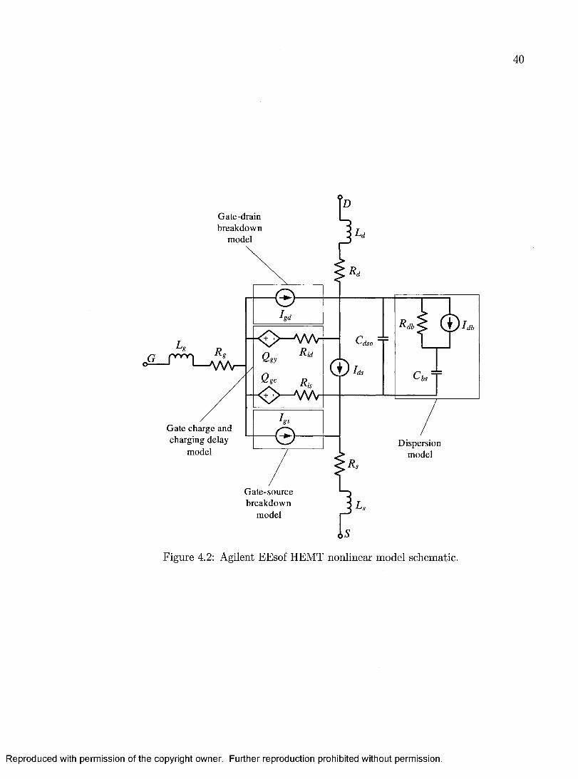
Gate-drain breakdown
m odel
db
Gate charge and charging delay
m odelDispersion
m odel
G ate-source breakdown
m odel
Figure 4.2: Agilent EEsof HEMT nonlinear model schematic.
Reproduced with permission of the copyright owner. Further reproduction prohibited without permission.
41
4.2.1 Drain-Source Current M odel
The drain-source current (Ids) model, adapted from [45], fits analytic expressions to
isothermal current-voltage measurements. Depending on the DC transconductance (gm)
and gate-source voltage (Vgs) profiles, Ids and output conductance (gds) are evaluated in
four distinct regions: below gate pinch-off (or gate threshold) voltage (Vp), between Vp
and peak gm, the region where grn is constant, and where grn compresses.
4.2.2 Dispersion M odel
In his article [58], Ladbrooke defines dispersion as a “term used to indicate th a t the
dynamic (or RF) characteristics of a device are different from the static (or DC) char
acteristics” . Dispersion has two main sources: one is trapped charge, and the other is
self-heating.
Charge Trapping
Charge accumulation at the surface or in the buffer layer of GaN HEMTs typically leads
to reduced channel current and decreased output power from the device. These effects are
modeled by the dispersion circuit proposed by Golio et al. [57] and shown in Figure 4.2.
The GaN HEMTs used in this work have been refined such th a t surface and buffer
charge trapping effects are negligible, and therefore not included as part of the device
model [59]. The interested reader is referred to [60-63] for more information on buffer
layer effects and surface charge trapping phenomena.
Reproduced with permission of the copyright owner. Further reproduction prohibited without permission.

42
S e lf -H e a t in g
Although a consequence of DC power dissipation in the device, self-heating occurs in a
complicated and often misunderstood manner at RF. Under static conditions, the applied
voltage and the resulting current change slowly enough to allow the lattice tem perature
of the device to reach steady state at each bias point. Self-heating is a manifestation of
the DC power dissipated through a HEMT which, for the most part, is determined by
the DC bias conditions. As the lattice tem perature increases at higher voltages, the self
heating mechanism increases phonon scattering which, in turn, reduces carrier mobility
and saturation velocity [64]. However, once a large-signal RF stimulus is superimposed
onto the DC bias, the lattice tem perature cannot adapt (the therm al time constant of the
lattice is long compared to the rate of change of the RF signal) and so remains fixed by
the bias point. The effects of self-heating, such as reduced transconductance and negative
output conductance, are well-known and discussed in more detail in [65] and [66].
In this case, the EEHEM T model is fit to pulsed current-volt age measurements taken
at deep Class AB biasing conditions. Pulsed measurements performed at a static quiescent
point not only captures the RF behaviour of the GaN HEMT operated as a power ampli
fier, but also provides steady-state therm al conditions for the measurements. Indeed, the
EEHEMT model comes complete with a therm al model tha t predicts the negative conduc
tance effects from self-heating under static measurements, but is appropriately excluded
as per the latter discussion [56]. As a precautionary measure however, large aluminum
heat-sinks are used on all designs to mitigate inevitable therm al effects resulting from the
RF cycle.
Reproduced with permission of the copyright owner. Further reproduction prohibited without permission.
43
4.2.3 Gate and Output Charge M odels
The gate-charge model, shown in Figure 4.2, fits bias-dependent capacitance profiles ex
tracted from measured y-parameters [53]. The depletion and channel regions are rep
resented by two charge sources, Qgc and Qgy, th a t model gate capacitance, and two
corresponding resistances, R ls and Rid, th a t model charging delay between the channel
and depletion region.
The output capacitance, CdS0, is a constant parameter, which gives the drain-source
charge as a function of VdS.
4.2.4 Gate Forward Conduction and Breakdown M odel
Gate forward conduction is modeled by the standard diode equation, which is a function
of Vga and diode ideality factor, rj [67]. The GaN Schottky diode exhibits some peculiar
characteristics th a t appear during model generation, suggesting th a t the well-known diode
equation is not appropriate for this device.
The limited availability of die for this work prevents the development of the gate-
to-source and gate-to-drain breakdown models. Measuring such device characteristics
typically leads to catastrophic device failure. The manufacturer has indicated a gate-to-
drain breakdown voltage level well above the peak voltage required for the Class E PA in
this work.
Reproduced with permission of the copyright owner. Further reproduction prohibited without permission.
4.3 Transistor C haracterization
44
The discussion on self-heating in Section 4.2.2 implies th a t the RF signal sees a unique set
of dynamic current-voltage characteristics for each static (or DC) bias point. In theory,
Class E PA operation requires a pinched-off gate bias level. The Ifds for the Class E PA in
Chapter 5 is 20 V; at this bias, the gate pinch-off voltage is approximately -3 V. The GaN
HEMT used in this thesis is designed to be operated at a 28 V drain bias in deep Class
AB mode. For this reason, the manufacturer-supplied dynamic current-voltage data is
generated at a Vds of 28 V and a Vgs of -2.6 V, which is sufficient for this application even
though the bias deviates from Class E conditions.
A pulsed current-voltage measurement setup is used to extract all dynamic current-
voltage data. The voltage pulse-width, during which time the current is measured, is
set short enough (200 ns) to ensure tha t the true RF behaviour is captured [58]. A
Hewlett-Packard 8510 Vector Network Analyzer, also with bias-tees, is used for on-wafer
bias-dependent s-parameter measurements [68]1.
As a starting point, extrinsic param eters are determined. Next, the model is fit to
Ids-Vds and DC gm profiles, as well as to the Schottky gate forward bias measurement.
Input and output capacitances and model-generated, bias-dependent s-parameters are fit
to measurements as a final step in the device modeling process. This process is iterative
with many trade-offs in modeling accuracy, so some model parameters are adjusted away
from extracted values in order to obtain the best possible fit to measured data. Optimized
1 All device m easurem ents in this section were conducted by N itronex Corporation in order to assist
w ith m odel developm ent carried out by th e author.
Reproduced with permission of the copyright owner. Further reproduction prohibited without permission.
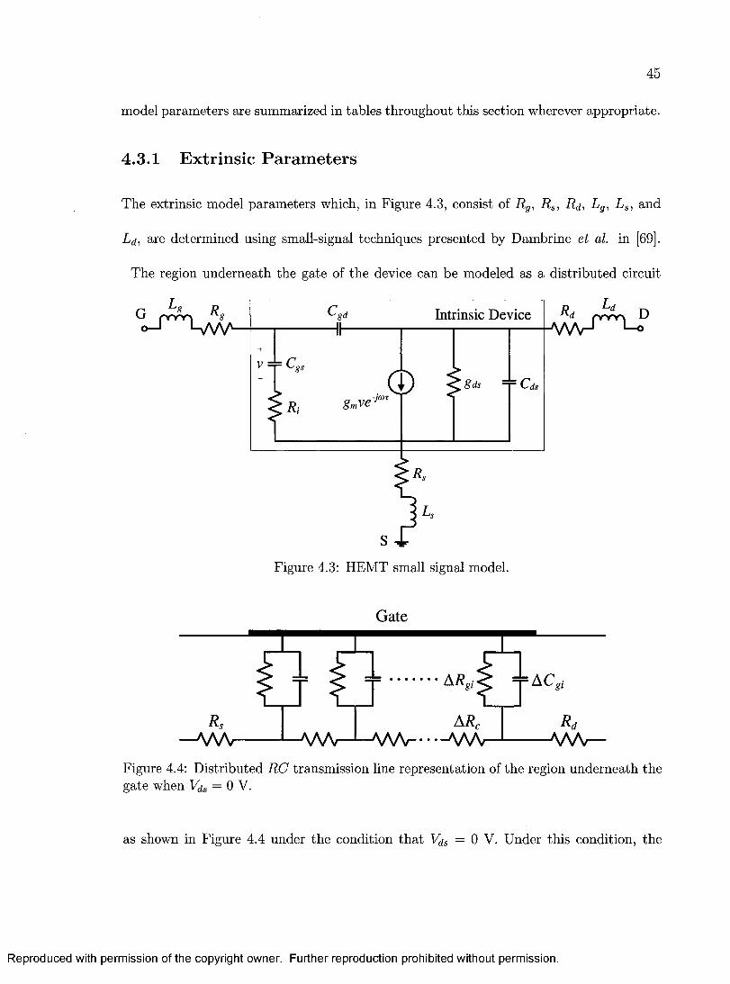
45
model parameters are summarized in tables throughout this section wherever appropriate.
4.3.1 Extrinsic Parameters
The extrinsic model parameters which, in Figure 4.3, consist of R g, R s, R fi, Lg, L a, and
L (j, are determined using small-signal techniques presented by Dambrine et al. in [69].
The region underneath the gate of the device can be modeled as a distributed circuit
Intrinsic Device
Figure 4.3: HEMT small signal model.
Gate
A RcAA/V~ * AAA/—
Figure 4.4: D istributed R C transmission line representation of the region underneath the gate when Vas = 0 V.
as shown in Figure 4.4 under the condition th a t Vds = 0 V. Under this condition, the
Reproduced with permission of the copyright owner. Further reproduction prohibited without permission.
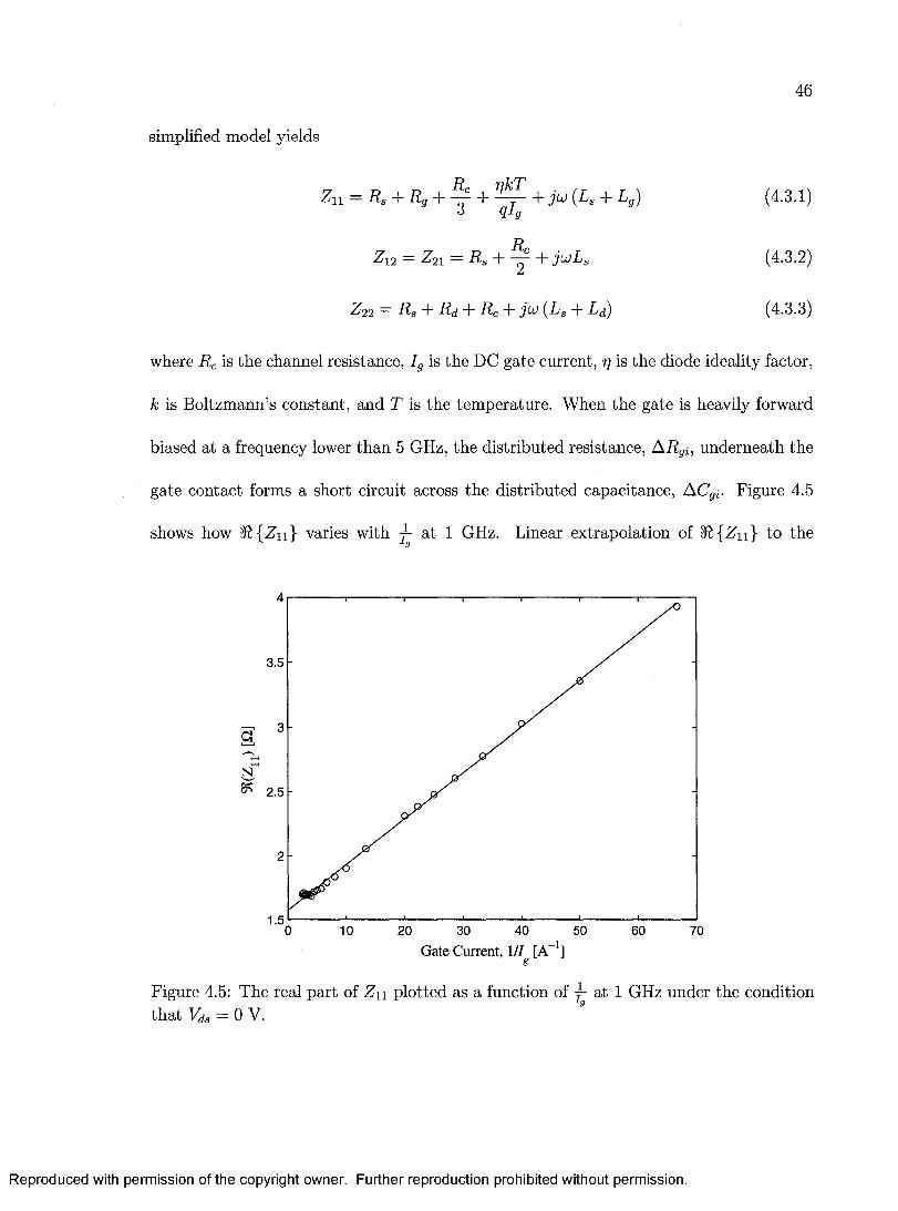
46
simplified model yields
Zn = R s + R g + — + - — |- juj (Ls + L g) (4.3.1)o q lg
Z 12 = Z 21 = R s + — + jioLs (4.3.2)
Z 22 — R s + Rd + R c + j u (Ls + Ld) (4.3.3)
where R c is the channel resistance, Ig is the DC gate current, rj is the diode ideality factor,
k is Boltzmann’s constant, and T is the tem perature. When the gate is heavily forward
biased at a frequency lower than 5 GHz, the distributed resistance, A R gi, underneath the
gate contact forms a short circuit across the distributed capacitance, A Cg{. Figure 4.5
shows how 5ft{Z n } varies with j- at 1 GHz. Linear extrapolation of 5ft{ Z u } to the
3.5
C3
^ 2.5
30 40
Gate Current, l / I [A-1]
20 60
Figure 4.5: The real part of Z \\ plotted as a function of j- at 1 GHz under the condition th a t Vds = 0 V.
Reproduced with permission of the copyright owner. Further reproduction prohibited without permission.

47
4- = 0 axis equates the fourth term in Equation 4.3.1 to zero, giving the expression inl 9
Equation 4.3.4.
$ { Z n }\Ig^ 00 = R s + R g + ^ = 1.551 n (4.3.4)
The real parts of Equations 4.3.1 - 4.3.3 and Equation 4.3.4 represent five unknowns in
four equations. In the absence of a fifth equations, the extrinsic elements in the symbolic
forms of Equations 4.3.1 - 4.3.3 are optimized to fit both measured z-parameters and the
condition in Equation 4.3.4. The schematic in Figure 4.6(a) models Equation 4.3.1 and
the schematic in Figure 4.6(b) models Equations 4.3.2 and 4.3.3.
(a) (b)
Figure 4.6: Schematic representations of (a) Equation 4.3.1 and (b) Equations 4.3.2 and 4.3.3
Initial estimates of the extrinsic inductances are obtained from the imaginary parts
of Equations 4.3.1- 4.3.3. Figure 4.7 shows ^ { Z n } , ^ { .£ 12}, and ^ { ^ 22} plotted versus
frequency up to 5 GHz. As expected, the linear progression of the imaginary parts of
the z-parameters indicate fixed extrinsic inductances with respect to frequency. Using
Equations 4.3.1 - 4.3.3, it is deduced from Figure 4.7 tha t L s & 1.52 pH, L g & 67.84
pH, and La ~ 98 pH. This information is used in an ADS optimization routine where the
Reproduced with permission of the copyright owner. Further reproduction prohibited without permission.
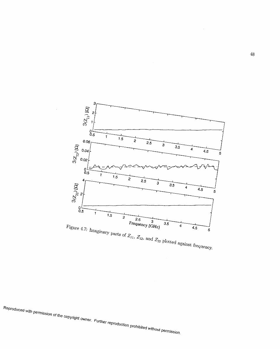
ReProduced
Figure 4.7. r .&gmary Parts o f ?
Rrequency [qh?] 3 5 4
11 ’ F>2 , and z*22 plotted «era,"u against frGlPuency.
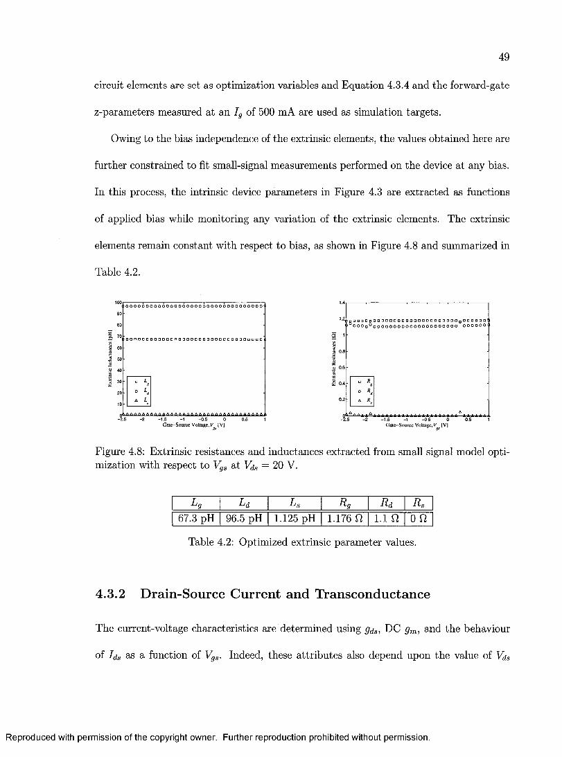
49
circuit elements are set as optimization variables and Equation 4.3.4 and the forward-gate
z-parameters measured at an Ig of 500 mA are used as simulation targets.
Owing to the bias independence of the extrinsic elements, the values obtained here are
further constrained to fit small-signal measurements performed on the device at any bias.
In this process, the intrinsic device parameters in Figure 4.3 are extracted as functions
of applied bias while monitoring any variation of the extrinsic elements. The extrinsic
elements remain constant w ith respect to bias, as shown in Figure 4.8 and summarized in
Table 4.2.
100
90
o o o o o o o o o o o o o o o o o o o o o o o o o o o o o o o o o o
i— I I O O D Q O O O O P P P n O O P D O n n o n n O P P D P D P P p p p P
.a 40 2 'S
qAA AAA A AAA A AAAA AAA A A A A AAA A A AAA A A A AAA-2 .5 - 2 -1 .5 -1 -0 .5 0 0.5 1
Gate-Source Voltage, V [V]
□ □ □ □ □ □ □ □ □ □ □ □ □ □ □ □ □ □ □ D a D o n n p Q g O D D o n o i 0 0 0 o ° 0 0 0 0 0 0 0 0 0 0 0 0 0 0 0 0 0 0 0 0 0 0 0 0 0 0 0 1
a 1 •
iS 0.4 □ Rs
oA R
( f ^ ^ A A ^ A A A A A A A A A A A A A A A A A A A A A A A A A A A i 4 -2 .5 - 2 -1 .5 -1 -0 ,5 0 0 ,5 1
Gate-Source Voltage, V [V]
Figure 4.8: Extrinsic resistances and inductances extracted from small signal model optimization with respect to Vgs at V(is = 20 V.
L9 Ld L s Rg Rd Rs67.3 pH 96.5 pH 1.125 pH 1.176 Q 1.1 0 o n
Table 4.2: Optimized extrinsic param eter values.
4.3.2 Drain-Source Current and Transconductance
The current-voltage characteristics are determined using g^s, DC gm, and the behaviour
of Ids as a function of Vgs. Indeed, these attributes also depend upon the value of Vrjs
Reproduced with permission of the copyright owner. Further reproduction prohibited without permission.
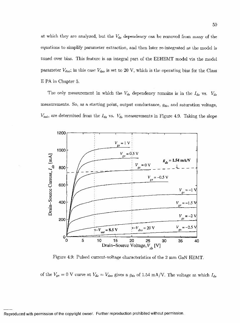
50
at which they are analyzed, but the Vds dependency can be removed from many of the
equations to simplify param eter extraction, and then later re-integrated as the model is
tuned over bias. This feature is an integral part of the EEHEM T model via the model
param eter Vdso\ in this case Vdso is set to 20 V, which is the operating bias for the Class
E PA in Chapter 5.
The only measurement in which the Vds dependency remains is in the I ds vs. Vds
measurements. So, as a starting point, output conductance, gds, and saturation voltage,
Vsat, are determined from the I ds vs. Vds measurements in Figure 4.9. Taking the slope
1200
10005 Vr— n
^ 8 0 0
cs8
u 6 0 0V = - 1 V<Dos-<3
oxn.A
4 0 0 V = -1 .5 V
Q V = - 2 V200
V = -2 .5 V< - V = 8 .5 Vsat
0 5 10 15 20 2 5 3 0 3 5 4 0Drain-Source Voltage, V , [V]
as
Figure 4.9: Pulsed current-voltage characteristics of the 2 mm GaN HEMT.
of the Vgs = 0 V curve at Vds = Vdso gives a gds of 1.54 mA/V. The voltage at which I ds
Reproduced with permission of the copyright owner. Further reproduction prohibited without permission.
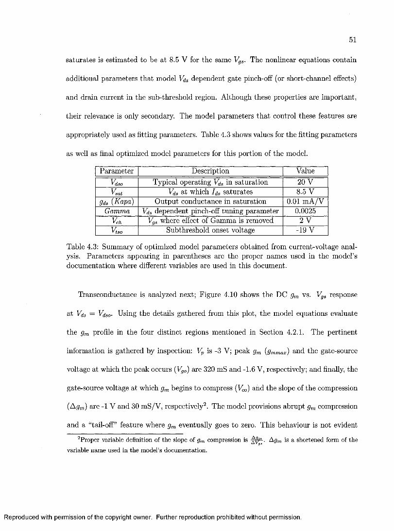
51
saturates is estimated to be at 8.5 V for the same Vgs. The nonlinear equations contain
additional parameters th a t model Vds dependent gate pinch-off (or short-channel effects)
and drain current in the sub-threshold region. Although these properties are im portant,
their relevance is only secondary. The model parameters th a t control these features are
appropriately used as fitting parameters. Table 4.3 shows values for the fitting parameters
as well as final optimized model param eters for this portion of the model.
Param eter Description Value
Vdso Typical operating Vds in saturation 20 VVSat Vds at which Ids saturates 8.5 V
gds (Kapa) O utput conductance in saturation 0.01 m A /VGamma Vds dependent pinch-off tuning parameter 0.0025
vch Vgs where effect of Gamma is removed 2 VVtso Subthreshold onset voltage -19 V
Table 4.3: Summary of optimized model parameters obtained from current-voltage analysis. Parameters appearing in parentheses are the proper names used in the model’s documentation where different variables are used in this document.
Transconductance is analyzed next; Figure 4.10 shows the DC gm vs. Vgs response
at Vds = Vdso- Using the details gathered from this plot, the model equations evaluate
the gm profile in the four distinct regions mentioned in Section 4.2.1. The pertinent
information is gathered by inspection: is -3 V; peak gm (gmmax) and the gate-source
voltage at which the peak occurs (Vgo) are 320 mS and -1.6 V, respectively; and finally, the
gate-source voltage at which gm begins to compress (Vco) and the slope of the compression
(Agm) are -1 V and 30 mS/V, respectively2. The model provisions abrupt gm compression
and a “tail-off” feature where gm eventually goes to zero. This behaviour is not evident
2Proper variable definition of the slope o f g m com pression is f'f/" '. A g m is a shortened form of theV g s
variable nam e used in the m odel’s docum entation.
Reproduced with permission of the copyright owner. Further reproduction prohibited without permission.
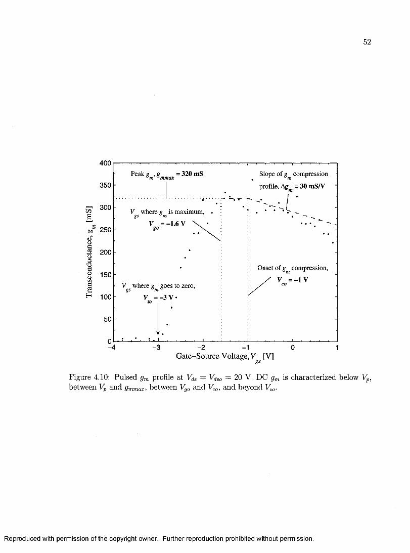
52
4 0 0
= 320 m S Slope o f compression
profile, Ag = 30 m S/V
Peak
3 5 0
5? 300B
2 5 04JOB 2000 |8 1 5 0
1 100
V where e is maximum,mV = -1.6 v \
Onset o f g m compression,
/ V = - 1 V/ COV where g goes to zero, gs mV = - 3 V •
5 0
- 4 - 3 -2 1 0 1Gate-Source Voltage, V [V]
gs
Figure 4.10: Pulsed gm profile at Vds = Vdso — 20 V. DC grn is characterized below Vp, between Vp and gmmax, between Vgo and Vco, and beyond Vco.
Reproduced with permission of the copyright owner. Further reproduction prohibited without permission.
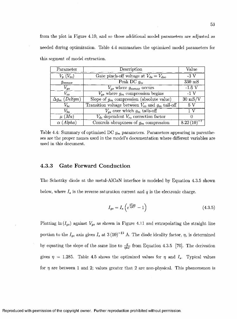
53
from the plot in Figure 4.10, and so those additional model param eters are adjusted as
needed during optimization. Table 4.4 summarizes the optimized model param eters for
this segment of model extraction.
Param eter Description Value{Vt0) Gate pinch-off voltage at Vds — Vdso -3 V
Qmmax Peak DC gm 330 mSV9o Vgs where gmmax occurs -1.6 VVC0 VgS where g rn compression begins -1 V
A g m (D e ltg m ) Slope of gm compression (absolute value) 30 m S/Vvbc Transition voltage between Vco and gm tail-off 5 Vvba Vgs over which grn tails-off 1 V
g, (Mu) Vds dependent Vco correction factor 0a (Alpha) Controls abruptness of gm compression 8 .2 2 (10)“ '
Table 4.4: Summary of optimized DC gm parameters. Param eters appearing in parentheses are the proper names used in the model’s documentation where different variables are used in this document.
4.3.3 Gate Forward Conduction
The Schottky diode at the metal-AlGaN interface is modeled by Equation 4.3.5 shown
below, where I s is the reverse saturation current and q is the electronic charge.
/ g V g s \
Igs = I s (ev»T - l j (4.3.5)
Plotting In (Igs) against Vgs as shown in Figure 4.11 and extrapolating the straight line
portion to the Igs axis gives I s at 3 (10)-12 A. The diode ideality factor, 77, is determined
by equating the slope of the same line to ^ from Equation 4.3.5 [70]. The derivation
gives 77 = 1.285. Table 4.5 shows the optimized values for 77 and I s. Typical values
for 77 are between 1 and 2; values greater th a t 2 are non-physical. This phenomenon is
Reproduced with permission of the copyright owner. Further reproduction prohibited without permission.
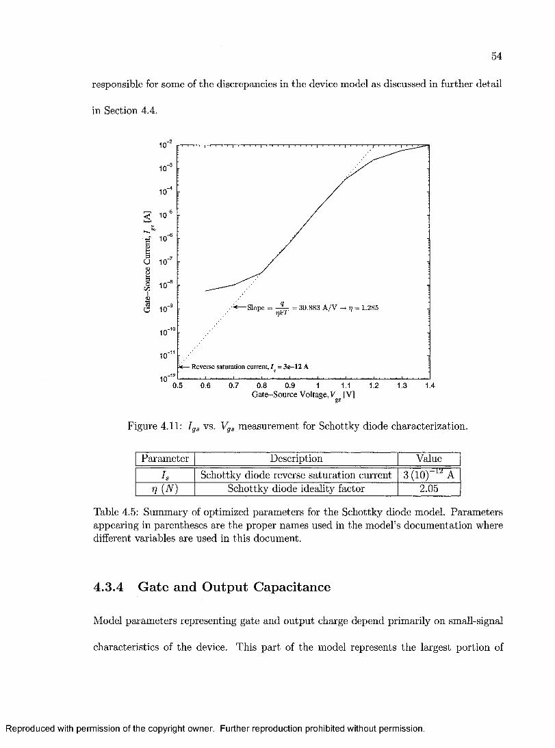
54
responsible for some of the discrepancies in the device model as discussed in further detail
in Section 4.4.
,-5<
$,-7
Slope = = 30.883 A/V -> r) = 1.285
,-1 0
— Reverse saturation current, I = 3e-12 A,-12
0.5 0.6 0.7 0.8 0.9 1 1.1Gate-Source Voltage, V [V]
1.2 1.4
Figure 4.11: Igs vs. Vgs measurement for Schottky diode characterization.
Param eter Description Value
Is Schottky diode reverse saturation current 3(10)- i " Ar , (N) Schottky diode ideality factor 2.05
Table 4.5: Summary of optimized parameters for the Schottky diode model. Parameters appearing in parentheses are the proper names used in the model’s documentation where different variables are used in this document.
4.3.4 Gate and Output Capacitance
Model parameters representing gate and output charge depend primarily on small-signal
characteristics of the device. This part of the model represents the largest portion of
Reproduced with permission of the copyright owner. Further reproduction prohibited without permission.
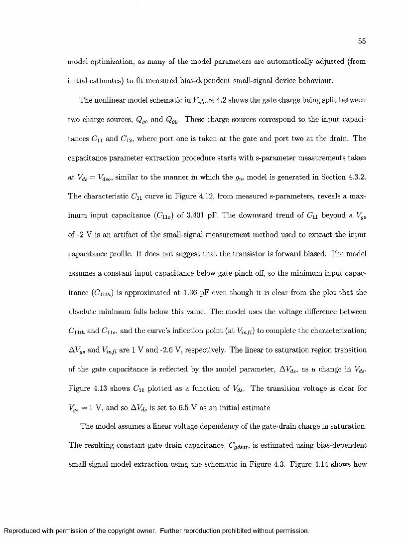
55
model optimization, as many of the model parameters are automatically adjusted (from
initial estimates) to fit measured bias-dependent small-signal device behaviour.
The nonlinear model schematic in Figure 4.2 shows the gate charge being split between
two charge sources, Qgc and Qgy. These charge sources correspond to the input capaci
tances C'u and C 12, where port one is taken at the gate and port two at the drain. The
capacitance param eter extraction procedure starts with s-parameter measurements taken
at Vds — Vdsoi similar to the manner in which the gm model is generated in Section 4.3.2.
The characteristic C n curve in Figure 4.12, from measured s-parameters, reveals a max
imum input capacitance (C u 0) of 3.401 pF. The downward trend of C'u beyond a Vgs
of -2 V is an artifact of the small-signal measurement method used to extract the input
capacitance profile. It does not suggest th a t the transistor is forward biased. The model
assumes a constant input capacitance below gate pinch-off, so the minimum input capac
itance (Cuth) is approximated at 1.36 pF even though it is clear from the plot th a t the
absolute minimum falls below this value. The model uses the voltage difference between
Cuth and Cuo, and the curve’s inflection point (at I4 i/z) to complete the characterization;
AVgs and Vinfi are 1 V and -2.6 V, respectively. The linear to saturation region transition
of the gate capacitance is reflected by the model parameter, A Vds, as a change in Vds-
Figure 4.13 shows Cn plotted as a function of Vds- The transition voltage is clear for
VgS = I V , and so A Vds is set to 6.5 V as an initial estimate
The model assumes a linear voltage dependency of the gate-drain charge in saturation.
The resulting constant gate-drain capacitance, Cgdsati is estim ated using bias-dependent
small-signal model extraction using the schematic in Figure 4.3. Figure 4.14 shows how
Reproduced with permission of the copyright owner. Further reproduction prohibited without permission.
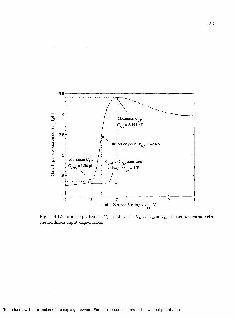
56
3 .5
:M aximum
C = 3 .401 pF
OS 2 .5 §
Inflection point, V = - 2 .6 V
M inimum C , ’ , , , to C . , transition11th ■ llovoltage, A V = 1 V<u
O
- 4 - 3 -2 1 0 1Gate-Source Voltage, V [V]
gs
Figure 4.12: Input capacitance, C'u, plotted vs. Vgs at Vrjs = Vdso is used to characterize the nonlinear input capacitance.
Reproduced with permission of the copyright owner. Further reproduction prohibited without permission.
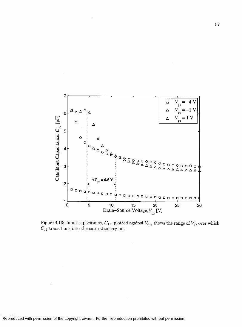
57
P-H&
o 5vuae3■M • rH
£ 4&U
& 3HH<Dtso
A A A .a
OO
O □
O A ° O A
° O £
A V . = 6.5 V < * >
2 2 2 9 ? o o oA a A a a a ° 0 0 0 ° 0 0 O O
A A A A A A A A / i
n D n n o D n p n i : | p n ( : | n
10 15 20 2 5 3 0Drain-Source Voltage, V , [V]
as
Figure 4.13: Input capacitance, C'u, plotted against Vrjs, shows the range of Vfjs over which C'u transitions into the saturation region.
Reproduced with permission of the copyright owner. Further reproduction prohibited without permission.
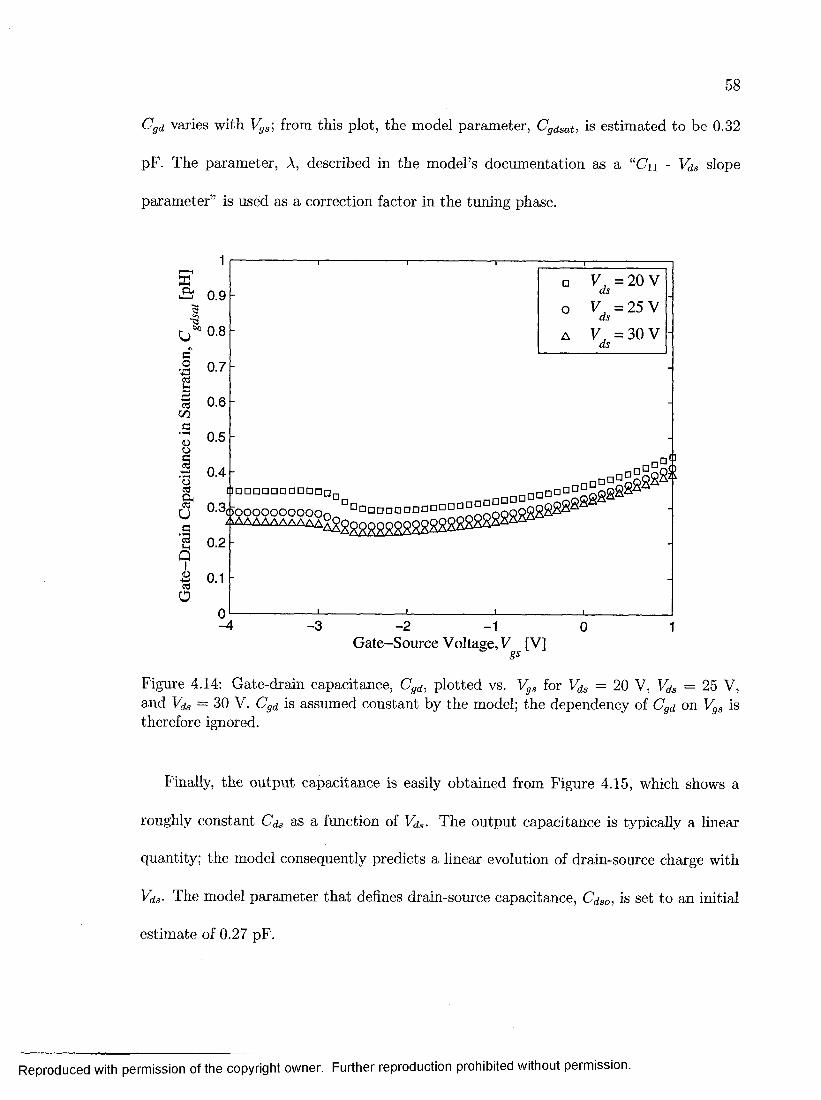
58
Cgd varies with Vga\ from this plot, the model parameter, Cgdsat, is estim ated to be 0.32
pF. The param eter, A, described in the model’s documentation as a “C'u - Vds slope
param eter” is used as a correction factor in the tuning phase.
^ 0.8co+-*Ss03c<Doaat
0 .7
0 .5
.« 0 .4oS 1Ph03 0 3u Ud< a
0.2
rinnDaa°°QOgi
/ iA a a a a a a a a
■gQIBo
- 4 ■3 -2 1 0 1G ate-S ource Voltage, V [V]
gs
Figure 4.14: Gate-drain capacitance, Cgd, plotted vs. Vgs for Vds = 20 V, Vds = 25 V, and Vds = 30 V. Cgd is assumed constant by the model; the dependency of Cgd on Vgs is therefore ignored.
Finally, the output capacitance is easily obtained from Figure 4.15, which shows a
roughly constant Cds as a function of Vds. The output capacitance is typically a linear
quantity; the model consequently predicts a linear evolution of drain-source charge with
Vds. The model param eter th a t defines drain-source capacitance, Cdso, is set to an initial
estimate of 0.27 pF.
Reproduced with permission of the copyright owner. Further reproduction prohibited without permission.

59
A
d011ood<uod03
• i-H
3£U<DOS-lS0
001dS
0.6
0 .5 5•S3
0 .5
0 .4 5
0 .4
0 .3 5
0 .3
0 .2 5 °
0.2
0 .1 5
0.120
□6
□
o
A
O
V = -4 Vgs
V = - i vgs
V =ovgs
Au
22 2 4 2 6 2 8 3 0Drain-Source Voltage, V , [V]
as
Figure 4.15: O utput capacitance, Cds, plotted vs. VdS for output capacitance extraction. Cds is constant with respect to VdS, as assumed by the nonlinear model.
Reproduced with permission of the copyright owner. Further reproduction prohibited without permission.
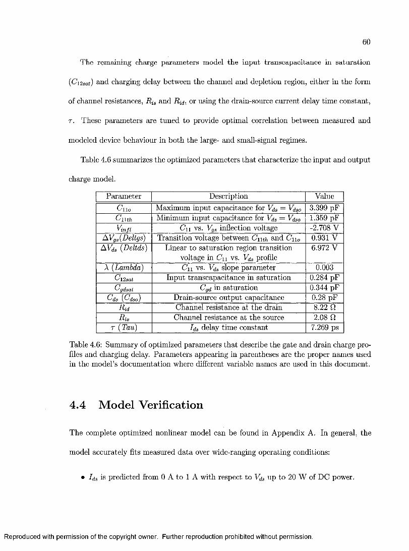
60
The remaining charge parameters model the input transcapacitance in saturation
{C\2sat) and charging delay between the channel and depletion region, either in the form
of channel resistances, RiS and Rid, or using the drain-source current delay time constant,
r . These param eters are tuned to provide optimal correlation between measured and
modeled device behaviour in both the large- and small-signal regimes.
Table 4.6 summarizes the optimized parameters th a t characterize the input and output
charge model.
Param eter Description Value
Cue Maximum input capacitance for VdS = VdS0 3.399 pFCnth Minimum input capacitance for Vds = Vdso 1.359 pFVinfl C n vs. Vgs inflection voltage -2.708 V
AVgS(Deltgs) Transition voltage between Cnth and C \i0 0.931 VA Vds (Deltds) Linear to saturation region transition
voltage in C'u vs. Vds profile6.972 V
A (Lambda) C'u vs. Vds slope parameter 0.003C\2 sat Input transcapacitance in saturation 0.284 pFCgdsat Cgd in saturation 0.344 pF
Cds (Cdso) Drain-source output capacitance 0.28 pFRid Channel resistance at the drain 8.22 fiRis Channel resistance at the source 2.08 Q
r ( Tau) Ids delay time constant 7.269 ps
Table 4.6: Summary of optimized parameters th a t describe the gate and drain charge profiles and charging delay. Parameters appearing in parentheses are the proper names used in the model’s documentation where different variable names are used in this document.
4.4 M odel Verification
The complete optimized nonlinear model can be found in Appendix A. In general, the
model accurately fits measured data over wide-ranging operating conditions:
• Ids is predicted from 0 A to 1 A with respect to Vds UP to 20 W of DC power.
Reproduced with permission of the copyright owner. Further reproduction prohibited without permission.
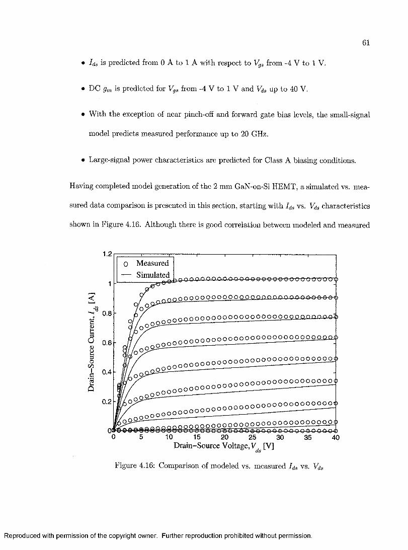
61
• Ids is predicted from 0 A to 1 A with respect to Vgs from -4 V to 1 V.
• DC gm is predicted for Vgs from -4 V to 1 V and Vds up to 40 V.
• W ith the exception of near pinch-off and forward gate bias levels, the small-signal
model predicts measured performance up to 20 GHz.
• Large-signal power characteristics are predicted for Class A biasing conditions.
Having completed model generation of the 2 mm GaN-on-Si HEMT, a simulated vs. mea
sured data comparison is presented in this section, starting w ith Ids vs. Vds characteristics
shown in Figure 4.16. Although there is good correlation between modeled and measured
1.20 Measured— Simulated ------------
■O 0000 0 0 0 0 0 0 0 0 0 9 0 0 0 0 0 0 0 0 0 0 0 o o~u
0 5 10 15 2 0 2 5 3 0 3 5 4 0Drain-Source Voltage, V , [V]
as
Figure 4.16: Comparison of modeled vs. measured Ids vs. Vds
Reproduced with permission of the copyright owner. Further reproduction prohibited without permission.
62
data, the model does not capture the knee region of the Ids - Vds profile over most of the
Vgs plane. The measured data indicates a smaller on-resistance than th a t predicted by
the model, translating to higher measured efficiency levels than those predicted in Class
E PA circuit simulations.
Figure 4.17 shows measured DC gm and Ids, plotted versus Vgs, and overlayed with
simulations, for V*, ranging from 10 V to 40 V. Modeled predictions are in good agreement
with measured device performance.
Measured and simulated small-signal s-parameter data for Vds — 20 V and Vgs = — 1
V are shown in Figure 4.18. This level of agreement is typical across drain bias levels
ranging from 10 V to 40 V and gate bias levels from below pinch-off (-4 V) to 0 V. The
only exceptions are at or near Vp and near the gate voltage th a t drives the Schottky diode
into the forward biased region of operation. The S n and S 22 responses in Figure 4.19
highlight the discrepancies in the model for a fixed Vds of 20 V.
W ith Vgs set to 1 V, measurements in Figure 4.19(a) show th a t the input resistance
is constant with frequency, while the model predicts a frequency dependence. Similarly,
the model predicts a frequency dependent output resistance at Vgs — —3 V, a prediction
th a t is contrary to the measured response as shown in Figure 4.19(b). These deviations
are a consequence of transmission line effects of the gate, source, and drain fingers on the
die th a t are not captured by the device model [30]. The choice of ideality factor is also to
blame (see Table 4.5). Although r\ is not particularly high at 2.05, the physical process th a t
determines rj, dictated by the Sah-Noyce-Schokley theory, does not account for ideality
factors greater than 2.0 [71]; but ideality factors as high as 26 have been encountered
Reproduced with permission of the copyright owner. Further reproduction prohibited without permission.
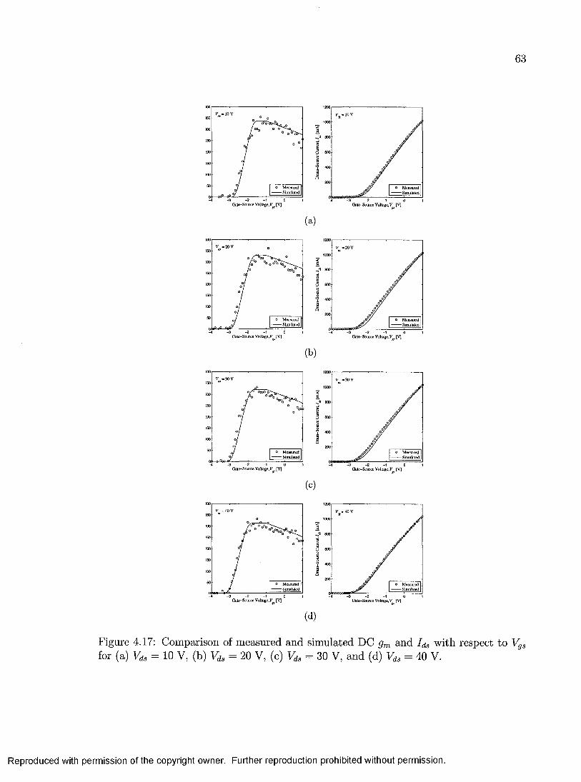
63
Gate-Source Vollage, V [V]
I
!ui3G
G ale-Source Voltage, V [V]
(a)
Gate-Source Voltage, V [V]
I•3U
1&
Gate-Source Voltage, V [V]
(b)
Gate-Source Voltage, V [V]
I
u8
Q
G ate-Source Voltage, V [V]
(c )
0*3
G ate-Source Voltage, V [V]
IIyI
G ate-Source Voltage, V [V]
(d)
Figure 4.17: Comparison of measured and simulated DC gm and I ds with respect to Vgs for (a) = 10 V, (b) Fds = 20 V, (c) = 30 V, and (d) = 40 V.
Reproduced with permission of the copyright owner. Further reproduction prohibited without permission.

64
120
150
180
o Measured — Simulated
210 330
240 300270
o Measured — Simulated
Figure 4.18: Comparison of measured vs. simulated s-parameters for Vds — 20 Y and Vga = - 1 V.
o Measured — Simulated
o Measured — Simulated
(a) (b)
Figure 4.19: Nonlinear model response deviates from measurements for (a) Vgs = 1 V and (b) Vgs = —3 V. The behaviour of the GaN Schottky diode and the transmission line nature of the gate, drain, and source fingers are not captured, causing deviations in predicted HEMT performance near Vp and the forward-biased gate voltage.
Reproduced with permission of the copyright owner. Further reproduction prohibited without permission.
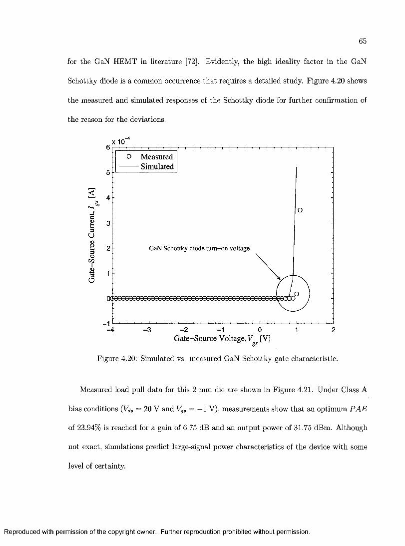
65
for the GaN HEMT in literature [72]. Evidently, the high ideality factor in the GaN
Schottky diode is a common occurrence th a t requires a detailed study. Figure 4.20 shows
the measured and simulated responses of the Schottky diode for further confirmation of
the reason for the deviations.
x 10'4
O Measured Simulated
3
83u4)a30oo1<D
GaN Schottky diode turn-on voltage
cdo
■4 ■2- 3 1 0 1 2Gate-Source Voltage, V [V]
gs
Figure 4.20: Simulated vs. measured GaN Schottky gate characteristic.
Measured load pull da ta for this 2 mm die are shown in Figure 4.21. Under Class A
bias conditions (Vas = 20 V and Vgs = — 1 V), measurements show th a t an optimum P A E
of 23.94% is reached for a gain of 6.75 dB and an output power of 31.75 dBm. Although
not exact, simulations predict large-signal power characteristics of the device with some
level of certainty.
Reproduced with permission of the copyright owner. Further reproduction prohibited without permission.
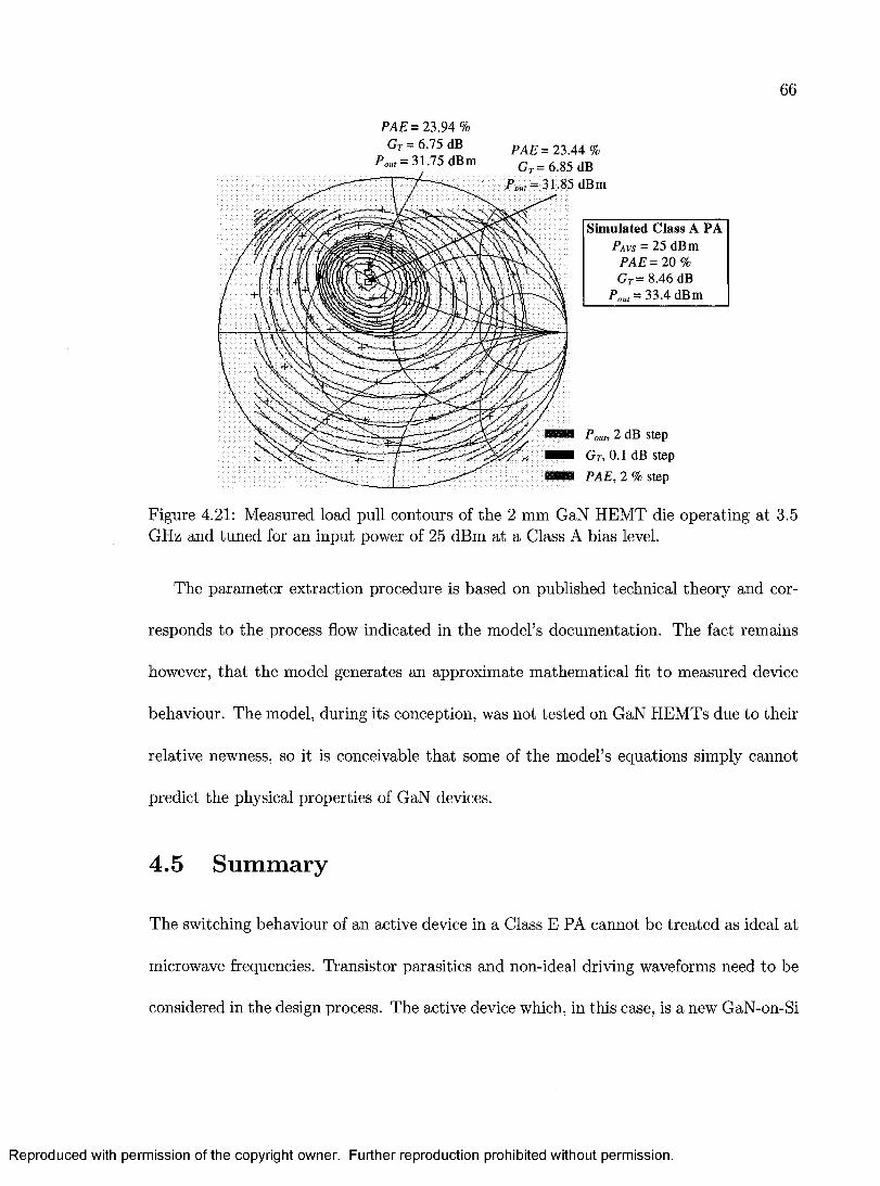
66
i4 %dBdBm
Simulated Class A PAP a v s = 25 dBm
PAE= 20%Gr = 8.46 dB
Pou = 33.4 dBm
Pottt, 2 dB step Gt, 0.1 dB step PAE, 2 % step
Figure 4.21: Measured load pull contours of the 2 mm GaN HEMT die operating at 3.5 GHz and tuned for an input power of 25 dBm at a Class A bias level.
The param eter extraction procedure is based on published technical theory and cor
responds to the process flow indicated in the model’s documentation. The fact remains
however, th a t the model generates an approximate mathematical fit to measured device
behaviour. The model, during its conception, was not tested on GaN HEMTs due to their
relative newness, so it is conceivable th a t some of the model’s equations simply cannot
predict the physical properties of GaN devices.
4.5 Sum m ary
The switching behaviour of an active device in a Class E PA cannot be treated as ideal at
microwave frequencies. Transistor parasitics and non-ideal driving waveforms need to be
considered in the design process. The active device which, in this case, is a new GaN-on-Si
PAE= 23.94 %Gt = 6.75 dB PAE = 23 1
Pout = 31.75 dBm Gr =6.85
Reproduced with permission of the copyright owner. Further reproduction prohibited without permission.

67
HEMT, is modeled in order to accurately capture the performance of a nonlinear PA in
simulation.
An existing ADS-based GaAs HEMT model is used to predict the performance of a
2 mm GaN-on-Si HEMT based on measured data supplied by the m anufacturer of the
device. The model predicts measured device behaviour for DC power up to 20 W and
Ids greater than 1 A. The model is accurate for frequencies up to 20 GHz. Correlation
between measured and simulated device behaviour is weaker near the gate pinch-off and
forward biased regions suggesting th a t some modifications to the model are needed for
this GaN process.
The empirical model does not allow modification of the m athem atical equations tha t
define the model. This, combined with the newness of the technology, limits the ability
of the model to provide an exact representation of the physical device. In spite of its de
ficiencies, the model predicts measured device behaviour reasonably well for the purposes
of this work.
Reproduced with permission of the copyright owner. Further reproduction prohibited without permission.

Chapter 5
Class E GaN-on-Si Microwave Power
Amplifier
Given the high breakdown voltage and high current density of GaN HEMTs, a Class E
power amplifier is a natural progression of the work presented so far. Using the nonlinear
model presented in the previous chapter, the first known 3.5 GHz GaN-on-Si Class E
power amplifier is dem onstrated in this chapter. The work presented here is an adaptation
of the Class E PA analysis and design done by Thomas Mader in his Ph.D. thesis [38,
73]. His work has been carried forward over the years [74-76], but to the best of the
author’s knowledge, has never been implemented in a GaN-on-Si PA. The GaN-based
Class E switched-mode concept is not novel. Others have published working Class E
power amplifiers, but most have based their GaN technology on expensive SiC substrates.
Perhaps the single most distinguishing feature of the PA in this work, is th a t the active
device has a silicon substrate; a technology tha t combines the superior performance of
GaN with a mass-producible inexpensive substrate.
Starting w ith the ideal Class E power amplifier circuit, this chapter evolves the basic
68
Reproduced with permission of the copyright owner. Further reproduction prohibited without permission.

69
lumped element design into a planar transmission line circuit. As the chapter progresses,
the degree of “idealness” is removed from the circuit simulations until a practical design
of each component in the PA is developed. The PA design specifications established in
Chapter 3 are repeated in Table 5.1, along with substrate properties.
Design frequency ( /i) 3.5 GHzO utput power (Pi) 1 W
Power-added efficiency (P A E ) ^ 40%Minimum input return loss (R L ) 15 dBDrain bias supply voltage (Vm ) 25 V
M aterial Rogers R T /duroid® 5880Substrate thickness 31 mil
Cladding 1 oz. rolled copper foilDielectric constant 2.20
Dissipation factor (10 GHz) 0.0009
Table 5.1: Class E PA specifications and high frequency laminate material properties.
Figure 5.1 shows a high-level diagram of the Class E PA, which consists of input
and output matching networks and additional biasing circuitry. The phasor impedance
50 nGaN
H EM T
Class E Load
Network
Input Bias Insertion
U nit
InputM atchingN etw ork
OutputBias
InsertionUnit
Figure 5.1: Block diagram of Class E power amplifier module
of the Class E load network is used to synthesize the appropriate output load network
th a t meets the criteria for Class E operation. The bias insertion circuit, which must be
included as part of the matching networks, is carefully designed to function only to bias
the active device without causing any unwanted effects. An entire section is duly devoted
Reproduced with permission of the copyright owner. Further reproduction prohibited without permission.
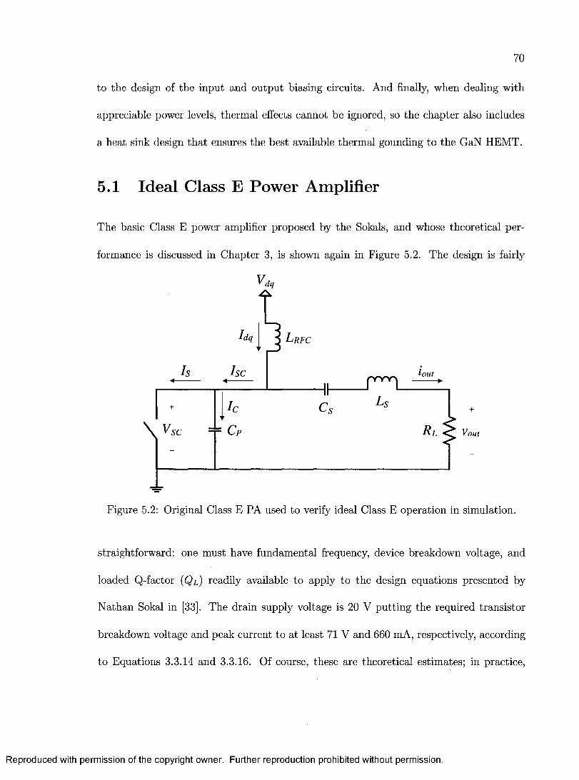
70
to the design of the input and output biasing circuits. And finally, when dealing with
appreciable power levels, therm al effects cannot be ignored, so the chapter also includes
a heat sink design th a t ensures the best available therm al gounding to the GaN HEMT.
5.1 Ideal Class E Power Am plifier
The basic Class E power amplifier proposed by the Sokals, and whose theoretical per
formance is discussed in Chapter 3, is shown again in Figure 5.2. The design is fairly
Vdq
sc
sc
Figure 5.2: Original Class E PA used to verify ideal Class E operation in simulation.
straightforward: one must have fundamental frequency, device breakdown voltage, and
loaded Q-factor (Ql ) readily available to apply to the design equations presented by
Nathan Sokal in [33]. The drain supply voltage is 20 V putting the required transistor
breakdown voltage and peak current to at least 71 V and 660 mA, respectively, according
to Equations 3.3.14 and 3.3.16. Of course, these are theoretical estimates; in practice,
Reproduced with permission of the copyright owner. Further reproduction prohibited without permission.
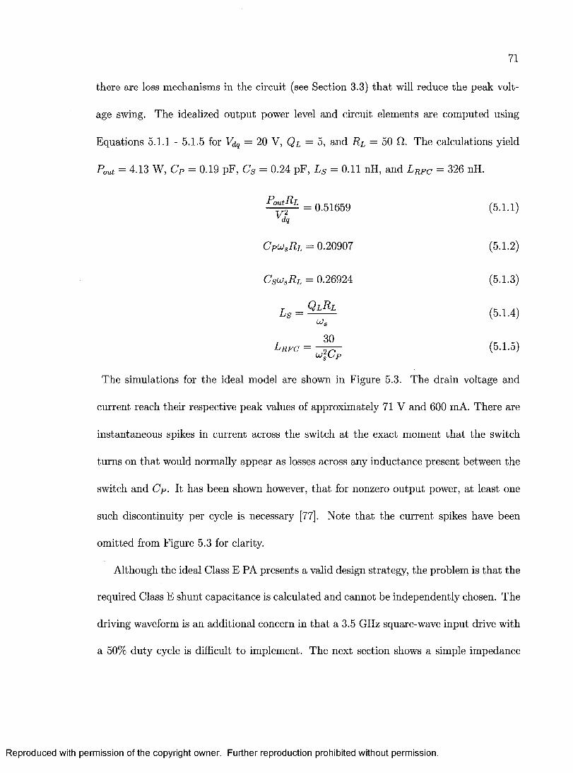
71
there are loss mechanisms in the circuit (see Section 3.3) tha t will reduce the peak volt
age swing. The idealized output power level and circuit elements are computed using
Equations 5.1.1 - 5.1.5 for Vdq — 20 V, Q l = 5, and Rp — 50 0 . The calculations yield
Pout — 4-13 W, Cp = 0.19 pF, Cs = 0.24 pF, Lg = 0.11 nH, and L rfc = 326 nH.
PyutPLVd2q
0.51659 (5.1.1)
Cp u sR l = 0.20907 (5.1.2)
Cs ujsR l = 0.26924 (5.1.3)
L s = (5.1.4)UJS
30L r f c = (5.1.5)
LOsCp
The simulations for the ideal model are shown in Figure 5.3. The drain voltage and
current reach their respective peak values of approximately 71 V and 600 mA. There are
instantaneous spikes in current across the switch at the exact moment tha t the switch
turns on th a t would normally appear as losses across any inductance present between the
switch and Cp. It has been shown however, th a t for nonzero output power, at least one
such discontinuity per cycle is necessary [77]. Note th a t the current spikes have been
om itted from Figure 5.3 for clarity.
Although the ideal Class E PA presents a valid design strategy, the problem is th a t the
required Class E shunt capacitance is calculated and cannot be independently chosen. The
driving waveform is an additional concern in th a t a 3.5 GHz square-wave input drive with
a 50% duty cycle is difficult to implement. The next section shows a simple impedance
Reproduced with permission of the copyright owner. Further reproduction prohibited without permission.
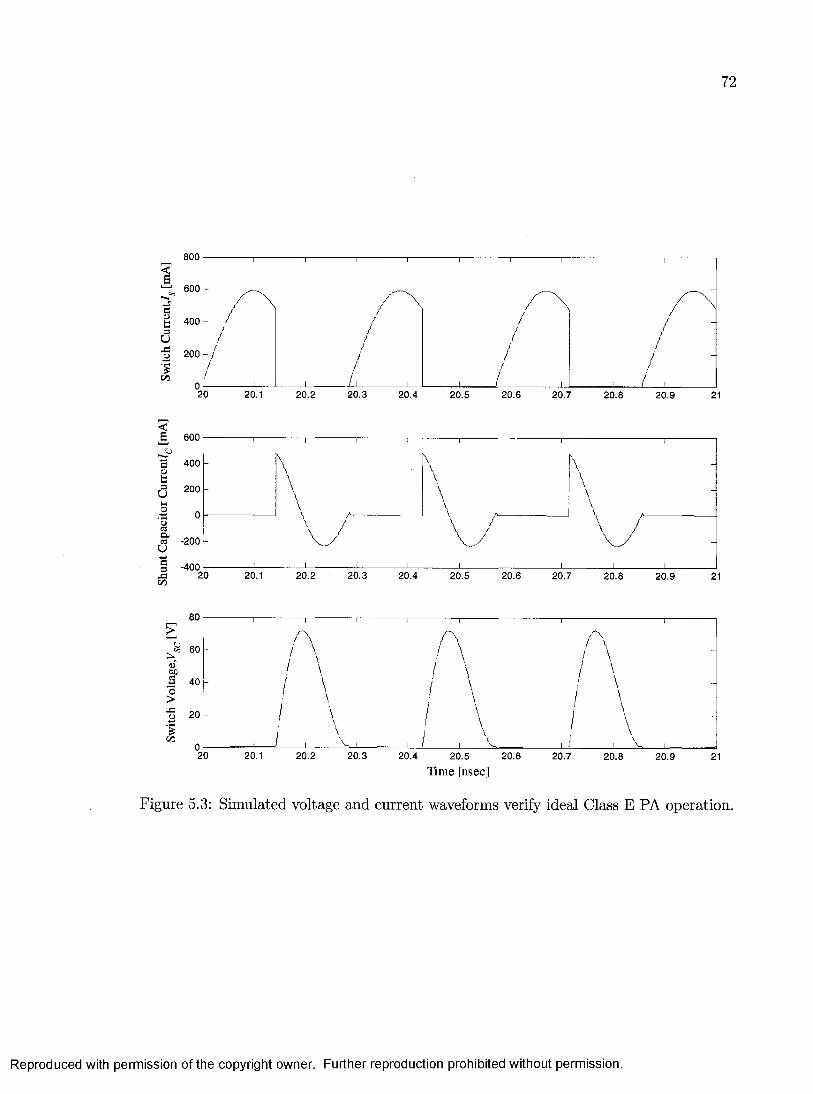
Shun
t C
apac
itor
Cur
rent
/c [m
A]
Switc
h C
urre
nt,/.
[m
A]
72
800
600
400
200
20.1 20.2 20.3 20.4 20.5 20.6 20.7 20.8 20.9
600
400
200
-200
-40020.1 20.2 20.3 20.4 20.5 20.6 20.7 20.8 20 .
80
60
40
20
020.1 20.2 20.3 20.4 20.5 20.6 20.7 20.8 20.9
Time [nsec]
Figure 5.3: Simulated voltage and current waveforms verify ideal Class E PA operation.
Reproduced with permission of the copyright owner. Further reproduction prohibited without permission.

73
analysis th a t solves the la tter problem and allows the load network to be realized with
microstrip transmission lines.
5.2 T he Class E Load N etw ork
The purpose of the Class E load network is to
1. provide the correct impedance magnitude and load angle to the output of the HEMT
at the fundamental frequency such th a t all Class E criteria, as per the discussion in
Section 3.3, are satisfied; and
2. ensure high impedance term inations for all higher-order harmonics (this is implicit
in the discussion in Section 3.3)
Although the first purpose is realizable, the second is not due to the narrowband nature of
transmission line circuits. For the moment, the discussion continues with the assumption
th a t higher-order harmonics are properly term inated.
The lumped element load network analysis proceeds with ideal RF chokes and coupling
capacitors in place of the true input and output bias insertion circuits. The input and
output biasing circuits are designed to not affect circuit performance, appearing invisible
to the drain of the HEMT. This level of exclusivity can be maintained by the biasing
circuits provided th a t the bias supply is properly decoupled and the bias circuit does not
load the PA over the RF band of interest. The bias circuit is assumed to consist only
of ideal elements throughout this Chapter until Section 5.4, where the complete design,
including measurements, is demonstrated.
Reproduced with permission of the copyright owner. Further reproduction prohibited without permission.
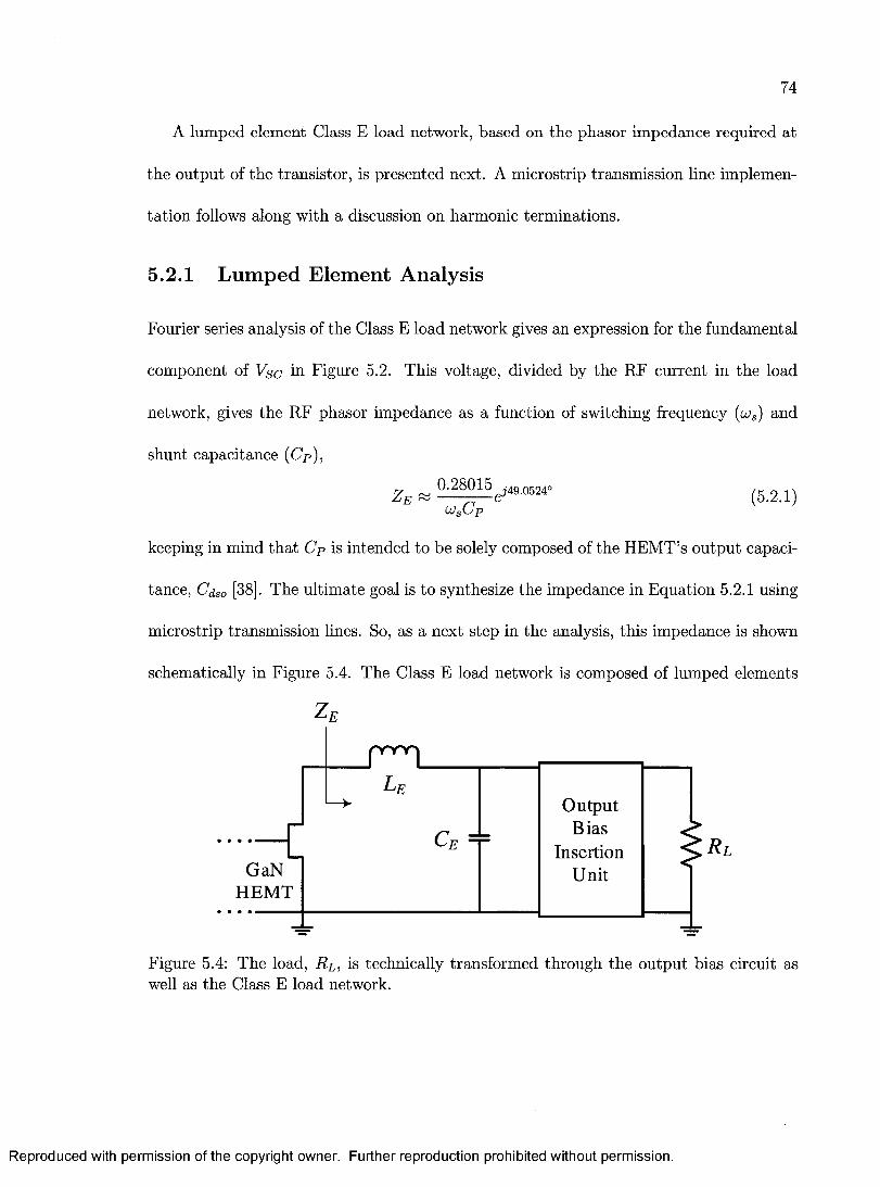
74
A lumped element Class E load network, based on the phasor impedance required at
the output of the transistor, is presented next. A microstrip transmission line implemen
tation follows along with a discussion on harmonic terminations.
5.2.1 Lumped Element Analysis
Fourier series analysis of the Class E load network gives an expression for the fundamental
component of Vsc in Figure 5.2. This voltage, divided by the RF current in the load
network, gives the RF phasor impedance as a function of switching frequency (uis) and
shunt capacitance (Cp),
Z E » 2 ^ 1 5 ^ 4 9 .0 5 2 4 - {5 2 x)UsCp
keeping in mind th a t Cp is intended to be solely composed of the HEM T’s output capaci
tance, Cdso [38]. The ultim ate goal is to synthesize the impedance in Equation 5.2.1 using
microstrip transmission lines. So, as a next step in the analysis, this impedance is shown
schematically in Figure 5.4. The Class E load network is composed of lumped elements
Z e
OutputBias
InsertionUnit
• •
GaNHEMT
• •
Figure 5.4: The load, Rp, is technically transformed through the output bias circuit as well as the Class E load network.
Reproduced with permission of the copyright owner. Further reproduction prohibited without permission.
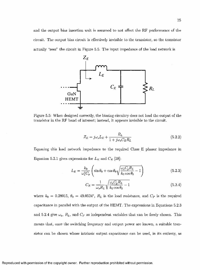
75
and the output bias insertion unit is assumed to not affect the RP performance of the
circuit. The output bias circuit is effectively invisible to the transistor, so the transistor
actually “sees” the circuit in Figure 5.5. The input impedance of the load network is
Figure 5.5: When designed correctly, the biasing circuitry does not load the output of the transistor in the RF band of interest; instead, it appears invisible to the circuit.
where ko = 0.28015, 0q = 49.0524°, R L is the load resistance, and Cp is the required
capacitance in parallel with the output of the HEMT. The expressions in Equations 5.2.3
and 5.2.4 give cos, Rp, and Cp as independent variables th a t can be freely chosen. This
means tha t, once the switching frequency and output power are known, a suitable tran
sistor can be chosen whose intrinsic output capacitance can be used, in its entirety, as
L e*-
GaNHEMT
- r CE R l
Z e — J ^ L e +R l (5.2.2)1 + M C e R l
Equating this load network impedance to the required Class E phasor impedance in
Equation 5.2.1 gives expressions for L p and Cp [38]:
(5.2.3)
(5.2.4)
Reproduced with permission of the copyright owner. Further reproduction prohibited without permission.
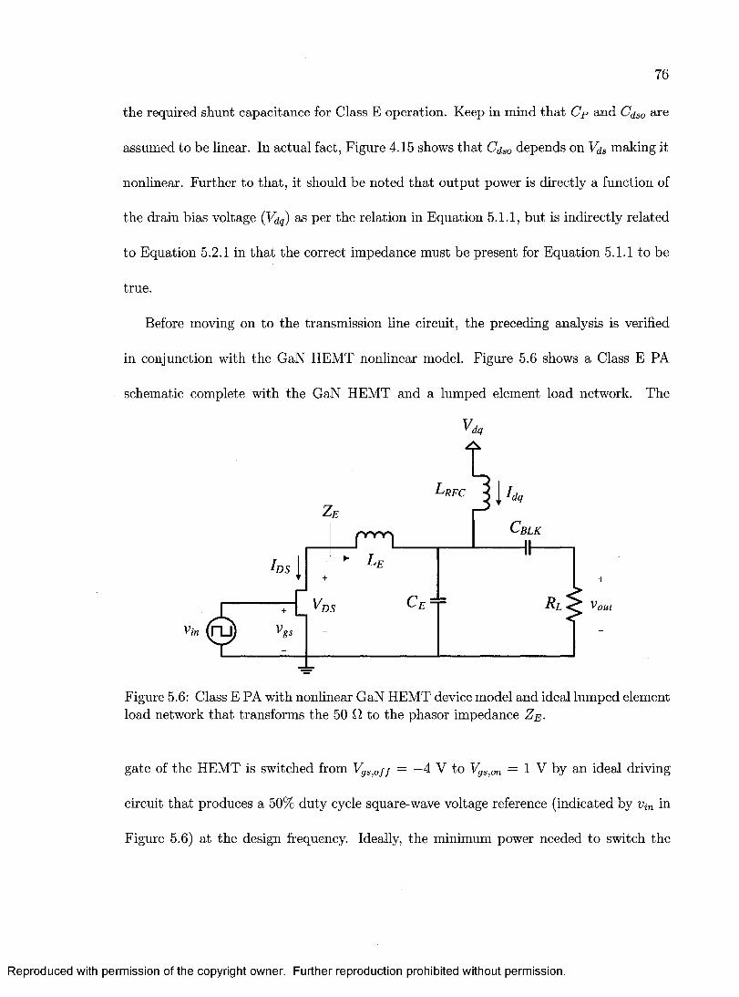
76
the required shunt capacitance for Class E operation. Keep in mind th a t Cp and Cdso are
assumed to be linear. In actual fact, Figure 4.15 shows th a t Cdso depends on Vds making it
nonlinear. Further to tha t, it should be noted th a t output power is directly a function of
the drain bias voltage (Vdq) as per the relation in Equation 5.1.1, but is indirectly related
to Equation 5.2.1 in th a t the correct impedance must be present for Equation 5.1.1 to be
true.
Before moving on to the transmission line circuit, the preceding analysis is verified
in conjunction with the GaN HEMT nonlinear model. Figure 5.6 shows a Class E PA
schematic complete with the GaN HEMT and a lumped element load network. The
Vdq
'RFC
C blk
DS
e ~ rDS
Figure 5.6: Class E PA with nonlinear GaN HEMT device model and ideal lumped element load network th a t transforms the 50 fI to the phasor impedance Zp-
gate of the HEMT is switched from VgSt0f f = —4 V to Vg,%on = 1 V by an ideal driving
circuit th a t produces a 50% duty cycle square-wave voltage reference (indicated by vin in
Figure 5.6) at the design frequency. Ideally, the minimum power needed to switch the
Reproduced with permission of the copyright owner. Further reproduction prohibited without permission.
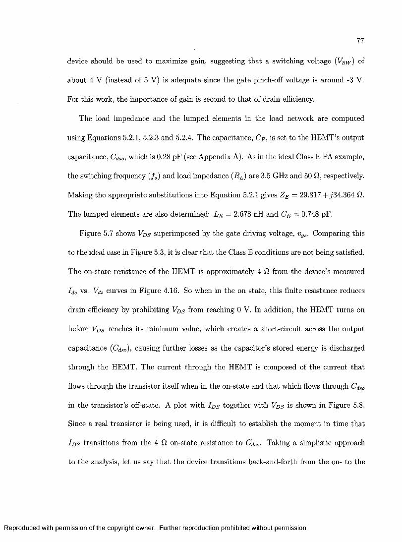
77
device should be used to maximize gain, suggesting th a t a switching voltage (Vsw) of
about 4 V (instead of 5 V) is adequate since the gate pinch-off voltage is around -3 V.
For this work, the importance of gain is second to tha t of drain efficiency.
The load impedance and the lumped elements in the load network are computed
using Equations 5.2.1, 5.2.3 and 5.2.4. The capacitance, Cp, is set to the HEM T’s output
capacitance, Cdso, which is 0.28 pF (see Appendix A). As in the ideal Class E PA example,
the switching frequency ( f s) and load impedance (R l ) are 3.5 GHz and 50 Cl, respectively.
Making the appropriate substitutions into Equation 5.2.1 gives Zp = 29.817 + j34.364 Cl.
The lumped elements are also determined: L E = 2.678 nH and Cp = 0.748 pF.
Figure 5.7 shows V d s superimposed by the gate driving voltage, vgs. Comparing this
to the ideal case in Figure 5.3, it is clear th a t the Class E conditions are not being satisfied.
The on-state resistance of the HEMT is approximately 4 Cl from the device’s measured
Ids vs. Vds curves in Figure 4.16. So when in the on state, this finite resistance reduces
drain efficiency by prohibiting Vds from reaching 0 V. In addition, the HEMT turns on
before VDs reaches its minimum value, which creates a short-circuit across the output
capacitance (Cdso)i causing further losses as the capacitor’s stored energy is discharged
through the HEMT. The current through the HEMT is composed of the current th a t
flows through the transistor itself when in the on-state and th a t which flows through Cdso
in the transistor’s off-state. A plot with I d s together with V d s is shown in Figure 5.8.
Since a real transistor is being used, it is difficult to establish the moment in time th a t
I d s transitions from the 4 Cl on-state resistance to C(iso. Taking a simplistic approach
to the analysis, let us say th a t the device transitions back-and-forth from the on- to the
Reproduced with permission of the copyright owner. Further reproduction prohibited without permission.
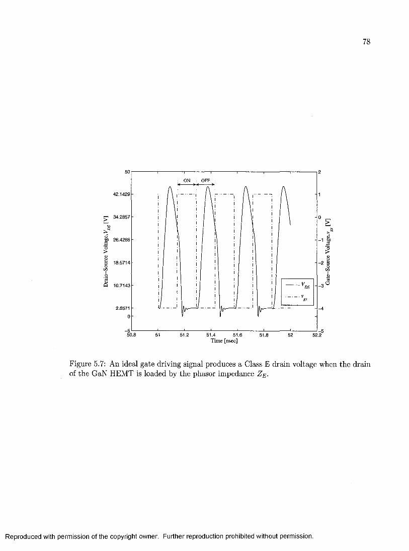
78
ON OFF
42.1429
CT 34.2857
«> 26.4286
3 18.5714o C/5
10.7143 -3DS
2.8571 -4
— -5 52.251.4
Time [nsec]51.2 51.6 51.8
Figure 5.7: An ideal gate driving signal produces a Class E drain voltage when the drain of the GaN HEMT is loaded by the phasor impedance Z e ■
Reproduced with permission of the copyright owner. Further reproduction prohibited without permission.
79
off-states instantaneously. The shaded region of the plot shows the power th a t is lost
every period due to the short-circuit across Cdso■ Since, in the off-state, the plot indicates
th a t IDS flows entirely through Cdso, there is no power loss, which is likely not the case
in practice.
DSON OFF0.7
DS
0.6
0.5
> 0.4
0.3
O£ 0.2 oGQ. 3
-20 e
CC
-0.1
-0.2
50.8 51.2 51.4 51.6 51.8 52.2Time [nsec]
Figure 5.8: An ideal gate driving signal produces these Id s and VDs waveforms when the drain of the GaN HEMT is loaded by the phasor impedance Z e -
There is room for improvement in terms of the circuit’s response to an ideal square-
wave input. The Class E impedance given by Equation 5.2.1 needs adjustment to account
for bondwire inductance and device parasitics. As a logical next step, the load network
impedance is adjusted to maximize drain efficiency and the ideal 3.5 GHz square-wave
driver is replaced with a large-amplitude voltage source conjugately matched to the gate
of the 2 mm HEMT. Relative to the output, the input of a transistor is less sensitive to
Reproduced with permission of the copyright owner. Further reproduction prohibited without permission.
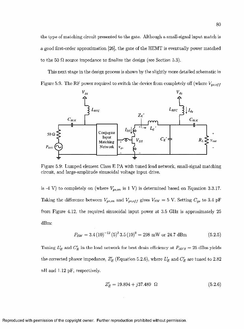
80
the type of matching circuit presented to the gate. Although a small-signal input match is
a good first-order approximation [26], the gate of the HEMT is eventually power matched
to the 50 0, source impedance to finalize the design (see Section 5.3).
This next stage in the design process is shown by the slightly more detailed schematic in
Figure 5.9. The RF power required to switch the device from completely off (where VgSj0f f
Vgq Vdq
'R F C'R F C
C blk■BLK
ConjugateInput
MatchingNetwork
50 Q
D S
\v s v'G
Figure 5.9: Lumped element Class E PA with tuned load network, small-signal matching circuit, and large-amplitude sinusoidal voltage input drive.
is -4 V) to completely on (where Vgs;0n is 1 V) is determined based on Equation 3.3.17.
Taking the difference between Vgs,0n and Vgs/Jf f gives Vsw = 5 V. Setting Cgs to 3.4 pF
from Figure 4.12, the required sinusoidal input power at 3.5 GHz is approximately 25
dBm:
P s w = 3.4 (10)~12 (5)2 3.5 (10)9 = 298 mW or 24.7 dBm (5.2.5)
Tuning L'E and C'E in the load network for best drain efficiency at P a v s = 25 dBm yields
the corrected phasor impedance, Z'E (Equation 5.2.6), where L'E and C'E are tuned to 2.82
nH and 1.12 pF, respectively.
Z'E = 19.894 + i37.489 Q (5.2.6)
Reproduced with permission of the copyright owner. Further reproduction prohibited without permission.
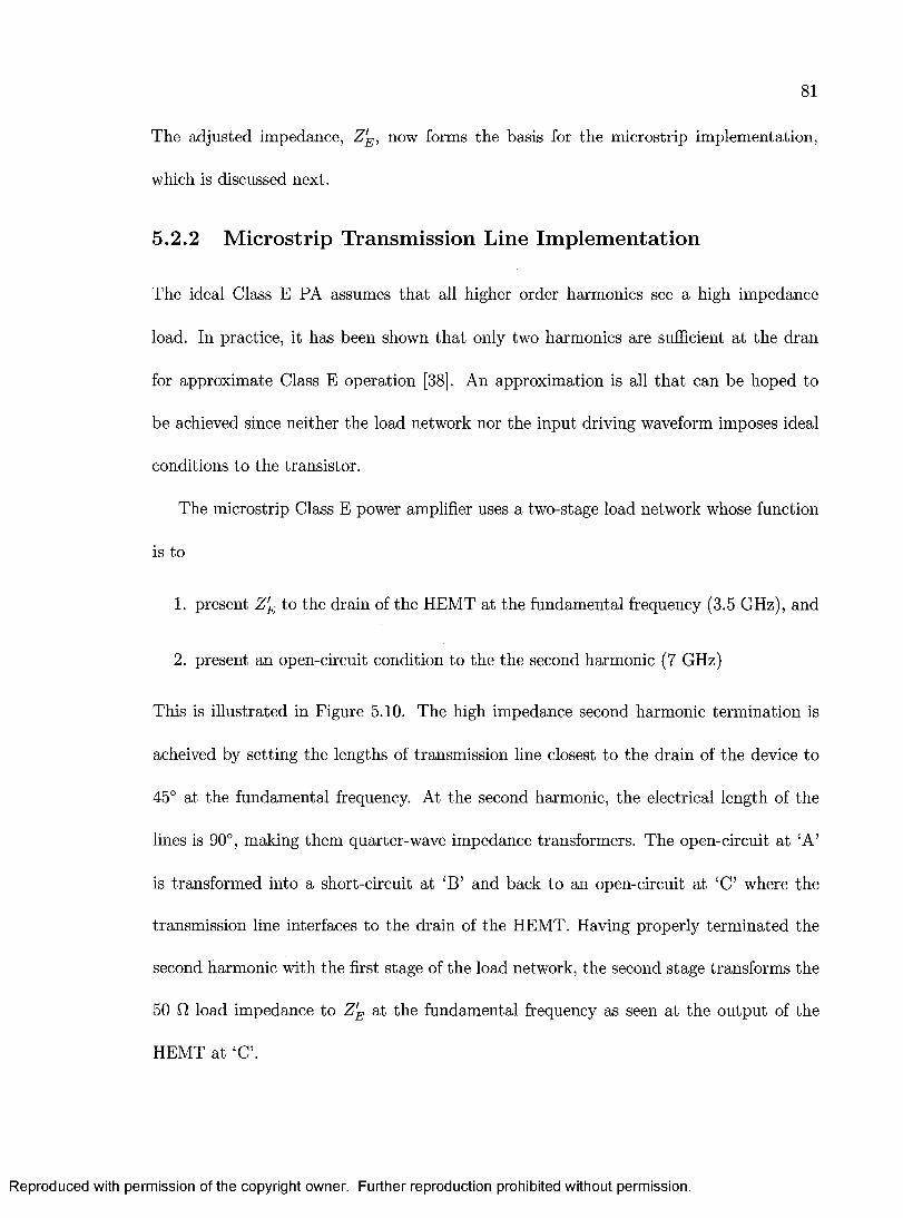
81
The adjusted impedance, Z'E, now forms the basis for the microstrip implementation,
which is discussed next.
5.2.2 M icrostrip Transmission Line Implementation
The ideal Class E PA assumes th a t all higher order harmonics see a high impedance
load. In practice, it has been shown th a t only two harmonics are sufficient at the dran
for approximate Class E operation [38]. An approximation is all th a t can be hoped to
be achieved since neither the load network nor the input driving waveform imposes ideal
conditions to the transistor.
The microstrip Class E power amplifier uses a two-stage load network whose function
is to
1. present Z'E to the drain of the HEMT at the fundamental frequency (3.5 GHz), and
2. present an open-circuit condition to the the second harmonic (7 GHz)
This is illustrated in Figure 5.10. The high impedance second harmonic term ination is
acheived by setting the lengths of transmission line closest to the drain of the device to
45° at the fundamental frequency. At the second harmonic, the electrical length of the
lines is 90°, making them quarter-wave impedance transformers. The open-circuit at ‘A ’
is transformed into a short-circuit at ‘B’ and back to an open-circuit at ‘C ’ where the
transmission line interfaces to the drain of the HEMT. Having properly term inated the
second harmonic with the first stage of the load network, the second stage transforms the
50 Q load impedance to Z'e at the fundamental frequency as seen at the output of the
HEMT at ‘C \
Reproduced with permission of the copyright owner. Further reproduction prohibited without permission.
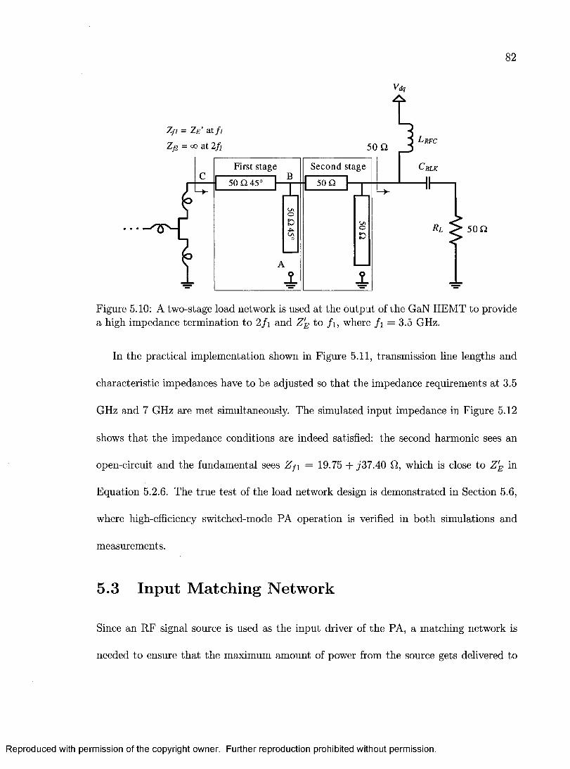
82
Vdq
50 £2
First stage S eco n d stage
50 Q50 £2 45
LAOLA© 50 Q• • •
Figure 5.10: A two-stage load network is used at the output of the GaN HEMT to provide a high impedance term ination to 2 /i and Z'E to f i , where f \ = 3.5 GHz.
In the practical implementation shown in Figure 5.11, transmission line lengths and
characteristic impedances have to be adjusted so th a t the impedance requirements at 3.5
GHz and 7 GHz are met simultaneously. The simulated input impedance in Figure 5.12
shows th a t the impedance conditions are indeed satisfied: the second harmonic sees an
open-circuit and the fundamental sees Z fi = 19.75 + j37.40 G, which is close to in
Equation 5.2.6. The true test of the load network design is dem onstrated in Section 5.6,
where high-efficiency switched-mode PA operation is verified in both simulations and
measurements.
5.3 Input M atching N etw ork
Since an RF signal source is used as the input driver of the PA, a matching network is
needed to ensure th a t the maximum amount of power from the source gets delivered to
Reproduced with permission of the copyright owner. Further reproduction prohibited without permission.
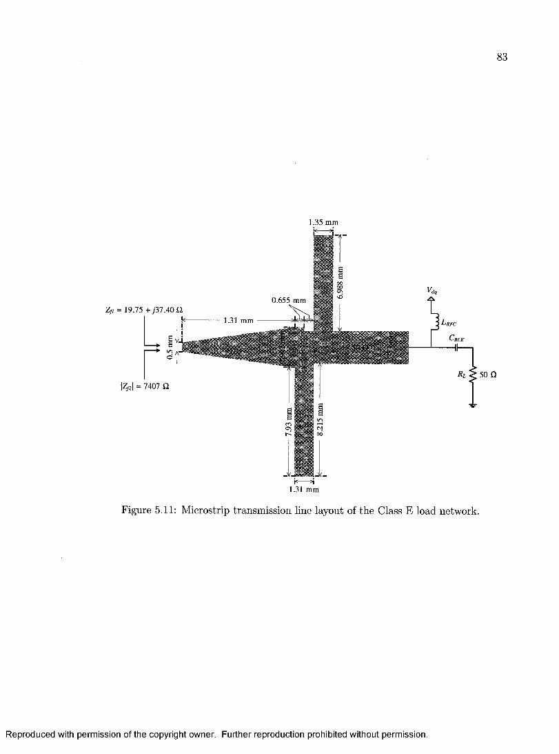
83
1.35 mm
h— H 1.31 mm
Figure 5.11: Microstrip transmission line layout of the Class E load network.
Reproduced with permission of the copyright owner. Further reproduction prohibited without permission.
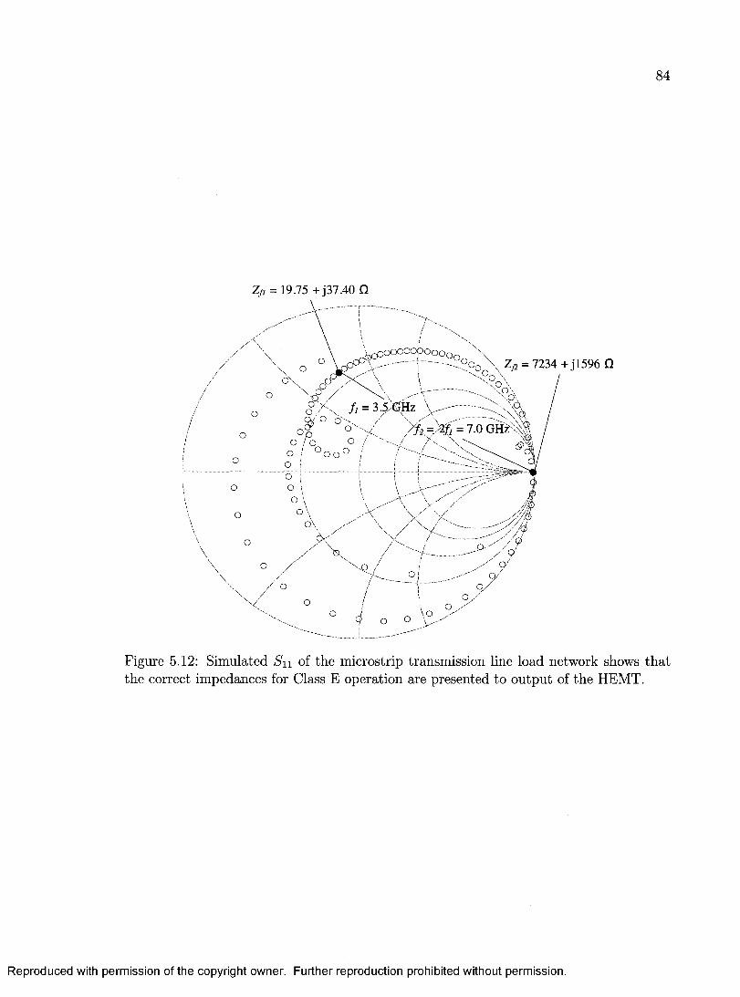
84
Zf l = 19.75 + j37.40 Q
/ / = 3.5 GHz \ -
o \ / /% = % = 7.0 GHz •O/O O / -.. . \
O / ° 0 0 ° 1O
Zp = 7234 + jl5 9 6 Q
Figure 5.12: Simulated S n of the microstrip transmission line load network shows th a t the correct impedances for Class E operation are presented to output of the HEMT.
Reproduced with permission of the copyright owner. Further reproduction prohibited without permission.
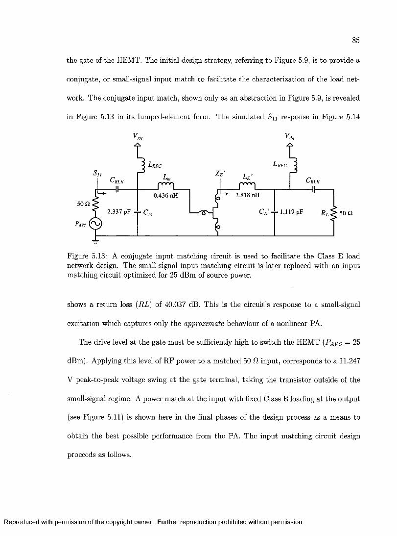
85
the gate of the HEMT. The initial design strategy, referring to Figure 5.9, is to provide a
conjugate, or small-signal input match to facilitate the characterization of the load net
work. The conjugate input match, shown only as an abstraction in Figure 5.9, is revealed
in Figure 5.13 in its lumped-element form. The simulated S n response in Figure 5.14
y dq
R F C'RF C
Le ’
2.818 nH
C blkB L K JVW ^L
0.436 nH50 Q
2.337 pF =±= C,
'a vs r o ,
Figure 5.13: A conjugate input matching circuit is used to facilitate the Class E load network design. The small-signal input matching circuit is later replaced with an input matching circuit optimized for 25 dBm of source power.
shows a return loss (RL) of 40.037 dB. This is the circuit’s response to a small-signal
excitation which captures only the approximate behaviour of a nonlinear PA.
The drive level at the gate must be sufficiently high to switch the HEMT (P a v s = 25
dBm). Applying this level of RF power to a matched 50 0, input, corresponds to a 11.247
V peak-to-peak voltage swing at the gate terminal, taking the transistor outside of the
small-signal regime. A power match at the input with fixed Class E loading at the output
(see Figure 5.11) is shown here in the final phases of the design process as a means to
obtain the best possible performance from the PA. The input matching circuit design
proceeds as follows.
Reproduced with permission of the copyright owner. Further reproduction prohibited without permission.
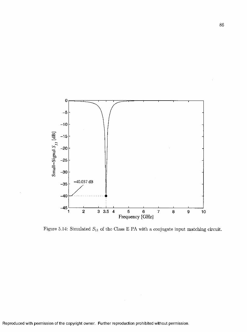
Smal
l-Si
gnal
S
[dB
]
86
- 5
-10
-20
- 2 5
- 3 0
-40.037 dB- 3 5
- 4 0
- 4 51 2 3 3 .5 4 5 6 7 8 9 10
Frequency [GHz]
Figure 5.14: Simulated S u of the Class E PA with a conjugate input matching circuit.
Reproduced with permission of the copyright owner. Further reproduction prohibited without permission.
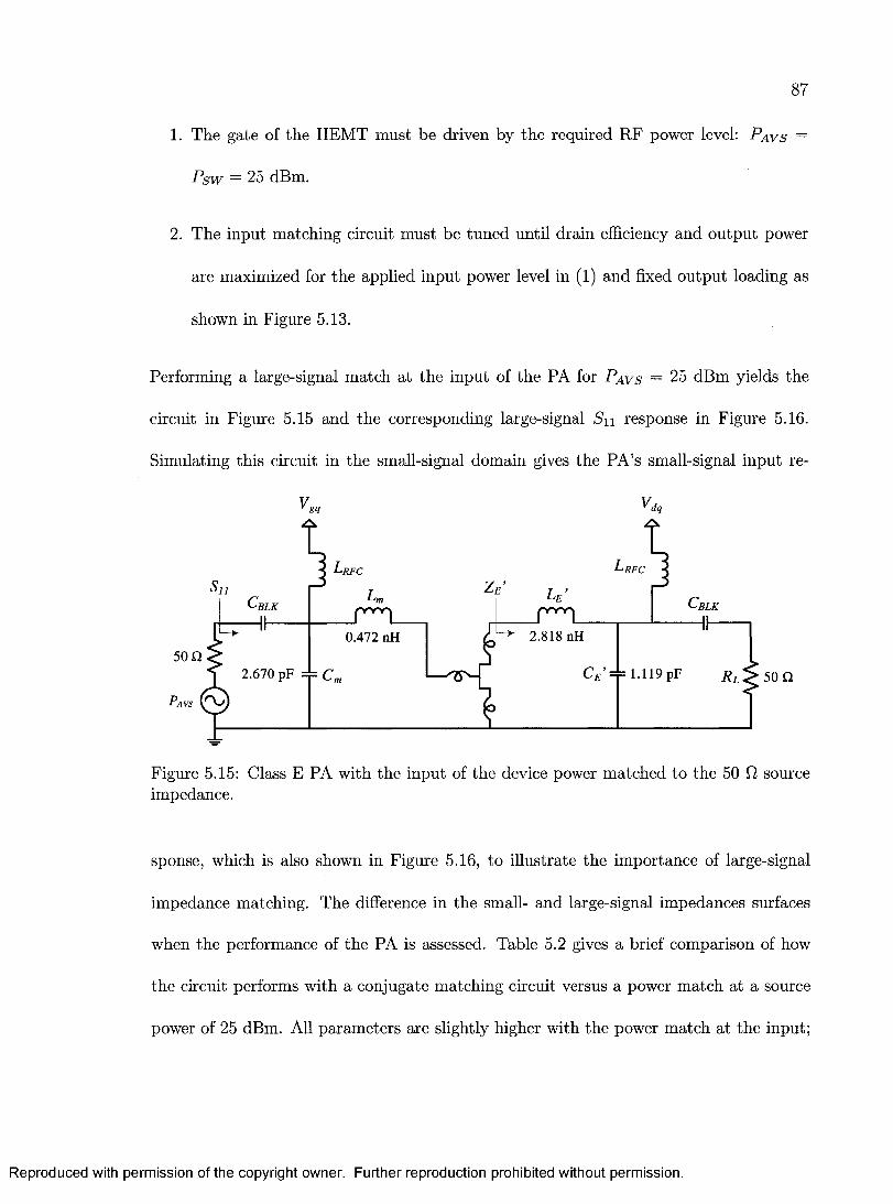
87
1. The gate of the HEMT must be driven by the required RF power level: P a v s =
Psw = 25 dBm.
2. The input matching circuit must be tuned until drain efficiency and output power
are maximized for the applied input power level in (1) and fixed output loading as
shown in Figure 5.13.
Performing a large-signal match at the input of the PA for P a v s — 25 dBm yields the
circuit in Figure 5.15 and the corresponding large-signal S n response in Figure 5.16.
Simulating this circuit in the small-signal domain gives the PA’s small-signal input re-
V Var gq y dq
R F C'RF C
Le ’_PnnrL2.818 nH
B L K j w v -l
0.472 nH
CE’ =F 1-119 pF2.670 pF 4= C,
\vs F V
Figure 5.15: Class E PA with the input of the device power matched to the 50 Q source impedance.
sponse, which is also shown in Figure 5.16, to illustrate the importance of large-signal
impedance matching. The difference in the small- and large-signal impedances surfaces
when the performance of the PA is assessed. Table 5.2 gives a brief comparison of how
the circuit performs with a conjugate matching circuit versus a power match at a source
power of 25 dBm. All parameters are slightly higher with the power match at the input;
Reproduced with permission of the copyright owner. Further reproduction prohibited without permission.
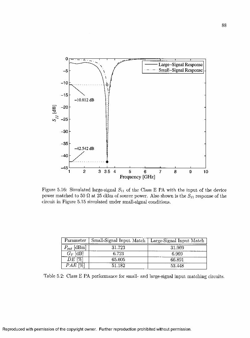
88
Large-Signal Response Small-Signal Response- 5
-10
- 1 5-10.812 dB
- 3 0
- 3 5-42 .542 dB
- 4 0
- 4 51 2 3 3 .5 4 5 6 7 8 9 10
Frequency [GHz]
Figure 5.16: Simulated large-signal S n of the Class E PA with the input of the device power matched to 50 0, at 25 dBm of source power. Also shown is the S n response of the circuit in Figure 5.15 simulated under small-signal conditions.
Param eter Small-Signal Input Match Large-Signal Input MatchPout [dBm] 31.723 31.969
G t [dB] 6.723 6.969D E [%] 65.005 66.891
P A E [%] 51.182 53.448
Table 5.2: Class E PA performance for small- and large-signal input matching circuits.
Reproduced with permission of the copyright owner. Further reproduction prohibited without permission.

89
two conclusions can therefore be made:
1. The Class E PA operates more efficiently and with higher output power when the
gate of the HEMT is loaded with a large-signal matching circuit than when loaded
with a conjugate matching circuit
2. The improvement with a power input match is significant, but not drastic. The
design strategy of using a conjugate input match to evaluate the performance of the
load network and to estimate the overall performance of the PA is therefore valid.
The lumped-element input matching circuit gives a high large-signal return loss of
42.542 dB, making it suitable for synthesis into a microstrip equivalent circuit as shown
in Figure 5.17.
5.4 B ias Insertion N etw ork and Stability
Considerable effort is always bestowed upon power amplifier matching circuitry so tha t
typical power amplifier specifications, such as gain, output power, and efficiency are met.
Comparatively speaking, the manner in which bias is inserted into the PA and the effects
of the bias insertion circuit on the power amplifier is usually the least considered facet of
the overall design [78].
The input and output bias circuits in this work are considered integral parts of the
Class E microwave power amplifier and so are included in every part of the design process.
They are designed to interface with a 50 Q system and to not interfere with the PA’s input
and output matching circuitry. The impedances are set up as shown in Figure 5.18. The
Reproduced with permission of the copyright owner. Further reproduction prohibited without permission.
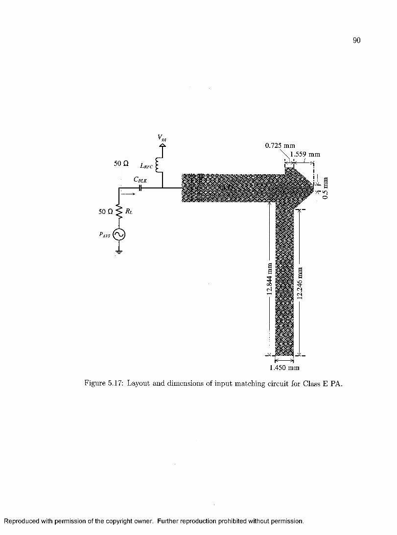
90
Sa
<N
IJ/—N N
1.450 mm
Figure 5.17: Layout and dimensions of input matching circuit for Class E PA.
Reproduced with permission of the copyright owner. Further reproduction prohibited without permission.
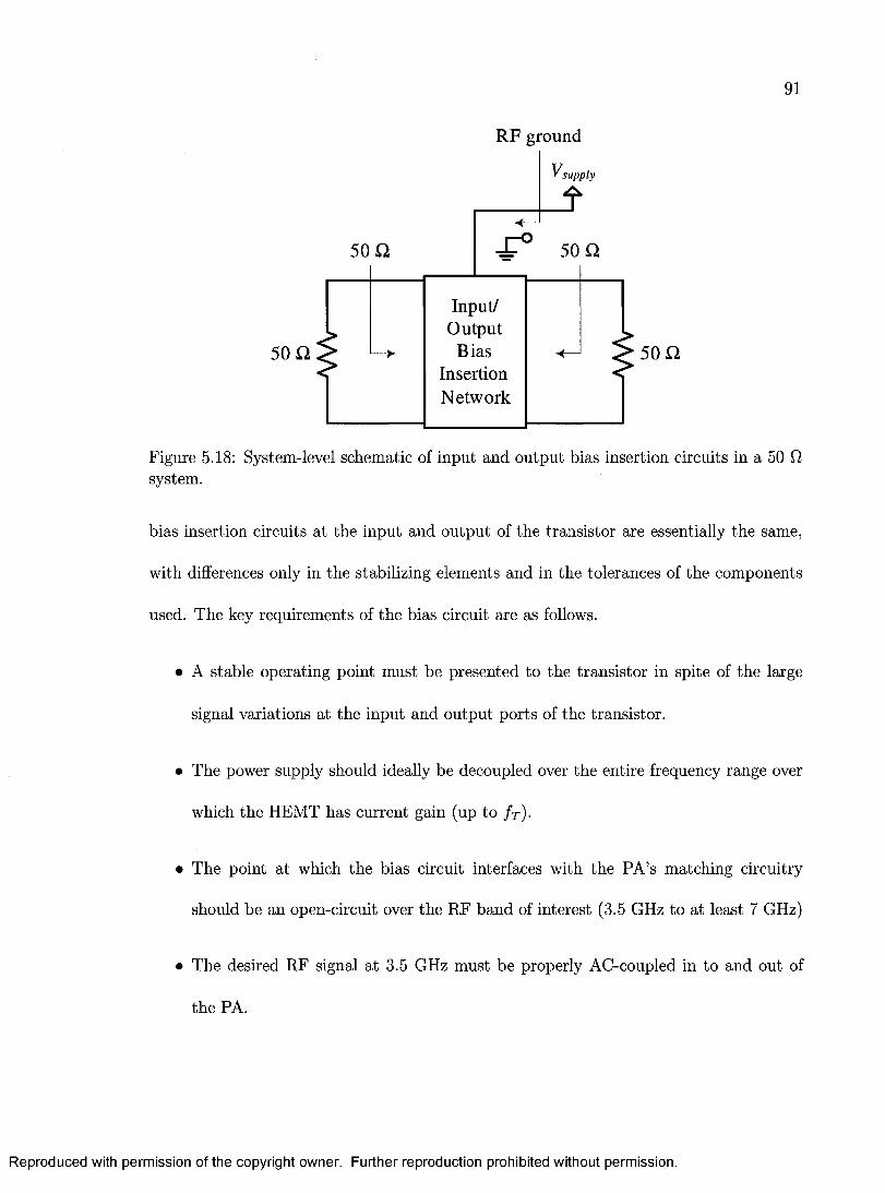
91
RF ground
50 0 X ° 50 0
50 0
Input/Output
BiasInsertionNetwork
50 0
Figure 5.18: System-level schematic of input and output bias insertion circuits in a 50 system.
bias insertion circuits at the input and output of the transistor are essentially the same,
with differences only in the stabilizing elements and in the tolerances of the components
used. The key requirements of the bias circuit are as follows.
• A stable operating point must be presented to the transistor in spite of the large
signal variations at the input and output ports of the transistor.
• The power supply should ideally be decoupled over the entire frequency range over
which the HEMT has current gain (up to fr ) .
• The point at which the bias circuit interfaces with the PA’s matching circuitry
should be an open-circuit over the RF band of interest (3.5 GHz to at least 7 GHz)
• The desired RF signal at 3.5 GHz must be properly AC-coupled in to and out of
the PA.
Reproduced with permission of the copyright owner. Further reproduction prohibited without permission.

92
• Out-of-band oscillation suppression should be included.
• Protection circuitry is required to prevent transistor from catastrophic burn-out
during the power-up sequence.
A system-level schematic for the design th a t follows is shown in Figure 5.19; the
blocks in the schematic are dissected in a four-part series. The first part deals w ith power
Vdd or Vgg
P ow er S upply D ecou p lin g
50 Q
—w vProtection or
Stabilizing R esistor
<
<
R F C oup lin g Capacitor
||
A\ Ferrite B ead s
for N o ise ^ Suppression
RF _ 3 C h ok e
j <
IIH igh RF
Im pedance
50 Q
Figure 5.19: Input and output bias insertion circuits (in a 50 system), consisting of power supply decoupling, protection, and noise suppression circuitry, provide a stable operating point to the Class E PA.
supply decoupling. This is followed by a discussion on in-band RF loading and out-of-
band oscillation suppression. Stability is a common theme throughout the design and
is touched upon in all sections. In the final PA design however, small-signal stability is
explicitly enforced w ith a series resistance in the input bias feed. Incidently, the same
Reproduced with permission of the copyright owner. Further reproduction prohibited without permission.
93
technique is used to prevent transistor burn-out. It is only appropriate then, to discuss
protection and stability here.
5.4.1 Power Supply Decoupling
The power supply decoupling circuit plays a m ajor role in eliminating power supply rip
ple th a t could otherwise couple into the gate of the HEMT via the intrinsic feedback
capacitance between the drain and the gate. Ideally, one designs the decoupling network
to present an RF short-circuit to the power-supply leads from the MHz range up to the
HEM T’s fr - Such a broadband low-impedance path to ground is acheived with a bank of
parallel capacitors connected as close as possible to the power supply connection of the
PA.
The power supply lead itself presents a significant source of inductance. Any sudden
change in current, for example when the power supply is turned on, causes the lead in
ductance to respond with a corresponding voltage spike, which could cause low-frequency
instability in the PA circuit. A large electrolytic capacitor is placed closest to the power
supply lead in order to shunt low-frequency noise. Higher capacitance values are placed in
parallel for any high-frequency ripple th a t may be present in the supply path. Large sep
aration between capacitance values is chosen to prevent unwanted resonances; a de-Q’ing
resistor is used where large capacitance separation is not possible. Figures 5.20 and 5.21
show the decoupling circuit and the corresponding simulation. A reasonable short circuit
is maintained up to at least the second harmonic at 7 GHz. Unfortunately, component
data does not allow simulation up to the HEM T’s f c of 13 GHz.
Reproduced with permission of the copyright owner. Further reproduction prohibited without permission.

94
Z„ = 0.1 + ;0.15 at 3.5 GHz Z u = 0.25 + j l . S at 7.0 GHz
Power Supply Decoupling Circuit
^ 8 Q —
I 9-1 pF,1 p F 7 ,5 p F 1 n F 2 2 p.F 2 2 0 p F
V<u or *
I---- •WV----- 1| Protection or | Stabilizingj ResistorI
140 M H z -7.1 GHz
to RF choke and oscillation suppression circuit
Figure 5.20: The power supply decoupling circuit provides a broadband RF short-circuit to the power supply.
Figure 5.21: S n response of the power supply decoupling circuit shows th a t a short circuit is maintained up to at least 7 GHz.
5.4.2 RF Loading and Oscillation Suppression
Special attention is paid to the drain bias network, more so than the gate bias, since it is
the loading at the output th a t primarily determines the performance of the PA. Once the
output bias network is designed, it is simply duplicated for the input with some minor
adjustments.
It is common practice to choose an RF choke inductance value whose reactance is
at least a factor of ten greater than the drain impedance [79]. The measured drain
impedance of the GaN HEMT is 14.2 Q, and so a large inductance of 12 nH is selected
whose self-resonance frequency is at 6.7 GHz and average current handling capability is
800 mA.
Most large devices exhibit potential instability at low frequencies where the port
impedances are defined primarily by the bias insertion networks [32]. In addition to
the noise suppression offered by the decoupling circuit, ferrite beads are placed in series
with the RF choke to provide a high resistance path for frequencies from 3 GHz down to
Reproduced with permission of the copyright owner. Further reproduction prohibited without permission.
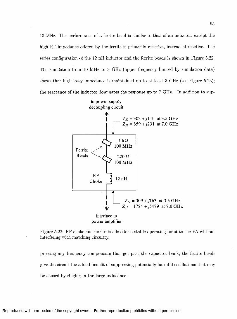
95
10 MHz. The performance of a ferrite bead is similar to th a t of an inductor, except the
high RF impedance offered by the ferrite is primarily resistive, instead of reactive. The
series configuration of the 12 nH inductor and the ferrite beads is shown in Figure 5.22.
The simulation from 10 MHz to 3 GHz (upper frequency limited by simulation data)
shows th a t high lossy impedance is maintained up to at least 3 GHz (see Figure 5.23);
the reactance of the inductor dominates the response up to 7 GHz. In addition to sup-
to power supply decoupling circuit
*Z22 = 303 + j l 10 at 3.5 GHz Z22 = 359 +;231 at 7.0 GHz
1 kQ 100 MHz
FerriteBeads 220 Q
100 MHz
RFChoke 12 nH
Zn = 309 + y'163 at 3.5 GHz Z n = 1784 + y'5479 at 7.0 GHz
interface to power amplifier
Figure 5.22: RF choke and ferrite beads offer a stable operating point to the PA without interfering with matching circuitry.
pressing any frequency components th a t get past the capacitor bank, the ferrite beads
give the circuit the added benefit of suppressing potentially harmful oscillations th a t may
be caused by ringing in the large inducance.
Reproduced with permission of the copyright owner. Further reproduction prohibited without permission.

96
GHz
(b)
^ 7 GHz
Figure 5.23: (a) SR and (b) 5 22 responses of the noise suppression/bias feed circuit shows high (primarily resistive) impedances looking into both ports of the circuit in a 50 system.
The bias network design, by virtue of the properly decoupled power supply and high
RF impedance presented up to 7 GHz, does not load the matching circuitry of the PA. To
guarantee th a t the DC bias does not interfere with the signal source at the input or the
measurement equipment at the output, the input and output signals are coupled to the
circuit with 7.5 pF coupling capacitors whose self-resonance frequency coincides w ith the
3.5 GHz fundamental tone. The input and output ports of the bias network are effectively
transparent to each other at 3.5 GHz.
5.4.3 Protection and Stability
As an added measure of protection to the transistor, a 33 resistance is added to the
power supply lead at the drain bias port. This is done to ensure th a t any stored charge
at the supply terminals does not dissipate entirely through the low impedance drain of
the HEMT, as this may cause device failure.
Reproduced with permission of the copyright owner. Further reproduction prohibited without permission.

97
The same technique is used at the input bias port; a 620 Q resistor is placed in series
with the input bias terminal for stability in addition to transistor protection.
5.4.4 Complete Circuit Simulation
The power supply decoupling circuit, protection resistor, and bias feed are simulated
together w ith all pad metallization to account for transmission line effects. The PA is
designed with 50 input and output terminations. The simulations in Figure 5.24 show
th a t the to ta l circuit (see Figure 5.19) is suitable for integration into a 50 Q, system.
1 G H z - 7 GHz
(a)
1 G H z - 7 GHz
Figure 5.24: (a) S u and (b) S 22 responses of the complete bias insertion circuit show input and output impedances close to 50 fh
W ith the bias insertion circuits integrated into the PA module, small-signal stability
is checked. The Rollet stability factor (or ^-factor) simulation is shown in Figure 5.25.
The simulation shows th a t the PA is unconditionally stable (since k > 1) for small signal
excitation.
Reproduced with permission of the copyright owner. Further reproduction prohibited without permission.
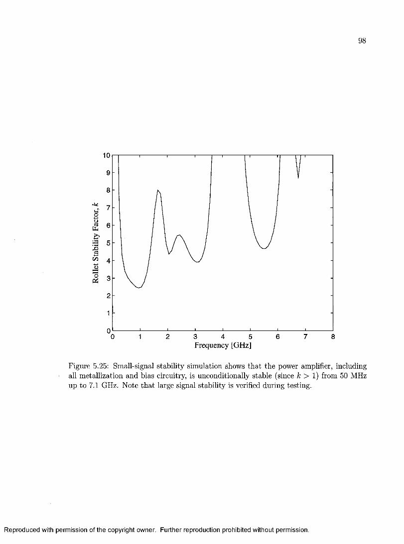
98
10
9
8
7
6
5
3
2
1
020 1 3 4 5 6 7 8
Frequency [GHz]
Figure 5.25: Small-signal stability simulation shows tha t the power amplifier, including all metallization and bias circuitry, is unconditionally stable (since k > 1) from 50 MHz up to 7.1 GHz. Note tha t large signal stability is verified during testing.
Reproduced with permission of the copyright owner. Further reproduction prohibited without permission.
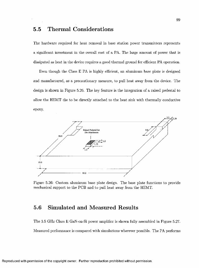
5.5 Therm al C onsiderations
99
The hardware required for heat removal in base station power transm itters represents
a significant investment in the overall cost of a PA. The large amount of power th a t is
dissipated as heat in the device requires a good therm al ground for efficient PA operation.
Even though the Class E PA is highly efficient, an aluminum base plate is designed
and manufactured, as a precautionary measure, to pull heat away from the device. The
design is shown in Figure 5.26. The key feature is the integration of a raised pedestal to
allow the HEMT die to be directly attached to the heat sink w ith thermally conductive
epoxy.
Raised Pedestal for Die Attachment
9 .0 ,
50.0
1.01.75
10.0
90.0
Figure 5.26: Custom aluminum base plate design. The base plate functions to provide mechanical support to the PCB and to pull heat away from the HEMT.
5.6 Sim ulated and M easured R esu lts
The 3.5 GHz Class E GaN-on-Si power amplifier is shown fully assembled in Figure 5.27.
Measured performance is compared with simulations wherever possible. The PA performs
Reproduced with permission of the copyright owner. Further reproduction prohibited without permission.
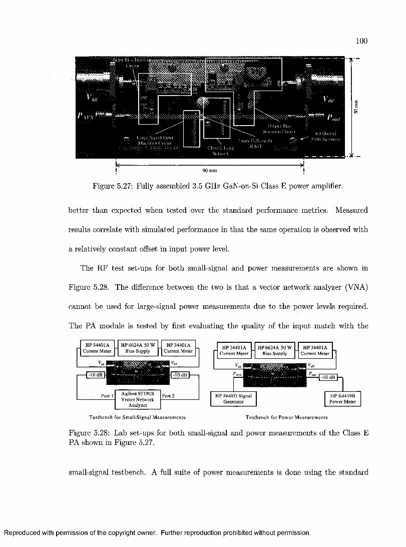
k - ->!I 90 mm j
Figure 5.27: Fully assembled 3.5 GHz GaN-on-Si Class E power amplifier.
better than expected when tested over the standard performance metrics. Measured
results correlate with simulated performance in th a t the same operation is observed with
a relatively constant offset in input power level.
The RF test set-ups for both small-signal and power measurements are shown in
Figure 5.28. The difference between the two is th a t a vector network analyzer (VNA)
cannot be used for large-signal power measurements due to the power levels required.
The PA module is tested by first evaluating the quality of the input m atch with the
HP 34401A HP 6624A 50 W HP 34401ACurrent Meter Bias Supply Current Meter
10 dB -10 dB
HP 34401A HP 6624A 50 W HP 34401ACurrent Meter Bias Supply Current Meter
Port 1 Agilent 8719ES Vector Network
Analyzer
Port 2
| -10 dB
HP 8648D Signal Generator
HP E4419B Power Meter
Testbench for Small-Signal Measurements Testbench for Power Measurements
Figure 5.28: Lab set-ups for both small-signal and power measurements of the Class E PA shown in Figure 5.27.
small-signal testbench. A full suite of power measurements is done using the standard
Reproduced with permission of the copyright owner. Further reproduction prohibited without permission.
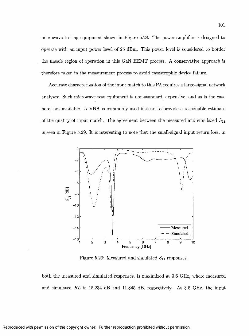
101
microwave testing equipment shown in Figure 5.28. The power amplifier is designed to
operate with an input power level of 25 dBm. This power level is considered to border
the unsafe region of operation in this GaN HEMT process. A conservative approach is
therefore taken in the measurement process to avoid catastrophic device failure.
Accurate characterization of the input match to this PA requires a large-signal network
analyzer. Such microwave test equipment is non-standard, expensive, and as is the case
here, not available. A VNA is commonly used instead to provide a reasonable estimate
of the quality of input match. The agreement between the measured and simulated S u
is seen in Figure 5.29. It is interesting to note th a t the small-signal input return loss, in
-2
-4
-6
-8
-10
MeasuredSimulated
-14
-161 2 3 4 5 6 8 9 107
Frequency [GHz]
Figure 5.29: Measured and simulated S u responses.
both the measured and simulated responses, is maximized at 3.6 GHz, where measured
and simulated R L is 15.234 dB and 11.845 dB, respectively. At 3.5 GHz, the input
Reproduced with permission of the copyright owner. Further reproduction prohibited without permission.
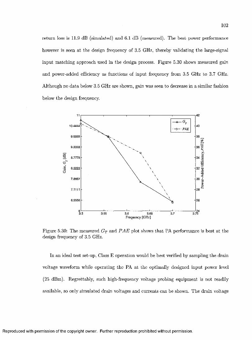
102
return loss is 11.9 dB (simulated) and 6.1 dB (measured). The best power performance
however is seen at the design frequency of 3.5 GHz, thereby validating the large-signal
input matching approach used in the design process. Figure 5.30 shows measured gain
and power-added efficiency as functions of input frequency from 3.5 GHz to 3.7 GHz.
Although no data below 3.5 GHz are shown, gain was seen to decrease in a similar fashion
below the design frequency.
10.4444
9.8889
i .3333
ffla 8.7778
G"1• § 8.2222 O
T3
7.6667
6.5556
3.5 3.55 3.6 3.65 3.7 3.75Frequency [GHz]
Figure 5.30: The measured Gt and P A E plot shows tha t PA performance is best at the design frequency of 3.5 GHz.
In an ideal test set-up, Class E operation would be best verified by sampling the drain
voltage waveform while operating the PA at the optimally designed input power level
(25 dBm). Regrettably, such high-frequency voltage probing equipment is not readily
available, so only simulated drain voltages and currents can be shown. The drain voltage
Reproduced with permission of the copyright owner. Further reproduction prohibited without permission.
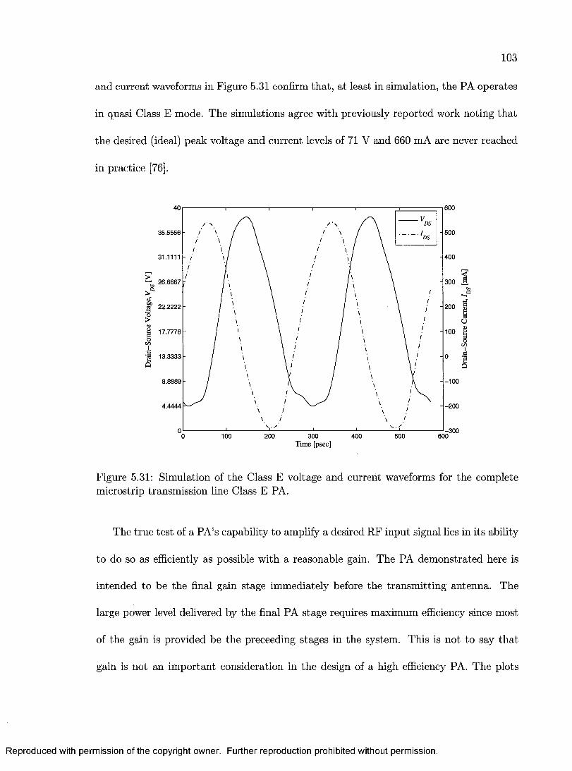
103
and current waveforms in Figure 5.31 confirm that, at least in simulation, the PA operates
in quasi Class E mode. The simulations agree with previously reported work noting th a t
the desired (ideal) peak voltage and current levels of 71 V and 660 mA are never reached
in practice [76].
600
DS
35.5556 500DS
31.1111 400
30026.6667
| 22.2222 200
17.7778
a 13.3333
-100
-2004.4444
-300100 200 300
Time [psec]400 500 600
Figure 5.31: Simulation of the Class E voltage and current waveforms for the complete microstrip transmission line Class E PA.
The true test of a PA’s capability to amplify a desired RF input signal lies in its ability
to do so as efficiently as possible w ith a reasonable gain. The PA dem onstrated here is
intended to be the final gain stage immediately before the transm itting antenna. The
large power level delivered by the final PA stage requires maximum efficiency since most
of the gain is provided be the preceeding stages in the system. This is not to say th a t
gain is not an im portant consideration in the design of a high efficiency PA. The plots
Reproduced with permission of the copyright owner. Further reproduction prohibited without permission.

104
in Figure 5.32 compare the PA’s measured output response with simulations. It is clear
40
£ 30 2.1 20
1010
10
12
12
Simulated ' Measured
14 16 18 20 22 24
Simulated ' Measured
14 16 18 20 22 24
60
q 20 SimulatedMeasured
20 22 24
60
? 20 — Simulated Measured
20
100
75
— Simulated Measured
25
20 24Available Source Power, PAVS [dBm]
Figure 5.32: The GaN Class E PA performs better than expected. There is a uniform 3.5 dB input power offset between measured and simulated results.
th a t the PA performs better in practice than in simulation. Most notable is the large
difference in gain ( G t )- at P a v s = 19 dBm, measurements show a G T of 10.74 dBm,
while simulations predict G t to be only 6.97 dB. Fundamental output power (P out), drain
efficiency (D E ), power-added efficiency (P A E ), and drain current (I d s ) all reflect this
larger gain by exhibiting results almost identical to simulated values, except at a uniformly
Reproduced with permission of the copyright owner. Further reproduction prohibited without permission.
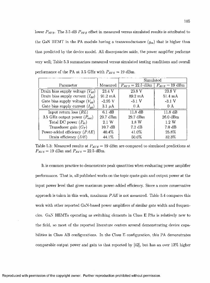
105
lower P a v s - The 3.5 dB P a v s offset in measured versus simulated results is a ttributed to
the GaN HEMT in the PA module having a transconductance (gm) th a t is higher than
th a t predicted by the device model. All discrepancies aside, the power amplifier performs
very well; Table 5.3 summarizes measured versus simulated testing conditions and overall
performance of the PA at 3.5 GHz with P a v s — 19 dBm.
Param eter MeasuredSimulated
P a v s = 22.5 dBm P a v s = 19 dBmDrain bias supply voltage (Vdd)
Drain bias supply current (Id a )
Gate bias supply voltage (V gg)
Gate bias supply current (Igg)
23.4 V 91.2 mA -2.95 V 3.1 n k
23.8 V 89.2 mA
-3.1 V 0 A
23.8 V 51.4 mA -3.1 V
0 AInput return loss ( R L )
3.5 GHz output power (P ou t)
Total DC power (Pdc)
Transducer gain ( G t )
Power-added efficiency (PAE) Drain efficiency (DE)
6.1 dB 29.7 dBm
2.1 W 10.7 dB 40.4% 44.1%
11.8 dB 29.7 dBm
1.8 W 7.2 dB 41.0% 50.6%
11.8 dB 26.0 dBm
1.2 W 7.0 dB 25.8% 32.3%
Table 5.3: Measured results at P a v s = 19 dBm are compared to simulated predictions at P a v s = 19 dBm and P a v s — 22.5 dBm.
It is common practice to demonstrate peak quantities when evaluating power amplifier
performance. T hat is, all published works on the topic quote gain and output power at the
input power level th a t gives maximum power-added efficiency. Since a more conservative
approach is taken in this work, maximum P A E is not measured. Table 5.4 compares this
work with other reported GaN-based power amplifiers of similar gate width and frequen
cies. GaN HEMTs operating as switching elements in Class E PAs is relatively new to
the field, so most of the reported literature centers around dem onstrating device capa
bilities in Class AB configurations. In the Class E configuration, this PA demonstrates
comparable output power and gain to th a t reported by [42], but has an over 13% higher
Reproduced with permission of the copyright owner. Further reproduction prohibited without permission.
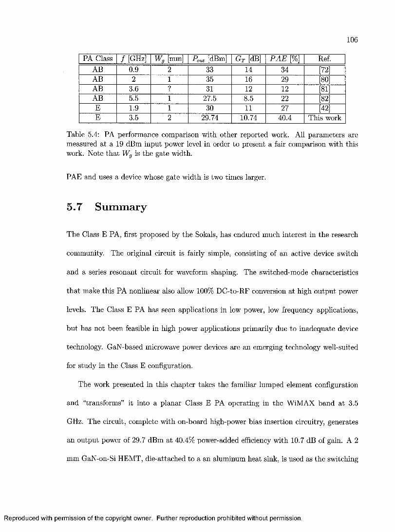
106
PA Class / [GHz] W g [mm] Pout [dBm] Gt [dB] P A E [%] Ref.AB 0.9 2 33 14 34 [72]AB 2 1 35 16 29 [80]AB 3.6 ? 31 12 12 [81]AB 5.5 1 27.5 8.5 22 [82]E 1.9 1 30 11 27 [42]E 3.5 2 29.74 10.74 40.4 This work
Table 5.4: PA performance comparison with other reported work. All param eters are measured at a 19 dBm input power level in order to present a fair comparison with this work. Note tha t W g is the gate width.
PAE and uses a device whose gate width is two times larger.
5.7 Sum m ary
The Class E PA, first proposed by the Sokals, has endured much interest in the research
community. The original circuit is fairly simple, consisting of an active device switch
and a series resonant circuit for waveform shaping. The switched-mode characteristics
th a t make this PA nonlinear also allow 100% DC-to-RF conversion at high output power
levels. The Class E PA has seen applications in low power, low frequency applications,
but has not been feasible in high power applications primarily due to inadequate device
technology. GaN-based microwave power devices are an emerging technology well-suited
for study in the Class E configuration.
The work presented in this chapter takes the familiar lumped element configuration
and “transforms” it into a planar Class E PA operating in the WiMAX band at 3.5
GHz. The circuit, complete w ith on-board high-power bias insertion circuitry, generates
an output power of 29.7 dBm at 40.4% power-added efficiency with 10.7 dB of gain. A 2
mm GaN-on-Si HEMT, die-attached to a an aluminum heat sink, is used as the switching
Reproduced with permission of the copyright owner. Further reproduction prohibited without permission.

107
element. Microstrip input and output matching circuits and lumped element bias insertion
units are fabricated/assembled on Rogers R T /duroid® 5880 high-frequency substrate.
The two-stage Class E load network functions to provide both a high impedance second
harmonic term ination and the correct Class E impedance to the drain of the HEMT. The
bias insertion circuits decouple the power supply and provide a stable operating point to
the PA without loading the matching circuitry. The input of the HEMT is power matched
to 50 Q for 25 dBm of input power and has a measured small-signal return loss of 6.1 dB.
Overall, the PA performs better than predicted in simulations. Measurements indicate
tha t the power required to switch the device between the on and off states is 3.5 dB lower
than the original estimate, giving gain, efficiency, and output power levels comparable to
simulations, but at a uniformly lower measured input power level.
Reproduced with permission of the copyright owner. Further reproduction prohibited without permission.
Chapter 6
Conclusions and Future Work
This research has shown the successful demonstration of GaN-on-Si transistor technology
for switched-mode microwave power amplifiers. Specific conclusions are as follows.
• GaN-on-Si HEMT technology promises to be lower cost than the alternative GaN-
on-SiC process; however, the therm al performance of Si as a substrate is still inferior
to tha t of SiC. Due to high 2DEG sheet charge densities and higher breakdown
electric field levels, GaN devices are better suited to high-frequency, high-power,
switched-mode power amplifier applications than established technologies, such as
Si LDMOSFET and GaAs M ESFET devices.
• A new large-signal equivalent model has been developed for a 2 mm x 0.7 fim
GaN-on-Si HEMT at DC and over the 1 - 2 0 GHz range, based on measured data.
The chosen EEsof GaAs nonlinear HEMT model reproduces the GaN transistor’s
behavior reasonably well over a large range of bias conditions (drain voltages and
currents up to 40 V and 1 A, respectively), signal levels (up to 25 dBm input power),
and frequencies.
108
Reproduced with permission of the copyright owner. Further reproduction prohibited without permission.

109
• The model does not accurately predict forward gate and pinched-off Schottky diode
behaviour, or the frequency dependence of extrinsic elements at the drain and gate.
• The design, optimization, fabrication and testing of a 3.5 GHz, 942 mW, Class E
power amplifier have been carried out. The PA has been designed using Agilent’s
ADS microwave circuit simulator with a nonlinear transistor model (developed as
part of this work), and has been successfully demonstrated in hybrid microstrip
technology. It displayed a measured gain of 10.7 dB, power-added efficiency of
40.4%, and output power of 942 mW. This high PAE was in good agreement with
predictions, although at operating power and gain levels th a t were offset from the
simulated values. The limitations of the model (both electrically and thermally)
and the newness of the devices employed (process variations) are responsible for the
differences observed.
• High power bias insertion circuits have been designed to decouple the power supply,
to AC couple the input and output signals, and to offer a stable operating point to
the PA without loading the matching circuitry.
• This work shows the suitability of low-cost GaN-on-Si transistor technology for
switched-mode microwave power amplifiers with possible applications in WiMAX
base stations and other communication systems.
While this thesis has been successful in achieving the objectives initially set out, it is
imperative th a t future work focus on the following.
• Custom device modeling of AlGaN/ GaN transistors is im portant due to deficiencies
Reproduced with permission of the copyright owner. Further reproduction prohibited without permission.

110
of currently available HEMT models th a t are based on other m aterial systems such
as AlGaAs/GaAs.
• Investigation of other switched-mode topologies such as Class F, Class M and Class
S.
• Use of GaN devices in other parts of the communications system (low-noise receivers,
phase shifter, etc.).
Reproduced with permission of the copyright owner. Further reproduction prohibited without permission.

A ppendix A
Agilent EEHEM T 2 mm GaN-on-Si
Nonlinear M odel
lJ
h
EE_HE^T1„Modei
Vto=Vtox V Tau=Taux psec C11th=C11thx pF Ng1= Vinfltc^G am m a-G am m ax C dso-Cdsox pF Vinfl=Vinflx V Vco=Vcox V Vtoactc=Vgo=Vgox V Rdb=1e9 Ohm Deltgs=Deltgsx V Vba=Vbax V Gmmaxactc=Vdelt- Cbs=Cbsx fF Deltds=Deltdsx V Vbc=Vbcx V Gammaactc=Vch=Vchx V Vtoac=Vtoacx V Lambda= Lambdax Mu=Mux Xti=Gmmax=Gmmaxx Gammaac=Gammaacx C12sat=C12satx pF Deltgm=Deltgmx wVgfwd=Vdso=Vdsox V Vdeltac= Cgdsat=Cgdsatx pF De!tgmac=Deltgmacx wBvgs=Vsat=Vsatx V Gmmaxac=Gmmaxacx Kbk= Alpha=Alphax V wBvgd=Kapa=Kapax S Kapaac=Kapaacx mS Vbr=160 V Tnom= wBvds=Peff=1e9 Peffac=1e9 Nbr= Rgtc= wldsmax=Vtso=Vtsox V Vtsoac=Vtsoacx V ldsoc=idsocx A Rdtc= wPmax=ls=lsx A Gdbm=Gdbmx Rd=Rdx Rstc= AIIParams=N=Nx Kdb=Kdbx Rs=Rsx Vtotc=Ris=Risx Ohm Vdsm=Vdsmx Rg=Rgx Gmmaxtc=Rid=Ridx Ohm C11o-C11ox pF Ugw= G am m atc-
E l VAR E l VAR
Vtox=-3 Cbsx=1.6e-13 C12satx=0.283738 Ldx=96.5Gammax=0.0025 Vtoacx=-3.2 Cgdsatx=0.343952 Lgx=67.3Vgox=-1.6 Gammaacx=0.0025 ldsocx=1.5 Lsx=1.125Vchx=2 Gmmaxacx=0.32 Rdx=1.1Gmmaxx=0.33 Kapaacx=0.00001 Rsx=0Vdsox=20 Vtsoacx=-19 Rgx=1.176Vsatx=8.5 Gdbmx=0 Vcox=-1.0Kapax=0.00001 Kdbx=0 Vbax=1Vtsox=-19 Vdsmx=1 Vbcx=5lsx=3e-12 C11ox=3.39872 Mux=0Nx=2.05 C11thx=1.35871 Deltgmx=0.03Ridx=8.22 Vinflx=-2.70755 Deltgmacx=0.03Risx=2.08 Deligsx=0.931521 Alphax=8.22149e-07Taux=7.2694 Deltdsx=6.97192Cdsox=0.28 Lam bdax=0.00267041
Figure A .l: Agilent EEsoff HEMT nonlinear model component used in circuit simulations.
Ill
Reproduced with permission of the copyright owner. Further reproduction prohibited without permission.

References
[1] S.J. Vaughan-Nichols. (2005, June) Achieving wireless broadband with wimax. [Online]. Available:http://ieeexplore.ieee.Org/iel5/2/28995/01306375. pdf ?arnumber=1306375
[2] J. Trulove. (2005, April) W im ax’s promise for developing countries. [Online]. Available: http://www.wimax.com/commentary/spotlight/wimaxspotlight2005_04_14
[3] “IEEE 802.16a standard and wimax: Igniting broadband wireless access,” W hite Paper, Worldwide Interoperability for Microwave Access Forum. [Online]. Available: www.wimaxforum.org/news/downloads/W iMAXW hitepaper.pdf
[4] G. Sims and I. Stephenson, Microwave Tubes and Semiconductor Devices. Glasgow, UK: Blackie and Son Limited, 1963.
[5] R. Borges. (2001, September) Gallium nitride electronic devices for high-power wireless applications. 0901Borges72.pdf. [Online]. Available: http: / /im ages.rfdesign.eom/files/4/
[6] TMD Technologies Ltd. (2005, April) Product summary tubes. tubes_product_summary_evd6054_issue%202.pdf. [Online]. Available: http://ww w .tm d.co.uk/m icrow ave/
[7] S. Patel. (2003, January/February) The bottleneck on the road to 3g. WirelessFuturesRoadTo3GJanFeb03.pdf. [Online]. Available: http://w w w .nitronex.com /m edia/
[8] F. Schwierz and J. Liou, Modern Microwave Transistors: Theory, Design, and Performance. Hoboken, NJ: John Wiley & Sons, Inc., 2003.
[9] N.V. Drozdovski and R.H. Caverly, “GaN-Based High electron Mobility Transistors for Microwave and RF Control Applications,” IEEE Transactions on Microwave Theory and Techniques, vol. 50, no. 1, pp. 1-8, January 2002.
[10] J. Lee, L. Eastman, and K.J. Webb, “A Gallium-Nitride Push-Pull Microwave Power Amplifier,” IEEE Transactions on Microwave Theory and Techniques, vol. 51, no. 11, pp. 89-92, November 2003.
112
Reproduced with permission of the copyright owner. Further reproduction prohibited without permission.
113
[11] D. Kimball, P. Draxler, J. Jeong, C. Hsia, S. Lanfranco, W. Nagy, K. Linthicum, L. Larson, and P.Asbeck, “50% PAE WCDMA basestation amplifier implemented with GaN HFETs,” in Compound Semiconductor Integrated Circuits Symposium Digest, 2005, November.
[12] J.D. Brown, R. Borges, E. Piner, A Vescan, S. Singhal, and R. Therrien, “Al- G aN/GaN HFETs fabricated on 100-mm GaN on silicon (111) substrates,” Solid- State Electronics, vol. 46, pp. 1535-1539, February 2002.
[13] N.O. Sokal and A.D. Sokal, “High-Efficiency Tuned Switching Power Amplifier,” U.S. Patent 3919656, Nov. 11, 1975.
[14] P.M. Smith, S.-M.J. Liu, M.-Y. Kao, P. Ho, S.C. Wang, K.H.G. Duh, S.T. Fu, and P.O. Chao, “W -Band High Efficiency InP-Based Power HEMT with 600 GHz f ma x ” IEEE Microwave and Guided Wave Letters, vol. 5, no. 7, 1995.
[15] K. Inoue, K. Ebihara, H. Haematsu, T. Igarashi, H. Takahashi, and J. Fukaya, “A 240 W Push-Pull Power FET for W-CDMA Base Stations,” IEEE Microwave Symposium Digest, vol. 3, pp. 1719-1722, June 2000.
[16] A.N. Lepore, H.M. Levy, R.C. Tiberio, P.J. Tasker, H. Lee. E.D. Wolf, L.F. Eastman, and E. Khon, “0.1 pm Gate Length MODFETs with Unity Current Gain Cutoff Frequency Above 110 GHz,” IE EE Electronics Letters, vol. 24, pp. 364-366, March 1988.
[17] S.E. Rosenbaum, B.K. Kormanyos, L.M. Jelloian, M. M atloubian, A.S. Brown, L.E. Larson, L.D. Nguyen, M.A. Thompson, L.P.B. Katehi, and G.M. Rebeiz, “155- and 213-GHz A lInA s/G alnA s/InP HEMT MMIC Oscillators,” IEEE Transactions on Microwave Theory and Techniques, vol. 47, pp. 927-932, April 1995.
[18] T. Palacios, A. Chakraborty, S. Heikman, S. Keller, S.P. DenBaars, and U.K. Mishra, “AlGaN/GaN High Electron Mobility Transistors W ith InGaN Back-Barriers,” IEEE Electron Device Letters, vol. 27, no. 1, pp. 13-15, January 2006.
[19] P. Javorka, A. Alam, A. Fox, M. Marso, M. Heuken, and P. Kordos, “AlGaN/GaN HEMTs on Silicon Substrates with fo of 32/20 GHz and f max of 27/22 GHz for 0.5/0.7 pm Gate Length,” IE E E Electronics Letters, vol. 38, no. 6, pp. 288-289, March 2002.
[20] Y. Tateno, H. Takahashi, T. Igarashi, and J. Fukaya, “A 150 W E-Mode GaAs Power FET with 35% PAE for W-CDMA Base Station,” IEEE Microwave Symposium Digest, vol. 3, pp. 1087-1090, June 1999.
[21] R. Grundbacher, M. Nishimoto, T.P. Chin, Y.C. Chen, R. Lai, and D. Yamauchi, “InP Power HEMTs W ith 36% PAE at 60 GHz,” Eleventh International Conference on Indium Phosphide and Related Materials, pp. 307-310, May 1999.
Reproduced with permission of the copyright owner. Further reproduction prohibited without permission.

114
[22] Y.-P. Wu, A. Saxler, M. Moore, R.P. Smith, S. Sheppard, P.M. Chavarkar, T. Wisleder, U.K. Mishra, and P. Parikh, “30-W /mm GaN HEMTs by Field Plate Optimization,” IEEE Electron Device Letters, vol. 25, no. 3, pp. 117-119, March 2004.
[23] J.W . Johnson, E.L. Piner. A. Vescan, R. Therrien, P. Rajagopal, J.C. Roberts, J.D. Brown, S. Singhal, and K.J. Linthicum, “12 W /m m AlGaN-GaN HFETs on Silicon Substrates,” IEEE Electron Device Letters, vol. 25, no. 7, pp. 459-461, July 2004.
[24] M. Matloubian, L.D. Nguyen, A.S. Brown, L.E. Larson, M.A. Melendes, and M.A. Thompson, “High Power and High Efficiency AlInAs/GalnAs on InP HEMTs,” IEEE Microwave Symposium Digest, vol. 2, pp. 721-724, June 1991.
[25] C. Nguyen and M. Micovic, “The State-of-the-Art of GaAs and InP Power Devices and Amplifiers,” IEEE Transactions on Electron Devices, vol. 48, no. 3, pp. 472-478, March 2001.
[26] S. Cripps, R F Power Amplifiers fo r Wireless Communications. Norwood, MA: Artech House, Inc., 1999.
[27] J. Rogers and C. P lett, Radio Frequency Integrated Circuit Design. Norwood, MA: Artech House, Inc., 2003.
[28] H.L. Krauss, C.W. Bostian, and F.H. Raab, Solid State Radio Engineering. New York, NY: John Wiley & Sons, Ltd., 1980.
[29] T. Lee, The Design of CMOS Radio-Frequency Integrated Circuits, 2nd ed. New York, NY: Cambridge University Press, 2004.
[30] S. McGarry, private communication, 2006.
[31] N.O. Sokal and A.D. Sokal, “Class E - A New Class of High-Efficiency Tuned Single- Ended Switching Power Amplifiers,” IEEE Journal o f Solid-State Circuits, vol. SC- 10, no. 3, pp. 168-176, June 1975.
[32] S.C. Cripps, R F Power Amplifiers fo r Wireless Communications, 2nd ed. Norwood, MA: Artech House, Inc., 2006.
[33] N. Sokal, “Class-E high-efficiency power amplifiers, from HF to microwave,” in Proceedings of the IEEE International Microwave Symposium, Boston, MA, June 2000, p p . 1109-1112.
[34] F.H. Raab, “Idealized Operation of the Class E Tuned Power Amplifier,” IEEE Transactions on Circuits and Systems, vol. CAS-24, no. 12, 1977.
[35] M.K. Kazimierczuk and K. Puczko, “Exact Analysis of Class E Tuned Power Amplifier at any Q and Switch Duty Cycle,” IE EE Transactions on Circuits and Systems, vol. CAS-34, no. 2, 1987.
Reproduced with permission of the copyright owner. Further reproduction prohibited without permission.

115
[36] D.K. Choi, “High Efficiency Switched-Mode Power Amplifiers for Wireless Communications,” Ph.D. dissertation, University of California, Santa Barbara, March 2001.
[37] F.J. Ortega-Gonzalez, “New Driver for High-Efficiency Switching RF Power Amplifiers,” IE EE Microwave and Optical Technology Letters, vol. 43, no. 5, pp. 370-372, December 2004.
[38] T.B. Mader, “Quasi-Optical Class-E Power Amplifiers,” Ph.D. dissertation, University of Colorado, Boulder, August 1995.
[39] J. Rollett, “Stability and Power-Gain Invariants of Linear Twoports,” IR E Transactions on Circuit Theory, vol. 9, pp. 29-32, March 1962.
[40] W. Saito, T. Domon, I. Omura, M. Karaguchi, Y. Takada, K. Tsuda, and M. Ya- maguchi, “Demonstration of 13.56-MHz class-e amplifier using a high-voltage GaN power-HEMT,” IE E E Electron device Letters, vol. 27, no. 5, pp. 326-328, May 2006.
[41] W. Saito, M. Karaguchi, Y. Takada, K. Tsuda, T. Domon, I. Omura, and M. Yam- aguchi, “Two-stage quasi-class-e power amplifier in GaN HEMT technology,” IEEE Microwave and Component Letters, vol. 16, no. 1, pp. 28-30, January 2006.
[42] H. Xu, S. Gao, S. Heikman, S.I. Long, U.K. Mishra, and R.A. York, “A high-efficiency class-e GaN HEMT power amplifier at 1.9 GHz,” IEEE Microwave and Component Letters, vol. 16, no. 1, pp. 22-24, January 2006.
[43] S. Gao, H. Xu, S. Heikman, U.K. Mishra, R.A. York, “Two-stage quasi-class-e power amplifier in GaN HEMT technology,” IE E E Microwave and Component Letters, vol. 16, no. 1, pp. 28-30, January 2006.
[44] R. P. W.L. Pribble, J.M. Milligan. (2006) High efficiency class-e amplifier utilizing gan hemt technology. Cree Inc. Durham, NC. [Online]. Available: www.cree.com
[45] W. Curtice, “A M ESFET model for use in the design of GaAs integrated circuits,” IEEE Transactions on Microwave Theory and Techniques, vol. MTT-28, no. 5, pp. 448-455, May 1980.
[46] K. Koh, H. Park, and S. Hong, “A spline large signal FET model based on bias dependent pulsed I-V measurements,” IE EE Transactions on Microwave Theory and Techniques, vol. 28, no. 5, pp. 448-455, May 2002.
[47] M. Reiser, “A Two-Dimensional Numerical FET Model for DC, AC, and Large- Signal Analysis,” IEEE Transactions on Electron Devices, vol. ED-20, no. 1, pp. 35-45, January 1973.
[48] J.J. Barnes, R.J. Lomax, G.I. Haddad, “Finite-Element Simulation of GaAs MES- FETs with Lateral Doping Profiles and Submicron Gates,” IEEE Transactions on Electron Devices, vol. ED-23, no. 9, pp. 1042-1048, September 1976.
Reproduced with permission of the copyright owner. Further reproduction prohibited without permission.
116
[49] A. Grebennikov, R F and Microwave Power Amplifier Design. U.S.A.: The McGraw- Hill Companies, Inc., 2005.
[50] J. Golio, Microwave M ESFETs & HEMTs. Norwood, MA: Artech House, Inc., 1991.
[51] A. Materka and T. Kacprzak, “Computer Calculation of Large-Signal GaAs FE T Amplifier Characteristics,” IE EE Transactions on Microwave Theory and Techniques, vol. MTT-33, no. 2, pp. 129-135, February 1985.
[52] W. Curtice and M. Ettenberg, “A nonlinear GaAs FET model for use in the design of output circuits for power amplifiers,” IEEE Transactions on Microwave Theory and Techniques, vol. MTT-33, no. 12, pp. 1383-1393, December 1985.
[53] H. Statz, P. Newman, I. Smith, R. Pucel, and H. Haus, “GaAs FET device and circuit simulation in spice,” IE E E Transactions on Electron Devices, vol. ED-34, pp. 160-169, February 1987.
[54] Agilent Technologies Inc., Nonlinear Devices. Palo Alto, CA: Agilent Technologies Inc., 2005, ch. 3.
[55] “Nitronex:Core Competencies:Crystal Growth,” coreComp.html, Nitronex Corporation, 2007. [Online]. Available: http ://w w w .nitronex.com /about/
[56] P. Canfield, S. Lam, and D. Allstot, “Modeling of frequency and tem perature effects in GaAs M ESFETs,” IEEE Journal o f Solid-State Circuits, vol. 25, no. 1, pp. 299- 305, February 1990.
[57] J. Golio, M. Miller, G. Maracas, and D. Johnson, “Frequency-dependent electrical characteristics of GaAs M ESFETs,” IE EE Transactions on Electron Devices, vol. 37, no. 5, pp. 1217-1226, May 1990.
[58] P.Ladbrooke and J. Bridge, “The Importance of the Current-Voltage Characteristics of FETs, HEMTs, and Bipolar Transistors in Contemporary Circuit Design,” Microwave Journal, March 2002.
[59] S. Manohar, A. Narayanan, A.Keerti, A. Pham, J. Brown, R. Borges, and K. Linthicum, “Characteristics of Microwave Power GaN HEMTs on 4-Inch Si Wafers,” IEEE Microwave Symposium Digest, vol. 1, pp. 449-452, June 2002.
[60] R.G. Trew, G.L. Bilbro, W. Kuang, Y. Liu, and H. Yin, “Microwave AlGaN/GaN HFETs,” IEEE Microwave Magazine, vol. 6, no. 1, pp. 56-66, March 2005.
[61] S. De Meyer, C. Charbonniaud, R. Quere, M. Campovecchio, R. Lossy, and J. Wurfl, “Mechanism of Power Density Degradation due to Trapping Effects in AlGaN/ GaN HEMTs,” IE EE Microwave Symposium Digest, vol. 1, pp. 455-458, June 2003.
Reproduced with permission of the copyright owner. Further reproduction prohibited without permission.
117
[62] S.C. Binari, K. Ikossi, J.A. Roussos, W. Kruppa, D. Park, H.B. Dietrich, D.D. Koleske, A.E. Wickenden, and R.L. Henry, “Trapping Effects and Microwave Performance in AlGaN/GaN HEMTs,” IEEE Transactions on Electron Devices, vol. 48, no. 3, 2001.
[63] T. Mizutani, Y. Ohno, M. Akita, S. Kishimoto, and K. Maezawa, “A Study on Current Collapse in AlGaN/GaN HEMTs Induced by Bias Stress,” IE E E Transactions on Electron Devices, vol. 50, no. 10, 2003.
[64] A.F.M. Anwar, S. Wu, and T. Webster, “Temperature Dependent Transport Properties in GaN, AlxGai_xN, and InxGai_xN Semiconductors,” IEEE Transactions on Electron Devices, vol. 48, no. 3, 2001.
[65] C. Wei, Y.A. Tkachenko, and D. Bartle, “An Accurate Large-Signal Model of GaAs M ESFET Which Accounts for Charge Conservation, Dispersion, and Self-Heating,” IEEE Transactions on Microwave Theory and Techniques, vol. 46, no. 11, pp. 1638- 1644, November 1998.
[66] M.J. Uren, T. M artin, J.C. Birbeck, R. Balmer, B.T. Highes, A.J. Hydes, H. Willis, T. Jelfs, “GaN/AlGaN HFETs Fabricated on a SiC Substrate,” in Eighth IEEE International Symposium on High Perfomance Electron Devices for Microwave and Optoelectronic Applications, Glasgow, United Kingdom, November.
[67] A. Sedra and K. Smith, Microelectronic Cicruits, 4th ed. New York, NY: Oxford University Press, Inc., 1998.
[68] A. Chaudhari, private communication, 2005.
[69] G. Dambrine, A. Cappy, F. Heliodore, and E. Playez, “A new method for determining the FET small-signal equivalent circuit,” IEEE Transactions on Microwave Theory and Techniques, vol. 36, no. 7, pp. 1151-1159, July 1988.
[70] Agilent Technologies. (2001, July) High Speed DC Characterization of Semiconductor Devices from Sub pA to 1A. 59502930.pdf. [Online]. Available: h tt p : / / www. home. agilent. com / upload / cmc .upload / All /
[71] J.M. Shah, Y. Li, T. Gessmann, and E.F. Schubert, “Experimental analysis and theoretical model for anomalously high ideality factors (n 3> 2.0) in AlGaN/GaN p-n junction diodes,” Journal o f Applied Physics, vol. 94, no. 4, 2003.
[72] P.M. Cabral, J.C. Pedro, and N.B. Carvalho, “Nonlinear Device Model of Microwave Power GaN HEMTs for High Power-Amplifier Design,” IE EE Transactions on M icrowave Theory and Techniques, vol. 52, no. 11, pp. 2585-2592, November 2004.
[73] T.B. Mader and Z. Popovic, “The Transmission-Line High-Efficiency Class-E Amplifier,” IEEE Microwave and Guided Wave Letters, vol. 5, no. 9, pp. 290-292, September 1995.
Reproduced with permission of the copyright owner. Further reproduction prohibited without permission.
118
[74] T.B. Mader, E.W. Bryerton, M. Markovic, M. Forman, and Z. Popovic, “Switched- Mode High Efficiency Microwave Power Amplifiers in a Free-Space Power-Combiner Array,” IE EE Transactions on Microwave Theory and Techniques, vol. 46, no. 10, pp. 1391-1397, October 1998.
[75] E.W. Bryerton, M.D. Weiss, and Z. Popovic, “Efficiency of Chip-Level Versus External Power Combining,” IE EE Transactions on Microwave Theory and Techniques, vol. 47, no. 8, pp. 1482-1485, October 1999.
[76] M.D. Weiss, M.H. Crites, E.W. Bryerton, J.F . W hitaker, and Z. Popovic, “Time- Domain Optical Sampling of Switched-Mode Microwave Amplifiers and Multipliers,” IE EE Transactions on Microwave Theory and Techniques, vol. 47, no. 12, pp. 2599- 2604, December 1999.
[77] M.K. Kazimierczuk, “Generalization of Conditions for 100-Percent Efficiency and Nonzero OutputPower in Power Amplifiers and Frequency Multipliers,” IE E E Transactions on Circuits and Systems, vol. CAS-33, no. 8, 1986.
[78] G. Gonzalez, Microwave Transistor Amplifiers: Analysis and Design, 2nd ed. Upper Saddle River, NJ: Prentice-Hall, Inc., 1997.
[79] R. Fiore. (2005, January) Capacitors in Broadband Applications. caps_broadbnd_apps.pdf. [Online]. Available: http: / / www.atceramics.com/technicalnotes/technotes.asp
[80] Y. Ando, Y Okamoto, K. Hataya, T. Nakayama, H. Miyamoto, T. Inoue, and M. Kuzuhara, “12 W /m m Recessed-Gate AlGaN/GaN Heterojunction Field-Plate FET,” Electron Devices Meeting, IED M ’03 Technical Digest, pp. 23.1.1-23.1.4, December 2003.
[81] S. Wood, P. Smith, W. Pribble, R. Pengelly, and J. Crescenzi. (2006, May) High Efficiency, High Linearity GaN HEMT Amplifiers for WiMAX Applications. HFE0506_Cree.pdf. [Online]. Available: h ttp : / / www. highfrequencyelectronics. com / Archives/May 06 /
[82] P. Colantonio, F. Giannini, R. Giofre, E. Limiti, A. Serino, M. Peroni, P. Romanini, and C. Proietti, “A C-band high-efficiency second-harmonic-tuned hybrid power amplifier in GaN technology,” IEEE Transactions on Microwave Theory and Techniques, vol. 54, no. 6, pp. 2713-2722, June 2006.
Reproduced with permission of the copyright owner. Further reproduction prohibited without permission.