Embed Size (px)
Citation preview

HIGH EFFICIENCY STEP-DOWN SWITCHED CAPACITOR DC-DC
CONVERTER
MOHD SYAZWAN BIN ROSDI
This thesis is submitted as partial fulfillment of the requirements for the award of the
Bachelor of Electrical Engineering (Electrical Power System)
Faculty of Electrical & Electronics Engineering
Universiti Malaysia Pahang
NOVEMBER, 2010

ii
“All the trademark and copyrights use herein are property of their respective owner.
References of information from other sources are quoted accordingly; otherwise the
information presented in this report is solely work of the author.”
Signature : ____________________________
Author : MOHD SYAZWAN BIN ROSDI
Date : 11 NOVEMBER 2010

iv
ACKNOWLEDGEMENT
First of all, I would like to thank my project supervisor, Miss Laili Binti
Ismail, who has given me much strong logistic support while implementing the
project given. She has always assisted me when I handling my project. Besides, I
would like to express my sincere appreciation for her valuable advices, guidance and
encouragement. This has inspired me to be more confident in trying new things.
Secondly, I would like to thank my family members especially my father
Rosdi Mohamed and my mother Masitah Hasan for giving me their loves and
supports throughout my four years of studies in Universiti Malaysia Pahang (UMP),
Gambang, Pahang.
Special thanks to Siti Zahirah Zulkapri who have given me inspiration and
strength to finish this project.
Then, I would like to thanks to staff FKEE, who have given me a great help
in accomplishing this project.
Last but not least, I would like to say millions of thanks to all my
coursemates and those who has lending me their helping hand.
Thank you.

v
ABSTRACT
The power requirement for vehicles increased continuously in the 20th
century as consumers required more from their vehicles; car manufacturers have
provided both standard and optional equipment to meet these demands. In addition,
during the last 25 years, government legislation for emissions and safety equipment
has also added to the power requirements.
To solve the power crises in vehicles of the future, a new standard for
automotive electrical systems, one based on a voltage, 42V, which is three times
higher than used in today’s vehicles is proposed. The need for this higher voltage is
being driven by the expectation that automotive electrical loads will continue to rise
sharply in the future. Increasing the vehicle voltage will allow the addition of higher
power loads without more expensive and heavier wiring. But some loads, such as the
existing vehicle lighting, would be better served by 5V. Therefore a possible
architecture, 42V power from the main battery is stepped down to 5V by a “High
Efficiency Step-Down Switched Capacitor DC-DC Converter”.
In this thesis, a prototype “Switched Capacitor Converter” is designed and
developed. This converter is capable of supplying 22A at 5V. This converter has an
overall efficiency of 80.69%. This prototype can act as a milestone for a better
performance, higher power and improve efficiency in tomorrow’s vehicles.

vi
ABSTRAK
Pada zaman ini, keperluan kuasa untuk kenderaan terus meningkat pada abad
ke-20 dan sebagai pengguna mengharapkan sesuatu yang lebih baik dari kenderaan;
pengeluar kereta telah meambah baik peralatan dan memperbanyakkan pilihan untuk
memenuhi tuntutan tersebut. Selain itu, hampir 25 tahun pihak kerajaan telah
menguat kuasa undang-undang mengenai peralatan keselamatan dan juga menambah
baik untuk memenuhi keperluan kuasa.
Untuk mengatasi krisis kuasa di dalam kenderaan masa depan, satu piawaian
baru untuk sistem otomotif, yang didasarkan pada voltan, 42V yang tiga kali lebih
tinggi daripada yang digunakan dalam kenderaan saat ini dicadangkan. Keperluan
voltan yang lebih tinggi ini didorong oleh keperluan penggunaan beban elektrik
automotif akan terus meningkat di masa depan. Peningkatan voltan kenderaan akan
membolehkan penambahan beban kuasa yang lebih tinggi tanpa kabel lebih mahal
dan lebih berat. Tetapi beberapa beban, seperti lampu kenderaan yang ada, akan lebih
baik jika menggunakan 5V. Oleh kerana itu, reka bentuk 42V kuasa dari bateri utama
diturunkan kepada 5V dengan menggunakan "Kecekapan Tinggi Suis Kapasitor
Pengubah Penurunan DC-DC".
Dalam tesis ini, prototaip "Switched Capacitor Converter" telah dirancang
dan direalisasikan. Pengubah ini mampu membekalkan keluaran 22A dan 5V.
Pengubah ini mempunyai kecekapan keseluruhan 80,69%. Prototaip ini boleh
bertindak sebagai tunggak untuk prestasi yang lebih baik, kuasa yang lebih tinggi dan
meningkatkan kecekapan dalam kenderaan masa hadapan.
viii
TABLE OF CONTENTS
CHAPTER TITLE PAGE
DECLARATION ii
DEDICATION iii
ACKNOWLEDGEMENTS iv
ABSTRACT v
ABSTRAK vi
TABLE OF CONTENTS vii
LIST OF FIGURES x
LIST OF TABLES xi
LIST OF APPENDICES xii
1.0 INTRODUCTION
1.1 Background of Study 1
1.2 Objective of the Project 3
1.3 Scope of the Project 3
1.4 Problem Statement 4
1.5 Thesis Outline 5
2.0 LITERATURE REVIEW
2.1 Introduction 6
2.1.1 DC-DC Converters 6
2.1.2 The fuctions of DC-DC Converter 7

viii
2.1.3 Overview of 42V System 7
2.1.4 Applications of 42V 9
2.2 Power Electronic Applications 11
2.2.1 Operation of Power MOSFET 11
2.2.2 Operating Temperatre and Ripple
Current 14
2.2.3 Transient and Limitation of Current
Spike 15
2.2.4 Inherent Energy Loss at Voltage
Difference 22
2.2.5 Target Voltages and SCC Equivalent
Circuit 25
2.2.6 Demystifying the Equivalent Resistor
Issue 28
2.2.7 Comparing Inducor-less,
Inductorbased Switching Regulator 33
3.0 METHODOLOGY
3.1 Block Diagram of Step-Down DC-DC
Converter 39
3.2 Inductorless 42-5V Switched Capacitor
DC-DC Converter 39
3.3 Stage Development 41
3.3.1 42/5V SC DC-DC Converter with
Improved Efficiency 41
3.4 Voltmeter Circuit 43
3.4.1 PIC16F877 Programming Code for
Voltmeter Circuit 45
4.0 RESULT AND DISCUSSION
4.1 Introduction 48
4.2 Operation of the Converter 48
4.2.1 Pulse Form Signal for MOSFET
Driver 49

ix
4.2.2 Voltage Output for SC DC-DC
Converter 51
4.2.3 LCD Display Result 54
4.3 Experiment Result 55
4.4 Hardware Implementation 57
5.0 CONCLUSION AND RECOMMENDATION
5.1 Conclusion 58
5.2 Recommendations 59
5.3 Costing 59
REFERENCES 61
APPENDICES
Appendix A 63
Appendix B 74

xi
LIST OF FIGURES
FIGURE NO. TITLE PAGE
2.1 Electrical power consumption trend 8
2.2 System power by 42 volt supply 9
2.3 Savings in fuel consumption (%) with 42V 10
2.4 Basic construction of N-channel MOSFET 12
2.5 N-channel MOSFET in the off-stage 12
2.6 N-channel MOSFET in the on-stage 13
2.7 Switched circuits including the ideal capacitors 16
2.8 Switched circuit including the serial resistor 17
2.9 Complete response of the charging circuit and its components 19
2.10 A large and fast decaying i(t) and an equivalent impulse 20
2.11 Complete response of the discharging circuit and its components 22
2.12 The output characteristics of a commercial SCC 26
2.13 The SCC equivalent circuit 27
2.14 Voltage follower SCC 28
2.15 Two non-overlapping clocks φ1 and φ2 29
2.16 Generic charge/discharge circuit 29
2.17 Functions 2coth and 2coth 32
2.18 Shown and generic boost(a) and buck(b) inductor-based
switching regulator 34

xii
2.19 Inductorless SRs exploit only one or two small and cheap
ceramic capacitors (flying capacitor Cf1 and Cf2) instead of
and expensive inductor 35
2.20 Shown is efficiency vs. input voltage for an inductorless
switching regulator. 36
2.21 Shown is typical efficiency vs. load for PWM Regulated
L-Based SR (a), and for the SRO-2.6~5.5/1.8~3.3 L-less SR
from DOLPHIN (b), for VIN = 3.3V & VOUT = 1.8V 37
3.1 The block diagram of Step-Down DC-DC SC Converter 39
3.2 Complete Circuit of SC 42-5V DC-DC Step-Down Converter 40
3.3 Circuit structure of the 42/5V SCC converter cell by using
PSpice 41
3.4 Circuit structure of the 42/5V SCC converter cell by using
Proteus 41
3.5 Schematic diagram of the 42/5 V SCC with feedback circuit 42
3.6 Output voltage display on LCD 43
3.7 Flow Chart for Output Voltage Display 44
4.1 Analytical view of the operation SC DC-DC Converter 48
4.2 Probe at Vpulse 49
4.3 Pulse form signal for MOSFET’s driver 50
4.4 Probe tapped at Vout 51
4.5 Output voltage response during start-up 51
4.6 Ripple output voltage waveform 52
4.7 Modified the pulse form by using Rise Time (TR) = 2ns and
Fall Time (TF) =2ns 52
4.8 Voltage output with pulse waveform 52

xiii
4.9 Probe tapped at Vin and Vout 53
4.10 Vin versus Vout 53
4.11 Probe tapped at Vin, Vout, Vpulse 53
4.12 Steady state waveforms 54
4.13 LCD display the voltage output 55
4.14 The voltage output and current output display by using
Proteus software 55
4.15 Hardware circuit implementation 57

xiii
LIST OF TABLE
TABLE NO. TITLE PAGE
5.1 List of component 59
LIST OF APPENDICES
APPENDIX TITLE PAGE
A Data sheet IRFP150N 63
B Data sheet IRF9140 73
1
CHAPTER 1
INTRODUCTION
This chapter will explain the background of the project, objective of the
project, scope of the project and problem statement. In this introduction section the
review of step-down switch capacitor converter (SCC) explained. At the end of
chapter 1 the thesis outline is briefly describe.
1.1 Background of Study
A DC-DC converter is a device that accepts a DC input voltage and produces
a DC output voltage. Typically, the output produced is at a different voltage level
than input. Portable electronic devices, such as cell phones, PDAs, pagers and
laptops, are usually powered by batteries. After the battery has been used for a period
of time, the battery voltage drops depending on the types of batteries and devices.
This voltage variation may cause some problems in the operation of the electronic
device powered by the batteries. So, DC-DC converters are often used to provide a
stable and constant power supply voltage for these portable electronic devices.
According the components used for storing and transferring energy, there are
two main kinds of topologies in DC/DC converters: inductive converters and
switched capacitor converters. The inductive converter using inductor as energy
storing and transferring component has been a power supply solution in all kinds of
applications for many years. It is still a good way to deliver a high load current over
500mA. But in recent years, since the size of portable electronic device is getting

2
smaller and smaller, and the load current and supply voltage are getting lower and
lower, the inductorless converters based on switched capacitor are more and more
popular in the space constrained applications with 10mA to 500mA load current.
Such converters avoid the use of bulky and noisy magnetic components, inductors.
They are available in small packages, operate with very low quiescent current and
require minimal external components. They have been the main power supply
solution for handheld portable instrumentations.
The purpose of a DC-DC converter is to provide a predetermined and
constant output voltage to a load from poorly specified or fluctuating input voltage
source. Linear regulators and switching converters are two common types of DC-DC
converters. In a linear regulator the output current comes directly from the power
supply, therefore the efficiency is approximately defined as the ratio of the output
voltage to supply voltage. It is obvious that a worse efficiency will be obtained when
the supply voltage is much larger than the output voltage. Switching converters are
more efficient than linear regulators due to intercepted energy transfer. This is done
by periodically switching energy storing components to deliver a portion of energy
from the power supply to the output.
The capacitive converters based on switched capacitors are widespread in
applications requiring small power and no isolation between input and output. Their
features relatively low noise, minimal radiated EMI, and in most cases as fabricated
as integrated circuits which have made capacitive converters popular for use in
power management for mobile devices. An additional goal of such converters is the
option for unloaded operation with no need for dummy loads or complex control.
However, capacitive converters suffer from inherent power loss during charging and
discharging of a capacitor connected in parallel with the voltage source or another
capacitor. Theory predicts that this power loss is proportional to the squared voltage
difference taking place before the corresponding circuit has been configured. As a
result, capacitive converters exhibit a rather high efficiency if the capacitors pre-
charged to certain voltages are paralleled with components maintaining similar
voltages.

3
1.2 Objective of the Project
The design process was considered successful when a proper topology and
control had been chosen to exceed the performance requirements and when
protection techniques and parts were selected to exceed the required reliability.
So the main objective will be:
(i) To design high efficiency of step-down switched capacitor converter
by using switched capacitor.
(ii) To show good behavior of the converter, small ripple of the output
voltage, and the efficiency above 80%.
(iii) To select suitable components for converter that ensures the best
performance.
1.3 Scope of the Project
. Nowadays all applications emphasize on efficiency. Switch mode power
supply (SMPS) design minimizes the use of loose components such as resistors and
use components that are ideally lossless, such as diodes switches, capacitors, and
MOSFETs. This project is developed step-down DC/DC switched capacitor
converter (SCC) by using switched capacitor (SC) configuration concentrates on
usage of power storage elements in the implementation of a power conversion
process, and then transferring the stored energy to the load.
The design of the switching converter and the selection of switching elements
and their configuration was the highest challenge. The simulation test has to be done
under ideal considerations, so that the implementation and fabrication of hardware
will be the real challenge. A proper topology was chosen that would exceed the
performance requirements. At the end of the switched capacitor converter output will
obtain high efficiency of voltage output.

4
1.4 Problem Statement
Switched capacitor converter requires more diode and capacitor than other
converters. The switching currents in these switched capacitor converter are also
high, and thus, electromagnetic inductance is a major concern. However, switched
capacitor converters are useful for small output power applications that do not
require isolation between the input and output [1].
Supply Mode Power Supply occupies between the two type of converters
namely, the line regulated and resonant converters. The main problem of the line
regulator is a high power loss which is being dissipated mainly as heat, and the
efficiency level is very low, at around only 40%. On the other hand these types of
regulators are cheap and simple, relative to resonant converters which are complex
and expensive but are highly efficient.
The switching converter is a good choice for many applications, and so the
development of this converter was the object under interest. The existence of a
transformer in DC-DC conversion process of switching converter, would limit the
control range of duty ratio to a small value.
The primary design problem of the system was to interconnect the converter
components and to control the switches, so that desired results can be obtained. The
secondary design problem was to avoid using loose components that will affect the
converter performance and characteristics.

5
1.5 Thesis Outline
The thesis is organized as follows. The main goal of this thesis is to
demonstrate the successful implementation of Switched Capacitor Converter into
tomorrow‟s vehicles. This design must be able to cater high power consumption
while maintaining high efficiency.
Following a brief introduction, Chapter 2 begins by providing background
information about the 42V architecture in future vehicles. Overviews of pass and
recent developments in relation to 42V architecture were discussed. Furthermore,
theories on step-down converters are detailed, with particular references made to
ripple voltage and waveform display.
Chapter 3 then proceeds to detailed design of proposed Switch Capacitor
Converter topology. This chapter present the project structure from provide the 42
Volt standardization, design theory and considerations for step-down converters to
obtain 5 Volt output voltage. Design consideration such as MOSFET switching
frequency, DC-DC step-down converter, driver and pulse width circuitries also
discussed.
Chapter 4 summarize on the expected result and discussion on the reasons
behind the failure of the actual circuitry. Analytical view of the circuit operation is
also presented. The problems faced during the implementation were brief too. Power
efficiency and the operation of each stage are discussed in this Chapter.
Lastly, Chapter 5 closed this thesis by suggesting some possible future
improvements and recommendation to increase the performance of the “Switched
Capacitor Step Down 42-5V Converter”. Following that, conclusions on the overall
view of this thesis were made.

6
CHAPTER 2
LITERATURE REVIEW
This chapter includes the study of basic concept of DC-DC switch capacitor
converter. In this chapter will explain in detail the structure and operation of switch
converter.
2.1 Introduction
2.1.1 DC-DC Converters
DC conversion is of great importance in many applications, starting from low
power applications to high power applications. The goal of any system is to
emphasize and achieve the efficiency to meet the system needs and requirements.
Several topologies have been developed in this area, but all these topologies can be
considered as apart or a combination of the basic topologies which are buck, boost
and flyback (Rashid, 2001).
For low power levels, linear regulators can provide a very high-quality output
voltage. For higher power levels, switching regulators are used. Switching regulators
use power electronic semiconductor switches in „on‟ and „off‟ state [2]. Because
there is a small power loss in those states (low voltage across a switch in the „on‟

7
state, zero current through a switch in the Off state), switching regulators can achieve
high efficiency energy conversion (Rashid, 2001).
2.1.2 The Functions of DC-DC Converters are:
i. Convert a DC input voltage Vs into a DC output voltage Vo.
ii. Regulate the DC output voltage against load and line variations.
iii. Reduce the AC voltage ripple on the DC output voltage below the
required level.
iv. Provide isolation between the input source and the load (if required).
v. Protect the supplied system and the input source from electromagnetic
interference (EMI) (Krein, 1998).
The DC-DC converter is considered as the heart of the power supply (Perez,
2000), thus it will affect the overall performance of the power supply system. The
converter accepts DC and produces a controlled DC output.
2.1.3 Overview of 42V System
42 volts is one of the key enabling technologies in the automotive industry for
the 21st
Century. It will enable other advanced technologies that bring enhancement
to all areas of the vehicle. Without it many would struggle or not be applied at all. [3]
The demand for electrical power in passenger cars has been growing steadily as
vehicle performance increases and more features are added to improve performance,
comfort and convenience, and safety.
Power demand on small cars has doubled from 500W in 1990 to approach
1KW today, while medium cars now average 1.5KW and large cars exceed 2KW. By
2005, demand will have reached 1.5, 2.8 and 3.5KW respectively. [3]

8
The practical limit for light vehicle electrical systems is about 200 amps,
beyond which the wire diameter becomes too large and bulky to handle. 200 amps
represents about 3KW for a 14V system, so it is clear that if future demand is to be
met, then higher voltages will have to be used. Figure 2.1 displays the electrical
power consumption trend from 1980-2005.
Figure 2.1 : Electrical power consumption trend [3]
42V has been internationally agreed as the maximum voltage that can be
safety used in a conventional, unprotected vehicle system. Using 42V, a maximum
power of 9KW can be achieved without exceeding 200amps. [3]
Thus 42V will be essential to meet future electrical demands on passenger
cars, but it will also bring major benefits, both in overall fuel consumption, and in the
performance and efficiency of many vehicle systems. 42V alternators are
significantly more efficient at all engine speeds than current 14V and will offer major
savings in fuel consumption. [3]

9
2.1.4 Applications of 42V
The availability of 42V power will result in the enablement of many new
systems throughout the vehicle, and in the demand of many components. Almost all
the accessories driven mechanically from the engine could be operated much more
efficiently by electricity if sufficient power were available. In terms of comfort and
convenience, 42V power will be important as a source of heat. In terms of safety,
electronically controlled electric powered systems will offer benefits in steering,
braking and handling. Figure 2.2 shows some of the systems that will be enabled by
42V.
Figure 2.2 : Systems power by 42 volt supply [3]
(i) Electric Power Steering
Current 14V systems limit the application of electric power steering to
small and medium size cars because of the large current needed for
slow speed man oeuvres, 42V will allow the use of electric power
steering on all sizes of cars and light commercial vehicles. [3]
(ii) Engine Water and Oil Pumps
Electrical loads such as speed variation and electronic control needed
for the water pump motor is best provided by a 42V system, as this
will save fuel while improving engine efficiency. [3]

10
(iii) Electromechanical Brakes
42V are essential to handle the power required for an emergency stop,
and to minimize the system weight. [3]
(iv) Electrically Powered Suspension Control
42V system can cover suspension, steering and brakes. [3]
(v) Electromagnetic Valve Operation (EMV)
Allows engine valves to operate completely independently, giving
more flexibility than any crankshaft driven variable valve system.
EMV will not be possible until 42V systems are developed. [3]
42V systems will save fuel and cut CO2
emissions by more efficient power
generation, by more efficient and intelligent operation of systems and accessories,
allowing the engine to operate in a stop/start regime. Currently, alternators are very
inefficient and can provide up to 60% efficiency. Whereas 42V combined
starter/alternators can achieve up to 80% efficiency. Figure 2.3 provides details on
savings in fuel consumption with 42V system.
Figure 2.3 : Savings in fuel consumption (%) with 42V [3]
11
2.2 Power Electronic Applications
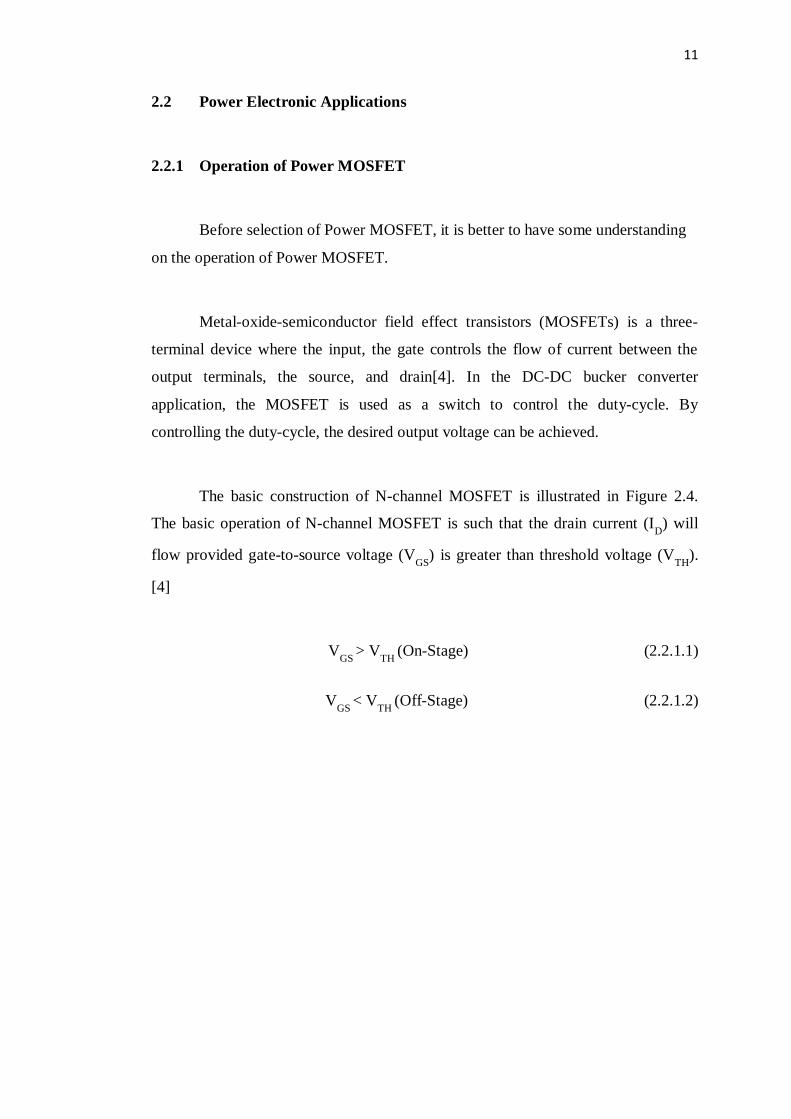
2.2.1 Operation of Power MOSFET
Before selection of Power MOSFET, it is better to have some understanding
on the operation of Power MOSFET.
Metal-oxide-semiconductor field effect transistors (MOSFETs) is a three-
terminal device where the input, the gate controls the flow of current between the
output terminals, the source, and drain[4]. In the DC-DC bucker converter
application, the MOSFET is used as a switch to control the duty-cycle. By
controlling the duty-cycle, the desired output voltage can be achieved.
The basic construction of N-channel MOSFET is illustrated in Figure 2.4.
The basic operation of N-channel MOSFET is such that the drain current (ID) will
flow provided gate-to-source voltage (VGS
) is greater than threshold voltage (VTH
).
[4]
V
GS > V
TH (On-Stage) (2.2.1.1)
V
GS < V
TH (Off-Stage) (2.2.1.2)
12
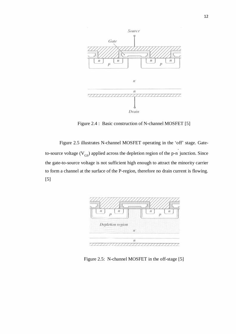
Figure 2.4 : Basic construction of N-channel MOSFET [5]
Figure 2.5 illustrates N-channel MOSFET operating in the „off‟ stage. Gate-
to-source voltage (VGS
) applied across the depletion region of the p-n-
junction. Since
the gate-to-source voltage is not sufficient high enough to attract the minority carrier
to form a channel at the surface of the P-region, therefore no drain current is flowing.
[5]
Figure 2.5: N-channel MOSFET in the off-stage [5]