Embed Size (px)
Citation preview
ASE Confidential / Security-BASE Confidential / Security-B
High Efficiency Power Solutions
byChip Embedding
Dr. Kay EssigASEJune, 2016
© ASE Group. All rights reserved.
ASE Confidential / Security-B
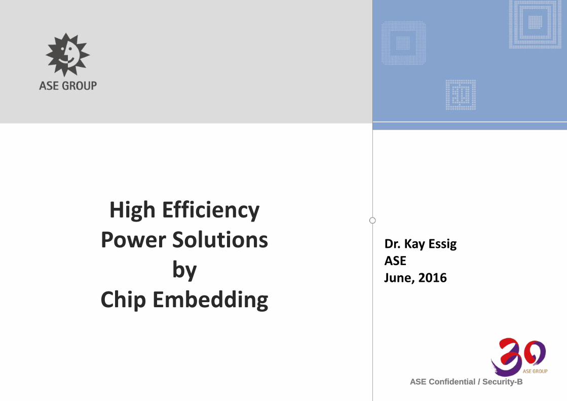
3D Integration
1
TSVStacked
& PoPEmbedded
© ASE Group. All rights reserved.
ASE Confidential / Security-B
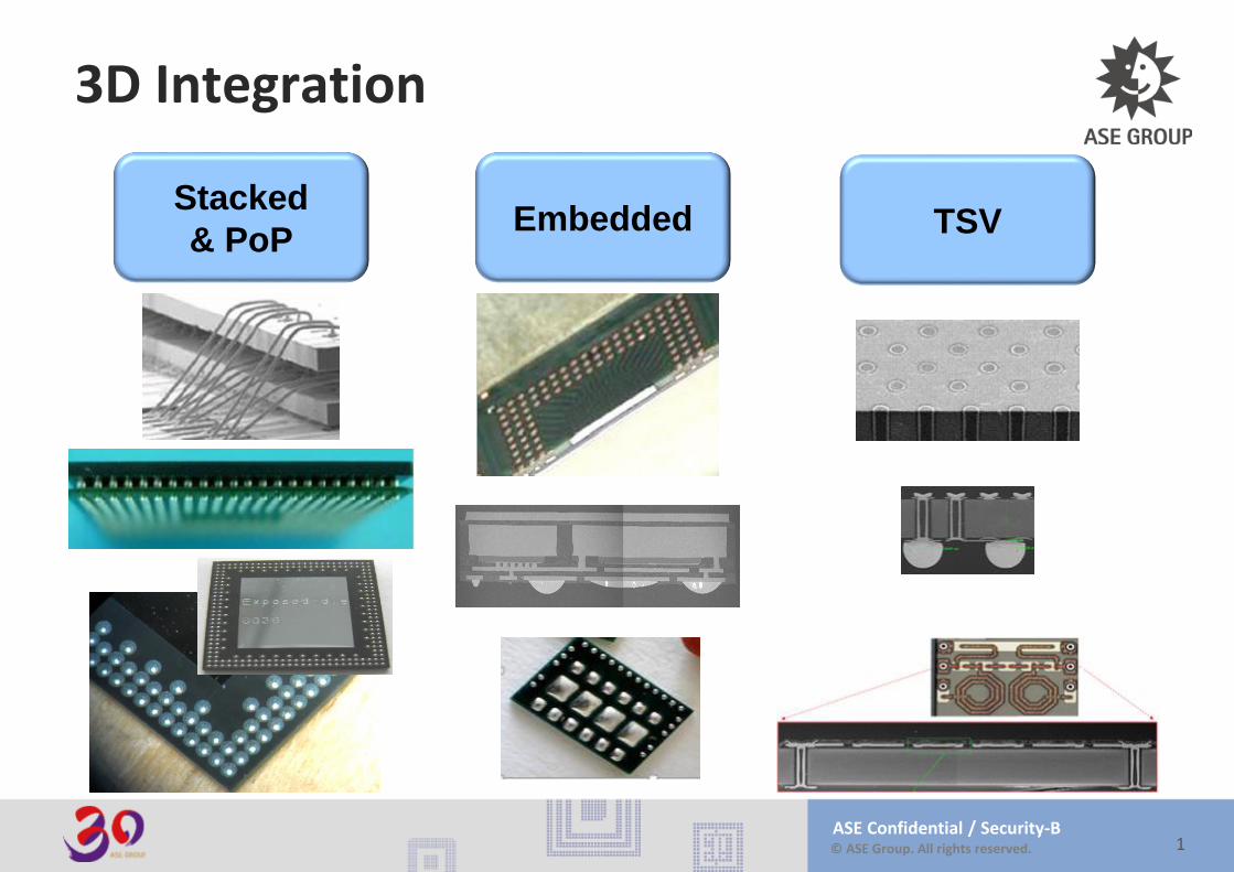
Embedded Technology Introduction
2
Embedded Components
Passive
Placed
Resistors
Capacitors
Formed
Materials are added to the printed circuit structure to create the passive element.
Active (Die)
Wafer LevelEmbedded Die
Embedded Die in Substrate
FOWLP is based on a reconfigured molded wafer infrastructure
Embedded die in package is based on a PCB type of panel infrastructure
© ASE Group. All rights reserved.
ASE Confidential / Security-B
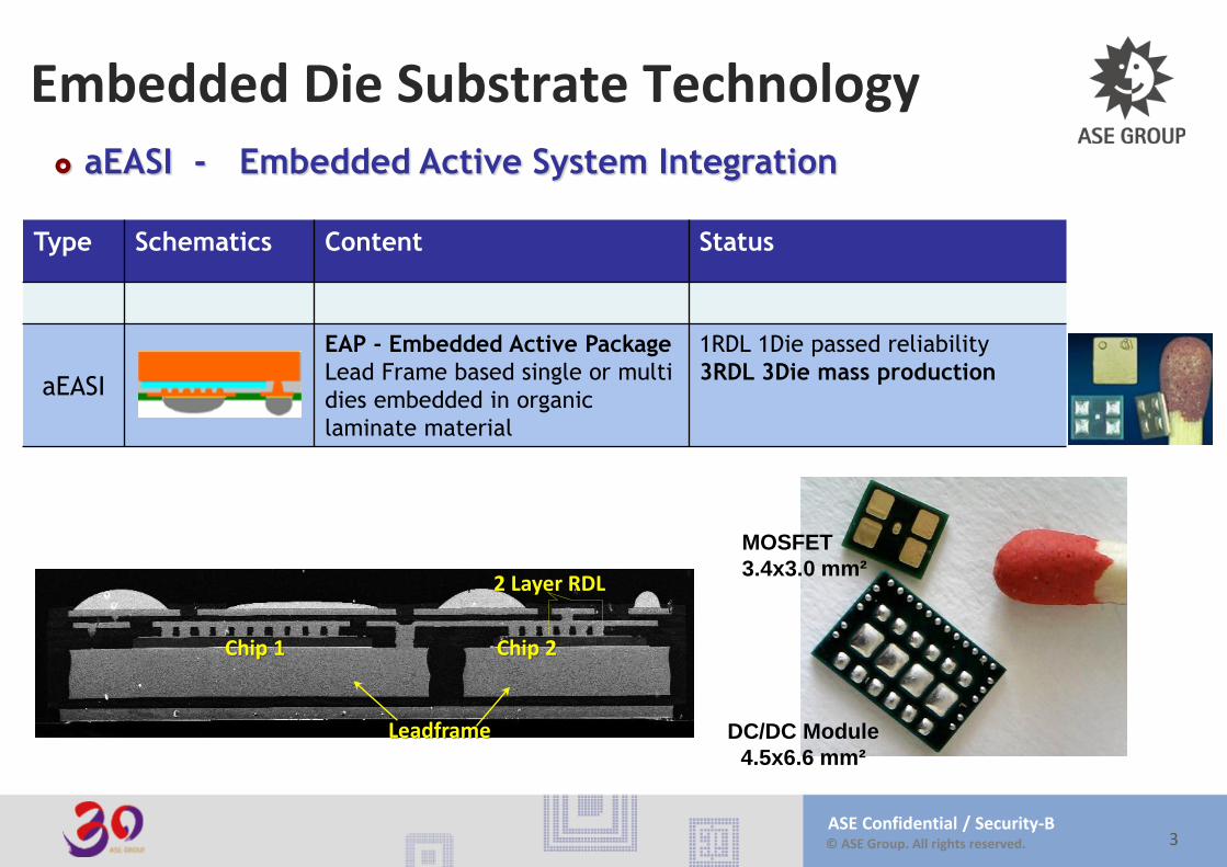
Embedded Die Substrate Technology
3
aEASI - Embedded Active System Integration
Type Schematics Content Status
aEASI
EAP - Embedded Active Package
Lead Frame based single or multi
dies embedded in organic
laminate material
1RDL 1Die passed reliability
3RDL 3Die mass production
DC/DC Module
4.5x6.6 mm²
MOSFET
3.4x3.0 mm²
Leadframe
Chip 1
2 Layer RDL
Chip 2
© ASE Group. All rights reserved.
ASE Confidential / Security-B4
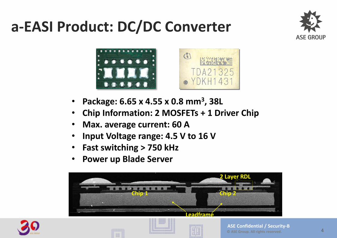
• Package: 6.65 x 4.55 x 0.8 mm3, 38L• Chip Information: 2 MOSFETs + 1 Driver Chip • Max. average current: 60 A• Input Voltage range: 4.5 V to 16 V• Fast switching > 750 kHz• Power up Blade Server
a-EASI Product: DC/DC Converter
Leadframe
Chip 1
2 Layer RDL
Chip 2
© ASE Group. All rights reserved.
ASE Confidential / Security-B
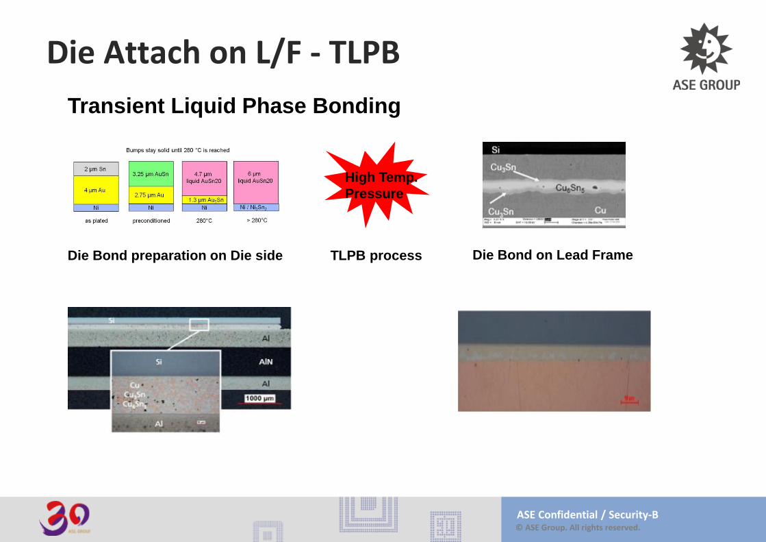
Die Attach on L/F - TLPB
Die Bond preparation on Die side TLPB process
High Temp.
Pressure
Die Bond on Lead Frame
Transient Liquid Phase Bonding
© ASE Group. All rights reserved.
ASE Confidential / Security-B
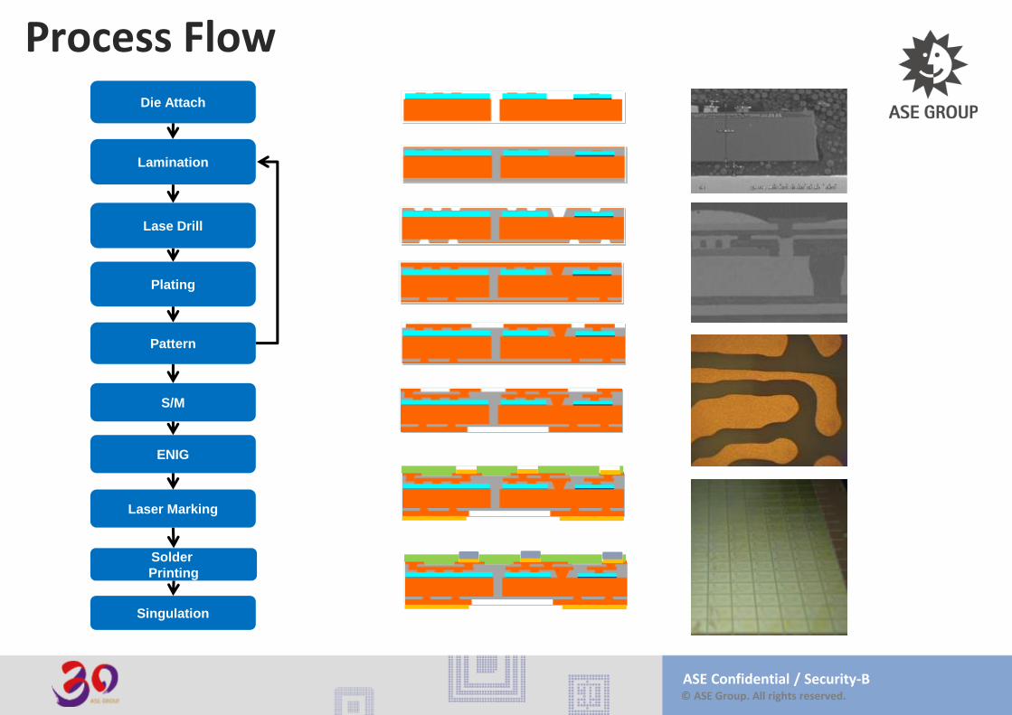
Process Flow
Lamination
Lase Drill
Solder
Printing
Singulation
Laser Marking
Die Attach
Plating
Pattern
ENIG
S/M
© ASE Group. All rights reserved.
ASE Confidential / Security-B
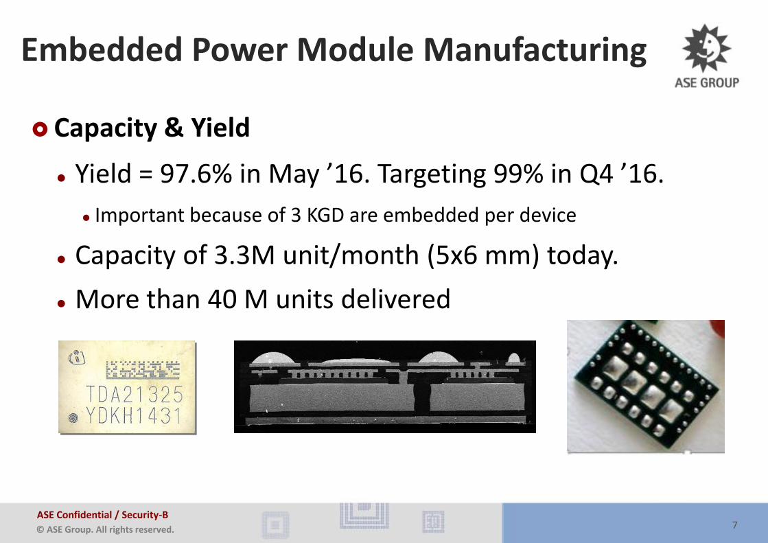
Capacity & Yield
Yield = 97.6% in May ’16. Targeting 99% in Q4 ’16.
Important because of 3 KGD are embedded per device
Capacity of 3.3M unit/month (5x6 mm) today.
More than 40 M units delivered
Embedded Power Module Manufacturing
7
© ASE Group. All rights reserved.
ASE Confidential / Security-B
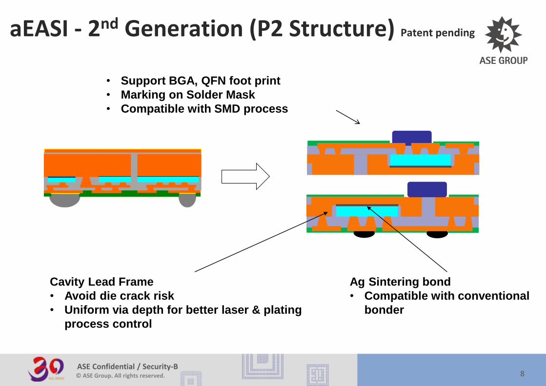
aEASI - 2nd Generation (P2 Structure) Patent pending
8
Cavity Lead Frame
• Avoid die crack risk
• Uniform via depth for better laser & plating
process control
Ag Sintering bond
• Compatible with conventional
bonder
• Support BGA, QFN foot print
• Marking on Solder Mask
• Compatible with SMD process
© ASE Group. All rights reserved.
ASE Confidential / Security-B
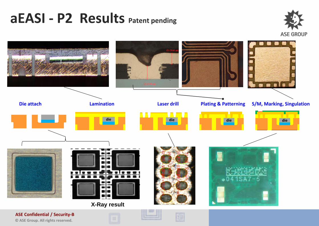
aEASI - P2 Results Patent pending
Die attach Lamination
die
Laser drill
die
Plating & Patterning
die
S/M, Marking, Singulation
die
X-Ray result
© ASE Group. All rights reserved.
ASE Confidential / Security-B
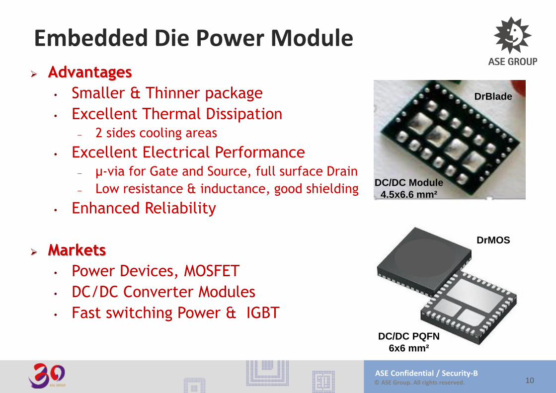
Embedded Die Power Module
10
Advantages
• Smaller & Thinner package
• Excellent Thermal Dissipation 2 sides cooling areas
• Excellent Electrical Performance µ-via for Gate and Source, full surface Drain
Low resistance & inductance, good shielding
• Enhanced Reliability
Markets
• Power Devices, MOSFET
• DC/DC Converter Modules
• Fast switching Power & IGBT
DC/DC Module
4.5x6.6 mm²
DC/DC PQFN
6x6 mm²
DrBlade
DrMOS
© ASE Group. All rights reserved.
ASE Confidential / Security-B11
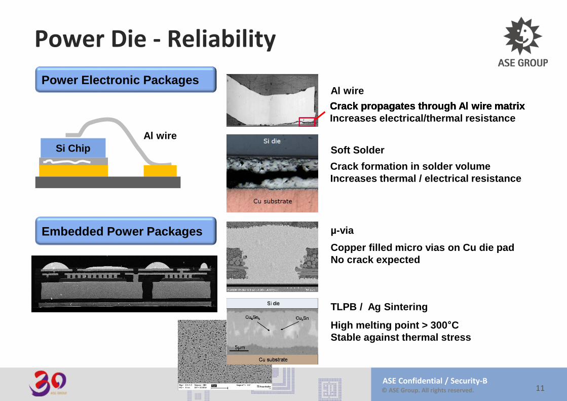
Power Die - Reliability
Si Chip
Crack propagates through Al wire matrix
Crack formation in solder volume
Increases thermal / electrical resistance
Crack propagates through Al wire matrixCrack propagates through Al wire matrix
Increases electrical/thermal resistance
High melting point > 300°CStable against thermal stress
Copper filled micro vias on Cu die pad
No crack expected
Power Electronic Packages
Embedded Power Packages
Al wire
Al wire
Soft Solder
µ-via
TLPB / Ag Sintering
© ASE Group. All rights reserved.
ASE Confidential / Security-B
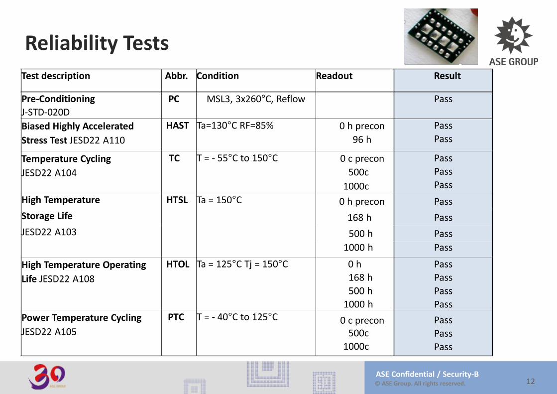
Reliability Tests
12
Test description Abbr. Condition Readout Result
Pre-Conditioning
J-STD-020D
PC MSL3, 3x260°C, Reflow Pass
Biased Highly Accelerated
Stress Test JESD22 A110
HAST Ta=130°C RF=85% 0 h precon
96 h
Pass
Pass
Temperature Cycling
JESD22 A104
TC T = - 55°C to 150°C 0 c precon
500c
1000c
Pass
Pass
Pass
High Temperature HTSL Ta = 150°C 0 h precon Pass
Storage Life 168 h Pass
JESD22 A103 500 h Pass
1000 h Pass
High Temperature Operating
Life JESD22 A108
HTOL Ta = 125°C Tj = 150°C 0 h
168 h
500 h
1000 h
Pass
Pass
Pass
Pass
Power Temperature Cycling
JESD22 A105
PTC T = - 40°C to 125°C 0 c precon 500c
1000c
Pass
Pass
Pass
© ASE Group. All rights reserved.
ASE Confidential / Security-B
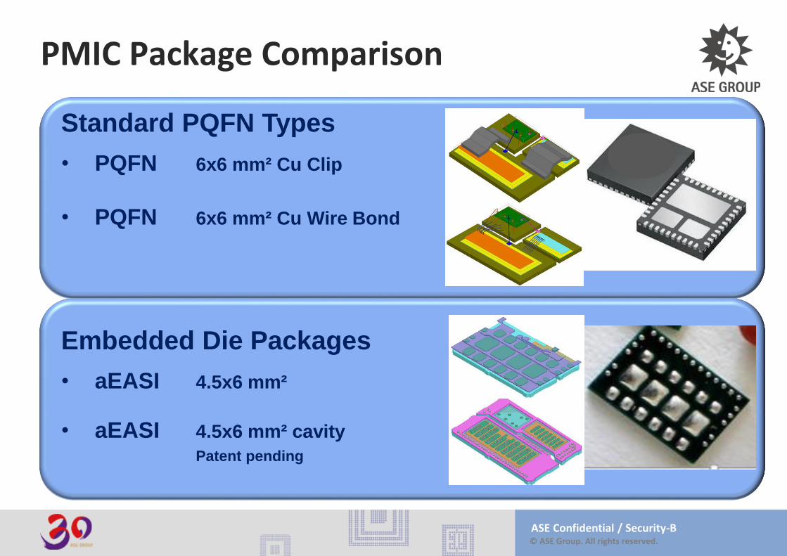
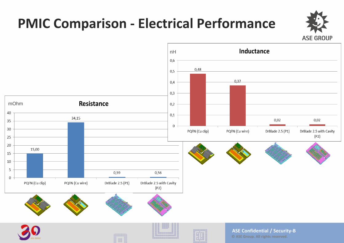
PMIC Package Comparison
Standard PQFN Types
• PQFN 6x6 mm² Cu Clip
• PQFN 6x6 mm² Cu Wire Bond
Embedded Die Packages
• aEASI 4.5x6 mm²
• aEASI 4.5x6 mm² cavity
Patent pending
© ASE Group. All rights reserved.
ASE Confidential / Security-B
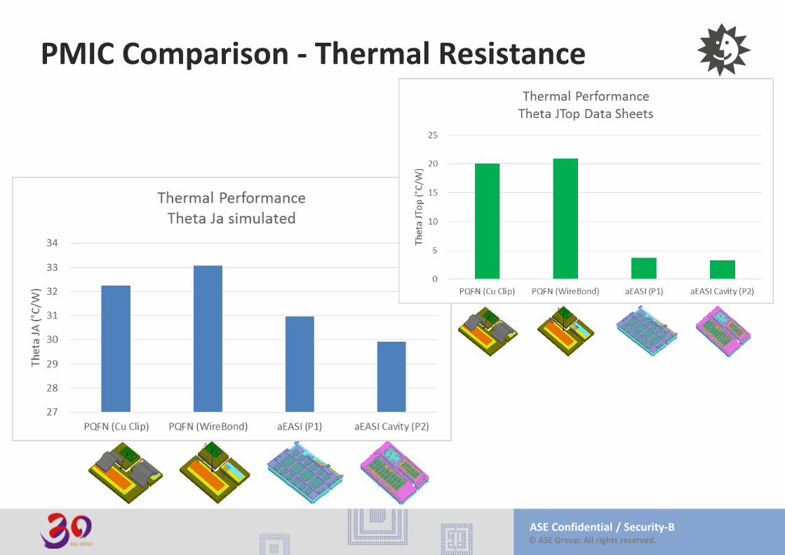
PMIC Comparison - Thermal Resistance
© ASE Group. All rights reserved.
ASE Confidential / Security-B
PMIC Comparison - Electrical Performance
mOhm
nH
© ASE Group. All rights reserved.
ASE Confidential / Security-B
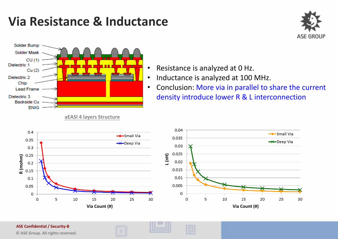
Via Resistance & Inductance
aEASI 4 layers Structure
• Resistance is analyzed at 0 Hz.• Inductance is analyzed at 100 MHz.• Conclusion: More via in parallel to share the current
density introduce lower R & L interconnection
R (
mo
hm
)
Via Count (#)
L (n
H)
Via Count (#)
© ASE Group. All rights reserved.
ASE Confidential / Security-B
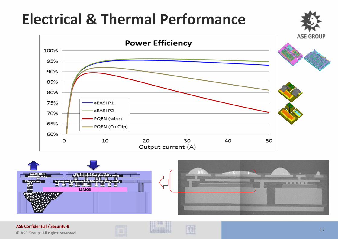
Electrical & Thermal Performance
17
LSMOS
© ASE Group. All rights reserved.
ASE Confidential / Security-B
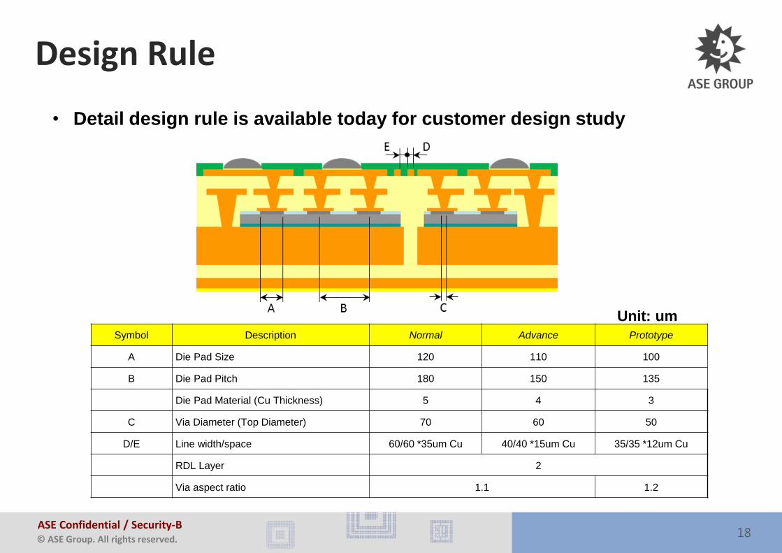
Unit: um
Design Rule
18
Symbol Description Normal Advance Prototype
A Die Pad Size 120 110 100
B Die Pad Pitch 180 150 135
Die Pad Material (Cu Thickness) 5 4 3
C Via Diameter (Top Diameter) 70 60 50
D/E Line width/space 60/60 *35um Cu 40/40 *15um Cu 35/35 *12um Cu
RDL Layer 2
Via aspect ratio 1.1 1.2
• Detail design rule is available today for customer design study
© ASE Group. All rights reserved.
ASE Confidential / Security-B
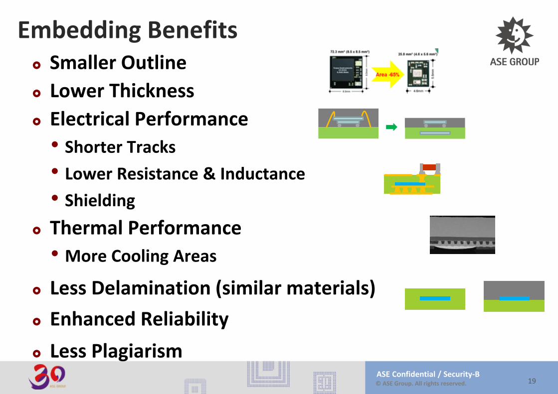
Embedding Benefits Smaller Outline
19
Lower Thickness
Electrical Performance
• Shorter Tracks
• Lower Resistance & Inductance
• Shielding
Thermal Performance
• More Cooling Areas
Less Delamination (similar materials)
Less Plagiarism
Enhanced Reliability
© ASE Group. All rights reserved.
ASE Confidential / Security-B20
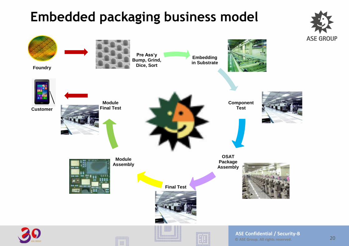
Embedded packaging business model
Embedding in Substrate
Component Test
OSAT Package
Assembly
Final Test
Module Assembly
Module Final Test
Pre Ass‘y Bump, Grind,
Dice, Sort
Process
Flow for
Embedded
Devices
Foundry
Customer
© ASE Group. All rights reserved.
ASE Confidential / Security-B
Summary
Embedded Components can have more and more important benefits than smaller outline
Embedded Power Modules show advantages in Thermal and Electrical Performance
ASE brought aEASI – Embedded Die Power Modules to HVM
Next Gen. aEASI shows enhanced manufacturability and flexibility
© ASE Group. All rights reserved.
ASE Confidential / Security-B
Thank You
www.aseglobal.com
22