Embed Size (px)
Citation preview
High efficiency double-wavelength dielectricmetasurface lenses with dichroic birefringentmeta-atomsEHSAN ARBABI, AMIR ARBABI, SEYEDEH MAHSA KAMALI, YUHORIE, AND ANDREI FARAON*T. J. Watson Laboratory of Applied Physics, California Institute of Technology, 1200 E. California Blvd., Pasadena, California 91125, USA*[email protected]
Abstract: Metasurfaces are ultrathin optical structures that manipulate optical wavefronts.Most metasurface devices which deflect light are designed for operation at a single wavelength,and their function changes as the wavelength is varied. Here we propose and demonstrate adouble-wavelength metasurface based on polarization dependent dielectric meta-atoms thatcontrol the phases of two orthogonal polarizations independently. Using this platform, we designlenses that focus light at 915 and 780 nm with perpendicular linear polarizations to the samefocal distance. Lenses with numerical apertures up to 0.7 and efficiencies from 65% to above90% are demonstrated. In addition to the high efficiency and numerical aperture, an importantfeature of this technique is that the two operation wavelengths can be chosen to be arbitrarilyclose. These characteristics make these lenses especially attractive for fluorescence microscopyapplications.
© 2016 Optical Society of America
OCIS codes: (050.6624) Subwavelength structures; (050.1965) Diffractive lenses; (220.1000) Aberration compensa-tion; (050.2555) Form birefringence.
References and links1. A. V. Kildishev, A. Boltasseva, and V. M. Shalaev, “Planar photonics with metasurfaces,” Science 339, 1232009
(2013).2. N. Yu and F. Capasso, “Flat optics with designer metasurfaces,” Nature Mater. 13, 139–150 (2014).3. S. Jahani and Z. Jacob, “All-dielectric metamaterials,” Nature Nanotech. 11, 23–36 (2016).4. P. Lalanne, S. Astilean, P. Chavel, E. Cambril, and H. Launois, “Blazed binary subwavelength gratings with
efficiencies larger than those of conventional echelette gratings,” Opt. Lett. 23, 1081–1083 (1998).5. S. Astilean, P. Lalanne, P. Chavel, E. Cambril, and H. Launois, “High-efficiency subwavelength diffractive element
patterned in a high-refractive-index material for 633 nm,” Opt. Lett. 23, 552–554 (1998).6. P. Lalanne, S. Astilean, P. Chavel, E. Cambril, and H. Launois, “Design and fabrication of blazed binary diffractive
elements with sampling periods smaller than the structural cutoff,” J. Opt. Soc. Am. A 16, 1143–1156 (1999).7. D. Fattal, J. Li, Z. Peng, M. Fiorentino, and R. G. Beausoleil, “Flat dielectric grating reflectors with focusing
abilities,” Nature Photon. 4, 466–470 (2010).8. D. Lin, P. Fan, E. Hasman, and M. L. Brongersma, “Dielectric gradient metasurface optical elements,” Science
345, 298–302 (2014).9. A. Arbabi, M. Bagheri, A. J. Ball, Y. Horie, D. Fattal, and A. Faraon, “Controlling the phase front of optical fiber
beams using high contrast metastructures” in CLEO: Science and Innovations, OSA Technical Digest (online)(Optical Society of America, 2014), paper STu3M.4.
10. S. Vo, D. Fattal, W. V. Sorin, P. Zhen, T. Tho, M. Fiorentino, and R. G. Beausoleil, “Sub-wavelength grating lenseswith a twist,” IEEE Photonics Technol. Lett. 26, 1375–1378 (2014).
11. A. Arbabi, Y. Horie, A. J. Ball, M. Bagheri, and A. Faraon, “Subwavelength-thick lenses with high numericalapertures and large efficiency based on high-contrast transmitarrays,” Nat. Commun. 6, 7069 (2015).
12. A. Arbabi, Y. Horie, M. Bagheri, and A. Faraon, “Dielectric metasurfaces for complete control of phase andpolarization with subwavelength spatial resolution and high transmission,” Nature Nanotech. 10, 937–943 (2015).
13. P. R. West, J. L. Stewart, A. V. Kildishev, V. M. Shalaev, V. V. Shkunov, F. Strohkendl, Y. A. Zakharenkov, R. K.Dodds, and R. Byren, “All-dielectric subwavelength metasurface focusing lens,” Opt. Express 22, 26212–26221(2014).
14. M. Decker, I. Staude, M. Falkner, J. Dominguez, D. N. Neshev, I. Brener, T. Pertsch, and Y. S. Kivshar, “High-efficiency dielectric huygens’ surfaces,” Adv. Opt. Mater. 3, 813–820 (2015).
Vol. 24, No. 16 | 8 Aug 2016 | OPTICS EXPRESS 18468
#267421 http://dx.doi.org/10.1364/OE.24.018468 Journal © 2016 Received 2 Jun 2016; revised 23 Jul 2016; accepted 25 Jul 2016; published 3 Aug 2016
15. Y. F. Yu, A. Y. Zhu, R. Paniagua-Dominguez, Y. H. Fu, B. Luk’yanchuk, and A. I. Kuznetsov, “High-transmissiondielectric metasurface with 2π phase control at visible wavelengths,” Laser Photon. Rev. 9, 412–418 (2015).
16. A. Arbabi, R. M. Briggs, Y. Horie, M. Bagheri, and A. Faraon, “Efficient dielectric metasurface collimating lensesfor mid-infrared quantum cascade lasers,” Opt. Express 23, 33310–33317 (2015).
17. S. Campione, L. I. Basilio, L. K. Warne, and M. B. Sinclair, “Tailoring dielectric resonator geometries fordirectional scattering and huygens’ metasurfaces,” Opt. Express 23, 2293–2307 (2015).
18. M. I. Shalaev, J. Sun, A. Tsukernik, A. Pandey, K. Nikolskiy, and N. M. Litchinitser, “High-efficiency all-dielectricmetasurfaces for ultracompact beam manipulation in transmission mode,” Nano Lett. 15, 6261–6266 (2015).
19. S. M. Kamali, A. Arbabi, E. Arbabi, Y. Horie, and A. Faraon, “Decoupling optical function and geometrical formusing conformal flexible dielectric metasurfaces,” Nat. Commun. 7, 11618 (2016).
20. S. M. Kamali, E. Arbabi, A. Arbabi, Y. Horie, and A. Faraon, “Highly tunable elastic dielectric metasurface lenses,”arXiv:1604.03597 (2016).
21. A. Faraon, A. Arbabi, Y. Horie, E. Arbabi, and S. M. Kamali, “Flat free-space optical elements based ondielectric metasurfaces,” SPIE Newsroom, http://spie.org/newsroom/6375-flat-free-space-optical-elements-based-on-dielectric-metasurfaces?ArticleID=x117825.
22. Y. Ren, L. Li, Z. Wang, S. M. Kamali, E. Arbabi, A. Arbabi, Z. Zhao, G. Xie, Y. Cao, N. Ahmed, Y. Yan, C. Liu,A. J. Willner, S. Ashrafi, M. Tur, A. Faraon, and A. E. Willner, “Orbital angular momentum-based space divisionmultiplexing for high-capacity underwater optical communications,” arXiv:1604.06865 (2016).
23. M. Born and E. Wolf, Principles of Optics: Electromagnetic Theory of Propagation, Interference and Diffractionof Light (Cambridge University ,1999).
24. D. C. O’Shea, T. J. Suleski, A. D. Kathman, and D. W. Prather, Diffractive Optics: Design, Fabrication, and Test(SPIE, 2004).
25. F. Aieta, M. A. Kats, P. Genevet, and F. Capasso, “Multiwavelength achromatic metasurfaces by dispersive phasecompensation,” Science 347, 1342–1345 (2015).
26. E. Arbabi, A. Arbabi, S. M. Kamali, Y. Horie, and A. Faraon, “Multiwavelength polarization-insensitive lensesbased on dielectric metasurfaces with meta-molecules,” Optica 3, 628–633 (2016).
27. O. Eisenbach, O. Avayu, R. Ditcovski, and T. Ellenbogen, “Metasurfaces based dual wavelength diffractive lenses,”Opt. Express 23, 3928–3936 (2015).
28. M. Khorasaninejad, F. Aieta, P. Kanhaiya, M. A. Kats, P. Genevet, D. Rousso, and F. Capasso, “Achromaticmetasurface lens at telecommunication wavelengths,” Nano Lett. 15, 5358–5362 (2015).
29. Z. Zhao, M. Pu, H. Gao, J. Jin, X. Li, X. Ma, Y. Wang, P. Gao, and X. Luo, “Multispectral optical metasurfacesenabled by achromatic phase transition,” Sci. Rep. 5, 15781 (2015).
30. M. P. Backlund, A. Arbabi, P. N. Petrov, E. Arbabi, S. Saurabh, A. Faraon, and W. E. Moerner, “Removingorientation-induced localization biases in single-molecule microscopy using a broadband metasurface mask,”Nature Photon. 10, 459–462 (2016).
31. V. Liu and S. Fan, “S4 : A free electromagnetic solver for layered periodic structures,” Comput. Phys. Commun.183, 2233–2244 (2012).
32. P. Lalanne, “Waveguiding in blazed-binary diffractive elements,” J. Opt. Soc. Am. A 16, 2517–2520 (1999).33. D. B. Murphy and M. W. Davidson, Fundamentals of Light Microscopy and Electronic Imaging, 2nd ed. (Wiley-
Blackwell, 2012).34. A. Arbabi, E. Arbabi, S. M. Kamali, Y. Horie, S. Han, and A. Faraon, “An optical metasurface planar camera,”
arXiv:1604.06160 (2016).
Metasurfaces are two-dimensional arrangements of sub-wavelength optical scatterers de-signed to control the amplitude, phase, and polarization of light [1–8]. Among these, highcontrast dielectric metasurfaces have proven to be very versatile due to their high efficiencyand ability to control phase and polarization of light with subwavelength resolution on bothplanar and non-planar surfaces in different parts of the optical spectrum [9–22]. Similar toother diffractive optical elements, metasurfaces with deflection capabilities such as lenses andbeam deflectors suffer from chromatic aberrations [23–26], as schematically shown in Fig. 1(a).Multi-wavelength metasurface lenses have been demonstrated using several techniques includingpolarization and wavelength selectivity of plasmonic nano-scatterers [27], aperiodic arrays ofcoupled dielectric resonators [25, 28], generating a hologram with the combined phase pro-files for multiple wavelengths [29], and using metamolecules formed from combining multiplemeta-atoms [26]. However, lenses demonstrated by these methods have multiple focuses at eachwavelength [25, 27–29] or have low efficiency at least at some of the wavelengths [25–29]. Inaddition, although the metamolecule technique used in [26] results in a single focus at each wave-length, the corrected wavelengths cannot be very close. Here we demonstrate double-wavelength
Vol. 24, No. 16 | 8 Aug 2016 | OPTICS EXPRESS 18469
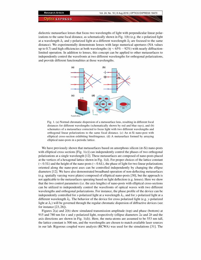
dielectric metasurface lenses that focus two wavelengths of light with perpendicular linear polar-izations to the same focal distance, as schematically shown in Fig. 1(b) (e.g. the x-polarized lightat a wavelength λ1 and y-polarized light at a different wavelength λ2 are focused to the samedistance). We experimentally demonstrate lenses with large numerical apertures (NA valuesup to 0.7) and high efficiencies at both wavelengths (η ∼ 65%−92%) with nearly diffraction-limited operation. In addition to lenses, this concept can be applied to other metasurfaces toindependently control the wavefronts at two different wavelengths for orthogonal polarizations,and provide different functionalities at those wavelengths.
(a) (b)
(c) (d)
Λ
Λ
2a
2b
x
y
Fused silica
α-Si
Fig. 1. (a) Normal chromatic dispersion of a metasurface lens, resulting in different focaldistances for different wavelengths (schematically shown by red and blue rays), and (b)schematics of a metasurface corrected to focus light with two different wavelengths andorthogonal linear polarizations to the same focal distance. (c) An α-Si nano-post withelliptical cross-section exhibiting birefringence. (d) A metasurface formed by arrayingelliptical nano-posts in a periodic lattice.
We have previously shown that metasurfaces based on amorphous silicon (α-Si) nano-postswith elliptical cross sections [Fig. 1(c)] can independently control the phases of two orthogonalpolarizations at a single wavelength [12]. These metasurfaces are composed of nano-posts placedat the vertices of a hexagonal lattice shown in Fig. 1(d). For proper choices of the lattice constant(∼ 0.5λ ) and the height of the nano-posts (∼ 0.6λ ), the phase of light for two linear polarizationsoriented along the nano-post axes can be controlled independently by changing the ellipsediameters [12]. We have also demonstrated broadband operation of non-deflecting metasurfaces(e.g. spatially varying wave plates) composed of elliptical nano-posts [30], but the approach isnot applicable to the metasurfaces operating based on light deflection (e.g. lenses). Here we showthat the two control parameters (i.e. the axis lengths) of nano-posts with elliptical cross-sectionscan be utilized to independently control the wavefronts of optical waves with two differentwavelengths and orthogonal polarizations. For instance, the phase profile of the device can beindependently controlled for x-polarized light at a wavelength λ1, and for y-polarized light at adifferent wavelength λ2. The behavior of the device for cross polarized light (e.g. y-polarizedlight at λ1) will be governed through the regular chromatic dispersion of diffractive devices (seefor instance [23, 26]).
Figures 2(a) and 2(b) show simulated transmission amplitude (top) and phase (bottom) at915 and 780 nm for x and y-polarized light, respectively (ellipse diameters 2a and 2b and theaxis directions are shown in Fig. 1(d)). Here, the meta-atoms are assumed to be 553 nm tall,the lattice constant is 500 nm, and the wavelengths are chosen to match available laser sourcesin our lab. Rigorous coupled wave analysis (RCWA) was used for the simulations [31]. The
Vol. 24, No. 16 | 8 Aug 2016 | OPTICS EXPRESS 18470
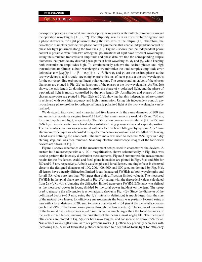
nano-posts operate as truncated multimode optical waveguides with multiple resonances aroundthe operation wavelengths [11, 19, 32]. The ellipticity, results in an effective birefringence anda phase difference for light polarized along the two axes of the ellipse [12]. Therefore, thetwo ellipse diameters provide two phase control parameters that enable independent control ofphase for light polarized along the two axes [12]. Figure 2 shows that the independent phasecontrol is possible even if the two orthogonal polarizations of light have different wavelengths.Using the simulated transmission amplitude and phase data, we find the corresponding ellipsediameters that provide any desired phase pairs at both wavelengths, φ1 and φ2, while keepingboth transmission amplitudes high. To simultaneously achieve the desired phases and hightransmission amplitudes at both wavelengths, we minimize the total complex amplitude errordefined as ε = |exp(iφ1)− t1|2 + |exp(iφ2)− t2|2. Here φ1 and φ2 are the desired phases at thetwo wavelengths, and t1 and t2 are complex transmissions of nano-posts at the two wavelengthsfor the corresponding orthogonal linear polarizations. The corresponding values of the chosendiameters are plotted in Fig. 2(c) as functions of the phases at the two wavelengths. As Fig. 2(c)shows, the axis length 2a dominantly controls the phase of x-polarized light, and the phase ofy-polarized light is mostly controlled by the axis length 2b. Amplitudes and phases of thesechosen nano-posts are plotted in Figs. 2(d) and 2(e), showing that this independent phase controlis achieved with very high accuracy and high transmission. Using this independent control, anytwo arbitrary phase profiles for orthogonal linearly polarized light at the two wavelengths can berealized.
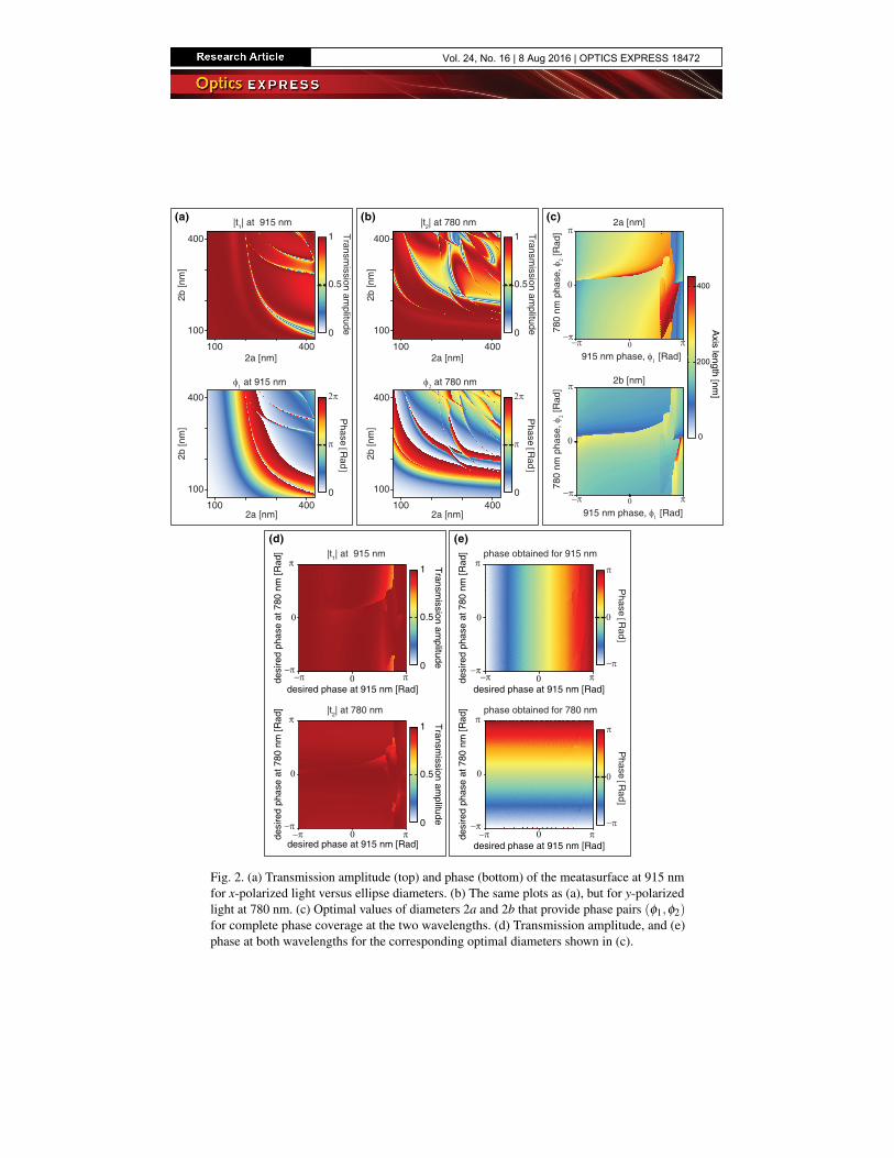
We designed, fabricated, and characterized five lenses with the same diameter of 200 µmand numerical apertures ranging from 0.12 to 0.7 that simultaneously work at 915 and 780 nm,for x and y-polarized light, respectively. The fabrication process was similar to [12]: a 553 nmα-Si layer was deposited on a fused silica substrate using plasma enhanced vapor deposition.The metasurface pattern was generated with an electron beam lithography system. A ∼70 nmaluminum oxide layer was deposited using electron beam evaporation, and was lifted off, leavinga hard mask defining the nano-posts. The hard mask was used to etch the α-Si layer in a dryetching step, and was then removed. Scanning electron microscope images of the fabricateddevices are shown in Fig. 3.
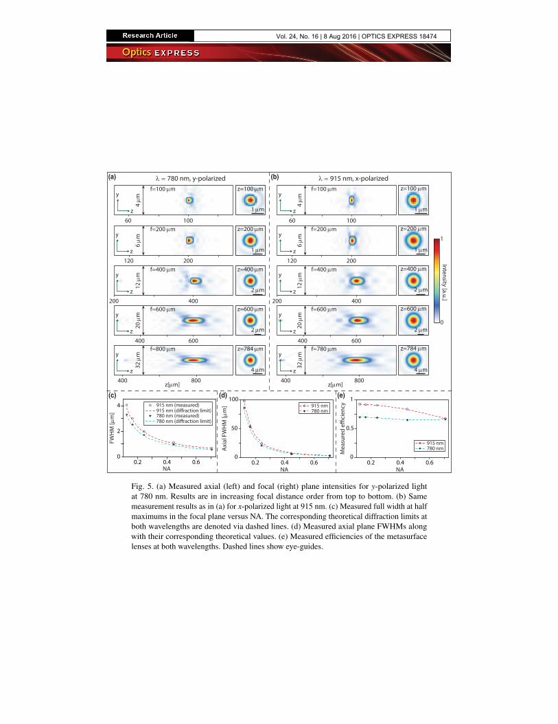
Figure 4 shows schematics of the measurement setups used to characterize the devices. Acustom built microscope with a ∼100× magnification, shown schematically in Fig. 4(a), wasused to perform the intensity distribution measurements. Figure 5 summarizes the measurementresults for the five lenses. Axial and focal plane intensities are plotted in Figs. 5(a) and 5(b) for780 and 915 nm, respectively. At both wavelengths and for all lenses, one single focus is observedclose to the designed distances of 100, 200, 400, 600, and 800 µm. As denoted by Fig. 5(c),all lenses have a nearly diffraction limited focus (measured FWHMs at both wavelengths andfor all NA values are less than 7% larger than their diffraction limited values). The measuredFWHMs in the axial plane are plotted in Fig. 5(d), along with the theoretical values calculatedfrom 2πw2/λ , with w denoting the diffraction limited transverse FWHM. Efficiency was definedas the measured power in focus, divided by the total power incident on the lens. The setupused to measure the efficiencies is schematically shown in Fig. 4(b). Since the diameter of thecollimated beam (∼2.3 mm, using the 1/e2 intensity definition) is much larger than the sizeof the metasurface lenses, for efficiency measurements the beam was partially focused using alens with a focal distance of 200 mm to have a diameter of ∼134 µm at the metasurface lenses(such that 99% of the beam power passes through the lens aperture). The radius of curvatureof the beam at the metasurfaces is ∼16 mm, which is much larger than the focal distances ofthe metasurface lenses, making the curvature of the beam almost negligible. The measuredefficiencies are plotted in Fig. 5(e) for both wavelengths, and are seen to be above 65% for allNAs at both wavelengths. Similar to our previous works [11], efficiency generally decreases withincreasing NA. A set of fabricated pinholes were used to filter out-of-focus light for efficiency
Vol. 24, No. 16 | 8 Aug 2016 | OPTICS EXPRESS 18471
(a) |t1| at 915 nm
φ1 at 915 nm
0.5
1
0
Transmission am
plitude
π
2π
0
Phase [R
ad]
2b [n
m]
2a [nm]100
100
400
400
2b [n
m]
2a [nm]100
100
400
400
2b [n
m]
2a [nm]
φ2 at 780 nm
|t2| at 780 nm
100
100
400
400
(b)
0.5
1
0
Transmission am
plitude
π
2π
0
Phase [R
ad]2b
[nm
]
2a [nm]100
100
400
400
780
nm p
hase
, φ2 [
Rad
]
915 nm phase, φ1 [Rad]
0
0 π−π
π
−π
(c) 2a [nm]
780
nm p
hase
, φ2 [
Rad
]
915 nm phase, φ1 [Rad]
0
0 π−π
π
−π
2b [nm]
200
400
0
Axis length [nm
]
|t1| at 915 nm
0.5
1
0
Transmission am
plitude
0.5
1
0
Transmission am
plitude
|t2| at 780 nm
desi
red
phas
e at
780
nm
[Rad
]
desired phase at 915 nm [Rad]
0
0 π−π
π
−π
(d)
desi
red
phas
e at
780
nm
[Rad
]
desired phase at 915 nm [Rad]
0
0 π−π
π
−π
0
−π
π
Phase [R
ad]
0
−π
π
Phase [R
ad]
phase obtained for 915 nm
phase obtained for 780 nm
desi
red
phas
e at
780
nm
[Rad
]
desired phase at 915 nm [Rad]
0
0 π−π
π
−π
(e)
desi
red
phas
e at
780
nm
[Rad
]
desired phase at 915 nm [Rad]
0
0 π−π
π
−π
Fig. 2. (a) Transmission amplitude (top) and phase (bottom) of the meatasurface at 915 nmfor x-polarized light versus ellipse diameters. (b) The same plots as (a), but for y-polarizedlight at 780 nm. (c) Optimal values of diameters 2a and 2b that provide phase pairs (φ1,φ2)for complete phase coverage at the two wavelengths. (d) Transmission amplitude, and (e)phase at both wavelengths for the corresponding optimal diameters shown in (c).
Vol. 24, No. 16 | 8 Aug 2016 | OPTICS EXPRESS 18472
(b)
500 nm
(a)
2 µm
Fig. 3. (a) Scanning electron micrograph of a fabricated device viewed normally, and (b) ata tilt angle.
Objective lens
Tube lens
CameraDevice
Polarizer
(a)
LaserCollimator
Polarizationcontroller
Device
Pinhole
(b)Optical power meter
PolarizerLaser
Collimator
Polarizationcontroller
Fig. 4. (a) Schematic of the measurement setup used for measuring intensity profiles, and(b) focusing efficiencies.
measurements. Diameters of the used pinholes were 6, 6, 10, 15, and 20 µm for different lensesin decreasing NA order. We attribute the lower efficiency at 780 nm to higher sensitivity of itsphase to fabrication errors.
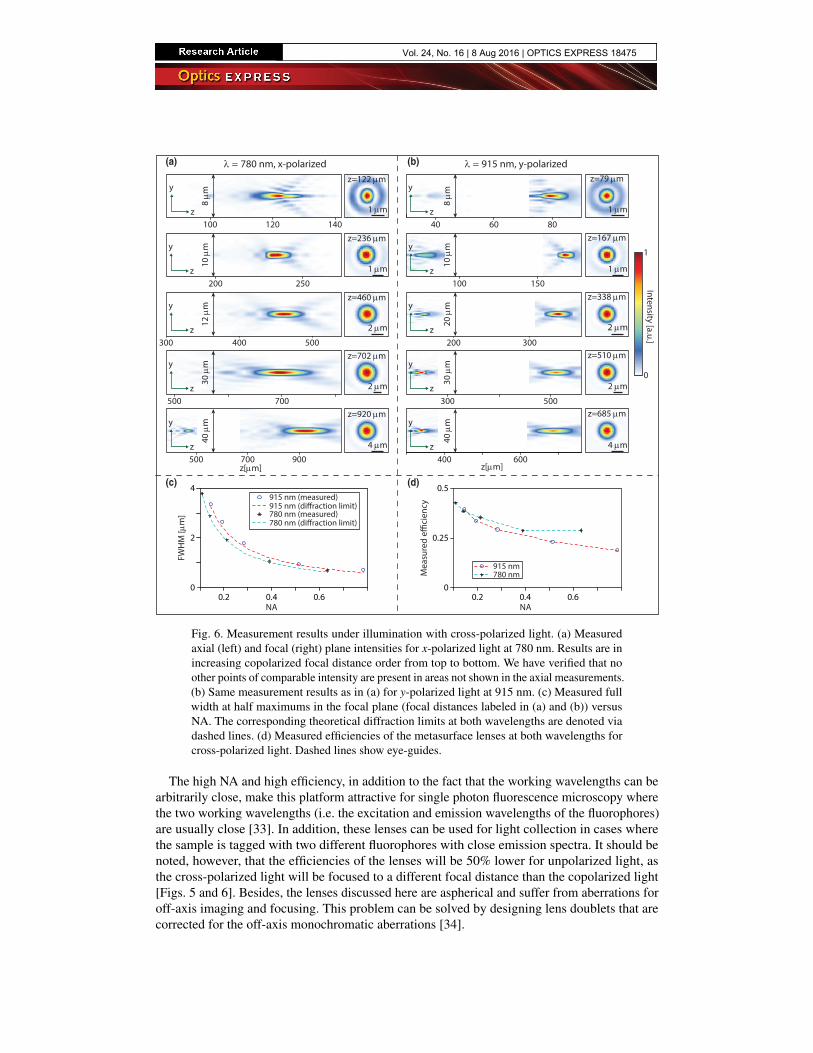
We have also characterized the operation of the devices under illumination with cross-polarized light (i.e. y-polarized light at 915 nm, and x-polarized light at 780 nm). In cross-polarized operation, the devices also exhibit Fresnel phase zones but these zones are not optimized for focusing to a tight spot. Indeed, the cross-polarization measurement results summarized in Fig. 6 show that the devices focus cross-polarized light as well, but with lower efficiency, higher distortions, and to focal distances different from the corresponding copolarized values. It is worth noting that these devices operate as diffractive lenses with different phase profiles for x and y-polarized light. Also, for each polarization they follow the regular chromatic dispersion of diffractive lenses, and therefore their focal distance changes with wavelength proportional to 1/λ [23, 24, 26]. Since cross-polarized light is focused to a different focal distance, it can be considered as loss when the device focuses unpolarized light. When the devices are used for imaging applications, the excitation and the collected paths need to be passed through polarizers. Otherwise, the image will exhibit elevated background and/or imaging artifacts depending on the exact lens design.
Vol. 24, No. 16 | 8 Aug 2016 | OPTICS EXPRESS 18473
1
0
Intensity [a.u.]
(a) (b)
z[µm]400 800
z
y
z[µm]
32 µ
m
400 600
z
y
20 µ
m
200 400
z
y
12 µ
m
120 200
z
y
6 µm
400 800
z
y
32 µ
m
4 µm
400 600
z
y
20 µ
m
2 µm
200 400
z
y
12 µ
m
2 µm
120 200
z
y
6 µm
1 µm
4 µm
2 µm
2 µm
1 µm
1 µm
z=100 µm
z=200 µm
z=400 µm
z=600 µm
z=784 µm
f=100 µm
f=200 µm
f=400 µm
f=600 µm
f=800 µm
60 100
z
y
4 µm
1 µm
60 100
z
y
4 µm
λ = 780 nm, y-polarized λ = 915 nm, x-polarized
(c)
FWH
M [µ
m]
Axi
al F
WH
M [µ
m]
0.2 0.4 0.60
2
4 915 nm (measured)
780 nm (measured)915 nm (di�raction limit)
780 nm (di�raction limit)
NA
(e)
Mea
sure
d e�
cien
cy
0.2 0.4 0.6
0.5
1
0
915 nm780 nm
NA
(d)
0.2 0.4 0.6
50
100
0
915 nm780 nm
NA
z=100 µm
z=200 µm
z=400 µm
z=600 µm
z=784 µm
f=100 µm
f=200 µm
f=400 µm
f=600 µm
f=780 µm
Fig. 5. (a) Measured axial (left) and focal (right) plane intensities for y-polarized lightat 780 nm. Results are in increasing focal distance order from top to bottom. (b) Samemeasurement results as in (a) for x-polarized light at 915 nm. (c) Measured full width at halfmaximums in the focal plane versus NA. The corresponding theoretical diffraction limits atboth wavelengths are denoted via dashed lines. (d) Measured axial plane FWHMs alongwith their corresponding theoretical values. (e) Measured efficiencies of the metasurfacelenses at both wavelengths. Dashed lines show eye-guides.
Vol. 24, No. 16 | 8 Aug 2016 | OPTICS EXPRESS 18474
1
0
Intensity [a.u.](a) (b)
z[µm]500 700 900z
y
z[µm]
40 µ
m
500 700z
y
30 µ
m
300 400 500z
y
12 µ
m
200 250z
y
10 µ
m
400 600z
y
40 µ
m4 µm
300 500z
y
30 µ
m
2 µm
200 300z
y
20 µ
m
2 µm
100 150z
y
10 µ
m
1 µm
4 µm
2 µm
2 µm
1 µm
1 µm
z=122 µm
z=236 µm
z=460 µm
z=702 µm
z=920 µm
100 120 140z
y
8 µm
1 µm
60 8040z
y
8 µm
λ = 780 nm, x-polarized λ = 915 nm, y-polarized
(c) (d)
Mea
sure
d e�
cien
cy
0.25
0.5
0
915 nm780 nm
z=79 µm
z=167 µm
z=338 µm
z=510 µm
z=685 µm
FWH
M [µ
m]
0
2
4915 nm (measured)
780 nm (measured)915 nm (di�raction limit)
780 nm (di�raction limit)
0.2 0.4 0.6NA
0.2 0.4 0.6NA
Fig. 6. Measurement results under illumination with cross-polarized light. (a) Measuredaxial (left) and focal (right) plane intensities for x-polarized light at 780 nm. Results are inincreasing copolarized focal distance order from top to bottom. We have verified that noother points of comparable intensity are present in areas not shown in the axial measurements.(b) Same measurement results as in (a) for y-polarized light at 915 nm. (c) Measured fullwidth at half maximums in the focal plane (focal distances labeled in (a) and (b)) versusNA. The corresponding theoretical diffraction limits at both wavelengths are denoted viadashed lines. (d) Measured efficiencies of the metasurface lenses at both wavelengths forcross-polarized light. Dashed lines show eye-guides.
The high NA and high efficiency, in addition to the fact that the working wavelengths can bearbitrarily close, make this platform attractive for single photon fluorescence microscopy wherethe two working wavelengths (i.e. the excitation and emission wavelengths of the fluorophores)are usually close [33]. In addition, these lenses can be used for light collection in cases wherethe sample is tagged with two different fluorophores with close emission spectra. It should benoted, however, that the efficiencies of the lenses will be 50% lower for unpolarized light, asthe cross-polarized light will be focused to a different focal distance than the copolarized light[Figs. 5 and 6]. Besides, the lenses discussed here are aspherical and suffer from aberrations foroff-axis imaging and focusing. This problem can be solved by designing lens doublets that arecorrected for the off-axis monochromatic aberrations [34].
Vol. 24, No. 16 | 8 Aug 2016 | OPTICS EXPRESS 18475
The maximum distance between the two operating wavelengths of the proposed metasurfaceplatform is limited by practical considerations. The nano-posts height should be large enoughto provide the required 2π phase at the longer wavelength. This results in higher sensitivity ofthe phases of nano-posts at the shorter wavelength to fabrication errors, which in turn decreasesdevice efficiency at that wavelength. This lower efficiency at the shorter wavelength is alreadyobserved in this work. Thus, the maximum wavelength distance is limited mostly by practicalconsiderations and the achievable fabrication tolerances.
In conclusion, birefringent elliptical nano-posts can be used to independently control opticalwavefronts at two different wavelengths with orthogonal linear polarizations. This control can beutilized to generate any desired wavefronts at both wavelengths, resulting in an optical behaviorat each wavelength independent from the other one. Using these meta-atoms, we demonstrateddouble-wavelength metasurface lenses that focus x and y-polarized light at 915 and 780 nm,respectively, to the same focal distance. Lenses with NA values up to 0.7 were experimentallydemonstrated to have nearly diffraction limited operation and efficiencies above 65%. Thismethod can also be combined with the recently demonstrated meta-molecule concept [26] toachieve more phase control parameters, and chromatically corrected lenses at four or morewavelengths.
Funding
This work was supported by Samsung Electronics. A.A. was also supported by National ScienceFoundation (NSF) award 1512266. S.M.K. was supported by the U.S. Department of Energy(DOE) “Light-Material Interactions in Energy Conversion” Energy Frontier Research Centerunder grant DE-SC0001293.
Acknowledgments
The devices were fabricated at the Kavli Nanoscience Institute at Caltech.
Vol. 24, No. 16 | 8 Aug 2016 | OPTICS EXPRESS 18476

![arXiv:1711.01448v1 [physics.app-ph] 4 Nov 2017 · The waveguide-fed metasurface is an emerging concept for aperture antenna design that leverages resonant, sub-wavelength, radiating](https://img.pdfslide.us/doc/110x75/5e916d6dbbf4310e00238d86/arxiv171101448v1-4-nov-2017-the-waveguide-fed-metasurface-is-an-emerging-concept.jpg)


![Chiral All-Dielectric Metasurface Based on Elliptic …downloads.hindawi.com/journals/ijap/aip/6352418.pdffunctionalities [8-16] were developed for several microwave THz, and optical](https://img.pdfslide.us/doc/110x75/5b1cde667f8b9af2348c3bc4/chiral-all-dielectric-metasurface-based-on-elliptic-8-16-were-developed-for-several.jpg)