Embed Size (px)
Citation preview
March 13th, 2009 5th Int'l Conference & Exhibit on D evice Packaging1/30
High Accuracy Placement,
In-situ Reflow or Thermo-Compression Bonding
Enabling High Density and Fine Pitch in 3D-IC
with Chip to Wafer Bonding Approach
Illustrated by an Application using Micro-Insertion
Gilbert Lecarpentier*, Jean Stephane Mottet*, François Marion*** SET S.A.S. (Smart Equipment Technology), Saint Jeoire, France
** CEA-LETI Minatec - Grenoble, France
March 13th, 2009 5th Int'l Conference & Exhibit on D evice Packaging2/30
OUTLINE
Introduction
Wafer Stacking Vs Chip-to-Wafer Bonding
Chip Bond Processes
Benefit of the Self Leveling Function
Conclusion
March 13th, 2009 5th Int'l Conference & Exhibit on D evice Packaging3/30
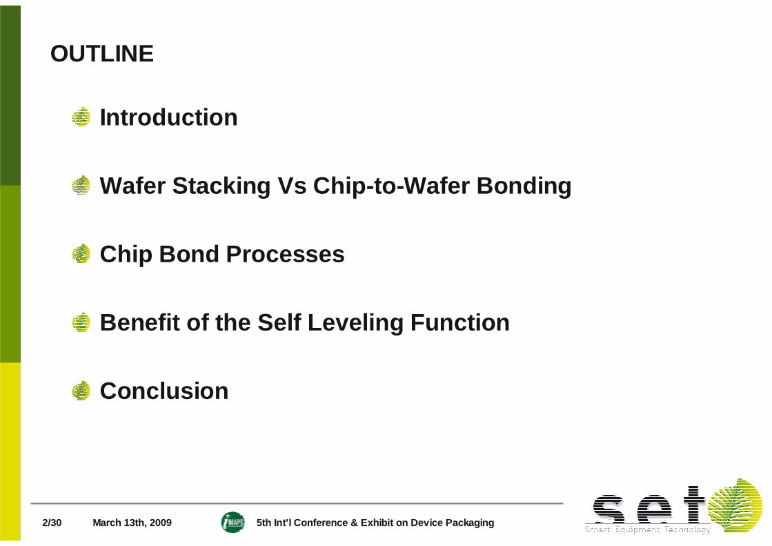
WHY 3D
3D provides an alternative to scaling
Drivers are:
� Performances
� Form Factor
� Cost
March 13th, 2009 5th Int'l Conference & Exhibit on D evice Packaging4/30
3D, NOVEL TECHNIQUE ?
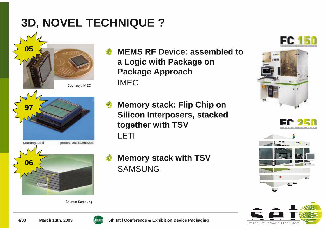
MEMS RF Device: assembled to a Logic with Package on Package ApproachIMEC
Memory stack: Flip Chip on Silicon Interposers, stacked together with TSVLETI
Memory stack with TSVSAMSUNG
Courtesy: IMEC
Source: Samsung
05
97
06
March 13th, 2009 5th Int'l Conference & Exhibit on D evice Packaging5/30
PLACEMENT SCHEMES
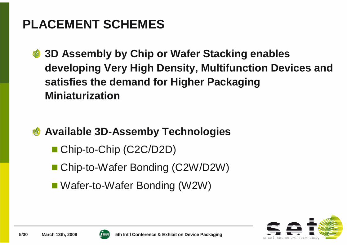
3D Assembly by Chip or Wafer Stacking enables developing Very High Density, Multifunction Devices and satisfies the demand for Higher Packaging Miniaturization
Available 3D-Assemby Technologies
� Chip-to-Chip (C2C/D2D)
� Chip-to-Wafer Bonding (C2W/D2W)
� Wafer-to-Wafer Bonding (W2W)
March 13th, 2009 5th Int'l Conference & Exhibit on D evice Packaging6/30
PLACEMENT SCHEMES
SET
March 13th, 2009 5th Int'l Conference & Exhibit on D evice Packaging7/30
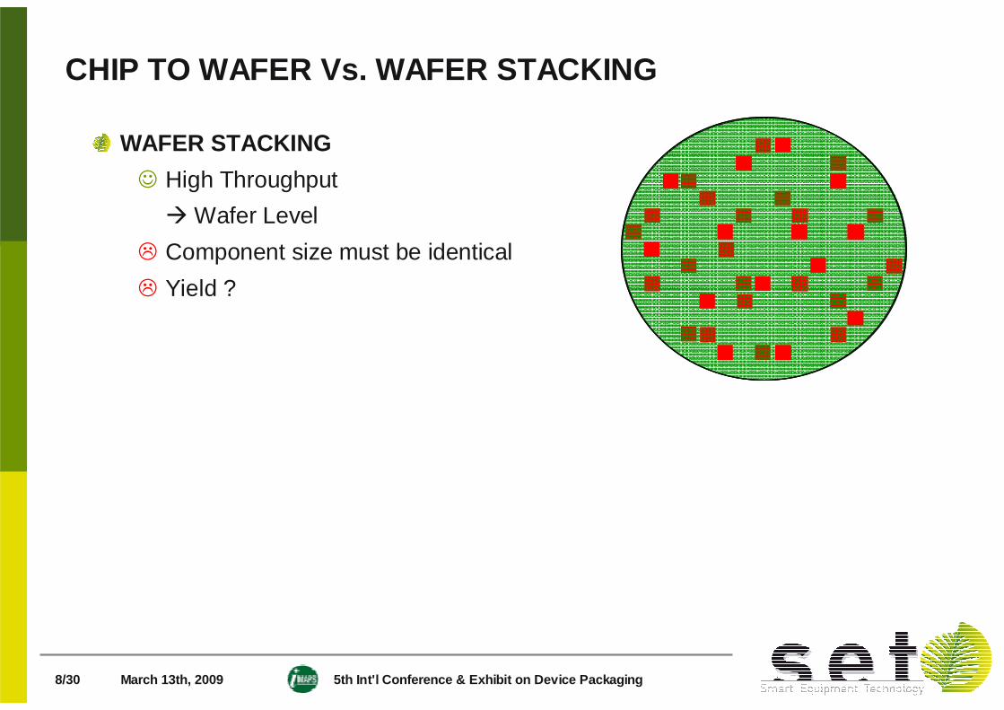
CHIP TO WAFER Vs. WAFER STACKING
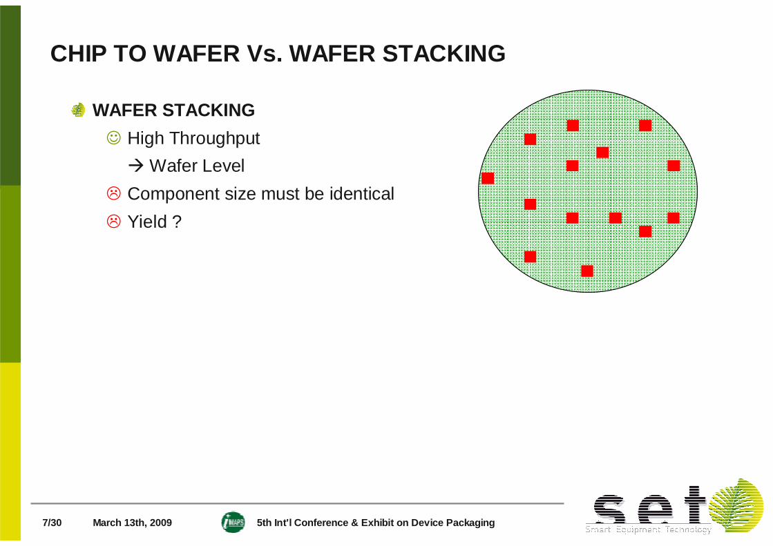
WAFER STACKING
☺ High Throughput
� Wafer Level
� Component size must be identical
� Yield ?
March 13th, 2009 5th Int'l Conference & Exhibit on D evice Packaging8/30
CHIP TO WAFER Vs. WAFER STACKING
WAFER STACKING
☺ High Throughput
� Wafer Level
� Component size must be identical
� Yield ?
March 13th, 2009 5th Int'l Conference & Exhibit on D evice Packaging9/30
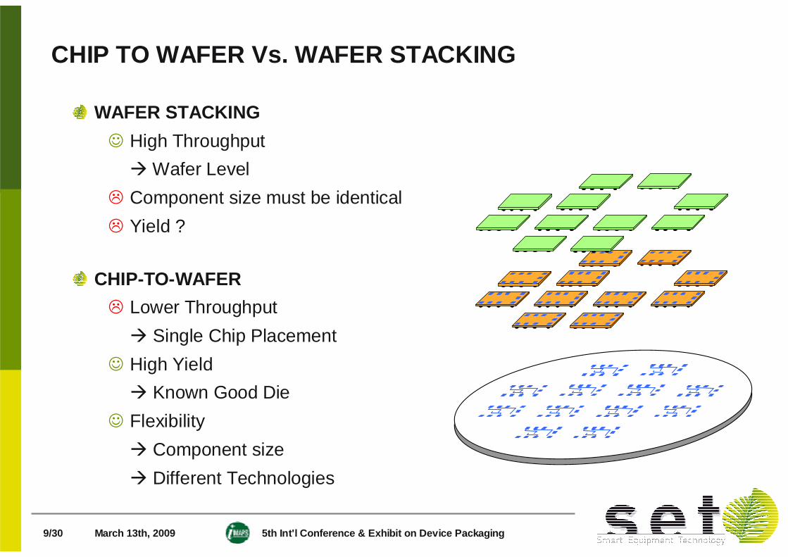
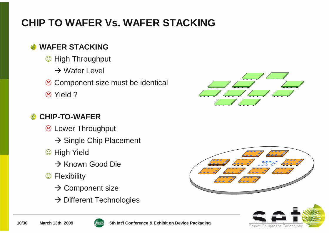
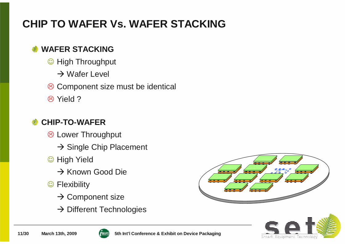
CHIP TO WAFER Vs. WAFER STACKING
WAFER STACKING
☺ High Throughput
� Wafer Level
� Component size must be identical
� Yield ?
CHIP-TO-WAFER
� Lower Throughput
� Single Chip Placement
☺ High Yield
� Known Good Die
☺ Flexibility
� Component size
� Different Technologies
March 13th, 2009 5th Int'l Conference & Exhibit on D evice Packaging10/30
CHIP TO WAFER Vs. WAFER STACKING
WAFER STACKING
☺ High Throughput
� Wafer Level
� Component size must be identical
� Yield ?
CHIP-TO-WAFER
� Lower Throughput
� Single Chip Placement
☺ High Yield
� Known Good Die
☺ Flexibility
� Component size
� Different Technologies
March 13th, 2009 5th Int'l Conference & Exhibit on D evice Packaging11/30
CHIP TO WAFER Vs. WAFER STACKING
WAFER STACKING
☺ High Throughput
� Wafer Level
� Component size must be identical
� Yield ?
CHIP-TO-WAFER
� Lower Throughput
� Single Chip Placement
☺ High Yield
� Known Good Die
☺ Flexibility
� Component size
� Different Technologies
March 13th, 2009 5th Int'l Conference & Exhibit on D evice Packaging12/30
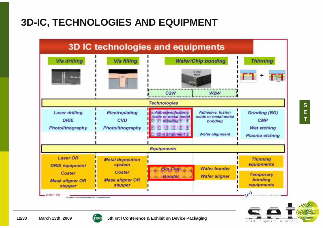
3D-IC, TECHNOLOGIES AND EQUIPMENT
SET
March 13th, 2009 5th Int'l Conference & Exhibit on D evice Packaging13/30
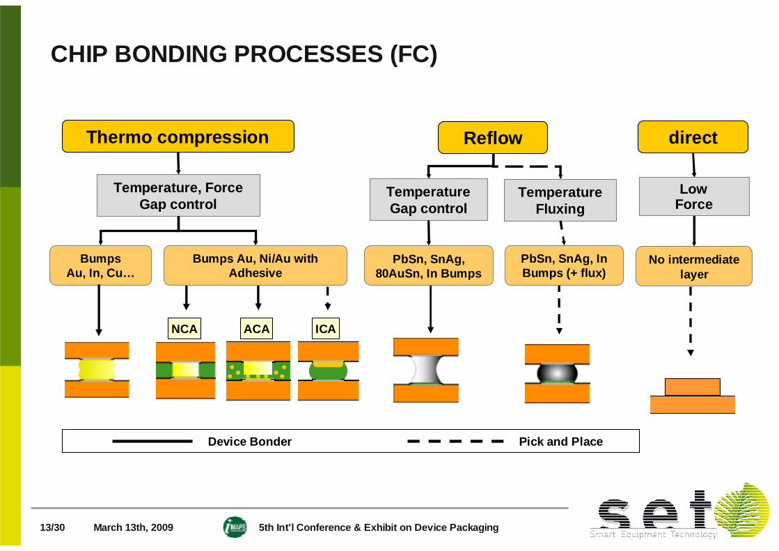
CHIP BONDING PROCESSES (FC)
Device Bonder Pick and Place
ICANCA ACA
Bumps Au, Ni/Au with Adhesive
Reflow
TemperatureFluxing
BumpsAu, In, Cu…
PbSn, SnAg, 80AuSn, In Bumps
PbSn, SnAg, InBumps (+ flux)
TemperatureGap control
Thermo compression
Temperature, ForceGap control
No intermediate layer
direct
LowForce
March 13th, 2009 5th Int'l Conference & Exhibit on D evice Packaging14/30
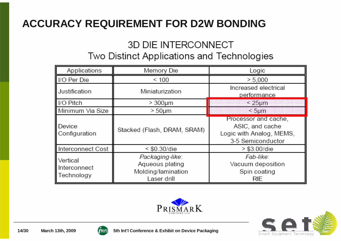
ACCURACY REQUIREMENT FOR D2W BONDING
March 13th, 2009 5th Int'l Conference & Exhibit on D evice Packaging15/30
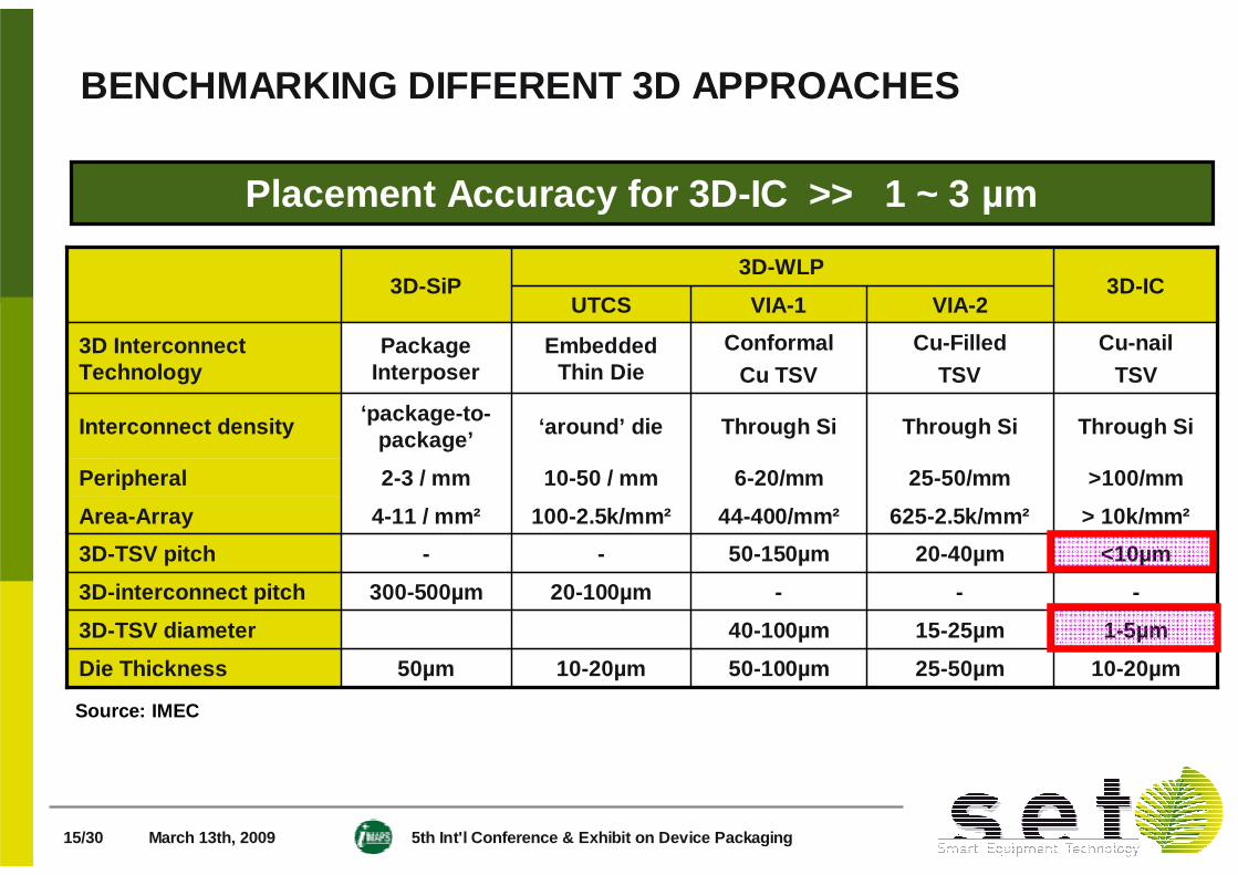
BENCHMARKING DIFFERENT 3D APPROACHES
3D-IC3D-WLP
3D-SiP
> 10k/mm²625-2.5k/mm²44-400/mm²100-2.5k/mm²4-11 / mm²Area-Array
>100/mm25-50/mm6-20/mm10-50 / mm2-3 / mmPeripheral
<10µm20-40µm50-150µm--3D-TSV pitch
---20-100µm300-500µm3D-interconnect pitch
10-20µm25-50µm50-100µm10-20µm50µmDie Thickness
1-5µm15-25µm40-100µm3D-TSV diameter
Through SiThrough SiThrough Si‘around’ die‘package-to-
package’Interconnect density
Cu-nailTSV
Cu-FilledTSV
ConformalCu TSV
Embedded Thin Die
Package Interposer
3D Interconnect Technology
VIA-2VIA-1UTCS
Placement Accuracy for 3D-IC >> 1 ~ 3 µm
Source: IMEC
March 13th, 2009 5th Int'l Conference & Exhibit on D evice Packaging16/30
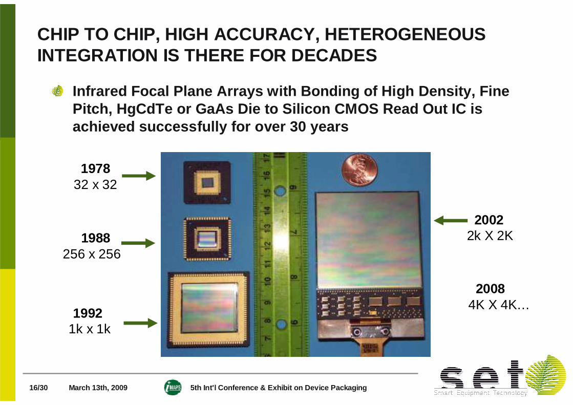
CHIP TO CHIP, HIGH ACCURACY, HETEROGENEOUS INTEGRATION IS THERE FOR DECADES
Infrared Focal Plane Arrays with Bonding of High De nsity, Fine Pitch, HgCdTe or GaAs Die to Silicon CMOS Read Out IC is achieved successfully for over 30 years
197832 x 32
1988256 x 256
19921k x 1k
20022k X 2K
20084K X 4K…
March 13th, 2009 5th Int'l Conference & Exhibit on D evice Packaging17/30
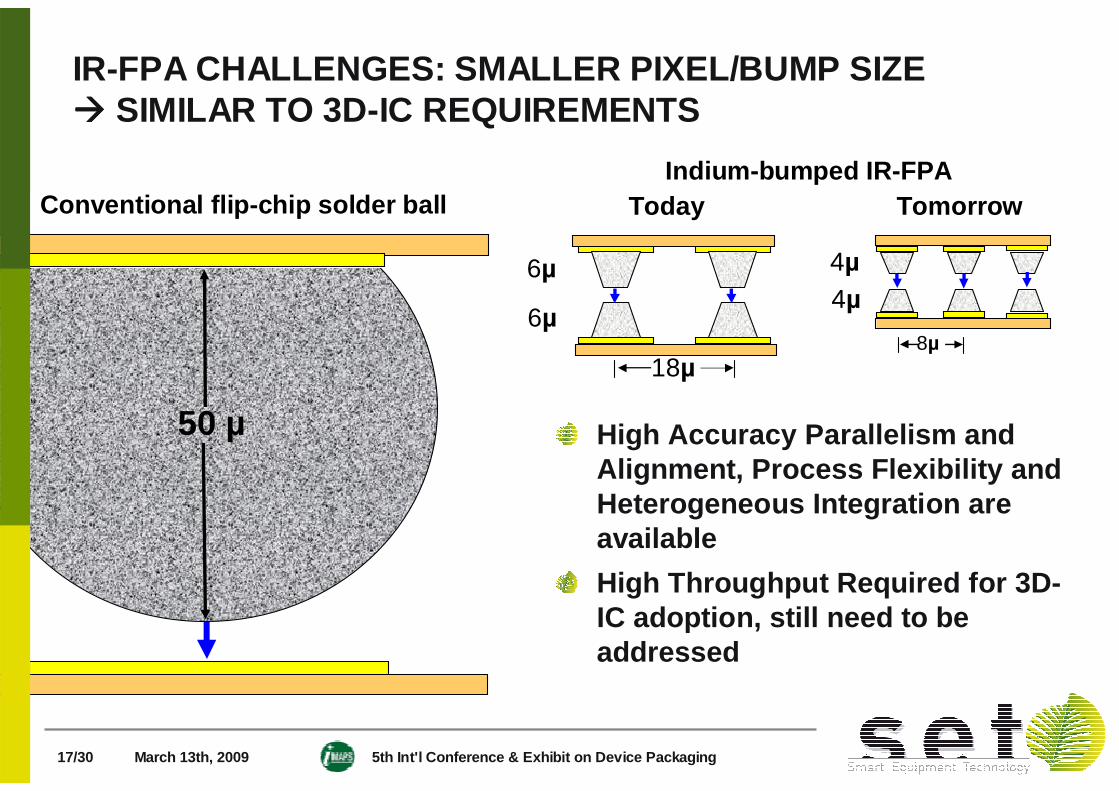
IR-FPA CHALLENGES: SMALLER PIXEL/BUMP SIZE���� SIMILAR TO 3D-IC REQUIREMENTS
High Accuracy Parallelism and Alignment, Process Flexibility and Heterogeneous Integration are available
High Throughput Required for 3D-IC adoption, still need to be addressed
Conventional flip-chip solder ball Today Tomorrow
50 µ
6µ
6µ
18µ
4µ4µ
8µ
Indium-bumped IR-FPA
March 13th, 2009 5th Int'l Conference & Exhibit on D evice Packaging18/30
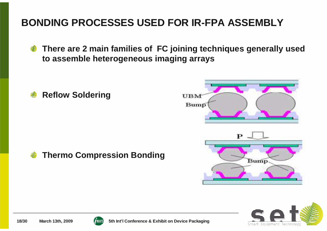
BONDING PROCESSES USED FOR IR-FPA ASSEMBLY
There are 2 main families of FC joining techniques generally used to assemble heterogeneous imaging arrays
Reflow Soldering
Thermo Compression Bonding
March 13th, 2009 5th Int'l Conference & Exhibit on D evice Packaging19/30
BONDING PROCESSES USED FOR IR-FPA ASSEMBLY
Reflow Soldering� T > Solder Melting Point� CTE Mismatch makes Alignment more and more difficult as Pitch
decrease and chip size increase� Oxide protection or removal is required
(Presented at Imaps - Device Packaging 2008)� Die Warp and Smaller Bumps make Self Alignment reflow impossible
Thermo Compression Bonding� T < Solder Melting Point� Force increases as the number of Pixel Number increases
( over 3 tons on large state of the art IR-FPA for Aerospace )
March 13th, 2009 5th Int'l Conference & Exhibit on D evice Packaging20/30
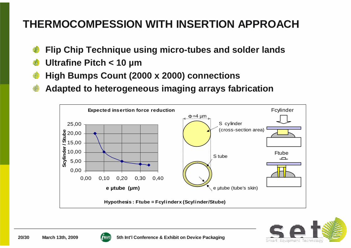
THERMOCOMPESSION WITH INSERTION APPROACH
Flip Chip Technique using micro-tubes and solder la ndsUltrafine Pitch < 10 µmHigh Bumps Count (2000 x 2000) connectionsAdapted to heterogeneous imaging arrays fabrication
0,00
5,00
10,00
15,00
20,00
25,00
0,00 0,10 0,20 0,30 0,40
e µtube (µm)
Scy
linde
r / S
tub
e
Expected insertion force reduction
Hypothesis : Ftube = Fcylinderx (Scylinder/Stube)
e µtube (tube's skin)
S tubeFtube
Φ =4 µm
S cylinder(cross-section area)
Fcylinder
March 13th, 2009 5th Int'l Conference & Exhibit on D evice Packaging21/30
THERMOCOMPESSION WITH INSERTION APPROACH
Flux Less� Gold plated µtubes break the native solder oxide establishing
electrical contact� No flux cleaning is required
Low Pressure� Sharp µtubes geometry and indium solder ductility, enable insertion
at low force (<0.5mN/connection)
� Can be handled by conventional FC Bonding equipment even for high very pin counts (i.e: >4 million connections)
Room Temperature� No CTE mismatch issues
� Bonding step can be completed by solid-solid diffusion
March 13th, 2009 5th Int'l Conference & Exhibit on D evice Packaging22/30
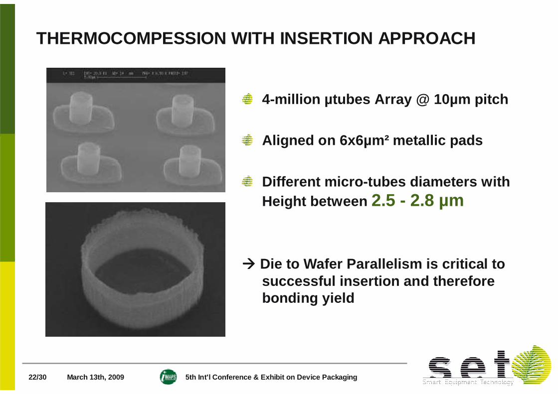
THERMOCOMPESSION WITH INSERTION APPROACH
4-million µtubes Array @ 10µm pitch
Aligned on 6x6µm² metallic pads
Different micro-tubes diameters with Height between 2.5 - 2.8 µm
���� Die to Wafer Parallelism is critical to successful insertion and therefore bonding yield
March 13th, 2009 5th Int'l Conference & Exhibit on D evice Packaging23/30
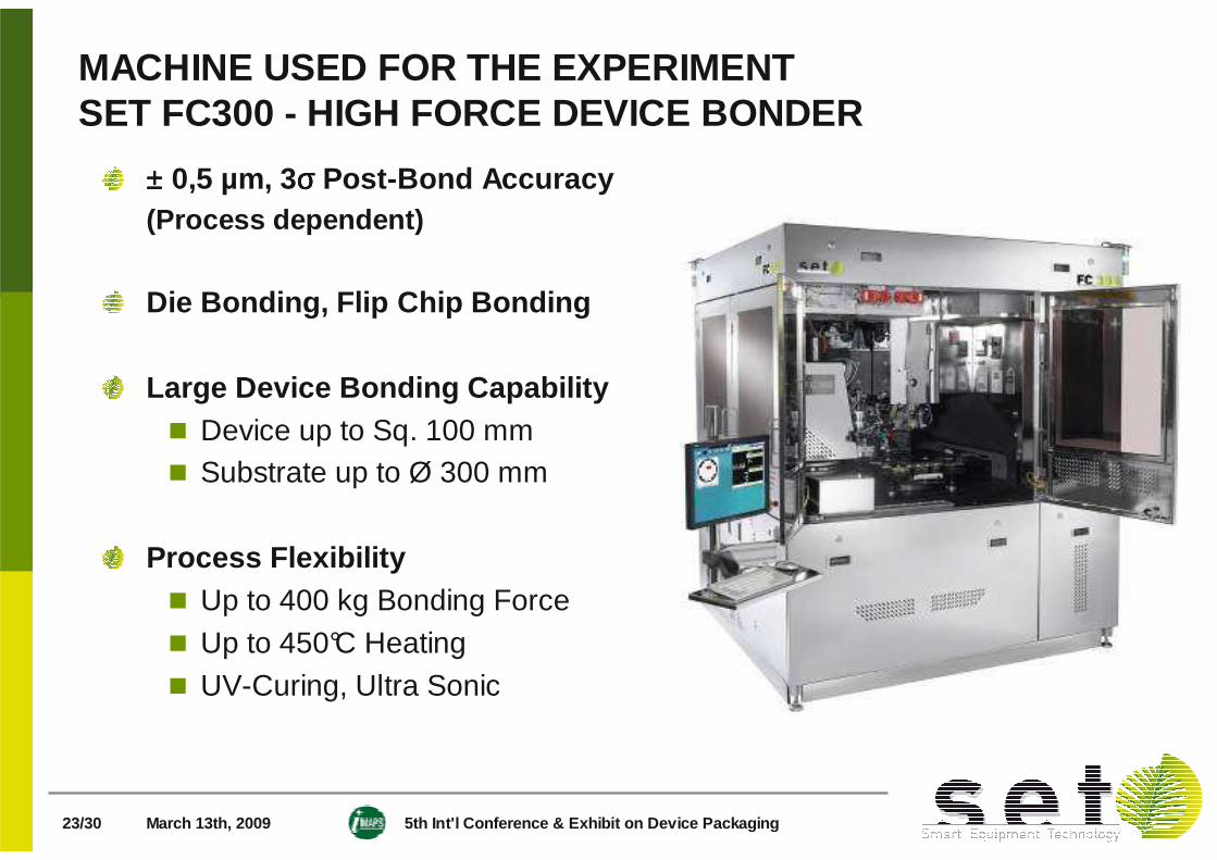
MACHINE USED FOR THE EXPERIMENTSET FC300 - HIGH FORCE DEVICE BONDER
±±±± 0,5 µm, 3σσσσ Post-Bond Accuracy(Process dependent)
Die Bonding, Flip Chip Bonding
Large Device Bonding Capability� Device up to Sq. 100 mm� Substrate up to Ø 300 mm
Process Flexibility� Up to 400 kg Bonding Force� Up to 450°C Heating� UV-Curing, Ultra Sonic
March 13th, 2009 5th Int'l Conference & Exhibit on D evice Packaging24/30
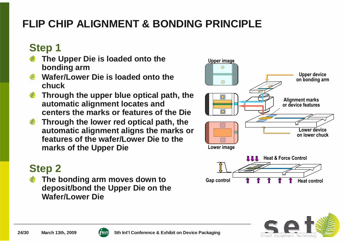
FLIP CHIP ALIGNMENT & BONDING PRINCIPLE
Step 1The Upper Die is loaded onto the bonding armWafer/Lower Die is loaded onto the chuckThrough the upper blue optical path, the automatic alignment locates and centers the marks or features of the Die Through the lower red optical path, the automatic alignment aligns the marks or features of the wafer/Lower Die to the marks of the Upper Die
Step 2The bonding arm moves down to deposit/bond the Upper Die on the Wafer/Lower Die
Upper deviceon bonding arm
Alignment marksor device features
Lower deviceon lower chuck
Upper image
Lower image
Heat control
Heat & Force Control
Gap control
March 13th, 2009 5th Int'l Conference & Exhibit on D evice Packaging25/30
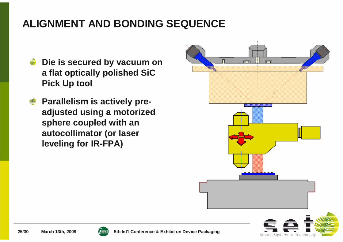
ALIGNMENT AND BONDING SEQUENCE
Die is secured by vacuum on a flat optically polished SiCPick Up tool
Parallelism is actively pre-adjusted using a motorized sphere coupled with an autocollimator (or laser leveling for IR-FPA)
March 13th, 2009 5th Int'l Conference & Exhibit on D evice Packaging26/30
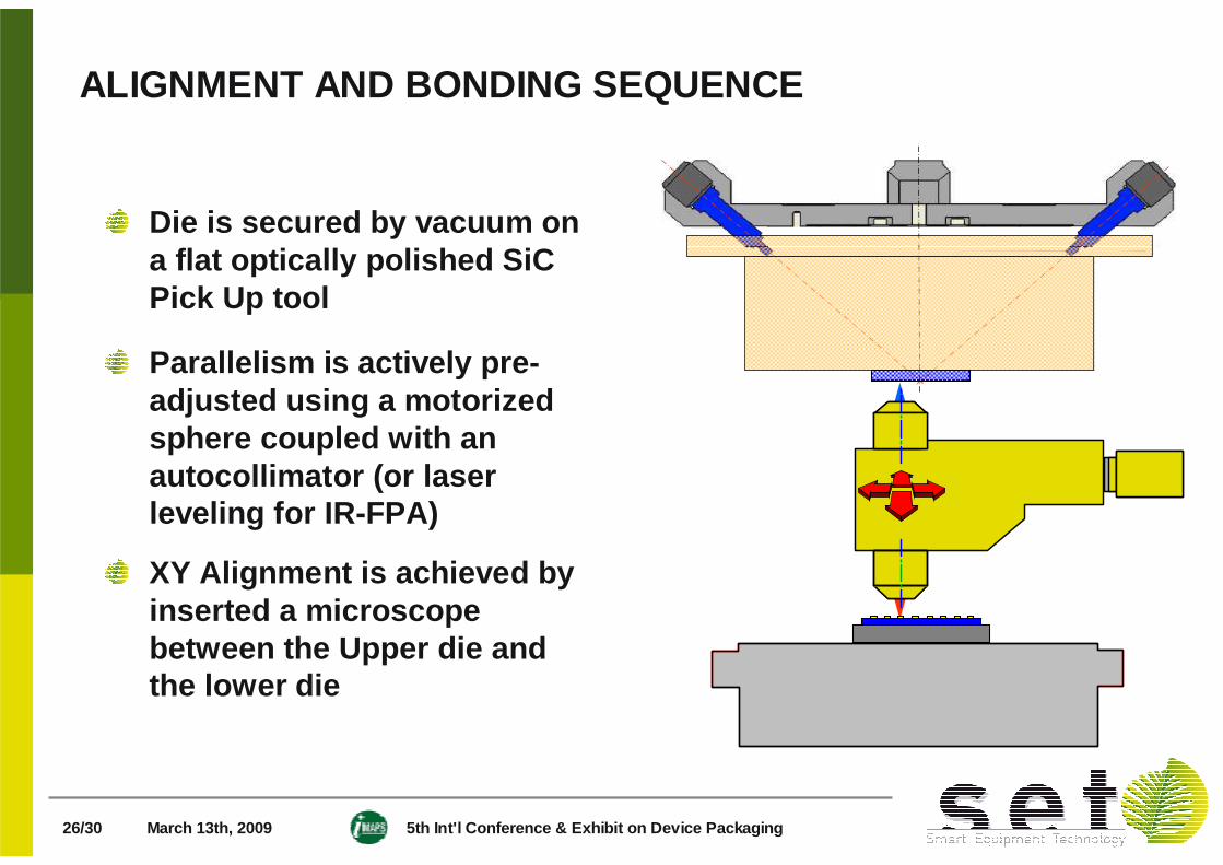
ALIGNMENT AND BONDING SEQUENCE
Die is secured by vacuum on a flat optically polished SiCPick Up tool
Parallelism is actively pre-adjusted using a motorized sphere coupled with an autocollimator (or laser leveling for IR-FPA)
XY Alignment is achieved by inserted a microscope between the Upper die and the lower die
March 13th, 2009 5th Int'l Conference & Exhibit on D evice Packaging27/30
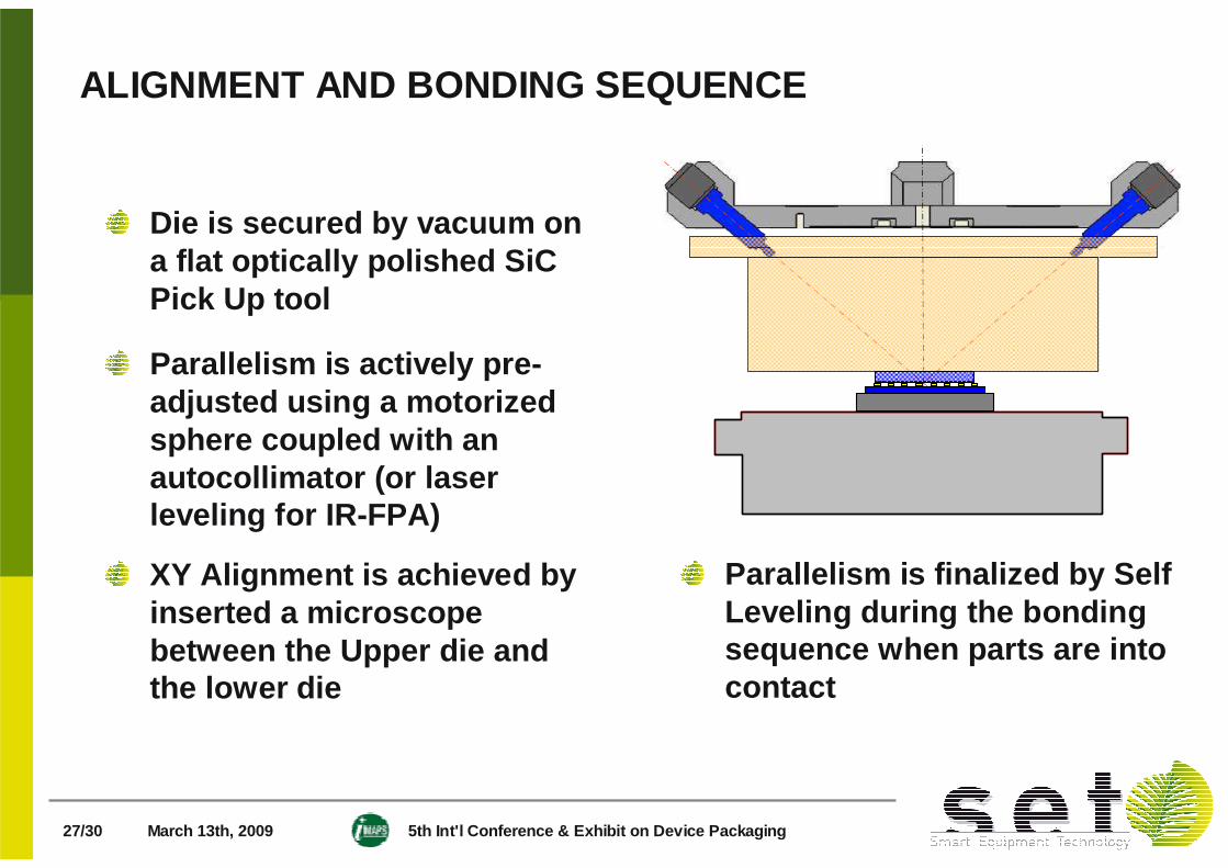
ALIGNMENT AND BONDING SEQUENCE
Die is secured by vacuum on a flat optically polished SiCPick Up tool
Parallelism is actively pre-adjusted using a motorized sphere coupled with an autocollimator (or laser leveling for IR-FPA)
XY Alignment is achieved by inserted a microscope between the Upper die and the lower die
Parallelism is finalized by Self Leveling during the bonding sequence when parts are into contact
March 13th, 2009 5th Int'l Conference & Exhibit on D evice Packaging28/30
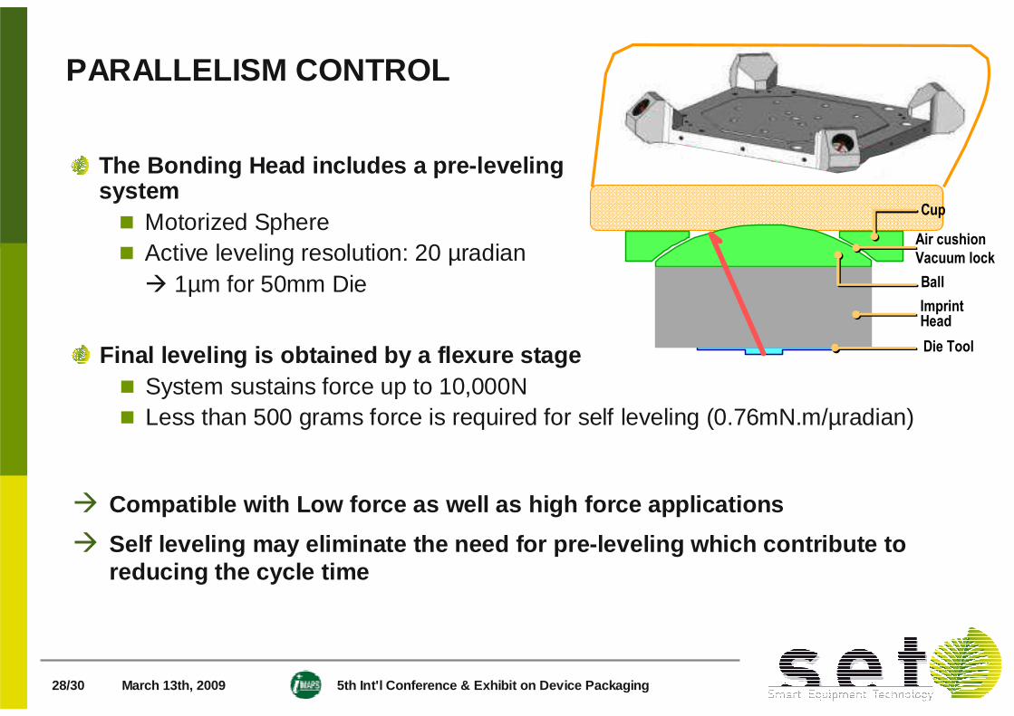
PARALLELISM CONTROL
The Bonding Head includes a pre-leveling system� Motorized Sphere � Active leveling resolution: 20 µradian
� 1µm for 50mm Die
Cup
Ball
Air cushion
Vacuum lock
Imprint Head
Die ToolFinal leveling is obtained by a flexure stage� System sustains force up to 10,000N� Less than 500 grams force is required for self leveling (0.76mN.m/µradian)
� Compatible with Low force as well as high force applications
� Self leveling may eliminate the need for pre-leveling which contribute to reducing the cycle time
March 13th, 2009 5th Int'l Conference & Exhibit on D evice Packaging29/30
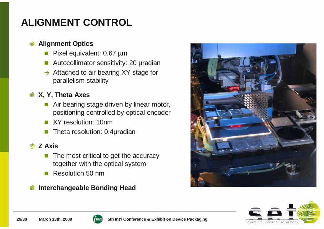
ALIGNMENT CONTROL
Alignment Optics� Pixel equivalent: 0.67 µm� Autocollimator sensitivity: 20 µradian� Attached to air bearing XY stage for
parallelism stability
X, Y, Theta Axes� Air bearing stage driven by linear motor,
positioning controlled by optical encoder� XY resolution: 10nm� Theta resolution: 0.4µradian
Z Axis� The most critical to get the accuracy
together with the optical system� Resolution 50 nm
Interchangeable Bonding Head
March 13th, 2009 5th Int'l Conference & Exhibit on D evice Packaging30/30
CONCLUSION
The Self Leveling System� First introduced on the SET Nanoimprinting Stepper� Successfully adapted to bonding tool� It will with no doubt contribute to good bonding when moving to direct
bonding (Oxide/Oxide or Cu/Cu)The Confinement Chamber for Oxide removal� Presented last year at the Device Packaging Conference
High Speed Tool are available at lower accuracy�High Throughput at High Accuracy Bonding still need to be achieved
Various Developments conducted to meet the requirement of the IR-FPA evolution actually benefit to the 3D-IC Application