Embed Size (px)
Citation preview
by
HIERARCHICAL DIRECT ORY CONTROLLERSIN THE NUMACHINE MUL TIPROCESSOR
Alexander Grbic
A thesis submitted in conformity with the requirementsfor the degree of Master of Applied Science
Graduate Department of Electrical and Computer EngineeringUniversity of Toronto
Copyright© 1996 by Alexander Grbic
ii
Hierar chical Directory Controllersin the NUMAchine Multipr ocessor
Alexander Grbic
Master of Applied Science, 1996
Department of Electrical and Computer Engineering
University of Toronto
AbstractIn multiprocessors, caching is an effective latency reducing
technique. However, adding caches to a multiprocessor system also
introduces the cache coherence problem. Many different solutions
to this problem have been proposed and implemented. This work
focuses on the design of hardware controllers that enforce cache
coherence, enable non-coherent operations, uncached operations
and special functions in the NUMAchine multiprocessor. The con-
troller logic is functionally decomposed into simpler components
which enables an efficient and flexible implementation in field-pro-
grammable devices (FPDs). The controllers have been built and
tested to run at a clock rate of 50 MHz. This implementation of
hardware cache coherence provides a good trade-off between cost,
flexibility and performance, placing it between implementations
using custom hardware and those using commodity parts.

iii
Acknowledgements
I would like to thank my supervisors Dr. Z. G. Vranesic and Dr.
S. Srbljic for their advice, guidance and encouragement. They have
introduced me to multiprocessors, cache coherence and NUMA-
chine. Without them, this work would not have been possible. I am
indebted to them both.
A deserved thanks goes to the other members of the NUMA-
chine project. Their help with implementation, simulation and
debugging is greatly appreciated.
I would like to thank my family for their love, support, and sac-
rifices. They have always had faith in me and stood behind what-
ever I chose to do. A very special thank you goes to Gordana for her
love, understanding, and dedication throughout all the hard work.
Many thanks go to my friends both inside and outside the Com-
puter and Electronics Group for making the last two years as much
fun as they have been. I express my thanks to Steve Caranci, Derek
DeVries, Robin Grindley, Rob Ho, Guy Lemieux, Kelvin Loveless,
Greg Steffan, and Dan Vranesic for making my graduate experience
more than just research.
During the past two years, I have been supported by an NSERC
Postgraduate Scholarship. I gratefully acknowledge this financial
assistance.
iv
Table of ContentsAbstract......................................................................................................ii
Acknowledgements..................................................................................iii
Table of Contents.....................................................................................iv
List of Figures..........................................................................................vii
List of Tables..........................................................................................viii
Chapter 1: Introduction ...........................................................................11.1 Motivation ........................................................................................................11.2 Objectives.........................................................................................................21.3 Overview..........................................................................................................3
Chapter 2: Background............................................................................42.1 Cache Coherence Problem................................................................................42.2 Cache Coherence Solutions..............................................................................6
2.2.1 Software-Based Cache Coherence...........................................................................6
2.2.2 Hardware-Based Cache Coherence..........................................................................7
2.3 Implementation Strategies..............................................................................112.3.1 Software.................................................................................................................11
2.3.2 Commodity Parts....................................................................................................11
2.3.3 Programmable Logic..............................................................................................12
2.3.4 Custom Hardware...................................................................................................12
2.4 Hardware Solutions........................................................................................132.4.1 DASH.....................................................................................................................13
2.4.2 Alewife ...................................................................................................................14
2.4.3 S3.mp......................................................................................................................15
2.4.4 Convex Exemplar...................................................................................................16
2.4.5 STiNG.....................................................................................................................16
2.4.6 Typhoon-0..............................................................................................................17
2.4.7 FLASH...................................................................................................................17
Chapter 3: NUMAchine Communication Protocols............................193.1 NUMAchine Architecture..............................................................................19
3.1.1 NUMAchine Hierarchy..........................................................................................19
3.1.2 Communication Scheme........................................................................................21
3.2 Cache Coherence Protocol..............................................................................213.2.1 States......................................................................................................................23
3.2.2 Basic Memory Operations......................................................................................24
3.2.3 Basic Network Cache Operations...........................................................................28
3.3 Uncached Operations......................................................................................313.3.1 Uncached Reads and Writes to DRAM..................................................................31
3.3.2 Uncached Reads and Writes to SRAM..................................................................31
v
3.3.3 Read_with_Lock and Write_with_Unlock to DRAM............................................32
3.3.4 Read_with_Lock and Write_with_Unlock to SRAM............................................32
3.4 Non-coherent Operations................................................................................323.4.1 Non-coherent Reads...............................................................................................32
3.4.2 Non-coherent Write-backs......................................................................................32
3.5 Special Functions............................................................................................333.5.1 Memory..................................................................................................................33
3.5.2 At Network Cache..................................................................................................34
3.6 Coherent Transaction Example.......................................................................35
Chapter 4: Controller Design................................................................384.1 Organization of Modules................................................................................38
4.1.1 Memory Module.....................................................................................................38
4.1.2 Network Interface Module.....................................................................................40
4.2 Specification of Controllers............................................................................414.2.1 Black Box Description...........................................................................................42
4.2.2 Inputs......................................................................................................................45
4.2.3 Outputs...................................................................................................................47
4.3 Functional Decomposition..............................................................................474.3.1 Giant State Machine...............................................................................................48
4.3.2 State Decoder and Packet Generator......................................................................48
4.3.3 Final Design...........................................................................................................49
4.4 Controller Operation.......................................................................................524.5 Controller Flexibility......................................................................................534.6 Controller Organization..................................................................................54
4.6.1 Memory Controller.................................................................................................55
4.6.2 Network Interface Controller.................................................................................55
4.7 Results............................................................................................................574.7.1 Simulation..............................................................................................................57
4.7.2 Performance...........................................................................................................57
4.7.3 Current Status.........................................................................................................60
Chapter 5: Conclusion............................................................................635.1 Contributions..................................................................................................635.2 Future Work....................................................................................................64
Appendix A: Another Coherent Transaction Example.......................66
Appendix B: Memory Card Controller ................................................69B.1 Definitions......................................................................................................69B.2 Coherent Operations.......................................................................................70B.3 Uncached Operations......................................................................................81B.4 Non-coherent Operations................................................................................83B.5 Special Functions............................................................................................84
vi
Appendix C: Network Interface Controller .........................................87C.1 Definitions......................................................................................................87C.2 Coherent Operations.......................................................................................88C.3 Uncached Operations....................................................................................109C.4 Non-coherent Operations..............................................................................111C.5 Special Functions.........................................................................................114
Appendix D: Memory Number Encodings.........................................118D.1 Action Number Encoding.............................................................................118D.2 State Number Encodings..............................................................................123
Appendix E: Network Interface Number Encodings........................124E.1 Action Number Encoding.............................................................................124E.2 State Number Encoding................................................................................130
Bibliography ..........................................................................................131
vii
List of Figur esFIGURE 2.1. Multiprocessor cache coherence basics.......................................................5FIGURE 2.2. Basic directory scheme................................................................................9FIGURE 3.1. NUMAchine hierarchy..............................................................................20FIGURE 3.2. Two-level NUMAchine cache coherence protocol....................................22FIGURE 3.3. State transition diagram at Memory...........................................................25FIGURE 3.4. State transition diagram at Network Cache...............................................28FIGURE 3.5. Example of local read requests..................................................................36FIGURE 4.1. NUMAchine Memory module...................................................................39FIGURE 4.2. NUMAchine Network Interface module...................................................41FIGURE 4.3. Format of NUMAchine packets.................................................................42FIGURE 4.4. Directory Controller...................................................................................43FIGURE 4.5. State and directory information stored in SRAM......................................45FIGURE 4.6. Functional decomposition of the Directory Controllers............................50FIGURE 4.7. Directory Controller implementation at the Memory module...................54FIGURE 4.8. Directory Controller implementation at the Network Interface module....56FIGURE 4.9. Timing of a transaction at the memory Directory Controller....................59FIGURE 4.10.Memory module with annotations.............................................................61FIGURE 4.11.Network Interface module with annotations..............................................62FIGURE A.1. Actions for a remote write.........................................................................66FIGURE D.1.States in Packet Generator.......................................................................118FIGURE E.1. States in Packet Generator.......................................................................124
viii
List of TablesTABLE 4.1. Types of packet responses generated by the Directory Controllers...........43TABLE 4.2. Input signals to the Directory Controllers..................................................44TABLE 4.3. Output signals from the Directory Controllers..........................................46TABLE 4.4. Logic used in Memory Controller.............................................................55TABLE 4.5. Logic used in Network Interface Controller..............................................57TABLE 4.6. Read latencies to different parts of memory hierarchy..............................58TABLE B.1. Local read requests....................................................................................70TABLE B.2. Local read exclusive and upgrade requests................................................71TABLE B.3. Local and remote write-backs....................................................................74TABLE B.4. Local and remote NACKs..........................................................................76TABLE B.5. Remote read requests.................................................................................77TABLE B.6. Remote read exclusive requests.................................................................78TABLE B.7. Remote upgrade requests and special exclusive reads...............................80TABLE B.8. Local/remote uncached reads and writes to DRAM..................................81TABLE B.9. Local/remote Read_w_Lock and Write_w_Unlock to DRAM.................81TABLE B.10. Local/remote uncached reads and writes to SRAM...................................82TABLE B.11. Local/remote Read_w_Lock and Write_w_Unlock to SRAM..................82TABLE B.12. Local/remote non-coherent read requests and write-backs........................83TABLE B.13. Processor and memory multicast requests.................................................84TABLE B.14. Update request and response......................................................................85TABLE B.15. Block Move................................................................................................86TABLE C.1. Local read requests....................................................................................88TABLE C.2. Local read exclusive and upgrade requests................................................91TABLE C.3. Local read exclusive and upgrade responses.............................................95TABLE C.4. Remote invalidations and local and remote write-backs...........................96TABLE C.5. Shared interventions from memory originating at a remote station..........98TABLE C.6. Shared interventions from memory originating at the local station.........102TABLE C.7. Exclusive interventions from memory originating at a remote station....103TABLE C.8. Exclusive interventions from memory originating at the local station....107TABLE C.9. NACKs from memory.............................................................................109TABLE C.10. Local/remote uncached read requests and writes to DRAM...................109TABLE C.11. Local/remote Read_w_Lock and Write_w_Unlock to DRAM...............110TABLE C.12. Local/remote uncached read requests and writes to SRAM....................110TABLE C.13. Local/remote Read_w_Lock and Write_w_Unlock to SRAM................111TABLE C.14. Local non-coherent read requests............................................................111TABLE C.15. Processor and memory multicast requests...............................................114TABLE C.16. Update......................................................................................................115TABLE C.17. Forced write-back by address and by index.............................................116TABLE C.18. Shared prefetch and exclusive prefetch...................................................117
ix
TABLE D.1. Types of packet generated by the Packet Generator................................119TABLE D.2. Single packet actions...............................................................................120TABLE D.3. Response-select line codes.......................................................................120TABLE D.4. Uncached DRAM actions........................................................................121TABLE D.5. Uncached SRAM actions.........................................................................121TABLE D.6. Data response actions...............................................................................121TABLE D.7. Prepacket response actions......................................................................122TABLE D.8. Postpacket response actions.....................................................................122TABLE D.9. Special functions actions.........................................................................122TABLE D.10. State number encodings...........................................................................123TABLE E.1. Types of packet generated by the Packet Generator................................125TABLE E.2. Single packet actions...............................................................................126TABLE E.3. Response-select line codes.......................................................................127TABLE E.4. Outgoing command codes.......................................................................127TABLE E.5. Uncached DRAM actions........................................................................127TABLE E.6. Uncached SRAM actions.........................................................................127TABLE E.7. Data response actions...............................................................................128TABLE E.8. Prepacket response actions......................................................................128TABLE E.9. Write-back actions...................................................................................129TABLE E.10. Special functions actions.........................................................................129TABLE E.11. No-packet actions....................................................................................129TABLE E.12. State number encodings...........................................................................130
1
Chapter 1
Intr oduction
1.1 Motivation
The use of caches is an effective latency reducing technique in computer systems.
Caches reduce the frequency of long latency events by exploiting temporal and spatial
locality. In multiprocessors, caching is particularly effective because of the long latencies
of data accesses to different parts of the memory system. Multiprocessors typically con-
tain a few levels of caching in the memory hierarchy. However, the addition of caches in a
multiprocessor system introduces the cache coherence problem. Multiple processors may
require a piece of data which is then brought into their respective caches. A mechanism
must exist to ensure that changes to copies of shared data be made visible to all processors
in order to provide an understandable programming model to the user.
The cache coherence problem can be handled through software, hardware or by a com-
bination of the two. Software-based approaches use software mechanisms to enforce
cache coherence and require little or no additional hardware. However, they are less effi-
cient because they require processor compute time to enforce cache coherence. In compar-
ison, hardware-based approaches are more efficient in general and provide ease of use
from a user perspective, but also require additional circuitry.
Various schemes have been used to enforce cache coherence in hardware. Many small-
scale machines use shared caches or snoopy schemes (bus-based systems) [10][25] while
large-scale systems tend to use directory schemes [2][16]. Directory-based schemes alle-
viate problems due to large amounts of network traffic generated by snoopy schemes in
large-scale systems and can be used with a variety of interconnects. They are enforced by
hardware controllers which are distributed throughout a system.
2
In general, the controller logic to enforce cache coherence can be implemented using a
number of different strategies. Custom hardware, a general-purpose co-processor or even
the compute processor can be used. Custom hardware is fast, but expensive. In compari-
son, using a general-purpose co-processor or the compute processor is cheaper, but less
efficient. These trade-offs must be carefully considered and weighed against the goals of a
particular multiprocessor.
The NUMAchine Multiprocessor [27] is a cache-coherent shared memory multipro-
cessor designed to have high performance, be cost effective and modular. Processors,
caches and memory are distributed across a number of stations which are interconnected
by a hierarchy of rings. To maintain cache coherence, a two-level cache coherence scheme
optimized for the NUMAchine architecture was developed.
In NUMAchine, cost-effectiveness is an important objective and is achieved through
the use of workstation technology and field-programmable devices (FPDs). A key require-
ment is that the multiprocessor system be viable and affordable in a relatively small con-
figuration without a large upfront cost. To keep the cost reasonably low and manufacturing
turnaround times short, all external logic is implemented in FPDs. These devices are inex-
pensive compared to custom design alternatives and the logic in these devices can be eas-
ily modified, which makes them very desirable for a research machine. An interesting
question is whether the directory controllers for cache coherence can be designed and
implemented in FPDs if a relatively high clock rate is desirable.
1.2 Objectives
This work focuses on the design of hardware controllers that enforce cache coherence,
enable non-coherent operations, uncached operations and special functions in the NUMA-
chine multiprocessor. These controllers, calleddirectory controllers in the rest of this
work, must be efficient because they can have a significant impact on the memory system
and the multiprocessor as a whole. Next, they must be flexible because a certain amount of
flexibility for changing the protocols and for adding extra functionality is desirable.
3
Finally, the controllers must also be cost-effective. To satisfy the above requirements,
careful consideration must be taken in the design of the controllers and in the choice of
implementation technology. Field-programmable devices (FPDs) present an interesting
alternative because they are cost effective and potentially flexible. The logic complexity
involved in maintaining cache coherence and the requirements set out by the NUMAchine
project for a clock frequency of 50 MHz present a tough set of design parameters for the
directory controllers using current state-of-the-art FPD technology.
This work assumes the definition of the NUMAchine protocols. It begins with a con-
sideration of implementation strategies and ends with a design and an implementation of
the directory controllers for the NUMAchine multiprocessor. The NUMAchine protocols
were defined by the NUMAchine project team and are formally specified by communicat-
ing state machines at different levels of the NUMAchine hierarchy. The main contribution
of this thesis work is the design and implementation of efficient and flexible directory con-
trollers with FPDs. This includes the design of the directory controllers, functional decom-
position of the logic, and implementation.
1.3 Overview
This thesis is organized as follows. Chapter 2 discusses the cache coherence problem
and suggested solutions as well as their implementation in existing machines. Chapter 3
describes the NUMAchine architecture and machine organization, its cache coherence
protocol, non-coherent operations, uncached operations and special functions. Chapter 4
gives the specification, design and functional decomposition of the directory controllers,
followed by results. Conclusions are given in Chapter 5.
4
Chapter 2
Background
This chapter begins with a discussion of the cache coherence problem. Next, solutions
to the problem are given followed by a discussion of the trade-offs involved with different
implementation technologies. The chapter ends with a survey of cache coherence imple-
mentations in existing shared-memory multiprocessors.
2.1 Cache Coherence Problem
As in uniprocessors, caching is an effective latency-reducing technique in multipro-
cessors. Many multiprocessors have primary and secondary caches associated with each
processor and may have higher-level caches as well.
Shared memory multiprocessing is becoming increasingly popular because it provides
a simple programming model and a fine grained sharing of data due to the shared address
space. Shared memory multiprocessing allows the sharing of data and code among the
processes in parallel applications. Sharing often results in copies of the same cache block
in multiple caches. Although this sharing is not a problem, if one processor writes to
shared data, then the other processors must be made aware of the change. This can be done
using hardware and/or software techniques. In order to maintain a coherent view of mem-
ory, the copies in all caches must be kept consistent. Copies of shared data must all have
the same value and changes to data must be made visible to all processors. This is known
as the cache coherence problem.
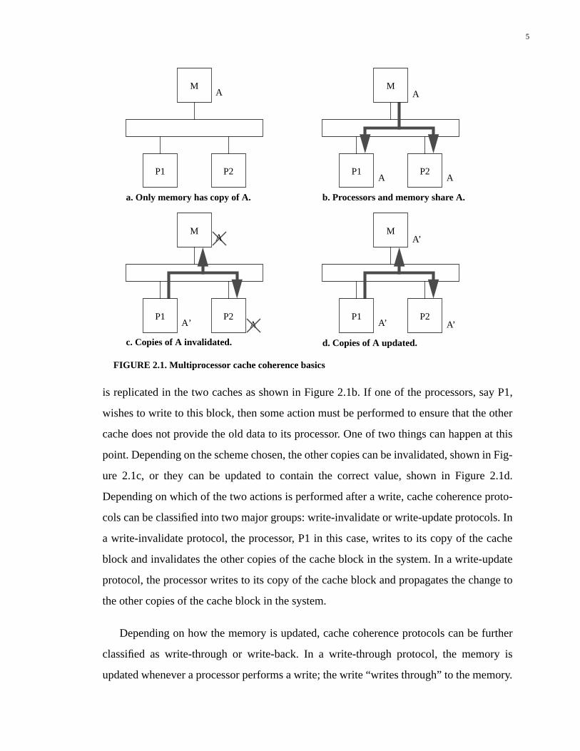
Figure 2.1 shows some of the basic issues involved in maintaining coherence among
different caches. A multiprocessor system with two processors, P1 and P2 with their
respective caches, and a memory, M, is assumed. Initially the memory has a copy of the
data while processors P1 and P2 do not have a copy as shown in Figure 2.1a. Next, P1 and
P2 read the same location and obtain a copy of the cache block from the memory. The data
5
is replicated in the two caches as shown in Figure 2.1b. If one of the processors, say P1,
wishes to write to this block, then some action must be performed to ensure that the other
cache does not provide the old data to its processor. One of two things can happen at this
point. Depending on the scheme chosen, the other copies can be invalidated, shown in Fig-
ure 2.1c, or they can be updated to contain the correct value, shown in Figure 2.1d.
Depending on which of the two actions is performed after a write, cache coherence proto-
cols can be classified into two major groups: write-invalidate or write-update protocols. In
a write-invalidate protocol, the processor, P1 in this case, writes to its copy of the cache
block and invalidates the other copies of the cache block in the system. In a write-update
protocol, the processor writes to its copy of the cache block and propagates the change to
the other copies of the cache block in the system.
Depending on how the memory is updated, cache coherence protocols can be further
classified as write-through or write-back. In a write-through protocol, the memory is
updated whenever a processor performs a write; the write “writes through” to the memory.
FIGURE 2.1. Multipr ocessor cache coherence basics
M
P1 P2
P2
M
P1
M
P1 P2
A A
A
A’ A’ A’
A’A
A
P2
M
P1
A
a. Only memory has copy of A. b. Processors and memory share A.
c. Copies of A invalidated. d. Copies of A updated.
6
In a write-back protocol, the memory is updated when another processor performs a read.
The cache block is returned to the requesting processor and a copy is also “written back”
to memory.
2.2 Cache Coherence Solutions
Cache coherence protocols deal with the problem of maintaining coherent data in the
caches of shared-memory multiprocessors. In this section a number of solutions to the
cache coherence problem are discussed. Cache coherence solutions can be classified into
two general categories: software-based and hardware-based.
2.2.1 Software-Based Cache Coherence
Software-based cache coherence schemes avoid the use of complex hardware for
maintaining coherent caches. A software mechanism is used to regulate the caching and
invalidation of shared data. Although these schemes perform worse than hardware
schemes in general, software cache coherence schemes are less expensive. In multiproces-
sors that do not provide hardware coherent caches such as the IBM RP3 [22], the Illinois
Cedar [13], the Hector multiprocessor [28], and the Cray T3D [20], the task of enforcing
cache coherence can be assigned to the user, the compiler or to the operating system.
In user-based approaches, it is up to the user to keep the data in the caches coherent by
inserting explicit commands into the application. This approach is used in some large
commercial multiprocessor systems where the user must use language extensions as in the
Cray T3D. When using language extensions, the user must decide how data is accessed
and where the parallelism is located. The main disadvantage of user-based schemes is that
they introduce additional complexity to the programmer.
Compiler-based approaches maintain coherence by determining when data is poten-
tially stale in a program [13][25] and by inserting instructions into the code which regulate
the cache and obtain correct values. At compile time, it is difficult to obtain perfect knowl-
edge of the run-time behavior of a program and to determine whether two references refer
7
to same location. This imprecision can result in poor overall performance because the
compiler must make conservative decisions for these types of accesses. To improve on
this, some schemes use additional hardware support to maintain run-time cache states [6].
In operating systems-based approaches [26], shared data in caches is kept coherent by
the operating system. It maintains the status of pages and limits access to processors.
Operating systems approaches lack in performance because of the larger granularity of
data, per-page basis, for which cache coherence is maintained.
2.2.2 Hardware-Based Cache Coherence
Hardware-based schemes maintain cache coherence with the use of additional hard-
ware mechanisms. Since the protocol is implemented in hardware, accessing data is trans-
parent to the programmer and to the operating system. During program execution, the
hardware detects certain conditions and acts appropriately to maintain coherence.
Hardware-based cache coherence schemes are typically more efficient than software
schemes because they do not use processor cycles to maintain coherence and do not rely
on the prediction of run-time behavior at compile-time. Instead, hardware schemes
dynamically detect conditions and act according to the cache coherence protocol at run-
time. Existing hardware cache coherence schemes include snoopy schemes, directory
schemes and schemes that involve cache coherent interconnect networks.
Snoopy Schemes
Snoopy schemes involve some sort of snooping of commands on the network. These
schemes assume that network traffic is visible to all devices. Each device performs coher-
ent operations according to a protocol and communication between caches and memory is
achieved using a broadcast mechanism. For a bus-based multiprocessor, sending a mes-
sage is effectively a broadcast because anything sent on the bus is visible to all other
devices. On bus-based multiprocessors, snoopy protocols are relatively simple to imple-
ment.
8
Snoopy protocols require a bus-snooping controller, a cache directory and a cache con-
troller. The bus-snooping controller does the snooping on the bus and determines whether
a coherence action is required. The cache directory stores the state of the cache block usu-
ally along with the cache block tags. The cache controller is a state machine which main-
tains the state of each cache block according to some state transition diagram.
To avoid interference and delays due to accessing the cache tags for every transaction
on the bus, a duplicate set of tags can be maintained. For each cache block, it contains the
same state information as the tags in the cache. This duplicate set of tags can be accessed
without disturbing the processor cache.
Even with large caches, a limit on the number of processors that can be put on a bus is
reached due to the amount of traffic on the bus and eventually due to physical constraints.
At this point, some other interconnection network must be used. For networks other than
buses, implementing a broadcast mechanism is not as simple as with a bus.
Dir ectory Schemes
In larger systems, broadcasting to all caches can become prohibitive due to the amount
of network traffic being generated. Since only a few copies of a given cache block exist in
caches for many applications, the amount of network traffic can be reduced by multicast-
ing coherence commands only to caches with copies of the block. A directory with infor-
mation on each cache block needs to be maintained so that coherence actions can be
multicast to the appropriate caches. These types of schemes are called directory schemes.
The directory is the primary mechanism for maintaining cache coherence in the sys-
tem. It keeps track of the locations of all copies of a cache block as well as the status of the
cache block. This information is used to determine which coherence action must be per-
formed for a particular memory access.
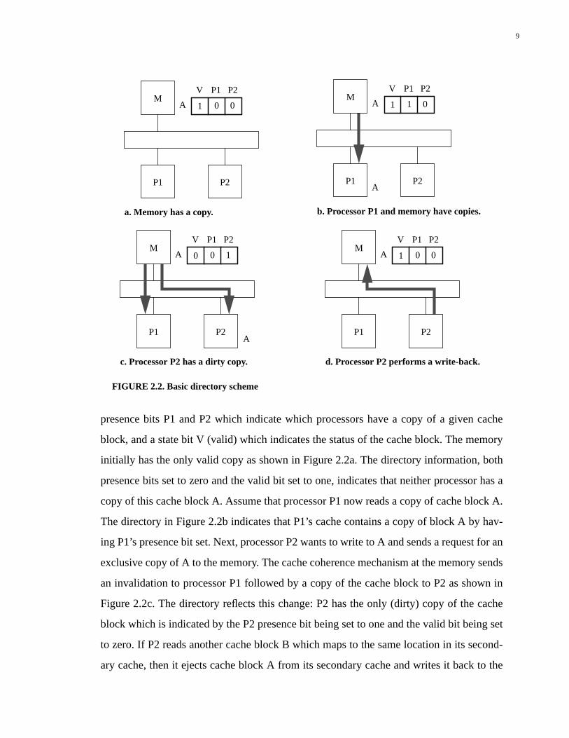
In Figure 2.2, a very basic directory scheme is shown. A multiprocessor system with
two processors, P1 and P2, and a memory, M, is assumed. For this example, a write-back/
invalidate protocol is used to maintain cache coherence. The directory consists of two
9
presence bits P1 and P2 which indicate which processors have a copy of a given cache
block, and a state bit V (valid) which indicates the status of the cache block. The memory
initially has the only valid copy as shown in Figure 2.2a. The directory information, both
presence bits set to zero and the valid bit set to one, indicates that neither processor has a
copy of this cache block A. Assume that processor P1 now reads a copy of cache block A.
The directory in Figure 2.2b indicates that P1’s cache contains a copy of block A by hav-
ing P1’s presence bit set. Next, processor P2 wants to write to A and sends a request for an
exclusive copy of A to the memory. The cache coherence mechanism at the memory sends
an invalidation to processor P1 followed by a copy of the cache block to P2 as shown in
Figure 2.2c. The directory reflects this change: P2 has the only (dirty) copy of the cache
block which is indicated by the P2 presence bit being set to one and the valid bit being set
to zero. If P2 reads another cache block B which maps to the same location in its second-
ary cache, then it ejects cache block A from its secondary cache and writes it back to the
FIGURE 2.2. Basic directory scheme
P2
M
P1
A
V P1 P2
10 0
A
a. Memory has a copy. b. Processor P1 and memory have copies.
c. Processor P2 has a dirty copy.
P2
M
P1
A
V P1 P2
01 0
P2
M
P1
A
V P1 P2
01 1
A
P2
M
P1
A
V P1 P2
01 0
d. Processor P2 performs a write-back.
10
memory as shown in Figure 2.2d. The directory updates its information indicating that the
only valid copy is in the memory.
In contrast to snoopy schemes, directory schemes are not limited to buses. Any general
interconnection network can be used. Many different versions of directory schemes have
been proposed and a number of machines with hardware cache coherence using directory
schemes have been built, some of which are discussed in section 2.3.
Inter connect Schemes
An alternate approach to cache coherence has been taken by providing a standardized,
cache coherent architecture for a large number of processors. The Scalable Coherent Inter-
face (SCI) [11], standardized by the IEEE, defines a fast multiprocessor backplane, a scal-
able architecture and cache coherence. The interconnect uses point-to-point bidirectional
links and transactions are initiated by a requester and completed by a responder.
Cache coherence is enforced using a directory-based protocol. SCI distributes the
directory by maintaining a doubly-linked list for each shared cache block in the system. At
the memory, state information and the pointer to the head of the list are stored. Each node
that caches a shared block keeps pointers to the next and previous nodes that also contain
the shared block. Each time a node accesses a shared cache block, it becomes the head of
the list. The head has the ability to maintain the list and it is the only node that can write to
a cache block. The head can obtain exclusive access, which is needed for a write, by purg-
ing the other entries from the list. A node that wishes to write and is not in the list or is not
the head of the list can insert itself at the head position.
The main advantage of SCI is that it scales well because the directory size increases
with the number of nodes in the system. The disadvantages of SCI include added com-
plexity to maintain the linked list of nodes as well as a fixed cost associated with any size
of machine due to storage requirements.
11
2.3 Implementation Strategies
In Section 2.2, a number of general approaches to enforcing cache coherence are
described. This section takes a more detailed look at the different implementation strate-
gies that can be used and the trade-offs associated with each implementation. When
choosing an implementation strategy for a particular system, a number of different factors
must be considered. Factors considered in the discussion are additional hardware cost,
performance, development time, flexibility, and accessibility of the protocol to applica-
tions. Based on these factors, it is useful to categorize implementation strategies into the
following categories: software implementation, implementation with commodity parts,
implementation in programmable devices and custom hardware implementation. The next
four subsections discuss the trade-offs for each category.
2.3.1 Software
This category involves using software, which is executed on the compute processor,
for maintaining cache coherence. The main advantage of this approach over the others is
that it is least expensive in terms of additional hardware required. Typically little or no
additional hardware is required to maintain cache coherence. Since the protocol is imple-
mented in software, it can be modified by changing the protocol code. The ease with
which changes to the protocol can be made makes this implementation very flexible and
provides for a relatively short turn-around time when altering the design. The protocol
code can be made accessible to applications and can be changed on-the-fly. Unfortunately,
performance is the factor that suffers most because processor cycles are stolen from the
application to maintain cache coherence.
2.3.2 Commodity Parts
In this category, cache coherence is implemented using an off-the-shelf co-processor
which executes protocol code for maintaining cache coherence. The main improvement
over the previous strategy is in performance. Processor compute cycles are no longer used
for cache coherence. Responsibility for maintaining cache coherence is removed from the
12
compute processor and relegated to the co-processor. This implementation is still very
flexible because the protocol software executing on the co-processor can be changed. The
protocol software may even be accessible to the application during execution. Hardware
development time for this implementation is short because it involves designing hardware
to work with the commodity co-processor. In terms of cost, this approach adds the cost of
the co-processor to the cost of the multiprocessor.
2.3.3 Programmable Logic
In recent years, programmable logic technology has greatly improved and is now
available with large logic capacity and reasonably fast speed. Programmable devices can
be used to implement hardware state machines and they provide a number of attractive
features for implementing hardware cache coherence. The major advantage over the last
category is in the potential performance improvement because protocol code is no longer
executed on a processor, but rather on specialized hardware. Since a state machine is hard-
wired, it should work much faster than a processor which has to execute instructions. With
the prices for programmable devices dropping, this approach is relatively inexpensive and
comparable to buying commodity parts. Development time increases for this implementa-
tion and some flexibility is lost over the previous implementation strategy. Protocols can
be changed, but this requires reprogramming of devices. Some devices offer reprogram-
mability without the removal of chips and reprogramming on the fly may be possible, but
it is not as easy as in co-processors or software implementations. One of the goals of the
work in this thesis is to demonstrate that it is possible to implement cache coherence for a
modern multiprocessor in programmable devices.
2.3.4 Custom Hardware
Custom hardware is used to achieve high performance. Development time for this
style of implementation is the longest and in terms of cost, this approach can be expensive
if used for prototyping or for a research machine. If a large number of machines are being
developed, then this approach is cost-effective because the cost of custom hardware can be
amortized over the total cost of many machines. If the implementation is hardwired, then
13
there is no flexibility in changing protocols. It cannot be modified unless a new chip is
manufactured.
It is also possible to custom design a co-processor which will execute the cache coher-
ence protocol. This provides considerable flexibility, but with some performance loss in
comparison to a hardwired state machine implemented with the same technology.
2.4 Hardwar e Solutions
In this section, a number of existing hardware cache coherence solutions are surveyed.
All of the systems support cache coherence and have a non-uniform memory access struc-
ture. They are referred to as CC-NUMA systems. The goals of a particular architecture
and the cache coherence protocols differ for the individual multiprocessors and as a result,
the mechanisms for enforcing cache coherence also vary. The implementation technology
used for the cache coherence mechanisms ranges from custom-designed hardware control-
lers on one end of the spectrum to off-the-shelf processors on the other.
2.4.1 DASH
The DASH multiprocessor [16][17] is a directory-based, shared-memory multiproces-
sor developed at Stanford University. DASH demonstrated that it is feasible to build a
scalable, cache coherent machine using a distributed directory protocol. The memory is
distributed among processing nodes, called clusters. In addition to memory, each cluster
contains 4 processors and a local I/O device. The clusters are connected by a pair of 2-D
mesh networks.
DASH implements a distributed, directory-based cache coherence protocol [15] which
is of the write-invalidation type. Within a cluster, bus snooping keeps the individual caches
coherent. At the cluster level, the directory tracks caching and the directory logic enforces
cache coherence.
The directory logic that implements the DASH cache coherence protocol is partitioned
into two modules called: the directory controller (DC) and the reply controller (RC). The
14
DC maintains a full bit-vector directory associated with cacheable main memory within
the cluster. The DC also sends all outbound requests and replies. The RC processes incom-
ing network messages. It keeps track of outstanding messages made by local processors,
translates remote messages and sends them to the bus. It also contains the remote access
cache (RAC) used to cache blocks belonging to other clusters.
The directory is implemented using DRAM technology and the cache coherence pro-
tocol is embedded in PROMs. Logic, implemented using PALs, is also required to access
the PROMs for the appropriate coherence actions to occur. This implementation allows for
some protocol changes to be made with small impact on the hardware.
2.4.2 Alewife
The Alewife Machine [2] is a directory-based cache coherent system developed at
MIT. Main features of this machine include the integration of shared-memory and mes-
sage-passing and the SPARCLE processor which supports fast multiple contexts. A pro-
cessing node consists of a SPARCLE processor, a portion of global memory, some private
memory, a floating-point co-processor, Communications and Memory Management Unit
(CMMU), and a router chip (ERMC). A mesh network is used for communication.
Cache coherence is enforced using a directory-based protocol. In order to reduce hard-
ware complexity, the hardware directory contains only five pointers. If more than five
nodes share a cache block, additional pointers are stored in main memory using a scheme
called LimitLESS directories [1]. Common-case memory accesses are handled in hard-
ware by the CMMU and a software trap is used to enforce coherence for memory blocks
that are shared among a large number of processors.
The Alewife CMMU consists of cache management and invalidation control, memory
coherence and DRAM control, a transaction buffer, network interface and DMA control,
network queues, registers and statistics logic. It contains processor and memory portions
of the cache coherence protocol, tracks outstanding coherence transactions, provides user-
15
level message passing and a number of hardware statistics facilities. The chip is imple-
mented in LEA-300K hybrid gate array technology from LSI Logic.
2.4.3 S3.mp
The S3.mp (Sun’s Scalable Shared memory MultiProcessor) [19] is a research project
at Sun Microsystems. The idea is to connect a number of processor nodes, possibly ordi-
nary workstations by adding an interconnect controller to the memory subsystem. The
processing nodes can support an arbitrary interconnection network and the system is able
to handle dynamic changes in configuration. Each prototype node consists of 2 processors,
a portion of memory, a memory controller and an interconnect controller in a multi-chip
module.
The cache coherence protocol is directory-based and uses a multiply-linked list
scheme to keep track of nodes having copies of the same cache block. The cache coher-
ence protocol is micro-programmable and the microcode for the protocol is stored in
SRAM. Bus snooping is used to maintain cache coherence within a node.
The multi-chip module (MCM) contains 2 gate arrays: The Memory Controller (TMC)
and The Interconnect Controller (TIC). TMC maintains directory information for local
memory, sends messages from local bus transactions or in response to remote messages,
performs memory operations in response to messages from remote nodes, maintains an
internode cache, and sends and receives diagnostic messages. TMC consists of a bus con-
troller, a memory controller, two identical protocol engines and a control unit to take care
of configuration management, and queues for interfacing to TIC. The two protocol
engines, RAS (Remote Access Server) and RMH (Remote Memory Handler), implement
the distributed cache coherence protocol and are programmable. The TIC is the building
block for a scalable interconnect network. Demo boards for TIC were FPGA-based and
ran at 51.8Mhz; ASICs are used in the prototype.
16
2.4.4 Convex Exemplar
The Exemplar multiprocessor [3][7] is a commercially available, shared-memory,
directory-based cache coherent multiprocessor developed by Convex Computer Corpora-
tion in 1993. It consists of up to 16 multiprocessor nodes, called hypernodes, connected by
a set of 4 unidirectional rings that use an SCI-based protocol. Each hypernode contains 8
Hewlett-Packard PA-RISC processors, a local memory, and an I/O interface. The compo-
nents within a hypernode are connected by a 5-port crossbar.
The DRAM on a hypernode is divided into local memory and a node cache. The node
cache contains copies of remote blocks that are being accessed on the local hypernode. An
SCI cache coherence protocol is used to keep the node caches coherent. Within a hypern-
ode, a full bit-vector directory is used to enforce coherence.
Each hypernode has the following ASICs: the Processor ASIC (PA), the Coherent
Memory Control ASIC (CMC) and the Coherent Toroidal Interconnect Control ASIC
(CTIC). The PA handles the coherence protocol within a hypernode and is connected to
the CMC by the crossbar. The CMC controls requests to memory and bridges the coher-
ence protocols. The CTIC is connected to the CMC and handles all coherence transactions
between hypernodes. All ASICs are implemented in Fujitsu’s GG11 250K gate GaAs
technology.
2.4.5 STiNG
STiNG [18] is a commercial, cache-coherent multiprocessor built by Sequent Com-
puter Systems Inc. An SCI-based interconnect is used to connect four-processor Symmet-
ric Multiprocessor nodes, called quads. Each quad contains four P6 processors, a memory,
I/O buses, and a bridge board called Lynx.
Within a quad, cache coherence is maintained using a snoopy cache coherence proto-
col. Each quad contains a Lynx board which plugs into the bus. The Lynx board contains a
remote cache and implements a directory-based cache coherence protocol based on SCI.
Two sets of tags are maintained: a bus-side directory which contains just the state of cache
17
blocks and a network-side directory which contains a state field as well as forward and
backward pointers.
Lynx consists of an Orion Bus Interface Controller (OBIC) ASIC, SCI Link Interface
Controller ASIC (SCLIC), the DataPump and the RAM arrays. The OBIC ASIC inter-
faces to the bus, implements the snooping bus logic and manages the remote cache. The
SCLIC ASIC contains a programmable protocol engine which implements the directory-
based coherence protocol. The DataPump provides the protocol for the SCI network.
2.4.6 Typhoon-0
Typhoon-0 [21][23] is a part of the Wisconsin Wind Tunnel project aimed at a parallel
programming interface called Tempest. This interface provides shared memory and mes-
sage passing which can be built on a variety of parallel computers. Typhoon is a Tempest
implementation on high-performance custom hardware using a network of bus-based
workstations. A prototype consisting of a number of nodes connected by a Myricom Myri-
net network has been built; it is called Typhoon-Zero. Cache coherence is maintained on a
cache block granularity and the local bus-based coherence uses snooping.
In the prototype, a dual ROSS hyperSparc module and Mbus module called Vortex are
used. The dual ROSS hyperSparc module contains two processors of which one is used as
a compute processor and the other as a protocol processor. Vortex primarily provides fine-
grained access control and integrates the network interface and protocol processor. Vortex
monitors every transaction on the bus, determines the tag address and drives it to the
SRAM. A conflicting memory access causes a block access fault and invokes a coherence
protocol action. In order to have working hardware quickly, the Vortex module was imple-
mented using field-programmable devices. The design runs at a 50MHz clock rate. Two
Altera EPF81188ARC240-2 devices (FLEX8000 series) and two SRAMs were used.
2.4.7 FLASH
The FLASH multiprocessor [14] being developed at Stanford University is a single-
address space machine consisting of a large number of processing nodes. Its goal is to
18
integrate cache-coherent shared memory and high-performance message passing. Each
node contains a microprocessor, a portion of main memory, a port to interconnection net-
work, I/O interface and a custom node controller called MAGIC (Memory And General
Interconnect Controller).
The MAGIC chip implements all data transfers both within a node and between nodes.
It contains a programmable protocol processor that controls the data path and implements
the protocols. MAGIC supports both cache coherence and message passing protocols for
each of which handlers can be written. A base cache coherence protocol and a base block-
transfer protocol currently exist. The cache coherence protocol is directory-based and con-
sists of a scalable directory data structure and a set of handlers. FLASH uses dynamic
pointer allocation for which a directory header for each block is stored in the main mem-
ory. The header contains boolean flags and a pointer to a linked list of nodes that contain
the shared block.
19
Chapter 3
NUMAchine Communication Protocols
The purpose of this chapter is to give a good indication of the complexity of the direc-
tory controllers for NUMAchine by describing the protocols that must be implemented.
The chapter begins with a brief description of the NUMAchine architecture followed by a
more detailed description of the NUMAchine cache coherence protocol, uncached opera-
tions, non-coherent operations and special functions.
3.1 NUMAchine Ar chitecture
NUMAchine is a scalable, cache-coherent, shared-memory multiprocessor being
developed at the University of Toronto. It is designed to be cost-effective, modular, and
easy to program. It is scalable to a reasonable size (hundreds of processors) and is afford-
able in small configurations. Cache coherence is enforced in hardware which provides
ease of programming. A 64-processor prototype has been designed and is in the produc-
tion stage.
3.1.1 NUMAchine Hierarchy
NUMAchine is a shared-memory multiprocessor with processors and memory distrib-
uted among a number of processing nodes calledstations. Stations are connected by a
hierarchy of high-speed bit-parallel rings which operate using a slotted-ring protocol.
Since the memory is distributed across a number of stations, the time to access a memory
location in the system varies depending on which processor issues the request and on
where the request is satisfied in the hierarchy. Therefore, the architecture is of the NUMA
(Non-Uniform Memory Access) type.
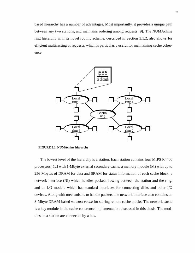
The 64-processor prototype has two levels of rings as shown in Figure 3.1: four local
rings connected by a central ring. The prototype will have 4 processors (P) on each station,
4 stations connected to a local ring and 4 local rings connected to a central ring. The ring-
20
based hierarchy has a number of advantages. Most importantly, it provides a unique path
between any two stations, and maintains ordering among requests [9]. The NUMAchine
ring hierarchy with its novel routing scheme, described in Section 3.1.2, also allows for
efficient multicasting of requests, which is particularly useful for maintaining cache coher-
ence.
The lowest level of the hierarchy is a station. Each station contains four MIPS R4400
processors [12] with 1-Mbyte external secondary cache, a memory module (M) with up to
256 Mbytes of DRAM for data and SRAM for status information of each cache block, a
network interface (NI) which handles packets flowing between the station and the ring,
and an I/O module which has standard interfaces for connecting disks and other I/O
devices. Along with mechanisms to handle packets, the network interface also contains an
8-Mbyte DRAM-basednetwork cache for storing remote cache blocks. The network cache
is a key module in the cache coherence implementation discussed in this thesis. The mod-
ules on a station are connected by a bus.
FIGURE 3.1. NUMAchine hierarchy
Central�
ring
Localring 1
Localring 2
Localring 3
Localring 0
P P P P
MI/O NI
21
3.1.2 Communication Scheme
The unidirectional rings provide a unique routing path for packets between two sta-
tions. The routing of packets begins and ends at the station-level and the destination of a
packet is specified using arouting mask.
The routing mask consists of a number of fields each of which represents a level in the
hierarchy. The number of bits in the field corresponds to the number of links in the next
level. In the two-level prototype, the routing mask consists of two 4-bit fields. Bits set in
the first field indicate the destination ring and bits set in the second field indicate the desti-
nation station on the ring. For point-to-point communication, each station in the hierarchy
can be uniquely identified by setting one bit in each of the fields. Multicasting to multiple
stations is possible by setting more than one bit in each of the fields; however, setting
more than one bit per field can specify more stations than required.
3.2 Cache Coherence Protocol
The NUMAchine cache coherence protocol is a hierarchical, directory-based, write-
back invalidate protocol optimized for the NUMAchine architecture. It exploits the multi-
cast mechanism, utilizes the point-to-point connections the ring provides, and is designed
to localize traffic within a single level of the hierarchy.
Before proceeding with a more detailed description of the NUMAchine cache coher-
ence protocol, it is useful to define some terminology. Home memory of a cache block
refers to the memory module to which the cache block belongs. If a particular station is
being discussed, it is referred to as thelocal station, andlocal memory or local network
cache refer to the memory or network cache on that station.Remote station, remote mem-
ory or remote network cache refer to any memory, network cache or station other than the
station being discussed.
The NUMAchine cache coherence protocol is hierarchical. Cache coherence is main-
tained at two levels as shown in Figure 3.2: the network level and the station level. Net-
work-level coherence is maintained between the home memory module of a cache block
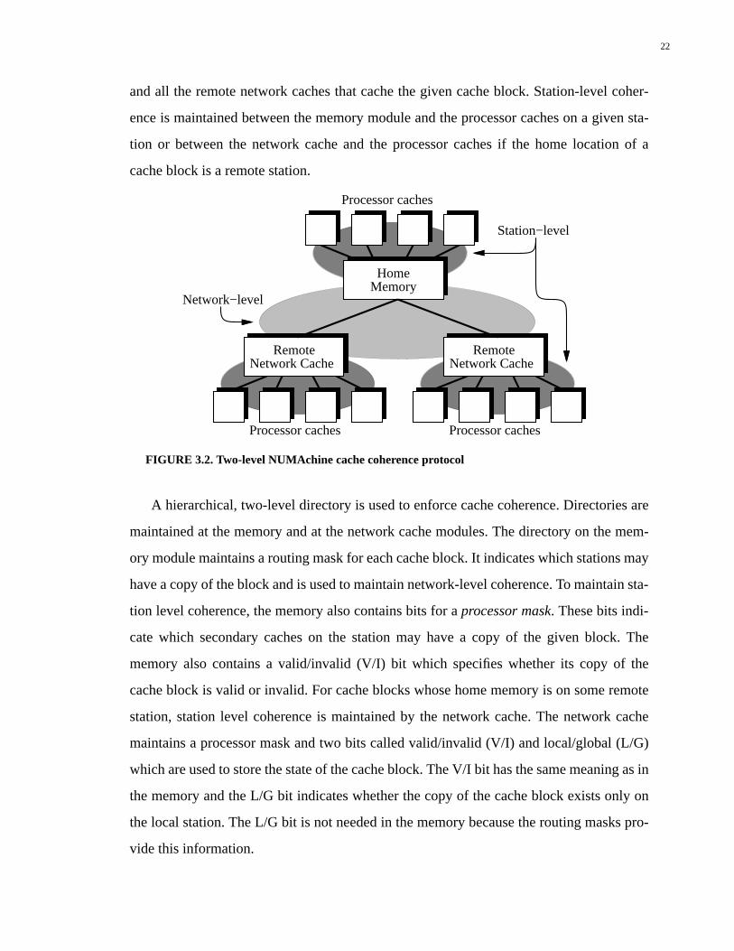
22
and all the remote network caches that cache the given cache block. Station-level coher-
ence is maintained between the memory module and the processor caches on a given sta-
tion or between the network cache and the processor caches if the home location of a
cache block is a remote station.
A hierarchical, two-level directory is used to enforce cache coherence. Directories are
maintained at the memory and at the network cache modules. The directory on the mem-
ory module maintains a routing mask for each cache block. It indicates which stations may
have a copy of the block and is used to maintain network-level coherence. To maintain sta-
tion level coherence, the memory also contains bits for aprocessor mask. These bits indi-
cate which secondary caches on the station may have a copy of the given block. The
memory also contains a valid/invalid (V/I) bit which specifies whether its copy of the
cache block is valid or invalid. For cache blocks whose home memory is on some remote
station, station level coherence is maintained by the network cache. The network cache
maintains a processor mask and two bits called valid/invalid (V/I) and local/global (L/G)
which are used to store the state of the cache block. The V/I bit has the same meaning as in
the memory and the L/G bit indicates whether the copy of the cache block exists only on
the local station. The L/G bit is not needed in the memory because the routing masks pro-
vide this information.
HomeMemory
RemoteNetwork Cache
RemoteNetwork Cache
Network−level
Station−level
Processor caches
Processor caches Processor caches
FIGURE 3.2. Two-level NUMAchine cache coherence protocol
23
3.2.1 States
Each cache block in a secondary cache, memory or network cache has some cache
coherence state associated with it. In the secondary cache three basic states,dirty, shared,
andinvalid, are defined in the standard way for write-back invalidate protocols. Four basic
states are defined in the network cache and memory modules. The states are defined using
the L/G and V/I bits:local valid (LV), local invalid (LI), global valid (GV) andglobal
invalid (GI). Even though the memory does not have a L/G bit, the information can be
derived from the routing mask. Each of these states also has a locked version which is
used to prevent other accesses to a block while it is undergoing a transition.
The two local states, LV and LI, indicate that valid copies of the cache block exist only
on the local station. If a cache block in the memory module (or network cache) is in the
LV state, then a copy exists in the memory module (or network cache) and it may be
shared by some of the secondary caches on the station. The secondary caches with a copy
of the cache block will be indicated by having a bit set in the processor mask. If the cache
block is in the LI state, then only one of the local secondary caches has a copy and that
cache is indicated by a bit set in the processor mask. The GV state indicates that the mem-
ory (or network cache) has a shared copy and that there are shared copies of the cache
block on multiple stations. The stations with shared copies are indicated by the routing
mask in the directory. The GI state has different meanings for the memory module and the
network cache. While in the network cache and the memory module, the GI state means
that there is not a valid copy of the cache block on this station, the GI state in the memory
module additionally means that some remote network cache has a copy of the cache block
in one of the local states, LV or LI. There is an additional state in the network cache called
the NOTIN1 state. This state indicates that a copy of the cache block is not present in the
network cache, but that it may be in one or more of the local secondary caches.
1. The NOTIN state is determined by a tag comparison.
24
3.2.2 Basic Memory Operations
Given the high hit rates in caches, most processor loads and stores are satisfied in the
first-level or second-level caches. For loads that cannot be satisfied in these caches, the
processor issues an external read request. If the cache block is not in the cache and the pro-
cessor performs a store, then a read-exclusive request is issued. If a processor performs a
store and the cache block is in the cache, but in the shared state, then the processor issues
an upgrade request. The processor also issues write-back requests when replacing dirty
cache blocks from its secondary cache.
State transitions for a cache block at the memory module and at the network cache are
given in Figures 3.3 and 3.4. Requests can either belocal or remote. A local request is ini-
tiated by a processor on the local station and a remote request is initiated by a processor on
a remote station.
Even though state transition diagrams give a good general description of the cache
coherence protocol, little information can be gained from these diagrams about the com-
munication between processors, memory modules and network caches, and about the
changes to the information in the directory. This section and the following section describe
some of the common cache coherence actions that must be performed at the memory mod-
ule and at the network cache for external requests. The description gives details of com-
munication between modules and of changes to directory information. If no change is
specified for the state or directory information, then it remains the same.
In the following descriptions, the cache coherence actions are divided by the type of
request. For each type, the actions are specified according to whether the request is local
or remote and according to the state of the cache block. Requests to cache blocks in states
other than specified by the protocol are considered errors.
Read Requests to Cache Blocks in the Memory Module
(i) Local read request (LocalRead) to a cache block in the LV or GV state: A copy of the
cache block is sent to the requesting processor and the processor mask is updated so that
it includes the requesting processor.
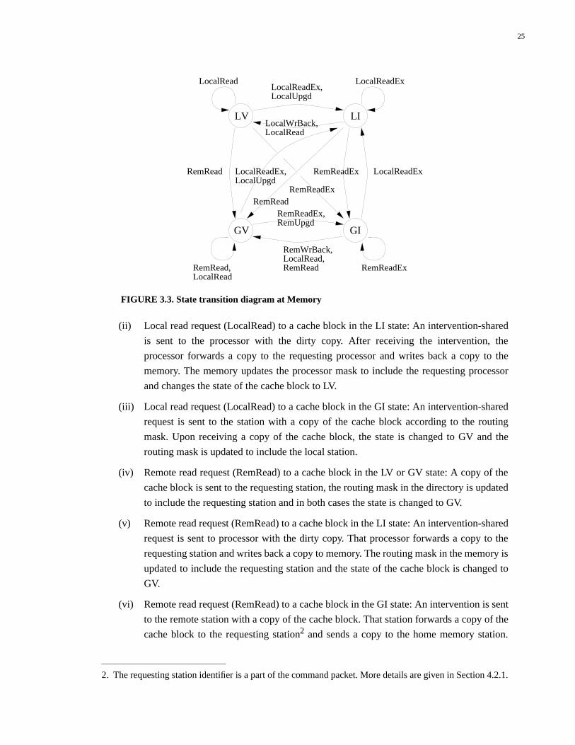
25
(ii) Local read request (LocalRead) to a cache block in the LI state: An intervention-shared
is sent to the processor with the dirty copy. After receiving the intervention, the
processor forwards a copy to the requesting processor and writes back a copy to the
memory. The memory updates the processor mask to include the requesting processor
and changes the state of the cache block to LV.
(iii) Local read request (LocalRead) to a cache block in the GI state: An intervention-shared
request is sent to the station with a copy of the cache block according to the routing
mask. Upon receiving a copy of the cache block, the state is changed to GV and the
routing mask is updated to include the local station.
(iv) Remote read request (RemRead) to a cache block in the LV or GV state: A copy of the
cache block is sent to the requesting station, the routing mask in the directory is updated
to include the requesting station and in both cases the state is changed to GV.
(v) Remote read request (RemRead) to a cache block in the LI state: An intervention-shared
request is sent to processor with the dirty copy. That processor forwards a copy to the
requesting station and writes back a copy to memory. The routing mask in the memory is
updated to include the requesting station and the state of the cache block is changed to
GV.
(vi) Remote read request (RemRead) to a cache block in the GI state: An intervention is sent
to the remote station with a copy of the cache block. That station forwards a copy of the
cache block to the requesting station2 and sends a copy to the home memory station.
2. The requesting station identifier is a part of the command packet. More details are given in Section 4.2.1.
LV LI
GV GI
RemReadEx LocalReadExRemRead
RemReadExRemRead
LocalRead
RemRead,LocalRead
RemReadEx
LocalReadExLocalReadEx,LocalUpgd
RemReadEx,RemUpgd
RemWrBack,LocalRead,RemRead
LocalWrBack,LocalRead
LocalReadEx,LocalUpgd
FIGURE 3.3. State transition diagram at Memory
26
Upon receiving the cache block, the memory updates the routing mask to include the
local and requesting stations and changes the state to GV.
Read-Exclusive Requests to Cache Blocks in the Memory Module
(i) Local read-exclusive (LocalReadEx) to a cache block in the LV state: An invalidation is
sent to other local processors that potentially have a shared copy, and a copy of the cache
block sent to the requesting processor. The processor mask in the directory is changed to
indicate the requesting processor and the state is changed to LI.
(ii) Local read-exclusive (LocalReadEx) to a cache block in the LI state: An intervention-
exclusive is sent to the processor with the dirty copy. That processor invalidates its own
copy, forwards a copy to the requesting processor and sends an acknowledgement to the
memory. At the memory, the processor mask is changed to point to the requester and the
state remains LI.
(iii) Local read exclusive (LocalReadEx) to a cache block in the GV state: An invalidate
request is multicast to stations that potentially have a shared copy of the cache block
including the local station. Upon receiving the invalidation, which serves as an
acknowledgement, the memory sends a copy of the cache block to the requesting
processor. The processor mask is changed to point to the requesting processor and the
state is changed to LI.
(iv) Local read-exclusive (LocalReadEx) to a cache block in the GI state: An intervention-
exclusive is sent to the remote station with a copy of the cache block and upon receiving
the cache block, the state is changed to LI and the processor mask is updated to indicate
the requesting processor.
(v) Remote read-exclusive (RemReadEx) to a cache block in the LV state: An invalidation is
sent to local processors that potentially have a shared copy and a copy of the cache block
is sent to the requesting station. The routing mask in the directory is changed to indicate
the requesting station and the state is changed to GI.
(vi) Remote read-exclusive (RemReadEx) to a cache block in the LI state: An intervention-
exclusive is sent to the processor with the dirty copy. That processor invalidates its own
copy, forwards a copy to the requesting station and sends an acknowledgment to the
memory. At the memory, the routing mask is changed to indicate the requesting station
and the state is changed to GI.
(vii) Remote read-exclusive (RemReadEx) to a cache block in the GV state: A copy of the
cache block is sent to the requesting station. It is followed by a multicast invalidate
request to all stations that potentially have a shared copy of the cache block including
the local station. Upon receiving the invalidation, which serves as an acknowledgment,
the memory changes the routing mask to indicate the requesting station and the state is
changed to GI.
27
(viii) Remote read-exclusive (RemReadEx) to GI: An intervention-exclusive is sent to the
remote station with a copy of the cache block. That station forwards a copy of the cache
block to the requesting station and sends an acknowledgement to the home memory.
Upon receiving the response, the memory remains in the GI state and updates the
routing mask to indicate the requesting station.
Upgrade Requests to Cache Blocks in the Memory Module
Upgrade requests (LocalUpgd and RemUpgd) to cache blocks in one of the invalid
states (LI or GI)3 are identical to read-exclusive requests for cache blocks in the invalid
states (LI or GI). Also, a remote upgrade to the LV state is identical to a remote read-
exclusive request in the LV state. In this section, only upgrades that require different
actions than read-exclusive requests will be described.
(i) Local upgrade (LocalUpgd) to a cache block in the LV state: An invalidation is sent to
other local processors that potentially have a shared copy and an acknowledgment to
proceed with the write is sent to the requesting processor. The processor mask in the
directory is changed to indicate the requesting processor and the state is changed to LI.
(ii) Local upgrade (LocalUpgd) to a cache block in the GV state: An invalidate request is
multicast to all stations that potentially have a shared copy of the cache block including
the local station. The invalidation serves as an acknowledgment to the requesting
processor. Upon receiving the invalidation, the memory changes the processor mask to
indicate the requesting processor and changes the state to LI.
(iii) Remote upgrade (RemUpgd) to a cache block in the GV state: A multicast invalidate
request is sent to all stations that potentially have a shared copy of the cache block
including the local station. The invalidation serves as an acknowledgment to the
requesting processor. Upon receiving the invalidation, the home memory changes the
routing mask to indicate the requesting station and the state is changed to GI.
Write-Back Requests to Cache Blocks in the Memory Module
(i) Local write-back (LocalWrBack) to a cache block in the LI state: Data is written to
memory and the cache block state is changed to LV. The processor mask is changed to
indicate that none of the local processors have a copy of the cache block.4
3. An upgrade can arrive at the memory even though the cache block is in one of the invalid states. Thismeans that the cache block was invalidated by some other request while the upgrade was in transit to thememory.
4. A processor can write-back a copy of the cache block to the (local) home memory and retain a sharedcopy in its secondary. In this case, the state in the memory will be changed to LV, but the processor maskwill indicate that the processor still has a copy of the cache block.
28
(ii) Remote write-back (RemWrBack) to a cache block in the GI state: Data is written to
memory and the state of the cache block is changed to LV. The routing mask is changed
to indicate that the local station is the only station with a copy of the cache block.5
3.2.3 Basic Network Cache Operations
In the network cache, the cache coherence actions for read requests, read-exclusive
requests and upgrade requests to one of the local states (LV and LI) are similar to those
performed at memory. Also, a local read request to the GV state in the network cache is
similar to a local read request to the GV state in memory. Hence, these will not be
described in this section.
5. Similarly, a processor can write-back a copy of the cache block to the (remote) home memory and retaina shared copy in its secondary. In this case, the state in the memory will be changed to GV and the routingmask will indicate that copies of the cache block exist on the local and requesting stations.
LV LI
GV GI
RemReadExLocalReadEx
RemRead
RemReadExRemRead
LocalRead
RemRead,LocalRead
RemReadEx
LocalReadExLocalReadEx,LocalUpgd
RemReadEx,RemUpgd
LocalWrBack,LocalRead
LocalReadEx,LocalUpgd
Not In
Ejection
Ejection
LocalReadEx,LocalUpgd
Ejection
Ejection
LocalRead
LocalRead
LocalRead
FIGURE 3.4. State transition diagram at Network Cache
29
Read Requests to Cache Blocks in the Network Cache
(i) Local read request (LocalRead) to a cache block in the GI state: The read request is
forwarded to home memory. When the network cache receives the cache block, a copy is
sent to the requesting processor, the state is changed to GV and the processor mask is set
to the requesting processor.
(ii) Local read request (LocalRead) to a cache block in the NOTIN state: If a cache block
that is mapped to the same place in the network cache is in the LV state, then it is first
written back to its home memory. The read request for the requested block is then sent to
the home memory. When the network cache receives the cache block, a copy is sent to
the requesting processor, the state is changed to GV and the processor mask is set to the
requesting processor.
Read-Exclusive and Upgrade Requests to Cache Blocks in the Network Cache
(i) Local read-exclusive (LocalReadEx) or upgrade (LocalUpgd) request to a cache block
in the GV state: An upgrade request is sent to home memory. Upon receiving an
invalidation which serves as an acknowledgment, an invalidation is sent to local
secondary caches that potentially have a shared copy of the cache block. The
invalidation is followed by a data response to the requesting processor in the case of a
read-exclusive request or an acknowledgment in the case of an upgrade request. The
state is changed to LI and the processor mask is set to indicate the requesting processor.
(ii) Local read-exclusive (LocalReadEx) or upgrade (LocalUpgd) request6 to a cache block
in the GI state: A read-exclusive request is sent to home memory. Upon receiving the
cache block, a copy is sent to the requesting processor, the processor mask is changed to
indicate the requesting processor and the state is changed to LI.
(iii) Local read-exclusive (LocalReadEx) or upgrade (LocalUpgd) request to a cache block
in the NOTIN state: If a cache block that is mapped to the same location in the network
cache is in the LV state, then it is first written back to its home memory. The request is
then sent to the home memory of the requested cache block. Upon receiving the cache
block, a copy is sent to the requesting processor, the processor mask is changed to
indicate the requester and the state is changed to LI.
Write-back Requests to Cache Blocks in the Network Cache
(i) Local write-back (LocalWrBack) to a cache block in the LI state: Data is written to the
network cache and the cache block state is changed to LV. The processor mask is
changed to indicate that none of the local processors has a copy of the cache block.7
6. An upgrade can arrive at the network cache even though the cache block is in the GI state. This meansthat the cache block was invalidated by some other request while the upgrade was in transit to the networkcache.
30
(ii) Local write-back (LocalWrBack) to a cache block in the NOTIN state: If the cache
block is not in the network cache, then the write-back is sent to the cache block’s home
memory. The state and processor mask remain unchanged.
Intervention-Shared Requests to Cache Blocks in the Network Cache
(i) Remote intervention-shared (RemRead) request to a cache block in the LV state: A copy
of the cache block is sent to the requesting station. A copy of the cache block is
additionally sent to the home memory if the requesting station is different from the
home memory station. The state of the cache block at the network cache is changed to
GV.
(ii) Remote intervention-shared (RemRead) request to a cache block in the LI state: An
intervention-shared is sent to the processor with the dirty copy. This processor then
forwards a copy to the requesting station and writes back a copy to the network cache.
The network cache sends an additional copy of the cache block to the home memory if it
is different from the requesting station. The state of the cache block is changed to GV.
(iii) Remote intervention-shared request (RemRead) to a cache block in the GV state: The
request is negatively acknowledged and the state remains GV.
(iv) Remote intervention-shared request (RemRead) to a cache block in the NOTIN state: An
intervention-shared is broadcast to all the local processors because of insufficient
information in the network cache. Responses from each processor are counted at the
network cache which also sends a copy to the requesting station and a copy to the home
memory station if it is different from the requesting station. The line in the network
cache is not replaced; its state does not change.
Intervention-Exclusive Requests to Cache Blocks in the Network Cache
(i) Remote intervention-exclusive request to a cache block in the LV state: Local copies of
the cache block are invalidated and a copy of the cache block is sent to the requesting
station. An acknowledgement is also sent to the home memory if the requesting station
is different from the home memory station. The processor mask is cleared and the state
of the cache block is changed to GI.
(ii) Remote intervention-exclusive request to a cache block in the LI state: An intervention
is sent to the processor with the dirty copy. The processor then forwards a copy to the
(remote) requesting station and sends an acknowledgement to the network cache. The
network cache sends an acknowledgement to the home memory if it is different from the
7. A processor can write-back a copy of the cache block to the (local) network cache and retain a sharedcopy in its secondary. In this case, the state in the network cache will change to LV, but the processor maskwill indicate that the processor still has a copy of the cache block.
31
requesting station. The network cache clears the processor mask and changes the state of
the cache block to GI.
(iii) Remote intervention-exclusive request to a cache block in the GV state: The request is
negatively acknowledged and the state of the cache block remains GV.
(iv) Remote intervention-exclusive request to a cache block in the NOTIN state: An
intervention-exclusive is broadcast to all the local processors because the processor
mask is not valid for the block being accessed. Responses from each processor are
counted at the network cache. When the data is returned by a processor, the network
cache sends a copy to the requesting station and an acknowledgement to the home
memory station if it is different from the requesting station. The block in the network
cache is not replaced; its state does not change.
3.3 Uncached Operations
In NUMAchine, caching at the secondary cache level can be bypassed by using
uncached operations. Uncached read and write operations to the network cache and to the
memory are supported. In the case of uncached operations to memory, the accesses bypass
the network cache level as well.
3.3.1 Uncached Reads and Writes to DRAM
The data in the memory or network cache modules can be read or written using dou-
bleword (64-bit) accesses. An uncached read will return the data to the requesting proces-
sor and an uncached write will modify the data regardless of the state of the cache block.
3.3.2 Uncached Reads and Writes to SRAM
The directory information in the memory and network cache modules can be accessed.
The directory contents and state of a cache block can be accessed on the memory module
and the directory contents, state and the tags of a cache block can be accessed on the net-
work cache.
32
3.3.3 Read_with_Lock and Write_with_Unlock to DRAM
This set of operations provides atomic access to the doublewords (64 bits) of data in
the memory and network cache modules. The first read locks the block and subsequent
reads cannot accesses the data until a write is performed by the same process.
3.3.4 Read_with_Lock and Write_with_Unlock to SRAM
This set of operations provides atomic accesses to the directory contents, state and tags
of cache blocks in either the memory or the network cache.
3.4 Non-coherent Operations
NUMAchine provides non-coherent operations as a way to bypass the cache coher-
ence mechanism for accessing cache blocks. Non-coherent operations are provided for
research in software cache coherence or hybrid hardware/software cache coherence proto-
cols. The cache blocks are still cached at all levels of the hierarchy and some directory
information is maintained for each cache block.
3.4.1 Non-coherent Reads
The memory or network cache always returns a cache block for non-coherent reads.
For local requests, the processor mask is updated by including the processor identifier of
the requester to the existing processor mask. For remote requests, the requesting station
identifier is OR-ed into the routing mask in the directory. Although the information stored
in the processor and routing masks is not used for non-coherent accesses, it provides infor-
mation which may be potentially useful for a software implementation of cache coher-
ence.
3.4.2 Non-coherent Write-backs
The memory can be updated using non-coherent write-backs. The previous data stored
in the memory will be overwritten by the data in the write-back.
33
3.5 Special Functions
NUMAchine also provides a number of additional operations, called special functions.
They provide added functionality which may prove to be useful to the operating system or
applications. Most special functions are initiated at the home memory of a cache block;
however, some are network cache specific and are initiated at the network cache. Special
functions can be specified for either cache blocks or for an address range.
3.5.1 Memory
The following subsections give a brief description of the special functions which are
initiated at the memory module. Lock/Unlock, Obtain_Copy, Kill_Copy and Block_Move
can be specified for an address range. The rest are performed on a cache block basis.
Lock/Unlock
Lock/Unlock provides a simple mechanism to lock and unlock a cache block. The user
does not have to explicitly write to the state information using an uncached write for the
whole entry in the SRAM.
Obtain_Copy
If a cache block is in one of the invalid states in its home memory, obtain_copy will
retrieve a copy of the block from either a local or remote cache and place it in the home
memory. Once the cache block is written to the home memory, it will be in one of the valid
states.
Kill_Copy
The Kill_copy function invalidates all copies of a cache block in the entire system.
This includes the copy of the cache block in the home memory.
Writeback_with_unlock
This is a special type of write-back which unlocks the cache block if it is locked. It is
intended for use with I/O when copying data to memory.
34
Processor Multicast
NUMAchine provides support for two types of multicasts: processor and memory. For
the processor multicast, the processor sends out a processor multicast request and the
cache block to selected remote network caches and to the home memory of the cache
block. The user must be careful when using this function because coherence must be
ensured by the user.
Memory Multicast
The second kind of multicast supported by NUMAchine is a memory multicast. The
processor sends a multicast request, which contains information on the targets of the mul-
ticast, to the home memory of the cache block. The memory locks the cache block and
multicasts it to the targeted remote network caches and to itself. The cache block remains
locked until the multicast request returns to the home memory. For this multicast, cache
coherence is enforced by the hardware.
Update
An update function for doublewords of data is supported. The update is sent to the
memory and the cache coherence controllers at the memory ensure that it is sent to all
caches with a copy of the data.
Block_Move
A block move function is provided to simplify copying of data between address
spaces. The address range and the destination are all that need be specified.
3.5.2 At Network Cache
The following subsections give a brief description of the special functions that are ini-
tiated at the network cache. Each of these is performed on a cache block basis.
35
Shared Prefetch
The shared prefetch function prefetches a copy of a cache block to the network cache.
The state of the cache block in the network cache will be GV which means that shared
copies exist in the system.
Exclusive Prefetch
The exclusive prefetch function prefetches a copy of a cache block to the network
cache. The state of the cache block in the network cache will be LV which means that the
local station is the only station with a copy of the cache block.
Forced Write-back
The forced write-back function causes a write-back from the network cache to the
home memory of the cache. Write-backs will only occur for cache blocks in the LV state.
3.6 Coherent Transaction Example
Appendices B and C give a formal description of the memory and the network inter-
face controllers as state machines [24]. This section provides a simple example of a coher-
ent transaction, which illustrates how these appendices can be used to understand the
NUMAchine protocols. A more complex example is given in Appendix A.
Table 3.5 reproduces Table B.1 from Appendix B (page 69). The table indicates the
response of the memory controller to local read requests. Column 1 in the table represents
the present state of the cache block. The headings on columns 2 and 3 indicate the requests
that trigger the responses given in these columns. Each response consists of a change in
state (if any) and an action that must be performed. The required action is indicated by a
number, and then fully explained below the table. The state change and the action are per-
formed atomically.
Consider the first row in the table, which is a response to a read request by a processor
to a cache block, A, whose home location is on the local station. The state of the cache
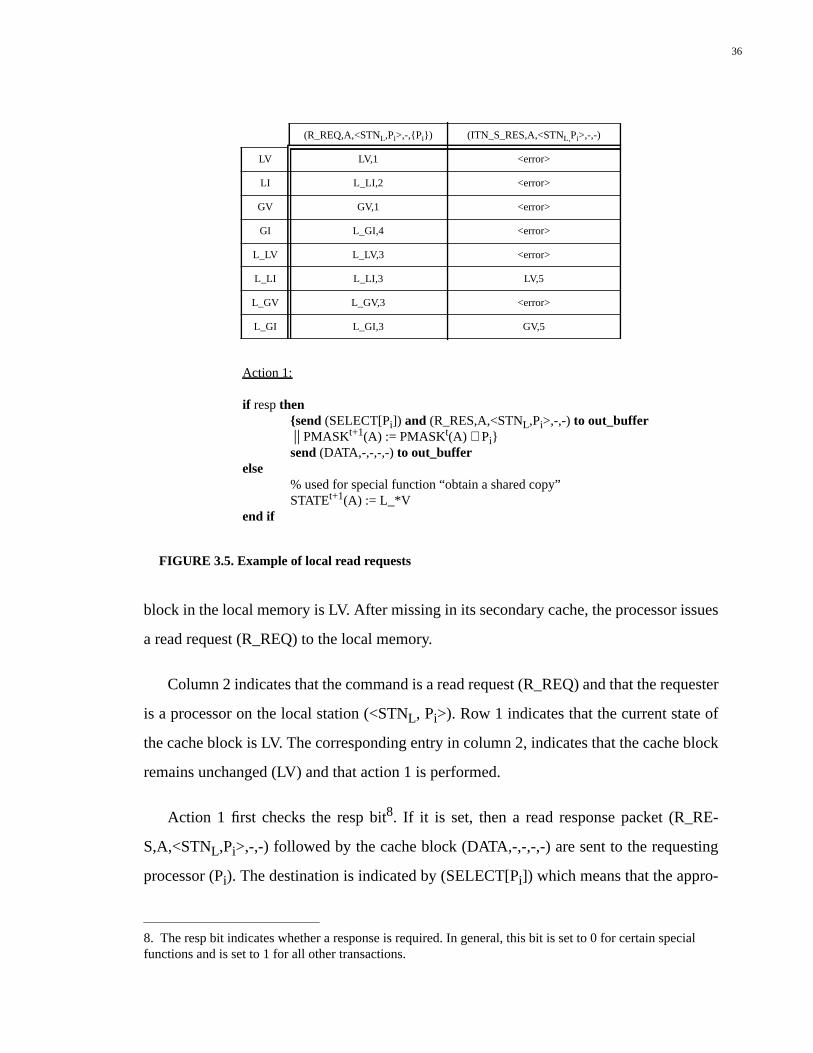
36
block in the local memory is LV. After missing in its secondary cache, the processor issues
a read request (R_REQ) to the local memory.
Column 2 indicates that the command is a read request (R_REQ) and that the requester
is a processor on the local station (<STNL, Pi>). Row 1 indicates that the current state of
the cache block is LV. The corresponding entry in column 2, indicates that the cache block
remains unchanged (LV) and that action 1 is performed.
Action 1 first checks the resp bit8. If it is set, then a read response packet (R_RE-
S,A,<STNL,Pi>,-,-) followed by the cache block (DATA,-,-,-,-) are sent to the requesting
processor (Pi). The destination is indicated by (SELECT[Pi]) which means that the appro-
8. The resp bit indicates whether a response is required. In general, this bit is set to 0 for certain specialfunctions and is set to 1 for all other transactions.
Action 1:
if respthen{send (SELECT[Pi]) and (R_RES,A,<STNL,Pi>,-,-) to out_buffer|| PMASKt+1(A) := PMASKt(A) ∨ Pi}send(DATA,-,-,-,-) to out_buffer
else% used for special function “obtain a shared copy”STATEt+1(A) := L_*V
end if
(R_REQ,A,<STNL,Pi>,-,{Pi}) (ITN_S_RES,A,<STNL,Pi>,-,-)
LV LV,1 <error>
LI L_LI,2 <error>
GV GV,1 <error>
GI L_GI,4 <error>
L_LV L_LV,3 <error>
L_LI L_LI,3 LV,5
L_GV L_GV,3 <error>
L_GI L_GI,3 GV,5
FIGURE 3.5. Example of local read requests
37
priate bus lines on the station are driven to select the requesting processor. The processor
mask (PMASK) is also modified in this action. It is updated to include the requesting pro-
cessor (Pi). This is done by “OR-ing” the requesting processor identifier and the previous
value of the PMASK. If the resp bit is zero, then the action for the special function
“Obtain_Copy” (R_REQ with the resp bit set to zero) is performed. Since the cache block
is already in the memory (LV state), it is just locked9. Had the cache block been in one of
the invalid states (LI or GI), the memory would have had to retrieve it.
9. The initiator of the Obtain_Copy special function must explicitly unlock the cache block.
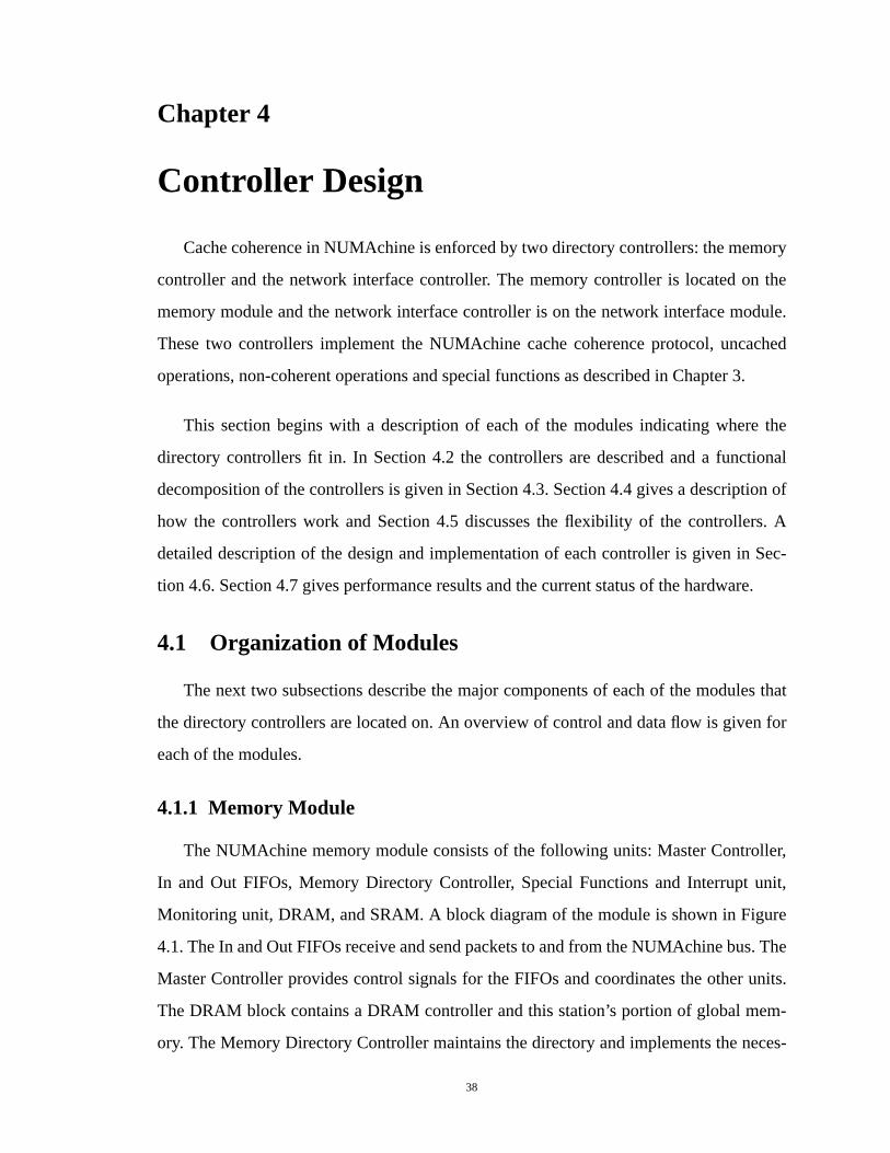
38
Chapter 4
Controller Design
Cache coherence in NUMAchine is enforced by two directory controllers: the memory
controller and the network interface controller. The memory controller is located on the
memory module and the network interface controller is on the network interface module.
These two controllers implement the NUMAchine cache coherence protocol, uncached
operations, non-coherent operations and special functions as described in Chapter 3.
This section begins with a description of each of the modules indicating where the
directory controllers fit in. In Section 4.2 the controllers are described and a functional
decomposition of the controllers is given in Section 4.3. Section 4.4 gives a description of
how the controllers work and Section 4.5 discusses the flexibility of the controllers. A
detailed description of the design and implementation of each controller is given in Sec-
tion 4.6. Section 4.7 gives performance results and the current status of the hardware.
4.1 Organization of Modules
The next two subsections describe the major components of each of the modules that
the directory controllers are located on. An overview of control and data flow is given for
each of the modules.
4.1.1 Memory Module
The NUMAchine memory module consists of the following units: Master Controller,
In and Out FIFOs, Memory Directory Controller, Special Functions and Interrupt unit,
Monitoring unit, DRAM, and SRAM. A block diagram of the module is shown in Figure
4.1. The In and Out FIFOs receive and send packets to and from the NUMAchine bus. The
Master Controller provides control signals for the FIFOs and coordinates the other units.
The DRAM block contains a DRAM controller and this station’s portion of global mem-
ory. The Memory Directory Controller maintains the directory and implements the neces-
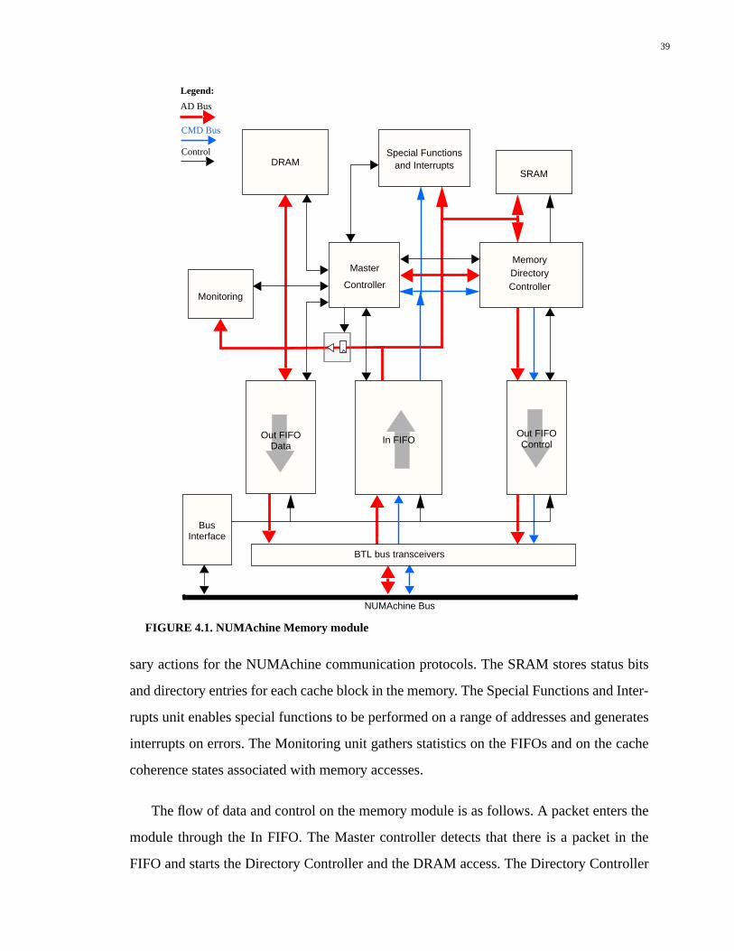
39
sary actions for the NUMAchine communication protocols. The SRAM stores status bits
and directory entries for each cache block in the memory. The Special Functions and Inter-
rupts unit enables special functions to be performed on a range of addresses and generates
interrupts on errors. The Monitoring unit gathers statistics on the FIFOs and on the cache
coherence states associated with memory accesses.
The flow of data and control on the memory module is as follows. A packet enters the
module through the In FIFO. The Master controller detects that there is a packet in the
FIFO and starts the Directory Controller and the DRAM access. The Directory Controller
In FIFOOut FIFOControl
FIGURE 4.1. NUMAchine Memory module
Special Functionsand Interrupts
NUMAchine Bus
Legend:
AD Bus
CMD Bus
ControlDRAM
SRAM
Monitoring
BTL bus transceivers
Out FIFOData
BusInterface
Controller
MemoryDirectoryMaster
Controller
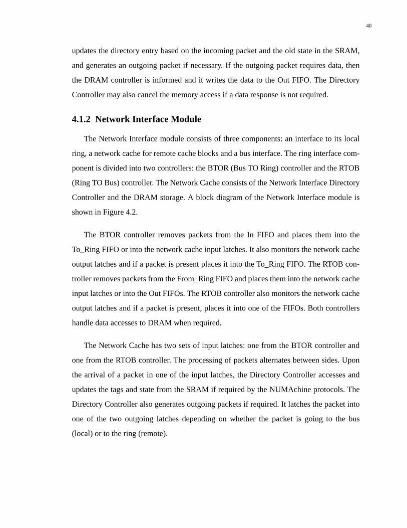
40
updates the directory entry based on the incoming packet and the old state in the SRAM,
and generates an outgoing packet if necessary. If the outgoing packet requires data, then
the DRAM controller is informed and it writes the data to the Out FIFO. The Directory
Controller may also cancel the memory access if a data response is not required.
4.1.2 Network Interface Module
The Network Interface module consists of three components: an interface to its local
ring, a network cache for remote cache blocks and a bus interface. The ring interface com-
ponent is divided into two controllers: the BTOR (Bus TO Ring) controller and the RTOB
(Ring TO Bus) controller. The Network Cache consists of the Network Interface Directory
Controller and the DRAM storage. A block diagram of the Network Interface module is
shown in Figure 4.2.
The BTOR controller removes packets from the In FIFO and places them into the
To_Ring FIFO or into the network cache input latches. It also monitors the network cache
output latches and if a packet is present places it into the To_Ring FIFO. The RTOB con-
troller removes packets from the From_Ring FIFO and places them into the network cache
input latches or into the Out FIFOs. The RTOB controller also monitors the network cache
output latches and if a packet is present, places it into one of the FIFOs. Both controllers
handle data accesses to DRAM when required.
The Network Cache has two sets of input latches: one from the BTOR controller and
one from the RTOB controller. The processing of packets alternates between sides. Upon
the arrival of a packet in one of the input latches, the Directory Controller accesses and
updates the tags and state from the SRAM if required by the NUMAchine protocols. The
Directory Controller also generates outgoing packets if required. It latches the packet into
one of the two outgoing latches depending on whether the packet is going to the bus
(local) or to the ring (remote).
41
4.2 Specification of Controllers
This section gives a functional specification of the Directory Controllers. Input and
output signals are specified and the possible types of output packets are described. The
appendices give a detailed specification of the Memory and Network Interface Directory
Controllers with all possible packets that can arrive at the memory and network cache
modules. For each incoming packet and for each possible state, the change of state and
NUMAchine Bus
Legend:
AD Bus
CMD Bus
Control
BTL bus transceivers
SRAM
OutOut
SRAM
From
Ring Ring
To
NC DRAMIn
Network InterfaceDirectoryController
BusInterface
BTORRTOB
FIFOFIFO FIFO
NCInputlatches
NCInputlatches
NCOutputlatches
NCOutputlatches
Local Ring
FIGURE 4.2. NUMAchine Network Interface module
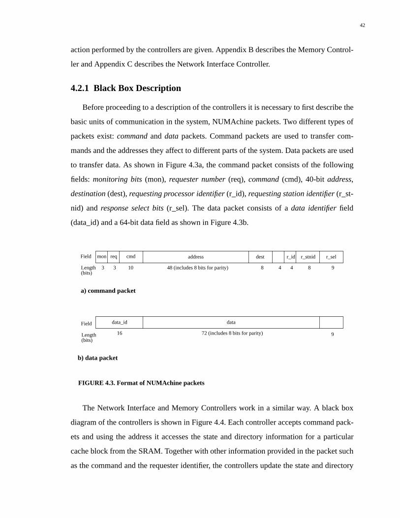
42
action performed by the controllers are given. Appendix B describes the Memory Control-
ler and Appendix C describes the Network Interface Controller.
4.2.1 Black Box Description
Before proceeding to a description of the controllers it is necessary to first describe the
basic units of communication in the system, NUMAchine packets. Two different types of
packets exist:command anddata packets. Command packets are used to transfer com-
mands and the addresses they affect to different parts of the system. Data packets are used
to transfer data. As shown in Figure 4.3a, the command packet consists of the following
fields: monitoring bits (mon), requester number (req), command (cmd), 40-bitaddress,
destination (dest),requesting processor identifier (r_id), requesting station identifier (r_st-
nid) andresponse select bits (r_sel). The data packet consists of adata identifier field
(data_id) and a 64-bit data field as shown in Figure 4.3b.
The Network Interface and Memory Controllers work in a similar way. A black box
diagram of the controllers is shown in Figure 4.4. Each controller accepts command pack-
ets and using the address it accesses the state and directory information for a particular
cache block from the SRAM. Together with other information provided in the packet such
as the command and the requester identifier, the controllers update the state and directory
FIGURE 4.3. Format of NUMAchine packets
cmd address dest r_id r_stnid r_selmon reqField
Length(bits)
3 3 10 48 (includes 8 bits for parity) 8 44 8 9
data_id dataField
Length(bits)
16 72 (includes 8 bits for parity) 9
a) command packet
b) data packet
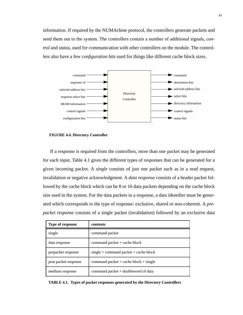
43
information. If required by the NUMAchine protocol, the controllers generate packets and
send them out to the system. The controllers contain a number of additional signals,con-
trol andstatus, used for communication with other controllers on the module. The control-
lers also have a fewconfiguration bits used for things like different cache block sizes.
If a response is required from the controllers, more than one packet may be generated
for each input. Table 4.1 gives the different types of responses that can be generated for a
given incoming packet. Asingle consists of just one packet such as in a read request,
invalidation or negative acknowledgment. Adata response consists of a header packet fol-
lowed by the cache block which can be 8 or 16 data packets depending on the cache block
size used in the system. For the data packets in a response, a data identifier must be gener-
ated which corresponds to the type of response: exclusive, shared or non-coherent. Apre-
packet responseconsists of a single packet (invalidation) followed by an exclusive data
Type of response contents
single command packet
data response command packet + cache block
prepacket response single + command packet + cache block
post packet response command packet + cache block + single
medium response command packet + doubleword of data
TABLE 4.1. Types of packet responses generated by the Directory Controllers
command
requester id
selected address bits
response select bits
SRAM information
command
selected address bits
select bits
directory information
control signals control signals
destination bits
configuration bits status bits
FIGURE 4.4. Directory Controller
Directory
Controller
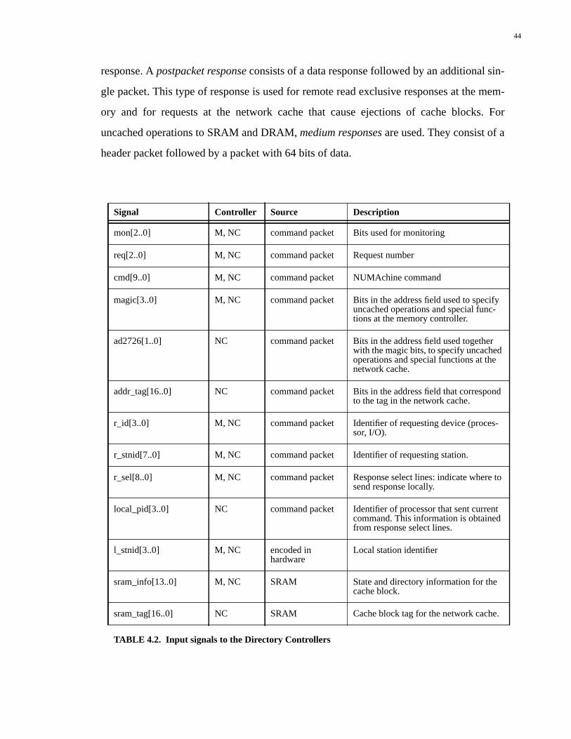
44
response. Apostpacket response consists of a data response followed by an additional sin-
gle packet. This type of response is used for remote read exclusive responses at the mem-
ory and for requests at the network cache that cause ejections of cache blocks. For
uncached operations to SRAM and DRAM,medium responses are used. They consist of a
header packet followed by a packet with 64 bits of data.
Signal Controller Source Description
mon[2..0] M, NC command packet Bits used for monitoring
req[2..0] M, NC command packet Request number
cmd[9..0] M, NC command packet NUMAchine command
magic[3..0] M, NC command packet Bits in the address field used to specifyuncached operations and special func-tions at the memory controller.
ad2726[1..0] NC command packet Bits in the address field used togetherwith the magic bits, to specify uncachedoperations and special functions at thenetwork cache.
addr_tag[16..0] NC command packet Bits in the address field that correspondto the tag in the network cache.
r_id[3..0] M, NC command packet Identifier of requesting device (proces-sor, I/O).
r_stnid[7..0] M, NC command packet Identifier of requesting station.
r_sel[8..0] M, NC command packet Response select lines: indicate where tosend response locally.
local_pid[3..0] NC command packet Identifier of processor that sent currentcommand. This information is obtainedfrom response select lines.
l_stnid[3..0] M, NC encoded inhardware
Local station identifier
sram_info[13..0] M, NC SRAM State and directory information for thecache block.
sram_tag[16..0] NC SRAM Cache block tag for the network cache.
TABLE 4.2. Input signals to the Directory Controllers
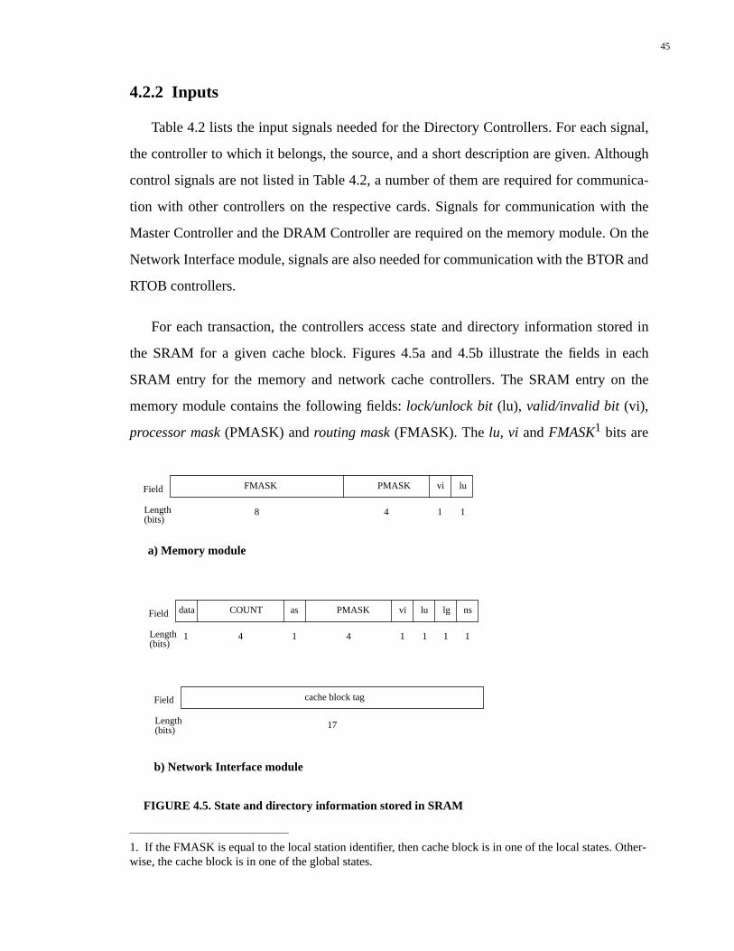
45
4.2.2 Inputs
Table 4.2 lists the input signals needed for the Directory Controllers. For each signal,
the controller to which it belongs, the source, and a short description are given. Although
control signals are not listed in Table 4.2, a number of them are required for communica-
tion with other controllers on the respective cards. Signals for communication with the
Master Controller and the DRAM Controller are required on the memory module. On the
Network Interface module, signals are also needed for communication with the BTOR and
RTOB controllers.
For each transaction, the controllers access state and directory information stored in
the SRAM for a given cache block. Figures 4.5a and 4.5b illustrate the fields in each
SRAM entry for the memory and network cache controllers. The SRAM entry on the
memory module contains the following fields:lock/unlock bit (lu), valid/invalid bit (vi),
processor mask (PMASK) androuting mask (FMASK). Thelu, vi andFMASK1 bits are
1. If the FMASK is equal to the local station identifier, then cache block is in one of the local states. Other-wise, the cache block is in one of the global states.
FIGURE 4.5. State and directory information stored in SRAM
Field
Length(bits)
Field
Length(bits)
luviPMASKFMASK
lu lgas vidata nsPMASKCOUNT
8
4
4
41
1 1
1 111 1
a) Memory module
b) Network Interface module
Field
Length(bits)
cache block tag
17
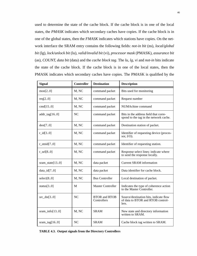
46
used to determine the state of the cache block. If the cache block is in one of the local
states, thePMASK indicates which secondary caches have copies. If the cache block is in
one of the global states, then the FMASK indicates which stations have copies. On the net-
work interface the SRAM entry contains the following fields:not-in bit (ns),local/global
bit (lg), lock/unlock bit (lu), valid/invalid bit (vi), processor mask (PMASK),assurance bit
(as),COUNT, data bit (data) and thecache block tag. Thelu, lg, vi andnot-in bits indicate
the state of the cache block. If the cache block is in one of the local states, then the
PMASK indicates which secondary caches have copies. The PMASK is qualified by the
Signal Controller Destination Description
mon[2..0] M, NC command packet Bits used for monitoring
req[2..0] M, NC command packet Request number
cmd[15..0] M, NC command packet NUMAchine command
addr_tag[16..0] NC command packet Bits in the address field that corre-spond to the tag in the network cache.
dest[7..0] M, NC command packet Destination station of packet.
r_id[3..0] M, NC command packet Identifier of requesting device (proces-sor, I/O).
r_stnid[7..0] M, NC command packet Identifier of requesting station.
r_sel[8..0] M, NC command packet Response select lines: indicate whereto send the response locally.
sram_state[13..0] M, NC data packet Current SRAM information
data_id[7..0] M, NC data packet Data identifier for cache block.
select[8..0] M, NC Bus Controller Local destination of packet.
status[3..0] M Master Controller Indicates the type of coherence actionto the Master Controller.
src_dst[3..0] NC BTOR and RTOBControllers
Source/destination bits, indicate flowof data to BTOR and RTOB control-lers.
sram_info[13..0] M, NC SRAM New state and directory informationwritten to SRAM.
sram_tag[16..0] NC SRAM Cache block tag written to SRAM.
TABLE 4.3. Output signals from the Directory Controllers
47
assurance bit. It indicates whether the PMASK is exact or whether it is a superset of the
secondary caches that are sharing copies2. The network interface containsCOUNT bits
and adata bit. The COUNT bits are used for counting responses from processors after an
intervention. The data bit indicates to the network cache whether it has already sent data to
the requester on a previous response to the intervention. The SRAM on the Network Inter-
face module also stores the tag for the cache block.
4.2.3 Outputs
Table 4.3 lists the output signals for each controller and provides a short description of
each signal.The components of an outgoing packet are similar to the incoming packet. In
addition to the fields that are used from the incoming packet, the controllers must generate
some other signals. A destination field must be generated which indicates the routing mask
for the target station. If the packet is going to a board on the local station, then select bits
must be also generated. On the memory module, the controller generates status bits used
by the Master Controller. These bits indicate what type of coherence action is being per-
formed so that the Master controller can enable the appropriate data paths. On the network
interface module,src_dst bits are generated for the BTOR and RTOB controllers. These
bits indicate the direction of data flow. Control signals are also required for the input and
output latches on the network interface module. To control the SRAM, a number of con-
trol signals must be generated on both modules.
4.3 Functional Decomposition
This section describes the various approaches taken in the design of the Directory
Controllers. Given the complexity of the controllers, designing logic for them which could
be implemented in current state-of-the-art field-programmable devices (FPDs) and run at a
clock frequency of 50 MHz was a challenge. This goal was achieved by a functional
decomposition of the controllers and placement into the appropriate devices. The large
2. The PMASK becomes inexact when a cache block, which is currently not in the network cache, isrequested. The PMASK is pessimistically set to ones except for the requesting processor because it is notknown whether any of the secondary caches have a copy of the cache block.
48
and complex circuits for the directory controllers were decomposed by hand into smaller
subcircuits. The decomposition prevented the replication of logic in different parts of the
controller by extracting common components. The decomposition also controlled the
number of signals that were shared between components which enabled a better fit into
devices. The next three sections describe the iterative design process.
4.3.1 Giant State Machine
The first approach was to directly implement a large state machine which would take
the inputs and generate the appropriate outputs as specified in the previous section. With
little initial experience in designing large logic circuits for FPDs, this seemed like a good
starting point since it was the way to implement general state machines. After implement-
ing a very small portion of the memory controller using the coherent transactions tables in
Appendix B, it was realized that this was a very inefficient way of doing things. The logic
generated for each state in the state machine was large and could not run at the appropriate
speed. This approach was quickly abandoned.
4.3.2 State Decoder and Packet Generator
A natural way to decompose the logic for the Directory Controllers is along its main
functions. Two main functions were identified: 1. state/directory modification and 2. the
generation of packets. In this design, the component which reads the old state of the cache
block and modifies it based on the command is called theState Decoder (SD). The other
component which generates outgoing packets based on the command and old state is
called thePacket Generator(PG). The state decoder, along with generating a new state to
be written to the directory, also generates a binary number called anaction number. The
action number is used by the packet generator to determine the type of packet to generate.
The functional decomposition also provides for a more efficient design because it allows
some pipelining. While the Packet Generator is generating a packet for the previous trans-
action, the State Decoder can work on the next transaction.
49
Using this functional decomposition, the State Decoder and Packet Generator were
implemented for the memory controller. The State Decoder consisted of combinational
logic only and the Packet Generator was a state machine. An additional smaller state
machine, the SRAM controller, was also created to generate control signals for reading
and writing to the SRAM and for communicating with the other components. The Packet
Generator fit into an Altera Complex Programmable Logic Device (CPLD) [8] called
EPM256ERC208-12. The State Decoder fit into four EPM7128QC100-10 and one
EPM7160EQC160-10. The EPM7160EQC160-10 contained State Decoder logic as well
as the SRAM controller. Although this design worked, it was fairly expensive in terms of
the number of chips used and PCB area that it required.
4.3.3 Final Design
Looking at the design from the previous section, the obvious place for improvement is
the State Decoder. An analysis of the logic generated by the Altera MAX+plusII CAD sys-
tem revealed that logic was being replicated. Functions common to many different types
of transactions such as determining whether a transaction was local or not or whether one
or several secondary caches shared a copy of a cache block was being replicated in many
different parts of the logic. Similarly, the logic to produce the new state and directory
information was also being replicated. The compiler was unable to extract the common
logic from the high-level code which was written in AHDL (Altera Hardware Description
Language). The common functions had to be extracted by hand. The state decoder was
functionally decomposed into aPredecoder, a simplerState Decoder and aDirectory
Maintenance Unit.
The following subsections describe the individual components of the Directory Con-
trollers in more detail. They are SRAM Controller (SC), Predecoder (P), State Decoder
(SD), Packet Generator (PG) and Directory Maintenance Unit (DMU). Figure 4.6 shows a
block diagram of the Directory Controller, its individual components and how they are
connected.
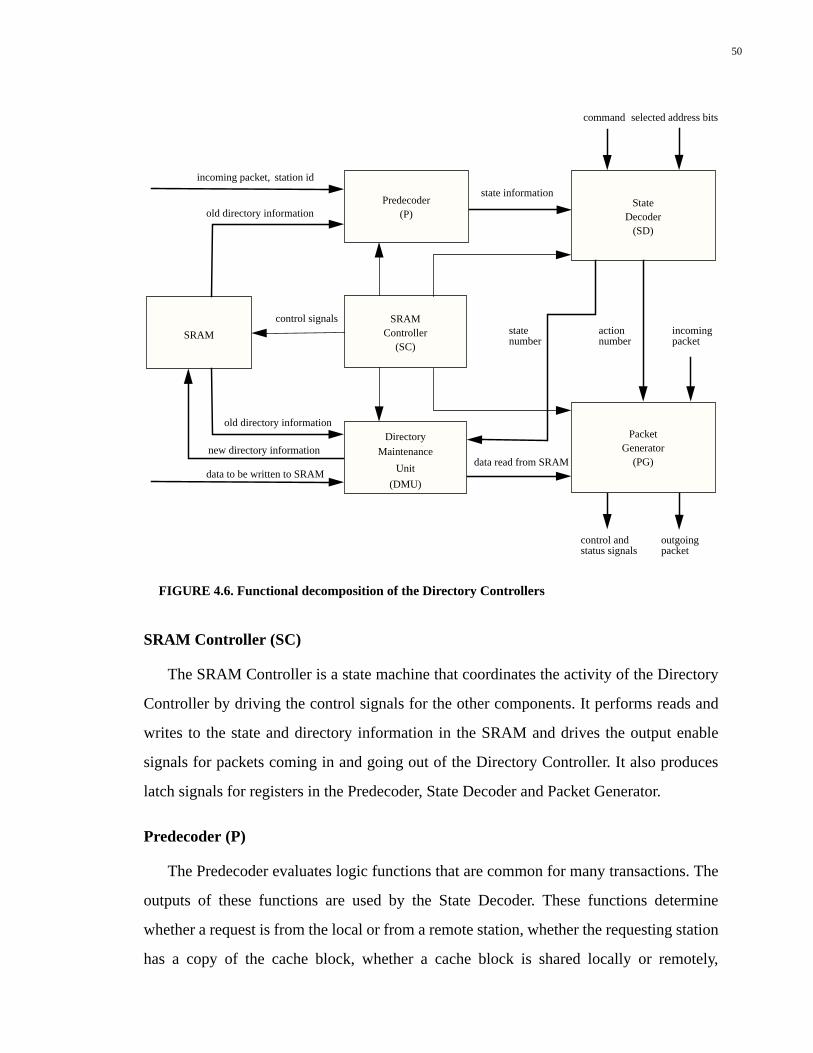
50
SRAM Controller (SC)
The SRAM Controller is a state machine that coordinates the activity of the Directory
Controller by driving the control signals for the other components. It performs reads and
writes to the state and directory information in the SRAM and drives the output enable
signals for packets coming in and going out of the Directory Controller. It also produces
latch signals for registers in the Predecoder, State Decoder and Packet Generator.
Predecoder (P)
The Predecoder evaluates logic functions that are common for many transactions. The
outputs of these functions are used by the State Decoder. These functions determine
whether a request is from the local or from a remote station, whether the requesting station
has a copy of the cache block, whether a cache block is shared locally or remotely,
FIGURE 4.6. Functional decomposition of the Directory Controllers
SRAMController
(SC)SRAM
Directory
Maintenance
Unit
(DMU)
Predecoder(P)
PacketGenerator
(PG)
StateDecoder
(SD)
command
state information
selected address bits
incoming packet,station id
old directory information
incoming
outgoingpacket
control andstatus signals
actionnumber
statenumber
old directory information
new directory information
data to be written to SRAMdata read from SRAM
control signals
packet
51
whether the count has reached the maximum, and so on. The Predecoder also contains reg-
isters which store the old state after it is read from the SRAM.
State Decoder (SD)
The State Decoder takes as its inputs the state and directory entry from the SRAM, the
command and some address bits from the incoming packet and the values of functions cal-
culated by the Predecoder. It generates a new state and two binary values:action number
andstate number. The action number gets latched into the packet generator indicating the
type of packet that needs to be generated. The state number tells the directory maintenance
unit how to modify the directory contents. The State Decoder consists of combinational
logic which detects all valid cache coherence combinations of input packets and cache
block information. If a condition that is not defined by the NUMAchine protocol is
detected, then an error is asserted.
Dir ectory Maintenance Unit (DMU)
The Directory Maintenance Unit modifies the directory information using the state
number produced by the State Decoder. The DMU modifies the routing masks and proces-
sor masks in the memory and the processor masks and COUNT bits in the network cache.
Each value of the state number represents one of the possible changes to the directory
entry for a cache block. The DMUs on the memory and network interface modules support
15 different state numbers. The exact encodings can be found in Appendices D and E. For
example, the processor mask and the routing mask can be updated to include the requester
indicated in the incoming packet, the processor mask can be cleared and the routing mask
set to the local station identifier, the entire directory entry can be overwritten by data pro-
vided in the incoming packet, and so on.
Packet Generator (PG)
The Packet Generator is a state machine that takes the incoming packet and the action
number as its input. Based on the action number, the state machine produces a packet as an
output on each clock cycle. State diagrams for the Packet Generator in the Memory mod-
ule and in the Network Interface module can be found in Appendices D and E. The action
52
number produced by the State Decoder on the memory module is a 10-bit binary number
and a 14-bit binary number on the network interface module. Four bits in each action num-
ber indicate the type of response that must be produced. These four bits cover all the pos-
sible types as specified in Table 4.1. The remaining bits give details about the outputs that
must be produced such as outgoing command, select bits and response select bits. For
implementing the NUMAchine protocols, 41 action numbers were required on the mem-
ory module and 68 action numbers were required on the network interface module. The
exact encodings of the action numbers and the meanings of each bit field are given in
Appendices D and E.
4.4 Controller Operation
This section describes in a step-by-step fashion the operation of the Directory Control-
lers. Transactions are pipelined through the controllers. One stage of the pipeline involves
modification of the state and directory information in the SRAM and the other involves
producing an outgoing packet. The following describes a typical transaction from the
arrival of an incoming packet to the generation of an outgoing packet.
(v) The packet is made available to the Directory Controllers and the SRAM read is
initiated.
(vi) The state and directory information read from the SRAM is latched into the Predecoder.
The input command and specific address bits are latched into the State Decoder.
(vii) The Predecoder functions are calculated and the outputs are passed on to the State
Decoder which begins decoding the type of transaction.
(viii) The state number and the new state generated by the State Decoder are used by the
Directory Maintenance Unit to modify the directory contents, which are then written
into the SRAM. The State Decoder also produces an action number which is latched into
the Packet Generator along with the command requester station id and response select
bits.
(ix) Once the action number has been latched in the Packet Generator and the new state and
directory contents have been written to SRAM, the SRAM controller can start with the
next transaction.
(x) If the Packet Generator is still busy producing packets for the previous transaction by
the time the action number for the next transaction is ready, then the new action number
53
will not be latched. The SRAM controller will wait for the previous transaction to
complete.
4.5 Controller Flexibility
The design of the Directory Controllers provides for flexibility in making changes to
the NUMAchine protocols. Since the decomposition of the logic was done by hand, sig-
nals between the different components were chosen so that they could remain fixed. The
pinouts of the chips do not have to be changed because each component of the directory
controllers is general enough to be used for different protocols. This framework makes it
possible to alter existing protocols or add extra functionality by making simple changes in
the State Decoder, Directory Maintenance Unit and Packet Generator.
In the State Decoder, logic must be added to detect the conditions for the new protocol
action. These conditions are some combination of commands and cache block states.
Logic must be added to drive the new values for action and state numbers. The action
number must be chosen so that the correct response packet type is produced and that the
fields in the outgoing packet are correct. If the packet that must be generated contains val-
ues for fields that have not been used in any of the protocols thus far, then extra logic must
be added to the appropriate state in the Packet Generator. Similarly, the state number must
be chosen so that the appropriate changes to the directory occur. If the logic to modify the
directory does not already exist in the Directory Maintenance Unit, then additional logic
must be added for the particular change. Detailed descriptions of the action and state num-
bers are given in Appendices D and E.
Although the design provides flexibility in terms of making changes to the protocols,
the extent to which changes can be made depends on how much extra logic is available in
the components. Therefore, it is desirable to leave extra unused logic in the devices used
for implementation.
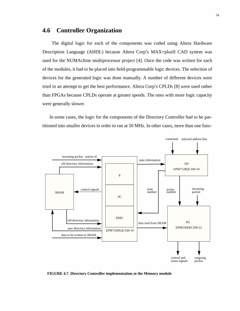
54
4.6 Controller Organization
The digital logic for each of the components was coded using Altera Hardware
Description Language (AHDL) because Altera Corp’s MAX+plusII CAD system was
used for the NUMAchine multiprocessor project [4]. Once the code was written for each
of the modules, it had to be placed into field-programmable logic devices. The selection of
devices for the generated logic was done manually. A number of different devices were
tried in an attempt to get the best performance. Altera Corp’s CPLDs [8] were used rather
than FPGAs because CPLDs operate at greater speeds. The ones with more logic capacity
were generally slower.
In some cases, the logic for the components of the Directory Controller had to be par-
titioned into smaller devices in order to run at 50 MHz. In other cases, more than one func-
FIGURE 4.7. Directory Controller implementation at the Memory module
SRAM
SD
EPM7128QC100-10
DMU
SC
P
EPM7160EQC160-10
PG
EPM256ERC208-12
command
state information
selected address bits
incoming packet,station id
old directory information
incoming
outgoingpacket
control andstatus signals
actionstatenumber
old directory information
new directory information
data to be written to SRAM
data read from SRAM
control signalspacketnumber
55
tionally decomposed component was placed into one larger chip to save on PCB area. This
section gives implementation details of the Directory Controllers at the memory module
and at the network interface module.
4.6.1 Memory Controller
Three Altera CPLDs are used for the Directory Controller on the memory module as
shown in Figure 4.6. The Predecoder, SRAM Controller and Directory Maintenance Unit
fit into an EPM7160EQC160-10. The State Decoder is placed in an EPM7128QC100-10
and the Packet Generator is in an EPM 7256ERC208-12. Table 4.4 gives an indication of
the logic size using the utilization and the number of available gates for each device as
specified by Altera [8]. This number is only an estimate intended to give an indication of
size. Extra space is available in each device in order to provide some flexibility in making
changes to the protocol or for correcting any errors in the implementation. A number of
discrete components are also used. Outgoing packets are written to FIFOs so that the
Directory Controller can immediately proceed to servicing the next transaction. The
amount of SRAM necessary for a maximum memory size of 256 Mbytes of storage is 4
Mbytes.
4.6.2 Network Interface Controller
The network interface controller requires more logic than the memory controller. This
is evident from the specification of controllers in Appendices B and C. For the network
interface controller, 5 Altera CPLDs are used as shown in Figure 4.8. The Predecoder and
Directory Maintenance Unit fit into an EPM7192EQC160-12. This chip also contains
logic for tag comparison (T). The State Decoder was placed into two EPM7160QC160-10
chip device usable gates
utilization estimated #of gates used
SD EPM7128QC100-10 2500 75% 1875
PG EPM7256ERC208-12 5000 76% 3800
P_DMU_SC EPM7160EQC160-10 3200 60% 1920
TABLE 4.4. Logic used in Memory Controller
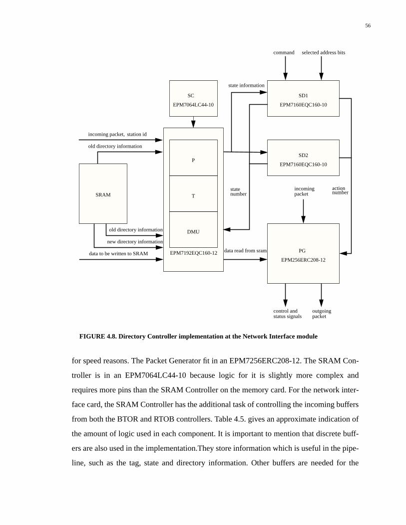
56
for speed reasons. The Packet Generator fit in an EPM7256ERC208-12. The SRAM Con-
troller is in an EPM7064LC44-10 because logic for it is slightly more complex and
requires more pins than the SRAM Controller on the memory card. For the network inter-
face card, the SRAM Controller has the additional task of controlling the incoming buffers
from both the BTOR and RTOB controllers. Table 4.5. gives an approximate indication of
the amount of logic used in each component. It is important to mention that discrete buff-
ers are also used in the implementation.They store information which is useful in the pipe-
line, such as the tag, state and directory information. Other buffers are needed for the
FIGURE 4.8. Directory Controller implementation at the Network Interface module
SC
EPM7064LC44-10
PG
EPM256ERC208-12
SD2
EPM7160EQC160-10
SD1
EPM7160EQC160-10
DMU
T
P
EPM7192EQC160-12
SRAM
command
state information
selected address bits
incoming packet,station id
old directory information
incoming
outgoingpacket
control andstatus signals
actionstatenumber
old directory information
new directory information
data to be written to SRAMdata read from sram
packetnumber
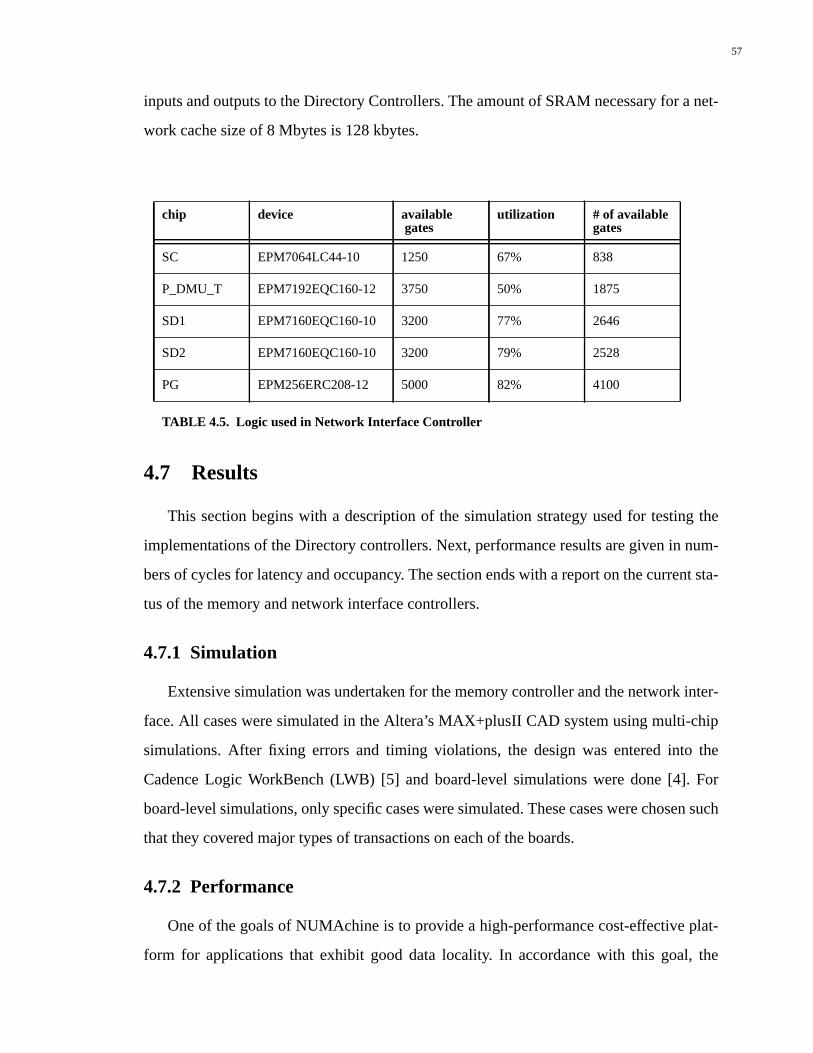
57
inputs and outputs to the Directory Controllers. The amount of SRAM necessary for a net-
work cache size of 8 Mbytes is 128 kbytes.
4.7 Results
This section begins with a description of the simulation strategy used for testing the
implementations of the Directory controllers. Next, performance results are given in num-
bers of cycles for latency and occupancy. The section ends with a report on the current sta-
tus of the memory and network interface controllers.
4.7.1 Simulation
Extensive simulation was undertaken for the memory controller and the network inter-
face. All cases were simulated in the Altera’s MAX+plusII CAD system using multi-chip
simulations. After fixing errors and timing violations, the design was entered into the
Cadence Logic WorkBench (LWB) [5] and board-level simulations were done [4]. For
board-level simulations, only specific cases were simulated. These cases were chosen such
that they covered major types of transactions on each of the boards.
4.7.2 Performance
One of the goals of NUMAchine is to provide a high-performance cost-effective plat-
form for applications that exhibit good data locality. In accordance with this goal, the
chip device available gates
utilization # of availablegates
SC EPM7064LC44-10 1250 67% 838
P_DMU_T EPM7192EQC160-12 3750 50% 1875
SD1 EPM7160EQC160-10 3200 77% 2646
SD2 EPM7160EQC160-10 3200 79% 2528
PG EPM256ERC208-12 5000 82% 4100
TABLE 4.5. Logic used in Network Interface Controller
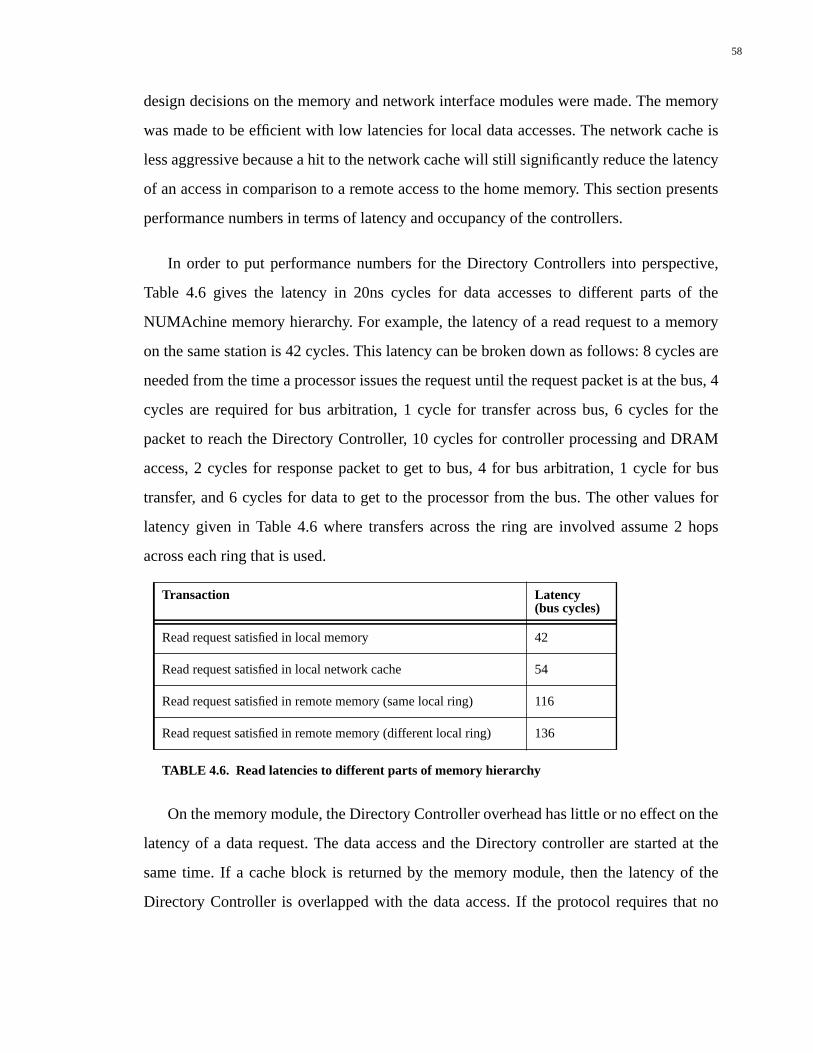
58
design decisions on the memory and network interface modules were made. The memory
was made to be efficient with low latencies for local data accesses. The network cache is
less aggressive because a hit to the network cache will still significantly reduce the latency
of an access in comparison to a remote access to the home memory. This section presents
performance numbers in terms of latency and occupancy of the controllers.
In order to put performance numbers for the Directory Controllers into perspective,
Table 4.6 gives the latency in 20ns cycles for data accesses to different parts of the
NUMAchine memory hierarchy. For example, the latency of a read request to a memory
on the same station is 42 cycles. This latency can be broken down as follows: 8 cycles are
needed from the time a processor issues the request until the request packet is at the bus, 4
cycles are required for bus arbitration, 1 cycle for transfer across bus, 6 cycles for the
packet to reach the Directory Controller, 10 cycles for controller processing and DRAM
access, 2 cycles for response packet to get to bus, 4 for bus arbitration, 1 cycle for bus
transfer, and 6 cycles for data to get to the processor from the bus. The other values for
latency given in Table 4.6 where transfers across the ring are involved assume 2 hops
across each ring that is used.
On the memory module, the Directory Controller overhead has little or no effect on the
latency of a data request. The data access and the Directory controller are started at the
same time. If a cache block is returned by the memory module, then the latency of the
Directory Controller is overlapped with the data access. If the protocol requires that no
Transaction Latency(bus cycles)
Read request satisfied in local memory 42
Read request satisfied in local network cache 54
Read request satisfied in remote memory (same local ring) 116
Read request satisfied in remote memory (different local ring) 136
TABLE 4.6. Read latencies to different parts of memory hierarchy
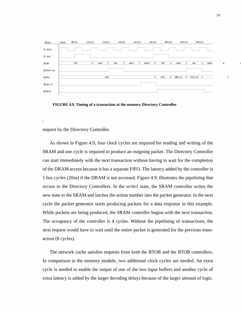
59
data be sent, then the DRAM access is cancelled. In this case, latency is added to the
request by the Directory Controller.
As shown in Figure 4.9, four clock cycles are required for reading and writing of the
SRAM and one cycle is required to produce an outgoing packet. The Directory Controller
can start immediately with the next transaction without having to wait for the completion
of the DRAM access because it has a separate FIFO. The latency added by the controller is
5 bus cycles (20ns) if the DRAM is not accessed. Figure 4.9. illustrates the pipelining that
occurs in the Directory Controllers. In thewrite1 state, the SRAM controller writes the
new state to the SRAM and latches the action number into the packet generator. In the next
cycle the packet generator starts producing packets for a data response in this example.
While packets are being produced, the SRAM controller begins with the next transaction.
The occupancy of the controller is 4 cycles. Without the pipelining of transactions, the
next request would have to wait until the entire packet is generated for the previous trans-
action (8 cycles).
The network cache satisfies requests from both the BTOR and the RTOB controllers.
In comparison to the memory module, two additional clock cycles are needed. An extra
cycle is needed to enable the output of one of the two input buffers and another cycle of
extra latency is added by the larger decoding delays because of the larger amount of logic.
MAX+plus II 7.0 File: /STUMM/E/E0/GRBIC/TEST.SCF Date: 11/04/96 15:16:46 Page: 1�
[I]�
clock�
[I]�
start�
[B]�
SC�
[B]�
state_rdy�
[B]�
PG�
[B]�
act_no
[B]�
busy
idle�
read� dec
wait1� write1� idle�
read� dec
wait2� write2� latch_next�
start� resp� data_id�
reset_act� start�
80.0ns�
100.0ns 120.0ns 140.0ns 160.0ns 180.0ns 200.0ns�
220.0ns�
240.0ns�
260.0ns�
280.0ns�
300.0ns�
Name:�
Value:�
FIGURE 4.9. Timing of a transaction at the memory Directory Controller
60
As a result, the time from when a packet is latched into the input buffers to when the new
state is written to the SRAM is 6 clock cycles. The packet generator works just as fast as
on the memory board, producing packets each clock cycle after the action number is
latched. Therefore, the latency of the controller is 7 cycles and the occupancy is 6 cycles.
The Directory Controller and the DRAM access do not overlap fully at the network
interface module. The DRAM access is started after the first packet of the transaction is
latched into the outgoing buffers. In contrast to the controller at the memory, the network
cache controller can only proceed to completion with the next transaction if the appropri-
ate outgoing latches are available. The outgoing packet will be waiting for the previous
transaction in the outgoing buffer to be serviced.
4.7.3 Current Status
The printed circuit boards for memory and network interface modules have been man-
ufactured and populated. Figures 4.10 and 4.11 show photographs of the memory module
and the network interface module. Extensive simulating with CAD tools has resulted in a
working prototype within a relatively short period of time. The NUMAchine protocol was
simulated by going through all input command and cache block state combinations.
Despite the extensive simulation performed, some minor hardware debugging was
required and minor changes were made by reprogramming the devices. Testing using pro-
grams written in assembly language and in the C programming language has been per-
formed. The Directory Controllers on both the Memory and Network Interface modules
work as expected.
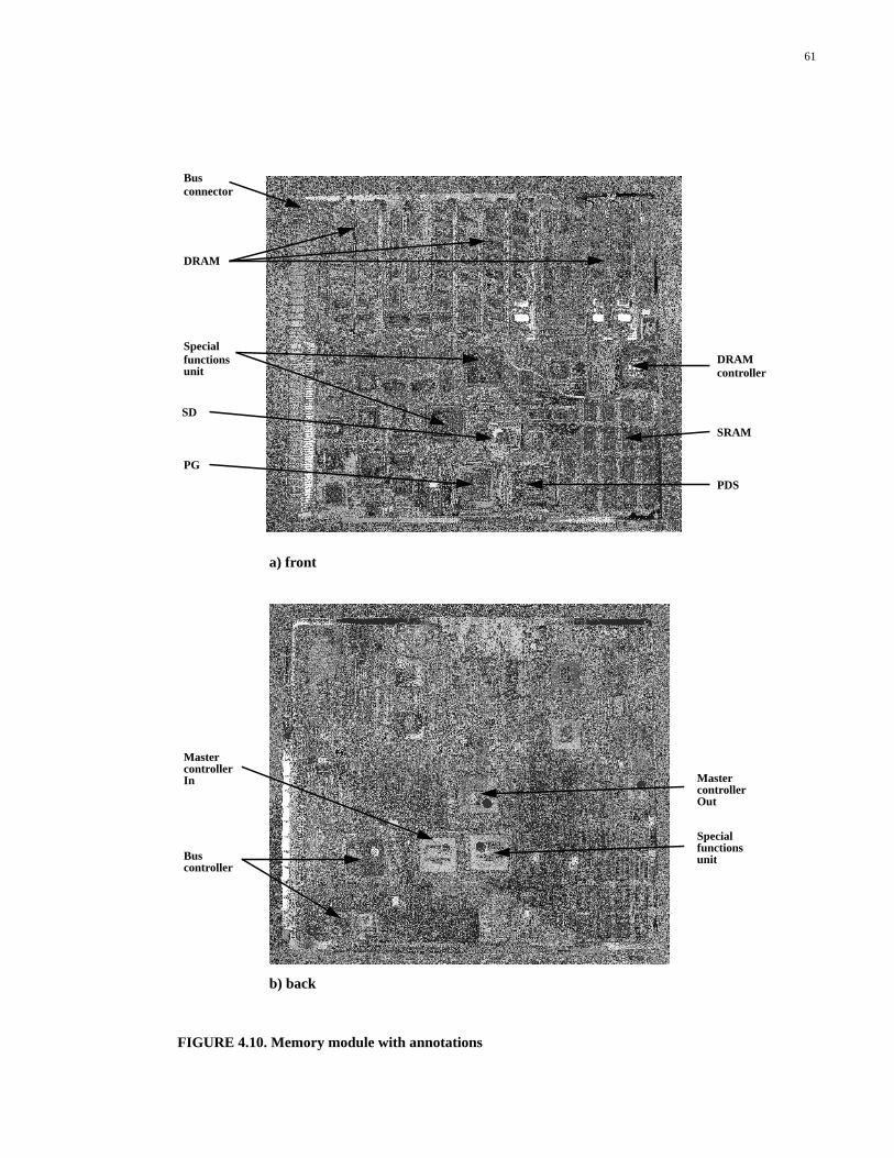
61
FIGURE 4.10. Memory module with annotations
DRAM
Specialfunctions
SD
PG
SRAM
PDS
DRAMcontroller
Busconnector
unit
Buscontroller
MastercontrollerIn Master
controllerOut
Specialfunctionsunit
b) back
a) front
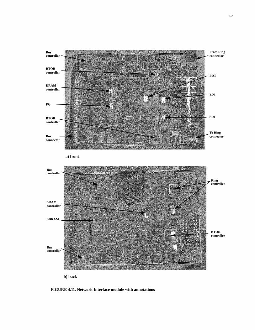
62
FIGURE 4.11. Network Interface module with annotations
RTOBcontroller
DRAMcontroller
PG
SD1
SD2
PDT
BTORcontroller
SRAMcontroller
From Ringconnector
To RingconnectorBus
connector
Buscontroller
Buscontroller
Buscontroller
SDRAM
BTORcontroller
Ringcontroller
a) front
b) back
63
Chapter 5
Conclusion
This work focuses on the design of directory controllers to enforce the communication
protocols in the NUMAchine multiprocessor. The controllers are required to be cost-effec-
tive and flexible. To satisfy these requirements, careful consideration must be taken in the
design of the controllers and in the choice of implementation technology. Field-program-
mable devices (FPDs) present an interesting alternative because they are cost-effective
and reprogrammable. The logic complexity involved in supporting the protocols and the
requirements set out by the NUMAchine project for a clock frequency of 50 MHz present
a tough set of design parameters for the directory controllers using current state-of-the-art
FPD technology.
5.1 Contributions
The contribution of this thesis is the design and implementation of directory control-
lers with FPDs which enforce the NUMAchine cache coherence protocol, support non-
coherent operations, uncached operations and special functions. The design and imple-
mentation of the directory controllers is achieved through a functional decomposition of
the controller logic enabling an efficient and flexible implementation in FPDs.
The directory controllers enforce the NUMAchine communication protocols. They
access and modify the directory contents, and produce appropriate packets. The memory
and network cache controllers run at a 50 MHz clock rate and have latencies of 5 and 7
clock cycles. For cases where data is returned to the requester, the controller latency is
overlapped with the DRAM access. The directory accesses and packet generation are
pipelined so that decoding of the next command can begin while the response for the cur-
rent transaction is being generated. The controllers have occupancies of 4 and 6 clock
cycles.
64
The implementation of the directory controllers in FPDs is possible by decomposing a
complex state machine into simpler machines. This functional decomposition has multiple
benefits. It reduces the amount of logic generated by preventing the replication of common
logic functions. This reduction in logic enables an implementation into FPDs because the
logic can fit on devices which run at the appropriate speeds. The functional decomposition
also provides flexibility. Changes to the protocols can be made easily by reprogramming
the devices used. The design is general enough to easily add new conditions to decode
incoming packets and code for generating types of outgoing packets. Additional logic is
available in the devices, and experience with fixes and modifications to the protocols is
good.
The memory and network cache modules have been manufactured and the controllers
have been tested. A working prototype demonstrates that it is possible to design inexpen-
sive and efficient directory controllers for a shared memory multiprocessor using pro-
grammable logic devices which run at clock frequency of 50 MHz. For a multiprocessor
such as NUMAchine whose goals include cost-effectiveness through the use of worksta-
tion technology, and that the multiprocessor system be viable and affordable in a relatively
small configuration, this implementation of hardware cache coherence provides a good
trade-off between cost, flexibility and performance.
5.2 Futur e Work
There are many directions for future work. An analysis of the many special functions
presented in Chapter 3 will provide insight into their effectiveness. The analysis may
reveal other functions which may be useful. Given the flexibility of the controllers, they
could be implemented by reprogramming the devices.
Fine tuning and modifications to the existing protocol are also interesting. Implemen-
tation of an update protocol and a comparison with the existing write-back invalidate pro-
tocol is possible. A hybrid invalidate/update protocol may prove beneficial for this system.
65
With prices of FPDs dropping and the logic capacity and speed increasing, single-chip
implementations of these controllers may be possible. This could add additional flexibility
and increased performance.
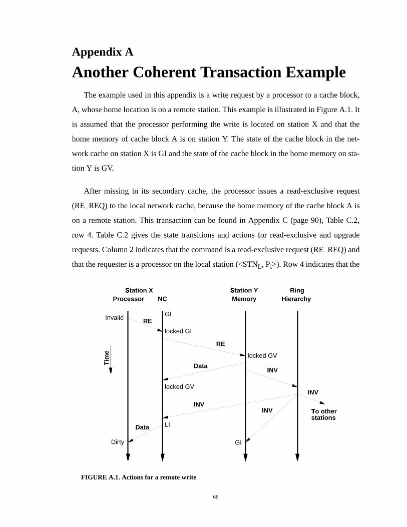
66
Appendix A
Another Coherent Transaction ExampleThe example used in this appendix is a write request by a processor to a cache block,
A, whose home location is on a remote station. This example is illustrated in Figure A.1. It
is assumed that the processor performing the write is located on station X and that the
home memory of cache block A is on station Y. The state of the cache block in the net-
work cache on station X is GI and the state of the cache block in the home memory on sta-
tion Y is GV.
After missing in its secondary cache, the processor issues a read-exclusive request
(RE_REQ) to the local network cache, because the home memory of the cache block A is
on a remote station. This transaction can be found in Appendix C (page 90), Table C.2,
row 4. Table C.2 gives the state transitions and actions for read-exclusive and upgrade
requests. Column 2 indicates that the command is a read-exclusive request (RE_REQ) and
that the requester is a processor on the local station (<STNL, Pi>). Row 4 indicates that the
GI
GIDirty
LI
locked GV
locked GV
locked GI
Invalid
RingHierarchyMemory
Station Y�
Station X�
NCProcessor
RE
RE
Data
Data
INV�
INV�
INV�
INV�
Tim
e
To other�
stations
FIGURE A.1. Actions for a remote write
67
current state of the cache block is GI. The cell entry in column 2 indicates that the cache
block is locked (LOCKED_GI) and that action 10 is performed. Action 10 requires that a
read-exclusive request be sent to the ring (RI) with the final destination being the home
memory (STNM(A)) of cache block A which is on station Y.1
When the read-exclusive request arrives at the home memory, the memory controller
locks the cache block (LOCKED_GV) and performs action 22 as specified in Appendix B
(page 77), Table B.6, column 2, row 3. Data is accessed from the DRAM and a read-exclu-
sive response (RE_RES_W) is returned to station X. The memory controller next sends
out an invalidate request (INV_REQ) to the network. The invalidate request goes to the
top of the (sub)hierarchy needed to multicast it, according to the routing mask (FMASK),
to stations with copies. When the invalidation (INV)2 returns to station Y, it goes to the
memory and to any local secondary caches with copies of the cache block. At the memory,
action 24 is performed. The cache block is unlocked, the state is changed to GI, the routing
mask is set to indicate the requesting station X and the processor mask is set to zero. This
can be found in Appendix B, Table B.6, column 4, row 7.
In the meantime, the data comprising the read-exclusive response (RE_RES_W)
arrives at the network interface on station X. This can be seen in Appendix C (page 94),
Table C.3, column 4, row10. Action 16 indicates that the data is written to the DRAM and
the state of the cache block remains the same. The data is returned to the requesting pro-
cessor by the network cache only upon receiving the invalidation (INV) sent out by the
home memory on station Y. This invalidation serves as an acknowledgment to proceed
with the write. Table C.3, column 5, row 9 in Appendix C (page 94) shows the appropriate
state change and action. The cache block is unlocked and its state changes to LI. Accord-
1. Action 10 also checks the response (resp) bit. This bit is set to 0 for certain special functions and is set to1 for all other transactions. In this example it is set to 1 and the processor mask (PMASK) is changed so thatthe requesting processor is removed from it. Although modifying the PMASK is unnecessary when the stateis GI, it is done because the same action is used for the not-in state.
2. On the way up the hierarchy, the invalidate message is called an invalidation request (INV_REQ). Once itstarts descending, the invalidate message becomes an invalidation (INV).
68
ing to action 12b3, a read-exclusive response with the data is sent to the requesting proces-
sor and the PMASK is changed to indicate the requesting processor.
3. Action 12b indicates that an invalidation is sent to local processors if the PMASK is not equal to zero. Forthe example discussed above, this invalidation is not sent to local processors because the initial state of thecache block was GI which means that the PMASK was initially zero. If the initial state of the cache blockhad been NOTIN then it would have been possible for other local processors to have copies of the cacheblock.
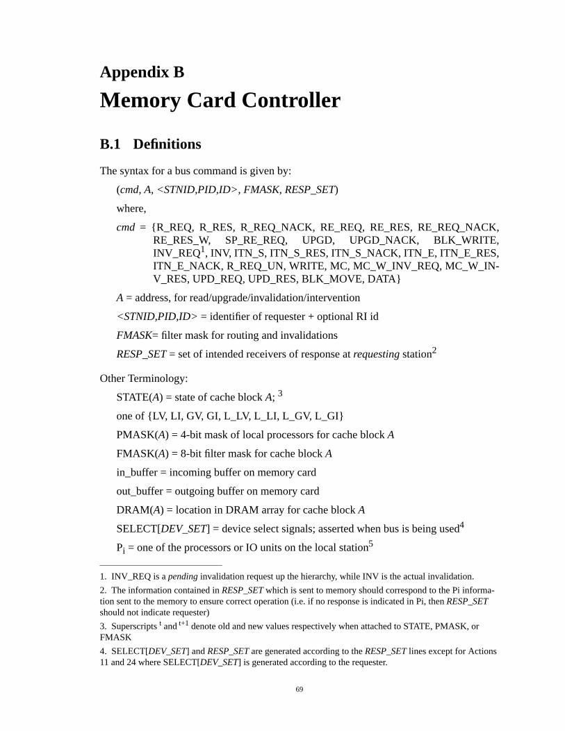
69
Appendix B
Memory Card Contr oller
B.1 Definitions
The syntax for a bus command is given by:
(cmd, A,<STNID,PID,ID>, FMASK, RESP_SET)
where,
cmd = {R_REQ, R_RES, R_REQ_NACK, RE_REQ, RE_RES, RE_REQ_NACK,RE_RES_W, SP_RE_REQ, UPGD, UPGD_NACK, BLK_WRITE,INV_REQ1, INV, ITN_S, ITN_S_RES, ITN_S_NACK, ITN_E, ITN_E_RES,ITN_E_NACK, R_REQ_UN, WRITE, MC, MC_W_INV_REQ, MC_W_IN-V_RES, UPD_REQ, UPD_RES, BLK_MOVE, DATA}
A = address, for read/upgrade/invalidation/intervention
<STNID,PID,ID> = identifier of requester + optional RI id
FMASK= filter mask for routing and invalidations
RESP_SET = set of intended receivers of response atrequesting station2
Other Terminology:
STATE(A) = state of cache blockA; 3
one of {LV, LI, GV, GI, L_LV, L_LI, L_GV, L_GI}
PMASK(A) = 4-bit mask of local processors for cache blockA
FMASK(A) = 8-bit filter mask for cache blockA
in_buffer = incoming buffer on memory card
out_buffer = outgoing buffer on memory card
DRAM(A) = location in DRAM array for cache blockA
SELECT[DEV_SET] = device select signals; asserted when bus is being used4
Pi = one of the processors or IO units on the local station5
1. INV_REQ is apending invalidation request up the hierarchy, while INV is the actual invalidation.
2. The information contained inRESP_SET which is sent to memory should correspond to the Pi informa-tion sent to the memory to ensure correct operation (i.e. if no response is indicated in Pi, thenRESP_SETshould not indicate requester)
3. Superscriptst and t+1 denote old and new values respectively when attached to STATE, PMASK, orFMASK
4. SELECT[DEV_SET] andRESP_SET are generated according to theRESP_SET lines except for Actions11 and 24 where SELECT[DEV_SET] is generated according to the requester.
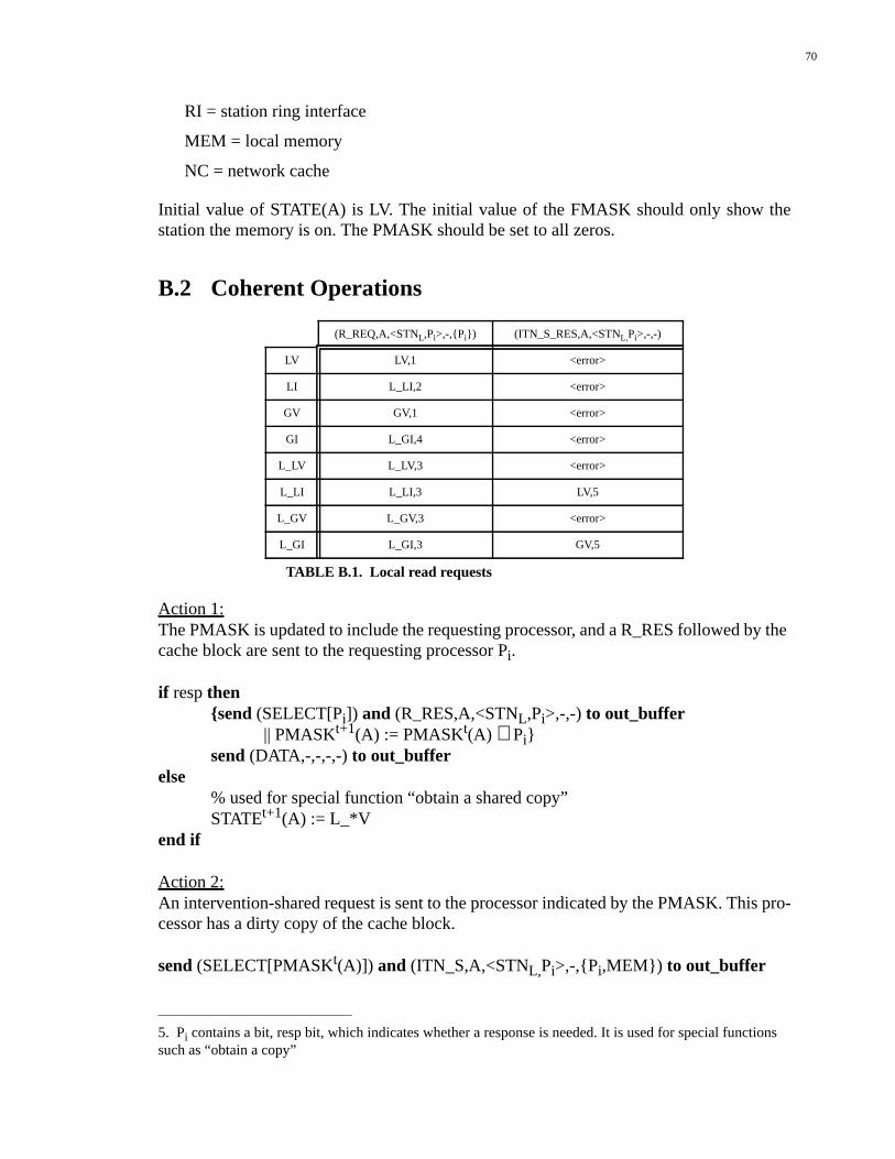
70
RI = station ring interface
MEM = local memory
NC = network cache
Initial value of STATE(A) is LV. The initial value of the FMASK should only show thestation the memory is on. The PMASK should be set to all zeros.
B.2 Coherent Operations
Action 1:The PMASK is updated to include the requesting processor, and a R_RES followed by thecache block are sent to the requesting processor Pi.
if respthen{send (SELECT[Pi]) and (R_RES,A,<STNL,Pi>,-,-) to out_buffer
|| PMASKt+1(A) := PMASKt(A) ∨ Pi}send(DATA,-,-,-,-) to out_buffer
else% used for special function “obtain a shared copy”STATEt+1(A) := L_*V
end if
Action 2:An intervention-shared request is sent to the processor indicated by the PMASK. This pro-cessor has a dirty copy of the cache block.
send (SELECT[PMASKt(A)]) and (ITN_S,A,<STNL,Pi>,-,{Pi,MEM}) to out_buffer
5. Pi contains a bit, resp bit, which indicates whether a response is needed. It is used for special functionssuch as “obtain a copy”
(R_REQ,A,<STNL,Pi>,-,{Pi}) (ITN_S_RES,A,<STNL,Pi>,-,-)
LV LV,1 <error>
LI L_LI,2 <error>
GV GV,1 <error>
GI L_GI,4 <error>
L_LV L_LV,3 <error>
L_LI L_LI,3 LV,5
L_GV L_GV,3 <error>
L_GI L_GI,3 GV,5
TABLE B.1. Local read requests
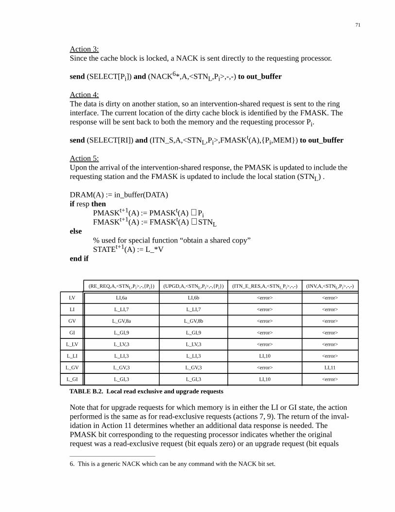
71
Action 3:Since the cache block is locked, a NACK is sent directly to the requesting processor.
send (SELECT[Pi]) and (NACK6*,A,<STNL,Pi>,-,-) to out_buffer
Action 4:The data is dirty on another station, so an intervention-shared request is sent to the ringinterface. The current location of the dirty cache block is identified by the FMASK. Theresponse will be sent back to both the memory and the requesting processor Pi.
send (SELECT[RI])and (ITN_S,A,<STNL,Pi>,FMASKt(A),{P i,MEM}) to out_buffer
Action 5:Upon the arrival of the intervention-shared response, the PMASK is updated to include therequesting station and the FMASK is updated to include the local station (STNL) .
DRAM(A) := in_buffer(DATA)if respthen
PMASKt+1(A) := PMASKt(A) ∨ PiFMASKt+1(A) := FMASKt(A) ∨ STNL
else% used for special function “obtain a shared copy”STATEt+1(A) := L_*V
end if
Note that for upgrade requests for which memory is in either the LI or GI state, the actionperformed is the same as for read-exclusive requests (actions 7, 9). The return of the inval-idation in Action 11 determines whether an additional data response is needed. ThePMASK bit corresponding to the requesting processor indicates whether the originalrequest was a read-exclusive request (bit equals zero) or an upgrade request (bit equals
6. This is a generic NACK which can be any command with the NACK bit set.
(RE_REQ,A,<STNL,Pi>,-,{Pi}) (UPGD,A,<STNL,Pi>,-,{Pi}) (ITN_E_RES,A,<STNL,Pi>,-,-) (INV,A,<STNL,Pi>,-,-)
LV LI,6a LI,6b <error> <error>
LI L_LI,7 L_LI,7 <error> <error>
GV L_GV,8a L_GV,8b <error> <error>
GI L_GI,9 L_GI,9 <error> <error>
L_LV L_LV,3 L_LV,3 <error> <error>
L_LI L_LI,3 L_LI,3 LI,10 <error>
L_GV L_GV,3 L_GV,3 <error> LI,11
L_GI L_GI,3 L_GI,3 LI,10 <error>
TABLE B.2. Local read exclusive and upgrade requests
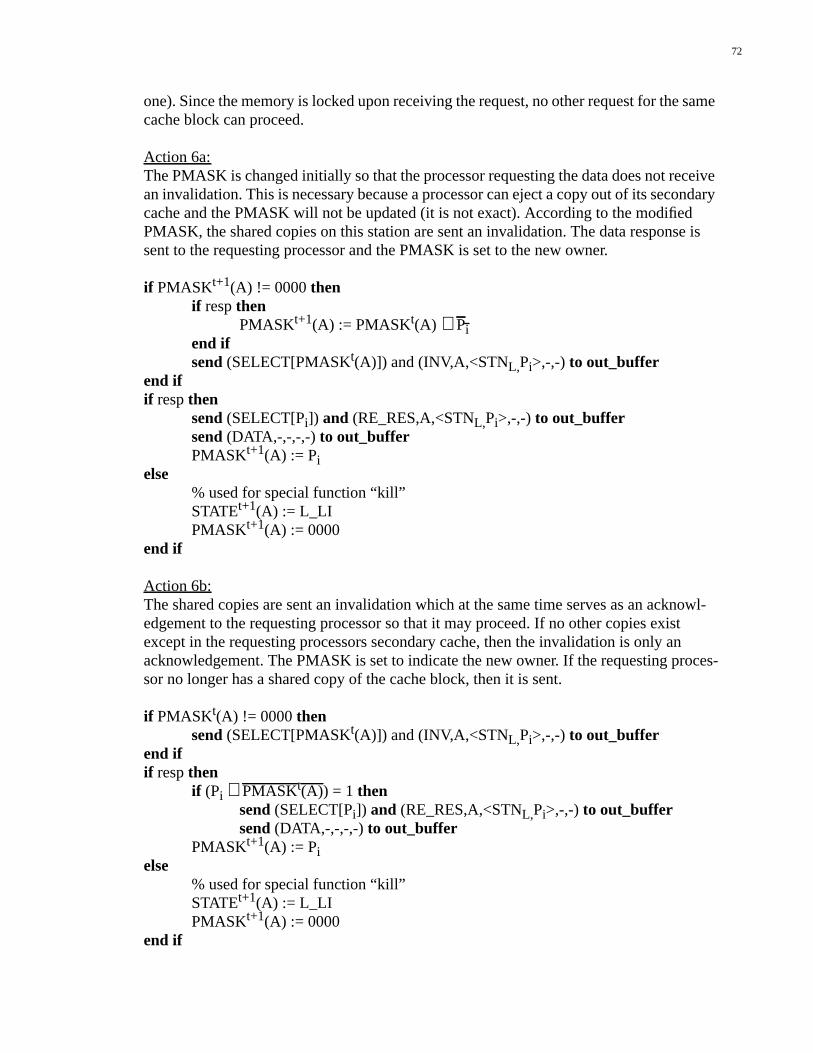
72
one). Since the memory is locked upon receiving the request, no other request for the samecache block can proceed.
Action 6a:The PMASK is changed initially so that the processor requesting the data does not receivean invalidation. This is necessary because a processor can eject a copy out of its secondarycache and the PMASK will not be updated (it is not exact). According to the modifiedPMASK, the shared copies on this station are sent an invalidation. The data response issent to the requesting processor and the PMASK is set to the new owner.
if PMASKt+1(A) != 0000thenif respthen
PMASKt+1(A) := PMASKt(A) ∧ Piend ifsend (SELECT[PMASKt(A)]) and(INV,A,<STNL,Pi>,-,-) to out_buffer
end ifif respthen
send (SELECT[Pi]) and (RE_RES,A,<STNL,Pi>,-,-) to out_buffersend (DATA,-,-,-,-) to out_bufferPMASKt+1(A) := Pi
else% used for special function “kill”STATEt+1(A) := L_LIPMASKt+1(A) := 0000
end if
Action 6b:The shared copies are sent an invalidation which at the same time serves as an acknowl-edgement to the requesting processor so that it may proceed. If no other copies existexcept in the requesting processors secondary cache, then the invalidation is only anacknowledgement. The PMASK is set to indicate the new owner. If the requesting proces-sor no longer has a shared copy of the cache block, then it is sent.
if PMASKt(A) != 0000thensend (SELECT[PMASKt(A)]) and(INV,A,<STNL,Pi>,-,-) to out_buffer
end ifif respthen
if (Pi ∧ PMASKt(A)) = 1 thensend (SELECT[Pi]) and (RE_RES,A,<STNL,Pi>,-,-) to out_buffersend (DATA,-,-,-,-) to out_buffer
PMASKt+1(A) := Pielse
% used for special function “kill”STATEt+1(A) := L_LIPMASKt+1(A) := 0000
end if
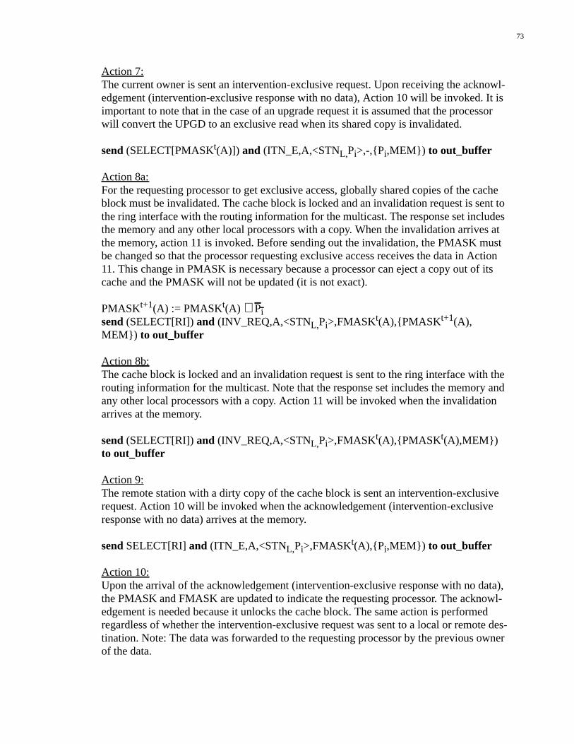
73
Action 7:The current owner is sent an intervention-exclusive request. Upon receiving the acknowl-edgement (intervention-exclusive response with no data), Action 10 will be invoked. It isimportant to note that in the case of an upgrade request it is assumed that the processorwill convert the UPGD to an exclusive read when its shared copy is invalidated.
send (SELECT[PMASKt(A)]) and (ITN_E,A,<STNL,Pi>,-,{Pi,MEM}) to out_buffer
Action 8a:For the requesting processor to get exclusive access, globally shared copies of the cacheblock must be invalidated. The cache block is locked and an invalidation request is sent tothe ring interface with the routing information for the multicast. The response set includesthe memory and any other local processors with a copy. When the invalidation arrives atthe memory, action 11 is invoked. Before sending out the invalidation, the PMASK mustbe changed so that the processor requesting exclusive access receives the data in Action11. This change in PMASK is necessary because a processor can eject a copy out of itscache and the PMASK will not be updated (it is not exact).
PMASKt+1(A) := PMASKt(A) ∧ Pisend (SELECT[RI])and (INV_REQ,A,<STNL,Pi>,FMASKt(A),{PMASK t+1(A),MEM}) to out_buffer
Action 8b:The cache block is locked and an invalidation request is sent to the ring interface with therouting information for the multicast. Note that the response set includes the memory andany other local processors with a copy. Action 11 will be invoked when the invalidationarrives at the memory.
send (SELECT[RI])and (INV_REQ,A,<STNL,Pi>,FMASKt(A),{PMASK t(A),MEM})to out_buffer
Action 9:The remote station with a dirty copy of the cache block is sent an intervention-exclusiverequest. Action 10 will be invoked when the acknowledgement (intervention-exclusiveresponse with no data) arrives at the memory.
send SELECT[RI]and (ITN_E,A,<STNL,Pi>,FMASKt(A),{P i,MEM}) to out_buffer
Action 10:Upon the arrival of the acknowledgement (intervention-exclusive response with no data),the PMASK and FMASK are updated to indicate the requesting processor. The acknowl-edgement is needed because it unlocks the cache block. The sameaction is performedregardless of whether the intervention-exclusive request was sent to a local or remote des-tination. Note: The data was forwarded to the requesting processor by the previous ownerof the data.
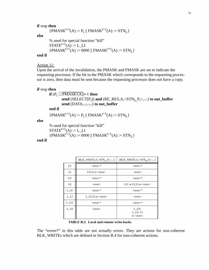
74
if respthen{PMASK t+1(A) := Pi || FMASKt+1(A) := STNL}
else% used for special function “kill”STATEt+1(A) := L_LI{PMASK t+1(A) := 0000 || FMASKt+1(A) := STNL}
end if
Action 11:Upon the arrival of the invalidation, the PMASK and FMASK are set to indicate therequesting processor. If the bit in the PMASK which corresponds to the requesting proces-sor is zero, then data must be sent because the requesting processor does not have a copy.
if respthenif (Pi ∧ PMASKt(A))=1 then
send (SELECT[Pi]) and (RE_RES,A,<STNL,Pi>,-,-) to out_buffersend (DATA,-,-,-,-) to out_buffer
end if
{PMASK t+1(A) := Pi || FMASKt+1(A) := STNL}else
% used for special function “kill”STATEt+1(A) := L_LI{PMASK t+1(A) := 0000 || FMASKt+1(A) := STNL}
end if
The “errors*” in this table are not actually errors. They are actions for non-coherentBLK_WRITEs which are defined in Section B.4 for non-coherent actions.
(BLK_WRITE,A,<STNL,,Pi>,-,-) (BLK_WRITE,A,<STNR,,Pi>,-,-)
LV <error>* <error>*
LI LV,12 or <error> <error>
GV <error>* <error>*
GI <error> GV or LV,13 or <error>
L_LV <error>* <error>*
L_LI L_LV,12 or <error> <error>
L_GV <error>* <error>*
L_GI <error> L_GV,L_LV, 13or <error>
TABLE B.3. Local and remote write-backs
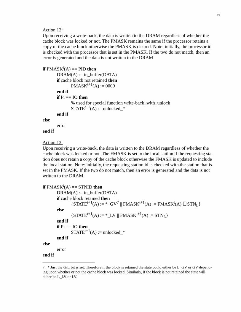
75
Action 12:Upon receiving a write-back, the data is written to the DRAM regardless of whether thecache block was locked or not. The PMASK remains the same if the processor retains acopy of the cache block otherwise the PMASK is cleared. Note: initially, the processor idis checked with the processor that is set in the PMASK. If the two do not match, then anerror is generated and the data is not written to the DRAM.
if PMASKt(A) == PID thenDRAM(A) := in_buffer(DATA)if cache block not retainedthen
PMASKt+1(A) := 0000end ifif Pi == IOthen
% used for special function write-back_with_unlockSTATEt+1(A) := unlocked_*
end ifelse
errorend if
Action 13:Upon receiving a write-back, the data is written to the DRAM regardless of whether thecache block was locked or not. The FMASK is set to the local station if the requesting sta-tion does not retain a copy of the cache block otherwise the FMASK is updated to includethe local station. Note: initially, the requesting station id is checked with the station that isset in the FMASK. If the two do not match, then an error is generated and the data is notwritten to the DRAM.
if FMASKt(A) == STNID thenDRAM(A) := in_buffer(DATA)if cache block retainedthen
{STATEt+1(A) := *_GV7 || FMASKt+1(A) := FMASKt(A) ∨ STNL}else
{STATEt+1(A) := *_LV || FMASKt+1(A) := STNL}end ifif Pi == IOthen
STATEt+1(A) := unlocked_*end if
elseerror
end if
7. * Just the G/L bit is set. Therefore if the block is retained the state could either be L_GV or GV depend-ing upon whether or not the cache block was locked. Similarly, if the block is not retained the state willeither be L_LV or LV.
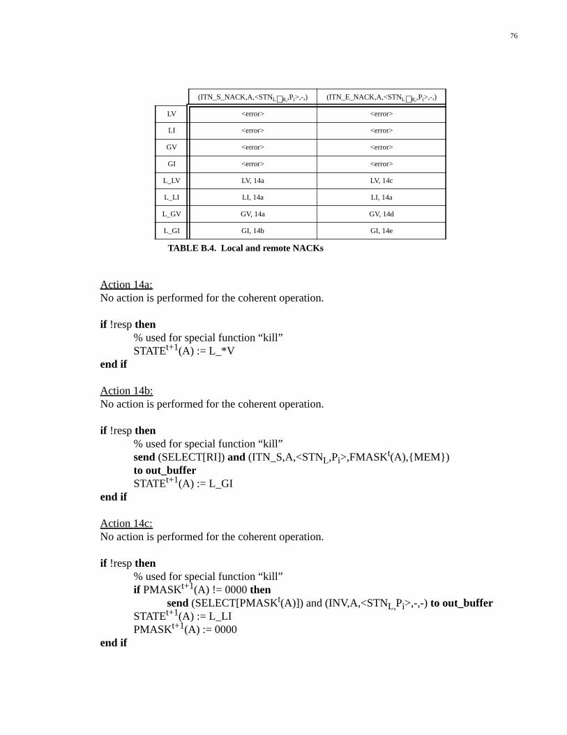
76
Action 14a:No action is performed for the coherent operation.
if !respthen% used for special function “kill”STATEt+1(A) := L_*V
end if
Action 14b:No action is performed for the coherent operation.
if !respthen% used for special function “kill”send (SELECT[RI])and (ITN_S,A,<STNL,Pi>,FMASKt(A),{MEM})to out_bufferSTATEt+1(A) := L_GI
end if
Action 14c:No action is performed for the coherent operation.
if !respthen% used for special function “kill”if PMASKt+1(A) != 0000then
send (SELECT[PMASKt(A)]) and(INV,A,<STNL,Pi>,-,-) to out_bufferSTATEt+1(A) := L_LIPMASKt+1(A) := 0000
end if
(ITN_S_NACK,A,<STNL∨R,,Pi>,-,) (ITN_E_NACK,A,<STNL∨R,,Pi>,-,)
LV <error> <error>
LI <error> <error>
GV <error> <error>
GI <error> <error>
L_LV LV, 14a LV, 14c
L_LI LI, 14a LI, 14a
L_GV GV, 14a GV, 14d
L_GI GI, 14b GI, 14e
TABLE B.4. Local and remote NACKs
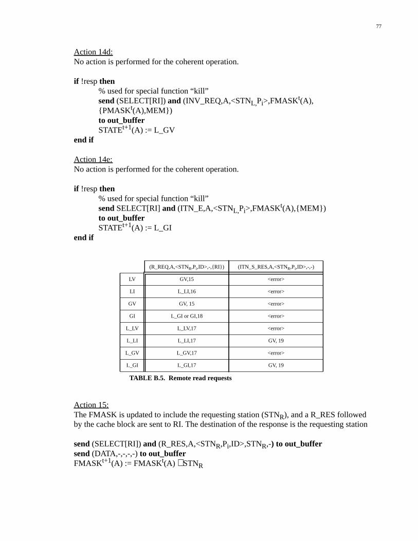
77
Action 14d:No action is performed for the coherent operation.
if !respthen% used for special function “kill”send (SELECT[RI])and (INV_REQ,A,<STNL,Pi>,FMASKt(A),{PMASK t(A),MEM})to out_bufferSTATEt+1(A) := L_GV
end if
Action 14e:No action is performed for the coherent operation.
if !respthen% used for special function “kill”send SELECT[RI]and (ITN_E,A,<STNL,Pi>,FMASKt(A),{MEM})to out_bufferSTATEt+1(A) := L_GI
end if
Action 15:The FMASK is updated to include the requesting station (STNR), and a R_RES followedby the cache block are sent to RI. The destination of the response is the requesting station
send (SELECT[RI])and (R_RES,A,<STNR,Pi,ID>,STNR,-) to out_buffersend(DATA,-,-,-,-) to out_bufferFMASKt+1(A) := FMASKt(A) ∨STNR
(R_REQ,A,<STNR,Pi,ID>,-,{RI}) (ITN_S_RES,A,<STNR,Pi,ID>,-,-)
LV GV,15 <error>
LI L_LI,16 <error>
GV GV, 15 <error>
GI L_GI or GI,18 <error>
L_LV L_LV,17 <error>
L_LI L_LI,17 GV, 19
L_GV L_GV,17 <error>
L_GI L_GI,17 GV, 19
TABLE B.5. Remote read requests
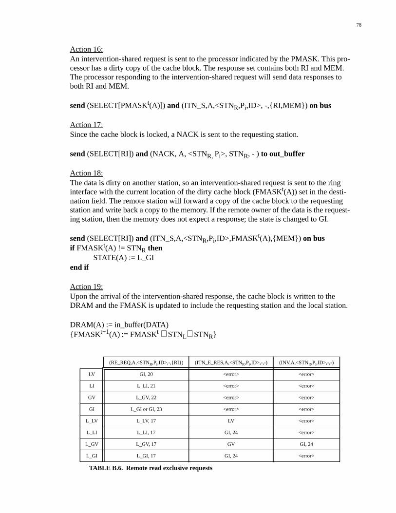
78
Action 16:An intervention-shared request is sent to the processor indicated by the PMASK. This pro-cessor has a dirty copy of the cache block. The response set contains both RI and MEM.The processor responding to the intervention-shared request will send data responses toboth RI and MEM.
send (SELECT[PMASKt(A)]) and (ITN_S,A,<STNR,Pi,ID>, -,{RI,MEM}) on bus
Action 17:Since the cache block is locked, a NACK is sent to the requesting station.
send (SELECT[RI]) and (NACK, A, <STNR, Pi>, STNR, - ) to out_buffer
Action 18:The data is dirty on another station, so an intervention-shared request is sent to the ringinterface with the current location of the dirty cache block (FMASKt(A)) set in the desti-nation field. The remote station will forward a copy of the cache block to the requestingstation and write back a copy to the memory. If the remote owner of the data is the request-ing station, then the memory does not expect a response; the state is changed to GI.
send (SELECT[RI])and (ITN_S,A,<STNR,Pi,ID>,FMASKt(A),{MEM}) on busif FMASKt(A) != STNR then
STATE(A) := L_GIend if
Action 19:Upon the arrival of the intervention-shared response, the cache block is written to theDRAM and the FMASK is updated to include the requesting station and the local station.
DRAM(A) := in_buffer(DATA){FMASK t+1(A) := FMASKt ∨ STNL∨ STNR}
(RE_REQ,A,<STNR,Pi,ID>,-,{RI}) (ITN_E_RES,A,<STNR,Pi,ID>,-,-) (INV,A,<STNR,Pi,ID>,-,-)
LV GI, 20 <error> <error>
LI L_LI, 21 <error> <error>
GV L_GV, 22 <error> <error>
GI L_GI or GI, 23 <error> <error>
L_LV L_LV, 17 LV <error>
L_LI L_LI, 17 GI, 24 <error>
L_GV L_GV, 17 GV GI, 24
L_GI L_GI, 17 GI, 24 <error>
TABLE B.6. Remote read exclusive requests
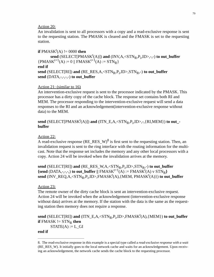
79
Action 20:An invalidation is sent to all processors with a copy and a read-exclusive response is sentto the requesting station. The PMASK is cleared and the FMASK is set to the requestingstation.
if PMASKt(A) != 0000thensend (SELECT[PMASKt(A)]) and (INV,A,<STNR,Pi,ID>,-,-) to out_buffer
{PMASK t+1(A) := 0 || FMASKt+1(A) := STNR}end ifsend (SELECT[RI])and (RE_RES,A,<STNR,Pi,ID>,STNR,-) to out_buffersend (DATA,-,-,-,-) to out_buffer
Action 21: (similar to 16)An intervention-exclusive request is sent to the processor indicated by the PMASK. Thisprocessor has a dirty copy of the cache block. The response set contains both RI andMEM. The processor responding to the intervention-exclusive request will send a dataresponses to the RI and an acknowledgement(intervention-exclusive response withoutdata) to the MEM.
send (SELECT[PMASKt(A)]) and (ITN_E,A,<STNR,Pi,ID>,-,{RI,MEM}) to out_-buffer
Action 22:A read-exclusive response (RE_RES_W)8 is first sent to the requesting station. Then, aninvalidation request is sent to the ring interface with the routing information for the multi-cast. Note that the response set includes the memory and any other local processors with acopy. Action 24 will be invoked when the invalidation arrives at the memory.
send (SELECT[RI])and (RE_RES_W,A,<STNR,Pi,ID>,STNR,-) to out_buffer{send (DATA,-,-,-,) to out_buffer || FMASKt+1(A) := FMASKt(A) v STNR}send (INV_REQ,A,<STNR,Pi,ID>,FMASKt(A),{MEM, PMASK t(A)}) to out_buffer
Action 23:The remote owner of the dirty cache block is sent an intervention-exclusive request.Action 24 will be invoked when the acknowledgement (intervention-exclusive responsewithout data) arrives at the memory. If the station with the data is the same as the request-ing station then memory does not require a response.
send (SELECT[RI])and (ITN_E,A,<STNR,Pi,ID>,FMASKt(A),{MEM}) to out_bufferif FMASK != STNR then
STATE(A) := L_GIend if
8. The read-exclusive response in this example is a special type called aread-exclusive response with a wait(RE_RES_W). It initially goes to the local network cache and waits for an acknowledgement. Upon receiv-ing an acknowledgement, the network cache sends the cache block to the requesting processor.
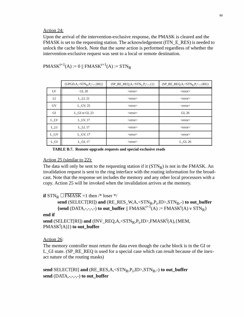
80
Action 24:Upon the arrival of the intervention-exclusive response, the PMASK is cleared and theFMASK is set to the requesting station. The acknowledgement (ITN_E_RES) is needed tounlock the cache block. Note that thesameaction is performed regardless of whether theintervention-exclusive request was sent to a local or remote destination.
PMASKt+1(A) := 0 || FMASKt+1(A) := STNR
Action 25 (similar to 22):The data will only be sent to the requesting station if it (STNR) is not in the FMASK. Aninvalidation request is sent to the ring interface with the routing information for the broad-cast. Note that the response set includes the memory and any other local processors with acopy. Action 25 will be invoked when the invalidation arrives at the memory.
if STNR ∧ FMASK =1 then /* loser */send (SELECT[RI])and (RE_RES_W,A,<STNR,Pi,ID>,STNR,-) to out_buffer{send (DATA,-,-,-,-) to out_buffer || FMASKt+1(A) := FMASKt(A) v STNR}
end ifsend (SELECT[RI]) and (INV_REQ,A,<STNR,Pi,ID>,FMASKt(A),{MEM,PMASKt(A)}) to out_buffer
Action 26:The memory controller must return the data even though the cache block is in the GI orL_GI state. (SP_RE_REQ is used for a special case which can result because of the inex-act nature of the routing masks)
send SELECT[RI]and (RE_RES,A,<STNR,Pi,ID>,STNR,-) to out_buffersend (DATA,-,-,-,-) to out_buffer
(UPGD,A,<STNR,Pi>,-,{RI}) (SP_RE_REQ,A,<STNL,Pi>,-,{}) (SP_RE_REQ,A,<STNR,Pi>,-,{RI})
LV GI, 20 <error> <error>
LI L_LI, 21 <error> <error>
GV L_GV, 25 <error> <error>
GI L_GI or GI, 23 <error> GI, 26
L_LV L_LV, 17 <error> <error>
L_LI L_LI, 17 <error> <error>
L_GV L_GV, 17 <error> <error>
L_GI L_GI, 17 <error> L_GI, 26
TABLE B.7. Remote upgrade requests and special exclusive reads
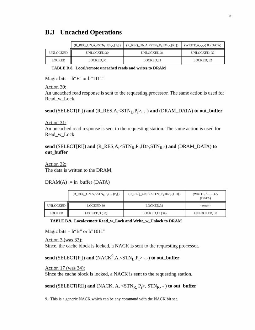
81
B.3 Uncached Operations
Magic bits = h“F” or b”1111”
Action 30:An uncached read response is sent to the requesting processor. The same action is used forRead_w_Lock.
send (SELECT[Pi]) and (R_RES,A,<STNL,Pi>,-,-) and (DRAM_DATA) to out_buffer
Action 31:An uncached read response is sent to the requesting station. The same action is used forRead_w_Lock.
send (SELECT[RI])and (R_RES,A,<STNR,Pi,ID>,STNR,-) and (DRAM_DATA) toout_buffer
Action 32:The data is written to the DRAM.
DRAM(A) := in_buffer (DATA)
Magic bits = h“B” or b”1011”
Action 3 (was 33):Since, the cache block is locked, a NACK is sent to the requesting processor.
send (SELECT[Pi]) and (NACK9,A,<STNL,Pi>,-,-) to out_buffer
Action 17 (was 34):Since the cache block is locked, a NACK is sent to the requesting station.
send (SELECT[RI]) and (NACK, A, <STNR, Pi>, STNR, - ) to out_buffer
9. This is a generic NACK which can be any command with the NACK bit set.
(R_REQ_UN,A,<STNL,Pi>,-,{Pi}) (R_REQ_UN,A,<STNR,Pi,ID>,-,{RI}) (WRITE,A,-,-,-) & (DATA)
UNLOCKED UNLOCKED,30 UNLOCKED,31 UNLOCKED, 32
LOCKED LOCKED,30 LOCKED,31 LOCKED, 32
TABLE B.8. Local/remote uncached reads and writes to DRAM
(R_REQ_UN,A,<STNL,Pi>,-,{Pi}) (R_REQ_UN,A,<STNR,Pi,ID>,-,{RI}) (WRITE,A,-,-,-) &(DATA)
UNLOCKED LOCKED,30 LOCKED,31 <error>
LOCKED LOCKED,3 (33) LOCKED,17 (34) UNLOCKED, 32
TABLE B.9. Local/remote Read_w_Lock and Write_w_Unlock to DRAM
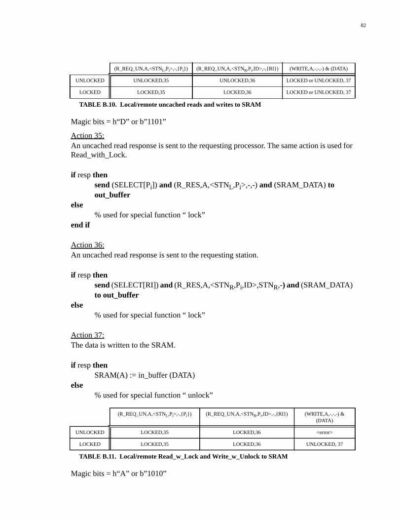
82
Magic bits = h“D” or b”1101”
Action 35:An uncached read response is sent to the requesting processor. The same action is used forRead_with_Lock.
if respthensend (SELECT[Pi]) and (R_RES,A,<STNL,Pi>,-,-) and (SRAM_DATA) toout_buffer
else% used for special function “ lock”
end if
Action 36:An uncached read response is sent to the requesting station.
if respthensend (SELECT[RI])and (R_RES,A,<STNR,Pi,ID>,STNR,-) and (SRAM_DATA)to out_buffer
else% used for special function “ lock”
Action 37:The data is written to the SRAM.
if respthenSRAM(A) := in_buffer (DATA)
else% used for special function “ unlock”
Magic bits = h“A” or b”1010”
(R_REQ_UN,A,<STNL,Pi>,-,{Pi}) (R_REQ_UN,A,<STNR,Pi,ID>,-,{RI}) (WRITE,A,-,-,-) & (DATA)
UNLOCKED UNLOCKED,35 UNLOCKED,36 LOCKED or UNLOCKED, 37
LOCKED LOCKED,35 LOCKED,36 LOCKED or UNLOCKED, 37
TABLE B.10. Local/remote uncached reads and writes to SRAM
(R_REQ_UN,A,<STNL,Pi>,-,{Pi}) (R_REQ_UN,A,<STNR,Pi,ID>,-,{RI}) (WRITE,A,-,-,-) &(DATA)
UNLOCKED LOCKED,35 LOCKED,36 <error>
LOCKED LOCKED,35 LOCKED,36 UNLOCKED, 37
TABLE B.11. Local/remote Read_w_Lock and Write_w_Unlock to SRAM
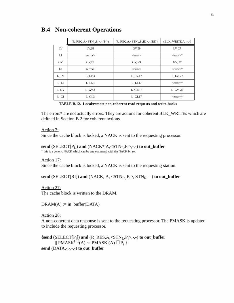
83
B.4 Non-coherent Operations
The errors* are not actually errors. They are actions for coherent BLK_WRITEs which aredefined in Section B.2 for coherent actions.
Action 3:Since the cache block is locked, a NACK is sent to the requesting processor.
send (SELECT[Pi]) and (NACK*,A,<STNL,Pi>,-,-) to out_buffer* this is a generic NACK which can be any command with the NACK bit set
Action 17:Since the cache block is locked, a NACK is sent to the requesting station.
send (SELECT[RI]) and (NACK, A, <STNR, Pi>, STNR, - ) to out_buffer
Action 27:The cache block is written to the DRAM.
DRAM(A) := in_buffer(DATA)
Action 28:A non-coherent data response is sent to the requesting processor. The PMASK is updatedto include the requesting processor.
{send (SELECT[Pi]) and (R_RES,A,<STNL,Pi>,-,-) to out_buffer|| PMASKt+1(A) := PMASKt(A) ∨ Pi }
send(DATA,-,-,-,-) to out_buffer
(R_REQ,A,<STNL,Pi>,-,{Pi}) (R_REQ,A,<STNR,Pi,ID>,-,{RI}) (BLK_WRITE,A,-,-,-)
LV LV,28 GV,29 LV, 27
LI <error> <error> <error>*
GV GV,28 GV, 29 GV, 27
GI <error> <error> <error>*
L_LV L_LV,3 L_LV,17 L_LV, 27
L_LI L_LI,3 L_LI,17 <error>*
L_GV L_GV,3 L_GV,17 L_GV, 27
L_GI L_GI,3 L_GI,17 <error>*
TABLE B.12. Local/remote non-coherent read requests and write-backs
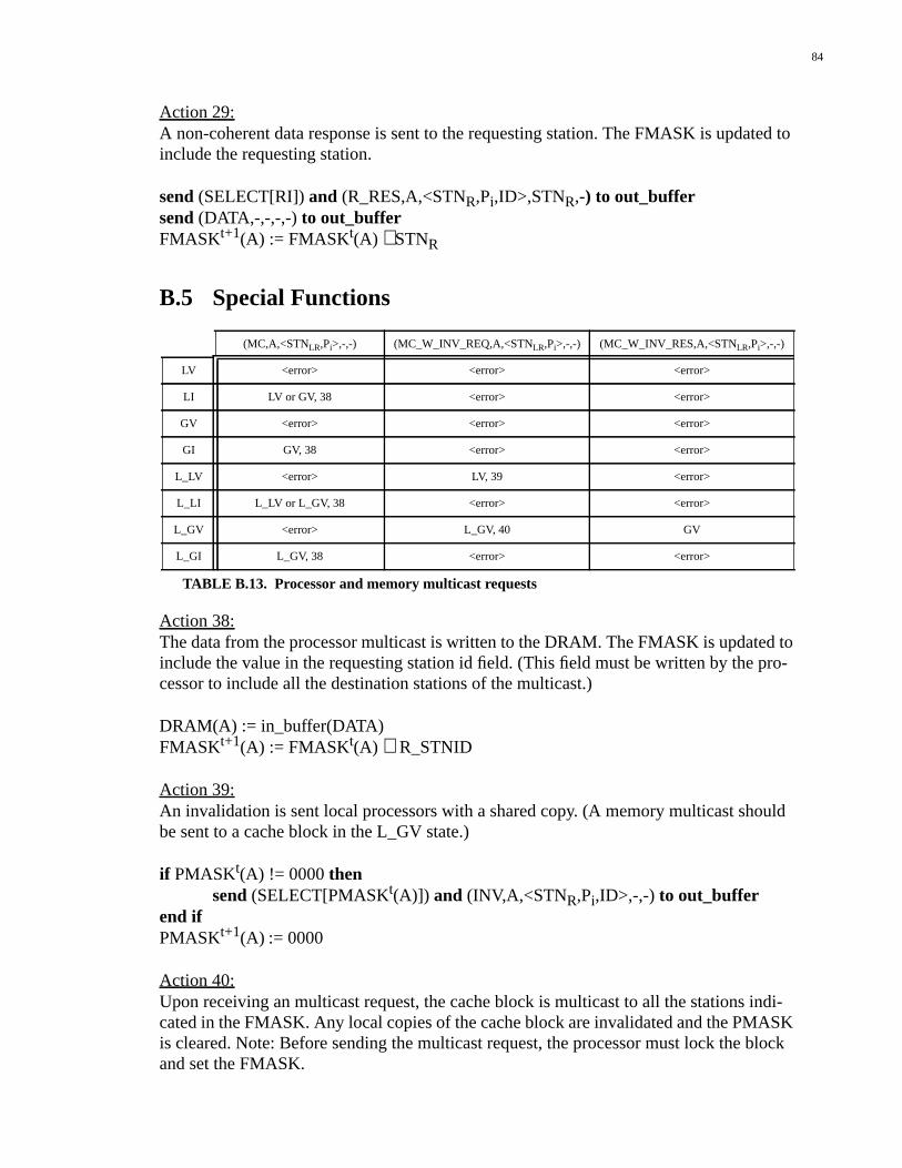
84
Action 29:A non-coherent data response is sent to the requesting station. The FMASK is updated toinclude the requesting station.
send (SELECT[RI])and (R_RES,A,<STNR,Pi,ID>,STNR,-) to out_buffersend(DATA,-,-,-,-) to out_bufferFMASKt+1(A) := FMASKt(A) ∨STNR
B.5 Special Functions
Action 38:The data from the processor multicast is written to the DRAM. The FMASK is updated toinclude the value in the requesting station id field. (This field must be written by the pro-cessor to include all the destination stations of the multicast.)
DRAM(A) := in_buffer(DATA)FMASKt+1(A) := FMASKt(A) ∨ R_STNID
Action 39:An invalidation is sent local processors with a shared copy. (A memory multicast shouldbe sent to a cache block in the L_GV state.)
if PMASKt(A) != 0000thensend (SELECT[PMASKt(A)]) and (INV,A,<STNR,Pi,ID>,-,-) to out_buffer
end ifPMASKt+1(A) := 0000
Action 40:Upon receiving an multicast request, the cache block is multicast to all the stations indi-cated in the FMASK. Any local copies of the cache block are invalidated and the PMASKis cleared. Note: Before sending the multicast request, the processor must lock the blockand set the FMASK.
(MC,A,<STNLR,Pi>,-,-) (MC_W_INV_REQ,A,<STNLR,Pi>,-,-) (MC_W_INV_RES,A,<STNLR,Pi>,-,-)
LV <error> <error> <error>
LI LV or GV, 38 <error> <error>
GV <error> <error> <error>
GI GV, 38 <error> <error>
L_LV <error> LV, 39 <error>
L_LI L_LV or L_GV, 38 <error> <error>
L_GV <error> L_GV, 40 GV
L_GI L_GV, 38 <error> <error>
TABLE B.13. Processor and memory multicast requests
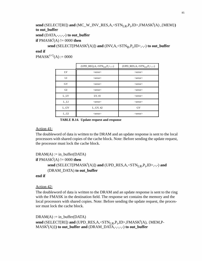
85
send (SELECT[RI])and (MC_W_INV_RES,A,<STNLR,Pi,ID>,FMASKt(A) ,{MEM} )to out_buffersend(DATA,-,-,-,-) to out_bufferif PMASKt(A) != 0000then
send (SELECT[PMASKt(A)]) and (INV,A,<STNR,Pi,ID>,-,-) to out_bufferend ifPMASKt+1(A) := 0000
Action 41:The doubleword of data is written to the DRAM and an update response is sent to the localprocessors with shared copies of the cache block. Note: Before sending the update request,the processor must lock the cache block.
DRAM(A) := in_buffer(DATA)if PMASKt(A) != 0000then
send (SELECT[PMASKt(A)]) and (UPD_RES,A,<STNLR,Pi,ID>,-,-) and(DRAM_DATA) to out_buffer
end if
Action 42:The doubleword of data is written to the DRAM and an update response is sent to the ringwith the FMASK in the destination field. The response set contains the memory and thelocal processors with shared copies. Note: Before sending the update request, the proces-sor must lock the cache block.
DRAM(A) := in_buffer(DATA)send (SELECT[RI])and (UPD_RES,A,<STNLR,Pi,ID>,FMASKt(A), {MEM,P-MASKt(A)} ) to out_buffer and (DRAM_DATA,-,-,-,-) to out_buffer
(UPD_REQ,A,<STNLR,Pi>,-,-) (UPD_RES,A,<STNLR,Pi>,-,-)
LV <error> <error>
LI <error> <error>
GV <error> <error>
GI <error> <error>
L_LV LV, 41 <error>
L_LI <error> <error>
L_GV L_GV, 42 GV
L_GI <error> <error>
TABLE B.14. Update request and response
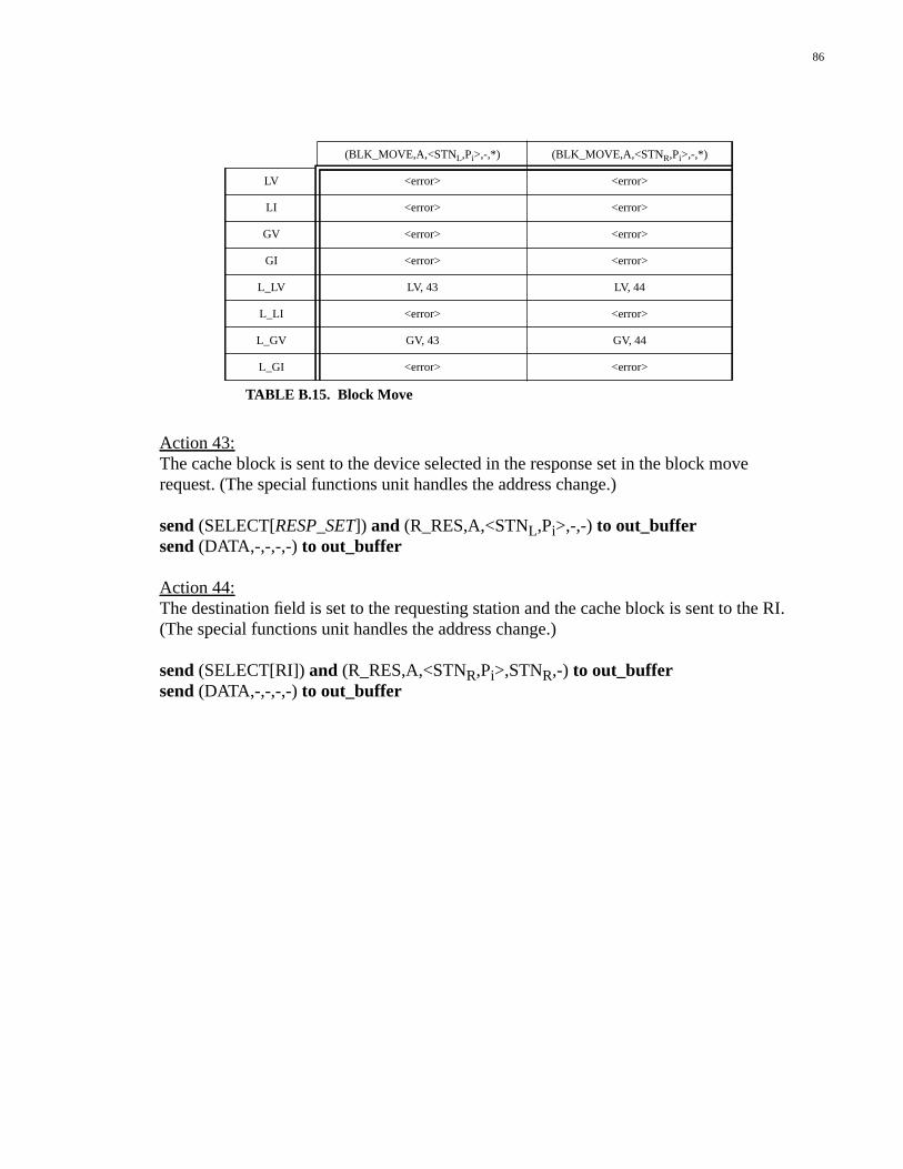
86
Action 43:The cache block is sent to the device selected in the response set in the block moverequest. (The special functions unit handles the address change.)
send (SELECT[RESP_SET]) and (R_RES,A,<STNL,Pi>,-,-) to out_buffersend(DATA,-,-,-,-) to out_buffer
Action 44:The destination field is set to the requesting station and the cache block is sent to the RI.(The special functions unit handles the address change.)
send (SELECT[RI])and (R_RES,A,<STNR,Pi>,STNR,-) to out_buffersend(DATA,-,-,-,-) to out_buffer
(BLK_MOVE,A,<STNL,Pi>,-,*) (BLK_MOVE,A,<STNR,Pi>,-,*)
LV <error> <error>
LI <error> <error>
GV <error> <error>
GI <error> <error>
L_LV LV, 43 LV, 44
L_LI <error> <error>
L_GV GV, 43 GV, 44
L_GI <error> <error>
TABLE B.15. Block Move
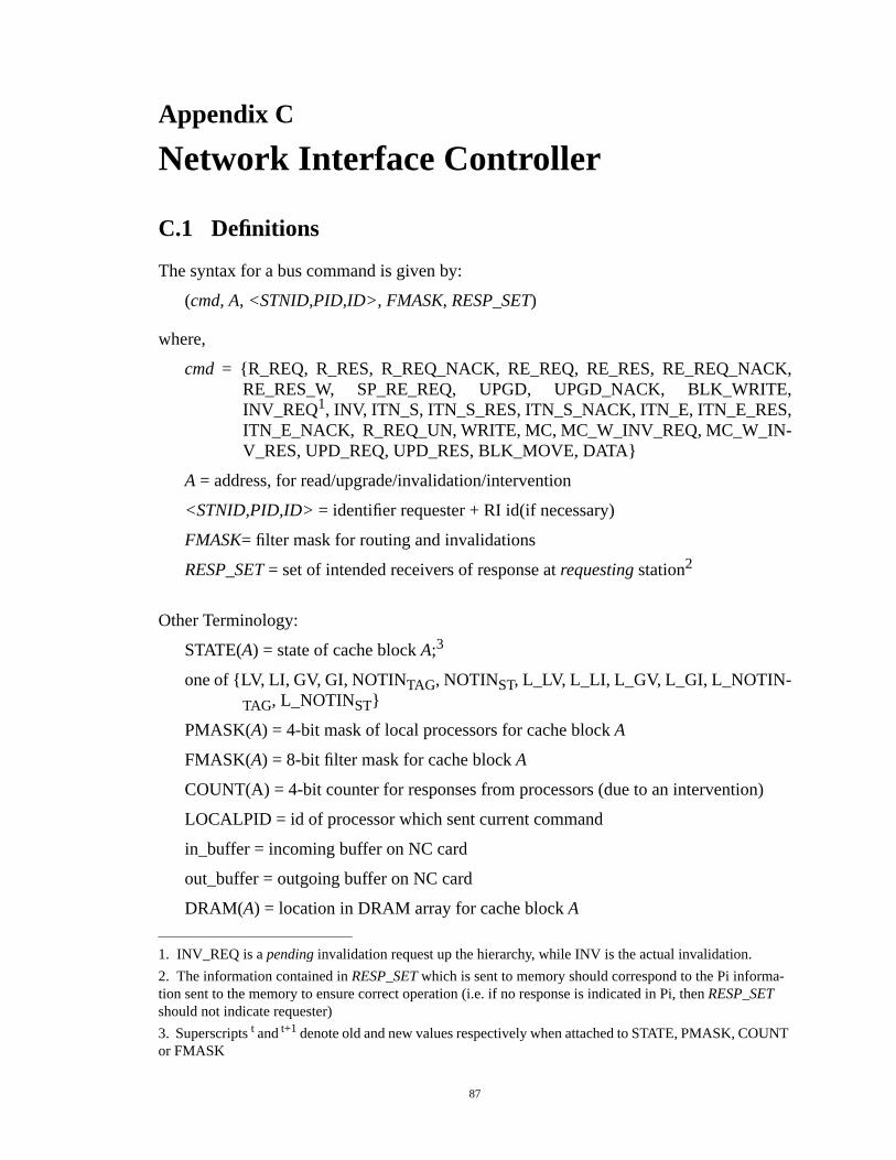
87
Appendix C
Network Interface Controller
C.1 Definitions
The syntax for a bus command is given by:
(cmd, A,<STNID,PID,ID>, FMASK, RESP_SET)
where,
cmd = {R_REQ, R_RES, R_REQ_NACK, RE_REQ, RE_RES, RE_REQ_NACK,RE_RES_W, SP_RE_REQ, UPGD, UPGD_NACK, BLK_WRITE,INV_REQ1, INV, ITN_S, ITN_S_RES, ITN_S_NACK, ITN_E, ITN_E_RES,ITN_E_NACK, R_REQ_UN, WRITE, MC, MC_W_INV_REQ, MC_W_IN-V_RES, UPD_REQ, UPD_RES, BLK_MOVE, DATA}
A = address, for read/upgrade/invalidation/intervention
<STNID,PID,ID> = identifier requester + RI id(if necessary)
FMASK= filter mask for routing and invalidations
RESP_SET = set of intended receivers of response atrequesting station2
Other Terminology:
STATE(A) = state of cache blockA;3
one of {LV, LI, GV, GI, NOTINTAG, NOTINST, L_LV, L_LI, L_GV, L_GI, L_NOTIN-
TAG, L_NOTINST}
PMASK(A) = 4-bit mask of local processors for cache blockA
FMASK(A) = 8-bit filter mask for cache blockA
COUNT(A) = 4-bit counter for responses from processors (due to an intervention)
LOCALPID = id of processor which sent current command
in_buffer = incoming buffer on NC card
out_buffer = outgoing buffer on NC card
DRAM(A) = location in DRAM array for cache blockA
1. INV_REQ is apending invalidation request up the hierarchy, while INV is the actual invalidation.
2. The information contained inRESP_SET which is sent to memory should correspond to the Pi informa-tion sent to the memory to ensure correct operation (i.e. if no response is indicated in Pi, thenRESP_SETshould not indicate requester)
3. Superscriptst and t+1 denote old and new values respectively when attached to STATE, PMASK, COUNTor FMASK
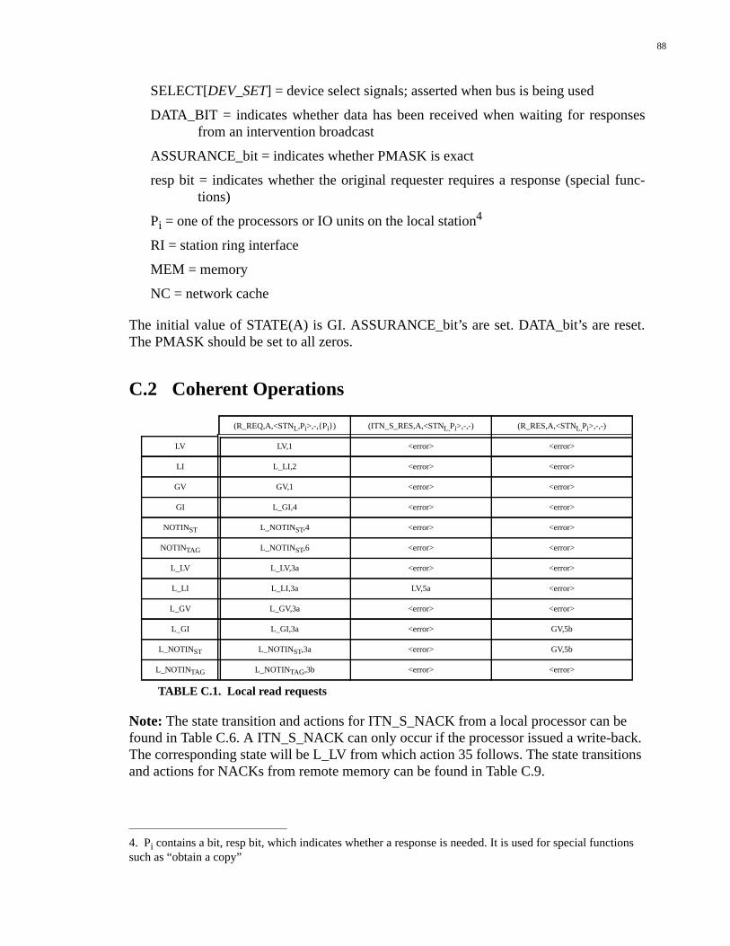
88
SELECT[DEV_SET] = device select signals; asserted when bus is being used
DATA_BIT = indicates whether data has been received when waiting for responsesfrom an intervention broadcast
ASSURANCE_bit = indicates whether PMASK is exact
resp bit = indicates whether the original requester requires a response (special func-tions)
Pi = one of the processors or IO units on the local station4
RI = station ring interface
MEM = memory
NC = network cache
The initial value of STATE(A) is GI. ASSURANCE_bit’s are set. DATA_bit’s are reset.The PMASK should be set to all zeros.
C.2 Coherent Operations
Note: The state transition and actions for ITN_S_NACK from a local processor can befound in Table C.6. A ITN_S_NACK can only occur if the processor issued a write-back.The corresponding state will be L_LV from which action 35 follows. The state transitionsand actions for NACKs from remote memory can be found in Table C.9.
4. Pi contains a bit, resp bit, which indicates whether a response is needed. It is used for special functionssuch as “obtain a copy”
(R_REQ,A,<STNL,Pi>,-,{Pi}) (ITN_S_RES,A,<STNL,Pi>,-,-) (R_RES,A,<STNL,Pi>,-,-)
LV LV,1 <error> <error>
LI L_LI,2 <error> <error>
GV GV,1 <error> <error>
GI L_GI,4 <error> <error>
NOTINST L_NOTINST,4 <error> <error>
NOTINTAG L_NOTINST,6 <error> <error>
L_LV L_LV,3a <error> <error>
L_LI L_LI,3a LV,5a <error>
L_GV L_GV,3a <error> <error>
L_GI L_GI,3a <error> GV,5b
L_NOTINST L_NOTINST,3a <error> GV,5b
L_NOTINTAG L_NOTINTAG,3b <error> <error>
TABLE C.1. Local read requests
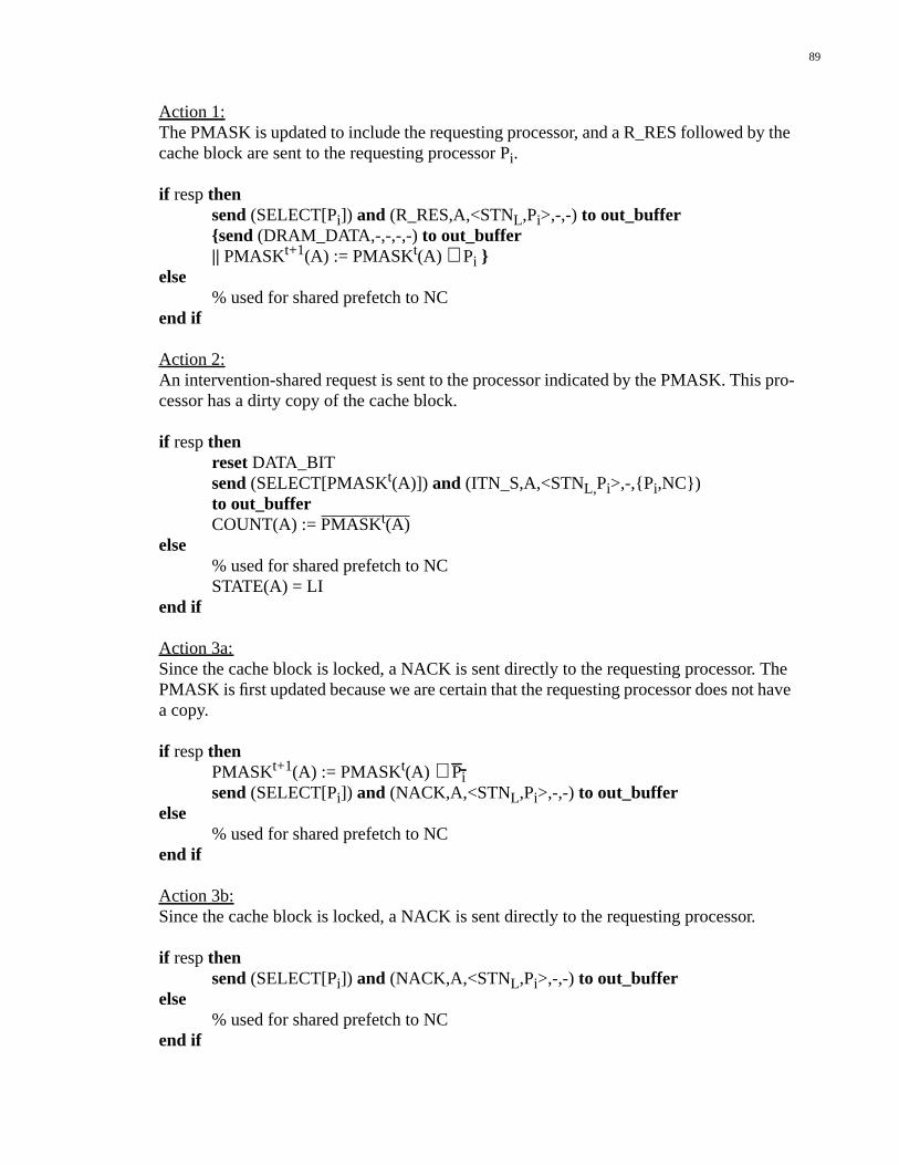
89
Action 1:The PMASK is updated to include the requesting processor, and a R_RES followed by thecache block are sent to the requesting processor Pi.
if respthensend (SELECT[Pi]) and (R_RES,A,<STNL,Pi>,-,-) to out_buffer{send(DRAM_DATA,-,-,-,-) to out_buffer|| PMASKt+1(A) := PMASKt(A) ∨ Pi }
else% used for shared prefetch to NC
end if
Action 2:An intervention-shared request is sent to the processor indicated by the PMASK. This pro-cessor has a dirty copy of the cache block.
if respthenreset DATA_BITsend (SELECT[PMASKt(A)]) and (ITN_S,A,<STNL,Pi>,-,{Pi,NC})to out_bufferCOUNT(A) := PMASKt(A)
else% used for shared prefetch to NCSTATE(A) = LI
end if
Action 3a:Since the cache block is locked, a NACK is sent directly to the requesting processor. ThePMASK is first updated because we are certain that the requesting processor does not havea copy.
if respthenPMASKt+1(A) := PMASKt(A) ∧ Pisend (SELECT[Pi]) and (NACK,A,<STNL,Pi>,-,-) to out_buffer
else% used for shared prefetch to NC
end if
Action 3b:Since the cache block is locked, a NACK is sent directly to the requesting processor.
if respthensend (SELECT[Pi]) and (NACK,A,<STNL,Pi>,-,-) to out_buffer
else% used for shared prefetch to NC
end if
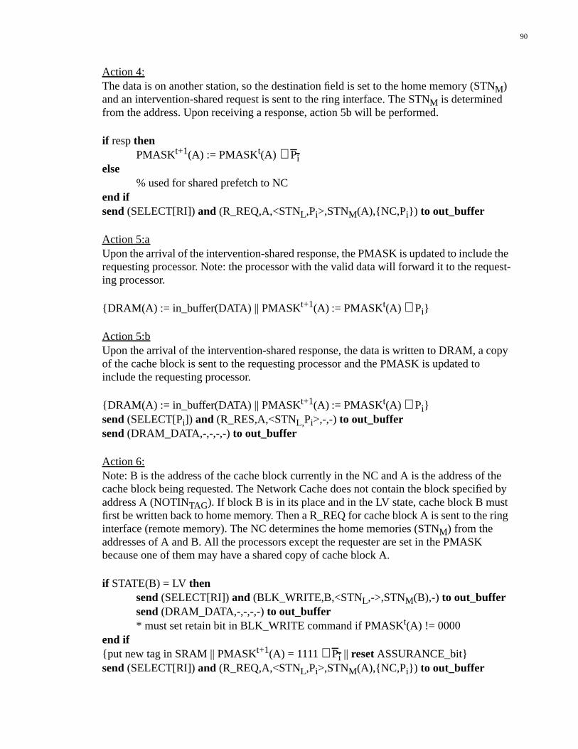
90
Action 4:The data is on another station, so the destination field is set to the home memory (STNM)and an intervention-shared request is sent to the ring interface. The STNM is determinedfrom the address. Upon receiving a response, action 5b will be performed.
if respthenPMASKt+1(A) := PMASKt(A) ∧ Pi
else% used for shared prefetch to NC
end ifsend (SELECT[RI]) and (R_REQ,A,<STNL,Pi>,STNM(A),{NC,Pi}) to out_buffer
Action 5:aUpon the arrival of the intervention-shared response, the PMASK is updated to include therequesting processor. Note: the processor with the valid data will forward it to the request-ing processor.
{DRAM(A) := in_buffer(DATA) || PMASKt+1(A) := PMASKt(A) ∨ Pi}
Action 5:bUpon the arrival of the intervention-shared response, the data is written to DRAM, a copyof the cache block is sent to the requesting processor and the PMASK is updated toinclude the requesting processor.
{DRAM(A) := in_buffer(DATA) || PMASKt+1(A) := PMASKt(A) ∨ Pi}send (SELECT[Pi]) and (R_RES,A,<STNL,Pi>,-,-) to out_buffersend (DRAM_DATA,-,-,-,-) to out_buffer
Action 6:Note: B is the address of the cache block currently in the NC and A is the address of thecache block being requested. The Network Cache does not contain the block specified byaddress A (NOTINTAG). If block B is in its place and in the LV state, cache block B mustfirst be written back to home memory. Then a R_REQ for cache block A is sent to the ringinterface (remote memory). The NC determines the home memories (STNM) from theaddresses of A and B. All the processors except the requester are set in the PMASKbecause one of them may have a shared copy of cache block A.
if STATE(B) = LV thensend (SELECT[RI])and (BLK_WRITE,B,<STNL,->,STNM(B),-) to out_buffersend(DRAM_DATA,-,-,-,-) to out_buffer* must set retain bit in BLK_WRITE command if PMASKt(A) != 0000
end if{put new tag in SRAM || PMASKt+1(A) = 1111 ∧ Pi || reset ASSURANCE_bit}send (SELECT[RI])and (R_REQ,A,<STNL,Pi>,STNM(A),{NC,Pi}) to out_buffer
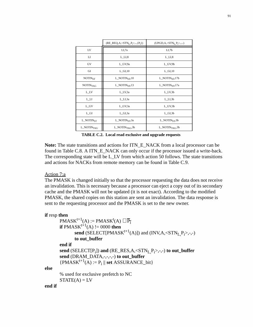
91
Note: The state transitions and actions for ITN_E_NACK from a local processor can befound in Table C.8. A ITN_E_NACK can only occur if the processor issued a write-back.The corresponding state will be L_LV from which action 50 follows. The state transitionsand actions for NACKs from remote memory can be found in Table C.9.
Action 7:aThe PMASK is changed initially so that the processor requesting the data does not receivean invalidation. This is necessary because a processor can eject a copy out of its secondarycache and the PMASK will not be updated (it is not exact). According to the modifiedPMASK, the shared copies on this station are sent an invalidation. The data response issent to the requesting processor and the PMASK is set to the new owner.
if respthenPMASKt+1(A) := PMASKt(A) ∧ Piif PMASKt+1(A) != 0000then
send (SELECT[PMASKt+1(A)]) and(INV,A,<STNL,Pi>,-,-)to out_buffer
end ifsend (SELECT[Pi]) and (RE_RES,A,<STNL,Pi>,-,-) to out_buffersend (DRAM_DATA,-,-,-,-) to out_buffer{PMASK t+1(A) := Pi ||set ASSURANCE_bit}
else% used for exclusive prefetch to NCSTATE(A) = LV
end if
(RE_REQ,A,<STNL,Pi>,-,{Pi}) (UPGD,A,<STNL,Pi>,-,-)
LV LI,7a LI,7b
LI L_LI,8 L_LI,8
GV L_GV,9a L_GV,9b
GI L_GI,10 L_GI,10
NOTINST L_NOTINST,10 L_NOTINST,17b
NOTINTAG L_NOTINST,13 L_NOTINST,17a
L_LV L_LV,3a L_LV,3b
L_LI L_LI,3a L_LI,3b
L_GV L_GV,3a L_GV,3b
L_GI L_GI,3a L_GI,3b
L_NOTINST L_NOTINST,3a L_NOTINST,3b
L_NOTINTAG L_NOTINTAG,3b L_NOTINTAG,3b
TABLE C.2. Local read exclusive and upgrade requests
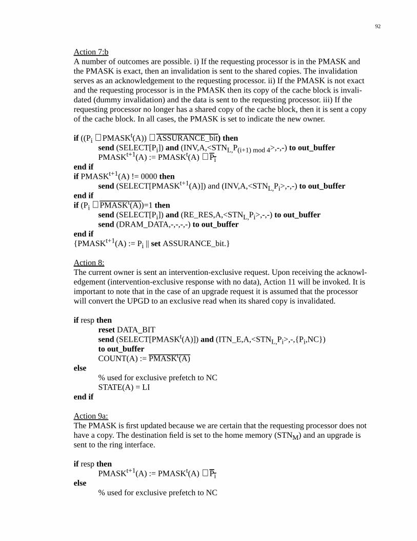
92
Action 7:bA number of outcomes are possible. i) If the requesting processor is in the PMASK andthe PMASK is exact, then an invalidation is sent to the shared copies. The invalidationserves as an acknowledgement to the requesting processor. ii) If the PMASK is not exactand the requesting processor is in the PMASK then its copy of the cache block is invali-dated (dummy invalidation) and the data is sent to the requesting processor. iii) If therequesting processor no longer has a shared copy of the cache block, then it is sent a copyof the cache block. In all cases, the PMASK is set to indicate the new owner.
if ((Pi ∧ PMASKt(A)) ∧ ASSURANCE_bit) thensend (SELECT[Pi]) and (INV,A,<STNL,P(i+1) mod 4>,-,-) to out_bufferPMASKt+1(A) := PMASKt(A) ∧ Pi
end ifif PMASKt+1(A) != 0000then
send (SELECT[PMASKt+1(A)]) and(INV,A,<STNL,Pi>,-,-) to out_bufferend ifif (Pi ∧ PMASKt(A))=1 then
send (SELECT[Pi]) and (RE_RES,A,<STNL,Pi>,-,-) to out_buffersend (DRAM_DATA,-,-,-,-) to out_buffer
end if{PMASK t+1(A) := Pi ||set ASSURANCE_bit.}
Action 8:The current owner is sent an intervention-exclusive request. Upon receiving the acknowl-edgement (intervention-exclusive response with no data), Action 11 will be invoked. It isimportant to note that in the case of an upgrade request it is assumed that the processorwill convert the UPGD to an exclusive read when its shared copy is invalidated.
if respthenreset DATA_BITsend (SELECT[PMASKt(A)]) and (ITN_E,A,<STNL,Pi>,-,{Pi,NC})to out_bufferCOUNT(A) := PMASKt(A)
else% used for exclusive prefetch to NCSTATE(A) = LI
end if
Action 9a:The PMASK is first updated because we are certain that the requesting processor does nothave a copy. The destination field is set to the home memory (STNM) and an upgrade issent to the ring interface.
if respthenPMASKt+1(A) := PMASKt(A) ∧ Pi
else% used for exclusive prefetch to NC
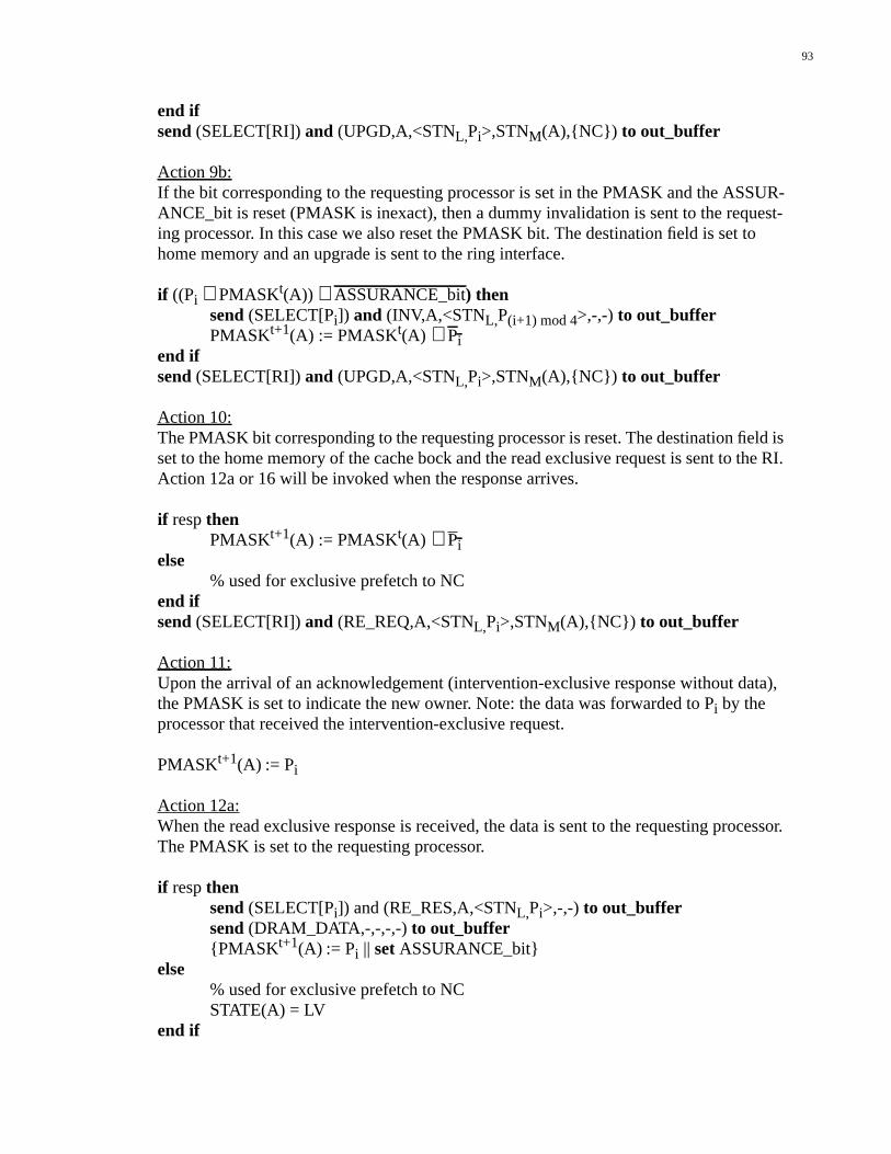
93
end ifsend (SELECT[RI]) and (UPGD,A,<STNL,Pi>,STNM(A),{NC}) to out_buffer
Action 9b:If the bit corresponding to the requesting processor is set in the PMASK and the ASSUR-ANCE_bit is reset (PMASK is inexact), then a dummy invalidation is sent to the request-ing processor. In this case we also reset the PMASK bit. The destination field is set tohome memory and an upgrade is sent to the ring interface.
if ((Pi ∧ PMASKt(A)) ∧ ASSURANCE_bit) thensend (SELECT[Pi]) and (INV,A,<STNL,P(i+1) mod 4>,-,-) to out_bufferPMASKt+1(A) := PMASKt(A) ∧ Pi
end ifsend (SELECT[RI]) and (UPGD,A,<STNL,Pi>,STNM(A),{NC}) to out_buffer
Action 10:The PMASK bit corresponding to the requesting processor is reset. The destination field isset to the home memory of the cache bock and the read exclusive request is sent to the RI.Action 12a or 16 will be invoked when the response arrives.
if respthenPMASKt+1(A) := PMASKt(A) ∧ Pi
else% used for exclusive prefetch to NC
end ifsend (SELECT[RI])and (RE_REQ,A,<STNL,Pi>,STNM(A),{NC}) to out_buffer
Action 11:Upon the arrival of an acknowledgement (intervention-exclusive response without data),the PMASK is set to indicate the new owner. Note: the data was forwarded to Pi by theprocessor that received the intervention-exclusive request.
PMASKt+1(A) := Pi
Action 12a:When the read exclusive response is received, the data is sent to the requesting processor.The PMASK is set to the requesting processor.
if respthensend (SELECT[Pi]) and (RE_RES,A,<STNL,Pi>,-,-) to out_buffersend (DRAM_DATA,-,-,-,-) to out_buffer{PMASK t+1(A) := Pi ||set ASSURANCE_bit}
else% used for exclusive prefetch to NCSTATE(A) = LV
end if
94
Action 12b:When an invalidation is received, it is sent locally if there are copies of the cache block. Ifthe requesting processor has a copy of the cache block, then this invalidation will serve asan acknowledgement. A read-exclusive response is sent to the requesting processor if itdoes not have a copy. The PMASK is set to the requesting processor.
if respthenif PMASKt(A) != 0000then
send (SELECT[PMASKt(A)]) and (INV,A,<STNL,Pi>,-,-) toout_bufferend ifif PMASK ∧ Pi = 1 then
send (SELECT[Pi]) and (RE_RES,A,<STNL,Pi>,-,-) to out_buffersend (DRAM_DATA,-,-,-,-) to out_buffer
end if{PMASK t+1(A) := Pi ||set ASSURANCE_bit}
else% used for exclusive prefetch to NCSTATE(A) = LV
end if
Action 13:Note: B is the address of the cache block currently in the NC and A is the address of thecache block being requested. The NC does not contain the block specified by address A(NOTINTAG). If block B is in its place and in the LV state, cache block B must first bewritten back to home memory. Then a RE_REQ for cache block A is sent to the ring inter-face (remote memory). The NC determines the home memories (STNM) from theaddresses of A and B. All the processors except the requester are set in the PMASKbecause one of them may have a shared copy of cache block A.
if STATE(B) = LV thensend (SELECT[RI])and (BLK_WRITE,B,<STNL,Pi>,STNM(B),-) to out_buffersend(DRAM_DATA,-,-,-,-) to out_buffer* must set retain bit in BLK_WRITE command if PMASKt(A) != 0000
end if{put new tag in SRAM || PMASKt+1(A) = 1111 ∧ Pi || reset ASSURANCE_bit}send (SELECT[RI])and (RE_REQ,A,<STNL,Pi>,STNM(A),{NC}) to out_buffer
Action 14:This means that the cache block has been invalidated before the response came back. Aspecial read exclusive request is sent to the home memory.
send (SELECT[RI])and (SP_RE_REQ,A,<STNL,Pi>,STNM(A),{NC})
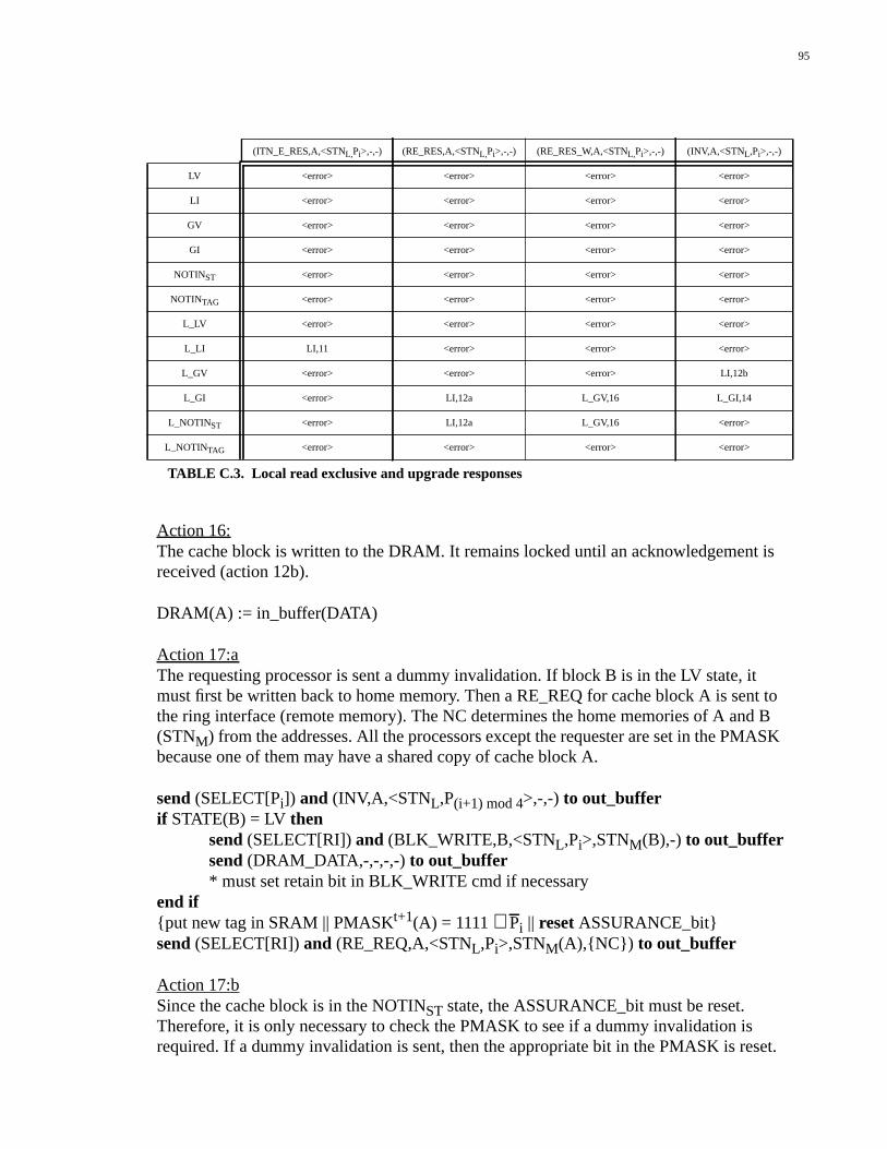
95
Action 16:The cache block is written to the DRAM. It remains locked until an acknowledgement isreceived (action 12b).
DRAM(A) := in_buffer(DATA)
Action 17:aThe requesting processor is sent a dummy invalidation. If block B is in the LV state, itmust first be written back to home memory. Then a RE_REQ for cache block A is sent tothe ring interface (remote memory). The NC determines the home memories of A and B(STNM) from the addresses. All the processors except the requester are set in the PMASKbecause one of them may have a shared copy of cache block A.
send (SELECT[Pi]) and (INV,A,<STNL,P(i+1) mod 4>,-,-) to out_bufferif STATE(B) = LV then
send (SELECT[RI])and (BLK_WRITE,B,<STNL,Pi>,STNM(B),-) to out_buffersend(DRAM_DATA,-,-,-,-) to out_buffer* must set retain bit in BLK_WRITE cmd if necessary
end if{put new tag in SRAM || PMASKt+1(A) = 1111 ∧ Pi || reset ASSURANCE_bit}send (SELECT[RI])and (RE_REQ,A,<STNL,Pi>,STNM(A),{NC}) to out_buffer
Action 17:bSince the cache block is in the NOTINST state, the ASSURANCE_bit must be reset.Therefore, it is only necessary to check the PMASK to see if a dummy invalidation isrequired. If a dummy invalidation is sent, then the appropriate bit in the PMASK is reset.
(ITN_E_RES,A,<STNL,Pi>,-,-) (RE_RES,A,<STNL,Pi>,-,-) (RE_RES_W,A,<STNL,Pi>,-,-) (INV,A,<STNL,Pi>,-,-)
LV <error> <error> <error> <error>
LI <error> <error> <error> <error>
GV <error> <error> <error> <error>
GI <error> <error> <error> <error>
NOTINST <error> <error> <error> <error>
NOTINTAG <error> <error> <error> <error>
L_LV <error> <error> <error> <error>
L_LI LI,11 <error> <error> <error>
L_GV <error> <error> <error> LI,12b
L_GI <error> LI,12a L_GV,16 L_GI,14
L_NOTINST <error> LI,12a L_GV,16 <error>
L_NOTINTAG <error> <error> <error> <error>
TABLE C.3. Local read exclusive and upgrade responses
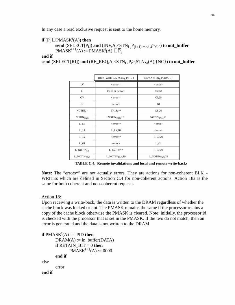
96
In any case a read exclusive request is sent to the home memory.
if (Pi ∧ PMASKt(A)) thensend (SELECT[Pi]) and (INV,A,<STNL,P(i+1) mod 4>,-,-) to out_bufferPMASKt+1(A) := PMASKt(A) ∧ Pi
end ifsend (SELECT[RI])and (RE_REQ,A,<STNL,Pi>,STNM(A),{NC}) to out_buffer
Note: The “errors*” are not actually errors. They are actions for non-coherent BLK_-WRITEs which are defined in Section C.4 for non-coherent actions. Action 18a is thesame for both coherent and non-coherent requests
Action 18:Upon receiving a write-back, the data is written to the DRAM regardless of whether thecache block was locked or not. The PMASK remains the same if the processor retains acopy of the cache block otherwise the PMASK is cleared. Note: initially, the processor idis checked with the processor that is set in the PMASK. If the two do not match, then anerror is generated and the data is not written to the DRAM.
if PMASKt(A) == PID thenDRAM(A) := in_buffer(DATA)if RETAIN_BIT = 0 then
PMASKt+1(A) := 0000end if
elseerror
end if
(BLK_WRITE,A,<STNL,Pi>,-,-) (INV,A<STNR,Pi,ID>,-,-)
LV <error>* <error>
LI LV,18 or <error> <error>
GV <error>* GI,20
GI <error> GI
NOTINST LV,18a** GI, 20
NOTINTAG NOTINTAG,19 NOTINTAG,21
L_LV <error>* <error>
L_LI L_LV,18 <error>
L_GV <error>* L_GI,20
L_GI <error> L_GI
L_NOTINST L_LV, 18a** L_GI,20
L_NOTINTAG L_NOTINTAG,19 L_NOTINTAG,21
TABLE C.4. Remote invalidations and local and remote write-backs
97
Action 18:aUpon receiving a write-back, the data is written to the DRAM regardless of whether thecache block was locked or not. The PMASK remains the same if the processor retains acopy of the cache block otherwise the requesting processor is removed from the PMASK.
DRAM(A) := in_buffer(DATA)if RETAIN_BIT = 0 then
PMASKt+1(A) := PMASKt(A) ∧ Piend if
Action 19:The write-back is sent to the home memory of the cache block.
send (SELECT[RI])and (BLK_WRITE,A,<STNL,Pi>,STNM(A),-) to out_bufferout_buffer := in_buffer(DATA)
Action 20:The invalidation is sent locally to the processors indicated by the PMASK. The PMASK iscleared.
if PMASKt(A) != 0000 thensend (SELECT[PMASKt(A)] and (INV,A,<STNR,Pi,ID>,-,-) to out_buffer{PMASK t+1(A) := 0000 ||set ASSURANCE_bit}
end if
Action 21:The invalidation is sent to all local processors because the information in the PMASKdoes not pertain to cache block A (NOTINTAG).
send ([SELECT[1111]) and (INV,A,<STNR,Pi,ID>,-,-) to out_buffer
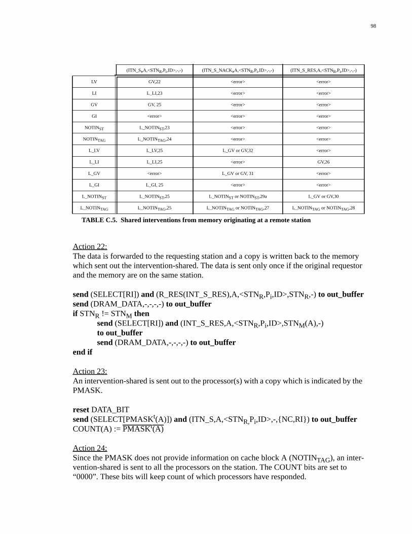
98
Action 22:The data is forwarded to the requesting station and a copy is written back to the memorywhich sent out the intervention-shared. The data is sent only once if the original requestorand the memory are on the same station.
send (SELECT[RI])and (R_RES(INT_S_RES),A,<STNR,Pi,ID>,STNR,-) to out_buffersend (DRAM_DATA,-,-,-,-) to out_bufferif STNR != STNM then
send (SELECT[RI])and (INT_S_RES,A,<STNR,Pi,ID>,STNM(A),-)to out_buffersend (DRAM_DATA,-,-,-,-) to out_buffer
end if
Action 23:An intervention-shared is sent out to the processor(s) with a copy which is indicated by thePMASK.
reset DATA_BITsend (SELECT[PMASKt(A)]) and (ITN_S,A,<STNR,Pi,ID>,-,{NC,RI}) to out_bufferCOUNT(A) := PMASKt(A)
Action 24:Since the PMASK does not provide information on cache block A (NOTINTAG), an inter-vention-shared is sent to all the processors on the station. The COUNT bits are set to“0000”. These bits will keep count of which processors have responded.
(ITN_S,A,<STNR,Pi,ID>,-,-) (ITN_S_NACK,A,<STNR,Pi,ID>,-,-) (ITN_S_RES,A,<STNR,Pi,ID>,-,-)
LV GV,22 <error> <error>
LI L_LI,23 <error> <error>
GV GV, 25 <error> <error>
GI <error> <error> <error>
NOTINST L_NOTINST,23 <error> <error>
NOTINTAG L_NOTINTAG,24 <error> <error>
L_LV L_LV,25 L_GV or GV,32 <error>
L_LI L_LI,25 <error> GV,26
L_GV <error> L_GV or GV, 31 <error>
L_GI L_GI, 25 <error> <error>
L_NOTINST L_NOTINST,25 L_NOTINST or NOTINST,29a L_GV or GV,30
L_NOTINTAG L_NOTINTAG,25 L_NOTINTAG or NOTINTAG,27 L_NOTINTAG or NOTINTAG,28
TABLE C.5. Shared interventions from memory originating at a remote station
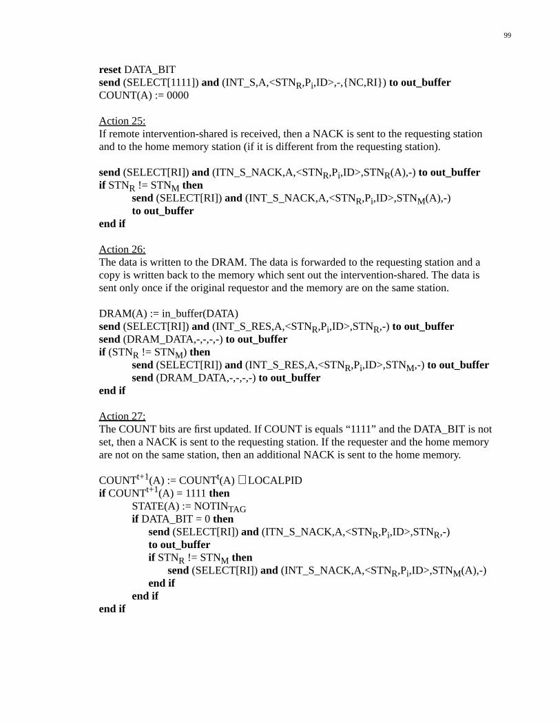
99
reset DATA_BITsend (SELECT[1111]) and (INT_S,A,<STNR,Pi,ID>,-,{NC,RI}) to out_bufferCOUNT(A) := 0000
Action 25:If remote intervention-shared is received, then a NACK is sent to the requesting stationand to the home memory station (if it is different from the requesting station).
send (SELECT[RI])and (ITN_S_NACK,A,<STNR,Pi,ID>,STNR(A),-) to out_bufferif STNR != STNM then
send (SELECT[RI])and (INT_S_NACK,A,<STNR,Pi,ID>,STNM(A),-)to out_buffer
end if
Action 26:The data is written to the DRAM. The data is forwarded to the requesting station and acopy is written back to the memory which sent out the intervention-shared. The data issent only once if the original requestor and the memory are on the same station.
DRAM(A) := in_buffer(DATA)send (SELECT[RI])and (INT_S_RES,A,<STNR,Pi,ID>,STNR,-) to out_buffersend (DRAM_DATA,-,-,-,-) to out_bufferif (STNR != STNM) then
send (SELECT[RI])and (INT_S_RES,A,<STNR,Pi,ID>,STNM,-) to out_buffersend (DRAM_DATA,-,-,-,-) to out_buffer
end if
Action 27:The COUNT bits are first updated. If COUNT is equals “1111” and the DATA_BIT is notset, then a NACK is sent to the requesting station. If the requester and the home memoryare not on the same station, then an additional NACK is sent to the home memory.
COUNTt+1(A) := COUNTt(A) ∨ LOCALPIDif COUNTt+1(A) = 1111 then
STATE(A) := NOTINTAGif DATA_BIT = 0 then
send (SELECT[RI])and (ITN_S_NACK,A,<STNR,Pi,ID>,STNR,-)to out_bufferif STNR != STNM then
send (SELECT[RI])and (INT_S_NACK,A,<STNR,Pi,ID>,STNM(A),-)end if
end ifend if
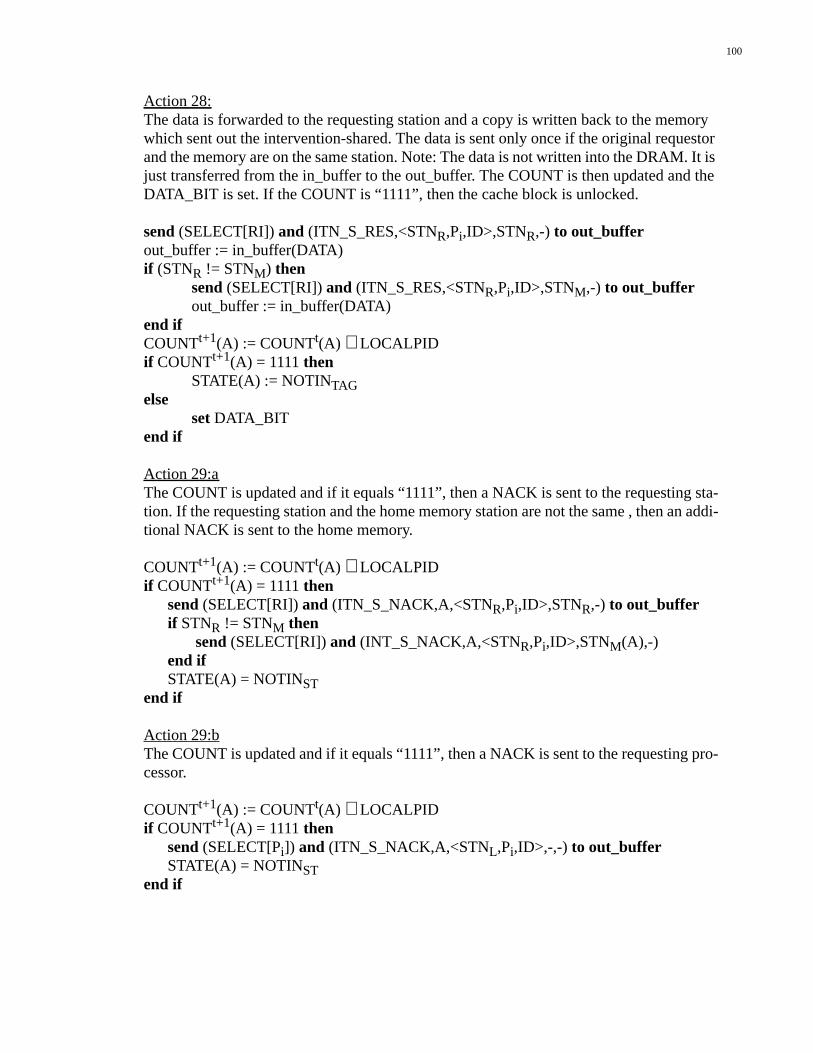
100
Action 28:The data is forwarded to the requesting station and a copy is written back to the memorywhich sent out the intervention-shared. The data is sent only once if the original requestorand the memory are on the same station. Note: The data is not written into the DRAM. It isjust transferred from the in_buffer to the out_buffer. The COUNT is then updated and theDATA_BIT is set. If the COUNT is “1111”, then the cache block is unlocked.
send (SELECT[RI])and (ITN_S_RES,<STNR,Pi,ID>,STNR,-) to out_bufferout_buffer := in_buffer(DATA)if (STNR != STNM) then
send (SELECT[RI])and (ITN_S_RES,<STNR,Pi,ID>,STNM,-) to out_bufferout_buffer := in_buffer(DATA)
end ifCOUNTt+1(A) := COUNTt(A) ∨ LOCALPIDif COUNTt+1(A) = 1111 then
STATE(A) := NOTINTAGelse
set DATA_BITend if
Action 29:aThe COUNT is updated and if it equals “1111”, then a NACK is sent to the requesting sta-tion. If the requesting station and the home memory station are not the same , then an addi-tional NACK is sent to the home memory.
COUNTt+1(A) := COUNTt(A) ∨ LOCALPIDif COUNTt+1(A) = 1111 then
send (SELECT[RI])and (ITN_S_NACK,A,<STNR,Pi,ID>,STNR,-) to out_bufferif STNR != STNM then
send (SELECT[RI])and (INT_S_NACK,A,<STNR,Pi,ID>,STNM(A),-)end ifSTATE(A) = NOTINST
end if
Action 29:bThe COUNT is updated and if it equals “1111”, then a NACK is sent to the requesting pro-cessor.
COUNTt+1(A) := COUNTt(A) ∨ LOCALPIDif COUNTt+1(A) = 1111 then
send (SELECT[Pi]) and (ITN_S_NACK,A,<STNL,Pi,ID>,-,-) to out_bufferSTATE(A) = NOTINST
end if
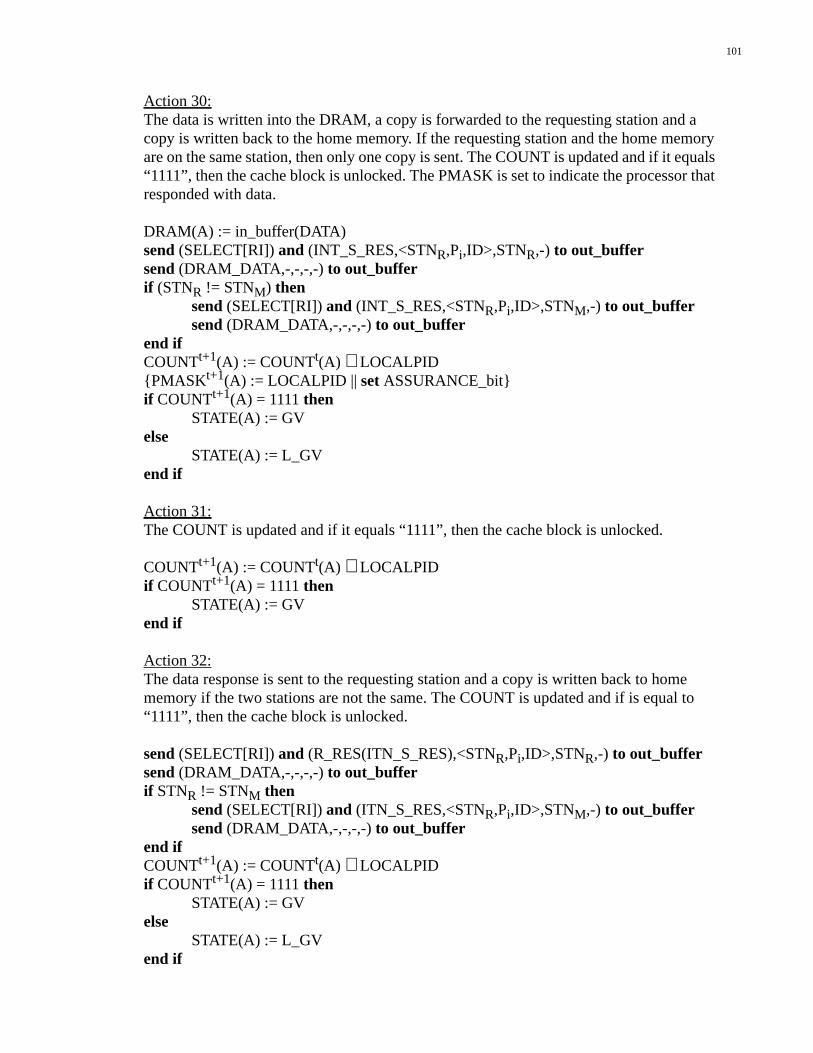
101
Action 30:The data is written into the DRAM, a copy is forwarded to the requesting station and acopy is written back to the home memory. If the requesting station and the home memoryare on the same station, then only one copy is sent. The COUNT is updated and if it equals“1111”, then the cache block is unlocked. The PMASK is set to indicate the processor thatresponded with data.
DRAM(A) := in_buffer(DATA)send (SELECT[RI])and (INT_S_RES,<STNR,Pi,ID>,STNR,-) to out_buffersend (DRAM_DATA,-,-,-,-) to out_bufferif (STNR != STNM) then
send (SELECT[RI])and (INT_S_RES,<STNR,Pi,ID>,STNM,-) to out_buffersend (DRAM_DATA,-,-,-,-) to out_buffer
end ifCOUNTt+1(A) := COUNTt(A) ∨ LOCALPID{PMASK t+1(A) := LOCALPID ||set ASSURANCE_bit}if COUNTt+1(A) = 1111 then
STATE(A) := GVelse
STATE(A) := L_GVend if
Action 31:The COUNT is updated and if it equals “1111”, then the cache block is unlocked.
COUNTt+1(A) := COUNTt(A) ∨ LOCALPIDif COUNTt+1(A) = 1111 then
STATE(A) := GVend if
Action 32:The data response is sent to the requesting station and a copy is written back to homememory if the two stations are not the same. The COUNT is updated and if is equal to“1111”, then the cache block is unlocked.
send (SELECT[RI])and (R_RES(ITN_S_RES),<STNR,Pi,ID>,STNR,-) to out_buffersend (DRAM_DATA,-,-,-,-) to out_bufferif STNR != STNM then
send (SELECT[RI])and (ITN_S_RES,<STNR,Pi,ID>,STNM,-) to out_buffersend (DRAM_DATA,-,-,-,-) to out_buffer
end ifCOUNTt+1(A) := COUNTt(A) ∨ LOCALPIDif COUNTt+1(A) = 1111 then
STATE(A) := GVelse
STATE(A) := L_GVend if
102
Action 33:The intervention-shared is recognized as the one originating on this station and an inter-vention-shared is sent to the processors in the PMASK.
reset DATA_BITsend (SELECT[PMASKt(A)]) and (ITN_S,A,<STNL,Pi,ID>,-,{NC,Pi}) to out_bufferCOUNT(A) := PMASKt(A)
Action 34:The data is written to the DRAM and the COUNT is updated. If COUNT equals “1111”,then the cache block is unlocked and the PMASK is updated to include the requesting pro-cessor.
DRAM(A) := in_buffer (DATA)COUNTt+1(A) := COUNTt(A) ∨ LOCALPID{PMASK t+1(A) := LOCALPID ||set ASSURANCE_bit}if COUNTt+1(A) = 1111 then
STATE(A) := LVPMASKt+1(A) := PMASKt(A) ∨ Pi
elseSTATE(A) := L_LVset DATA_BIT
end if
(ITN_S,A,<STNL,Pi,ID>,-,-) (ITN_S_NACK,A,<STNL,Pi,ID>,-,-) (ITN_S_RES,A,<STNL,Pi,ID>,-,-)
LV <error> <error> <error>
LI <error> <error> <error>
GV <error> <error> <error>
GI <error> <error> <error>
NOTINST <error> <error> <error>
NOTINTAG <error> <error> <error>
L_LV LV,36 L_LV or LV,35 <error>
L_LI <error> <error> <error>
L_GV <error> <error> <error>
L_GI <error> <error> <error>
L_NOTINST L_NOTINST,33 L_NOTINST or NOTINST,29b L_LV or LV,34
L_NOTINTAG <error> <error> <error>
TABLE C.6. Shared interventions from memory originating at the local station
103
Action 35:There are two ways the cache block could have arrived in this state. One is due to an inter-vention-shared response and the other is due to a write-back. The DATA_BIT must firstchecked and f it is not set, then a data response is sent to the requesting processor. COUNTis updated and the block is unlocked if this is the last response.
if DATA_BIT = 0 thensend (SELECT[Pi]) and (R_RES(ITN_S_RES),<STNL,Pi,ID>,-,-) to out_buffersend (DRAM_DATA,-,-,-,-) to out_bufferset DATA_BIT
end ifCOUNTt+1(A) := COUNTt(A) ∨ LOCALPIDif COUNTt+1(A) = 1111 then
STATE(A) := LVPMASKt+1(A) := PMASKt(A) ∨ Pireset DATA_BIT
end if
Action 36:Since the cache block is valid due to a write-back, a data response is sent to the requestingprocessor.
send (SELECT[Pi]) and (R_RES,<STNL,Pi,ID>,-,-) to out_buffersend (DRAM_DATA,-,-,-,-) to out_bufferPMASKt+1(A) := PMASKt(A) ∨ Pi
*L_GV is used instead of L_GI so that this state table has as many common states as pos-sible with Table 5.
(ITN_E,A,<STNR,Pi,ID>,-,-) (ITN_E_NACK,A,<STNR,Pi,ID>,-,-) (ITN_E_RES,A,<STNR,Pi,ID>,-,-)
LV GI,37 <error> <error>
LI L_LI, 38 <error> <error>
GV GV, 40 <error> <error>
GI <error> <error> <error>
NOTINST L_NOTINST ,38 <error> <error>
NOTINTAG L_NOTINTAG ,39 <error> <error>
L_LV L_LV,40 L_GV or GI, 41 <error>
L_LI L_LI,40 <error> GI, 45
L_GV <error> L_GV or GI, 42 <error>
L_GI L_GI, 40 <error> <error>
L_NOTINST L_NOTINST,40 L_NOTINSTor NOTINST , 43 L_GV or GI, 46 *
L_NOTINTAG L_NOTINTAG,40 L_NOTINTAG or NOTINTAG , 44 L_NOTINTAG or NOTINTAG, 47
TABLE C.7. Exclusive interventions from memory originating at a remote station
104
Action 37:First, the local copies, if any exist, are invalidated. Then, the data response is forwarded tothe requesting station. If the requesting station and the home memory station are different,then the memory is sent an acknowledgement (intervention-exclusive response with nodata).
if PMASK(A) != 0000thensend SELECT[PMASK]and (INV,A,<STNR,Pi>,-,-) to out_buffer
end ifsend (SELECT[RI]) and (RE_RES(ITN_E_RES),A,<STNR,Pi>,STNR,-) to out_buffersend SELECT[RI]and (DRAM_DATA,-,-,-,-) to out_bufferif STNR != STNM then
send (SELECT[RI]) and (ITN_E_RES,A,<STNR,Pi>,STNM,-) to out_bufferend if{PMASK t+1(A) := 0000 || set ASSURANCE_bit}
Action 38:An intervention-exclusive request is sent out to the processor(s) with a copy (according tothe PMASK).
reset DATA_BITsend (SELECT[PMASKt(A)]) and (ITN_E,A,<STNR,Pi,ID>,-,{NC,RI}) to out_bufferCOUNT(A) := PMASKt(A)
Action 39:Since the PMASK does not provide information on cache block A (NOTINTAG), an inter-vention-exclusive is sent to all the processors on the station. The COUNT bits are set to“0000”. These bits will keep count of which processors have responded.
reset DATA_BITsend (SELECT[1111]) and (INT_E,A,<STNR,Pi,ID>,-,{NC,RI}) to out_bufferCOUNT(A) := 0000
Action 40:If remote intervention-shared is received, then a NACK is sent to the requesting stationand to the home memory station (if it is different from the requesting station).
send (SELECT[RI])and (ITN_E_NACK,A,<STNR,Pi,ID>,STNR(A),-) to out_bufferif STNR != STNM then
send (SELECT[RI])and (INT_E_NACK,A,<STNR,Pi,ID>,STNM(A),-)to out_buffer
end if
Action 41:The data response is sent to the requesting station. If it is different from the home memorystation, then an acknowledgement (intervention-exclusive response without data) is sent tothe home memory. COUNT is updated and if is equal to “1111” then PMASK is cleared.
105
send (SELECT[RI])and (RE_RES(ITN_E_RES),<STNR,Pi,ID>,STNR,-) to out_buffersend (DRAM_DATA,-,-,-,-) to out_bufferif STNR != STNM then
send (SELECT[RI])and (ITN_E_RES,<STNR,Pi,ID>,STNM,-) to out_bufferend ifCOUNTt+1(A) := COUNTt(A) ∨ LOCALPIDif COUNTt+1(A) = 1111 then
STATE(A) := GI{PMASK t+1(A) := 0000 ||set ASSURANCE_bit}
elseSTATE(A) := L_GV
end if
Action 42:The COUNT is updated and if it is “1111”, then the cache block is unlocked, the state ischanged to GI, and the PMASK is cleared.
COUNTt+1(A) := COUNTt(A) ∨ LOCALPIDif COUNTt+1(A) = 1111 then
STATE(A) := GI{PMASK t+1(A) := 0000 ||set ASSURANCE_bit}
end if
Action 43:The COUNT is updated and if it equals “1111”, then a NACK is sent to the requesting sta-tion. If the requesting station and the home memory station are not the same, then an addi-tional NACK is sent to the home memory.
COUNTt+1(A) := COUNTt(A) ∨ LOCALPIDif COUNTt+1(A) = 1111 then
send (SELECT[RI])and (ITN_E_NACK,A,<STNR,Pi,ID>,STNR,-) to out_bufferif STNR != STNM then
send (SELECT[RI])and (INT_E_NACK,A,<STNR,Pi,ID>,STNM(A),-)end ifSTATE(A) = NOTINST
end if
Action 44:The COUNT is updated. If it equals “1111” and the DATA_BIT is not set, then a NACK issent to the requesting processor. If the requesting station and the home memory station arenot the same, then an additional NACK is sent to the home memory.
106
COUNTt+1(A) := COUNTt(A) ∨ LOCALPIDif COUNTt+1(A) = 1111 then
STATE(A) := NOTINTAGif DATA_BIT = 0 then
send (SELECT[RI])and (ITN_E_NACK,A,<STNR,Pi,ID>,STNR,-)to out_bufferif STNR != STNM then
send (SELECT[RI])and (INT_E_NACK,A,<STNR,Pi,ID>,STNM(A),-)end if
end ifend if
Action 45:The data response is sent to the requesting station. If it is different from the home memorystation, then an acknowledgement (intervention-exclusive response without data) is sent tothe home memory. The PMASK is cleared.
send (SELECT[RI])and (INT_E_RES,<STNR,Pi,ID>,STNR(A),-) to out_buffersend SELECT[RI]and (DRAM_DATA,-,-,-,-) to out_bufferif (STNR != STNM) then
send (SELECT[RI])and (INT_E_RES,<STNR,Pi,ID>,STNM(A),-) to out_bufferend if{PMASK t+1(A) := 0000 ||set ASSURANCE_bit}
Action 46:The data response is sent to the requesting station. If it is different from the home memorystation, then an acknowledgement (intervention-exclusive response without data) is sent tothe home memory. If the COUNT equals “1111” then the cache block is unlocked, thestate is changed to GI and the PMASK is cleared.
send (SELECT[RI])and (INT_E_RES,<STNR,Pi,ID>,STNR(A),-) to out_buffersend SELECT[RI]and (DRAM_DATA,-,-,-,-) to out_bufferif (STNR != STNM) then
send (SELECT[RI])and (ITN_E_RES,<STNR,Pi,ID>,STNM(A),-) to out_bufferend ifCOUNTt+1(A) := COUNTt(A) ∨ LOCALPIDif COUNTt+1(A) = 1111 then
STATE(A) := GI{PMASK t+1(A) := 0000 ||set ASSURANCE_bit}
elseSTATE(A) := L_GV
end if
Action 47:The data response is sent to the requesting station. If it is different from the home memorystation, then an acknowledgement (intervention-exclusive response without data) is sent tothe home memory. If the COUNT is “1111” then the cache block is unlocked.
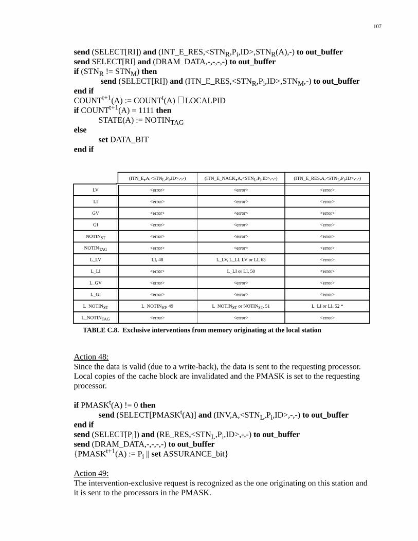
107
send (SELECT[RI])and (INT_E_RES,<STNR,Pi,ID>,STNR(A),-) to out_buffersend SELECT[RI]and (DRAM_DATA,-,-,-,-) to out_bufferif (STNR != STNM) then
send (SELECT[RI])and (ITN_E_RES,<STNR,Pi,ID>,STNM,-) to out_bufferend ifCOUNTt+1(A) := COUNTt(A) ∨ LOCALPIDif COUNTt+1(A) = 1111 then
STATE(A) := NOTINTAGelse
set DATA_BITend if
Action 48:Since the data is valid (due to a write-back), the data is sent to the requesting processor.Local copies of the cache block are invalidated and the PMASK is set to the requestingprocessor.
if PMASKt(A) != 0 thensend (SELECT[PMASKt(A)] and (INV,A,<STNL,Pi,ID>,-,-) to out_buffer
end ifsend (SELECT[Pi]) and (RE_RES,<STNL,Pi,ID>,-,-) to out_buffersend (DRAM_DATA,-,-,-,-) to out_buffer{PMASK t+1(A) := Pi ||set ASSURANCE_bit}
Action 49:The intervention-exclusive request is recognized as the one originating on this station andit is sent to the processors in the PMASK.
(ITN_E,A,<STNL,Pi,ID>,-,-) (ITN_E_NACK,A,<STNL,Pi,ID>,-,-) (ITN_E_RES,A,<STNL,Pi,ID>,-,-)
LV <error> <error> <error>
LI <error> <error> <error>
GV <error> <error> <error>
GI <error> <error> <error>
NOTINST <error> <error> <error>
NOTINTAG <error> <error> <error>
L_LV LI, 48 L_LV, L_LI, LV or LI, 63 <error>
L_LI <error> L_LI or LI, 50 <error>
L_GV <error> <error> <error>
L_GI <error> <error> <error>
L_NOTINST L_NOTINST, 49 L_NOTINST or NOTINST, 51 L_LI or LI, 52 *
L_NOTINTAG <error> <error> <error>
TABLE C.8. Exclusive interventions from memory originating at the local station
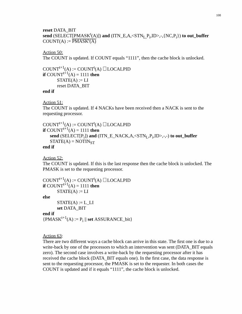
108
reset DATA_BITsend (SELECT[PMASKt(A)]) and (ITN_E,A,<STNL,Pi,ID>,-,{NC,Pi}) to out_bufferCOUNT(A) := PMASKt(A)
Action 50:The COUNT is updated. If COUNT equals “1111”, then the cache block is unlocked.
COUNTt+1(A) := COUNTt(A) ∨ LOCALPIDif COUNTt+1(A) = 1111 then
STATE(A) := LIreset DATA_BIT
end if
Action 51:The COUNT is updated. If 4 NACKs have been received then a NACK is sent to therequesting processor.
COUNTt+1(A) := COUNTt(A) ∨ LOCALPIDif COUNTt+1(A) = 1111 then
send (SELECT[Pi]) and (ITN_E_NACK,A,<STNL,Pi,ID>,-,-) to out_bufferSTATE(A) = NOTINST
end if
Action 52:The COUNT is updated. If this is the last response then the cache block is unlocked. ThePMASK is set to the requesting processor.
COUNTt+1(A) := COUNTt(A) ∨ LOCALPIDif COUNTt+1(A) = 1111 then
STATE(A) := LIelse
STATE(A) := L_LIset DATA_BIT
end if{PMASK t+1(A) := Pi ||set ASSURANCE_bit}
Action 63:There are two different ways a cache block can arrive in this state. The first one is due to awrite-back by one of the processors to which an intervention was sent (DATA_BIT equalszero). The second case involves a write-back by the requesting processor after it hasreceived the cache block (DATA_BIT equals one). In the first case, the data response issent to the requesting processor, the PMASK is set to the requester. In both cases theCOUNT is updated and if it equals “1111”, the cache block is unlocked.
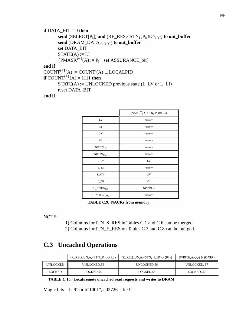
109
if DATA_BIT = 0 thensend (SELECT[Pi]) and (RE_RES,<STNL,Pi,ID>,-,-) to out_buffersend (DRAM_DATA,-,-,-,-) to out_bufferset DATA_BITSTATE(A) := LI{PMASK t+1(A) := Pi ||set ASSURANCE_bit}
end ifCOUNTt+1(A) := COUNTt(A) ∨ LOCALPIDif COUNTt+1(A) = 1111 then
STATE(A) := UNLOCKED previous state (L_LV or L_LI)reset DATA_BIT
end if
NOTE:1) Columns for ITN_S_RES in Tables C.1 and C.6 can be merged.2) Columns for ITN_E_RES on Tables C.3 and C.8 can be merged.
C.3 Uncached Operations
Magic bits = h“9” or b”1001”, ad2726 = b”01”
(NACK*,A,<STNL,Pi,ID>,-,-)
LV <error>
LI <error>
GV <error>
GI <error>
NOTINST <error>
NOTINTAG <error>
L_LV LV
L_LI <error>
L_GV GV
L_GI GI
L_NOTINST NOTINST
L_NOTINTAG <error>
TABLE C.9. NACKs fr om memory
(R_REQ_UN,A,<STNL,Pi>,-,{Pi}) (R_REQ_UN,A,<STNR,Pi,ID>,-,{RI}) (WRITE,A,-,-,-) & (DATA)
UNLOCKED UNLOCKED,55 UNLOCKED,56 UNLOCKED, 57
LOCKED LOCKED,55 LOCKED,56 LOCKED, 57
TABLE C.10. Local/remote uncached read requests and writes to DRAM
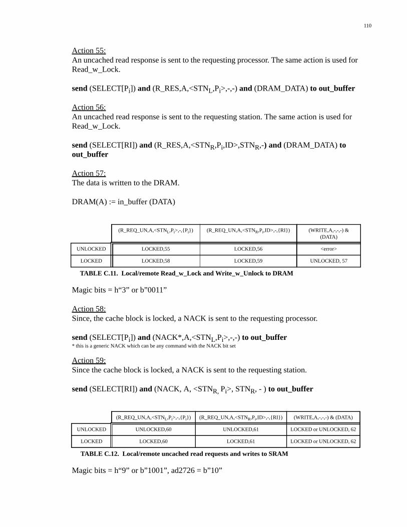
110
Action 55:An uncached read response is sent to the requesting processor. The same action is used forRead_w_Lock.
send (SELECT[Pi]) and (R_RES,A,<STNL,Pi>,-,-) and (DRAM_DATA) to out_buffer
Action 56:An uncached read response is sent to the requesting station. The same action is used forRead_w_Lock.
send (SELECT[RI])and (R_RES,A,<STNR,Pi,ID>,STNR,-) and (DRAM_DATA) toout_buffer
Action 57:The data is written to the DRAM.
DRAM(A) := in_buffer (DATA)
Magic bits = h“3” or b”0011”
Action 58:Since, the cache block is locked, a NACK is sent to the requesting processor.
send (SELECT[Pi]) and (NACK*,A,<STNL,Pi>,-,-) to out_buffer* this is a generic NACK which can be any command with the NACK bit set
Action 59:Since the cache block is locked, a NACK is sent to the requesting station.
send (SELECT[RI]) and (NACK, A, <STNR, Pi>, STNR, - ) to out_buffer
Magic bits = h“9” or b”1001”, ad2726 = b”10”
(R_REQ_UN,A,<STNL,Pi>,-,{Pi}) (R_REQ_UN,A,<STNR,Pi,ID>,-,{RI}) (WRITE,A,-,-,-) &(DATA)
UNLOCKED LOCKED,55 LOCKED,56 <error>
LOCKED LOCKED,58 LOCKED,59 UNLOCKED, 57
TABLE C.11. Local/remote Read_w_Lock and Write_w_Unlock to DRAM
(R_REQ_UN,A,<STNL,Pi>,-,{Pi}) (R_REQ_UN,A,<STNR,Pi,ID>,-,{RI}) (WRITE,A,-,-,-) & (DATA)
UNLOCKED UNLOCKED,60 UNLOCKED,61 LOCKED or UNLOCKED, 62
LOCKED LOCKED,60 LOCKED,61 LOCKED or UNLOCKED, 62
TABLE C.12. Local/remote uncached read requests and writes to SRAM
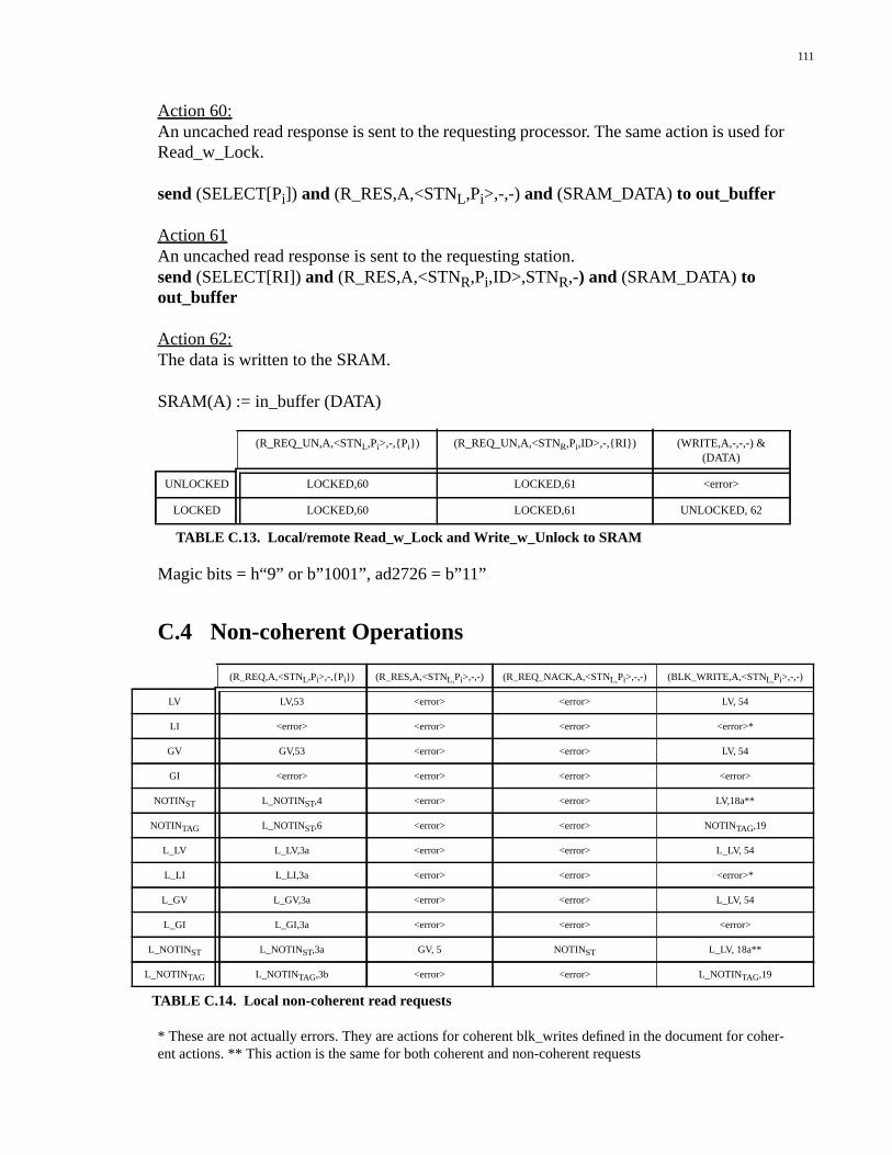
111
Action 60:An uncached read response is sent to the requesting processor. The same action is used forRead_w_Lock.
send (SELECT[Pi]) and (R_RES,A,<STNL,Pi>,-,-) and (SRAM_DATA) to out_buffer
Action 61An uncached read response is sent to the requesting station.send (SELECT[RI])and (R_RES,A,<STNR,Pi,ID>,STNR,-) and (SRAM_DATA) toout_buffer
Action 62:The data is written to the SRAM.
SRAM(A) := in_buffer (DATA)
Magic bits = h“9” or b”1001”, ad2726 = b”11”
C.4 Non-coherent Operations
* These are not actually errors. They are actions for coherent blk_writes defined in the document for coher-ent actions. ** This action is the same for both coherent and non-coherent requests
(R_REQ_UN,A,<STNL,Pi>,-,{Pi}) (R_REQ_UN,A,<STNR,Pi,ID>,-,{RI}) (WRITE,A,-,-,-) &(DATA)
UNLOCKED LOCKED,60 LOCKED,61 <error>
LOCKED LOCKED,60 LOCKED,61 UNLOCKED, 62
TABLE C.13. Local/remote Read_w_Lock and Write_w_Unlock to SRAM
(R_REQ,A,<STNL,Pi>,-,{Pi}) (R_RES,A,<STNL,Pi>,-,-) (R_REQ_NACK,A,<STNL,Pi>,-,-) (BLK_WRITE,A,<STNL,Pi>,-,-)
LV LV,53 <error> <error> LV, 54
LI <error> <error> <error> <error>*
GV GV,53 <error> <error> LV, 54
GI <error> <error> <error> <error>
NOTINST L_NOTINST,4 <error> <error> LV,18a**
NOTINTAG L_NOTINST,6 <error> <error> NOTINTAG,19
L_LV L_LV,3a <error> <error> L_LV, 54
L_LI L_LI,3a <error> <error> <error>*
L_GV L_GV,3a <error> <error> L_LV, 54
L_GI L_GI,3a <error> <error> <error>
L_NOTINST L_NOTINST,3a GV, 5 NOTINST L_LV, 18a**
L_NOTINTAG L_NOTINTAG,3b <error> <error> L_NOTINTAG,19
TABLE C.14. Local non-coherent read requests
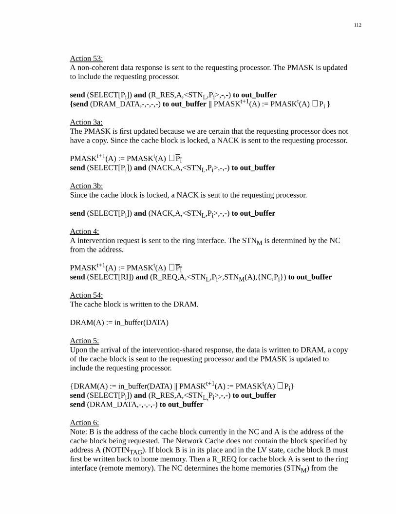
112
Action 53:A non-coherent data response is sent to the requesting processor. The PMASK is updatedto include the requesting processor.
send (SELECT[Pi]) and (R_RES,A,<STNL,Pi>,-,-) to out_buffer{send(DRAM_DATA,-,-,-,-) to out_buffer ||PMASKt+1(A) := PMASKt(A) ∨ Pi }
Action 3a:The PMASK is first updated because we are certain that the requesting processor does nothave a copy. Since the cache block is locked, a NACK is sent to the requesting processor.
PMASKt+1(A) := PMASKt(A) ∧ Pisend (SELECT[Pi]) and (NACK,A,<STNL,Pi>,-,-) to out_buffer
Action 3b:Since the cache block is locked, a NACK is sent to the requesting processor.
send (SELECT[Pi]) and (NACK,A,<STNL,Pi>,-,-) to out_buffer
Action 4:A intervention request is sent to the ring interface. The STNM is determined by the NCfrom the address.
PMASKt+1(A) := PMASKt(A) ∧ Pisend (SELECT[RI]) and (R_REQ,A,<STNL,Pi>,STNM(A),{NC,Pi}) to out_buffer
Action 54:The cache block is written to the DRAM.
DRAM(A) := in_buffer(DATA)
Action 5:Upon the arrival of the intervention-shared response, the data is written to DRAM, a copyof the cache block is sent to the requesting processor and the PMASK is updated toinclude the requesting processor.
{DRAM(A) := in_buffer(DATA) || PMASKt+1(A) := PMASKt(A) ∨ Pi}send (SELECT[Pi]) and (R_RES,A,<STNL,Pi>,-,-) to out_buffersend (DRAM_DATA,-,-,-,-) to out_buffer
Action 6:Note: B is the address of the cache block currently in the NC and A is the address of thecache block being requested. The Network Cache does not contain the block specified byaddress A (NOTINTAG). If block B is in its place and in the LV state, cache block B mustfirst be written back to home memory. Then a R_REQ for cache block A is sent to the ringinterface (remote memory). The NC determines the home memories (STNM) from the
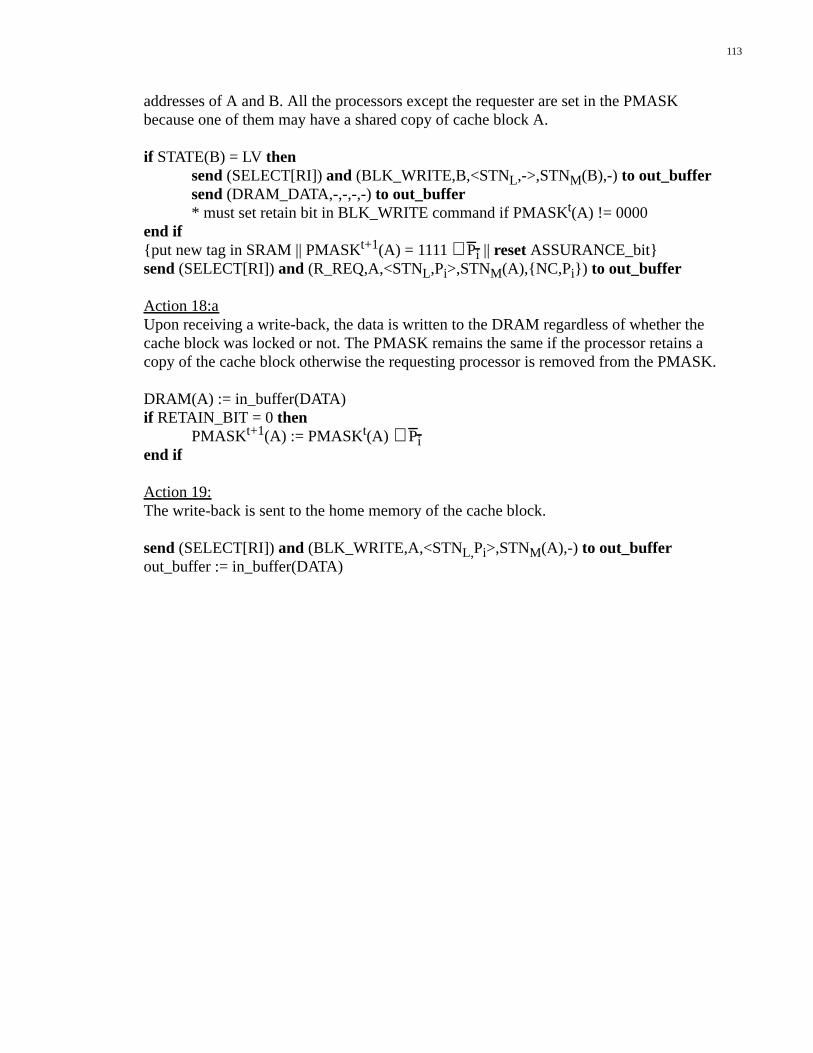
113
addresses of A and B. All the processors except the requester are set in the PMASKbecause one of them may have a shared copy of cache block A.
if STATE(B) = LV thensend (SELECT[RI])and (BLK_WRITE,B,<STNL,->,STNM(B),-) to out_buffersend(DRAM_DATA,-,-,-,-) to out_buffer* must set retain bit in BLK_WRITE command if PMASKt(A) != 0000
end if{put new tag in SRAM || PMASKt+1(A) = 1111 ∧ Pi || reset ASSURANCE_bit}send (SELECT[RI])and (R_REQ,A,<STNL,Pi>,STNM(A),{NC,Pi}) to out_buffer
Action 18:aUpon receiving a write-back, the data is written to the DRAM regardless of whether thecache block was locked or not. The PMASK remains the same if the processor retains acopy of the cache block otherwise the requesting processor is removed from the PMASK.
DRAM(A) := in_buffer(DATA)if RETAIN_BIT = 0 then
PMASKt+1(A) := PMASKt(A) ∧ Piend if
Action 19:The write-back is sent to the home memory of the cache block.
send (SELECT[RI])and (BLK_WRITE,A,<STNL,Pi>,STNM(A),-) to out_bufferout_buffer := in_buffer(DATA)
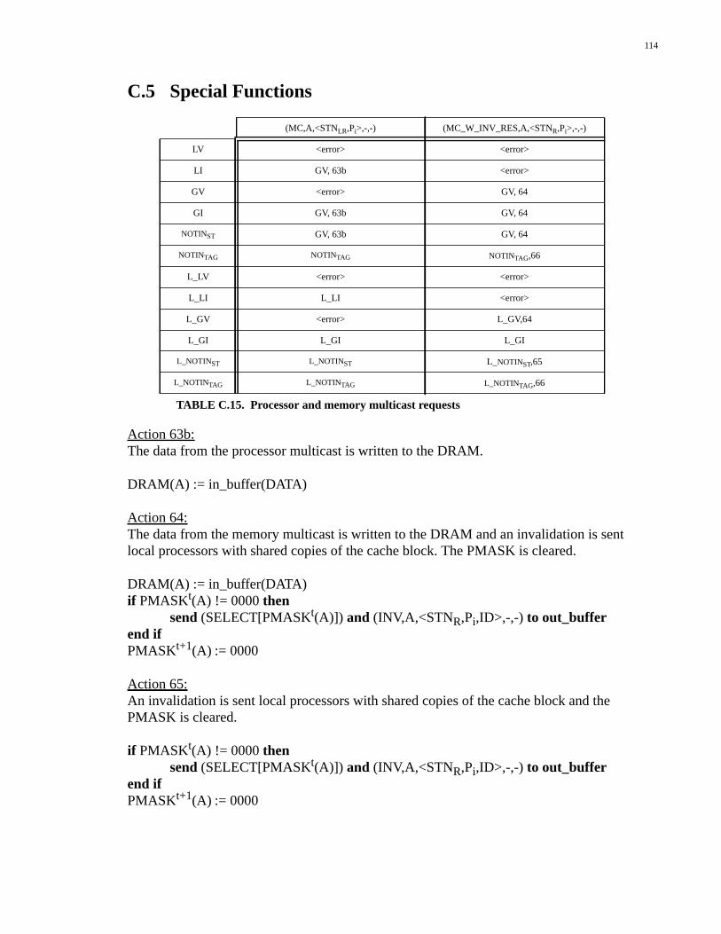
114
C.5 Special Functions
Action 63b:The data from the processor multicast is written to the DRAM.
DRAM(A) := in_buffer(DATA)
Action 64:The data from the memory multicast is written to the DRAM and an invalidation is sentlocal processors with shared copies of the cache block. The PMASK is cleared.
DRAM(A) := in_buffer(DATA)if PMASKt(A) != 0000then
send (SELECT[PMASKt(A)]) and (INV,A,<STNR,Pi,ID>,-,-) to out_bufferend ifPMASKt+1(A) := 0000
Action 65:An invalidation is sent local processors with shared copies of the cache block and thePMASK is cleared.
if PMASKt(A) != 0000thensend (SELECT[PMASKt(A)]) and (INV,A,<STNR,Pi,ID>,-,-) to out_buffer
end ifPMASKt+1(A) := 0000
(MC,A,<STNLR,Pi>,-,-) (MC_W_INV_RES,A,<STNR,Pi>,-,-)
LV <error> <error>
LI GV, 63b <error>
GV <error> GV, 64
GI GV, 63b GV, 64
NOTINST GV, 63b GV, 64
NOTINTAG NOTINTAG NOTINTAG,66
L_LV <error> <error>
L_LI L_LI <error>
L_GV <error> L_GV,64
L_GI L_GI L_GI
L_NOTINST L_NOTINST L_NOTINST,65
L_NOTINTAG L_NOTINTAG L_NOTINTAG,66
TABLE C.15. Processor and memory multicast requests
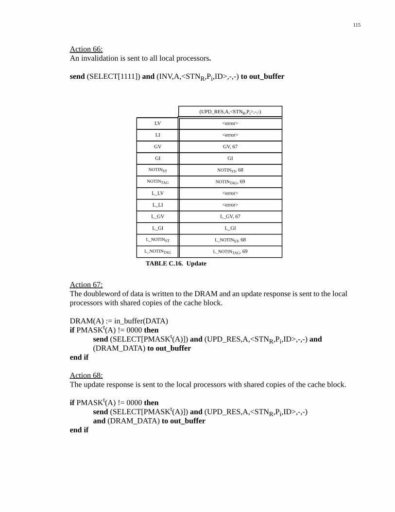
115
Action 66:An invalidation is sent to all local processors.
send (SELECT[1111]) and (INV,A,<STNR,Pi,ID>,-,-) to out_buffer
Action 67:The doubleword of data is written to the DRAM and an update response is sent to the localprocessors with shared copies of the cache block.
DRAM(A) := in_buffer(DATA)if PMASKt(A) != 0000then
send (SELECT[PMASKt(A)]) and (UPD_RES,A,<STNR,Pi,ID>,-,-) and(DRAM_DATA) to out_buffer
end if
Action 68:The update response is sent to the local processors with shared copies of the cache block.
if PMASKt(A) != 0000thensend (SELECT[PMASKt(A)]) and (UPD_RES,A,<STNR,Pi,ID>,-,-)and (DRAM_DATA) to out_buffer
end if
(UPD_RES,A,<STNR,Pi>,-,-)
LV <error>
LI <error>
GV GV, 67
GI GI
NOTINST NOTINST, 68
NOTINTAG NOTINTAG, 69
L_LV <error>
L_LI <error>
L_GV L_GV, 67
L_GI L_GI
L_NOTINST L_NOTINST, 68
L_NOTINTAG L_NOTINTAG, 69
TABLE C.16. Update
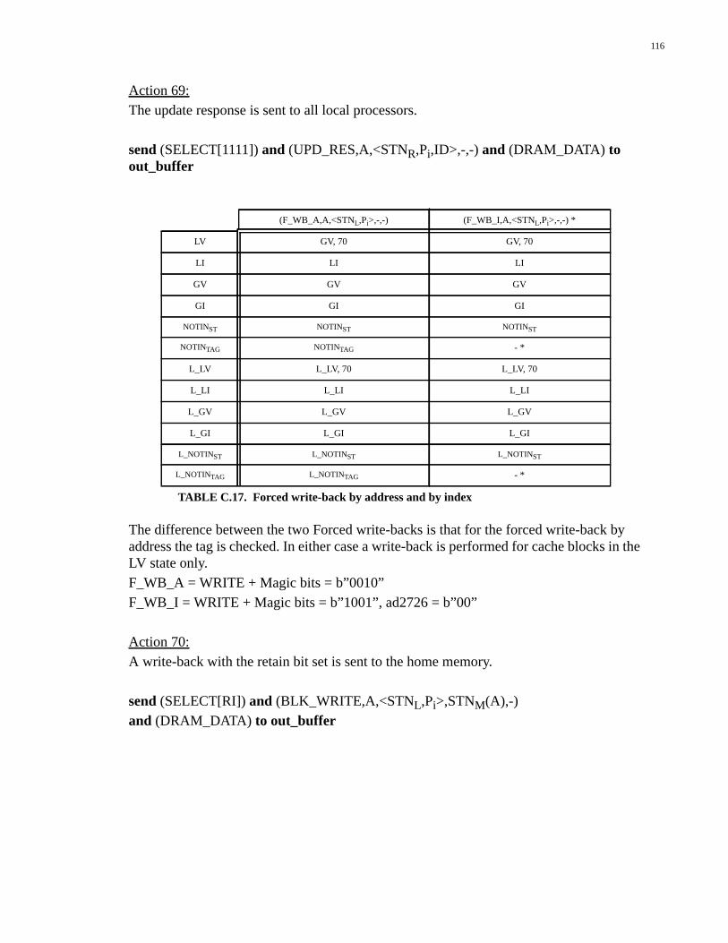
116
Action 69:The update response is sent to all local processors.
send (SELECT[1111]) and (UPD_RES,A,<STNR,Pi,ID>,-,-) and (DRAM_DATA) toout_buffer
The difference between the two Forced write-backs is that for the forced write-back byaddress the tag is checked. In either case a write-back is performed for cache blocks in theLV state only.F_WB_A = WRITE + Magic bits = b”0010”F_WB_I = WRITE + Magic bits = b”1001”, ad2726 = b”00”
Action 70:A write-back with the retain bit set is sent to the home memory.
send (SELECT[RI]) and (BLK_WRITE,A,<STNL,Pi>,STNM(A),-)and (DRAM_DATA) to out_buffer
(F_WB_A,A,<STNL,Pi>,-,-) (F_WB_I,A,<STNL,Pi>,-,-) *
LV GV, 70 GV, 70
LI LI LI
GV GV GV
GI GI GI
NOTINST NOTINST NOTINST
NOTINTAG NOTINTAG - *
L_LV L_LV, 70 L_LV, 70
L_LI L_LI L_LI
L_GV L_GV L_GV
L_GI L_GI L_GI
L_NOTINST L_NOTINST L_NOTINST
L_NOTINTAG L_NOTINTAG - *
TABLE C.17. Forced write-back by address and by index
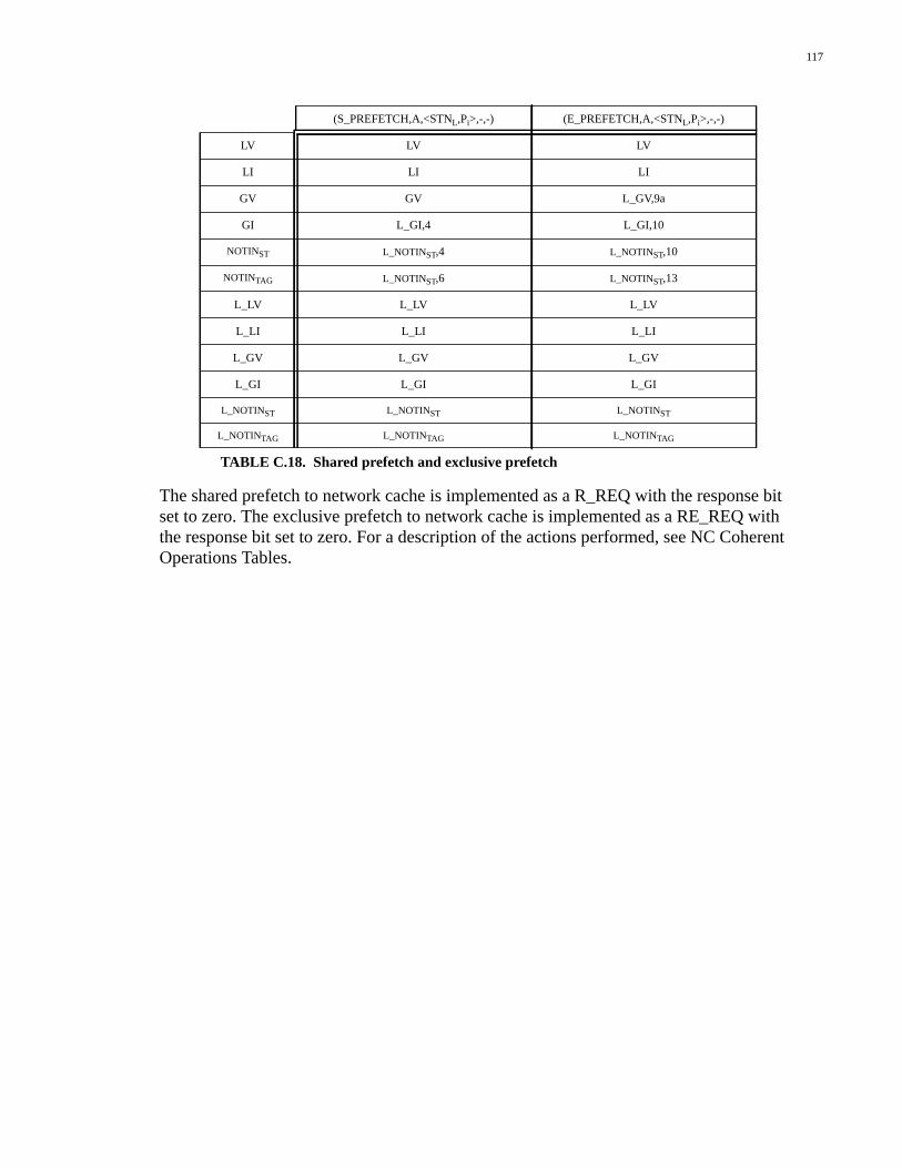
117
The shared prefetch to network cache is implemented as a R_REQ with the response bitset to zero. The exclusive prefetch to network cache is implemented as a RE_REQ withthe response bit set to zero. For a description of the actions performed, see NC CoherentOperations Tables.
(S_PREFETCH,A,<STNL,Pi>,-,-) (E_PREFETCH,A,<STNL,Pi>,-,-)
LV LV LV
LI LI LI
GV GV L_GV,9a
GI L_GI,4 L_GI,10
NOTINST L_NOTINST,4 L_NOTINST,10
NOTINTAG L_NOTINST,6 L_NOTINST,13
L_LV L_LV L_LV
L_LI L_LI L_LI
L_GV L_GV L_GV
L_GI L_GI L_GI
L_NOTINST L_NOTINST L_NOTINST
L_NOTINTAG L_NOTINTAG L_NOTINTAG
TABLE C.18. Shared prefetch and exclusive prefetch
118
Appendix D
Memory Number Encodings
The action number encodings are given in Section D.1 and the state number encodings
are given in section D.2.
D.1 Action Number Encoding
FIGURE D.1. States in Packet Generator
Figure D.1 shows the states in the Packet Generator. Each state (except start and reset)
generates a packet. The response type is determined by four bits (9-6). The encoding for
each type is given in Table D.1. The remaining bits in the action number are specific to the
particular action that must be performed. The full encodings for each action number are
given in the remaining tables.
single data_resp prepkt
postpkt
preresp
postresp
start
reset reset reset
data_id
reset
unc_sram unc_dram
reset
special
bc_inv
119
The bit fields in the action number are defined as:
sm = single/many packets bit
cu = cached/uncached bit
data = data response bit
prepost = prepkt/postpkt bit
lr = local/remote bit
nack = NACK bit
rs2-rs0 = response select code
sink = sinkable bit
cn = coherent/non-coherent bit
sd = SRAM/DRAM bit
se = shared/exclusive bit
re = outgoing command must be read exclusive
invldn = outgoing command must be invalidation
decr = decrement counter bit
cp = remove requesting processor from the PMASK (actions 6 and 8)
upd = update bit
bc_int = broadcast/interrupt bit
p_inv = invalidate after broadcast bit
Type of response contents [9] [8] [7] [6]
no action no packet 0 0 0 0
single command packet 1 1 x x
data response command packet + cache block 0 1 1 x
prepacket response single + command packet + cache block 0 1 0 1
post packet response command packet + cache block + single 0 1 0 0
uncached SRAM command packet + doubleword of data 1 0 1 x
uncached DRAM command packet + doubleword of data 1 0 0 x
special command packet + doubleword of data 0 0 1 x
TABLE D.1. Types of packet generated by the Packet Generator
120
ActionNumber
[10] [9] [8] [7] [6] [5] [4] [3] [2] [1] [0]
cp sm cu rs2 rs1 rs0 invldn re nack lr sink
2 0 1 1 0 0 1 0 0 0 1 0
3 0 1 1 1 1 1 0 0 1 1 1
4 0 1 1 0 0 1 0 0 0 0 0
6 0 1 1 1 1 1 1 0 0 1 1
7 0 1 1 0 0 1 0 1 0 1 0
* 8a 1 1 1 1 0 0 1 0 0 0 1
* 8b 0 1 1 1 0 0 1 0 0 0 1
9 0 1 1 0 0 1 0 1 0 0 0
16 0 1 1 0 1 1 0 0 0 1 0
17 0 1 1 1 1 1 0 0 1 0 1
18_a 0 1 1 0 1 0 0 0 0 0 0
18_b 0 1 1 0 1 0 0 0 0 0 1
21 0 1 1 0 1 1 0 1 0 1 0
23_a 0 1 1 0 1 0 0 1 0 0 0
23_b 0 1 1 0 1 0 0 1 0 0 1
25 0 1 1 1 0 0 1 0 0 0 0
TABLE D.2. Single packet actions
rs2 rs1 rs0 Devices Selected
0 0 0 none
0 0 1 resp_set, MEM
0 1 0 MEM
0 1 1 RI, MEM
1 0 0 PMASK, MEM
1 1 1 NO CHANGE FROM INPUT
TABLE D.3. Response-select line codes
121
ActionNumber
[10] [9] [8] [7] [6] [5] [4] [3] [2] [1] [0]
sm cu sd upd nack lr sink
30 0 1 0 0 0 0 0 0 0 1 1
31 0 1 0 0 0 0 0 0 0 0 1
33 0 1 0 0 0 0 0 0 1 1 1
34 0 1 0 0 0 0 0 0 1 0 1
UPDATE_L(41)
0 1 0 0 0 0 0 1 0 1 1
UPDATE_R(42)
0 1 0 0 0 0 0 1 0 0 1
TABLE D.4. Uncached DRAM actions
ActionNumber
[10] [9] [8] [7] [6] [5] [4] [3] [2] [1] [0]
sm cu sd nack lr sink
35 0 1 0 1 0 0 0 0 0 1 1
36 0 1 0 1 0 0 0 0 0 0 1
TABLE D.5. Uncached SRAM actions
ActionNumber
[10] [9] [8] [7] [6] [5] [4] [3] [2] [1] [0]
sm cu data decr cn se re nack lr sink
1 0 0 1 1 1 1 1 0 0 1 1
15 0 0 1 1 1 1 1 0 0 0 1
6 0 0 1 1 1 1 0 1 0 1 1
20 0 0 1 1 1 1 0 1 0 0 1
11 0 0 1 1 0 1 0 1 0 1 1
26 0 0 1 1 1 1 0 1 0 0 1
28 0 0 1 1 1 0 1 0 0 1 1
29 0 0 1 1 1 0 1 0 0 0 1
TABLE D.6. Data response actions
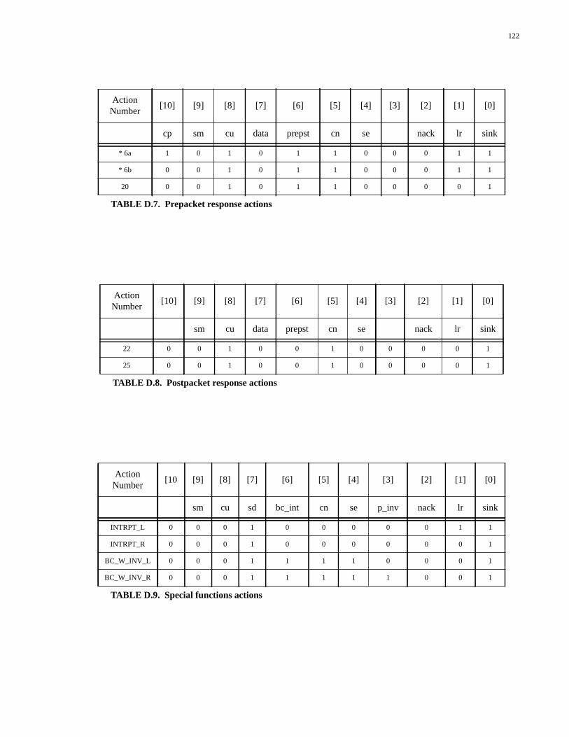
122
ActionNumber
[10] [9] [8] [7] [6] [5] [4] [3] [2] [1] [0]
cp sm cu data prepst cn se nack lr sink
* 6a 1 0 1 0 1 1 0 0 0 1 1
* 6b 0 0 1 0 1 1 0 0 0 1 1
20 0 0 1 0 1 1 0 0 0 0 1
TABLE D.7. Prepacket response actions
ActionNumber
[10] [9] [8] [7] [6] [5] [4] [3] [2] [1] [0]
sm cu data prepst cn se nack lr sink
22 0 0 1 0 0 1 0 0 0 0 1
25 0 0 1 0 0 1 0 0 0 0 1
TABLE D.8. Postpacket response actions
ActionNumber
[10 [9] [8] [7] [6] [5] [4] [3] [2] [1] [0]
sm cu sd bc_int cn se p_inv nack lr sink
INTRPT_L 0 0 0 1 0 0 0 0 0 1 1
INTRPT_R 0 0 0 1 0 0 0 0 0 0 1
BC_W_INV_L 0 0 0 1 1 1 1 0 0 0 1
BC_W_INV_R 0 0 0 1 1 1 1 1 0 0 1
TABLE D.9. Special functions actions
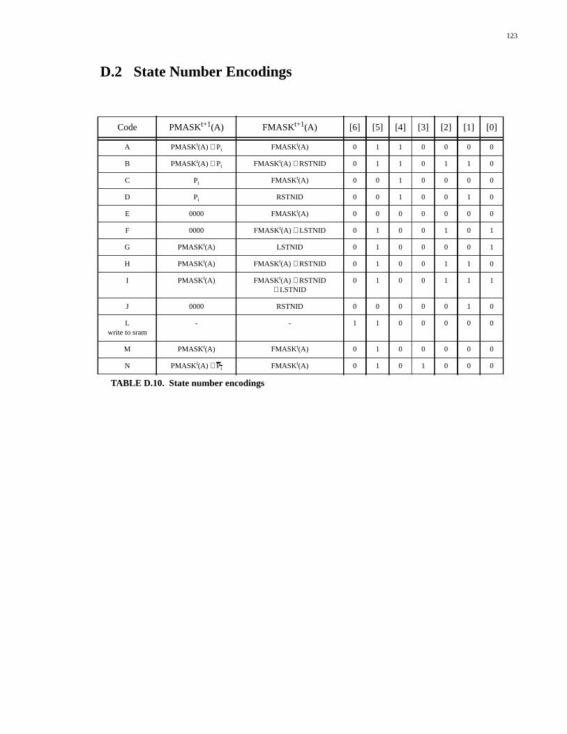
123
D.2 State Number Encodings
Code PMASKt+1(A) FMASKt+1(A) [6] [5] [4] [3] [2] [1] [0]
A PMASKt(A) ∨ Pi FMASKt(A) 0 1 1 0 0 0 0
B PMASKt(A) ∨ Pi FMASKt(A) ∨ RSTNID 0 1 1 0 1 1 0
C Pi FMASKt(A) 0 0 1 0 0 0 0
D Pi RSTNID 0 0 1 0 0 1 0
E 0000 FMASKt(A) 0 0 0 0 0 0 0
F 0000 FMASKt(A) ∨ LSTNID 0 1 0 0 1 0 1
G PMASKt(A) LSTNID 0 1 0 0 0 0 1
H PMASKt(A) FMASKt(A) ∨ RSTNID 0 1 0 0 1 1 0
I PMASKt(A) FMASKt(A) ∨ RSTNID∨ LSTNID
0 1 0 0 1 1 1
J 0000 RSTNID 0 0 0 0 0 1 0
Lwrite to sram
- - 1 1 0 0 0 0 0
M PMASKt(A) FMASKt(A) 0 1 0 0 0 0 0
N PMASKt(A) ∧ Pi FMASKt(A) 0 1 0 1 0 0 0
TABLE D.10. State number encodings
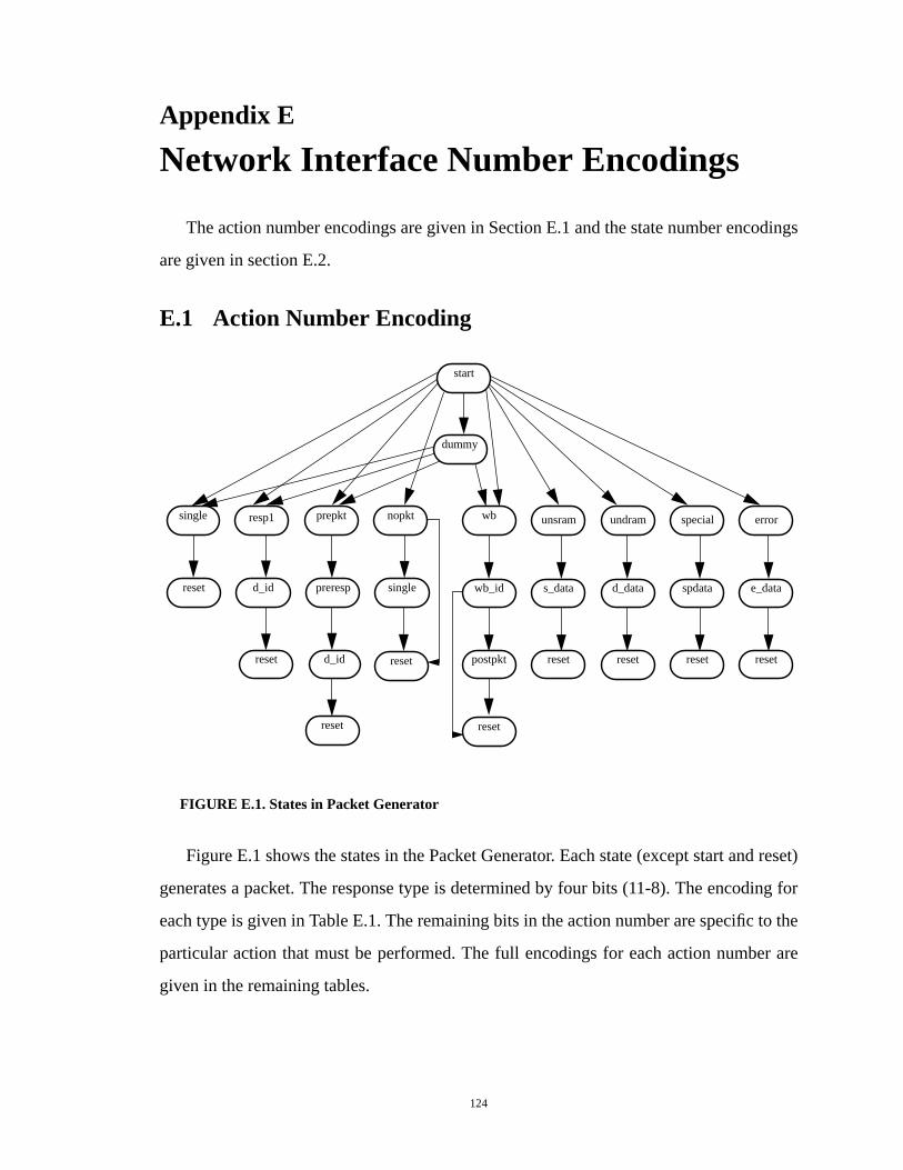
124
Appendix E
Network Interface Number Encodings
The action number encodings are given in Section E.1 and the state number encodings
are given in section E.2.
E.1 Action Number Encoding
FIGURE E.1. States in Packet Generator
Figure E.1 shows the states in the Packet Generator. Each state (except start and reset)
generates a packet. The response type is determined by four bits (11-8). The encoding for
each type is given in Table E.1. The remaining bits in the action number are specific to the
particular action that must be performed. The full encodings for each action number are
given in the remaining tables.
single resp1 prepkt
reset
prerespreset
wb
d_id
s_data d_data spdata
reset
unsram undram
reset
special
d_id wb_id
reset
reset
reset
dummy
nopkt
single
reset reset
e_data
error
postpkt
start
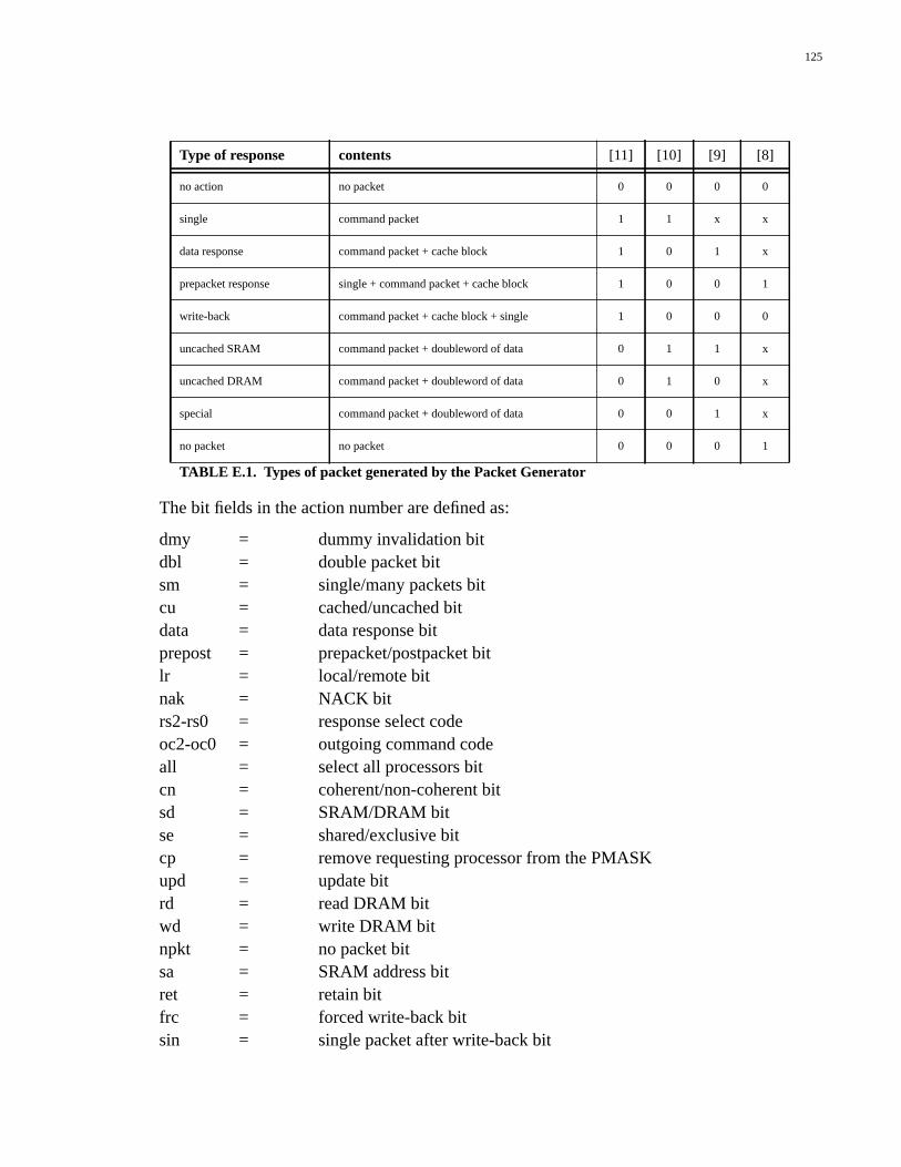
125
The bit fields in the action number are defined as:
dmy = dummy invalidation bitdbl = double packet bitsm = single/many packets bitcu = cached/uncached bitdata = data response bitprepost = prepacket/postpacket bitlr = local/remote bitnak = NACK bitrs2-rs0 = response select codeoc2-oc0 = outgoing command codeall = select all processors bitcn = coherent/non-coherent bitsd = SRAM/DRAM bitse = shared/exclusive bitcp = remove requesting processor from the PMASKupd = update bitrd = read DRAM bitwd = write DRAM bitnpkt = no packet bitsa = SRAM address bitret = retain bitfrc = forced write-back bitsin = single packet after write-back bit
Type of response contents [11] [10] [9] [8]
no action no packet 0 0 0 0
single command packet 1 1 x x
data response command packet + cache block 1 0 1 x
prepacket response single + command packet + cache block 1 0 0 1
write-back command packet + cache block + single 1 0 0 0
uncached SRAM command packet + doubleword of data 0 1 1 x
uncached DRAM command packet + doubleword of data 0 1 0 x
special command packet + doubleword of data 0 0 1 x
no packet no packet 0 0 0 1
TABLE E.1. Types of packet generated by the Packet Generator
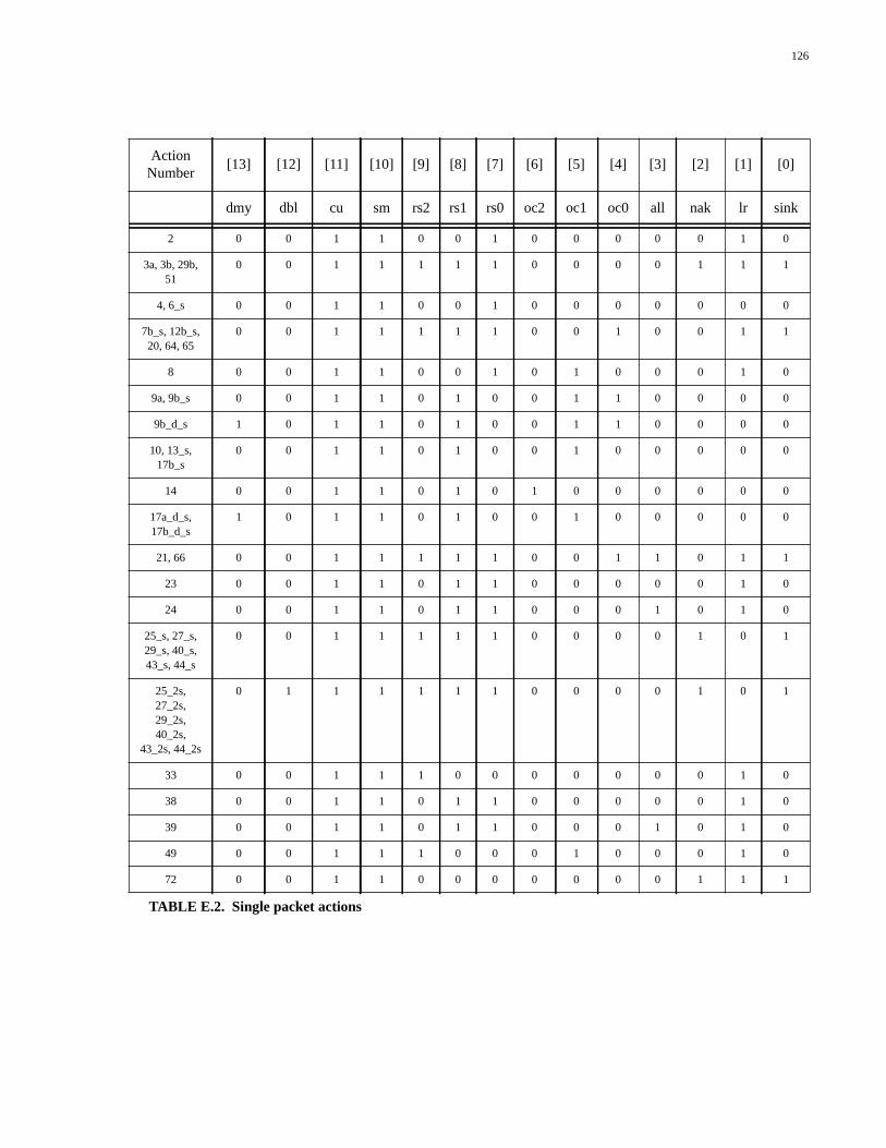
126
ActionNumber
[13] [12] [11] [10] [9] [8] [7] [6] [5] [4] [3] [2] [1] [0]
dmy dbl cu sm rs2 rs1 rs0 oc2 oc1 oc0 all nak lr sink
2 0 0 1 1 0 0 1 0 0 0 0 0 1 0
3a, 3b, 29b,51
0 0 1 1 1 1 1 0 0 0 0 1 1 1
4, 6_s 0 0 1 1 0 0 1 0 0 0 0 0 0 0
7b_s, 12b_s,20, 64, 65
0 0 1 1 1 1 1 0 0 1 0 0 1 1
8 0 0 1 1 0 0 1 0 1 0 0 0 1 0
9a, 9b_s 0 0 1 1 0 1 0 0 1 1 0 0 0 0
9b_d_s 1 0 1 1 0 1 0 0 1 1 0 0 0 0
10, 13_s,17b_s
0 0 1 1 0 1 0 0 1 0 0 0 0 0
14 0 0 1 1 0 1 0 1 0 0 0 0 0 0
17a_d_s,17b_d_s
1 0 1 1 0 1 0 0 1 0 0 0 0 0
21, 66 0 0 1 1 1 1 1 0 0 1 1 0 1 1
23 0 0 1 1 0 1 1 0 0 0 0 0 1 0
24 0 0 1 1 0 1 1 0 0 0 1 0 1 0
25_s, 27_s,29_s, 40_s,43_s, 44_s
0 0 1 1 1 1 1 0 0 0 0 1 0 1
25_2s,27_2s,29_2s,40_2s,
43_2s, 44_2s
0 1 1 1 1 1 1 0 0 0 0 1 0 1
33 0 0 1 1 1 0 0 0 0 0 0 0 1 0
38 0 0 1 1 0 1 1 0 0 0 0 0 1 0
39 0 0 1 1 0 1 1 0 0 0 1 0 1 0
49 0 0 1 1 1 0 0 0 1 0 0 0 1 0
72 0 0 1 1 0 0 0 0 0 0 0 1 1 1
TABLE E.2. Single packet actions
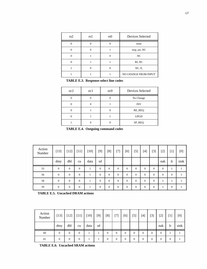
127
rs2 rs1 rs0 Devices Selected
0 0 0 none
0 0 1 resp_set, NC
0 1 0 NC
0 1 1 RI, NC
1 0 0 NC, Pi
1 1 1 NO CHANGE FROM INPUT
TABLE E.3. Response-select line codes
oc2 oc1 oc0 Devices Selected
0 0 0 No Change
0 0 1 INV
0 1 0 RE_REQ
0 1 1 UPGD
1 0 0 SP_REQ
TABLE E.4. Outgoing command codes
ActionNumber
[13] [12] [11] [10] [9] [8] [7] [6] [5] [4] [3] [2] [1] [0]
dmy dbl cu data sd nak lr sink
55 0 0 0 1 0 0 0 0 0 0 0 0 1 1
56 0 0 0 1 0 0 0 0 0 0 0 0 0 1
58 0 0 0 1 0 0 0 0 0 0 0 1 1 1
59 0 0 0 1 0 0 0 0 0 0 0 1 0 1
TABLE E.5. Uncached DRAM actions
ActionNumber
[13] [12] [11] [10] [9] [8] [7] [6] [5] [4] [3] [2] [1] [0]
dmy dbl cu data sd nak lr sink
60 0 0 0 1 1 0 0 0 0 0 0 0 1 1
61 0 0 0 1 1 0 0 0 0 0 0 0 0 1
TABLE E.6. Uncached SRAM actions
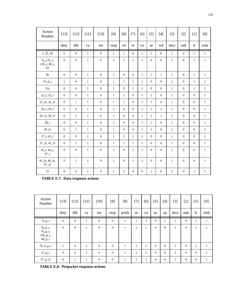
128
ActionNumber
[13] [12] [11] [10] [9] [8] [7] [6] [5] [4] [3] [2] [1] [0]
dmy dbl cu sm resp rd re cn se wd decr nak lr sink
1, 35, 36 0 0 1 0 1 1 0 1 1 0 1 0 1 1
7a_r,7b_r,12b_r, 48_r,
63
0 0 1 0 1 1 1 1 0 0 1 0 1 1
5b 0 0 1 0 1 0 0 1 1 1 1 0 1 1
7b_d_r 1 0 1 0 1 1 1 1 0 0 1 0 1 1
12a 0 0 1 0 1 0 1 1 0 0 1 0 1 1
22_r, 32_r 0 0 1 0 1 1 0 1 1 0 1 0 0 1
22_2r, 32_2r 0 1 1 0 1 1 0 1 1 0 1 0 0 1
26_r, 30_r 0 0 1 0 1 0 0 1 1 1 1 0 0 1
26_2r, 30_2r 0 1 1 0 1 0 0 1 1 1 1 0 0 1
28_r 0 0 1 0 1 0 0 1 1 0 1 0 0 1
28_2r 0 1 1 0 1 0 0 1 1 0 1 0 0 1
37_r, 41_r 0 0 1 0 1 1 1 1 0 0 1 0 0 1
37_2r, 41_2r 0 1 1 0 1 1 1 1 0 0 1 0 0 1
45_r, 46_r,47_r
0 0 1 0 1 0 1 1 0 0 1 0 0 1
45_2r, 46_2r,47_2r
0 1 1 0 1 0 1 1 0 0 1 0 0 1
53 0 0 1 0 1 1 0 0 1 0 1 0 1 1
TABLE E.7. Data response actions
ActionNumber
[13] [12] [11] [10] [9] [8] [7] [6] [5] [4] [3] [2] [1] [0]
dmy dbl cu sm resp prwb re cn se cp decr nak lr sink
7a_p_r 0 0 1 0 0 1 1 1 0 1 1 0 1 1
7a_p_r,7b_p_r,12b_p_r,48_p_r
0 0 1 0 0 1 1 1 0 0 1 0 1 1
7b_d_p_r 1 0 1 0 0 1 1 1 0 0 1 0 1 1
37_p_r 0 0 1 0 0 1 1 1 0 0 1 0 0 1
37_p_2r 0 1 1 0 0 1 1 1 0 0 1 0 0 1
TABLE E.8. Prepacket response actions
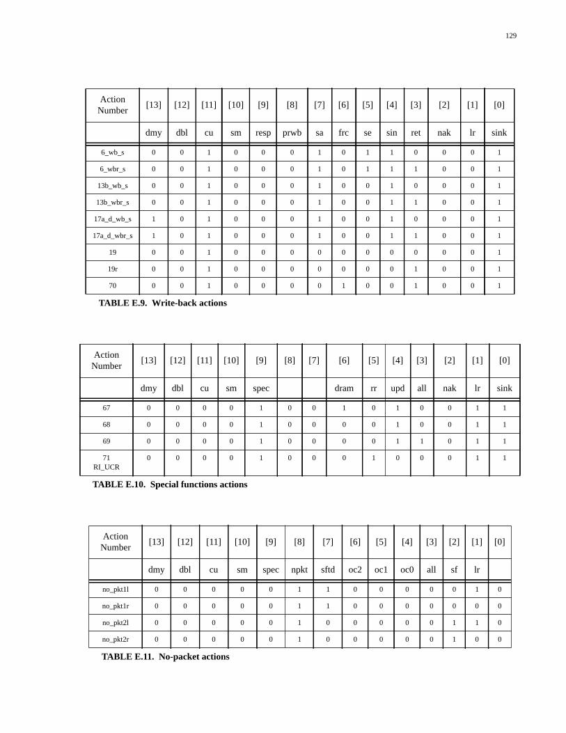
129
ActionNumber
[13] [12] [11] [10] [9] [8] [7] [6] [5] [4] [3] [2] [1] [0]
dmy dbl cu sm resp prwb sa frc se sin ret nak lr sink
6_wb_s 0 0 1 0 0 0 1 0 1 1 0 0 0 1
6_wbr_s 0 0 1 0 0 0 1 0 1 1 1 0 0 1
13b_wb_s 0 0 1 0 0 0 1 0 0 1 0 0 0 1
13b_wbr_s 0 0 1 0 0 0 1 0 0 1 1 0 0 1
17a_d_wb_s 1 0 1 0 0 0 1 0 0 1 0 0 0 1
17a_d_wbr_s 1 0 1 0 0 0 1 0 0 1 1 0 0 1
19 0 0 1 0 0 0 0 0 0 0 0 0 0 1
19r 0 0 1 0 0 0 0 0 0 0 1 0 0 1
70 0 0 1 0 0 0 0 1 0 0 1 0 0 1
TABLE E.9. Write-back actions
ActionNumber
[13] [12] [11] [10] [9] [8] [7] [6] [5] [4] [3] [2] [1] [0]
dmy dbl cu sm spec dram rr upd all nak lr sink
67 0 0 0 0 1 0 0 1 0 1 0 0 1 1
68 0 0 0 0 1 0 0 0 0 1 0 0 1 1
69 0 0 0 0 1 0 0 0 0 1 1 0 1 1
71RI_UCR
0 0 0 0 1 0 0 0 1 0 0 0 1 1
TABLE E.10. Special functions actions
ActionNumber
[13] [12] [11] [10] [9] [8] [7] [6] [5] [4] [3] [2] [1] [0]
dmy dbl cu sm spec npkt sftd oc2 oc1 oc0 all sf lr
no_pkt1l 0 0 0 0 0 1 1 0 0 0 0 0 1 0
no_pkt1r 0 0 0 0 0 1 1 0 0 0 0 0 0 0
no_pkt2l 0 0 0 0 0 1 0 0 0 0 0 1 1 0
no_pkt2r 0 0 0 0 0 1 0 0 0 0 0 1 0 0
TABLE E.11. No-packet actions
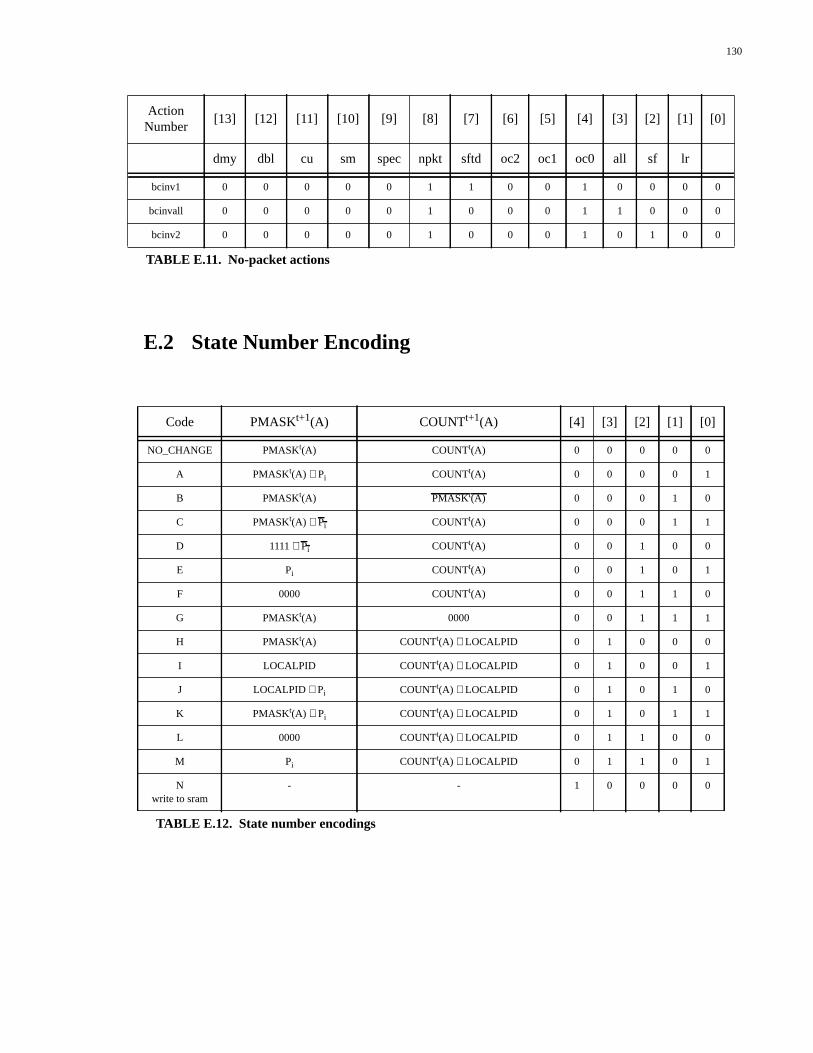
130
E.2 State Number Encoding
bcinv1 0 0 0 0 0 1 1 0 0 1 0 0 0 0
bcinvall 0 0 0 0 0 1 0 0 0 1 1 0 0 0
bcinv2 0 0 0 0 0 1 0 0 0 1 0 1 0 0
Code PMASKt+1(A) COUNTt+1(A) [4] [3] [2] [1] [0]
NO_CHANGE PMASKt(A) COUNTt(A) 0 0 0 0 0
A PMASKt(A) ∨ Pi COUNTt(A) 0 0 0 0 1
B PMASKt(A) PMASKt(A) 0 0 0 1 0
C PMASKt(A) ∧ Pi COUNTt(A) 0 0 0 1 1
D 1111 ∧ Pi COUNTt(A) 0 0 1 0 0
E Pi COUNTt(A) 0 0 1 0 1
F 0000 COUNTt(A) 0 0 1 1 0
G PMASKt(A) 0000 0 0 1 1 1
H PMASKt(A) COUNTt(A) ∨ LOCALPID 0 1 0 0 0
I LOCALPID COUNTt(A) ∨ LOCALPID 0 1 0 0 1
J LOCALPID ∨ Pi COUNTt(A) ∨ LOCALPID 0 1 0 1 0
K PMASKt(A) ∨ Pi COUNTt(A) ∨ LOCALPID 0 1 0 1 1
L 0000 COUNTt(A) ∨ LOCALPID 0 1 1 0 0
M Pi COUNTt(A) ∨ LOCALPID 0 1 1 0 1
Nwrite to sram
- - 1 0 0 0 0
TABLE E.12. State number encodings
ActionNumber
[13] [12] [11] [10] [9] [8] [7] [6] [5] [4] [3] [2] [1] [0]
dmy dbl cu sm spec npkt sftd oc2 oc1 oc0 all sf lr
TABLE E.11. No-packet actions
131
Bibliography[1] A. Agarwal, B. -H. Lim, D. Kranz, and J. Kubiatowicz, “LimitLESS Direc-
tories: A Scalable Cache Coherence Scheme,”Proceedings of the 4th Inter-national Conference on Architectural Support for ProgrammingLanguages and Operating Systems, Santa Clara, CA, April 1991, pp. 224-234.
[2] A. Agarwal, R. Bianchini, D. Chaiken, K. L. Johnson, D. Kranz, J. Kubia-towicz, B. -H. Lim, K. Mackenzie, and D. Yeung, “The MIT AlewifeMachine: Architecture and performance,”Proceedings of the 22th AnnualInternational Symposium on Computer Architecture, Santa MargheritaLiguire, Italy, June1995, pp. 2-13.
[3] T. Brewer, A Highly Scalable System Utilizing up to 128 PA-RISC Proces-sors, Convex Computer Corporation.
[4] S. Brown, N. Manjikian, Z. Vranesic, S. Caranci, A.Grbic, R. Grindley, M.Gusat, K. Loveless, Z. Zilic, and S. Srbljic, “Experience in Designing aLarge-scale Multiprocessor using Field-Programmable Devices andAdvanced CAD Tools,” Proceedings of the 33rd Design Automation Con-ference, Las Vegas, NV, June 1996, pp.427-432.
[5] Cadence Logic Workbench, release 9404, Cadence Design Systems Inc.,75 West Plumeria Drive, San Jose, CA 95134.
[6] L. Choi and P. -C. Yew, “Compiler and Hardware Support for CacheCoherence in Large-Scale Multiprocessors,”Proceedings of the 23thAnnual International Symposium on Computer Architecture, Philadelphia,PA, May 1996, pp. 283-294.
[7] Convex Computer, SPP1000 Systems Overview, Convex Computer Corpo-ration, 1994.
[8] 1995 Data Book, Altera Corp, 2610 Orchard Parkway, San Jose, CA95134.
[9] K. Farkas, Z. Vranesic and M. Stumm, “Scalable Cache Consistency forHierarchically Structured Multiprocessors,”The Journal of Supercomput-ing, Kluwer Academic Publishers, Boston, MA, 1995, pp. 345-368.
[10] M. Galles and E. Williams, Performance optimizations, implementation,and verification of the SGI Challenge multiprocessor, Silicon GraphicsComputer Systems, 1994.
[11] D. Gustavson, “The Scalable Coherent Interface and Related StandardsProjects,”IEEE Micro, 12(1), January 1992, pp.10-22.
132
[12] J. Heinrich,R4000 Microprocessor User’s Manual, Second Edition, MIPSTechnologies Inc., Mountain View, CA, April 1994.
[13] D. Kuck, E. Davidson, D. Lawrie, A. Sameh, C. -Q. Zhu, A. Veidenbaum,J. Konicek, P. Yew, K. Gallivan, W. Jalby, H. Wijshoff, R. Bramley, U. M.Yang, P. Emrath, D. Padua, R. Eigenmann, J. Hoeflinger, G. Jaxon, Z. Li,T. Murphy, J. Andrews, S. Turner, “The Cedar System and an Initial Perfor-mance Study,” Proceedings of the 20th Annual International Symposiumon Computer Architecture, San Diego, CA, May 1993, pp. 213-223.
[14] J. Kuskin, D. Ofelt, M. Heinrich, J. Heinlein, R. Simoni, K. Gharachorloo,J. Chapin, D. Nakahira, J. Baxter, M. Horowitz, A. Gupta, M. Rosenblumand J. Hennessy, “The Stanford FLASH multiprocessor,” Proceedings ofthe 21th Annual International Symposium on Computer Architecture, Chi-cago, IL, May 1994, pp. 302-313.
[15] D. Lenoski, J. Laudon, K. Gharachorloo, A. Gupta, J. Hennessy, “TheDirectory-based Cache Coherence Protocol for the DASH Multiprocessor,”Proceedings of the 17th Annual International Symposium on ComputerArchitecture, Seattle, WA, May 1990, pp. 148-159.
[16] D. Lenoski, J. Laudon, T. Joe, D. Nakahira, L. Stevens, A. Gupta, J. Hen-nessy, “The DASH Prototype: Implementation and Performance,”Proceed-ings of the 19th Annual International Symposium on ComputerArchitecture, Gold Coast, Australia, May 1992, pp. 92-103.
[17] D. E. Lenoski, W. -D. Weber, Scalable Shared-Memory Multiprocessing,Second Edition, Morgan Kaufmann Publishers, San Franscisco, CA, 1995.
[18] Thomas D. Lovett, Russel M. Clapp, “STiNG: A CC-NUMA ComputerSystem for the Commercial Marketplace,”Proceedings of the 23th AnnualInternational Symposium on Computer Architecture, Philadelphia, PA,May 1996, pp. 308-317.
[19] A. Nowatzyk, G. Aybay, M. Browne, E. Kelly, M. Parkin, B. Radke, S.Vishin, “The S3.mp Scalable Shared Memory Multiprocessor,” Proceed-ings of the 24th International Conference on Parallel Processing, Ocono-mowoc, WI, August 1995.
[20] W. Oed, “The Cray Research Massively Parallel Processor System CrayT3D,” Technical Report, Cray Research GmbH, Munich, Germany,November 1993.
[21] R. W. Pfile, “Typhoon-Zero Implementation: The Vortex Module,”Techni-cal Report 1290, Computer Sciences Department, University of Wiscon-sin-Madison, WI, October 1995.
133
[22] G. F. Pfister, W. C. Brantley, D. A. George, S. L. Harvey, W. J. Kleinfelder,K. P. McAulif fe, E.A. Melton, V. A. Norton and J. Weiss, “The IBMResearch Parallel Processor Prototype (RP3): Introduction and Architec-ture,” Proceedings of the 1985 International Conference on Parallel Pro-cessing, August 1985, pp. 764-769.
[23] S. K. Reinhardt, R. W. Pfile and D. A. Wood, “Decoupled Hardware Sup-port for Distributed Shared Memory,” Proceedings of the 23th AnnualInternational Symposium on Computer Architecture, Philadelphia, PA,May 1996, pp. 34-43.
[24] S. Srbljic and L. Budin, “Analytical Performance Evaluation of Data Repli-cation Based Shared Memory Model,”Proceedings of the 2th InternationalSymposium on High Performance Distributed Computing, Spokane WA,July 1993, pp. 326-335.
[25] P. Stenstrom, “A Survey of Cache Coherence Schemes for Multiproces-sors,”IEEE Computer, 23(6), June 1990, pp.12-24.
[26] M. Stumm, R. Unrau, and O. Krieger, “Designing a Scalable OperatingSystem for Shared Memory Multiprocessors,”Proceedings of the UsenixWorkshop on Micro-kernels and Other Kernel Architectures, Seattle, WA,April 1992, pp.285-303.
[27] Z. Vranesic, S. Brown, M. Stumm, S. Caranci, A. Grbic, R. Grindley,M. Gusat, O. Krieger, G. Lemieux, K. Loveless, N. Manjikian, Z. Zilic,T. Abdelrahman, B. Gamsa, P. Pereira, K. Sevcik, A. Elkateeb, S. Srbljic,“The NUMAchine Multiprocessor,” Technical Report CSRI-324, Com-puter Systems Research Institute, University of Toronto, Canada, June1995.
[28] Z. G. Vranesic, M. Stumm, D. Lewis, and R. White, “Hector: A hierarchi-cally structured shared-memory multiprocessor,” IEEE Computer, 24(1),January 1991, pp. 72-79.