Embed Size (px)
Citation preview

Version 1.0 May 2007 © JMicron 2007. All rights reserved. Page 1 Copying prohibited.
JMicron/JM20329
JM20329
Hi-Speed USB to SATA Bridge
Datasheet
Rev. 1.0

Version 1.0 May 2007 © JMicron 2007. All rights reserved. Page 2 Copying prohibited.
JMicron/JM20329
Revision History
Version Date Revision Description 0.8 2007/3/20 Initialization of this document for JM20329.
0.9 2007/4/16 1. Modify pin out description
2. Remove the description about Serial Flash and Fingerprint recognition.
3. Modify the EEPROM configuration description
1.0 2007/5/3 1. Add pin description in USB suspend mode.
2. Remove the typing error of pin17 in SATA power pin
© Copyright JMicron Technology, 2007.
All Rights Reserved.
Printed in Taiwan 2007 JMicron and the JMicron Logo are trademarks of JMicron Technology Corporation in Taiwan and/or other countries. Other company, product and service names may be trademarks or service marks of others. All information contained in this document is subject to change without notice. The products described in this document are NOT intended for use implantation or other life supports application where malfunction may result in injury or death to persons. The information contained in this document does not affect or change JMicron’s product specification or warranties. Nothing in this document shall operate as an express or implied license or environments, and is presented as an illustration. The results obtained in other operating environments may vary. THE INFORMATION CONTAINED IN THIS DOCUMENT IS PROVIEDE ON AN “AS IS” BASIS. In no event will JMicron be liable for damages arising directly or indirectly from any use of the information contained in this document. JMicron Technology Corporation 1F, No.13, Innovation Road I, Science Based Industrial Park Hsinchu, Taiwan, R.O.C For more information on JMicron products, please visit the JMicron web site at http://www.JMicron.com or send email to [email protected]

Version 1.0 May 2007 © JMicron 2007. All rights reserved. Page 3 Copying prohibited.
JMicron/JM20329
Table of Contents 1. General Description ................................................................................................................................................ 4
2. Features ................................................................................................................................................................. 4
3. Main Applications................................................................................................................................................. 5
4. Block Diagram ...................................................................................................................................................... 5
5. Package and Pin Assignments.............................................................................................................................. 6
5.1 Package Pin Out ................................................................................................................................................................. 6
5.2 Package Outline.................................................................................................................................................................. 7
6. Pin Descriptions....................................................................................................................................................... 8
6.1 Pin Type Definition............................................................................................................................................................. 8
6.2 Serial ATA Interface ........................................................................................................................................................... 8
6.3 USB Interface...................................................................................................................................................................... 8
6.4 Crystal Interface................................................................................................................................................................. 9
6.5 Voltage Regulator ............................................................................................................................................................... 9
6.6 Digital Power Supply and System Control Interface....................................................................................................... 9
7. Electrical Characteristics ..................................................................................................................................... 11
7.1 Absolute Maximum Rating.............................................................................................................................................. 11
7.2 Recommended Power Supply Operation Conditions .................................................................................................... 11
7.3 Recommended External Clock Source Conditions........................................................................................................ 11
7.4 Power Supply DC Characteristics................................................................................................................................... 11
8. External Serial EEPROM Configuration ........................................................................................................... 12

Version 1.0 May 2007 © JMicron 2007. All rights reserved. Page 4 Copying prohibited.
JMicron/JM203291. General Description
The JM20329 is the single chip solution to bridge between USB host and SATA device. The highly integrated Hi-Speed USB
and SATA Phys technology provides a cost-effective solution to apply USB to SATA device enclosure. The USB adhere to the Mass
Storage Class Bulk-Only Transport Specification. The embedded command parser supports both ATA and ATAPI command set
with LBA48 addressing capability.
This chip is designed by 0.18um CMOS technology with 48 LQFP package.
2. Features
Compliance with Gen1i/Gen1m of Serial ATA II Electrical Specification 2.5
Support SATA II Asynchronous Signal Recovery (Hot Plug) feature
Compliance with USB 2.0 electrical specification
Support USB High-Speed and Full-Speed Operation
Compliance with USB Mass Storage Class, Bulk-Only Transport Specification
Support ATA/ATAPI PACKET command set
Support ATA/ATAPI LBA48 addressing mode
Support 12MHz external crystal
Support external NVRAM for Vender Specific VID/PID of USB Device Controller
Embedded 3.3V to 1.8V voltage regulator
Single power 3.3V power supply
0.18um CMOS technology
48 LQFP package
8 GPIO

Version 1.0 May 2007 © JMicron 2007. All rights reserved. Page 5 Copying prohibited.
JMicron/JM203293. Main Applications
Hi-Speed USB to SATA Device
SATA USB
SATA Device PC
Figure 1 High-Speed USB to SATA Bridge
4. Block Diagram
SATA
Lin
k La
yer
SATA
Phy
sica
l Lay
er
Register Files
SATA
Tra
nspo
rt La
yer
FIFO
FIFO
SATADevice
USBHost
USB
2.0
PH
Y
USB
Seria
l Int
erfa
ce E
ngin
e(S
IE)
Register Files
Figure 2 Block Diagram

Version 1.0 May 2007 © JMicron 2007. All rights reserved. Page 6 Copying prohibited.
JMicron/JM203295. Package and Pin Assignments 5.1 Package Pin Out
1 2 3 4 5 6 7 8 9 10 11 12
13
14
15
16
17
18
19
20
21
22
23
24
48
47
46
45
44
43
42
41
40
39
38
37
36 35 34 33 32 31 30 29 28 27 26 25
GPI
O[2
2]
DG
ND
GPI
O[7
]
AVD
DH
AG
ND
H
AVR
EG
VCC
O
GPI
O[2
3]
Reserve3
GPIO[18]
UAO
PTM
ode
Reserve0
TME#
PHYR
DY
VCC
K
DG
ND
HD
DA
TEST[0]
DGND
TEST
[2]
VBU
S
DM
RST
#TEST[1]
XTALO
Reserve2 DP
AVDDH
AGNDH
AVDDH
AGND
REXT
RXP
RXN
Reserve1
VCCK
UAI
VCCOG
PIO
[1]
GPI
O[0
]
GPI
O[2
]
GPI
O[3
]
TXP
TXN
XTA
LI
AVDDL
AGND
VCCO: 3.3VVCCK: 1.8VAVDDH: 3.3VAVDDL: 1.8V
Figure 3 Package Pin Assignment
Version 1.0 May 2007 © JMicron 2007. All rights reserved. Page 7 Copying prohibited.
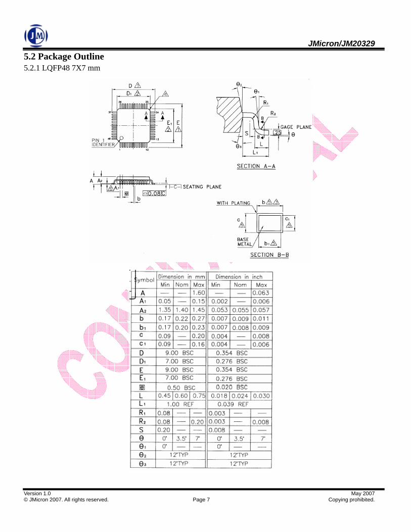
JMicron/JM203295.2 Package Outline 5.2.1 LQFP48 7X7 mm
Version 1.0 May 2007 © JMicron 2007. All rights reserved. Page 8 Copying prohibited.
JMicron/JM20329
6. Pin Descriptions 6.1 Pin Type Definition
Pin Type Definition
A Analog D Digital
I Input
O Output
IO Bi-directional
L Internal weak pull-low (Typical 31 KΩ)
H Internal weak pull-high (Typical 31 KΩ)
6.2 Serial ATA Interface
Signal Name Pin No. Type Description RXP 21 AI Serial ATA RX+ signal.
A 10nF CAP should be connected between this pin and SATA connector.RXN 22 AI Serial ATA RX- signal.
A 10nF CAP should be connected between this pin and SATA connector.TXP 26 AO Serial ATA TX+ signal.
A 10nF CAP should be connected between this pin and SATA connector.TXN 25 AO Serial ATA TX- signal.
A 10nF CAP should be connected between this pin and SATA connector.REXT 20 AI External Reference Resistance.
A 12KΩ±1% external resistor should be connected to this pin. AVDDL 23 AI SATA Analog 1.8V Power Supply.
This power could be sourced from internal 1.8V voltage regulator through AVREG pin.
AGND 24,19 AI SATA Analog Ground. AVDDH 18 AI SATA Analog 3.3V Power Supply.
6.3 USB Interface
Signal Name Pin No. Type Description DM 14 AIO USB Bus D- Signal. DP 15 AIO USB Bus D+ Signal. VBUS 8 DIL USB Cable Power Detector.
The 4.7KΩ and 10KΩ resistances should be connected to divide the 5V cable power into 3.3V.
AVDDH 16 AI USB Analog 3.3V Power Supply. AGNDH 17 AI USB Analog Ground.

Version 1.0 May 2007 © JMicron 2007. All rights reserved. Page 9 Copying prohibited.
JMicron/JM20329 6.4 Crystal Interface
Signal Name Pin No. Type Description XTALI 12 AI Crystal Input/Oscillator Input.
It is connected to a 12MHz crystal or crystal oscillator. XTALO 13 AO Crystal Output.
It is connected to a crystal. While crystal oscillator is applied, this pin should be reserved as No Connection (NC).
6.5 Voltage Regulator
Signal Name Pin No. Type Description AVREG 9 AO Voltage Regulator 1.8V Output. AVDDH 10 AI Voltage Regulator 3.3V Power Supply. AGNDH 11 AI Voltage Regulator Ground.
6.6 Digital Power Supply and System Control Interface
Signal Name Pin No. Type Description VCCO 5,42 DI Digital 3.3V Power Supply. VCCK 36,44 DI Digital 1.8V Core Power. DGND 4,35,43 DI Digital Ground. RST# 7 DIH System Global Reset Input.
Active-low to reset the entire chip. An external 10msec RC should be connected to this pin.
TME# 31 DIH MP Test Mode Enable. This pin is reserved for IC mass production testing. Keep this pin to logic “1” in normal operation.
HDDA 33 DO SATA Device Active. 0 : Device active. 1 : IDLE. Output to “0” in USB Suspend mode. (F)
TEST[2:0] 3,41,45 DIL DIL DIL
MP TEST Mode Selection. For IC mass production testing. We strongly recommend customer to make TEST[2:0] = 000. Input in USB Suspend mode
GPIO[0]
30 DIOH ATA/ATAPI Power Down Mode Enable/EEPROM 9346 Data Output (DO) GPIO0 (1) At Power on MCU will detect this pin. 0: Enable MCU issue spin down command to HDD in suspend mode. 1: Disable MCU issue spin down command to HDD in suspend mode. (2) After power on status detecting, this pin becomes Data Output of serial EEPROM 9346. (3) While EEPROM detection is complete, this pin is default set to input, and could act as GPIO pin by SCSI-2 vender command (button input). Input in USB Suspend mode(F)
Version 1.0 May 2007 © JMicron 2007. All rights reserved. Page 10 Copying prohibited.
JMicron/JM20329Signal Name Pin No. Type Description
GPIO[1]
29 DIOH EEPROM 9346 Data Input (DI) /GPIO1 (1) After power on status detecting, this pin becomes Data Input of serial EEPROM 9346. (2) While EEPROM detection is complete, this pin is default set to input, and could act as GPIO pin by SCSI-2 vender command (button input). Input in USB Suspend mode(F)
GPIO[2]
28 DIOH USB Attach Sequence/EEPROM 9346 Serial Clock (SK)/GPIO2 (1) The internal controller will detect the pin status after power on. The functionality of power on initial state determines the USB attach sequence of JM20329 0: Attached USB first. 1: Check SATA device first. (2) This pin is Serial Clock of serial EEPROM 9346. (3) While EEPROM detection is complete, this pin is default set to input, and could act as GPIO pin by SCSI-2 vender command (button input). Input in USB Suspend mode (F)
GPIO[3]
27 DIOH EEPROM 9346 Chip Select (CS) /GPIO3 (1) This pin functions as Chip Select of EEPROM 9346 in EEPRM detection. (2) While EEPROM detection is complete, this pin is default set to input, and could act as GPIO pin by SCSI-2 vender command. Note that it only supports 9346 with 64x16-bit mode. Input in USB Suspend mode (F)
PTMODE 34 DIH Protocol mode 1: Enable USB to SATA function. 0: Disable USB and SATA function. Input in USB Suspend mode (F)
GPIO[7] 6 DIO GPIO 7: USB Bus State. This pin will go high while the USB Vbus is applied. It will go low only in (1) Vbus is detached. (2) Vbus is attached and USB is configured and enter suspend state. (F)
GPIO[18] 48 DIO Can be configured by SCSI-2 vender command. Output to “0” in USB Suspend mode(F)
GPIO[22] 1 DIO Can be configured by SCSI-2 vender command. Output to “0” in USB Suspend mode(F)
GPIO[23] 2 DIO Can be configured by SCSI-2 vender command Output to “0” in USB Suspend mode. (F)
Reserved[3:0] 47,46,38,37
DIO DIO
DIOH DIOH
Reserved Pins. They are for internal used only. We strongly recommend customer to make Reserved[3:0] = 0011. Input in USB Suspend mode (F)
UAI 39 DIH 8051 UART interface. Input in USB Suspend mode
UAO 40 DO 8051 UART interface. Output to “1” in USB Suspend mode.
PHYRDY 32 DO SATA PHY is ready. 0: SATA interface not established. 1: SATA interface established. Output to “0” in USB Suspend mode.

Version 1.0 May 2007 © JMicron 2007. All rights reserved. Page 11 Copying prohibited.
JMicron/JM203297. Electrical Characteristics 7.1 Absolute Maximum Rating
Parameter Symbol Condition Min Max Unit
Analog power supply AVDDH -0.5 6 V
Digital I/O power supply DVDD -0.5 6 V
Digital I/O input voltage VI(D) -0.4 DVDD+0.4 V
Storage temperature TSTORAGE -55 140 oC
7.2 Recommended Power Supply Operation Conditions
Parameter Symbol Condition Min Typical Max Unit
Operation digital power supply DVDD 3.0 3.3 3.6 V
Operation analog power supply AVDDH 3.0 3.3 3.6 V
Ambient operation temperature TA -10 70 oC
Junction temperature TJ 0 125 oC
7.3 Recommended External Clock Source Conditions
Parameter Symbol Condition Min Typical Max Unit
External reference clock 12 MHz
Clock Duty Cycle 45 50 55 %
7.4 Power Supply DC Characteristics Parameter Symbol Condition Min Typical Max Unit
Digital I/O power supply IDVDD 3.3v 1 mA
Internal digital Power Supply IDDH_VR 1.8v 47 mA
USB Analog Power Supply IAVDDH_USB 3.3v 27 mA
SATA Analog Power Supply IAVDDH_SATA 3.3v 36 mA
SATA Analog Power Supply IAVDDL_SATA 1.8v 62 mA

Version 1.0 May 2007 © JMicron 2007. All rights reserved. Page 12 Copying prohibited.
JMicron/JM203298. External Serial EEPROM Configuration
The external EEPROM only support 9346 at 64x16 mode. The vender could store the Vender specific USB Device
Descriptor, Manufacture String (Index 0x0A), and Product String (Index 0x0B) according to the below table.
Support 3 strings:
1. Manufacture or HDD one of them
The Manufacture-String maximum size is 30 characters.
The HDD-String maximum size is 24 characters.
2. Product string
The Product-string maximum size is 30 characters.
3. Serial number
The Serial number-string maximum size is 30 characters.