Embed Size (px)
Citation preview

This is information on a product in full production.
August 2015 DocID15354 Rev 12 1/23
2N3700HR
Hi-Rel 80 V, 1 A NPN transistor
Datasheet - production data
Figure 1. Internal schematic diagram
Features
• Hermetic packages
• ESCC and Jans qualified
• Up to 100 krad(Si) low dose rate
DescriptionThe 2N3700HR is a NPN transistor specifically designed for aerospace and Hi-Rel applications. It is available in the JAN qualification system (MIL-PRF19500) and in the ESCC qualification system (ESCC 5000). In case of discrepancies between this datasheet and the relevant agency specification, the latter takes precedence.
TO-18
LCC-3
3
1
2
UB
3
1
2
4
3
1
2
Pin 4 in UB is connected to the metallic lid
V(BR)CEO 80 V
IC(max) 1 A
HFE at 10 V - 150 mA >100
Table 1. Device summary
DeviceQualification
systemAgency
specificationPackage Radiation level EPPL
JANSR2N3700UBx JANSR MIL-PRF-19500/391 UB100 krad
high and low dose rate-
JANS2N3700UBx JANS MIL-PRF-19500/391 UB - -
2N3700RUBx ESCC Flight 5201/004 UB 100 krad - low dose rate Target
2N3700UBx ESCC Flight 5201/004 UB - Target
SOC3700RHRx ESCC Flight 5201/004 LCC-3 100 krad - low dose rate Yes
SOC3700HRx ESCC Flight 5201/004 LCC-3 - Yes
2N3700RHRx ESCC Flight 5201/004 TO-18 100 krad - low dose rate -
2N3700HRx ESCC Flight 5201/004 TO-18 - -
www.st.com
Contents 2N3700HR
2/23 DocID15354 Rev 12
Contents
1 Electrical ratings . . . . . . . . . . . . . . . . . . . . . . . . . . . . . . . . . . . . . . . . . . . . 3
2 Electrical characteristics . . . . . . . . . . . . . . . . . . . . . . . . . . . . . . . . . . . . . 4
2.1 JANS electrical characteristics . . . . . . . . . . . . . . . . . . . . . . . . . . . . . . . . . . 4
2.2 ESCC electrical characteristics . . . . . . . . . . . . . . . . . . . . . . . . . . . . . . . . . 5
2.3 Electrical characteristics (curves) . . . . . . . . . . . . . . . . . . . . . . . . . . . . . . . . 6
2.4 Test circuits . . . . . . . . . . . . . . . . . . . . . . . . . . . . . . . . . . . . . . . . . . . . . . . . . 7
3 Radiation hardness assurance . . . . . . . . . . . . . . . . . . . . . . . . . . . . . . . . 9
4 Package information . . . . . . . . . . . . . . . . . . . . . . . . . . . . . . . . . . . . . . . . 12
4.1 UB package information . . . . . . . . . . . . . . . . . . . . . . . . . . . . . . . . . . . . . . 13
4.2 LCC-3 package information . . . . . . . . . . . . . . . . . . . . . . . . . . . . . . . . . . . 15
4.3 TO-218 package information . . . . . . . . . . . . . . . . . . . . . . . . . . . . . . . . . . 17
5 Order codes . . . . . . . . . . . . . . . . . . . . . . . . . . . . . . . . . . . . . . . . . . . . . . . 19
6 Shipping details . . . . . . . . . . . . . . . . . . . . . . . . . . . . . . . . . . . . . . . . . . . . 21
6.1 Date code . . . . . . . . . . . . . . . . . . . . . . . . . . . . . . . . . . . . . . . . . . . . . . . . . 21
6.2 Documentation . . . . . . . . . . . . . . . . . . . . . . . . . . . . . . . . . . . . . . . . . . . . . 21
7 Revision history . . . . . . . . . . . . . . . . . . . . . . . . . . . . . . . . . . . . . . . . . . . 22

DocID15354 Rev 12 3/23
2N3700HR Electrical ratings
23
1 Electrical ratings
Table 2. Absolute maximum ratings
Symbol Parameter Value Unit
VCBO Collector-base voltage (IE = 0) 140 V
VCEO Collector-emitter voltage (IB = 0) 80 V
VEBO Emitter-base voltage (IC = 0) 7 V
IC Collector current 1 A
Ptot
Total dissipation at Tamb = 25 °C
for 2N3700HR 0.5 W
for SOC3700HRB 0.5 W
for SOC3700HRB (1)
1. When mounted on a 15 x 15 x 0.6 mm ceramic substrate.
0.76 W
Total dissipation at Tc = 25 °C for 2N3700HR 1.8 W
Tstg Storage temperature -65 to 200 °C
TJ Max. operating junction temperature 200 °C
Table 3. Thermal data
Symbol Parameter LCC-3 and UB TO-18 Unit
RthJC
Thermal resistance junction-case (max) for JAN
- -
°C/W
Thermal resistance junction-case (max) for ESCC
350 97
RthJSP(IS)
Thermal resistance junction-solder pad (infinite sink) (max) for JAN
90 -
Thermal resistance junction-solder pad (infinite sink) (max) for ESCC
- -
RthJA
Thermal resistance junction-ambient (max) for JAN
325 -
Thermal resistance junction-ambient (max) for ESCC
240(1)
1. When mounted on a 15 x 15 x 0.6 mm ceramic substrate.
350

Electrical characteristics 2N3700HR
4/23 DocID15354 Rev 12
2 Electrical characteristics
JANS and ESCC version of the products are assembled and tested in compliance with the agency specification it is qualified in. The electrical characteristics of each version are provided in dedicated tables.
Tcase = 25 °C unless otherwise specified.
2.1 JANS electrical characteristics
Table 4. JANS electrical characteristics
Symbol Parameter Test conditions Min. Typ. Max. Unit
ICBOCollector cut-off current (IE = 0)
VCB = 140 V - 10 µA
ICESCollector cut-off current (IE = 0)
VCE = 90 VVCE = 90 V, Tamb= 150°C
-105
nAµA
IEBOEmitter cut-off current(IC = 0)
VEB = 5 VVEB = 7 V
-1010
nAµA
V(BR)CEO
Collector-emitter breakdown voltage
(IB = 0)IC = 30 mA - 80 V
VCE(sat)Collector-emitter saturation voltage
IC = 150 mA IB = 15 mA
IC = 500 mA IB = 50 mA-
0.2
0.5
V
V
VBE(sat)Base-emitter saturation voltage
IC = 150 mA IB = 15 mA - 1.1 V
hFE DC current gain
IC = 0.1 mA VCE = 10 V 50 - 200
IC = 10 mA VCE = 10 V 90 -
IC = 150 mA VCE = 10 V 100 - 300
IC = 150 mA VCE = 10 VTamb= -55 °C
40 -
IC = 500 mA VCE = 10 V 50 - 200
IC = 1 A VCE = 10 V 15 -
hfeSmall signal current gain
VCE = 5 V IC = 1 mA f = 1 kHz
80 - 400
VCE = 10 V IC = 50 mA f = 20 MHz
5 - 20
CoboOutput capacitance(IE = 0)
VEB = 0.5 V100 kHz; f = 1 MHz
- 12 pF
CiboOutput capacitance(IE = 0)
VEB = 0.5 V100 kHz; f = 1 MHz
- 60 pF

DocID15354 Rev 12 5/23
2N3700HR Electrical characteristics
23
2.2 ESCC electrical characteristics
NF Noise figureVCE = 10 V IC = 100 µARg = 1 kW, power bandwidth
- 4 dB
r'b,Cc(1) Collector-base time constant
VCB =10 V; IC=10 mA; f=79.8 MHz
- 400 ps
toff + toff Switching times see circuit Figure 6 - 30 ns
1. This parameter may be determined by applying an rf signal voltage of 1.0 volt (rms) across the collector-base terminals, and measuring the ac voltage drop (Veb ) with a high- impedance rf voltmeter across the emitter-base terminals. With f = 79.8 MHz used for the 1.0 volt signal, the following computation applies: r'b , Cc(ps) = 2 X Veb (mV).
Table 4. JANS electrical characteristics (continued)
Symbol Parameter Test conditions Min. Typ. Max. Unit
Table 5. ESCC 5201/004 electrical characteristics
Symbol Parameter Test conditions Min. Typ. Max. Unit
ICBOCollector cut-off current (IE = 0)
VCB = 90 V - 10 nA
VCB = 90 V, Tamb = 150 °C - 10 µA
IEBOEmitter cut-off current(IC = 0)
VEB = 5 V - 10 nA
V(BR)CBO
Collector-base breakdown voltage
(IE = 0)IC = 100 µA 140 - V
V(BR)CEO(1)
Collector-emitter breakdown voltage(IB = 0)
IC = 30 mA 80 - V
V(BR)EBO
Emitter-base breakdown voltage(IC = 0)
IE = 100 µA 7 - V
VCE(sat) (1) Collector-emitter
saturation voltageIC = 150 mA IB = 15 mAIC = 500 mA IB = 50 mA
-0.20.5
V
VBE(sat) (1) Base-emitter
saturation voltage
IC = 150 mA IB = 15 mAIC = 150 mA IB = 15 mA; Tamb = 110 °C
-1
0.9 V
hFE DC current gain
IC = 10 mA, VCE = 10 V 90 -
IC = 150 mA, VCE = 10 V 100 - 300
IC = 500 mA, VCE = 10 V 50 -
IC = 150 mA, VCE = 10 V; Tamb = -55 °C
40 -
hfeSmall signal current gain
IC = 50 mA, VCE = 10 V; f = 20 MHz
5 -
Electrical characteristics 2N3700HR
6/23 DocID15354 Rev 12
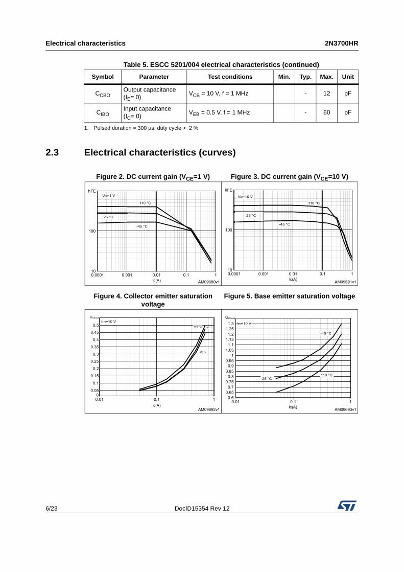
2.3 Electrical characteristics (curves)
CCBOOutput capacitance (IE= 0)
VCB = 10 V, f = 1 MHz - 12 pF
CIBOInput capacitance (IC= 0)
VEB = 0.5 V, f = 1 MHz - 60 pF
1. Pulsed duration = 300 µs, duty cycle > 2 %
Table 5. ESCC 5201/004 electrical characteristics (continued)
Symbol Parameter Test conditions Min. Typ. Max. Unit
Figure 2. DC current gain (VCE=1 V) Figure 3. DC current gain (VCE=10 V)
Figure 4. Collector emitter saturation voltage
Figure 5. Base emitter saturation voltage

DocID15354 Rev 12 7/23
2N3700HR Electrical characteristics
23
2.4 Test circuits
Figure 6. JANS non saturated switching-time test circuit
1.NOTES:
2.
The rise time (tr) of the applied pulse shall be ≤ 2.0 ns, duty cycle ≤ 2 percent and thegenerator source impedance shall be 50 ohms.Sampling oscilloscope: ZIN ≥ 100 kΩ, CIN ≤ 12 pF, rise time ≤ 2.0 ns.
+18 V
Gipd040620131551FSR

Electrical characteristics 2N3700HR
8/23 DocID15354 Rev 12
Figure 7. ESCC resistive load switching test circuit
1. Fast electronic switch
2. Non-inductive resistor

DocID15354 Rev 12 9/23
2N3700HR Radiation hardness assurance
23
3 Radiation hardness assurance
The products guaranteed in radiation within the JANS system fully comply with the MIL-PRF-19500/255 specification.
The products guaranteed in radiation within the ESCC system fully comply with the ESCC 5201/004 and ESCC 22900 specifications.
JANS radiation assurance
ST JANS parts guaranteed at 100 krad (Si), tested, in full compliancy with the MIL-PRF-19500 specification, specifically the Group D, subgroup 2 inspection, between 50 and 300 rad/s. On top of the standard JANSR high dose rate by wafer lot guarantee, ST 2N3700HR series include an additional wafer by wafer 100 krad Low dose rate guarantee at 0.1 rad/s, identical to the ESCC 100 krad guarantee. It is supported with the same Radiation Verification Test report provided with each shipment. A brief summary of the standard High Dose Rate by wafer lot JANSR guarantee is provided below:
• All test are performed in accordance to MIL-PRF-19500 and test method 1019 of MIL-STD-750 for total Ionizing dose.
• The table below provides for each monitored parameters of the test conditions and the acceptance criteria.
Table 6. MIL-PRF-19500 (test method 1019) post radiation electrical characteristics
Symbol Parameter Test conditions Min. Typ. Max. Unit
ICBOCollector cut-off current (IE = 0)
VCB = 140 V - 20 µA
ICESCollector-emitter cut-off current
VCE = 90 V - 20 nA
IEBOEmitter cut-off current(IC = 0)
VEB = 5 VVEB = 7 V
-2020
nAµA
V(BR)CEO
Collector-emitter breakdown voltage(IB = 0)
IC = 30 mA - 80 V
VCE(sat) Collector-emitter saturation voltage
IC = 150 mA IB = 15 mAIC = 500 mA IB = 50 mA
-0.230.58
VV
VBE(sat)Base-emitter saturation voltage
IC = 150 mA IB = 15 mA - 1.1 V
[hFE] Post irradiation gain calculation
IC = 150 mA VCE = 10 V [50](1)
1. See method 1019 of MIL-STD-750 for how to determine [hFE] by first calculating the delta (1/hFE) from the pre- and post-radiation hFE. Notice the [hFE] is not the same as hFE and cannot be measured directly. The [hFE] value can never exceed the pre-radiation minimum hFE that it is based upon.
- 300
IC = 0.1 mA VCE = 10 V [25](1) - 200
IC = 10 mA VCE = 10 V [45](1) -
IC = 500 mA VCE = 10 V [25](1) - 200
IC = 1.0 A VCE = 10 V [7.5](1) -

Radiation hardness assurance 2N3700HR
10/23 DocID15354 Rev 12
ESCC radiation assurance
Each product lot is tested according to the ESCC basic specification 22900, with a minimum of 11 samples per diffusion lot and 5 samples per wafer, one sample being kept as unirradiated sample, all of them being fully compliant with the applicable ESCC generic and/or detailed specification.
ST goes beyond the ESCC specification by performing the following procedure:
• Test of 11 pieces by wafer, 5 biased at least 80% of V(BR)CEO, 5 unbiased and 1 kept for reference
• Irradiation at 0.1 rad (Si)/s
• Acceptance criteria of each individual wafer if as 100 krad guaranteed if all 10 samples comply with the post radiation electrical characteristics provided in Table 7: ESCC 5201/004 post radiation electrical characteristics
• Delivery together with the parts of the radiation verification test (RVT) report of the particular wafer used to manufacture the products. This RVT includes the value of each parameter at 30, 50, 70 and 100 krad (Si) and after 24 hour annealing at room temperature and after an additional 168 hour annealing at 100°C.
Table 7. ESCC 5201/004 post radiation electrical characteristics
Symbol Parameter Test conditions Min. Typ. Max. Unit
ICBOCollector cut-off current (IE = 0)
VCB = 90 V - 10 nA
IEBOEmitter cut-off current(IC = 0)
VEB = 5 V - 10 nA
V(BR)CBO
Collector-base breakdown voltage(IE = 0)
IC = 100 µA 140 - V
V(BR)CEO(1)
1. Pulsed duration = 300 µs, duty cycle > 2 %
Collector-emitter breakdown voltage
(IB = 0)IC = 30 mA 80 - V
V(BR)EBO
Emitter-base breakdown voltage(IC = 0)
IE = 100 µA 7 - V
VCE(sat) (1) Collector-emitter
saturation voltageIC = 150 mA IB = 15 mAIC = 500 mA IB = 50 mA
-0.20.5
VV
VBE(sat) (1) Base-emitter
saturation voltageIC = 150 mA IB = 15 mA - 1 V
[hFE] (1) Post irradiation gain
calculation (2)
2. The post-irradiation gain calculation of [hFE], made using hFE measurements from prior to and on completion of irradiation testing and after each annealing step if any, shall be as specified in MILSTD-750 method 1019.
IC = 10 mA VCE = 10 VIC = 150 mA VCE = 10 VIC = 500 mA VCE = 10 V
[45][50][25]
-[300]

DocID15354 Rev 12 11/23
2N3700HR Radiation hardness assurance
23
Table 8. Radiation summary
Radiation test 100 krad ESCC
Wafer tested each
Part tested 5 biased + 5 unbiased
Dose rate 0.1 rad/s
Acceptance MIL-STD-750 method 1019
Displacement damage Optional
Agency part number (ex) 5202/001/04R (1)
1. Example of the 2N3700 in LCC-3 gold finish.
ST part number (ex) SOC3700RHRG
Documents CoC +RVT
Package information 2N3700HR
12/23 DocID15354 Rev 12
4 Package information
In order to meet environmental requirements, ST offers these devices in different grades of ECOPACK® packages, depending on their level of environmental compliance. ECOPACK® specifications, grade definitions and product status are available at: www.st.com. ECOPACK® is an ST trademark.
DocID15354 Rev 12 13/23
2N3700HR Package information
23
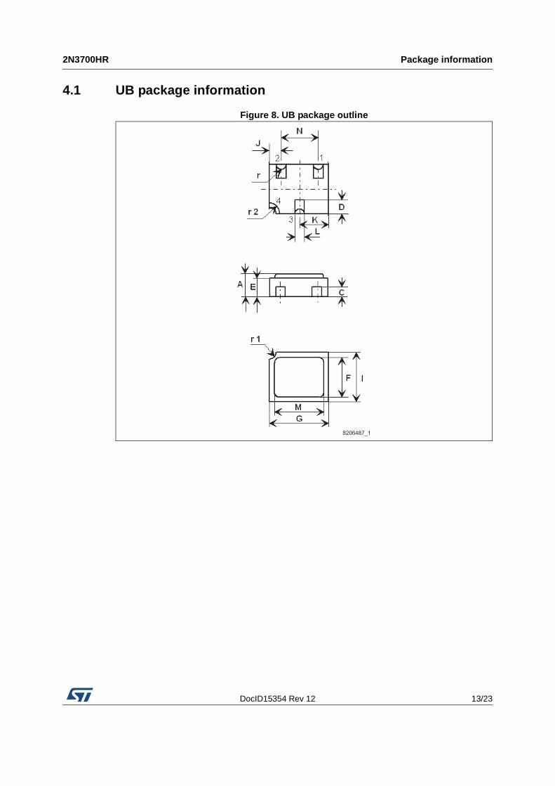
4.1 UB package information
Figure 8. UB package outline
8206487_1

Package information 2N3700HR
14/23 DocID15354 Rev 12
Table 9. UB package mechanical data
Dim.mm.
Min. Typ. Max.
A 1.16 1.42
C 0.46 0.51 0.56
D 0.56 0.76 0.96
E 0.92 1.02 1.12
F 1.95 2.03 2.11
G 2.92 3.05 3.18
I 2.41 2.54 2.67
J 0.42 0.57 0.72
K 1.37 1.52 1.67
L 0.41 0.51 0.61
M 2.46 2.54 2.62
N 1.81 1.91 2.01
r 0.20
r1 0.30
r2 0.56

DocID15354 Rev 12 15/23
2N3700HR Package information
23
4.2 LCC-3 package information
Figure 9. LCC-3 package outline
2 1
3
N
0041211_12

Package information 2N3700HR
16/23 DocID15354 Rev 12
Table 10. LCC-3 package mechanical data
Dim.mm.
Min. Typ. Max.
A 1.16 1.42
C 0.45 0.50 0.56
D 0.60 0.76 0.91
E 0.91 1.01 1.12
F 1.95 2.03 2.11
G 2.92 3.05 3.17
I 2.41 2.54 2.66
J 0.42 0.57 0.72
K 1.37 1.52 1.67
L 0.40 0.50 0.60
M 2.46 2.54 2.62
N 1.80 1.90 2.00
R 0.30

DocID15354 Rev 12 17/23
2N3700HR Package information
23
4.3 TO-18 package information
Figure 10. TO-18 package outline

Package information 2N3700HR
18/23 DocID15354 Rev 12
Table 11. TO-18 mechanical data
Dim.mm.
Min. Typ. Max.
A 12.70 13.20 14.20
B 0.41 0.45 0.48
C 0.36 0.47
D 4.88 5.33
E 4.63 4.70
F 5.31 5.45
G 2.49 2.54 2.59
H 0.80 0.90 1.00
I 0.95 1.00 1.05
L 42° 45° 48°

2N3700H
RO
rder co
des
DocID
15354 Rev 12
19/23
5 Order codes
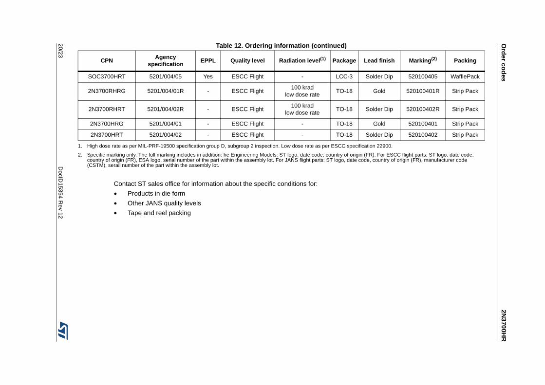
Table 12. Ordering information
CPNAgency
specificationEPPL Quality level Radiation level(1) Package Lead finish Marking(2) Packing
J2N3700UB1 - -Engineering model
JANS- UB Gold J3700UB1 WafflePack
2N3700UB1 - -Engineering model
ESCC- UB Gold 2N3700UB1 WafflePack
SOC37001 - -Engineering model
ESCC- LCC-3 Gold SOC37001 WafflePack
JANSR2N3700UBG MIL-PRF-19500/391 - JANSR100 krad
high and low dose rate
UB Gold JSR3700 WafflePack
JANSR2N3700UBT MIL-PRF-19500/391 - JANSR100 krad
high and low dose rate
UB Solder Dip JSR3700 WafflePack
JANS2N3700UBG MIL-PRF-19500/391 - JANS - UB Gold JS3700 WafflePack
JANS2N3700UBT MIL-PRF-19500/391 - JANS - UB Solder Dip JS3700 WafflePack
2N3700RUBG 5201/004/06R Target ESCC Flight100 krad
low dose rateUB Gold 520100406R WafflePack
2N3700RUBT 5201/004/07R Target ESCC Flight100 krad
low dose rateUB Solder Dip 520100407R WafflePack
2N3700UBG 5201/004/06 Target ESCC Flight - UB Gold 520100406 WafflePack
2N3700UBT 5201/004/07 Target ESCC Flight - UB Solder Dip 520100407 WafflePack
SOC3700RHRG 5201/004/04R Yes ESCC Flight100 krad
low dose rateLCC-3 Gold 520100404R WafflePack
SOC3700RHRT 5201/004/05R Yes ESCC Flight100 krad
low dose rateLCC-3 Solder Dip 520100405R WafflePack
SOC3700HRG 5201/004/04 Yes ESCC Flight - LCC-3 Gold 520100404 WafflePack
Ord
er cod
es2N
3700HR
20/23D
ocID15354 R
ev 12
Contact ST sales office for information about the specific conditions for:
• Products in die form
• Other JANS quality levels
• Tape and reel packing
SOC3700HRT 5201/004/05 Yes ESCC Flight - LCC-3 Solder Dip 520100405 WafflePack
2N3700RHRG 5201/004/01R - ESCC Flight100 krad
low dose rateTO-18 Gold 520100401R Strip Pack
2N3700RHRT 5201/004/02R - ESCC Flight100 krad
low dose rateTO-18 Solder Dip 520100402R Strip Pack
2N3700HRG 5201/004/01 - ESCC Flight - TO-18 Gold 520100401 Strip Pack
2N3700HRT 5201/004/02 - ESCC Flight - TO-18 Solder Dip 520100402 Strip Pack
1. High dose rate as per MIL-PRF-19500 specification group D, subgroup 2 inspection. Low dose rate as per ESCC specification 22900.
2. Specific marking only. The full marking includes in addition: he Engineering Models: ST logo, date code; country of origin (FR). For ESCC flight parts: ST logo, date code, country of origin (FR), ESA logo, serial number of the part within the assembly lot. For JANS flight parts: ST logo, date code, country of origin (FR), manufacturer code (CSTM), serail number of the part within the assembly lot.
Table 12. Ordering information (continued)
CPNAgency
specificationEPPL Quality level Radiation level(1) Package Lead finish Marking(2) Packing

DocID15354 Rev 12 21/23
2N3700HR Shipping details
23
6 Shipping details
6.1 Date codeData code xyywwz is structured as described below:
6.2 Documentation
Table 13. Date code
x yy ww z
EM (ESCC and JANS)
3
last two digits of the year
week digitslot index in the
weekESCC flight -
JANS flight (diffused in Singapore)
W
Table 14. Documentation provided for each type of product
Quality level Radiation level Documentation
Engineering model - -
JANS Flight - Certificate of conformance
JANSR Flight
MIL-STD 100kradCertificate of conformance 50 rad/s radiation verification test report
ST 100KradCertificate of conformance 0.1 rad/s radiation verification test report on each wafer
ESCC Flight
- Certificate of conformance
100 krad Certificate of conformance
0.1 rad/s radiation verification test report
Revision history 2N3700HR
22/23 DocID15354 Rev 12
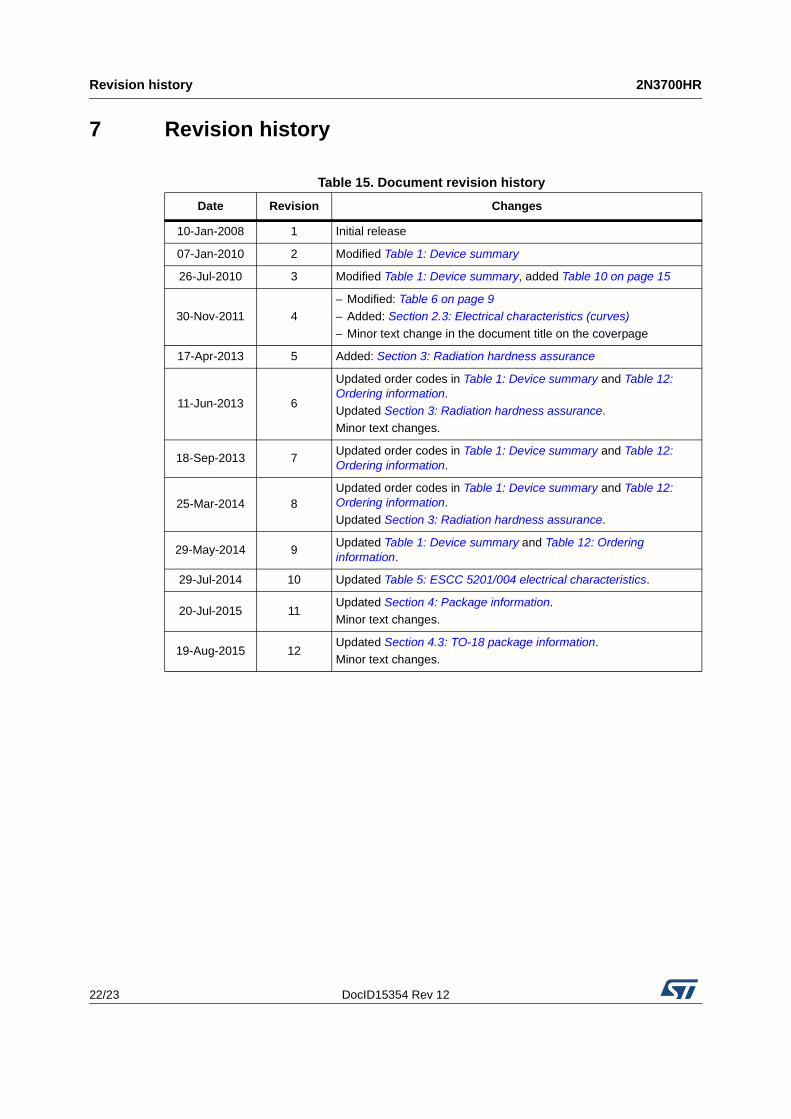
7 Revision history
Table 15. Document revision history
Date Revision Changes
10-Jan-2008 1 Initial release
07-Jan-2010 2 Modified Table 1: Device summary
26-Jul-2010 3 Modified Table 1: Device summary, added Table 10 on page 15
30-Nov-2011 4– Modified: Table 6 on page 9– Added: Section 2.3: Electrical characteristics (curves)
– Minor text change in the document title on the coverpage
17-Apr-2013 5 Added: Section 3: Radiation hardness assurance
11-Jun-2013 6
Updated order codes in Table 1: Device summary and Table 12: Ordering information.Updated Section 3: Radiation hardness assurance.Minor text changes.
18-Sep-2013 7Updated order codes in Table 1: Device summary and Table 12: Ordering information.
25-Mar-2014 8Updated order codes in Table 1: Device summary and Table 12: Ordering information.Updated Section 3: Radiation hardness assurance.
29-May-2014 9Updated Table 1: Device summary and Table 12: Ordering information.
29-Jul-2014 10 Updated Table 5: ESCC 5201/004 electrical characteristics.
20-Jul-2015 11Updated Section 4: Package information.Minor text changes.
19-Aug-2015 12Updated Section 4.3: TO-18 package information.Minor text changes.

DocID15354 Rev 12 23/23
2N3700HR
23
IMPORTANT NOTICE – PLEASE READ CAREFULLY
STMicroelectronics NV and its subsidiaries (“ST”) reserve the right to make changes, corrections, enhancements, modifications, and improvements to ST products and/or to this document at any time without notice. Purchasers should obtain the latest relevant information on ST products before placing orders. ST products are sold pursuant to ST’s terms and conditions of sale in place at the time of order acknowledgement.
Purchasers are solely responsible for the choice, selection, and use of ST products and ST assumes no liability for application assistance or the design of Purchasers’ products.
No license, express or implied, to any intellectual property right is granted by ST herein.
Resale of ST products with provisions different from the information set forth herein shall void any warranty granted by ST for such product.
ST and the ST logo are trademarks of ST. All other product or service names are the property of their respective owners.
Information in this document supersedes and replaces information previously supplied in any prior versions of this document.
© 2015 STMicroelectronics – All rights reserved