Embed Size (px)
Citation preview
HAL Id: tel-00744846https://tel.archives-ouvertes.fr/tel-00744846
Submitted on 24 Oct 2012
HAL is a multi-disciplinary open accessarchive for the deposit and dissemination of sci-entific research documents, whether they are pub-lished or not. The documents may come fromteaching and research institutions in France orabroad, or from public or private research centers.
L’archive ouverte pluridisciplinaire HAL, estdestinée au dépôt et à la diffusion de documentsscientifiques de niveau recherche, publiés ou non,émanant des établissements d’enseignement et derecherche français ou étrangers, des laboratoirespublics ou privés.
Heavy metal ion sensors based on organic microcavitylasers
Sergii Lozenko
To cite this version:Sergii Lozenko. Heavy metal ion sensors based on organic microcavity lasers. Other [cond-mat.other].École normale supérieure de Cachan - ENS Cachan, 2011. English. �NNT : 2011DENS0045�. �tel-00744846�
""
ENSC-2011 N° 285
THESE DE DOCTORAT
DE L!ECOLE NORMALE SUPERIEURE DE CACHAN
Présentée par
Sergii LOZENKO
pour obtenir le grade de
DOCTEUR DE L!ECOLE NORMALE SUPERIEURE DE CACHAN
Domaine :
SCIENCES PHYSIQUES
Sujet de la thèse :
Heavy metal ion sensors based on organic microcavity lasers
Thèse présentée et soutenue à Cachan le 04/11/2011 devant le jury composé de : GAVIOT Etienne Professeur (L!Université du Maine) Président CHEN Yong Directeur de Recherches (ENS) Rapporteur BENISTY Henri Professeur (IOGS) Rapporteur BLAU Werner Professeur (Trinity College Dublin) Examinateur LERAY Isabelle Directrice de Recherches (ENSC) Examinatrice LEBENTAL Melanie Maître de Conférences (ENSC) Directrice de thèse ZYSS Joseph Professeur (ENSC) Directeur de thèse
Laboratoire de Photonique Quantique et Moleculaire ENS CACHAN/CNRS/UMR 8537 61, avenue du Président Wilson, 94235 CACHAN CEDEX (France)

""
""
Abstract""
Monitoring of environmental pollutants present at low concentrations requires creation of
miniature, low-cost, and highly sensitive detectors that are capable to specifically identify target
substances. In this thesis, a detection approach based on refractive index sensing with polymer
micro-lasers is proposed and its application to the detection of heavy metal pollutants in water
(mercury � Hg2+
, cadmium � Cd2+
and lead � Pb2+
) is studied. The resonance frequencies of the
microcavity are highly sensitive to the refractive indices of the resonator surrounding: the
resonances shift by a small amount when the surface refractive index changes, resulting from the
interaction of the mode evanescent field with the surrounding medium. This permits label-free
detection by coating the resonator with a suitable recognition species.
The originality of this work lies in the utilization of active microcavities, or microlasers,
created of the dye-doped polymers. Active microcavities offer an enhanced signal/noise ratio as
compared to the passive ones and very narrow resonance peaks even at moderate quality factors
(Q œ 6000). The choice of polymers as an active medium is connected with a number of
advantages they offer: as opposite to semiconductors, polymers can be easily functionalized,
integrated in microfluidic circuits and are cheaper in processing. Moreover, the use of porous
polymer matrices may allow accumulation of analyte ions inside the microcavity and thus
enhance the sensitivity.
Two possible applications of microlasers are investigated in the thesis: refractive index
variation sensing with non-functionalized cavities and heavy metal ion detection with
functionalized cavities. In the first case, the sensitivity values have been obtained, comparable
with the reported in literature for planar passive microresonators. In the second case, the
experimental proofs of specific detection of mercury ions in liquid at 10-6
M concentration are
presented. The ways of sensitivity improvement are discussed and verified and a foundation is
layed for the creation of integrated Lab-on-Chip microfluidic biochemical detector.
""
Resume""
Le contrôle des polluants environnementaux présents à faible concentration a conduit à la
création de détecteurs miniaturisés, à bas coûts et ultra-sensibles, capables d�identifier
spécifiquement certaines substances. Dans cette thèse, la méthode de détection explorée repose
sur la sensibilité de micro-lasers polymères à une variation d�indice de réfraction. Cette approche
a été mise en application pour détecter des métaux lourds (mercure � Hg2+
, cadmium � Cd2+
et
plomb � Pb2+
) dans l�eau potable. En effet les fréquences de résonance de ces micro-cavités sont
particulièrement sensibles à l�indice de réfraction du milieu extérieur et se déplacent lorsque
celui-ci est modifié. Ce système permet ainsi une détection sans marqueur (« label ») en
recouvrant la cavité d�une couche de reconnaissance spécifique de l�espèce recherchée.
L�originalité de ce travail repose sur l�utilisation de micro-cavités actives, ou micro-lasers,
fabriquées avec des polymères dopés par des colorants lasers. En effet les micro-lasers
permettent d�augmenter le rapport signal/bruit et de profiter de pics de résonance étroits, même
pour des facteurs de qualité de l�ordre de quelques milliers seulement. Le choix de matériaux
organiques comme milieu à gain a été dicté par les nombreux avantages qu�ils offrent.
Contrairement aux semi-conducteurs inorganiques, les polymères peuvent être fonctionnalisés de
manière relativement aisée et l�utilisation de matériaux poreux devrait augmenter la sensibilité
en faisant circuler le fluide à tester à l�intérieur même du résonateur. De plus le protocole de
fabrication des micro-lasers organiques reste d�un coût modéré et permet une intégration aisée en
micro-fluidique.
Deux voies différentes ont été explorées dans cette thèse : détection d�une variation d�indice
de réfraction avec des cavités non-fonctionnalisées et détection d�ions lourds avec des cavités
fonctionnalisées. Dans le premier cas, la sensibilité obtenue est comparable à ce qui est publié
pour des micro-résonateurs passifs. Dans le second cas, nous avons réussi à mettre en évidence la
présence d�ions mercure jusqu�à 10-6
M. Quelques approches ont été envisagées pour diminuer
encore le seuil de détection dont certaines ont été vérifiées expérimentalement. Ainsi, cette étude
propose un prototype de composant sur puce pour la détection d�espèces chimiques ou
biologiques."
""
Acknowledgments""
First of all I would like to thank my advisors � Melanie Lebental and Joseph Zyss for
offering me this interesting research subject at LPQM and d�Alembert Institute. I thank Joseph
Zyss for all the fruitful and enriching discussions, which helped to advance the work. I owe to
Melanie Lebental, for guiding me through with patience and enthusiasm, giving hints if the work
seemed to reach a deadlock and encouraging when the success seemed within a step away.
I would like also to express my gratitude to Henri Benisty and Yong Chen, who have
accepted to be my referees, to read and evaluate my manuscript, as well as to Etienne Gaviot, the
chair of the jury, Werner Blau, who made a long trip to be at my defense and Isabelle Leray.
I can�t but thank my colleagues-chemists from PPSM department � Isabelle Leray,
Jacques Delaire, Jean-Pierre Lefevre, Djibril Faye, Emma and Cylia who greatly helped me in
this interdisciplinary domain. Their experience, support, participation and devotion brought me
to where I am now in this research and let me accomplish my thesis. I thank as well Isabelle
Ledoux, the head of LPQM department, always ready to help and advice in any situation.
I should mention also Christian Ulysse from LPN laboratory for his precious contribution
- e-beam fabrication of microcavities, and Joseph Lautru for managing the clean-room of ENS
Cachan and providing technological support. I thank also the administration of LPQM and
d�Alembert Institute.
At last (which is not the least) I would like to thank all my colleagues of LPQM and
PPSM departments who contributed to the creative and friendly atmosphere which is
indispensable for work and life. I thank Nadia Djellali, Iryna Gozhyk, Clement Lafargue,
Bassam Hajj, Marcin Zielinski, Camille Delezoide and everyone else who made these three years
of life an unforgettable experience.
" "

"
""
"
"
""
Table"of"Contents""
"I."General"Introduction"................................................................................................................................"1"
Introduction"..............................................................................................................................................."2"1.1." Motivation"and"scientific"interest."................................................................................................ "3"1.2." Approaches"to"chemicalど"and"bioど"sensing.".................................................................................."4"
1.2.1." Sensor"performance".............................................................................................................."6"
II."Theoretical"basics"....................................................................................................................................."9"
2.1." Planar"waveguides"and"cavities..................................................................................................."10"2.1.1." Ray"optics"approach"............................................................................................................"11"2.1.2." Wave"approach.".................................................................................................................."12"
2.2." Dielectric"cavities."....................................................................................................................... "15"2.2.1." Cavity"characteristics.".........................................................................................................."15"2.2.2." Whispering"Gallery"Modes".................................................................................................. "17"
2.3." Active"cavities".............................................................................................................................. "18"2.3.1." Experimental"setup"for"spectra"recording."........................................................................."19"2.3.2." Experimental"data"treatment".............................................................................................. "20"2.3.3." Polarization"influence."........................................................................................................."22"
III."Technology:"creating"a"microlaser"........................................................................................................"25"
3.1." Materials:"polymers"and"dyes.".................................................................................................... "26"3.2." Material"characterization:"Amplified"Spontaneous"Emission"and"ellipsometry."........................"28"3.3." Materials:"choice"of"a"laser"dye.".................................................................................................. "29"3.4." Microcavity"fabrication"technology."........................................................................................... "31"
3.4.1." Photolithography."................................................................................................................"32"3.4.2." Eどbeam"lithography."............................................................................................................"33"3.4.3." Fabrication"by"laser"ablation"and"2どphoton"polymerization.".............................................."34"
3.5." Alternative"cavity"geometry."......................................................................................................."36"3.5.1." Transparent"quartz"substrate."............................................................................................. "36"3.5.2." Pedestal"cavities."................................................................................................................."36"3.5.3." Lowどindex"substrate"cavities."Pillar"cavities."......................................................................."38"3.5.4." Allどpolymer"pedestal"cavities."............................................................................................. "39"
IV."Microlaser"as"a"refractive"index"sensor."............................................................................................... "43"
4.1." Principle"of"refractive"index"change"detection.".........................................................................."44"4.2." Designing"a"microfluidic"chip."..................................................................................................... "46"4.3." Sensing"selectivity:"specific"ligand"grafting."................................................................................"51"4.4." Sensing"and"various"cavity"shapes."Choice"of"the"optimal"shape.".............................................."56"
4.4.1." Factors"influencing"sensitivity"to"refractive"index"variation.".............................................."57"4.4.2." Optimal"cavity"shape"..........................................................................................................."63"
4.5." Experimental"proof"of"RI"variation"sensing"and"heavy"metal"ions"detection."............................"68"4.5.1." First"measurements"of"lasing"spectra"in"liquids."................................................................."68"4.5.2." Refractive"index"variation:"preparation"of"sample"solutions"and"first"attempts."..............."69"

"
""
4.5.3." Proof"of"RI"variation"sensing"principle."..............................................................................."70"4.5.4." Temperature"Influence"......................................................................................................."76"
4.6." Detection"of"heavyどmetal"ions"with"microcavity"sensors.".........................................................."77"
V."Pedestal"microcavities"........................................................................................................................... "81"
5.1." Plane"substrate"vs"pedestal."......................................................................................................."82"5.1.1." Vertical"modes."..................................................................................................................."83"
5.2." Pedestal"influence"on"emission"properties."..............................................................................."86"5.2.1." Enhanced"intensity"and"lower"lasing"threshold."................................................................."86"5.2.2." Explanation"with"numerical"simulations............................................................................."87"5.2.3." New"spectral"features:"disk"and"square"microcavities."......................................................"89"5.2.4." Hotどspots"and"angular"emission"diagrams."........................................................................"91"
5.3." Pedestal"influence"on"sensitivity."............................................................................................... "93"5.3.1." Effective"refractive"index"in"pedestal"geometry."................................................................"94"5.3.2." Sensitivity"of"a"FabryどPerot"cavity"...................................................................................... "96"5.3.3." Sensitivity"of"stadiumどshaped"cavities."..............................................................................."97"
5.4." Refractive"index"variation"sensing"with"pedestal"cavities."........................................................."99"5.5." Detection"of"heavyどmetal"ions"with"pedestal"microcavity"sensor.".........................................."100"5.6." Pillar"microcavities"on"lowどindex"substrate".............................................................................."102"
5.6.1." Pillar"vs"silica"substrate"cavities."....................................................................................... "102"5.6.2." Refractive"index"variation"sensing"with"pillar"microacvities."..........................................."104"
Conclusions".............................................................................................................................................."107"
Annex"1."Numerical"simulations."............................................................................................................."109"
1." FDTD"simulations."....................................................................................................................."109"2." Finite"Element"Method."............................................................................................................"116"
"
" "

"
""
" "

"
""
"
"

Chapter"I"�"General"Introduction"
1""
1. Chapter"I"""
General Introduction
"
"Introduction"..............................................................................................................................................."2"1.1." Motivation"and"scientific"interest."................................................................................................ "3"1.2." Approaches"to"chemicalど"and"bioど"sensing.".................................................................................."4"
1.2.1." Sensor"performance".............................................................................................................."6"
""
"
" "
Chapter"I"�"General"Introduction"
2""
Introduction
"
The subject of this PhD thesis lies at the interface of two rapidly and extensively developing
domains of research and technology: photonics and Lab-on-Chips. The term photonics, which
appeared initially in 1960s-1970s with the development of semiconductor light emitters and
optical fibers nowadays generalizes the research on emission, generation, transmission and
detection of light as well as utilization of light in the areas traditionally occupied by electronics,
such as signal processing and data transfer. From the research of distinct functional elements:
laser diodes, optical fibers, light detectors photonics evolved into an area embracing complex,
all-optical signal processing systems. That�s why the term photonics is sometimes used as an
analogy to term electronics. Optical signal transfer and amplification systems has already
become a reality since 1980s with the invention of erbium-doped fibers, while nowadays
numerous (and fruitful) investigations are carried out to create all-optical binary logic elements
[1-3], optical memory [4-7] and, by analogy with electronic integrated circuits, optical integrated
circuits [8-11].
The second broad domain of research, widely known as Lab-on-Chips, focuses on the
development and integration on a single substrate of miniaturized devices that possess broad
functionality that would typically require an entire biological laboratory [12, 13]. Through a
network of microfluidic channels very small volumes (micro- to nanoliters) of biological
samples can be transported, mixed, separated, and analyzed with significant advantages in terms
of high sensitivity, speed of analysis, low sample and reagent consumption, and measurement
automation and standardization. Applications of LOCs may range from chemical synthesis and
drug developments [14] to environmental monitoring and detection of chemical and biological
threats.
The present thesis was performed within the �microFLUID� project (THEME ICT-
2007.3.6) which is a part of the 7th
Framework Programme, supported by the European
Comission. The aim of the project is creation of polymeric Lab-on-Chips for bio- and chemical
sensing purposes using femtosecond laser processing. The main goal of our work is the
development of a prototype of a sensor based on polymer microlasers that is able to detect
heavy-metal ions in water for environmental monitoring purposes.
The choice of polymeric materials for the microlaser fabrication is based on a number of
considerations. First of all, many polymeric materials, as opposite to semiconductors, can be
easily functionalized biochemically in order to attach target biomolecules for specific
detection. At the same time they are perfectly compatible with microfluidics thus allowing
excellent optofluidic integration of chemical and bio-sensors [15-19]. The second reason is that
polymers possess the advantage of low┽cost mass production owing to different technological
processes of fabrication that we will use and discuss in this thesis. Due to their intrinsic
physic┽chemical properties they offer many advantages for processing and conditioning in
comparison with inorganic materials. Techniques like molding or nanoimprint lithography [20-
24] may be applied to fabricate polymer structures, which ensure high throughput and resolution
at low fabrication cost, impossible with semiconductor microstructures. Polymers are also
compatible with mass-production using traditional UV lithography technique. It should be noted
however that the lithography utilized for polymer┽based photonic devices fabrication, although
Chapter"I"�"General"Introduction"
3""
directly derived from that of semiconductor fabrication technology, does not require heavy
and expensive equipment. In this thesis, novel approaches to fabrication of microcavities, like
laser ablation and 2-photon polymerization will also be considered. Another advantage is a large
possibility of integration with different inorganic materials such as semiconductor, glass, sol┽gel,
ceramics [25], thus allowing simple construction of lab┽on┽chip for biochemical sensing
applications. Finally, the third reason is the low refractive index of polymers resulting in low
scattering loss on optical waveguide surfaces and in efficient coupling between these
waveguides and optical fibers. Though in this project we didn�t utilize the waveguides, we
foresee the possibility of their integration in LOCs to collect the emission of microlasers.
The sensing principle that we implement is detection of the wavelength shift 〉そ in the lasing
spectrum due to the influence of the refractive index change 〉n of the medium surrounding the
cavity. Generally, we may mark out two possible applications of microcavities as sensors. The
first one is the refractive index variation sensing with non-functionalized cavities. In this case it
is desirable to achieve the maximum possible spectral shift in response to the variation of index
of the surrounding medium. The second one is the detection of analyte molecules with
functionalized cavities. In the ideal case, the spectral shift should be observed only when the
analyte molecules are bound by specific ligands and cavity spectrum should not be sensitive to
the refractive index of the liquid carrying the molecules that we want to detect. However as the
sensitivity to the analyte molecules is usually interconnected with the sensitivity to the bulk
refractive index variation, a correct reference should be carefully chosen in the sensing
experiments.
The thesis is split over 5 chapters. In this first chapter the general introduction is given, the
motivation and novelty of the work are explained and a short review of the principles of sensor
functioning and the state of art is presented. The second chapter introduces the theoretical ground
necessary for understanding the work. In the last three chapters the original results obtained
within the thesis are presented. Chapter 3 is entirely devoted to the technological aspects and
explains the properties of the chosen materials and process of fabrication of microcavities. In the
chapter 4 we talk about the sensing principle employed in this thesis, the design of microfluidic
circuits, various aspects that influence the sensitivity of the cavity to refractive index variation.
Experimental results of refractive index variation sensing and mercury detection in water are
presented in this chapter. Chapter 5 is devoted to the novel cavity architectures � pedestal and
pillar cavities � which are introduced in chapters 3 and 4. Experimental proofs of enhanced
sensitivity of these cavity types are presented at the end of the chapter and their advantages and
drawbacks are discussed. The descriptions of numerical simulations performed within the thesis
are postponed to the Annex 1.
1.1. Motivation"and"scientific"interest."
Screening of water for contamination is a very important task for preserving the
environment and improving human health. Mercury (Hg2+
), cadmium (Cd2+
) and lead (Pb2+
) are
the most toxic heavy metal ions, causing adverse environmental and health problems as they are
responsible for a wide variety of diseases [26-29]. The release of these detrimental ions into the
environment originates from numerous natural and man-made sources, such as fossil fuel
combustion and the electronic industry. For these reasons, the level of heavy metal ions in
drinking water is the object of strict health official norms and must not exceed 1たg/L for Hg2+
,
Chapter"I"�"General"Introduction"
4""
10たg/L for Pb2+
and 5たg/L for Cd2+
[30]. While sophisticated analytical techniques (atomic
absorption or atomic emission spectroscopies for instance) are currently used in applications
relevant to environmental contamination, there is still a significant need to provide inexpensive
and real-time monitoring methods that can detect the presence and, preferably, concentration of
pollutants. There exist only rare examples of mobile sensors for heavy metal detection based on
electrochemical techniques [31] such as ion┽selective electrodes and voltammetry and some
optical/colorimetric methods [32, 33]. The advantage of a portable Lab-on-Chip system becomes
obvious, as it may allow performing in-field analyses also by not-specialized personnel with
reduction of time and cost of the analysis and use a small quantity of reagents to perform the
tests.
Historically, the research in active polymer microcavities or microlasers is one of the main
research directions of LPQM laboratory (Laboratoire de Photonique Quantique et Moleculaire)
of ENS de Cachan. Alongside with fundamental aspects and experimental study of the cavity
emission properties [34, 35] various practical applications of microlasers are being investigated.
In my thesis, we explore the applications of the microcavity lasers to bio- or chemical sensing.
As it has been demonstrated in the theses of my perdecessors, the relatively high quality factors
(œ6000) in such resonators lead to very narrow resonances. We expect the resonance frequencies
to be highly sensitive to the refractive indices of the resonator and surroundings: the resonances
will shift by a small amount when the surface refractive index changes, resulting from the
interaction of the mode evanescent field with the surrounding medium. This permits label-free
detection [36] by either coating the resonator with a suitable recognition species or by making
the microresonator from a species-selective material such as a molecularly-imprinted polymer
(MIP). Moreover, the integration of optical sensing in microfluidic Lab-on-Chips will
significantly increase the device compactness and portability.
1.2. Approaches"to"chemical┽"and"bio┽"sensing."
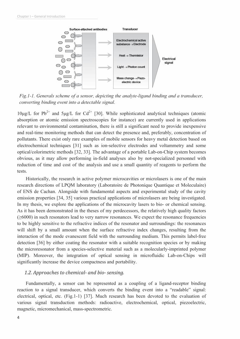
Fundamentally, a sensor can be represented as a coupling of a ligand-receptor binding
reaction to a signal transducer, which converts the binding event into a �readable� signal:
electrical, optical, etc. (Fig.1-1) [37]. Much research has been devoted to the evaluation of
various signal transduction methods: radioactive, electrochemical, optical, piezoelectric,
magnetic, micromechanical, mass-spectrometric.
Fig.1-1. Generals scheme of a sensor, depicting the analyte-ligand binding and a transducer,
converting binding event into a detectable signal.
Chapter"I"�"General"Introduction"
5""
Among the advantages of optical sensors is the
sensitivity, real-time detection of biomolecular
interactions and simplicity of response
interpretation allow them to be applied widely.
Optical sensing techniques are based on various
sensing transduction mechanisms, for example,
chemiluminescence, fluorescence, light absorption
and scattering, reflectance, surface plasmon
resonance (SPR) and Raman scattering. A very
wide-spread approach in optical sensing is based on
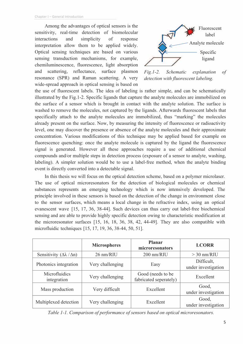
the use of fluorescent labels. The idea of labeling is rather simple, and can be schematically
illustrated by the Fig.1-2. Specific ligands that capture the analyte molecules are immobilized on
the surface of a sensor which is brought in contact with the analyte solution. The surface is
washed to remove the molecules, not captured by the ligands. Afterwards fluorescent labels that
specifically attach to the analyte molecules are immobilized, thus �marking� the molecules
already present on the surface. Now, by measuring the intensity of fluorescence or radioactivity
level, one may discover the presence or absence of the analyte molecules and their approximate
concentration. Various modifications of this technique may be applied based for example on
fluorescence quenching: once the analyte molecule is captured by the ligand the fluorescence
signal is generated. However all these approaches require a use of additional chemical
compounds and/or multiple steps in detection process (exposure of a sensor to analyte, washing,
labeling). A simpler solution would be to use a label-free method, when the analyte binding
event is directly converted into a detectable signal.
In this thesis we will focus on the optical detection scheme, based on a polymer microlaser.
The use of optical microresonators for the detection of biological molecules or chemical
substances represents an emerging technology which is now intensively developed. The
principle involved in these sensors is based on the detection of the change in environment close
to the sensor surfaces, which means a local change in the refractive index, using an optical
evanescent wave [15, 17, 36, 38-44]. Such devices can thus carry out label┽free biochemical
sensing and are able to provide highly specific detection owing to characteristic modification at
the microresonator surfaces [15, 16, 18, 36, 38, 42, 44-49]. They are also compatible with
microfluidic techniques [15, 17, 19, 36, 38-44, 50, 51].
"Fig.1-2. Schematic explanation of
detection with fluorescent labeling.
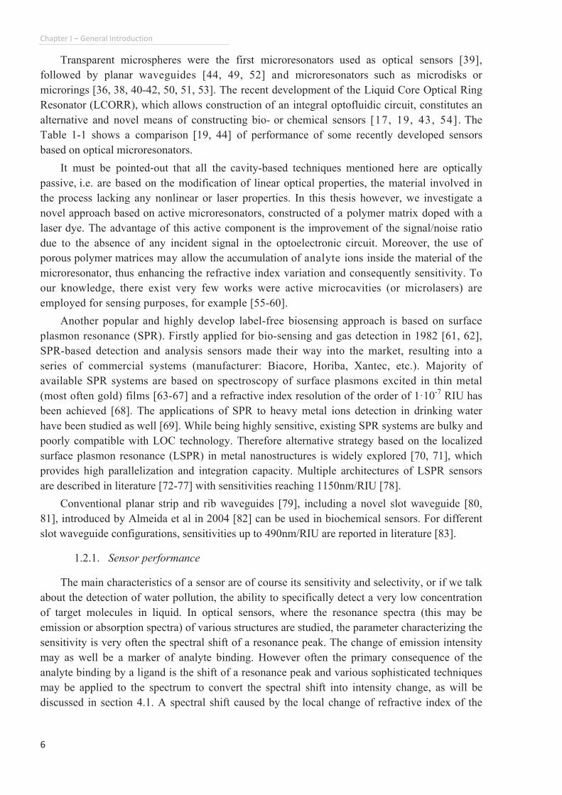
MicrospheresPlanar
microresonatorsLCORR
Sensitivity (Äそ / Än) 26 nm/RIU 200 nm/RIU > 30 nm/RIU
Photonics integration Very challenging EasyDifficult,
under investigation
Microfluidics
integration Very challenging
Good (needs to be
fabricated seperately) Excellent
Mass production Very difficult Excellent Good,
under investigation
Multiplexed detection Very challenging Excellent Good,
under investigation
Table 1-1. Comparison of performance of sensors based on optical microresonators.
Fluorescent
label
Analyte molecule
Specific
ligand
Chapter"I"�"General"Introduction"
6""
Transparent microspheres were the first microresonators used as optical sensors [39],
followed by planar waveguides [44, 49, 52] and microresonators such as microdisks or
microrings [36, 38, 40-42, 50, 51, 53]. The recent development of the Liquid Core Optical Ring
Resonator (LCORR), which allows construction of an integral optofluidic circuit, constitutes an
alternative and novel means of constructing bio- or chemical sensors [17, 19, 43, 54]. The
Table 1-1 shows a comparison [19, 44] of performance of some recently developed sensors
based on optical microresonators.
It must be pointed┽out that all the cavity-based techniques mentioned here are optically
passive, i.e. are based on the modification of linear optical properties, the material involved in
the process lacking any nonlinear or laser properties. In this thesis however, we investigate a
novel approach based on active microresonators, constructed of a polymer matrix doped with a
laser dye. The advantage of this active component is the improvement of the signal/noise ratio
due to the absence of any incident signal in the optoelectronic circuit. Moreover, the use of
porous polymer matrices may allow the accumulation of analyte ions inside the material of the
microresonator, thus enhancing the refractive index variation and consequently sensitivity. To
our knowledge, there exist very few works were active microcavities (or microlasers) are
employed for sensing purposes, for example [55-60].
Another popular and highly develop label-free biosensing approach is based on surface
plasmon resonance (SPR). Firstly applied for bio-sensing and gas detection in 1982 [61, 62],
SPR-based detection and analysis sensors made their way into the market, resulting into a
series of commercial systems (manufacturer: Biacore, Horiba, Xantec, etc.). Majority of
available SPR systems are based on spectroscopy of surface plasmons excited in thin metal
(most often gold) films [63-67] and a refractive index resolution of the order of 1·10-7
RIU has
been achieved [68]. The applications of SPR to heavy metal ions detection in drinking water
have been studied as well [69]. While being highly sensitive, existing SPR systems are bulky and
poorly compatible with LOC technology. Therefore alternative strategy based on the localized
surface plasmon resonance (LSPR) in metal nanostructures is widely explored [70, 71], which
provides high parallelization and integration capacity. Multiple architectures of LSPR sensors
are described in literature [72-77] with sensitivities reaching 1150nm/RIU [78].
Conventional planar strip and rib waveguides [79], including a novel slot waveguide [80,
81], introduced by Almeida et al in 2004 [82] can be used in biochemical sensors. For different
slot waveguide configurations, sensitivities up to 490nm/RIU are reported in literature [83].
1.2.1. Sensor performance
The main characteristics of a sensor are of course its sensitivity and selectivity, or if we talk
about the detection of water pollution, the ability to specifically detect a very low concentration
of target molecules in liquid. In optical sensors, where the resonance spectra (this may be
emission or absorption spectra) of various structures are studied, the parameter characterizing the
sensitivity is very often the spectral shift of a resonance peak. The change of emission intensity
may as well be a marker of analyte binding. However often the primary consequence of the
analyte binding by a ligand is the shift of a resonance peak and various sophisticated techniques
may be applied to the spectrum to convert the spectral shift into intensity change, as will be
discussed in section 4.1. A spectral shift caused by the local change of refractive index of the
Chapter"I" "General"Introduction"
7""
medium is usually measured in nanometers / refractive index units (RIU) and higher values mean
the sensor is capable to detect lower concentrations of analyte.
In Table 1-1 the comparison of sensitivity of different microresonator types is given,
evidencing that planar microresonators, the ones that will be studied in this thesis, demonstrate
higher sensitivity in comparison with other resonator types. In this work we are focusing on
active microcavities and study the emission spectra, therefore the Q-factor of the cavity does not
play the crucial role. First of all, highly confined modes are less likely to be observed in the
emission of a microlaser. Secondly, the width of the resonance peaks in this case is defined not
only by the quality factor of the passive cavity but also by nonlinear processes connected with
lasing.
Another important parameter of the performance of a bio- or chemical sensor is its
response time. While not crucial for the heavy metals detection in this work, response time may
be important for some biological applications. In many existing optofluidic devices, the time
constant of the microfluidic flow limits the response of the sensors for continuous monitoring.
Worse, this time constant is even more prolonged if regeneration of the sensing surfaces is
required because of the generally complicated rinsing sequence that is introduced [15, 16, 38,
39, 45-48, 50]. This limitation is fundamental, however the intrinsic response of the optical
sensor is crucial because it influences the overall response time of the device. In the present
project, the microlaser response to the change of its surrounding is expected to be very fast, of
the order of milliseconds, allowing observation of fast occurring processes, like for example
conformational changes of biological macromolecules.
Finally for the construction of a mobile sensing device, its compatibility with mass
production techniques is crucial and possibility of integration of multiple components on a
single chip is a very important criterion. In this aspect, planar microresonators are again the
leaders among the optical resonators, as they are inherently compatible with the existing planar
fabrication techniques developed in semiconductor industry. On the contrary, mass fabrication
of spherical or any other �3-dimensional� structures may be very difficult and integration with
other photonic or microfluidic components even more challenging, as separate fabrication may
be needed.
In traditional experimental setups used in conjunction with LOCs, both excitation and
detection are performed using bulk optical equipment to focus the excitation light into a tiny
measurement volume and to collect the resulting emission. Several efforts have been performed
in order to improve integration [84-88]. In particular, optical waveguides allow confinement
and transport of light in the chip, directing it into a small volume of the microfluidic channel
and collecting the incident and transmitted/emitted light. The integration on the same substrate
of optical and microfluidic components has far┽reaching scientific and technological
implications; to define this new field, the terms �optofluidics� has been recently
introduced in the scientific literature [89-91]. Integration of multiple components on a single
chip may require complicated multi-stage manufacturing processes, therefore much research is
devoted as well to the development of microfabrication techniques. In this thesis, we will use
traditional laboratory equipment, including lasers and spectrometers; however the architecture of
our microlaser allows easy integration of waveguides or other photonic components on a single
wafer. The ways also exist to integrate a compact detection system, which is based on the

Chapter"I" "General"Introduction"
8""
conversion of a wavelength shift into intensity change and subsequent detection with a
photodiode.
Conclusions
During this thesis we will fabricate active organic microcavities (or microlasers) based
on polymer matrix doped with a laser dye. Cavities will be functionalized with specific
ligands and experiments of mercury ions detection in liquid will be performed by recording
the wavelength shift in the microlaser emission spectrum. The ways of sensitivity
improvement will be proposed and experimentally proven with the novel pedestal and pillar
microcavities.
The work on this interdisciplinary project was carried out in close collaboration with the
chemists at PPSM laboratory, ENS Cachan. Our colleagues are responsible for the part of the
work dealing with synthesis of specific ligands capable of binding heavy metal ions, as well
as development and optimization of ligand grafting process on the polymer microresonators.
The research on porous polymers as active medium is also carried out in close cooperation.

Chapter"II"�"Theoretical"Basics"
9""
2. Chapter"II"""
Theoretical basics
""
2.1." Planar"waveguides"and"cavities..................................................................................................."10"2.1.1." Ray"optics"approach"............................................................................................................"11"2.1.2." Wave"approach.".................................................................................................................."12"
2.2." Dielectric"cavities."....................................................................................................................... "15"2.2.1." Cavity"characteristics.".........................................................................................................."15"2.2.2." Whispering"Gallery"Modes".................................................................................................. "17"
2.3." Active"cavities".............................................................................................................................. "18"2.3.1." Experimental"setup"for"spectra"recording."........................................................................."19"2.3.2." Experimental"data"treatment".............................................................................................. "20"2.3.3." Polarization"influence."........................................................................................................."22"
""" "
Chapter"II" "Theoretical"Basics"
10""
Introduction
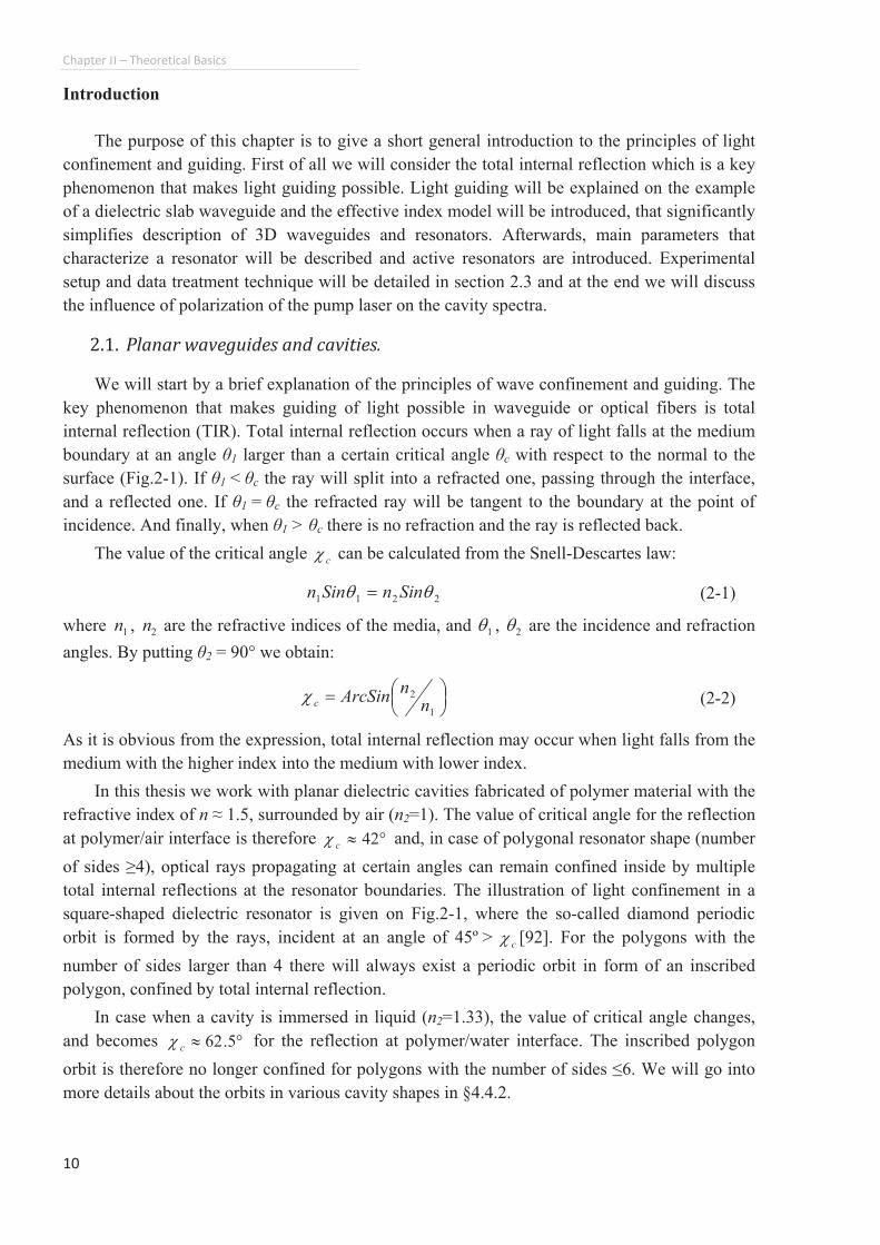
The purpose of this chapter is to give a short general introduction to the principles of light
confinement and guiding. First of all we will consider the total internal reflection which is a key
phenomenon that makes light guiding possible. Light guiding will be explained on the example
of a dielectric slab waveguide and the effective index model will be introduced, that significantly
simplifies description of 3D waveguides and resonators. Afterwards, main parameters that
characterize a resonator will be described and active resonators are introduced. Experimental
setup and data treatment technique will be detailed in section 2.3 and at the end we will discuss
the influence of polarization of the pump laser on the cavity spectra. に┻な┻ Planar"waveguides"and"cavities."
We will start by a brief explanation of the principles of wave confinement and guiding. The
key phenomenon that makes guiding of light possible in waveguide or optical fibers is total
internal reflection (TIR). Total internal reflection occurs when a ray of light falls at the medium
boundary at an angle し1 larger than a certain critical angle しc with respect to the normal to the
surface (Fig.2-1). If し1 < しc the ray will split into a refracted one, passing through the interface,
and a reflected one. If し1 = しc the refracted ray will be tangent to the boundary at the point of
incidence. And finally, when し1 > しc there is no refraction and the ray is reflected back.
The value of the critical angle ce can be calculated from the Snell-Descartes law:
2211 ss SinnSinn ? (2-1)
where 1n , 2n are the refractive indices of the media, and 1s , 2s are the incidence and refraction
angles. By putting し2 = 90° we obtain:
ÕÖÔÄÅÃ?1
2
nn
ArcSince (2-2)
As it is obvious from the expression, total internal reflection may occur when light falls from the
medium with the higher index into the medium with lower index.
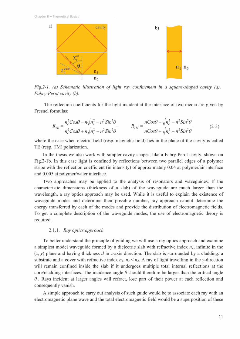
In this thesis we work with planar dielectric cavities fabricated of polymer material with the
refractive index of n à 1.5, surrounded by air (n2=1). The value of critical angle for the reflection
at polymer/air interface is therefore fl… 42ce and, in case of polygonal resonator shape (number
of sides œ4), optical rays propagating at certain angles can remain confined inside by multiple
total internal reflections at the resonator boundaries. The illustration of light confinement in a
square-shaped dielectric resonator is given on Fig.2-1, where the so-called diamond periodic
orbit is formed by the rays, incident at an angle of 45º > ce [92]. For the polygons with the
number of sides larger than 4 there will always exist a periodic orbit in form of an inscribed
polygon, confined by total internal reflection.
In case when a cavity is immersed in liquid (n2=1.33), the value of critical angle changes,
and becomes fl… 5.62ce for the reflection at polymer/water interface. The inscribed polygon
orbit is therefore no longer confined for polygons with the number of sides ø6. We will go into
more details about the orbits in various cavity shapes in §4.4.2.
Chapter"II"�"Theoretical"Basics"
11""
Fig.2-1. (a) Schematic illustration of light ray confinement in a square-shaped cavity (a),
Fabry-Perot cavity (b).
The reflection coefficients for the light incident at the interface of two media are given by
Fresnel formulas:
ssss
2222
2222
SinnnnCosn
SinnnnCosnR
ee
ee
TE /-//? ss
ss222
222
SinnnnCos
SinnnnCosR
e
e
TM /-//? (2-3)
where the case when electric field (resp. magnetic field) lies in the plane of the cavity is called
TE (resp. TM) polarization.
In the thesis we also work with simpler cavity shapes, like a Fabry-Perot cavity, shown on
Fig.2-1b. In this case light is confined by reflections between two parallel edges of a polymer
stripe with the reflection coefficient (in intensity) of approximately 0.04 at polymer/air interface
and 0.005 at polymer/water interface.
Two approaches may be applied to the analysis of resonators and waveguides. If the
characteristic dimensions (thickness of a slab) of the waveguide are much larger than the
wavelength, a ray optics approach may be used. While it is useful to explain the existence of
waveguide modes and determine their possible number, ray approach cannot determine the
energy transferred by each of the modes and provide the distribution of electromagnetic fields.
To get a complete description of the waveguide modes, the use of electromagnetic theory is
required.
2.1.1. Ray optics approach
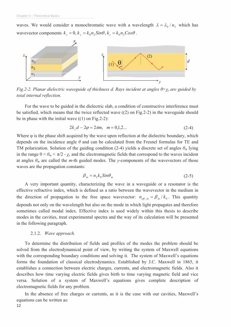
To better understand the principle of guiding we will use a ray optics approach and examine
a simplest model waveguide formed by a dielectric slab with refractive index n1, infinite in the
(x, y) plane and having thickness d in z-axis direction. The slab is surrounded by a cladding: a
substrate and a cover with refractive index n1, n3 < n2. A ray of light travelling in the y-direction
will remain confined inside the slab if it undergoes multiple total internal reflections at the
core/cladding interfaces. The incidence angle し should therefore be larger than the critical angle
しc. Rays incident at larger angles will refract, lose part of their power at each reflection and
consequently vanish.
A simple approach to carry out analysis of such guide would be to associate each ray with an
electromagnetic plane wave and the total electromagnetic field would be a superposition of these
a) b)
Chapter"II" "Theoretical"Basics"
12""
waves. We would consider a monochromatic wave with a wavelength 20 / nnn ? which has
wavevector components ss CosnkkSinnkkk zyx 2020 ,,0 ??? .
Fig.2-2. Planar dielectric waveguide of thickness d. Rays incident at angles し>ぬc are guided by
total internal reflection.
For the wave to be guided in the dielectric slab, a condition of constructive interference must
be satisfied, which means that the twice reflected wave ((2) on Fig.2-2) in the waveguide should
be in phase with the initial wave ((1) on Fig.2-2):
...2,1,0,222 ??/ mmdk z rl (2-4)
Where l is the phase shift acquired by the wave upon reflection at the dielectric boundary, which
depends on the incidence angle し and can be calculated from the Fresnel formulas for TE and
TM polarization. Solution of the guiding condition (2-4) yields a discrete set of angles しm lying
in the range 0 < しm < ヾ/2 - ぬc and the electromagnetic fields that correspond to the waves incident
at angles しm are called the m-th guided modes. The y-components of the wavevectors of those
waves are the propagation constants:
mm Sinkn sd 02? (2-5)
A very important quantity, characterizing the wave in a waveguide or a resonator is the
effective refractive index, which is defined as a ratio between the wavevector in the medium in
the direction of propagation to the free space wavevector: 0, / kn mmeff d? . This quantity
depends not only on the wavelength but also on the mode in which light propagates and therefore
sometimes called modal index. Effective index is used widely within this thesis to describe
modes in the cavities, treat experimental spectra and the way of its calculation will be presented
in the following paragraph.
2.1.2. Wave approach.
To determine the distribution of fields and profiles of the modes the problem should be
solved from the electrodynamical point of view, by writing the system of Maxwell equations
with the corresponding boundary conditions and solving it. The system of Maxwell�s equations
forms the foundation of classical electrodynamics. Established by J.C. Maxwell in 1865, it
establishes a connection between electric charges, currents, and electromagnetic fields. Also it
describes how time varying electric fields gives birth to time varying magnetic field and vice
versa. Solution of a system of Maxwell�s equations gives complete description of
electromagnetic fields for any problem.
In the absence of free charges or currents, as it is the case with our cavities, Maxwell�s
equations can be written as:
Chapter"II" "Theoretical"Basics"
13""
0),( ?©ı trDEE
t
trBtrE •
•/?·ı ),(),(
EEEE
(2-6)
0),( ?©ı trBEE
t
trDtrH •
•?·ı ),(),(
EEEE
where ),()(),( trErtrDEEEEE g? and ),()(),( trHrtrB
EEEEE o? are linear constitutive relations
connecting electric displacement DE
with electric field and magnetic induction BE
with magnetic
field through the dielectric permittivity g and magnetic permeability o which are tensors in the
most general case. Taking the curl of the equation t
trBtrE •
•/?·ı ),(),(
EEEE
, a wave propagation
equation can be derived which becomes Helmholtz equation, when time dependency of the fields
has harmonic form )exp( tiy/ :
0)()()( 22
0 ?-F rErnkrEEEEEE
(2-7)
where 0k is a free space wavevector and 0
2 /)()( gg rrnEE ? � refractive index of the medium.
In the case of the slab waveguide, shown on Fig.2-2, it can be proven mathematically that
two wave polarizations � TE and TM may propagate. We will remind that we call TE (TM)
polarization orientation of the EE
vector in the plane (perpendicular to the plane) of the
waveguide. Taking into account that polymer is an isotropic and non-magnetic material (µ=1, iis scalar), equation (2-7) for TE polarization may be rewritten as:
0),(),( 22
0 ?-F zyEnkzyE xix (2-8)
where ni (i=1,2,3) is the refractive index of the dielectric layer (core or claddings) where wave
propagation is considered. We will look for the solutions of equation (2-8) in the form:
yj
mmxmezuAzyE
d/? )(),( (2-9)
where Am is a numerical constant, md is a propagation constant, and )(zum is an unknown
function. By substituting solutions (2-9) into (2-8) we obtain:
2
0
222
,
2
,2
2
,0 knuz
uimmimmi
m /??/•• dii (2-10)
Solution of this equation depends on the sign of 2
,mii . For the guided modes inside the core
2nni ? , 02knm >d and consequently 02
, >mii . In this case, (2-10) is satisfied by periodic
oscillating functions in the form )exp(~ ,2 zju mm i‒ . For electric fields inside the cladding
3,1nni ? , 03,1 knm @d and 02
),3,1( @mi . There is no propagation in the claddings and electric field
decays exponentially along the z-axis. In this case equation (2-10) is satisfied by solutions in the
form of decaying exponents )exp(~ ),3,1( zu mm i‒ . Therefore, an arbitrary TE field in the
dielectric waveguide can be represented as a superposition of m modes:
yj
m
m
mxmezuAzyE
d/Â? )(),( (2-11)
Chapter"II" "Theoretical"Basics"
14""
where Am is the amplitude of the mode m. Electric field distribution for several guided modes in
a dielectric slab waveguide is displayed on Fig.2-3a. Field distribution of the magnetic field H
and also in the case of TM polarization can be found similarly.
The dispersion relation for the waveguide modes can be obtained from the constructive
interference condition (2-4) [93]. The phase shifts upon reflections at the core/substrate and
core/cover interfaces are calculated from (2-3) where cosines and sines of angle し are expressed
through the components of the wavevector ky and kz and substituted into (2-4). The following
expression may be obtained:
where2
3
2
21
n
n?j , 2
1
2
2
2n
n?j for TM polarization, 121 ??jj for TE polarization; n2 � is the
index of the cavity material and effn is the effective index. The advantage of introduction of
effective index, is that the vertical component of the wavevector kz is now hidden inside neff and
therefore we may consider the waveguide as a two-dimensional, lying in (x,y) plane while
effective index takes into account the vertical z-dimension.
It is convenient to plot the effective index as a function of d/そ which is made on the Fig.2-3b
for n1=1.45, n2=1.54, n3=1 � refractive indices of the silica substrate and polymer guiding layer,
that are used to fabricate microcavities studied in this thesis. As it is seen from the plot, the
values of effective index lie in the range limited from below by the index of a substrate or a
cover (n1 or n3, whichever is higher) and from above by the index of a guiding layer
]),,[sup( 231, nnnn meff Œ . There exists certain limiting d/そ ratio, below which no wave
confinement and guiding is possible. For a fixed value of wavelength (そ=600nm) this means that
the waveguide has a cutoff thickness, which in our case equals approximately nmd TM 208min ?and nmd TE 255min ? for TM and TE polarizations. For the ratio d/そ Ã 1, which is typical for the
cavities studied in this thesis, only one mode (l=0) may be confined in the guiding layer along
...2,1,0,)()(2
22
2
2
1
2
222
2
2
3
2
1
22
2 ?©-//-/
/?/ llnn
nnArctg
nn
nnArctgnn
d
eff
eff
eff
eff
eff rjjnr
(2-12)
1,45
1,47
1,49
1,51
1,53
1,55
0 1 2 3 4 5
l=1l=0
n
n2
TE
TM
d/n
nef
f
Fig.2-3. (a) Field distributions E(z) for several TE guided modes in a planar waveguide. (b)
Effective refractive index of a guiding layer as a function of h/そ for constant substrate indices
Chapter"II" "Theoretical"Basics"
15""
the z-axis [94]. With the increase of d/そ ratio, higher order modes (lŒ0) appear.
While planar waveguides as the one described here has limited practical use, it serves as a
convenient model structure to explain the principles of wave confinement and guiding and to
introduce an important concept of effective refractive index, that will be used later to analyze
dielectric cavities and treat experimental spectra. に┻に┻ "Dielectric"cavities."In the previous example of an infinite slab waveguide, light was confined along the z-axis
and could freely propagate in x and y directions. If we limit the width and the length of a slab,
we will obtain a structure in which light is confined in all 3 dimensions1. The configuration of
the electromagnetic fields and frequencies at which confinement is possible depend on the shape
of a cavity and properties of material.
In this thesis we work with quasi 2D dielectric cavities made of planar polymer structures of
various shapes lying on a substrate with a lower refractive index (e.g. SiO2, n=1.45). The
transverse dimensions (along z-axis) of a cavity are of the order of a wavelength (そ=600nm), in
order to obtain a cavity supporting only one mode in vertical direction. This should significantly
simplify the treatment and explanation of observed emission spectra. The lateral dimensions of
the cavities are of the order of 100そ, and are chosen to have sufficient gain in the active medium
to achieve lasing. Due to the high substrate losses, the cavities smaller than approx.
50µm x 50µm require high pumping fluence in order to observe lasing emission, which bleaches
the laser dye very quickly.
Taking into account that the cavities are fabricated of a dielectric polymer material, the
mode energy is radiated in the surrounding space and therefore they belong to the class of open
electrodynamical systems. In open resonators, as opposite to closed ones (i.e. radiofrequency
resonators with perfectly conducting walls) electromagnetic fields do not vanish at its borders
but may extend far behind the resonator�s boundaries. Theoretical description of open systems is
a very complicated task and, in case of planar dielectric cavities, a disk is the only system for
which exact solutions of Maxwell equations exist [95]. Numerical modeling is therefore often
applied for their analysis [96-99]. In this thesis, we will use Finite-Difference Time Domain
(FDTD) method and Finite Element method (FEM) in order to analyze the electromagnetic field
distribution in the cavity and predict the influence of the external medium on the cavity
resonance spectra.
In this section we will briefly introduce main parameters characterizing the cavities, while
planar cavities of various shapes used in this work and their suitability for sensing applications
will be described in more details in §4.4.
2.2.1. Cavity characteristics.
In order to introduce the main parameters characterizing a cavity, we will revert to the ray
optics approach and consider a resonator formed by N mirrors, placed in such a way that once
""""""""""""""""""""""""""""""""""""""""""""""""""""""""""""1 Strictly speaking, expression (2-12) used to calculate the effective index is only valid for an infinite (in lateral
dimensions) waveguide and becomes paradoxical near the edges of a planar resonator. However, it serves a good
approximation and effective index calculated by (2-12) allows proper treatment of experimental results (calculation
of periodic orbit lengths from emission spectra).
Chapter"II"�"Theoretical"Basics"
16""
the ray of light is injected inside, it may travel in a closed loop between them. Similar as before,
each ray with may be associated with a plane wave. A wave will be confined inside such
resonator, if after completing one roundtrip (N reflections), it is identical to the initial injected
one, which means it is in phase:
Where Nrr ...1 are the reflection coefficients of the mirrors, neff is the effective index of the cavity
medium, L is the length of a roundtrip distance. Condition (2-13) will be satisfied for a discrete
set of wavenumbers km, which forms the resonance spectrum of the cavity. We will call periodic
orbit the optical path of light inside the cavity which satisfies (2-13).
Quality Factor
One of the basic characteristics of a resonator is its quality factor, which is defined in words
as the ratio of the time-averaged energy stored in the cavity to the energy loss per cycle. The
quality factor can be measured experimentally from the spectrum of the cavity and is defined as:
where そ is the wavelength of the resonance and 2/1nF is the width of the resonance peak at half
of its magnitude. For sensing applications when the spectral shift is detected, we are interested
to have narrow resonance peaks, therefore high quality factor is a very important characteristics
of microcavities. Quality factor is also connected with the lifetime k of the photon inside a cavity,
which can be expressed as:
where p is the resonance frequency.
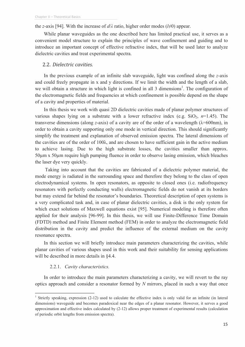
Finesse and Free Spectral Range
By definition, the free spectra range (FSR) is a wavelength spacing FSRnF (or frequency
spacing FSRpF ) between the adjacent
resonances of a cavity. It is illustrated
on Fig.2-4, on the example of a typical
emission spectrum, registered from a
planar microcavity. In general, the FSR
becomes larger when the physical
dimensions of the resonator decrease. A
large FSR allows development of single
mode microlasers and may be
advantageous for the development of
spectral shift detection schemes when a
wavelength shift is converted into
intensity change (see §4.1)
The strict condition on the
frequencies of optical waves that are
permitted to exist inside a resonator is
1...)(
21 ?meffm kLnik
Nerrr (2-13)
2/1nn
F?Q (2-14)
rpv 2/Q? (2-15)
606 607 608
0,0
0,5
1,0
F
FnFSR
Inte
nsity,
norm
Wavelength, nm
FnFSR
Fig.2-4. Resonance peaks of a lossy resonator
(Fabry-Perot), illustrating the free spectral range
and the finesse.
Chapter"II"�"Theoretical"Basics"
17""
relaxed when the resonator has losses. The two principal sources of loss are: 1) losses due to
absorption and scattering in the resonator medium; and 2) losses due to imperfect reflection at
the mirrors. Presence of losses leads to the broadening of resonances so that in a real cavity
resonance peaks always have some finite width, as different from the ideal no loss resonator,
where the resonance peaks are delta functions. The quantity that connects the width of a
resonance peak with the free spectral range is called finesse and is defined as:
When the finesse is large ( 1@@F ) the resonator spectral response features sharp peaks around
the resonance frequencies.
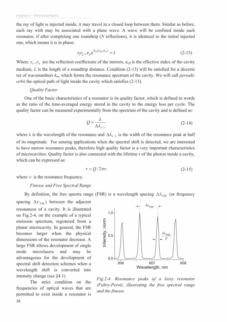
2.2.2. Whispering Gallery Modes
The name �whispering gallery� originates from acoustical features of certain architecture
shapes: it was noticed that a word pronounced by whisper near the wall of the dome can be
clearly heard at the opposite side of the dome, but not in the middle of the building, even though
the distance between the speaker and the listener is large. The fact that sound in a closed space
seems to propagate not along the shortest path but along the concave wall was first studied and
explained by Lord Rayleigh in 1910 [100]. The same physical effect is observed also for the
radio and optical frequency waves, when due to multiple total internal reflections wave
propagates along the concave boundary of a body. For historical reasons, such modes bear the
name �whispering gallery modes� (WGM). The employment of WGMs in an axially-symmetric
dielectric body for the creation of a high quality factor electromagnetic resonator was first
proposed by Richtmyer in 1939 [101].
Fig.2-5. Geometrical optics (a) and wave optics (b) representation of a whispering gallery
mode in a planar disc cavity. Cavity contour is shown in white dash on (b).
The most common resonator shapes where WGMs are observed are spheres or, in case of
planar cavities studied in this work - disks. From the ray optics point of view, the light is trapped
inside the disk by continuous total internal reflections at the curved boundary surface (Fig.2-5).
Such modes possess high quality factors (experimentally up to 1011
[102]) leading to very
narrow resonances. Moreover, high localization of the modes in a narrow region close to the
cavity boundary, promotes nonlinear effects and leads to low lasing threshold if active cavity is
considered. The main interest of WGMs in sensing application is their localization close to the
boundary of the cavity, and therefore higher sensitivity to the changes in the medium
2/1nnFF? FSRF (2-16)
a) b)
Chapter"II" "Theoretical"Basics"
18""
surrounding the cavity. The advantage of WGM-supporting cavity over other planar cavity
shapes will be grounded in §4.4 with the experimental proofs presented in §4.5. に┻ぬ┻ "Active"cavities""
Until now in this introduction we talked about passive dielectric cavities. In this work
however, we study cavities fabricated of a material with gain, or active cavities, in which laser
generation is possible under appropriate conditions. To create a microlaser we introduce a laser
dye homogeneously mixed inside the polymer that forms the cavity body. The dye molecules are
pumped with a laser. Their emission is trapped inside the microcavity, amplified due to the
multiple passes of light inside the cavity and stimulated emission, and emitted through the cavity
boundaries. Up to now it seems that the spectral features are largely determined by the passive
cavity resonances. It is important therefore to have laser dye emission in the spectral range,
where passive cavity features sharp resonances.
Laser dyes are extensively studied since the beginning of the laser era (60s-70s) and possess
a number of advantages: ease of manipulation, low cost, wide fluorescence band [103]. Laser
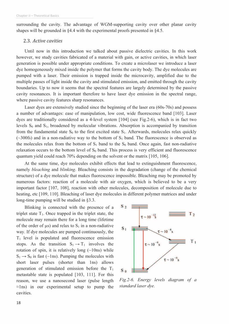
dyes are traditionally considered as a 4-level system [104] (see Fig.2-6), which is in fact two
levels S0 and S1, broadened by molecular vibrations. Absorption is accompanied by transition
from the fundamental state S0 to the first excited state S1. Afterwards, molecules relax quickly
(~300fs) and in a non-radiative way to the bottom of S1 band. The fluorescence is observed as
the molecules relax from the bottom of S1 band to the S0 band. Once again, fast non-radiative
relaxation occurs to the bottom level of S0 band. This process is very efficient and fluorescence
quantum yield could reach 70% depending on the solvent or the matrix [105, 106].
At the same time, dye molecules exhibit effects that lead to extinguishment fluorescence,
namely bleaching and blinking. Bleaching consists in the degradation (change of the chemical
structure) of a dye molecule that makes fluorescence impossible. Bleaching may be promoted by
numerous factors: reaction of a molecule with air oxygen, which is believed to be a very
important factor [107, 108], reaction with other molecules, decomposition of molecule due to
heating, etc [109, 110]. Bleaching of laser dye molecules in different polymer matrices and under
long-time pumping will be studied in §3.3.
Blinking is connected with the presence of a
triplet state T1. Once trapped in the triplet state, the
molecule may remain there for a long time (lifetime
of the order of µs) and relax to S1 in a non-radiative
way. If dye molecules are pumped continuously, the
T1 level is populated and fluorescence emission
stops. As the transition S1 s T1 involves the
rotation of spin, it is relatively long (~10ns) while
S1 s S0 is fast (~1ns). Pumping the molecules with
short laser pulses (shorter than 1ns) allows
generation of stimulated emission before the T1
metastable state is populated [103, 111]. For this
reason, we use a nanosecond laser (pulse length
Ã1ns) in our experimental setup to pump the
cavities.
Fig.2-6. Energy levels diagram of a
standard laser dye.
Chapter"II" "Theoretical"Basics"
19""
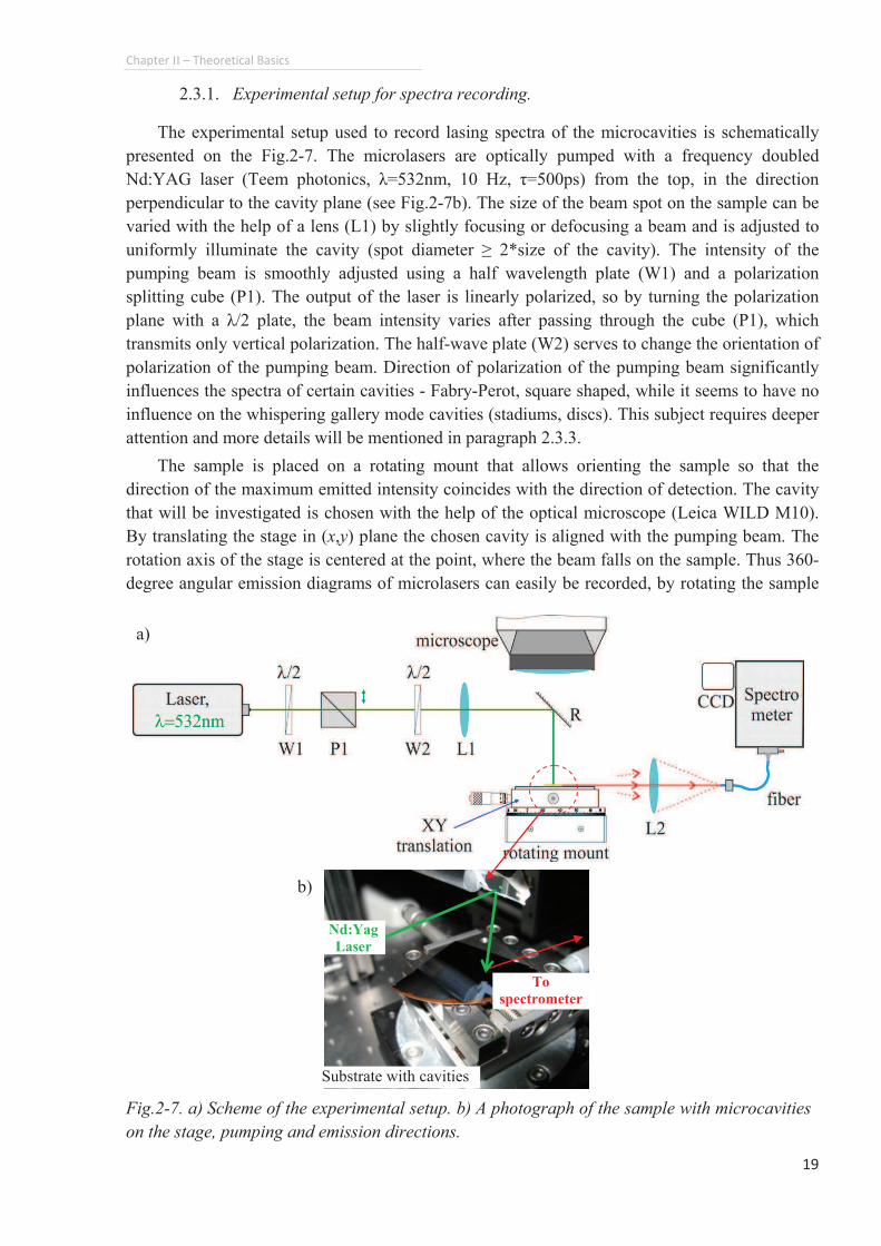
2.3.1. Experimental setup for spectra recording.
The experimental setup used to record lasing spectra of the microcavities is schematically
presented on the Fig.2-7. The microlasers are optically pumped with a frequency doubled
Nd:YAG laser (Teem photonics, そ=532nm, 10 Hz, k=500ps) from the top, in the direction
perpendicular to the cavity plane (see Fig.2-7b). The size of the beam spot on the sample can be
varied with the help of a lens (L1) by slightly focusing or defocusing a beam and is adjusted to
uniformly illuminate the cavity (spot diameter œ 2*size of the cavity). The intensity of the
pumping beam is smoothly adjusted using a half wavelength plate (W1) and a polarization
splitting cube (P1). The output of the laser is linearly polarized, so by turning the polarization
plane with a そ/2 plate, the beam intensity varies after passing through the cube (P1), which
transmits only vertical polarization. The half-wave plate (W2) serves to change the orientation of
polarization of the pumping beam. Direction of polarization of the pumping beam significantly
influences the spectra of certain cavities - Fabry-Perot, square shaped, while it seems to have no
influence on the whispering gallery mode cavities (stadiums, discs). This subject requires deeper
attention and more details will be mentioned in paragraph 2.3.3.
The sample is placed on a rotating mount that allows orienting the sample so that the
direction of the maximum emitted intensity coincides with the direction of detection. The cavity
that will be investigated is chosen with the help of the optical microscope (Leica WILD M10).
By translating the stage in (x,y) plane the chosen cavity is aligned with the pumping beam. The
rotation axis of the stage is centered at the point, where the beam falls on the sample. Thus 360-
degree angular emission diagrams of microlasers can easily be recorded, by rotating the sample
Fig.2-7. a) Scheme of the experimental setup. b) A photograph of the sample with microcavities
on the stage, pumping and emission directions.
a)
Nd:Yag
Laser
To
spectrometer
Substrate with cavities
b)
Chapter"II" "Theoretical"Basics"
20""
in its plane and recording the spectra at needed angular step. The emitted light coming out of the
cavity in the lateral direction is collected in the far-field with a lens L2 (collection angle ~6º) that
focuses the emission into an optical fiber, connected to an Acton SpectraPro 2500i spectrometer
(F/6.5, 500mm focal length) equipped with a Princeton Instruments PIXIS 100 cooled CCD
camera (resolution: 1340 x 100; pixel size: 20µm x 20µm). In the spectrum captured by the
camera, one pixel corresponds to 0.029nm when converted to a wavelength scale. The spectra of
the cavities are normally registered at a laser pulse repetition rate of 10Hz and an integration
time of 3s, which corresponds to 30 pump pulses per one recorded spectrum (CCD camera
shutter is synchronized with the pumping laser pulses). Integration time is chosen to achieve an
optimal signal/bleaching ratio.
In its current configuration, our setup allows making only �2-dimensional� observations.
Only the emission coming out of the cavities in their plane can be collected and studied, the
detector cannot be placed at a certain angle relative to the cavity plane, as well as the excitation
beam is always perpendicular to the cavity plane. We have noticed that the angle between the
excitation beam and the cavity plane significantly influences the observed lasing spectra
therefore perpendicularity of the beam was carefully controlled. This dependence on
perpendicularity, similarly to dependence on the pumping beam polarization, is probably
explained by the change of efficiency of excitation as well as the change of prevailing emission
direction of the dye molecules in the polymer matrix. Such in-plane measurements were
sufficient for most of the tasks of studying the traditional thin single vertical mode cavities
(thickness ø wavelength) on the plane substrate, like measuring lasing thresholds, emission
diagrams, assessment of sensitivity. However for novel cavity geometries, like pedestal cavities,
described in Chapter 5 or 3D cavities (thickness > wavelength) it becomes necessary to observe
the emission patterns not only in the cavity plane but also at a various angles to the plane. This
necessity will become obvious after the properties of pedestal cavities will be explained in more
details. The 3D setup that will allow full control over the pump beam incidence angle and the
observation angle is being currently developed by Clement Lafargue at LPQM and will be
described in his PhD thesis.
2.3.2. Experimental data treatment
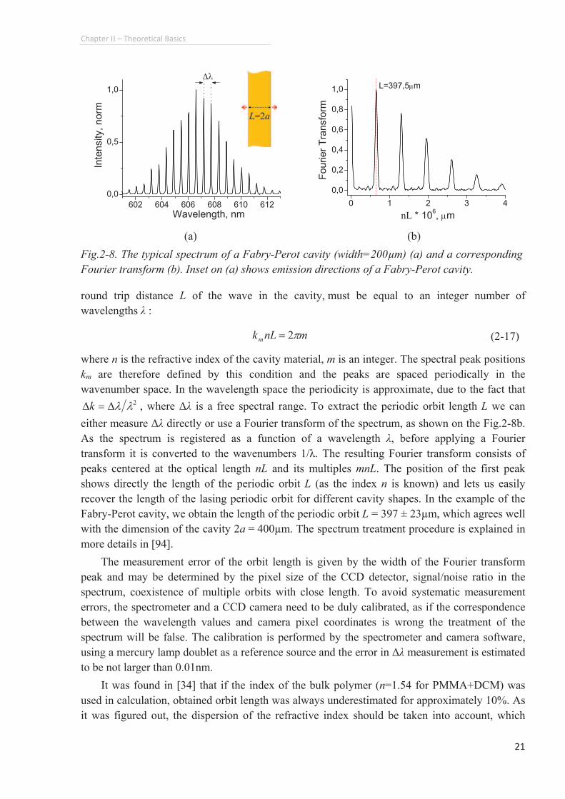
Emission spectra of microlasers bear the geometrical features of the cavities and analysis of
the spectra gives insight into the excited modes. In a simplified geometrical view, the light
confined in the active cavity reflects on the cavity borders and travels along the closed loop
which leads to the amplification and generation of a lasing spectrum, whose typical pattern is
shown on Fig.2-8a. The length of the path traveled by the light during a roundtrip in the cavity
can be recovered from the spectrum. To easily understand the procedure we use to treat the
spectrum, we will explain it on the example of a Fabry-Perot cavity, which features only one
periodic orbit.
The cavity consists of a long dye-doped polymer bar, as displayed on the inset of Fig.2-8a,
pumped uniformly (the diameter of the pump laser spot is larger than the width of the cavity).
The periodic orbit with the length L=2a gives birth to a Fabry-Perot resonance between the two
parallel walls of the cavity, and laser emission (marked by red arrows on the figure) is registered
in one of the directions perpendicular to the cavity edges. The resonance condition states that the
Chapter"II" "Theoretical"Basics"
21""
round trip distance L of the wave in the cavity, must be equal to an integer number of
wavelengths そ :
mnLkm r2? (2-17)
where n is the refractive index of the cavity material, m is an integer. The spectral peak positions
km are therefore defined by this condition and the peaks are spaced periodically in the
wavenumber space. In the wavelength space the periodicity is approximate, due to the fact that 2nnF?Fk , where 〉そ is a free spectral range. To extract the periodic orbit length L we can
either measure 〉そ directly or use a Fourier transform of the spectrum, as shown on the Fig.2-8b.
As the spectrum is registered as a function of a wavelength そ, before applying a Fourier
transform it is converted to the wavenumbers 1/そ. The resulting Fourier transform consists of
peaks centered at the optical length nL and its multiples mnL. The position of the first peak
shows directly the length of the periodic orbit L (as the index n is known) and lets us easily
recover the length of the lasing periodic orbit for different cavity shapes. In the example of the
Fabry-Perot cavity, we obtain the length of the periodic orbit L = 397 ± 23µm, which agrees well
with the dimension of the cavity 2a = 400µm. The spectrum treatment procedure is explained in
more details in [94].
The measurement error of the orbit length is given by the width of the Fourier transform
peak and may be determined by the pixel size of the CCD detector, signal/noise ratio in the
spectrum, coexistence of multiple orbits with close length. To avoid systematic measurement
errors, the spectrometer and a CCD camera need to be duly calibrated, as if the correspondence
between the wavelength values and camera pixel coordinates is wrong the treatment of the
spectrum will be false. The calibration is performed by the spectrometer and camera software,
using a mercury lamp doublet as a reference source and the error in 〉そ measurement is estimated
to be not larger than 0.01nm.
It was found in [34] that if the index of the bulk polymer (n=1.54 for PMMA+DCM) was
used in calculation, obtained orbit length was always underestimated for approximately 10%. As
it was figured out, the dispersion of the refractive index should be taken into account, which
602 604 606 608 610 612
0,0
0,5
1,0In
ten
sity,
norm
Wavelength, nm
Fn
0 1 2 3 4
0,0
0,2
0,4
0,6
0,8
1,0 L=397,5om
nL * 106, om
Fourier
Tra
nsfo
rm
(a) (b)
Fig.2-8. The typical spectrum of a Fabry-Perot cavity (width=200µm) (a) and a corresponding
Fourier transform (b). Inset on (a) shows emission directions of a Fabry-Perot cavity.
Chapter"II" "Theoretical"Basics"
22""
compensates for the missing 10%. The total refractive index which is also called a group index
therefore becomes:
Here the first term in the formula (2-18) is the effective refractive index calculated at the
wavelength of interest 0n , the second term is the dispersion of the index of bulk polymer
(retrieved from ellipsometry measurements) and the third term is the calculated dispersion of the
effective refractive index. The calculation is performed for the wavelength nm6000 ?n and two
values of medium refractive index: 1 and 1.33, corresponding to the cavity in air and in water.
The values of effective index and dispersion of effective index are given with precision of 3
digits after decimal point in order to underline the difference between them. However the
dispersion of the bulk material is measured only with the precision of two digits after decimal
point, consequently the final result is rounded. Another source of error comes from the fact that
the value of effective refractive index may vary substantially for different cavity modes but we
neglect this variation and always use the value calculated for a fundamental mode of a guiding
layer surrounded by infinitely thick claddings.
The values of the group index were found to be equal (within the error range) for different
medium indices. While the value of effective refractive index of the cavity in water increases, the
dispersion becomes lower and the group index remains almost unchanged. Therefore the same
value of ntotal can be applied for extraction of periodic orbit length both for the cavities in air and
in water.
2.3.3. Polarization influence.
Laser dye molecules, due to their 3-dimensional shape, exhibit sensitivity to the polarization
of the incident emission. Depending on the molecule orientation, light of one polarization may
be absorbed more efficiently than another one. Direction of molecule�s emission will also
depend on its orientation. As molecules are introduced inside the cavity, the direction of
molecule�s emission may play a very important role in the efficiency of excitation of cavity
modes. The influence of polarization on the spectra of cavities is a complicated issue that
requires a separate deep study, which is not the subject of this thesis, however it can be visually
explained by the 2D example of a Fabry-Perot cavity (Fig.2-9b) if we consider dye molecules as
linear dipoles lying in the plane of the cavity. Such simplified representation is of course
imprecise, but allows us to qualitatively explain the observed changes in the lasing spectra.
When polarization of the pumping beam, incident from the top, is parallel to the cavity walls (||P
), the dye molecules with the dipoles oriented along the polarization direction are effectively
nnnnn ••/•
•/? effbulk
efftotal
nnnn 000 )( (2-18)
TM
0.1?en ?totaln 1.496 � -0.10 � -0.059 = 1.65 ± 0.01
33.1?en ?totaln 1.502 � -0.10 � -0.048 = 1.65 ± 0.01
TE
0.1?en ?totaln 1.502 � -0.10 � -0.049 = 1.65 ± 0.01
33.1?en ?totaln 1.505 � -0.10 � -0.043 = 1.65 ± 0.01
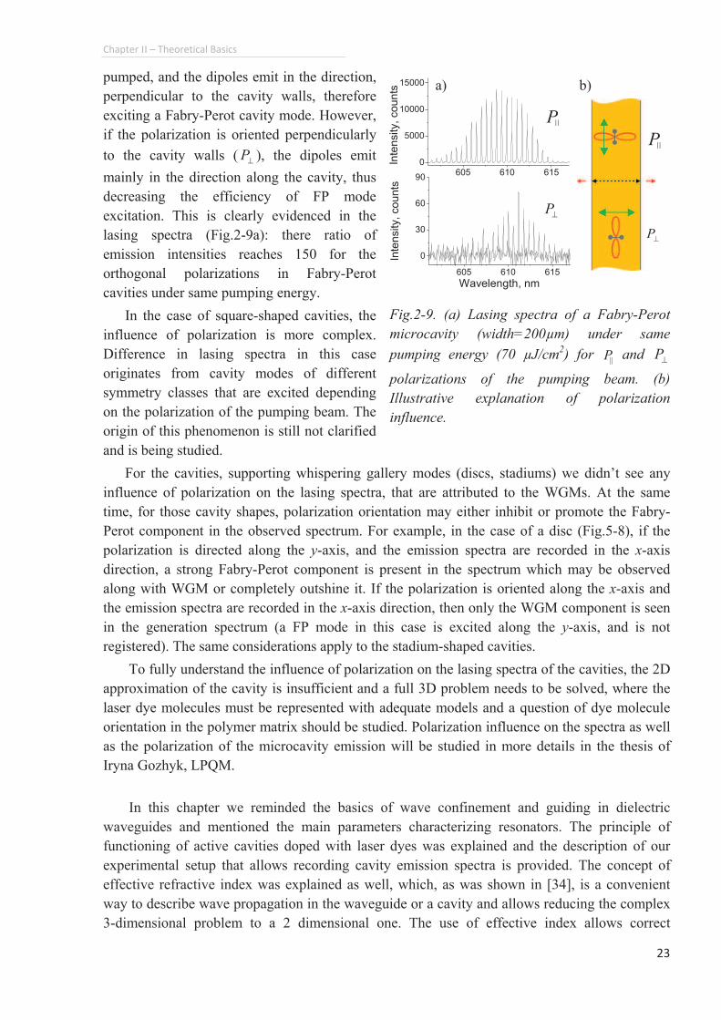
Chapter"II"�"Theoretical"Basics"
23""
pumped, and the dipoles emit in the direction,
perpendicular to the cavity walls, therefore
exciting a Fabry-Perot cavity mode. However,
if the polarization is oriented perpendicularly
to the cavity walls ( P̀ ), the dipoles emit
mainly in the direction along the cavity, thus
decreasing the efficiency of FP mode
excitation. This is clearly evidenced in the
lasing spectra (Fig.2-9a): there ratio of
emission intensities reaches 150 for the
orthogonal polarizations in Fabry-Perot
cavities under same pumping energy.
In the case of square-shaped cavities, the
influence of polarization is more complex.
Difference in lasing spectra in this case
originates from cavity modes of different
symmetry classes that are excited depending
on the polarization of the pumping beam. The
origin of this phenomenon is still not clarified
and is being studied.
For the cavities, supporting whispering gallery modes (discs, stadiums) we didn�t see any
influence of polarization on the lasing spectra, that are attributed to the WGMs. At the same
time, for those cavity shapes, polarization orientation may either inhibit or promote the Fabry-
Perot component in the observed spectrum. For example, in the case of a disc (Fig.5-8), if the
polarization is directed along the y-axis, and the emission spectra are recorded in the x-axis
direction, a strong Fabry-Perot component is present in the spectrum which may be observed
along with WGM or completely outshine it. If the polarization is oriented along the x-axis and
the emission spectra are recorded in the x-axis direction, then only the WGM component is seen
in the generation spectrum (a FP mode in this case is excited along the y-axis, and is not
registered). The same considerations apply to the stadium-shaped cavities.
To fully understand the influence of polarization on the lasing spectra of the cavities, the 2D
approximation of the cavity is insufficient and a full 3D problem needs to be solved, where the
laser dye molecules must be represented with adequate models and a question of dye molecule
orientation in the polymer matrix should be studied. Polarization influence on the spectra as well
as the polarization of the microcavity emission will be studied in more details in the thesis of
Iryna Gozhyk, LPQM.
In this chapter we reminded the basics of wave confinement and guiding in dielectric
waveguides and mentioned the main parameters characterizing resonators. The principle of
functioning of active cavities doped with laser dyes was explained and the description of our
experimental setup that allows recording cavity emission spectra is provided. The concept of
effective refractive index was explained as well, which, as was shown in [34], is a convenient
way to describe wave propagation in the waveguide or a cavity and allows reducing the complex
3-dimensional problem to a 2 dimensional one. The use of effective index allows correct
605 610 6150
5000
10000
15000
605 610 615
0
30
60
90
Inte
nsity, counts
Inte
nsity, counts
Wavelength, nm
Fig.2-9. (a) Lasing spectra of a Fabry-Perot
microcavity (width=200µm) under same
pumping energy (70 µJ/cm2) for
||P and P̀
polarizations of the pumping beam. (b)
Illustrative explanation of polarization
influence.
"
"
P̀
||P||P "
P̀ "
b)"
a)

Chapter"II"�"Theoretical"Basics"
24""
treatment of experimental results and lets us extract the length of periodic orbit from the lasing
spectrum of a cavity. Obtained orbit lengths are in good agreement with physical dimensions of a
cavity.
Chapter"III" "Technology:"Creating"a"Microlaser"
25""
3. Chapter"III"""
Technology: creating a microlaser.
""
3.1." Materials:"polymers"and"dyes.".................................................................................................... "26"3.2." Material"characterization:"Amplified"Spontaneous"Emission"and"ellipsometry."........................"28"3.3." Materials:"choice"of"a"laser"dye.".................................................................................................. "29"3.4." Microcavity"fabrication"technology."........................................................................................... "31"
3.4.1." Photolithography."................................................................................................................"32"3.4.2." Eどbeam"lithography."............................................................................................................"33"3.4.3." Fabrication"by"laser"ablation"and"2どphoton"polymerization.".............................................."34"
3.5." Alternative"cavity"geometry."......................................................................................................."36"3.5.1." Transparent"quartz"substrate."............................................................................................. "36"3.5.2." Pedestal"cavities."................................................................................................................."36"3.5.3." Lowどindex"substrate"cavities."Pillar"cavities."......................................................................."38"3.5.4." Allどpolymer"pedestal"cavities."............................................................................................. "39"
""" "
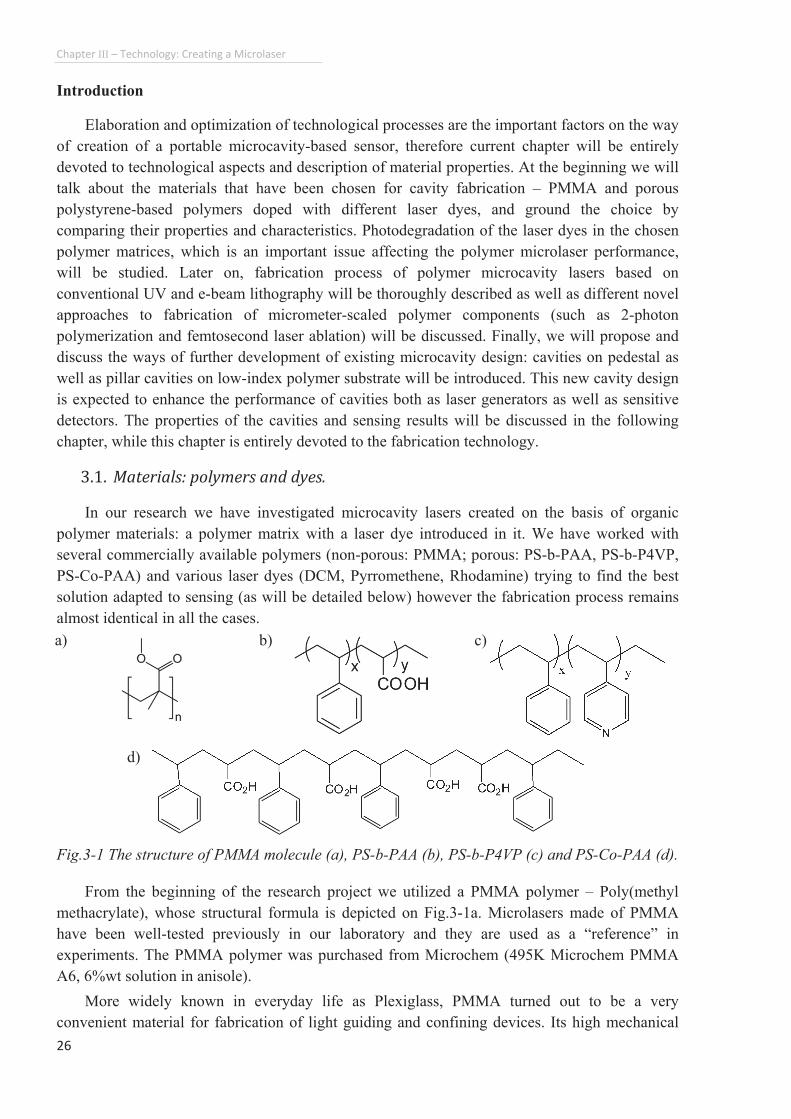
Chapter"III" "Technology:"Creating"a"Microlaser""
26""
Introduction
Elaboration and optimization of technological processes are the important factors on the way
of creation of a portable microcavity-based sensor, therefore current chapter will be entirely
devoted to technological aspects and description of material properties. At the beginning we will
talk about the materials that have been chosen for cavity fabrication � PMMA and porous
polystyrene-based polymers doped with different laser dyes, and ground the choice by
comparing their properties and characteristics. Photodegradation of the laser dyes in the chosen
polymer matrices, which is an important issue affecting the polymer microlaser performance,
will be studied. Later on, fabrication process of polymer microcavity lasers based on
conventional UV and e-beam lithography will be thoroughly described as well as different novel
approaches to fabrication of micrometer-scaled polymer components (such as 2-photon
polymerization and femtosecond laser ablation) will be discussed. Finally, we will propose and
discuss the ways of further development of existing microcavity design: cavities on pedestal as
well as pillar cavities on low-index polymer substrate will be introduced. This new cavity design
is expected to enhance the performance of cavities both as laser generators as well as sensitive
detectors. The properties of the cavities and sensing results will be discussed in the following
chapter, while this chapter is entirely devoted to the fabrication technology. ぬ┻な┻ "Materials:"polymers"and"dyes."
In our research we have investigated microcavity lasers created on the basis of organic
polymer materials: a polymer matrix with a laser dye introduced in it. We have worked with
several commercially available polymers (non-porous: PMMA; porous: PS-b-PAA, PS-b-P4VP,
PS-Co-PAA) and various laser dyes (DCM, Pyrromethene, Rhodamine) trying to find the best
solution adapted to sensing (as will be detailed below) however the fabrication process remains
almost identical in all the cases.
Fig.3-1 The structure of PMMA molecule (a), PS-b-PAA (b), PS-b-P4VP (c) and PS-Co-PAA (d).
From the beginning of the research project we utilized a PMMA polymer � Poly(methyl
methacrylate), whose structural formula is depicted on Fig.3-1a. Microlasers made of PMMA
have been well-tested previously in our laboratory and they are used as a �reference� in
experiments. The PMMA polymer was purchased from Microchem (495K Microchem PMMA
A6, 6%wt solution in anisole).
More widely known in everyday life as Plexiglass, PMMA turned out to be a very
convenient material for fabrication of light guiding and confining devices. Its high mechanical
a) b) c)
d)
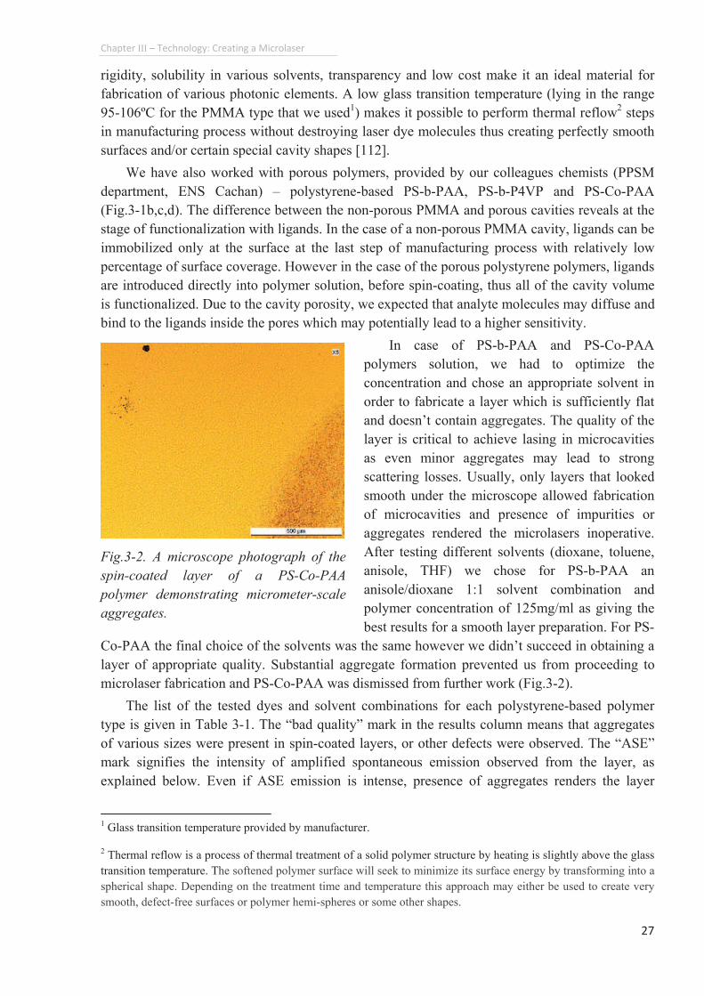
Chapter"III" "Technology:"Creating"a"Microlaser"
27""
rigidity, solubility in various solvents, transparency and low cost make it an ideal material for
fabrication of various photonic elements. A low glass transition temperature (lying in the range
95-106ºC for the PMMA type that we used1) makes it possible to perform thermal reflow
2 steps
in manufacturing process without destroying laser dye molecules thus creating perfectly smooth
surfaces and/or certain special cavity shapes [112].
We have also worked with porous polymers, provided by our colleagues chemists (PPSM
department, ENS Cachan) � polystyrene-based PS-b-PAA, PS-b-P4VP and PS-Co-PAA
(Fig.3-1b,c,d). The difference between the non-porous PMMA and porous cavities reveals at the
stage of functionalization with ligands. In the case of a non-porous PMMA cavity, ligands can be
immobilized only at the surface at the last step of manufacturing process with relatively low
percentage of surface coverage. However in the case of the porous polystyrene polymers, ligands
are introduced directly into polymer solution, before spin-coating, thus all of the cavity volume
is functionalized. Due to the cavity porosity, we expected that analyte molecules may diffuse and
bind to the ligands inside the pores which may potentially lead to a higher sensitivity.
In case of PS-b-PAA and PS-Co-PAA
polymers solution, we had to optimize the
concentration and chose an appropriate solvent in
order to fabricate a layer which is sufficiently flat
and doesn�t contain aggregates. The quality of the
layer is critical to achieve lasing in microcavities
as even minor aggregates may lead to strong
scattering losses. Usually, only layers that looked
smooth under the microscope allowed fabrication
of microcavities and presence of impurities or
aggregates rendered the microlasers inoperative.
After testing different solvents (dioxane, toluene,
anisole, THF) we chose for PS-b-PAA an
anisole/dioxane 1:1 solvent combination and
polymer concentration of 125mg/ml as giving the
best results for a smooth layer preparation. For PS-
Co-PAA the final choice of the solvents was the same however we didn�t succeed in obtaining a
layer of appropriate quality. Substantial aggregate formation prevented us from proceeding to
microlaser fabrication and PS-Co-PAA was dismissed from further work (Fig.3-2).
The list of the tested dyes and solvent combinations for each polystyrene-based polymer
type is given in Table 3-1. The �bad quality� mark in the results column means that aggregates
of various sizes were present in spin-coated layers, or other defects were observed. The �ASE�
mark signifies the intensity of amplified spontaneous emission observed from the layer, as
explained below. Even if ASE emission is intense, presence of aggregates renders the layer
""""""""""""""""""""""""""""""""""""""""""""""""""""""""""""1 Glass transition temperature provided by manufacturer.
2 Thermal reflow is a process of thermal treatment of a solid polymer structure by heating is slightly above the glass
transition temperature. The softened polymer surface will seek to minimize its surface energy by transforming into a
spherical shape. Depending on the treatment time and temperature this approach may either be used to create very
smooth, defect-free surfaces or polymer hemi-spheres or some other shapes.
Fig.3-2. A microscope photograph of the
spin-coated layer of a PS-Co-PAA
polymer demonstrating micrometer-scale
aggregates.
Chapter"III" "Technology:"Creating"a"Microlaser""
28""
unusable for cavity fabrication. For example, in the case of Anisole/THF solvent combination for
PS-b-PAA, the resulting layer was very non-uniform in thickness as a result of high solvent
volatility: solution started to dry before wafer was fully covered with polymer, however
observed ASE emission was strong. For the PS-b-P4VP polymer, aggregation can be explained
taking into account the polymer structure, which is a combination of hydrophilic and
hydrophobic parts. Probably, a self-organization of these two components in solution occurs that
leads to formation of micelles, rendering the dried polymer layer unusable. ぬ┻に┻ "Material"characterization:"Amplified"Spontaneous"Emission"and"ellipsometry."
In order to verify whether a dye-doped polymer layer is suitable for microlaser fabrication
we record its amplified spontaneous emission (ASE) spectra. ASE by definition is a process of
amplification of spontaneous emission during its propagation in a medium with gain. To record
an ASE spectrum, a doped polymer layer is pumped from the top, close to the cleaved edge, as
shown on Fig.3-3. A spontaneous emission in the lateral direction that has been amplified during
single pass in the active medium with a large gain is captured and recorded by spectrometer. A
signature of amplified spontaneous emission is an intense and narrow peak, dominating over the
luminescence spectrum. An intense ASE
peak signifies high active medium gain,
efficiency of the laser dye and good
waveguiding properties of the polymer
layer � absence of aggregates or other
scattering centers.
We have performed spectral
ellipsometry measurements (Sopra GES 5
ellipsometer, performed by Nguyen Chi
Thanh, LPQM) to determine the refractive
indices of pure and dye-doped PMMA
Dye Solvent Conc,
mg/ml
Result
PS-b-PAA
DCM-OH 1% , 2% Dioxane/toluene 1:1 150 Quality: fine. ASE: very weak.
DCM-OH 1% Anisole/THF 1:1 150 Quality: bad. ASE: intense.
DCM-OH 1% , 2%, 5% Anisole/Dioxane 1:1 125 Quality: fine. ASE: very weak.
DCM 2%, 5% Anisole/Dioxane 1:1 125 Quality: fine. ASE: intense.
Rhod640 2% Anisole/Dioxane 1:1 125 Rhodamine partly insoluble
Pyr605 2%, 5% Anisole/Dioxane 1:1 125 Quality: fine. ASE: intense.
PS-Co-PAA
DCM 2% Anisole/Dioxane 1:1 125 Quality: bad.
Rhod640 2% Anisole/Dioxane 1:1 125 Quality: bad + Rhodamine
insoluble
PS-b-P4VP
DCM 2% 3-pentanone/cyclohexane 200 Quality: bad. ASE: intense.
DCM 2% 3-pentanone/cyclohexane 150 Quality: bad. ASE: intense.
Table 3-1. Tested laser dyes, solvent combinations, polymer concentration in solvent for each
polymer type.
Fig.3-3. A schematic representation of ASE spectra
recording.
Chapter"III"�"Technology:"Creating"a"Microlaser"
29""
and PS-b-PAA layers at そ Ã 610 nm. A good refractive index contrast is necessary between the
polymer layer and a substrate in order to ensure good wave confinement and prevent mode
leakage into the substrate. Moreover, the knowledge of the refractive index and its dispersion is
necessary to analyze the lasing spectra of cavities and to calculate the optical path of light inside
[94].
For a PMMA layer (non-doped) we have measured a refractive index in the range of 1.484 -
1.495 units. For a PMMA+DCM 5% layer, the estimated value is n = 1.54. For the layer of PS-b-
PAA + Pyrromethene 2% measurements gave the refractive index value of n à 1.75.
Measurements of indices of doped layers are complicated due to the dye absorption that adds
resonant peaks in the measured data and makes it difficult to interpret the results. ぬ┻ぬ┻ "Materials:"choice"of"a"laser"dye."
A choice of the appropriate laser dye is very important to create an efficient, long-lasting
microlaser with stable emission intensity. Initially we have worked with a DCM laser dye. DCM
(4-dicyanomethylene-2-methyl-6-p-dimethylaminostyryl-4H-pyran) is a commercial dye with a
fluorescence spectrum centered around 600nm. Besides relatively low cost (purchased from
Exciton) and availability, the main assets of DCM are a good fluorescence quantum yield and a
large Stokes shift (~100nm) (Fig.3-4a) which prevents from reabsorption of the emitted light.
However, the DCM dye is subject to fast photobleaching under continuous pumping.
400 500 600 700 8000,0
0,2
0,4
0,6
0,8
1,0
Abs./
Flu
or.
, norm
Absorption
Fluorescence
Wavelength, nm400 500 600 700 800
0,0
0,2
0,4
0,6
0,8
1,0
Ab
s./
Flu
or.
, n
orm
Wavelength, nm
Absorption
Fluorescence
(a) (b) (c)
Fig.3-4. Absorption and fluorescence spectra of a layer of (a) PMMA+DCM 5%, (b)
PMMA+Pyr605 5% and (c) PMMA+Rhod640 5%.
While talking of the dye instability one needs to distinguish two different aspects. The first
one is the stability in time, which means the ability of polymer/dye combination to preserve its
properties during a long storage time. The second one is the photostability, or the behavior of the
dye under continuous exposure to pumping emission or ambient light. We have also
experimented with Pyrromethene 605 (nmax,abs = 543 nm in ethanol) and Rhodamine 640
(nmax,abs = 575 nm in ethanol) laser dyes, purchased from Exciton, which are both known to be
more photostable than DCM. Their absorption and fluorescence spectra are given in Fig.3-4b,c.
As it is obvious from the spectrum, absorption maximum of Pyrromethene 605 in PMMA matrix
(そ Ã 545nm) lies much closer to the pumping laser wavelength (532nm) thus more efficient
pump energy conversion is expected.
Introduction of different laser dyes into the non-porous PMMA matrix creates a material that
preserves its emissive properties for ages � the cavities prepared in PMMA-DCM were stored for
years without any noticeable ageing and change in their emission intensity. At the same time,
Chapter"III" "Technology:"Creating"a"Microlaser""
30""
when the dyes were introduced inside the
porous PS-b-PAA matrix, the cavities stopped
functioning after just 2-3 months of storage at
room temperature and atmosphere which may
be explained by the penetration of the oxygen
inside the polymer matrix due to porosity and
consequent dye degradation.
Dye photobleaching doesn�t only lead to
the decrease of emission intensity, but also to
the blue-shift of the emission maximum. For
example, Fig.3-5 shows the blue shift of the
maximum of an ASE spectrum of a porous PS-
b-PAA polymer layer doped with
pyrromethene dye. For a laser microcavity this
means that in a continuous series of
measurements, each subsequent spectrum is blue-shifted relative to the previous one. This effect
was observed and quantified in [35]. For a PMMA-DCM cavity the blue-shift rate of the lasing
spectrum was estimated to be hそ= 3.33·10-4
nm/s while pumping with 700ps laser pulses at 10Hz
repetition rate (4たJ pulse energy). The values of the blue-shift vary depending on the polymer-
dye combination and pump fluence and may become very significant for the microcavities. In
case of sensing applications, where we aim at detecting certain analyte presence by a spectral
shift, parasitic blue-shift creates significant interference and complicates results interpretation.
This stimulated us to experiment with different dyes that combine high quantum yield with an
improved photostability in the used polymer matrices. High quantum yield allows lower
pumping intensity and improved photostability leads to a smaller value of a blue-shift.
An optimal laser dye concentration has to be found for each polymer to achieve maximum
emission intensity while avoiding concentration quenching. ASE spectra were recorded from
dye-doped polymer layer in order to estimate their lasing ability. Both Rhodamine 640 and
Pyrromethene 605 dyes in PMMA matrix show significantly higher emission intensity than
DCM (Fig.3-6a). We have investigated their photostability under long-time illumination of the
layers by the pulsed pumping laser (pulse energy 9.3µJ, pulse duration 700ps, repetition rate
10Hz). The DCM dye turns out to be the less stable out of 3 competitors (Fig.3-6b, black) with
the ASE intensity decrease of more than 30% after 15 minutes of continuous illumination, while
Rhodamine 640 was found to be the less degrading dye.
In porous PS-b-PAA matrix Pyrromethene 605 at 2% concentration provides the maximum
emission efficiency (Fig.3-6c), however the photostability of the dye is rather short, as can be
seen on Fig.3-6d, � 60% of intensity decrease after 15 minutes of continuous excitation. For the
microcavities doped with Pyrromethene 605, the photostability was found to be significantly
lower than for doped layer, probably due to the smaller volume of the material that is excited
(cavity lateral dimensions ~150µm). The Rhodamine 640 dye is an ionic species and is not well
soluble in a weakly polar anisole/dioxane solvent combination which explains its low observed
performance. Hence temporal intensity decay was not measured for Rhodamine in PS-b-PAA.
0 5 10 15 20
603,0
603,5
604,0
604,5
605,0
605,5
Wave
len
gth
, n
m
Time, min
Fig.3-5. A blue-shift of the ASE maximum
peak of PS-b-PAA+Pyr605 2% during 20
minutes exposure to the pump laser (700ps,
10Hz repetition rate, 6.2µJ pulse energy).
Chapter"III" "Technology:"Creating"a"Microlaser"
31""
According to the measurements results, for the cavity manufacturing in the case of PMMA
polymer the dye concentration (DCM, Rhodamine 640 or Pyrromethene 605) is chosen to be 5%
in weight. In the case of PS-b-PAA polymer, dye concentration (DCM or Pyrromethene 605)
was chosen to be 2%. ぬ┻ね┻ "Microcavity"fabrication"technology."
Several technological processes are available for laser microcavity fabrication in polymers.
Cavities can be formed either by conventional lithography (UV or e-beam) or, as was supposed
in the microFLUID project we were working on, by using novel approaches such as femtosecond
laser ablation or 2-photon polymerization. Below we will briefly discuss the techniques and the
results we obtained.
540 570 600 630 660 690 720
0
10000
20000
30000
40000
50000
60000 ASE PMMA+DCM 5%
ASE PMMA+Pyr605 5%
ASE PMMA+Rhod640 5%
Wavelength, nm
Inte
nsity,
counts
0 2 4 6 8 10 12 14 16
70
80
90
100
ASE PMMA+DCM 5%
ASE PMMA+Pyr605 5%
ASE PMMA+Rhod640 5%
20%
Time, min
Inte
nsity, %
5%
32%
(a) (b)
540 570 600 630 660 690 720
100
1000
10000
ASE PS-b-PAA + DCM 2%
ASE PS-b-PAA + Rhod640 2%
ASE PS-b-PAA + Pyr605 2%
Wavelength, nm
Inte
nsity,
co
un
ts
0 2 4 6 8 10 12 14 160
20
40
60
80
100
ASE PS-b-PAA + Pyr605 2%
ASE PS-b-PAA + DCM 2%
80%
Time, min
Inte
nsity,
% 65%
(c) (d)
Fig.3-6. (a) ASE spectra of PMMA polymer layers with different laser dyes: DCM (black),
Pyrromethene 605 (green) and Rhodamine 640 (red) laser dyes demonstrate high efficiency of
Rhodamine and Pyrromethene (pump energy 9.3µJ). (b) Decay of the ASE intensity in PMMA
under continuous exposure to the pumping laser pulses (9.3µJ, 700ps, 10Hz). (c) ASE spectra of
PS-b-PAA layers with DCM, Pyrromethene 605 and Rhodamine 640 dyes on the logarithmic
scale. (d) Decay of the ASE intensity in PS-b-PAA under continuous exposure to the pumping
laser pulses (6.2µJ, 700ps, 10Hz)
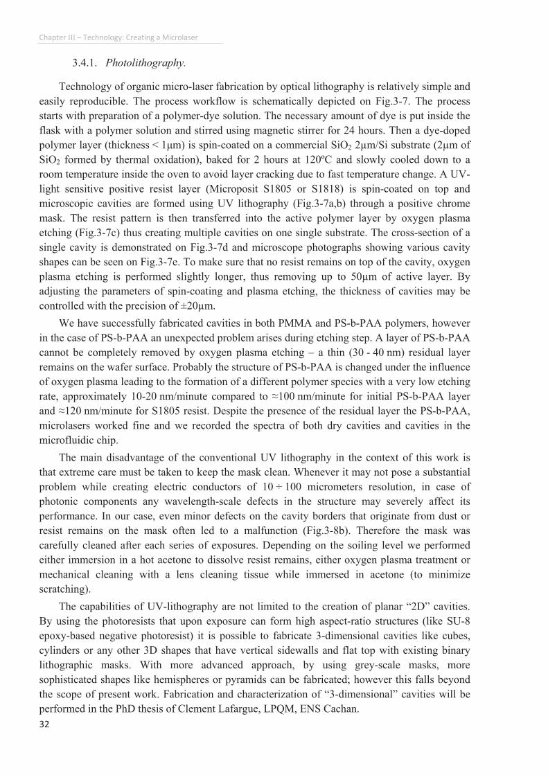
Chapter"III"�"Technology:"Creating"a"Microlaser""
32""
3.4.1. Photolithography.
Technology of organic micro-laser fabrication by optical lithography is relatively simple and
easily reproducible. The process workflow is schematically depicted on Fig.3-7. The process
starts with preparation of a polymer-dye solution. The necessary amount of dye is put inside the
flask with a polymer solution and stirred using magnetic stirrer for 24 hours. Then a dye-doped
polymer layer (thickness < 1たm) is spin-coated on a commercial SiO2 2µm/Si substrate (2µm of
SiO2 formed by thermal oxidation), baked for 2 hours at 120ºC and slowly cooled down to a
room temperature inside the oven to avoid layer cracking due to fast temperature change. A UV-
light sensitive positive resist layer (Microposit S1805 or S1818) is spin-coated on top and
microscopic cavities are formed using UV lithography (Fig.3-7a,b) through a positive chrome
mask. The resist pattern is then transferred into the active polymer layer by oxygen plasma
etching (Fig.3-7c) thus creating multiple cavities on one single substrate. The cross-section of a
single cavity is demonstrated on Fig.3-7d and microscope photographs showing various cavity
shapes can be seen on Fig.3-7e. To make sure that no resist remains on top of the cavity, oxygen
plasma etching is performed slightly longer, thus removing up to 50µm of active layer. By
adjusting the parameters of spin-coating and plasma etching, the thickness of cavities may be
controlled with the precision of ±20µm.
We have successfully fabricated cavities in both PMMA and PS-b-PAA polymers, however
in the case of PS-b-PAA an unexpected problem arises during etching step. A layer of PS-b-PAA
cannot be completely removed by oxygen plasma etching � a thin (30 - 40 nm) residual layer
remains on the wafer surface. Probably the structure of PS-b-PAA is changed under the influence
of oxygen plasma leading to the formation of a different polymer species with a very low etching
rate, approximately 10-20 nm/minute compared to Ã100 nm/minute for initial PS-b-PAA layer
and Ã120 nm/minute for S1805 resist. Despite the presence of the residual layer the PS-b-PAA,
microlasers worked fine and we recorded the spectra of both dry cavities and cavities in the
microfluidic chip.
The main disadvantage of the conventional UV lithography in the context of this work is
that extreme care must be taken to keep the mask clean. Whenever it may not pose a substantial
problem while creating electric conductors of 10 ÷ 100 micrometers resolution, in case of
photonic components any wavelength-scale defects in the structure may severely affect its
performance. In our case, even minor defects on the cavity borders that originate from dust or
resist remains on the mask often led to a malfunction (Fig.3-8b). Therefore the mask was
carefully cleaned after each series of exposures. Depending on the soiling level we performed
either immersion in a hot acetone to dissolve resist remains, either oxygen plasma treatment or
mechanical cleaning with a lens cleaning tissue while immersed in acetone (to minimize
scratching).
The capabilities of UV-lithography are not limited to the creation of planar �2D� cavities.
By using the photoresists that upon exposure can form high aspect-ratio structures (like SU-8
epoxy-based negative photoresist) it is possible to fabricate 3-dimensional cavities like cubes,
cylinders or any other 3D shapes that have vertical sidewalls and flat top with existing binary
lithographic masks. With more advanced approach, by using grey-scale masks, more
sophisticated shapes like hemispheres or pyramids can be fabricated; however this falls beyond
the scope of present work. Fabrication and characterization of �3-dimensional� cavities will be
performed in the PhD thesis of Clement Lafargue, LPQM, ENS Cachan.
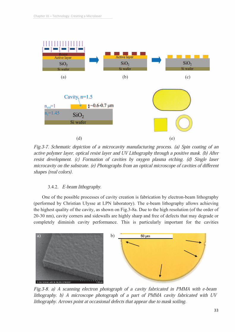
Chapter"III" "Technology:"Creating"a"Microlaser"
33""
3.4.2. E-beam lithography. One of the possible processes of cavity creation is fabrication by electron-beam lithography
(performed by Christian Ulysse at LPN laboratory). The e-beam lithography allows achieving
the highest quality of the cavity, as shown on Fig.3-8a. Due to the high resolution (of the order of
20-30 nm), cavity corners and sidewalls are highly sharp and free of defects that may degrade or
completely diminish cavity performance. This is particularly important for the cavities
(a) (b) (c)
(d) (e)
Fig.3-7. Schematic depiction of a microcavity manufacturing process. (a) Spin coating of an active polymer layer, optical resist layer and UV Lithography through a positive mask. (b) After resist development. (c) Formation of cavities by oxygen plasma etching. (d) Single laser microcavity on the substrate. (e) Photographs from an optical microscope of cavities of different shapes (real colors).
Fig.3-8. a) A scanning electron photograph of a cavity fabricated in PMMA with e-beam lithography. b) A microscope photograph of a part of PMMA cavity fabricated with UV lithography. Arrows point at occasional defects that appear due to mask soiling.
a) b)
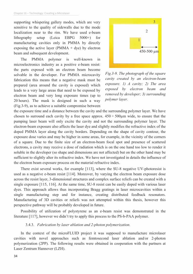
Chapter"III" "Technology:"Creating"a"Microlaser""
34""
supporting whispering gallery modes, which are very
sensitive to the quality of sidewalls due to the mode
localization near to the rim. We have used e-beam
lithography setup (Leica EBPG 5000+) for
manufacturing cavities only in PMMA by directly
exposing the active layer (PMMA + dye) by electron
beam and subsequent development.
The PMMA polymer is well-known in
microelectronics industry as a positive e-beam resist:
the parts exposed with an electron beam become
solvable in the developer. For PMMA microcavity
fabrication this means that a negative mask must be
prepared (area around the cavity is exposed) which
leads to a very large areas that need to be exposed by
electron beam and very long exposure times (up to
20 hours). The mask is designed in such a way
(Fig.3-9), as to achieve a suitable compromise between
the exposure time and a distance between the cavity and the surrounding polymer layer. We have
chosen to surround each cavity by a free space approx. 450 ÷ 500µm wide, to ensure that the
pumping laser beam will only excite the cavity and not the surrounding polymer layer. The
electron-beam exposure also affects the laser dye and slightly modifies the refractive index of the
doped PMMA layer along the cavity borders. Depending on the shape of cavity contour, the
exposure dose varies and may be higher in some areas, for example, in the vicinity of the corners
of a square. Due to the finite size of an electron-beam focal spot and presence of scattered
electrons, a cavity may receive a dose of radiation which is on the one hand too low to render it
soluble in the developer (so shape and dimensions are not affected) but on the other hand may be
sufficient to slightly alter its refractive index. We have not investigated in details the influence of
the electron beam exposure process on the material refractive index.
There exist several works, for example [113], where the SU-8 negative UV-photoresist is
used as a negative e-beam resist [114]. Moreover, by varying the electron beam exposure dose
across the resist layer, 3-dimensional structures and complex surface reliefs can be created with a
single exposure [115, 116]. At the same time, SU-8 resist can be easily doped with various laser
dyes. This approach allows thus incorporating Bragg gratings in laser microcavities within a
single manufacturing step and for instance, creating distributed feedback resonators.
Manufacturing of 3D cavities or reliefs was not attempted within this thesis, however this
perspective pathway will be probably developed in future.
Possibility of utilization of polystyrene as an e-beam resist was demonstrated in the
literature [117], however we didn�t try to apply this process to the PS-b-PAA polymer.
3.4.3. Fabrication by laser ablation and 2-photon polymerization.
In the context of the microFLUID project it was supposed to manufacture microlaser
cavities with novel approaches such as femtosecond laser ablation and/or 2-photon
polymerization (2PP). The following results were obtained in cooperation with the partners at
Laser Zentrum Hannover (LZH).
Fig.3-9. The photograph of the square
cavity created by an electron-beam
exposure. 1) A cavity; 2) The area
exposed by electron beam and
removed by developer; 3) surrounding
polymer layer.
3
1
2
450-500 µm
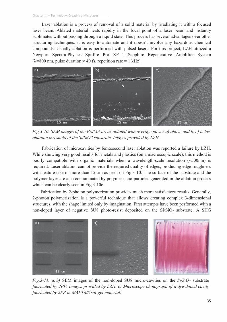
Chapter"III"�"Technology:"Creating"a"Microlaser"
35""
Laser ablation is a process of removal of a solid material by irradiating it with a focused
laser beam. Ablated material heats rapidly in the focal point of a laser beam and instantly
sublimates without passing through a liquid state. This process has several advantages over other
structuring techniques: it is easy to automate and it doesn�t involve any hazardous chemical
compounds. Usually ablation is performed with pulsed lasers. For this project, LZH utilized a
Newport Spectra-Physics Spitfire Pro XP Ti:Sapphire Regenerative Amplifier System
(n=800 nm, pulse duration à 40 fs, repetition rate = 1 kHz).
Fabrication of microcavities by femtosecond laser ablation was reported a failure by LZH.
While showing very good results for metals and plastics (on a macroscopic scale), this method is
poorly compatible with organic materials when a wavelength-scale resolution (~500nm) is
required. Laser ablation cannot provide the required quality of edges, producing edge roughness
with feature size of more than 15 µm as seen on Fig.3-10. The surface of the substrate and the
polymer layer are also contaminated by polymer nano-particles generated in the ablation process
which can be clearly seen in Fig.3-10c.
Fabrication by 2-photon polymerization provides much more satisfactory results. Generally,
2-photon polymerization is a powerful technique that allows creating complex 3-dimensional
structures, with the shape limited only by imagination. First attempts have been performed with a
non-doped layer of negative SU8 photo-resist deposited on the Si/SiO2 substrate. A SHG
Fig.3-10. SEM images of the PMMA areas ablated with average power a) above and b, c) below
ablation threshold of the Si/SiO2 substrate. Images provided by LZH.
Fig.3-11. a, b) SEM images of the non-doped SU8 micro-cavities on the Si/SiO2 substrate
fabricated by 2PP. Images provided by LZH. c) Microscope photograph of a dye-doped cavity
fabricated by 2PP in MAPTMS sol-gel material.
a) b) c)
a) b) c)
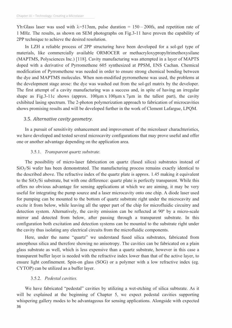
Chapter"III" "Technology:"Creating"a"Microlaser""
36""
Yb:Glass laser was used with n=513nm, pulse duration = 150 � 200fs, and repetition rate of
1 MHz. The results, as shown on SEM photographs on Fig.3-11 have proven the capability of
2PP technique to achieve the desired resolution.
In LZH a reliable process of 2PP structuring have been developed for a sol-gel type of
materials, like commercially available ORMOCER or methacryloxypropyltrimethoxysilane
(MAPTMS, Polysciences Inc.) [118]. Cavity manufacturing was attempted in a layer of MAPTS
doped with a derivative of Pyrromethene 605 synthesized at PPSM, ENS Cachan. Chemical
modification of Pyrromethene was needed in order to ensure strong chemical bonding between
the dye and MAPTMS molecules. When non-modified pyrromethene was used, the problems at
the development stage arose: the dye was washed out from the sol-gel matrix by the developer.
The first attempt of a cavity manufacturing was a success and, in spite of having an irregular
shape as Fig.3-11c shows (approx. 100µm x 100µm x 7µm in the tallest part), the cavity
exhibited lasing spectrum. The 2-photon polymerization approach to fabrication of microcavities
shows promising results and will be developed further in the work of Clement Lafargue, LPQM. ぬ┻の┻ "Alternative"cavity"geometry."
In a pursuit of sensitivity enhancement and improvement of the microlaser charachteristics,
we have developed and tested several microcavity configurations that may prove useful and offer
one or another advantage depending on the application area.
3.5.1. Transparent quartz substrate.
The possibility of micro-laser fabrication on quartz (fused silica) substrates instead of
SiO2/Si wafer has been demonstrated. The manufacturing process remains exactly identical to
the described above. The refractive index of the quartz plate is approx. 1.45 making it equivalent
to the SiO2/Si substrate, but with one difference: quartz plate is perfectly transparent. While this
offers no obvious advantage for sensing applications at which we are aiming, it may be very
useful for integrating the pump source and a laser microcavity onto one chip. A diode laser used
for pumping can be mounted to the bottom of quartz substrate right under the microcavity and
excite it from below, while leaving all the upper part of the chip for microfluidic circuitry and
detection system. Alternatively, the cavity emission can be reflected at 90º by a micro-scale
mirror and detected from below, after passing through a transparent substrate. In this
configuration both excitation and detection systems can be mounted to the substrate right under
the cavity thus isolating any electrical circuits from the microfluidic components.
Here, under the name �quartz� we understand fused silica substrates, fabricated from
amorphous silica and therefore showing no anisotropy. The cavities can be fabricated on a plain
glass substrate as well, which is less expensive than a quartz substrate, however in this case a
transparent buffer layer is needed with the refractive index lower than that of the active layer, to
ensure light confinement. Spin-on glass (SOG) or a polymer with a low refractive index (eg.
CYTOP) can be utilized as a buffer layer.
3.5.2. Pedestal cavities.
We have fabricated �pedestal� cavities by utilizing a wet-etching of silica subtsrate. As it
will be explained at the beginning of Chapter 5, we expect pedestal cavities supporting
whispering gallery modes to be advantageous for sensing applications. Alongside with expected
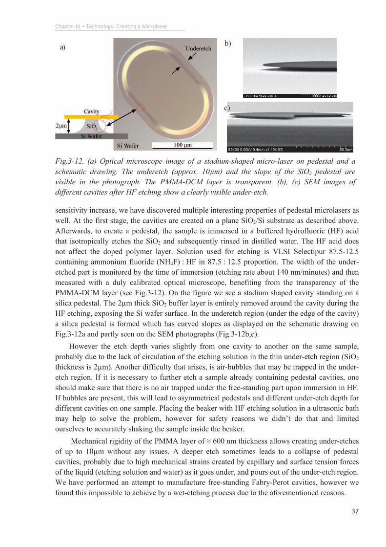
Chapter"III" "Technology:"Creating"a"Microlaser"
37""
sensitivity increase, we have discovered multiple interesting properties of pedestal microlasers as
well. At the first stage, the cavities are created on a plane SiO2/Si substrate as described above.
Afterwards, to create a pedestal, the sample is immersed in a buffered hydrofluoric (HF) acid
that isotropically etches the SiO2 and subsequently rinsed in distilled water. The HF acid does
not affect the doped polymer layer. Solution used for etching is VLSI Selectipur 87.5-12.5
containing ammonium fluoride (NH4F) : HF in 87.5 : 12.5 proportion. The width of the under-
etched part is monitored by the time of immersion (etching rate about 140 nm/minutes) and then
measured with a duly calibrated optical microscope, benefiting from the transparency of the
PMMA-DCM layer (see Fig.3-12). On the figure we see a stadium shaped cavity standing on a
silica pedestal. The 2µm thick SiO2 buffer layer is entirely removed around the cavity during the
HF etching, exposing the Si wafer surface. In the underetch region (under the edge of the cavity)
a silica pedestal is formed which has curved slopes as displayed on the schematic drawing on
Fig.3-12a and partly seen on the SEM photographs (Fig.3-12b,c).
However the etch depth varies slightly from one cavity to another on the same sample,
probably due to the lack of circulation of the etching solution in the thin under-etch region (SiO2
thickness is 2µm). Another difficulty that arises, is air-bubbles that may be trapped in the under-
etch region. If it is necessary to further etch a sample already containing pedestal cavities, one
should make sure that there is no air trapped under the free-standing part upon immersion in HF.
If bubbles are present, this will lead to asymmetrical pedestals and different under-etch depth for
different cavities on one sample. Placing the beaker with HF etching solution in a ultrasonic bath
may help to solve the problem, however for safety reasons we didn�t do that and limited
ourselves to accurately shaking the sample inside the beaker.
Mechanical rigidity of the PMMA layer of à 600 nm thickness allows creating under-etches
of up to 10µm without any issues. A deeper etch sometimes leads to a collapse of pedestal
cavities, probably due to high mechanical strains created by capillary and surface tension forces
of the liquid (etching solution and water) as it goes under, and pours out of the under-etch region.
We have performed an attempt to manufacture free-standing Fabry-Perot cavities, however we
found this impossible to achieve by a wet-etching process due to the aforementioned reasons.
Fig.3-12. (a) Optical microscope image of a stadium-shaped micro-laser on pedestal and a
schematic drawing. The underetch (approx. 10µm) and the slope of the SiO2 pedestal are
visible in the photograph. The PMMA-DCM layer is transparent. (b), (c) SEM images of
different cavities after HF etching show a clearly visible under-etch.
b)
c)
Chapter"III" "Technology:"Creating"a"Microlaser""
38""
After creating a pedestal, another oxygen plasma etching step may be used to adjust the
thickness of the cavity and to obtain cavities of the order of or thinner that the cutoff thickness
for the cavity on a plane SiO2 substrate (Ã300nm). This order of operations is preferable as wet-
etching the thinner and therefore more fragile cavities may easily collapse them. The advantage
of thinner cavities for sensing will be explained in paragraph 4.4.1.
3.5.3. Low-index substrate cavities. Pillar cavities.
We have successfully fabricated laser microcavities on a low-index, transparent polymer
buffer layer. On the one hand, the transparent buffer layer may be indispensable if cavities are to
be fabricated on a transparent glass substrate, when detection or excitation is performed through
the substrate. On the other hand, the CYTOP polymer used as buffer has refractive index lower
than that of the silica, therefore we expect it to have positive influence on the lasing properties of
our cavities. Higher refractive index contrast means better mode confinement in the active layer
and lower losses. Moreover, as it will become clear from Chapter 5, cavities on CYTOP pillars
may be advantageous for sensing applications.
The fabrication process of the cavities on a low-index polymer substrate is generally similar
but includes few additional steps. As a buffer layer we have used a CYTOP CTX-809A polymer
(Asahi Glass Co. Ltd.) that belongs to the class of fluoropolymers [119, 120]. A 2µm thick layer
of CYTOP is spin-coated on a commercial Si substrate (or on glass), baked for 2 hours at 180ºC
and slowly cooled down to a room temperature. The measured refractive index of the layer was
n à 1.34 (ellipsometry performed by Nguyen Chi Thanh, LPQM). After baking, CYTOP forms a
highly hydrophobic, transparent coating resistant to majority of organic solvents. In order to
make PMMA (or any other polymer) adhesion possible, a CYTOP surface was activated by a
Fig.3-13. a) A schematic image of a polymer microcavity on a low-index CYTOP substrate.
Inset shows the angle at which the cavity is photographed. b,c) Schematic depiction of
correspondingly asymmetric and symmetric cavity on a CYTOP pillar. d,e) Microscope and
SEM photographs of a working cavity on a CYTOP pillar (total thickness approx. 3.5µm).
a) b) c)
d) e)Microscope photo
Si wafer edge
SEM photo
PMMA
CYTOP
Ã3.5µm
Si
Chapter"III"�"Technology:"Creating"a"Microlaser"
39""
short exposure to oxygen plasma. Immediately after, a dye-doped PMMA layer was spin-coated,
and processed as was described above. The etching rate of CYTOP in the oxygen plasma (bias
300V, 50W RF power, 5mT O2 pressure) is approx. 380nm/min which is substantially higher
than for PMMA (Ã180nm/min) and S1818 resist (Ã120nm/min). It is difficult to precisely control
the etching (which is a complex process and the rate may vary, in general, nonlinearly with time)
to stop at exactly the right moment, so a PMMA cavity is always standing on a little CYTOP
pillar as displayed on a scheme on Fig.3-13a.
While advantageous for various reasons (see Chapter 5.6) these cavities are not very well
suited for sensing: a microfluidic chip cannot be attached to the CYTOP layer; a clean Si wafer
surface would be preferable. A logical continuation of this process was the creation of CYTOP
pillars (Fig.3-13b,d,e). By slightly increasing the resist thickness and oxygen plasma etching
time, it is possible to entirely remove the CYTOP substrate and create a cavity on top of the
pillar. Due to the big difference in etching rates, pillar height can be varied to a great extent and
made as high as 7-10µm, which may be required by the lab-on-a-chip architecture.
Generally, utilization of a low-index polymer substrate layer enables us to easily create
microlaser cavities on virtually any surface, where a smooth layer can be spin-coated. Thus all-
polymer devices can easily be created by conventional lithographic techniques, if we replace
quartz or silicon substrates by a plastic with a thin layer of low-index polymer spin-coated on
top. Moreover, symmetrical cavities that have no cutoff thickness can be easily constructed, if
another layer of CYTOP is spin-coated on the doped PMMA layer (Fig.3-13c).
3.5.4. All-polymer pedestal cavities.
As a further development of pillar cavity technology, we have attempted to combine the
advantages of a pedestal and a low-index substrate and to create a cavity on a low-index CYTOP
pedestal. This process is possible due to the fact that solvents that dissolve fluoropolymers are
often chemically inert to other organic compounds making it possible to selectively dissolve the
CYTOP substrate without affecting the cavity. We have used Perfluorodecalin (chemical
formula: C10F18) purchased from Sigma-Aldrich as a solvent, which is a flammable but relatively
non-toxic compound, much safer in handling than HF acid. It should be noted also that a wide
range of fluorinated solvents are currently available on the market: 3M Fluorinert liquid,
perfluoro(methyldecalin), perfluorokerosene, perfluoroheptane and its isomers and combinations
[121, 122]. The choice of solvent is therefore not limited to perfluorodecalin and determined by
the availability of one or another compound.
The process of CYTOP dissolution is substantially different from the oxide etching by HF.
When immersed in acid, SiO2 is completely dissolved with no residues remaining, however
when CYTOP is immersed in the solvent, a combination of dissolution and lift-off processes
occurs. Depending on the molecular weight, the CYTOP layer can be a very stable solid that will
not entirely dissolve but will decompose in tiny fragments and peel off the surface.
First we have measured the dissolution/lift-off rate by immersing a spin-coated layer of
CYTOP into perfluorodecalin and measuring the layer thickness before and after immersion. The
layer was rinsed with distilled water immediately after solvent immersion. The etch rate was
found to be Ã125nm/min, however a large number of tiny peeled of fragments were found on the
layer surface after the rinse. Perfluorodecalin is an oily substance and is not easily washed away
by water. So the alternative to the water rinse was to dip a sample for a few seconds in a pure
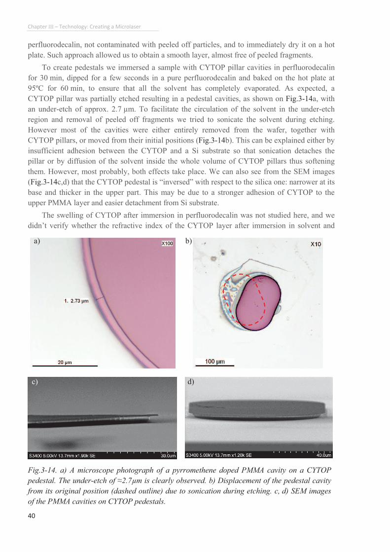
Chapter"III" "Technology:"Creating"a"Microlaser""
40""
perfluorodecalin, not contaminated with peeled off particles, and to immediately dry it on a hot
plate. Such approach allowed us to obtain a smooth layer, almost free of peeled fragments.
To create pedestals we immersed a sample with CYTOP pillar cavities in perfluorodecalin
for 30 min, dipped for a few seconds in a pure perfluorodecalin and baked on the hot plate at
95ºC for 60 min, to ensure that all the solvent has completely evaporated. As expected, a
CYTOP pillar was partially etched resulting in a pedestal cavities, as shown on Fig.3-14a, with
an under-etch of approx. 2.7 µm. To facilitate the circulation of the solvent in the under-etch
region and removal of peeled off fragments we tried to sonicate the solvent during etching.
However most of the cavities were either entirely removed from the wafer, together with
CYTOP pillars, or moved from their initial positions (Fig.3-14b). This can be explained either by
insufficient adhesion between the CYTOP and a Si substrate so that sonication detaches the
pillar or by diffusion of the solvent inside the whole volume of CYTOP pillars thus softening
them. However, most probably, both effects take place. We can also see from the SEM images
(Fig.3-14c,d) that the CYTOP pedestal is �inversed� with respect to the silica one: narrower at its
base and thicker in the upper part. This may be due to a stronger adhesion of CYTOP to the
upper PMMA layer and easier detachment from Si substrate.
The swelling of CYTOP after immersion in perfluorodecalin was not studied here, and we
didn�t verify whether the refractive index of the CYTOP layer after immersion in solvent and
Fig.3-14. a) A microscope photograph of a pyrromethene doped PMMA cavity on a CYTOP
pedestal. The under-etch of Ã2.7µm is clearly observed. b) Displacement of the pedestal cavity
from its original position (dashed outline) due to sonication during etching. c, d) SEM images
of the PMMA cavities on CYTOP pedestals.
a) b)
c) d)

Chapter"III" "Technology:"Creating"a"Microlaser"
41""
drying remains the same as the index of a newly spin-coated layer. We have demonstrated the
possibility of creating fully organic pedestal cavities, but the process still needs to be optimized.

Chapter"III"�"Technology:"Creating"a"Microlaser""
42""

Chapter"IV" "Microlaser"as"a"Refractive"Index"Sensor"
43""
4. Chapter"IV"""
Microlaser as a refractive index sensor
""
4.1." Principle"of"refractive"index"change"detection.".........................................................................."44"4.2." Designing"a"microfluidic"chip."..................................................................................................... "46"4.3." Sensing"selectivity:"specific"ligand"grafting."................................................................................"51"4.4." Sensing"and"various"cavity"shapes."Choice"of"the"optimal"shape.".............................................."56"
4.4.1." Factors"influencing"sensitivity"to"refractive"index"variation.".............................................."57"4.4.2." Optimal"cavity"shape"..........................................................................................................."63"
4.5." Experimental"proof"of"RI"variation"sensing"and"heavy"metal"ions"detection."............................"68"4.5.1." First"measurements"of"lasing"spectra"in"liquids."................................................................."68"4.5.2." Refractive"index"variation:"preparation"of"sample"solutions"and"first"attempts."..............."69"4.5.3." Proof"of"RI"variation"sensing"principle."..............................................................................."70"4.5.4." Temperature"Influence........................................................................................................"76"
4.6." Detection"of"heavyどmetal"ions"with"microcavity"sensors.".........................................................."77""
"
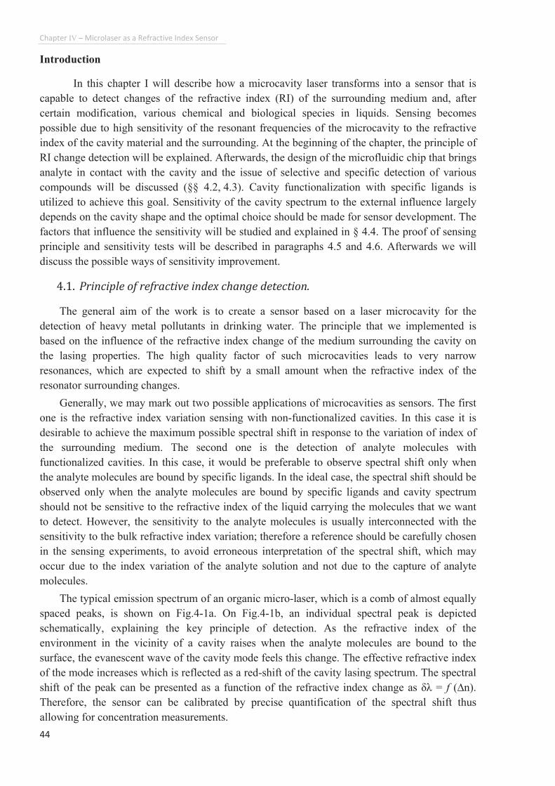
Chapter"IV"�"Microlaser"as"a"Refractive"Index"Sensor"
44""
Introduction
In this chapter I will describe how a microcavity laser transforms into a sensor that is
capable to detect changes of the refractive index (RI) of the surrounding medium and, after
certain modification, various chemical and biological species in liquids. Sensing becomes
possible due to high sensitivity of the resonant frequencies of the microcavity to the refractive
index of the cavity material and the surrounding. At the beginning of the chapter, the principle of
RI change detection will be explained. Afterwards, the design of the microfluidic chip that brings
analyte in contact with the cavity and the issue of selective and specific detection of various
compounds will be discussed (§§ 4.2, 4.3). Cavity functionalization with specific ligands is
utilized to achieve this goal. Sensitivity of the cavity spectrum to the external influence largely
depends on the cavity shape and the optimal choice should be made for sensor development. The
factors that influence the sensitivity will be studied and explained in § 4.4. The proof of sensing
principle and sensitivity tests will be described in paragraphs 4.5 and 4.6. Afterwards we will
discuss the possible ways of sensitivity improvement. ね┻な┻ "Principle"of"refractive"index"change"detection."
The general aim of the work is to create a sensor based on a laser microcavity for the
detection of heavy metal pollutants in drinking water. The principle that we implemented is
based on the influence of the refractive index change of the medium surrounding the cavity on
the lasing properties. The high quality factor of such microcavities leads to very narrow
resonances, which are expected to shift by a small amount when the refractive index of the
resonator surrounding changes.
Generally, we may mark out two possible applications of microcavities as sensors. The first
one is the refractive index variation sensing with non-functionalized cavities. In this case it is
desirable to achieve the maximum possible spectral shift in response to the variation of index of
the surrounding medium. The second one is the detection of analyte molecules with
functionalized cavities. In this case, it would be preferable to observe spectral shift only when
the analyte molecules are bound by specific ligands. In the ideal case, the spectral shift should be
observed only when the analyte molecules are bound by specific ligands and cavity spectrum
should not be sensitive to the refractive index of the liquid carrying the molecules that we want
to detect. However, the sensitivity to the analyte molecules is usually interconnected with the
sensitivity to the bulk refractive index variation; therefore a reference should be carefully chosen
in the sensing experiments, to avoid erroneous interpretation of the spectral shift, which may
occur due to the index variation of the analyte solution and not due to the capture of analyte
molecules.
The typical emission spectrum of an organic micro-laser, which is a comb of almost equally
spaced peaks, is shown on Fig.4-1a. On Fig.4-1b, an individual spectral peak is depicted
schematically, explaining the key principle of detection. As the refractive index of the
environment in the vicinity of a cavity raises when the analyte molecules are bound to the
surface, the evanescent wave of the cavity mode feels this change. The effective refractive index
of the mode increases which is reflected as a red-shift of the cavity lasing spectrum. The spectral
shift of the peak can be presented as a function of the refractive index change as hそ = f (Än).
Therefore, the sensor can be calibrated by precise quantification of the spectral shift thus
allowing for concentration measurements.
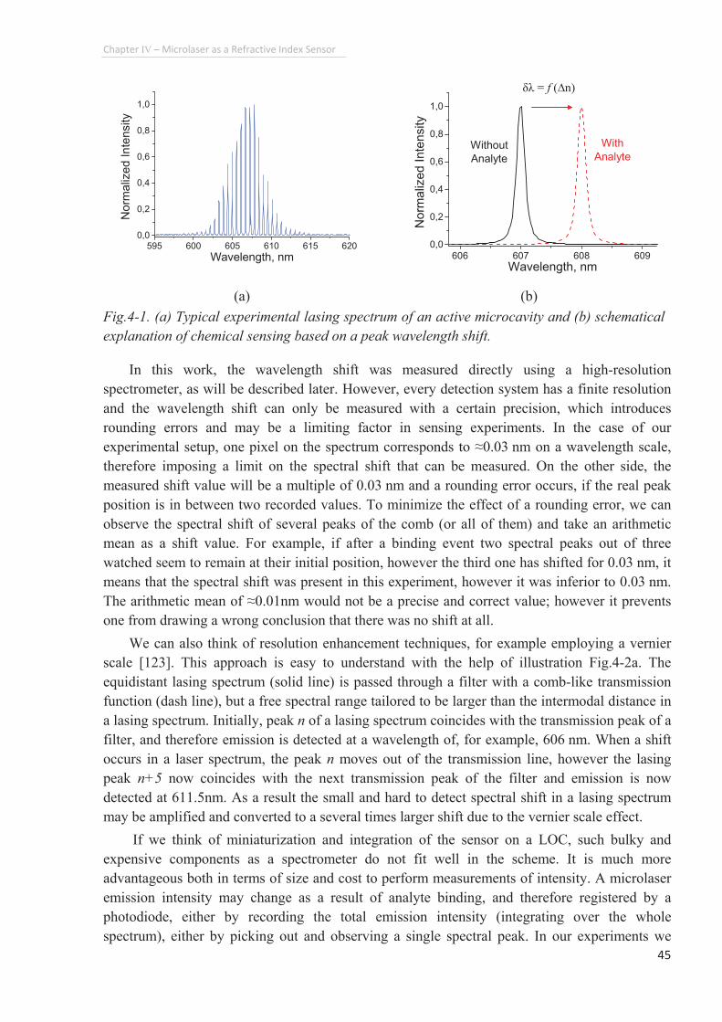
Chapter"IV"�"Microlaser"as"a"Refractive"Index"Sensor"
45""
In this work, the wavelength shift was measured directly using a high-resolution
spectrometer, as will be described later. However, every detection system has a finite resolution
and the wavelength shift can only be measured with a certain precision, which introduces
rounding errors and may be a limiting factor in sensing experiments. In the case of our
experimental setup, one pixel on the spectrum corresponds to Ã0.03 nm on a wavelength scale,
therefore imposing a limit on the spectral shift that can be measured. On the other side, the
measured shift value will be a multiple of 0.03 nm and a rounding error occurs, if the real peak
position is in between two recorded values. To minimize the effect of a rounding error, we can
observe the spectral shift of several peaks of the comb (or all of them) and take an arithmetic
mean as a shift value. For example, if after a binding event two spectral peaks out of three
watched seem to remain at their initial position, however the third one has shifted for 0.03 nm, it
means that the spectral shift was present in this experiment, however it was inferior to 0.03 nm.
The arithmetic mean of Ã0.01nm would not be a precise and correct value; however it prevents
one from drawing a wrong conclusion that there was no shift at all.
We can also think of resolution enhancement techniques, for example employing a vernier
scale [123]. This approach is easy to understand with the help of illustration Fig.4-2a. The
equidistant lasing spectrum (solid line) is passed through a filter with a comb-like transmission
function (dash line), but a free spectral range tailored to be larger than the intermodal distance in
a lasing spectrum. Initially, peak n of a lasing spectrum coincides with the transmission peak of a
filter, and therefore emission is detected at a wavelength of, for example, 606 nm. When a shift
occurs in a laser spectrum, the peak n moves out of the transmission line, however the lasing
peak n+5 now coincides with the next transmission peak of the filter and emission is now
detected at 611.5nm. As a result the small and hard to detect spectral shift in a lasing spectrum
may be amplified and converted to a several times larger shift due to the vernier scale effect.
If we think of miniaturization and integration of the sensor on a LOC, such bulky and
expensive components as a spectrometer do not fit well in the scheme. It is much more
advantageous both in terms of size and cost to perform measurements of intensity. A microlaser
emission intensity may change as a result of analyte binding, and therefore registered by a
photodiode, either by recording the total emission intensity (integrating over the whole
spectrum), either by picking out and observing a single spectral peak. In our experiments we
595 600 605 610 615 620
0,0
0,2
0,4
0,6
0,8
1,0
No
rma
lize
d In
ten
sity
Wavelength, nm 606 607 608 609
0,0
0,2
0,4
0,6
0,8
1,0
With
Analyte
Wavelength, nm
Norm
aliz
ed Inte
nsity
Without
Analyte
(a) (b)
Fig.4-1. (a) Typical experimental lasing spectrum of an active microcavity and (b) schematical
explanation of chemical sensing based on a peak wavelength shift.
hそ = f (Än)"
Chapter"IV"�"Microlaser"as"a"Refractive"Index"Sensor"
46""
couldn�t determine any dependency in the intensity change as a result of analyte binding or
refractive index change, therefore this approach was not applicable in our particular case
(Fig.4-2b).
Other, indirect ways of measurement of wavelength shift are also possible, which should be
advantageous for a miniature lab-on-a-chip (LOC) system. The wavelength shift can be
converted into the change of intensity if we employ a filtering scheme that will isolate one single
peak out of the lasing spectrum, or if a single-mode microlaser will be employed. Then, if the
photodetector records laser emission intensity at the wavelength of this peak, any shift in the
peak maximum will be detected with high precision as a change of emission intensity, assuming
that the peak is narrow.
Alternatively, other configurations can be thought of, in which the intensity change is
measured. If the direction of microlaser emission maximum depends on the refractive index of
the medium, which is true for stadium-shaped cavities (as we will see later), then the change of
emission direction can be recorded as a variation of intensity by a photodiode that collects laser
emission at a certain narrow angle. One more possible mode of detection system functioning is
the �binary� on/off action of the microlaser under certain conditions. In a case, when a lasing
periodic orbit in a cavity becomes deconfined when the index of the surrounding medium
bypasses a certain threshold value, the lasing spectrum will abruptly change. This change will be
measured by a photodiode as either a jump in intensity or total absence of emission, depending
on the cavity lasing orbit.
While the direct measurement of the spectral shift by a spectrometer was accomplished in
this thesis as the simplest to implement for laboratory tests of micro-laser based detectors, the
more sophisticated, integrable and compact detection schemes may be realized in future work on
microcavity sensors. ね┻に┻ "Designing"a"microfluidic"chip."
In order to transform a microcavity laser into a detection system, it must be somehow
brought in contact with the analyte solution. The simplest solution that can be thought of is
simply placing the drop of the analyte solution on top of the cavity. This approach, which is not
606 608 610 6120
50
100
150
200
250
300
n+5
Inte
nsi
ty, co
unts
Wavelength, nm
n
599,75 600,00 600,25 600,50
0
100
200
300
400
500
600 608
Wavelength, nm
Inte
nsi
ty, co
unts
248
x2.5 intensity
variation
(a) (b)
Fig.4-2. a) An illustration demonstrating the vernier scale principle in spectral shift detection
b) Intensity variation of the same peak within a series of spectra
Chapter"IV" "Microlaser"as"a"Refractive"Index"Sensor"
47""
applicable for the integrated detection system, may seem sufficient for the intermediate
experiments. However, the drop of liquid placed on the cavity acts as a lens both for the
excitation beam and for the laser emission of the cavity itself, uncontrollably changing the
conditions of experiment, deflecting the emission and rendering the results irreproducible.
Therefore, one of the priority tasks of the project is the integration of microcavities and
possibly other photonic components into the microfluidic networks to address the sensing
application. The ability to adequately manipulate fluids is essential for a LOC system. This can
range from simple flow-through systems that require little interference from an operating device,
to complex networks containing active elements for the control of movement of one or several
drops of fluid.
Current task of heavy metals detection implies that the microfluidic chip must fulfill the
following criteria: 1) it must ensure effective delivery/evacuation of analyte to/from the cavity
surface; 2) it should allow easy pumping of the microlaser cavity and 3) microlaser emission
spectra must be easily registered. Therefore a work has been performed in order to find a
microfluidic network design that fulfills all the stated criteria.
The scheme of the microfluidic chip that was designed, made of Polydimethylsiloxane
(PDMS) by molding technique is presented on Fig.4-6a,b with caption indicating liquid inlet and
outlet channels. PDMS is a silicon-based organic polymer, used in a wide range of domains,
from medicine to food industry and is a most common material for fabrication of microfluidic
chips [124-127]. It is optically clear (n à 1.41 ÷ 1.43), and in general, is considered to be inert,
non-toxic and non-flammable. For microfluidic chip fabrication it is supplied as a two-
component kit: a liquid PDMS prepolymer and a cross-linking agent. Once mixed in appropriate
proportions, cross-linking process starts under room temperature and PDMS cures to a hard
rubbery state. Thanks to its properties, it is a perfect material for molding: a silicon wafer or a
glass plate can be used as a mold on which a relief pattern of microfluidic channels is created.
The liquid prepolymer is then poured into the mold and left to polymerize. When removed from
the mold, even the smallest relief details are left imprinted in the PDMS slab.
For our microfluidic chip fabrication we purchased a two-part kit from Dow Corning: a
pourable liquid SYLGARD 184 Silicone Elastomer (PDMS) and a curing agent. Polymerization
of liquid PDMS is achieved by mixing the two components in a 10:1 ratio by volume. Once
mixed, the cross-linking reaction starts and proceeds slowly: the cross-linking at a room
temperature completes in 48hours. We fabricated a mold from a layer of SU-8 2025 photoresist
(~25µm thick) spin-coated on a Si wafer and patterned by UV-lithography (Fig.4-3a). Prior to
Fig.4-3. Explanation of the PDMS chip manufacturing process: a) A mold fabricated in SU-8
photoresist on Si wafer; b) A mold with two vertical glass plates fixed on it; c) A finished PDMS
chip bonded to a wafer, showing a concave upper surface.
a) b) c)
Chapter"IV" "Microlaser"as"a"Refractive"Index"Sensor"
48""
pouring the liquid PDMS prepolymer, the mold was treated by the vapor of HMDS
(Hexamethyldisilazane), which silanizes the surface thus rendering it hydrophobic and facilitates
PDMS detachment from the mold. The mold is placed in a closed container with a beaker of
liquid HMDS inside for approximately 30 minutes. The volatile HMDS liquid evaporates inside
the container and forms a very thin layer on the mold surface that is sufficient to prevent PDMS
from sticking to the mold. To accelerate the polymerization process, heat treatment is applied
that drastically increases cross-linking rate: we baked the mold with liquid PDMS inside the
oven at 75ºC for 120min, which was sufficient for polymerization reaction to complete. During
the process, the mold is rigidly fixed in a home-made Teflon holder that prevents liquid PDMS
from leaking.
Afterwards, the ready-made chip � a polymerized PDMS slab with imprinted channels � is
carefully detached from the mold. The needed parts of the slab can be easily cut out with a
scalpel or a razor blade. The holes are cut through the slab using a thin metal tube with a
sharpened section edge. The holes will be used later to connect flexible inlet and outlet pipes.
The surfaces of the chip are protected from dust and soiling with a scotch tape (3M) up to the
moment of attachment to the wafer.
The chip can be sealed to a clean, smooth glass or SiO2 plate or silicon surface. The surface
of a cured PDMS is hydrophobic, therefore oxygen plasma oxidation is used to activate the
surface by disrupting surface bonds and creating SiOH groups. After the treatment, the PDMS is
placed on a wafer with the activated side (the side with imprinted channels) down and once the
bonds relax to their normal state, the slab is permanently sealed to the surface, thus creating a
waterproof channel with inlet and outlet connectors. Oxidized PDMS surface remains stable in
air, for a time largely sufficient to attach the slab to
a wafer and, after a certain time hydrophobic
recovery of the surface is inevitable, independently
of the surrounding medium.
One of the tasks that needed to be solved is the
effective circulation of the analyte solution inside
the microfluidic chamber to ensure that the entire
surface of the cavity is exposed to the analyte. After
numerical modelisation (COMSOL Multiphysics)
of the liquid flow inside the chamber, we came up
with the solution to introduce rhombus-shaped
mixers inside the chamber as displayed on Fig.4-4
(results obtained and presented in the thesis of Wu
Ting, PPSM). Without the mixers the flow tends to
concentrate in the central part of the chamber,
whenever the sides are not sufficiently accessed by
liquid. Introduction of mixers in front of the inlet
channel leads to more uniform distribution of the
analyte solution throughout the chamber at the flow
velocity of 0.007 m/s and homogenizes the flow
velocity distribution across the chamber.
Fig.4-4. Numerical modelisation of the
flow in a microfluidic chamber. Color
code: flow velocity in m/s. Red arrow
lengths is proportional to the flow
velocity in a given area.
Chapter"IV" "Microlaser"as"a"Refractive"Index"Sensor"
49""
We have also investigated an alternative approach to achieve efficient liquid circulation and
wetting the cavities in a microfluidic chamber without utilization of the mixers but just by
modifying the shape of the chamber. Numerical simulations using COMSOL Multiphysics have
been performed for the case of stadium-shaped chambers. The stadium-shaped billiard is known
to be a chaotic system. It is thus an archetypal research object in quantum chaos physics. By
analogy, we wanted to estimate the behavior of stadium-shaped chamber in microfluidics
network. Results of simulations are presented on Fig.4-5. The figures show flow velocity
distribution inside the chamber in meters/s with red color corresponding to the fastest and blue �
to the slowest flow velocity. Several configurations of inlet/outlet channels have been
considered. However, simulations proved that effective liquid circulation is achieved only at
inlet flow velocity of about 0.055 m/s which is about ten times larger than in currently used
system with mixers. Therefore the chamber design with rhombus-shaped mixers inside was
preferred as simpler and ensuring the desired result.
In order to observe cavity�s optical response the sidewalls of the PDMS chip must be highly
flat and transparent to allow light to escape the chip and minimize losses due to light refraction
and scattering on surface roughnesses. If the PDMS slab is cut with a scalpel after curing, the
resulting side surfaces are rough and diffusing (Fig.4-6c), making it virtually impossible to
observe microcavity emission through the chip. Such fabrication is appropriate if the emission is
recorded through the transparent top side of the PDMS chip or through the bottom supporting
glass plate. In our configuration, when emission is collected sideways, the recorded ASE
intensity was more than 200 times lower than for the same sample without the PDMS chip.
Several ways of solving the issue were considered: we tried carefully cutting the PDMS with
a thin razor blade, which didn�t bring positive results as the edge remained diffusive; we
considered modifying the mold by attaching two polished wafer pieces. However the simplest
way to achieve highly transparent sidewalls was chosen. As it is shown on Fig.4-3b two parallel
glass plates were fixed vertically on the mold during PDMS chip manufacturing. The contact of
the liquid PDMS with the smooth glass surface ensures the necessary quality of the chip
sidewalls after solidification (Fig.4-6c). We also exposed glass plates to HMDS vapor, however
polymerized chip is easily detached from the plates even without this precaution. The Teflon
mold holder, mentioned above (and not shown on the photographs), also serves to rigidly fix the
glass plates.
Fig.4-5. Numerical simulation results for liquid flow velocity distribution (m/s, shown in color)
in stadium-shaped microfluidic chamber for 2 different configurations of inlet/outlet channels.
Red arrow lengths is proportional to the flow velocity in a given area.
Chapter"IV" "Microlaser"as"a"Refractive"Index"Sensor"
50""
The drawback of this fabrication approach that immediately becomes obvious is that the top
surface of the PDMS chip has a curved shape instead of being flat. The PDMS in its liquid
phase, contained within two glass plates forms a concave meniscus, which we see in the chip
after polymerization (Fig.4-3c). If the microcavity pumping is performed from the top, as it is
realized in our experimental setup, the meniscus will play the role of a lens, deflecting the pump
laser beam and complicating the alignment of the pump with the cavity. The simplest
improvement to solve this issue would be to fix the third glass plate in a horizontal position, in
between the two vertical ones, so that the liquid PDMS touches it when poured on the mold and
doesn�t form a concave meniscus. This would somewhat complicate the microfluidic chip
production, however facilitating the beam alignment. We worked with the concave PDMS chips,
as the alignment problem is not a crucial one at this stage and did not influence the measurement
precision.
The second source of inaccuracy comes from the positioning of the two glass plates: they
are neither ideally parallel nor ideally vertical
(perpendicular to the mold). These features are
transferred into a PDMS chip leading to deflection of the
cavity emission that passes through the sidewalls, both in
vertical and horizontal planes. A mold with precisely
aligned holders for glass plates needs to be manufactured
to avoid described defects; however the degree of
influence of these inaccuracies was acceptable and didn�t
pose any significant problems in current experiments.
Finally, the third difficulty comes from the fact,
that the PDMS wall should be preferably perpendicular to
the direction of maximum emission of the cavity. The
situation is illustrated on Fig.4-7: if the cavity is in the air
(n1=1), refraction of cavity emission (red line) on two
(a) (b) (c)
Fig.4-6. (a) A scheme of the microfluidic channel with microcavities inside it (view from the top).
(b) Photograph of the working microfluidic sensor prototype: a molded PDMS cap with a
microfluidic channel placed on top of the SiO2/Si substrate with microlaser cavities on it. (c)
Photograph demonstrating the transparent sidewalls of the final PDMS chip (bottom) in
comparison with the diffusive sides of the first chip designs (top).
Fig.4-7. Schematic view of a cavity
inside the microfluidic channel
illustrating the case when cavity
emission direction is not
perpendicular to the PDMS wall.
Transparent sidewalls
"
"
"
Cavities
Mixers
Inlet
Outlet
Chamber with cavities
Diffusive
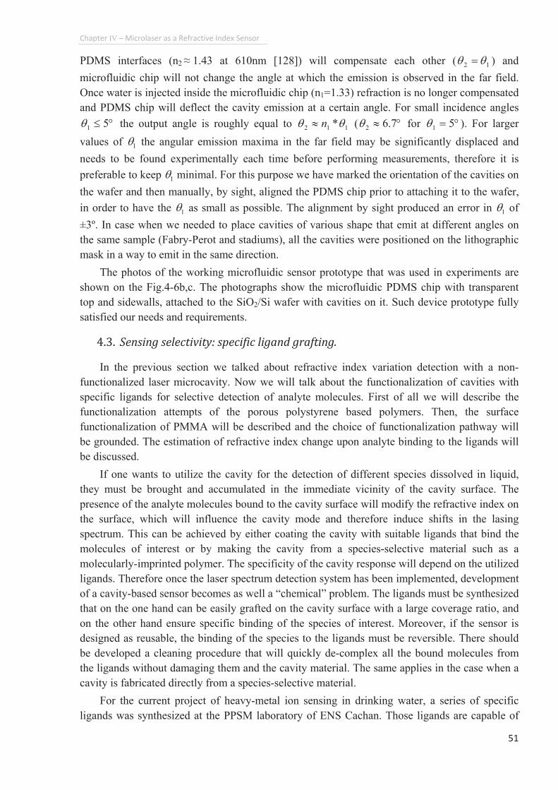
Chapter"IV" "Microlaser"as"a"Refractive"Index"Sensor"
51""
PDMS interfaces (n2 Ã 1.43 at 610nm [128]) will compensate each other ( 12 ss ? ) and
microfluidic chip will not change the angle at which the emission is observed in the far field.
Once water is injected inside the microfluidic chip (n1=1.33) refraction is no longer compensated
and PDMS chip will deflect the cavity emission at a certain angle. For small incidence angles
fl~ 51s the output angle is roughly equal to 112 *ss n… ( fl… 7.62s for fl? 51s ). For larger
values of 1s the angular emission maxima in the far field may be significantly displaced and
needs to be found experimentally each time before performing measurements, therefore it is
preferable to keep 1s minimal. For this purpose we have marked the orientation of the cavities on
the wafer and then manually, by sight, aligned the PDMS chip prior to attaching it to the wafer,
in order to have the 1s as small as possible. The alignment by sight produced an error in 1s of
±3º. In case when we needed to place cavities of various shape that emit at different angles on
the same sample (Fabry-Perot and stadiums), all the cavities were positioned on the lithographic
mask in a way to emit in the same direction.
The photos of the working microfluidic sensor prototype that was used in experiments are
shown on the Fig.4-6b,c. The photographs show the microfluidic PDMS chip with transparent
top and sidewalls, attached to the SiO2/Si wafer with cavities on it. Such device prototype fully
satisfied our needs and requirements. ね┻ぬ┻ "Sensing"selectivity:"specific"ligand"grafting."
In the previous section we talked about refractive index variation detection with a non-
functionalized laser microcavity. Now we will talk about the functionalization of cavities with
specific ligands for selective detection of analyte molecules. First of all we will describe the
functionalization attempts of the porous polystyrene based polymers. Then, the surface
functionalization of PMMA will be described and the choice of functionalization pathway will
be grounded. The estimation of refractive index change upon analyte binding to the ligands will
be discussed.
If one wants to utilize the cavity for the detection of different species dissolved in liquid,
they must be brought and accumulated in the immediate vicinity of the cavity surface. The
presence of the analyte molecules bound to the cavity surface will modify the refractive index on
the surface, which will influence the cavity mode and therefore induce shifts in the lasing
spectrum. This can be achieved by either coating the cavity with suitable ligands that bind the
molecules of interest or by making the cavity from a species-selective material such as a
molecularly-imprinted polymer. The specificity of the cavity response will depend on the utilized
ligands. Therefore once the laser spectrum detection system has been implemented, development
of a cavity-based sensor becomes as well a �chemical� problem. The ligands must be synthesized
that on the one hand can be easily grafted on the cavity surface with a large coverage ratio, and
on the other hand ensure specific binding of the species of interest. Moreover, if the sensor is
designed as reusable, the binding of the species to the ligands must be reversible. There should
be developed a cleaning procedure that will quickly de-complex all the bound molecules from
the ligands without damaging them and the cavity material. The same applies in the case when a
cavity is fabricated directly from a species-selective material.
For the current project of heavy-metal ion sensing in drinking water, a series of specific
ligands was synthesized at the PPSM laboratory of ENS Cachan. Those ligands are capable of
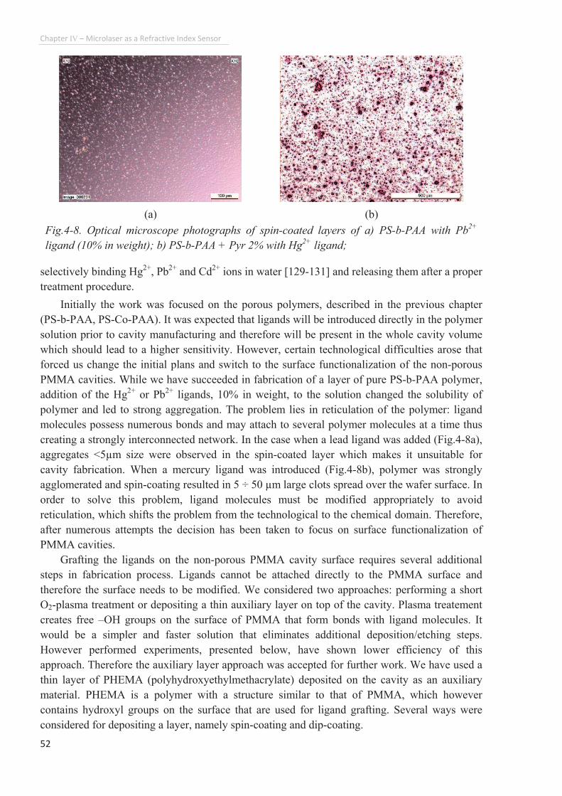
Chapter"IV" "Microlaser"as"a"Refractive"Index"Sensor"
52""
selectively binding Hg2+
, Pb2+
and Cd2+
ions in water [129-131] and releasing them after a proper
treatment procedure.
Initially the work was focused on the porous polymers, described in the previous chapter
(PS-b-PAA, PS-Co-PAA). It was expected that ligands will be introduced directly in the polymer
solution prior to cavity manufacturing and therefore will be present in the whole cavity volume
which should lead to a higher sensitivity. However, certain technological difficulties arose that
forced us change the initial plans and switch to the surface functionalization of the non-porous
PMMA cavities. While we have succeeded in fabrication of a layer of pure PS-b-PAA polymer,
addition of the Hg2+
or Pb2+
ligands, 10% in weight, to the solution changed the solubility of
polymer and led to strong aggregation. The problem lies in reticulation of the polymer: ligand
molecules possess numerous bonds and may attach to several polymer molecules at a time thus
creating a strongly interconnected network. In the case when a lead ligand was added (Fig.4-8a),
aggregates <5µm size were observed in the spin-coated layer which makes it unsuitable for
cavity fabrication. When a mercury ligand was introduced (Fig.4-8b), polymer was strongly
agglomerated and spin-coating resulted in 5 ÷ 50 µm large clots spread over the wafer surface. In
order to solve this problem, ligand molecules must be modified appropriately to avoid
reticulation, which shifts the problem from the technological to the chemical domain. Therefore,
after numerous attempts the decision has been taken to focus on surface functionalization of
PMMA cavities.
Grafting the ligands on the non-porous PMMA cavity surface requires several additional
steps in fabrication process. Ligands cannot be attached directly to the PMMA surface and
therefore the surface needs to be modified. We considered two approaches: performing a short
O2-plasma treatment or depositing a thin auxiliary layer on top of the cavity. Plasma treatement
creates free �OH groups on the surface of PMMA that form bonds with ligand molecules. It
would be a simpler and faster solution that eliminates additional deposition/etching steps.
However performed experiments, presented below, have shown lower efficiency of this
approach. Therefore the auxiliary layer approach was accepted for further work. We have used a
thin layer of PHEMA (polyhydroxyethylmethacrylate) deposited on the cavity as an auxiliary
material. PHEMA is a polymer with a structure similar to that of PMMA, which however
contains hydroxyl groups on the surface that are used for ligand grafting. Several ways were
considered for depositing a layer, namely spin-coating and dip-coating.
(a) (b)
Fig.4-8. Optical microscope photographs of spin-coated layers of a) PS-b-PAA with Pb2+
ligand (10% in weight); b) PS-b-PAA + Pyr 2% with Hg2+
ligand;
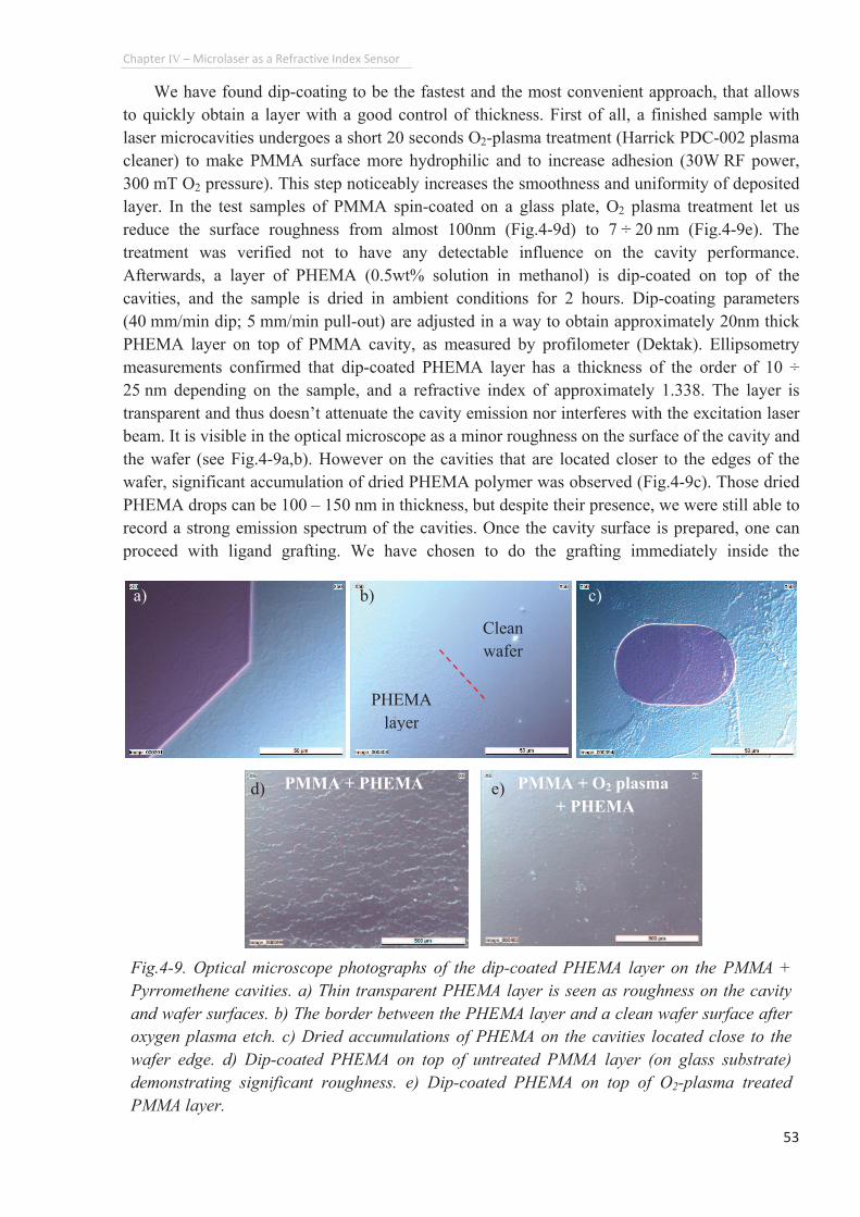
Chapter"IV"�"Microlaser"as"a"Refractive"Index"Sensor"
53""
We have found dip-coating to be the fastest and the most convenient approach, that allows
to quickly obtain a layer with a good control of thickness. First of all, a finished sample with
laser microcavities undergoes a short 20 seconds O2-plasma treatment (Harrick PDC-002 plasma
cleaner) to make PMMA surface more hydrophilic and to increase adhesion (30W RF power,
300 mT O2 pressure). This step noticeably increases the smoothness and uniformity of deposited
layer. In the test samples of PMMA spin-coated on a glass plate, O2 plasma treatment let us
reduce the surface roughness from almost 100nm (Fig.4-9d) to 7 ÷ 20 nm (Fig.4-9e). The
treatment was verified not to have any detectable influence on the cavity performance.
Afterwards, a layer of PHEMA (0.5wt% solution in methanol) is dip-coated on top of the
cavities, and the sample is dried in ambient conditions for 2 hours. Dip-coating parameters
(40 mm/min dip; 5 mm/min pull-out) are adjusted in a way to obtain approximately 20nm thick
PHEMA layer on top of PMMA cavity, as measured by profilometer (Dektak). Ellipsometry
measurements confirmed that dip-coated PHEMA layer has a thickness of the order of 10 ÷
25 nm depending on the sample, and a refractive index of approximately 1.338. The layer is
transparent and thus doesn�t attenuate the cavity emission nor interferes with the excitation laser
beam. It is visible in the optical microscope as a minor roughness on the surface of the cavity and
the wafer (see Fig.4-9a,b). However on the cavities that are located closer to the edges of the
wafer, significant accumulation of dried PHEMA polymer was observed (Fig.4-9c). Those dried
PHEMA drops can be 100 � 150 nm in thickness, but despite their presence, we were still able to
record a strong emission spectrum of the cavities. Once the cavity surface is prepared, one can
proceed with ligand grafting. We have chosen to do the grafting immediately inside the
Fig.4-9. Optical microscope photographs of the dip-coated PHEMA layer on the PMMA +
Pyrromethene cavities. a) Thin transparent PHEMA layer is seen as roughness on the cavity
and wafer surfaces. b) The border between the PHEMA layer and a clean wafer surface after
oxygen plasma etch. c) Dried accumulations of PHEMA on the cavities located close to the
wafer edge. d) Dip-coated PHEMA on top of untreated PMMA layer (on glass substrate)
demonstrating significant roughness. e) Dip-coated PHEMA on top of O2-plasma treated
PMMA layer.
PHEMA
layer
Clean
wafer
PMMA + PHEMA PMMA + O2 plasma
+ PHEMA
a) b) c)
d) e)
Chapter"IV" "Microlaser"as"a"Refractive"Index"Sensor"
54""
microfluidic chip, by flowing the appropriate reagents through which is advantageous for several
reasons. First of all, the quantity of reagents needed is significantly smaller as only the cavities
of interest are exposed to solution. If not, the whole wafer should be immersed in the ligand
solution. The second important point is that the ligand molecules may be damaged by the oxygen
plasma treatment during attachment of PDMS microfluidic chip. We didn�t test, whether plasma
treatment affects the ligands, but proceeded immediately with the safer approach and grafted the
ligands at the last step.
At this stage we have functionalized the cavities with thiol groups that are known to
selectively bind mercury [132, 133]. We used a commercially available organosilane 3-MPTS
(3-mercaptopropyltrimethoxysilane) as a source of thiol groups [134]. The preference was given
for a commercial material due to a large number of tests that needed to be performed before the
functionalization procedure and sensing experiment protocol were optimized. Synthesis of our
own ligands for testing purposes is unjustified due to a high cost and large quantities needed for
tests. The functionalization was performed as follows: pure 3-MPTS was injected in the
microfluidic channel with the help of a syringe pump and left inside for 30 minutes; after
channel is rinsed with water to remove the excess of unbound material and dried with nitrogen.
Procedure is repeated 3 times.
We have performed AFM microscopy observation of the PMMA layers on glass substrate
(without PDMS cover), functionalized with different approaches (Fig.4-11). The spin-coated
PMMA layer represents a smooth surface with a minor nanometer-scale roughness. After O2-
plasma oxidation, we observe the increase of surface roughness (~8nm) and the picture changes
slightly after grafting the thiol ligands. After PHEMA layer is deposited, we observe a
significantly rougher surface (~40nm) that clearly evidences PHEMA presence. When thiol is
grafted on PMMA/PHEMA layer, we observe even higher surface unevenness (up to 100nm).
However these observations don�t lead to any quantitative conclusions about the ligand presence
on the polymer surface.
The presence of the thin PHEMA layer on the wafer surface around the cavities makes it
impossible to attach a microfluidic chip, therefore all the unneeded PHEMA must be removed
first. The PDMS sticks well to a clean surface, like glass or silica but the presence of any organic
contamination prevents it from attaching. To clean the surface, the cavities that will be used in
sensing experiment are selected and protected by a hard mask (covered by a small piece of
wafer), and the sample undergoes another short-term oxygen plasma exposure in the Reactive
ion etching machine (bias 300V, 50W RF power, 5mT O2 pressure), that removes the
unprotected PHEMA layer, leaving a clean wafer surface (Fig.4-9b). Afterwards, a microfluidic
chip is attached to the wafer (as explained in § 4.2) and the cavity functionalization is performed
inside the microfluidic channel (Fig.4-10a).
To quantitatively compare the efficiency of different functionalization pathways, thiol
ligands were grafted on the surface of non-doped PMMA surfaces through both O2-plasma
treatment and PHEMA layer approaches. Afterwards ligands were labeled with 5-IAF
fluorescein derivative (5-Iodoacetamidofluorescein) and grafting efficiency was evaluated by
recording the fluorescence spectra (Fig.4-10b). The labeling was performed as follows: 4 mM/L
5-IAF solution in Na2HPO4 buffer (0.1M/L, pH=9.1) is injected in the microfluidic channel and
left for 30 minutes; after channel is rinsed with water and dried with nitrogen. Procedure is
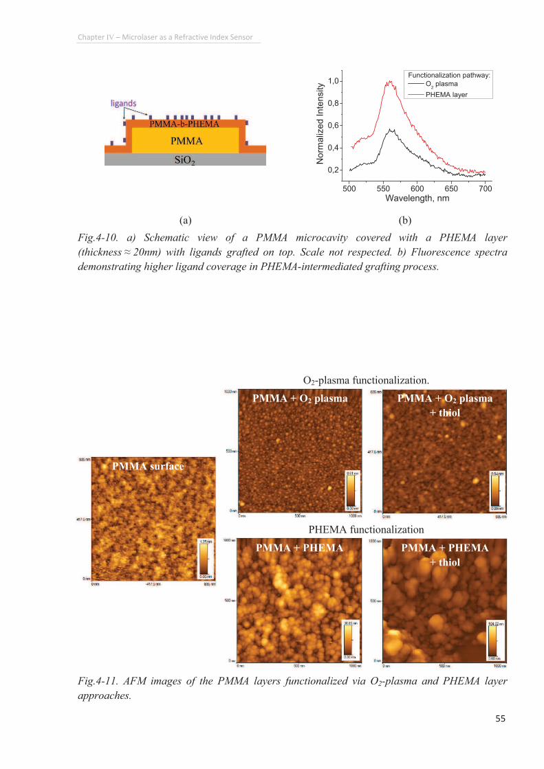
Chapter"IV" "Microlaser"as"a"Refractive"Index"Sensor"
55""
500 550 600 650 700
0,2
0,4
0,6
0,8
1,0
No
rma
lize
d I
nte
nsity
Wavelength, nm
Functionalization pathway:
O2 plasma
PHEMA layer
(a) (b)
Fig.4-10. a) Schematic view of a PMMA microcavity covered with a PHEMA layer
(thickness à 20nm) with ligands grafted on top. Scale not respected. b) Fluorescence spectra
demonstrating higher ligand coverage in PHEMA-intermediated grafting process.
O2-plasma functionalization.
PHEMA functionalization
Fig.4-11. AFM images of the PMMA layers functionalized via O2-plasma and PHEMA layer
approaches.
PMMA surface
PMMA + O2 plasma PMMA + O2 plasma
+ thiol
PMMA + PHEMA PMMA + PHEMA
+ thiol
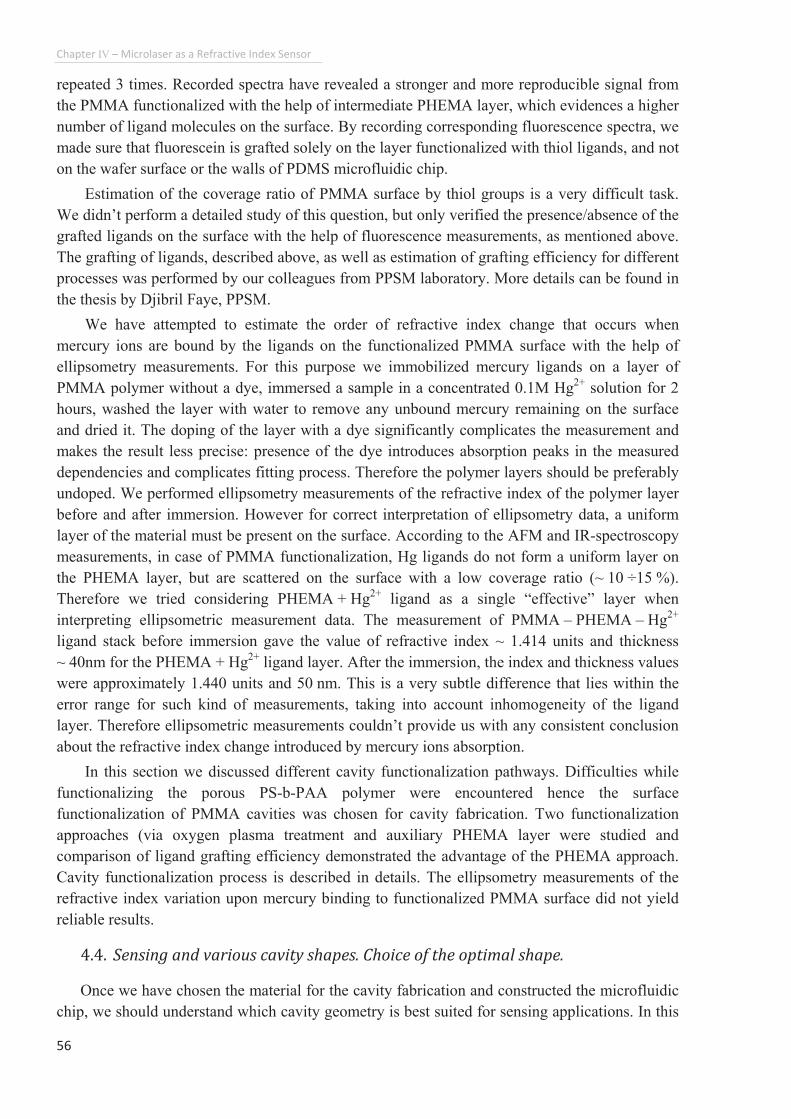
Chapter"IV" "Microlaser"as"a"Refractive"Index"Sensor"
56""
repeated 3 times. Recorded spectra have revealed a stronger and more reproducible signal from
the PMMA functionalized with the help of intermediate PHEMA layer, which evidences a higher
number of ligand molecules on the surface. By recording corresponding fluorescence spectra, we
made sure that fluorescein is grafted solely on the layer functionalized with thiol ligands, and not
on the wafer surface or the walls of PDMS microfluidic chip.
Estimation of the coverage ratio of PMMA surface by thiol groups is a very difficult task.
We didn�t perform a detailed study of this question, but only verified the presence/absence of the
grafted ligands on the surface with the help of fluorescence measurements, as mentioned above.
The grafting of ligands, described above, as well as estimation of grafting efficiency for different
processes was performed by our colleagues from PPSM laboratory. More details can be found in
the thesis by Djibril Faye, PPSM.
We have attempted to estimate the order of refractive index change that occurs when
mercury ions are bound by the ligands on the functionalized PMMA surface with the help of
ellipsometry measurements. For this purpose we immobilized mercury ligands on a layer of
PMMA polymer without a dye, immersed a sample in a concentrated 0.1M Hg2+
solution for 2
hours, washed the layer with water to remove any unbound mercury remaining on the surface
and dried it. The doping of the layer with a dye significantly complicates the measurement and
makes the result less precise: presence of the dye introduces absorption peaks in the measured
dependencies and complicates fitting process. Therefore the polymer layers should be preferably
undoped. We performed ellipsometry measurements of the refractive index of the polymer layer
before and after immersion. However for correct interpretation of ellipsometry data, a uniform
layer of the material must be present on the surface. According to the AFM and IR-spectroscopy
measurements, in case of PMMA functionalization, Hg ligands do not form a uniform layer on
the PHEMA layer, but are scattered on the surface with a low coverage ratio (~ 10 ÷15 %).
Therefore we tried considering PHEMA + Hg2+
ligand as a single �effective� layer when
interpreting ellipsometric measurement data. The measurement of PMMA � PHEMA � Hg2+
ligand stack before immersion gave the value of refractive index ~ 1.414 units and thickness
~ 40nm for the PHEMA + Hg2+
ligand layer. After the immersion, the index and thickness values
were approximately 1.440 units and 50 nm. This is a very subtle difference that lies within the
error range for such kind of measurements, taking into account inhomogeneity of the ligand
layer. Therefore ellipsometric measurements couldn�t provide us with any consistent conclusion
about the refractive index change introduced by mercury ions absorption.
In this section we discussed different cavity functionalization pathways. Difficulties while
functionalizing the porous PS-b-PAA polymer were encountered hence the surface
functionalization of PMMA cavities was chosen for cavity fabrication. Two functionalization
approaches (via oxygen plasma treatment and auxiliary PHEMA layer were studied and
comparison of ligand grafting efficiency demonstrated the advantage of the PHEMA approach.
Cavity functionalization process is described in details. The ellipsometry measurements of the
refractive index variation upon mercury binding to functionalized PMMA surface did not yield
reliable results. ね┻ね┻ "Sensing"and"various"cavity"shapes."Choice"of"the"optimal"shape."
Once we have chosen the material for the cavity fabrication and constructed the microfluidic
chip, we should understand which cavity geometry is best suited for sensing applications. In this
Chapter"IV"�"Microlaser"as"a"Refractive"Index"Sensor"
57""
section, we will talk about the requirements that a microlaser should satisfy to be used as a
sensor. A simple theoretical explanation of the cavity sensitivity to refractive index variation will
be given in section 4.4.1 that allows predicting the expected spectral shift for the cavities of
different shapes (Fabry-Perot, polygons). Numerical simulation will be employed to verify the
model and to analyze the chaotic stadium-shaped cavities, where analytical solution is
impossible. Afterwards in section 4.4.2, basing on the theoretical model and numerical
simulation, we will chose the optimal cavity shape to be used in a sensor.
4.4.1. Factors influencing sensitivity to refractive index variation.
As we have already seen in the previous chapters, various microlaser shapes can be easily
fabricated, each having its own emission features and characteristics. To better understand which
cavity shape one should use for the sensing application, we will investigate the factors that
influence the microlaser spectra. The medium surrounding the cavity may influence the lasing
spectra by two different mechanisms:
‚ First of all, the thin cavity layer (in case of PMMA, nbulk à 1.54) is surrounded by claddings
with different refractive indexes (SiO2 substrate, n = 1.45; air, n = 1). The wave confined and
propagating in the cavity is described in terms of an effective refractive index that depends
on the index of the active polymer layer, buffer layer and upper cladding (air). Once the
index of the surrounding medium (upper cladding) changes, the cavity mode will inevitably
feel this change. And this influence will be more pronounced, if the mode is partially
deconfined, i.e. there exists a significant evanescent wave tail in the upper cladding layer.
The term �effective refractive index� (also called modal index) can lead to confusion at
this point. It is easy to believe, that effective index is some kind of an average between the
indices of a guiding layer and the claddings, with the contributions depending on the mode
energy localization. Though in many cases this intuitive logic seems to work, such
interpretation would be wrong. Effective refractive index of the mode may differ
substantially for the modes having very similar spatial localization.
‚ The second factor affecting the spectra is the phase incursion. As wave propagating in the
cavity reflects at the cavity/surrounding medium interface it acquires a phase incursion (〉轄)
which will influences the spectrum.
From the resonance condition which states that the round trip distance L of the wave in the
cavity, must be equal to an integer number of wavelengths そ
mNnL rhnr
22 ?©- (4-1)
where n is the refractive index of the cavity material, N � number of reflections experienced by
the wave along the roundtrip, 轄 � phase change upon one reflection. One can deduce the
following relation for the wavelength shift, assuming that phase change and effective refractive
index change influence the spectrum independently:
00
2
2 ?F?FF-F?F
hnhr
nn eff
n
nnnL
N
eff
(4-2)
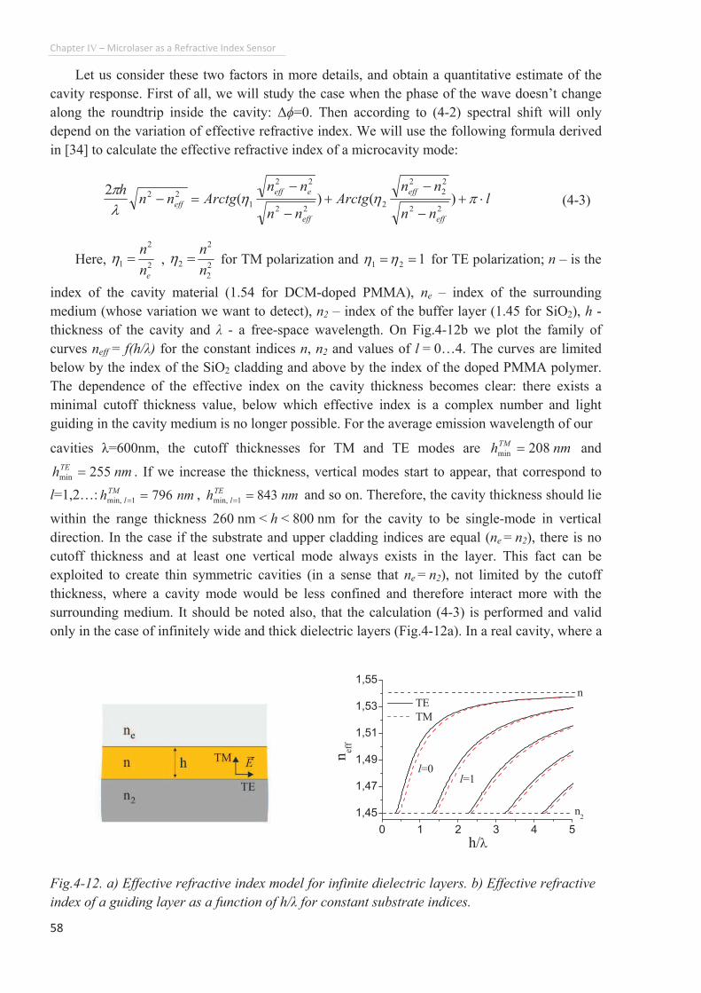
Chapter"IV"�"Microlaser"as"a"Refractive"Index"Sensor"
58""
Let us consider these two factors in more details, and obtain a quantitative estimate of the
cavity response. First of all, we will study the case when the phase of the wave doesn�t change
along the roundtrip inside the cavity: 〉轄=0. Then according to (4-2) spectral shift will only
depend on the variation of effective refractive index. We will use the following formula derived
in [34] to calculate the effective refractive index of a microcavity mode:
Here, 2
2
1
en
n?j , 2
2
2
2n
n?j for TM polarization and 121 ??jj for TE polarization; n � is the
index of the cavity material (1.54 for DCM-doped PMMA), ne � index of the surrounding
medium (whose variation we want to detect), n2 � index of the buffer layer (1.45 for SiO2), h -
thickness of the cavity and そ - a free-space wavelength. On Fig.4-12b we plot the family of
curves neff = f(h/そ) for the constant indices n, n2 and values of l = 0�4. The curves are limited
below by the index of the SiO2 cladding and above by the index of the doped PMMA polymer.
The dependence of the effective index on the cavity thickness becomes clear: there exists a
minimal cutoff thickness value, below which effective index is a complex number and light
guiding in the cavity medium is no longer possible. For the average emission wavelength of our
cavities そ=600nm, the cutoff thicknesses for TM and TE modes are nmhTM 208min ? and
nmhTE 255min ? . If we increase the thickness, vertical modes start to appear, that correspond to
l=1,2�: nmhTM
l 7961min, ?? , nmhTE
l 8431min, ?? and so on. Therefore, the cavity thickness should lie
within the range thickness 260 nm < h < 800 nm for the cavity to be single-mode in vertical
direction. In the case if the substrate and upper cladding indices are equal (ne = n2), there is no
cutoff thickness and at least one vertical mode always exists in the layer. This fact can be
exploited to create thin symmetric cavities (in a sense that ne = n2), not limited by the cutoff
thickness, where a cavity mode would be less confined and therefore interact more with the
surrounding medium. It should be noted also, that the calculation (4-3) is performed and valid
only in the case of infinitely wide and thick dielectric layers (Fig.4-12a). In a real cavity, where a
lnn
nnArctg
nn
nnArctgnn
h
eff
eff
eff
eeff
eff ©-//-/
/?/ rjjnr
)()(2
22
2
2
2
222
22
1
22(4-3)
1,45
1,47
1,49
1,51
1,53
1,55
0 1 2 3 4 5
l=1l=0
n
n2
TE
TM
h/n
nef
f
Fig.4-12. a) Effective refractive index model for infinite dielectric layers. b) Effective refractive
index of a guiding layer as a function of h/そ for constant substrate indices.
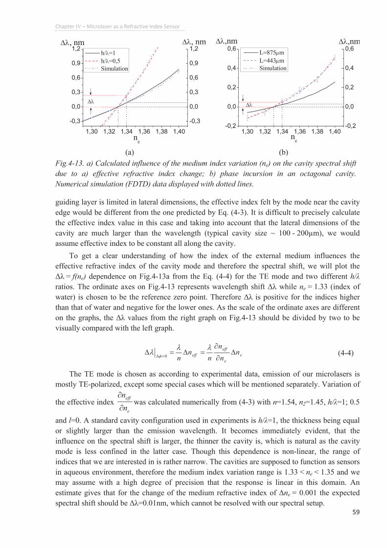
Chapter"IV"�"Microlaser"as"a"Refractive"Index"Sensor"
59""
guiding layer is limited in lateral dimensions, the effective index felt by the mode near the cavity
edge would be different from the one predicted by Eq. (4-3). It is difficult to precisely calculate
the effective index value in this case and taking into account that the lateral dimensions of the
cavity are much larger than the wavelength (typical cavity size ~ 100 - 200µm), we would
assume effective index to be constant all along the cavity.
To get a clear understanding of how the index of the external medium influences the
effective refractive index of the cavity mode and therefore the spectral shift, we will plot the
〉そ = f(ne) dependence on Fig.4-13a from the Eq. (4-4) for the TE mode and two different h/そratios. The ordinate axes on Fig.4-13 represents wavelength shift 〉そ while ne = 1.33 (index of
water) is chosen to be the reference zero point. Therefore 〉そ is positive for the indices higher
than that of water and negative for the lower ones. As the scale of the ordinate axes are different
on the graphs, the 〉そ values from the right graph on Fig.4-13 should be divided by two to be
visually compared with the left graph.
The TE mode is chosen as according to experimental data, emission of our microlasers is
mostly TE-polarized, except some special cases which will be mentioned separately. Variation of
the effective index e
eff
n
n
••
was calculated numerically from (4-3) with n=1.54, n2=1.45, h/そ=1; 0.5
and l=0. A standard cavity configuration used in experiments is h/そ=1, the thickness being equal
or slightly larger than the emission wavelength. It becomes immediately evident, that the
influence on the spectral shift is larger, the thinner the cavity is, which is natural as the cavity
mode is less confined in the latter case. Though this dependence is non-linear, the range of
indices that we are interested in is rather narrow. The cavities are supposed to function as sensors
in aqueous environment, therefore the medium index variation range is 1.33 < ne < 1.35 and we
may assume with a high degree of precision that the response is linear in this domain. An
estimate gives that for the change of the medium refractive index of 〉ne = 0.001 the expected
spectral shift should be 〉そ=0.01nm, which cannot be resolved with our spectral setup.
1,30 1,32 1,34 1,36 1,38 1,40
-0,3
0,0
0,3
0,6
0,9
1,2 h/n=1
h/n=0,5
Simulation
Fn, nm Fn, nm
ne
Fn
-0,3
0,0
0,3
0,6
0,9
1,2
1,30 1,32 1,34 1,36 1,38 1,40-0,2
0,0
0,2
0,4
0,6Fn,nm
L=875om
L=443om
Simulation
ne
Fn,nm
-0,2
0,0
0,2
0,4
0,6
Fn
(a) (b)
Fig.4-13. a) Calculated influence of the medium index variation (ne) on the cavity spectral shift
due to a) effective refractive index change; b) phase incursion in an octagonal cavity.
Numerical simulation (FDTD) data displayed with dotted lines.
""e
e
eff
eff nn
n
nn
nF•
•?F?F ?Fnnn h 0 "
" (4-4)
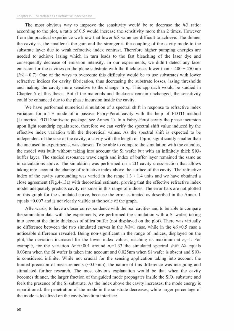
Chapter"IV"�"Microlaser"as"a"Refractive"Index"Sensor"
60""
The most obvious way to improve the sensitivity would be to decrease the h/そ ratio:
according to the plot, a ratio of 0.5 would increase the sensitivity more than 2 times. However
from the practical experience we know that lower h/そ value are difficult to achieve. The thinner
the cavity is, the smaller is the gain and the stronger is the coupling of the cavity mode to the
substrate layer due to weak refractive index contrast. Therefore higher pumping energies are
needed to achieve lasing which in turn leads to the fast bleaching of the laser dye and
consequently decrease of emission intensity. In our experiments, we didn�t detect any laser
emission for the cavities on the plane substrate with the thicknesses lower than ~ 400 ÷ 450 nm
(h/そ ~ 0.7). One of the ways to overcome this difficulty would be to use substrates with lower
refractive indices for cavity fabrication, thus decreasing the substrate losses, lasing thresholds
and making the cavity more sensitive to the change in ne. This approach would be studied in
Chapter 5 of this thesis. But if the materials and thickness remain unchanged, the sensitivity
could be enhanced due to the phase incursion inside the cavity.
We have performed numerical simulation of a spectral shift in response to refractive index
variation for a TE mode of a passive Fabry-Perot cavity with the help of FDTD method
(Lumerical FDTD software package, see Annex 1). In a Fabry-Perot cavity the phase incursion
upon light roundtrip equals zero, therefore we can verify the spectral shift value induced by the
effective index variation with the theoretical values. As the spectral shift is expected to be
independent of the size of the cavity, a cavity with the length of 15µm, significantly smaller than
the one used in experiments, was chosen. To be able to compare the simulation with the calculus,
the model was built without taking into account the Si wafer but with an infinitely thick SiO2
buffer layer. The studied resonance wavelength and index of buffer layer remained the same as
in calculations above. The simulation was performed on a 2D cavity cross-section that allows
taking into account the change of refractive index above the surface of the cavity. The refractive
index of the cavity surrounding was varied in the range 1.3 ÷ 1.4 units and we have obtained a
close agreement (Fig.4-13a) with theoretical estimate, proving that the effective refractive index
model adequately predicts cavity response in this range of indices. The error bars are not plotted
on this graph for the simulated curve, because the error estimated as described in the Annex 1
equals ±0.007 and is not clearly visible at the scale of the graph.
Afterwards, to have a closer correspondence with the real cavities and to be able to compare
the simulation data with the experiments, we performed the simulation with a Si wafer, taking
into account the finite thickness of silica buffer (not displayed on the plot). There was virtually
no difference between the two simulated curves in the h/そ=1 case, while in the h/そ=0.5 case a
noticeable difference revealed. Being non-significant in the range of indices, displayed on the
plot, the deviation increased for the lower index values, reaching its maximum at ne=1. For
example, for the variation 〉n=0.001 around ne=1.33 the simulated spectral shift 〉そ equals
0.03nm when the Si wafer is taken into account and 0.025nm when Si wafer is absent and SiO2
is considered infinite. While not crucial for the sensing application taking into account the
limited precision of measurements (~0.03nm), the nature of this difference was intriguing and
stimulated further research. The most obvious explanation would be that when the cavity
becomes thinner, the larger fraction of the guided mode propagates inside the SiO2 substrate and
feels the presence of the Si substrate. As the index above the cavity increases, the mode energy is
repartitioned: the penetration of the mode in the substrate decreases, while larger percentage of
the mode is localized on the cavity/medium interface.
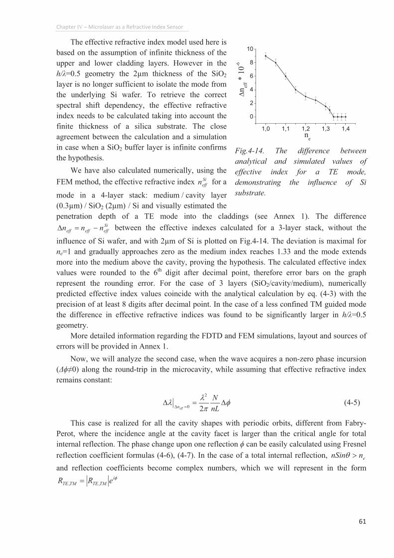
Chapter"IV" "Microlaser"as"a"Refractive"Index"Sensor"
61""
The effective refractive index model used here is
based on the assumption of infinite thickness of the
upper and lower cladding layers. However in the
h/そ=0.5 geometry the 2µm thickness of the SiO2
layer is no longer sufficient to isolate the mode from
the underlying Si wafer. To retrieve the correct
spectral shift dependency, the effective refractive
index needs to be calculated taking into account the
finite thickness of a silica substrate. The close
agreement between the calculation and a simulation
in case when a SiO2 buffer layer is infinite confirms
the hypothesis.
We have also calculated numerically, using the
FEM method, the effective refractive index Si
effn for a
mode in a 4-layer stack: medium / cavity layer
(0.3µm) / SiO2 (2µm) / Si and visually estimated the
penetration depth of a TE mode into the claddings (see Annex 1). The difference Si
effeffeff nnn /?F between the effective indexes calculated for a 3-layer stack, without the
influence of Si wafer, and with 2µm of Si is plotted on Fig.4-14. The deviation is maximal for
ne=1 and gradually approaches zero as the medium index reaches 1.33 and the mode extends
more into the medium above the cavity, proving the hypothesis. The calculated effective index
values were rounded to the 6th
digit after decimal point, therefore error bars on the graph
represent the rounding error. For the case of 3 layers (SiO2/cavity/medium), numerically
predicted effective index values coincide with the analytical calculation by eq. (4-3) with the
precision of at least 8 digits after decimal point. In the case of a less confined TM guided mode
the difference in effective refractive indices was found to be significantly larger in h/そ=0.5
geometry.
More detailed information regarding the FDTD and FEM simulations, layout and sources of
errors will be provided in Annex 1.
Now, we will analyze the second case, when the wave acquires a non-zero phase incursion
(〉轄Œ0) along the round-trip in the microcavity, while assuming that effective refractive index
remains constant:
"" hrnn F?F ?F nL
N
effn 2
2
0"" (4-5)
This case is realized for all the cavity shapes with periodic orbits, different from Fabry-
Perot, where the incidence angle at the cavity facet is larger than the critical angle for total
internal reflection. The phase change upon one reflection 轄 can be easily calculated using Fresnel
reflection coefficient formulas (4-6), (4-7). In the case of a total internal reflection, ennSin @sand reflection coefficients become complex numbers, which we will represent in the form
hiTMTETMTE eRR ,, ?
1,0 1,1 1,2 1,3 1,4
0
2
4
6
8
10
ne
Fn eff *
10
-6
Fig.4-14. The difference between
analytical and simulated values of
effective index for a TE mode,
demonstrating the influence of Si
substrate.
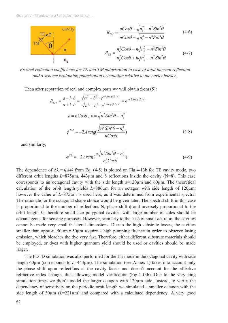
Chapter"IV" "Microlaser"as"a"Refractive"Index"Sensor"
62""
Then after separation of real and complex parts we will obtain from (5):
"" )/(2
)/(22
)/(22abArctgi
abArctgi
abArctgi
TM eeba
eba
bia
biaR ©/
©©/ ?©-
©-?©-©/?
"""
snCosa ? ," 222
enSinnb /? s "
)(2
222
ssh
nCos
nSinnArctg
eTM//? (4-8)
and similarly,"
)(22
222
ssh
Cosn
nSinnnArctg
e
eTE//? (4-9)
The dependence of 〉そ = f(〉轄) from Eq. (4-5) is plotted on Fig.4-13b for TE cavity mode, two
different orbit lengths L=875µm, 443µm and 8 reflections inside the cavity (N=8). This case
corresponds to an octagonal cavity with the side length a=120µm and 60µm. The theoretical
calculation of the orbit length yields L=886µm for an octagon with side length of 120µm,
however the value of L=875µm is used here, as it was determined from experimental spectra.
The rationale for the octagonal shape choice would be given later. The spectral shift in this case
is proportional to the number of reflections N, phase shift 思 and inversely proportional to the
orbit length L; therefore small-size polygonal cavities with large number of sides should be
advantageous for sensing purposes. However, similarly to the case of small h/そ ratio, the cavities
cannot be made very small in lateral dimensions. Due to the high substrate losses, the cavities
smaller than approx. 50µm x 50µm require a high pumping fluence in order to observe lasing
emission, which bleaches the dye very fast. Therefore, either different substrate materials should
be employed, or dyes with higher quantum yield should be used or cavities should be made
larger.
The FDTD simulation was also performed for the TE mode in the octagonal cavity with side
length 60µm (corresponds to L=443µm). The simulation (see Annex 1) takes into account only
the phase shift upon reflections at the cavity facets and doesn�t account for the effective
refractive index change, thus allowing model verification (Fig.4-13b). Due to the very long
simulation times we didn�t model the larger octagon with 120µm side. Instead, to verify the
dependency of sensitivity on the periodic orbit length we simulated a smaller octagon with the
side length of 30µm (L=221µm) and compared with a calculated dependency. A very good
ssss
222
222
SinnnnCos
SinnnnCosR
e
e
TM /-//? (4-6)
ssss
2222
2222
SinnnnCosn
SinnnnCosnR
ee
ee
TE /-//? (4-7)
Fresnel reflection coefficients for TE and TM polarization in case of total internal reflection
and a scheme explaining polarization orientation relative to the cavity border.
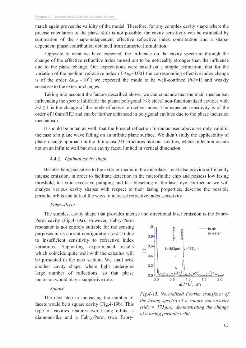
Chapter"IV"�"Microlaser"as"a"Refractive"Index"Sensor"
63""
match again proves the validity of the model. Therefore, for any complex cavity shape where the
precise calculation of the phase shift is not possible, the cavity sensitivity can be estimated by
summation of the shape-independent effective refractive index contribution and a shape-
dependent phase contribution obtained from numerical simulation.
Opposite to what we have expected, the influence on the cavity spectrum through the
change of the effective refractive index turned out to be noticeably stronger than the influence
due to the phase change. Our expectations were based on a simple estimation, that for the
variation of the medium refractive index of 〉ne=0.001 the corresponding effective index change
is of the order 〉neff ~ 10-5
; we expected the mode to be well-confined (h/そ=1) and weakly
sensitive to the exterior changes.
Taking into account the factors described above, we can conclude that the main mechanism
influencing the spectral shift for the planar polygonal (ø 8 sides) non-functionalized cavities with
h/そ ø 1 is the change of the mode effective refractive index. The expected sensitivity is of the
order of 10nm/RIU and can be further enhanced in polygonal cavities due to the phase incursion
mechanism.
It should be noted as well, that the Fresnel reflection formulas used above are only valid in
the case of a plane wave falling on an infinite plane surface. We didn�t study the applicability of
phase change approach in the thin quasi-2D structures like our cavities, where reflection occurs
not on an infinite wall but on a cavity facet, limited in vertical dimension.
4.4.2. Optimal cavity shape
Besides being sensitive to the exterior medium, the microlaser must also provide sufficiently
intense emission, in order to facilitate detection in the microfluidic chip and possess low lasing
threshold, to avoid excessive pumping and fast bleaching of the laser dye. Further on we will
analyze various cavity shapes with respect to their lasing properties, describe the possible
periodic orbits and talk of the ways to increase refractive index sensitivity.
Fabry-Perot
The simplest cavity shape that provides intense and directional laser emission is the Fabry-
Perot cavity (Fig.4-19a). However, Fabry-Perot
resonator is not entirely suitable for the sensing
purposes in its current configuration (h/そÃ1) due
to insufficient sensitivity to refractive index
variations. Supporting experimental results
which coincide quite well with the calculus will
be presented in the next section. We shall seek
another cavity shape, where light undergoes
large number of reflections, so that phase
incursion would play a supportive role.
Square
The next step in increasing the number of
facets would be a square cavity (Fig.4-19b). This
type of cavities features two lasing orbits: a
diamond-like and a Fabry-Perot (two Fabry-
0,0 0,5 1,0 1,5 2,00,0
0,2
0,4
0,6
0,8
1,0 in air
in water
Dia
mond
L=353om L=487om
FT
nL*106, om
Fabry
-Pero
t
Fig.4-15. Normalized Fourier transform of
the lasing spectra of a square microcavity
(side = 175µm), demonstrating the change
of a lasing periodic orbit.
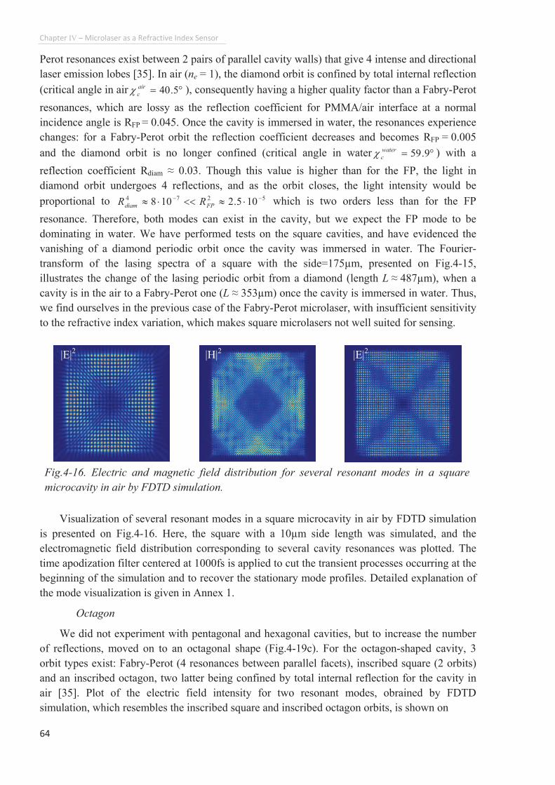
Chapter"IV"�"Microlaser"as"a"Refractive"Index"Sensor"
64""
Perot resonances exist between 2 pairs of parallel cavity walls) that give 4 intense and directional
laser emission lobes [35]. In air (ne = 1), the diamond orbit is confined by total internal reflection
(critical angle in air fl? 5.40air
ce ), consequently having a higher quality factor than a Fabry-Perot
resonances, which are lossy as the reflection coefficient for PMMA/air interface at a normal
incidence angle is RFP = 0.045. Once the cavity is immersed in water, the resonances experience
changes: for a Fabry-Perot orbit the reflection coefficient decreases and becomes RFP = 0.005
and the diamond orbit is no longer confined (critical angle in water fl? 9.59water
ce ) with a
reflection coefficient Rdiam à 0.03. Though this value is higher than for the FP, the light in
diamond orbit undergoes 4 reflections, and as the orbit closes, the light intensity would be
proportional to 5274 105.2108 // ©…>>©… FPdiam RR which is two orders less than for the FP
resonance. Therefore, both modes can exist in the cavity, but we expect the FP mode to be
dominating in water. We have performed tests on the square cavities, and have evidenced the
vanishing of a diamond periodic orbit once the cavity was immersed in water. The Fourier-
transform of the lasing spectra of a square with the side=175µm, presented on Fig.4-15,
illustrates the change of the lasing periodic orbit from a diamond (length L Ã 487µm), when a
cavity is in the air to a Fabry-Perot one (L Ã 353µm) once the cavity is immersed in water. Thus,
we find ourselves in the previous case of the Fabry-Perot microlaser, with insufficient sensitivity
to the refractive index variation, which makes square microlasers not well suited for sensing.
Visualization of several resonant modes in a square microcavity in air by FDTD simulation
is presented on Fig.4-16. Here, the square with a 10µm side length was simulated, and the
electromagnetic field distribution corresponding to several cavity resonances was plotted. The
time apodization filter centered at 1000fs is applied to cut the transient processes occurring at the
beginning of the simulation and to recover the stationary mode profiles. Detailed explanation of
the mode visualization is given in Annex 1.
Octagon
We did not experiment with pentagonal and hexagonal cavities, but to increase the number
of reflections, moved on to an octagonal shape (Fig.4-19c). For the octagon-shaped cavity, 3
orbit types exist: Fabry-Perot (4 resonances between parallel facets), inscribed square (2 orbits)
and an inscribed octagon, two latter being confined by total internal reflection for the cavity in
air [35]. Plot of the electric field intensity for two resonant modes, obrained by FDTD
simulation, which resembles the inscribed square and inscribed octagon orbits, is shown on
Fig.4-16. Electric and magnetic field distribution for several resonant modes in a square
microcavity in air by FDTD simulation.
|E|2"
|H|2"
|E|2
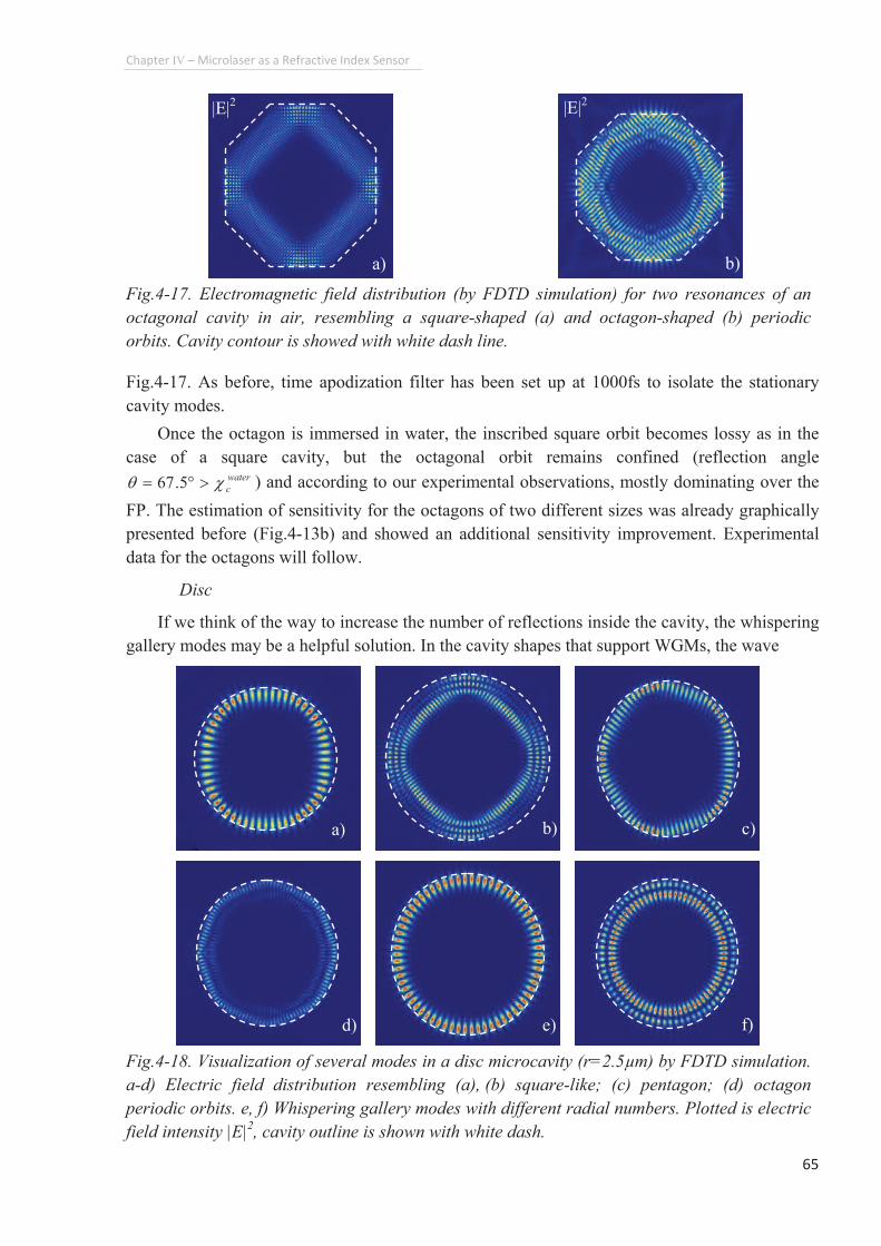
Chapter"IV" "Microlaser"as"a"Refractive"Index"Sensor"
65""
Fig.4-17. As before, time apodization filter has been set up at 1000fs to isolate the stationary
cavity modes.
Once the octagon is immersed in water, the inscribed square orbit becomes lossy as in the
case of a square cavity, but the octagonal orbit remains confined (reflection angle water
ces @fl? 5.67 ) and according to our experimental observations, mostly dominating over the
FP. The estimation of sensitivity for the octagons of two different sizes was already graphically
presented before (Fig.4-13b) and showed an additional sensitivity improvement. Experimental
data for the octagons will follow.
Disc
If we think of the way to increase the number of reflections inside the cavity, the whispering
gallery modes may be a helpful solution. In the cavity shapes that support WGMs, the wave
Fig.4-17. Electromagnetic field distribution (by FDTD simulation) for two resonances of an
octagonal cavity in air, resembling a square-shaped (a) and octagon-shaped (b) periodic
orbits. Cavity contour is showed with white dash line.
Fig.4-18. Visualization of several modes in a disc microcavity (r=2.5µm) by FDTD simulation.
a-d) Electric field distribution resembling (a), (b) square-like; (c) pentagon; (d) octagon
periodic orbits. e, f) Whispering gallery modes with different radial numbers. Plotted is electric
field intensity |E|2, cavity outline is shown with white dash.
a)"
b) c)
d)"
e) f)
|E|2"
a) b)
|E|2
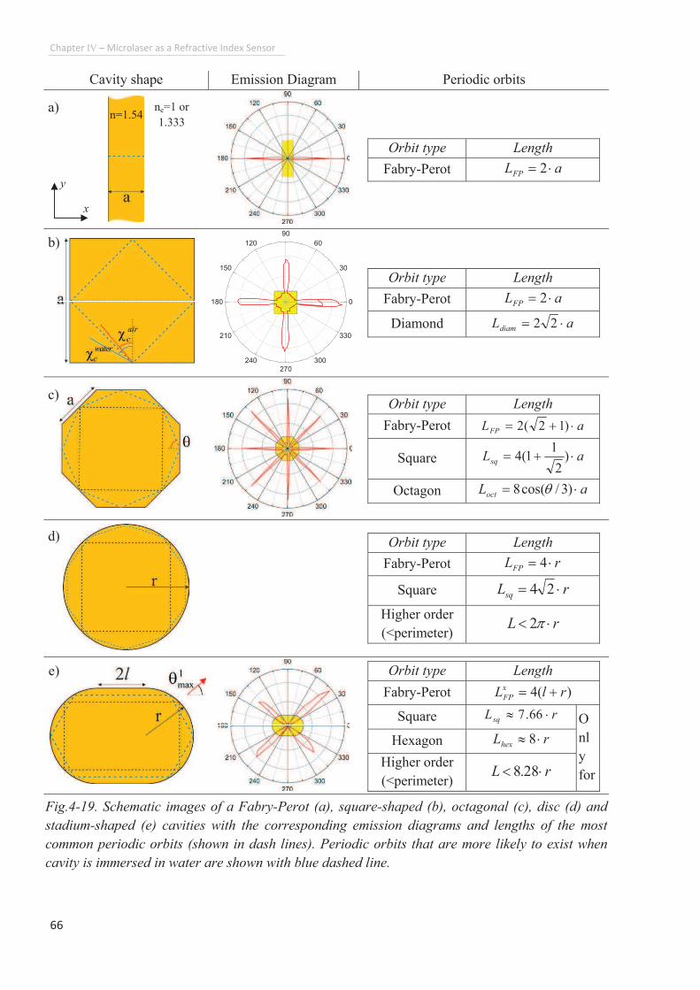
Chapter"IV" "Microlaser"as"a"Refractive"Index"Sensor"
66""
Cavity shape Emission Diagram Periodic orbits
Orbit type Length
Fabry-Perot aLFP ©? 2
0
30
60
90
120
150
180
210
240
270
300
330
Orbit type Length
Fabry-Perot aLFP ©? 2
Diamond aLdiam ©? 22 "
Orbit type Length
Fabry-Perot aLFP ©-? )12(2
Square aLsq ©-? )2
11(4 "
Octagon aLoct ©? )3/cos(8 s
Orbit type Length
Fabry-Perot rLFP ©? 4
Square rLsq ©? 24 "Higher order
(<perimeter) rL ©> r2 "
Orbit type Length
Fabry-Perot )(4 rlLx
FP -?Square rLsq ©… 66.7 "
"Hexagon rLhex ©… 8"
Higher order
(<perimeter) rL ©> 28.8 "
Fig.4-19. Schematic images of a Fabry-Perot (a), square-shaped (b), octagonal (c), disc (d) and
stadium-shaped (e) cavities with the corresponding emission diagrams and lengths of the most
common periodic orbits (shown in dash lines). Periodic orbits that are more likely to exist when
cavity is immersed in water are shown with blue dashed line.
ne=1 or
1.333 n=1.54
O
nl
y
for
a)""
b)""
c)""
d)""
e)""
y
x
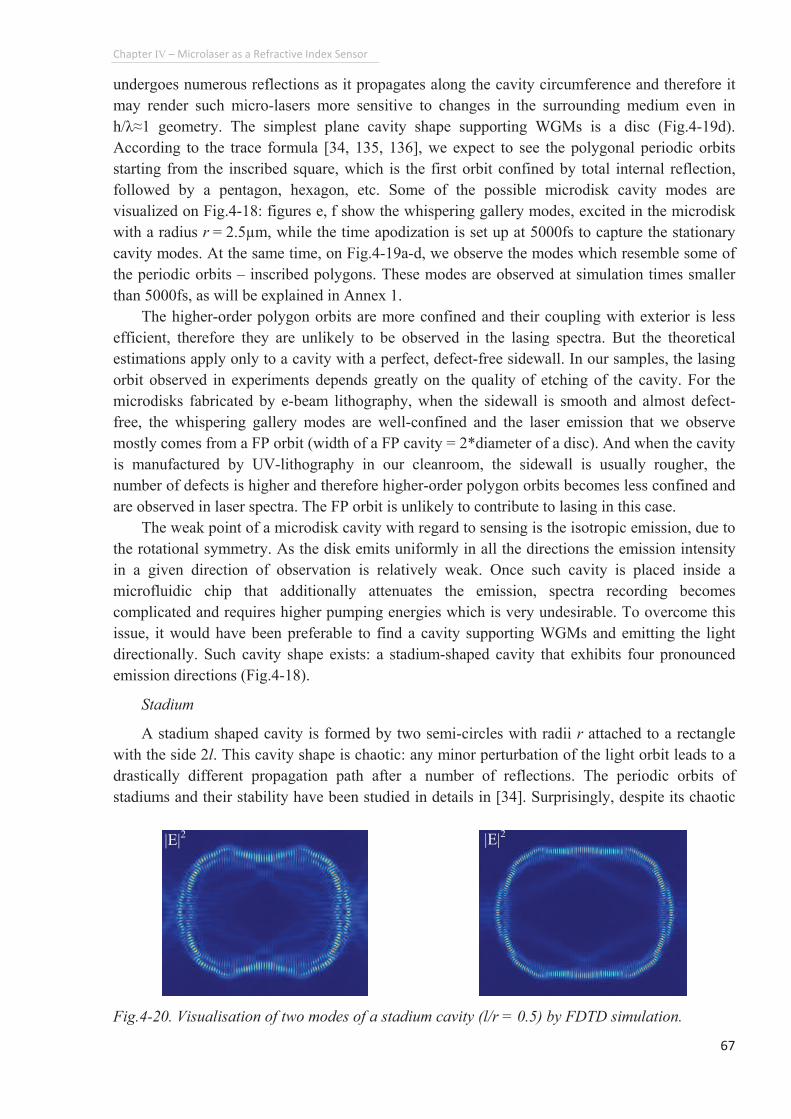
Chapter"IV" "Microlaser"as"a"Refractive"Index"Sensor"
67""
undergoes numerous reflections as it propagates along the cavity circumference and therefore it
may render such micro-lasers more sensitive to changes in the surrounding medium even in
h/そÃ1 geometry. The simplest plane cavity shape supporting WGMs is a disc (Fig.4-19d).
According to the trace formula [34, 135, 136], we expect to see the polygonal periodic orbits
starting from the inscribed square, which is the first orbit confined by total internal reflection,
followed by a pentagon, hexagon, etc. Some of the possible microdisk cavity modes are
visualized on Fig.4-18: figures e, f show the whispering gallery modes, excited in the microdisk
with a radius r = 2.5µm, while the time apodization is set up at 5000fs to capture the stationary
cavity modes. At the same time, on Fig.4-19a-d, we observe the modes which resemble some of
the periodic orbits � inscribed polygons. These modes are observed at simulation times smaller
than 5000fs, as will be explained in Annex 1.
The higher-order polygon orbits are more confined and their coupling with exterior is less
efficient, therefore they are unlikely to be observed in the lasing spectra. But the theoretical
estimations apply only to a cavity with a perfect, defect-free sidewall. In our samples, the lasing
orbit observed in experiments depends greatly on the quality of etching of the cavity. For the
microdisks fabricated by e-beam lithography, when the sidewall is smooth and almost defect-
free, the whispering gallery modes are well-confined and the laser emission that we observe
mostly comes from a FP orbit (width of a FP cavity = 2*diameter of a disc). And when the cavity
is manufactured by UV-lithography in our cleanroom, the sidewall is usually rougher, the
number of defects is higher and therefore higher-order polygon orbits becomes less confined and
are observed in laser spectra. The FP orbit is unlikely to contribute to lasing in this case.
The weak point of a microdisk cavity with regard to sensing is the isotropic emission, due to
the rotational symmetry. As the disk emits uniformly in all the directions the emission intensity
in a given direction of observation is relatively weak. Once such cavity is placed inside a
microfluidic chip that additionally attenuates the emission, spectra recording becomes
complicated and requires higher pumping energies which is very undesirable. To overcome this
issue, it would have been preferable to find a cavity supporting WGMs and emitting the light
directionally. Such cavity shape exists: a stadium-shaped cavity that exhibits four pronounced
emission directions (Fig.4-18).
Stadium
A stadium shaped cavity is formed by two semi-circles with radii r attached to a rectangle
with the side 2l. This cavity shape is chaotic: any minor perturbation of the light orbit leads to a
drastically different propagation path after a number of reflections. The periodic orbits of
stadiums and their stability have been studied in details in [34]. Surprisingly, despite its chaotic
Fig.4-20. Visualisation of two modes of a stadium cavity (l/r = 0.5) by FDTD simulation.
|E|2"
|E|2
Chapter"IV" "Microlaser"as"a"Refractive"Index"Sensor"
68""
nature, stadium cavities exhibit high directionality of emission that has been studied theoretically
in [137, 138] and in [34] the lens models have been developed, that predicts and experimentally
confirms the angular positions of the maxima and shows that these angles depend on l/r ratio
(which is a stadium deformation parameter). In our sensing experiments we have used stadiums
with the ratio l/r = 0.5, which exhibit four symmetrical emission maxima at the angles …4,3,2,1
maxs42º, 138º, 222º, 318º. Distribution of electric field for two different modes of a stadium
microcavity, calculated with FDTD, is shown on Fig.4-20.
Most of the refractive index variation sensing and heavy-metal detection results in this thesis
were obtained with the stadium cavities. In order to make all the cavities (Fabry-Perot, squares,
stadiums) emit in the same direction, perpendicular to the PDMS chip wall, the stadiums on the
lithographic mask were rotated at 42º, so that two of their emission maxima are oriented in
parallel with the emission of other cavity shapes.
The main drawback of the WGM cavities, which deals more with technology than physics,
lies in the higher requirements for the cavity edge quality, as the mode is localized mostly in the
region near the perimeter, undergoes numerous reflections at the sidewall and any minor
fabrication defects may significantly affect lasing performance. ね┻の┻ "Experimental"proof"of"RI"variation"sensing"and"heavy"metal"ions"detection."
Before proceeding with detection of heavy metal ions with functionalized cavities, we
needed to obtain an experimental proof of the medium influence on the cavity spectra in order to
choose and work further with the best available solution. While making multiple trials at this
stage of work is still acceptable, once functionalization with ligands is involved, each failed
attempt is not only time and material consuming, but also expensive.
4.5.1. First measurements of lasing spectra in liquids.
Once the optimal cavity shape has been clarified, that should let us (at least in theory)
achieve the highest sensitivity to changes in cavity surrounding, we can proceed with the
experimental verification. The first attempts that we have performed were aimed to detect laser
emission spectra of cavities in liquids. It was not evident, especially for the complex, non-
integrable chaotic cavites like stadiums, how will the liquid environment with elevated refractive
index influence their lasing properties. For the �simple� shapes, like Fabry-Perot, square... for
which a closed periodic orbit can be plotted from geometric optics considerations (Fig.4-19a,b,c)
one can try to predict the behavior of the cavity in water. For the Fabry-Perot, for example, the
periodic orbit will not change, but will only become less confined due to lower index contrast
with the environment. For the square cavity the influence is more significant: we have predicted
and experimentally observed the change of the lasing periodic orbit from a diamond in air to a
Fabry-Perot in water (Fig.4-15). In the octagonal cavities, the inscribed octagon orbit remains
confined by total internal reflection. In other words, all the microlasers when immersed in liquid,
continued to function properly.
However, once the stadium cavity is considered, we cannot predict its behavior so simply
due to the cavity�s chaotic nature. In the first experiments with stadiums, we noticed a sudden
drop of detected emission intensity (to zero for some of the stadiums) at the observation angle of
42°, where the intensity should be maximal, once a cavity is immersed in water. The maximum
was found to lie in the range 25º - 32° for different cavities, which was not expected. We
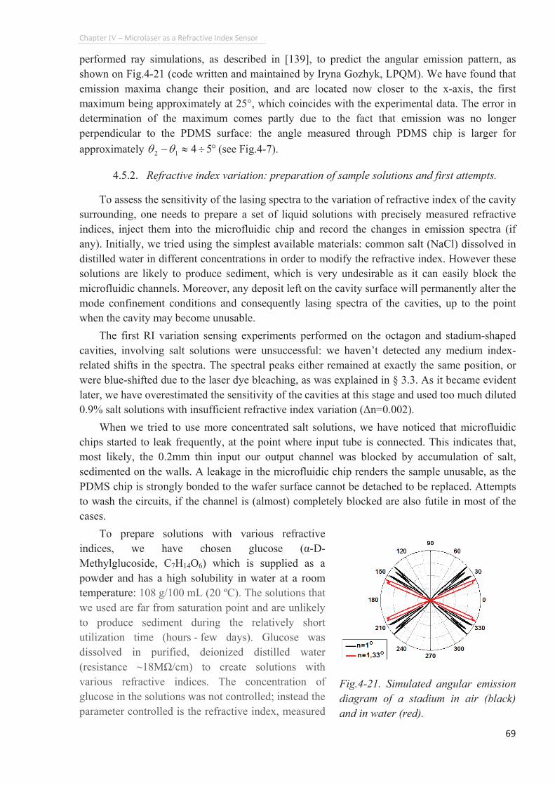
Chapter"IV" "Microlaser"as"a"Refractive"Index"Sensor"
69""
performed ray simulations, as described in [139], to predict the angular emission pattern, as
shown on Fig.4-21 (code written and maintained by Iryna Gozhyk, LPQM). We have found that
emission maxima change their position, and are located now closer to the x-axis, the first
maximum being approximately at 25°, which coincides with the experimental data. The error in
determination of the maximum comes partly due to the fact that emission was no longer
perpendicular to the PDMS surface: the angle measured through PDMS chip is larger for
approximately fl„…/ 5412 ss (see Fig.4-7).
4.5.2. Refractive index variation: preparation of sample solutions and first attempts.
To assess the sensitivity of the lasing spectra to the variation of refractive index of the cavity
surrounding, one needs to prepare a set of liquid solutions with precisely measured refractive
indices, inject them into the microfluidic chip and record the changes in emission spectra (if
any). Initially, we tried using the simplest available materials: common salt (NaCl) dissolved in
distilled water in different concentrations in order to modify the refractive index. However these
solutions are likely to produce sediment, which is very undesirable as it can easily block the
microfluidic channels. Moreover, any deposit left on the cavity surface will permanently alter the
mode confinement conditions and consequently lasing spectra of the cavities, up to the point
when the cavity may become unusable.
The first RI variation sensing experiments performed on the octagon and stadium-shaped
cavities, involving salt solutions were unsuccessful: we haven�t detected any medium index-
related shifts in the spectra. The spectral peaks either remained at exactly the same position, or
were blue-shifted due to the laser dye bleaching, as was explained in § 3.3. As it became evident
later, we have overestimated the sensitivity of the cavities at this stage and used too much diluted
0.9% salt solutions with insufficient refractive index variation (〉n=0.002).
When we tried to use more concentrated salt solutions, we have noticed that microfluidic
chips started to leak frequently, at the point where input tube is connected. This indicates that,
most likely, the 0.2mm thin input our output channel was blocked by accumulation of salt,
sedimented on the walls. A leakage in the microfluidic chip renders the sample unusable, as the
PDMS chip is strongly bonded to the wafer surface cannot be detached to be replaced. Attempts
to wash the circuits, if the channel is (almost) completely blocked are also futile in most of the
cases.
To prepare solutions with various refractive
indices, we have chosen glucose (g-D-
Methylglucoside, C7H14O6) which is supplied as a
powder and has a high solubility in water at a room
temperature: 108 g/100 mL (20 ºC). The solutions that
we used are far from saturation point and are unlikely
to produce sediment during the relatively short
utilization time (hours - few days). Glucose was
dissolved in purified, deionized distilled water
(resistance ~18Mっ/cm) to create solutions with
various refractive indices. The concentration of
glucose in the solutions was not controlled; instead the
parameter controlled is the refractive index, measured
Fig.4-21. Simulated angular emission
diagram of a stadium in air (black)
and in water (red).
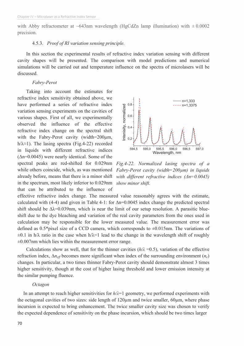
Chapter"IV" "Microlaser"as"a"Refractive"Index"Sensor"
70""
with Abby refractometer at ~643nm wavelength (HgCdZn lamp illumination) with ± 0.0002
precision.
4.5.3. Proof of RI variation sensing principle.
In this section the experimental results of refractive index variation sensing with different
cavity shapes will be presented. The comparison with model predictions and numerical
simulations will be carried out and temperature influence on the spectra of microlasers will be
discussed.
Fabry-Perot
Taking into account the estimates for
refractive index sensitivity obtained above, we
have performed a series of refractive index
variation sensing experiments on the cavities of
various shapes. First of all, we experimentally
observed the influence of the effective
refractive index change on the spectral shift
with the Fabry-Perot cavity (width=200µm,
h/そÃ1). The lasing spectra (Fig.4-22) recorded
in liquids with different refractive indices
(〉n=0.0045) were nearly identical. Some of the
spectral peaks are red-shifted for 0.029nm
while others coincide, which, as was mentioned
already before, means that there is a minor shift
in the spectrum, most likely inferior to 0.029nm
that can be attributed to the influence of
effective refractive index change. The measured value reasonably agrees with the estimate,
calculated with (4-4) and given in Table 4-1: for Än=0.0045 index change the predicted spectral
shift should be 〉そ=0.039nm, which is near the limit of our setup resolution. A parasitic blue-
shift due to the dye bleaching and variation of the real cavity parameters from the ones used in
calculation may be responsible for the lower measured value. The measurement error was
defined as 0.5*pixel size of a CCD camera, which corresponds to ±0.015nm. The variations of
±0.1 in h/そ ratio in the case when h/そ=1 lead to the change in the wavelength shift of roughly
±0.007nm which lies within the measurement error range.
Calculations show as well, that for the thinner cavities (h/そ =0.5), variation of the effective
refraction index, Äneff becomes more significant when index of the surrounding environment (ne)
changes. In particular, a two times thinner Fabry-Perot cavity should demonstrate almost 3 times
higher sensitivity, though at the cost of higher lasing threshold and lower emission intensity at
the similar pumping fluence.
Octagon
In an attempt to reach higher sensitivities for h/そ=1 geometry, we performed experiments with
the octagonal cavities of two sizes: side length of 120µm and twice smaller, 60µm, where phase
incursion is expected to bring enhancement. The twice smaller cavity size was chosen to verify
the expected dependence of sensitivity on the phase incursion, which should be two times larger
594,5 595,0 595,5 596,0 596,5 597,0
0,2
0,4
0,6
0,8 n=1,333
n=1,3375
Inte
nis
ity, norm
aliz
ed
Wavelength, nm
Fig.4-22. Normalized lasing spectra of a
Fabry-Perot cavity (width=200µm) in liquids
with different refractive indices (〉n=0.0045)
show minor shift.
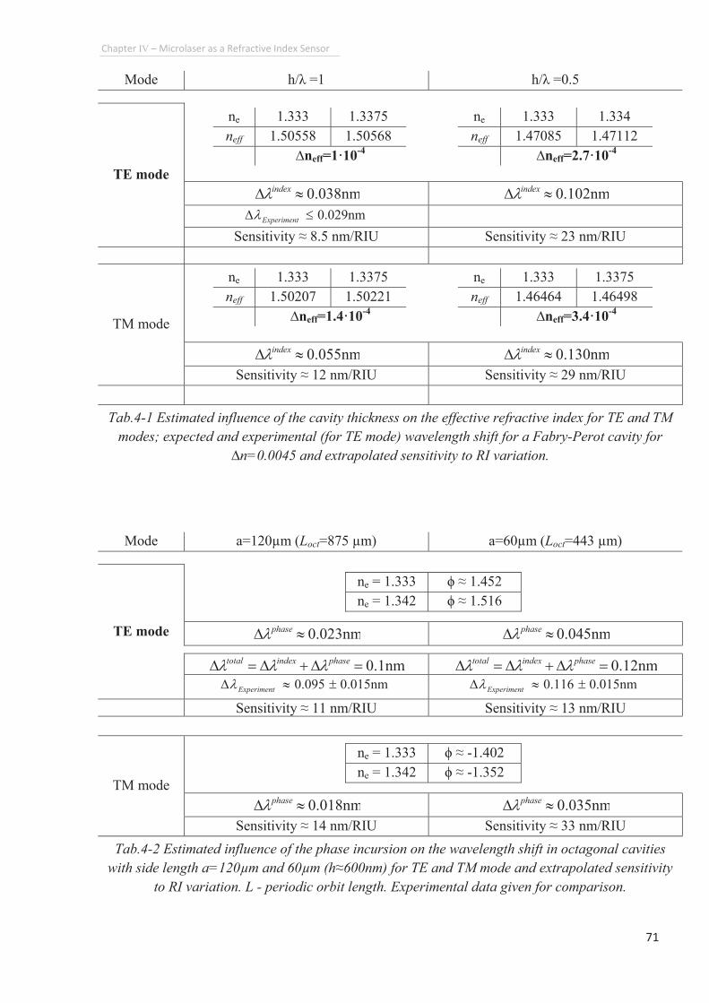
Chapter"IV" "Microlaser"as"a"Refractive"Index"Sensor"
71""
Mode h/そ =1 h/そ =0.5
TE mode
ne 1.333 1.3375 ne 1.333 1.334
neff 1.50558 1.50568 neff 1.47085 1.47112
Äneff=1·10-4 Äneff=2.7·10
-4
0.038nm…F indexn 0.102nm…F indexn0.029nm~F Experimentn
Sensitivity à 8.5 nm/RIU Sensitivity à 23 nm/RIU
TM mode
ne 1.333 1.3375 ne 1.333 1.3375
neff 1.50207 1.50221 neff 1.46464 1.46498
Äneff=1.4·10-4 Äneff=3.4·10
-4
0.055nm…F indexn 0.130nm…F indexnSensitivity à 12 nm/RIU Sensitivity à 29 nm/RIU
Tab.4-1 Estimated influence of the cavity thickness on the effective refractive index for TE and TM
modes; expected and experimental (for TE mode) wavelength shift for a Fabry-Perot cavity for
Än=0.0045 and extrapolated sensitivity to RI variation.
Mode a=120µm (Loct=875 µm) a=60µm (Loct=443 µm)
TE mode
ne = 1.333 思 Ã 1.452
ne = 1.342 思 Ã 1.516
0.023nm…F phasen 0.045nm…F phasen0.1nm?F-F?F phaseindextotal nnn 0.12nm?F-F?F phaseindextotal nnn
0.015nm0.095 ‒…F Experimentn 0.015nm0.116 ‒…F ExperimentnSensitivity à 11 nm/RIU Sensitivity à 13 nm/RIU
TM mode
ne = 1.333 思 Ã -1.402
ne = 1.342 思 Ã -1.352
0.018nm…F phasen 0.035nm…F phasenSensitivity à 14 nm/RIU Sensitivity à 33 nm/RIU
Tab.4-2 Estimated influence of the phase incursion on the wavelength shift in octagonal cavities
with side length a=120µm and 60µm (hÃ600nm) for TE and TM mode and extrapolated sensitivity
to RI variation. L - periodic orbit length. Experimental data given for comparison.
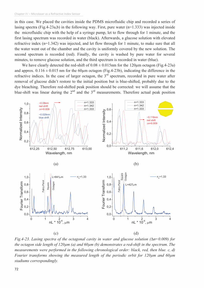
Chapter"IV"�"Microlaser"as"a"Refractive"Index"Sensor"
72""
in this case. We placed the cavities inside the PDMS microfluidic chip and recorded a series of
lasing spectra (Fig.4-23a,b) in the following way. First, pure water (n=1.333) was injected inside
the microfluidic chip with the help of a syringe pump, let to flow through for 1 minute, and the
first lasing spectrum was recorded in water (black). Afterwards, a glucose solution with elevated
refractive index (n=1.342) was injected, and let flow through for 1 minute, to make sure that all
the water went out of the chamber and the cavity is uniformly covered by the new solution. The
second spectrum is recorded (red). Finally, the cavity is washed by pure water for several
minutes, to remove glucose solution, and the third spectrum is recorded in water (blue).
We have clearly detected the red-shift of 0.08 ± 0.015nm for the 120µm octagon (Fig.4-23a)
and approx. 0.116 ± 0.015 nm for the 60µm octagon (Fig.4-23b), indicating the difference in the
refractive indices. In the case of larger octagon, the 3rd
spectrum, recorded in pure water after
removal of glucose didn�t restore to the initial position but is blue-shifted, probably due to the
dye bleaching. Therefore red-shifted peak position should be corrected: we will assume that the
blue-shift was linear during the 2nd
and the 3rd
measurements. Therefore actual peak position
612,25 612,50 612,75 613,00
0,2
0,4
0,6
0,8
1,0
~0.029nm
blue shift
n=1.333
n=1.342
n=1.333
~0.08nm
red shift
Fn=0.009
Norm
aliz
ed I
nte
nsity
Wavelength, nm
611,2 611,6 612,0 612,40,0
0,2
0,4
0,6
n=1.333
n=1.342
n=1.333
Norm
aliz
ed I
nte
nsity
Wavelength, nm
~0.116nm
red shift
Fn=0.009
(a) (b)
0 1 2 3 4
0,0
0,2
0,4
0,6
0,8
1,0
Octa
gon
Square
nL * 10-6, om
Fourie
r T
ransfo
rm
Fabry
-Pero
t
L=841om ne=1,33
0 1 2 3 4
0,0
0,2
0,4
0,6
0,8
1,0
Octa
go
n
L=427om
ne=1,33
Fabry
-Pero
t Square
Fo
urier
Tra
nsfo
rm
nL * 10-6, om
(c) (d)
Fig.4-23. Lasing spectra of the octagonal cavity in water and glucose solution (Än=0.009) for
the octagon side length of 120µm (a) and 60µm (b) demonstrates a red-shift in the spectrum. The
measurements were performed in the following chronological order: black, red, then blue. c, d)
Fourier transforms showing the measured length of the periodic orbit for 120µm and 60µm
stadiums correspondingly.
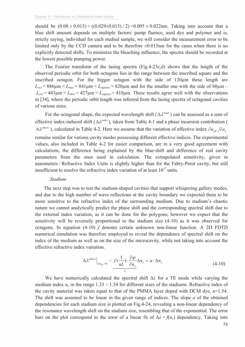
Chapter"IV"�"Microlaser"as"a"Refractive"Index"Sensor"
73""
should be (0.08 ± 0.015) + ((0.029±0.015) / 2) =0.095 ± 0.022nm. Taking into account that a
blue shift amount depends on multiple factors: pump fluence, used dye and polymer and is,
strictly saying, individual for each studied sample, we will consider the measurement error to be
limited only by the CCD camera and to be therefore ±0.015nm for the cases when there is no
explicitly detected shifts. To minimize the bleaching influence, the spectra should be recorded at
the lowest possible pumping power.
The Fourier transform of the lasing spectra (Fig.4-23c,d) shows that the length of the
observed periodic orbit for both octagons lies in the range between the inscribed square and the
inscribed octagon. For the bigger octagon with the side of 120µm these length are
Loct = 886µm < Lmes = 841µm < Lsquare = 820µm and for the smaller one with the side of 60µm �
Loct = 443µm < Lmes = 427µm < Lsquare = 410µm. These results agree well with the observations
in [34], where the periodic orbit length was inferred from the lasing spectra of octagonal cavities
of various sizes.
For the octagonal shape, the expected wavelength shift ( totalnF ) can be assessed as a sum of
effective index-induced shift ( indexnF ), taken from Table 4-1 and a phase incursion contribution (phasenF ), calculated in Table 4-2. Here we assume that the variation of effective index
eeff nn ••remains similar for various cavity modes possessing different effective indices. The experimental
values, also included in Table 4-2 for easier comparison, are in a very good agreement with
calculations, the difference being explained by the blue-shift and difference of real cavity
parameters from the ones used in calculation. The extrapolated sensitivity, given in
nanometers / Refractive Index Units is slightly higher than for the Fabry-Perot cavity, but still
insufficient to resolve the refractive index variation of at least 10-3
units.
Stadium
The next step was to test the stadium-shaped cavities that support whispering gallery modes,
and due to the high number of wave reflections at the cavity boundary we expected them to be
more sensitive to the refractive index of the surrounding medium. Due to stadium�s chaotic
nature we cannot analytically predict the phase shift and the corresponding spectral shift due to
the external index variation, as it can be done for the polygons; however we expect that the
sensitivity will be reversely proportional to the stadium size (4-10) as it was observed for
octagons. In equation (4-10) f denotes certain unknown non-linear function. A 2D FDTD
numerical simulation was therefore employed to reveal the dependence of spectral shift on the
index of the medium as well as on the size of the microcavity, while not taking into account the
effective refractive index variation.
We have numerically calculated the spectral shift 〉そ for a TE mode while varying the
medium index ne in the range 1.33 ÷ 1.34 for different sizes of the stadiums. Refractive index of
the cavity material was taken equal to that of the PMMA layer doped with DCM dye, n=1.54.
The shift was assumed to be linear in the given range of indices. The slope a of the obtained
dependencies for each stadium size is plotted on Fig.4-24, revealing a non-linear dependency of
the resonance wavelength shift on the stadium size, resembling that of the exponential. The error
bars on the plot correspond to the error of a linear fit of 〉そ = f(ne) dependency. Taking into
""ee
a
en
phase nannnL
feff
F©?F••©F ?F+*+)(
ln )1
(~0 "
"(4-10)
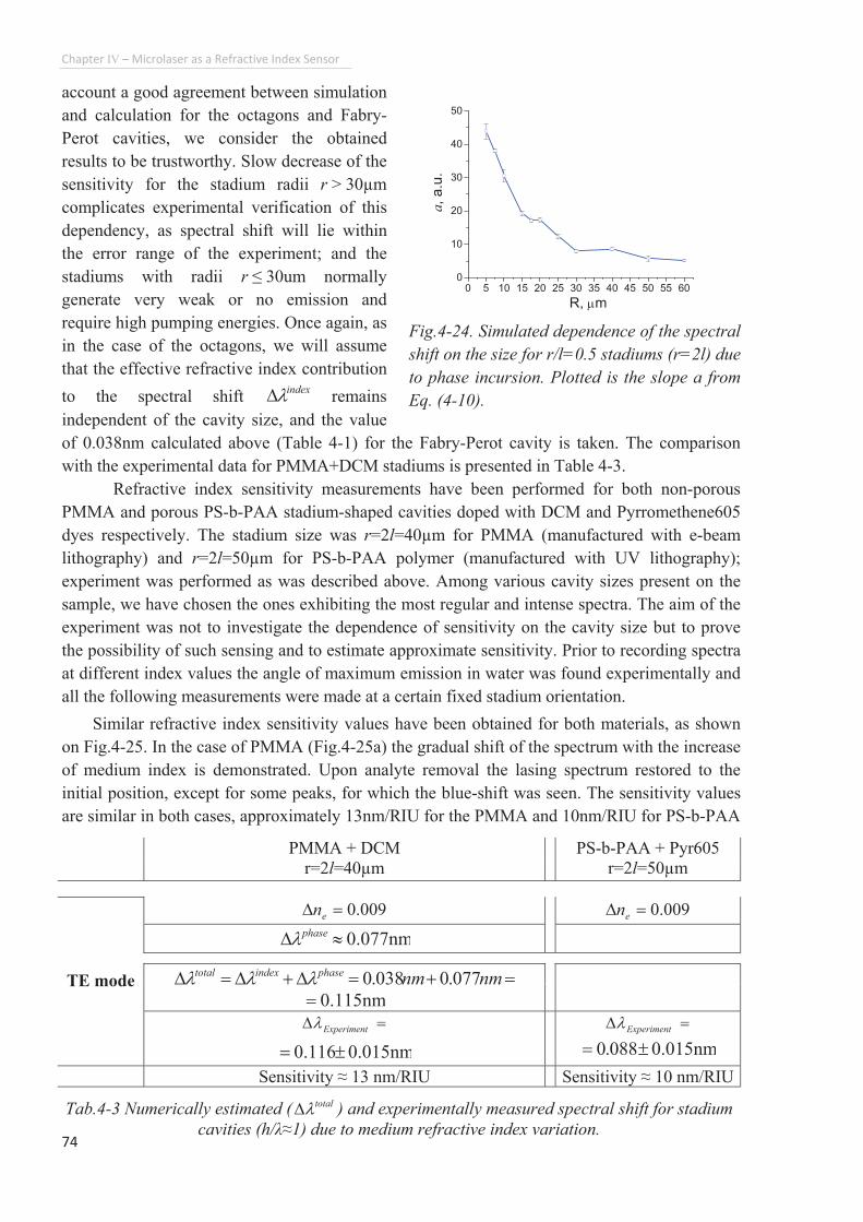
Chapter"IV"�"Microlaser"as"a"Refractive"Index"Sensor"
74""
account a good agreement between simulation
and calculation for the octagons and Fabry-
Perot cavities, we consider the obtained
results to be trustworthy. Slow decrease of the
sensitivity for the stadium radii r > 30µm
complicates experimental verification of this
dependency, as spectral shift will lie within
the error range of the experiment; and the
stadiums with radii r ø 30um normally
generate very weak or no emission and
require high pumping energies. Once again, as
in the case of the octagons, we will assume
that the effective refractive index contribution
to the spectral shift indexnF remains
independent of the cavity size, and the value
of 0.038nm calculated above (Table 4-1) for the Fabry-Perot cavity is taken. The comparison
with the experimental data for PMMA+DCM stadiums is presented in Table 4-3.
Refractive index sensitivity measurements have been performed for both non-porous
PMMA and porous PS-b-PAA stadium-shaped cavities doped with DCM and Pyrromethene605
dyes respectively. The stadium size was r=2l=40µm for PMMA (manufactured with e-beam
lithography) and r=2l=50µm for PS-b-PAA polymer (manufactured with UV lithography);
experiment was performed as was described above. Among various cavity sizes present on the
sample, we have chosen the ones exhibiting the most regular and intense spectra. The aim of the
experiment was not to investigate the dependence of sensitivity on the cavity size but to prove
the possibility of such sensing and to estimate approximate sensitivity. Prior to recording spectra
at different index values the angle of maximum emission in water was found experimentally and
all the following measurements were made at a certain fixed stadium orientation.
Similar refractive index sensitivity values have been obtained for both materials, as shown
on Fig.4-25. In the case of PMMA (Fig.4-25a) the gradual shift of the spectrum with the increase
of medium index is demonstrated. Upon analyte removal the lasing spectrum restored to the
initial position, except for some peaks, for which the blue-shift was seen. The sensitivity values
are similar in both cases, approximately 13nm/RIU for the PMMA and 10nm/RIU for PS-b-PAA
0 5 10 15 20 25 30 35 40 45 50 55 600
10
20
30
40
50
a,
a.u
.
R, om
Fig.4-24. Simulated dependence of the spectral
shift on the size for r/l=0.5 stadiums (r=2l) due
to phase incursion. Plotted is the slope a from
Eq. (4-10).
PMMA + DCM PS-b-PAA + Pyr605
r=2l=40µm r=2l=50µm
TE mode
0.009?F en 0.009?F en
0.077nm…F phasen?-?F-F?F nmnmphaseindextotal 077.0038.0nnn
0.115nm?"
?F Experimentn0.015nm0.116‒?
?F Experimentn0.015nm088.0 ‒?
Sensitivity à 13 nm/RIU Sensitivity à 10 nm/RIU
Tab.4-3 Numerically estimated ( totalnF ) and experimentally measured spectral shift for stadium
cavities (h/そÃ1) due to medium refractive index variation.
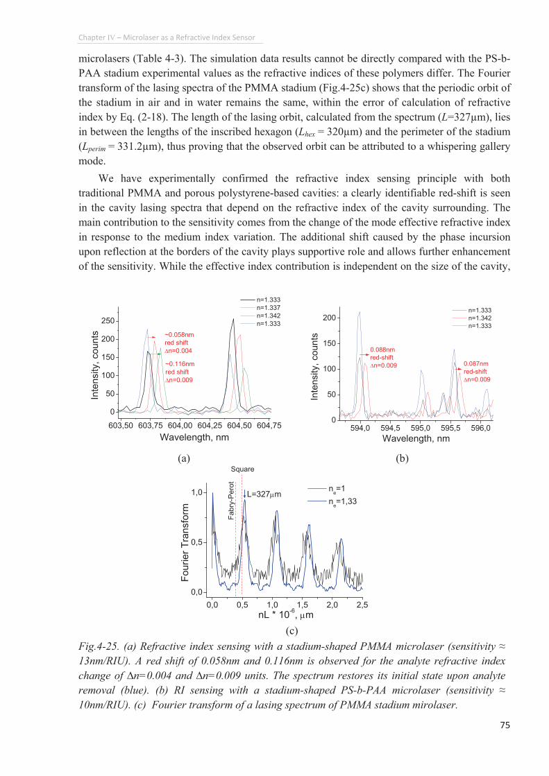
Chapter"IV"�"Microlaser"as"a"Refractive"Index"Sensor"
75""
microlasers (Table 4-3). The simulation data results cannot be directly compared with the PS-b-
PAA stadium experimental values as the refractive indices of these polymers differ. The Fourier
transform of the lasing spectra of the PMMA stadium (Fig.4-25c) shows that the periodic orbit of
the stadium in air and in water remains the same, within the error of calculation of refractive
index by Eq. (2-18). The length of the lasing orbit, calculated from the spectrum (L=327µm), lies
in between the lengths of the inscribed hexagon (Lhex = 320µm) and the perimeter of the stadium
(Lperim = 331.2µm), thus proving that the observed orbit can be attributed to a whispering gallery
mode.
We have experimentally confirmed the refractive index sensing principle with both
traditional PMMA and porous polystyrene-based cavities: a clearly identifiable red-shift is seen
in the cavity lasing spectra that depend on the refractive index of the cavity surrounding. The
main contribution to the sensitivity comes from the change of the mode effective refractive index
in response to the medium index variation. The additional shift caused by the phase incursion
upon reflection at the borders of the cavity plays supportive role and allows further enhancement
of the sensitivity. While the effective index contribution is independent on the size of the cavity,
603,50 603,75 604,00 604,25 604,50 604,75
0
50
100
150
200
250
n=1.333
n=1.337
n=1.342
n=1.333
~0.058nm
red shift
Fn=0.004
Wavelength, nm
Inte
nsity,
counts
~0.116nm
red shift
Fn=0.009
594,0 594,5 595,0 595,5 596,00
50
100
150
200 n=1.333
n=1.342
n=1.333
Inte
nsity,
co
un
ts
Wavelength, nm
0.088nm
red-shift
Fn=0.009 0.087nm
red-shift
Fn=0.009
(a) (b)
0,0 0,5 1,0 1,5 2,0 2,5
0,0
0,5
1,0
Square
L=327om
Fa
bry
-Pero
t
Fouri
er
Tra
nsfo
rm
nL * 10-6, om
ne=1
ne=1,33
(c)
Fig.4-25. (a) Refractive index sensing with a stadium-shaped PMMA microlaser (sensitivity Ã13nm/RIU). A red shift of 0.058nm and 0.116nm is observed for the analyte refractive index
change of Än=0.004 and Än=0.009 units. The spectrum restores its initial state upon analyte
removal (blue). (b) RI sensing with a stadium-shaped PS-b-PAA microlaser (sensitivity Ã10nm/RIU). (c) Fourier transform of a lasing spectrum of PMMA stadium mirolaser.
Chapter"IV"�"Microlaser"as"a"Refractive"Index"Sensor"
76""
the phase incursion part grows linearly with the decrease of the cavity size and increase of the
number of reflections at the cavity border (at least for the polygonal shapes).
The experimental sensitivity values for the octagons (a = 60µm) and stadiums of the tested
size (the shape that we expected to possess the highest sensitivity) were found to be very close,
approximately 13nm/RIU (which approximately coincides with numerically predicted
sensitivity). Further decrease of the lateral dimensions as well as cavity thickness, that is
expected to improve the sensitivity, is problematic for the current cavity architecture as was
already mentioned above. Therefore a novel cavity design described in Chapter 5 � cavity on a
pedestal � has been implemented and investigated, that weakens the constraints on the cavity size
and significantly enhances sensitivity.
4.5.4. Temperature Influence
An important question that has been omitted until now is the temperature dependence of the
spectral shift. The essence of the problem lies in the dependency of the polymer refractive index
on the temperature, due to thermal volume expansion. A smallest variation in the cavity
refractive index will lead to the change in the optical path inside the cavity and consequent shift
of the resonances. The dependency of effective refractive index on the temperature will therefore
be constituted of the dependencies of indices of polymer and claddings:
dT
dn
n
n
dT
dn
n
n
dT
dn
n
n
dT
dne
e
effSiO
SiO
effpolymer
polymer
effeff
••-•
•-••? 2
2
(4-11)
The following experimental values of temperature coefficient of refractive indices were
taken for estimation: 4102.1 /©/…
dT
dnPMMA [140] , 51012 /©…dT
dnSiO [141], 41012 /©…
dT
dn OH [142].
The contributions of indices of claddings and polymer into variation of effective index can be
calculated using (3) and are approximately: 9.0…••
PMMA
eff
n
n, 1.0
2
…••
SiO
eff
n
n, 02.0…••
e
eff
n
n. The
temperature coefficient of effective refractive index is therefore estimated to be of the order 10-4
,
two orders less than the influence of the medium refractive index that we are measuring:"
24 1010 // …••>…
e
effeff
n
n
dT
dn(4-12)
In our experimental setup, no temperature stabilization was employed. Though variation of
temperature of several degrees may give a measurable influence in the measurement results, we
assume that this contribution is negligible. Moreover, within one experiment, all the liquids are
kept at the same conditions and are let to flow through the microfluidic chip for a minute or two
prior to performing actual measurement, therefore we do not expect to experience temperature
variations during the time of experiment. The laboratory where experiment where performed is
located in the basement and is air-conditioned, which practically eliminates temperature
variations during the day.

Chapter"IV" "Microlaser"as"a"Refractive"Index"Sensor"
77""
ね┻は┻ "Detection"of"heavy┽metal"ions"with"microcavity"sensors."
Once we have proven the possibility of refractive index variation sensing with an organic
laser microcavities, and found an optimal cavity shape that leads to the highest sensitivity, we
can proceed with functionalization of the cavities with specific ligands and detection of heavy
metal ions in liquids. The stadium-shaped cavities were verified to generate intense emission
with a regular spectrum, corresponding to whispering gallery modes prior to functionalization
with mercury-binding thiol groups that was performed as described in part 4.3. Due to the
sensitivity of the thiol ligands to oxygen, functionalization was performed right before (at most
two hours) performing the sensing experiments and sample was stored in an exsiccator under
vacuum. This problem would be absent for the specific ligands synthesized at PPSM, ENS
Cachan.
The experiment is performed similarly to the refractive index sensing experiment, but there
exist two important differences. First of all, in the case of mercury solutions, the refractive index
variation is created locally by the metal ions captured by the ligands, in the thin layer close to the
cavity surface. We tried to estimate this variation with ellipsometry, as was described above, but
did not obtain coherent results. The refractive index of the mercury solutions, measured by the
Abbe refractometer is the same (within the precision of measurement) for all the concentrations
and is equal to 1.3345, that of the MES (2-(N-morpholino)ethanesulfonic acid) buffer, used to
prepare the solutions. The difference in refractive indices between the solutions of different
concentration would complicate the result interpretation: it would be impossible to distinguish,
whether the spectral shift comes from the presence of metal ions or from the difference in
solution indices. In this case, each spectrum recorded in the analyte solution should be compared
to the spectrum recorded in the reference solution with the same refractive index, which would
slightly complicate the experiment. Secondly, in the case functionalized, chemical bonds are
formed between the analyte ions and ligands. A technique to decomplex the analyte ions should
be developed if the sensor is planned as reusable. We have experimentally verified two
approaches for release of the bound mercury ions from the ligands: washing the cavities with
acidic solutions (PH 1 or PH 3.5) or with dimercaptopropanol, which are known to release
mercury from thiol groups [131]. However after treatment with acidic solution, we noticed the
changes in the lasing spectra, which may probably occur due to protonation of Pyrromethene
dye. Therefore we used dimercaptopropanol that didn�t exhibit any negative effects on cavity
performance. More details about mercury complexation will be presented in the PhD thesis of
Djibril Faye, PPSM, ENS Cachan.
The set of analyte solutions and corresponding washing solutions were obtained from our
colleagues. The analyte solutions contain mercury Hg2+
in MES buffer with linearly increasing
concentration: from 10-6
M to 10-3
M with 10-1
step. The washing solutions contain 2,3-
dimercapto-1-propanol at a concentration one order higher than that of a mercury. It has been
shown in [154] that the most efficient decoupling of mercury from thiol ligands is achieved in
the dimercaptopropanol solution with 50 times higher concentration than that of the mercury.
This means, that after injection of 1·10-6
M Hg2+
solution in a microfluidic chip, washing was
performed with 5·10-5
M dimercaptopropanol solution and so on.
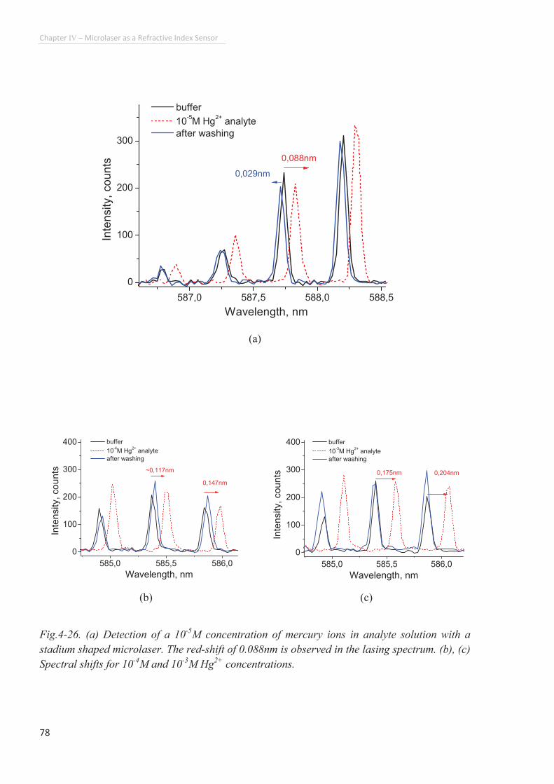
Chapter"IV" "Microlaser"as"a"Refractive"Index"Sensor"
78""
""
587,0 587,5 588,0 588,5
0
100
200
300
0,088nm
0,029nm
Wavelength, nm
Inte
nsity,
co
un
ts buffer
10-5M Hg
2+ analyte
after washing
(a)
585,0 585,5 586,0
0
100
200
300
400 buffer
10-4M Hg
2+ analyte
after washing
~0,117nm
Wavelength, nm
Inte
nsity,
co
un
ts
0,147nm
"
585,0 585,5 586,0
0
100
200
300
400 buffer
10-3M Hg
2+ analyte
after washing
0,175nm 0,204nm
Inte
nsity, cou
nts
Wavelength, nm"
(b) (c)
Fig.4-26. (a) Detection of a 10-5
M concentration of mercury ions in analyte solution with a
stadium shaped microlaser. The red-shift of 0.088nm is observed in the lasing spectrum. (b), (c)
Spectral shifts for 10-4
M and 10-3
M Hg2+
concentrations.
Chapter"IV"�"Microlaser"as"a"Refractive"Index"Sensor"
79""
In order to avoid cavity pollution with mercury salts, we varied the mercury concentration
from the lowest, 10-6
M to the highest, 10-3
M, while performing measurements. The solutions are
injected inside the microfluidic chip with a pump at the flow rate of approximately 10ml/hour
and in the case of a mercury analyte, let inside the chip for 8-10 minutes to increase the amount
of ions captured by ligands. No separate study was performed on the rate of
complexation/decomplexation of mercury ions by thiols.
Sensing experiments were performed on a stadium-shaped cavity (R=2l=50µm), fabricated
in PMMA polymer doped with Pyrromethene 605 dye. For the 10-6
M Hg2+
concentration we
didn�t detect any changes in spectra. The results presented on Fig.4-26a evidence a clearly
detectable red-shift of 〉そ Ã 0.088nm between the lasing spectra in buffer solution and in the
analyte with 10-5
M Hg2+
concentration, proving therefore the viability of the sensing approach.
The cavity was washed with 3ml of 5·10-4
M dimercaptopropanol solution, the clean buffer was
injected again and the lasing spectrum restored to its initial position with a slight blue-shift. The
actual value of red-shift is slightly smaller if blue-shift correction is taken into account and is
therefore approximately 〉そ = 0.088nm - 0.029nm/2 = 0.073nm. For higher concentrations of
mercury, 10-4
M and 10-3
M, the spectral shift was expectedly stronger, following an
approximately linear dependence, and equal 0.146nm and 0.175 ÷ 0.204nm correspondingly
(Fig.4-26b,c).
Several cycles of washing/analyte injection were performed and similar spectral shifts were
recorded for the same analyte concentration. In some cases, like on Fig.4-26b, spectra didn�t
restore to the initial state after washing but remained slightly red-shifted. Additional, longer
washing with dimercaptopropanol led to complete mercury decomplexation (or below the
detectable level) and restoration of the spectra. The reference experiment was performed with
non-functionalized cavity and no spectral shift was detected, whatever the mercury concentration
was.
The obtained results confirmed the possibility of heavy metal ions detection in liquids with
concentrations down to 10-5
M, however to be competitive with other detection approaches, for
instance fluorescence labelling, sensitivity needs to be increased for at least 3 orders of
magnitude. In the next chapter we will present the results of mercury detection with pedestal
microcavities, featuring enhanced sensitivity.

Chapter"IV" "Microlaser"as"a"Refractive"Index"Sensor"
80""
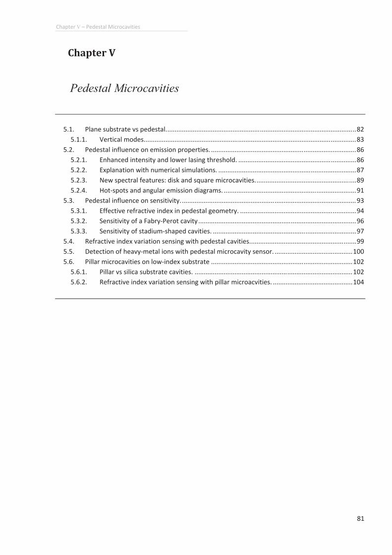
Chapter"V"�"Pedestal"Microcavities"
81""
5. Chapter"V"""
Pedestal Microcavities
""
5.1." Plane"substrate"vs"pedestal."........................................................................................................"82"5.1.1." Vertical"modes."...................................................................................................................."83"
5.2." Pedestal"influence"on"emission"properties."................................................................................"86"5.2.1." Enhanced"intensity"and"lower"lasing"threshold."................................................................."86"5.2.2." Explanation"with"numerical"simulations."............................................................................"87"5.2.3." New"spectral"features:"disk"and"square"microcavities."......................................................."89"5.2.4." Hotどspots"and"angular"emission"diagrams."........................................................................."91"
5.3." Pedestal"influence"on"sensitivity."................................................................................................ "93"5.3.1." Effective"refractive"index"in"pedestal"geometry."................................................................"94"5.3.2." Sensitivity"of"a"FabryどPerot"cavity"....................................................................................... "96"5.3.3." Sensitivity"of"stadiumどshaped"cavities."..............................................................................."97"
5.4." Refractive"index"variation"sensing"with"pedestal"cavities.".........................................................."99"5.5." Detection"of"heavyどmetal"ions"with"pedestal"microcavity"sensor."..........................................."100"5.6." Pillar"microcavities"on"lowどindex"substrate".............................................................................."102"
5.6.1." Pillar"vs"silica"substrate"cavities."....................................................................................... "102"5.6.2." Refractive"index"variation"sensing"with"pillar"microacvities."............................................"104"
"""
Chapter"V" "Pedestal"Microcavities""
82""
Introduction
In this chapter we will discuss the prospective cavity design � pedestal cavities that should
in theory lead to a significant sensitivity increase of a microlaser-based sensor. The technology
of the pedestal cavity fabrication was detailed in Chapter 3. First of all the primary difference
between the conventional and pedestal cavities will be outlined and the consequences on the
lasing spectra and performance will be discussed and supported by numerical simulations. A
striking influence of the pedestal geometry on the spectra has been discovered. Afterwards the
sensing results will be presented, including refractive index variation sensing as well as mercury
ions detection in liquid. Finally, cavities on a low-index CYTOP substrate and all-polymer
pedestal cavities will be discussed. の┻な┻ "Plane"substrate"vs"pedestal."
The work on the pedestal microcavities started as a search of the ways to enhance sensor
performance. Our expectations for higher sensitivity were based on the following two ideas,
illustrated on Fig.5-1a:
‚ First of all, the mode localized in the free-standing region of the cavity will not
experience coupling to the substrate, but will interact with the surrounding medium,
which will lead to stronger influence on the effective refractive index and consequently
sensitivity. The effect is expected to be the strongest for the whispering gallery modes,
which are localized in the region close to the cavity circumference. In the case of
functionalized cavities, pedestal structure can be considered as an increase of the
effective sensing surface, covered by ligands.
‚ Secondly, the free-hanging cavity part can be considered as a symmetric waveguide: a
cavity layer surrounded by two claddings (air) with equal refractive indices. For such a
structure there exists no cutoff thickness: at least one vertical mode is always confined in
a waveguide. For a whispering gallery mode cavity this means, that if the underetch is
made deep enough so that the mode is located inside the freely-hanging part, the cavity
can be made thinner (ø cutoff thickness) than in case when it is supported by the
substrate. This in turn will lead to lower mode confinement and higher interaction with
the surrounding medium. In other words, geometries with h/そ ø 0.5 are achievable (see
section 4.4.1).
While the increase of the effective sensing surface is clearly seen from the scheme on
Fig.5-1a the weakening of mode confinement in thinner cavities can be conveniently illustrated
if we plot a profile of the guided mode in the cavity layer (Fig.5-2). The mode profile was
calculated numerically, similar to as described in Annex 1. One can observe qualitatively, that in
case of the thinner pedestal cavity (h/そ=0.5) in water (Fig.5-2b) the intensity of the electric field
in the vicinity of the cavity surface is higher than in h/そ=1 pedestal case, being approximately
65% of the maximum field intensity compared to ~50% in the former case and ~40% for a cavity
without a pedestal. Thus medium index variation or presence of analyte molecules captured by
ligands is expected to significantly alter the cavity mode effective refractive index and
consequently the lasing spectra.
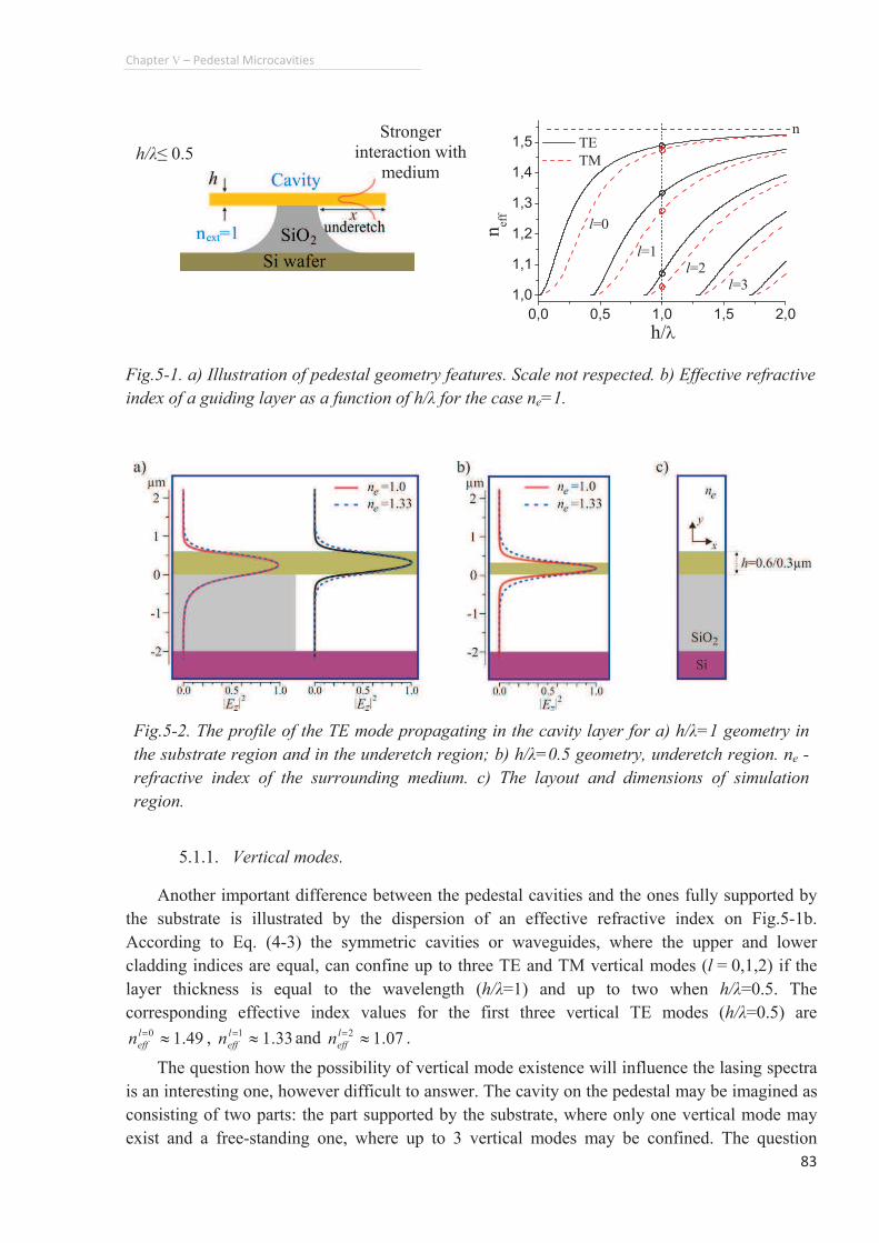
Chapter"V"�"Pedestal"Microcavities"
83""
1,0
1,1
1,2
1,3
1,4
1,5
0,0 0,5 1,0 1,5 2,0
l=3l=2
l=1
l=0
TE
TM
n
h/n
nef
f
Fig.5-1. a) Illustration of pedestal geometry features. Scale not respected. b) Effective refractive
index of a guiding layer as a function of h/そ for the case ne=1.
Fig.5-2. The profile of the TE mode propagating in the cavity layer for a) h/そ=1 geometry in
the substrate region and in the underetch region; b) h/そ=0.5 geometry, underetch region. ne -
refractive index of the surrounding medium. c) The layout and dimensions of simulation
region.
5.1.1. Vertical modes.
Another important difference between the pedestal cavities and the ones fully supported by
the substrate is illustrated by the dispersion of an effective refractive index on Fig.5-1b.
According to Eq. (4-3) the symmetric cavities or waveguides, where the upper and lower
cladding indices are equal, can confine up to three TE and TM vertical modes (l = 0,1,2) if the
layer thickness is equal to the wavelength (h/そ=1) and up to two when h/そ=0.5. The
corresponding effective index values for the first three vertical TE modes (h/そ=0.5) are
49.10 …?leffn , 33.11 …?l
effn and 07.12 …?leffn .
The question how the possibility of vertical mode existence will influence the lasing spectra
is an interesting one, however difficult to answer. The cavity on the pedestal may be imagined as
consisting of two parts: the part supported by the substrate, where only one vertical mode may
exist and a free-standing one, where up to 3 vertical modes may be confined. The question
h/そø 0.5"Stronger
interaction with
medium
Chapter"V"�"Pedestal"Microcavities""
84""
therefore is what will be the configuration of a resulting cavity mode and whether modes with
different l numbers may coexist in different cavity parts.
The analytical solution of this problem is impossible; therefore we will apply the finite
element numerical modeling in an attempt to discover the mode profile. On Fig.5-3a the profiles
of the vertical TE modes with l=1,2 are plotted for a cavity part with an underetch (n2=1). The
profile of l=0 mode can be seen on Fig.5-2a. Now we will try to visualize the mode profiles in a
pedestal waveguide structure, depicted on Fig.5-3b, where the left part of the waveguide is
supported by a silica substrate and the right part has an underetch. To simplify the task, the
simulation has been performed without taking into account the presence of a Si wafer. The
depicted structure is a cross-section of an infinite waveguide, where wave propagates along the
z-axis, and not a cross-section of a whispering gallery mode cavity (disc, for example). Therefore
configuration of mode electromagnetic fields found in simulation would be different from the
one existing in a WGM cavity. Also, obtained results are not directly applicable for the Fabry-
Perot cavities, where resonance occurs along the x-axis (in connotations of Fig.5-3b), while here
wave propagates along the z-axis.
We will try to find out, whether a vertical mode in the underetch part of a waveguide may
coexist together with a mode in a substrate-supported part. For this purpose we will look for the
guided modes of a pedestal waveguide with the effective indices close to the ones calculated
theoretically from Eq.(4-3) for the following cases: 1) TE, l=0 mode in a waveguide on silica
substrate, 2) TE, l=0 mode in a free-standing waveguide (n2=1), 3) TE, l=1,2 modes in a free-
standing waveguide. The discovered modes are displayed on Fig.5-3 c-1 � c-6. For the effective
index value of neff=1.50171 close to that of the fully supported waveguide (TE, l=0; n=1.45;
neff=1.50209) there exists a mode fully localized inside the part of a guide supported by a
substrate and which doesn�t extend into the right part with an under-etch (Fig.5-3 c-1). A number
of transverse modes may also exist, fully confined in the left part of the waveguide with slightly
lower effective indices (Fig.5-3 c-2). Here we name �transverse� a mode whose electric filed Ez
has multiple maxima along the x-axis (Fig.5-3e) as opposite to the fundamental mode, whose Ez
component doesn�t vary along x-axis (Fig.5-3d). Afterwards at neff=1.48898, close to the index of
a free-standing waveguide (TE, l=0; n=1.0; neff=1.48940) there appears a mode confined in the
part of a waveguide with an underetch coupled to a transverse mode with multiple maxima along
the x-axis, propagating in the substrate-supported waveguide part (Fig.5-3 c-3). A family of
transverse modes with lower effective indices is excited, which are localized both in the
supported cavity part as well as in the one with the underetch (Fig.5-3 c-4). Finally, for the neff
values close to that of the first and second vertical modes in a free-standing waveguide, we find
that in the right part, the field configuration indeed corresponds to that of the vertical mode with
l=1 and l=2 (Fig.5-3 c-5, c-6), however no energy is guided in the waveguide part supported by
the substrate. Instead, there exists a mode, propagating both in the PMMA guiding layer and in
the silica substrate. Such mode should have high losses and is unlikely to exist in a real cavity, as
the part of the energy coupled into a SiO2 substrate is guided out of the cavity.
Concluding the results, it seems that the pedestal waveguide structure is most likely to be
single-mode in vertical direction and supporting a family of transverse modes. An exception may
be a whispering gallery mode cavity, where the underetch is made deep enough so that the mode
is entirely localized inside the free-standing part and doesn�t �feel� the part of the cavity
supported by a substrate. In this case vertical excitations may be found.
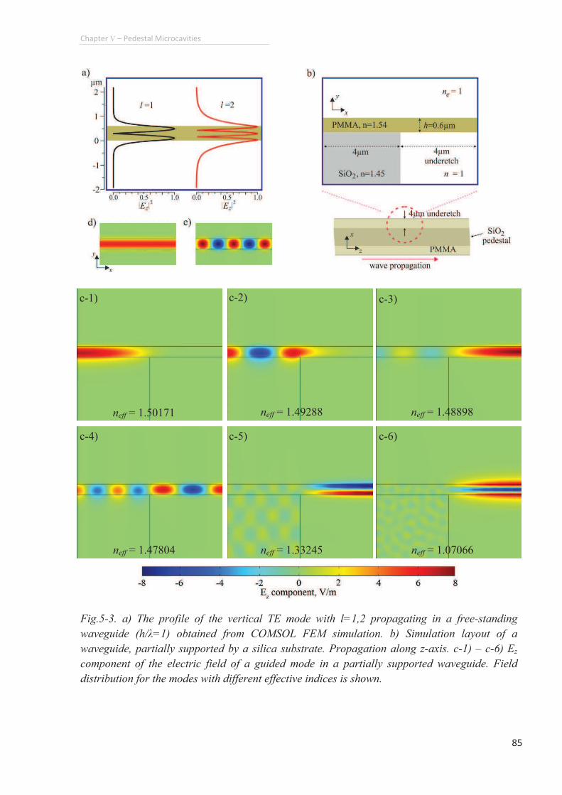
Chapter"V" "Pedestal"Microcavities"
85""
Fig.5-3. a) The profile of the vertical TE mode with l=1,2 propagating in a free-standing
waveguide (h/そ=1) obtained from COMSOL FEM simulation. b) Simulation layout of a
waveguide, partially supported by a silica substrate. Propagation along z-axis. c-1) � c-6) Ez
component of the electric field of a guided mode in a partially supported waveguide. Field
distribution for the modes with different effective indices is shown.
neff = 1.50171
c-1)
neff = 1.49288
c-2)
neff = 1.48898
c-3)
neff = 1.47804
c-4)
neff = 1.33245
c-5)
neff = 1.07066
c-6)
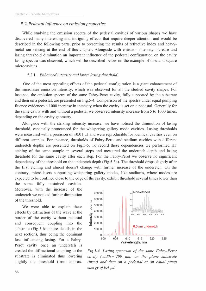
Chapter"V" "Pedestal"Microcavities""
86""
の┻に┻Pedestal"influence"on"emission"properties."
While studying the emission spectra of the pedestal cavities of various shapes we have
discovered many interesting and intriguing effects that require deeper attention and would be
described in the following parts, prior to presenting the results of refractive index and heavy-
metal ion sensing at the end of this chapter. Alongside with emission intensity increase and
lasing threshold diminution an important influence of the pedestal configuration on the cavity
lasing spectra was observed, which will be described below on the example of disc and square
microcavities.
5.2.1. Enhanced intensity and lower lasing threshold.
One of the most appealing effects of the pedestal configuration is a giant enhancement of
the microlaser emission intensity, which was observed for all the studied cavity shapes. For
instance, the emission spectra of the same Fabry-Perot cavity, fully supported by the substrate
and then on a pedestal, are presented on Fig.5-4. Comparison of the spectra under equal pumping
fluence evidences a 1000 increase in intensity when the cavity is set on a pedestal. Generally for
the same cavity with and without a pedestal we observed intensity increase from 5 to 1000 times,
depending on the cavity geometry.
Alongside with the striking intensity increase, we have noticed the diminution of lasing
threshold, especially pronounced for the whispering gallery mode cavities. Lasing thresholds
were measured with a precision of ±0.01 µJ and were reproducible for identical cavities even on
different samples. For instance, thresholds of Fabry-Perot and stadium cavities with different
underetch depths are presented on Fig.5-5. To record these dependencies we performed HF
etching of the same sample in several steps and measured the underetch depth and lasing
threshold for the same cavity after each step. For the Fabry-Perot we observe no significant
dependency of the threshold on the underetch depth (Fig.5-5a). The threshold drops slightly after
the first etching and almost doesn�t change with further increase of the underetch. On the
contrary, micro-lasers supporting whispering gallery modes, like stadiums, where modes are
expected to be confined close to the edge of the cavity, exhibit threshold several times lower than
the same fully sustained cavities.
Moreover, with the increase of the
underetch we noticed further diminution
of the threshold.
We were able to explain these
effects by diffraction of the wave at the
border of the cavity without pedestal
and consequent coupling into the
substrate (Fig.5-6a, more details in the
next section), thus being the dominant
loss influencing lasing. For a Fabry-
Perot cavity once an underetch is
created the diffractional coupling to the
substrate is eliminated thus lowering
slightly the threshold (from approx.
600 605 610 615 620 625
0
10000
20000
30000
40000
50000
60000
70000
595 600 605 610 615 620
0
20
40
60
Inte
nsity,
co
un
ts
Wavelength, nm
Non-etched
6,5 om underetch
Fig.5-4. Lasing spectrum of the same Fabry-Perot
cavity (width = 200 µm) on the plane substrate
(inset) and then on a pedestal at an equal pump
energy of 0.4 µJ.
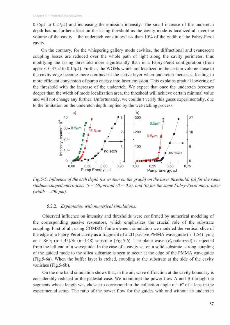
Chapter"V" "Pedestal"Microcavities"
87""
0.35µJ to 0.27µJ) and increasing the emission intensity. The small increase of the underetch
depth has no further effect on the lasing threshold as the cavity mode is localized all over the
volume of the cavity � the underetch constitutes less than 10% of the width of the Fabry-Perot
cavity.
On the contrary, for the whispering gallery mode cavities, the diffractional and evanescent
coupling losses are reduced over the whole path of light along the cavity perimeter, thus
modifying the lasing threshold more significantly than in a Fabry-Perot configuration (from
approx. 0.37µJ to 0.14µJ). Further, the WGMs which are localized in the certain volume close to
the cavity edge become more confined in the active layer when underetch increases, leading to
more efficient conversion of pump energy into laser emission. This explains gradual lowering of
the threshold with the increase of the underetch. We expect that once the underetch becomes
deeper than the width of mode localization area, the threshold will achieve certain minimal value
and will not change any further. Unfortunately, we couldn�t verify this guess experimentally, due
to the limitation on the underetch depth implied by the wet-etching process.
0,00 0,30 0,60 0,90
0
10
20
30
40
b)a)
Pump Energy, oJ
8.5om6.5om
Inte
nsity,
counts
*10
-4
Pump Energy, oJ
no etch
1
2
3
0,00 0,25 0,50 0,75
100
200
300
8.5om
no etch
6.5om"
0
9
18
27
"
Fig.5-5. Influence of the etch depth (as written on the graph) on the laser threshold: (a) for the same
stadium-shaped micro-laser (r = 60µm and r/l = 0.5), and (b) for the same Fabry-Perot micro-laser
(width = 200 µm).
5.2.2. Explanation with numerical simulations.
Observed influence on intensity and thresholds were confirmed by numerical modeling of
the corresponding passive resonators, which emphasizes the crucial role of the substrate
coupling. First of all, using COMSOl finite element simulation we modeled the vertical slice of
the edge of a Fabry-Perot cavity as a fragment of a 2D passive PMMA waveguide (n=1.54) lying
on a SiO2 (n=1.45)/Si (n=3.48) substrate (Fig.5-6). The plane wave (Ez-polarized) is injected
from the left end of a waveguide. In the case of a cavity set on a solid substrate, strong coupling
of the guided mode to the silica substrate is seen to occur at the edge of the PMMA waveguide
(Fig.5-6a). When the buffer layer is etched, coupling to the substrate at the side of the cavity
vanishes (Fig.5-6b).
On the one hand simulation shows that, in the air, wave diffraction at the cavity boundary is
considerably reduced in the pedestal case. We monitored the power flow A and B through the
segments whose length was chosen to correspond to the collection angle of ~6º of a lens in the
experimental setup. The ratio of the power flow for the guides with and without an underetch
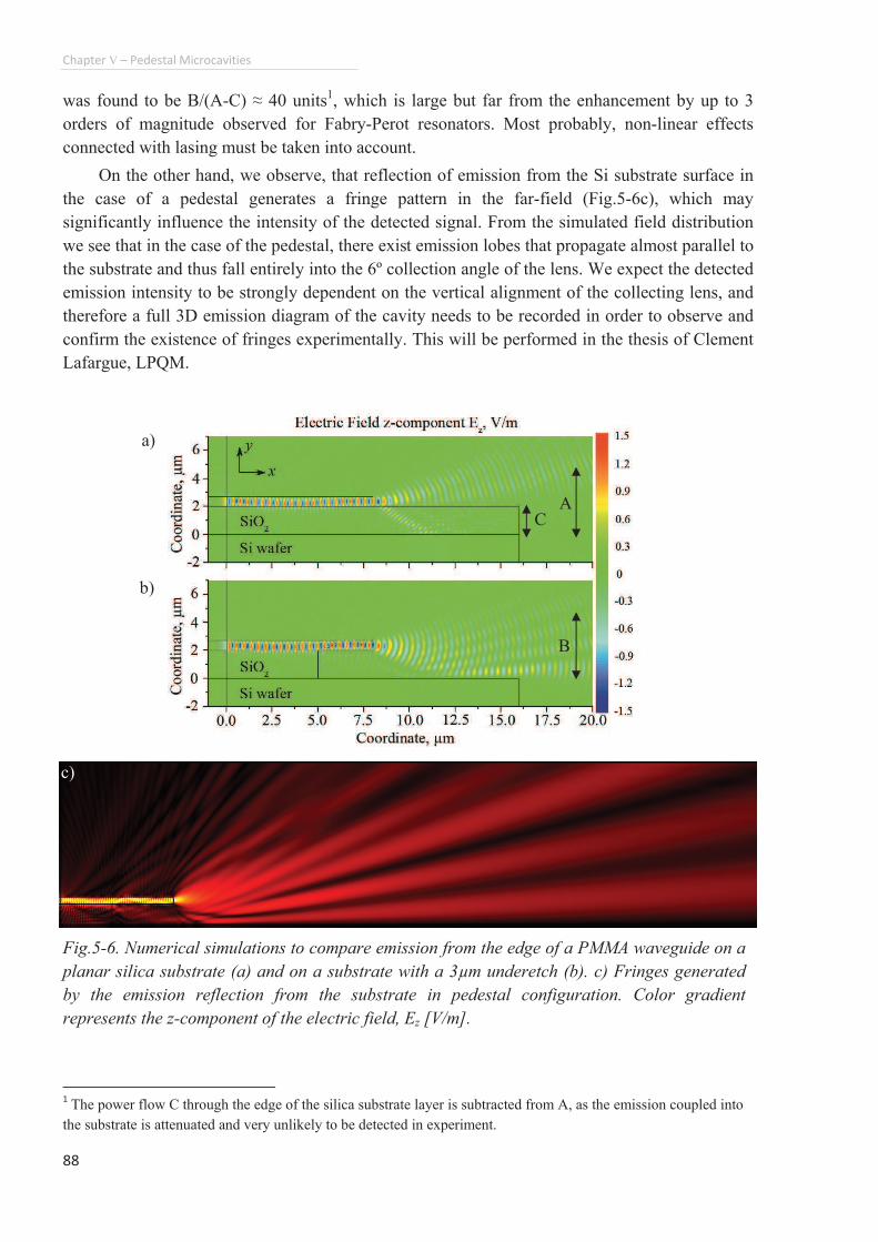
Chapter"V" "Pedestal"Microcavities""
88""
was found to be B/(A-C) Ã 40 units1, which is large but far from the enhancement by up to 3
orders of magnitude observed for Fabry-Perot resonators. Most probably, non-linear effects
connected with lasing must be taken into account.
On the other hand, we observe, that reflection of emission from the Si substrate surface in
the case of a pedestal generates a fringe pattern in the far-field (Fig.5-6c), which may
significantly influence the intensity of the detected signal. From the simulated field distribution
we see that in the case of the pedestal, there exist emission lobes that propagate almost parallel to
the substrate and thus fall entirely into the 6º collection angle of the lens. We expect the detected
emission intensity to be strongly dependent on the vertical alignment of the collecting lens, and
therefore a full 3D emission diagram of the cavity needs to be recorded in order to observe and
confirm the existence of fringes experimentally. This will be performed in the thesis of Clement
Lafargue, LPQM.
""""""""""""""""""""""""""""""""""""""""""""""""""""""""""""1"The power flow C through the edge of the silica substrate layer is subtracted from A, as the emission coupled into
the substrate is attenuated and very unlikely to be detected in experiment."
Fig.5-6. Numerical simulations to compare emission from the edge of a PMMA waveguide on a
planar silica substrate (a) and on a substrate with a 3µm underetch (b). c) Fringes generated
by the emission reflection from the substrate in pedestal configuration. Color gradient
represents the z-component of the electric field, Ez [V/m].
A
B
C
c)
a)
b)
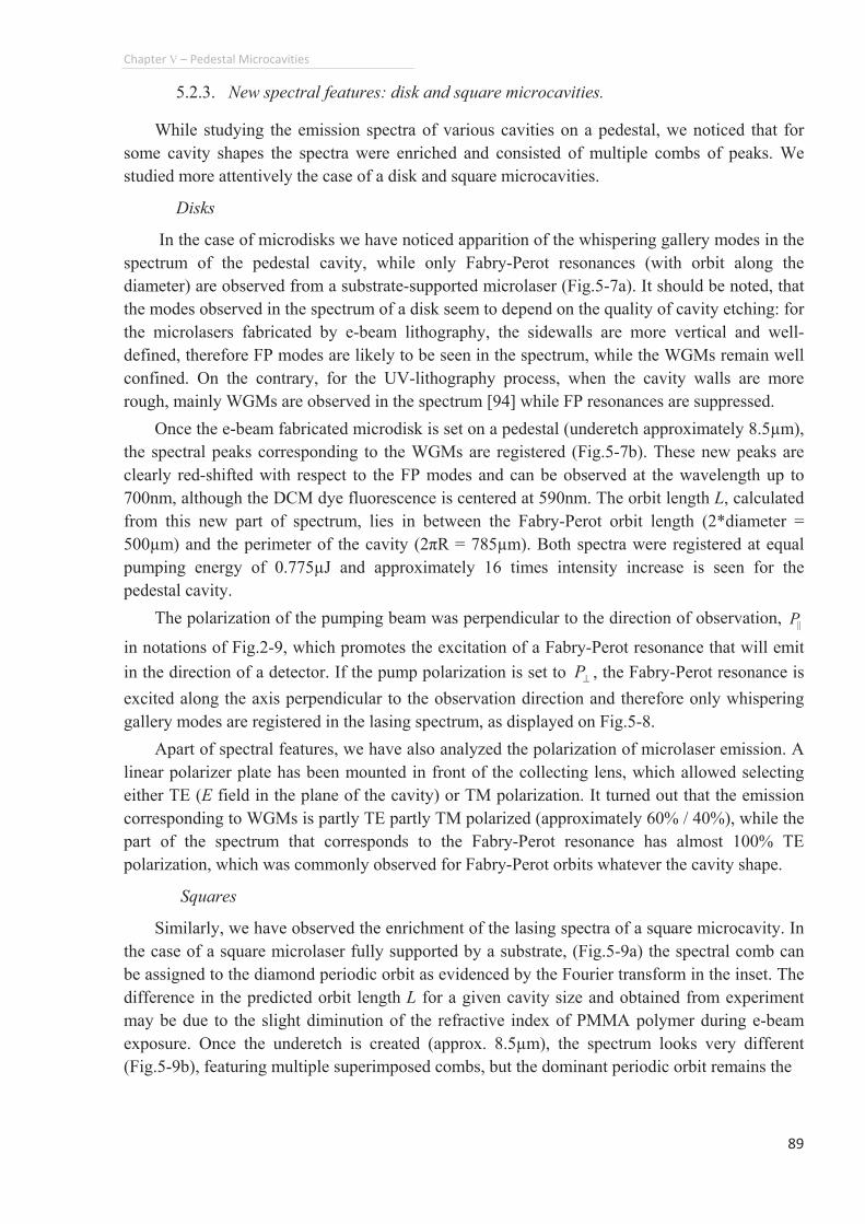
Chapter"V"�"Pedestal"Microcavities"
89""
5.2.3. New spectral features: disk and square microcavities.
While studying the emission spectra of various cavities on a pedestal, we noticed that for
some cavity shapes the spectra were enriched and consisted of multiple combs of peaks. We
studied more attentively the case of a disk and square microcavities.
Disks
In the case of microdisks we have noticed apparition of the whispering gallery modes in the
spectrum of the pedestal cavity, while only Fabry-Perot resonances (with orbit along the
diameter) are observed from a substrate-supported microlaser (Fig.5-7a). It should be noted, that
the modes observed in the spectrum of a disk seem to depend on the quality of cavity etching: for
the microlasers fabricated by e-beam lithography, the sidewalls are more vertical and well-
defined, therefore FP modes are likely to be seen in the spectrum, while the WGMs remain well
confined. On the contrary, for the UV-lithography process, when the cavity walls are more
rough, mainly WGMs are observed in the spectrum [94] while FP resonances are suppressed.
Once the e-beam fabricated microdisk is set on a pedestal (underetch approximately 8.5µm),
the spectral peaks corresponding to the WGMs are registered (Fig.5-7b). These new peaks are
clearly red-shifted with respect to the FP modes and can be observed at the wavelength up to
700nm, although the DCM dye fluorescence is centered at 590nm. The orbit length L, calculated
from this new part of spectrum, lies in between the Fabry-Perot orbit length (2*diameter =
500µm) and the perimeter of the cavity (2ヾR = 785µm). Both spectra were registered at equal
pumping energy of 0.775µJ and approximately 16 times intensity increase is seen for the
pedestal cavity.
The polarization of the pumping beam was perpendicular to the direction of observation, ||P
in notations of Fig.2-9, which promotes the excitation of a Fabry-Perot resonance that will emit
in the direction of a detector. If the pump polarization is set to P̀ , the Fabry-Perot resonance is
excited along the axis perpendicular to the observation direction and therefore only whispering
gallery modes are registered in the lasing spectrum, as displayed on Fig.5-8.
Apart of spectral features, we have also analyzed the polarization of microlaser emission. A
linear polarizer plate has been mounted in front of the collecting lens, which allowed selecting
either TE (E field in the plane of the cavity) or TM polarization. It turned out that the emission
corresponding to WGMs is partly TE partly TM polarized (approximately 60% / 40%), while the
part of the spectrum that corresponds to the Fabry-Perot resonance has almost 100% TE
polarization, which was commonly observed for Fabry-Perot orbits whatever the cavity shape.
Squares
Similarly, we have observed the enrichment of the lasing spectra of a square microcavity. In
the case of a square microlaser fully supported by a substrate, (Fig.5-9a) the spectral comb can
be assigned to the diamond periodic orbit as evidenced by the Fourier transform in the inset. The
difference in the predicted orbit length L for a given cavity size and obtained from experiment
may be due to the slight diminution of the refractive index of PMMA polymer during e-beam
exposure. Once the underetch is created (approx. 8.5µm), the spectrum looks very different
(Fig.5-9b), featuring multiple superimposed combs, but the dominant periodic orbit remains the
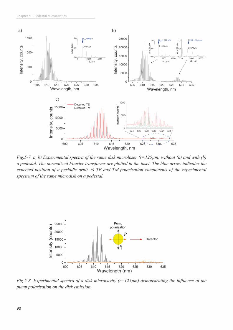
Chapter"V" "Pedestal"Microcavities""
90""
605 610 615 620 625 630 6350
500
1000
1500
Inte
nsity,
cou
nts
Wavelength, nm
0 2000 40000,0
0,5
1,0
Am
plit
ud
e
nL, om
L=491om
LFP
=500om
605 610 615 620 625 630 6350
5000
10000
15000
20000
25000
Inte
nsity,
cou
nts
Wavelength, nm
0 2000 40000,0
0,5
1,0
Am
plit
ud
e
nL, om
L=495om
LFP
= 500 om 2rR = 785 om
0 2000 40000,0
0,5
1,0
L=674om
Am
plit
ud
e
nL, om
600 605 610 615 620 625 630 635
0
5000
10000
15000
624 626 628 630 632 634
0
500
1000 Detected TE
Detected TM
Inte
nsity,
co
un
ts
Wavelength, nm
Inte
nsity, counts
"Fig.5-7. a, b) Experimental spectra of the same disk microlaser (r=125µm) without (a) and with (b)
a pedestal. The normalized Fourier transforms are plotted in the inset. The blue arrow indicates the
expected position of a periodic orbit. c) TE and TM polarization components of the experimental
spectrum of the same microdisk on a pedestal.
600 605 610 615 620 625 630 635
0
5000
10000
15000
20000
25000
Detector
Inte
nsity (
co
un
ts)
Wavelength (nm)
Pump
polarization
Fig.5-8. Experimental spectra of a disk microcavity (r=125µm) demonstrating the influence of the
pump polarization on the disk emission.
||P
P̀
a) b)
c)
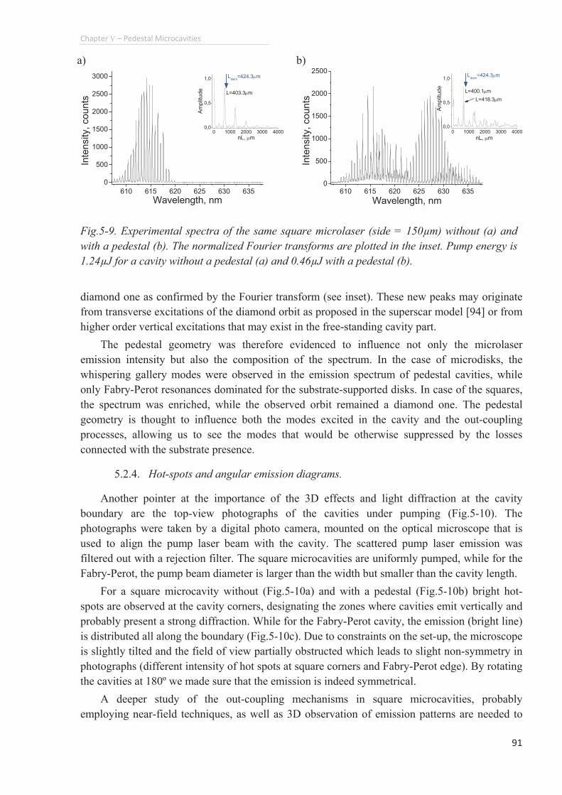
Chapter"V" "Pedestal"Microcavities"
91""
diamond one as confirmed by the Fourier transform (see inset). These new peaks may originate
from transverse excitations of the diamond orbit as proposed in the superscar model [94] or from
higher order vertical excitations that may exist in the free-standing cavity part.
The pedestal geometry was therefore evidenced to influence not only the microlaser
emission intensity but also the composition of the spectrum. In the case of microdisks, the
whispering gallery modes were observed in the emission spectrum of pedestal cavities, while
only Fabry-Perot resonances dominated for the substrate-supported disks. In case of the squares,
the spectrum was enriched, while the observed orbit remained a diamond one. The pedestal
geometry is thought to influence both the modes excited in the cavity and the out-coupling
processes, allowing us to see the modes that would be otherwise suppressed by the losses
connected with the substrate presence.
5.2.4. Hot-spots and angular emission diagrams.
Another pointer at the importance of the 3D effects and light diffraction at the cavity
boundary are the top-view photographs of the cavities under pumping (Fig.5-10). The
photographs were taken by a digital photo camera, mounted on the optical microscope that is
used to align the pump laser beam with the cavity. The scattered pump laser emission was
filtered out with a rejection filter. The square microcavities are uniformly pumped, while for the
Fabry-Perot, the pump beam diameter is larger than the width but smaller than the cavity length.
For a square microcavity without (Fig.5-10a) and with a pedestal (Fig.5-10b) bright hot-
spots are observed at the cavity corners, designating the zones where cavities emit vertically and
probably present a strong diffraction. While for the Fabry-Perot cavity, the emission (bright line)
is distributed all along the boundary (Fig.5-10c). Due to constraints on the set-up, the microscope
is slightly tilted and the field of view partially obstructed which leads to slight non-symmetry in
photographs (different intensity of hot spots at square corners and Fabry-Perot edge). By rotating
the cavities at 180º we made sure that the emission is indeed symmetrical.
A deeper study of the out-coupling mechanisms in square microcavities, probably
employing near-field techniques, as well as 3D observation of emission patterns are needed to
610 615 620 625 630 635
0
500
1000
1500
2000
2500
3000
Inte
nsity,
co
un
ts
Wavelength, nm
0 1000 2000 3000 40000,0
0,5
1,0 Ldiam
=424.3om
L=403.3om
Am
plit
ud
e
nL, om
610 615 620 625 630 6350
500
1000
1500
2000
2500
Wavelength, nm
Inte
nsity,
co
un
ts
0 1000 2000 3000 40000,0
0,5
1,0
L=418.3om
Am
plit
ud
e
nL, om
L=400.1om
Ldiam
=424.3om
Fig.5-9. Experimental spectra of the same square microlaser (side = 150µm) without (a) and
with a pedestal (b). The normalized Fourier transforms are plotted in the inset. Pump energy is
1.24µJ for a cavity without a pedestal (a) and 0.46µJ with a pedestal (b).
a) b)
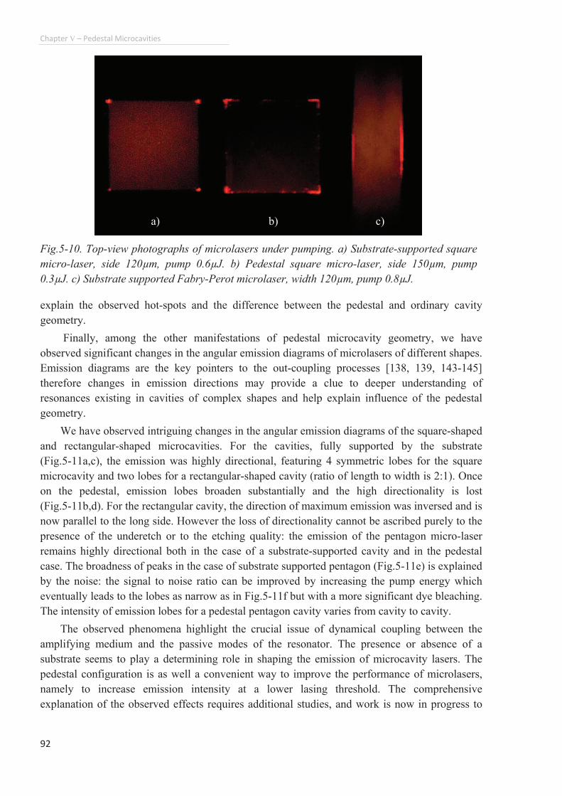
Chapter"V" "Pedestal"Microcavities""
92""
explain the observed hot-spots and the difference between the pedestal and ordinary cavity
geometry.
Finally, among the other manifestations of pedestal microcavity geometry, we have
observed significant changes in the angular emission diagrams of microlasers of different shapes.
Emission diagrams are the key pointers to the out-coupling processes [138, 139, 143-145]
therefore changes in emission directions may provide a clue to deeper understanding of
resonances existing in cavities of complex shapes and help explain influence of the pedestal
geometry.
We have observed intriguing changes in the angular emission diagrams of the square-shaped
and rectangular-shaped microcavities. For the cavities, fully supported by the substrate
(Fig.5-11a,c), the emission was highly directional, featuring 4 symmetric lobes for the square
microcavity and two lobes for a rectangular-shaped cavity (ratio of length to width is 2:1). Once
on the pedestal, emission lobes broaden substantially and the high directionality is lost
(Fig.5-11b,d). For the rectangular cavity, the direction of maximum emission was inversed and is
now parallel to the long side. However the loss of directionality cannot be ascribed purely to the
presence of the underetch or to the etching quality: the emission of the pentagon micro-laser
remains highly directional both in the case of a substrate-supported cavity and in the pedestal
case. The broadness of peaks in the case of substrate supported pentagon (Fig.5-11e) is explained
by the noise: the signal to noise ratio can be improved by increasing the pump energy which
eventually leads to the lobes as narrow as in Fig.5-11f but with a more significant dye bleaching.
The intensity of emission lobes for a pedestal pentagon cavity varies from cavity to cavity.
The observed phenomena highlight the crucial issue of dynamical coupling between the
amplifying medium and the passive modes of the resonator. The presence or absence of a
substrate seems to play a determining role in shaping the emission of microcavity lasers. The
pedestal configuration is as well a convenient way to improve the performance of microlasers,
namely to increase emission intensity at a lower lasing threshold. The comprehensive
explanation of the observed effects requires additional studies, and work is now in progress to
Fig.5-10. Top-view photographs of microlasers under pumping. a) Substrate-supported square
micro-laser, side 120µm, pump 0.6µJ. b) Pedestal square micro-laser, side 150µm, pump
0.3µJ. c) Substrate supported Fabry-Perot microlaser, width 120µm, pump 0.8µJ.
a) b) c)
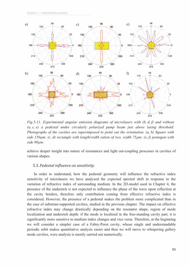
Chapter"V"�"Pedestal"Microcavities"
93""
achieve deeper insight into nature of resonances and light out-coupling processes in cavities of
various shapes. の┻ぬ┻Pedestal"influence"on"sensitivity."
In order to understand, how the pedestal geometry will influence the refractive index
sensitivity of microlasers we have analyzed the expected spectral shift in response to the
variation of refractive index of surrounding medium. In the 2D-model used in Chapter 4, the
presence of the underetch is not expected to influence the phase of the wave upon reflection at
the cavity borders, therefore only contribution coming from effective refractive index is
considered. However, the presence of a pedestal makes the problem more complicated than in
the case of substrate-supported cavities, studied in the previous chapter. The impact on effective
refractive index may change drastically depending on the resonator shape, region of mode
localization and underetch depth: if the mode is localized in the free-standing cavity part, it is
significantly more sensitive to medium index changes and vice versa. Therefore, at the beginning
we will consider a simpler case of a Fabry-Perot cavity, whose single and understandable
periodic orbit makes quantitative analysis easier and then we will move to whispering gallery
mode cavities, were analysis is mostly carried out numerically.
Fig.5-11. Experimental angular emission diagrams of microlasers with (b, d, f) and without
(a, c, e) a pedestal under circularly polarized pump beam just above lasing threshold.
Photographs of the cavities are superimposed to point out the orientation. (a, b) Square with
side 150µm; (c, d) rectangle with length/width ration of two, width 75µm; (e, f) pentagon with
side 90µm.
a) e)c)
b) f)d)
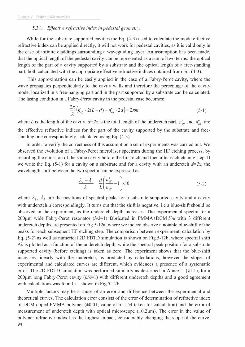
Chapter"V"�"Pedestal"Microcavities""
94""
5.3.1. Effective refractive index in pedestal geometry.
While for the substrate supported cavities the Eq. (4-3) used to calculate the mode effective
refractive index can be applied directly, it will not work for pedestal cavities, as it is valid only in
the case of infinite claddings surrounding a waveguiding layer. An assumption has been made,
that the optical length of the pedestal cavity can be represented as a sum of two terms: the optical
length of the part of a cavity supported by a substrate and the optical length of a free-standing
part, both calculated with the appropriate effective refractive indices obtained from Eq. (4-3).
This approximation can be easily applied in the case of a Fabry-Perot cavity, where the
wave propagates perpendicularly to the cavity walls and therefore the percentage of the cavity
mode, localized in a free-hanging part and in the part supported by a substrate can be calculated.
The lasing condition in a Fabry-Perot cavity in the pedestal case becomes:
* + mdndLn effeff rnr
22)(22 ?©||-/©| " (5-1)
where L is the length of the cavity, d=2x is the total length of the underetch part, effn| and
effn || are
the effective refractive indices for the part of the cavity supported by the substrate and free-
standing one correspondingly, calculated using Eq. (4-3).
In order to verify the correctness of this assumption a set of experiments was carried out. We
observed the evolution of a Fabry-Perot microlaser spectrum during the HF etching process, by
recording the emission of the same cavity before the first etch and then after each etching step. If
we write the Eq. (5-1) for a cavity on a substrate and for a cavity with an underetch d=2x, the
wavelength shift between the two spectra can be expressed as:
011
12 >ÕÕÖÔ
ÄÄÅÃ /|
||?/eff
eff
n
n
L
d
nnn
" (5-2)
where 1n , 2n are the positions of spectral peaks for a substrate supported cavity and a cavity
with underetch d correspondingly. It turns out that the shift is negative, i.e a blue-shift should be
observed in the experiment, as the underetch depth increases. The experimental spectra for a
200µm wide Fabry-Perot resonator (h/そ=1) fabricated in PMMA+DCM 5% with 3 different
underetch depths are presented on Fig.5-12a, where we indeed observe a notable blue-shift of the
peaks for each subsequent HF etching step. The comparison between experiment, calculation by
Eq. (5-2) as well as numerical 2D FDTD simulation is shown on Fig.5-12b, where spectral shift
〉そ is plotted as a function of the underetch depth, while the spectral peak position for a substrate
supported cavity (before etching) is taken as zero. The experiment shows that the blue-shift
increases linearly with the underetch, as predicted by calculations, however the slopes of
experimental and calculated curves are different, which evidences a presence of a systematic
error. The 2D FDTD simulation was performed similarly as described in Annex 1 (§1.1), for a
200µm long Fabry-Perot cavity (h/そ=1) with different underetch depths and a good agreement
with calculations was found, as shown in Fig.5-12b.
Multiple factors may be a cause of an error and difference between the experimental and
theoretical curves. The calculation error consists of the error of determination of refractive index
of DCM doped PMMA polymer (±0.01; value of n=1.54 taken for calculation) and the error of
measurement of underetch depth with optical microscope (±0.2µm). The error in the value of
polymer refractive index has the highest impact, considerably changing the slope of the curve.
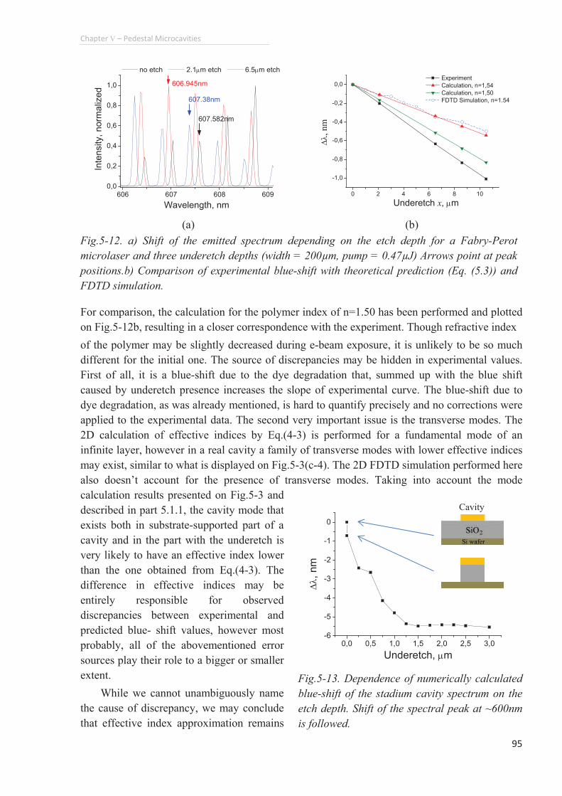
Chapter"V"�"Pedestal"Microcavities"
95""
For comparison, the calculation for the polymer index of n=1.50 has been performed and plotted
on Fig.5-12b, resulting in a closer correspondence with the experiment. Though refractive index
of the polymer may be slightly decreased during e-beam exposure, it is unlikely to be so much
different for the initial one. The source of discrepancies may be hidden in experimental values.
First of all, it is a blue-shift due to the dye degradation that, summed up with the blue shift
caused by underetch presence increases the slope of experimental curve. The blue-shift due to
dye degradation, as was already mentioned, is hard to quantify precisely and no corrections were
applied to the experimental data. The second very important issue is the transverse modes. The
2D calculation of effective indices by Eq.(4-3) is performed for a fundamental mode of an
infinite layer, however in a real cavity a family of transverse modes with lower effective indices
may exist, similar to what is displayed on Fig.5-3(c-4). The 2D FDTD simulation performed here
also doesn�t account for the presence of transverse modes. Taking into account the mode
calculation results presented on Fig.5-3 and
described in part 5.1.1, the cavity mode that
exists both in substrate-supported part of a
cavity and in the part with the underetch is
very likely to have an effective index lower
than the one obtained from Eq.(4-3). The
difference in effective indices may be
entirely responsible for observed
discrepancies between experimental and
predicted blue- shift values, however most
probably, all of the abovementioned error
sources play their role to a bigger or smaller
extent.
While we cannot unambiguously name
the cause of discrepancy, we may conclude
that effective index approximation remains
606 607 608 609
0,0
0,2
0,4
0,6
0,8
1,0
no etch 2.1om etch 6.5om etch
Wavelength, nm
Inte
nsity, norm
aliz
ed
607.582nm
607.38nm
606.945nm
0 2 4 6 8 10
-1,0
-0,8
-0,6
-0,4
-0,2
0,0
Fn, n
m
Underetch x, om
Experiment
Calculation, n=1,54
Calculation, n=1,50
FDTD Simulation, n=1.54
(a) (b)
Fig.5-12. a) Shift of the emitted spectrum depending on the etch depth for a Fabry-Perot
microlaser and three underetch depths (width = 200µm, pump = 0.47µJ) Arrows point at peak
positions.b) Comparison of experimental blue-shift with theoretical prediction (Eq. (5.3)) and
FDTD simulation.
0,0 0,5 1,0 1,5 2,0 2,5 3,0-6
-5
-4
-3
-2
-1
0
Fn, n
m
Underetch, om
Fig.5-13. Dependence of numerically calculated
blue-shift of the stadium cavity spectrum on the
etch depth. Shift of the spectral peak at ~600nm
is followed.
"
Cavity

Chapter"V"�"Pedestal"Microcavities""
96""
robust even in the non-trivial case of pedestal cavities as shown on Fig.5-12 and adequately
describes the behavior of a system despite the difference in numerical values.
To further verify the validity of approach for whispering gallery mode cavities, we
performed a 3-dimensional FDTD simulation for a stadium shaped cavity (r=2l=5µm, h/そ=1),
while gradually changing the underetch depth and observed evolution of the resonance spectrum.
Obtained result (Fig.5-13) confirms the qualitative explanation of the processes occurring in a
pedestal cavity: for small underetch depths, an increasing blue shift is seen in the spectrum,
similarly to Fig.5-12b. As the underetch increases further, the blue-shift reaches saturation which
means that primary part of the mode energy is now localized in the free-standing section of the
cavity, and according to accepted approximation, the resonance spectrum is now mostly
determined by the effective index of a mode in a free-standing cavity part. Similarly to the
simulation of pedestal cavity sensitivity, there are two points on the graph that correspond to the
underetch of 0µm: the first one is related to the cavity on the infinitely wide substrate and the
second one to the pillar configuration. The saturation is observed for the underetch depth
x œ 1.5µm, which is consistent with the refractive index sensitivity simulation, performed in the
section 5.3.3. No quantitative calculation has been performed for this case as well as no
experimental verification has been carried out for the WGM cavities.
5.3.2. Sensitivity of a Fabry-Perot cavity
Having obtained the proofs of validity of effective index approach, we may now analyze the
spectral shift due to variation of the medium refractive index, which can now be approximately
expressed as:
"" * + * + e
e
eff
e
eff
effeff
nn
n
Ld
n
n
Ld
Ldn
Ldn
FÕÕÖÔÄÄÅ
Õ||•©-•
|•©/©©||-/©|?F ?F 11
0
nn h "" (5-3)
"
1,32 1,34 1,36 1,38 1,40 1,42
-0,3
0,0
0,3
0,6
0,9
1,2Fn, nm Fn, nm
ne
-0,3
0,0
0,3
0,6
0,9
1,21 0,4
10,2 0
0,4
0,2
0
d/L
Fig.5-14. Calculated influence of the medium index variation (ne) on the Fabry-Perot cavity
spectral shift due to effective refractive index change for several d/L ratios. b) Illustration of a
Fabry-Perot cavity on a pedestal (view from the top), showing the underetch.
h/そ=1
h/そ=0.5"
Fabry-Perot
resonance"
underetch
a) b)
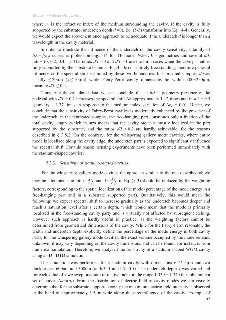
Chapter"V"�"Pedestal"Microcavities"
97""
where ne is the refractive index of the medium surrounding the cavity. If the cavity is fully
supported by the substrate (underetch depth d =0), Eq. (5-3) transforms into Eq. (4-4). Generally,
we would expect the abovementioned approach to be adequate if the underetch d is longer than a
wavelength in the cavity material.
In order to illustrate the influence of the underetch on the cavity sensitivity, a family of
〉そ = f(ne) curves is plotted on Fig.5-14 for TE mode, h/そ=1; 0.5 geometries and several d/L
ratios (0, 0.2, 0.4, 1). The ratios d/L =0 and d/L =1 are the limit cases when the cavity is either
fully supported by the substrate (same as Fig.4-13a) or entirely free-standing, therefore pedestal
influence on the spectral shift is limited by these two boundaries. In fabricated samples, d was
usually ø 20µm (x ø 10µm) while Fabry-Perot cavity dimensions lie within 100÷250µm,
meaning d/L ø 0.2.
Comparing the calculated data, we can conclude, that at h/そ=1 geometry presence of the
pedestal with d/L = 0.2 increases the spectral shift 〉そ approximately 1.12 times and in h/そ = 0.5
geometry � 1.37 times in response to the medium index variation of 〉ne = 0.01. Hence, we
conclude that the sensitivity of Fabry-Perot cavities is moderately enhanced by the presence of
the underetch: in the fabricated samples, the free-hanging part constitutes only a fraction of the
total cavity length (which in turn means that the cavity mode is mostly localized in the part
supported by the substrate) and the ratios d/L > 0.2 are hardly achievable, for the reasons
described in § 3.5.2. On the contrary, for the whispering gallery mode cavities, where entire
mode is localized along the cavity edge, the underetch part is expected to significantly influence
the spectral shift. For this reason, sensing experiments have been performed immediately with
the stadium-shaped cavities.
5.3.3. Sensitivity of stadium-shaped cavities.
For the whispering gallery mode cavities the approach similar to the one described above
may be attempted: the ratios L
d and L
d/1 in Eq. (5-3) should be replaced by the weighting
factors, corresponding to the spatial localization of the mode (percentage of the mode energy in a
free-hanging part and in a substrate supported part). Qualitatively, this would mean the
following: we expect spectral shift to increase gradually as the underetch becomes deeper and
reach a saturation level after a certain depth, which would mean that the mode is primarily
localized in the free-standing cavity party and is virtually not affected by subsequent etching.
However such approach is hardly useful in practice, as the weighting factors cannot be
determined from geometrical dimensions of the cavity. While for the Fabry-Perot resonator, the
width and underetch depth explicitly define the percentage of the mode energy in both cavity
parts, for the whispering gallery mode cavities, the exact volume occupied by the mode remains
unknown, it may vary depending on the cavity dimensions and can be found, for instance, from
numerical simulation. Therefore, we analyzed the sensitivity of a stadium shaped WGM cavity
using a 3D FDTD simulation.
The simulation was performed for a stadium cavity with dimensions r=2l=5µm and two
thicknesses: 600nm and 300nm (ie. h/そ=1 and h/そ=0.5). The underetch depth x was varied and
for each value of x we swept medium refractive index in the range 1.330 ÷ 1.340 thus obtaining a
set of curves 〉そ=f(ne). From the distribution of electric field of cavity modes we can visually
determine that for the substrate-supported cavity the maximum electric field intensity is observed
in the band of approximately 1.5µm wide along the circumference of the cavity. Example of
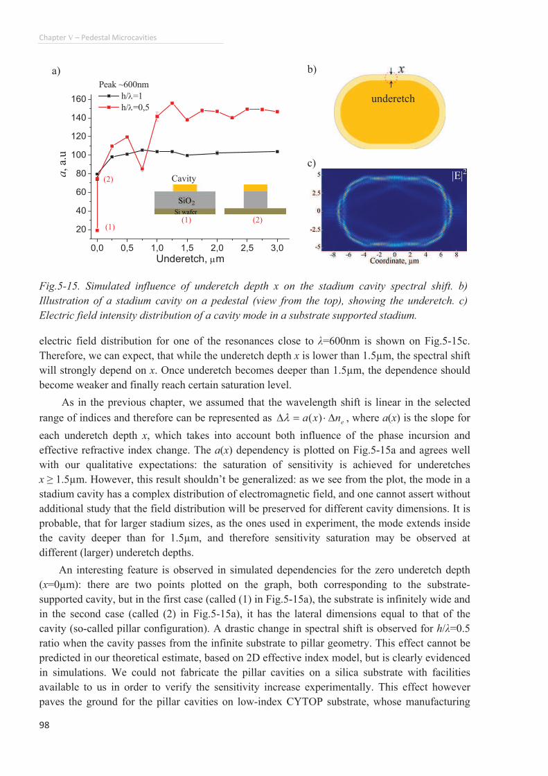
Chapter"V"�"Pedestal"Microcavities""
98""
electric field distribution for one of the resonances close to そ=600nm is shown on Fig.5-15c.
Therefore, we can expect, that while the underetch depth x is lower than 1.5µm, the spectral shift
will strongly depend on x. Once underetch becomes deeper than 1.5µm, the dependence should
become weaker and finally reach certain saturation level.
As in the previous chapter, we assumed that the wavelength shift is linear in the selected
range of indices and therefore can be represented as enxa F©?F )(n , where a(x) is the slope for
each underetch depth x, which takes into account both influence of the phase incursion and
effective refractive index change. The a(x) dependency is plotted on Fig.5-15a and agrees well
with our qualitative expectations: the saturation of sensitivity is achieved for underetches
x œ 1.5µm. However, this result shouldn�t be generalized: as we see from the plot, the mode in a
stadium cavity has a complex distribution of electromagnetic field, and one cannot assert without
additional study that the field distribution will be preserved for different cavity dimensions. It is
probable, that for larger stadium sizes, as the ones used in experiment, the mode extends inside
the cavity deeper than for 1.5µm, and therefore sensitivity saturation may be observed at
different (larger) underetch depths.
An interesting feature is observed in simulated dependencies for the zero underetch depth
(x=0µm): there are two points plotted on the graph, both corresponding to the substrate-
supported cavity, but in the first case (called (1) in Fig.5-15a), the substrate is infinitely wide and
in the second case (called (2) in Fig.5-15a), it has the lateral dimensions equal to that of the
cavity (so-called pillar configuration). A drastic change in spectral shift is observed for h/そ=0.5
ratio when the cavity passes from the infinite substrate to pillar geometry. This effect cannot be
predicted in our theoretical estimate, based on 2D effective index model, but is clearly evidenced
in simulations. We could not fabricate the pillar cavities on a silica substrate with facilities
available to us in order to verify the sensitivity increase experimentally. This effect however
paves the ground for the pillar cavities on low-index CYTOP substrate, whose manufacturing
"
0,0 0,5 1,0 1,5 2,0 2,5 3,0
20
40
60
80
100
120
140
160
Peak ~600nm
h/n=1
h/n=0,5
Underetch, om
a, a.
u
Fig.5-15. Simulated influence of underetch depth x on the stadium cavity spectral shift. b)
Illustration of a stadium cavity on a pedestal (view from the top), showing the underetch. c)
Electric field intensity distribution of a cavity mode in a substrate supported stadium.
underetch"
Cavity
(1) (2)
a) b)
c)|E|
2
(1)
(2)
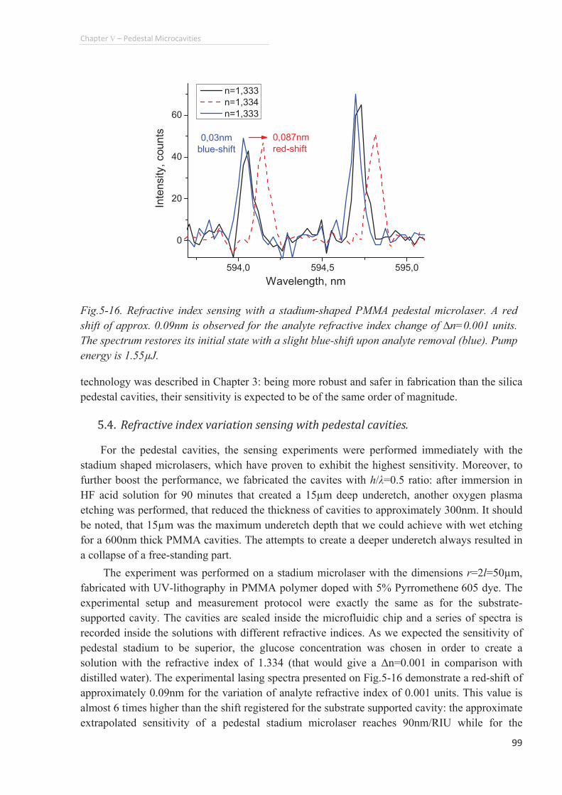
Chapter"V"�"Pedestal"Microcavities"
99""
technology was described in Chapter 3: being more robust and safer in fabrication than the silica
pedestal cavities, their sensitivity is expected to be of the same order of magnitude. の┻ね┻ "Refractive"index"variation"sensing"with"pedestal"cavities."
For the pedestal cavities, the sensing experiments were performed immediately with the
stadium shaped microlasers, which have proven to exhibit the highest sensitivity. Moreover, to
further boost the performance, we fabricated the cavites with h/そ=0.5 ratio: after immersion in
HF acid solution for 90 minutes that created a 15µm deep underetch, another oxygen plasma
etching was performed, that reduced the thickness of cavities to approximately 300nm. It should
be noted, that 15µm was the maximum underetch depth that we could achieve with wet etching
for a 600nm thick PMMA cavities. The attempts to create a deeper underetch always resulted in
a collapse of a free-standing part.
The experiment was performed on a stadium microlaser with the dimensions r=2l=50µm,
fabricated with UV-lithography in PMMA polymer doped with 5% Pyrromethene 605 dye. The
experimental setup and measurement protocol were exactly the same as for the substrate-
supported cavity. The cavities are sealed inside the microfluidic chip and a series of spectra is
recorded inside the solutions with different refractive indices. As we expected the sensitivity of
pedestal stadium to be superior, the glucose concentration was chosen in order to create a
solution with the refractive index of 1.334 (that would give a 〉n=0.001 in comparison with
distilled water). The experimental lasing spectra presented on Fig.5-16 demonstrate a red-shift of
approximately 0.09nm for the variation of analyte refractive index of 0.001 units. This value is
almost 6 times higher than the shift registered for the substrate supported cavity: the approximate
extrapolated sensitivity of a pedestal stadium microlaser reaches 90nm/RIU while for the
594,0 594,5 595,0
0
20
40
60
n=1,333
n=1,334
n=1,333
Inte
nsity,
cou
nts
Wavelength, nm
0,087nm
red-shift
0,03nm
blue-shift
Fig.5-16. Refractive index sensing with a stadium-shaped PMMA pedestal microlaser. A red
shift of approx. 0.09nm is observed for the analyte refractive index change of Än=0.001 units.
The spectrum restores its initial state with a slight blue-shift upon analyte removal (blue). Pump
energy is 1.55µJ.
Chapter"V" "Pedestal"Microcavities""
100""
substrate-supported stadium it was 13nm/RIU. Though the energy of pump beam was decreased
to the minimum, a blue-shift was observed in all the recorded spectra.
Due to the very high memory requirements, the FDTD simulation cannot be run for the
cavity sizes used in experiment, but nevertheless an attempt to estimate the pedestal cavity
sensitivity using the data of 2D and 3D simulations may be undertaken. We expect, that the
effective refractive index contribution to sensitivity ( indexnF ) does not depend on the cavity
dimensions. The latter is taken into account by the phase-dependent contribution ( phasenF ).
Therefore, we may estimate the indexnF for the pedestal stadium from a 3D simulation, performed
for a small cavity and then account for the cavity size by taking the appropriate value for phasenFfrom a 2D simulation (Fig.4-24). For example, the 3D simulation performed above for a stadium
cavity with r = 5µm takes into account both effective index and phase incursion contributions.
Therefore, the effective index contribution for the cavity of any size would be phase
r
index aaa 5?/?= 145 � 44 = 101, where a is the slope in a linear dependency 〉そ=a·〉ne; a à 145 is taken from
the Fig.5-15a and phase
ra 5? = 44 is taken from Fig.4-24. Then, for the cavity with r = 50µm used in
the experiment we obtain: a = 101 + phase
ra 50? = 101 + 8 = 109, which gives 〉そ = 109·0.001 =
0.109nm, a value very close to the one obtained experimentally (0.087nm; may be underrated by
the blue shift). Of course, multiple measurements for the cavities of different sizes need to be
performed in order to claim a good agreement between the experiments and simulations, but at
least we may see that such approach yields an approximately correct result.
Concluding the results, we have experimentally confirmed the enhanced sensitivity of
pedestal whispering gallery mode microlasers to the medium index variation (90nm/RIU against
13nm/RIU for the substrate-supported). A good agreement with numerical simulation was
achieved. If higher sensitivity is to be reached, several approaches may be considered. First of
all, porous polymer may be utilized as an active medium. While attempts performed within this
thesis with polystyrene based polymers didn�t lead to any improvement in sensitivity, this may
only mean that more research on porous materials should be carried out. Another approach that
requires deeper study would consist in using systems of coupled resonators. Coupling efficiency
may be strongly influenced by the medium refractive index thus remarkably increasing the
overall system sensitivity. Finally, a more straightforward way would be to decrease the size of
the stadium cavity: as simulation results on Fig.4-24 evidence, a phase-dependent sensitivity
contribution for a stadium with the radius r = 25µm should be two times higher, and for a
stadium with r = 5µm � 9 times higher than for the ones, used in experiments (r = 50µm).
Smaller cavity sizes should be achievable if substrates with lower refractive index and/or more
efficient laser dyes are used and also if more elaborate emission detection system is employed. の┻の┻ "Detection"of"heavy┽metal"ions"with"pedestal"microcavity"sensor."
After obtaining the proofs of enhanced sensitivity of pedestal cavities, we have repeated the
experiment of mercury ions detection in liquid solution. For this purpose a sample with h/そ=1
stadium-shaped cavities was fabricated in PMMA doped with 5% Pyrromethene 605. The
sample was treated for 30min with HF acid to create an underetch of approximately 4.5µm. We
have intentionally reduced the depth of the underetch for this experiment and didn�t further thin
the cavities to increase the mechanical durability. Actually during the functionalization step the
cavity undergoes multiple immersions in liquids and some other manipulations that may
Chapter"V" "Pedestal"Microcavities"
101""
potentially collapse the fragile pedestal cavities. Afterwards, the cavities were functionalized as
described in §4.3, and sealed into PDMS microfluidic chip.
Mercury sensing experiment was performed on a stadium cavity with the radius of
r=2l=50µm, following the same measurement protocol as in the case of substrate supported
cavity. We started with 10-6
M Hg2+
solution in MES buffer and the resulting lasing spectra are
shown on Fig.5-17. First of all a spectrum in pure MES buffer was recorded. Afterwards, we
injected 1ml of Hg2+
analyte, let it flow thorough the chip at 14ml/hour and recorded the first
spectrum (not shown on the plot). A red-shift of 0.145nm was clearly detected. Once again 1ml
of Hg analyte was injected at the same velocity and the second spectrum was recorded,
exhibiting a red-shift of 0.174 with respect to the clean buffer reference. The injection was
repeated two more times and each time a gradual increase of the red-shift was observed. The
spectrum on Fig.5-17 demonstrates the resulting red-shift of 0.232nm after 4 injections of 1ml of
mercury analyte.
Then the cavity was washed with 3ml of 5·10-5
M dimercaptopropanol solution, however the
spectrum didn�t restore to the initial position. Two more washing steps with the same
concentration of dimercaptopropanol were performed, however we couldn�t achieve a full
restoration of the lasing spectrum, as it was with substrate-supported cavity � spectral peaks
remained red-shifted for 0.116nm (blue curve on Fig.5-17). We therefore didn�t proceed with
lower mercury concentrations.
On the one hand we have successfully demonstrated the enhanced sensitivity of a
functionalized pedestal cavity and detected the 10-6
M concentration of mercury solution. We
demonstrated the gradual red-shift of the lasing spectrum after each analyte injection which may
be probably explained by the increase of number of mercury ions captured by the ligands. On the
other hand, the red-shift was not completely reversible and the spectrum didn�t restore to the
initial position. The only explanation we could think of is connected with the presence of the
underetch: due to the worse circulation of the washing solution in the thin gap under the free-
standing cavity part there may be remaining mercury ions bonded with the ligands. The
circulation may be even more obstructed by microscopic air bubbles, which can be trapped
within the gap near the pedestal.
Further experiments are needed in order to estimate the maximum achievable sensitivity
with functionalized pedestal cavities and also to verify whether the irreversibility of lasing
spectrum was a one-time problem or it is regularly persisting. Taking into account the large
spectral shift observed, we may expect that at least 10-7
M mercury concentration can be detected
with a pedestal stadium microlaser.
While showing promising results in terms of sensitivity, pedestal cavities possess inherent
flaw connected with the presence of a thin gap, where liquid circulation may be complicated or
completely obstructed by micrometer-scale air-bubbles or sediment particles. While air bubbles
can be relatively easily released if their presence is discovered, the microscopic particles
depending on their nature may be very hard to remove from the thin gap and once trapped inside,
may permanently alter the spectrum of a microlaser. Moreover, taking into account higher
fragility of pedestal cavities, a non-pedestal configuration is preferred for implementation in
operational sensing systems. In the next section, we will see the implementation of a prospective
pillar microcavity on a low-index polymer substrate, which due to a number of advantages may
be preferable over the pedestal geometry.
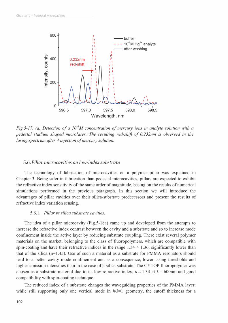
Chapter"V"�"Pedestal"Microcavities""
102""
の┻は┻Pillar"microcavities"on"low┽index"substrate"
The technology of fabrication of microcavities on a polymer pillar was explained in
Chapter 3. Being safer in fabrication than pedestal microcavities, pillars are expected to exhibit
the refractive index sensitivity of the same order of magnitude, basing on the results of numerical
simulations performed in the previous paragraph. In this section we will introduce the
advantages of pillar cavities over their silica-substrate predecessors and present the results of
refractive index variation sensing.
5.6.1. Pillar vs silica substrate cavities.
The idea of a pillar microcavity (Fig.5-18a) came up and developed from the attempts to
increase the refractive index contrast between the cavity and a substrate and so to increase mode
confinement inside the active layer by reducing substrate coupling. There exist several polymer
materials on the market, belonging to the class of fluoropolymers, which are compatible with
spin-coating and have their refractive indices in the range 1.34 ÷ 1.36, significantly lower than
that of the silica (n=1.45). Use of such a material as a substrate for PMMA resonators should
lead to a better cavity mode confinement and as a consequence, lower lasing thresholds and
higher emission intensities than in the case of a silica substrate. The CYTOP fluoropolymer was
chosen as a substrate material due to its low refractive index, n à 1.34 at そ = 600nm and good
compatibility with spin-coating technique.
The reduced index of a substrate changes the waveguiding properties of the PMMA layer:
while still supporting only one vertical mode in h/そ=1 geometry, the cutoff thickness for a
596,5 597,0 597,5 598,0 598,50
200
400
600 buffer
10-6M Hg
2+ analyte
after washingIn
ten
sity,
co
un
ts
Wavelength, nm
0,232nm
red-shift
Fig.5-17. (a) Detection of a 10-6
M concentration of mercury ions in analyte solution with a
pedestal stadium shaped microlaser. The resulting red-shift of 0.232nm is observed in the
lasing spectrum after 4 injection of mercury solution.
Chapter"V" "Pedestal"Microcavities"
103""
fundamental TE mode is reduced to nmhTE 184min ? (compared to 255nm for silica substrate),
that may allow creating thin cavities (h/そ < 0.5) whose strong evanescent field, similarly to the
pedestal case, will interact with the surrounding medium and lead to a higher sensitivity. It may
happen though, that the minimal thickness at which the microlasers can function would be
determined not by the cutoff thickness, but by the volume of the active medium, or in other
words, by the gain/loss ratio. A small cavity volume may have insufficient gain for the laser
generation to occur. Therefore the minimal thickness may be different for various lateral
dimensions of the cavity. This question was not studied in details and further experiments are
needed before any conclusions can be drawn.
It is during the first manufacturing attempts, that we realized that a pillar configuration can
be easily created (see section 3.5.3). A pillar cavity may be a worth competitor to the silica
pedestal configuration: it possesses some of the advantages of pedestal cavities while
overcoming their major drawbacks. Firstly, diffractive coupling into the substrate at the edge of
the cavity, which is the major source of losses influencing lasing, is eliminated in the pillar
geometry. This effect cannot be predicted using the model based on effective refractive index
which we developed for the analysis of the pedestal cavities, however was observed in the
numerical simulations. Combined with the higher confinement of mode in the active cavity layer
this should lead to lower lasing threshold and higher emission intensities than for the equivalent
cavity on a silica pillar. Unfortunately, we cannot fabricate a cavity on a silica pillar in order to
compare their characteristics, and comparison between a CYTOP pillar and a silica pedestal
would be incorrect. Secondly, a dangerous HF etchant is eliminated from the technological
process and, finally, the mechanical durability of pillar cavities is similar to that of the substrate
supported analogues as the fragile free-standing part is absent here.
Among the weak points were pillar cavities lose to their pedestal competitors, are the
impossibility to achieve quite the same confinement for the whispering gallery modes: while in
the pedestal cavity with a sufficiently deep underetch we may expect a whispering gallery mode
to be mostly localized in the free-standing cavity part, for the pillar cavities, the mode will
always feel the presence of a substrate. Also, if we consider sensing applications, functionalized
pedestal cavities of the same dimensions possess larger surface of contact with the analyte than
the pillars, which may allow them to capture a larger number of analyte molecules and play a
decisive role in their higher sensitivity. All of these drawbacks (though not the fragility) may be
overcome in the pedestal CYTOP cavities, whose manufacturing technology we tried to
implement (Chapter 3), however no measurements have been performed yet with the CYTOP
pedestals except the experimental confirmation of their functioning: the pedestal stadium cavities
with 2.7µm underetch described in §3.5.4 were generating laser emission.
While we haven�t performed quantitative comparison of the pillar and pedestal cavity
performance, we observed very similar tendencies: emission intensities for the micropillars are
significantly stronger than for the substrate supported cavities and lasing spectra are observed at
approximately the same pump energies as in the pedestal case which evidences a lower
threshold. For example for the Fabry-Perot cavities, we observe a strong amplification of signal
for a pillar cavity in comparison with a silica substrate-supported cavity of the same width
(Fig.5-18b), similar as it was evidenced for pedestal microlasers. The results on Fig.5-18b should
be treated rather illustrative than quantitative, as the spectra were recorded from the cavities on
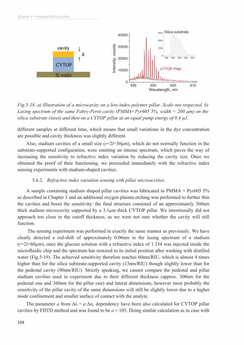
Chapter"V"�"Pedestal"Microcavities""
104""
different samples at different time, which means that small variations in the dye concentration
are possible and cavity thickness was slightly different.
Also, stadium cavities of a small size (r=2l=30µm), which do not normally function in the
substrate-supported configuration, were emitting an intense spectrum, which paves the way of
increasing the sensitivity to refractive index variation by reducing the cavity size. Once we
obtained the proof of their functioning, we proceeded immediately with the refractive index
sensing experiments with stadium-shaped cavities.
5.6.2. Refractive index variation sensing with pillar microacvities.
A sample containing stadium shaped pillar cavities was fabricated in PMMA + Pyr605 5%
as described in Chapter 3 and an additional oxygen plasma etching was performed to further thin
the cavities and boost the sensitivity: the final structure consisted of an approximately 360nm
thick stadium microcavity supported by a 3.1µm thick CYTOP pillar. We intentionally did not
approach too close to the cutoff thickness, as we were not sure whether the cavity will still
function.
The sensing experiment was performed in exactly the same manner as previously. We have
clearly detected a red-shift of approximately 0.06nm in the lasing spectrum of a stadium
(r=2l=60µm), once the glucose solution with a refractive index of 1.334 was injected inside the
microfluidic chip and the spectrum has restored to its initial position after washing with distilled
water (Fig.5-19). The achieved sensitivity therefore reaches 60nm/RIU, which is almost 4 times
higher than for the silica substrate-supported cavity (13nm/RIU) though slightly lower than for
the pedestal cavity (90nm/RIU). Strictly speaking, we cannot compare the pedestal and pillar
stadium cavities used in experiment due to their different thickness (approx. 300nm for the
pedestal one and 360nm for the pillar one) and lateral dimensions, however most probably the
sensitivity of the pillar cavity of the same dimensions will still be slightly lower due to a higher
mode confinement and smaller surface of contact with the analyte.
The parameter a from 〉そ = a·〉ne dependency have been also calculated for CYTOP pillar
cavities by FDTD method and was found to be a à 105. Doing similar calculation as in case with
595 600 605 6100
10000
20000
30000
40000
CYTOP Pillar
Silica substrate
Inte
nsity, cou
nts
Wavelength, nm
586 588 590 592 5940
1000
2000
3000
Fig.5-18. a) Illustration of a microcavity on a low-index polymer pillar. Scale not respected. b)
Lasing spectrum of the same Fabry-Perot cavity (PMMA+Pyr605 5%, width = 200 µm) on the
silica substrate (inset) and then on a CYTOP pillar at an equal pump energy of 0.4 µJ.
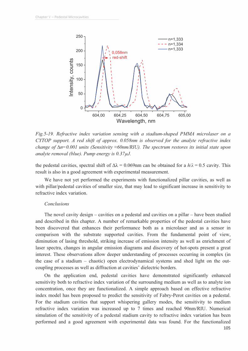
Chapter"V"�"Pedestal"Microcavities"
105""
the pedestal cavities, spectral shift of 〉そ = 0.069nm can be obtained for a h/そ = 0.5 cavity. This
result is also in a good agreement with experimental measurement.
We have not yet performed the experiments with functionalized pillar cavities, as well as
with pillar/pedestal cavities of smaller size, that may lead to significant increase in sensitivity to
refractive index variation.
Conclusions
The novel cavity design � cavities on a pedestal and cavities on a pillar � have been studied
and described in this chapter. A number of remarkable properties of the pedestal cavities have
been discovered that enhances their performance both as a microlaser and as a sensor in
comparison with the substrate supported cavities. From the fundamental point of view,
diminution of lasing threshold, striking increase of emission intensity as well as enrichment of
laser spectra, changes in angular emission diagrams and discovery of hot-spots present a great
interest. These observations allow deeper understanding of processes occurring in complex (in
the case of a stadium � chaotic) open electrodynamical systems and shed light on the out-
coupling processes as well as diffraction at cavities� dielectric borders.
On the application end, pedestal cavities have demonstrated significantly enhanced
sensitivity both to refractive index variation of the surrounding medium as well as to analyte ion
concentration, once they are functionalized. A simple approach based on effective refractive
index model has been proposed to predict the sensitivity of Fabry-Perot cavities on a pedestal.
For the stadium cavities that support whispering gallery modes, the sensitivity to medium
refractive index variation was increased up to 7 times and reached 90nm/RIU. Numerical
simulation of the sensitivity of a pedestal stadium cavity to refractive index variation has been
performed and a good agreement with experimental data was found. For the functionalized
604,00 604,25 604,50 604,75 605,00
0
50
100
150
200
250 n=1,333
n=1,334
n=1,3330,058nm
red-shift
Inte
nsity, counts
Wavelength, nm
Fig.5-19. Refractive index variation sensing with a stadium-shaped PMMA microlaser on a
CYTOP support. A red shift of approx. 0.058nm is observed for the analyte refractive index
change of Än=0.001 units (Sensitivity Ã60nm/RIU). The spectrum restores its initial state upon
analyte removal (blue). Pump energy is 0.37µJ.

Chapter"V"�"Pedestal"Microcavities""
106""
stadium cavities, one order of magnitude in sensitivity was gained, and detection of 10-6
M
concentration of Hg2+
in liquid solution was demonstrated, though lasing spectra were not
completely reversible.
Finally, pillar microcavities on low-index CYTOP substrate have been fabricated and have
demonstrated similar enhanced performance both in terms of laser characteristics (increased
intensity and lower thresholds) as well as sensitivity to refractive index variation � spectral shift
up to 60nm/RIU have been obtained.
"
107""
Conclusions"
In this thesis we have studied the application of polymer microcavity lasers for
chemical sensing, more precisely, for the detection of heavy metal ions in water for
environmental monitoring purposes. The goal of the work was to fabricate a prototype of a
Lab-on-Chip sensor capable of detecting traces of heavy metal (Hg2+
, Pb2+
, Cd2+
) ions in
drinking water through the change of the emission spectra of microlasers. We present the
proofs of viability of such sensing approach.
The first two chapters lay out the scientific interest and novelty of the work, followed
by a brief theoretical reminder of the principles of wave guiding and confinement. A
rationale for the choice of polymer materials as cavity body is given, emphasizing the ease of
functionalization with ligands, biocompatibility, low cost and simplicity of technological
processes, easy integration with microfluidics. Experimental setup for emission spectra
recording of microlasers is described and data processing techniques are explained.
The fabrication technique of microlasers is detailed in chapter 3, explaining the
fabrication of conventional silicon substrate-supported cavities, pedestal cavities, and
cavities on a low-index CYTOP polymer substrate that opens the way to all-polymer Lab-on-
Chip design. The description of the used polymers � PMMA and porous polystyrene based
polymers (PS-b-PAA, PS-Co-PAA, PS-P4VP) is given followed by the study of laser dye
photostability in polymer matrices. Performance of porous polymers was inferior to that of
PMMA: we observed fast dye degradation during storage in ambient conditions and ligand
grafting led to reticulation of polymer layers (§4.3). Preliminary fabrication attempts of
microcavities by laser ablation and 2-photon polymerization are reported, performed in
cooperation with Laser Centrum Hannover, demonstrating poor suitability of laser ablation
for polymer structuring and promising results of 2-photon polymerization.
Two applications of laser microcavities have been studied: detection of the refractive
index variation of the medium by the non-functionalized cavities and detection of heavy
metal ions in liquid by functionalized cavities. For this purpose the microfluidic chip has
been developed that allows optical pumping and recording of the emission spectra of
microlasers immersed in liquids (§4.2).
We have experimentally demonstrated for the first time the wavelength shift in the
lasing spectra of the non-functionalized active microcavities in response to variation of the
refractive index of the medium, surrounding the cavity. Two cavity types have been studied:
polygonal cavities and stadium-shaped cavities which support whispering gallery modes. The
analytical (for polygonal cavities) and numerical FDTD analysis (for WGM cavities) of the
influence of the cavity shape on sensitivity to index variation were performed and obtained
results are in a good agreement with the experiments. Experimentally observed sensitivity to
refractive index variation is approximately 14nm/RIU for the substrate-supported microlasers
of both types. Meanwhile, the proof of mercury ions detection in liquid with functionalized
stadium-shaped microcavity (PMMA+Pyrromethene 605) have also been obtained � a 10-5
M
"
108""
Hg2+
concentration has been detected via a red-shift in the lasing spectrum, which is
reversible after the cavities are washed with dimercaptopropanol, that releases mercury from
ligands.
The ways of sensitivity improvement have been proposed and explored in Chapter 5
with pedestal and pillar microcavities supporting whispering gallery modes, which have
demonstrated significantly enhanced sensitivity both to refractive index variation of the
surrounding medium as well as to analyte ion concentration, once they are functionalized.
Almost 7 times higher sensitivity to refractive index variation was registered with pedestal
cavities (~90nm/RIU) and almost 5 times higher with pillar cavities on CYTOP substrate
(~60nm/RIU). Obtained sensitivity values are comparable with reported in literature [19, 79] for
microspheres and planar microcavities. The FDTD numerical modeling of pedestal and pillar
cavities yielded sensitivity values very close to experimental. The functionalized stadium
cavities demonstrated a gain of one order of magnitude in sensitivity and detection of 10-6
M
concentration of Hg2+
in liquid solution is reported, though spectral shift was not entirely
reversible.
Alongside with enhanced sensitivity, pedestal microcavities were discovered to possess a
number of interesting properties in comparison with substrate supported cavity: reduced lasing
threshold, stronger emission intensity, unexpected angular emission patterns. Explanation
attempt of the observed effects is undertaken in §5.2
While successfully proving the possibility of chemical sensing with functionalized
microlasers, this work lays down a basis for future research, both fundamental and applied. On
the fundamental end, the problem of emission of pedestal microlasers may be studied.
Diffraction on the dielectric edge of a microcavity, a problem yet unsolved analytically, is
thought to play an important role in shaping the microlaser angular emission patterns. Recording
of full 3D angular emission diagrams may shed light on the outcoupling processes and help
develop theoretical models describing emission of different cavity shapes. On the more applied
end, many problems still need to be solved. First of all, the ways of sensitivity enhancement
proposed here (§5.4) may be explored (reduction of cavity size for stadiums, further work on
functionalization of porous materials, coupled microcavities). Question of sensor selectivity in
multicomponent solutions need to be studied and ligands for other heavy metals (Cd2+
, Pb2+
)
need to be tested with microlasers. Influence of temperature on microlaser spectra, casually
mentioned here, should be evaluated more deeply. Secondly, creation of an integrated LOC on
the basis of microlasers may be continued. For this purpose, a miniaturized detection system
needs to be developed, compatible with microfluidics, which excludes the need for a
spectrometer and can be integrated on the same substrate with the microlasers. Finally,
parallelization capacity may be studied, for simultaneous operation of multiple microlasers,
functionalized with various types of ligands.
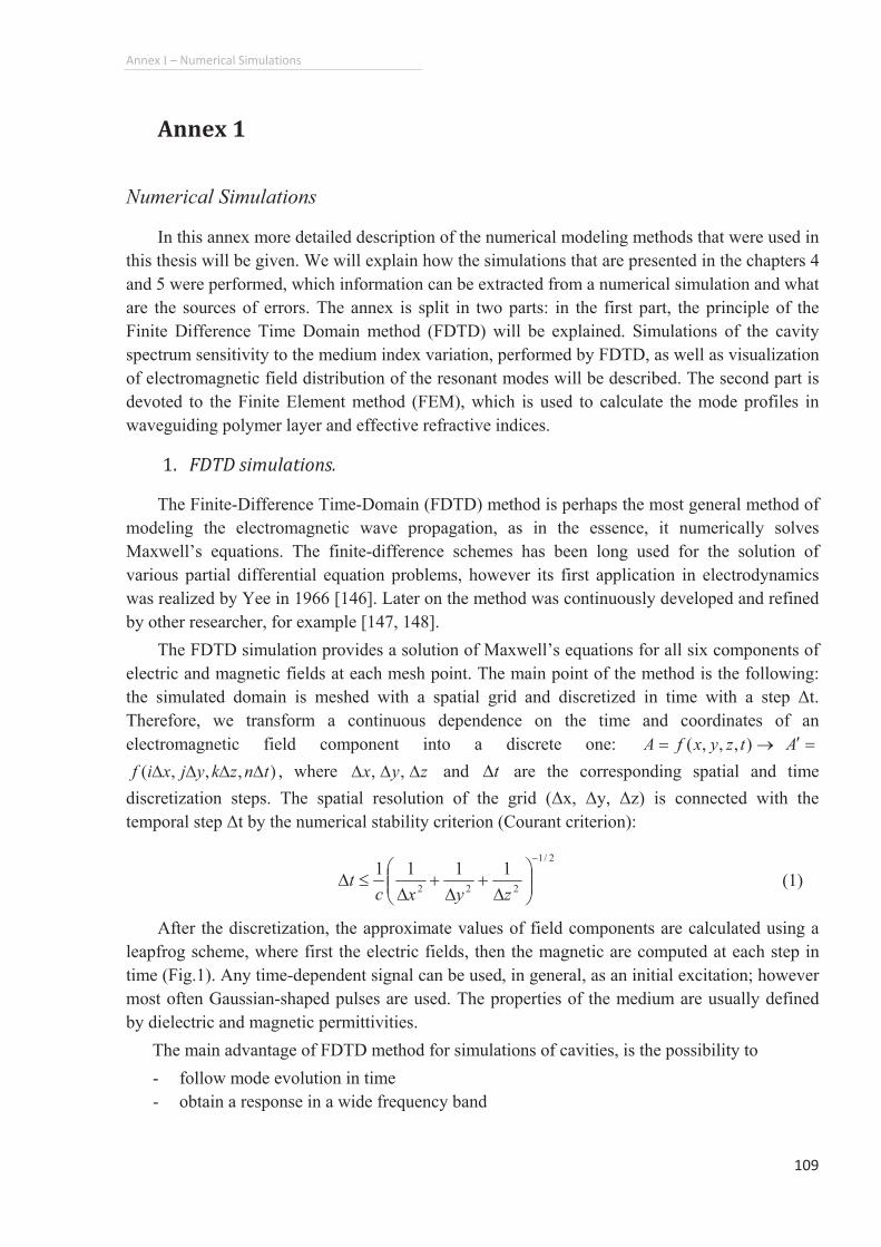
Annex"I" "Numerical"Simulations"
109""
1. Annex"1""
Numerical Simulations
In this annex more detailed description of the numerical modeling methods that were used in
this thesis will be given. We will explain how the simulations that are presented in the chapters 4
and 5 were performed, which information can be extracted from a numerical simulation and what
are the sources of errors. The annex is split in two parts: in the first part, the principle of the
Finite Difference Time Domain method (FDTD) will be explained. Simulations of the cavity
spectrum sensitivity to the medium index variation, performed by FDTD, as well as visualization
of electromagnetic field distribution of the resonant modes will be described. The second part is
devoted to the Finite Element method (FEM), which is used to calculate the mode profiles in
waveguiding polymer layer and effective refractive indices. な┻ FDTD"simulations."
The Finite-Difference Time-Domain (FDTD) method is perhaps the most general method of
modeling the electromagnetic wave propagation, as in the essence, it numerically solves
Maxwell�s equations. The finite-difference schemes has been long used for the solution of
various partial differential equation problems, however its first application in electrodynamics
was realized by Yee in 1966 [146]. Later on the method was continuously developed and refined
by other researcher, for example [147, 148].
The FDTD simulation provides a solution of Maxwell�s equations for all six components of
electric and magnetic fields at each mesh point. The main point of the method is the following:
the simulated domain is meshed with a spatial grid and discretized in time with a step 〉t.
Therefore, we transform a continuous dependence on the time and coordinates of an
electromagnetic field component into a discrete one: ›? ),,,( tzyxfA ?|A
),,,( tnzkyjxif FFFF , where zyx FFF ,, and tF are the corresponding spatial and time
discretization steps. The spatial resolution of the grid (〉x, 〉y, 〉z) is connected with the
temporal step 〉t by the numerical stability criterion (Courant criterion):
After the discretization, the approximate values of field components are calculated using a
leapfrog scheme, where first the electric fields, then the magnetic are computed at each step in
time (Fig.1). Any time-dependent signal can be used, in general, as an initial excitation; however
most often Gaussian-shaped pulses are used. The properties of the medium are usually defined
by dielectric and magnetic permittivities.
The main advantage of FDTD method for simulations of cavities, is the possibility to
- follow mode evolution in time
- obtain a response in a wide frequency band
2/1
222
1111/ÕÕÖÔÄÄÅ
ÃF-F-F~F
zyxct (1)
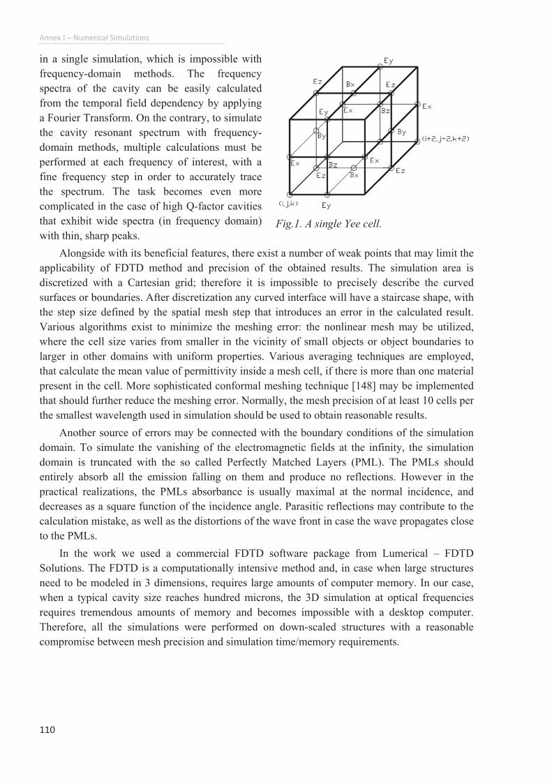
Annex"I"�"Numerical"Simulations"
110""
in a single simulation, which is impossible with
frequency-domain methods. The frequency
spectra of the cavity can be easily calculated
from the temporal field dependency by applying
a Fourier Transform. On the contrary, to simulate
the cavity resonant spectrum with frequency-
domain methods, multiple calculations must be
performed at each frequency of interest, with a
fine frequency step in order to accurately trace
the spectrum. The task becomes even more
complicated in the case of high Q-factor cavities
that exhibit wide spectra (in frequency domain)
with thin, sharp peaks.
Alongside with its beneficial features, there exist a number of weak points that may limit the
applicability of FDTD method and precision of the obtained results. The simulation area is
discretized with a Cartesian grid; therefore it is impossible to precisely describe the curved
surfaces or boundaries. After discretization any curved interface will have a staircase shape, with
the step size defined by the spatial mesh step that introduces an error in the calculated result.
Various algorithms exist to minimize the meshing error: the nonlinear mesh may be utilized,
where the cell size varies from smaller in the vicinity of small objects or object boundaries to
larger in other domains with uniform properties. Various averaging techniques are employed,
that calculate the mean value of permittivity inside a mesh cell, if there is more than one material
present in the cell. More sophisticated conformal meshing technique [148] may be implemented
that should further reduce the meshing error. Normally, the mesh precision of at least 10 cells per
the smallest wavelength used in simulation should be used to obtain reasonable results.
Another source of errors may be connected with the boundary conditions of the simulation
domain. To simulate the vanishing of the electromagnetic fields at the infinity, the simulation
domain is truncated with the so called Perfectly Matched Layers (PML). The PMLs should
entirely absorb all the emission falling on them and produce no reflections. However in the
practical realizations, the PMLs absorbance is usually maximal at the normal incidence, and
decreases as a square function of the incidence angle. Parasitic reflections may contribute to the
calculation mistake, as well as the distortions of the wave front in case the wave propagates close
to the PMLs.
In the work we used a commercial FDTD software package from Lumerical � FDTD
Solutions. The FDTD is a computationally intensive method and, in case when large structures
need to be modeled in 3 dimensions, requires large amounts of computer memory. In our case,
when a typical cavity size reaches hundred microns, the 3D simulation at optical frequencies
requires tremendous amounts of memory and becomes impossible with a desktop computer.
Therefore, all the simulations were performed on down-scaled structures with a reasonable
compromise between mesh precision and simulation time/memory requirements.
Fig.1. A single Yee cell.
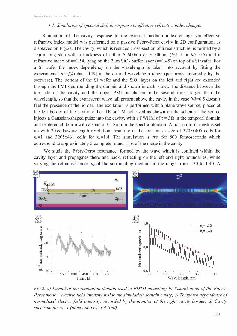
Annex"I" "Numerical"Simulations"
111""
1.1. Simulation of spectral shift in response to effective refractive index change.
Simulation of the cavity response to the external medium index change via effective
refractive index model was performed on a passive Fabry-Perot cavity in 2D configuration, as
displayed on Fig.2a. The cavity, which is reduced cross-section of a real structure, is formed by a
15µm long slab with a thickness of either h=600nm or h=300nm (h/そ=1 or h/そ=0.5) and a
refractive index of n=1.54, lying on the 2µm SiO2 buffer layer (n=1.45) on top of a Si wafer. For
a Si wafer the index dependency on the wavelength is taken into account by fitting the
experimental n = f(k) data [149] in the desired wavelength range (performed internally by the
software). The bottom of the Si wafer and the SiO2 layer on the left and right are extended
through the PMLs surrounding the domain and shown in dark violet. The distance between the
top side of the cavity and the upper PML is chosen to be several times larger than the
wavelength, so that the evanescent wave tail present above the cavity in the case h/そ=0.5 doesn�t
feel the presence of the border. The excitation is performed with a plane wave source, placed at
the left border of the cavity, either TE or TM polarized as shown on the scheme. The source
injects a Gaussian-shaped pulse into the cavity, with a FWHM of k = 3fs in the temporal domain
and centered at 0.6µm with a span of 0.18µm in the spectral domain. A non-uniform mesh is set
up with 20 cells/wavelength resolution, resulting in the total mesh size of 3205x405 cells for
ne=1 and 3205x461 cells for ne=1.4. The simulation is run for 800 femtoseconds which
correspond to approximately 5 complete round-trips of the mode in the cavity.
We study the Fabry-Perot resonance, formed by the wave which is confined within the
cavity layer and propagates there and back, reflecting on the left and right boundaries, while
varying the refractive index ne of the surrounding medium in the range from 1.30 to 1.40. A
0 150 300 450 600 750-30
-20
-10
0
|E|2
norm
aliz
ed,
Log s
cale
Time, fs500 550 600 650 700
0,6
0,8
1,0 n
e=1,30
ne=1,40
Norm
aliz
ed s
pec
trum
Wavelength, nm
Fig.2. a) Layout of the simulation domain used in FDTD modeling; b) Visualisation of the Fabry-
Perot mode � electric field intensity inside the simulation domain cavity; c) Temporal dependence of
normalized electric field intensity, recorded by the monitor at the right cavity border; d) Cavity
spectrum for ne=1 (black) and ne=1.4 (red).
|E|2"
a)" b)
c)" d)
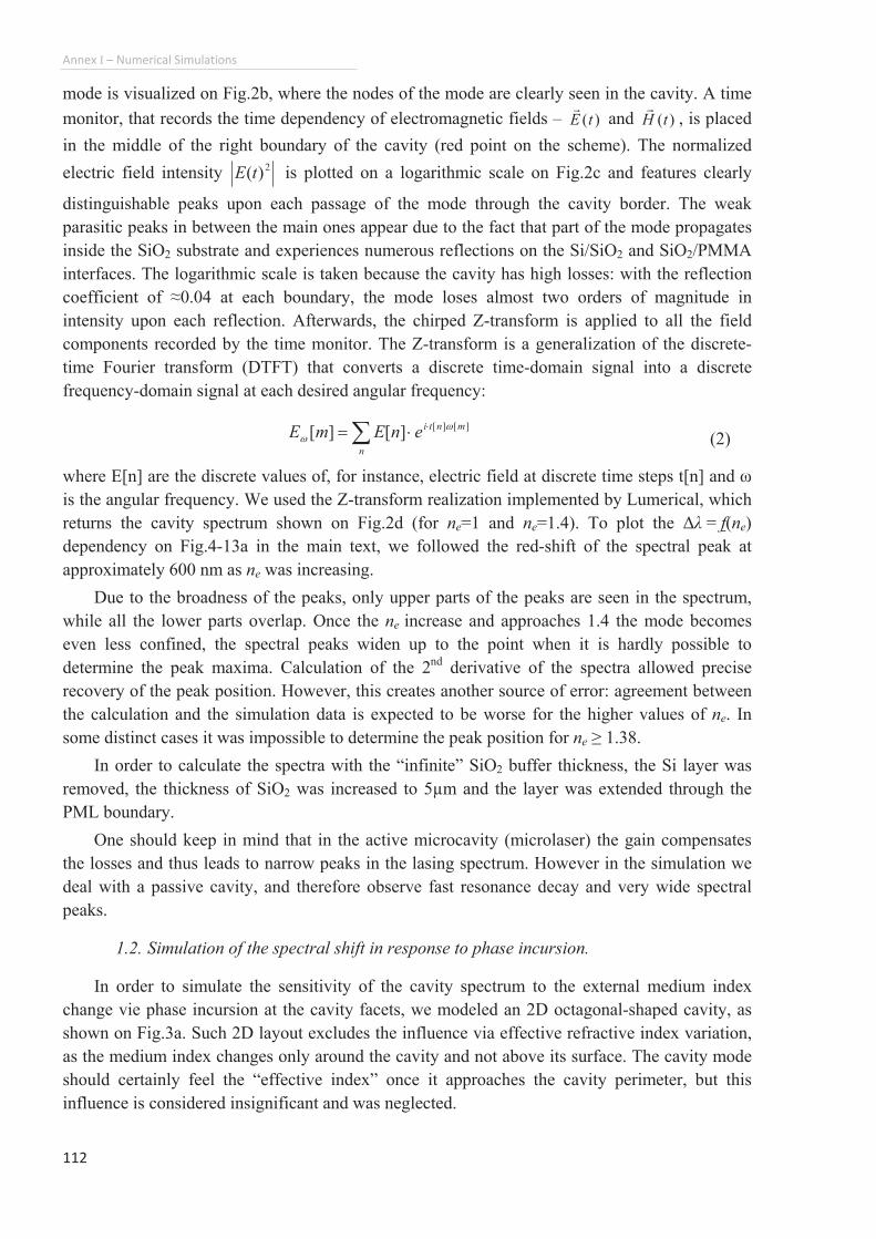
Annex"I" "Numerical"Simulations"
112""
mode is visualized on Fig.2b, where the nodes of the mode are clearly seen in the cavity. A time
monitor, that records the time dependency of electromagnetic fields � )(tEE
and )(tHE
, is placed
in the middle of the right boundary of the cavity (red point on the scheme). The normalized
electric field intensity 2)(tE is plotted on a logarithmic scale on Fig.2c and features clearly
distinguishable peaks upon each passage of the mode through the cavity border. The weak
parasitic peaks in between the main ones appear due to the fact that part of the mode propagates
inside the SiO2 substrate and experiences numerous reflections on the Si/SiO2 and SiO2/PMMA
interfaces. The logarithmic scale is taken because the cavity has high losses: with the reflection
coefficient of Ã0.04 at each boundary, the mode loses almost two orders of magnitude in
intensity upon each reflection. Afterwards, the chirped Z-transform is applied to all the field
components recorded by the time monitor. The Z-transform is a generalization of the discrete-
time Fourier transform (DTFT) that converts a discrete time-domain signal into a discrete
frequency-domain signal at each desired angular frequency:
where E[n] are the discrete values of, for instance, electric field at discrete time steps t[n] and のis the angular frequency. We used the Z-transform realization implemented by Lumerical, which
returns the cavity spectrum shown on Fig.2d (for ne=1 and ne=1.4). To plot the 〉そ = f(ne)
dependency on Fig.4-13a in the main text, we followed the red-shift of the spectral peak at
approximately 600 nm as ne was increasing.
Due to the broadness of the peaks, only upper parts of the peaks are seen in the spectrum,
while all the lower parts overlap. Once the ne increase and approaches 1.4 the mode becomes
even less confined, the spectral peaks widen up to the point when it is hardly possible to
determine the peak maxima. Calculation of the 2nd
derivative of the spectra allowed precise
recovery of the peak position. However, this creates another source of error: agreement between
the calculation and the simulation data is expected to be worse for the higher values of ne. In
some distinct cases it was impossible to determine the peak position for ne œ 1.38.
In order to calculate the spectra with the �infinite� SiO2 buffer thickness, the Si layer was
removed, the thickness of SiO2 was increased to 5µm and the layer was extended through the
PML boundary.
One should keep in mind that in the active microcavity (microlaser) the gain compensates
the losses and thus leads to narrow peaks in the lasing spectrum. However in the simulation we
deal with a passive cavity, and therefore observe fast resonance decay and very wide spectral
peaks.
1.2. Simulation of the spectral shift in response to phase incursion.
In order to simulate the sensitivity of the cavity spectrum to the external medium index
change vie phase incursion at the cavity facets, we modeled an 2D octagonal-shaped cavity, as
shown on Fig.3a. Such 2D layout excludes the influence via effective refractive index variation,
as the medium index changes only around the cavity and not above its surface. The cavity mode
should certainly feel the �effective index� once it approaches the cavity perimeter, but this
influence is considered insignificant and was neglected.
 ©©?n
mntienEmE ][][][][ yy (2)
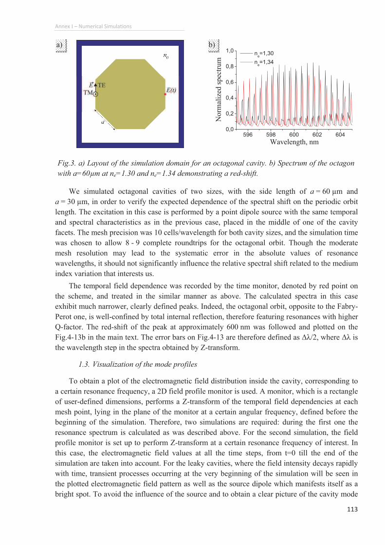
Annex"I" "Numerical"Simulations"
113""
We simulated octagonal cavities of two sizes, with the side length of a = 60 µm and
a = 30 µm, in order to verify the expected dependence of the spectral shift on the periodic orbit
length. The excitation in this case is performed by a point dipole source with the same temporal
and spectral characteristics as in the previous case, placed in the middle of one of the cavity
facets. The mesh precision was 10 cells/wavelength for both cavity sizes, and the simulation time
was chosen to allow 8 - 9 complete roundtrips for the octagonal orbit. Though the moderate
mesh resolution may lead to the systematic error in the absolute values of resonance
wavelengths, it should not significantly influence the relative spectral shift related to the medium
index variation that interests us.
The temporal field dependence was recorded by the time monitor, denoted by red point on
the scheme, and treated in the similar manner as above. The calculated spectra in this case
exhibit much narrower, clearly defined peaks. Indeed, the octagonal orbit, opposite to the Fabry-
Perot one, is well-confined by total internal reflection, therefore featuring resonances with higher
Q-factor. The red-shift of the peak at approximately 600 nm was followed and plotted on the
Fig.4-13b in the main text. The error bars on Fig.4-13 are therefore defined as 〉そ/2, where 〉そ is
the wavelength step in the spectra obtained by Z-transform.
1.3. Visualization of the mode profiles
To obtain a plot of the electromagnetic field distribution inside the cavity, corresponding to
a certain resonance frequency, a 2D field profile monitor is used. A monitor, which is a rectangle
of user-defined dimensions, performs a Z-transform of the temporal field dependencies at each
mesh point, lying in the plane of the monitor at a certain angular frequency, defined before the
beginning of the simulation. Therefore, two simulations are required: during the first one the
resonance spectrum is calculated as was described above. For the second simulation, the field
profile monitor is set up to perform Z-transform at a certain resonance frequency of interest. In
this case, the electromagnetic field values at all the time steps, from t=0 till the end of the
simulation are taken into account. For the leaky cavities, where the field intensity decays rapidly
with time, transient processes occurring at the very beginning of the simulation will be seen in
the plotted electromagnetic field pattern as well as the source dipole which manifests itself as a
bright spot. To avoid the influence of the source and to obtain a clear picture of the cavity mode
596 598 600 602 6040,0
0,2
0,4
0,6
0,8
1,0 n
e=1,30
ne=1,34
Wavelength, nm
Norm
aliz
ed s
pec
trum
Fig.3. a) Layout of the simulation domain for an octagonal cavity. b) Spectrum of the octagon
with a=60µm at ne=1.30 and ne=1.34 demonstrating a red-shift.
a)" b)
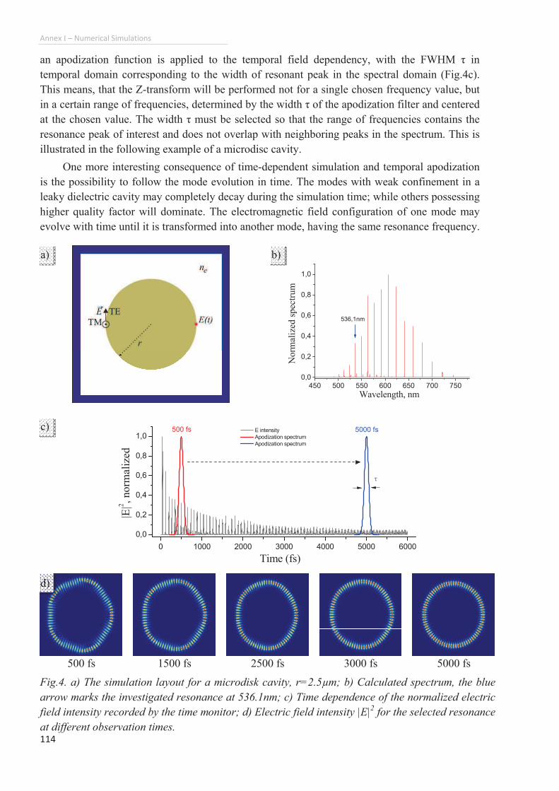
Annex"I" "Numerical"Simulations"
114""
an apodization function is applied to the temporal field dependency, with the FWHM k in
temporal domain corresponding to the width of resonant peak in the spectral domain (Fig.4c).
This means, that the Z-transform will be performed not for a single chosen frequency value, but
in a certain range of frequencies, determined by the width k of the apodization filter and centered
at the chosen value. The width k must be selected so that the range of frequencies contains the
resonance peak of interest and does not overlap with neighboring peaks in the spectrum. This is
illustrated in the following example of a microdisc cavity.
One more interesting consequence of time-dependent simulation and temporal apodization
is the possibility to follow the mode evolution in time. The modes with weak confinement in a
leaky dielectric cavity may completely decay during the simulation time; while others possessing
higher quality factor will dominate. The electromagnetic field configuration of one mode may
evolve with time until it is transformed into another mode, having the same resonance frequency.
"450 500 550 600 650 700 750
0,0
0,2
0,4
0,6
0,8
1,0
No
rmal
ized
sp
ectr
um
Wavelength, nm
536,1nm
"
"
0 1000 2000 3000 4000 5000 6000
0,0
0,2
0,4
0,6
0,8
1,0
v
5000 fs
|E|2
, norm
aliz
ed
Time (fs)
500 fs E intensity
Apodization spectrum
Apodization spectrum
500 fs 1500 fs 2500 fs 3000 fs 5000 fs
Fig.4. a) The simulation layout for a microdisk cavity, r=2.5µm; b) Calculated spectrum, the blue
arrow marks the investigated resonance at 536.1nm; c) Time dependence of the normalized electric
field intensity recorded by the time monitor; d) Electric field intensity |E|2 for the selected resonance
at different observation times.
a)" b)
c)"
d)"
Annex"I" "Numerical"Simulations"
115""
That is what was observed for certain resonances of a microdisk cavity: if we follow in time the
electric field intensity pattern for a resonance peak at 536.1nm (Fig.4b) of a microdisk with
r=2.5µm (Fig.4a), we evidence its gradual evolution (Fig.4c) from an inscribed pentagon orbit at
the beginning of the simulation (time ø3000fs) to a certain eigenmode of a microdisk (time
œ4000fs), whose field distribution corresponds to that of a whispering gallery mode. The
simulation here is performed for a TM mode (Fig.4a), similar as was described above, for a
medium index ne=1.
Annex"I" "Numerical"Simulations"
116""
に┻ Finite"Element"Method."
The Finite Element Method (FEM) is a method of approximate numerical solution of partial
differential equations (PDE) as well as integral equations. The first mathematical treatment of
FEM was introduced by Richard Courant in 1943 [150, 151]. The detailed explanation of the
method is rather complicated and is definitely out of the scope of this thesis; therefore we will
just give a short schematic outline of the modeling steps.
‚ First of all, the solution domain is partitioned into a set of mesh elements which are typically
either square or triangular in 2D and cubic or tetrahedron in 3D.
‚ The dependent variables of PDE are approximated with functions that can be described with
a finite number of parameters. For a single variable u: Â?i
iiUu lwhere Ui (so-called degrees of freedom) are the values of u in the node points of the mesh
and li are the basis functions.
‚ Assembling a system of equations for all the elements in the solution domain and solving it
numerically.
To perform FEM modeling we have used COMSOL Multiphysics software which is a
powerful tool for solving various kinds of physical (chemical, mechanical, etc.) problems where
the phenomenon under investigation can be described with a system of PDEs.
In a FEM simulation as opposed to FDTD the calculation is performed at one single
frequency defined before the beginning of a simulation. Therefore to obtain, for example, a
spectrum of resonant frequencies of a cavity, multiple simulations need to be performed in a
certain range of frequencies with a small step. The narrower are the resonance peaks of the
cavity, the smaller should be the frequency step, therefore FDTD simulation is preferable for
such calculations. At the same time, FDTD only solves a set of Maxwell equations for electric
and magnetic field components, therefore problems, where a propagation constant or effective
index of a guided mode needs to be found require different solution methods and FEM is
convenient for this purposes.
Another advantage of finite element method is the intrinsic support of non-orthogonal
meshes. Rectangular mesh, which is the only possibility in FDTD1, cannot precisely discretize
the curved boundaries of objects and leads to numerical errors. In FEM, on the contrary,
triangular mesh can be used with large difference in size between the adjacent mesh elements
which therefore allows more precise description of curved interfaces. [152],[153]
1.4. Effective refractive index calculation
In order to calculate the effective refractive index of the TE mode propagating in the active
layer while taking into account the finite thickness of the SiO2 buffer layer (presence of Si
substrate) the simulation schematically depicted on Fig.5c was set-up. In our connotation, for a
TE mode electric field lies in the plane of the cavity. A simulation domain consists of a stack of
""""""""""""""""""""""""""""""""""""""""""""""""""""""""""""1 There exist works in literature where FDTD implementation on triangular [151] and non-orthogonal meshes [152]
is demonstrated. However, majority of commercial FDTD packages only support rectangular meshes.
Annex"I" "Numerical"Simulations"
117""
4 layers: Si (2µm) / SiO2 (2µm) / PMMA (0.6µm or 0.3µm) / medium (4µm) with the width of
6um. The refractive indices are the following: Si � n=3.94 (crystalline silicon, そ=600nm [149]),
SiO2 � n=1.45, PMMA � n=1.54, medium - ne. The equation solved is the Helmholtz equation
for the Ez field component (propagation perpendicular to the plane of drawing):
where く is the propagation constant, k0 is the free-space wavenumber. Once the value of
propagation constant is known, the effective index is calculated as:
The initial value of effn is given to COMSOL and afterwards software searches for converging
solutions of Eq.(3) in the vicinity of this initial value. The result of the simulation is the list of
the effective indices of the modes that may propagate in the structure and corresponding
distributions of electric field Ez.
The simulation domain is truncated by a �perfect magnetic conductor� boundary condition,
meaning that the tangential component of the magnetic field and normal component of the
electric field are equal to zero:
where nE
is the normal vector to the boundary. This boundary condition allows correct
representation of infiniteness of dielectric layers along the x axis when only Ez component of
electric field is non-zero. The domain is meshed with a non-uniform triangular mesh reaching
15÷30 mesh cells/wavelength resolution. The initial guess value of neff is given to COMSOL and
afterwards it searches for the converging solutions of Eq. (3) in the vicinity of this value.
The refractive index of the surrounding medium ne is varied in the range 1 ÷ 1.4 and the
calculated effective refractive index values are used to plot Fig.4-14 in the main text. It was
found that the effective index of the guided mode in the case of 2µm SiO2 layer is lower than the
one calculated analytically for infinite buffer layer thickness. The calculation errors in this case
would arise due to the finite size of the mesh cells and, more important, due to the limited
"" 0)( 2
0
222 ?/-ı zz EknE d " (3)
""0/ kneff d? " (4)
Fig.5. The Ez component of a field of a TE mode propagating in the cavity layer for a) h/そ=1
and b) h/そ=0.5 geometries and two different values of medium index; Inset shows stronger
electric field intensity in the Si wafer layer in case when ne=1. c) The layout of simulation.
0?·HnEE
, 0?©EnEE
(5)
Annex"I" "Numerical"Simulations"
118""
thickness of the Si layer, which was chosen in order to balance a fine mesh resolution with
reasonable memory consumption.
The modulus squared of the Ez electric field component is plotted for h/そ = 1 geometry on
Fig.5a (h = 0.6µm) and h/そ = 0.5 on Fig.5b (h = 0.3µm) so that it is possible to visually estimate
the mode localization in the cavity and claddings. In the case of a thicker cavity (h/そ=1), the
mode is mostly confined within the active layer, electric field extends into the silica buffer but
diminishes to zero at the interface with Si substrate, so that the mode is not influenced by its
presence. However in the case of a twice thinner cavity (h/そ = 0.5) the mode is mostly localized
at the cavity/SiO2 interface, extends deeply into the buffer layer and, as the inset on Fig.5b
shows, there exist part of the mode propagating inside the Si substrate. The effective index in
this case is slightly different from the predicted by Eq. (4-3). Once the index of the medium
above the cavity rises, the mode shifts closer to the cavity/medium interface and the influence of
the Si substrate decreases.
For a TM mode it was found that while in h/そ=1 case the confinement is rather strong and
mode effective index is not influenced by a silicon substrate, but in h/そ=0.5 case the mode
extends significantly into the substrate leading to the difference of the order 10-3
between the
analytical and numerical effective index calculations.
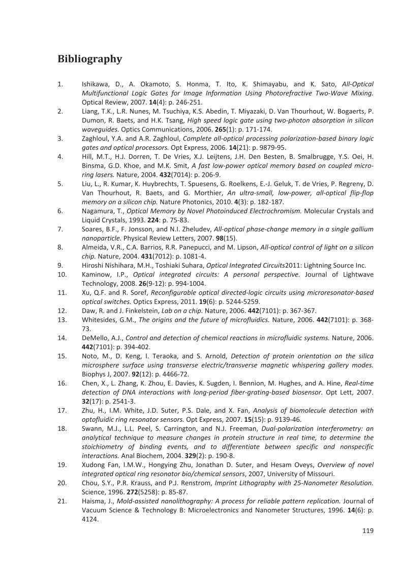
"
119""
Bibliography"
1." Ishikawa," D.," A." Okamoto," S." Honma," T." Ito," K." Shimayabu," and" K." Sato," AllどOptical"Multifunctional" Logic" Gates" for" Image" Information" Using" Photorefractive" TwoどWave"Mixing."Optical"Review,"2007."14(4):"p."246ど251."
2." Liang,"T.K.,"L.R."Nunes,"M."Tsuchiya,"K.S."Abedin,"T."Miyazaki,"D."Van"Thourhout,"W."Bogaerts,"P."Dumon,"R."Baets,"and"H.K."Tsang,"High"speed" logic"gate"using"twoどphoton"absorption" in"silicon"waveguides."Optics"Communications,"2006."265(1):"p."171ど174."
3." Zaghloul,"Y.A."and"A.R."Zaghloul,"Complete"allどoptical"processing"polarizationどbased"binary" logic"gates"and"optical"processors."Opt"Express,"2006."14(21):"p."9879ど95."
4." Hill,"M.T.,"H.J."Dorren," T."De"Vries," X.J." Leijtens," J.H."Den"Besten,"B." Smalbrugge," Y.S."Oei,"H."Binsma,"G.D."Khoe,"and"M.K."Smit,"A" fast" lowどpower"optical"memory"based"on"coupled"microどring"lasers."Nature,"2004."432(7014):"p."206ど9."
5." Liu,"L.,"R."Kumar,"K."Huybrechts,"T."Spuesens,"G."Roelkens,"E.どJ."Geluk,"T."de"Vries,"P."Regreny,"D."Van" Thourhout," R." Baets," and" G." Morthier," An" ultraどsmall," lowどpower," allどoptical" flipどflop"memory"on"a"silicon"chip."Nature"Photonics,"2010."4(3):"p."182ど187."
6." Nagamura,"T.,"Optical"Memory"by"Novel"Photoinduced"Electrochromism."Molecular"Crystals"and"Liquid"Crystals,"1993."224:"p."75ど83."
7." Soares,"B.F.,"F."Jonsson,"and"N.I."Zheludev,"Allどoptical"phaseどchange"memory"in"a"single"gallium"nanoparticle."Physical"Review"Letters,"2007."98(15)."
8." Almeida,"V.R.,"C.A."Barrios,"R.R."Panepucci,"and"M."Lipson,"Allどoptical"control"of"light"on"a"silicon"chip."Nature,"2004."431(7012):"p."1081ど4."
9." Hiroshi"Nishihara,"M.H.,"Toshiaki"Suhara,"Optical"Integrated"Circuits2011:"Lightning"Source"Inc."10." Kaminow," I.P.," Optical" integrated" circuits:" A" personal" perspective." Journal" of" Lightwave"
Technology,"2008."26(9ど12):"p."994ど1004."11." Xu,"Q.F."and"R."Soref,"Reconfigurable"optical"directedどlogic"circuits"using"microresonatorどbased"
optical"switches."Optics"Express,"2011."19(6):"p."5244ど5259."12." Daw,"R."and"J."Finkelstein,"Lab"on"a"chip."Nature,"2006."442(7101):"p."367ど367."13." Whitesides,"G.M.,"The"origins"and"the"future"of"microfluidics."Nature,"2006."442(7101):"p."368ど
73."14." DeMello,"A.J.,"Control"and"detection"of"chemical"reactions"in"microfluidic"systems."Nature,"2006."
442(7101):"p."394ど402."15." Noto," M.," D." Keng," I." Teraoka," and" S." Arnold," Detection" of" protein" orientation" on" the" silica"
microsphere" surface" using" transverse" electric/transverse"magnetic"whispering" gallery"modes."Biophys"J,"2007."92(12):"p."4466ど72."
16." Chen,"X.,"L."Zhang,"K."Zhou,"E."Davies,"K."Sugden,"I."Bennion,"M."Hughes,"and"A."Hine,"Realどtime"detection" of"DNA" interactions"with" longどperiod" fiberどgratingどbased" biosensor."Opt" Lett," 2007."32(17):"p."2541ど3."
17." Zhu,"H.," I.M."White," J.D." Suter," P.S."Dale," and" X." Fan,"Analysis" of" biomolecule" detection"with"optofluidic"ring"resonator"sensors."Opt"Express,"2007."15(15):"p."9139ど46."
18." Swann," M.J.," L.L." Peel," S." Carrington," and" N.J." Freeman," Dualどpolarization" interferometry:" an"analytical" technique" to"measure" changes" in" protein" structure" in" real" time," to" determine" the"stoichiometry" of" binding" events," and" to" differentiate" between" specific" and" nonspecific"interactions."Anal"Biochem,"2004."329(2):"p."190ど8."
19." Xudong" Fan," I.M.W.,"Hongying" Zhu," Jonathan"D." Suter," and"Hesam"Oveys,"Overview" of" novel"integrated"optical"ring"resonator"bio/chemical"sensors,"2007,"University"of"Missouri."
20." Chou,"S.Y.,"P.R."Krauss,"and"P.J."Renstrom," Imprint"Lithography"with"25どNanometer"Resolution."Science,"1996."272(5258):"p."85ど87."
21." Haisma,"J.,"Moldどassisted"nanolithography:"A"process"for"reliable"pattern"replication."Journal"of"Vacuum"Science"&"Technology"B:"Microelectronics"and"Nanometer"Structures,"1996."14(6):"p."4124."
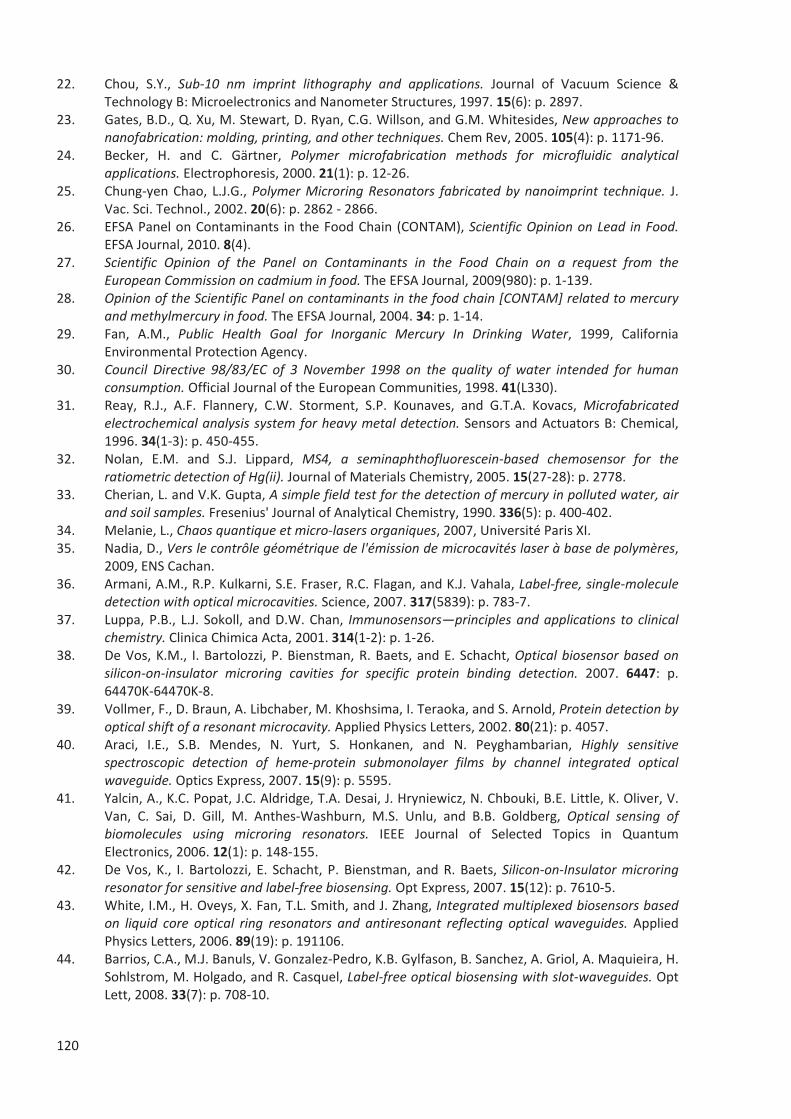
"
120""
22." Chou," S.Y.," Subど10" nm" imprint" lithography" and" applications." Journal" of" Vacuum" Science" &"Technology"B:"Microelectronics"and"Nanometer"Structures,"1997."15(6):"p."2897."
23." Gates,"B.D.,"Q."Xu,"M."Stewart,"D."Ryan,"C.G."Willson,"and"G.M."Whitesides,"New"approaches"to"nanofabrication:"molding,"printing,"and"other"techniques."Chem"Rev,"2005."105(4):"p."1171ど96."
24." Becker," H." and" C." Gärtner," Polymer" microfabrication" methods" for" microfluidic" analytical"applications."Electrophoresis,"2000."21(1):"p."12ど26."
25." Chungどyen"Chao,"L.J.G.,"Polymer"Microring"Resonators" fabricated"by"nanoimprint" technique." J."Vac."Sci."Technol.,"2002."20(6):"p."2862"ど"2866."
26." EFSA"Panel"on"Contaminants" in"the"Food"Chain" (CONTAM),"Scientific"Opinion"on"Lead" in"Food."EFSA"Journal,"2010."8(4)."
27." Scientific" Opinion" of" the" Panel" on" Contaminants" in" the" Food" Chain" on" a" request" from" the"European"Commission"on"cadmium"in"food."The"EFSA"Journal,"2009(980):"p."1ど139."
28." Opinion"of"the"Scientific"Panel"on"contaminants"in"the"food"chain"[CONTAM]"related"to"mercury"and"methylmercury"in"food."The"EFSA"Journal,"2004."34:"p."1ど14."
29." Fan," A.M.," Public" Health" Goal" for" Inorganic" Mercury" In" Drinking" Water," 1999," California"Environmental"Protection"Agency."
30." Council"Directive" 98/83/EC" of" 3"November" 1998" on" the" quality" of"water" intended" for" human"consumption."Official"Journal"of"the"European"Communities,"1998."41(L330)."
31." Reay," R.J.," A.F." Flannery," C.W." Storment," S.P." Kounaves," and" G.T.A." Kovacs,"Microfabricated"electrochemical"analysis"system"for"heavy"metal"detection."Sensors"and"Actuators"B:"Chemical,"1996."34(1ど3):"p."450ど455."
32." Nolan," E.M." and" S.J." Lippard," MS4," a" seminaphthofluoresceinどbased" chemosensor" for" the"ratiometric"detection"of"Hg(ii)."Journal"of"Materials"Chemistry,"2005."15(27ど28):"p."2778."
33." Cherian,"L."and"V.K."Gupta,"A"simple"field"test"for"the"detection"of"mercury"in"polluted"water,"air"and"soil"samples."Fresenius'"Journal"of"Analytical"Chemistry,"1990."336(5):"p."400ど402."
34." Melanie,"L.,"Chaos"quantique"et"microどlasers"organiques,"2007,"Université"Paris"XI."35." Nadia,"D.,"Vers"le"contrôle"géométrique"de"l'émission"de"microcavités"laser"à"base"de"polymères,"
2009,"ENS"Cachan."36." Armani,"A.M.,"R.P."Kulkarni,"S.E."Fraser,"R.C."Flagan,"and"K.J."Vahala,"Labelどfree,"singleどmolecule"
detection"with"optical"microcavities."Science,"2007."317(5839):"p."783ど7."37." Luppa,"P.B.,"L.J."Sokoll,"and"D.W."Chan," Immunosensors principles"and"applications" to"clinical"
chemistry."Clinica"Chimica"Acta,"2001."314(1ど2):"p."1ど26."38." De"Vos,"K.M.," I."Bartolozzi,"P."Bienstman,"R."Baets,"and"E."Schacht,"Optical"biosensor"based"on"
siliconどonどinsulator" microring" cavities" for" specific" protein" binding" detection." 2007." 6447:" p."64470Kど64470Kど8."
39." Vollmer,"F.,"D."Braun,"A."Libchaber,"M."Khoshsima,"I."Teraoka,"and"S."Arnold,"Protein"detection"by"optical"shift"of"a"resonant"microcavity."Applied"Physics"Letters,"2002."80(21):"p."4057."
40." Araci," I.E.," S.B." Mendes," N." Yurt," S." Honkanen," and" N." Peyghambarian," Highly" sensitive"spectroscopic" detection" of" hemeどprotein" submonolayer" films" by" channel" integrated" optical"waveguide."Optics"Express,"2007."15(9):"p."5595."
41." Yalcin,"A.,"K.C."Popat,"J.C."Aldridge,"T.A."Desai,"J."Hryniewicz,"N."Chbouki,"B.E."Little,"K."Oliver,"V."Van," C." Sai," D." Gill," M." AnthesどWashburn," M.S." Unlu," and" B.B." Goldberg," Optical" sensing" of"biomolecules" using" microring" resonators." IEEE" Journal" of" Selected" Topics" in" Quantum"Electronics,"2006."12(1):"p."148ど155."
42." De"Vos,"K.," I."Bartolozzi,"E."Schacht,"P."Bienstman,"and"R."Baets,"SiliconどonどInsulator"microring"resonator"for"sensitive"and"labelどfree"biosensing."Opt"Express,"2007."15(12):"p."7610ど5."
43." White,"I.M.,"H."Oveys,"X."Fan,"T.L."Smith,"and"J."Zhang,"Integrated"multiplexed"biosensors"based"on" liquid" core"optical" ring" resonators"and"antiresonant" reflecting"optical"waveguides."Applied"Physics"Letters,"2006."89(19):"p."191106."
44." Barrios,"C.A.,"M.J."Banuls,"V."GonzalezどPedro,"K.B."Gylfason,"B."Sanchez,"A."Griol,"A."Maquieira,"H."Sohlstrom,"M."Holgado,"and"R."Casquel,"Labelどfree"optical"biosensing"with"slotどwaveguides."Opt"Lett,"2008."33(7):"p."708ど10."
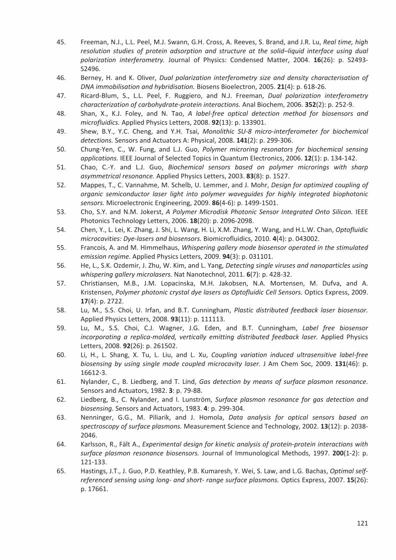
"
121""
45." Freeman,"N.J.,"L.L."Peel,"M.J."Swann,"G.H."Cross,"A."Reeves,"S."Brand,"and"J.R."Lu,"Real"time,"high"resolution" studies" of" protein" adsorption" and" structure" at" the" solid liquid" interface" using" dual"polarization" interferometry." Journal" of" Physics:" Condensed" Matter," 2004." 16(26):" p." S2493どS2496."
46." Berney,"H."and"K."Oliver,"Dual"polarization" interferometry" size"and"density" characterisation"of"DNA"immobilisation"and"hybridisation."Biosens"Bioelectron,"2005."21(4):"p."618ど26."
47." RicardどBlum," S.," L.L." Peel," F." Ruggiero," and" N.J." Freeman," Dual" polarization" interferometry"characterization"of"carbohydrateどprotein"interactions."Anal"Biochem,"2006."352(2):"p."252ど9."
48." Shan," X.," K.J." Foley," and" N." Tao," A" labelどfree" optical" detection" method" for" biosensors" and"microfluidics."Applied"Physics"Letters,"2008."92(13):"p."133901."
49." Shew," B.Y.," Y.C." Cheng," and" Y.H." Tsai," Monolithic" SUど8" microどinterferometer" for" biochemical"detections."Sensors"and"Actuators"A:"Physical,"2008."141(2):"p."299ど306."
50." ChungどYen," C.," W." Fung," and" L.J." Guo," Polymer" microring" resonators" for" biochemical" sensing"applications."IEEE"Journal"of"Selected"Topics"in"Quantum"Electronics,"2006."12(1):"p."134ど142."
51." Chao," C.どY." and" L.J." Guo," Biochemical" sensors" based" on" polymer" microrings" with" sharp"asymmetrical"resonance."Applied"Physics"Letters,"2003."83(8):"p."1527."
52." Mappes,"T.,"C."Vannahme,"M."Schelb,"U."Lemmer,"and"J."Mohr,"Design"for"optimized"coupling"of"organic" semiconductor" laser" light" into" polymer" waveguides" for" highly" integrated" biophotonic"sensors."Microelectronic"Engineering,"2009."86(4ど6):"p."1499ど1501."
53." Cho,"S.Y."and"N.M." Jokerst,"A"Polymer"Microdisk"Photonic"Sensor" Integrated"Onto"Silicon." IEEE"Photonics"Technology"Letters,"2006."18(20):"p."2096ど2098."
54." Chen,"Y.,"L."Lei,"K."Zhang,"J."Shi,"L."Wang,"H."Li,"X.M."Zhang,"Y."Wang,"and"H.L.W."Chan,"Optofluidic"microcavities:"Dyeどlasers"and"biosensors."Biomicrofluidics,"2010."4(4):"p."043002."
55." Francois,"A."and"M."Himmelhaus,"Whispering"gallery"mode"biosensor"operated"in"the"stimulated"emission"regime."Applied"Physics"Letters,"2009."94(3):"p."031101."
56." He,"L.,"S.K."Ozdemir,"J."Zhu,"W."Kim,"and"L."Yang,"Detecting"single"viruses"and"nanoparticles"using"whispering"gallery"microlasers."Nat"Nanotechnol,"2011."6(7):"p."428ど32."
57." Christiansen," M.B.," J.M." Lopacinska," M.H." Jakobsen," N.A." Mortensen," M." Dufva," and" A."Kristensen,"Polymer"photonic"crystal"dye"lasers"as"Optofluidic"Cell"Sensors."Optics"Express,"2009."17(4):"p."2722."
58." Lu,"M.," S.S."Choi,"U." Irfan," and"B.T."Cunningham," Plastic" distributed" feedback" laser"biosensor."Applied"Physics"Letters,"2008."93(11):"p."111113."
59." Lu," M.," S.S." Choi," C.J." Wagner," J.G." Eden," and" B.T." Cunningham," Label" free" biosensor"incorporating" a" replicaどmolded," vertically" emitting" distributed" feedback" laser."Applied" Physics"Letters,"2008."92(26):"p."261502."
60." Li," H.," L." Shang," X." Tu," L." Liu," and" L." Xu," Coupling" variation" induced" ultrasensitive" labelどfree"biosensing"by"using" single"mode" coupled"microcavity" laser." J"Am"Chem"Soc,"2009."131(46):"p."16612ど3."
61." Nylander,"C.,"B."Liedberg,"and"T."Lind,"Gas"detection"by"means"of" surface"plasmon" resonance."Sensors"and"Actuators,"1982."3:"p."79ど88."
62." Liedberg,"B.," C."Nylander," and" I." Lunström," Surface" plasmon" resonance" for" gas" detection" and"biosensing."Sensors"and"Actuators,"1983."4:"p."299ど304."
63." Nenninger," G.G.," M." Piliarik," and" J." Homola," Data" analysis" for" optical" sensors" based" on"spectroscopy"of"surface"plasmons."Measurement"Science"and"Technology,"2002."13(12):"p."2038ど2046."
64." Karlsson,"R.,"Fält"A.,"Experimental"design"for"kinetic"analysis"of"proteinどprotein"interactions"with"surface"plasmon" resonance"biosensors." Journal"of" Immunological"Methods,"1997."200(1ど2):"p."121ど133."
65." Hastings,"J.T.,"J."Guo,"P.D."Keathley,"P.B."Kumaresh,"Y."Wei,"S."Law,"and"L.G."Bachas,"Optimal"selfどreferenced"sensing"using"longど"and"shortど"range"surface"plasmons."Optics"Express,"2007."15(26):"p."17661."
"
122""
66." Dostálek,"J."and"J."Homola,"Surface"plasmon"resonance"sensor"based"on"an"array"of"diffraction"gratings"for"highly"parallelized"observation"of"biomolecular" interactions."Sensors"and"Actuators"B:"Chemical,"2008."129(1):"p."303ど310."
67." Sadowski,"J.W.,"J."Lekkala,"and"I."Vikholm,"Biosensors"based"on"surface"plasmons"excited"in"nonどnoble"metals."Biosensors"and"Bioelectronics,"1991."6(5):"p."439ど444."
68." Homola,"J.,"Surface"plasmon"resonance"sensors"for"detection"of"chemical"and"biological"species."Chem"Rev,"2008."108(2):"p."462ど93."
69." Forzani,"E.S.,"H."Zhang,"W."Chen,"and"N."Tao,"Detection"of"Heavy"Metal" Ions" in"Drinking"Water"Using"a"HighどResolution"Differential"Surface"Plasmon"Resonance"Sensor."Environmental"Science"&"Technology,"2005."39(5):"p."1257ど1262."
70." Chen," C.D.," S.F." Cheng," L.K." Chau," and" C.R."Wang," Sensing" capability" of" the" localized" surface"plasmon"resonance"of"gold"nanorods."Biosens"Bioelectron,"2007."22(6):"p."926ど32."
71." Haes,"A.J."and"R.P."Van"Duyne,"A"Nanoscale"Optical"Biosensor:""Sensitivity"and"Selectivity"of"an"Approach"Based"on"the"Localized"Surface"Plasmon"Resonance"Spectroscopy"of"Triangular"Silver"Nanoparticles."J"Am"Chem"Soc,"2002."124(35):"p."10596ど10604."
72." Hall," W.P.," S.N." Ngatia," and" R.P." Van" Duyne," LSPR" Biosensor" Signal" Enhancement" Using"NanoparticleどAntibody"Conjugates."J"Phys"Chem"C"Nanomater"Interfaces,"2011."115(5):"p."1410ど1414."
73." Wang," T.どJ." and" P.どC." Ho," Localized" surface" plasmon" resonance" biosensing" by" electroどoptic"modulation"with"sensitivity"and"resolution"tunability."Journal"of"Applied"Physics,"2011."109(6):"p."064703."
74." Xiang,"G.,"N." Zhang," and" X." Zhou," Localized" surface" plasmon" resonance" biosensing"with" large"area"of"gold"nanoholes"fabricated"by"nanosphere"lithography."Nanoscale"Res"Lett,"2010."5(5):"p."818ど22."
75." Murray,"W.A.,"B."Auguié,"and"W.L."Barnes,"Sensitivity"of"Localized"Surface"Plasmon"Resonances"to"Bulk"and"Local"Changes"in"the"Optical"Environment."The"Journal"of"Physical"Chemistry"C,"2009."113(13):"p."5120ど5125."
76." Shao,"Y.,"S."Xu,"X."Zheng,"Y."Wang,"and"W."Xu,"Optical"Fiber"LSPR"Biosensor"Prepared"by"Gold"Nanoparticle"Assembly"on"Polyelectrolyte"Multilayer."Sensors,"2010."10(4):"p."3585ど3596."
77." McFarland,"A.D."and"R.P."Van"Duyne,"Single"Silver"Nanoparticles"as"RealどTime"Optical"Sensors"with"Zeptomole"Sensitivity."Nano"Letters,"2003."3(8):"p."1057ど1062."
78." Hao," F.," Y." Sonnefraud," P." Van" Dorpe," S.A." Maier," N.J." Halas," and" P." Nordlander," Symmetry"breaking" in" plasmonic" nanocavities:" subradiant" LSPR" sensing" and" a" tunable" Fano" resonance."Nano"Lett,"2008."8(11):"p."3983ど8."
79." Fan,"X.," I.M."White,"S.I."Shopova,"H."Zhu,"J.D."Suter,"and"Y."Sun,"Sensitive"optical"biosensors"for"unlabeled"targets:"a"review."Anal"Chim"Acta,"2008."620(1ど2):"p."8ど26."
80." Barrios,"C.A.,"Optical"SlotどWaveguide"Based"Biochemical"Sensors."Sensors,"2009."9(6):"p."4751ど4765."
81." Dell'Olio," F." and" V.M." Passaro," Optical" sensing" by" optimized" silicon" slot" waveguides." Optics"Express,"2007."15(8):"p."4977."
82." Almeida," V.R.," Q." Xu," C.A." Barrios," and" M." Lipson," Guiding" and" confining" light" in" void"nanostructure."Opt"Lett,"2004."29(11):"p."1209."
83." Robinson," J.T.," L." Chen," and"M." Lipson,"Onどchip" gas" detection" in" silicon" optical"microcavities."Optics"Express,"2008."16(6):"p."4296."
84." Hübner," J.r.,"K.B."Mogensen,"A.M." Jorgensen,"P."Friis,"P."Telleman,"and" J.r.P."Kutter," Integrated"optical"measurement" system" for" fluorescence" spectroscopy" in"microfluidic"channels."Review"of"Scientific"Instruments,"2001."72(1):"p."229."
85." Mogensen,"K.B.,"J."ElどAli,"A."Wolff,"and"J.P."Kutter,"Integration"of"Polymer"Waveguides"for"Optical"Detection"in"Microfabricated"Chemical"Analysis"Systems."Applied"Optics,"2003."42(19):"p."4072."
86." Mazurczyk," R.," J." Vieillard," A." Bouchard," B."Hannes," and" S." Krawczyk," A" novel" concept" of" the"integrated" fluorescence" detection" system" and" its" application" in" a" labどonどaどchip" microdevice."Sensors"and"Actuators"B:"Chemical,"2006."118(1ど2):"p."11ど19."
"
123""
87." Yin," D.," D.W." Deamer," H." Schmidt," J.P." Barber," and" A.R." Hawkins," Singleどmolecule" detection"sensitivity"using"planar"integrated"optics"on"a"chip."Opt"Lett,"2006."31(14):"p."2136."
88." Yin,"D.,"E.J."Lunt,"M.I."Rudenko,"D.W."Deamer,"A.R."Hawkins,"and"H."Schmidt,"Planar"optofluidic"chip"for"single"particle"detection,"manipulation,"and"analysis."Lab"Chip,"2007."7(9):"p."1171ど5."
89." Psaltis,"D.," S.R."Quake," and" C." Yang,"Developing" optofluidic" technology" through" the" fusion" of"microfluidics"and"optics."Nature,"2006."442(7101):"p."381ど6."
90." Monat,"C.,"P."Domachuk,"and"B.J."Eggleton,"Integrated"optofluidics:"A"new"river"of" light."Nature"Photonics,"2007."1(2):"p."106ど114."
91." Levy,"U."and"R."Shamai,"Tunable"optofluidic"devices."Microfluidics"and"Nanofluidics,"2007."4(1ど2):"p."97ど105."
92." Chen,"Y.,"K."Huang,"and"Y."Lan,"Quantum"manifestations"of"classical"periodic"orbits" in"a"square"billiard:"Formation"of"vortex"lattices."Physical"Review"E,"2002."66(6)."
93." B."E."A."Saleh,"M.C.T.,"Fundamentals"of"Photonics,"ed."J.W."Goodman1991:"John"Wiley"&"Sons,"Inc."
94." Lebental," M.," N." Djellali," C." Arnaud," J.S." Lauret," J." Zyss," R." Dubertrand," C." Schmit," and" E."Bogomolny,"Inferring"periodic"orbits"from"spectra"of"simply"shaped"microlasers."Physical"Review"A,"2007."76(2)."
95." Dubertrand,"R.,"E."Bogomolny,"N."Djellali,"M."Lebental,"and"C."Schmit,"Circular"dielectric"cavity"and"its"deformations."Physical"Review"A,"2008."77(1)."
96." Robertson," R.," E." Tentzeris," M." Krumpholz," and" L.P.B." Katehi," Modelling" of" dielectric" cavity"structures" using" multiresolution" timeどdomain" analysis." International" Journal" of" Numerical"Modelling:"Electronic"Networks,"Devices"and"Fields,"1998."11(1):"p."55ど68."
97." Taflove,"A."and"K.R."Umashankar,"Review"of"FDどTD"numerical"modeling"of"electromagnetic"wave"scattering"and"radar"cross"section."Proceedings"of"the"IEEE,"1989."77(5):"p."682ど699."
98." Lee,"J.F.,"Finite"element"analysis"of"lossy"dielectric"waveguides."IEEE"Transactions"on"Microwave"Theory"and"Techniques,"1994."42(6):"p."1025ど1031."
99." Rahman,"B.M.A."and" J.B."Davies,"FiniteどElement"Analysis"of"Optical"and"Microwave"Waveguide"Problems."IEEE"Transactions"on"Microwave"Theory"and"Techniques,"1984."32(1):"p."20ど28."
100." Rayleigh,"L.,"The"Problem"of"the"Whispering"Gallery."Phil."Mag.,"1910(20):"p."1001ど1004."101." Richtmyer,"R.D.,"Dielectric"Resonators."Journal"of"Applied"Physics,"1939."10(6):"p."391."102." Savchenkov,"A.A.,"A.B."Matsko,"V.S." Iichenko," and" L."Maleki,"Optical"whispering" gallery"mode"
resonators"with"Q">"1011"and"F">"107."2007:"p."1ど2."103." Peterson,"O.G.,"Organic"Dye"Laser"Threshold."Journal"of"Applied"Physics,"1971."42(5):"p."1917."104." Alain"Orszag,"G.H.,"Les"lasers"et"leurs"applications1980:"Masson."105." Crosby,"G.A."and"J.N."Demas,"Measurement"of"photoluminescence"quantum"yields."Review."The"
Journal"of"Physical"Chemistry,"1971."75(8):"p."991ど1024."106." Tagaya,"A.," T." Kobayashi," S."Nakatsuka," E."Nihei," K." Sasaki," and" Y." Koike,"High"Gain" and"High"
Power" Organic" DyeどDoped" Polymer" Optical" Fiber" Amplifiers:" Absorption" and" Emission" Cross"Sections"and"Gain"Characteristics."Japanese"Journal"of"Applied"Physics,"1997."36(Part"1,"No."5A):"p."2705ど2708."
107." Lill,"Y." and"B."Hecht," Single"dye"molecules" in"an"oxygenどdepleted" environment"as"photostable"organic"triggered"singleどphoton"sources."Applied"Physics"Letters,"2004."84(10):"p."1665."
108." Zondervan," R.," F." Kulzer," M.A." Kol'chenk," and" M." Orrit," Photobleaching" of" Rhodamine" 6G" in"Poly(vinyl"alcohol)"at"the"Ensemble"and"SingleどMolecule"Levels."The"Journal"of"Physical"Chemistry"A,"2004."108(10):"p."1657ど1665."
109." Dubois,"A.,"M."Canva,"A."Brun,"F."Chaput,"and"J.どP."Boilot,"Photostability"of"dye"molecules"trapped"in"solid"matrices."Applied"Optics,"1996."35(18):"p."3193."
110." Popov," S.," Dye" Photodestruction" in" a" SolidどState" Dye" Laser" with" a" Polymeric" Gain" Medium."Applied"Optics,"1998."37(27):"p."6449."
111." Sorokin,"P.,"Flashlampどpumped"organic"dye" lasers." IEEE" Journal"of"Quantum"Electronics,"1968."4(5):"p."315ど315."
112." Grossmann," T.," M." Hauser," T." Beck," C." GohnどKreuz," M." Karl," H." Kalt," C." Vannahme," and" T."Mappes,"HighどQ"conical"polymeric"microcavities."Applied"Physics"Letters,"2010."96(1):"p."013303."
"
124""
113." Bilenberg," B.," S." Jacobsen," M." Schmidt," L." Skjolding," P." Shi," P." Boggild," J." Tegenfeldt," and" A."Kristensen," High" resolution" 100kV" electron" beam" lithography" in" SUど8." Microelectronic"Engineering,"2006."83(4ど9):"p."1609ど1612."
114." Campo," A.d." and" C." Greiner," SUど8:" a" photoresist" for" highどaspectどratio" and" 3D" submicron"lithography."Journal"of"Micromechanics"and"Microengineering,"2007."17(6):"p."R81どR95."
115." Kudryashov,"V.,"X.C."Yuan,"W.C."Cheong,"and"K."Radhakrishnan,"Grey"scale"structures"formation"in"SUど8"with"eどbeam"and"UV."Microelectronic"Engineering,"2003."67ど8:"p."306ど311."
116." Balslev,"S.,"T."Rasmussen,"P."Shi,"and"A."Kristensen,"Single"mode"solid"state"distributed"feedback"dye"laser"fabricated"by"gray"scale"electron"beam"lithography"on"a"dye"doped"SUど8"resist."Journal"of"Micromechanics"and"Microengineering,"2005."15(12):"p."2456ど2460."
117." Bhuvana,"T."and"G.U."Kulkarni,"Polystyrene"as"a"zwitter"resist"in"electron"beam"lithography"based"electroless"patterning"of"gold."Bulletin"of"Materials"Science,"2008."31(3):"p."201ど206."
118." Ovsianikov," A.," A." Gaidukeviciute," B.N." Chichkov," M." Oubaha," B.D." MacCraith," I." Sakellari," A."Giakoumaki,"D."Gray,"M."Vamvakaki,"M."Farsari,"and"C."Fotakis,"TwoどPhoton"Polymerization"of"Hybrid"SolどGel"Materials"for"Photonics"Applications."Laser"Chemistry,"2008."2008:"p."1ど7."
119." Smart,"B.E.,"A.E."Feiring,"C.G."Krespan,"Z.どY."Yang,"M.どH."Hung,"P.R."Resnick,"W.R."Dolbier,"and"X.X." Rong," New" industrial" fluoropolymer" science" and" technology." Macromolecular" Symposia,"1995."98(1):"p."753ど767."
120." Scheirs," J.," Modern" fluoropolymers" :" high" performancepolymers" for" diverse" applications," ed."Wiley1997."660."
121." Katz,"H.E.O.M.,"MD,"US),"Dhar,"Bal"Mukund" (Baltimore,"MD,"US),"PATTERNING"DEVICES"USING"FLUORINATED" COMPOUNDS," 2010," THE" JOHNS" HOPKINS" UNIVERSITY" (Baltimore," MD," US):"United"States."
122." Jeffrey" A." Hrivnak;" Waiter" Mahler," W.G.O.B.," Viacheslav" and" R.C.W." Alexandrovich" Petrov,"Solvents" for" amorphous" fluoropolymers," 2001," E." I." du" Pont" de" Nemours" and" Company,"Wilmington,"DE"(US)."
123." Claes," T.,"W."Bogaerts," and" P."Bienstman," Experimental" characterization" of" a" silicon" photonic"biosensor" consisting" of" two" cascaded" ring" resonators" based" on" the" Vernierどeffect" and"introduction" of" a" curve" fitting"method" for" an" improved" detection" limit."Optics" Express," 2010."18(22):"p."22747."
124." Duffy," D.C.," J.C." McDonald," O.J." Schueller," and" G.M." Whitesides," Rapid" Prototyping" of"Microfluidic"Systems"in"Poly(dimethylsiloxane)."Anal"Chem,"1998."70(23):"p."4974ど84."
125." Sia," S.K." and" G.M." Whitesides," Microfluidic" devices" fabricated" in" poly(dimethylsiloxane)" for"biological"studies."Electrophoresis,"2003."24(21):"p."3563ど76."
126." McDonald," J.C." and" G.M." Whitesides," Poly(dimethylsiloxane)" as" a" Material" for" Fabricating"Microfluidic"Devices."Accounts"of"Chemical"Research,"2002."35(7):"p."491ど499."
127." Whitesides," G.M.," J.C." McDonald," D.C." Duffy," J.R." Anderson," D.T." Chiu," H.K." Wu," and" O.J.A."Schueller," Fabrication"of"microfluidic" systems" in"poly(dimethylsiloxane)." Electrophoresis,"2000."21(1):"p."27ど40."
128." ChangどYen,"D.A.,"R.K."Eich,"and"B.K."Gale,"A"monolithic"PDMS"waveguide"system"fabricated"using"softどlithography"techniques."Journal"of"Lightwave"Technology,"2005."23(6):"p."2088ど2093."
129." Zhao,"L.,"T."Wu,"J.P."Lefevre,"I."Leray,"and"J.A."Delaire,"Fluorimetric"lead"detection"in"a"microfluidic"device."Lab"Chip,"2009."9(19):"p."2818ど23."
130." Soibinet,"M.,"V."Souchon," I."Leray,"and"B."Valeur,"Rhodど5N"as"a"fluorescent"molecular"sensor"of"cadmium(II)"ion."J"Fluoresc,"2008."18(6):"p."1077ど82."
131." HaどThi,"M.H.,"M."Penhoat,"V."Michelet,"and" I." Leray,"Highly" selective"and" sensitive"phosphane"sulfide"derivative"for"the"detection"of"Hg2+" in"an"organoaqueous"medium."Org"Lett,"2007."9(6):"p."1133ど6."
132." RosどLis," J.V.,"R."Casasus,"M."Comes,"C."Coll,"M.D."Marcos,"R."MartinezどManez," F." Sancenon," J."Soto,"P."Amoros,"J."El"Haskouri,"N."Garro,"and"K."Rurack,"A"mesoporous"3D"hybrid"material"with"dual"functionality"for"Hg2+"detection"and"adsorption."Chemistry,"2008."14(27):"p."8267ど78."
"
125""
133." Walcarius," A." and" C." Delacote," Mercury(II)" binding" to" thiolどfunctionalized" mesoporous" silicas:"critical"effect"of"pH"and" sorbent"properties"on" capacity"and" selectivity."Anal"Chim"Acta,"2005."547(1):"p."3ど13."
134." Halliwell," C.M." and" A.E.G." Cass," A" Factorial" Analysis" of" Silanization" Conditions" for" the"Immobilization"of"Oligonucleotides"on"Glass"Surfaces."Anal"Chem,"2001."73(11):"p."2476ど2483."
135." Bogomolny," E.," R." Dubertrand," and" C." Schmit," Trace" formula" for" dielectric" cavities:" General"properties."Physical"Review"E,"2008."78(5)."
136." Bogomolny,"E.,"N."Djellali,"R."Dubertrand,"I."Gozhyk,"M."Lebental,"C."Schmit,"C."Ulysse,"and"J."Zyss,"Trace" formula" for" dielectric" cavities." II." Regular," pseudointegrable," and" chaotic" examples."Physical"Review"E,"2011."83(3)."
137." Lebental," M.," J.S." Lauret," R." Hierle," J." Zyss," C." Schmit," and" E." Bogomolny," Dielectric" stadium"shaped"microlasers."2006:"p."1ど2."
138." Lebental,"M.," J."Lauret," J."Zyss,"C."Schmit,"and"E."Bogomolny,"Directional"emission"of" stadiumどshaped"microlasers."Physical"Review"A,"2007."75(3)."
139." Djellali,"N.,"I."Gozhyk,"D."Owens,"S."Lozenko,"M."Lebental,"J."Lautru,"C."Ulysse,"B."Kippelen,"and"J."Zyss,"Controlling" the"directional"emission"of"holey"organic"microlasers."Applied"Physics"Letters,"2009."95(10):"p."101108."
140." Cariou,"J.M.,"J."Dugas,"L."Martin,"and"P."Michel,"Refractiveどindex"variations"with"temperature"of"PMMA"and"polycarbonate."Applied"Optics,"1986."25(3):"p."334."
141." Toyoda,"T."and"M."Yabe,"The"temperature"dependence"of"the"refractive"indices"of"fused"silica"and"crystal"quartz."Journal"of"Physics"D:"Applied"Physics,"1983."16(5):"p."L97どL100."
142." Hawkes,"J.B."and"R.W."Astheimer,"The"Temperature"Coefficient"of"the"Refractive"Index"of"Water."Journal"of"the"Optical"Society"of"America,"1948."38(9):"p."804."
143." Schwefel,"H.G.L.,"N.B."Rex,"H.E."Tureci,"R.K."Chang,"and"A.D."Stone,"Dramatic"shape"sensitivity"of"emission"patterns"for"similarly"deformed"cylindrical"polymer"lasers."2002:"p."24ど25."
144." Dettmann,"C.P.,"G.V."Morozov,"M."Sieber,"and"H."Waalkens,"Unidirectional"emission"from"circular"dielectric"microresonators"with"a"point"scatterer."Physical"Review"A,"2009."80(6)."
145." Wang,"Q.J.,"C."Yan,"N."Yu," J."Unterhinninghofen," J."Wiersig,"C."Pflugl," L."Diehl,"T."Edamura,"M."Yamanishi,"H."Kan,"and"F."Capasso,"Whisperingどgallery"mode"resonators"for"highly"unidirectional"laser"action."Proc"Natl"Acad"Sci"U"S"A,"2010."107(52):"p."22407ど12."
146." Kane,"Y.,"Numerical"solution"of"initial"boundary"value"problems"involving"maxwell's"equations"in"isotropic"media."IEEE"Transactions"on"Antennas"and"Propagation,"1966."14(3):"p."302ど307."
147." Allen" Taflove," S.H.," Computational" Electromagnetics:" The" FiniteどDifference" TimeどDomain"Method."3rd"Revised"edition"ed2005."
148." Wenhua," Y." and"R."Mittra,"A" conformal" finite" difference" time" domain" technique" for"modeling"curved"dielectric"surfaces."IEEE"Microwave"and"Wireless"Components"Letters,"2001."11(1):"p."25ど27."
149." Palik,"E.D.,"Handbook"of"optical"constants"of"solids1991:"Academic"Press."1096."150." Pelosi,"G.,"The"finiteどelement"method,"Part"I:"R."L."Courant"[Historical"Corner]."IEEE"Antennas"and"
Propagation"Magazine,"2007."49(2):"p."180ど182."151." M."Krizek,"P.N.,"Rolf"Stenberg,"Finite"Element"Methods:"Fifty"Years"of"the"Courant"Method1994."
536."152." Liu," Y.X.," C.D." Sarris," and" G.V." Eleftheriades," Triangularどmeshどbased" FDTD" analysis" of" twoど
dimensional"plasmonic"structures"supporting"backward"waves"at"optical"frequencies."Journal"of"Lightwave"Technology,"2007."25(3):"p."938ど945."
153." Liu," J.," M." Brio," and" J.V." Moloney," Overlapping" Yee" FDTD" Method" on" Nonorthogonal" Grids."Journal"of"Scientific"Computing,"2008."39(1):"p."129ど143."
154." " HaどThi," M.どH.," Nouvelles" architectures" supramoléculaires" à" base" de" ligands" phosphorés"fluorescents:"Synthèse,"études"photophysiques"et"applications,"2007,"ENS"Cachan."
"
"


![A Quasi-Continuous Superradiant Raman Laser With …...microcavity diode lasers [20] and far infrared (FIR) gas lasers, using Xe [21], NH 3 [22, 23], and HeXe /HeNe [12], operating](https://img.pdfslide.us/doc/110x75/5f4c7d9cb2514c0a58259478/a-quasi-continuous-superradiant-raman-laser-with-microcavity-diode-lasers-20.jpg)