Embed Size (px)
Citation preview
UNIVERSITY OF HELSINKI REPORT SERIES IN PHYSICS
HU-P-D99
Heavy Ion Recoil Spectroscopyof Surface Layers
Timo Sajavaara
Accelerator Laboratory
Department of Physical Sciences
Faculty of Science
University of HelsinkiHelsinki, Finland
ACADEMIC DISSERTATION
To be presented, with the permission of the Faculty of Science of the University of Helsinki, for
public criticism in the Small Auditorium (E204) of Physicum, on October 5th, 2002 at 12 o’clock
noon.
HELSINKI 2002

ISBN 951-45-8952-1 (printed version)ISSN 0356-0961
Helsinki 2002Yliopistopaino
ISBN 952-10-0560-2 (PDF version)http://ethesis.helsinki.fi/
Helsinki 2002Helsingin yliopiston verkkojulkaisut
T. Sajavaara: Heavy Ion Recoil Spectroscopy of Surface Layers, University of Helsinki, 2002,
65 p.+appendices, University of Helsinki Report Series in Physics, HU-P-D99, ISSN 0356-0961,
ISBN 951-45-8952-1 (printed version), ISBN 952-10-0560-2 (PDF version)
Classification (INSPEC): A8280, A6855
Keywords: Elastic recoil detection, detection efficiency, multiple scattering, surface roughness,
atomic layer deposition
ABSTRACT
Determination of atomic concentration distributions in thin films is a key problem in materials
science. The optimisation process of the thin film growth parameters in particular requires detailed
information about the elemental concentrations of the main constituents and undesired impurities.
So far, the characterisation methods capable of a depth-sensitive analysis of all elements have
remained limited.
In the research for this thesis, the concentration distributions of elements in surface layers were
studied using heavy ion elastic recoil detection analysis (HI-ERDA). The analysis was expanded
to include hydrogen and the heaviest elements. The energy-dependent detection efficiency of the
time-of-flight energy telescope was determined for the lightest elements.
The reliability of the concentration distributions obtained was seen to be strongly affected by the
multiple scatterings of the ions and surface roughness of the sample. Both of them were studied by
comparing Monte Carlo simulation results with the experimental ones. The surface topographies
used in the simulations were determined with a scanning probe microscope.
The analysis procedures developed were applied to characterise novel materials such as atomic
layer deposited thin films used in future integrated circuit designs and pulsed vacuum arc deposited
thin films, which are candidates for fusion reactor wall materials.
Contents
1 INTRODUCTION 6
2 PURPOSE AND STRUCTURE OF THIS STUDY 8
3 PRINCIPLES OF HEAVY ION SPECTROSCOPY 10
3.1 Ion energy loss . . . . . . . . . . . . . . . . . . . . . . . . . . . . . . . . . . . . 10
3.2 Scattering kinematics and scattering cross section . . . . . . . . . . . . . . . . . . 12
4 PROGRESS IN TIME-OF-FLIGHT ELASTIC RECOIL DETECTION MEASURE-MENTS 15
4.1 Setup in the Accelerator Laboratory . . . . . . . . . . . . . . . . . . . . . . . . . 16
4.2 Detection efficiency . . . . . . . . . . . . . . . . . . . . . . . . . . . . . . . . . 19
4.2.1 Electron emission and multiplication . . . . . . . . . . . . . . . . . . . . 19
4.2.2 Discriminator threshold . . . . . . . . . . . . . . . . . . . . . . . . . . . 21
4.3 Hydrogen analysis . . . . . . . . . . . . . . . . . . . . . . . . . . . . . . . . . . 23
4.4 Forward scattering analysis . . . . . . . . . . . . . . . . . . . . . . . . . . . . . . 24
5 COMPLEMENTARY MEASUREMENTS 26
5.1 Nuclear reaction analysis and Rutherford backscattering spectrometry . . . . . . . 26
5.2 Other thin film characterisation methods . . . . . . . . . . . . . . . . . . . . . . . 28
5.2.1 Secondary ion mass spectrometry . . . . . . . . . . . . . . . . . . . . . . 28
5.2.2 Scanning electron microscopy . . . . . . . . . . . . . . . . . . . . . . . . 28
5.2.3 X-ray photoelectron spectroscopy . . . . . . . . . . . . . . . . . . . . . . 29
5.2.4 Scanning probe microscopy . . . . . . . . . . . . . . . . . . . . . . . . . 30
6 PROGRESS IN THE ANALYSIS PROCEDURE AND RESULTS OBTAINED 31
6.1 Beam quality and measurement geometry effects . . . . . . . . . . . . . . . . . . 31
6.2 Selection of ions . . . . . . . . . . . . . . . . . . . . . . . . . . . . . . . . . . . 33
6.3 Concentration determination . . . . . . . . . . . . . . . . . . . . . . . . . . . . . 35
6.3.1 Energy spectrum . . . . . . . . . . . . . . . . . . . . . . . . . . . . . . . 35
6.3.2 Stopping power independent concentration determination . . . . . . . . . . 35
6.3.3 Calculation of concentration distributions . . . . . . . . . . . . . . . . . . 37
6.3.4 TOF-ERDA performance . . . . . . . . . . . . . . . . . . . . . . . . . . . 38
6.4 Multiple and plural scattering . . . . . . . . . . . . . . . . . . . . . . . . . . . . 38
6.5 Surface roughness . . . . . . . . . . . . . . . . . . . . . . . . . . . . . . . . . . . 42
6.6 Ion beam induced modification . . . . . . . . . . . . . . . . . . . . . . . . . . . . 45
6.6.1 Sputtering and elemental losses . . . . . . . . . . . . . . . . . . . . . . . 45
6.6.2 Destruction of the crystalline structure . . . . . . . . . . . . . . . . . . . . 47
6.7 Summary of TOF-ERDA results . . . . . . . . . . . . . . . . . . . . . . . . . . . 49
7 CONCLUSIONS AND CONSIDERATIONS FOR FUTURE RESEARCH 52
ACKNOWLEDGEMENTS 53
REFERENCES 54
6
1 INTRODUCTION
The need for better characterisation methods is a driving force in the ion beam analysis community.
The requirements differ. For one the first atomic layers at the surface are the focus of interest, and
for another what is fascinating occurs at the depth of tens of micrometres. In this thesis, surface
layers denote sample structures which can be probed with ion beam analysis methods. Today
miniaturisation in semiconductor industry has directed the research towards smaller dimensions
and structures. The central part of this research is concerned with thin films, and the demand for
high performance characterisation methods is growing.
The functionality of a device or thin film in a device is an outcome of their properties. For a deeper
understanding of the behaviour of a transistor and an optical device, the characteristic properties
of all the components, such as conductors, insulators, electrical junctions, and semiconductors,
have to be known. Since thin films are a major part of the research in semiconductor industry, the
development and usability of the characterisation methods for them are of great importance.
Growth methods used for thin film deposition depend on the application and scale of production.
Some of the deposition methods are scalable from research size deposition up to mass production
like magnetron sputtering. Depending on the properties required of the layers to be grown, a suit-
able method is chosen. From microelectronic industry’s viewpoint, a very attractive deposition
technique is atomic layer deposition (ALD) [1], a Finnish invention which is a chemical vapour
deposition (CVD) method with excellent characteristics such as good step coverage, low growth
temperatures, and accurate film thickness control. ALD-grown high-k oxides can be the solution
that takes us to the terahertz era in processor performance when SiO2 is replaced by other gate
oxide materials [2].
Because of the great variety of thin film types, compositions, and applications, there is a large
number of vital properties to be studied. These properties include, for example, refraction index
in optical coatings, permittivity and resistivity for insulating films, emission colour and brightness
for electroluminescent films, and wear resistance for hard coatings. Moreover there are qualities
like film composition and surface structure which are always significant and therefore needed in
a complete interpretation. Acquaintance with these characteristics is the key to the understanding
other properties.
For composition determination, energetic ion beams have been used since the early twentieth cen-
tury and Ernst Rutherford’s days. Initially the methods used were qualitative and not depth sensi-
tive. After the Second World War the wide availability of single-ended Van de Graaff accelerators
gave rise to ion beam analysis. Through the development of surface barrier energy detectors made
of high purity silicon and data collection facilities these methods became to be widely used. The
driving force was, like it is today, the rapid development of microelectronics. Rutherford Backscat-
tering Spectrometry (RBS) provided a tool for quantitative depth profiling of elements. Today
ion beam analysis methods like RBS, elastic recoil detection analysis (ERDA), and nuclear reac-
7
tion analysis (NRA) are applied to solve a variety of problems, e g film constituents, diffusion
behaviour, and impurity atom location in a lattice.
Forward scattered energetic recoil atoms were used in depth profiling for the first time in 1976,
when L’Ecuyer et al published the results of a study in which they had detected recoils using
incident 25–40 MeV 35Cl ions [3]. After a quarter of a century, the ERDA methods can now
be divided coarsely into two groups: incident light ion ERDA utilises low voltage single ended
accelerators, and incident heavy ion ERDA (HI-ERDA) mainly uses large tandem accelerators
built originally for nuclear physics research. The latter are usually equipped with element or mass
sensitive detectors. The suitability of HI-ERDA for the depth profiling of light atoms has been
generally acknowledged, but the utilisation of forward scattered incident ions broadens the analysis
to the heaviest atoms.
In HI-ERDA, some factors, such as multiple scattering and ion beam induced damage, have to be
taken into consideration. These two are not strong effects when light projectiles like He and Li are
used. In addition to these two, also the glancing angles of in-going and out-coming particles make
the surface topography related effects important in the interpretation of the results. By including
surface topography information into ion beam analysis, a reliable elemental characterisation of the
surface layers can be obtained.
In the 1980s, surface characterisation moved from larger structures to a range of individual atoms
after Binnig et al made the first scanning tunnelling microscope (STM) in 1982 [4, 5]. It was the
first time atoms, lattice defects, and atomic planes could be seen in structures. Together with atomic
force microscopy (AFM) [6], this and related techniques have revolutionised surface research. A
common name for these methods is scanning probe microscopy (SPM). The lateral resolution of
AFM and STM is better than that of the other surface characterisation methods.
Quantitative depth profiling of all the sample atoms in one measurement is now in the focus of
inclusive research. It can be achieved by means of HI-ERDA. This technique has been found to be
especially useful in the characterisation of silicon dioxide replacing ALD-grown dielectric films.
The depth profiling applicability of the method is much larger and extends, for example in this
thesis, from the first wall materials of the fusion reactor to future solar cell materials.
8
2 PURPOSE AND STRUCTURE OF THIS STUDY
The purpose of the present study was to improve the versatility and credibility of ERDA when
incident high energy heavy ions and time-of-flight-energy (TOF-E) telescope are employed. The
usability of heavy ions in the analysis of thin films and different materials were dealt with. The
method was applied to the characterisation of a number of novel materials.
The following papers and the present introductory section constitute this thesis. In the introductory
section the papers are referred to by Roman numbers. In papers I–III the measurement system
and heavy ion ERDA characteristics are dealt with. Paper IV represents a study in which TOF-
ERDA was applied to analyse challenging ALD deposited thin films with light and very heavy
constituents. Complementary characterisation methods were used in papers V and VI. Paper VII
represents a migration study performed with TOF-ERDA.
Paper I: Y. Zhang, H.J. Whitlow, T. Winzell, I.F. Bubb, T. Sajavaara, K. Arstila, and J. Keinonen,
Detection Efficiency of time-of-flight energy elastic recoil detection analysis systems, Nuclear In-
struments and Methods in Physics Research B, 149 (1999) 477.
Energy dependent detection efficiencies for the TOF-E telescopes in Uppsala and Helsinki
were determined and compared for different elements. Different factors governing the de-
tection efficiency are discussed in detail and empirical elemental fitting functions for energy
dependent detection efficiencies are presented.
Paper II: K. Arstila, T. Sajavaara, and J. Keinonen, Monte Carlo simulation of multiple scattering
effects in elastic recoil detection, Nuclear Instruments and Methods in Physics Research B, 174(2001) 163.
The multiple and plural scattering and their importance in HI-ERDA are dealt with and a high
performance Monte Carlo (MC) simulation program for ERD energy spectra is developed.
Paper III: T. Sajavaara, K. Arstila, A. Laakso, and J. Keinonen, Effects of surface roughness
on results in elastic recoil detection measurements, Nuclear Instruments and Methods in Physics
Research B, 161–163 (2000) 235.
Surface roughness effects are dealt with for thin film layers on a rough substrate. Experi-
mental ERD results are compared with those obtained in MC simulations using a topography
measured with AFM.
Paper IV: P. Alen, M. Juppo, M. Ritala, M. Leskelä, T. Sajavaara, and J. Keinonen, Tert-butylamine
and allylamine as reductive nitrogen sources in atomic layer deposition of TaN thin films, Journal
of Materials Research, 17 (2002) 107.
TaN, a candidate for diffusion barrier material in electrodes of microelectronics, is charac-
terised by means of TOF-ERDA, energy dispersive X-ray spectroscopy and X-ray diffraction.
In TOF-ERDA, the forward scattered projectiles were utilised in Ta depth profiling.
9
Paper V: M. Kemell, M. Ritala, H. Saloniemi, M. Leskelä, T. Sajavaara, and E. Rauhala, One-
step electrodeposition of Cu2 xSe and CuInSe2 thin films by the induced co-deposition mechanism,
Journal of the Electrochemical Society, 147 (2000) 1080.
Thin films grown by a one-step electrodeposition method are studied by means of scanning
electron microscopy, energy dispersive X-ray spectroscopy, X-ray diffraction, and ion beam
analysis using TOF-ERDA and RBS.
Paper VI: E. Vainonen-Ahlgren, T. Ahlgren, J. Likonen, S. Lehto, T. Sajavaara, W. Rydman, J.
Keinonen, and C.H. Wu, Deuterium diffusion in silicon-doped diamond-like carbon films, Physical
Review B, 63 (2001) 045406.
Diffusion of deuterium in diamond-like carbon films with different silicon contents (0–33 at.%)
is studied. Secondary-ion-mass spectrometry (SIMS) and TOF-ERDA are used for the depth
profile determination of elements.
Paper VII: T. Sajavaara, R. Lappalainen, K. Arstila, W.-M. Li, M. Ritala, M. Leskelä, and E.
Soininen, Modification of ALE-grown SrS thin films by ion implantation of Cu and codopants,
Nuclear Instruments and Methods in Physics Research B, 148 (1999) 715.
ALD-grown SrS thin films were implanted with Cu ions and then coimplanted with Cl and
O ions. Diffusion behaviour of these ions and photoluminescence characteristics are studied
for annealed films.
The above papers are the product of a group effort. My contribution to the related experimental
work was concerned with detection efficiency measurements in the Accelerator Laboratory of the
University of Helsinki [I], sample preparation and ion beam analysis [II], AFM and ion beam anal-
ysis [III], and TOF-ERD analysis [IV–VII]. In addition, the ERD analysis techniques developed for
this thesis have been utilised for the data in the papers [7–35] for which I did the TOF-ERD analysis
and the AFM, and scanning electron microscopy measurements. The MC simulation program used
in papers II and III was written by Dr. Kai Arstila. I was the responsible author in papers III and
VII, had a major contribution in writing papers I and II, and participated in writing papers IV-VI.
Chapter 3 will introduce the principles of the physical processes involved in heavy ion spectroscopy.
The progress in the TOF-ERDA measurements in the Accelerator Laboratory will be dealt with in
chapter 4 and additional results to paper I are presented. The progress in the analysis procedure
done for this thesis and some application examples will be taken up in chapter 4. The measurements
complementary to TOF-ERDA used in this thesis will be discussed in chapter 5. In chapter 6 main
factors affecting heavy ion spectroscopy will be dealt with in a view of the papers II and III, the
progress in the analysis procedure, and the main results of TOF-ERD analyses of various thin films
are presented. Chapter 7 will present conclusions and some considerations for future research in
this area.
10
3 PRINCIPLES OF HEAVY ION SPECTROSCOPY
Every depth sensitive analysis method which utilises energetic ion beams, is based on the energy
loss of ions traversing in a material. Therefore it is necessary to be acquainted with ion energy loss
phenomena. The yield and kinematics in ion beam methods also depend on the scattering process
which will be described with classical equations below.
3.1 Ion energy loss
An ion which penetrates material loses its energy when interacting with sample atoms. The in-
teractions are usually divided into two separate processes, namely energy loss in elastic collisions
with sample atom nuclei (nuclear stopping power) and inelastic collisions with electrons (electronic
stopping power). In ion beam analysis, if the density of a target material is known, an energy loss in
units keV/nm can be used. The quantity is widely called stopping power of the target material for a
penetrating ion, despite the fact that it really is a resistive force instead of power. If the density of a
material is not known, the density independent stopping cross-sections in unit eV/(1015atoms/cm2)
are used in the analysis.
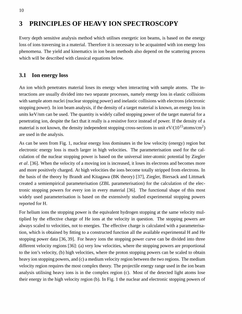
As can be seen from Fig. 1, nuclear energy loss dominates in the low velocity (energy) region but
electronic energy loss is much larger in high velocities. The parameterisation used for the cal-
culation of the nuclear stopping power is based on the universal inter-atomic potential by Ziegler
et al. [36]. When the velocity of a moving ion is increased, it loses its electrons and becomes more
and more positively charged. At high velocities the ions become totally stripped from electrons. In
the basis of the theory by Brandt and Kitagawa (BK theory) [37], Ziegler, Biersack and Littmark
created a semiempirical parameterisation (ZBL parameterisation) for the calculation of the elec-
tronic stopping powers for every ion in every material [36]. The functional shape of this most
widely used parameterisation is based on the extensively studied experimental stopping powers
reported for H.
For helium ions the stopping power is the equivalent hydrogen stopping at the same velocity mul-
tiplied by the effective charge of He ions at the velocity in question. The stopping powers are
always scaled to velocities, not to energies. The effective charge is calculated with a parameterisa-
tion, which is obtained by fitting to a constructed function all the available experimental H and He
stopping power data [36, 39]. For heavy ions the stopping power curve can be divided into three
different velocity regions [36]: (a) very low velocities, where the stopping powers are proportional
to the ion’s velocity, (b) high velocities, where the proton stopping powers can be scaled to obtain
heavy ion stopping powers, and (c) a medium velocity region between the two regions. The medium
velocity region requires the most complex theory. The projectile energy range used in the ion beam
analysis utilising heavy ions is in the complex region (c). Most of the detected light atoms lose
their energy in the high velocity region (b). In Fig. 1 the nuclear and electronic stopping powers of
11
10-2 10-1 100 101 102
Energy (MeV)
10-1
100
101
Sto
ppin
gpo
wer
(keV
/nm
)
Sn(35Cl)
Sn(79Br)
Sn(127I)
Sn(197Au)
Sel(35Cl)
Sel(79Br)
Sel(127I)
Sel(197Au)
Figure 1: Nuclear (Sn) and electronic (Sel) stopping powers of silicon for the 35Cl, 79Br, 127I, and197Au ions calculated using the ZBL parameterisation [36, 38]. The energy region relevant in theTOF-ERD analysis in the Accelerator Laboratory is shadowed.
silicon are plotted for 35Cl, 79Br, 127I, and 197Au ions in the energy range of 0.01–500 MeV in the
framework of the ZBL-parameterisation. These ions have been utilised in this thesis, and they are
the most used ones in HI-ERDA in the literature.
As there is no first-principles theory to calculate the stopping powers, more experimental stopping
power data are required for different ion-material combinations. The data can then be used in the
fittings to the semiempirical models to increase the accuracy of the stopping powers reproduced
by the ZBL model. The inaccuracy of the ZBL parameterisation for heavy ions can be as high as
20% [40]. The reason for the uncertainties are the incorrect shapes of the functions used in the
fittings and the large scattering of the experimental data.
In the Accelerator Laboratory, techniques have been developed to measure the electronic stopping
powers by means of the inverted Doppler shift attenuation method (IDSA). The velocity depen-
dency of the stopping powers has been obtained for Mg [41, 42], Si [40, 43], and P ions [43]. To
fulfill the growing need for heavy ion stopping cross-sections in various materials, a novel method
has recently been introduced by Zhang et al , where a TOF-E telescope was utilised to measure the
stopping powers of self-supporting films for a variety of ions [44,45] and over a wide energy range.
The same method was simultaneously independently used by Trzaska et al [46, 47].
12
MI
θ
φ
E
E
R R
M
R
R
I IM Z
M ZI 2 E
0I
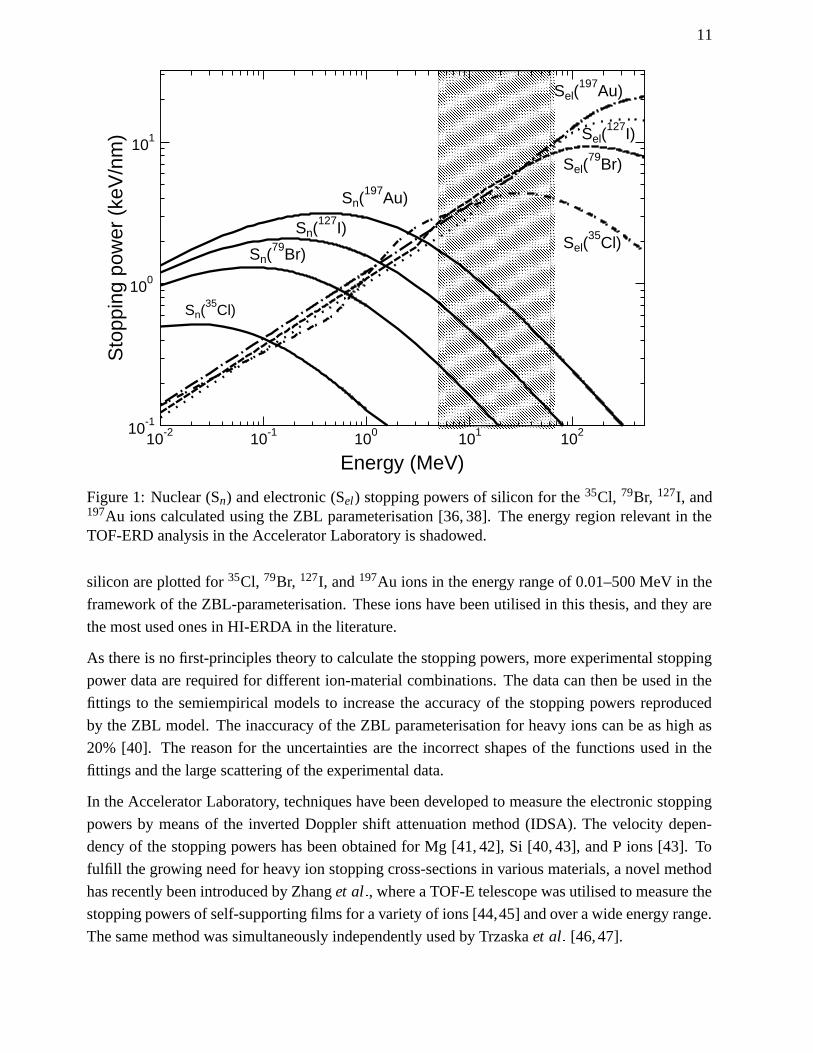
Figure 2: Schematic picture of a heavy ion elastic scattering. The subscripts I and R denote theincident and recoil ions, respectively.
Due to the statistical fluctuations in the number of collision processes, energy spread or energy
straggling is also present during the slowing down. On the basis of a fitting function by Chu [48],
Yang et al performed a fit to the experimental straggling data for H, He, and heavy ions [49]. The
deduced parameterisation applies only to the energy loss and does not include the angular spread.
The surface layers in ion beam analysis mostly contain more than one element. For calculating
stopping power of the samples of compound materials an additivity rule by Bragg and Kleeman is
applied [50]. According to this Braggs rule, the stopping cross-sections of elements multiplied by
their atomic concentration percentage in a compound are added to get the stopping cross-section
of the compound. This simplified approximation does not take into account the realistic electron
densities of the compound matter.
Despite the need for accurate stopping power data of compounds, not many publications are found
on the topic in the literature. One reason is the fact that the preparation of representative self-
supporting thin films out of compounds is difficult in most cases and the conventional transmission
method is difficult to use for the stopping power measurements. In this method the ion energy
loss in a self-supporting film is measured, and area and mass of the film are determined and the
stopping cross-section is deduced. The IDSA measurements can be done well for bulk samples,
and the stopping powers can be obtained, as is indicated by an example for Si in ceramics [51].
3.2 Scattering kinematics and scattering cross section
In ERDA the scattering of an energetic ion with a sample atom is regarded as a classical two-
body collision where the only force present is the Coulomb repulsion between two bare nuclei
as illustrated in Fig. 2. In an elastic collision the energy and momentum are conserved and the
13
final energy of both the projectile and the target atom can be calculated exactly. In the laboratory
coordinates the final energy of a target atom with the mass MR hit by a projectile with the mass MI
and energy EI is obtained from the following equation:
ER 4MIMR cos2 φ
MI MR 2 EI0 ΛEI0 (1)
where φ is the recoil angle and Λ is called the kinematic factor. Similarly, a projectile scattered to
the angle θ has an energy of
EI2 EI0 ER
M2R M2
I sin2 θ MI cosθ
MI MR 2
EI0 K1EI0 (2)
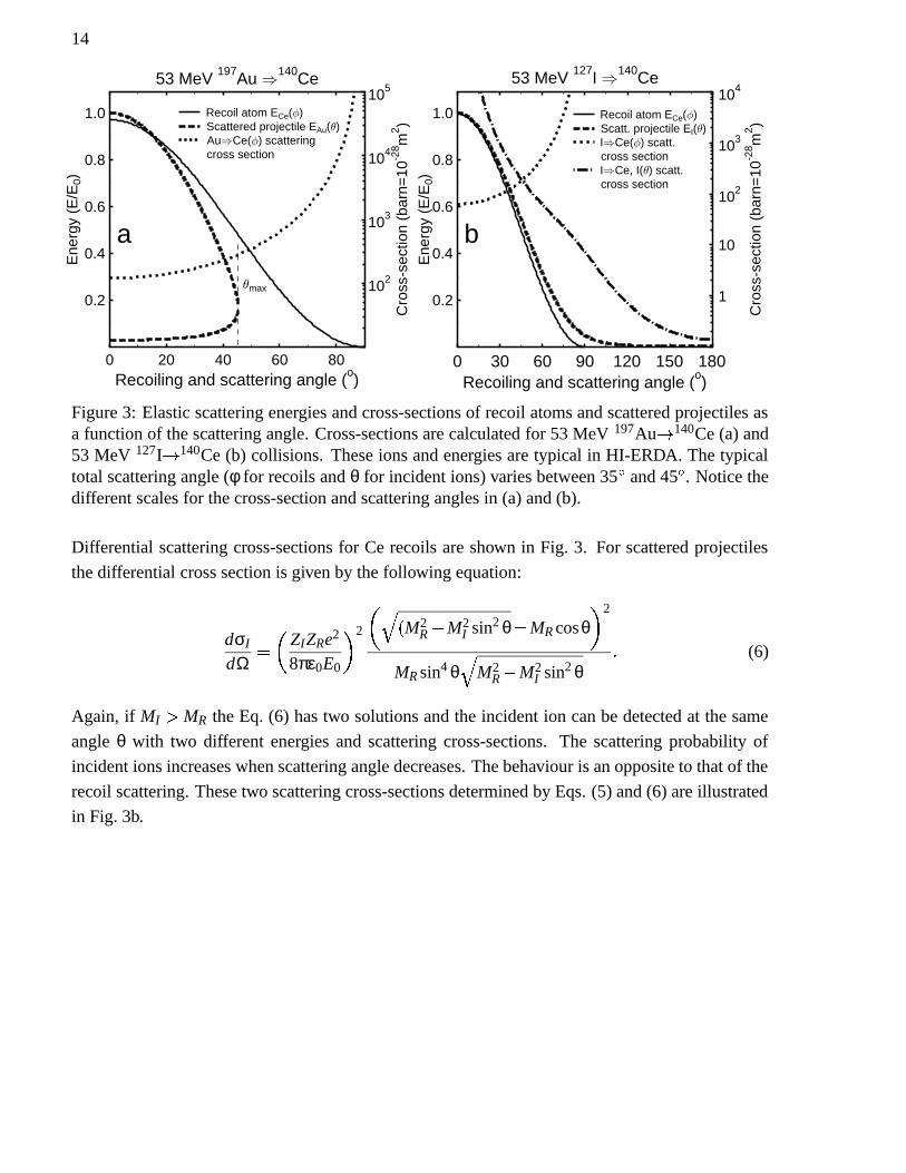
If MI MR, the equation has two solutions as illustrated in Fig. 3a, where the final energies of
both the 140Ce recoil and the 197Au projectile are drawn as a function of the scattering angle. The
two solutions in the Eq. (2) denote that the incident 197Au ions may scatter to the angle θ with
two different energies. When MI MR, the maximum scattering angle θmax is determined by the
positive solution of the square root in Eq. (2) and
θmax arcsin
MR
MI (3)
If the heaviest element in the sample is 140Ce, the maximum angle for the direct scattering of a197Au projectile is 45.3 . If MI MR the numerator in Eq. (2) is a sum. This is illustrated in Fig. 3b,
where the final energies of the 127I projectile and 140Ce recoil atom are drawn as a function of the
scattering angle. The elastic scattering cross-sections or scattering probabilities can be deduced by
using the Coulomb potential
Vr 1
4πε0
ZIZRe2
r (4)
where e is the unit of the electrical charge, ε0 the permittivity for a vacuum, and Z1 and ZR are
atomic numbers of the projectile and the recoil atom, respectively. If the scattering occurs within
the radius of K-shell electrons, it can be treated as a pure Coulomb scattering. This scattering is
also often called the Rutherford scattering contrary to scatterings between two nuclei shadowed by
electrons in the low energy region or two nuclei approaching so close to each other in high energy
collisions that the nuclear force affects the scattering cross-section. In the laboratory coordinates
the differential cross-section for recoil atoms is
dσR
dΩ ZIZRe2
8πε0E0 2 1 MI MR 2
cos3 φ (5)
14
0 20 40 60 80Recoiling and scattering angle (o)
0.2
0.4
0.6
0.8
1.0
Ene
rgy
(E/E
0)53 MeV 197Au 140Ce
cross sectionAu Ce( ) scatteringScattered projectile EAu( )Recoil atom ECe( )
max 102
103
104
105
Cro
ss-s
ectio
n(b
arn=
10-2
8 m2 )
0 30 60 90 120 150 180Recoiling and scattering angle (o)
0.2
0.4
0.6
0.8
1.0
Ene
rgy
(E/E
0)
53 MeV 127I 140Ce
cross sectionI Ce, I( ) scatt.cross sectionI Ce( ) scatt.Scatt. projectile EI( )Recoil atom ECe( )
a b
1
10
102
103
104
Cro
ss-s
ectio
n(b
arn=
10-2
8 m2 )
Figure 3: Elastic scattering energies and cross-sections of recoil atoms and scattered projectiles asa function of the scattering angle. Cross-sections are calculated for 53 MeV 197Au 140Ce (a) and53 MeV 127I 140Ce (b) collisions. These ions and energies are typical in HI-ERDA. The typicaltotal scattering angle (φ for recoils and θ for incident ions) varies between 35 and 45 . Notice thedifferent scales for the cross-section and scattering angles in (a) and (b).
Differential scattering cross-sections for Ce recoils are shown in Fig. 3. For scattered projectiles
the differential cross section is given by the following equation:
dσI
dΩ ZIZRe2
8πε0E0 2 M2
R M2I sin2 θ MR cosθ 2
MR sin4 θ M2R M2
I sin2 θ (6)
Again, if MI MR the Eq. (6) has two solutions and the incident ion can be detected at the same
angle θ with two different energies and scattering cross-sections. The scattering probability of
incident ions increases when scattering angle decreases. The behaviour is an opposite to that of the
recoil scattering. These two scattering cross-sections determined by Eqs. (5) and (6) are illustrated
in Fig. 3b.
15
4 PROGRESS IN TIME-OF-FLIGHT ELASTIC RECOIL DE-
TECTION MEASUREMENTS
The idea of ERDA is to detect forward scattered sample atoms and use the stopping power, scatter-
ing cross-section, and kinematics to determine the concentration distributions of different elements.
The the first measurements were performed using transmission geometry [3]. More attention at-
tracted a method where the projectiles went in and the recoils came out from the same side of the
sample (see Fig. 4) and the recoil energy spectrum was measured [52, 53]. With this setup it was
also possible to analyse other samples than self-supporting films.
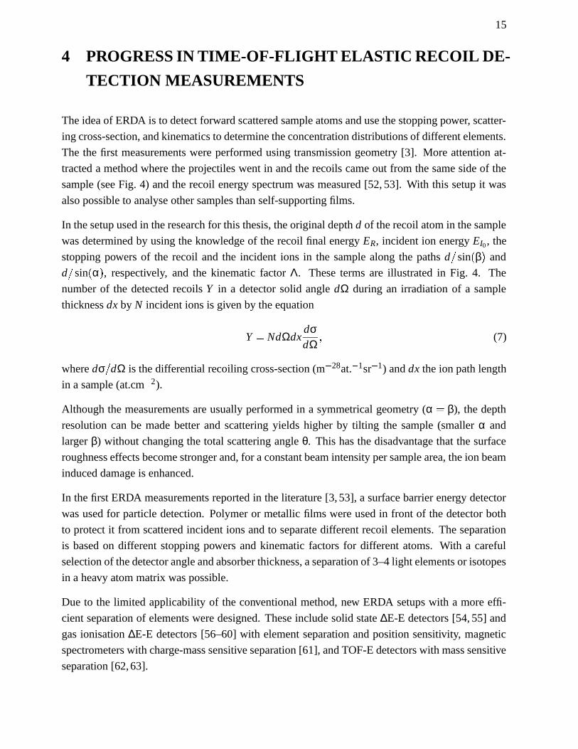
In the setup used in the research for this thesis, the original depth d of the recoil atom in the sample
was determined by using the knowledge of the recoil final energy ER, incident ion energy EI0 , the
stopping powers of the recoil and the incident ions in the sample along the paths d sinβ and
d sinα , respectively, and the kinematic factor Λ. These terms are illustrated in Fig. 4. The
number of the detected recoils Y in a detector solid angle dΩ during an irradiation of a sample
thickness dx by N incident ions is given by the equation
Y NdΩdxdσdΩ (7)
where dσ dΩ is the differential recoiling cross-section (m 28at.
1sr 1) and dx the ion path length
in a sample (at.cm 2).
Although the measurements are usually performed in a symmetrical geometry (α β), the depth
resolution can be made better and scattering yields higher by tilting the sample (smaller α and
larger β) without changing the total scattering angle θ. This has the disadvantage that the surface
roughness effects become stronger and, for a constant beam intensity per sample area, the ion beam
induced damage is enhanced.
In the first ERDA measurements reported in the literature [3, 53], a surface barrier energy detector
was used for particle detection. Polymer or metallic films were used in front of the detector both
to protect it from scattered incident ions and to separate different recoil elements. The separation
is based on different stopping powers and kinematic factors for different atoms. With a careful
selection of the detector angle and absorber thickness, a separation of 3–4 light elements or isotopes
in a heavy atom matrix was possible.
Due to the limited applicability of the conventional method, new ERDA setups with a more effi-
cient separation of elements were designed. These include solid state ∆E-E detectors [54, 55] and
gas ionisation ∆E-E detectors [56–60] with element separation and position sensitivity, magnetic
spectrometers with charge-mass sensitive separation [61], and TOF-E detectors with mass sensitive
separation [62, 63].
16
I0E
EI
R0E
ER
dr
rout
αβ surface
φ
Θ
in
sample
Figure 4: Scattering geometry of an ERDA experiment.
4.1 Setup in the Accelerator Laboratory
There are a number of different measurement setups for TOF-ERDA. For instance, the time of flight
can be determined by means of two identical timing gates [63–66] or an energy detector can be used
to obtain the timing signal [62, 67]. The energy spectra are usually deduced from TOF-spectra,
because TOF-detector has a linear calibration for all ions. The calibration is also independent of
the irradiation damage, in contrary to charged particle detectors. The energy resolution of the TOF-
detector for heavy ions is better and for light ions like C, N, and O of the same order than that
of charged particle detector. A solitary high energy resolution TOF-detector can also be used in
forward or backscattering geometry [68].
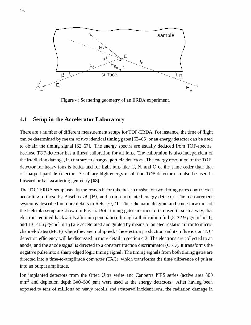
The TOF-ERDA setup used in the research for this thesis consists of two timing gates constructed
according to those by Busch et al [69] and an ion implanted energy detector. The measurement
system is described in more details in Refs. 70, 71. The schematic diagram and some measures of
the Helsinki setup are shown in Fig. 5. Both timing gates are most often used in such a way, that
electrons emitted backwards after ion penetration through a thin carbon foil (5–22.9 µg/cm2 in T1
and 10–21.6 µg/cm2 in T2) are accelerated and guided by means of an electrostatic mirror to micro-
channel-plates (MCP) where they are multiplied. The electron production and its influence on TOF
detection efficiency will be discussed in more detail in section 4.2. The electrons are collected to an
anode, and the anode signal is directed to a constant fraction discriminator (CFD). It transforms the
negative pulse into a sharp edged logic timing signal. The timing signals from both timing gates are
directed into a time-to-amplitude converter (TAC), which transforms the time difference of pulses
into an output amplitude.
Ion implanted detectors from the Ortec Ultra series and Canberra PIPS series (active area 300
mm2 and depletion depth 300–500 µm) were used as the energy detectors. After having been
exposed to tens of millions of heavy recoils and scattered incident ions, the radiation damage in
17
! ! ! !! ! ! ! ! ! !! ! ! ! ! ! ! ! !! ! ! ! ! ! ! !! ! ! ! !! !" " "" " " " " "" " " " " " " " "" " " " " " " "" " " " "" "# # # ## # # # # ## # # # # # # # ## # # # # # # ## # # # ## #$ $ $$ $ $ $ $ $$ $ $ $ $ $ $ $ $$ $ $ $ $ $ $ $$ $ $ $ $$ $% % % %% % % % % % %% % % % % % % % % %% % % % % % % % % % %% % % % % % % % % %% % % % % % %% % % % %%& & && & & & & && & & & & & & & && & & & & & & & & & && & & & & & & & & && & & & & & && & & &&' ' ' '' ' ' ' ' ' '' ' ' ' ' ' ' ' '' ' ' ' ' ' ' '' ' ' ' '' '( ( (( ( ( ( ( (( ( ( ( ( ( ( ( (( ( ( ( ( ( ( (( ( ( ( (( () ) ) )) ) ) ) ) ) )) ) ) ) ) ) ) ) )) ) ) ) ) ) ) )) ) ) ) )) )* * ** * * * * ** * * * * * * * ** * * * * * * ** * * * ** *
T2
T1
488 mm310 mm
E
71 mm
684 mm
Sample
Heavy ion
Figure 5: Schematic picture of the TOF-ERDA setup. The solid angle of the system, 0.18 mSr,is restricted by the circular aperture (18 mm in diameter) of the frame of the carbon foil in thesecond timing gate (T2), located at 1172 mm from the sample. The solid angle of the first detectoris reduced with an extra aperture (7 mm in diameter) located at 310 mm from the sample to reducethe amount of insignificant counts (outside T2 solid angle, electron induced, etc.) in the first timinggate.
the detector deteriorates the energy resolution and increases the leakage current. In contrast to
surface barrier detectors, ion implanted detectors can be annealed (2 hours in air at 200 C) and
their original performance restored. A normal preamplifier (Ortec 142) and an amplifier (Tennelec
TC 242) chain was used to amplify analog pulses, and both time and energy pulse-height signals
were converted into digital ones in Canberra analog-to-digital converters (ADC) and recorded with
a Canberra MPA/PC multiparameter system.
In most of the existing TOF-ERDA setups the signal from the first timing gate is delayed for a
few hundred nanoseconds, and the signal from the second gate is used as a start signal. This
arrangement is motivated by the lower false event count rate of the second detector. On the other
hand, long delay cables increase the noise in the TOF detector and degenerate the TOF resolution.
This was tested by taking delayed TOF, direct TOF, and energy signals at the same time. Direct
TOF signals are used today because they have a better time resolution and no events are lost at
normal count rates (less than 1000 Hz). The situation would be different if the count rate of false
events were higher at the first timing gate, for instance due to the aging of the MCP.
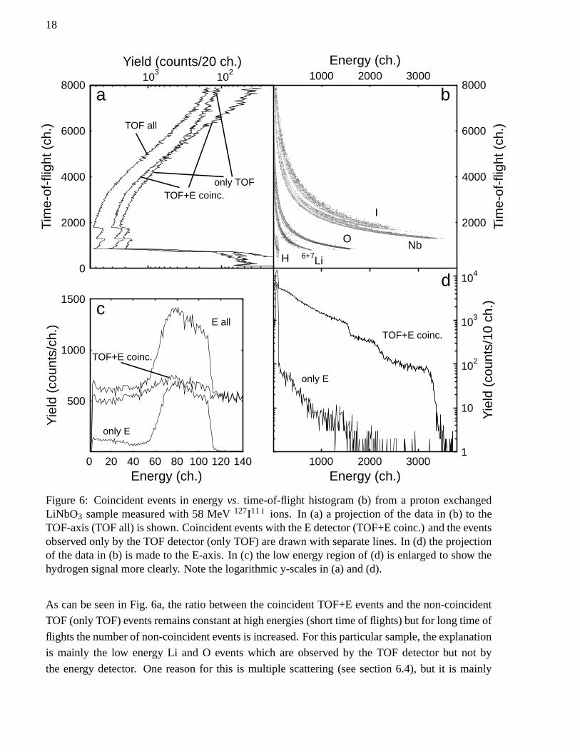
An example of TOF-E data is shown in Fig. 6. The data is from a study in which the time and
temperature dependency of the proton exchange in LiNbO3 was studied [34]. This optical wave
guide material was measured using 58 MeV 127I11 + ions. Fig. 6a shows the projection of the
histogram in Fig. 6b to the TOF axis. Fig. 6c shows a low energy area magnification of the energy-
axis projection in Fig. 6d. The measurements were done in the coincident and non-coincident
modes. TOF and E events appearing at a maximum of 2.1 µs from each other were collected in
coincidence and the events outside this limit where marked as non-coincident events.
18
1000 2000 3000Energy (ch.)
2000
4000
6000
8000
Tim
e-of
-flig
ht(c
h.)
2000
4000
6000
8000
0
Tim
e-of
-flig
ht(c
h.)
Yield (counts/20 ch.)
251022510325
1000 2000 3000Energy (ch.)
1
10
102
103
104
Yie
ld(c
ount
s/10
ch.)
20 40 60 80 100 120 1400Energy (ch.)
500
1000
1500
Yie
ld(c
ount
s/ch
.)
NbO
6+7LiH
I
103 102
TOF all
TOF+E coinc.only TOF
TOF+E coinc.
only E
TOF+E coinc.
E all
only E
a b
c
d
Figure 6: Coincident events in energy vs time-of-flight histogram (b) from a proton exchangedLiNbO3 sample measured with 58 MeV 127I11 + ions. In (a) a projection of the data in (b) to theTOF-axis (TOF all) is shown. Coincident events with the E detector (TOF+E coinc.) and the eventsobserved only by the TOF detector (only TOF) are drawn with separate lines. In (d) the projectionof the data in (b) is made to the E-axis. In (c) the low energy region of (d) is enlarged to show thehydrogen signal more clearly. Note the logarithmic y-scales in (a) and (d).
As can be seen in Fig. 6a, the ratio between the coincident TOF+E events and the non-coincident
TOF (only TOF) events remains constant at high energies (short time of flights) but for long time of
flights the number of non-coincident events is increased. For this particular sample, the explanation
is mainly the low energy Li and O events which are observed by the TOF detector but not by
the energy detector. One reason for this is multiple scattering (see section 6.4), but it is mainly
19
due to the low energy discrimination of the energy detector. The ratio of the short flight times
is proportional to the ratio of the solid angles of the aperture in front of the first timing gate and
aperture carrying the carbon foil in the second timing gate.
As can be seen in Fig. 6d, the number of non-coincident events in the energy detector (only E) is
very low for heavy elements and high energies. However, for hydrogen the TOF detection efficiency
is strongly energy dependent (as is discussed in more detail in section 4.2) and the amount of non-
coincident events is high.
4.2 Detection efficiency
The ERDA techniques combined with a TOF-E telescope provide a very useful tool for quantitative
elemental depth profiling for all the elements in almost any matrix. The detection efficiency of our
TOF-E telescope was studied in paper I. This section presents the main results obtained and some
further studies closely related to detection efficiency.
4.2.1 Electron emission and multiplication
In an ideal TOF-E telescope every ion within the solid angle of the detector creates a signal in the
timing gates and the energy detector. For light element recoils this is restricted by the detection
efficiency of the TOF detector lower than 100%. This is due to the low electron emission in the
carbon foils of the timing gate. For H and He ions the electronic stopping powers are so low that
only a few electrons are emitted from the carbon foils [72]. One possible solution to step up the
electron emission is to increase the thickness of the carbon foil. As observed by Koschar et al [73], the secondary electron yields for 12 MeV 12C ions are saturated for carbon foil thicknesses
over 15 µg/cm2. However, at the thickness of 5 µg/cm2 the electron emission reaches 80% of its
maximum for 12 MeV 12C ions. In addition to energy loss, electron emission is also dependent on
the charge state of the passing ion. In the research for this thesis the thinnest carbon foils used were
5 µg/cm2 thick. The same detection efficiencies were obtained for them as for 22 µg/cm2 thick
foils. Also much thinner carbon foils have been used by other groups [68, 74, 75], but the films
were diamond-like carbon (DLC) films.
In Fig. 7a the dependency of the detection efficiency on the electronic stopping power is plotted for
light ions. The detection efficiency of the charged particle detector is presumed to be 100% in the
energy range of this study. According to the Sternglass theory [76], the mean number of ejected
secondary electrons is proportional to the electronic stopping power. The relation between the
MCP signals and stopping power can be seen in Fig. 7b, where the MCP signal height and stopping
power are plotted as a function of the energy of 11B ions passing the carbon foil. When compared to
the SRIM2000 stopping power of carbon for 11B, the shape of the MCP signal is narrower and the
maximum is at a much lower energy. The energy dependency of the measured MCP signals agrees
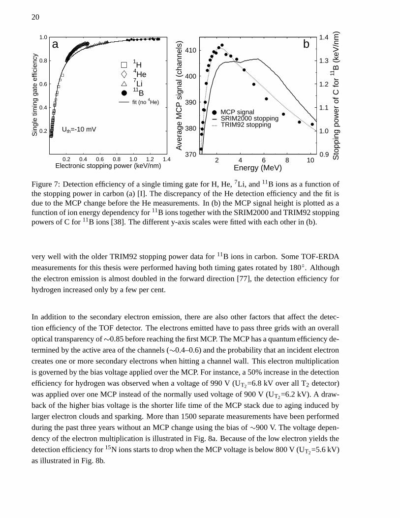
20
0.2 0.4 0.6 0.8 1.0 1.2 1.4Electronic stopping power (keV/nm)
0.2
0.4
0.6
0.8
1.0
Uth=-10 mV
Sin
gle
timin
gga
teef
ficie
ncy
11B
7Li
4He
1H
fit (no 4He)
2 4 6 8 10Energy (MeV)
370
380
390
400
410
Ave
rage
MC
Psi
gnal
(cha
nnel
s)
0.9
1.0
1.1
1.2
1.3
1.4
Sto
ppin
gpo
wer
ofC
for
11B
(keV
/nm
)
a b
MCP signalSRIM2000 stoppingTRIM92 stopping
Figure 7: Detection efficiency of a single timing gate for H, He, 7Li, and 11B ions as a function ofthe stopping power in carbon (a) [I]. The discrepancy of the He detection efficiency and the fit isdue to the MCP change before the He measurements. In (b) the MCP signal height is plotted as afunction of ion energy dependency for 11B ions together with the SRIM2000 and TRIM92 stoppingpowers of C for 11B ions [38]. The different y-axis scales were fitted with each other in (b).
very well with the older TRIM92 stopping power data for 11B ions in carbon. Some TOF-ERDA
measurements for this thesis were performed having both timing gates rotated by 180 . Although
the electron emission is almost doubled in the forward direction [77], the detection efficiency for
hydrogen increased only by a few per cent.
In addition to the secondary electron emission, there are also other factors that affect the detec-
tion efficiency of the TOF detector. The electrons emitted have to pass three grids with an overall
optical transparency of , 0.85 before reaching the first MCP. The MCP has a quantum efficiency de-
termined by the active area of the channels ( , 0.4–0.6) and the probability that an incident electron
creates one or more secondary electrons when hitting a channel wall. This electron multiplication
is governed by the bias voltage applied over the MCP. For instance, a 50% increase in the detection
efficiency for hydrogen was observed when a voltage of 990 V (UT2=6.8 kV over all T2 detector)
was applied over one MCP instead of the normally used voltage of 900 V (UT2=6.2 kV). A draw-
back of the higher bias voltage is the shorter life time of the MCP stack due to aging induced by
larger electron clouds and sparking. More than 1500 separate measurements have been performed
during the past three years without an MCP change using the bias of , 900 V. The voltage depen-
dency of the electron multiplication is illustrated in Fig. 8a. Because of the low electron yields the
detection efficiency for 15N ions starts to drop when the MCP voltage is below 800 V (UT2=5.6 kV)
as illustrated in Fig. 8b.
21
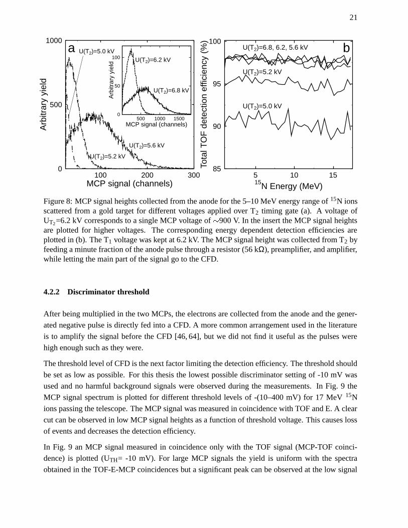
5 10 1515N Energy (MeV)
85
90
95
100
Tota
lTO
Fde
tect
ion
effic
ienc
y(%
)
100 200 300MCP signal (channels)
0
500
1000A
rbitr
ary
yiel
d
500 1000 1500MCP signal (channels)
0
50
100
Arb
itrar
yyi
eld
a bU(T2)=6.8, 6.2, 5.6 kV
U(T2)=5.2 kV
U(T2)=5.0 kV
U(T2)=5.0 kV
U(T2)=5.2 kV
U(T2)=5.6 kV
U(T2)=6.2 kV
U(T2)=6.8 kV
Figure 8: MCP signal heights collected from the anode for the 5–10 MeV energy range of 15N ionsscattered from a gold target for different voltages applied over T2 timing gate (a). A voltage ofUT2=6.2 kV corresponds to a single MCP voltage of , 900 V. In the insert the MCP signal heightsare plotted for higher voltages. The corresponding energy dependent detection efficiencies areplotted in (b). The T1 voltage was kept at 6.2 kV. The MCP signal height was collected from T2 byfeeding a minute fraction of the anode pulse through a resistor (56 kΩ), preamplifier, and amplifier,while letting the main part of the signal go to the CFD.
4.2.2 Discriminator threshold
After being multiplied in the two MCPs, the electrons are collected from the anode and the gener-
ated negative pulse is directly fed into a CFD. A more common arrangement used in the literature
is to amplify the signal before the CFD [46, 64], but we did not find it useful as the pulses were
high enough such as they were.
The threshold level of CFD is the next factor limiting the detection efficiency. The threshold should
be set as low as possible. For this thesis the lowest possible discriminator setting of -10 mV was
used and no harmful background signals were observed during the measurements. In Fig. 9 the
MCP signal spectrum is plotted for different threshold levels of -(10–400 mV) for 17 MeV 15N
ions passing the telescope. The MCP signal was measured in coincidence with TOF and E. A clear
cut can be observed in low MCP signal heights as a function of threshold voltage. This causes loss
of events and decreases the detection efficiency.
In Fig. 9 an MCP signal measured in coincidence only with the TOF signal (MCP-TOF coinci-
dence) is plotted (UTH= -10 mV). For large MCP signals the yield is uniform with the spectra
obtained in the TOF-E-MCP coincidences but a significant peak can be observed at the low signal
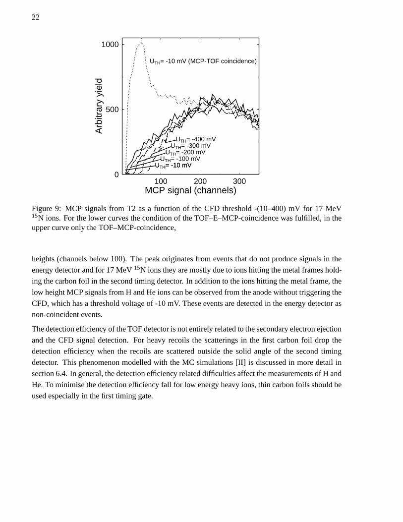
22
100 200 300MCP signal (channels)
0
500
1000
Arb
itrar
yyi
eld
UTH= -10 mVUTH= -100 mV
UTH= -200 mVUTH= -300 mV
UTH= -400 mV
UTH= -10 mV
UTH= -10 mV (MCP-TOF coincidence)
Figure 9: MCP signals from T2 as a function of the CFD threshold -(10–400) mV for 17 MeV15N ions. For the lower curves the condition of the TOF–E–MCP-coincidence was fulfilled, in theupper curve only the TOF–MCP-coincidence,
heights (channels below 100). The peak originates from events that do not produce signals in the
energy detector and for 17 MeV 15N ions they are mostly due to ions hitting the metal frames hold-
ing the carbon foil in the second timing detector. In addition to the ions hitting the metal frame, the
low height MCP signals from H and He ions can be observed from the anode without triggering the
CFD, which has a threshold voltage of -10 mV. These events are detected in the energy detector as
non-coincident events.
The detection efficiency of the TOF detector is not entirely related to the secondary electron ejection
and the CFD signal detection. For heavy recoils the scatterings in the first carbon foil drop the
detection efficiency when the recoils are scattered outside the solid angle of the second timing
detector. This phenomenon modelled with the MC simulations [II] is discussed in more detail in
section 6.4. In general, the detection efficiency related difficulties affect the measurements of H and
He. To minimise the detection efficiency fall for low energy heavy ions, thin carbon foils should be
used especially in the first timing gate.
23
4.3 Hydrogen analysis
A low detection efficiency for hydrogen is a serious problem for TOF detectors [62,65,78] because
hydrogen is one of the most regular and crucial impurities in thin films and semiconductor materials.
Therefore, much effort has been expended to detect it with different ion beam analysis methods.
A method used extensively for hydrogen detection is nuclear reaction analysis (NRA) utilising the
reaction 1H(15N,αγ)12C. This is a very sensitive method with a good depth resolution for hydrogen
profiling [79–81]. Yet a determination of the absolute hydrogen concentration requires the use of
hydrogen standards and detailed measurements are time-consuming.
For the detection of hydrogen in TOF-ERDA measurements a charged-particle detector specific
to hydrogen profiling has been used [82]. Undesired recoiled and scattered ions are avoided by
placing an absorber foil in front of the detector. Such an absorber thickness is chosen that only
light ions can pass the foil. A drawback of this method is decreased energy resolution due to the
energy straggling of ions in the absorber foil.
A setup consisting of a transmission energy detector (∆E) and a residual energy (E) detector can
be used as was done by Wielunski et al [83]. As the energy loss in the ∆E detector is isotope
dependent, different isotopes can easily be separated by plotting the events in a ∆E,E histogram. If a
light projectile like He is used, the low stopping power deteriorates the depth resolution to 40–50 nm
depending on the matrix [83]. For quantitative results, this setup requires the use of a standard
sample with a known hydrogen isotope concentration or simultaneous RBS measurements [83].
Another common approach is to measure the detection efficiency of a TOF detector for different
elements and use the efficiencies to normalize the measured energy spectra for hydrogen [84]. No
additional detector is required and the normalization is easy to do. However, as the efficiencies
for high-energy H ions can be quite low (<10%), the counting statistics becomes a problem. In
addition, any change in the detection efficiency affect the determination of the hydrogen content.
The detection efficiency can change for instance due to the aging of the MCPs and drift in the high
voltages applied to the timing gates.
A highly improved method was developed for this thesis. It resembles an approach which combines
charged-particle and gas-ionisation detectors [56–60]. The main idea behind it becomes evident
from Fig. 6c. Instead of only measuring the coincident events of the TOF and energy detectors,
the data are selected to include also the non-coincident events. By taking advantage of the fact that
the TOF detection efficiency for other recoils than hydrogen is close to 100%, the non-coincident
events in the energy detector are mainly from hydrogen recoils. By adding the coincident and non-
coincident events a 100% detection efficiency is obtained for hydrogen. However, another condition
has to be fulfilled: the maximum flight time has to be long enough for even the low energy heavy
recoils and scattered ions to traverse the flight path during it. In our detector with the flight path of
684 mm, a 500 ns wide time window was found to be suitable. A broader time window would create
noise events and limit the count rate. Too narrow a time window would leave low energy heavy ions
24
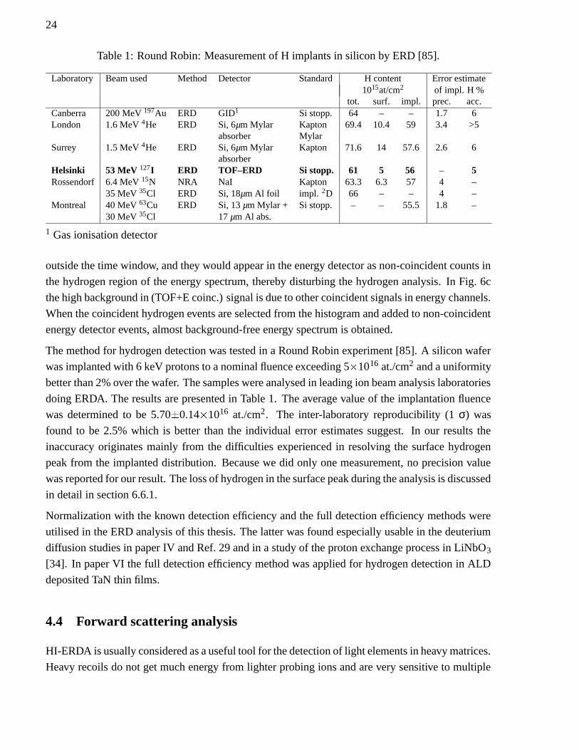
Table 1: Round Robin: Measurement of H implants in silicon by ERD [85].
Laboratory Beam used Method Detector Standard H content Error estimate1015at/cm2 of impl. H %
tot. surf. impl. prec. acc.Canberra 200 MeV 197Au ERD GID1 Si stopp. 64 – – 1.7 6London 1.6 MeV 4He ERD Si, 6µm Mylar Kapton 69.4 10.4 59 3.4 >5
absorber MylarSurrey 1.5 MeV 4He ERD Si, 6µm Mylar Kapton 71.6 14 57.6 2.6 6
absorberHelsinki 53 MeV 127I ERD TOF–ERD Si stopp. 61 5 56 – 5Rossendorf 6.4 MeV 15N NRA NaI Kapton 63.3 6.3 57 4 –
35 MeV 35Cl ERD Si, 18µm Al foil impl. 2D 66 – – 4 –Montreal 40 MeV 63Cu ERD Si, 13 µm Mylar + Si stopp. – – 55.5 1.8 –
30 MeV 35Cl 17 µm Al abs.
1 Gas ionisation detector
outside the time window, and they would appear in the energy detector as non-coincident counts in
the hydrogen region of the energy spectrum, thereby disturbing the hydrogen analysis. In Fig. 6c
the high background in (TOF+E coinc.) signal is due to other coincident signals in energy channels.
When the coincident hydrogen events are selected from the histogram and added to non-coincident
energy detector events, almost background-free energy spectrum is obtained.
The method for hydrogen detection was tested in a Round Robin experiment [85]. A silicon wafer
was implanted with 6 keV protons to a nominal fluence exceeding 5 - 1016 at./cm2 and a uniformity
better than 2% over the wafer. The samples were analysed in leading ion beam analysis laboratories
doing ERDA. The results are presented in Table 1. The average value of the implantation fluence
was determined to be 5.70 0.14 - 1016 at./cm2. The inter-laboratory reproducibility (1 σ) was
found to be 2.5% which is better than the individual error estimates suggest. In our results the
inaccuracy originates mainly from the difficulties experienced in resolving the surface hydrogen
peak from the implanted distribution. Because we did only one measurement, no precision value
was reported for our result. The loss of hydrogen in the surface peak during the analysis is discussed
in detail in section 6.6.1.
Normalization with the known detection efficiency and the full detection efficiency methods were
utilised in the ERD analysis of this thesis. The latter was found especially usable in the deuterium
diffusion studies in paper IV and Ref. 29 and in a study of the proton exchange process in LiNbO3
[34]. In paper VI the full detection efficiency method was applied for hydrogen detection in ALD
deposited TaN thin films.
4.4 Forward scattering analysis
HI-ERDA is usually considered as a useful tool for the detection of light elements in heavy matrices.
Heavy recoils do not get much energy from lighter probing ions and are very sensitive to multiple
25
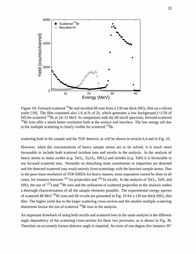
10 20 30 40Energy (MeV)
0
2000
4000
6000
Yie
ld(c
ount
s/ch
anne
l)
Recoiled HfScattered 79Br
Figure 10: Forward scattered 79Br and recoiled Hf ions from a 130 nm thick HfO2 film on a siliconwafer [18]. The film contained also 1.6 at.% of Zr, which generates a low background (<1/50 ofHf) for scattered 79Br at 24–31 MeV. In comparison with the Hf recoil spectrum, forward scattered79Br ions offer a much better resolution both at the surface and interface. The low energy tail dueto the multiple scattering is clearly visible for scattered 79Br.
scattering both in the sample and the TOF detector, as will be shown in section 6.4 and in Fig. 10.
However, when the concentrations of heavy sample atoms are to be solved, it is much more
favourable to include both scattered incident ions and recoils in the analysis. In the analysis of
heavy atoms in many oxides (e g TaO2, Ta2O5, HfO2) and nitrides (e g TaN) it is favourable to
use forward scattered ions. Normally no disturbing main constituents or impurities are detected
and the detected scattered ions result entirely from scatterings with the heaviest sample atoms. Due
to the poor mass resolution of TOF-ERDA for heavy masses, mass separation cannot be done in all
cases, for instance between 197Au projectiles and 181Ta recoils. In the analysis of TaO2, TaN, and
HfO2 the use of 127I and 79Br ions and the utilisation of scattered projectiles in the analysis makes
a thorough characterisation of all the sample elements possible. The experimental energy spectra
of scattered 48 MeV 79Br ions and Hf recoils are presented in Fig. 10 for a 130 nm thick HfO2 thin
film. The higher yield due to the larger scattering cross-section and the smaller multiple scattering
distortions favour the use of scattered 79Br ions in the analysis.
An important drawback of using both recoils and scattered ions in the same analysis is the different
angle dependency of the scattering cross-section for these two processes, as is shown in Fig. 3b.
Therefore an accurately known detector angle is required. An error of one degree (for instance 39
26
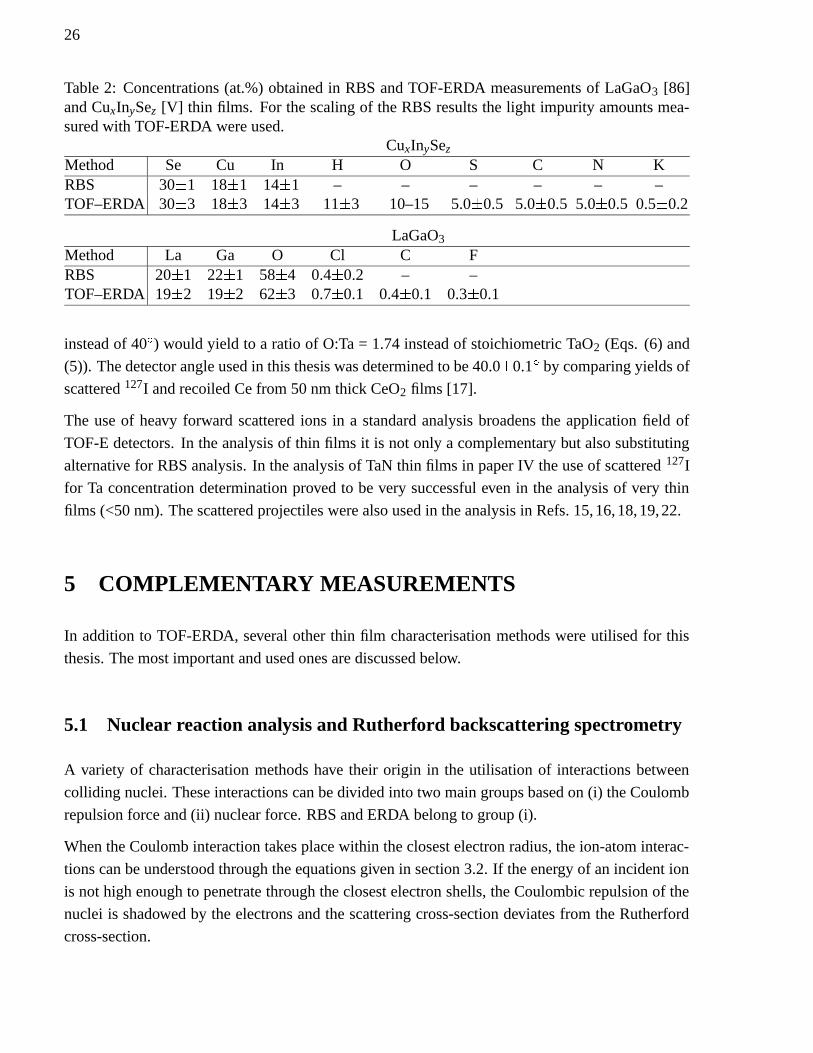
Table 2: Concentrations (at.%) obtained in RBS and TOF-ERDA measurements of LaGaO3 [86]and CuxInySez [V] thin films. For the scaling of the RBS results the light impurity amounts mea-sured with TOF-ERDA were used.
CuxInySez
Method Se Cu In H O S C N KRBS 30 1 18 1 14 1 – – – – – –TOF–ERDA 30 3 18 3 14 3 11 3 10–15 5.0 0.5 5.0 0.5 5.0 0.5 0.5 0.2
LaGaO3
Method La Ga O Cl C FRBS 20 1 22 1 58 4 0.4 0.2 – –TOF–ERDA 19 2 19 2 62 3 0.7 0.1 0.4 0.1 0.3 0.1
instead of 40 ) would yield to a ratio of O:Ta = 1.74 instead of stoichiometric TaO2 (Eqs. (6) and
(5)). The detector angle used in this thesis was determined to be 40.0 0.1 by comparing yields of
scattered 127I and recoiled Ce from 50 nm thick CeO2 films [17].
The use of heavy forward scattered ions in a standard analysis broadens the application field of
TOF-E detectors. In the analysis of thin films it is not only a complementary but also substituting
alternative for RBS analysis. In the analysis of TaN thin films in paper IV the use of scattered 127I
for Ta concentration determination proved to be very successful even in the analysis of very thin
films (<50 nm). The scattered projectiles were also used in the analysis in Refs. 15, 16, 18, 19, 22.
5 COMPLEMENTARY MEASUREMENTS
In addition to TOF-ERDA, several other thin film characterisation methods were utilised for this
thesis. The most important and used ones are discussed below.
5.1 Nuclear reaction analysis and Rutherford backscattering spectrometry
A variety of characterisation methods have their origin in the utilisation of interactions between
colliding nuclei. These interactions can be divided into two main groups based on (i) the Coulomb
repulsion force and (ii) nuclear force. RBS and ERDA belong to group (i).
When the Coulomb interaction takes place within the closest electron radius, the ion-atom interac-
tions can be understood through the equations given in section 3.2. If the energy of an incident ion
is not high enough to penetrate through the closest electron shells, the Coulombic repulsion of the
nuclei is shadowed by the electrons and the scattering cross-section deviates from the Rutherford
cross-section.
27
0 100 200 300Depth (nm)
0
10
20
30
40
50
60
70
Con
cent
ratio
n(a
t.%
)
CHClGaLaO
0 100 200 300Depth (nm)
0
10
20
30
40
50C
once
ntra
tion
(at.
%)
KCSNOHInCuSe
0.5 1.0 1.5 2.0
Scattered 4He ion energy (MeV)
0
2000
4000
6000
8000
10000
12000
Yie
ld(c
ount
s/ch
anne
l)
4.0 4.5 5.0 5.5
Scattered 4He ion energy (MeV)
0
500
1000
1500
Yie
ld(c
ount
s/ch
anne
l)
LaGaO3 CuxInySez
2 MeV He 6.5 MeV He
CuSe
Mo
In
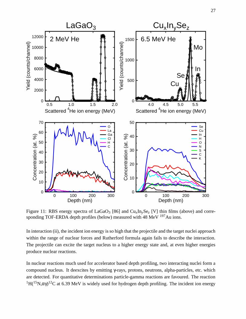
Figure 11: RBS energy spectra of LaGaO3 [86] and CuxInySez [V] thin films (above) and corre-sponding TOF-ERDA depth profiles (below) measured with 48 MeV 197Au ions.
In interaction (ii), the incident ion energy is so high that the projectile and the target nuclei approach
within the range of nuclear forces and Rutherford formula again fails to describe the interaction.
The projectile can excite the target nucleus to a higher energy state and, at even higher energies
produce nuclear reactions.
In nuclear reactions much used for accelerator based depth profiling, two interacting nuclei form a
compound nucleus. It deexcites by emitting γ-rays, protons, neutrons, alpha-particles, etc. which
are detected. For quantitative determinations particle-gamma reactions are favoured. The reaction1H(15N,αγ)12C at 6.39 MeV is widely used for hydrogen depth profiling. The incident ion energy
28
is changed in the vicinity of a very narrow resonance at 6.39 MeV (full width half maximum
120 30 eV [87]), and the amount of emitted 4.43 MeV gamma rays is detected as a function of
energy (depth) [79]. For particle-particle reactions, deuterium induced reactions are ones mostly
used in backscattering geometry; with them low concentration levels of light elements (from 2H
to O) can be detected. In all nuclear reaction methods a well characterised standard is needed and
careful incident ion fluence repetition is required for exact quantification.
In RBS, only the backscattered probing ion is detected, and the depth in which the scattering had
occurred can be calculated by means of scattering kinematics (Eq. 2) and stopping powers. In a
typical measurement geometry the energy detector is at an angle of 170 and the sample normal di-
rection tilted 175 with respect to the incoming beam. When homogeneous thin films with all film
elements detectable are measured, atomic concentrations can be calculated from the backscattering
yields according to the Rutherford scattering cross-sections, see Eq. (6). Moreover, the stopping
cross-sections of many materials for most commonly used hydrogen and helium ions are experi-
mentally well known.
Complementary RBS spectra and TOF-ERDA depth profiles of LaGaO3 [86] and CuxInySez [V]
thin films are presented in Fig. 11. The atomic concentrations of the same samples are presented in
Table 2. For this thesis, RBS was used in papers III,V, and VI, and in Refs. 20, 21, 27, 32, 33.
5.2 Other thin film characterisation methods
5.2.1 Secondary ion mass spectrometry
Secondary ion mass spectrometry (SIMS) is a very sensitive depth profiling method for all ele-
ments in a sample. In SIMS a focused ion beam (Ce + or O +2 ) is used to erode the studied sample
and the yields of different emitted sample ions are measured as a function of time. The time scale is
converted to a depth scale by measuring the depth of the produced crater and assuming a constant
erosion rate. SIMS is a very powerful tool for diffusion studies and depth profiling of low concen-
trations (below ppm levels) in homogeneous samples. For quantitative analysis, the use of either
specially prepared standard samples, for instance ion beam implanted [32], or well characterised
samples is required. In paper VI and Refs. 29, 30 the concentrations measured by TOF-ERDA
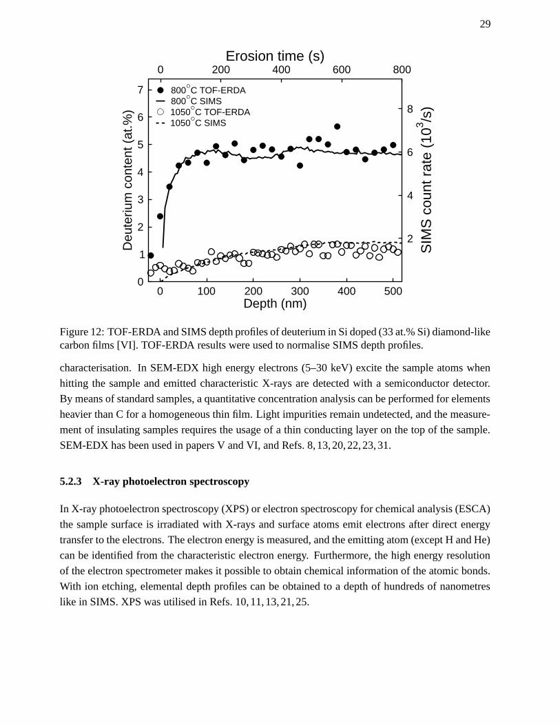
were used to normalise the SIMS results. This is illustrated in Fig. 12 in which both TOF-ERDA
and SIMS deuterium depth profiles in Si doped DLC films (33 at.% Si) are presented [VI]. In the
TOF-ERD analysis of the deuterium content the method described in section 4.3 was used.
5.2.2 Scanning electron microscopy
Scanning electron microscope (SEM) combined with energy dispersive X-ray detection (SEM-
EDX) has a wide dynamic scanning range, and its easy usage has made it a basic tool in materials
29
0 100 200 300 400 500Depth (nm)
0
1
2
3
4
5
6
7
Deu
teriu
mco
nten
t(at
.%)
0 200 400 600 800Erosion time (s)
2
4
6
8
SIM
Sco
untr
ate
(103 /s
)
1050 C SIMS1050 C TOF-ERDA800 C SIMS800 C TOF-ERDA
Figure 12: TOF-ERDA and SIMS depth profiles of deuterium in Si doped (33 at.% Si) diamond-likecarbon films [VI]. TOF-ERDA results were used to normalise SIMS depth profiles.
characterisation. In SEM-EDX high energy electrons (5–30 keV) excite the sample atoms when
hitting the sample and emitted characteristic X-rays are detected with a semiconductor detector.
By means of standard samples, a quantitative concentration analysis can be performed for elements
heavier than C for a homogeneous thin film. Light impurities remain undetected, and the measure-
ment of insulating samples requires the usage of a thin conducting layer on the top of the sample.
SEM-EDX has been used in papers V and VI, and Refs. 8, 13, 20, 22, 23, 31.
5.2.3 X-ray photoelectron spectroscopy
In X-ray photoelectron spectroscopy (XPS) or electron spectroscopy for chemical analysis (ESCA)
the sample surface is irradiated with X-rays and surface atoms emit electrons after direct energy
transfer to the electrons. The electron energy is measured, and the emitting atom (except H and He)
can be identified from the characteristic electron energy. Furthermore, the high energy resolution
of the electron spectrometer makes it possible to obtain chemical information of the atomic bonds.
With ion etching, elemental depth profiles can be obtained to a depth of hundreds of nanometres
like in SIMS. XPS was utilised in Refs. 10, 11, 13, 21, 25.
30
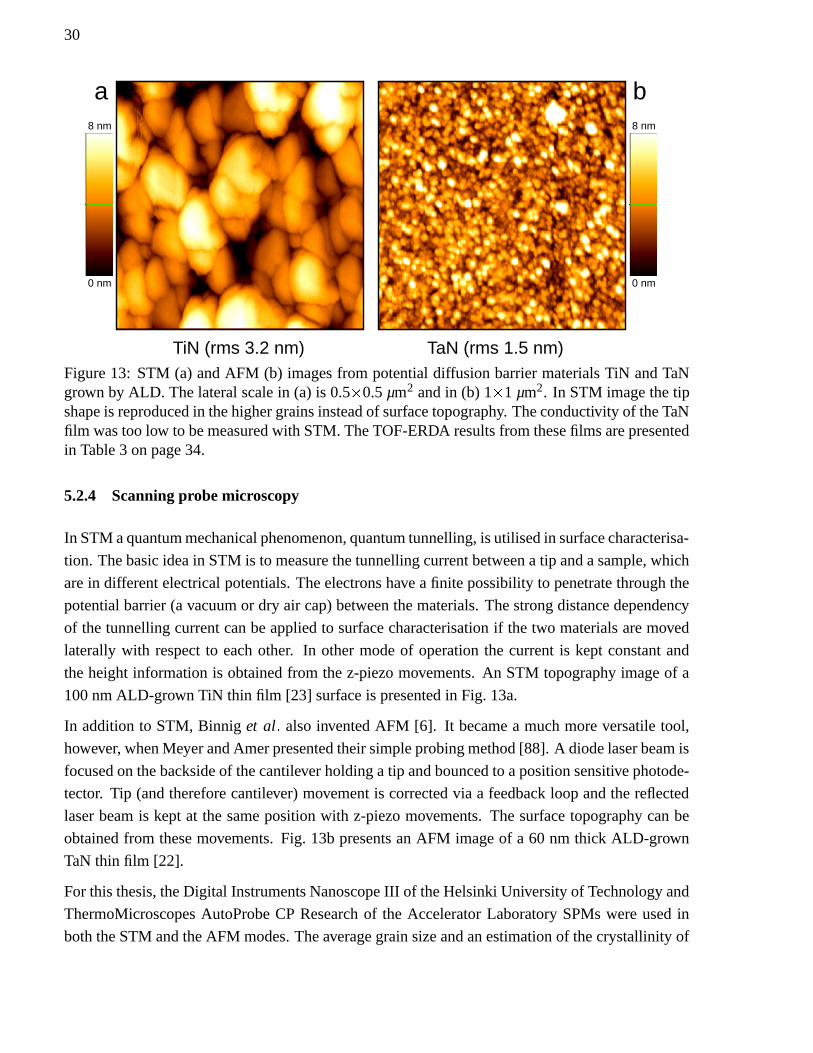
0 nm
8 nm
0 nm
8 nm
TiN (rms 3.2 nm) TaN (rms 1.5 nm)
a b
Figure 13: STM (a) and AFM (b) images from potential diffusion barrier materials TiN and TaNgrown by ALD. The lateral scale in (a) is 0.5 - 0.5 µm2 and in (b) 1 - 1 µm2. In STM image the tipshape is reproduced in the higher grains instead of surface topography. The conductivity of the TaNfilm was too low to be measured with STM. The TOF-ERDA results from these films are presentedin Table 3 on page 34.
5.2.4 Scanning probe microscopy
In STM a quantum mechanical phenomenon, quantum tunnelling, is utilised in surface characterisa-
tion. The basic idea in STM is to measure the tunnelling current between a tip and a sample, which
are in different electrical potentials. The electrons have a finite possibility to penetrate through the
potential barrier (a vacuum or dry air cap) between the materials. The strong distance dependency
of the tunnelling current can be applied to surface characterisation if the two materials are moved
laterally with respect to each other. In other mode of operation the current is kept constant and
the height information is obtained from the z-piezo movements. An STM topography image of a
100 nm ALD-grown TiN thin film [23] surface is presented in Fig. 13a.
In addition to STM, Binnig et al also invented AFM [6]. It became a much more versatile tool,
however, when Meyer and Amer presented their simple probing method [88]. A diode laser beam is
focused on the backside of the cantilever holding a tip and bounced to a position sensitive photode-
tector. Tip (and therefore cantilever) movement is corrected via a feedback loop and the reflected
laser beam is kept at the same position with z-piezo movements. The surface topography can be
obtained from these movements. Fig. 13b presents an AFM image of a 60 nm thick ALD-grown
TaN thin film [22].
For this thesis, the Digital Instruments Nanoscope III of the Helsinki University of Technology and
ThermoMicroscopes AutoProbe CP Research of the Accelerator Laboratory SPMs were used in
both the STM and the AFM modes. The average grain size and an estimation of the crystallinity of
31
the grown film can be obtained from SPM images. In ion beam analysis, especially with glancing
in-going and out-coming angles the information of the surface topography is crucial and the aid of
AFM or STM is needed. SPM techniques were utilised in paper VI and in Refs. 10–14,17,19,21,24.
6 PROGRESS IN THE ANALYSIS PROCEDURE AND RE-
SULTS OBTAINED
In addition to the basic physical principles of ERDA presented in section 3 and the measurement
system optimisation described in section 4, there are several factors which have to be taken into
account when the measured spectra are interpreted and the elemental concentrations deduced. The
analysis procedure used in the Accelerator Laboratory in TOF-ERDA and an MC program, which
assists in interpreting the analysis results, are described below.
6.1 Beam quality and measurement geometry effects
The energy calibration of the analysing magnet in the 5 MV tandem accelerator EGP-10-II of the
Accelerator Laboratory is based on the 6.39 MeV resonance of the reaction 1H(15N,αγ)12C. The
energy spread of the incident beam used in this study was of the order of 10 keV.
During this study additional steering plates were installed into the high voltage terminal of the
accelerator. Originally the accelerator was planned only for singly charged protons. The electrodes
in the second accelerating tube are tilted to form an inclined electric field to prevent electrons
to be accelerated towards the positive terminal. When ions with higher charge states (above 7+)
are used the same inclined field also steers the ions towards the electrodes, and the assistance of
the new steering plates is needed to direct the trajectories of the high charge state ions through
the accelerating tube and the analysing magnet. After the installation of the plates the maximum
available incident ion energy was almost doubled for ERD measurements.
In the beam lines of the target hall, the maximum beam angular divergence ( , 0.1 full width at
half maximum) is governed by a magnetic quadrupole situated at 5.8 metres before the target.
The solid angle of the TOF telescope defines the width of the scattering angle θ=40.0 0 4 . The
energy broadening due to the solid angle is overtaken by multiple and plural scattering of in-going
and out-coming ions, if the recoiled ions originate from greater depth than first tens of nanometres
[II]. The beam spot size (normally the in-coming beam cross-section is about 1.5 - 3 mm2) effect
is insignificant for the energy resolution. During the measurements the beam spot location was
monitored optically from a quartz located at the sample holder.
32
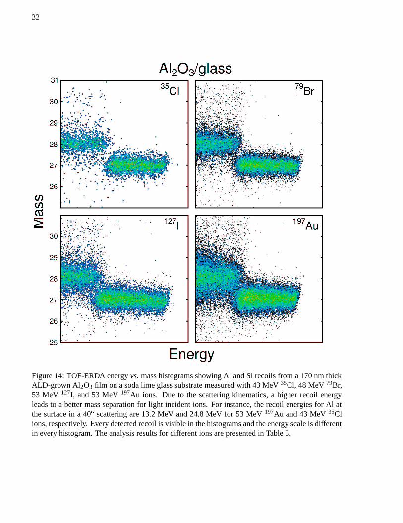
Figure 14: TOF-ERDA energy vs mass histograms showing Al and Si recoils from a 170 nm thickALD-grown Al2O3 film on a soda lime glass substrate measured with 43 MeV 35Cl, 48 MeV 79Br,53 MeV 127I, and 53 MeV 197Au ions. Due to the scattering kinematics, a higher recoil energyleads to a better mass separation for light incident ions. For instance, the recoil energies for Al atthe surface in a 40 scattering are 13.2 MeV and 24.8 MeV for 53 MeV 197Au and 43 MeV 35Clions, respectively. Every detected recoil is visible in the histograms and the energy scale is differentin every histogram. The analysis results for different ions are presented in Table 3.
33
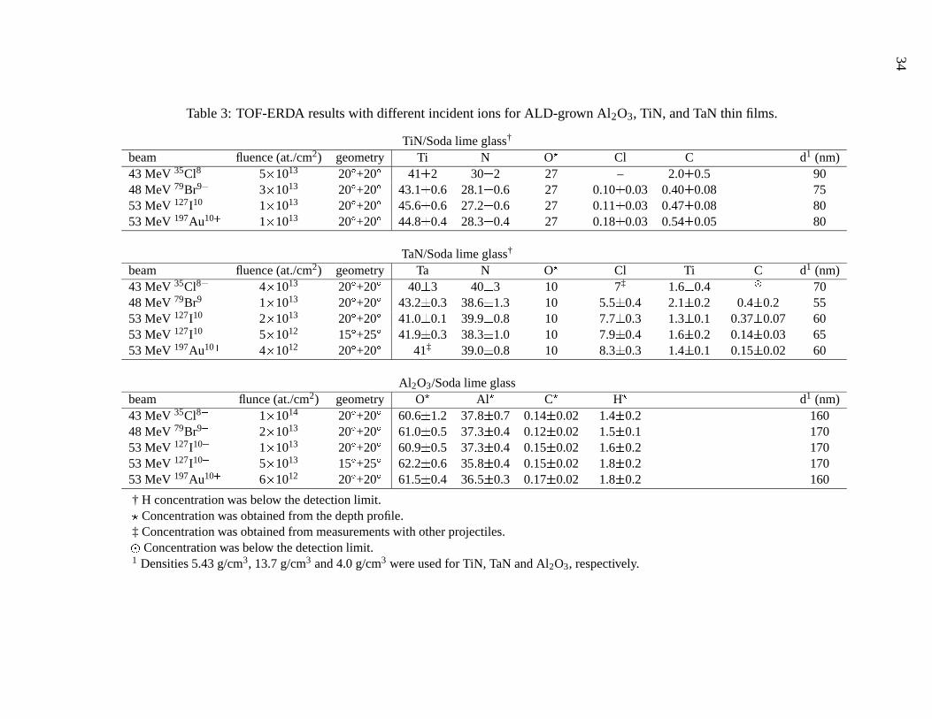
6.2 Selection of ions
The incident ions available from the different ion sources of the EGP-10-II range from hydrogen to
gold. In most cases the highest energies possible are preferred in HI-ERDA because of the greater
analysis depths, better mass separation, and smaller multiple scattering effects. To reach the high
energies, ions with high charge states are required, and to obtain sufficient high beam currents for
the analysis, high electron affinity elements are preferred. For example, the elements in the halogen
group are especially suitable, because from them sufficiently high negative ion currents can be
produced from the ion source. Most of HI-ERDA in the literature has been done with Cl, Br and I
beams. Also Au has a high electron affinity and is much used.
We studied the suitability of different incident ions (43 MeV 35Cl, 48 MeV 79Br, 53 MeV 127I, and
48 MeV 197Au) in view of analysis and measurement fluency, accuracy, and ion induced irradiation
effects in ALD-grown Al2O3 [89], TiN [23] and TaN [22] thin films. Desorption during the mea-
surements and irradiation effects at the surface were studied for these ions. Additionally, 15 +25 geometry was studied for the mostly used 53 MeV 127I ions. The results are given in Table 3. The
elemental concentrations for TiN and TaN thin films were calculated directly from the number of
events in the energy spectra by means of scattering cross-sections. This is stopping power inde-
pendent approach (see section 6.3.2). An exception was oxygen, for which the concentration was
obtained stopping dependently from the concentration distributions. For Al2O3 films the atomic
concentrations were obtained from the concentration distributions. In the analysis of TiN and TaN
with 35Cl ions and TaN with 79Br and 127I ions the forward scattered incident ions were used in the
analysis of Ti and Ta. The layer thicknesses were also determined from the depth profiles using the
literature values for the film densities.
All incident ions employed were found feasible in the analysis of these films, although the low beam
currents obtained for 35Cl8 + ions required longer measuring times. On the other hand, 43 MeV 35Cl
ions give more energy to light recoils and improve their mass separation as is illustrated for Al and
Si signals in Fig. 14. The concentration results measured with different incident ions were quite
consistent for TaN and Al2O3. For TiN the origin of the high carbon content measured with 35Cl
ions remained unclear. The observed differences in other concentrations can be mostly explained
by small discrepancies in the samples. In the thickness determination the errors can be thought
to be due to the stopping powers [36] used. The given uncertainty estimates are obtained from
the measurement statistics and the inaccuracies rising from ion beam induced desorption, which is
discussed in more detail in section 6.6.1.
34
Table 3: TOF-ERDA results with different incident ions for ALD-grown Al2O3, TiN, and TaN thin films.
TiN/Soda lime glass†
beam fluence (at./cm2) geometry Ti N O
.
Cl C d1 (nm)43 MeV 35Cl8
/
5 0 1013 20
1
+20
1
41
2
2 30
2
2 27 – 2.0
20.5 90
48 MeV 79Br9
/
3 0 1013 20
1
+20
1
43.1
2
0.6 28.1
2
0.6 27 0.10
2
0.03 0.40
20.08 75
53 MeV 127I10
/
1 0 1013 20
1
+20
1
45.6
2
0.6 27.2
2
0.6 27 0.11
2
0.03 0.47
20.08 80
53 MeV 197Au10
/
1 0 1013 20
1
+20
1
44.8
2
0.4 28.3
2
0.4 27 0.18
20.03 0.54
20.05 80
TaN/Soda lime glass†
beam fluence (at./cm2) geometry Ta N O
.
Cl Ti C d1 (nm)43 MeV 35Cl8
/
4 0 1013 20
1
+20
1
40
2
3 40
2
3 10 7‡ 1.6
20.4
3
7048 MeV 79Br9
/
1 0 1013 20
1
+20
1
43.2
2
0.3 38.6
2
1.3 10 5.52
0.4 2.1
20.2 0.4
2
0.2 5553 MeV 127I10
/
2 0 1013 20
1
+20
1
41.0
2
0.1 39.9
2
0.8 10 7.72
0.3 1.3
20.1 0.37
2
0.07 6053 MeV 127I10
/
5 0 1012 15
1
+25
1
41.9
2
0.3 38.3
2
1.0 10 7.9
20.4 1.6
2
0.2 0.14
2
0.03 6553 MeV 197Au10
/
4 0 1012 20
1
+20
1
41‡ 39.0
20.8 10 8.3
20.3 1.4
2
0.1 0.15
2
0.02 60
Al2O3/Soda lime glassbeam flunce (at./cm2) geometry O
.
Al
.C
.H
.
d1 (nm)43 MeV 35Cl8
/
1 0 1014 20
1
+20
1
60.6
21.2 37 48 20.7 0.14
20.02 1.4
2
0.2 16048 MeV 79Br9
/
2 0 1013 20
1
+20
1
61.0
20.5 37 43 20.4 0.12
20.02 1.5
2
0.1 17053 MeV 127I10
/
1 0 1013 20
1
+20
1
60.9
20.5 37 43 20.4 0.15
20.02 1.6
2
0.2 17053 MeV 127I10
/
5 0 1013 15
1
+25
162.2
20.6 35 48 20.4 0.15
20.02 1.8
2
0.2 17053 MeV 197Au10
/
6 0 1012 20
1
+20
161.5
20.4 36 45 20.3 0.17
2
0.02 1.8
2
0.2 160
† H concentration was below the detection limit.5 Concentration was obtained from the depth profile.‡ Concentration was obtained from measurements with other projectiles.6
Concentration was below the detection limit.1 Densities 5.43 g/cm3, 13.7 g/cm3 and 4.0 g/cm3 were used for TiN, TaN and Al2O3, respectively.
35
6.3 Concentration determination
In analysis where backscattering of ions is utilised the direct result is an energy spectrum from
which the events originating from the scatterings with different sample elements can be distin-
guished by means of the kinematic factor (Eq. 2) and the stopping powers. Some preliminary
information is often required (film constituents, thicknesses, light impurities) in detailed analysis.
For element resolving techniques like TOF-ERDA, no a prori information about the sample com-
position is needed as different elements can be separated and selected according to their mass or
atomic numbers as illustrated in Figs. 14 and 15.
6.3.1 Energy spectrum
In TOF-ERDA the mass calculation is based on the measured time of flight and energy for every
recoil. However, the energy detector has a non-linear energy response for different heavy ions, and
a higher order energy detector calibration has to be used [90]. Difficulties may also arise when
mass overlapping occurs with the neighbouring elements as can be seen in Fig. 15 for scattered 127I
and recoiled Xe. Here Xe was an impurity in Ar gas used in a film deposition by magnetron sput-
tering. From these E-mass or TOF-mass histograms the events corresponding to different masses
can be selected and the elemental energy spectra deduced from the TOF data. Normally the ob-
tained energy spectra are not the final results, but they are used to further calculate the elemental
concentrations.
6.3.2 Stopping power independent concentration determination
The stopping powers normally used [36] can differ as much as 20% from the correct ones [51].
Especially for heavy ions, the lack of experimental data is a problem, and therefore a stopping
power independent approach gives more reliable results. The elemental concentrations of a thin
film can be obtained by using the number of the recoil atoms or the scattered ions in the energy
spectra and by calculating the ratios using Eqs. (5) and (6) for the recoil and scattering cross-
sections, respectively. This approach can be used only if certain conditions are fulfilled: (i) The
film has to be homogeneous, and no concentration peaks at the surface or interface are present. (ii)
The detection efficiency for different elements has to be known, and correction parameters must be
used, if necessary. (iii) The film should be relatively flat and thin to avoid low energy tails due to
the roughness and multiple scattering. (iv) The substrate should not contain the same elements as
the thin film on it. When these conditions are fulfilled, the uncertainty of the obtained concentration
ratios arises almost only from the statistics of the detected recoils.
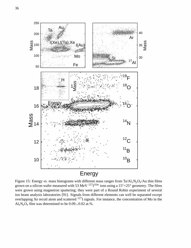
36
Energy
10
12
14
16
18
Mas
s
10B
11B
12C
19F
14N
16O
18O
Energy0
1
Mas
sH
30
35
40
Mas
s
27AlSi
Ar
50
100
150
200
250
Mas
s
Fe
Mo
I(Au)I(Xe),I(Ta),Xe
AuTa
Figure 15: Energy vs mass histograms with different mass ranges from Ta/AlxNyOz/Au thin filmsgrown on a silicon wafer measured with 53 MeV 127I10 + ions using a 15 +25 geometry. The filmswere grown using magnetron sputtering; they were part of a Round Robin experiment of severalion beam analysis laboratories [91]. Signals from different elements can well be separated exceptoverlapping Xe recoil atom and scattered 127I signals. For instance, the concentration of Mo in theAlxNyOz film was determined to be 0.09 0.02 at.%.
37
6.3.3 Calculation of concentration distributions
The basic idea in the most common methods for obtaining depth profiles is the backward calcula-
tion of the recoiling depth. In the energy spectrum a channel corresponds to a certain depth slice.
The depth is calculated using scattering kinematics and either experimental or more often semi-
empirical stopping powers [36]. The yield at different depths is then normalised using stopping
powers and scattering cross-sections for a given incident ion and sample atoms. If all the sample
elements can be analysed, the final depth profiles can be normalised to unity and atomic ratios are
obtained. If the film thickness is determined with other methods (e g optical measurements for
transparent films), ERDA is used only for compositional analysis and the stopping power uncer-
tainties for the projectiles become insignificant as the projectile energy loss is the same for all the
recoils scattered at the same depth. The relative projectile energy loss when going in and the recoil
energy loss when coming out are roughly equal for most projectile-recoil pairs. The density used
in the analysis is only a coefficient in the depth scale; it does not influence the concentrations.
A more sophisticated, but also more complicated, way to analyse HI-ERD energy spectra is to
use simulation program which produces energy spectra and then compares the experimental and
simulated spectra with each other [92, 93]. The final depth profiles of elements are obtained from
the simulated depth distributions giving the best fit with the experimental ones. The advantage of
this approach is the possibility to add the energy spreading factors like measurement geometry,
beam divergence and energy deviation, detector resolution, and energy straggling to the program.
In principle, the result should give the true sample structure. However, in HI-ERDA multiple and
plural scattering effects are strong, and cannot yet be fully reproduced with the analytical approach
[II]. These effects require full MC simulations, which still demand a great deal of computing time.
For the analysis of RBS spectra, the programs based on analytical functions are very useful, whereas
more complex HI-ERD is still a problem. The Bayesian probability theory [94] in the deconvolution
of the measured spectra along with the MC program written in the Accelerator Laboratory is aimed
at reproducing the concentration profiles of different elements directly [95].
Many times the final result obtained by means of HI-ERD analysis combines both stopping power
dependent and independent analysis. For instance, the ratio of the main constituents (like in ox-
ides) can be obtained very accurately using the stopping power independent approach but the light
impurity amounts as well as their locations are determined from the concentration distributions to
avoid errors generated by surface and interface peaks. Depth profiles are also used to verify the
homogeneity of a thin film. In the present study an analysing program by Arai et al [96] was
modified to make it possible to use also the forward scattered projectiles in the analysis.
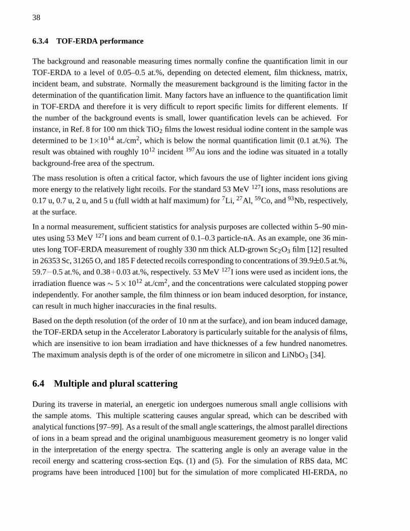
38
6.3.4 TOF-ERDA performance
The background and reasonable measuring times normally confine the quantification limit in our
TOF-ERDA to a level of 0.05–0.5 at.%, depending on detected element, film thickness, matrix,
incident beam, and substrate. Normally the measurement background is the limiting factor in the
determination of the quantification limit. Many factors have an influence to the quantification limit
in TOF-ERDA and therefore it is very difficult to report specific limits for different elements. If
the number of the background events is small, lower quantification levels can be achieved. For
instance, in Ref. 8 for 100 nm thick TiO2 films the lowest residual iodine content in the sample was
determined to be 1 - 1014 at./cm2, which is below the normal quantification limit (0.1 at.%). The
result was obtained with roughly 1012 incident 197Au ions and the iodine was situated in a totally
background-free area of the spectrum.
The mass resolution is often a critical factor, which favours the use of lighter incident ions giving
more energy to the relatively light recoils. For the standard 53 MeV 127I ions, mass resolutions are
0.17 u, 0.7 u, 2 u, and 5 u (full width at half maximum) for 7Li, 27Al, 59Co, and 93Nb, respectively,
at the surface.
In a normal measurement, sufficient statistics for analysis purposes are collected within 5–90 min-
utes using 53 MeV 127I ions and beam current of 0.1–0.3 particle-nA. As an example, one 36 min-
utes long TOF-ERDA measurement of roughly 330 nm thick ALD-grown Sc2O3 film [12] resulted
in 26353 Sc, 31265 O, and 185 F detected recoils corresponding to concentrations of 39.9 0.5 at.%,
59.7 0.5 at.%, and 0.38 0.03 at.%, respectively. 53 MeV 127I ions were used as incident ions, the
irradiation fluence was , 5 - 1012 at./cm2, and the concentrations were calculated stopping power
independently. For another sample, the film thinness or ion beam induced desorption, for instance,
can result in much higher inaccuracies in the final results.
Based on the depth resolution (of the order of 10 nm at the surface), and ion beam induced damage,
the TOF-ERDA setup in the Accelerator Laboratory is particularly suitable for the analysis of films,
which are insensitive to ion beam irradiation and have thicknesses of a few hundred nanometres.
The maximum analysis depth is of the order of one micrometre in silicon and LiNbO3 [34].
6.4 Multiple and plural scattering
During its traverse in material, an energetic ion undergoes numerous small angle collisions with
the sample atoms. This multiple scattering causes angular spread, which can be described with
analytical functions [97–99]. As a result of the small angle scatterings, the almost parallel directions
of ions in a beam spread and the original unambiguous measurement geometry is no longer valid
in the interpretation of the energy spectra. The scattering angle is only an average value in the
recoil energy and scattering cross-section Eqs. (1) and (5). For the simulation of RBS data, MC
programs have been introduced [100] but for the simulation of more complicated HI-ERDA, no
39
0 5 10 15 20Energy (MeV)
102
103
104
105
106
Cou
nts/
chan
nel Sum
Group 3Group 2Group 1
0 20 40 60 80( )
-90
-60
-30
0
30
60
90
()
G2G3
G1
Figure 16: Simulated energy spectra for recoils emitted from deeper Cu layer to three differentdirection regions from a sample structure of 23 nm Cu/200 nm Ti/23 nm Cu/Si wafer [II]. 53 MeV127I incident ions were used. The TOF–E detector is located at θ=40 . The selected areas areillustrated in the inset.
MC simulation program like the one utilised for this thesis [II] has been previously used in the
literature.
Equally important in the analysis are events where the scattering occurs closer to the sample atom
nucleus resulting in a large angle scattering. Although these events are scarce, they can play an
important role in the analysis. These scatterings are referred as plural scattering. Due to the nature
of these events, no analytical function has been used to simulate them and they require full MC
simulations. Despite the exponential development in computer performance, these simulations
are not yet achievable within reasonable computing time without major enhancements in the code
[101, 102]. By means of the following enhancements in our code [II], the computing performance
was improved drastically:
(i) The scattering process and the recoil generation process were treated as separated processes, and
the recoil producing cross-section was increased so that each primary ion produces 10 recoils on
an average.
(ii) A restricted depth dependent emission solid angle was used for recoils. It was determined by a
presimulation procedure.
40
(iii) A variable depth dependent cross-section was used to produce a roughly equal number of
recoils for all depths. Cross-section changes were compensated by the use of statistical weights for
recoils.
(iv) A virtual detector having the size of 100 times that of the original detector was used. Recoils
hitting the virtual detector were directed to the real detector by recalculating their recoil energy,
scattering cross-section, and energy losses.
The basic idea behind our multiple scattering code development [II] was that the simulations should
be fast enough to produce energy spectra that can later be utilised in an analysis procedure using
the Bayesian probability theory [95].
In the first phase [II] the program was tested with known sandwich sample structures and the recoil
emission angle dependency for the detected ions was studied. The program was found to reproduce
the measured experimental spectra very well. Before the completion of a new analysis procedure,
the current one is a very useful aid in the interpretation of TOF-ERDA results and in the future
development of the spectrometer.
The MC program can be used when the original depths and recoiling histories of events in the
different parts of the energy spectrum is studied as illustrated in Fig. 16. It was observed that
a clear initial recoil direction dependency for deep lying layers in the sample exists for different
regions in the energy spectrum. The great majority of the events are emitted close to the detector
direction (group 1) whereas the low energy tail is due to the recoils emitted to large angles (θ=60–
80 ) having a high scattering cross-section but low energies (group 2). The recoils emitted to
smaller angles (group 3) are not favoured by the scattering cross-section, but they result in a flat
distribution starting from the highest energies and lasting to the lowest ones. If the incident ion
scatters close to the surface direction, the effective thickness of the layer increases and detected
recoils are emitted towards small angles as in group 3.
The multiple scattering is also an important factor in the TOF-E telescope as the ions scatter in the
carbon foils of the TOF detector. As a result they may scatter outside the detector solid angle which
is limited by the metal frame carrying the second carbon foil. This effect can be simulated with
our MC program. The detection efficiency for different carbon foil thicknesses in T1 is plotted as
a function of the atomic number of recoils in Fig. 17a. In Fig. 17b the detection efficiency of the
TOF-E telescope for Nb in LiNbO3 is plotted as a function of the recoiling depth for a 5 µg/cm2
carbon foil thickness. In both simulations incident 58 MeV 127I ions and a detector angle of 40 were used. In Fig. 17c the obtained efficiency was used to normalise the depth profile of Nb in
a proton exchanged LiNbO3 sample. The original Nb depth profile is presented together with the
corrected one, H, and Li depth profiles. For clarity reasons oxygen depth profile at concentration
of 60 at.% is not presented. The sample was similar to those studied in [34] and the TOF-E data of
the same measurement is presented in Fig. 6.
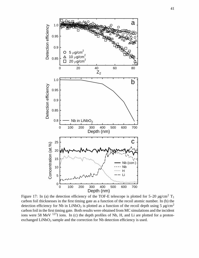
41
0 20 40 60 80Z2
0.85
0.9
0.95
1.0
Det
ectio
nef
ficie
ncy
20 g/cm210 g/cm25 g/cm2
0 100 200 300 400 500 600 700Depth (nm)
0.8
0.85
0.9
0.95
1.0
Det
ectio
nef
ficie
ncy
Nb in LiNbO3
0 100 200 300 400 500 600 700Depth (nm)
0
5
10
15
20
25
Con
cent
ratio
n(a
t.%)
LiHNbNb (corr.)
a
b
c
Figure 17: In (a) the detection efficiency of the TOF-E telescope is plotted for 5–20 µg/cm2 T1
carbon foil thicknesses in the first timing gate as a function of the recoil atomic number. In (b) thedetection efficiency for Nb in LiNbO3 is plotted as a function of the recoil depth using 5 µg/cm2
carbon foil in the first timing gate. Both results were obtained from MC simulations and the incidentions were 58 MeV 127I ions. In (c) the depth profiles of Nb, H, and Li are plotted for a proton-exchanged LiNbO3 sample and the correction for Nb detection efficiency is used.
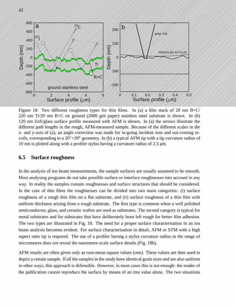
42
0 2 4 6 8Surface profile ( m)
-800
-600
-400
-200
0
200
400
600
800D
epth
(nm
)
Ti
C
I127
12
B+C
ground stainless steel
0 0.1 0.2 0.3 0.4 0.5Surface profile ( m)
-200
100
0
100
200
Dep
th(n
m)
AFM−TIP
PROFILER STYLUS
a b
Figure 18: Two different roughness types for thin films. In (a) a film stack of 20 nm B+C/220 nm Ti/20 nm B+C on ground (2000 grit paper) stainless steel substrate is shown. In (b)120 nm ZnS/glass surface profile measured with AFM is shown. In (a) the arrows illustrate thedifferent path lengths in the rough, AFM-measured sample. Because of the different scales in thex- and y-axis of (a), an angle correction was made for in-going incident ions and out-coming re-coils, corresponding to a 20 +20 geometry. In (b) a typical AFM tip with a tip curvature radius of10 nm is plotted along with a profiler stylus having a curvature radius of 2.5 µm.
6.5 Surface roughness
In the analysis of ion beam measurements, the sample surfaces are usually assumed to be smooth.
Most analysing programs do not take possible surface or interface roughnesses into account in any
way. In reality the samples contain roughnesses and surface structures that should be considered.
In the case of thin films the roughnesses can be divided into two main categories: (i) surface
roughness of a rough thin film on a flat substrate, and (ii) surface roughness of a thin film with
uniform thickness arising from a rough substrate. The first type is common when a well polished
semiconductor, glass, and ceramic wafers are used as substrates. The second category is typical for
metal substrates and for substrates that have deliberately been left rough for better film adhesion.
The two types are illustrated in Fig. 18. The need for a proper surface characterisation in an ion
beam analysis becomes evident. For surface characterisation in detail, AFM or STM with a high
aspect ratio tip is required. The use of a profiler having a stylus curvature radius in the range of
micrometres does not reveal the nanometre-scale surface details (Fig. 18b).
AFM results are often given only as root-mean-square values (rms). These values are then used to
depict a certain sample. If all the samples in the study have identical grain sizes and are also uniform
in other ways, this approach is defensible. However, in most cases this is not enough: the reader of
the publication cannot reproduce the surface by means of an rms value alone. The two situations
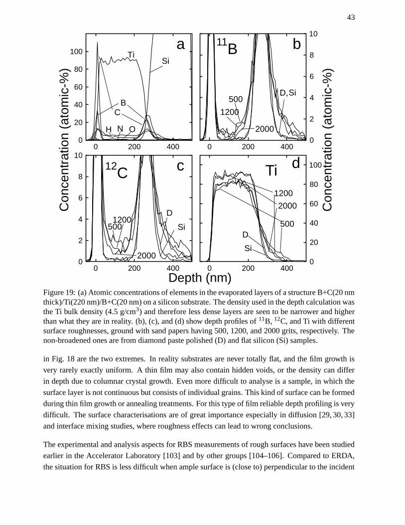
43
0 200 4000
2
4
6
8
10
0 200 4000
20
40
60
80
100
0 200 4000
2
4
6
8
10
0 200 4000
20
40
60
80
100
Depth (nm)
Con
cent
ratio
n(a
tom
ic-%
)
Con
cent
ratio
n(a
tom
ic-%
)
a b11B
c12CdTi
500
5001200 500
B
H ON
C
D
Si
2000
D
Si
2000
1200
2000
1200
D,Si
TiSi
Figure 19: (a) Atomic concentrations of elements in the evaporated layers of a structure B+C(20 nmthick)/Ti(220 nm)/B+C(20 nm) on a silicon substrate. The density used in the depth calculation wasthe Ti bulk density (4.5 g/cm3) and therefore less dense layers are seen to be narrower and higherthan what they are in reality. (b), (c), and (d) show depth profiles of 11B, 12C, and Ti with differentsurface roughnesses, ground with sand papers having 500, 1200, and 2000 grits, respectively. Thenon-broadened ones are from diamond paste polished (D) and flat silicon (Si) samples.
in Fig. 18 are the two extremes. In reality substrates are never totally flat, and the film growth is
very rarely exactly uniform. A thin film may also contain hidden voids, or the density can differ
in depth due to columnar crystal growth. Even more difficult to analyse is a sample, in which the
surface layer is not continuous but consists of individual grains. This kind of surface can be formed
during thin film growth or annealing treatments. For this type of film reliable depth profiling is very
difficult. The surface characterisations are of great importance especially in diffusion [29, 30, 33]
and interface mixing studies, where roughness effects can lead to wrong conclusions.
The experimental and analysis aspects for RBS measurements of rough surfaces have been studied
earlier in the Accelerator Laboratory [103] and by other groups [104–106]. Compared to ERDA,
the situation for RBS is less difficult when ample surface is (close to) perpendicular to the incident
44
and backscattered ions. Thus a roughness of type (ii) is invisible in the RBS analysis. However,
a roughness of type (i) broadens the low energy edge of the concentration distribution originating
from collisions with thin film atoms.
Also for ERDA, some previous studies have been made in which periodic roughness effects have
been studied [107]. The roughness has also been approached through projectile and recoil effective
path lengths [108, 109], and the influence of the surface roughness on measured depth profiles and
implanted ion amounts has been examined [105].
In paper III the substrate roughness was varied by using different grit sand papers in the grinding
process. Thin film stacks were evaporated on rough surfaces in the same vacuum. This structure
was chosen to mimic the situation in which a sensitive thin film is enclosed between protecting
layers and the impurity amounts in the sensitive layer should be studied. This situation occurs for
instance with easily oxidising SrS electroluminescent thin films, which should be covered with a
protecting Al2O3 layer [IV]. The film structure was B+C(20 nm thick)/Ti(220 nm)/B+C(20 nm) on
a silicon wafer and the stainless steel substrates. The stainless steel substrates were ground with
sand papers having grits 500, 1200, and 2000. In addition, one stainless steel substrate was polished
to be mirror-like with diamond paste. A silicon wafer was used as a flat reference.
The depth profiles from measurements performed using 53 MeV 127I beams are presented in
Fig. 19. In (a) the depth profiles of all the film elements on a flat silicon substrate are plotted.
In (b) and (c) the depth profiles show an increase in the 11B and 12C contents in the Ti layer as
a function of the surface roughness. The observed increase is not real but due to the substrate
roughness. The 11B and 12C counts inside the Ti films indicate to 4 and 10 times greater impurity
concentrations for the grits 2000 and 500, respectively, than what is seen for the films grown on
silicon or steel substrates polished with a diamond paste. The detected recoil intensities of 11B and12C calculated from all the depth profiles were within 5% each others. Another surface roughness
related effect can be seen in Fig. 19d. The lowering of the near surface area in the depth profiles
obtained from rough samples is due to the reduced probability of such recoils that are produced
near the surface and hit the detector without passing any roughness edges.
In paper III an MC simulation was performed for the sample ground with 500 grit paper. The
surface topography used in the simulation was obtained from several AFM measurements of the
sample. However, the measured energy spectrum was only qualitatively reproduced. The reason
for this could be insufficient amount of AFM images to describe all surface characteristics from the
TOF-ERDA beam spot area.
The concentration distributions presented in Fig. 19 show that the distributions obtained from
ground samples differ significantly from the ones obtained from polished steel or silicon wafer.
However, in a visual inspection the sample ground with a 2000 grit paper was a mirror-like and did
not deviate from the smooth ones in this sense. The requirement of careful surface characterisation
is evident in this case.
45
6.6 Ion beam induced modification
The most common ion beam analysis methods (RBS, ERDA, NRA) are non-destructive in many
applications and do not modify the studied sample significantly. Especially compared to other
common depth profiling methods, such as SIMS, XPS, and Auger-electron spectroscopy, in which
ion beams are used to erode the sample and a visible crater is formed, these high energy ion beam
methods are non-destructive. In the measurements performed in backscattering geometry, detectors
with large solid angles can be utilised, because then scattering kinematics do not significantly affect
the energy resolution. However, the use of high energy heavy ions and detectors with small solid
angles increase the deposited energy per detected particle and, for HI-ERDA, ion beam induced
effects should always be taken into consideration. The origin of the modification is in the electronic
and nuclear energy loss processes.
Polymer films are an example of a sensitive sample type. Even at low irradiation fluences with
heavy ions, a rapid polymer chain braking occurs and the film is destroyed. Different ion induced
effects appear in different sample types, and all of these should be taken into account and their
influence minimised. On the other hand, we have observed by means of Raman spectroscopy ion
beam induced recovery of a degraded structure in annealed diamond-like carbon films with high Si
content (33 at.%) [31].
6.6.1 Sputtering and elemental losses
In the analysis of metals and most semiconductors, sputtering can be regarded to be dependent on
the nuclear stopping [110]. For typical fluences of the order of 1012–1014 ions/cm2 in TOF-ERDA
measurements an exceptionally high sputtering yield of 10 atoms/ion would result in a loss of only
one monolayer ( , 1015 at./cm2) [110]. In comparison with the depth resolution (about 10 nm at the
surface) this is a negligible effect. If the analysed layer is very thin, the sputtering may still become
a factor limiting accuracy. The sputtering of an analysed layer can be avoided with a protective
layer (i e evaporated gold).
Ion beam induced desorption modifies samples much more than sputtering caused by the nuclear
collisions. A typical desorption behaviour is described by an exponential law and the desorption
yield decreases and even vanishes with high fluences. Behrisch et al [111] explain this as a result
of gradual destruction due to the damage created by incident ions forming a cylinder of a destructed
volume around the ion trajectory. For an approximated rectangular shaped cross section of a beam
spot, the drop of concentration is exponential at first and the concentration reaches a saturation
value rapidly, but for a Gaussian shaped cross section of a beam spot, the elemental concentration
losses occur more slowly and linearly. The loss of material is usually limited to volatile species in
addition to surface sputtering.
Walker et al [112] studied the elemental losses in insulating materials using 1.1 MeV/nucleon
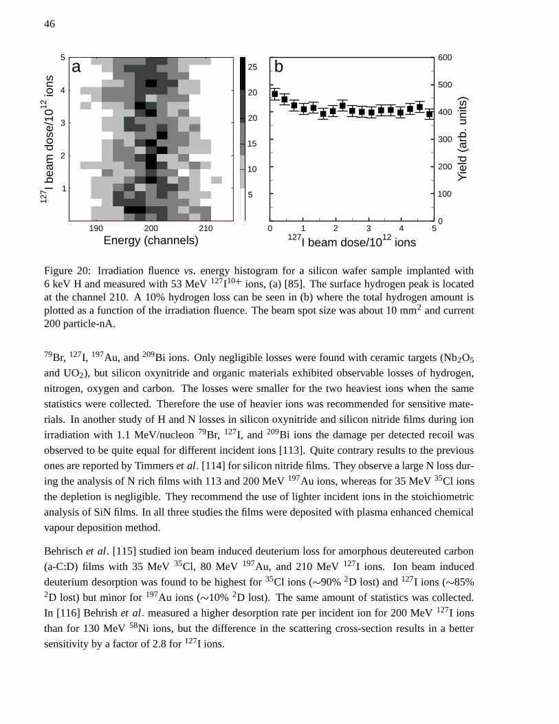
46
0 1 2 3 4 5127I beam dose/1012 ions
0
100
200
300
400
500
600
Yie
ld(a
rb.u
nits
)
190 200 210
Energy (channels)
1
2
3
4
5
127 Ib
eam
dose
/1012
ions
5
10
15
20
20
25a b
Figure 20: Irradiation fluence vs energy histogram for a silicon wafer sample implanted with6 keV H and measured with 53 MeV 127I10 + ions, (a) [85]. The surface hydrogen peak is locatedat the channel 210. A 10% hydrogen loss can be seen in (b) where the total hydrogen amount isplotted as a function of the irradiation fluence. The beam spot size was about 10 mm2 and current200 particle-nA.
79Br, 127I, 197Au, and 209Bi ions. Only negligible losses were found with ceramic targets (Nb2O5
and UO2), but silicon oxynitride and organic materials exhibited observable losses of hydrogen,
nitrogen, oxygen and carbon. The losses were smaller for the two heaviest ions when the same
statistics were collected. Therefore the use of heavier ions was recommended for sensitive mate-
rials. In another study of H and N losses in silicon oxynitride and silicon nitride films during ion
irradiation with 1.1 MeV/nucleon 79Br, 127I, and 209Bi ions the damage per detected recoil was
observed to be quite equal for different incident ions [113]. Quite contrary results to the previous
ones are reported by Timmers et al [114] for silicon nitride films. They observe a large N loss dur-
ing the analysis of N rich films with 113 and 200 MeV 197Au ions, whereas for 35 MeV 35Cl ions
the depletion is negligible. They recommend the use of lighter incident ions in the stoichiometric
analysis of SiN films. In all three studies the films were deposited with plasma enhanced chemical
vapour deposition method.
Behrisch et al [115] studied ion beam induced deuterium loss for amorphous deutereuted carbon
(a-C:D) films with 35 MeV 35Cl, 80 MeV 197Au, and 210 MeV 127I ions. Ion beam induced
deuterium desorption was found to be highest for 35Cl ions ( , 90% 2D lost) and 127I ions ( , 85%2D lost) but minor for 197Au ions ( , 10% 2D lost). The same amount of statistics was collected.
In [116] Behrish et al measured a higher desorption rate per incident ion for 200 MeV 127I ions
than for 130 MeV 58Ni ions, but the difference in the scattering cross-section results in a better
sensitivity by a factor of 2.8 for 127I ions.
47
In the Accelerator Laboratory, TOF-ERD measurements are done event by event, and the elemental
losses during the measurements are always monitored. Therefore the amount of an element can be
extrapolated to the beginning of a measurement. An example of hydrogen loss is shown in Fig. 20.
The hydrogen energy spectra of the samples used in the Round Robin experiment [85] are plotted to
a histogram as a function of the ion fluence in (a) and the total hydrogen yield is plotted as a function
of the ion fluence in (b). About half of the total 10% loss during the measurement was regarded
to be due to the surface hydrogen loss. In the analysis of ALD grown thin films the desorption
of the volatile residual impurities (mainly H) was in some measurements so great that it had an
effect on the accuracy of the results reported in paper V and in Refs. 10, 14. The behaviour can be
explaned by a three step process [117]: activation, diffusion to the surface mainly through the grain
boundaries, and release from the surface as a molecule. In porous materials like the fusion reactor
wall materials the desorption can occur even at the depth of several hundred nanometres [118].
Ion induced desorption and surface modification were studied for 43 MeV 35Cl, 48 MeV 79Br,
53 MeV 127I, and 53 MeV 197Au ions and TiN, TaN, and Al2O3 films (see Table 3). Some desorp-
tion of impurities was observed, but the highest losses ( , 20%) were found for hydrogen in Al2O3
measured with 35Cl and 197Au. It was not possible to draw any general conclusions concerning
the optimal incident ion with respect to the induced desorption for these thin films. In the AFM
and STM studies some minor surface modification was observed only for TaN irradiated with 79Br
ions. For sensitive samples the beam intensity per unit area should be minimised or detector solid
angle increased and damage thereby reduced.
6.6.2 Destruction of the crystalline structure
In semiconductors bombarded with high energy heavy ions, nuclear collisions displace atoms from
their lattice sites and generate defects and defect clusters. Walker et al [119] studied this process
for Si and GaAs bombarded with 54–98 MeV 127I ions incident at an angle of 22.5 to the target
surface. As a result, a measurable but relative small sample damage was observed for a fluence
of 1014 ions/cm2. Irradiation induced damage was studied with channelling-RBS and transmission
electron microscopy. In HI-ERDA, ion beam induced damage can be measured in situ by means
of a position sensitive detector and blocking method [120]. In semiconductor materials, this defect
generation process was utilised by us for making faster laser optic devices by generating recombi-
nation centres to semiconductor saturable-absorber mirrors by a 30 MeV Ni irradiation to a fluence
of 1012 at./cm2 [121, 122].
For insulating crystalline materials, amorphisation is much more rapid and strongly related also to
the electronic stopping of heavy ions at MeV energies [123, 124]. We observed a rapid amorphisa-
tion of α-quartz [125] and LiNbO3 [126] during TOF-ERDA measurements, determined afterwards
by means of channelling-RBS and X-ray diffraction, respectively. It is notable, that in both studies
no elemental losses were observed even though the crystalline structure was destroyed to a depth
of 2 µm.
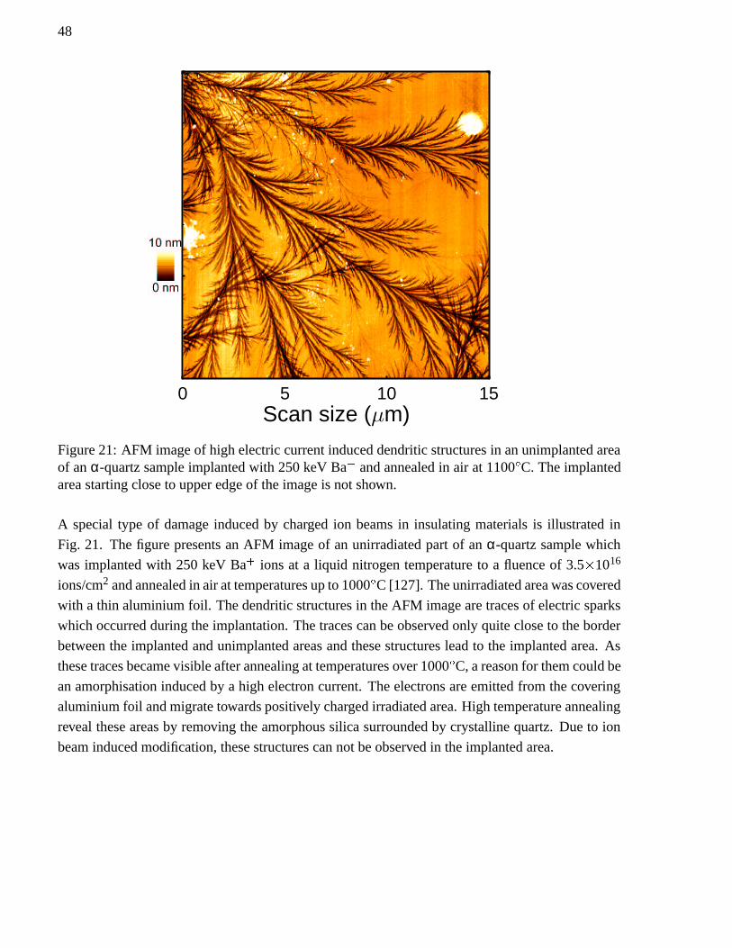
48
0 5 10 15Scan size ( m)
Figure 21: AFM image of high electric current induced dendritic structures in an unimplanted areaof an α-quartz sample implanted with 250 keV Ba + and annealed in air at 1100 C. The implantedarea starting close to upper edge of the image is not shown.
A special type of damage induced by charged ion beams in insulating materials is illustrated in
Fig. 21. The figure presents an AFM image of an unirradiated part of an α-quartz sample which
was implanted with 250 keV Ba + ions at a liquid nitrogen temperature to a fluence of 3.5 - 1016
ions/cm2 and annealed in air at temperatures up to 1000 C [127]. The unirradiated area was covered
with a thin aluminium foil. The dendritic structures in the AFM image are traces of electric sparks
which occurred during the implantation. The traces can be observed only quite close to the border
between the implanted and unimplanted areas and these structures lead to the implanted area. As
these traces became visible after annealing at temperatures over 1000 C, a reason for them could be
an amorphisation induced by a high electron current. The electrons are emitted from the covering
aluminium foil and migrate towards positively charged irradiated area. High temperature annealing
reveal these areas by removing the amorphous silica surrounded by crystalline quartz. Due to ion
beam induced modification, these structures can not be observed in the implanted area.
49
6.7 Summary of TOF-ERDA results
In the research for this thesis TOF-ERDA has been utilised mainly in the analysis of main con-
stituents and impurities in thin films. The thin films to be analysed were deposited using different
methods and the impurities detected can in most cases be understood from the growth parameters
and precursors used. The main sample and analysis characteristics are summarised in Table 4.
For the multiple scattering and surface roughness studies, tailored thin film structures were grown
by electron beam evaporation in papers II and III. The results of these studies are presented in
sections 6.4 and 6.5.
Films grown by ALD have been studied in papers IV and VII, and in Refs. 7–24. ALD is based
on the saturation of individual, sequentially performed surface reactions between the substrate and
the reactants used [1, 128]. When the monolayer is filled, the surface becomes passive for that
particular reactant. During the growth, precursors are transported to the reactor by an inert gas
(usually N2) flow. Several precursors can be utilised, depending on the grown material. Between
the growth pulses the reactor is purged with an inert gas pulse. For certain precursors, growth
temperature, pulse lengths, and thin film substrate can be varied in order to find the optimal growth
conditions. The ALD films are normally polycrystalline or amorphous, and they have an excellent
step coverage.
At some temperature and pulse length range of the ALD process the chemical reaction proceeds
until saturation and the following purge pulse blows the precursor residuals away. However, at
lower temperatures the chemical reaction does not necessarily become complete and organic or
inorganic residuals are left at the surface, and during the next growth pulse they are covered by the
next layer. At too high temperatures the precursors may decompose before reaching the surface or
react with wrong species, and again residual impurities can be observed. In TOF-ERD analysis the
film main component as well as impurity concentration distributions were obtained. As emerges
from Table 4, the incident ions have to be chosen so that elements which are of interest can be
detected as well as possible. For example, 79Br ions were utilised in the analysis if iodide precursors
were used during the film growth. In most cases some negligible hydrogen and carbon losses from
surface were observed during the ion beam irradiation. If the losses were significant, the original
content was extrapolated from data collected event by event. Especially for the processes in which
organic precursors were used, the ability of an accurate H and C analysis was proven to be very
useful.
The analysis results of CuxInySez films grown by electrodeposition [VI] are presented in Fig. 11 and
Table 2. Although the film surfaces were even visually rough and H losses were observed during
the measurements, TOF-ERD analysis gave important information of the light impurity elements.
In the analysis of main components, TOF-ERDA results agreed well with RBS results.
Ion beam assisted deposition was applied for the growth of hard coatings [25, 26] and reactive
magnetron for FeN films. TOF-ERD analysis provided information on the film uniformity and the
50
impurity contents.
Deuterium diffusion behaviour and concentration distributions were determined for pulsed vacuum
arc deposition grown films [V, 29–31]. Diamond-like carbon films were doped with different sil-
icon contents. TOF-ERDA results for deuterium were used to normalise SIMS depth profiles. In
Ref. 28 diamond-like carbon films with hydrogen reservoirs were studied with TOF-ERDA. Dif-
ferent hydrogen doping methods were studied and the hydrogen concentrations were provided by
TOF-ERDA.
TOF-ERDA has been found to be a useful tool in migration studies. The oxygen activated recrys-
tallisation and out-migration of the implanted Li-ions in α-quartz has been studied earlier in our
laboratory [129]. In this thesis the 18O in-migration and Na out-migration was studied [33]. The
migration of elements was studied with TOF-ERDA and the recrystallisation with channelling-
RBS. In paper VII 18O and 37Cl ions were coimplanted with 63Cu ions to study the photolumi-
nescence (PL) colour and intensity, and the migration behaviour as a function of the fluence and
post-implantation annealing temperature. The migration behaviour was studied with TOF-ERDA.
51
Table 4: Summary of TOF-ERD analysis.
Material Precursors1 and induced modifications Detected elements Incident ions Other methods2 Comments Ref.
ALD-grown oxidesAl2O3, Ta2O5 Al(CH3)3, Ta(OEt)5, H2O Ta,Al,O,C,H 34 MeV 127I XRD3 early study [7]TiO2 TiI4, H2O2 Ti,O,H,I 48 MeV 197Au XRD low I levels (1–15 71014 at./cm2) [8](Al,Zr,Hf,Ta,Si) oxides metal alkoxides and halides Ta,Hf,Zr,Ti,Cl,Si,O,C,H 53 MeV 127I [9]MgO cp2Mg, H2O Mg,O,C,H 53 MeV 127I XRD,XPS4 Ion beam induced H loss [10]Y2O3 Y(thd)3,Y(thd)3(biby),Y(thd)3(phen),O3 Y,F,O,N,C,H 53 MeV 127I XRD,FTIR,XPS [11]Sc2O3 Sc(thd)3, (cp3)Sc,H2O,H2O2,O3 Sc,O,H,C,F 53 MeV 127I XRD,FTIR5 [12]YxZryOz Y(thd)3,Zr(thd)4 ,cp2ZrCl2,cp2Zr(CH3)2,O3 Y,Zr,O,H,C,F,Cl 53 MeV 127I XRD,XRF6,SEM-EDX7 [13]ZrxAlyNbzOs,ZryAlzOx Nb(OC2H5)5, ZrCl4,Al(CH3)3, H2O Nb,Zr,Cl,Al,O,C,H 53 MeV 127I XRD Zr and Nb not separated [14]HfO2-Al2O3-Nb2O5 HfCl4,HfI4,Nb(OC2H5)5,Al(CH3)3,H2O Hf,Nb,Cl,Al,O,C,H 53 MeV 127I XRD forw. scatt. 127I used in Hf determ. [15]ZrO2 ZrI4, H2O,H2O2 I,Zr,O,H 48 MeV 197Au RHEED8 Ion beam induced H loss [16]Er2O3 Er(thd)3, O3 Er,O,H,C,F 51 MeV 127I XRD [17]HfO2 HfI4,O2 Hf,I,O,H 48 MeV 79Br XRD,SEM-EDX forw. scatt. 79Br used in Hf determ. [18]HfO2 HfI4,HfCl4,H2O Hf,I,Cl,O,H 48 MeV 79Br XRD forw. scatt. 79Br used in Hf determ. [19]SrTiO3 Sr(C5
iPr3H2)2,Ti(OiPr)4, H2O Sr,Ti,Al,O,C,H 34 MeV 127I RBS,XRD,SEM-EDX [20]LaAlO3 La(thd)3,AlC5H8O2,O3 La,Al,F,O,C,H 48 MeV 197Au RBS,XPS,XRD,FTIR [21]ALD-grown nitridesTaN TaCl5,TaBr5,NH3,C4H11N,C3H7N Ta,Br,Cl,O,N,C,H 53 MeV 127I XRD,SEM-EDX forw. scatt. 127I used in Ta determ. [IV]TaN TaCl5,C3H9Al Ta,Cl,Al,O,N,C,H 53 MeV 127I XRD,SEM-EDX forw. scatt. 127I used in Ta determ. [22]TiN TiCl4,TiI4,tBuNH2,allylNH2,NH3 Ti,O,N,C,H 53 MeV 127I and 197Au XRD [23]ALD-grown sulfidesSrS,BaS (C5
iPrH2)2Sr(THF),(C5(CH3)5)2Sr(THF)x, Ba,Sr,S,O,C,H 34 and 53 MeV 127I XRD [24](C5(CH3)5)2Ba(THF)x,H2S
Electrodeposition grown filmsCuInSe2 CuCl,SeO2,InCl3 In,Mo,Se,Cu,K,S,O,N,C,H 48 MeV 127I RBS,XRD,SEM-EDX rough films, H loss [V]Ion beam assisted deposition grown nitridesCxNy evap. C,N2+Ar Ar,O,N,C,H 48 MeV 127I XPS,XANES9,µ-Raman [25]BxCyNz evap. B4C,N2+Ar Ar,O,C,N,B,H 48 MeV 127I XANES [26]Reactive magnetron sputtering grown filmsFeNy Fe,N2,Ar Fe,O,N,C,H 37 MeV 197Au RBS,CEMS10,XRD early study [27]Pulsed vacuum arc deposition grown filmsta-C1,H:ta-C,CH:Ti graphite,H2,CH4 Ti,C,H 34 MeV 127I low friction films with H reserv. [28]ta-CxSiy:D graphite,Si,D2 Si,O,C,D,H 53 MeV 127I RBS,SIMS,SEM-EDX ERDA normalized SIMS spectra [VI], [29–31]Ion beam modification and migration studies(100)GaAs 20 keV Be impl. As,Ga,Be 37 MeV 197Au channeling-RBS,SIMS migration studies [32]α-quartz 50 keV Na impl. Si,Na,18O,16O 53 MeV 127I channeling-RBS migration studies [33]SrS 60 keV 18O, 80 keV 37Cl, 120 keV 63Cu Sr,Cu,Cl,S,Al,18O,16O,C,H 34 MeV 127I migration and PL emission study [VII]LiNbO3 proton exchange Nb,O,Li,H 55 MeV 127I,48 MeV 79Br,XRD maximum depth of 81 µm was [34]
43 MeV 35Cl reached in the analysisLiNbO3 Zn in-diffusion Nb,Zn,O,Li 55 MeV 127I XRD [35]
1 thd = C11H19O2, cp = C5H5, biby = C10H8N2, phen = C12H8N2, iPr = i-C3H7, tma = C3H9Al, tBu = (CH3)3C-, allyl = CH2=CHCH2-, THF = C4H8O, ta-H = tetrahedral amorphous carbon, same asDLC (diamond-like carbon) ; 2 Other compositional characterisation methods used; 3 X-ray diffraction; 4 X-ray photoelectron spectroscopy; 5 Fourier transform infrared spectrometer; 6 X-ray fluorescence;7 Scanning electron microscopy with energy dispersive X-ray detector; 8 Reflection high-energy electron diffractometry; 9 X-ray absorption near-edge spectroscopy; 10 Conversion electron Mössbauer spectroscopy
52
7 CONCLUSIONS AND CONSIDERATIONS FOR FUTURE
RESEARCH
In the research for this thesis TOF-ERDA measurements have been performed to characterise a
wide range of different samples. By means of the method developed for hydrogen detection and
by making use of forward scattered incident ions in the analysis, a quantitative, standard-free, and
rapid detection method for all sample elements was obtained. Three out of the four main matters
influencing the usability of heavy ion ERDA have been studied: understanding of multiple scatter-
ing, surface roughness, and ion beam induced damage effects is a key to a correct interpretation of
the measured data. The fourth factor, stopping power inaccuracy, can be avoided in many cases by
using the total elemental yields and scattering cross-sections in the analysis. Today TOF-ERDA is
an analysis method extensively used in the Accelerator Laboratory. It is capable of characterising
various sample types with high reliability. The standard operation procedures used in the techni-
cal operation and analysis guarantee good day-to-day reproducibility. This has enabled us to use
TOF-ERDA also in the analysis of industrial samples.
The driving force behind the present study was the rapid growth of thin film applications and de-
velopment of film growth methods. Thin film research requires fast and reliable feedback, and it
should be possible to analyse new materials without tedious use of standard samples and prelimi-
nary knowledge of sample structures and constituents. In this field TOF-ERDA is a very powerful
technique. In measurements of, for instance, low impurity levels, diffusion behaviour, and elemen-
tal ratios, other methods like RBS and SIMS are complementary to TOF-ERDA.
The further development of the TOF-ERDA method will focus on the position sensitivity of the
telescope. This would enable us to enlarge the solid angle of the detector, and at the same time
improve the depth resolution at the sample surface by correcting kinematic broadening. In the
future we are planning to build a TOF-E telescope in which the position information is obtained
from the magnified electron signal of the timing gate. Reduced ion beam induced damage and
better depth resolution are mandatory conditions in the depth profiling of gate oxides in their normal
thicknesses of a few nanometres.
The versatility of the TOF-ERDA beam line has recently been increased by mounting an X-ray
detector to the chamber at angle of 90 . Preliminary measurements have shown the usefulness of
the additional detector in the analysis of oxides which contain elements having neighbouring atomic
numbers and overlapping isotope masses. By the use of the X-ray detector also those elements that
are not separated in TOF-ERDA data can be quantified simultaneously.
53
ACKNOWLEDGEMENTS
I wish to thank Professor Juhani Keinonen, Head of the Department of Physical Sciences, for
giving me the opportunity to work in the field of ion beam physics. I also thank him warmly for his
supervision of my work during the preparation of the current thesis.
My thanks are also due to the former and current Heads of the Accelerator Laboratory, Professor
Jyrki Räisänen and Dr Eero Rauhala, for placing the facilities of the laboratory at my disposal.
I have had the chance to collaborate with two Finnish research groups which perform thin film
research at the highest international level. I want to thank Professor Markku Leskelä and Dr Mikko
Ritala, University of Helsinki, and Professor Lauri Niinistö, Helsinki University of Technology, as
well as the co-authors of all the papers included in this thesis.
I want to thank Dr Janne Jokinen for tutoring me with the TOF-ERDA basics. For his sharing a
room, fits of laughter, and periods of concern with me for a number of years, I want to extend warm
thanks to Dr Kai Arstila, who has been such a good friend all of this time.
The working atmosphere at the Laboratory has always been positive and encouraging and it has
been understood that it is also of importance to have occacional relaxation in spare time. For both
scientific and non-scientific considerations, my special thanks are due to Dr Kai Nordlund, Dr
Emppu Salonen, Dr Jura Tarus, Dr Arkady Krasheninnikov, Marcus Gustafsson, M.Sc., and Petteri
Pusa, M.Sc. Mr Heikki Sepponen deserves warm thanks for the stable operation of the EGP-10-II
accelerator.
During my Helsinki years, the Keskisuomalainen Osakunta nation KSO and all the friends at KSO
have played an important role in my life. The time spent at the activities at KSO has served as a
stable counterbalance for the research work and vice versa.
I want to thank my parents Paula and Kari and my sister Anu, who have encouraged, supported,
and believed in me all the time.
My warmest thanks are due to Katri, who has loved and supported me through an entire decade.
Financial support from the Magnus Ehrnrooth foundation and the Vilho, Kalle, and Yrjö Väisälä
foundation is gratefully acknowledged.
Helsinki, September 2002
T. S.
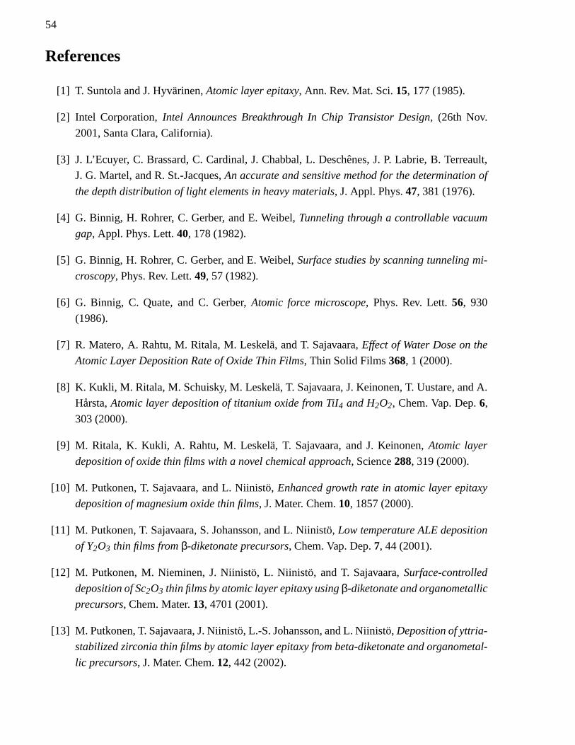
54
References
[1] T. Suntola and J. Hyvärinen, Atomic layer epitaxy, Ann. Rev. Mat. Sci. 15, 177 (1985).
[2] Intel Corporation, Intel Announces Breakthrough In Chip Transistor Design, (26th Nov.
2001, Santa Clara, California).
[3] J. L’Ecuyer, C. Brassard, C. Cardinal, J. Chabbal, L. Deschênes, J. P. Labrie, B. Terreault,
J. G. Martel, and R. St.-Jacques, An accurate and sensitive method for the determination of
the depth distribution of light elements in heavy materials, J. Appl. Phys. 47, 381 (1976).
[4] G. Binnig, H. Rohrer, C. Gerber, and E. Weibel, Tunneling through a controllable vacuum
gap, Appl. Phys. Lett. 40, 178 (1982).
[5] G. Binnig, H. Rohrer, C. Gerber, and E. Weibel, Surface studies by scanning tunneling mi-
croscopy, Phys. Rev. Lett. 49, 57 (1982).
[6] G. Binnig, C. Quate, and C. Gerber, Atomic force microscope, Phys. Rev. Lett. 56, 930
(1986).
[7] R. Matero, A. Rahtu, M. Ritala, M. Leskelä, and T. Sajavaara, Effect of Water Dose on the
Atomic Layer Deposition Rate of Oxide Thin Films, Thin Solid Films 368, 1 (2000).
[8] K. Kukli, M. Ritala, M. Schuisky, M. Leskelä, T. Sajavaara, J. Keinonen, T. Uustare, and A.
Hårsta, Atomic layer deposition of titanium oxide from TiI4 and H2O2, Chem. Vap. Dep. 6,
303 (2000).
[9] M. Ritala, K. Kukli, A. Rahtu, M. Leskelä, T. Sajavaara, and J. Keinonen, Atomic layer
deposition of oxide thin films with a novel chemical approach, Science 288, 319 (2000).
[10] M. Putkonen, T. Sajavaara, and L. Niinistö, Enhanced growth rate in atomic layer epitaxy
deposition of magnesium oxide thin films, J. Mater. Chem. 10, 1857 (2000).
[11] M. Putkonen, T. Sajavaara, S. Johansson, and L. Niinistö, Low temperature ALE deposition
of Y2O3 thin films from β-diketonate precursors, Chem. Vap. Dep. 7, 44 (2001).
[12] M. Putkonen, M. Nieminen, J. Niinistö, L. Niinistö, and T. Sajavaara, Surface-controlled
deposition of Sc2O3 thin films by atomic layer epitaxy using β-diketonate and organometallic
precursors, Chem. Mater. 13, 4701 (2001).
[13] M. Putkonen, T. Sajavaara, J. Niinistö, L.-S. Johansson, and L. Niinistö, Deposition of yttria-
stabilized zirconia thin films by atomic layer epitaxy from beta-diketonate and organometal-
lic precursors, J. Mater. Chem. 12, 442 (2002).
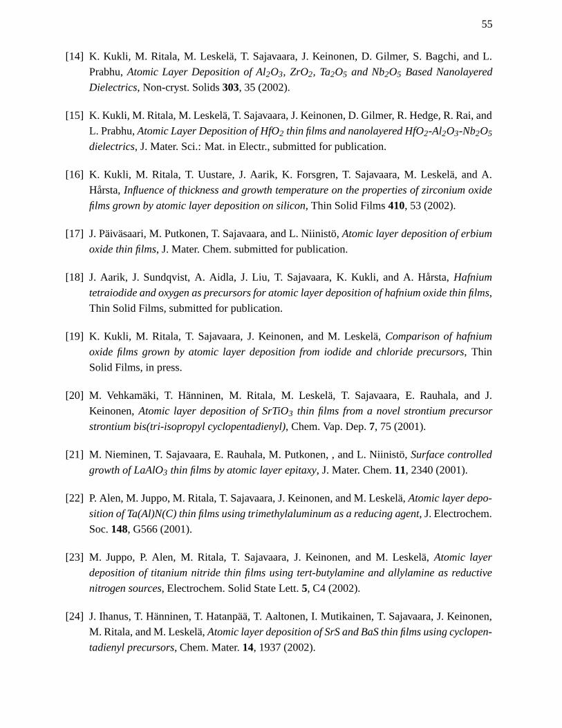
55
[14] K. Kukli, M. Ritala, M. Leskelä, T. Sajavaara, J. Keinonen, D. Gilmer, S. Bagchi, and L.
Prabhu, Atomic Layer Deposition of Al2O3, ZrO2, Ta2O5 and Nb2O5 Based Nanolayered
Dielectrics, Non-cryst. Solids 303, 35 (2002).
[15] K. Kukli, M. Ritala, M. Leskelä, T. Sajavaara, J. Keinonen, D. Gilmer, R. Hedge, R. Rai, and
L. Prabhu, Atomic Layer Deposition of HfO2 thin films and nanolayered HfO2-Al2O3-Nb2O5
dielectrics, J. Mater. Sci.: Mat. in Electr., submitted for publication.
[16] K. Kukli, M. Ritala, T. Uustare, J. Aarik, K. Forsgren, T. Sajavaara, M. Leskelä, and A.
Hårsta, Influence of thickness and growth temperature on the properties of zirconium oxide
films grown by atomic layer deposition on silicon, Thin Solid Films 410, 53 (2002).
[17] J. Päiväsaari, M. Putkonen, T. Sajavaara, and L. Niinistö, Atomic layer deposition of erbium
oxide thin films, J. Mater. Chem. submitted for publication.
[18] J. Aarik, J. Sundqvist, A. Aidla, J. Liu, T. Sajavaara, K. Kukli, and A. Hårsta, Hafnium
tetraiodide and oxygen as precursors for atomic layer deposition of hafnium oxide thin films,
Thin Solid Films, submitted for publication.
[19] K. Kukli, M. Ritala, T. Sajavaara, J. Keinonen, and M. Leskelä, Comparison of hafnium
oxide films grown by atomic layer deposition from iodide and chloride precursors, Thin
Solid Films, in press.
[20] M. Vehkamäki, T. Hänninen, M. Ritala, M. Leskelä, T. Sajavaara, E. Rauhala, and J.
Keinonen, Atomic layer deposition of SrTiO3 thin films from a novel strontium precursor
strontium bis(tri-isopropyl cyclopentadienyl), Chem. Vap. Dep. 7, 75 (2001).
[21] M. Nieminen, T. Sajavaara, E. Rauhala, M. Putkonen, , and L. Niinistö, Surface controlled
growth of LaAlO3 thin films by atomic layer epitaxy, J. Mater. Chem. 11, 2340 (2001).
[22] P. Alen, M. Juppo, M. Ritala, T. Sajavaara, J. Keinonen, and M. Leskelä, Atomic layer depo-
sition of Ta(Al)N(C) thin films using trimethylaluminum as a reducing agent, J. Electrochem.
Soc. 148, G566 (2001).
[23] M. Juppo, P. Alen, M. Ritala, T. Sajavaara, J. Keinonen, and M. Leskelä, Atomic layer
deposition of titanium nitride thin films using tert-butylamine and allylamine as reductive
nitrogen sources, Electrochem. Solid State Lett. 5, C4 (2002).
[24] J. Ihanus, T. Hänninen, T. Hatanpää, T. Aaltonen, I. Mutikainen, T. Sajavaara, J. Keinonen,
M. Ritala, and M. Leskelä, Atomic layer deposition of SrS and BaS thin films using cyclopen-
tadienyl precursors, Chem. Mater. 14, 1937 (2002).
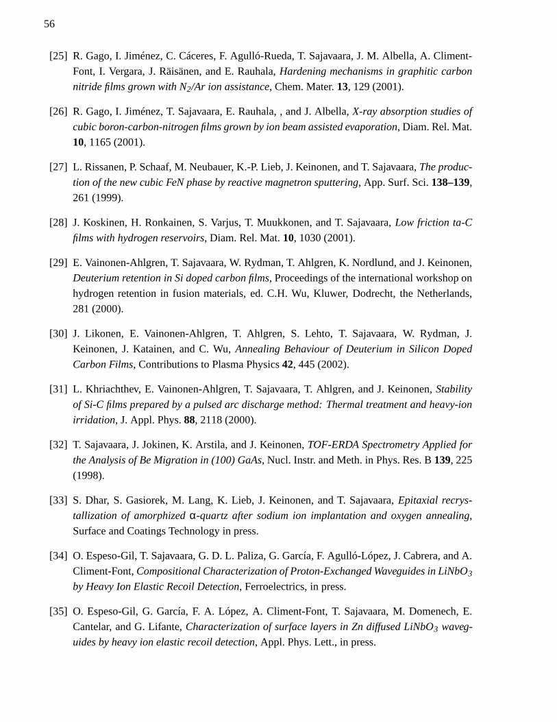
56
[25] R. Gago, I. Jiménez, C. Cáceres, F. Agulló-Rueda, T. Sajavaara, J. M. Albella, A. Climent-
Font, I. Vergara, J. Räisänen, and E. Rauhala, Hardening mechanisms in graphitic carbon
nitride films grown with N2/Ar ion assistance, Chem. Mater. 13, 129 (2001).
[26] R. Gago, I. Jiménez, T. Sajavaara, E. Rauhala, , and J. Albella, X-ray absorption studies of
cubic boron-carbon-nitrogen films grown by ion beam assisted evaporation, Diam. Rel. Mat.
10, 1165 (2001).
[27] L. Rissanen, P. Schaaf, M. Neubauer, K.-P. Lieb, J. Keinonen, and T. Sajavaara, The produc-
tion of the new cubic FeN phase by reactive magnetron sputtering, App. Surf. Sci. 138–139,
261 (1999).
[28] J. Koskinen, H. Ronkainen, S. Varjus, T. Muukkonen, and T. Sajavaara, Low friction ta-C
films with hydrogen reservoirs, Diam. Rel. Mat. 10, 1030 (2001).
[29] E. Vainonen-Ahlgren, T. Sajavaara, W. Rydman, T. Ahlgren, K. Nordlund, and J. Keinonen,
Deuterium retention in Si doped carbon films, Proceedings of the international workshop on
hydrogen retention in fusion materials, ed. C.H. Wu, Kluwer, Dodrecht, the Netherlands,
281 (2000).
[30] J. Likonen, E. Vainonen-Ahlgren, T. Ahlgren, S. Lehto, T. Sajavaara, W. Rydman, J.
Keinonen, J. Katainen, and C. Wu, Annealing Behaviour of Deuterium in Silicon Doped
Carbon Films, Contributions to Plasma Physics 42, 445 (2002).
[31] L. Khriachthev, E. Vainonen-Ahlgren, T. Sajavaara, T. Ahlgren, and J. Keinonen, Stability
of Si-C films prepared by a pulsed arc discharge method: Thermal treatment and heavy-ion
irridation, J. Appl. Phys. 88, 2118 (2000).
[32] T. Sajavaara, J. Jokinen, K. Arstila, and J. Keinonen, TOF-ERDA Spectrometry Applied for
the Analysis of Be Migration in (100) GaAs, Nucl. Instr. and Meth. in Phys. Res. B 139, 225
(1998).
[33] S. Dhar, S. Gasiorek, M. Lang, K. Lieb, J. Keinonen, and T. Sajavaara, Epitaxial recrys-
tallization of amorphized α-quartz after sodium ion implantation and oxygen annealing,
Surface and Coatings Technology in press.
[34] O. Espeso-Gil, T. Sajavaara, G. D. L. Paliza, G. García, F. Agulló-López, J. Cabrera, and A.
Climent-Font, Compositional Characterization of Proton-Exchanged Waveguides in LiNbO3
by Heavy Ion Elastic Recoil Detection, Ferroelectrics, in press.
[35] O. Espeso-Gil, G. García, F. A. López, A. Climent-Font, T. Sajavaara, M. Domenech, E.
Cantelar, and G. Lifante, Characterization of surface layers in Zn diffused LiNbO3 waveg-
uides by heavy ion elastic recoil detection, Appl. Phys. Lett., in press.
57
[36] J. Ziegler, J. Biersack, and U. Littmark, The Stopping and Range of Ions in Solids (Pergamon
Press, Inc., New York, 1985).
[37] W. Brandt and M. Kitagawa, Phys. Rev. B 25, 5631 (1982).
[38] J. Ziegler and J. Biersack, SRIM-2000 computer code, www.srim.org.
[39] J. Ziegler, Stopping of energetic light ions in elemental matter, Appl. Phys. Lett. 85, 1249
(1999).
[40] K. Arstila, J. Keinonen, and P. Tikkanen, Stopping power for low-velocity heavy ions: (0.01–
0.9) MeV/nucleon Si ions in 18 (Z=13-79) metals, Nucl. Instr. and Meth. in Phys. Res. B 101,
321 (1995).
[41] K. Arstila, J. Keinonen, P. Tikkanen, and A. Kuronen, Stopping power for low-velocity heavy
ions: (0–1.0)-MeV/nucleon Mg ions in 17 (Z=22–79) elemental solids, Phys. Rev. B 41, 6117
(1990).
[42] K. Arstila, J. Keinonen, P. Tikkanen, and A. Kuronen, Stopping power for low-velocity Mg
ions in Si, Ge, and GaAs, Phys. Rev. B 43, 13967 (1991).
[43] J. Keinonen, K. Arstila, and P. Tikkanen, Electronic stopping power of Si and Ge for MeV-
energy Si and P ions, Appl. Phys. Lett. 60, 228 (1992).
[44] Y. Zhang, G. Possnert, and H. Whitlow, Measurements of the mean energy-loss of swift heavy
ions in carbon with high precision, Nucl. Instr. and Meth. in Phys. Res. B 183, 34 (2001).
[45] Y. Zhang and G. Possnert, Electronic stopping power of swift heavy ions in carbon, Nucl.
Instr. and Meth. in Phys. Res. B 190, 69 (2002).
[46] W. Trzaska, T. Alanko, V. Lyapin, and J. Räisänen, A novel method for obtaining continuous
stopping power curves, Nucl. Instr. and Meth. in Phys. Res. B 183, 203 (2001).
[47] T. Alanko, W. Trzaska, V. Lyapin, J. Räisänen, G. Tiourine, and A. Virtanen, Simultaneous
wide-range stopping power determination for several ions, Nucl. Instr. and Meth. in Phys.
Res. B 190, 60 (2002).
[48] W. Chu, Calculation of energy straggling for protons and helium ions, Phys. Rev. A 13, 2057
(1976).
[49] Q. Yang, D. O’Connor, and Z. Wang, Empirical formulae for energy loss straggling of ions
in matter, Nucl. Instr. and Meth. in Phys. Res. B 61, 149 (1991).
[50] W. Bragg and R. Kleeman, On the alpha particles of radium, and their loss of range in
passing through various atoms and molecules, Philos. Mag. 10, 318 (1905).
58
[51] K. Arstila, An experimental method for precise determination of electronic stopping powers
for heavy ions, Nucl. Instr. and Meth. in Phys. Res. B 168, 473 (2000).
[52] B. Terreault, J. Martel, R. St-Jacques, and J. L’Ecuyer, Depth profiling of light elements in
materials with high-energy ion beams, J. Vac. Sci. Technol. 14, 492 (1977).
[53] B. Doyle and P. Peercy, Technique for profiling 1H with 2.5-MeV Van de Graaff accelerators,
Appl. Phys. Lett. 34, 811 (1979).
[54] W. Bik, C. de Laat, and F. Habraken, On the use of a dE-E telescope in elastic recoil detec-
tion, Nucl. Instr. and Meth. in Phys. Res. B 64, 832 (1992).
[55] F. Habraken, Light element depth profiling using elastic recoil detection, Nucl. Instr. and
Meth. in Phys. Res. B 68, 181 (1992).
[56] M. Petrascu, I. Berceanu, I. Brancus, A. Buta, M. Duma, C. Grama, I. Lazar, I. Mihai, M.
Petrovici, V. Simion, M. Mihaila, and I. Ghita, A method for analysis and profiling of boron,
carbon and oxygen impurities in semiconductor wafers by recoil atoms in heavy ion beams,
Nucl. Instr. and Meth. in Phys. Res. B 4, 396 (1984).
[57] L. Seiberling, Si-H and C-H bond breaking during MeV-ion bombardment of native oxide of
silicon, Nucl. Instr. and Meth. in Phys. Res. B 24/24, 526 (1987).
[58] R. Behrisch, R. Grötzschel, E. Hentschel, and W. Assmann, HIERD analysis of the low-Z
deposits on probes from the vessel walls of fusion experiments, Nucl. Instr. and Meth. in
Phys. Res. B 68, 245 (1992).
[59] D. Avasthi, D. Kabiraj, A. Bhagwat, G. Mehta, V. Vankar, and S. Ogale, Simultaneous de-
tection of light elements by ERDA with gas-ionisation/Si Delta E-E detector telescope, Nucl.
Instr. and Meth. in Phys. Res. B 93, 480 (1994).
[60] J. Forster, P. Currie, J. Davies, R. Siegele, S. Wallace, and D. Zelenitsky, Elastic recoil
detection (ERD) with extremely heavy ions, Nucl. Instr. and Meth. in Phys. Res. B 113, 308
(1996).
[61] C. Gossett, Use of magnetic spectrometer to profile light elements by elastic recoil detection,
Nucl. Instr. and Meth. in Phys. Res. B 15, 481 (1986).
[62] R. Groleau, S. Gujrathi, and J. Martin, Time-of-flight system for profiling recoiled light ele-
ments, Nucl. Instr. and Meth. 218, 11 (1983).
[63] J. Thomas, M. Fallavier, D. Ramdane, N. Chevarier, and A. Chevarier, High resolutuion
depth profiling of light elements in high atomic mass materials, Nucl. Instr. and Meth. 218,
125 (1983).
59
[64] H. Whitlow, G. Possnert, and C. Petersson, Quantative mass and energy dispersive elastic
recoil spectrometry: Resolution and efficiency considerations, Nucl. Instr. and Meth. in Phys.
Res. B 27, 448 (1987).
[65] E. Arai, H. Funaki, M. Katayama, and K. Shimizu, TOF-ERD experiments using a 10 MeV35Cl beam, Nucl. Instr. and Meth. in Phys. Res. B 64, 296 (1992).
[66] P. Goppelt, B. Gebauer, D. Fink, M. Wilpert, T. Wilpert, and W. Bohne, Nucl. Instr. and
Meth. in Phys. Res. B 68, 235 (1992).
[67] W. Hong, S. Hayakawa, Y. Gohshi, K. Maeda, S. Fukuda, M. Yanokura, K. Kimura, I.
Tanihata, and M. Aratani, Development of a high mass-resolution TOF-ERDA system for a
wide mass range, Nucl. Instr. and Meth. in Phys. Res. B 124, 95 (1997).
[68] M. Döbeli, R. Ender, V. Liechtenstein, and D. Vetterli, Time-of-light spectrometry applied to
2 MeV He RBS, Nucl. Instr. and Meth. in Phys. Res. B 142, 417 (1998).
[69] F. Busch, W.Pfeffer, B. Kohlmeyer, D. Schull, and F. Puhlhoffer, A position-sensitive trans-
mission time detector, Nucl. Instr. and Meth. 171, 71 (1980).
[70] J. Jokinen, J. Keinonen, P. Tikkanen, A. Kuronen, T. Ahlgren, and K. Nordlund, Comparison
of TOF-ERDA and nuclear resonance reaction techniques for range profile measurements of
keV energy implants, Nucl. Instr. and Meth. in Phys. Res. B 119, 533 (1996).
[71] J. Jokinen, Time-of-flight spectrometry of recoiled atoms in the analysis of thin films, Acta
Polytech. Scand. Appl. Phys. Series 212, 1 (1997).
[72] J. Schader, B. Kolb, K. Sevier, and K. Groeneweld, Electron ejection from beam-tilted-foil
experiments, Nucl. Instr. and Meth. 151, 563 (1978).
[73] P. Koschar, K. Kroneberger, A. Clouvas, M. Burkhard, W. Meckbach, O. Heil, J. Kemmler,
H. Rothard, K. Groeneveld, R. Schramm, and H.-D. Betz, Secondary-electron yield as a
probe of preequilibrium stopping power of heavy ions colliding with solids, Phys. Rev. A 40,
3632 (1989).
[74] V. Liechtenstein, T. M. Ivkova, E. Olshanski, A. Baranov, R. Repnow, R. Hellborg, R. Weller,
and H. Wirth, Preparation and evaluation of thin diamond-like carbon foils for heavy-ion
tandem accelerators and time-of-flight spectrometers, Nucl. Instr. and Meth. in Phys. Res. A
397, 140 (1997).
[75] V. Liechtenstein, T. Ivkova, E. Olshanski, A. Baranov, R. Repnow, R. Hellborg, R. A. Weller,
and H. L. Wirth, Preparation and comparative testing of advanced diamond-like carbon foils
for tandem accelerators and time-of-flight spectrometers, Nucl. Instr. and Meth. in Phys. Res.
A 438, 79 (1999).
60
[76] E. Sternglass, Theory of secondary electron emission by high-speed ions, Phys. Rev. 108, 1
(1957).
[77] R. Neugebauer, R. Wuensch, T. Jalowy, K. O. Groeneveld, H. Rothard, A. Clouvas, and C.
Potiriadis, Secondary electron emission near the electronic stopping power maximum, Phys.
Rev. B 59, 11113 (1999).
[78] T. Conlon, Materials characterization with MeV ions, Nucl. Instr. and Meth. in Phys. Res. B
40–41, 828 (1989).
[79] W. Lanford, H. Trautvetter, J. Ziegler, and J. Keller, New precision technique for measuring
the concentration versus depth of hydrogen in solids, Appl. Phys. Lett. 28, 566 (1976).
[80] P. Torri, J. Keinonen, and K. Nordlund, A low-level detection system for hydrogen analysis
with the reaction 1H(15N, αγ)12C, Nucl. Instr. and Meth. in Phys. Res. B 84, 105 (1994).
[81] J. Jokinen, P. Haussalo, J. Keinonen, M. Ritala, D. Riihelä, and M. Leskelä, Analysis of AlN
thin films by combining TOF-ERDA and NRB techniques, Thin Solid Films 289, 159 (1996).
[82] W. Bohne, J. Röhrich, and G. Röschert, The Berlin time-of-flight ERDA setup, Nucl. Instr.
and Meth. in Phys. Res. B 136-138, 633 (1998).
[83] M. Wielunski, M. Mayer, R. Behrisch, J. Roth, and B. Scherzer, Simultaneous profiling of
hydrogen and deuterium by 2.6 MeV 4He ERDA using ∆E–E telescope detector, Nucl. Instr.
and Meth. in Phys. Res. B 122, 113 (1997).
[84] S. Gujrathi and S. Bultena, Depth profiling of hydrogen using the high efficiency ERD-TOF
technique, Nucl. Instr. and Meth. in Phys. Res. B 64, 789 (1992).
[85] G. Boudreault, R. Elliman, R. Grötzschel, S. Gujrathi, C. Jeynes, W. Lennard, E. Rauhala, T.
Sajavaara, H. Timmers, and T. Weijers, Round Robin: Measurement of H implants in Silicon
by ERD, Poster at 15th Ion Beam Analysis -conference, Cairns, Australia (2001).
[86] M. Nieminen, S. Lehto, and L. Niinistö, Atomic layer epitaxy growth of LaGaO3 thin films,
J. Mat. Chem. 11, 3148 (2001).
[87] B. Maurel and G. Amsel, A new measurement of the 429 keV 15N(p,αγ)12C resonance. Ap-
plications of the very narrow width found to 15N and 1H depth location. I. Resonance width
measurement, Nucl. Instr. and Meth. 218, 159 (1983).
[88] G. Meyer and N. Amer, Novel optical approach to atomic force microscopy, Appl. Phys.
Lett. 53, 1045 (1988).
[89] A. Ott, J. Klaus, J. Johnson, and S. George, Al3O3 thin film growth on Si(100) using binary
reaction sequence chemistry, Thin Solid Films 292, 130 (1997).
61
[90] M. E. Bouanani, M. Hult, L. Persson, E. Swietlicki, M. Andersson, M. Östling, N. Lund-
berg, C. Zaring, D. Cohen, N. Dytlewski, P. Johnston, S. Walker, I. Bubb, and H. Whitlow,
Multivariate analysis method for energy calibration and improved mass assignment in recoil
spectrometry, Nucl. Instr. and Meth. in Phys. Res. B 94, 530 (1994).
[91] Round Robin: Characterisation of the Thickness and Composition of Thin to Ultra-thin
AlNO Films (IAEA coordinated project, coordinator N.P. Barradas).
[92] K. Oxorn, S. Gujrathi, S. Bultena, L. Cliche, and J. Minskin, An iterative computer analysis
package for elastic recoil detection, Nucl. Instr. and Meth. in Phys. Res. B 45, 166 (1990).
[93] N. P. Barradas, C. Jeynes, and R. Webb, Simulated annealing analysis of Rutherford
backscattering data, Appl. Phys. Lett. 71, 291 (1997).
[94] R. Fischer, M. Mayer, W. von der Linden, and V. Dose, Enhancement of the energy resolution
in ion-beam experimentswith the maximum-entropy method, Phys. Rev. E 55, 6667 (1997).
[95] E. Edelmann, K. Arstila, and J. Keinonen, to be published.
[96] E. Arai, H. Funaki, M. Katayama, and K. Shimizu, Stoichiometry and profiling of surface
layers by means of TOF-E ERDA and RBS, Nucl. Instr. and Meth. in Phys. Res. B 68, 202
(1992).
[97] P. Sigmund and K. Winterborn, Small-angle multiple scattering of ions in the screened
Coulomb region. I. Angular distributions, Nucl. Instr. and Meth. 119, 541 (1974).
[98] E. Szilagyi and F. Paszti, Theoretical calculation of the depth resolution of IBA methods,
Nucl. Instr. and Meth. in Phys. Res. B 85, 616 (1994).
[99] E. Szilágyi, L. Wielunski, and F. Pászti, Theoretical approximation of energy distribution of
elastically recoiled hydrogen atoms, Nucl. Instr. and Meth. in Phys. Res. B 136–138, 701
(1998).
[100] P. Bauer, E. Steinbauer, and J. Biersack, The width of an RBS spectrum: influence of plural
and multiple scattering, Nucl. Instr. and Meth. in Phys. Res. B 64, 711 (1992).
[101] P. Johnston, R. Franich, I. Bubb, M. Bouanani, D. Cohen, N. Dytlewksi, and R. Siegele, The
effects of large angle plural scattering on heavy ion elastic recoil detection analysis, Nucl.
Instr. and Meth. in Phys. Res. B 161–163, 314 (2000).
[102] R. D. Franich, P. N. Johnston, I. F. Bubb, N. Dytlewski, and D. D. Cohen, Efficiency en-
hancements to Monte Carlo simulation of heavy ion elastic recoil detection analysis spectra,
Nucl. Instr. and Meth. in Phys. Res. B 190, 252 (2002).
62
[103] J. Slotte, A. Laakso, T. Ahlgren, E. Rauhala, R. Salonen, J. Räisänen, A. Simon, I. Uzonyi,
Z. Kiss, and E. Somorjai, Influence of surface topography on depth profiles obtained by
Rutherford backscattering spectrometry, J. Appl. Phys. 87, 140 (2000).
[104] H. Metzner, M. Gossla, and T. Hahn, Rutherford backscattering spectroscopy of rough films:
Theoretical considerations, Nucl. Instr. and Meth. in Phys. Res. B 124, 567 (1996).
[105] R. Behrisch, S. Grigull, U. Kreissig, and R. Grötzschel, Influence of surface roughness on
measuring depth profiles and the total amount of implanted ions by RBS and ERDA, Nucl.
Instr. and Meth. in Phys. Res. B 136–138, 628 (1998).
[106] H. Metzner, M. Gossla, T. Hahn, J. Conrad, and J.-H. Bremer, Rutherford backscattering
spectroscopy of rough films: Experimental aspects, Nucl. Instr. and Meth. in Phys. Res. B
134, 249 (1998).
[107] A. Kitamura, T. Tamai, A. Taniike, Y. Furuyama, T. Maeda, N. Ogiwara, and M. Saidoh,
Simulation of ERD spectra for a surface with a periodic roughness, Nucl. Instr. and Meth.
in Phys. Res. B 134, 98 (1998).
[108] I.-M. Yesil, W. Assmann, H. Huber, and K. Löbner, Simulation of surface roughness effects
in ERDA, Nucl. Instr. and Meth. in Phys. Res. B 136–138, 623 (1998).
[109] S. Lindner, W. Bohne, A. Jäger-Waldau, M. Lux-Steiner, J. Röhrich, and G. Vogl, Investiga-
tions of atomic diffusion at CIGSSe/ZnSe interfaces with heavy ion elastic recoil detection
analysis (HI-ERDA ), Thin Solid Films 403–404, 432 (2002).
[110] J. R. Tesmer and M. Nastasi (ed.), Handbook of Modern Ion Beam Materials Analysis (Ma-
terials Research Society, Pittsburgh, USA, 1995).
[111] R. Behrisch, W. von der Linden, U. von Toussaint, and D. Grambole, Surface layer destruc-
tion during ion beam analysis, Nucl. Instr. and Meth. in Phys. Res. B 155, 440 (1999).
[112] S. Walker, J. Davies, J. Forster, S. Wallace, and A. Kockelkoren, Radiation damage during
heavy ion elastic recoil detection analysis of insulating materials, Nucl. Instr. and Meth. in
Phys. Res. B 136-138, 707 (1998).
[113] S. Wallace, A. Kockelkoren, M. Boudreau, P. Mascher, J. Forster, and J. Davies, Hydrogen
and Nitrogen Loss during ERD Analysis of Silicon (Oxy)nitrides, Mat. Sci. Forum 248-249,
381 (1997).
[114] H. Timmers, T. Weijers, R. Elliman, J. Uribasterra, H. J. Whitlow, and E.-L. Sarwe, Thresh-
old stoichiometry for beam induced nitrogen depletion of SiN, Nucl. Instr. and Meth. in Phys.
Res. B 190, 428 (2002).
63
[115] R. Behrisch, M. Mayer, W. Jacob, W. Assmann, G. Dollinger, A. Bergmaier, U. Kreissig, M.
Friedrich, G. Sun, D. Hildebrandt, M. Akbi, W. Schneider, D. Schleußner, W. Knapp, and C.
Edelmann, Quantitative analysis of deuterium in a-C:D layers, a Round Robin experiment,
J. Nucl. Mat. 281, 42 (2000).
[116] R. Behrisch, V. Prozesky, H. Huber, and W. Assmann, Hydrogen desorption induced by
heavy-ions during surface layer analysis with ERDA, Nucl. Instr. and Meth. in Phys. Res. B
118, 262 (1996).
[117] G. Dollinger, M. Boulouednine, A. Bergmaier, T. Faestermann, and C. Frey, Limits in elastic
recoil detection analysis with heavy ions, Nucl. Instr. and Meth. in Phys. Res. B 118, 291
(1996).
[118] J. Likonen, S. Lehto, T. Sajavaara, J. Keinonen, and P. Coad, Characterization of JET wall
tiles with surface analytical techniques, to be published.
[119] P. Johnston, I. Budd, S. Walker, W. Stannard, D. Jamieson, S. Dooley, D. Cohen, N.
Dytlewski, and J. Martin, Damage in semiconductor materials during heavy-ion elastic re-
coil detection analysis, Nucl. Instr. and Meth. in Phys. Res. B 113, 312 (1996).
[120] H. Huber, W. Assmann, S. A. Karamian, H. Mieskes, H. Nolte, E. Gazis, M. Kokkoris, S.
Kossionides, R. Vlastou, R. Grötzschel, A. Mücklich, and W. Prusseit, Heavy-ion induced
damage of crystalline Ge and W in the 0.5–8 A MeV range, Nucl. Instr. and Meth. in Phys.
Res. B 146, 309 (1998).
[121] M. Guina, N. Xiang, A. Vainionpaa, O. Okhotnikov, T. Sajavaara, and J. Keinonen, Self-
starting stretched-pulse fiber laser mode locked and stabilized with slow and fast semicon-
ductor saturable absorbers, Optics Lett. 26, 1809 (2001).
[122] N. Xiang, M. Guina, A. Vainionpaa, J. Lyytikäinen, S. Suomalainen, M. Saarinen, O. Okhot-
nikov, T. Sajavaara, and J. Keinonen, Broadband Semiconductor Saturable Absorber Mirrors
in the 1.55-µm Wavelenght Range for Pulse Generation in Fiber, J. Quantum Electronics 38,
369 (2002).
[123] W. Weber, Models and mechanisms of irradiation-induced amorphization in ceramics, Nucl.
Instr. and Meth. in Phys. Res. B 166-167, 98 (2000).
[124] F. Baudenbacher, M. Bauer, H. Kinder, G. Dollinger, F. Ohnesorge, and W. Assman, Impact
and characterisation of heavy ion tracks on epitaxial growth, Nucl. Instr. and Meth. in Phys.
Res. B 107, 327 (1996).
[125] S. Dhar, S. Gasiorek, M. Lang, K. Lieb, J. Keinonen, and T. Sajavaara, to be published.
64
[126] O. Espeso-Gil, T. Sajavaara, G. D. L. Paliza, G. García, F. Agulló-López, J. Cabrera, and A.
Climent-Font, to be published.
[127] S. Gasiorek, S. Dhar, T. Sajavaara, K. Lieb, and J. Keinonen, to be published.
[128] T. Suntola, Atomic layer epitaxy, Thin Solid Films 216, 84 (1992).
[129] M. Gustafsson, F. Roccaforte, W. Bolse, L. Ziegeler, and K. P. Lieb, Oxygen-activated epi-
taxial recrystallization of Li-implanted α-SiO2, Phys. Rev. B 61, 3327 (2000).