Embed Size (px)
Citation preview
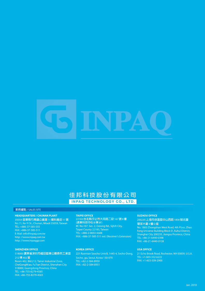
HEADQUARTERS / CHUNAN PLANT
35059 11 11No.11, Ke-Yi St., Chunan, Miaoli 35059, TaiwanTEL: +886-37-585-555FAX: +886-37-585-511E-Mail: [email protected]: //www.inpaq.com.twhttp: //www.inpaqgp.com
KOREA OFFICE
221 Raemian Seocho Univill, 1445-4, Secho-Dong,
Secho_gu, Seoul, Korea 130-070TEL: +82-2-584-8959FAX: +82-2-584-8951
SUZHOU OFFICE
200235 1800
4 DNo. 1800 Zhongshan West Road, 4th Floor, Zhao Feng Universe Building Block D ,Xuhui District,Shanghai City 200235, Jiangsu Province, China TEL: +86-21-6440-0398FAX: +86-21-6440-0138
TAIPEI OFFICE22183 167 8( B 8F)8F, No.167, Sec. 2, Datong Rd., Sijhih City, Taipei County 22183, TaiwanTEL: +886-2-8692-6688 FAX: +886-37-585-511 ext: (Receiver's Extension)
SHENZHEN OFFICE
518000
212 402Room 402, Bld.212, Tairan Industrial Zone,CheGongMiao, FuTian District, Shenzhen City518000, Guangdong Province, ChinaTEL: +86-755-8279-4585 FAX: +86-755-8279-4565
USA OFFICE
21 Echo Brook Road, Rochester, NH 03839, U.S.A.TEL: +1-603-332-6222FAX: +1-603-509-2900
/ SALES SITE
Jan. 2010
http://www.inpaq.com.tw
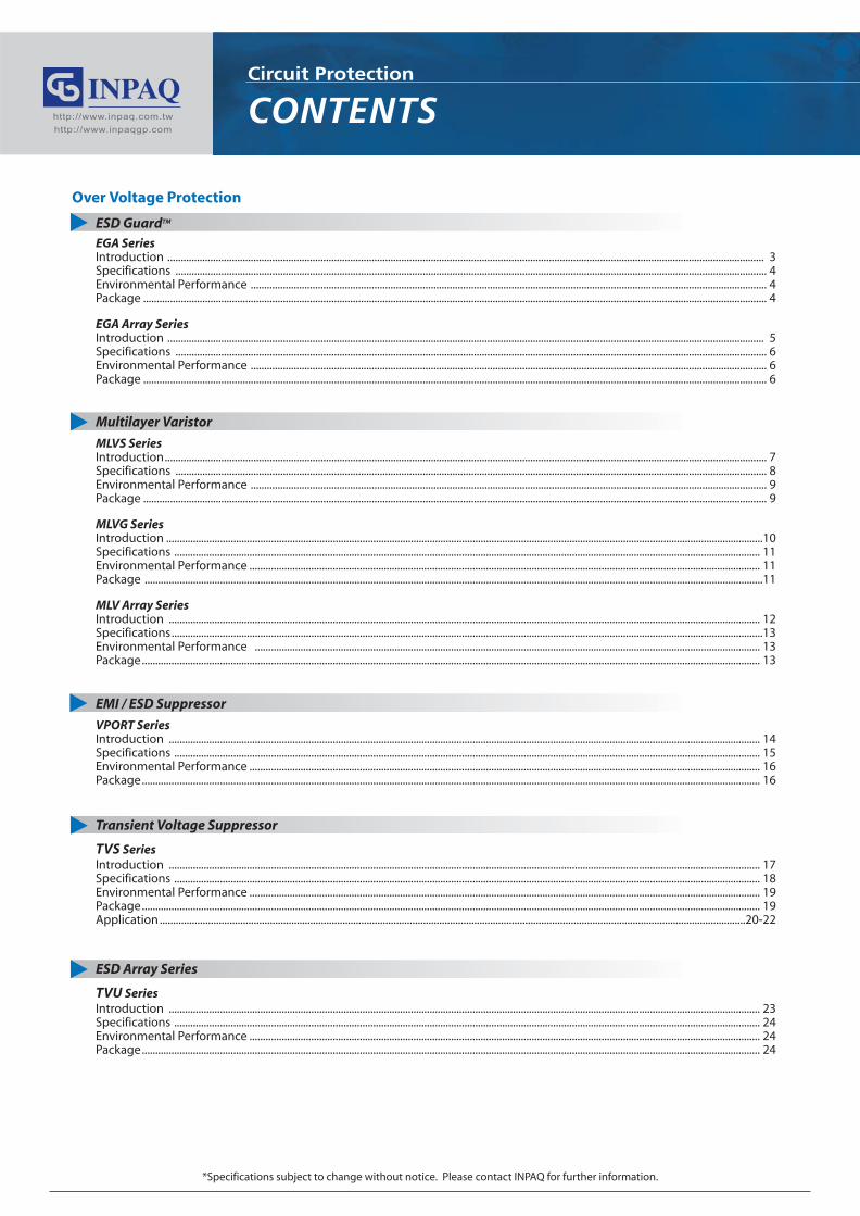
http://www.inpaqgp.comCONTENTSCircuit Protection
Over Voltage Protection
ESD GuardTM
EGA SeriesIntroduction .............................................................................................................................................................................................................................. 3Specifications ............................................................................................................................................................................................................................ 4Environmental Performance ................................................................................................................................................................................................ 4Package ........................................................................................................................................................................................................................................ 4
EGA Array SeriesIntroduction .............................................................................................................................................................................................................................. 5Specifications ............................................................................................................................................................................................................................ 6Environmental Performance ................................................................................................................................................................................................ 6Package ........................................................................................................................................................................................................................................ 6
Multilayer Varistor
MLVS SeriesIntroduction................................................................................................................................................................................................................................ 7Specifications ............................................................................................................................................................................................................................ 8Environmental Performance ................................................................................................................................................................................................ 9Package ........................................................................................................................................................................................................................................ 9
MLVG SeriesIntroduction ..............................................................................................................................................................................................................................10Specifications .......................................................................................................................................................................................................................... 11Environmental Performance .............................................................................................................................................................................................. 11Package ......................................................................................................................................................................................................................................11
MLV Array SeriesIntroduction ............................................................................................................................................................................................................................ 12Specifications............................................................................................................................................................................................................................13Environmental Performance ............................................................................................................................................................................................ 13Package...................................................................................................................................................................................................................................... 13
EMI / ESD Suppressor
VPORT SeriesIntroduction ............................................................................................................................................................................................................................ 14Specifications .......................................................................................................................................................................................................................... 15Environmental Performance .............................................................................................................................................................................................. 16Package...................................................................................................................................................................................................................................... 16
Transient Voltage Suppressor
TVS SeriesIntroduction ............................................................................................................................................................................................................................ 17Specifications .......................................................................................................................................................................................................................... 18Environmental Performance .............................................................................................................................................................................................. 19Package...................................................................................................................................................................................................................................... 19Application..........................................................................................................................................................................................................................20-22
ESD Array Series
TVU SeriesIntroduction ............................................................................................................................................................................................................................ 23Specifications .......................................................................................................................................................................................................................... 24Environmental Performance .............................................................................................................................................................................................. 24Package...................................................................................................................................................................................................................................... 24
*Specifications subject to change without notice. Please contact INPAQ for further information.
http://www.inpaq.com.tw
http://www.inpaqgp.com
2
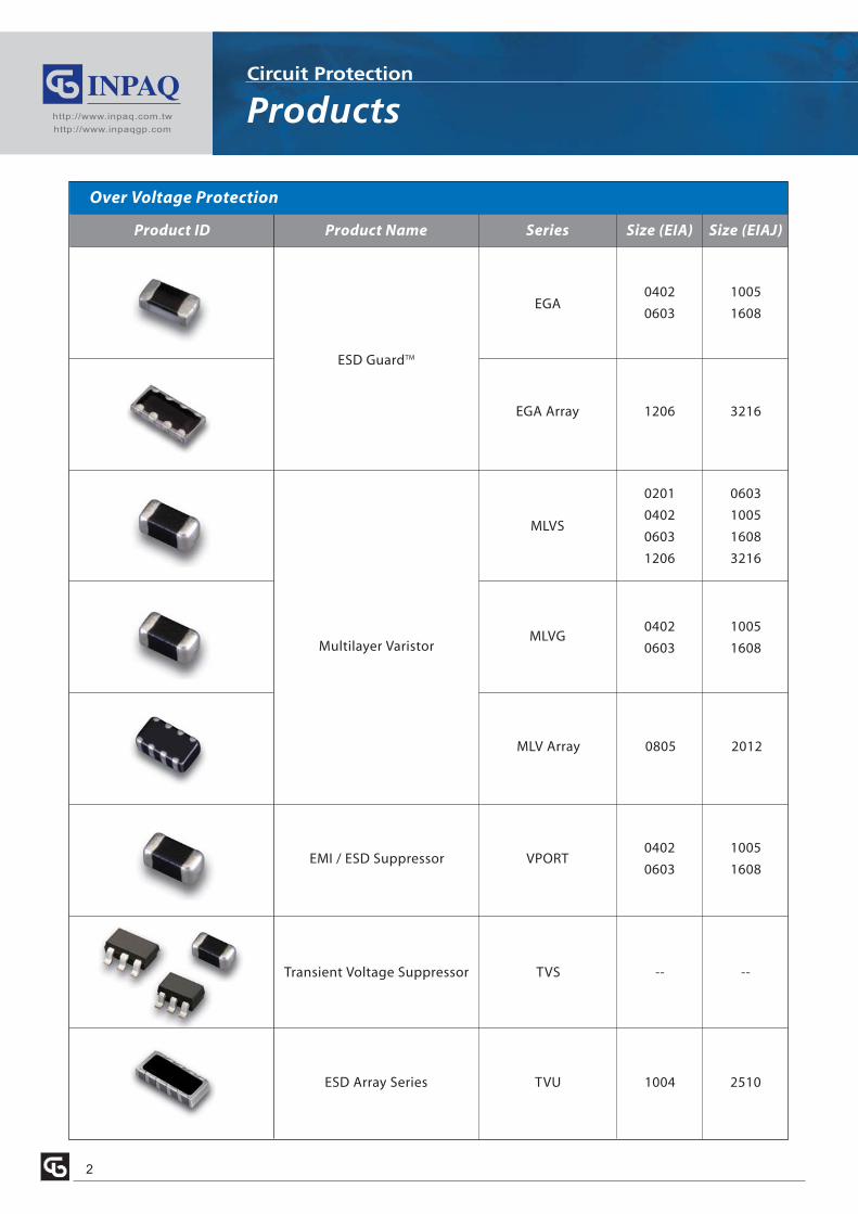
ProductsCircuit Protection
Product ID Product Name Series Size (EIA) Size (EIAJ)
ESD GuardTM
EGA0402
0603
1005
1608
EGA Array 1206 3216
MLV Array 0805 2012
Multilayer Varistor
MLVS
0201
0402
0603
1206
0603
1005
1608
3216
MLVG0402
0603
1005
1608
EMI / ESD Suppressor
ESD Array Series TVU
--TVSTransient Voltage Suppressor --
1004 2510
VPORT0402
0603
1005
1608
Over Voltage Protection
http://www.inpaq.com.tw
http://www.inpaqgp.com
3
Unit: mm
1 4 5 6
Applications
How to Order
Dimensions
Features
EGA SeriesESD GUARDTM
Protection against high ESD voltage and currentCompact size for EIA 0402 and 0603Extremely quick response time (<1ns)Extremely low capacitance (<0.5pF)Extremely low leakage currentZero signal distortionBi-directional
EGA10402V05AH, EGA10402V12A0, EGA10603 Series are applied to RF module, Antenna circuit, IEEE-1394, USB2.0, DVI, HDMI and DisplayPort…etc.high speed signal interface.EGA10402V05A2 is recommended to use the application of RF antenna front-end circuit without DC bias.
EGA 1 0603 V05 A1 - B1 2 3 4 5
Series Type : ESD GuardTM Series
Elements Type
Chip Size (EIA) : 0402/0603
Rated Voltage, VDC
Model Code
Suffix for Special Code6
5
4
3
2
1
B
H
L
W
Size EIA (EIAJ) 0402 (1005) 0603 (1608)
L 1.00±0.1 1.60±0.1
W 0.50±0.1 0.85±0.15
H 0.34±0.1 0.51±0.05
B 0.20±0.1 0.30±0.2
http://www.inpaq.com.tw
http://www.inpaqgp.com
4
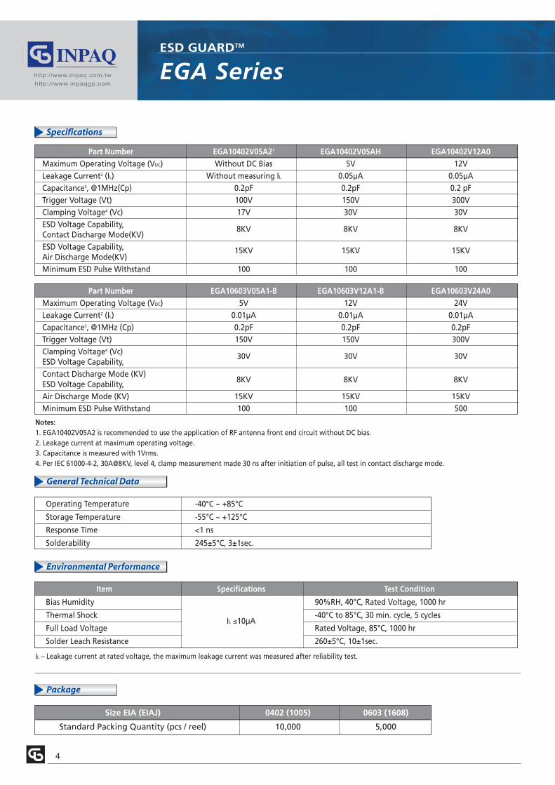
Specifications
Environmental Performance
General Technical Data
EGA SeriesESD GUARDTM
Package
Notes:1. EGA10402V05A2 is recommended to use the application of RF antenna front end circuit without DC bias.2. Leakage current at maximum operating voltage.3. Capacitance is measured with 1Vrms.4. Per IEC 61000-4-2, 30A@8KV, level 4, clamp measurement made 30 ns after initiation of pulse, all test in contact discharge mode.
IL – Leakage current at rated voltage, the maximum leakage current was measured after reliability test.
Part Number EGA10402V05A21 EGA10402V05AH EGA10402V12A0Maximum Operating Voltage (VDC) Without DC Bias 5V 12VLeakage Current2 (IL) Without measuring IL 0.05µA 0.05µACapacitance3, @1MHz(Cp) 0.2pF 0.2pF 0.2 pFTrigger Voltage (Vt) 100V 150V 300VClamping Voltage4 (Vc) 17V 30V 30VESD Voltage Capability, Contact Discharge Mode(KV)
8KV 8KV 8KV
ESD Voltage Capability, Air Discharge Mode(KV)
15KV 15KV 15KV
Minimum ESD Pulse Withstand 100 100 100
Part Number EGA10603V05A1-B EGA10603V12A1-B EGA10603V24A0Maximum Operating Voltage (VDC) 5V 12V 24VLeakage Current2 (IL) 0.01µA 0.01µA 0.01µACapacitance3, @1MHz (Cp) 0.2pF 0.2pF 0.2pFTrigger Voltage (Vt) 150V 150V 300VClamping Voltage4 (Vc) 30V 30V 30VESD Voltage Capability, Contact Discharge Mode (KV)
8KV 8KV 8KVESD Voltage Capability, Air Discharge Mode (KV) 15KV 15KV 15KVMinimum ESD Pulse Withstand 100 100 500
Item Specifications Test Condition
Bias Humidity 90%RH, 40°C, Rated Voltage, 1000 hr
Thermal ShockIL ≤10µA
-40°C to 85°C, 30 min. cycle, 5 cycles
Full Load Voltage Rated Voltage, 85°C, 1000 hr
Solder Leach Resistance 260±5°C, 10±1sec.
Operating Temperature -40°C ~ +85°C
Storage Temperature -55°C ~ +125°C
Response Time <1 ns
Solderability 245±5°C, 3±1sec.
Size EIA (EIAJ) 0402 (1005) 0603 (1608)
Standard Packing Quantity (pcs / reel) 10,000 5,000
http://www.inpaq.com.tw
http://www.inpaqgp.com
5
Unit: mm
1 6
Applications
How to Order
Dimensions
Features
1
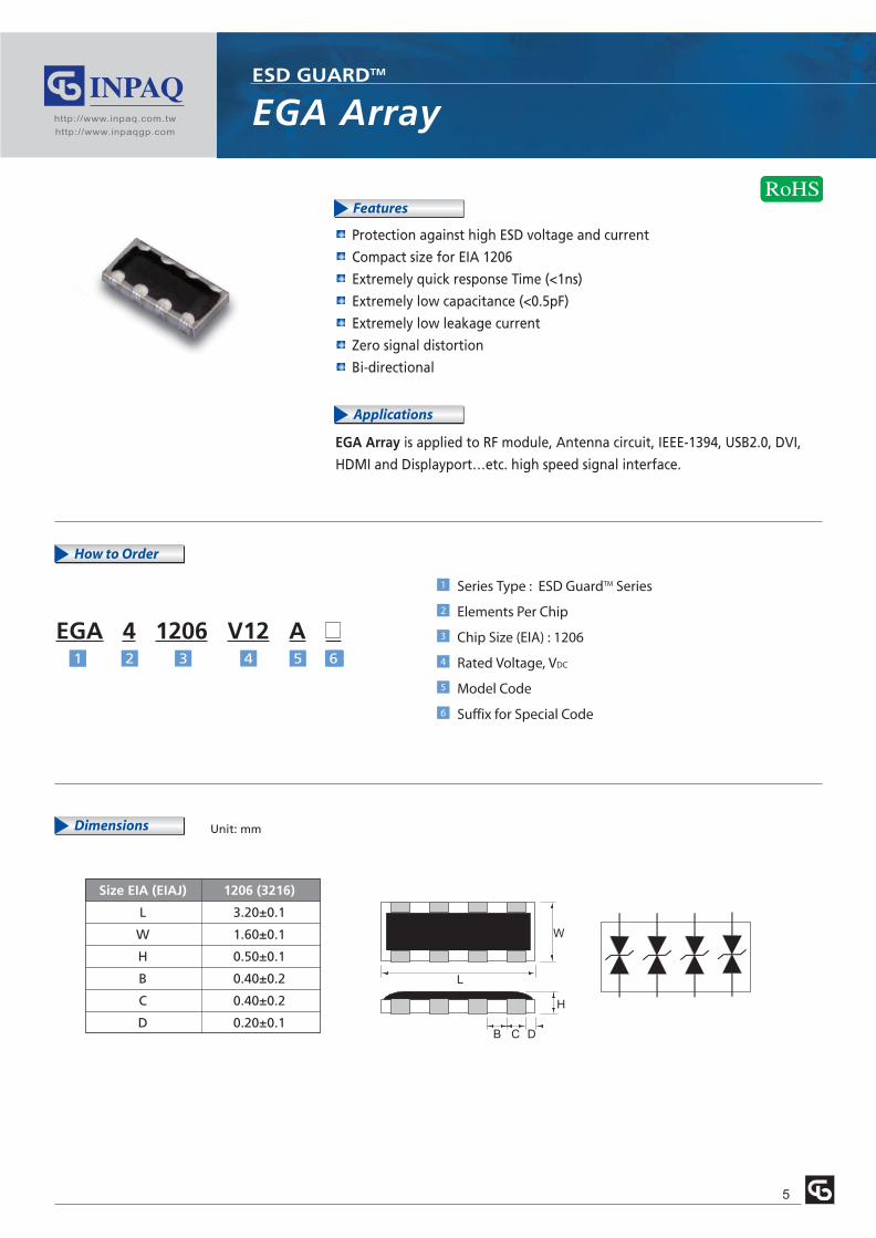
EGA ArrayESD GUARDTM
Protection against high ESD voltage and current
Compact size for EIA 1206
Extremely quick response Time (<1ns)
Extremely low capacitance (<0.5pF)
Extremely low leakage current
Zero signal distortion
Bi-directional
EGA Array is applied to RF module, Antenna circuit, IEEE-1394, USB2.0, DVI,
HDMI and Displayport…etc. high speed signal interface.
EGA 4 1206 V12 A --2 3 4 5 6
Series Type : ESD GuardTM Series
Elements Per Chip
Chip Size (EIA) : 1206
Rated Voltage, VDC
Model Code
Suffix for Special Code6
5
4
3
2
1
W
L
H
DB C
Size EIA (EIAJ) 1206 (3216)
L 3.20±0.1
W 1.60±0.1
H 0.50±0.1
B 0.40±0.2
C 0.40±0.2
D 0.20±0.1
http://www.inpaq.com.tw
http://www.inpaqgp.com
6
Specifications
EGA ArrayESD GUARDTM
Package
Notes:1. Leakage current at maximum operating voltage.2. Capacitance is measured with 1Vrms.3. Per IEC 61000-4-2, 30A@8KV, level 4, clamp measurement made 30 ns after initiation of pulse, all test in contact discharge mode.
IL – Leakage current at rated voltage, the maximum leakage current was measured after reliability test.
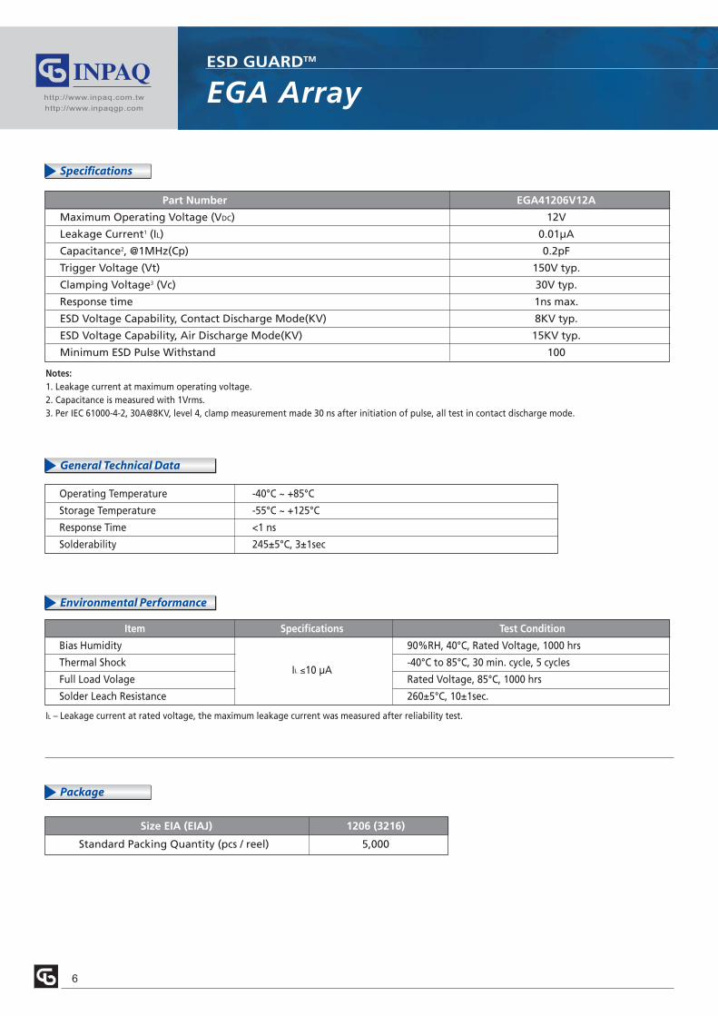
Part Number EGA41206V12A
Maximum Operating Voltage (VDC) 12V
Leakage Current1 (IL) 0.01µA
Capacitance2, @1MHz(Cp) 0.2pF
Trigger Voltage (Vt) 150V typ.
Clamping Voltage3 (Vc) 30V typ.
Response time 1ns max.
ESD Voltage Capability, Contact Discharge Mode(KV) 8KV typ.
ESD Voltage Capability, Air Discharge Mode(KV) 15KV typ.
Minimum ESD Pulse Withstand 100
Item Specifications Test Condition
Bias Humidity 90%RH, 40°C, Rated Voltage, 1000 hrs
Thermal ShockIL ≤10 µA
-40°C to 85°C, 30 min. cycle, 5 cycles
Full Load Volage Rated Voltage, 85°C, 1000 hrs
Solder Leach Resistance 260±5°C, 10±1sec.
Operating Temperature -40°C ~ +85°C
Storage Temperature -55°C ~ +125°C
Response Time <1 ns
Solderability 245±5°C, 3±1sec
Size EIA (EIAJ) 1206 (3216)
Standard Packing Quantity (pcs / reel) 5,000
Environmental Performance
General Technical Data
http://www.inpaq.com.tw
http://www.inpaqgp.com
7
Unit: mm
1 5
How to Order
Dimensions
Features
1
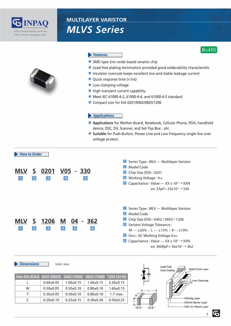
MLVS SeriesMULTILAYER VARISTOR
SMD type zinc oxide based ceramic chip
Lead free plating termination provided good solderability characteristic
Insulator overcoat keeps excellent low and stable leakage current
Quick response time (<1ns)
Low clamping voltage
High transient current capability
Meet IEC 61000-4-2, 61000-4-4, and 61000-4-5 standard
Compact size for EIA 0201/0402/0603/1206
Applications for Mother Board, Notebook, Cellular Phone, PDA, handheld device, DSC, DV, Scanner, and Set-Top Box…etc.Suitable for Push-Button, Power Line and Low Frequency single line overvoltage protect.
MLV S 0201 V05 - 3302 3 4
Series Type : MLV — Multilayer Varistor
Model Code
Chip Size (EIA) : 0201
Working Voltage : VDC
Capacitance : Value — XX x 10N XXN
ex: 33pF= 33x100 330
5
4
3
2
1
1 61
MLV S 1206 M 04 - 3622 3 4 5
Series Type : MLV — Multilayer Varistor
Model Code
Chip Size (EIA) : 0402 / 0603 / 1206
Varistor Voltage Tolerance :
M — ±20% ; L — ±15% ; K— ±10%
VRMS : AC Working Voltage VRMS
Capacitance : Value — XX x 10N XXN
ex: 3600pF= 36x102 362
6
5
4
3
2
1
Applications
Size EIA (EIAJ) 0201 (0603) 0402 (1005) 0603 (1608) 1206 (3216)
L 0.60±0.05 1.00±0.15 1.60±0.15 3.20±0.15
W 0.30±0.05 0.50±0.10 0.80±0.10 1.60±0.15
T 0.30±0.05 0.50±0.10 0.80±0.10 1.7 max.
C 0.20±0.10 0.25±0.15 0.30±0.20 0.50±0.25
http://www.inpaq.com.tw
http://www.inpaqgp.com
8
Specifications
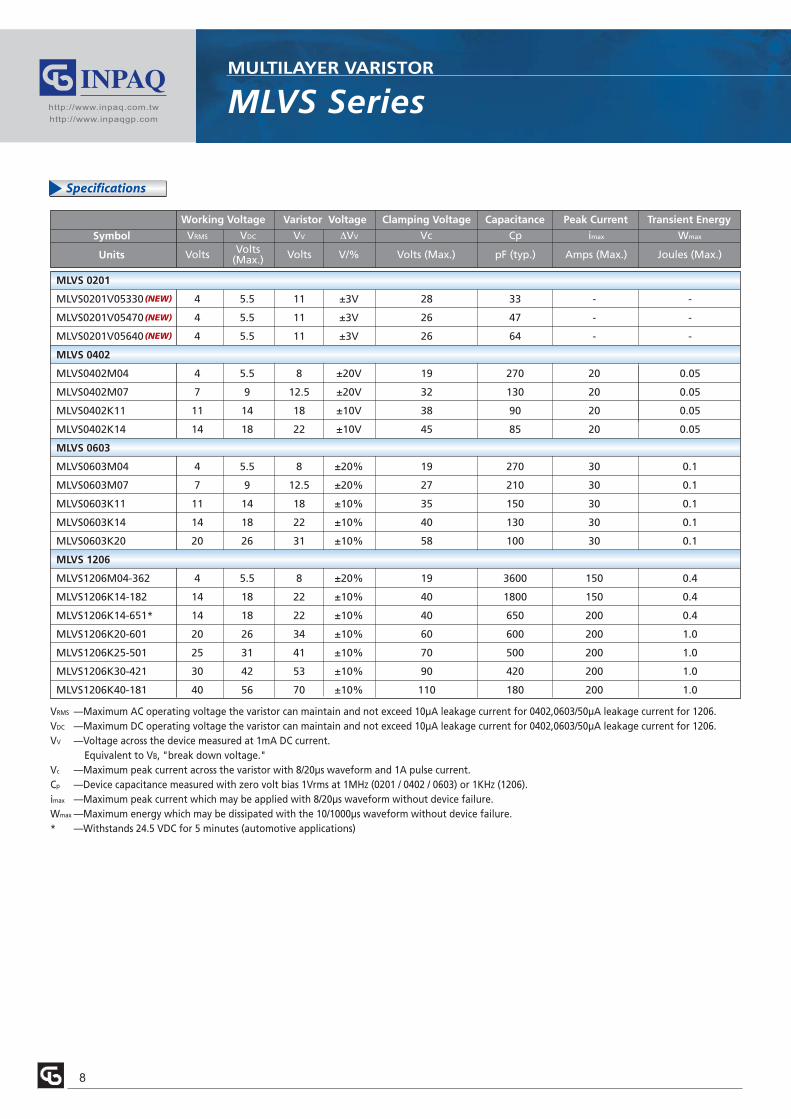
MLVS SeriesMULTILAYER VARISTOR
Symbol
Units
Working Voltage
∆VVVV
Varistor Voltage
Vc
Clamping Voltage
Cp
Capacitance
imax
Peak Current
Wmax
Transient Energy
VDCVRMS
V/%Volts Volts (Max.) pF (typ.) Amps (Max.) Joules (Max.)Volts(Max.)Volts
MLVS 0201
MLVS0201V05330 4 5.5 11 ±3V 28 33 - -
MLVS0201V05470 4 5.5 11 ±3V 26 47 - -
MLVS0201V05640 4 5.5 11 ±3V 26 64 - -
MLVS 0402
MLVS0402M04 4 5.5 8 ±20V 19 270 20 0.05
MLVS0402M07 7 9 12.5 ±20V 32 130 20 0.05
MLVS0402K11 11 14 18 ±10V 38 90 20 0.05
MLVS0402K14 14 18 22 ±10V 45 85 20 0.05
MLVS 0603
MLVS0603M04 4 5.5 8 ±20% 19 270 30 0.1
MLVS0603M07 7 9 12.5 ±20% 27 210 30 0.1
MLVS0603K11 11 14 18 ±10% 35 150 30 0.1
MLVS0603K14 14 18 22 ±10% 40 130 30 0.1
MLVS0603K20 20 26 31 ±10% 58 100 30 0.1
MLVS 1206
MLVS1206M04-362 4 5.5 8 ±20% 19 3600 150 0.4
MLVS1206K14-182 14 18 22 ±10% 40 1800 150 0.4
MLVS1206K14-651* 14 18 22 ±10% 40 650 200 0.4
MLVS1206K20-601 20 26 34 ±10% 60 600 200 1.0
MLVS1206K25-501 25 31 41 ±10% 70 500 200 1.0
MLVS1206K30-421 30 42 53 ±10% 90 420 200 1.0
MLVS1206K40-181 40 56 70 ±10% 110 180 200 1.0
VRMS —Maximum AC operating voltage the varistor can maintain and not exceed 10µA leakage current for 0402,0603/50µA leakage current for 1206.VDC —Maximum DC operating voltage the varistor can maintain and not exceed 10µA leakage current for 0402,0603/50µA leakage current for 1206.VV —Voltage across the device measured at 1mA DC current.
Equivalent to VB, "break down voltage."Vc —Maximum peak current across the varistor with 8/20µs waveform and 1A pulse current.Cp —Device capacitance measured with zero volt bias 1Vrms at 1MHZ (0201 / 0402 / 0603) or 1KHZ (1206). imax —Maximum peak current which may be applied with 8/20µs waveform without device failure.Wmax —Maximum energy which may be dissipated with the 10/1000µs waveform without device failure.* —Withstands 24.5 VDC for 5 minutes (automotive applications)
(NEW)
(NEW)
(NEW)
http://www.inpaq.com.tw
http://www.inpaqgp.com
9
MLVS SeriesMULTILAYER VARISTOR
Package
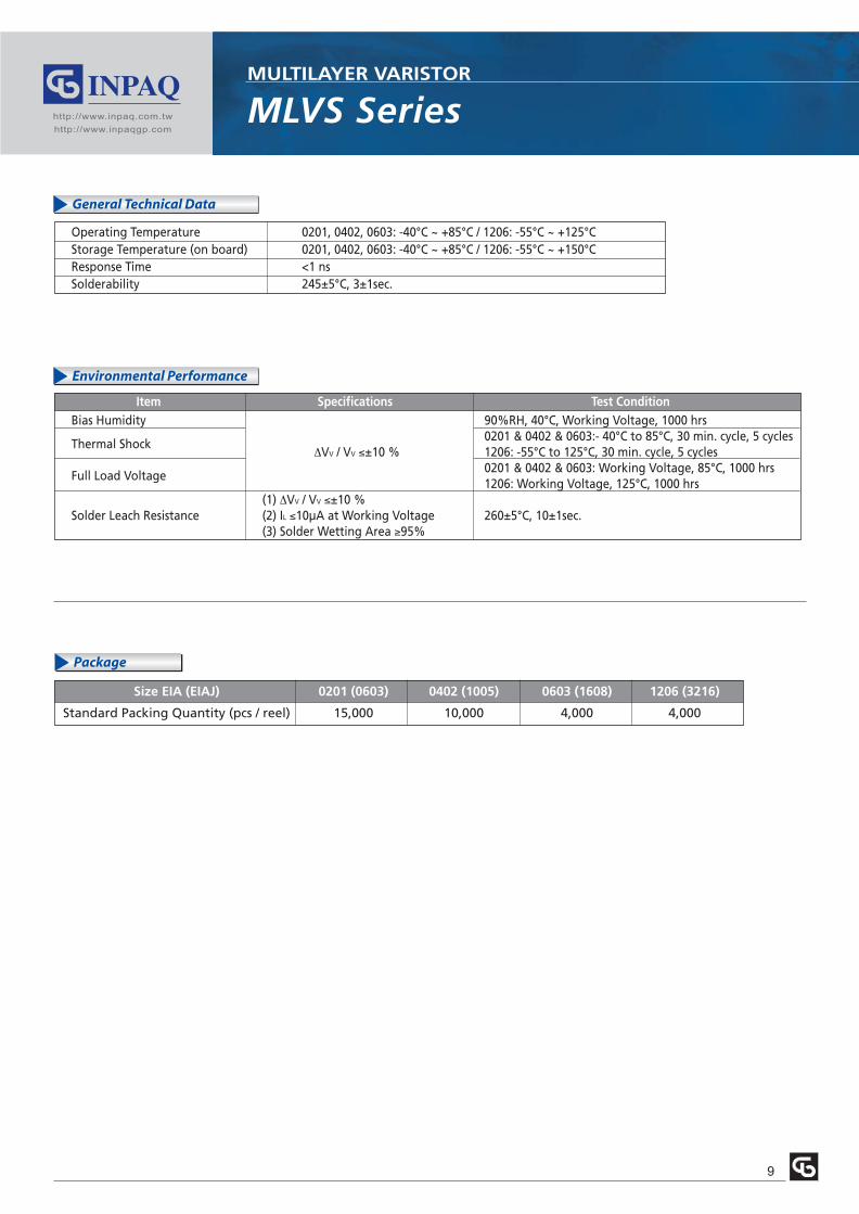
Operating Temperature 0201, 0402, 0603: -40°C ~ +85°C / 1206: -55°C ~ +125°CStorage Temperature (on board) 0201, 0402, 0603: -40°C ~ +85°C / 1206: -55°C ~ +150°CResponse Time <1 nsSolderability 245±5°C, 3±1sec.
Size EIA (EIAJ) 0201 (0603) 0402 (1005) 0603 (1608) 1206 (3216)
Standard Packing Quantity (pcs / reel) 15,000 10,000 4,000 4,000
Item Specifications Test ConditionBias Humidity 90%RH, 40°C, Working Voltage, 1000 hrs
Thermal Shock0201 & 0402 & 0603:- 40°C to 85°C, 30 min. cycle, 5 cycles
∆VV / VV ≤±10 % 1206: -55°C to 125°C, 30 min. cycle, 5 cycles
Full Load Voltage0201 & 0402 & 0603: Working Voltage, 85°C, 1000 hrs1206: Working Voltage, 125°C, 1000 hrs
(1) ∆VV / VV ≤±10 %Solder Leach Resistance (2) IL ≤10µA at Working Voltage 260±5°C, 10±1sec.
(3) Solder Wetting Area ≥95%
Environmental Performance
General Technical Data
http://www.inpaq.com.tw
http://www.inpaqgp.com
10
How to Order
Features
Unit: mm
1
Dimensions
1 5
Applications
MLVG SeriesMULTILAYER VARISTOR
Lead free type
SMD type zinc oxide based ceramic chip
Insulator over coat keeps excellent low and stable leakage current
Plating termination provided good solderability characteristic
Wide operating voltage range, VDC: 5.5V to 18V
Quick response time (<1ns)
Low clamping voltage
Meet IEC 61000-4-2 standard
Low capacitance can meet high speed single transient voltage protection
Low capacitance product applications for high-speed signal lines such as
HDMI, DVI, USB, IEEE1394 Port etc.
Normal capacitance product applications for I/O Port (RS232, USB, PS2,
VGA, Audio) on Mother Board and Notebook, Set-Top Box, MP3 Players,
DVD Players, and Docking System etc.
MLV G 0603 331 N V18 -- --2 3 4 6 7 8
1
Series Type : MLV — Multilayer Varistor
Model Code
Chip Size(EIA) : 0402 / 0603
Capacitance : Value-XRX=0.XpF, ex: 1R0=1.0pF,
XXx10N XXN, ex: 330pF=33x101 331
Capacitance Tolerance :
T -±1.4pF, Q or L- ±2.0pF, U - ±0.9pF, N - ±30%
Working Voltage : VDC
Special Code
Special Code8
7
6
5
4
3
2
1
1 5
MLV G 0402 1R0 U V18 -- --2 3 4 6 7 8
Size EIA (EIAJ) 0402 (1005) 0603 (1608)
L 1.00±0.15 1.60±0.20
W 0.50±0.10 0.80±0.20
T 0.50±0.10 0.80±0.20
C 0.25±0.15 0.30±0.20
http://www.inpaq.com.tw
http://www.inpaqgp.com
11
Specifications
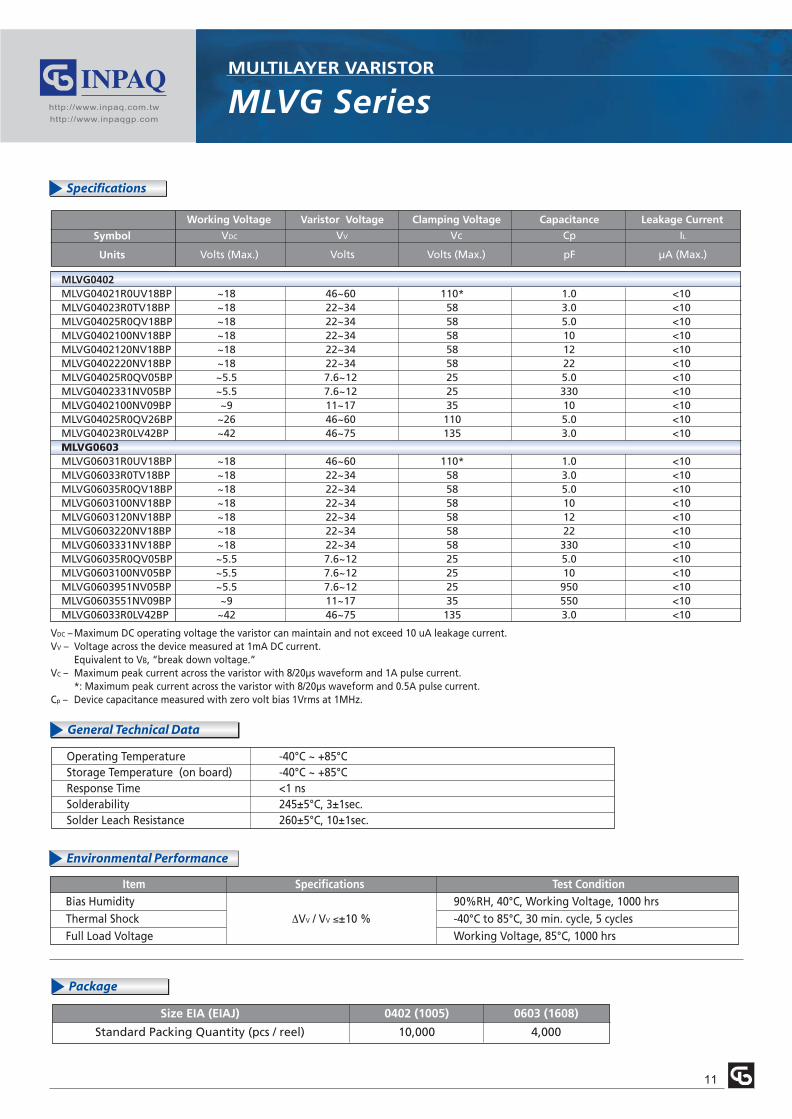
MLVG SeriesMULTILAYER VARISTOR
Symbol
Units
Working Voltage
VV
Varistor Voltage
Vc
Clamping Voltage
Cp
Capacitance
IL
Leakage Current
VDC
Volts Volts (Max.) pF µA (Max.)Volts (Max.)
Package
Operating Temperature -40°C ~ +85°CStorage Temperature (on board) -40°C ~ +85°CResponse Time <1 nsSolderability 245±5°C, 3±1sec.Solder Leach Resistance 260±5°C, 10±1sec.
Size EIA (EIAJ) 0402 (1005) 0603 (1608)
Standard Packing Quantity (pcs / reel) 10,000 4,000
MLVG0402MLVG04021R0UV18BP ~18 46~60 110* 1.0 <10MLVG04023R0TV18BP ~18 22~34 58 3.0 <10MLVG04025R0QV18BP ~18 22~34 58 5.0 <10MLVG0402100NV18BP ~18 22~34 58 10 <10MLVG0402120NV18BP ~18 22~34 58 12 <10MLVG0402220NV18BP ~18 22~34 58 22 <10MLVG04025R0QV05BP ~5.5 7.6~12 25 5.0 <10MLVG0402331NV05BP ~5.5 7.6~12 25 330 <10MLVG0402100NV09BP ~9 11~17 35 10 <10MLVG04025R0QV26BP ~26 46~60 110 5.0 <10MLVG04023R0LV42BP ~42 46~75 135 3.0 <10MLVG0603MLVG06031R0UV18BP ~18 46~60 110* 1.0 <10MLVG06033R0TV18BP ~18 22~34 58 3.0 <10MLVG06035R0QV18BP ~18 22~34 58 5.0 <10MLVG0603100NV18BP ~18 22~34 58 10 <10MLVG0603120NV18BP ~18 22~34 58 12 <10MLVG0603220NV18BP ~18 22~34 58 22 <10MLVG0603331NV18BP ~18 22~34 58 330 <10MLVG06035R0QV05BP ~5.5 7.6~12 25 5.0 <10MLVG0603100NV05BP ~5.5 7.6~12 25 10 <10MLVG0603951NV05BP ~5.5 7.6~12 25 950 <10MLVG0603551NV09BP ~9 11~17 35 550 <10MLVG06033R0LV42BP ~42 46~75 135 3.0 <10
Item Specifications Test ConditionBias Humidity 90%RH, 40°C, Working Voltage, 1000 hrsThermal Shock ∆VV / VV ≤±10 % -40°C to 85°C, 30 min. cycle, 5 cyclesFull Load Voltage Working Voltage, 85°C, 1000 hrs
Environmental Performance
General Technical Data
VDC – Maximum DC operating voltage the varistor can maintain and not exceed 10 uA leakage current.VV – Voltage across the device measured at 1mA DC current.
Equivalent to VB, “break down voltage.”VC – Maximum peak current across the varistor with 8/20µs waveform and 1A pulse current.
*: Maximum peak current across the varistor with 8/20µs waveform and 0.5A pulse current.Cp – Device capacitance measured with zero volt bias 1Vrms at 1MHz.
http://www.inpaq.com.tw
http://www.inpaqgp.com
12
Unit: mm
1
How to Order
Dimensions
Features
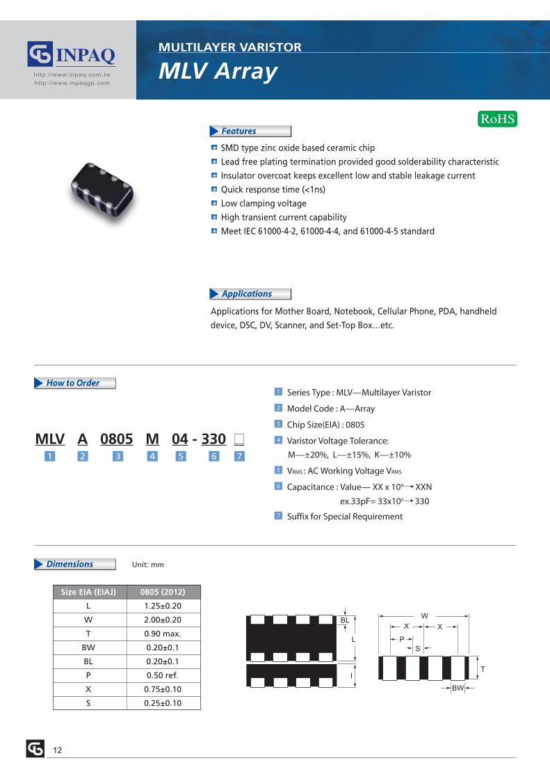
MLV ArrayMULTILAYER VARISTOR
SMD type zinc oxide based ceramic chip
Lead free plating termination provided good solderability characteristic
Insulator overcoat keeps excellent low and stable leakage current
Quick response time (<1ns)
Low clamping voltage
High transient current capability
Meet IEC 61000-4-2, 61000-4-4, and 61000-4-5 standard
Applications for Mother Board, Notebook, Cellular Phone, PDA, handheld
device, DSC, DV, Scanner, and Set-Top Box…etc.
MLV A 0805 M 04 - 330 --2 3 4 5 6 7
Applications
W
X
T
L
I
P
X
S
BL
BW
Size EIA (EIAJ) 0805 (2012)
L 1.25±0.20
W 2.00±0.20
T 0.90 max.
BW 0.20±0.1
BL 0.20±0.1
P 0.50 ref.
X 0.75±0.10
S 0.25±0.10
Series Type : MLV—Multilayer Varistor
Model Code : A—Array
Chip Size(EIA) : 0805
Varistor Voltage Tolerance:
M—±20%, L—±15%, K—±10%
VRMS : AC Working Voltage VRMS
Capacitance : Value— XX x 10N XXN
ex.33pF= 33x100 330
Suffix for Special Requirement7
6
5
4
3
2
1
http://www.inpaq.com.tw
http://www.inpaqgp.com
13
Specifications
MLV ArrayMULTILAYER VARISTOR
Symbol
Units
Working Voltage
∆VVVV
Varistor Voltage
Vc
Clamping Voltage
Cp
Capacitance
imax
Peak Current
Wmax
Transient Energy
VDCVRMS
%Volts Volts (Max.) pF (typ.) Amps (Max.) Joules (Max.)Volts(Max.)Volts
MLVA 0805MLVA0805M04-100 4 5.5 12 ±20 34 10 1 0.05MLVA0805M04-330 4 5.5 12 ±20 28 33 10 0.01MLVA0805M04-500 4 5.5 12 ±20 27 50 10 0.01MLVA0805K14-150 14 18 28 ±10 58 15 5 0.01
VRMS —Maximum AC operating voltage the varistor can maintain and not exceed 10µA leakage current.VDC —Maximum DC operating voltage the varistor can maintain and not exceed 10µA leakage current.VV —Voltage across the device measured at 1mA DC current.
Equivalent to VB, "break down voltage."Vc —Maximum peak current across the varistor with 8/20µs waveform and 1A pulse current.Cp —Device capacitance measured with zero volt bias 1Vrms at 1MHz.imax —Maximum peak current which may be applied with 8/20µs waveform without device failure. Wmax —Maximum energy which may be dissipated with the 10/1000µs waveform without device failure.
Package
Size EIA (EIAJ) 0805 (2012)
Standard Packing Quantity (pcs / reel) 4,000
Operating Temperature -40°C ~ +85°CStorage Temperature (on board) -40°C ~ +85°CResponse Time <1 nsSolderability 245±5°C, 3±1sec.Solder Leach Resistance 260±5°C, 10±1sec.
Item Specifications Test ConditionBias Humidity 90%RH, 40°C, Working Voltage, 1000 hrsThermal Shock ∆VV / VV ≤±10 % -40°C to 85°C, 30 min. cycle, 5 cyclesFull Load Voltage Working Voltage, 85°C, 1000 hrs
Environmental Performance
General Technical Data
http://www.inpaq.com.tw
http://www.inpaqgp.com
14
Unit: mm
4
Applications
How to Order
Dimensions
Features
VPORT SeriesEMI/ESD SUPPRESSOR
Dual function for EMI and ESD
Compact size for EIA 0402 and 0603
ESD protection for IEC61000-4-2 Level 4
Fixed capacitance suitable for high-speed I/O port transient voltage protection
RoHS Compliant
Applications for I/O Port for Mother Board and Notebook
(RS232, USB, PS2, VGA, Audio), Set-Top Box, MP3 Players, DVD Players,
and Docking System etc.
VPORT 0402 100 M V05 --1 2 3 4 5 6
Series Type : V—Over Voltage Protection
PORT—EMI Protection for I/O Port
Chip Size(EIA) : 0402 / 0603
Capacitance : Value—XXx10N XXN
ex:10pF=10x100 100
Capacitance Tolerance : M—±20%
Working Voltage : 0402 5V
0603 5V/12V
Suffix for Special Code6
5
4
3
2
1
Size EIA (EIAJ) 0402 (1005) 0603 (1608)
L 1.00±0.15 1.60±0.20
W 0.50±0.10 0.80±0.20
T 0.50±0.10 0.80±0.20
C 0.25±0.15 0.30±0.20
http://www.inpaq.com.tw
http://www.inpaqgp.com
15
Specifications
VPORT SeriesEMI/ESD SUPPRESSOR
*Description A B C D E F G
Part NumberOperating
Voltage(VDC)
LeakageCurrent
(IL)
Capacitance(Cp)
ClampingVoltage
(Vc)
CapacitanceTolerance
DissipationFactor
TemperatureCharacteristic
VPORT 0402 XXXX V05 Series
General Characteristics (25±5°C)
VPORT0402100MV05VPORT0402220MV05VPORT0402330MV05VPORT0402470MV05VPORT0402101MV05VPORT0402151MV05VPORT0402181MV05VPORT0402221MV05
5V <15µA M: ±20% 4.0%max. ∆C: +15%/-15%
5V <15µA M: ±20% 4.0%max. ∆C: +15%/-15%
12V <15µA M: ±20% 4.0%max. ∆C: +15%/-15%
VPORT0603220MV12VPORT0603330MV12VPORT0603470MV12VPORT0603151MV12VPORT0603181MV12VPORT0603331MV12
VPORT0603100MV05VPORT0603220MV05VPORT0603330MV05VPORT0603470MV05VPORT0603101MV05VPORT0603151MV05VPORT0603181MV05VPORT0603221MV05VPORT0603331MV05VPORT0603471MV05VPORT0603102MV05
10223347100150180220
3430282623222220
3430282623222220191919
102233471001501802203304701000
223347150180330
424038353130
VPORT 0603 XXXX V12 Series
VPORT 0603 XXXX V05 Series
http://www.inpaq.com.tw
http://www.inpaqgp.com
16
Specifications
VPORT SeriesEMI/ESD SUPPRESSOR
Operating Temperature -40°C ~ +85°CStorage Temperature (on board) -40°C ~ +85°CResponse Time <1 nsSolderability 245±5°C, 3±1sec
Item Description
A Max. Continuous Operating Voltage (VDC).
B Leakage Current (IL). Measured at rated continuous operating voltage.
CCapacitance (Cp) . The test condition is 1KHz (≥100pF) /1MHz (<100pF) 1Vrms ±10%
and the environment temperature is 25±2°C.
D Max. Clamping voltage (Vc). Maximum peak current across the chip with 8/20µs waveform and 1A pulse current.
E Capacitance Tolerance. Capacitance Tolerance, M=±20%.
F Dissipation Factor.
G Temperature Characteristic. -30°C ~ +85°C.
Package
Size EIA (EIAJ) 0402 (1005) 0603 (1608)
Standard Packing Quantity (pcs / reel) 10,000 4,000
*Description
Environmental Performance
General Technical Data
Item Specifications Test ConditionBias Humidity 90%RH, 40°C, Working Voltage, 1000 hrsThermal Shock -40°C to 85°C, 30 min. cycle, 5 cyclesFull Load Voltage Working Voltage, 85°C, 1000 hrsSolder Leach Resistance 260±5°C, 10±1sec.
(1) IL ≤15µA at Working Voltage(2) ∆Cp/Cp ≤ ±10%(3) Solder Wetting Area ≥95%
http://www.inpaq.com.tw
http://www.inpaqgp.com
17
Specifications
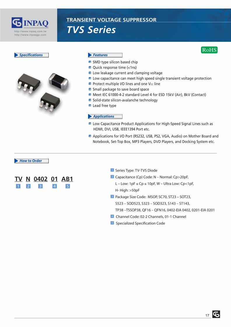
TVS SeriesTRANSIENT VOLTAGE SUPPRESSOR
Applications
How to Order
Features
SMD type silicon based chipQuick response time (<1ns)Low leakage current and clamping voltageLow capacitance can meet high speed single transient voltage protectionProtect multiple I/O lines and one VCC lineSmall package to save board spaceMeet IEC 61000-4-2 standard Level 4 for ESD 15kV (Air), 8kV (Contact)Solid-state silicon-avalanche technologyLead free type
Low Capacitance Product Applications for High-Speed Signal Lines such as HDMI, DVI, USB, IEEE1394 Port etc.
Applications for I/O Port (RS232, USB, PS2, VGA, Audio) on Mother Board andNotebook, Set-Top Box, MP3 Players, DVD Players, and Docking System etc.
TV N 0402 01 AB11 2 3 4 5
Series Type: TV-TVS Diode
Capacitance (Cp) Code: N – Normal: Cp>20pF,
L – Low: 1pF ≤ Cp ≤ 10pF, W – Ultra Low: Cp<1pF,
H- High: >50pF
Package Size Code: MSOP, SC70, ST23 – SOT23,
S523 – SOD523, S323 – SOD323, S143 – ST143,
TP38 –TSSOP38, QF16 – QFN16, 0402-EIA 0402, 0201-EIA 0201
Channel Code: 02-2 Channels, 01-1 Channel
Specialized Specification Code5
4
3
2
1
http://www.inpaq.com.tw
http://www.inpaqgp.com
18
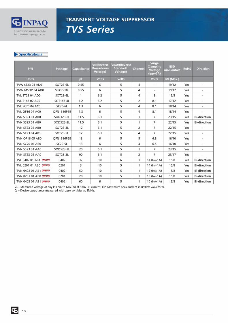
Specifications
TVS SeriesTRANSIENT VOLTAGE SUPPRESSOR
Units pF Volts Volts Volts kV (Max.)
PackageP/N Capacitance Channel RoHS DirectionVB (Reverse Breakdown Voltage)
VRWM(Reverse Stand-off Voltage)
SurgeClampingVoltage(Ipp=5A)
ESDAir/Contact
TVW ST23 04 AD0 SOT23-6L 0.55 6 5 4 - 19/12 Yes -
TVW MSOP 04 AD0 MSOP-10L 0.55 6 5 4 - 19/12 Yes -
TVL ST23 04 AD0 SOT23-6L 1 6.2 5 4 8 15/8 Yes -
TVL S143 02 AC0 SOT143-4L 1.2 6.2 5 2 8.1 17/12 Yes -
TVL SC70 04 AC0 SC70-6L 1.3 6 5 4 8.1 18/14 Yes -
TVL QF16 04 AC0 QFN1616P6E 1.3 6 5 4 8.1 18/14 Yes -
TVN S323 01 AB0 SOD323-2L 11.5 6.1 5 1 7 23/15 Yes Bi-direction
TVN S523 01 AB0 SOD523-2L 11.5 6.1 5 1 7 22/15 Yes Bi-direction
TVN ST23 02 AB0 SOT23-3L 12 6.1 5 2 7 22/15 Yes -
TVN ST23 04 AB1 SOT23-5L 12 6.1 5 4 7 22/15 Yes -
TVN QF16 05 AB0 QFN1616P6E 13 6 5 5 6.8 16/10 Yes -
TVN SC70 04 AB0 SC70-5L 13 6 5 4 6.5 16/10 Yes -
TVN S523 01 AA0 SOD523-2L 20 6.1 5 1 7 23/15 Yes -
TVN ST23 02 AA0 SOT23-3L 90 6.1 5 2 7 23/17 Yes -
TVL 0402 01 AB1 0402 6 10 6 1 14 (IPP=1A) 15/8 Yes Bi-direction
TVL 0201 01 AB0 0201 3 10 5 1 14 (IPP=1A) 15/8 Yes Bi-direction
TVN 0402 01 AB1 0402 50 10 5 1 12 (IPP=1A) 15/8 Yes Bi-direction
TVN 0201 01 AB0 0201 20 10 5 1 13 (IPP=1A) 15/8 Yes Bi-direction
TVH 0402 01 AB1 0402 60 6 5 1 10 (IPP=1A) 15/8 Yes Bi-direction
VB – Measured voltage at any I/O pin to Ground at 1mA DC current. IPP–Maximum peak current in 8/20ms waveform. Cp – Device capacitance measured with zero volt bias at 1MHz.
(NEW)
(NEW)
(NEW)
(NEW)
(NEW)
http://www.inpaq.com.tw
http://www.inpaqgp.com
19
TVS SeriesTRANSIENT VOLTAGE SUPPRESSOR
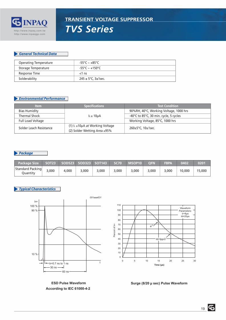
Operating Temperature -55°C ~ +85°C
Storage Temperature -55°C ~ +150°C
Response Time <1 ns
Solderability 245 ± 5°C, 3±1sec.
General Technical Data
Item Specifications Test ConditionBias Humidity 90%RH, 40°C, Working Voltage, 1000 hrsThermal Shock IL ≤ 10µA -40°C to 85°C, 30 min. cycle, 5 cyclesFull Load Voltage Working Voltage, 85°C, 1000 hrs
Solder Leach Resistance(1) IL ≤10µA at Working Voltage
260±5°C, 10±1sec.(2) Solder Wetting Area ≥95%
Environmental Performance
Package
Package Size SOT23 SOD523 SOD323 SOT143 SC70 MSOP10 QFN FBPA 0402 0201
Standard Packing 3,000 4,000 3,000 3,000 3,000 3,000 3,000 3,000 10,000 15,000Quantity
Typical Characteristics
tr=0.7 ns to 1 ns
30 ns
60 ns
t
001aaa631
IPP
100 %
90 %
10 %
Waveform
Parameters:
tr=8µs
td=20µs
e-t
td=Ipp/2
0
0 5 10 15
Time (µs)
20 25 30
10
20
30
40
50
60
70
80
90
100
110
Perc
cnt of lP
P
ESD Pulse Waveform
According to IEC 61000-4-2
Surge (8/20 µ sec) Pulse Waveform
http://www.inpaq.com.tw
http://www.inpaqgp.com
20
TVS SeriesTRANSIENT VOLTAGE SUPPRESSOR
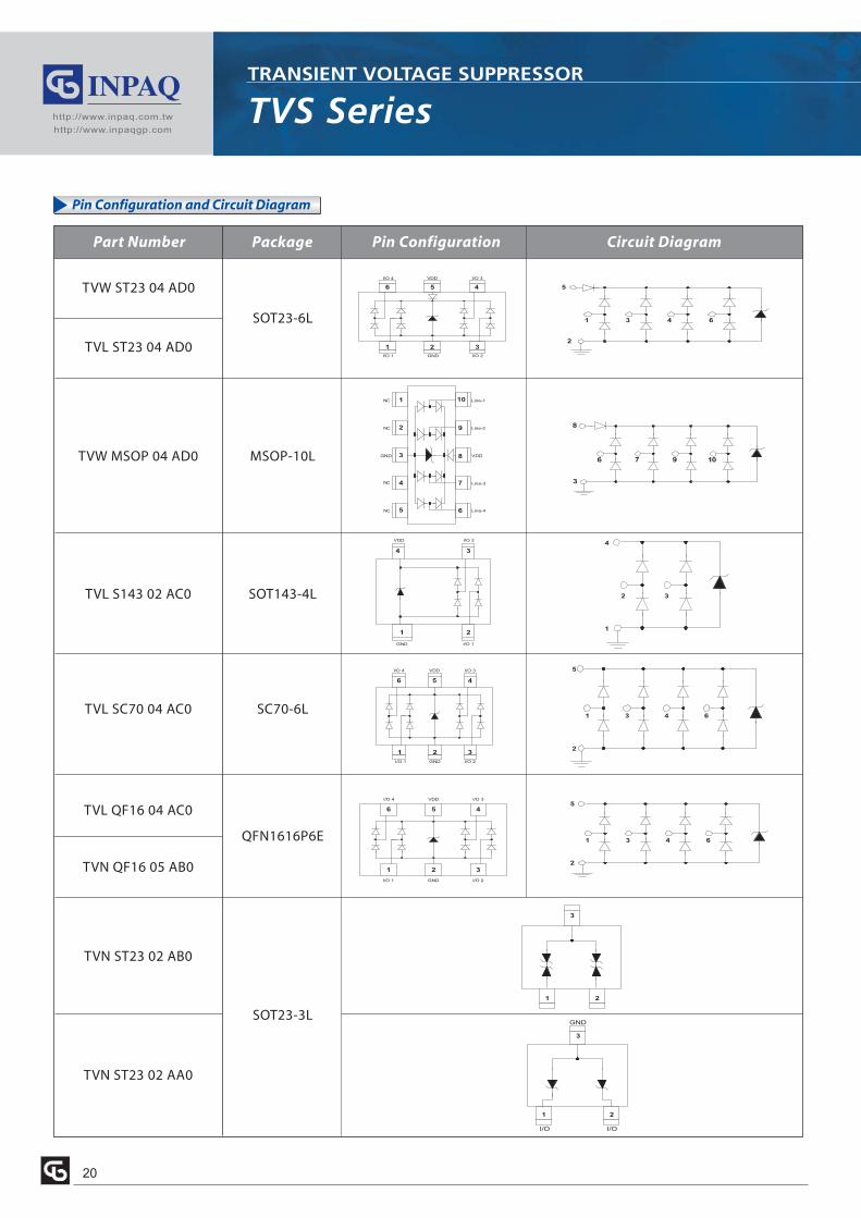
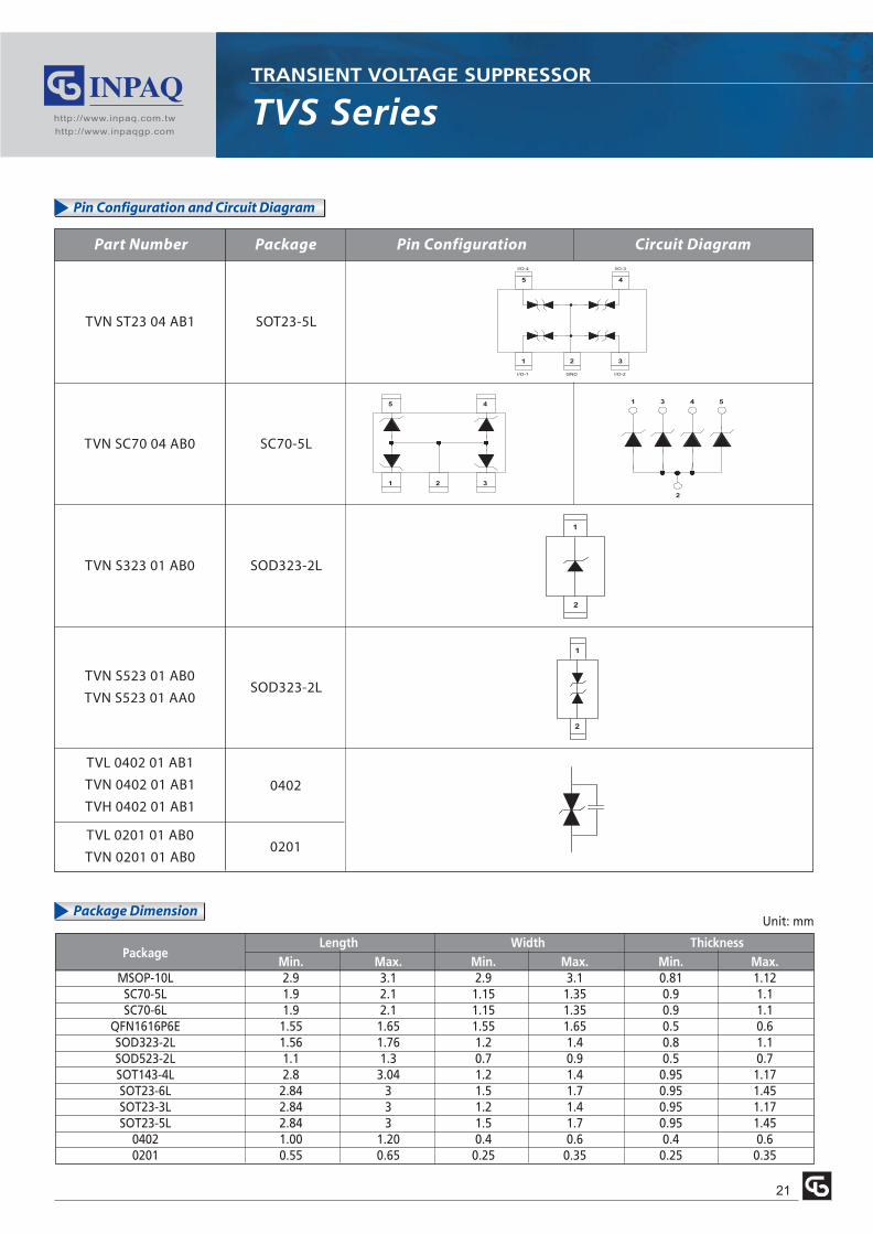
Part Number Package Pin Configuration Circuit Diagram
TVW ST23 04 AD0
TVL ST23 04 AD0
SOT23-6L
MSOP-10LTVW MSOP 04 AD0
SOT143-4LTVL S143 02 AC0
SC70-6LTVL SC70 04 AC0
QFN1616P6E
TVL QF16 04 AC0
TVN QF16 05 AB0
SOT23-3L
TVN ST23 02 AB0
TVN ST23 02 AA0
6 5 4
1 2 3I/O 1 I/O 2
I/O 3I/O 4 VDD
GND
1 3 4 6
5
2
NC
NC
GND
NC
NC
10
9
8
7
6
Line-1
Line-2
VDD
Line-3
Line-4
1
2
3
4
5
6 7 9 10
3
8
4 3
1 2
VDD I/O 2
I/O 1GND
2 3
1
4
6 5 4
1 2 3
I/O 1 I/O 2
I/O 3I/O 4 VDD
GND
1 3 4 6
2
5
6 5 4
1 2 3
I/O 1 I/O 2
I/O 3I/O 4 VDD
GND
1 3 4 6
2
5
3
1 2
3
1 2
GND
I/O I/O
Pin Configuration and Circuit Diagram
http://www.inpaq.com.tw
http://www.inpaqgp.com
21
TVS SeriesTRANSIENT VOLTAGE SUPPRESSOR
Part Number Package Pin Configuration Circuit Diagram
SOT23-5LTVN ST23 04 AB1
SC70-5LTVN SC70 04 AB0
SOD323-2LTVN S323 01 AB0
SOD323-2L
0402
0201
TVN S523 01 AB0
TVN S523 01 AA0
TVL 0402 01 AB1
TVN 0402 01 AB1
TVH 0402 01 AB1
TVL 0201 01 AB0
TVN 0201 01 AB0
5 4
1 2 3
I/O-4 I/O-3
I/O-2GNDI/O-1
1 2 3
5 4 53
2
1 4
Package Dimension
PackageLength Width Thickness
Min. Max. Min. Max. Min. Max.MSOP-10L 2.9 3.1 2.9 3.1 0.81 1.12SC70-5L 1.9 2.1 1.15 1.35 0.9 1.1SC70-6L 1.9 2.1 1.15 1.35 0.9 1.1
QFN1616P6E 1.55 1.65 1.55 1.65 0.5 0.6SOD323-2L 1.56 1.76 1.2 1.4 0.8 1.1SOD523-2L 1.1 1.3 0.7 0.9 0.5 0.7SOT143-4L 2.8 3.04 1.2 1.4 0.95 1.17SOT23-6L 2.84 3 1.5 1.7 0.95 1.45SOT23-3L 2.84 3 1.2 1.4 0.95 1.17SOT23-5L 2.84 3 1.5 1.7 0.95 1.45
0402 1.00 1.20 0.4 0.6 0.4 0.60201 0.55 0.65 0.25 0.35 0.25 0.35
Unit: mm
Pin Configuration and Circuit Diagram
1
2
1
2
htt
p:/
/ww
w.i
np
aq
.co
m.t
w
htt
p:/
/ww
w.i
np
aq
gp
.co
m
22
TVS
Seri
esTR
AN
SIE
NT V
OLT
AG
E S
UPPR
ESSO
R
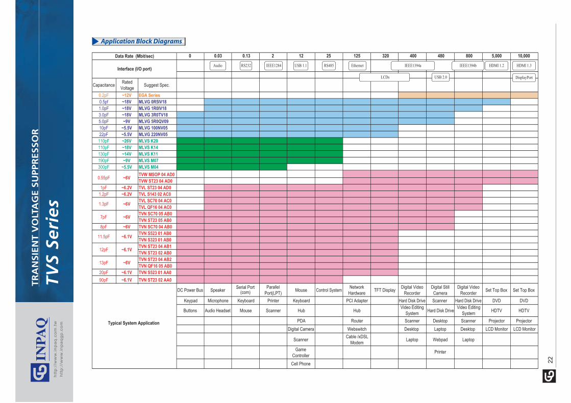
0 0.03 0.13 2 12 25 125 320 400 480 800 5,000 10,000
CapacitanceRated
VoltageSuggest Spec.
0.2pF ~12V EGA Series
0.5pf ~18V MLVG 0R5IV18
1.0pF ~18V MLVG 1R0IV18
3.0pF ~18V MLVG 3R0TV18
5.0pF ~9V MLVG 5R0QV09
10pF ~5.5V MLVG 100NV05
22pF ~5.5V MLVG 220NV05
110pF ~26V MLVS K20
110pF ~18V MLVS K14
130pF ~14V MLVS K11
190pF ~9V MLVS M07
300pF ~5.5V MLVS M04
TVW MSOP 04 AD0
TVW ST23 04 AD0
1pF ~6.2V TVL ST23 04 AD0
1.2pF ~6.2V TVL S143 02 AC0
TVL SC70 04 AC0
TVL QF16 04 AC0
TVN SC70 05 AB0
TVN ST23 05 AB0
8pF ~6V TVN SC70 04 AB0
TVN S523 01 AB0
TVN S323 01 AB0
TVN ST23 04 AB1
TVN ST23 02 AB0
TVN ST23 04 AB2
TVN QF16 05 AB0
20pF ~6.1V TVN S523 01 AA0
90pF ~6.1V TVN ST23 02 AA0
DC Power Bus SpeakerSerial Port
(com)
Parallel
Port(LPT)Mouse Control System
Network
HardwareTFT Display
Digital Video
Recorder
Digital Still
Camera
Digital Video
RecorderSet Top Box Set Top Box
Keypad Microphone Keyboard Printer Keyboard PCI Adapter Hard Disk Drive Scanner Hard Disk Drive DVD DVD
Buttons Audio Headset Mouse Scanner Hub HubVideo Editing
SystemHard Disk Drive
Video Editing
SystemHDTV HDTV
PDA Router Scanner Desktop Scanner Projector Projector
Digital Camera Webswitch Desktop Laptop Desktop LCD Monitor LCD Monitor
ScannerCable /xDSL
ModemLaptop Webpad Laptop
Game
ControllerPrinter
Cell Phone
11.5pF
~6.1V12pF
~6V13pF
Data Rate (Mbit/sec)
Interface (I/O port)
Typical System Application
0.55pF ~6V
1.3pF ~6V
7pF ~6V
~6.1V
Audio RS232 IEEE1284 RS485 Ethernet
USB 2.0
HDMI 1.3
LCDs
IEEE1394a IEEE1394bUSB 1.1 HDMI 1.2
DisplayPort
Application Block Diagrams
http://www.inpaq.com.tw
http://www.inpaqgp.com
23
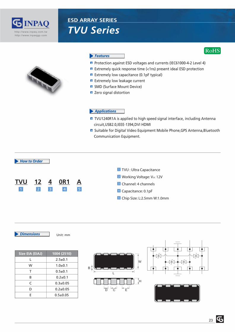
TVU SeriesESD ARRAY SERIES
Unit: mm
Applications
How to Order
Dimensions
Features
1
Protection against ESD voltages and currents (IEC61000-4-2 Level 4)
Extremely quick response time (<1ns) present ideal ESD protection
Extremely low capacitance (0.1pF typical)
Extremely low leakage current
SMD (Surface Mount Device)
Zero signal distortion
TVU1240R1A is applied to high speed signal interface, including Antenna
circuit,USB2.0,IEEE-1394,DVI HDMI
Suitable for Digital Video Equipment Mobile Phone,GPS Antenna,Bluetooth
Communication Equipment.
TVU 12 4 0R1 A2 3 4 5
TVU : Ultra Capacitance
Working Voltage: VDC 12V
Channel: 4 channels
Capacitance: 0.1pF
Chip Size: L:2.5mm W:1.0mm 5
4
3
2
1
L
W
B
H
E D C
Size EIA (EIAJ) 1004 (2510)
L 2.5±0.1
W 1.0±0.1
T 0.5±0.1
B 0.2±0.1
C 0.3±0.05
D 0.2±0.05
E 0.5±0.05
http://www.inpaq.com.tw
http://www.inpaqgp.com
24
Specifications
TVU SeriesESD ARRAY SERIES
Package
IL – Leakage current at rated voltage, the maximum leakage current was measured after reliability test.
Characteristics TVU1240R1A
Rated Voltage (max) 12V
Leakage Current (max) (@12VDC) 0.01µA
Trigger Voltage (Vt ) 300V typ.
Clamping Voltage (Vc) 30V typ.
Capacitance (Cp), @1MHz 0.1pF typ.
Response Time <1ns
ESD Voltage Capability, IEC 61000-4-2 Contact Discharge Mode 8KV
ESD Voltage Capability, IEC 61000-4-2 Air Discharge Mode 15KV
ESD Withstand Pulses 100 typ.
Item Specifications Test Condition
Bias Humidity 90%RH, 40°C, Rated Voltage, 1000 hrs
Thermal ShockIL ≤10 µA
-40°C to 85°C, 30 min. cycle, 5 cycles
Full Load Volage Rated Voltage, 85°C, 1000 hrs
Solder Leach Resistance 260±5°C, 10±1sec.
Operating Temperature -40°C ~ +85°C
Storage Temperature -55°C ~ +125°C
Response Time <1 ns
Solderability 245±5°C, 3±1sec
Size EIA (EIAJ) 1004 (2510)
Standard Packing Quantity (pcs / reel) 5,000
Environmental Performance
General Technical Data
(NEW)