Embed Size (px)
Citation preview
HE W LETT- PACKARD JO URN AL T E C H N I C A L I N F O R M A T I O N F R O M T H E - d p - L A B O R A T O R I E S
A T E O F F I C E S â € ¢ 1 5 0 1 P A G E M I L L R O A D â € ¢ P A L O A L T O , C A L I F O R N I A 9 4 3 0 4 â € ¢ V O L . 1 7 , N O . 7 M A R C H , 1 9 6 6
L I N - D B
o o
C O V E R : L O W - F R E Q U E N C Y R F I M E A S U R E M E N T S , p a g e 1 2
I C R O V O L T - S E N S I T I V I T Y F L O A T I N G D C V O L T M E T E R , p a g e 2
T R A N S F E R R I N G S T A N D A R D D C V O L T A G E S , p a g e 7
© Copr. 1949-1998 Hewlett-Packard Co.
A S E N S I T I V E , W I D E R A N G E D C N U L L V O L T M E T E R W I T H A N I N T E R N A L B U C K I N G S U P P L Y F O R Z E R O L O A D I N G E R R O R
A f loat ing, h igh-sens i t iv i ty DC Nul l Meter measures vo l tages to be low 1 mic rovo l t and ach ieves
v i r tua l l y i n f in i te inpu t impedance w i th a buck ing supp ly . THE MINIMUM SIGNAL that can be
measured with precision by a sensi tive electronic dc voltmeter is de termined by noise. The noise causes needle fluctuations which result in r e a d i n g u n c e r t a i n t i e s . H e n c e , among other considerations, the de sign of a sensitive voltmeter is con cerned with the minimization of noise, an effort that is concerned pri marily with optimization of the in put amplifier for lowest noise per formance.
A related problem resulting from increased sensitivity in a voltmeter is drift, which affects reading ac curacy. The effects of dc drift in the amplifier itself can be eliminated by the use of chopper stabili /ation. Drift caused by thermal emf's. which assume major impórtame in the microvolt region, is reduced by using only one t\pc of metal, usually solid copper, for the input circuitn in cluding the input terminals.
Other problems in sensitive meas urements are created by ac signals superimposed on the dc signal to be measured, since the ac is quite often
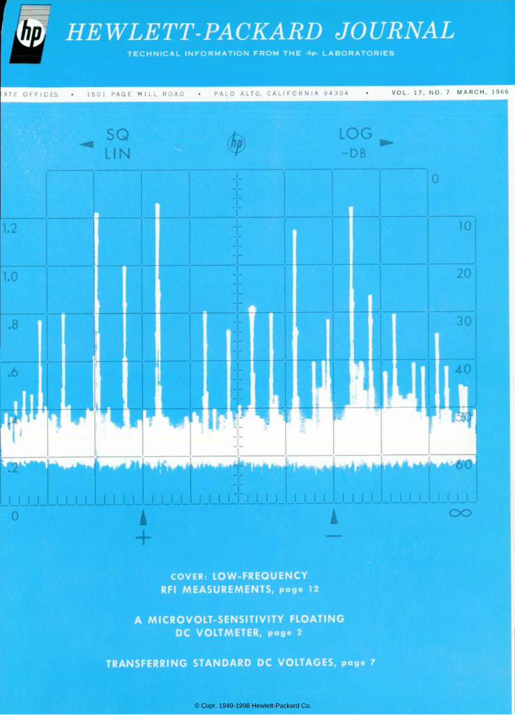
Fig. calibrating DC Null Voltmeter is part of standards lab set-up for calibrating universal ratio sets, volt boxes, and Kelvin-Varley voltage dividers. Volt meter corre di f ference, i f any, between s teps on rat io set and corre sponding steps on precision divider in temperature-stable oil bath. Precision divider is composed of new -hp- standard resistors, to be described in forth coming circuits High stability and sensitivity in high impedance circuits make DC Null Voltmeter well-suited for standards lab applications of this type. 0.1 voltmeter resolution as null indicator approaches 0.1 ¡iV
and full scale sensitivity is 3 ¡nV.
much larger than the dc signal in microvolt measurements. If the ac signal is phase coherent with the (hopper frequency, it is converted into a dc voltage, causing reading errors. Superimposed signals whiih are not phase-coherent usually do
' 4 I 9 A O C N U L L V O L T M E T E R
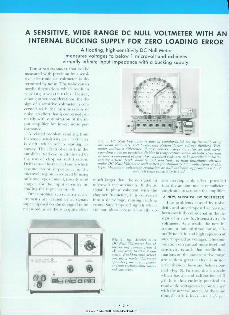
Fig. 2. -hp- Model 419A DC Null Voltmeter has 18 measuring ranges from 3 /¿V end scale to 1000 V end scale. Pushbuttons select operating mode. Voltmeter operates from ac line power or from rechargeable inter nal batteries.
not develop a dc offset, provided that the ac does not have sufficient amplitude to saturate the amplifier.
A N E W , S E N S I T I V E D C V O L T M E T E R
The problems caused by noise, drift, and superimposed ac have all been carefully considered in the de sign of a new high-sensitivity dc voltmeter. As a result, the new in strument has minimal noise, vir tually no drift, and high rejection of superimposed ac voltages. The com bination of residual noise level and sensitivity is such that needle fluc tuations on the most sensitive range are seldom greater than 1 minor scale division above and below nom inal (Fig. 3). Further, this is a scale which has an end calibration of 3 ¿U.V. It is thus entirely practical to resolve dc voltages to below 0.5 ¿iV with the new voltmeter. At the same time, dc drift i* Ics-, than 0.5 /A' ¡XT
© Copr. 1949-1998 Hewlett-Packard Co.
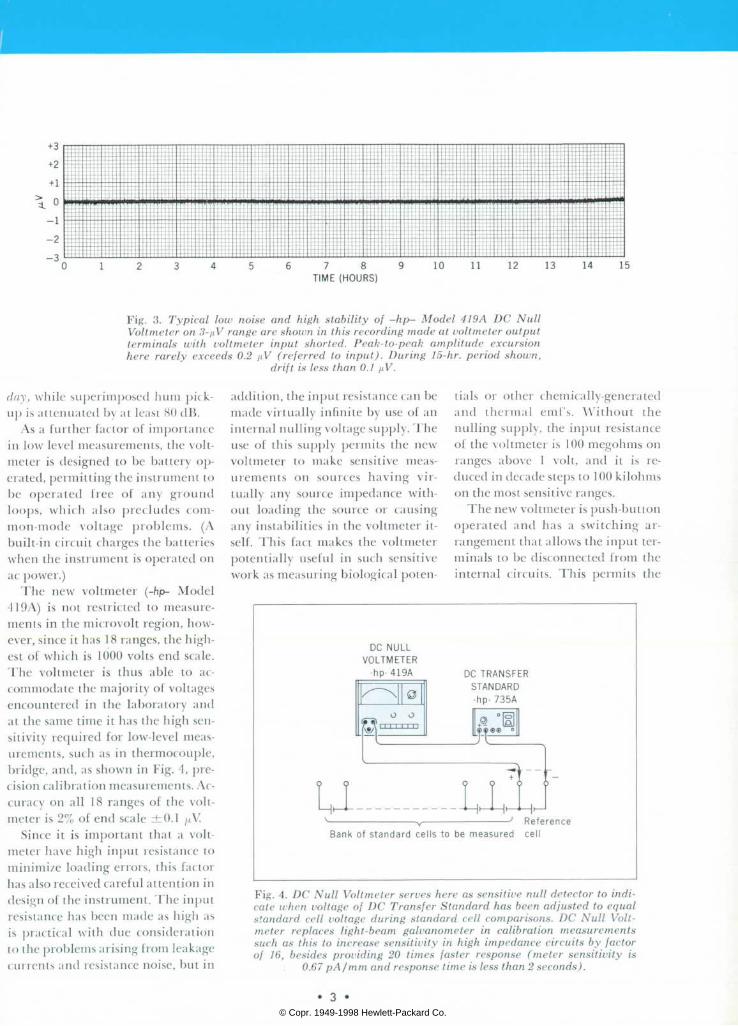
Fig. Null Typical low noise and high stability of -hp- Model 419A DC Null Voltmeter on 3-/iV range are shown in this recording made at voltmeter output terminals with voltmeter input shorted. Peak-to-peak amplitude excursion here rarely exceeds 0.2 nV (referred to input). During 15-hr, period shown,
drift is less than 0.1 ¡iV.
day, while superimposed hum pick up is attenuated by at least 80 dB.
As a further factor of importance in low level measurements, the volt meter is designed to be battery op erated, permitting the instrument to be opera ted f ree of any ground loops, which also precludes com mon-mode voltage problems. (A built-in circuit charges the batteries when the instrument is operated on ac power.)
The new voltmeter (-hp- Model 4.19A) is not restricted to measure ments in the microvolt region, how ever, since it has 18 ranges, the high est of which is 1000 volts end scale. The voltmeter is thus able to ac commodate the majority of voltages encountered in the laboratory and at the same time it has the high sen sitivity required for low-level meas urements, such as in thermocouple, bridge, and, as shown in Fig. 4, pre cision calibration measurements. Ac curacy on all 18 ranges of the volt meter is 2% of end scale ±0.1 ^V
Since it is important that a volt meter have high input resistance to minimize loading errors, this factor has also received careful attention in design of the instrument. The input resistance has been made as high as is practical with due consideration to the problems arising from leakage currents and resistance noise, but in
addition, the input resistance can be made virtually infinite by use of an internal nulling voltage supply. The use of this supply permits the new voltmeter to make sensitive meas urements on sources having vir tually any source impedance with out loading the source or causing any instabilities in the voltmeter it self. This fact makes the voltmeter potentially useful in such sensitive work as measuring biological poten
tials or other chemically-generated and thermal emf 's . Without the nulling supply, the input resistance of the voltmeter is 100 megohms on ranges above 1 volt , and i t is re duced in decade steps to 100 kilohms on the most sensitive ranges.
The new voltmeter is push-button operated and has a switching ar rangement that allows the input ter minals to be disconnected from the internal circuits. This permits the
D C N U L L VOLTMETER
- h p - 4 1 9 A DC TRANSFER STANDARD -hp - 735A
U R e f e r e n c e
B a n k o f s t a n d a r d c e l l s t o b e m e a s u r e d c e l l
Fig. to indi Null Voltmeter serves here as sensitive null detector to indi cate equal voltage of DC Transfer Standard has been adjusted to equal standard cell voltage during standard cell comparisons. DC Null Volt meter replaces light-beam galvanometer in calibration measurements such factor this to increase sensitivity in high impedance circuits by factor of 16, besides providing 20 times faster response (meter sensitivity is
0.67 pA/mm and response time is less than 2 seconds).
© Copr. 1949-1998 Hewlett-Packard Co.
INTERNAL
IFUNCTION!
I n p u t I u r n m u i i H L O u t p u t I INTEGRATOR
h o p p e r A m p l i f i e r
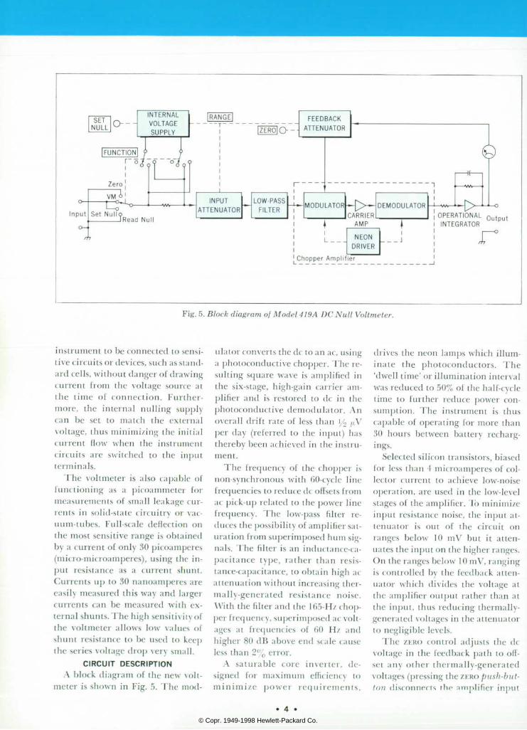
Fig. 5. Block diagram of Model 419 A DC Null Voltmeter.
instrument to be connected to sensi tive circuits or devices, such as stand ard cells, without danger of drawing current from the voltage source at the t ime of connect ion. Fur ther more, the internal nulling supply can be set to match the external voltage, thus minimi/ing the initial current flow when the instrument circuits are switched to the input terminals.
The voltmeter is also capable of functioning as a picoammeter for measurements of small leakage cur rents in solid-state circuitry or vac uum-tubes. Full-scale deflection on the most sensitive range is obtained by a current of only 30 picoamperes (micro-microamperes), using the in put resistance as a current shunt. Currents up to 30 nanoamperes are easily measured this way and larger currents can be measured with ex ternal shunts. The high sensitivity of the voltmeter allows low values of shunt resistance to be used to keep the series voltage drop very small.
CIRCUIT DESCRIPTION A block diagram of the new volt
meter is shown in Fig. 5. The mod
ulator converts the dc to an ac, using a photoconductive chopper. The re sulting square wave is amplified in the six-stage, high-gain carrier am plifier and is restored to dc in the photoconductive demodulator. An overall drift rate of less than i/2 ¡¿V
per clay (referred to the input) has thereby been achieved in the instru ment.
The frequency of the chopper is non-synchronous with GO-cycle line frequencies to reduce dc offsets from ac pick-up related to the power line frequency. The low-pass filter re duces the possibility of amplifier sat uration from superimposed hum sig nals. The filter is an inductance-ca pacitance type, rather than resis tance-capacitance, to obtain high ac attenuation without increasing ther mally-generated resistance noise. With the filter and the 165-Hz chop per frequency, superimposed ac volt ages at frequencies of 60 Hz and higher 80 clB above end scale cause less than 2% error.
A sa turab le core inver te r , de signed for maximum efficiency to min imi / e power r equ i r emen t s ,
drives the neon lamps which illum inate the photoconcluctors. The 'dwell time' or illumination interval was reduced to 50% of the half-cycle time to further reduce power con sumption. The instrument is thus capable of operating for more than 30 hours between battery recharg- ings.
Selected silicon transistors, biased for less than 4 microamperes of col lector current to achieve low-noise operation, are used in the low-level stages of the amplifier. To minimize input resistance noise, the input at tenuator is out of the circuit on ranges below 10 mV but i t atten uates the input on the higher ranges. On the ranges below 10 mV, ranging is controlled by the feedback atten uator which divides the voltage at the amplifier output rather than at the input, thus reducing thermally- generated voltages in the attenuator to negligible levels.
The ZERO control adjusts the dc voltage in the feedback path to off set any other thermally-generated voltages (pressing the ZERO pusli-but-
ton disconnects the amplifier input
. 4 • © Copr. 1949-1998 Hewlett-Packard Co.
- 4 o - - 3 o - - 2 c r
-.15 ( P r o b a b i l i t y t h a t n o i s e p e a k w i l l e x c e e d c o r r e s p o n d i n g v o l t a g e ) 1 0 0 5 0 10 5 0 1
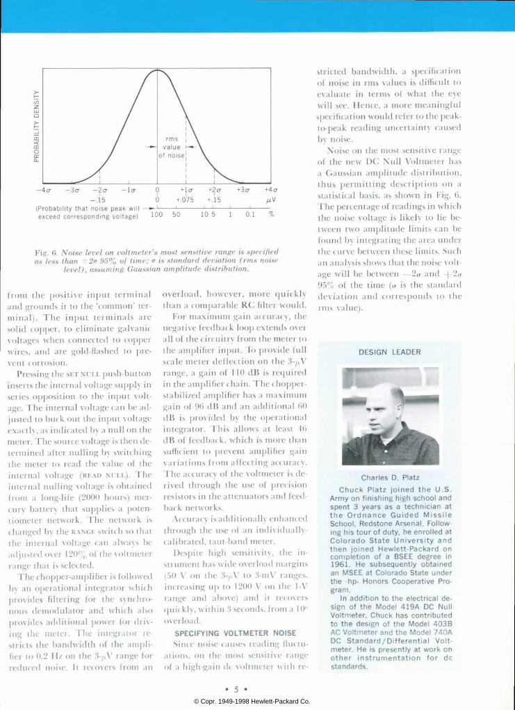
Fig. 6. Noise level on voltmeter's most sensitive range is specified as less than ±2a 95% of time; a is standard deviation (rms noise
level), assuming Gaussian amplitude distribution.
from the positive input terminal and "rounds it to the 'common' ter minal) . The input terminals are solid copper, to eliminate galvanic voltages when connected to copper wires, and are gold-flashed to pre vent corrosion.
Pressing the SET NULL push-button inserts the internal voltage supply in series opposition to the input volt age. The internal voltage can be ad justed to buck out the input voltage exactly, as indicated by a null on the meter. The source voltage is then de termined after nulling by switching the meter to read the value of the internal voltage (READ NULL). The internal nulling voltage is obtained from a long-life (2000 hours) mer cury battery that supplies a poten tiometer network. The network is changed by the RANGE switch so that the internal voltage can always be adjusted over 120% of the voltmeter range that is selected.
The chopper-amplifier is followed by an operational integrator which provides filtering for the synchro nous demodulator and which also provides additional power for driv ing the meter. The integrator re stricts the bandwidth of the ampli fier to 0.2 H/ on the 3-/¿V range for reduced noise. It recovers from an
overload, however, more quickly than a comparable RC filter would.
For maximum gain accuracy, the negative feedback loop extends over all of the circuitry from the meter to the amplifier input. To provide full scale meter deflection on the 3-/J.V range, a gain of 110 dB is required in the amplifier chain. The chopper- stabili/ed amplifier has a maximum gain of 96 dB and an additional 60 dB is provided by the operational integrator. This allows at least 46 dB of feedback, which is more than sufficient to prevent amplifier gain variations from affecting accuracy. The accuracy of the voltmeter is de rived through the use of precision resistors in the attenuators and feed back networks.
Accuracy is additionally enhanced through the use of an indi\ ¡dually- calibrated, taut-band meter.
Despite high sensitivity, the in strument has wide overload margins (50 V on the 3-/j,V to 3-mV ranges. increasing up to 1200 V on the 1-V range and above) and it recovers quickly, within 3 seconds, from a 10" overload.
S P E C I F Y I N G V O L T M E T E R N O I S E Since noise causes reading fluctu
ations, on the most sensitive range of a high-gain dc voltmeter with re
stricted bandwidth, a specification of noise in rms values is difficult to evaluate in terms of what the eye will see. Hence, a more meaningful specification would refer to the peak- to-peak reading uncertainty caused by noise.
Noise on the most sensitive range of the new DC Null Voltmeter has a Gaussian amplitude distribution, thus permitting description on a statistical basis, as shown in Fig. 6. The percentage of readings in which the noise voltage is likely to lie be tween two amplitude limits can be found by integrating the area under the curve between these limits. Such an analysis shows that the noise volt age will be between — 2cr and -\-2cr
95% of the time (a is the standard deviation and corresponds to the rms value).
D E S I G N L E A D E R
C h a r l e s D . P l a t z C h u c k P l a t z j o i n e d t h e U . S .
A r m y o n f i n i s h i n g h i g h s c h o o l a n d s p e n t 3 y e a r s a s a t e c h n i c i a n a t t h e O r d n a n c e G u i d e d M i s s i l e S c h o o l , R e d s t o n e A r s e n a l . F o l l o w i n g h i s t o u r o f d u t y , h e e n r o l l e d a t C o l o r a d o S t a t e U n i v e r s i t y a n d t h e n j o i n e d H e w l e t t - P a c k a r d o n c o m p l e t i o n o f a B S E E d e g r e e i n 1 9 6 1 . H e s u b s e q u e n t l y o b t a i n e d a n M S E E a t C o l o r a d o S t a t e u n d e r t h e - h p - H o n o r s C o o p e r a t i v e P r o g r a m .
I n a d d i t i o n t o t h e e l e c t r i c a l d e s i g n o f t h e M o d e l 4 1 9 A D C N u l l V o l t m e t e r , C h u c k h a s c o n t r i b u t e d t o t h e d e s i g n o f t h e M o d e l 4 0 3 B A C V o l t m e t e r a n d t h e M o d e l 7 4 0 A D C S t a n d a r d / D i f f e r e n t i a l V o l t m e t e r . H e i s p r e s e n t l y a t w o r k o n o t h e r i n s t r u m e n t a t i o n f o r d c s tanda rds .
• 5 © Copr. 1949-1998 Hewlett-Packard Co.
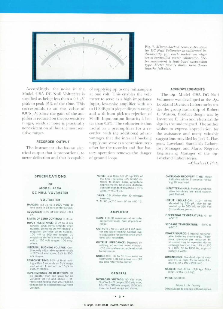
Fig. 7. Mirror-backed zero-center scale for DC Null Voltmeter is calibrated in d i v idua l l y f o r each me te r on -hp - servo- controlled meter calibrator. Me ter movement is taut-band suspension type. Meter face is shown here three- fourths full size.
Accordingly , the noise in the Model 419A DC Null Voltmeter is specified as being less than a 0.3 /¿V peà k-to-peak 95% of the time. This cor responds to an rms va lue of 0.075 ¡j.V. Since the gain of the am plifier is reduced on the less sensitive ranges, residual noise is practically nonexistent on all but the most sen sitive ranges.
R E C O R D E R O U T P U T
The instrument also has an elec trical output that is proportional to meter deflection and that is capable
of supplying up to one milliampere at one volt. This enables the volt meter to serve as a high impedance input, low-noise amplifier with up to 1 10 dB gain (depending on range) and with hum pick-up rejection of 80 dB. Input-output linearity is bet ter than 0.5%. The voltmeter is thus useful as a preamplifier for a re corder, with the additional advan- vantages that the internal bucking supply can serve as a convenient /ero offset for the recorder and that bat tery operation removes the danger of ground loops.
ACKNOWLEDGMENTS The -hp- Model 419A DC Null
Voltmeter was developed at the -hp-
Loveland Division Laboratories un der the group leadership of Robert E. Watson. Product design was by Lawrence E. Linn and electrical de sign by the undersigned. The author wishes to express appreciation for the assistance and many valuable suggestions provided by Jack L. Har- gens, Loveland Standards Labora tory Manager, and Marco Negrete, Engineering Manager of the -hp- Loveland Laboratories.
-Charles D. Platz
S P E C I F I C A T I O N S
-hp- M O D E L 4 1 9 A
D C N U L L V O L T M E T E R
V O L T M E T E R
RANGES: ±3 /,V to ±1000 volts dc end scale in 18 zero center ranges.
ACCURACY: ±2% of end scale ±0.1 f»V.
L I M I T S O F Z E R O C O N T R O L : Â ± 1 5 , , V .
INPUT RESISTANCE: 3 , ,V to 3 mV ranges : 100k ohms ( in f in i te when nul led). 10 mV to 30 mV ranges: 1 m e g o h m ( i n f i n i t e w h e n n u l l e d ) . 1 0 0 m V t o 3 0 0 m V r a n g e s : 1 0 megohms ( in f in i te when nul led) . 1 vo l t t o 100 vo l t r anges : 100 meg ohms.
I N T E R N A L B U C K I N G V O L T A G E : C o n t inuously adjustable approximately ±120% of end scale, 3-.uV to 300- mV ranges.
RESPONSE TIME: 95% of f inal read ing within 3 seconds on 3-,»V range and w i t h i n 1 second on 10 - / iV t o 1000-V ranges.
S U P E R I M P O S E D A C R E J E C T I O N : 8 0 dB g rea te r t han end sca le f o r ac vo l t ages 60 Hz and above †” a f fects reading less than 2%. Peak ac voltage not to exceed max overload voltage.
NOISE: Less than 0.3 ¡,V p-p 95% of the t ime (between ±2<r l imi ts) re f e r r e d t o i n p u t ; n o i s e a m p l i t u d e a p p r o x i m a t e s G a u s s i a n d i s t r i b u t ion with standard deviat ion a (rms value) = 0.075 ^V.
DRIFT: 0 .5 , iV /day a f te r 30 minu tes warm-up.
T. C. .05 nV/ 'C f rom 0° to +50° C.
A M P L I F I E R
GAIN: 110 dB max imum a t reco rde r output terminals. Gain depends on range.
OUTPUT: 0 to ± 1 volt at 1 mA max. for end scale reading. Output level is adjustable for convenience when used with recorders.
OUTPUT IMPEDANCE: Depends on s e t t i n g o f o u t p u t l e v e l c o n t r o l . <35 ohms when output level is set to max imum.
NOISE: 0.01 Hz to 5 Hz — same as vol tmeter; 5 Hz and above — <10 mV rms referred to output.
G E N E R A L
OVERLOAD VOLTAGE: 50 Vdc max, 3-/iV to 3-mV ranges; 500 Vdc max, 10-mV to 300-mV ranges; 1200 Vdc max. on 1-volt range and above.
OVERLOAD RECOVERY TIME: Meter ind ica tes w i th in 3 seconds fo l low ing 10' overload.
INPUT TERMINALS: Posit ive and neg a t i ve t e rm ina l s a re so l i d coppe r , gold f lashed.
I N P U T I S O L A T I O N : > 1 0 ' Â ° o h m s s h u n t e d b y 2 5 0 p p . M a y b e o p e ra ted up t o 500 Vdc o r 350 Vac (rms) above ground.
O P E R A T I N G T E M P E R A T U R E : 0  ° t o +50°C.
STORAGE TEMPERATURE: -40°C to +60°C.
POWER SOURCE: 4 internal recharge ab le ba t te r ies ( fu rn ished) . Th i r ty - h o u r o p e r a t i o n p e r r e c h a r g e . I n s t rument may be opera ted dur ing recharge f rom ac l ine ; 115 or 230 V ±10%, 50 to 1000 Hz, approx i mately 3 watts.
DIMENSIONS: Standard -hp- ' /z mod ule; 6'/2 in. high, 734 in. wide, 8 in. deep (152 x 197 x 203 mm).
W E I G H T : N e t : 8 I b s . ( 3 , 6 k g ) . S h i p ping: 12 Ibs. (5,4 kg).
PRICE: $450.00.
Pr ices f .o.b. factory Data subject to change without notice
• 6 •
© Copr. 1949-1998 Hewlett-Packard Co.
A P O R T A B L E D C V O L T A G E S T A N D A R D P R O V I D I N G 1 0 P P M T R A N S F E R A C C U R A C Y
A new type o f ins t rument t rans fe rs p rec is ion dc vo l tages ou t o f the s tandards labora to ry to work ing a reas .
RECENTLY DEVELOPED INSTRU MENTS — digital voltmeters in par ticular — now enable measurement accuracies approaching 0.01% or better in normal working environ ments outside of the standards lab. As with other precision instrumen tation, maintaining the rated accu racy of these instruments requires periodic calibration, but calibration becomes increasingly complicated as instrument accuracy approaches that of available reference stand ards.
The primary reference voltage standard in most laboratories is the saturated cell. These devices have excellent long-term stability but they are sensitive to temperature as well as to physical motion and load ing, and should be used with care to prevent damage. Saturated cells must be maintained in a carefully controlled environment if their po tential accuracy is to be reali/ed.
The unsaturated cell has been the preferred device for use as a working standard. Unsaturated cells are less susceptible to temperature changes
Fig. 1. -hp- Model 735 A DC Transfer Standard supplies any one of four highly-stable switch-selected voltages to floating and guarded output terminals. Instrument is portable but has stability within 1 or 2 ppm per 8 hours. Tem perature coefficient is less than 1
ppm/°C.
(typically 4 ppm/°C) but exhibit greater change of voltage with time, typically 2-5 ppm/month. Unsat urated cells therefore must be re turned to the standards lab period ically for calibration.
When standard cells are used for the calibration of other equipment, the cell voltage, which is usually within 1.018 to 1.020 volts, is trans lated to a decade level, i.e., 1 V, 10 V and so on. This requires a time-con suming procedure involving some calculations and the use of precision resistive dividers and null indica tors.
T H E E L E C T R O N I C T R A N S F E R S T A N D A R D
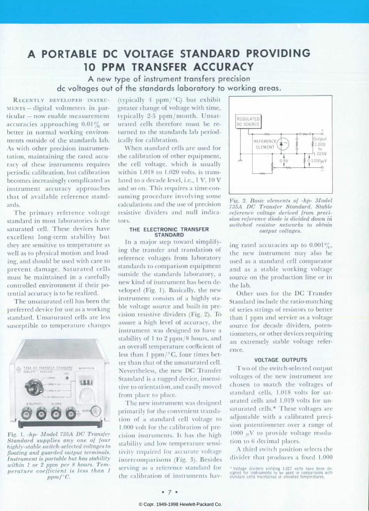
In a major step toward simplify ing the transfer and translation of reference voltages from laboratory standards to comparison equipment outside the standards laboratory, a new kind of instrument has been de veloped (Fig. 1). Basically, the new instrument consists of a highly sta ble voltage source and built-in pre cision resistive dividers (Fig. 2). To assure a high level of accuracy, the instrument was designed to have a stability of 1 to 2 ppm/8 hours, and an overall temperature coefficient of less than 1 ppm/°C, four times bet ter than that of the unsaturated cell. Nevertheless, the new DC Transfer Standard is a rugged device, insensi tive to orientation, and easily moved from place to place.
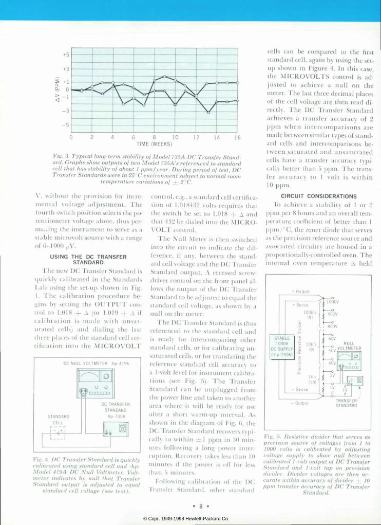
The ne\v instrument was designed primarily for the convenient transla tion of a standard cell voltage to 1 .000 volt for the calibration of pre cision instruments. It has the high stability and low temperature sensi tivity required for accurate voltage intercomparisons (Fig. 3). Besides serving as a reference standard for the calibration of instruments hav-
Fig. 2. Basic elements of -hp- Model 735A DC Transfer Standard. Stable reference voltage derived from preci sion reference diode is divided down in switched resistor networks to obtain
output voltages.
ing rated accuracies up to 0.001%, the new instrument may also be used as a standard cell comparator and as a stable working voltage source on the production line or in the lab.
Other uses for the DC Transfer Standard include the ratio-matching of series strings of resistors to better than 1 ppm and service as a voltage source for decade dividers, poten tiometers, or other devices requiring an extremely stable voltage refer ence.
V O L T A G E O U T P U T S
Two of the switch-selected output voltages of the new instrument are chosen to match the voltages of standard cells, 1.018 volts for sat urated cells and 1.019 volts for un saturated cells. These voltages are adjustable with a calibrated preci sion potentiometer over a range of 1000 /xV to provide voltage resolu tion to 6 decimal places.
A third switch position selects the divider that produces a fixed 1.000
" V o l t a g e d i v i d e r s y i e l d i n g 1 . 0 1 7 v o l t s h a v e b e e n d e s i g n e d f o r i n s t r u m e n t s t o b e u s e d i n c o m p a r i s o n s w i t h s tandard ce l l s ma in ta ined a t e leva ted tempera tures .
© Copr. 1949-1998 Hewlett-Packard Co.
6 8 1 0 T I M E ( W E E K S )
12 It,
Fig. Stand Typical long-term stability of Model 735 A DC Transfer Stand ard. Graphs show outputs of two Model 735A's referenced to standard cell that has stability of about 1 ppm/year. During period of test, DC Transfer Standards were in 25° C environment subject to normal room
temperature variations of ± 2°C.
V, without the provision for ÃIK re- mental voltage adjustment. The fourth switch position selects the po tentiometer voltage alone, thus per- miiiing the instrument to serve as a stable microvolt source with a range of 0-1000juV.
U S I N G T H E D C T R A N S F E R S T A N D A R D
The new DC Transfer Standard is (juickly calibrated in the Standards Lab using the set-up shown in Fig. 1. The calibration procedure be gins by setting the OUTPUT con trol to 1.018 -f A (or 1.019 + A if calibration is made with unsat- uratcd cells) and dialing the last three places of the standard cell cer- ti ficat ion into the MICROVOLT
Fig. 4. DC Transfer Standard is quickly calibrated using standard cell and -hp- Model 419A DC Null Voltmeter. Volt meter indicates by null that Transfer Standard output is adjusted to equal
standard cell voltage (see text).
control, e.g., a standard cell certifica tion of 1.018432 volts requires that the switch be set to 1.018 + A and that 432 be dialed into the MICRO VOLT control.
The Null Meter is then switched into the circuit to indicate the dif ference, if any, between the stand ard cell voltage and the DC Transfer Standard output. A recessed screw driver control on the front panel al lows the output of the DC Transfer Standard to be adjusted to equal the standard cell voltage, as shown by a null on the meter.
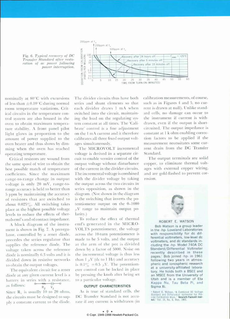
The DC Transfer Standard is thus referenced to the standard cell and is ready for intercomparing other standard cells, or for calibrating un- saturated cells, or for translating the reference standard cell accuracy to a 1 -volt level for instrument calibra tions (see Fig. 5). The Transfer Standard can be unplugged from the power line and taken to another area where it will be ready for use alter a short warm-up interval. As shown in the diagram of Fig. 6, the DC Transfer Standard recovers typi cally to within ± 1 ppm in 30 min utes following a long power inter ruption. Recovery takes less than 10 minutes if the power is oil for less than "> minutes.
Following calibration of the DC Transfer Standard, other standard
cells can be compared to the first standard cell, again by using the set up shown in Figure 4. In this case, the MICROVOLTS control is ad justed to achieve a null on the meter. The last three decimal places of the cell voltage are then read di rectly. The DC Transfer Standard achieves a transfer accuracy of 2 ppm when intercomparisons are made between similar types of stand ard cells and intercomparisons be tween saturated and unsaturated cells have a transfer accuracy typi cally better than 5 ppm. The trans fer accuracy to 1 volt is within 10 ppm.
C I R C U I T C O N S I D E R A T I O N S To achieve a stability of 1 or 2
ppm per 8 hours and an overall tem perature coefficient of better than 1 ppm/°C, the /ener diode that serves as the precision reference source and associated circuitry are housed in a proportionally-controlled oven. The internal oven temperature is held
+ Output
- O u t p u t
Fig. 5. Resistive divider that serves as precision source of voltages from 1 to 1000 volts is calibrated by adjusting voltage supply to show null between calibrated 1-volt output of DC Transfer Standard and 1-volt tap on precision divider. Divider voltages are then ac curate within accuracy of divider ± 10 ppm transfer accuracy of DC Transfer
Standard.
© Copr. 1949-1998 Hewlett-Packard Co.
2 0 0 p p m a t t . 2 0 0 p p m a t t 0
5 0 0 p p m a t t o
Fig. 6. Typical recovery of DC T r a n s f e r S t a n d a r d a f t e r r e s t o - j , r a t i o n o f a c p o w e r f o l l o w i n g " 5 '
power interruption. § £
l e c o v e r y a f t e r 2 4 h o u r s o f f - R e c o v e r y a f t e r 5 m i n u t e s o f f "
1 0 1 5 2 0 2 5 3 0 3 5 4 0 4 5 TIME FROM TURN-ON (MINUTES)
50
nominally at 80°C with excursions of less than ±0.1 0°C during normal room temperature variations. Crit ical circuits in the temperature con trol system are also housed in the oven to obtain maximum tempera ture stability. A front panel pilot light glows in proportion to the amount of power supplied to the oven heater and thus shows by dim ming when the oven has reached operating temperature.
Critical resistors are wound from the same spool of wire to obtain the best possible match of temperature coefficients. Since the maximum range-to-range change in output voltage is only 20 mV, range-to- range accuracy is held to better than ") ppm by maintaining the accuracy of resistors that are switched to about 0.025%. All switching takes place at the highest possible voltage levels to reduce the effects of ther- malsemf 'sand of contact impedance.
A block diagram of the instru ment is shown in Fig. 7. A preregu- lator, controlled by a zener diode, precedes the series regulator that supplies the reference diode. The voltage taken across the reference diode is nominally 0.3 volts and it is divided down in resistive networks to obtain the output voltages.
The equivalent circuit for a zener diode at any given current level is a battery in series with a resistance,
o w * l i l i o a s f o l l o w s : p ' nz vz Since Rz is usually 10 to 20 ohms, the circuits must be designed to sup ply a constant current to the diode.
The divider circuits thus have both series and shunt elements so that each divider draws I mA when switched into the circuit, maintain ing the load on the regulating sys tem constant at all times. The 'Cali brate' control is a fine adjustment on the 1 mA current and it therefore calibrates all three fixed output volt ages simultaneously.
The MICROVOLT incremental voltage is derived in a separate cir cuit to enable vernier control of the output voltage without disturbance of the current in the divider circuits. The incremental voltage is combined with the divider voltage by taking the output across the two circuits in series opposition, as shown in the diagram. (Not shown in the diagram is the switching that inverts the po tentiometer output on the 0-1000 juV range to maintain output po larity.)
To reduce the effect of thermal emf's generated in the MICRO VOLTS potentiometer, the voltage across the 10-turn potentiometer is made to be 5 volts, and the output at the arm of the pot is divided down by a factor of 5000. Noise on the incremental voltage is thus less than I //.V (dc to 1 Hz) and accuracy is 0.1% ±0.5 ¿iV. The potentiom eter control can be locked in place by pressing the knob after being set to a particular voltage.
O U T P U T C H A R A C T E R I S T I C S As is true of standard cells, the
DC Transfer Standard is not accu rate if any current is withdrawn (in
calibration measurements, of course, such as in Figures 4 and 5, no cur rent is drawn at null). Unlike stand ard cells, no damage can occur to the instrument if current is with drawn, even if the output is short- circuited. The output impedance is constant at 1 k ohm enabling correc tion factors to be applied if the measurement necessitates some cur rent drain from the DC Transfer Standard.
The output terminals are solid copper, to eliminate thermal volt ages with external copper wiring, and are gold-flashed to prevent cor rosion.
f -
R O B E R T E . W A T S O N B o b W a t s o n i s a g r o u p l e a d e r
i n t he -hp - Love land Labo ra to r i es w i t h r e s p o n s i b i l i t y f o r d c d i f f e r e n t i a l v o l t m e t e r s , l o w - l e v e l d c v o l t m e t e r s , a n d d c s t a n d a r d s i n c l u d i n g t h e - h p - M o d e l 7 4 0 A D C S t a n d a r d / D i f f e r e n t i a l V o l t m e t e r r e c e n t l y d e s c r i b e d i n t h e s e p a g e s . B o b j o i n e d - h p - i n 1 9 6 1 f o l l o w i n g t w o y e a r s i n a t m o s p h e r i c a n d i o n o s p h e r i c r e s e a r c h a t a u n i v e r s i t y - a f f i l i a t e d l a b o r a t o r y . H e h o l d s b o t h a B S E E a n d a n M S E E f r o m t h e U n i v e r s i t y o f U t a h a n d i s a m e m b e r o f E t a K a p p a N u , T a u B e t a P i , a n d S igma XL 1 Rober t E . Watson, 'A Combined DC Vo l tage S t a n d a r d a n d D i f f e r e n t i a l V o l t m e t e r f o r P r e c ise Ca l ib ra t ion Work , ' 'Hewle t t -Packard Jour na l ,1 Vol . 16, No. 9 , May, 1965.
© Copr. 1949-1998 Hewlett-Packard Co.
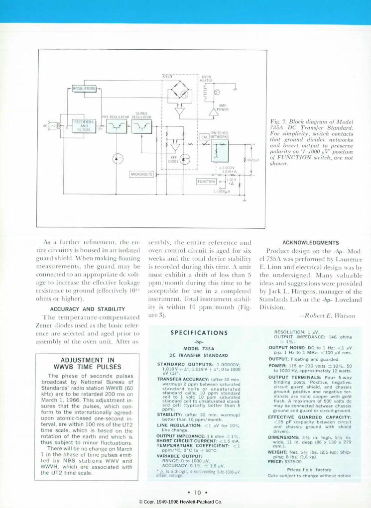
O u t p u t
Fig. 7. Block diagram of Model 735A DC Transfer Standard. For simplicity, switch contacts that ground divider networks and invert output to preserve polarity on '1-1000 /¿V position of FUNCTION switch, are not shown.
As a further refinement, the en tire circuitry is housed in an isolated guard shield. When making floating measurements, the guard may be connected to an appropriate dc volt age to increase the effective leakage resistance to ground (effectively 1011 ohms or higher).
A C C U R A C Y A N D S T A B I L I T Y
The temperature-compensated Zener diodes used as the basic refer ence are selected and aged prior to assembly of the oven unit. After as-
A D J U S T M E N T I N W W V B T I M E P U L S E S
T h e p h a s e o f s e c o n d s p u l s e s b r o a d c a s t b y N a t i o n a l B u r e a u o f S t a n d a r d s ' r a d i o s t a t i o n W W V B ( 6 0 k H z ) a r e t o b e r e t a r d e d 2 0 0 m s o n M a r c h 1 , 1 9 6 6 . T h i s a d j u s t m e n t i n s u r e s t h a t t h e p u l s e s , w h i c h c o n f o r m t o t h e i n t e r n a t i o n a l l y a g r e e d - u p o n a t o m i c - b a s e d o n e - s e c o n d i n t e r v a l , a r e w i t h i n 1 0 0 m s o f t h e U T 2 t i m e s c a l e , w h i c h i s b a s e d o n t h e r o t a t i o n o f t h e e a r t h a n d w h i c h i s t h u s s u b j e c t t o m i n o r f l u c t u a t i o n s .
The re w i l l be no change on March 1 i n t h e p h a s e o f t i m e p u l s e s e m i t t e d b y N B S s t a t i o n s W W V a n d W W V H , w h i c h a r e a s s o c i a t e d w i t h t h e U T 2 t i m e s c a l e .
sembly, the entire reference and oven control circuit is aged for six weeks and the total device stability is recorded during this time. A unit must exhibit a drift of less than 5 ppm/month during this time to be acceptable for use in a completed instrument. Total instrument stabil ity is within 10 ppm/month (Fig ure 3).
S P E C I F I C A T I O N S -hp-
M O D E L 7 3 5 A D C T R A N S F E R S T A N D A R D
S T A N D A R D O U T P U T S : 1 0 0 0 0 0 V ; 1 . 0 1 8 V + A - ; 1 . 0 1 9 V 4 - A ' ; O t o 1 0 0 0 / i V ( A ) - .
T R A N S F E R A C C U R A C Y : ( a f t e r 3 0 m i n . w a r m u p ) 2 p p m b e t w e e n s a t u r a t e d s t a n d a r d c e l l s o r u n s a t u r a t e d s t a n d a r d c e l l s ; 1 0 p p m s t a n d a r d c e l l t o 1 v o l t ; 1 0 p p m s a t u r a t e d s t a n d a r d c e l l t o u n s a t u r a t e d s t a n d a r d c e l l ( t y p i c a l l y b e t t e r t h a n 5 p p m ) .
S T A B I L I T Y : ( a f t e r 3 0 m i n . w a r m u p ) b e t t e r t h a n 1 0 p p m / m o n t h .
L I N E R E G U L A T I O N : < 1 , u V f o r 1 0 % l i n e c h a n g e .
O U T P U T I M P E D A N C E : 1 k o h m  ± 1 % . S H O R T C I R C U I T C U R R E N T : < 1 . 5 m A T E M P E R A T U R E C O E F F I C I E N T : < 1
p p m / Â ° C , 0 Â ° C t o - 5 0 Â ° C . V A R I A B L E O U T P U T :
R A N G E : 0 t o 1 0 0 0 / i V . A C C U R A C Y : 0 . 1 % Â ± 1 . 5 / i V .
* A i s a 3 -d ig i t , d i r ec t - read ing O- to - lOOO-^V o f f se t vo l tage .
A C K N O W L E D G M E N T S
Product design on the -hp- Mod el 735A was performed by Laurence E. Linn and electrical design was by the undersigned. Many valuable ideas and suggestions were provided by Jack L. Hargens, manager of the Standards Lab at the -hp- Loveland Division.
—Robert E. Watson
R E S O L U T I O N : 1 u V . O U T P U T I M P E D A N C E : 1 4 6 o h m s
±1%. O U T P U T N O I S E : D C t o 1 H z : < 1  ¿ i V
p - p . 1 H z t o 1 M H z : < 1 0 0 /  ¿ V r m s . O U T P U T : F l o a t i n g a n d g u a r d e d . P O W E R : 1 1 5 o r 2 3 0 v o l t s  ± 1 0 % , 5 0
t o 1 0 0 0 H z , a p p r o x i m a t e l y 1 2 w a t t s . O U T P U T T E R M I N A L S : F o u r 5 - w a y
b i n d i n g p o s t s . P o s i t i v e , n e g a t i v e , c i r c u i t g u a r d s h i e l d , a n d c h a s s i s g r o u n d ; p o s i t i v e a n d n e g a t i v e t e r m i n a l s a r e s o l i d c o p p e r w i t h g o l d f l a s h . A m a x i m u m o f 5 0 0 v o l t s d c m a y b e c o n n e c t e d b e t w e e n c h a s s i s g r o u n d a n d g u a r d o r c i r c u i t g r o u n d .
E F F E C T I V E G U A R D E D C A P A C I T Y : < 2 5 p F ( c a p a c i t y b e t w e e n c i r c u i t a n d c h a s s i s g r o u n d w i t h s h i e l d d r i v e n ) .
D I M E N S I O N S : 3 % i n . h i g h , S ' / a i n . w i d e , 1 1 i n . d e e p ( 8 6 x 1 3 0 x 2 7 9 m m . ) .
W E I G H T : N e t : 5 > / 2 I b s . ( 2 , 5 k g ) ; S h i p p i n g : 8 I b s . ( 3 , 6 k g ) .
P R I C E : $ 3 7 5 . 0 0 .
P r i c e s f . o . b . f a c t o r y D a t a s u b j e c t t o c h a n g e w i t h o u t n o t i c e
10 © Copr. 1949-1998 Hewlett-Packard Co.
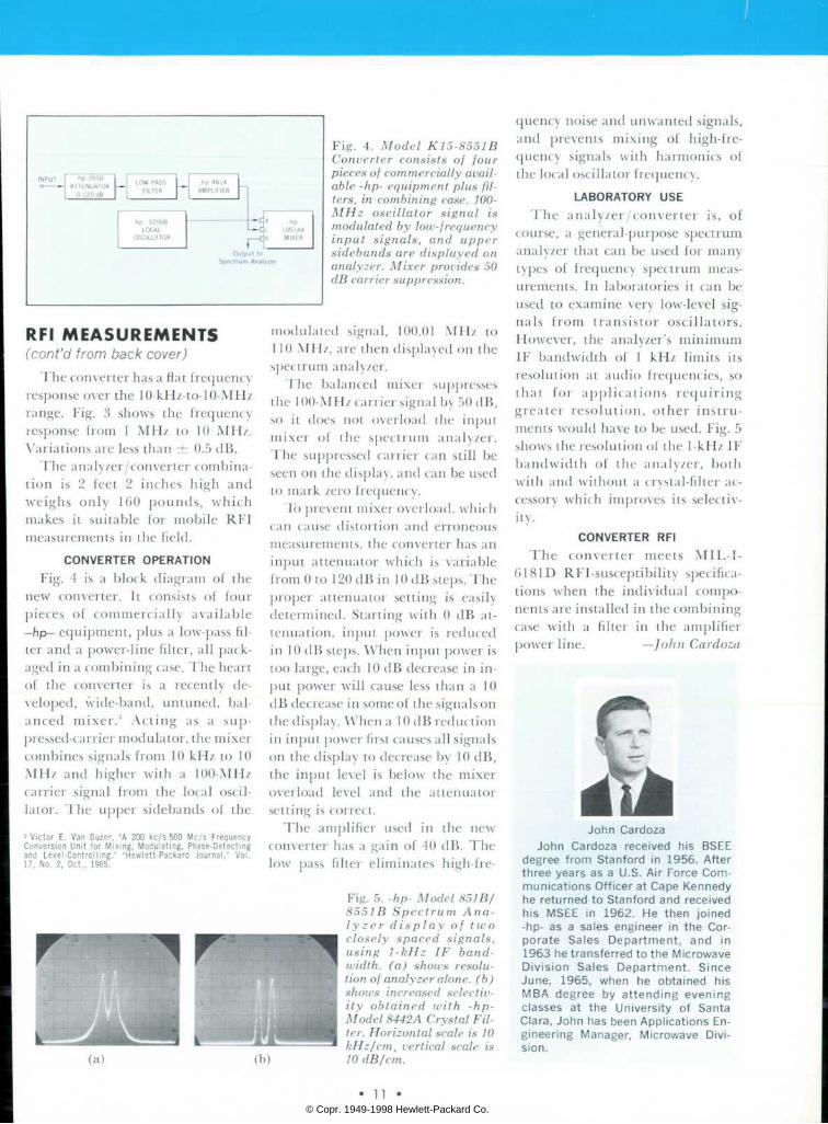
Fig. 4. Model K15-8551B Converter consists of four pieces of commercially avail able -hp- equipment plus fil ters, in combining case. 100- MHz oscillator signal is modulated by low-frequency input signals, and upper sidebands are displayed on analyzer. Mixer provides 50 dB carrier suppression.
R F I M E A S U R E M E N T S (cont 'd f rom back cover)
The converter has a flat frequency response over the 10-kH/-to-10-MH/. range. Fig. 3 shows the frequency response from 1 MHz to 10 MHz. Variations are less than ± 0.5 dB.
The analy/er/converter combina t ion is 2 feet 2 inches high and weighs only 160 pounds, which makes it suitable for mobile RFI measurements in the field.
C O N V E R T E R O P E R A T I O N
Fig. 4 is a block diagram of the new converter. It consists of four pieces of commercially available — hp- equipment, plus a low-pass fil ter and a power-line filter, all pack aged in a combining case. The heart of the converter is a recently de veloped, wide-band, untuned, bal anced mixer .2 Act ing as a sup- pressed-carrier modulator, the mixer combines signals from 10 kHz to 10 MHz and higher with a 100-MH/ carrier signal from the local oscil lator. The upper sidebands of the
2 V i c t o r E . V a n D u z e r , ' A 2 0 0 k c / s 5 0 0 M c / s F r e q u e n c y Convers ion Un i t fo r Mix ing , Modu la t ing , Phase-Detec t ing a n d L e v e l - C o n t r o l l i n g . ' ' H e w l e t t - P a c k a r d J o u r n a l , ' V o l . 17, No. 2 , Oct . , 1965.
modulated signal, 100.01 MHz to 1 10 MHz, are then displayed on the spectrum analyzer.
The balanced mixer suppresses the 100-MHz carrier signal by 50 dB, so it does not overload the input mixer of the spectrum analyzer. The suppressed carrier can still be seen on the display, and can be used to mark zero frequency.
To prevent mixer overload, which can cause distortion and erroneous measurements, the converter has an input attenuator which is variable from 0 to 1 20 dB in 1 0 dB steps. The proper attenuator setting is easily determined. Starting with 0 dB at tenuation, input power is reduced in 10 dB steps. When input power is too large, each 10 dB decrease in in put power will cause less than a 10 dB decrease in some of the signals on the display. When a 10 dB reduction in input power first causes all signals on the display to decrease by 10 dB, the input level is below the mixer overload level and the attenuator setting is correct.
The amplifier used in the new converter has a gain of 40 dB. The low pass filter eliminates high-fre-
Fig. 5. -hp- Model 851B/ 8551B Spectrum Ana l y zer d i sp lay o f two closely spaced signals, using 1-kHz IF band width, (a) shows resolu tion of analyzer alone, (b) shows increased selectiv ity obtained with -hp- Model 8442 A Crystal Fil ter. Horizontal scale is 10 kHz/cm, vertical scale is 10 dB/cm.
quency noise and unwanted signals, and prevents mixing of high-fre quency signals with harmonics of the local oscillator frequency.
L A B O R A T O R Y U S E
The analyzer /conver ter i s , of course, a general-purpose spectrum analyzer that can be used for many types of frequency spectrum meas urements. In laboratories it can be used to examine very low-level sig nals from transistor oscil lators. However, the analyzer's minimum IF bandwidth of 1 kHz limits its resolution at audio frequencies, so tha t fo r app l i ca t ions r equ i r ing grea ter resolu t ion , o ther ins t ru ments would have to be used. Fig. 5 shows the resolution of the 1-kHz IF bandwidth of the analyzer, both with and without a crystal-filter ac cessory which improves its selectiv ity.
C O N V E R T E R R F I
T h e c o n v e r t e r m e e t s M I L - I - 6181D RFI-susceptibility specifica tions when the individual compo nents are installed in the combining case with a filter in the amplifier p o w e r l i n e . â € ” J o h n C a r d o z a
(b)
J o h n C a r d o z a J o h n C a r d o z a r e c e i v e d h i s B S E E
d e g r e e f r o m S t a n f o r d i n 1 9 5 6 . A f t e r t h r e e y e a r s a s a U . S . A i r F o r c e C o m m u n i c a t i o n s O f f i c e r a t C a p e K e n n e d y h e r e t u r n e d t o S t a n f o r d a n d r e c e i v e d h i s M S E E i n 1 9 6 2 . H e t h e n j o i n e d - h p - a s a s a l e s e n g i n e e r i n t h e C o r p o r a t e S a l e s D e p a r t m e n t , a n d i n 1 9 6 3 h e t r a n s f e r r e d t o t h e M i c r o w a v e D i v i s i o n S a l e s D e p a r t m e n t . S i n c e J u n e , 1 9 6 5 , w h e n h e o b t a i n e d h i s M B A d e g r e e b y a t t e n d i n g e v e n i n g c l a s s e s a t t h e U n i v e r s i t y o f S a n t a C l a r a , J o h n h a s b e e n A p p l i c a t i o n s E n g i n e e r i n g M a n a g e r , M i c r o w a v e D i v i s ion.
I I © Copr. 1949-1998 Hewlett-Packard Co.
R F I M E A S U R E M E N T S D O W N T O 1 0 k H z W I T H S P E C T R U M A N A L Y Z E R C O N V E R T E R
ALL ELECTRICAL DEVICES generate unwanted signals, harmonics, leak age, and electrical transients, which can interfere with sensit ive elec tronic equipment operating in any part of the electromagnetic spec trum. Because of this interference problem, U.S. government procure ment agencies often specify that many kinds of electrical equipment be checked for ' radio frequency' emissions over a frequency range of almost six decades, from the upper audio frequencies (14 kHz) to the high microwave frequencies (10 GHz). In the past, such radio fre quency interference (RFI) measure ments had to be made with a num ber of receivers, each one covering a sma l l po r t ion o f t he spec t rum. Shortcomings of this method were the time and equipment required, the possibility of human errors, and
* S e r i o u s n e s s o f t h e i n t e r f e r e n c e p r o b l e m i s i n d i c a t e d by b i l l S . 1015, now before the U.S. Senate , wh ich wou ld e m p o w e r t h e F e d e r a l C o m m u n i c a t i o n s C o m m i s s i o n t o r e g u l a t e t h e m a n u f a c t u r e , s a l e , s h i p m e n t , o r u s e o f d e v i c e s t h a t c r e a t e ' h a r m f u l r a d i o f r e q u e n c y i n t e r fe rence ' .
Fig. 1. New -hp- Model K15-8551B S p e c t r u m - A n a l y z e r U p - C o n v e r t e r mounted on top of -hp- Model 851B/ 8551B Spectrum Analyzer. Analyzer range without converter is 10 MHz to 40 GHz : converter extends this down to
10 kHz.
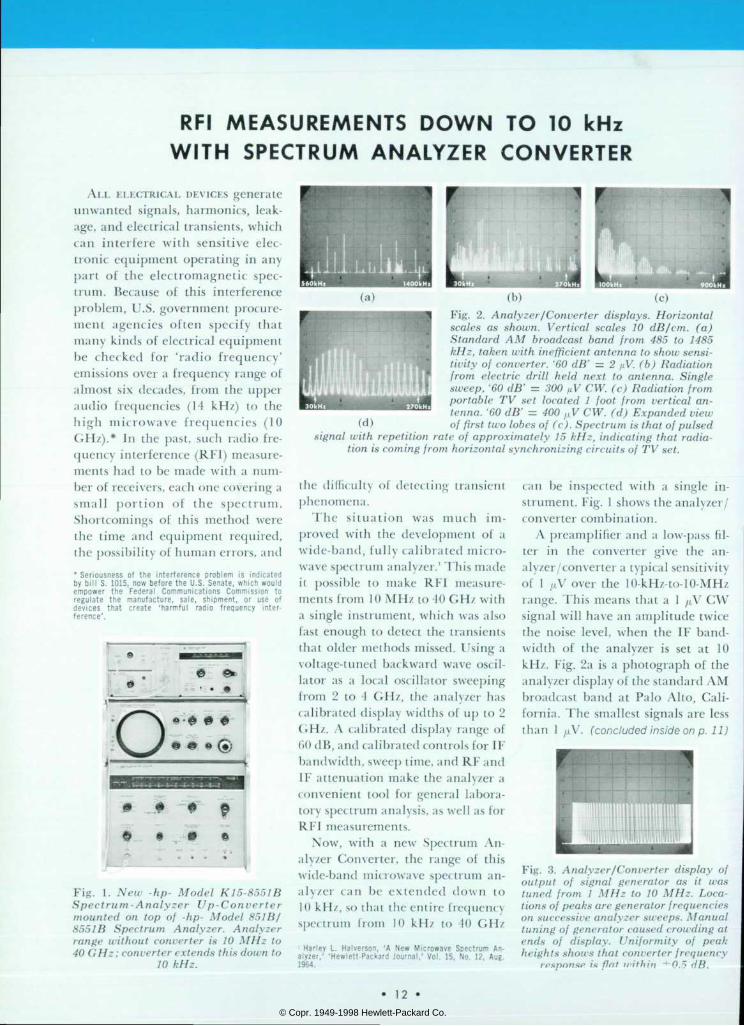
Fig. 2. Analyzer/Converter displays. Horizontal scales as shown. Vertical scales 10 dB/ctn. (a) Standard AM broadcast band from 485 to 1485 kHz, taken with inefficient antenna to show sensi tivity of converter. '60 dB' = 2 /iV. (b) Radiation from electric drill held next to antenna. Single sweep, '60 dB' = 300 ¡iV CW. (c) Radiation from portable TV set located 1 foot from vertical an tenna. '60 dB' = 400 ,,V CW. (d) Expanded view
( d ) o f f i r s t t w o l o b e s o f ( c ) . S p e c t r u m i s t h a t o f p u l s e d signal radia repetition rate of approximately 15 kHz, indicating that radia
tion set. coming from horizontal synchronizing circuits of TV set.
the difficulty of detecting transient phenomena.
T h e s i t u a t i o n w a s m u c h i m proved with the development of a wide-band, fully calibrated micro wave spectrum analyzer.1 This made it possible to make RFI measure ments from 10 MHz to 40 GHz with a single instrument, which was also fast enough to detect the transients that older methods missed. Using a voltage-tuned backward wave oscil lator as a local oscillator sweeping from 2 to 4 GHz, the analyzer has calibrated display widths of up to 2 GHz. A calibrated display range of f>0 dB, and calibrated controls for IF bandwidth, sweep time, and RF and IF attenuation make the analyzer a convenient tool for general labora tory spectrum analysis, as well as for RFI measurements.
Now, with a new Spectrum An- alv/er Converter, the range of this wide-band microwave spectrum an- a lv /e i can be extended down to 10 kHz, so that the entire frequency spectrum from 10 kH/ to 40 GHz
H a r l e y L . H a l v e r s o n , ' A N e w M i c r o w a v e S p e c t r u m A n a l yze r , ' 'Hew le t t -Packa rd Jou rna l , ' Vo l . 15 , No 12 , Aug 1964.
can be inspected with a single in strument. Fig. 1 shows the analyzer/ converter combination.
A preamplifier and a low-pass fil te r in the conver ter g ive the an alyzer/converter a typical sensitivity of 1 ijV over the 10-kHz-to-lO-MHz range. This means that a 1 /¿V CW signal will have an amplitude twice the noise level, when the IF band width of the analyzer is set at 10 kHz. Fig. 2a is a photograph of the analyzer display of the standard AM broadcast band at Palo Alto, Cali fornia. The smallest signals are less than 1 /J.V. (concludedinsideonp.il)
Fig. 3. Analyzer/Converter display of output of signal generator as it was tuned from 1 MHz to 10 MHz. Loca tion* of peaks are generator frequencies on successive analyzer sweeps. Manual tinting of generator caused crowding at ends of display. Uniformity of peak heights shows that converter frequency
is flnt irithin "*~0.5 dB,
12 © Copr. 1949-1998 Hewlett-Packard Co.