Embed Size (px)
Citation preview

ISBN 978-80-261-0973-0, © University of West Bohemia, 2021
Hardware Security of Emerging Non-Volatile
Memory Devices under Imaging AttacksNhu Huynh
Department of Electrical and Computer
Engineering The University of Texas at San Antonio
San Antonio, U.S.A
Hebin Cherian
Department of Electrical and Computer
Engineering The University of Texas at San Antonio
San Antonio, U.S.A
Ethan C. Ahn
Department of Electrical and Computer
Engineering The University of Texas at San Antonio
San Antonio, U.S.A
Abstract—The emerging non-volatile memory (NVM)
devices are currently changing the landscape of computing
hardware. However, their hardware security remains
relatively unexplored in the field. This is a critical research
problem because given that they are non-volatile, sensitive
information may be vulnerable to various physical attacks
unless properly encrypted. In this work, we investigated
security vulnerability of two emerging non-volatile memory
devices (STT-MRAM and RRAM) against the most
commonly available, non-destructive physical attack –
Scanning Electron Microscope (SEM) imaging. The central
premise is that if any difference of memory cells in high
resistance and low resistance (bit ‘1’ and ‘0’) states can be
detected in SEM, stored data could possibly leak or be stolen
by adversaries. It is concluded that unless advanced elemental
analysis techniques such as energy dispersive x-ray
spectroscopy (EDX) are used, it is very unlikely that the bit
information stored in these memory cells leak out by imaging
attacks.
Keywords—hardware security, imaging attacks, SEM,
EDX, emerging NVMs, STT-MRAM, RRAM
I. INTRODUCTION
Unlike traditional volatile memories (SRAM and
DRAM), emerging NVMs [1-2] can retain stored data even
when a system’s power is off while providing superior
scalability. Thus, investigating them as non-volatile
components of the memory hierarchy has become a critical
field of study. For example, when they are employed as
main memory, non-volatility provides the unique benefits
of almost zero idle power, and removal of periodic
refreshes that would otherwise contribute to a significant
portion of power consumption in DRAM-based main
memories. However, this can also introduce new design
and implementation challenges; and, in particular, for the
purposes of this work, we note that critical issues may arise
in the hardware security aspect because some sensitive
information will remain in the memory and still be able to
be probed even when a system’s power is off. Information
stored in the non-volatile main or cache memory is thus
susceptible to various physical attacks, which cannot be
protected by conventional software-based
countermeasures that only work when a system’s power is
on. Therefore, the physical attacks from various
adversaries may result in unauthorized privilege escalation
or significant leakage of sensitive information such as
encryption keys and personally identifiable information.
In this study, we chose spin transfer torque magnetic
random-access memory (STT-MRAM) [3] and resistive
random-access memory (RRAM) [4] as representative
emerging NVM devices. Besides the rapidly rising
neuromorphic application domain [5-6], both technologies
possess the great potential to become a new mainstream
memory. The STT-MRAM technology that can endure
practically unlimited write/erase programming cycles and
therefore fulfill the endurance requirement for main
memory (> 1015 cycles) has already been developed [7],
making it possible to realize visions of replacing DRAM
[8], or even certain embedded memories (SRAM cache [9]
or eFlash [10]). When it comes to RRAM, owing to its
simple device structure and ability to be readily adopted in
the bit-cost scalable 3D architecture, RRAM has been the
most promising successor to 3D NAND in aggressively
scaled technology nodes [11].
Our experiments were conducted on fully-functional,
state-of-the-art, nanoscale STT-MRAM and RRAM
devices fabricated through our industry collaborators. The
security vulnerability of these NVM cells was
systematically investigated by programming them to either
low-resistance state (LRS) or high-resistance state (HRS)
using the semiconductor parameter analyzer (Keithley
4200A) attached to the probe station (Cascade Summit
11000B), ensuring the cell status with low read-out
voltages (0.1 V), and finally examining them in the SEM
(Hitachi SU1510) of various operating modes. In regard to
the experimental study on physical attacks to memories,
traditional volatile (SRAM and DRAM) and non-volatile
(ROM and flash) memories have already been explored in
terms of fault injection, power analysis, chip modification,
microprobing, and imaging attack scenarios [12-13]. This
work serves as the security vulnerability study on both
emerging NVMs, STT-MRAM and RRAM, under SEM
imaging attacks.
II. SECURITY VULNERABILITY OF STT-MRAM
This section examines first the security vulnerability of
STT-MRAM by investigating its R-V (resistance-voltage)
switching characteristics, programing each cell to either
LRS or HRS, and analyzing them in the SEM imaging.
A. STT-MRAM Basics and R-V Characteristics
In STT-MRAM, a spin-polarized current exerts a spin
transfer torque (STT) to change the magnetization
direction of a nanomagnet. The resultant resistance
difference can be detected as the magnetoresistance (MR)
ratio, offering read and write times of down to a few
nanoseconds [14]. Recently, Everspin Technologies
reported its increasing revenue with Gb STT-MRAM chips
that employ the state-of-the-art perpendicular MTJ (p-
MTJ) technology [15]. Furthermore, using the novel spin-
orbit torque (SOT) mechanism for magnetization
switching may open new possibilities to overcome the
shortcomings of contemporary STT-MRAM technology,
2021
Inte
rnat
iona
l Con
fere
nce
on A
pplie
d El
ectr
onic
s (AE
) | 9
78-8
0-26
1-09
73-0
/21/
$31.
00 ©
2021
10.2
3919
/AE5
1540
.202
1.95
4288
4
such as the trade-off between switching speed and power
consumption [16].
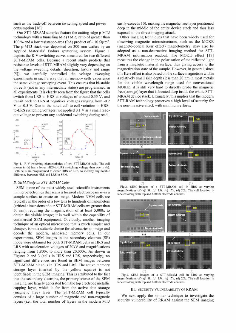
Our STT-MRAM samples feature the cutting-edge p-MTJ
technology with a tunneling MR (TMR) ratio of greater than
100 % and a low resistance-area (RA) product of ~ 10 Ωµm2.
The p-MTJ stack was deposited on 300 mm wafers by an
Applied Materials’ Endura sputtering system. Figure 1
depicts the R-V switching curves measured for two different
STT-MRAM cells. Because a recent study predicts that
resistance levels of STT-MRAM slightly vary depending on
the voltage sweeping details (direction, history and range
[5]), we carefully controlled the voltage sweeping
experiments in such a way that all memory cells experience
the same voltage sweeping event. This ensures that bi-stable
bit cells (not in any intermediate states) are programmed in
all experiments. It is clearly seen from the figure that the cells
switch from LRS to HRS at voltages of around 0.35 V, and
transit back to LRS at negatives voltages ranging from -0.2
V to -0.5 V. Due to the noted cell-to-cell variation in HRS-
to-LRS switching voltages, we applied 0.1 V as a small read-
out voltage to prevent any accidental switching during read.
(a) (b)
Fig. 1. R-V switching characteristics of two STT-MRAM cells. The cell shown in (a) has a lower HRS-to-LRS switching voltage than one in (b).
Both cells are programmed to either HRS or LRS, to identify any notable
difference between HRS and LRS in SEM.
B. SEM Study on STT-MRAM Cells
SEM is one of the most widely used scientific instruments
in microelectronics that scans a focused electron beam over a
sample surface to create an image. Modern NVM cells are
typically in the order of a few tens to hundreds of nanometers
(critical dimensions of our STT-MRAM cells are greater than
50 nm), requiring the magnification of at least 5,000x to
obtain the visible image; it is well within the capability of
commercial SEM equipment. Obviously, another imaging
technique of an optical microscope that is much simpler and
cheaper, is not a suitable choice for adversaries to image and
decode the modern, nanoscale memory cells. In our
experiments, SEM images in the secondary electron (SE)
mode were obtained for both STT-MRAM cells in HRS and
LRS with acceleration voltages of 20kV and magnifications
ranging from 1,800x to more than 20,000x. As shown in
Figures 2 and 3 (cells in HRS and LRS, respectively), no
significant differences are found in SEM images between
STT-MRAM bit cells in HRS and LRS. The active memory
storage layer (marked by the yellow square) is not
identifiable in the SEM imaging. This is attributed to the fact
that the secondary electrons, the primary source of the SEM
imaging, are largely generated from the top electrode metallic
capping layer, which is far from the active data storage
(magnetic free) layer. The STT-MRAM cell typically
consists of a large number of magnetic and non-magnetic
layers (i.e., the total number of layers in the modern MTJ
easily exceeds 10), making the magnetic free layer positioned
deep in the middle of the entire device stack and thus less
exposed to the direct imaging attack.
Other imaging techniques that have been widely used for
observing magnetic microstructures, such as the MOKE
(magneto-optical Kerr effect) magnetometry, may also be
adopted as a non-destructive imaging method for STT-
MRAM information readout. The MOKE effect [17]
measures the change in the polarization of the reflected light
from a magnetic material surface, thus giving access to the
magnetization state of the sample. However, in general, since
this Kerr effect is also based on the surface magnetism within
a relatively small skin depth (less than 20 nm in most metals
for the visible wavelength range used for conventional
MOKE), it is still very hard to directly probe the magnetic
free (storage) layer that is located deep inside the whole STT-
MRAM device stack. Ultimately, this implies that the modern
STT-RAM technology preserves a high level of security for
the non-invasive attack with minimum efforts.
(a) (b)
(c) (d)
Fig.2. SEM images of a STT-MRAM cell in HRS at varying
magnifications of (a)1.8k, (b) 15k, (c) 17k, (d) 20k. The cell location is labeled along with top and bottom electrode contacts.
(a) (b)
(c) (d)
Fig.3. SEM images of a STT-MRAM cell in LRS at varying magnifications of (a)1.8k, (b) 15k, (c) 17k, (d) 20k. The cell location is
labeled along with top and bottom electrode contacts.
III. SECURITY VULNERABILITY OF RRAM
We next apply the similar technique to investigate the
security vulnerability of RRAM against the SEM imaging
-1 -0.5 0 0.5 1
Voltage (V)
1000
1500
2000
2500
3000
3500
4000
Re
sis
tan
ce
()
P STATE,
LRS,
BIT '0'
AP STATE,
HRS,
BIT '1'
-1 -0.5 0 0.5 1
Voltage (V)
800
1000
1200
1400
1600
1800
2000
2200
2400
Re
sis
tan
ce
()
AP STATE,
HRS,
BIT '1'
P STATE,
LRS,
BIT '0'
attack. As compared with STT-MRAM, RRAM features a
relatively simple device structure. Therefore, one may
speculate that RRAM is more vulnerable to physical attacks
than STT-MRAM. In this study, two different commonly
used device geometries of RRAM – namely, capacitor and
crossbar, were both examined.
A. RRAM Basics and I-V Characteristics
RRAM has a simple two-terminal device structure
consisting of a transition metal oxide sandwiched between
two metal electrodes. RRAM is thus a promising candidate
to complement 3D NAND for mass storage applications. The
switching mechanism is governed by the formation and
rupture of a conductive filament by migrating oxygen ions
(metal-oxide RAM) or high-mobility metal electrode ions
(conductive-bridge RAM) [4].
In Figure 4, we first examined the hysteretic I-V switching
characteristics of two RRAM cells; one is the capacitor-type
that exhibits the bipolar behavior (Figure 4a), and another is
the crossbar-type (Figure 4b). Because the I-V curves of
RRAM are typically characterized by the (possible) existence
of a forming curve (the very first SET switching at a
relatively high voltage bias) and cycle-to-cycle variability,
we tested the RRAM cells with multiple switching cycles
until we clearly understand the switching behavior and
determine the proper read-out voltages for both LRS and
HRS.
(a) (b)
Fig.4. I-V graphs of RRAM of the capacitor-type (a) and the crossbar-
type (b). Our capacitor-type RRAM cell (critical dimension: 500 nm)
exhibits the bipolar switching characteristic along with forming-free behavior. For both devices, multiple switching cycles are confirmed to best
determine the cell status and the read-out voltage.
B. SEM Study on RRAM Cells
After carefully programming both the types of RRAM
cells into HRS and LRS, and confirming their bit status, we
examined their SEM images using the similar conditions
applied to STT-MRAM (SE mode, acceleration voltage of 20
kV, magnifications of up to 12,000x). Figures 5 and 6 show
the SEM images of capacitor-type RRAM cells at the active
device region for the cell sizes of 500 nm and 2 µm,
respectively, and Figure 7 depicts the SEM images of the
crossbar-type. Despite the relatively simple device structure,
RRAM is still found to be very hard to differentiate between
LRS and HRS in SE-mode SEM images.
(a) (b)
(c) (d) Fig,5. SEM images of 500 nm capacitor-type RRAM cells at varying
magnifications of (a) 10k (HRS), (b) 10k (LRS), (c) 12k (HRS), (d) 12k
(LRS). No clear differences are observed between cells in HRS and LRS.
(a) (b)
(c) (d)
Fig.6. SEM images of 2 µm capacitor-type RRAM cells at varying
magnifications of (a)10k (HRS), (b) 10k (LRS), (c) 14k (HRS), (d) 14k (LRS). No clear differences are observed between cells in HRS and LRS.
(a) (b)
(c) (d)
Fig.7. SEM images of crossbar-type RRAM cells at varying
magnifications of (a)8k (HRS), (b) 8k (LRS), (c) 14k (HRS), (d) 14k (LRS). No clear differences are observed between cells in HRS and LRS.
C. EDX Study on RRAM Cells
It is noted that the scientific instrument such as SEM is
typically equipped with its spectroscopic analysis capability.
EDX is a commonly used technique for the elemental or
chemical characterization of samples, so adversaries who
have access to the SEM equipment may also adopt EDX to
further investigate the memory cell. In order to examine the
security vulnerability of RRAM under such elemental
analysis, we performed EDX on RRAM cells of either LRS
or HRS under varying acceleration voltages of SEM. In this
task, we focused on the capacitor-type RRAM device that
-3 -2 -1 0 1 2 3
Voltage (V)
-0.02
-0.01
0
0.01
0.02
Cu
rre
nt
(A)
1st set
1st reset
2nd set
2nd reset
3rd set
SET
RESET
-3 -2 -1 0 1 2 3
Voltage (V)
-3
-2
-1
0
1
2
Cu
rre
nt
(A)
10-4
forming
1st set
1st reset
2nd set
2nd reset
RESET
SET
FORMING
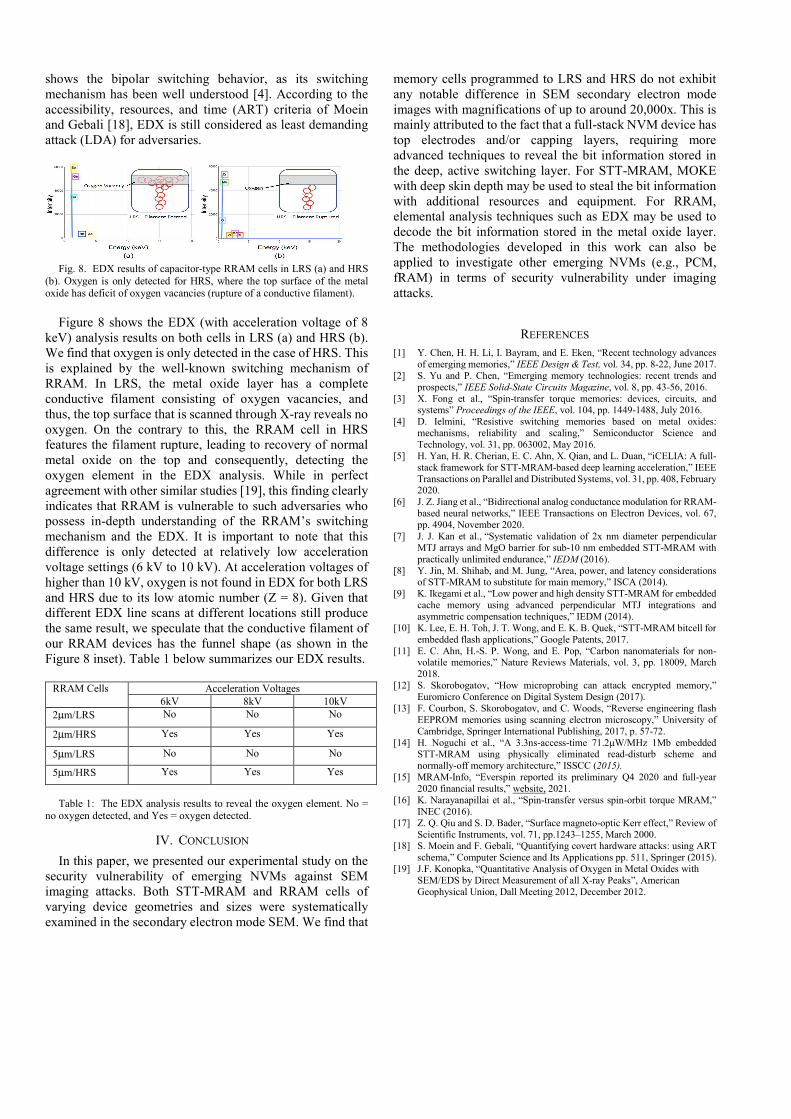
shows the bipolar switching behavior, as its switching
mechanism has been well understood [4]. According to the
accessibility, resources, and time (ART) criteria of Moein
and Gebali [18], EDX is still considered as least demanding
attack (LDA) for adversaries.
Fig. 8. EDX results of capacitor-type RRAM cells in LRS (a) and HRS
(b). Oxygen is only detected for HRS, where the top surface of the metal oxide has deficit of oxygen vacancies (rupture of a conductive filament).
Figure 8 shows the EDX (with acceleration voltage of 8
keV) analysis results on both cells in LRS (a) and HRS (b).
We find that oxygen is only detected in the case of HRS. This
is explained by the well-known switching mechanism of
RRAM. In LRS, the metal oxide layer has a complete
conductive filament consisting of oxygen vacancies, and
thus, the top surface that is scanned through X-ray reveals no
oxygen. On the contrary to this, the RRAM cell in HRS
features the filament rupture, leading to recovery of normal
metal oxide on the top and consequently, detecting the
oxygen element in the EDX analysis. While in perfect
agreement with other similar studies [19], this finding clearly
indicates that RRAM is vulnerable to such adversaries who
possess in-depth understanding of the RRAM’s switching
mechanism and the EDX. It is important to note that this
difference is only detected at relatively low acceleration
voltage settings (6 kV to 10 kV). At acceleration voltages of
higher than 10 kV, oxygen is not found in EDX for both LRS
and HRS due to its low atomic number (Z = 8). Given that
different EDX line scans at different locations still produce
the same result, we speculate that the conductive filament of
our RRAM devices has the funnel shape (as shown in the
Figure 8 inset). Table 1 below summarizes our EDX results.
RRAM Cells Acceleration Voltages
6kV 8kV 10kV
2µm/LRS No No No
2µm/HRS Yes Yes Yes
5µm/LRS No No No
5µm/HRS Yes Yes Yes
Table 1: The EDX analysis results to reveal the oxygen element. No = no oxygen detected, and Yes = oxygen detected.
IV. CONCLUSION
In this paper, we presented our experimental study on the
security vulnerability of emerging NVMs against SEM
imaging attacks. Both STT-MRAM and RRAM cells of
varying device geometries and sizes were systematically
examined in the secondary electron mode SEM. We find that
memory cells programmed to LRS and HRS do not exhibit
any notable difference in SEM secondary electron mode
images with magnifications of up to around 20,000x. This is
mainly attributed to the fact that a full-stack NVM device has
top electrodes and/or capping layers, requiring more
advanced techniques to reveal the bit information stored in
the deep, active switching layer. For STT-MRAM, MOKE
with deep skin depth may be used to steal the bit information
with additional resources and equipment. For RRAM,
elemental analysis techniques such as EDX may be used to
decode the bit information stored in the metal oxide layer.
The methodologies developed in this work can also be
applied to investigate other emerging NVMs (e.g., PCM,
fRAM) in terms of security vulnerability under imaging
attacks.
REFERENCES
[1] Y. Chen, H. H. Li, I. Bayram, and E. Eken, “Recent technology advances
of emerging memories,” IEEE Design & Test, vol. 34, pp. 8-22, June 2017.
[2] S. Yu and P. Chen, “Emerging memory technologies: recent trends and
prospects,” IEEE Solid-State Circuits Magazine, vol. 8, pp. 43-56, 2016.
[3] X. Fong et al., “Spin-transfer torque memories: devices, circuits, and systems” Proceedings of the IEEE, vol. 104, pp. 1449-1488, July 2016.
[4] D. Ielmini, “Resistive switching memories based on metal oxides:
mechanisms, reliability and scaling,” Semiconductor Science and
Technology, vol. 31, pp. 063002, May 2016.
[5] H. Yan, H. R. Cherian, E. C. Ahn, X. Qian, and L. Duan, “iCELIA: A full-
stack framework for STT-MRAM-based deep learning acceleration,” IEEE
Transactions on Parallel and Distributed Systems, vol. 31, pp. 408, February 2020.
[6] J. Z. Jiang et al., “Bidirectional analog conductance modulation for RRAM-
based neural networks,” IEEE Transactions on Electron Devices, vol. 67,
pp. 4904, November 2020.
[7] J. J. Kan et al., “Systematic validation of 2x nm diameter perpendicular
MTJ arrays and MgO barrier for sub-10 nm embedded STT-MRAM with
practically unlimited endurance,” IEDM (2016).
[8] Y. Jin, M. Shihab, and M. Jung, “Area, power, and latency considerations of STT-MRAM to substitute for main memory,” ISCA (2014).
[9] K. Ikegami et al., “Low power and high density STT-MRAM for embedded
cache memory using advanced perpendicular MTJ integrations and
asymmetric compensation techniques,” IEDM (2014).
[10] K. Lee, E. H. Toh, J. T. Wong, and E. K. B. Quek, “STT-MRAM bitcell for
embedded flash applications,” Google Patents, 2017.
[11] E. C. Ahn, H.-S. P. Wong, and E. Pop, “Carbon nanomaterials for non-volatile memories,” Nature Reviews Materials, vol. 3, pp. 18009, March
2018.
[12] S. Skorobogatov, “How microprobing can attack encrypted memory,”
Euromicro Conference on Digital System Design (2017).
[13] F. Courbon, S. Skorobogatov, and C. Woods, “Reverse engineering flash
EEPROM memories using scanning electron microscopy,” University of
Cambridge, Springer International Publishing, 2017, p. 57-72.
[14] H. Noguchi et al., “A 3.3ns-access-time 71.2μW/MHz 1Mb embedded STT-MRAM using physically eliminated read-disturb scheme and
normally-off memory architecture,” ISSCC (2015).
[15] MRAM-Info, “Everspin reported its preliminary Q4 2020 and full-year
2020 financial results,” website, 2021.
[16] K. Narayanapillai et al., “Spin-transfer versus spin-orbit torque MRAM,”
INEC (2016).
[17] Z. Q. Qiu and S. D. Bader, “Surface magneto-optic Kerr effect,” Review of
Scientific Instruments, vol. 71, pp.1243–1255, March 2000. [18] S. Moein and F. Gebali, “Quantifying covert hardware attacks: using ART
schema,” Computer Science and Its Applications pp. 511, Springer (2015).
[19] J.F. Konopka, “Quantitative Analysis of Oxygen in Metal Oxides with
SEM/EDS by Direct Measurement of all X-ray Peaks”, American
Geophysical Union, Dall Meeting 2012, December 2012.
![Mining in Emerging Economies - Ernst & Young€¦ · Mining in Emerging Economies - Sharing the Spoils | 3 Volatile and uncertain scenario L`] jYha\ hY[] g^ _jgol` l`Yl l`] eafaf_](https://img.pdfslide.us/doc/110x75/5b7320257f8b9a58028e26dc/mining-in-emerging-economies-ernst-mining-in-emerging-economies-sharing.jpg)