Embed Size (px)
Citation preview
RENESAS 16-BIT CMOS SINGLE-CHIP MICROCOMPUTER
M16C FAMILY / M16C/60 SERIES
M16C/62 Group (M16C/62P)16
Rev. 1.20Revision date: Sep. 11, 2003
Hardware Manual
www.renesas.com
Before using this material, please visit the our website to confirm that this is the most current document available.
REJ09B0016-0120Z

Keep safety first in your circuit designs!
Notes regarding these materials
• Renesas Technology Corporation puts the maximum effort into making semiconductor prod-ucts better and more reliable, but there is always the possibility that trouble may occur withthem. Trouble with semiconductors may lead to personal injury, fire or property damage.Remember to give due consideration to safety when making your circuit designs, with ap-propriate measures such as (i) placement of substitutive, auxiliary circuits, (ii) use of non-flammable material or (iii) prevention against any malfunction or mishap.
• These materials are intended as a reference to assist our customers in the selection of theRenesas Technology Corporation product best suited to the customer's application; they donot convey any license under any intellectual property rights, or any other rights, belongingto Renesas Technology Corporation or a third party.
• Renesas Technology Corporation assumes no responsibility for any damage, or infringe-ment of any third-party's rights, originating in the use of any product data, diagrams, charts,programs, algorithms, or circuit application examples contained in these materials.
• All information contained in these materials, including product data, diagrams, charts, pro-grams and algorithms represents information on products at the time of publication of thesematerials, and are subject to change by Renesas Technology Corporation without noticedue to product improvements or other reasons. It is therefore recommended that custom-ers contact Renesas Technology Corporation or an authorized Renesas Technology Cor-poration product distributor for the latest product information before purchasing a productlisted herein.The information described here may contain technical inaccuracies or typographical errors.Renesas Technology Corporation assumes no responsibility for any damage, liability, orother loss rising from these inaccuracies or errors.Please also pay attention to information published by Renesas Technology Corporation byvarious means, including the Renesas Technology Corporation Semiconductor home page(http://www.renesas.com).
• When using any or all of the information contained in these materials, including productdata, diagrams, charts, programs, and algorithms, please be sure to evaluate all informa-tion as a total system before making a final decision on the applicability of the informationand products. Renesas Technology Corporation assumes no responsibility for any dam-age, liability or other loss resulting from the information contained herein.
• Renesas Technology Corporation semiconductors are not designed or manufactured foruse in a device or system that is used under circumstances in which human life is poten-tially at stake. Please contact Renesas Technology Corporation or an authorized RenesasTechnology Corporation product distributor when considering the use of a product con-tained herein for any specific purposes, such as apparatus or systems for transportation,vehicular, medical, aerospace, nuclear, or undersea repeater use.
• The prior written approval of Renesas Technology Corporation is necessary to reprint orreproduce in whole or in part these materials.
• If these products or technologies are subject to the Japanese export control restrictions,they must be exported under a license from the Japanese government and cannot be im-ported into a country other than the approved destination.Any diversion or reexport contrary to the export control laws and regulations of Japan and/or the country of destination is prohibited.
• Please contact Renesas Technology Corporation for further details on these materials or the products contained therein.
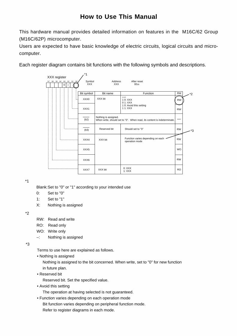
How to Use This Manual
This hardware manual provides detailed information on features in the M16C/62 Group
(M16C/62P) microcomputer.
Users are expected to have basic knowledge of electric circuits, logical circuits and micro-
computer.
*2
RW: Read and write
RO: Read only
WO: Write only
–: Nothing is assigned
*1
Blank:Set to "0" or "1" according to your intended use
0: Set to "0"
1: Set to "1"
X: Nothing is assigned
*3
Terms to use here are explained as follows.
• Nothing is assigned
Nothing is assigned to the bit concerned. When write, set to "0" for new function
in future plan.
• Reserved bit
Reserved bit. Set the specified value.
• Avoid this setting
The operation at having selected is not guaranteed.
• Function varies depending on each operation mode
Bit function varies depending on peripheral function mode.
Refer to register diagrams in each mode.
*3
XXX registerSymbol Address After reset XXX XXX 0016
Bit nameBit symbol RW
b7 b6 b5 b4 b3 b2 b1 b0
XXX bit 1 0: XXX0 1: XXX1 0: Avoid this setting1 1: XXX
b1 b0
XXX1
XXX0
XXX4
Reserved bit
XXX5
XXX7
XXX6
Function
Nothing is assigned.When write, should set to "0". When read, its content is indeterminate.
XXX bit
Function varies depending on each operation mode
Should set to "0"
0
(b3)
(b2)
RW
RW
RW
RW
WO
RW
RO
XXX bit
0: XXX1: XXX
*1
*2
Each register diagram contains bit functions with the following symbols and descriptions.
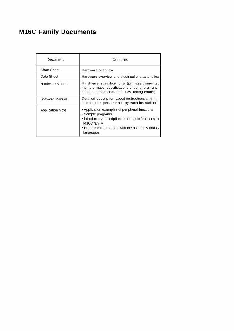
Contents
Hardware overview
Hardware overview and electrical characteristics
Hardware specifications (pin assignments,memory maps, specifications of peripheral func-tions, electrical characteristics, timing charts)
Detailed description about instructions and mi-crocomputer performance by each instruction
• Application examples of peripheral functions• Sample programs• Introductory description about basic functions inM16C family
• Programming method with the assembly and Clanguages
Document
Short Sheet
M16C Family Documents
Data Sheet
Hardware Manual
Software Manual
Application Note
A-1
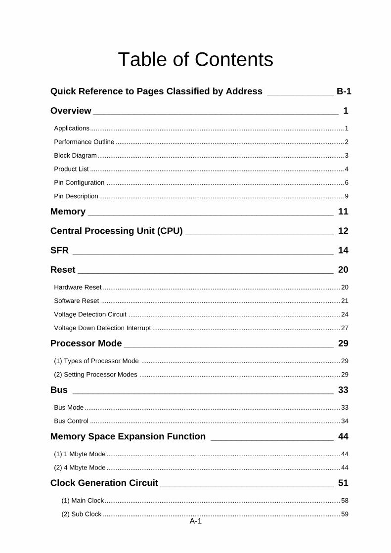
Table of ContentsQuick Reference to Pages Classified by Addres s _____________ B-1
Overview ________________________________________________ 1
Applications...........................................................................................................................................1
Performance Outline .............................................................................................................................2
Block Diagram.......................................................................................................................................3
Product List ...........................................................................................................................................4
Pin Configuration ..................................................................................................................................6
Pin Description ......................................................................................................................................9
Memory ________________________________________________ 11
Central Processing Unit (CPU) _____________________________ 12
SFR ___________________________________________________ 14
Reset __________________________________________________ 20
Hardware Reset ..................................................................................................................................20
Software Reset ...................................................................................................................................21
Voltage Detection Circuit ....................................................................................................................24
Voltage Down Detection Interrupt .......................................................................................................27
Processor Mode _________________________________________ 29
(1) Types of Processor Mode .............................................................................................................29
(2) Setting Processor Modes .............................................................................................................. 29
Bus ___________________________________________________ 33
Bus Mode ............................................................................................................................................33
Bus Control ......................................................................................................................................... 34
Memory Space Expansion Function ________________________ 44
(1) 1 Mbyte Mode ................................................................................................................................44
(2) 4 Mbyte Mode ................................................................................................................................44
Clock Generation Circuit __________________________________ 51
(1) Main Clock .................................................................................................................................58
(2) Sub Clock ..................................................................................................................................59
A-2
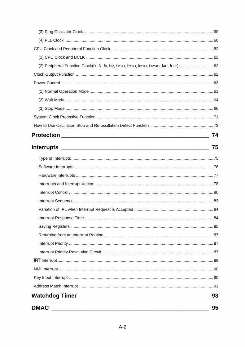
(3) Ring Oscillator Clock .................................................................................................................60
(4) PLL Clock ..................................................................................................................................60
CPU Clock and Peripheral Function Clock .........................................................................................62
(1) CPU Clock and BCLK ...............................................................................................................62
(2) Peripheral Function Clock(f1, f2, f8, f32, f1SIO, f2SIO, f8SIO, f32SIO, fAD, fC32) ..............................62
Clock Output Function ........................................................................................................................62
Power Control .....................................................................................................................................63
(1) Normal Operation Mode ............................................................................................................63
(2) Wait Mode .................................................................................................................................64
(3) Stop Mode .................................................................................................................................66
System Clock Protective Function ......................................................................................................71
How to Use Oscillation Stop and Re-oscillation Detect Function ....................................................... 73
Protection ______________________________________________ 74
Interrupts ______________________________________________ 75
Type of Interrupts ............................................................................................................................75
Software Interrupts .........................................................................................................................76
Hardware Interrupts ........................................................................................................................77
Interrupts and Interrupt Vector ........................................................................................................78
Interrupt Control ..............................................................................................................................80
Interrupt Sequence .........................................................................................................................83
Variation of IPL when Interrupt Request is Accepted .....................................................................84
Interrupt Response Time ................................................................................................................ 84
Saving Registers .............................................................................................................................85
Returning from an Interrupt Routine ...............................................................................................87
Interrupt Priority ..............................................................................................................................87
Interrupt Priority Resolution Circuit .................................................................................................87______
INT Interrupt ........................................................................................................................................89______
NMI Interrupt .......................................................................................................................................90
Key Input Interrupt ..............................................................................................................................90
Address Match Interrupt .....................................................................................................................91
Watchdog Timer _________________________________________ 93
DMAC _________________________________________________ 95
A-3
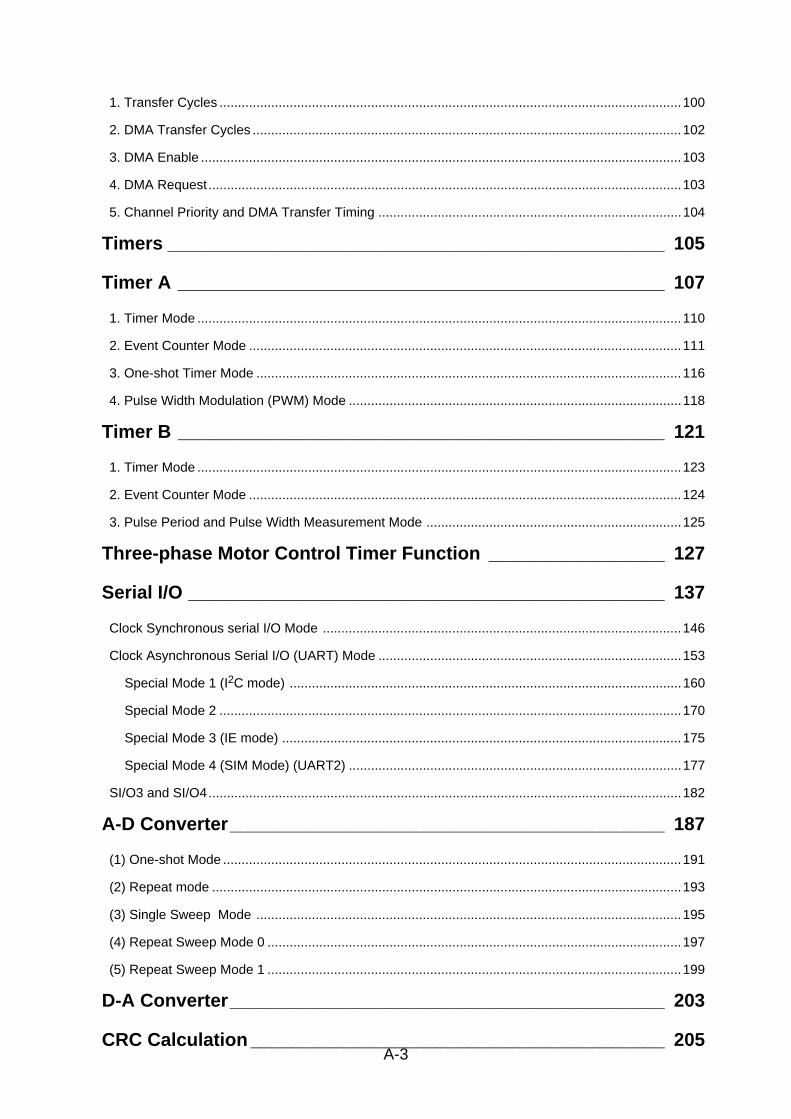
1. Transfer Cycles .............................................................................................................................100
2. DMA Transfer Cycles ....................................................................................................................102
3. DMA Enable ..................................................................................................................................103
4. DMA Request ................................................................................................................................103
5. Channel Priority and DMA Transfer Timing ..................................................................................104
Timers ________________________________________________ 105
Timer A _______________________________________________ 107
1. Timer Mode ...................................................................................................................................110
2. Event Counter Mode .....................................................................................................................111
3. One-shot Timer Mode ...................................................................................................................116
4. Pulse Width Modulation (PWM) Mode ..........................................................................................118
Timer B _______________________________________________ 121
1. Timer Mode ...................................................................................................................................123
2. Event Counter Mode .....................................................................................................................124
3. Pulse Period and Pulse Width Measurement Mode .....................................................................125
Three-phase Motor Control Timer Function _________________ 127
Serial I/O ______________________________________________ 137
Clock Synchronous serial I/O Mode .................................................................................................146
Clock Asynchronous Serial I/O (UART) Mode ..................................................................................153
Special Mode 1 (I2C mode) ..........................................................................................................160
Special Mode 2 .............................................................................................................................170
Special Mode 3 (IE mode) ............................................................................................................175
Special Mode 4 (SIM Mode) (UART2) ..........................................................................................177
SI/O3 and SI/O4................................................................................................................................182
A-D Converter__________________________________________ 187
(1) One-shot Mode ............................................................................................................................191
(2) Repeat mode ...............................................................................................................................193
(3) Single Sweep Mode ...................................................................................................................195
(4) Repeat Sweep Mode 0 ................................................................................................................197
(5) Repeat Sweep Mode 1 ................................................................................................................199
D-A Converter__________________________________________ 203
CRC Calculation ________________________________________ 205
A-4
Programmable I/O Ports _________________________________ 207
(1) Port Pi Direction Register (PDi Register, i = 0 to 13) ................................................................... 207
(2) Port Pi Register (Pi Register, i = 0 to 13) ....................................................................................207
(3) Pull-up Control Register 0 to Pull-up Control Register 2 (PUR0 to PUR2 Registers) .................207
(4) Port Control Register ...................................................................................................................207
Electrical Characteristics ________________________________ 220
Electrical Characteristics (Vcc1 = Vcc2 = 5V)...................................................................................225
Electrical Characteristics (Vcc1 = Vcc2 = 3V)...................................................................................242
Flash Memory Version___________________________________ 259
Memory Map .....................................................................................................................................261
Boot Mode ........................................................................................................................................262
Functions To Prevent Flash Memory from Rewriting ........................................................................ 262
• ROM Code Protect Function ......................................................................................................262
• ID Code Check Function ............................................................................................................262
CPU Rewrite Mode ...........................................................................................................................264
• EW0 Mode ..................................................................................................................................265
• EW1 Mode ..................................................................................................................................265
Software Commands ....................................................................................................................273
Data Protect Function ...................................................................................................................278
Status Register ............................................................................................................................. 278
Full Status Check ..........................................................................................................................280
Standard Serial I/O Mode .............................................................................................................282
Parallel I/O Mode _______________________________________ 289
User ROM and Boot ROM Areas ......................................................................................................289
ROM Code Protect Function .............................................................................................................289
Package Dimensions ____________________________________ 290
Register Index _________________________________________ 295
M16C/62 Group (M16C/62P) Usage Notes Reference BookFor the most current Usage Notes Reference Book, please visit our website.
B-1
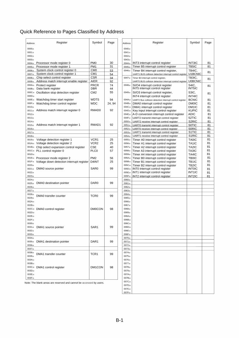
Quick Reference to Pages Classified by Address
000016
000116
000216
000316
000416
000516
000616
000716
000816
000916
000A16
000B16
000C16
000D16
000E16
000F16
001016
001116
001216
001316
001416
001516
001616
001716
001816
001916
001A16
001B16
001C16
001D16
001E16
001F16
002016
002116
002216
002316
002416
002516
002616
002716
002816
002916
002A16
002B16
002C16
002D16
002E16
002F16
003016
003116
003216
003316
003416
003516
003616
003716
003816
003916
003A16
003B16
003C16
003D16
003E16
003F16
Address
Note: The blank areas are reserved and cannot be accessed by users.
Register Symbol Page
004016
004116
004216
004316
004416
004516
004616
004716
004816
004916
004A16
004B16
004C16
004D16
004E16
004F16
005016
005116
005216
005316
005416
005516
005616
005716
005816
005916
005A16
005B16
005C16
005D16
005E16
005F16
006016
006116
006216
006316
006416
006516
006616
006716
006816
006916
006A16
006B16
006C16
006D16
006E16
006F16
007016
007116
007216
007316
007416
007516
007616
007716
007816
007916
007A16
007B16
007C16
007D16
007E16
007F16
Watchdog timer start register WDTSWatchdog timer control register WDC
Processor mode register 0 PM0
Chip select control register CSR
System clock control register 0 CM0System clock control register 1 CM1
Address match interrupt enable register AIERProtect register PRCR
Processor mode register 1 PM1
Data bank register DBROscillation stop detection register CM2
Chip select expansion control register CSEPLL control register 0 PLC0
Processor mode register 2 PM2
Address match interrupt register 0 RMAD0
Address match interrupt register 1 RMAD1
DMA0 control register DM0CON
DMA0 transfer counter TCR0
DMA1 control register DM1CON
DMA1 source pointer SAR1
DMA1 destination pointer DAR1
DMA0 destination pointer DAR0
DMA0 source pointer SAR0
Voltage detection register 1 VCR1Voltage detection register 2 VCR2
Voltage down detection interrupt register D4INT
UART0 transmit interrupt control register S0TICUART0 receive interrupt control register S0RICUART1 transmit interrupt control register S1TICUART1 receive interrupt control register S1RIC
DMA1 transfer counter TCR1
INT3 interrupt control register INT3ICTimer B5 interrupt control register TB5ICTimer B4 interrupt control register, TB4IC,UART1 BUS collision detection interrupt control register U1BCNICTimer B3 interrupt control register, TB3IC,UART0 BUS collision detection interrupt control register U0BCNICSI/O4 interrupt control register S4IC,INT5 interrupt control register INT5ICSI/O3 interrupt control register, S3IC,INT4 interrupt control register INT4ICUART2 Bus collision detection interrupt control register BCNICDMA0 interrupt control register DM0ICDMA1 interrupt control register DM1ICKey input interrupt control register KUPICA-D conversion interrupt control register ADICUART2 transmit interrupt control register S2TICUART2 receive interrupt control register S2RIC
Timer A0 interrupt control register TA0ICTimer A1 interrupt control register TA1ICTimer A2 interrupt control register TA2ICTimer A3 interrupt control register TA3ICTimer A4 interrupt control register TA4ICTimer B0 interrupt control register TB0IC
Timer B2 interrupt control register TB2ICINT0 interrupt control register INT0ICINT1 interrupt control register INT1ICINT2 interrupt control register INT2IC
Timer B1 interrupt control register TB1IC
303153543492744455
9424, 94
92
92
25254057
5625
99
99
99
98
99
99
99
98
8181
81
81
81
81
81818181818181818181818181818181818181818181
Address Register Symbol Page
B-2
Quick Reference to Pages Classified by Address
N
o
t
e
1
:
T
h
e
b
l
a
n
k
a
r
e
a
s
a
r
e
r
e
s
e
r
v
e
d
a
n
d
c
a
n
n
o
t
b
e
a
c
c
e
s
s
e
d
b
y
u
s
e
r
s
.N
o
t
e
2
:
T
h
i
s
r
e
g
i
s
t
e
r
i
s
i
n
c
l
u
d
e
d
i
n
t
h
e
f
l
a
s
h
m
e
m
o
r
y
v
e
r
s
i
o
n
.
0 3
4
01
6
0
3
4
11
6
0
3
4
21
6
0
3
4
31
6
0
3
4
41
6
0
3
4
51
6
0
3
4
61
6
0
3
4
71
6
0
3
4
81
6
0
3
4
91
6
0
3
4
A1
6
0
3
4
B1
6
0
3
4
C1
6
0
3
4
D1
6
0
3
4
E1
6
0
3
4
F1
6
0
3
5
01
6
0
3
5
11
6
0
3
5
21
6
0
3
5
31
6
0
3
5
41
6
0
3
5
51
6
0
3
5
61
6
0
3
5
71
6
0
3
5
81
6
0
3
5
91
6
0
3
5
A1
6
0
3
5
B1
6
0
3
5
C1
6
0
3
5
D1
6
0
3
5
E1
6
0
3
5
F1
6
0
3
6
01
6
0
3
6
11
6
0
3
6
21
6
0
3
6
31
6
0
3
6
41
6
0
3
6
51
6
0
3
6
61
6
0
3
6
71
6
0
3
6
81
6
0
3
6
91
6
0
3
6
A1
6
0
3
6
B1
6
0
3
6
C1
6
0
3
6
D1
6
0
3
6
E1
6
0
3
6
F1
6
0
3
7
01
6
0
3
7
11
6
0
3
7
21
6
0
3
7
31
6
0
3
7
41
6
0
3
7
51
6
0
3
7
61
6
0
3
7
71
6
0
3
7
81
6
0
3
7
91
6
0
3
7
A1
6
0
3
7
B1
6
0
3
7
C1
6
0
3
7
D1
6
0
3
7
E1
6
0
3
7
F1
6
0 0
8
01
6
0
0
8
11
6
0
0
8
21
6
0
0
8
31
6
0
0
8
41
6
0
0
8
51
6
0
0
8
61
6
0
1
B
01
6
0
1
B
11
6
0
1
B
21
6
0
1
B
31
6
0
1
B
41
6
0
1
B
51
6
0
1
B
61
6
0
1
B
71
6
0
1
B
81
6
0
1
B
91
6
0
1
B
A1
6
0
1
B
B1
6
0
1
B
C1
6
0
1
B
D1
6
0
1
B
E1
6
0
1
B
F1
6
0
2
5
01
6
0
2
5
11
6
0
2
5
21
6
0
2
5
31
6
0
2
5
41
6
0
2
5
51
6
0
2
5
61
6
0
2
5
71
6
0
2
5
81
6
0
2
5
91
6
0
2
5
A1
6
0
2
5
B1
6
0
2
5
C1
6
0
2
5
D1
6
0
2
5
E1
6
0
2
5
F1
6
0
3
3
01
6
0
3
3
11
6
0
3
3
21
6
0
3
3
31
6
0
3
3
41
6
0
3
3
51
6
0
3
3
61
6
0
3
3
71
6
0
3
3
81
6
0
3
3
91
6
0
3
3
A1
6
0
3
3
B1
6
0
3
3
C1
6
0
3
3
D1
6
0
3
3
E1
6
0
3
3
F1
6
Peripheral clock select register PCLKR
F
l
a
s
h
m
e
m
o
r
y
c
o
n
t
r
o
l
r
e
g
i
s
t
e
r
0 F
M
R
0
F
l
a
s
h
m
e
m
o
r
y
c
o
n
t
r
o
l
r
e
g
i
s
t
e
r
1 F
M
R
1
A
d
d
r
e
s
s
m
a
t
c
h
i
n
t
e
r
r
u
p
t
r
e
g
i
s
t
e
r
2 R
M
A
D
2
A
d
d
r
e
s
s
m
a
t
c
h
i
n
t
e
r
r
u
p
t
r
e
g
i
s
t
e
r
3 R
M
A
D
3
A
d
d
r
e
s
s
m
a
t
c
h
i
n
t
e
r
r
u
p
t
e
n
a
b
l
e
r
e
g
i
s
t
e
r
2 A
I
E
R
2
F
l
a
s
h
i
d
e
n
t
i
f
i
c
a
t
i
o
n
r
e
g
i
s
t
e
r F
I
D
R
T
i
m
e
r
A
1
-
1
r
e
g
i
s
t
e
r T
A
1
1
T
i
m
e
r
A
2
-
1
r
e
g
i
s
t
e
r T
A
2
1
D
e
a
d
t
i
m
e
t
i
m
e
r D
T
TT
i
m
e
r
B
2
i
n
t
e
r
r
u
p
t
o
c
c
u
r
r
e
n
c
e
f
r
e
q
u
e
n
c
y
s
e
t
c
o
u
n
t
e
r I
C
T
B
2
T
h
r
e
e
-
p
h
a
s
e
P
W
M
c
o
n
t
r
o
l
r
e
g
i
s
t
e
r
0 I
N
V
C
0T
h
r
e
e
-
p
h
a
s
e
P
W
M
c
o
n
t
r
o
l
r
e
g
i
s
t
e
r
1 I
N
V
C
1T
h
r
e
e
-
p
h
a
s
e
o
u
t
p
u
t
b
u
f
f
e
r
r
e
g
i
s
t
e
r
0 I
D
B
0T
h
r
e
e
-
p
h
a
s
e
o
u
t
p
u
t
b
u
f
f
e
r
r
e
g
i
s
t
e
r
1 I
D
B
1
T
i
m
e
r
B
3
r
e
g
i
s
t
e
r T
B
3
T
i
m
e
r
B
4
r
e
g
i
s
t
e
r T
B
4
T
i
m
e
r
B
5
r
e
g
i
s
t
e
r T
B
5
T
i
m
e
r
B
3
,
4
,
5
c
o
u
n
t
s
t
a
r
t
f
l
a
g T
B
S
R
T
i
m
e
r
B
3
m
o
d
e
r
e
g
i
s
t
e
r T
B
3
M
RT
i
m
e
r
B
4
m
o
d
e
r
e
g
i
s
t
e
r T
B
4
M
RT
i
m
e
r
B
5
m
o
d
e
r
e
g
i
s
t
e
r T
B
5
M
R
Interrupt cause select register IFSRSI/O3 transmit/receive register S3TRR
S
I
/
O
4
t
r
a
n
s
m
i
t
/
r
e
c
e
i
v
e
r
e
g
i
s
t
e
r S
4
T
R
R
S
I
/
O
3
c
o
n
t
r
o
l
r
e
g
i
s
t
e
r S
3
CSI/O3 bit rate generator S3BRG
SI/O4 bit rate generator S4BRGS
I
/
O
4
c
o
n
t
r
o
l
r
e
g
i
s
t
e
r S
4
C
U
A
R
T
2
s
p
e
c
i
a
l
m
o
d
e
r
e
g
i
s
t
e
r U
2
S
M
R
U
A
R
T
2
r
e
c
e
i
v
e
b
u
f
f
e
r
r
e
g
i
s
t
e
r
U
2
R
B
UART2 transmit buffer register U2TB
U
A
R
T
2
t
r
a
n
s
m
i
t
/
r
e
c
e
i
v
e
c
o
n
t
r
o
l
r
e
g
i
s
t
e
r
0 U
2
C
0
U
A
R
T
2
t
r
a
n
s
m
i
t
/
r
e
c
e
i
v
e
m
o
d
e
r
e
g
i
s
t
e
r
U
2
M
R
UART2 transmit/receive control register 1 U2C1
UART2 bit rate generator U2BRG
T
i
m
e
r
A
4
-
1
r
e
g
i
s
t
e
r T
A
4
1
U
A
R
T
2
s
p
e
c
i
a
l
m
o
d
e
r
e
g
i
s
t
e
r
2 U
2
S
M
R
2UART2 special mode register 3 U2SMR3
I n
t
e
r
r
u
p
t
c
a
u
s
e
s
e
l
e
c
t
r
e
g
i
s
t
e
r
2 I
F
S
R
2
A
UART0 special mode register 2 U0SMR2U
A
R
T
0
s
p
e
c
i
a
l
m
o
d
e
r
e
g
i
s
t
e
r
U
0
S
M
R
UART0 special ode register 3 U0SMR3UART0 special mode register 4 U0SMR4
U
A
R
T
1
s
p
e
c
i
a
l
m
o
d
e
r
e
g
i
s
t
e
r
2 U
1
S
M
R
2UART1 special mode register U1SMR
UART1 special mode register 3 U1SMR3U
A
R
T
1
s
p
e
c
i
a
l
m
o
d
e
r
e
g
i
s
t
e
r
4 U
1
S
M
R
4
U
A
R
T
2
s
p
e
c
i
a
l
m
o
d
e
r
e
g
i
s
t
e
r
4 U
2
S
M
R
4
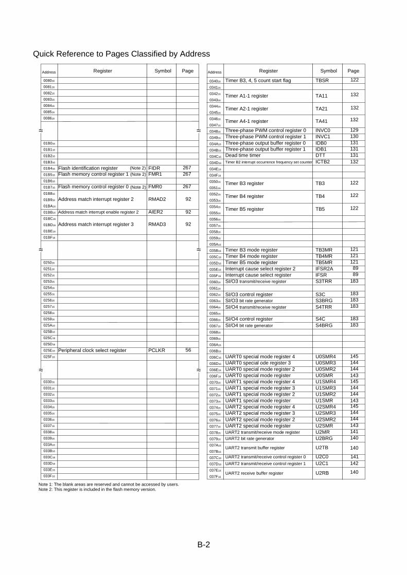
2
6
7
1
2
2
2
6
7
2
6
7
9
2
9
2
92
5
6
1
3
2
1
3
2
1
3
2
1
2
91
3
0
1
3
11
3
1
1
3
11
3
2
1
2
2
1
2
2
1
2
2
1211
2
1
1
2
1
183
1
8
31
8
3
1
8
3
1
8
3183
1
4
51
4
4
1
4
41
4
3
1451
4
4
1441431451
4
4
1441
4
3
1
4
1140
1
4
0
1
4
11
4
2
1
4
0
8
98
9
(Note 2)(
N
o
t
e
2
)
A
d
d
r
e
s
s R
e
g
i
s
t
e
r S
y
m
b
o
l Page A
d
d
r
e
s
s R
e
g
i
s
t
e
r S
y
m
b
o
l P
a
g
e
(
N
o
t
e
2
)
≈≈
≈≈
≈≈
B-3
Quick Reference to Pages Classified by Address
038016
038116
038216
038316
038416
038516
038616
038716
038816
038916
038A16
038B16
038C16
038D16
038E16
038F16
039016
039116
039216
039316
039416
039516
039616
039716
039816
039916
039A16
039B16
039C16
039D16
039E16
039F16
03A016
03A116
03A216
03A316
03A416
03A516
03A616
03A716
03A816
03A916
03AA16
03AB16
03AC16
03AD16
03AE16
03AF16
03B016
03B116
03B216
03B316
03B416
03B516
03B616
03B716
03B816
03B916
03BA16
03BB16
03BC16
03BD16
03BE16
03BF16
Note : The blank areas are reserved and cannot be accessed by users.
03C016
03C116
03C216
03C316
03C416
03C516
03C616
03C716
03C816
03C916
03CA16
03CB16
03CC16
03CD16
03CE16
03CF16
03D016
03D116
03D216
03D316
03D416
03D516
03D616
03D716
03D816
03D916
03DA16
03DB16
03DC16
03DD16
03DE16
03DF16
03E016
03E116
03E216
03E316
03E416
03E516
03E616
03E716
03E816
03E916
03EA16
03EB16
03EC16
03ED16
03EE16
03EF16
03F016
03F116
03F216
03F316
03F416
03F516
03F616
03F716
03F816
03F916
03FA16
03FB16
03FC16
03FD16
03FE16
03FF16
Count start flag TABSR
Trigger select register TRGSR
Timer A0 register TA0
Timer A1 register TA1
Timer A2 register TA2
Timer B0 register TB0
Timer B1 register TB1
Timer B2 register TB2
One-shot start flag ONSF
Timer A0 mode register TA0MRTimer A1 mode register TA1MRTimer A2 mode register TA2MR
Timer B0 mode register TB0MRTimer B1 mode register TB1MRTimer B2 mode register TB2MR
Up-down flag UDF
Timer A3 register TA3
Timer A4 register TA4
Timer A3 mode register TA3MRTimer A4 mode register TA4MR
Clock prescaler reset flag CPSRF
UART0 transmit/receive mode register U0MR
UART0 transmit buffer register U0TB
UART0 receive buffer register U0RB
UART1 transmit/receive mode register U1MR
UART1 transmit buffer register U1TB
UART1 receive buffer register U1RB
UART0 bit rate generator U0BRG
UART0 transmit/receive control register 0 U0C0UART0 transmit/receive control register 1 U0C1
UART1 bit rate generator U1BRG
UART1 transmit/receive control register 0 U1C0UART1 transmit/receive control register 1 U1C1
DMA1 request cause select register DM1SL
DMA0 request cause select register DM0SL
CRC data register CRCD
CRC input register CRCIN
UART transmit/receive control register 2 UCON
Timer B2 special mode register TB2SC
A-D control register 1 ADCON1
Port P9 register P9
Pull-up control register 0 PUR0
Port control register PCR
A-D register 7 AD7
A-D register 0 AD0
A-D register 1 AD1
A-D register 2 AD2
A-D register 3 AD3
A-D register 4 AD4
A-D register 5 AD5
A-D register 6 AD6
A-D control register 0 ADCON0
D-A register 0 DA0
D-A register 1 DA1
D-A control register DACON
A-D control register 2 ADCON2
Port P0 register P0
Port P0 direction register PD0Port P1 register P1
Port P1 direction register PD1Port P2 register P2
Port P2 direction register PD2Port P3 register P3
Port P3 direction register PD3Port P4 register P4
Port P4 direction register PD4Port P5 register P5
Port P5 direction register PD5Port P6 register P6
Port P6 direction register PD6Port P7 register P7
Port P7 direction register PD7Port P8 register P8
Port P8 direction register PD8Port P9 direction register PD9Port P10 register P10
Port P10 direction register PD10
Pull-up control register 1 PUR1Pull-up control register 2 PUR2
Port P14 control register PC14Pull-up control register 3 PUR3
Port P11 register P11
Port P12 register P12Port P13 register P13
Port P11 direction register PD11
Port P12 direction register PD12Port P13 direction register PD13
108, 122, 133
109109, 122
109, 133
108
190
190
190
190
190
122
122
122, 133
107107, 134
107
121121
132
141140
140
141142
140
141140
140
141142
140
143
97
98
205
205
190
190
190
190
189189204
204
204
215215214214213213214214213213214214213213214214213213214214213213214214213213214214213213216216216217
108
108, 132
108, 132
108
108, 132
107, 134
107, 134
121, 134
Address Register Symbol Page Address Register Symbol Page
Overview
1
Renesas microcomputers
M16C / 62P Group SINGLE-CHIP 16-BIT CMOS MICROCOMPUTER
OverviewThe M16C/62 group (M16C/62P) of single-chip microcomputers are built using the high-performance sili-
con gate CMOS process using a M16C/60 Series CPU core and are packaged in a 100-pin and 128-pin
plastic molded QFP. These single-chip microcomputers operate using sophisticated instructions featuring
a high level of instruction efficiency. With 1M bytes of address space, they are capable of executing instruc-
tions at high speed. In addition, this microcomputer contains a multiplier and DMAC which combined with
fast instruction processing capability, makes it suitable for control of various OA, communication, and in-
dustrial equipment which requires high-speed arithmetic/logic operations.
ApplicationsAudio, cameras, office/communications/portable/industrial equipment, etc
Specifications written in this manual are believed to be accurate, but arenot guaranteed to be entirely free of error. Specifications in this manualmay be changed for functional or performance improvements. Please makesure your manual is the latest edition.
Overview
2
Renesas microcomputers
M16C / 62P Group SINGLE-CHIP 16-BIT CMOS MICROCOMPUTER
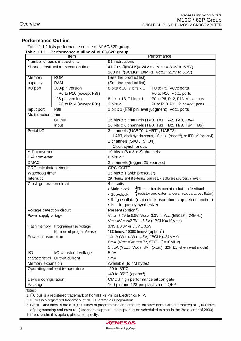
Table 1.1.1. Performance outline of M16C/62P group
Performance OutlineTable 1.1.1 lists performance outline of M16C/62P group.
Item PerformanceNumber of basic instructions 91 instructionsShortest instruction execution time 41.7 ns (f(BCLK)= 24MHZ, VCC1= 3.0V to 5.5V)
100 ns (f(BCLK)= 10MHZ, VCC1= 2.7V to 5.5V)Memory ROM (See the product list)capacity RAM (See the product list)I/O port 100-pin version 8 bits x 10, 7 bits x 1 P0 to P5: VCC2 ports
P0 to P10 (except P85) P6 to P10: VCC1 ports128-pin version 8 bits x 13, 7 bits x 1, P0 to P5, P12, P13: VCC2 ports P0 to P14 (except P85) 2 bits x 1 P6 to P10, P11, P14: VCC1 ports
Input port P85_______
1 bit x 1 (NMI pin level judgment): VCC1 portsMultifunction timer
Output 16 bits x 5 channels (TA0, TA1, TA2, TA3, TA4)Input 16 bits x 6 channels (TB0, TB1, TB2, TB3, TB4, TB5)
Serial I/O 3 channels (UART0, UART1, UART2) UART, clock synchronous, I2C bus1 (option4), or IEBus2 (option4)2 channels (SI/O3, SI/O4) Clock synchronous
A-D converter 10 bits x (8 x 3 + 2) channelsD-A converter 8 bits x 2DMAC 2 channels (trigger: 25 sources)CRC calculation circuit CRC-CCITTWatchdog timer 15 bits x 1 (with prescaler)Interrupt 29 internal and 8 external sources, 4 software sources, 7 levelsClock generation circuit 4 circuits
• Main clock• Sub-clock• Ring oscillator(main-clock oscillation stop detect function)• PLL frequency synthesizer
Voltage detection circuit Present (option4)Power supply voltage VCC1=3.0V to 5.5V, VCC2=3.0V to VCC1(f(BCLK)=24MHZ)
VCC1=VCC2=2.7V to 5.5V (f(BCLK)=10MHZ)Flash memory Program/erase voltage 3.3V ± 0.3V or 5.0V ± 0.5V
Number of program/erase 100 times, 10000 times3 (option4)Power consumption 14mA (VCC1=VCC2=5V, f(BCLK)=24MHZ)
8mA (VCC1=VCC2=3V, f(BCLK)=10MHZ)1.8µA (VCC1=VCC2=3V, f(XCIN)=32kHZ, when wait mode)
I/O I/O withstand voltage 5.0Vcharacteristics Output current 5mAMemory expansion Available (to 4M bytes)Operating ambient temperature -20 to 85°C
-40 to 85°C (option4)Device configuration CMOS high performance silicon gatePackage 100-pin and 128-pin plastic mold QFP
(These circuits contain a built-in feedback resistor and external ceramic/quartz oscillator)
Notes: 1. I2C bus is a registered trademark of Koninklijke Philips Electronics N. V. 2. IEBus is a registered trademark of NEC Electronics Corporation. 3. Block 1 and block A are a 10,000 times of programming and erasure. All other blocks are guaranteed of 1,000 times of programming and erasure. (Under development; mass production scheduled to start in the 3rd quarter of 2003) 4. If you desire this option, please so specify.
Overview
3
Renesas microcomputers
M16C / 62P Group SINGLE-CHIP 16-BIT CMOS MICROCOMPUTER
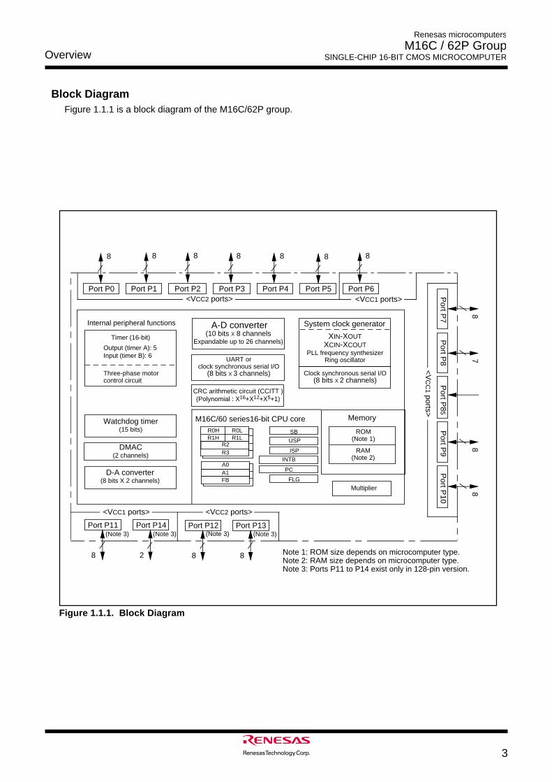
Block DiagramFigure 1.1.1 is a block diagram of the M16C/62P group.
Timer (16-bit)
Output (timer A): 5Input (timer B): 6
Internal peripheral functions
Watchdog timer(15 bits)
DMAC(2 channels)
D-A converter(8 bits X 2 channels)
A-D converter(10 bits X 8 channels
Expandable up to 26 channels)
UART orclock synchronous serial I/O
(8 bits X 3 channels)
System clock generator
XIN-XOUTXCIN-XCOUT
PLL frequency synthesizerRing oscillator
M16C/60 series16-bit CPU core
Port P0
8
Port P1
8
Port P2
8
Port P3
8
Port P4
8
Port P5
8
Port P6
8
CRC arithmetic circuit (CCITT )(Polynomial : X16+X12+X5+1)
Memory
87
88
Port P
10P
ort P9
Port P
8P
ort P7
Port P
85
ROM (Note 1)
RAM (Note 2)
Note 1: ROM size depends on microcomputer type.Note 2: RAM size depends on microcomputer type.Note 3: Ports P11 to P14 exist only in 128-pin version.
Clock synchronous serial I/O(8 bits X 2 channels)
R0LR0HR1H R1L
R2R3
SB
FLG
USP
ISP
INTB
PC
Multiplier
Port P11
8
Port P14
2
Port P12
8
Port P13
8
Three-phase motor control circuit
A0A1FB
<VCC2 ports>
(Note 3) (Note 3) (Note 3) (Note 3)
<VCC1 ports>
<V
CC
1 ports>
<VCC1 ports> <VCC2 ports>
Figure 1.1.1. Block Diagram
Overview
4
Renesas microcomputers
M16C / 62P Group SINGLE-CHIP 16-BIT CMOS MICROCOMPUTER
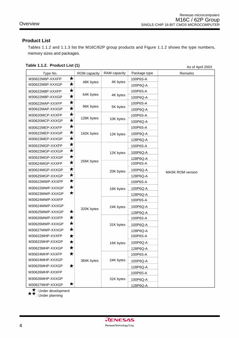
Product ListTables 1.1.2 and 1.1.3 list the M16C/62P group products and Figure 1.1.2 shows the type numbers,
memory sizes and packages.
Table 1.1.2. Product List (1)
RAM capacityROM capacity Package type RemarksType No.
As of April 2003
MASK ROM version
384K bytes
M30622MEP-XXXFP
M30620MCP-XXXFP
M30622MAP-XXXFP
M30622M8P-XXXFP
M30622M6P-XXXFP
100P6Q-A
M30622MEP-XXXGP
M30620MCP-XXXGP
M30622MAP-XXXGP
M30622M8P-XXXGP
M30622M6P-XXXGP
100P6S-A
100P6Q-A
100P6S-A
100P6Q-A
100P6S-A
100P6Q-A
100P6S-A
100P6Q-A
100P6S-A
M30623MEP-XXXGP 128P6Q-A
M30624MGP-XXXFP 100P6S-A
M30624MGP-XXXGP 100P6Q-A
M30625MGP-XXXGP 128P6Q-A
M30622MGP-XXXFP 100P6S-A
M30622MGP-XXXGP 100P6Q-A
128P6Q-AM30623MGP-XXXGP
M30626MWP-XXXFP 100P6S-A
M30626MWP-XXXGP 100P6Q-A
128P6Q-AM30627MWP-XXXGP
M30624MWP-XXXFP 100P6S-A
100P6Q-AM30624MWP-XXXGP
128P6Q-AM30625MWP-XXXGP
M30622MWP-XXXFP 100P6S-A
M30622MWP-XXXGP 100P6Q-A
M30626MHP-XXXFP 100P6S-A
M30626MHP-XXXGP 100P6Q-A
128P6Q-AM30623MWP-XXXGP
128P6Q-AM30627MHP-XXXGP
100P6S-AM30624MHP-XXXFP
100P6Q-AM30624MHP-XXXGP
128P6Q-AM30625MHP-XXXGP
M30622MHP-XXXFP 100P6S-A
M30622MHP-XXXGP 100P6Q-A
128P6Q-AM30623MHP-XXXGP
48K bytes
64K bytes
96K bytes
128K bytes
192K bytes
256K bytes
320K bytes
31K bytes
24K bytes
16K bytes
31K bytes
24K bytes
16K bytes
12K bytes
12K bytes
10K bytes
5K bytes
4K bytes
4K bytes
20K bytes
: Under development: Under planning
Overview
5
Renesas microcomputers
M16C / 62P Group SINGLE-CHIP 16-BIT CMOS MICROCOMPUTER
Package type: FP : Package 100P6S-A GP : Package 100P6Q-A, 128P6Q-A
ROM No. Omitted for flash memory version and external ROM version
ROM capacity: 6: 48K bytes 8: 64K bytes A: 96K bytes C: 128K bytes E: 192K bytes
Memory type: M: Mask ROM version F: Flash memory version S: External ROM version
Type No. M 3 0 6 2 6 M H P– X X X F P
M16C/62 Group
M16C Family
Shows RAM capacity, pin count, etc(The value itself has no specific meaning)
G: 256K bytesW: 320K bytesH: 384K bytesJ: 512K bytes
Figure 1.1.2. Type No., Memory Size, and Package
M30627FJPGP
M30625FGPGP 128P6Q-A
100P6S-AM30622F8PFP
M30622F8PGP 100P6Q-A
M30620FCPFP 100P6S-A
100P6Q-AM30620FCPGP
M30624FGPGP
100P6S-AM30624FGPFP
M30626FHPFP
128P6Q-A
100P6S-A
100P6Q-AM30626FHPGP
M30627FHPGP
M30626FJPFP
100P6Q-A
100P6S-A
M30626FJPGP
M30620SPFP
M30620SPGP
100P6Q-A
M30622SPFP
M30622SPGP
128P6Q-A
100P6Q-A
100P6S-A
100P6Q-A
100P6S-A
384K bytes
64K bytes
128K bytes
256K bytes
512K bytes
RAM capacityROM capacity Package type RemarksType No.
Flash memory version
External ROM version
31K bytes
10K bytes
4K bytes
20K bytes
4K bytes
31K bytes
10K bytes
: Under development: Under planning
As of April 2003Table 1.1.3. Product List (2)
Overview
6
Renesas microcomputers
M16C / 62P Group SINGLE-CHIP 16-BIT CMOS MICROCOMPUTER
1 2 3 4 5 6 7 8 9 10 11 12 13 14 15 16 17 18 19 20 21 22 23 24 25 26 27 28 29 30
31
32
33
34
35
36
37
38
39
40
41
42
43
44
45
46
47
48
49
50
515253545556575859606162636465666768697071727374757677787980
81
82
83
84
85
86
87
88
89
90
91
92
93
94
95
96
97
98
99
100
P00/AN00/D0
P01/AN01/D1
P02/AN02/D2
P03/AN03/D3
P04/AN04/D4
P05/AN05/D5
P06/AN06/D6
P07/AN07/D7
P10
/D8
P11
/D9
P12
/D10
P13
/D11
P14
/D12
VREF
AVSS
VC
C1
XIN
XO
UT
VS
S
RE
SE
T
CN
Vss
P87
/XC
IN
P86
/XC
OU
T
BY
TE
P20
/AN
20/A
0(/D
0/-)
P21
/AN
21/A
1(/D
1/D
0)P
2 2/A
N22
/A2(
/D2/
D1)
P23
/AN
23/A
3(/D
3/D
2)P
2 4/A
N24
/A4(
/D4/
D3)
P25
/AN
25/A
5(/D
5/D
4)P
26/A
N26
/A6(
/D6/
D5)
P2 7
/AN
27/A
7(/D
7/D
6)
P3 0
/A8(
/-/D
7)
P31
/A9
P32
/A10
P33
/A11
P34
/A12
P35
/A13
P36
/A14
P37
/A15
P40
/A16
P41
/A17
P42
/A18
P43
/A19
P74
/TA
2OU
T/W
P76
/TA
3OU
T
P56/ALE
P77
/TA
3IN
P55/HOLDP54/HLDAP53/BCLKP52/RD
VC
C2
VS
S
P57/RDY/CLKOUT
P45/CS1P46/CS2P47/CS3
AVCC
P63/TXD0/SDA0
P65/CLK1
P66/RxD1/SCL1
P67/TXD1/SDA1
P61/CLK0
P62/RxD0/SCL0
P100/AN0
P101/AN1
P102/AN2
P103/AN3
P93
/DA
0/T
B3I
N
P94
/DA
1/T
B4I
N
P95
/AN
EX
0/C
LK4
P96
/AN
EX
1/S
OU
T4
P91
/TB
1IN/S
IN3
P9 2
/TB
2IN/S
OU
T3
P80
/TA
4OU
T/U
P60/CTS0/RTS0
P64/CTS1/RTS1/CTS0/CLKS1
P72
/CLK
2/T
A1O
UT/V
P8 2
/INT
0
P71
/RxD
2/S
CL2
/TA
0IN/T
B5I
N(N
ote)
P83
/INT
1
P85
/NM
I
P97/ADTRG/SIN4
P44/CS0
P50/WRL/WRP51/WRH/BHE
P90
/TB
0IN/C
LK3
P70
/TXD
2/S
DA
2/T
A0O
UT(N
ote)
P8 4
/INT
2
P81
/TA
4IN/U
P73
/CT
S2/
RT
S2/
TA
1IN/V
P75
/TA
2IN/W
P15
/D13
/INT
3P
16/D
14/IN
T4
P17
/D15
/INT
5
P107/AN7/KI3P106/AN6/KI2P105/AN5/KI1P104/AN4/KI0
Package: 100P6S-A
Figure 1.1.3. Pin Configuration (Top View)
M16C/62P Group
PIN CONFIGURATION (top view)
Note: P70 and P71 are N channel open-drain output pins.
Pin ConfigurationFigures 1.1.3 to 1.1.5 show the pin configurations (top view).
Overview
7
Renesas microcomputers
M16C / 62P Group SINGLE-CHIP 16-BIT CMOS MICROCOMPUTER
1 2 3 4 5 6 7 8 9 10 11 12 13 14 15 16 17 18 19 20 21 22 23 24 25
2627
28
29
3031
32
33
34
35
36
37
38
39
40
41
42
43
44
45
46
47
48
49
50
51525354555657585960616263646566676869707172737475
76
77
78
79
80
81
82
83
84
85
86
87
88
89
90
91
92
93
94
95
96
97
98
99
100
P00/AN00/D0
P01/AN01/D1
P02/AN02/D2P03/AN03/D3
P04/AN04/D4
P05/AN05/D5
P06/AN06/D6
P07/AN07/D7
P10/D8
P11/D9
P12/D10
P13
/D11
P14
/D12
VREF
AVSS
VC
C1
XIN
XO
UT
VS
S
RE
SE
T
CN
Vss
P87
/XC
IN
P86
/XC
OU
T
BY
TE
P20
/AN
20/A
0(/D
0/-)
P21
/AN
21/A
1(/D
1/D
0)P
22/A
N22
/A2(
/D2/
D1)
P23
/AN
23/A
3(/D
3/D
2)P
24/A
N24
/A4(
/D4/
D3)
P25
/AN
25/A
5(/D
5/D
4)P
26/A
N26
/A6(
/D6/
D5)
P27
/AN
27/A
7(/D
7/D
6)
P30
/A8(
/-/D
7)
P31
/A9
P32
/A10
P33
/A11
P34
/A12
P35
/A13
P36
/A14
P37
/A15
P40
/A16
P41
/A17
P42/A18
P43/A19
P74
/TA
2OU
T/W
P76
/TA
3OU
T
P56/ALE
P77
/TA
3IN
P55/HOLDP54/HLDAP53/BCLKP52/RD
VC
C2
VS
S
P57/RDY/CLKOUT
P45/CS1P46/CS2P47/CS3
AVcc
P63/TXD0/SDA0
P65/CLK1
P66/RxD1/SCL1
P67/TXD1/SDA1
P61/CLK0
P62/RxD0/SCL0
P100/AN0
P101/AN1
P102/AN2
P103/AN3
P93
/DA
0/T
B3I
N
P94
/DA
1/T
B4I
N
P95/ANEX0/CLK4P96/ANEX1/SOUT4
P91
/TB
1IN/S
IN3
P92
/TB
2IN/S
OU
T3
P80
/TA
4OU
T/U
P60/CTS0/RTS0
P64/CTS1/RTS1/CTS0/CLKS1
P82
/INT
0
P83
/INT
1
P85
/NM
I
P97/ADTRG/SIN4
P44/CS0
P50/WRL/WRP51/WRH/BHE
P90
/TB
0IN/C
LK3
P84
/INT
2
P72/CLK2/TA1OUT/VP71/RxD2/SCL2/TA0IN/TB5IN(Note)P70/TXD2/SDA2/TA0OUT(Note)
P75
/TA
2IN/W
P73
/CT
S2/
RT
S2/
TA
1IN/V
P15
/D13
/INT
3
P16
/D14
/INT
4
P17
/D15
/INT
5
P107/AN7/KI3P106/AN6/KI2P105/AN5/KI1P104/AN4/KI0
P81
/TA
4IN/U
Figure 1.1.4. Pin Configuration (Top View)
Package: 100P6Q-A
M16C/62P Group
PIN CONFIGURATION (top view)
Note: P70 and P71 are N channel open-drain output pins.
Overview
8
Renesas microcomputers
M16C / 62P Group SINGLE-CHIP 16-BIT CMOS MICROCOMPUTER
Figure 1.1.5. Pin Configuration (Top View)
Package: 128P6Q-A
PIN CONFIGURATION (top view)
1 2 3 4 5 6 7 8 9 10 11 12 13 14 15 16 17 18 19 20 21 22 23 24 25 26 27 28 29 30
737475767778798081828384858687888990919293949596979899100101102
109
110
111
112
113
114
115
116
117
118
119
120
121
122
123
124
125
126
127
128 39
40
41
42
4344
45
46
47
48
49
50
51
52
53
54
55
56
57
58
59
60
61
62
63104
105
106
107
108
31 32 33 34 35 36 37
66676869707172
38
65
64103
P00/AN00/D0
P01/AN01/D1
P02/AN02/D2
P03/AN03/D3
P04/AN04/D4
P05/AN05/D5
P06/AN06/D6
P07/AN07/D7
P10/D8
P11
/D9
P12
/D10
AVSS
VC
C1
XIN
XO
UT
VS
S
RE
SE
T
CN
Vss
P87
/XC
IN
P86
/XC
OU
T
BY
TE
P74
/TA
2OU
T/W
P76
/TA
3OU
T
P56/ALE
P77
/TA
3IN
P55/HOLDP54/HLDA
P53/BCLKP52/RD
P57/RDY/CLKOUT
P47
/CS
3
P63/TXD0/SDA0
P65/CLK1
P66
/RxD
1/S
CL1
P67
/TXD
1/S
DA
1
P61/CLK0
P62/RxD0/SCL0
P100/AN0
P101/AN1
P102/AN2
P103/AN3
P93
/DA
0/T
B3I
N
P94
/DA
1/T
B4I
N
P95
/AN
EX
0/C
LK4
P96
/AN
EX
1/S
OU
T4
P91
/TB
1IN/S
IN3
P92
/TB
2IN/S
OU
T3
P80
/TA
4OU
T/U
P60/CTS0/RTS0
P64/CTS1/RTS1/CTS0/CLKS1
P82
/INT
0
P83
/INT
1
P85
/NM
I
P45
/CS
1P
46/C
S2
P44
/CS
0P50/WRL/WRP51/WRH/BHE
P90
/TB
0IN/C
LK3
P72
/CLK
2/T
A1O
UT/V
P71
/RxD
2/S
CL2
/TA
0IN/T
B5I
N(N
ote)
P70
/TXD
2/S
DA
2/T
A0O
UT(N
ote)
P84
/INT
2
P81
/TA
4IN/U
P73
/CT
S2/
RT
S2/
TA
1IN/V
P75
/TA
2IN/W
P107/AN7/KI3P106/AN6/KI2P105/AN5/KI1P104/AN4/KI0
VR
EF
AV
CC
P97
/AD
TR
G/S
IN4
P14
1
P14
0
P137
P136
P135
P134
P13
/D11
P14
/D12
P20
/AN
20/A
0(/D
0/-)
P21
/AN
21/A
1(/D
1/D
0)P
22/A
N22
/A2(
/D2/
D1)
P23
/AN
23/A
3(/D
3/D
2)P
24/A
N24
/A4(
/D4/
D3)
P25
/AN
25/A
5(/D
5/D
4)P
26/A
N26
/A6(
/D6/
D5)
P27
/AN
27/A
7(/D
7/D
6)
P30
/A8(
/-/D
7)
P31
/A9
P32
/A10
P33
/A11
P34
/A12
P35
/A13
P36
/A14
P37
/A15
P40
/A16
P41
/A17
P42
/A18
P43
/A19
VC
C2
VS
S
P15
/D13
/INT
3P
16/D
14/IN
T4
P17
/D15
/INT
5
P12
4
P12
3
P113
P112
P111
P110
VC
C1
VSS
P130
P131
P132
P133
P125
P126
P127
P114
P115
P116
P117
P12
2
P12
1
P12
0
M16C/62P Group
Note: P70 and P71 are N channel open-drain output pins.
Overview
9
Renesas microcomputers
M16C / 62P Group SINGLE-CHIP 16-BIT CMOS MICROCOMPUTER
VCC1, VCC2,VSS
CNVSS
XIN
XOUT
BYTE
AVCC
AVSS
VREF
P00 to P07
D0 to D7
P10 to P17
D8 to D15
P20 to P27
A0 to A7
A0/D0 to A7/D7
A0A1/D0 toA7/D6
P30 to P37
A8 to A15
A8/D7,A9 to A15
P40 to P47
Signal name
Power supply input
CNVSS
Reset input
Clock input
Clock output
External data bus width select input
Analog powersupply input
Referencevoltage input
I/O port P0
I/O port P1
I/O port P2
I/O port P3
I/O port P4
Apply 2.7V to 5.5 V to the VCC1 and VCC2 pins and 0 V to the VSS pin. The Vcc apply condition is that VCC2 ≤ VCC1
Function
This pin switches between processor modes. Connect this pin to VSS pin when after a reset you want to start operation in single-chip mode (memory expansion mode) or the VCC1 pin when starting operation in microprocessor mode.
“L” on this input resets the microcomputer.
These pins are provided for the main clock generating circuit input/output. Connect a ceramic resonator or crystal between the XIN and the XOUT pins. To use an externally derived clock, input it to the XIN pin and leave the XOUT pin open.
This pin selects the width of an external data bus. A 16-bit width is selected when this input is “L”; an 8-bit width is selected when this input is “H”. This input must be fixed to either “H” or “L”. Connect this pin to the VSS pin when operating in single-chip mode.
This pin is a power supply input for the A-D converter. Connect this pin to VCC1.
This pin is a power supply input for the A-D converter. Connect this pin to VSS.
This pin is a reference voltage input for the A-D converter.
This is an 8-bit CMOS I/O port. This port has an input/output select direction register, allowing each pin in that port to be directed for input or output individually. If any port is set for input, selection can be made for it in a program whether or not to have a pull-up resistor in 4 bit units. This selection is unavailable in memory extension and microprocessor modes.This port can function as input pins for the A-D converter when so selected in a program.
When set as a separate bus, these pins input and output data (D0–D7).
This is an 8-bit I/O port equivalent to P0. P15 to P17 also function as INT interrupt input pins as selected by a program.
When set as a separate bus, these pins input and output data (D8–D15).
This is an 8-bit I/O port equivalent to P0. This port can function as input pins for the A-D converter when so selected in a program.
These pins output 8 low-order address bits (A0 to A7).
If the external bus is set as an 8-bit wide multiplexed bus, these pins input and output data (D0 to D7) and output 8 low-order address bits (A0 to A7) separated in time by multiplexing.
If the external bus is set as a 16-bit wide multiplexed bus, these pins input and output data (D0 to D6) and output address (A1 to A7) separated in time by multiplexing. They also output address (A0).This is an 8-bit I/O port equivalent to P0.
These pins output 8 middle-order address bits (A8 to A15).
If the external bus is set as a 16-bit wide multiplexed bus, these pins input and output data (D7) and output address (A8) separated in time by multiplexing. They also output address (A9 to A15).This is an 8-bit I/O port equivalent to P0.
Pin name
Input
Input
Input
Output
Input
Input
Input/output
Input/output
Input/output
Input/output
I/O type
Analog powersupply input
Input/output
Output
Input/output
OutputInput/output
Input/output
OutputInput/outputOutput
Input/output
OutputOutput
A16 to A19,CS0 to CS3
These pins output A16 to A19 and CS0 to CS3 signals. A16 to A19 are 4 high- order address bits. CS0 to CS3 are chip select signals used to specify an access space.
RESET
(Note)
Power supply
VCC1
VCC2
VCC1
VCC1
VCC2
VCC2
VCC2
VCC2
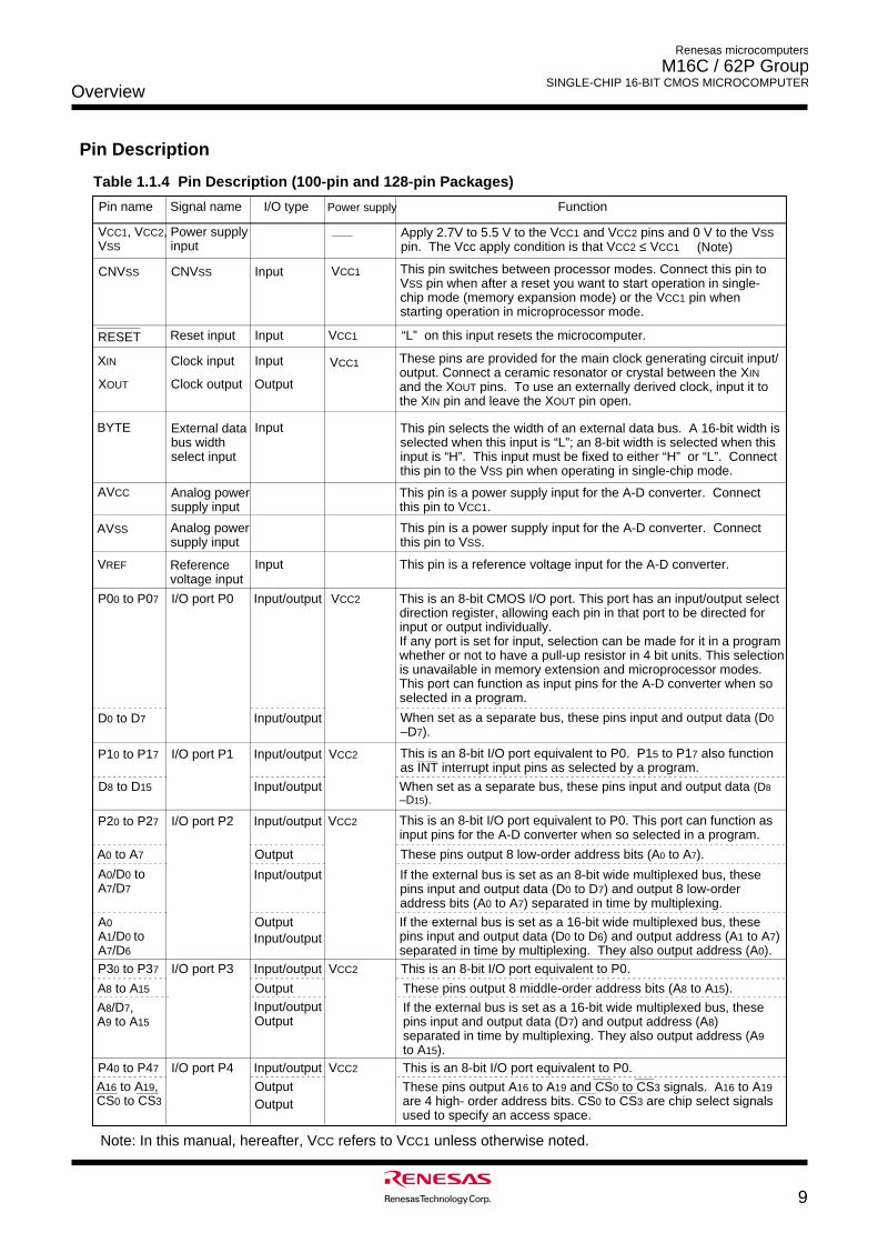
Table 1.1.4 Pin Description (100-pin and 128-pin Packages)
Note: In this manual, hereafter, VCC refers to VCC1 unless otherwise noted.
Pin Description
Renesas microcomputers
M16C / 62P Group SINGLE-CHIP 16-BIT CMOS MICROCOMPUTEROverview
10
Table 1.1.5 Pin Description (100-pin and 128-pin Packages) (Continued)
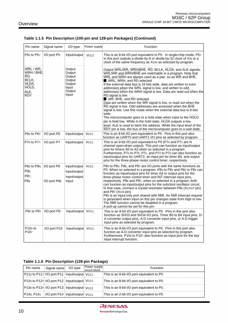
Signal name FunctionPin name I/O type Power supply
VCC2P50 to P57
WRL / WR,WRH / BHE,RD,BCLK,HLDA,HOLD,ALE,RDY
I/O port P5 Input/output
VCC1P60 to P67 I/O port P6 Input/output
VCC1P70 to P77 I/O port P7 Input/output
VCC1P80 to P84,
P87,
P85
I/O port P8
I/O port P85
Input/output
Input/outputInput
OutputOutputOutputOutputOutputInputOutputInput
This is an 8-bit I/O port equivalent to P0. In single-chip mode, P57 in this port outputs a divide-by-8 or divide-by-32 clock of XIN or a clock of the same frequency as XCIN as selected by program.
This is an 8-bit I/O port equivalent to P0. Pins in this port also function as UART0 and UART1 I/O pins as selected by program.This is an 8-bit I/O port equivalent to P0 (P70 and P71 are N channel open-drain output). This port can function as input/output pins for timers A0 to A3 when so selected in a program. Furthermore, P70 to P75, P71, and P72 to P75 can also function as input/output pins for UART2, an input pin for timer B5, and output pins for the three-phase motor control timer, respectively.
Output WRL/WR, WRH/BHE, RD, BCLK, HLDA, and ALE signals. WRL/WR and WRH/BHE are switchable in a program. Note that WRL and WRH are always used as a pair, so as WR and BHE. WRL, WRH, and RD selectedIf the external data bus is 16 bits wide, data are written to even addresses when the WRL signal is low, and written to odd addresses when the WRH signal is low. Data are read out when the RD signal is low. WR, BHE, and RD selectedData are written when the WR signal is low, or read out when the RD signal is low. Odd addresses are accessed when the BHE signal is low. Use this mode when the external data bus is 8 bits wide.The microcomputer goes to a hold state when input to the HOLD pin is held low. While in the hold state, HLDA outputs a low level. ALE is used to latch the address. While the input level of the RDY pin is low, the bus of the microcomputer goes to a wait state.
P80 to P84, P86, and P87 are I/O ports with the same functions as P0. When so selected in a program, P80 to P81 and P82 to P84 can function as input/output pins for timer A4 or output pins for the three-phase motor control timer and INT interrupt input pins, respectively. P86 and P87, when so selected in a program, both can function as input/output pins for the subclock oscillator circuit. In that case, connect a crystal resonator between P86 (XCOUT pin) and P87 (XCIN pin). P85 is an input-only port shared with NMI. An NMI interrupt request is generated when input on this pin changes state from high to low. The NMI function cannot be disabled in a program.A pull-up cannot be set for this pin.
This is an 8-bit I/O port equivalent to P0. Pins in this port also function as SI/O3 and SI/O4 I/O pins, Timer B0 to B4 input pins, D-A converter output pins, A-D converter input pins, or A-D trigger input pins as selected by program.
P90 to P97 I/O port P9 Input/output VCC1
This is an 8-bit I/O port equivalent to P0. Pins in this port also function as A-D converter input pins as selected by program. Furthermore, P104 to P107 also function as input pins for the key input interrupt function.
P100 to P107
I/O port P10 Input/output VCC1
P86, Input/output
Table 1.1.6 Pin Description (128-pin Package)
P110 to P117
Signal name
I/O port P11
Pin name I/O type
Input/output
P120 to P127 I/O port P12 Input/output
P130 to P137 I/O port P13 Input/output
P140, P141 I/O port P14
Function
This is an 8-bit I/O port equivalent to P0.
This is an 8-bit I/O port equivalent to P0.
This is an 8-bit I/O port equivalent to P0.
This is an 2-bit I/O port equivalent to P0.Input/output
Power supply circuit block
VCC2
VCC2
VCC1
VCC1
Memory
11
Renesas microcomputers
M16C / 62P Group SINGLE-CHIP 16-BIT CMOS MICROCOMPUTER
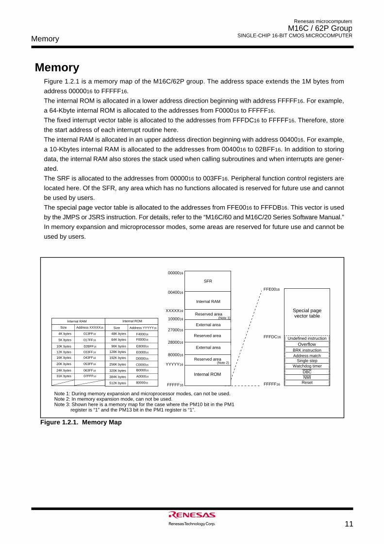
MemoryFigure 1.2.1 is a memory map of the M16C/62P group. The address space extends the 1M bytes from
address 0000016 to FFFFF16.
The internal ROM is allocated in a lower address direction beginning with address FFFFF16. For example,
a 64-Kbyte internal ROM is allocated to the addresses from F000016 to FFFFF16.
The fixed interrupt vector table is allocated to the addresses from FFFDC16 to FFFFF16. Therefore, store
the start address of each interrupt routine here.
The internal RAM is allocated in an upper address direction beginning with address 0040016. For example,
a 10-Kbytes internal RAM is allocated to the addresses from 0040016 to 02BFF16. In addition to storing
data, the internal RAM also stores the stack used when calling subroutines and when interrupts are gener-
ated.
The SRF is allocated to the addresses from 0000016 to 003FF16. Peripheral function control registers are
located here. Of the SFR, any area which has no functions allocated is reserved for future use and cannot
be used by users.
The special page vector table is allocated to the addresses from FFE0016 to FFFDB16. This vector is used
by the JMPS or JSRS instruction. For details, refer to the “M16C/60 and M16C/20 Series Software Manual.”
In memory expansion and microprocessor modes, some areas are reserved for future use and cannot be
used by users.
Figure 1.2.1. Memory Map
0000016
XXXXX16
AAAAAAAAAAAAAAAAAAAAAAAAExternal area
Internal ROM
SFR
Internal RAM
Reserved area
Reserved area
FFE0016
FFFDC16
FFFFF16 Note 1: During memory expansion and microprocessor modes, can not be used.Note 2: In memory expansion mode, can not be used.Note 3: Shown here is a memory map for the case where the PM10 bit in the PM1
register is “1” and the PM13 bit in the PM1 register is “1”.
Undefined instruction
OverflowBRK instructionAddress match
Single stepWatchdog timer
Reset
Special pagevector table
DBCNMI
4K bytes 013FF16
02BFF16
017FF16
Address XXXXX16
033FF16
10K bytes
5K bytes
12K bytes
Size Address YYYYY16Size
F000016
E800016
F400016
96K bytes
48K bytes
64K bytesReserved area
External area
0040016
1000016
2700016
2800016
8000016
YYYYY16
FFFFF16
(Note 1)
(Note 2)
E000016
256K bytes
128K bytes
192K bytes D000016
320K bytes
C000016
384K bytes
B000016
A000016
512K bytes 8000016
063FF16
053FF16
07FFF16
24K bytes
20K bytes
31K bytes
Internal RAM Internal ROM
043FF1616K bytes
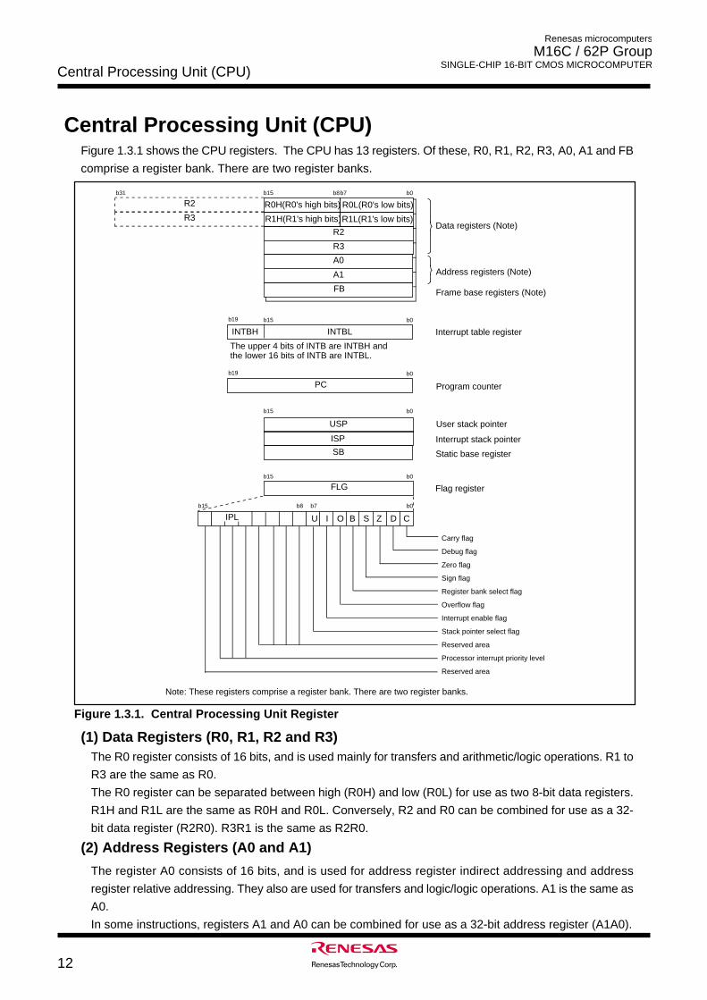
Renesas microcomputers
M16C / 62P Group SINGLE-CHIP 16-BIT CMOS MICROCOMPUTER
Central Processing Unit (CPU)
12
Central Processing Unit (CPU)Figure 1.3.1 shows the CPU registers. The CPU has 13 registers. Of these, R0, R1, R2, R3, A0, A1 and FB
comprise a register bank. There are two register banks.
Figure 1.3.1. Central Processing Unit Register
(1) Data Registers (R0, R1, R2 and R3)The R0 register consists of 16 bits, and is used mainly for transfers and arithmetic/logic operations. R1 to
R3 are the same as R0.
The R0 register can be separated between high (R0H) and low (R0L) for use as two 8-bit data registers.
R1H and R1L are the same as R0H and R0L. Conversely, R2 and R0 can be combined for use as a 32-
bit data register (R2R0). R3R1 is the same as R2R0.
(2) Address Registers (A0 and A1)
The register A0 consists of 16 bits, and is used for address register indirect addressing and address
register relative addressing. They also are used for transfers and logic/logic operations. A1 is the same as
A0.
In some instructions, registers A1 and A0 can be combined for use as a 32-bit address register (A1A0).
Data registers (Note)
Address registers (Note)
Frame base registers (Note)
Program counter
Interrupt table register
User stack pointer
Interrupt stack pointer
Static base register
Flag register
Note: These registers comprise a register bank. There are two register banks.
R0H(R0's high bits)b15 b8 b7 b0
R3
INTBH
USP
ISP
SB
AAAA
AAAAAAAAAA
AAAAAAAAAAAAAAAAAA
AAAAAAAAAAAAAACDZSBOIUIPL
R0L(R0's low bits)
R1H(R1's high bits)R1L(R1's low bits)
R2b31
R3
R2
A1
A0
FB
b19
INTBLb15 b0
PCb19 b0
b15 b0
FLGb15 b0
b15 b0 b7 b8
Reserved area
Carry flag
Debug flag
Zero flag
Sign flag
Register bank select flag
Overflow flag
Interrupt enable flag
Stack pointer select flag
Reserved area
Processor interrupt priority level
The upper 4 bits of INTB are INTBH and the lower 16 bits of INTB are INTBL.
Central Processing Unit (CPU)
13
Renesas microcomputers
M16C / 62P Group SINGLE-CHIP 16-BIT CMOS MICROCOMPUTER
(3) Frame Base Register (FB)FB is configured with 16 bits, and is used for FB relative addressing.
(4) Interrupt Table Register (INTB)
INTB is configured with 20 bits, indicating the start address of an interrupt vector table.
(5) Program Counter (PC)
PC is configured with 20 bits, indicating the address of an instruction to be executed.
(6) User Stack Pointer (USP) and Interrupt Stack Pointer (ISP)
Stack pointer (SP) comes in two types: USP and ISP, each configured with 16 bits.
Your desired type of stack pointer (USP or ISP) can be selected by the U flag of FLG.
(7) Static Base Register (SB)SB is configured with 16 bits, and is used for SB relative addressing.
(8) Flag Register (FLG)
FLG consists of 11 bits, indicating the CPU status.
• Carry Flag (C Flag)
This flag retains a carry, borrow, or shift-out bit that has occurred in the arithmetic/logic unit.
• Debug Flag (D Flag)
The D flag is used exclusively for debugging purpose. During normal use, it must be set to “0”.
• Zero Flag (Z Flag)
This flag is set to “1” when an arithmetic operation resulted in 0; otherwise, it is “0”.
• Sign Flag (S Flag)
This flag is set to “1” when an arithmetic operation resulted in a negative value; otherwise, it is “0”.
• Register Bank Select Flag (B Flag)
Register bank 0 is selected when this flag is “0” ; register bank 1 is selected when this flag is “1”.
• Overflow Flag (O Flag)
This flag is set to “1” when the operation resulted in an overflow; otherwise, it is “0”.
• Interrupt Enable Flag (I Flag)
This flag enables a maskable interrupt.
Maskable interrupts are disabled when the I flag is “0”, and are enabled when the I flag is “1”. The I
flag is cleared to “0” when the interrupt request is accepted.
• Stack Pointer Select Flag (U Flag)
ISP is selected when the U flag is “0”; USP is selected when the U flag is “1”.
The U flag is cleared to “0” when a hardware interrupt request is accepted or an INT instruction for
software interrupt Nos. 0 to 31 is executed.
• Processor Interrupt Priority Level (IPL)
IPL is configured with three bits, for specification of up to eight processor interrupt priority levels from
level 0 to level 7.
If a requested interrupt has priority greater than IPL, the interrupt is enabled.
• Reserved Area
When write to this bit, write "0". When read, its content is indeterminate.
Renesas microcomputers
M16C / 62P Group SINGLE-CHIP 16-BIT CMOS MICROCOMPUTERSFR
14
DMA0 control register DM0CON 00000X002
DMA0 transfer counter TCR0 XX16XX16
DMA1 control register DM1CON 00000X002
DMA1 source pointer SAR1 XX16XX16XX16
DMA1 transfer counter TCR1 XX16XX16
DMA1 destination pointer DAR1 XX16XX16XX16
Watchdog timer start register WDTS XX16
Watchdog timer control register WDC 00XXXXXX2(Note 4)
Processor mode register 0 (Note 2) PM0 000000002(CNVSS pin is “L”)
000000112(CNVSS pin is “H”)
Chip select control register CSR 000000012
System clock control register 0 CM0 010010002System clock control register 1 CM1 001000002
Address match interrupt enable register AIER XXXXXX002Protect register PRCR XX0000002
Processor mode register 1 PM1 000010002
DMA0 destination pointer DAR0 XX16XX16XX16
Note 1: The blank areas are reserved and cannot be accessed by users.Note 2: The PM00 and PM01 bits do not change at software reset, watchdog timer reset and oscillation stop detection reset.Note 3: The CM20, CM21, and CM27 bits do not change at oscillation stop detection reset.Note 4: The WDC5 bit is “0” (cold start) immediately after power-on. It can only be set to “1” in a program. It is set to “0” when the input voltage
at the VCC1 pin drops to Vdet2 or less while the VC25 bit in the VCR2 register is set to “1” (RAM retention limit detection circuit enableNote 5: This register does not change at software reset, watchdog timer reset and oscillation stop detection reset.X : Nothing is mapped to this bit
Data bank register DBR 0016Oscillation stop detection register (Note 3) CM2 0000X0002
Chip select expansion control register CSE 0016PLL control register 0 PLC0 0001X0102
Processor mode register 2 PM2 XXX000002
000016
000116
000216
000316
000416
000516
000616
000716
000816
000916
000A16
000B16
000C16
000D16
000E16
000F16
001016
001116
001216
001316
001416
001516
001616
001716
001816
001916
001A16
001B16
001C16
001D16
001E16
001F16
002016
002116
002216
002316
002416
002516
002616
002716
002816
002916
002A16
002B16
002C16
002D16
002E16
002F16
003016
003116
003216
003316
003416
003516
003616
003716
003816
003916
003A16
003B16
003C16
003D16
003E16
003F16
Address Register Symbol After reset
Address match interrupt register 0 RMAD0 00160016X016
Address match interrupt register 1 RMAD1 00160016X016
DMA0 source pointer SAR0 XX16XX16XX16
Voltage detection register 1 (Note 5) VCR1 000010002Voltage detection register 2 (Note 5) VCR2 0016
Voltage down detection interrupt register D4INT 0016
SFR
Renesas microcomputers
M16C / 62P Group SINGLE-CHIP 16-BIT CMOS MICROCOMPUTERSFR
15
Timer A1 interrupt control register TA1IC XXXXX0002
UART0 transmit interrupt control register S0TIC XXXXX0002
Timer A0 interrupt control register TA0IC XXXXX0002
Timer A2 interrupt control register TA2IC XXXXX0002
UART0 receive interrupt control register S0RIC XXXXX0002UART1 transmit interrupt control register S1TIC XXXXX0002UART1 receive interrupt control register S1RIC XXXXX0002
DMA1 interrupt control register DM1IC XXXXX0002DMA0 interrupt control register DM0IC XXXXX0002
Key input interrupt control register KUPIC XXXXX0002A-D conversion interrupt control register ADIC XXXXX0002
UART2 Bus collision detection interrupt control register BCNIC XXXXX0002
UART2 transmit interrupt control register S2TIC XXXXX0002UART2 receive interrupt control register S2RIC XXXXX0002
INT1 interrupt control register INT1IC XX00X0002
Timer B0 interrupt control register TB0IC XXXXX0002
Timer B2 interrupt control register TB2IC XXXXX0002
Timer A3 interrupt control register TA3IC XXXXX0002
INT2 interrupt control register INT2IC XX00X0002
INT0 interrupt control register INT0IC XX00X0002
Timer B1 interrupt control register TB1IC XXXXX0002
Timer A4 interrupt control register TA4IC XXXXX0002
INT3 interrupt control register INT3IC XX00X0002Timer B5 interrupt control register TB5IC XXXXX0002
Timer B4 interrupt control register, UART1 BUS collision detection interrupt control register TB4IC, U1BCNIC XXXXX0002Timer B3 interrupt control register, UART0 BUS collision detection interrupt control register TB3IC, U0BCNIC XXXXX0002
SI/O4 interrupt control register (S4IC), INT5 interrupt control register S4IC, INT5IC XX00X0002
SI/O3 interrupt control register, INT4 interrupt control register S3IC, INT4IC XX00X0002
Note :The blank areas are reserved and cannot be accessed by users.
X : Nothing is mapped to this bit
004016
004116
004216
004316
004416
004516
004616
004716
004816
004916
004A16
004B16
004C16
004D16
004E16
004F16
005016
005116
005216
005316
005416
005516
005616
005716
005816
005916
005A16
005B16
005C16
005D16
005E16
005F16
006016
006116
006216
006316
006416
006516
006616
006716
006816
006916
006A16
006B16
006C16
006D16
006E16
006F16
007016
007116
007216
007316
007416
007516
007616
007716
007816
007916
007A16
007B16
007C16
007D16
007E16
007F16
Address Register Symbol After reset
Renesas microcomputers
M16C / 62P Group SINGLE-CHIP 16-BIT CMOS MICROCOMPUTERSFR
16
008016
008116
008216
008316
008416
008516
008616
01B016
01B116
01B216
01B316
01B416
01B516
01B616
01B716
01B816
01B916
01BA16
01BB16
01BC16
01BD16
01BE16
01BF16
025016
025116
025216
025316
025416
025516
025616
025716
025816
025916
025A16
025B16
025C16
025D16
025E16
025F16
033016
033116
033216
033316
033416
033516
033616
033716
033816
033916
033A16
033B16
033C16
033D16
033E16
033F16
Note 1: The blank areas are reserved and cannot be accessed by users.Note 2: This register is included in the flash memory version.
X : Nothing is mapped to this bit
Peripheral clock select register PCLKR 000000112
Flash memory control register 0 (Note 2) FMR0 XX0000012
Flash memory control register 1 (Note 2) FMR1 0X00XX0X2
Address match interrupt register 2 RMAD2 00160016X016
Address match interrupt register 3 RMAD3 00160016X016
Address match interrupt enable register 2 AIER2 XXXXXX002
Address Register Symbol After reset
~~ ~~
~~ ~~
~~ ~~
Flash identification register (Note 2) FIDR XXXXXX002
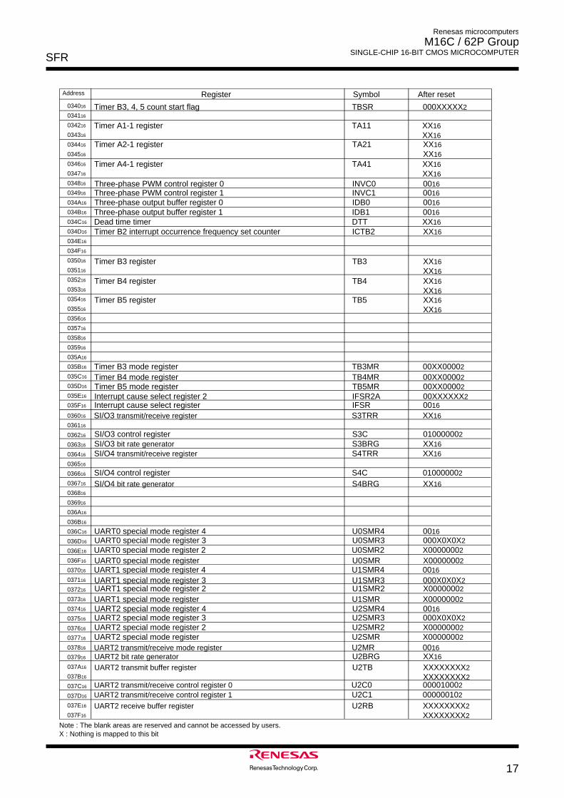
Renesas microcomputers
M16C / 62P Group SINGLE-CHIP 16-BIT CMOS MICROCOMPUTERSFR
17
Address Register Symbol After reset034016
034116
034216
034316
034416
034516
034616
034716
034816
034916
034A16
034B16
034C16
034D16
034E16
034F16
035016
035116
035216
035316
035416
035516
035616
035716
035816
035916
035A16
035B16
035C16
035D16
035E16
035F16
036016
036116
036216
036316
036416
036516
036616
036716
036816
036916
036A16
036B16
036C16
036D16
036E16
036F16
037016
037116
037216
037316
037416
037516
037616
037716
037816
037916
037A16
037B16
037C16
037D16
037E16
037F16
Timer A1-1 register TA11 XX16XX16
Timer A2-1 register TA21 XX16XX16
Dead time timer DTT XX16Timer B2 interrupt occurrence frequency set counter ICTB2 XX16
Three-phase PWM control register 0 INVC0 0016Three-phase PWM control register 1 INVC1 0016Three-phase output buffer register 0 IDB0 0016Three-phase output buffer register 1 IDB1 0016
Timer B3 register TB3 XX16XX16
Timer B4 register TB4 XX16XX16
Timer B5 register TB5 XX16XX16
Timer B3, 4, 5 count start flag TBSR 000XXXXX2
Timer B3 mode register TB3MR 00XX00002
Timer B4 mode register TB4MR 00XX00002Timer B5 mode register TB5MR 00XX00002
Interrupt cause select register IFSR 0016
SI/O3 transmit/receive register S3TRR XX16
SI/O4 transmit/receive register S4TRR XX16
SI/O3 control register S3C 010000002SI/O3 bit rate generator S3BRG XX16
SI/O4 bit rate generator S4BRG XX16
SI/O4 control register S4C 010000002
UART2 special mode register U2SMR X00000002
UART2 receive buffer register U2RB XXXXXXXX2XXXXXXXX2
UART2 transmit buffer register U2TB XXXXXXXX2XXXXXXXX2
UART2 transmit/receive control register 0 U2C0 000010002
UART2 transmit/receive mode register U2MR 0016
UART2 transmit/receive control register 1 U2C1 000000102
UART2 bit rate generator U2BRG XX16
Timer A4-1 register TA41 XX16XX16
UART2 special mode register 2 U2SMR2 X00000002
Note : The blank areas are reserved and cannot be accessed by users.X : Nothing is mapped to this bit
UART2 special mode register 3 U2SMR3 000X0X0X2
Interrupt cause select register 2 IFSR2A 00XXXXXX2
UART0 special mode register 2 U0SMR2 X00000002
UART0 special mode register U0SMR X00000002
UART0 special mode register 3 U0SMR3 000X0X0X2UART0 special mode register 4 U0SMR4 0016
UART1 special mode register 2 U1SMR2 X00000002
UART1 special mode register U1SMR X00000002
UART1 special mode register 3 U1SMR3 000X0X0X2
UART1 special mode register 4 U1SMR4 0016
UART2 special mode register 4 U2SMR4 0016
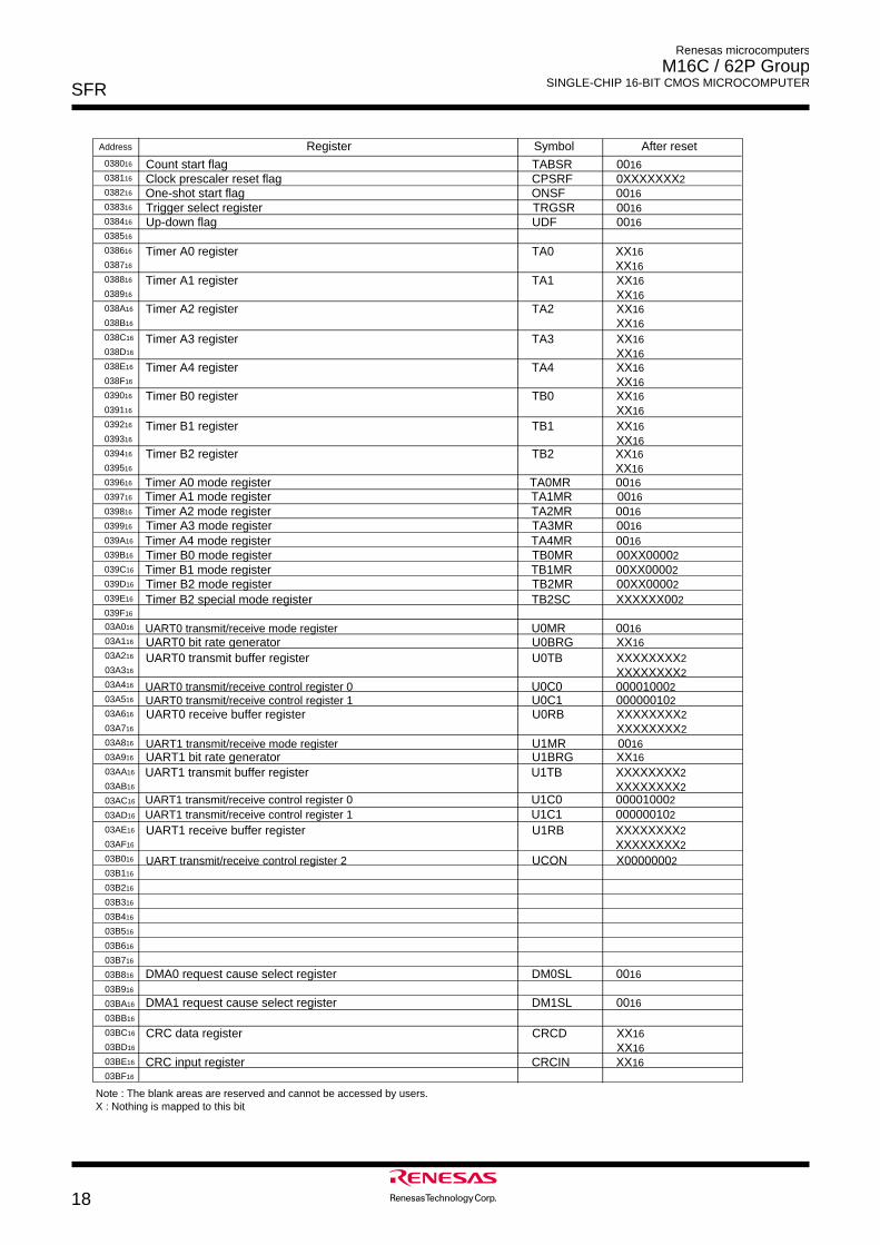
Renesas microcomputers
M16C / 62P Group SINGLE-CHIP 16-BIT CMOS MICROCOMPUTERSFR
18
038016
038116
038216
038316
038416
038516
038616
038716
038816
038916
038A16
038B16
038C16
038D16
038E16
038F16
039016
039116
039216
039316
039416
039516
039616
039716
039816
039916
039A16
039B16
039C16
039D16
039E16
039F16
03A016
03A116
03A216
03A316
03A416
03A516
03A616
03A716
03A816
03A916
03AA16
03AB16
03AC16
03AD16
03AE16
03AF16
03B016
03B116
03B216
03B316
03B416
03B516
03B616
03B716
03B816
03B916
03BA16
03BB16
03BC16
03BD16
03BE16
03BF16
Timer A0 register TA0 XX16XX16
Timer A1 register TA1 XX16XX16
Timer A2 register TA2 XX16XX16
Timer B0 register TB0 XX16XX16
Timer B1 register TB1 XX16XX16
Timer B2 register TB2 XX16XX16
Count start flag TABSR 0016
One-shot start flag ONSF 0016
Timer A0 mode register TA0MR 0016Timer A1 mode register TA1MR 0016Timer A2 mode register TA2MR 0016
Timer B0 mode register TB0MR 00XX00002Timer B1 mode register TB1MR 00XX00002Timer B2 mode register TB2MR 00XX00002
Up-down flag UDF 0016
Timer A3 register TA3 XX16XX16
Timer A4 register TA4 XX16XX16
Timer A3 mode register TA3MR 0016Timer A4 mode register TA4MR 0016
Trigger select register TRGSR 0016
Clock prescaler reset flag CPSRF 0XXXXXXX2
UART0 transmit/receive mode register U0MR 0016
UART0 transmit buffer register U0TB XXXXXXXX2XXXXXXXX2
UART0 receive buffer register U0RB XXXXXXXX2XXXXXXXX2
UART1 transmit/receive mode register U1MR 0016
UART1 transmit buffer register U1TB XXXXXXXX2XXXXXXXX2
UART1 receive buffer register U1RB XXXXXXXX2XXXXXXXX2
UART0 bit rate generator U0BRG XX16
UART0 transmit/receive control register 0 U0C0 000010002UART0 transmit/receive control register 1 U0C1 000000102
UART1 bit rate generator U1BRG XX16
UART1 transmit/receive control register 0 U1C0 000010002UART1 transmit/receive control register 1 U1C1 000000102
DMA1 request cause select register DM1SL 0016
DMA0 request cause select register DM0SL 0016
CRC data register CRCD XX16XX16
CRC input register CRCIN XX16
UART transmit/receive control register 2 UCON X00000002
Note : The blank areas are reserved and cannot be accessed by users.X : Nothing is mapped to this bit
Timer B2 special mode register TB2SC XXXXXX002
Address Register Symbol After reset
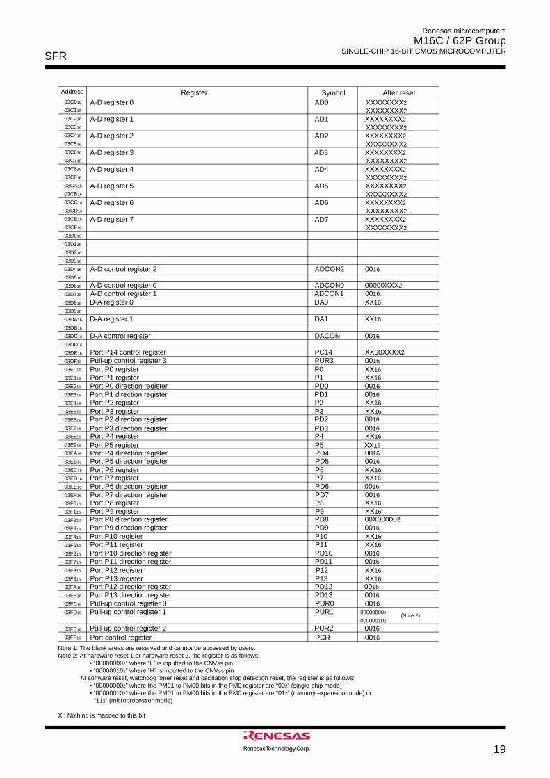
Renesas microcomputers
M16C / 62P Group SINGLE-CHIP 16-BIT CMOS MICROCOMPUTERSFR
19
03C016
03C116
03C216
03C316
03C416
03C516
03C616
03C716
03C816
03C916
03CA16
03CB16
03CC16
03CD16
03CE16
03CF16
03D016
03D116
03D216
03D316
03D416
03D516
03D616
03D716
03D816
03D916
03DA16
03DB16
03DC16
03DD16
03DE16
03DF16
03E016
03E116
03E216
03E316
03E416
03E516
03E616
03E716
03E816
03E916
03EA16
03EB16
03EC16
03ED16
03EE16
03EF16
03F016
03F116
03F216
03F316
03F416
03F516
03F616
03F716
03F816
03F916
03FA16
03FB16
03FC16
03FD16
03FE16
03FF16
Note 1: The blank areas are reserved and cannot be accessed by users.Note 2: At hardware reset 1 or hardware reset 2, the register is as follows: • “000000002” where “L” is inputted to the CNVSS pin
• “000000102” where “H” is inputted to the CNVSS pin At software reset, watchdog timer reset and oscillation stop detection reset, the register is as follows: • “000000002” where the PM01 to PM00 bits in the PM0 register are “002” (single-chip mode) • “000000102” where the PM01 to PM00 bits in the PM0 register are “012” (memory expansion mode) or “112” (microprocessor mode)
X : Nothing is mapped to this bit
A-D register 7 AD7 XXXXXXXX2XXXXXXXX2
A-D register 0 AD0 XXXXXXXX2XXXXXXXX2
A-D register 1 AD1 XXXXXXXX2XXXXXXXX2
A-D register 2 AD2 XXXXXXXX2XXXXXXXX2
A-D register 3 AD3 XXXXXXXX2XXXXXXXX2
A-D register 4 AD4 XXXXXXXX2XXXXXXXX2
A-D register 5 AD5 XXXXXXXX2XXXXXXXX2
A-D register 6 AD6 XXXXXXXX2XXXXXXXX2
A-D control register 0 ADCON0 00000XXX2
D-A register 0 DA0 XX16
D-A register 1 DA1 XX16
D-A control register DACON 0016
A-D control register 2 ADCON2 0016
A-D control register 1 ADCON1 0016
Port P0 register P0 XX16
Port P0 direction register PD0 0016Port P1 register P1 XX16
Port P1 direction register PD1 0016Port P2 register P2 XX16
Port P2 direction register PD2 0016Port P3 register P3 XX16
Port P3 direction register PD3 0016Port P4 register P4 XX16
Port P4 direction register PD4 0016Port P5 register P5 XX16
Port P5 direction register PD5 0016Port P6 register P6 XX16
Port P6 direction register PD6 0016Port P7 register P7 XX16
Port P7 direction register PD7 0016Port P8 register P8 XX16
Port P8 direction register PD8 00X000002Port P9 register P9 XX16
Port P9 direction register PD9 0016Port P10 register P10 XX16
Port P10 direction register PD10 0016
Pull-up control register 0 PUR0 0016Pull-up control register 1 PUR1 000000002
000000102
Pull-up control register 2 PUR2 0016
Port control register PCR 0016
Port P14 control register PC14 XX00XXXX2Pull-up control register 3 PUR3 0016
Port P11 register P11 XX16
Port P12 register P12 XX16Port P13 register P13 XX16
Port P11 direction register PD11 0016
Port P12 direction register PD12 0016Port P13 direction register PD13 0016
Register Symbol After resetAddress
(Note 2)
Reset
20
Renesas microcomputers
M16C / 62P Group SINGLE-CHIP 16-BIT CMOS MICROCOMPUTER
ResetThere are four types of resets: a hardware reset, a software reset, an watchdog timer reset, and an oscilla-
tion stop detection reset.
Hardware Reset
There are two types of hardware resets: a hardware reset 1 and a hardware reset 2.
Hardware Reset 1____________ _____________
A reset is applied using the RESET pin. When an “L” signal is applied to the RESET pin while the
power supply voltage is within the recommended operating condition, the pins are initialized (see____________
Table 1.5.1. Pin Status When RESET Pin Level is “L”). The oscillation circuit is initialized and the main____________
clock starts oscillating. When the input level at the RESET pin is released from “L” to “H”, the CPU and
SFR are initialized, and the program is executed starting from the address indicated by the reset____________
vector. The internal RAM is not initialized. If the RESET pin is pulled “L” while writing to the internal
RAM, the internal RAM becomes indeterminate.
Figure 1.5.1 shows the example reset circuit. Figure 1.5.2 shows the reset sequence. Table 1.5.1____________
shows the status of the other pins while the RESET pin is “L”. Figure 1.5.3 shows the CPU register
status after reset. Refer to “SFR” for SFR status after reset.
1. When the power supply is stable____________
(1) Apply an “L” signal to the RESET pin.
(2) Supply a clock for 20 cycles or more to the XIN pin.
(3) Apply an “H” signal to the RESET pin.
2. Power on____________
(1) Apply an “L” signal to the RESET pin.
(2) Let the power supply voltage increase until it meets the recommended operating condition.
(3) Wait td(P-R) or more until the internal power supply stabilizes.
(4) Supply a clock for 20 cycles or more to the XIN pin.____________
(5) Apply an “H” signal to the RESET pin.
Hardware Reset 2
This reset is generated by the microcomputer’s internal voltage detection circuit. The voltage detec-
tion circuit monitors the voltage supplied to the VCC1 pin.
If the VC26 bit in the VCR2 register is set to “1” (reset level detection circuit enabled), the microcom-
puter is reset when the voltage at the VCC1 input pin drops below Vdet3.
Similarly, if the VC25 bit in the VCR2 register is set to “1” (RAM retention limit detection circuit en-
abled), the microcomputer is reset when the voltage at the VCC1 input pin drops below Vdet2.
Conversely, when the input voltage at the VCC1 pin rises to Vdet3 or more, the pins and the CPU and
SFR are initialized, and the program is executed starting from the address indicated by the reset
vector. It takes about td(S-R) before the program starts running after Vdet3 is detected. The initialized
pins and registers and the status thereof are the same as in hardware reset 1.
Set the CM10 bit in the CM1 register to “1” (stop mode) after setting the VC25 bit to “1” (RAM retention
limit detection circuit enabled), and the microcomputer will be reset when the voltage at the VCC1 input
pin drops below Vdet2 and comes out of reset when the voltage at the VCC1 input pin rises above
Vdet3. During stop mode, the value set in the VC26 bit has no effect. Therefore, no reset is generated
even when the input voltage at the VCC1 pin drops to Vdet3 or less.
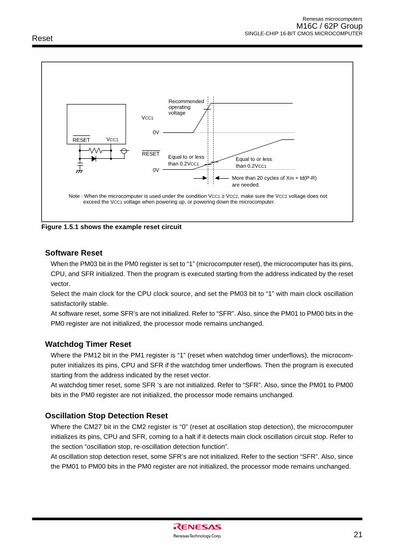
Reset
21
Renesas microcomputers
M16C / 62P Group SINGLE-CHIP 16-BIT CMOS MICROCOMPUTER
R
E
S
E
T VC
C
1
R
E
S
E
T
VC
C
1
0 V
0 V
M
o
r
e
t
h
a
n
2
0
c
y
c
l
e
s
o
f
XI
N
+
t
d
(
P
-
R
)
a
r
e
n
e
e
d
e
d
.
E
q
u
a
l
t
o
o
r
l
e
s
s
t
h
a
n
0
.
2
VC
C
1
N
o
t
e
:
W
h
e
n
t
h
e
m
i
c
r
o
c
o
m
p
u
t
e
r
i
s
u
s
e
d
u
n
d
e
r
t
h
e
c
o
n
d
i
t
i
o
n
VC
C
1
≥
VC
C
2,
m
a
k
e
s
u
r
e
t
h
e
VC
C
2
v
o
l
t
a
g
e
d
o
e
s
n
o
t
e
x
c
e
e
d
t
h
e
VC
C
1
v
o
l
t
a
g
e
w
h
e
n
p
o
w
e
r
i
n
g
u
p
,
o
r
p
o
w
e
r
i
n
g
d
o
w
n
t
h
e
m
i
c
r
o
c
o
m
p
u
t
e
r
.
E
q
u
a
l
t
o
o
r
l
e
s
s
t
h
a
n
0
.
2
VC
C
1
Re
c
o
m
m
e
n
d
e
d
o
p
e
r
a
t
i
n
gv
o
l
t
a
g
e
Figure 1.5.1 shows the example reset circuit
Software ResetWhen the PM03 bit in the PM0 register is set to “1” (microcomputer reset), the microcomputer has its pins,
CPU, and SFR initialized. Then the program is executed starting from the address indicated by the reset
vector.
Select the main clock for the CPU clock source, and set the PM03 bit to “1” with main clock oscillation
satisfactorily stable.
At software reset, some SFR’s are not initialized. Refer to “SFR”. Also, since the PM01 to PM00 bits in the
PM0 register are not initialized, the processor mode remains unchanged.
Watchdog Timer ResetWhere the PM12 bit in the PM1 register is “1” (reset when watchdog timer underflows), the microcom-
puter initializes its pins, CPU and SFR if the watchdog timer underflows. Then the program is executed
starting from the address indicated by the reset vector.
At watchdog timer reset, some SFR ’s are not initialized. Refer to “SFR”. Also, since the PM01 to PM00
bits in the PM0 register are not initialized, the processor mode remains unchanged.
Oscillation Stop Detection ResetWhere the CM27 bit in the CM2 register is “0” (reset at oscillation stop detection), the microcomputer
initializes its pins, CPU and SFR, coming to a halt if it detects main clock oscillation circuit stop. Refer to
the section “oscillation stop, re-oscillation detection function”.
At oscillation stop detection reset, some SFR’s are not initialized. Refer to the section “SFR”. Also, since
the PM01 to PM00 bits in the PM0 register are not initialized, the processor mode remains unchanged.
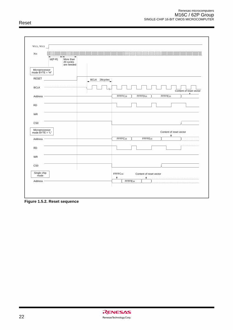
Reset
22
Renesas microcomputers
M16C / 62P Group SINGLE-CHIP 16-BIT CMOS MICROCOMPUTER
td(P-R) More than20 cyclesare needed
BCLK
Address
Address
Address
Microprocessor mode BYTE = “H”
Microprocessor mode BYTE = “L”
Single chip mode
XIN
RESET
RD
WR
CS0
RD
WR
CS0
Content of reset vector
BCLK 28cycles
FFFFC16 FFFFD16 FFFFE16
Content of reset vector
FFFFC16 FFFFE16
Content of reset vector
FFFFE16
FFFFC16
VCC1, VCC2
Figure 1.5.2. Reset sequence
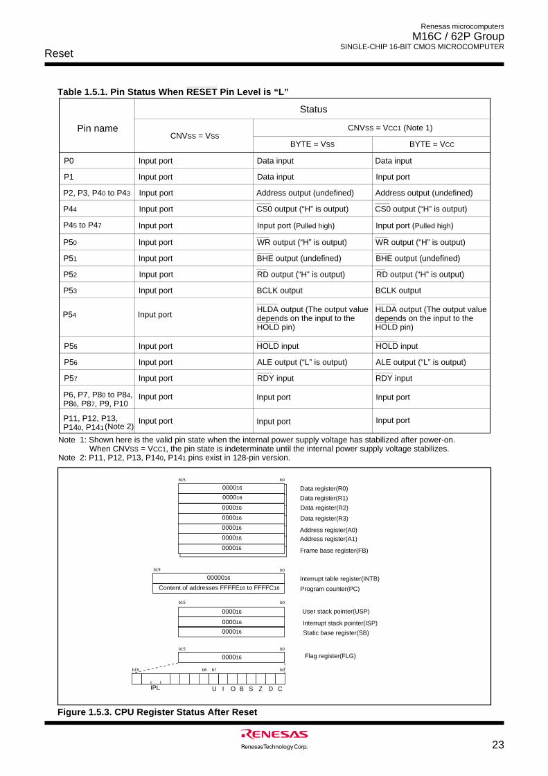
Reset
23
Renesas microcomputers
M16C / 62P Group SINGLE-CHIP 16-BIT CMOS MICROCOMPUTER
____________
Table 1.5.1. Pin Status When RESET Pin Level is “L”
Status
CNVSS = VCC1 (Note 1)CNVSS = VSS
BYTE = VSS BYTE = VCC
Pin name
P0
P1
P2, P3, P40 to P43
P44
P45 to P47
P50
P51
P52
P53
P54
P55
P56
P57
P6, P7, P80 to P84,P86, P87, P9, P10
Input port
Input port
Input port
Input port
Input port
Input port
Input port
Input port
Input port
Input port
Input port
Input port
Input port
Input port
Data input
Data input
Address output (undefined)
BCLK output
ALE output (“L” is output)
CS0 output (“H” is output)
WR output (“H” is output)
RD output (“H” is output)
RDY input
Input port
BCLK output
BHE output (undefined)
HLDA output (The output value depends on the input to the HOLD pin)
HOLD input
Data input
Address output (undefined)
CS0 output (“H” is output)
Input port (Pulled high)
Input port Input port
RDY input
ALE output (“L” is output)
HOLD input
HLDA output (The output value depends on the input to the HOLD pin)
RD output (“H” is output)
BHE output (undefined)
WR output (“H” is output)
P11, P12, P13,P140, P141
Input port Input port Input port (Note 2)
Note 1: Shown here is the valid pin state when the internal power supply voltage has stabilized after power-on. When CNVSS = VCC1, the pin state is indeterminate until the internal power supply voltage stabilizes. Note 2: P11, P12, P13, P140, P141 pins exist in 128-pin version.
Input port (Pulled high)
Figure 1.5.3. CPU Register Status After Reset
b15 b0
Data register(R0)
Address register(A0)
Frame base register(FB)
Program counter(PC)
Interrupt table register(INTB)
User stack pointer(USP)
Interrupt stack pointer(ISP)
Static base register(SB)
Flag register(FLG)
000016
000016
000016
AAAAAAAAAAAAAAA AAAAAAACDZSBOIUIPL
000016
000016
000016
000016
000016
b19 b0
Content of addresses FFFFE16 to FFFFC16
b15 b0
b15 b0
b15 b0 b7 b8
0000016
Data register(R1)
Data register(R2)
Data register(R3)
Address register(A1)
000016
000016
000016
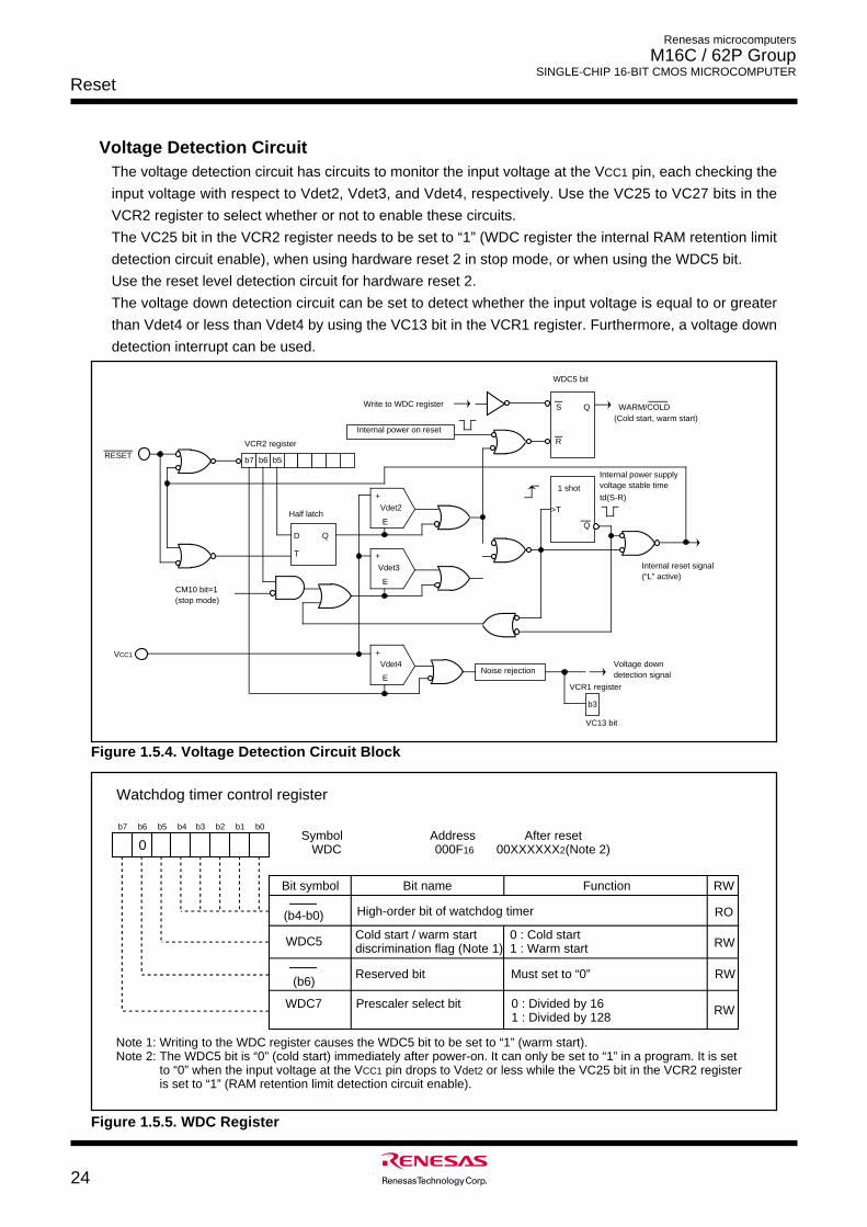
Reset
24
Renesas microcomputers
M16C / 62P Group SINGLE-CHIP 16-BIT CMOS MICROCOMPUTER
Voltage Detection CircuitThe voltage detection circuit has circuits to monitor the input voltage at the VCC1 pin, each checking the
input voltage with respect to Vdet2, Vdet3, and Vdet4, respectively. Use the VC25 to VC27 bits in the
VCR2 register to select whether or not to enable these circuits.
The VC25 bit in the VCR2 register needs to be set to “1” (WDC register the internal RAM retention limit
detection circuit enable), when using hardware reset 2 in stop mode, or when using the WDC5 bit.
Use the reset level detection circuit for hardware reset 2.
The voltage down detection circuit can be set to detect whether the input voltage is equal to or greater
than Vdet4 or less than Vdet4 by using the VC13 bit in the VCR1 register. Furthermore, a voltage down
detection interrupt can be used.
b7 b6 b5
VCR2 register RESET
CM10 bit=1(stop mode)
+
E
Vdet2
+ Vdet3
+ Vdet4
ENoise rejection
Voltage downdetection signal
b3
VCR1 register
VC13 bit
Internal power on reset
Write to WDC register S
R
Q WARM/COLD
>T
Q
1 shottd(S-R)
Internal reset signal (“L” active)
WDC5 bit
Internal power supply voltage stable time
E
(Cold start, warm start)
VCC1
T
D Q
Half latch
Figure 1.5.4. Voltage Detection Circuit Block
Watchdog timer control register
Symbol Address After reset WDC 000F16 00XXXXXX2(Note 2)
FunctionBit symbol RW
b7 b6 b5 b4 b3 b2 b1 b0
High-order bit of watchdog timer
WDC7
Bit name
Prescaler select bit 0 : Divided by 161 : Divided by 128
Reserved bit Must set to “0”
0
RO
RW
RW
RW
Cold start / warm start discrimination flag (Note 1)
0 : Cold start1 : Warm startWDC5
Note 1: Writing to the WDC register causes the WDC5 bit to be set to “1” (warm start).Note 2: The WDC5 bit is “0” (cold start) immediately after power-on. It can only be set to “1” in a program. It is set
to “0” when the input voltage at the VCC1 pin drops to Vdet2 or less while the VC25 bit in the VCR2 register is set to “1” (RAM retention limit detection circuit enable).
(b4-b0)
(b6)
Figure 1.5.5. WDC Register
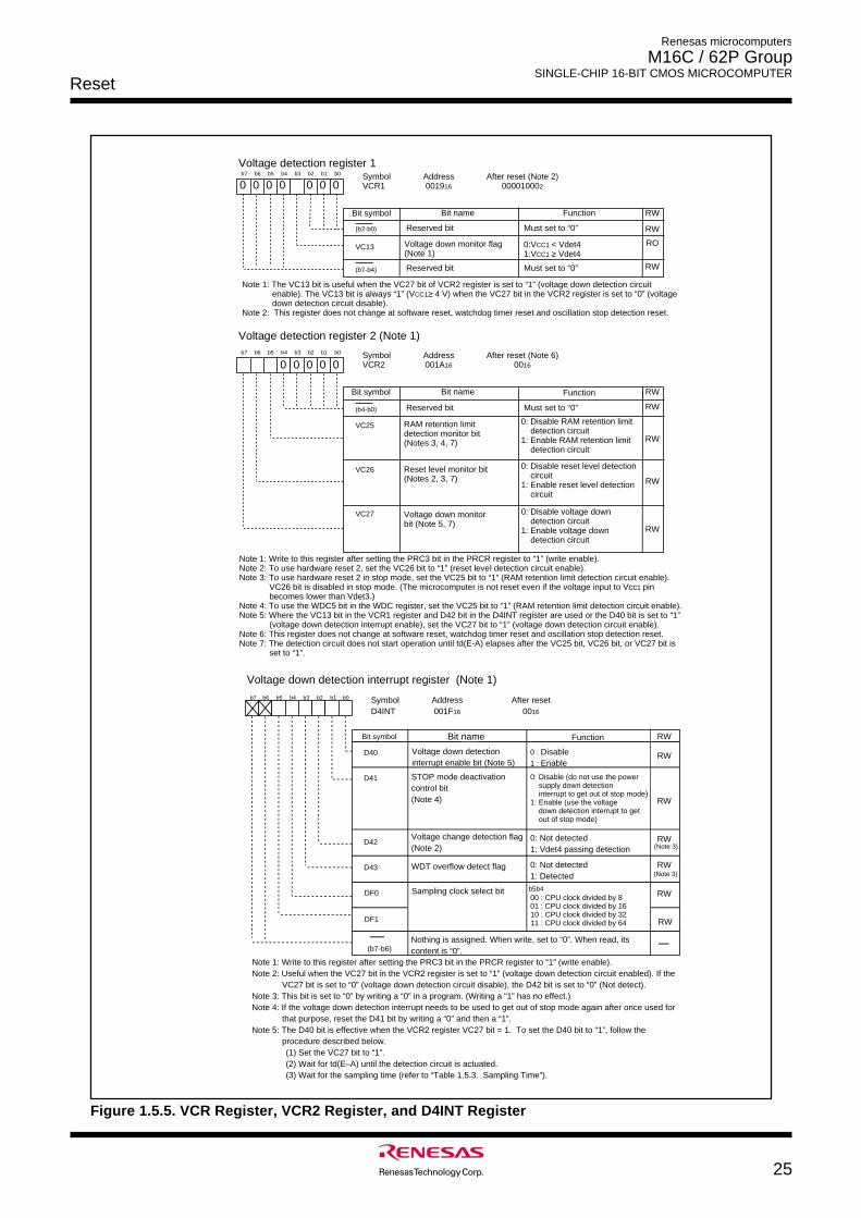
Reset
25
Renesas microcomputers
M16C / 62P Group SINGLE-CHIP 16-BIT CMOS MICROCOMPUTER
D40
Voltage down detection interrupt register (Note 1)
Symbol Address After reset D4INT 001F16 0016
Voltage down detection interrupt enable bit (Note 5)
Bit nameBit symbol
b7 b6 b5 b4 b3 b2 b1 b0
0 : Disable1 : Enable
D41 STOP mode deactivation control bit(Note 4)
0: Disable (do not use the power supply down detection interrupt to get out of stop mode)1: Enable (use the voltage down detection interrupt to get out of stop mode)
D42Voltage change detection flag (Note 2)
0: Not detected1: Vdet4 passing detection
D43 WDT overflow detect flag 0: Not detected1: Detected
DF0 Sampling clock select bit00 : CPU clock divided by 801 : CPU clock divided by 1610 : CPU clock divided by 3211 : CPU clock divided by 64DF1
Note 1: Write to this register after setting the PRC3 bit in the PRCR register to “1” (write enable).Note 2: Useful when the VC27 bit in the VCR2 register is set to “1” (voltage down detection circuit enabled). If the
VC27 bit is set to “0” (voltage down detection circuit disable), the D42 bit is set to “0” (Not detect). Note 3: This bit is set to “0” by writing a “0” in a program. (Writing a “1” has no effect.) Note 4: If the voltage down detection interrupt needs to be used to get out of stop mode again after once used for
that purpose, reset the D41 bit by writing a “0” and then a “1”. Note 5: The D40 bit is effective when the VCR2 register VC27 bit = 1. To set the D40 bit to “1”, follow the
procedure described below. (1) Set the VC27 bit to “1”. (2) Wait for td(E–A) until the detection circuit is actuated. (3) Wait for the sampling time (refer to “Table 1.5.3. Sampling Time”).
b5b4
RW
RW
RW
RW(Note 3)
RW
RW
RW
(b7-b6)
Function
(Note 3)
Nothing is assigned. When write, set to “0”. When read, its content is “0”.
V
C
1
3
V
o
l
t
a
g
e
d
e
t
e
c
t
i
o
n
r
e
g
i
s
t
e
r
1S
y
m
b
o
l A
d
d
r
e
s
s A
f
t
e
r
r
e
s
e
t
(
N
o
t
e
2
)
V
C
R
1 0
0
1
91
6 0
0
0
0
1
0
0
02
Voltage down monitor flag (Note 1)
Bit name FunctionB
i
t
s
y
m
b
o
l R
W
b 7 b
6 b
5 b
4 b
3 b
2 b
1 b
0
N
o
t
e
1
:
T
h
e
V
C
1
3
b
i
t
i
s
u
s
e
f
u
l
w
h
e
n
t
h
e
V
C
2
7
b
i
t
o
f
V
C
R
2
r
e
g
i
s
t
e
r
i
s
s
e
t
t
o
“
1
”
(
v
o
l
t
a
g
e
d
o
w
n
d
e
t
e
c
t
i
o
n
c
i
r
c
u
i
t
e
n
a
b
l
e
)
.
T
h
e
V
C
1
3
b
i
t
i
s
a
l
w
a
y
s
“
1
”
(
VC
C
1≥
4
V
)
w
h
e
n
t
h
e
V
C
2
7
b
i
t
i
n
t
h
e
V
C
R
2
r
e
g
i
s
t
e
r
i
s
s
e
t
t
o
“
0
”
(
v
o
l
t
a
g
e
d
o
w
n
d
e
t
e
c
t
i
o
n
c
i
r
c
u
i
t
d
i
s
a
b
l
e
)
.N
o
t
e
2
:
T
h
i
s
r
e
g
i
s
t
e
r
d
o
e
s
n
o
t
c
h
a
n
g
e
a
t
s
o
f
t
w
a
r
e
r
e
s
e
t
,
w
a
t
c
h
d
o
g
t
i
m
e
r
r
e
s
e
t
a
n
d
o
s
c
i
l
l
a
t
i
o
n
s
t
o
p
d
e
t
e
c
t
i
o
n
r
e
s
e
t
.
0 :
VC
C
1
<
V
d
e
t
4
1
:
VC
C
1
≥
V
d
e
t
4R
O
0 0 0 0 0 0 0
R
W
R
W
R
e
s
e
r
v
e
d
b
i
t
R
e
s
e
r
v
e
d
b
i
t
M
u
s
t
s
e
t
t
o
“
0
”
M
u
s
t
s
e
t
t
o
“
0
”
V
o
l
t
a
g
e
d
e
t
e
c
t
i
o
n
r
e
g
i
s
t
e
r
2
(
N
o
t
e
1
)
S
y
m
b
o
l A
d
d
r
e
s
s A
f
t
e
r
r
e
s
e
t
(
N
o
t
e
6
)
V
C
R
2 0
0
1
A1
6 0
01
6
Bit nameB
i
t
s
y
m
b
o
l
b 7 b
6 b
5 b
4 b
3 b
2 b
1 b
0
N
o
t
e
1
:
W
r
i
t
e
t
o
t
h
i
s
r
e
g
i
s
t
e
r
a
f
t
e
r
s
e
t
t
i
n
g
t
h
e
P
R
C
3
b
i
t
i
n
t
h
e
P
R
C
R
r
e
g
i
s
t
e
r
t
o
“
1
”
(
w
r
i
t
e
e
n
a
b
l
e
)
.N
o
t
e
2
:
T
o
u
s
e
h
a
r
d
w
a
r
e
r
e
s
e
t
2
,
s
e
t
t
h
e
V
C
2
6
b
i
t
t
o
“
1
”
(
r
e
s
e
t
l
e
v
e
l
d
e
t
e
c
t
i
o
n
c
i
r
c
u
i
t
e
n
a
b
l
e
)
.
N
o
t
e
3
:
T
o
u
s
e
h
a
r
d
w
a
r
e
r
e
s
e
t
2
i
n
s
t
o
p
m
o
d
e
,
s
e
t
t
h
e
V
C
2
5
b
i
t
t
o
“
1
”
(
R
A
M
r
e
t
e
n
t
i
o
n
l
i
m
i
t
d
e
t
e
c
t
i
o
n
c
i
r
c
u
i
t
e
n
a
b
l
e
)
.V
C
2
6
b
i
t
i
s
d
i
s
a
b
l
e
d
i
n
s
t
o
p
m
o
d
e
.
(
T
h
e
m
i
c
r
o
c
o
m
p
u
t
e
r
i
s
n
o
t
r
e
s
e
t
e
v
e
n
i
f
t
h
e
v
o
l
t
a
g
e
i
n
p
u
t
t
o
V
c
c1
p
i
n
b
e
c
o
m
e
s
l
o
w
e
r
t
h
a
n
V
d
e
t
3
.
)N
o
t
e
4
:
T
o
u
s
e
t
h
e
W
D
C
5
b
i
t
i
n
t
h
e
W
D
C
r
e
g
i
s
t
e
r
,
s
e
t
t
h
e
V
C
2
5
b
i
t
t
o
“
1
”
(
R
A
M
r
e
t
e
n
t
i
o
n
l
i
m
i
t
d
e
t
e
c
t
i
o
n
c
i
r
c
u
i
t
e
n
a
b
l
e
)
.
N
o
t
e
5
:
W
h
e
r
e
t
h
e
V
C
1
3
b
i
t
i
n
t
h
e
V
C
R
1
r
e
g
i
s
t
e
r
a
n
d
D
4
2
b
i
t
i
n
t
h
e
D
4
I
N
T
r
e
g
i
s
t
e
r
a
r
e
u
s
e
d
o
r
t
h
e
D
4
0
b
i
t
i
s
s
e
t
t
o
“
1
”
(
v
o
l
t
a
g
e
d
o
w
n
d
e
t
e
c
t
i
o
n
i
n
t
e
r
r
u
p
t
e
n
a
b
l
e
)
,
s
e
t
t
h
e
V
C
2
7
b
i
t
t
o
“
1
”
(
v
o
l
t
a
g
e
d
o
w
n
d
e
t
e
c
t
i
o
n
c
i
r
c
u
i
t
e
n
a
b
l
e
)
.N
o
t
e
6
:
T
h
i
s
r
e
g
i
s
t
e
r
d
o
e
s
n
o
t
c
h
a
n
g
e
a
t
s
o
f
t
w
a
r
e
r
e
s
e
t
,
w
a
t
c
h
d
o
g
t
i
m
e
r
r
e
s
e
t
a
n
d
o
s
c
i
l
l
a
t
i
o
n
s
t
o
p
d
e
t
e
c
t
i
o
n
r
e
s
e
t
.N
o
t
e
7
:
T
h
e
d
e
t
e
c
t
i
o
n
c
i
r
c
u
i
t
d
o
e
s
n
o
t
s
t
a
r
t
o
p
e
r
a
t
i
o
n
u
n
t
i
l
t
d
(
E
-
A
)
e
l
a
p
s
e
s
a
f
t
e
r
t
h
e
V
C
2
5
b
i
t
,
V
C
2
6
b
i
t
,
o
r
V
C
2
7
b
i
t
i
s
s
e
t
t
o
“
1
”
.
V
C
2
5 R
A
M
r
e
t
e
n
t
i
o
n
l
i
m
i
t
d
e
t
e
c
t
i
o
n
m
o
n
i
t
o
r
b
i
t(
N
o
t
e
s
3
,
4
,
7
)
0: Disable RAM retention limit detection circuit 1: Enable RAM retention limit detection circuit
V
C
2
6
VC27
R
W
R
W
RW
R
W
R
W
0 0 0 0 0
Function
R
e
s
e
r
v
e
d
b
i
t M
u
s
t
s
e
t
t
o
“
0
”
Reset level monitor bit (Notes 2, 3, 7)
0: Disable reset level detection circuit 1: Enable reset level detection circuit
Voltage down monitor bit (Note 5, 7)
0: Disable voltage down detection circuit 1: Enable voltage down detection circuit
( b
2
-
b
0
)
( b
7
-
b
4
)
( b
4
-
b
0
)
Figure 1.5.5. VCR Register, VCR2 Register, and D4INT Register
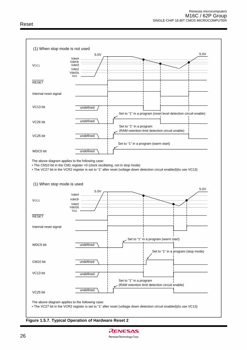
Reset
26
Renesas microcomputers
M16C / 62P Group SINGLE-CHIP 16-BIT CMOS MICROCOMPUTER
Vdet4
Vdet3
5.0V 5.0V
VCC1
Internal reset signal
VC13 bit
VC25 bit
Set to “1” in a program(RAM retention limit detection circuit enable)
(1) When stop mode is not used
5.0V5.0V
VCC1
WDC5 bit
VC13 bit
VC25 bit
Set to “1” in a program (warm start)
(1) When stop mode is used
Internal reset signal
CM10 bit
Set to “1” in a program (stop mode)
VSS
undefined
undefined
undefined
undefined
undefined
VC26 bit
Set to “1” in a program (reset level detection circuit enable)
undefined
undefined
RESET
Vdet4
Vdet3r
VSS
Vdet2
RESET
Vdet3r
Vdet3s
Vdet3s
Vdet2
WDC5 bit
Set to “1” in a program (warm start)
undefined
The above diagram applies to the following case:• The CM10 bit in the CM1 register =0 (clock oscillating, not in stop mode)• The VC27 bit in the VCR2 register is set to “1” after reset (voltage down detection circuit enabled)(to use VC13)
The above diagram applies to the following case:• The VC27 bit in the VCR2 register is set to “1” after reset (voltage down detection circuit enabled)(to use VC13)
Set to “1” in a program(RAM retention limit detection circuit enable)
Figure 1.5.7. Typical Operation of Hardware Reset 2
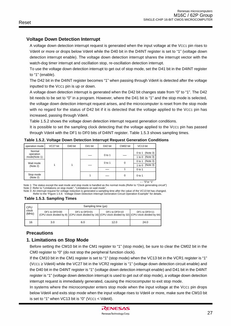
Reset
27
Renesas microcomputers
M16C / 62P Group SINGLE-CHIP 16-BIT CMOS MICROCOMPUTER
Voltage Down Detection InterruptA voltage down detection interrupt request is generated when the input voltage at the VCC1 pin rises to
Vdet4 or more or drops below Vdet4 while the D40 bit in the D4INT register is set to “1” (voltage down
detection interrupt enable). The voltage down detection interrupt shares the interrupt vector with the
watch-dog timer interrupt and oscillation stop, re-oscillation detection interrupt.
To use the voltage down detection interrupt to get out of stop mode, set the D41 bit in the D4INT register
to “1” (enable).
The D42 bit in the D4INT register becomes “1” when passing through Vdet4 is detected after the voltage
inputted to the VCC1 pin is up or down.
A voltage down detection interrupt is generated when the D42 bit changes state from “0” to “1”. The D42
bit needs to be set to “0” in a program. However, where the D41 bit is “1” and the stop mode is selected,
the voltage down detection interrupt request arises, and the microcomputer is reset from the stop mode
with no regard for the status of D42 bit if it is detected that the voltage applied to the VCC1 pin has
increased, passing through Vdet4.
Table 1.5.2 shows the voltage down detection interrupt request generation conditions.
It is possible to set the sampling clock detecting that the voltage applied to the VCC1 pin has passed
through Vdet4 with the DF1 to DF0 bits of D4INT register. Table 1.5.3 shows sampling times.
Table 1.5.2. Voltage Down Detection Interrupt Request Generation ConditionsD41 bitVC27 bitoperation mode D40 bit D42 bit CM02 bit VC13 bit
Normaloperation
mode(Note 1)
Wait mode(Note 2)
Stop mode(Note 2)
Note 1: The status except the wait mode and stop mode is handled as the normal mode.(Refer to “Clock generating circuit”)Note 2: Refer to “Limitations on stop mode”, “Limitations on wait mode”.Note 3: An interrupt request for voltage reduction is generated a sampling time after the value of the VC13 bit has changed. Refer to the “Figure 1.5.9. Voltage Down Detection Interrupt Generation Circuit Operation Example” for details.
0 to 1
10
1
1
0
1 to 0
0 to 1
1 to 0
0 to 1
0 to 1
0 to 1
0 to 1
1
(Note 3)
(Note 3)
(Note 3)
(Note 3)
– : “0”or “1”
Table 1.5.3. Sampling Times
Precautions
1. Limitations on Stop ModeBefore setting the CM10 bit in the CM1 register to “1” (stop mode), be sure to clear the CM02 bit in the
CM0 register to “0” (do not stop the peripheral function clock).
If the CM10 bit in the CM1 register is set to “1” (stop mode) when the VC13 bit in the VCR1 register is “1”
(VCC1 ≥ Vdet4) while the VC27 bit in the VCR2 register is “1” (voltage down detection circuit enable) and
the D40 bit in the D4INT register is “1” (voltage down detection interrupt enable) and D41 bit in the D4INT
register is “1” (voltage down detection interrupt is used to get out of stop mode), a voltage down detection
interrupt request is immediately generated, causing the microcomputer to exit stop mode.
In systems where the microcomputer enters stop mode when the input voltage at the VCC1 pin drops
below Vdet4 and exits stop mode when the input voltage rises to Vdet4 or more, make sure the CM10 bit
is set to “1” when VC13 bit is “0” (VCC1 < Vdet4).
CPUclock(MHz)
DF1 to DF0=00(CPU clock divided by 8)
Sampling time (µs)
16 3.0 6.0 12.0 24.0
DF1 to DF0=01(CPU clock divided by 16)
DF1 to DF0=10(CPU clock divided by 32)
DF1 to DF0=11(CPU clock divided by 64)
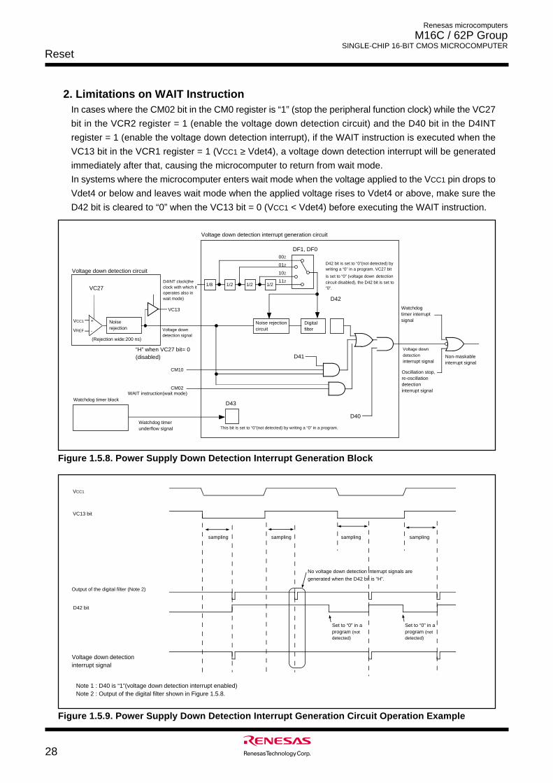
Reset
28
Renesas microcomputers
M16C / 62P Group SINGLE-CHIP 16-BIT CMOS MICROCOMPUTER
2. Limitations on WAIT InstructionIn cases where the CM02 bit in the CM0 register is “1” (stop the peripheral function clock) while the VC27
bit in the VCR2 register = 1 (enable the voltage down detection circuit) and the D40 bit in the D4INT
register = 1 (enable the voltage down detection interrupt), if the WAIT instruction is executed when the
VC13 bit in the VCR1 register = 1 (VCC1 ≥ Vdet4), a voltage down detection interrupt will be generated
immediately after that, causing the microcomputer to return from wait mode.
In systems where the microcomputer enters wait mode when the voltage applied to the VCC1 pin drops to
Vdet4 or below and leaves wait mode when the applied voltage rises to Vdet4 or above, make sure the
D42 bit is cleared to “0” when the VC13 bit = 0 (VCC1 < Vdet4) before executing the WAIT instruction.
Output of the digital filter (Note 2)
D42 bit
Note 1 : D40 is “1”(voltage down detection interrupt enabled)Note 2 : Output of the digital filter shown in Figure 1.5.8.
Voltage down detectioninterrupt signal
No voltage down detection interrupt signals are
generated when the D42 bit is “H”.
sampling
Set to “0” in a program (not detected)
VC13 bit
VCC1
sampling sampling sampling
Set to “0” in a program (not detected)
Voltage down detection interrupt generation circuit
Watchdog timer interrupt signal
D42 bit is set to “0”(not detected) by writing a “0” in a program. VC27 bit
is set to “0” (voltage down detection circuit disabled), the D42 bit is set to “0”.VC27
VC13
Voltage down detection circuit
D4INT clock(the clock with which it operates also in wait mode) D42
DF1, DF0
1/2
002
012
102
1121/21/21/8
Non-maskableinterrupt signal
Oscillation stop, re-oscillation detectioninterrupt signal
Voltage down detection interrupt signal
Watchdog timer block
This bit is set to “0”(not detected) by writing a “0” in a program.Watchdog timer underflow signal
D43
D41
CM02WAIT instruction(wait mode)
D40
VCC1
VREF
+
-
Noise rejection
(Rejection wide:200 ns)
Voltage down detection signal
“H” when VC27 bit= 0 (disabled)
Noise rejection circuit
Digitalfilter
CM10
Figure 1.5.8. Power Supply Down Detection Interrupt Generation Block
Figure 1.5.9. Power Supply Down Detection Interrupt Generation Circuit Operation Example
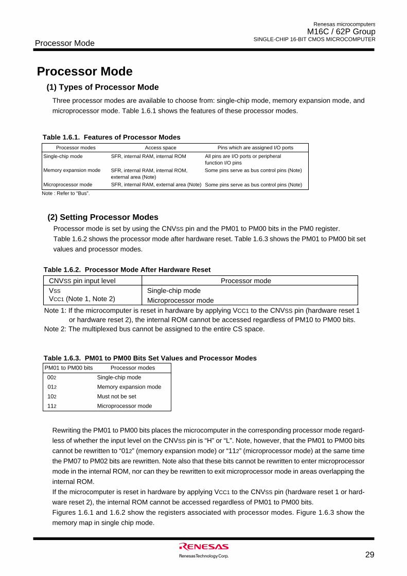
29
Renesas microcomputers
M16C / 62P Group SINGLE-CHIP 16-BIT CMOS MICROCOMPUTER
Processor Mode
Processor Mode(1) Types of Processor Mode
Three processor modes are available to choose from: single-chip mode, memory expansion mode, and
microprocessor mode. Table 1.6.1 shows the features of these processor modes.
(2) Setting Processor ModesProcessor mode is set by using the CNVSS pin and the PM01 to PM00 bits in the PM0 register.
Table 1.6.2 shows the processor mode after hardware reset. Table 1.6.3 shows the PM01 to PM00 bit set
values and processor modes.
Table 1.6.2. Processor Mode After Hardware Reset
Table 1.6.1. Features of Processor Modes Processor modes Access space Pins which are assigned I/O ports
Single-chip mode SFR, internal RAM, internal ROM All pins are I/O ports or peripheral function I/O pins
Memory expansion mode SFR, internal RAM, internal ROM,external area (Note)
Some pins serve as bus control pins (Note)
Microprocessor mode SFR, internal RAM, external area (Note) Some pins serve as bus control pins (Note)
Note : Refer to “Bus”.
CNVSS pin input level Processor modeVSS Single-chip modeVCC1 (Note 1, Note 2) Microprocessor mode
Note 1: If the microcomputer is reset in hardware by applying VCC1 to the CNVSS pin (hardware reset 1 or hardware reset 2), the internal ROM cannot be accessed regardless of PM10 to PM00 bits.
Note 2: The multiplexed bus cannot be assigned to the entire CS space.
Table 1.6.3. PM01 to PM00 Bits Set Values and Processor ModesPM01 to PM00 bits Processor modes
Single-chip mode
Memory expansion mode
Must not be set
002
012
102
Microprocessor mode112
Rewriting the PM01 to PM00 bits places the microcomputer in the corresponding processor mode regard-
less of whether the input level on the CNVSS pin is “H” or “L”. Note, however, that the PM01 to PM00 bits
cannot be rewritten to “012” (memory expansion mode) or “112” (microprocessor mode) at the same time
the PM07 to PM02 bits are rewritten. Note also that these bits cannot be rewritten to enter microprocessor
mode in the internal ROM, nor can they be rewritten to exit microprocessor mode in areas overlapping the
internal ROM.
If the microcomputer is reset in hardware by applying VCC1 to the CNVSS pin (hardware reset 1 or hard-
ware reset 2), the internal ROM cannot be accessed regardless of PM01 to PM00 bits.
Figures 1.6.1 and 1.6.2 show the registers associated with processor modes. Figure 1.6.3 show the
memory map in single chip mode.
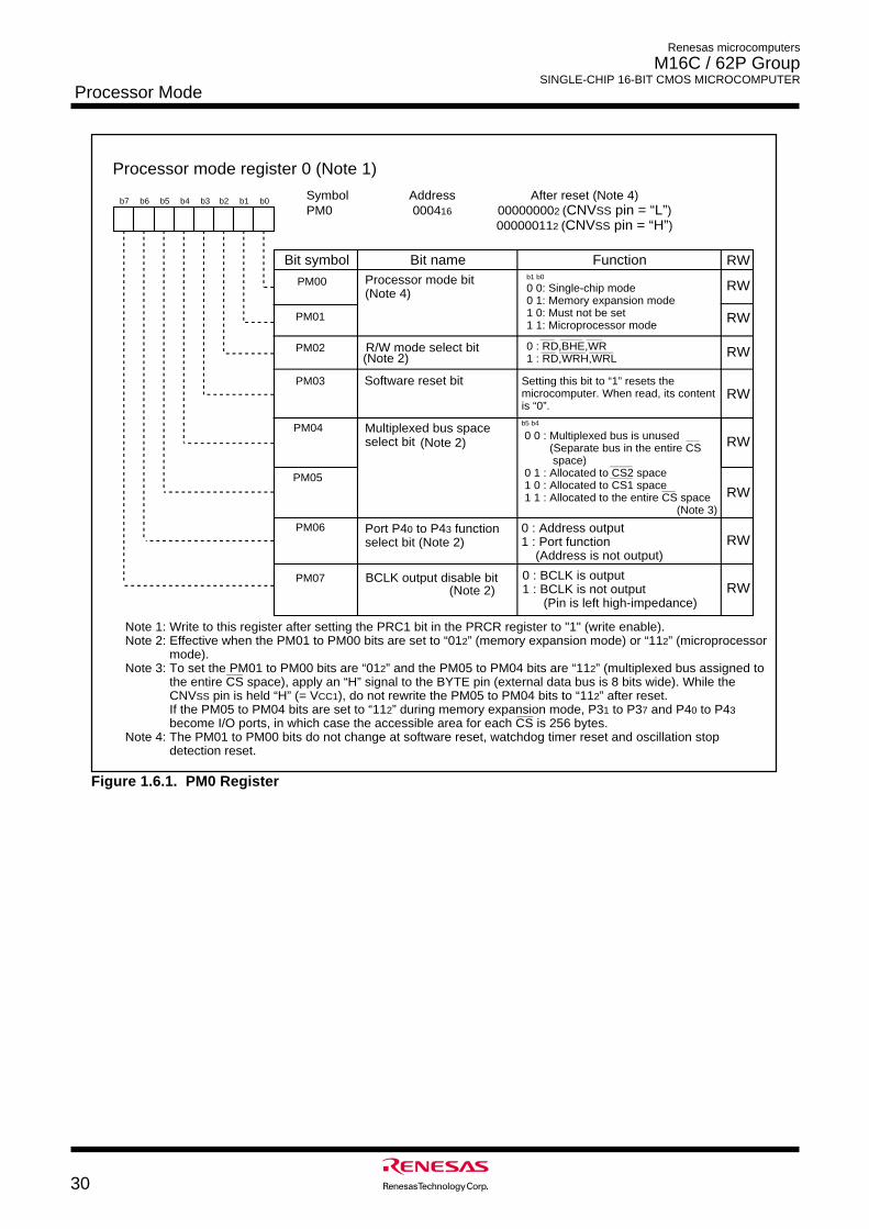
30
Renesas microcomputers
M16C / 62P Group SINGLE-CHIP 16-BIT CMOS MICROCOMPUTER
Processor Mode
Figure 1.6.1. PM0 Register
Processor mode register 0 (Note 1)
Symbol Address After reset (Note 4)PM0 000416 000000002 (CNVSS pin = “L”)
000000112 (CNVSS pin = “H”)
Bit name FunctionBit symbol RW
b7 b6 b5 b4 b3 b2 b1 b0
0 0: Single-chip mode0 1: Memory expansion mode1 0: Must not be set1 1: Microprocessor mode
b1 b0
PM03
PM01
PM00 Processor mode bit(Note 4)
PM02 R/W mode select bit 0 : RD,BHE,WR1 : RD,WRH,WRL
Software reset bit Setting this bit to “1” resets the microcomputer. When read, its content is “0”.
PM04 0 0 : Multiplexed bus is unused (Separate bus in the entire CS space)0 1 : Allocated to CS2 space1 0 : Allocated to CS1 space1 1 : Allocated to the entire CS space
(Note 3)
b5 b4 Multiplexed bus space select bit
PM05
RW
RW
RW
RW
PM06
PM07
Port P40 to P43 function select bit (Note 2)
0 : Address output1 : Port function (Address is not output)
BCLK output disable bit 0 : BCLK is output1 : BCLK is not output (Pin is left high-impedance)
Note 1: Write to this register after setting the PRC1 bit in the PRCR register to "1" (write enable).Note 2: Effective when the PM01 to PM00 bits are set to “012” (memory expansion mode) or “112” (microprocessor
mode).Note 3: To set the PM01 to PM00 bits are “012” and the PM05 to PM04 bits are “112” (multiplexed bus assigned to
the entire CS space), apply an “H” signal to the BYTE pin (external data bus is 8 bits wide). While the CNVSS pin is held “H” (= VCC1), do not rewrite the PM05 to PM04 bits to “112” after reset. If the PM05 to PM04 bits are set to “112” during memory expansion mode, P31 to P37 and P40 to P43 become I/O ports, in which case the accessible area for each CS is 256 bytes.
Note 4: The PM01 to PM00 bits do not change at software reset, watchdog timer reset and oscillation stop detection reset.
RW
RW
RW
RW
(Note 2)
(Note 2)
(Note 2)
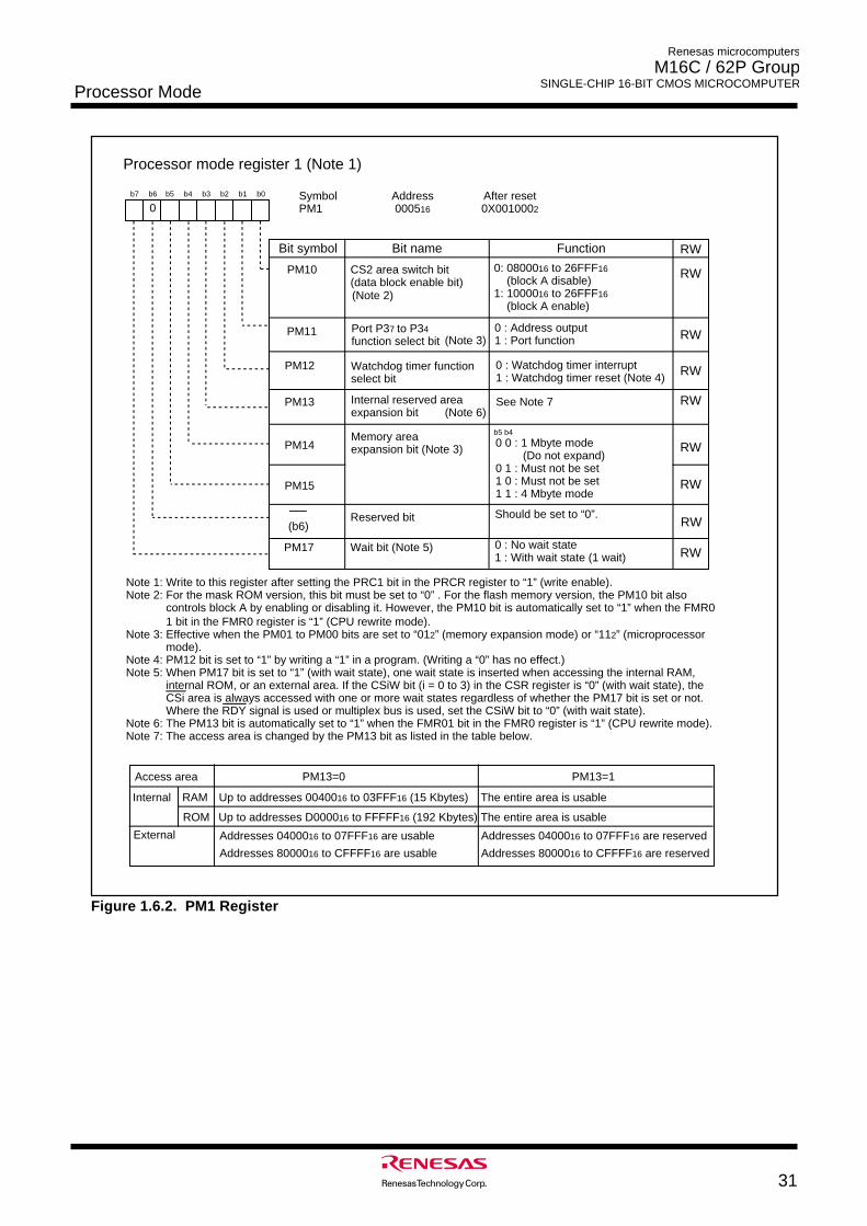
31
Renesas microcomputers
M16C / 62P Group SINGLE-CHIP 16-BIT CMOS MICROCOMPUTER
Processor Mode
Figure 1.6.2. PM1 Register
Processor mode register 1 (Note 1)
Symbol Address After resetPM1 000516 0X0010002
Bit name FunctionBit symbol RW
b7 b6 b5 b4 b3 b2 b1 b0
CS2 area switch bit(data block enable bit)
0: 0800016 to 26FFF16 (block A disable)1: 1000016 to 26FFF16 (block A enable)
PM10
(Note 2)
RW
Port P37 to P34 function select bit
Note 1: Write to this register after setting the PRC1 bit in the PRCR register to “1” (write enable).Note 2: For the mask ROM version, this bit must be set to “0” . For the flash memory version, the PM10 bit also
controls block A by enabling or disabling it. However, the PM10 bit is automatically set to “1” when the FMR01 bit in the FMR0 register is “1” (CPU rewrite mode).
Note 3: Effective when the PM01 to PM00 bits are set to “012” (memory expansion mode) or “112” (microprocessor mode).
Note 4: PM12 bit is set to “1” by writing a “1” in a program. (Writing a “0” has no effect.) Note 5: When PM17 bit is set to “1” (with wait state), one wait state is inserted when accessing the internal RAM,
internal ROM, or an external area. If the CSiW bit (i = 0 to 3) in the CSR register is “0” (with wait state), the CSi area is always accessed with one or more wait states regardless of whether the PM17 bit is set or not. Where the RDY signal is used or multiplex bus is used, set the CSiW bit to “0” (with wait state).
Note 6: The PM13 bit is automatically set to “1” when the FMR01 bit in the FMR0 register is “1” (CPU rewrite mode).Note 7: The access area is changed by the PM13 bit as listed in the table below.
PM17 Wait bit (Note 5) 0 : No wait state 1 : With wait state (1 wait)
Internal reserved area expansion bit
PM13 See Note 7
Should be set to “0”.
0 : Watchdog timer interrupt 1 : Watchdog timer reset (Note 4)
Watchdog timer function select bit
PM12
PM14
PM15
Memory area expansion bit (Note 3) 0 0 : 1 Mbyte mode
(Do not expand)0 1 : Must not be set1 0 : Must not be set1 1 : 4 Mbyte mode
b5 b4
PM11 (Note 3)
0 : Address output 1 : Port function RW
RW
RW
RW
RW
RW
(b6)
Access area
Internal RAM
ROM
Up to addresses 0040016 to 03FFF16 (15 Kbytes)
Up to addresses D000016 to FFFFF16 (192 Kbytes)
PM13=0 PM13=1
The entire area is usable
The entire area is usable
External Addresses 0400016 to 07FFF16 are usable
Addresses 8000016 to CFFFF16 are usable
Addresses 0400016 to 07FFF16 are reserved
Addresses 8000016 to CFFFF16 are reserved
Reserved bit RW
0
(Note 6)
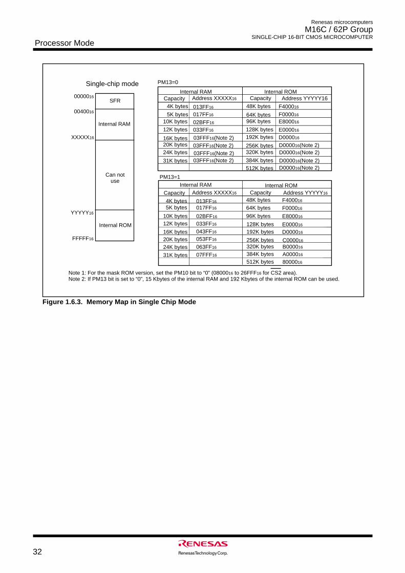
32
Renesas microcomputers
M16C / 62P Group SINGLE-CHIP 16-BIT CMOS MICROCOMPUTER
Processor Mode
Single-chip mode
SFR
Internal RAM
Can not use
Internal ROM
0000016
0040016
XXXXX16
YYYYY16
FFFFF16
Note 1: For the mask ROM version, set the PM10 bit to “0” (0800016 to 26FFF16 for CS2 area). Note 2: If PM13 bit is set to “0”, 15 Kbytes of the internal RAM and 192 Kbytes of the internal ROM can be used.
PM13=0
PM13=1
Capacity Address YYYYY16
128K bytes E000016
256K bytes D000016(Note 2)
Capacity Address XXXXX16
12K bytes 033FF16
20K bytes 03FFF16(Note 2)
10K bytes 02BFF16
24K bytes 03FFF16(Note 2)384K bytes D000016(Note 2)512K bytes D000016(Note 2)
Internal RAM Internal ROM
4K bytes 013FF16
5K bytes 017FF16
31K bytes 03FFF16(Note 2)
48K bytes F400016
64K bytes F000016
96K bytes E800016
192K bytes D000016
320K bytes D000016(Note 2)
128K bytes E000016
256K bytes C000016
12K bytes 033FF16
20K bytes 053FF16
10K bytes 02BFF16
24K bytes 063FF16
384K bytes A000016
512K bytes 8000016
Internal RAM Internal ROM
4K bytes 013FF16
5K bytes 017FF16
31K bytes 07FFF16
48K bytes F400016
64K bytes F000016
96K bytes E800016
192K bytes D000016
320K bytes B000016
16K bytes 043FF16
16K bytes 03FFF16(Note 2)
Capacity Capacity Address YYYYY16Address XXXXX16
Figure 1.6.3. Memory Map in Single Chip Mode
Bus
33
Renesas microcomputers
M16C / 62P Group SINGLE-CHIP 16-BIT CMOS MICROCOMPUTER
BusDuring memory expansion or microprocessor mode, some pins serve as the bus control pins to perform
_______
data input/output to and from external devices. These bus control pins include A0 to A19, D0 to D15, CS0_______ _____ ________ ______ ________ ________ ________ __________ _________
to CS3, RD, WRL/WR, WRH/BHE, ALE, RDY, HOLD, HLDA and BCLK.
Bus Mode
The bus mode, either multiplexed or separate, can be selected using the PM05 to PM04 bits in the PM0
register.
Separate Bus
In this bus mode, data and address are separate.
Multiplexed Bus
In this bus mode, data and address are multiplexed.
• When the input level on BYTE pin is high (8-bit data bus)
D0 to D7 and A0 to A7 are multiplexed.
• When the input level on BYTE pin is low (16-bit data bus)
D0 to D7 and A1 to A8 are multiplexed. D8 to D15 are not multiplexed. Do not use D8 to D15.
External buses connecting to a multiplexed bus are allocated to only the even addresses of the micro-
computer. Odd addresses cannot be accessed.
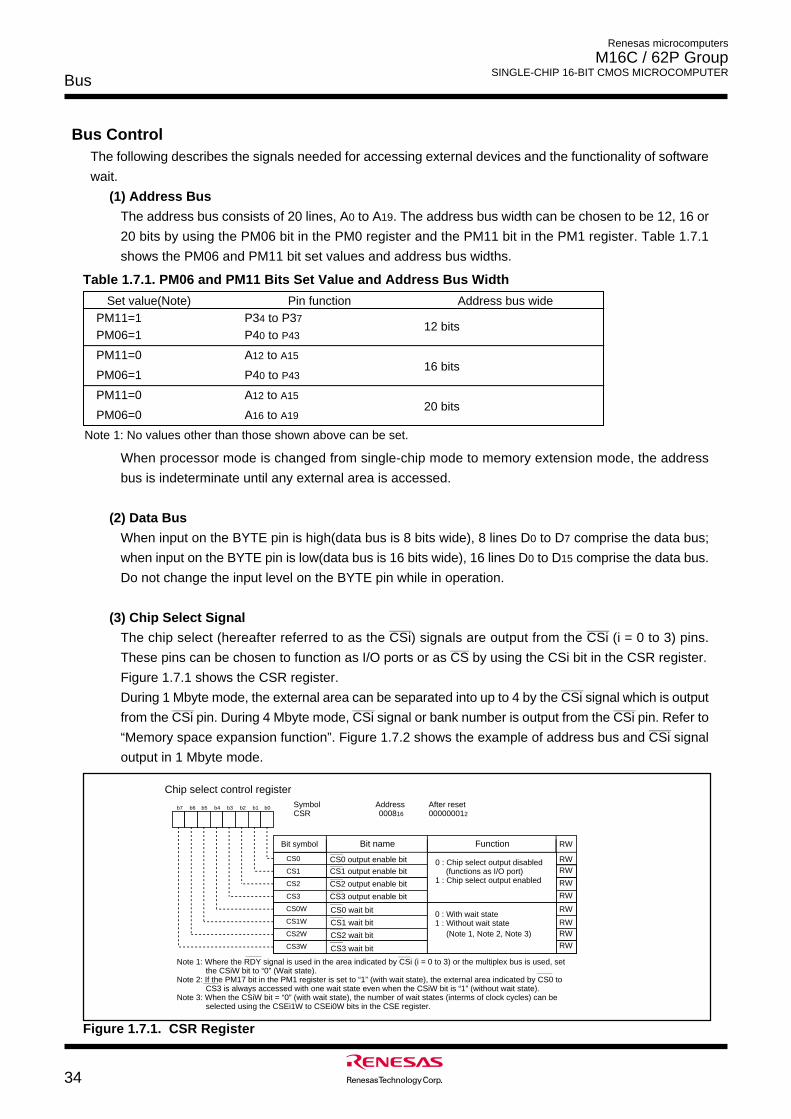
Bus
34
Renesas microcomputers
M16C / 62P Group SINGLE-CHIP 16-BIT CMOS MICROCOMPUTER
FunctionBit symbol Bit name
Chip select control registerSymbol Address After reset CSR 000816 000000012
RW
b7 b6 b5 b4 b3 b2 b1 b0
CS1
CS0
CS3
CS2
CS0 output enable bit
CS1 output enable bit
CS2 output enable bit
CS3 output enable bit
CS1W
CS0W
CS3W
CS2W
CS0 wait bit
CS1 wait bit
CS2 wait bit
CS3 wait bit
0 : Chip select output disabled(functions as I/O port)
1 : Chip select output enabled
0 : With wait state1 : Without wait state
RWRW
RW
RW
RW
RWRW
RW
(Note 1, Note 2, Note 3)
Note 1: Where the RDY signal is used in the area indicated by CSi (i = 0 to 3) or the multiplex bus is used, set the CSiW bit to “0” (Wait state).
Note 2: If the PM17 bit in the PM1 register is set to “1” (with wait state), the external area indicated by CS0 to CS3 is always accessed with one wait state even when the CSiW bit is “1” (without wait state).
Note 3: When the CSiW bit = “0” (with wait state), the number of wait states (interms of clock cycles) can be selected using the CSEi1W to CSEi0W bits in the CSE register.
Figure 1.7.1. CSR Register
Bus ControlThe following describes the signals needed for accessing external devices and the functionality of software
wait.
(1) Address Bus
The address bus consists of 20 lines, A0 to A19. The address bus width can be chosen to be 12, 16 or
20 bits by using the PM06 bit in the PM0 register and the PM11 bit in the PM1 register. Table 1.7.1
shows the PM06 and PM11 bit set values and address bus widths.
When processor mode is changed from single-chip mode to memory extension mode, the address
bus is indeterminate until any external area is accessed.
(2) Data Bus
When input on the BYTE pin is high(data bus is 8 bits wide), 8 lines D0 to D7 comprise the data bus;
when input on the BYTE pin is low(data bus is 16 bits wide), 16 lines D0 to D15 comprise the data bus.
Do not change the input level on the BYTE pin while in operation.
(3) Chip Select Signal______ ______
The chip select (hereafter referred to as the CSi) signals are output from the CSi (i = 0 to 3) pins._____
These pins can be chosen to function as I/O ports or as CS by using the CSi bit in the CSR register.
Figure 1.7.1 shows the CSR register.______
During 1 Mbyte mode, the external area can be separated into up to 4 by the CSi signal which is output______ ______ ______
from the CSi pin. During 4 Mbyte mode, CSi signal or bank number is output from the CSi pin. Refer to______
“Memory space expansion function”. Figure 1.7.2 shows the example of address bus and CSi signal
output in 1 Mbyte mode.
Set value(Note) Pin functionPM11=1 P34 to P37
Address bus wide
12 bitsPM06=1 P40 to P43
PM11=0 A12 to A1516 bits
PM06=1 P40 to P43
PM11=0 A12 to A1520 bits
PM06=0 A16 to A19
Note 1: No values other than those shown above can be set.
Table 1.7.1. PM06 and PM11 Bits Set Value and Address Bus Width
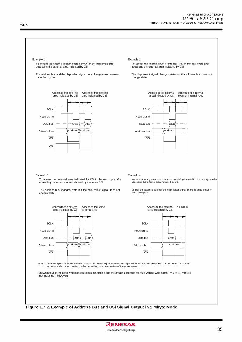
Bus
35
Renesas microcomputers
M16C / 62P Group SINGLE-CHIP 16-BIT CMOS MICROCOMPUTER
______
Figure 1.7.2. Example of Address Bus and CSi Signal Output in 1 Mbyte Mode
Example 1
BCLK
Read signal
Data bus
Address bus
CSi
Access to the external area indicated by CSi
Access to the external area indicated by CSj
Address
Data
CSj
Data
BCLK
Read signal
Data bus
Address bus
CSi
Access to the external area indicated by CSi
Access to the internal ROM or internal RAM
Address
Data
BCLK
Read signal
Data bus
Address bus
CSi
Access to the external area indicated by CSi
Access to the same external area
Address
Data Data
BCLK
Read signal
Data bus
Address bus
CSi
Access to the external area indicated by CSi
No access
Address
Data
Address
Address
Shown above is the case where separate bus is selected and the area is accessed for read without wait states. i = 0 to 3, j = 0 to 3(not including i, however)
To access the external area indicated by CSj in the next cycle after accessing the external area indicated by CSi
The address bus and the chip select signal both change state between these two cycles.
Example 2
To access the internal ROM or internal RAM in the next cycle after accessing the external area indicated by CSi
The chip select signal changes state but the address bus does not change state
Example 4
Not to access any area (nor instruction prefetch generated) in the next cycle after accessing the external area indicated by CSi
Neither the address bus nor the chip select signal changes state between these two cycles
Example 3
To access the external area indicated by CSi in the next cycle after accessing the external area indicated by the same CSi
The address bus changes state but the chip select signal does not change state
Note : These examples show the address bus and chip select signal when accessing areas in two successive cycles. The chip select bus cycle may be extended more than two cycles depending on a combination of these examples.
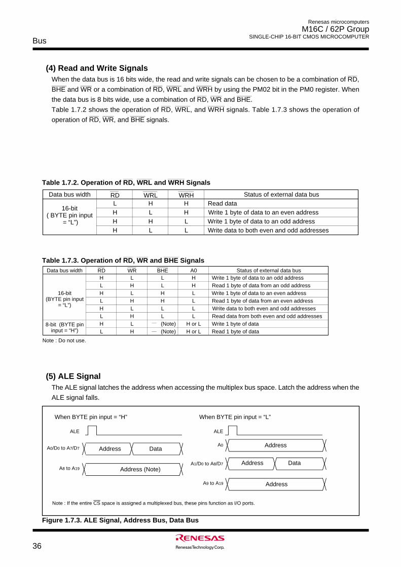
Bus
36
Renesas microcomputers
M16C / 62P Group SINGLE-CHIP 16-BIT CMOS MICROCOMPUTER
_____ ______ ________
Table 1.7.3. Operation of RD, WR and BHE SignalsStatus of external data busRD BHEWR
H L LL H LH L HL H H
Write 1 byte of data to an odd addressRead 1 byte of data from an odd addressWrite 1 byte of data to an even addressRead 1 byte of data from an even address
Data bus width A0HHLL
H L L LL H L LH L H or LL H H or L
8-bit (BYTE pin input = “H”)
Write data to both even and odd addressesRead data from both even and odd addressesWrite 1 byte of dataRead 1 byte of data
16-bit (BYTE pin input
= “L”)
(Note)(Note)
Note : Do not use.
Status of external data busRead dataWrite 1 byte of data to an even addressWrite 1 byte of data to an odd addressWrite data to both even and odd addresses
WRHWRLRDData bus width
16-bit ( BYTE pin input
= “L”)
HHH
HLHL
HHLL
L
_____ ________ _________
Table 1.7.2. Operation of RD, WRL and WRH Signals
(4) Read and Write Signals_____
When the data bus is 16 bits wide, the read and write signals can be chosen to be a combination of RD,________ ______ _____ ________ ________
BHE and WR or a combination of RD, WRL and WRH by using the PM02 bit in the PM0 register. When_____ ______ ________
the data bus is 8 bits wide, use a combination of RD, WR and BHE._____ ________ _________
Table 1.7.2 shows the operation of RD, WRL, and WRH signals. Table 1.7.3 shows the operation of_____ ______ ________
operation of RD, WR, and BHE signals.
(5) ALE SignalThe ALE signal latches the address when accessing the multiplex bus space. Latch the address when the
ALE signal falls.
When BYTE pin input = “H” When BYTE pin input = “L”
ALE
Address Data
Address (Note)
A0/D0 to A7/D7
A8 to A19
ALE
Address Data
Address
A1/D0 to A8/D7
A9 to A19
Address A0
Note : If the entire CS space is assigned a multiplexed bus, these pins function as I/O ports.
Figure 1.7.3. ALE Signal, Address Bus, Data Bus
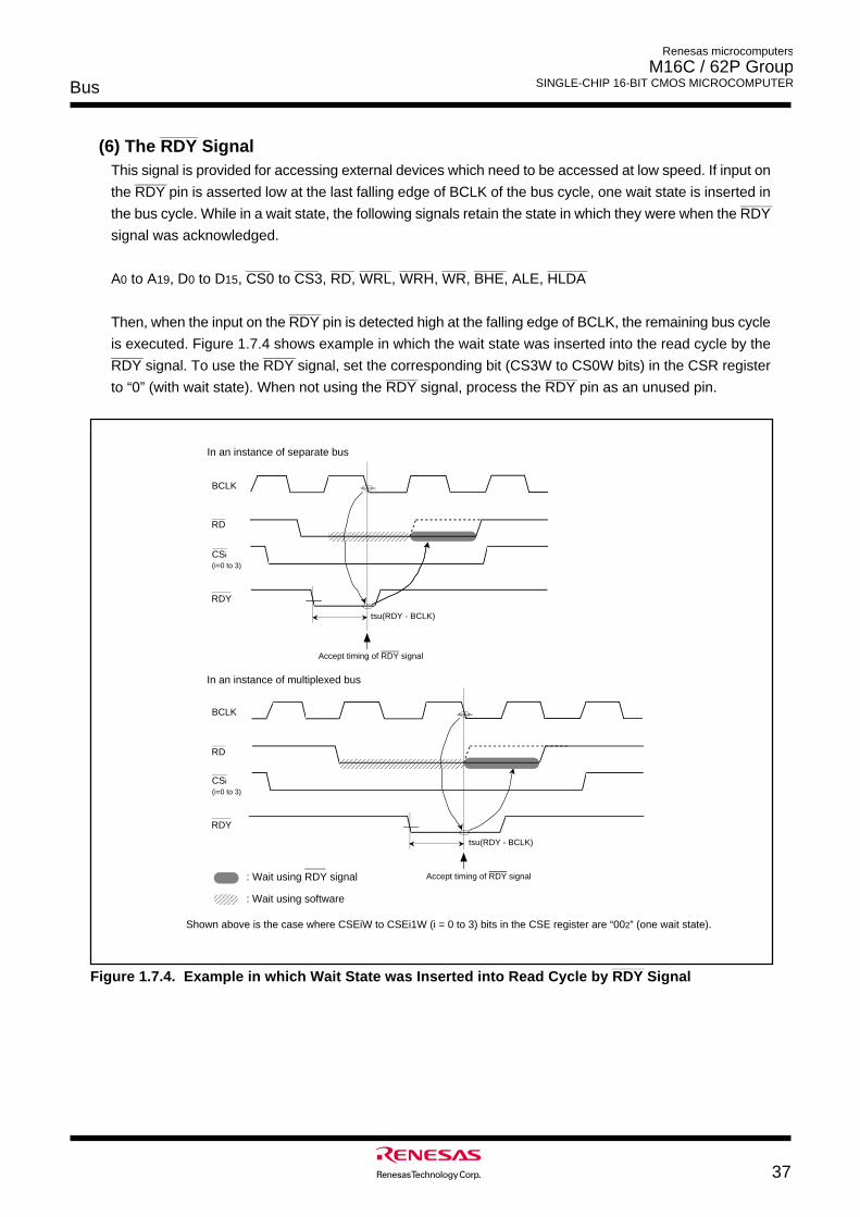
Bus
37
Renesas microcomputers
M16C / 62P Group SINGLE-CHIP 16-BIT CMOS MICROCOMPUTER
________
Figure 1.7.4. Example in which Wait State was Inserted into Read Cycle by RDY Signal
BCLK
RD
CSi(i=0 to 3)
RDY
tsu(RDY - BCLK)
AAAAA
BCLK
RD
CSi(i=0 to 3)
RDY
tsu(RDY - BCLK)
AAAAAA
AAAA
In an instance of separate bus
In an instance of multiplexed bus
Accept timing of RDY signal : Wait using RDY signal
: Wait using software
Accept timing of RDY signal
Shown above is the case where CSEiW to CSEi1W (i = 0 to 3) bits in the CSE register are “002” (one wait state).
________
(6) The RDY SignalThis signal is provided for accessing external devices which need to be accessed at low speed. If input on
________
the RDY pin is asserted low at the last falling edge of BCLK of the bus cycle, one wait state is inserted in________
the bus cycle. While in a wait state, the following signals retain the state in which they were when the RDY
signal was acknowledged.
______ ______ ______ ________ ________ ______ ________ __________
A0 to A19, D0 to D15, CS0 to CS3, RD, WRL, WRH, WR, BHE, ALE, HLDA
________
Then, when the input on the RDY pin is detected high at the falling edge of BCLK, the remaining bus cycle
is executed. Figure 1.7.4 shows example in which the wait state was inserted into the read cycle by the________ ________
RDY signal. To use the RDY signal, set the corresponding bit (CS3W to CS0W bits) in the CSR register________ ________
to “0” (with wait state). When not using the RDY signal, process the RDY pin as an unused pin.
Bus
38
Renesas microcomputers
M16C / 62P Group SINGLE-CHIP 16-BIT CMOS MICROCOMPUTER
Table 1.7.4. Microcomputer Status in Hold State
Item Status
BCLK Output_______ _______ _____ ________ _________ _______ _______
A0 to A19, D0 to D15, CS0 to CS3, RD, WRL, WRH, WR, BHE High-impedance
I/O ports P0, P1, P3, P4(Note 2) High-impedance
P6 to P14(Note 1) Maintains status when hold signal is received__________
HLDA Output “L”
Internal peripheral circuits ON (but watchdog timer stops)
ALE signal Undefined
__________
HOLD > DMAC > CPU
(7) Hold SignalThis signal is used to transfer control of the bus from the CPU or DMAC to an external circuit. When the
__________
input on HOLD pin is pulled low, the microcomputer is placed in a hold state after the bus access then in__________
process finishes. The microcomputer remains in the hold state while the HOLD pin is held low, during__________
which time the HLDA pin outputs a low-level signal.
Table 1.7.4 shows the microcomputer status in the hold state.__________
Bus-using priorities are given to HOLD, DMAC, and CPU in order of decreasing precedence. However,
if the CPU is accessing an odd address in word units, the DMAC cannot gain control of the bus during two
separate accesses.
Figure 1.7.5. Bus-using Priorities
Note 1: P11 to P14 are included in the 128-pin version.
Note 2: When I/O port function is selected.
Note 3: The watchdog timer dose not stop when the PM22 bit in the PM2 register is set to “1” (the count
source for the watchdog timer is the ring oscillator clock).
(8) BCLK Output If the PM07 bit in the PM0 register is set to “0” (output enable), a clock with the same frequency as that
of the CPU clock is output as BCLK from the BCLK pin. Refer to “CPU clock and pheripheral clock”.
Bus
39
Renesas microcomputers
M16C / 62P Group SINGLE-CHIP 16-BIT CMOS MICROCOMPUTER
Processor mode Memory expansion mode or microprocessor modeMemory expansionmode
002(separate bus)
PM05–PM04 bits
012(CS2 is for multiplexed bus and others are for separate bus)102(CS1 is for multiplexed bus and others are for separate bus)
Data bus width 8 bits “H”BYTE pin
P00 to P07 D0 to D7 D0 to D7 D0 to D7(Note 4) D0 to D7(Note 4) I/O ports
P10 to P17 I/O ports D8 to D15 I/O ports D8 to D15(Note 4) I/O ports
P20 A0 A0 A0/D0(Note 2) A0 A0/D0
P21 to P27 A1 to A7 A1 to A7 A1 to A7/D1 to D7(Note 2)
A1 to A7/D0 to D6(Note 2)
A1 to A7/D1 to D7
P30 A8 A8 A8 A8/D7(Note 2) A8
P31 to P33 A9 to A11 I/O ports
P34 to P37 A12 to A15
I/O ports
P40 to P43 A16 to A19
I/O ports
P44 I/O ports
P45
P46
P47
P50
WRL
P52 RD
P53 BCLK
P54 HLDA
P55 HOLDP56 ALE
P57 RDY
112(multiplexed bus for the entire space)(Note 1)
PM11=0
PM11=1
I/O ports
PM06=0
PM06=1
I/O ports
CS0=0
CS0=1 CS0
I/O portsCS1=0
CS1=1 CS1
I/O portsCS2=0
CS2=1 CS2
I/O portsCS3=0
CS3=1 CS3
PM02=0
PM02=1
WR
(Note 3) WRL(Note 3) (Note 3)
P51 BHE
WRH
PM02=0
PM02=1 (Note 3) WRH(Note 3) (Note 3)
Note 1: To set the PM01 to PM00 bits are set to “012” and the PM05 to PM04 bits are set to “112” (multiplexed bus assigned to the entire CS space), apply “H” to the BYTE pin (external data bus 8 bits wide). While the CNVSS pin is held “H” (= VCC1), do not rewrite the PM05 to PM04 bits to “112” after reset. If the PM05 to PM04 bits are set to “112” during memory expansion mode, P31 to P37 and P40 to P43become I/O ports, in which case the accessible area for each CS is 256 bytes.
Note 2: In separate bus mode, these pins serve as the address bus.Note 3: If the data bus is 8 bits wide, make sure the PM02 bit is set to “0” (RD, BHE, WR).Note 4: When accessing the area that uses a multiplexed bus, these pins output an indeterminate value during a write.
I/O ports: Function as I/O ports or peripheral function I/O pins.
8 bits “H”
8 bits “H”
16 bits “L”
16 bits “L”
Table 1.7.5. Pin Functions for Each Processor Mode
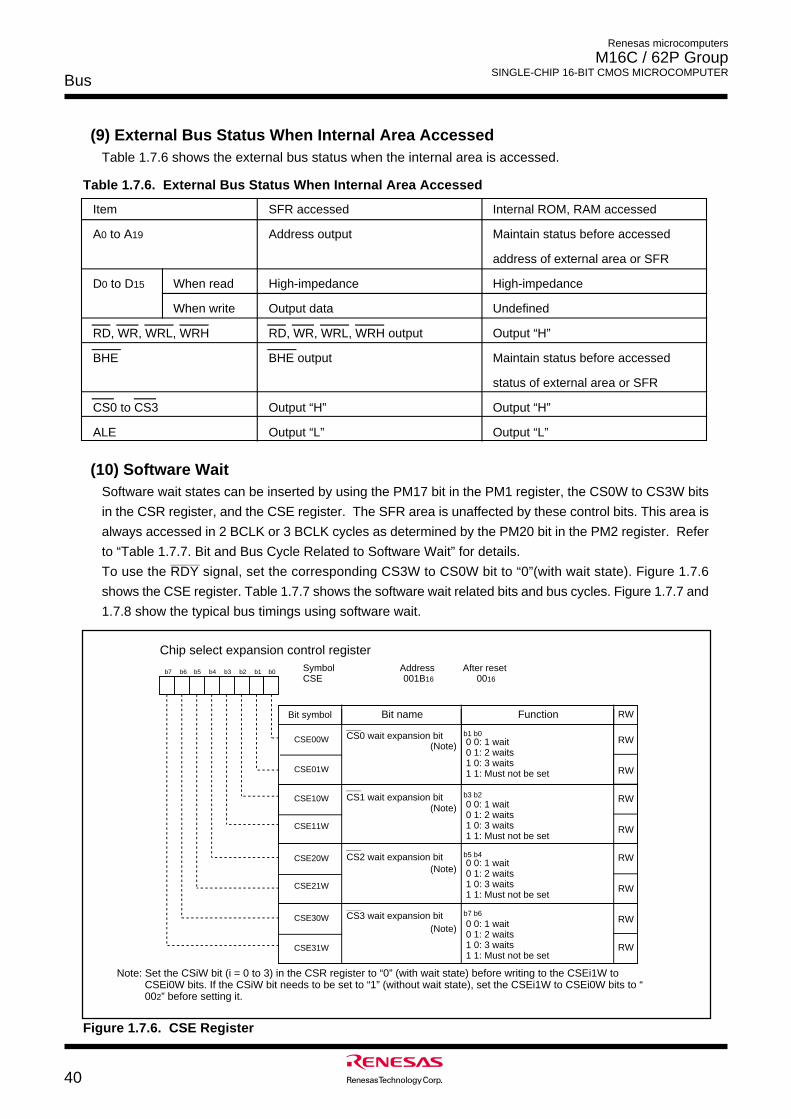
Bus
40
Renesas microcomputers
M16C / 62P Group SINGLE-CHIP 16-BIT CMOS MICROCOMPUTER
(10) Software WaitSoftware wait states can be inserted by using the PM17 bit in the PM1 register, the CS0W to CS3W bits
in the CSR register, and the CSE register. The SFR area is unaffected by these control bits. This area is
always accessed in 2 BCLK or 3 BCLK cycles as determined by the PM20 bit in the PM2 register. Refer
to “Table 1.7.7. Bit and Bus Cycle Related to Software Wait” for details.________
To use the RDY signal, set the corresponding CS3W to CS0W bit to “0”(with wait state). Figure 1.7.6
shows the CSE register. Table 1.7.7 shows the software wait related bits and bus cycles. Figure 1.7.7 and
1.7.8 show the typical bus timings using software wait.
(9) External Bus Status When Internal Area AccessedTable 1.7.6 shows the external bus status when the internal area is accessed.
Table 1.7.6. External Bus Status When Internal Area Accessed
Item SFR accessed Internal ROM, RAM accessed
A0 to A19 Address output Maintain status before accessed
address of external area or SFR
D0 to D15 When read High-impedance High-impedance
When write Output data Undefined
RD, WR, WRL, WRH RD, WR, WRL, WRH output Output “H”
BHE BHE output Maintain status before accessed
status of external area or SFR
CS0 to CS3 Output “H” Output “H”
ALE Output “L” Output “L”
Figure 1.7.6. CSE Register
FunctionBit symbol Bit name
Chip select expansion control registerSymbol Address After reset CSE 001B16 0016
RW
b7 b6 b5 b4 b3 b2 b1 b0
CSE00W CS0 wait expansion bit0 0: 1 wait0 1: 2 waits1 0: 3 waits1 1: Must not be set
b1 b0
CSE01W
(Note)
CSE10W CS1 wait expansion bit0 0: 1 wait0 1: 2 waits1 0: 3 waits1 1: Must not be set
b3 b2
CSE11W
(Note)
CSE20W CS2 wait expansion bit0 0: 1 wait0 1: 2 waits1 0: 3 waits1 1: Must not be set
b5 b4
CSE21W
(Note)
CSE30W CS3 wait expansion bit0 0: 1 wait0 1: 2 waits1 0: 3 waits1 1: Must not be set
b7 b6
CSE31W
(Note)
Note: Set the CSiW bit (i = 0 to 3) in the CSR register to “0” (with wait state) before writing to the CSEi1W to CSEi0W bits. If the CSiW bit needs to be set to “1” (without wait state), set the CSEi1W to CSEi0W bits to “002” before setting it.
RW
RW
RW
RW
RW
RW
RW
RW
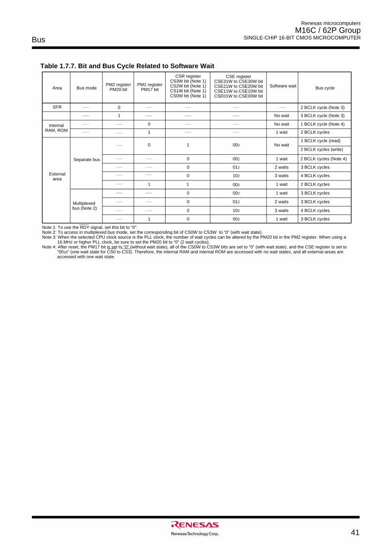
Bus
41
Renesas microcomputers
M16C / 62P Group SINGLE-CHIP 16-BIT CMOS MICROCOMPUTER
Bus modePM1 register
PM17 bit
CSE registerCSE31W to CSE30W bit CSE21W to CSE20W bit CSE11W to CSE10W bit CSE01W to CSE00W bit
Bus cycle
CSR registerCS3W bit (Note 1)CS2W bit (Note 1)CS1W bit (Note 1)CS0W bit (Note 1)
Area Software wait
Note 1: To use the RDY signal, set this bit to “0”. Note 2: To access in multiplexed bus mode, set the corresponding bit of CS0W to CS3W to “0” (with wait state).Note 3: When the selected CPU clock source is the PLL clock, the number of wait cycles can be altered by the PM20 bit in the PM2 register. When using a
16 MHZ or higher PLL clock, be sure to set the PM20 bit to “0” (2 wait cycles). Note 4: After reset, the PM17 bit is set to “0” (without wait state), all of the CS0W to CS3W bits are set to “0” (with wait state), and the CSE register is set to
“0016” (one wait state for CS0 to CS3). Therefore, the internal RAM and internal ROM are accessed with no wait states, and all external areas are accessed with one wait state.
Separate bus
Multiplexed bus (Note 2)
1
0
1
1
1
0
0
0
1
0
0
0
0
002
002
012
102
002
012
102
3 BCLK cycle (Note 3)
2 BCLK cycles
1 BCLK cycle (read)
2 BCLK cycles (write)
2 BCLK cycles (Note 4)
3 BCLK cycles
4 BCLK cycles
2 BCLK cycles
3 BCLK cycles
3 BCLK cycles
4 BCLK cycles
3 BCLK cycles
InternalRAM, ROM
External area
No wait
1 wait
No wait
1 wait
2 waits
3 waits
1 wait
1 wait
2 waits
3 waits
1 wait
002
002
2 BCLK cycle (Note 3)SFR
PM2 registerPM20 bit
0
1
0 1 BCLK cycle (Note 4)No wait
Table 1.7.7. Bit and Bus Cycle Related to Software Wait
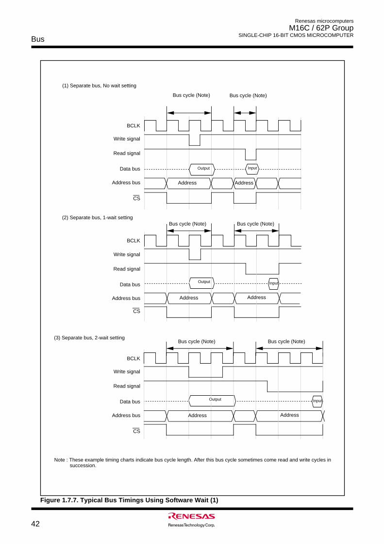
Bus
42
Renesas microcomputers
M16C / 62P Group SINGLE-CHIP 16-BIT CMOS MICROCOMPUTER
Figure 1.7.7. Typical Bus Timings Using Software Wait (1)
BCLK
Read signal
Write signal
Data bus
Address bus Address Address
Output Input
Address Address
Bus cycle (Note)
Bus cycle (Note)
(1) Separate bus, No wait setting
(2) Separate bus, 1-wait setting
Output Input
Note : These example timing charts indicate bus cycle length. After this bus cycle sometimes come read and write cycles in succession.
Bus cycle (Note)
Bus cycle (Note)
(3) Separate bus, 2-wait setting
Output
Address Address
Bus cycle (Note) Bus cycle (Note)
Input
BCLK
BCLK
CS
Read signal
Write signal
Data bus
Address bus
CS
CS
Read signal
Write signal
Data bus
Address bus
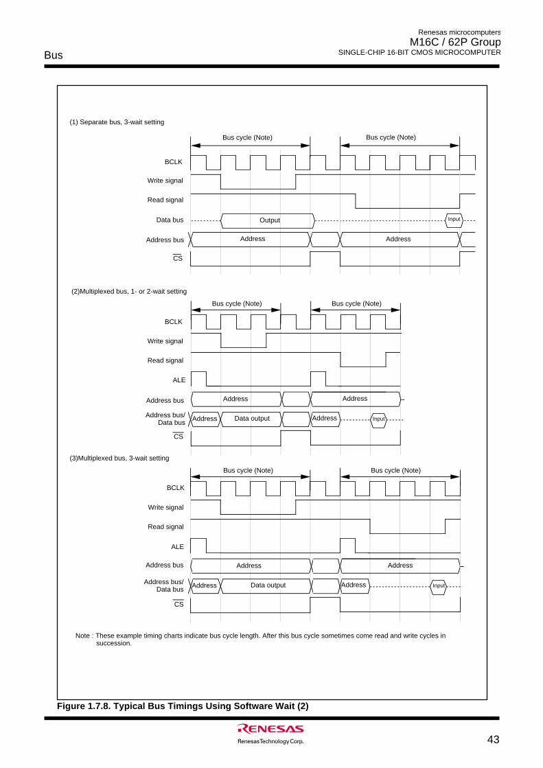
Bus
43
Renesas microcomputers
M16C / 62P Group SINGLE-CHIP 16-BIT CMOS MICROCOMPUTER
Figure 1.7.8. Typical Bus Timings Using Software Wait (2)
Address
Address
Data output
Address
Address Input
Bus cycle (Note)
Bus cycle (Note)
(1) Separate bus, 3-wait setting
Read signal
Write signal
Address bus/Data bus
CS
Address bus
ALE
(3)Multiplexed bus, 3-wait setting
Output
Note : These example timing charts indicate bus cycle length. After this bus cycle sometimes come read and write cycles in succession.
Bus cycle (Note)
Bus cycle (Note)
Input
Address
Address
Address bus/Data bus Address
Address
Data output
Address
Address Input
ALE
Bus cycle (Note)
(2)Multiplexed bus, 1- or 2-wait setting
Bus cycle (Note)
BCLK
CS
BCLK
CS
BCLK
Write signal
Read signal
Data bus
Address bus
Write signal
Read signal
Address bus
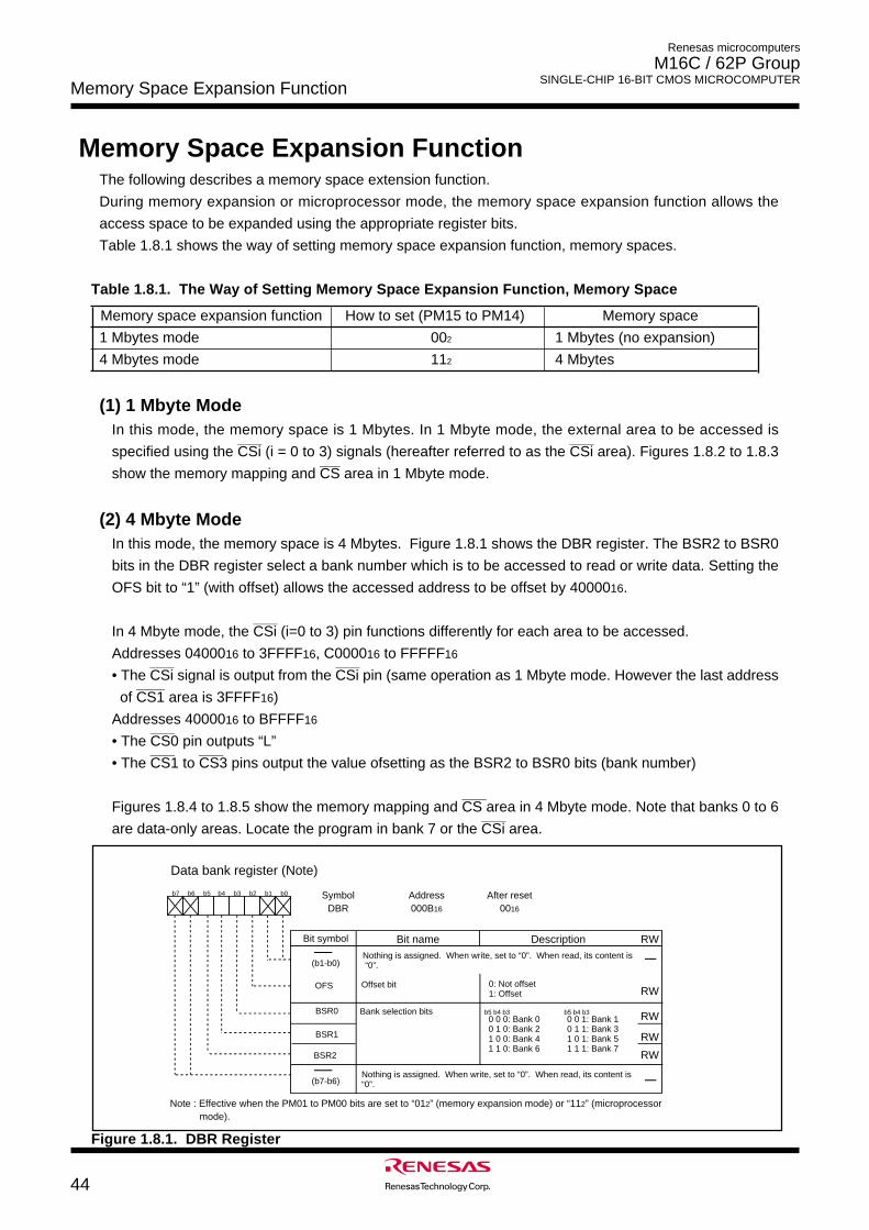
44
Renesas microcomputers
M16C / 62P Group SINGLE-CHIP 16-BIT CMOS MICROCOMPUTER
Memory Space Expansion Function
Memory Space Expansion FunctionThe following describes a memory space extension function.
During memory expansion or microprocessor mode, the memory space expansion function allows the
access space to be expanded using the appropriate register bits.
Table 1.8.1 shows the way of setting memory space expansion function, memory spaces.
Table 1.8.1. The Way of Setting Memory Space Expansion Function, Memory Space
Memory space expansion function How to set (PM15 to PM14) Memory space
1 Mbytes mode 002 1 Mbytes (no expansion)
4 Mbytes mode 112 4 Mbytes
(1) 1 Mbyte ModeIn this mode, the memory space is 1 Mbytes. In 1 Mbyte mode, the external area to be accessed is
______ ______
specified using the CSi (i = 0 to 3) signals (hereafter referred to as the CSi area). Figures 1.8.2 to 1.8.3_____
show the memory mapping and CS area in 1 Mbyte mode.
(2) 4 Mbyte ModeIn this mode, the memory space is 4 Mbytes. Figure 1.8.1 shows the DBR register. The BSR2 to BSR0
bits in the DBR register select a bank number which is to be accessed to read or write data. Setting the
OFS bit to “1” (with offset) allows the accessed address to be offset by 4000016.
______
In 4 Mbyte mode, the CSi (i=0 to 3) pin functions differently for each area to be accessed.
Addresses 0400016 to 3FFFF16, C000016 to FFFFF16______ ______
• The CSi signal is output from the CSi pin (same operation as 1 Mbyte mode. However the last address_______
of CS1 area is 3FFFF16)
Addresses 4000016 to BFFFF16______
• The CS0 pin outputs “L”______ ______
• The CS1 to CS3 pins output the value ofsetting as the BSR2 to BSR0 bits (bank number)
______
Figures 1.8.4 to 1.8.5 show the memory mapping and CS area in 4 Mbyte mode. Note that banks 0 to 6______
are data-only areas. Locate the program in bank 7 or the CSi area.
Figure 1.8.1. DBR Register
Data bank register (Note)
Symbol Address After resetDBR 000B16 0016
Bit name Description Bit symbol RW
b7 b6 b5 b4 b3 b2 b1 b0
OFS Offset bit 0: Not offset1: Offset
BSR0 Bank selection bits0 0 0: Bank 0 0 0 1: Bank 1 0 1 0: Bank 2 0 1 1: Bank 31 0 0: Bank 4 1 0 1: Bank 5 1 1 0: Bank 6 1 1 1: Bank 7
Nothing is assigned. When write, set to “0”. When read, its content is “0”.
Nothing is assigned. When write, set to “0”. When read, its content is “0”.
b5 b4 b3 b5 b4 b3
RW
RW
BSR1
BSR2
(b1-b0)
(b7-b6)
RW
RW
Note : Effective when the PM01 to PM00 bits are set to “012” (memory expansion mode) or “112” (microprocessor mode).
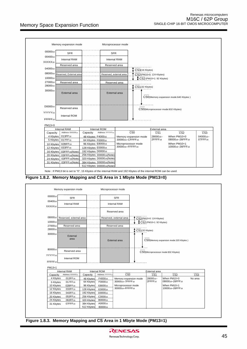
45
Renesas microcomputers
M16C / 62P Group SINGLE-CHIP 16-BIT CMOS MICROCOMPUTERMemory Space Expansion Function
AAAAAAAAAA
AAAAAAAAAAAAAAAAAAAA
Microprocessor mode
0000016
0040016
XXXXX16
YYYYY16
FFFFF16
8000016
0800016
Memory expansion mode
SFR
Internal RAM
Internal ROM
Reserved area
Reserved, external area CS2(PM10=0: 124 Kbytes)
CS1(32 Kbytes)
CS0(Microprocessor mode:832 Kbytes)
2800016
3000016
Reserved area2700016
Capacity Address YYYYY16
128 Kbytes E000016
256 Kbytes C000016
Capacity Address XXXXX16
12 Kbytes 033FF16
20 Kbytes 053FF16
10 Kbytes 02BFF16
24 Kbytes 063FF16
384 Kbytes A000016
512 Kbytes 8000016
PM13=1
External area
1000016
AAAAAAAAAA
AAAAAAAAAAAAAAAAAAAAAAAAAAAAAA
SFR
Internal RAM
Reserved area
Reserved area
External area
CS2(PM10=1: 92 Kbytes)
CS0(Memory expansion mode:320 Kbytes )
Internal RAM Internal ROMCS0
Memory expansion mode3000016–7FFFF16
External areaCS1
Microprocessor mode3000016–FFFFF16
2800016–2FFFF16
CS2When PM10=00800016–26FFF16
When PM10=11000016–26FFF16
CS3No area4 Kbytes 013FF16
5 Kbytes 017FF16
31 Kbytes 07FFF16
48 Kbytes F400016
64 Kbytes F000016
96 Kbytes E800016
192 Kbytes D000016
320 Kbytes B000016
16 Kbytes 043FF16
Reserved, external area
AAAAAAAA
AAAAAAAAAAAAAAAA
Microprocessor mode
0000016
0040016
XXXXX16
YYYYY16
FFFFF16
D000016
0800016
Memory expansion mode
AAAAAAAA
SFR
Internal RAM
Internal ROM
Reserved area
Reserved area
CS3(16 Kbytes)
CS2(PM10=0: 124 Kbytes)
CS1(32 Kbytes)
CS0(Microprocessor mode:832 Kbytes)
2800016
3000016
0400016
Reserved area2700016
Capacity Address YYYYY16
128 Kbytes E000016
256 Kbytes D000016(Note)
Capacity Address XXXXX16
12 Kbytes 033FF16
20 Kbytes 03FFF16(Note)
10 Kbytes 02BFF16
24 Kbytes 03FFF16(Note)
384 Kbytes D000016(Note)512 Kbytes D000016(Note)
PM13=0
Reserved, External area
External area
1000016
AAAAAAAA
AAAAAAAAAAAAAAAAAAAAAAAAAAAAAAAA
SFR
Internal RAM
Reserved area
Reserved area
Reserved, external area
External area
CS2(PM10=1: 92 Kbytes)
CS0(Memory expansion mode:640 Kbytes )
Internal RAM Internal ROMCS0
Memory expansion mode3000016–CFFFF16
External areaCS1
Microprocessor mode3000016–FFFFF16
2800016–2FFFF16
CS2When PM10=00800016–26FFF16
When PM10=11000016–26FFF16
CS30400016–07FFF16
4 Kbytes 013FF16
5 Kbytes 017FF16
31 Kbytes 03FFF16(Note)
48 Kbytes F400016
64 Kbytes F000016
96 Kbytes E800016
192 Kbytes D000016
320 Kbytes D000016(Note)
16 Kbytes 03FFF16(Note)
Note : If PM13 bit is set to “0”, 15 Kbytes of the internal RAM and 192 Kbytes of the internal ROM can be used. ______
Figure 1.8.2. Memory Mapping and CS Area in 1 Mbyte Mode (PM13=0)
______
Figure 1.8.3. Memory Mapping and CS Area in 1 Mbyte Mode (PM13=1)
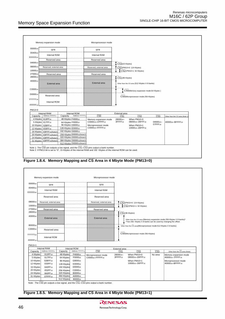
46
Renesas microcomputers
M16C / 62P Group SINGLE-CHIP 16-BIT CMOS MICROCOMPUTER
Memory Space Expansion Function
______
Figure 1.8.4. Memory Mapping and CS Area in 4 Mbyte Mode (PM13=0)
AAAAAAAAAA
AAAAAAAAAAAAAAAAAAAA
Microprocessor mode
0000016
0040016
XXXXX16
YYYYY16
FFFFF16
D000016
0800016
Memory expansion mode
AAAAA
SFR
Internal RAM
Internal ROM
Reserved area
Reserved area
CS3(16 Kbytes)
CS2(PM10=0: 124 Kbytes)
CS1(96 Kbytes)
CS0(Microprocessor mode:256 Kbytes)
2800016
4000016
0400016
Reserved area2700016
PM13=0
Reserved, external area
External area
1000016
AAAAAAAAAAAA
AAAAAAAAAAAAAAAAAAAAAAAAAAAAAAAAAAAA
AAAAA
SFR
Internal RAM
Reserved area
Reserved area
External area
CS2(PM10=1: 92 Kbytes)
CS0(Memory expansion mode:64 Kbytes )
CS0
Memory expansion modeC000016–CFFFF16
External areaCS1
Microprocessor modeC000016–FFFFF16
2800016–3FFFF16
CS2When PM10=00800016–26FFF16
When PM10=11000016–26FFF16
CS3
0400016–07FFF16
C000016
Other than the CS area (512 Kbytes X 8 banks)
4000016–BFFFF16
Other than the CS area (Note 1)
Note 1: The CS0 pin outputs a low signal, and the CS1–CS3 pins output a bank number.Note 2: If PM13 bit is set to “0”, 15 Kbytes of the internal RAM and 192 Kbytes of the internal ROM can be used.
Capacity Address YYYYY16
128 Kbytes E000016
256 Kbytes D000016(Note2)
Capacity Address XXXXX16
12 Kbytes 033FF16
20 Kbytes 03FFF16(Note2)
10 Kbytes 02BFF16
24 Kbytes 03FFF16(Note2)384 Kbytes D000016(Note2)
512 Kbytes D000016(Note2)
Internal RAM Internal ROM
4 Kbytes 013FF16
5 Kbytes 017FF16
31 Kbytes 03FFF16(Note2)
48 Kbytes F400016
64 Kbytes F000016
96 Kbytes E800016
192 Kbytes D000016
320 Kbytes D000016(Note2)
16 Kbytes 03FFF16(Note2)
Reserved, external area
AAAAA
AAAAAAAAAAAAAAA
Microprocessor mode
0000016
0040016
XXXXX16
YYYYY16
FFFFF16
C000016
0800016
Memory expansion mode
SFR
Internal RAM
Internal ROM
Reserved area
Reserved area
CS2(PM10=0: 124 Kbytes)
CS1(96 Kbytes)
CS0(Microprocessor mode:256 Kbytes)
2800016
4000016
Reserved area2700016
PM13=1
External area
1000016 AAAAA
AAAAAAAAAAAAAAAAAAAAAAAAA
SFR
Internal RAM
Reserved area
Reserved area
External area
CS2(PM10=1: 92 Kbytes)
Other than the CS area(Microprocessor mode:512 Kbytes X 8 banks)
CS0External area
CS1
Microprocessor modeC000016–FFFFF16
2800016–3FFFF16
CS2When PM10=00800016–26FFF16
When PM10=11000016–26FFF16
CS3No area
8000016
Other than the CS area (Memory expansion mode:256 Kbytes X 8 banks)**Two 256 Kbytes X 8 banks can be used by changing the offset.
Other than the CS area (Note)
Memory expansion mode4000016–7FFFF16
Microprocessor mode4000016–BFFFF16
Note : The CS0 pin outputs a low signal, and the CS1–CS3 pins output a bank number.
Capacity Address YYYYY16
128 Kbytes E000016
256 Kbytes C000016
Capacity Address XXXXX16
12 Kbytes 033FF16
20 Kbytes 053FF16
10 Kbytes 02BFF16
24 Kbytes 063FF16
384 Kbytes A000016
512 Kbytes 8000016
Internal RAM Internal ROM
4 Kbytes 013FF16
5 Kbytes 017FF16
31 Kbytes 07FFF16
48 Kbytes F400016
64 Kbytes F000016
96 Kbytes E800016
192 Kbytes D000016
320 Kbytes B000016
16 Kbytes 043FF16
Reserved, external area Reserved, external area
______
Figure 1.8.5. Memory Mapping and CS Area in 4 Mbyte Mode (PM13=1)
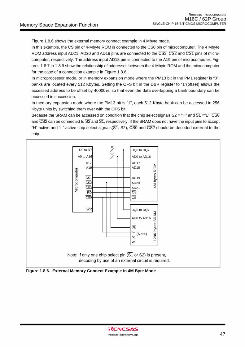
47
Renesas microcomputers
M16C / 62P Group SINGLE-CHIP 16-BIT CMOS MICROCOMPUTERMemory Space Expansion Function
Figure 1.8.6 shows the external memory connect example in 4 Mbyte mode._____ _______
In this example, the CS pin of 4-Mbyte ROM is connected to the CS0 pin of microcomputer. The 4 Mbyte_______ _______ _______
ROM address input AD21, AD20 and AD19 pins are connected to the CS3, CS2 and CS1 pins of micro-
computer, respectively. The address input AD18 pin is connected to the A19 pin of microcomputer. Fig-
ures 1.8.7 to 1.8.9 show the relationship of addresses between the 4-Mbyte ROM and the microcomputer
for the case of a connection example in Figure 1.8.6.
In microprocessor mode, or in memory expansion mode where the PM13 bit in the PM1 register is “0”,
banks are located every 512 Kbytes. Setting the OFS bit in the DBR register to “1”(offset) allows the
accessed address to be offset by 4000016, so that even the data overlapping a bank boundary can be
accessed in succession.
In memory expansion mode where the PM13 bit is “1”, each 512-Kbyte bank can be accessed in 256
Kbyte units by switching them over with the OFS bit.____ _______
Because the SRAM can be accessed on condition that the chip select signals S2 = “H” and S1 =“L”, CS0_______ _____ ____
and CS2 can be connected to S2 and S1, respectively. If the SRAM does not have the input pins to accept____ _______ _______
“H” active and “L” active chip select signals(S1, S2), CS0 and CS2 should be decoded external to the
chip.
17
8
Mic
roco
mpu
ter
D0 to D7
A0 to A16
A17
RD
WR
CS1
CS2
CS3
CS0
A19
4M b
ytes
RO
MDQ0 to DQ7
AD0 to AD16
AD17AD18
AD19
OE
CS
128K
byt
es S
RA
M
DQ0 to DQ7
AD0 to AD16
S2
W
OE
S1
AD20
AD21
Note: If only one chip select pin (S1 or S2) is present, decoding by use of an external circuit is required.
(Note)
Figure 1.8.6. External Memory Connect Example in 4M Byte Mode
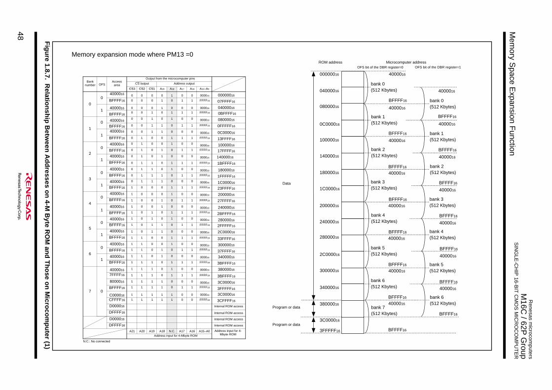
48
Renesas m
icrocomputers
M16C
/ 62P G
roup S
ING
LE-C
HIP
16-BIT
CM
OS
MIC
RO
CO
MP
UT
ER
Mem
ory Space E
xpansion Function
00000016
08000016
10000016
18000016
20000016
28000016
38000016
3FFFFF16
ROM address Microcomputer address
4000016
BFFFF16
3C000016
34000016
2C000016
24000016
1C000016
14000016
0C000016
04000016
bank 0(512 Kbytes)
bank 1(512 Kbytes)
bank 1(512 Kbytes)
bank 2(512 Kbytes)
bank 2(512 Kbytes)
bank 3(512 Kbytes)
bank 3(512 Kbytes)
bank 4(512 Kbytes)
bank 4(512 Kbytes)
bank 5(512 Kbytes)
bank 5(512 Kbytes)
bank 6(512 Kbytes)
bank 6(512 Kbytes)
bank 7(512 Kbytes)
AAAAAAAA
AAAAAAAAAAAA
AAAAAAAAAAAA
AAAAAAAA
AAAAAAAAAAAA
AAAAAAAAAAAA
AAAAAAAAAAAA
AAAAAAAAAAAA
AAAAAAAAAAAA
AAAAAAAAAAAA
AAAAAAAAAAAA
AAAAAAAA
AAAAAAAAAAAA
AAAAAAAAAAAA
Data
Program or data
OFS bit of the DBR register=0 OFS bit of the DBR register=1
30000016
bank 0(512 Kbytes)4000016
4000016
4000016
4000016
4000016
4000016
4000016
BFFFF16
BFFFF16
BFFFF16
BFFFF16
BFFFF16
BFFFF16
4000016
BFFFF16
4000016
BFFFF16
4000016
BFFFF16
4000016
BFFFF16
4000016
BFFFF16
4000016
BFFFF16
4000016
BFFFF16
Program or dataBFFFF16
Fig
ure 1.8.7. R
elation
ship
Betw
een A
dd
resses on
4-M B
yte RO
M an
d T
ho
se on
Micro
com
pu
ter (1)
A20 A19 A18 N.C. A17 A16 A15–A0
Address input for 4-Mbyte ROM
Address input for 4-Mbyte ROM
A18
CS output Address outputOFSAccess
area
Output from the microcomputer pins
CS3 CS2 CS1 A19 A17 A16 A15–A0
4000016 0 000016 00000016
Banknumber
0
0BFFFF16 FFFF16
040000161
08000016
1
0
0C0000161
10000016
2
0
140000161
18000016
3
0
1C0000161
20000016
4
0
240000161
28000016
5
0
2C0000161
30000016
6
0
340000161
4000016 38000016
7 0
8000016 3C000016
C000016 3C000016
D000016 Internal ROM access
Internal ROM access
Internal ROM access
Internal ROM access
A21
0
0
0
0
0
0
0
0
0
0
0
0
0
0
1
1
1
1
1
1
1
1
1
1
1
1
1
1
1
1
1
1
1
0
0
0
0
0
0
0
1
1
1
1
1
1
1
1
0
0
0
0
0
0
0
0
1
1
1
1
1
1
1
1
1
1
1
0
0
0
1
1
1
1
0
0
0
0
1
1
1
1
0
0
0
0
1
1
1
1
0
0
0
0
1
1
1
1
1
1
1
0
1
1
0
0
1
1
0
0
1
1
0
0
1
1
0
0
1
1
0
0
1
1
0
0
1
1
0
0
0
1
1
1
1
1
0
0
1
1
0
1
0
0
1
1
0
0
1
1
0
0
1
1
0
0
1
1
0
0
1
1
1
0
0
1
1
0
1
0
1
0
1
0
1
0
1
0
1
0
1
0
1
0
1
0
1
0
1
0
1
0
1
0
1
0
1
0
1
0
1
0
0
0
1
0
1
0
1
0
1
0
1
0
1
0
1
0
1
0
1
0
1
0
1
0
1
0
1
0
1
0
1
0
1
0
0
4000016
BFFFF16
4000016
BFFFF16
4000016
BFFFF16
4000016
BFFFF16
4000016
BFFFF16
4000016
BFFFF16
4000016
BFFFF16
4000016
BFFFF16
4000016
BFFFF16
4000016
BFFFF16
4000016
BFFFF16
4000016
BFFFF16
4000016
BFFFF16
7FFFF16
BFFFF16
CFFFF16
DFFFF16
D000016
DFFFF16
000016
FFFF16
000016
FFFF16
000016
FFFF16
000016
FFFF16
000016
FFFF16
000016
FFFF16
000016
FFFF16
000016
FFFF16
000016
FFFF16
000016
FFFF16
000016
FFFF16
000016
FFFF16
000016
FFFF16
000016
FFFF16
000016
FFFF16
000016
FFFF16
07FFFF16
0BFFFF16
0FFFFF16
13FFFF16
17FFFF16
1BFFFF16
1FFFFF16
23FFFF16
27FFFF16
2BFFFF16
2FFFFF16
33FFFF16
37FFFF16
3BFFFF16
3BFFFF16
3FFFFF16
3CFFFF16
N.C.: No connected
Memory expansion mode where PM13 =0
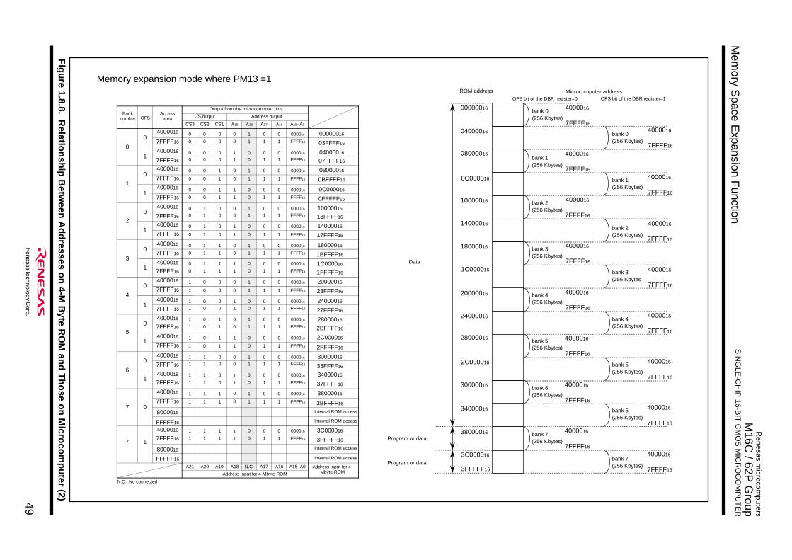
49
Renesas m
icrocomputers
M16C
/ 62P G
roup S
ING
LE-C
HIP
16-BIT
CM
OS
MIC
RO
CO
MP
UT
ER
Mem
ory Space E
xpansion Function
Fig
ure 1.8.8. R
elation
ship
Betw
een A
dd
resses on
4-M B
yte RO
M an
d T
ho
se on
Micro
com
pu
ter (2)
00000016
08000016
10000016
18000016
20000016
28000016
38000016
3FFFFF16
ROM address
3C000016
34000016
2C000016
24000016
1C000016
14000016
0C000016
04000016
bank 0(256 Kbytes)
bank 1(256 Kbytes)
bank 1(256 Kbytes)
bank 2(256 Kbytes)
bank 2(256 Kbytes)
bank 3(256 Kbytes
bank 3(256 Kbytes)
bank 4(256 Kbytes)
bank 4(256 Kbytes)
bank 5(256 Kbytes)
bank 5(256 Kbytes)
bank 6(256 Kbytes)
bank 6(256 Kbytes)
bank 7(256 Kbytes)
AAAAAA
AAAAAAAAA
AAAAAAAAA
AAAAAA
AAAAAAAAA
AAAAAAAAA
AAAAAAAAA
AAAAAAAAA
AAAAAAAAA
AAAAAAAAA
AAAAAAAAA
AAAAAA
AAAAAAAAA
AAAAAAAAA
Data
Program or data
30000016
bank 0(256 Kbytes)
Microcomputer addressOFS bit of the DBR register=0 OFS bit of the DBR register=1
4000016
7FFFF16
4000016
7FFFF16
4000016
7FFFF16
4000016
7FFFF16
4000016
7FFFF16
4000016
7FFFF16
4000016
7FFFF16
Program or databank 7(256 Kbytes)
4000016
7FFFF16
4000016
7FFFF16
4000016
7FFFF16
4000016
7FFFF16
4000016
7FFFF16
4000016
7FFFF16
4000016
7FFFF16
4000016
7FFFF16
4000016
7FFFF16
A20 A19 A18 N.C. A17 A16 A15–A0
Address input for 4-Mbyte ROM
Address input for 4-Mbyte ROM
A18
CS output Address outputOFSAccess
area
Output from the microcomputer pins
CS3 CS2 CS1 A19 A17 A16 A15–A0
7FFFF16
0 000016 00000016
Banknumber
0
0
07FFFF161
08000016
1
0
0C0000161
10000016
2
0
140000161
18000016
3
0
1C0000161
20000016
4
0
240000161
28000016
5
0
2C0000161
30000016
6
0
1
1
340000161
0
0
38000016
7 0Internal ROM access
7 1
1
1
3C000016
8000016
Internal ROM access
Internal ROM access
Internal ROM access
A21
03FFFF16
04000016
0BFFFF16
0FFFFF16
13FFFF16
17FFFF16
1BFFFF16
1FFFFF16
23FFFF16
27FFFF16
2BFFFF16
2FFFFF16
33FFFF16
37FFFF16
3BFFFF16
3FFFFF16
FFFF16
000016
FFFF16
000016
FFFF16
000016
FFFF16
000016
FFFF16
000016
FFFF16
000016
FFFF16
000016
FFFF16
000016
FFFF16
000016
FFFF16
000016
FFFF16
000016
FFFF16
000016
FFFF16
000016
FFFF16
000016
FFFF16
000016
FFFF16
0
0
0
0
0
0
0
0
0
0
0
0
0
0
0
1
1
1
1
1
1
1
1
1
1
1
1
1
1
1
1
0
0
0
0
0
0
0
0
1
1
1
1
1
1
1
1
0
0
0
0
0
0
0
0
1
1
1
1
1
1
1
1
0
0
0
0
1
1
1
1
0
0
0
0
1
1
1
1
0
0
0
0
1
1
1
1
0
0
0
0
1
1
1
1
0
0
1
1
0
0
1
1
0
0
1
1
0
0
1
1
0
0
1
1
0
0
1
1
0
0
1
1
0
0
1
1
0
0
1
1
0
0
1
1
0
0
1
1
0
0
1
1
0
0
1
1
0
0
1
1
0
0
0
1
0
1
0
1
0
1
0
1
0
1
0
1
0
1
0
1
0
1
0
1
0
1
0
1
0
1
0
1
0
1
0
1
0
1
0
1
0
1
0
1
0
1
0
1
0
1
0
1
0
1
0
1
0
1
0
1
0
1
0
1
0
1
4000016
7FFFF16
4000016
7FFFF16
4000016
7FFFF16
4000016
7FFFF16
4000016
7FFFF16
4000016
7FFFF16
4000016
7FFFF16
4000016
7FFFF16
4000016
7FFFF16
4000016
7FFFF16
4000016
7FFFF16
4000016
7FFFF16
4000016
7FFFF16
4000016
7FFFF16
4000016
FFFFF16
8000016
7FFFF16
4000016
FFFFF16
N.C.: No connected
Memory expansion mode where PM13 =1
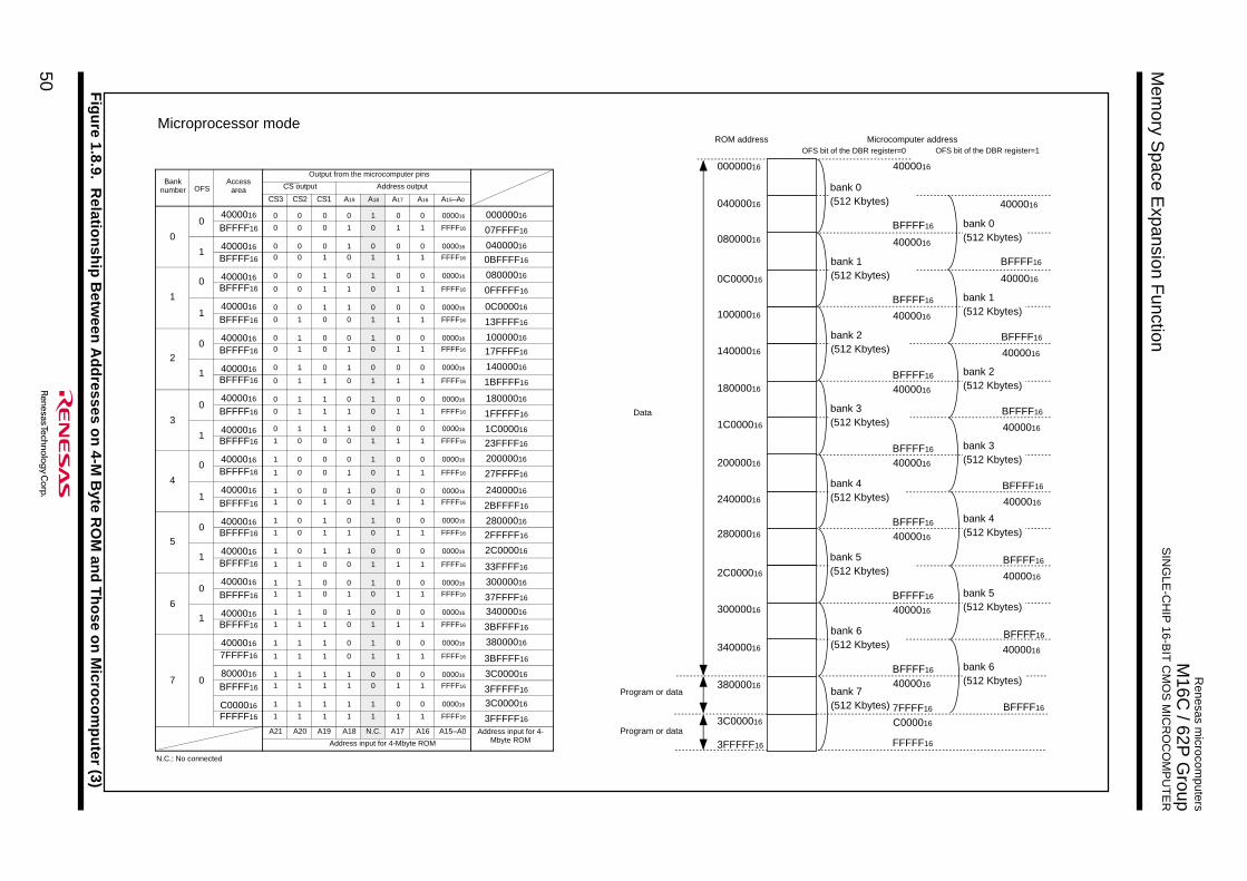
50
Renesas m
icrocomputers
M16C
/ 62P G
roup S
ING
LE-C
HIP
16-BIT
CM
OS
MIC
RO
CO
MP
UT
ER
Mem
ory Space E
xpansion Function
Fig
ure 1.8.9. R
elation
ship
Betw
een A
dd
resses on
4-M B
yte RO
M an
d T
ho
se on
Micro
com
pu
ter (3)
00000016
08000016
10000016
18000016
20000016
28000016
38000016
3FFFFF16
ROM address Microcomputer address
4000016
BFFFF16
3C000016
34000016
2C000016
24000016
1C000016
14000016
0C000016
04000016
bank 0(512 Kbytes)
bank 1(512 Kbytes)
bank 1(512 Kbytes)
bank 2(512 Kbytes)
bank 2(512 Kbytes)
bank 3(512 Kbytes)
bank 3(512 Kbytes)
bank 4(512 Kbytes)
bank 4(512 Kbytes)
bank 5(512 Kbytes)
bank 5(512 Kbytes)
bank 6(512 Kbytes)
bank 6(512 Kbytes)
bank 7(512 Kbytes)
AAAAAA
AAAAAAAAA
AAAAAAAAA
AAAAAA
AAAAAAAAA
AAAAAAAAA
AAAAAAAAA
AAAAAAAAA
AAAAAAAAA
AAAAAAAAA
AAAAAAAAA
AAAAAA
AAAAAAAAA
AAAAAAAAA
Data
Program or data
OFS bit of the DBR register=0 OFS bit of the DBR register=1
30000016
bank 0(512 Kbytes)4000016
4000016
4000016
4000016
4000016
4000016
4000016
BFFFF16
BFFFF16
BFFFF16
BFFFF16
BFFFF16
BFFFF16
4000016
BFFFF16
4000016
BFFFF16
4000016
BFFFF16
4000016
BFFFF16
4000016
BFFFF16
4000016
BFFFF16
4000016
BFFFF16
Program or dataFFFFF16
7FFFF16
C000016A20 A19 A18 N.C. A17 A16 A15–A0
Address input for 4-Mbyte ROM
Address input for 4-Mbyte ROM
A18
CS output Address outputOFSAccess
area
Output from the microcomputer pins
CS3 CS2 CS1 A19 A17 A16 A15–A0
4000016 0 000016 00000016
Banknumber
0
0
040000161
08000016
1
0
0C0000161
10000016
2
0
140000161
18000016
3
0
1C0000161
20000016
4
0
240000161
28000016
5
0
2C0000161
30000016
6
0
340000161
38000016
7 08000016 3C000016
C000016 3C000016
A21
BFFFF16
4000016
BFFFF16
4000016
BFFFF16
4000016
BFFFF16
4000016
BFFFF16
4000016
BFFFF16
4000016
BFFFF16
4000016
BFFFF16
4000016
BFFFF16
4000016
BFFFF16
4000016
BFFFF16
4000016
BFFFF16
4000016
BFFFF16
4000016
BFFFF16
4000016
7FFFF16
BFFFF16
FFFFF16
0
0
0
0
0
0
0
0
0
0
0
0
0
0
1
1
1
1
1
1
1
1
1
1
1
1
1
1
1
1
1
1
1
0
0
0
0
0
0
0
1
1
1
1
1
1
1
1
0
0
0
0
0
0
0
0
1
1
1
1
1
1
1
1
1
1
1
0
0
0
1
1
1
1
0
0
0
0
1
1
1
1
0
0
0
0
1
1
1
1
0
0
0
0
1
1
1
1
1
1
1
0
1
1
0
0
1
1
0
0
1
1
0
0
1
1
0
0
1
1
0
0
1
1
0
0
1
1
0
0
0
1
1
1
1
1
0
0
1
1
0
0
1
1
0
0
1
1
0
0
1
1
0
0
1
1
0
0
1
1
0
0
1
1
1
0
0
1
1
0
1
0
1
0
1
0
1
0
1
0
1
0
1
0
1
0
1
0
1
0
1
0
1
0
1
0
1
0
1
0
1
0
1
0
1
0
1
0
1
0
1
0
1
0
1
0
1
0
1
0
1
0
1
0
1
0
1
0
1
0
1
0
1
0
1
0
1
FFFF16
000016
FFFF16
000016
FFFF16
000016
FFFF16
000016
FFFF16
000016
FFFF16
000016
FFFF16
000016
FFFF16
000016
FFFF16
000016
FFFF16
000016
FFFF16
000016
FFFF16
000016
FFFF16
000016
FFFF16
000016
FFFF16
000016
FFFF16
000016
FFFF16
07FFFF16
0BFFFF16
0FFFFF16
13FFFF16
17FFFF16
1BFFFF16
1FFFFF16
23FFFF16
27FFFF16
2BFFFF16
2FFFFF16
33FFFF16
37FFFF16
3BFFFF16
3BFFFF16
3FFFFF16
3FFFFF16
N.C.: No connected
Microprocessor mode
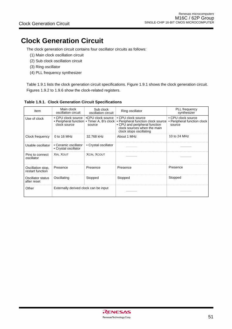
51
Renesas microcomputers
M16C / 62P Group SINGLE-CHIP 16-BIT CMOS MICROCOMPUTERClock Generation Circuit
• CPU clock source• Peripheral function
clock source
Use of clock
Main clock oscillation circuit
Sub clock oscillation circuitItem
•CPU clock source• Timer A, B's clock
source
Clock frequency 0 to 16 MHz 32.768 kHz
• Ceramic oscillator• Crystal oscillator
Usable oscillator • Crystal oscillator
XIN, XOUTPins to connect oscillator
XCIN, XCOUT
PresenceOscillation stop,restart function
Presence
OscillatingOscillator status after reset
Stopped
Externally derived clock can be inputOther
PLL frequencysynthesizer
10 to 24 MHz
Presence
Stopped
Ring oscillator
• CPU clock source• Peripheral function clock source• CPU and peripheral function
clock sources when the main clock stops oscillating
About 1 MHz
Presence
Stopped
• CPU clock source• Peripheral function clock
source
Clock Generation CircuitThe clock generation circuit contains four oscillator circuits as follows:
(1) Main clock oscillation circuit
(2) Sub clock oscillation circuit
(3) Ring oscillator
(4) PLL frequency synthesizer
Table 1.9.1 lists the clock generation circuit specifications. Figure 1.9.1 shows the clock generation circuit.
Figures 1.9.2 to 1.9.6 show the clock-related registers.
Table 1.9.1. Clock Generation Circuit Specifications
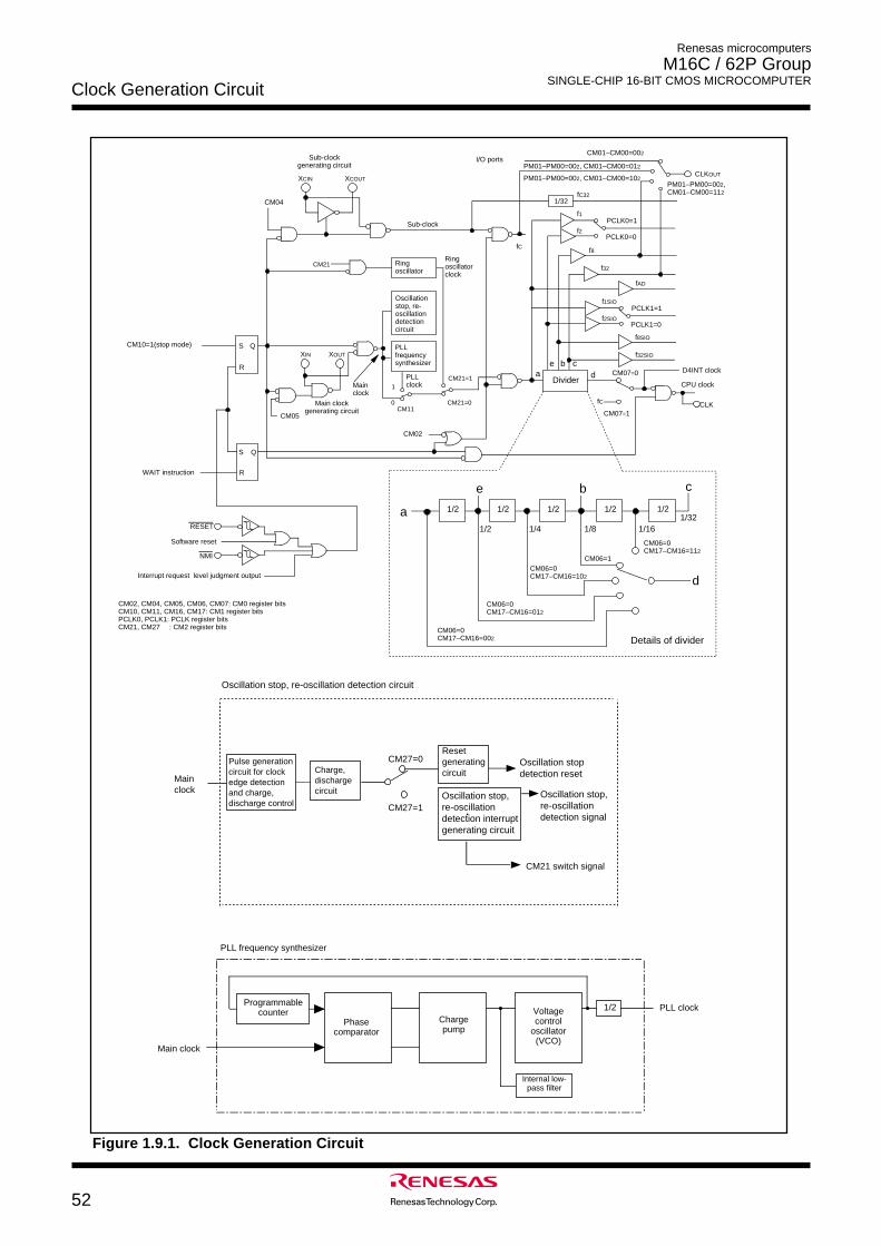
52
Renesas microcomputers
M16C / 62P Group SINGLE-CHIP 16-BIT CMOS MICROCOMPUTER
Clock Generation Circuit
fC32
CM02, CM04, CM05, CM06, CM07: CM0 register bitsCM10, CM11, CM16, CM17: CM1 register bitsPCLK0, PCLK1: PCLK register bitsCM21, CM27 : CM2 register bits
1/32
Main clockgenerating circuit
fC
CM02
CM04
CM10=1(stop mode) QS
R
WAIT instruction
CM05
QS
R
NMI
Interrupt request level judgment output
RESET
Software reset
fC
CPU clock
CM07=0
CM07=1AAAAAAAAAAAA
Dividera d
1/2 1/2 1/2 1/2
CM06=0CM17–CM16=002
CM06=0CM17–CM16=012
CM06=0CM17–CM16=102
CM06=1
CM06=0CM17–CM16=112
d
a
Details of divider
Sub-clockgenerating circuit
XCIN XCOUT
XOUTXIN
f8
f32
cb
b
1/2
c
f32SIO
f8SIO
fAD
f1
e
e
1/2 1/4 1/8 1/161/32
PCLK0=1
AAAAAAA
AAAA
PLL frequency synthesizer
0
1CM21=1
CM11CM21=0
AAAAAAAARing
oscillator
AAAAAAA
PLLclock
Sub-clock
Ring oscillatorclock
BCLK
PCLK0=0f2
f1SIOPCLK1=1AAA
PCLK1=0f2SIO
Main clock
CLKOUT
AAAA
A
PM01–PM00=002, CM01–CM00=012
PM01–PM00=002, CM01–CM00=102
CM01–CM00=002I/O ports
PM01–PM00=002, CM01–CM00=112
CM21
Oscillation stop, re-oscillation detection circuit
D4INT clock
Figure 1.9.1. Clock Generation Circuit
Phase comparator
Chargepump
Voltagecontrol
oscillator(VCO)
PLL clock
Main clock
1/2Programmablecounter
Internal low-pass filter
PLL frequency synthesizer
Pulse generation circuit for clock edge detection and charge, discharge control
Charge, dischargecircuit
Resetgenerating circuit
Oscillation stop, re-oscillationdetection interruptgenerating circuit
Mainclock
Oscillation stopdetection reset
CM27=0
CM21 switch signal
Oscillation stop, re-oscillationdetection signal
Oscillation stop, re-oscillation detection circuit
CM27=1
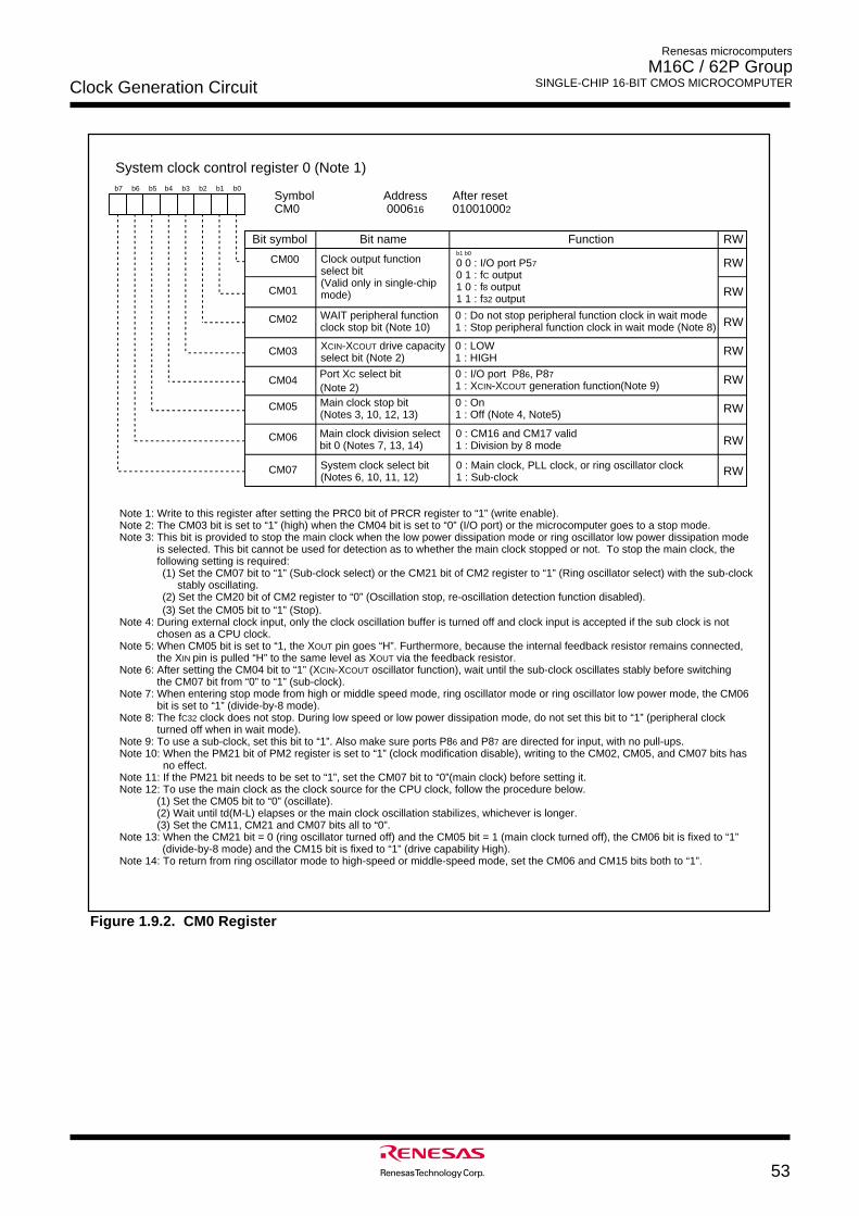
53
Renesas microcomputers
M16C / 62P Group SINGLE-CHIP 16-BIT CMOS MICROCOMPUTERClock Generation Circuit
System clock control register 0 (Note 1)
Symbol Address After reset CM0 000616 010010002
Bit name FunctionBit symbol
b7 b6 b5 b4 b3 b2 b1 b0
0 0 : I/O port P570 1 : fC output1 0 : f8 output1 1 : f32 output
b1 b0
CM07
CM05
CM04
CM03
CM01
CM02
CM00
CM06
Clock output function select bit(Valid only in single-chip mode)
WAIT peripheral function clock stop bit (Note 10)
0 : Do not stop peripheral function clock in wait mode1 : Stop peripheral function clock in wait mode (Note 8)
XCIN-XCOUT drive capacity select bit (Note 2)
0 : LOW1 : HIGH
Port XC select bit 0 : I/O port P86, P871 : XCIN-XCOUT generation function(Note 9)
Main clock stop bit (Notes 3, 10, 12, 13)
0 : On1 : Off (Note 4, Note5)
Main clock division select bit 0 (Notes 7, 13, 14)
0 : CM16 and CM17 valid1 : Division by 8 mode
System clock select bit(Notes 6, 10, 11, 12)
0 : Main clock, PLL clock, or ring oscillator clock1 : Sub-clock
Note 1: Write to this register after setting the PRC0 bit of PRCR register to “1” (write enable).Note 2: The CM03 bit is set to “1” (high) when the CM04 bit is set to “0” (I/O port) or the microcomputer goes to a stop mode.Note 3: This bit is provided to stop the main clock when the low power dissipation mode or ring oscillator low power dissipation mode
is selected. This bit cannot be used for detection as to whether the main clock stopped or not. To stop the main clock, the following setting is required:(1) Set the CM07 bit to “1” (Sub-clock select) or the CM21 bit of CM2 register to “1” (Ring oscillator select) with the sub-clock stably oscillating.(2) Set the CM20 bit of CM2 register to “0” (Oscillation stop, re-oscillation detection function disabled).(3) Set the CM05 bit to “1” (Stop).
Note 4: During external clock input, only the clock oscillation buffer is turned off and clock input is accepted if the sub clock is not chosen as a CPU clock.
Note 5: When CM05 bit is set to “1, the XOUT pin goes “H”. Furthermore, because the internal feedback resistor remains connected, the XIN pin is pulled “H” to the same level as XOUT via the feedback resistor.
Note 6: After setting the CM04 bit to “1” (XCIN-XCOUT oscillator function), wait until the sub-clock oscillates stably before switching the CM07 bit from “0” to “1” (sub-clock).
Note 7: When entering stop mode from high or middle speed mode, ring oscillator mode or ring oscillator low power mode, the CM06 bit is set to “1” (divide-by-8 mode).
Note 8: The fC32 clock does not stop. During low speed or low power dissipation mode, do not set this bit to “1” (peripheral clock turned off when in wait mode).
Note 9: To use a sub-clock, set this bit to “1”. Also make sure ports P86 and P87 are directed for input, with no pull-ups. Note 10: When the PM21 bit of PM2 register is set to “1” (clock modification disable), writing to the CM02, CM05, and CM07 bits has
no effect.Note 11: If the PM21 bit needs to be set to “1”, set the CM07 bit to “0”(main clock) before setting it. Note 12: To use the main clock as the clock source for the CPU clock, follow the procedure below.
(1) Set the CM05 bit to “0” (oscillate).(2) Wait until td(M-L) elapses or the main clock oscillation stabilizes, whichever is longer.(3) Set the CM11, CM21 and CM07 bits all to “0”.
Note 13: When the CM21 bit = 0 (ring oscillator turned off) and the CM05 bit = 1 (main clock turned off), the CM06 bit is fixed to “1” (divide-by-8 mode) and the CM15 bit is fixed to “1” (drive capability High).
Note 14: To return from ring oscillator mode to high-speed or middle-speed mode, set the CM06 and CM15 bits both to “1”.
RW
(Note 2)
RW
RW
RW
RW
RW
RW
RW
RW
Figure 1.9.2. CM0 Register
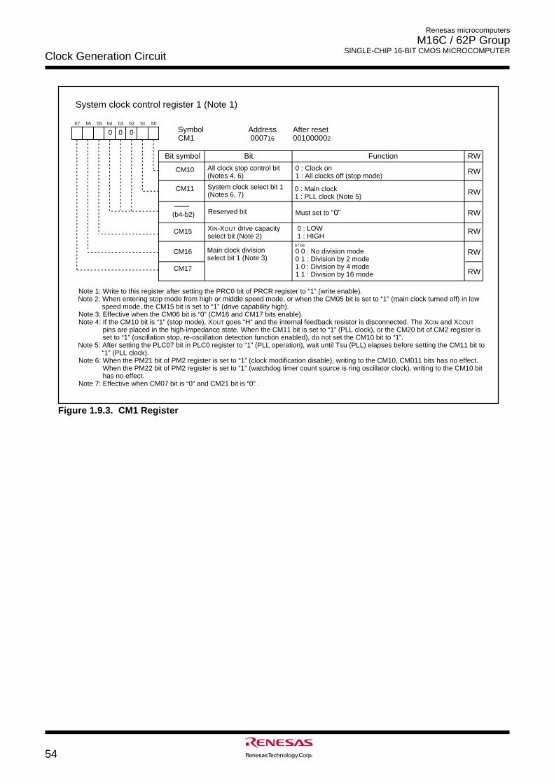
54
Renesas microcomputers
M16C / 62P Group SINGLE-CHIP 16-BIT CMOS MICROCOMPUTER
Clock Generation Circuit
System clock control register 1 (Note 1)
Symbol Address After reset CM1 000716 001000002
Bit name
FunctionBit symbol
b7 b6 b5 b4 b3 b2 b1 b0
CM10 All clock stop control bit(Notes 4, 6)
0 : Clock on1 : All clocks off (stop mode)
Note 1: Write to this register after setting the PRC0 bit of PRCR register to “1” (write enable).Note 2: When entering stop mode from high or middle speed mode, or when the CM05 bit is set to “1” (main clock turned off) in low
speed mode, the CM15 bit is set to “1” (drive capability high).Note 3: Effective when the CM06 bit is “0” (CM16 and CM17 bits enable).Note 4: If the CM10 bit is “1” (stop mode), XOUT goes “H” and the internal feedback resistor is disconnected. The XCIN and XCOUT
pins are placed in the high-impedance state. When the CM11 bit is set to “1” (PLL clock), or the CM20 bit of CM2 register is set to “1” (oscillation stop, re-oscillation detection function enabled), do not set the CM10 bit to “1”.
Note 5: After setting the PLC07 bit in PLC0 register to “1” (PLL operation), wait until Tsu (PLL) elapses before setting the CM11 bit to“1” (PLL clock).
Note 6: When the PM21 bit of PM2 register is set to “1” (clock modification disable), writing to the CM10, CM011 bits has no effect.When the PM22 bit of PM2 register is set to “1” (watchdog timer count source is ring oscillator clock), writing to the CM10 bit has no effect.
Note 7: Effective when CM07 bit is “0” and CM21 bit is “0” .
CM15 XIN-XOUT drive capacity select bit (Note 2)
0 : LOW 1 : HIGH
RW
CM16
CM17
Reserved bit Must set to “0”
Main clock division select bit 1 (Note 3)
0 0 : No division mode0 1 : Division by 2 mode1 0 : Division by 4 mode1 1 : Division by 16 mode
b7 b6
00 0
CM11 System clock select bit 1(Notes 6, 7)
0 : Main clock 1 : PLL clock (Note 5)
RW
RW
RW
RW
RW
RW
(b4-b2)
Figure 1.9.3. CM1 Register
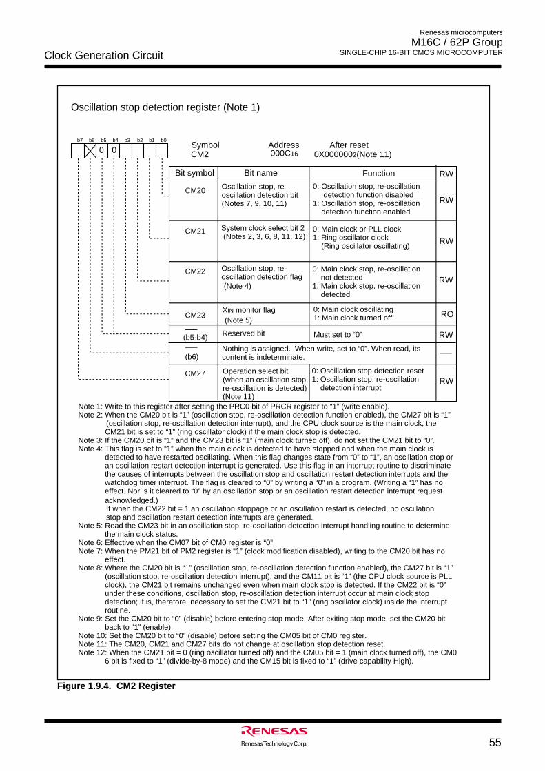
55
Renesas microcomputers
M16C / 62P Group SINGLE-CHIP 16-BIT CMOS MICROCOMPUTERClock Generation Circuit
b7 b6 b5 b4 b3 b2 b1 b0
RW
CM20
CM21
Oscillation stop detection register (Note 1)
Symbol Address After reset CM2 000C16 0X0000002(Note 11)
Bit name FunctionBit symbol
System clock select bit 2 (Notes 2, 3, 6, 8, 11, 12)
0: Oscillation stop, re-oscillation detection function disabled1: Oscillation stop, re-oscillation detection function enabled
0: Main clock or PLL clock 1: Ring oscillator clock (Ring oscillator oscillating)
Oscillation stop, re-oscillation detection bit(Notes 7, 9, 10, 11)
Note 1: Write to this register after setting the PRC0 bit of PRCR register to “1” (write enable).Note 2: When the CM20 bit is “1” (oscillation stop, re-oscillation detection function enabled), the CM27 bit is “1”
(oscillation stop, re-oscillation detection interrupt), and the CPU clock source is the main clock, the CM21 bit is set to “1” (ring oscillator clock) if the main clock stop is detected.
Note 3: If the CM20 bit is “1” and the CM23 bit is “1” (main clock turned off), do not set the CM21 bit to “0”. Note 4: This flag is set to “1” when the main clock is detected to have stopped and when the main clock is
detected to have restarted oscillating. When this flag changes state from “0” to “1”, an oscillation stop or an oscillation restart detection interrupt is generated. Use this flag in an interrupt routine to discriminate the causes of interrupts between the oscillation stop and oscillation restart detection interrupts and the watchdog timer interrupt. The flag is cleared to “0” by writing a “0” in a program. (Writing a “1” has no effect. Nor is it cleared to “0” by an oscillation stop or an oscillation restart detection interrupt request acknowledged.) If when the CM22 bit = 1 an oscillation stoppage or an oscillation restart is detected, no oscillation stop and oscillation restart detection interrupts are generated.
Note 5: Read the CM23 bit in an oscillation stop, re-oscillation detection interrupt handling routine to determine the main clock status.
Note 6: Effective when the CM07 bit of CM0 register is “0”.Note 7: When the PM21 bit of PM2 register is “1” (clock modification disabled), writing to the CM20 bit has no
effect.Note 8: Where the CM20 bit is “1” (oscillation stop, re-oscillation detection function enabled), the CM27 bit is “1”
(oscillation stop, re-oscillation detection interrupt), and the CM11 bit is “1” (the CPU clock source is PLL clock), the CM21 bit remains unchanged even when main clock stop is detected. If the CM22 bit is “0” under these conditions, oscillation stop, re-oscillation detection interrupt occur at main clock stop detection; it is, therefore, necessary to set the CM21 bit to “1” (ring oscillator clock) inside the interrupt routine.
Note 9: Set the CM20 bit to “0” (disable) before entering stop mode. After exiting stop mode, set the CM20 bit back to “1” (enable).
Note 10: Set the CM20 bit to “0” (disable) before setting the CM05 bit of CM0 register.Note 11: The CM20, CM21 and CM27 bits do not change at oscillation stop detection reset.Note 12: When the CM21 bit = 0 (ring oscillator turned off) and the CM05 bit = 1 (main clock turned off), the CM0
6 bit is fixed to “1” (divide-by-8 mode) and the CM15 bit is fixed to “1” (drive capability High).
CM22
CM23
Oscillation stop, re-oscillation detection flag
0: Main clock stop, re-oscillation not detected1: Main clock stop, re-oscillation detected
0: Main clock oscillating1: Main clock turned off
XIN monitor flag
(Note 4)
CM27 0: Oscillation stop detection reset 1: Oscillation stop, re-oscillation detection interrupt
Nothing is assigned. When write, set to “0”. When read, its content is indeterminate.
Operation select bit(when an oscillation stop, re-oscillation is detected)(Note 11)
RW
RW
RW
RW
RO
(b6)
(Note 5)
Reserved bit(b5-b4) Must set to “0” RW
0 0
Figure 1.9.4. CM2 Register
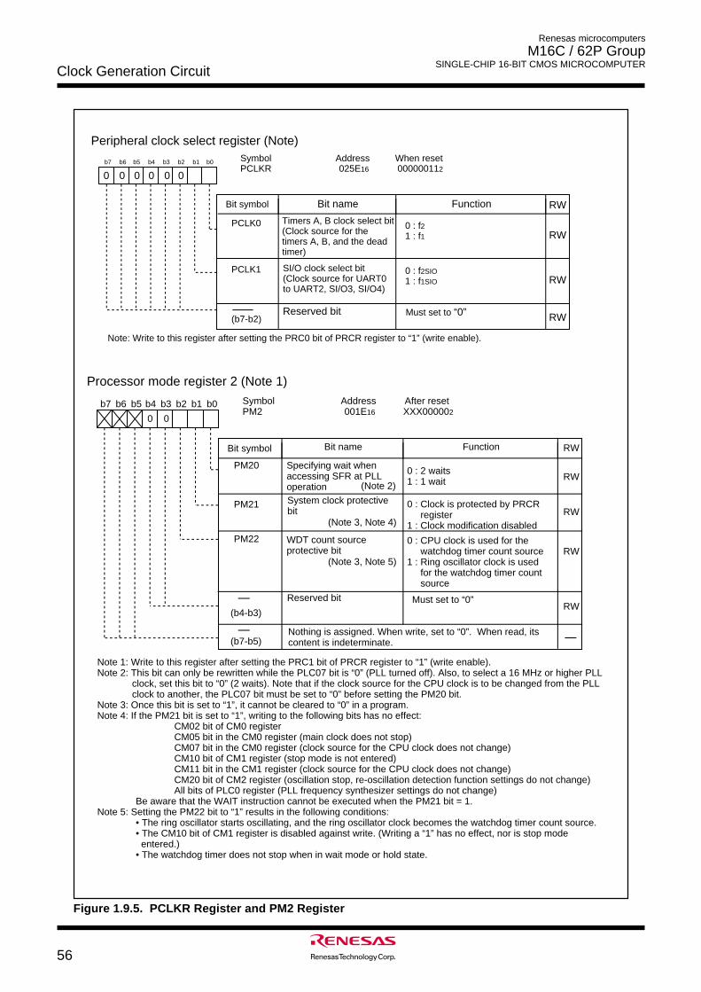
56
Renesas microcomputers
M16C / 62P Group SINGLE-CHIP 16-BIT CMOS MICROCOMPUTER
Clock Generation Circuit
Figure 1.9.5. PCLKR Register and PM2 Register
FunctionBit symbol Bit name
Peripheral clock select register (Note)Symbol Address When reset PCLKR 025E16 000000112
RW
b7 b6 b5 b4 b3 b2 b1 b0
PCLK0 Timers A, B clock select bit (Clock source for the timers A, B, and the dead timer)
0 : f21 : f1
0 0 0
Reserved bit Must set to “0”
Note: Write to this register after setting the PRC0 bit of PRCR register to “1” (write enable).
0 0 0
PCLK1 SI/O clock select bit (Clock source for UART0 to UART2, SI/O3, SI/O4)
0 : f2SIO1 : f1SIO
RW
RW
RW(b7-b2)
FunctionBit symbol Bit name
Processor mode register 2 (Note 1)
Symbol Address After reset PM2 001E16 XXX000002
RW
b7 b6 b5 b4 b3 b2 b1 b0
PM20 Specifying wait when accessing SFR at PLL operation
0 : 2 waits1 : 1 wait
0 0
Reserved bit Must set to “0”
Nothing is assigned. When write, set to “0”. When read, its content is indeterminate.
Note 1: Write to this register after setting the PRC1 bit of PRCR register to “1” (write enable).Note 2: This bit can only be rewritten while the PLC07 bit is “0” (PLL turned off). Also, to select a 16 MHz or higher PLL clock, set this bit to “0” (2 waits). Note that if the clock source for the CPU clock is to be changed from the PLL clock to another, the PLC07 bit must be set to “0” before setting the PM20 bit.Note 3: Once this bit is set to “1”, it cannot be cleared to “0” in a program.Note 4: If the PM21 bit is set to “1”, writing to the following bits has no effect:
CM02 bit of CM0 register CM05 bit in the CM0 register (main clock does not stop)CM07 bit in the CM0 register (clock source for the CPU clock does not change)CM10 bit of CM1 register (stop mode is not entered)CM11 bit in the CM1 register (clock source for the CPU clock does not change)CM20 bit of CM2 register (oscillation stop, re-oscillation detection function settings do not change)All bits of PLC0 register (PLL frequency synthesizer settings do not change)
Be aware that the WAIT instruction cannot be executed when the PM21 bit = 1.Note 5: Setting the PM22 bit to “1” results in the following conditions:
• The ring oscillator starts oscillating, and the ring oscillator clock becomes the watchdog timer count source.• The CM10 bit of CM1 register is disabled against write. (Writing a “1” has no effect, nor is stop mode entered.)• The watchdog timer does not stop when in wait mode or hold state.
(Note 2)RW
RW
RW
PM21
(b7-b5)
System clock protectivebit
0 : Clock is protected by PRCR register1 : Clock modification disabled
PM22 WDT count source protective bit
(Note 3, Note 4)
(Note 3, Note 5)
0 : CPU clock is used for the watchdog timer count source1 : Ring oscillator clock is used for the watchdog timer count source
RW
(b4-b3)
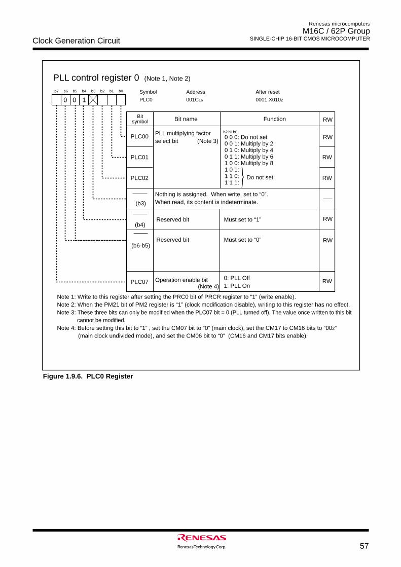
57
Renesas microcomputers
M16C / 62P Group SINGLE-CHIP 16-BIT CMOS MICROCOMPUTERClock Generation Circuit
Figure 1.9.6. PLC0 Register
PLC00
PLC01
PLC02
PLC07
(Note 3)
(Note 4)
Function
Note 1: Write to this register after setting the PRC0 bit of PRCR register to “1” (write enable).Note 2: When the PM21 bit of PM2 register is “1” (clock modification disable), writing to this register has no effect.Note 3: These three bits can only be modified when the PLC07 bit = 0 (PLL turned off). The value once written to this bit cannot be modified.Note 4: Before setting this bit to “1” , set the CM07 bit to “0” (main clock), set the CM17 to CM16 bits to “002” (main clock undivided mode), and set the CM06 bit to “0” (CM16 and CM17 bits enable).
PLL control register 0 (Note 1, Note 2)
PLL multiplying factorselect bit
Nothing is assigned. When write, set to “0”. When read, its content is indeterminate.
Reserved bit
Operation enable bit
0 0 0:0 0 1: Multiply by 20 1 0: Multiply by 40 1 1: Multiply by 61 0 0: Multiply by 81 0 1: 1 1 0: 1 1 1:
0: PLL Off1: PLL On
Must set to “1”
Bit nameBitsymbol
Symbol Address After reset
PLC0 001C16 0001 X0102
RW
b1b0b2
Reserved bit Must set to “0”
Do not set
RW
RW
RW
RW
RW
RW
Do not set
(b4)
(b6-b5)
(b3)
b7 b6 b5 b4 b3 b2 b1 b0
0 10
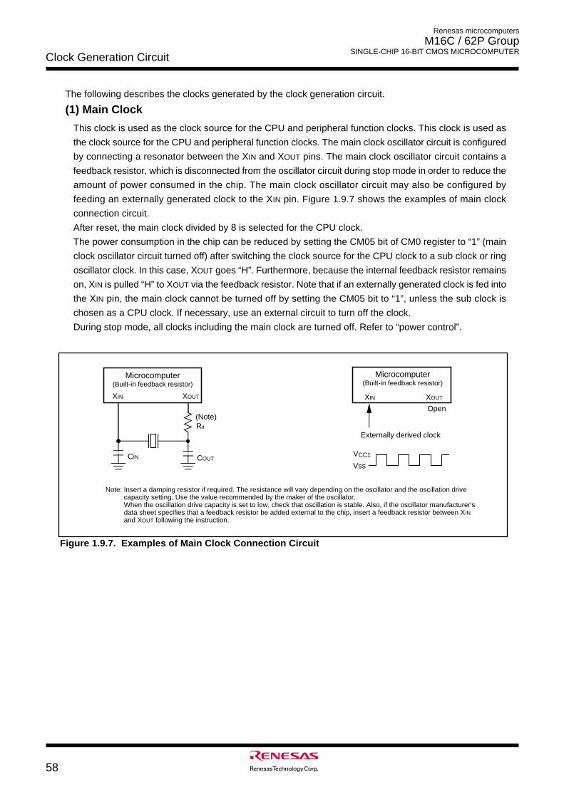
58
Renesas microcomputers
M16C / 62P Group SINGLE-CHIP 16-BIT CMOS MICROCOMPUTER
Clock Generation Circuit
Microcomputer(Built-in feedback resistor)
XIN XOUT
Externally derived clock
Open
VCC1
Vss
Microcomputer(Built-in feedback resistor)
XIN XOUT
Rd
CIN COUT
(Note)
Note: Insert a damping resistor if required. The resistance will vary depending on the oscillator and the oscillation drive capacity setting. Use the value recommended by the maker of the oscillator.When the oscillation drive capacity is set to low, check that oscillation is stable. Also, if the oscillator manufacturer's data sheet specifies that a feedback resistor be added external to the chip, insert a feedback resistor between XIN and XOUT following the instruction.
Figure 1.9.7. Examples of Main Clock Connection Circuit
The following describes the clocks generated by the clock generation circuit.
(1) Main Clock
This clock is used as the clock source for the CPU and peripheral function clocks. This clock is used as
the clock source for the CPU and peripheral function clocks. The main clock oscillator circuit is configured
by connecting a resonator between the XIN and XOUT pins. The main clock oscillator circuit contains a
feedback resistor, which is disconnected from the oscillator circuit during stop mode in order to reduce the
amount of power consumed in the chip. The main clock oscillator circuit may also be configured by
feeding an externally generated clock to the XIN pin. Figure 1.9.7 shows the examples of main clock
connection circuit.
After reset, the main clock divided by 8 is selected for the CPU clock.
The power consumption in the chip can be reduced by setting the CM05 bit of CM0 register to “1” (main
clock oscillator circuit turned off) after switching the clock source for the CPU clock to a sub clock or ring
oscillator clock. In this case, XOUT goes “H”. Furthermore, because the internal feedback resistor remains
on, XIN is pulled “H” to XOUT via the feedback resistor. Note that if an externally generated clock is fed into
the XIN pin, the main clock cannot be turned off by setting the CM05 bit to “1”, unless the sub clock is
chosen as a CPU clock. If necessary, use an external circuit to turn off the clock.
During stop mode, all clocks including the main clock are turned off. Refer to “power control”.
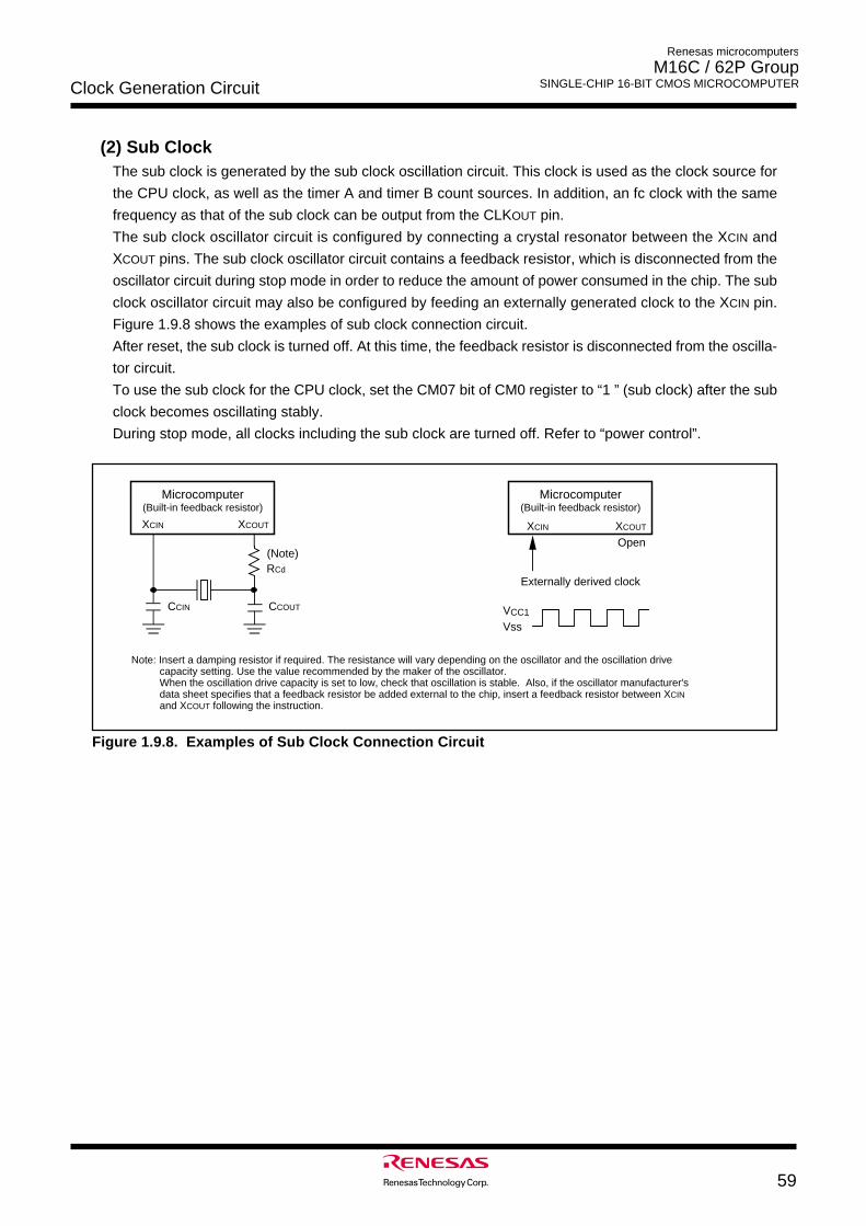
59
Renesas microcomputers
M16C / 62P Group SINGLE-CHIP 16-BIT CMOS MICROCOMPUTERClock Generation Circuit
Microcomputer (Built-in feedback resistor)
XCIN XCOUT
Externally derived clock
Open
Vss
Note: Insert a damping resistor if required. The resistance will vary depending on the oscillator and the oscillation drive capacity setting. Use the value recommended by the maker of the oscillator.When the oscillation drive capacity is set to low, check that oscillation is stable. Also, if the oscillator manufacturer's data sheet specifies that a feedback resistor be added external to the chip, insert a feedback resistor between XCIN and XCOUT following the instruction.
Microcomputer (Built-in feedback resistor)
XCIN XCOUT
(Note)
CCIN CCOUT
RCd
VCC1
Figure 1.9.8. Examples of Sub Clock Connection Circuit
(2) Sub ClockThe sub clock is generated by the sub clock oscillation circuit. This clock is used as the clock source for
the CPU clock, as well as the timer A and timer B count sources. In addition, an fc clock with the same
frequency as that of the sub clock can be output from the CLKOUT pin.
The sub clock oscillator circuit is configured by connecting a crystal resonator between the XCIN and
XCOUT pins. The sub clock oscillator circuit contains a feedback resistor, which is disconnected from the
oscillator circuit during stop mode in order to reduce the amount of power consumed in the chip. The sub
clock oscillator circuit may also be configured by feeding an externally generated clock to the XCIN pin.
Figure 1.9.8 shows the examples of sub clock connection circuit.
After reset, the sub clock is turned off. At this time, the feedback resistor is disconnected from the oscilla-
tor circuit.
To use the sub clock for the CPU clock, set the CM07 bit of CM0 register to “1 ” (sub clock) after the sub
clock becomes oscillating stably.
During stop mode, all clocks including the sub clock are turned off. Refer to “power control”.
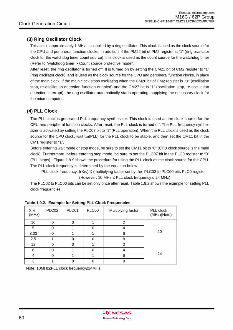
60
Renesas microcomputers
M16C / 62P Group SINGLE-CHIP 16-BIT CMOS MICROCOMPUTER
Clock Generation Circuit
(3) Ring Oscillator ClockThis clock, approximately 1 MHz, is supplied by a ring oscillator. This clock is used as the clock source for
the CPU and peripheral function clocks. In addition, if the PM22 bit of PM2 register is “1” (ring oscillator
clock for the watchdog timer count source), this clock is used as the count source for the watchdog timer
(Refer to “watchdog timer • Count source protective mode”.
After reset, the ring oscillator is turned off. It is turned on by setting the CM21 bit of CM2 register to “1”
(ring oscillator clock), and is used as the clock source for the CPU and peripheral function clocks, in place
of the main clock. If the main clock stops oscillating when the CM20 bit of CM2 register is “1” (oscillation
stop, re-oscillation detection function enabled) and the CM27 bit is “1” (oscillation stop, re-oscillation
detection interrupt), the ring oscillator automatically starts operating, supplying the necessary clock for
the microcomputer.
(4) PLL Clock
The PLL clock is generated PLL frequency synthesizer. This clock is used as the clock source for the
CPU and peripheral function clocks. After reset, the PLL clock is turned off. The PLL frequency synthe-
sizer is activated by setting the PLC07 bit to “1” (PLL operation). When the PLL clock is used as the clock
source for the CPU clock, wait tsu(PLL) for the PLL clock to be stable, and then set the CM11 bit in the
CM1 register to “1”.
Before entering wait mode or stop mode, be sure to set the CM11 bit to “0” (CPU clock source is the main
clock). Furthermore, before entering stop mode, be sure to set the PLC07 bit in the PLC0 register to “0”
(PLL stops). Figure 1.9.9 shows the procedure for using the PLL clock as the clock source for the CPU.
The PLL clock frequency is determined by the equation below.
PLL clock frequency=f(XIN) X (multiplying factor set by the PLC02 to PLC00 bits PLC0 register
(However, 10 MHz ≤ PLL clock frequency ≤ 24 MHz)
The PLC02 to PLC00 bits can be set only once after reset. Table 1.9.2 shows the example for setting PLL
clock frequencies.
XIN(MHz)
PLC02 PLC01 PLC00 Multiplying factor PLL clock(MHz)(Note)
10 0 0 1 2
205 0 1 0 4
3.33 0 1 1 62.5 1 0 0 81264 24
3
0 0 1 20 1 0 40 1 1 61 0 0 8
Note: 10MHz≤PLL clock frequency≤24MHz.
Table 1.9.2. Example for Setting PLL Clock Frequencies
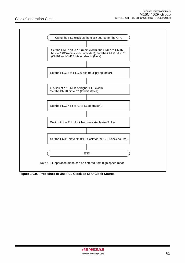
61
Renesas microcomputers
M16C / 62P Group SINGLE-CHIP 16-BIT CMOS MICROCOMPUTERClock Generation Circuit
Figure 1.9.9. Procedure to Use PLL Clock as CPU Clock Source
Using the PLL clock as the clock source for the CPU
Set the CM07 bit to “0” (main clock), the CM17 to CM16 bits to “002”(main clock undivided), and the CM06 bit to “0” (CM16 and CM17 bits enabled). (Note)
Set the PLC02 to PLC00 bits (multiplying factor).
(To select a 16 MHz or higher PLL clock)Set the PM20 bit to “0” (2-wait states).
Set the PLC07 bit to “1” (PLL operation).
Wait until the PLL clock becomes stable (tsu(PLL)).
Set the CM11 bit to “1” (PLL clock for the CPU clock source).
END
Note : PLL operation mode can be entered from high speed mode.
62
Renesas microcomputers
M16C / 62P Group SINGLE-CHIP 16-BIT CMOS MICROCOMPUTER
Clock Generation Circuit
CPU Clock and Peripheral Function ClockTwo type clocks: CPU clock to operate the CPU and peripheral function clocks to operate the peripheral
functions.
(1) CPU Clock and BCLKThese are operating clocks for the CPU and watchdog timer.
The clock source for the CPU clock can be chosen to be the main clock, sub clock, ring oscillator clock or
the PLL clock.
If the main clock or ring oscillator clock is selected as the clock source for the CPU clock, the selected
clock source can be divided by 1 (undivided), 2, 4, 8 or 16 to produce the CPU clock. Use the CM06 bit in
CM0 register and the CM17 to CM16 bits in CM1 register to select the divide-by-n value.
When the PLL clock is selected as the clock source for the CPU clock, the CM06 bit should be set to “0”
and the CM17 to CM16 bits to “002” (undivided).
After reset, the main clock divided by 8 provides the CPU clock.
During memory expansion or microprocessor mode, a BCLK signal with the same frequency as the CPU
clock can be output from the BCLK pin by setting the PM07 bit of PM0 register to “0” (output enabled).
Note that when entering stop mode from high or middle speed mode, ring oscillator mode or ring oscillator
low power dissipation mode, or when the CM05 bit of CM0 register is set to “1” (main clock turned off) in
low-speed mode, the CM06 bit of CM0 register is set to “1” (divide-by-8 mode).
(2) Peripheral Function Clock(f1, f2, f8, f32, f1SIO, f2SIO, f8SIO, f32SIO, fAD, fC32)These are operating clocks for the peripheral functions.
Of these, fi (i = 1, 2, 8, 32) and fiSIO are derived from the main clock, PLL clock or ring oscillator clock by
dividing them by i. The clock fi is used for timers A and B, and fiSIO is used for serial I/O. The f8 and f32
clocks can be output from the CLKOUT pin.
The fAD clock is produced from the main clock, PLL clock or ring oscillator clock, and is used for the A-D
converter.
When the WAIT instruction is executed after setting the CM02 bit of CM0 register to “1” (peripheral
function clock turned off during wait mode), or when the microcomputer is in low power dissipation mode,
the fi, fiSIO and fAD clocks are turned off.
The fC32 clock is produced from the sub clock, and is used for timers A and B. This clock can be used
when the sub clock is on.
Clock Output FunctionDuring single-chip mode, the f8, f32 or fC clock can be output from the CLKOUT pin. Use the CM01 to
CM00 bits of CM0 register to select.
63
Renesas microcomputers
M16C / 62P Group SINGLE-CHIP 16-BIT CMOS MICROCOMPUTERClock Generation Circuit
Power ControlThere are three power control modes. For convenience’ sake, all modes other than wait and stop modes
are referred to as normal operation mode here.
(1) Normal Operation Mode
Normal operation mode is further classified into seven modes.
In normal operation mode, because the CPU clock and the peripheral function clocks both are on, the
CPU and the peripheral functions are operating. Power control is exercised by controlling the CPU clock
frequency. The higher the CPU clock frequency, the greater the processing capability. The lower the CPU
clock frequency, the smaller the power consumption in the chip. If the unnecessary oscillator circuits are
turned off, the power consumption is further reduced.
Before the clock sources for the CPU clock can be switched over, the new clock source to which switched
must be oscillating stably. If the new clock source is the main clock, sub clock or PLL clock, allow a
sufficient wait time in a program until it becomes oscillating stably.
Note that operation modes cannot be changed directly from low speed or low power dissipation mode to
ring oscillator or ring oscillator low power dissipation mode. Nor can operation modes be changed directly
from ring oscillator or ring oscillator low power dissipation mode to low speed or low power dissipation
mode. Where the CPU clock source is changed from the ring oscillator to the main clock, change the
operation mode to the medium speed mode (divided by 8 mode) after the clock was divided by 8 (the
CM06 bit of CM0 register was set to “1”) in the ring oscillator mode.
• High-speed Mode
The main clock divided by 1 provides the CPU clock. If the sub clock is on, fC32 can be used as the
count source for timers A and B.
• PLL Operation Mode
The main clock multiplied by 2, 4, 6 or 8 provides the PLL clock, and this PLL clock serves as the CPU
clock. If the sub clock is on, fC32 can be used as the count source for timers A and B. PLL operation
mode can be entered from high speed mode. If PLL operation mode is to be changed to wait or stop
mode, first go to high speed mode before changing.
• Medium-speed Mode
The main clock divided by 2, 4, 8 or 16 provides the CPU clock. If the sub clock is on, fC32 can be used
as the count source for timers A and B.
• Low-speed Mode
The sub clock provides the CPU clock. The main clock is used as the clock source for the peripheral
function clock when the CM21 bit is set to “0” (ring oscillator turned off), and the ring oscillator clock is
used when the CM21 bit is set to “1” (ring oscillator oscillating).
The fC32 clock can be used as the count source for timers A and B.
• Low Power Dissipation Mode
In this mode, the main clock is turned off after being placed in low speed mode. The sub clock provides
the CPU clock. The fC32 clock can be used as the count source for timers A and B.
Simultaneously when this mode is selected, the CM06 bit of CM0 register becomes “1” (divided by 8
mode). In the low power dissipation mode, do not change the CM06 bit. Consequently, the medium
speed (divided by 8) mode is to be selected when the main clock is operated next.
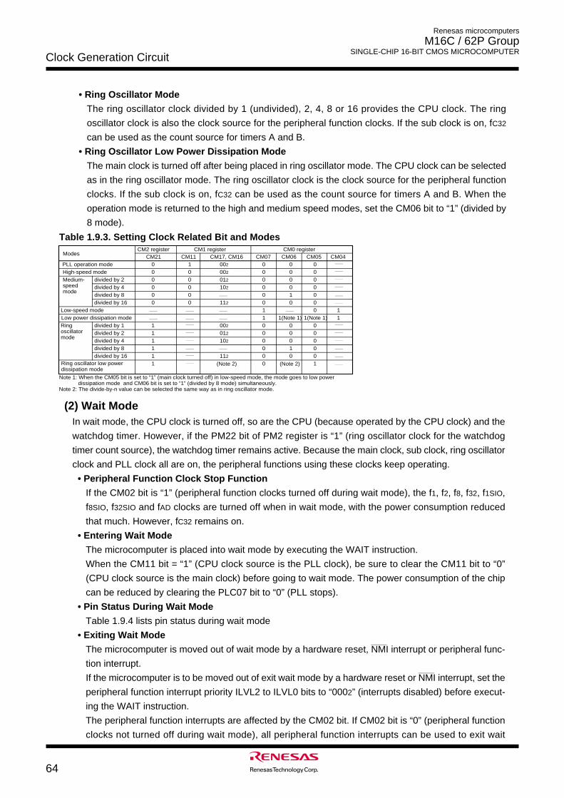
64
Renesas microcomputers
M16C / 62P Group SINGLE-CHIP 16-BIT CMOS MICROCOMPUTER
Clock Generation Circuit
• Ring Oscillator Mode
The ring oscillator clock divided by 1 (undivided), 2, 4, 8 or 16 provides the CPU clock. The ring
oscillator clock is also the clock source for the peripheral function clocks. If the sub clock is on, fC32
can be used as the count source for timers A and B.
• Ring Oscillator Low Power Dissipation Mode
The main clock is turned off after being placed in ring oscillator mode. The CPU clock can be selected
as in the ring oscillator mode. The ring oscillator clock is the clock source for the peripheral function
clocks. If the sub clock is on, fC32 can be used as the count source for timers A and B. When the
operation mode is returned to the high and medium speed modes, set the CM06 bit to “1” (divided by
8 mode).
Modes CM2 register
CM21CM1 register
CM11 CM17, CM16CM0 register
CM07 CM06 CM05 CM04PLL operation mode 0 1 002 0 0High-speed mode 0 0 002 0 0 0Medium-speed mode
0 0 012 0 0 00 0 102 0 0 0
divided by 2
0 0 0 1 00 0 112 0 0 0
Low-speed mode 1 0 1 Low power dissipation mode 1 1(Note 1) 1Ring oscillator mode
1
divided by 4divided by 8divided by 16
Ring oscillator low power dissipation mode
Note 1: When the CM05 bit is set to “1” (main clock turned off) in low-speed mode, the mode goes to low power dissipation mode and CM06 bit is set to “1” (divided by 8 mode) simultaneously.
Note 2: The divide-by-n value can be selected the same way as in ring oscillator mode.
0
0
1 012 0 0 01 102 0 0 01 0 1 01 112 0 0 0
1 002 0 0 0
(Note 2)
divided by 2divided by 4divided by 8divided by 16
divided by 11(Note 1)
(Note 2) 1
(2) Wait ModeIn wait mode, the CPU clock is turned off, so are the CPU (because operated by the CPU clock) and the
watchdog timer. However, if the PM22 bit of PM2 register is “1” (ring oscillator clock for the watchdog
timer count source), the watchdog timer remains active. Because the main clock, sub clock, ring oscillator
clock and PLL clock all are on, the peripheral functions using these clocks keep operating.
• Peripheral Function Clock Stop Function
If the CM02 bit is “1” (peripheral function clocks turned off during wait mode), the f1, f2, f8, f32, f1SIO,
f8SIO, f32SIO and fAD clocks are turned off when in wait mode, with the power consumption reduced
that much. However, fC32 remains on.
• Entering Wait Mode
The microcomputer is placed into wait mode by executing the WAIT instruction.
When the CM11 bit = “1” (CPU clock source is the PLL clock), be sure to clear the CM11 bit to “0”
(CPU clock source is the main clock) before going to wait mode. The power consumption of the chip
can be reduced by clearing the PLC07 bit to “0” (PLL stops).
• Pin Status During Wait Mode
Table 1.9.4 lists pin status during wait mode
• Exiting Wait Mode______
The microcomputer is moved out of wait mode by a hardware reset, NMI interrupt or peripheral func-
tion interrupt.______
If the microcomputer is to be moved out of exit wait mode by a hardware reset or NMI interrupt, set the
peripheral function interrupt priority ILVL2 to ILVL0 bits to “0002” (interrupts disabled) before execut-
ing the WAIT instruction.
The peripheral function interrupts are affected by the CM02 bit. If CM02 bit is “0” (peripheral function
clocks not turned off during wait mode), all peripheral function interrupts can be used to exit wait
Table 1.9.3. Setting Clock Related Bit and Modes
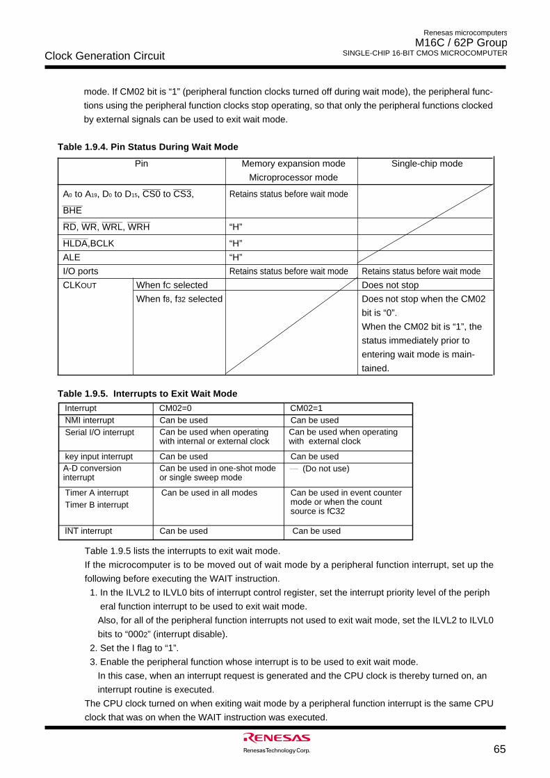
65
Renesas microcomputers
M16C / 62P Group SINGLE-CHIP 16-BIT CMOS MICROCOMPUTERClock Generation Circuit
Table 1.9.4. Pin Status During Wait Mode
Pin Memory expansion mode Single-chip mode
Microprocessor mode_______ _______
A0 to A19, D0 to D15, CS0 to CS3, Retains status before wait mode________
BHE_____ ______ ________ _________
RD, WR, WRL, WRH “H”__________
HLDA,BCLK “H”
ALE “H”
I/O ports Retains status before wait mode Retains status before wait mode
CLKOUT When fC selected Does not stop
When f8, f32 selected Does not stop when the CM02
bit is “0”.
When the CM02 bit is “1”, the
status immediately prior to
entering wait mode is main-
tained.
Interrupt CM02=0 CM02=1 NMI interrupt Can be usedSerial I/O interrupt Can be used when operating
with internal or external clockCan be used when operating with external clock
key input interrupt Can be used Can be usedA-D conversion interrupt
Can be used in one-shot mode or single sweep mode
Timer A interrupt Can be used in all modes Can be used in event counter mode or when the count source is fC32
Timer B interrupt
INT interrupt
Can be used
Can be used
(Do not use)
Can be used
Table 1.9.5. Interrupts to Exit Wait Mode
mode. If CM02 bit is “1” (peripheral function clocks turned off during wait mode), the peripheral func-
tions using the peripheral function clocks stop operating, so that only the peripheral functions clocked
by external signals can be used to exit wait mode.
Table 1.9.5 lists the interrupts to exit wait mode.
If the microcomputer is to be moved out of wait mode by a peripheral function interrupt, set up the
following before executing the WAIT instruction.
1. In the ILVL2 to ILVL0 bits of interrupt control register, set the interrupt priority level of the periph
eral function interrupt to be used to exit wait mode.
Also, for all of the peripheral function interrupts not used to exit wait mode, set the ILVL2 to ILVL0
bits to “0002” (interrupt disable).
2. Set the I flag to “1”.
3. Enable the peripheral function whose interrupt is to be used to exit wait mode.
In this case, when an interrupt request is generated and the CPU clock is thereby turned on, an
interrupt routine is executed.
The CPU clock turned on when exiting wait mode by a peripheral function interrupt is the same CPU
clock that was on when the WAIT instruction was executed.
66
Renesas microcomputers
M16C / 62P Group SINGLE-CHIP 16-BIT CMOS MICROCOMPUTER
Clock Generation Circuit
(3) Stop Mode
In stop mode, all oscillator circuits are turned off, so are the CPU clock and the peripheral function clocks.Therefore, the CPU and the peripheral functions clocked by these clocks stop operating. The leastamount of power is consumed in this mode. If the voltage applied to Vcc1 and Vcc2 pins is VRAM or more,the internal RAM is retained. When applying 2.7 or less voltage to Vcc1 and Vcc2 pins, make sureVcc1≥Vcc2≥VRAM.However, the peripheral functions clocked by external signals keep operating. The following interruptscan be used to exit stop mode.
______
• NMI interrupt• Key interrupt
______
• INT interrupt• Timer A, Timer B interrupt (when counting external pulses in event counter mode)• Serial I/O interrupt (when external clock is selected)
• Voltage down detection interrupt (refer to “voltage down detection interrupt” for an operating condition)
• Entering Stop ModeThe microcomputer is placed into stop mode by setting the CM10 bit of CM1 register to “1” (all clocksturned off). At the same time, the CM06 bit of CM0 register is set to “1” (divide-by-8 mode) and theCM15 bit of CM1 register is set to “1” (main clock oscillator circuit drive capability high).Before entering stop mode, set the CM20 bit to “0” (oscillation stop, re-oscillation detection functiondisable).Also, if the CM11 bit is “1” (PLL clock for the CPU clock source), set the CM11 bit to “0” (main clock forthe CPU clock source) and the PLC07 bit to “0” (PLL turned off) before entering stop mode.
• Pin Status in Stop ModeTable 1.9.6 lists pin status during stop mode
• Exiting Stop Mode______
The microcomputer is moved out of stop mode by a hardware reset, NMI interrupt or peripheral func-tion interrupt.
______
If the microcomputer is to be moved out of stop mode by a hardware reset or NMI interrupt, set theperipheral function interrupt priority ILVL2 to ILVL0 bits to “0002” (interrupts disable) before setting theCM10 bit to “1”.If the microcomputer is to be moved out of stop mode by a peripheral function interrupt, set up thefollowing before setting the CM10 bit to “1”.
1. In the ILVL2 to ILVL0 bits of interrupt control register, set the interrupt priority level of the periph-eral function interrupt to be used to exit stop mode.Also, for all of the peripheral function interrupts not used to exit stop mode, set the ILVL2 to ILVL0bits to “0002”.
2. Set the I flag to “1”.3. Enable the peripheral function whose interrupt is to be used to exit stop mode.
In this case, when an interrupt request is generated and the CPU clock is thereby turned on, aninterrupt service routine is executed.
______
Which CPU clock will be used after exiting stop mode by a peripheral function or NMI interrupt isdetermined by the CPU clock that was on when the microcomputer was placed into stop mode asfollows:If the CPU clock before entering stop mode was derived from the sub clock: sub clockIf the CPU clock before entering stop mode was derived from the main clock: main clock divide-by-8If the CPU clock before entering stop mode was derived from the ring oscillator clock: ring oscillatorclock divide-by-8
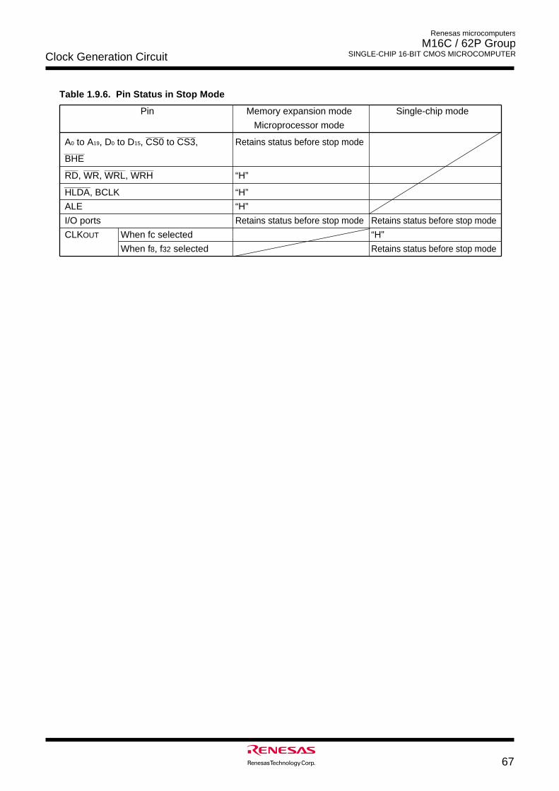
67
Renesas microcomputers
M16C / 62P Group SINGLE-CHIP 16-BIT CMOS MICROCOMPUTERClock Generation Circuit
Pin Memory expansion mode Single-chip mode
Microprocessor mode_______ _______
A0 to A19, D0 to D15, CS0 to CS3, Retains status before stop mode________
BHE_____ ______ ________ _________
RD, WR, WRL, WRH “H”__________
HLDA, BCLK “H”
ALE “H”
I/O ports Retains status before stop mode Retains status before stop mode
CLKOUT When fc selected “H”
When f8, f32 selected Retains status before stop mode
Table 1.9.6. Pin Status in Stop Mode
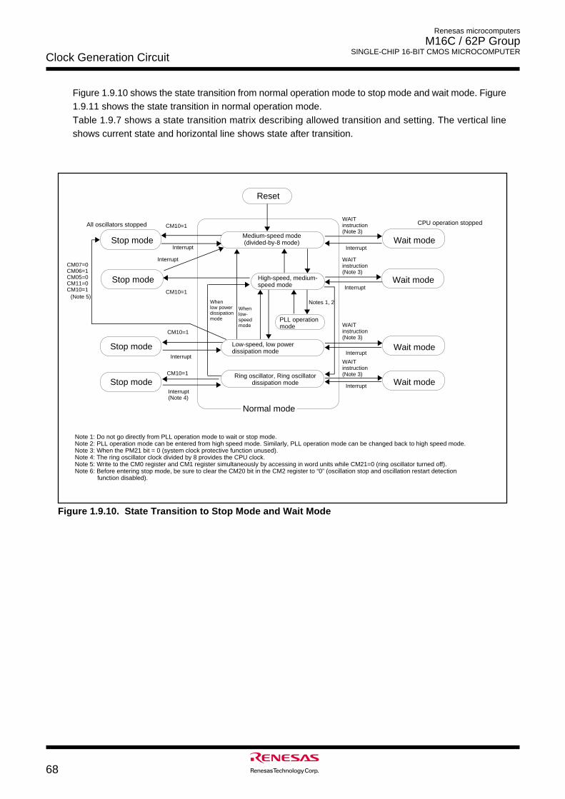
68
Renesas microcomputers
M16C / 62P Group SINGLE-CHIP 16-BIT CMOS MICROCOMPUTER
Clock Generation Circuit
Figure 1.9.10. State Transition to Stop Mode and Wait Mode
Reset
Medium-speed mode(divided-by-8 mode)
High-speed, medium-speed mode
Stop mode Wait mode Interrupt
CM10=1
Interrupt
Normal mode
Low-speed, low powerdissipation mode
CM10=1
Stop mode Interrupt
Wait mode Interrupt
CM10=1
Stop mode
All oscillators stopped
InterruptWait mode
WAIT instruction(Note 3)
Interrupt
CPU operation stopped
Whenlow-speedmode
Whenlow powerdissipationmode PLL operation
mode
Notes 1, 2
Note 1: Do not go directly from PLL operation mode to wait or stop mode.Note 2: PLL operation mode can be entered from high speed mode. Similarly, PLL operation mode can be changed back to high speed mode. Note 3: When the PM21 bit = 0 (system clock protective function unused).Note 4: The ring oscillator clock divided by 8 provides the CPU clock.Note 5: Write to the CM0 register and CM1 register simultaneously by accessing in word units while CM21=0 (ring oscillator turned off).Note 6: Before entering stop mode, be sure to clear the CM20 bit in the CM2 register to “0” (oscillation stop and oscillation restart detection
function disabled).
Ring oscillator, Ring oscillatordissipation mode Wait mode Interrupt
CM10=1
Interrupt(Note 4)
Stop mode
WAIT instruction(Note 3)
WAIT instruction(Note 3)
WAIT instruction(Note 3)
CM07=0CM06=1CM05=0CM11=0CM10=1
(Note 5)
Figure 1.9.10 shows the state transition from normal operation mode to stop mode and wait mode. Figure1.9.11 shows the state transition in normal operation mode.Table 1.9.7 shows a state transition matrix describing allowed transition and setting. The vertical lineshows current state and horizontal line shows state after transition.
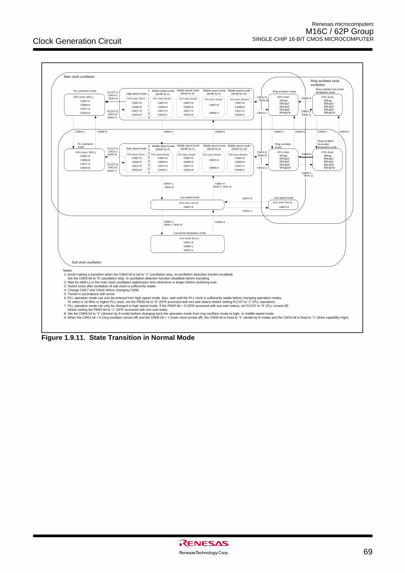
69
Renesas microcomputers
M16C / 62P Group SINGLE-CHIP 16-BIT CMOS MICROCOMPUTERClock Generation Circuit
Figure 1.9.11. State Transition in Normal Mode
CM04=0
CPU clock: f(PLL)
CM07=0
CM06=0
CM17=0
CM16=0
PLL operation mode
CM07=0
CM06=0
CM17=0
CM16=0
CM07=0
CM17=0
CM06=0
CM16=0
CM07=0
CM17=0
CM06=0
CM16=1
CM07=0
CM17=1
CM06=0
CM16=0
CM07=0
CM06=1
CM07=0
CM17=1
CM06=0
CM16=1
High-speed mode
CM07=0
CM17=0
CM06=0
CM16=0
CM07=0
CM17=0
CM06=0
CM16=1
CM07=0
CM17=1
CM06=0
CM16=0
CM07=0
CM06=1
CM07=0
CM17=1
CM06=0
CM16=1
CM07=0
Low-speed mode
CM07=0
Low power dissipation mode
CM06=1
CM15=1
Ring oscillator mode
CPU clock
Ring oscillatormode
CPU clock
CPU clock
Ring oscillator low power dissipation mode
CPU clock
CM07=0
Low-speed mode
PLC07=1CM11=1(Note 6)
PLC07=0CM11=0(Note 7)
CM04=0
PLC07=1CM11=1
PLC07=0CM11=0
CM04=0CM04=1CM04=1 CM04=1 CM04=0CM04=1
CM07=0(Note 2, Note 4)
CM07=1(Note 3)
CM05=1(Note 1, Note 9)
CM05=0
CM21=0(Note 8)
CM21=1
CM21=0(Note 8)
CM21=1
CM21=0
CM21=1
Main clock oscillationRing oscillator clock oscillation
Sub clock oscillation
f(Ring)f(Ring)/2f(Ring)/4f(Ring)/8f(Ring)/16
f(Ring)f(Ring)/2f(Ring)/4f(Ring)/8f(Ring)/16
f(Ring)f(Ring)/2f(Ring)/4f(Ring)/8f(Ring)/16
f(Ring)f(Ring)/2f(Ring)/4f(Ring)/8f(Ring)/16
PLL operation mode
CPU clock: f(PLL)CPU clock: f(XIN)
High-speed modeMiddle-speed mode (divide by 2)
CPU clock: f(XIN)/2 CPU clock: f(XIN)/4 CPU clock: f(XIN)/8 CPU clock: f(XIN)/16
CPU clock: f(XCIN)
CPU clock: f(XCIN)
CPU clock: f(XCIN)
CM05=0M0M
CM05=1(Note 1)
CM05=1(Note 1)
CM05=0
(Note 6)
(Note 7)
Middle-speed mode (divide by 4)
Middle-speed mode (divide by 8)
Middle-speed mode (divide by 16)
Middle-speed mode (divide by 2)
Middle-speed mode (divide by 4)
Middle-speed mode (divide by 8)
Middle-speed mode (divide by 16)
CPU clock: f(XIN) CPU clock: f(XIN)/2 CPU clock: f(XIN)/4 CPU clock: f(XIN)/8 CPU clock: f(XIN)/16
Ring oscillator low power dissipation mode
Notes: 1: Avoid making a transition when the CM20 bit is set to “1” (oscillation stop, re-oscillation detection function enabled). Set the CM20 bit to “0” (oscillation stop, re-oscillation detection function disabled) before transiting. 2: Wait for td(M-L) or the main clock oscillation stabilization time whichever is longer before switching over. 3: Switch clock after oscillation of sub-clock is sufficiently stable. 4: Change CM17 and CM16 before changing CM06. 5: Transit in accordance with arrow. 6: PLL operation mode can only be entered from high speed mode. Also, wait until the PLL clock is sufficiently stable before changing operation modes. To select a 16 MHz or higher PLL clock, set the PM20 bit to “0” (SFR accessed with two wait states) before setting PLC07 to “1” (PLL operation). 7: PLL operation mode can only be changed to high speed mode. If the PM20 bit = 0 (SFR accessed with two wait states), set PLC07 to “0” (PLL turned off) before setting the PM20 bit to “1” (SFR accessed with one wait state). 8: Set the CM06 bit to “1” (division by 8 mode) before changing back the operation mode from ring oscillator mode to high- or middle-speed mode. 9: When the CM21 bit = 0 (ring oscillator turned off) and the CM05 bit = 1 (main clock turned off), the CM06 bit is fixed to “1” (divide-by-8 mode) and the CM15 bit is fixed to “1” (drive capability High).
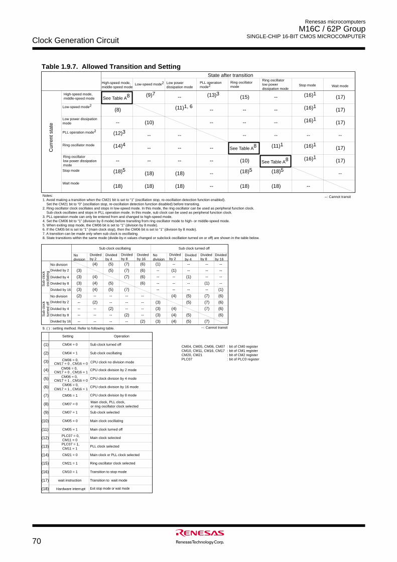
70
Renesas microcomputers
M16C / 62P Group SINGLE-CHIP 16-BIT CMOS MICROCOMPUTER
Clock Generation Circuit
Table 1.9.7. Allowed Transition and Setting
High-speed mode, middle-speed mode
Ring oscillator mode
Stop mode
Wait mode
Ring oscillatorlow power dissipationmode
PLL operation mode2
Low power dissipationmode
Low-speed mode2
Cur
rent
sta
te
State after transition
See Table A8
--
(8)
(18)5
(9)7 --
(10)
(11)1, 6
(12)3
(14)4
--
--
--
--
--
(13)3 (15) --
--
--
--
--
--
--
(10)
--
--
--
-- -- --
--
--
(18)(18) --
--
(16)1 (17)
(16)1 (17)
(16)1 (17)
(16)1 (17)
(16)1 (17)
-- --
(18)5 (18)5
(18)(18)(18)(18)(18)
(1)
(2)
(3)
(4)
(5)
(6)
(7)
(8)
(9)
(10)
(11)
(12)
(13)
(14)
(15)
(16)
(17)
(18)
Setting Operation
CM04 = 0 Sub clock turned off
CM04 = 1 Sub clock oscillating
CM06 = 0,CPU clock no division modeCM17 = 0 , CM16 = 0
CM06 = 0, CPU clock division by 2 modeCM17 = 0 , CM16 = 1
CM06 = 0, CPU clock division by 4 modeCM17 = 1 , CM16 = 0
CM06 = 1 CPU clock division by 8 mode
CM06 = 0, CPU clock division by 16 modeCM17 = 1 , CM16 = 1
CM07 = 0 Main clock, PLL clock, or ring oscillator clock selected
CM07 = 1 Sub clock selected
CM05 = 0 Main clock oscillating
CM05 = 1 Main clock turned off
PLC07 = 0,CM11 = 0
Main clock selected
PLC07 = 1,CM11 = 1
PLL clock selected
CM21 = 0 Main clock or PLL clock selected
CM21 = 1 Ring oscillator clock selected
CM10 = 1 Transition to stop mode
wait instruction Transition to wait mode
Hardware interrupt Exit stop mode or wait mode
Notes:1. Avoid making a transition when the CM21 bit is set to “1” (oscillation stop, re-oscillation detection function enabled). Set the CM21 bit to “0” (oscillation stop, re-oscillation detection function disabled) before transiting.2. Ring oscillator clock oscillates and stops in low-speed mode. In this mode, the ring oscillator can be used as peripheral function clock. Sub clock oscillates and stops in PLL operation mode. In this mode, sub clock can be used as peripheral function clock.3. PLL operation mode can only be entered from and changed to high-speed mode.4. Set the CM06 bit to “1” (division by 8 mode) before transiting from ring oscillator mode to high- or middle-speed mode.5. When exiting stop mode, the CM06 bit is set to “1” (division by 8 mode).6. If the CM05 bit is set to “1” (main clock stop), then the CM06 bit is set to “1” (division by 8 mode).7. A transition can be made only when sub clock is oscillating. 8. State transitions within the same mode (divide-by-n values changed or subclock oscillation turned on or off) are shown in the table below.
--: Cannot transit
(11)1
High-speed mode, middle-speed mode
Ring oscillatormode Stop mode Wait mode
Ring oscillatorlow powerdissipation mode
PLL operationmode2
Low powerdissipation mode
Low-speed mode2
See Table A8
See Table A8
(3)
(3)
(3)
(3)
(4)
(4)
(4)
(4)
(5)
(7)
(7)
(5)
(5)
(5)
(7)
(7)
(6)
(6)
(6)
(6)
No division
Divided by 2
(3)
(3)
(3)
(3)
(4)
(4)
(4)
(4)
(5)
(5)
(5)
(5) (7)
(7)
(7)
(7)
(6)
(6)
(6)
(6)
(1)
(1)
(1)
(1)
(1)
(2)
(2)
(2)
(2)
(2)
--
--
-- --
--
--
----
--
--
--
--
--
--
--
-- -- --
-- --
--
--
--
--
--
--
--
--
--
--
-- --
--
--
--
--
--
--
--
--
Sub clock oscillating Sub clock turned off
--: Cannot transit
Divided by 4
Divided by 8
Divided by 16
No division
Divided by 2
Dividedby 4
Divided by 8
Divided by 16
No division
Divided by 4
Sub
clo
ck
osci
llatin
gS
ub c
lock
tu
rned
off
Divided by 8
Divided by 16
Divided by 2
No division
Divided by 4
Divided by 8
Divided by 16
Divided by 2
9. ( ) : setting method. Refer to following table.
CM04, CM05, CM06, CM07 : bit of CM0 registerCM10, CM11, CM16, CM17 : bit of CM1 registerCM20, CM21 : bit of CM2 registerPLC07 : bit of PLC0 register
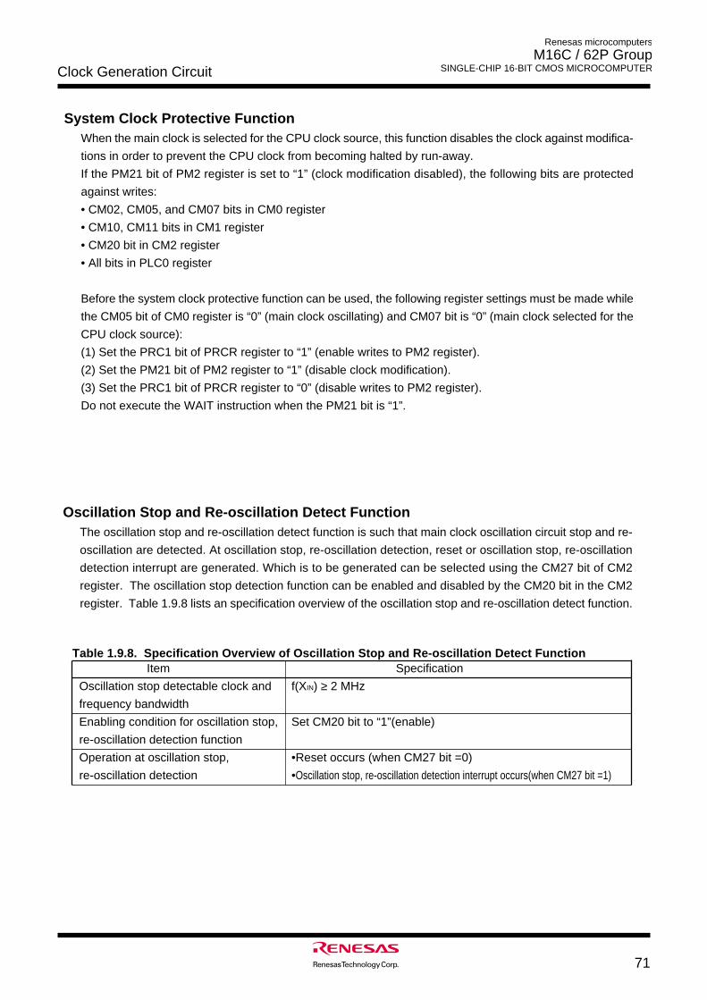
71
Renesas microcomputers
M16C / 62P Group SINGLE-CHIP 16-BIT CMOS MICROCOMPUTERClock Generation Circuit
System Clock Protective FunctionWhen the main clock is selected for the CPU clock source, this function disables the clock against modifica-
tions in order to prevent the CPU clock from becoming halted by run-away.
If the PM21 bit of PM2 register is set to “1” (clock modification disabled), the following bits are protected
against writes:
• CM02, CM05, and CM07 bits in CM0 register
• CM10, CM11 bits in CM1 register
• CM20 bit in CM2 register
• All bits in PLC0 register
Before the system clock protective function can be used, the following register settings must be made while
the CM05 bit of CM0 register is “0” (main clock oscillating) and CM07 bit is “0” (main clock selected for the
CPU clock source):
(1) Set the PRC1 bit of PRCR register to “1” (enable writes to PM2 register).
(2) Set the PM21 bit of PM2 register to “1” (disable clock modification).
(3) Set the PRC1 bit of PRCR register to “0” (disable writes to PM2 register).
Do not execute the WAIT instruction when the PM21 bit is “1”.
Oscillation Stop and Re-oscillation Detect FunctionThe oscillation stop and re-oscillation detect function is such that main clock oscillation circuit stop and re-
oscillation are detected. At oscillation stop, re-oscillation detection, reset or oscillation stop, re-oscillation
detection interrupt are generated. Which is to be generated can be selected using the CM27 bit of CM2
register. The oscillation stop detection function can be enabled and disabled by the CM20 bit in the CM2
register. Table 1.9.8 lists an specification overview of the oscillation stop and re-oscillation detect function.
Table 1.9.8. Specification Overview of Oscillation Stop and Re-oscillation Detect FunctionItem Specification
Oscillation stop detectable clock and f(XIN) ≥ 2 MHz
frequency bandwidth
Enabling condition for oscillation stop, Set CM20 bit to “1”(enable)
re-oscillation detection function
Operation at oscillation stop, •Reset occurs (when CM27 bit =0)
re-oscillation detection •Oscillation stop, re-oscillation detection interrupt occurs(when CM27 bit =1)
72
Renesas microcomputers
M16C / 62P Group SINGLE-CHIP 16-BIT CMOS MICROCOMPUTER
Clock Generation Circuit
(1) Operation When CM27 bit = 0 (Oscillation Stop Detection Reset)Where main clock stop is detected when the CM20 bit is “1” (oscillation stop, re-oscillation detection
function enabled), the microcomputer is initialized, coming to a halt (oscillation stop reset; refer to “SFR”,
“Reset”).
This status is reset with hardware reset 1 or hardware reset 2. Also, even when re-oscillation is detected,
the microcomputer can be initialized and stopped; it is, however, necessary to avoid such usage. (During
main clock stop, do not set the CM20 bit to “1” and the CM27 bit to “0”.)
(2) Operation When CM27 bit = 0 (Oscillation Stop and Re-oscillation Detect Interrupt)Where the main clock corresponds to the CPU clock source and the CM20 bit is “1” (oscillation stop and
re-oscillation detect function enabled), the system is placed in the following state if the main clock comes
to a halt:
• Oscillation stop and re-oscillation detect interrupt request occurs.
• The ring oscillator starts oscillation, and the ring oscillator clock becomes the clock source for CPU clock
and peripheral functions in place of the main clock.
• CM21 bit = 1 (ring oscillator clock for CPU clock source)
• CM22 bit = 1 (main clock stop detected)
• CM23 bit = 1 (main clock stopped)
Where the PLL clock corresponds to the CPU clock source and the CM20 bit is “1”, the system is placed
in the following state if the main clock comes to a halt: Since the CM21 bit remains unchanged, set it to “1”
(ring oscillator clock) inside the interrupt routine.
• Oscillation stop and re-oscillation detect interrupt request occurs.
• CM22 bit = 1 (main clock stop detected)
• CM23 bit = 1 (main clock stopped)
• CM21 bit remains unchanged
Where the CM20 bit is “1”, the system is placed in the following state if the main clock re-oscillates from
the stop condition:
• Oscillation stop and re-oscillation detect interrupt request occurs.
• CM22 bit = 1 (main clock re-oscillation detected)
• CM23 bit = 0 (main clock oscillation)
• CM21 bit remains unchanged
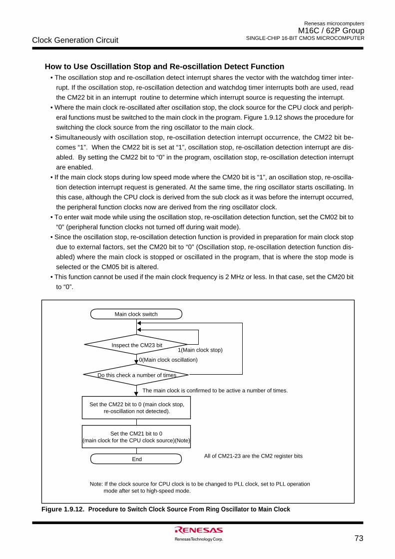
73
Renesas microcomputers
M16C / 62P Group SINGLE-CHIP 16-BIT CMOS MICROCOMPUTERClock Generation Circuit
How to Use Oscillation Stop and Re-oscillation Detect Function• The oscillation stop and re-oscillation detect interrupt shares the vector with the watchdog timer inter-
rupt. If the oscillation stop, re-oscillation detection and watchdog timer interrupts both are used, read
the CM22 bit in an interrupt routine to determine which interrupt source is requesting the interrupt.
• Where the main clock re-oscillated after oscillation stop, the clock source for the CPU clock and periph-
eral functions must be switched to the main clock in the program. Figure 1.9.12 shows the procedure for
switching the clock source from the ring oscillator to the main clock.
• Simultaneously with oscillation stop, re-oscillation detection interrupt occurrence, the CM22 bit be-
comes “1”. When the CM22 bit is set at “1”, oscillation stop, re-oscillation detection interrupt are dis-
abled. By setting the CM22 bit to “0” in the program, oscillation stop, re-oscillation detection interrupt
are enabled.
• If the main clock stops during low speed mode where the CM20 bit is “1”, an oscillation stop, re-oscilla-
tion detection interrupt request is generated. At the same time, the ring oscillator starts oscillating. In
this case, although the CPU clock is derived from the sub clock as it was before the interrupt occurred,
the peripheral function clocks now are derived from the ring oscillator clock.
• To enter wait mode while using the oscillation stop, re-oscillation detection function, set the CM02 bit to
“0” (peripheral function clocks not turned off during wait mode).
• Since the oscillation stop, re-oscillation detection function is provided in preparation for main clock stop
due to external factors, set the CM20 bit to “0” (Oscillation stop, re-oscillation detection function dis-
abled) where the main clock is stopped or oscillated in the program, that is where the stop mode is
selected or the CM05 bit is altered.
• This function cannot be used if the main clock frequency is 2 MHz or less. In that case, set the CM20 bit
to “0”.
Figure 1.9.12. Procedure to Switch Clock Source From Ring Oscillator to Main Clock
Main clock switch
Inspect the CM23 bit
Do this check a number of times
Set the CM22 bit to 0 (main clock stop,re-oscillation not detected).
Set the CM21 bit to 0(main clock for the CPU clock source)(Note)
1(Main clock stop)
0(Main clock oscillation)
The main clock is confirmed to be active a number of times.
All of CM21-23 are the CM2 register bitsEnd
Note: If the clock source for CPU clock is to be changed to PLL clock, set to PLL operation mode after set to high-speed mode.
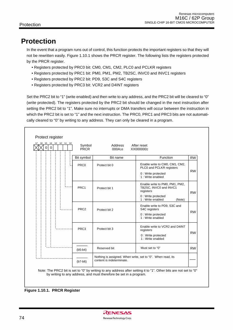
Renesas microcomputers
M16C / 62P Group SINGLE-CHIP 16-BIT CMOS MICROCOMPUTER
74
Protection
ProtectionIn the event that a program runs out of control, this function protects the important registers so that they will
not be rewritten easily. Figure 1.10.1 shows the PRCR register. The following lists the registers protected
by the PRCR register.
• Registers protected by PRC0 bit: CM0, CM1, CM2, PLC0 and PCLKR registers
• Registers protected by PRC1 bit: PM0, PM1, PM2, TB2SC, INVC0 and INVC1 registers
• Registers protected by PRC2 bit: PD9, S3C and S4C registers
• Registers protected by PRC3 bit: VCR2 and D4INT registers
Set the PRC2 bit to “1” (write enabled) and then write to any address, and the PRC2 bit will be cleared to “0”
(write protected). The registers protected by the PRC2 bit should be changed in the next instruction after
setting the PRC2 bit to “1”. Make sure no interrupts or DMA transfers will occur between the instruction in
which the PRC2 bit is set to “1” and the next instruction. The PRC0, PRC1 and PRC3 bits are not automati-
cally cleared to “0” by writing to any address. They can only be cleared in a program.
Protect register
Symbol Address After resetPRCR 000A16 XX0000002
Bit nameBit symbol
b7 b6 b5 b4 b3 b2 b1 b0
0 : Write protected1 : Write enabled
PRC1
PRC0
PRC2
Function RW
Note: The PRC2 bit is set to “0” by writing to any address after setting it to “1”. Other bits are not set to “0” by writing to any address, and must therefore be set in a program.
0
RW
RW
RW
Nothing is assigned. When write, set to “0”. When read, its content is indeterminate.
Reserved bit Must set to “0” RW
Protect bit 0
Protect bit 1
Protect bit 2
Enable write to CM0, CM1, CM2, PLC0 and PCLKR registers
0 : Write protected1 : Write enabled (Note)
Enable write to PM0, PM1, PM2, TB2SC, INVC0 and INVC1 registers
0 : Write protected1 : Write enabled
Enable write to PD9, S3C and S4C registers
PRC3 RW
Protect bit 3
0 : Write protected1 : Write enabled
Enable write to VCR2 and D4INT registers
(b5-b4)
(b7-b6)
0
Figure 1.10.1. PRCR Register
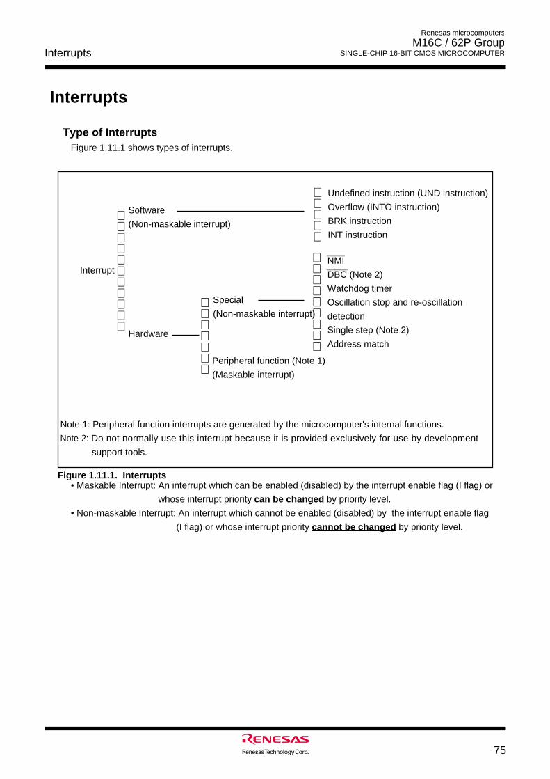
Interrupts
75
Renesas microcomputers
M16C / 62P Group SINGLE-CHIP 16-BIT CMOS MICROCOMPUTER
• Maskable Interrupt: An interrupt which can be enabled (disabled) by the interrupt enable flag (I flag) or
whose interrupt priority can be changed by priority level.
• Non-maskable Interrupt: An interrupt which cannot be enabled (disabled) by the interrupt enable flag
(I flag) or whose interrupt priority cannot be changed by priority level.
Figure 1.11.1. Interrupts
Interrupt
Software
(Non-maskable interrupt)
Hardware
Special
(Non-maskable interrupt)
Peripheral function (Note 1)
(Maskable interrupt)
Undefined instruction (UND instruction)
Overflow (INTO instruction)
BRK instruction
INT instruction
_______
NMI________
DBC (Note 2)
Watchdog timer
Oscillation stop and re-oscillation
detection
Single step (Note 2)
Address match
Note 1: Peripheral function interrupts are generated by the microcomputer's internal functions.
Note 2: Do not normally use this interrupt because it is provided exclusively for use by development
support tools.
Interrupts
Type of InterruptsFigure 1.11.1 shows types of interrupts.
Renesas microcomputers
M16C / 62P Group SINGLE-CHIP 16-BIT CMOS MICROCOMPUTERInterrupts
76
Software InterruptsA software interrupt occurs when executing certain instructions. Software interrupts are non-maskable
interrupts.
• Undefined Instruction Interrupt
An undefined instruction interrupt occurs when executing the UND instruction.
• Overflow Interrupt
An overflow interrupt occurs when executing the INTO instruction with the O flag set to “1” (the opera-
tion resulted in an overflow). The following are instructions whose O flag changes by arithmetic:
ABS, ADC, ADCF, ADD, CMP, DIV, DIVU, DIVX, NEG, RMPA, SBB, SHA, SUB
• BRK Interrupt
A BRK interrupt occurs when executing the BRK instruction.
• INT Instruction Interrupt
An INT instruction interrupt occurs when executing the INT instruction. Software interrupt Nos. 0 to 63
can be specified for the INT instruction. Because software interrupt Nos. 4 to 31 are assigned to
peripheral function interrupts, the same interrupt routine as for peripheral function interrupts can be
executed by executing the INT instruction.
In software interrupt Nos. 0 to 31, the U flag is saved to the stack during instruction execution and is
cleared to “0” (ISP selected) before executing an interrupt sequence. The U flag is restored from the
stack when returning from the interrupt routine. In software interrupt Nos. 32 to 63, the U flag does not
change state during instruction execution, and the SP then selected is used.
Interrupts
77
Renesas microcomputers
M16C / 62P Group SINGLE-CHIP 16-BIT CMOS MICROCOMPUTER
Hardware InterruptsHardware interrupts are classified into two types — special interrupts and peripheral function interrupts.
(1) Special Interrupts
Special interrupts are non-maskable interrupts._______
• NMI Interrupt_______ _______
An NMI interrupt is generated when input on the NMI pin changes state from high to low. For details_______
about the NMI interrupt, refer to the section "NMI interrupt".________
• DBC Interrupt
Do not normally use this interrupt because it is provided exclusively for use by development support
tools.
• Watchdog Timer Interrupt
Generated by the watchdog timer. Once a watchdog timer interrupt is generated, be sure to initialize
the watchdog timer. For details about the watchdog timer, refer to the section "watchdog timer".
• Oscillation Stop and Re-oscillation Detection Interrupt
Generated by the oscillation stop and re-oscillation detection function. For details about the oscilla-
tion stop and re-oscillation detection function, refer to the section "clock generating circuit".
• Voltage Down Detection Interrupt
Generated by the voltage detection circuit. For details about the voltage detection circuit, refer to the
section "voltage detection circuit".
• Single-step Interrupt
Do not normally use this interrupt because it is provided exclusively for use by development support
tools.
• Address Match Interrupt
An address match interrupt is generated immediately before executing the instruction at the address
indicated by the RMAD0 to RMAD3 register that corresponds to one of the AIER register’s AIER0 or
AIER1 bit or the AIER2 register’s AIER20 or AIER21 bit which is "1" (address match interrupt en-
abled). For details about the address match interrupt, refer to the section "address match interrupt".
(2) Peripheral Function Interrupts
Peripheral function interrupts are maskable interrupts and generated by the microcomputer's internal
functions. The interrupt sources for peripheral function interrupts are listed in “Table 1.11.2.
Relocatable Vector Tables”. For details about the peripheral functions, refer to the description of each
peripheral function in this manual.
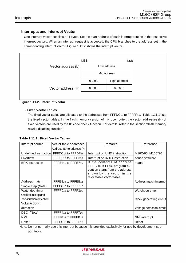
Renesas microcomputers
M16C / 62P Group SINGLE-CHIP 16-BIT CMOS MICROCOMPUTERInterrupts
78
Interrupt source Vector table addresses Remarks Reference
Address (L) to address (H)
Undefined instruction FFFDC16 to FFFDF16 Interrupt on UND instruction M16C/60, M16C/20
Overflow FFFE016 to FFFE316 Interrupt on INTO instruction serise software
BRK instruction FFFE416 to FFFE716 maual
Address match FFFE816 to FFFEB16 Address match interrupt
Single step (Note) FFFEC16 to FFFEF16
Watchdog timer FFFF016 to FFFF316 Watchdog timerOscillation stop and
re-oscillation detection Clock generating circuitVoltage down
detection Voltage detection circuit________
DBC (Note) FFFF416 to FFFF716_______
NMI FFFF816 to FFFFB16_______
NMI interrupt
Reset FFFFC16 to FFFFF16 Reset
Note: Do not normally use this interrupt because it is provided exclusively for use by development sup-
port tools.
Figure 1.11.2. Interrupt Vector
AAAAAAAAAAAAAAAAAA
Mid addressAAAAAAAAAAAAAAAAAA
Low address
AAAAAAAAAAAAAAAAAA
0 0 0 0 High address
AAAAAAAAAAAAAAAAAA
0 0 0 0 0 0 0 0
Vector address (L)
LSBMSB
Vector address (H)
Interrupts and Interrupt VectorOne interrupt vector consists of 4 bytes. Set the start address of each interrupt routine in the respective
interrupt vectors. When an interrupt request is accepted, the CPU branches to the address set in the
corresponding interrupt vector. Figure 1.11.2 shows the interrupt vector.
• Fixed Vector Tables
The fixed vector tables are allocated to the addresses from FFFDC16 to FFFFF16. Table 1.11.1 lists
the fixed vector tables. In the flash memory version of microcomputer, the vector addresses (H) of
fixed vectors are used by the ID code check function. For details, refer to the section "flash memory
rewrite disabling function".
Table 1.11.1. Fixed Vector Tables
If the contents of addressFFFE716 is FF16, program ex-ecution starts from the addressshown by the vector in therelocatable vector table.
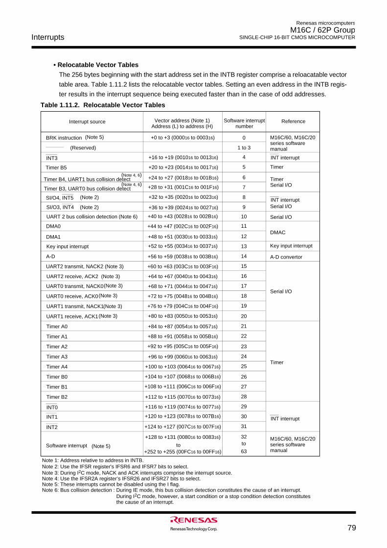
Interrupts
79
Renesas microcomputers
M16C / 62P Group SINGLE-CHIP 16-BIT CMOS MICROCOMPUTER
Table 1.11.2. Relocatable Vector Tables
Software interrupt number
Reference
Note 1: Address relative to address in INTB.Note 2: Use the IFSR register's IFSR6 and IFSR7 bits to select.Note 3: During I2C mode, NACK and ACK interrupts comprise the interrupt source. Note 4: Use the IFSR2A register’s IFSR26 and IFSR27 bits to select.Note 5: These interrupts cannot be disabled using the I flag.Note 6: Bus collision detection : During IE mode, this bus collision detection constitutes the cause of an interrupt.
During I2C mode, however, a start condition or a stop condition detection constitutes the cause of an interrupt.
Vector address (Note 1)Address (L) to address (H)
0
11
12
13
14
17
18
19
20
21
22
23
24
25
26
27
28
29
30
31
32
63
to
10
15
16
5
6
7
8
4
9
1 to 3
Interrupt source
BRK instruction
INT3
SI/O3, INT4
SI/O4, INT5
Timer B4, UART1 bus collision detect
Timer B5
(Note 2)
(Note 2)
DMA0
DMA1
Key input interrupt
A-D
UART0 transmit, NACK0
UART0 receive, ACK0
UART1 transmit, NACK1
UART1 receive, ACK1
Timer A0
Timer A1
Timer A2
Timer A3
Timer A4
Timer B0
Timer B1
Timer B2
INT0
INT1
INT2
Software interrupt
UART 2 bus collision detection
UART2 transmit, NACK2 (Note 3)
UART2 receive, ACK2 (Note 3)
(Note 4, 6)
Timer B3, UART0 bus collision detect(Note 4, 6)
M16C/60, M16C/20 series software manual
INT interrupt
Timer
TimerSerial I/O
Serial I/OINT interrupt
Serial I/O
DMAC
Key input interrupt
A-D convertor
Serial I/O
Timer
INT interrupt
M16C/60, M16C/20 series software manual
(Note 5)
(Reserved)
+0 to +3 (000016 to 000316)
+44 to +47 (002C16 to 002F16)
+48 to +51 (003016 to 003316)
+52 to +55 (003416 to 003716)
+56 to +59 (003816 to 003B16)
+68 to +71 (004416 to 004716)
+72 to +75 (004816 to 004B16)
+76 to +79 (004C16 to 004F16)
+80 to +83 (005016 to 005316)
+84 to +87 (005416 to 005716)
+88 to +91 (005816 to 005B16)
+92 to +95 (005C16 to 005F16)
+96 to +99 (006016 to 006316)
+100 to +103 (006416 to 006716)
+104 to +107 (006816 to 006B16)
+108 to +111 (006C16 to 006F16)
+112 to +115 (007016 to 007316)
+116 to +119 (007416 to 007716)
+120 to +123 (007816 to 007B16)
+124 to +127 (007C16 to 007F16)
+128 to +131 (008016 to 008316)
+252 to +255 (00FC16 to 00FF16)
+40 to +43 (002816 to 002B16)
+60 to +63 (003C16 to 003F16)
+64 to +67 (004016 to 004316)
+20 to +23 (001416 to 001716)
+24 to +27 (001816 to 001B16)
+28 to +31 (001C16 to 001F16)
+32 to +35 (002016 to 002316)
+16 to +19 (001016 to 001316)
+36 to +39 (002416 to 002716)
to
(Note 3)
(Note 3)
(Note 3)
(Note 3)
(Note 5)
(Note 6)
• Relocatable Vector Tables
The 256 bytes beginning with the start address set in the INTB register comprise a reloacatable vector
table area. Table 1.11.2 lists the relocatable vector tables. Setting an even address in the INTB regis-
ter results in the interrupt sequence being executed faster than in the case of odd addresses.
Renesas microcomputers
M16C / 62P Group SINGLE-CHIP 16-BIT CMOS MICROCOMPUTERInterrupts
80
Interrupt ControlThe following describes how to enable/disable the maskable interrupts, and how to set the priority in which
order they are accepted. What is explained here does not apply to nonmaskable interrupts.
Use the FLG register’s I flag, IPL, and each interrupt control register’s ILVL2 to ILVL0 bits to enable/disable
the maskable interrupts. Whether an interrupt is requested is indicated by the IR bit in each interrupt control
register.
Figure 1.11.3 shows the interrupt control registers.
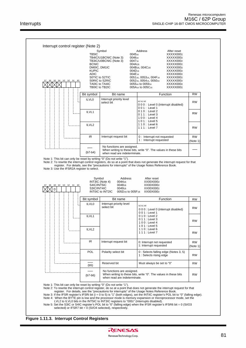
Interrupts
81
Renesas microcomputers
M16C / 62P Group SINGLE-CHIP 16-BIT CMOS MICROCOMPUTER
Figure 1.11.3. Interrupt Control Registers
Symbol Address After resetINT3IC (Note 4) 004416 XX00X0002S4IC/INT5IC 004816 XX00X0002S3IC/INT4IC 004916 XX00X0002INT0IC to INT2IC 005D16 to 005F16 XX00X0002
Bit name FunctionBit symbol
b7 b6 b5 b4 b3 b2 b1 b0
AAAAAA
ILVL0
IR
POL
No functions are assigned.When writing to these bits, write “0”. The values in these bits when read are indeterminate.
Interrupt priority level select bit
Interrupt request bit
Polarity select bit
Reserved bit
0: Interrupt not requested1: Interrupt requested
0 : Selects falling edge (Notes 3, 5)1 : Selects rising edge
Must always be set to “0”
ILVL1
ILVL2
Note 1: This bit can only be reset by writing “0” (Do not write “1”). Note 2: To rewrite the interrupt control register, do so at a point that does not generate the interrupt request for that
register. For details, see the “precautions for interrupts” of the Usage Notes Reference Book. Note 3: If the IFSR register’s IFSRi bit (i = 0 to 5) is “1” (both edges), set the INTiIC register’s POL bit to “0” (falling edge). Note 4: When the BYTE pin is low and the processor mode is memory expansion or microprocessor mode, set the
LVL2 to ILVL0 bits in the INT5IC to INT3IC registers to “0002” (interrupts disabled).Note 5: Set the S3IC or S4IC register’s POL bit to “0” (falling edge) when the IFSR register’s IFSR6 bit = 0 (SI/O3
selected) or IFSR7 bit = 0 (SI/O4 selected), respectively.
(Note 1)
Interrupt control register (Note 2)
b7 b6 b5 b4 b3 b2 b1 b0
AAAAAAAAAAAA
Bit name FunctionBit symbol RW
Symbol Address After reset TB5IC 004516 XXXXX0002TB4IC/U1BCNIC (Note 3) 004616 XXXXX0002TB3IC/U0BCNIC (Note 3) 004716 XXXXX0002BCNIC 004A16 XXXXX0002DM0IC, DM1IC 004B16, 004C16 XXXXX0002KUPIC 004D16 XXXXX0002ADIC 004E16 XXXXX0002S0TIC to S2TIC 005116, 005316, 004F16 XXXXX0002S0RIC to S2RIC 005216, 005416, 005016 XXXXX0002TA0IC to TA4IC 005516 to 005916 XXXXX0002TB0IC to TB2IC 005A16 to 005C16 XXXXX0002
ILVL0
IR
Interrupt priority level select bit
Interrupt request bit 0 : Interrupt not requested1 : Interrupt requested
ILVL1
ILVL2
No functions are assigned.When writing to these bits, write “0”. The values in these bits when read are indeterminate.
(Note 1)
Note 1: This bit can only be reset by writing “0” (Do not write “1”). Note 2: To rewrite the interrupt control registers, do so at a point that does not generate the interrupt request for that register. For details, see the “precautions for interrupts” of the Usage Notes Reference Book. Note 3: Use the IFSR2A register to select.
0 0 0 : Level 0 (interrupt disabled)0 0 1 : Level 1 0 1 0 : Level 2 0 1 1 : Level 3 1 0 0 : Level 4 1 0 1 : Level 5 1 1 0 : Level 6 1 1 1 : Level 7
b2 b1 b0
0 0 0 : Level 0 (interrupt disabled)0 0 1 : Level 1 0 1 0 : Level 2 0 1 1 : Level 3 1 0 0 : Level 4 1 0 1 : Level 5 1 1 0 : Level 6 1 1 1 : Level 7
b2 b1 b0
0
RW
RW
RW
RW
(b7-b4)
RW
RW
RW
RW
RW
RW
RW
RW(b7-b6)
(b5)
Renesas microcomputers
M16C / 62P Group SINGLE-CHIP 16-BIT CMOS MICROCOMPUTERInterrupts
82
I FlagThe I flag enables or disables the maskable interrupt. Setting the I flag to “1” (= enabled) enables the
maskable interrupt. Setting the I flag to “0” (= disabled) disables all maskable interrupts.
IR Bit
The IR bit is set to “1” (= interrupt requested) when an interrupt request is generated. Then, when the
interrupt request is accepted and the CPU branches to the corresponding interrupt vector, the IR bit is
cleared to “0” (= interrupt not requested).
The IR bit can be cleared to “0” in a program. Note that do not write “1” to this bit.
Table 1.11.4. Interrupt Priority Levels Enabled by IPL
Table 1.11.3. Settings of Interrupt Priority Levels
ILVL2 to ILVL0 bitsInterrupt priority
levelPriorityorder
0002
0012
0102
0112
1002
1012
1102
1112
Level 0 (interrupt disabled)
Level 1
Level 2
Level 3
Level 4
Level 5
Level 6
Level 7
Low
High
Enabled interrupt priority levels
Interrupt levels 1 and above are enabled
Interrupt levels 2 and above are enabled
Interrupt levels 3 and above are enabled
Interrupt levels 4 and above are enabled
Interrupt levels 5 and above are enabled
Interrupt levels 6 and above are enabled
Interrupt levels 7 and above are enabled
All maskable interrupts are disabled
IPL
0002
0012
0102
0112
1002
1012
1102
1112
ILVL2 to ILVL0 Bits and IPLInterrupt priority levels can be set using the ILVL2 to ILVL0 bits.
Table 1.11.3 shows the settings of interrupt priority levels and Table 1.11.4 shows the interrupt priority
levels enabled by the IPL.
The following are conditions under which an interrupt is accepted:
· I flag = “1”
· IR bit = “1”
· interrupt priority level > IPL
The I flag, IR bit, ILVL2 to ILVL0 bits and IPL are independent of each other. In no case do they affect one
another.
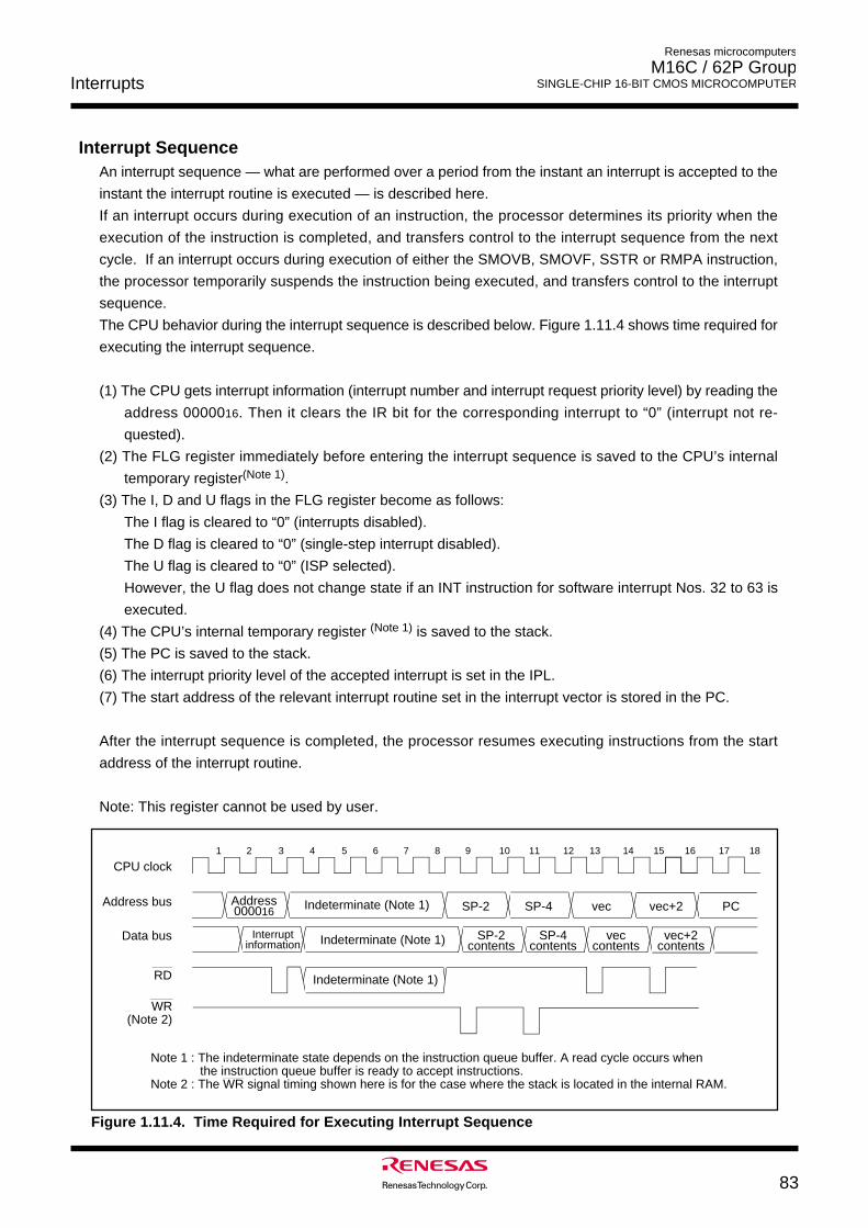
Interrupts
83
Renesas microcomputers
M16C / 62P Group SINGLE-CHIP 16-BIT CMOS MICROCOMPUTER
Interrupt SequenceAn interrupt sequence — what are performed over a period from the instant an interrupt is accepted to the
instant the interrupt routine is executed — is described here.
If an interrupt occurs during execution of an instruction, the processor determines its priority when the
execution of the instruction is completed, and transfers control to the interrupt sequence from the next
cycle. If an interrupt occurs during execution of either the SMOVB, SMOVF, SSTR or RMPA instruction,
the processor temporarily suspends the instruction being executed, and transfers control to the interrupt
sequence.
The CPU behavior during the interrupt sequence is described below. Figure 1.11.4 shows time required for
executing the interrupt sequence.
(1) The CPU gets interrupt information (interrupt number and interrupt request priority level) by reading the
address 0000016. Then it clears the IR bit for the corresponding interrupt to “0” (interrupt not re-
quested).
(2) The FLG register immediately before entering the interrupt sequence is saved to the CPU’s internal
temporary register(Note 1).
(3) The I, D and U flags in the FLG register become as follows:
The I flag is cleared to “0” (interrupts disabled).
The D flag is cleared to “0” (single-step interrupt disabled).
The U flag is cleared to “0” (ISP selected).
However, the U flag does not change state if an INT instruction for software interrupt Nos. 32 to 63 is
executed.
(4) The CPU’s internal temporary register (Note 1) is saved to the stack.
(5) The PC is saved to the stack.
(6) The interrupt priority level of the accepted interrupt is set in the IPL.
(7) The start address of the relevant interrupt routine set in the interrupt vector is stored in the PC.
After the interrupt sequence is completed, the processor resumes executing instructions from the start
address of the interrupt routine.
Note: This register cannot be used by user.
Indeterminate (Note 1)
1 2 3 4 5 6 7 8 9 10 11 12 13 14 15 16 17 18
Indeterminate (Note 1) SP-2 contents
SP-4 contents
vec contents
vec+2 contents
Interrupt information
Address 000016 Indeterminate (Note 1) SP-2 SP-4 vec vec+2 PC
CPU clock
Address bus
Data bus
WR (Note 2)
RD
Note 1 : The indeterminate state depends on the instruction queue buffer. A read cycle occurs when the instruction queue buffer is ready to accept instructions.
Note 2 : The WR signal timing shown here is for the case where the stack is located in the internal RAM.
Figure 1.11.4. Time Required for Executing Interrupt Sequence
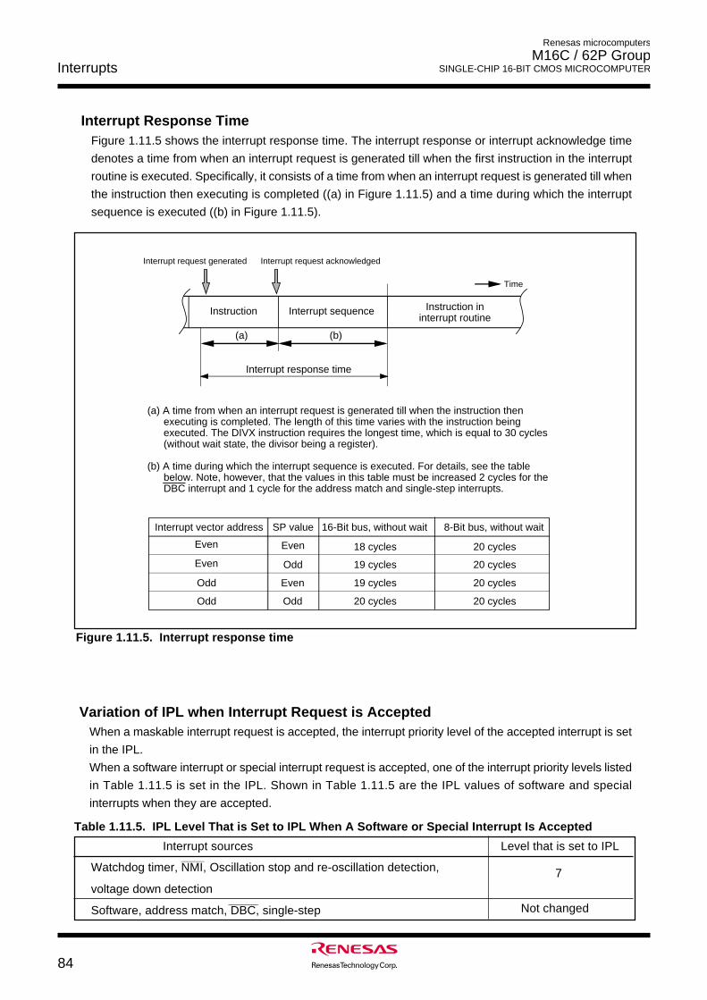
Renesas microcomputers
M16C / 62P Group SINGLE-CHIP 16-BIT CMOS MICROCOMPUTERInterrupts
84
Interrupt sources
7
Level that is set to IPL_______
Watchdog timer, NMI, Oscillation stop and re-oscillation detection,
voltage down detection_________
Software, address match, DBC, single-step Not changed
Variation of IPL when Interrupt Request is AcceptedWhen a maskable interrupt request is accepted, the interrupt priority level of the accepted interrupt is set
in the IPL.
When a software interrupt or special interrupt request is accepted, one of the interrupt priority levels listed
in Table 1.11.5 is set in the IPL. Shown in Table 1.11.5 are the IPL values of software and special
interrupts when they are accepted.
Table 1.11.5. IPL Level That is Set to IPL When A Software or Special Interrupt Is Accepted
Instruction Interrupt sequence Instruction in interrupt routine
Time
Interrupt response time
(a) (b)
Interrupt request acknowledgedInterrupt request generated
(a) A time from when an interrupt request is generated till when the instruction then executing is completed. The length of this time varies with the instruction being executed. The DIVX instruction requires the longest time, which is equal to 30 cycles (without wait state, the divisor being a register).
(b) A time during which the interrupt sequence is executed. For details, see the table below. Note, however, that the values in this table must be increased 2 cycles for the DBC interrupt and 1 cycle for the address match and single-step interrupts.
Interrupt vector address
Even
Even
Odd
Odd
SP value
Even
Odd
Even
Odd
16-Bit bus, without wait
18 cycles
19 cycles
19 cycles
20 cycles
8-Bit bus, without wait
20 cycles
20 cycles
20 cycles
20 cycles
Figure 1.11.5. Interrupt response time
Interrupt Response TimeFigure 1.11.5 shows the interrupt response time. The interrupt response or interrupt acknowledge time
denotes a time from when an interrupt request is generated till when the first instruction in the interrupt
routine is executed. Specifically, it consists of a time from when an interrupt request is generated till when
the instruction then executing is completed ((a) in Figure 1.11.5) and a time during which the interrupt
sequence is executed ((b) in Figure 1.11.5).
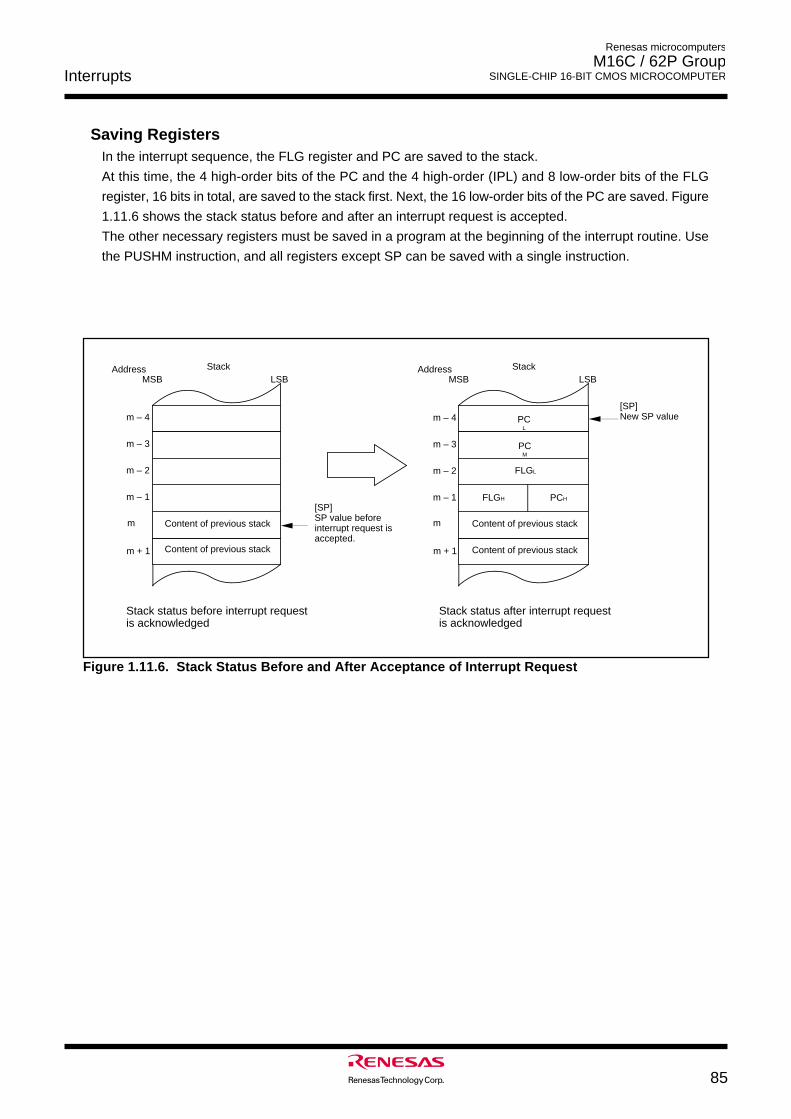
Interrupts
85
Renesas microcomputers
M16C / 62P Group SINGLE-CHIP 16-BIT CMOS MICROCOMPUTER
Saving RegistersIn the interrupt sequence, the FLG register and PC are saved to the stack.
At this time, the 4 high-order bits of the PC and the 4 high-order (IPL) and 8 low-order bits of the FLG
register, 16 bits in total, are saved to the stack first. Next, the 16 low-order bits of the PC are saved. Figure
1.11.6 shows the stack status before and after an interrupt request is accepted.
The other necessary registers must be saved in a program at the beginning of the interrupt routine. Use
the PUSHM instruction, and all registers except SP can be saved with a single instruction.
Address
Content of previous stack
Stack
[SP]SP value beforeinterrupt request is accepted.
m
m – 1
m – 2
m – 3
m – 4
Stack status before interrupt requestis acknowledged
Stack status after interrupt requestis acknowledged
Content of previous stackm + 1
MSB LSB
m
m – 1
m – 2
m – 3
m – 4
Address
FLGL
Content of previous stack
Stack
FLGH PCH
[SP]New SP value
Content of previous stackm + 1
MSB LSB
PCL
PCM
Figure 1.11.6. Stack Status Before and After Acceptance of Interrupt Request
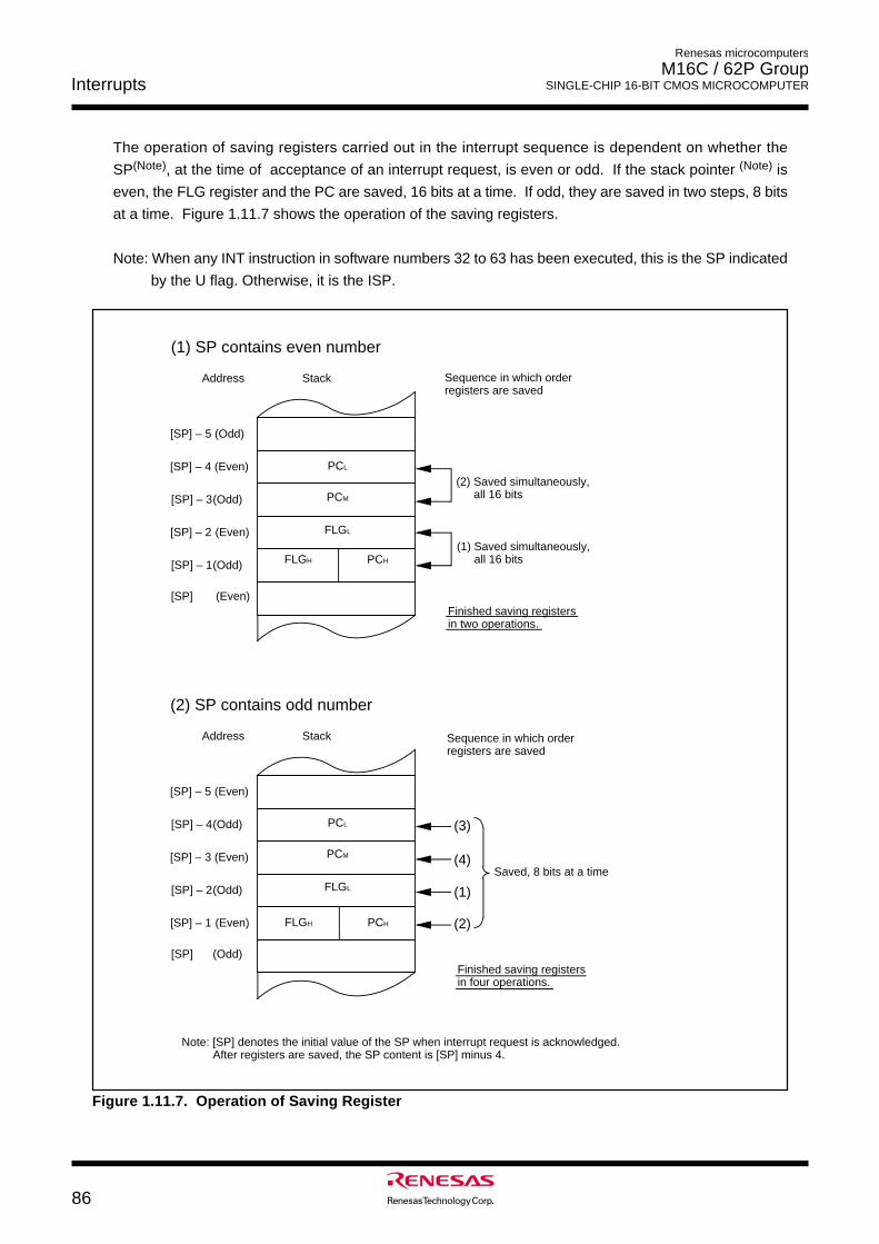
Renesas microcomputers
M16C / 62P Group SINGLE-CHIP 16-BIT CMOS MICROCOMPUTERInterrupts
86
Figure 1.11.7. Operation of Saving Register
(2) SP contains odd number
[SP] (Odd)
[SP] – 1 (Even)
[SP] – 2(Odd)
[SP] – 3 (Even)
[SP] – 4(Odd)
[SP] – 5 (Even)
Address Sequence in which order registers are saved
(2)
(1)
Finished saving registers in four operations.
(3)
(4)
(1) SP contains even number
[SP] (Even)
[SP] – 1(Odd)
[SP] – 2 (Even)
[SP] – 3(Odd)
[SP] – 4 (Even)
[SP] – 5 (Odd)
Note: [SP] denotes the initial value of the SP when interrupt request is acknowledged.After registers are saved, the SP content is [SP] minus 4.
Address
PCM
Stack
FLGL
PCL
Sequence in which order registers are saved
(2) Saved simultaneously, all 16 bits
(1) Saved simultaneously, all 16 bits
Finished saving registers in two operations.
PCM
Stack
FLGL
PCL
Saved, 8 bits at a time
FLGH PCH
FLGH PCH
The operation of saving registers carried out in the interrupt sequence is dependent on whether the
SP(Note), at the time of acceptance of an interrupt request, is even or odd. If the stack pointer (Note) is
even, the FLG register and the PC are saved, 16 bits at a time. If odd, they are saved in two steps, 8 bits
at a time. Figure 1.11.7 shows the operation of the saving registers.
Note: When any INT instruction in software numbers 32 to 63 has been executed, this is the SP indicated
by the U flag. Otherwise, it is the ISP.
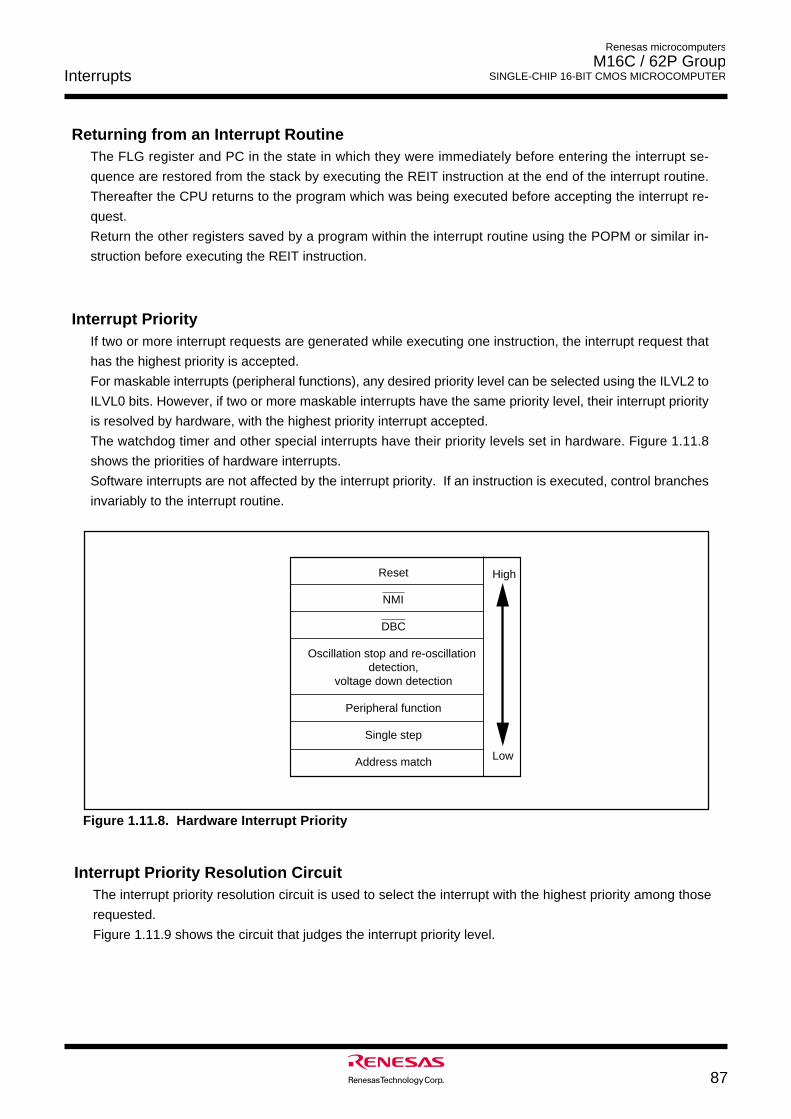
Interrupts
87
Renesas microcomputers
M16C / 62P Group SINGLE-CHIP 16-BIT CMOS MICROCOMPUTER
Interrupt PriorityIf two or more interrupt requests are generated while executing one instruction, the interrupt request that
has the highest priority is accepted.
For maskable interrupts (peripheral functions), any desired priority level can be selected using the ILVL2 to
ILVL0 bits. However, if two or more maskable interrupts have the same priority level, their interrupt priority
is resolved by hardware, with the highest priority interrupt accepted.
The watchdog timer and other special interrupts have their priority levels set in hardware. Figure 1.11.8
shows the priorities of hardware interrupts.
Software interrupts are not affected by the interrupt priority. If an instruction is executed, control branches
invariably to the interrupt routine.
Returning from an Interrupt RoutineThe FLG register and PC in the state in which they were immediately before entering the interrupt se-
quence are restored from the stack by executing the REIT instruction at the end of the interrupt routine.
Thereafter the CPU returns to the program which was being executed before accepting the interrupt re-
quest.
Return the other registers saved by a program within the interrupt routine using the POPM or similar in-
struction before executing the REIT instruction.
Interrupt Priority Resolution CircuitThe interrupt priority resolution circuit is used to select the interrupt with the highest priority among those
requested.
Figure 1.11.9 shows the circuit that judges the interrupt priority level.
Figure 1.11.8. Hardware Interrupt Priority
Reset
Oscillation stop and re-oscillation detection,
voltage down detection
Peripheral function
Single step
Address match
High
Low
NMI
DBC
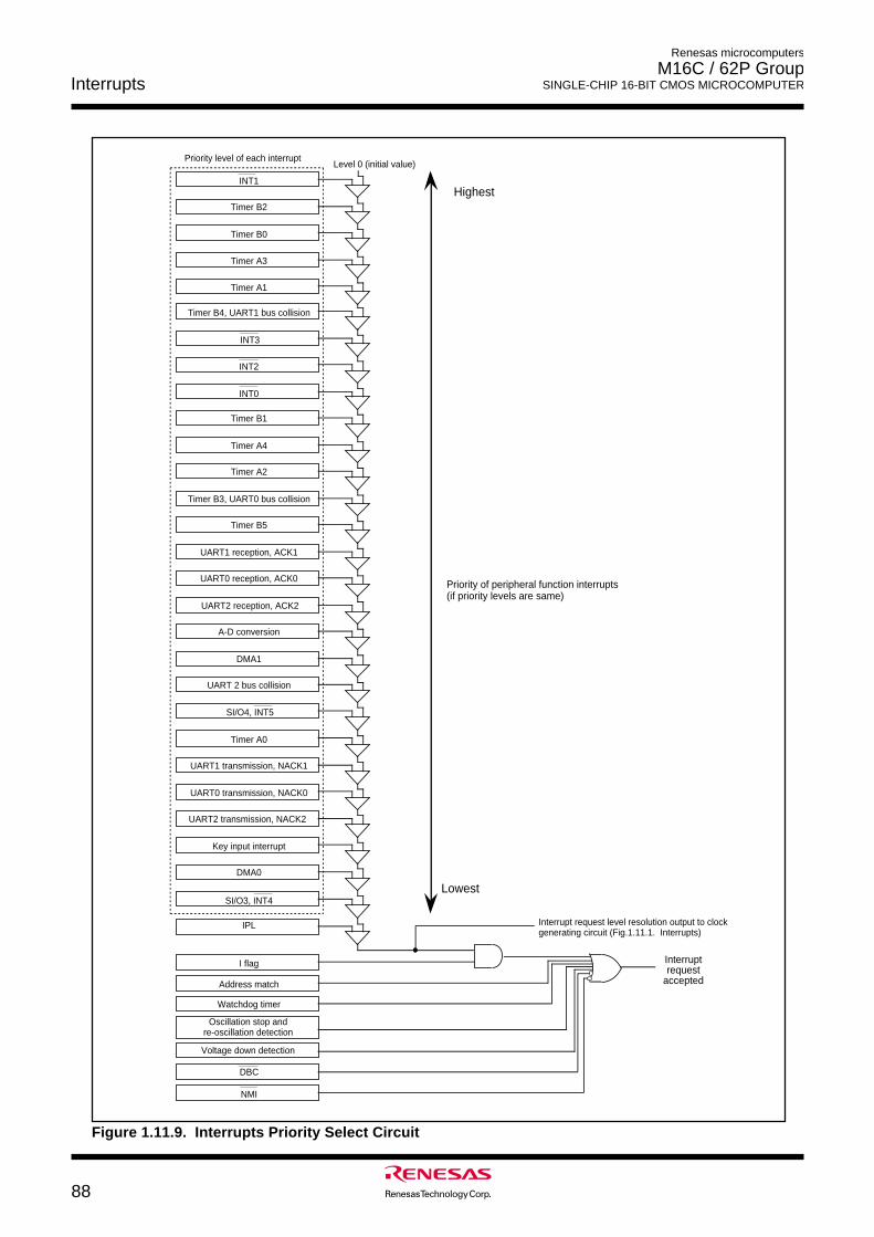
Renesas microcomputers
M16C / 62P Group SINGLE-CHIP 16-BIT CMOS MICROCOMPUTERInterrupts
88
Figure 1.11.9. Interrupts Priority Select Circuit
Timer B2
Timer B0
Timer A3
Timer A1
Timer B1
Timer A4
Timer A2
UART1 reception, ACK1
UART0 reception, ACK0
UART2 reception, ACK2
A-D conversion
DMA1
UART 2 bus collision
Timer A0
UART1 transmission, NACK1
UART0 transmission, NACK0
UART2 transmission, NACK2
Key input interrupt
DMA0
IPL
I flag
INT1
INT2
INT0
Watchdog timer
DBC
NMI
Interrupt request
accepted
Level 0 (initial value)Priority level of each interrupt
Highest
Lowest
Priority of peripheral function interrupts(if priority levels are same)
Timer B4, UART1 bus collision
INT3
Timer B3, UART0 bus collision
Timer B5
SI/O4, INT5
SI/O3, INT4
Address match
Interrupt request level resolution output to clock generating circuit (Fig.1.11.1. Interrupts)
Oscillation stop and re-oscillation detection
Voltage down detection
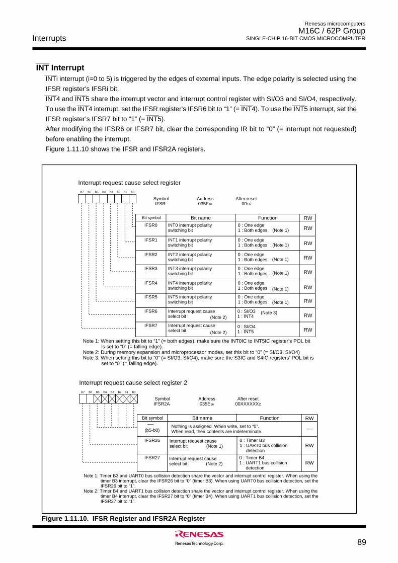
Interrupts
89
Renesas microcomputers
M16C / 62P Group SINGLE-CHIP 16-BIT CMOS MICROCOMPUTER
______
INT Interrupt_______
INTi interrupt (i=0 to 5) is triggered by the edges of external inputs. The edge polarity is selected using the
IFSR register's IFSRi bit._______ _______
INT4 and INT5 share the interrupt vector and interrupt control register with SI/O3 and SI/O4, respectively._______ _______ _______
To use the INT4 interrupt, set the IFSR register’s IFSR6 bit to “1” (= INT4). To use the INT5 interrupt, set the_______
IFSR register’s IFSR7 bit to “1” (= INT5).
After modifying the IFSR6 or IFSR7 bit, clear the corresponding IR bit to “0” (= interrupt not requested)
before enabling the interrupt.
Figure 1.11.10 shows the IFSR and IFSR2A registers.
Figure 1.11.10. IFSR Register and IFSR2A Register
Interrupt request cause select register
Bit name FunctionBit symbol RW
Symbol Address After resetIFSR 035F16 0016
IFSR0
b7 b6 b5 b4 b3 b2 b1 b0
AAAAAAAAAAAAAA
INT0 interrupt polarity switching bit
0 : SI/O31 : INT4
0 : SI/O41 : INT5
0 : One edge1 : Both edges
0 : One edge1 : Both edges
0 : One edge1 : Both edges
0 : One edge1 : Both edges
0 : One edge1 : Both edges
INT1 interrupt polarity switching bit
INT2 interrupt polarity switching bit
INT3 interrupt polarity switching bit
INT4 interrupt polarity switching bit
INT5 interrupt polarity switching bit
0 : One edge1 : Both edges
Interrupt request cause select bit
Interrupt request cause select bit
IFSR1
IFSR2
IFSR3
IFSR4
IFSR5
IFSR6
IFSR7
RW
RW
RW
RW
RW
RW
RW
RW
(Note 1)
(Note 1)
(Note 1)
(Note 1)
(Note 1)
(Note 1)
(Note 3)(Note 2)
(Note 2)
Note 1: When setting this bit to “1” (= both edges), make sure the INT0IC to INT5IC register’s POL bit is set to “0” (= falling edge).Note 2: During memory expansion and microprocessor modes, set this bit to “0” (= SI/O3, SI/O4)Note 3: When setting this bit to “0” (= SI/O3, SI/O4), make sure the S3IC and S4IC registers’ POL bit is set to “0” (= falling edge).
Interrupt request cause select register 2
Bit name FunctionBit symbol RW
Symbol Address After resetIFSR2A 035E16 00XXXXXX2
b7 b6 b5 b4 b3 b2 b1 b0
AAAAAAAAAAAAAA
0 : Timer B31 : UART0 bus collision detection
0 : Timer B41 : UART1 bus collision detection
IFSR26
IFSR27
Interrupt request cause select bit (Note 1)
Interrupt request cause select bit (Note 2)
RW
RW
(b5-b0)Nothing is assigned. When write, set to “0”. When read, their contents are indeterminate.
Note 1: Timer B3 and UART0 bus collision detection share the vector and interrupt control register. When using the timer B3 interrupt, clear the IFSR26 bit to “0” (timer B3). When using UART0 bus collision detection, set the IFSR26 bit to “1”.
Note 2: Timer B4 and UART1 bus collision detection share the vector and interrupt control register. When using the timer B4 interrupt, clear the IFSR27 bit to “0” (timer B4). When using UART1 bus collision detection, set the IFSR27 bit to “1”.
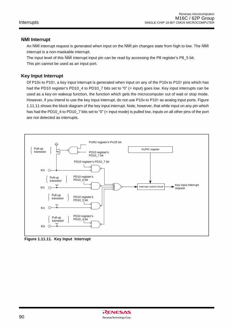
Renesas microcomputers
M16C / 62P Group SINGLE-CHIP 16-BIT CMOS MICROCOMPUTERInterrupts
90
Interrupt control circuit
KUPIC register
Key input interrupt request
KI3
KI2
KI1
KI0
PUR2 register's PU25 bit
PD10 register's PD10_7 bit
Pull-up transistor
PD10 register's PD10_7 bit
PD10 register's PD10_6 bit
PD10 register's PD10_5 bit
PD10 register's PD10_4 bit
Pull-up transistor
Pull-up transistor
Pull-up transistor
Figure 1.11.11. Key Input Interrupt
______
NMI Interrupt_______ _______ ______
An NMI interrupt request is generated when input on the NMI pin changes state from high to low. The NMI
interrupt is a non-maskable interrupt._______
The input level of this NMI interrupt input pin can be read by accessing the P8 register’s P8_5 bit.
This pin cannot be used as an input port.
Key Input InterruptOf P104 to P107, a key input interrupt is generated when input on any of the P104 to P107 pins which has
had the PD10 register’s PD10_4 to PD10_7 bits set to “0” (= input) goes low. Key input interrupts can be
used as a key-on wakeup function, the function which gets the microcomputer out of wait or stop mode.
However, if you intend to use the key input interrupt, do not use P104 to P107 as analog input ports. Figure
1.11.11 shows the block diagram of the key input interrupt. Note, however, that while input on any pin which
has had the PD10_4 to PD10_7 bits set to “0” (= input mode) is pulled low, inputs on all other pins of the port
are not detected as interrupts.
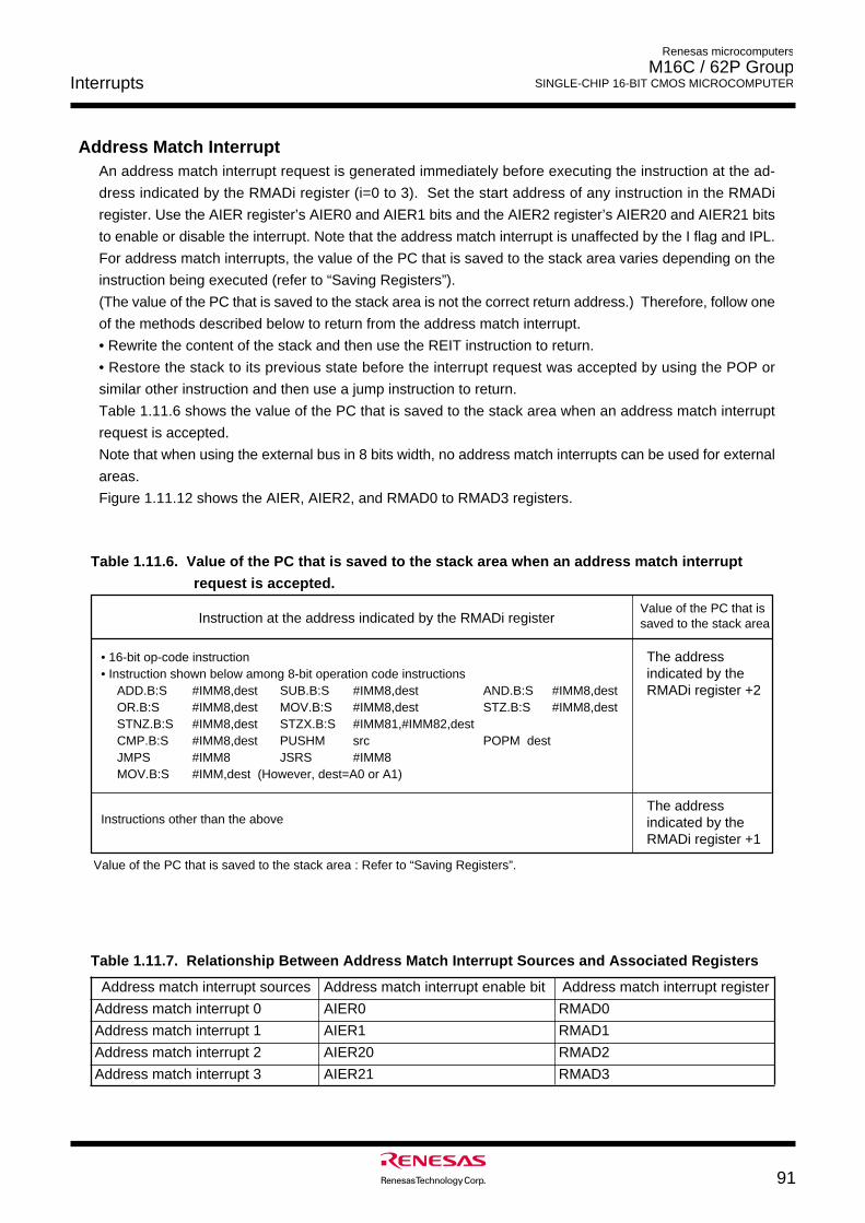
Interrupts
91
Renesas microcomputers
M16C / 62P Group SINGLE-CHIP 16-BIT CMOS MICROCOMPUTER
Address Match InterruptAn address match interrupt request is generated immediately before executing the instruction at the ad-
dress indicated by the RMADi register (i=0 to 3). Set the start address of any instruction in the RMADi
register. Use the AIER register’s AIER0 and AIER1 bits and the AIER2 register’s AIER20 and AIER21 bits
to enable or disable the interrupt. Note that the address match interrupt is unaffected by the I flag and IPL.
For address match interrupts, the value of the PC that is saved to the stack area varies depending on the
instruction being executed (refer to “Saving Registers”).
(The value of the PC that is saved to the stack area is not the correct return address.) Therefore, follow one
of the methods described below to return from the address match interrupt.
• Rewrite the content of the stack and then use the REIT instruction to return.
• Restore the stack to its previous state before the interrupt request was accepted by using the POP or
similar other instruction and then use a jump instruction to return.
Table 1.11.6 shows the value of the PC that is saved to the stack area when an address match interrupt
request is accepted.
Note that when using the external bus in 8 bits width, no address match interrupts can be used for external
areas.
Figure 1.11.12 shows the AIER, AIER2, and RMAD0 to RMAD3 registers.
Table 1.11.7. Relationship Between Address Match Interrupt Sources and Associated Registers
Address match interrupt sources Address match interrupt enable bit Address match interrupt register
Address match interrupt 0 AIER0 RMAD0
Address match interrupt 1 AIER1 RMAD1
Address match interrupt 2 AIER20 RMAD2
Address match interrupt 3 AIER21 RMAD3
• 16-bit op-code instruction• Instruction shown below among 8-bit operation code instructions ADD.B:S #IMM8,dest SUB.B:S #IMM8,dest AND.B:S #IMM8,dest OR.B:S #IMM8,dest MOV.B:S #IMM8,dest STZ.B:S #IMM8,dest STNZ.B:S #IMM8,dest STZX.B:S #IMM81,#IMM82,dest CMP.B:S #IMM8,dest PUSHM src POPM dest JMPS #IMM8 JSRS #IMM8 MOV.B:S #IMM,dest (However, dest=A0 or A1)
Instructions other than the above
Instruction at the address indicated by the RMADi registerValue of the PC that is saved to the stack area
The address indicated by the RMADi register +2
The address indicated by the RMADi register +1
Value of the PC that is saved to the stack area : Refer to “Saving Registers”.
Table 1.11.6. Value of the PC that is saved to the stack area when an address match interrupt
request is accepted.
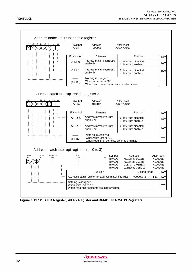
Renesas microcomputers
M16C / 62P Group SINGLE-CHIP 16-BIT CMOS MICROCOMPUTERInterrupts
92
Bit nameBit symbol
Symbol Address After resetAIER 000916 XXXXXX002
Address match interrupt enable register
Function RW
AAAAAAAAAAAAAAAAAAAAAAAAAAAA
AAAAAAAAAAAAAAAAAAAAAAAAAAAA
Address match interrupt 0 enable bit
0 : Interrupt disabled1 : Interrupt enabled
AIER0
Address match interrupt 1 enable bit
AIER1
Symbol Address After reset RMAD0 001216 to 001016 X0000016RMAD1 001616 to 001416 X0000016RMAD2 01BA16 to 01B816 X0000016RMAD3 01BE16 to 01BC16 X0000016
b7 b6 b5 b4 b3 b2 b1 b0
Address setting register for address match interrupt
Function Setting range
Address match interrupt register i (i = 0 to 3)
0000016 to FFFFF16
0 : Interrupt disabled1 : Interrupt enabled
b0 b7 b0b3(b19) (b16)
b7 b0(b15) (b8)
b7(b23)
Bit nameBit symbol
Symbol Address After resetAIER2 01BB16 XXXXXX002
Address match interrupt enable register 2
Function RW
AAAAAAAAAAAAAAAAAAAAAAAAAAAAAAAAAAAAAAAAAA
AAAAAAAAAAAAAAAAAAAAAAAAAAAAAAAAAAAAAAAAAA
Address match interrupt 2 enable bit
0 : Interrupt disabled1 : Interrupt enabled
AIER20
Address match interrupt 3 enable bit
AIER21
b7 b6 b5 b4 b3 b2 b1 b0
0 : Interrupt disabled1 : Interrupt enabled
RW
RW
(b7-b2)
RW
RW
(b7-b2)
RW
RW
Nothing is assigned.When write, set to “0”. When read, their contents are indeterminate.
Nothing is assigned.When write, set to “0”. When read, their contents are indeterminate.
Nothing is assigned.When write, set to “0”. When read, their contents are indeterminate.
Figure 1.11.12. AIER Register, AIER2 Register and RMAD0 to RMAD3 Registers
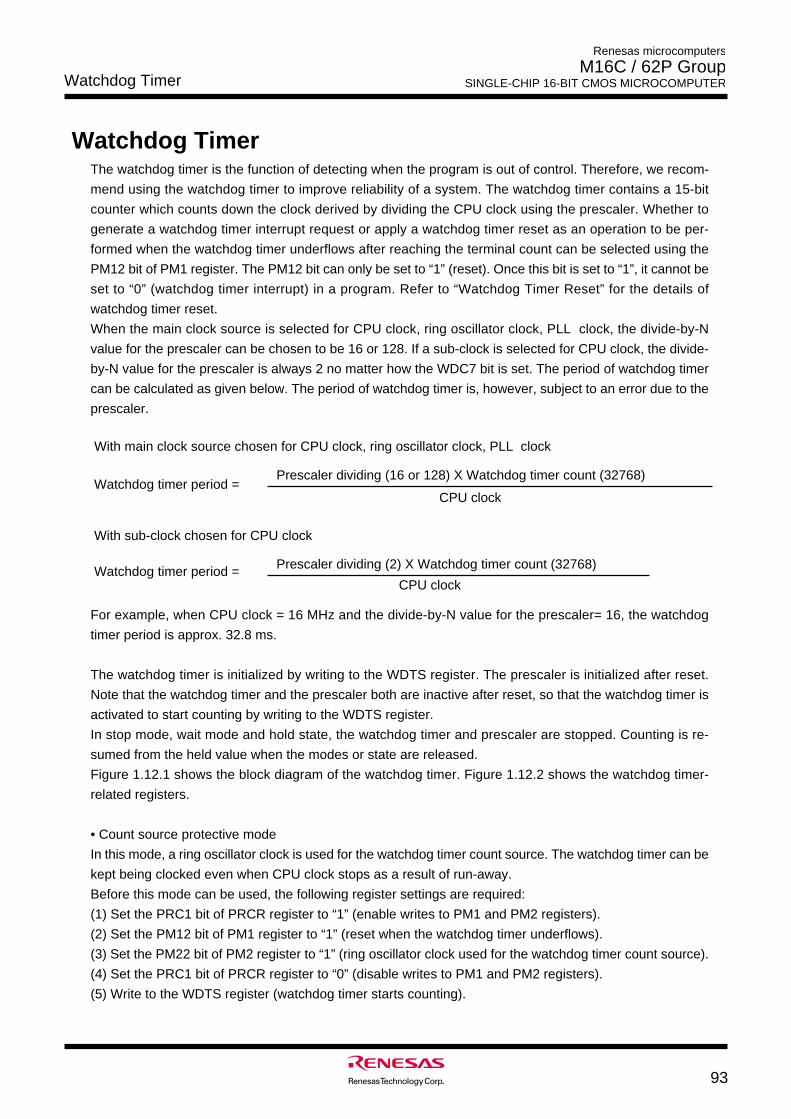
Watchdog Timer
93
Renesas microcomputers
M16C / 62P Group SINGLE-CHIP 16-BIT CMOS MICROCOMPUTER
Watchdog TimerThe watchdog timer is the function of detecting when the program is out of control. Therefore, we recom-
mend using the watchdog timer to improve reliability of a system. The watchdog timer contains a 15-bit
counter which counts down the clock derived by dividing the CPU clock using the prescaler. Whether to
generate a watchdog timer interrupt request or apply a watchdog timer reset as an operation to be per-
formed when the watchdog timer underflows after reaching the terminal count can be selected using the
PM12 bit of PM1 register. The PM12 bit can only be set to “1” (reset). Once this bit is set to “1”, it cannot be
set to “0” (watchdog timer interrupt) in a program. Refer to “Watchdog Timer Reset” for the details of
watchdog timer reset.
When the main clock source is selected for CPU clock, ring oscillator clock, PLL clock, the divide-by-N
value for the prescaler can be chosen to be 16 or 128. If a sub-clock is selected for CPU clock, the divide-
by-N value for the prescaler is always 2 no matter how the WDC7 bit is set. The period of watchdog timer
can be calculated as given below. The period of watchdog timer is, however, subject to an error due to the
prescaler.
For example, when CPU clock = 16 MHz and the divide-by-N value for the prescaler= 16, the watchdog
timer period is approx. 32.8 ms.
The watchdog timer is initialized by writing to the WDTS register. The prescaler is initialized after reset.
Note that the watchdog timer and the prescaler both are inactive after reset, so that the watchdog timer is
activated to start counting by writing to the WDTS register.
In stop mode, wait mode and hold state, the watchdog timer and prescaler are stopped. Counting is re-
sumed from the held value when the modes or state are released.
Figure 1.12.1 shows the block diagram of the watchdog timer. Figure 1.12.2 shows the watchdog timer-
related registers.
• Count source protective mode
In this mode, a ring oscillator clock is used for the watchdog timer count source. The watchdog timer can be
kept being clocked even when CPU clock stops as a result of run-away.
Before this mode can be used, the following register settings are required:
(1) Set the PRC1 bit of PRCR register to “1” (enable writes to PM1 and PM2 registers).
(2) Set the PM12 bit of PM1 register to “1” (reset when the watchdog timer underflows).
(3) Set the PM22 bit of PM2 register to “1” (ring oscillator clock used for the watchdog timer count source).
(4) Set the PRC1 bit of PRCR register to “0” (disable writes to PM1 and PM2 registers).
(5) Write to the WDTS register (watchdog timer starts counting).
With main clock source chosen for CPU clock, ring oscillator clock, PLL clock
Watchdog timer period =
With sub-clock chosen for CPU clock
Prescaler dividing (2) X Watchdog timer count (32768)
CPU clock
Watchdog timer period =Prescaler dividing (16 or 128) X Watchdog timer count (32768)
CPU clock
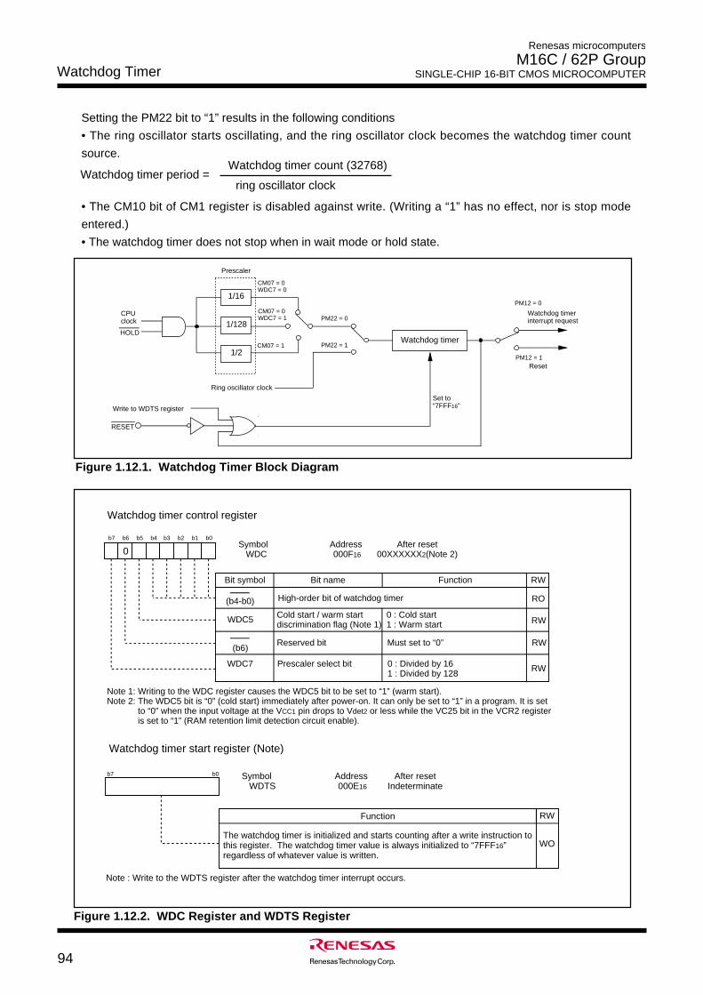
Watchdog Timer
94
Renesas microcomputers
M16C / 62P Group SINGLE-CHIP 16-BIT CMOS MICROCOMPUTER
Watchdog timer control register
Symbol Address After reset WDC 000F16 00XXXXXX2(Note 2)
FunctionBit symbol RW
b7 b6 b5 b4 b3 b2 b1 b0
High-order bit of watchdog timer
WDC7
Bit name
Prescaler select bit 0 : Divided by 161 : Divided by 128
Reserved bit Must set to “0”
0
RO
RW
RW
RW
Cold start / warm start discrimination flag (Note 1)
0 : Cold start1 : Warm startWDC5
Note 1: Writing to the WDC register causes the WDC5 bit to be set to “1” (warm start).Note 2: The WDC5 bit is “0” (cold start) immediately after power-on. It can only be set to “1” in a program. It is set
to “0” when the input voltage at the VCC1 pin drops to Vdet2 or less while the VC25 bit in the VCR2 register is set to “1” (RAM retention limit detection circuit enable).
(b4-b0)
(b6)
Figure 1.12.2. WDC Register and WDTS Register
CPUclock
Write to WDTS register
RESET
PM12 = 0
Watchdog timer
Set to “7FFF16”
1/128
1/16
CM07 = 0WDC7 = 1
CM07 = 0WDC7 = 0
CM07 = 1
HOLD
1/2
Prescaler
PM12 = 1
Watchdog timer interrupt request
Reset
PM22 = 0
PM22 = 1
Ring oscillator clock
Figure 1.12.1. Watchdog Timer Block Diagram
Watchdog timer start register (Note)
Symbol Address After reset WDTS 000E16 Indeterminate
WO
b7 b0
Function
The watchdog timer is initialized and starts counting after a write instruction to this register. The watchdog timer value is always initialized to “7FFF16”regardless of whatever value is written.
RW
Note : Write to the WDTS register after the watchdog timer interrupt occurs.
Setting the PM22 bit to “1” results in the following conditions
• The ring oscillator starts oscillating, and the ring oscillator clock becomes the watchdog timer count
source.
• The CM10 bit of CM1 register is disabled against write. (Writing a “1” has no effect, nor is stop mode
entered.)
• The watchdog timer does not stop when in wait mode or hold state.
Watchdog timer period =Watchdog timer count (32768)
ring oscillator clock
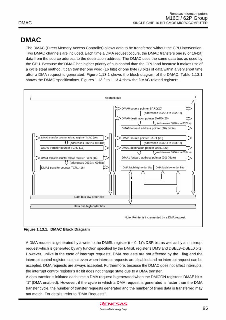
DMAC
95
Renesas microcomputers
M16C / 62P Group SINGLE-CHIP 16-BIT CMOS MICROCOMPUTER
DMACThe DMAC (Direct Memory Access Controller) allows data to be transferred without the CPU intervention.Two DMAC channels are included. Each time a DMA request occurs, the DMAC transfers one (8 or 16-bit)data from the source address to the destination address. The DMAC uses the same data bus as used bythe CPU. Because the DMAC has higher priority of bus control than the CPU and because it makes use ofa cycle steal method, it can transfer one word (16 bits) or one byte (8 bits) of data within a very short timeafter a DMA request is generated. Figure 1.13.1 shows the block diagram of the DMAC. Table 1.13.1shows the DMAC specifications. Figures 1.13.2 to 1.13.4 show the DMAC-related registers.
Figure 1.13.1. DMAC Block Diagram
AAA
AAA AA
AAAA
AA
AA
AAAAAA
AAAA
AA
A
AA
A
Data bus low-order bits
DMA latch high-order bits DMA latch low-order bits
DMA0 source pointer SAR0(20)
DMA0 destination pointer DAR0 (20)
DMA0 forward address pointer (20) (Note)
Data bus high-order bits
AAAA
AAAA
AA
AAAAAAAAAAAAAAAAAAAAAAAAAAAAAAAAAAAAAAAAAAAAAAAAAAAAAAAA
AAAAAAAAAAAAAAAddress bus
AAAA
AAAAAA
DMA1 destination pointer DAR1 (20)
DMA1 source pointer SAR1 (20)
DMA1 forward address pointer (20) (Note)AAAA
AA
DMA0 transfer counter reload register TCR0 (16)
DMA0 transfer counter TCR0 (16)
DMA1 transfer counter reload register TCR1 (16)
DMA1 transfer counter TCR1 (16)A
A(addresses 002916, 002816)
(addresses 003916, 003816)
(addresses 002216 to 002016)
(addresses 002616 to 002416)
(addresses 003216 to 003016)
(addresses 003616 to 003416)
Note: Pointer is incremented by a DMA request.
AA
AAAA
AA
AAAAAAAAA
AAA
AAAAAA
AAAA
AA
AAA
AAAA
A DMA request is generated by a write to the DMiSL register (i = 0–1)’s DSR bit, as well as by an interrupt
request which is generated by any function specified by the DMiSL register’s DMS and DSEL3–DSEL0 bits.
However, unlike in the case of interrupt requests, DMA requests are not affected by the I flag and the
interrupt control register, so that even when interrupt requests are disabled and no interrupt request can be
accepted, DMA requests are always accepted. Furthermore, because the DMAC does not affect interrupts,
the interrupt control register’s IR bit does not change state due to a DMA transfer.
A data transfer is initiated each time a DMA request is generated when the DMiCON register’s DMAE bit =
“1” (DMA enabled). However, if the cycle in which a DMA request is generated is faster than the DMA
transfer cycle, the number of transfer requests generated and the number of times data is transferred may
not match. For details, refer to “DMA Requests”.
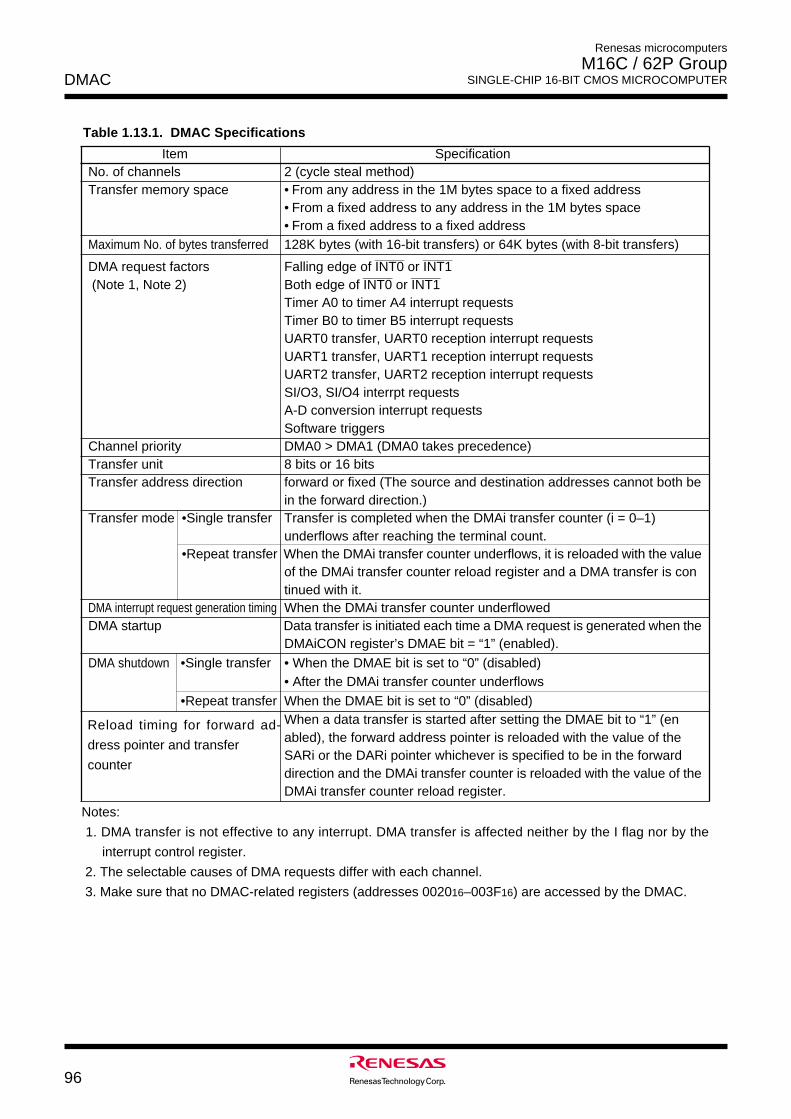
DMAC
96
Renesas microcomputers
M16C / 62P Group SINGLE-CHIP 16-BIT CMOS MICROCOMPUTER
Item SpecificationNo. of channels 2 (cycle steal method)Transfer memory space • From any address in the 1M bytes space to a fixed address
• From a fixed address to any address in the 1M bytes space• From a fixed address to a fixed address
Maximum No. of bytes transferred 128K bytes (with 16-bit transfers) or 64K bytes (with 8-bit transfers)
DMA request factors________ ________
Falling edge of INT0 or INT1 (Note 1, Note 2)
________ ________
Both edge of INT0 or INT1Timer A0 to timer A4 interrupt requestsTimer B0 to timer B5 interrupt requestsUART0 transfer, UART0 reception interrupt requestsUART1 transfer, UART1 reception interrupt requestsUART2 transfer, UART2 reception interrupt requestsSI/O3, SI/O4 interrpt requestsA-D conversion interrupt requestsSoftware triggers
Channel priority DMA0 > DMA1 (DMA0 takes precedence)Transfer unit 8 bits or 16 bitsTransfer address direction forward or fixed (The source and destination addresses cannot both be
in the forward direction.)Transfer mode •Single transfer Transfer is completed when the DMAi transfer counter (i = 0–1)
underflows after reaching the terminal count.•Repeat transfer When the DMAi transfer counter underflows, it is reloaded with the value
of the DMAi transfer counter reload register and a DMA transfer is continued with it.
DMA interrupt request generation timing When the DMAi transfer counter underflowedDMA startup Data transfer is initiated each time a DMA request is generated when the
DMAiCON register’s DMAE bit = “1” (enabled).
DMA shutdown •Single transfer • When the DMAE bit is set to “0” (disabled)• After the DMAi transfer counter underflows
•Repeat transfer When the DMAE bit is set to “0” (disabled)When a data transfer is started after setting the DMAE bit to “1” (enabled), the forward address pointer is reloaded with the value of theSARi or the DARi pointer whichever is specified to be in the forwarddirection and the DMAi transfer counter is reloaded with the value of theDMAi transfer counter reload register.
Table 1.13.1. DMAC Specifications
Notes:
1. DMA transfer is not effective to any interrupt. DMA transfer is affected neither by the I flag nor by the
interrupt control register.
2. The selectable causes of DMA requests differ with each channel.
3. Make sure that no DMAC-related registers (addresses 002016–003F16) are accessed by the DMAC.
Reload timing for forward ad-
dress pointer and transfer
counter
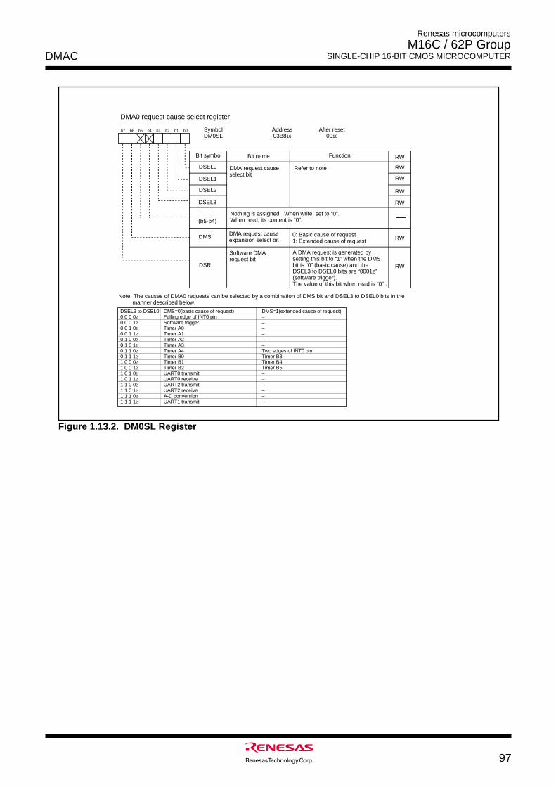
DMAC
97
Renesas microcomputers
M16C / 62P Group SINGLE-CHIP 16-BIT CMOS MICROCOMPUTER
DMA0 request cause select register
Symbol Address After resetDM0SL 03B816 0016
FunctionBit symbol
b7 b6 b5 b4 b3 b2 b1 b0
DMA request cause select bit
DSEL0
RW
DSEL1
DSEL2
DSEL3
Nothing is assigned. When write, set to “0”. When read, its content is “0”.
Software DMA request bit
A DMA request is generated by setting this bit to “1” when the DMS bit is “0” (basic cause) and the DSEL3 to DSEL0 bits are “00012” (software trigger).The value of this bit when read is “0” .
DSR
DSEL3 to DSEL0 DMS=0(basic cause of request) DMS=1(extended cause of request)0 0 0 02 Falling edge of INT0 pin – 0 0 0 12 Software trigger – 0 0 1 02 Timer A0 –0 0 1 12 Timer A1 –0 1 0 02 Timer A2 –0 1 0 12 Timer A3 –0 1 1 02 Timer A4 Two edges of INT0 pin 0 1 1 12 Timer B0 Timer B31 0 0 02 Timer B1 Timer B41 0 0 12 Timer B2 Timer B51 0 1 02 UART0 transmit – 1 0 1 12 UART0 receive –1 1 0 02 UART2 transmit – 1 1 0 12 UART2 receive –1 1 1 02 A-D conversion –1 1 1 12 UART1 transmit –
Bit name
DMA request cause expansion select bitDMS 0: Basic cause of request
1: Extended cause of request
RW
RW
RW
RW
RW
RW
(b5-b4)
Refer to note
Note: The causes of DMA0 requests can be selected by a combination of DMS bit and DSEL3 to DSEL0 bits in the manner described below.
Figure 1.13.2. DM0SL Register
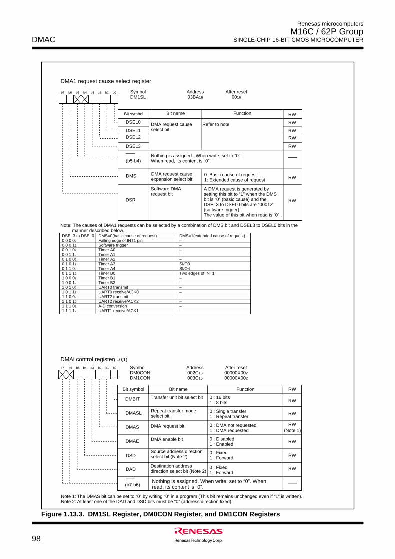
DMAC
98
Renesas microcomputers
M16C / 62P Group SINGLE-CHIP 16-BIT CMOS MICROCOMPUTER
DMAi control register(i=0,1)
Symbol Address After resetDM0CON 002C16 00000X002DM1CON 003C16 00000X002
Bit name FunctionBit symbol
Transfer unit bit select bit
b7 b6 b5 b4 b3 b2 b1 b0
0 : 16 bits1 : 8 bits
DMBIT
DMASL
DMAS
DMAE
Repeat transfer mode select bit
0 : Single transfer1 : Repeat transfer
DMA request bit 0 : DMA not requested1 : DMA requested
0 : Disabled1 : Enabled
0 : Fixed1 : Forward
DMA enable bit
Source address direction select bit (Note 2)
Destination address direction select bit (Note 2)
0 : Fixed1 : Forward
DSD
DAD
Nothing is assigned. When write, set to “0”. When read, its content is “0”.
Note 1: The DMAS bit can be set to “0” by writing “0” in a program (This bit remains unchanged even if “1” is written).Note 2: At least one of the DAD and DSD bits must be “0” (address direction fixed).
(Note 1)
DMA1 request cause select register
Symbol Address After resetDM1SL 03BA16 0016
FunctionBit symbol
b7 b6 b5 b4 b3 b2 b1 b0
DMA request cause select bit
DSEL0
RW
DSEL1DSEL2
DSEL3
Software DMA request bit
DSR
DSEL3 to DSEL0 DMS=0(basic cause of request) DMS=1(extended cause of request)0 0 0 02 Falling edge of INT1 pin – 0 0 0 12 Software trigger –0 0 1 02 Timer A0 –0 0 1 12 Timer A1 –0 1 0 02 Timer A2 –0 1 0 12 Timer A3 SI/O3 0 1 1 02 Timer A4 SI/O4 0 1 1 12 Timer B0 Two edges of INT1 1 0 0 02 Timer B1 – 1 0 0 12 Timer B2 – 1 0 1 02 UART0 transmit – 1 0 1 12 UART0 receive/ACK0 – 1 1 0 02 UART2 transmit – 1 1 0 12 UART2 receive/ACK2 – 1 1 1 02 A-D conversion – 1 1 1 12 UART1 receive/ACK1 –
Bit name
DMA request cause expansion select bit
DMS
RW
RW
RW
RW
RW
RW
(b5-b4)
RW
RW
RW
RW
RW
RW
RW
(b7-b6)
Note: The causes of DMA1 requests can be selected by a combination of DMS bit and DSEL3 to DSEL0 bits in the manner described below.
Nothing is assigned. When write, set to “0”. When read, its content is “0”.
A DMA request is generated by setting this bit to “1” when the DMS bit is “0” (basic cause) and the DSEL3 to DSEL0 bits are “00012” (software trigger).The value of this bit when read is “0” .
0: Basic cause of request1: Extended cause of request
Refer to note
Figure 1.13.3. DM1SL Register, DM0CON Register, and DM1CON Registers
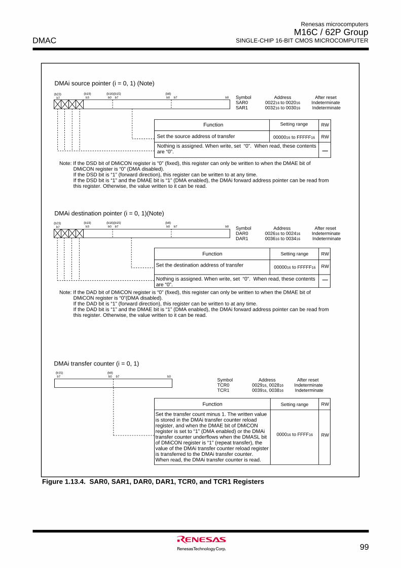
DMAC
99
Renesas microcomputers
M16C / 62P Group SINGLE-CHIP 16-BIT CMOS MICROCOMPUTER
b7 b0 b7 b0(b8)(b15)
Function
Set the transfer count minus 1. The written value is stored in the DMAi transfer counter reload register, and when the DMAE bit of DMiCON register is set to “1” (DMA enabled) or the DMAi transfer counter underflows when the DMASL bit of DMiCON register is “1” (repeat transfer), the value of the DMAi transfer counter reload register is transferred to the DMAi transfer counter.When read, the DMAi transfer counter is read.
Symbol Address After reset TCR0 002916, 002816 Indeterminate TCR1 003916, 003816 Indeterminate
DMAi transfer counter (i = 0, 1)
Setting range
000016 to FFFF16
b7(b23)
b3 b0 b7 b0 b7 b0(b8)(b16)(b15)(b19)
Function RW
Set the source address of transfer
Symbol Address After reset SAR0 002216 to 002016 Indeterminate SAR1 003216 to 003016 Indeterminate
DMAi source pointer (i = 0, 1) (Note)
Setting range
0000016 to FFFFF16
Nothing is assigned. When write, set “0”. When read, these contents are “0”.
Symbol Address After reset DAR0 002616 to 002416 Indeterminate DAR1 003616 to 003416 Indeterminate
b3 b0 b7 b0 b7 b0(b8)(b15)(b16)(b19)
Function
Set the destination address of transfer
DMAi destination pointer (i = 0, 1)(Note)
Setting range
0000016 to FFFFF16
b7(b23)
RW
RW
RW
RW
RW
Note: If the DSD bit of DMiCON register is “0” (fixed), this register can only be written to when the DMAE bit of DMiCON register is “0” (DMA disabled).If the DSD bit is “1” (forward direction), this register can be written to at any time. If the DSD bit is “1” and the DMAE bit is “1” (DMA enabled), the DMAi forward address pointer can be read from this register. Otherwise, the value written to it can be read.
Nothing is assigned. When write, set “0”. When read, these contents are “0”.
Note: If the DAD bit of DMiCON register is “0” (fixed), this register can only be written to when the DMAE bit of DMiCON register is “0”(DMA disabled).If the DAD bit is “1” (forward direction), this register can be written to at any time. If the DAD bit is “1” and the DMAE bit is “1” (DMA enabled), the DMAi forward address pointer can be read from this register. Otherwise, the value written to it can be read.
Figure 1.13.4. SAR0, SAR1, DAR0, DAR1, TCR0, and TCR1 Registers
DMAC
100
Renesas microcomputers
M16C / 62P Group SINGLE-CHIP 16-BIT CMOS MICROCOMPUTER
1. Transfer CyclesThe transfer cycle consists of a memory or SFR read (source read) bus cycle and a write (destination
write) bus cycle. The number of read and write bus cycles is affected by the source and destination
addresses of transfer. During memory extension and microprocessor modes, it is also affected by the________
BYTE pin level. Furthermore, the bus cycle itself is extended by a software wait or RDY signal.
(a) Effect of Source and Destination Addresses
If the transfer unit and data bus both are 16 bits and the source address of transfer begins with an odd
address, the source read cycle consists of one more bus cycle than when the source address of
transfer begins with an even address.
Similarly, if the transfer unit and data bus both are 16 bits and the destination address of transfer
begins with an odd address, the destination write cycle consists of one more bus cycle than when the
destination address of transfer begins with an even address.
(b) Effect of BYTE Pin Level
During memory extension and microprocessor modes, if 16 bits of data are to be transferred on an 8-
bit data bus (input on the BYTE pin = high), the operation is accomplished by transferring 8 bits of data
twice. Therefore, this operation requires two bus cycles to read data and two bus cycles to write data.
Furthermore, if the DMAC is to access the internal area (internal ROM, internal RAM, or SFR), unlike
in the case of the CPU, the DMAC does it through the data bus width selected by the BYTE pin.
(c) Effect of Software Wait
For memory or SFR accesses in which one or more software wait states are inserted, the number of
bus cycles required for that access increases by an amount equal to software wait states.
_______
(d) Effect of RDY Signal
During memory extension and microprocessor modes, DMA transfers to and from an external area________ ________
are affected by the RDY signal. Refer to “RDY signal”.
Figure 1.13.5 shows the example of the cycles for a source read. For convenience, the destination write
cycle is shown as one cycle and the source read cycles for the different conditions are shown. In reality,
the destination write cycle is subject to the same conditions as the source read cycle, with the transfer
cycle changing accordingly. When calculating transfer cycles, take into consideration each condition for
the source read and the destination write cycle, respectively. For example, when data is transferred in 16
bit units using an 8-bit bus ((2) in Figure 1.13.5), two source read bus cycles and two destination write bus
cycles are required.
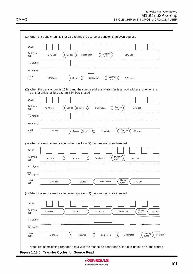
DMAC
101
Renesas microcomputers
M16C / 62P Group SINGLE-CHIP 16-BIT CMOS MICROCOMPUTER
BCLK
Address bus
RD signal
WR signal
Data bus
CPU use
CPU use CPU use
CPU useSource
Source
Destination
Destination
Dummy cycle
Dummy cycle
(1) When the transfer unit is 8 or 16 bits and the source of transfer is an even address
BCLK
Address bus
RD signal
WR signal
Data bus
CPU use
CPU use CPU use
CPU useSource
Source
Destination
Destination
Dummy cycle
Dummy cycle
(3) When the source read cycle under condition (1) has one wait state inserted
BCLK
Address bus
RD signal
WR signal
Data bus
CPU use
CPU use CPU use
CPU useSource
Source
Destination
Destination
Dummy cycle
Dummy cycle
Source + 1
Source + 1
(2) When the transfer unit is 16 bits and the source address of transfer is an odd address, or when the transfer unit is 16 bits and an 8-bit bus is used
BCLK
Address bus
RD signal
WR signal
Data bus
CPU use
CPU use CPU use
CPU useSource
Source
Destination
Destination
Dummy cycle
Dummy cycle
Source + 1
Source + 1
(4) When the source read cycle under condition (2) has one wait state inserted
Note: The same timing changes occur with the respective conditions at the destination as at the source.
Figure 1.13.5. Transfer Cycles for Source Read
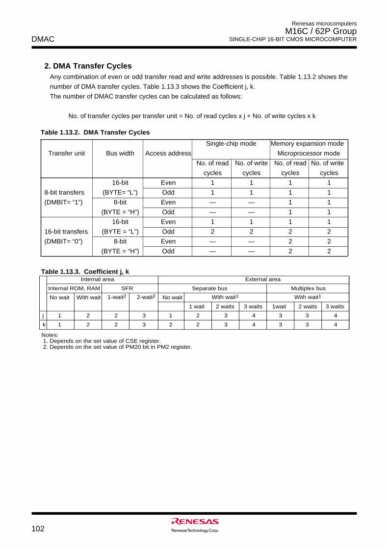
DMAC
102
Renesas microcomputers
M16C / 62P Group SINGLE-CHIP 16-BIT CMOS MICROCOMPUTER
Single-chip mode Memory expansion mode
Transfer unit Bus width Access address Microprocessor mode
No. of read No. of write No. of read No. of write
cycles cycles cycles cycles
16-bit Even 1 1 1 1
8-bit transfers (BYTE= “L”) Odd 1 1 1 1
(DMBIT= “1”) 8-bit Even — — 1 1
(BYTE = “H”) Odd — — 1 1
16-bit Even 1 1 1 1
16-bit transfers (BYTE = “L”) Odd 2 2 2 2
(DMBIT= “0”) 8-bit Even — — 2 2
(BYTE = “H”) Odd — — 2 2
Table 1.13.2. DMA Transfer Cycles
2. DMA Transfer CyclesAny combination of even or odd transfer read and write addresses is possible. Table 1.13.2 shows the
number of DMA transfer cycles. Table 1.13.3 shows the Coefficient j, k.
The number of DMAC transfer cycles can be calculated as follows:
No. of transfer cycles per transfer unit = No. of read cycles x j + No. of write cycles x k
Table 1.13.3. Coefficient j, kInternal area
Internal ROM, RAM SFR Separate bus
External area
Multiplex bus
No wait With wait No wait With wait1
1
1
2
2
3
3
1
2
1 wait
2
2 waits
3
3 waits
4
1wait
3
2 waits
3
3 waits
4
With wait1
j
k 2 3 4 3 3 4
Notes: 1. Depends on the set value of CSE register. 2. Depends on the set value of PM20 bit in PM2 register.
2
2
1-wait2 2-wait2
DMAC
103
Renesas microcomputers
M16C / 62P Group SINGLE-CHIP 16-BIT CMOS MICROCOMPUTER
3. DMA EnableWhen a data transfer starts after setting the DMAE bit in DMiCON register (i = 0, 1) to “1” (enabled), the
DMAC operates as follows:
(1) Reload the forward address pointer with the SARi register value when the DSD bit in DMiCON register
is “1” (forward) or the DARi register value when the DAD bit of DMiCON register is “1” (forward).
(2) Reload the DMAi transfer counter with the DMAi transfer counter reload register value.
If the DMAE bit is set to “1” again while it remains set, the DMAC performs the above operation. However,
if a DMA request may occur simultaneously when the DMAE bit is being written, follow the steps below.
Step 1: Write “1” to the DMAE bit and DMAS bit in DMiCON register simultaneously.
Step 2: Make sure that the DMAi is in an initial state as described above (1) and (2) in a program.
If the DMAi is not in an initial state, the above steps should be repeated.
4. DMA RequestThe DMAC can generate a DMA request as triggered by the cause of request that is selected with the
DMS and DSEL3 to DSEL0 bits of DMiSL register (i = 0, 1) on either channel. Table 1.13.4 shows the
timing at which the DMAS bit changes state.
Whenever a DMA request is generated, the DMAS bit is set to “1” (DMA requested) regardless of whether
or not the DMAE bit is set. If the DMAE bit was set to “1” (enabled) when this occurred, the DMAS bit is
set to “0” (DMA not requested) immediately before a data transfer starts. This bit cannot be set to “1” in
a program (it can only be set to “0”).
The DMAS bit may be set to “1” when the DMS or the DSEL3 to DSEL0 bits change state. Therefore,
always be sure to set the DMAS bit to “0” after changing the DMS or the DSEL3 to DSEL0 bits.
Because if the DMAE bit is “1”, a data transfer starts immediately after a DMA request is generated, the
DMAS bit in almost all cases is “0” when read in a program. Read the DMAE bit to determine whether the
DMAC is enabled.
Table 1.13.4. Timing at Which the DMAS Bit Changes State
DMA factor
Software trigger
Peripheral function
Timing at which the bit is set to “1” Timing at which the bit is set to “0” DMAS bit of the DMiCON register
When the DSR bit of DMiSL register is set to “1”
When the interrupt control register for the peripheral function that is selected by the DSEL3 to DSEL0 and DMS bits of DMiSL register has its IR bit set to “1”
• Immediately before a data transfer starts• When set by writing “0” in a program
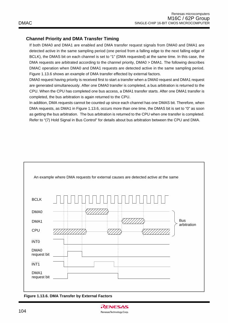
DMAC
104
Renesas microcomputers
M16C / 62P Group SINGLE-CHIP 16-BIT CMOS MICROCOMPUTER
Channel Priority and DMA Transfer TimingIf both DMA0 and DMA1 are enabled and DMA transfer request signals from DMA0 and DMA1 are
detected active in the same sampling period (one period from a falling edge to the next falling edge of
BCLK), the DMAS bit on each channel is set to “1” (DMA requested) at the same time. In this case, the
DMA requests are arbitrated according to the channel priority, DMA0 > DMA1. The following describes
DMAC operation when DMA0 and DMA1 requests are detected active in the same sampling period.
Figure 1.13.6 shows an example of DMA transfer effected by external factors.
DMA0 request having priority is received first to start a transfer when a DMA0 request and DMA1 request
are generated simultaneously. After one DMA0 transfer is completed, a bus arbitration is returned to the
CPU. When the CPU has completed one bus access, a DMA1 transfer starts. After one DMA1 transfer is
completed, the bus arbitration is again returned to the CPU.
In addition, DMA requests cannot be counted up since each channel has one DMAS bit. Therefore, when
DMA requests, as DMA1 in Figure 1.13.6, occurs more than one time, the DMAS bit is set to “0” as soon
as getting the bus arbitration. The bus arbitration is returned to the CPU when one transfer is completed.
Refer to “(7) Hold Signal in Bus Control” for details about bus arbitration between the CPU and DMA.
BCLK
AAAAAAAA
DMA0
AAAADMA1
DMA0request bit
DMA1request bit
AAAA
AAAAAAAAAAAAAAAA
AAAAAAAAAA
AAAACPU
INT0
INT1
An example where DMA requests for external causes are detected active at the same
Bus arbitration
Figure 1.13.6. DMA Transfer by External Factors
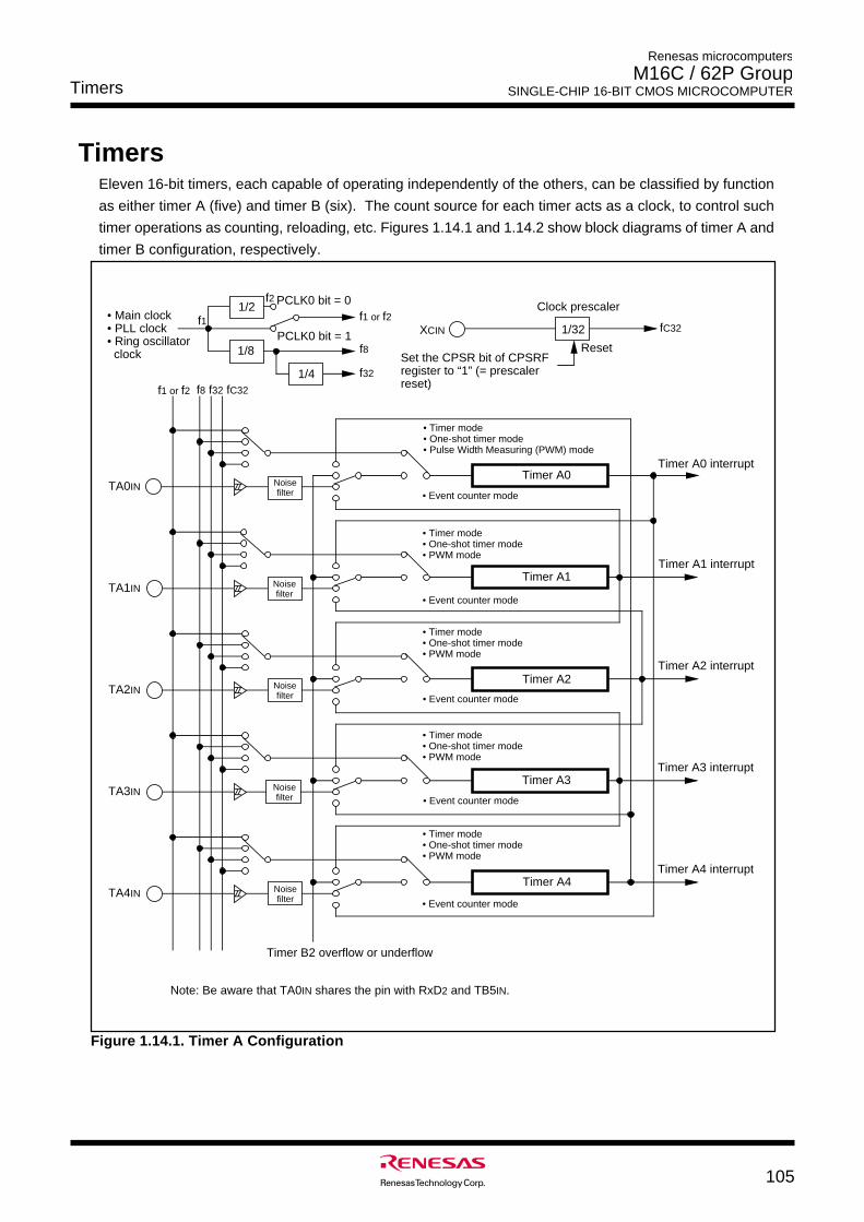
Timers
105
Renesas microcomputers
M16C / 62P Group SINGLE-CHIP 16-BIT CMOS MICROCOMPUTER
TimersEleven 16-bit timers, each capable of operating independently of the others, can be classified by function
as either timer A (five) and timer B (six). The count source for each timer acts as a clock, to control such
timer operations as counting, reloading, etc. Figures 1.14.1 and 1.14.2 show block diagrams of timer A and
timer B configuration, respectively.
• Timer mode• One-shot timer mode• Pulse Width Measuring (PWM) mode
• Timer mode• One-shot timer mode• PWM mode
• Timer mode• One-shot timer mode• PWM mode
• Timer mode• One-shot timer mode• PWM mode
• Timer mode• One-shot timer mode• PWM mode
• Event counter mode
• Event counter mode
• Event counter mode
• Event counter mode
• Event counter mode
TA0IN
TA1IN
TA2IN
TA3IN
TA4IN
Timer A0
Timer A1
Timer A2
Timer A3
Timer A4
f8 f32 fC32
Timer A0 interrupt
Timer A1 interrupt
Timer A2 interrupt
Timer A3 interrupt
Timer A4 interrupt
Noise filter
Noise filter
Noise filter
Noise filter
Noise filter
1/32 fC32
1/8
1/4
f1 or f2
f8
f32
• Main clock• PLL clock• Ring oscillator clock
XCIN
Set the CPSR bit of CPSRF register to “1” (= prescaler reset)
Reset
Clock prescaler
Timer B2 overflow or underflow
Note: Be aware that TA0IN shares the pin with RxD2 and TB5IN.
1/2f1
f2 PCLK0 bit = 0
PCLK0 bit = 1
f1 or f2
Figure 1.14.1. Timer A Configuration
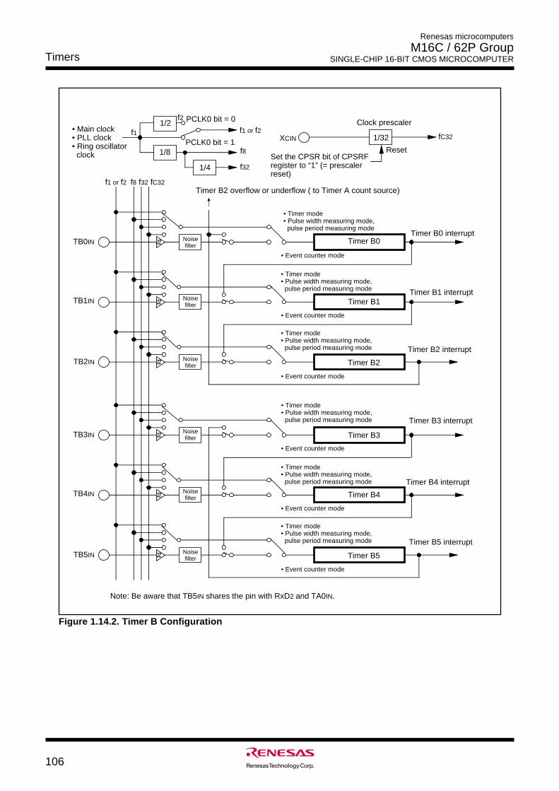
Timers
106
Renesas microcomputers
M16C / 62P Group SINGLE-CHIP 16-BIT CMOS MICROCOMPUTER
Figure 1.14.2. Timer B Configuration
• Event counter mode
• Event counter mode
• Event counter mode
• Timer mode • Pulse width measuring mode, pulse period measuring mode
• Timer mode • Pulse width measuring mode, pulse period measuring mode
• Timer mode • Pulse width measuring mode, pulse period measuring mode
TB0IN
TB1IN
TB2IN
Timer B0
Timer B1
Timer B2
f8 f32 fC32
Timer B0 interruptNoise filter
Noise filter
Noise filter
1/32 fC32XCIN
Reset
Clock prescaler
Timer B2 overflow or underflow ( to Timer A count source)
• Event counter mode
• Event counter mode
• Event counter mode
• Timer mode • Pulse width measuring mode, pulse period measuring mode
• Timer mode • Pulse width measuring mode, pulse period measuring mode
• Timer mode • Pulse width measuring mode, pulse period measuring mode
TB3IN
TB4IN
TB5IN
Timer B3
Timer B4
Timer B5
Timer B3 interruptNoise filter
Noise filter
Noise filter
Timer B1 interrupt
Timer B2 interrupt
Timer B4 interrupt
Timer B5 interrupt
1/8
1/4
f8
f32
1/2f1 or f2• Main clock
• PLL clock• Ring oscillator clock Set the CPSR bit of CPSRF
register to “1” (= prescaler reset)
Note: Be aware that TB5IN shares the pin with RxD2 and TA0IN.
f1
f2 PCLK0 bit = 0
PCLK0 bit = 1
f1 or f2
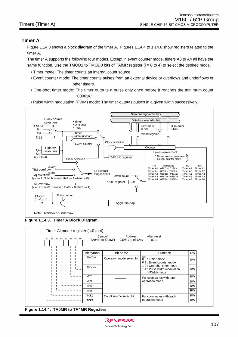
Timers (Timer A)
107
Renesas microcomputers
M16C / 62P Group SINGLE-CHIP 16-BIT CMOS MICROCOMPUTER
Timer AFigure 1.14.3 shows a block diagram of the timer A. Figures 1.14.4 to 1.14.6 show registers related to the
timer A.
The timer A supports the following four modes. Except in event counter mode, timers A0 to A4 all have the
same function. Use the TMOD1 to TMOD0 bits of TAiMR register (i = 0 to 4) to select the desired mode.
• Timer mode: The timer counts an internal count source.
• Event counter mode: The timer counts pulses from an external device or overflows and underflows of
other timers.
• One-shot timer mode: The timer outputs a pulse only once before it reaches the minimum count
“000016.”
• Pulse width modulation (PWM) mode: The timer outputs pulses in a given width successively.
Figure 1.14.4. TA0MR to TA4MR Registers
TABSR register
Up-count/down-count
TAi Addresses TAj TAkTimer A0 038716 - 038616 Timer A4 Timer A1Timer A1 038916 - 038816 Timer A0 Timer A2Timer A2 038B16 - 038A16 Timer A1 Timer A3Timer A3 038D16 - 038C16 Timer A2 Timer A4Timer A4 038F16 - 038E16 Timer A3 Timer A0
Always counts down except in event counter mode
Reload register
Counter
Low-order 8 bits AAAA
High-order 8 bits
Clock source selection
• Timer (gate function)
• Timer • One shot • PWM
f1 or f2f8f32
TAiIN (i = 0 to 4)
TB2 overflow
• Event counter
fC32
Clock selection
TAj overflow (j = i – 1. Note, however, that j = 4 when i = 0)
Pulse output
Toggle flip-flop
TAiOUT (i = 0 to 4)
Data bus low-order bits
Data bus high-order bits
AA
UDF register
Down count
TAk overflow (k = i + 1. Note, however, that k = 0 when i = 4)
Polarity selection
To external trigger circuit
(Note)
(Note)
Note: Overflow or underflow
Clock selection
Timer Ai mode register (i=0 to 4)Symbol Address After reset
TA0MR to TA4MR 039616 to 039A16 0016
Bit name FunctionBit symbol RW
b7 b6 b5 b4 b3 b2 b1 b0
0 0 : Timer mode 0 1 : Event counter mode 1 0 : One-shot timer mode 1 1 : Pulse width modulation
(PWM) mode
b1 b0
TCK1
MR3
MR2
MR1
TMOD1
MR0
TMOD0
TCK0
Function varies with each operation mode
Count source select bit
Operation mode select bit RW
RW
RW
RW
RW
RW
RW
RWFunction varies with each operation mode
Figure 1.14.3. Timer A Block Diagram
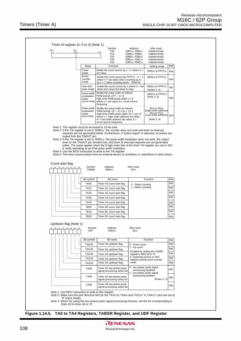
Timers (Timer A)
108
Renesas microcomputers
M16C / 62P Group SINGLE-CHIP 16-BIT CMOS MICROCOMPUTER
Figure 1.14.5. TA0 to TA4 Registers, TABSR Register, and UDF Register
Symbol Address After reset TA0 038716, 038616 Indeterminate TA1 038916, 038816 Indeterminate TA2 038B16, 038A16 Indeterminate TA3 038D16, 038C16 Indeterminate TA4 038F16, 038E16 Indeterminate
b7 b0 b7 b0(b15) (b8)
Timer Ai register (i= 0 to 4) (Note 1)
RW
Divide the count source by n + 1 where n = set value
Function Setting range
Divide the count source by FFFF16 – n + 1 where n = set value when counting up or by n + 1 when counting down
Divide the count source by n where n = set value and cause the timer to stop
Modify the pulse width as follows:PWM period: (216 – 1) / fjHigh level PWM pulse width: n / fj where n = set value, fj = count source frequency
000016 to FFFE16 (Note 3, 4)
Note 1: The register must be accessed in 16 bit units.Note 2: If the TAi register is set to ‘000016,’ the counter does not work and timer Ai interrupt
requests are not generated either. Furthermore, if “pulse output” is selected, no pulses are output from the TAiOUT pin.
Note 3: If the TAi register is set to ‘000016,’ the pulse width modulator does not work, the output level on the TAiOUT pin remains low, and timer Ai interrupt requests are not generated either. The same applies when the 8 high-order bits of the timer TAi register are set to ‘0016’ while operating as an 8-bit pulse width modulator.
Note 4: Use the MOV instruction to write to the TAi register.Note 5: The timer counts pulses from an external device or overflows or underflows in other timers.
0016 to FE16(High-order address)
0016 to FF16(Low-order address)
Timer A4 up/down flag
Timer A3 up/down flag
Timer A2 up/down flag
Timer A1 up/down flag
Timer A0 up/down flag
Timer A2 two-phase pulse signal processing select bit
Timer A3 two-phase pulse signal processing select bit
Timer A4 two-phase pulse signal processing select bit
Symbol Address After resetUDF 038416 0016
TA4P
TA3P
TA2P
Up/down flag (Note 1)
Bit name FunctionBit symbol
b7 b6 b5 b4 b3 b2 b1 b0
TA4UD
TA3UD
TA2UD
TA1UD
TA0UD 0 : Down count 1 : Up count
Enabled by setting the TAiMR register’s MR2 bit to “0”(= switching source in UDF register) during event counter mode.
0 : two-phase pulse signal processing disabled
1 : two-phase pulse signal processing enabled
Symbol Address After resetTABSR 038016 0016
Count start flag
Bit name FunctionBit symbol RW
b7 b6 b5 b4 b3 b2 b1 b0
AAAAAAAAAAAAAAAAAAAAAAAAAAAAAAAAAAAAAAAAAA
AAAAAAAAAAAAAAAAAAAAAAAAAAAATimer B2 count start flag
Timer B1 count start flag
Timer B0 count start flag
Timer A4 count start flag
Timer A3 count start flag
Timer A2 count start flag
Timer A1 count start flag
Timer A0 count start flag 0 : Stops counting1 : Starts counting
TB2S
TB1S
TB0S
TA4S
TA3S
TA2S
TA1S
TA0S
Note 1: Use MOV instruction to write to this register. Note 2: Make sure the port direction bits for the TA2IN to TA4IN and TA2OUT to TA4OUT pins are set to
“0” (input mode).Note 3: When not using the two-phase pulse signal processing function, set the bit corresponding to
timer A2 to timer A4 to “0”.
RW
RW
WO
WO
WO
RW
RW
RW
RW
RW
RW
RW
RW
RW
RW
RW
RW
RW
RW
WO
WO
WO
Timer modeEvent counter mode
One-shot timer mode
Pulse width modulation mode(16-bit PWM)
Pulse width modulation mode(8-bit PWM)
000016 to FFFF16
000016 to FFFF16
000016 to FFFF16
(Notes 2, 4)
Mode
Modify the pulse width as follows:PWM period: (28 – 1) x (m + 1)/ fjHigh level PWM pulse width: (m + 1)n / fj where n = high-order address set value, m = low-order address set value, fj = count source frequency
(Note 3, 4)
(Notes 2, 3)
(Note 5)
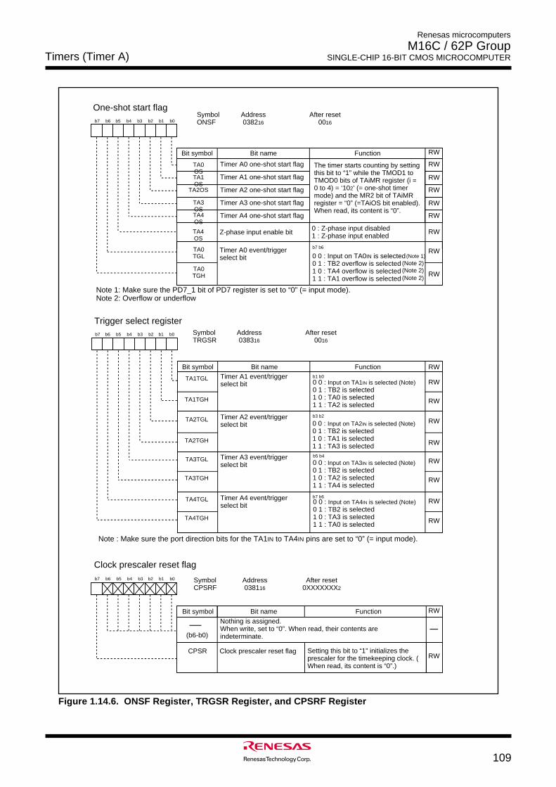
Timers (Timer A)
109
Renesas microcomputers
M16C / 62P Group SINGLE-CHIP 16-BIT CMOS MICROCOMPUTER
Symbol Address After resetCPSRF 038116 0XXXXXXX2
Clock prescaler reset flag
Bit name FunctionBit symbol
b7 b6 b5 b4 b3 b2 b1 b0
AAAAAAAAAAAAAAAAAAAAAAAAAAAAAAClock prescaler reset flag Setting this bit to “1” initializes the
prescaler for the timekeeping clock. (When read, its content is “0”.)
CPSR
Nothing is assigned.When write, set to “0”. When read, their contents are indeterminate.
TA1TGL
Symbol Address After resetTRGSR 038316 0016
Timer A1 event/trigger select bit 0 0 : Input on TA1IN is selected (Note)
0 1 : TB2 is selected1 0 : TA0 is selected 1 1 : TA2 is selected
Trigger select register
Bit name FunctionBit symbol
b7 b6 b5 b4 b3 b2 b1 b0
0 0 : Input on TA2IN is selected (Note) 0 1 : TB2 is selected 1 0 : TA1 is selected 1 1 : TA3 is selected
0 0 : Input on TA3IN is selected (Note)0 1 : TB2 is selected 1 0 : TA2 is selected 1 1 : TA4 is selected
0 0 : Input on TA4IN is selected (Note)0 1 : TB2 is selected 1 0 : TA3 is selected 1 1 : TA0 is selected
Timer A2 event/trigger select bit
Timer A3 event/trigger select bit
Timer A4 event/trigger select bit
TA1TGH
TA2TGL
TA2TGH
TA3TGL
TA3TGH
TA4TGL
TA4TGH
b1 b0
b3 b2
b5 b4
b7 b6
Note : Make sure the port direction bits for the TA1IN to TA4IN pins are set to “0” (= input mode).
TA1OS
TA2OS
TA0OS
One-shot start flagSymbol Address After resetONSF 038216 0016
Timer A0 one-shot start flag
Timer A1 one-shot start flag
Timer A2 one-shot start flag
Timer A3 one-shot start flag
Timer A4 one-shot start flag
TA3OSTA4OS
Bit name FunctionBit symbol
b7 b6 b5 b4 b3 b2 b1 b0
TA0TGL
TA0TGH
0 0 : Input on TA0IN is selected0 1 : TB2 overflow is selected1 0 : TA4 overflow is selected1 1 : TA1 overflow is selected
Timer A0 event/triggerselect bit
b7 b6
RW
The timer starts counting by setting this bit to “1” while the TMOD1 to TMOD0 bits of TAiMR register (i = 0 to 4) = ‘102’ (= one-shot timer mode) and the MR2 bit of TAiMR register = “0” (=TAiOS bit enabled). When read, its content is “0”.
Z-phase input enable bitTA4OS
0 : Z-phase input disabled1 : Z-phase input enabled
RW
RW
RW
RW
RW
RW
RW
RW
RW
RW
RW
RW
RW
RW
RW
RW
RW
RW
RW
(b6-b0)
(Note 2) (Note 2) (Note 2)
Note 1: Make sure the PD7_1 bit of PD7 register is set to “0” (= input mode). Note 2: Overflow or underflow
(Note 1)
Figure 1.14.6. ONSF Register, TRGSR Register, and CPSRF Register
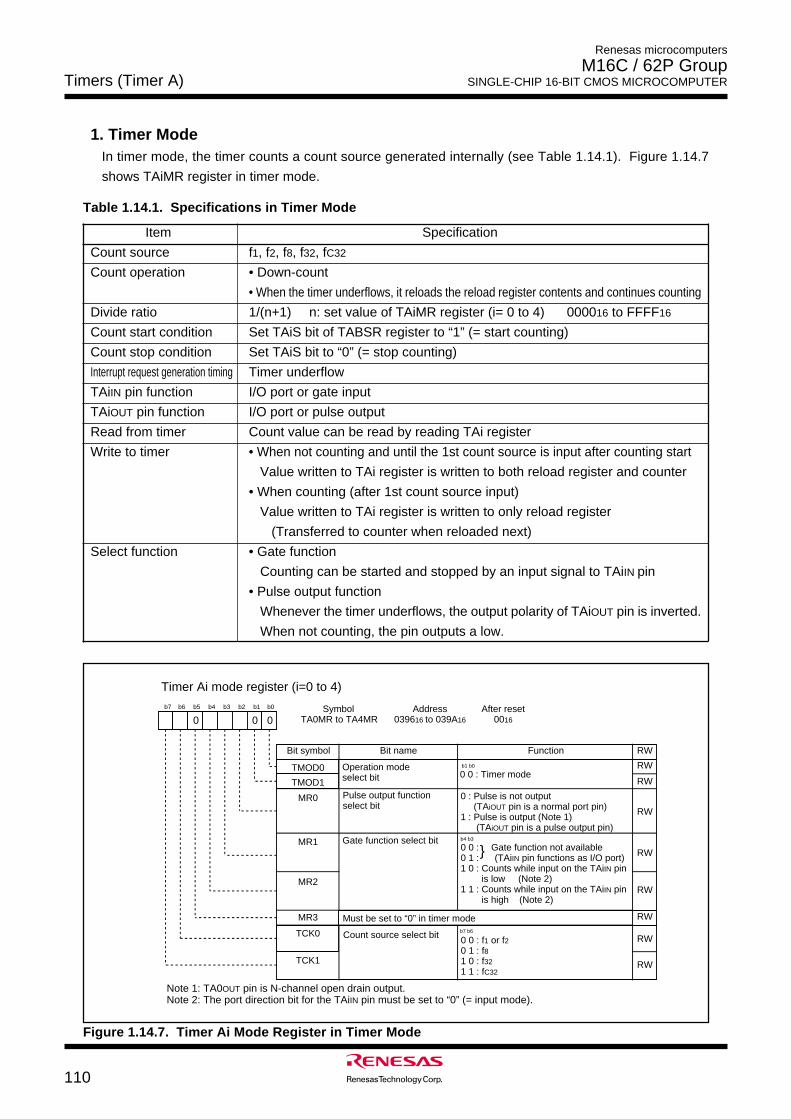
Timers (Timer A)
110
Renesas microcomputers
M16C / 62P Group SINGLE-CHIP 16-BIT CMOS MICROCOMPUTER
Item Specification
Count source f1, f2, f8, f32, fC32
Count operation • Down-count
• When the timer underflows, it reloads the reload register contents and continues counting
Divide ratio 1/(n+1) n: set value of TAiMR register (i= 0 to 4) 000016 to FFFF16
Count start condition Set TAiS bit of TABSR register to “1” (= start counting)
Count stop condition Set TAiS bit to “0” (= stop counting)
Interrupt request generation timing Timer underflow
TAiIN pin function I/O port or gate input
TAiOUT pin function I/O port or pulse output
Read from timer Count value can be read by reading TAi register
Write to timer • When not counting and until the 1st count source is input after counting start
Value written to TAi register is written to both reload register and counter
• When counting (after 1st count source input)
Value written to TAi register is written to only reload register
(Transferred to counter when reloaded next)
Select function • Gate function
Counting can be started and stopped by an input signal to TAiIN pin
• Pulse output function
Whenever the timer underflows, the output polarity of TAiOUT pin is inverted.
When not counting, the pin outputs a low.
1. Timer ModeIn timer mode, the timer counts a count source generated internally (see Table 1.14.1). Figure 1.14.7
shows TAiMR register in timer mode.
Table 1.14.1. Specifications in Timer Mode
Note 1: TA0OUT pin is N-channel open drain output.Note 2: The port direction bit for the TAiIN pin must be set to “0” (= input mode).
Timer Ai mode register (i=0 to 4)
Symbol Address After resetTA0MR to TA4MR 039616 to 039A16 0016
Bit name FunctionBit symbol RW
b7 b6 b5 b4 b3 b2 b1 b0
Operation mode select bit 0 0 : Timer mode
b1 b0
TMOD1
TMOD0
MR0 Pulse output function select bit
0 : Pulse is not output (TAiOUT pin is a normal port pin)1 : Pulse is output (Note 1) (TAiOUT pin is a pulse output pin)
Gate function select bit0 0 : Gate function not available0 1 : (TAiIN pin functions as I/O port)1 0 : Counts while input on the TAiIN pin is low (Note 2)1 1 : Counts while input on the TAiIN pin is high (Note 2)
b4 b3
MR2
MR1
MR3 Must be set to “0” in timer mode
0 0 : f1 or f2 0 1 : f8 1 0 : f32 1 1 : fC32
b7 b6
TCK1
TCK0 Count source select bit
0 00
RW
RW
RW
RW
RW
RW
RW
RW
Figure 1.14.7. Timer Ai Mode Register in Timer Mode
Timers (Timer A)
111
Renesas microcomputers
M16C / 62P Group SINGLE-CHIP 16-BIT CMOS MICROCOMPUTER
Item SpecificationCount source • External signals input to TAiIN pin (i=0 to 4) (effective edge can be selected
in program)• Timer B2 overflows or underflows,
timer Aj (j=i-1, except j=4 if i=0) overflows or underflows,timer Ak (k=i+1, except k=0 if i=4) overflows or underflows
Count operation • Up-count or down-count can be selected by external signal or program• When the timer overflows or underflows, it reloads the reload register con-
tents and continues counting. When operating in free-running mode, thetimer continues counting without reloading.
Divided ratio 1/ (FFFF16 - n + 1) for up-count1/ (n + 1) for down-count n : set value of TAi register 000016 to FFFF16
Count start condition Set TAiS bit of TABSR register to “1” (= start counting)
Count stop condition Set TAiS bit to “0” (= stop counting)Interrupt request generation timing Timer overflow or underflowTAiIN pin function I/O port or count source inputTAiOUT pin function I/O port, pulse output, or up/down-count select inputRead from timer Count value can be read by reading TAi registerWrite to timer • When not counting and until the 1st count source is input after counting start
Value written to TAi register is written to both reload register and counter
• When counting (after 1st count source input)
Value written to TAi register is written to only reload register
(Transferred to counter when reloaded next)Select function • Free-run count function
Even when the timer overflows or underflows, the reload register content isnot reloaded to it
• Pulse output functionWhenever the timer underflows or underflows, the output polarity of TAiOUT
pin is inverted . When not counting, the pin outputs a low.
2. Event Counter ModeIn event counter mode, the timer counts pulses from an external device or overflows and underflows ofother timers. Timers A2, A3 and A4 can count two-phase external signals. Table 1.14.2 lists specifica-tions in event counter mode (when not processing two-phase pulse signal). Table 1.14.3 lists specifica-tions in event counter mode (when processing two-phase pulse signal with the timers A2, A3 and A4).Figure 1.14.8 shows TAiMR register in event counter mode (when not processing two-phase pulse sig-nal). Figure 1.14.9 shows TA2MR to TA4MR registers in event counter mode (when processing two-phase pulse signal with the timers A2, A3 and A4).
Table 1.14.2. Specifications in Event Counter Mode (when not processing two-phase pulse signal)
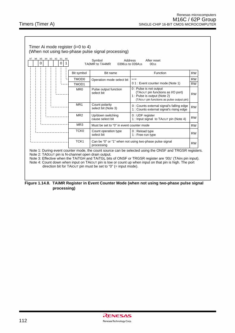
Timers (Timer A)
112
Renesas microcomputers
M16C / 62P Group SINGLE-CHIP 16-BIT CMOS MICROCOMPUTER
Note 1: During event counter mode, the count source can be selected using the ONSF and TRGSR registers.Note 2: TA0OUT pin is N-channel open drain output.Note 3: Effective when the TAiTGH and TAiTGL bits of ONSF or TRGSR register are ‘002’ (TAiIN pin input). Note 4: Count down when input on TAiOUT pin is low or count up when input on that pin is high. The port
direction bit for TAiOUT pin must be set to “0” (= input mode).
Symbol Address After resetTA0MR to TA4MR 039616 to 039A16 0016
WR
b7 b6 b5 b4 b3 b2 b1 b0
Operation mode select bit0 1 : Event counter mode (Note 1)b1 b0 TMOD0
MR0 Pulse output functionselect bit
0 : Pulse is not output(TAiOUT pin functions as I/O port)
1 : Pulse is output (Note 2)(TAiOUT pin functions as pulse output pin)
Count polarity select bit (Note 3)
MR2
MR1
MR3 Must be set to “0” in event counter mode
TCK0 Count operation type select bit
0 10
0 : Counts external signal's falling edge1 : Counts external signal's rising edge
Up/down switching cause select bit
0 : UDF register1 : Input signal to TAiOUT pin (Note 4)
0 : Reload type1 : Free-run type
Bit symbol Bit name Function RW
TCK1 Can be “0” or “1” when not using two-phase pulse signal processing
TMOD1
Timer Ai mode register (i=0 to 4)(When not using two-phase pulse signal processing)
RWRW
RW
RW
RW
RW
RW
RW
Figure 1.14.8. TAiMR Register in Event Counter Mode (when not using two-phase pulse signalprocessing)
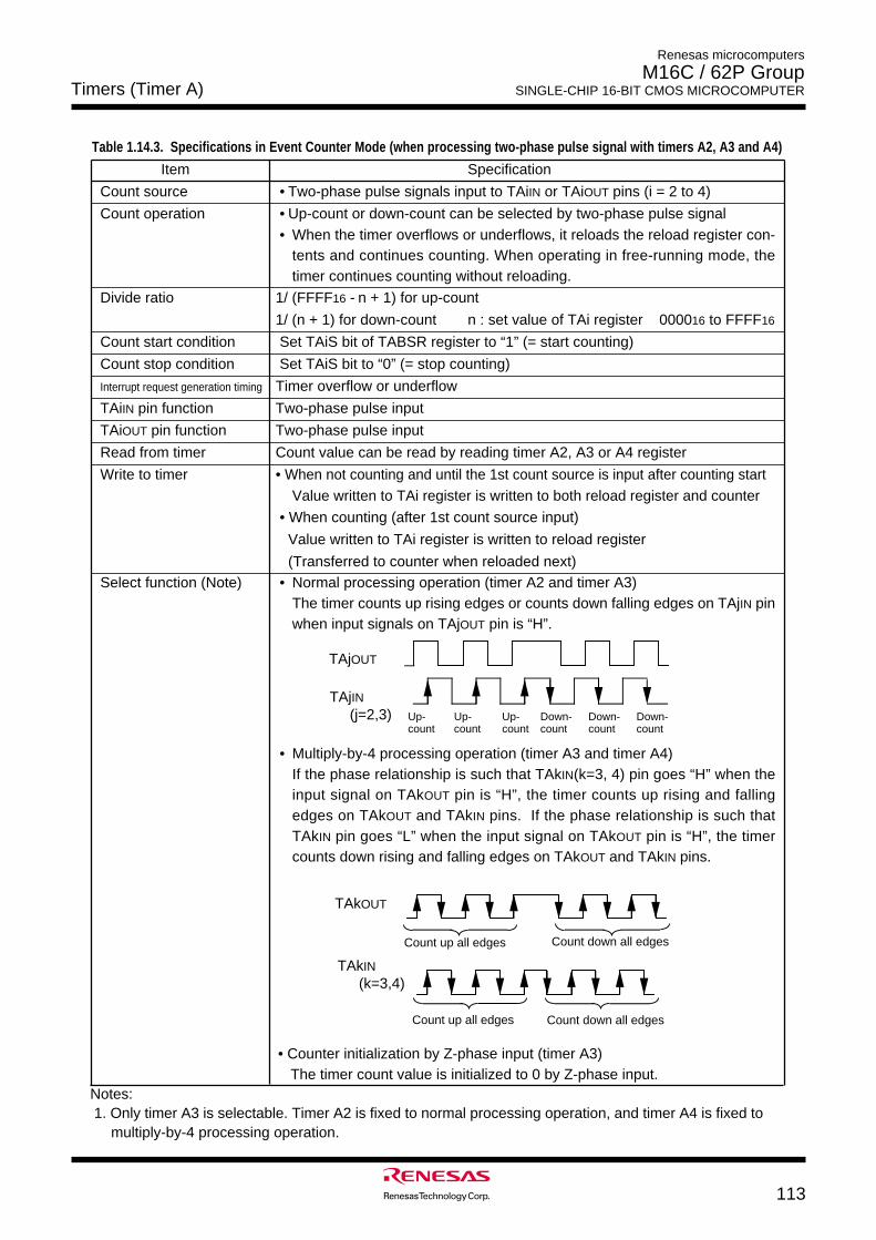
Timers (Timer A)
113
Renesas microcomputers
M16C / 62P Group SINGLE-CHIP 16-BIT CMOS MICROCOMPUTER
Item Specification
Count source • Two-phase pulse signals input to TAiIN or TAiOUT pins (i = 2 to 4)
Count operation • Up-count or down-count can be selected by two-phase pulse signal• When the timer overflows or underflows, it reloads the reload register con-
tents and continues counting. When operating in free-running mode, thetimer continues counting without reloading.
Divide ratio 1/ (FFFF16 - n + 1) for up-count
1/ (n + 1) for down-count n : set value of TAi register 000016 to FFFF16
Count start condition Set TAiS bit of TABSR register to “1” (= start counting)
Count stop condition Set TAiS bit to “0” (= stop counting)
Interrupt request generation timing Timer overflow or underflow
TAiIN pin function Two-phase pulse input
TAiOUT pin function Two-phase pulse input
Read from timer Count value can be read by reading timer A2, A3 or A4 register
Write to timer • When not counting and until the 1st count source is input after counting startValue written to TAi register is written to both reload register and counter
• When counting (after 1st count source input)
Value written to TAi register is written to reload register
(Transferred to counter when reloaded next)Select function (Note) • Normal processing operation (timer A2 and timer A3)
The timer counts up rising edges or counts down falling edges on TAjIN pinwhen input signals on TAjOUT pin is “H”.
• Multiply-by-4 processing operation (timer A3 and timer A4)If the phase relationship is such that TAkIN(k=3, 4) pin goes “H” when theinput signal on TAkOUT pin is “H”, the timer counts up rising and fallingedges on TAkOUT and TAkIN pins. If the phase relationship is such thatTAkIN pin goes “L” when the input signal on TAkOUT pin is “H”, the timercounts down rising and falling edges on TAkOUT and TAkIN pins.
Table 1.14.3. Specifications in Event Counter Mode (when processing two-phase pulse signal with timers A2, A3 and A4)
TAjOUT
Up-count
Up- count
Up- count
Down- count
Down- count
Down- count
TAjIN(j=2,3)
TAkOUT
TAkIN
(k=3,4)
Count up all edges
Count up all edges
Count down all edges
Count down all edges
• Counter initialization by Z-phase input (timer A3)The timer count value is initialized to 0 by Z-phase input.
Notes: 1. Only timer A3 is selectable. Timer A2 is fixed to normal processing operation, and timer A4 is fixed to
multiply-by-4 processing operation.
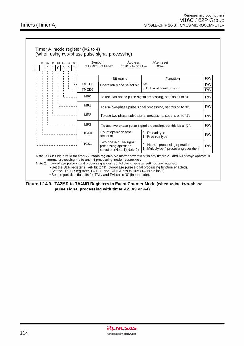
Timers (Timer A)
114
Renesas microcomputers
M16C / 62P Group SINGLE-CHIP 16-BIT CMOS MICROCOMPUTER
Note 1: TCK1 bit is valid for timer A3 mode register. No matter how this bit is set, timers A2 and A4 always operate in normal processing mode and x4 processing mode, respectively.Note 2: If two-phase pulse signal processing is desired, following register settings are required:
• Set the UDF register’s TAiP bit to “1” (two-phase pulse signal processing function enabled).• Set the TRGSR register’s TAiTGH and TAiTGL bits to ‘002’ (TAiIN pin input).• Set the port direction bits for TAiIN and TAiOUT to “0” (input mode).
Timer Ai mode register (i=2 to 4) (When using two-phase pulse signal processing)
Symbol Address After resetTA2MR to TA4MR 039816 to 039A16 0016
b6 b5 b4 b3 b2 b1 b0
Operation mode select bit0 1 : Event counter modeb1 b0
TMOD1
TMOD0
MR0 To use two-phase pulse signal processing, set this bit to “0”.
MR2
MR1
MR3
TCK1
TCK0
0 10
Bit name Function RW
Count operation type select bit
Two-phase pulse signal processing operation select bit (Note 1)(Note 2)
0 : Reload type1 : Free-run type
0 : Normal processing operation1 : Multiply-by-4 processing operation
001
RWRW
RW
RW
RW
RW
RW
RW
To use two-phase pulse signal processing, set this bit to “0”.
To use two-phase pulse signal processing, set this bit to “1”.
To use two-phase pulse signal processing, set this bit to “0”.
Figure 1.14.9. TA2MR to TA4MR Registers in Event Counter Mode (when using two-phasepulse signal processing with timer A2, A3 or A4)
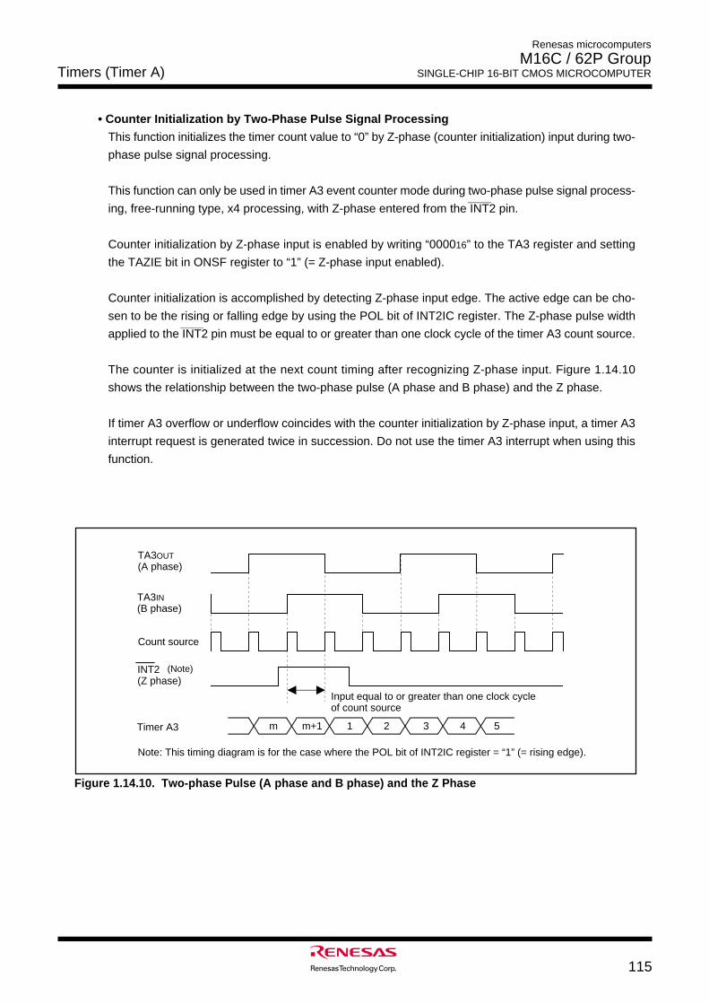
Timers (Timer A)
115
Renesas microcomputers
M16C / 62P Group SINGLE-CHIP 16-BIT CMOS MICROCOMPUTER
m m+1 1 2 3 4 5
TA3OUT(A phase)
Count source
TA3IN(B phase)
Timer A3
INT2 (Z phase)
(Note)
Input equal to or greater than one clock cycle of count source
Note: This timing diagram is for the case where the POL bit of INT2IC register = “1” (= rising edge).
• Counter Initialization by Two-Phase Pulse Signal Processing
This function initializes the timer count value to “0” by Z-phase (counter initialization) input during two-
phase pulse signal processing.
This function can only be used in timer A3 event counter mode during two-phase pulse signal process-_______
ing, free-running type, x4 processing, with Z-phase entered from the INT2 pin.
Counter initialization by Z-phase input is enabled by writing “000016” to the TA3 register and setting
the TAZIE bit in ONSF register to “1” (= Z-phase input enabled).
Counter initialization is accomplished by detecting Z-phase input edge. The active edge can be cho-
sen to be the rising or falling edge by using the POL bit of INT2IC register. The Z-phase pulse width_______
applied to the INT2 pin must be equal to or greater than one clock cycle of the timer A3 count source.
The counter is initialized at the next count timing after recognizing Z-phase input. Figure 1.14.10
shows the relationship between the two-phase pulse (A phase and B phase) and the Z phase.
If timer A3 overflow or underflow coincides with the counter initialization by Z-phase input, a timer A3
interrupt request is generated twice in succession. Do not use the timer A3 interrupt when using this
function.
Figure 1.14.10. Two-phase Pulse (A phase and B phase) and the Z Phase
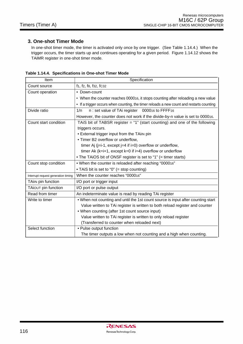
Timers (Timer A)
116
Renesas microcomputers
M16C / 62P Group SINGLE-CHIP 16-BIT CMOS MICROCOMPUTER
Item Specification
Count source f1, f2, f8, f32, fC32
Count operation • Down-count
• When the counter reaches 000016, it stops counting after reloading a new value
• If a trigger occurs when counting, the timer reloads a new count and restarts counting
Divide ratio 1/n n : set value of TAi register 000016 to FFFF16
However, the counter does not work if the divide-by-n value is set to 000016.Count start condition TAiS bit of TABSR register = “1” (start counting) and one of the following
triggers occurs.• External trigger input from the TAiIN pin• Timer B2 overflow or underflow,
timer Aj (j=i-1, except j=4 if i=0) overflow or underflow,timer Ak (k=i+1, except k=0 if i=4) overflow or underflow
• The TAiOS bit of ONSF register is set to “1” (= timer starts)
Count stop condition • When the counter is reloaded after reaching “000016”
• TAiS bit is set to “0” (= stop counting)
Interrupt request generation timing When the counter reaches “000016”
TAiIN pin function I/O port or trigger input
TAiOUT pin function I/O port or pulse output
Read from timer An indeterminate value is read by reading TAi registerWrite to timer • When not counting and until the 1st count source is input after counting start
Value written to TAi register is written to both reload register and counter• When counting (after 1st count source input)
Value written to TAi register is written to only reload register(Transferred to counter when reloaded next)
Select function • Pulse output functionThe timer outputs a low when not counting and a high when counting.
Table 1.14.4. Specifications in One-shot Timer Mode
3. One-shot Timer ModeIn one-shot timer mode, the timer is activated only once by one trigger. (See Table 1.14.4.) When thetrigger occurs, the timer starts up and continues operating for a given period. Figure 1.14.12 shows theTAiMR register in one-shot timer mode.
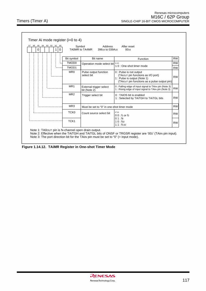
Timers (Timer A)
117
Renesas microcomputers
M16C / 62P Group SINGLE-CHIP 16-BIT CMOS MICROCOMPUTER
Figure 1.14.12. TAiMR Register in One-shot Timer Mode
Bit name
Timer Ai mode register (i=0 to 4)
Symbol Address After resetTA0MR to TA4MR 39616 to 039A16 0016
Function Bit symbol
b7 b6 b5 b4 b3 b2 b1 b0
Operation mode select bit1 0 : One-shot timer modeb1 b0
TMOD1
TMOD0
MR0 Pulse output function select bit
0 : Pulse is not output (TAiOUT pin functions as I/O port)1 : Pulse is output (Note 1) (TAiOUT pin functions as a pulse output pin)
MR2
MR1
MR3 Must be set to “0” in one-shot timer mode
0 0 : f1 or f20 1 : f81 0 : f321 1 : fC32
b7 b6
TCK1
TCK0 Count source select bit
1 00
0 : TAiOS bit is enabled1 : Selected by TAiTGH to TAiTGL bits
Trigger select bit
External trigger select bit (Note 2)
0 : Falling edge of input signal to TAiIN pin (Note 3)1 : Rising edge of input signal to TAiIN pin (Note 3)
Note 1: TA0OUT pin is N-channel open drain output.Note 2: Effective when the TAiTGH and TAiTGL bits of ONSF or TRGSR register are ‘002’ (TAiIN pin input). Note 3: The port direction bit for the TAiIN pin must be set to “0” (= input mode).
RW
RW
RW
RW
RW
RW
RW
RW
RW
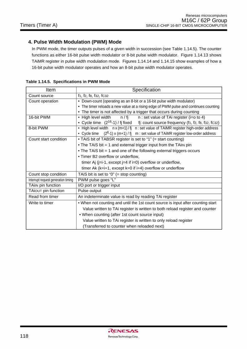
Timers (Timer A)
118
Renesas microcomputers
M16C / 62P Group SINGLE-CHIP 16-BIT CMOS MICROCOMPUTER
4. Pulse Width Modulation (PWM) ModeIn PWM mode, the timer outputs pulses of a given width in succession (see Table 1.14.5). The counter
functions as either 16-bit pulse width modulator or 8-bit pulse width modulator. Figure 1.14.13 shows
TAiMR register in pulse width modulation mode. Figures 1.14.14 and 1.14.15 show examples of how a
16-bit pulse width modulator operates and how an 8-bit pulse width modulator operates.
Table 1.14.5. Specifications in PWM Mode
Item SpecificationCount source f1, f2, f8, f32, fC32
Count operation • Down-count (operating as an 8-bit or a 16-bit pulse width modulator)• The timer reloads a new value at a rising edge of PWM pulse and continues counting• The timer is not affected by a trigger that occurs during counting
16-bit PWM • High level width n / fj n : set value of TAi register (i=o to 4)• Cycle time (216-1) / fj fixed fj: count source frequency (f1, f2, f8, f32, fC32)
8-bit PWM • High level width n x (m+1) / fj n : set value of TAiMR register high-order address• Cycle time (28-1) x (m+1) / fj m : set value of TAiMR register low-order address
Count start condition • TAiS bit of TABSR register is set to “1” (= start counting)• The TAiS bit = 1 and external trigger input from the TAiIN pin• The TAiS bit = 1 and one of the following external triggers occurs• Timer B2 overflow or underflow,
timer Aj (j=i-1, except j=4 if i=0) overflow or underflow,timer Ak (k=i+1, except k=0 if i=4) overflow or underflow
Count stop condition TAiS bit is set to “0” (= stop counting)Interrupt request generation timing PWM pulse goes “L”TAiIN pin function I/O port or trigger inputTAiOUT pin function Pulse outputRead from timer An indeterminate value is read by reading TAi register
Write to timer • When not counting and until the 1st count source is input after counting startValue written to TAi register is written to both reload register and counter
• When counting (after 1st count source input)Value written to TAi register is written to only reload register(Transferred to counter when reloaded next)
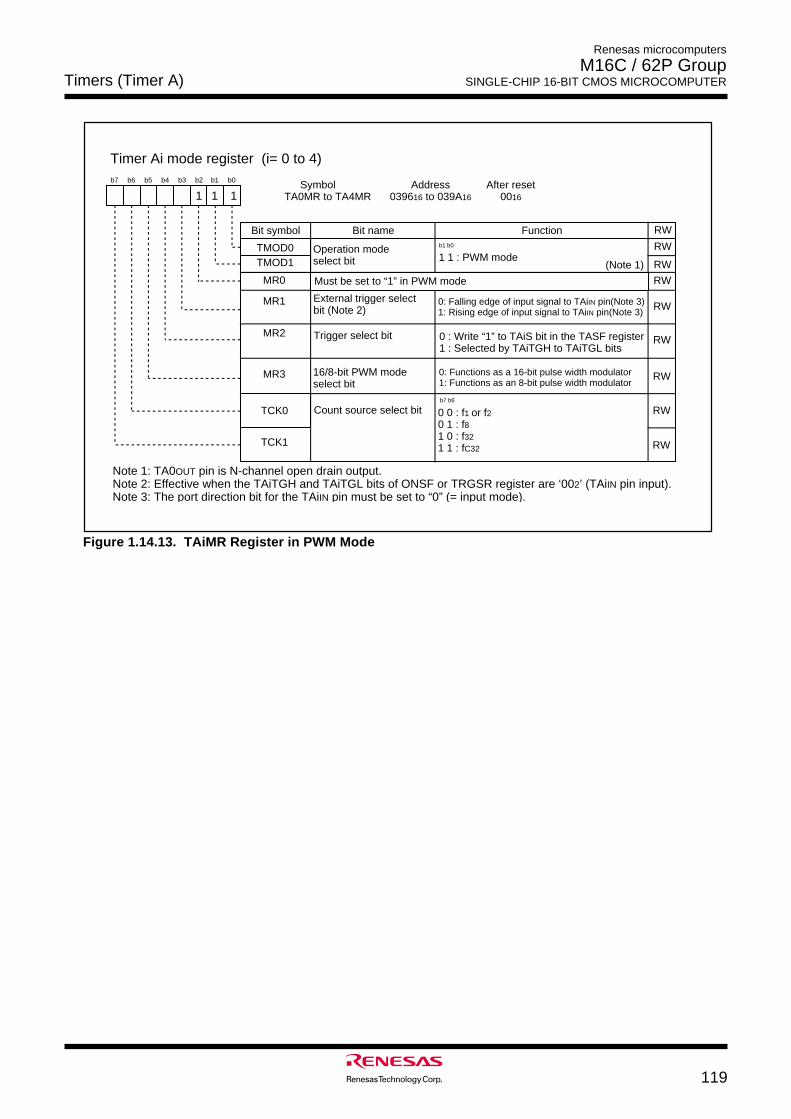
Timers (Timer A)
119
Renesas microcomputers
M16C / 62P Group SINGLE-CHIP 16-BIT CMOS MICROCOMPUTER
Figure 1.14.13. TAiMR Register in PWM Mode
Bit name
Timer Ai mode register (i= 0 to 4)
Symbol Address After resetTA0MR to TA4MR 039616 to 039A16 0016
FunctionBit symbol
b7 b6 b5 b4 b3 b2 b1 b0
Operation mode select bit 1 1 : PWM mode
b1 b0
TMOD1TMOD0
MR0
MR2
MR1
MR3
0 0 : f1 or f20 1 : f81 0 : f321 1 : fC32
b7 b6
TCK1
TCK0 Count source select bit
RW
1 11
Must be set to “1” in PWM mode
16/8-bit PWM mode select bit
0: Functions as a 16-bit pulse width modulator1: Functions as an 8-bit pulse width modulator
Trigger select bit
External trigger select bit (Note 2)
0: Falling edge of input signal to TAiIN pin(Note 3)1: Rising edge of input signal to TAiIN pin(Note 3)
RW
RW
RW
RW
RW
RW
RW
RW
(Note 1)
0 : Write “1” to TAiS bit in the TASF register 1 : Selected by TAiTGH to TAiTGL bits
Note 1: TA0OUT pin is N-channel open drain output.Note 2: Effective when the TAiTGH and TAiTGL bits of ONSF or TRGSR register are ‘002’ (TAiIN pin input). Note 3: The port direction bit for the TAiIN pin must be set to “0” (= input mode).
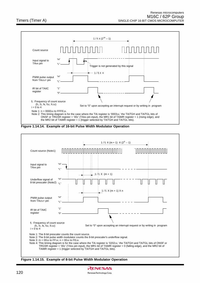
Timers (Timer A)
120
Renesas microcomputers
M16C / 62P Group SINGLE-CHIP 16-BIT CMOS MICROCOMPUTER
1 / fi X (2 – 1) 16
Count source
Input signal to TAiIN pin
PWM pulse output from TAiOUT pin
Trigger is not generated by this signal
“H”
“H”
“L”
“L”
IR bit of TAiIC register
“1”
“0”
fj : Frequency of count source(f1, f2, f8, f32, fC32)
i = 0 to 4
Note 1: n = 000016 to FFFE16.Note 2: This timing diagram is for the case where the TAi register is ‘000316,’ the TAiTGH and TAiTGL bits of
ONSF or TRGSR register = ‘002’ (TAiIN pin input), the MR1 bit of TAiMR register = 1 (rising edge), and the MR2 bit of TAiMR register = 1 (trigger selected by TAiTGH and TAiTGL bits).
1 / fj X n
Set to “0” upon accepting an interrupt request or by writing in program
Count source (Note1)
Input signal to TAiIN pin
Underflow signal of 8-bit prescaler (Note2)
PWM pulse output from TAiOUT pin
“H”
“H”
“H”
“L”
“L”
“L”
“1”
“0”
Set to “0” upon accepting an interrupt request or by writing in program
Note 1: The 8-bit prescaler counts the count source.Note 2: The 8-bit pulse width modulator counts the 8-bit prescaler's underflow signal.Note 3: m = 0016 to FF16; n = 0016 to FE16.Note 4: This timing diagram is for the case where the TAi register is ‘020216,’ the TAiTGH and TAiTGL bits of ONSF or
TRGSR register = ‘002’ (TAiIN pin input), the MR1 bit of TAiMR register = 0 (falling edge), and the MR2 bit of TAiMR register = 1 (trigger selected by TAiTGH and TAiTGL bits).
AAAAAAAAAAAAAAAAAAAAAAAAAAAAAAAAAA
1 / fj X (m + 1) X (2 – 1) 8
1 / fj X (m + 1) X n
1 / fj X (m + 1)
IR bit of TAiIC register
fj : Frequency of count source(f1, f2, f8, f32, fC32)
i = 0 to 4
Figure 1.14.14. Example of 16-bit Pulse Width Modulator Operation
Figure 1.14.15. Example of 8-bit Pulse Width Modulator Operation
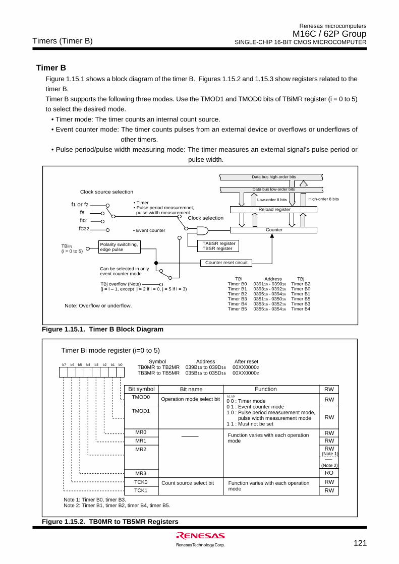
Timers (Timer B)
121
Renesas microcomputers
M16C / 62P Group SINGLE-CHIP 16-BIT CMOS MICROCOMPUTER
Timer BFigure 1.15.1 shows a block diagram of the timer B. Figures 1.15.2 and 1.15.3 show registers related to the
timer B.
Timer B supports the following three modes. Use the TMOD1 and TMOD0 bits of TBiMR register (i = 0 to 5)
to select the desired mode.
• Timer mode: The timer counts an internal count source.
• Event counter mode: The timer counts pulses from an external device or overflows or underflows of
other timers.
• Pulse period/pulse width measuring mode: The timer measures an external signal's pulse period or
pulse width.
Figure 1.15.1. Timer B Block Diagram
Timer Bi mode register (i=0 to 5)
Symbol Address After resetTB0MR to TB2MR 039B16 to 039D16 00XX00002 TB3MR to TB5MR 035B16 to 035D16 00XX00002
Bit name FunctionBit symbol RW
b7 b6 b5 b4 b3 b2 b1 b0
0 0 : Timer mode0 1 : Event counter mode1 0 : Pulse period measurement mode,
pulse width measurement mode1 1 : Must not be set
b1 b0
TCK1
MR3
MR2
MR1
TMOD1
MR0
TMOD0
TCK0
Function varies with each operation mode
Count source select bit
Operation mode select bit
(Note 1)
(Note 2)
Note 1: Timer B0, timer B3.Note 2: Timer B1, timer B2, timer B4, timer B5.
RW
RW
RWRWRW
RW
RW
RO
Function varies with each operation mode
Clock source selection
• Event counter
• Timer• Pulse period measuremnet, pulse width measurement
Reload register
Low-order 8 bits High-order 8 bits
Data bus low-order bits
Data bus high-order bits
f1 or f2f8f32
TBj overflow (Note) (j = i – 1, except j = 2 if i = 0, j = 5 if i = 3)
Can be selected in only event counter mode
TABSR registerTBSR register
fC32
Polarity switching, edge pulse
TBiIN
(i = 0 to 5)
Counter reset circuit
Counter
TBi Address TBjTimer B0 039116 - 039016 Timer B2Timer B1 039316 - 039216 Timer B0Timer B2 039516 - 039416 Timer B1Timer B3 035116 - 035016 Timer B5Timer B4 035316 - 035216 Timer B3Timer B5 035516 - 035416 Timer B4
Clock selection
Note: Overflow or underflow.
Figure 1.15.2. TB0MR to TB5MR Registers
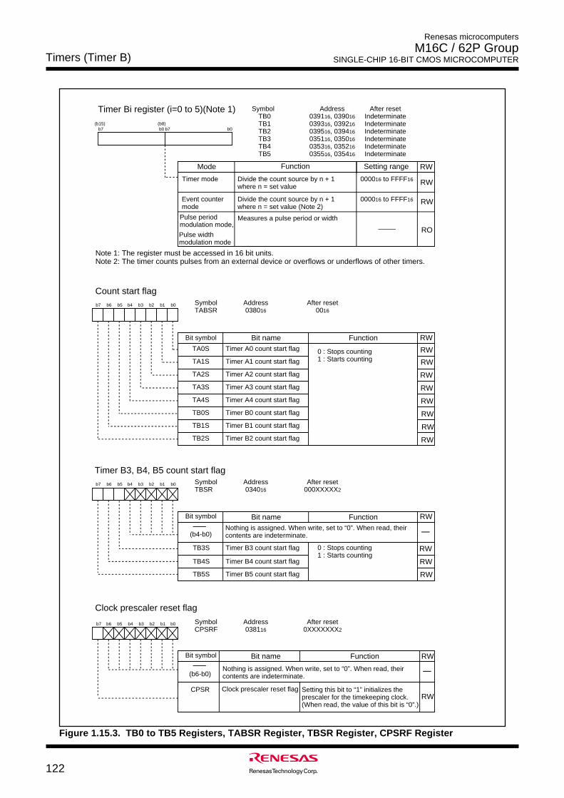
Timers (Timer B)
122
Renesas microcomputers
M16C / 62P Group SINGLE-CHIP 16-BIT CMOS MICROCOMPUTER
Symbol Address After resetTABSR 038016 0016
Count start flag
Bit nameBit symbol
b7 b6 b5 b4 b3 b2 b1 b0
AAAAAAAAAAAAAAAAAAAAAAAAAAAAAAAAAAAAAAAAAAAAAAAAAAAAAAAAAAAAAAAAAAAAAAAAAAA
AAAAAAAAAAAAAAAAAAAAAAAAAAAAAAAAAAAAAAAAAAAAAAAAAAAAAAAAAAAAAAAAAAAAAAAAAAA
AAAAAAAAAAAAAAAAAAAAAAAAAAAAAAAAAAAAAAAAAAAAATimer B2 count start flag
Timer B1 count start flag
Timer B0 count start flag
Timer A4 count start flag
Timer A3 count start flag
Timer A2 count start flag
Timer A1 count start flag
Timer A0 count start flag 0 : Stops counting1 : Starts counting
TB2S
TB1S
TB0S
TA4S
TA3S
TA2S
TA1S
TA0S
Function
Symbol Address After resetCPSRF 038116 0XXXXXXX2
Clock prescaler reset flag
Bit name FunctionBit symbol
b7 b6 b5 b4 b3 b2 b1 b0
AAAAAAAAAAAAAAAAAAAAAAAAAAAAAAClock prescaler reset flagCPSR
Symbol Address After resetTB0 039116, 039016 IndeterminateTB1 039316, 039216 IndeterminateTB2 039516, 039416 IndeterminateTB3 035116, 035016 IndeterminateTB4 035316, 035216 IndeterminateTB5 035516, 035416 Indeterminate
b7 b0 b7 b0(b15) (b8)
Timer Bi register (i=0 to 5)(Note 1)
RW
Measures a pulse period or width
Function
Symbol Address After resetTBSR 034016 000XXXXX2
Timer B3, B4, B5 count start flag
Bit nameBit symbol
b7 b6 b5 b4 b3 b2 b1 b0
AAAAAAAAAAAAAAAAAAAAAAAAAAAAAAAAAAAAAAAAAAAAAAAAAAAAAAAAAAAA
AAAAAAAAAAAAAAAAAAAAAAAAAAAAAAAAAAAAAAAAAAAAATimer B5 count start flag
Timer B4 count start flag
Timer B3 count start flag 0 : Stops counting1 : Starts counting
TB5S
TB4S
TB3S
Nothing is assigned. When write, set to “0”. When read, their contents are indeterminate.
Function
Nothing is assigned. When write, set to “0”. When read, their contents are indeterminate.
RW
RW
RO
RW
RW
RW
RW
RW
RW
RW
RW
RW
RW
RW
RW
RW
RW
RW
(b4-b0)
(b6-b0)
Note 1: The register must be accessed in 16 bit units.Note 2: The timer counts pulses from an external device or overflows or underflows of other timers.
Divide the count source by n + 1 where n = set value
Timer mode
Event counter mode
000016 to FFFF16
Divide the count source by n + 1 where n = set value (Note 2)
000016 to FFFF16
Pulse periodmodulation mode,
Pulse width modulation mode
Setting this bit to “1” initializes the prescaler for the timekeeping clock.(When read, the value of this bit is “0”.)
Mode Setting range
Figure 1.15.3. TB0 to TB5 Registers, TABSR Register, TBSR Register, CPSRF Register
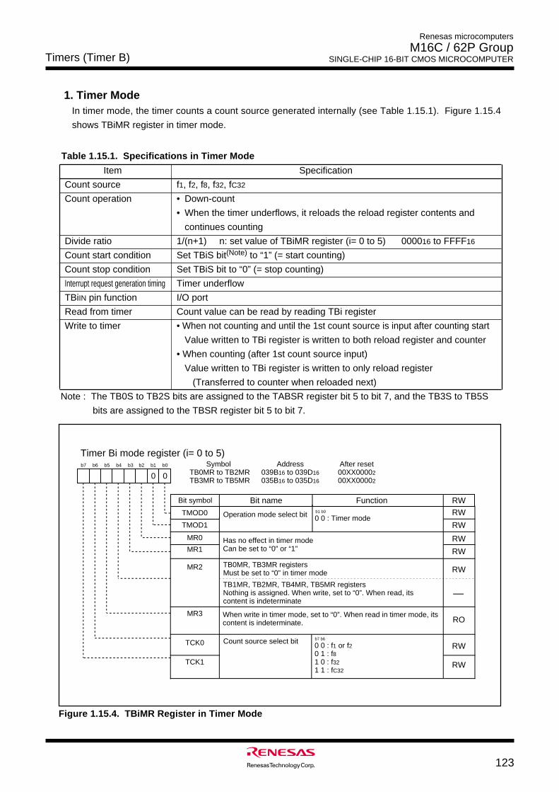
Timers (Timer B)
123
Renesas microcomputers
M16C / 62P Group SINGLE-CHIP 16-BIT CMOS MICROCOMPUTER
Item Specification
Count source f1, f2, f8, f32, fC32
Count operation • Down-count
• When the timer underflows, it reloads the reload register contents and
continues counting
Divide ratio 1/(n+1) n: set value of TBiMR register (i= 0 to 5) 000016 to FFFF16
Count start condition Set TBiS bit(Note) to “1” (= start counting)
Count stop condition Set TBiS bit to “0” (= stop counting)
Interrupt request generation timing Timer underflow
TBiIN pin function I/O port
Read from timer Count value can be read by reading TBi register
Write to timer • When not counting and until the 1st count source is input after counting start
Value written to TBi register is written to both reload register and counter
• When counting (after 1st count source input)
Value written to TBi register is written to only reload register
(Transferred to counter when reloaded next)
Note : The TB0S to TB2S bits are assigned to the TABSR register bit 5 to bit 7, and the TB3S to TB5S
bits are assigned to the TBSR register bit 5 to bit 7.
1. Timer ModeIn timer mode, the timer counts a count source generated internally (see Table 1.15.1). Figure 1.15.4
shows TBiMR register in timer mode.
Table 1.15.1. Specifications in Timer Mode
Timer Bi mode register (i= 0 to 5)Symbol Address After reset
TB0MR to TB2MR 039B16 to 039D16 00XX00002TB3MR to TB5MR 035B16 to 035D16 00XX00002
Bit name FunctionBit symbol RW
b7 b6 b5 b4 b3 b2 b1 b0
AAAAAA
Operation mode select bit 0 0 : Timer modeb1 b0
TMOD1
TMOD0
MR0 Has no effect in timer mode Can be set to “0” or “1”
MR2
MR1
MR3
0 0 : f1 or f20 1 : f81 0 : f321 1 : fC32
TCK1
TCK0 Count source select bit
00
TB0MR, TB3MR registersMust be set to “0” in timer mode
b7 b6
RW
RW
RW
RW
RW
RW
RW
RO
TB1MR, TB2MR, TB4MR, TB5MR registersNothing is assigned. When write, set to “0”. When read, its content is indeterminate
When write in timer mode, set to “0”. When read in timer mode, its content is indeterminate.
Figure 1.15.4. TBiMR Register in Timer Mode
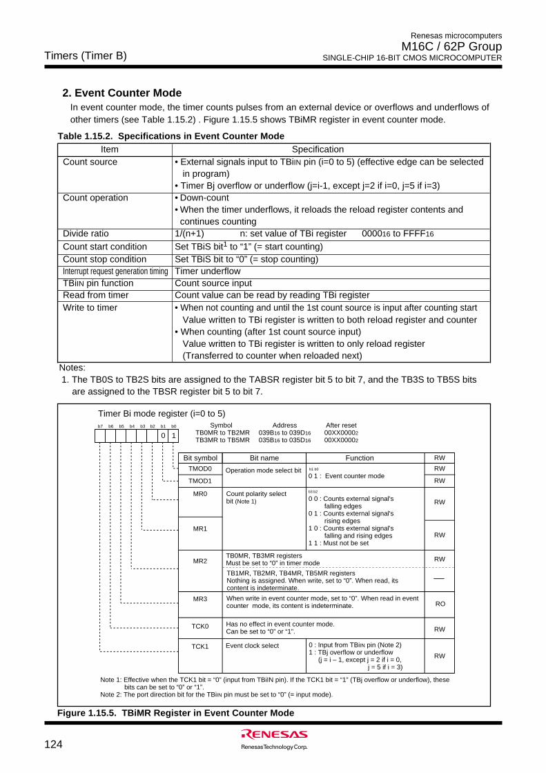
Timers (Timer B)
124
Renesas microcomputers
M16C / 62P Group SINGLE-CHIP 16-BIT CMOS MICROCOMPUTER
Item SpecificationCount source • External signals input to TBiIN pin (i=0 to 5) (effective edge can be selected
in program)• Timer Bj overflow or underflow (j=i-1, except j=2 if i=0, j=5 if i=3)
Count operation • Down-count• When the timer underflows, it reloads the reload register contents and
continues countingDivide ratio 1/(n+1) n: set value of TBi register 000016 to FFFF16
Count start condition Set TBiS bit1 to “1” (= start counting)Count stop condition Set TBiS bit to “0” (= stop counting)Interrupt request generation timing Timer underflowTBiIN pin function Count source inputRead from timer Count value can be read by reading TBi registerWrite to timer • When not counting and until the 1st count source is input after counting start
Value written to TBi register is written to both reload register and counter• When counting (after 1st count source input)
Value written to TBi register is written to only reload register(Transferred to counter when reloaded next)
Notes: 1. The TB0S to TB2S bits are assigned to the TABSR register bit 5 to bit 7, and the TB3S to TB5S bits
are assigned to the TBSR register bit 5 to bit 7.
2. Event Counter ModeIn event counter mode, the timer counts pulses from an external device or overflows and underflows ofother timers (see Table 1.15.2) . Figure 1.15.5 shows TBiMR register in event counter mode.
Table 1.15.2. Specifications in Event Counter Mode
Figure 1.15.5. TBiMR Register in Event Counter Mode
Timer Bi mode register (i=0 to 5)Symbol Address After reset
TB0MR to TB2MR 039B16 to 039D16 00XX00002TB3MR to TB5MR 035B16 to 035D16 00XX00002
Bit name FunctionBit symbol RW
b7 b6 b5 b4 b3 b2 b1 b0
AA
Operation mode select bit0 1 : Event counter mode b1 b0
TMOD1
TMOD0
MR0 Count polarity select bit (Note 1)
MR2
MR1
MR3
TCK1
TCK0
0 1
0 0 : Counts external signal's falling edges
0 1 : Counts external signal's rising edges
1 0 : Counts external signal's falling and rising edges
1 1 : Must not be set
b3 b2
Note 1: Effective when the TCK1 bit = “0” (input from TBiIN pin). If the TCK1 bit = “1” (TBj overflow or underflow), these bits can be set to “0” or “1”.Note 2: The port direction bit for the TBiIN pin must be set to “0” (= input mode).
Has no effect in event counter mode.Can be set to “0” or “1”.
Event clock select 0 : Input from TBiIN pin (Note 2)1 : TBj overflow or underflow
(j = i – 1, except j = 2 if i = 0, j = 5 if i = 3)
RW
RW
RW
RW
RW
RW
RW
RO
TB0MR, TB3MR registersMust be set to “0” in timer mode
TB1MR, TB2MR, TB4MR, TB5MR registersNothing is assigned. When write, set to “0”. When read, its content is indeterminate.
When write in event counter mode, set to “0”. When read in event counter mode, its content is indeterminate.
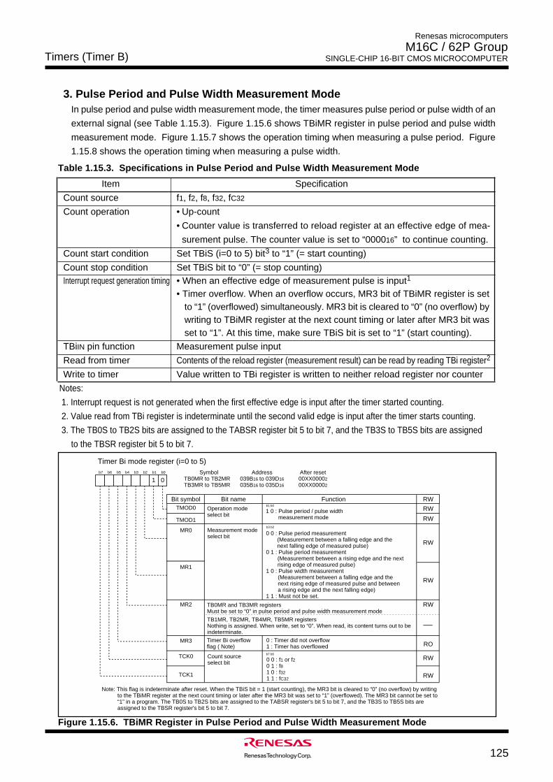
Timers (Timer B)
125
Renesas microcomputers
M16C / 62P Group SINGLE-CHIP 16-BIT CMOS MICROCOMPUTER
Item Specification
Count source f1, f2, f8, f32, fC32
Count operation • Up-count
• Counter value is transferred to reload register at an effective edge of mea-
surement pulse. The counter value is set to “000016” to continue counting.
Count start condition Set TBiS (i=0 to 5) bit3 to “1” (= start counting)
Count stop condition Set TBiS bit to “0” (= stop counting)Interrupt request generation timing • When an effective edge of measurement pulse is input1
• Timer overflow. When an overflow occurs, MR3 bit of TBiMR register is setto “1” (overflowed) simultaneously. MR3 bit is cleared to “0” (no overflow) bywriting to TBiMR register at the next count timing or later after MR3 bit wasset to “1”. At this time, make sure TBiS bit is set to “1” (start counting).
TBiIN pin function Measurement pulse input
Read from timer Contents of the reload register (measurement result) can be read by reading TBi register2
Write to timer Value written to TBi register is written to neither reload register nor counter
Notes:
1. Interrupt request is not generated when the first effective edge is input after the timer started counting.
2. Value read from TBi register is indeterminate until the second valid edge is input after the timer starts counting.
3. The TB0S to TB2S bits are assigned to the TABSR register bit 5 to bit 7, and the TB3S to TB5S bits are assigned
to the TBSR register bit 5 to bit 7.
3. Pulse Period and Pulse Width Measurement ModeIn pulse period and pulse width measurement mode, the timer measures pulse period or pulse width of an
external signal (see Table 1.15.3). Figure 1.15.6 shows TBiMR register in pulse period and pulse width
measurement mode. Figure 1.15.7 shows the operation timing when measuring a pulse period. Figure
1.15.8 shows the operation timing when measuring a pulse width.
Table 1.15.3. Specifications in Pulse Period and Pulse Width Measurement Mode
Figure 1.15.6. TBiMR Register in Pulse Period and Pulse Width Measurement Mode
Timer Bi mode register (i=0 to 5)Symbol Address After reset
TB0MR to TB2MR 039B16 to 039D16 00XX00002TB3MR to TB5MR 035B16 to 035D16 00XX00002
Bit nameBit symbol RW
b7 b6 b5 b4 b3 b2 b1 b0
Operation mode select bit
1 0 : Pulse period / pulse width measurement mode
b1 b0
TMOD1
TMOD0
MR0 Measurement mode select bit
MR2
MR1
MR3
TCK1
TCK0
01
0 0 : Pulse period measurement(Measurement between a falling edge and the next falling edge of measured pulse)
0 1 : Pulse period measurement(Measurement between a rising edge and the next rising edge of measured pulse)
1 0 : Pulse width measurement(Measurement between a falling edge and the next rising edge of measured pulse and between a rising edge and the next falling edge)
1 1 : Must not be set.
Function
b3 b2
Count source select bit
Timer Bi overflow flag ( Note)
0 : Timer did not overflow1 : Timer has overflowed
0 0 : f1 or f20 1 : f81 0 : f321 1 : fC32
b7 b6
Note: This flag is indeterminate after reset. When the TBiS bit = 1 (start counting), the MR3 bit is cleared to “0” (no overflow) by writing to the TBiMR register at the next count timing or later after the MR3 bit was set to “1” (overflowed). The MR3 bit cannot be set to “1” in a program. The TB0S to TB2S bits are assigned to the TABSR register's bit 5 to bit 7, and the TB3S to TB5S bits are assigned to the TBSR register's bit 5 to bit 7.
RW
RW
RW
RW
RW
RW
RW
RO
TB0MR and TB3MR registersMust be set to “0” in pulse period and pulse width measurement mode
TB1MR, TB2MR, TB4MR, TB5MR registersNothing is assigned. When write, set to “0”. When read, its content turns out to be indeterminate.
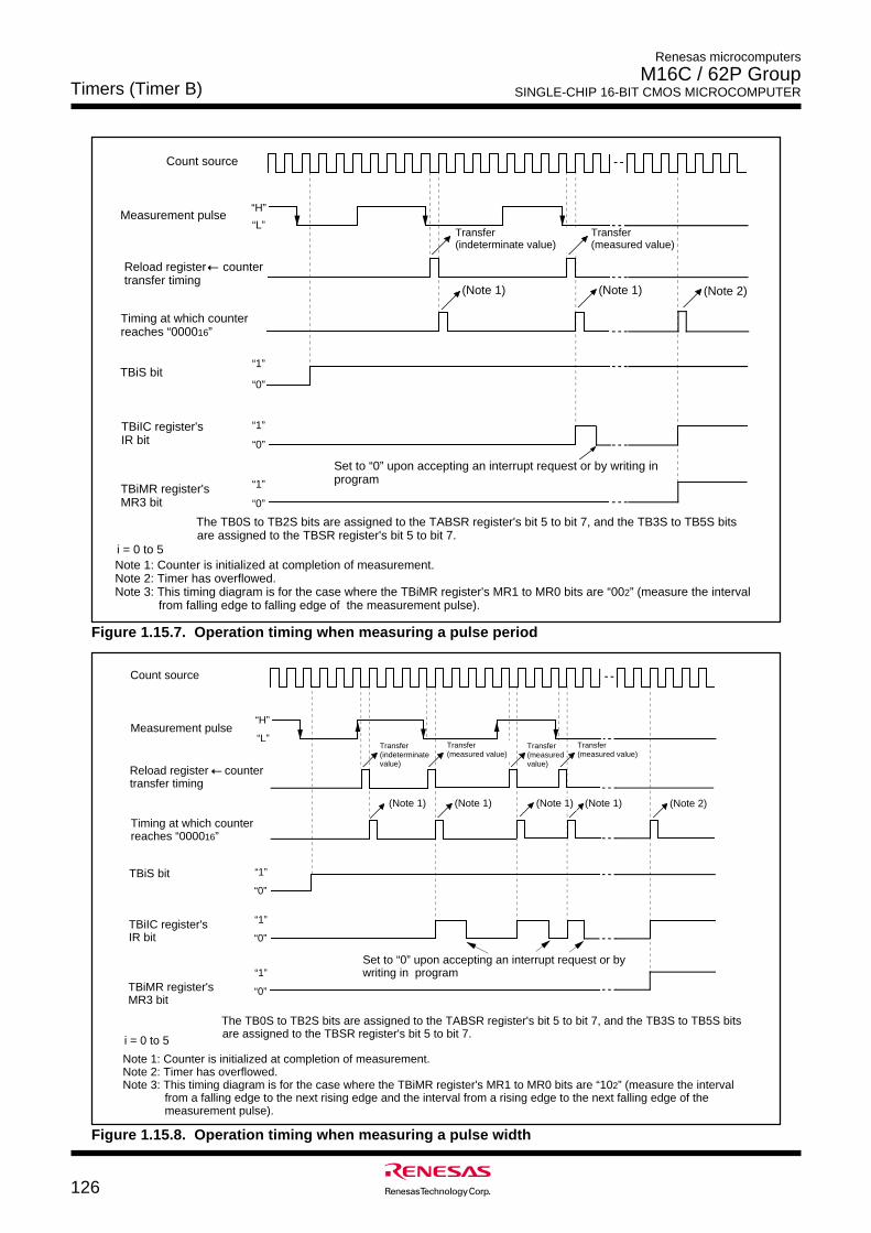
Timers (Timer B)
126
Renesas microcomputers
M16C / 62P Group SINGLE-CHIP 16-BIT CMOS MICROCOMPUTER
Figure 1.15.8. Operation timing when measuring a pulse width
Measurement pulse“H”
Count source
Timing at which counter reaches “000016”
“1”
“1”
Transfer (measured value)
Transfer(measured value)
“L”
“0”
“0”
“1”
“0”
(Note 1)(Note 1)(Note 1)
Transfer (measured value)
(Note 1) (Note 2)
Transfer (indeterminate value)
Reload register counter transfer timing
TBiS bit
TBiIC register'sIR bit
TBiMR register'sMR3 bit
Note 1: Counter is initialized at completion of measurement.Note 2: Timer has overflowed.Note 3: This timing diagram is for the case where the TBiMR register's MR1 to MR0 bits are “102” (measure the interval from a falling edge to the next rising edge and the interval from a rising edge to the next falling edge of the measurement pulse).
The TB0S to TB2S bits are assigned to the TABSR register's bit 5 to bit 7, and the TB3S to TB5S bits are assigned to the TBSR register's bit 5 to bit 7.
Set to “0” upon accepting an interrupt request or by writing in program
i = 0 to 5
Figure 1.15.7. Operation timing when measuring a pulse period
Count source
Measurement pulse
TBiS bit
TBiIC register'sIR bit
Timing at which counter reaches “000016”
“H”
“1”
Transfer (indeterminate value)
“L”
“0”
“0”
TBiMR register'sMR3 bit
“1”
“0”
Note 1: Counter is initialized at completion of measurement.Note 2: Timer has overflowed.Note 3: This timing diagram is for the case where the TBiMR register's MR1 to MR0 bits are “002” (measure the interval from falling edge to falling edge of the measurement pulse).
(Note 1)(Note 1) (Note 2)
Transfer(measured value)
“1”
Reload register counter transfer timing
The TB0S to TB2S bits are assigned to the TABSR register's bit 5 to bit 7, and the TB3S to TB5S bits are assigned to the TBSR register's bit 5 to bit 7.
Set to “0” upon accepting an interrupt request or by writing in program
i = 0 to 5
Three-phase Motor Control Timer Functions
127
Renesas microcomputers
M16C / 62P Group SINGLE-CHIP 16-BIT CMOS MICROCOMPUTER
Three-phase Motor Control Timer FunctionTimers A1, A2, A4 and B2 can be used to output three-phase motor drive waveforms. Table 1.16.1 lists the
specifications of the three-phase motor control timer function. Figure 1.16.1 shows the block diagram for
three-phase motor control timer function. Also, the related registers are shown on Figure 1.16.2 to Figure
1.16.7.
Table 1.16.1. Three-phase Motor Control Timer FunctionS Specifications Item SpecificationThree-phase waveform output pin
___ ___ ___
Six pins (U, U, V, V, W, W)Forced cutoff input1
_______
Input “L” to NMI pinUsed Timers Timer A4, A1, A2 (used in the one-shot timer mode)
___
Timer A4: U- and U-phase waveform control___
Timer A1: V- and V-phase waveform control___
Timer A2: W- and W-phase waveform controlTimer B2 (used in the timer mode)
Carrier wave cycle controlDead timer timer (3 eight-bit timer and shared reload register)
Dead time controlOutput waveform Triangular wave modulation, Sawtooth wave modification
Enable to output “H” or “L” for one cycleEnable to set positive-phase level and negative-phaselevel respectively
Carrier wave cycle Triangular wave modulation: count source x (m+1) x 2Sawtooth wave modulation: count source x (m+1)
m: Setting value of TB2 register, 0 to 65535Count source: f1, f2, f8, f32, fC32
Three-phase PWM output width Triangular wave modulation: count source x n x 2Sawtooth wave modulation: count source x n
n: Setting value of TA4, TA1 and TA2 register (of TA4, TA41, TA1, TA11, TA2 and TA21 registers when setting the INV11 bit to “1”), 1 to 65535Count source: f1, f2, f8, f32, fC32
Dead time Count source x p, or no dead timep: Setting value of DTT register, 1 to 255
Count source: f1, f2, f1 divided by 2, f2 divided by 2Active level Eable to select “H” or “L”Positive and negative-phase concurrent Positive and negative-phases concurrent active disable
functionPositive and negative-phases concurrent active detect function
Interrupt frequency For Timer B2 interrupt, select a carrier wave cycle-to-cyclebasis through 15 times carrier wave cycle-to-cycle basis
active disable function
Notes:_______
1. Forced cutoff with NMI input is effective when the IVPCR1 bit of TB2SC register is set to “1” (three-phase_______ _______
output forcible cutoff by NMI input enabled). If an “L” signal is applied to the NMI pin when the IVPCR1 bitis “1”, the related pins go to a high-impedance state regardless of which functions of those pins are beingused.
Related pins P72/CLK2/TA1OUT/V_________ _________ ___
P73/CTS2/RTS2/TA1IN/VP74/TA2OUT/W
____
P75/TA2IN/WP80/TA4OUT/U
___
P81/TA4IN/U
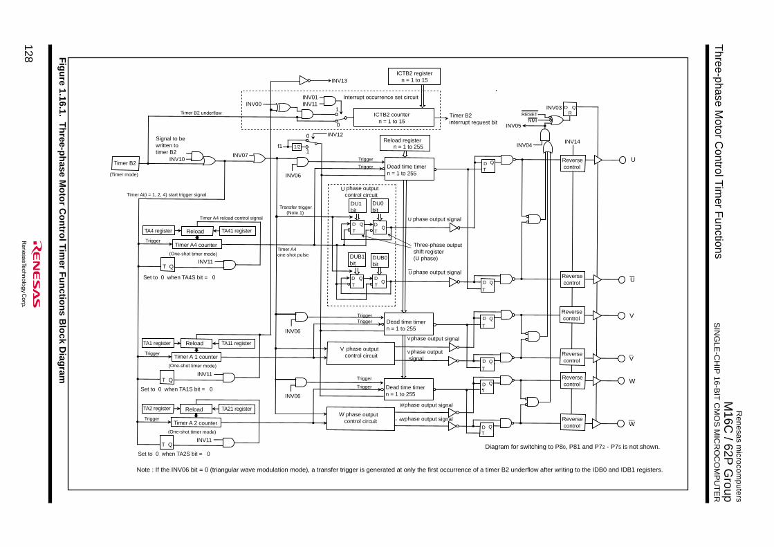
Three-phase M
otor Control T
imer F
unctions
128
Renesas m
icrocomputers
M16C
/ 62P G
roup S
ING
LE-C
HIP
16-BIT
CM
OS
MIC
RO
CO
MP
UT
ER
DR
Q
0 INV12
1
TriggerTrigger
Timer B2
(Timer mode)
Signal to be written to timer B2
1Timer B2interrupt request bit
DU1bit
DT
Q
U
Three-phase output shift register (U phase)
Dead time timern = 1 to 255
Trigger
Trigger
Reload registern = 1 to 255
Trigger
Trigger
U phase output signal
U
V
V
V
W
W
W phase output control circuit
D QT
D Q
T
W
D Q
T
D Q
T
V
D Q
T
U
D Q
T
Reverse control
U
W
V
Reload
Timer A 1 counter
(One-shot timer mode)
Trigger
T Q
Reload
Timer A 2 counter
(One-shot timer mode)
Trigger
T Q
Reload
Timer A4 counter
(One-shot timer mode)
Trigger
T Q
Transfer trigger(Note 1)
Timer B2 underflow
DU0bit
DUB0bit
TA4 register TA41 register
TA1 register TA11 register
TA2 register TA21 register
Timer Ai(i = 1, 2, 4) start trigger signal
Timer A4 reload control signal
Timer A4one-shot pulse DUB1
bit
Dead time timern = 1 to 255
Dead time timern = 1 to 255
Interrupt occurrence set circuit
ICTB2 registern = 1 to 15
0
INV13
ICTB2 countern = 1 to 15
RESETNMI
INV03
INV14
INV05
INV04
INV00INV01INV11
INV11
INV11
INV11
INV06
INV06
INV06
INV07INV10
1/2f1
phase output control circuit
phase output control circuit
phase output signal
phase output signal
phase output signal
phase output signal
phase output signal
Reverse control
Reverse control
Reverse control
Reverse control
Reverse control
DT
DT
Q DT
Note : If the INV06 bit = 0 (triangular wave modulation mode), a transfer trigger is generated at only the first occurrence of a timer B2 underflow after writing to the IDB0 and IDB1 registers.
Set to 0 when TA2S bit = 0
Set to 0 when TA1S bit = 0
Set to 0 when TA4S bit = 0
Diagram for switching to P80, P81 and P72 - P75 is not shown.
Fig
ure 1.16.1. T
hree-p
hase M
oto
r Co
ntro
l Tim
er Fu
nctio
ns B
lock D
iagram
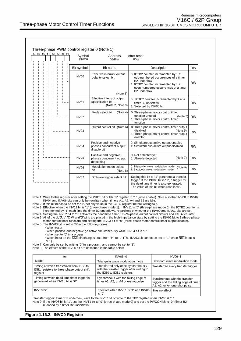
Three-phase Motor Control Timer Functions
129
Renesas microcomputers
M16C / 62P Group SINGLE-CHIP 16-BIT CMOS MICROCOMPUTER
Three-phase PWM control register 0 (Note 1)
Symbol Address After reset INVC0 034816 0016
b7 b6 b5 b4 b3 b2 b1 b0
Effective interrupt output polarity select bit INV00
Bit symbol Bit name Description RW
INV01
Effective interrupt output specification bit
INV02
Mode select bit
INV04Positive and negative phases concurrent output disable bit
INV07 Software trigger select bit
INV06 Modulation mode select bit
INV05Positive and negative phases concurrent output detect flag
INV03Output control bit
0: ICTB2 counter incremented by 1 at odd-numbered occurrences of a timer B2 underflow
1: ICTB2 counter incremented by 1 at even-numbered occurrences of a timer B2 underflow
0: ICTB2 counter incremented by 1 at a timer B2 underflow
1: Selected by INV00 bit
0: Three-phase motor control timer function unused1: Three-phase motor control timer function
0: Three-phase motor control timer output disabled1: Three-phase motor control timer output enabled
0: Simultaneous active output enabled1: Simultaneous active output disabled
0: Not detected yet1: Already detected
0: Triangular wave modulation mode1: Sawtooth wave modulation mode
Setting this bit to “1” generates a transfer trigger. If the INV06 bit is “1”, a trigger for the dead time timer is also generated. The value of this bit when read is “0”.
(Note 9)
(Note 3)
(Note 7)
(Note 2, Note 3)
Note 1: Write to this register after setting the PRC1 bit of PRCR register to “1” (write enable). Note also that INV00 to INV02, INV04 and INV06 bits can only be rewritten when timers A1, A2, A4 and B2 are idle.
Note 2: If this bit needs to be set to “1”, set any value in the ICTB2 register before writing to it. Note 3: Effective when the INV11 bit is “1” (three-phase mode 1). If INV11 is “0” (three-phase mode 0), the ICTB2 counter is
incremented by “1” each time the timer B2 underflows, regardless of whether the INV00 and INV01 bits are set. Note 4: Setting the INV02 bit to “1” activates the dead time timer, U/V/W-phase output control circuits and ICTB2 counter.Note 5: All of the U, U, V, V, W and W pins are placed in the high-impedance state by setting the INV02 bit to 1 (three-phase
motor control timer function) and setting the INV03 bit to “0” (three-phase motor control timer output disable). Note 6: The INV03 bit is set to “0” in the following cases:
• When reset• When positive and negative go active simultaneously while INV04 bit is “1”• When set to “0” in a program• When input on the NMI pin changes state from “H” to “L” (The INV03 bit cannot be set to “1” when NMI input is “L”.)
Note 7: Can only be set by writing “0” in a program, and cannot be set to “1”.Note 8: The effects of the INV06 bit are described in the table below.
(Note 4)
RW
RW
RW
RW
RW
RW
RW
RW
(Note 5)
(Note 8)
ItemMode
Timing at which transferred from IDB0 to IDB1 registers to three-phase output shift register
Timing at which dead time timer trigger is generated when INV16 bit is “0”
INV13 bit
INV06=0
Triangular wave modulation mode
Transferred only once synchronously with the transfer trigger after writing to the IDB0 to IDB1 registers
Synchronous with the falling edge of timer A1, A2, or A4 one-shot pulse
Effective when INV11 is “1” and INV06 is “0”
INV06=1
Sawtooth wave modulation mode
Transferred every transfer trigger
Synchronous with the transfer trigger and the falling edge of timer A1, A2, or A4 one-shot pulse
Transfer trigger: Timer B2 underflow, write to the INV07 bit or write to the TB2 register when INV10 is “1”Note 9: If the INV06 bit is “1”, set the INV11 bit to “0” (three-phase mode 0) and set the PWCON bit to “0” (timer B2
reloaded by a timer B2 underflow).
(Note 6)
(Note 5)
Has no effect
Figure 1.16.2. INVC0 Register
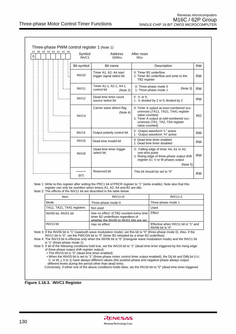
Three-phase Motor Control Timer Functions
130
Renesas microcomputers
M16C / 62P Group SINGLE-CHIP 16-BIT CMOS MICROCOMPUTER
Figure 1.16.3. INVC1 Register
Three-phase PWM control register 1 (Note 1)
Symbol Address After resetINVC1 034916 0016
b7 b6 b5 b4 b3 b2 b1 b0
Timer A1, A2, A4 start trigger signal select bitINV10
Bit symbol Bit name Description RW
INV11
Timer A1-1, A2-1, A4-1 control bit
INV12 Dead time timer count source select bit
INV14 Output polarity control bit
(b7)Reserved bit
INV16Dead time timer trigger select bit
INV15 Dead time invalid bit
INV13
Carrier wave detect flag
0: Timer B2 underflow1: Timer B2 underflow and write to the TB2 register
0: Three-phase mode 01: Three-phase mode 1
0 : f1 or f21 : f1 divided by 2 or f2 divided by 2
0: Timer A output at even-numbered occ- urrences (TA11, TA21, TA41 register value counted)1: Timer A output at odd-numbered occ- urrences (TA1, TA2, TA4 register value counted)
0 : Output waveform “L” active1 : Output waveform “H” active
0: Dead time timer enabled1: Dead time timer disabled
0: Falling edge of timer A4, A1 or A2 one-shot pulse1: Rising edge of three-phase output shift register (U, V or W phase) output
This bit should be set to “0”
Note 1: Write to this register after setting the PRC1 bit of PRCR register to “1” (write enable). Note also that this register can only be rewritten when timers A1, A2, A4 and B2 are idle.
Note 2: The effects of the INV11 bit are described in the table below.
(Note 5)
(Note 4)
RW
RW
RW
RW
RW
RW
RW
RO
(Note 2)
Item
Mode
TA11, TA21, TA41 registers
INV00 bit, INV01 bit
INV13 bit
INV11=0
Three-phase mode 1Three-phase mode 0
Not used
Has no effect. ICTB2 counted every time timer B2 underflows regardless of whether the INV00 to INV01 bits are set.Has no effect
INV11=1
Used
Effect
Effective when INV11 bit is “1” and INV06 bit is “0”
Note 3: If the INV06 bit is “1” (sawtooth wave modulation mode), set this bit to “0” (three-phase mode 0). Also, if the INV11 bit is “0”, set the PWCON bit to “0” (timer B2 reloaded by a timer B2 underflow).
Note 4: The INV13 bit is effective only when the INV06 bit is “0” (triangular wave modulation mode) and the INV11 bit is “1” (three-phase mode 1).
Note 5: If all of the following conditions hold true, set the INV16 bit to “1” (dead time timer triggered by the rising edge of three-phase output shift register output)• The INV15 bit is “0” (dead time timer enabled)• When the INV03 bit is set to “1” (three-phase motor control timer output enabled), the Dij bit and DiBj bit (i:U, V, or W, j: 0 to 1) have always different values (the positive-phase and negative-phase always output different levels during the period other than dead time).
Conversely, if either one of the above conditions holds false, set the INV16 bit to “0” (dead time timer triggered
(Note 3)
0
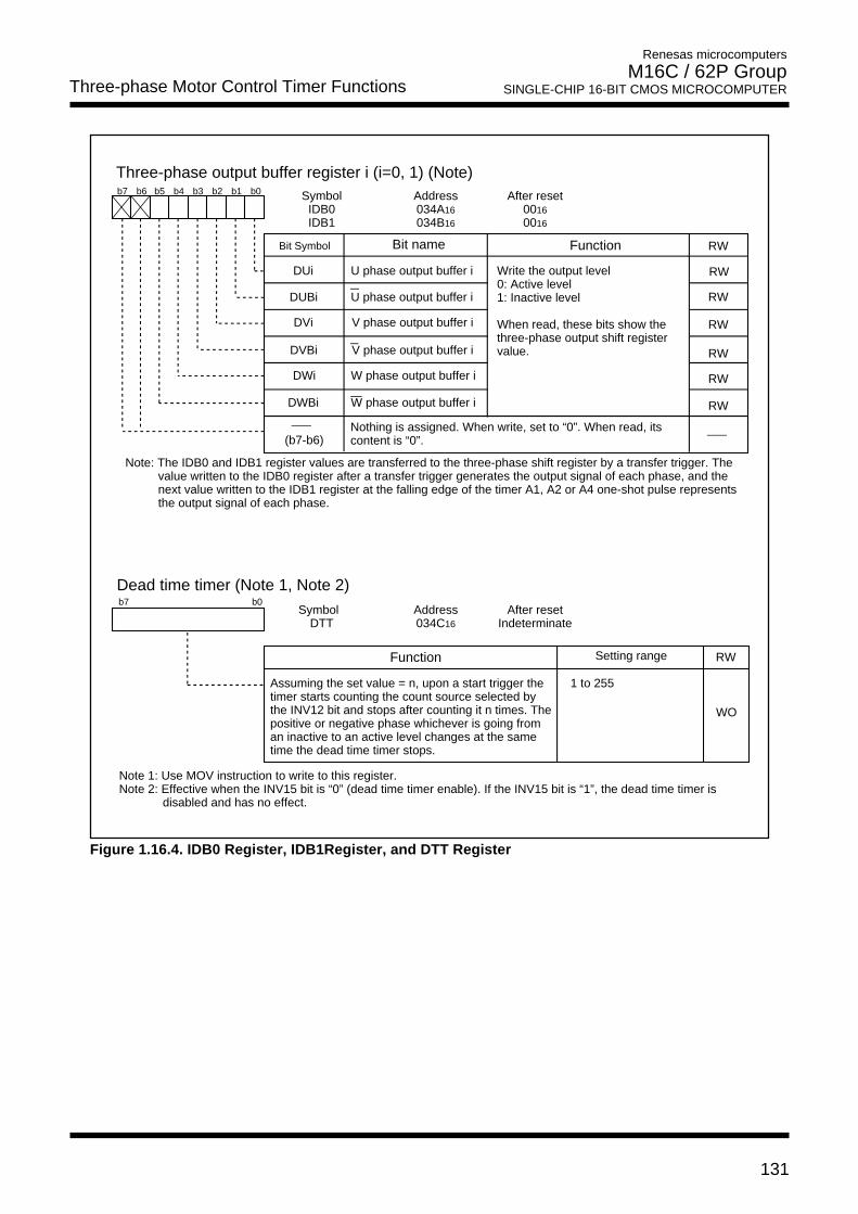
Three-phase Motor Control Timer Functions
131
Renesas microcomputers
M16C / 62P Group SINGLE-CHIP 16-BIT CMOS MICROCOMPUTER
Three-phase output buffer register i (i=0, 1) (Note)Symbol Address After resetIDB0 034A16 0016IDB1 034B16 0016
Bit name FunctionBit Symbol
b7 b6 b5 b4 b3 b2 b1 b0
DUi
DUBi
DVi
DWi
DVBi
DWBi
U phase output buffer i Write the output level0: Active level1: Inactive level
When read, these bits show the three-phase output shift register value.
V phase output buffer i
W phase output buffer i
U phase output buffer i
V phase output buffer i
W phase output buffer i
Dead time timer (Note 1, Note 2)
Symbol Address After resetDTT 034C16 Indeterminate
Function Setting range
b7 b0
Assuming the set value = n, upon a start trigger the timer starts counting the count source selected by the INV12 bit and stops after counting it n times. The positive or negative phase whichever is going from an inactive to an active level changes at the same time the dead time timer stops.
1 to 255
Note: The IDB0 and IDB1 register values are transferred to the three-phase shift register by a transfer trigger. The value written to the IDB0 register after a transfer trigger generates the output signal of each phase, and the next value written to the IDB1 register at the falling edge of the timer A1, A2 or A4 one-shot pulse represents the output signal of each phase.
Note 1: Use MOV instruction to write to this register.Note 2: Effective when the INV15 bit is “0” (dead time timer enable). If the INV15 bit is “1”, the dead time timer is disabled and has no effect.
RW
RW
RW
RW
RW
RW
RW
Nothing is assigned. When write, set to “0”. When read, its content is “0”.(b7-b6)
RW
WO
Figure 1.16.4. IDB0 Register, IDB1Register, and DTT Register
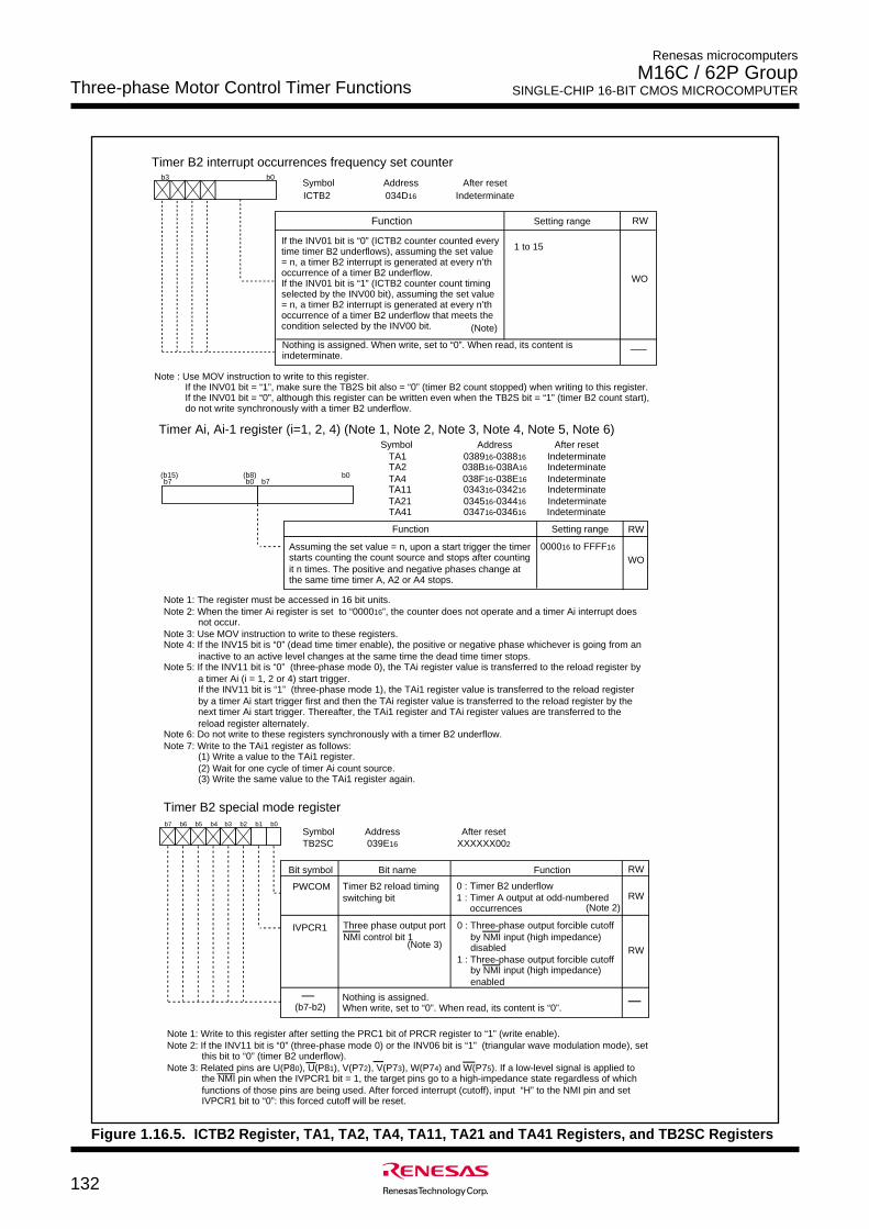
Three-phase Motor Control Timer Functions
132
Renesas microcomputers
M16C / 62P Group SINGLE-CHIP 16-BIT CMOS MICROCOMPUTER
Symbol Address After reset TA1 038916-038816 Indeterminate TA2 038B16-038A16 Indeterminate
TA4 038F16-038E16 Indeterminate TA11 034316-034216 Indeterminate TA21 034516-034416 Indeterminate TA41 034716-034616 Indeterminate
b7 b0 b7b0(b15) (b8)
RW
Assuming the set value = n, upon a start trigger the timer starts counting the count source and stops after counting it n times. The positive and negative phases change at the same time timer A, A2 or A4 stops.
Function Setting range
Timer Ai, Ai-1 register (i=1, 2, 4) (Note 1, Note 2, Note 3, Note 4, Note 5, Note 6)
Note 1: The register must be accessed in 16 bit units.Note 2: When the timer Ai register is set to “000016”, the counter does not operate and a timer Ai interrupt does
not occur.Note 3: Use MOV instruction to write to these registers.Note 4: If the INV15 bit is “0” (dead time timer enable), the positive or negative phase whichever is going from an
inactive to an active level changes at the same time the dead time timer stops. Note 5: If the INV11 bit is “0” (three-phase mode 0), the TAi register value is transferred to the reload register by
a timer Ai (i = 1, 2 or 4) start trigger. If the INV11 bit is “1” (three-phase mode 1), the TAi1 register value is transferred to the reload register by a timer Ai start trigger first and then the TAi register value is transferred to the reload register by the next timer Ai start trigger. Thereafter, the TAi1 register and TAi register values are transferred to the reload register alternately.
Note 6: Do not write to these registers synchronously with a timer B2 underflow.Note 7: Write to the TAi1 register as follows:
(1) Write a value to the TAi1 register.(2) Wait for one cycle of timer Ai count source.(3) Write the same value to the TAi1 register again.
WO000016 to FFFF16
PWCOM
Symbol Address After resetTB2SC 039E16 XXXXXX002
Timer B2 reload timing switching bit
0 : Timer B2 underflow1 : Timer A output at odd-numbered occurrences
Timer B2 special mode register
Bit name FunctionBit symbol
b7 b6 b5 b4 b3 b2 b1 b0
Nothing is assigned.When write, set to “0”. When read, its content is “0”.
IVPCR1 Three phase output port NMI control bit 1
0 : Three-phase output forcible cutoff by NMI input (high impedance) disabled1 : Three-phase output forcible cutoff by NMI input (high impedance) enabled
(Note 3)
Note 1: Write to this register after setting the PRC1 bit of PRCR register to “1” (write enable).Note 2: If the INV11 bit is “0” (three-phase mode 0) or the INV06 bit is “1” (triangular wave modulation mode), set this bit to “0” (timer B2 underflow). Note 3: Related pins are U(P80), U(P81), V(P72), V(P73), W(P74) and W(P75). If a low-level signal is applied to the NMI pin when the IVPCR1 bit = 1, the target pins go to a high-impedance state regardless of which functions of those pins are being used. After forced interrupt (cutoff), input “H” to the NMI pin and set IVPCR1 bit to “0”: this forced cutoff will be reset.
RW
RW
RW
(b7-b2)
(Note 2)
Figure 1.16.5. ICTB2 Register, TA1, TA2, TA4, TA11, TA21 and TA41 Registers, and TB2SC Registers
Timer B2 interrupt occurrences frequency set counter
Symbol Address After resetICTB2 034D16 Indeterminate
Function Setting range
b3 b0
If the INV01 bit is “0” (ICTB2 counter counted every time timer B2 underflows), assuming the set value = n, a timer B2 interrupt is generated at every n’th occurrence of a timer B2 underflow. If the INV01 bit is “1” (ICTB2 counter count timing selected by the INV00 bit), assuming the set value = n, a timer B2 interrupt is generated at every n’th occurrence of a timer B2 underflow that meets the condition selected by the INV00 bit.
1 to 15
Note : Use MOV instruction to write to this register.If the INV01 bit = “1”, make sure the TB2S bit also = “0” (timer B2 count stopped) when writing to this register. If the INV01 bit = “0”, although this register can be written even when the TB2S bit = “1” (timer B2 count start), do not write synchronously with a timer B2 underflow.
RW
WO
(Note)
Nothing is assigned. When write, set to “0”. When read, its content is indeterminate.
Three-phase Motor Control Timer Functions
133
Renesas microcomputers
M16C / 62P Group SINGLE-CHIP 16-BIT CMOS MICROCOMPUTER
Figure 1.16.6. TB2 Register, TRGSR Register, and TABSR Register
TA1TGL
Symbol Address After resetTRGSR 038316 0016
Timer A1 event/trigger select bit
To use the V-phase output control circuit, set these bits to “012”(TB2 underflow).
Trigger select register
Bit name FunctionBit symbol
b0
To use the W-phase output control circuit, set these bits to “012”(TB2 underflow).
0 0 : Input on TA3IN is selected (Note 1) 0 1 : TB2 overflow is selected (Note 2) 1 0 : TA2 overflow is selected (Note 2) 1 1 : TA4 overflow is selected (Note 2)
To use the U-phase output control circuit, set these bits to “012”(TB2 underflow).
Timer A2 event/trigger select bit
Timer A3 event/trigger select bit
Timer A4 event/trigger select bit
RW
TA1TGH
TA2TGL
TA2TGH
TA3TGL
TA3TGH
TA4TGL
TA4TGH
b5 b4
Note 1: Set the corresponding port direction bit to “0” (input mode).Note 2: Overflow or underflow.
b7 b6 b5 b4 b3 b2 b1
Symbol Address After resetTABSR 038016 0016
Count start flag
Bit name FunctionBit symbol
b7 b6 b5 b4 b3 b2 b1 b0
AAAAAAAAAAAAAAAAAAAAAAAAAAAAAAAA
AAAAAAAAAAAAAAAAAAAAAAAAAAAAAAAAAAAAAAAAAAAAAAAATimer B2 count start flag
Timer B1 count start flag
Timer B0 count start flag
Timer A4 count start flag
Timer A3 count start flag
Timer A2 count start flag
Timer A1 count start flag
Timer A0 count start flag 0 : Stops counting1 : Starts counting
TB2S
TB1S
TB0S
TA4S
TA3S
TA2S
TA1S
TA0S
RW
RW
RW
RW
RW
RW
RW
RW
RW
RW
RW
RW
RW
RW
RW
RW
RW
Symbol Address After reset TB2 039516-039416 Indeterminate b7 b0 b7
b0(b15) (b8)
RW
000016 to FFFF16
Function Setting range
Timer B2 register (Note )
Note : The register must be accessed in 16 bit units.
RWDivide the count source by n + 1 where n = set value. Timer A1, A2 and A4 are started at every occurrence of underflow.
Three-phase Motor Control Timer Functions
134
Renesas microcomputers
M16C / 62P Group SINGLE-CHIP 16-BIT CMOS MICROCOMPUTER
Bit name
Timer Ai mode registerSymbol Address After resetTA1MR 039716 0016
TA2MR 039816 0016TA4MR 039A16 0016
Function Bit symbol
b7 b6 b5 b4 b3 b2 b1 b0
Operation mode select bit
Must set to “102” (one-shot timer mode) for the three-phase motor control timer function TMOD1
TMOD0
MR0 Pulse output function select bit
Must set to “0” for the three-phase motor control timer function
MR2
MR1
MR3 Must set to “0” for the three-phase motor control timer function
0 0 : f1 or f20 1 : f81 0 : f32
1 1 : fC32
b7 b6
TCK1
TCK0 Count source select bit
1 00
Must set to “1” (selected by TRGSR register) for the three-phase motor control timer function
Trigger select bit
External trigger select bit
RW
Timer B2 mode registerSymbol Address After resetTB2MR 039D16 00XX00002
Bit name FunctionBit symbol RW
b7 b6 b5 b4 b3 b2 b1 b0
AAAAAA
Operation mode select bit Set to “002” (timer mode) for the three-phase motor control timer function TMOD1
TMOD0
MR0
MR2
MR1
MR3
0 0 : f1 or f20 1 : f81 0 : f321 1 : fC32
TCK1
TCK0 Count source select bit
0
When write in three-phase motor control timer function, write “0”.When read, its content is indeterminate.
0
b7 b6
1
0
Has no effect for the three-phase motor control timer function
RW
RW
RW
RW
RW
RW
RW
RW
RW
RW
RW
RW
RW
RW
RO
Has no effect for the three-phase motor control timer function.When write, set to “0”. When read, its content is indeterminate.
Must set to “0” for the three-phase motor control timer function
RW
Figure 1.16.7. TA1MR, TA2MR, TA4MR, and TB2MR Registers
Three-phase Motor Control Timer Functions
135
Renesas microcomputers
M16C / 62P Group SINGLE-CHIP 16-BIT CMOS MICROCOMPUTER
Start trigger signal for timer A4*
Timer B2
U phase
Carrier wave
Signal wave
U phase output signal *
m n n p pm
U phase
U phase
U phase
INV14 = 0
Timer A4one-shot pulse*
INV14 = 1
Dead time
Dead time
Transfer to three-phaseoutput shift register
Rewriting IDB0, IDB1 registers
* Internal signals. See the block diagram of the three-phase motor control timer function.
An example for changing PWM outputs is shown below.(1)When INV11=1(three-phase mode 1)· INV01=0, ICTB2=216(timer B2 interrupt is generated at every 2’th occurrence of a timer B2 underflow), or INV01=1, INV00=1, ICTB2=116(timer B2 interrupt is generated at even-numbered occurrences of a timer B2 underflow).· Initial timer value: TA41=m, TA4=m. The TA4 and TA41 registers are modified every time a timer B2 interrupt occurs. First time, TA41= n, TA4 = n. Second time, TA41 = p, TA4 = p.· Initial values of IDB0 and IDB1 registers: DU0 = 1, DUB0 = 0, DU1 = 0, DUB1 = 1.The register values are changed to DU0 = 1, DUB0 = 0, DU1= 1 and DUB1 = 0 the third time a timer B2 interrupt occurs.
(2)When INV11=0(three-phase mode 0)· INV01=0, ICTB2=116(timer B2 interrupt is generated at every occurrence of a timer B2 underflow)· Initial timer value: TA4 = m. The TA4 register is modified each time a timer B2 interrupt occurs. First time, TA4 = m. Second time, TA4 = n. Third time, TA4 = n. Fourth time, TA4 = p. Fifth time, TA4 = p.· Initial values of IDB0 and IDB1 registers: DU0=1, DUB0=0, DU1=0, DUB1=1.The register values are changed to DU0 = 1, DUB0 = 0, DU1= 1 and DUB1 = 0 the sixth time a timer B2 interrupt occurs.
TB2S bit of the TABSR register
INV13(INV11=1(three-phase mode 1))
Shown here is a typical waveform for the case where INVC0 = 00XX11XX2 (X = set as suitable for the system) and INVC1 = 010XXXX02.
U phase output signal *
(“L” active)
(“H” active)
The value written to the TA4 register and TA41 register are inverted at odd-numbered timer A outputs.
Figure 1.16.8. Triangular Wave Modulation Operation
The three-phase motor control timer function is enabled by setting the INV02 bit of INVC0 register to “1”.
When this function is on, timer B2 is used to control the carrier wave, and timers A4, A1 and A2 are used__ ___ ___
to control three-phase PWM outputs (U, U, V, V, W and W). The dead time is controlled by a dedicated
dead time timer. Figure 1.16.8 shows the example of triangular modulation waveform and Figure 1.16.9
shows the example of sawtooth modulation waveform.
Three-phase Motor Control Timer Functions
136
Renesas microcomputers
M16C / 62P Group SINGLE-CHIP 16-BIT CMOS MICROCOMPUTER
Timer B2
U phase
Carrier wave
Signal wave
U phase output signal *
U phase
U phase output signal *
U phase
U phase
INV14 = 0
Carrier wave: sawtooth waveform
INV14 = 1
Transfer to three-phaseoutput shift register
Rewriting IDB0, IDB1 registers
* Internal signals. See the block diagram of the three-phase motor control timer function.
Shown here is a typical waveform for the case where INVC0= 01XX110X2 (X = set as suitable for the system) and INVC1 = 010XXX002. An example for changing PWM outputs is shown below.• ICTB2=n (timer B2 interrupt is generated at every n’th occurrence of a timer B2 underflow)• Initial values of IDB0 and IDB1 registers: DU0=0, DUB0=1, DU1=1, DUB1=1. The register values are changed to DU0=1, DUB0=0, DU1=1, DUB1=1 a timer B2 interrupt occurs.
Start trigger signal for timer A4*
Timer A4one-shot pulse*
Dead time
Dead time(“H” active)
(“L” active)
Figure 1.16.9. Sawtooth Wave Modulation Operation
Serial I/O
137
Renesas microcomputers
M16C / 62P Group SINGLE-CHIP 16-BIT CMOS MICROCOMPUTER
Serial I/OSerial I/O is configured with five channels: UART0 to UART2, SI/O3 and SI/O4.
UARTi (i=0 to 2)UARTi each have an exclusive timer to generate a transfer clock, so they operate independently of each
other.
Figure 1.17.1 shows the block diagram of UARTi. Figures 1.17.2 shows the block diagram of the UARTi
transmit/receive.
UARTi has the following modes:
• Clock synchronous serial I/O mode
• Clock asynchronous serial I/O mode (UART mode).
• Special mode 1 (I2C mode)
• Special mode 2
• Special mode 3 (Bus collision detection function, IE mode) : UART0, UART1
• Special mode 4 (SIM mode) : UART2
Figures 1.17.3 to 1.17.8 show the UARTi-related registers.
Refer to tables listing each mode for register setting.
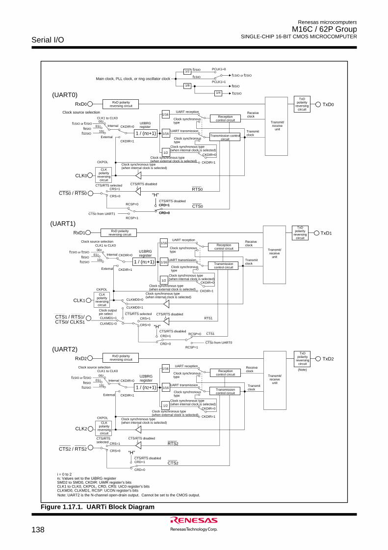
Renesas microcomputers
M16C / 62P Group SINGLE-CHIP 16-BIT CMOS MICROCOMPUTERSerial I/O
138
Figure 1.17.1. UARTi Block Diagram
Clock synchronous type (when internal clock is selected)
Clock synchronous type(when external clock is selected)
Clock source selection
Internal
External
CTS/RTS disabled
CTS/RTS selected
RxD0
1 / (n0+1)
1/16
1/16
1/2
U0BRG register
CLK0
CTS0 / RTS0
f1SIO or f2SIO
f8SIO
f32SIO
RTS0
CTS0
TxD0
(UART0)
f1SIO or f2SIO1/21/2
1/8 f8SIO
1/4 f32SIO
f1SIO
f2SIO PCLK1=0
PCLK1=1
CLK1 to CLK0002
012
102
CKDIR=0
CKDIR=1
CKPOL
CKDIR=0
CKDIR=1
CRS=1
CRS=0
CRD=0
CRD=1RCSP=0
RCSP=1
“H”
CRD=0
CRD=1
RxD polarity reversing circuit
Main clock, PLL clock, or ring oscillator clock
UART reception
Clock synchronous type
UART transmission
Clock synchronous type
Clock synchronous type(when internal clock is selected)
Receive clock
Transmit clock
Reception control circuit
Transmission control circuit
Transmit/receive
unit
TxD polarity
reversing circuit
CLK polarity
reversing circuit
CTS/RTS disabled
CTS0 from UART1
UART reception
Clock synchronous type
RxD1 TxD1
(UART1)
1 / (n1+1)
1/16
1/16
1/2
U1BRGregister
CLK1
f1SIO or f2SIO
f8SIO
f32SIO
CLK1 to CLK0002
012
102
CKDIR=0
CKDIR=1
CKPOL
CKDIR=0
CKDIR=1
“H”
CRD=0
CRD=1
CLKMD0=0
CLKMD1=0
CRS=1
CRS=0
RCSP=0
RCSP=1
CLKMD0=1
CLKMD1=1
RxD polarity reversing circuit
Clock source selection
Internal
External
UART transmission
Clock synchronous type
Clock synchronous type(when internal clock is selected)
Receive clock
Transmit clock
Reception control circuit
Transmission control circuit
Transmit/receive
unit
TxD polarity
reversing circuit
Clock synchronous type (when external clock is selected)
Clock synchronous type (when internal clock is selected)
CLK polarity
reversing circuit
RTS1
CTS1
Clock output pin select CTS/RTS disabled
CTS/RTS disabled
CTS/RTS selected
CTS0 from UART0
CTS1 / RTS1/CTS0/ CLKS1
Note: UART2 is the N-channel open-drain output. Cannot be set to the CMOS output.
i = 0 to 2ni: Values set to the UiBRG registerSMD2 to SMD0, CKDIR: UiMR register's bitsCLK1 to CLK0, CKPOL, CRD, CRS: UiC0 register's bitsCLKMD0, CLKMD1, RCSP: UCON register's bits
RxD2
CLK2
CTS2 / RTS2RTS2
CTS2
TxD2
(UART2)
1 / (n2+1)
1/16
1/16
1/2
U2BRG register
f1SIO or f2SIO
f8SIO
f32SIO
CLK1 to CLK0002
012
102
CKDIR=0
CKDIR=1
CKPOL
CKDIR=0
CKDIR=1
CRS=1
“H”
CRD=0
CRD=1
Reception control circuit
Transmission control circuit
UART reception
Clock synchronous type
UART transmission
Clock synchronous type
Clock synchronous type(when internal clock is selected)
Receive clock
Transmit clock
RxD polarity reversing circuit
Internal
External
Clock source selection
TxD polarity
reversing circuit
Transmit/receive
unit
(Note)
Clock synchronous type (when internal clock is selected)
Clock synchronous type (when external clock is selected)
CLKpolarity
reversing circuit
CTS/RTS disabled
CTS/RTS disabled
CRS=0
CTS/RTS selected
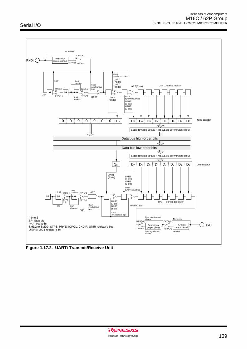
Serial I/O
139
Renesas microcomputers
M16C / 62P Group SINGLE-CHIP 16-BIT CMOS MICROCOMPUTER
SP SP PAR
2SP
1SP
UART
UART(7 bits)UART(8 bits)
UART(7 bits)
UART(9 bits)
Clock synchronous type
Clock synchronous type
Data bus low-order bits
TxDi
UARTi transmit register
PAR disabled
PAR enabled
D8 D7 D6 D5 D4 D3 D2 D1 D0 UiTB register
UART(8 bits)UART(9 bits)
Clock synchronous type
UiRB register
UARTi receive register
2SP
1SPUART(7 bits)UART(8 bits) UART(7 bits)
UART(9 bits)
Clock synchronous type
Clock synchronous type
RxDi
UART(8 bits)UART(9 bits)
Data bus high-order bits
D7 D6 D5 D4 D3 D2 D1 D0D80 0 0 0 0 0 0
SP SP PAR
“0”
Reverse
No reverse
Error signal output circuit
RxD datareverse circuit
Error signal output enable
Error signal output disable
Reverse
No reverse
Logic reverse circuit + MSB/LSB conversion circuit
Logic reverse circuit + MSB/LSB conversion circuit
PAR enabled
PAR disabled
UART
Clock synchronous type
TxD datareverse circuit
i=0 to 2SP: Stop bitPAR: Parity bitSMD2 to SMD0, STPS, PRYE, IOPOL, CKDIR: UiMR register's bitsUiERE: UiC1 register's bit
IOPOL=1
IOPOL=0
STPS= 0
STPS= 1 PRYE=1
PRYE=0
STPS= 1
STPS= 0
PRYE=0
PRYE=1
IOPOL=1
IOPOL=0
UiERE=1
UiERE=0
Figure 1.17.2. UARTi Transmit/Receive Unit
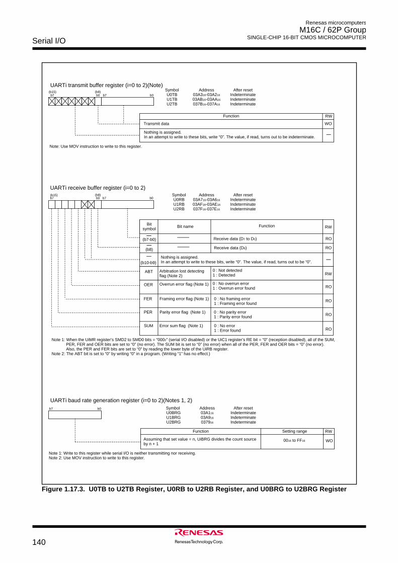
Renesas microcomputers
M16C / 62P Group SINGLE-CHIP 16-BIT CMOS MICROCOMPUTERSerial I/O
140
Figure 1.17.3. U0TB to U2TB Register, U0RB to U2RB Register, and U0BRG to U2BRG Register
(b15)b7 b0
(b8)b7 b0
UARTi transmit buffer register (i=0 to 2)(Note)
Function
Transmit data
Nothing is assigned.In an attempt to write to these bits, write “0”. The value, if read, turns out to be indeterminate.
Symbol Address After resetU0TB 03A316-03A216 IndeterminateU1TB 03AB16-03AA16 IndeterminateU2TB 037B16-037A16 Indeterminate
RW
Note: Use MOV instruction to write to this register.
WO
b7
UARTi baud rate generation register (i=0 to 2)(Notes 1, 2)b0 Symbol Address After reset
U0BRG 03A116 Indeterminate U1BRG 03A916 Indeterminate U2BRG 037916 Indeterminate
Function
Assuming that set value = n, UiBRG divides the count source by n + 1
0016 to FF16
Setting range
Note 1: Write to this register while serial I/O is neither transmitting nor receiving. Note 2: Use MOV instruction to write to this register.
RW
WO
Note 1: When the UiMR register’s SMD2 to SMD0 bits = “0002” (serial I/O disabled) or the UiC1 register’s RE bit = “0” (reception disabled), all of the SUM, PER, FER and OER bits are set to “0” (no error). The SUM bit is set to “0” (no error) when all of the PER, FER and OER bits = “0” (no error). Also, the PER and FER bits are set to “0” by reading the lower byte of the UiRB register.
Note 2: The ABT bit is set to “0” by writing “0” in a program. (Writing “1” has no effect.)
(b15) Symbol Address After resetU0RB 03A716-03A616 IndeterminateU1RB 03AF16-03AE16 IndeterminateU2RB 037F16-037E16 Indeterminate
b7 b0(b8)
b7 b0
UARTi receive buffer register (i=0 to 2)
FunctionBit nameBit symbol
0 : No framing error1 : Framing error found
0 : No parity error1 : Parity error found
0 : No error1 : Error found
OER
FER
PER
SUM
Overrun error flag (Note 1)
Framing error flag (Note 1)
Parity error flag (Note 1)
Error sum flag (Note 1)
0 : No overrun error1 : Overrun error found
Receive data (D7 to D0)
ABT Arbitration lost detecting flag (Note 2)
0 : Not detected1 : Detected
RW
RW
RO
RO
RO
RO
RO
(b7-b0)
(b10-b9)
Receive data (D8) RO(b8)
Nothing is assigned.In an attempt to write to these bits, write “0”. The value, if read, turns out to be “0”.
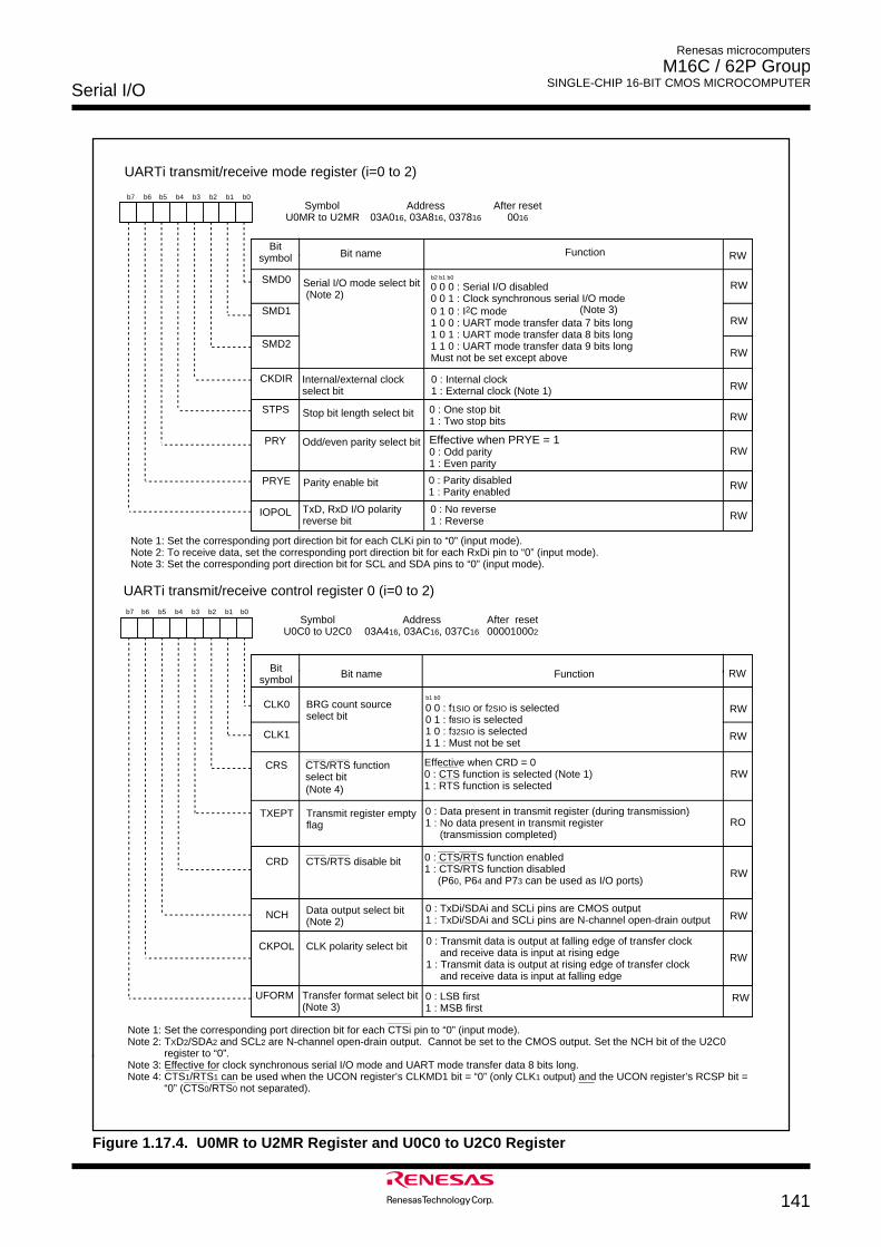
Serial I/O
141
Renesas microcomputers
M16C / 62P Group SINGLE-CHIP 16-BIT CMOS MICROCOMPUTER
UARTi transmit/receive mode register (i=0 to 2)
Symbol Address After resetU0MR to U2MR 03A016, 03A816, 037816 0016
b7 b6 b5 b4 b3 b2 b1 b0
Bit nameBit
symbol RW
CKDIR
SMD1
SMD0 Serial I/O mode select bit (Note 2)
SMD2
Internal/external clock select bit
STPS
PRY
PRYE
IOPOL
Parity enable bit
0 : Internal clock1 : External clock (Note 1)
Stop bit length select bit
Odd/even parity select bit
TxD, RxD I/O polarity reverse bit
0 : One stop bit1 : Two stop bits
0 : Parity disabled1 : Parity enabled
0 0 0 : Serial I/O disabled0 0 1 : Clock synchronous serial I/O mode0 1 0 : I2C mode1 0 0 : UART mode transfer data 7 bits long1 0 1 : UART mode transfer data 8 bits long 1 1 0 : UART mode transfer data 9 bits longMust not be set except above
b2 b1 b0
Effective when PRYE = 10 : Odd parity1 : Even parity
0 : No reverse1 : Reverse
Function
Note 1: Set the corresponding port direction bit for each CLKi pin to “0” (input mode).Note 2: To receive data, set the corresponding port direction bit for each RxDi pin to “0” (input mode). Note 3: Set the corresponding port direction bit for SCL and SDA pins to “0” (input mode).
UARTi transmit/receive control register 0 (i=0 to 2)
Symbol Address After resetU0C0 to U2C0 03A416, 03AC16, 037C16 000010002
b7 b6 b5 b4 b3 b2 b1 b0
Function
TXEPT
CLK1
CLK0
CRS
CRD
NCH
CKPOL
BRG count source select bit
Transmit register empty flag
0 : Transmit data is output at falling edge of transfer clock and receive data is input at rising edge
1 : Transmit data is output at rising edge of transfer clock and receive data is input at falling edge
CLK polarity select bit
CTS/RTS function select bit
CTS/RTS disable bit
Data output select bit(Note 2)
0 0 : f1SIO or f2SIO is selected0 1 : f8SIO is selected1 0 : f32SIO is selected1 1 : Must not be set
b1 b0
0 : LSB first1 : MSB first
0 : Data present in transmit register (during transmission)1 : No data present in transmit register (transmission completed)
0 : CTS/RTS function enabled1 : CTS/RTS function disabled
(P60, P64 and P73 can be used as I/O ports)
0 : TxDi/SDAi and SCLi pins are CMOS output1 : TxDi/SDAi and SCLi pins are N-channel open-drain output
UFORM Transfer format select bit(Note 3)
Effective when CRD = 00 : CTS function is selected (Note 1)1 : RTS function is selected
Bit nameBit symbol
Note 1: Set the corresponding port direction bit for each CTSi pin to “0” (input mode).Note 2: TXD2/SDA2 and SCL2 are N-channel open-drain output. Cannot be set to the CMOS output. Set the NCH bit of the U2C0
register to “0”.Note 3: Effective for clock synchronous serial I/O mode and UART mode transfer data 8 bits long. Note 4: CTS1/RTS1 can be used when the UCON register’s CLKMD1 bit = “0” (only CLK1 output) and the UCON register’s RCSP bit =
“0” (CTS0/RTS0 not separated).
RW
RW
RW
RW
RW
RW
RW
RW
RW
RW
RW
RW
RW
RW
RW
RW
RO
(Note 3)
(Note 4)
Figure 1.17.4. U0MR to U2MR Register and U0C0 to U2C0 Register
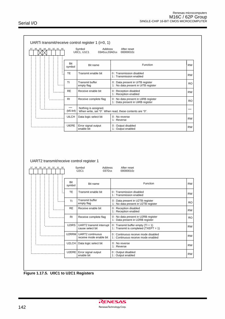
Renesas microcomputers
M16C / 62P Group SINGLE-CHIP 16-BIT CMOS MICROCOMPUTERSerial I/O
142
UARTi transmit/receive control register 1 (i=0, 1)
Symbol Address After resetU0C1, U1C1 03A516,03AD16 000000102
b7 b6 b5 b4 b3 b2 b1 b0
Bit nameBit symbol RWFunction
TE
TI
RE
RI
Transmit enable bit
Receive enable bit
Receive complete flag
Transmit buffer empty flag
0 : Transmission disabled1 : Transmission enabled
0 : Data present in UiTB register 1 : No data present in UiTB register
0 : Reception disabled1 : Reception enabled
0 : No data present in UiRB register 1 : Data present in UiRB register
Nothing is assigned.When write, set “0”. When read, these contents are “0”.
UART2 transmit/receive control register 1
Symbol Address After resetU2C1 037D16 000000102
b7 b6 b5 b4 b3 b2 b1 b0
Bit nameBit symbol
Function
TE
TI
RE
RI
Transmit enable bit
Receive enable bit
Receive complete flag
Transmit buffer empty flag
0 : Transmission disabled1 : Transmission enabled
0 : Reception disabled1 : Reception enabled
U2IRS UART2 transmit interrupt cause select bit
0 : Transmit buffer empty (TI = 1)1 : Transmit is completed (TXEPT = 1)
U2RRM UART2 continuous receive mode enable bit
0 : Continuous receive mode disabled1 : Continuous receive mode enabled
Data logic select bit 0 : No reverse1 : Reverse
U2LCH
U2ERE Error signal output enable bit
0 : Output disabled1 : Output enabled
Data logic select bit 0 : No reverse1 : Reverse
UiLCH
UiERE Error signal output enable bit
0 : Output disabled1 : Output enabled
RW
RW
RW
RW
RO
RO
RW
RW
RW
RW
RW
RW
RW
RO
RO
(b5-b4)
0 : Data present in U2TB register 1 : No data present in U2TB register
0 : No data present in U2RB register 1 : Data present in U2RB register
Figure 1.17.5. U0C1 to U2C1 Registers
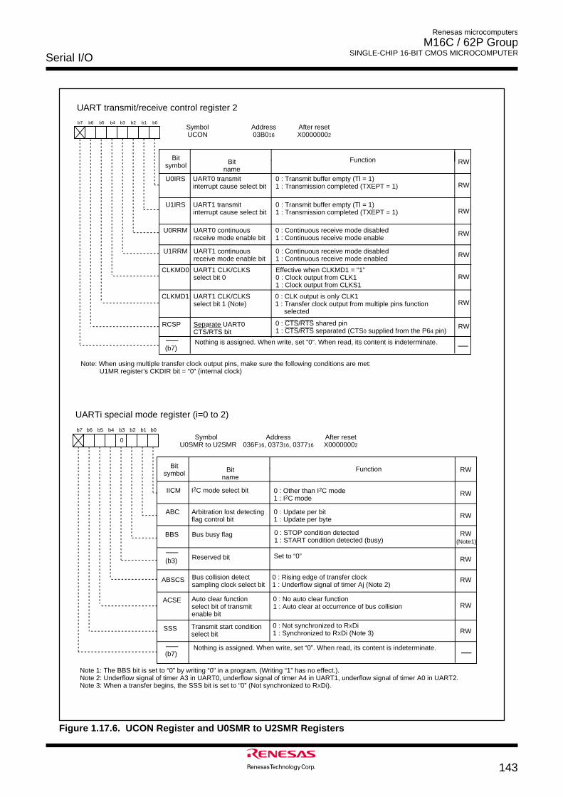
Serial I/O
143
Renesas microcomputers
M16C / 62P Group SINGLE-CHIP 16-BIT CMOS MICROCOMPUTER
Figure 1.17.6. UCON Register and U0SMR to U2SMR Registers
Note: When using multiple transfer clock output pins, make sure the following conditions are met: U1MR register’s CKDIR bit = “0” (internal clock)
UART transmit/receive control register 2
Symbol Address After resetUCON 03B016 X00000002
b7 b6 b5 b4 b3 b2 b1 b0
Bit name
Bit symbol RWFunction
CLKMD0
CLKMD1
UART0 transmit interrupt cause select bit
UART0 continuous receive mode enable bit
0 : Continuous receive mode disabled1 : Continuous receive mode enable
UART1 continuous receive mode enable bit
UART1 CLK/CLKS select bit 0
UART1 transmit interrupt cause select bit
0 : Transmit buffer empty (Tl = 1) 1 : Transmission completed (TXEPT = 1)
0 : Transmit buffer empty (Tl = 1)1 : Transmission completed (TXEPT = 1)
0 : CLK output is only CLK11 : Transfer clock output from multiple pins function
selected
0 : Continuous receive mode disabled1 : Continuous receive mode enabled
Nothing is assigned. When write, set “0”. When read, its content is indeterminate.
U0IRS
U1IRS
U0RRM
U1RRM
UART1 CLK/CLKS select bit 1 (Note)
Effective when CLKMD1 = “1” 0 : Clock output from CLK11 : Clock output from CLKS1
UARTi special mode register (i=0 to 2)
Symbol Address After resetU0SMR to U2SMR 036F16, 037316, 037716 X00000002
b7 b6 b5 b4 b3 b2 b1 b0
Bit name
Bit symbol
Function
ABSCS
ACSE
SSS
I2C mode select bit
Bus busy flag 0 : STOP condition detected1 : START condition detected (busy)
Bus collision detectsampling clock select bit
Arbitration lost detecting flag control bit
0 : Other than I2C mode1 : I2C mode
0 : Update per bit1 : Update per byte
IICM
ABC
BBS
0 : Not synchronized to RXDi1 : Synchronized to RXDi (Note 3)
Set to “0”
Transmit start condition select bit
0 : Rising edge of transfer clock 1 : Underflow signal of timer Aj (Note 2)
Auto clear function select bit of transmit enable bit
0 : No auto clear function1 : Auto clear at occurrence of bus collision
Note 1: The BBS bit is set to “0” by writing “0” in a program. (Writing “1” has no effect.).Note 2: Underflow signal of timer A3 in UART0, underflow signal of timer A4 in UART1, underflow signal of timer A0 in UART2. Note 3: When a transfer begins, the SSS bit is set to “0” (Not synchronized to RXDi).
(Note1)
RCSP Separate UART0 CTS/RTS bit
0 : CTS/RTS shared pin1 : CTS/RTS separated (CTS0 supplied from the P64 pin)
Nothing is assigned. When write, set “0”. When read, its content is indeterminate.
RW
RW
RW
RW
RW
RW
RW
(b7)
RW
RW
RW
RW
RW
RW
RW
RW
(b7)
0
(b3) Reserved bit
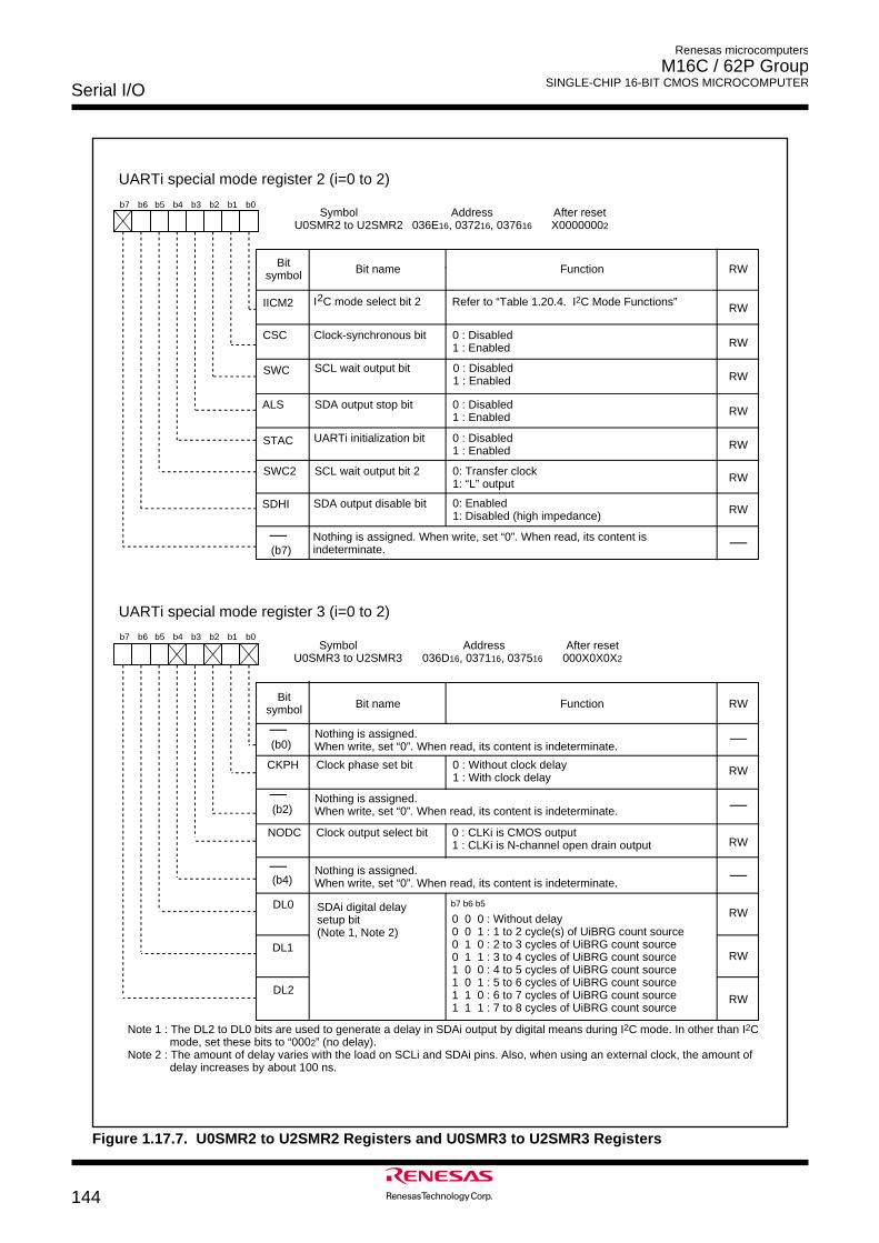
Renesas microcomputers
M16C / 62P Group SINGLE-CHIP 16-BIT CMOS MICROCOMPUTERSerial I/O
144
UARTi special mode register 2 (i=0 to 2)
Symbol Address After resetU0SMR2 to U2SMR2 036E16, 037216, 037616 X00000002
b7 b6 b5 b4 b3 b2 b1 b0
Bit nameBit symbol RWFunction
STAC
SWC2
SDHI
I C mode select bit 2
SCL wait output bit 0 : Disabled1 : Enabled
SDA output stop bit
UARTi initialization bit
Clock-synchronous bit
Refer to “Table 1.20.4. I2C Mode Functions”
0 : Disabled1 : Enabled
IICM2
CSC
SWC
ALS 0 : Disabled1 : Enabled
SDA output disable bit
SCL wait output bit 2
0: Enabled1: Disabled (high impedance)
0 : Disabled1 : Enabled
0: Transfer clock1: “L” output
2
UARTi special mode register 3 (i=0 to 2)
Symbol Address After resetU0SMR3 to U2SMR3 036D16, 037116, 037516 000X0X0X2
b7 b6 b5 b4 b3 b2 b1 b0
Bit nameBit
symbol Function
DL2
SDAi digital delay setup bit(Note 1, Note 2)
DL0
DL1
0 0 0 : Without delay0 0 1 : 1 to 2 cycle(s) of UiBRG count source0 1 0 : 2 to 3 cycles of UiBRG count source0 1 1 : 3 to 4 cycles of UiBRG count source1 0 0 : 4 to 5 cycles of UiBRG count source1 0 1 : 5 to 6 cycles of UiBRG count source1 1 0 : 6 to 7 cycles of UiBRG count source1 1 1 : 7 to 8 cycles of UiBRG count source
Nothing is assigned.When write, set “0”. When read, its content is indeterminate.
b7 b6 b5
Nothing is assigned. When write, set “0”. When read, its content is indeterminate.
0 : Without clock delay1 : With clock delay
Clock phase set bit
0 : CLKi is CMOS output1 : CLKi is N-channel open drain output
Clock output select bit
CKPH
NODC
Note 1 : The DL2 to DL0 bits are used to generate a delay in SDAi output by digital means during I2C mode. In other than I2C mode, set these bits to “0002” (no delay).
Note 2 : The amount of delay varies with the load on SCLi and SDAi pins. Also, when using an external clock, the amount of delay increases by about 100 ns.
RW
RW
RW
RW
RW
RW
RW
(b7)
RW
RW
RW
RW
RW
RW
(b0)
Nothing is assigned.When write, set “0”. When read, its content is indeterminate.
Nothing is assigned.When write, set “0”. When read, its content is indeterminate.
(b2)
(b4)
Figure 1.17.7. U0SMR2 to U2SMR2 Registers and U0SMR3 to U2SMR3 Registers
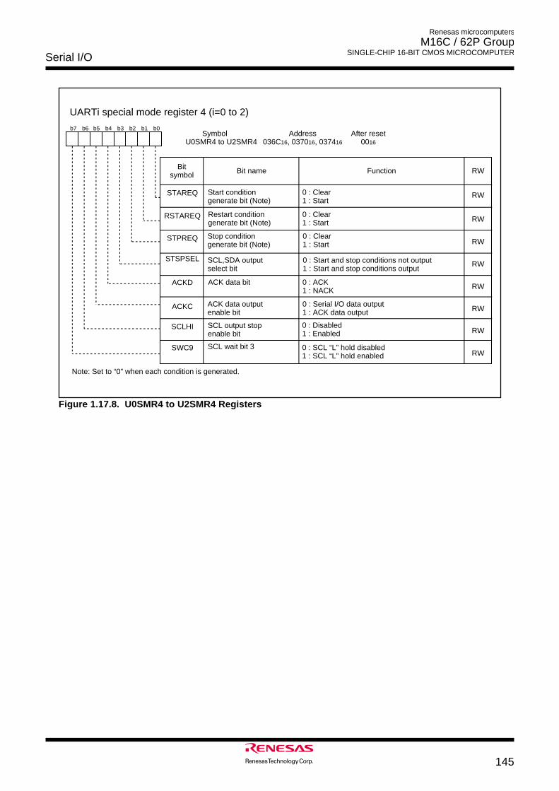
Serial I/O
145
Renesas microcomputers
M16C / 62P Group SINGLE-CHIP 16-BIT CMOS MICROCOMPUTER
Figure 1.17.8. U0SMR4 to U2SMR4 Registers
UARTi special mode register 4 (i=0 to 2)
Symbol Address After resetU0SMR4 to U2SMR4 036C16, 037016, 037416 0016
b7 b6 b5 b4 b3 b2 b1 b0
Bit nameBit symbol RWFunction
ACKC
SCLHI
SWC9
Start conditiongenerate bit (Note)
Stop conditiongenerate bit (Note)
0 : Clear1 : Start
SCL,SDA outputselect bit
ACK data bit
Restart conditiongenerate bit (Note)
0 : Clear1 : Start
0 : Clear1 : Start
STAREQ
RSTAREQ
STPREQ
ACKD
0 : Start and stop conditions not output1 : Start and stop conditions output
SCL output stopenable bit
ACK data outputenable bit
0 : Disabled1 : Enabled
0 : ACK1 : NACK
0 : Serial I/O data output1 : ACK data output
Note: Set to “0” when each condition is generated.
STSPSEL
0 : SCL “L” hold disabled1 : SCL “L” hold enabled
SCL wait bit 3
RW
RW
RW
RW
RW
RW
RW
RW
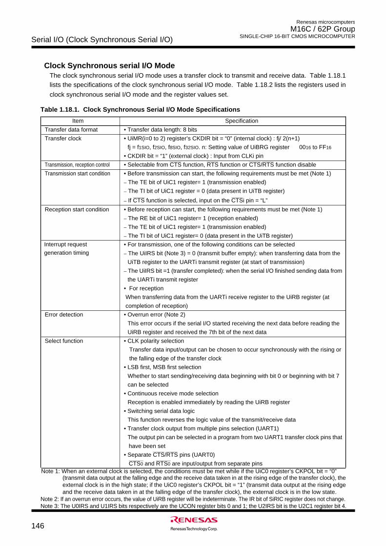
Renesas microcomputers
M16C / 62P Group SINGLE-CHIP 16-BIT CMOS MICROCOMPUTERSerial I/O (Clock Synchronous Serial I/O)
146
Clock Synchronous serial I/O ModeThe clock synchronous serial I/O mode uses a transfer clock to transmit and receive data. Table 1.18.1lists the specifications of the clock synchronous serial I/O mode. Table 1.18.2 lists the registers used in
clock synchronous serial I/O mode and the register values set.
Item Specification
Transfer data format • Transfer data length: 8 bits
Transfer clock • UiMR(i=0 to 2) register’s CKDIR bit = “0” (internal clock) : fj/ 2(n+1)
fj = f1SIO, f2SIO, f8SIO, f32SIO. n: Setting value of UiBRG register 0016 to FF16
• CKDIR bit = “1” (external clock) : Input from CLKi pin
Transmission, reception control_______ _______ _______ _______
• Selectable from CTS function, RTS function or CTS/RTS function disable
Transmission start condition • Before transmission can start, the following requirements must be met (Note 1)_ The TE bit of UiC1 register= 1 (transmission enabled)_ The TI bit of UiC1 register = 0 (data present in UiTB register)
_______ ________ If CTS function is selected, input on the CTSi pin = “L”
Reception start condition • Before reception can start, the following requirements must be met (Note 1)_ The RE bit of UiC1 register= 1 (reception enabled)_ The TE bit of UiC1 register= 1 (transmission enabled)_ The TI bit of UiC1 register= 0 (data present in the UiTB register)
• For transmission, one of the following conditions can be selected_ The UiIRS bit (Note 3) = 0 (transmit buffer empty): when transferring data from the
UiTB register to the UARTi transmit register (at start of transmission)_ The UiIRS bit =1 (transfer completed): when the serial I/O finished sending data from
the UARTi transmit register
• For reception
When transferring data from the UARTi receive register to the UiRB register (at
completion of reception)
Error detection • Overrun error (Note 2)
This error occurs if the serial I/O started receiving the next data before reading the
UiRB register and received the 7th bit of the next data
Select function • CLK polarity selection
Transfer data input/output can be chosen to occur synchronously with the rising or
the falling edge of the transfer clock
• LSB first, MSB first selection
Whether to start sending/receiving data beginning with bit 0 or beginning with bit 7
can be selected
• Continuous receive mode selection
Reception is enabled immediately by reading the UiRB register
• Switching serial data logic
This function reverses the logic value of the transmit/receive data
• Transfer clock output from multiple pins selection (UART1)
The output pin can be selected in a program from two UART1 transfer clock pins that
have been set_______ _______
• Separate CTS/RTS pins (UART0)_________ _________
CTS0 and RTS0 are input/output from separate pinsNote 1: When an external clock is selected, the conditions must be met while if the UiC0 register’s CKPOL bit = “0”
Interrupt requestgeneration timing
(transmit data output at the falling edge and the receive data taken in at the rising edge of the transfer clock), theexternal clock is in the high state; if the UiC0 register’s CKPOL bit = “1” (transmit data output at the rising edgeand the receive data taken in at the falling edge of the transfer clock), the external clock is in the low state.
Note 2: If an overrun error occurs, the value of UiRB register will be indeterminate. The IR bit of SiRIC register does not change.Note 3: The U0IRS and U1IRS bits respectively are the UCON register bits 0 and 1; the U2IRS bit is the U2C1 register bit 4.
Table 1.18.1. Clock Synchronous Serial I/O Mode Specifications
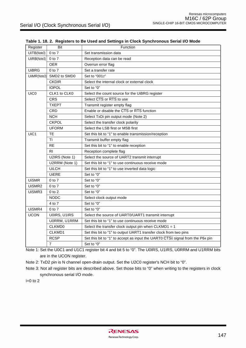
Serial I/O (Clock Synchronous Serial I/O)
147
Renesas microcomputers
M16C / 62P Group SINGLE-CHIP 16-BIT CMOS MICROCOMPUTER
Table 1. 18. 2. Registers to Be Used and Settings in Clock Synchronous Serial I/O ModeRegister Bit Function
UiTB(Note3) 0 to 7 Set transmission data
UiRB(Note3) 0 to 7 Reception data can be read
OER Overrun error flag
UiBRG 0 to 7 Set a transfer rate
UiMR(Note3) SMD2 to SMD0 Set to “0012”
CKDIR Select the internal clock or external clock
IOPOL Set to “0”
UiC0 CLK1 to CLK0 Select the count source for the UiBRG register
CRS_______ _______
Select CTS or RTS to use
TXEPT Transmit register empty flag
CRD_______ _______
Enable or disable the CTS or RTS function
NCH Select TxDi pin output mode (Note 2)
CKPOL Select the transfer clock polarity
UFORM Select the LSB first or MSB first
UiC1 TE Set this bit to “1” to enable transmission/reception
TI Transmit buffer empty flag
RE Set this bit to “1” to enable reception
RI Reception complete flag
U2IRS (Note 1) Select the source of UART2 transmit interrupt
U2RRM (Note 1) Set this bit to “1” to use continuous receive mode
UiLCH Set this bit to “1” to use inverted data logic
UiERE Set to “0”
UiSMR 0 to 7 Set to “0”
UiSMR2 0 to 7 Set to “0”
UiSMR3 0 to 2 Set to “0”
NODC Select clock output mode
4 to 7 Set to “0”
UiSMR4 0 to 7 Set to “0”
UCON U0IRS, U1IRS Select the source of UART0/UART1 transmit interrupt
U0RRM, U1RRM Set this bit to “1” to use continuous receive mode
CLKMD0 Select the transfer clock output pin when CLKMD1 = 1
CLKMD1 Set this bit to “1” to output UART1 transfer clock from two pins
RCSP_________
Set this bit to “1” to accept as input the UART0 CTS0 signal from the P64 pin
7 Set to “0”
Note 1: Set the U0C1 and U1C1 register bit 4 and bit 5 to “0”. The U0IRS, U1IRS, U0RRM and U1RRM bits
are in the UCON register.
Note 2: TxD2 pin is N channel open-drain output. Set the U2C0 register's NCH bit to “0”.
Note 3: Not all register bits are described above. Set those bits to “0” when writing to the registers in clock
synchronous serial I/O mode.
i=0 to 2
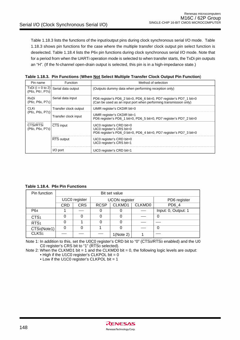
Renesas microcomputers
M16C / 62P Group SINGLE-CHIP 16-BIT CMOS MICROCOMPUTERSerial I/O (Clock Synchronous Serial I/O)
148
Table 1.18.3 lists the functions of the input/output pins during clock synchronous serial I/O mode. Table
1.18.3 shows pin functions for the case where the multiple transfer clock output pin select function is
deselected. Table 1.18.4 lists the P64 pin functions during clock synchronous serial I/O mode. Note that
for a period from when the UARTi operation mode is selected to when transfer starts, the TxDi pin outputs
an “H”. (If the N-channel open-drain output is selected, this pin is in a high-impedance state.)
Table 1.18.3. Pin Functions (When Not Select Multiple Transfer Clock Output Pin Function)Pin name Function Method of selection
TxDi (i = 0 to 2)(P63, P67, P70)
Serial data output
Serial data input
Transfer clock output
Transfer clock input
I/O port
(Outputs dummy data when performing reception only)
RxDi(P62, P66, P71)
CLKi(P61, P65, P72)
UiMR register’s CKDIR bit=0
UiMR register’s CKDIR bit=1PD6 register’s PD6_1 bit=0, PD6_5 bit=0, PD7 register’s PD7_2 bit=0
PD6 register’s PD6_2 bit=0, PD6_6 bit=0, PD7 register’s PD7_1 bit=0(Can be used as an input port when performing transmission only)
UiC0 register’s CRD bit=0UiC0 register’s CRS bit=0PD6 register’s PD6_0 bit=0, PD6_4 bit=0, PD7 register’s PD7_3 bit=0
UiC0 register’s CRD bit=0UiC0 register’s CRS bit=1
UiC0 register’s CRD bit=1
CTS input
RTS output
CTSi/RTSi(P60, P64, P73)
Pin function Bit set value
U1C0 register UCON register PD6 register CRD CRS RCSP CLKMD1 CLKMD0 PD6_4
P64 1 0 0 Input: 0, Output: 1
CTS1 0 0 0 0
RTS1 1 0 0
CTS0(Note1) 0CLKS1
000 0 1 0
1(Note 2) 1
Note 1: In addition to this, set the U0C0 register’s CRD bit to “0” (CTS0/RTS0 enabled) and the U0C0 register’s CRS bit to “1” (RTS0 selected).
Note 2: When the CLKMD1 bit = 1 and the CLKMD0 bit = 0, the following logic levels are output:• High if the U1C0 register’s CLKPOL bit = 0• Low if the U1C0 register’s CLKPOL bit = 1
Table 1.18.4. P64 Pin Functions
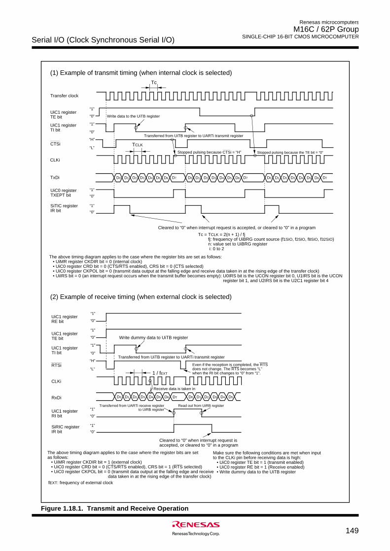
Serial I/O (Clock Synchronous Serial I/O)
149
Renesas microcomputers
M16C / 62P Group SINGLE-CHIP 16-BIT CMOS MICROCOMPUTER
Figure 1.18.1. Transmit and Receive Operation
(1) Example of transmit timing (when internal clock is selected)
D0 D1 D2 D3 D4 D5 D6 D7 D0 D1 D2 D3 D4 D5 D6 D7 D0 D1 D2 D3 D4 D5 D6 D7
Tc
TCLK
Stopped pulsing because the TE bit = “0”
Write data to the UiTB register
Tc = TCLK = 2(n + 1) / fjfj: frequency of UiBRG count source (f1SIO, f2SIO, f8SIO, f32SIO)n: value set to UiBRG register i: 0 to 2
Transfer clock
UiC1 registerTE bit
UiC1 registerTI bit
CLKi
TxDi
“H”
“L”
“0”
“1”
“0”
“1”
“0”
“1”
CTSi
“0”
“1”
Stopped pulsing because CTSi = “H”
Transferred from UiTB register to UARTi transmit register
The above timing diagram applies to the case where the register bits are set as follows: • UiMR register CKDIR bit = 0 (internal clock) • UiC0 register CRD bit = 0 (CTS/RTS enabled), CRS bit = 0 (CTS selected) • UiC0 register CKPOL bit = 0 (transmit data output at the falling edge and receive data taken in at the rising edge of the transfer clock) • UiIRS bit = 0 (an interrupt request occurs when the transmit buffer becomes empty): U0IRS bit is the UCON register bit 0, U1IRS bit is the UCON
register bit 1, and U2IRS bit is the U2C1 register bit 4
Cleared to “0” when interrupt request is accepted, or cleared to “0” in a program
UiC0 registerTXEPT bit
SiTIC registerIR bit
1 / fEXT
Write dummy data to UiTB registerUiC1 registerTE bit
UiC1 registerTI bit
CLKi
RxDi
UiC1 registerRI bit
RTSi“H”
“L”
“0”
“1”
“0”
“1”
“0”
“1”
UiC1 registerRE bit “0”
“1”
Receive data is taken in
Transferred from UiTB register to UARTi transmit register
Read out from UiRB register
fEXT: frequency of external clock
Transferred from UARTi receive registerto UiRB register
SiRIC registerIR bit “0”
“1”
D0 D1 D2 D3 D4 D5 D6 D7 D0 D1 D2 D3 D4 D5
Make sure the following conditions are met when input to the CLKi pin before receiving data is high: • UiC0 register TE bit = 1 (transmit enabled) • UiC0 register RE bit = 1 (Receive enabled) • Write dummy data to the UiTB register
Cleared to “0” when interrupt request is accepted, or cleared to “0” in a program
The above timing diagram applies to the case where the register bits are set as follows: • UiMR register CKDIR bit = 1 (external clock) • UiC0 register CRD bit = 0 (CTS/RTS enabled), CRS bit = 1 (RTS selected) • UiC0 register CKPOL bit = 0 (transmit data output at the falling edge and receive
data taken in at the rising edge of the transfer clock)
Even if the reception is completed, the RTS does not change. The RTS becomes “L” when the RI bit changes to “0” from “1”.
(2) Example of receive timing (when external clock is selected)
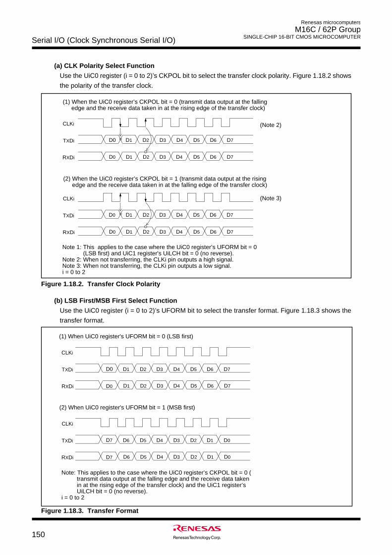
Renesas microcomputers
M16C / 62P Group SINGLE-CHIP 16-BIT CMOS MICROCOMPUTERSerial I/O (Clock Synchronous Serial I/O)
150
(a) CLK Polarity Select Function
Use the UiC0 register (i = 0 to 2)’s CKPOL bit to select the transfer clock polarity. Figure 1.18.2 shows
the polarity of the transfer clock.
(2) When the UiC0 register’s CKPOL bit = 1 (transmit data output at the rising edge and the receive data taken in at the falling edge of the transfer clock)
D1 D2 D3 D4 D5 D6 D7
D1 D2 D3 D4 D5 D6 D7
D0
D0
TXDi
RXDi
CLKi
(1) When the UiC0 register’s CKPOL bit = 0 (transmit data output at the falling edge and the receive data taken in at the rising edge of the transfer clock)
D1 D2 D3 D4 D5 D6 D7D0
D1 D2 D3 D4 D5 D6 D7D0
TXDi
RXDi
CLKi
Note 1: This applies to the case where the UiC0 register’s UFORM bit = 0 (LSB first) and UiC1 register's UiLCH bit = 0 (no reverse).
Note 2: When not transferring, the CLKi pin outputs a high signal.Note 3: When not transferring, the CLKi pin outputs a low signal.i = 0 to 2
(Note 2)
(Note 3)
Figure 1.18.2. Transfer Clock Polarity
(b) LSB First/MSB First Select Function
Use the UiC0 register (i = 0 to 2)’s UFORM bit to select the transfer format. Figure 1.18.3 shows the
transfer format.
Figure 1.18.3. Transfer Format
(1) When UiC0 register's UFORM bit = 0 (LSB first)
D0
D0
D1 D2 D3 D4 D5 D6 D7
D1 D2 D3 D4 D5 D6 D7
TXDi
RXDi
CLKi
(2) When UiC0 register's UFORM bit = 1 (MSB first)
D6 D5 D4 D3 D2 D1 D0D7
D7 D6 D5 D4 D3 D2 D1 D0
TXDi
RXDi
CLKi
Note: This applies to the case where the UiC0 register’s CKPOL bit = 0 (transmit data output at the falling edge and the receive data taken in at the rising edge of the transfer clock) and the UiC1 register’s UiLCH bit = 0 (no reverse).
i = 0 to 2
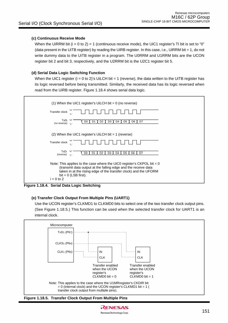
Serial I/O (Clock Synchronous Serial I/O)
151
Renesas microcomputers
M16C / 62P Group SINGLE-CHIP 16-BIT CMOS MICROCOMPUTER
(c) Continuous Receive Mode
When the UiRRM bit (i = 0 to 2) = 1 (continuous receive mode), the UiC1 register’s TI bit is set to “0”
(data present in the UiTB register) by reading the UiRB register. In this case, i.e., UiRRM bit = 1, do not
write dummy data to the UiTB register in a program. The U0RRM and U1RRM bits are the UCON
register bit 2 and bit 3, respectively, and the U2RRM bit is the U2C1 register bit 5.
(d) Serial Data Logic Switching Function
When the UiC1 register (i = 0 to 2)’s UiLCH bit = 1 (reverse), the data written to the UiTB register has
its logic reversed before being transmitted. Similarly, the received data has its logic reversed when
read from the UiRB register. Figure 1.18.4 shows serial data logic.
Figure 1.18.4. Serial Data Logic Switching
D0 D1 D2 D3 D4 D5 D6 D7
Transfer clock
TxDi(no reverse)
“H”
“L”
“H”
“L”
TxDi(reverse) D0 D1 D2 D3 D4 D5 D6 D7
“H”
“L”
(1) When the UiC1 register's UiLCH bit = 0 (no reverse)
Transfer clock“H”
“L”
(2) When the UiC1 register's UiLCH bit = 1 (reverse)
Note: This applies to the case where the UiC0 register’s CKPOL bit = 0 (transmit data output at the falling edge and the receive data taken in at the rising edge of the transfer clock) and the UFORM bit = 0 (LSB first).
i = 0 to 2
(e) Transfer Clock Output From Multiple Pins (UART1)
Use the UCON register’s CLKMD1 to CLKMD0 bits to select one of the two transfer clock output pins.
(See Figure 1.18.5.) This function can be used when the selected transfer clock for UART1 is an
internal clock.
Figure 1.18.5. Transfer Clock Output From Multiple Pins
Microcomputer
TXD1 (P67)
CLKS1 (P64)
CLK1 (P65) IN
CLK
IN
CLK
Note: This applies to the case where the U1MRregister's CKDIR bit = 0 (internal clock) and the UCON register's CLKMD1 bit = 1 (transfer clock output from multiple pins).
Transfer enabled when the UCON register's CLKMD0 bit = 0
Transfer enabled when the UCON register's CLKMD0 bit = 1
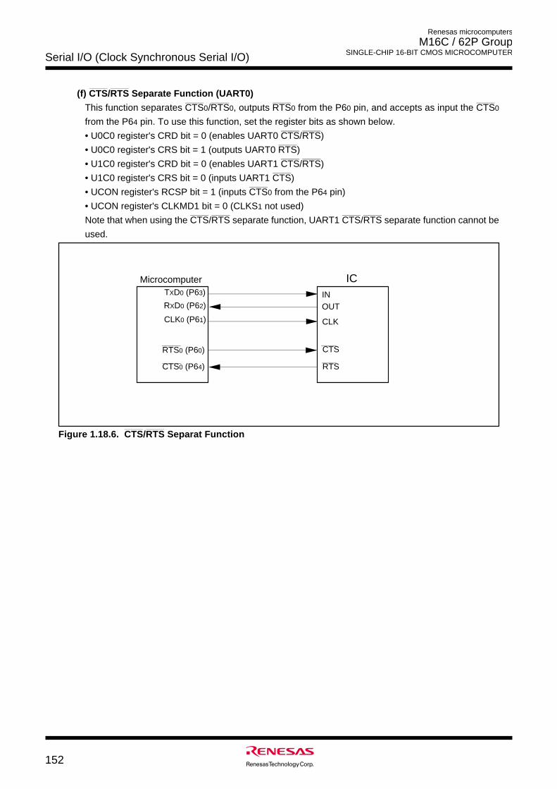
Renesas microcomputers
M16C / 62P Group SINGLE-CHIP 16-BIT CMOS MICROCOMPUTERSerial I/O (Clock Synchronous Serial I/O)
152
_______ _______
(f) CTS/RTS Separate Function (UART0)_______ _______ _______ _______
This function separates CTS0/RTS0, outputs RTS0 from the P60 pin, and accepts as input the CTS0
from the P64 pin. To use this function, set the register bits as shown below._______ _______
• U0C0 register's CRD bit = 0 (enables UART0 CTS/RTS)_______
• U0C0 register's CRS bit = 1 (outputs UART0 RTS)_______ _______
• U1C0 register's CRD bit = 0 (enables UART1 CTS/RTS)_______
• U1C0 register's CRS bit = 0 (inputs UART1 CTS)_______
• UCON register's RCSP bit = 1 (inputs CTS0 from the P64 pin)
• UCON register's CLKMD1 bit = 0 (CLKS1 not used)_______ _______ _______ _______
Note that when using the CTS/RTS separate function, UART1 CTS/RTS separate function cannot be
used.
_______ _______
Figure 1.18.6. CTS/RTS Separat Function
MicrocomputerTXD0 (P63)
RXD0 (P62)INOUT
CTS
RTSCTS0 (P64)
RTS0 (P60)
IC
CLK0 (P61) CLK
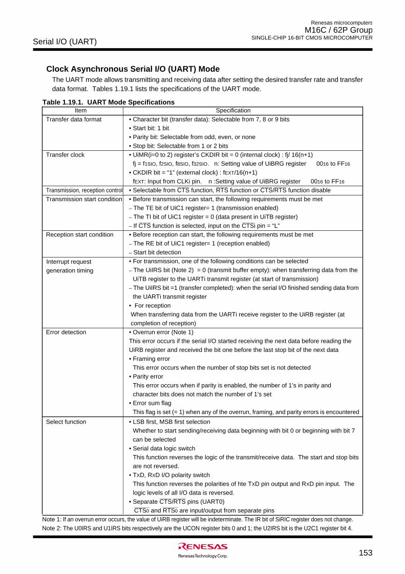
Serial I/O (UART)
153
Renesas microcomputers
M16C / 62P Group SINGLE-CHIP 16-BIT CMOS MICROCOMPUTER
Item Specification
Transfer data format • Character bit (transfer data): Selectable from 7, 8 or 9 bits• Start bit: 1 bit• Parity bit: Selectable from odd, even, or none
• Stop bit: Selectable from 1 or 2 bitsTransfer clock • UiMR(i=0 to 2) register’s CKDIR bit = 0 (internal clock) : fj/ 16(n+1)
fj = f1SIO, f2SIO, f8SIO, f32SIO. n: Setting value of UiBRG register 0016 to FF16
• CKDIR bit = “1” (external clock) : fEXT/16(n+1)fEXT: Input from CLKi pin. n :Setting value of UiBRG register 0016 to FF16
Transmission, reception control_______ _______ _______ _______
• Selectable from CTS function, RTS function or CTS/RTS function disable
Transmission start condition • Before transmission can start, the following requirements must be met_ The TE bit of UiC1 register= 1 (transmission enabled)_ The TI bit of UiC1 register = 0 (data present in UiTB register)
_______ ________ If CTS function is selected, input on the CTSi pin = “L”
Reception start condition • Before reception can start, the following requirements must be met_ The RE bit of UiC1 register= 1 (reception enabled)_ Start bit detection• For transmission, one of the following conditions can be selected_ The UiIRS bit (Note 2) = 0 (transmit buffer empty): when transferring data from the
UiTB register to the UARTi transmit register (at start of transmission)_ The UiIRS bit =1 (transfer completed): when the serial I/O finished sending data from
the UARTi transmit register
• For reception When transferring data from the UARTi receive register to the UiRB register (at completion of reception)
Error detection • Overrun error (Note 1)This error occurs if the serial I/O started receiving the next data before reading theUiRB register and received the bit one before the last stop bit of the next data
• Framing errorThis error occurs when the number of stop bits set is not detected
• Parity error
This error occurs when if parity is enabled, the number of 1’s in parity andcharacter bits does not match the number of 1’s set
• Error sum flag
This flag is set (= 1) when any of the overrun, framing, and parity errors is encountered
Select function • LSB first, MSB first selectionWhether to start sending/receiving data beginning with bit 0 or beginning with bit 7can be selected
• Serial data logic switchThis function reverses the logic of the transmit/receive data. The start and stop bitsare not reversed.
• TXD, RXD I/O polarity switchThis function reverses the polarities of hte TXD pin output and RXD pin input. Thelogic levels of all I/O data is reversed.
_______ _______
• Separate CTS/RTS pins (UART0)_________ _________
CTS0 and RTS0 are input/output from separate pinsNote 1: If an overrun error occurs, the value of UiRB register will be indeterminate. The IR bit of SiRIC register does not change.
Note 2: The U0IRS and U1IRS bits respectively are the UCON register bits 0 and 1; the U2IRS bit is the U2C1 register bit 4.
Clock Asynchronous Serial I/O (UART) ModeThe UART mode allows transmitting and receiving data after setting the desired transfer rate and transferdata format. Tables 1.19.1 lists the specifications of the UART mode.
Interrupt requestgeneration timing
Table 1.19.1. UART Mode Specifications
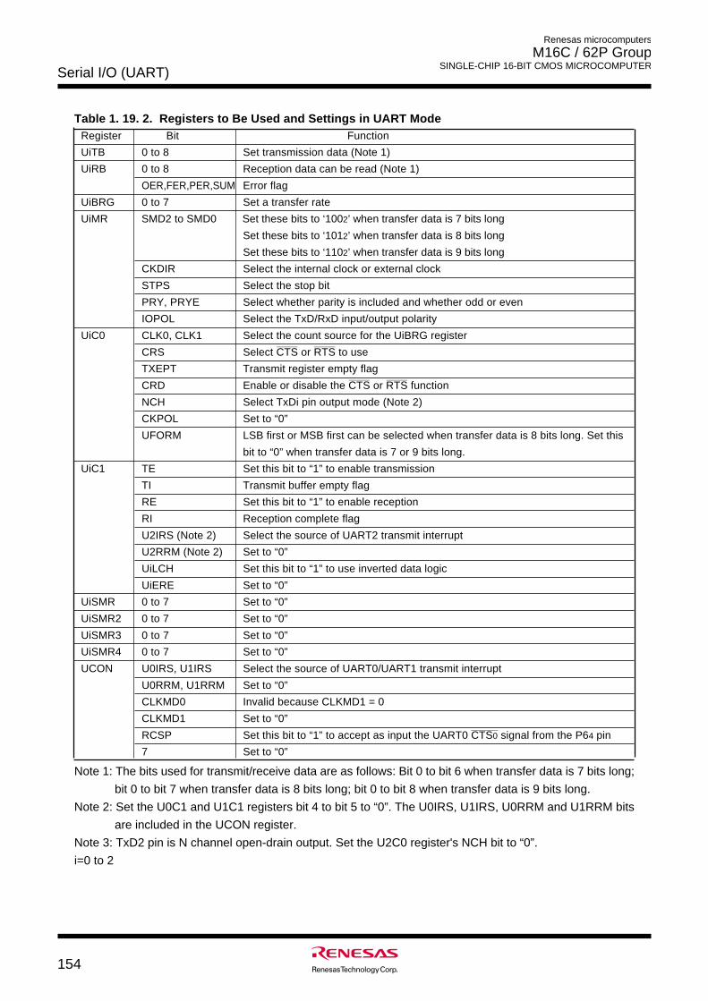
Renesas microcomputers
M16C / 62P Group SINGLE-CHIP 16-BIT CMOS MICROCOMPUTER
Serial I/O (UART)
154
Table 1. 19. 2. Registers to Be Used and Settings in UART ModeRegister Bit Function
UiTB 0 to 8 Set transmission data (Note 1)
UiRB 0 to 8 Reception data can be read (Note 1)
OER,FER,PER,SUM Error flag
UiBRG 0 to 7 Set a transfer rate
UiMR SMD2 to SMD0 Set these bits to ‘1002’ when transfer data is 7 bits long
Set these bits to ‘1012’ when transfer data is 8 bits long
Set these bits to ‘1102’ when transfer data is 9 bits long
CKDIR Select the internal clock or external clock
STPS Select the stop bit
PRY, PRYE Select whether parity is included and whether odd or even
IOPOL Select the TxD/RxD input/output polarity
UiC0 CLK0, CLK1 Select the count source for the UiBRG register
CRS_______ _______
Select CTS or RTS to use
TXEPT Transmit register empty flag
CRD_______ _______
Enable or disable the CTS or RTS function
NCH Select TxDi pin output mode (Note 2)
CKPOL Set to “0”
UFORM LSB first or MSB first can be selected when transfer data is 8 bits long. Set this
bit to “0” when transfer data is 7 or 9 bits long.
UiC1 TE Set this bit to “1” to enable transmission
TI Transmit buffer empty flag
RE Set this bit to “1” to enable reception
RI Reception complete flag
U2IRS (Note 2) Select the source of UART2 transmit interrupt
U2RRM (Note 2) Set to “0”
UiLCH Set this bit to “1” to use inverted data logic
UiERE Set to “0”
UiSMR 0 to 7 Set to “0”
UiSMR2 0 to 7 Set to “0”
UiSMR3 0 to 7 Set to “0”
UiSMR4 0 to 7 Set to “0”
UCON U0IRS, U1IRS Select the source of UART0/UART1 transmit interrupt
U0RRM, U1RRM Set to “0”
CLKMD0 Invalid because CLKMD1 = 0
CLKMD1 Set to “0”
RCSP_________
Set this bit to “1” to accept as input the UART0 CTS0 signal from the P64 pin
7 Set to “0”
Note 1: The bits used for transmit/receive data are as follows: Bit 0 to bit 6 when transfer data is 7 bits long;
bit 0 to bit 7 when transfer data is 8 bits long; bit 0 to bit 8 when transfer data is 9 bits long.
Note 2: Set the U0C1 and U1C1 registers bit 4 to bit 5 to “0”. The U0IRS, U1IRS, U0RRM and U1RRM bits
are included in the UCON register.
Note 3: TxD2 pin is N channel open-drain output. Set the U2C0 register's NCH bit to “0”.
i=0 to 2
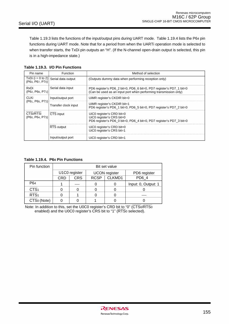
Serial I/O (UART)
155
Renesas microcomputers
M16C / 62P Group SINGLE-CHIP 16-BIT CMOS MICROCOMPUTER
Table 1.19.3 lists the functions of the input/output pins during UART mode. Table 1.19.4 lists the P64 pin
functions during UART mode. Note that for a period from when the UARTi operation mode is selected to
when transfer starts, the TxDi pin outputs an “H”. (If the N-channel open-drain output is selected, this pin
is in a high-impedance state.)
Table 1.19.3. I/O Pin Functions
Pin name Function Method of selection
TxDi (i = 0 to 2)(P63, P67, P70)
Serial data output
Serial data input
Input/output port
Transfer clock input
Input/output port
(Outputs dummy data when performing reception only)
RxDi(P62, P66, P71)
CLKi(P61, P65, P72)
UiMR register’s CKDIR bit=0
UiMR register’s CKDIR bit=1PD6 register’s PD6_1 bit=0, PD6_5 bit=0, PD7 register’s PD7_2 bit=0
PD6 register’s PD6_2 bit=0, PD6_6 bit=0, PD7 register’s PD7_1 bit=0(Can be used as an input port when performing transmission only)
UiC0 register’s CRD bit=0UiC0 register’s CRS bit=0PD6 register’s PD6_0 bit=0, PD6_4 bit=0, PD7 register’s PD7_3 bit=0
UiC0 register’s CRD bit=0UiC0 register’s CRS bit=1
UiC0 register’s CRD bit=1
CTS input
RTS output
CTSi/RTSi(P60, P64, P73)
Table 1.19.4. P64 Pin Functions
Pin function Bit set value
U1C0 register UCON register PD6 register CRD CRS RCSP CLKMD1 PD6_4
P64 1 0 0 Input: 0, Output: 1CTS1 0 0 0 0RTS1 1 0 0CTS0 (Note) 0
000 0 1 0
Note: In addition to this, set the U0C0 register’s CRD bit to “0” (CTS0/RTS0 enabled) and the U0C0 register’s CRS bit to “1” (RTS0 selected).
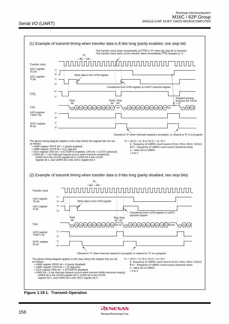
Renesas microcomputers
M16C / 62P Group SINGLE-CHIP 16-BIT CMOS MICROCOMPUTER
Serial I/O (UART)
156
Startbit
Parity bit
TxDi
CTSi
“1”
“0”
“1”
“L”
“H”
“0”
“1”
Tc = 16 (n + 1) / fj or 16 (n + 1) / fEXT
fj : frequency of UiBRG count source (f1SIO, f2SIO, f8SIO, f32SIO)fEXT : frequency of UiBRG count source (external clock)n : value set to UiBRG
i: 0 to 2
“0”
“1”
TxDi
“0”
“1”
“0”
“1”
“0”
“1”
Transfer clock
Tc
“0”
“1”
Tc
Transfer clock
D0 D1 D2 D3 D4 D5 D6 D7ST P D0 D1 D2 D3 D4 D5 D6 D7SP ST P SP D0 D1ST
Stop bit
Start bit
The transfer clock stops momentarily as CTSi is “H” when the stop bit is checked. The transfer clock starts as the transfer starts immediately CTSi changes to “L”.
D0 D1 D2 D3 D4 D5 D6 D7ST SPD8 D0 D1 D2 D3 D4 D5 D6 D7ST D8 D0 D1STSPSP
Stop bit
Stop bit
“0”
SP
Stopped pulsing because the TE bit = “0”
Write data to the UiTB register
UiC1 registerTE bit
UiC1 registerTI bit
UiC0 registerTXEPT bit
SiTIC registerIR bit
Transferred from UiTB register to UARTi transmit register
The above timing diagram applies to the case where the register bits are set as follows: • UiMR register PRYE bit = 1 (parity enabled) • UiMR register STPS bit = 0 (1 stop bit) • UiC0 register CRD bit = 0 (CTS/RTS enabled), CRS bit = 0 (CTS selected) • UiIRS bit = 1 (an interrupt request occurs when transmit completed):
U0IRS bit is the UCON register bit 0, U1IRS bit is the UCON register bit 1, and U2IRS bit is the U2C1 register bit 4
Cleared to “0” when interrupt request is accepted, or cleared to “0” in a program
UiC1 registerTE bit
UiC1 registerTI bit
UiC0 registerTXEPT bit
SiTIC registerIR bit
Cleared to “0” when interrupt request is accepted, or cleared to “0” in a program
Write data to the UiTB register
Transferred from UiTB register to UARTi transmit register
Tc = 16 (n + 1) / fj or 16 (n + 1) / fEXT
fj : frequency of UiBRG count source (f1SIO, f2SIO, f8SIO, f32SIO)fEXT : frequency of UiBRG count source (external clock)n : value set to UiBRG
i: 0 to 2
The above timing diagram applies to the case where the register bits are set as follows: • UiMR register PRYE bit = 0 (parity disabled) • UiMR register STPS bit = 1 (2 stop bits) • UiC0 register CRD bit = 1 (CTS/RTS disabled) • UiIRS bit = 0 (an interrupt request occurs when transmit buffer becomes empty):
U0IRS bit is the UCON register bit 0, U1IRS bit is the UCON register bit 1, and U2IRS bit is the U2C1 register bit 4
(1) Example of transmit timing when transfer data is 8 bits long (parity enabled, one stop bit)
(2) Example of transmit timing when transfer data is 9 bits long (parity disabled, two stop bits)
Figure 1.19.1. Transmit Operation
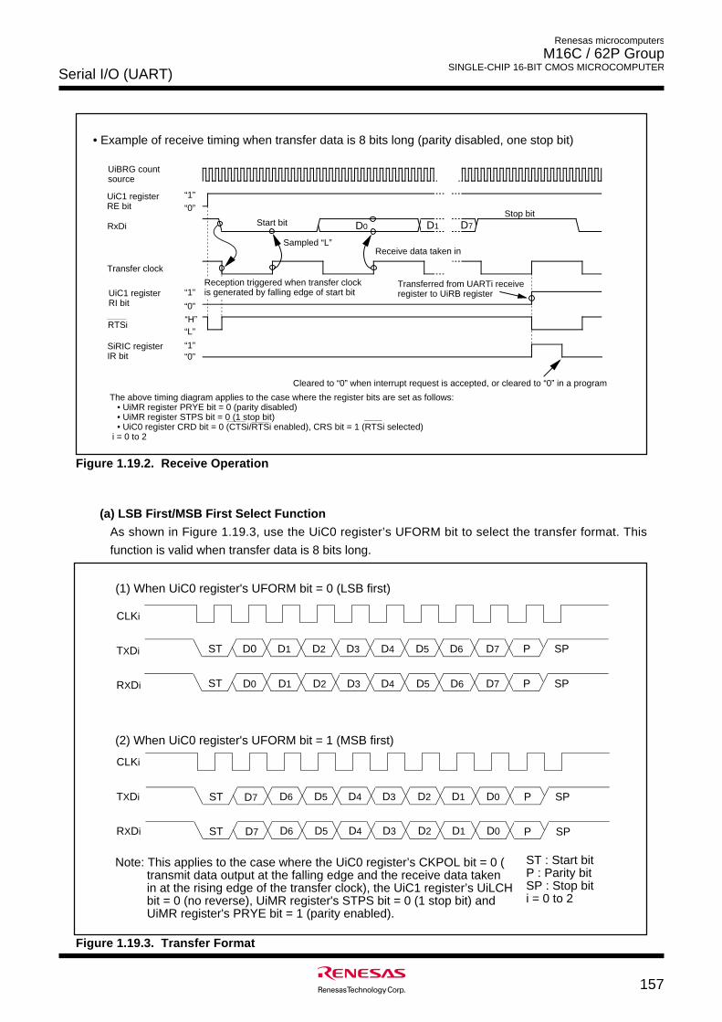
Serial I/O (UART)
157
Renesas microcomputers
M16C / 62P Group SINGLE-CHIP 16-BIT CMOS MICROCOMPUTER
• Example of receive timing when transfer data is 8 bits long (parity disabled, one stop bit)
Figure 1.19.2. Receive Operation
D0Start bit
Sampled “L”
UiBRG count source
RxDi
Transfer clock
RTSi
Stop bit
“1”
“0”
“0”
“1”
“H”“L”
“0”“1”
Reception triggered when transfer clock is generated by falling edge of start bit
UiC1 registerRE bit
UiC1 registerRI bit
SiRIC registerIR bit
Cleared to “0” when interrupt request is accepted, or cleared to “0” in a program
Receive data taken in
D7D1
Transferred from UARTi receive register to UiRB register
The above timing diagram applies to the case where the register bits are set as follows: • UiMR register PRYE bit = 0 (parity disabled) • UiMR register STPS bit = 0 (1 stop bit) • UiC0 register CRD bit = 0 (CTSi/RTSi enabled), CRS bit = 1 (RTSi selected) i = 0 to 2
(a) LSB First/MSB First Select Function
As shown in Figure 1.19.3, use the UiC0 register’s UFORM bit to select the transfer format. This
function is valid when transfer data is 8 bits long.
Figure 1.19.3. Transfer Format
(1) When UiC0 register's UFORM bit = 0 (LSB first)
(2) When UiC0 register's UFORM bit = 1 (MSB first)
Note: This applies to the case where the UiC0 register’s CKPOL bit = 0 (transmit data output at the falling edge and the receive data taken in at the rising edge of the transfer clock), the UiC1 register’s UiLCH bit = 0 (no reverse), UiMR register's STPS bit = 0 (1 stop bit) and UiMR register's PRYE bit = 1 (parity enabled).
D1 D2 D3 D4 D5 D6 SPD0
D1 D2 D3 D4 D5 D6 SPD0
TXDi
RXDi
CLKi
D6 D5 D4 D3 D2 D1 D0D7
TXDi
RXDi
CLKi
ST
ST
D7 P
D7 P
SP
SP
ST
ST
P
P
D6 D5 D4 D3 D2 D1 D0D7
ST : Start bitP : Parity bitSP : Stop biti = 0 to 2
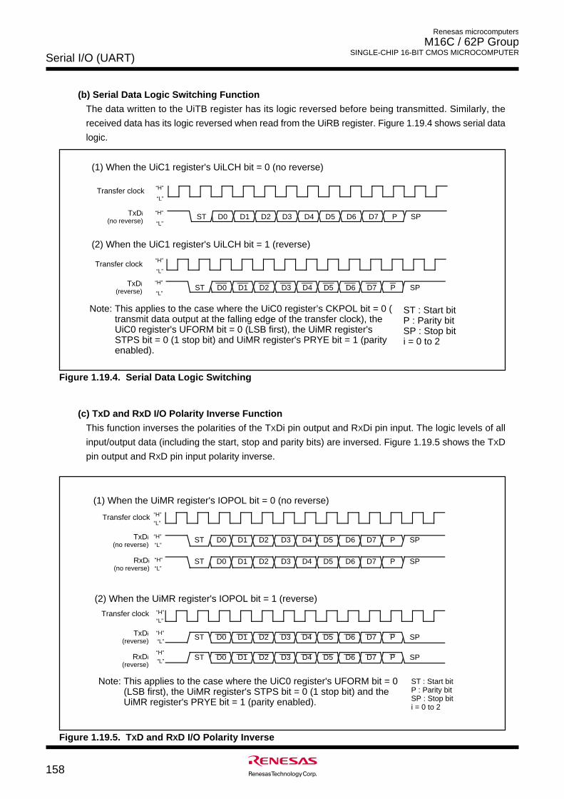
Renesas microcomputers
M16C / 62P Group SINGLE-CHIP 16-BIT CMOS MICROCOMPUTER
Serial I/O (UART)
158
(c) TxD and RxD I/O Polarity Inverse Function
This function inverses the polarities of the TXDi pin output and RXDi pin input. The logic levels of all
input/output data (including the start, stop and parity bits) are inversed. Figure 1.19.5 shows the TXD
pin output and RXD pin input polarity inverse.
Figure 1.19.5. TXD and RXD I/O Polarity Inverse
(b) Serial Data Logic Switching Function
The data written to the UiTB register has its logic reversed before being transmitted. Similarly, the
received data has its logic reversed when read from the UiRB register. Figure 1.19.4 shows serial data
logic.
Figure 1.19.4. Serial Data Logic Switching
Transfer clock “H”
“L”
D0 D1 D2 D3 D4 D5 D6 D7 P SPSTTxDi(no reverse)
“H”
“L”
TxDi(reverse) SPST D3 D4 D5 D6 D7 PD0 D1 D2
“H”
“L”
(1) When the UiC1 register's UiLCH bit = 0 (no reverse)
(2) When the UiC1 register's UiLCH bit = 1 (reverse)
Transfer clock “H”
“L”
Note: This applies to the case where the UiC0 register’s CKPOL bit = 0 (transmit data output at the falling edge of the transfer clock), the UiC0 register's UFORM bit = 0 (LSB first), the UiMR register's STPS bit = 0 (1 stop bit) and UiMR register's PRYE bit = 1 (parity enabled).
ST : Start bitP : Parity bitSP : Stop biti = 0 to 2
(1) When the UiMR register's IOPOL bit = 0 (no reverse)
(2) When the UiMR register's IOPOL bit = 1 (reverse)
Note: This applies to the case where the UiC0 register's UFORM bit = 0 (LSB first), the UiMR register's STPS bit = 0 (1 stop bit) and the UiMR register's PRYE bit = 1 (parity enabled).
ST : Start bitP : Parity bitSP : Stop biti = 0 to 2
D0 D1 D2 D3 D4 D5 D6 D7 P SPST
SPST D3 D4 D5 D6 D7 PD0 D1 D2
D0 D1 D2 D3 D4 D5 D6 D7 P SPST“H”
SPST D3 D4 D5 D6 D7 PD0 D1 D2
Transfer clock
TxDi(no reverse)
RxDi(no reverse)
Transfer clock
TxDi(reverse)
RxDi(reverse)
“L”
“H”
“L”
“H”
“L”
“H”
“L”
“H”
“L”
“H”
“L”
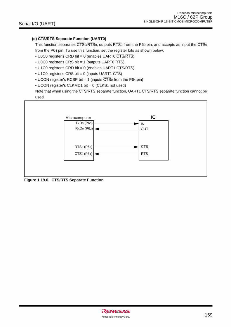
Serial I/O (UART)
159
Renesas microcomputers
M16C / 62P Group SINGLE-CHIP 16-BIT CMOS MICROCOMPUTER
_______ _______
(d) CTS/RTS Separate Function (UART0)_______ _______ _______ _______
This function separates CTS0/RTS0, outputs RTS0 from the P60 pin, and accepts as input the CTS0
from the P64 pin. To use this function, set the register bits as shown below._______ _______
• U0C0 register's CRD bit = 0 (enables UART0 CTS/RTS)_______
• U0C0 register's CRS bit = 1 (outputs UART0 RTS)_______ _______
• U1C0 register's CRD bit = 0 (enables UART1 CTS/RTS)_______
• U1C0 register's CRS bit = 0 (inputs UART1 CTS)_______
• UCON register's RCSP bit = 1 (inputs CTS0 from the P64 pin)
• UCON register's CLKMD1 bit = 0 (CLKS1 not used)_______ _______ _______ _______
Note that when using the CTS/RTS separate function, UART1 CTS/RTS separate function cannot be
used.
_______ _______
Figure 1.19.6. CTS/RTS Separate Function
MicrocomputerTXD0 (P63)
RXD0 (P62)INOUT
CTS
RTSCTS0 (P64)
RTS0 (P60)
IC
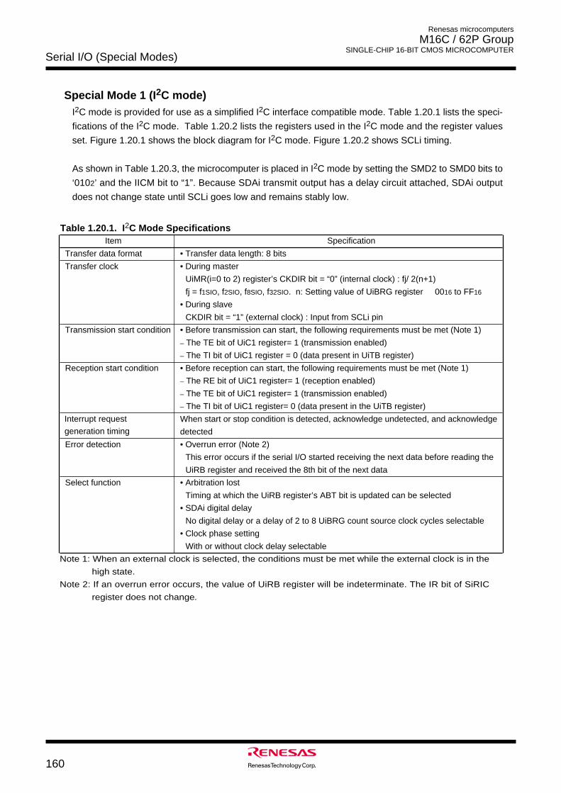
Serial I/O (Special Modes)
160
Renesas microcomputers
M16C / 62P Group SINGLE-CHIP 16-BIT CMOS MICROCOMPUTER
Special Mode 1 (I2C mode)I2C mode is provided for use as a simplified I2C interface compatible mode. Table 1.20.1 lists the speci-
fications of the I2C mode. Table 1.20.2 lists the registers used in the I2C mode and the register values
set. Figure 1.20.1 shows the block diagram for I2C mode. Figure 1.20.2 shows SCLi timing.
As shown in Table 1.20.3, the microcomputer is placed in I2C mode by setting the SMD2 to SMD0 bits to
‘0102’ and the IICM bit to “1”. Because SDAi transmit output has a delay circuit attached, SDAi output
does not change state until SCLi goes low and remains stably low.
Table 1.20.1. I2C Mode SpecificationsItem Specification
Transfer data format • Transfer data length: 8 bits
Transfer clock • During master
UiMR(i=0 to 2) register’s CKDIR bit = “0” (internal clock) : fj/ 2(n+1)
fj = f1SIO, f2SIO, f8SIO, f32SIO. n: Setting value of UiBRG register 0016 to FF16
• During slave
CKDIR bit = “1” (external clock) : Input from SCLi pin
Transmission start condition • Before transmission can start, the following requirements must be met (Note 1)_ The TE bit of UiC1 register= 1 (transmission enabled)_ The TI bit of UiC1 register = 0 (data present in UiTB register)
Reception start condition • Before reception can start, the following requirements must be met (Note 1)_ The RE bit of UiC1 register= 1 (reception enabled)_ The TE bit of UiC1 register= 1 (transmission enabled)_ The TI bit of UiC1 register= 0 (data present in the UiTB register)
When start or stop condition is detected, acknowledge undetected, and acknowledge
detected
Error detection • Overrun error (Note 2)
This error occurs if the serial I/O started receiving the next data before reading the
UiRB register and received the 8th bit of the next data
Select function • Arbitration lost
Timing at which the UiRB register’s ABT bit is updated can be selected
• SDAi digital delay
No digital delay or a delay of 2 to 8 UiBRG count source clock cycles selectable
• Clock phase setting
With or without clock delay selectable
Note 1: When an external clock is selected, the conditions must be met while the external clock is in the
high state.
Note 2: If an overrun error occurs, the value of UiRB register will be indeterminate. The IR bit of SiRIC
register does not change.
Interrupt request
generation timing
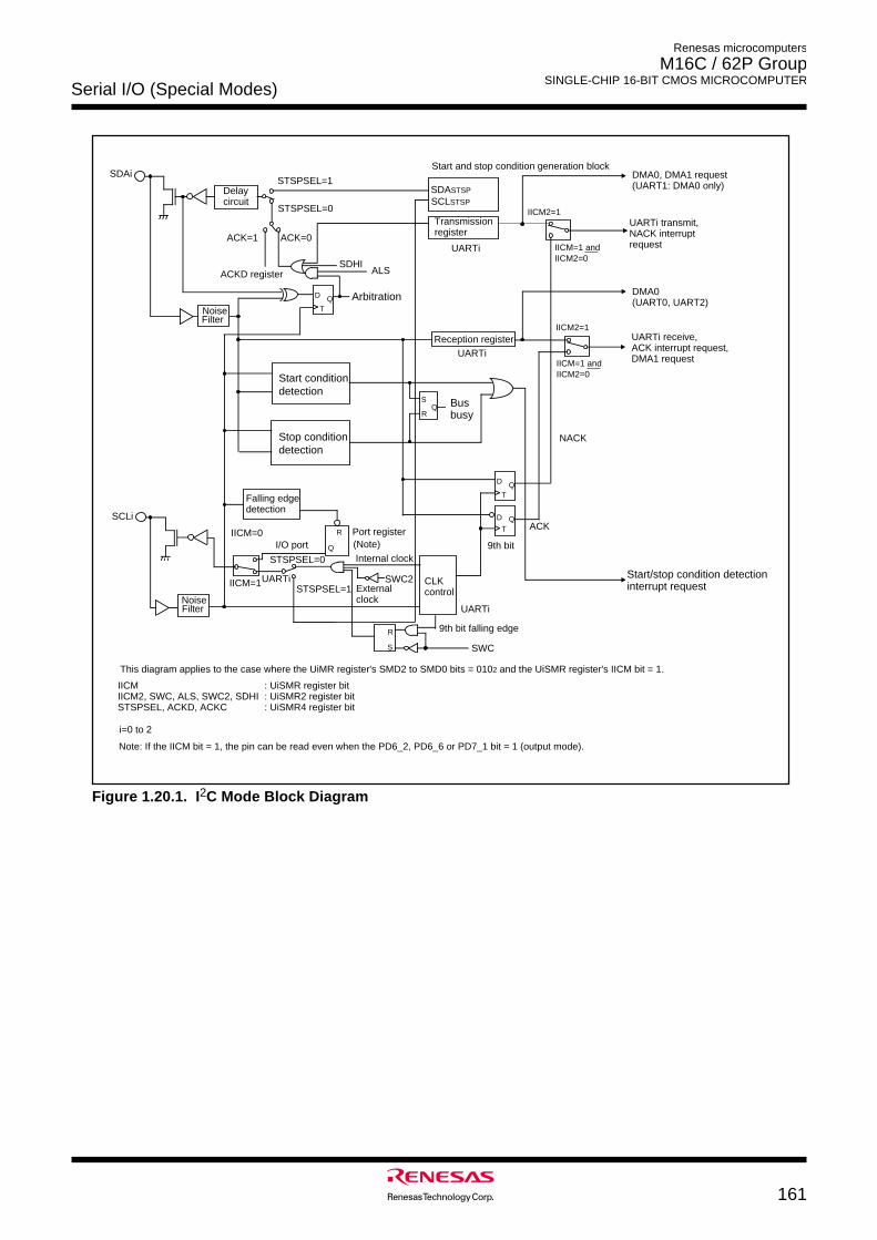
Serial I/O (Special Modes)
161
Renesas microcomputers
M16C / 62P Group SINGLE-CHIP 16-BIT CMOS MICROCOMPUTER
CLK control
Falling edge detection
External clock
Internal clock
Start/stop condition detection interrupt request
Start condition detection
Stop condition detection
Reception register
Bus busy
Transmission register
ArbitrationNoiseFilter
SDAi
SCLi
UARTi
D
TQ
D
TQ
D
TQ
NACK
ACK
UARTi
UARTi
UARTi
R
UARTi transmit, NACK interrupt request
UARTi receive,ACK interrupt request,DMA1 request
IICM=1 andIICM2=0
S
RQ
ALS
R
S SWC
IICM=1 and IICM2=0
IICM2=1
IICM2=1
SWC2
SDHI
DMA0, DMA1 request(UART1: DMA0 only)
NoiseFilter
i=0 to 2
IICM : UiSMR register bitIICM2, SWC, ALS, SWC2, SDHI : UiSMR2 register bitSTSPSEL, ACKD, ACKC : UiSMR4 register bit
IICM=0
IICM=1
DMA0(UART0, UART2)
STSPSEL=0
STSPSEL=1
STSPSEL=1
STSPSEL=0
SDASTSP
SCLSTSP
ACK=1 ACK=0
Q
Port register(Note)I/O port
9th bit falling edge
9th bit
ACKD register
Delay circuit
This diagram applies to the case where the UiMR register's SMD2 to SMD0 bits = 0102 and the UiSMR register's IICM bit = 1.
Note: If the IICM bit = 1, the pin can be read even when the PD6_2, PD6_6 or PD7_1 bit = 1 (output mode).
Start and stop condition generation block
Figure 1.20.1. I2C Mode Block Diagram
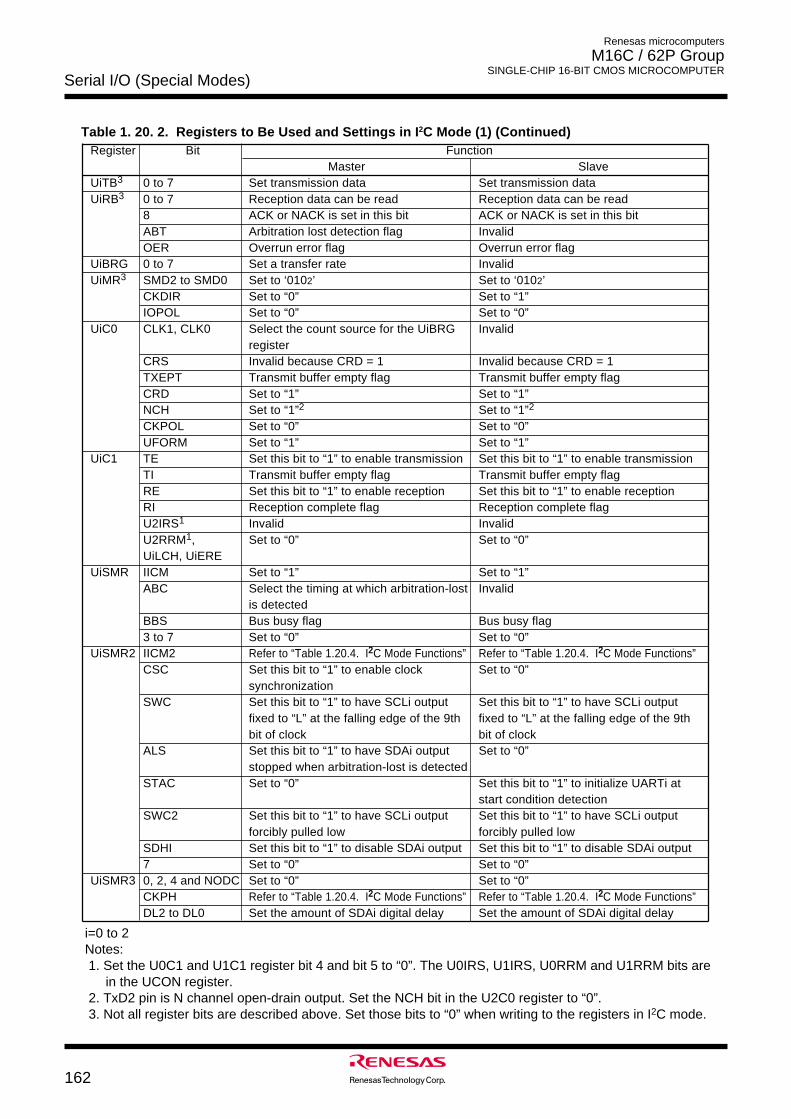
Serial I/O (Special Modes)
162
Renesas microcomputers
M16C / 62P Group SINGLE-CHIP 16-BIT CMOS MICROCOMPUTER
Table 1. 20. 2. Registers to Be Used and Settings in I2C Mode (1) (Continued)Register Bit Function
Master SlaveUiTB3 0 to 7 Set transmission data Set transmission dataUiRB3 0 to 7 Reception data can be read Reception data can be read
8 ACK or NACK is set in this bit ACK or NACK is set in this bitABT Arbitration lost detection flag InvalidOER Overrun error flag Overrun error flag
UiBRG 0 to 7 Set a transfer rate InvalidUiMR3 SMD2 to SMD0 Set to ‘0102’ Set to ‘0102’
CKDIR Set to “0” Set to “1”IOPOL Set to “0” Set to “0”
UiC0 CLK1, CLK0 Select the count source for the UiBRG Invalidregister
CRS Invalid because CRD = 1 Invalid because CRD = 1TXEPT Transmit buffer empty flag Transmit buffer empty flagCRD Set to “1” Set to “1”NCH Set to “1”2 Set to “1”2
CKPOL Set to “0” Set to “0”UFORM Set to “1” Set to “1”
UiC1 TE Set this bit to “1” to enable transmission Set this bit to “1” to enable transmissionTI Transmit buffer empty flag Transmit buffer empty flagRE Set this bit to “1” to enable reception Set this bit to “1” to enable receptionRI Reception complete flag Reception complete flagU2IRS1 Invalid InvalidU2RRM1, Set to “0” Set to “0”UiLCH, UiERE
UiSMR IICM Set to “1” Set to “1”ABC Select the timing at which arbitration-lost Invalid
is detectedBBS Bus busy flag Bus busy flag3 to 7 Set to “0” Set to “0”
UiSMR2 IICM2 Refer to “Table 1.20.4. I2C Mode Functions” Refer to “Table 1.20.4. I2C Mode Functions”CSC Set this bit to “1” to enable clock Set to “0”
synchronizationSWC Set this bit to “1” to have SCLi output Set this bit to “1” to have SCLi output
fixed to “L” at the falling edge of the 9th fixed to “L” at the falling edge of the 9thbit of clock bit of clock
ALS Set this bit to “1” to have SDAi output Set to “0”stopped when arbitration-lost is detected
STAC Set to “0” Set this bit to “1” to initialize UARTi atstart condition detection
SWC2 Set this bit to “1” to have SCLi output Set this bit to “1” to have SCLi outputforcibly pulled low forcibly pulled low
SDHI Set this bit to “1” to disable SDAi output Set this bit to “1” to disable SDAi output7 Set to “0” Set to “0”
UiSMR3 0, 2, 4 and NODC Set to “0” Set to “0”CKPH Refer to “Table 1.20.4. I2C Mode Functions” Refer to “Table 1.20.4. I2C Mode Functions”DL2 to DL0 Set the amount of SDAi digital delay Set the amount of SDAi digital delay
i=0 to 2Notes: 1. Set the U0C1 and U1C1 register bit 4 and bit 5 to “0”. The U0IRS, U1IRS, U0RRM and U1RRM bits are
in the UCON register. 2. TxD2 pin is N channel open-drain output. Set the NCH bit in the U2C0 register to “0”. 3. Not all register bits are described above. Set those bits to “0” when writing to the registers in I2C mode.
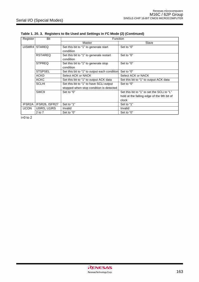
Serial I/O (Special Modes)
163
Renesas microcomputers
M16C / 62P Group SINGLE-CHIP 16-BIT CMOS MICROCOMPUTER
UiSMR4 STAREQ Set this bit to “1” to generate start Set to “0”condition
RSTAREQ Set this bit to “1” to generate restart Set to “0”condition
STPREQ Set this bit to “1” to generate stop Set to “0”condition
STSPSEL Set this bit to “1” to output each condition Set to “0”ACKD Select ACK or NACK Select ACK or NACKACKC Set this bit to “1” to output ACK data Set this bit to “1” to output ACK dataSCLHI Set this bit to “1” to have SCLi output Set to “0”
stopped when stop condition is detectedSWC9 Set to “0” Set this bit to “1” to set the SCLi to “L”
hold at the falling edge of the 9th bit ofclock
IFSR2A IFSR26, ISFR27 Set to “1” Set to “1”UCON U0IRS, U1IRS Invalid Invalid
2 to 7 Set to “0” Set to “0”
Register Bit FunctionMaster Slave
Table 1. 20. 3. Registers to Be Used and Settings in I2C Mode (2) (Continued)
i=0 to 2
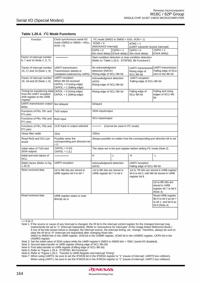
Serial I/O (Special Modes)
164
Renesas microcomputers
M16C / 62P Group SINGLE-CHIP 16-BIT CMOS MICROCOMPUTER
Function I2C mode (SMD2 to SMD0 = 0102, IICM = 1)Clock synchronous serial I/O mode (SMD2 to SMD0 = 0012, IICM = 0)
Factor of interrupt number 15, 17 and 19 (Note 1, 6)
No acknowledgment detection (NACK) Rising edge of SCLi 9th bit
Factor of interrupt number 16, 18 and 20 (Note 1, 6)
Start condition detection or stop condition detection(Refer to “Table 1.20.5. STSPSEL Bit Functions”)
UARTi transmission output delay
Functions of P63, P67 and P70 pins
Noise filter width
Read RxDi and SCLi pin levels
Factor of interrupt number 6, 7 and 10 (Note 1, 5, 7)
Acknowledgment detection (ACK) Rising edge of SCLi 9th bit
Initial value of TxDi and SDAi outputs
UARTi transmissionTransmission started or completed (selected by UiIRS)UARTi receptionWhen 8th bit receivedCKPOL = 0 (rising edge)CKPOL = 1 (falling edge)
Not delayed
TxDi output
RxDi input
CLKi input or output selected
15ns
Possible when the corresponding port direction bit = 0
CKPOL = 0 (H)CKPOL = 1 (L)
Delayed
SDAi input/output
SCLi input/output
(Cannot be used in I2C mode)
Initial and end values of SCLi
H
200ns
Always possible no matter how the corresponding port direction bit is set
The value set in the port register before setting I2C mode (Note 2)
Timing for transferring data from the UART reception shift register to the UiRB register
IICM2 = 0 (NACK/ACK interrupt)
IICM2 = 1(UART transmit/ receive interrupt)
CKPH = 1(Clock delay)
CKPH = 1(Clock delay)
UARTi transmissionRising edge of SCLi 9th bit
UARTi transmissionFalling edge of SCLi next to the 9th bit
UARTi receptionFalling edge of SCLi 9th bit
CKPOL = 0 (rising edge)CKPOL = 1 (falling edge)
Rising edge of SCLi 9th bit Falling edge of SCLi 9th bit
Falling and rising edges of SCLi 9th bit
Functions of P62, P66 and P71 pins
Functions of P61, P65 and P72 pins
i = 0 to 2Note 1: If the source or cause of any interrupt is changed, the IR bit in the interrupt control register for the changed interrupt may
inadvertently be set to “1” (interrupt requested). (Refer to “precautions for interrupts” of the Usage Notes Reference Book.) If one of the bits shown below is changed, the interrupt source, the interrupt timing, etc. change. Therefore, always be sure to clear the IR bit to “0” (interrupt not requested) after changing those bits.SMD2 to SMD0 bits in the UiMR register, IICM bit in the UiSMR register, IICM2 bit in the UiSMR2 register, CKPH bit in the UiSMR3 register
Note 2: Set the initial value of SDAi output while the UiMR register’s SMD2 to SMD0 bits = ‘0002’ (serial I/O disabled).Note 3: Second data transfer to UiRB register (Rising edge of SCLi 9th bit)Note 4: First data transfer to UiRB register (Falling edge of SCLi 9th bit)Note 5: Refer to “Figure 1.20.4. STSPSEL Bit Functions”.Note 6: Refer to “Figure 1.20.2. Transfer to UiRB Register and Interrupt Timing”.Note 7: When using UART0, be sure to set the IFSR26 bit in the IFSR2A register to “1” (cause of interrupt: UART0 bus collision).
When using UART1, be sure to set the IFSR26 bit in the IFSR2A register to “1” (cause of interrupt: UART1 bus collision).
DMA1 factor (Refer to Fig 1.20.2)
UARTi reception Acknowledgment detection (ACK)
UARTi receptionFalling edge of SCLi 9th bit
Store received data 1st to 8th bits are stored in UiRB register bit 0 to bit 7
1st to 8th bits are stored in UiRB register bit 7 to bit 0
1st to 7th bits are stored in UiRB register bit 6 to bit 0, with 8th bit stored in UiRB register bit 8
L
Read UiRB register Bit 6 to bit 0 as bit 7 to bit 1, and bit 8 as bit 0 (Note 4)
Read received data UiRB register status is read directly as is
CKPH = 0(No clock delay)
CKPH = 0(No clock delay)
HL
1st to 8th bits are stored in UiRB register bit 7 to bit 0 (Note 3)
Table 1.20.4. I2C Mode Functions
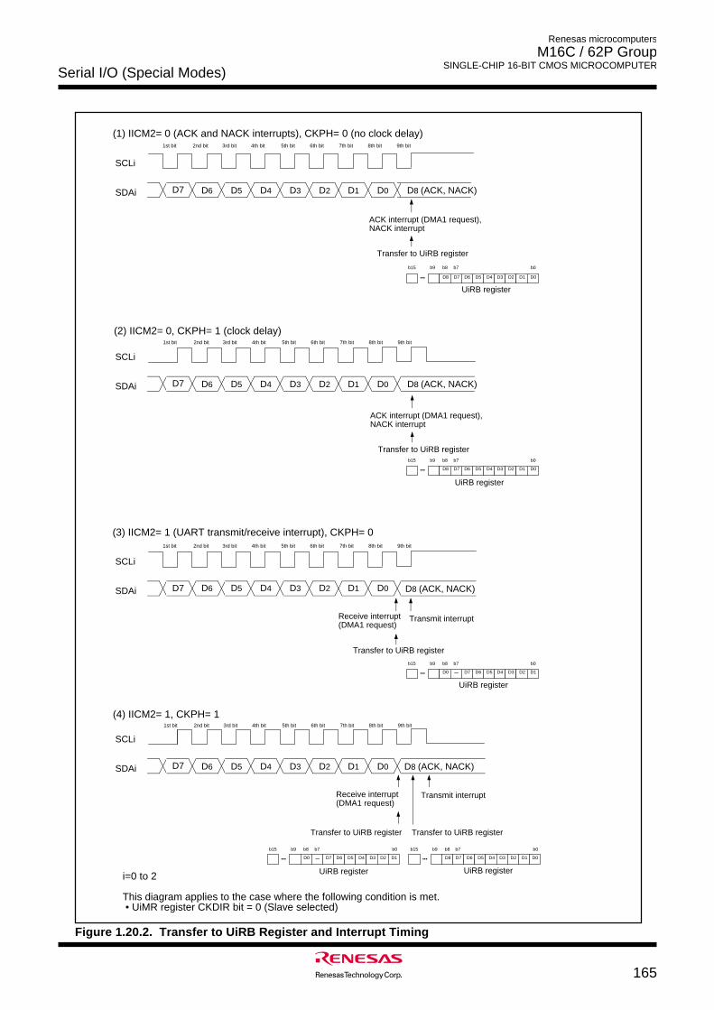
Serial I/O (Special Modes)
165
Renesas microcomputers
M16C / 62P Group SINGLE-CHIP 16-BIT CMOS MICROCOMPUTER
Figure 1.20.2. Transfer to UiRB Register and Interrupt Timing
(3) IICM2= 1 (UART transmit/receive interrupt), CKPH= 0
(1) IICM2= 0 (ACK and NACK interrupts), CKPH= 0 (no clock delay)
i=0 to 2
This diagram applies to the case where the following condition is met. • UiMR register CKDIR bit = 0 (Slave selected)
ACK interrupt (DMA1 request), NACK interrupt
Transfer to UiRB register
Receive interrupt (DMA1 request)
Transmit interrupt
Transfer to UiRB register
(4) IICM2= 1, CKPH= 1
D6 D5 D4 D3 D2 D1D7SDAi
SCLi
D0
D6 D5 D4 D3 D2 D1D7SDAi
SCLi
D0
D6 D5 D4 D3 D2 D1 D8 (ACK, NACK)D7SDAi
SCLi
D0
D8 (ACK, NACK)
D8 (ACK, NACK)
D6 D5 D4 D3 D2 D1 D8 (ACK, NACK)D7SDAi
SCLi
D0
1st bit 2nd bit 3rd bit 4th bit 5th bit 6th bit 7th bit 8th bit 9th bit
b15
•••
b9 b8 b7 b0
D8 D7 D6 D5 D4 D3 D2 D1 D0
UiRB register
b15
•••
b9 b8 b7 b0
D8 D7 D6 D5 D4 D3 D2 D1 D0
b15
•••
b9 b8 b7 b0
D0 D7 D6 D5 D4 D3 D2 D1
b15
•••
b9 b8 b7 b0
D0 D7 D6 D5 D4 D3 D2 D1
b15
•••
b9 b8 b7 b0
D8 D7 D6 D5 D4 D3 D2 D1 D0
1st bit 2nd bit 3rd bit 4th bit 5th bit 6th bit 7th bit 8th bit 9th bit
1st bit 2nd bit 3rd bit 4th bit 5th bit 6th bit 7th bit 8th bit 9th bit
1st bit 2nd bit 3rd bit 4th bit 5th bit 6th bit 7th bit 8th bit 9th bit
(2) IICM2= 0, CKPH= 1 (clock delay)
ACK interrupt (DMA1 request), NACK interrupt
Transfer to UiRB register
UiRB register
Transmit interrupt
Transfer to UiRB register
Receive interrupt (DMA1 request)
Transfer to UiRB register
UiRB register
UiRB register UiRB register
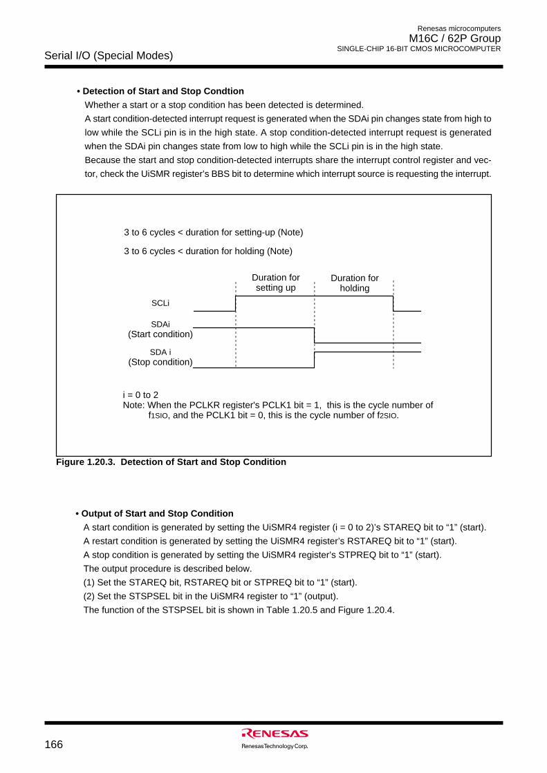
Serial I/O (Special Modes)
166
Renesas microcomputers
M16C / 62P Group SINGLE-CHIP 16-BIT CMOS MICROCOMPUTER
• Detection of Start and Stop Condtion
Whether a start or a stop condition has been detected is determined.
A start condition-detected interrupt request is generated when the SDAi pin changes state from high to
low while the SCLi pin is in the high state. A stop condition-detected interrupt request is generated
when the SDAi pin changes state from low to high while the SCLi pin is in the high state.
Because the start and stop condition-detected interrupts share the interrupt control register and vec-
tor, check the UiSMR register’s BBS bit to determine which interrupt source is requesting the interrupt.
Figure 1.20.3. Detection of Start and Stop Condition
• Output of Start and Stop Condition
A start condition is generated by setting the UiSMR4 register (i = 0 to 2)’s STAREQ bit to “1” (start).
A restart condition is generated by setting the UiSMR4 register’s RSTAREQ bit to “1” (start).
A stop condition is generated by setting the UiSMR4 register’s STPREQ bit to “1” (start).
The output procedure is described below.
(1) Set the STAREQ bit, RSTAREQ bit or STPREQ bit to “1” (start).
(2) Set the STSPSEL bit in the UiSMR4 register to “1” (output).
The function of the STSPSEL bit is shown in Table 1.20.5 and Figure 1.20.4.
3 to 6 cycles < duration for setting-up (Note)
3 to 6 cycles < duration for holding (Note)
i = 0 to 2Note: When the PCLKR register's PCLK1 bit = 1, this is the cycle number of f1SIO, and the PCLK1 bit = 0, this is the cycle number of f2SIO.
Duration for setting up
Duration for holding
SCLi
SDAi(Start condition)
SDA i(Stop condition)
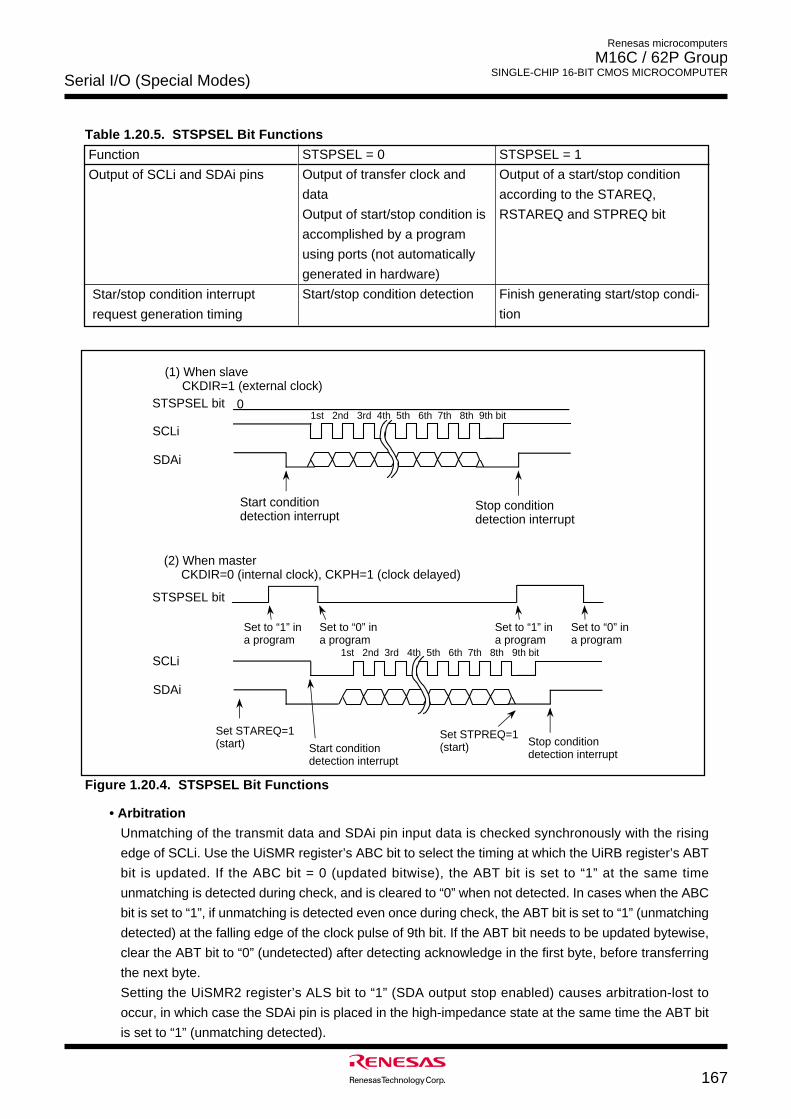
Serial I/O (Special Modes)
167
Renesas microcomputers
M16C / 62P Group SINGLE-CHIP 16-BIT CMOS MICROCOMPUTER
Table 1.20.5. STSPSEL Bit Functions
Figure 1.20.4. STSPSEL Bit Functions
Function
Output of SCLi and SDAi pins
Star/stop condition interrupt
request generation timing
STSPSEL = 0
Output of transfer clock and
data
Output of start/stop condition is
accomplished by a program
using ports (not automatically
generated in hardware)
Start/stop condition detection
STSPSEL = 1
Output of a start/stop condition
according to the STAREQ,
RSTAREQ and STPREQ bit
Finish generating start/stop condi-
tion
Start condition detection interrupt
Stop condition detection interrupt
(1) When slave CKDIR=1 (external clock)
Start condition detection interrupt
Stop condition detection interrupt
(2) When master CKDIR=0 (internal clock), CKPH=1 (clock delayed)
SDAi
SCLi
Set STAREQ=1 (start)
Set STPREQ=1 (start)
STSPSEL bit 0
SDAi
SCLi
STSPSEL bit
Set to “1” in a program
Set to “0” in a program
Set to “1” in a program
Set to “0” in a program
1st 2nd 3rd 4th 5th 6th 7th 8th 9th bit
1st 2nd 3rd 4th 5th 6th 7th 8th 9th bit
• Arbitration
Unmatching of the transmit data and SDAi pin input data is checked synchronously with the rising
edge of SCLi. Use the UiSMR register’s ABC bit to select the timing at which the UiRB register’s ABT
bit is updated. If the ABC bit = 0 (updated bitwise), the ABT bit is set to “1” at the same time
unmatching is detected during check, and is cleared to “0” when not detected. In cases when the ABC
bit is set to “1”, if unmatching is detected even once during check, the ABT bit is set to “1” (unmatching
detected) at the falling edge of the clock pulse of 9th bit. If the ABT bit needs to be updated bytewise,
clear the ABT bit to “0” (undetected) after detecting acknowledge in the first byte, before transferring
the next byte.
Setting the UiSMR2 register’s ALS bit to “1” (SDA output stop enabled) causes arbitration-lost to
occur, in which case the SDAi pin is placed in the high-impedance state at the same time the ABT bit
is set to “1” (unmatching detected).
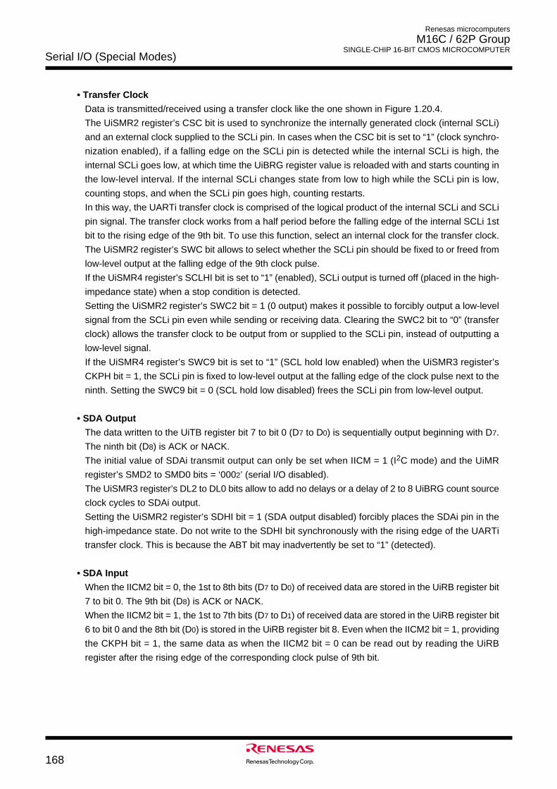
Serial I/O (Special Modes)
168
Renesas microcomputers
M16C / 62P Group SINGLE-CHIP 16-BIT CMOS MICROCOMPUTER
• Transfer Clock
Data is transmitted/received using a transfer clock like the one shown in Figure 1.20.4.
The UiSMR2 register’s CSC bit is used to synchronize the internally generated clock (internal SCLi)
and an external clock supplied to the SCLi pin. In cases when the CSC bit is set to “1” (clock synchro-
nization enabled), if a falling edge on the SCLi pin is detected while the internal SCLi is high, the
internal SCLi goes low, at which time the UiBRG register value is reloaded with and starts counting in
the low-level interval. If the internal SCLi changes state from low to high while the SCLi pin is low,
counting stops, and when the SCLi pin goes high, counting restarts.
In this way, the UARTi transfer clock is comprised of the logical product of the internal SCLi and SCLi
pin signal. The transfer clock works from a half period before the falling edge of the internal SCLi 1st
bit to the rising edge of the 9th bit. To use this function, select an internal clock for the transfer clock.
The UiSMR2 register’s SWC bit allows to select whether the SCLi pin should be fixed to or freed from
low-level output at the falling edge of the 9th clock pulse.
If the UiSMR4 register’s SCLHI bit is set to “1” (enabled), SCLi output is turned off (placed in the high-
impedance state) when a stop condition is detected.
Setting the UiSMR2 register’s SWC2 bit = 1 (0 output) makes it possible to forcibly output a low-level
signal from the SCLi pin even while sending or receiving data. Clearing the SWC2 bit to “0” (transfer
clock) allows the transfer clock to be output from or supplied to the SCLi pin, instead of outputting a
low-level signal.
If the UiSMR4 register’s SWC9 bit is set to “1” (SCL hold low enabled) when the UiSMR3 register’s
CKPH bit = 1, the SCLi pin is fixed to low-level output at the falling edge of the clock pulse next to the
ninth. Setting the SWC9 bit = 0 (SCL hold low disabled) frees the SCLi pin from low-level output.
• SDA Output
The data written to the UiTB register bit 7 to bit 0 (D7 to D0) is sequentially output beginning with D7.
The ninth bit (D8) is ACK or NACK.
The initial value of SDAi transmit output can only be set when IICM = 1 (I2C mode) and the UiMR
register’s SMD2 to SMD0 bits = ‘0002’ (serial I/O disabled).
The UiSMR3 register’s DL2 to DL0 bits allow to add no delays or a delay of 2 to 8 UiBRG count source
clock cycles to SDAi output.
Setting the UiSMR2 register’s SDHI bit = 1 (SDA output disabled) forcibly places the SDAi pin in the
high-impedance state. Do not write to the SDHI bit synchronously with the rising edge of the UARTi
transfer clock. This is because the ABT bit may inadvertently be set to “1” (detected).
• SDA Input
When the IICM2 bit = 0, the 1st to 8th bits (D7 to D0) of received data are stored in the UiRB register bit
7 to bit 0. The 9th bit (D8) is ACK or NACK.
When the IICM2 bit = 1, the 1st to 7th bits (D7 to D1) of received data are stored in the UiRB register bit
6 to bit 0 and the 8th bit (D0) is stored in the UiRB register bit 8. Even when the IICM2 bit = 1, providing
the CKPH bit = 1, the same data as when the IICM2 bit = 0 can be read out by reading the UiRB
register after the rising edge of the corresponding clock pulse of 9th bit.
Serial I/O (Special Modes)
169
Renesas microcomputers
M16C / 62P Group SINGLE-CHIP 16-BIT CMOS MICROCOMPUTER
• ACK and NACK
If the STSPSEL bit in the UiSMR4 register is set to “0” (start and stop conditions not generated) and
the ACKC bit in the UiSMR4 register is se to “1” (ACK data output), the value of the ACKD bit in the
UiSMR4 register is output from the SDAi pin.
If the IICM2 bit = 0, a NACK interrupt request is generated if the SDAi pin remains high at the rising
edge of the 9th bit of transmit clock pulse. An ACK interrupt request is generated if the SDAi pin is low
at the rising edge of the 9th bit of transmit clock pulse.
If ACKi is selected for the cause of DMA1 request, a DMA transfer can be activated by detection of an
acknowledge.
• Initialization of Transmission/Reception
If a start condition is detected while the STAC bit = 1 (UARTi initialization enabled), the serial I/O
operates as described below.
- The transmit shift register is initialized, and the content of the UiTB register is transferred to the
transmit shift register. In this way, the serial I/O starts sending data synchronously with the next
clock pulse applied. However, the UARTi output value does not change state and remains the same
as when a start condition was detected until the first bit of data is output synchronously with the input
clock.
- The receive shift register is initialized, and the serial I/O starts receiving data synchronously with the
next clock pulse applied.
- The SWC bit is set to “1” (SCL wait output enabled). Consequently, the SCLi pin is pulled low at the
falling edge of the ninth clock pulse.
Note that when UARTi transmission/reception is started using this function, the TI does not change
state. Note also that when using this function, the selected transfer clock should be an external clock.
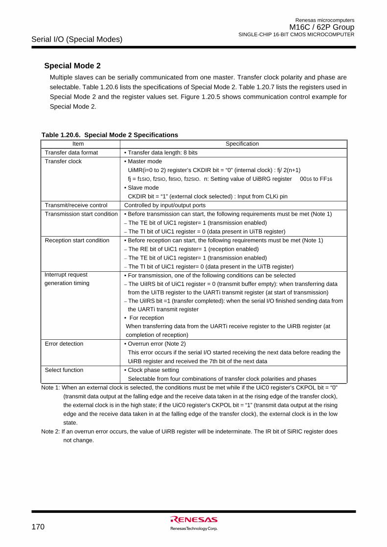
Serial I/O (Special Modes)
170
Renesas microcomputers
M16C / 62P Group SINGLE-CHIP 16-BIT CMOS MICROCOMPUTER
Special Mode 2Multiple slaves can be serially communicated from one master. Transfer clock polarity and phase are
selectable. Table 1.20.6 lists the specifications of Special Mode 2. Table 1.20.7 lists the registers used in
Special Mode 2 and the register values set. Figure 1.20.5 shows communication control example for
Special Mode 2.
Table 1.20.6. Special Mode 2 SpecificationsItem Specification
Transfer data format • Transfer data length: 8 bits
Transfer clock • Master mode
UiMR(i=0 to 2) register’s CKDIR bit = “0” (internal clock) : fj/ 2(n+1)
fj = f1SIO, f2SIO, f8SIO, f32SIO. n: Setting value of UiBRG register 0016 to FF16
• Slave mode
CKDIR bit = “1” (external clock selected) : Input from CLKi pin
Transmit/receive control Controlled by input/output ports
Transmission start condition • Before transmission can start, the following requirements must be met (Note 1)_ The TE bit of UiC1 register= 1 (transmission enabled)_ The TI bit of UiC1 register = 0 (data present in UiTB register)
Reception start condition • Before reception can start, the following requirements must be met (Note 1)_ The RE bit of UiC1 register= 1 (reception enabled)_ The TE bit of UiC1 register= 1 (transmission enabled)_ The TI bit of UiC1 register= 0 (data present in the UiTB register)
• For transmission, one of the following conditions can be selected_ The UiIRS bit of UiC1 register = 0 (transmit buffer empty): when transferring data
from the UiTB register to the UARTi transmit register (at start of transmission)_ The UiIRS bit =1 (transfer completed): when the serial I/O finished sending data from
the UARTi transmit register
• For reception When transferring data from the UARTi receive register to the UiRB register (at
completion of reception)
Error detection • Overrun error (Note 2)
This error occurs if the serial I/O started receiving the next data before reading the
UiRB register and received the 7th bit of the next data
Select function • Clock phase setting
Selectable from four combinations of transfer clock polarities and phases
Note 1: When an external clock is selected, the conditions must be met while if the UiC0 register’s CKPOL bit = “0”
(transmit data output at the falling edge and the receive data taken in at the rising edge of the transfer clock),
the external clock is in the high state; if the UiC0 register’s CKPOL bit = “1” (transmit data output at the rising
edge and the receive data taken in at the falling edge of the transfer clock), the external clock is in the low
state.
Note 2: If an overrun error occurs, the value of UiRB register will be indeterminate. The IR bit of SiRIC register does
not change.
Interrupt request
generation timing
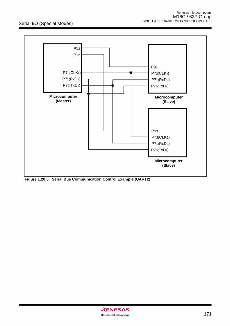
Serial I/O (Special Modes)
171
Renesas microcomputers
M16C / 62P Group SINGLE-CHIP 16-BIT CMOS MICROCOMPUTER
P13
P12
P70(TxD2)
P72(CLK2)
P71(RxD2)
P93
P70(TxD2)
P72(CLK2)
P71(RxD2)
P93
P70(TxD2)
P72(CLK2)
P71(RxD2)
Microcomputer (Master)
Microcomputer (Slave)
Microcomputer (Slave)
Figure 1.20.5. Serial Bus Communication Control Example (UART2)
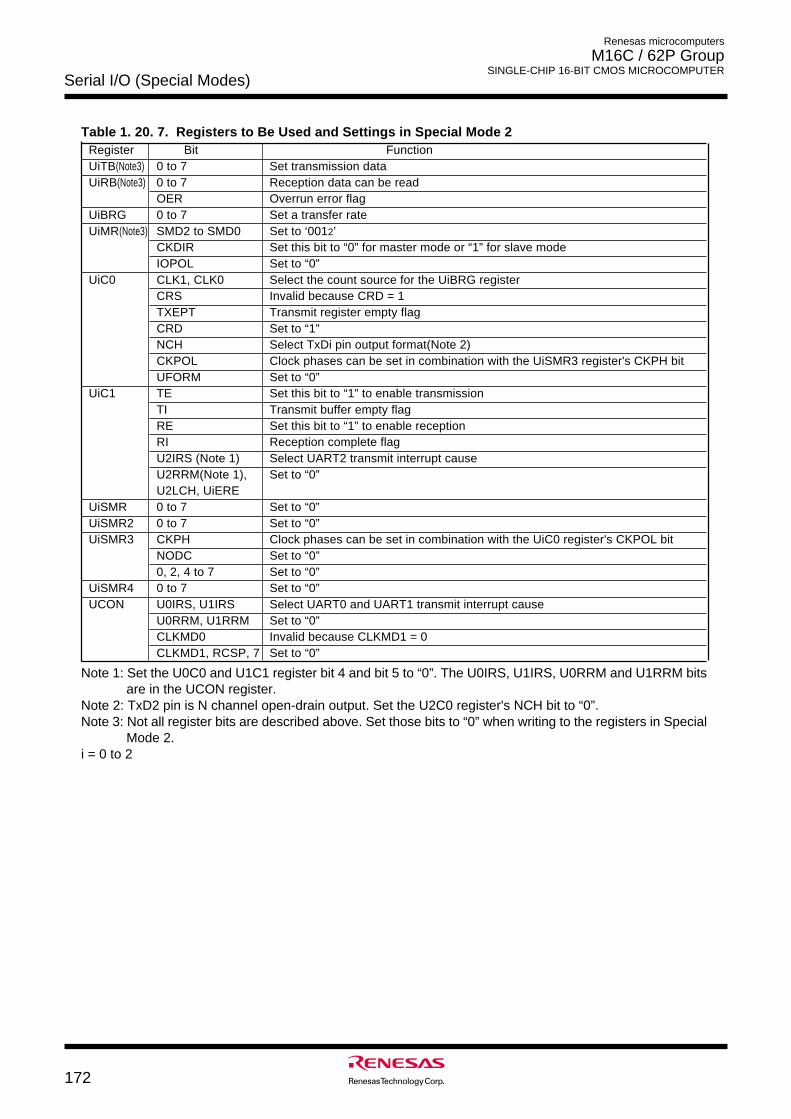
Serial I/O (Special Modes)
172
Renesas microcomputers
M16C / 62P Group SINGLE-CHIP 16-BIT CMOS MICROCOMPUTER
Table 1. 20. 7. Registers to Be Used and Settings in Special Mode 2Register Bit FunctionUiTB(Note3) 0 to 7 Set transmission dataUiRB(Note3) 0 to 7 Reception data can be read
OER Overrun error flagUiBRG 0 to 7 Set a transfer rateUiMR(Note3) SMD2 to SMD0 Set to ‘0012’
CKDIR Set this bit to “0” for master mode or “1” for slave modeIOPOL Set to “0”
UiC0 CLK1, CLK0 Select the count source for the UiBRG registerCRS Invalid because CRD = 1TXEPT Transmit register empty flagCRD Set to “1”NCH Select TxDi pin output format(Note 2)CKPOL Clock phases can be set in combination with the UiSMR3 register's CKPH bitUFORM Set to “0”
UiC1 TE Set this bit to “1” to enable transmissionTI Transmit buffer empty flagRE Set this bit to “1” to enable receptionRI Reception complete flagU2IRS (Note 1) Select UART2 transmit interrupt causeU2RRM(Note 1), Set to “0”U2LCH, UiERE
UiSMR 0 to 7 Set to “0”UiSMR2 0 to 7 Set to “0”UiSMR3 CKPH Clock phases can be set in combination with the UiC0 register's CKPOL bit
NODC Set to “0”0, 2, 4 to 7 Set to “0”
UiSMR4 0 to 7 Set to “0”UCON U0IRS, U1IRS Select UART0 and UART1 transmit interrupt cause
U0RRM, U1RRM Set to “0”CLKMD0 Invalid because CLKMD1 = 0CLKMD1, RCSP, 7 Set to “0”
Note 1: Set the U0C0 and U1C1 register bit 4 and bit 5 to “0”. The U0IRS, U1IRS, U0RRM and U1RRM bitsare in the UCON register.
Note 2: TxD2 pin is N channel open-drain output. Set the U2C0 register's NCH bit to “0”.Note 3: Not all register bits are described above. Set those bits to “0” when writing to the registers in Special
Mode 2.i = 0 to 2
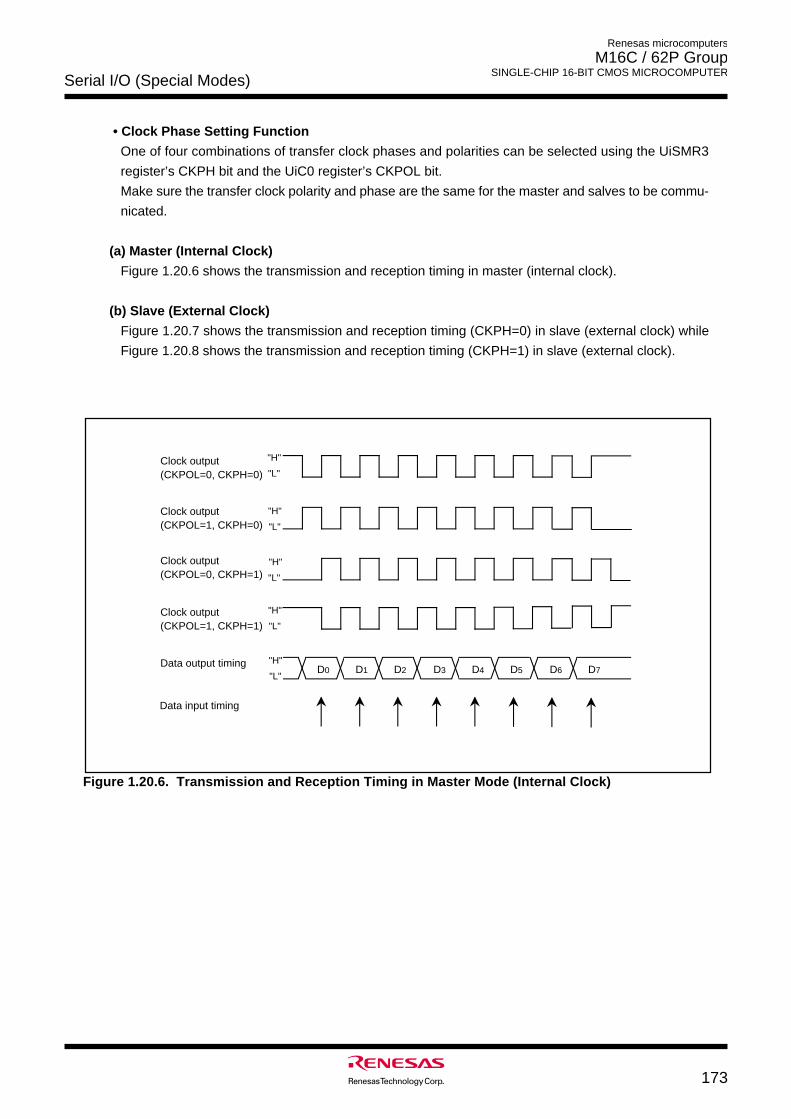
Serial I/O (Special Modes)
173
Renesas microcomputers
M16C / 62P Group SINGLE-CHIP 16-BIT CMOS MICROCOMPUTER
• Clock Phase Setting Function
One of four combinations of transfer clock phases and polarities can be selected using the UiSMR3
register’s CKPH bit and the UiC0 register’s CKPOL bit.
Make sure the transfer clock polarity and phase are the same for the master and salves to be commu-
nicated.
(a) Master (Internal Clock)
Figure 1.20.6 shows the transmission and reception timing in master (internal clock).
(b) Slave (External Clock)
Figure 1.20.7 shows the transmission and reception timing (CKPH=0) in slave (external clock) while
Figure 1.20.8 shows the transmission and reception timing (CKPH=1) in slave (external clock).
Data output timing
Data input timing
D0 D1 D2 D3 D4 D6 D7D5
Clock output(CKPOL=0, CKPH=0)
"H"
"L"
Clock output(CKPOL=1, CKPH=0)
"H"
"L"
Clock output(CKPOL=0, CKPH=1)
"H"
"L"
Clock output(CKPOL=1, CKPH=1)
"H"
"L"
"H"
"L"
Figure 1.20.6. Transmission and Reception Timing in Master Mode (Internal Clock)
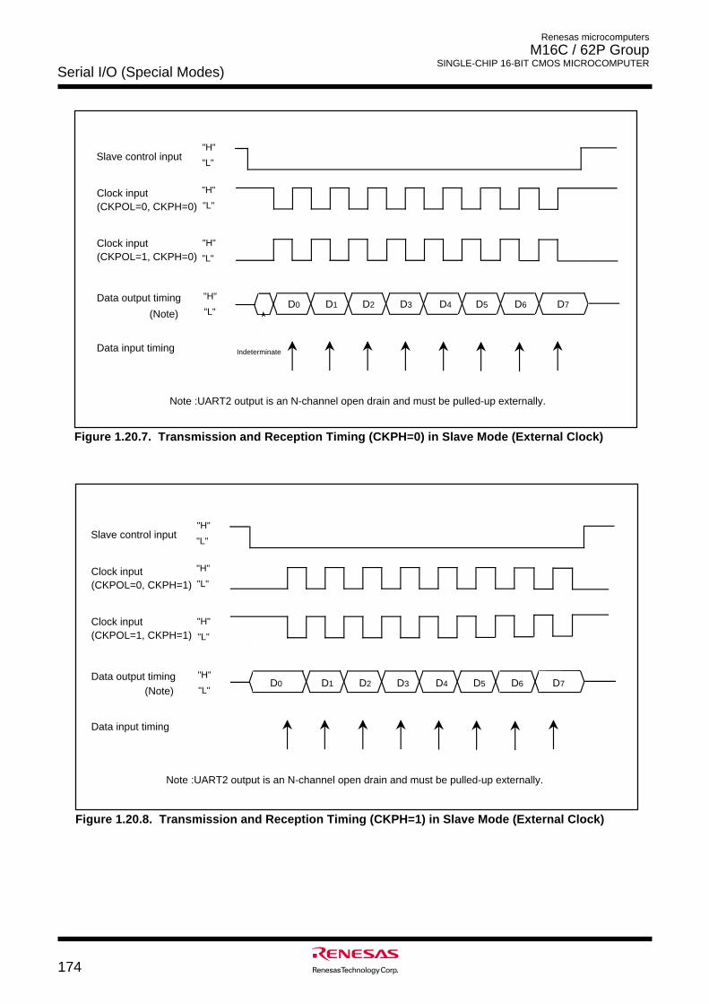
Serial I/O (Special Modes)
174
Renesas microcomputers
M16C / 62P Group SINGLE-CHIP 16-BIT CMOS MICROCOMPUTER
Figure 1.20.7. Transmission and Reception Timing (CKPH=0) in Slave Mode (External Clock)
Figure 1.20.8. Transmission and Reception Timing (CKPH=1) in Slave Mode (External Clock)
Slave control input
Clock input(CKPOL=0, CKPH=0)
Clock input(CKPOL=1, CKPH=0)
Data output timing
Data input timing
"H"
"L"
"H"
"L"
"H"
"L"
"H"
"L"D0 D1 D2 D3 D4 D6 D7D5
Indeterminate
Note :UART2 output is an N-channel open drain and must be pulled-up externally.
(Note)
Clock input(CKPOL=0, CKPH=1)
Clock input(CKPOL=1, CKPH=1)
Data output timing
Data input timing
"H"
"L"
"H"
"L"
"H"
"L"
"H"
"L"D0 D1 D2 D3 D6 D7D4 D5
Note :UART2 output is an N-channel open drain and must be pulled-up externally.
(Note)
Slave control input
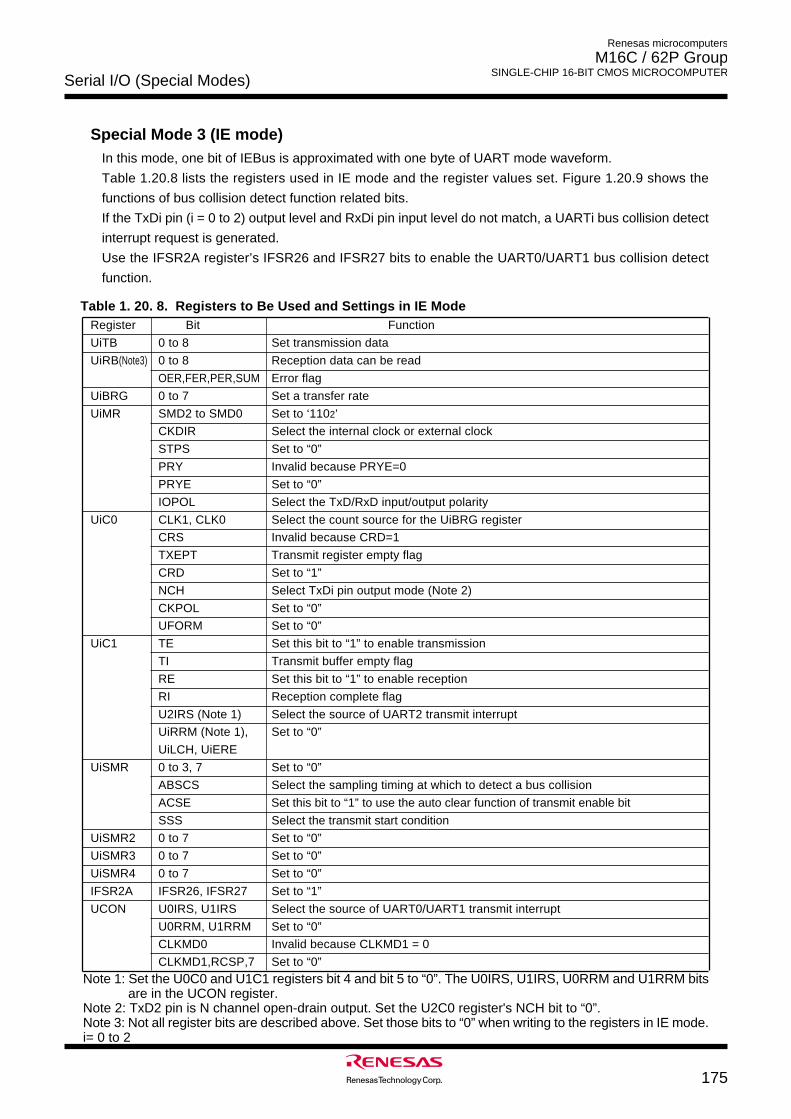
Serial I/O (Special Modes)
175
Renesas microcomputers
M16C / 62P Group SINGLE-CHIP 16-BIT CMOS MICROCOMPUTER
Special Mode 3 (IE mode)In this mode, one bit of IEBus is approximated with one byte of UART mode waveform.
Table 1.20.8 lists the registers used in IE mode and the register values set. Figure 1.20.9 shows the
functions of bus collision detect function related bits.
If the TxDi pin (i = 0 to 2) output level and RxDi pin input level do not match, a UARTi bus collision detect
interrupt request is generated.
Use the IFSR2A register’s IFSR26 and IFSR27 bits to enable the UART0/UART1 bus collision detect
function.
Table 1. 20. 8. Registers to Be Used and Settings in IE ModeRegister Bit Function
UiTB 0 to 8 Set transmission data
UiRB(Note3) 0 to 8 Reception data can be read
OER,FER,PER,SUM Error flag
UiBRG 0 to 7 Set a transfer rate
UiMR SMD2 to SMD0 Set to ‘1102’
CKDIR Select the internal clock or external clock
STPS Set to “0”
PRY Invalid because PRYE=0
PRYE Set to “0”
IOPOL Select the TxD/RxD input/output polarity
UiC0 CLK1, CLK0 Select the count source for the UiBRG register
CRS Invalid because CRD=1
TXEPT Transmit register empty flag
CRD Set to “1”
NCH Select TxDi pin output mode (Note 2)
CKPOL Set to “0”
UFORM Set to “0”
UiC1 TE Set this bit to “1” to enable transmission
TI Transmit buffer empty flag
RE Set this bit to “1” to enable reception
RI Reception complete flag
U2IRS (Note 1) Select the source of UART2 transmit interrupt
UiRRM (Note 1), Set to “0”
UiLCH, UiERE
UiSMR 0 to 3, 7 Set to “0”
ABSCS Select the sampling timing at which to detect a bus collision
ACSE Set this bit to “1” to use the auto clear function of transmit enable bit
SSS Select the transmit start condition
UiSMR2 0 to 7 Set to “0”
UiSMR3 0 to 7 Set to “0”
UiSMR4 0 to 7 Set to “0”
IFSR2A IFSR26, IFSR27 Set to “1”
UCON U0IRS, U1IRS Select the source of UART0/UART1 transmit interrupt
U0RRM, U1RRM Set to “0”
CLKMD0 Invalid because CLKMD1 = 0
CLKMD1,RCSP,7 Set to “0”
Note 1: Set the U0C0 and U1C1 registers bit 4 and bit 5 to “0”. The U0IRS, U1IRS, U0RRM and U1RRM bitsare in the UCON register.
Note 2: TxD2 pin is N channel open-drain output. Set the U2C0 register's NCH bit to “0”.Note 3: Not all register bits are described above. Set those bits to “0” when writing to the registers in IE mode.i= 0 to 2
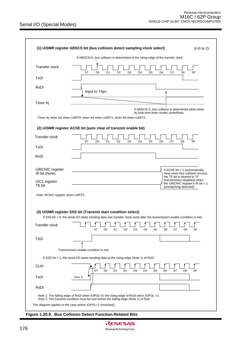
Serial I/O (Special Modes)
176
Renesas microcomputers
M16C / 62P Group SINGLE-CHIP 16-BIT CMOS MICROCOMPUTER
(2) UiSMR register ACSE bit (auto clear of transmit enable bit)
(1) UiSMR register ABSCS bit (bus collision detect sampling clock select)
If ABSCS=0, bus collision is determined at the rising edge of the transfer clock
Transfer clock
Timer Aj
(3) UiSMR register SSS bit (Transmit start condition select)
Transmission enable condition is met
If SSS bit = 1, the serial I/O starts sending data at the rising edge (Note 1) of RxDi
TxDi
CLKi
TxDi
RxDi
TxDi
RxDi
ST D0 D1 D2 D3 D4 D5 D6 D7 D8 SP
Input to TAjIN
If ABSCS=1, bus collision is determined when timer Aj (one-shot timer mode) underflows.
TxDi
RxDi
ST D0 D1 D2 D3 D4 D5 D6 D7 D8 SP
ST D0 D1 D2 D3 D4 D5 D6 D7 D8 SP
ST D0 D1 D2 D3 D4 D5 D6 D7 D8 SP
(i=0 to 2)
Timer Aj: timer A3 when UART0; timer A4 when UART1; timer A0 when UART2
Transfer clock
UiBCNIC registerIR bit (Note)
UiC1 registerTE bit
Note: BCNIC register when UART2.
If ACSE bit = 1 (automatically clear when bus collision occurs), the TE bit is cleared to “0”(transmission disabled) when the UiBCNIC register’s IR bit = 1(unmatching detected).
If SSS bit = 0, the serial I/O starts sending data one transfer clock cycle after the transmission enable condition is met.
Transfer clock
(Note 2)
Note 1: The falling edge of RxDi when IOPOL=0; the rising edge of RxDi when IOPOL =1.Note 2: The transmit condition must be met before the falling edge (Note 1) of RxD.
This diagram applies to the case where IOPOL=1 (reversed).
Figure 1.20.9. Bus Collision Detect Function-Related Bits
Serial I/O (Special Modes)
177
Renesas microcomputers
M16C / 62P Group SINGLE-CHIP 16-BIT CMOS MICROCOMPUTER
Item Specification
Transfer data format • Direct format• Inverse format
Transfer clock • U2MR register’s CKDIR bit = “0” (internal clock) : fi/ 16(n+1)
fi = f1SIO, f2SIO, f8SIO, f32SIO. n: Setting value of U2BRG register 0016 to FF16
• CKDIR bit = “1” (external clock) : fEXT/16(n+1)fEXT: Input from CLK2 pin. n: Setting value of U2BRG register 0016 to FF16
Transmission start condition • Before transmission can start, the following requirements must be met_ The TE bit of U2C1 register= 1 (transmission enabled)_ The TI bit of U2C1 register = 0 (data present in U2TB register)
Reception start condition • Before reception can start, the following requirements must be met_ The RE bit of U2C1 register= 1 (reception enabled)_ Start bit detection
• For transmissionWhen the serial I/O finished sending data from the U2TB transfer register (U2IRS bit =1)
• For receptionWhen transferring data from the UART2 receive register to the U2RB register (at
completion of reception)Error detection • Overrun error (Note 1)
This error occurs if the serial I/O started receiving the next data before reading the
U2RB register and received the bit one before the last stop bit of the next data• Framing error
This error occurs when the number of stop bits set is not detected
• Parity errorDuring reception, if a parity error is detected, parity error signal is output from theTxD2 pin.
During transmission, a parity error is detected by the level of input to the RXD2 pinwhen a transmission interrupt occurs
• Error sum flag
This flag is set (= 1) when any of the overrun, framing, and parity errors is encountered
Special Mode 4 (SIM Mode) (UART2)
Based on UART mode, this is an SIM interface compatible mode. Direct and inverse formats can be
implemented, and this mode allows to output a low from the TxD2 pin when a parity error is detected.
Tables 1.20.9 lists the specifications of SIM mode. Table 1.20.10 lists the registers used in the SIM mode
and the register values set.
Table 1.20.9. SIM Mode Specifications
Interrupt request
generation timing(Note 2)
Note 1: If an overrun error occurs, the value of U2RB register will be indeterminate. The IR bit of S2RIC
register does not change.
Note 2: A transmit interrupt request is generated by setting the U2C1 register U2IRS bit to “1” (transmission
complete) and U2ERE bit to “1” (error signal output) after reset. Therefore, when using SIM mode,
be sure to clear the IR bit to “0” (no interrupt request) after setting these bits.
Renesas microcomputers
M16C / 62P Group SINGLE-CHIP 16-BIT CMOS MICROCOMPUTER
Serial I/O (Special Modes)
178
Register Bit Function
U2TB(Note) 0 to 7 Set transmission dataU2RB(Note) 0 to 7 Reception data can be read
OER,FER,PER,SUM Error flagU2BRG 0 to 7 Set a transfer rateU2MR SMD2 to SMD0 Set to ‘1012’
CKDIR Select the internal clock or external clockSTPS Set to “0”PRY Set this bit to “1” for direct format or “0” for inverse formatPRYE Set to “1”
IOPOL Set to “0”
U2C0 CLK1, CLK0 Select the count source for the U2BRG register
CRS Invalid because CRD=1
TXEPT Transmit register empty flag
CRD Set to “1”
NCH Set to “0”
CKPOL Set to “0”
UFORM Set this bit to “0” for direct format or “1” for inverse format
U2C1 TE Set this bit to “1” to enable transmission
TI Transmit buffer empty flag
RE Set this bit to “1” to enable reception
RI Reception complete flag
U2IRS Set to “1”
U2RRM Set to “0”
U2LCH Set this bit to “0” for direct format or “1” for inverse format
U2ERE Set to “1”
U2SMR(Note) 0 to 3 Set to “0”
U2SMR2 0 to 7 Set to “0”
U2SMR3 0 to 7 Set to “0”
U2SMR4 0 to 7 Set to “0”
Table 1. 20. 10. Registers to Be Used and Settings in SIM Mode
Note: Not all register bits are described above. Set those bits to “0” when writing to the registers in SIM mode.
Serial I/O (Special Modes)
179
Renesas microcomputers
M16C / 62P Group SINGLE-CHIP 16-BIT CMOS MICROCOMPUTER
Figure 1.20.10. Transmit and Receive Timing in SIM Mode
Transfer clock
An “L” level is output from TxD2 due to the occurrence of a parity error
Read the U2RB register
Cleared to “0” when interrupt request is accepted, or cleared to “0” in a program
U2C1 registerTE bit
D0 D1 D2 D3 D4 D5 D6 D7ST P
“0”
“1”
“0”
“1”
“0”
“1”
“0”
“1”
D0 D1 D2 D3 D4 D5 D6 D7ST P SP
Tc
SP
D0 D1 D2 D3 D4 D5 D6 D7ST P
TxD2
“0”
“1”
“0”
“1”
“0”
“1”
D0 D1 D2 D3 D4 D5 D6 D7ST P SP
Tc
SP
D0 D1 D2 D3 D4 D5 D6 D7ST P D0 D1 D2 D3 D4 D5 D6 D7ST P
SP
SP
D0 D1 D2 D3 D4 D5 D6 D7ST P D0 D1 D2 D3 D4 D5 D6 D7ST P
SP
SP
TxD2
RxD2 pin level
U2C1 registerTI bit
Parity error signal sent back from receiver
(Note)
U2C0 registerTXEPT bit
S2TIC registerIR bit
Start bit
Parity bit
Stop bit
Write data to U2TB register
Transferred from U2TB register to UART2 transmit register
An “L” level returns due to the occurrence of a parity error.
The level is detected by the interrupt routine.
The level is detected by the interrupt routine.
The IR bit is set to “1” at the falling edge of transfer clock
Note : Because TxD2 and RxD2 are connected, this is composite waveform consisting of the transmitter's transmit waveform and the parity error signal received.
Note : Because TxD2 and RxD2 are connected, this is composite waveform consisting of the TxD2 output and the parity error signal sent back from receiver.
Tc = 16 (n + 1) / fi or 16 (n + 1) / fEXT
fi : frequency of U2BRG count source (f1SIO, f2SIO, f8SIO, f32SIO) fEXT : frequency of U2BRG count source (external clock) n : value set to U2BRG
Tc = 16 (n + 1) / fi or 16 (n + 1) / fEXT
fi : frequency of U2BRG count source (f1SIO, f2SIO, f8SIO, f32SIO) fEXT : frequency of U2BRG count source (external clock) n : value set to U2BRG
The above timing diagram applies to the case where data is transferred in the direct format. • U2MR register STPS bit = 0 (1 stop bit) • U2MR register PRY bit = 1 (even) • U2C0 register UFORM bit = 0 (LSB first) • U2C1 register U2LCH bit = 0 (no reverse) • U2C1 register U2IRSCH bit = 1 (transmit is completed)
Start bit
Parity bit
Stop bit
Cleared to “0” when interrupt request is accepted, or cleared to “0” in a program
Read the U2RB register
(1) Transmission
Transfer clock
U2C1 registerRE bit
RxD2 pin level
Transmitter's transmit waveform
(Note)
U2C0 registerRI bit
S2RIC registerIR bit
(1) Reception
The above timing diagram applies to the case where data is transferred in the direct format. • U2MR register STPS bit = 0 (1 stop bit) • U2MR register PRY bit = 1 (even) • U2C0 register UFORM bit = 0 (LSB first) • U2C1 register U2LCH bit = 0 (no reverse) • U2C1 register U2IRSCH bit = 1 (transmit is completed)
Renesas microcomputers
M16C / 62P Group SINGLE-CHIP 16-BIT CMOS MICROCOMPUTER
Serial I/O (Special Modes)
180
Figure 1.20.11 shows the example of connecting the SIM interface. Connect TXD2 and RXD2 and apply
pull-up.
Figure 1.20.11. SIM Interface Connection
Microcomputer
SIM card
TxD2
RxD2
(a) Parity Error Signal Output
The parity error signal is enabled by setting the U2C1 register’s U2ERE bit to “1”.
• When receiving
The parity error signal is output when a parity error is detected while receiving data. This is achieved
by pulling the TxD2 output low with the timing shown in Figure 1.20.12. If the R2RB register is read
while outputting a parity error signal, the PER bit is cleared to “0” and at the same time the TxD2 output
is returned high.
• When transmitting
A transmission-finished interrupt request is generated at the falling edge of the transfer clock pulse
that immediately follows the stop bit. Therefore, whether a parity signal has been returned can be
determined by reading the port that shares the RxD2 pin in a transmission-finished interrupt service
routine.
Figure 1.20.12. Parity Error Signal Output Timing
ST : Start bitP : Even ParitySP : Stop bit
D0 D1 D2 D3 D4 D5 D6 D7 P SPST
(Note)
Transfer clock
RxD2
TxD2
U2C1 registerRI bit
“H”
“L”
“H”
“L”
“H”
“L”
“1”
“0”
This timing diagram applies to the case where the direct format is implemented.
Note: The output of microcomputer is in the high-impedance state (pulled up externally).
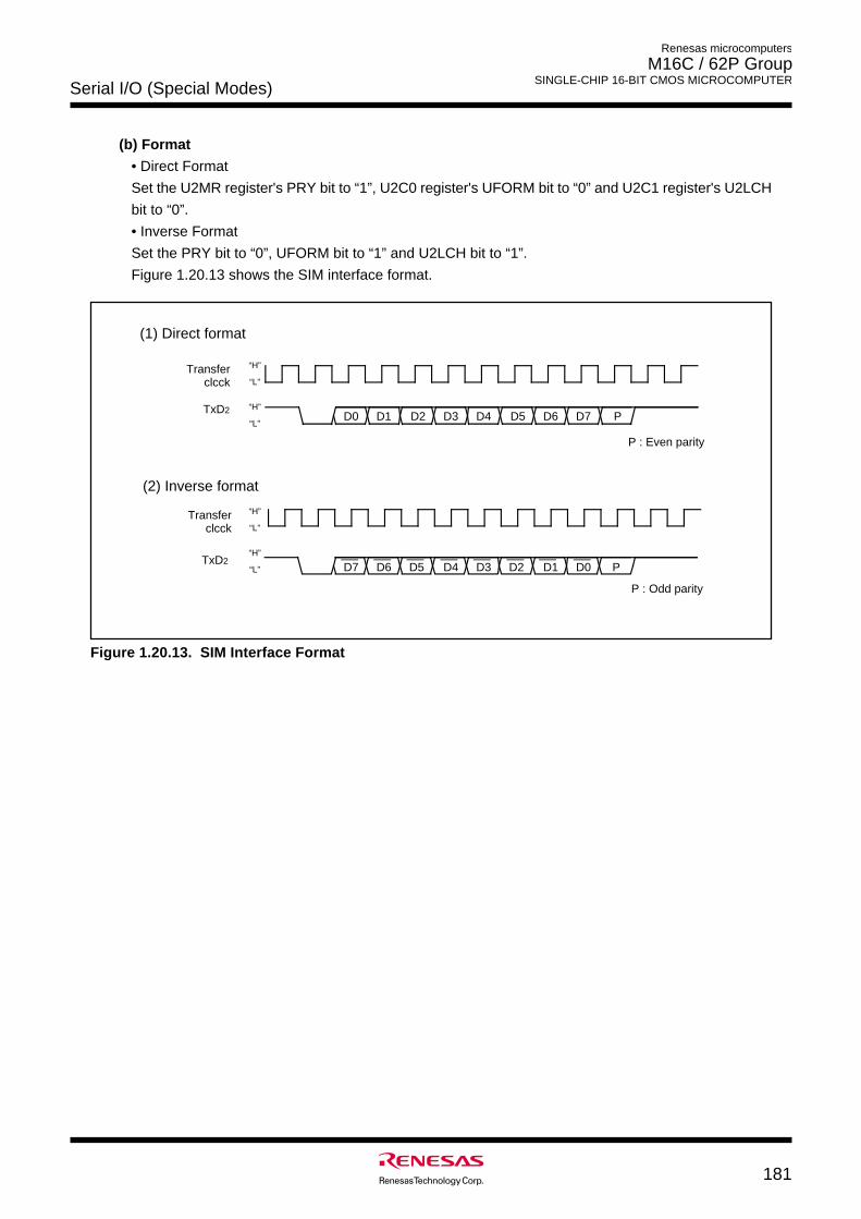
Serial I/O (Special Modes)
181
Renesas microcomputers
M16C / 62P Group SINGLE-CHIP 16-BIT CMOS MICROCOMPUTER
(b) Format
• Direct Format
Set the U2MR register's PRY bit to “1”, U2C0 register's UFORM bit to “0” and U2C1 register's U2LCH
bit to “0”.
• Inverse Format
Set the PRY bit to “0”, UFORM bit to “1” and U2LCH bit to “1”.
Figure 1.20.13 shows the SIM interface format.
Figure 1.20.13. SIM Interface Format
P : Even parity
D0 D1 D2 D3 D4 D5 D6 D7 P
Transfer clcck
TxD2
TxD2D7 D6 D5 D4 D3 D2 D1 D0 P
Transfer clcck
(1) Direct format
“H”
“L”
“H”
“L”
(2) Inverse format
P : Odd parity
“H”
“L”
“H”
“L”
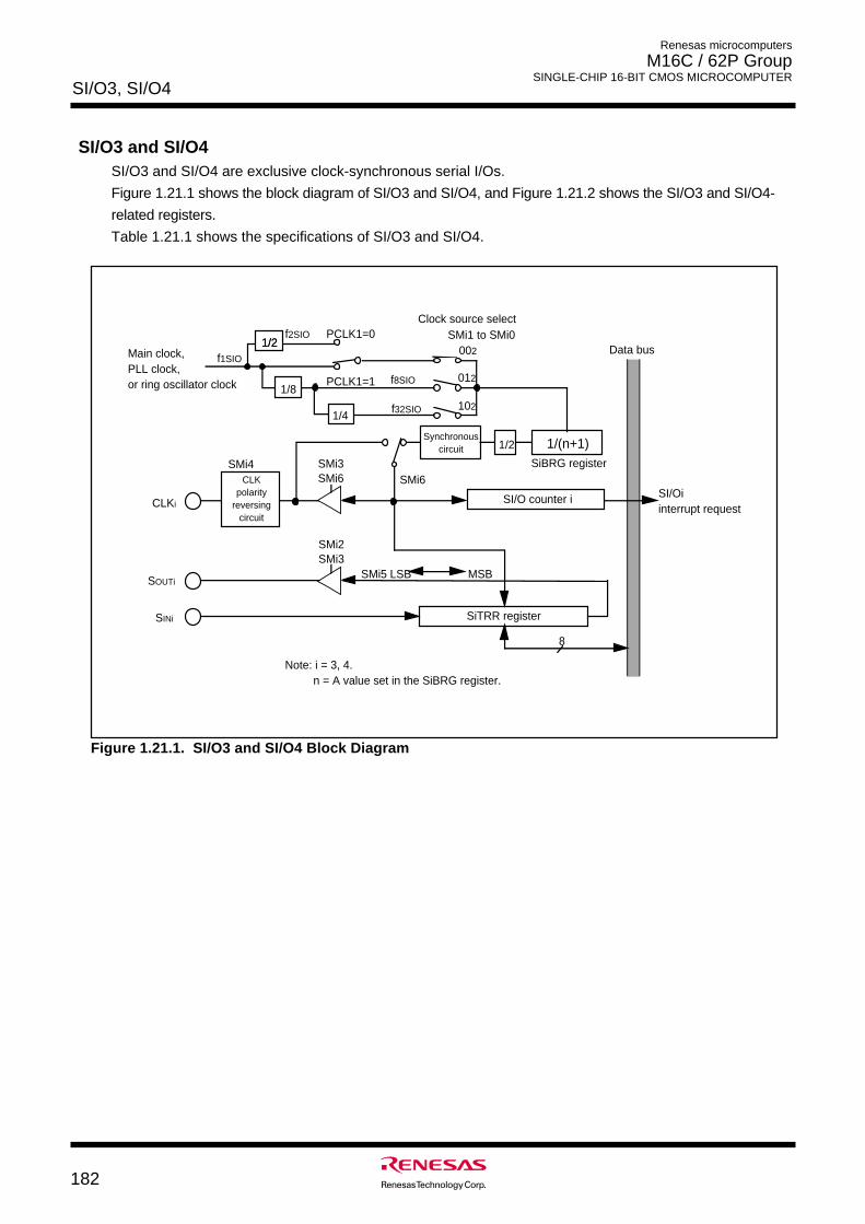
182
Renesas microcomputers
M16C / 62P Group SINGLE-CHIP 16-BIT CMOS MICROCOMPUTER
SI/O3, SI/O4
SI/O3 and SI/O4SI/O3 and SI/O4 are exclusive clock-synchronous serial I/Os.
Figure 1.21.1 shows the block diagram of SI/O3 and SI/O4, and Figure 1.21.2 shows the SI/O3 and SI/O4-
related registers.
Table 1.21.1 shows the specifications of SI/O3 and SI/O4.
Figure 1.21.1. SI/O3 and SI/O4 Block Diagram
Data bus
SI/Oi interrupt request
Note: i = 3, 4. n = A value set in the SiBRG register.
SiTRR register
SI/O counter i
8
SMi5 LSB MSB
SMi2SMi3
SMi3SMi6
SMi1 to SMi0
CLKi
SOUTi
SINi
SiBRG registerSMi6
1/(n+1)1/2
1/2Main clock,PLL clock, or ring oscillator clock
f1SIO
1/2
1/8
1/4
f8SIO
f32SIO
f2SIO PCLK1=0
PCLK1=1
SMi4
002
012
102
Clock source select
Synchronous circuit
CLK polarity
reversing circuit
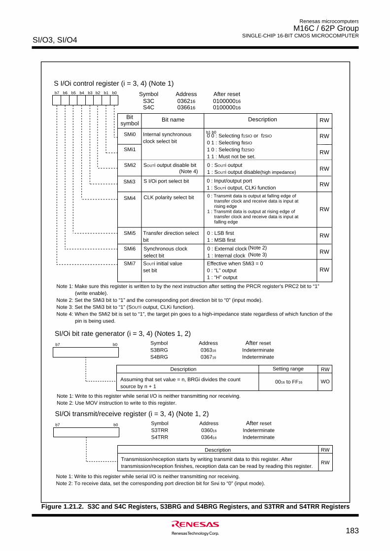
183
Renesas microcomputers
M16C / 62P Group SINGLE-CHIP 16-BIT CMOS MICROCOMPUTER
SI/O3, SI/O4
SI/Oi transmit/receive register (i = 3, 4) (Note 1, 2)
b7 b0 Symbol Address After resetS3TRR 036016 IndeterminateS4TRR 036416 Indeterminate
Description
Transmission/reception starts by writing transmit data to this register. After transmission/reception finishes, reception data can be read by reading this register.
Note 1: Write to this register while serial I/O is neither transmitting nor receiving. Note 2: To receive data, set the corresponding port direction bit for SINi to “0” (input mode).
RW
RW
S I/Oi control register (i = 3, 4) (Note 1)
Symbol Address After resetS3C 036216 010000016S4C 036616 010000016
b7 b6 b5 b4 b3 b2 b1 b0
Description
SMi5
SMi1
SMi0
SMi3
SMi6
SMi7
Internal synchronous clock select bit
Transfer direction select bit
S I/Oi port select bit
SOUTi initial value set bit
0 0 : Selecting f1SIO or f2SIO 0 1 : Selecting f8SIO 1 0 : Selecting f32SIO
1 1 : Must not be set.
b1 b0
0 : External clock 1 : Internal clock
Effective when SMi3 = 00 : “L” output 1 : “H” output
0 : Input/output port 1 : SOUTi output, CLKi function
Bit nameBit symbol
Synchronous clock select bit
0 : LSB first 1 : MSB first
SMi2 SOUTi output disable bit 0 : SOUTi output 1 : SOUTi output disable(high impedance)
Note 1: Make sure this register is written to by the next instruction after setting the PRCR register's PRC2 bit to “1”(write enable).
Note 2: Set the SMi3 bit to “1” and the corresponding port direction bit to “0” (input mode).Note 3: Set the SMi3 bit to “1” (SOUTi output, CLKi function).Note 4: When the SMi2 bit is set to “1”, the target pin goes to a high-impedance state regardless of which function of the
pin is being used.
CLK polarity select bitSMi4 0 : Transmit data is output at falling edge of transfer clock and receive data is input at rising edge
1 : Transmit data is output at rising edge of transfer clock and receive data is input at falling edge
RW
RW
RW
RW
RW
RW
RW
RW
RW
(Note 4)
(Note 2)(Note 3)
SI/Oi bit rate generator (i = 3, 4) (Notes 1, 2)
b7 b0 Symbol Address After resetS3BRG 036316 IndeterminateS4BRG 036716 Indeterminate
Description
Assuming that set value = n, BRGi divides the count source by n + 1
0016 to FF16
Setting range RW
WO
Note 1: Write to this register while serial I/O is neither transmitting nor receiving. Note 2: Use MOV instruction to write to this register.
Figure 1.21.2. S3C and S4C Registers, S3BRG and S4BRG Registers, and S3TRR and S4TRR Registers
184
Renesas microcomputers
M16C / 62P Group SINGLE-CHIP 16-BIT CMOS MICROCOMPUTER
SI/O3, SI/O4
Item Specification
Transfer data format • Transfer data length: 8 bits
Transfer clock • SiC (i=3, 4) register’s SMi6 bit = “1” (internal clock) : fj/ 2(n+1)
fj = f1SIO, f8SIO, f32SIO. n=Setting value of SiBRG register 0016 to FF16.
• SMi6 bit = “0” (external clock) : Input from CLKi pin (Note 1)
Transmission/reception • Before transmission/reception can start, the following requirements must be met
start condition Write transmit data to the SiTRR register (Notes 2, 3)
• When SiC register's SMi4 bit = 0
The rising edge of the last transfer clock pulse (Note 4)
• When SMi4 = 1
The falling edge of the last transfer clock pulse (Note 4)
CLKi pin fucntion I/O port, transfer clock input, transfer clock output
SOUTi pin function I/O port, transmit data output, high-impedance
SINi pin function I/O port, receive data input
Select function • LSB first or MSB first selection
Whether to start sending/receiving data beginning with bit 0 or beginning with bit 7
can be selected
• Function for setting an SOUTi initial value set function
When the SiC register's SMi6 bit = 0 (external clock), the SOUTi pin output level while
not tranmitting can be selected.
• CLK polarity selection
Whether transmit data is output/input timing at the rising edge or falling edge of
transfer clock can be selected.
Note 1: To set the SiC register’s SMi6 bit to “0” (external clock), follow the procedure described below.
• If the SiC register’s SMi4 bit = 0, write transmit data to the SiTRR register while input on the CLKi pin is
high. The same applies when rewriting the SiC register’s SMi7 bit.
• If the SMi4 bit = 1, write transmit data to the SiTRR register while input on the CLKi pin is low. The same
applies when rewriting the SMi7 bit.
• Because shift operation continues as long as the transfer clock is supplied to the SI/Oi circuit, stop the
transfer clock after supplying eight pulses. If the SMi6 bit = 1 (internal clock), the transfer clock automatically
stops.
Note 2: Unlike UART0 to UART2, SI/Oi (i = 3 to 4) is not separated between the transfer register and buffer. There-
fore, do not write the next transmit data to the SiTRR register during transmission.
Note 3: When the SiC register’s SMi6 bit = 1 (internal clock), SOUTi retains the last data for a 1/2 transfer clock period
after completion of transfer and, thereafter, goes to a high-impedance state. However, if transmit data is
written to the SiTRR register during this period, SOUTi immediately goes to a high-impedance state, with the
data hold time thereby reduced.
Note 4: When the SiC register’s SMi6 bit = 1 (internal clock), the transfer clock stops in the high state if the SMi4 bit
= 0, or stops in the low state if the SMi4 bit = 1.
Table 1.21.1. SI/O3 and SI/O4 Specifications
Interrupt request
generation timing
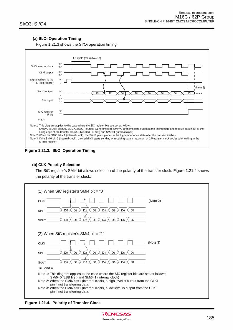
185
Renesas microcomputers
M16C / 62P Group SINGLE-CHIP 16-BIT CMOS MICROCOMPUTER
SI/O3, SI/O4
(a) SI/Oi Operation Timing
Figure 1.21.3 shows the SI/Oi operation timing
D7D0 D1 D2 D3 D4 D5 D6
i= 3, 4
1.5 cycle (max)
SI/Oi internal clock
CLKi output
Signal written to the SiTRR register
SOUTi output
SINi input
SiIC registerIR bit
(Note 2)
Note 1: This diagram applies to the case where the SiC register bits are set as follows:SMi2=0 (SOUTi output), SMi3=1 (SOUTi output, CLKi function), SMi4=0 (transmit data output at the falling edge and receive data input at therising edge of the transfer clock), SMi5=0 (LSB first) and SMi6=1 (internal clock)
Note 2: When the SMi6 bit = 1 (internal clock), the SOUTi pin is placed in the high-impedance state after the transfer finishes.Note 3: If the SMi6 bit=0 (internal clock), the serial I/O starts sending or receiving data a maximum of 1.5 transfer clock cycles after writing to the
SiTRR register.
"H""L"
"H""L"
"H""L"
"H""L"
"H""L"
"1""0"
(Note 3)
Figure 1.21.3. SI/Oi Operation Timing
(b) CLK Polarity Selection
The SiC register's SMi4 bit allows selection of the polarity of the transfer clock. Figure 1.21.4 shows
the polarity of the transfer clock.
Figure 1.21.4. Polarity of Transfer Clock
(2) When SiC register's SMi4 bit = “1”
(Note 3)
D1 D2 D3 D4 D5 D6 D7
D1 D2 D3 D4 D5 D6 D7
D0
D0
SINi
SOUTi
CLKi
(1) When SiC register's SMi4 bit = “0”
Note 1: This diagram applies to the case where the SiC register bits are set as follows:SMi5=0 (LSB first) and SMi6=1 (internal clock)
Note 2: When the SMi6 bit=1 (internal clock), a high level is output from the CLKi pin if not transferring data.Note 3: When the SMi6 bit=1 (internal clock), a low level is output from the CLKi pin if not transferring data.
D1 D2 D3 D4 D5 D6 D7D0
D1 D2 D3 D4 D5 D6 D7D0
SINi
SOUTi
CLKi (Note 2)
i=3 and 4
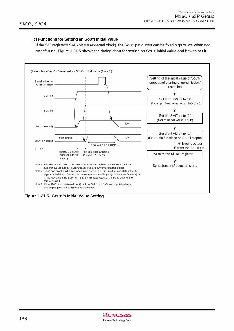
186
Renesas microcomputers
M16C / 62P Group SINGLE-CHIP 16-BIT CMOS MICROCOMPUTER
SI/O3, SI/O4
(c) Functions for Setting an SOUTi Initial Value
If the SiC register’s SMi6 bit = 0 (external clock), the SOUTi pin output can be fixed high or low when not
transferring. Figure 1.21.5 shows the timing chart for setting an SOUTi initial value and how to set it.
Figure 1.21.5. SOUTi’s Initial Value Setting
Setting of the initial value of SOUTi output and starting of transmission/
reception
Set the SMi3 bit to “0” (SOUTi pin functions as an I/O port)
Write to the SiTRR register
Serial transmit/reception starts
Set the SMi7 bit to “1” (SOUTi initial value = “H”)
Set the SMi3 bit to “1” (SOUTi pin functions as SOUTi output)
“H” level is output from the SOUTi pin
Signal written to SiTRR register
SOUTi (internal)
SMi7 bit
SOUTi pin output
SMi3 bit
Setting the SOUTi initial value to “H”
Port selection switching(I/O port SOUTi)
D0
(i = 3, 4)
Initial value = “H” (Note 3)
Port output D0
(Example) When “H” selected for SOUTi initial value (Note 1)
Note 1: This diagram applies to the case where the SiC register bits are set as follows:SMi2=0 (SOUTi output), SMi5=0 (LSB first) and SMi6=0 (external clock)
Note 2: SOUTi can only be initialized when input on the CLKi pin is in the high state if the SiCregister’s SMi4 bit = 0 (transmit data output at the falling edge of the transfer clock) orin the low state if the SMi4 bit = 1 (transmit data output at the rising edge of the transfer clock).
Note 3: If the SMi6 bit = 1 (internal clock) or if the SMi2 bit = 1 (SOUT output disabled), this output goes to the high-impedance state.
(Note 2)
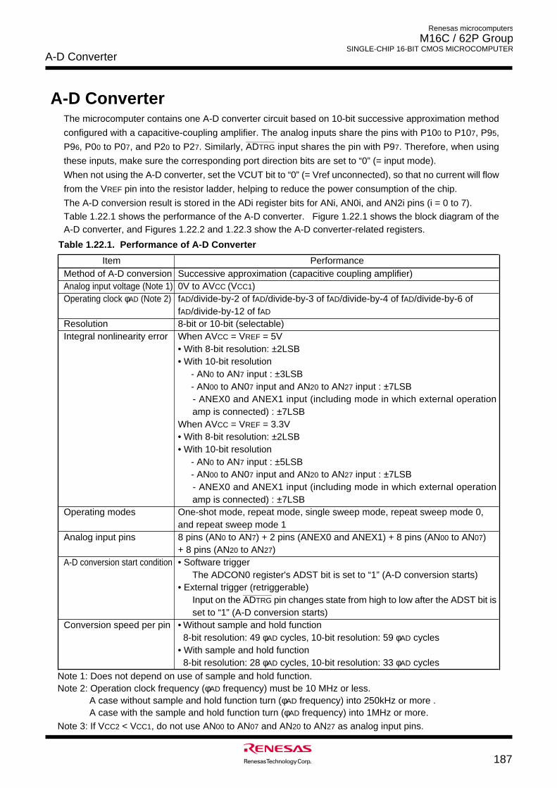
A-D Converter
187
Renesas microcomputers
M16C / 62P Group SINGLE-CHIP 16-BIT CMOS MICROCOMPUTER
Item PerformanceMethod of A-D conversion Successive approximation (capacitive coupling amplifier)Analog input voltage (Note 1) 0V to AVCC (VCC1)Operating clock φAD (Note 2) fAD/divide-by-2 of fAD/divide-by-3 of fAD/divide-by-4 of fAD/divide-by-6 of
fAD/divide-by-12 of fAD
Resolution 8-bit or 10-bit (selectable)Integral nonlinearity error When AVCC = VREF = 5V
• With 8-bit resolution: ±2LSB• With 10-bit resolution
- AN0 to AN7 input : ±3LSB - AN00 to AN07 input and AN20 to AN27 input : ±7LSB
- ANEX0 and ANEX1 input (including mode in which external operationamp is connected) : ±7LSB
When AVCC = VREF = 3.3V• With 8-bit resolution: ±2LSB• With 10-bit resolution
- AN0 to AN7 input : ±5LSB - AN00 to AN07 input and AN20 to AN27 input : ±7LSB
- ANEX0 and ANEX1 input (including mode in which external operationamp is connected) : ±7LSB
Operating modes One-shot mode, repeat mode, single sweep mode, repeat sweep mode 0,and repeat sweep mode 1
Analog input pins 8 pins (AN0 to AN7) + 2 pins (ANEX0 and ANEX1) + 8 pins (AN00 to AN07)+ 8 pins (AN20 to AN27)
A-D conversion start condition • Software triggerThe ADCON0 register's ADST bit is set to “1” (A-D conversion starts)
• External trigger (retriggerable)___________
Input on the ADTRG pin changes state from high to low after the ADST bit isset to “1” (A-D conversion starts)
Conversion speed per pin • Without sample and hold function8-bit resolution: 49 φAD cycles, 10-bit resolution: 59 φAD cycles
• With sample and hold function8-bit resolution: 28 φAD cycles, 10-bit resolution: 33 φAD cycles
A-D ConverterThe microcomputer contains one A-D converter circuit based on 10-bit successive approximation method
configured with a capacitive-coupling amplifier. The analog inputs share the pins with P100 to P107, P95,___________
P96, P00 to P07, and P20 to P27. Similarly, ADTRG input shares the pin with P97. Therefore, when using
these inputs, make sure the corresponding port direction bits are set to “0” (= input mode).
When not using the A-D converter, set the VCUT bit to “0” (= Vref unconnected), so that no current will flow
from the VREF pin into the resistor ladder, helping to reduce the power consumption of the chip.
The A-D conversion result is stored in the ADi register bits for ANi, AN0i, and AN2i pins (i = 0 to 7).Table 1.22.1 shows the performance of the A-D converter. Figure 1.22.1 shows the block diagram of theA-D converter, and Figures 1.22.2 and 1.22.3 show the A-D converter-related registers.
Table 1.22.1. Performance of A-D Converter
Note 1: Does not depend on use of sample and hold function.Note 2: Operation clock frequency (φAD frequency) must be 10 MHz or less.
A case without sample and hold function turn (φAD frequency) into 250kHz or more .A case with the sample and hold function turn (φAD frequency) into 1MHz or more.
Note 3: If VCC2 < VCC1, do not use AN00 to AN07 and AN20 to AN27 as analog input pins.
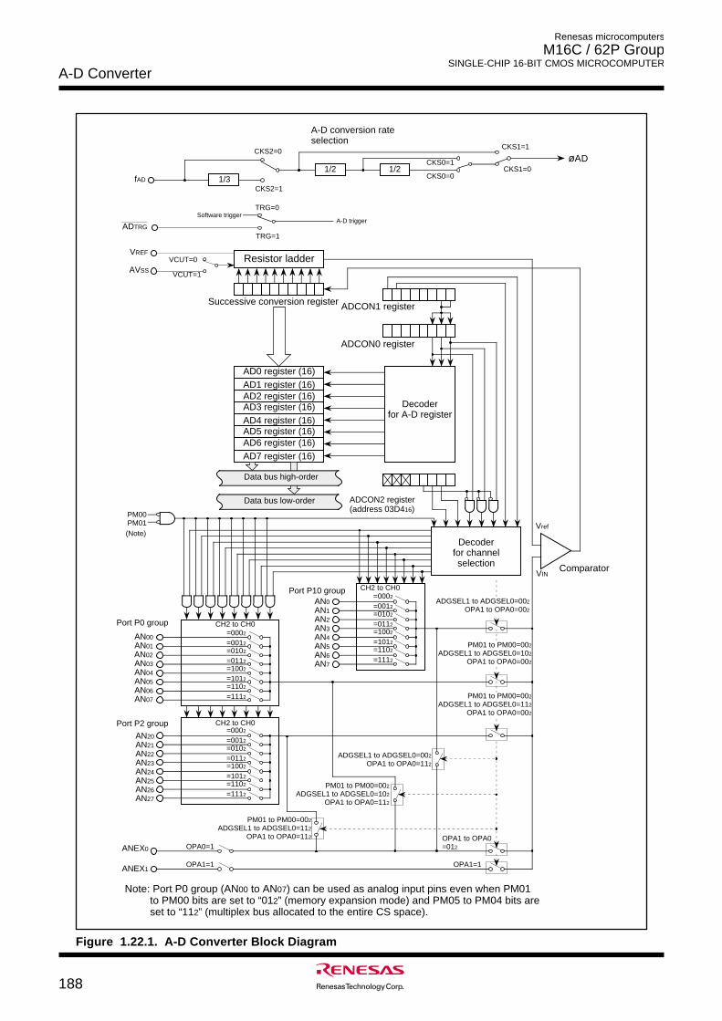
Renesas microcomputers
M16C / 62P Group SINGLE-CHIP 16-BIT CMOS MICROCOMPUTER
A-D Converter
188
Figure 1.22.1. A-D Converter Block Diagram
ANEX0
ANEX1
OPA0=1
OPA1=1
PM01 to PM00=002
ADGSEL1 to ADGSEL0=102
OPA1 to OPA0=112
ADGSEL1 to ADGSEL0=002
OPA1 to OPA0=112
=0002
=0012
=0102
=0112
=1002
=1012
=1102
=1112
AN0AN1AN2AN3AN4AN5AN6AN7
AN00AN01AN02AN03AN04AN05AN06AN07
Vref
VIN
CH2 to CH0
PM00PM01
Decoderfor channel selection
AD0 register (16)
Data bus low-order
VREF
AVSS
VCUT=0
VCUT=1
Data bus high-order
OPA1=1
Port P10 group
Port P0 group
PM01 to PM00=002
ADGSEL1 to ADGSEL0=102
OPA1 to OPA0=002
ADGSEL1 to ADGSEL0=002
OPA1 to OPA0=002
OPA1 to OPA0=012
AN20AN21AN22AN23AN24AN25AN26AN27
PM01 to PM00=002
ADGSEL1 to ADGSEL0=112
OPA1 to OPA0=112
PM01 to PM00=002
ADGSEL1 to ADGSEL0=112
OPA1 to OPA0=002
fAD
CKS0=1
CKS0=0
CKS1=1
CKS1=01/3
CKS2=0
CKS2=1
1/21/2øAD
A-D conversion rate selection
Resistor ladder
Successive conversion register
ADCON0 register
ADCON1 register
Comparator
Decoder for A-D register
AD1 register (16)AD2 register (16)AD3 register (16)AD4 register (16)AD5 register (16)AD6 register (16)AD7 register (16)
ADCON2 register (address 03D416)
Port P2 group
ADTRG
TRG=0
TRG=1
A-D triggerSoftware trigger
=0002
=0012
=0102
=0112
=1002
=1012
=1102
=1112
=0002
=0012
=0102
=0112
=1002
=1012
=1102
=1112
CH2 to CH0
CH2 to CH0
(Note)
Note: Port P0 group (AN00 to AN07) can be used as analog input pins even when PM01 to PM00 bits are set to “012” (memory expansion mode) and PM05 to PM04 bits are set to “112” (multiplex bus allocated to the entire CS space).
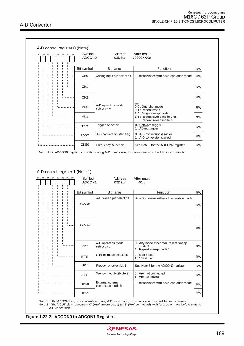
A-D Converter
189
Renesas microcomputers
M16C / 62P Group SINGLE-CHIP 16-BIT CMOS MICROCOMPUTER
Figure 1.22.2. ADCON0 to ADCON1 Registers
A-D control register 0 (Note)Symbol Address After resetADCON0 03D616 00000XXX2
b7 b6 b5 b4 b3 b2 b1 b0
Analog input pin select bitCH0
Bit symbol Bit name Function
CH1
CH2
A-D operation mode select bit 0
0 0 : One-shot mode0 1 : Repeat mode1 0 : Single sweep mode1 1 : Repeat sweep mode 0 or
Repeat sweep mode 1
MD0
MD1
Trigger select bit 0 : Software trigger1 : ADTRG trigger
TRG
ADST A-D conversion start flag 0 : A-D conversion disabled1 : A-D conversion started
Frequency select bit 0 See Note 3 for the ADCON2 registerCKS0
RW
A-D control register 1 (Note 1)
Symbol Address After resetADCON1 03D716 0016
Bit name FunctionBit symbol
b7 b6 b5 b4 b3 b2 b1 b0
A-D sweep pin select bit
SCAN0
SCAN1
MD2
BITS8/10-bit mode select bit 0 : 8-bit mode
1 : 10-bit mode
VCUT
OPA0
Vref connect bit (Note 2)
OPA1
A-D operation mode select bit 1
0 : Any mode other than repeat sweep mode 1
1 : Repeat sweep mode 1
0 : Vref not connected1 : Vref connected
External op-amp connection mode bit
b4 b3
Note: If the ADCON0 register is rewritten during A-D conversion, the conversion result will be indeterminate.
Frequency select bit 1CKS1
RW
RW
RW
RW
RW
RW
RW
RW
RW
RW
RW
RW
RW
RW
RW
RW
RW
Function varies with each operation mode
Function varies with each operation mode
See Note 3 for the ADCON2 register
Note 1: If the ADCON1 register is rewritten during A-D conversion, the conversion result will be indeterminate. Note 2: If the VCUT bit is reset from “0” (Vref unconnected) to “1” (Vref connected), wait for 1 µs or more before starting A-D conversion.
Function varies with each operation mode
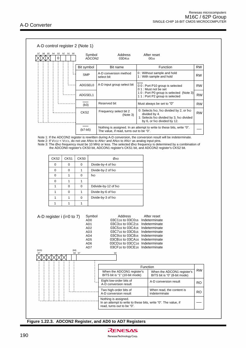
Renesas microcomputers
M16C / 62P Group SINGLE-CHIP 16-BIT CMOS MICROCOMPUTER
A-D Converter
190
A-D control register 2 (Note 1)
Symbol Address After resetADCON2 03D416 0016
b7 b6 b5 b4 b3 b2 b1 b0
A-D conversion method select bit
0 : Without sample and hold1 : With sample and hold
Bit symbol Bit name Function RW
SMP
Reserved bit Must always be set to “0”
0
Note 1: If the ADCON2 register is rewritten during A-D conversion, the conversion result will be indeterminate.Note 2: If VCC2 < VCC1, do not use AN00 to AN07 and AN20 to AN27 as analog input pins.Note 3: The ØAD frequency must be 10 MHz or less. The selected ØAD frequency is determined by a combination of the ADCON0 register's CKS0 bit, ADCON1 register's CKS1 bit, and ADCON2 register's CKS2 bit.
A-D input group select bit 0 0 : Port P10 group is selected0 1 : Must not be set1 0 : Port P0 group is selected (Note 3)1 1 : Port P2 group is selected
b2 b1
Frequency select bit 2 (Note 3)
CKS2
ADGSEL0
ADGSEL1
RW
RW
RW
RW
RW
A-D register i (i=0 to 7) Symbol Address After resetAD0 03C116 to 03C016 IndeterminateAD1 03C316 to 03C216 IndeterminateAD2 03C516 to 03C416 IndeterminateAD3 03C716 to 03C616 IndeterminateAD4 03C916 to 03C816 IndeterminateAD5 03CB16 to 03CA16 IndeterminateAD6 03CD16 to 03CC16 IndeterminateAD7 03CF16 to 03CE16 Indeterminate
Eight low-order bits of A-D conversion result
Function
(b15)b7b7 b0 b0
(b8)
When the ADCON1 register's BITS bit is “1” (10-bit mode)
Nothing is assigned.In an attempt to write to these bits, write “0”. The value, if read, turns out to be “0”.
When read, the content is indeterminate
RW
RO
RO
(b3)
Nothing is assigned. In an attempt to write to these bits, write “0”. The value, if read, turns out to be “0”.(b7-b5)
0: Selects fAD, fAD divided by 2, or fAD divided by 4.
1: Selects fAD divided by 3, fAD divided by 6, or fAD divided by 12.
CKS2 CKS1 CKS0 ØAD
0 0 0
0 0 1
0 1 0
1 0 0
1 0 1
1 1 0
1 1 1
Divide-by-4 of fAD
Divide-by-2 of fAD
fAD
Ddivide-by-12 of fAD
0 1 1
Divide-by-6 of fAD
Divide-by-3 of fAD
Two high-order bits of A-D conversion result
When the ADCON1 register's BITS bit is “0” (8-bit mode)
A-D conversion result
Figure 1.22.3. ADCON2 Register, and AD0 to AD7 Registers
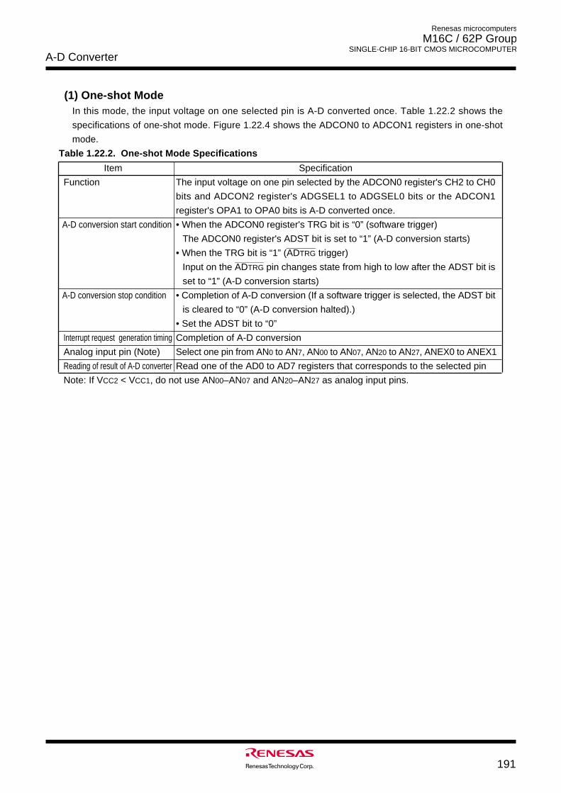
A-D Converter
191
Renesas microcomputers
M16C / 62P Group SINGLE-CHIP 16-BIT CMOS MICROCOMPUTER
(1) One-shot ModeIn this mode, the input voltage on one selected pin is A-D converted once. Table 1.22.2 shows the
specifications of one-shot mode. Figure 1.22.4 shows the ADCON0 to ADCON1 registers in one-shot
mode.
Table 1.22.2. One-shot Mode Specifications
Item Specification
Function The input voltage on one pin selected by the ADCON0 register's CH2 to CH0
bits and ADCON2 register's ADGSEL1 to ADGSEL0 bits or the ADCON1
register's OPA1 to OPA0 bits is A-D converted once.
A-D conversion start condition • When the ADCON0 register's TRG bit is “0” (software trigger)
The ADCON0 register's ADST bit is set to “1” (A-D conversion starts)___________
• When the TRG bit is “1” (ADTRG trigger)___________
Input on the ADTRG pin changes state from high to low after the ADST bit is
set to “1” (A-D conversion starts)
A-D conversion stop condition • Completion of A-D conversion (If a software trigger is selected, the ADST bit
is cleared to “0” (A-D conversion halted).)
• Set the ADST bit to “0”
Interrupt request generation timing Completion of A-D conversion
Analog input pin (Note) Select one pin from AN0 to AN7, AN00 to AN07, AN20 to AN27, ANEX0 to ANEX1
Reading of result of A-D converter Read one of the AD0 to AD7 registers that corresponds to the selected pin
Note: If VCC2 < VCC1, do not use AN00–AN07 and AN20–AN27 as analog input pins.
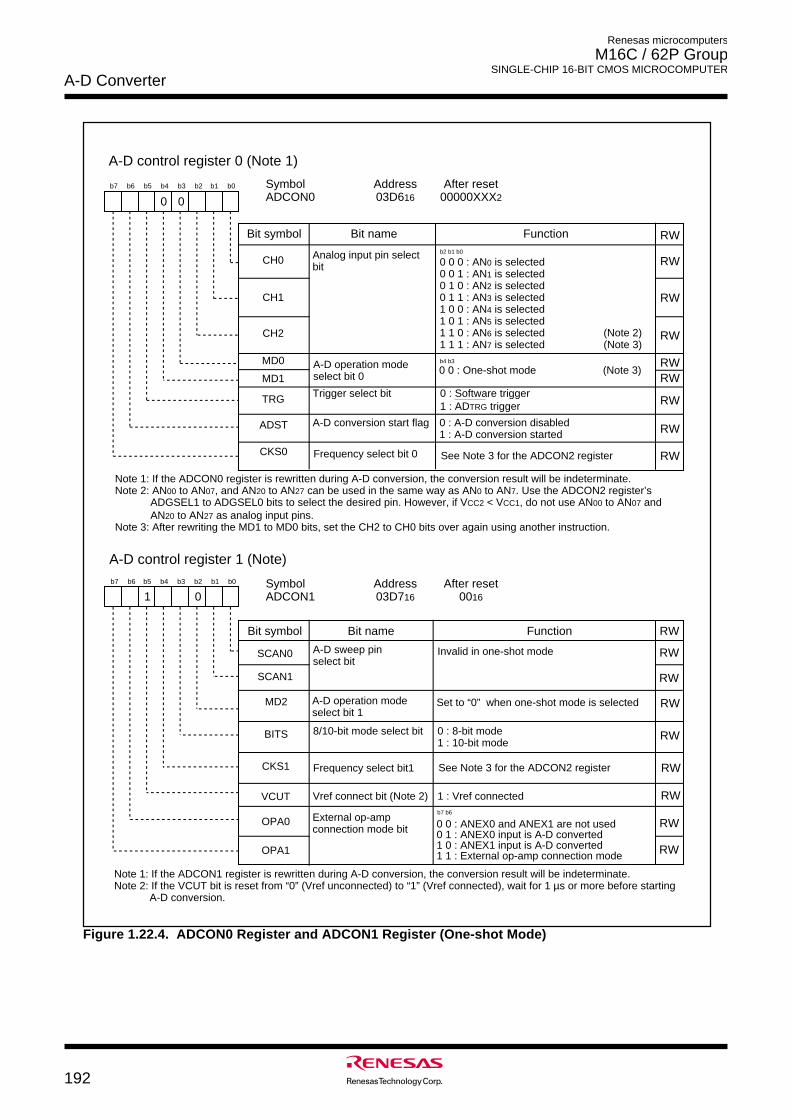
Renesas microcomputers
M16C / 62P Group SINGLE-CHIP 16-BIT CMOS MICROCOMPUTER
A-D Converter
192
A-D control register 0 (Note 1)
Symbol Address After resetADCON0 03D616 00000XXX2
b7 b6 b5 b4 b3 b2 b1 b0
Analog input pin select bit
Bit symbol Bit name Function
CH1
CH2
A-D operation mode select bit 0
MD0
MD1Trigger select bit 0 : Software trigger
1 : ADTRG triggerTRG
ADST A-D conversion start flag 0 : A-D conversion disabled1 : A-D conversion started
Frequency select bit 0CKS0
RW
00
A-D control register 1 (Note)
Symbol Address After resetADCON1 03D716 0016
Bit name FunctionBit symbol
b7 b6 b5 b4 b3 b2 b1 b0
A-D sweep pin select bit
SCAN0
SCAN1
MD2
BITS 8/10-bit mode select bit 0 : 8-bit mode 1 : 10-bit mode
VCUT
OPA0
Vref connect bit (Note 2)
OPA1
A-D operation mode select bit 1
Set to “0” when one-shot mode is selected
1 : Vref connected
External op-amp connection mode bit 0 0 : ANEX0 and ANEX1 are not used
0 1 : ANEX0 input is A-D converted1 0 : ANEX1 input is A-D converted1 1 : External op-amp connection mode
RW
Invalid in one-shot mode
0
0 0 0 : AN0 is selected0 0 1 : AN1 is selected0 1 0 : AN2 is selected0 1 1 : AN3 is selected1 0 0 : AN4 is selected1 0 1 : AN5 is selected1 1 0 : AN6 is selected (Note 2)1 1 1 : AN7 is selected (Note 3)
b2 b1 b0
0 0 : One-shot mode (Note 3)b4 b3
CH0
b7 b6
1
Frequency select bit1CKS1
Note 1: If the ADCON0 register is rewritten during A-D conversion, the conversion result will be indeterminate. Note 2: AN00 to AN07, and AN20 to AN27 can be used in the same way as AN0 to AN7. Use the ADCON2 register’s ADGSEL1 to ADGSEL0 bits to select the desired pin. However, if VCC2 < VCC1, do not use AN00 to AN07 and AN20 to AN27 as analog input pins.Note 3: After rewriting the MD1 to MD0 bits, set the CH2 to CH0 bits over again using another instruction.
RW
RW
RW
RWRW
RW
RW
RW
RW
RW
RW
RW
RW
RW
RW
RW
See Note 3 for the ADCON2 register
See Note 3 for the ADCON2 register
Note 1: If the ADCON1 register is rewritten during A-D conversion, the conversion result will be indeterminate. Note 2: If the VCUT bit is reset from “0” (Vref unconnected) to “1” (Vref connected), wait for 1 µs or more before starting A-D conversion.
Figure 1.22.4. ADCON0 Register and ADCON1 Register (One-shot Mode)
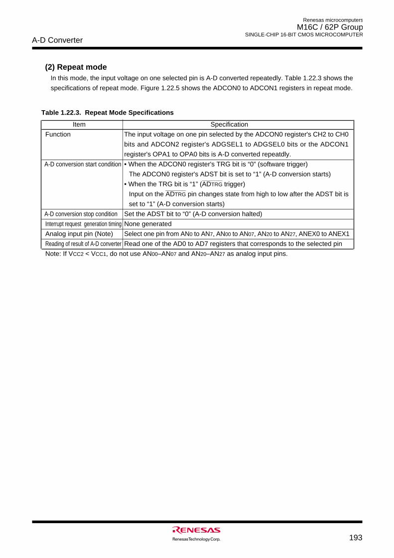
A-D Converter
193
Renesas microcomputers
M16C / 62P Group SINGLE-CHIP 16-BIT CMOS MICROCOMPUTER
(2) Repeat modeIn this mode, the input voltage on one selected pin is A-D converted repeatedly. Table 1.22.3 shows the
specifications of repeat mode. Figure 1.22.5 shows the ADCON0 to ADCON1 registers in repeat mode.
Item Specification
Function The input voltage on one pin selected by the ADCON0 register's CH2 to CH0
bits and ADCON2 register's ADGSEL1 to ADGSEL0 bits or the ADCON1
register's OPA1 to OPA0 bits is A-D converted repeatdly.
A-D conversion start condition • When the ADCON0 register's TRG bit is “0” (software trigger)
The ADCON0 register's ADST bit is set to “1” (A-D conversion starts)___________
• When the TRG bit is “1” (ADTRG trigger)___________
Input on the ADTRG pin changes state from high to low after the ADST bit is
set to “1” (A-D conversion starts)
A-D conversion stop condition Set the ADST bit to “0” (A-D conversion halted)
Interrupt request generation timing None generated
Analog input pin (Note) Select one pin from AN0 to AN7, AN00 to AN07, AN20 to AN27, ANEX0 to ANEX1
Reading of result of A-D converter Read one of the AD0 to AD7 registers that corresponds to the selected pin
Note: If VCC2 < VCC1, do not use AN00–AN07 and AN20–AN27 as analog input pins.
Table 1.22.3. Repeat Mode Specifications
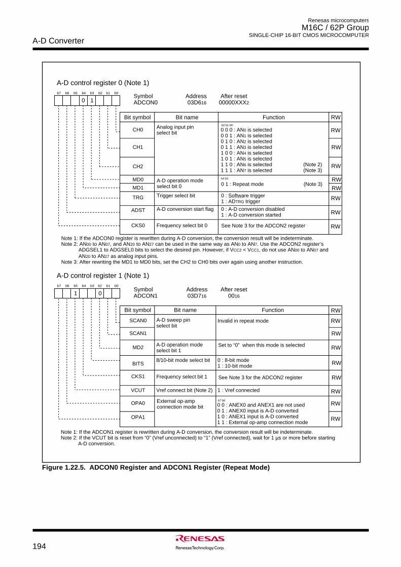
Renesas microcomputers
M16C / 62P Group SINGLE-CHIP 16-BIT CMOS MICROCOMPUTER
A-D Converter
194
A-D control register 0 (Note 1)
Symbol Address After resetADCON0 03D616 00000XXX2
b7 b6 b5 b4 b3 b2 b1 b0
Analog input pin select bit
CH0
Bit symbol Bit name Function
CH1
CH2
A-D operation mode select bit 0
MD0
MD1
Trigger select bit 0 : Software trigger1 : ADTRG trigger
TRG
ADST A-D conversion start flag 0 : A-D conversion disabled1 : A-D conversion started
Frequency select bit 0CKS0
RW
A-D control register 1 (Note 1)
Symbol Address After resetADCON1 03D716 0016
Bit name FunctionBit symbol
b7 b6 b5 b4 b3 b2 b1 b0
A-D sweep pin select bit
SCAN0
SCAN1
MD2
BITS8/10-bit mode select bit 0 : 8-bit mode
1 : 10-bit mode
VCUT
OPA0
Vref connect bit (Note 2)
OPA1
A-D operation mode select bit 1
1 : Vref connected
External op-amp connection mode bit
0 1
Invalid in repeat mode
0
0 0 0 : AN0 is selected0 0 1 : AN1 is selected0 1 0 : AN2 is selected0 1 1 : AN3 is selected1 0 0 : AN4 is selected1 0 1 : AN5 is selected1 1 0 : AN6 is selected (Note 2)1 1 1 : AN7 is selected (Note 3)
b2 b1 b0
0 1 : Repeat mode (Note 3)b4 b3
0 0 : ANEX0 and ANEX1 are not used0 1 : ANEX0 input is A-D converted1 0 : ANEX1 input is A-D converted1 1 : External op-amp connection mode
b7 b6
1
Frequency select bit 1CKS1
Set to “0” when this mode is selected
RW
RW
RW
RW
RW
RW
RW
RW
RW
RW
RW
RW
RW
RW
RW
RW
RW
See Note 3 for the ADCON2 register
Note 1: If the ADCON0 register is rewritten during A-D conversion, the conversion result will be indeterminate. Note 2: AN00 to AN07, and AN20 to AN27 can be used in the same way as AN0 to AN7. Use the ADCON2 register’s ADGSEL1 to ADGSEL0 bits to select the desired pin. However, if VCC2 < VCC1, do not use AN00 to AN07 and AN20 to AN27 as analog input pins.Note 3: After rewriting the MD1 to MD0 bits, set the CH2 to CH0 bits over again using another instruction.
Note 1: If the ADCON1 register is rewritten during A-D conversion, the conversion result will be indeterminate. Note 2: If the VCUT bit is reset from “0” (Vref unconnected) to “1” (Vref connected), wait for 1 µs or more before starting A-D conversion.
See Note 3 for the ADCON2 register
Figure 1.22.5. ADCON0 Register and ADCON1 Register (Repeat Mode)
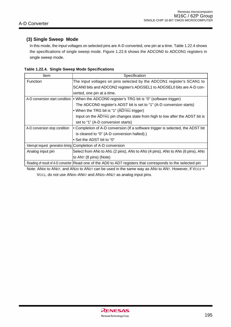
A-D Converter
195
Renesas microcomputers
M16C / 62P Group SINGLE-CHIP 16-BIT CMOS MICROCOMPUTER
(3) Single Sweep ModeIn this mode, the input voltages on selected pins are A-D converted, one pin at a time. Table 1.22.4 shows
the specifications of single sweep mode. Figure 1.22.6 shows the ADCON0 to ADCON1 registers in
single sweep mode.
Item Specification
Function The input voltages on pins selected by the ADCON1 register's SCAN1 to
SCAN0 bits and ADCON2 register's ADGSEL1 to ADGSEL0 bits are A-D con-
verted, one pin at a time.
A-D conversion start condition • When the ADCON0 register's TRG bit is “0” (software trigger)
The ADCON0 register's ADST bit is set to “1” (A-D conversion starts)___________
• When the TRG bit is “1” (ADTRG trigger)___________
Input on the ADTRG pin changes state from high to low after the ADST bit is
set to “1” (A-D conversion starts)
A-D conversion stop condition • Completion of A-D conversion (If a software trigger is selected, the ADST bit
is cleared to “0” (A-D conversion halted).)
• Set the ADST bit to “0”
Interrupt request generation timing Completion of A-D conversion
Analog input pin Select from AN0 to AN1 (2 pins), AN0 to AN3 (4 pins), AN0 to AN5 (6 pins), AN0
to AN7 (8 pins) (Note)
Reading of result of A-D converter Read one of the AD0 to AD7 registers that corresponds to the selected pin
Note: AN00 to AN07, and AN20 to AN27 can be used in the same way as AN0 to AN7. However, if VCC2 <
VCC1, do not use AN00–AN07 and AN20–AN27 as analog input pins.
Table 1.22.4. Single Sweep Mode Specifications
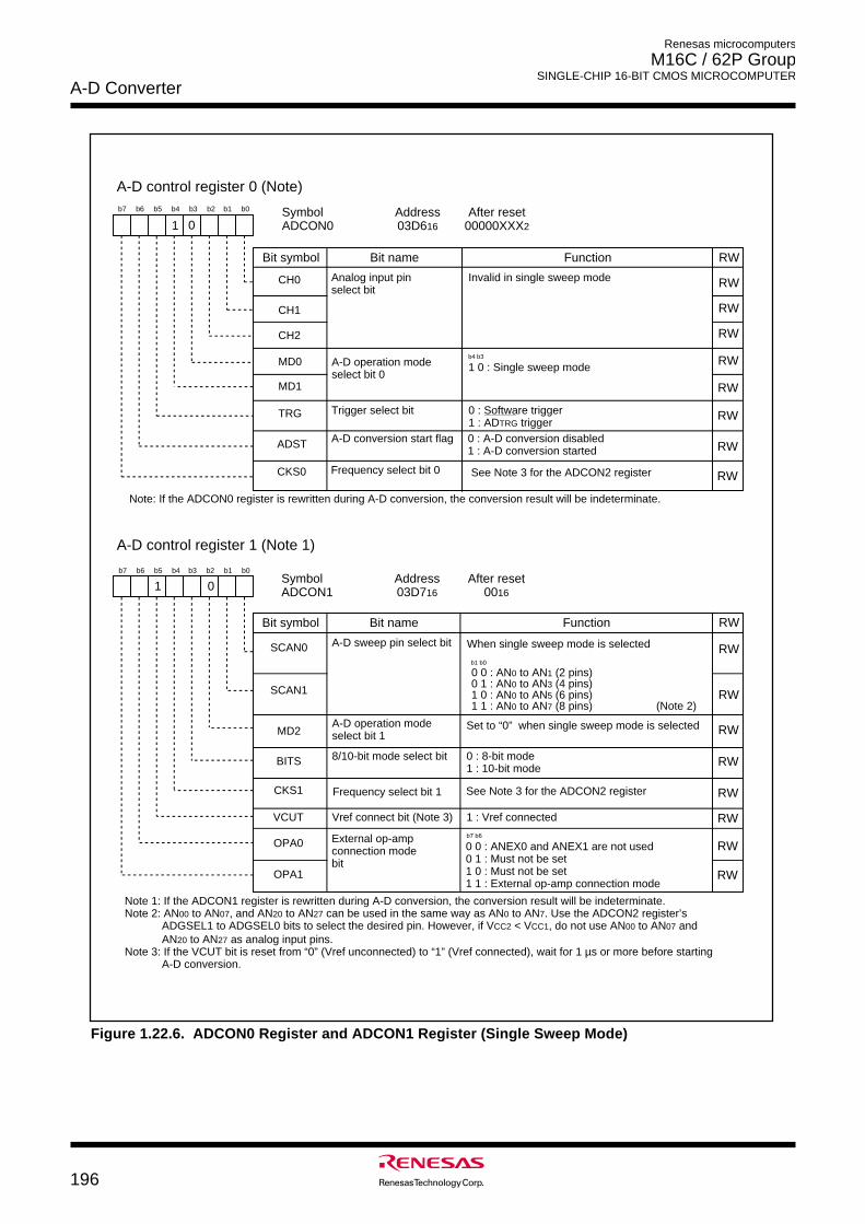
Renesas microcomputers
M16C / 62P Group SINGLE-CHIP 16-BIT CMOS MICROCOMPUTER
A-D Converter
196
A-D control register 0 (Note)
Symbol Address After resetADCON0 03D616 00000XXX2
b7 b6 b5 b4 b3 b2 b1 b0
Analog input pin select bit
CH0
Bit symbol Bit name Function
CH1
CH2
A-D operation mode select bit 0
1 0 : Single sweep modeMD0
MD1
Trigger select bit 0 : Software trigger1 : ADTRG trigger
TRG
ADST A-D conversion start flag 0 : A-D conversion disabled1 : A-D conversion started
Frequency select bit 0CKS0
RW
1 0
Invalid in single sweep mode
b4 b3
RW
RW
RW
RW
RW
RW
RW
RW
A-D control register 1 (Note 1)
Symbol Address After resetADCON1 03D716 0016
Bit name FunctionBit symbol
b7 b6 b5 b4 b3 b2 b1 b0
A-D sweep pin select bitSCAN0
SCAN1
MD2
BITS 8/10-bit mode select bit 0 : 8-bit mode 1 : 10-bit mode
VCUT
OPA0
Vref connect bit (Note 3)
OPA1
A-D operation mode select bit 1
1 : Vref connected
External op-amp connection mode bit
0
When single sweep mode is selected
0 0 : AN0 to AN1 (2 pins)0 1 : AN0 to AN3 (4 pins)1 0 : AN0 to AN5 (6 pins)1 1 : AN0 to AN7 (8 pins) (Note 2)
b1 b0
0 0 : ANEX0 and ANEX1 are not used0 1 : Must not be set1 0 : Must not be set1 1 : External op-amp connection mode
b7 b6
1
Frequency select bit 1CKS1
Set to “0” when single sweep mode is selected
RW
RW
RW
RW
RW
RW
RW
RW
RW
See Note 3 for the ADCON2 register
Note: If the ADCON0 register is rewritten during A-D conversion, the conversion result will be indeterminate.
Note 1: If the ADCON1 register is rewritten during A-D conversion, the conversion result will be indeterminate. Note 2: AN00 to AN07, and AN20 to AN27 can be used in the same way as AN0 to AN7. Use the ADCON2 register’s ADGSEL1 to ADGSEL0 bits to select the desired pin. However, if VCC2 < VCC1, do not use AN00 to AN07 and AN20 to AN27 as analog input pins.Note 3: If the VCUT bit is reset from “0” (Vref unconnected) to “1” (Vref connected), wait for 1 µs or more before starting A-D conversion.
See Note 3 for the ADCON2 register
Figure 1.22.6. ADCON0 Register and ADCON1 Register (Single Sweep Mode)
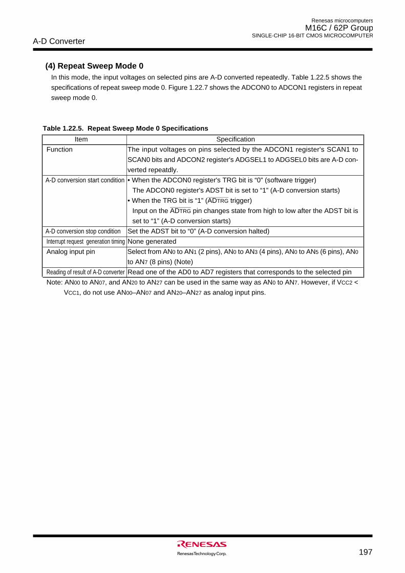
A-D Converter
197
Renesas microcomputers
M16C / 62P Group SINGLE-CHIP 16-BIT CMOS MICROCOMPUTER
(4) Repeat Sweep Mode 0In this mode, the input voltages on selected pins are A-D converted repeatedly. Table 1.22.5 shows the
specifications of repeat sweep mode 0. Figure 1.22.7 shows the ADCON0 to ADCON1 registers in repeat
sweep mode 0.
Item Specification
Function The input voltages on pins selected by the ADCON1 register's SCAN1 to
SCAN0 bits and ADCON2 register's ADGSEL1 to ADGSEL0 bits are A-D con-
verted repeatdly.
A-D conversion start condition • When the ADCON0 register's TRG bit is “0” (software trigger)
The ADCON0 register's ADST bit is set to “1” (A-D conversion starts)___________
• When the TRG bit is “1” (ADTRG trigger)___________
Input on the ADTRG pin changes state from high to low after the ADST bit is
set to “1” (A-D conversion starts)
A-D conversion stop condition Set the ADST bit to “0” (A-D conversion halted)
Interrupt request generation timing None generated
Analog input pin Select from AN0 to AN1 (2 pins), AN0 to AN3 (4 pins), AN0 to AN5 (6 pins), AN0
to AN7 (8 pins) (Note)
Reading of result of A-D converter Read one of the AD0 to AD7 registers that corresponds to the selected pin
Note: AN00 to AN07, and AN20 to AN27 can be used in the same way as AN0 to AN7. However, if VCC2 <
VCC1, do not use AN00–AN07 and AN20–AN27 as analog input pins.
Table 1.22.5. Repeat Sweep Mode 0 Specifications

Renesas microcomputers
M16C / 62P Group SINGLE-CHIP 16-BIT CMOS MICROCOMPUTER
A-D Converter
198
A-D control register 0 (Note)
Symbol Address After resetADCON0 03D616 00000XXX2
b7 b6 b5 b4 b3 b2 b1 b0
Analog input pin select bit
CH0
Bit symbol Bit name Function
CH1
CH2
A-D operation mode select bit 0
1 1 : Repeat sweep mode 0 or Repeat sweep mode 1
MD0
MD1
Trigger select bit 0 : Software trigger1 : ADTRG trigger
TRG
ADST A-D conversion start flag 0 : A-D conversion disabled1 : A-D conversion started
Frequency select bit 0CKS0
RW
A-D control register 1 (Note 1)
Symbol Address After resetADCON1 03D716 0016
Bit name FunctionBit symbol
b7 b6 b5 b4 b3 b2 b1 b0
A-D sweep pin select bitSCAN0
SCAN1
MD2
BITS 8/10-bit mode select bit 0 : 8-bit mode 1 : 10-bit mode
VCUT
OPA0
Vref connect bit (Note 3)
OPA1
A-D operation mode select bit 1
1 : Vref connected
External op-amp connection mode bit
1 1
Invalid in repeat sweep mode 0
0
b4 b3
When repeat sweep mode 0 is selected
0 0 : AN0, AN1 (2 pins)0 1 : AN0 to AN3 (4 pins)1 0 : AN0 to AN5 (6 pins)1 1 : AN0 to AN7 (8 pins) (Note 2)
b1 b0
0 0 : ANEX0 and ANEX1 are not used0 1 : Must not be set1 0 : Must not be set1 1 : External op-amp connection mode
b7 b6
1
Frequency select bit 1CKS1
Set to “0” when repeat sweep mode 0 is selected
RW
RW
RW
RW
RW
RW
RW
RW
RW
RW
RW
RW
RW
RW
RW
RW
RW
See Note 3 for the ADCON2 register
Note: If the ADCON0 register is rewritten during A-D conversion, the conversion result will be indeterminate.
Note 1: If the ADCON1 register is rewritten during A-D conversion, the conversion result will be indeterminate. Note 2: AN00 to AN07, and AN20 to AN27 can be used in the same way as AN0 to AN7. Use the ADCON2 register’s ADGSEL1 to ADGSEL0 bits to select the desired pin. However, if VCC2 < VCC1, do not use AN00 to AN07 and AN20 to AN27 as analog input pins.Note 3: If the VCUT bit is reset from “0” (Vref unconnected) to “1” (Vref connected), wait for 1 µs or more before starting A-D conversion.
See Note 3 for the ADCON2 register
Figure 1.22.7. ADCON0 Register and ADCON1 Registers (Repeat Sweep Mode 0)
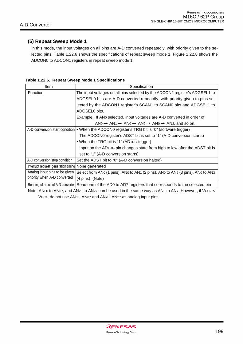
A-D Converter
199
Renesas microcomputers
M16C / 62P Group SINGLE-CHIP 16-BIT CMOS MICROCOMPUTER
(5) Repeat Sweep Mode 1In this mode, the input voltages on all pins are A-D converted repeatedly, with priority given to the se-
lected pins. Table 1.22.6 shows the specifications of repeat sweep mode 1. Figure 1.22.8 shows the
ADCON0 to ADCON1 registers in repeat sweep mode 1.
Table 1.22.6. Repeat Sweep Mode 1 Specifications
Item Specification
Function The input voltages on all pins selected by the ADCON2 register's ADGSEL1 to
ADGSEL0 bits are A-D converted repeatdly, with priority given to pins se-
lected by the ADCON1 register's SCAN1 to SCAN0 bits and ADGSEL1 to
ADGSEL0 bits.
Example : If AN0 selected, input voltages are A-D converted in order of
AN0 AN1 AN0 AN2 AN0 AN3, and so on.
A-D conversion start condition • When the ADCON0 register's TRG bit is “0” (software trigger)
The ADCON0 register's ADST bit is set to “1” (A-D conversion starts)___________
• When the TRG bit is “1” (ADTRG trigger)___________
Input on the ADTRG pin changes state from high to low after the ADST bit is
set to “1” (A-D conversion starts)
A-D conversion stop condition Set the ADST bit to “0” (A-D conversion halted)
Interrupt request generation timing None generated
Select from AN0 (1 pins), AN0 to AN1 (2 pins), AN0 to AN2 (3 pins), AN0 to AN3
(4 pins) (Note)
Reading of result of A-D converter Read one of the AD0 to AD7 registers that corresponds to the selected pin
Note: AN00 to AN07, and AN20 to AN27 can be used in the same way as AN0 to AN7. However, if VCC2 <
VCC1, do not use AN00–AN07 and AN20–AN27 as analog input pins.
Analog input pins to be givenpriority when A-D converted
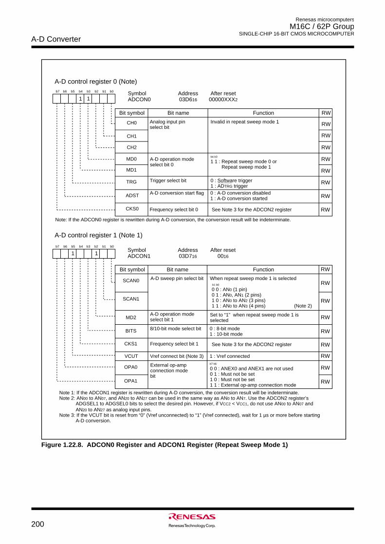
Renesas microcomputers
M16C / 62P Group SINGLE-CHIP 16-BIT CMOS MICROCOMPUTER
A-D Converter
200
A-D control register 0 (Note)
Symbol Address After resetADCON0 03D616 00000XXX2
b7 b6 b5 b4 b3 b2 b1 b0
Analog input pin select bit
CH0
Bit symbol Bit name Function
CH1
CH2
A-D operation mode select bit 0
1 1 : Repeat sweep mode 0 or Repeat sweep mode 1
MD0
MD1
Trigger select bit 0 : Software trigger1 : ADTRG trigger
TRG
ADST A-D conversion start flag 0 : A-D conversion disabled1 : A-D conversion started
Frequency select bit 0CKS0
RW
A-D control register 1 (Note 1)
Symbol Address After resetADCON1 03D716 0016
Bit name FunctionBit symbol
b7 b6 b5 b4 b3 b2 b1 b0
A-D sweep pin select bitSCAN0
SCAN1
MD2
BITS 8/10-bit mode select bit 0 : 8-bit mode 1 : 10-bit mode
VCUT
OPA0
Vref connect bit (Note 3)
OPA1
A-D operation mode select bit 1
1 : Vref connected
External op-amp connection mode bit
1 1
Invalid in repeat sweep mode 1
1
b4 b3
When repeat sweep mode 1 is selected
0 0 : AN0 (1 pin)0 1 : AN0, AN1 (2 pins)1 0 : AN0 to AN2 (3 pins)1 1 : AN0 to AN3 (4 pins) (Note 2)
b1 b0
0 0 : ANEX0 and ANEX1 are not used0 1 : Must not be set1 0 : Must not be set1 1 : External op-amp connection mode
b7 b6
1
Frequency select bit 1CKS1
Set to “1” when repeat sweep mode 1 is selected
RW
RW
RW
RW
RW
RW
RW
RW
RW
RW
RW
RW
RW
RW
RW
RW
RW
See Note 3 for the ADCON2 register
Note: If the ADCON0 register is rewritten during A-D conversion, the conversion result will be indeterminate.
Note 1: If the ADCON1 register is rewritten during A-D conversion, the conversion result will be indeterminate. Note 2: AN00 to AN07, and AN20 to AN27 can be used in the same way as AN0 to AN7. Use the ADCON2 register’s ADGSEL1 to ADGSEL0 bits to select the desired pin. However, if VCC2 < VCC1, do not use AN00 to AN07 and AN20 to AN27 as analog input pins.Note 3: If the VCUT bit is reset from “0” (Vref unconnected) to “1” (Vref connected), wait for 1 µs or more before starting A-D conversion.
See Note 3 for the ADCON2 register
Figure 1.22.8. ADCON0 Register and ADCON1 Register (Repeat Sweep Mode 1)
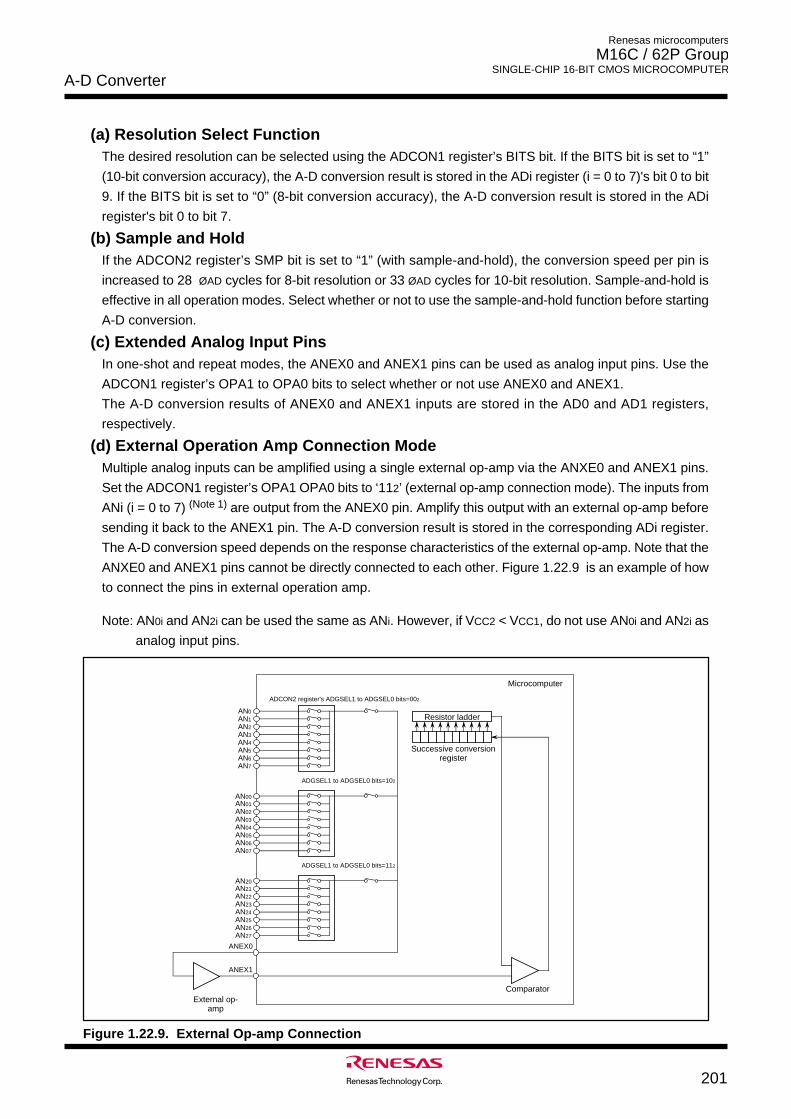
A-D Converter
201
Renesas microcomputers
M16C / 62P Group SINGLE-CHIP 16-BIT CMOS MICROCOMPUTER
(a) Resolution Select FunctionThe desired resolution can be selected using the ADCON1 register’s BITS bit. If the BITS bit is set to “1”
(10-bit conversion accuracy), the A-D conversion result is stored in the ADi register (i = 0 to 7)'s bit 0 to bit
9. If the BITS bit is set to “0” (8-bit conversion accuracy), the A-D conversion result is stored in the ADi
register's bit 0 to bit 7.
(b) Sample and HoldIf the ADCON2 register’s SMP bit is set to “1” (with sample-and-hold), the conversion speed per pin is
increased to 28 ØAD cycles for 8-bit resolution or 33 ØAD cycles for 10-bit resolution. Sample-and-hold is
effective in all operation modes. Select whether or not to use the sample-and-hold function before starting
A-D conversion.
(c) Extended Analog Input PinsIn one-shot and repeat modes, the ANEX0 and ANEX1 pins can be used as analog input pins. Use the
ADCON1 register’s OPA1 to OPA0 bits to select whether or not use ANEX0 and ANEX1.
The A-D conversion results of ANEX0 and ANEX1 inputs are stored in the AD0 and AD1 registers,
respectively.
(d) External Operation Amp Connection ModeMultiple analog inputs can be amplified using a single external op-amp via the ANXE0 and ANEX1 pins.
Set the ADCON1 register’s OPA1 OPA0 bits to ‘112’ (external op-amp connection mode). The inputs from
ANi (i = 0 to 7) (Note 1) are output from the ANEX0 pin. Amplify this output with an external op-amp before
sending it back to the ANEX1 pin. The A-D conversion result is stored in the corresponding ADi register.
The A-D conversion speed depends on the response characteristics of the external op-amp. Note that the
ANXE0 and ANEX1 pins cannot be directly connected to each other. Figure 1.22.9 is an example of how
to connect the pins in external operation amp.
Note: AN0i and AN2i can be used the same as ANi. However, if VCC2 < VCC1, do not use AN0i and AN2i as
analog input pins.
ADCON2 register's ADGSEL1 to ADGSEL0 bits=002
Successive conversion register
ComparatorExternal op-
amp
AN0AN1AN2AN3AN4AN5AN6AN7
ANEX0
ANEX1
AN00AN01AN02AN03AN04AN05AN06AN07
ADGSEL1 to ADGSEL0 bits=102
AN20AN21AN22AN23AN24AN25AN26AN27
ADGSEL1 to ADGSEL0 bits=112
Resistor ladder
Microcomputer
Figure 1.22.9. External Op-amp Connection
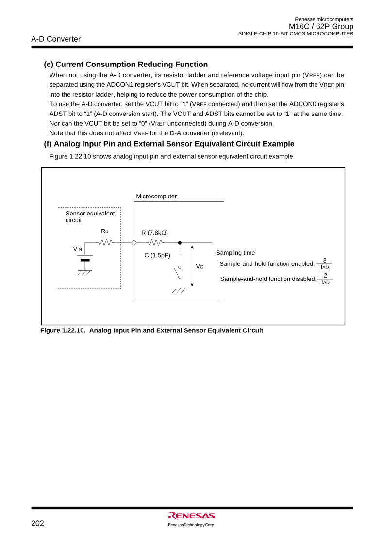
Renesas microcomputers
M16C / 62P Group SINGLE-CHIP 16-BIT CMOS MICROCOMPUTER
A-D Converter
202
(e) Current Consumption Reducing FunctionWhen not using the A-D converter, its resistor ladder and reference voltage input pin (VREF) can be
separated using the ADCON1 register’s VCUT bit. When separated, no current will flow from the VREF pin
into the resistor ladder, helping to reduce the power consumption of the chip.
To use the A-D converter, set the VCUT bit to “1” (VREF connected) and then set the ADCON0 register’s
ADST bit to “1” (A-D conversion start). The VCUT and ADST bits cannot be set to “1” at the same time.
Nor can the VCUT bit be set to “0” (VREF unconnected) during A-D conversion.
Note that this does not affect VREF for the D-A converter (irrelevant).
(f) Analog Input Pin and External Sensor Equivalent Circuit Example
Figure 1.22.10 shows analog input pin and external sensor equivalent circuit example.
Figure 1.22.10. Analog Input Pin and External Sensor Equivalent Circuit
R0 R (7.8kΩ)
C (1.5pF)VIN
VC
Sampling time3
fADSample-and-hold function enabled:
2fAD
Sample-and-hold function disabled:
Microcomputer
Sensor equivalent circuit
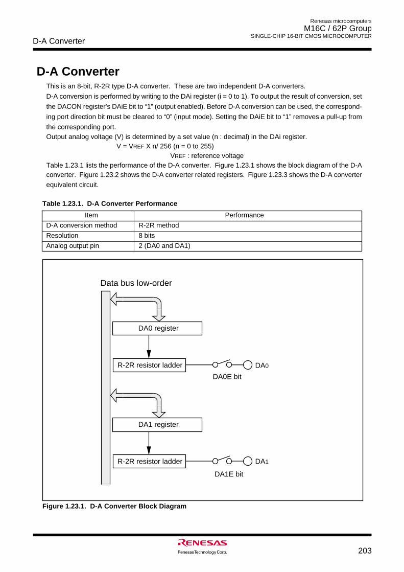
D-A Converter
203
Renesas microcomputers
M16C / 62P Group SINGLE-CHIP 16-BIT CMOS MICROCOMPUTER
D-A ConverterThis is an 8-bit, R-2R type D-A converter. These are two independent D-A converters.
D-A conversion is performed by writing to the DAi register (i = 0 to 1). To output the result of conversion, set
the DACON register’s DAiE bit to “1” (output enabled). Before D-A conversion can be used, the correspond-
ing port direction bit must be cleared to “0” (input mode). Setting the DAiE bit to “1” removes a pull-up from
the corresponding port.Output analog voltage (V) is determined by a set value (n : decimal) in the DAi register.
V = VREF X n/ 256 (n = 0 to 255)VREF : reference voltage
Table 1.23.1 lists the performance of the D-A converter. Figure 1.23.1 shows the block diagram of the D-Aconverter. Figure 1.23.2 shows the D-A converter related registers. Figure 1.23.3 shows the D-A converter
equivalent circuit.
Item Performance
D-A conversion method R-2R method
Resolution 8 bits
Analog output pin 2 (DA0 and DA1)
Table 1.23.1. D-A Converter Performance
AAAADA0
AAAADA1
Data bus low-order
DA0 register
R-2R resistor ladder
DA0E bit
DA1 register
R-2R resistor ladder
DA1E bit
Figure 1.23.1. D-A Converter Block Diagram
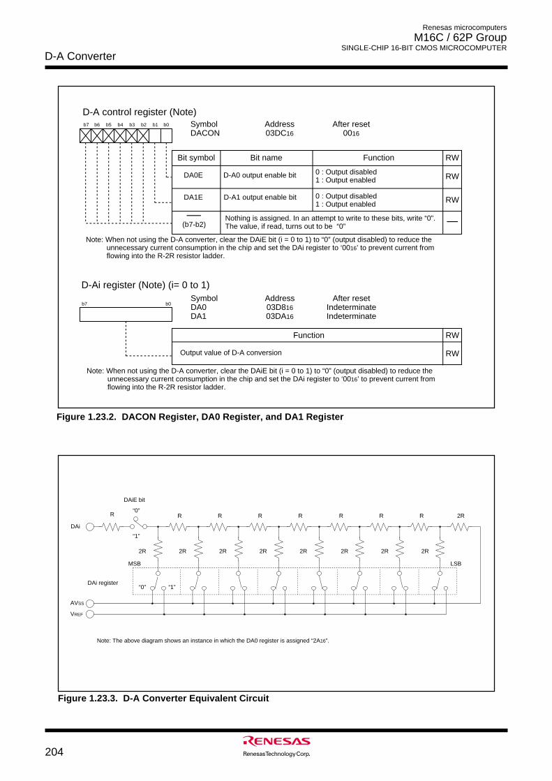
D-A Converter
204
Renesas microcomputers
M16C / 62P Group SINGLE-CHIP 16-BIT CMOS MICROCOMPUTER
Figure 1.23.2. DACON Register, DA0 Register, and DA1 Register
D-Ai register (Note) (i= 0 to 1)Symbol Address After resetDA0 03D816 IndeterminateDA1 03DA16 Indeterminate
WR
b7 b0
Function RW
Output value of D-A conversion
D-A control register (Note)Symbol Address After resetDACON 03DC16 0016
b7 b6 b5 b4 b3 b2 b1 b0
D-A0 output enable bit DA0E
Bit symbol Bit name Function RW
0 : Output disabled1 : Output enabled
D-A1 output enable bit 0 : Output disabled1 : Output enabled
DA1E
Nothing is assigned. In an attempt to write to these bits, write “0”. The value, if read, turns out to be “0”
RW
RW
(b7-b2)
RW
Note: When not using the D-A converter, clear the DAiE bit (i = 0 to 1) to “0” (output disabled) to reduce the unnecessary current consumption in the chip and set the DAi register to ‘0016’ to prevent current from flowing into the R-2R resistor ladder.
Note: When not using the D-A converter, clear the DAiE bit (i = 0 to 1) to “0” (output disabled) to reduce the unnecessary current consumption in the chip and set the DAi register to ‘0016’ to prevent current from flowing into the R-2R resistor ladder.
VREF
AVSS
2R
R
2R
R
2R
R
2R
R
2R
R
2R
R
2R
R
2R
2R
DAi
MSB LSB
DAiE bit
“0”
“1”
DAi register
Note: The above diagram shows an instance in which the DA0 register is assigned “2A16”.
“0” “1”
R
Figure 1.23.3. D-A Converter Equivalent Circuit
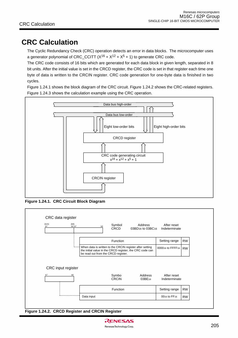
CRC Calculation
205
Renesas microcomputers
M16C / 62P Group SINGLE-CHIP 16-BIT CMOS MICROCOMPUTER
CRC CalculationThe Cyclic Redundancy Check (CRC) operation detects an error in data blocks. The microcomputer uses
a generator polynomial of CRC_CCITT (X16 + X12 + X5 + 1) to generate CRC code.
The CRC code consists of 16 bits which are generated for each data block in given length, separated in 8
bit units. After the initial value is set in the CRCD register, the CRC code is set in that register each time one
byte of data is written to the CRCIN register. CRC code generation for one-byte data is finished in two
cycles.
Figure 1.24.1 shows the block diagram of the CRC circuit. Figure 1.24.2 shows the CRC-related registers.
Figure 1.24.3 shows the calculation example using the CRC operation.
Figure 1.24.2. CRCD Register and CRCIN Register
Symbol Address After resetCRCD 03BD16 to 03BC16 Indeterminate
b7 b0 b7 b0(b15) (b8)
CRC data register
Function Setting range
000016 to FFFF16
Symbo Address After resetCRCIN 03BE16 Indeterminate
b7 b0
CRC input register
Data input
Function
0016 to FF16
RW
RW
RW
RW
Setting range
When data is written to the CRCIN register after setting the initial value in the CRCD register, the CRC code can be read out from the CRCD register.
AAAAAEight low-order bits AAAAAAAEight high-order bits
Data bus high-order
Data bus low-order
AAAAAAAAAAAAAAAAAAAAAA
AAAAAAAAAAAA
CRCD register
CRCIN register
AAAAAAAAAAAAAAAAAAAAAAAAAAAAAAAAA
CRC code generating circuit x16 + x12 + x5 + 1
Figure 1.24.1. CRC Circuit Block Diagram
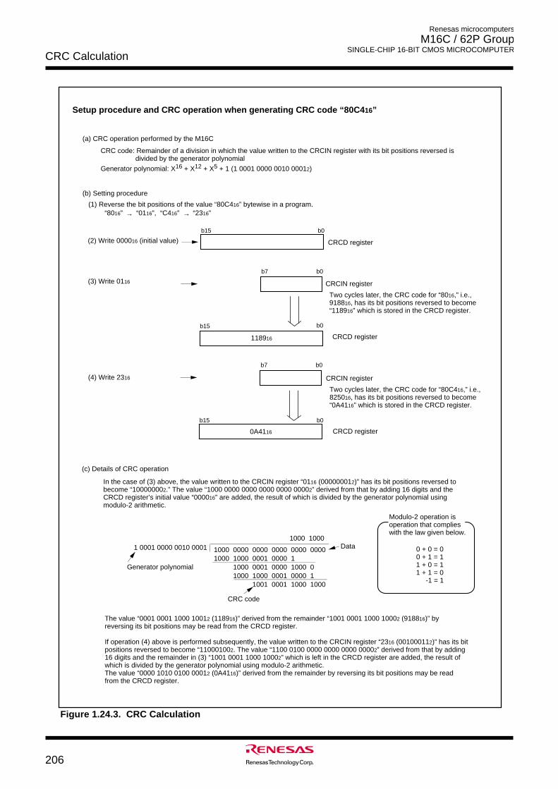
CRC Calculation
206
Renesas microcomputers
M16C / 62P Group SINGLE-CHIP 16-BIT CMOS MICROCOMPUTER
(2) Write 000016 (initial value)
b15 b0
CRCD register
1 0001 0000 0010 0001 1000 0000 0000 0000 0000 00001000 1000 0001 0000 1 1000 0001 0000 1000 0 1000 1000 0001 0000 1 1001 0001 1000 1000
1000 1000
Generator polynomial
Data
CRC code
Modulo-2 operation is operation that complies with the law given below.
0 + 0 = 00 + 1 = 11 + 0 = 11 + 1 = 0 -1 = 1
Setup procedure and CRC operation when generating CRC code “80C416”
(a) CRC operation performed by the M16C
CRC code: Remainder of a division in which the value written to the CRCIN register with its bit positions reversed is divided by the generator polynomial
(1) Reverse the bit positions of the value “80C416” bytewise in a program.
(3) Write 0116
b0b7
b15 b0
CRCIN register
CRCD register118916
Two cycles later, the CRC code for “8016,” i.e., 918816, has its bit positions reversed to become“118916” which is stored in the CRCD register.
(c) Details of CRC operation
In the case of (3) above, the value written to the CRCIN register “0116 (000000012)” has its bit positions reversed to become “100000002.” The value “1000 0000 0000 0000 0000 00002” derived from that by adding 16 digits and the CRCD register’s initial value “000016” are added, the result of which is divided by the generator polynomial using modulo-2 arithmetic.
The value “0001 0001 1000 10012 (118916)” derived from the remainder “1001 0001 1000 10002 (918816)” by reversing its bit positions may be read from the CRCD register.
If operation (4) above is performed subsequently, the value written to the CRCIN register “2316 (001000112)” has its bit positions reversed to become “110001002. The value “1100 0100 0000 0000 0000 00002” derived from that by adding 16 digits and the remainder in (3) “1001 0001 1000 10002” which is left in the CRCD register are added, the result of which is divided by the generator polynomial using modulo-2 arithmetic. The value “0000 1010 0100 00012 (0A4116)” derived from the remainder by reversing its bit positions may be read from the CRCD register.
(b) Setting procedure
Generator polynomial: X16 + X12 + X5 + 1 (1 0001 0000 0010 00012)
“8016” “0116”, “C416” “2316” → →
(4) Write 2316
b0b7
b15 b0
0A4116
CRCIN register
CRCD register
Two cycles later, the CRC code for “80C416,” i.e., 825016, has its bit positions reversed to become“0A4116” which is stored in the CRCD register.
Figure 1.24.3. CRC Calculation
Programmable I/O Ports
207
Renesas microcomputers
M16C / 62P Group SINGLE-CHIP 16-BIT CMOS MICROCOMPUTER
Programmable I/O PortsThe programmable input/output ports (hereafter referred to simply as “I/O ports”) consist of 87 lines P0 to
P10 (except P85) for the 100-pin version, or 113 lines P0 to P14 (except P85) for the 128-pin version. Eachport can be set for input or output every line by using a direction register, and can also be chosen to be or
not be pulled high every 4 lines. P85 is an input-only port and does not have a pull-up resistor. Port P85_______ ______
shares the pin with NMI, so that the NMI input level can be read from the P8 register P8_5 bit.
Figures 1.25.1 to 1.25.4 show the I/O ports. Figure 1.25.5 shows the I/O pins.
Each pin functions as an I/O port, a peripheral function input/output, or a bus control pin.
For details on how to set peripheral functions, refer to each functional description in this manual. If any pinis used as a peripheral function input or D-A converter output pin, set the direction bit for that pin to “0” (input
mode). Any pin used as an output pin for peripheral functions other than the D-A converter is directed for
output no matter how the corresponding direction bit is set.
When using any pin as a bus control pin, refer to “Bus Control.”
P0 to P5, P12, and P13 are capable of VCC2-level input/output; P6 to P11 and P14 are capable of VCC1-
level input/output.(1) Port Pi Direction Register (PDi Register, i = 0 to 13)
Figure 1.25.6 shows the direction registers.
This register selects whether the I/O port is to be used for input or output. The bits in this register corre-spond one for one to each port.
During memory extension and microprocessor modes, the PDi registers for the pins functioning as bus_______ _______ _______ _________ ______ __________________ _________ _________ _________
control pins (A0 to A19, D0 to D15, CS0 to CS3, RD, WRL/WR, WRH/BHE, ALE, RDY, HOLD, HLDA, and
BCLK) cannot be modified.
No direction register bit for P85 is available.(2) Port Pi Register (Pi Register, i = 0 to 13)
Figure 1.25.7 and 1.25.8 show the Pi registers.Data input/output to and from external devices are accomplished by reading and writing to the Pi register.
The Pi register consists of a port latch to hold the input/output data and a circuit to read the pin status. For
ports set for input mode, the input level of the pin can be read by reading the corresponding Pi register,
and data can be written to the port latch by writing to the Pi register.
For ports set for output mode, the port latch can be read by reading the corresponding Pi register, and
data can be written to the port latch by writing to the Pi register. The data written to the port latch is outputfrom the pin. The bits in the Pi register correspond one for one to each port.
During memory extension and microprocessor modes, the PDi registers for the pins functioning as bus_______ _______ _______ _________ ______ __________________ _________ _________ _________
control pins (A0 to A19, D0 to D15, CS0 to CS3, RD, WRL/WR, WRH/BHE, ALE, RDY, HOLD, HLDA, and
BCLK) cannot be modified.
(3) Pull-up Control Register 0 to Pull-up Control Register 2 (PUR0 to PUR2 Registers)Figure 1.25.9 shows the PUR0 to PUR2 registers.The PUR0 to PUR2 register bits can be used to select whether or not to pull the corresponding port high
in 4 bit units. The port chosen to be pulled high has a pull-up resistor connected to it when the direction bit
is set for input mode.
However, the pull-up control register has no effect on P0 to P3, P40 to P43, and P5 during memory
extension and microprocessor modes. Although the register contents can be modified, no pull-up resis-
tors are connected.(4) Port Control Register
Figure 1.25.10 shows the port control register.When the P1 register is read after setting the PCR register’s PCR0 bit to “1”, the corresponding port latch
can be read no matter how the PD1 register is set.
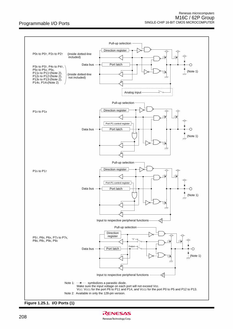
Renesas microcomputers
M16C / 62P Group SINGLE-CHIP 16-BIT CMOS MICROCOMPUTERProgrammable I/O Ports
208
Figure 1.25.1. I/O Ports (1)
P10 to P14
P15 to P17
P57, P60, P64, P73 to P76, P80, P81, P90, P92
Data bus
(Note 1)
Analog input
P00 to P07, P20 to P27
P30 to P37, P40 to P47, P50 to P54, P56, P110 to P117(Note 2), P120 to P127(Note 2), P130 to P137(Note 2), P140, P141(Note 2)
(inside dotted-line included)
(inside dotted-line not included)
"1"
Output
Data bus
Data bus
Data bus
Pull-up selection
Direction register
Direction register
Direction register
Direction register
Port latch
Port latch
Port latch
Port latch
Pull-up selection
Pull-up selection
Pull-up selection
(Note 1)
(Note 1)
(Note 1)
Port P1 control register
Port P1 control register
Input to respective peripheral functions
Input to respective peripheral functions
Note 1: symbolizes a parasitic diode.Make sure the input voltage on each port will not exceed Vcc.VCC: VCC1 for the port P6 to P11 and P14, and VCC2 for the port P0 to P5 and P12 to P13.
Note 2: Available in only the 128-pin version.
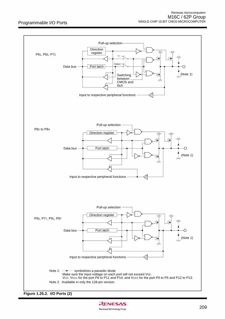
Programmable I/O Ports
209
Renesas microcomputers
M16C / 62P Group SINGLE-CHIP 16-BIT CMOS MICROCOMPUTER
Figure 1.25.2. I/O Ports (2)
P82 to P84
(Note 1)
P55, P77, P91, P97
Data bus
Pull-up selection
Direction register
Port latch
Data bus
Pull-up selection
Direction register
Port latch
Input to respective peripheral functions
Input to respective peripheral functions
(Note 1)
P61, P65, P72"1"
OutputData bus
Direction register
Port latch
Pull-up selection
(Note 1)
Input to respective peripheral functions
Switching betweenCMOS andNch
Note 1: symbolizes a parasitic diode.Make sure the input voltage on each port will not exceed Vcc.VCC: VCC1 for the port P6 to P11 and P14, and VCC2 for the port P0 to P5 and P12 to P13.
Note 2: Available in only the 128-pin version.
Renesas microcomputers
M16C / 62P Group SINGLE-CHIP 16-BIT CMOS MICROCOMPUTERProgrammable I/O Ports
210
Figure 1.25.3. I/O Ports (3)
P62, P66
Data bus
Pull-up selection
Direction register
Port latch
Input to respective peripheral functions
(Note 1)
P70, P71
Data bus
Direction register
Port latch
Input to respective peripheral functions
(Note 2)
Output
“1”
P85
Data bus
(Note 1)NMI interrupt input
P63, P67
Output
“1”
Data bus
Pull-up selection
Direction register
Port latch
(Note 1)
Switching between CMOS and Nch
Note 2: symbolizes a parasitic diode.
Note 1: symbolizes a parasitic diode.Make sure the input voltage on each port will not exceed Vcc. VCC: VCC1 for the port P6 to P11 and P14, and VCC2 for the port P0 to P5 and P12 to P13.
Switching between CMOS and Nch
Programmable I/O Ports
211
Renesas microcomputers
M16C / 62P Group SINGLE-CHIP 16-BIT CMOS MICROCOMPUTER
Figure 1.25.4. I/O Ports (4)
P93, P94
P96
P95
Data bus
Direction register
Pull-up selection
Port latch
Analog input
Input to respective peripheral functions
P100 to P103 (inside dotted-line not included)P104 to P107 (inside dotted-line included)
D-A output enabled
Analog output
“1”
Output
(Note)
Direction register
Direction register
Direction register
Data bus
Data bus
Data bus
Port latch
Port latch
Port latch
Analog input
Analog input
Pull-up selection
Pull-up selection
Pull-up selection
Input to respective peripheral functions
Input to respective peripheral functions
D-A output enabled
(Note)
(Note)
(Note)
“1”
Output
Note: symbolizes a parasitic diode.Make sure the input voltage on each port will not exceed Vcc.VCC: VCC1 for the port P6 to P11 and P14, and VCC2 for the port P0 to P5 and P12 to P13.
Renesas microcomputers
M16C / 62P Group SINGLE-CHIP 16-BIT CMOS MICROCOMPUTERProgrammable I/O Ports
212
Figure 1.25.6. I/O Pins
Figure 1.25.5. I/O Ports (5)
BYTEBYTE signal input
CNVSS
CNVSS signal input
RESETRESET signal input
(Note 2)
(Note 1)
(Note 2)
(Note 1)
(Note 1)
Note 1: symbolizes a parasitic diode. Make sure the input voltage on each port will not exceed VCC1.
Note 2: A parasitic diode on the VCC1 side is added to the mask ROM version. Make sure the input voltage on each port will not exceed VCC1.
P87
P86
fc
Rf
Rd
Data bus
Direction register
Pull-up selection
Port latch
"1"
Output
Direction register
Pull-up selection
Port latchData bus(Note)
(Note)
Note: symbolizes a parasitic diode.Make sure the input voltage on each port will not exceed VCC.VCC: VCC1 for the port P6 to P11 and P14, and VCC2 for the port P0 to P5 and P12 to P13.
Programmable I/O Ports
213
Renesas microcomputers
M16C / 62P Group SINGLE-CHIP 16-BIT CMOS MICROCOMPUTER
Figure 1.25.7. PD0 to PD13 Registers
Port Pi direction register (i=0 to 7 and 9 to 13) (Note 1, 2, 3)
Symbol Address After resetPD0 to PD3 03E216, 03E316, 03E616, 03E716 0016PD4 to PD7 03EA16, 03EB16, 03EE16, 03EF16 0016PD9 to PD12 03F316, 03F616, 03F716, 03FA16 0016PD13 03FB16 0016
Bit name FunctionBit symbol RW
b7 b6 b5 b4 b3 b2 b1 b0
PDi_0 Port Pi0 direction bit
PDi_1 Port Pi1 direction bit
PDi_2 Port Pi2 direction bit
PDi_3 Port Pi3 direction bit
PDi_4 Port Pi4 direction bit
PDi_5 Port Pi5 direction bit
PDi_6 Port Pi6 direction bit
PDi_7 Port Pi7 direction bit
0 : Input mode(Functions as an input port)
1 : Output mode(Functions as an output port)
(i = 0 to 7 and 9 to 13)
Port P8 direction register
Symbol Address After resetPD8 03F216 00X000002
Bit name FunctionBit symbol
b7 b6 b5 b4 b3 b2 b1 b0
PD8_0 Port P80 direction bit
PD8_1 Port P81 direction bit
PD8_2 Port P82 direction bit
PD8_3 Port P83 direction bit
PD8_4 Port P84 direction bitNothing is assigned. In an attempt to write to this bit, write “0”. The value, if read, turns out to be indeterminate.
PD8_6 Port P86 direction bit
PD8_7 Port P87 direction bit
0 : Input mode(Functions as an input port)
1 : Output mode(Functions as an output port)
0 : Input mode(Functions as an input port)
1 : Output mode(Functions as an output port)
Note 1: Make sure the PD9 register is written to by the next instruction after setting the PRCR register’s PRC2 bit to “1” (write enabled).Note 2: During memory extension and microprocessor modes, the PD register for the pins
functioning as bus control pins (A0 to A19, D0 to D15, CS0 to CS3, RD, WRL/WR, WRH/BHE, ALE, RDY, HOLD, HLDA and BCLK) cannot be modified.
Note 3: To use ports P11 to P14, set the PUR3 register’s PU37 bit to “1” (enable). If this bit is set to “0” (disable), the P11 to P14 pins are placed in the high-impedance state.
RWRWRWRW
RW
RWRWRW
RW
RW
RWRWRWRW
RW
RW
(b5)
Renesas microcomputers
M16C / 62P Group SINGLE-CHIP 16-BIT CMOS MICROCOMPUTERProgrammable I/O Ports
214
Port Pi register (i=0 to 7 and 9 to 13) (Note 2, 3)Symbol Address After reset
P0 to P3 03E016, 03E116, 03E416, 03E516 IndeterminateP4 to P7 03E816, 03E916, 03EC16, 03ED16 IndeterminateP9 to P12 03F116, 03F416, 03F516, 03F816 IndeterminateP13 03F916 Indeterminate
Bit name FunctionBit symbol RW
b7 b6 b5 b4 b3 b2 b1 b0
Pi_0 Port Pi0 bit
Pi_1 Port Pi1 bit
Pi_2 Port Pi2 bit
Pi_3 Port Pi3 bit
Pi_4 Port Pi4 bit
Pi_5 Port Pi5 bit
Pi_6 Port Pi6 bit
Pi_7 Port Pi7 bit
The pin level on any I/O port which is set for input mode can be read by reading the corresponding bit in this register. The pin level on any I/O port which is set for output mode can be controlled by writing to the corresponding bit in this register 0 : “L” level 1 : “H” level (Note 1)
(i = 0 to 7 and 9 to 13)
Port P8 register
Symbol Address After reset P8 03F016 Indeterminate
Bit name FunctionBit symbol
b7 b6 b5 b4 b3 b2 b1 b0
P8_0 Port P80 bit
P8_1 Port P81 bit
P8_2 Port P82 bit
P8_3 Port P83 bit
P8_4 Port P84 bit
P8_5 Port P85 bit
P8_6 Port P86 bit
P8_7 Port P87 bit
The pin level on any I/O port which is set for input mode can be read by reading the corresponding bit in this register. The pin level on any I/O port which is set for output mode can be controlled by writing to the corresponding bit in this register (except for P85)0 : “L” level1 : “H” level
Note 1: Since P70 and P71 are N-channel open drain ports, the data is high-impedance.
RWRWRWRWRW
RWRWRW
RWRWRW
RW
RWRW
RWRW
RO
Note 2: During memory extension and microprocessor modes, the Pi register for the pins functioning as bus control pins (A0 to A19, D0 to D15, CS0 to CS3, RD, WRL/WR, WRH/BHE, ALE, RDY, HOLD, HLDA and BCLK) cannot be modified.
Note 3: To use ports P11 to P14, set the PUR3 register’s PU37 bit to “1” (enable). If this bit is set to “0” (disable), the P11 to P14 registers are cleared to ‘0016’ and the P11 to P14 pins are placed in the high-impedance state.
Figure 1.25.8. P0 to P13 Registers
Programmable I/O Ports
215
Renesas microcomputers
M16C / 62P Group SINGLE-CHIP 16-BIT CMOS MICROCOMPUTER
Port P14 control register (128-pin package)
RW
b7 b6 b5 b4 b3 b2 b1 b0
P140 Port P140 bit
P141 Port P141 bit
PD140 Port P140 direction bit
PD141 Port P141 direction bit
0 : Input mode(Functions as an input port)
1 : Output mode(Functions as an output port)
Pull-up control register 3 (128-pin package)
Symbol Address After resetPUR3 03DF16 0016
b7 b6 b5 b4 b3 b2 b1 b0
PU30 P110 to P113 pull-up 0 : Not pulled high1 : Pulled high (Note 1)PU31 P114 to P117 pull-up
PU32 P120 to P123 pull-up
PU33 P124 to P127 pull-up
PU34 P130 to P133 pull-up
PU35 P134 to P137 pull-up
PU36 P140, P141 pull-up
PU37 P11 to P14 enabling bit 0 : Unusable (Note 2)1 : Usable
Symbol Address After reset PC14 03DE16 XX00XXXX2
Bit name FunctionBit symbol
The pin level on any I/O port which is set for input mode can be read by reading the corresponding bit in this register. The pin level on any I/O port which is set for output mode can be controlled by writing to the corresponding bit in this register 0 : “L” level1 : “H” level
Nothing is assigned. In an attempt to write to this bit, write “0”. The value, if read, turns out to be indeterminate.
Bit name FunctionBit symbol
RW
RW
RW
RW
RW
RW
RW
RW
RW
RW
RW
RW
RW
Nothing is assigned. In an attempt to write to this bit, write “0”. The value, if read, turns out to be indeterminate.
(b3-b2)
(b7-b6)
Note 1: The pin for which this bit is “1” (pulled high) and the direction bit is “0” (input mode) is pulled high. Note 2: If the PU37 bit is set to “0” (unusable), the P11 to P14 pins are placed in the high-impedance state and the P11 to P14 registers are cleared to “0”.
Figure 1.25.9. PC14 Register and PUR3 Register
Renesas microcomputers
M16C / 62P Group SINGLE-CHIP 16-BIT CMOS MICROCOMPUTERProgrammable I/O Ports
216
Pull-up control register 0 (Note 1)
Symbol Address After resetPUR0 03FC16 0016
Bit name Function Bit symbol RW
b7 b6 b5 b4 b3 b2 b1 b0
PU00 P00 to P03 pull-up
PU01 P04 to P07 pull-up
PU02 P10 to P13 pull-up
PU03 P14 to P17 pull-up
PU04 P20 to P23 pull-up
PU05 P24 to P27 pull-up
PU06 P30 to P33 pull-up
PU07 P34 to P37 pull-up
0 : Not pulled high 1 : Pulled high (Note 2)
Pull-up control register 1
Symbol Address After reset(Note 5)PUR1 03FD16 000000002
000000102
Bit name Function Bit symbol
b7 b6 b5 b4 b3 b2 b1 b0
PU10 P40 to P43 pull-up (Note 2)
PU11 P44 to P47 pull-up (Note 4)
PU12 P50 to P53 pull-up (Note 2)
PU13 P54 to P57 pull-up (Note 2)
PU14 P60 to P63 pull-up
PU15 P64 to P67 pull-up
PU16 P72 to P73 pull-up (Note 1)
PU17 P74 to P77 pull-up
0 : Not pulled high 1 : Pulled high (Note 3)
Note 1: The P70 and P71 pins do not have pull-ups.Note 2: During memory extension and microprocessor modes, the pins are not pulled high although the contents of these bits can be modified.Note 3: The pin for which this bit is “1” (pulled high) and the direction bit is “0” (input mode) is pulled high.Note 4: If the PM01 to PM00 bits are set to “012” (memory expansion mode) or “112” (microprocessor mode) in a program during single-chip mode, the PU11 bit becomes “1”.Note 5: The values after hardware reset 1 and 2 are as follows: • 000000002 when input on CNVss pin is “L“ • 000000102 when input on CNVss pin is “H“ The values after software reset, watchdog timer reset and oscillation stop detection reset are as follows: • 000000002 when PM 01 to PM00 bits of PM0 register are “002“ (single-chip mode) • 000000102 when PM 01 to PM00 bits of PM0 register are “012“ (memory expansion mode) or “112“ (microprocessor mode)
Note 1: During memory extension and microprocessor modes, the pins are not pulled high although their corresponding register contents can be modified.
RWRWRWRWRWRWRWRW
RWRWRWRWRWRWRWRWRW
Note 2: The pin for which this bit is “1” (pulled high) and the direction bit is “0” (input mode) is pulled high.
Pull-up control register 2
Symbol Address After resetPUR2 03FE16 0016
Bit name FunctionBit symbol
b7 b6 b5 b4 b3 b2 b1 b0
PU20 P80 to P83 pull-up
PU21 P84 to P87 pull-upPU22 P90 to P93 pull-up
PU23 P94 to P97 pull-up
PU24 P100 to P103 pull-up
PU25 P104 to P107 pull-up
Nothing is assigned. In an attempt to write to these bits, write “0”. The value, if read, turns out to be “0”.
0 : Not pulled high 1 : Pulled high (Note 1)
RWRWRW
RW
RWRWRW
(b7-b6)
Note 1: The pin for which this bit is “1” (pulled high) and the direction bit is “0” (input mode) is pulled high.Note 2: The P85 pin does not have pull-up.
(Note 2)
Figure 1.25.10. PUR0 to PUR2 Registers
Programmable I/O Ports
217
Renesas microcomputers
M16C / 62P Group SINGLE-CHIP 16-BIT CMOS MICROCOMPUTER
Figure 1.25.11. PCR Register
Port control register
Symbpl Address After resetPCR 03FF16 0016
Bit name FunctionBit symbol RW
b7 b6 b5 b4 b3 b2 b1 b0
PCR0 Port P1 control bit
Nothing is assigned. In an attempt to write to these bits, write “0”. The value, if read, turns out to be “0”.
RW
(b7-b1)
Operation performed when the P1 register is read 0: When the port is set for input,
the input levels of P10 to P17 pins are read. When set for output, the port latch is read.
1: The port latch is read regardless of whether the port is set for input or output.
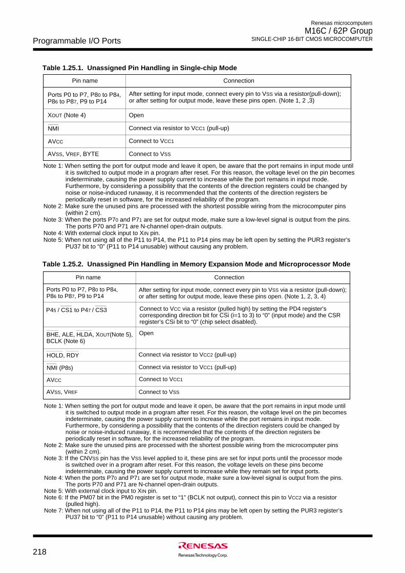
Renesas microcomputers
M16C / 62P Group SINGLE-CHIP 16-BIT CMOS MICROCOMPUTERProgrammable I/O Ports
218
Pin name Connection
Ports P0 to P7, P80 to P84, P86 to P87, P9 to P14
XOUT (Note 4)
AVSS, VREF, BYTE
AVCC
After setting for input mode, connect every pin to VSS via a resistor(pull-down); or after setting for output mode, leave these pins open. (Note 1, 2 ,3)
Open
Connect to VCC1
Connect to VSS
NMI Connect via resistor to VCC1 (pull-up)
Note 1: When setting the port for output mode and leave it open, be aware that the port remains in input mode until it is switched to output mode in a program after reset. For this reason, the voltage level on the pin becomes indeterminate, causing the power supply current to increase while the port remains in input mode. Furthermore, by considering a possibility that the contents of the direction registers could be changed by noise or noise-induced runaway, it is recommended that the contents of the direction registers be periodically reset in software, for the increased reliability of the program.
Note 2: Make sure the unused pins are processed with the shortest possible wiring from the microcomputer pins (within 2 cm).
Note 3: When the ports P70 and P71 are set for output mode, make sure a low-level signal is output from the pins. The ports P70 and P71 are N-channel open-drain outputs.
Note 4: With external clock input to XIN pin. Note 5: When not using all of the P11 to P14, the P11 to P14 pins may be left open by setting the PUR3 register’s
PU37 bit to “0” (P11 to P14 unusable) without causing any problem.
Table 1.25.1. Unassigned Pin Handling in Single-chip Mode
Pin name Connection
Ports P0 to P7, P80 to P84, P86 to P87, P9 to P14
AVSS, VREF
AVCC
After setting for input mode, connect every pin to VSS via a resistor (pull-down); or after setting for output mode, leave these pins open. (Note 1, 2, 3, 4)
Open
Connect to VCC1
Connect to VSS
Note 1: When setting the port for output mode and leave it open, be aware that the port remains in input mode until it is switched to output mode in a program after reset. For this reason, the voltage level on the pin becomes indeterminate, causing the power supply current to increase while the port remains in input mode. Furthermore, by considering a possibility that the contents of the direction registers could be changed by noise or noise-induced runaway, it is recommended that the contents of the direction registers be periodically reset in software, for the increased reliability of the program.
Note 2: Make sure the unused pins are processed with the shortest possible wiring from the microcomputer pins (within 2 cm).
Note 3: If the CNVSS pin has the VSS level applied to it, these pins are set for input ports until the processor mode is switched over in a program after reset. For this reason, the voltage levels on these pins become indeterminate, causing the power supply current to increase while they remain set for input ports.
Note 4: When the ports P70 and P71 are set for output mode, make sure a low-level signal is output from the pins. The ports P70 and P71 are N-channel open-drain outputs.
Note 5: With external clock input to XIN pin. Note 6: If the PM07 bit in the PM0 register is set to “1” (BCLK not output), connect this pin to VCC2 via a resistor (pulled high).Note 7: When not using all of the P11 to P14, the P11 to P14 pins may be left open by setting the PUR3 register’s
PU37 bit to “0” (P11 to P14 unusable) without causing any problem.
HOLD, RDY Connect via resistor to VCC2 (pull-up)
BHE, ALE, HLDA, XOUT(Note 5), BCLK (Note 6)
P45 / CS1 to P47 / CS3 Connect to VCC via a resistor (pulled high) by setting the PD4 register’s corresponding direction bit for CSi (i=1 to 3) to “0” (input mode) and the CSR register’s CSi bit to “0” (chip select disabled).
NMI (P85) Connect via resistor to VCC1 (pull-up)
Table 1.25.2. Unassigned Pin Handling in Memory Expansion Mode and Microprocessor Mode
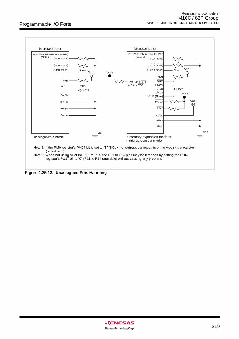
Programmable I/O Ports
219
Renesas microcomputers
M16C / 62P Group SINGLE-CHIP 16-BIT CMOS MICROCOMPUTER
Figure 1.25.12. Unassigned Pins Handling
(Input mode)···
(Input mode)
(Output mode)
NMI
XOUT
AVCC
BYTE
AVSS
VREF
Microcomputer
VCC1
VSS
In single-chip mode
Port P6 to P14 (except for P85)
(Input mode)···
(Input mode)
(Output mode)
NMI
XOUT
AVCC
AVSS
VREF
Open
Microcomputer
VCC2
VSS
In memory expansion mode or in microprocessor mode
HOLD
RDY
ALE
BCLK (Note)
BHEHLDAOpen
Open Open
···
···
Port P45 / CS1to P47 / CS3
Note 1: If the PM0 register’s PM07 bit is set to “1” (BCLK not output), connect this pin to VCC2 via a resistor (pulled high).Note 2: When not using all of the P11 to P14, the P11 to P14 pins may be left open by setting the PUR3 register’s PU37 bit to “0” (P11 to P14 unusable) without causing any problem.
(Note 2)Port P0 to P14 (except for P85)
(Note 2)
VCC1 VCC2VCC1
VCC1
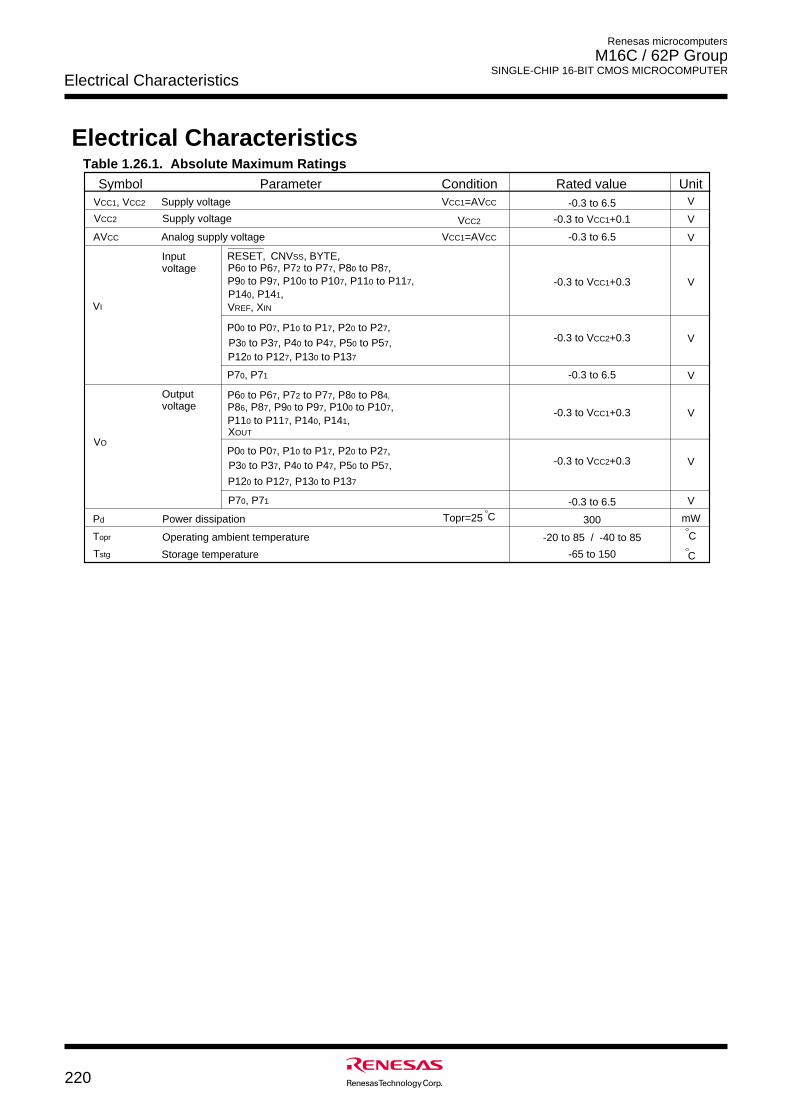
Renesas microcomputers
M16C / 62P Group SINGLE-CHIP 16-BIT CMOS MICROCOMPUTER
Electrical Characteristics
220
Table 1.26.1. Absolute Maximum Ratings
Operating ambient temperature
Parameter Unit
VREF, XIN
Input voltage
Analog supply voltage
Supply voltage
Output voltage
XOUTVO
-0.3 to VCC1+0.3
-0.3 to VCC1+0.3
Pd Power dissipation
Storage temperature
Rated valueV
V
V
Condition
VI
AVCC
VCC1, VCC2
Tstg
Topr
Symbol
mW
P30 to P37, P40 to P47, P50 to P57,
P60 to P67, P72 to P77, P80 to P87,
P60 to P67, P72 to P77, P80 to P84,
P00 to P07, P10 to P17, P20 to P27,
P90 to P97, P100 to P107, P110 to P117,
P86, P87, P90 to P97, P100 to P107,
P70, P71
P70, P71
-0.3 to 6.5
V
V
RESET, CNVSS, BYTE,
VCC1=AVCC
VCC1=AVCC -0.3 to 6.5
P140, P141,
Supply voltage -0.3 to VCC1+0.1 VVCC2 VCC2
P120 to P127, P130 to P137
-0.3 to VCC2+0.3 V
V
P110 to P117, P140, P141,
P30 to P37, P40 to P47, P50 to P57, P00 to P07, P10 to P17, P20 to P27,
P120 to P127, P130 to P137
-0.3 to VCC2+0.3 V
-0.3 to 6.5
-65 to 150
300
-20 to 85 / -40 to 85
-0.3 to 6.5
C
Topr=25 C
C
Electrical Characteristics
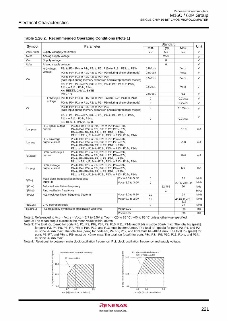
Electrical Characteristics
221
Renesas microcomputers
M16C / 62P Group SINGLE-CHIP 16-BIT CMOS MICROCOMPUTER
2.7 5
.
5Typ. M
a
x
. UnitParameter
VC
C
1,
VC
C
2 5
.
0S
u
p
p
l
y
v
o
l
t
a
g
e
(
VC
C
1≥V
C
C
2)
Symbol M
i
n
.S
t
a
n
d
a
r
d
A
n
a
l
o
g
s
u
p
p
l
y
v
o
l
t
a
g
e VC
C
1A
V
c
c VV0
0A
n
a
l
o
g
s
u
p
p
l
y
v
o
l
t
a
g
e
S
u
p
p
l
y
v
o
l
t
a
g
e
VI
H
IO
H
(
a
v
g
)
HIGH average output current
mA
mA
V
s
s
A
V
s
s0.8VCC2
VV
V
V
V
VC
C
2
0.2VCC2
0.2VCC1
0
0
0
L
O
W
i
n
p
u
t
v
o
l
t
a
g
e
0
.
1
6
VC
C
2
IOH (peak)
HIGH peak output current
H
I
G
H
i
n
p
u
t
v
o
l
t
a
g
e
-5.0
-10.0P00 to P07, P10 to P17, P20 to P27,P30 to P37,P40 to P47, P50 to P57, P60 to P67,P72 to P77,P
80
t
o
P
84
,P
86
,P
87
,P
90
t
o
P
97
,P
1
00
t
o
P
1
07,
P31 to P37, P40 to P47, P50 to P57, P120 to P127, P130 to P137
V
V0
.
8
VC
C
2
0.5VCC2
VC
C
2
VC
C
2( d
a
t
a
i
n
p
u
t
d
u
r
i
n
g
m
e
m
o
r
y
e
x
p
a
n
s
i
o
n
a
n
d
m
i
c
r
o
p
r
o
c
e
s
s
o
r
m
o
d
e
s
)
P
00
t
o
P
07,
P
10
t
o
P
17,
P
20
t
o
P
27,
P
30
(
d
u
r
i
n
g
s
i
n
g
l
e
-
c
h
i
p
m
o
d
e
)
P
00
t
o
P
07,
P
10
t
o
P
17,
P
20
t
o
P
27,
P
30
L
O
W
p
e
a
k
o
u
t
p
u
t
c
u
r
r
e
n
t 10.0
5
.
0
mA
f (
XI
N)Main clock input oscillation frequency(Note 4)
LOW average output current
IOL (peak)
m
AIO
L
(
a
v
g
)
V
P00 to P07, P10 to P17, P20 to P27,P30 to P37,P40 to P47, P50 to P57, P60 to P67,P72 to P77,P80 to P84,P86,P87,P90 to P97,P100 to P107,
P00 to P07, P10 to P17, P20 to P27,P30 to P37,P40 to P47, P50 to P57, P60 to P67,P70 to P77,P80 to P84,P86,P87,P90 to P97,P100 to P107,
P00 to P07, P10 to P17, P20 to P27,P30 to P37,P40 to P47, P50 to P57, P60 to P67,P70 to P77,P80 to P84,P86,P87,P90 to P97,P100 to P107,
P
70
,
P
71
0.8VCC1 6
.
5 V
VI
L
2
0
X
VC
C
1-
4
4
VC
C
1=
3
.
0
t
o
5
.
5
V
VC
C
1=
2
.
7
t
o
3
.
0
V
0
0
MHz
MHz
1
6
f (
XC
I
N) S
u
b
-
c
l
o
c
k
o
s
c
i
l
l
a
t
i
o
n
f
r
e
q
u
e
n
c
y kHz5
032.768
P
1
10
t
o
P
1
17,
P
1
20
t
o
P
1
27,
P
1
30
t
o
P
1
37,
P
1
40,
P
1
41
P110 to P117, P120 to P127, P130 to P137, P140, P141
P110 to P117, P120 to P127, P130 to P137, P140, P141
P110 to P117, P120 to P127, P130 to P137, P140, P141
N
o
t
e
1
:
R
e
f
e
r
e
n
c
e
d
t
o
VC
C
=
VC
C
1
=
VC
C
2
=
2
.
7
t
o
5
.
5
V
a
t
T
o
p
r
=
-
2
0
t
o
8
5
°
C
/
-
4
0
t
o
8
5
°
C
u
n
l
e
s
s
o
t
h
e
r
w
i
s
e
s
p
e
c
i
f
i
e
d
.
N
o
t
e
2
:
T
h
e
m
e
a
n
o
u
t
p
u
t
c
u
r
r
e
n
t
i
s
t
h
e
m
e
a
n
v
a
l
u
e
w
i
t
h
i
n
1
0
0
m
s
.N
o
t
e
3
:
T
h
e
t
o
t
a
l
IO
L
(
p
e
a
k
)
f
o
r
p
o
r
t
s
P
0
,
P
1
,
P
2
,
P
86,
P
87,
P
9
,
P
1
0
,
P
1
1
,
P
1
40
a
n
d
P
1
41
m
u
s
t
b
e
8
0
m
A
m
a
x
.
T
h
e
t
o
t
a
l
IO
L
(
p
e
a
k
)
f
o
r
p
o
r
t
s
P
3
,
P
4
,
P
5
,
P
6
,
P
7
,
P
80
t
o
P
84,
P
1
2
,
a
n
d
P
1
3
m
u
s
t
b
e
8
0
m
A
m
a
x
.
T
h
e
t
o
t
a
l
IO
H
(
p
e
a
k
)
f
o
r
p
o
r
t
s
P
0
,
P
1
,
a
n
d
P
2
m
u
s
t
b
e
-
4
0
m
A
m
a
x
.
T
h
e
t
o
t
a
l
IO
H
(
p
e
a
k
)
f
o
r
p
o
r
t
s
P
3
,
P
4
,
P
5
,
P
1
2
,
a
n
d
P
1
3
m
u
s
t
b
e
-
4
0
m
A
m
a
x
.
T
h
e
t
o
t
a
l
IO
H
(
p
e
a
k
)
f
o
r
p
o
r
t
s
P
6
,
P
7
,
a
n
d
P
80
t
o
P
84
m
u
s
t
b
e
-
4
0
m
A
m
a
x
.
T
h
e
t
o
t
a
l
IO
H
(
p
e
a
k
)
f
o
r
p
o
r
t
s
P
86,
P
87,
P
9
,
P
1
0
,
P
1
1
,
P
1
40,
a
n
d
P
1
41 m
u
s
t
b
e
-
4
0
m
A
m
a
x
.N
o
t
e
4
:
R
e
l
a
t
i
o
n
s
h
i
p
b
e
t
w
e
e
n
m
a
i
n
c
l
o
c
k
o
s
c
i
l
l
a
t
i
o
n
f
r
e
q
u
e
n
c
y
,
P
L
L
c
l
o
c
k
o
s
c
i
l
l
a
t
i
o
n
f
r
e
q
u
e
n
c
y
a
n
d
s
u
p
p
l
y
v
o
l
t
a
g
e
.
0
.
8
VC
C
1 VVCC1P
60
t
o
P
67,
P
72
t
o
P
77,
P
80
t
o
P
87,
P
90
t
o
P
97,
P
1
00
t
o
P
1
07,
XI
N,
R
E
S
E
T
,
C
N
VS
S,
B
Y
T
EP
1
10
t
o
P
1
17,
P
1
40,
P
1
41,
P
31
t
o
P
37,
P
40
t
o
P
47,
P
50
t
o
P
57
,
P
1
20
t
o
P
1
27,
P
1
30
t
o
P
1
37
P
00
t
o
P
07,
P
10
t
o
P
17,
P
20
t
o
P
27,
P
30
(
d
u
r
i
n
g
s
i
n
g
l
e
-
c
h
i
p
m
o
d
e
)
V0.2VCC20
( d
a
t
a
i
n
p
u
t
d
u
r
i
n
g
m
e
m
o
r
y
e
x
p
a
n
s
i
o
n
a
n
d
m
i
c
r
o
p
r
o
c
e
s
s
o
r
m
o
d
e
s
)
P
00
t
o
P
07,
P
10
t
o
P
17,
P
20
t
o
P
27,
P
30
P60 to P67, P70 to P77, P80 to P87, P90 to P97, P100 to P107,
XIN, RESET, CNVSS, BYTEP110 to P117, P140, P141,
f (Ring) Ring oscillation frequency MHz1f (
P
L
L
) P
L
L
c
l
o
c
k
o
s
c
i
l
l
a
t
i
o
n
f
r
e
q
u
e
n
c
y
(
N
o
t
e
4
)
4
6
.
6
7
X
VC
C
1-1
1
6
VC
C
1=
3
.
0
t
o
5
.
5
V
VC
C
1=
2
.
7
t
o
3
.
0
V
10
1
0
MHz
MHz
2
4
f (
B
C
L
K
) C
P
U
o
p
e
r
a
t
i
o
n
c
l
o
c
k 0 MHz24
TSU(PLL) PLL frequency synthesizer stabilization wait time VC
C
1=
5
.
0
V
VC
C
1=
3
.
0
V 5020 ms
ms
Main clock input oscillation frequency
16.0
0.0
f(X
IN)
oper
atin
g m
axim
um fr
eque
ncy
[MH
Z]
VCC1[V] (main clock: no division)
5.53.0
10.0
2.7AAAAAAAAAAAAAAAAAAAAAAAAAAAAAAAAAAAA
20 x VCC1-44MHZ
PLL clock oscillation frequency
24.0
0.0f(P
LL)
oper
atin
g m
axim
um fr
eque
ncy
[MH
Z]
VCC1[V] (PLL clock oscillation)
5.5
10.0
2.7
AAAAAAAAAAAAAAAAAAAAAAAAAAAAAA
3.0
46.67 x VCC1-116MHZ
Table 1.26.2. Recommended Operating Conditions (Note 1)
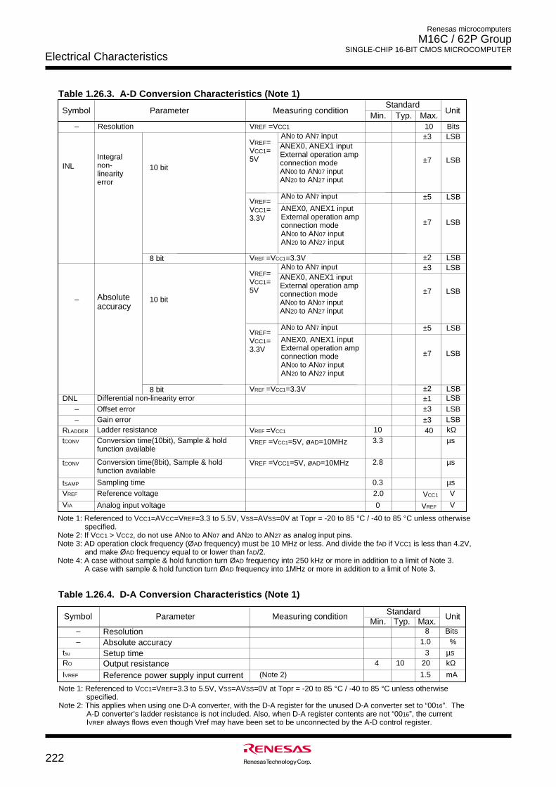
Renesas microcomputers
M16C / 62P Group SINGLE-CHIP 16-BIT CMOS MICROCOMPUTER
Electrical Characteristics
222
Table 1.26.3. A-D Conversion Characteristics (Note 1)Standard
Min. T
y
p
. Max.–
I N
L
R
e
s
o
l
u
t
i
o
n
I n
t
e
g
r
a
l
n
o
n
-l
i
n
e
a
r
i
t
y
e
r
r
o
r
BitsVREF =VCC1 1 0
S
y
m
b
o
l Parameter M
e
a
s
u
r
i
n
g
c
o
n
d
i
t
i
o
n Unit
AN0 to AN7 inputA
N
E
X
0
,
A
N
E
X
1
i
n
p
u
tE
x
t
e
r
n
a
l
o
p
e
r
a
t
i
o
n
a
m
p
c
o
n
n
e
c
t
i
o
n
m
o
d
eA
N0
0
t
o
A
N0
7
i
n
p
u
tA
N2
0
t
o
A
N2
7
i
n
p
u
t
VREF=VCC1=5V
L S
B±
3
L S
B±
7
LSBVREF =VCC1=3.3V8
b
i
t ±2
RL
A
D
D
E
R
tC
O
N
V
Ladder resistanceConversion time(10bit), Sample & hold function available
Reference voltage
Analog input voltage
kΩµs
V
VIA
VREF
V0
2.0
10
VCC1
VR
E
F
403.3
Conversion time(8bit), Sample & hold function available
µ
s2 .
8tCONV
tS
A
M
P Sampling time 0 .
3 µ
s
VREF =VCC1
VREF =VCC1=5V, øAD=10MHz
VREF =VCC1=5V, øAD=10MHz
D
N
L Differential non-linearity errorOffset errorGain error
––
L S
B
L S
B
L S
B
±1± 3
±3
Note 1: Referenced to VCC1=AVCC=VREF=3.3 to 5.5V, VSS=AVSS=0V at Topr = -20 to 85 °C / -40 to 85 °C unless otherwise specified.
Note 2: If VCC1 > VCC2, do not use AN00 to AN07 and AN20 to AN27 as analog input pins.Note 3: AD operation clock frequency (ØAD frequency) must be 10 MHz or less. And divide the fAD if VCC1 is less than 4.2V,
and make ØAD frequency equal to or lower than fAD/2.Note 4: A case without sample & hold function turn ØAD frequency into 250 kHz or more in addition to a limit of Note 3.
A case with sample & hold function turn ØAD frequency into 1MHz or more in addition to a limit of Note 3.
1 0
b
i
t
AN0 to AN7 input
ANEX0, ANEX1 inputExternal operation amp connection modeAN00 to AN07 inputAN20 to AN27 input
VREF=VCC1=3.3V
LSB± 5
L S
B±
7
AN0 to AN7 inputA
N
E
X
0
,
A
N
E
X
1
i
n
p
u
tE
x
t
e
r
n
a
l
o
p
e
r
a
t
i
o
n
a
m
p
c
o
n
n
e
c
t
i
o
n
m
o
d
eA
N0
0
t
o
A
N0
7
i
n
p
u
tA
N2
0
t
o
A
N2
7
i
n
p
u
t
VREF=VCC1=5V
L S
B±
3
L S
B±
7
LSBVREF =VCC1=3.3V8 bit ± 2
1 0
b
i
t
AN0 to AN7 input
ANEX0, ANEX1 inputExternal operation amp connection modeAN00 to AN07 inputAN20 to AN27 input
VREF=VCC1=3.3V
LSB± 5
LSB±7
– Absolute accuracy
Table 1.26.4. D-A Conversion Characteristics (Note 1)
M
i
n
. T
y
p
. M
a
x
.––
tsu
RO
R
e
s
o
l
u
t
i
o
nA
b
s
o
l
u
t
e
a
c
c
u
r
a
c
ySetup timeOutput resistanceR
e
f
e
r
e
n
c
e
p
o
w
e
r
s
u
p
p
l
y
i
n
p
u
t
c
u
r
r
e
n
t
Bits%
kΩm
AIV
R
E
F
1 .
0
1 .
5
8
3
S
y
m
b
o
l P
a
r
a
m
e
t
e
r Measuring condition U
n
i
t
20104µs
( N
o
t
e
2
)
Standard
Note 1: Referenced to VCC1=VREF=3.3 to 5.5V, VSS=AVSS=0V at Topr = -20 to 85 °C / -40 to 85 °C unless otherwise specified.
Note 2: This applies when using one D-A converter, with the D-A register for the unused D-A converter set to “0016”. The A-D converter’s ladder resistance is not included. Also, when D-A register contents are not “0016”, the current IVREF always flows even though Vref may have been set to be unconnected by the A-D control register.
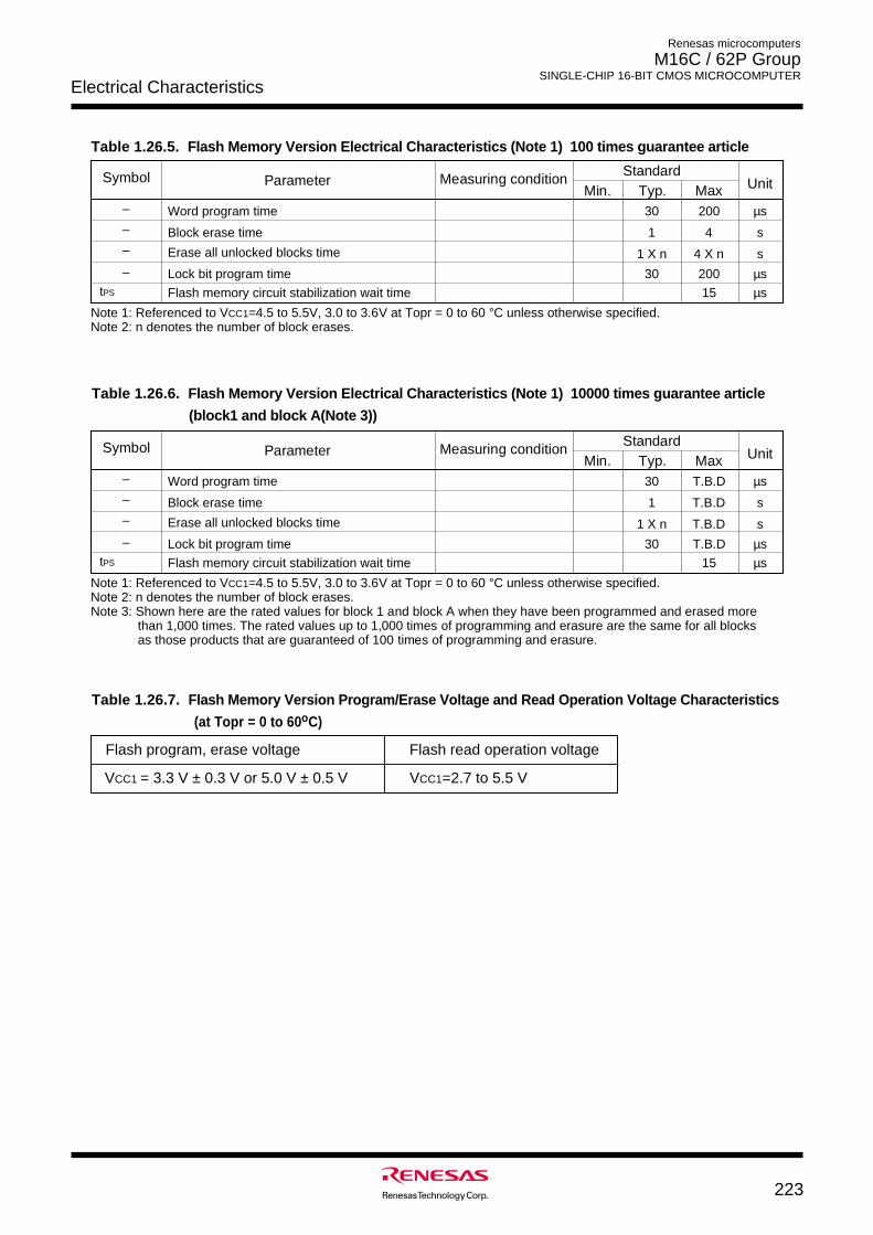
Electrical Characteristics
223
Renesas microcomputers
M16C / 62P Group SINGLE-CHIP 16-BIT CMOS MICROCOMPUTER
Table 1.26.5. Flash Memory Version Electrical Characteristics (Note 1) 100 times guarantee article
W
o
r
d
p
r
o
g
r
a
m
t
i
m
e
B
l
o
c
k
e
r
a
s
e
t
i
m
e
E
r
a
s
e
a
l
l
u
n
l
o
c
k
e
d
b
l
o
c
k
s
t
i
m
e
L o
c
k
b
i
t
p
r
o
g
r
a
m
t
i
m
e
3
0
1
1
X
n
3
0
200
4
4
X
n
2
0
0
µ
s
s
s
µ
s
ParameterStandard
M
i
n
. Typ. M
a
x U
n
i
t
N
o
t
e
1
:
R
e
f
e
r
e
n
c
e
d
t
o
VC
C
1=
4
.
5
t
o
5
.
5
V
,
3
.
0
t
o
3
.
6
V
a
t
T
o
p
r
=
0
t
o
6
0
°
C
u
n
l
e
s
s
o
t
h
e
r
w
i
s
e
s
p
e
c
i
f
i
e
d
.
N
o
t
e
2
:
n
d
e
n
o
t
e
s
t
h
e
n
u
m
b
e
r
o
f
b
l
o
c
k
e
r
a
s
e
s
.
Measuring conditionS
y
m
b
o
l
–
–
–
–
tP
S F
l
a
s
h
m
e
m
o
r
y
c
i
r
c
u
i
t
s
t
a
b
i
l
i
z
a
t
i
o
n
w
a
i
t
t
i
m
e 1
5 µ
s
W
o
r
d
p
r
o
g
r
a
m
t
i
m
e
B
l
o
c
k
e
r
a
s
e
t
i
m
e
Erase all unlocked blocks time
Lock bit program time
3
0
1
1
X
n
30
T.B.D
T
.
B
.
D
T
.
B
.
D
T.B.D
µ
s
s
s
µs
ParameterStandard
Min. Typ. Max U
n
i
t
Note 1: Referenced to VCC1=4.5 to 5.5V, 3.0 to 3.6V at Topr = 0 to 60 °C unless otherwise specified. Note 2: n denotes the number of block erases.Note 3: Shown here are the rated values for block 1 and block A when they have been programmed and erased more
than 1,000 times. The rated values up to 1,000 times of programming and erasure are the same for all blocks as those products that are guaranteed of 100 times of programming and erasure.
Measuring conditionS
y
m
b
o
l
–
–
–
–
tPS Flash memory circuit stabilization wait time 15 µs
Table 1.26.7. Flash Memory Version Program/Erase Voltage and Read Operation Voltage Characteristics
(at Topr = 0 to 60oC)
Flash program, erase voltage Flash read operation voltage
VCC1 = 3.3 V ± 0.3 V or 5.0 V ± 0.5 V VCC1=2.7 to 5.5 V
Table 1.26.6. Flash Memory Version Electrical Characteristics (Note 1) 10000 times guarantee article
(block1 and block A(Note 3))
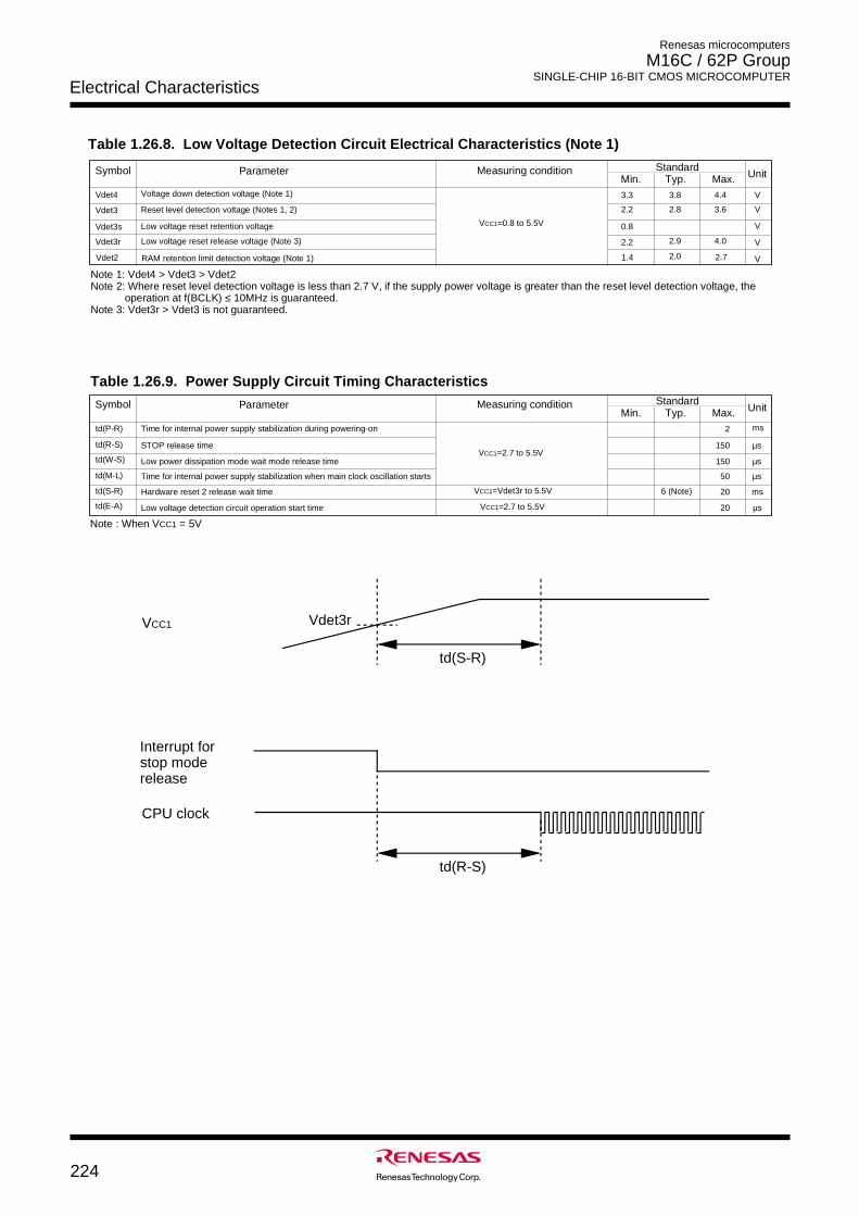
Renesas microcomputers
M16C / 62P Group SINGLE-CHIP 16-BIT CMOS MICROCOMPUTER
Electrical Characteristics
224
Table 1.26.8. Low Voltage Detection Circuit Electrical Characteristics (Note 1)
S
y
m
b
o
l S
t
a
n
d
a
r
dT
y
p
. U
n
i
tM
e
a
s
u
r
i
n
g
c
o
n
d
i
t
i
o
n
M
i
n
. M
a
x
.P
a
r
a
m
e
t
e
r
V
d
e
t
4 Vo
l
t
a
g
e
d
o
w
n
d
e
t
e
c
t
i
o
n
v
o
l
t
a
g
e
(
N
o
t
e
1
)
V3
.
8 4
.
4
VC
C
1=
0
.
8
t
o
5
.
5
V
Note 1: Vdet4 > Vdet3 > Vdet2Note 2: Where reset level detection voltage is less than 2.7 V, if the supply power voltage is greater than the reset level detection voltage, the
operation at f(BCLK) ≤ 10MHz is guaranteed.Note 3: Vdet3r > Vdet3 is not guaranteed.
3
.
3
V
d
e
t
3 R
e
s
e
t
l
e
v
e
l
d
e
t
e
c
t
i
o
n
v
o
l
t
a
g
e
(
N
o
t
e
s
1
,
2
)
V2
.
8 3
.
62
.
2
V
d
e
t
2 R
A
M
r
e
t
e
n
t
i
o
n
l
i
m
i
t
d
e
t
e
c
t
i
o
n
v
o
l
t
a
g
e
(
N
o
t
e
1
)
V
2
.
7
0
.
8
2
.
9 4
.
0
2
.
0
S
y
m
b
o
l S
t
a
n
d
a
r
dT
y
p
. U
n
i
tM
e
a
s
u
r
i
n
g
c
o
n
d
i
t
i
o
n
M
i
n
. M
a
x
.P
a
r
a
m
e
t
e
r
2
VCC1=2.7 to 5.5V
N
o
t
e
:
W
h
e
n
VC
C
1
=
5
V
150
6 (Note)
50
t d
(
R
-
S
) STOP release time
20
t d
(
M
-
L
) Time for internal power supply stabilization when main clock oscillation starts
20
t d
(
S
-
R
) H
a
r
d
w
a
r
e
r
e
s
e
t
2
r
e
l
e
a
s
e
w
a
i
t
t
i
m
e
µs
m
s
V
d
e
t
3
s L
o
w
v
o
l
t
a
g
e
r
e
s
e
t
r
e
t
e
n
t
i
o
n
v
o
l
t
a
g
e
V
d
e
t
3
r L
o
w
v
o
l
t
a
g
e
r
e
s
e
t
r
e
l
e
a
s
e
v
o
l
t
a
g
e
(
N
o
t
e
3
)
2
.
2
1.
4
V
V
t d
(
P
-
R
) T
i
m
e
f
o
r
i
n
t
e
r
n
a
l
p
o
w
e
r
s
u
p
p
l
y
s
t
a
b
i
l
i
z
a
t
i
o
n
d
u
r
i
n
g
p
o
w
e
r
i
n
g
-
o
n
t d
(
E
-
A
) L
o
w
v
o
l
t
a
g
e
d
e
t
e
c
t
i
o
n
c
i
r
c
u
i
t
o
p
e
r
a
t
i
o
n
s
t
a
r
t
t
i
m
e
µs
µs
m
s
VC
C
1=
2
.
7
t
o
5
.
5
V
VCC1=Vdet3r to 5.5V
t d
(
W
-
S
) Low power dissipation mode wait mode release time 150 µs
Interrupt for stop moderelease
CPU clock
td(R-S)
td(S-R)
Vdet3rVCC1
Table 1.26.9. Power Supply Circuit Timing Characteristics
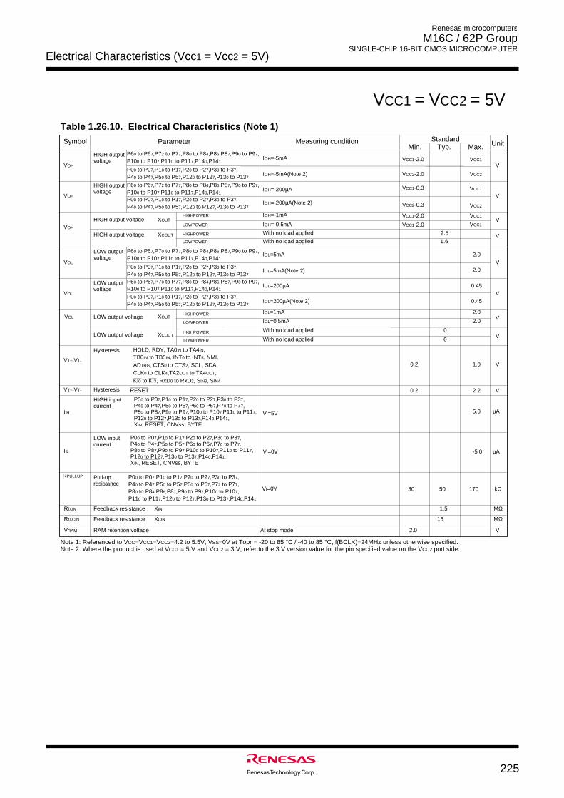
Electrical Characteristics (Vcc1 = Vcc2 = 5V)
225
Renesas microcomputers
M16C / 62P Group SINGLE-CHIP 16-BIT CMOS MICROCOMPUTER
VCC1 = VCC2 = 5VTable 1.26.10. Electrical Characteristics (Note 1)S
y
m
b
o
l
VO
H
VO
H
H
I
G
H
o
u
t
p
u
t
v
o
l
t
a
g
eVO
H
VO
L
L
O
W
o
u
t
p
u
tv
o
l
t
a
g
e
L
O
W
o
u
t
p
u
tv
o
l
t
a
g
eVO
L
VOL
H
I
G
H
o
u
t
p
u
t
v
o
l
t
a
g
e
H
I
G
H
o
u
t
p
u
t
v
o
l
t
a
g
e
StandardT
y
p
. U
n
i
tM
e
a
s
u
r
i
n
g
c
o
n
d
i
t
i
o
n
V
V
VXO
U
T
V
2
.
0
0
.
4
5V
VXO
U
T2
.
0
2
.
0
M
i
n
. Max.
VC
C
2-
2
.
0
P
a
r
a
m
e
t
e
r
IOH=-5mA(Note 2)
IOH=-1mA
IOH=-200µA(Note 2)
IOH=-0.5mA
IOL=5mA(Note 2)
IOL=1mA
IOL=200µA(Note 2)
IOL=0.5mA
P
60
t
o
P
67,
P
72
t
o
P
77,
P
80
t
o
P
84,
P
86,
P
87,
P
90
t
o
P
97,
H
I
G
H
P
O
W
E
R
L O
W
P
O
W
E
R
HIGHPOWER
L O
W
P
O
W
E
R
H
I
G
H
P
O
W
E
R
L O
W
P
O
W
E
R
H
I
G
H
o
u
t
p
u
t
v
o
l
t
a
g
e
XC
O
U
T With no load applied
With no load applied
2.5
1
.
6V
Hysteresis
Hysteresis
H
I
G
H
i
n
p
u
tc
u
r
r
e
n
tII
H
L
O
W
i
n
p
u
tc
u
r
r
e
n
tIIL
VR
A
M R
A
M
r
e
t
e
n
t
i
o
n
v
o
l
t
a
g
e
VT
+
-VT
-
VT+-VT-
C
L
K0
t
o
C
L
K4,
T
A
2O
U
T
t
o
T
A
4O
U
T,
0.2 1.0 V
0.2 2.2 V
5
.
0 µ
A
µ
A
At stop mode 2
.
0 V
RESET
HOLD, RDY, TA0IN to TA4IN,
A
DT
R
G,
C
T
S0
t
o
C
T
S2,
S
C
L
,
S
D
A
,
VI=5V
VI=0V - 5
.
0
RfXIN
Rf
X
C
I
N
Feedback resistance XIN
F
e
e
d
b
a
c
k
r
e
s
i
s
t
a
n
c
e
XC
I
N 1
5
1.5 MΩ
M
Ω
P00 to P07,P10 to P17,P20 to P27,P30 to P37,P40 to P47,P50 to P57,P60 to P67,P70 to P77,P80 to P87,P90 to P97,P100 to P107,P110 to P117,P120 to P127,P130 to P137,P140,P141,XIN, RESET, CNVss, BYTE
P00 to P07,P10 to P17,P20 to P27,P30 to P37,P40 to P47,P50 to P57,P60 to P67,P70 to P77,P80 to P87,P90 to P97,P100 to P107,P110 to P117,P120 to P127,P130 to P137,P140,P141,XIN, RESET, CNVss, BYTE
RP
U
L
L
U
P P
u
l
l
-
u
pr
e
s
i
s
t
a
n
c
e5
0 k Ω
T
B
0I
N
t
o
T
B
5I
N,
I
N
T0
t
o
I
N
T5,
N
M
I
,
VXC
O
U
T0
0
With no load applied
With no load appliedHIGHPOWER
LOWPOWER
VI=
0
V 3
0 1
7
0
K
I0
t
o
K
I3,
R
x
D0
t
o
R
x
D2,
SI
N
3,
SI
N
4
P
40
t
o
P
47,
P
50
t
o
P
57,
P
1
20
t
o
P
1
27,
P
1
30
t
o
P
1
37
P
40
t
o
P
47,
P
50
t
o
P
57,
P
60
t
o
P
67,
P
72
t
o
P
77,P80 to P84,P86,P87,P90 to P97,P100 to P107,
P00 to P07,P10 to P17,P20 to P27,P30 to P37,
P
1
10
t
o
P
1
17,
P
1
20
t
o
P
1
27,
P
1
30
t
o
P
1
37,
P
1
40,
P
1
41
VC
C
2-
0
.
3
VC
C
1-
2
.
0
VC
C
1-
2
.
0
N
o
t
e
1
:
R
e
f
e
r
e
n
c
e
d
t
o
VC
C=
VC
C
1=
VC
C
2=
4
.
2
t
o
5
.
5
V
,
VS
S=
0
V
a
t
T
o
p
r
=
-
2
0
t
o
8
5
°
C
/
-
4
0
t
o
8
5
°
C
,
f
(
B
C
L
K
)
=
2
4
M
H
z
u
n
l
e
s
s
o
t
h
e
r
w
i
s
e
s
p
e
c
i
f
i
e
d
.
N
o
t
e
2
:
W
h
e
r
e
t
h
e
p
r
o
d
u
c
t
i
s
u
s
e
d
a
t
VC
C
1
=
5
V
a
n
d
VC
C
2
=
3
V
,
r
e
f
e
r
t
o
t
h
e
3
V
v
e
r
s
i
o
n
v
a
l
u
e
f
o
r
t
h
e
p
i
n
s
p
e
c
i
f
i
e
d
v
a
l
u
e
o
n
t
h
e
VC
C
2
p
o
r
t
s
i
d
e
.
VCC2
VCC2
P
1
00
t
o
P
1
07,
P
1
10
t
o
P
1
17,
P
1
40,
P
1
41
P00 to P07,P10 to P17,P20 to P27,P30 to P37,
IOH=-5mA
IOH=-200µAP60 to P67,P72 to P77,P80 to P84,P86,P87,P90 to P97,
P
40
t
o
P
47,
P
50
t
o
P
57,
P
1
20
t
o
P
1
27,
P
1
30
t
o
P
1
37
P
1
00
t
o
P
1
07,
P
1
10
t
o
P
1
17,
P
1
40,
P
1
41
P00 to P07,P10 to P17,P20 to P27,P30 to P37,
VC
C
1-
2
.
0
VC
C
1-
0
.
3
VCC1
VCC1
VCC1
VCC1
P
60
t
o
P
67,
P
70
t
o
P
77,
P
80
t
o
P
84,
P
86,
P
87,
P
90
t
o
P
97,
P
40
t
o
P
47,
P
50
t
o
P
57,
P
1
20
t
o
P
1
27,
P
1
30
t
o
P
1
37
P
1
00
t
o
P
1
07,
P
1
10
t
o
P
1
17,
P
1
40,
P
1
41
P
00
t
o
P
07,
P
10
t
o
P
17,
P
20
t
o
P
27,
P
30
t
o
P
37,
P
60
t
o
P
67,
P
70
t
o
P
77,
P
80
t
o
P
84,
P
86,
P
87,
P
90
t
o
P
97,
P
40
t
o
P
47,
P
50
t
o
P
57,
P
1
20
t
o
P
1
27,
P
1
30
t
o
P
1
37
P
1
00
t
o
P
1
07,
P
1
10
t
o
P
1
17,
P
1
40,
P
1
41
P
00
t
o
P
07,
P
10
t
o
P
17,
P
20
t
o
P
27,
P
30
t
o
P
37,
IOL=5mA
IOL=200µA
2
.
0
0
.
4
5
L
O
W
o
u
t
p
u
t
v
o
l
t
a
g
e
L
O
W
o
u
t
p
u
t
v
o
l
t
a
g
e
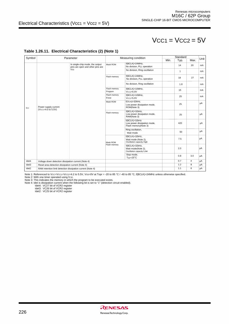
Electrical Characteristics (Vcc1 = Vcc2 = 5V)
226
Renesas microcomputers
M16C / 62P Group SINGLE-CHIP 16-BIT CMOS MICROCOMPUTER
VCC1 = VCC2 = 5VTable 1.26.11. Electrical Characteristics (2) (Note 1)
S
y
m
b
o
l S
t
a
n
d
a
r
dTyp. UnitMeasuring condition
M
i
n
. Max.P
a
r
a
m
e
t
e
r
IC
CP
o
w
e
r
s
u
p
p
l
y
c
u
r
r
e
n
t(
VC
C
1=
4
.
0
t
o
5
.
5
V
)
N
o
d
i
v
i
s
i
o
n
,
P
L
L
o
p
e
r
a
t
i
o
n m
AI n
s
i
n
g
l
e
-
c
h
i
p
m
o
d
e
,
t
h
e
o
u
t
p
u
t
p
i
n
s
a
r
e
o
p
e
n
a
n
d
o
t
h
e
r
p
i
n
s
a
r
e
VS
S
14 20f (
B
C
L
K
)
=
2
4
M
H
z
,
N
o
d
i
v
i
s
i
o
n
,
P
L
L
o
p
e
r
a
t
i
o
n m
A1
8f(BCLK)=24MHz,
M
a
s
k
R
O
M
27F
l
a
s
h
m
e
m
o
r
y
15 m
AF
l
a
s
h
m
e
m
o
r
yP
r
o
g
r
a
m VC
C
1=
5
.
0
Vf (
B
C
L
K
)
=
1
0
M
H
z
,
25 mAF
l
a
s
h
m
e
m
o
r
y
E
r
a
s
e VC
C
1=
5
.
0
Vf (
B
C
L
K
)
=
1
0
M
H
z
,
Topr=25°C3.0 µAStop mode,
f(BCLK)=32kHz, Wait mode (Note 2), Oscillation capacity High
7.5 µ
A
0.8
2
.
0 µ
A
M
a
s
k
R
O
MF
l
a
s
h
m
e
m
o
r
y
Note 1: Referenced to VCC=VCC1=VCC2=4.2 to 5.5V, VSS=0V at Topr = -20 to 85 °C / -40 to 85 °C, f(BCLK)=24MHz unless otherwise specified. Note 2: With one timer operated using fC32.Note 3: This indicates the memory in which the program to be executed exists.Note 4: Idet is dissipation current when the following bit is set to “1” (detection circuit enabled).
Idet4: VC27 bit of VCR2 registerIdet3: VC26 bit of VCR2 registerIdet2: VC25 bit of VCR2 register
mA1.8
Wait modeµ
A
Low power dissipation mode, ROM(Note 3)
f (
XC
I
N)
=
3
2
k
H
z
,
µ
AM
a
s
k
R
O
M
L
o
w
p
o
w
e
r
d
i
s
s
i
p
a
t
i
o
n
m
o
d
e
,
R
A
M
(
N
o
t
e
3
)
f (
B
C
L
K
)
=
3
2
k
H
z
420 µALow power dissipation mode, Flash memory(Note 3)
f (
B
C
L
K
)
=
3
2
k
H
z
,
µ
AF
l
a
s
h
m
e
m
o
r
y2
5
Ri
n
g
o
s
c
i
l
l
a
t
i
o
n
,5
0
m
A1N
o
d
i
v
i
s
i
o
n
,
R
i
n
g
o
s
c
i
l
l
a
t
i
o
n
2
5
f (
B
C
L
K
)
=
3
2
k
H
z
,
Wait mode(Note 2), Oscillation capacity Low
I d
e
t
4 V
o
l
t
a
g
e
d
o
w
n
d
e
t
e
c
t
i
o
n
d
i
s
s
i
p
a
t
i
o
n
c
u
r
r
e
n
t
(
N
o
t
e
4
)
4 µA0.7
Idet3 R
e
s
e
t
a
r
e
a
d
e
t
e
c
t
i
o
n
d
i
s
s
i
p
a
t
i
o
n
c
u
r
r
e
n
t
(
N
o
t
e
4
)
8 µ
A1
.
2
I d
e
t
2 RAM retention limit detection dissipation current (Note 4) 6 µA1
.
1
N
o
d
i
v
i
s
i
o
n
,
R
i
n
g
o
s
c
i
l
l
a
t
i
o
n
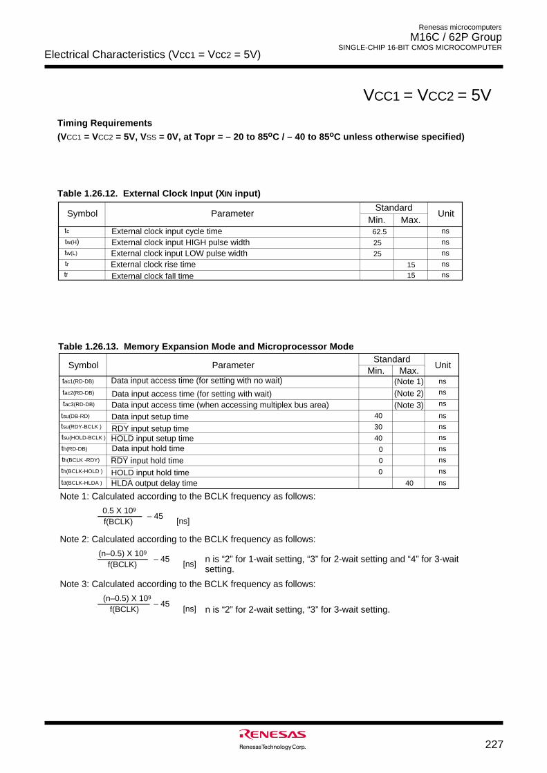
Electrical Characteristics (Vcc1 = Vcc2 = 5V)
227
Renesas microcomputers
M16C / 62P Group SINGLE-CHIP 16-BIT CMOS MICROCOMPUTER
VCC1 = VCC2 = 5V
Timing Requirements
(VCC1 = VCC2 = 5V, VSS = 0V, at Topr = – 20 to 85oC / – 40 to 85oC unless otherwise specified)
Table 1.26.13. Memory Expansion Mode and Microprocessor Mode
Max.
External clock rise time nstr
Min.External clock input cycle timeExternal clock input HIGH pulse widthExternal clock input LOW pulse width
External clock fall time
ns
ns
ns
ns
tc
tw(H)
tw(L)
tf
ParameterSymbol UnitStandard
62.5
25
25
1515
Table 1.26.12. External Clock Input (XIN input)
(Note 1) (Note 2) (Note 3)
40
30
0
0
40
0
Note 1: Calculated according to the BCLK frequency as follows:
40
Min.
Data input setup time nstsu(DB-RD)
tsu(RDY-BCLK )
ParameterSymbol UnitMax.
Standard
nsRDY input setup time
Data input hold time nsth(RD-DB)
th(BCLK -RDY) nsRDY input hold time
nsHOLD input setup timetsu(HOLD-BCLK )
nsHOLD input hold timeth(BCLK-HOLD )
Data input access time (for setting with no wait) nstac1(RD-DB)
ns
ns
tac2(RD-DB)
tac3(RD-DB)
Data input access time (for setting with wait) Data input access time (when accessing multiplex bus area)
nstd(BCLK-HLDA ) HLDA output delay time
f(BCLK) – 45
0.5 X 10⁹
[ns]
Note 2: Calculated according to the BCLK frequency as follows:
f(BCLK) – 45
(n–0.5) X 109
[ns]
Note 3: Calculated according to the BCLK frequency as follows:
f(BCLK) – 45
(n–0.5) X 109
[ns]
n is “2” for 1-wait setting, “3” for 2-wait setting and “4” for 3-wait setting.
n is “2” for 2-wait setting, “3” for 3-wait setting.
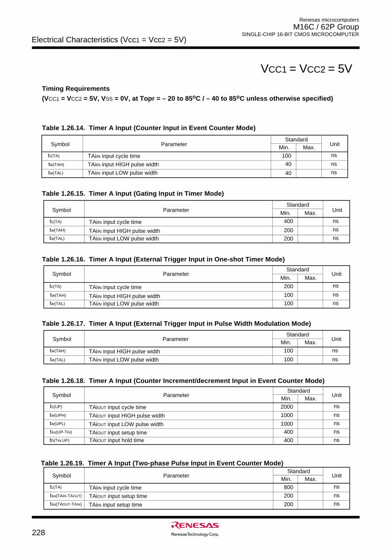
Electrical Characteristics (Vcc1 = Vcc2 = 5V)
228
Renesas microcomputers
M16C / 62P Group SINGLE-CHIP 16-BIT CMOS MICROCOMPUTER
VCC1 = VCC2 = 5V
Timing Requirements
(VCC1 = VCC2 = 5V, VSS = 0V, at Topr = – 20 to 85oC / – 40 to 85oC unless otherwise specified)
Table 1.26.15. Timer A Input (Gating Input in Timer Mode)
Table 1.26.16. Timer A Input (External Trigger Input in One-shot Timer Mode)
Table 1.26.17. Timer A Input (External Trigger Input in Pulse Width Modulation Mode)
Table 1.26.18. Timer A Input (Counter Increment/decrement Input in Event Counter Mode)
Table 1.26.14. Timer A Input (Counter Input in Event Counter Mode)
StandardMax.
nsTAiIN input LOW pulse widthtw(TAL)
Min.ns
ns
Unit
TAiIN input HIGH pulse widthtw(TAH)
ParameterSymbol
tc(TA) TAiIN input cycle time
40
100
40
Standard
Max.Min.ns
ns
ns
Unit
TAiIN input cycle time
TAiIN input HIGH pulse widthTAiIN input LOW pulse width
tc(TA)
tw(TAH)
tw(TAL)
Symbol Parameter
400
200
200
Standard
Max.Min.ns
ns
ns
Unit
TAiIN input cycle time
TAiIN input HIGH pulse widthTAiIN input LOW pulse width
tc(TA)
tw(TAH)
tw(TAL)
Symbol Parameter
200
100
100
StandardMax.Min.
ns
ns
Unit
tw(TAH)
tw(TAL)
Symbol Parameter
TAiIN input HIGH pulse width
TAiIN input LOW pulse width
100
100
StandardMax.Min.
ns
ns
ns
Unit
ns
ns
Symbol Parameter
TAiOUT input cycle time
TAiOUT input HIGH pulse width
TAiOUT input LOW pulse width
TAiOUT input setup timeTAiOUT input hold time
tc(UP)
tw(UPH)
tw(UPL)
tsu(UP-TIN)
th(TIN-UP)
2000
1000
1000
400
400
StandardMax.Min.
ns
ns
ns
UnitSymbol Parameter
TAiIN input cycle time
TAiOUT input setup time
TAiIN input setup time
tc(TA)
tsu(TAIN-TAOUT)
tsu(TAOUT-TAIN)
800
200
200
Table 1.26.19. Timer A Input (Two-phase Pulse Input in Event Counter Mode)

Electrical Characteristics (Vcc1 = Vcc2 = 5V)
229
Renesas microcomputers
M16C / 62P Group SINGLE-CHIP 16-BIT CMOS MICROCOMPUTER
Table 1.26.20. Timer B Input (Counter Input in Event Counter Mode)
Table 1.26.21. Timer B Input (Pulse Period Measurement Mode)
Table 1.26.22. Timer B Input (Pulse Width Measurement Mode)
Table 1.26.23. A-D Trigger Input
Table 1.26.24. Serial I/O
_______
Table 1.26.25. External Interrupt INTi Input
VCC1 = VCC2 = 5V
ns
ns
ns
ns
ns
ns
ns
Standard
Max.Min.
TBiIN input cycle time (counted on one edge)
TBiIN input HIGH pulse width (counted on one edge)
TBiIN input LOW pulse width (counted on one edge)
ns
ns
ns
tc(TB)
tw(TBH)
tw(TBL)
ParameterSymbol Unit
tc(TB)
tw(TBL)
tw(TBH)
ns
ns
nsTBiIN input HIGH pulse width (counted on both edges)
TBiIN input LOW pulse width (counted on both edges)
TBiIN input cycle time (counted on both edges)
Standard
Max.Min.
ns
ns
tc(TB)
tw(TBH)
Symbol Parameter Unit
tw(TBL) nsTBiIN input HIGH pulse width
TBiIN input cycle time
TBiIN input LOW pulse width
Standard
Max.Min.ns
ns
tc(TB)
Symbol Parameter Unit
tw(TBL) ns
tw(TBH)
TBiIN input cycle time
TBiIN input HIGH pulse width
TBiIN input LOW pulse width
Standard
Max.Min.ns
ns
tc(AD)
tw(ADL)
Symbol Parameter Unit
ADTRG input cycle time (trigger able minimum)
ADTRG input LOW pulse width
Standard
Max.Min.ns
ns
tw(INH)
tw(INL)
Symbol Parameter Unit
INTi input LOW pulse width
INTi input HIGH pulse width
Standard
Max.Min.
CLKi input cycle time
CLKi input HIGH pulse width
CLKi input LOW pulse width
tc(CK)
tw(CKH)
tw(CKL)
ParameterSymbol Unit
td(C-Q)
tsu(D-C)
th(C-Q) TxDi hold time
RxDi input setup time
TxDi output delay time
th(C-D) RxDi input hold time
100
40
40
80
80
200
400
200200
400
200
200
1000
125
250
250
200
100
100
0
30
90
80
Timing Requirements
(VCC1 = VCC2 = 5V, VSS = 0V, at Topr = – 20 to 85oC / – 40 to 85oC unless otherwise specified)
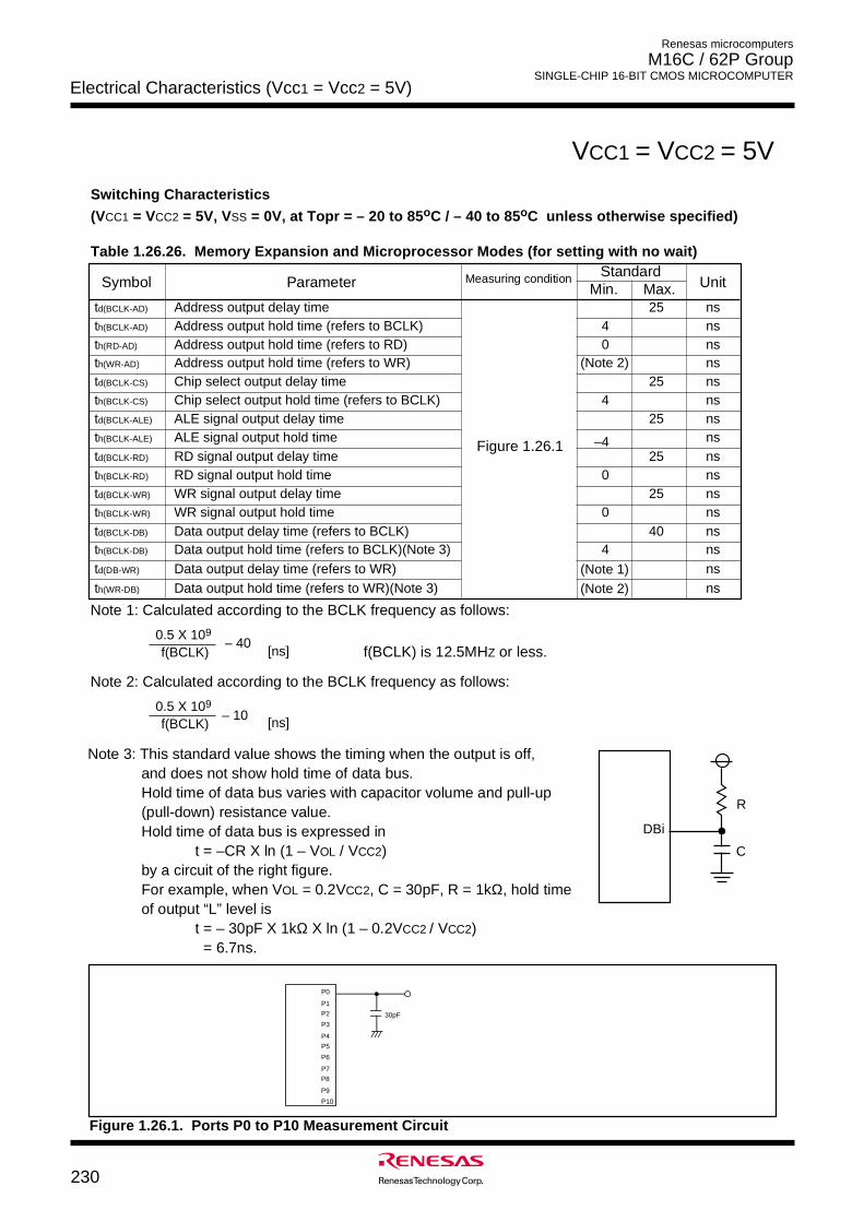
Electrical Characteristics (Vcc1 = Vcc2 = 5V)
230
Renesas microcomputers
M16C / 62P Group SINGLE-CHIP 16-BIT CMOS MICROCOMPUTER
Table 1.26.26. Memory Expansion and Microprocessor Modes (for setting with no wait)
VCC1 = VCC2 = 5V
Switching Characteristics
(VCC1 = VCC2 = 5V, VSS = 0V, at Topr = – 20 to 85oC / – 40 to 85oC unless otherwise specified)
S
y
m
b
o
lStandardM
e
a
s
u
r
i
n
g
c
o
n
d
i
t
i
o
n
M
a
x
.M
i
n
.P
a
r
a
m
e
t
e
r U
n
i
t
td
(
B
C
L
K
-
A
D
) A
d
d
r
e
s
s
o
u
t
p
u
t
d
e
l
a
y
t
i
m
e 2 5 n
s
th
(
B
C
L
K
-
A
D
) A
d
d
r
e
s
s
o
u
t
p
u
t
h
o
l
d
t
i
m
e
(
r
e
f
e
r
s
t
o
B
C
L
K
) 4 n s
th
(
B
C
L
K
-
C
S
) C
h
i
p
s
e
l
e
c
t
o
u
t
p
u
t
h
o
l
d
t
i
m
e
(
r
e
f
e
r
s
t
o
B
C
L
K
) 4 n s
td
(
B
C
L
K
-
A
L
E
) A
L
E
s
i
g
n
a
l
o
u
t
p
u
t
d
e
l
a
y
t
i
m
e 2 5 n
s
th
(
B
C
L
K
-
A
L
E
) A
L
E
s
i
g
n
a
l
o
u
t
p
u
t
h
o
l
d
t
i
m
e – 4 n
s
td(BCLK-RD) RD signal output delay time 25 nsth
(
B
C
L
K
-
R
D
) R
D
s
i
g
n
a
l
o
u
t
p
u
t
h
o
l
d
t
i
m
e 0 n s
td
(
B
C
L
K
-
W
R
) W
R
s
i
g
n
a
l
o
u
t
p
u
t
d
e
l
a
y
t
i
m
e 2 5 n
s
th(BCLK-WR) WR signal output hold time 0 nstd(BCLK-DB) Data output delay time (refers to BCLK) 40 nsth
(
B
C
L
K
-
D
B
) D
a
t
a
o
u
t
p
u
t
h
o
l
d
t
i
m
e
(
r
e
f
e
r
s
t
o
B
C
L
K
)
(
N
o
t
e
3
) 4 n s
th
(
W
R
-
D
B
) D
a
t
a
o
u
t
p
u
t
h
o
l
d
t
i
m
e
(
r
e
f
e
r
s
t
o
W
R
)
(
N
o
t
e
3
) n s
td(DB-WR) Data output delay time (refers to WR) ns
Note 1: Calculated according to the BCLK frequency as follows:
f(BCLK) 0.5 X 10⁹
– 40[ns]
td
(
B
C
L
K
-
C
S
) C
h
i
p
s
e
l
e
c
t
o
u
t
p
u
t
d
e
l
a
y
t
i
m
e 2 5 n
s
th
(
R
D
-
A
D
) A
d
d
r
e
s
s
o
u
t
p
u
t
h
o
l
d
t
i
m
e
(
r
e
f
e
r
s
t
o
R
D
) 0 n s
th
(
W
R
-
A
D
) A
d
d
r
e
s
s
o
u
t
p
u
t
h
o
l
d
t
i
m
e
(
r
e
f
e
r
s
t
o
W
R
) ( N
o
t
e
2
) n
s
Note 3: This standard value shows the timing when the output is off, and does not show hold time of data bus.Hold time of data bus varies with capacitor volume and pull-up (pull-down) resistance value.Hold time of data bus is expressed in
t = –CR X ln (1 – VOL / VCC2) by a circuit of the right figure.For example, when VOL = 0.2VCC2, C = 30pF, R = 1kΩ, hold time of output “L” level is
t = – 30pF X 1kΩ X ln (1 – 0.2VCC2 / VCC2) = 6.7ns.
D
B
i
R
C
( N
o
t
e
1
)
(Note 2)
N
o
t
e
2
:
C
a
l
c
u
l
a
t
e
d
a
c
c
o
r
d
i
n
g
t
o
t
h
e
B
C
L
K
f
r
e
q
u
e
n
c
y
a
s
f
o
l
l
o
w
s
:
f (
B
C
L
K
)
0 .
5
X
1
09
[ns]
f(BCLK) is 12.5MHZ or less.
–
1
0
Figure 1.26.1
P6
P7
P8
P10
P9
P0
P1
P2
P3
P4
P5
30pF
Figure 1.26.1. Ports P0 to P10 Measurement Circuit
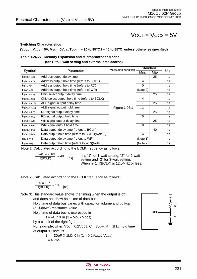
Electrical Characteristics (Vcc1 = Vcc2 = 5V)
231
Renesas microcomputers
M16C / 62P Group SINGLE-CHIP 16-BIT CMOS MICROCOMPUTER
Table 1.26.27. Memory Expansion and Microprocessor Modes
(for 1- to 3-wait setting and external area access)
VCC1 = VCC2 = 5VSwitching Characteristics
(VCC1 = VCC2 = 5V, VSS = 0V, at Topr = – 20 to 85oC / – 40 to 85oC unless otherwise specified)
Figure 1.26.1
S
y
m
b
o
lS
t
a
n
d
a
r
dMeasuring conditionM
a
x
.M
i
n
.P
a
r
a
m
e
t
e
r U
n
i
t
td
(
B
C
L
K
-
A
D
) A
d
d
r
e
s
s
o
u
t
p
u
t
d
e
l
a
y
t
i
m
e 25 n s
th
(
B
C
L
K
-
A
D
) A
d
d
r
e
s
s
o
u
t
p
u
t
h
o
l
d
t
i
m
e
(
r
e
f
e
r
s
t
o
B
C
L
K
) 4 n s
th
(
B
C
L
K
-
C
S
) C
h
i
p
s
e
l
e
c
t
o
u
t
p
u
t
h
o
l
d
t
i
m
e
(
r
e
f
e
r
s
t
o
B
C
L
K
) 4 n s
td(BCLK-ALE) ALE signal output delay time 25 nsth(BCLK-ALE) ALE signal output hold time –4 nstd
(
B
C
L
K
-
R
D
) R
D
s
i
g
n
a
l
o
u
t
p
u
t
d
e
l
a
y
t
i
m
e 25 n s
th
(
B
C
L
K
-
R
D
) R
D
s
i
g
n
a
l
o
u
t
p
u
t
h
o
l
d
t
i
m
e 0 n s
td
(
B
C
L
K
-
W
R
) W
R
s
i
g
n
a
l
o
u
t
p
u
t
d
e
l
a
y
t
i
m
e 25 n s
th(BCLK-WR) WR signal output hold time 0 nstd
(
B
C
L
K
-
D
B
) D
a
t
a
o
u
t
p
u
t
d
e
l
a
y
t
i
m
e
(
r
e
f
e
r
s
t
o
B
C
L
K
) 40 n s
th(BCLK-DB) Data output hold time (refers to BCLK)(Note 3) 4 ns
th
(
W
R
-
D
B
) D
a
t
a
o
u
t
p
u
t
h
o
l
d
t
i
m
e
(
r
e
f
e
r
s
t
o
W
R
)
(
N
o
t
e
3
) n s
td(DB-WR) Data output delay time (refers to WR) ns
N
o
t
e
1
:
C
a
l
c
u
l
a
t
e
d
a
c
c
o
r
d
i
n
g
t
o
t
h
e
B
C
L
K
f
r
e
q
u
e
n
c
y
a
s
f
o
l
l
o
w
s
:
f(BCLK) (n–0.5) X 109
–
4
0
[ns]
td
(
B
C
L
K
-
C
S
) C
h
i
p
s
e
l
e
c
t
o
u
t
p
u
t
d
e
l
a
y
t
i
m
e 25 n s
th
(
R
D
-
A
D
) A
d
d
r
e
s
s
o
u
t
p
u
t
h
o
l
d
t
i
m
e
(
r
e
f
e
r
s
t
o
R
D
) 0 n s
th
(
W
R
-
A
D
) A
d
d
r
e
s
s
o
u
t
p
u
t
h
o
l
d
t
i
m
e
(
r
e
f
e
r
s
t
o
W
R
) ( N
o
t
e
2
) n
s
Note 3: This standard value shows the timing when the output is off, and does not show hold time of data bus.Hold time of data bus varies with capacitor volume and pull-up (pull-down) resistance value.Hold time of data bus is expressed in
t = –CR X ln (1 – VOL / VCC2) by a circuit of the right figure.For example, when VOL = 0.2VCC2, C = 30pF, R = 1kΩ, hold time of output “L” level is
t = – 30pF X 1kΩ X ln (1 – 0.2VCC2 / VCC2) = 6.7ns.
DBi
R
C
( N
o
t
e
1
)
(Note 2)
Note 2: Calculated according to the BCLK frequency as follows:
f (
B
C
L
K
)
0.5 X 10⁹
[ n
s
]
n is “1” for 1-wait setting, “2” for 2-wait setting and “3” for 3-wait setting.When n=1, f(BCLK) is 12.5MHZ or less.
–
1
0
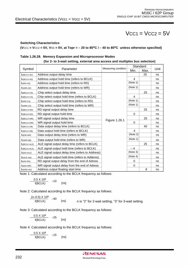
Electrical Characteristics (Vcc1 = Vcc2 = 5V)
232
Renesas microcomputers
M16C / 62P Group SINGLE-CHIP 16-BIT CMOS MICROCOMPUTER
Table 1.26.28. Memory Expansion and Microprocessor Modes
(for 2- to 3-wait setting, external area access and multiplex bus selection)
VCC1 = VCC2 = 5V
Switching Characteristics
(VCC1 = VCC2 = 5V, VSS = 0V, at Topr = – 20 to 85oC / – 40 to 85oC unless otherwise specified)
SymbolStandard
Measuring conditionMax.Min.Parameter Unit
td(BCLK-AD) Address output delay time 25 ns
th(BCLK-AD) Address output hold time (refers to BCLK) 4 ns
td(BCLK-CS) Chip select output delay time 25 nsth(BCLK-CS) Chip select output hold time (refers to BCLK) 4 ns
nsth(RD-AD) Address output hold time (refers to RD) (Note 1)
td(BCLK-RD) RD signal output delay time 25 ns
th(BCLK-RD) RD signal output hold time 0 ns
nsth(WR-AD) Address output hold time (refers to WR) (Note 1)
td(BCLK-WR) WR signal output delay time 25 ns
td(BCLK-DB) Data output delay time (refers to BCLK) 40 ns
th(BCLK-DB) Data output hold time (refers to BCLK) 4 nstd(DB-WR) Data output delay time (refers to WR) (Note 2) ns
td(BCLK-ALE) ALE signal output delay time (refers to BCLK) 25 ns
th(BCLK-ALE) ALE signal output hold time (refers to BCLK) – 4 ns
th(ALE-AD) ALE signal output hold time (refers to Adderss) ns
th(BCLK-WR) WR signal output hold time 0 ns
nsth(RD-CS) Chip select output hold time (refers to RD) (Note 1)
th(WR-CS) Chip select output hold time (refers to WR) (Note 1) ns
td(AD-RD) RD signal output delay from the end of Adress ns0
td(AD-WR) WR signal output delay from the end of Adress ns0tdZ(RD-AD) Address output floating start time ns8
th(WR-DB) Data output hold time (refers to WR) ns(Note 1)
Note 1: Calculated according to the BCLK frequency as follows:
f(BCLK) 0.5 X 10⁹
[ns]
td(AD-ALE) ALE signal output delay time (refers to Address) ns(Note 3)
Note 2: Calculated according to the BCLK frequency as follows:
f(BCLK) (n–0.5) X 109
–40[ns]
Note 3: Calculated according to the BCLK frequency as follows:
f(BCLK) 0.5 X 10⁹
–25[ns]
n is “2” for 2-wait setting, “3” for 3-wait setting.
(Note 4)
–10
Note 4: Calculated according to the BCLK frequency as follows:
f(BCLK) 0.5 X 10⁹
[ns]
–15
Figure 1.26.1
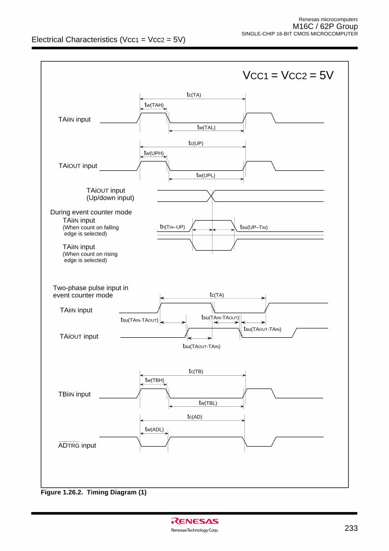
Electrical Characteristics (Vcc1 = Vcc2 = 5V)
Renesas microcomputers
M16C / 62P Group SINGLE-CHIP 16-BIT CMOS MICROCOMPUTER
233
VCC1 = VCC2 = 5V
TAiIN input
TAiOUT input
During event counter mode
tc(TA)
tw(TAH)
tw(TAL)
tc(UP)
tw(UPH)
tw(UPL)
th(TIN–UP) tsu(UP–TIN)TAiIN input(When count on falling edge is selected)
TAiIN input(When count on rising edge is selected)
TAiOUT input(Up/down input)
TBiIN input
tc(TB)
tw(TBH)
tw(TBL)
tc(AD)
tw(ADL)
ADTRG input
tc(TA)
tsu(TAIN-TAOUT)
tsu(TAOUT-TAIN)
tsu(TAOUT-TAIN)
Two-phase pulse input in event counter mode
TAiIN input
TAiOUT input
tsu(TAIN-TAOUT)
Figure 1.26.2. Timing Diagram (1)
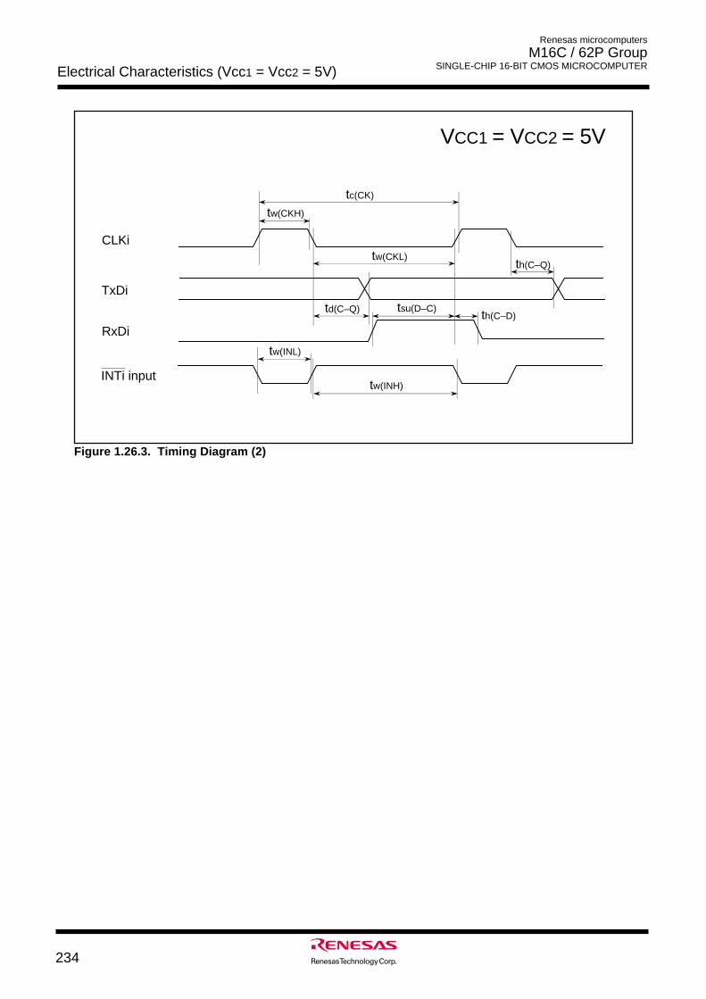
Electrical Characteristics (Vcc1 = Vcc2 = 5V)
Renesas microcomputers
M16C / 62P Group SINGLE-CHIP 16-BIT CMOS MICROCOMPUTER
234
VCC1 = VCC2 = 5V
Figure 1.26.3. Timing Diagram (2)
tsu(D–C)
CLKi
TxDi
RxDi
tc(CK)
tw(CKH)
tw(CKL)
tw(INL)
tw(INH)
td(C–Q) th(C–D)
th(C–Q)
INTi input
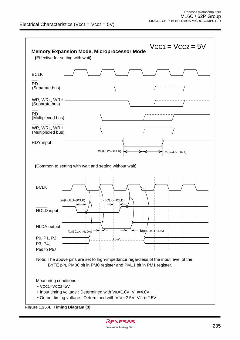
Electrical Characteristics (Vcc1 = Vcc2 = 5V)
Renesas microcomputers
M16C / 62P Group SINGLE-CHIP 16-BIT CMOS MICROCOMPUTER
235
VCC1 = VCC2 = 5V
Figure 1.26.4. Timing Diagram (3)
Measuring conditions : • VCC1=VCC2=5V • Input timing voltage : Determined with VIL=1.0V, VIH=4.0V • Output timing voltage : Determined with VOL=2.5V, VOH=2.5V
Memory Expansion Mode, Microprocessor Mode
BCLK
HOLD input
HLDA output
P0, P1, P2, P3, P4, P50 to P52
(Common to setting with wait and setting without wait)
Note: The above pins are set to high-impedance regardless of the input level of the BYTE pin, PM06 bit in PM0 register and PM11 bit in PM1 register.
th(BCLK–HOLD)tsu(HOLD–BCLK)
(Effective for setting with wait)
td(BCLK–HLDA)td(BCLK–HLDA)
Hi–Z
RDY input
tsu(RDY–BCLK) th(BCLK–RDY)
BCLK
RD(Multiplexed bus)
(Multiplexed bus)WR, WRL, WRH
WR, WRL, WRH(Separate bus)
RD(Separate bus)
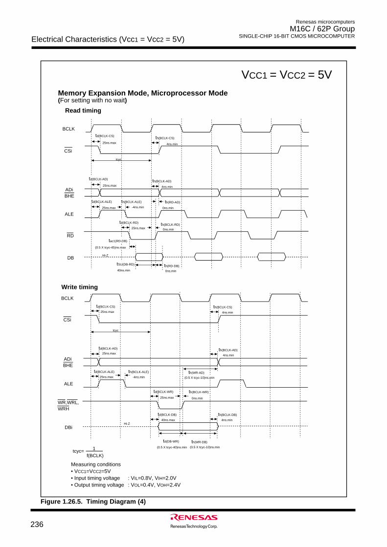
Electrical Characteristics (Vcc1 = Vcc2 = 5V)
Renesas microcomputers
M16C / 62P Group SINGLE-CHIP 16-BIT CMOS MICROCOMPUTER
236
VCC1 = VCC2 = 5V
BCLK
CSi
td(BCLK-CS)
25ns.max
ADi 25ns.max
ALE 25ns.max -4ns.min
RD
25ns.max th(BCLK-RD)
0ns.min
th(BCLK-AD)
4ns.min
th(BCLK-CS)
4ns.min
Hi-Z DB
th(RD-DB)
0ns.min
0ns.min
th(RD-AD)
BHE
tcyc
Read timing
td(BCLK-AD)
td(BCLK-ALE) th(BCLK-ALE)
tSU(DB-RD)
td(BCLK-RD)
40ns.min
tac1(RD-DB)
Memory Expansion Mode, Microprocessor Mode(For setting with no wait)
Measuring conditions • VCC1=VCC2=5V • Input timing voltage : VIL=0.8V, VIH=2.0V• Output timing voltage : VOL=0.4V, VOH=2.4V
WR,WRL,WRH
25ns.max
th(BCLK-WR)
0ns.min
BCLK
CSi
td(BCLK-CS)
25ns.max
ADi
td(BCLK-AD)
25ns.max
ALE
25ns.max
td(BCLK-ALE) th(BCLK-ALE)
-4ns.min
th(BCLK-AD)
4ns.min
th(BCLK-CS)
4ns.min
tcyc
th(WR-AD)
BHE
td(BCLK-DB)
40ns.max 4ns.min
th(BCLK-DB)
td(DB-WR)
(0.5 X tcyc-40)ns.min
th(WR-DB)
DBi
Write timing
td(BCLK-WR)
Hi-Z
(0.5 X tcyc-45)ns.max
tcyc= 1
f(BCLK)
(0.5 X tcyc-10)ns.min
(0.5 X tcyc-10)ns.min
Figure 1.26.5. Timing Diagram (4)
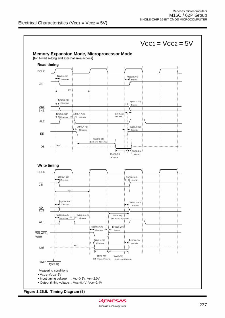
Electrical Characteristics (Vcc1 = Vcc2 = 5V)
Renesas microcomputers
M16C / 62P Group SINGLE-CHIP 16-BIT CMOS MICROCOMPUTER
237
VCC1 = VCC2 = 5V
BCLK
CSi
td(BCLK-CS)
25ns.max
ADi
td(BCLK-AD)
25ns.max
ALE
25ns.max
th(BCLK-ALE)
-4ns.min
RD
25ns.max
th(BCLK-RD)
0ns.min
th(BCLK-AD)
4ns.min
th(BCLK-CS)
4ns.min
Hi-ZDB
tSU(DB-RD)
40ns.min
th(RD-DB)
0ns.min
tcyc
BHE
Read timing
WR,WRL,WRH
25ns.max
th(BCLK-WR)
0ns.min
BCLK
CSi
td(BCLK-CS)
25ns.max
ADi
td(BCLK-AD)
25ns.max
ALE
25ns.max
td(BCLK-ALE) th(BCLK-ALE)
-4ns.min
th(BCLK-AD)
4ns.min
th(BCLK-CS)
4ns.min
tcyc
th(WR-AD)
BHE
td(BCLK-DB)
40ns.max 4ns.min
th(BCLK-DB)
td(DB-WR)
(0.5 X tcyc-40)ns.min (0.5 X tcyc-10)ns.min
th(WR-DB)
DBi
Write timing
td(BCLK-ALE)
td(BCLK-RD)
(0.5 X tcyc-10)ns.min
td(BCLK-WR)
0ns.min
th(RD-AD)
tac2(RD-DB)
Hi-Z
Memory Expansion Mode, Microprocessor Mode(for 1-wait setting and external area access)
Measuring conditions • VCC1=VCC2=5V • Input timing voltage : VIL=0.8V, VIH=2.0V• Output timing voltage : VOL=0.4V, VOH=2.4V
(1.5 X tcyc-45)ns.max
tcyc=f(BCLK)
1
Figure 1.26.6. Timing Diagram (5)
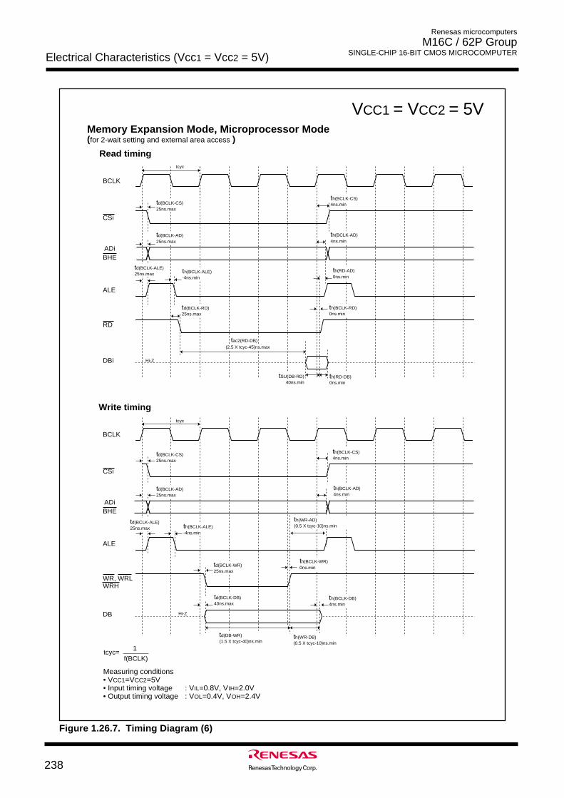
Electrical Characteristics (Vcc1 = Vcc2 = 5V)
Renesas microcomputers
M16C / 62P Group SINGLE-CHIP 16-BIT CMOS MICROCOMPUTER
238
VCC1 = VCC2 = 5V
Read timing
Write timing
BCLK
CSi
ALE
DB
ADiBHE
WR, WRLWRH
Memory Expansion Mode, Microprocessor Mode(for 2-wait setting and external area access )
BCLK
CSi
ALE
DBi
ADiBHE
RD
tcyc
td(BCLK-CS)25ns.max
td(BCLK-AD)25ns.max
td(BCLK-ALE)25ns.max th(BCLK-ALE)
-4ns.min
td(BCLK-RD)25ns.max
Hi-Z
tSU(DB-RD)40ns.min
th(RD-DB)0ns.min
th(BCLK-RD)0ns.min
th(RD-AD)0ns.min
th(BCLK-AD)4ns.min
th(BCLK-CS)4ns.min
tcyc
Hi-Z
td(BCLK-CS)25ns.max
td(BCLK-AD)25ns.max
td(BCLK-ALE)25ns.max th(BCLK-ALE)
-4ns.min
td(BCLK-WR)25ns.max
th(BCLK-CS)4ns.min
th(BCLK-AD)4ns.min
th(WR-AD)(0.5 X tcyc-10)ns.min
th(BCLK-WR)0ns.min
td(BCLK-DB)40ns.max
td(DB-WR)(1.5 X tcyc-40)ns.min
th(BCLK-DB)4ns.min
th(WR-DB)(0.5 X tcyc-10)ns.min
Measuring conditions • VCC1=VCC2=5V • Input timing voltage : VIL=0.8V, VIH=2.0V• Output timing voltage : VOL=0.4V, VOH=2.4V
tac2(RD-DB)(2.5 X tcyc-45)ns.max
tcyc=1
f(BCLK)
Figure 1.26.7. Timing Diagram (6)
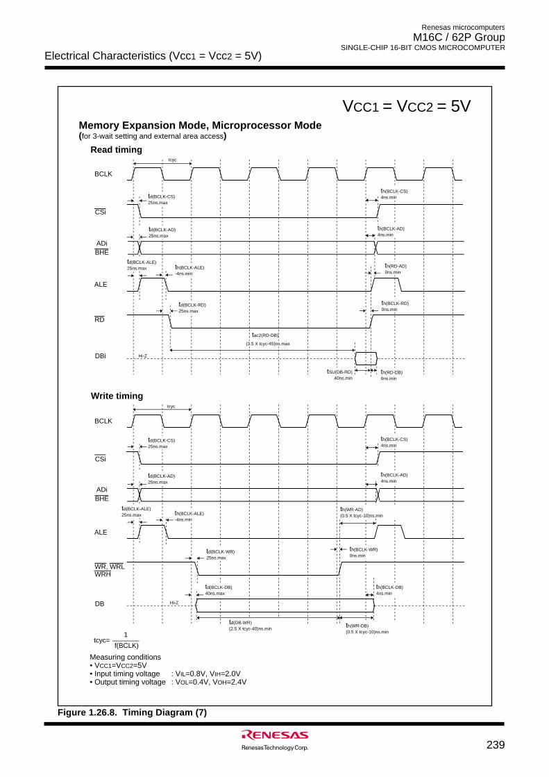
Electrical Characteristics (Vcc1 = Vcc2 = 5V)
Renesas microcomputers
M16C / 62P Group SINGLE-CHIP 16-BIT CMOS MICROCOMPUTER
239
VCC1 = VCC2 = 5V
Figure 1.26.8. Timing Diagram (7)
Read timing
Write timing
BCLK
CSi
ALE
DB
ADiBHE
WR, WRLWRH
Memory Expansion Mode, Microprocessor Mode(for 3-wait setting and external area access)
BCLK
CSi
ALE
DBi
ADiBHE
RD
tcyc
td(BCLK-CS)25ns.max
td(BCLK-AD)25ns.max
td(BCLK-ALE)25ns.max th(BCLK-ALE)
-4ns.min
td(BCLK-RD)25ns.max
Hi-Z
tSU(DB-RD)40ns.min
th(RD-DB)0ns.min
th(BCLK-RD)0ns.min
th(RD-AD)0ns.min
th(BCLK-AD)4ns.min
th(BCLK-CS)4ns.min
tcyc
Hi-Z
td(BCLK-CS)25ns.max
td(BCLK-AD)25ns.max
td(BCLK-ALE)25ns.max th(BCLK-ALE)
-4ns.min
td(BCLK-WR)25ns.max
th(BCLK-CS)4ns.min
th(BCLK-AD)4ns.min
th(WR-AD)(0.5 X tcyc-10)ns.min
th(BCLK-WR)0ns.min
td(BCLK-DB)40ns.max
td(DB-WR)(2.5 X tcyc-40)ns.min
th(BCLK-DB)4ns.min
th(WR-DB)(0.5 X tcyc-10)ns.min
Measuring conditions • VCC1=VCC2=5V • Input timing voltage : VIL=0.8V, VIH=2.0V• Output timing voltage : VOL=0.4V, VOH=2.4V
tac2(RD-DB)
(3.5 X tcyc-45)ns.max
tcyc=1
f(BCLK)
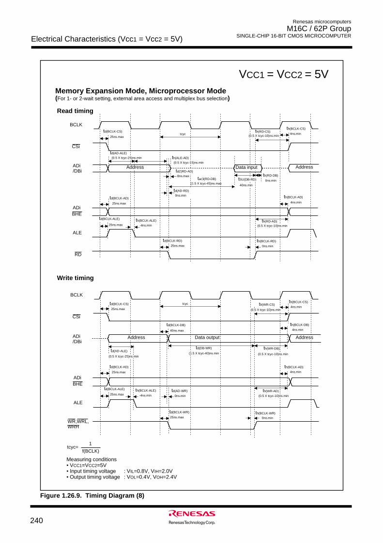
Electrical Characteristics (Vcc1 = Vcc2 = 5V)
Renesas microcomputers
M16C / 62P Group SINGLE-CHIP 16-BIT CMOS MICROCOMPUTER
240
VCC1 = VCC2 = 5V
Figure 1.26.9. Timing Diagram (8)
M
e
m
o
r
y
E
x
p
a
n
s
i
o
n
M
o
d
e
,
M
i
c
r
o
p
r
o
c
e
s
s
o
r
M
o
d
e(F
o
r
1
-
o
r
2
-
w
a
i
t
s
e
t
t
i
n
g
,
e
x
t
e
r
n
a
l
a
r
e
a
a
c
c
e
s
s
a
n
d
m
u
l
t
i
p
l
e
x
b
u
s
s
e
l
e
c
t
i
o
n)
BCLK
C
S
i
td
(
B
C
L
K
-
C
S
)
2 5
n
s
.
m
a
x
A
D
i
td
(
B
C
L
K
-
A
D
)
2 5
n
s
.
m
a
x
A
L
E
th
(
B
C
L
K
-
A
L
E
)
-4ns.min
R
D
25ns.maxth(BCLK-RD)
0ns.min
th
(
B
C
L
K
-
A
D
)
4 n
s
.
m
i
n
th(BCLK-CS)
4 n
s
.
m
i
nt
c
y
c
th(RD-CS)
th
(
R
D
-
A
D
)
B
H
E
A
D
i/
D
B
ith
(
R
D
-
D
B
)
0 n
s
.
m
i
n
td
(
A
D
-
A
L
E
)
R
e
a
d
t
i
m
i
n
g
td(BCLK-WR)
25ns.maxth
(
B
C
L
K
-
W
R
)
0 n
s
.
m
i
n
B
C
L
K
CSi
td(BCLK-CS)
25ns.max
A
D
i
td(BCLK-AD)
2 5
n
s
.
m
a
x
A
L
E
2 5
n
s
.
m
a
x
th
(
B
C
L
K
-
A
L
E
)
- 4
n
s
.
m
i
n
th
(
B
C
L
K
-
A
D
)
4 n
s
.
m
i
n
th(BCLK-CS)
4 n
s
.
m
i
n
tcyc
th(WR-AD)
B
H
E
td(BCLK-DB)
40ns.max 4 n
s
.
m
i
n
th(BCLK-DB)
td(DB-WR) th(WR-DB)
ADi/DBi
D
a
t
a
o
u
t
p
u
t
WR,WRL,WRH
W
r
i
t
e
t
i
m
i
n
g
A
d
d
r
e
s
s
(0.5 X tcyc-10)ns.min
A
d
d
r
e
s
sData input
40ns.min
(0.5 X tcyc-10)ns.min
td
(
B
C
L
K
-
A
L
E
)
td(BCLK-RD)
(
0
.
5
X
t
c
y
c
-
1
0
)
n
s
.
m
i
n
th(WR-CS)
A
d
d
r
e
s
s
td(AD-ALE)
( 0
.
5
X
t
c
y
c
-
2
5
)
n
s
.
m
i
n
(1.5 X tcyc-40)ns.min
(0.5 X tcyc-10)ns.min
td(BCLK-ALE)
( 0
.
5
X
t
c
y
c
-
2
5
)
n
s
.
m
i
n
Address
2 5
n
s
.
m
a
x
tS
U
(
D
B
-
R
D
)tac3(RD-DB)
( 0
.
5
X
t
c
y
c
-
1
0
)
n
s
.
m
i
n
(0.5 X tcyc-15)ns.min
td(AD-RD)
0ns.min
td
Z
(
R
D
-
A
D
)
8ns.max
td(AD-WR)
0ns.min
M
e
a
s
u
r
i
n
g
c
o
n
d
i
t
i
o
n
s
•
VC
C
1=
VC
C
2=
5
V
•
I
n
p
u
t
t
i
m
i
n
g
v
o
l
t
a
g
e :
VI
L=
0
.
8
V
,
VI
H=
2
.
0
V•
O
u
t
p
u
t
t
i
m
i
n
g
v
o
l
t
a
g
e :
VO
L=
0
.
4
V
,
VO
H=
2
.
4
V
th(ALE-AD)
( 1
.
5
X
t
c
y
c
-
4
5
)
n
s
.
m
a
x
tcyc=1
f(BCLK)
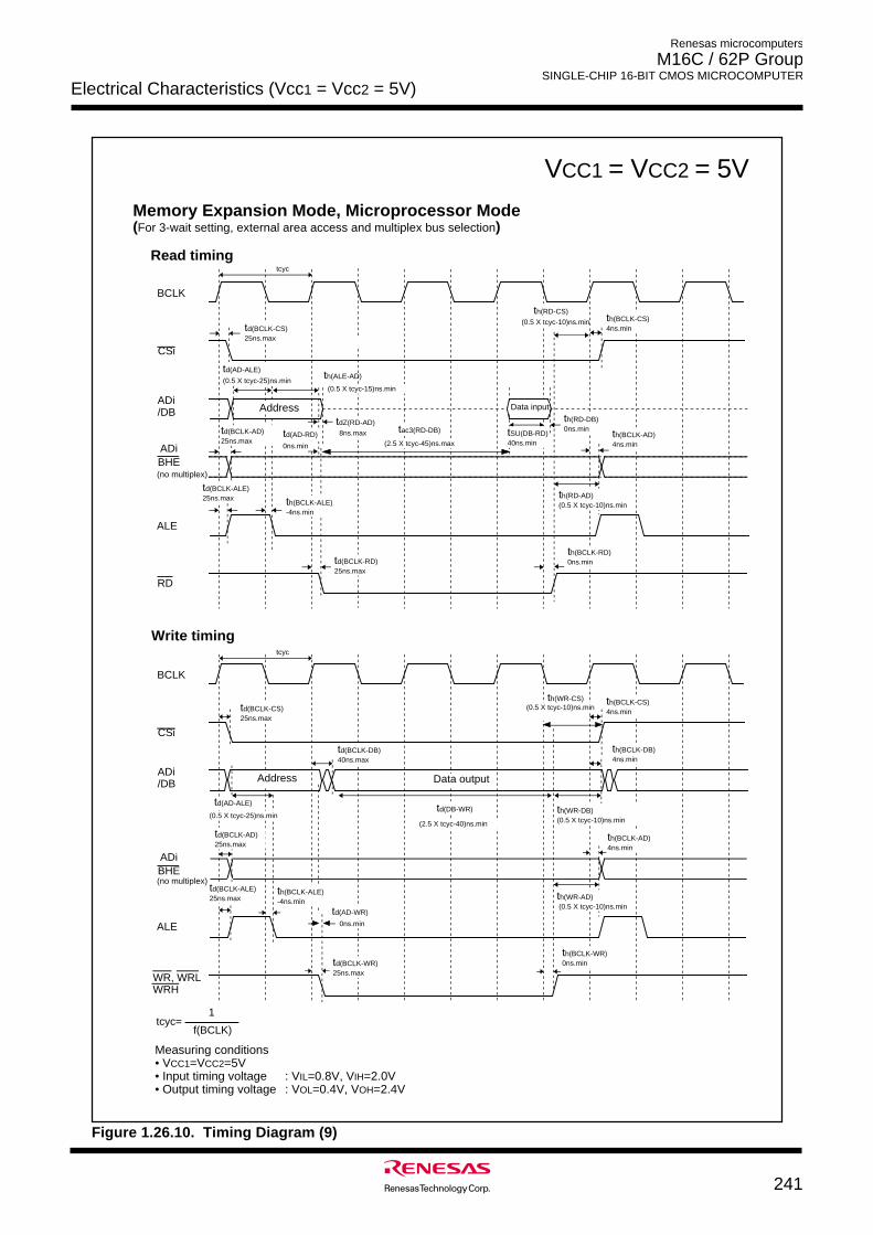
Electrical Characteristics (Vcc1 = Vcc2 = 5V)
Renesas microcomputers
M16C / 62P Group SINGLE-CHIP 16-BIT CMOS MICROCOMPUTER
241
VCC1 = VCC2 = 5V
Figure 1.26.10. Timing Diagram (9)
Read timing
Write timing
Memory Expansion Mode, Microprocessor Mode(For 3-wait setting, external area access and multiplex bus selection)
BCLK
CSi
ALE
RD
ADi /DB
ADiBHE
BCLK
CSi
ALE
ADi /DB
tcyc
td(BCLK-AD)25ns.max
tcyc
Data output
th(BCLK-CS)4ns.mintd(BCLK-CS)
25ns.max
td(BCLK-ALE)25ns.max th(BCLK-ALE)
-4ns.min
td(BCLK-RD)25ns.max
th(BCLK-RD)0ns.min
tSU(DB-RD)40ns.min
th(RD-DB)0ns.min
th(RD-AD)(0.5 X tcyc-10)ns.min
th(BCLK-AD)4ns.min
td(BCLK-CS)25ns.max
td(BCLK-AD)25ns.max
th(BCLK-DB)4ns.min
th(BCLK-WR)0ns.min
th(WR-AD) (0.5 X tcyc-10)ns.min
th(BCLK-AD)4ns.min
th(BCLK-CS)4ns.min
td(BCLK-ALE)25ns.max
td(BCLK-WR)25ns.max
th(WR-DB)(0.5 X tcyc-10)ns.min
Data input Address
Address
ADiBHE
WR, WRLWRH
Measuring conditions • VCC1=VCC2=5V • Input timing voltage : VIL=0.8V, VIH=2.0V• Output timing voltage : VOL=0.4V, VOH=2.4V
td(AD-ALE)
(0.5 X tcyc-25)ns.min
td(AD-RD)
0ns.min
tdZ(RD-AD)
8ns.max tac3(RD-DB)
td(BCLK-DB)40ns.max
AAAA(0.5 X tcyc-10)ns.min th(WR-CS)
td(DB-WR)
(2.5 X tcyc-40)ns.min
td(AD-WR)
0ns.min
th(RD-CS)
(0.5 X tcyc-10)ns.min
td(AD-ALE)
(0.5 X tcyc-25)ns.min
(2.5 X tcyc-45)ns.max
tcyc=1
f(BCLK)
(no multiplex)
(no multiplex)
th(ALE-AD)
(0.5 X tcyc-15)ns.min
th(BCLK-ALE)-4ns.min
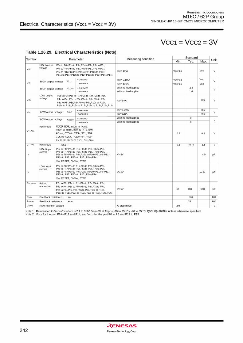
Renesas microcomputers
M16C / 62P Group SINGLE-CHIP 16-BIT CMOS MICROCOMPUTER
Electrical Characteristics (Vcc1 = Vcc2 = 3V)
242
VCC1 = VCC2 = 3VTable 1.26.29. Electrical Characteristics (Note)
S
y
m
b
o
l
VO
H
HIGH output voltageVO
H
VO
L
L
O
W
o
u
t
p
u
tv
o
l
t
a
g
e
VO
L
H
I
G
H
o
u
t
p
u
t
v
o
l
t
a
g
e
StandardT
y
p
. U
n
i
tMeasuring condition
V
VXO
U
T
V
VXO
U
T0
.
5
0
.
5
Min. M
a
x
.
VCC-0.5
P
a
r
a
m
e
t
e
r
IO
H=-1
m
A
IO
H=-0
.
1
m
A
IO
H=-5
0
µ
A
IO
L=
1
m
A
IO
L=
0
.
1
m
A
IO
L=
5
0
µ
A
P00 to P07,P10 to P17,P20 to P27,P30 to P37, P40 to P47,P50 to P57,P60 to P67,P72 to P77, P80 to P84,P86,P87,P90 to P97,P100 to P107,
H
I
G
H
P
O
W
E
R
L O
W
P
O
W
E
R
H
I
G
H
P
O
W
E
R
L O
W
P
O
W
E
R
H
I
G
H
P
O
W
E
R
L O
W
P
O
W
E
R
XC
O
U
T W
i
t
h
n
o
l
o
a
d
a
p
p
l
i
e
d
W
i
t
h
n
o
l
o
a
d
a
p
p
l
i
e
d
2
.
5
1.6V
H
y
s
t
e
r
e
s
i
s
H
y
s
t
e
r
e
s
i
s
H
I
G
H
i
n
p
u
tc
u
r
r
e
n
tIIH
LOW inputcurrent
IIL
VR
A
M R
A
M
r
e
t
e
n
t
i
o
n
v
o
l
t
a
g
e
VT
+
-VT
-
VT
+
-VT
-
0.2 0.8 V
0
.
2 1.8 V
P
00
t
o
P
07,
P
10
t
o
P
17,
P
20
t
o
P
27,
P
30
t
o
P
37,P
40
t
o
P
47,
P
50
t
o
P
57,
P
60
t
o
P
67,
P
70
t
o
P
77,P
80
t
o
P
87,
P
90
t
o
P
97,
P
1
00
t
o
P
1
07
,P
1
10
t
o
P
1
17,P
1
20
t
o
P
1
27,
P
1
30
t
o
P
1
37,
P
1
40,
P
1
41,4.0 µA
µA
A
t
s
t
o
p
m
o
d
e 2.0 V
R
E
S
E
T
XI
N,
R
E
S
E
T
,
C
N
V
s
s
,
B
Y
T
E
VI=3V
VI=0V -4.0
Rf
X
I
N
Rf
X
C
I
N
F
e
e
d
b
a
c
k
r
e
s
i
s
t
a
n
c
e XI
N
F
e
e
d
b
a
c
k
r
e
s
i
s
t
a
n
c
e XC
I
N 2
5
3.0 MΩ
MΩ
RPULLUP Pull-upresistance
1
0
0 kΩ
VXC
O
U
T0
0
W
i
t
h
n
o
l
o
a
d
a
p
p
l
i
e
d
W
i
t
h
n
o
l
o
a
d
a
p
p
l
i
e
dH
I
G
H
P
O
W
E
R
L O
W
P
O
W
E
R
VI=
0
V 5
0 5
0
0
C
L
K0
t
o
C
L
K4,
T
A
2O
U
T
t
o
T
A
4O
U
T,
H
O
L
D
,
R
D
Y
,
T
A
0I
N
t
o
T
A
4I
N,
ADTRG, CTS0 to CTS2, SCL, SDA,
T
B
0I
N
t
o
T
B
5I
N,
I
N
T0
t
o
I
N
T5,
N
M
I
,
K
I0
t
o
K
I3,
R
x
D0
t
o
R
x
D2,
SI
N
3,
SI
N
4
P110 to P117,P120 to P127,P130 to P137,P140,P141
P
00
t
o
P
07,
P
10
t
o
P
17,
P
20
t
o
P
27,
P
30
t
o
P
37,
P
40
t
o
P
47,
P
50
t
o
P
57,
P
60
t
o
P
67,
P
70
t
o
P
77,
P
80
t
o
P
84,
P
86,
P
87,
P
90
t
o
P
97,
P
1
00
t
o
P
1
07,
P
1
10
t
o
P
1
17,
P
1
20
t
o
P
1
27,
P
1
30
t
o
P
1
37,
P
1
40,
P
1
41
P
00
t
o
P
07,
P
10
t
o
P
17,
P
20
t
o
P
27,
P
30
t
o
P
37,P
40
t
o
P
47,
P
50
t
o
P
57,
P
60
t
o
P
67,
P
70
t
o
P
77,P
80
t
o
P
87,
P
90
t
o
P
97,
P
1
00
t
o
P
1
07
,P
1
10
t
o
P
1
17,P
1
20
t
o
P
1
27,
P
1
30
t
o
P
1
37,
P
1
40,
P
1
41,
XI
N,
R
E
S
E
T
,
C
N
V
s
s
,
B
Y
T
E
P00 to P07,P10 to P17,P20 to P27,P30 to P37, P
40
t
o
P
47,
P
50
t
o
P
57,
P
60
t
o
P
67,
P
72
t
o
P
77,
P
80
t
o
P
84,
P
86,
P
87,
P
90
t
o
P
97,
P
1
00
t
o
P
1
07,
P110 to P117,P120 to P127,P130 to P137,P140,P141
VCC-0.5
VCC-0.5
N
o
t
e
1
:
R
e
f
e
r
e
n
c
e
d
t
o
VC
C=
VC
C
1=
VC
C
2=
2
.
7
t
o
3
.
3
V
,
VS
S=
0
V
a
t
T
o
p
r
=
-
2
0
t
o
8
5
°
C
/
-
4
0
t
o
8
5
°
C
,
f
(
B
C
L
K
)
=
1
0
M
H
z
u
n
l
e
s
s
o
t
h
e
r
w
i
s
e
s
p
e
c
i
f
i
e
d
.
N
o
t
e
2
:
VC
C
1
f
o
r
t
h
e
p
o
r
t
P
6
t
o
P
1
1
a
n
d
P
1
4
,
a
n
d
VC
C
2
f
o
r
t
h
e
p
o
r
t
P
0
t
o
P
5
a
n
d
P
1
2
t
o
P
1
3
.
VC
C
VC
C
VC
C
0
.
5
(0.7)
HIGH output voltage
LOW output voltage
LOW output voltage

Electrical Characteristics (Vcc1 = Vcc2 = 3V)
243
Renesas microcomputers
M16C / 62P Group SINGLE-CHIP 16-BIT CMOS MICROCOMPUTER
VCC1 = VCC2 = 3VTable 1.26.30. Electrical Characteristics (2) (Note 1)
S
y
m
b
o
l StandardT
y
p
. U
n
i
tM
e
a
s
u
r
i
n
g
c
o
n
d
i
t
i
o
n
M
i
n
. Max.P
a
r
a
m
e
t
e
r
N
o
d
i
v
i
s
i
o
n m
AI n
s
i
n
g
l
e
-
c
h
i
p
m
o
d
e
,
t
h
e
o
u
t
p
u
t
p
i
n
s
a
r
e
o
p
e
n
a
n
d
o
t
h
e
r
p
i
n
s
a
r
e
VS
S
8 11f(BCLK)=10MHz,
N
o
d
i
v
i
s
i
o
n m
Af(BCLK)=10MHz,
M
a
s
k
R
O
M
1
3F
l
a
s
h
m
e
m
o
r
y
mA1.8
m
A1No division, Ring oscillation
IC
CPower supply current(VCC1=2.7 to 3.6V)
Topr=25°C3.0 µ
AStop mode,
f(BCLK)=32kHz, Wait mode (Note 2), Oscillation capacity High
6.0 µ
A
0.7
1.8 µA
Mask ROMFlash memory
N
o
t
e
1
:
R
e
f
e
r
e
n
c
e
d
t
o
VC
C=
VC
C
1=
VC
C
2=
2
.
7
t
o
3
.
3
V
,
VS
S=
0
V
a
t
T
o
p
r
=
-
2
0
t
o
8
5
°
C
/
-
4
0
t
o
8
5
°
C
,
f
(
B
C
L
K
)
=
1
0
M
H
z
u
n
l
e
s
s
o
t
h
e
r
w
i
s
e
s
p
e
c
i
f
i
e
d
.
N
o
t
e
2
:
W
i
t
h
o
n
e
t
i
m
e
r
o
p
e
r
a
t
e
d
u
s
i
n
g
fC
3
2.N
o
t
e
3
:
T
h
i
s
i
n
d
i
c
a
t
e
s
t
h
e
m
e
m
o
r
y
i
n
w
h
i
c
h
t
h
e
p
r
o
g
r
a
m
t
o
b
e
e
x
e
c
u
t
e
d
e
x
i
s
t
s
.N
o
t
e
4
:
I
d
e
t
i
s
d
i
s
s
i
p
a
t
i
o
n
c
u
r
r
e
n
t
w
h
e
n
t
h
e
f
o
l
l
o
w
i
n
g
b
i
t
i
s
s
e
t
t
o
“
1
”
(
d
e
t
e
c
t
i
o
n
c
i
r
c
u
i
t
e
n
a
b
l
e
d
)
.I
d
e
t
4
:
V
C
2
7
b
i
t
o
f
V
C
R
2
r
e
g
i
s
t
e
rI
d
e
t
3
:
V
C
2
6
b
i
t
o
f
V
C
R
2
r
e
g
i
s
t
e
rI
d
e
t
2
:
V
C
2
5
b
i
t
o
f
V
C
R
2
r
e
g
i
s
t
e
r
Wait modeµA
Low power dissipation mode, ROM(Note 3)
f (
XC
I
N)
=
3
2
k
H
z
,
µA
M
a
s
k
R
O
M
L
o
w
p
o
w
e
r
d
i
s
s
i
p
a
t
i
o
n
m
o
d
e
,
R
A
M
(
N
o
t
e
3
)
f (
B
C
L
K
)
=
3
2
k
H
z
,
420 µ
ALow power dissipation mode, Flash memory(Note 3)
f (
B
C
L
K
)
=
3
2
k
H
z
,
µAF
l
a
s
h
m
e
m
o
r
y 2
5
Ring oscillation, 45
2
5
f (
B
C
L
K
)
=
3
2
k
H
z
,
W
a
i
t
m
o
d
e
(
N
o
t
e
2
)
,
O
s
c
i
l
l
a
t
i
o
n
c
a
p
a
c
i
t
y
L
o
w
Idet4 Voltage down detection dissipation current (Note 4) 4 µ
A0.6
I d
e
t
3 R
e
s
e
t
l
e
v
e
l
d
e
t
e
c
t
i
o
n
d
i
s
s
i
p
a
t
i
o
n
c
u
r
r
e
n
t
(
N
o
t
e
4
)
2 µA0
.
4
Idet2 R
A
M
r
e
t
e
n
t
i
o
n
l
i
m
i
t
d
e
t
e
c
t
i
o
n
d
i
s
s
i
p
a
t
i
o
n
c
u
r
r
e
n
t
(
N
o
t
e
4
)
4 µA0.9
No division, Ring oscillation
8
Vcc1=3.0V m
AF
l
a
s
h
m
e
m
o
r
y12f
(
B
C
L
K
)
=
1
0
M
H
z
,
P
r
o
g
r
a
m
Vcc1=3.0V m
AF
l
a
s
h
m
e
m
o
r
y2
2f (
B
C
L
K
)
=
1
0
M
H
z
,
E
r
a
s
e
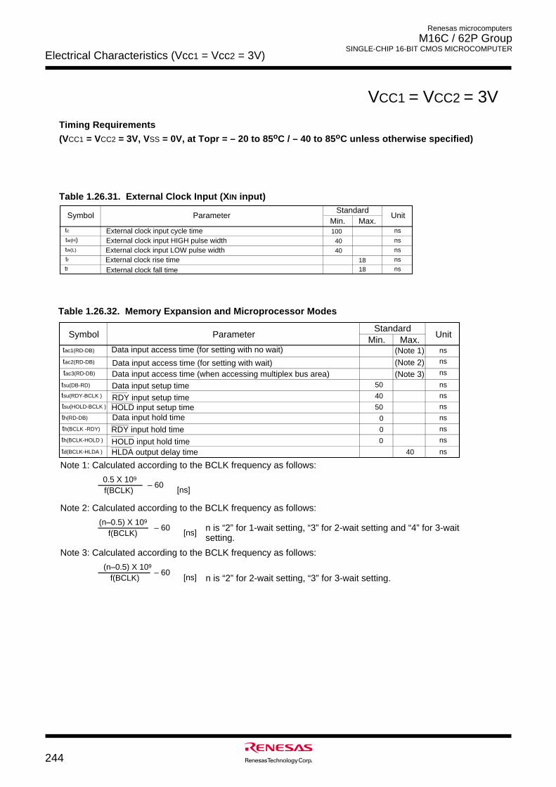
Renesas microcomputers
M16C / 62P Group SINGLE-CHIP 16-BIT CMOS MICROCOMPUTER
Electrical Characteristics (Vcc1 = Vcc2 = 3V)
244
VCC1 = VCC2 = 3V
Timing Requirements
(VCC1 = VCC2 = 3V, VSS = 0V, at Topr = – 20 to 85oC / – 40 to 85oC unless otherwise specified)
Table 1.26.32. Memory Expansion and Microprocessor Modes
Table 1.26.31. External Clock Input (XIN input)
Max.
External clock rise time nstr
Min.External clock input cycle timeExternal clock input HIGH pulse widthExternal clock input LOW pulse width
External clock fall time
ns
ns
ns
ns
tc
tw(H)
tw(L)
tf
ParameterSymbol UnitStandard
100
40
40
1818
(Note 1) (Note 2) (Note 3)
50
40
0
0
50
0
Note 1: Calculated according to the BCLK frequency as follows:
40
Min.
Data input setup time nstsu(DB-RD)
tsu(RDY-BCLK )
ParameterSymbol UnitMax.
Standard
nsRDY input setup time
Data input hold time nsth(RD-DB)
th(BCLK -RDY) nsRDY input hold time
nsHOLD input setup timetsu(HOLD-BCLK )
nsHOLD input hold timeth(BCLK-HOLD )
Data input access time (for setting with no wait) nstac1(RD-DB)
ns
ns
tac2(RD-DB)
tac3(RD-DB)
Data input access time (for setting with wait) Data input access time (when accessing multiplex bus area)
nstd(BCLK-HLDA ) HLDA output delay time
f(BCLK) – 60
0.5 X 10⁹
[ns]
Note 2: Calculated according to the BCLK frequency as follows:
f(BCLK) – 60
(n–0.5) X 109
[ns]
Note 3: Calculated according to the BCLK frequency as follows:
f(BCLK) – 60
(n–0.5) X 109
[ns]
n is “2” for 1-wait setting, “3” for 2-wait setting and “4” for 3-wait setting.
n is “2” for 2-wait setting, “3” for 3-wait setting.
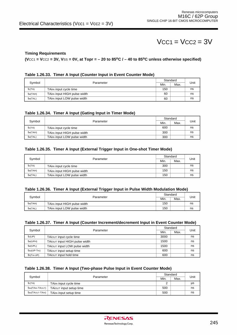
Electrical Characteristics (Vcc1 = Vcc2 = 3V)
245
Renesas microcomputers
M16C / 62P Group SINGLE-CHIP 16-BIT CMOS MICROCOMPUTER
VCC1 = VCC2 = 3V
Timing Requirements
(VCC1 = VCC2 = 3V, VSS = 0V, at Topr = – 20 to 85oC / – 40 to 85oC unless otherwise specified)
Table 1.26.33. Timer A Input (Counter Input in Event Counter Mode)Standard
Max.
nsTAiIN input LOW pulse widthtw(TAL)
Min.ns
ns
Unit
TAiIN input HIGH pulse widthtw(TAH)
ParameterSymbol
tc(TA) TAiIN input cycle time
60
150
60
Standard
Max.Min.
ns
ns
ns
Unit
TAiIN input cycle time
TAiIN input HIGH pulse widthTAiIN input LOW pulse width
tc(TA)
tw(TAH)
tw(TAL)
Symbol Parameter
600
300
300
Standard
Max.Min.ns
ns
ns
Unit
TAiIN input cycle time
TAiIN input HIGH pulse widthTAiIN input LOW pulse width
tc(TA)
tw(TAH)
tw(TAL)
Symbol Parameter
300
150
150
StandardMax.Min.
ns
ns
Unit
tw(TAH)
tw(TAL)
Symbol Parameter
TAiIN input HIGH pulse width
TAiIN input LOW pulse width
150
150
StandardMax.Min.
ns
ns
ns
Unit
ns
ns
Symbol Parameter
TAiOUT input cycle time
TAiOUT input HIGH pulse width
TAiOUT input LOW pulse width
TAiOUT input setup timeTAiOUT input hold time
tc(UP)
tw(UPH)
tw(UPL)
tsu(UP-TIN)
th(TIN-UP)
3000
1500
1500
600
600
StandardMax.Min.
µs
ns
ns
UnitSymbol Parameter
TAiIN input cycle time
TAiOUT input setup time
TAiIN input setup time
tc(TA)
tsu(TAIN-TAOUT)
tsu(TAOUT-TAIN)
2
500
500
Table 1.26.34. Timer A Input (Gating Input in Timer Mode)
Table 1.26.35. Timer A Input (External Trigger Input in One-shot Timer Mode)
Table 1.26.36. Timer A Input (External Trigger Input in Pulse Width Modulation Mode)
Table 1.26.37. Timer A Input (Counter Increment/decrement Input in Event Counter Mode)
Table 1.26.38. Timer A Input (Two-phase Pulse Input in Event Counter Mode)
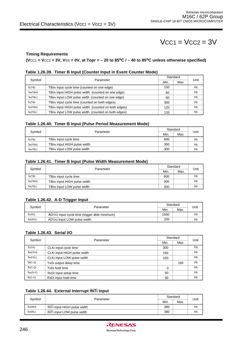
Renesas microcomputers
M16C / 62P Group SINGLE-CHIP 16-BIT CMOS MICROCOMPUTER
Electrical Characteristics (Vcc1 = Vcc2 = 3V)
246
VCC1 = VCC2 = 3V
Table 1.26.39. Timer B Input (Counter Input in Event Counter Mode)
Table 1.26.40. Timer B Input (Pulse Period Measurement Mode)
Table 1.26.41. Timer B Input (Pulse Width Measurement Mode)
Table 1.26.42. A-D Trigger Input
Table 1.26.43. Serial I/O
_______
Table 1.26.44. External Interrupt INTi Input
ns
ns
ns
ns
ns
ns
ns
Standard
Max.Min.
TBiIN input cycle time (counted on one edge)
TBiIN input HIGH pulse width (counted on one edge)
TBiIN input LOW pulse width (counted on one edge)
ns
ns
ns
tc(TB)
tw(TBH)
tw(TBL)
ParameterSymbol Unit
tc(TB)
tw(TBL)
tw(TBH)
ns
ns
nsTBiIN input HIGH pulse width (counted on both edges)
TBiIN input LOW pulse width (counted on both edges)
TBiIN input cycle time (counted on both edges)
Standard
Max.Min.
ns
ns
tc(TB)
tw(TBH)
Symbol Parameter Unit
tw(TBL) nsTBiIN input HIGH pulse width
TBiIN input cycle time
TBiIN input LOW pulse width
Standard
Max.Min.ns
ns
tc(TB)
Symbol Parameter Unit
tw(TBL) ns
tw(TBH)
TBiIN input cycle time
TBiIN input HIGH pulse width
TBiIN input LOW pulse width
Standard
Max.Min.ns
ns
tc(AD)
tw(ADL)
Symbol Parameter Unit
ADTRG input cycle time (trigger able minimum)
ADTRG input LOW pulse width
Standard
Max.Min.ns
ns
tw(INH)
tw(INL)
Symbol Parameter Unit
INTi input LOW pulse width
INTi input HIGH pulse width
Standard
Max.Min.
CLKi input cycle time
CLKi input HIGH pulse width
CLKi input LOW pulse width
tc(CK)
tw(CKH)
tw(CKL)
ParameterSymbol Unit
td(C-Q)
tsu(D-C)
th(C-Q) TxDi hold time
RxDi input setup time
TxDi output delay time
th(C-D) RxDi input hold time
150
60
60
120
120
300
600
300300
600
300
300
1500
200
380
380
300
150
150
0
50
90
160
Timing Requirements
(VCC1 = VCC2 = 3V, VSS = 0V, at Topr = – 20 to 85oC / – 40 to 85oC unless otherwise specified)
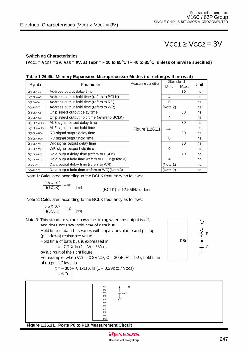
Electrical Characteristics (Vcc1 ≥ Vcc2 = 3V)
247
Renesas microcomputers
M16C / 62P Group SINGLE-CHIP 16-BIT CMOS MICROCOMPUTER
VCC1 ≥ VCC2 = 3V
Switching Characteristics
(VCC1 = VCC2 = 3V, VSS = 0V, at Topr = – 20 to 85oC / – 40 to 85oC unless otherwise specified)
Figure 1.26.11
Figure 1.26.11. Ports P0 to P10 Measurement Circuit
Table 1.26.45. Memory Expansion, Microprocessor Modes (for setting with no wait)
S
y
m
b
o
lS
t
a
n
d
a
r
dMeasuring conditionM
a
x
.M
i
n
.Parameter U
n
i
t
td
(
B
C
L
K
-
A
D
) A
d
d
r
e
s
s
o
u
t
p
u
t
d
e
l
a
y
t
i
m
e 3 0 n
s
th
(
B
C
L
K
-
A
D
) A
d
d
r
e
s
s
o
u
t
p
u
t
h
o
l
d
t
i
m
e
(
r
e
f
e
r
s
t
o
B
C
L
K
) 4 n s
th
(
B
C
L
K
-
C
S
) C
h
i
p
s
e
l
e
c
t
o
u
t
p
u
t
h
o
l
d
t
i
m
e
(
r
e
f
e
r
s
t
o
B
C
L
K
) 4 n s
td
(
B
C
L
K
-
A
L
E
) A
L
E
s
i
g
n
a
l
o
u
t
p
u
t
d
e
l
a
y
t
i
m
e 3 0 n
s
th
(
B
C
L
K
-
A
L
E
) A
L
E
s
i
g
n
a
l
o
u
t
p
u
t
h
o
l
d
t
i
m
e – 4 n
s
td
(
B
C
L
K
-
R
D
) R
D
s
i
g
n
a
l
o
u
t
p
u
t
d
e
l
a
y
t
i
m
e 3 0 n
s
th
(
B
C
L
K
-
R
D
) R
D
s
i
g
n
a
l
o
u
t
p
u
t
h
o
l
d
t
i
m
e 0 n s
td
(
B
C
L
K
-
W
R
) W
R
s
i
g
n
a
l
o
u
t
p
u
t
d
e
l
a
y
t
i
m
e 3 0 n
s
th
(
B
C
L
K
-
W
R
) W
R
s
i
g
n
a
l
o
u
t
p
u
t
h
o
l
d
t
i
m
e 0 n s
td
(
B
C
L
K
-
D
B
) D
a
t
a
o
u
t
p
u
t
d
e
l
a
y
t
i
m
e
(
r
e
f
e
r
s
t
o
B
C
L
K
) 40 n s
th(BCLK-DB) Data output hold time (refers to BCLK)(Note 3) 4 ns
th
(
W
R
-
D
B
) D
a
t
a
o
u
t
p
u
t
h
o
l
d
t
i
m
e
(
r
e
f
e
r
s
t
o
W
R
)
(
N
o
t
e
3
) n s
td
(
D
B
-
W
R
) D
a
t
a
o
u
t
p
u
t
d
e
l
a
y
t
i
m
e
(
r
e
f
e
r
s
t
o
W
R
) n s
N
o
t
e
1
:
C
a
l
c
u
l
a
t
e
d
a
c
c
o
r
d
i
n
g
t
o
t
h
e
B
C
L
K
f
r
e
q
u
e
n
c
y
a
s
f
o
l
l
o
w
s
:
f (
B
C
L
K
)
0 .
5
X
1
09
–
4
0
[ns]
td
(
B
C
L
K
-
C
S
) C
h
i
p
s
e
l
e
c
t
o
u
t
p
u
t
d
e
l
a
y
t
i
m
e 3 0 n
s
th
(
R
D
-
A
D
) A
d
d
r
e
s
s
o
u
t
p
u
t
h
o
l
d
t
i
m
e
(
r
e
f
e
r
s
t
o
R
D
) 0 n s
th
(
W
R
-
A
D
) A
d
d
r
e
s
s
o
u
t
p
u
t
h
o
l
d
t
i
m
e
(
r
e
f
e
r
s
t
o
W
R
) (Note 2) n s
N
o
t
e
3
:
T
h
i
s
s
t
a
n
d
a
r
d
v
a
l
u
e
s
h
o
w
s
t
h
e
t
i
m
i
n
g
w
h
e
n
t
h
e
o
u
t
p
u
t
i
s
o
f
f
,
a
n
d
d
o
e
s
n
o
t
s
h
o
w
h
o
l
d
t
i
m
e
o
f
d
a
t
a
b
u
s
.H
o
l
d
t
i
m
e
o
f
d
a
t
a
b
u
s
v
a
r
i
e
s
w
i
t
h
c
a
p
a
c
i
t
o
r
v
o
l
u
m
e
a
n
d
p
u
l
l
-
u
p
(
p
u
l
l
-
d
o
w
n
)
r
e
s
i
s
t
a
n
c
e
v
a
l
u
e
.H
o
l
d
t
i
m
e
o
f
d
a
t
a
b
u
s
i
s
e
x
p
r
e
s
s
e
d
i
n
t
=
–
C
R
X
l
n
(
1
–
VO
L
/
VC
C
2)
b
y
a
c
i
r
c
u
i
t
o
f
t
h
e
r
i
g
h
t
f
i
g
u
r
e
.F
o
r
e
x
a
m
p
l
e
,
w
h
e
n
VO
L
=
0
.
2
VC
C
2,
C
=
3
0
p
F
,
R
=
1
kΩ,
h
o
l
d
t
i
m
e
o
f
o
u
t
p
u
t
“
L
”
l
e
v
e
l
i
s
t
=
–
3
0
p
F
X
1
kΩ
X
l
n
(
1
–
0
.
2
VC
C
2
/
VC
C
2)
=
6
.
7
n
s
.
D
B
i
R
C
(Note 1)(Note 2)
Note 2: Calculated according to the BCLK frequency as follows:
f (
B
C
L
K
)
0 .
5
X
1
09
[ns]
f(BCLK) is 12.5MHZ or less.
–
1
0
P6
P7
P8
P10
P9
P0
P1
P2
P3
P4
P5
30pF
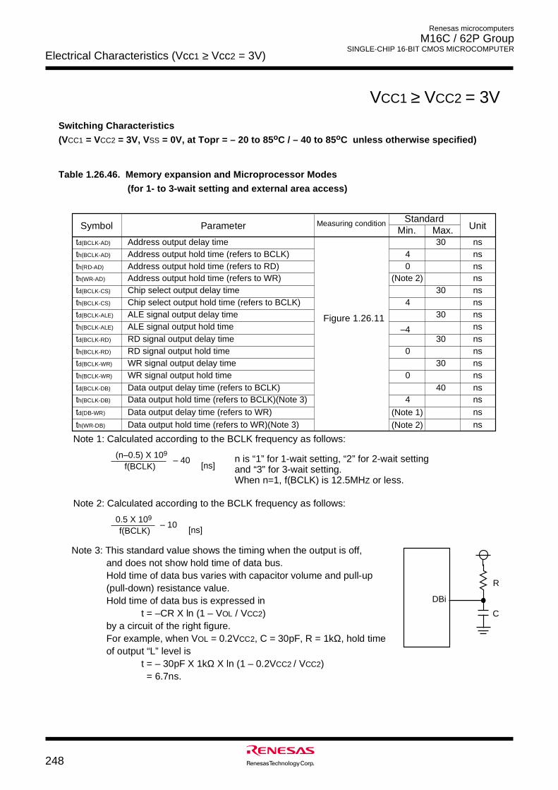
Renesas microcomputers
M16C / 62P Group SINGLE-CHIP 16-BIT CMOS MICROCOMPUTER
Electrical Characteristics (Vcc1 ≥ Vcc2 = 3V)
248
VCC1 ≥ VCC2 = 3V
Table 1.26.46. Memory expansion and Microprocessor Modes
(for 1- to 3-wait setting and external area access)
Switching Characteristics
(VCC1 = VCC2 = 3V, VSS = 0V, at Topr = – 20 to 85oC / – 40 to 85oC unless otherwise specified)
Figure 1.26.11
SymbolStandardMeasuring condition
Max.M
i
n
.P
a
r
a
m
e
t
e
r Unit
td
(
B
C
L
K
-
A
D
) A
d
d
r
e
s
s
o
u
t
p
u
t
d
e
l
a
y
t
i
m
e 3 0 n
s
th
(
B
C
L
K
-
A
D
) A
d
d
r
e
s
s
o
u
t
p
u
t
h
o
l
d
t
i
m
e
(
r
e
f
e
r
s
t
o
B
C
L
K
) 4 n s
th
(
B
C
L
K
-
C
S
) C
h
i
p
s
e
l
e
c
t
o
u
t
p
u
t
h
o
l
d
t
i
m
e
(
r
e
f
e
r
s
t
o
B
C
L
K
) 4 n s
td
(
B
C
L
K
-
A
L
E
) A
L
E
s
i
g
n
a
l
o
u
t
p
u
t
d
e
l
a
y
t
i
m
e 3 0 n
s
th(BCLK-ALE) ALE signal output hold time –4 nstd
(
B
C
L
K
-
R
D
) R
D
s
i
g
n
a
l
o
u
t
p
u
t
d
e
l
a
y
t
i
m
e 3 0 n
s
th
(
B
C
L
K
-
R
D
) R
D
s
i
g
n
a
l
o
u
t
p
u
t
h
o
l
d
t
i
m
e 0 n s
td(BCLK-WR) WR signal output delay time 30 nsth(BCLK-WR) WR signal output hold time 0 nstd(BCLK-DB) Data output delay time (refers to BCLK) 40 nsth
(
B
C
L
K
-
D
B
) D
a
t
a
o
u
t
p
u
t
h
o
l
d
t
i
m
e
(
r
e
f
e
r
s
t
o
B
C
L
K
)
(
N
o
t
e
3
) 4 n s
th
(
W
R
-
D
B
) D
a
t
a
o
u
t
p
u
t
h
o
l
d
t
i
m
e
(
r
e
f
e
r
s
t
o
W
R
)
(
N
o
t
e
3
) n s
td
(
D
B
-
W
R
) D
a
t
a
o
u
t
p
u
t
d
e
l
a
y
t
i
m
e
(
r
e
f
e
r
s
t
o
W
R
) n s
Note 1: Calculated according to the BCLK frequency as follows:
f (
B
C
L
K
)
( n
–
0
.
5
)
X
1
09
– 40[ n
s
]
td(BCLK-CS) Chip select output delay time 30 ns
th
(
R
D
-
A
D
) A
d
d
r
e
s
s
o
u
t
p
u
t
h
o
l
d
t
i
m
e
(
r
e
f
e
r
s
t
o
R
D
) 0 n s
th
(
W
R
-
A
D
) A
d
d
r
e
s
s
o
u
t
p
u
t
h
o
l
d
t
i
m
e
(
r
e
f
e
r
s
t
o
W
R
) (Note 2) n s
N
o
t
e
3
:
T
h
i
s
s
t
a
n
d
a
r
d
v
a
l
u
e
s
h
o
w
s
t
h
e
t
i
m
i
n
g
w
h
e
n
t
h
e
o
u
t
p
u
t
i
s
o
f
f
,
a
n
d
d
o
e
s
n
o
t
s
h
o
w
h
o
l
d
t
i
m
e
o
f
d
a
t
a
b
u
s
.H
o
l
d
t
i
m
e
o
f
d
a
t
a
b
u
s
v
a
r
i
e
s
w
i
t
h
c
a
p
a
c
i
t
o
r
v
o
l
u
m
e
a
n
d
p
u
l
l
-
u
p
(
p
u
l
l
-
d
o
w
n
)
r
e
s
i
s
t
a
n
c
e
v
a
l
u
e
.H
o
l
d
t
i
m
e
o
f
d
a
t
a
b
u
s
i
s
e
x
p
r
e
s
s
e
d
i
n
t
=
–
C
R
X
l
n
(
1
–
VO
L
/
VC
C
2)
b
y
a
c
i
r
c
u
i
t
o
f
t
h
e
r
i
g
h
t
f
i
g
u
r
e
.F
o
r
e
x
a
m
p
l
e
,
w
h
e
n
VO
L
=
0
.
2
VC
C
2,
C
=
3
0
p
F
,
R
=
1
kΩ,
h
o
l
d
t
i
m
e
o
f
o
u
t
p
u
t
“
L
”
l
e
v
e
l
i
s
t
=
–
3
0
p
F
X
1
kΩ
X
l
n
(
1
–
0
.
2
VC
C
2
/
VC
C
2)
=
6
.
7
n
s
.
D
B
i
R
C
(Note 1)(Note 2)
N
o
t
e
2
:
C
a
l
c
u
l
a
t
e
d
a
c
c
o
r
d
i
n
g
t
o
t
h
e
B
C
L
K
f
r
e
q
u
e
n
c
y
a
s
f
o
l
l
o
w
s
:
f (
B
C
L
K
)
0 .
5
X
1
09
[ n
s
]
n
i
s
“
1
”
f
o
r
1
-
w
a
i
t
s
e
t
t
i
n
g
,
“
2
”
f
o
r
2
-
w
a
i
t
s
e
t
t
i
n
g
a
n
d
“
3
”
f
o
r
3
-
w
a
i
t
s
e
t
t
i
n
g
.W
h
e
n
n
=
1
,
f
(
B
C
L
K
)
i
s
1
2
.
5
M
HZ
o
r
l
e
s
s
.
– 10
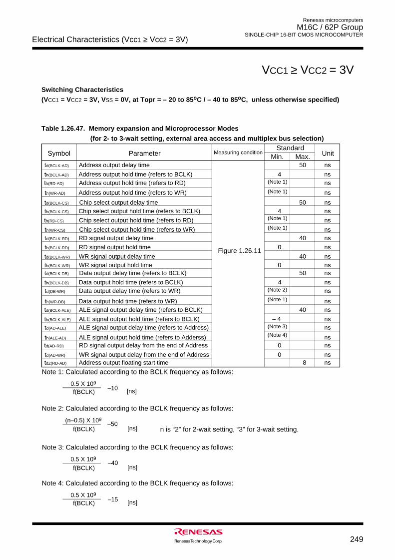
Electrical Characteristics (Vcc1 ≥ Vcc2 = 3V)
249
Renesas microcomputers
M16C / 62P Group SINGLE-CHIP 16-BIT CMOS MICROCOMPUTER
VCC1 ≥ VCC2 = 3V
Switching Characteristics
(VCC1 = VCC2 = 3V, VSS = 0V, at Topr = – 20 to 85oC / – 40 to 85oC, unless otherwise specified)
Figure 1.26.11
Table 1.26.47. Memory expansion and Microprocessor Modes
(for 2- to 3-wait setting, external area access and multiplex bus selection)
SymbolStandard
Measuring conditionMax.Min.Parameter Unit
td(BCLK-AD) Address output delay time 50 ns
th(BCLK-AD) Address output hold time (refers to BCLK) 4 ns
td(BCLK-CS) Chip select output delay time 50 nsth(BCLK-CS) Chip select output hold time (refers to BCLK) 4 ns
nsth(RD-AD) Address output hold time (refers to RD) (Note 1)
td(BCLK-RD) RD signal output delay time 40 ns
th(BCLK-RD) RD signal output hold time 0 ns
nsth(WR-AD) Address output hold time (refers to WR) (Note 1)
td(BCLK-WR) WR signal output delay time 40 ns
td(BCLK-DB) Data output delay time (refers to BCLK) 50 ns
th(BCLK-DB) Data output hold time (refers to BCLK) 4 nstd(DB-WR) Data output delay time (refers to WR) (Note 2) ns
td(BCLK-ALE) ALE signal output delay time (refers to BCLK) 40 ns
th(BCLK-ALE) ALE signal output hold time (refers to BCLK) – 4 ns
th(ALE-AD) ALE signal output hold time (refers to Adderss) ns
th(BCLK-WR) WR signal output hold time 0 ns
nsth(RD-CS) Chip select output hold time (refers to RD)
th(WR-CS) Chip select output hold time (refers to WR) (Note 1) ns
td(AD-RD) RD signal output delay from the end of Address ns0
td(AD-WR) WR signal output delay from the end of Address ns0tdZ(RD-AD) Address output floating start time ns8
th(WR-DB) Data output hold time (refers to WR) ns(Note 1)
Note 1: Calculated according to the BCLK frequency as follows:
f(BCLK) 0.5 X 10⁹
[ns]
td(AD-ALE) ALE signal output delay time (refers to Address) ns(Note 3)
Note 2: Calculated according to the BCLK frequency as follows:
f(BCLK) (n–0.5) X 109
–50[ns]
Note 3: Calculated according to the BCLK frequency as follows:
f(BCLK) 0.5 X 10⁹
–40[ns]
n is “2” for 2-wait setting, “3” for 3-wait setting.
(Note 1)
(Note 4)
–10
Note 4: Calculated according to the BCLK frequency as follows:
f(BCLK) 0.5 X 10⁹
–15 [ns]
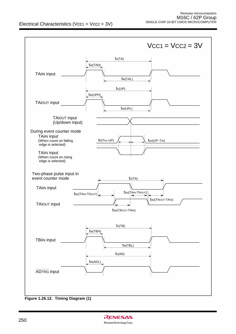
Electrical Characteristics (Vcc1 = Vcc2 = 3V)
Renesas microcomputers
M16C / 62P Group SINGLE-CHIP 16-BIT CMOS MICROCOMPUTER
250
VCC1 = VCC2 = 3V
Figure 1.26.12. Timing Diagram (1)
TAiIN input
TAiOUT input
During event counter mode
TBiIN input
tc(TA)
tw(TAH)
tw(TAL)
tc(UP)
tw(UPH)
tw(UPL)
tc(TB)
tw(TBH)
tw(TBL)
tc(AD)
tw(ADL)
th(TIN–UP) tsu(UP–TIN)TAiIN input(When count on falling edge is selected)
TAiIN input(When count on rising edge is selected)
TAiOUT input(Up/down input)
ADTRG input
tc(TA)
tsu(TAIN-TAOUT)
tsu(TAOUT-TAIN)
tsu(TAOUT-TAIN)
Two-phase pulse input in event counter mode
TAiIN input
TAiOUT input
tsu(TAIN-TAOUT)
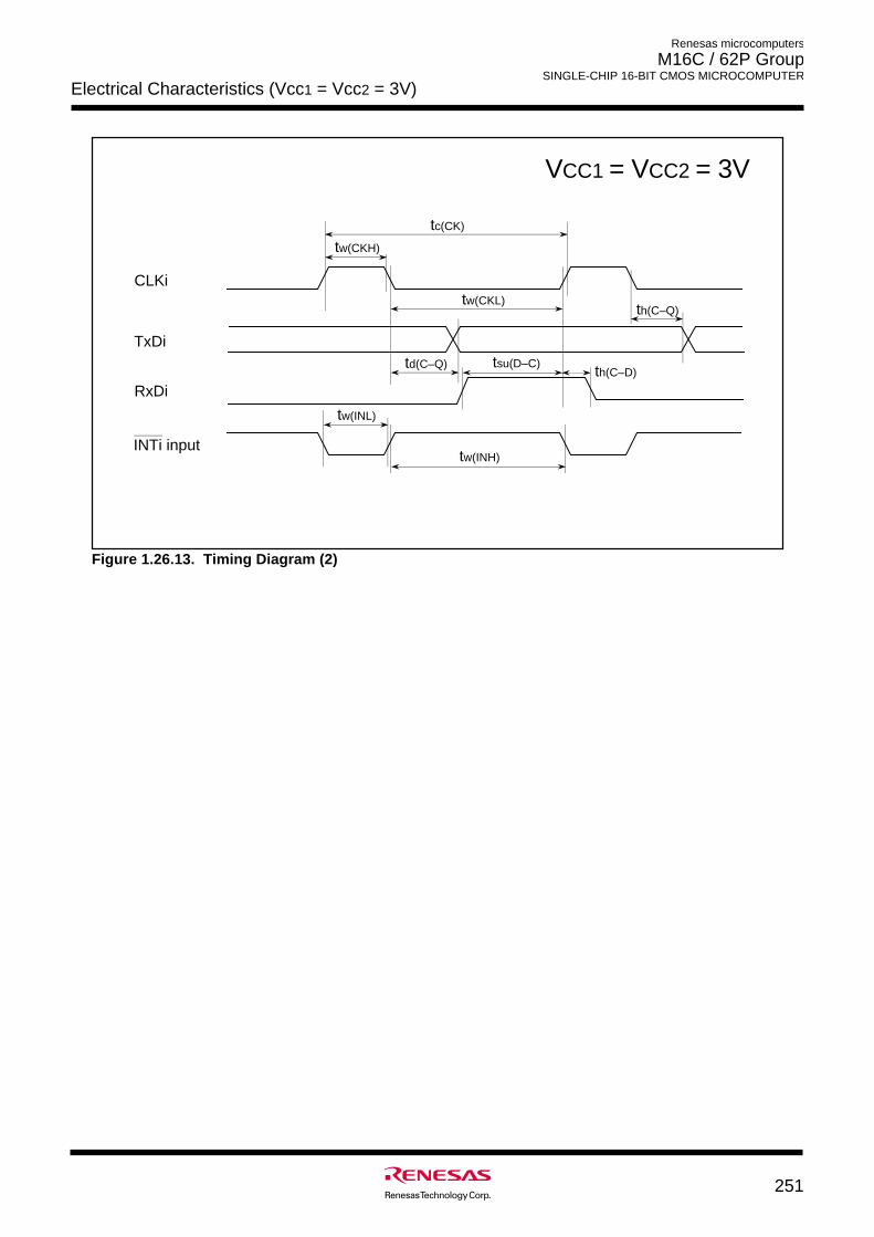
Electrical Characteristics (Vcc1 = Vcc2 = 3V)
Renesas microcomputers
M16C / 62P Group SINGLE-CHIP 16-BIT CMOS MICROCOMPUTER
251
VCC1 = VCC2 = 3V
Figure 1.26.13. Timing Diagram (2)
tsu(D–C)
CLKi
TxDi
RxDi
tc(CK)
tw(CKH)
tw(CKL)
tw(INL)
tw(INH)
td(C–Q) th(C–D)
th(C–Q)
INTi input
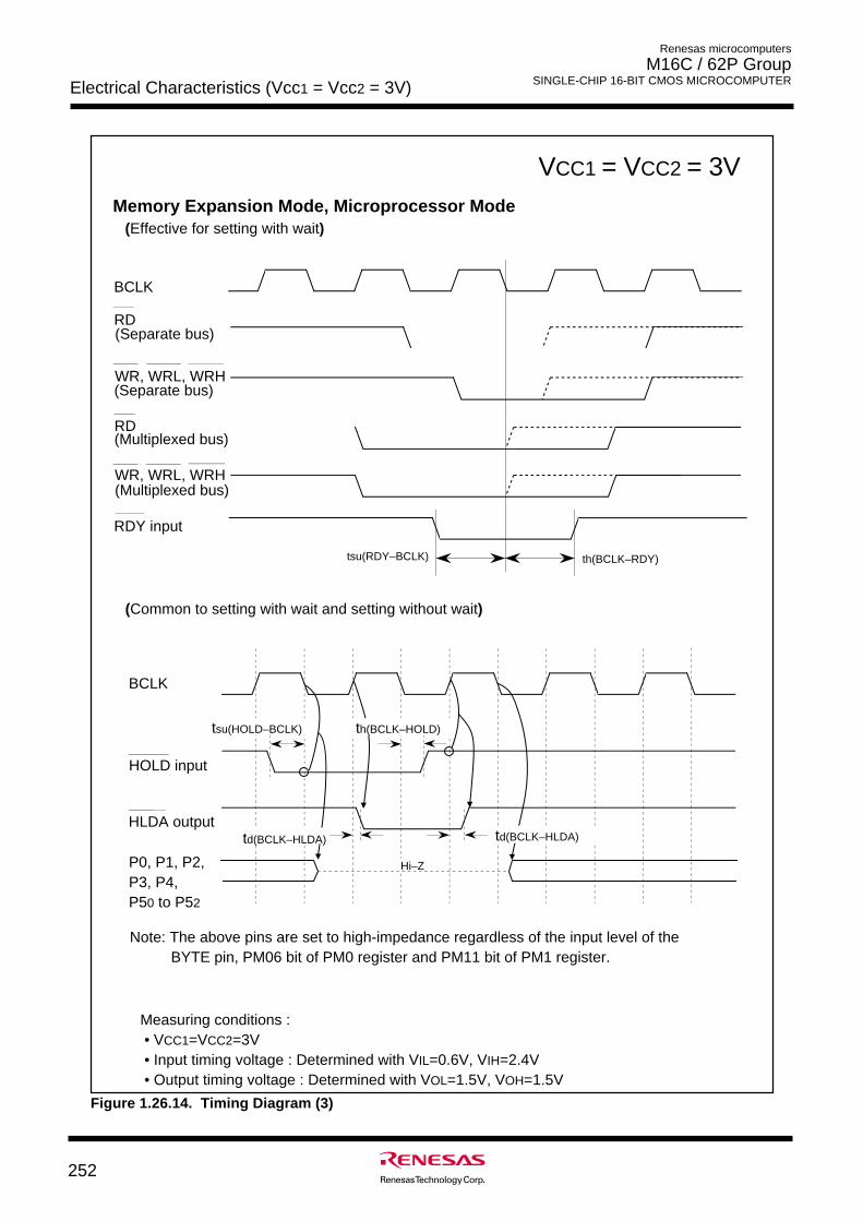
Electrical Characteristics (Vcc1 = Vcc2 = 3V)
Renesas microcomputers
M16C / 62P Group SINGLE-CHIP 16-BIT CMOS MICROCOMPUTER
252
VCC1 = VCC2 = 3V
Figure 1.26.14. Timing Diagram (3)
Measuring conditions : • VCC1=VCC2=3V • Input timing voltage : Determined with VIL=0.6V, VIH=2.4V • Output timing voltage : Determined with VOL=1.5V, VOH=1.5V
Memory Expansion Mode, Microprocessor Mode
BCLK
HOLD input
HLDA output
P0, P1, P2, P3, P4, P50 to P52
(Common to setting with wait and setting without wait)
Note: The above pins are set to high-impedance regardless of the input level of the BYTE pin, PM06 bit of PM0 register and PM11 bit of PM1 register.
th(BCLK–HOLD)tsu(HOLD–BCLK)
(Effective for setting with wait)
td(BCLK–HLDA)td(BCLK–HLDA)
Hi–Z
RDY input
tsu(RDY–BCLK) th(BCLK–RDY)
BCLK
RD(Multiplexed bus)
(Multiplexed bus)WR, WRL, WRH
WR, WRL, WRH(Separate bus)
RD(Separate bus)
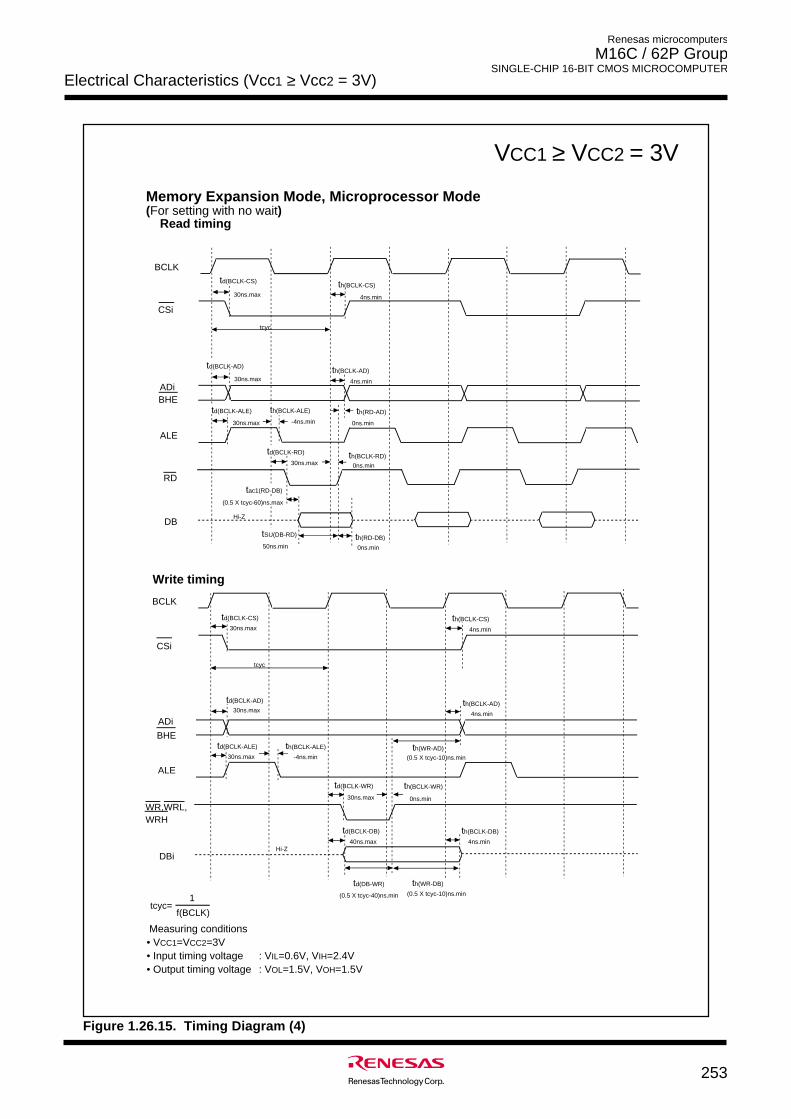
Electrical Characteristics (Vcc1 ≥ Vcc2 = 3V)
Renesas microcomputers
M16C / 62P Group SINGLE-CHIP 16-BIT CMOS MICROCOMPUTER
253
VCC1 ≥ VCC2 = 3V
Figure 1.26.15. Timing Diagram (4)
BCLK
CSi
td(BCLK-CS)
30ns.max
ADi 30ns.max
ALE 30ns.max -4ns.min
RD
30ns.max th(BCLK-RD)
0ns.min
th(BCLK-AD)
4ns.min
th(BCLK-CS)
4ns.min
Hi-Z DB
th(RD-DB)
0ns.min
0ns.min
th(RD-AD)
BHE
tcyc
Read timing
td(BCLK-AD)
td(BCLK-ALE) th(BCLK-ALE)
tSU(DB-RD)
td(BCLK-RD)
50ns.min
tac1(RD-DB)
Memory Expansion Mode, Microprocessor Mode(For setting with no wait)
Measuring conditions • VCC1=VCC2=3V • Input timing voltage : VIL=0.6V, VIH=2.4V• Output timing voltage : VOL=1.5V, VOH=1.5V
WR,WRL,WRH
30ns.max
th(BCLK-WR)
0ns.min
BCLK
CSi
td(BCLK-CS)
30ns.max
ADi
td(BCLK-AD)
30ns.max
ALE
30ns.max
td(BCLK-ALE) th(BCLK-ALE)
-4ns.min
th(BCLK-AD)
4ns.min
th(BCLK-CS)
4ns.min
tcyc
th(WR-AD)
BHE
td(BCLK-DB)
40ns.max 4ns.min
th(BCLK-DB)
td(DB-WR)
(0.5 X tcyc-40)ns.min
th(WR-DB)
DBi
Write timing
td(BCLK-WR)
Hi-Z
(0.5 X tcyc-60)ns.max
tcyc=1
f(BCLK)
(0.5 X tcyc-10)ns.min
(0.5 X tcyc-10)ns.min
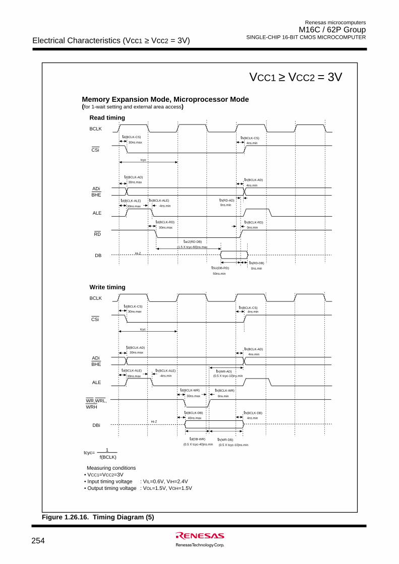
Electrical Characteristics (Vcc1 ≥ Vcc2 = 3V)
Renesas microcomputers
M16C / 62P Group SINGLE-CHIP 16-BIT CMOS MICROCOMPUTER
254
VCC1 ≥ VCC2 = 3V
Figure 1.26.16. Timing Diagram (5)
BCLK
CSi
td(BCLK-CS)
30ns.max
ADi
td(BCLK-AD)
30ns.max
ALE
30ns.max
th(BCLK-ALE)
-4ns.min
RD
30ns.max
th(BCLK-RD)
0ns.min
th(BCLK-AD)
4ns.min
th(BCLK-CS)
4ns.min
Hi-ZDB
tSU(DB-RD)
50ns.min
th(RD-DB)
0ns.min
tcyc
BHE
Read timing
WR,WRL,WRH
30ns.max
th(BCLK-WR)
0ns.min
BCLK
CSi
td(BCLK-CS)
30ns.max
ADi
td(BCLK-AD)
30ns.max
ALE
30ns.max
td(BCLK-ALE) th(BCLK-ALE)
-4ns.min
th(BCLK-AD)
4ns.min
th(BCLK-CS)4ns.min
tcyc
th(WR-AD)
BHE
td(BCLK-DB)
40ns.max 4ns.min
th(BCLK-DB)
td(DB-WR)
(0.5 X tcyc-40)ns.min (0.5 X tcyc-10)ns.min
th(WR-DB)
DBi
Write timing
td(BCLK-ALE)
td(BCLK-RD)
(0.5 X tcyc-10)ns.min
td(BCLK-WR)
0ns.min
th(RD-AD)
tac2(RD-DB)
Hi-Z
Memory Expansion Mode, Microprocessor Mode(for 1-wait setting and external area access)
Measuring conditions • VCC1=VCC2=3V • Input timing voltage : VIL=0.6V, VIH=2.4V• Output timing voltage : VOL=1.5V, VOH=1.5V
(1.5 X tcyc-60)ns.max
tcyc=1
f(BCLK)
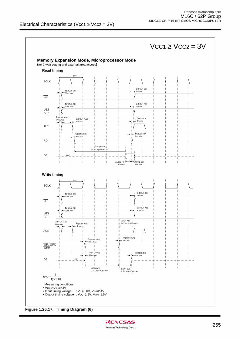
Electrical Characteristics (Vcc1 ≥ Vcc2 = 3V)
Renesas microcomputers
M16C / 62P Group SINGLE-CHIP 16-BIT CMOS MICROCOMPUTER
255
VCC1 ≥ VCC2 = 3V
Figure 1.26.17. Timing Diagram (6)
Read timing
Write timing
BCLK
CSi
ALE
DB
ADiBHE
WR, WRLWRH
Memory Expansion Mode, Microprocessor Mode(for 2-wait setting and external area access)
BCLK
CSi
ALE
DBi
ADiBHE
RD
tcyc
td(BCLK-CS)30ns.max
td(BCLK-AD)30ns.max
td(BCLK-ALE)30ns.max th(BCLK-ALE)
-4ns.min
td(BCLK-RD)30ns.max
Hi-Z
tSU(DB-RD)50ns.min
th(RD-DB)0ns.min
th(BCLK-RD)0ns.min
th(RD-AD)0ns.min
th(BCLK-AD)4ns.min
th(BCLK-CS)4ns.min
tcyc
Hi-Z
td(BCLK-CS)30ns.max
td(BCLK-AD)30ns.max
td(BCLK-ALE)30ns.max th(BCLK-ALE)
-4ns.min
td(BCLK-WR)30ns.max
th(BCLK-CS)4ns.min
th(BCLK-AD)4ns.min
th(WR-AD)(0.5 X tcyc-10)ns.min
th(BCLK-WR)0ns.min
td(BCLK-DB)40ns.max
td(DB-WR)(1.5 X tcyc-40)ns.min
th(BCLK-DB)4ns.min
th(WR-DB)(0.5 X tcyc-10)ns.min
Measuring conditions • VCC1=VCC2=3V • Input timing voltage : VIL=0.6V, VIH=2.4V• Output timing voltage : VOL=1.5V, VOH=1.5V
tac2(RD-DB)
(2.5 X tcyc-60)ns.max
tcyc=1
f(BCLK)
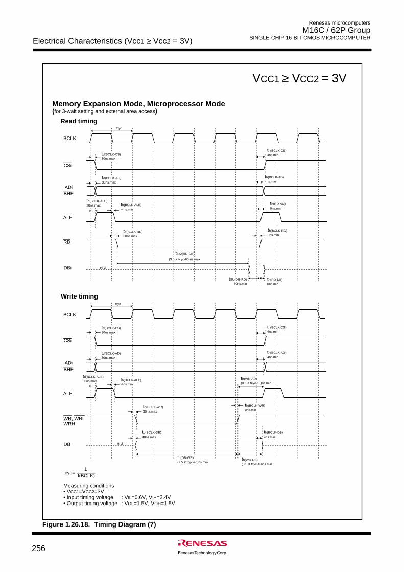
Electrical Characteristics (Vcc1 ≥ Vcc2 = 3V)
Renesas microcomputers
M16C / 62P Group SINGLE-CHIP 16-BIT CMOS MICROCOMPUTER
256
VCC1 ≥ VCC2 = 3V
Figure 1.26.18. Timing Diagram (7)
Read timing
Write timing
BCLK
CSi
ALE
DB
ADiBHE
WR, WRLWRH
Memory Expansion Mode, Microprocessor Mode(for 3-wait setting and external area access)
BCLK
CSi
ALE
DBi
ADiBHE
RD
tcyc
td(BCLK-CS)30ns.max
td(BCLK-AD)30ns.max
td(BCLK-ALE)30ns.max th(BCLK-ALE)
-4ns.min
td(BCLK-RD)30ns.max
Hi-Z
tSU(DB-RD)50ns.min
th(RD-DB)0ns.min
th(BCLK-RD)0ns.min
th(RD-AD)0ns.min
th(BCLK-AD)4ns.min
th(BCLK-CS)4ns.min
tcyc
Hi-Z
td(BCLK-CS)30ns.max
td(BCLK-AD)30ns.max
td(BCLK-ALE)30ns.max th(BCLK-ALE)
-4ns.min
td(BCLK-WR)30ns.max
th(BCLK-CS)4ns.min
th(BCLK-AD)4ns.min
th(WR-AD)(0.5 X tcyc-10)ns.min
th(BCLK-WR)0ns.min
td(BCLK-DB)40ns.max
td(DB-WR)(2.5 X tcyc-40)ns.min
th(BCLK-DB)4ns.min
th(WR-DB)(0.5 X tcyc-10)ns.min
Measuring conditions • VCC1=VCC2=3V • Input timing voltage : VIL=0.6V, VIH=2.4V• Output timing voltage : VOL=1.5V, VOH=1.5V
tac2(RD-DB)
(3.5 X tcyc-60)ns.max
tcyc=1
f(BCLK)
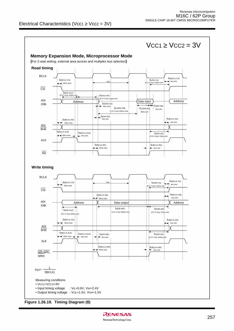
Electrical Characteristics (Vcc1 ≥ Vcc2 = 3V)
Renesas microcomputers
M16C / 62P Group SINGLE-CHIP 16-BIT CMOS MICROCOMPUTER
257
VCC1 ≥ VCC2 = 3V
Figure 1.26.19. Timing Diagram (8)
Memory Expansion Mode, Microprocessor Mode(For 2-wait setting, external area access and multiplex bus selection)
BCLK
CSi
td(BCLK-CS)
40ns.max
ADi
td(BCLK-AD)
40ns.max
ALE
th(BCLK-ALE)-4ns.min
RD
40ns.max
th(BCLK-RD)
0ns.min
th(BCLK-AD)
4ns.min
th(BCLK-CS)
4ns.mintcycth(RD-CS)
th(RD-AD)
BHE
ADi/DBi th(RD-DB)
0ns.min
td(AD-ALE)
Read timing
td(BCLK-WR)
40ns.maxth(BCLK-WR)
0ns.min
BCLK
CSi
td(BCLK-CS)
40ns.max
ADi
td(BCLK-AD)
40ns.max
ALE
40ns.maxth(BCLK-ALE)
-4ns.min
th(BCLK-AD)
4ns.min
th(BCLK-CS)
4ns.min tcyc
th(WR-AD)
BHE
td(BCLK-DB)
50ns.max 4ns.min
th(BCLK-DB)
td(DB-WR) th(WR-DB)
ADi/DBi
Data output
WR,WRL,WRH
Write timing
Address
(0.5 X tcyc-10)ns.min
AddressData input
50ns.min
(0.5 X tcyc-10)ns.min
td(BCLK-ALE)
td(BCLK-RD)
(0.5 X tcyc-10)ns.min
th(WR-CS)
Address
td(AD-ALE)
(0.5 X tcyc-40)ns.min(1.5 X tcyc-50)ns.min
(0.5 X tcyc-10)ns.min
td(BCLK-ALE)
(0.5 X tcyc-40)ns.min
Address
40ns.max
tSU(DB-RD)tac3(RD-DB)
(0.5 X tcyc-10)ns.min
th(ALE-AD)
td(AD-RD)0ns.min
tdZ(RD-AD)8ns.max
td(AD-WR)
0ns.min
Measuring conditions • VCC1=VCC2=3V • Input timing voltage : VIL=0.6V, VIH=2.4V• Output timing voltage : VOL=1.5V, VOH=1.5V
(1.5 X tcyc-60)ns.max
tcyc=1
f(BCLK)
(0.5 X tcyc-15)ns.min
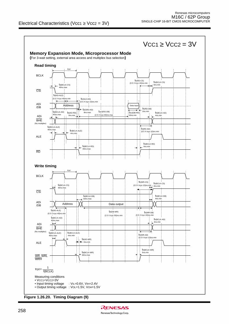
Electrical Characteristics (Vcc1 ≥ Vcc2 = 3V)
Renesas microcomputers
M16C / 62P Group SINGLE-CHIP 16-BIT CMOS MICROCOMPUTER
258
VCC1 ≥ VCC2 = 3V
Figure 1.26.20. Timing Diagram (9)
Read timing
Write timing
Memory Expansion Mode, Microprocessor Mode(For 3-wait setting, external area access and multiplex bus selection)
BCLK
CSi
ALE
RD
ADi /DB
ADi
BHE
BCLK
CSi
ALE
ADi /DB
tcyc
td(BCLK-AD)40ns.max
tcyc
Data output
th(BCLK-CS)6ns.mintd(BCLK-CS)
40ns.max
td(BCLK-ALE)40ns.max th(BCLK-ALE)
-4ns.min
td(BCLK-RD)40ns.max
th(BCLK-RD)0ns.min
tSU(DB-RD)50ns.min
th(RD-DB)0ns.min
th(RD-AD)(0.5 X tcyc-10)ns.min
th(BCLK-AD)4ns.min
td(BCLK-CS)40ns.max
td(BCLK-AD)40ns.max
th(BCLK-DB)4ns.min
th(BCLK-WR)0ns.min
th(WR-AD)(0.5 X tcyc-10)ns.min
th(BCLK-AD)4ns.min
th(BCLK-CS)4ns.min
td(BCLK-ALE)40ns.max
td(BCLK-WR)40ns.max
th(WR-DB)(0.5 X tcyc-10)ns.min
Data input Address
Address
ADi
BHE
WR, WRLWRH
Measuring conditions • VCC1=VCC2=3V • Input timing voltage : VIL=0.6V, VIH=2.4V• Output timing voltage : VOL=1.5V, VOH=1.5V
th(ALE-AD)
td(AD-ALE)
(0.5 X tcyc-40)ns.min
td(AD-RD)0ns.min
tdZ(RD-AD)8ns.max tac3(RD-DB)
td(BCLK-DB)50ns.max
(0.5 X tcyc-10)ns.min
th(WR-CS)
td(DB-WR)
(2.5 X tcyc-50)ns.min
td(AD-WR)0ns.min
th(RD-CS)(0.5 X tcyc-10)ns.min
td(AD-ALE)
(0.5 X tcyc-40)ns.min
(2.5 X tcyc-60)ns.max
tcyc= 1f(BCLK)
th(BCLK-ALE)-4ns.min
(No multiplex)
(No multiplex)
(0.5 X tcyc-15)ns.min
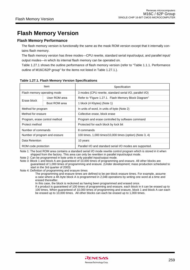
Flash Memory Version
259
Renesas microcomputers
M16C / 62P Group SINGLE-CHIP 16-BIT CMOS MICROCOMPUTER
Table 1.27.1. Flash Memory Version Specifications
Flash Memory VersionFlash Memory Performance
The flash memory version is functionally the same as the mask ROM version except that it internally con-
tains flash memory.
The flash memory version has three modes—CPU rewrite, standard serial input/output, and parallel input/
output modes—in which its internal flash memory can be operated on.
Table 1.27.1 shows the outline performance of flash memory version (refer to “Table 1.1.1. Performance
outline of M16C/62P group” for the items not listed in Table 1.27.1.).
Item
Flash memory operating mode
Erase block
Method for program
Method for erasure
Program, erase control method
Protect method
Number of commands
Number of program and erasure
ROM code protection
Specification
3 modes (CPU rewrite, standard serial I/O, parallel I/O)
Refer to “Figure 1.27.1. Flash Memory Block Diagram”
1 block (4 Kbytes) (Note 1)
In units of word, in units of byte (Note 2)
Collective erase, block erase
Program and erase controlled by software command
Protected for each block by lock bit
8 commands
100 times, 1,000 times/10,000 times (option) (Note 3, 4)
Parallel I/O and standard serial I/O modes are supported.
Note 1: The boot ROM area contains a standard serial I/O mode rewrite control program which is stored in it when shipped from the factory. This area can only be rewritten in parallel input/output mode.
Note 2: Can be programmed in byte units in only parallel input/output mode. Note 3: Block 1 and block A are guaranteed of 10,000 times of programming and erasure. All other blocks are
guaranteed of 1,000 times of programming and erasure. (Under development; mass production scheduled to start in the 3rd quarter of 2003)
Note 4: Definition of programming and erasure timesThe programming and erasure times are defined to be per-block erasure times. For example, assume a case where a 4K-byte block A is programmed in 2,048 operations by writing one word at a time and erased thereafter. In this case, the block is reckoned as having been programmed and erased once. If a product is guaranteed of 100 times of programming and erasure, each block in it can be erased up to 100 times. When guaranteed of 10,000 times of programming and erasure, block 1 and block A can each be erased up to 10,000 times. All other blocks can each be erased up to 1,000 times.
User ROM area
Boot ROM area
Data Retention 10 years
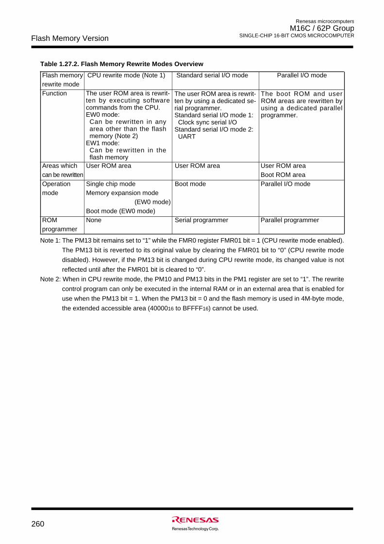
Flash Memory Version
260
Renesas microcomputers
M16C / 62P Group SINGLE-CHIP 16-BIT CMOS MICROCOMPUTER
Table 1.27.2. Flash Memory Rewrite Modes Overview
Flash memory CPU rewrite mode (Note 1) Standard serial I/O mode Parallel I/O moderewrite modeFunction
Areas which User ROM area User ROM area User ROM areacan be rewritten Boot ROM areaOperation Single chip mode Boot mode Parallel I/O modemode Memory expansion mode
(EW0 mode)Boot mode (EW0 mode)
ROM None Serial programmer Parallel programmerprogrammer
The user ROM area is rewrit-ten by executing softwarecommands from the CPU.EW0 mode:
Can be rewritten in anyarea other than the flashmemory (Note 2)
EW1 mode:Can be rewritten in theflash memory
The user ROM area is rewrit-ten by using a dedicated se-rial programmer.Standard serial I/O mode 1:
Clock sync serial I/OStandard serial I/O mode 2:
UART
The boot ROM and userROM areas are rewritten byusing a dedicated parallelprogrammer.
Note 1: The PM13 bit remains set to “1” while the FMR0 register FMR01 bit = 1 (CPU rewrite mode enabled).
The PM13 bit is reverted to its original value by clearing the FMR01 bit to “0” (CPU rewrite mode
disabled). However, if the PM13 bit is changed during CPU rewrite mode, its changed value is not
reflected until after the FMR01 bit is cleared to “0”.
Note 2: When in CPU rewrite mode, the PM10 and PM13 bits in the PM1 register are set to “1”. The rewrite
control program can only be executed in the internal RAM or in an external area that is enabled for
use when the PM13 bit = 1. When the PM13 bit = 0 and the flash memory is used in 4M-byte mode,
the extended accessible area (4000016 to BFFFF16) cannot be used.
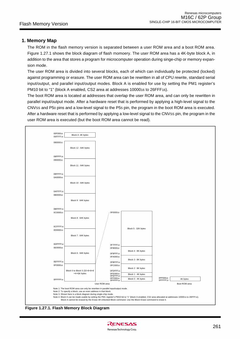
Flash Memory Version
261
Renesas microcomputers
M16C / 62P Group SINGLE-CHIP 16-BIT CMOS MICROCOMPUTER
1. Memory MapThe ROM in the flash memory version is separated between a user ROM area and a boot ROM area.
Figure 1.27.1 shows the block diagram of flash momoery. The user ROM area has a 4K-byte block A, in
addition to the area that stores a program for microcomputer operation during singe-chip or memory expan-
sion mode.
The user ROM area is divided into several blocks, each of which can individually be protected (locked)
against programming or erasure. The user ROM area can be rewritten in all of CPU rewrite, standard serial
input/output, and parallel input/output modes. Block A is enabled for use by setting the PM1 register’s
PM10 bit to “1” (block A enabled, CS2 area at addresses 1000016 to 26FFF16).
The boot ROM area is located at addresses that overlap the user ROM area, and can only be rewritten in
parallel input/output mode. After a hardware reset that is performed by applying a high-level signal to the
CNVSS and P50 pins and a low-level signal to the P55 pin, the program in the boot ROM area is executed.
After a hardware reset that is performed by applying a low-level signal to the CNVSS pin, the program in the
user ROM area is executed (but the boot ROM area cannot be read).
Figure 1.27.1. Flash Memory Block Diagram
00FFFF16Block A :4K bytes
00F00016
4K bytes0FF000160FFFFF16
Boot ROM area
Note 1: The boot ROM area can only be rewritten in parallel input/output mode. Note 2: To specify a block, use an even address in that block.Note 3: Shown here is a block diagram during single-chip mode.Note 4: Block A can be made usable by setting the PM1 register’s PM10 bit to “1” (block A enabled, CS2 area allocated at addresses 1000016 to 26FFF16). Block A cannot be erased by the Erase All Unlocked Block command. Use the Block Erase command to erase it.
0F000016
Block 0 to Block 5 (32+8+8+8+4+4)K bytes
0E000016
Block 6 : 64K bytes
0EFFFF16
0D000016
Block 7 : 64K bytes
0DFFFF16
0C000016
Block 8 : 64K bytes
0CFFFF16
0B000016
Block 9 : 64K bytes
0BFFFF16
0A000016
Block 10 : 64K bytes
0AFFFF16
0FFFFF160FF000160FFFFF16
Block 0 : 4K bytes
Block 1 : 4K bytes
Block 2 : 8K bytes
0FE000160FEFFF16
0FC00016
0FDFFF16
Block 3 : 8K bytes0FA00016
0FBFFF16
Block 4 : 8K bytes0F800016
0F9FFF16
Block 5 : 32K bytes
0F000016
0F7FFF16
User ROM area
09000016
Block 11 : 64K bytes
09FFFF16
08000016
Block 12 : 64K bytes
08FFFF16
Flash Memory
262
Renesas microcomputers
M16C / 62P Group SINGLE-CHIP 16-BIT CMOS MICROCOMPUTER
Boot ModeAfter a hardware reset which is performed by applying a low-level signal to the P55 pin and a high-level
signal to the CNVSS and P50 pins, the microcomputer is placed in boot mode, thereby executing the pro-
gram in the boot ROM area.
During boot mode, the boot ROM and user ROM areas are switched over by the FMR05 bit in the FMR0
register.
The boot ROM area contains a standard serial input/output mode based rewrite control program which was
stored in it when shipped from the factory.
The boot ROM area can be rewritten in parallel input/output mode. Prepare an EW0 mode based rewrite
control program and write it in the boot ROM area, and the flash memory can be rewritten as suitable for the
system.
Functions To Prevent Flash Memory from RewritingTo prevent the flash memory from being read or rewritten easily, parallel input/output mode has a ROM
code protect and standard serial input/output mode has an ID code check function.
• ROM Code Protect FunctionThe ROM code protect function inhibits the flash memory from being read or rewritten during parallel
input/output mode. Figure 1.27.2 shows the ROMCP register.
The ROMCP register is located in the user ROM area. The ROMCP1 bit consists of two bits. The ROM
code protect function is enabled by clearing one or both of two ROMCP1 bits to “0” when the ROMCR bits
are not ‘002,’ with the flash memory thereby protected against reading or rewriting. Conversely, when the
ROMCR bits are ‘002’ (ROM code protect removed), the flash memory can be read or rewritten. Once the
ROM code protect function is enabled, the ROMCR bits cannot be changed during parallel input/output
mode. Therefore, use standard serial input/output or other modes to rewrite the flash memory.
• ID Code Check Function
Use this function in standard serial input/output mode. Unless the flash memory is blank, the ID codes
sent from the programmer and the ID codes written in the flash memory are compared to see if they
match. If the ID codes do not match, the commands sent from the programmer are not accepted. The ID
code consists of 8-bit data, the areas of which, beginning with the first byte, are 0FFFDF16, 0FFFE316,
0FFFEB16, 0FFFEF16, 0FFFF316, 0FFFF716, and 0FFFFB16. Prepare a program in which the ID codes
are preset at these addresses and write it in the flash memory.
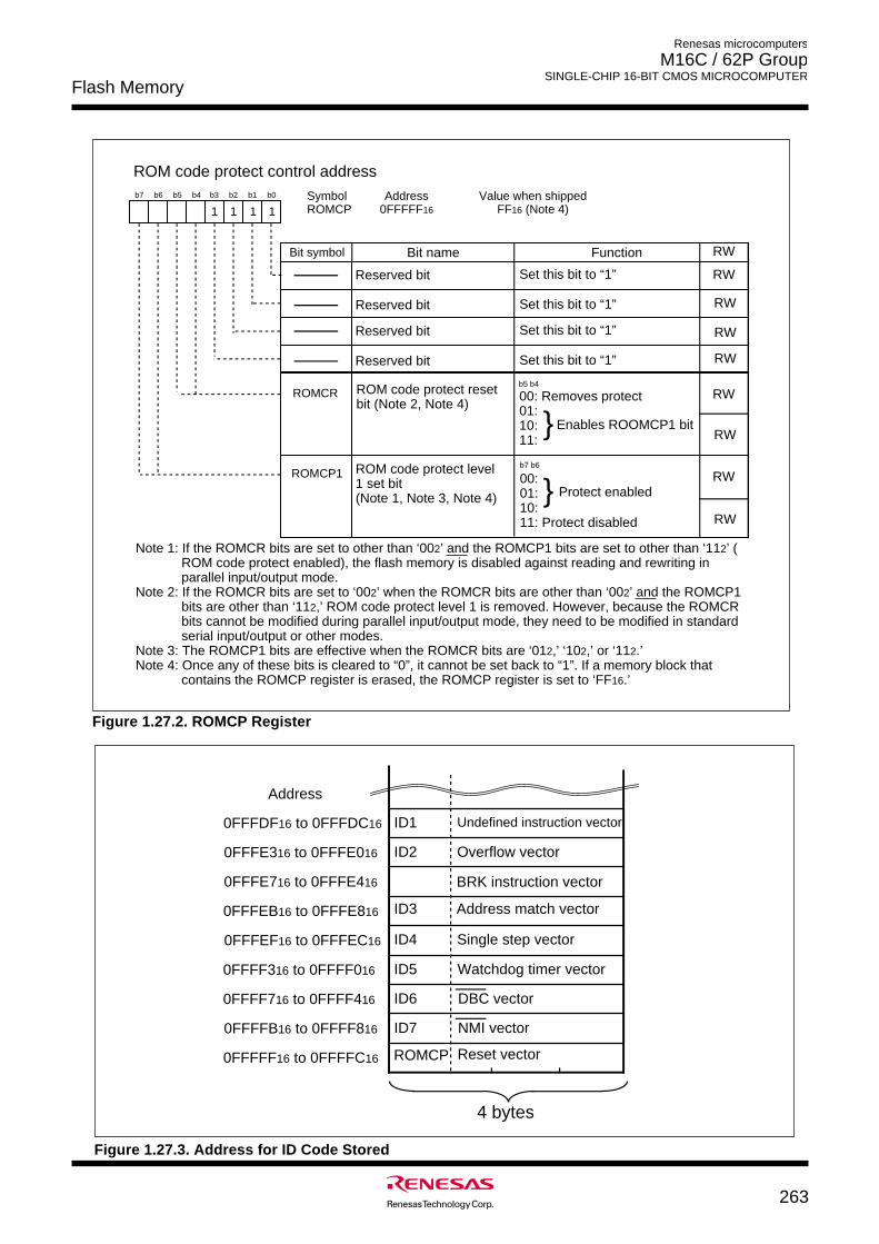
Flash Memory
263
Renesas microcomputers
M16C / 62P Group SINGLE-CHIP 16-BIT CMOS MICROCOMPUTER
Figure 1.27.2. ROMCP Register
Figure 1.27.3. Address for ID Code Stored
Symbol Address Value when shippedROMCP 0FFFFF16 FF16 (Note 4)
ROM code protect control address
Bit name FunctionBit symbol
b7 b6 b5 b4 b3 b2 b1 b0
00: Removes protect01: 10: 11:
00: 01: 10: 11: Protect disabled
ROM code protect reset bit (Note 2, Note 4)
ROM code protect level 1 set bit (Note 1, Note 3, Note 4)
ROMCR
ROMCP1
b5 b4
b7 b6
11
Reserved bit Set this bit to “1”
Reserved bit Set this bit to “1”
Reserved bit Set this bit to “1”
Reserved bit Set this bit to “1”
Enables ROOMCP1 bit
Protect enabled
Note 1: If the ROMCR bits are set to other than ‘002’ and the ROMCP1 bits are set to other than ‘112’ (ROM code protect enabled), the flash memory is disabled against reading and rewriting in parallel input/output mode.
Note 2: If the ROMCR bits are set to ‘002’ when the ROMCR bits are other than ‘002’ and the ROMCP1 bits are other than ‘112,’ ROM code protect level 1 is removed. However, because the ROMCR bits cannot be modified during parallel input/output mode, they need to be modified in standard serial input/output or other modes.
Note 3: The ROMCP1 bits are effective when the ROMCR bits are ‘012,’ ‘102,’ or ‘112.’Note 4: Once any of these bits is cleared to “0”, it cannot be set back to “1”. If a memory block that
contains the ROMCP register is erased, the ROMCP register is set to ‘FF16.’
11
RW
RW
RW
RW
RW
RW
RW
RW
RW
Reset vector
Watchdog timer vector
Single step vector
Address match vector
BRK instruction vector
Overflow vector
Undefined instruction vector
ID7
ID6
ID5
ID4
ID3
ID2
ID1
DBC vector
NMI vector
0FFFFF16 to 0FFFFC16
0FFFFB16 to 0FFFF816
0FFFF716 to 0FFFF416
0FFFF316 to 0FFFF016
0FFFEF16 to 0FFFEC16
0FFFEB16 to 0FFFE816
0FFFE716 to 0FFFE416
0FFFE316 to 0FFFE016
0FFFDF16 to 0FFFDC16
4 bytes
Address
ROMCP
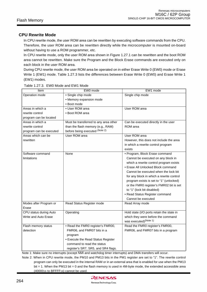
Flash Memory
264
Renesas microcomputers
M16C / 62P Group SINGLE-CHIP 16-BIT CMOS MICROCOMPUTER
CPU Rewrite ModeIn CPU rewrite mode, the user ROM area can be rewritten by executing software commands from the CPU.Therefore, the user ROM area can be rewritten directly while the microcomputer is mounted on-boardwithout having to use a ROM programmer, etc.In CPU rewrite mode, only the user ROM area shown in Figure 1.27.1 can be rewritten and the boot ROMarea cannot be rewritten. Make sure the Program and the Block Erase commands are executed only oneach block in the user ROM area.During CPU rewrite mode, the user ROM area be operated on in either Erase Write 0 (EW0) mode or EraseWrite 1 (EW1) mode. Table 1.27.3 lists the differences between Erase Write 0 (EW0) and Erase Write 1
(EW1) modes.
Table 1.27.3. EW0 Mode and EW1 ModeItem EW0 mode EW1 mode
Operation mode • Single chip mode Single chip mode• Memory expansion mode
• Boot modeAreas in which a • User ROM area User ROM arearewrite control • Boot ROM area
program can be locatedAreas in which a Must be transferred to any area other Can be executed directly in the userrewrite control than the flash memory (e.g., RAM) ROM area
program can be executed before being executed (Note 2)
Areas which can be User ROM area User ROM arearewritten However, this does not include the area
in which a rewrite control programexists
Software command None • Program, Block Erase command
limitations Cannot be executed on any block inwhich a rewrite control program exists
• Erase All Unlocked Block command
Cannot be executed when the lock bitfor any block in which a rewrite controlprogram exists is set to “1” (unlocked)
or the FMR0 register’s FMR02 bit is setto “1” (lock bit disabled)
• Read Status Register command
Cannot be executedModes after Program or Read Status Register mode Read Array modeErase
CPU status during Auto Operating Hold state (I/O ports retain the state inWrite and Auto Erase which they were before the command
was executed)(Note 1)
Flash memory status • Read the FMR0 register's FMR00, Read the FMR0 register's FMR00,detection FMR06, and FMR07 bits in a FMR06, and FMR07 bits in a program
program
• Execute the Read Status Registercommand to read the statusregister's SR7, SR5, and SR4 flags.
_______
Note 1: Make sure no interrupts (except NMI and watchdog timer interrupts) and DMA transfers will occur.Note 2: When in CPU rewrite mode, the PM10 and PM13 bits in the PM1 register are set to “1”. The rewrite control
program can only be executed in the internal RAM or in an external area that is enabled for use when the PM13
bit = 1. When the PM13 bit = 0 and the flash memory is used in 4M-byte mode, the extended accessible area(4000016 to BFFFF16) cannot be used.
Flash Memory
265
Renesas microcomputers
M16C / 62P Group SINGLE-CHIP 16-BIT CMOS MICROCOMPUTER
• EW0 ModeThe microcomputer is placed in CPU rewrite mode by setting the FMR0 register’s FMR01 bit to “1” (CPU
rewrite mode enabled), ready to accept commands. In this case, because the FMR1 register’s FMR11 bit
= 0, EW0 mode is selected. The FMR01 bit can be set to “1” by writing “0” and then “1” in succession.
Use software commands to control program and erase operations. Read the FMR0 register or status
register to check the status of program or erase operation at completion.
• EW1 Mode
EW1 mode is selected by setting FMR11 bit to “1” (by writing “0” and then “1” in succession) after setting
the FMR01 bit to “1” (by writing “0” and then “1” in succession).
Read the FMR0 register to check the status of program or erase operation at completion. The status
register cannot be read during EW1 mode.
Flash Memory
266
Renesas microcomputers
M16C / 62P Group SINGLE-CHIP 16-BIT CMOS MICROCOMPUTER
Figure 1.27.4 shows the FIDR, FMR0 and FMR1 registers.
FMR00 Bit
This bit indicates the operating status of the flash memory. The bit is “0” when the Program, Erase, or
Lock Bit program is running; otherwise, the bit is “1”.
FMR01 BitThe microcomputer is made ready to accept commands by setting the FMR01 bit to “1” (CPU rewrite
mode). During boot mode, make sure the FMR05 bit also is “1” (user ROM area access).
FMR02 BitThe lock bit set for each block can be disabled by setting the FMR02 bit to “1” (lock bit disabled). (Refer to
the description of the data protect function.) The lock bits set are enabled by setting the FMR02 bit to “0”.
The FMR02 bit only disables the lock bit function and does not modify the lock bit data (lock bit status
flag). However, if the Erase command is executed while the FMR02 bit is set to “1”, the lock bit data
changes state from “0” (locked) to “1” (unlocked) after Erase is completed.
FMSTP Bit
This bit is provided for initializing the flash memory control circuits, as well as for reducing the amount of
current consumed in the flash memory. Setting the FMSTP bit to “1” makes the internal flash memory
inaccessible. Therefore, make sure the FMSTP bit is modified in other than the flash memory area.
In the following cases, set the FMSTP bit to “1”:
• When flash memory access resulted in an error while erasing or programming in EW0 mode (FMR00
bit not reset to “1” (ready))
• When entering low power mode or ring low power mode
Figure 1.27.7 shows a flow chart to be followed before and after entering low power mode.
Note that when going to stop or wait mode, the FMR0 register does not need to be set because the power
for the internal flash memory is automatically turned off and is turned back on again after returning from
stop or wait mode.
FMR05 Bit
This bit switches between the boot ROM and user ROM areas during boot mode. Set this bit to “0” when
accessing the boot ROM area (for read) or “1” (user ROM access) when accessing the user ROM area
(for read, write, or erase).
FMR06 Bit
This is a read-only bit indicating the status of auto program operation. The bit is set to “1” when a program
error occurs; otherwise, it is cleared to “0”. For details, refer to the description of the full status check.
FMR07 BitThis is a read-only bit indicating the status of auto erase operation. The bit is set to “1” when an erase
error occurs; otherwise, it is cleared to “0”. For details, refer to the description of the full status check.
Figure 1.27.5 and 1.27.6 show the setting and resetting of EW0 mode and EW1 mode, respectively.
FMR11 BitSetting this bit to “1” places the microcomputer in EW1 mode.
FMR16 Bit
This is a read-only bit indicating the execution result of the Read Lock Bit Status command.
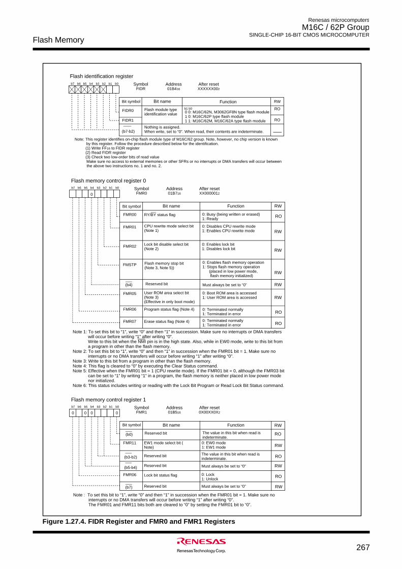
Flash Memory
267
Renesas microcomputers
M16C / 62P Group SINGLE-CHIP 16-BIT CMOS MICROCOMPUTER
Flash memory control register 0Symbol Address After resetFMR0 01B716 XX0000012
b7 b6 b5 b4 b3 b2 b1 b0
FMR00
Bit symbol Bit name Function RW
0: Busy (being written or erased)1: Ready
CPU rewrite mode select bit (Note 1)
0: Disables CPU rewrite mode 1: Enables CPU rewrite mode
FMR01
0: Boot ROM area is accessed1: User ROM area is accessed
Lock bit disable select bit (Note 2)
0: Enables lock bit1: Disables lock bit
Flash memory stop bit (Note 3, Note 5))
User ROM area select bit (Note 3) (Effective in only boot mode)
FMR02
FMSTP
FMR05
0
RY/BY status flag
Reserved bit Must always be set to “0”
0: Terminated normally1: Terminated in error
Program status flag (Note 4)FMR06
0: Terminated normally1: Terminated in error
Erase status flag (Note 4)FMR07
Flash memory control register 1Symbol Address After resetFMR1 01B516 0X00XX0X2
b7 b6 b5 b4 b3 b2 b1 b0
Bit symbol Bit name Function
EW1 mode select bit (Note)
0: EW0 mode 1: EW1 mode
FMR11
0
Reserved bit Must always be set to “0”
Reserved bit The value in this bit when read is indeterminate.
Reserved bit Must always be set to “0”
0: Lock1: Unlock
Lock bit status flagFMR06
000
RW
RW
RW
RW
RW
RO
RO
RO
RO
RW
RO
RW
RW
RW
(b0)
(b5-b4)
(b7)
(b4)
0: Enables flash memory operation1: Stops flash memory operation (placed in low power mode, flash memory initialized)
Note 1: To set this bit to “1”, write “0” and then “1” in succession. Make sure no interrupts or DMA transfers will occur before writing “1” after writing “0”.Write to this bit when the NMI pin is in the high state. Also, while in EW0 mode, write to this bit from a program in other than the flash memory.
Note 2: To set this bit to “1”, write “0” and then “1” in succession when the FMR01 bit = 1. Make sure no interrupts or no DMA transfers will occur before writing “1” after writing “0”.
Note 3: Write to this bit from a program in other than the flash memory. Note 4: This flag is cleared to “0” by executing the Clear Status command.Note 5: Effective when the FMR01 bit = 1 (CPU rewrite mode). If the FMR01 bit = 0, although the FMR03 bit
can be set to “1” by writing “1” in a program, the flash memory is neither placed in low power mode nor initialized.
Note 6: This status includes writing or reading with the Lock Bit Program or Read Lock Bit Status command.
Reserved bit The value in this bit when read is indeterminate.(b3-b2) RO
Note : To set this bit to “1”, write “0” and then “1” in succession when the FMR01 bit = 1. Make sure no interrupts or no DMA transfers will occur before writing “1” after writing “0”.The FMR01 and FMR11 bits both are cleared to “0” by setting the FMR01 bit to “0”.
Flash identification registerSymbol Address After reset
FIDR 01B416 XXXXXX002
b7 b6 b5 b4 b3 b2 b1 b0
FIDR0
Bit symbol Bit name Function RW
0 0: M16C/62N, M3062GF8N type flash module1 0: M16C/62P type flash module1 1: M16C/62M, M16C/62A type flash module
Flash module typeidentification value
Note: This register identifies on-chip flash module type of M16C/62 group. Note, however, no chip version is known by this register. Follow the procedure described below for the identification.(1) Write FF16 to FIDR register(2) Read FIDR register(3) Check two low-order bits of read valueMake sure no access to external memories or other SFRs or no interrupts or DMA transfers will occur between the above two instructions no. 1 and no. 2.
FIDR1
Nothing is assigned.When write, set to “0”. When read, their contents are indeterminate.(b7-b2)
b1 b0 RO
RO
Figure 1.27.4. FIDR Register and FMR0 and FMR1 Registers
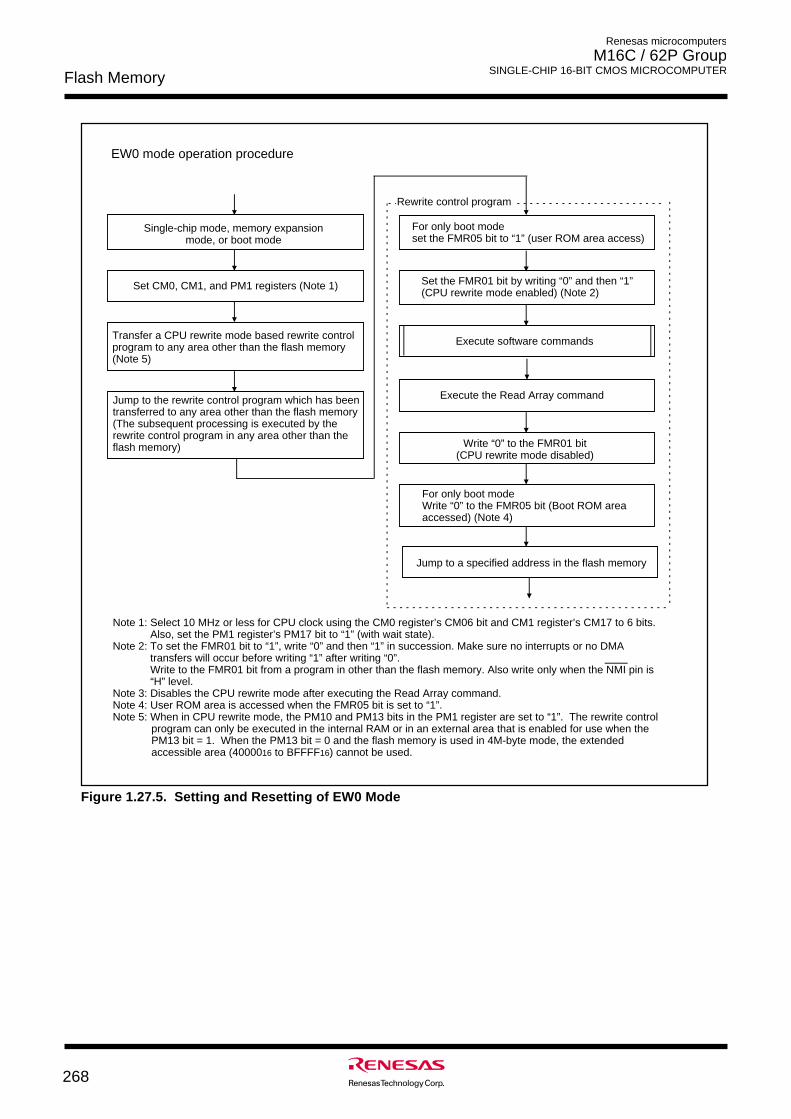
Flash Memory
268
Renesas microcomputers
M16C / 62P Group SINGLE-CHIP 16-BIT CMOS MICROCOMPUTER
Execute the Read Array command
Single-chip mode, memory expansion mode, or boot mode
Set CM0, CM1, and PM1 registers (Note 1)
Execute software commands
Jump to the rewrite control program which has been transferred to any area other than the flash memory (The subsequent processing is executed by the rewrite control program in any area other than the flash memory)
Transfer a CPU rewrite mode based rewrite control program to any area other than the flash memory (Note 5)
For only boot modeWrite “0” to the FMR05 bit (Boot ROM area accessed) (Note 4)
Write “0” to the FMR01 bit(CPU rewrite mode disabled)
For only boot modeset the FMR05 bit to “1” (user ROM area access)
Set the FMR01 bit by writing “0” and then “1” (CPU rewrite mode enabled) (Note 2)
EW0 mode operation procedure
Rewrite control program
Jump to a specified address in the flash memory
Note 1: Select 10 MHz or less for CPU clock using the CM0 register’s CM06 bit and CM1 register’s CM17 to 6 bits. Also, set the PM1 register’s PM17 bit to “1” (with wait state).
Note 2: To set the FMR01 bit to “1”, write “0” and then “1” in succession. Make sure no interrupts or no DMA transfers will occur before writing “1” after writing “0”.Write to the FMR01 bit from a program in other than the flash memory. Also write only when the NMI pin is “H” level.
Note 3: Disables the CPU rewrite mode after executing the Read Array command.Note 4: User ROM area is accessed when the FMR05 bit is set to “1”. Note 5: When in CPU rewrite mode, the PM10 and PM13 bits in the PM1 register are set to “1”. The rewrite control
program can only be executed in the internal RAM or in an external area that is enabled for use when the PM13 bit = 1. When the PM13 bit = 0 and the flash memory is used in 4M-byte mode, the extended accessible area (4000016 to BFFFF16) cannot be used.
Figure 1.27.5. Setting and Resetting of EW0 Mode
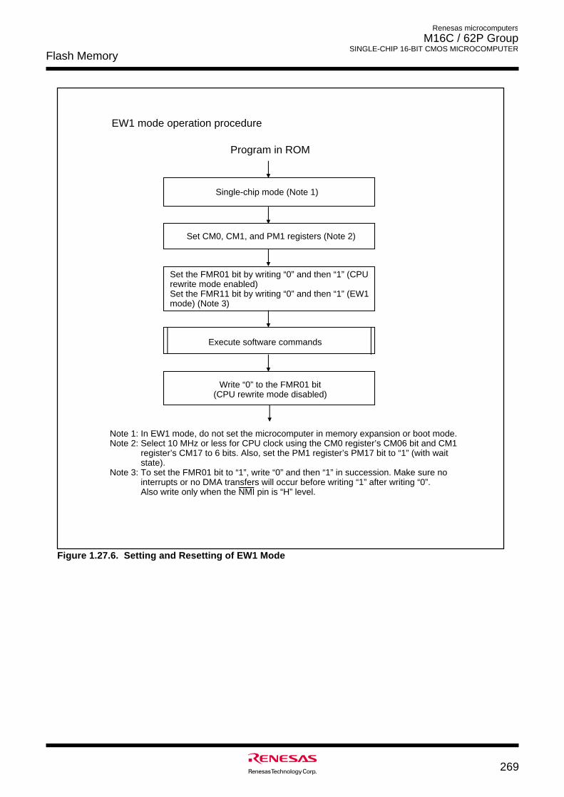
Flash Memory
269
Renesas microcomputers
M16C / 62P Group SINGLE-CHIP 16-BIT CMOS MICROCOMPUTER
Figure 1.27.6. Setting and Resetting of EW1 Mode
Single-chip mode (Note 1)
Set CM0, CM1, and PM1 registers (Note 2)
Set the FMR01 bit by writing “0” and then “1” (CPU rewrite mode enabled) Set the FMR11 bit by writing “0” and then “1” (EW1 mode) (Note 3)
Program in ROM
EW1 mode operation procedure
Execute software commands
Write “0” to the FMR01 bit(CPU rewrite mode disabled)
Note 1: In EW1 mode, do not set the microcomputer in memory expansion or boot mode.Note 2: Select 10 MHz or less for CPU clock using the CM0 register’s CM06 bit and CM1
register’s CM17 to 6 bits. Also, set the PM1 register’s PM17 bit to “1” (with wait state).
Note 3: To set the FMR01 bit to “1”, write “0” and then “1” in succession. Make sure no interrupts or no DMA transfers will occur before writing “1” after writing “0”.
Also write only when the NMI pin is “H” level.
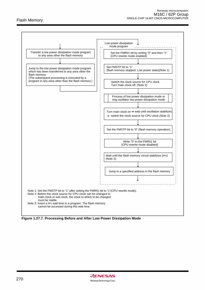
Flash Memory
270
Renesas microcomputers
M16C / 62P Group SINGLE-CHIP 16-BIT CMOS MICROCOMPUTER
Figure 1.27.7. Processing Before and After Low Power Dissipation Mode
Turn main clock on
Transfer a low power dissipation mode program to any area other the flash memory
Switch the clock source for CPU clock.Turn main clock off. (Note 2)
Jump to the low power dissipation mode program which has been transferred to any area other the flash memory.(The subsequent processing is executed by a program in any area other than the flash memory.)
Wait until the flash memory circuit stabilizes (tPS)(Note 3)
Set the FMSTP bit to “0” (flash memory operation)
Set FMSTP bit to “1”(flash memory stopped. Low power state)(Note 1)
Process of low power dissipation mode or ring oscillator low power dissipation mode
switch the clock source for CPU clock (Note 2)
Low power dissipation mode program
Write “0” to the FMR01 bit(CPU rewrite mode disabled)
Set the FMR01 bit by writing “0” and then “1” (CPU rewrite mode enabled)
Jump to a specified address in the flash memory
wait until oscillation stabilizes
Note 1: Set the FMSTP bit to “1” after setting the FMR01 bit to “1”(CPU rewrite mode).Note 2: Before the clock source for CPU clock can be changed to
main clock or sub clock, the clock to which to be changed must be stable.
Note 3: Insert a tPS wait time in a program. The flash memory cannot be accessed during this wait time.
Flash Memory
271
Renesas microcomputers
M16C / 62P Group SINGLE-CHIP 16-BIT CMOS MICROCOMPUTER
Precautions on CPU Rewrite ModeDescribed below are the precautions to be observed when rewriting the flash memory in CPU rewrite mode.
(1) Operation Speed
Before entering CPU rewrite mode (EW0 or EW1 mode), select 10 MHz or less for CPU clock using
the CM06 bit in the CM0 register and the CM17 to CM16 bits in the CM1 register. Also, set the PM17
bit in the PM1 register to “1” (with wait state).
(2) Instructions to Prevent from Using
The following instructions cannot be used in EW0 mode because the flash memory’s internal data is
referenced: UND instruction, INTO instruction, JMPS instruction, JSRS instruction, and BRK instruc-
tion.
(3) Interrupts
EW0 Mode
• Any interrupt which has a vector in the variable vector table can be used providing that its vector is
transferred into the RAM area._______
• The NMI and watchdog timer interrupts can be used because the FMR0 register and FMR1 regis-
ter are initialized when one of those interrupts occurs. The jump addresses for those interrupt
service routines should be set in the fixed vector table._______
Because the rewrite operation is halted when a NMI or watchdog timer interrupt occurs, the rewrite
program must be executed again after exiting the interrupt service routine.
• The address match interrupt cannot be used because the flash memory’s internal data is refer-
enced.
EW1 Mode
• Make sure that any interrupt which has a vector in the variable vector table or address match
interrupt will not be accepted during the auto program or auto erase period.
• Avoid using watchdog timer interrupts._______
• The NMI interrupt can be used because the FMR0 register and FMR1 register are initialized when
this interrupt occurs. The jump address for the interrupt service routine should be set in the fixed
vector table._______
Because the rewrite operation is halted when a NMI interrupt occurs, the rewrite program must be
executed again after exiting the interrupt service routine.
(4) How to Access
To set the FMR01, FMR02, or FMR11 bit to “1”, write “0” and then “1” in succession. This is necessary
to ensure that no interrupts or DMA transfers will occur before writing “1” after writing “0”. Also only_______
when NMI pin is “H” level.
(5) Writing in the User ROM Space
EW0 Mode
• If the power supply voltage drops while rewriting any block in which the rewrite control program is
stored, a problem may occur that the rewrite control program is not correctly rewritten and, conse-
quently, the flash memory becomes unable to be rewritten thereafter. In this case, standard serial
I/O or parallel I/O mode should be used.
EW1 Mode
• Avoid rewriting any block in which the rewrite control program is stored.
Flash Memory
272
Renesas microcomputers
M16C / 62P Group SINGLE-CHIP 16-BIT CMOS MICROCOMPUTER
(6) DMA Transfer
In EW1 mode, make sure that no DMA transfers will occur while the FMR0 register’s FMR00 bit = 0
(during the auto program or auto erase period).
(7) Writing Command and Data
Write the command code and data at even addresses.
(8) Wait Mode
When shifting to wait mode, set the FMR01 bit to “0” (CPU rewrite mode disabled) before executing
the WAIT instruction.
(9) Stop Mode
When shifting to stop mode, the following settings are required:
• Set the FMR01 bit to “0” (CPU rewrite mode disabled) and disable DMA transfers before setting the
CM10 bit to “1” (stop mode).
• Execute the JMP.B instruction subsequent to the instruction which sets the CM10 bit to “1” (stop
mode)
Example program BSET 0, CM1 ; Stop mode
JMP.B L1
L1:
Program after returning from stop mode
(10) Low Power Dissipation Mode and Ring Oscillator Low Power Dissipation Mode
If the CM05 bit is set to “1” (main clock stop), the following commands must not be executed.
• Program
• Block erase
• Erase all unlocked blocks
• Lock bit program
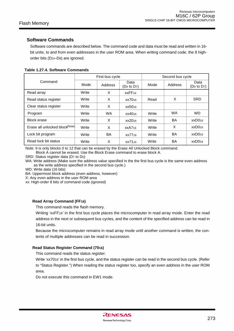
Flash Memory
273
Renesas microcomputers
M16C / 62P Group SINGLE-CHIP 16-BIT CMOS MICROCOMPUTER
Software CommandsSoftware commands are described below. The command code and data must be read and written in 16-
bit units, to and from even addresses in the user ROM area. When writing command code, the 8 high-
order bits (D1t–D8) are ignored.
Table 1.27.4. Software Commands
Read Array Command (FF16)This command reads the flash memory.
Writing ‘xxFF16’ in the first bus cycle places the microcomputer in read array mode. Enter the read
address in the next or subsequent bus cycles, and the content of the specified address can be read in
16-bit units.
Because the microcomputer remains in read array mode until another command is written, the con-
tents of multiple addresses can be read in succession.
Read Status Register Command (7016)This command reads the status register.
Write ‘xx7016’ in the first bus cycle, and the status register can be read in the second bus cycle. (Refer
to “Status Register.”) When reading the status register too, specify an even address in the user ROM
area.
Do not execute this command in EW1 mode.
Command
Program
Clear status register
Read array
Read status register
(Note)
First bus cycle Second bus cycle
Lock bit program
Erase all unlocked block
Block erase
Read lock bit status
Write
Write
Write
Write
Write
Write
Write
Write
Mode
Read
Write
Write
Write
Write
Write
Mode
X
BA
X
WA
BA
BA
Address
SRD
xxD016
xxD016
WD
xxD016
xxD016
Data(D0 to D7)
xxFF16
xx7016
xx5016
xx4016
xx7716
xxA716
xx2016
xx7116
Data(D0 to D7)
X
X
X
WA
BA
X
X
X
Address
Note: It is only blocks 0 to 12 that can be erased by the Erase All Unlocked Block command. Block A cannot be erased. Use the Block Erase command to erase block A.SRD: Status register data (D7 to D0)WA: Write address (Make sure the address value specified in the the first bus cycle is the same even address as the write address specified in the second bus cycle.)WD: Write data (16 bits)BA: Uppermost block address (even address, however)X: Any even address in the user ROM areaxx: High-order 8 bits of command code (ignored)
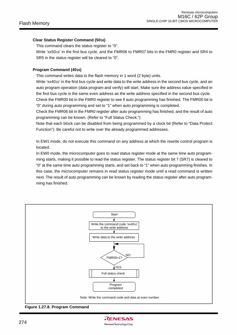
Flash Memory
274
Renesas microcomputers
M16C / 62P Group SINGLE-CHIP 16-BIT CMOS MICROCOMPUTER
Start
Program completed
YES
NO
Note: Write the command code and data at even number.
Write the command code ‘xx4016’ to the write address
Write data to the write address
FMR00=1?
Full status check
Figure 1.27.8. Program Command
Clear Status Register Command (5016)This command clears the status register to “0”.
Write ‘xx5016’ in the first bus cycle, and the FMR06 to FMR07 bits in the FMR0 register and SR4 to
SR5 in the status register will be cleared to “0”.
Program Command (4016)
This command writes data to the flash memory in 1 word (2 byte) units.
Write ‘xx4016’ in the first bus cycle and write data to the write address in the second bus cycle, and an
auto program operation (data program and verify) will start. Make sure the address value specified in
the first bus cycle is the same even address as the write address specified in the second bus cycle.
Check the FMR00 bit in the FMR0 register to see if auto programming has finished. The FMR00 bit is
“0” during auto programming and set to “1” when auto programming is completed.
Check the FMR06 bit in the FMR0 register after auto programming has finished, and the result of auto
programming can be known. (Refer to “Full Status Check.”)
Note that each block can be disabled from being programmed by a clock bit (Refer to “Data Protect
Function”). Be careful not to write over the already programmed addresses.
In EW1 mode, do not execute this command on any address at which the rewrite control program is
located.
In EW0 mode, the microcomputer goes to read status register mode at the same time auto program-
ming starts, making it possible to read the status register. The status register bit 7 (SR7) is cleared to
“0” at the same time auto programming starts, and set back to “1” when auto programming finishes. In
this case, the microcomputer remains in read status register mode until a read command is written
next. The result of auto programming can be known by reading the status register after auto program-
ming has finished.
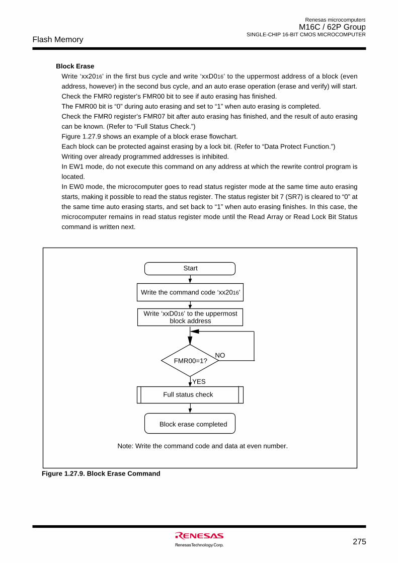
Flash Memory
275
Renesas microcomputers
M16C / 62P Group SINGLE-CHIP 16-BIT CMOS MICROCOMPUTER
Write ‘xxD016’ to the uppermost block address
Start
Block erase completed
YES
NO
Note: Write the command code and data at even number.
Write the command code ‘xx2016’
FMR00=1?
Full status check
Figure 1.27.9. Block Erase Command
Block Erase
Write ‘xx2016’ in the first bus cycle and write ‘xxD016’ to the uppermost address of a block (even
address, however) in the second bus cycle, and an auto erase operation (erase and verify) will start.
Check the FMR0 register’s FMR00 bit to see if auto erasing has finished.
The FMR00 bit is “0” during auto erasing and set to “1” when auto erasing is completed.
Check the FMR0 register’s FMR07 bit after auto erasing has finished, and the result of auto erasing
can be known. (Refer to “Full Status Check.”)
Figure 1.27.9 shows an example of a block erase flowchart.
Each block can be protected against erasing by a lock bit. (Refer to “Data Protect Function.”)
Writing over already programmed addresses is inhibited.
In EW1 mode, do not execute this command on any address at which the rewrite control program is
located.
In EW0 mode, the microcomputer goes to read status register mode at the same time auto erasing
starts, making it possible to read the status register. The status register bit 7 (SR7) is cleared to “0” at
the same time auto erasing starts, and set back to “1” when auto erasing finishes. In this case, the
microcomputer remains in read status register mode until the Read Array or Read Lock Bit Status
command is written next.
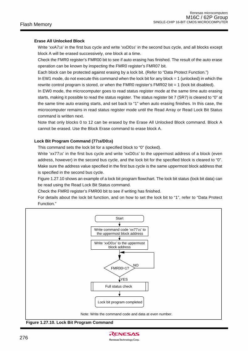
Flash Memory
276
Renesas microcomputers
M16C / 62P Group SINGLE-CHIP 16-BIT CMOS MICROCOMPUTER
Write ‘xxD016’ to the uppermost block address
Start
Lock bit program completed
YES
NO
Note: Write the command code and data at even number.
Write command code ‘xx7716’ to the uppermost block address
FMR00=1?
Full status check
Erase All Unlocked Block
Write ‘xxA716’ in the first bus cycle and write ‘xxD016’ in the second bus cycle, and all blocks except
block A will be erased successively, one block at a time.
Check the FMR0 register’s FMR00 bit to see if auto erasing has finished. The result of the auto erase
operation can be known by inspecting the FMR0 register’s FMR07 bit.
Each block can be protected against erasing by a lock bit. (Refer to “Data Protect Function.”)
In EW1 mode, do not execute this command when the lock bit for any block = 1 (unlocked) in which the
rewrite control program is stored, or when the FMR0 register’s FMR02 bit = 1 (lock bit disabled).
In EW0 mode, the microcomputer goes to read status register mode at the same time auto erasing
starts, making it possible to read the status register. The status register bit 7 (SR7) is cleared to “0” at
the same time auto erasing starts, and set back to “1” when auto erasing finishes. In this case, the
microcomputer remains in read status register mode until the Read Array or Read Lock Bit Status
command is written next.
Note that only blocks 0 to 12 can be erased by the Erase All Unlocked Block command. Block A
cannot be erased. Use the Block Erase command to erase block A.
Lock Bit Program Command (7716/D016)
This command sets the lock bit for a specified block to “0” (locked).
Write ‘xx7716’ in the first bus cycle and write ‘xxD016’ to the uppermost address of a block (even
address, however) in the second bus cycle, and the lock bit for the specified block is cleared to “0”.
Make sure the address value specified in the first bus cycle is the same uppermost block address that
is specified in the second bus cycle.
Figure 1.27.10 shows an example of a lock bit program flowchart. The lock bit status (lock bit data) can
be read using the Read Lock Bit Status command.
Check the FMR0 register’s FMR00 bit to see if writing has finished.
For details about the lock bit function, and on how to set the lock bit to “1”, refer to “Data Protect
Function.”
Figure 1.27.10. Lock Bit Program Command
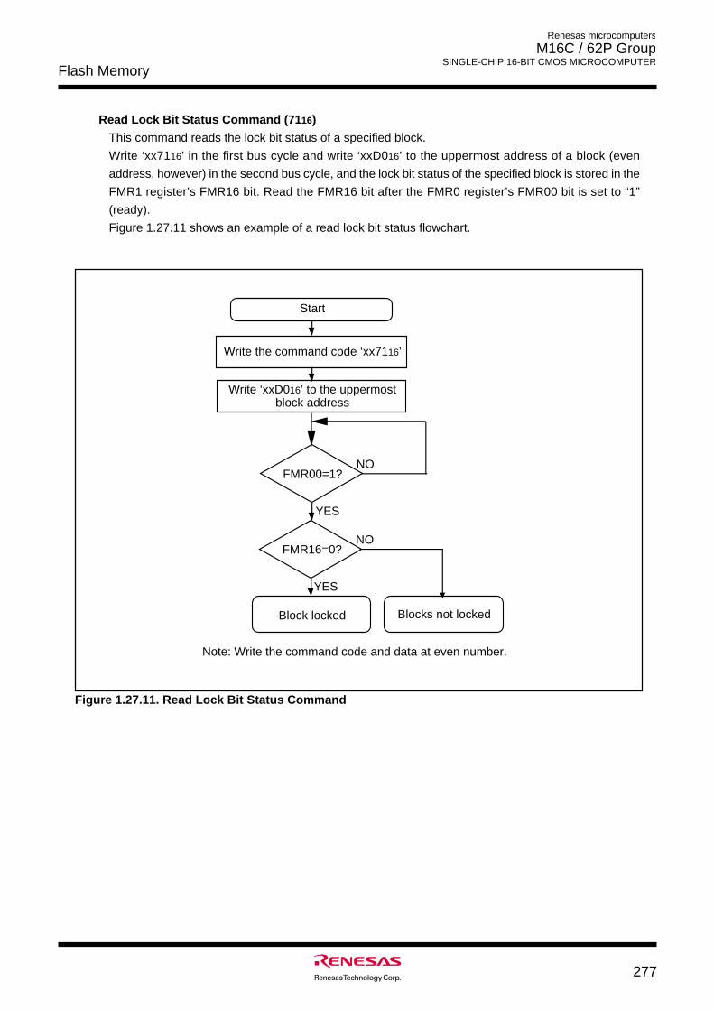
Flash Memory
277
Renesas microcomputers
M16C / 62P Group SINGLE-CHIP 16-BIT CMOS MICROCOMPUTER
Blocks not locked
Write ‘xxD016’ to the uppermost block address
Start
Block locked
YES
NO
Note: Write the command code and data at even number.
Write the command code ‘xx7116’
FMR00=1?
YES
NOFMR16=0?
Read Lock Bit Status Command (7116)
This command reads the lock bit status of a specified block.
Write ‘xx7116’ in the first bus cycle and write ‘xxD016’ to the uppermost address of a block (even
address, however) in the second bus cycle, and the lock bit status of the specified block is stored in the
FMR1 register’s FMR16 bit. Read the FMR16 bit after the FMR0 register’s FMR00 bit is set to “1”
(ready).
Figure 1.27.11 shows an example of a read lock bit status flowchart.
Figure 1.27.11. Read Lock Bit Status Command
Flash Memory
278
Renesas microcomputers
M16C / 62P Group SINGLE-CHIP 16-BIT CMOS MICROCOMPUTER
Data Protect FunctionEach block in the flash memory has a nonvolatile lock bit. The lock bit is effective when the FMR02 bit =
0 (lock bit enabled). The lock bit allows each block to be individually protected (locked) against program-
ming and erasure. This helps to prevent data from inadvertently written to or erased from the flash
memory. The following shows the relationship between the lock bit and the block status.
• When the lock bit = 0, the block is locked (protected against programming and erasure).
• When the lock bit = 1, the block is not locked (can be programmed or erased.
The lock bit is cleared to “0” (locked) by executing the Lock Bit Program command, and is set to “1”
(unlocked) by erasing the block. The lock bit cannot be set to “1” by a command.
The lock bit status can be read using the Read Lock Bit Status command
The lock bit function is disabled by setting the FMR02 bit to “1”, with all blocks placed in an unlocked state.
(The lock bit data itself does not change state.) Setting the FMR02 bit to “0” enables the lock bit function
(lock bit data retained).
If the Block Erase or Erase All Unlocked Block command is executed while the FMR02 bit = 1, the target
block or all blocks are erased irrespective of how the lock bit is set. The lock bit for each block is set to “1”
after completion of erasure.
For details about the commands, refer to “Software Commands.”
Status RegisterThe status register indicates the operating status of the flash memory and whether an erase or program-
ming operation terminated normally or in error. The status of the status register can be known by reading
the FMR0 register’s FMR00, FMR06, and FMR07 bits.
Table 1.27.5 shows the status register.
In EW0 mode, the status register can be read in the following cases:
(1) When a given even address in the user ROM area is read after writing the Read Status Register
command
(2) When a given even address in the user ROM area is read after executing the Program, Block Erase,
Erase All Unlocked Block, or Lock Bit Program command but before executing the Read Array
command.
Sequencer Status (SR7 and FMR00 Bits )
The sequence status indicates the operating status of the flash memory. SR7 = 0 (busy) during auto
programming, auto erase, and lock bit write, and is set to “1” (ready) at the same time the operation
finishes.
Erase Status (SR5 and FMR07 Bits)
Refer to “Full Status Check.”
Program Status (SR4 and FMR06 Bits)
Refer to “Full Status Check.”
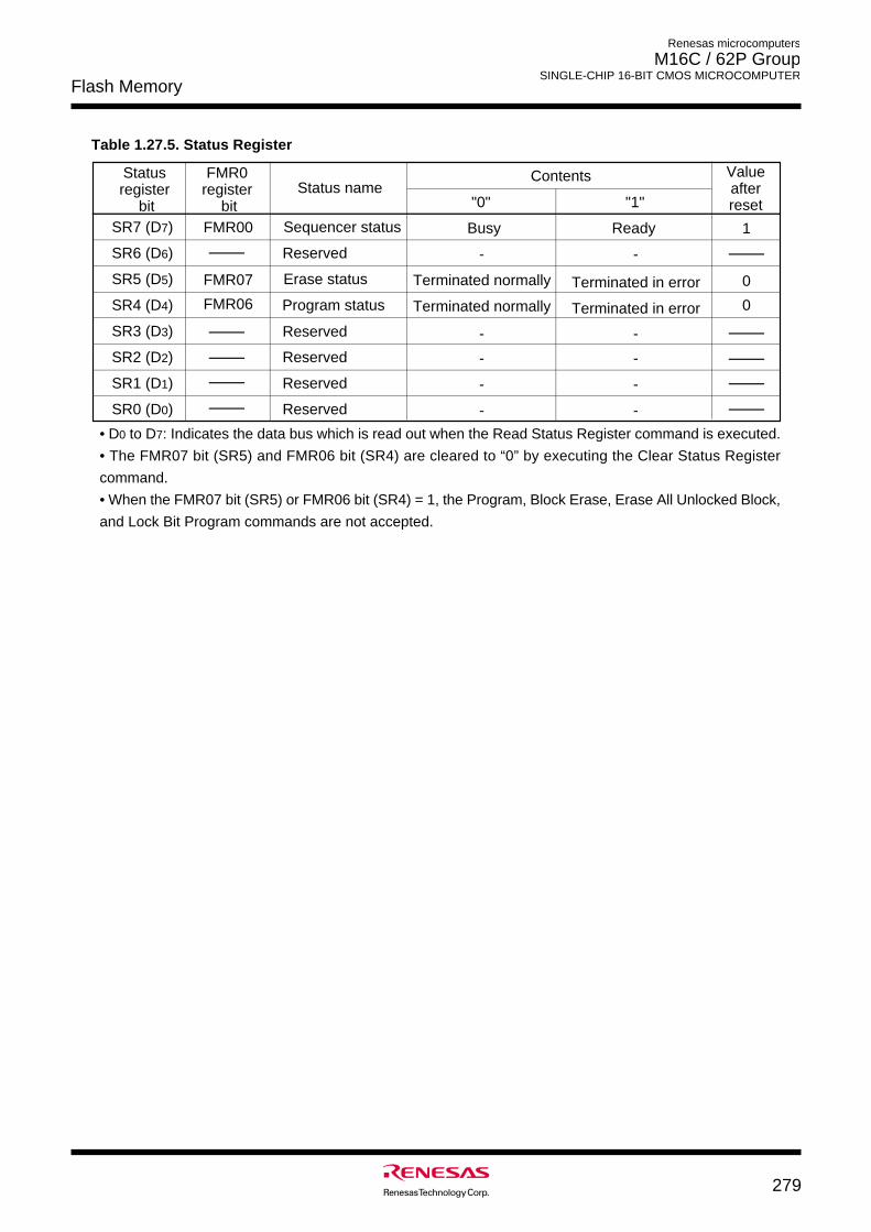
Flash Memory
279
Renesas microcomputers
M16C / 62P Group SINGLE-CHIP 16-BIT CMOS MICROCOMPUTER
Status register
bit
SR4 (D4)
SR5 (D5)
SR7 (D7)
SR6 (D6)
Status nameContents
SR1 (D1)
SR2 (D2)
SR3 (D3)
SR0 (D0)
Program status
Erase status
Sequencer status
Reserved
Reserved
Reserved
Reserved
"1"
Ready
Terminated in error
Terminated in error
-
-
-
-
-
"0"
Busy
Terminated normally
Terminated normally
-
-
-
-
-Reserved
FMR0register
bitFMR00
FMR07
FMR06
Value afterreset
1
0
0
Table 1.27.5. Status Register
• D0 to D7: Indicates the data bus which is read out when the Read Status Register command is executed.
• The FMR07 bit (SR5) and FMR06 bit (SR4) are cleared to “0” by executing the Clear Status Register
command.
• When the FMR07 bit (SR5) or FMR06 bit (SR4) = 1, the Program, Block Erase, Erase All Unlocked Block,
and Lock Bit Program commands are not accepted.
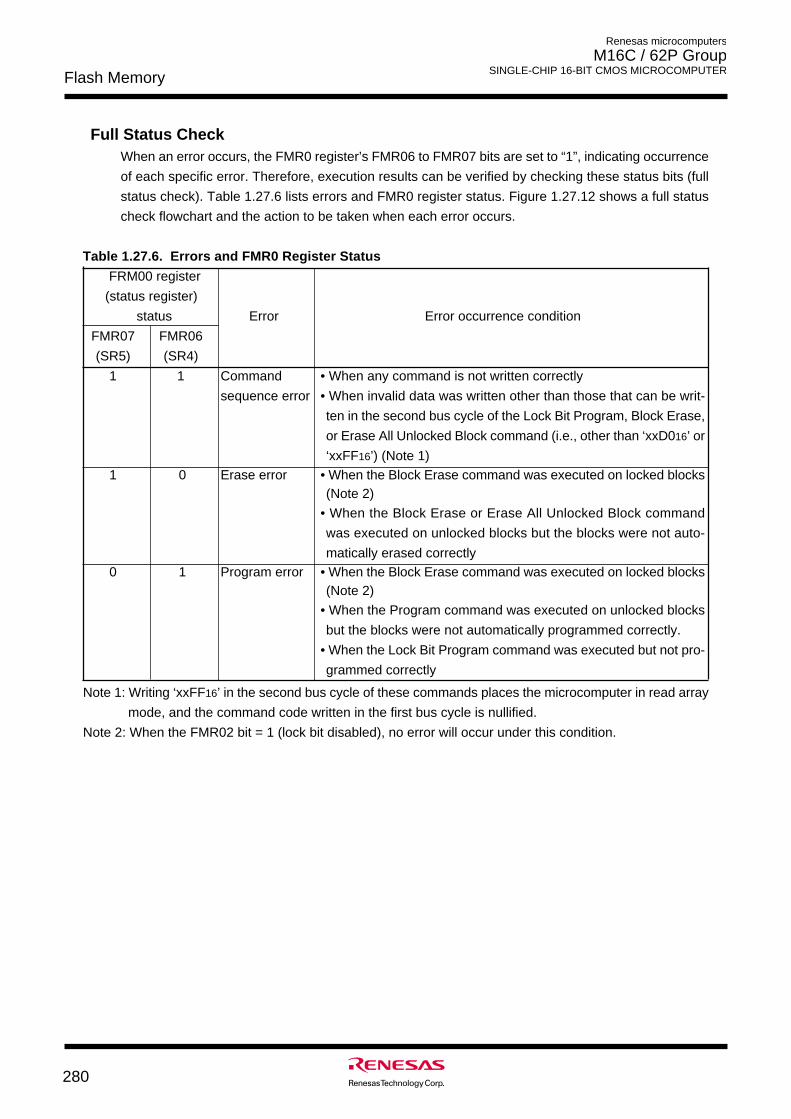
Flash Memory
280
Renesas microcomputers
M16C / 62P Group SINGLE-CHIP 16-BIT CMOS MICROCOMPUTER
Full Status CheckWhen an error occurs, the FMR0 register’s FMR06 to FMR07 bits are set to “1”, indicating occurrence
of each specific error. Therefore, execution results can be verified by checking these status bits (full
status check). Table 1.27.6 lists errors and FMR0 register status. Figure 1.27.12 shows a full status
check flowchart and the action to be taken when each error occurs.
Table 1.27.6. Errors and FMR0 Register Status
FRM00 register
(status register)
status Error Error occurrence condition
FMR07 FMR06
(SR5) (SR4)
1 1 Command • When any command is not written correctly
sequence error • When invalid data was written other than those that can be writ-
ten in the second bus cycle of the Lock Bit Program, Block Erase,
or Erase All Unlocked Block command (i.e., other than ‘xxD016’ or
‘xxFF16’) (Note 1)1 0 Erase error • When the Block Erase command was executed on locked blocks
(Note 2)
• When the Block Erase or Erase All Unlocked Block command
was executed on unlocked blocks but the blocks were not auto-
matically erased correctly0 1 Program error • When the Block Erase command was executed on locked blocks
(Note 2)
• When the Program command was executed on unlocked blocks
but the blocks were not automatically programmed correctly.
• When the Lock Bit Program command was executed but not pro-
grammed correctly
Note 1: Writing ‘xxFF16’ in the second bus cycle of these commands places the microcomputer in read array
mode, and the command code written in the first bus cycle is nullified.
Note 2: When the FMR02 bit = 1 (lock bit disabled), no error will occur under this condition.
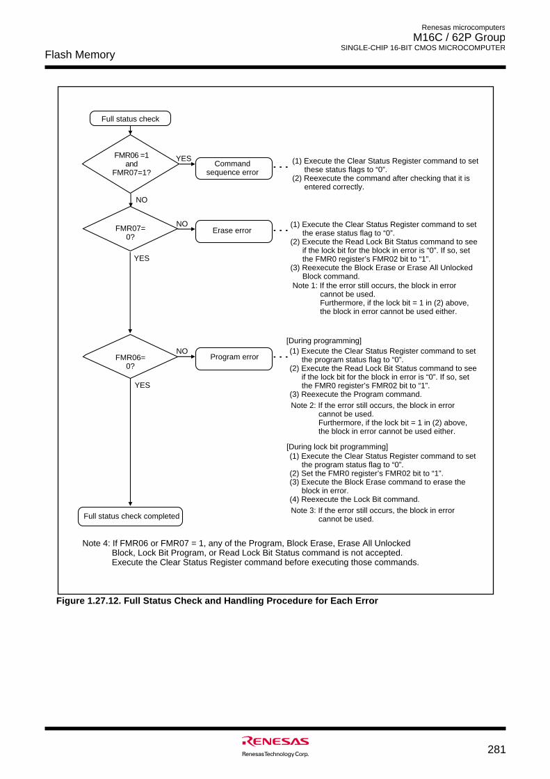
Flash Memory
281
Renesas microcomputers
M16C / 62P Group SINGLE-CHIP 16-BIT CMOS MICROCOMPUTER
Full status check
FMR06 =1and
FMR07=1?
NO
Command sequence error
YES
FMR07=0?
YES
Erase errorNO
(1) Execute the Clear Status Register command to setthese status flags to “0”.
(2) Reexecute the command after checking that it is entered correctly.
(1) Execute the Clear Status Register command to set the erase status flag to “0”.
(2) Execute the Read Lock Bit Status command to see if the lock bit for the block in error is “0”. If so, set the FMR0 register’s FMR02 bit to “1”.
(3) Reexecute the Block Erase or Erase All Unlocked Block command.
Note 4: If FMR06 or FMR07 = 1, any of the Program, Block Erase, Erase All Unlocked Block, Lock Bit Program, or Read Lock Bit Status command is not accepted. Execute the Clear Status Register command before executing those commands.
FMR06=0?
YES
Program errorNO
Full status check completed
Note 1: If the error still occurs, the block in error cannot be used.Furthermore, if the lock bit = 1 in (2) above, the block in error cannot be used either.
(1) Execute the Clear Status Register command to set the program status flag to “0”.
(2) Execute the Read Lock Bit Status command to see if the lock bit for the block in error is “0”. If so, set the FMR0 register’s FMR02 bit to “1”.
(3) Reexecute the Program command.Note 2: If the error still occurs, the block in error
cannot be used.Furthermore, if the lock bit = 1 in (2) above, the block in error cannot be used either.
[During programming]
(1) Execute the Clear Status Register command to set the program status flag to “0”.
(2) Set the FMR0 register’s FMR02 bit to “1”. (3) Execute the Block Erase command to erase the
block in error.(4) Reexecute the Lock Bit command.Note 3: If the error still occurs, the block in error
cannot be used.
[During lock bit programming]
Figure 1.27.12. Full Status Check and Handling Procedure for Each Error
Flash Memory
282
Renesas microcomputers
M16C / 62P Group SINGLE-CHIP 16-BIT CMOS MICROCOMPUTER
Standard Serial I/O ModeIn standard serial input/output mode, the user ROM area can be rewritten while the microcomputer is
mounted on-board by using a serial programmer suitable for the M16C/62P group. For more information
about serial programmers, contact the manufacturer of your serial programmer. For details on how to use,
refer to the user’s manual included with your serial programmer.
Table 1.27.7 lists pin functions (flash memory standard serial input/output mode). Figures 1.27.13 to
1.27.15 show pin connections for standard serial input/output mode.
ID Code Check Function
This function determines whether the ID codes sent from the serial programmer and those written in the
flash memory match. (Refer to the description of the functions to inhibit rewriting flash memory version.)
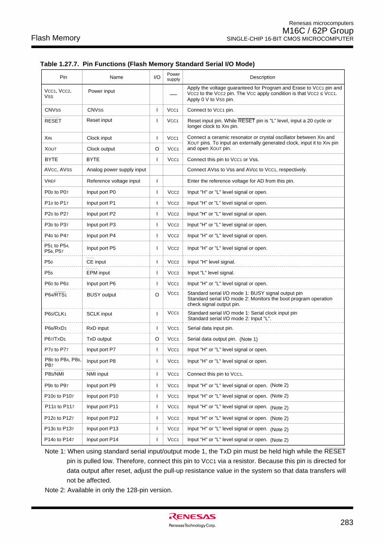
Flash Memory
283
Renesas microcomputers
M16C / 62P Group SINGLE-CHIP 16-BIT CMOS MICROCOMPUTER
Pin Description
VCC1, VCC2, VSS
Apply the voltage guaranteed for Program and Erase to VCC1 pin and VCC2 to the VCC2 pin. The VCC apply condition is that VCC2 ≤ VCC1. Apply 0 V to VSS pin.
CNVSS Connect to VCC1 pin.
RESET
XIN Connect a ceramic resonator or crystal oscillator between XIN and XOUT pins. To input an externally generated clock, input it to XIN pin and open XOUT pin.XOUT
BYTE Connect this pin to VCC1 or Vss.
AVCC, AVSS
VREF
Connect AVss to Vss and AVcc to VCC1, respectively.
Enter the reference voltage for AD from this pin.
P00 to P07 Input "H" or "L" level signal or open.
P10 to P17 Input "H" or "L" level signal or open.
P20 to P27 Input "H" or "L" level signal or open.
P30 to P37 Input "H" or "L" level signal or open.
P40 to P47 Input "H" or "L" level signal or open.
P51 to P54, P56, P57
Input "H" or "L" level signal or open.
P50 Input "H" level signal.
P55 Input "L" level signal.
P60 to P63 Input "H" or "L" level signal or open.
P64/RTS1 Standard serial I/O mode 1: BUSY signal output pinStandard serial I/O mode 2: Monitors the boot program operation check signal output pin.
P65/CLK1
P66/RXD1 Serial data input pin.
P67/TXD1 Serial data output pin.
P70 to P77 Input "H" or "L" level signal or open.
P80 to P84, P86,P87
Input "H" or "L" level signal or open.
P90 to P97 Input "H" or "L" level signal or open.
P100 to P107 Input "H" or "L" level signal or open.
Name
Power input
CNVSS
Reset input
Clock input
Clock output
BYTE
Analog power supply input
Reference voltage input
Input port P0
Input port P1
Input port P2
Input port P3
Input port P4
Input port P5
CE input
EPM input
Input port P6
BUSY output
SCLK input
RxD input
TxD output
Input port P7
Input port P8
Input port P9
Input port P10
I/O
I
I
I
O
I
I
I
I
I
I
I
I
I
I
I
O
I
I
O
I
I
I
I
P85/NMI NMI input I Connect this pin to VCC1.
Standard serial I/O mode 1: Serial clock input pinStandard serial I/O mode 2: Input "L".
P120 to P127 Input "H" or "L" level signal or open.
P130 to P137 Input "H" or "L" level signal or open.
Input port P12
Input port P13
I
I
P110 to P117 Input port P11 I Input "H" or "L" level signal or open.
P140 to P147 Input "H" or "L" level signal or open.Input port P14 I
Reset input pin. While RESET pin is "L" level, input a 20 cycle or longer clock to XIN pin.
(Note 1)
(Note 2)
(Note 2)
(Note 2)
(Note 2)
(Note 2)
(Note 2)
Power supply
VCC1
VCC1
VCC1
VCC2
VCC2
VCC2
VCC2
VCC2
VCC2
VCC2
VCC2
VCC1
VCC1
VCC1
VCC1
VCC1
VCC1
VCC1
VCC1
VCC1
VCC1
VCC1
VCC2
VCC2
VCC1
VCC1
VCC1
Table 1.27.7. Pin Functions (Flash Memory Standard Serial I/O Mode)
___________
Note 1: When using standard serial input/output mode 1, the TxD pin must be held high while the RESET
pin is pulled low. Therefore, connect this pin to VCC1 via a resistor. Because this pin is directed for
data output after reset, adjust the pull-up resistance value in the system so that data transfers will
not be affected.
Note 2: Available in only the 128-pin version.
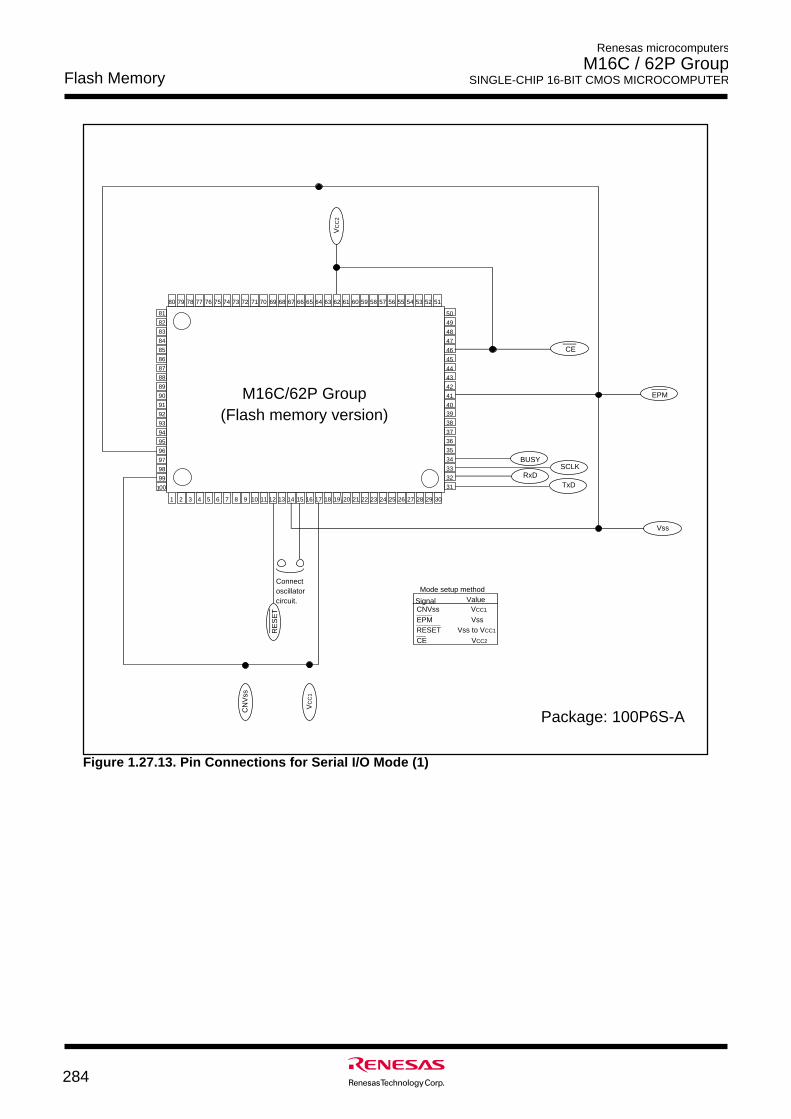
Flash Memory
284
Renesas microcomputers
M16C / 62P Group SINGLE-CHIP 16-BIT CMOS MICROCOMPUTER
Figure 1.27.13. Pin Connections for Serial I/O Mode (1)
1 2 3 4 5 6 7 8 9 10 11 12 13 14 15 16 17 18 19 20 21 22 23 24 25 26 27 28 29 30
31
32
33
34
35
36
37
38
3940
41
42
43
44
45
46
47
48
49
50
515253545556575859606162636465666768697071727374757677787980
81
82
83
84
85
86
87
88
89
90
91
92
93
94
95
96
97
98
99
100
Connect oscillator circuit.
CNVss VCC1
EPM VssRESET Vss to VCC1
CE VCC2
Signal ValueMode setup method
Vss
RxDTxD
SCLK
CN
Vss
CE
EPM
BUSY
RE
SE
T
VC
C2
VC
C1
Package: 100P6S-A
M16C/62P Group(Flash memory version)
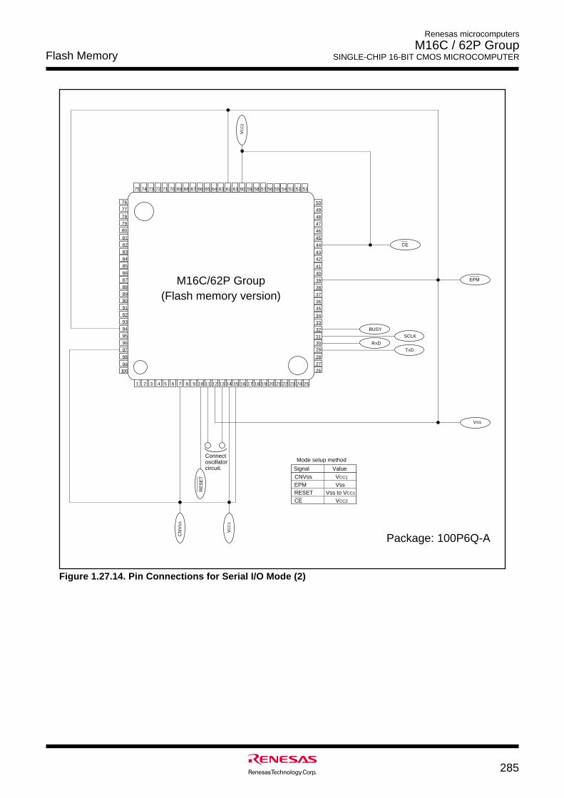
Flash Memory
285
Renesas microcomputers
M16C / 62P Group SINGLE-CHIP 16-BIT CMOS MICROCOMPUTER
Figure 1.27.14. Pin Connections for Serial I/O Mode (2)
1 2 3 4 5 6 7 8 9 10 11 12 13 14 15 16 17 18 19 20 21 22 23 24 25
2627
28
293031
32
33
34
35
36
37
38
39
40
41
4243
44
45
46
47
48
49
50
51525354555657585960616263646566676869707172737475
76
77
78
7980
81
82
83
84
85
86
87
88
8990
91
92
93
94
95
96
97
98
99100
CNVss VCC1
EPM VssRESET Vss to VCC1
CE VCC2
Signal Value
Mode setup method
CN
VS
S
RE
SE
T
VSS
CE
BUSY
EPM
SCLK
RXD
TXD
VC
C2
VC
C1
Connect oscillator circuit.
Package: 100P6Q-A
M16C/62P Group(Flash memory version)
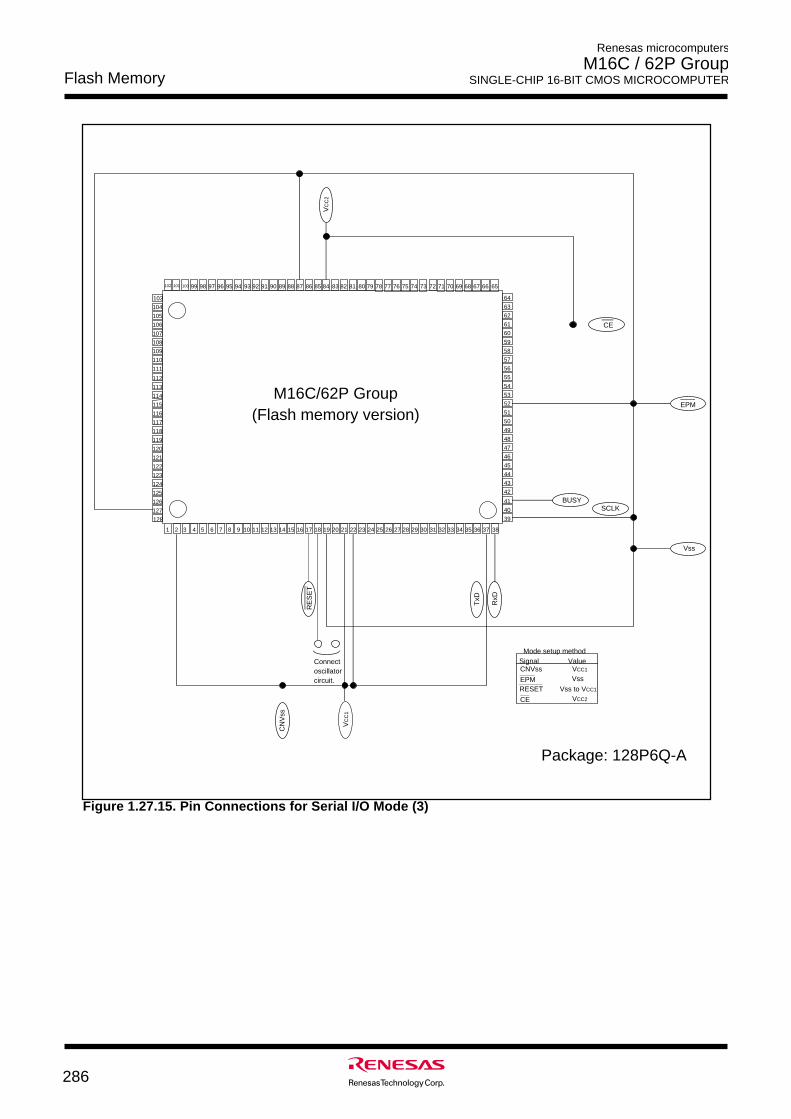
Flash Memory
286
Renesas microcomputers
M16C / 62P Group SINGLE-CHIP 16-BIT CMOS MICROCOMPUTER
Figure 1.27.15. Pin Connections for Serial I/O Mode (3)
Package: 128P6Q-A
1 2 3 4 5 6 7 8 9 10 11 12 13 14 15 16 17 18 19 20 21 22 23 24 25 26 27 28 29 30
737475767778798081828384858687888990919293949596979899100101102
109
110
111
112
113
114
115
116
117
118
119
120
121
122
123
124
125
126
127
128 39
40
41
42
43
44
45
46
47
48
49
50
51
52
53
54
55
56
57
58
59
60
61
62
63104
105
106
107
108
31 32 33 34 35 36 37
66676869707172
38
65
64103
CNVss VCC1
EPM Vss
RESET Vss to VCC1
CE VCC2
Signal ValueMode setup method
CE
EPM
Vss
CN
Vss
RE
SE
T
SCLKBUSY
RxD
TxD
VC
C2
VC
C1
Connect oscillator circuit.
M16C/62P Group(Flash memory version)
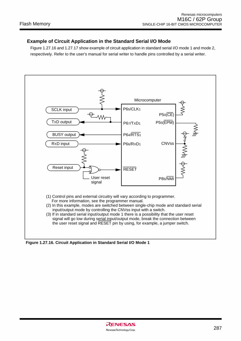
Flash Memory
287
Renesas microcomputers
M16C / 62P Group SINGLE-CHIP 16-BIT CMOS MICROCOMPUTER
Example of Circuit Application in the Standard Serial I/O ModeFigure 1.27.16 and 1.27.17 show example of circuit application in standard serial I/O mode 1 and mode 2,
respectively. Refer to the user's manual for serial writer to handle pins controlled by a serial writer.
Figure 1.27.16. Circuit Application in Standard Serial I/O Mode 1
SCLK input
BUSY output
RXD input CNVss
P50(CE)
P55(EPM)
RESETReset input
User reset signal
Microcomputer
(1) Control pins and external circuitry will vary according to programmer. For more information, see the programmer manual.(2) In this example, modes are switched between single-chip mode and standard serial
input/output mode by controlling the CNVss input with a switch.(3) If in standard serial input/output mode 1 there is a possibility that the user reset
signal will go low during serial input/output mode, break the connection between the user reset signal and RESET pin by using, for example, a jumper switch.
TXD output
P64/RTS1
P65/CLK1
P67/TXD1
P85/NMI
P66/RXD1
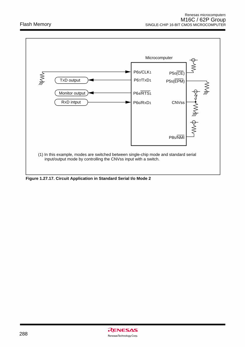
Flash Memory
288
Renesas microcomputers
M16C / 62P Group SINGLE-CHIP 16-BIT CMOS MICROCOMPUTER
Monitor output
TXD output
Microcomputer
(1) In this example, modes are switched between single-chip mode and standard serial input/output mode by controlling the CNVss input with a switch.
P64/RTS1
P65/CLK1
P67/TXD1
CNVss
P50(CE)
P55(EPM)
P85/NMI
P66/RXD1RXD intput
Figure 1.27.17. Circuit Application in Standard Serial I/o Mode 2
Flash Memory
289
Renesas microcomputers
M16C / 62P Group SINGLE-CHIP 16-BIT CMOS MICROCOMPUTER
Parallel I/O ModeIn parallel input/output mode, the user ROM and boot ROM areas can be rewritten by using a parallel
programmer suitable for the M16C/62 group (M16C/62P). For more information about parallel program-
mers, contact the manufacturer of your parallel programmer. For details on how to use, refer to the user’s
manual included with your parallel programmer.
User ROM and Boot ROM AreasIn the boot ROM area, an erase block operation is applied to only one 4 Kbyte block. The boot ROM area
contains a standard serial input/output mode based rewrite control program which was written in it when
shipped from the factory. Therefore, when using a serial programmer, be careful not to rewrite the boot
ROM area.
When in parallel output mode, the boot ROM area is located at addresses 0FF00016 to 0FFFFF16. When
rewriting the boot ROM area, make sure that only this address range is rewritten. (Do not access other
than the addresses 0FF00016 to 0FFFFF16.)
ROM Code Protect FunctionThe ROM code protect function inhibits the flash memory from being read or rewritten. (Refer to the
description of the functions to inhibit rewriting flash memory version.)
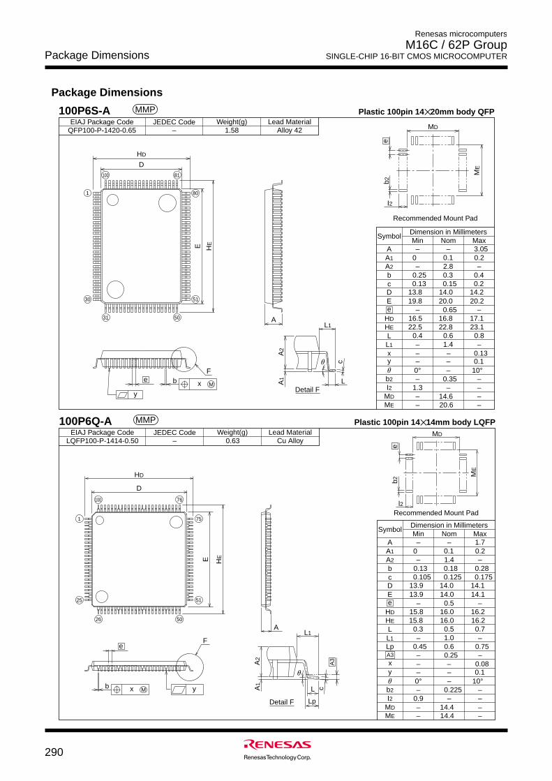
290
Renesas microcomputers
M16C / 62P Group SINGLE-CHIP 16-BIT CMOS MICROCOMPUTERPackage Dimensions
Package Dimensions
QFP100-P-1420-0.65 1.58Weight(g)
–JEDEC CodeEIAJ Package Code Lead Material
Alloy 42
100P6S-A Plastic 100pin 14 20mm body QFP
–0.1
–
– –0.2
––
– –
––
––
–
SymbolMin Nom Max
A
A2
bcDE
HE
LL1
y
b2
Dimension in Millimeters
HD
A1
0.35––I2 1.3––MD 14.6––ME 20.6
10°0°0.1
1.40.80.60.4
23.122.822.517.116.816.5
0.6520.220.019.814.214.013.8
0.20.150.130.40.30.25
2.80
3.05
e
ee
E
c
HE
1
30
31
81
50
80
51
HD
D
MD
ME
A
F
A1
A2
L1
L
yb2
I2
Recommended Mount Pad
Detail F
100
x – – 0.13
b x M
MMP
LQFP100-P-1414-0.50Weight(g)
– 0.63JEDEC CodeEIAJ Package Code Lead Material
Cu Alloy
100P6Q-A Plastic 100pin 14 14mm body LQFP
–0.1
–
– –0.2
––
– –
––
––
–
SymbolMin Nom Max
A
A2
bcDE
HE
LL1
y
b2
Dimension in Millimeters
HD
A1
0.225––I2 0.9––MD 14.4––ME 14.4
10°0°0.1
1.00.70.50.3
16.216.015.816.216.015.8
0.514.114.013.914.114.013.90.1750.1250.1050.280.180.13
1.40
1.7
e
e
E HE
1
76
75
51
5026
25
HD
D
A
F
y
100
Lp 0.45––
0.60.25–
0.75–
0.08xA3
b x M A1
A2
L1
L
Detail F Lp
A3
c
MD
l2
b2
ME
e
Recommended Mount Pad
MMP
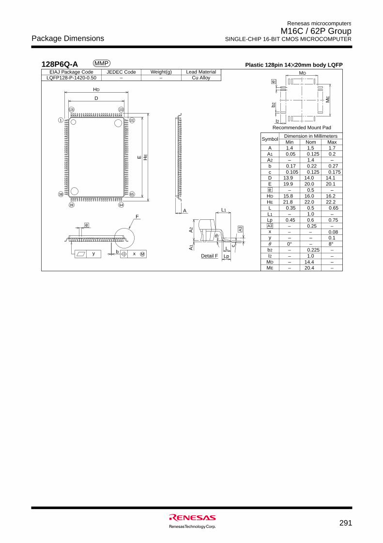
291
Renesas microcomputers
M16C / 62P Group SINGLE-CHIP 16-BIT CMOS MICROCOMPUTERPackage Dimensions
MD
l2
b2
ME
e
Recommended Mount Pad
Lp 0.45––
0.60.25–
0.75–
0.08xA3
y b x M Lp
A3
LQFP128-P-1420-0.50 –Weight(g)
–JEDEC CodeEIAJ Package Code Lead Material
Cu Alloy
128P6Q-A Plastic 128pin 14 20mm body LQFP
1.50.125
1.4
– –0.2
––
– –
––
––
–
SymbolMin Nom Max
A
A2
bcDE
HE
LL1
y
b2
Dimension in Millimeters
HD
A1
0.225–1.0I2 –––MD 14.4––ME 20.4
8°0°0.1
1.00.650.50.35
22.222.021.816.216.015.8
0.520.120.019.914.114.013.90.1750.1250.1050.270.220.17
1.40.05
1.7
e
e
E
c
HE
1
38
39 64
65
HD
D
AF
A1
A2
L1
L
Detail F
128 103
102
MMP
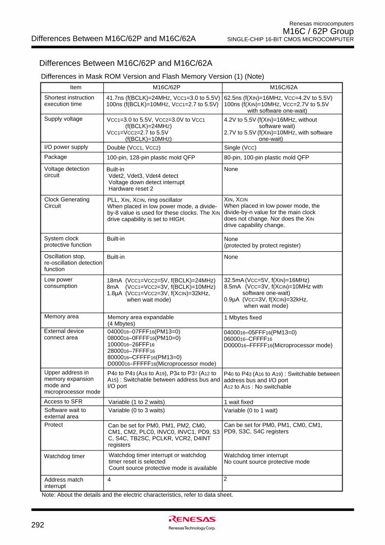
292
Renesas microcomputers
M16C / 62P Group SINGLE-CHIP 16-BIT CMOS MICROCOMPUTERDifferences Between M16C/62P and M16C/62A
Differences Between M16C/62P and M16C/62A
Item M16C/62A M16C/62P
Shortest instruction execution time
Supply voltage
62.5ns (f(XIN)=16MHZ, VCC=4.2V to 5.5V)100ns (f(XIN)=10MHZ, VCC=2.7V to 5.5V
with software one-wait)
4.2V to 5.5V (f(XIN)=16MHZ, without software wait)
2.7V to 5.5V (f(XIN)=10MHZ, with software one-wait)
41.7ns (f(BCLK)=24MHZ, VCC1=3.0 to 5.5V)100ns (f(BCLK)=10MHZ, VCC1=2.7 to 5.5V)
VCC1=3.0 to 5.5V, VCC2=3.0V to VCC1(f(BCLK)=24MHZ)
VCC1=VCC2=2.7 to 5.5V(f(BCLK)=10MHZ)
Clock GeneratingCircuit
Address match interrupt
Memory area
Watchdog timer
Memory area expandable (4 Mbytes)
XIN, XCINWhen placed in low power mode, the divide-by-n value for the main clock does not change. Nor does the XIN drive capability change.
2
Watchdog timer interrupt or watchdog timer reset is selectedCount source protective mode is available
32.5mA (VCC=5V, f(XIN)=16MHz)8.5mA (VCC=3V, f(XCIN)=10MHz with
software one-wait)0.9µA (VCC=3V, f(XCIN)=32kHz,
when wait mode)
Low powerconsumption
1 Mbytes fixed
PLL, XIN, XCIN, ring oscillatorWhen placed in low power mode, a divide-by-8 value is used for these clocks. The XIN drive capability is set to HIGH.
4
Watchdog timer interruptNo count source protective mode
18mA (VCC1=VCC2=5V, f(BCLK)=24MHz)8mA (VCC1=VCC2=3V, f(BCLK)=10MHz)1.8µA (VCC1=VCC2=3V, f(XCIN)=32kHz,
when wait mode)
Note: About the details and the electric characteristics, refer to data sheet.
Differences in Mask ROM Version and Flash Memory Version (1) (Note)
I/O power supply Double (VCC1, VCC2) Single (VCC)
Package 100-pin, 128-pin plastic mold QFP 80-pin, 100-pin plastic mold QFP
Oscillation stop,re-oscillation detection function
Built-in None
External device connect area
0400016–07FFF16(PM13=0)0800016–0FFFF16(PM10=0)1000016–26FFF162800016–7FFFF168000016–CFFFF16(PM13=0)D000016–FFFFF16(Microprocessor mode)
0400016–05FFF16(PM13=0)0600016–CFFFF16D000016–FFFFF16(Microprocessor mode)
Upper address in memory expansion mode and microprocessor mode
P40 to P43 (A16 to A19), P34 to P37 (A12 to A15) : Switchable between address bus and I/O port
P40 to P43 (A16 to A19) : Switchable between address bus and I/O portA12 to A15 : No switchable
Access to SFR 1 wait fixedVariable (1 to 2 waits)Software wait to external area
Variable (0 to 1 wait)Variable (0 to 3 waits)
Protect Can be set for PM0, PM1, CM0, CM1, PD9, S3C, S4C registers
Can be set for PM0, PM1, PM2, CM0, CM1, CM2, PLC0, INVC0, INVC1, PD9, S3C, S4C, TB2SC, PCLKR, VCR2, D4INT registers
Voltage detection circuit
Built-inVdet2, Vdet3, Vdet4 detectVoltage down detect interruptHardware reset 2
None
System clock protective function
Built-in None(protected by protect register)
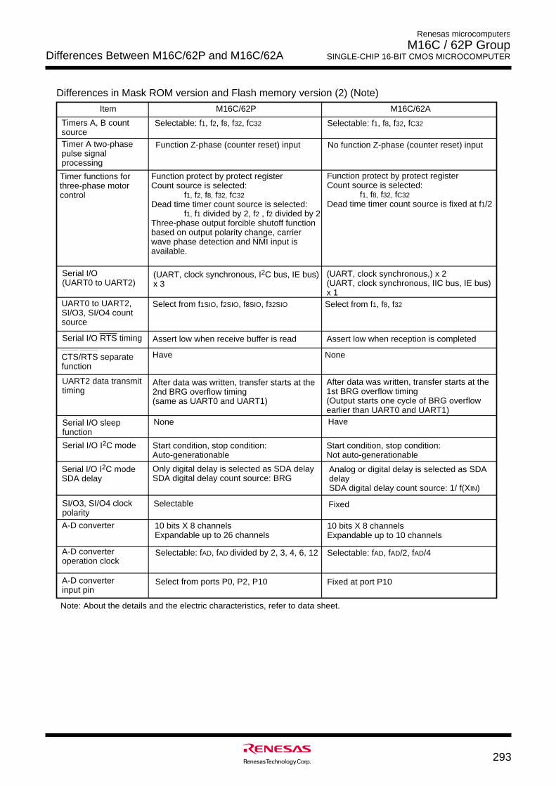
293
Renesas microcomputers
M16C / 62P Group SINGLE-CHIP 16-BIT CMOS MICROCOMPUTERDifferences Between M16C/62P and M16C/62A
Item M16C/62AM16C/62P
Serial I/O(UART0 to UART2)
(UART, clock synchronous,) x 2(UART, clock synchronous, IIC bus, IE bus) x 1
(UART, clock synchronous, I2C bus, IE bus) x 3
Differences in Mask ROM version and Flash memory version (2) (Note)
Timers A, B count source
Selectable: f1, f8, f32, fC32Selectable: f1, f2, f8, f32, fC32
Timer functions for three-phase motor control
Timer A two-phase pulse signal processing
No function Z-phase (counter reset) inputFunction Z-phase (counter reset) input
Function protect by protect registerCount source is selected:
f1, f8, f32, fC32Dead time timer count source is fixed at f1/2
UART0 to UART2, SI/O3, SI/O4 count source
Select from f1, f8, f32Select from f1SIO, f2SIO, f8SIO, f32SIO
Serial I/O sleep function
A-D converter
SI/O3, SI/O4 clock polarity
10 bits X 8 channels Expandable up to 10 channels
Selectable
Have
Analog or digital delay is selected as SDA delaySDA digital delay count source: 1/ f(XIN)
Serial I/O I2C mode SDA delay
Fixed
None
10 bits X 8 channels Expandable up to 26 channels
Only digital delay is selected as SDA delaySDA digital delay count source: BRG
Note: About the details and the electric characteristics, refer to data sheet.
UART2 data transmit timing
After data was written, transfer starts at the 2nd BRG overflow timing(same as UART0 and UART1)
After data was written, transfer starts at the 1st BRG overflow timing(Output starts one cycle of BRG overflow earlier than UART0 and UART1)
Serial I/O I2C mode Start condition, stop condition: Auto-generationable
Start condition, stop condition:Not auto-generationable
A-D converter operation clock
Selectable: fAD, fAD/2, fAD/4Selectable: fAD, fAD divided by 2, 3, 4, 6, 12
A-D converterinput pin
Fixed at port P10Select from ports P0, P2, P10
Assert low when receive buffer is read Assert low when reception is completedSerial I/O RTS timing
Function protect by protect registerCount source is selected:
f1, f2, f8, f32, fC32Dead time timer count source is selected:
f1, f1 divided by 2, f2 , f2 divided by 2Three-phase output forcible shutoff function based on output polarity change, carrier wave phase detection and NMI input is available.
CTS/RTS separate function
NoneHave
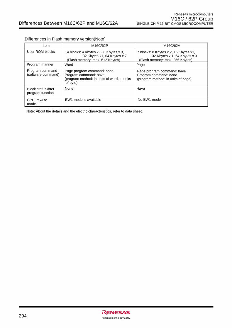
294
Renesas microcomputers
M16C / 62P Group SINGLE-CHIP 16-BIT CMOS MICROCOMPUTERDifferences Between M16C/62P and M16C/62A
Item M16C/62A M16C/62P
User ROM blocks 7 blocks: 8 Kbytes x 2, 16 Kbytes x1, 32 Kbytes x 1, 64 Kbytes x 3 (Flash memory: max. 256 Kbytes)
14 blocks: 4 Kbytes x 3, 8 Kbytes x 3, 32 Kbytes x1, 64 Kbytes x 7 (Flash memory: max. 512 Kbytes)
Block status after program function
None Have
Note: About the details and the electric characteristics, refer to data sheet.
Differences in Flash memory version(Note)
Program command(software command)
Page program command: noneProgram command: have(program method: in units of word, in units of byte)
Page program command: haveProgram command: none(program method: in units of page)
Program manner PageWord
CPU rewrite mode
No EW1 modeEW1 mode is available
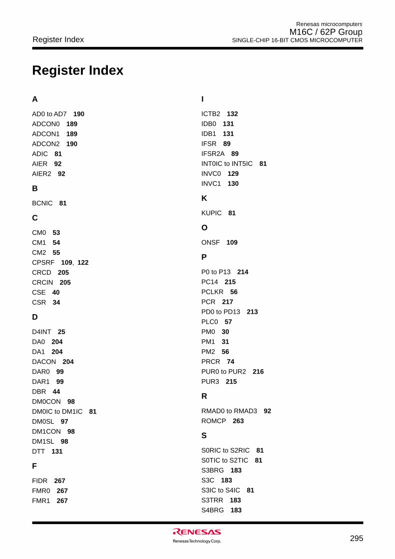
295
Renesas microcomputers
M16C / 62P Group SINGLE-CHIP 16-BIT CMOS MICROCOMPUTERRegister Index
Register Index
A
AD0 to AD7 190
ADCON0 189
ADCON1 189
ADCON2 190
ADIC 81
AIER 92
AIER2 92
B
BCNIC 81
C
CM0 53
CM1 54
CM2 55
CPSRF 109, 122
CRCD 205
CRCIN 205
CSE 40
CSR 34
D
D4INT 25
DA0 204
DA1 204
DACON 204
DAR0 99
DAR1 99
DBR 44
DM0CON 98
DM0IC to DM1IC 81
DM0SL 97
DM1CON 98
DM1SL 98
DTT 131
F
FIDR 267
FMR0 267
FMR1 267
I
ICTB2 132
IDB0 131
IDB1 131
IFSR 89
IFSR2A 89
INT0IC to INT5IC 81
INVC0 129
INVC1 130
K
KUPIC 81
O
ONSF 109
P
P0 to P13 214
PC14 215
PCLKR 56
PCR 217
PD0 to PD13 213
PLC0 57
PM0 30
PM1 31
PM2 56
PRCR 74
PUR0 to PUR2 216
PUR3 215
R
RMAD0 to RMAD3 92
ROMCP 263
S
S0RIC to S2RIC 81
S0TIC to S2TIC 81
S3BRG 183
S3C 183
S3IC to S4IC 81
S3TRR 183
S4BRG 183
296
Renesas microcomputers
M16C / 62P Group SINGLE-CHIP 16-BIT CMOS MICROCOMPUTERRegister Index
S4C 183
S4TRR 183
SAR0 99
SAR1 99
T
TA0 to TA4 108
TA0IC to TA4IC 81
TA0MR to TA4MR 107
TA1 132
TA11 132
TA1MR 134
TA2 132
TA21 132
TA2MR 134
TA4 132
TA41 132
TA4MR 134
TABSR 108, 122, 133
TB0 to TB5 122
TB0IC to TB5IC 81
TB0MR to TB5MR 121
TB2 133
TB2MR 134
TB2SC 132
TBSR 122
TCR0 99
TCR1 99
TRGSR 109, 133
U
U0BCNIC to U1BCNIC 81
U0BRG to U2BRG 140
U0C0 to U2C0 141
U0C1 to U2C1 142
U0MR to U2MR 141
U0RB to U2RB 140
U0SMR to U2SMR 143
U0SMR2 to U2SMR2 144
U0SMR3 to U2SMR3 144
U0SMR4 to U2SMR4 145
U0TB to U2TB 140
UCON 143
UDF 108
V
VCR1 25
VCR2 25
W
WDC 24, 94
WDTS 94
REVISION HISTORY
Rev. Date Description
Page Summary
C-1
M16C/62 GROUP (M16C/62P) Group Hardware Manual
1.0 Jan/31/Y03 (Continued)
Applications are partly revised.Table 1.1.1 is partly revised.Table 1.1.3 is partly revised.Figure 1.1.2 is partly revised.Explanation of “Memory” is partly revised.Explanation of “Hardware Reset 1” is partly revised.Figure 1.5.1 is partly revised.Figure 1.5.2 is partly revised.Figure 1.5.4 is partly revised.VCR2 Register in Figure 1.5.6 is partly revised.Figure 1.5.6 is partly revised.Explanation of “Power Supply Down Detection Interrupt” is partly revised.Figure 1.6.1 is partly revised.Figure 1.6.2 is partly revised.Table 1.7.5 is partly revised.Table 1.7.7 is partly revised.Figure 1.7.8 is partly revised.Explanation of “4 Mbyte Mode” is partly revised.Notes 12 and 13 in Figure 1.9.2 is partly revised.Notes 2 and 5 in Figure 1.9.3 is partly revised.Figure 1.9.4 is partly revised.Note 4 in Figure 1.9.6 is partly revised.Explanation of “PLL Clock” is partly revised.Figure 1.9.9 is partly revised.Explanation of “CPU Clock and BCLK” is partly revised.Explanation of “Low-speed Mode” is partly revised.Explanation of “Low Power Dissipation Mode” is partly revised.Explanation of “Ring Oscillator Low Power Dissipation Mode” is partly revised.Table 1.9.3 is partly revised.Table 1.9.5 is partly revised.Figure 1.9.10 is partly revised.Figure 1.9.11 is partly revised.Table 1.9.7 is added.Explanation of “System Clock Protective Function” is partly revised.Explanation of “Power Supply Down Detection Interrupt” is partly revised.Table 1.11.1 is partly revised.Figure 1.11.9 is partly revised.WDTS Register in Figure 1.12.2 is partly revised.Figure 1.13.2 is partly revised.Figure 1.13.3 is partly revised.Figure 1.13.5 is partly revised.Table 1.13.3 is partly revised.Explanation of “DMA Enable” is partly revised.Figure 1.14.3 is partly revised.Table 1.14.3 is partly revised.Explanation of “Counter Initialization by Two-Phase Pulse Signal Processing” ispartly revised.Figure 1.14.10 is partly revised.Figure 1.14.14 is partly revised.Figure 1.14.15 is partly revised.
12551120212224252627303139414344535455576061626363646465686970717778889699
100103104105109115117
117122122
REVISION HISTORY
Rev. Date Description
Page Summary
C-2
M16C/62 GROUP (M16C/62P) Group Hardware Manual
Figure 1.15.3 is partly revised.Figure 1.15.7 is partly revised.Figure 1.15.8 is partly revised.Figure 1.16.1 is partly revised.Figure 1.16.3 is partly revised.Note 7 is added to TAi, TAi1 Register in Figure 1.16.5.Figure 1.16.8 is partly revised.UiSMR2 Register in Figure 1.17.7 is partly revised.Figure 1.20.1 is partly revised.Table 1.20.2 and Table 1.20.3 are partly revised.Figure 1.20.4 is partly revised.Explanation of “Arbitration” is partly revised.Explanation of “Transfer Clock” is partly revised.Explanation of “ACK and NACK” is partly revised.Explanation of “Special Mode 4 (SIM Mode)” is partly revised.Table 1.20.9 is partly revised.Figure 1.21.1 is partly revised.Figure 1.21.4 is partly revised.Explanation of “External Operation Amp Connection Mode” is partly revised.Explanation of “Caution of Using A-D Converter” is partly revised.Figure 1.22.11 is partly revisedTable 1.23.1 is partly revised.Figure 1.23.3 is partly revised.Figure 1.25.9 is partly revised.Table 1.26.1 is partly revised.Table 1.26.2 is partly revised.Note 1 of Table 1.26.3 is partly revised.Note 1 of Table 1.26.4 is partly revised.Table 1.26.6 is partly revised.Note 1 of Table 1.26.9 is partly revised.Note 1 of Table 1.26.10 is partly revised.Measurement conditions of timing requirements are partly revised.Table 1.26.11 is partly revised.Measurement conditions of timing requirements are partly revised.Table 1.26.18 is added.Measurement conditions of timing requirements are partly revised.Measurement conditions of switching characteristics are partly revised.Measurement conditions of switching characteristics are partly revised.Measurement conditions of switching characteristics are partly revised.Figure 1.26.2 is partly revised.Figure 1.26.9 is partly revised.Note of Table 1.26.28 is partly revised.Figure 1.26.29 is partly revised.Measurement conditions of timing requirements are partly revised.Table 1.26.30 is partly revised.Measurement conditions of timing requirements are partly revised.Table 1.26.37 is added.Measurement conditions of timing requirements are partly revised.Measurement conditions of switching characteristics are partly revised.Measurement conditions of switching characteristics are partly revised.
124128128130132134137146163
164, 165169169170171179179184187203205205206207218223224225225225227228229229230230231232233234235242244245246246247247248249250
1.0 Jan/31/Y03 (Continued)
REVISION HISTORY
Rev. Date Description
Page Summary
C-3
M16C/62 GROUP (M16C/62P) Group Hardware Manual
Measurement conditions of switching characteristics are partly revised.Figure 1.26.12 is partly revised.Figure 1.26.15 is partly revised.Figure 1.26.16 is partly revised.Figure 1.26.17 is partly revised.Figure 1.26.18 is partly revised.Figure 1.26.19 is partly revised.Figure 1.26.20 is partly revised.Explanation of “Memory Map” is partly revised.Explanation of “Boot Mode” is partly revised.Figure 1.27.3 is partly revised.Note of FIDR Register in Figure 1.27.4 is partly revised.Figure 1.27.7 is partly revised.Explanation of “Interrupts” is partly revised.Explanation of “Writing in the User ROM Space” is partly revised.Table 1.27.4 is partly revised.Explanation of “Read Array Command” is partly revised.Explanation of “Program Command” is partly revised.Figure 1.27.15 is partly revised.Partly revised.
251252255256257258259260262263264268271272272274274278287293
1.0 Jan/31/Y03
1.10 May/28/Y03 (Continued)
Table 1.1.1 is partly revised.Table 1.1.2 and 1.1.3 is partly revised.SFR is partly revised.Note 1 is partly revised.Explanation of “Hardware Reset 1” is partly revised.Note 1 is added.Figure 1.5.4 is partly revised.Note 1 of Figure 1.5.5 is partly revised.Figure 1.5.7 is partly revised.Table 1.5.2 is partly revised.Table 1.5.3 is partly revised.Explanation of “1. Limitations on Stop Mode” is partly revised.Explanation of “1. Limitations on WAIT instruction” is partly revised.Figure 1.5.8 is partly revised.Note is added.Explanation of “Multiplexed Bus” is revised.Explanation of “(2) Data Bus” is revised.Explanation of “(7) Hold Signal” is revised.Note 3 of Table 1.7.4 is added.Note 4 of Table 1.7.5 is added.Explanation of “(10) Software Wait” is revised.Table 1.7.7 is revised.Table of Figure 1.8.5 is revised.Explanation is revised.Figures 1.8.7 to 1.8.9 is partly revised.Explanation of “Clock Generation Circuit” is revised.Figure 1.9.1 is revised.Note of Figure 1.9.2 is revised.Note 12 is added.Explanation of “(1) Main clock” is partly revised.
24-5
14-19
202324
2627
28
31333438
3940414647
48-505152535558
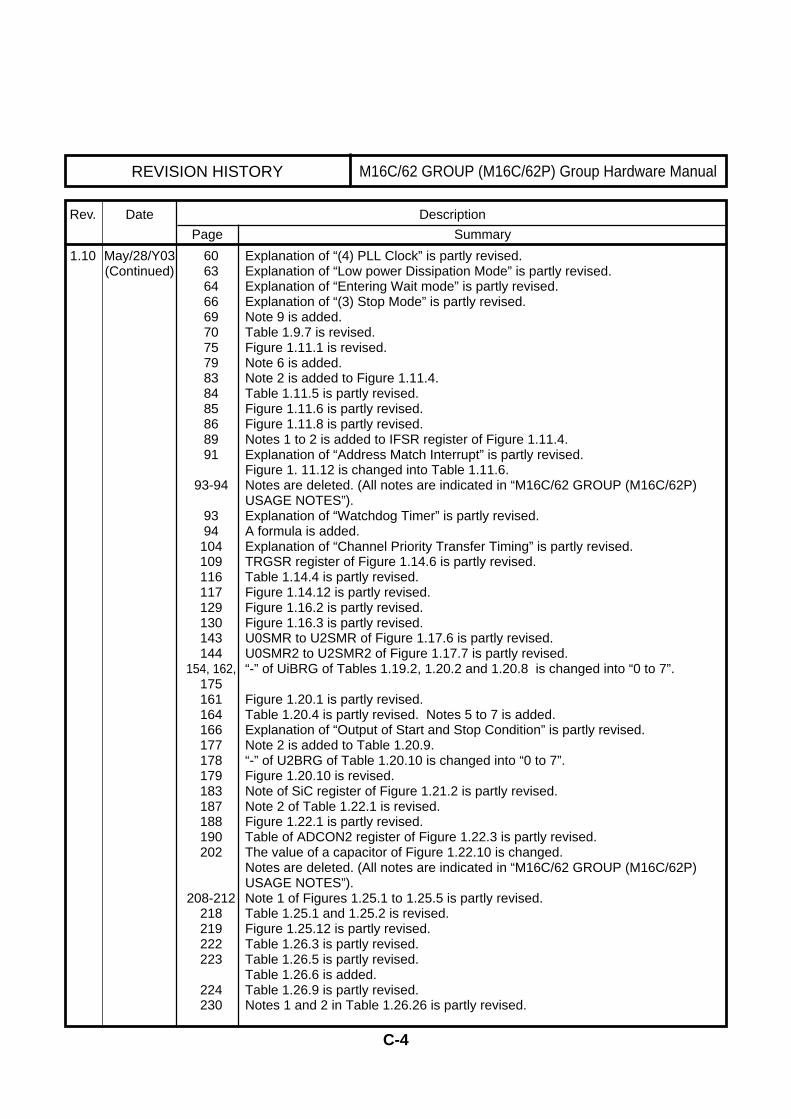
REVISION HISTORY
Rev. Date Description
Page Summary
C-4
M16C/62 GROUP (M16C/62P) Group Hardware Manual
6063646669707579838485868991
93-94
9394104109116117129130143144
154, 162,175161164166177178179183187188190202
208-212218219222223
224230
Explanation of “(4) PLL Clock” is partly revised.Explanation of “Low power Dissipation Mode” is partly revised.Explanation of “Entering Wait mode” is partly revised.Explanation of “(3) Stop Mode” is partly revised.Note 9 is added.Table 1.9.7 is revised.Figure 1.11.1 is revised.Note 6 is added.Note 2 is added to Figure 1.11.4.Table 1.11.5 is partly revised.Figure 1.11.6 is partly revised.Figure 1.11.8 is partly revised.Notes 1 to 2 is added to IFSR register of Figure 1.11.4.Explanation of “Address Match Interrupt” is partly revised.Figure 1. 11.12 is changed into Table 1.11.6.Notes are deleted. (All notes are indicated in “M16C/62 GROUP (M16C/62P)USAGE NOTES”).Explanation of “Watchdog Timer” is partly revised.A formula is added.Explanation of “Channel Priority Transfer Timing” is partly revised.TRGSR register of Figure 1.14.6 is partly revised.Table 1.14.4 is partly revised.Figure 1.14.12 is partly revised.Figure 1.16.2 is partly revised.Figure 1.16.3 is partly revised.U0SMR to U2SMR of Figure 1.17.6 is partly revised.U0SMR2 to U2SMR2 of Figure 1.17.7 is partly revised.“-” of UiBRG of Tables 1.19.2, 1.20.2 and 1.20.8 is changed into “0 to 7”.
Figure 1.20.1 is partly revised.Table 1.20.4 is partly revised. Notes 5 to 7 is added.Explanation of “Output of Start and Stop Condition” is partly revised.Note 2 is added to Table 1.20.9.“-” of U2BRG of Table 1.20.10 is changed into “0 to 7”.Figure 1.20.10 is revised.Note of SiC register of Figure 1.21.2 is partly revised.Note 2 of Table 1.22.1 is revised.Figure 1.22.1 is partly revised.Table of ADCON2 register of Figure 1.22.3 is partly revised.The value of a capacitor of Figure 1.22.10 is changed.Notes are deleted. (All notes are indicated in “M16C/62 GROUP (M16C/62P)USAGE NOTES”).Note 1 of Figures 1.25.1 to 1.25.5 is partly revised.Table 1.25.1 and 1.25.2 is revised.Figure 1.25.12 is partly revised.Table 1.26.3 is partly revised.Table 1.26.5 is partly revised.Table 1.26.6 is added.Table 1.26.9 is partly revised.Notes 1 and 2 in Table 1.26.26 is partly revised.
1.10 May/28/Y03 (Continued)
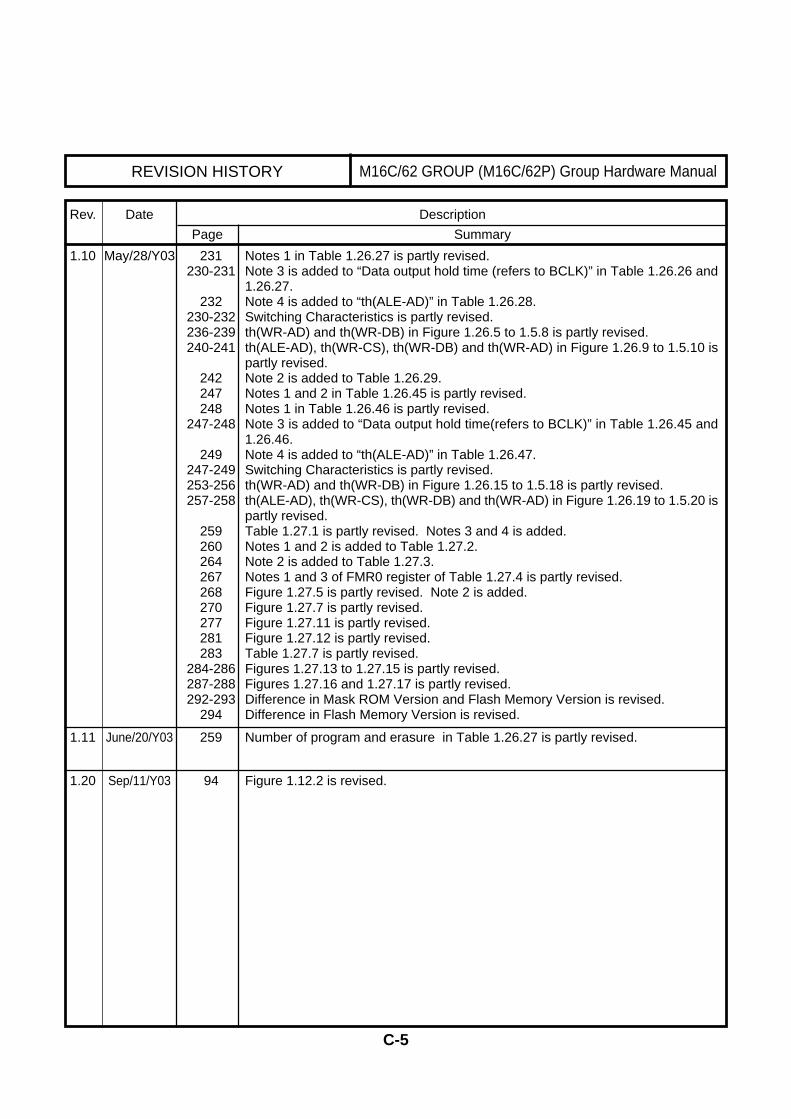
REVISION HISTORY
Rev. Date Description
Page Summary
C-5
M16C/62 GROUP (M16C/62P) Group Hardware Manual
231230-231
232230-232236-239240-241
242247248
247-248
249247-249253-256257-258
259260264267268270277281283
284-286287-288292-293
294
Notes 1 in Table 1.26.27 is partly revised.Note 3 is added to “Data output hold time (refers to BCLK)” in Table 1.26.26 and1.26.27.Note 4 is added to “th(ALE-AD)” in Table 1.26.28.Switching Characteristics is partly revised.th(WR-AD) and th(WR-DB) in Figure 1.26.5 to 1.5.8 is partly revised.th(ALE-AD), th(WR-CS), th(WR-DB) and th(WR-AD) in Figure 1.26.9 to 1.5.10 ispartly revised.Note 2 is added to Table 1.26.29.Notes 1 and 2 in Table 1.26.45 is partly revised.Notes 1 in Table 1.26.46 is partly revised.Note 3 is added to “Data output hold time(refers to BCLK)” in Table 1.26.45 and1.26.46.Note 4 is added to “th(ALE-AD)” in Table 1.26.47.Switching Characteristics is partly revised.th(WR-AD) and th(WR-DB) in Figure 1.26.15 to 1.5.18 is partly revised.th(ALE-AD), th(WR-CS), th(WR-DB) and th(WR-AD) in Figure 1.26.19 to 1.5.20 ispartly revised.Table 1.27.1 is partly revised. Notes 3 and 4 is added.Notes 1 and 2 is added to Table 1.27.2.Note 2 is added to Table 1.27.3.Notes 1 and 3 of FMR0 register of Table 1.27.4 is partly revised.Figure 1.27.5 is partly revised. Note 2 is added.Figure 1.27.7 is partly revised.Figure 1.27.11 is partly revised.Figure 1.27.12 is partly revised.Table 1.27.7 is partly revised.Figures 1.27.13 to 1.27.15 is partly revised.Figures 1.27.16 and 1.27.17 is partly revised.Difference in Mask ROM Version and Flash Memory Version is revised.Difference in Flash Memory Version is revised.
1.10 May/28/Y03
259 Number of program and erasure in Table 1.26.27 is partly revised.1.11 June/20/Y03
94 Figure 1.12.2 is revised.1.20 Sep/11/Y03
RENESAS 16-BIT CMOS SINGLE-CHIP MICROCOMPUTERHARDWARE MANUALM16C/62 Group (M16C/62P) Rev.1.20
Editioned byCommittee of editing of RENESAS Semiconductor Hardware Manual
This book, or parts thereof, may not be reproduced in any form without permissionof Renesas Technology Corporation.Copyright © 2003. Renesas Technology Corporation, All rights reserved.
M16C/62 Group (M16C/62P)Hardware Manual
2-6-2, Ote-machi, Chiyoda-ku, Tokyo,100-0004, Japan
RENESAS 16-BIT SINGLE-CHIP MICROCOMPUTER
M16C FAMILY / M16C/60 SERIES
M16C/62 Group(M16C/62P)16
Rev. 1.10Revision date: May. 28, 2003
Usage Notes Reference Book
www.renesas.com
Before using this material, please visit our website to confirm that this is the most current document available.
REJ09B0017-0110Z
For the most current Usage Notes Reference Book, please visit our website.

Keep safety first in your circuit designs!
Notes regarding these materials
• Renesas Technology Corporation puts the maximum effort into making semiconductor prod-ucts better and more reliable, but there is always the possibility that trouble may occur withthem. Trouble with semiconductors may lead to personal injury, fire or property damage.Remember to give due consideration to safety when making your circuit designs, with ap-propriate measures such as (i) placement of substitutive, auxiliary circuits, (ii) use of non-flammable material or (iii) prevention against any malfunction or mishap.
• These materials are intended as a reference to assist our customers in the selection of theRenesas Technology Corporation product best suited to the customer's application; they donot convey any license under any intellectual property rights, or any other rights, belongingto Renesas Technology Corporation or a third party.
• Renesas Technology Corporation assumes no responsibility for any damage, or infringe-ment of any third-party's rights, originating in the use of any product data, diagrams, charts,programs, algorithms, or circuit application examples contained in these materials.
• All information contained in these materials, including product data, diagrams, charts, pro-grams and algorithms represents information on products at the time of publication of thesematerials, and are subject to change by Renesas Technology Corporation without noticedue to product improvements or other reasons. It is therefore recommended that custom-ers contact Renesas Technology Corporation or an authorized Renesas Technology Cor-poration product distributor for the latest product information before purchasing a productlisted herein.The information described here may contain technical inaccuracies or typographical errors.Renesas Technology Corporation assumes no responsibility for any damage, liability, orother loss rising from these inaccuracies or errors.Please also pay attention to information published by Renesas Technology Corporation byvarious means, including the Renesas Technology Corporation Semiconductor home page(http://www.renesas.com).
• When using any or all of the information contained in these materials, including productdata, diagrams, charts, programs, and algorithms, please be sure to evaluate all informa-tion as a total system before making a final decision on the applicability of the informationand products. Renesas Technology Corporation assumes no responsibility for any dam-age, liability or other loss resulting from the information contained herein.
• Renesas Technology Corporation semiconductors are not designed or manufactured foruse in a device or system that is used under circumstances in which human life is poten-tially at stake. Please contact Renesas Technology Corporation or an authorized RenesasTechnology Corporation product distributor when considering the use of a product con-tained herein for any specific purposes, such as apparatus or systems for transportation,vehicular, medical, aerospace, nuclear, or undersea repeater use.
• The prior written approval of Renesas Technology Corporation is necessary to reprint orreproduce in whole or in part these materials.
• If these products or technologies are subject to the Japanese export control restrictions,they must be exported under a license from the Japanese government and cannot be im-ported into a country other than the approved destination.Any diversion or reexport contrary to the export control laws and regulations of Japan and/or the country of destination is prohibited.
• Please contact Renesas Technology Corporation for further details on these materials or the products contained therein.

PrefaceThe “Usage Notes Reference Book” is a
compilat ion of usage notes from the
Hardware Manual as well as technical
news related to this product.
A-1
Table of Contents1. Usage Precaution_______________________________________ 1
1.1 Precautions for External Bus ..........................................................................................................1
1.2 Precautions for PLL Frequency Synthesizer ..................................................................................2
1.3 Precautions for Power Control ........................................................................................................3
1.4 Precautions for Protect ...................................................................................................................4
1.5 Precautions for Interrupts ...............................................................................................................5
1.5.1 Reading address 0000016.......................................................................................................5
1.5.2 Setting the SP ..........................................................................................................................5_______
1.5.3 The NMI Interrupt .....................................................................................................................5
1.5.4 Changing the Interrupt Generate Factor ..................................................................................6______
1.5.5 INT Interrupt .............................................................................................................................6
1.5.6 Rewrite the Interrupt Control Register .....................................................................................7
1.5.7 Watchdog Timer Interrupt ........................................................................................................8
1.6 Precautions for DMAC ....................................................................................................................9
1.6.1 Write to DMAE Bit in DMiCON Register ..................................................................................9
1.7 Precautions for Timers ..................................................................................................................10
1.7.1 Timer A ..................................................................................................................................10
1.7.1.1 Timer A (Timer Mode)....................................................................................................10
1.7.1.2 Timer A (Event Counter Mode) ......................................................................................11
1.7.1.3 Timer A (One-shot Timer Mode) ....................................................................................12
1.7.1.4 Timer A (Pulse Width Modulation Mode) .......................................................................13
1.7.2 Timer B ..................................................................................................................................14
1.7.2.1 Timer B (Timer Mode)....................................................................................................14
1.7.2.2 Timer B (Event Counter Mode) ......................................................................................15
1.7.2.3 Timer B (Pulse Period/pulse Width Measurement Mode) ............................................16
1.8 Precautions for Serial I/O (Clock-synchronous Serial I/O) ............................................................17
1.8.1 Transmission/reception ..........................................................................................................17
1.8.2 Transmission .........................................................................................................................18
1.8.3 Reception ...............................................................................................................................19
A-2
1.9 Precautions for Serial I/O (UART Mode) ......................................................................................20
1.9.1 Special Mode 2 .....................................................................................................................20
1.9.2 Special Mode 4 (SIM Mode) .................................................................................................20
1.10 Precautions for A-D Converter ....................................................................................................21
1.11 Precautions for Programmable I/O Ports ....................................................................................23
1.12 Electric Characteristic Differences Between Mask ROM and Flash Memory Version Microcomputers ...... 24
1.13 Precautions for Flash Memory Version .......................................................................................25
1.13.1 Precautions for Functions to Inhibit Rewriting Flash Memory Rewrite ................................25
1.13.2 Precautions for Stop mode ..................................................................................................25
1.13.3 Precautions for Wait mode ..................................................................................................25
1.13.4 Precautions for Low power dissipation mode, ring oscillator low power dissipation mode ................. 25
1.13.5 Writing command and data ..................................................................................................25
1.13.6 Precautions for Program Command ....................................................................................25
1.13.7 Precautions for Lock Bit Program Command ......................................................................26
1.13.8 Operation speed ..................................................................................................................26
1.13.9 Instructions inhibited against use .........................................................................................26
1.13.10 Interrupts ............................................................................................................................26
1.13.11 How to access ...................................................................................................................26
1.13.12 Writing in the user ROM area ............................................................................................27
1.13.13 DMA transfer ......................................................................................................................27
1.13.14 Regarding Programming/Erasure Times and Execution Time ..........................................27
2. Differences Made Depending on Manufactured Time ________ 28
2.1 Vdet2 Detection ............................................................................................................................28
2.2 RESET Input .................................................................................................................................29
2.3 Serial I/O .......................................................................................................................................30
1.1 Precautions for External Bus
1
Renesas microcomputers
M16C / 62P Group SINGLE-CHIP 16-BIT CMOS MICROCOMPUTER
1. Usage Precaution
1.1 Precautions for External Bus1. The external ROM version can operate only in the microprocessor mode, connect the CNVSS pin to
VCC1.
2. When resetting CNVss pin with "H" input, contents of internal ROM cannot be read out.
1.2 Precautions for PLL Frequency Synthesizer
2
Renesas microcomputers
M16C / 62P Group SINGLE-CHIP 16-BIT CMOS MICROCOMPUTER
1.2 Precautions for PLL Frequency SynthesizerMake the supply voltage stable to use the PLL frequency synthesizer.
For ripple with the supply voltage 5V, keep below 10kHz as frequency, below 0.5V (peak to peak) as
voltage fluctuation band and below 1V/mS as voltage fluctuation rate.
For ripple with the supply voltage 3V, keep below 10kHz as frequency, below 0.3V (peak to peak) as
voltage fluctuation band and below 0.6V/mS as voltage fluctuation rate.
1.3 Precautions for Power Control
3
Renesas microcomputers
M16C / 62P Group SINGLE-CHIP 16-BIT CMOS MICROCOMPUTER
1.3 Precautions for Power Control____________
1. When exiting stop mode by hardware reset, set RESET pin to “L” until a main clock oscillation is
stabilized.
2. Insert more than four NOP instructions after an WAIT instruction or a instruction to set the CM10 bit of
CM1 register to “1”. When shifting to wait mode or stop mode, an instruction queue reads ahead to the
next instruction to halt a program by an WAIT instruction and an instruction to set the CM10 bit to “1” (all
clocks stopped). The next instruction may be executed before entering wait mode or stop mode, de-
pending on a combination of instruction and an execution timing.
3. Wait until the td(M-L) elapses or main clock oscillation stabilization time, whichever is longer, before
switching the clock source for CPU clock to the main clock.
Similarly, wait until the sub clock oscillates stably before switching the clock source for CPU clock to the
sub clock.
4. Suggestions to reduce power consumption
(a) Ports
The processor retains the state of each I/O port even when it goes to wait mode or to stop mode. A
current flows in active I/O ports. A pass current flows in input ports that high-impedance state. When
entering wait mode or stop mode, set non-used ports to input and stabilize the potential.
(b) A-D converter
When A-D conversion is not performed, set the VCUT bit of ADiCON1 register to “0” (no VREF connec-
tion). When A-D conversion is performed, start the A-D conversion at least 1 µs or longer after setting
the VCUT bit to “1” (VREF connection).
(c) D-A converter
When not performing D-A conversion, set the DAiE bit (i=0, 1) of DACON register to “0” (input inhib-
ited) and DAi register to “0016”.
(d) Stopping peripheral functions
Use the CM0 register CM02 bit to stop the unnecessary peripheral functions during wait mode.
However, because the peripheral function clock (fC32) generated from the sub-clock does not stop,
this measure is not conducive to reducing the power consumption of the chip. If low speed mode or
low power dissipation mode is to be changed to wait mode, set the CM02 bit to “0” (do not peripheral
function clock stopped when in wait mode), before changing wait mode.
(e) Switching the oscillation-driving capacity
Set the driving capacity to “LOW” when oscillation is stable.
(f) External clock
When using an external clock input for the CPU clock, set the CM0 register CM05 bit to “1” (stop).
Setting the CM05 bit to “1” disables the XOUT pin from functioning, which helps to reduce the amount
of current drawn in the chip. (When using an external clock input, note that the clock remains fed into
the chip regardless of how the CM05 bit is set.)

1.4 Precautions for Protect
4
Renesas microcomputers
M16C / 62P Group SINGLE-CHIP 16-BIT CMOS MICROCOMPUTER
1.4 Precautions for ProtectSet the PRC2 bit to “1” (write enabled) and then write to any address, and the PRC2 bit will be cleared to “0”
(write protected). The registers protected by the PRC2 bit should be changed in the next instruction after
setting the PRC2 bit to “1”. Make sure no interrupts or DMA transfers will occur between the instruction in
which the PRC2 bit is set to “1” and the next instruction.
5
1.5 Precautions for Interrupts
Renesas microcomputers
M16C / 62P Group SINGLE-CHIP 16-BIT CMOS MICROCOMPUTER
1.5 Precautions for Interrupts
1.5.1 Reading address 0000016
Do not read the address 0000016 in a program. When a maskable interrupt request is accepted, the CPU
reads interrupt information (interrupt number and interrupt request priority level) from the address
0000016 during the interrupt sequence. At this time, the IR bit for the accepted interrupt is cleared to “0”.
If the address 0000016 is read in a program, the IR bit for the interrupt which has the highest priority
among the enabled interrupts is cleared to “0”. This causes a problem that the interrupt is canceled, or an
unexpected interrupt request is generated.
1.5.2 Setting the SP
Set any value in the SP(USP, ISP) before accepting an interrupt. The SP(USP, ISP) is cleared to ‘000016’
after reset. Therefore, if an interrupt is accepted before setting any value in the SP(USP, ISP), the pro-
gram may go out of control._______
Especially when using NMI interrupt, set a value in the ISP at the beginning of the program. For the first_______
and only the first instruction after reset, all interrupts including NMI interrupt are disabled.
_______
1.5.3 The NMI Interrupt_______ _______
1. The NMI interrupt cannot be disabled. If this interrupt is unused, connect the NMI pin to VCC1 via a
resistor (pull-up)._______
2. The input level of the NMI pin can be read by accessing the P8 register’s P8_5 bit. Note that the P8_5_______
bit can only be read when determining the pin level in NMI interrupt routine._______
3. Stop mode cannot be entered into while input on the NMI pin is low. This is because while input on the_______
NMI pin is low the CM1 register’s CM10 bit is fixed to “0”._______ _______
4. Do not go to wait mode while input on the NMI pin is low. This is because when input on the NMI pin
goes low, the CPU stops but CPU clock remains active; therefore, the current consumption in the chip
does not drop. In this case, normal condition is restored by an interrupt generated thereafter._______
5. The low and high level durations of the input signal to the NMI pin must each be 2 CPU clock cycles +
300 ns or more.
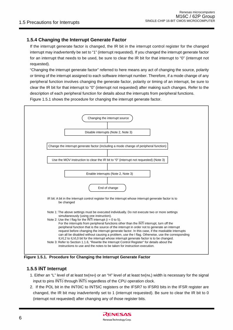
6
1.5 Precautions for Interrupts
Renesas microcomputers
M16C / 62P Group SINGLE-CHIP 16-BIT CMOS MICROCOMPUTER
______
1.5.5 INT Interrupt1. Either an “L” level of at least tW(INH) or an “H” level of at least tW(INL) width is necessary for the signal
________ ________
input to pins INT0 through INT5 regardless of the CPU operation clock.
2. If the POL bit in the INT0IC to INT5IC registers or the IFSR7 to IFSR0 bits in the IFSR register are
changed, the IR bit may inadvertently set to 1 (interrupt requested). Be sure to clear the IR bit to 0
(interrupt not requested) after changing any of those register bits.
1.5.4 Changing the Interrupt Generate FactorIf the interrupt generate factor is changed, the IR bit in the interrupt control register for the changed
interrupt may inadvertently be set to “1” (interrupt requested). If you changed the interrupt generate factor
for an interrupt that needs to be used, be sure to clear the IR bit for that interrupt to “0” (interrupt not
requested).
“Changing the interrupt generate factor” referred to here means any act of changing the source, polarity
or timing of the interrupt assigned to each software interrupt number. Therefore, if a mode change of any
peripheral function involves changing the generate factor, polarity or timing of an interrupt, be sure to
clear the IR bit for that interrupt to “0” (interrupt not requested) after making such changes. Refer to the
description of each peripheral function for details about the interrupts from peripheral functions.
Figure 1.5.1 shows the procedure for changing the interrupt generate factor.
Figure 1.5.1. Procedure for Changing the Interrupt Generate Factor
Changing the interrupt source
Disable interrupts (Note 2, Note 3)
Use the MOV instruction to clear the IR bit to “0” (interrupt not requested) (Note 3)
Change the interrupt generate factor (including a mode change of peripheral function)
Enable interrupts (Note 2, Note 3)
End of change
IR bit: A bit in the interrupt control register for the interrupt whose interrupt generate factor is to be changed
Note 1: The above settings must be executed individually. Do not execute two or more settings simultaneously (using one instruction).Note 2: Use the I flag for the INTi interrupt (i = 0 to 5). For the interrupts from peripheral functions other than the INTi interrupt, turn off the peripheral function that is the source of the interrupt in order not to generate an interrupt request before changing the interrupt generate factor. In this case, if the maskable interrupts can all be disabled without causing a problem, use the I flag. Otherwise, use the corresponding ILVL2 to ILVL0 bit for the interrupt whose interrupt generate factor is to be changed. Note 3: Refer to Section 1.1.6, “Rewrite the Interrupt Control Register” for details about the instructions to use and the notes to be taken for instruction execution.
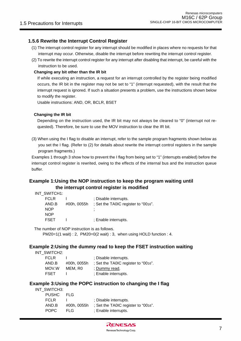
7
1.5 Precautions for Interrupts
Renesas microcomputers
M16C / 62P Group SINGLE-CHIP 16-BIT CMOS MICROCOMPUTER
1.5.6 Rewrite the Interrupt Control Register(1) The interrupt control register for any interrupt should be modified in places where no requests for that
interrupt may occur. Otherwise, disable the interrupt before rewriting the interrupt control register.
(2) To rewrite the interrupt control register for any interrupt after disabling that interrupt, be careful with the
instruction to be used.
Changing any bit other than the IR bit
If while executing an instruction, a request for an interrupt controlled by the register being modified
occurs, the IR bit in the register may not be set to “1” (interrupt requested), with the result that the
interrupt request is ignored. If such a situation presents a problem, use the instructions shown below
to modify the register.
Usable instructions: AND, OR, BCLR, BSET
Changing the IR bit
Depending on the instruction used, the IR bit may not always be cleared to “0” (interrupt not re-
quested). Therefore, be sure to use the MOV instruction to clear the IR bit.
(3) When using the I flag to disable an interrupt, refer to the sample program fragments shown below as
you set the I flag. (Refer to (2) for details about rewrite the interrupt control registers in the sample
program fragments.)
Examples 1 through 3 show how to prevent the I flag from being set to “1” (interrupts enabled) before the
interrupt control register is rewrited, owing to the effects of the internal bus and the instruction queue
buffer.
Example 1:Using the NOP instruction to keep the program waiting until the interrupt control register is modified
INT_SWITCH1:FCLR I ; Disable interrupts.AND.B #00h, 0055h ; Set the TA0IC register to “0016”.NOP ; NOPFSET I ; Enable interrupts.
The number of NOP instruction is as follows.PM20=1(1 wait) : 2, PM20=0(2 wait) : 3, when using HOLD function : 4.
Example 2:Using the dummy read to keep the FSET instruction waiting INT_SWITCH2:
FCLR I ; Disable interrupts.AND.B #00h, 0055h ; Set the TA0IC register to “0016”.MOV.W MEM, R0 ; Dummy read.FSET I ; Enable interrupts.
Example 3:Using the POPC instruction to changing the I flagINT_SWITCH3:
PUSHC FLGFCLR I ; Disable interrupts.AND.B #00h, 0055h ; Set the TA0IC register to “0016”.POPC FLG ; Enable interrupts.
8
1.5 Precautions for Interrupts
Renesas microcomputers
M16C / 62P Group SINGLE-CHIP 16-BIT CMOS MICROCOMPUTER
1.5.7 Watchdog Timer InterruptInitialize the watchdog timer after the watchdog timer interrupt occurs.
9
Renesas microcomputers
M16C / 62P Group SINGLE-CHIP 16-BIT CMOS MICROCOMPUTER
1.6 Precautions for DMAC
1.6 Precautions for DMAC
1.6.1 Write to DMAE Bit in DMiCON RegisterWhen both of the conditions below are met, follow the steps below.
Conditions
• The DMAE bit is set to “1” again while it remains set (DMAi is in an active state).
• A DMA request may occur simultaneously when the DMAE bit is being written.
Step 1: Write “1” to the DMAE bit and DMAS bit in DMiCON register simultaneously(*1).
Step 2: Make sure that the DMAi is in an initial state(*2) in a program.
If the DMAi is not in an initial state, the above steps should be repeated.
Notes:
*1. The DMAS bit remains unchanged even if “1” is written. However, if “0” is written to this bit, it is set to
“0” (DMA not requested). In order to prevent the DMAS bit from being modified to “0”, “1” should be
written to the DMAS bit when “1” is written to the DMAE bit. In this way the state of the DMAS bit
immediately before being written can be maintained.
Similarly, when writing to the DMAE bit with a read-modify-write instruction, “1” should be written to
the DMAS bit in order to maintain a DMA request which is generated during execution.
*2. Read the TCRi register to verify whether the DMAi is in an initial state. If the read value is equal to a
value which was written to the TCRi register before DMA transfer start, the DMAi is in an initial state.
(If a DMA request occurs after writing to the DMAE bit, the value written to the TCRi register is “1”.) If
the read value is a value in the middle of transfer, the DMAi is not in an initial state.
1.7 Precautions for Timers
10
Renesas microcomputers
M16C / 62P Group SINGLE-CHIP 16-BIT CMOS MICROCOMPUTER
1.7 Precautions for Timers
1.7.1 Timer A
1.7.1.1 Timer A (Timer Mode)
1. The timer remains idle after reset. Set the mode, count source, counter value, etc. using the TAiMR
(i = 0 to 4) register and the TAi register before setting the TAiS bit in the TABSR register to “1” (count
starts).
Always make sure the TAiMR register is modified while the TAiS bit remains “0” (count stops)
regardless whether after reset or not.
2. While counting is in progress, the counter value can be read out at any time by reading the TAi
register. However, if the counter is read at the same time it is reloaded, the value “FFFF16” is read.
Also, if the counter is read before it starts counting after a value is set in the TAi register while not
counting, the set value is read.
______
3. If a low-level signal is applied to the NMI pin when the TB2SC register IVPCR1 bit = “1” (three-phase______
output forcible cutoff by input on NMI pin enabled), the TA1OUT, TA2OUT and TA4OUT pins go to a
high-impedance state.
1.7 Precautions for Timers
11
Renesas microcomputers
M16C / 62P Group SINGLE-CHIP 16-BIT CMOS MICROCOMPUTER
1.7.1.2 Timer A (Event Counter Mode)
1. The timer remains idle after reset. Set the mode, count source, counter value, etc. using the TAiMR
(i = 0 to 4) register, the TAi register, the UDF register, the ONSF register TAZIE, TA0TGL and
TA0TGH bits and the TRGSR register before setting the TAiS bit in the TABSR register to “1” (count
starts).
Always make sure the TAiMR register, the UDF register, the ONSF register TAZIE, TA0TGL and
TA0TGH bits and the TRGSR register are modified while the TAiS bit remains “0” (count stops)
regardless whether after reset or not.
2. While counting is in progress, the counter value can be read out at any time by reading the TAi
register. However, “FFFF16” can be read in underflow, while reloading, and “000016” in overflow.
When setting TAi register to a value during a counter stop, the setting value can be read before a
counter starts counting. Also, if the counter is read before it starts counting after a value is set in the
TAi register while not counting, the set value is read.
______
3. If a low-level signal is applied to the NMI pin when the TB2SC register IVPCR1 bit = “1” (three-phase______
output forcible cutoff by input on NMI pin enabled), the TA1OUT, TA2OUT and TA4OUT pins go to a
high-impedance state.
1.7 Precautions for Timers
12
Renesas microcomputers
M16C / 62P Group SINGLE-CHIP 16-BIT CMOS MICROCOMPUTER
1.7.1.3 Timer A (One-shot Timer Mode)
1. The timer remains idle after reset. Set the mode, count source, counter value, etc. using the TAiMR
(i = 0 to 4) register, the TAi register, the ONSF register TA0TGL and TA0TGH bits and the TRGSR
register before setting the TAiS bit in the TABSR register to “1” (count starts).
Always make sure the TAiMR register, the ONSF register TA0TGL and TA0TGH bits and the
TRGSR register are modified while the TAiS bit remains “0” (count stops) regardless whether after
reset or not.
2. When setting TAiS bit to “0” (count stop), the followings occur:
• A counter stops counting and a content of reload register is reloaded.
• TAiOUT pin outputs “L”.
• After one cycle of the CPU clock, the IR bit of TAiIC register is set to “1” (interrupt request).
3. Output in one-shot timer mode synchronizes with a count source internally generated. When an
external trigger has been selected, one-cycle delay of a count source as maximum occurs between
a trigger input to TAiIN pin and output in one-shot timer mode.
4. The IR bit is set to “1” when timer operation mode is set with any of the following procedures:
• Select one-shot timer mode after reset.
• Change an operation mode from timer mode to one-shot timer mode.
• Change an operation mode from event counter mode to one-shot timer mode.
To use the timer Ai interrupt (the IR bit), set the IR bit to “0” after the changes listed above have
been made.
5. When a trigger occurs, while counting, a counter reloads the reload register to continue counting
after generating a re-trigger and counting down once. To generate a trigger while counting, gener-
ate a second trigger between occurring the previous trigger and operating longer than one cycle of
a timer count source.
______
6. If a low-level signal is applied to the NMI pin when the TB2SC register IVPCR1 bit = “1” (three-phase______
output forcible cutoff by input on NMI pin enabled), the TA1OUT, TA2OUT and TA4OUT pins go to a
high-impedance state.
1.7 Precautions for Timers
13
Renesas microcomputers
M16C / 62P Group SINGLE-CHIP 16-BIT CMOS MICROCOMPUTER
1.7.1.4 Timer A (Pulse Width Modulation Mode)
1. The timer remains idle after reset. Set the mode, count source, counter value, etc. using the TAiMR
(i = 0 to 4) register, the TAi register, the ONSF register TA0TGL and TA0TGH bits and the TRGSR
register before setting the TAiS bit in the TABSR register to “1” (count starts).
Always make sure the TAiMR register, the ONSF register TA0TGL and TA0TGH bits and the
TRGSR register are modified while the TAiS bit remains “0” (count stops) regardless whether after
reset or not.
2. The IR bit is set to “1” when setting a timer operation mode with any of the following procedures:
• Select the PWM mode after reset.
• Change an operation mode from timer mode to PWM mode.
• Change an operation mode from event counter mode to PWM mode.
To use the timer Ai interrupt (interrupt request bit), set the IR bit to “0” by program after the above
listed changes have been made.
3. When setting TAiS register to “0” (count stop) during PWM pulse output, the following action occurs:
• Stop counting.
• When TAiOUT pin is output “H”, output level is set to “L” and the IR bit is set to “1”.
• When TAiOUT pin is output “L”, both output level and the IR bit remains unchanged.
______
4. If a low-level signal is applied to the NMI pin when the TB2SC register IVPCR1 bit = “1” (three-phase______
output forcible cutoff by input on NMI pin enabled), the TA1OUT, TA2OUT and TA4OUT pins go to a
high-impedance state.
1.7 Precautions for Timers
14
Renesas microcomputers
M16C / 62P Group SINGLE-CHIP 16-BIT CMOS MICROCOMPUTER
1.7.2 Timer B
1.7.2.1 Timer B (Timer Mode)
1. The timer remains idle after reset. Set the mode, count source, counter value, etc. using the TBiMR
(i = 0 to 5) register and TBi register before setting the TBiS bit in the TABSR or the TBSR register to
“1” (count starts).
Always make sure the TBiMR register is modified while the TBiS bit remains “0” (count stops)
regardless whether after reset or not.
2. A value of a counter, while counting, can be read in TBi register at any time. “FFFF16” is read while
reloading. Setting value is read between setting values in TBi register at count stop and starting a
counter.
1.7 Precautions for Timers
15
Renesas microcomputers
M16C / 62P Group SINGLE-CHIP 16-BIT CMOS MICROCOMPUTER
1.7.2.2 Timer B (Event Counter Mode)
1. The timer remains idle after reset. Set the mode, count source, counter value, etc. using the TBiMR
(i = 0 to 5) register and TBi register before setting the TBiS bit in the TABSR or the TBSR register to
“1” (count starts).
Always make sure the TBiMR register is modified while the TBiS bit remains “0” (count stops)
regardless whether after reset or not.
2. The counter value can be read out on-the-fly at any time by reading the TBi register. However, if this
register is read at the same time the counter is reloaded, the read value is always “FFFF16.” If the
TBi register is read after setting a value in it while not counting but before the counter starts count-
ing, the read value is the one that has been set in the register.
1.7 Precautions for Timers
16
Renesas microcomputers
M16C / 62P Group SINGLE-CHIP 16-BIT CMOS MICROCOMPUTER
1.7.2.3 Timer B (Pulse Period/pulse Width Measurement Mode)
1. The timer remains idle after reset. Set the mode, count source, etc. using the TBiMR (i = 0 to 5)
register before setting the TBiS bit in the TABSR or the TBSR register to “1” (count starts).
Always make sure the TBiMR register is modified while the TBiS bit remains “0” (count stops)
regardless whether after reset or not. To clear the MR3 bit to “0” by writing to the TBiMR register
while the TBiS bit = “1” (count starts), be sure to write the same value as previously written to the
TM0D0, TM0D1, MR0, MR1, TCK0 and TCK1 bits and a 0 to the MR2 bit.
2. The IR bit of TBiIC register (i=0 to 5) goes to “1” (interrupt request), when an effective edge of a
measurement pulse is input or timer Bi is overflowed. The factor of interrupt request can be deter-
mined by use of the MR3 bit of TBiMR register within the interrupt routine.
3. If the source of interrupt cannot be identified by the MR3 bit such as when the measurement pulse
input and a timer overflow occur at the same time, use another timer to count the number of times
timer B has overflowed.
4. To set the MR3 bit to “0” (no overflow), set TBiMR register with setting the TBiS bit to “1” and
counting the next count source after setting the MR3 bit to “1” (overflow).
5. Use the IR bit of TBiIC register to detect only overflows. Use the MR3 bit only to determine the
interrupt factor within the interrupt routine.
6. When a count is started and the first effective edge is input, an indeterminate value is transferred to
the reload register. At this time, timer Bi interrupt request is not generated.
7. A value of the counter is indeterminate at the beginning of a count. MR3 may be set to “1” and timer
Bi interrupt request may be generated between a count start and an effective edge input.
8. For pulse width measurement, pulse widths are successively measured. Use program to check
whether the measurement result is an “H” level width or an “L” level width.
1. The timer remains idle after reset. Set the mode, count source, counter value, etc. using the TAiMR
(i = 0 to 5) register and the TBi register before setting the TABSR register or TBiS bit in the TBSR
register to “1” (count starts).
Always make sure the TBiMR registe is modified while the TBiS bit remains “0” (count stops) re-
gardless whether after reset or not.
1.8 Precautions for Serial I/O (Clock-synchronous Serial I/O)
17
Renesas microcomputers
M16C / 62P Group SINGLE-CHIP 16-BIT CMOS MICROCOMPUTER
1.8 Precautions for Serial I/O (Clock-synchronous Serial I/O)
1.8.1 Transmission/reception_______ ________
1. With an external clock selected, and choosing the RTS function, the output level of the RTSi pin goes
to “L” when the data-receivable status becomes ready, which informs the transmission side that the________
reception has become ready. The output level of the RTSi pin goes to “H” when reception starts. So if________ ________
the RTSi pin is connected to the CTSi pin on the transmission side, the circuit can transmission and_______
reception data with consistent timing. With the internal clock, the RTS function has no effect.
_______
2. If a low-level signal is applied to the NMI pin when the TB2SC register IVPCR1 bit = “1” (three-phase_______ _________
output forcible cutoff by input on NMI pin enabled), the RTS2 and CLK2 pins go to a high-impedance
state.
1.8 Precautions for Serial I/O (Clock-synchronous Serial I/O)
18
Renesas microcomputers
M16C / 62P Group SINGLE-CHIP 16-BIT CMOS MICROCOMPUTER
1.8.2 TransmissionWhen an external clock is selected, the conditions must be met while if the UiC0 register’s CKPOL bit =
“0” (transmit data output at the falling edge and the receive data taken in at the rising edge of the transfer
clock), the external clock is in the high state; if the UiC0 register’s CKPOL bit = “1” (transmit data output at
the rising edge and the receive data taken in at the falling edge of the transfer clock), the external clock is
in the low state.
• The TE bit of UiC1 register= “1” (transmission enabled)
• The TI bit of UiC1 register = “0” (data present in UiTB register)_______ _______
• If CTS function is selected, input on the CTSi pin = “L”
1.8 Precautions for Serial I/O (Clock-synchronous Serial I/O)
19
Renesas microcomputers
M16C / 62P Group SINGLE-CHIP 16-BIT CMOS MICROCOMPUTER
1.8.3 Reception1. In operating the clock-synchronous serial I/O, operating a transmitter generates a shift clock. Fix set-
tings for transmission even when using the device only for reception. Dummy data is output to the
outside from the TxDi pin when receiving data.
2. When an internal clock is selected, set the UiC1 register (i = 0 to 2)’s TE bit to 1 (transmission enabled)
and write dummy data to the UiTB register, and the shift clock will thereby be generated. When an
external clock is selected, set the UiC1 register (i = 0 to 2)’s TE bit to 1 and write dummy data to the
UiTB register, and the shift clock will be generated when the external clock is fed to the CLKi input pin.
3. When successively receiving data, if all bits of the next receive data are prepared in the UARTi receive
register while the UiC1 register (i = 0 to 2)’s RE bit = “1” (data present in the UiRB register), an overrun
error occurs and the UiRB register OER bit is set to “1” (overrun error occurred). In this case, because
the content of the UiRB register is indeterminate, a corrective measure must be taken by programs on
the transmit and receive sides so that the valid data before the overrun error occurred will be retransmit-
ted. Note that when an overrun error occurred, the SiRIC register IR bit does not change state.
4. To receive data in succession, set dummy data in the lower-order byte of the UiTB register every time
reception is made.
5. When an external clock is selected, the conditions must be met while if the CKPOL bit = “0”, the
external clock is in the high state; if the CKPOL bit = “1”, the external clock is in the low state.
• The RE bit of UiC1 register= “1” (reception enabled)
• The TE bit of UiC1 register= “1” (transmission enabled)
• The TI bit of UiC1 register= “0” (data present in the UiTB register)
1.9 Precautions for Serial I/O (UART Mode)
20
Renesas microcomputers
M16C / 62P Group SINGLE-CHIP 16-BIT CMOS MICROCOMPUTER
1.9 Precautions for Serial I/O (UART Mode)
1.9.1 Special Mode 2_______
If a low-level signal is applied to the NMI pin when the TB2SC register IVPCR1 bit = 1 (three-phase output_______ _________
forcible cutoff by input on NMI pin enabled), the RTS2 and CLK2 pins go to a high-impedance state.
1.9.2 Special Mode 4 (SIM Mode)
A transmit interrupt request is generated by setting the U2C1 register U2IRS bit to “1” (transmission
complete) and U2ERE bit to “1” (error signal output) after reset. Therefore, when using SIM mode, be
sure to clear the IR bit to “0” (no interrupt request) after setting these bits.
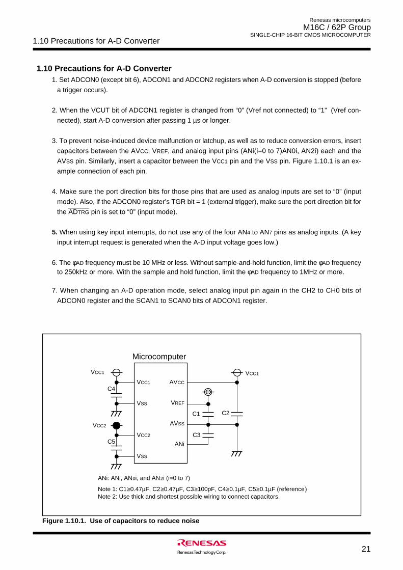
1.10 Precautions for A-D Converter
21
Renesas microcomputers
M16C / 62P Group SINGLE-CHIP 16-BIT CMOS MICROCOMPUTER
1.10 Precautions for A-D Converter1. Set ADCON0 (except bit 6), ADCON1 and ADCON2 registers when A-D conversion is stopped (before
a trigger occurs).
2. When the VCUT bit of ADCON1 register is changed from “0” (Vref not connected) to “1” (Vref con-
nected), start A-D conversion after passing 1 µs or longer.
3. To prevent noise-induced device malfunction or latchup, as well as to reduce conversion errors, insert
capacitors between the AVCC, VREF, and analog input pins (ANi(i=0 to 7)AN0i, AN2i) each and the
AVSS pin. Similarly, insert a capacitor between the VCC1 pin and the VSS pin. Figure 1.10.1 is an ex-
ample connection of each pin.
4. Make sure the port direction bits for those pins that are used as analog inputs are set to “0” (input
mode). Also, if the ADCON0 register’s TGR bit = 1 (external trigger), make sure the port direction bit for___________
the ADTRG pin is set to “0” (input mode).
5. When using key input interrupts, do not use any of the four AN4 to AN7 pins as analog inputs. (A key
input interrupt request is generated when the A-D input voltage goes low.)
6. The φAD frequency must be 10 MHz or less. Without sample-and-hold function, limit the φAD frequencyto 250kHZ or more. With the sample and hold function, limit the φAD frequency to 1MHZ or more.
7. When changing an A-D operation mode, select analog input pin again in the CH2 to CH0 bits of
ADCON0 register and the SCAN1 to SCAN0 bits of ADCON1 register.
Figure 1.10.1. Use of capacitors to reduce noise
Microcomputer
Note 1: C1≥0.47µF, C2≥0.47µF, C3≥100pF, C4≥0.1µF, C5≥0.1µF (reference)Note 2: Use thick and shortest possible wiring to connect capacitors.
VCC1
VSS
AVCC
AVSS
VREF
ANi
C4
C1 C2
C3VCC2
VSS
C5
ANi: ANi, AN0i, and AN2i (i=0 to 7)
VCC1 VCC1
VCC2
1.10 Precautions for A-D Converter
22
Renesas microcomputers
M16C / 62P Group SINGLE-CHIP 16-BIT CMOS MICROCOMPUTER
8. If VCC2 < VCC1, do not use AN00 to AN07 and AN20 to AN27 as analog input pins.
9. If the CPU reads the ADi register (i = 0 to 7) at the same time the conversion result is stored in the ADi
register after completion of A-D conversion, an incorrect value may be stored in the ADi register. This
problem occurs when a divide-by-n clock derived from the main clock or a subclock is selected for CPU
clock.
• When operating in one-shot or single-sweep mode
Check to see that A-D conversion is completed before reading the target ADi register. (Check the
ADIC register’s IR bit to see if A-D conversion is completed.)
• When operating in repeat mode or repeat sweep mode 0 or 1
Use the main clock for CPU clock directly without dividing it.
10. If A-D conversion is forcibly terminated while in progress by setting the ADCON0 register’s ADST bit
to “0” (A-D conversion halted), the conversion result of the A-D converter is indeterminate. The contents
of ADi registers irrelevant to A-D conversion may also become indeterminate. If while A-D conversion is
underway the ADST bit is cleared to “0” in a program, ignore the values of all ADi registers.
23
1.11 Precautions for Programmable I/O Ports
Renesas microcomputers
M16C / 62P Group SINGLE-CHIP 16-BIT CMOS MICROCOMPUTER
1.11 Precautions for Programmable I/O Ports_______
1. If a low-level signal is applied to the NMI pin when the TB2SC register IVPCR1 bit = “1” (three-phase_______
output forcible cutoff by input on NMI pin enabled), the P72 to P75, P80 and P81 pins go to a high-
impedance state.
2. Setting the SM32 bit in the S3C register to “1” causes the P92 pin to go to a high-impedance state.
Similarly, setting the SM42 bit in the S4C register to “1” causes the P96 pin to go to a high-impedance
state.
3. The input threshold voltage of pins differs between programmable input/output ports and peripheral
functions.
Therefore, if any pin is shared by a programmable input/output port and a peripheral function and the
input level at this pin is outside the range of recommended operating conditions VIH and VIL (neither
“high” nor “low”), the input level may be determined differently depending on which side—the program-
mable input/output port or the peripheral function—is currently selected.
1.12 Electric Characteristic Differences Between Mask ROM and Flash Memory Version Microcomputers
24
Renesas microcomputers
M16C / 62P Group SINGLE-CHIP 16-BIT CMOS MICROCOMPUTER
1.12 Electric Characteristic Differences Between Mask ROM and Flash Memory Version MicrocomputersFlash memory version and mask ROM version may have different characteristics, operating margin, noise
tolerated dose, noise width dose in electrical characteristics due to internal ROM, different layout pattern,
etc. When switching to the mask ROM version, conduct equivalent tests as system evaluation tests con-
ducted in the flush memory version.
1.13 Precautions for Flash Memory Version
25
Renesas microcomputers
M16C / 62P Group SINGLE-CHIP 16-BIT CMOS MICROCOMPUTER
1.13 Precautions for Flash Memory Version
1.13.1 Precautions for Functions to Inhibit Rewriting Flash Memory RewriteID codes are stored in addresses 0FFFDF16, 0FFFE316, 0FFFEB16, 0FFFEF16, 0FFFF316, 0FFFF716,
and 0FFFFB16. If wrong data are written to theses addresses, the flash memory cannot be read or written
in standard serial I/O mode.
The ROMCP register is mapped in address 0FFFFF16. If wrong data is written to this address, the flash
memory cannot be read or written in parallel I/O mode.
In the flash memory version of microcomputer, these addresses are allocated to the vector addresses (H)
of fixed vectors.
1.13.2 Precautions for Stop modeWhen shifting to stop mode, the following settings are required:
• Set the FMR01 bit to “0” (CPU rewrite mode disabled) and disable DMA transfers before setting the
CM10 bit to “1” (stop mode).
• Execute the JMP.B instruction subsequent to the instruction which sets the CM10 bit to “1” (stop
mode)
Example program BSET 0, CM1 ; Stop mode
JMP.B L1
L1:
Program after returning from stop mode
1.13.3 Precautions for Wait modeWhen shifting to wait mode, set the FMR01 bit to “0” (CPU rewrite mode diabled) before executing the
WAIT instruction.
1.13.4 Precautions for Low power dissipation mode, ring oscillator low power dissipation mode
If the CM05 bit is set to “1” (main clock stop), the following commands must not be executed.
• Program
• Block erase
• Erase all unlocked blocks
• Lock bit program
1.13.5 Writing command and dataWrite the command code and data at even addresses.
1.13.6 Precautions for Program CommandWrite ‘xx4016’ in the first bus cycle and write data to the write address in the second bus cycle, and an
auto program operation (data program and verify) will start. Make sure the address value specified in the
first bus cycle is the same even address as the write address specified in the second bus cycle.
1.13 Precautions for Flash Memory Version
26
Renesas microcomputers
M16C / 62P Group SINGLE-CHIP 16-BIT CMOS MICROCOMPUTER
1.13.7 Precautions for Lock Bit Program CommandWrite ‘xx7716’ in the first bus cycle and write ‘xxD016’ to the uppermost address of a block (even address,
however) in the second bus cycle, and the lock bit for the specified block is cleared to “0”. Make sure the
address value specified in the first bus cycle is the same uppermost block address that is specified in the
second bus cycle.
1.13.8 Operation speed
Before entering CPU rewrite mode (EW0 or EW1 mode), select 10 MHz or less for CPU clock using the
CM0 register’s CM06 bit and CM1 register’s CM17–6 bits. Also, set the PM1 register’s PM17 bit to 1 (with
wait state).
1.13.9 Instructions inhibited against useThe following instructions cannot be used in EW0 mode because the flash memory’s internal data is
referenced: UND instruction, INTO instruction, JMPS instruction, JSRS instruction, and BRK instruction
1.13.10 Interrupts
EW0 Mode
• Any interrupt which has a vector in the variable vector table can be used providing that its vector is
transferred into the RAM area._______
• The NMI and watchdog timer interrupts can be used because the FMR0 register and FMR1 regis-
ter are initialized when one of those interrupts occurs. The jump addresses for those interrupt
service routines should be set in the fixed vector table._______
Because the rewrite operation is halted when a NMI or watchdog timer interrupt occurs, the rewrite
program must be executed again after exiting the interrupt service routine.
• The address match interrupt cannot be used because the flash memory’s internal data is refer-
enced.
EW1 Mode
• Make sure that any interrupt which has a vector in the variable vector table or address match
interrupt will not be accepted during the auto program or auto erase period.
• Avoid using watchdog timer interrupts._______
• The NMI interrupt can be used because the FMR0 register and FMR1 register are initialized when
this interrupt occurs. The jump address for the interrupt service routine should be set in the fixed
vector table._______
Because the rewrite operation is halted when a NMI interrupt occurs, the rewrite program must be
executed again after exiting the interrupt service routine.
1.13.11 How to accessTo set the FMR01, FMR02, or FMR11 bit to “1”, write “0” and then “1” in succession. This is necessary to
ensure that no interrupts or DMA transfers will occur before writing “1” after writing “0”. Also only when_______
NMI pin is “H” level.
1.13 Precautions for Flash Memory Version
27
Renesas microcomputers
M16C / 62P Group SINGLE-CHIP 16-BIT CMOS MICROCOMPUTER
1.13.12 Writing in the user ROM areaEW0 Mode
• If the power supply voltage drops while rewriting any block in which the rewrite control program is
stored, a problem may occur that the rewrite control program is not correctly rewritten and, conse-
quently, the flash memory becomes unable to be rewritten thereafter. In this case, standard serial
I/O or parallel I/O mode should be used.
EW1 Mode
• Avoid rewriting any block in which the rewrite control program is stored.
1.13.13 DMA transferIn EW1 mode, make sure that no DMA transfers will occur while the FMR0 register’s FMR00 bit = 0
(during the auto program or auto erase period).
1.13.14 Regarding Programming/Erasure Times and Execution Time
As the number of programming/erasure times increases, so does the execution time for software com-
mands (Program, Block Erase, Erase All Unlock Blocks, and Lock Bit Program). Especially when the
number of programming/erasure times exceeds 1,000, the software command execution time is notice-
ably extended. Therefore, the software command wait time that is set must be greater than the maximum
rated value of electrical characteristics._______
The software commands are aborted by hardware reset 1, hardware reset 2, NMI interrupt, and watchdog
timer interrupt. If a software command is aborted by such reset or interrupt, the block that was in process
must be erased before reexecuting the aborted command.
28
2.1 Vdet2 Detection
Renesas microcomputers
M16C / 62P Group SINGLE-CHIP 16-BIT CMOS MICROCOMPUTER
2. Differences Made Depending on Manufactured Time
2.1 Vdet2 DetectionThe present version of the products may not detect the Vdet2 voltage in the voltage detection circuit prop-
erly. Therefore, the followings should be noted.
(1) When the VC25 bit in the VCR2 register is set to “1” (enabling the RAM retention limit detection
circuit), the present version may not be reset even if the voltage at the Vcc1 input pin drops below
Vdet2.
(2) The WD5 bit in the WDC register may not change properly.
Supplementary ExplanationNormally, during the stop mode, the Vdet3 voltage is not detected, and thus no reset is generated even
when the input voltage at the VCC1 pin drops to Vdet3 or less. Therefore, if the microcomputer is not reset
when the VCC1 voltage drops below Vdet2 due to the reason described in the above No.1, the microcom-
puter cannot get out of the stop mode with Hardware Reset 2.
29
2.2 RESET Input
Renesas microcomputers
M16C / 62P Group SINGLE-CHIP 16-BIT CMOS MICROCOMPUTER
2.2 RESET InputEnsure that pin RESET must hold valid-low state during powering-up.
When using a reset IC, use a CMOS type IC. When using an open-drain type reset IC, insert a capacitor
between the reset input and Vss and a resistor between the input and Vcc respectively. The R-C time
constant of the capacitor and resistor must provide a low state at least 10 times longer than the Vcc rise
time.
30
2.3 Serial I/O
Renesas microcomputers
M16C / 62P Group SINGLE-CHIP 16-BIT CMOS MICROCOMPUTER
2.3 Serial I/OFor the RXDi input setup time, refer to the rated values shown below, as well as Electrical Characteristics
Table 1.26.23, “Serial I/O,” and Table 1.26.42, “Serial I/O,” in the Hardware Manual.
ns
Standard
Max.Min.ParameterSymbol Unit
tsu(D-C) RxDi input setup time 70
Note: Refer to “Table 1.26.23. Serial I/O of the Electrical Characteristics in the Hardware Manual”.
ns
Standard
Max.Min.ParameterSymbol Unit
tsu(D-C) RxDi input setup time 100
Note: Refer to “Table 1.26.42. Serial I/O of the Electrical Characteristics in the Hardware Manual”.
Table2.3.1. Serial I/O (VCC1=VCC2=5V)
Table2.3.2. Serial I/O (VCC1=VCC2=3V)
REVISION HISTORY M16C/62 GROUP (M16C/62P) USAGE NOTES
Rev. Date Description
Page Summary
B-1
1.0 Jan/31/Y03 Figure 1.1.1 is partly revised.The section “1.3 Precautions for DMAC” is added.The section “1.4.1 Timers A and B” is added.The section “1.4.3.2 Timer B (Pulse Period/Pulse Width Measurement Mode” ispartly revised.The section “1.5.3 Reception” is partly revised.The section “1.6 Precautions for Serial I/O (UART Mode, Special Mode 2)” is partlyrevised.The section “1.8 Precautions for Power Control” is partly revised.The section “1.11.1 Precautions for Functions to Inhibit Rewriting Flash MemoryRewrite” is partly revised.The section “1.11.2 Precautions for Program Command” is partly revised.The section “1.12 Precautions for PLL Frequency Synthesizer” is partly revised.
18915
1819
2225
2638
1.10 May/28/Y03 A written order is all changed.The written order of the section “1.5 Precautions for Interrupt” is changed.The section “1.5.2 Setting the SP” is added.The section “1.5.4 Changing the Interrupt Generate Factor” is added.Figure 1.5.1 is revised.______
The section “1.5.5 INT Interrupt” is revised.The section “1.5.6 Rewrite the Interrupt Control Register” is revised.The text of the section “1.7 Precautions for Timers” and the section “1.7.1 Timer A”is deleted.“1.” of the section “1.7.1.1 Timer A (Timer Mode)” to “1.7.1.4 Timer A (Pulse WidthModulation Mode)”is revised.“1.” of the section “1.7.2.1 Timer B (Timer Mode)” is revised.“1.” of the section “1.7.2.2 Timer B (Event Counter Mode)” is added.“1.” of the section “1.7.2.3 Timer B (Pulse Period/Pulse Width Measurement Mode)”is revised.The section “1.9.2 Special Mode 4 (SIM Mode)” is added.Figure 1.10.1 is revised.A written order is changed.“2.” of the section “1.11 Precautions for Programmable I/O Ports” is revised.The written order of the section “1.13 Precautions for Flash Memory Version” ischanged.The section “1.13.14 Regarding Programming/Erasure Times and Execution Time”is added.The section “2.2 RESET Input” is added.The section “2.3 Serial I/O” is added.
-5-856
710
10 to 13
141516
20212223
25-27
27
2930

RENESAS 16-BIT SINGLE-CHIP MICROCOMPUTERUSAGE NOTES REFERENCE BOOKM16C/62 Group (M16C/62P) Rev.1.10
Editioned byCommittee of editing of RENESAS Semiconductor Usage Notes ReferenceBook
This book, or parts thereof, may not be reproduced in any form without permissionof Renesas Technology Corporation.Copyright © 2003. Renesas Technology Corporation, All rights reserved.
M16C/62 Group (M16C/62P)Usage Notes Reference Book
2-6-2, Ote-machi, Chiyoda-ku, Tokyo,100-0004, Japan