Embed Size (px)
Citation preview
Calhoun: The NPS Institutional Archive
Theses and Dissertations Thesis Collection
1974-09
Hardware implementation of recursive fixed-point
filters for minimum quantization noise
Rodolfo, Carlos Jose de Almeida Rodrigues
Monterey, California. Naval Postgraduate School
http://hdl.handle.net/10945/17043

HARDWARE IMPLEMENTATION OF RECURSIVE FIXED-POINTDIGITAL FILTERS FOR MINIMUM QUANTIZATION NOISE
Carlos Jose de Almeida Rodrigues Rodolfo

DUDLEY KNOX LIBRARYNAVAL POSTGRADUATE SCHOOLMONTEREY. CALIFORNIA 93940

NAVAL POSTGRADUATE SCHOOL
Monterey, California
THARDWARE IMPLEMENTATION OF RECURSIVE
FIXED-POINT DIGITAL FILTERS FORQUANTIZATION NOISE
by
MINIMUM
Carlos Jose* de Almeida Rodrigues
September 197^
Rodclfo
Thesis Adviso r : S . R
.
Parker
Approved for public release; distribution unlimited.
1164089


UNCLASSIFIEDSECURITY CLASSIFICATION OF THIS PAGE (When Dm. En«er»rf)
REPORT DOCUMENTATION PAGE READ INSTRUCTIONSBEFORC COMPLETING FORM
t. REPORT NUMBER 2. GOVT ACCESSION NO. 3. RECIPIENTS CATALOG *UM3ER
4. TITLE (and Subtitle)
Hardware Implementation of RecursiveFixed-Point Digital Filters for MinimumQuantization Noise
5. TYPE OF REPORT & PERIOD COVERED
Engineers Thesis;September 197^
6. PERFORMING ORG. REPORT NUMBER
7. AUTHOR)-
*;
Carlos Jose* de Almeida Rodrigues Rodolfo8. CONTRACT OR GRANT NUMBERfe)
9. PERFORMING ORGANIZATION NAME AND ADDRESS
Naval Postgraduate SchoolMonterey, California 939^0
10. PROGRAM ELEMENT. PROJECT, TASKAREA ft WORK UNIT NUMBERS
II. CONTROLLING OFFICE NAME AND ADDRESS
Naval Postgraduate SchoolMonterey, California 939^0
12. REPORT DATE
September 197413. NUMBER OF PAGES
14 414. MONITORING AGENCY NAME 4 ADDRESSf*/ different from Controlling Oltlce)
Naval Postgraduate SchoolMonterey, California 939^0
15. SECURITY CLASS, (of thta report)
Unclassified
15«. DECLASSIFI CATION/ DOWN GRADINGSCHEDULE
16. DISTRIBUTION ST ATEMENT (of thta Report)
Approved for public release; distribution unlimited.
17. DISTRIBUTION STATEMENT (of the abstract entered In Block 20, If different from Report)
16. SUPPLEMENTARY NOTES
19. KEY WORDS fConi/nu» on reverse aide it neceaaary and Identify by block number)
Digital FilterArithmetic Quantization ErrorsHardware Implementation
20. ABSTRACT (Continue on reverse aide If neceaaary and Identify by block number)
Design and implementation of recursive digital filters withfixed point arithmetic using special hardware are considered indetail and applied to a mechanization of a second order filterstructure with variable coefficients.
Two new methods of performing quantization after arithmeticoperations within a digital filter are presented: quantizationJafter addition and quantization before multiplication . Both
DD f JAN 73 1473 EDITION OF 1 NOV 65 IS OBSOLETE
(Page 1) S/ N 0102-014-6601I
1
UNCLASSIFIEDSECURITY CLASSIFICATION OF THIS PAGE (Wh.en Data Entered)


UNCLASSIFIED
CbCIJHlTY CLASSIFICATION OF THIS PAGEfH?i«n Dafa EnKrv
(20. ABSTRACT Continued)
methods are shown applicable to hardware implementation ofdigital filters and offer advantages over the usual quantizationafter multiplication. Error bounds are derived for these twoquantization schemes and compared with the results previouslyobtained by other authors. It is concluded that the quantiza-tion before multiplication is the most suitable for hardwarefilter implementation. A design modification of the presentlyavailable hardware chips in order to permit round-off ortruncation before multiplication is presented.
DD1 BPto
U73 <BACK>UNCLASSIFIED
O/ N 0102-014-0601 2 SECURITY CLASSIFICATION OF THIS PAGErWi"" 0«f« En(»r»d;


Hardware Implementation of RecursiveFixed-Point Digital Filters for Minimum
Quantization Noise
by
Carlos Jose de Almeida Rodrigues RodolfoLieutenant, Portuguese Navy
B.S.E.E., Naval Postgraduate School, June 1973M.S.E.E., Naval Postgraduate School , December 1973
Submitted in partial fulfillment of therequirements for the degree of
ELECTRICAL ENGINEER
from the
NAVAL POSTGRADUATE SCHOOLSeptember 1974

7/ :

DUDLEY KNOX LIBR'RY
NAVAL POSTGRADUATE SCHOOL
MONTEREY, CALIFORNIA 9394Q
ABSTRACT
Design and implementation of recursive digital filters
with fixed point arithmetic using special hardware are
considered in detail and applied to a mechanization of a
second order filter structure with variable coefficients.
Two new methods of performing quantization after arith-
metic operations within a digital filter are presented:
quantization after addition and quantization before multi-
plication. Both methods are shown applicable to hardware
implementation of digital filters and offer advantages over
the usual quantization after multiplication. Error bounds
are derived for these two quantization schemes and compared
with the results previously obtained by other authors. It
is concluded that the quantization before multiplication is
the most suitable for hardware filter implementation. A
design modification of the presently available hardware
chips in order to permit round-off or truncation before
multiplication is presented.


TABLE OF CONTENTS
I. INTRODUCTION 12
A. IMPORTANCE AND APPLICATIONS OF DIGITALFILTERS 15
B. PREVIEW OF RESULTS 18
II. DIGITAL CONSIDERATIONS 18
A. INTRODUCTION 18
B. TWO'S COMPLEMENT NOTATION 18
1. Serial Processing 19
2. Advantages of Two's ComplementNotation 21
3. Number of Bits Required 22
C. ARITHMETIC OPERATIONS 2 3
1. Storage 23
2. Negation 25
3. Serial Addition 25
4. Multiplication 30
D. SAMPLING 39
E. CONVERSION 4l
1. Analog-to-Digital Conversion 4l
2. Digital-to-Analog Conversion 41
III. DIGITAL IMPLEMENTAION. HARDWARE DESIGNCONSIDERATION 44
A. INTRODUCTION 44
B. QUANTIZATION EFFECTS 44
C. WORD LENGTH REQUIREMENTS 46

1. Input Data Word Length (C) 46
2. Computational Data Word Length (M) — 49
3. Multiplier Word Length (N) 50
D. GAIN SCALING 51
E. TIMING 53
F. HARDWARE DESIGN 54
1. Devices 54
a. Serial/Parallel Multiplier (SPM) 54
b. Shift Register Adder (SRA) 59
2. Canonical Realization of SecondOrder Sections 59
3. Example of a Low Pass DigitalFilter Design 65
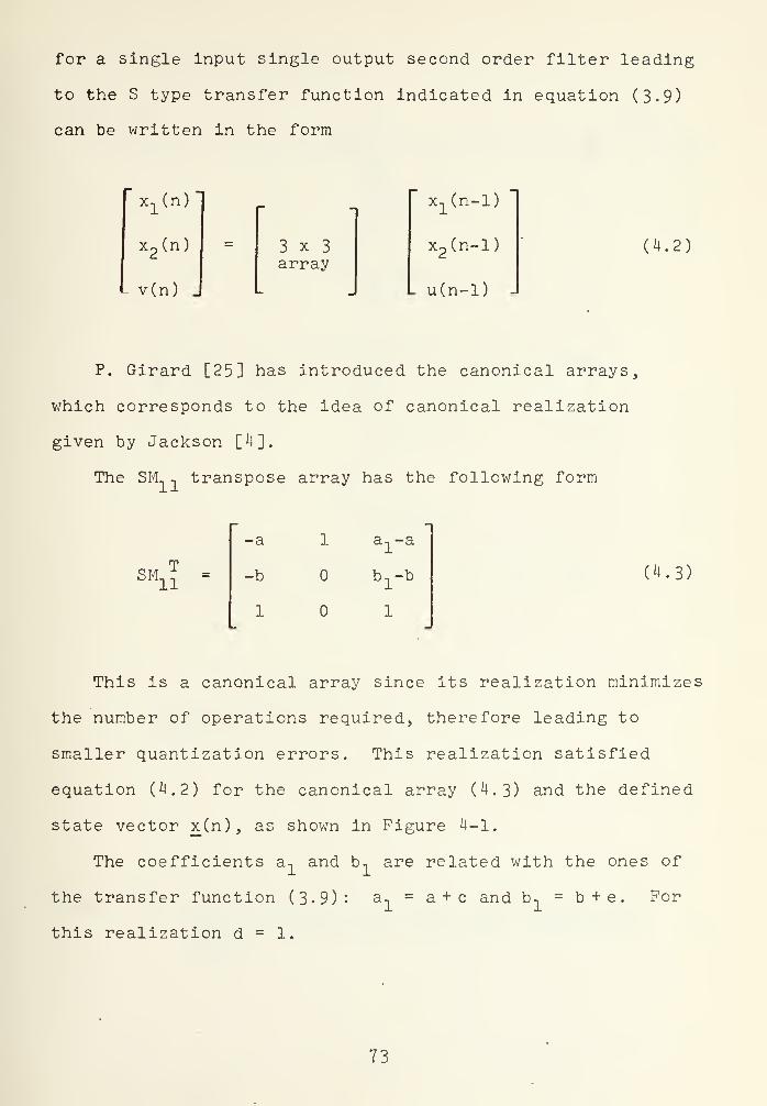
IV. DESIGN OF A SECOND ORDER DIGITAL FILTERSECTION USING THE SM-^ TRANSPOSE FORM 72
A. INTRODUCTION 72
B. STRUCTURE MECHANIZATION 75
C. SHIFT REGISTER TIMING 77
D. TIMING DIAGRAM 80
E. DESIGN OF A SHIFT REGISTER CONTROLLEDBY THE COEFFICIENT WORD LENGTH 83
F. MULTIPLIER TIMING SIGNALS 84
V. QUANTIZATION AFTER ADDITION AND QUANTIZATIONBEFORE MULTIPLICATION. ERROR BOUNDS 87
A. INTRODUCTION 87
B. ADVANTAGES OF QUANTIZATION AFTERADDITION AND QUANTIZATION BEFOREMULTIPLICATION 88
C. HARDWARE MODIFICATION TO PERFORMQUANTIZATION BEFORE MULTIPLICATION 89


1. Serial/Parallel Multiplier PerformingTruncation or Rounding BeforeMultiplication 91
2. Shift Register Adder Circuitry forQuantization Before Multiplication 95
D. ERROR BOUNDS DUE TO FINITE PRECISIONARITHMETIC IN DIGITAL FILTERS 95
1. Quantization After Addition 96
2. Quantization Before Multiplication 101
E. CONCLUSIONS 109
APPENDIX A. POLE-ZERO CORRESPONDENCE BETWEENS AND Z-DOMAIN 110
APPENDIX B. DISCRETE TRANSFER FUNCTION REALIZATIONS — 113
APPENDIX C. FUNCTIONAL TRANSFORMS 127
APPENDIX D. AMPLITUDE BOUND OF LIMIT CYCLES INDIGITAL FILTERS USING LYAPUNOV'SDIRECT METHOD 131
LIST OF REFERENCES 139
INITIAL DISTRIBUTION LIST 1^2


LIST OF FIGURES
Analog and Digital Filter Comparison 13
Formatting of the Binary Number 20
The Cyclic Nature of Two's Complement Addition 20
Shift Register Cell 24
Two's Complement Inverter 24
Serial Adder 27
Serial Adder Logic 27
Serial Adder . 28
Timing Diagram 2 8
Basic Serial/Parallel Multiplier 31
Two's Complement Multiplication 33
4-Bit Serial/Parallel Multiplier — 35
Timing Chart of a Two's Complement Multiplication- 38
Narrowband Signal After Sampling 40
Wideband Signal After Sampling 40
An Analog-To-Digital Converter 42
Current Summing with an Operational Amplifierto Obtain a Digital-to-Analog Conversion 42
Word Lengths in a Digital Filter 47
Block Diagram of 65001NA Serial/ParallelMultiplier 57
3-3 Timing Diagram for 8-Bit-Plus-Sign Multiplierand Multiplicand in Minimum-Time CyclicOperation 58
3-4 Block Logic Diagram of 65007NA/BShift-Register/Adder 60
1--1
2--1
2--2
2-
2--4
2--5
2--6
2--7a
2--7b
2--8
2--9
2--10
2--11
2--12a
2--12b
2--13
2--14
3--1
3--2


3-5 Simplified Logic Organization of ShiftRegister/Adder 6l
3-6 Recursive Canonical Realization of aSecond Order Filter Section on SM.., Form 64
3-7 Distribution of Gains and Delays on theSecond Order Low Pass Filter Example 64
3-8 Block Diagram of a Second Order Low PassFilter Implementation Showing TimingDistribution 70
4-1 Canonic Realization of a Second OrderSection Based Upon the SM,, Transpose Array — 74
4-2 Block Diagram of a Second Order FilterMechanization in the SM]_]_ Transposed FormShowing Timing Distribution 76
4-3 Assembly Wiring Diagram of a Second OrderFilter Section Implemented in the SM-qTransposed Form with NRMELC Building Chips 79
4-4 Timing Diagram for an Input Signal15-Bit-Plus-Sign, Scaling Coefficientlo—Bit Plus Sisrn and Data ComputationalWordiength 29-Bit-Plus-Sign 81
4-5a Shift Register (Type A) Connection toObtain (N 1 + 2) Bit Delay 85
4-5b Coefficient Word Length Diode Matrix 85
5-1 Advantage of QAA over QAM When The Magnitudeof the Coefficient Multiplier is Larger thanOne. Shown for |a| < 2. 90
5-2 Two's Complement Truncation/RoundingCircuit 92
5-3 Modified SPM to Perform Truncation orRounding Before Multiplication 92
5-4 Timing Signals for the Modified SPM Shownin Figure 5-3 94
5-5 Second Order Single-Input Single-OutputDigital Filter. Quantization After Addition - 97


5-6 Second Order Single-Input Single-OutputDigital Filter. Quantization BeforeMultiplication 103
A-l Mapping s-Plane into z-Plane 112
B-l Direct Realization 116
B-2 Canonical Realization 117
B-3 Cascade Realization of H(z) ' 119
B-k.
Parallel Realization of H(z) 119
B-5 Hybrid Realizations 120
B-6 Block Diagram of a Non-Recursive orTransversal Filter 122
B-7 Block Diagram of Transversal FilterMechanization for Finite FourierCosine Series 124
B-8 Block Diagram of Transversal FilterMechanization for Finite FourierSine Series ~ 125
C-l Comparison of the Three Types ofz-Transforms Available to TransformPoles and Zeros from the s-Planeto the z-Plane 130
D-l Second Order Digital Filter with TwoPoles Using Quantization AfterMultiplication 132
D-2 Second Order Digital Filter with TwoPoles Using Quantization After Addition 132
10


ACKNOWLEDGMENTS
I would like to express my appreciation to the Portuguese
Navy for the opportunity to pursue this Electrical Engineer's
degree program. I would also like to thank Dr. Sydney R.
Parker for his guidance and motivation in this field and my
wife, Ana Maria, for her constant help, encouragement and
perserverence through all my scholarship period and in
typing the smooth draft of this thesis.
Agradeco a Marinha de Guerra Portuguesa a oportunidade3
que me foi concedida permitindo-me terminar o curso de
Engenheiro Electrdnico. Agradeco tambem ao Professor
Doctor Sydney R. Parker pela sua orientacao e pelo
interesse que criou em mim nesta area de estudo, e a"
minha mulher, Ana Maria, nao sd pela sua constante ajuda,
encorajamento e perserveranca durante todo o perfodo escolar,
mas tambem pela sua valiosa colaboracao em dactilografar
esta tese.
11


I. INTRODUCTION
A. IMPORTANCE AND APPLICATIONS OF DIGITAL FILTERS
A digital filter (D.F.) is defined [29] as a computa-
tional process or algorithm by which an input digital
(discrete time and amplitude) signal or sequence of numbers
is transformed into an output digital signal.
A digital filter can be compared to an analog filter as
illustrated in Figure 1-1. A signal source x(t) is fed into
the two processors. If the output y*(t) looks like the
output y?(t) for all x(t), the upper and lower signal
channels must be equivalent and then the digital processor
is an equivalent of the analog filter, but operating on a
digital signal, x*(t), from the analog to digital converter
(ADC). Therefore the digital processor can be called a
digital filter.
A digital filter can be implemented as a subroutine in
a general purpose computer or as hardware in the form of a
special purpose digital processor. In the hardware form,
a D.F. is a collection of storage elements, adders and
multipliers connected together in a prescribed way (filter
structure), much as the continuous filter is an ordered
connection of resistors, capacitors, inductors and active
gain elements.
12


X(t)
ANALOG
PROCESSOR
( FILTER)
Y(t)ADC
ADCX*(t)
DIGITAL
PROCESSOR
(FILTER)
Y (t)
Y, (!)
FIGURE I -I ANALOG AND DIGITAL FILTER COMPARISON
13

The advantages of digital filters over their analog
counterparts are numerous [31]. Some of the advantages are:
a) arbitrarily high precision in the computationalprocess
,
b) no parameter or component value drifting,
c) flexibility in the processing procedure, which allowsthe construction of adaptive filters,
d) no necessity for impedance matching,
e) possibility to use time-sharing techniques,
f) easy realization of complex circuits,
g) high reliability,
h) small circuit size,
i) decreasing costs for mass-produced basic building blocks.
The following are typical examples of the superiority of
digital filters over similar analog filter types: (1) Linear
phase filters can be implemented by digital filters having
extremely fast roll-off with either narrow or wide passbands
or stopbands, and do not introduce nonlinear phase shift in
the passband. (2) Comb filters are particularly useful for
isolating repetitive signals of a known frequency. For
example, in sonar systems, signals must be isolated from
noise or other unwanted signals. (3) The extremely critical
tolerances on crossover amplitude and phase characteristics
of filters operating on adjacent passbands can be mechanized
within any specified accuracy without drift or component
aging effects. These accuracy and drift problems are
encountered in spectrum analyzers and synthesizers having
applications in radar, sonar, communications, and channel
selectors. (M) Speech analysis and synthesis sometimes
14


requires a nonlinear phase response because both the
magnitude and phase characteristics must be detected. In
addition, the need to vary the filter characteristics is a
necessity and may be varied or programmed easily with
digital filters. (5) Two-dimensional filtering is widely
used in the areas of image and geological data processing.
B. PREVIEW OP RESULTS
Digital filter implementation has been confined primarily
to computer programs for simulation or for processing rela-
tively small amounts of data, usually not in real time.
However, the rapid development of integrated-circuit tech-
nology and specially large-scale-integration (LSI) is
creating increasing interest in the hardware digital filter
implementation. Mechanization hardware is discussed in
Chapter II and its utilization in a digital filter design
in Chapter III.
The design of a D.F. can utilize methods which are
similar to those used for analog filters. Pole-zero analysis
is essentially the same in the Z-domain used for discrete
systems as it is in the Laplace transform domain used for
continuous systems. Appendix A presents the Z-transform
and the mapping of the s-plane into the z-plane, and
discusses the significance of the pole positions. The
transfer function decomposition methods of continuous systems
are also easily applied to the Z-domain filter function and
15


result In the same filter forms, as shown In the discrete
transfer function realization methods presented in Appendix
B and In the functional transforms discussion in -Appendix C.
An example of a D.F. design using a Z-transform technique and
its hardware implementation are illustrated at the end of
Chapter III. A complex application of the North American
Rockwell building chips in the hardware design of a second
Torder section using a SM11 structure and permitting
variable coefficients and word lengths is presented in
detail in Chapter IV.
Errors due to finite precision in the representation of
numbers in a D.F. always occur. The quantization noise
problem is particularly serious in recursive D.F. wherein
the algorithm uses the results of previous calculations to
generate present signal quantities. The fact that quantiza-
tion errors are fed back can cause limit cycle oscillation.
In Chapter V two new quantization methods are presented:
quantization after addition (QAA) and quantization before
multiplication (QBM). The former has been barely studied
in the literature and the latter is not even mentioned.
For the second order filter, using fixed point arithmetic,
quantization bounds are derived for QAA and for QBM and
compared with the results obtained by Yakowitz and S.R.
Parker [20-32] for the case of quantization after multiplica-
tion (QAM). This study concludes that the bounds for QBM
can be at most as large as the bounds for QAA and shows that
the bounds for QBM are larger or equal to the bounds for QAA.
16


In Appendix D, using Lyaponov's direct method, a quantization
bound for QAA in a two pole, no zero filter, Is determined
and compared with a value calculated in a previous work by
Parker and Hess [1]. The result now obtained is half as
large. Some other advantages of using QBM or QAA in
hardware filter implementation are mentioned in the same
chapter and a modification to the present hardware building
chips is included in order to permit roundoff or truncation
before multiplication in the implemented filter structure,
otherwise restricted to truncation after multiplication.
17


II. DIGITAL CONSIDERATIONS
A. INTRODUCTION
A digital filter (D.F.) can be constructed from a small
set of relatively simple digital circuits, primarily shift
registers and adders, weel suited for large-scale integration
(LSI) technology.
In this chapter the advantages of serial, two's comple-
ment binary arithmetic in the implementation of digital
filters are discussed. The required shifting and arithmetic
operations are described. Particularly, the serial/parallel
multiplier and its circuits are studied in detail. The
effect of sampling an analog signal is shown and a brief
description of simple analog-to-digital and digital-to-analog
converter circuits is also included.
B. TWO'S COMPLEMENT NOTATION
The 2's complement of a binary number is formed by
simply subtracting each digit (bit) of the number from 1
and adding a one to the least significant bit (LSB) . Two's
complement coding of a digital number is used when both
positive and negative numbers are to be represented. The
two's complement of a number a, with N data bits, has the
form
a al
a2
a3
* '
*
aN
where the bits a. are either zero or one.
18


Since only fractional numbers will be used, the value
of a has magnitude less than one, then
N-ia=-a n
+ I a,
2
i=l
The bit a is the sign bit and is commonly separated
from the other bits by a decimal point, as represented in
Figure 2-1, and the bit aNis the least significant bit
(LSB).
Positive numbers are coded in simple binary. Negative
numbers are formed by taking the two's complement of the
corresponding positive numbers.
1 . Serial Processing
Serial processing of digital numbers is obtained by
entering the digital number into sequential circuits one
bit at a time with the least significant bit first. Parallel
processing is accomplished if all bits are entered simulta-
neously. Gabel [30] has recently presented a parallel
arithmetic structure for recursive digital filtering whose
main advantage is a processing time independent of word
length. Digital filters are generally serial machines
since they present several advantages:
(i) They can be implemented using less and simpler hardware.
(ii) Carry-propagation delays found in parallel circuitsare eliminated.
(iii) The delay operator z"1 of the digital filter is easily
implemented with a single-input, single-output shiftregister.
(iv) Serial processing aids appreciably in the implementationof multiplexing schemes.
19


DIGITAL REGISTER
SIGN Bl
= +
I = ~
,^4 CON DATA BITS
FIGURE 2-1 FORMATTING OF THE BINARY NUMBER
(-1^)
o.oi
0.11
( + %)
1.00
(-1)
FIGURE 2-2 the CYCLIC nature of two's
COMPLEMENT ADDITION
20


2. Advantages of Two's Complement Notation
One advantage of two's complement Is that formated
data can be clocked into an arithmetic unit, with the least
significant bit first, with no advance knowledge of the
sign of the data [4]. Another advantage is associated with
overflow in addition. Overflow in a digital filter occurs
in the adder when the sum of the two numbers has a larger
number of bits. Then the sum overflows into the sign bit.
The output during overflow will be in error, but using two's
complemented it can be recovered. If for instance, more
than two numbers are being added, some of the partial sums
will overflow, but the final sum may not.
The process of recovering an overflow is illustrated in
Figure 2-2 in which the values of the two's complement
number are arranged on a circle. Addition of positive
numbers causes movement in the clockwise direction and that
of negative numbers causes movement in the counter clockwise
direction. Thus if positive overflow occurs the result will
be a negative number and if negative overflow occurs the
result will be positive. If +1/2 is added to +3/4, the
result would be -3/4 due to overflow, but if a third number
-1/2 were added, the result would be +3/4 which is correct.
The same could be observed if one of the Inputs has already
overflowed from some previous operation.
The range over which the two's complement unit may be
considered linear is from -1 to (1 - 2~) where 2~ represents
the least significant bit (LSB) and' N the number of data bits
in the number.
21


3. Number of Bits Required
The binary representation of a decimal number can
have a very large length. Therefore, the number of bits
necessary for representing a decimal number with a known
accuracy has to be determined.
Let the decimal number
D-Jx = E b, 10 J
J-l J
scaled such that |x| < 1 , be known with an accuracy
(x-Ax) < x < (x+Ax) where
tx = | 10"D
and let the binary number (considering only the significant
bits)
B-i
1=1 ±
be the approximation of the decimal number, with an accuracy
1 -MAy = £- 2 . Since the accuracy of the binary number has to
be at least as great as the accuracy of the decimal number,
it follows that
B > D log210 - 3.32 D (2.1)
22


Therefore, the number of bits (sign bit excluded) necessary
to represent in binary a decimal number (magnitude less
than one) with an accuracy up to the D decimal place,
is given by the first integer bigger than the product
3.32 x 4 = 13.28
C. ARITHMETIC OPERATIONS
The only operations which have to be considered for a
digital filter implementation are:
(i) Storage or shifting
(ii) Negation
(iii) Addition
(iv) Multiplication
1. Storage
Digital information is stored in a two state
device called a flip-flop, which can remember, or store,
a binary bit of information because of its bistable
characteristic.
A shift register can be implemented using two such
flip-flops placed in series and gated alternately as shown
in Figure 2-3. Placing N shift registers cells in series
the output is the input delayed by N clock periods.
23


X'_J.
I
r
<—
*
x 2
L
n
PI P 2
n
-o
FIGURE 2- 3 SHIFT REGISTER CELL
Input —*
Clock->
Clear—
>
o Output
• FIGURE 2-4 TWO'S COMPLEMENT INVERTER
24


2 . Negation
A very useful method of inverting a two's complement
number using serial arithmetic is to complement every bit
which passes after, but not including, the first "1".
0. 1010100Inverted
1. 0101100
The sequential circuit presented in Figure 2-4 uses
the method previously described for the implementation of a
two's complement inverse. The input enters serially with
the least significant bit (LSB) first with the Q output of
the flip-flop initially cleared to zero. The bits pass
unchanged through NAND gates 1 and 3. The first one will
change the flip-flop state during the next clock pulse, thus
all succeeding bits pass through the inverter and NAND gates
2 and 3. The clear pulse resets the flip-flop after the
number has passed.
3. Serial Addition
Serial digital adders have three inputs (2 data and
1 carry) and two outputs (1 sum and 1 carry) as shown in
Figure 2-5, and can be summarized by the truth Table II-l.
25


INPUTS OUTPUTS
A B c 1 2
1 1
1 1
1 1 1
1 1
1 1 1
1 1 1
1 1 1 1 1
TABLE II-l
TRUTH TABLE FOR SERIAL ADDER
From this truth table the following logic equations
can be obtained
SUM = 0UTPUT1 = AB'C + A'BC' + A'B'C + ABC
= A(B'C H BC) + A' (BC + B'C)
CARRY = 0UTPUT2 = A'BC + AB'C + ABC + ABC
= BC + A(B'C + BC )
Figure 2-6 shows the logic implementation of the
above equations.
In Figure 2-7(a) is shown a circuit used to implement
two's complement addition involving one full adder and one
flip-flop, which acts as the delay element. An inverter is
used in the carry circuit of the standard full adder
integrated circuit.
26


INPUT A
INPUT B
INPUT C(CARRY)
> OUTPUT I
fr OUTPUT 2
(CARRY)
DELAY
FIGURE 2" 5 SERIAL ADDER
A-BC- -•-
0-
0-
0-
o
o o
\
(DELAY)
FIGURE 2-6 SERIAL ADDER LOGIC
-^OUTPUT I
9+ OUTPUT 2(CARRY)
27

B
CLOCK
CLEAR
DELAY FLIP-FLOP
(a)
CLOCK PERIOD III2l3l4l5l6l7l8l
CLOCK
JJ1J1
i1o
1
n nruA 1 i
o
1 1 1
B 1 1
•N
N+l | 1
1
1 1 O 1 1
N +1 1 1
CLEAR
CN
1
o . 1
1 1 1 i i i
1 1
I 1 1
(b)
1 i i i
FIGURE 2- 7(a) SERIAL ADDER
(b) TIMING DIAGRAM
-*> SUM
28


To Illustrate the operation of this circuit, an
example of the addition of two numbers in two's complement
notation will be performed.
A 1.0111101 (-67/128)
B 0.0110001 (+49/128)
A + B 1.1101110 (-9/64)
The corresponding timing diagram of this addition
is shown in Figure 2-7(b). Assuming that the transfer
information takes place when the clock changes from zero
to one (positive going edge), it can be observed that during
each clock period the full adder adds the bits A, B and C
corresponding to that time and produces the sum E and the
carry output C ._, this one will be delayed by one clock
period so that It will appear at the input C during the
next time period. A clear pulse will zero the carry during
the first time period.
The time difference between the time the input bit
enters and the time at which the output bit appears is
called the "propagation delay" of the adder. The propagation
delay to the sum output is usually larger than that of the
carry output.
In order to avoid synchronization errors, flip-flops
are generally necessary between adder stages to keep the
data in synchronization.
29


4. Multiplication
Multiplication is the most complex and the most time
consuming arithmetic operation required in digital filters.
Normal binary multiplication is performed by successive
additions and shifting, which process is controlled by the
multiplier bits: if a 1, the multiplicand is added to the
sum of partial product; if a 0, no addition is performed.
Since the filtering process must operate synchron-
ously, the multiplication must be of fixed time duration.
In addition to the speed considerations the amount and the
complexity of the hardware required to perform multiplication
is also important. Considering these factors, the serial/
parallel multiplier (SPM) , in which a serial data is multi-
plied by a parallel coefficent word, has been used almost
exclusively.
The serial/parallel multiplier (SPM) accepts an M-bit
serial multiplier and an N-bit paralled multiplicand input.
Figure 2-8 shows a basic SPM, where a, represents the most
significant bit (MSB) and a the least significant bit (LSB)
.
The multiplier enters serially on the line "m" with the LSB
appearing first. The number of adders in this SPM depends
on the number of bits of the multiplicand. N-l full adders
are required for a N bit multiplicand. If a 1-bit appears
on the multiplier serial input line, m, the stored multipli-
cand is gated to the adders through the AND-gates and the
first partial product is generated. Each individual sum at
each adder is then delayed I-bit time and input to the next
30


Ooo0.
Q.
UJ-J-J<
2
UJ
_lQ.
<a:
2
a:UJCO
oCO<CD
COi
CMUJcr
OLl
31

adder. The carry from each adder is stored in the flip-
flop which provides 1-bit delay so that the carry is fed back
into the adders during the next clock time. If a "0" bit
appears on the multiplier, causes all zeros to be sent to
the adder and then the partial product will also be all
zeros
.
The LSB of the product will appear at the sum output
of the last adder during the first clock period and the
MSB will appear at the output during clock time N+M.
The modified version of the basic SPM shown in
Figure 2-10 generally increases the versatility of the
device, since it has the capability of multiplying either
positive or negative numbers represented in two's complement
coding.
The multiplication of a negative multiplicand with
a positive multiplier is illustrated in Figure 2-9a. As
before a "1" in the multiplier causes the multiplicand to
be shifted to the left, but due to the negative multiplicand,
the multiplicand sign-bit must be spread to perform the
required correction. Thus the multiplier being "1", and
the multiplicand negative (MSB is 1) 1' s must be spread to
the left of the MSB of the partial products. The multiplier
being "0", the partial product will be all zeros, and 0's
will spread to the left.
The multiplication of a positive multiplicand with
a negative multiplier is illustrated in Figure 2-9b. In
32

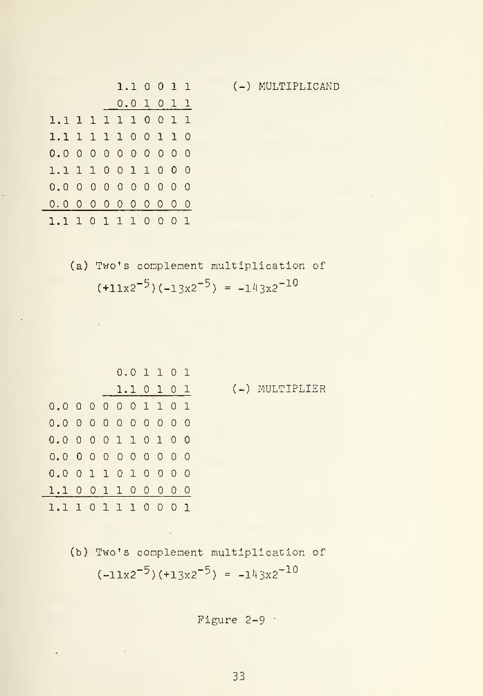
1.1 1 1 (-) MULTIPLICAND
0.0 1 1 1
1.1 1111100111.1 1111001100.0 0000000001.1 1100110000.0 0000000000. 00000000001.1 101110001
(a) Two's complement multiplication of
(+Ilx2" 5 )(-13x2~ 5) = -I43x2" 10
0.0 1 1 1
1.1 1 1 (-) MULTIPLIER
0.0 0000011010.0 0000000000.0 0001101000.0 0000000000.0 0110100001.1 0011000001. 11011100 1
(b) Two's complement multiplication of
(-Ilx2~ 5 )(+13x2-5
) = -143X2"10
Figure 2-9 '
33

this case an ordinary multiplication will be performed
except for the multiplier sign bit. The partial product of
the multiplier sign bit has to be complemented, or since
in this case the MSB of the multiplier is "1", the two's
complement of the multiplicand is added instead to achieve
the required correction.
In Figure 2-10 the network at the extreme left
involving one AND-gate, one OR-gate and one type T flip-
flop, acts as the sign spreader of the multiplicand as
required. T is a single pulse, one clock period in length,
which occurs at the time in which the sign bit of the multi-
plicand appears at the input. Therefore only the sign bit
of the multiplicand is gated to the flip-flop. If the
multiplicand is positive, the sign bit will be zero and
this circuit will take no action. If the multiplicand is
negative, the sign bit will be one and the T flip-flop,
which was previously set to zero state by T , will change
to one state and hold for the rest of the multiplication
process. Therefore, the sign of the multiplicand will be
spread. The time signal T is a single pulse occurring at
the time the sign bit of the product appears at the output
and its function is clear all flip-flop before the next
multiplication.
Tfi
is a single pulse occuring during the first time
period of the multiplication process. The OR-gate in the
carry circuit of the first adder and this time signal, TQ ,
3^


3
LJ
<
JE
CD
+
CO
GQ
Z
orL±J
_JQ_
b
UJ
<or
£
<orUJ
CDI
LU
CD
CO
+
35


are used to subtract the multiplicand as required when the
multiplier is negative. If the multiplier is positive, afl
will be zero. Taking the 4-bit SPM of Figure 2-10, then
point 5 will always be zero. The inversion after the delay
will make point 7 one and its sum with 11 (which is one
since TQ
at the input of the OR-gate is one at the first
time period of the multiplication process), will generate
a carry one at point 11. Therefore the output 12 of the
first adder represents only the A input of the adder.
If the multiplier is negative, point 5 will depend
on the existing multiplicand serial input bit during each
time period. This circuit operates as two's complement
subtracter for the multiplicand when the multiplier is
negative.
The operations of the sign-spreader and the subtracter
perform the corrective measure which enables the SPM to
perform positive , negative and mixed multiplication.
An additional delay flip-flop included in the sum
output of the last adder besides compensation for propagation
delay, provides an extra delay required when two's complement
multiplication is performed. When a N-bit number if multi-
plied by a M-bit number the resulting product has M+N+2
bits, but only M+N bits have magnitude information. The
remaining 2 bits will indicate the sign of the product. The
redundant sign bit can be eliminated by truncation.
36


In order to illustrate the operation of the SPM of
Figure 2-10 the following example with a negative multipli-
cand and positive multiplier is used.
1.1 1 1 Multiplicand A = -5/16
0.1 1 Multiplier B = + 3/4
000000000111101100111011000000000000
1.11000100 Product AB = -15/64
A timing chart for this multiplication is presented
in Figure 2-11, which shows the states of each circuit point
labeled in Figure 2-10 for each time period.
This multiplier can be expanded to accept any length
serial multiplicand and parallel multiplier numbers [4],
however the timing signals must be changed accordingly so
that they occur in proper correspondnece with the serial
input number and the product.
In a digital filter the multiplier numbers are the
coefficients of the filter transfer function. If a fixed
filter is used, the coefficient will remain unchanged and
the multiplier bits can be hard wired. However if the
coefficients are variables, external switches may be set to
37


CIRCUITPOINT
TIME PERIOD
1 2 3 4 5 6 7 8 9 10
1 1 1 1 1
2 1
3 1 1 1
4 1 1 1 1 1 1 1
5
6
7 1 1 1 1 1 1 1 1 1 1
8 1 1 1 1 1 1 1
9 1 1 1 1 1 1 1 1 1 1
10 1 1 1 1 1 1 1 1
11 1 1 1 1 1 1 1 1 1
12 1 1 1 1 1 1 1 1
13 1 1 1 1 1 1
lh 1 1 1 1 1 1 1
15 1 1 1 1 1 1 1
16 1 1 1 1 1 1
17 1 1 1 1 1
18 1 1 1 1
19
20
21
22 1 1 1 1
23 1 1 1 1 PRODUCT
Ts
1
To
1
Tc
1i
Figure 2-11. Timing chart of a two's complementmultiplication with multiplicand-5/16 and multiplier +3/4
38


realize a particular filter - this is generally the case
when laboratory units, or read-only-memory (ROM) are used -
which is advantageous when the filter is to be multiplexed.
The advantages of using this two's complement serial/
parallel multiplier for digital filter is now evident.
There is only a N+l bit delay (number of bits parallel
input) and the multiplication process takes only M+N+2 time
periods to be completed, but since the redundant sign bit
can be truncated a word length of M+N+l bits can be used.
This type of multiplier using flip-flop between the full
adders, eliminates greatly propagation delay problems.
D. SAMPLING
The sampling rate required for a sampler is determined
by the analog input signal. If the input signal is periodic
with period T, the minimum sampling rate which is called
the "Nyquist rate" is 1/2T samples per second according
to the sampling theorem.
Because of the effect of sampling, the original data
spectrum is scaled and repeated across the entire spectrum.
If the signal is sampled at a rate less than the Nyquist
rate, or in other words, if the spectrum of the input signal
is limited between ±w /2 , a distortion due to the overlaping
side bands will occur, as observed in Figure 2-12b. This
effect is called "folding" or "aliasing". Since the infor-
mation lost by folding can not be recovered, care should be
taken in the design of a digital filter. A practical limit
39


r^"^\ ^ x ^jw>
u FREQUENCY
Narrowband Signal Before Sampling
M NYOU1ST .
INTERVAL^j X*(j w )
-u -u/2 w /2 w» » $ s
Figure 2-12a. Narrowband Signal After Sampling
X(j(j)
Wideband Signal Before Sampling
NYQUISTINTERVAL
X'(J^)
Figure 2-12b. Wideband Signal After Sampling
l\0


of ±w /5 for the spectrum of the input signal has beens
found at the Naval Electronic Laboratory Center [133.
Therefore, digital filter applications are more suited for
narrow band signals.
E. CONVERSION
1. Analog to Digital Conversion
The analog to digital converter (ADC) generates a
digital number which is proportional to the amplitude of
each pulse from the sampler by comparing the amplitude of
input with some reference, which is generally generated by
a digital to analog converter (DAC) , as shown in Figure 2-13.
The parallel inputs to the D/A come from an up/down counter
which seeks a zero erro ri at the comparator ir^ut. In o^der
to hold the input constant during the conversion process
it is necessary to precede the ADC by a sample/hold circuit,
which holds the level sampled until the next sample is made.
Since most ADC's have parallel outputs, as the one described,
conversion must be made to a serial number, using a parallel-in
serial-out shift register, before entering the digital filter.
2
.
Digital to Analog Conversion
The D/A conversion is generally a simpler process
than the A/D conversion. The basic digital-to analog con-
verter produces a certain output voltage for each different
digital input. This is commonly done as shown in Figure 2-14,
using a resistor network with one resistor connected to each
bit of the input digital number. The resistor values are
Ml


SAMPLERSIGN DETECTION
-\|x| cE
HOLD
/
INTEGRATION ANDPOSITION WEIGHTING
ANALOGVOLTAGES
N
E E an 2
n=ln
-n
z\ *I COMPARATOR
f(t)=±l -* mi imtfd
IsLUlm 1 L K
• • •a
DIGITAL-TO-ANALOGCONVERTER(DAC)
,
">-
1
•:*2.aN -
FORMS LINEAR COMBINATION BINARYOUTPUT
Figure 2-13. An Analog-To-Digital Converter
e„ - e n N N e. - e„i = _J o = z i = E -± a
Rk=l
kk=l
Rk
-\W
'2——VSAr
rn :
^/W
" Ro ^ V R
k
1 "*"k =
R°/R|(
- Ro ^ e
k/Rk
Figure 2-14. Current Summing with an OperationalAmplifier to Obtain a Digital-to-AnaioiConversion
'12


weighted to be proportional to the value of each corres-
ponding input bit. The resulting currents are then summed
using an operational amplifier to produce a level which is
proportional to the value of the input digital number.
M3


III. DIGITAL IMPLEMENTATION. HARDWARE DESIGN CONSIDERATION
A. INTRODUCTION
The realization of a digital filter Involves three main
synthesis steps:
(i) Approximating the ideal filter transfer function by
classical means and apply a convenient Z-transform technique
[12]; an optimization algorithm to minimize, for example,
a square error criterion in the frequency domain [26];
or any other direction design method to obtain a discrete
filter which satisfies the given specifications.
(ii) Quantizing the multiplier coefficient of the filter
in the appropriate cascade, parallel or hybrid form in such a
way to minimize cost and complexity, while still satisfying
the filter specifications.
(iii) Selecting a specific configuration for the digital
filter, specifying the word length used and the arithmetic
mode (only fixed point is being considered in this work)
,
the quantization type (round off or truncation) and where
in the circuit will be effective (generally after multipli-
cation) , so as to satisfy the specifications relating to
quantization noise.
B. QUANTIZATION EFFECTS
When a D.F. is implemented with special purpose hardware
'(or on a computer) errors and constraints due to finite word
length are unavoidable. This quantization effects must be
M


considered, both in deciding what word length (or register
length) is needed for a given filter implementation and in
choosing between several possible implementations of the
same filter design, which will be affected differently by
quantization.
There are four main errors due to quantization effects
(i) Input quantization producing A/D conversion errors,
(ii) Arithmetic quantization generating noise by the roundoff
or truncation of quantities after arithmetic operations,
(iii) Quantization of the filter coefficient producing a
pole-zero displacement, and (iv) Constraints on signal levels
imposed by the need of preventing overflow. The effects of
these errors and constraints will vary depending upon the
arithmetic used.
Weinstein and Oppenheim [22] have shown that floating
point arithmetic is generally less noisy than fixed point
arithmetic and it is known that floating point provides greater
dynamic range. Fixed point mode is much easier to implement,
and its error analysis is much less involved, therefore it is
the one more often addressed in the literature. A discussion
and bibliography of the literature concerning this error
effects appears in [18-23-24], The analysis of quantiza-
tion noise due to roundoff after multiplication has been
studied by stochastic [5-6] and deterministic methods
[1-7-8-9], assuming uncorrelated noise sources. Under the
general assumption of correlated noise sources a stochastic
method has been studied by S.R. Parker, and P. Girard [25].
U5


Mitra and Sherwood [21] have proposed a technique for
estimation of pole zero displacement due to coefficient
quantization in fixed point arithmetic. E. Avenhaus [27]
has presented a method to find canonical structures which
minimize the coefficient sensitivity due to rounding errors
when small coefficient word length is used. Knowles and
Olcayto [19] have indicated a method of analysis of the
response of a D.F. affected by the coefficient accuracy
using a "stray" transfer function in parallel with the
corresponding ideal filter, but this method is not suitable
for cascade realizations.
C. WORD LENGTH REQUIREMENTS
When a filter is constructed with digital hardware, the
minimum word lengths needed for specified performance accu-
racy must be determined. This is one of the most important
and difficult decisions in a digital design.
Figure 3-1 visualizes the relationship between the word
lengths (number of bits in the number, sign bit excluded):
in the input word (C), in the serial word being processed
within the arithmetic unit (M) and in the multiplier coeffi-
cients (N). When the sign bit is included, these word
lengths will be represented by C', M' and N', respectively.
1. Input Data Wordlength (C)
The input word length is the word length of the data
out of the A/D converter. Therefore, it is related mainly
to the input quantization error in the sampling A/D conversion
46


iA/D
CONVERTERC-BITS
MULTIPLIERCOEFFICIENTS
N-BITS
M-BITS
M> C
DIGITALFILTER
C-BITS
FIGURE 3-1 WORD LENGTHS IN ADIGITAL FILTER
47


process and determines the granularity or the number of
levels of quantization required of the A/D converter.
The size of the quantization step used, h, depends
principally on the dynamic range and on the granularity of
the A/D converter. The dynamic range is the. ratio between
the largest signal or saturation level (x ) and the
smallest signal detectable or threshold level (x.^).
Considering only the dynamic range dependence, the
quantization step
h = xsat/xth
must be equal to the LSB with an accuracy of C significant
bits, or
h- 2"C
therefore
C - 1°S2 ^sat/xth ) (3.1)
Considering only the granularity of the A/D conver-
sion, and assuming an additive white noise is introduced
at the converter, resulting in a noise figure F, expressed
in dB, the following equation can be obtained [3]:
US


F - lOlogQ
o2
C = ±y—
1
(3<2)201og
102
2where a represents the mean square level of the signal.
s
As a design criterion, the signal may be assumed to have a
Gaussian amplitude distribution with a standard deviation
of 1/3, and then from equations (3.1) and (3-2) will result
in
X-Jli r
F * 1Qlosio 3
>2 xthJ > L 20 log
1Q2
C» = C+l = max{[l + log -^-] , [__^L1] } (3.3)
2. Computational Data Word Length (M)
As mentioned previously, the arithmetic quantization
noise is unavoidable and may be very significant in a D.P.
and all the methods of analysis available presently are
quite complex. Fettweis [17] has observed that round
off (or truncation) noise depends only on the word length
(M) at the input of the D.F., therefore M-C extra bits
(all zeros initially) are appended to the A/D converter
output
.
The serial/parallel multiplier described later can
handle any word length (M) , however, if the coefficient word
length (N) remains the same, the sampling rate and then the
speed of the process will be reduced, as indicated by equation
(3.8). Also the number of the shift registers used in the
hardware filter implementation will increase as M increases
as will be shown later.
49


3. Multiplier Word Length (N)
The multiplier coefficient length is associated
with the accuracy with which the poles and zeros may be
placed, or in other words, the tolerances of the filter
design.
Multipliers with low sensitivity can be implemented
with fewer bits, hence yielding a circuit with potentially
lower cost and higher speed. Since first and second order
sections are the building blocks being used, only the results
of the coefficient accuracy applied to this case will be
presented.
According to [3] a first order filter with a pole
or zero (s+ot) with a tolerance of ±Aa, requires a corres-
ponding multiplier word length
N > log2
[2e"aT
aT^] (3.1)
and for a second order filter, with complex conjugate pair
poles at s = -an
- jujQwith a characteristic equation is
the z plane given by
—1 —21 + az + bz = (z - z.)(z - Zp) =
where
a = -2rcos


b = r2
"*oT
zl,2
Arg zl 2
= 9 = W T
For the tolerances of ±Aa and ±Au> the word length of
the coefficient multipliers has to be:
for a:
N > - log2p4>/b j^i co
QT sin (w
QT)l (3-5)
for b:
N > - log2 [4 a T e °
^-J (3.6)
As will be observed later the number of serial/parallel
multipliers used will depend on this word length (N).
D. GAIN SCALING
Overflow occurs when a D.F. computes a number that is
too large to be represented In the arithmetic used in the
filter. If no compensation is made for the overflow, then
large errors in the filter output will result.
Several techniques are used to compensate or to avoid
overflow. One method is to detect overflow and then compen-
sate for it immediately after it occurs. If a positive
51


overflow is detected, a large negative number is injected
into the filter and if a negative overflow is detected, a
large positive number is injected. The overflow will then
be compensated due to the cyclic. nature of 2 * s complement
arithmetic, and no error will occur. Another method is
saturation arithmetic where a sum that is too large to be
represented is set equal to the largest representable
number in the filter. The output will be in error, but
it will avoid overflow oscillations.
The most common method of preventing overflow is the
process of scaling. The simplest form of scaling is effec-
tively to reduce the size of the input signal. However, if
the analog input is reduced, the signal-to-noise ratio will
usually be decreased. Therefore, it is usually more desirable
to reduce the digital input signal with a scaler between
the A/D converter and the filter input. This scaler can be
a shift register which effectively divides by powers of two
or a multiplier whose coefficient is less than one. This
last approach will be the one used. In fact, all second
order filter sections will be preceded by a scaling multi-
plier (K) that will be set just low enough to prevent over-
flow at any adder. Thereby, linearity is assured while
maximizing the dynamic range of each section and consequently
of the filter. This is achieved by seeking a value of K
such that for all the possible digital filter inputs, X(z),
the output of each adder, Y (z), will satisfy
52


Y1(z)
xi^y< 1 (3.7)
zmax=exp(ja)T)
E. TIMING
Timing is another requirement in digital filter design,
since sequential circuits are used. The "filter word"
length (number of time periods required to process one
input word before the next word may be entered) has to be
determined. Mathematically the filter word length corres-
ponds to the delay operator z~ which appears in the de-
sired D.F. transfer function. As will be shown in the
examples presented later, the filter word length is a func-
tion of the multiplication time and it is generally given
as (M' + N') bits, where M' and N 1 are respectively the
number if bits used to represent the computational data
word and the scaling coefficient in the multiplier (sign
bit included). Then, the maximum word rate (sampling rate)
at which the filter can operate is
fn ffW
=M' + N 1
=M + N + 2
(
3
' 8^
where f_ is the bit rate, determined by the system clock
rate, and (M' + N 1) is generally referred to as the word
time.
53

F. HARDWARE DESIGN
The following discussion on hardware implementation will
be restricted to MOS/LSI 1 technology. Two types of MOS/LSI
chips developed by the North American Rockwell Microelectronics
Company (NRMEC) will be presented and a design method of
second order filter sections will be introduced. This method
will be illustrated with a low pass digital filter example
using a z-transform technique.
1 . The Devices
The North American Rockwell Microelectronics Company
(NRMEC) has developed two LSI processing devices to operate
on two's complement formatted serial digital data and LSI
compatible analog-to-digital and digital-to-analog converters.
Table III-l presents the characteristics of this MOS/LSI
digital filter building block. Filters may be configured
using this device over the frequency range of to 20 KHz.
•. The serial/parallel multiplier (SPM) and the shift
register adder (SRA) are the processing devices. This MOS/LSI
device utilizes p-channel enhancement mode transistors. A
four phase clock scheme is required to perform both the SPM
and the SRA.
a. Serial/Parallel Multiplier (SPM)
One SPM chip forms the sign-corrected product of
an input data word of any length and a scaling coefficient
MOS technology refers to a device with three layers:metal-oxide-semiconductor. LSI means large-scale integrationprocess
.
5^


Characteristics SPM SRA A/D-D/A
Size (in mils) 142 x 136 180 x 216 180 x 180
Frequency (MHz) 1.5 1.0 1.0
Power Dissipation(in mw at 1 MHz) 35 max 200 max 75 max
Output Drive Capability 100 pf 50 pf 100 pf
Voltage (clock, input,
supply -30V max -30V max -30V max
Number of Devices (MOSFETS) 640 1250 1800
Mechanized terms 322 410 11 bit
Number of Pins (flat pack) 42 42 42
Table III-l. Characteristics of LSI digital filter devicesfrom North American Rockwell MicroelectronicsCompany
55


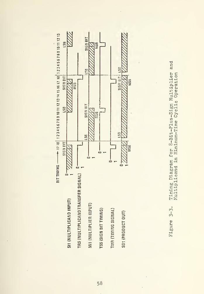
of length up to 8 bits plus sign. Longer coefficient
multiplications can be performed by cascading SPM chips.
The scaling coefficient (multiplicand) can be loaded in
parallel or serial and transferred to parallel holding
register. Generally in digital filters applications the
scaling coefficient is input serially at SI1, least signif-
icant bit (LSB) first, by changing the TRS input from "0"
to "1" one bit after inputting the sign bit, as observed
in the timing diagram of Figure 3-3. The serial word
(multiplier) is inputted LSB first into Mil input and input
TSS should be taken to a "1" for one bit at the same time
as the sign bit appears on the Mil input. The TMR signal
being "1" clears the adders and sign bit circuitry and holds
the output to "0". The LSB of the multiplier should be
inputted 2 bits after this TMR signal.
From Figure 3-2 can be observed that the LSB
of the product appears at the output (SOI or S02) one bit
after the LSB of the multiplier input signal enters the Mil
input. For an N* bit coefficient multiplicand, the
multiplication process will produce a delay of N' bits at
the SOI output. In Figure 3-3 a 9 bit delay between the
sign bit of the multiplier input and the product output is
observed for the 9 bit (8 + sign) scaling coefficient
(multiplicand) used.
The multiplier performs proper sign connection
only if the inputs (data and scaling coefficients) have
56


so—
-P
3
<D
cd
Ucd
Oh
cd
•HU(D
CO
<.HOO
In
WttV
O
cd
Sh
hOcd
•HQ
ooiH
C\J
I
CO
CD
U
w•H
57

CO
CM
r- CO.— CO
enoor-coin
COCM
I
co H-
CO
^— tZco t£"~
SoID
co
CM
t- ea— co
CDCOr-»
COin
COCM
co i—
z **
— ZCO
1 1 =:CO
IDzs
zr
i
L, I
S
3
Z3
i
!i
uCOccUJu.
m̂t COr- z=3 < -—
*
o_ rr r-Z h- 3 ^M. ^^,
o2<CO
-Ja.
H-_J=>
COcc
a. CO -J ^_^
o z Z <t H-2CJ
cc
r-
zC£
CO
3Or—
-J
r-. J
s
-J0_
—
J
CO
zCO
COCO
oz
cc
CJ=3aorea.
5CO H- 5 H- r- CO
ccd
CD
rH 4P
prH
s
CD
Oo
C -HhOrH•H OCO
I
CO
rHfU
I
-P•HPQ
I
CO
O<H
>>OCD
6•HE-t
I
6
2•HC
6-Hcd
bD Ccd cd
•H OQ -H
rHfaO CuC -H•H PErH•H 3Eh 2
I
co
<D
U
hO•H
58


magnitudes both greater than unity. This potential problem
can generally be solved in a practical mechanization as
will be shown.
b. Shift Register Adder (SRA)
As shown in the block logic diagram of Figure 3-4
and in the simplified functional diagram of Figure 3-5 a SRA
consists of two identical 7 to 15 bit shift-and-hold registers,
two 4-input adders and a timing and control circuitry.
Each adder exhibits a one-bit time delay. One
of the adders is able to inhibit two inputs if the input
CNI is made "1". Both adders are reset by a "1" on control
inputs TR1 and TC21.
The register section is able of adjust in length
to accommodate the length of the data word in the computa-
tional loop, by coding the inputs A, B and C. A shift
register longer than 15 bits is obtained by cascading these
register sections. Particular, a delay up to 30 bits can
be obtained cascading the two sections of a single SRA chip.
The timing and control section provides the proper
timing signals not only to the SRA but also to the multipliers
that may be associated with that SRA. The timing signals T,
and T~ are the only required timing inputs.
2 . Canonic Realization of Second Order Sections
Given a linear time invariant system it is shown in
Appendix B that its transfer function can be expressed as a
parallel, cascade or hybrid realization of first and second
order transfer function sections.
59


31 Uj-SI'jJ
NO ?
»Ovi«
— J) >«Bil i'i.M. |
I B'Jt -«:.|? H'1-..S'tn)
IJ. -i
I
SYMBOL : FUNCTION
NO I
AOOtBOutput
f.O I
ADOF.ROU'PUT
TimingIN>"UIS
CLOCKINI>UTS
'4-1
*wl 11
'JO II
iB"i, "o ^
SRI> |'0U"UI
TJI
I«]IV2TMI
TIMINGOUTPUTS
TSSOF MULTl
Figure 3-4. Block Logic Diagram of 65007NA/BShift-Register/Adder
60


w
H Z ot
QW H
3&c
i
5 QOA
-—st—
i
^
wH03
flf 1
I
A
GO
Hst-
1o
<5 1
1
t
uCD
T3
<\UCD
-Pw•HbO<D
c£
-p
•H
Cmo
coHPcti
t>3
•HCcd
bOMOO•HhOO
t30)
•H«M•HH&•HCO
ImCD
M
b£>
•H
61

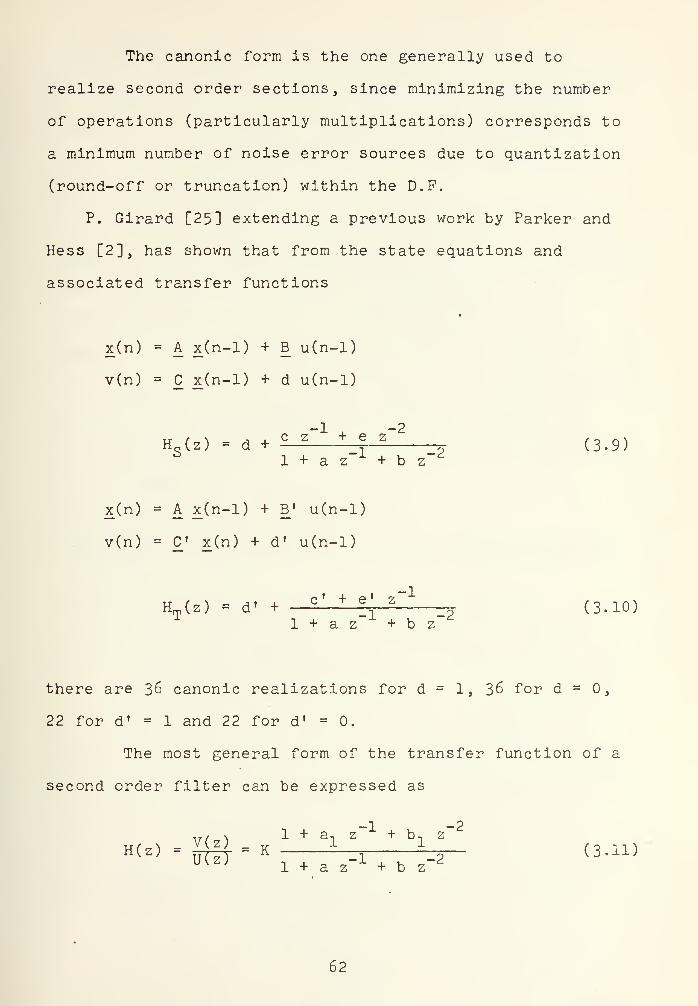
The canonic form is the one generally used to
realize second order sections, since minimizing the number
of operations (particularly multiplications) corresponds to
a minimum number of noise error sources due to quantization
(round-off or truncation) within the D.F.
P. Girard [25] extending a previous work by Parker and
Hess [2], has shown that from the state equations and
associated transfer functions
x(n) = A x(n-l) + B u(n-l)
v(n) = C x(n-l) + d u(n-l)
-1 -2H„(z) = d + 2_2 ±-f-S (3.9)
l+az x+ bz^
x(n) = A x(n-l) + B f u(n-l)
v(n) = C x(n) + d» u(n-l)
HT (z) = d« +c< + e ' Z
p (3.10)1 + a z + b z
there are 36 canonic realizations for d = 1, 36 for d = 0,
22 for d' = 1 and 22 for d' = 0.
The most general form of the transfer function of a
second order filter can be expressed as
-1 -2,,/ x 1 + a, z + b-, z
H(z) =uTzT
= K ^"=1 ~-T~ (3 - 11}U<ZJ l+az x +bz^
62


from which eq. (3-9) can be obtained by dividing the
denominator into the numerator in ascending powers of z .
Equation (3.10) can also be obtained from eq. (3.11), if
b / 0, by dividing the denominator into the numerator in
descending powers of z~ .
Only poles and zeros within the unit" circle (in the
z plane) will be considered, since it corresponds to minimum
phase stable filters. Therefore the magnitude of the
coefficients "b," and "b" are less than unity and the
magnitude of the coefficients "a," and "a" are less than two.
Equation (3.11) is easily mechanized in the S forma3
[2], also called SM,, form [25], as shown in Figure 3-6.
z~ is the unity delay operator and the multiplier gains are
the coefficients K, a-,b- , a and b.
MQ
sets the scaling coefficient (K)
M, sets a/2, which affects the resonant frequency of thepole.
Mp sets b, which affects the damping of the pole.
Mo sets a,/2, which affects the frequency of the zero.
Mm sets b, , which affects the depth of notch of the zeros.
Since a and a, can be as large as two, the multipliers
M, and M~ are set at half value but summed twice at the
adders. This will assure that the multipliers will perform
the proper sign connection since all inputs will be less than
unity.
This configuration is capable of realizing real and
complex pairs of poles and zeros within the unit circle.
63


U(Z)MO
Ml
V(Z)
M3
KX> <33
M2 W M4
/ -b "^ * ^ b| \
+*
FIGURE 3-6 RECURSIVE CANONICAL realization of aSECOND ORDER FILTER SECTION ON SM„ FORM
INPUT ,MQ
N ©,
+
N'-BIT
DELAY\
\
I -BIT DELAY
M
DI-BITDELAY
f>
OUTPUT
-o
D2-BITDELAY
-»M2D3-BITDELAY
CD3D4-BITDELAY
FIGURE3-7DISTRIBUTION OF GAINS AND DELAYS ON THESECOND ORDER LOW PASS FILTER EXAMPLE
6l\

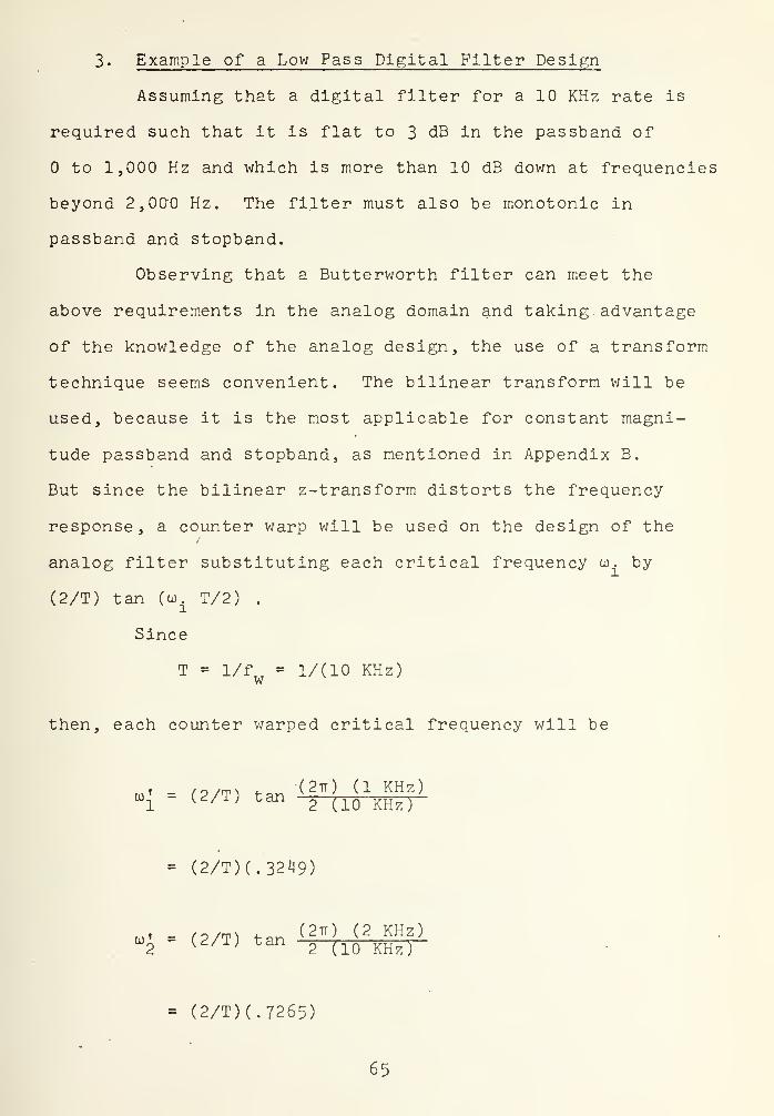
3. Example of a Low Pass Digital Filter Design
Assuming that a digital filter for a 10 KHz rate is
required such that it is flat to 3 dB in the passband of
to 1,000 Hz and which is more than 10 dB down at frequencies
beyond 2,000 Hz. The filter must also be monotonic in
passband and stopband.
Observing that a Butterworth filter can meet the
above requirements in the analog domain and taking advantage
of the knowledge of the analog design, the use of a transform
technique seems convenient. The bilinear transform will be
used, because it is the most applicable for constant magni-
tude passband and stopband, as mentioned in Appendix B.
But since the bilinear z-transform distorts the frequency
response, a counter warp will be used on the design of the
analog filter substituting each critical frequency co. by
(2/T) tan (co±
T/2) .
Since
T = 1/f = 1/(10 KHz)w
then, each counter warped critical frequency will be
u . _ (2/T) t -n(2tt) (1 KHz)
Wl
" (2/T) tan2 (10 KHz)
= (2/T)(.32^9)
O)' = (2/T) f.n (27° (2 KHz)»2
(2/T) tan2 ( 10 KHz )
= (2/T) (.7265)
65


The cut off frequency is specified by the 3 dB point;
then, in this case
u» = to' = (2/TX.3249)c 1
Applying the Butterworth analog design method
(Vp/V)2
= 1 + (x/x3dB )
2n
where for a low pass filter x = u and x«,D = w and V isr 3dB c p
the peak amplitude
V is the amplitude at a given point x
n is the order of the "filter
Since V /V2
= 10 dB then (Vp/V
2)
2= 10 and the order of
the filter can be obtained from
&)"--1 + [ — > 10 giving n = 2
Then
H(u>) = 1 g- = 1
1 + (U)/C0J^n
1 + (u)/UJ 4
and
H(s) =
(s/o) )
2+ l.Mi4(s/wJ + 1
66

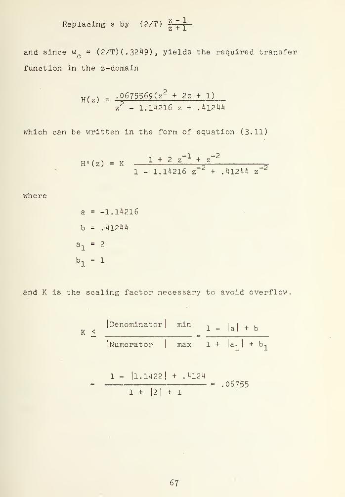
Replacing s by (2/T) —py
and since uq
= (2/T) (. 32*19) , yields the required transfer
function in the z-domain
H( z )= » o6 75569(z
2+ 2z + 1)
z2
- 1.14216 z + .41244
which can be written in the form of equation (3-11)
-1 -2H'(z) = K
1 + 2 z
1 - 1.14216 z2
+ .41244 z2
where
a = -1.14216
b = .41244
al " 2
bl " X
and K is the scaling factor necessary to avoid overflow.
K(Denominator | min
1i i ,
< J. —i a I
(Numerator max 1 + la-, I+ b-.
1 - |l.l422 |+ .4124— = .06755
1 + 2+1
67


Using the mechanization shown in Figure 3-6 it can
be observed that with the multiplier coefficients previously
calculated, the multipliers M3 and M4 are not necessary.
Therefore a realization of the type presented in Figure 3-7
will be attempted. The timing distribution calculation will
give the required delays (D,,Dp,D_ and Dj to the shift
registers.
Assuming the same accuracy in all multiplier coeffi-
cients, each multiplier will present N' - bit delay and each
adder 1 - bit delay. For a computational word length M 1
, a
restriction is given by equation (3.8). From this equation
since the chips can not operate at a bit rate higher than
1 MHz and a sampling rate of 10 KHz is required, then the
word time M' +N' must be less than 100.
Since the data at ( 3 J must be in word synchronization
with C l\ but delayed one word time
1+D1+N' = M' +N' then Dl = M f - 1
and similarly with the data at ( 2J and ( 5J
Dl + D2 - M' + N» then D2 = N ' + 1
The data at (O has to be delayed two word times from the
data at (lj and in word synchronization with it
Dl + D2 + D3 + N' = 2(M* + N«) then D3 = M f - 1
68


Finally, comparing the data at \6J with the data at ($J we
can obtain
D3 + D4 = M ! + N f then Dl = N' + 1
For a precision of 5 decimals on the coefficients
of the multipliers, the use of equation (2.1) will indicate
the need of 17 bits. One SPM chip will permit only a
coefficient up to 8-bit-plus sign. Two SPM chips will
permit up to l6-bit plus sign (N T = 17 bits). Each
multiplication will be realized cascading two SPM, and
therefore six SPM chips will be required.
The computational word length (M') has to be larger
than the word length out of the A/D converter and should be
made large enough to compensate for truncation errors in
the filter computation. Choosing M' - 30 bits and recalling
that each SRA chip provides two separate shift registers
capable of delaying up to 15 bits, it can be concluded from
the timing calculations made previously that four SRA chips
are required, since Dl , D2 , D3 and D^t need 29, 18, 29 and
18-bit delays, respectively.
However, a better solution can be achieved using
only two SRA chips and an extra multiplier (M3) . This
multiplier is set with a fixed coefficient of minus one in
order to permit two additions and two subtractions at the
output of the SRA, as shown in Figure 3-8. Therefore,
D2 = N' +1 bit delays are obtained with N 1 - bit of the
69

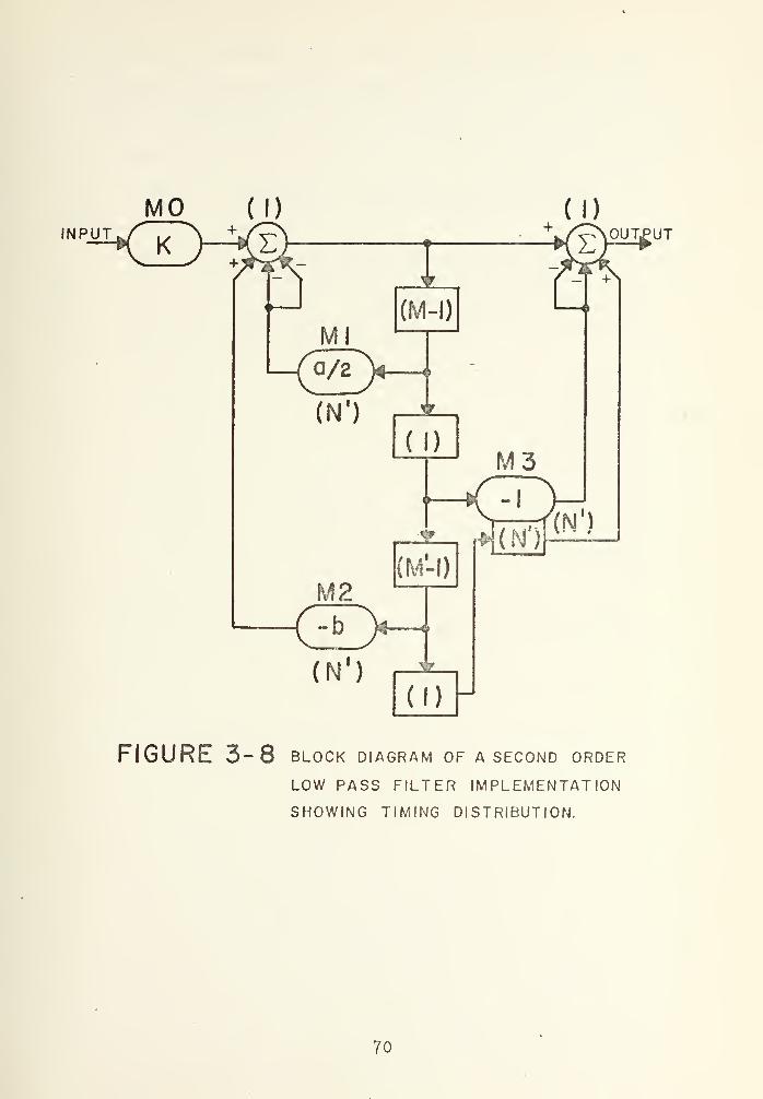
MO ( I)
FIGURE 3-8 BLOCK DIAGRAM of a second order
LOW PASS FILTER IMPLEMENTATION
SHOWING TIMING DISTRIBUTION.
70


multiplication process plus one bit delay available from
the previous shift register, which uses M' - 1 bit delay.
In order to obtain Dh = N' +1 bit delays, the shift register
of the multiplier M3 is used giving N* bit delays and as
before one bit is available from the previous shift
register (D3 = M' - 1)
.
For the chosen word lengths M' = 30 bits and N' = 17
bits, only four SPM and two SRA chips will be required,
rather than three SPM and four SRA.
71


IV. DESIGN OF A SECOND ORDER DIGITAL FILTER SECTIONUSING THE SMu TRANSPOSE FORM
A. INTRODUCTION
TA second order building section in the SM,-, form
(transpose of SM-.,) has been designed able t'o perform with
the digital filter laboratory unit built by S.A. White from
the North American Rockwell Electronics Group.
In order to permit the same parameter variations, the
designed section is capable of a computational word length
(M') from 16 to 30 bits and multiplier coefficient (N')
12, 14 or 17. The length of both these words as mentioned
previously, affect the accuracy and the speed of the digital
filter. The clock frequency is variable between 25 KHz and
1 MHz. The filter sampling rate is related to the previous
variables by the equation (3.8).
The second order building block implements the following
expression
1 + a-, z"1
+ b-, z~2
Y(z) = K ±~ ±3— X-,(z) + X?(z) - X 9
(z) - Xjz)1 + az
-1+ bz
^ 3
+ X5(z) - X
6(z) - X
?(z)
(4.1)
The following state equation
x(n) = A x(n-l) + B u(n-l)
v(n) = C x(n-l) + d u(n-l)
72

for a single Input single output second order filter leading
to the S type transfer function indicated in equation (3.9)
can be written in the form
x-j^Cn)
x2(n)
L v(n) J
3x3array
x]_(n-l)
x2(n-l)
L u(n-l) J
(1.2)
P. Girard [25] has introduced the canonical arrays,
which corresponds to the idea of canonical realization
given by Jackson [4].
The SKL - transpose array has the following form
SM11
-a 1 a.,-a
-b bx-b
1 1
(4.3)
This is a canonical array since its realization minimizes
the number of operations required, therefore leading to
smaller quantization errors. This realization satisfied
equation (4.2) for the canonical array (4.3) and the defined
state vector x(n), as shown in Figure 4-1.
The coefficients a-, and b. are related with the ones of
the transfer function (3.9): a-, = a + c and b-, = b + e. For
this realization d = 1.
73


U(n-I) V(n)
Nil ]=
-a I aj -a- b b| - b
I I
FIGURE4-1 CANONIC REALIZATION OF A SECOND ORDERSECTION BASED UPON THE SM„ TRANSPOSEARRAY
74


B. STRUCTURE MECHANIZATION
The design will be restricted to stable minimum phase
filters. Stability implies poles within the unit circle
in the Z-plane or in a parameter plane |a| < 2 and |b| < 1.
Minimum phase implies zeros within the unit circle or
|a-,| < 2 and |b,|
< 1. Since for proper multiplier operation,
the magnitude of the coefficient has to be less than one,
some arrangement has to be made. In the multipliers M2 and
M4 the coefficient introduced will be respectively a /2 and
a/2, but as observed in Figure 4-2 the second half of the
adder number one, Al(2), will sum twice the output coming
from the first half of the shift register, SR(1), which is
delaying the resulting information not only from M?
and Mn
but also from M, and M~. Therefore the coefficient of this
last multiplier will be set at b-,/2 and b/2, respectively.
The block diagram mechanization presented in Figure 4-2,
minimizes the number of devices required to perform a SM,-,
transpose form realization for the required specifications.
The truncation processed in the D.F. is generally
represented after each multiplication, however the NRMEC
chips perform the truncation at the input of each adder.
No problem will occur if the realization is of the SM,. form
as shown previously by Figure 3-6. However in a transpose
realization the scaling coefficient multiplier, MO, is
cascade with other multipliers. The truncation could be
simply realized with an AND-gate controlled by a signal
composed by a string of ones M' bits long. The first half
75


A3 (2)
INPUT ®DATA
* "\
DATA
bUTPUT
(D[ A2 (2)
-Q Ml }-»(l/^-\M3 /(N 1
)(N 1
) (I)
FIGURE 4-2 bloc diagram of a second order filter
MECHANIZATION IN THE [smJ 1 FORM SHOWING TIMING DISTRIBUTION
76


of the adder number one, Al(l), has been utilized instead,
since from the three SRA chips needed, only five adders were
used. Al(l) also provides the necessary bit delay to obtain
the synchronization of the signals (8) and U.3) at the
first half of the adder numbers two A2(l). The two adders
of chip number three A3(l) and A3(2), facilitate the inter-
connection of other filter sections in parralel.
Multiplier M5 with a fixed scaling coefficient of -1,
has been introduced in order to provide a N' - bit delay to
the signal coming out of A2(2). Since the shift register
of M5 is free, due to its fixed coefficient, it will be used
to delay the synchronization signal N' - bit.
C. SHIFT REGISTER TIMING
The next step towards the implementation of this filter
section is to determine the timing requirements. For a
computational word length of M' bits and a multiplier coeffi-
cient of N' bits, correspond a multiplier output of
(M» + N' ) bits, therefore a word time z"1
= (JVP + N') bits
is established. As before, each multiplier will be treated
as presenting an effective delay of N 1 bit times, and that
each adder will produce a one bit time delay.
The delay provided by the shift register SR(1) has to be
such that the data at (id) are in word synchronization with,
but delayed one word time from the data at [2j . Then,
1-bit delay at Aid) plus N'-bit delay at M2 plus 1-bit
delay at A2(l) plus the delay at SR(1) as to be equal to
one word time, (M' + N') bits, or.
77


1 + N' + 1 + delay SR(1) = M« + N»
then delay SR(1) = M' - 2
Similarly, the delay provided by SR(2) has to be such
that the data at \7j are in word synchronization with, but
delayed one word time from the data at ( 8J. Starting from
the signal at Cij :
N» + 1 + N f + delay SR(2) = N' + (M 1 + N')
then delay SR(2) = M' - 1
Since the computational word length M' can be as large
as 30 bits, one entire SRA chip or two halves are required
for each delay SR(1) and SR(2).
Next, it is necessary to verify that the data UJ and
(12) entering A2(2) are in word synchronization. In fact
starting from [2j , via Ml, a delay of 1 + N' is obtained
at (kj and via M3 the same delay is obtained at u.2) .
From Figure 4-2, it can be observed that the output
presents a delay of (N' + 1) bits with respect to the input
Thus, for a synchronization input signal T-, , the corre-
N 1 + 1sponding synchro output is T, d , where d represents
one bit delay time.
Figure '4-3 presents the wiring diagram of this filter
section. The small numbers inside each box represent the
pin number of the MOS chips. The multipliers are used in
78


79


pairs to obtain the required coefficient accuracy
(N 1 up to 17-bits). Then MO becomes M01 and M02, etc. All
multiplier shift registers are wired in series for serial
loading of the multiplier coefficients. The scaling coeffi-
cient word is read into this shift register cyclically.
The box marked T in the shift register adders represents
the timing sections of these devices. Each T-section
provides the proper timing signals not only to the. proper
SRA but also to the associated multipliers. SRA1 - T
N*receives as inputs the signals T, and T-,d and since an
N' + loutput with 1-bit delay is required, T,d , SRA1 with
type B pin configuration has to be used. For similar
reasons, SRA2 will also be type B.
D. TIMING DIAGRAM
In order to illustrate the processing of the signal
through the filter and obtain a timing diagram, the maximum
word lengths for the computational loop (M' = 30) and for
the multiplier coefficients (N' = 17) will be assumed and
without loss of generality an input data signal of 15-bit
plus sign will be considered.
The timing at the points marked with circled numbers in
Figure 4-2 is illustrated in Figure 4-4. The data enters
the scaling multiplier MO, at ClJ at word time I, with the
LSB input first and the sign bit 16-bits later. This data
is represented shaded so that the propagation of that word
through the filter can be traced by following the shaded data.
80


1 i
Hhlr6 < 6 jt o — o-o — o— o— o
2 2
P
!
1
p.
61
o — o — o — o
is I I i ill IS isili
« X— F_J o< z2 UJ
S2 d
— <
51
(T O
Is
I
UJ
ID
=1
3 o
©0(3© ® © © @ ©
81

The data at (2J are represented by a longer data word
than the one at (lj because the multiplier generates a double-
precision product (15 + 16 + 1 = 32-bit) and delayed N f =
17 bit. Then the data out of MO is longer than the
computational word length. The truncation to 30 - bit will
occur at the input of the adder, Al(l). The reset signal
for this adder, shown at the line RES Al(l) of Figure 4-4,
is off only for 30-bit, eliminating the two first bits
being inputed to the adder. The data through Al(l) will be
delayed 1-bit and as indicated at (3) will be 30-bit long,
inputing the multiplier Ml and M2
.
The data at ( kj and (jOj after weighted by the multipliers
Ml and M2 respectively, will be M + N + l = M'+N'-l =
30 + 17 - l = 46 bit long and delayed N' = 17-bit from the
multiplier input data at \3>\
The data at f 4J must be in word synchronization with the
data at (l2) inputing A2(2). The required truncation to
30-bit is operated at the input adder. The reset signal,
RES A2(2), has to be T1
delayed 38 bits or in general
T d . The data at the output of this adder (5) is
then 30 - bit long and 1 - bit delayed from its inputs.
The data at (s\ due to the multiplication process will
be again 46-bit long and delayed 17-bit from the input at
\5j • The shift register SR(2), implemented with the second
half of the SRA's numbers one and two, as shown in Figure
4-3, will delay the data (T) by M 1 - 1 = 29 - bit.
82


The data at \7J must be in word synchronization with,
and delayed one word time from the data at (SJ and (13) ,
inputing A2(l). The truncation of these data inputs are
truncated to the computational word length at the input of
2N ' + 4 38this adder. A reset signal T,d = T-,dJ is required.
The data at \9j passes through the shift register SR(1)
so that its output at (10) will be M f - 2 = 28 - bit delayed
from Mn.
The data at (lOJ has to be in word synchronization with
the data at \2j 3 inputing Al(2). Here, the truncation will
affect only the data (2) since the data QOJ resulting from
delaying the output of an adder conserves the computational
word length.
The data output of this filter section at (ll) can be
added with six more data inputs provided fron other filter
sections for a parallel realization or cascaded with
identical sections for a series realization.
E. DESIGN OF A SHIFT REGISTER CONTROLLED BYTHE COEFFICIENT WORD LENGTH
As seen previously a reset signal delaying T-, by (2N' +4)
bit is required for both adders A2(l) and A2(2). Since all
multipliers are capable of control N', the shift register-
part of M5, can be used, because its coefficient (minus one)
is fixed. In Figure 5-3 the output pin 3 of M52 provides
a signal T, delayed N' - bit. Unfortunately, no other
multiplier shift register is available to obtain a shift
register controllable by the coefficient word length.
83

Figure 4-5a shows the wiring connections to a third
shift register which can delay a signal by (N' + 2) bit
delay. Figure 4-5b presents the design of a diode matrix
able to control the length coding of that shift register.
The coefficient word length (N') can have the values 12,
14 and 17. If 12-bit has been chosen all shift register
input length coding will be zeros, and a 7-bit delay is
obtained at each one, resulting in an output 14 bit delayed.
If a 14-bit coefficient word length is chosen, the multiplier
selector switch set at 14, will put "1" on line B2 , all
other inputs remaining "0"'s and then SR(2) will produce 9
bit delay resulting in an output 16-bit delayed. If the
multiplier selector switch is set at 17, lines Bl , CC1 and
B2 will go "1", then a 10-bit delay will be produced SR3(1)
and a 9-bit delay at SR3(2), resulting in an output 19-bit
delayed.
The shift register used (SRA 3) is package type A,
since type B having a different pins connection, will not
permit the proper code combination.
F. MULTIPLIER TIMING SIGNALS
The sign bit timing, TSS , is a one bit signal which
goes "1" at the same time as the sign bit of the data appears
at the multiplier serial input. Then, for the multiplier
MO, TSS appears at the l6th bit time as the sign bit at
TlJ, and cyclically one word length (M* + N 1 = 47-bit)
84


INPUTSIGNAL"
N 1
= 12
N1
= 14
N 1 = 17
34 SR3(I) 22
33 32 31
t t tAl Bl CCI
I I
28 SR3 (2) 24
33 30 29
A2 B2 CC2
OUTPUT"^SIGNAL
7 + 7= 14 BIT DELAY
7+9= 16 BIT DELAY
I 10+9 = OBIT DELAY
(I0K)
rVAr
r-VSAr
(I0K)
GND
(a)
T~ry
/\.
TO MULTIPLIERSELECTOR SWITCH
(-24 VOLTS)
VAl Bl CCI y ^A2 B2 CC2y
TO SR3 (2)TO SR3 (I)
(b)FIGURE 4-5
(a) SHIFT REGISTER (TYPE A) CONNECTION TOOBTAIN (N 1 +2) BIT DELAY
(b) COEFFICIENT WORD LENGTH DIODE MATRIX
85


later. Similarly the signals TSS 1,2,3,4 for the multiplier
Ml, M2, M3 and M4 and the signal TSS 5 for the multiplier
M5.
The timing signal TMR is a one bit signal which goes
"1" two bit time before the LSB of the data appears at the
multiplier serial input. The multiplication starts at that
time. Then, TMR appears at the' 46th bit time, two bits
before the LSB appears at flY Similarly, TMR 1,2,3,4 for
Ml, M2, M3, M4 and TMR 5 for M5.
The multiplicand transfer signal, TRS , transfers the
serial multiplier coefficient input to a larallel register,
after the whole signal be inputed. Then TRS goes "1" for
one bit, one bit after the sign bit of the multiplier coeffi-
cient be inputed. Then, TRS appears at the 33th bit
time, one bit later than the sign bit of COEFF MO. Simi-
larly, TRS 1,2,3,4 with respect to COEFF Ml, 2, 3, 4. The
multiplier M5 does not need the TRS signal since its
coefficient (-1) is fixed.
Although not represented in Figure 4-3, all data and
synchronization filter outputs should have a buffer circuit
to perform a convenient output isolation. The design of
this buffer circuits and other controls however applicable
to this design are not included, since they are referred to
in [28].
86


V. QUANTIZATION AFTER ADDITION AND QUANTIZATION
BEFORE MULTIPLICATION. ERROR BOUNDS
A. INTRODUCTION
When a digital filter is implemented, errors due to
finite precision in the representation of the numbers always
occurs. The word length after a multiplier or an adder is
in general larger than the original word length. The case
of increasing word length after an adder which results in
"overflow" can be avoided by proper scaling at the input of
the filter, as shown before. Therefore only the case of
increasing word length after multiplication will be treated.
Up to now, the realization of D.F. has been done almost
exclusively using special purpose computers. Thus in order
to reduce storage, quantization is performed exactly when
the number of bits is increasing, such as after multiplica-
tion. Almost all of the literature has been dedicated to
the case of quantization after multiplication, either using
a stochastic approach [5-6-20] or a deterministic one [1].
For hardware implementation of D.F.'s, for instance
using the SRA (shift register adders) and SPM (serial parallel
multiplier) chips from NRMEC, it is possible to maintain the
resulting M' + N 1 - 1 bits after a multiplication of a N'
bit multiplier times a M' bit multiplicand (sign bits in-
cluded) until after next addition, because two consecutive
multiplications will not occur (otherwise a single one would
87

suffice). It is possible to go even further, by carrying
the M f + N' - 1 bits until the next multiplication will
be performed. This leads to two new methods of performing
the quantization. Namely, quantization after addition (QAA)
and quantization before multiplication (QBM).
QAA only recently has been addressed [10-11], and shown
that for the case of magnitude truncation, a second order
D.F. has almost no limit cycles. QBM has not even been
mentioned in the literature before.
It can be observed that for hardware implementation of D.F.,
using for instance NRMEC chips, the filter word length and
the storage of the devices for the cases QAA and QBM are
exactly the same as when used with QAM (quantization after
multiplication). For this last case the adder would be
active for M' bits (wordlength of the computational loop
in the filter) and off for the remaining N' bits of filter
wordlength (
z" 1= M' + N' bits). However for QAA or QBM,
the adder will be active for the M* + N* - 1 bits from the
previous multiplication.
B. ADVANTAGES OF QAA AND QBM
It will be proved later that QAA will produce no larger
quantization error bound than QAM, and that the error bound
for QBM is smaller or equal to the QAA. In Appendix C,
Lyapunov's direct method is applied to find the amplitude
bound of the limit cycles in the second order D.F. assuming
QAA. The result obtained Is two times smaller than that
88

determined by Parker and Hess [1] for the case of QAM.
Another advantage of using QAA or QBM over QAM is shown
next
.
In Chapter III it was mentioned that the magnitude of
the multiplier coefficient has to be less than one in order
to allow a proper operation of the SPM. From the examples
presented in Chapter III and IV, it has been observed that
whenever the magnitude of the multiplier coefficient is as
large as two, as is common practice, one can introduce one
half of the multiplier coefficient and sum twice the multi-
plier output at the next adder, as shown in Figure 5-la.
If finite arithmetic is now considered the output quan-
tization errors for QAM and for QAA will be different.
Consider, for instance, an input signal weighted by a coeffi-
cient (|a| £ 2) and that rounding with a quantization step
of h being used. For QAM, the maximum errors introduced
after multiplication will be | e|
= h/2 and, since the outputa
of the multiplier is added twice at the adder as shown in
Figure 5-lb , the maximum output errors will be h. For QAA,
as shown in Figure 5-lc, the maximum magnitude output error
will be h/2. Therefore two times smaller than for QBM.
C. HARDWARE MODIFICATIONS TO PERFORM QBM
According to the reasons presented earlier, a hardware
design able to perform QBM seems convenient. The MRMEC
chips described In Chapter III could only perform truncation
before each addition, which is equivalent to QAM (truncation)
89


(a)
M = h/2
'
(b)
|e'| = h/2
i
eil
= h/2
(c)
Figure 5-1. Advantage of QAA over QAM When theMagnitude of the Coefficient Multiplieris Larger than One. Shown for |a| < 2.
90


if two multipliers are not cascade. However the NRMEC
chips can easily be modified so that they are able to perform
truncation or rounding before multiplication.
1 . Serial/parallel Multiplier Performing Truncationor Rounding Before Multiplication
One way to obtain QBM, using truncation or rounding
as desired, is to precede each SPM with a circuit as shown
in Figure 5-2. It consists of one full adder and 2 flip-
flop's acting as delay elements. An inverter is used in
the carry circuit of the standard full adder integrated
circuit.
Another way is to design a new SPM with the circuit
described above included within the chips, as shown in Figure
5-3. Since the present SPM chip has 3^ pads and it is
mounted in a ^2-lead pack, the three new inputs required
(t, MI2 and r) can easily be placed in the available package
pins.
The operation of the circuit presented in Figure 5-3
can be described as follows. Due to a previous multiplica-
tion the input to a multiplier can be as large as M' + N' - 1
bit, where M' and N 1 represent, respectively, the number of
bits of the computational loop within the filter and the
number of bits of the coefficient multiplier (sign bit in-
cluded). At the beginning of the present multiplication
this data input can not be larger than the computational
word length (M 1
) , in order that no more than M' + N 1 - 1
91


Figure 5-2. Two's Complement Truncation/Rounding Circuit
COEFF IN
t _'—»
1
MT° X i 4 *. fs
r .
•2
PRODUCTOUT
Figure 5-3. Modified SPM to Perform Truncation o:
Rounding Before Multiplication
92


bits appear at the output produced to avoid overlapping with
the next word. Then truncation or rounding is required at
the data input at MI2 to reduce this information to M' bits
or, in other words, to eliminate up to N'-l bits. If trun-
cation is desired the input "r" is grounded and the input
"t" will receive a signal as shown in Figure 5-^; a string
of ones M* bit long starting M' bits prior to the sign bit
be input at MI2. The output of AND gate number 2 will be
always zero, and the AND gate number 1 will eliminate any
information until "t" goes "1". Then, for a M f + N' - 1
bit input, the first N'-l bits will be suppressed, and the
information entering the SPM will have N' bits and will be
1-bit delayed by the adder.
If the input data already has M 1 bits or less, no
bit will be eliminated using input MI2 , but the 1-bit delay
at the adder will exist. In order to eliminate the delay
in this case, the input Mil has been made available.
If rounding is required, both the signals "t" and
"r" will be present. The rounding signal, "r 1, is a 1-bit
signal which goes "1" M 1 bit prior to the sign bit of the
data inputed at MI2. This signal will appear at the input
of the gate 2 at the same time as the most significant bit
(MSB) of the information being eliminated. This will be the
only information passing gate 2. The output of gate 1, will
truncate the input to M' bit as before, but now the previous
MSB will be added to the LSB of the. M 1 bit information. Thus
a rounded M' bit data will input the SPM.
93


(M' +N' - 1) bit
MULTIPLIERINPUT(MI2)
DATA
MS3 of the information to ge eliminated
(N* -1) bit M 1 bit
ROUNDINGSIGNAL
l U
TRUNCATINGSIGNAL
INPUTSPM
Figure 5-4. Timing Signals for the Modified SPMShown in Figure 5-3
9X

2. SRA Circuitry For Quantization Before Multiplication
The shift register adder chip itself requires no
alteration for the QBM operation. Only the reset signal
going to the adders must be modified. As shown in the timing
diagrams, Figures 3-3 and 4-4, this reset signal was "0"
during the M' bit prior to the input of the sign bit of the
data being added, and "1" for the remaining N' bit time.
Therefore the addition process was performed only during the
last M 1 bit. For the QBM operation, the adder has to be
active during (M* + N' - 1) bits. Then the reset signal
has to be "0" during the (M' + N ? - 1) bit information
entering the adder or, in other words, it will be a 1-bit
signal going to one the next bit after the sign bits of the
data are inputed to the adder.
D. ERROR BOUNDS DUE TO FINITE PRECISION ARITHMETIC IN D.F. »S
Using the state space formulation of a second order
digital filter, the difference between the states and outputs
of a finite fixed point arithmetic D.F. and its infinite
precision (ideal) counterpart is derived for the nev; quan-
tization methods (QAA and QBM) introduced earlier. The QAA
bound derivation follows a similar path used by S.R. Parker
and Yakowitz [32] on their quantization after multiplication
study. A different approach is required to compare QAA
with QBM. Rounding is assumed with quantization step
±h/2.
95

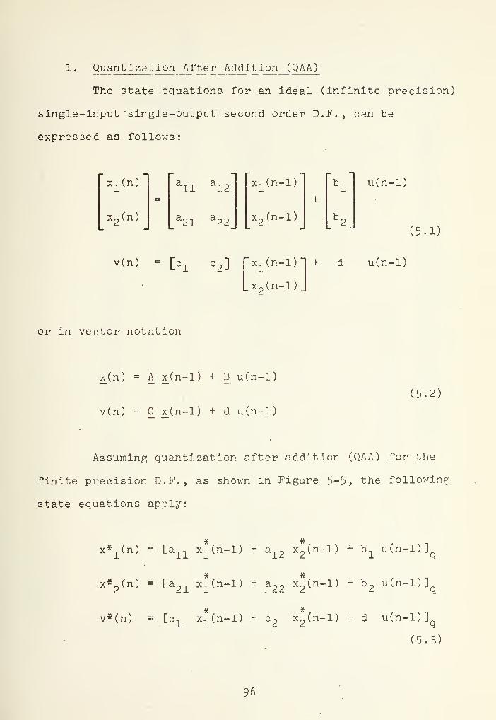
1. Quantization After Addition (QAA)
The state equations for an ideal (infinite precision)
single-input single-output second order D.F., can be
expressed as follows:
x1(n)
x2(n)
all
al2
a21
a22
x1(n-l)
+V
x2(n-l) .V
u(n-l)
(5.1)
v(n) = [c1
c2 ]
x1(n-l)
x2(n-l)
+ d u(n-l)
or in vector notation
(n) = A x(n-l) + B u(n-l)
v(n) = C x(n-l) + d u(n-l)
(5.2)
Assuming quantization after addition (QAA) for the
finite precision D.F., as shown in Figure 5-5, the following
state equations apply:
x*1(n)
x*2(n)
[ai:L
x1(n-l) + a
12x2(n-l) + b
±u(n-l)]
[a21
x,(n-l) + a22
x2(n-l) + b
2u(n-l)]
v*(n) = [c1
x1(n-l) + c
2x2(n-l) + d u(n-l)]
(5.3)
96


PrH
-P•HbO•HQ-P
apo
I
<DrHbOC•HCO C
oP -H3 Pa-H
H 'OI <CD
rH Jh
bO CD
C P•H <Vh
CO <
<L) O
U PO ctf
N
C PO Co ctf
CD 3CO Of
I
U
hO•H
97


where * indicates signals in the finite precision filter.
Or, in vector notation,
x*(n) = [A x*(n-l) + B u(n-l)]
(5.-*)
v*(n) = [C x*(n-l) + d u(n-l)]
where the input has been assumed quantized i.e.,
u*(n-l) = [u(n-l)] . The output appears also quantized,
v*(n) , so that it can used as input to a next second order
stage.
Define the error vectors e_(n) and e(n), as follows
e(n) = A x*(n-l) + B u(n-l) - [A x*(n-l) + B u(n-l)]
(5.5)
£(n) = C x*(n-l) + d u(n-l) - [C x*(n-l) + d u(n-l)]
Assuming rounding with a quantization step of ±h/2
,
the above error vectors are bounded
ev (n) < p. h/2 k = 1,2k k
(5.6)
|e(n) | < p3h/2
where
98


k = 1,2,3
if all elements in the Kth row of theD.F. array are or 1
otherwise
Therefore, it is possible to find constant vectors
e and e, whose elements are larger than the magnitude of
the correspondent elements of e(n) and e(n). Then
<e(n) > < e
<e(n)> < c
(5.7)
Defining the state and output errors the same way
as in [32] there results analogously
y(n) = x(n) - x*(n)
= A x(n-l) + B u(n-l) - [A x(n-l) + B u(n-l)]
- A x*(n-l) + A x*(n-l) (5.8)
= A y(n-l) + e(n)
Av(n) = v(n) - v*(n)
= C x*(n-l) + d u(n-l) - [C x*(n-l) + d u(n-l)l
- C x*(n-l) + C x*(n-l)
99


Av(n) = C y(n-l) + e(n) (5.9)
The error propagation equation (5.8) and the output
error equation (5 . 9) have exactly the same form as the ones
derived for rounding after multiplication in [32], and
therefore lead to a state error magnitude vector
nI.
<y(n)> <_ E <A > e1=0
(5.10)
and an output error magnitude bound
<Av(n)> < <C> <y(n-l)> + e (5.11)
The bounds on the errors for QAA as indicated by
(5.11) are at most as large as the ones indicated for QAM,
For example, a SM array
-a -b 1
10c el
f
See Ref. [25] for the definition of canonical arrays.
100


for QAM:
e1
= 2 h/2 = h
e2
= h/2 =
e = 2 h/2 = h
for QAA:
e = 1 h/2 = h/2
e2
= h/2 =
e = 1 h/2 = h/2
Using equations (5.10) and (5.11), it can be con-
cluded that the error magnitude bound for QAA is one-half
the value in QAM in this example.
2 . Quantization Before Multiplication
In order to compare QAA with QBM another approach
will be used. Define the following error vectors:
eu(n-l) = u*(n-l) - [u*(n-D]
e (n-1) = x*(n-l) - [x*(n-l)] nA 4
101
(5.12)


and assuming that these errors are introduced before each
multiplication process according to the value of the error
control parameters a.., p. , y. and 5 (where i,j = 1,2),
as shown in Figure 5-6, the state equations of a finite
precision D.F. can be written as
xx(n)
x2(n)
all
ai2
21 2^
x1(n-l)
x2(n-l)
all"
all
a12* a12
a21* a21 a22* a22
e (n-1)Xl
e (n-1)u x
2
u (n-1) - h'bl
32'b
2
e (n-1)u
v (n) =[cl
c2 ]
Fx*(n-1)
L x2(n-1)
- [Y1 -c 1 y 2.c
2 ]e (n-1)xl
e (n-1)x2
+ d u (n-1) - 6 d e (n-1)
or in vector notation
x*(n) = A x*(n-l) - aA e (n-1) + B u*(n-l) - 3B e (n-1)
(5.13)
v*(n) = C x*(n-l) -yCe (n-1) + d u*(n-l) - 6d e (n-1)
If quantization after addition (QAA) is to be
considered, all error control parameters (a,3,Y,<5) are set
102

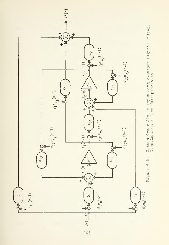
103


equal to one. This is equivalent to introduce the error
after the delay operator, rather than after the addition,
but the value of the error is not affected. .
If quantization before multiplication (QBM) is to
be studied, then set
a.U
if a, . = 1
aiJ ' 1
if b±
= 1
b±
¥ 1
if c. - 1
c. ¥1
(5.1^)
if d = 1
«
1 d ¥ 1
Here, the input signal has not been assumed to be
quantized, since the output signal is not generally quan-
tized. Therefore, these stages can also be cascade.
These error vectors are bounded, and assuming again
rounding with a quantization step' of ±h/2, it follows that
104


I h/2
e (n-1)xl
if at least one of the coefficients^ all
,a21 ,c 1^ is different from
or 1
otherwise
ey
(n-1)x2
h/2
I
if at least one of the coefficients(a,p,ap
2,c
2) is different from
or 1
otherv;ise
e (n-1)u
h/2 if at least one of the coefficients(b, ,bp,d) is different from or 1
otherwise
Then it is possible to find constant error vectors
e and e whose elements are larger than the magnitude of
the corresponding elements of e (n-1) and e (n-1) , orA. Li
e (n-1) I < e
and
e (n-1) I < e .
It can be observed that the value of this constant
vector component depends on the existence of nonzero non-ones
columns on the D.F. array, rather than on the rows.
105


vk l k = 1,2 (5.15)
uh
V3 2
where
/
vk
=
k-l,2,3
if all elements in the Kth columnof the D.F. array are or 1
otherwise
Defining the state and the output errors as before,
it results in
y(n) = x(n) - x*(n)
= A x(n-l) + B u*(n-l)
- [A x*(n-l) -aAe (n-1) + B u*(n-l) - BB e (n-1)]A Li
A y(n-l) + oA e (n-1) + 3B e (n-1) (5.16)
Av(n) = v(n) - v*(n)
= C x(n-l) + d u*(n-l)
- [C x(n-l) - YC e (n-1) + d u*(n-l) - 6d e (n-1)]
= C y(n-l) + jC e (n-1) + 6d e (n-1)A. w
(5.17)
106


Assuming x(-l) = x*(-l) and e (-1) = e (-1) = 0, and using
the propagation error equation (5.16),
y(0) = x(-l) - x*(-l) =
y(l) = A y(0) + aA e (0) + BB e (0) = aA e (0) + BB e (0)X U X "—~ u
y(2) = A y(l) + aA e (1) + BB e (1)A. \X
= A aA e (0) + aA e (1) + A BB e (0) + BB e (1)x x u — u
then
n-1y(ri) = Z A
1=0
n-l-lTU ex(i) + 6B e
u(£)
= E A^TaA e (n-l-1) + BB e (n-£-l)l£=0 L x u j
f r- -ON(5. J-O;
(5.19)
and from equation (5.17) using (5.18) and (5.19)
Av(n) = C I P^~l 2
[~oA exU) + BB e^)] + yC e_
x(n-l) + Sd e
u(n-l)
(5.20)
n_1 if= C I A aA e (n-l-2) + BB e (n-£-2)
1=0 Lx u
+ 1^ £v (n-1)
+ 6d e (n-1)u
(5.21)
107


From equation (5.19) it follows that the state error
magnitude vector is
nI £
<y(n)> = < Z A aAe (n-£-l) + k BB e (n-£-l)>1=0
~x u
nI I
< £ <A > <aA> e + <A > <£B> e (5.22)- 1=0 ~ — "x ~ — u
and from equation (5.21) using (5.17) the output error
magnitude bound can be obtained
<Av(n)> < <C> <y(n-l)> + <yC> e + |6d| e (5.23)x u
where the state error bound, <y(n-i)>, is given by equation
(5.22).
As observed previously, for QAA all error control
parameters are equal to unity. Therefore for QAA, equation
(5.22) and (5.23) reduces to
<y(n)> £ <a/+1
> e + <Al > <B> e (5.24)j: Li
<Av(n)> < <C> <y(n-l)> + <C> e + |d| e (5.25)
For QBM, it holds that
<aA> < <A>
108


<3B> <_ <B>
<yC> <_ <C^>
|6d| < |d|
since <Q> is defined as the matrix formed by the absolute
value of each element of the matrix Q.
Therefore the bounds for QBM given by equations
(5.22) and (5.23) are at least as large as the bounds given
for QAA by equations (5.24) and (5.25), respectively.
E. CONCLUSIONS
Quantization after addition and quantization before
multiplication methods have been shown applicable to hard-
ware implementation of digital filters. Advantages of
these two methods over the usual quantization after multi-
plication has been demonstrated and QBM proved to be the
more effective to reduce error quantization bounds. There-
fore QBM is the most suitable form for hardware implementa-
tion of digital filters. The modification required to
perform rounding or truncation before multiplication using
the available NRMEC chips has been presented.
109


APPENDIX A
POLE-ZERO CORRESPONDENCE IN S AND Z-DOMAIN
1. Definition of the Z-Transform
Given a sequence (x(n)} the two-sided z-transformn=o°
is defined as
X(z) = Z[x(n)] = Z x(n) z"n
. (A.l)n=-oo
When x(n) = for n < 0, the one-sided z-transform is
defined
A °°
X(z) = Z x(n) z"n
(A. 2)n=0
From the relation to the Laplace-Fourier transform
z" 1 = e"sT (A. 3)
is called the unit delay operator.
2. Mapping S-Plane into Z-Plane
Breaking s and z into real and imaginary parts,
s = a + ju) and z = a + jv
110


Since
„ _ Ts _ To jcoT _ Tocos WT Tcsin wTz-e-e e -e + J e
" «CA.4)
When, co = 0, then from (A. 4)
> 1 for a > 1Tov = and a = e
< 1 for a < 1
For a pole at -°°, a = -°°, and from (A. 4) v = and
a = 0, then mapp onto the origin of the z plane.
For imaginary poles, a = 0, we have from (A. H)
2 2v = sin cot and a = cos cot or v + a = 1, therefore the
imaginary axis of the s plane maps on the unit circle of
the z plane.
Figure A-l summarizes the mapping of the s plane into
the z plane. The left half s plane is mapped inside the
unit circle (|z| = 1) in the z plane. The imaginary s
plane is mapped onto |z| = 1. The right half s plane is
mapped into the region |z| > 1 . The left stripe/limited
by half the sampling frequency (±oo /*J) in the s plane maps
to the right within |z| < 1 region. The left stripes
bounded by + co /4 and + co_/2 or -co /4 and -co /2 in the s planeS So S
maps to the left within |z| < 1 region. The point at
infinity in the negative real s-plane is mapped into the
z-plane origin, and the s-plane origin is mapped into the
+1 point in the z-plane. It can be concluded that the
farther the real component of the s-plane complex pole is
111

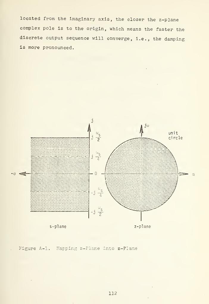
located from the imaginary axis, the closer the z-plane
complex pole is to the origin, which means the faster the
discrete output sequence will converge, i.e., the damping
is more pronounced.
-a
unitcircle
s-plane z-plane
Figure A-l. Mapping s-Piane into z-Plane
112


APPENDIX B
DISCRETE TRANSFER FUNCTION REALIZATION
1. Discrete Transfer Functions
A linear time-invariant discrete-time filter is described
by the difference equation
M Ny(nT) = Z a.x[(n-k)T] - E b,y[(n-k)T] (B.l)
k=0K
k=l K
which discrete output, y(nT), is a linear combination of the
past and present M input samples and N output samples.
The transfer function of this discrete system, similarly
a£ for the continuation case is defined
Q(z) - iff}_
(B.2)
and taking the z-transform of (B.l) and rearranging gives
Z akz
G(z) = ^—r; (B.3)-k
1 + Z b,zK
k=l K
The observation of this transfer function shows that it
is identical to those obtained from the Laplace transform
analysis of continuous systems described by linear constant
coefficients, ordinary differential equations. The roots
of the denominator of G(z) are called the poles of the discrete
113


system, and the roots of the denominators are called the
zeros. However, the discrete system is stable in the sense
that every bounded input sequence yields a bounded output
sequence if and only if the poles of G(z) lie within the
unit circle in the z-plane
.
The frequency spectrum of the discrete system is periodic
in a) with period 2tt/T due to sampling, and this spectrum can
be computed by letting z = exp(jwT) in the transfer function.
2. Recursive Filter Realization
If in the transfer function of a D.F., all b. are zero,
the filter has no feedback, as revealed by inspection of
(B.l) or (B.3), and is said to be of the nonrecursive or
transversal type.
If at least one b, and one a, value are nonzero, the
filter is called recursive.
The nonrecursive filter has finite memory and can have
excellent phase characteristics, but tends to require a large
number of terms to obtain a relative sharp cut off [161. The
recursive filter has an infinite memory and tends to have
fewer terms. Therefore sharp cut off filters are much easier
to design using a recursive structure. The design method for
this type of filter will be discussed later.
A transfer function can be realized by direct form or by
reduction to lower order form, generally first or second
order sections in a cascade, parallel or hybrid structure.
114


I
a. Direct Realization
From a given transfer function of a D.F. the
difference equation (B.l) can be obtained, and performing
the direct operations implied by that equation the so called
"direct" realization is obtained, as shown in Figure B-l.
Using an intermediate variable w(n) such that
Nw(nT) = I b,w[(n-k)T] + x(nT)
k=lK
equation (B.l) can be written
My(nT) = E a,w[(n-k)T]
( B .i|)
k=0
The realization based upon (B.4) is shown in Figure
B-2 and is called the "canonical" realization of the filter,
since the number of delays and multipliers is minimized.
b . Reduction to Lower Order Forms
This form is more convenient because lower order forms
present not only a smaller coefficient sensitivity [16] but
also a reduced quantization noise effect [18]. Thus, a
higher order filter is obtained by combining first and
second order sections.
(1) Cascade Realization
By factoring the overall transfer function can
be written associating zeros and poles in the form
PH(z) = k + I G,(z) (B.5)
p i=l
115


Figure B-l. Direct Realization
116

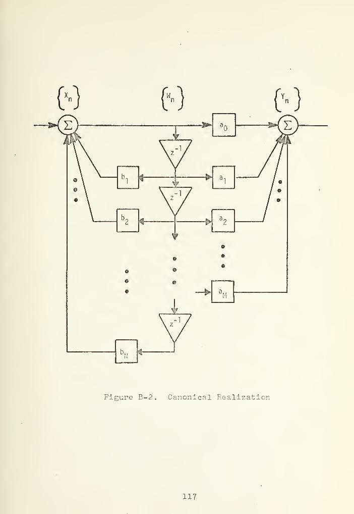
Figure B-2 . Canonical Realization
117


as illustrated in Figure B-3, where G. (z) represents the
transfer function of the first or second order sections.
(2) Parallel Realization
By partial fraction expansion, a transfer
function with simple poles can be written as the sum of the
first and second order transfer functions, in the form
c
H(z) = k n G,(z)c 1=1 ±
as realized in Figure B-4.
If the transfer function has multiple poles,
higher order sections will be required.
The parallel realization permits an easy scaling
of the D.F., but the obtaining of the transfer function and
the zeros are not readily identifiable.
(3) Hybrid Realization
The hybrid form is a combination of parallel
and cascade, as shown in Figure B-5 (a) and (b) the design
to obtain the hybrid form is not as simple and should only
be used when the cascade form becomes too difficult to scale.
3 . Nonrecursive Filter Realization
The z-transform applied to a continuous filter
transfer function can not be applied to nonrecursive filters,
also called transversal filters. This type of filter is very
useful, in particular, if a linear phase minimum phase or
a prescribed magnitude characteristic is desired.
118


INPUT
• • —I Gc(z)
OUTPUT—
H(z) = K n G.(z)c
i=l1
Figure B-3. Cascade Realization of K(z)
k. kp
£
£
INPUT
G^z) ~v£
G2(z) '1
•••
a t -^'j
P("
OUTPUT
H(z) = Kp
+ ^ G^z)i=l
Figure B-^. Parallel Realization of H(z)
119


H(z) K1[K
2+ K
3G
1
(z)G2(z) + K
4G3
( z )
G
4( z )
]
(a)
H(z) = K1
[K2
+ G^z) + G2(z).][K
3+ G
3(z) + G
4(z)]
(b)
Figure B-5. Hybrid Realizations
120

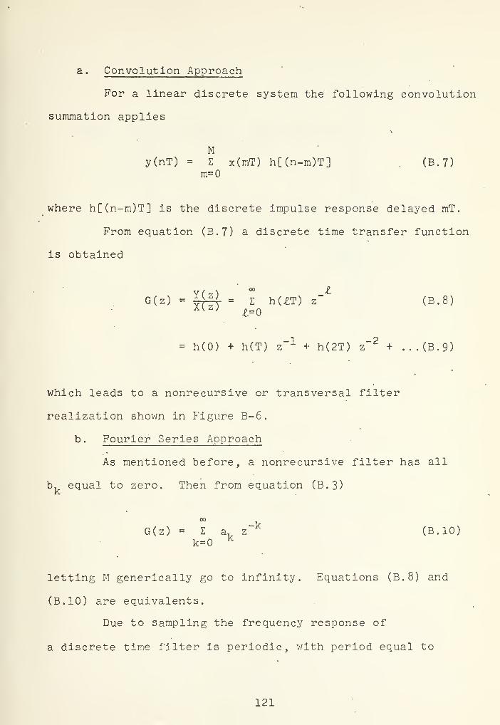
a. Convolution Approach
For a linear discrete system the following convolution
summation applies
My(nT) = Z x(mT) h[(n-m)T] (B.7)
m=0
where h[(n-m)T] is the discrete impulse response delayed mT.
From equation (B.7) a discrete time transfer function
is obtained
G(z) = ^114 = Z h(£T) z (B.8).
Mz; 1=0
= h(0) + h(T) z'1
+ h(2T) z"2
+ ...(B.9)
which leads to a nonrecursive or transversal filter
realization shown in Figure B-6.
b . Fourier Series Approach
As mentioned before, a nonrecursive filter has all
b, equal to zero. Then from equation (B.3)
00-V
G(z) = E a. z (B.10)k=0
K
letting M generically go to infinity. Equations (B.8) and
(B.10) are equivalents.
Due to sampling the frequency response of
a discrete time filter is periodic, with period equal to
121

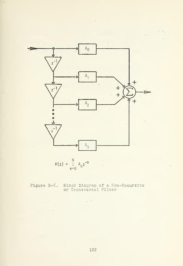
FitA2
•••
4r
^ A:i
N
H(z) = I Anz
n=0
-n
Figure B-6. Block Diagram of a Non-Recursiveor Transversal Filter
122


its sampling frequency, go = 2tt/T. This periodic frequencyt
s
response may be represented as a Fourier series. The form
of the series to be used will depend on whether the desired
frequency characteristics are an odd or even function with
respect to zero frequency.
Even functions can be written in the form
G (ju>) = A n + E A cos(wnT) (B.ll)e , nn=l
and odd functions in the form
G (ju>) = Z B sin(wnT) (B.12)n=l
n
Using the relation z = exp(jwT), equations (B.ll)
and equation (B.12) can be presented as (B.13) and (B.14).
00 ^
G (ju>) = An
+ I -£ (zn
+ z"n
) (B.13)e u
n=l
Go(jo3) = Z
2T I*" ~ Z"R)
(B ' lk)
n=l
To obtain filters with real coefficients, the j of
equation (B.14) can be dropped. The resulting filter will
have a phase shift displacement of 90° from the theoretical
function, but the magnitude function will not be affected.
Figures B-7 and B-8 illustrate the block diagram
realization of nonrecursive filters for finite (since the
123


N A
H(z) - z"N
[A0+ Z -^(z n+ z-
n)]
un=l
c
Figure B-7. Block Diagram of Transversal FilterMechanization for Finite FourierCosine Series
124

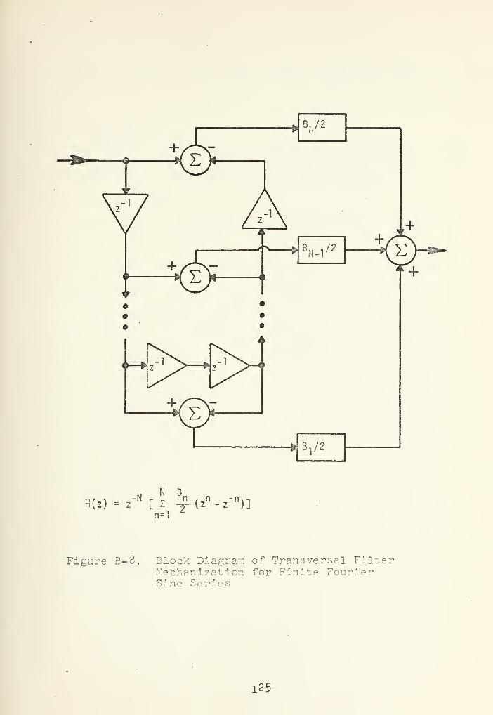
N B
n(z) = z [ I -*- (z -z )]
n=l*
Figure 3-8. Block Diagram of Transversal FilterMechanization for Finite FourierSine Series
125


summation stops after N terms) Fourier cosine and sine
series, respectively.
3. Windowing
In order to establish a physical realizable filter design,
the summation in equations (B.8), (B.13) and (B.14) must
stop after N terms.
The effect of truncating the response from an infinite
number of terms accounts to a distortion of the frequency
response curve, called "GIBB's phenomenon", which is what
normally happens when a Fourier series is truncated.
This truncation is equivalent to multiplication by a
window function, W, , which is nonzero for a length of tine
NT, or in the frequency domain is equivalent to the convolu-
tion G'(w) = G(w)*W(w). This accounts for the distortion
in the frequency domain, but also helps to avoid it, if a
proper window function is chosen. In general, a low pass
filtering or smoothing of the magnitude response is obtained
by the window function.
The best known are the Haming and Hanning windows [14].
The Kaiser window [16] is relatively easy to use and exhibits
superior side lobe suppression and produces designs which
compare with others developed through more involved proce-
dures [3].
126

APPENDIX C
FUNCTIONAL TRANSFORMS
There are three most common methods of mapping a trans-
fer function from the s-domain to the z-domain : standard,
bilinear and matched z transforms.
The bilinear and matched are optimized for sine waves
yielding the most accurate transform in the communications
field. A summary of each transform is presented next and
a comparison table is shown in Figure C-l.
The hand calculation of these transforms for more than
a first-order one stage filter is extremely complex and
requires a high level of accuracy. Therefore the use of a
computer program [13] is helpful.
1. Standard z-Transform
The standard or impulse invariant z-transform uses the
transformation z = exp(sT). It requires the partial frac-
tion expansion of the transfer function of the continuous
filter. Therefore a sum of first order terms is obtained
and the exponential transform indicated on Figure C-l is
applied to each one, yielding a parallel realization. In
general, this representation gives excellent results when
applied to all-pole low-pass and bandpass filters [12].
The design of bandstop and high-pass filters can only be
accomplished adding in cascade a wideband low-pass filter,
called "guard filter" in order to eliminate folding.
127


2. Bilinear z-Transform
The bilinear z-transform (trapezoidal integration)
eliminates the folding problem of standard z-transforms
,
and is very useful to realize digital filters that have
relative constant magnitude passband and stopband
characteristics
.
This transformation
s = (2/T) (l-z~1)/(l + z"
1)
is an algebraic one, so it can be applied to the factored
or unfactored transfer function of the continuous filter.
This mapping, however, distorts the frequency response.
Therefore it is necessary to counter-wrap the desired
radian frequency response before applying the transformation.
Then each critical imaginary frequency to. is replaced by
2/T Tan(l/2io.T) . This still does not yield an exact equi-
valence between the two frequency responses, therefore care
must be used when designing filters with critical frequencies
near the half-sampling frequency.
3. Matched z-Transform
This transformation generates a digital transfer function
with poles and zeros matched to those of the continuous func-
tions. The exponential transformation s = exp(sT) is then
applied to poles and zeros. It requires factoring both
128

'numerator and denominator of the continuous transfer function
to the form s - b and replaced by 1 - z~ exp(bT). Addi-
tional zeros at half the sampling frequency may be required
in order that the power of the poles and zeros are the
same
.
129


ooO . »
gto 1 S-aj i- qj p
o c qj r^J en £- ^^*oo Lu >, 00 c O CLQJ s_ M- QJ 1— C l— -r- <4- X
E •r- C -a Qj O to •r- 03 r— 00 QJs- i- O QJ M- C c— C CL E
"O o O) -r- s_ to QJ O to f— QJ O E 03 1
QJ <*- OO +-> o c a. q. o 03 X- -r- o3 S- ISl
x: to 03 4-> 03 rn i/l t- •r -Pl/1 1—u c 03 M u s_ .C QJ +-> S- 3 T- 1 1
•t-> 03 • r- 03 h- oo a: oo O cr-o 4- r—to i- 01 i U_ •r— H- QJ XJ i
—
03 i—s: h- TD 03 j_ 01 >-> S_ J-< (O >, •i— A
i r— QJ to QJ c QJ U Q) QJ I U +-> TM qj or QJ +-> o > C +-> i— >,4- C C• 1— i- i— •I"" S- QJ O J3 03 O QJ QJ QJ 1
>- •r~ *r— +-> QJ CJ o3 03 E * -C 3 C13 U_ u oo cr i- +-> c +-> cr o XIcr c QJ QJ 03 •r- 4-> O QJ CL I
QJ 4- 3 i_ s_ x: =3 3 •<- -t-> t- X 00cc o u_ CL, U_ CJ OO JD 4-> 03 U. UJ
s-QJ ,—+-> XJ
S- c r—o o a "r- E 1
•r— <D QJ Li_ S-
E .— -•-> Q. 00 o ^—^ «, s
S- O) 03 i_ c -— >, *4- ,
—
,
—
s- o i— N 03 i- 1 o 00 i— t— oo 1 1
03 <+- r— "1— 12 QJ +-> £= CL CJ o3 i— x: C N NQJ CO 03 1— 1 4- 03 t- 00 •1— 03 +-> 03 1 +C C S- 03 QJ OO i— 03 QJ +J s_ «r- -a S- r—•r- 03t— i.
03 QJO- 03
u.oa: 00•r—
O O T- 1—
•r- »— S- 00 QJ >> i- CL-a O cvj|i—CO 1 (/) to to !
—
c Q) T3 O QJ <u w c •r— Ahvl "O qj QJ o > 3 C +J
i— LU 03 OO 03 Ir— •r— S- S_ *r— S- +-> QJ a JD CQ i- S-
QJ i- t- QJ 4-> QJ -r- CJ 03 03 OO QJ XI 1
•r- QJ C5 +-> U oo c cr s_ 4-J QJ QJ 4-> QJ>- OO CTr- c QJ en QJ 03 •r- CL"0 .
—
en XIQJ -r- 3 i- 03 S- SZ =J >,-r- -r- i—
1
ce: U_ U_ o_ SI u_ CJ U1H2LL < to
co o•r- QJ+-> +-> "OO QJ •r- C E
1— 03 to E 03 i-
QJ I- S- c: -r— O ,*~^
U_ QJ <+- o i— to 4- 1—E ,— +-> c O Q. "O to to X)t_ 03 C r— i— o 00 C OS c s ^
"O o S- O 03 T- •r— QJ QJ OS CL 03 CLs- ^- 03 t- •r- U_ +-> Cl.CC CQ5>, i_ X03 t0 Q- +-> +-> o 03 O <— I— I— QJ•o c 03 S- <*- c x: a S_ i— c cc r—
«
C 03 03 IM 03 O C5 oo _E o^^o r— 1
03 S- •r™ a. u_ <+- 03 N+-> 1— tO i
—
c 00 f— 00 ^-» •r-1
00 1 -O 03 (/) o s- QJ 1 QJ C to -»-> 4 r~r^j r— QJ <u •!— QJ > QJ i— O 00 C T
<D o: J- 00 c+- S- oo .a !- ro QJr- •r- C oo QJ <— o3 •-> Cl C i
>- =3 03 c 00 3 +-> u -a ocr cl 03 QJ Q. r- C C CL l-QQJ X s_ S- E =5 =3 03 X C£\ 1
or uj 1— C_ >—
t
OO Ll_ CQ UJ1»/>
V)
6>H QJ
o XJ<+H •Mt/1
c ort cr, -»->
^ OM U QJ
I CJ C!N M 03
i—
1
m t3 PL:
o c 1
03 t/)
V)
<D to QJ
ft a) x;X 1—
1
M4-> O
PhEQJ OCJ E Jh
fH sh mXj o+-> m r~s
tn ti
Q) c; ox: rt •H-M !-h +->
•M om co O 3
+-> «4H
co O ht/j rH QJ
•H X3 <+H QJ
J-i ai tn ccd rH C rt
CL, •H 03 i—
1
E rt Ji do > 4-> 1
u Rj ^—' IM
uQ)
i—
I
U303
H
130


APPFMDIX D
AMPLITUDE BOUND OF LIMIT CYCLES IN
D.P. USING LYAPUNOV's DIRECT METHOD
For the case of quantization after addition (QAA) a
second-order digital filter section with two poles and no
zeros will be studied similarly and compared with results
obtained by Parker and Hess [1] for quantization after
multiplication (QAM).
The system presented in Figure D-l for QAM can be
redrawn as shown in Figure D-2 considering roundoff after
addition and described by the following difference equation
(where u(n) = 0)
x*(n) = [-a x*(n-l) - b x*(n-2)] (D.l)
For a normalized quantization step (h=l), this equation
can be written as
x*(n) = -a x*(n-l) - b x*(n-2) ± [.5 - 6(n)] (D.2)
where
< 6(n) < 1.0
131


U(n)
x*(n)
KZHQ <3 C -b
J*-
Figure D-l. Second Order D.F. with Two Poles UsingQuantization After Multiplication
U(n)
Figure D-2, Second Order D.F. with Two Poles UsingQuantization After Addition
132


The roundoff noise sequence e(n) = .5 - <5(n) range
between ±.5 and can be considered as driving function to
the difference equation (D.2) for the study of the natural
response of the system (zero input, initial condition only).
Then the error source can be considered 'as an input
|u(n)| = |e(n)| < .5
and using the state variables x,*(n) = x*(n-2), x^in) = x*(n-l),
u(n) = e(n), equation (D.2) can be written as
x*(n+l) =1
-b -aL
x*(n) + u(n) (D.3)
or
x*(n+l) = A x*(n) + B u(n) (D.4)
The transfer function of this filter is
G(z) =7~1 -1
, , ^2"1 + a z + b z
(D.5)
and its characteristic equation is
l + az 1+ bz 2
= (D.6)
133


The steady state frequency response is obtained by
setting z = e~ J where T is tfce? sampling interval.
Therefore,
= 1 + a(cos u)T - j sin WT) + b(cos 2 WT - j sin 2 WT)
= 1 + a cos wT + b cos 2coT - j sin (ooT)(a + 2b cos uT)
(D.7)
This equation is satisfied if both real and imaginary
parts are simultaneously satisfied, thenI
the imaginary part is zero when
i) a + 2b cos toT = cos WT = -^
22
since cos 2wT = 2(cos coT) - 1 = -^-p - 1
2bthe real part becomes
= 1 + a (-,£-) + b(-^ - 1) = 1 - b (D.8)dD
2b
ii) sin wT = T = Ktt K = 0,1,2
the real part becomes
0=1+ (-l)k
a + b (D.9)
13^


Equation (D.8) and (D.9) are the stability boundaries
for a so-called "linear" second order D.F.
The term linear means that overflow or saturation arith-
metic which may occur for large signal amplitude is not
considered, but only the nonlinearity characteristics of
the quantizer. Therefore small signal amplitudes are
assumed.
Then a linear filter, as defined previously, has the
stability boundaries
l-b=0 b = l
(D.10)
l±a + b =I al = 1 + b
Therefore, for b < 1 and |a| < (1+b) the corresponding
linear system is asymptotically stable in large (ASIL)
.
Since the input is also bounded for all n _> , the
theorem mentioned in the Appendix of [1] can be applied.
It states that for a system described by the state equation
x(n + 1) = A x(n) + B u(n) , if the homogenous system is
TASIL and has a Lyapunov function V = x Q x with
AV = - x C x and |u(n)| <_ k for all n > 0, then the
system is stable and the states are certain to enter a
region defined by |x| < r2 , where
135


r2
= K.;X max(Q)
X min(Q)
|
|AT
Q B|
|
X min(C)
/|AT
Q B|
|
2BT
/ +
X min(C) X min(C)
(C.ll)
with
X min(Q) = minimum eigenvalue of matrix Q;
X max(Q) = maximum eigenvalue of matrix Q;
T T|A Q B| = norm of the matrix product A Q B
defined as max a. . where a. . are
elements of AT
Q B;
Ixl = norm of the state vector.
The Lyapunov function V = x Q x where Q is a real
symmetric and positive definite matrix (RSPDM) can be
found for any RSPDM C from the equation
-C=AT QA-Q (C12)
in this case
Q =l ll
L12
12
•22
136


and since the choice of C is arbitrary as long as it is RSPDM
choose £ equal to a 2 x 2 identity matrix. Then from
equation (D.12) results
-1
- -1_
-b
1 -a
qll q l2
Lq12 q 22 j
1 q q
q 12 q22J
(D.13)
whose solution is
qn = 1 +2b (1+b)
(l-b)[(l+b)2
- a2
]
122ab
(l-b)[(l+b)2
- a2
]
{
= 2(l+b)22 (l-b)[(l+b)
2- a
2]
TDefining co = |A Q B
-b
1 -a
qll q 12
- q i2 q22J
-b q22
.Q12- aq22J
137


then
a) = max(|b q 9P | , |q15 - a q ~| )L 22 12 L 22
and substituting into equation (D.ll)
K. = 1/2 since |u(n)| = |e(n)| <_ .5
A min(C) = 1
Bl
Q B = [0 1] q ll ql2'
LQ 12 q 22-»
L22
the following state bound is obtained
|x*(n)| < 1/2 iX max(Q)
X min(Q)[co + lJaj
2+ q 22 j (D.15)
Comparing equation (D.15) with the one derived by S.R.
Parker and Hess [1] for QAM, it can be concluded that the
upper bound on amplitude of the limit cycles for quantization
after addition is two times smaller than for quantization
after multiplication.
138


LIST OF REFERENCES
1. Parker, S. R. and Hess, S. F. , "Limit-Cycle Oscillationsin Digital Filters," IEEE Transactions on Circuit Theory ,
v. CT-18, no. 6, pp. 6«7-697, November, 1971.
2. Parker, S. R. and Hess, S., "Canonic Realizations ofSecond-Order Digital Filters Due to Finite PrecisionArithmetic," IEEE Transactions on Circuit Theory ,
v. CT-19, no. 4, pp. 410-413, July, 1972.
3. White, S. A., "Introduction to Implementation of DigitalFilters," Electronics Research Division Rockwell Inter-national , Publication X73-371/501, March, 1-973.
4. Jackson, L. B. , Kaiser, J. F. and McDonald, H. S., "AnApproach to the Implementation of Digital Filters,"IEEE Transactions on Audio Electroacoustics , v. AU-16,pp. 413-421, September, 196b.
5. Jackson, L. B. , "On the Interaction of Roundoff Noiseand Dynamic Range in Digital Filters," Bell SystemTechnical Journal , v. 49, pp. 159-184, February, 1970.
6. Jackson, L. B. , "Roundoff-Noise Analysis for Fixed-PointDigital Filters Realized in Cascade or Parallel Form,"IEEE Trans. Audio Electroacoust
.
, vol. AU-18, pp. 107-121, June, 1970.
7. Slaughter, J. B. , "Quantization Errors in Digital ControlSystems," IEEE Transactions on Automatic Control ,
v. AC-9, pp. 70-74, January, 1964.
8. Johnson, G. W. , "Upper Bound on Dynamic QuantizationError in Digital Control Systems via the Direct Methodof Liapunov," IEEE Trans. Automat. Contr. , vol. AC-10,PP. 439-448, January, 1965.
9. Lack, G. N. T. , "Comments on 'Upper Bound on DynamicQuantization Error in Digital Control Systems via theDirect Method of Liapunov'," IEEE Trans. Automat. Contr.(Corresp.) , vol. AC-11, pp. 331-333, April, 1966.
10. Claasen, T. A. C. M. , MecKlenbrauker , W. F. G. , andPeek, J. B. H., "Second-Order Digital Filter with onlyOne Magnitude Truncation Quantizer and Having PracticallyNo Limit Cycles," Electronic Letters , v. 9, no. 22,November, 1973.
11. Claasen, T. A. C. M. , Mecklenbrauker , W. E. G., andPeek, J. B. H. , "Some Remarks on the Classification ofLimit Cycles," Phylips Research Report , V. 28, no. 4,August, 1973.
139


12. Golden, R. M. , "Digital Filter Synthesis by Samp led- Data'Transformation," IEEE Transactions on Audio and Electro-acoustics , v. AU-16, no. 3, pp . 321-329.
13. Naval Electronics Laboratory Center, Report 2570,"Digital Filter Design Utilizing Large Scale IntegrationTechnology," by R.E. Johnston, December, 1973.
14
.
Blackman, R. B. , and Tukey, J. W. , The Measurement ofPower Spectra from the Point of View of CommunicationsEngineering , Dover Press, 1959.
15. Gold, B. and Rader, C. M. , Digital Processing of Signals ,
McGraw-Hill, Inc., 1969.
16. Kaiser, J. F., "Digital Filters"in System Analysis byDigital Computers by J. F. Kaiser and F. F. Kuo , Eds.,New York, Wiley, pp. 218-285, 1966.
17. Fettweis, A., "On the Connection Between MultiplierWord Length Limitation and Roundoff Noise in DigitalFilters," IEEE Transactions on Circuit Theory , V. CT-19,no. 5, pp. 486-491, September, 1972.
18. Aggarwal , J. K. , "Input Quantization and ArithmeticRoundoff in Digital Filters - A Review" , InformationSystems Research Laboratory , Technical Report no. 130,July, 1972.
19. Knowles, J. B. and Olcayto, E. M. , "Coefficient Accuracyand Digital Filter Response," IEEE Transactions onCircuit Theory , v. CT-15, no. 1 , pp . 31-41, March, 1968.
20. Yakowitz, S. and Parker, S. R. , "Computation of Boundsfor Digital Filter Quantization Errors," IEEE Transactionson Circuit Theory , v. CT-20, no. 4, pp. 391-396, July,1973.
21. Mitra , S. K. and Sherwood, R. J., "Estimation of Pole-zero Displacements of a Digital Filter Due to CoefficientQuantization", IEEE Transactions on Circuits and Systems ,
v. CAS-21, no. 1, January, 1974.
22. Weinstein, C. and Oppenheim, A. V., "A Comparison ofRoundoff Noise in Flotaint Point and Fixed Point DigitalFilter Realizations," Proceedings of the IEEE (Letters) ,
v. 57, PP. 1181-1183, June, 1969.
23. Oppenheim, A. V. and Weinstein, C. J., "Effects of FiniteRegister Length in Digital Filtering and the Fast FourierTransform," Proceedings of the IEEE , v. 60, no. 8,
PP. 957-176, August, 1972.
140


2k. Liu, B. , "Effect of Finite Word Length on the Accuracyof Digital Filters - A Review," IEEE Transactions onCircuit Theory , v. CT-18, pp. 670-677, November, 1971.
25. Girard, P., "Correlated Noise Effects of Structure inDigital Filters", PH. D. Thesis, Naval PostgraduateSchool, Monterey, California, 197*1.
26. Steiglitz, K. , "Computer Aided Design of RecursiveDigital Filters", IEEE Transactions on Audio and Electro-acoustics , v. AU-18, no. 2 , p. 12 3, June, 1970.
27. Avenghaus, E. , "A Proposal to Find Canonical Structuresfor the Implementation of Digital Filters with SmallCoefficient Word Length" , Nachrichtentechnische Zeitung ,
Heft 8, 1972.
28. White, S. A. and Graske , R. , "Digital Filter LaboratoryUnit" , Electronics Research Division Rockwell International ,
Report T73-2W501, August, 1973.
29. Rabiner, L. R. , and others, "Terminology in DigitalSignal Processing," IEEE Transactions on Audio andElectroacoustics , v. AU-20, pp. 332-337, December,1972.
30. Gabel, R. A. , "A Parallel Arithmetic Hardware Structurefor Recursive Digital Filtering", IEEE Transactions onAcoustics, Speech and Signal Processing , v. ASSP-22no. 4, August, 1974.
31. G - AE Concepts Subcommittee on Digital Filtering, IEEETransactions on Audio and Electroacoustics , v. AU-16
,
no. 3, September, 196b.
32. Parker, S. R. and Yakowitz, S., "A General Method forCalculating Quantization Error Bounds in Fixed PointMultivariable Digital Filters", to be published in IEEETransactions on Circuit and Systems , April 1975.
mi


INITIAL DISTRIBUTION LIST
No. Copies
1. Defense Documentation CenterCameron StationAlexandria, Virginia 22314
2. Library, Code 0212Naval Postgraduate SchoolMonterey, California 93940
3. Direccao Do Servico De InstrucaoMinisterio Da MarinhaLisboa2, Portugal
4. Department Chairman, Code 52Department of Electrical EngineeringNaval Postgraduate SchoolMonterey, California 93940
5. Professor S. R. Parker, Code 52PxDepartment of Electrical EngineeringNaval Postgraduate SchoolMonterey, California 93940
6. Assoc. Professor V. M. Pov/ers, Code 52PwDepartment of Electrical EngineeringNaval Postgraduate SchoolMonterey, California 93940
7. LT Carlos J. A. R. RodolfoCalqada Do Cardeal 24-2-DtLisboa2, Portugal
8. Assoc. Professor M. L. Cotton, Code 52CcDepartment of Electrical EngineeringNaval Postgraduate SchoolMonterey, California 93940
9. Assoc. Professor R. Panholzer, Code 52PzDepartment of Electrical EngineeringNaval Postgraduate SchoolMonterey, California 93940
10. LCDR L. Souchon, Federal German NavySMC 2988Naval Postgraduate SchoolMonterey, California 93940
142


11. Professor J. K. AggarwalDepartment of Electrical and Electronic
Research CenterThe University of TexasAustin, Texas 78712
12. Prof. Bede LiuDepartment of Electrical EngineeringPrinceton UniversityPrinceton, New Jersey
13. Mr. W. J. Dejka, Code 4300Advanced Modular Concepts DivisionNaval Electronics Laboratory CenterSan Diego, California 92152
14. Dr. G. M. Dillard, Code 3300Decision and Control Technology DivisionNaval Electronics Laboratory CenterSan Diego, California 92152
15. Professor Alfred FettweisRucha University BochumBuscheystrasseD-463 BockumFederal German Republic
16. Dr. L. B. JacksonRockland Laboratories DivisionRockland Systems Corporation131 Erie Street, EastBlauvelt, New York 10913
17. Dr. J. F. KaiserBell Telephone Laboratories, Room 7c-201Murray Hill, New Jersey 07974
18. Professor B. LeonDepartment of Electrical EngineeringPurdue UniversityLafayette, Indiana 49707
19. Professor S. K. MitraElectrical Engineering DepartmentUniversity of California, DavisDavis, California 95616
20. Professor A. V. OppenheimRoom 36-377Massachusetts Institute of TechnologyCambridge, Massachusetts 02139'
143


21. Dr. S. A. V/hiteAutonetics DivisionNorth American Rockwell CorporationP. 0. Box 3669Anaheim, California 92803
22. LCDR P. E. Girard, USN8071 Wildflower WaySan Diego, California 92120
23. Assoc. Professor G. A. Rahe , Code 52RaDepartment of Electrical EngineeringNaval Postgraduate SchoolMonterey, California 939^0
1U4


,
Thesis
R6713c.l
-•r >
Rodo 1 f
Ha rclws re implementat ion
of recursive fixed-pointdigi tal f
i
Iters for
minimum quantizationnoise.

thesR6713
Hardware implementation of recursive fix
3 2768 000 99675 5
DUDLEY KNOX LIBRARY


![FPGA BASED FIXED POINT LMS ADAPTIVE FILTERS...FPGA Based Fixed Point LMS Adaptive Filters 31 editor@iaeme.com form called the delayed LMS (DLMS) algorithm [3]–[5], which](https://img.pdfslide.us/doc/110x75/602d0ff8c7da254b68381091/fpga-based-fixed-point-lms-adaptive-fpga-based-fixed-point-lms-adaptive-filters.jpg)