Embed Size (px)
Citation preview

#60
Page 1AN60 05/05/03
Hardware Implementation Guide for the PI7C8154By Glenn Sanders
IntroductionThe PCI interface was originally created for the personalcomputing industry. These days it has been adopted by systemdesigners who incorporate it into Datacom, Telecom, PCs,Servers, and many other systems. Currently the PCI interface isused mainly as an expansion bus to add PCI slots on the systemmotherboards that have wide ranging applications. It is alsoused in add-in cards since most systems have PCI slots availableto insert the PCI add-in cards.
As bandwidth requirements increased, the PCI bus was extendedto support 64-bit transfers at up to 66MHz clock speed, givingapproximately 4 times greater bandwidth over the earlier 32-bit/33MHz PCI bus implementations. Three factors complicatedthis approach:� Increasing clock speed decreased the number of available
loads per PCI bus (2 PCI connectors or 4 embedded devicesat 66MHz)
� The trace length of the bus is decreased� A 66MHz PCI bus will drop to 33MHz speed when an
older style 33MHz add-in card is inserted.
A PCI-to-PCI bridge overcomes these limitations by adding anew �secondary� bus, which is electrically and physicallydistinct from the previous or �primary� PCI bus. Now this buscan have loading, layout distances, and potentially differing busclock frequencies.
The PI7C8154 2-Port PCI-to-PCI Bridge is a 64-bit, 66MHzchip that can be used either within a motherboard, Backplane, orAdd-In Card.
Example of 4-Port Ethernet Network Card
Schematic and Layout GuidelinesThis section has guidelines for hardware implementation of thePI7C8154 PCI-to-PCI Bridge into a motherboard or add-in card.
PowerThe 8154 bridge supports both 3.3V and 5V signalingenvironments. The chip core is powered by 3.3V VDD andsignaling on either bus is at the voltage level of the respectiveP_VIO (pin R20) or S_VIO (pin N22) inputs.
Clock FrequencyInput clocks:The input clock frequency comes through signal P_CLK. Thissignal can be up to 66 MHz; the secondary bus clock will beinternally derived from this clock and output at 1x or 1/2xprimary input clock frequency according to:
Primarybus clock
S_M66EN Secondary bus speed
66 MHz High 66 MHz66 MHz Low 33 MHz50 MHz High 50 MHz50 MHz Low 25 MHz33 MHz Low 33 MHz33 MHz * [externally
pulled High by5K-ohm orgreater resistor]
33 MHz; +S_M66EN will bedriven low by thebridge
*The last case is where an expansion card designed for 66 MHzoperation is placed into a 33 MHz slot or the normally 66 MHzprimary bus has some other add-in card with M66EN tied low(thus forcing that bus to 33 MHz operation).The input clock can be either 3.3V or 5V logic levels at 33MHz; per PCI spec 66 MHz clocks should be 3.3 V.
Output Clocks:Each secondary clock output is limited to one load. Onesecondary clock output is used to feedback into S_CLKIN, withthe remaining 8 clocks driving embedded PCI devices/slots.
All secondary clock traces including feedback should have thesame length so as to deliver the clock at the same time at theirrespective destinations. This means that the furthest secondarybus device from the bridge governs the effective secondary busclock trace lengths. Unused clock outputs can be disabled bywriting to the bridge configuration register at offset 68h, orterminated electrically.

#60
Page 2AN60 05/05/03
Clock lines are best terminated with a series terminationresistor. The value to use depends on the impedance of yourtransmission lines. For example, our 65-ohm trace impedancereference board uses 22-ohm resistors placed close to the bridge.
Programming clock outputsUnused clock outputs can be disabled by using a serial clockmask shift to selectively disable secondary clock outputs.
The 8154 uses GPIO[0] and GPIO[2] pins and the MSK_INsignal to input a 16-bit serial data stream. This data is shiftedinto the secondary clock control register as soon as P_RESET_Ldeasserts. S_RESET_L delays deassertion until the 8154completes shifting in the clock mask data. GPIO[0] acts as theshift register clock and GPIO[2] determines shift or loadoperation during that shift register clock cycle. MSK_IN is the1 bit serial data bus for this operation; thus tying it low will busall �0� values (enabling all clocks) and eliminate the need forthe external shift register circuit at several dollars savings.
Bit Description S_clk_o1:0 Device 0 / slot 0 PRSNT#<1:2> 03:2 Device 1 / slot 1 PRSNT#<1:2> 15:4 Device 2 / slot 2 PRSNT#<1:2> 27:6 Device 3 / slot 3 PRSNT#<1:2> 38 Device 4 49 Device 5 510 Device 6 611 Device 7 712 Device 8 813 S_CLKIN (feedback clock input) 914 Reserved Ignored15 Reserved Ignored
For the first 4 devices, the two bits corresponding to PRSNT#[2]and PRSNT#[1] are ANDed, so that a low on either is countedas a low for that device, low being an enable for that device�sPCI clock.
Figure 2: Schematics section: Programmng secondary clocks

#60
Page 3AN60 05/05/03
Miscellaneous Signal ConnectionsUnused INPUT signals should not be left floating.Where �pull up� is used, use a 5-10K-ohm resistor to VCC/VDD.For 8154 IC:Pin name Pin Requested value
MSK_IN R21
NOT pulled internally; do notfloat this signal. Tie low toenable all secondary busclocks, or connect to thecircuit shown in figure 2.
CONFIG66 R22
Used to prevent the bridgefrom 66MHz operation whentied low; this pin should betied high to allow 66MHzoperation.
TCK N20 Pull up if JTAG port not used
TMS P21 Pulled Up internally so can beNC
TDO P22 Output so can be no connect
TDI P23 Pulled Up internally so can beNC
TRST_L N23 Pulled Up internally so can beNC
GPIO[3:0] K2,K3,L4,L1
Pull Up through 10K-ohmresistor
P_M66EN AB10 Pull up through 10K-ohmresistor if capable of 66MHz
S_M66EN A14
Pull up through 10K-ohmresistor if capable of 66MHz;else tie low for 33MHz onlysecondary bus
S_CFN_L K1
Tie low for secondary businternal arbiter; pull high forexternal arbiter. For moredetails see page 4. Do not float
BPCCE R4Tie low if not using powermanagement; pull up to enablepower management
PMEENA_L D11
Tie this signal low to indicatesome downstream devices arecapable of asserting PME#,else tie high to disable powermanagement.
P_AD[63:32]
For add-in cards, themotherboard is assumed tohave pull-up resistors herealready, in order to support32-bit cards placed into 64-bitslots. If this bridge is amotherboard or backplane, theprimary PCI bus willl need tohave pullups in the 5-10K-ohm range.**
P_CBE[7:4] Pulled high by motherboard**P_PAR64 T21 Pulled high by motherboard**P_REQ64_L AC14 Pulled high by motherboard**P_ACK64_L AB14 Pulled high by motherboard**
S_SERR_L B11 Pull upS_PERR_L C11 Pull upS_LOCK_L A11 Pull upS_STOP_L C10 Pull upS_DEVSEL_L B10 Pull upS_TRDY_L A10 Pull up
S_IRDY_L C9 Pull up
S_FRAME_L B9 Pull up
S_RESET_L H2 Pull up
S_AD[63:32] Pull high individually
S_CBE[7:4] Pull high individually
S_PAR64 N21 Pull up
S_ACK64_L C18 Pull up
S_REQ64_L B19 Pull up
For each PCI slot:Pin name location Requested value
REQ# Pull high through externalresistor
SDONE (A40) Pull upSBO# (A41) Pull up
PRSNT1# (B9) Pull up and decouple with a0.01uF capacitor
PRSNT2# (B11) Pull up and decouple with a0.01uF capacitor
Additional PCI signals per PCI specification 2.2, section 2.2.7:
PRSNT[1:2] Normally these are pulled high with a decouplingcapacitor to ground on the secondary bus.PME# Power Management Event signal, an optional signal.*PMEENA_L. When low, 5 bits [31:27] are set at offset DEh toindicate the corresponding secondary bus devices support thePME# pin. The bridge does not have a PME# input; but it doeshave this as a method to notify device drivers that downstreamdevices may support PME# assertion, and to scan them todetermine actual PME# pin support. The actual PCI connectorPME# signal is then bused from the secondary PCI bus, aroundthe bridge and out onto the primary PCI bus edge connector (foran add-in card) or onto the primary PCI bus for a motherboardimplementation.

#60
Page 4AN60 05/05/03
3.3Vaux: This power source, if implemented on your design,should be bused from the primary PCI connector around thebridge to the secondary bus connectors.
Power DecouplingIn order to reduce noise at Vdd or ground from impacting thebridge, place 4 sets of decoupling capacitors top and bottom asclose as possible to each corner of the bridge IC. These shouldbe {0.1 uF, 0.01 uF, 0.001 uF} on bottom side and be {10 uF,0.1 uF, 0.01 uF, 0.001 uF} top side. These are in addition tofurther decoupling at the PCI primary interface and secondaryslots as needed per PCI spec 2.2 sec. 4.4.2.1 �powerdecoupling�.
For add-in cards, please add the following decoupling capacitorsat the edge connector, for 3.3V and 5V pins, with values {0.1uF, 0.01 uF, 0.001 uF}. Use high quality, low ESR surfacemounted ceramic capacitors.
PCI INTERRUPTSPCI interrupts are processed at the motherboard south bridge,which sits on the primary PCI bus (thus upstream from the8154). Thus there aren�t signals at the bridge for interruptprocessing; rather during layout the board designer routes theINTA#, INTB#, INTC#, and INTD# signals directly to thecorresponding signals on the primary bus.
When the secondary bus is to have PCI connectors, the pinposition of the PCI INTx# signals rotates from slot to slot., perPCI 2.2 spec 2.2.6 (page 14).
Six layer board stacking recommendationFor 5V or mixed signaling environments, we recommend a 6layer board arranged as follows:
Top route clock and other critical signals on topInternal plane 1 GroundInternal plane 2 3.3 VInternal plane 3 5 V (with 12V islands)Internal plane 4 GroundBottom signal connections
Do NOT route high frequency bus signals under the bridge.
Signal layers should be separated by ground planes, and nosignals routed between ground and power planes. Use FR-4material for board fabrication.
General layout guidelines1. Limit your trace lengths. Longer traces display more
resistance and induction and introduce more delays. It alsolimits the bandwidth which varies inversely with the squareof trace length.
2. Use higher impedance traces. Raising the impedance willalso increase the bandwidth. Per PCI specification 2.2section 4.4.3.3 trace impedance should be controlled to bewithin 60 to 100 ohms range.
3. Do not use any clock signal loops. Keep clock lines straightwhen possible.
4. For related clock signals that have skew specifications,match the clock trace lengths.
5. Do not route signals in the ground and Vcc planes.6. Do not route signals close to the edge of the PCB board.7. Make sure there is a solid ground plane beneath the bridge
IC (PI7C8154).8. The power plane should face the return ground plane. No
signals should be routed between power and ground.9. Route clock signals on the top layer and avoid vias for these
signals. Vias change the impedance and introduce moreskew and reflections.
10. Do not use any connectors on clock traces.11. Use wide traces for power and ground.12. Keep high speed noise sources away from the PI7C8154.13. Remember that per PCI spec 2.2 sec 4.4.3.1, the PI7C8154
should have a primary PCI edge connector to BGA padtrace distance of not more than 1.5 inches (37.5 mm) forsignals coming from the primary PCI interface. Secondaryinterface signals would then be limited as in PCImotherboard layout rules.
Figure 3: Top Layer Overview
#60
Page 5AN60 05/05/03
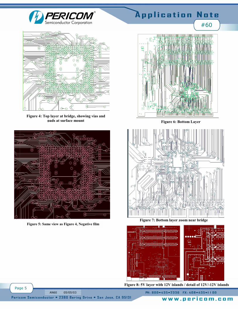
Figure 4: Top layer at bridge, showing vias andpads at surface mount
Figure 5: Same view as Figure 4, Negative film
Figure 6: Bottom Layer
Figure 7: Bottom layer zoom near bridge
Figure 8: 5V layer with 12V islands / detail of 12V/-12V islands

#60
Page 6AN60 05/05/03
External ArbiterAn arbiter needs to watch the PCI bus clock, each REQ#, andthe control signals RESET#, TRDY#, DEVSEL#, LOCK#,STOP#, FRAME#, CBE[3:0] and IRDY#. The 8154 normallyuses an internal abiter for the secondary PCI bus. Howeverthere exists a method to use an external arbiter:
In order to disable the internal arbiter, tie high (pin K1)S_CFN_L.
Next the bridge needs to output a REQ# and wait for a GNT#input just like any other bus master device. When the bridge isin the internal arbiter mode, it waits to receive as inputs REQ#sfrom bus master devices on the secondary bus and then issues asan output a corresponding GNT#. Now that the bridge is yetanother device, it must output a REQ# to the external arbiter andwait its turn to use the bus, which will be an input GNT# signal.The signal named S_GNT_L[0] (pin E2) will become the bridgeREQ# on the secondary bus, since it is an output from thebridge, in external arbiter mode. Signal name S_REQ_L[0](pin D4), as it is an input, will be the bridge GNT# on thesecondary bus when in external arbiter mode.
Finally, route the S_REQ_L[3:0] traces from the PCI slotconnectors/embedded devices to the external arbiter. Route theS_GNT_L[3:0] devices likewise. At the 8154 bridge, the inputsS_REQ_L[3:0] do not have any internal pullups, so the signalsS_REQ_L[3:0] need pull ups at the inputs to the bridge. AsGNT#s are normally output by the bridge, the S_GNT#[3:0] canalso be left as no connect in external arbiter mode.
References1) Pericom Semiconductor App Note #22 �Solutions to
Current High-Speed Board Design�2) PCI Local Bus specification 2.2 section 4.4 �Expansion
Board Specification� [decoupling through routingrecommendations and impedance sections] p150-152.
3) PCI Local Bus specification 2.2 section 4.2.6 Pinoutrecommendation p131.
4) PCI Local Bus specification 2.2 section 4.3.3 Pull-upsp136.
5) Compact PCI PICMG 2.0 R3.0. p17-20 �ElectricalRequirements�
6) Pericom semiconductor App Note #31 �Zero-Delay ClockBuffer Layout and Schematic Guidelines� p1.
Reference board schematics and gerber files available onrequest.
Figure 10. Example of connections to an external arbiter