Embed Size (px)
Citation preview
© 2016-2017 NXP B.V.
Hardware Development Guide for i.MX7Dual
and 7Solo Applications Processors
1. About this guide
This document’s purpose is to help hardware engineers
design and test their i.MX 7 series processor based designs.
It provides information on board layout recommendations,
design checklists to ensure first-pass success and ways to
avoid board bring-up problems. It also provides
information on board-level testing and simulation such as
using BSDL for board-level testing, using the IBIS model for electrical integrity simulation and more.
Engineers are expected to have a working understanding of
board layouts and terminology, IBIS modeling, BSDL testing and common board hardware terminology.
This guide is released along with relevant device-specific
hardware documentation such as datasheets, reference manuals, and application notes available on nxp.com.
NXP Semiconductors Document Number: IMX7DSHDG
User's Guide Rev. 1 , 07/2017
1. About this guide .............................................................. 1 2. i.MX7DS design checklist ............................................... 6 3. i.MX7 series layout recommendations ............................ 15 4. Avoiding board bring-up problems................................. 33 5. Ethernet connections ..................................................... 37 6. IBIS model.................................................................... 38 7. Using BSDL for board-level testing ............................... 45 8. Revision history ............................................................ 47
Contents
About this guide
Hardware Development Guide for i.MX7Dual and 7Solo Applications Processors, Rev. 1, 07/2017
2 NXP Semiconductors
1.1. Devices supported
This Hardware Developer’s Guide currently supports the i.MX 7D, and the i.MX7S.
1.2. Essential reference
This guide is intended as a companion to the i.MX 7 series chip reference manuals and data sheets. For
reflow profile and thermal limits during soldering, see Solder Joint Temperature and Package Peak
Temperature (document AN3298). These documents are available on nxp.com.
1.3. Suggested reading
This section lists additional reading that provides background for the information in this manual as well
as general information about the architecture.
1.3.1. General information
The following documentation provides useful information about the ARM® processor architecture and
computer architecture in general:
For information about the ARM Cortex-A7 processor see:
www.arm.com/products/processors/cortex-a/cortex-a7.php
Computer Architecture: A Quantitative Approach (Fourth Edition) - by John L. Hennessy
and David A. Patterson
Computer Organization and Design: The Hardware/Software Interface (Second Edition), by
David A. Patterson and John L. Hennessy
The following documentation provides useful information about high-speed board design:
Right the First Time- A Practical Handbook on High Speed PCB and System Design -
Volumes I & II - Lee W. Ritchey (Speeding Edge) - ISBN 0-9741936- 0-72
Signal and Power Integrity Simplified (2nd Edition) - Eric Bogatin (Prentice Hall)- ISBN 0-
13-703502-0
High Speed Digital Design- A Handbook of Black Magic - Howard W. Johnson & Martin Graham (Prentice Hall) - ISBN 0-13-395724-1
High Speed Signal Propagation- Advanced Black Magic - Howard W. Johnson & Martin
Graham - (Prentice Hall) - ISBN 0-13-084408-X
High Speed Digital System Design- A handbook of Interconnect Theory and Practice - Hall,
Hall and McCall (Wiley Interscience 2000) - ISBN 0-36090-2
Signal Integrity Issues and Printed Circuit Design - Doug Brooks (Prentice Hall) ISBN 0-13-
141884-X
PCB Design for Real-World EMI Control - Bruce R. Archambeault (Kluwer Academic
Publishers Group) - ISBN 1-4020-7130-2
Digital Design for Interference Specifications- A Practical Handbook for EMI Suppression -
David L. Terrell & R. Kenneth Keenan (Newnes Publishing) - ISBN 0-7506-7282-X
About this guide
Hardware Development Guide for i.MX7Dual and 7Solo Applications Processors, Rev. 1, 07/2017
NXP Semiconductors 3
Electromagnetic Compatibility Engineering- Henry Ott (1st Edition - John Wiley and Sons) -
ISBN 0-471-85068-3
Introduction to Electromagnetic Compatibility - Clayton R. Paul (John Wiley and Sons) -
ISBN 978-0-470-18930-6
Grounding & Shielding Techniques - Ralph Morrison (5th Edition - John Wiley & Sons) -
ISBN 0-471-24518-6
• EMC for Product Engineers - Tim Williams (Newnes Publishing) - ISBN 0-7506- 2466-3
1.4. Related documentation
NXP documentation is available from the sources listed on the back page of this guide.
Additional literature is published as new NXP products become available. For a current list of
documentation, see nxp.com.
1.5. Conventions
This document uses the following notational conventions:
Courier Used to indicate commands, command parameters, code examples, and file and
directory names.
Italics Italics indicates command or function parameters.
Bold Function names are written in bold.
cleared/set When a bit takes the value zero, it is said to be cleared; when it takes a value of one, it is
said to be set.
mnemonics Instruction mnemonics are shown in lowercase bold Book titles in text are set in italics.
sig_name Internal signals are written in all lowercase.
nnnn nnnnh Denotes hexadecimal number
0b Denotes binary number
rA, rB Instruction syntax used to identify a source GPR
rD Instruction syntax used to identify a destination GPR
REG[FIELD] Abbreviations for registers are shown in uppercase text. Specific bits, fields, or ranges
appear in brackets. For example, MSR[LE] refers to the little-endian mode enable bit in
the machine state register.
x In some contexts, such as signal encodings, an unitalicized x indicates a don’t care.
x An italicized x indicates an alphanumeric variable.
n, m An italicized n indicates a numeric variable.
In this guide, notation for all logical, bit-wise, arithmetic, comparison, and assignment
operations follow C Language conventions.
About this guide
Hardware Development Guide for i.MX7Dual and 7Solo Applications Processors, Rev. 1, 07/2017
4 NXP Semiconductors
1.6. Signal conventions
PWR_ON_RESET An overbar indicates that a signal is active when low _b, _B Alternate notation
indicating an active-low signal signal_name Lowercase italics is used to indicate internal signals.
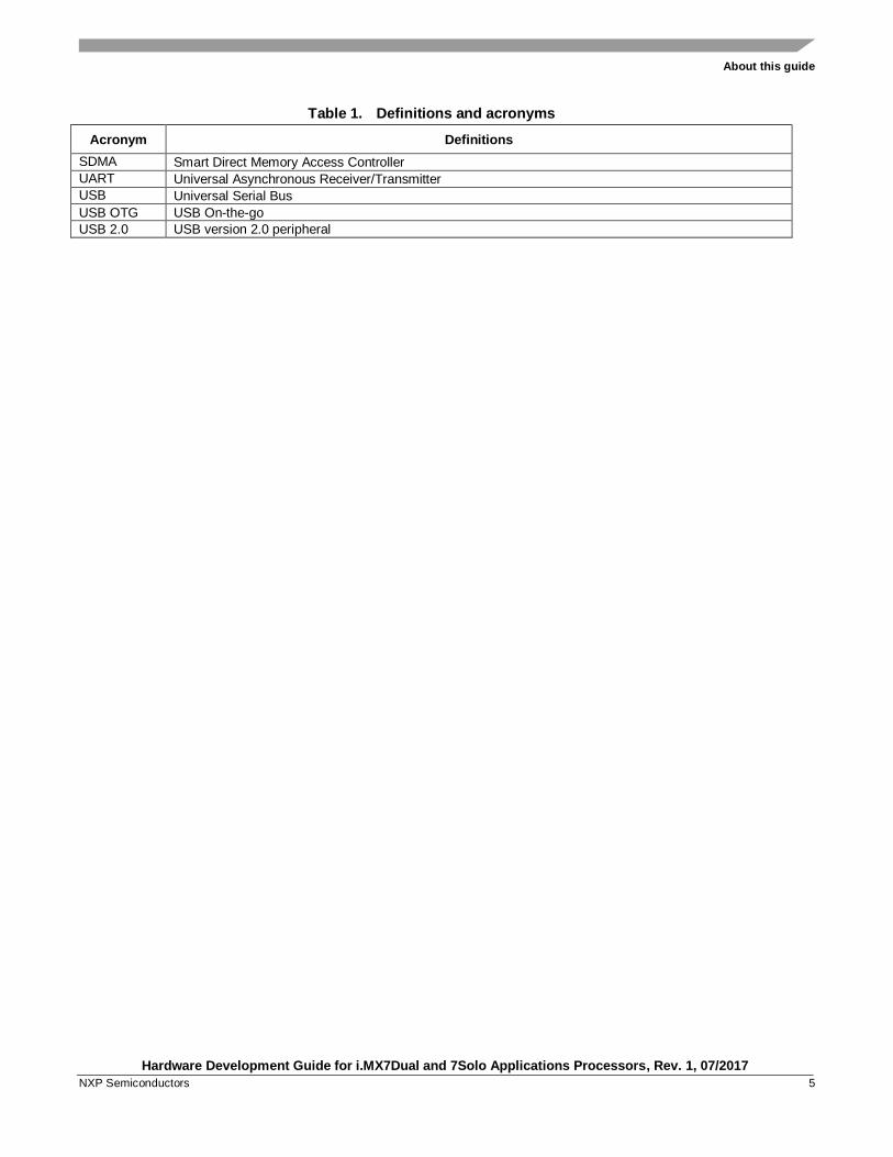
1.7. Acronyms and abbreviations
The following table defines the acronyms and abbreviations used in this document.
Table 1. Definitions and acronyms
Acronym Definitions
ARM Advanced RISC Machines processor architecture
BGA Ball Grid Array package
BOM Bill of Materials
BSDL Boundary Scan Description Language
CAN Flexible Controller Area Network peripheral
CCM Clock Controller Module
CSI MIPI Camera Serial Interface
DDR Dual Data Rate DRAM
DDR3 DDR3 DRAM
DDR3L Low voltage DDR3 DRAM
DDR3U Ultra-low voltage DDR3 DRAM
DRAM Dynamic Random Access Memory
ECSPI Enhanced Configurable SPI peripheral
EIM External Interface Module
ENET 10/100/1000 Mbps Ethernet MAC peripheral
EPIT Enhanced Periodic Interrupt Timer peripheral
ESR Equivalent Series Resistance (of a crystal)
GND Ground
GPC General Power Controller
GPIO General-Purpose Input/Output
HDCP High-bandwidth Digital Content Protection
I2C Inter-integrated Circuit interface
IBIS Input Output Buffer Information Specification
IOMUX i.MX7 chip-level I/O multiplexing
JTAG Joint Test Action Group
KPP Keypad Port Peripheral
LDB LVDS Display Bridge
LDO Low Drop-out Regulator
LPCG Low Power Clock Gating
LPPDR2 Low-power DDR2 DRAM
LVDS Low-voltage Differential Signaling
MLB MediaLB 150 peripheral
MMDC Multi-Mode DDR Controller
ODT On-Die Termination
OTP One-Time Programmable
PCB Printed Circuit Board
PCIe PCI express
PCISig Peripheral Component Interconnect Special Interest Group
PMIC Power Management Integrated Circuit
POR Power-On Reset
RAM Random Access Memory
RGMII Reduced Giagit Media Independent Interface (Ethernet)
RMII Reduced Media Independent Interface (Ethernet)
ROM Read-Only Memory
About this guide
Hardware Development Guide for i.MX7Dual and 7Solo Applications Processors, Rev. 1, 07/2017
NXP Semiconductors 5
Table 1. Definitions and acronyms
Acronym Definitions
SDMA Smart Direct Memory Access Controller
UART Universal Asynchronous Receiver/Transmitter
USB Universal Serial Bus
USB OTG USB On-the-go
USB 2.0 USB version 2.0 peripheral
i.MX7DS design checklist
Hardware Development Guide for i.MX7Dual and 7Solo Applications Processors, Rev. 1, 07/2017
6 NXP Semiconductors
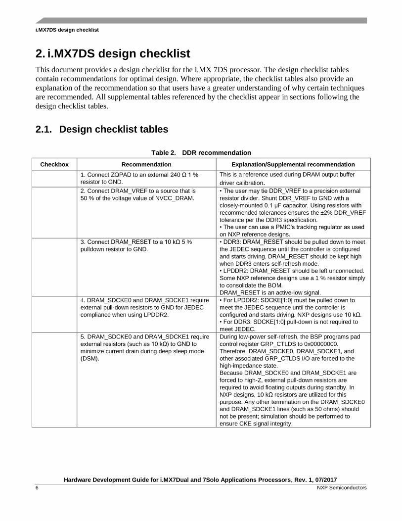
2. i.MX7DS design checklist
This document provides a design checklist for the i.MX 7DS processor. The design checklist tables
contain recommendations for optimal design. Where appropriate, the checklist tables also provide an
explanation of the recommendation so that users have a greater understanding of why certain techniques
are recommended. All supplemental tables referenced by the checklist appear in sections following the
design checklist tables.
2.1. Design checklist tables
Table 2. DDR recommendation
Checkbox Recommendation Explanation/Supplemental recommendation
1. Connect ZQPAD to an external 240 Ω 1 %
resistor to GND.
This is a reference used during DRAM output buffer
driver calibration.
2. Connect DRAM_VREF to a source that is
50 % of the voltage value of NVCC_DRAM.
• The user may tie DDR_VREF to a precision external
resistor divider. Shunt DDR_VREF to GND with a
closely-mounted 0.1 μF capacitor. Using resistors with
recommended tolerances ensures the ±2% DDR_VREF
tolerance per the DDR3 specification.
• The user can use a PMIC’s tracking regulator as used
on NXP reference designs.
3. Connect DRAM_RESET to a 10 kΩ 5 %
pulldown resistor to GND.
• DDR3: DRAM_RESET should be pulled down to meet
the JEDEC sequence until the controller is configured
and starts driving. DRAM_RESET should be kept high
when DDR3 enters self-refresh mode.
• LPDDR2: DRAM_RESET should be left unconnected.
Some NXP reference designs use a 1 % resistor simply
to consolidate the BOM.
DRAM_RESET is an active-low signal.
4. DRAM_SDCKE0 and DRAM_SDCKE1 require
external pull-down resistors to GND for JEDEC
compliance when using LPDDR2.
• For LPDDR2: SDCKE[1:0] must be pulled down to
meet the JEDEC sequence until the controller is
configured and starts driving. NXP designs use 10 kΩ.
• For DDR3: SDCKE[1:0] pull-down is not required to
meet JEDEC.
5. DRAM_SDCKE0 and DRAM_SDCKE1 require
external resistors (such as 10 kΩ) to GND to
minimize current drain during deep sleep mode
(DSM).
During low-power self-refresh, the BSP programs pad
control register GRP_CTLDS to 0x00000000.
Therefore, DRAM_SDCKE0, DRAM_SDCKE1, and
other associated GRP_CTLDS I/O are forced to the
high-impedance state.
Because DRAM_SDCKE0 and DRAM_SDCKE1 are
forced to high-Z, external pull-down resistors are
required to avoid floating outputs during standby. In
NXP designs, 10 kΩ resistors are utilized for this
purpose. Any other termination on the DRAM_SDCKE0
and DRAM_SDCKE1 lines (such as 50 ohms) should
not be present; simulation should be performed to
ensure CKE signal integrity.
i.MX7DS design checklist
Hardware Development Guide for i.MX7Dual and 7Solo Applications Processors, Rev. 1, 07/2017
NXP Semiconductors 7
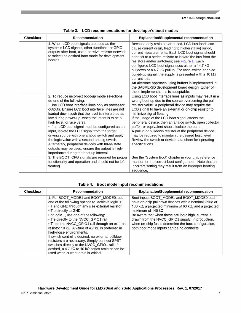
Table 3. LCD recommendations for developer's boot modes
Checkbox Recommendation Explanation/Supplemental recommendation
1. When LCD boot signals are used as the system’s LCD signals, other functions, or GPIO outputs after boot, use a passive resistor network to select the desired boot mode for development boards.
Because only resistors are used, LCD bus loads can
cause current drain, leading to higher (false) supply
current measurements. Each LCD boot signal should
connect to a series resistor to isolate the bus from the
resistors and/or switchers; see Figure 1. Each
configured LCD boot signal sees either a 14.7 kΩ
pulldown or a 4.7 kΩ pullup. For each switch-enabled
pulled-up signal, the supply is presented with a 10 kΩ
current load.
An alternate approach using buffers is implemented in
the SABRE-SD development board design. Either of
these implementations is acceptable.
2. To reduce incorrect boot-up mode selections,
do one of the following:
• Use LCD boot interface lines only as processor
outputs. Ensure LCD boot interface lines are not
loaded down such that the level is interpreted as
low during power-up, when the intent is to be a
high level, or vice versa.
• If an LCD boot signal must be configured as an
input, isolate the LCD signal from the target
driving source with one analog switch and apply
the logic value with a second analog switch.
Alternately, peripheral devices with three-state
outputs may be used; ensure the output is high-
impedance during the boot up interval.
Using LCD boot interface lines as inputs may result in a
wrong boot up due to the source overcoming the pull
resistor value. A peripheral device may require the
LCD signal to have an external or on-chip resistor to
minimize signal floating.
If the usage of the LCD boot signal affects the
peripheral device, then an analog switch, open collector
buffer, or equivalent should isolate the path.
A pullup or pulldown resistor at the peripheral device
may be required to maintain the desired logic level.
Review the switch or device data sheet for operating
specifications.
3. The BOOT_CFG signals are required for proper
functionality and operation and should not be left
floating
See the “System Boot” chapter in your chip reference
manual for the correct boot configuration. Note that an
incorrect setting may result from an improper booting
sequence.
Table 4. Boot mode input recommendations
Checkbox Recommendation Explanation/Supplemental recommendation
1. For BOOT_MODE1 and BOOT_MODE0, use
one of the following options to achieve logic 0:
• Tie to GND through any size external resistor
• Tie directly to GND
For logic 1, use one of the following:
• Tie directly to the NVCC_GPIO1 rail
• Tie to the NVCC_GPIO1 rail through an external
resistor 10 kΩ. A value of 4.7 kΩ is preferred in
high-noise environments. If switch control is desired, no external pulldown resistors are necessary. Simply connect SPST switches directly to the NVCC_GPIO1 rail. If desired, a 4.7 kΩ to 10 kΩ series resistor can be used when current drain is critical.
Boot inputs BOOT_MODE1 and BOOT_MODE0 each
have on-chip pulldown devices with a nominal value of
100 kΩ, a projected minimum of 60 kΩ, and a projected
maximum of 140 kΩ.
Be aware that when these are logic high, current is
drawn from the NVCC_GPIO1 supply. In production,
when on-chip fuses determine the boot configuration,
both boot mode inputs can be no connects
i.MX7DS design checklist
Hardware Development Guide for i.MX7Dual and 7Solo Applications Processors, Rev. 1, 07/2017
8 NXP Semiconductors
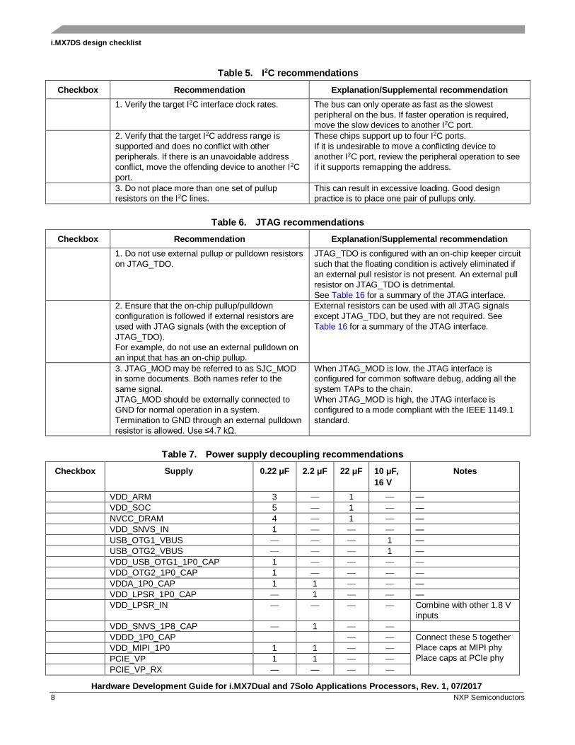
Table 5. I2C recommendations
Checkbox Recommendation Explanation/Supplemental recommendation
1. Verify the target I2C interface clock rates. The bus can only operate as fast as the slowest
peripheral on the bus. If faster operation is required,
move the slow devices to another I2C port.
2. Verify that the target I2C address range is
supported and does no conflict with other
peripherals. If there is an unavoidable address
conflict, move the offending device to another I2C
port.
These chips support up to four I2C ports.
If it is undesirable to move a conflicting device to
another I2C port, review the peripheral operation to see
if it supports remapping the address.
3. Do not place more than one set of pullup
resistors on the I2C lines.
This can result in excessive loading. Good design
practice is to place one pair of pullups only.
Table 6. JTAG recommendations
Checkbox Recommendation Explanation/Supplemental recommendation
1. Do not use external pullup or pulldown resistors
on JTAG_TDO.
JTAG_TDO is configured with an on-chip keeper circuit
such that the floating condition is actively eliminated if
an external pull resistor is not present. An external pull
resistor on JTAG_TDO is detrimental.
See Table 16 for a summary of the JTAG interface.
2. Ensure that the on-chip pullup/pulldown
configuration is followed if external resistors are
used with JTAG signals (with the exception of
JTAG_TDO).
For example, do not use an external pulldown on
an input that has an on-chip pullup.
External resistors can be used with all JTAG signals
except JTAG_TDO, but they are not required. See
Table 16 for a summary of the JTAG interface.
3. JTAG_MOD may be referred to as SJC_MOD
in some documents. Both names refer to the
same signal.
JTAG_MOD should be externally connected to
GND for normal operation in a system.
Termination to GND through an external pulldown
resistor is allowed. Use ≤4.7 kΩ.
When JTAG_MOD is low, the JTAG interface is
configured for common software debug, adding all the
system TAPs to the chain.
When JTAG_MOD is high, the JTAG interface is
configured to a mode compliant with the IEEE 1149.1
standard.
Table 7. Power supply decoupling recommendations
Checkbox Supply 0.22 μF 2.2 μF 22 μF 10 μF,
16 V
Notes
VDD_ARM 3 — 1 — —
VDD_SOC 5 — 1 — —
NVCC_DRAM 4 — 1 — —
VDD_SNVS_IN 1 — — — —
USB_OTG1_VBUS — — — 1 —
USB_OTG2_VBUS — — — 1 —
VDD_USB_OTG1_1P0_CAP 1 — — — —
VDD_OTG2_1P0_CAP 1 — — — —
VDDA_1P0_CAP 1 1 — — —
VDD_LPSR_1P0_CAP — 1 — — —
VDD_LPSR_IN — — — — Combine with other 1.8 V
inputs
VDD_SNVS_1P8_CAP — 1 — —
VDDD_1P0_CAP — — Connect these 5 together
Place caps at MIPI phy
Place caps at PCIe phy VDD_MIPI_1P0 1 1 — —
PCIE_VP 1 1 — —
PCIE_VP_RX — — — —
i.MX7DS design checklist
Hardware Development Guide for i.MX7Dual and 7Solo Applications Processors, Rev. 1, 07/2017
NXP Semiconductors 9
Table 7. Power supply decoupling recommendations
Checkbox Supply 0.22 μF 2.2 μF 22 μF 10 μF,
16 V
Notes
PCIE_VP_TX — — — —
VDDA_PHY_1P8 3 1 — — —
VDDA_MIPI_1P8 — — — — —
PCIE_VPH — — — — Connect these 4 together
PCIE_VPH_TX — — — —
PCIE_VPH_RX — — — —
VDDA_PHY_1P8 — — — —
VDDA_1P8_IN
1 1 — — Connect these 2 together
VDDA_XTAL_1P8
— —
VDD_TEMPSENSOR_1P8 1 1 — — Connect these 3 together
Ferrite bead from same
source as VDDA_1P8_IN VDDA_ADC1_1P8 — — — —
VDDA_ADC2_1P8 — — — —
PVCC_EPDC_LCD_CAP — 1 — — Single cap to GND
PVCC_ENET_CAP — 1 — — Short PVCC_ENET_CAP
to PVCC_SAI_CAP PVCC_SAI_SD_CAP — — —
PVCC_I2C_SPI_UART_CAP — 1 — — Single cap to GND
PVCC_GPIO_CAP — 1 — — Single cap to GND
FUSE_FSOURCE
— — — — Connect directly to a
1.8 V that is nearby and
meets current
requirements
NVCC_GPIO1 1 — — — —
NVCC_GPIO2 1 — — — —
NVCC_SD1 1 — — — —
NVCC_SD2 1 — — — —
NVCC_SD3 1 — — — —
NVCC_ENET1 1 — — — —
NVCC_EPDC1 — — — — Use 470nF
NVCC_EPDC2 — — — — Use 470nF
NVCC_SAI 1 — — — —
NVCC_LCD — 1 — — —
NVCC_SPI 1 — — — —
NVCC_I2C 1 — — — —
NVCC_UART 1 — — — —
VDD_USB_OTG1_3P3_IN 1 1 — — —
VDD_USB_OTG2_3P3_IN 1 1 — — —
DRAM_VREF — — — — Add cap divider and
resistor divider. Or source
from PMIC and follow
PMIC recommendations.
NVCC_DRAM_CKE 1 — — — Can short to
NVCC_DRAM
NOTE
Use the smallest capacitor package size allowed with your design rules.
For 0.22 μF use 0201 or 0402 size. 0201 package preferred
For 2.2 μF caps, 0402 package preferred.
For 22 μF caps, 0603 package preferred.
i.MX7DS design checklist
Hardware Development Guide for i.MX7Dual and 7Solo Applications Processors, Rev. 1, 07/2017
10 NXP Semiconductors
Table 8. Power supply decoupling recommendations
Checkbox Recommendation Explanation/Supplemental recommendation
1. Comply with the power-up sequence guidelines
as described in the data sheet to guarantee
reliable operation of the device.
Any deviation from these sequences may result in the
following situations:
• Excessive current during power-up phase
• Prevention of the device from booting
• Irreversible damage to the processor (worst-case
scenario)
2. Do not overload coin cell backup power rail
VDD_SNVS_IN. Note that the following I/Os are
associated with VDD_SNVS_IN; most inputs have
on-chip pull resistors and do not require external
resistors:
• ONOFF – on-chip pullup
• TAMPER – on-chip pulldown
• PMIC_STBY_REQ – push-pull output
• PMIC_ON_REQ – push-pull output
• TEST_MODE – on-chip pulldown
NXP PMIC PMPF3000 VSNVS regulator is rated to
supply 400 μA output current under worst-case
operating conditions. The VDD_SNVS_IN regulator can
supply larger current in transient situations without
damaging the regulator.
Concerning i.MX7:
• When VDD_SNVS_IN = VDD_IP8_IN, SNVS domain
current is drawn from both equally.
• When VDD_IP8_IN > VDD_SNVS_IN,
VDD_IP8_IN supplies all SNVS domain current and
current flows into VDD_SNVS_IN to charge a coin cell
battery.
• When VDD_SNVS_IN > VDD_IP8_IN,
VDD_SNVS_IN supplies current to SNVS, and some
current flows into VDD_HIGH_IN.
Note: VDD_IP8_IN must be valid (above the internal
detector threshold, 2.4 V typ) for the current flow to
occur. Thus, current flow only happens when
VDD_IP8_IN is powered to a level below
VDD_SNVS_IN. If VDD_IP8_IN is off or low, no extra
current is drawn from VDD_SNVS_IN. The whole circuit
assumes it is charging a coin cell and starts charging
when VDD_IP8_IN is valid. If you are driving
VDD_SNVS_IN with a non-battery power source, it
must be at the same level as VDD_IP8_IN or current
will flow between them.
• When VDD_SNVS_IN is not powered by a battery, it is
recommended that VDD_SNVS_IN = VDD_IP8_IN. If
VDD_SNVS_IN is tied to a battery, the battery
eventually discharges to a value equal to that of
VDD_IP8_IN and never subsequently charges above
VDD_IP8_IN.
The battery chemistry may add restrictions to
VDD_IP8_IN’s voltage range. External charging
components should be based on the battery
manufacturer's specifications.
3. Maximum ripple voltage requirements. Common requirement for ripple noise should be less
than 5 % Vp-p of supply voltage average value.
Related power rails affected: all VDD_xxx_IN and
VDD_xxx_CAP.
4. If VDD_SNVS_IN is directly supplied by a coin
cell, a schottky diode is required between
VDD_IP8_IN and VDD_SNVS_IN. The cathode is
connected to VDD_SNVS_IN.
Alternately, VDD_IP8_IN and VDD_SNVS_IN can
be tied together if the real-time clock function
When no power is supplied to VDD_VSNVS_IN, the
diode limits the voltage difference between the two on-
chip SNVS power domains to approximately 0.3 V.
The processor is designed to allow current flow
between the two SNVS power domains proportional to
the voltage difference.
5. If boundary scan test (BSDL) will be used, the
following supplies must be powered: PCIE_VP,
PCIE_VPH, PCIE_VPTX
The boundary scan test scan chain runs through the
PCIe PHY. If the PCIe PHY supplies are not powered,
the scan chain will not function.
i.MX7DS design checklist
Hardware Development Guide for i.MX7Dual and 7Solo Applications Processors, Rev. 1, 07/2017
NXP Semiconductors 11
Table 9. Oscillator and clock recommendations
Checkbox Recommendation Explanation/Supplemental recommendation
1. Precision 32.768 kHz oscillator Connect a
crystal between RTC_XTALI and RTC_XTALO.
Choose a crystal with a maximum of 100 kΩ ESR
(equivalent series resistance) and follow the
manufacturer’s recommendation for loading
capacitance. Be sure to take into account the
internal load capacitors of the i.MX7
The integrated oscillation amplifier has an on-chip self-
biasing scheme, but is high-impedance (relatively weak)
to minimize power consumption. Care must be taken to
limit parasitic leakage from RTC_XTALI and
RTC_XTALO to either power or ground (> 100 MΩ) as
this negatively affects the amplifier bias and causes a
reduction of startup margin.
Use short traces between the crystal and the processor,
with a ground plane under the crystal, load capacitors,
and associated traces.
2. External kilohertz source If feeding an external
clock into the device, RTC_XTALI can be driven
DC-coupled with RTC_XTALO floated or driven
with a complimentary signal.
The voltage level of this driving clock should not exceed
the voltage of VDD_SNVS_CAP and the frequency
should be <100 kHz under typical conditions. Do not
exceed VDD_SNVS_CAP or damage/malfunction may
occur. The RTC_XTALI signal should not be driven if
the VDD_SNVS_CAP supply is off. This can lead to
damage or malfunction.
For RTC_XTALI VIL and VIH voltage levels, see the
latest i.MX 7 series datasheet available at nxp.com.
Note that if this external clock is stopped, the internal
ring oscillator starts automatically.
Table 10. Reset and ON/OFF recommendations
Checkbox Recommendation Explanation/Supplemental recommendation
1. If the external SRC_POR_B signal is used to
control the processor POR, then SRC_POR_B
must be immediately asserted at power-up and
remain asserted until the VDD_ARM and
VDD_SOC supplies are stable. VDD_ARM and
VDD_SOC may be applied in either order with no
restrictions. In the absence of an external reset
feeding the SRC_POR_B input, the internal POR
module takes control.
A reset switch may be wired to the chip’s POR_B, which
is a cold-reset negative-logic input that resets all
modules and logic in the IC. POR_B may be used in
addition to internally generated power-on reset signal
(logical AND, both internal and external signals are
considered active low).
2. For portable applications, the ONOFF input
may be connected to an ON/OFF SPST push-
button switch. On-chip debouncing is provided,
and this input has an on-chip pullup. If not used,
ONOFF should be a no connect.
A brief connection to GND in OFF mode causes the
internal power management state machine to change
state to ON. In ON mode, a brief connection to GND
generates an interrupt (intended to be a software-
controllable power-down).
An approximate 5 second or more connection to GND
causes a forced OFF.
Table 11. PCIE recommendations
Checkbox Recommendation Explanation/Supplemental recommendation
1. Appropriative PCIe reference clock generator is
suggested. i.MX differential clock is not
compliance with PCIe standard.
—
2. The differential transmitter must be ac coupled.
Use a 0.1 μF-series capacitor on PCIE_TXP and
a second 0.1 μF on PCIE_TXM.
To ensure PCIe specification compliance, ac coupling is
required at each transmitter. The receiver must be DC
coupled.
i.MX7DS design checklist
Hardware Development Guide for i.MX7Dual and 7Solo Applications Processors, Rev. 1, 07/2017
12 NXP Semiconductors
3. PCIe Jitter compliance
NXP recommends including an external clock
source that meets the PCIe jitter specification
untils the i.MX 7DS PCIe jitter compliance can be
assessed.
—
Table 12. USB recommendations
Checkbox Recommendation Explanation/Supplemental recommendation
1. USB OTG
To comply with the USB OTG specification, the
VBUS supply on the OTG connector should
default to off when the boards power up.
The processor should turn VBUS on as required.
Table 13. Reference resistor recommendations
Checkbox Recommendation Explanation/Supplemental recommendation
1. PCIE_REXT – Connect an external 4.7 KΩ 1%
resistor to GND.
The impedance calibration process requires connection
of this reference resistor. If PCIe is unused, the
reference resistor may be populated if desired for
manufacturability purposes, or left no-connect for cost
savings.
Table 14. Miscellaneous recommendations
Checkbox Recommendation Explanation/Supplemental recommendation
1. The TEST_MODE input is internally connected
to an on-chip pulldown device. The user must tie
this signal to GND.
This input is reserved for NXP manufacturing use.
2. For termination of unused analog interfaces,
see Datasheet for this part.
—
3. GPANAIO must be a no connect. The user
must leave this connection floating.
This output is reserved for NXP manufacturing use.
4. NC contacts are no connect and should be
floated.
Depending on the feature set, some versions of the IC
may have NC contacts connected inside the BGA.
i.MX7DS design checklist
Hardware Development Guide for i.MX7Dual and 7Solo Applications Processors, Rev. 1, 07/2017
NXP Semiconductors 13
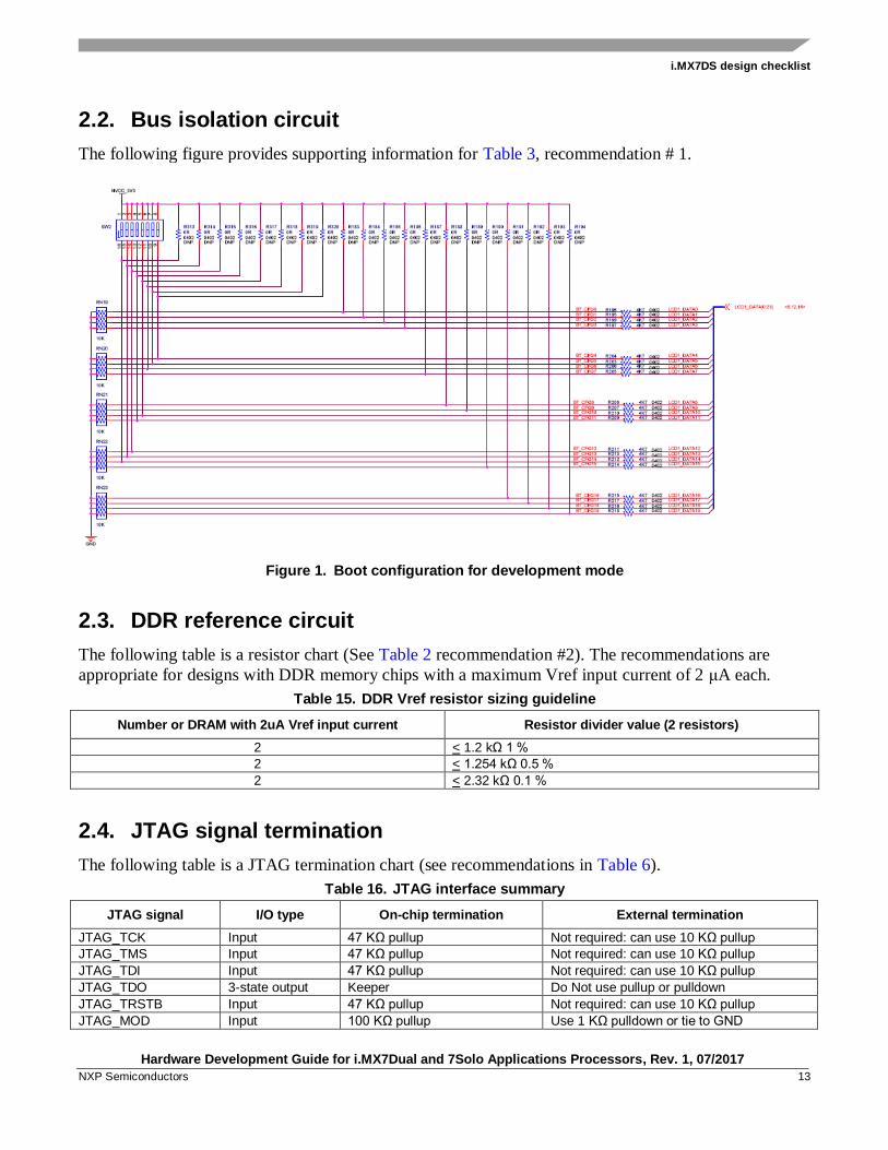
2.2. Bus isolation circuit
The following figure provides supporting information for Table 3, recommendation # 1.
Figure 1. Boot configuration for development mode
2.3. DDR reference circuit
The following table is a resistor chart (See Table 2 recommendation #2). The recommendations are
appropriate for designs with DDR memory chips with a maximum Vref input current of 2 μA each.
Table 15. DDR Vref resistor sizing guideline
Number or DRAM with 2uA Vref input current Resistor divider value (2 resistors)
2 < 1.2 kΩ 1 %
2 < 1.254 kΩ 0.5 %
2 < 2.32 kΩ 0.1 %
2.4. JTAG signal termination
The following table is a JTAG termination chart (see recommendations in Table 6).
Table 16. JTAG interface summary
JTAG signal I/O type On-chip termination External termination
JTAG_TCK Input 47 KΩ pullup Not required: can use 10 KΩ pullup
JTAG_TMS Input 47 KΩ pullup Not required: can use 10 KΩ pullup
JTAG_TDI Input 47 KΩ pullup Not required: can use 10 KΩ pullup
JTAG_TDO 3-state output Keeper Do Not use pullup or pulldown
JTAG_TRSTB Input 47 KΩ pullup Not required: can use 10 KΩ pullup
JTAG_MOD Input 100 KΩ pullup Use 1 KΩ pulldown or tie to GND
i.MX7DS design checklist
Hardware Development Guide for i.MX7Dual and 7Solo Applications Processors, Rev. 1, 07/2017
14 NXP Semiconductors
2.5. Oscillator tolerance
The following table provides 24 MHz oscillator tolerance guidelines (see Table 9, recommendations #4
and #5). Because these are guidelines, the designer must verify all tolerances per the official
specifications.
Table 17. 24 MHz crystal tolerance guidelines
Interface Tolerance (+ ppm)
Ethernet 50
USB 2.0 500
PCIe 300
2.6. Unused analog interfaces
For recommendations for unused analog interfaces see appropriate i.MX7 Datasheet section
“3.2 Recommended connections for unused analog interfaces.”
i.MX7 series layout recommendations
Hardware Development Guide for i.MX7Dual and 7Solo Applications Processors, Rev. 1, 07/2017
NXP Semiconductors 15
3. i.MX7 series layout recommendations
3.1. Introduction
This chapter provides recommendations to assist design engineers with the layout of an i.MX7 series-
based system.
3.2. Basic design recommendations
The i.MX 7DS processor comes in multiple packages. For detailed information, see the i.MX 7
datasheets.
When using the Allegro tool, optimal practice is to use the footprint as created by NXP. When not using
the Allegro tool, use the Allegro footprint export feature (supported by many tools). If export is not
possible, create the footprint per the package mechanical dimensions outlined in the product data sheet.
Native Allegro layout and gerber files are available on nxp.com.
3.2.1. Placing decoupling capacitors
Place small decoupling and larger bulk capacitors on the bottom side of the PCB.
The 0201 decoupling and 0603 bulk capacitors should be mounted as close as possible to the power vias.
The distance should be less than 50 mils. Additional bulk capacitors can be placed near the edge of the
BGA via array. Placing the decoupling capacitors close to the power balls is critical to minimize
inductance and ensure high-speed transient current demand by the processor.
A correct via size is critical for preserving adequate routing space. The recommended geometry for the
via pads is: pad size 18 mils and drill 8 mils.
The following list provides the main recommendations for choosing the correct decoupling scheme:
• Place the largest capacitance in the smallest package that budget and manufacturing can support.
• For high speed bypassing, select the required capacitance with the smallest package (for
example, 0.22 μF and package 0201).
• Minimize trace length (inductance) to small caps.
• Series inductance cancels out capacitance.
• Tie caps to GND plane directly with a via.
• Place capacitors close to the power contact of the associate package designed from the
schematic.
• A preferred BGA power decoupling design is the layout is available through nxp.com.
Customers should use the NXP design strategy for power and decoupling.
3.3. Stack-up recommendations
High-speed design requires a good stack-up in order have the right impedance for the critical traces. The
constraints for the trace width may depend on a number of factors, such as the board stack-up and
i.MX7 series layout recommendations
Hardware Development Guide for i.MX7Dual and 7Solo Applications Processors, Rev. 1, 07/2017
16 NXP Semiconductors
associated dielectric and copper thickness, required impedance, and required current (for power traces).
The NXP reference design uses a minimum trace width of 3 mils for the DDR routing. The stack-up also
determines the constraints for routing and spacing.
Consider the following when designing the stack-up and selecting the material for your board.
• Board stack-up is critical for high-speed signal quality.
• You must preplan impedance of critical traces
• High-speed signals must have reference planes on adjacent layers to minimize cross-talk.
• FSL reference design equals Isola 370HR.
• FSL validation boards equals Isola FR408.
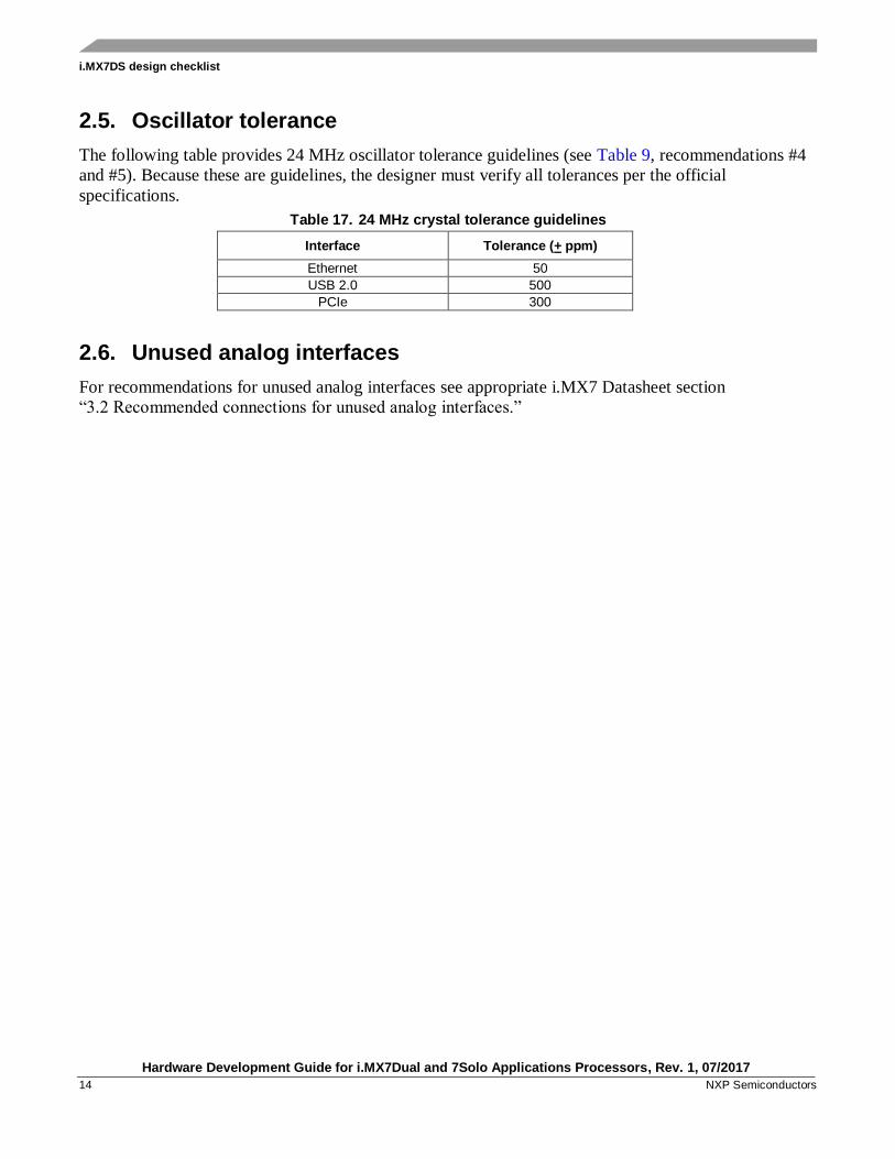
The recommended stack-up is 8-layers, with the layer stack as shown in the following figure. The left-
hand image shows the detail provided by NXP inside the fabrication detail as a part of the Gerber files.
The right-and side shows the solution suggested by the PCB fabrication company for our requirements.
Figure 2. Layer stack SABRE SD board
The following table shows a working stack-up implementation:
Table 18. Stackup implementation
Layers
Single Ended Differential
Trace width (Mils)
Impedance (Ωs)
Trace width (Mils)
Trace spacing ‘Airgap’ (Mils)
Impedance (Ωs)
Trace width (Mils)
Tracespacing ‘Airgap’ (Mils)
Impedance (Ωs)
TOP 4.7 50 4.3 5.8 90 3.7 5.3 100
INT1 4.5 50 4.2 5.8 90 3.8 5.2
INT2 4.5 50 4.2 5.8 90 3.8 5.2
BOT 4.7 50 4.3 5.7 90 3.7 533 100
i.MX7 series layout recommendations
Hardware Development Guide for i.MX7Dual and 7Solo Applications Processors, Rev. 1, 07/2017
NXP Semiconductors 17
Figure 3. Example top layer impedance from PCB fabricator
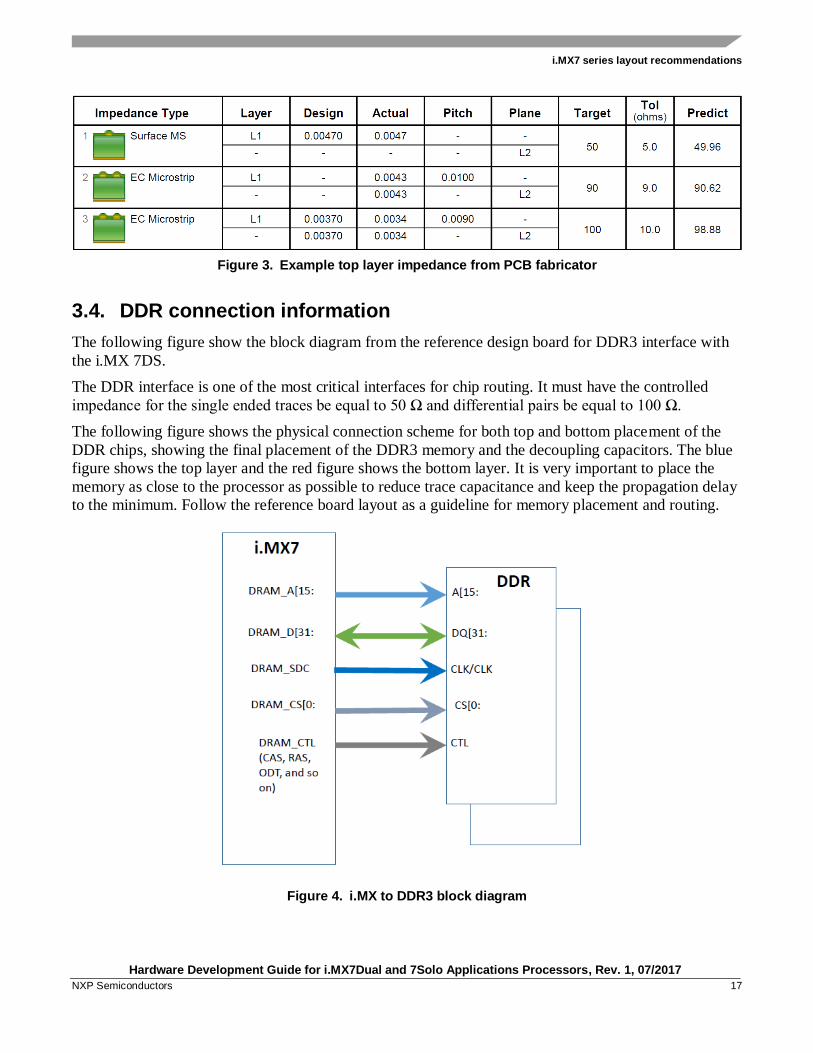
3.4. DDR connection information
The following figure show the block diagram from the reference design board for DDR3 interface with
the i.MX 7DS.
The DDR interface is one of the most critical interfaces for chip routing. It must have the controlled
impedance for the single ended traces be equal to 50 Ω and differential pairs be equal to 100 Ω.
The following figure shows the physical connection scheme for both top and bottom placement of the
DDR chips, showing the final placement of the DDR3 memory and the decoupling capacitors. The blue
figure shows the top layer and the red figure shows the bottom layer. It is very important to place the
memory as close to the processor as possible to reduce trace capacitance and keep the propagation delay
to the minimum. Follow the reference board layout as a guideline for memory placement and routing.
Figure 4. i.MX to DDR3 block diagram
i.MX7 series layout recommendations
Hardware Development Guide for i.MX7Dual and 7Solo Applications Processors, Rev. 1, 07/2017
18 NXP Semiconductors
3.4.1. DDR routing rules
The i.MX7D processor is not capable of automatically calibrating each DQS strobe to arrive at the
DRAM in phase with the SDCLK signal. Therefore, Fly-By topologies are not recommended or
supported for designs i.MX7D. The following table provides DDR trace routing guidelines:
Table 19. DDR trace routing guidelines
Group Chip signals DRAM Type Length
Recommendations Min Max
Clock
DRAM_SDCLK[1:0]
DRAM_SDCLK_B[1:0] DDR3
Short as
possible 1900mils
Match the signals ± 5 mils.
LPDDR2/3 Short as
possible 1400mils
Address and
Command
DRAM_A[15:0]
DRAM_SDBA[2:0]
DRAM_RAS
DRAM_CAS
DRAM_SDWE
DRAM_CS
DRAM_CKE
DRAM_ODT
DDR3
Clock (min) –
55 mils
Clock (min)
+ 55 mils
Best practice is to match the signals ±
55 mils.
DRAM_A[9:0]
DRAM_CS
DRAM_CKE
LPDDR2/3
Byte Group
1
DRAM_D[7:0]
DRAM_DQM0
DRAM_SDQS0
DRAM_SDQS0_B
— — —
Best Practice:
DQS strobe should have maximum
length of Clock -10 mils
Match the differential signals of each
DQS pair ± 5 mils.
Match the signals of each byte group ±
55 mils to the strobe.
Limit minimum DQS length to Clock
(min) – 200 mils.
If the DQS strobe is more than 200 mils
shorter than Clock (min), consider
manually adjusting each field of register
DDR_PHY_LVL_CON0.
Increment +1 for each 100 mils that the
DQS trace is shorter than Clock (min).
Byte Group
2
DRAM_D[15:8]
DRAM_DQM1
DRAM_SDQS1
DRAM_SDQS1_B
— — —
Byte Group
3
DRAM_D[23:16]
DRAM_DQM2
DRAM_SDQS2
DRAM_SDQS2_B
— — —
Byte Group
4
DRAM_D[31:24]
DRAM_DQM3
DRAM_SDQS3
DRAM_SDQS3_B
— — —
i.MX7 series layout recommendations
Hardware Development Guide for i.MX7Dual and 7Solo Applications Processors, Rev. 1, 07/2017
NXP Semiconductors 19
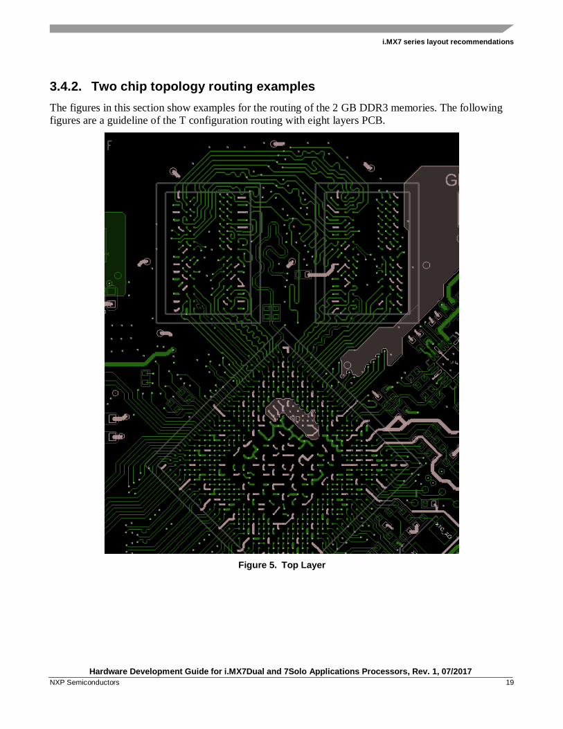
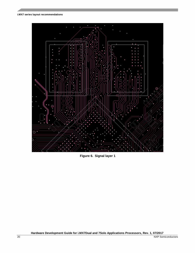
3.4.2. Two chip topology routing examples
The figures in this section show examples for the routing of the 2 GB DDR3 memories. The following
figures are a guideline of the T configuration routing with eight layers PCB.
Figure 5. Top Layer
i.MX7 series layout recommendations
Hardware Development Guide for i.MX7Dual and 7Solo Applications Processors, Rev. 1, 07/2017
20 NXP Semiconductors
Figure 6. Signal layer 1
i.MX7 series layout recommendations
Hardware Development Guide for i.MX7Dual and 7Solo Applications Processors, Rev. 1, 07/2017
NXP Semiconductors 21
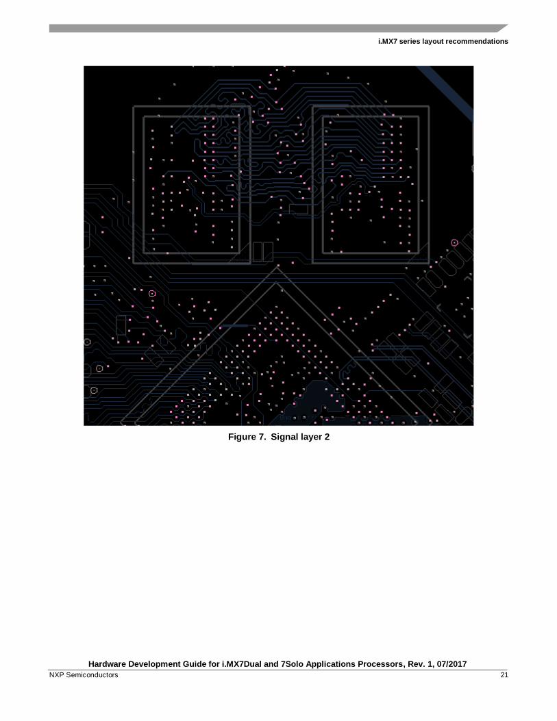
Figure 7. Signal layer 2
i.MX7 series layout recommendations
Hardware Development Guide for i.MX7Dual and 7Solo Applications Processors, Rev. 1, 07/2017
22 NXP Semiconductors
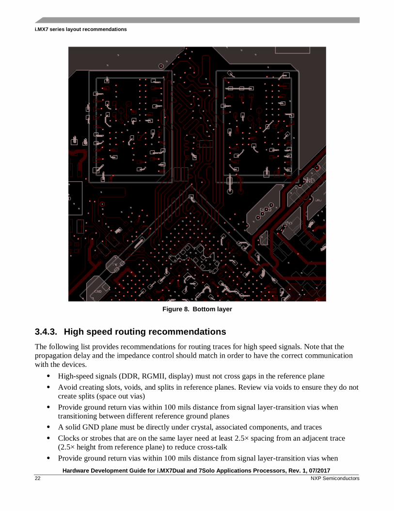
Figure 8. Bottom layer
3.4.3. High speed routing recommendations
The following list provides recommendations for routing traces for high speed signals. Note that the
propagation delay and the impedance control should match in order to have the correct communication
with the devices.
• High-speed signals (DDR, RGMII, display) must not cross gaps in the reference plane
• Avoid creating slots, voids, and splits in reference planes. Review via voids to ensure they do not
create splits (space out vias)
• Provide ground return vias within 100 mils distance from signal layer-transition vias when
transitioning between different reference ground planes
• A solid GND plane must be directly under crystal, associated components, and traces
• Clocks or strobes that are on the same layer need at least 2.5× spacing from an adjacent trace
(2.5× height from reference plane) to reduce cross-talk
• Provide ground return vias within 100 mils distance from signal layer-transition vias when
i.MX7 series layout recommendations
Hardware Development Guide for i.MX7Dual and 7Solo Applications Processors, Rev. 1, 07/2017
NXP Semiconductors 23
transitioning between different reference ground planes
• All synchronous modules should have bus length matching and relative clock length control
For SD module interfaces:
— Match data and CMD trace lengths (length delta depends on bus rates)
— CLK should be longer than the longest signal in the Data/CMD group (+5 mils)
— Similar DDR rules must be followed for data, address and control as for SD module
interfaces
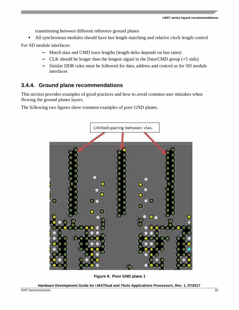
3.4.4. Ground plane recommendations
This section provides examples of good practices and how to avoid common user mistakes when
flowing the ground planes layers.
The following two figures show common examples of poor GND planes.
Figure 9. Poor GND plane 1
i.MX7 series layout recommendations
Hardware Development Guide for i.MX7Dual and 7Solo Applications Processors, Rev. 1, 07/2017
24 NXP Semiconductors
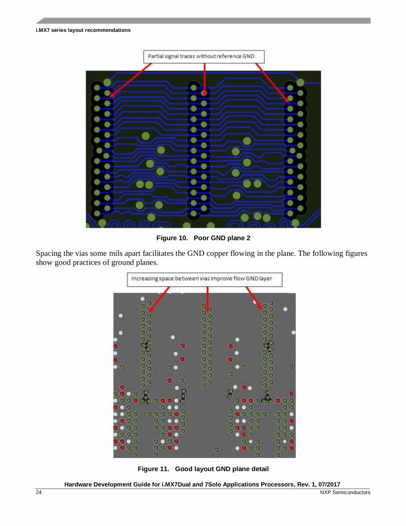
Figure 10. Poor GND plane 2
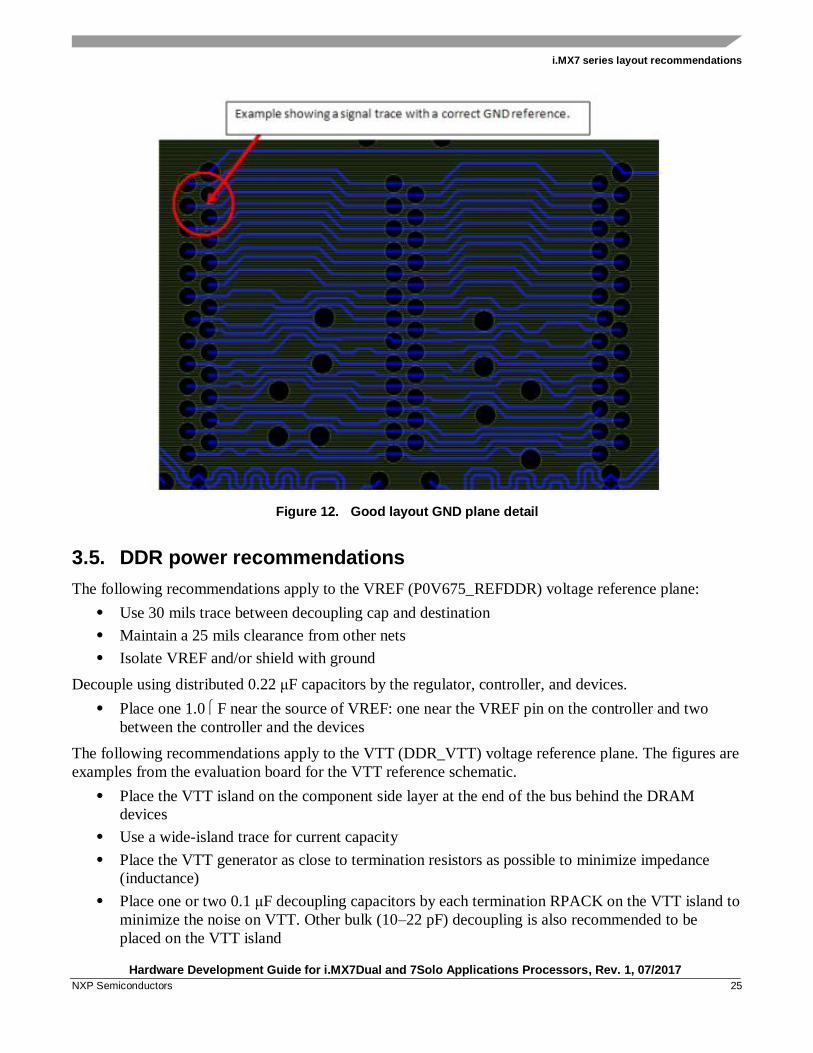
Spacing the vias some mils apart facilitates the GND copper flowing in the plane. The following figures
show good practices of ground planes.
Figure 11. Good layout GND plane detail
i.MX7 series layout recommendations
Hardware Development Guide for i.MX7Dual and 7Solo Applications Processors, Rev. 1, 07/2017
NXP Semiconductors 25
Figure 12. Good layout GND plane detail
3.5. DDR power recommendations
The following recommendations apply to the VREF (P0V675_REFDDR) voltage reference plane:
• Use 30 mils trace between decoupling cap and destination
• Maintain a 25 mils clearance from other nets
• Isolate VREF and/or shield with ground
Decouple using distributed 0.22 μF capacitors by the regulator, controller, and devices.
• Place one 1.0 F near the source of VREF: one near the VREF pin on the controller and two
between the controller and the devices
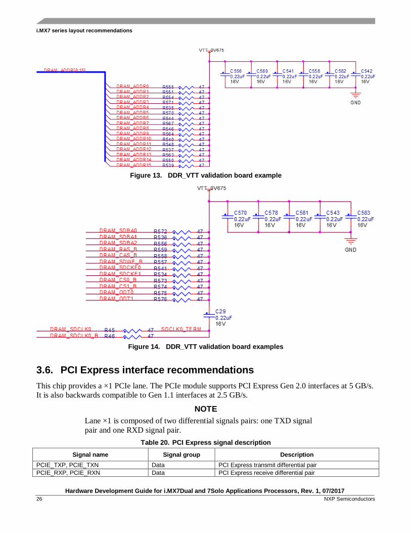
The following recommendations apply to the VTT (DDR_VTT) voltage reference plane. The figures are
examples from the evaluation board for the VTT reference schematic.
• Place the VTT island on the component side layer at the end of the bus behind the DRAM
devices
• Use a wide-island trace for current capacity
• Place the VTT generator as close to termination resistors as possible to minimize impedance
(inductance)
• Place one or two 0.1 μF decoupling capacitors by each termination RPACK on the VTT island to
minimize the noise on VTT. Other bulk (10–22 pF) decoupling is also recommended to be
placed on the VTT island
i.MX7 series layout recommendations
Hardware Development Guide for i.MX7Dual and 7Solo Applications Processors, Rev. 1, 07/2017
26 NXP Semiconductors
Figure 13. DDR_VTT validation board example
Figure 14. DDR_VTT validation board examples
3.6. PCI Express interface recommendations
This chip provides a ×1 PCIe lane. The PCIe module supports PCI Express Gen 2.0 interfaces at 5 GB/s.
It is also backwards compatible to Gen 1.1 interfaces at 2.5 GB/s.
NOTE
Lane ×1 is composed of two differential signals pairs: one TXD signal
pair and one RXD signal pair.
Table 20. PCI Express signal description
Signal name Signal group Description
PCIE_TXP, PCIE_TXN Data PCI Express transmit differential pair
PCIE_RXP, PCIE_RXN Data PCI Express receive differential pair
i.MX7 series layout recommendations
Hardware Development Guide for i.MX7Dual and 7Solo Applications Processors, Rev. 1, 07/2017
NXP Semiconductors 27
3.6.1. PCI Express general routing guidelines
Use the following recommendations for PCI Express general routing:
• The trace width and spacing of the lanes ×1 signals should be such that the differential
impedance is 85 Ω ± 10 %
• The PCIE_REXT contacts should be connected to a 200 1 % resistor to ground. The trace
length between the pin and the resistor should be minimized. The resistor value is defined within
the data sheet and should determine the exact resistor value
• Route traces over continuous planes (power and ground):
— They should not pass over any power/GND plane slots or anti-etch
— When placing connectors, make sure the ground plane clear-outs around each pin have
ground continuity between all pins
• Maintain the parallelism (skew matched) between DP and DM, and match overall differential
length difference to less than 5 mils
• Maintain symmetric routing for each differential pair
• Do not route DP and DM traces under oscillators or parallel to clock traces and/or data buses.
• Minimize the lengths of high speed signals that run parallel to the DP and DM pair
• Keep DP and DM traces as short as possible
• Route DP and DM signals with a minimum amount of corners. Use 45-degree turns instead of
90-degree turns
• Avoid layer changes (vias) on DP and DM signals. Do not create stubs or branches
• Provide ground return vias within 50 mils distance from signal layer-transition vias when
transitioning between different reference ground planes
3.6.2. PCI Express coupling lane
Based on our development design, we have the following coupling signal schema. Consult the PCISig
documentation for detailed information.
• DC-coupled Rx signals with 0 Ωresistors
• AC-coupled Tx signals with 0.1 μF capacitors
3.6.3. Additional resources for PCI Express signal routing
recommendations
For more information about PCI Express signal routing recommendations see the following.
• NXP Hardware Design Considerations for PCI Express® and SGMII
(http://www.nxp.com/support/online-academy/hardware-design-considerations-for-pci-express-
and-sgmii:TP_HARDWARE_DESIGN_PCI_SMGIII?fsrch=1&sr=1&pageNum=1)
• PCISig, PCI Express Base Specification
• PCISig, PCI Express Card Electromechanical Specification
• PCISig, PCSIG Board Design Guidelines for PCI Express™ Architecture
i.MX7 series layout recommendations
Hardware Development Guide for i.MX7Dual and 7Solo Applications Processors, Rev. 1, 07/2017
28 NXP Semiconductors
• PCI Express Basics: Developing Physical Design Rules for PCIe
(http://www.mentor.com/products/pcb-system-design/multimedia/pcie-basics-webinar)
3.6.4. USB recommendations
Use the following recommendations for the USB:
• Route the high speed clocks and the DP and DM differential pair first
• Route DP and DM signals on the top or bottom layer of the board
• The trace width and spacing of the DP and DM signals should meet the differential impedance
requirement of 90
• Route traces over continuous planes (power and ground):
— They should not pass over any power/GND plane slots or anti-etch
— When placing connectors, make sure the ground plane clearouts around each pin have
ground continuity between all pins
• Maintain the parallelism (skew matched) between DP and DM, and match overall differential
length difference to less than 5 mils
• Maintain symmetric routing for each differential pair
• Do not route DP and DM traces under oscillators or parallel to clock traces and/or data buses
• Minimize the lengths of high speed signals that run parallel to the DP and DM pair
• Keep DP and DM traces as short as possible
• Route DP and DM signals with a minimum amount of corners. Use 45-degree turns instead of
90-degree turns
• Avoid layer changes (vias) on DP and DM signals. Do not create stubs or branches
• Provide ground return vias within 50 mils distance from signal layer-transition vias when
transitioning between different reference ground planes
3.6.5. Impedance signal recommendations
Use the following table as a reference when you are updating or creating constraints in your software
PCB tool to set up the impedance and the correct trace width.
Table 21. Impedance signal recommendations
Signal Group Impedance Layout Tolerance (+)
All signals, unless specified 50 Ω SE 10 %
PCIe Diff signals 85 Ω Diff 10 %
USB Diff signals 90 Ω Diff 10 %
Diff signals:
DDR, Phy IC to Ethernet Connector
100 Ω Diff 10 %
i.MX7 series layout recommendations
Hardware Development Guide for i.MX7Dual and 7Solo Applications Processors, Rev. 1, 07/2017
NXP Semiconductors 29
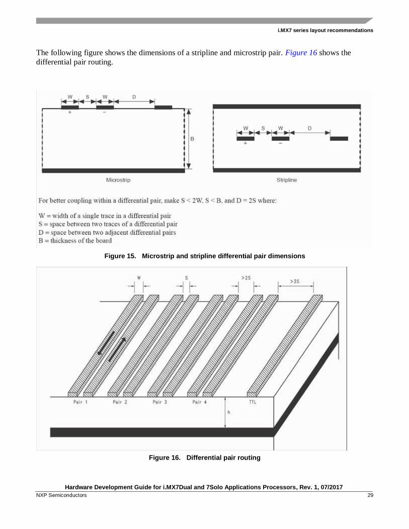
The following figure shows the dimensions of a stripline and microstrip pair. Figure 16 shows the
differential pair routing.
Figure 15. Microstrip and stripline differential pair dimensions
Figure 16. Differential pair routing

i.MX7 series layout recommendations
Hardware Development Guide for i.MX7Dual and 7Solo Applications Processors, Rev. 1, 07/2017
30 NXP Semiconductors
• The space between two adjacent differential pairs should be greater than or equal to twice the
space between the two individual conductors.
• The skew between LVDS pairs should be within the minimum recommendation (± 100 mil).
3.7. Reference resistors
NOTE
The reference resistor and the connection should be placed away from
noisy regions. Noise induced on it may impact the internal circuit and
degrade the interface signals.
3.8. ESD and radiated emissions recommendations
The PCB design should use six or more layers, with solid power and ground planes. The
recommendations for ESD immunity and radiated emissions performance are as follows:
• All components with ground chassis shields (USB jack, buttons, and so on) should connect the
shield to the PCB chassis ground ring.
• Ferrite beads should be placed on each signal line connecting to an external cable. These ferrite
beads must be placed as close to the PCB jack as possible.
NOTE
Ferrite beads should have a minimum impedance of 500 at 100 MHz
with the exception of the ferrite on USB_5V.
• Ferrite beads should NOT be placed on the USB D+/D– signal lines as this can cause USB signal
integrity problems. For radiated emissions problems due to USB, a common mode choke may be
placed on the D+/D– signal lines. However, in most cases, it should not be required if the PCB
layout is satisfactory. Ideally, the common mode choke should be approved for high speed USB
use or tested thoroughly to verify there are no signal integrity issues created.
• It is highly recommended that ESD protection devices be used on ports connecting to external
connectors. See the reference schematic (available at nxp.com) for detailed information about
ESD protection implementation on the USB interfaces.
• If possible, stitch all around the board with vias with 100 mils spacing between them connected
to GND planes with exposed solder mask to improve EMI.
3.9. Component placement recommendations
Adhere to the following recommendations when placing components:
• Place components such that short and/or critical routes can be easily laid out.
— Critical routes determine component location
— Orient devices to facilitate routes (minimize length and crossovers)
Consider placing the following pairings adjacent:
i.MX7 series layout recommendations
Hardware Development Guide for i.MX7Dual and 7Solo Applications Processors, Rev. 1, 07/2017
NXP Semiconductors 31
— i.MX and DDR
— PHY and associated jack
— Jack and CODEC input
— Bluetooth® (or other RF) and antenna
3.10. Reducing skew and phase problems in deferential pairs traces
Differential pair technology has evolved to require more stringent checking in the area of phase control.
This is evident on the higher data rates associated with parallel buses such as PCI Gen 2, DDR, LVDS,
or Ethernet. In the simplest of terms, Diff Pair technology sends opposite and equal signals down a pair
of traces. Keeping these opposite signals in phase is essential to assuring that they function as intended.
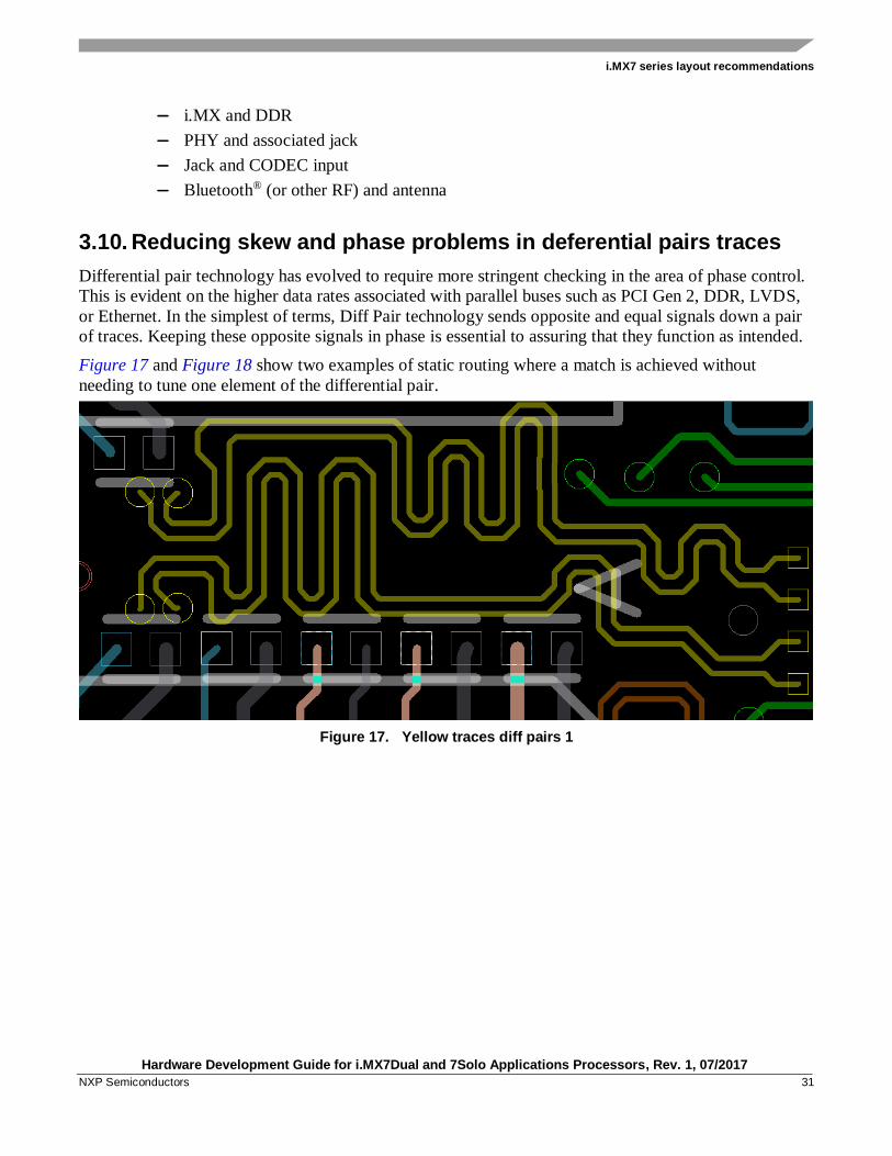
Figure 17 and Figure 18 show two examples of static routing where a match is achieved without
needing to tune one element of the differential pair.
Figure 17. Yellow traces diff pairs 1
i.MX7 series layout recommendations
Hardware Development Guide for i.MX7Dual and 7Solo Applications Processors, Rev. 1, 07/2017
32 NXP Semiconductors
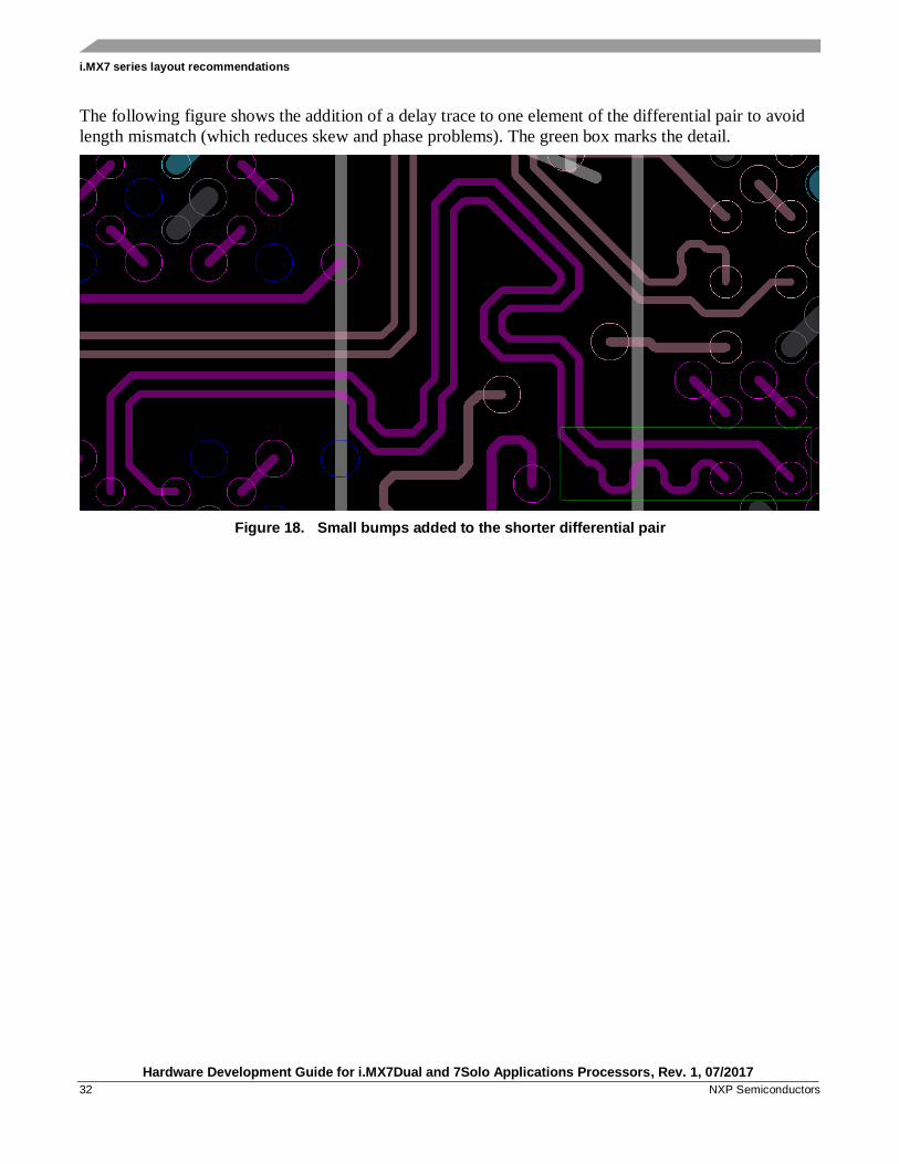
The following figure shows the addition of a delay trace to one element of the differential pair to avoid
length mismatch (which reduces skew and phase problems). The green box marks the detail.
Figure 18. Small bumps added to the shorter differential pair
Avoiding board bring-up problems
Hardware Development Guide for i.MX7Dual and 7Solo Applications Processors, Rev. 1, 07/2017
NXP Semiconductors 33
4. Avoiding board bring-up problems
4.1. Introduction
This chapter provides recommendations for avoiding typical mistakes when bringing up a board for the
first time. These recommendations consist of basic techniques that have proven useful in the past for
detecting board issues and addressing the three most typical bring-up pitfalls: power, clocks, and reset.
A sample bring-up checklist is provided at the end of the chapter.
4.2. Using a current monitor to avoid power pitfalls
Using incorrect voltage rails is a common power pitfall. To help avoid this mistake, create a basic table
called a voltage report prior to bringing up your board. This table helps validate that all the supplies are
reaching the expected levels.
To create a voltage report, list the following:
• Your board voltage sources
• Default power-up values for the board voltage sources
• Best location on the board to measure the voltage level of each supply
Carefully determine the best measurement location for each power supply to avoid a large voltage drop
(IR drop) on the board, which causes inaccurate current values to be measured. The following guidelines
help produce the best current measurements:
• Measure closest to the load (in this case the i.MX6 processor)
• Make two measurements: the first after initial board power-up and the second while running a
heavy use-case that stresses the i.MX7 processor
Ensure that the supplies that are powering the i.MX7 meet the DC electrical specifications as listed in
your chip-specific data sheet.
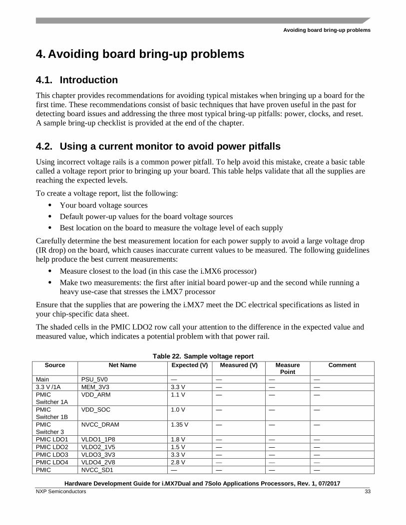
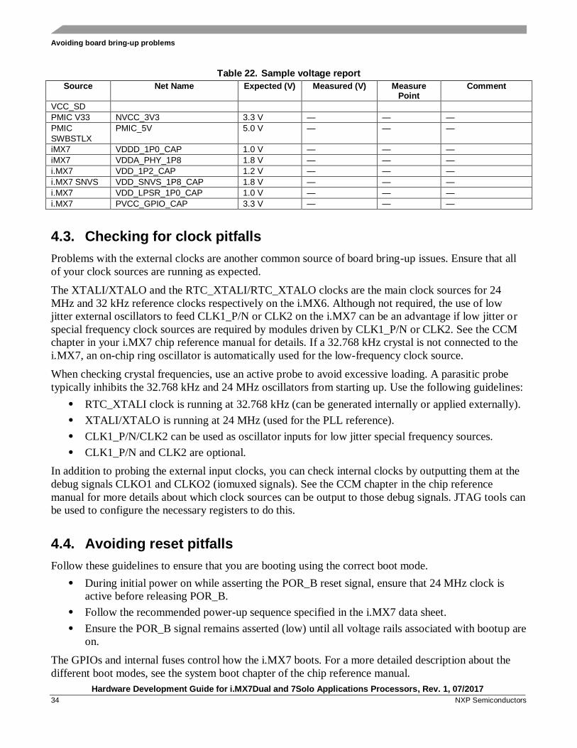
The shaded cells in the PMIC LDO2 row call your attention to the difference in the expected value and
measured value, which indicates a potential problem with that power rail.
Table 22. Sample voltage report
Source Net Name Expected (V) Measured (V) Measure Point
Comment
Main PSU_5V0 — — — —
3.3 V /1A MEM_3V3 3.3 V — — —
PMIC
Switcher 1A
VDD_ARM 1.1 V — — —
PMIC
Switcher 1B
VDD_SOC 1.0 V — — —
PMIC
Switcher 3
NVCC_DRAM 1.35 V — — —
PMIC LDO1 VLDO1_1P8 1.8 V — — —
PMIC LDO2 VLDO2_1V5 1.5 V — — —
PMIC LDO3 VLDO3_3V3 3.3 V — — —
PMIC LDO4 VLDO4_2V8 2.8 V — — —
PMIC NVCC_SD1 — — — —
Avoiding board bring-up problems
Hardware Development Guide for i.MX7Dual and 7Solo Applications Processors, Rev. 1, 07/2017
34 NXP Semiconductors
Table 22. Sample voltage report
Source Net Name Expected (V) Measured (V) Measure Point
Comment
VCC_SD
PMIC V33 NVCC_3V3 3.3 V — — —
PMIC
SWBSTLX
PMIC_5V 5.0 V — — —
iMX7 VDDD_1P0_CAP 1.0 V — — —
iMX7 VDDA_PHY_1P8 1.8 V — — —
i.MX7 VDD_1P2_CAP 1.2 V — — —
i.MX7 SNVS VDD_SNVS_1P8_CAP 1.8 V — — —
i.MX7 VDD_LPSR_1P0_CAP 1.0 V — — —
i.MX7 PVCC_GPIO_CAP 3.3 V — — —
4.3. Checking for clock pitfalls
Problems with the external clocks are another common source of board bring-up issues. Ensure that all
of your clock sources are running as expected.
The XTALI/XTALO and the RTC_XTALI/RTC_XTALO clocks are the main clock sources for 24
MHz and 32 kHz reference clocks respectively on the i.MX6. Although not required, the use of low
jitter external oscillators to feed CLK1_P/N or CLK2 on the i.MX7 can be an advantage if low jitter or
special frequency clock sources are required by modules driven by CLK1_P/N or CLK2. See the CCM
chapter in your i.MX7 chip reference manual for details. If a 32.768 kHz crystal is not connected to the
i.MX7, an on-chip ring oscillator is automatically used for the low-frequency clock source.
When checking crystal frequencies, use an active probe to avoid excessive loading. A parasitic probe
typically inhibits the 32.768 kHz and 24 MHz oscillators from starting up. Use the following guidelines:
• RTC_XTALI clock is running at 32.768 kHz (can be generated internally or applied externally).
• XTALI/XTALO is running at 24 MHz (used for the PLL reference).
• CLK1_P/N/CLK2 can be used as oscillator inputs for low jitter special frequency sources.
• CLK1_P/N and CLK2 are optional.
In addition to probing the external input clocks, you can check internal clocks by outputting them at the
debug signals CLKO1 and CLKO2 (iomuxed signals). See the CCM chapter in the chip reference
manual for more details about which clock sources can be output to those debug signals. JTAG tools can
be used to configure the necessary registers to do this.
4.4. Avoiding reset pitfalls
Follow these guidelines to ensure that you are booting using the correct boot mode.
• During initial power on while asserting the POR_B reset signal, ensure that 24 MHz clock is
active before releasing POR_B.
• Follow the recommended power-up sequence specified in the i.MX7 data sheet.
• Ensure the POR_B signal remains asserted (low) until all voltage rails associated with bootup are
on.
The GPIOs and internal fuses control how the i.MX7 boots. For a more detailed description about the
different boot modes, see the system boot chapter of the chip reference manual.
Avoiding board bring-up problems
Hardware Development Guide for i.MX7Dual and 7Solo Applications Processors, Rev. 1, 07/2017
NXP Semiconductors 35
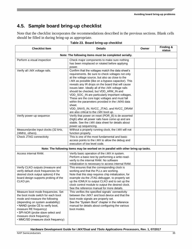
4.5. Sample board bring-up checklist
Note that the checklist incorporates the recommendations described in the previous sections. Blank cells
should be filled in during bring-up as appropriate.
Table 23. Board bring-up checklist
Checklist Item Details Owner Finding &
status
Note: The following items must be completed serially.
Perform a visual inspection Check major components to make sure nothing
has been misplaced or rotated before applying
power.
Verify all i.MX voltage rails. Confirm that the voltages match the data sheet’s
requirements. Be sure to check voltages not only
at the voltage source, but also as close to the
i.MX as possible (like on a bypass capacitor). This
reveals any IR drops on the board that will cause
issues later. Ideally all of the i.MX voltage rails
should be checked, but VDD_ARM_IN and
VDD_SOC_IN are particularly important voltages.
These are the core logic voltages and must fall
within the parameters provided in the i.MX6 data
sheet.
VDD_SNVS_IN, NVCC_JTAG, and NVCC_DRAM
are also critical to the i.MX boot up.
Verify power-up sequence Verify that power on reset (POR_B) is de-asserted
(high) after all power rails have come up and are
stable. See the i.MX data sheet for details about
power-up sequencing.
Measure/probe input clocks (32 kHz,
24MHz, others).
Without a properly running clock, the i.MX will not
function properly.
Check JTAG connectivity This is one of the most fundamental and basic
access points to the i.MX to allow the debug and
execution of low level code.
Note: The following items may be worked on in parallel with other bring up tasks.
Access internal RAM. Verify basic operation of the i.MX in system.
Perform a basic test by performing a write-read-
verify to the internal RAM. No software
initialization is necessary to access internal RAM.
Verify CLKO outputs (measure and
verify default clock frequencies for
desired clock output options) if the
board design supports probing of the
CLKO pin.
This ensures that the corresponding clock is
working and that the PLLs are working.
Note that this step requires chip initialization, for
example via the JTAG debugger, to properly set
up the IOMUX to output CLKO and to set up the
clock control module to output the desired clock.
See the reference manual for more details.
Measure boot mode frequencies. Set
the boot mode switch for each boot
mode and measure the following
(depending on system availability):
• NAND (probe CE to verify boot,
measure RE frequency)
• SPI-NOR (probe slave select and
measure clock frequency)
• MMC/SD (measure clock frequency)
This verifies the specified signals’ connectivity
between the i.MX7 and boot device and that the
boot mode signals are properly set.
See the “System Boot” chapter in the reference
manual for details about configuring the various
boot modes.
Ethernet connections
Hardware Development Guide for i.MX7Dual and 7Solo Applications Processors, Rev. 1, 07/2017
36 NXP Semiconductors
Table 23. Board bring-up checklist
Checklist Item Details Owner Finding &
status
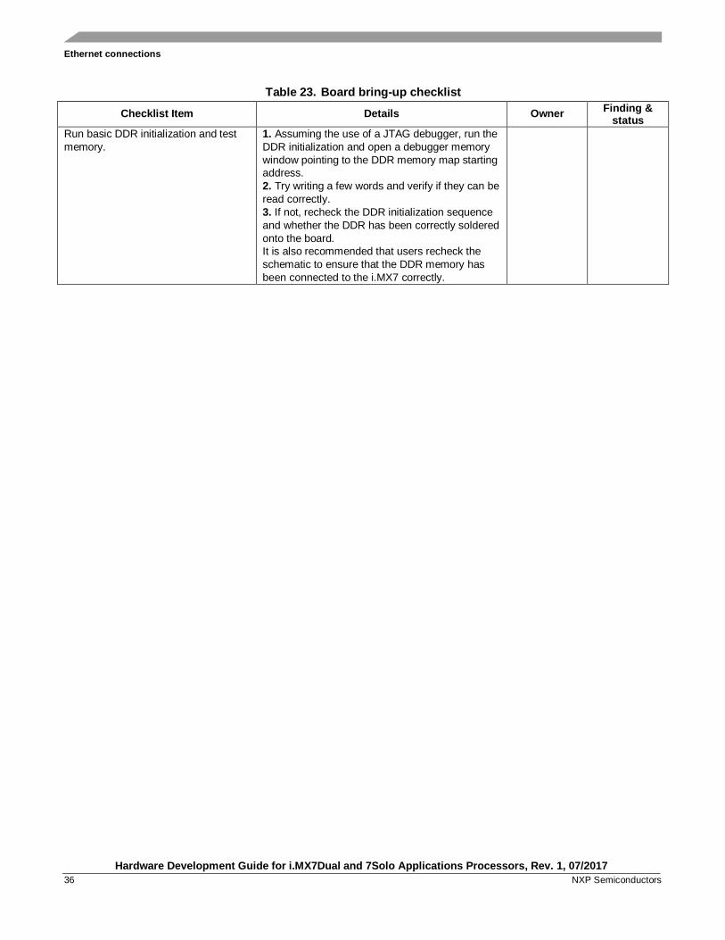
Run basic DDR initialization and test
memory.
1. Assuming the use of a JTAG debugger, run the
DDR initialization and open a debugger memory
window pointing to the DDR memory map starting
address.
2. Try writing a few words and verify if they can be
read correctly.
3. If not, recheck the DDR initialization sequence
and whether the DDR has been correctly soldered
onto the board.
It is also recommended that users recheck the
schematic to ensure that the DDR memory has
been connected to the i.MX7 correctly.
Ethernet connections
Hardware Development Guide for i.MX7Dual and 7Solo Applications Processors, Rev. 1, 07/2017
NXP Semiconductors 37
5. Ethernet connections
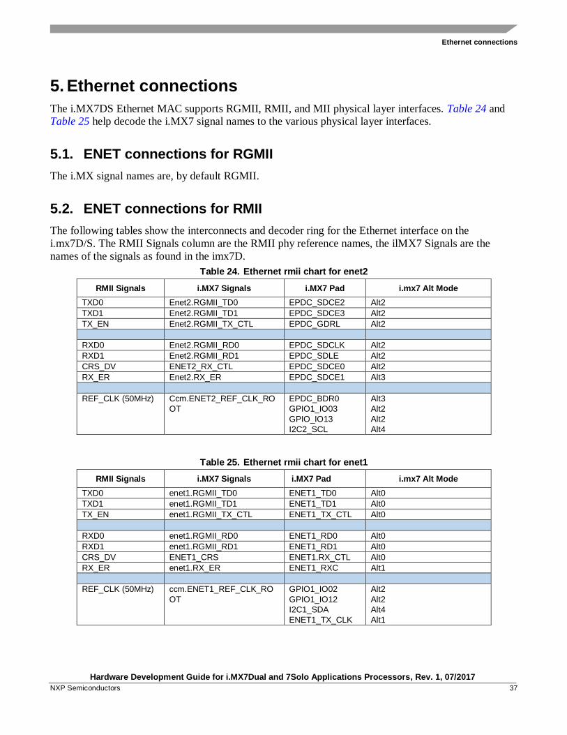
The i.MX7DS Ethernet MAC supports RGMII, RMII, and MII physical layer interfaces. Table 24 and
Table 25 help decode the i.MX7 signal names to the various physical layer interfaces.
5.1. ENET connections for RGMII
The i.MX signal names are, by default RGMII.
5.2. ENET connections for RMII
The following tables show the interconnects and decoder ring for the Ethernet interface on the
i.mx7D/S. The RMII Signals column are the RMII phy reference names, the ilMX7 Signals are the
names of the signals as found in the imx7D.
Table 24. Ethernet rmii chart for enet2
RMII Signals i.MX7 Signals i.MX7 Pad i.mx7 Alt Mode
TXD0 Enet2.RGMII_TD0 EPDC_SDCE2 Alt2
TXD1 Enet2.RGMII_TD1 EPDC_SDCE3 Alt2
TX_EN Enet2.RGMII_TX_CTL EPDC_GDRL Alt2
RXD0 Enet2.RGMII_RD0 EPDC_SDCLK Alt2
RXD1 Enet2.RGMII_RD1 EPDC_SDLE Alt2
CRS_DV ENET2_RX_CTL EPDC_SDCE0 Alt2
RX_ER Enet2.RX_ER EPDC_SDCE1 Alt3
REF_CLK (50MHz) Ccm.ENET2_REF_CLK_RO
OT
EPDC_BDR0
GPIO1_IO03
GPIO_IO13
I2C2_SCL
Alt3
Alt2
Alt2
Alt4
Table 25. Ethernet rmii chart for enet1
RMII Signals i.MX7 Signals i.MX7 Pad i.mx7 Alt Mode
TXD0 enet1.RGMII_TD0 ENET1_TD0 Alt0
TXD1 enet1.RGMII_TD1 ENET1_TD1 Alt0
TX_EN enet1.RGMII_TX_CTL ENET1_TX_CTL Alt0
RXD0 enet1.RGMII_RD0 ENET1_RD0 Alt0
RXD1 enet1.RGMII_RD1 ENET1_RD1 Alt0
CRS_DV ENET1_CRS ENET1.RX_CTL Alt0
RX_ER enet1.RX_ER ENET1_RXC Alt1
REF_CLK (50MHz) ccm.ENET1_REF_CLK_RO
OT
GPIO1_IO02
GPIO1_IO12
I2C1_SDA
ENET1_TX_CLK
Alt2
Alt2
Alt4
Alt1
IBIS model
Hardware Development Guide for i.MX7Dual and 7Solo Applications Processors, Rev. 1, 07/2017
38 NXP Semiconductors
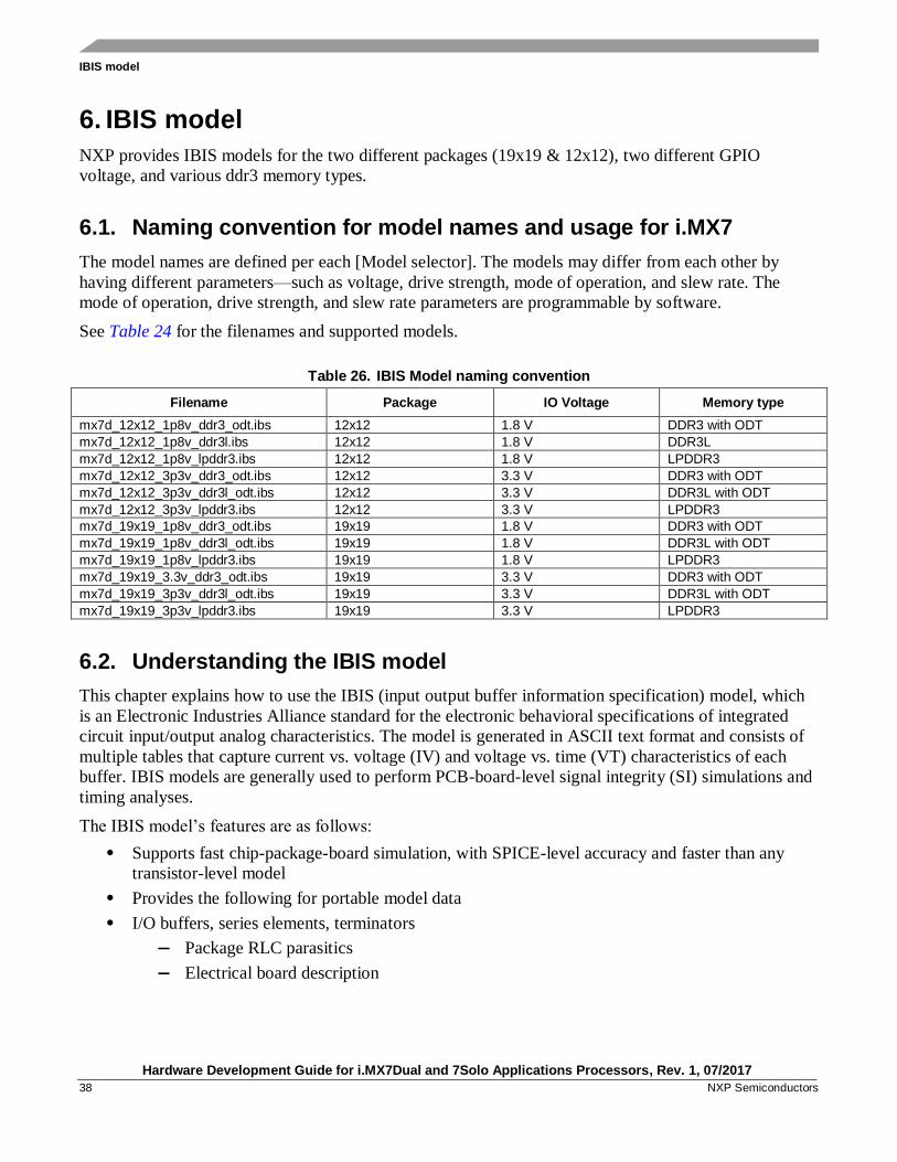
6. IBIS model
NXP provides IBIS models for the two different packages (19x19 & 12x12), two different GPIO
voltage, and various ddr3 memory types.
6.1. Naming convention for model names and usage for i.MX7
The model names are defined per each [Model selector]. The models may differ from each other by
having different parameters—such as voltage, drive strength, mode of operation, and slew rate. The
mode of operation, drive strength, and slew rate parameters are programmable by software.
See Table 24 for the filenames and supported models.
Table 26. IBIS Model naming convention
Filename Package IO Voltage Memory type
mx7d_12x12_1p8v_ddr3_odt.ibs 12x12 1.8 V DDR3 with ODT
mx7d_12x12_1p8v_ddr3l.ibs 12x12 1.8 V DDR3L
mx7d_12x12_1p8v_lpddr3.ibs 12x12 1.8 V LPDDR3
mx7d_12x12_3p3v_ddr3_odt.ibs 12x12 3.3 V DDR3 with ODT
mx7d_12x12_3p3v_ddr3l_odt.ibs 12x12 3.3 V DDR3L with ODT
mx7d_12x12_3p3v_lpddr3.ibs 12x12 3.3 V LPDDR3
mx7d_19x19_1p8v_ddr3_odt.ibs 19x19 1.8 V DDR3 with ODT
mx7d_19x19_1p8v_ddr3l_odt.ibs 19x19 1.8 V DDR3L with ODT
mx7d_19x19_1p8v_lpddr3.ibs 19x19 1.8 V LPDDR3
mx7d_19x19_3.3v_ddr3_odt.ibs 19x19 3.3 V DDR3 with ODT
mx7d_19x19_3p3v_ddr3l_odt.ibs 19x19 3.3 V DDR3L with ODT
mx7d_19x19_3p3v_lpddr3.ibs 19x19 3.3 V LPDDR3
6.2. Understanding the IBIS model
This chapter explains how to use the IBIS (input output buffer information specification) model, which
is an Electronic Industries Alliance standard for the electronic behavioral specifications of integrated
circuit input/output analog characteristics. The model is generated in ASCII text format and consists of
multiple tables that capture current vs. voltage (IV) and voltage vs. time (VT) characteristics of each
buffer. IBIS models are generally used to perform PCB-board-level signal integrity (SI) simulations and
timing analyses.
The IBIS model’s features are as follows:
• Supports fast chip-package-board simulation, with SPICE-level accuracy and faster than any
transistor-level model
• Provides the following for portable model data
• I/O buffers, series elements, terminators
— Package RLC parasitics
— Electrical board description
IBIS model
Hardware Development Guide for i.MX7Dual and 7Solo Applications Processors, Rev. 1, 07/2017
NXP Semiconductors 39
6.3. IBIS structure and content
An IBIS file contains the data required to model a component’s input, output, and I/O buffers
behaviorally in ASCII format. The basic IBIS file contains the following data:
• Header information regarding the model file
• Information about the component, the package’s electrical characteristics, and the pin-to-buffer
model mapping (in other words, which pins are connected to which buffer models)
• The data required to model each unique input, output, and I/O buffer design on the component
IBIS models are component-centric, meaning they allow users to model an entire component rather than
only a particular buffer. Therefore, in addition to the electrical characteristics of a component’s buffers,
an IBIS file includes the component’s pin-to-buffer mapping and the electrical parameters of the
component’s package.
6.4. Header information
The first section of an IBIS file provides the basic information about the file and its data. The following
table explains the header information notation.
Table 27. IBIS header Information
Keyword Required Description
[IBIS Ver] Yes Version of IBIS Specification this file uses.
[Comment char] No Change the comment character. Defaults to the pip (|) character.
[File Name] Yes Name of this file. All file names must be lower case. The file name extension for
IBIS file is “.ibs”
[File Rev] Yes The revision level of this file. The specification contains guideline for assigning
revision levels.
[Date] No Date the file was created.
[Source] No The source of the data in this file. Data is taken from a simulation and validated on
a board.
[Notes] No Component or file-specific notes.
[Disclaimer] No May be legally required
[Copyright] No The file’s copyright notice
Example 1. IBIS header Information
[IBIS Ver] 4.2 [File name] ult1_12x12_3p3v_ddr3_odt.ibs [File Rev] 1.0 [Date] Oct 6, 2015 [Source] [Disclaimer]
6.5. Component and pin information
The second section of an IBIS file is where the data book information regarding the component’s pinout,
pin-to-buffer mapping, and the package and pin electrical parameters is placed.
IBIS model
Hardware Development Guide for i.MX7Dual and 7Solo Applications Processors, Rev. 1, 07/2017
40 NXP Semiconductors
Table 28. Component and pin Information
Keyword Required Description
[Component] Yes The name of the component being modeled. Standard practice has been to use the
industry standard part designation. Note that IBIS files may contain multiple
[Component] descriptions.
[Manufacturer] Yes The name of the component manufacturer
[Package] Yes This keyword contains the range (minimum, typical and maximum values) over
which the packages’ lead resistance, inductance, and capacitance vary (the R_pkg,
L_pkg, and C_pkg parameters).
[Pin] Yes This keyword contains the pin-to-buffer mapping information. In addition, the model
creator can use this keyword to list the package information: R, L, and C data for
each individual pin (R_pin, L_pin, and C_pin parameters).
[Package Model] No If the component model includes an external package model (or uses the [Define
Package Model] keyword within the IBIS file itself), this keyword indicates the name
of that package model.
[Pin Mapping] No This keyword is used if the model creator wishes to include information on buffer
power and ground connections. This information may be used for simulations
involving multiple outputs switching.
[Diff Pin] No This keyword is used to associate buffers that should be driven in a complementary
fashion as a differential pair.
[Model Selector] This keyword provides a simple means by which several buffers can be made
optionally available for simulation at the same physical pin of the component.
Example 2. Component and pin information
[Component] mx7_ult1_12x12 [Manufacturer] Freescale ||||||||||||||||||||||||||||||||||||||||||||||||||||||| [Package] |variable typ min max R_pkg 0.2177 0.0666 0.37705 L_pkg 2.3724nH 0.7912nH 4.095nH C_pkg 0.6482pF 0.3055pF 1.6214pF [Pin] signal_name model_name R_pin L_pin C_pin A05 SD1_CD_B MPBI 0.354724 3.18226nH 0.60709pF B04 SD1_DATA0 MPBI 0.188298 2.01806nH 0.82959pF A04 SD1_DATA1 MPBI 0.349718 3.33815nH 0.60202pF
6.6. Model information
The [Model] keyword starts the description of the data for a particular buffer.
IBIS model
Hardware Development Guide for i.MX7Dual and 7Solo Applications Processors, Rev. 1, 07/2017
NXP Semiconductors 41
Table 29. Model Information
Keyword Comment
[Model Spec] General set of parameters for the model simulation.
[Receiver Thresholds] Threshold information for the different simulation cases.
[Temperatere Range] The temperature range over which the min, typ and max IV and switching data have been
gathered.
[Voltage Range] The range over which Vcc is varied to obtain the min, type and max pullup and power
clamp data.
[Pulldown]
[Pullup]
[GND_clamp]
[POWER_clamp]
IV information.
[Ramp]
[Rising Waveform]
[Falling Waveform]
VT information
[Test Data]
[Rising Waveform Near]
[Rising Waveform Far]
[Falling Waveform Near]
[Falling Waveform Far]
[Test Load]
VT golden model information
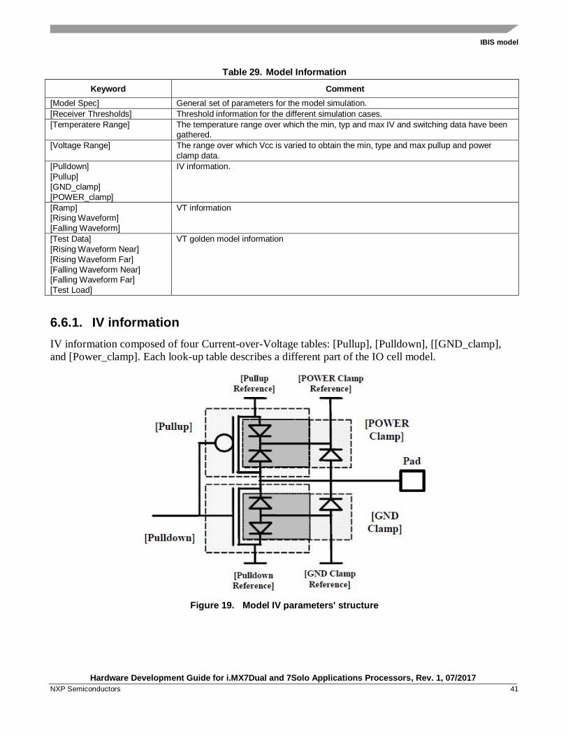
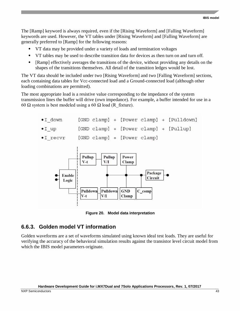
6.6.1. IV information
IV information composed of four Current-over-Voltage tables: [Pullup], [Pulldown], [[GND_clamp],
and [Power_clamp]. Each look-up table describes a different part of the IO cell model.
Figure 19. Model IV parameters' structure
IBIS model
Hardware Development Guide for i.MX7Dual and 7Solo Applications Processors, Rev. 1, 07/2017
42 NXP Semiconductors
6.6.2. VT information
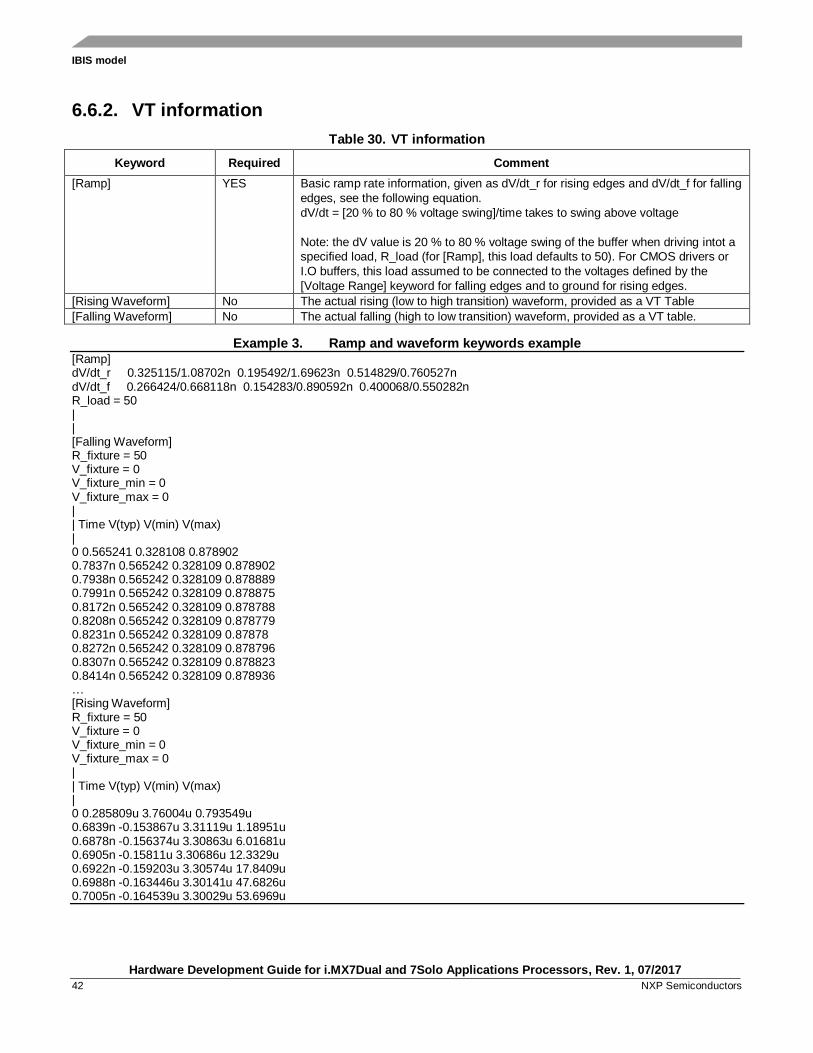
Table 30. VT information
Keyword Required Comment
[Ramp] YES Basic ramp rate information, given as dV/dt_r for rising edges and dV/dt_f for falling
edges, see the following equation.
dV/dt = [20 % to 80 % voltage swing]/time takes to swing above voltage
Note: the dV value is 20 % to 80 % voltage swing of the buffer when driving intot a
specified load, R_load (for [Ramp], this load defaults to 50). For CMOS drivers or
I.O buffers, this load assumed to be connected to the voltages defined by the
[Voltage Range] keyword for falling edges and to ground for rising edges.
[Rising Waveform] No The actual rising (low to high transition) waveform, provided as a VT Table
[Falling Waveform] No The actual falling (high to low transition) waveform, provided as a VT table.
Example 3. Ramp and waveform keywords example [Ramp] dV/dt_r 0.325115/1.08702n 0.195492/1.69623n 0.514829/0.760527n dV/dt_f 0.266424/0.668118n 0.154283/0.890592n 0.400068/0.550282n R_load = 50 | | [Falling Waveform] R_fixture = 50 V_fixture = 0 V_fixture_min = 0 V_fixture_max = 0 | | Time V(typ) V(min) V(max) | 0 0.565241 0.328108 0.878902 0.7837n 0.565242 0.328109 0.878902 0.7938n 0.565242 0.328109 0.878889 0.7991n 0.565242 0.328109 0.878875 0.8172n 0.565242 0.328109 0.878788 0.8208n 0.565242 0.328109 0.878779 0.8231n 0.565242 0.328109 0.87878 0.8272n 0.565242 0.328109 0.878796 0.8307n 0.565242 0.328109 0.878823 0.8414n 0.565242 0.328109 0.878936 … [Rising Waveform] R_fixture = 50 V_fixture = 0 V_fixture_min = 0 V_fixture_max = 0 | | Time V(typ) V(min) V(max) | 0 0.285809u 3.76004u 0.793549u 0.6839n -0.153867u 3.31119u 1.18951u 0.6878n -0.156374u 3.30863u 6.01681u 0.6905n -0.15811u 3.30686u 12.3329u 0.6922n -0.159203u 3.30574u 17.8409u 0.6988n -0.163446u 3.30141u 47.6826u 0.7005n -0.164539u 3.30029u 53.6969u
IBIS model
Hardware Development Guide for i.MX7Dual and 7Solo Applications Processors, Rev. 1, 07/2017
NXP Semiconductors 43
The [Ramp] keyword is always required, even if the [Rising Waveform] and [Falling Waveform]
keywords are used. However, the VT tables under [Rising Waveform] and [Falling Waveform] are
generally preferred to [Ramp] for the following reasons:
• VT data may be provided under a variety of loads and termination voltages
• VT tables may be used to describe transition data for devices as then turn on and turn off.
• [Ramp] effectively averages the transitions of the device, without providing any details on the
shapes of the transitions themselves. All detail of the transition ledges would be lost.
The VT data should be included under two [Rising Waveform] and two [Falling Waveform] sections,
each containing data tables for Vcc-connected load and a Ground-connected load (although other
loading combinations are permitted).
The most appropriate load is a resistive value corresponding to the impedance of the system
transmission lines the buffer will drive (own impedance). For example, a buffer intended for use in a
60 Ω system is best modeled using a 60 Ω load (R_fixture).
Figure 20. Model data interpretation
6.6.3. Golden model VT information
Golden waveforms are a set of waveforms simulated using known ideal test loads. They are useful for
verifying the accuracy of the behavioral simulation results against the transistor level circuit model from
which the IBIS model parameters originate.
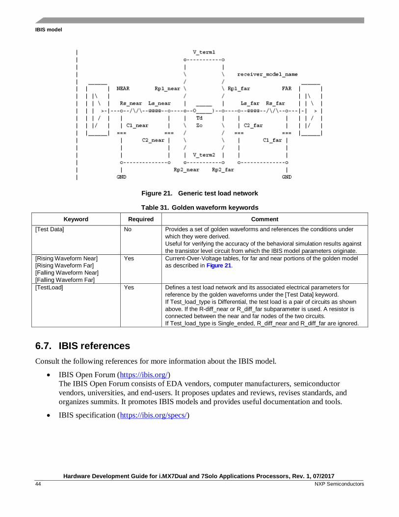
IBIS model
Hardware Development Guide for i.MX7Dual and 7Solo Applications Processors, Rev. 1, 07/2017
44 NXP Semiconductors
Figure 21. Generic test load network
Table 31. Golden waveform keywords
Keyword Required Comment
[Test Data] No Provides a set of golden waveforms and references the conditions under
which they were derived.
Useful for verifying the accuracy of the behavioral simulation results against
the transistor level circuit from which the IBIS model parameters originate.
[Rising Waveform Near]
[Rising Waveform Far]
[Falling Waveform Near]
[Falling Waveform Far]
Yes Current-Over-Voltage tables, for far and near portions of the golden model
as described in Figure 21.
[TestLoad] Yes Defines a test load network and its associated electrical parameters for
reference by the golden waveforms under the [Test Data] keyword.
If Test_load_type is Differential, the test load is a pair of circuits as shown
above. If the R-diff_near or R_diff_far subparameter is used. A resistor is
connected between the near and far nodes of the two circuits.
If Test_load_type is Single_ended, R_diff_near and R_diff_far are ignored.
6.7. IBIS references
Consult the following references for more information about the IBIS model.
IBIS Open Forum (https://ibis.org/)
The IBIS Open Forum consists of EDA vendors, computer manufacturers, semiconductor
vendors, universities, and end-users. It proposes updates and reviews, revises standards, and
organizes summits. It promotes IBIS models and provides useful documentation and tools.
IBIS specification (https://ibis.org/specs/)
Using BSDL for board-level testing
Hardware Development Guide for i.MX7Dual and 7Solo Applications Processors, Rev. 1, 07/2017
NXP Semiconductors 45
7. Using BSDL for board-level testing
7.1. BSDL overview
Boundary scan description language (BSDL) is used for board-level testing after components have been
assembled. The interface for this test uses the JTAG pins. The definition is contained within IEEE Std
1149.1.
7.2. How BSDL functions
The BSDL file defines the internal scan chain, which is the serial linkage of the IO cells, within a
particular device. The scan chain looks like a large shift register, which provides means to read the logic
level applied to a pin or to output a logic state on that pin. Using JTAG commands, a test tool uses the
BSDL file to control the scan chain so the device-board connectivity can be tested.
For example, when using an external ROM test interface, the test tool would do the following:
1. Output a specific set of addresses and controls to pins connected to the ROM
2. Perform a read command and scan out the values of the ROM data pins.
3. Compare the values read with the known golden values.
Based on this procedure, the tool can determine whether the interface between the two parts is connected
properly and does not contain shorts or opens.
7.3. Downloading the BSDL file
The BSDL file for each i.MX process is stored on the NXP website upon product release. Contact your
local sales office or field applications engineer to check the availability of information prior to product
releases.
7.4. Pin Coverage of BSDL
Each pin is defined as a port within the BSDL file. You an open the file with a text editor to review how
each pin will function. The BSDL file defines these functions as shown:
-- PORT DESCRIPTION TERMS -- in = input only -- out = three-state output (0, Z, 1) -- buffer = two-state output (0, 1) -- inout = bidirectional
-- linkage = OTHER (vdd, vss, analog)
The appearance of “linkage” in a pin’s file implies that the pin cannot be used with boundary scan.
These are usually power pins or analog pins that cannot be defined with a digital logic state.
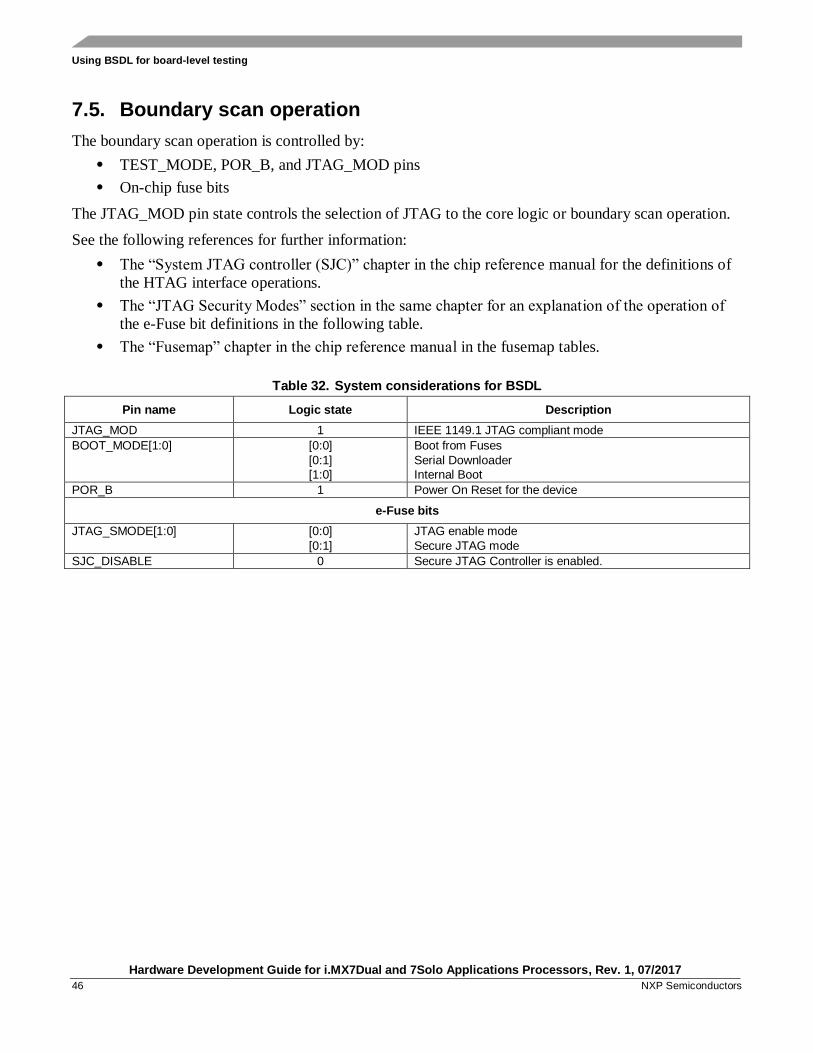
Using BSDL for board-level testing
Hardware Development Guide for i.MX7Dual and 7Solo Applications Processors, Rev. 1, 07/2017
46 NXP Semiconductors
7.5. Boundary scan operation
The boundary scan operation is controlled by:
• TEST_MODE, POR_B, and JTAG_MOD pins
• On-chip fuse bits
The JTAG_MOD pin state controls the selection of JTAG to the core logic or boundary scan operation.
See the following references for further information:
• The “System JTAG controller (SJC)” chapter in the chip reference manual for the definitions of
the HTAG interface operations.
• The “JTAG Security Modes” section in the same chapter for an explanation of the operation of
the e-Fuse bit definitions in the following table.
• The “Fusemap” chapter in the chip reference manual in the fusemap tables.
Table 32. System considerations for BSDL
Pin name Logic state Description
JTAG_MOD 1 IEEE 1149.1 JTAG compliant mode
BOOT_MODE[1:0] [0:0]
[0:1]
[1:0]
Boot from Fuses
Serial Downloader
Internal Boot
POR_B 1 Power On Reset for the device
e-Fuse bits
JTAG_SMODE[1:0] [0:0]
[0:1]
JTAG enable mode
Secure JTAG mode
SJC_DISABLE 0 Secure JTAG Controller is enabled.
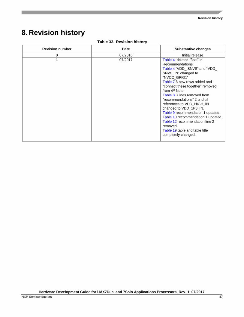
Revision history
Hardware Development Guide for i.MX7Dual and 7Solo Applications Processors, Rev. 1, 07/2017
NXP Semiconductors 47
8. Revision history Table 33. Revision history
Revision number Date Substantive changes
0 07/2016 Initial release
1 07/2017 Table 4: deleted “float” in
Recommendations.
Table 4 “VDD_ SNVS” and “VDD_
SNVS_IN” changed to
“NVCC_GPIO1”
Table 7 8 new rows added and
“connect these together” removed
from 4th Note.
Table 8 3 lines removed from
“recommendations” 2 and all
references to VDD_HIGH_IN
changed to VDD_1P8_IN.
Table 9 recommendation 1 updated.
Table 10 recommendation 1 updated.
Table 12 recommendation line 2
removed.
Table 19 table and table title
completely changed.
Document Number: IMX7DSHDG Rev. 1
07/2017
How to Reach Us:
Home Page:
nxp.com
Web Support:
nxp.com/support
Information in this document is provided solely to enable system and software
implementers to use NXP products. There are no express or implied copyright licenses
granted hereunder to design or fabricate any integrated circuits based on the
information in this document. NXP reserves the right to make changes without further
notice to any products herein.
NXP makes no warranty, representation, or guarantee regarding the suitability of its
products for any particular purpose, nor does NXP assume any liability arising out of
the application or use of any product or circuit, and specifically disclaims any and all
liability, including without limitation consequential or incidental damages. “Typical”
parameters that may be provided in NXP data sheets and/or specifications can and do
vary in different applications, and actual performance may vary over time. All operating
parameters, including “typicals,” must be validated for each customer application by
customer’s technical experts. NXP does not convey any license under its patent rights
nor the rights of others. NXP sells products pursuant to standard terms and conditions
of sale, which can be found at the following address:
nxp.com/SalesTermsandConditions.
NXP, the NXP logo, NXP SECURE CONNECTIONS FOR A SMARTER WORLD, I2C
BUS, Freescale, the Freescale logo, the Energy Efficient Solutions logo, and Kinetis are
trademarks of NXP B.V. All other product or service names are the property of their
respective owners.
ARM, the ARM powered logo, and Cortex are registered trademarks of ARM Limited (or
its subsidiaries) in the EU and/or elsewhere. All rights reserved.
© 2016-2017 NXP B.V.