Embed Size (px)
Citation preview
Hardware Description Language -Introduction
� HDL is a language that describes the hardware of digital systems in a textual form.
� It resembles a programming language, but is specifically oriented to describing hardware structures and behaviors.
� The main difference with the traditional programming languages is HDL’s representation of extensive parallel operations whereas traditional ones represents mostly serial operations.
� The most common use of a HDL is to provide an alternative to schematics.
HDL – Introduction (2)
� When a language is used for the above purpose (i.e. to
provide an alternative to schematics), it is referred to as a
structural description in which the language describes an
interconnection of components.
� Such a structural description can be used as input to logic
simulation just as a schematic is used.
� Models for each of the primitive components are required.
� If an HDL is used, then these models can also be written in
the HDL providing a more uniform, portable
representation for simulation input.
HDL – Introduction (3)
� HDL can be used to represent logic diagrams, Boolean expressions, and other more complex digital circuits.
� Thus, in top down design, a very high-level description of a entire system can be precisely specified using an HDL.
� This high-level description can then be refined and partitioned into lower-level descriptions as a part of the design process.
HDL – Introduction (4)
� As a documentation language, HDL is used to represent and
document digital systems in a form that can be read by both
humans and computers and is suitable as an exchange
language between designers.
� The language content can be stored and retrieved easily and
processed by computer software in an efficient manner.
� There are two applications of HDL processing: Simulation
and Synthesis
Logic Simulation
� A simulator interprets the HDL description and produces a
readable output, such as a timing diagram, that predicts
how the hardware will behave before its is actually
fabricated.
� Simulation allows the detection of functional errors in a
design without having to physically create the circuit.
Logic Simulation (2)
� The stimulus that tests the functionality of the design is
called a test bench.
� To simulate a digital system
� Design is first described in HDL
� Verified by simulating the design and checking it with a test bench
which is also written in HDL.
Logic Simulation
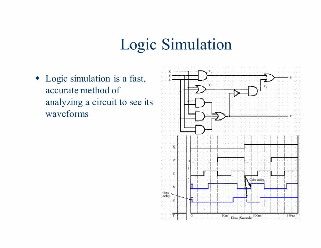
� Logic simulation is a fast,
accurate method of
analyzing a circuit to see its
waveforms
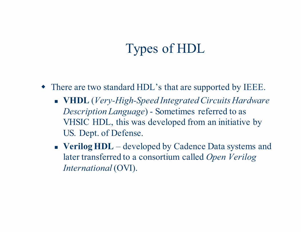
Types of HDL
� There are two standard HDL’s that are supported by IEEE.
� VHDL (Very-High-Speed Integrated Circuits Hardware
Description Language) - Sometimes referred to as
VHSIC HDL, this was developed from an initiative by
US. Dept. of Defense.
� Verilog HDL – developed by Cadence Data systems and
later transferred to a consortium called Open Verilog
International (OVI).
Verilog
� Verilog HDL has a syntax that describes precisely the legal
constructs that can be used in the language.
� It uses about 100 keywords pre-defined, lowercase,
identifiers that define the language constructs.
� Example of keywords: module, endmodule, input, output
wire, and, or, not , etc.,
� Any text between two slashes (//) and the end of line is
interpreted as a comment.
� Blank spaces are ignored and names are case sensitive.
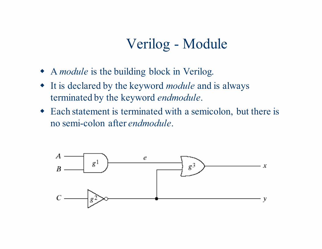
Verilog - Module
� A module is the building block in Verilog.
� It is declared by the keyword module and is always
terminated by the keyword endmodule.
� Each statement is terminated with a semicolon, but there is
no semi-colon after endmodule.
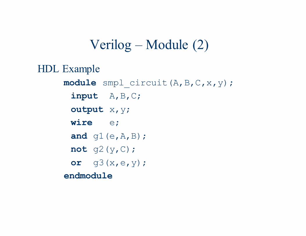
Verilog – Module (2)
HDL Example
module smpl_circuit(A,B,C,x,y);
input A,B,C;
output x,y;
wire e;
and g1(e,A,B);
not g2(y,C);
or g3(x,e,y);
endmodule
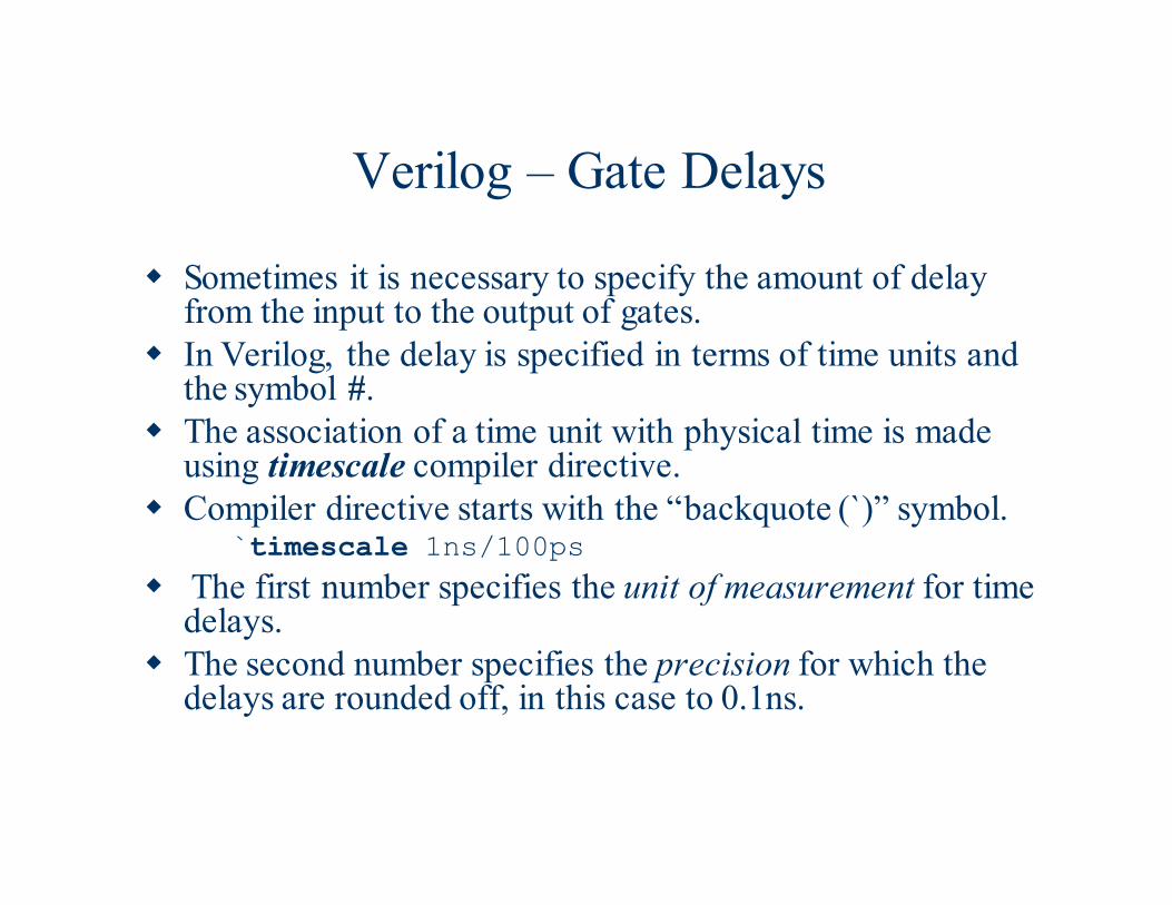
Verilog – Gate Delays
� Sometimes it is necessary to specify the amount of delay from the input to the output of gates.
� In Verilog, the delay is specified in terms of time units and the symbol #.
� The association of a time unit with physical time is made using timescale compiler directive.
� Compiler directive starts with the “backquote (`)” symbol.`timescale 1ns/100ps
� The first number specifies the unit of measurement for time delays.
� The second number specifies the precision for which the delays are rounded off, in this case to 0.1ns.
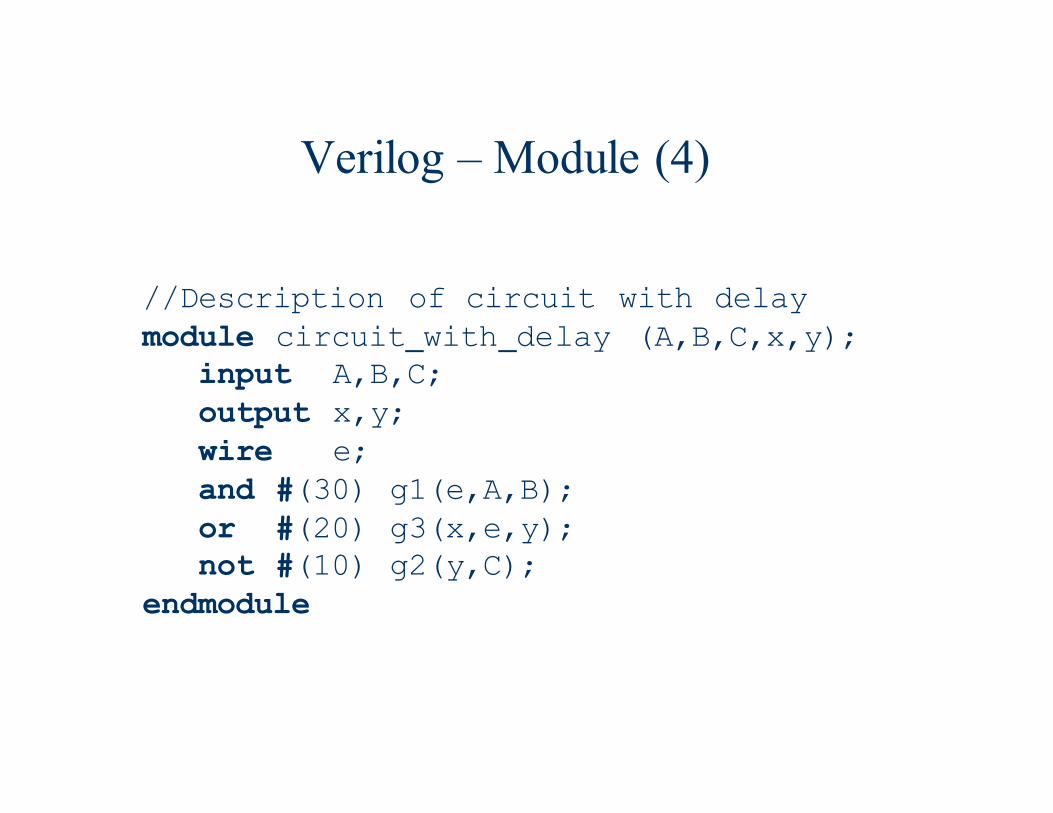
Verilog – Module (4)
//Description of circuit with delay
module circuit_with_delay (A,B,C,x,y);input A,B,C;
output x,y;
wire e;
and #(30) g1(e,A,B);or #(20) g3(x,e,y);not #(10) g2(y,C);
endmodule
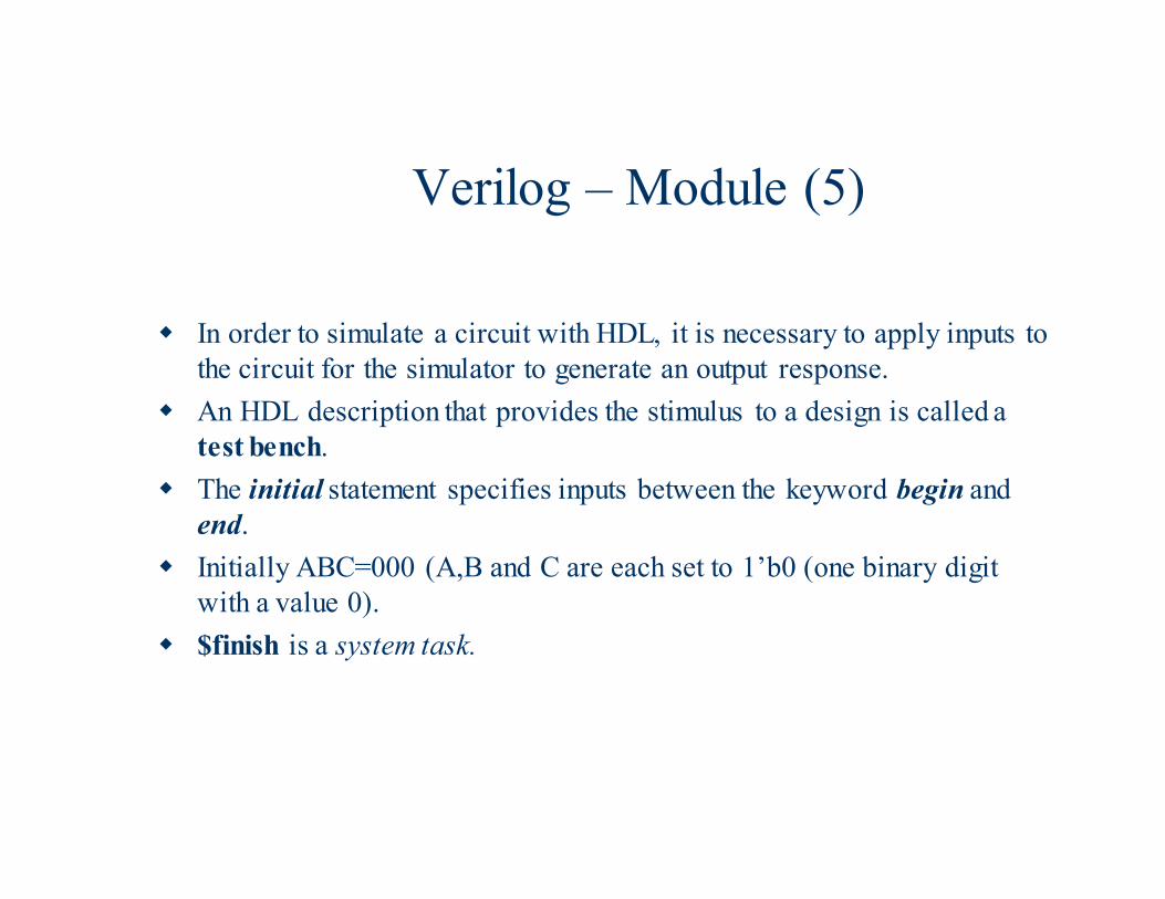
Verilog – Module (5)
� In order to simulate a circuit with HDL, it is necessary to apply inputs to
the circuit for the simulator to generate an output response.
� An HDL description that provides the stimulus to a design is called a
test bench.
� The initial statement specifies inputs between the keyword begin and
end.
� Initially ABC=000 (A,B and C are each set to 1’b0 (one binary digit
with a value 0).
� $finish is a system task.
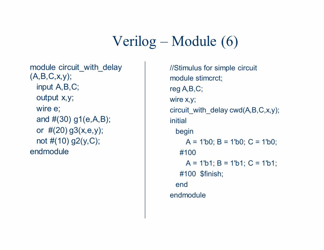
Verilog – Module (6)
//Stimulus for simple circuit
module stimcrct;
reg A,B,C;
wire x,y;
circuit_with_delay cwd(A,B,C,x,y);
initial
begin
A = 1'b0; B = 1'b0; C = 1'b0;
#100
A = 1'b1; B = 1'b1; C = 1'b1;
#100 $finish;
end
endmodule
module circuit_with_delay (A,B,C,x,y);
input A,B,C;
output x,y;
wire e;
and #(30) g1(e,A,B);
or #(20) g3(x,e,y);
not #(10) g2(y,C);
endmodule
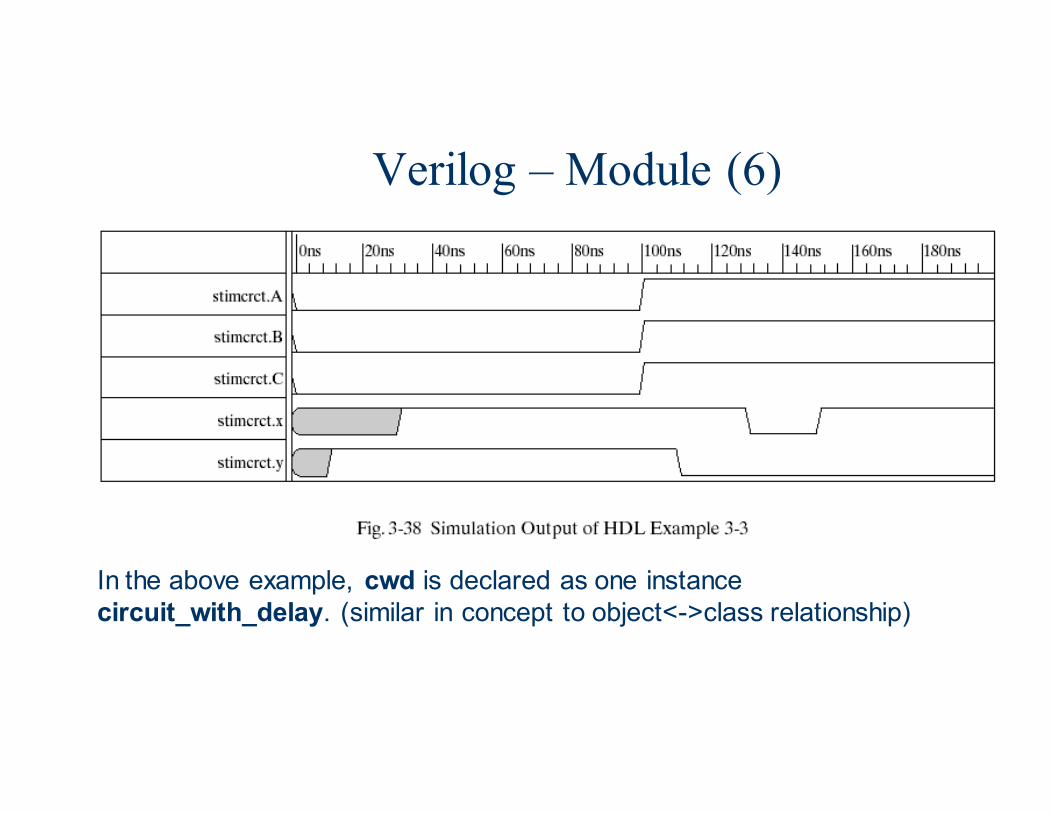
Verilog – Module (6)
In the above example, cwd is declared as one instance circuit_with_delay. (similar in concept to object<->class relationship)
Verilog – Module (7)
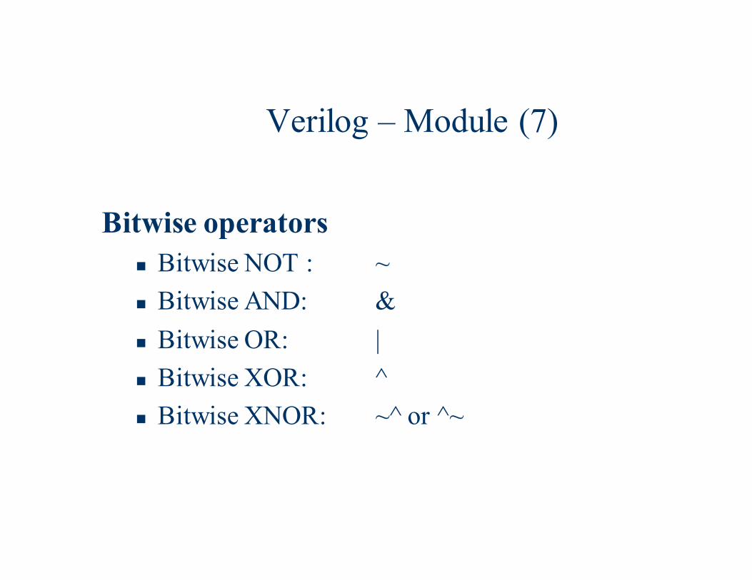
Bitwise operators
� Bitwise NOT : ~
� Bitwise AND: &
� Bitwise OR: |
� Bitwise XOR: ^
� Bitwise XNOR: ~^ or ^~
Verilog – Module (8)
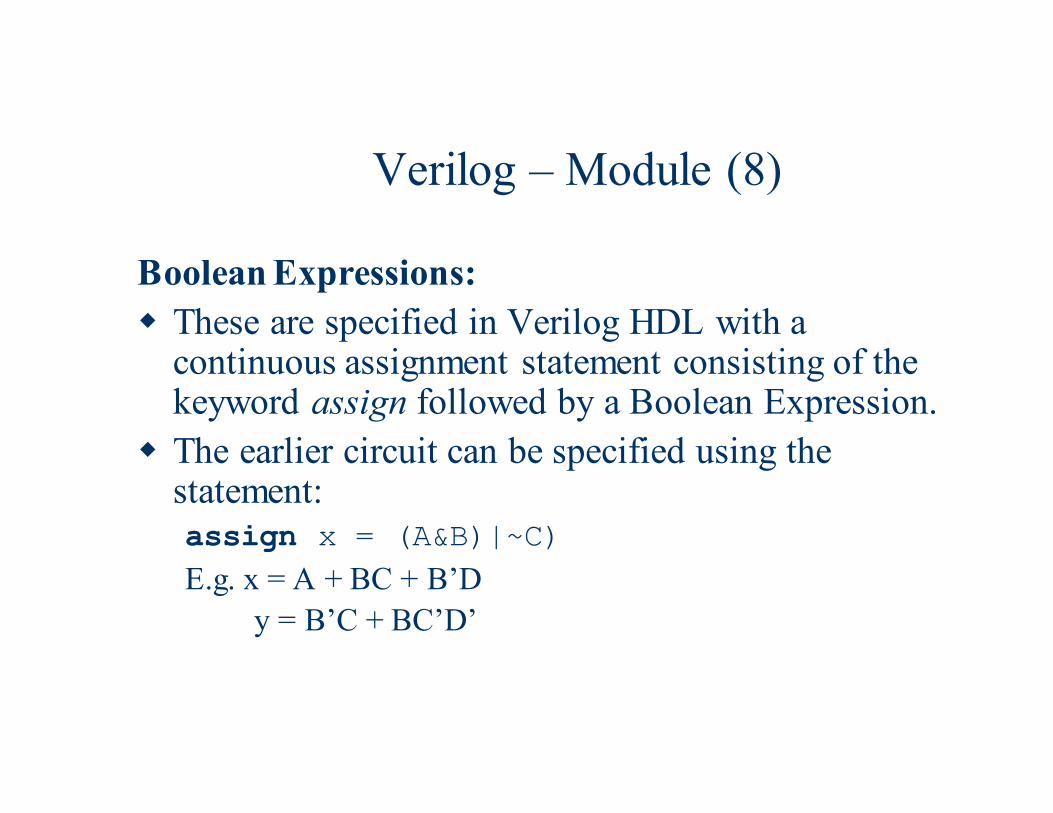
Boolean Expressions:
� These are specified in Verilog HDL with a continuous assignment statement consisting of the keyword assign followed by a Boolean Expression.
� The earlier circuit can be specified using the statement:assign x = (A&B)|~C)
E.g. x = A + BC + B’D
y = B’C + BC’D’
Verilog – Module (9)
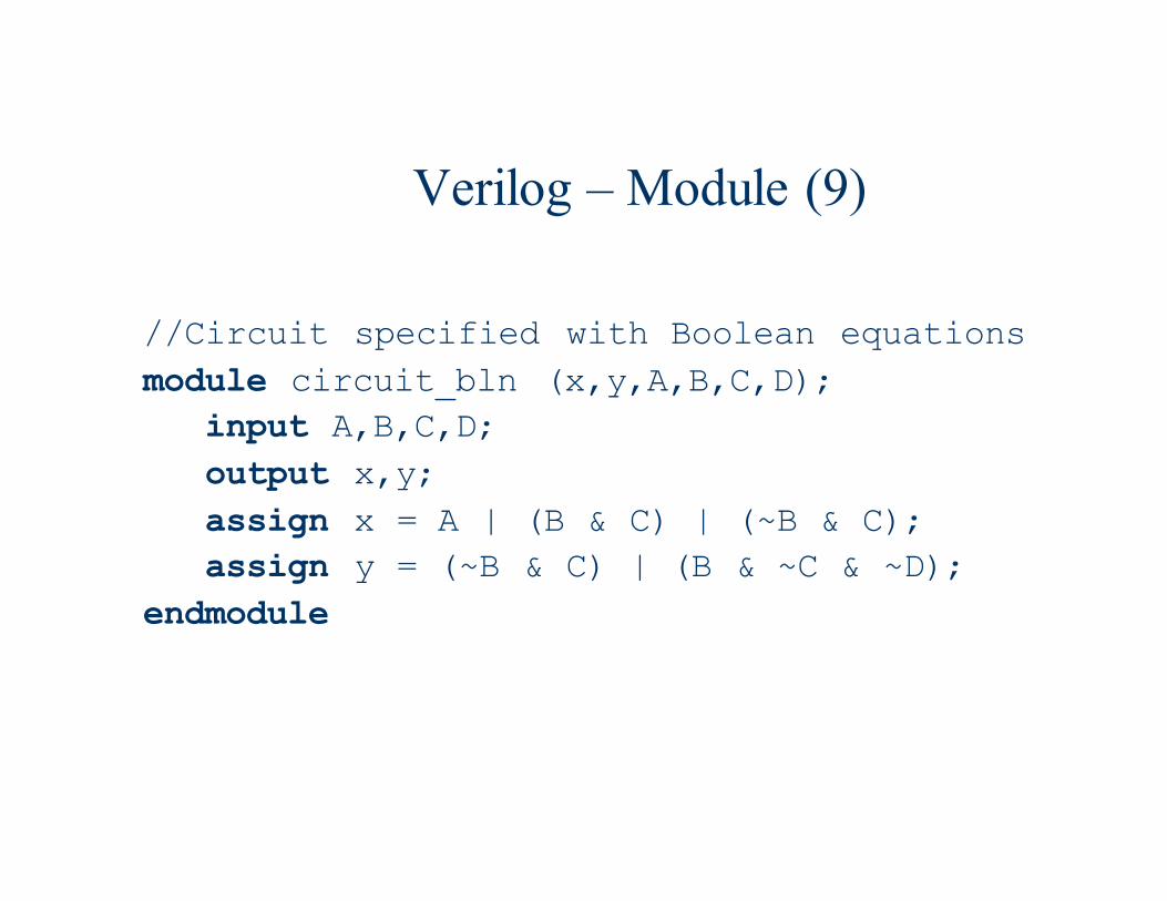
//Circuit specified with Boolean equations
module circuit_bln (x,y,A,B,C,D);
input A,B,C,D;
output x,y;
assign x = A | (B & C) | (~B & C);
assign y = (~B & C) | (B & ~C & ~D);
endmodule
Verilog – Module (10)
User Defined Primitives (UDP):
� The logic gates used in HDL descriptions with keywords and, or,etc., are defined by the system and are referred to as system primitives.
� The user can create additional primitives by defining them in tabular form.
� These type of circuits are referred to as user-defined primitives.
Verilog – Module (12)
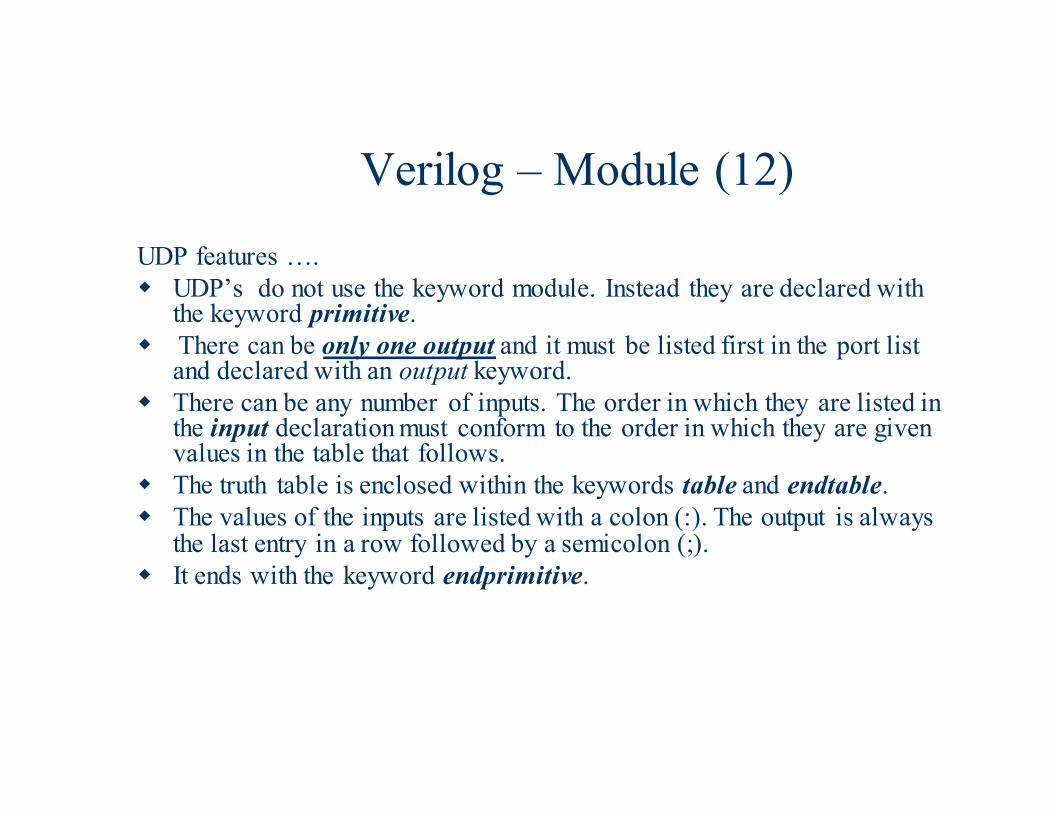
UDP features ….
� UDP’s do not use the keyword module. Instead they are declared with the keyword primitive.
� There can be only one output and it must be listed first in the port list and declared with an output keyword.
� There can be any number of inputs. The order in which they are listed in the input declaration must conform to the order in which they are given values in the table that follows.
� The truth table is enclosed within the keywords table and endtable.
� The values of the inputs are listed with a colon (:). The output is always the last entry in a row followed by a semicolon (;).
� It ends with the keyword endprimitive.
Verilog – Module (13)
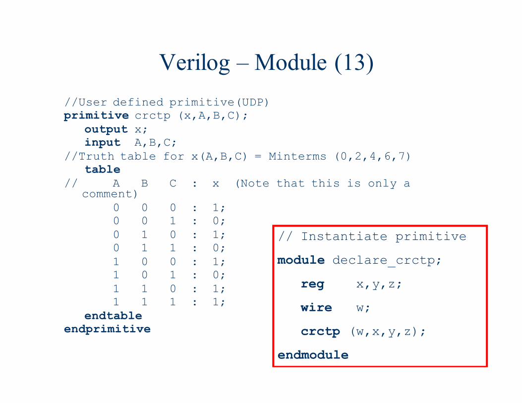
//User defined primitive(UDP) primitive crctp (x,A,B,C);
output x;input A,B,C;
//Truth table for x(A,B,C) = Minterms (0,2,4,6,7)table
// A B C : x (Note that this is only a comment)
0 0 0 : 1;0 0 1 : 0;0 1 0 : 1;0 1 1 : 0;1 0 0 : 1;1 0 1 : 0;1 1 0 : 1;1 1 1 : 1;
endtableendprimitive
// Instantiate primitive
module declare_crctp;
reg x,y,z;
wire w;
crctp (w,x,y,z);
endmodule
Verilog – Module (14)
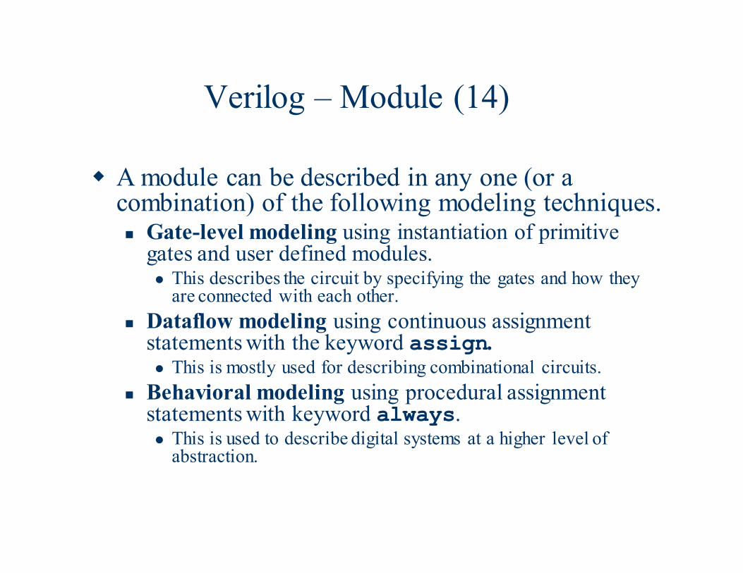
� A module can be described in any one (or a combination) of the following modeling techniques.� Gate-level modeling using instantiation of primitive
gates and user defined modules.� This describes the circuit by specifying the gates and how they
are connected with each other.
� Dataflow modeling using continuous assignment statements with the keyword assign.� This is mostly used for describing combinational circuits.
� Behavioral modeling using procedural assignment statements with keyword always.� This is used to describe digital systems at a higher level of
abstraction.
Gate-Level Modeling
� Here a circuit is specified by its logic gates and their
interconnections.
� It provides a textual description of a schematic diagram.
� Verilog recognizes 12 basic gates as predefined primitives.
� 4 primitive gates of 3-state type.
� Other 8 are: and, nand, or, nor, xor, xnor, not, buf
� When the gates are simulated, the system assigns a four-
valued logic set to each gate – 0,1,unknown (x) and high
impedance (z)
Gate-level modeling (2)
� When a primitive gate is incorporated into a
module, we say it is instantiated in the module.
� In general, component instantiations are
statements that reference lower-level components
in the design, essentially creating unique copies
(or instances) of those components in the higher-
level module.
� Thus, a module that uses a gate in its description is
said to instantiate the gate.
Gate-level Modeling (3)
� Modeling with vector data (multiple bit widths):
� A vector is specified within square brackets and two
numbers separated with a colon.
e.g. output[0:3] D; - This declares an output vector
D with 4 bits, 0 through 3.
wire[7:0] SUM; – This declares a wire vector
SUM with 8 bits numbered 7 through 0.
The first number listed is the most significant bit of the
vector.
Gate-level Modeling
� Two or more modules can be combined to build a hierarchical description of a design.
� There are two basic types of design methodologies.� Top down: In top-down design, the top level block is defined and
then sub-blocks necessary to build the top level block are identified.
� Bottom up: Here the building blocks are first identified and then combine to build the top level block.
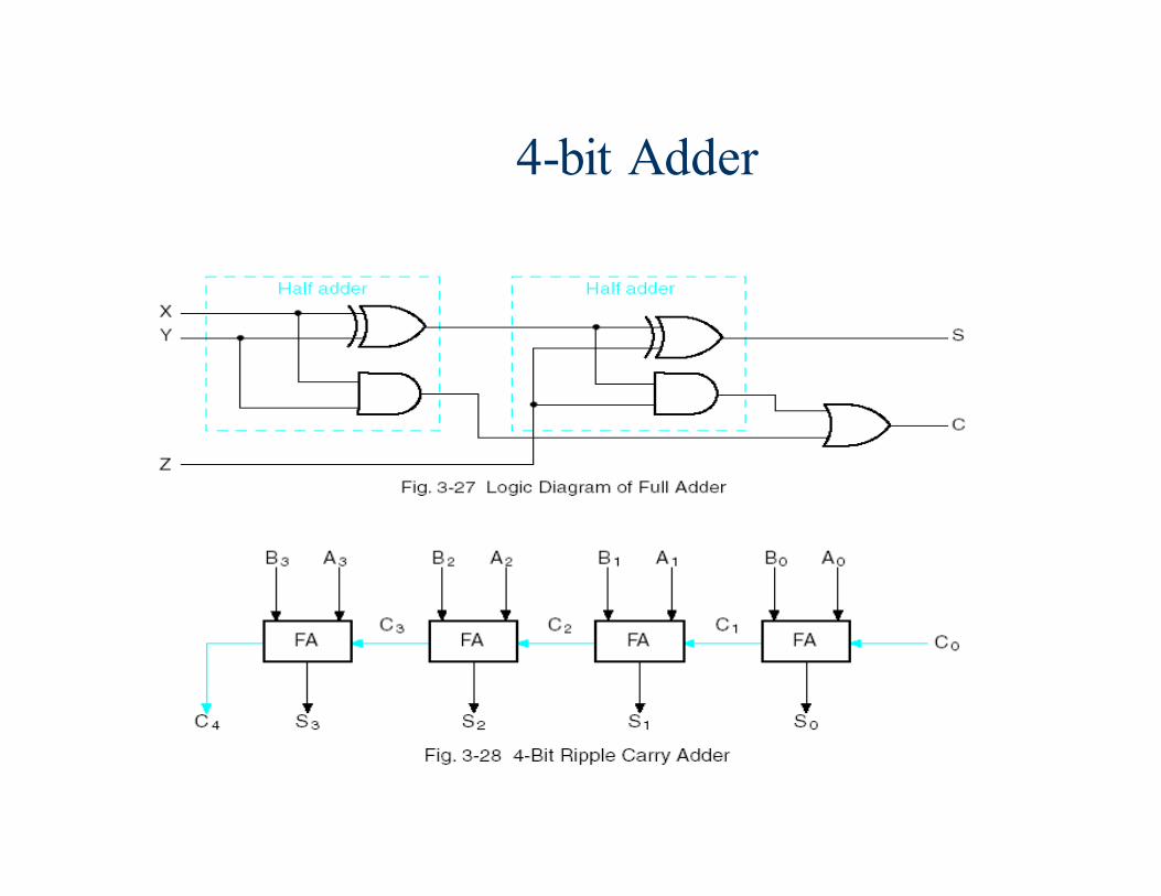
� In a top-down design, a 4-bit binary adder is defined as top-level block with 4 full adder blocks. Then we describe two half-adders that are required to create the full adder.
� In a bottom-up design, the half-adder is defined, then the full adder is constructed and the 4-bit adder is built from the full adders.
Gate-level Modeling
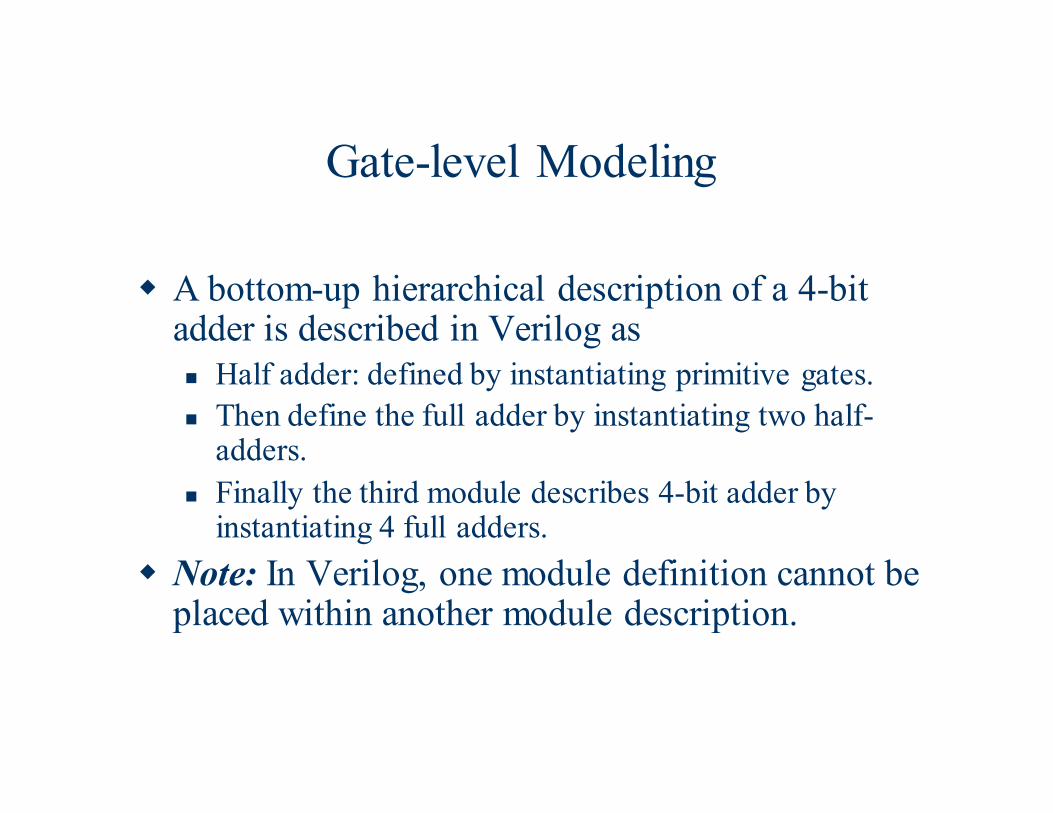
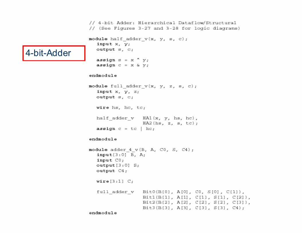
� A bottom-up hierarchical description of a 4-bit adder is described in Verilog as
� Half adder: defined by instantiating primitive gates.
� Then define the full adder by instantiating two half-adders.
� Finally the third module describes 4-bit adder by instantiating 4 full adders.
� Note: In Verilog, one module definition cannot be placed within another module description.
4-bit Half Adder
4-bit Full Adder
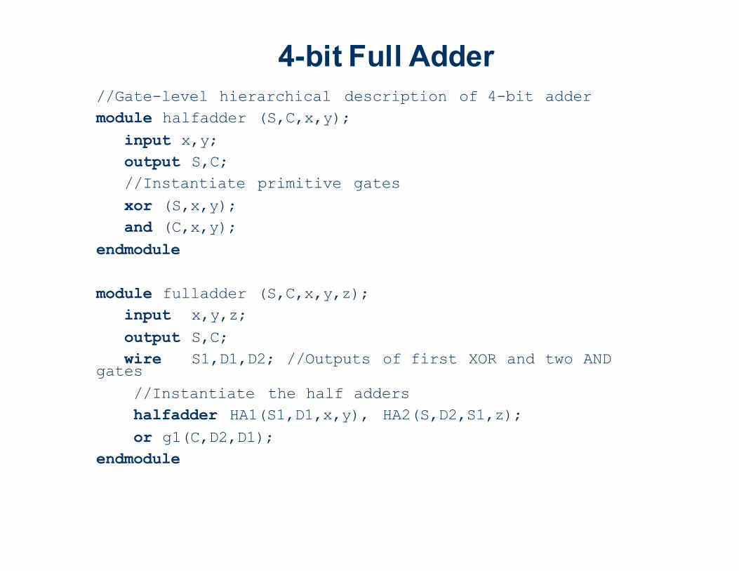
//Gate-level hierarchical description of 4-bit adder
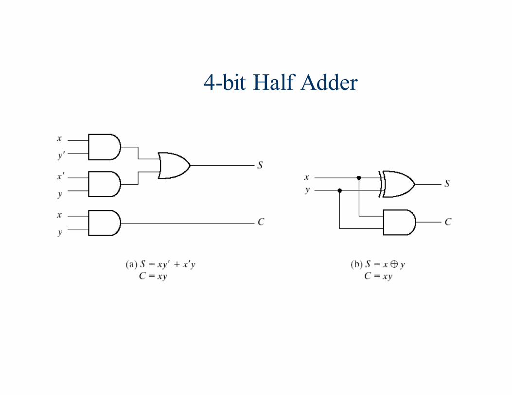
module halfadder (S,C,x,y);
input x,y;
output S,C;
//Instantiate primitive gates
xor (S,x,y);
and (C,x,y);
endmodule
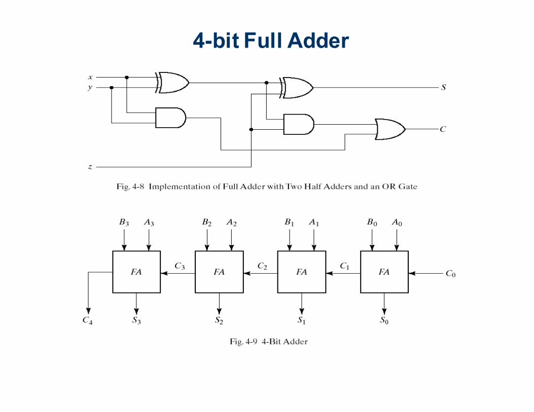
module fulladder (S,C,x,y,z);
input x,y,z;
output S,C;
wire S1,D1,D2; //Outputs of first XOR and two AND gates
//Instantiate the half adders
halfadder HA1(S1,D1,x,y), HA2(S,D2,S1,z);
or g1(C,D2,D1);
endmodule
4-bit Full Adder
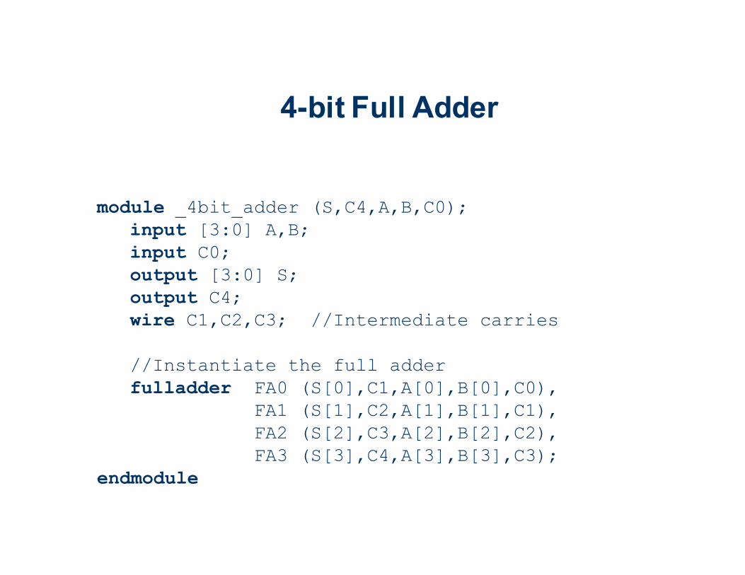
module _4bit_adder (S,C4,A,B,C0);
input [3:0] A,B;
input C0;
output [3:0] S;
output C4;
wire C1,C2,C3; //Intermediate carries
//Instantiate the full adder
fulladder FA0 (S[0],C1,A[0],B[0],C0),
FA1 (S[1],C2,A[1],B[1],C1),
FA2 (S[2],C3,A[2],B[2],C2),
FA3 (S[3],C4,A[3],B[3],C3);
endmodule
4-bit Full Adder
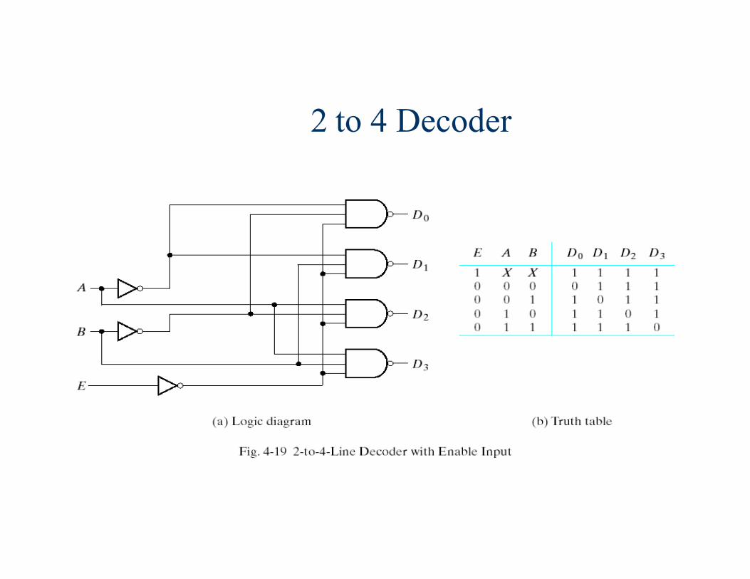
2 to 4 Decoder
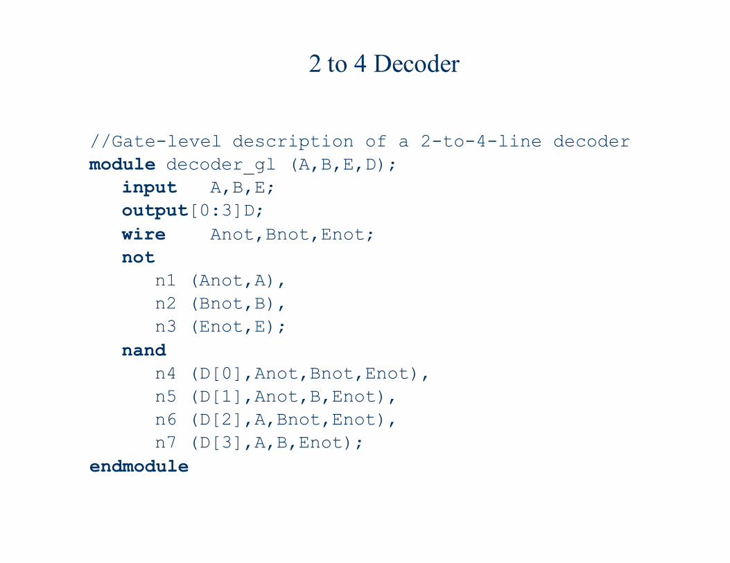
//Gate-level description of a 2-to-4-line decoder
module decoder_gl (A,B,E,D);
input A,B,E;
output[0:3]D;
wire Anot,Bnot,Enot;
not
n1 (Anot,A),
n2 (Bnot,B),
n3 (Enot,E);
nand
n4 (D[0],Anot,Bnot,Enot),
n5 (D[1],Anot,B,Enot),
n6 (D[2],A,Bnot,Enot),
n7 (D[3],A,B,Enot);
endmodule
2 to 4 Decoder
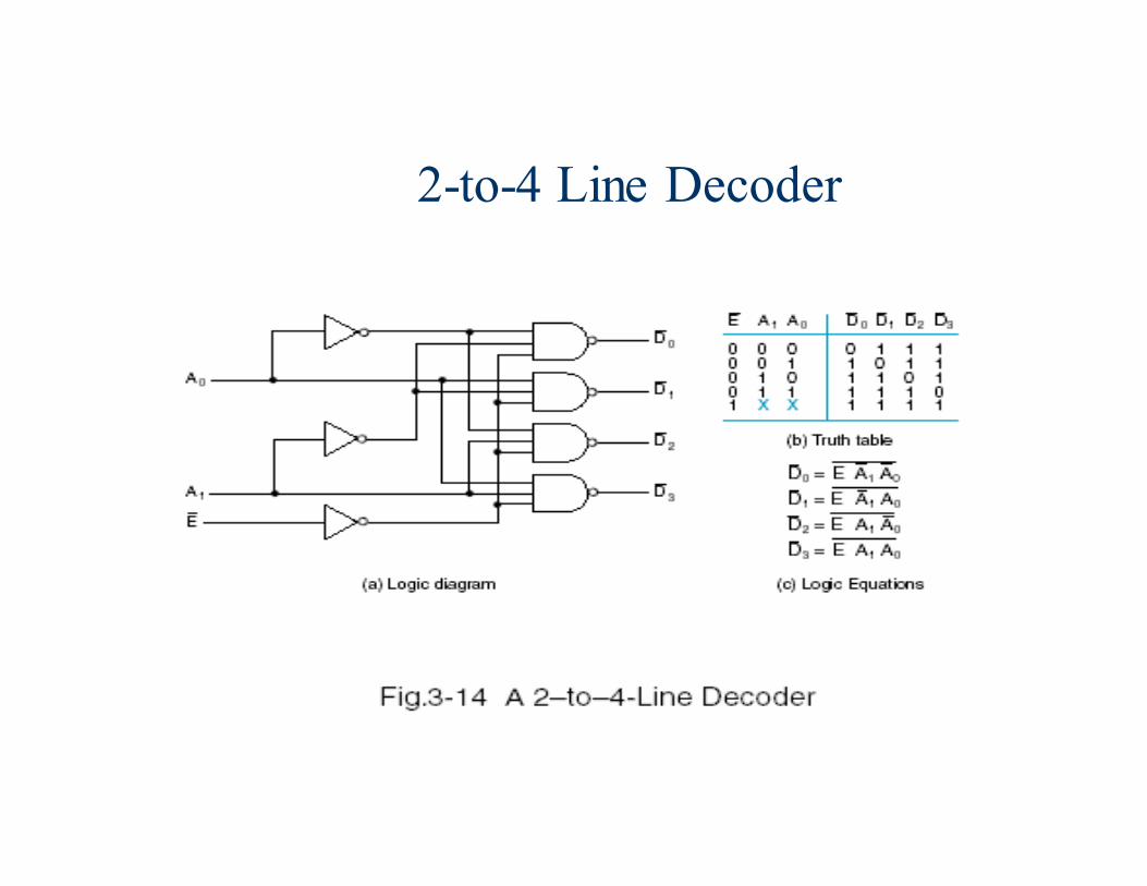
2-to-4 Line Decoder
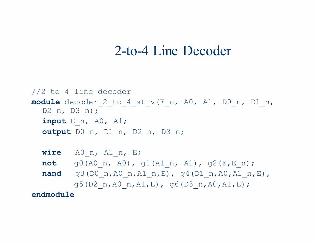
2-to-4 Line Decoder
//2 to 4 line decoder
module decoder_2_to_4_st_v(E_n, A0, A1, D0_n, D1_n, D2_n, D3_n);
input E_n, A0, A1;
output D0_n, D1_n, D2_n, D3_n;
wire A0_n, A1_n, E;
not g0(A0_n, A0), g1(A1_n, A1), g2(E,E_n);
nand g3(D0_n,A0_n,A1_n,E), g4(D1_n,A0,A1_n,E),
g5(D2_n,A0_n,A1,E), g6(D3_n,A0,A1,E);
endmodule
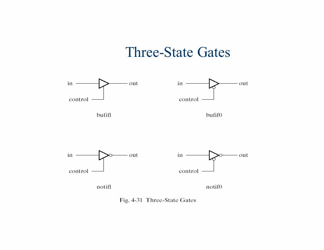
Three-State Gates
Three-State Gates
� Three-state gates have a control input that can place the gate into a high-impedance state. (symbolized by z in HDL).
� The bufif1 gate behaves like a normal buffer if control=1. The output goes to a high-impedance state zwhen control=0.
� bufif0 gate behaves in a similar way except that the high-impedance state occurs when control=1
� Two not gates operate in a similar manner except that the o/p is the complement of the input when the gate is not in a high impedance state.
� The gates are instantiated with the statement
� gate name (output, input, control);
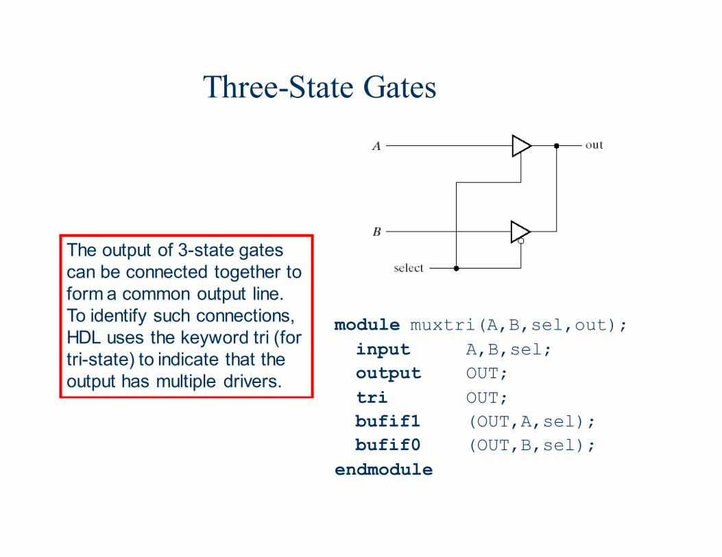
Three-State Gates
module muxtri(A,B,sel,out);
input A,B,sel;
output OUT;
tri OUT;
bufif1 (OUT,A,sel);
bufif0 (OUT,B,sel);
endmodule
The output of 3-state gates can be connected together to form a common output line. To identify such connections, HDL uses the keyword tri (for tri-state) to indicate that the output has multiple drivers.
Three-State Gates
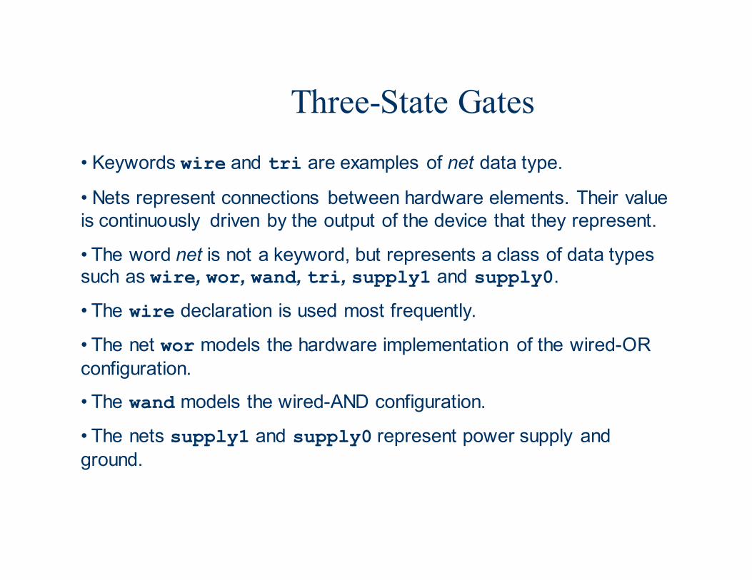
• Keywords wire and tri are examples of net data type.
• Nets represent connections between hardware elements. Their value is continuously driven by the output of the device that they represent.
• The word net is not a keyword, but represents a class of data types such as wire, wor, wand, tri, supply1 and supply0.
• The wire declaration is used most frequently.
• The net wor models the hardware implementation of the wired-OR
configuration.
• The wand models the wired-AND configuration.
• The nets supply1 and supply0 represent power supply and
ground.
Dataflow Modeling
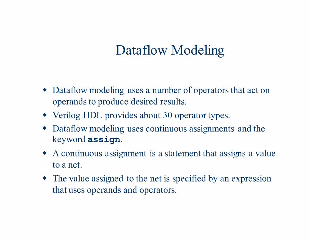
� Dataflow modeling uses a number of operators that act on
operands to produce desired results.
� Verilog HDL provides about 30 operator types.
� Dataflow modeling uses continuous assignments and the keyword assign.
� A continuous assignment is a statement that assigns a value
to a net.
� The value assigned to the net is specified by an expression
that uses operands and operators.
Dataflow Modeling (2)
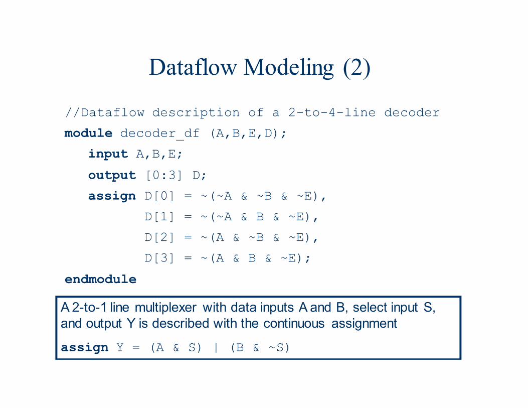
//Dataflow description of a 2-to-4-line decoder
module decoder_df (A,B,E,D);
input A,B,E;
output [0:3] D;
assign D[0] = ~(~A & ~B & ~E),
D[1] = ~(~A & B & ~E),
D[2] = ~(A & ~B & ~E),
D[3] = ~(A & B & ~E);
endmodule
A 2-to-1 line multiplexer with data inputs A and B, select input S, and output Y is described with the continuous assignment
assign Y = (A & S) | (B & ~S)
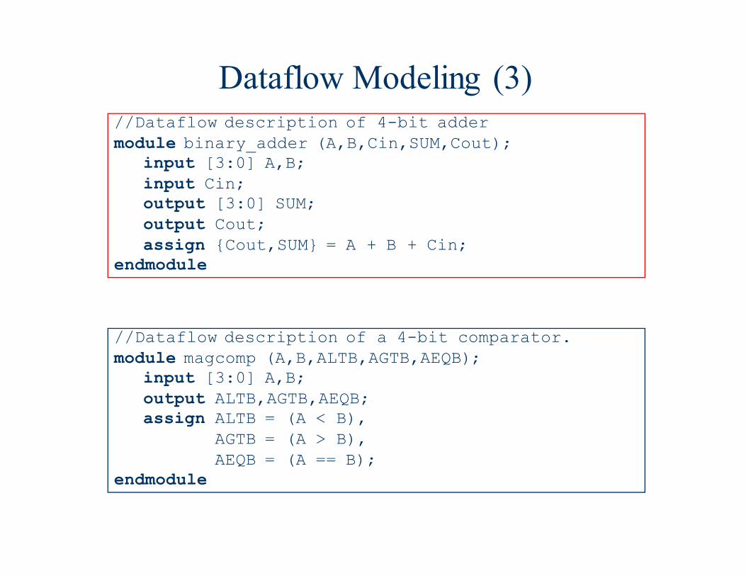
Dataflow Modeling (3)//Dataflow description of 4-bit adder
module binary_adder (A,B,Cin,SUM,Cout);input [3:0] A,B;
input Cin;output [3:0] SUM;
output Cout;
assign {Cout,SUM} = A + B + Cin;endmodule
//Dataflow description of a 4-bit comparator.
module magcomp (A,B,ALTB,AGTB,AEQB);input [3:0] A,B;
output ALTB,AGTB,AEQB;assign ALTB = (A < B),
AGTB = (A > B),
AEQB = (A == B);endmodule
Dataflow Modeling (4)
� The addition logic of 4 bit adder is described by a single
statement using the operators of addition and concatenation.
� The plus symbol (+) specifies the binary addition of the 4 bits of A with the 4 bits of B and the one bit of Cin.
� The target output is the concatenation of the output carry Cout and the four bits of SUM.
� Concatenation of operands is expressed within braces and a
comma separating the operands. Thus, {Cout,SUM}
represents the 5-bit result of the addition operation.
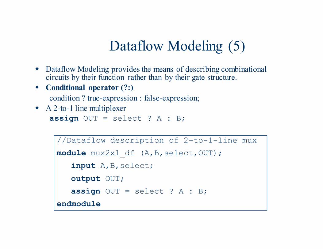
Dataflow Modeling (5)
� Dataflow Modeling provides the means of describing combinational circuits by their function rather than by their gate structure.
� Conditional operator (?:)
condition ? true-expression : false-expression;
� A 2-to-1 line multiplexer
assign OUT = select ? A : B;
//Dataflow description of 2-to-1-line mux
module mux2x1_df (A,B,select,OUT);
input A,B,select;
output OUT;
assign OUT = select ? A : B;
endmodule
Behavioral Modeling
� Behavioral modeling represents digital circuits at a functional and algorithmic level.
� It is used mostly to describe sequential circuits, but can also be used to describe combinational circuits.
� Behavioral descriptions use the keyword always followed by a list of procedural assignment statements.
� The target output of procedural assignment statements must be of the reg data type.
� A reg data type retains its value until a new value is assigned.
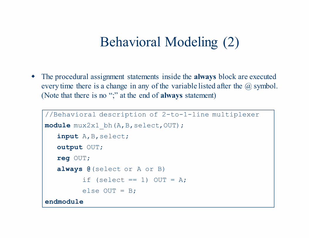
Behavioral Modeling (2)
� The procedural assignment statements inside the always block are executed
every time there is a change in any of the variable listed after the @ symbol.
(Note that there is no “;” at the end of always statement)
//Behavioral description of 2-to-1-line multiplexer
module mux2x1_bh(A,B,select,OUT);
input A,B,select;
output OUT;
reg OUT;
always @(select or A or B)
if (select == 1) OUT = A;
else OUT = B;
endmodule
Behavioral Modeling (3)
4-to-1 line multiplexer
Behavioral Modeling (4)
//Behavioral description of 4-to-1 line mux
module mux4x1_bh (i0,i1,i2,i3,select,y);
input i0,i1,i2,i3;
input [1:0] select;
output y;
reg y;
always @(i0 or i1 or i2 or i3 or select)
case (select)
2'b00: y = i0;
2'b01: y = i1;
2'b10: y = i2;
2'b11: y = i3;
endcase
endmodule
Behavioral Modeling (5)
� In 4-to-1 line multiplexer, the select input is defined
as a 2-bit vector and output y is declared as a reg
data.
� The always block has a sequential block enclosed between the keywords case and endcase.
� The block is executed whenever any of the inputs
listed after the @ symbol changes in value.
Writing a Test Bench
� A test bench is an HDL program used for applying stimulus to an HDL design in order to test it and observe its response during simulation.
� In addition to the always statement, test benches use the initial statement to provide a stimulus to the circuit under test.
� The always statement executes repeatedly in a loop. The initial statement executes only once starting from simulation time=0 and may continue with any operations that are delayed by a given number of units as specified by the symbol #.
Writing a Test Bench (2)
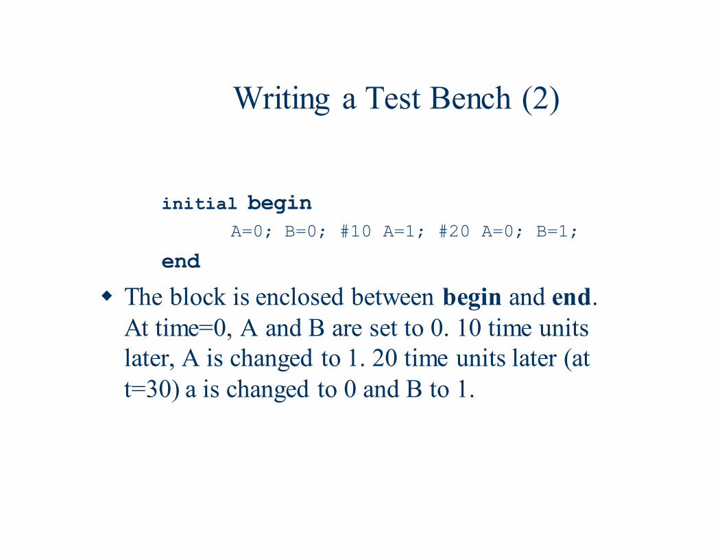
initial begin
A=0; B=0; #10 A=1; #20 A=0; B=1;
end
� The block is enclosed between begin and end.
At time=0, A and B are set to 0. 10 time units
later, A is changed to 1. 20 time units later (at
t=30) a is changed to 0 and B to 1.
Writing a Test Bench (2)
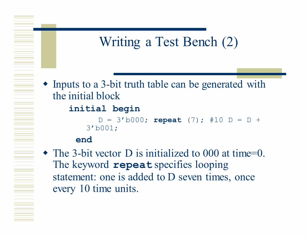
� Inputs to a 3-bit truth table can be generated with the initial block
initial beginD = 3’b000; repeat (7); #10 D = D +
3’b001;
end
� The 3-bit vector D is initialized to 000 at time=0. The keyword repeat specifies looping statement: one is added to D seven times, once every 10 time units.
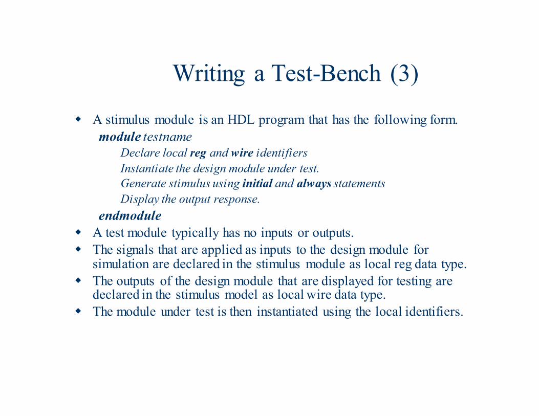
Writing a Test-Bench (3)
� A stimulus module is an HDL program that has the following form.
module testname
Declare local reg and wire identifiers
Instantiate the design module under test.
Generate stimulus using initial and always statements
Display the output response.
endmodule
� A test module typically has no inputs or outputs.
� The signals that are applied as inputs to the design module for simulation are declared in the stimulus module as local reg data type.
� The outputs of the design module that are displayed for testing are declared in the stimulus model as local wire data type.
� The module under test is then instantiated using the local identifiers.
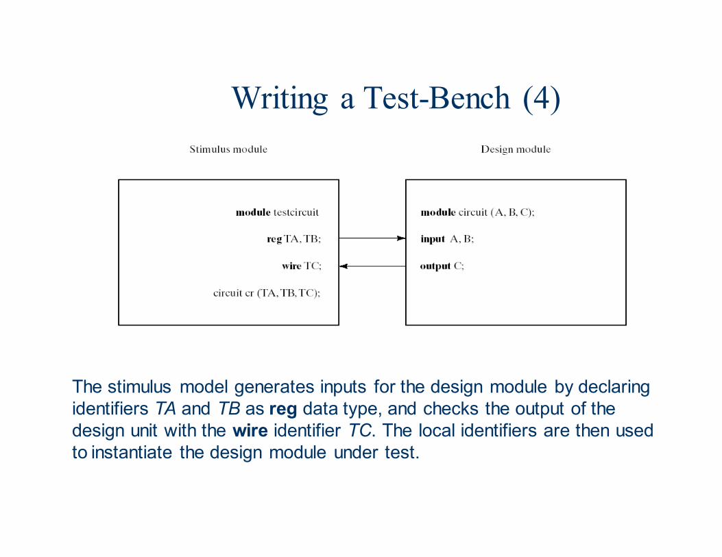
Writing a Test-Bench (4)
The stimulus model generates inputs for the design module by declaring identifiers TA and TB as reg data type, and checks the output of the design unit with the wire identifier TC. The local identifiers are then used to instantiate the design module under test.
Writing a Test-Bench (5)
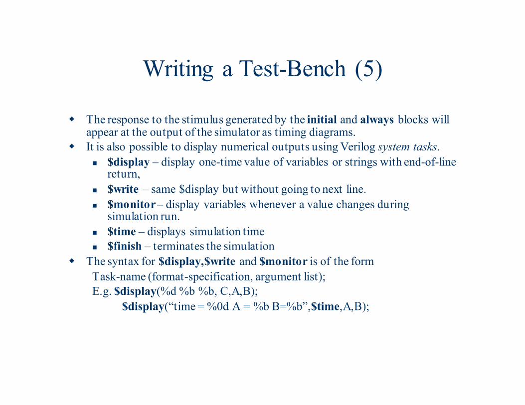
� The response to the stimulus generated by the initial and always blocks will appear at the output of the simulator as timing diagrams.
� It is also possible to display numerical outputs using Verilog system tasks.
� $display – display one-time value of variables or strings with end-of-line return,
� $write – same $display but without going to next line.
� $monitor– display variables whenever a value changes during simulation run.
� $time – displays simulation time
� $finish – terminates the simulation
� The syntax for $display,$write and $monitor is of the form
Task-name (format-specification, argument list);
E.g. $display(%d %b %b, C,A,B);
$display(“time = %0d A = %b B=%b”,$time,A,B);
Writing a Test-Bench (6)
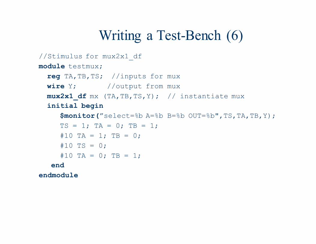
//Stimulus for mux2x1_df
module testmux;
reg TA,TB,TS; //inputs for mux
wire Y; //output from mux
mux2x1_df mx (TA,TB,TS,Y); // instantiate mux
initial begin
$monitor(”select=%b A=%b B=%b OUT=%b",TS,TA,TB,Y);
TS = 1; TA = 0; TB = 1;
#10 TA = 1; TB = 0;
#10 TS = 0;
#10 TA = 0; TB = 1;
end
endmodule
Writing a Test-Bench (7)
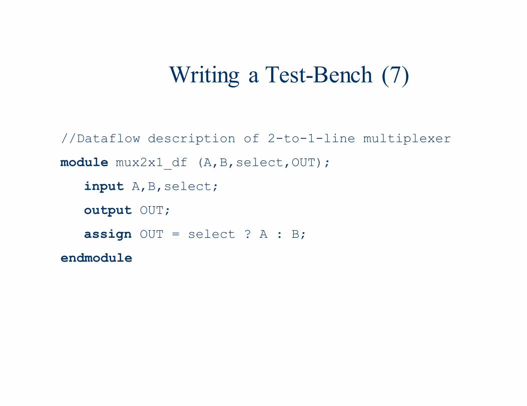
//Dataflow description of 2-to-1-line multiplexer
module mux2x1_df (A,B,select,OUT);
input A,B,select;
output OUT;
assign OUT = select ? A : B;
endmodule
Descriptions of Circuits
� Structural Description – This is directly equivalent to the
schematic of a circuit and is specifically oriented to
describing hardware structures using the components of a
circuit.
� Dataflow Description – This describes a circuit in terms of
function rather than structure and is made up of concurrent
assignment statements or their equivalent. Concurrent
assignments statements are executed concurrently, i.e. in
parallel whenever one of the values on the right hand side of
the statement changes.
Descriptions of Circuits (2)
� Hierarchical Description – Descriptions that represent
circuits using hierarchy have multiple entities, one for each
element of the Hierarchy.
� Behavioral Description – This refers to a description of a
circuit at a level higher than the logic level. This type of
description is also referred to as the register transfers level.
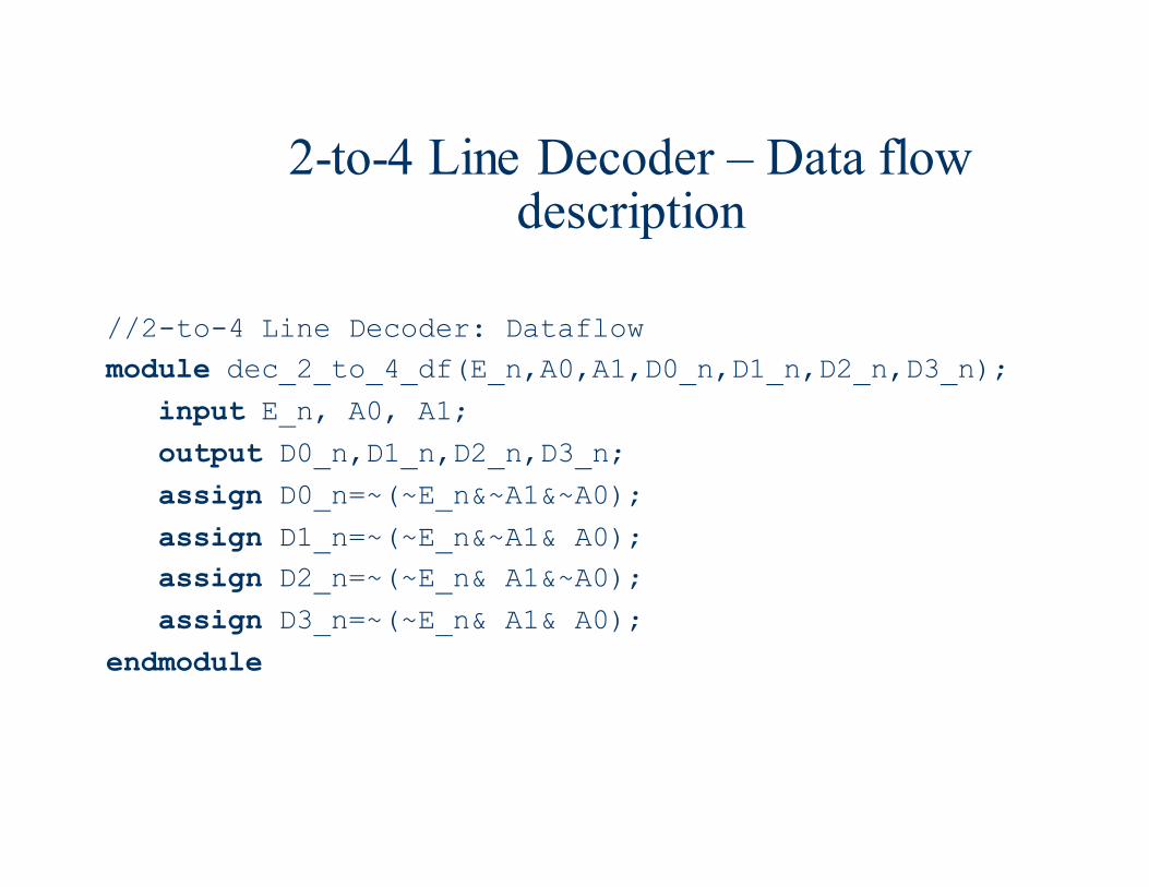
2-to-4 Line Decoder – Data flow description
//2-to-4 Line Decoder: Dataflow
module dec_2_to_4_df(E_n,A0,A1,D0_n,D1_n,D2_n,D3_n);
input E_n, A0, A1;
output D0_n,D1_n,D2_n,D3_n;
assign D0_n=~(~E_n&~A1&~A0);
assign D1_n=~(~E_n&~A1& A0);
assign D2_n=~(~E_n& A1&~A0);
assign D3_n=~(~E_n& A1& A0);
endmodule
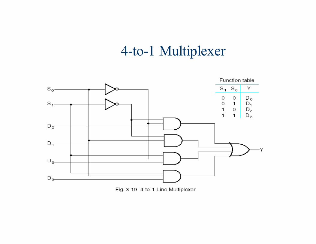
4-to-1 Multiplexer
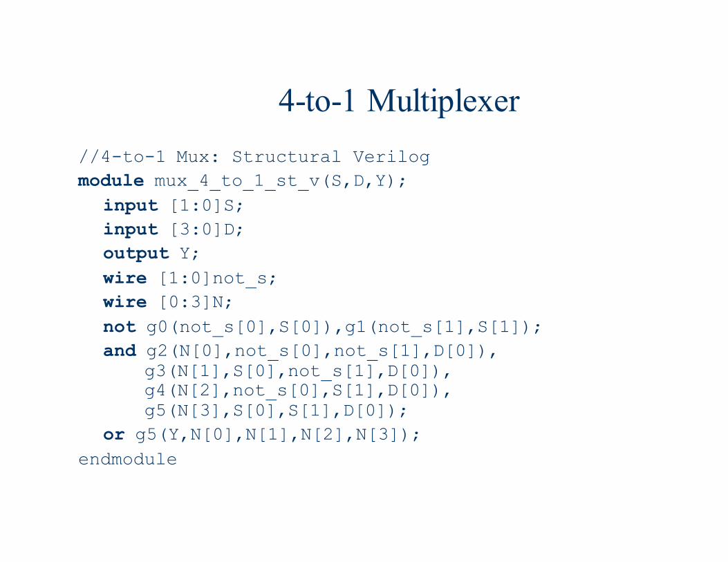
4-to-1 Multiplexer
//4-to-1 Mux: Structural Verilog
module mux_4_to_1_st_v(S,D,Y);
input [1:0]S;
input [3:0]D;
output Y;
wire [1:0]not_s;
wire [0:3]N;
not g0(not_s[0],S[0]),g1(not_s[1],S[1]);
and g2(N[0],not_s[0],not_s[1],D[0]), g3(N[1],S[0],not_s[1],D[0]), g4(N[2],not_s[0],S[1],D[0]), g5(N[3],S[0],S[1],D[0]);
or g5(Y,N[0],N[1],N[2],N[3]);
endmodule
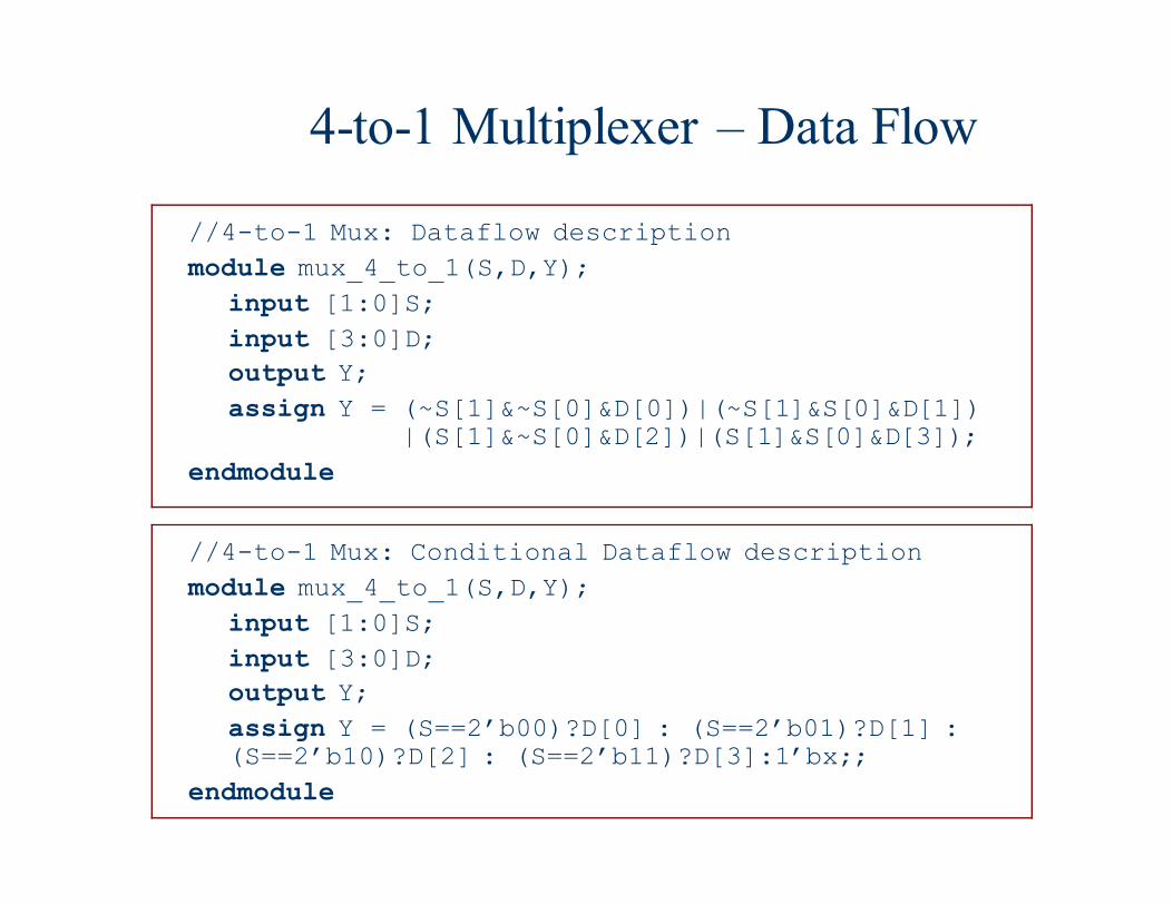
4-to-1 Multiplexer – Data Flow
//4-to-1 Mux: Dataflow description
module mux_4_to_1(S,D,Y);
input [1:0]S;
input [3:0]D;
output Y;
assign Y = (~S[1]&~S[0]&D[0])|(~S[1]&S[0]&D[1]) |(S[1]&~S[0]&D[2])|(S[1]&S[0]&D[3]);
endmodule
//4-to-1 Mux: Conditional Dataflow description
module mux_4_to_1(S,D,Y);
input [1:0]S;
input [3:0]D;
output Y;
assign Y = (S==2’b00)?D[0] : (S==2’b01)?D[1] : (S==2’b10)?D[2] : (S==2’b11)?D[3]:1’bx;;
endmodule
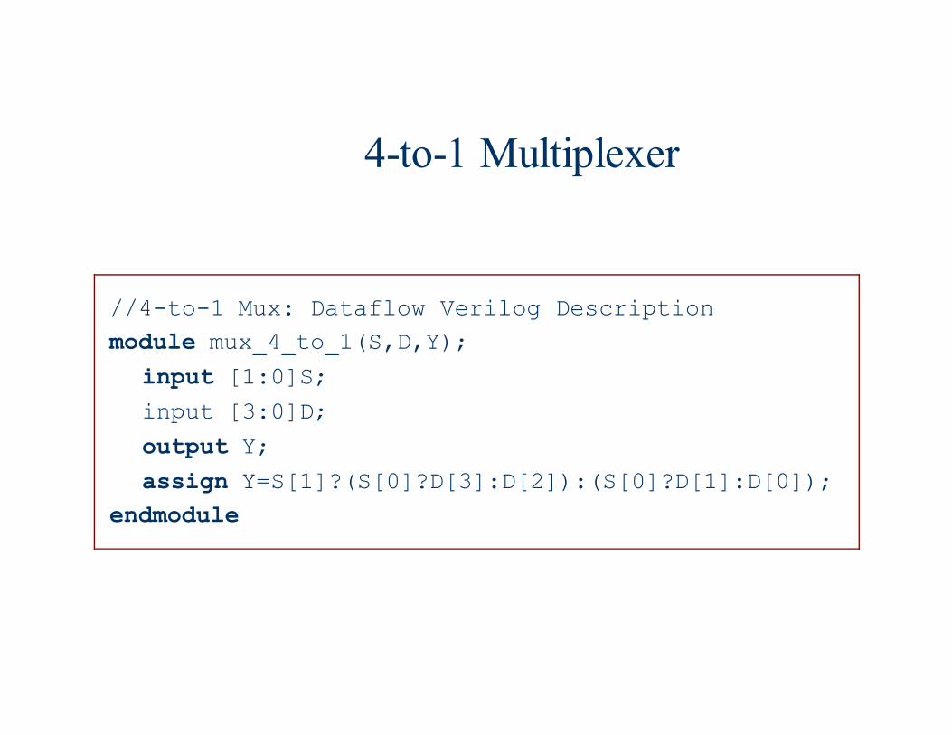
4-to-1 Multiplexer
//4-to-1 Mux: Dataflow Verilog Description
module mux_4_to_1(S,D,Y);
input [1:0]S;
input [3:0]D;
output Y;
assign Y=S[1]?(S[0]?D[3]:D[2]):(S[0]?D[1]:D[0]);
endmodule
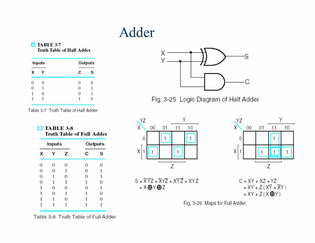
Adder
4-bit Adder
4-bit-Adder
4-bit Adder
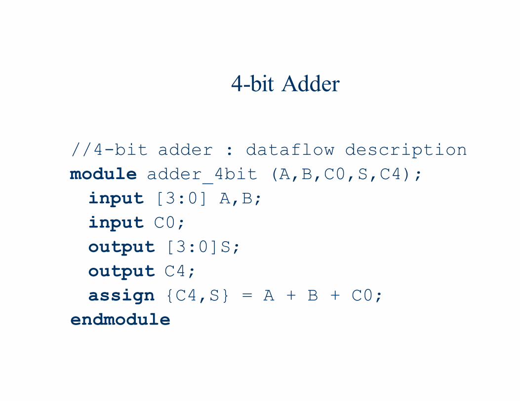
//4-bit adder : dataflow description
module adder_4bit (A,B,C0,S,C4);
input [3:0] A,B;
input C0;
output [3:0]S;
output C4;
assign {C4,S} = A + B + C0;
endmodule
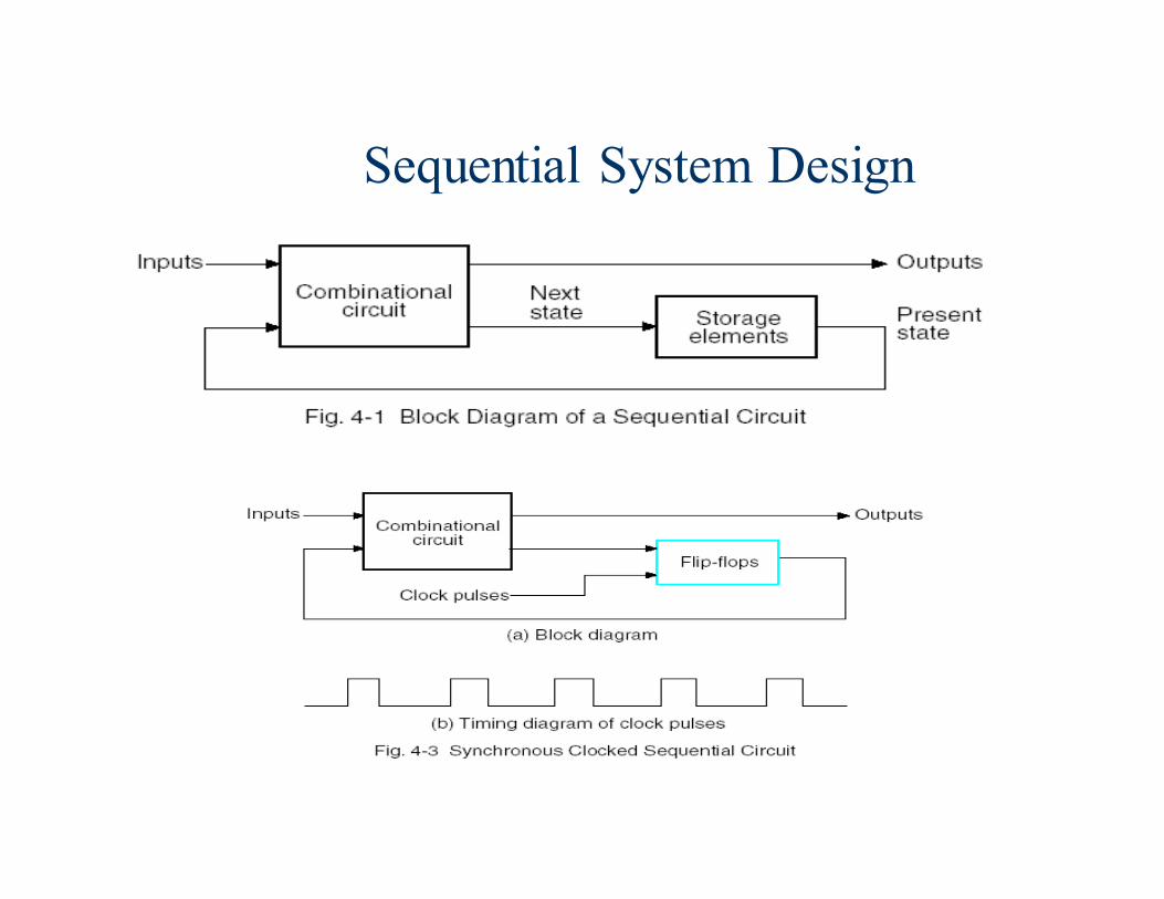
Sequential System Design
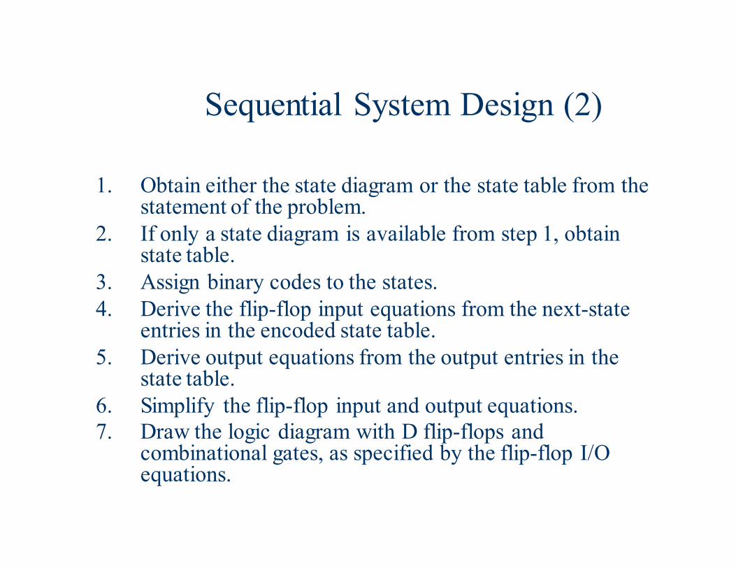
Sequential System Design (2)
1. Obtain either the state diagram or the state table from the statement of the problem.
2. If only a state diagram is available from step 1, obtain state table.
3. Assign binary codes to the states.
4. Derive the flip-flop input equations from the next-state entries in the encoded state table.
5. Derive output equations from the output entries in the state table.
6. Simplify the flip-flop input and output equations.
7. Draw the logic diagram with D flip-flops and combinational gates, as specified by the flip-flop I/O equations.
Behavioral Modeling in SSD
� There are two kinds of behavioral statements in Verilog HDL: initial and always.
� The initial behavior executes once beginning at time=0.
� The always behavior executes repeatedly and re-executes
until the simulation terminates.
� A behavior is declared within a module by using the
keywords initial or always, followed by a statement
or a block of statements enclosed by the keywords beginand end.
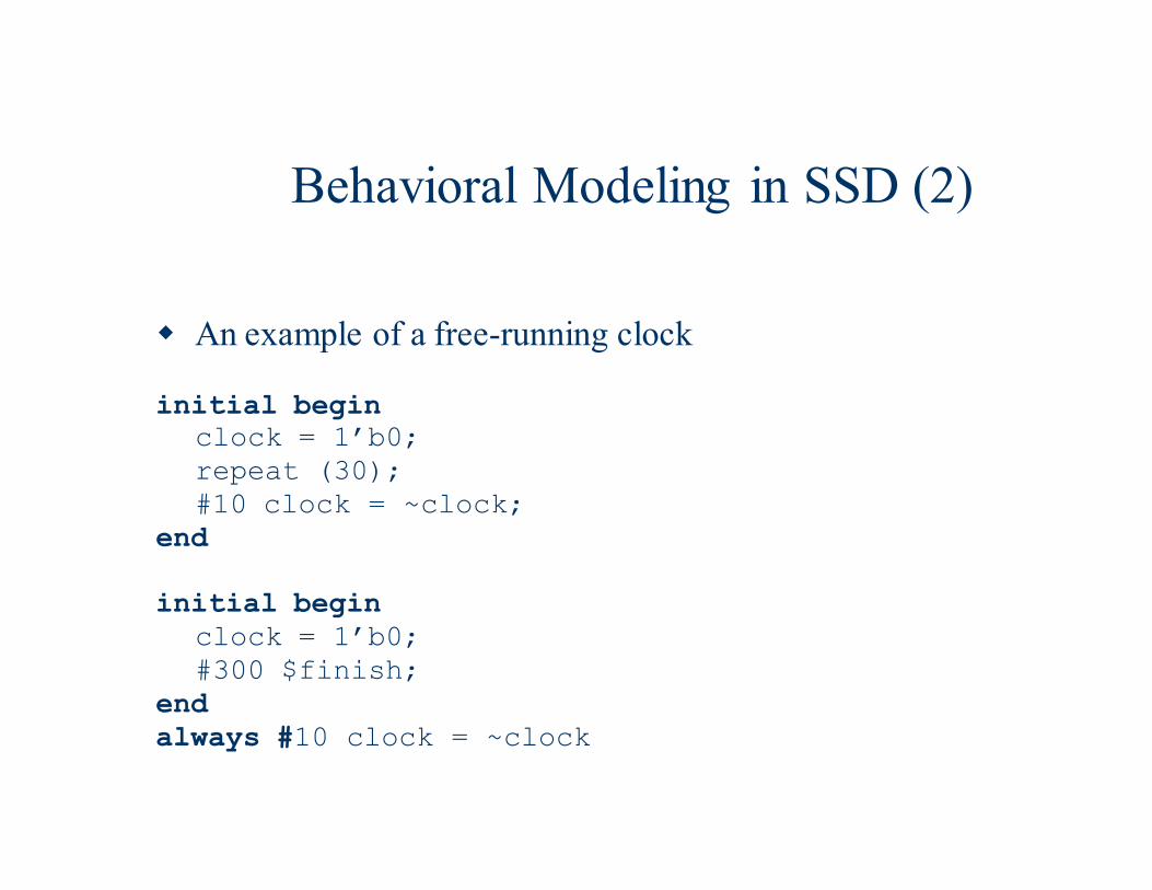
Behavioral Modeling in SSD (2)
� An example of a free-running clock
initial beginclock = 1’b0;repeat (30);#10 clock = ~clock;
end
initial beginclock = 1’b0;#300 $finish;
endalways #10 clock = ~clock
Behavioral Modeling in SSD (3)
� The always statement can be controlled by delays that wait for a certain time or by certain conditions to become true or by events to occur.
� This type of statement is of the form:always @ (event control expression)
Procedural assignment statements
� The event control expression specifies the condition that must occur to activate the execution of the procedural assignment statements.
� The variables in the left-hand side of the procedural statements must be of the reg data type and must be declared as such.
Behavioral Modeling in SSD (4)
� The statements within the block, after the event control expression, execute sequentially and the execution suspends after the last statement has executed.
� Then the always statement waits again for an event to occur.
� Two kind of events:� Level sensitive (E.g. in combinational circuits and in latches)
always @(A or B or Reset)will cause the execution of the procedural statements in the always block if changes occur in A or Bor Reset.
� Edge-triggered (In synchronous sequential circuits, changes in flip-flops must occur only in response to a transition of a clock pulse. always @(posedge clock or negedge reset)will cause the
execution of the procedural statements only if the clock goes through a positive transition or if the reset goes through a negative transition.
Behavioral Modeling in SSD (5)
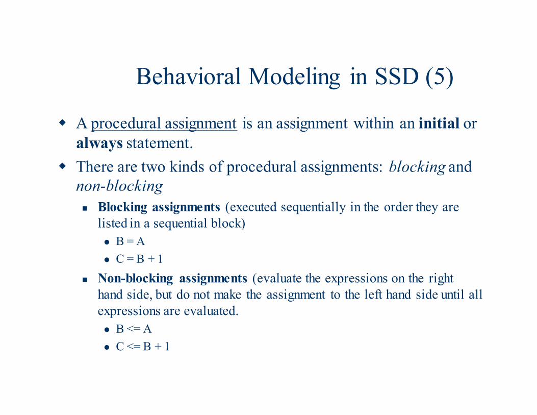
� A procedural assignment is an assignment within an initial or
always statement.
� There are two kinds of procedural assignments: blocking and
non-blocking
� Blocking assignments (executed sequentially in the order they are
listed in a sequential block)
� B = A
� C = B + 1
� Non-blocking assignments (evaluate the expressions on the right
hand side, but do not make the assignment to the left hand side until all
expressions are evaluated.
� B <= A
� C <= B + 1
Flip-Flops and Latches
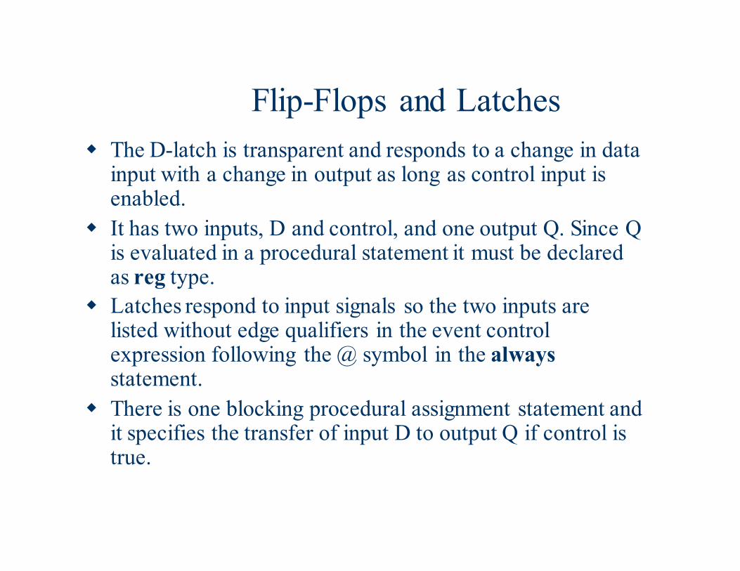
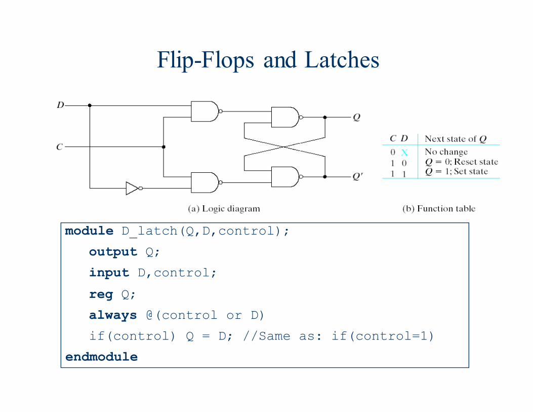
� The D-latch is transparent and responds to a change in data input with a change in output as long as control input is enabled.
� It has two inputs, D and control, and one output Q. Since Q is evaluated in a procedural statement it must be declared as reg type.
� Latches respond to input signals so the two inputs are listed without edge qualifiers in the event control expression following the @ symbol in the alwaysstatement.
� There is one blocking procedural assignment statement and it specifies the transfer of input D to output Q if control is true.
Flip-Flops and Latches
module D_latch(Q,D,control);
output Q;
input D,control;
reg Q;
always @(control or D)
if(control) Q = D; //Same as: if(control=1)
endmodule
Flip-Flops and Latches
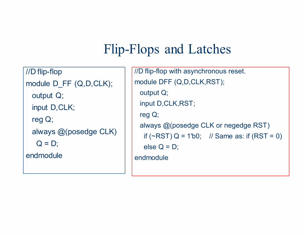
//D flip-flop
module D_FF (Q,D,CLK);
output Q;
input D,CLK;
reg Q;
always @(posedge CLK)
Q = D;
endmodule
//D flip-flop with asynchronous reset.
module DFF (Q,D,CLK,RST);
output Q;
input D,CLK,RST;
reg Q;
always @(posedge CLK or negedge RST)
if (~RST) Q = 1'b0; // Same as: if (RST = 0)
else Q = D;
endmodule
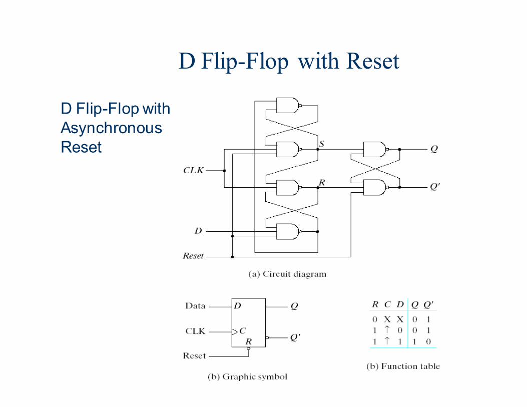
D Flip-Flop with Reset
D Flip-Flop with Asynchronous Reset
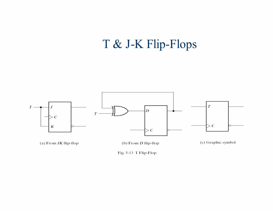
T & J-K Flip-Flops
T & J-K Flip-Flops //T flip-flop from D flip-flop and gates
module TFF (Q,T,CLK,RST);
output Q;
input T,CLK,RST;
wire DT;
assign DT = Q ̂T ;
//Instantiate the D flip-flop
DFF TF1 (Q,DT,CLK,RST);
endmodule
//JK flip-flop from D flip-flop and gates
module JKFF (Q,J,K,CLK,RST);
output Q;
input J,K,CLK,RST;
wire JK;
assign JK = (J & ~Q) | (~K & Q);
//Instantiate D flipflop
DFF JK1 (Q,JK,CLK,RST);
endmodule
flop-flipJK afor '')1(
flop-flip T afor )1(
QKJQtQ
TQtQ
+=+
⊕=+
Characteristic equations of the flip-flops:
J-K Flip-Flop
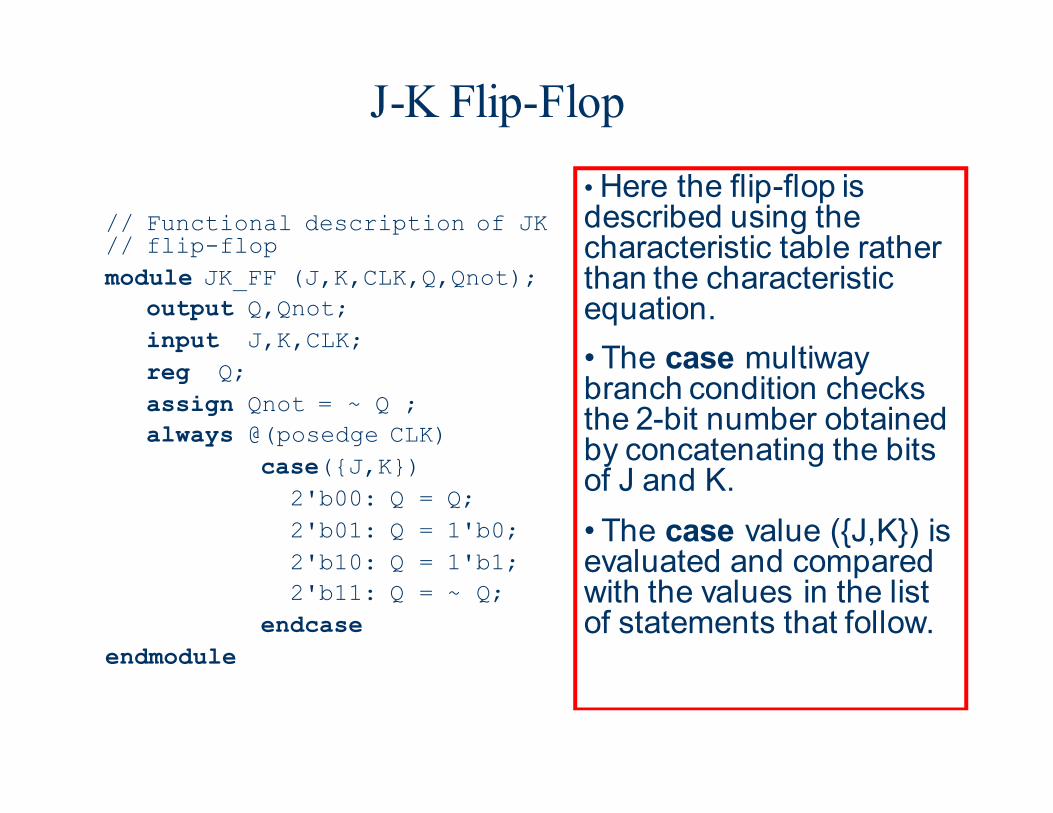
// Functional description of JK // flip-flop
module JK_FF (J,K,CLK,Q,Qnot);
output Q,Qnot;
input J,K,CLK;
reg Q;
assign Qnot = ~ Q ;
always @(posedge CLK)
case({J,K})
2'b00: Q = Q;
2'b01: Q = 1'b0;
2'b10: Q = 1'b1;
2'b11: Q = ~ Q;
endcase
endmodule
• Here the flip-flop is described using the characteristic table rather than the characteristic equation.
• The case multiway branch condition checks the 2-bit number obtained by concatenating the bits of J and K.
• The case value ({J,K}) is evaluated and compared with the values in the list of statements that follow.
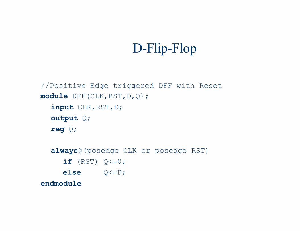
D-Flip-Flop
//Positive Edge triggered DFF with Reset
module DFF(CLK,RST,D,Q);
input CLK,RST,D;
output Q;
reg Q;
always@(posedge CLK or posedge RST)
if (RST) Q<=0;
else Q<=D;
endmodule
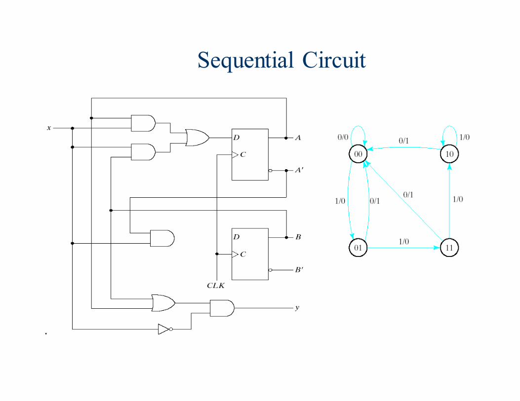
Sequential Circuit
Sequential Circuit (2)
//Mealy state diagram for the circuit
module Mealy_mdl (x,y,CLK,RST);
input x,CLK,RST;
output y;
reg y;
reg [1:0] Prstate,Nxtstate;
parameter S0=2'b00,S1=2'b01,S2=2'b10,S3=2'b11;
always@(posedge CLK or negedge RST)
if (~RST) Prstate = S0; //Initialize to state S0
else Prstate = Nxtstate; //Clock operations
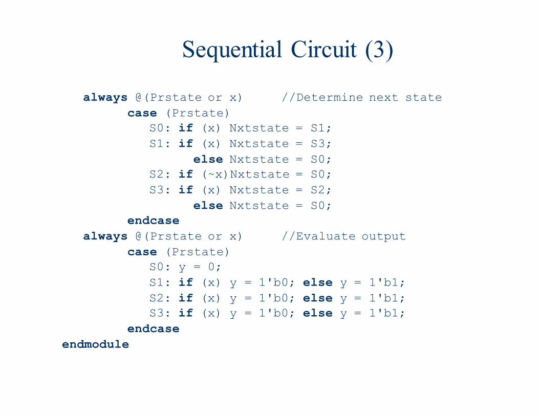
Sequential Circuit (3)
always @(Prstate or x) //Determine next state
case (Prstate)
S0: if (x) Nxtstate = S1;
S1: if (x) Nxtstate = S3;
else Nxtstate = S0;
S2: if (~x)Nxtstate = S0;
S3: if (x) Nxtstate = S2;
else Nxtstate = S0;
endcase
always @(Prstate or x) //Evaluate output
case (Prstate)
S0: y = 0;
S1: if (x) y = 1'b0; else y = 1'b1;
S2: if (x) y = 1'b0; else y = 1'b1;
S3: if (x) y = 1'b0; else y = 1'b1;
endcase
endmodule
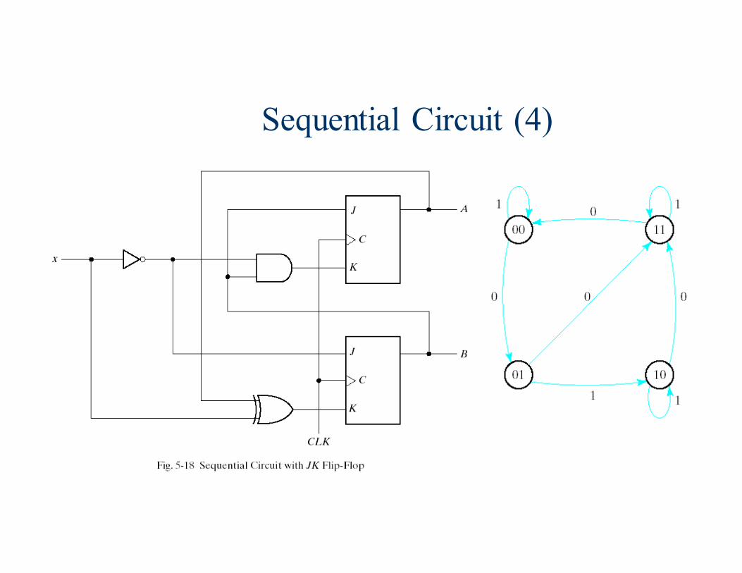
Sequential Circuit (4)
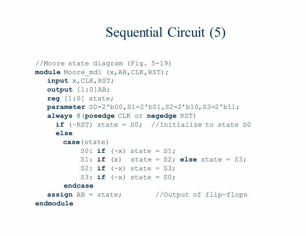
Sequential Circuit (5)
//Moore state diagram (Fig. 5-19)
module Moore_mdl (x,AB,CLK,RST);
input x,CLK,RST;
output [1:0]AB;
reg [1:0] state;
parameter S0=2'b00,S1=2'b01,S2=2'b10,S3=2'b11;
always @(posedge CLK or negedge RST)
if (~RST) state = S0; //Initialize to state S0
else
case(state)
S0: if (~x) state = S1;
S1: if (x) state = S2; else state = S3;
S2: if (~x) state = S3;
S3: if (~x) state = S0;
endcase
assign AB = state; //Output of flip-flops
endmodule
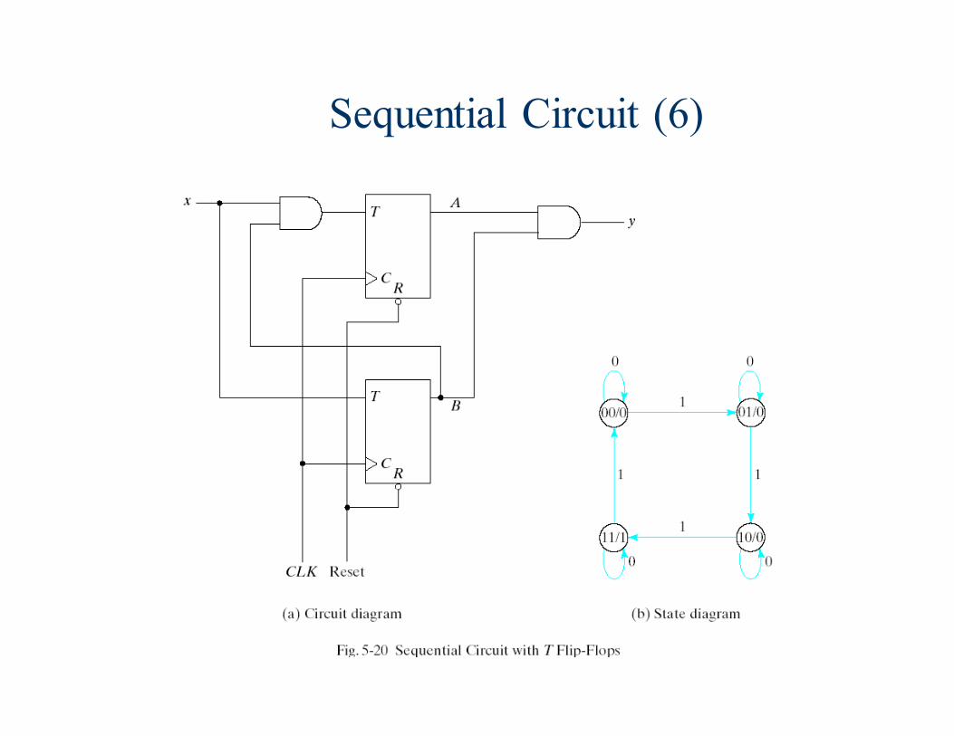
Sequential Circuit (6)
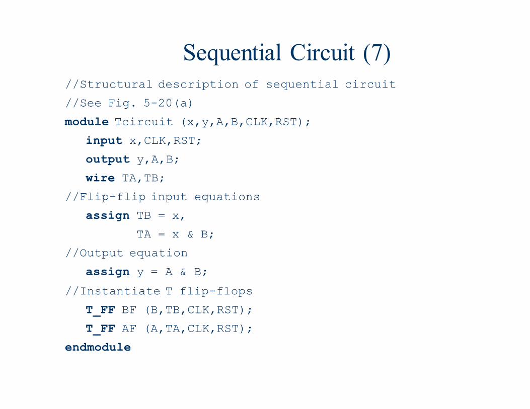
Sequential Circuit (7)//Structural description of sequential circuit
//See Fig. 5-20(a)
module Tcircuit (x,y,A,B,CLK,RST);
input x,CLK,RST;
output y,A,B;
wire TA,TB;
//Flip-flip input equations
assign TB = x,
TA = x & B;
//Output equation
assign y = A & B;
//Instantiate T flip-flops
T_FF BF (B,TB,CLK,RST);
T_FF AF (A,TA,CLK,RST);
endmodule
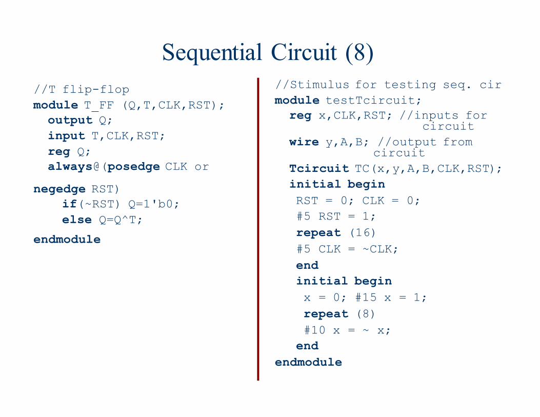
Sequential Circuit (8)
//T flip-flop
module T_FF (Q,T,CLK,RST);
output Q;
input T,CLK,RST;
reg Q;
always@(posedge CLK or
negedge RST)
if(~RST) Q=1'b0;
else Q=Q^T;
endmodule
//Stimulus for testing seq. cir
module testTcircuit;
reg x,CLK,RST; //inputs for circuit
wire y,A,B; //output from circuit
Tcircuit TC(x,y,A,B,CLK,RST);
initial begin
RST = 0; CLK = 0;
#5 RST = 1;
repeat (16)
#5 CLK = ~CLK;
end
initial begin
x = 0; #15 x = 1;
repeat (8)
#10 x = ~ x;
end
endmodule
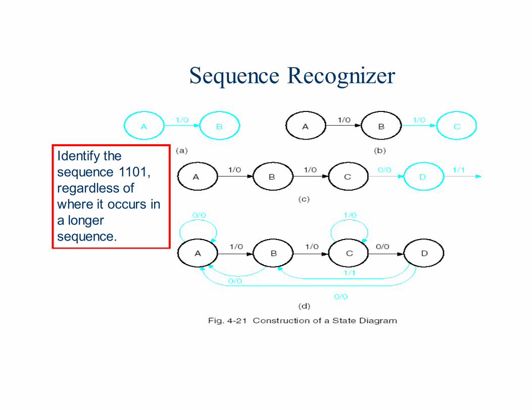
Sequence Recognizer
Identify the sequence 1101, regardless of where it occurs in a longer sequence.
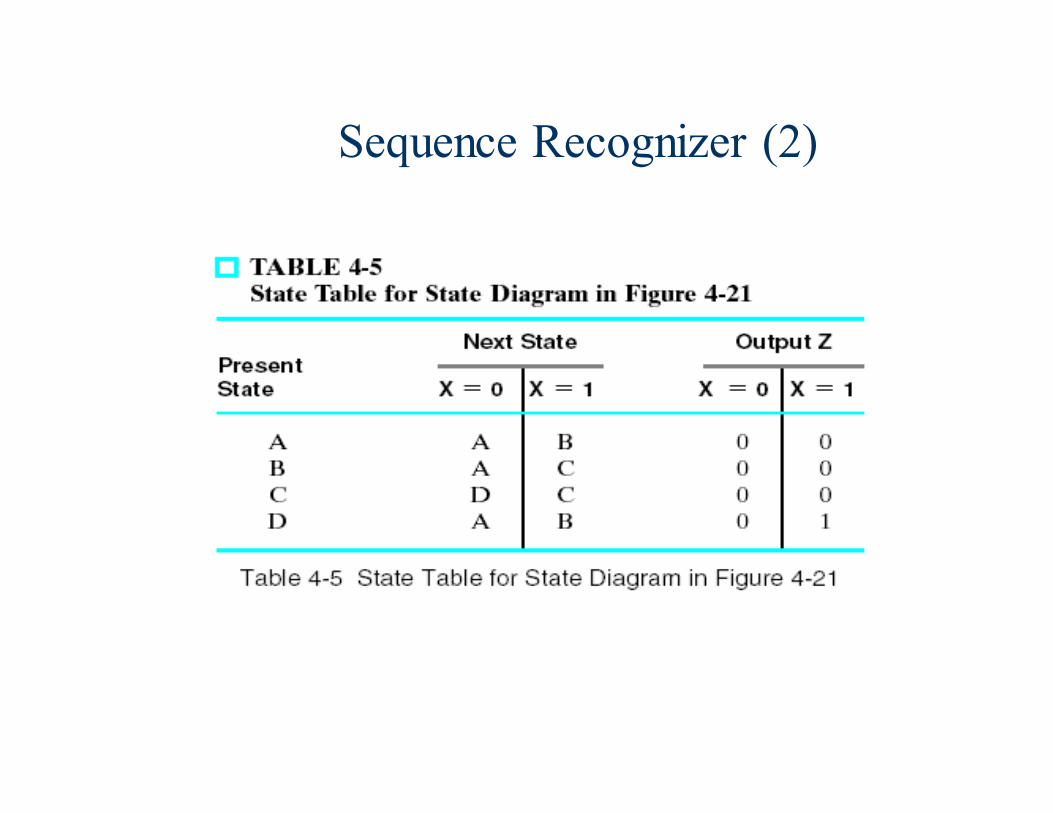
Sequence Recognizer (2)
Sequence Recognizer
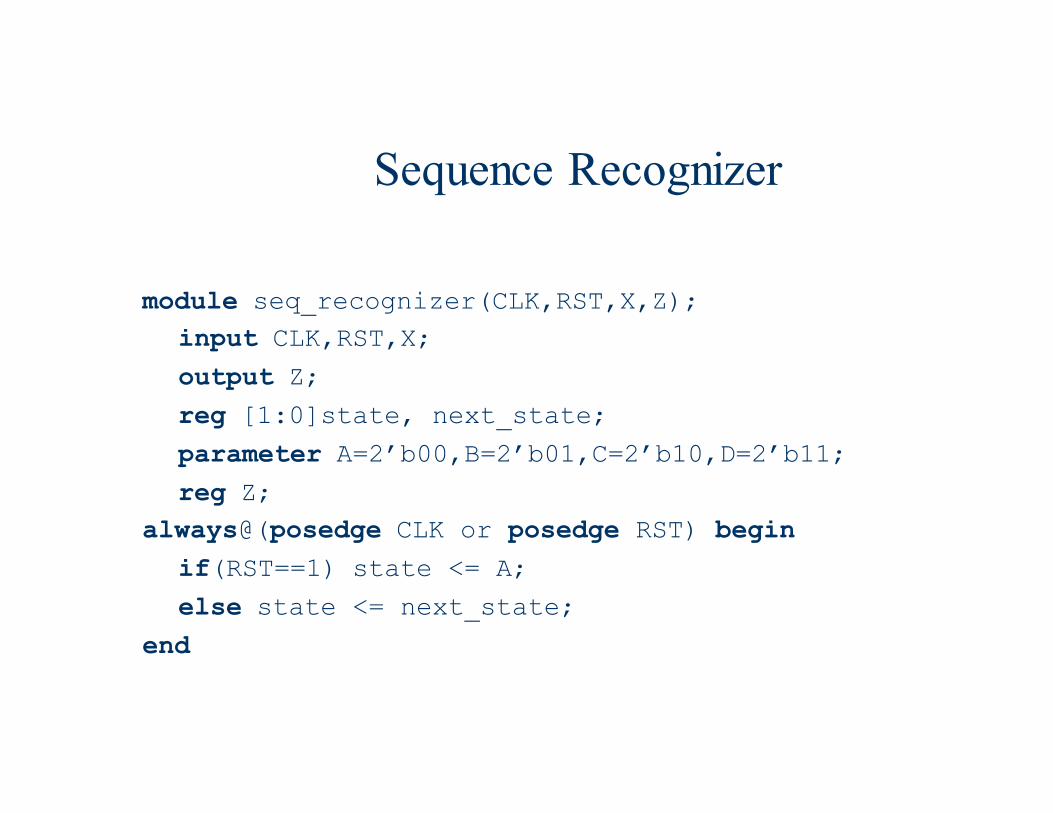
module seq_recognizer(CLK,RST,X,Z);
input CLK,RST,X;
output Z;
reg [1:0]state, next_state;
parameter A=2’b00,B=2’b01,C=2’b10,D=2’b11;
reg Z;
always@(posedge CLK or posedge RST) begin
if(RST==1) state <= A;
else state <= next_state;
end
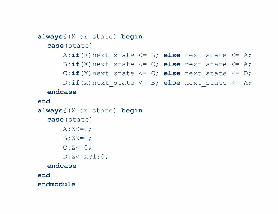
always@(X or state) begin
case(state)
A:if(X)next_state <= B; else next_state <= A;
B:if(X)next_state <= C; else next_state <= A;
C:if(X)next_state <= C; else next_state <= D;
D:if(X)next_state <= B; else next_state <= A;
endcase
end
always@(X or state) begin
case(state)
A:Z<=0;
B:Z<=0;
C:Z<=0;
D:Z<=X?1:0;
endcase
end
endmodule
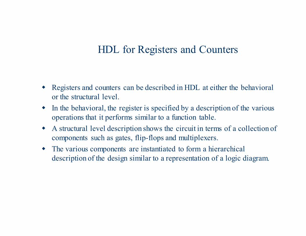
HDL for Registers and Counters
� Registers and counters can be described in HDL at either the behavioral
or the structural level.
� In the behavioral, the register is specified by a description of the various
operations that it performs similar to a function table.
� A structural level description shows the circuit in terms of a collection of
components such as gates, flip-flops and multiplexers.
� The various components are instantiated to form a hierarchical
description of the design similar to a representation of a logic diagram.
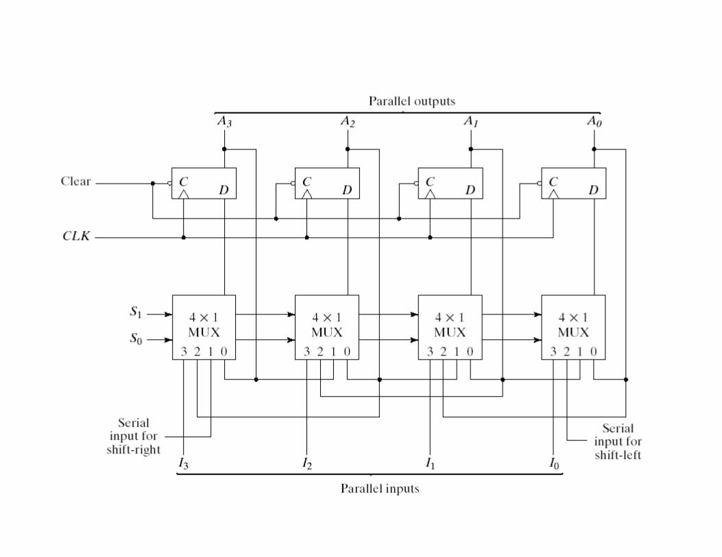
HDL for Registers and Counters (2)
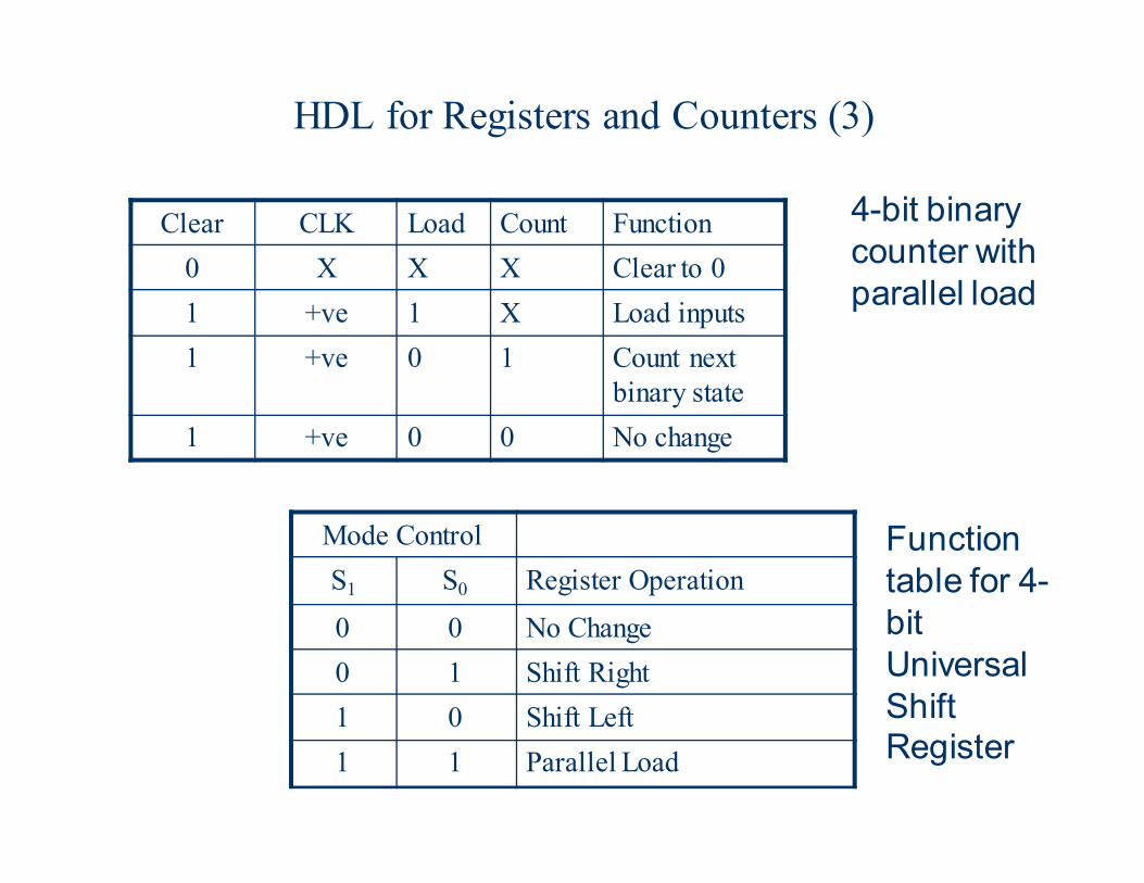
HDL for Registers and Counters (3)
Mode Control
S1 S0 Register Operation
0 0 No Change
0 1 Shift Right
1 0 Shift Left
1 1 Parallel Load
Clear CLK Load Count Function
0 X X X Clear to 0
1 +ve 1 X Load inputs
1 +ve 0 1 Count next
binary state
1 +ve 0 0 No change
Function table for 4-bit Universal Shift Register
4-bit binary counter with parallel load
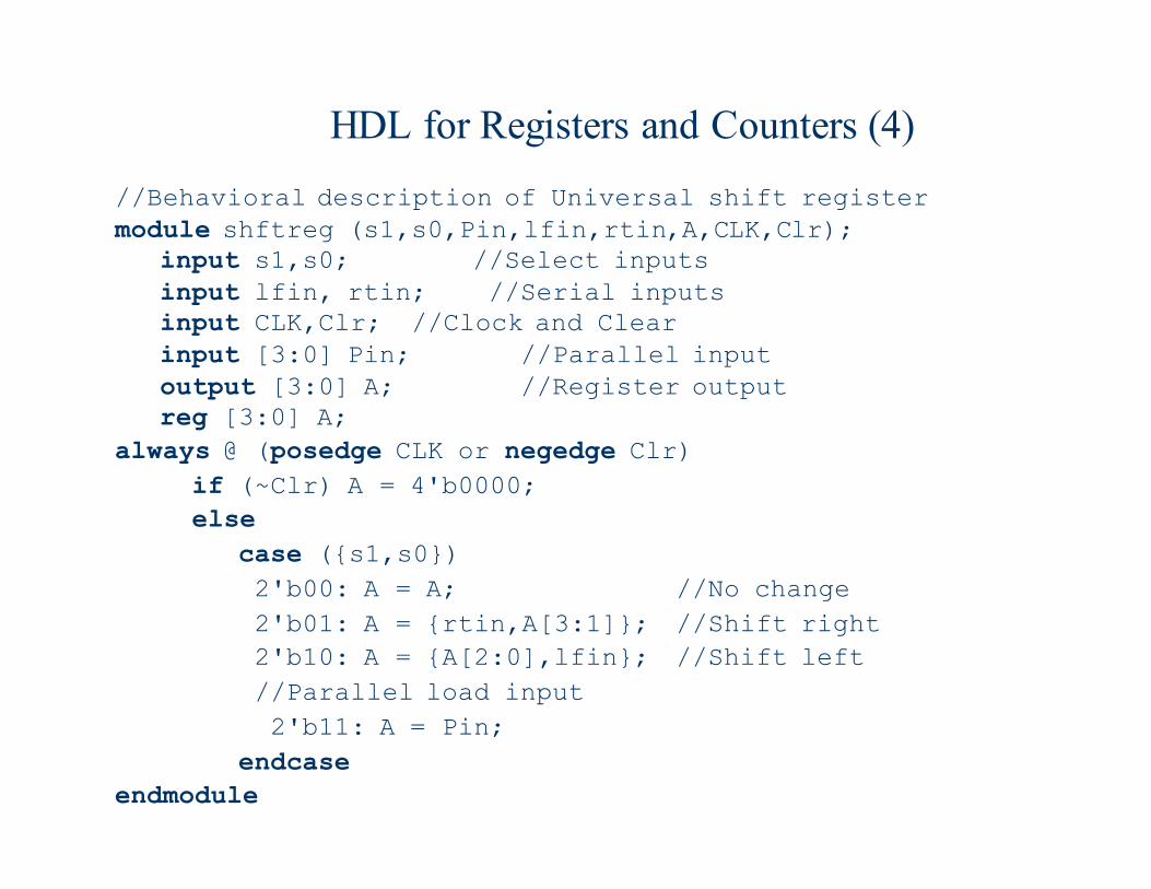
HDL for Registers and Counters (4)
//Behavioral description of Universal shift register
module shftreg (s1,s0,Pin,lfin,rtin,A,CLK,Clr);input s1,s0; //Select inputs
input lfin, rtin; //Serial inputs input CLK,Clr; //Clock and Clear
input [3:0] Pin; //Parallel input
output [3:0] A; //Register outputreg [3:0] A;
always @ (posedge CLK or negedge Clr)
if (~Clr) A = 4'b0000;
else
case ({s1,s0})
2'b00: A = A; //No change
2'b01: A = {rtin,A[3:1]}; //Shift right
2'b10: A = {A[2:0],lfin}; //Shift left
//Parallel load input
2'b11: A = Pin;
endcase
endmodule
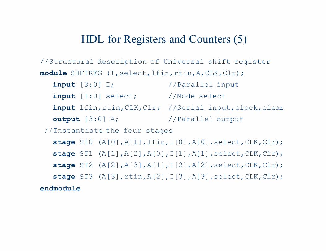
HDL for Registers and Counters (5)
//Structural description of Universal shift register
module SHFTREG (I,select,lfin,rtin,A,CLK,Clr);
input [3:0] I; //Parallel input
input [1:0] select; //Mode select
input lfin,rtin,CLK,Clr; //Serial input,clock,clear
output [3:0] A; //Parallel output
//Instantiate the four stages
stage ST0 (A[0],A[1],lfin,I[0],A[0],select,CLK,Clr);
stage ST1 (A[1],A[2],A[0],I[1],A[1],select,CLK,Clr);
stage ST2 (A[2],A[3],A[1],I[2],A[2],select,CLK,Clr);
stage ST3 (A[3],rtin,A[2],I[3],A[3],select,CLK,Clr);
endmodule
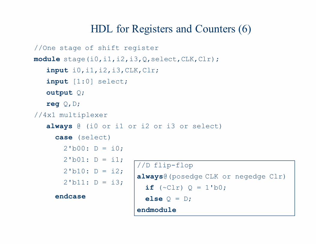
HDL for Registers and Counters (6)
//One stage of shift register
module stage(i0,i1,i2,i3,Q,select,CLK,Clr);
input i0,i1,i2,i3,CLK,Clr;
input [1:0] select;
output Q;
reg Q,D;
//4x1 multiplexer
always @ (i0 or i1 or i2 or i3 or select)
case (select)
2'b00: D = i0;
2'b01: D = i1;
2'b10: D = i2;
2'b11: D = i3;
endcase
//D flip-flop
always@(posedge CLK or negedge Clr)
if (~Clr) Q = 1'b0;
else Q = D;
endmodule
HDL for Registers and Counters (7)
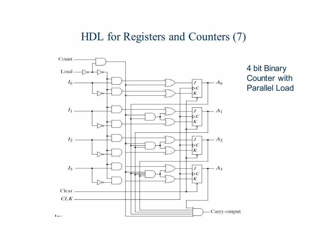
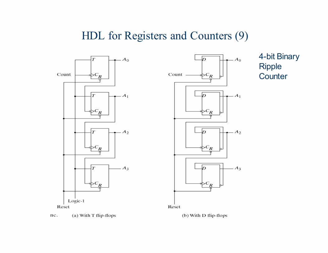
4 bit Binary Counter with Parallel Load
HDL for Registers and Counters (8)
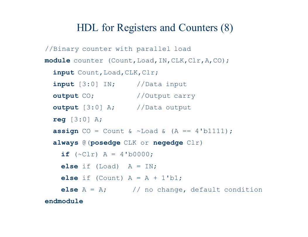
//Binary counter with parallel load
module counter (Count,Load,IN,CLK,Clr,A,CO);
input Count,Load,CLK,Clr;
input [3:0] IN; //Data input
output CO; //Output carry
output [3:0] A; //Data output
reg [3:0] A;
assign CO = Count & ~Load & (A == 4'b1111);
always @(posedge CLK or negedge Clr)
if (~Clr) A = 4'b0000;
else if (Load) A = IN;
else if (Count) A = A + 1'b1;
else A = A; // no change, default condition
endmodule
HDL for Registers and Counters (9)
4-bit Binary Ripple Counter
HDL for Registers and Counters (10)
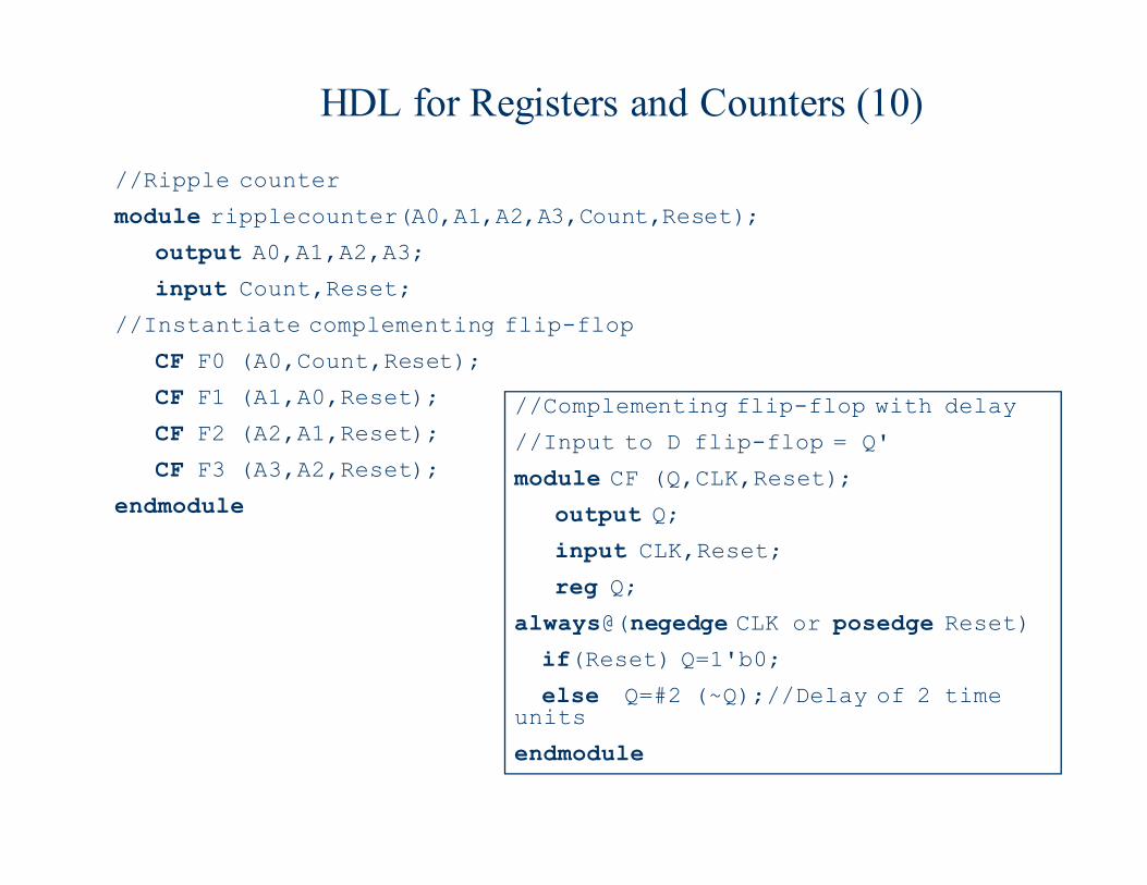
//Ripple counter
module ripplecounter(A0,A1,A2,A3,Count,Reset);
output A0,A1,A2,A3;
input Count,Reset;
//Instantiate complementing flip-flop
CF F0 (A0,Count,Reset);
CF F1 (A1,A0,Reset);
CF F2 (A2,A1,Reset);
CF F3 (A3,A2,Reset);
endmodule
//Complementing flip-flop with delay
//Input to D flip-flop = Q'
module CF (Q,CLK,Reset);
output Q;
input CLK,Reset;
reg Q;
always@(negedge CLK or posedge Reset)
if(Reset) Q=1'b0;
else Q=#2 (~Q);//Delay of 2 time units
endmodule
HDL for Registers and Counters (11)
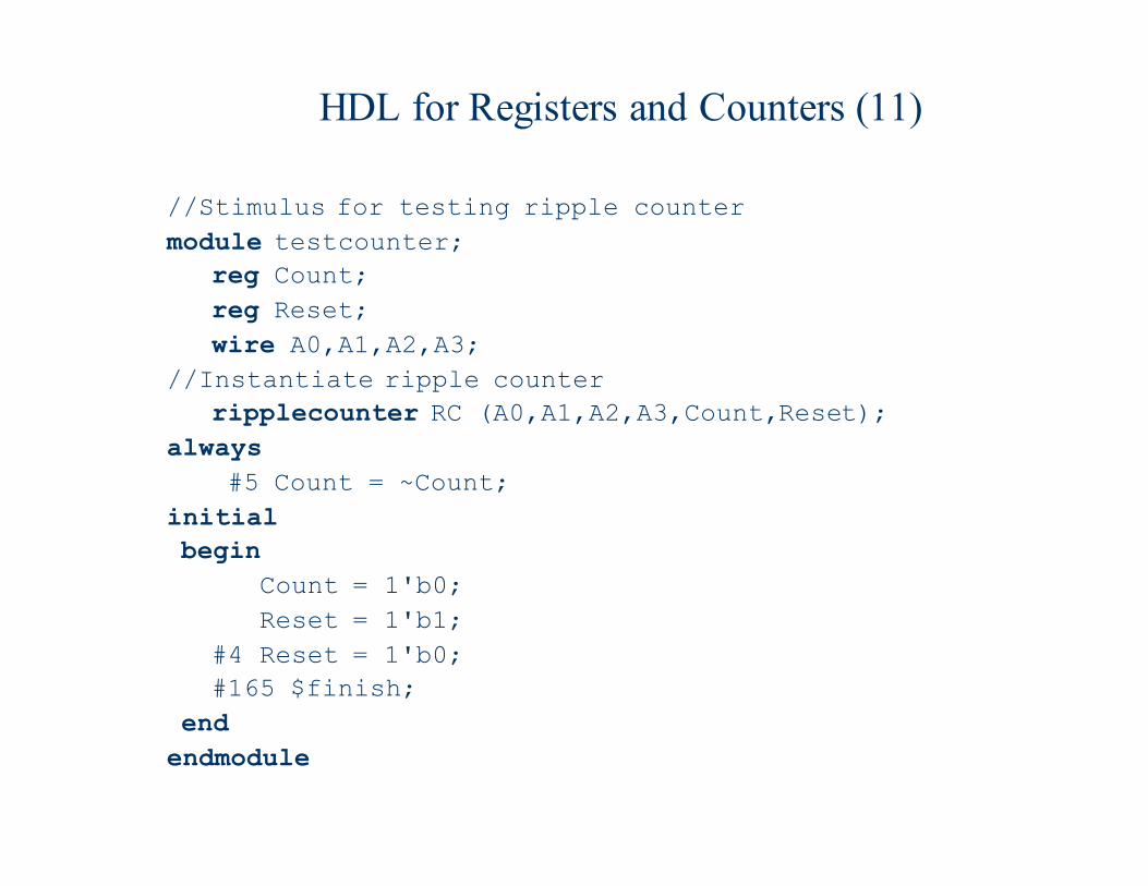
//Stimulus for testing ripple counter
module testcounter;
reg Count;
reg Reset;
wire A0,A1,A2,A3;
//Instantiate ripple counter
ripplecounter RC (A0,A1,A2,A3,Count,Reset);
always
#5 Count = ~Count;
initial
begin
Count = 1'b0;
Reset = 1'b1;
#4 Reset = 1'b0;
#165 $finish;
end
endmodule
Some arithmetic fundamentals
� Unsigned numbers: values are always positive
� Example: 1000 10102 = 27+23+21=14610
� Signed numbers: two’s complement notation
� Example: 1000 10102 = -27+23+21=-11810
� Leftmost bit called the sign bit
� Positive numbers have a sign bit of 0, negative numbers a sign bit of 1
� Sign extending a number: replicate the most significant bit the number of
times needed
� Example: 1000 10102 is the same as 1111 1111 1000 10102
Some arithmetic fundamentals
� Negating a two’s complement number: invert (NOT) all bits
and add 1
� Example: negative of 1000 1010 = 0111 0101 + 1 =
0111 0110 = 118
� Logical operations
� AND, OR, NOR, XOR perform logic function on a bit-by-bit basis
� Example: 1000 1010 AND 1101 0110 = 1000 0010
� Also arithmetic/logical shift left/right
Integer and floating point computation� Most general-purpose ISAs specify separate integer and floating
point register files
� Operand representation formats differ
� Computation hardware differs
� Result is a split of the execution core into integer and floating
point sections
instructioninstructioninstructioninstructionmemorymemorymemorymemory
PPPPCCCC
integerintegerintegerintegerregisterregisterregisterregister
filefilefilefile
integerintegerintegerintegerALUALUALUALU
integerintegerintegerintegermultipliermultipliermultipliermultiplier
datadatadatadatamemorymemorymemorymemory
flt ptflt ptflt ptflt ptregisterregisterregisterregister
filefilefilefile
flt ptflt ptflt ptflt ptadderadderadderadder
flt ptflt ptflt ptflt ptmultipliermultipliermultipliermultiplier
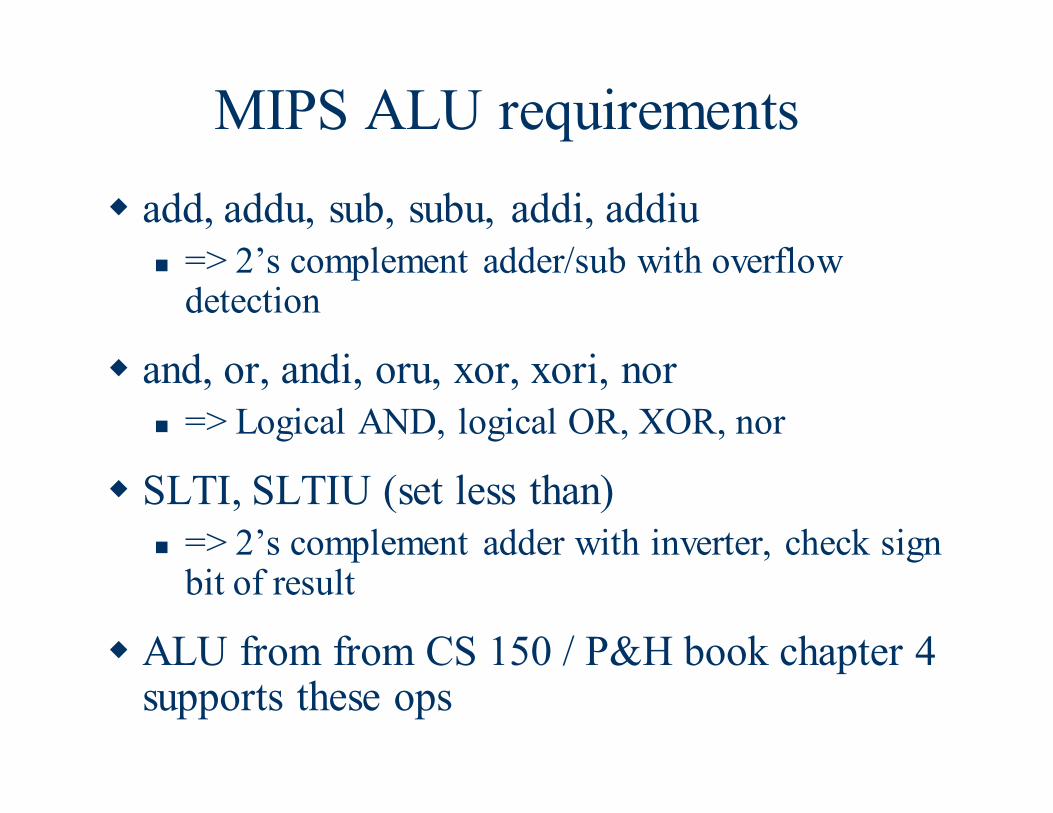
MIPS ALU requirements
� add, addu, sub, subu, addi, addiu
� => 2’s complement adder/sub with overflow detection
� and, or, andi, oru, xor, xori, nor
� => Logical AND, logical OR, XOR, nor
� SLTI, SLTIU (set less than)
� => 2’s complement adder with inverter, check sign bit of result
� ALU from from CS 150 / P&H book chapter 4 supports these ops
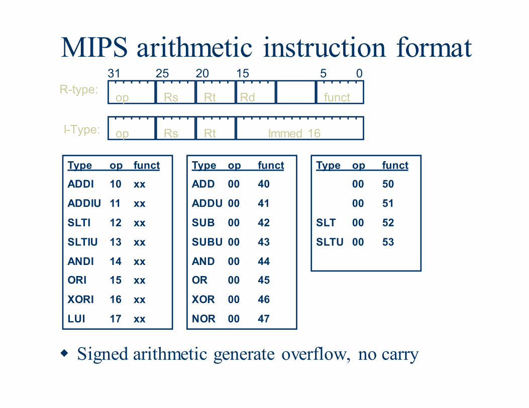
MIPS arithmetic instruction format
� Signed arithmetic generate overflow, no carry
R-type:
I-Type:
31 25 20 15 5 0
op Rs Rt Rd funct
op Rs Rt Immed 16
Type op funct
ADDI 10 xx
ADDIU 11 xx
SLTI 12 xx
SLTIU 13 xx
ANDI 14 xx
ORI 15 xx
XORI 16 xx
LUI 17 xx
Type op funct
ADD 00 40
ADDU 00 41
SUB 00 42
SUBU 00 43
AND 00 44
OR 00 45
XOR 00 46
NOR 00 47
Type op funct
00 50
00 51
SLT 00 52
SLTU 00 53
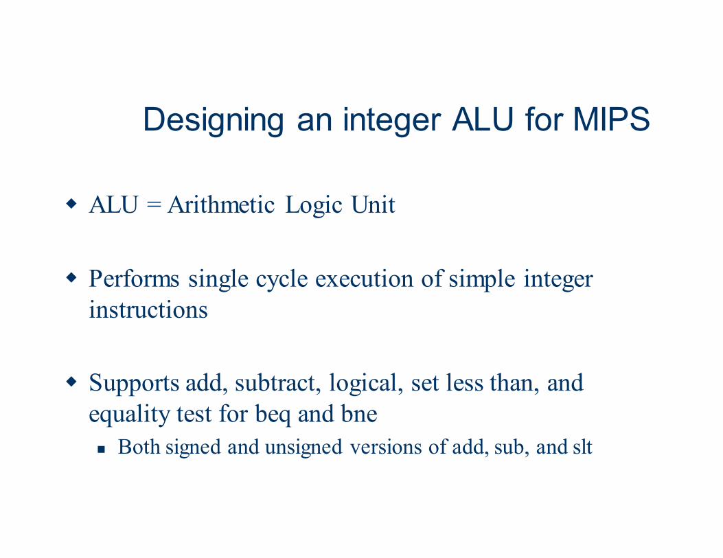
Designing an integer ALU for MIPS
� ALU = Arithmetic Logic Unit
� Performs single cycle execution of simple integer
instructions
� Supports add, subtract, logical, set less than, and
equality test for beq and bne
� Both signed and unsigned versions of add, sub, and slt
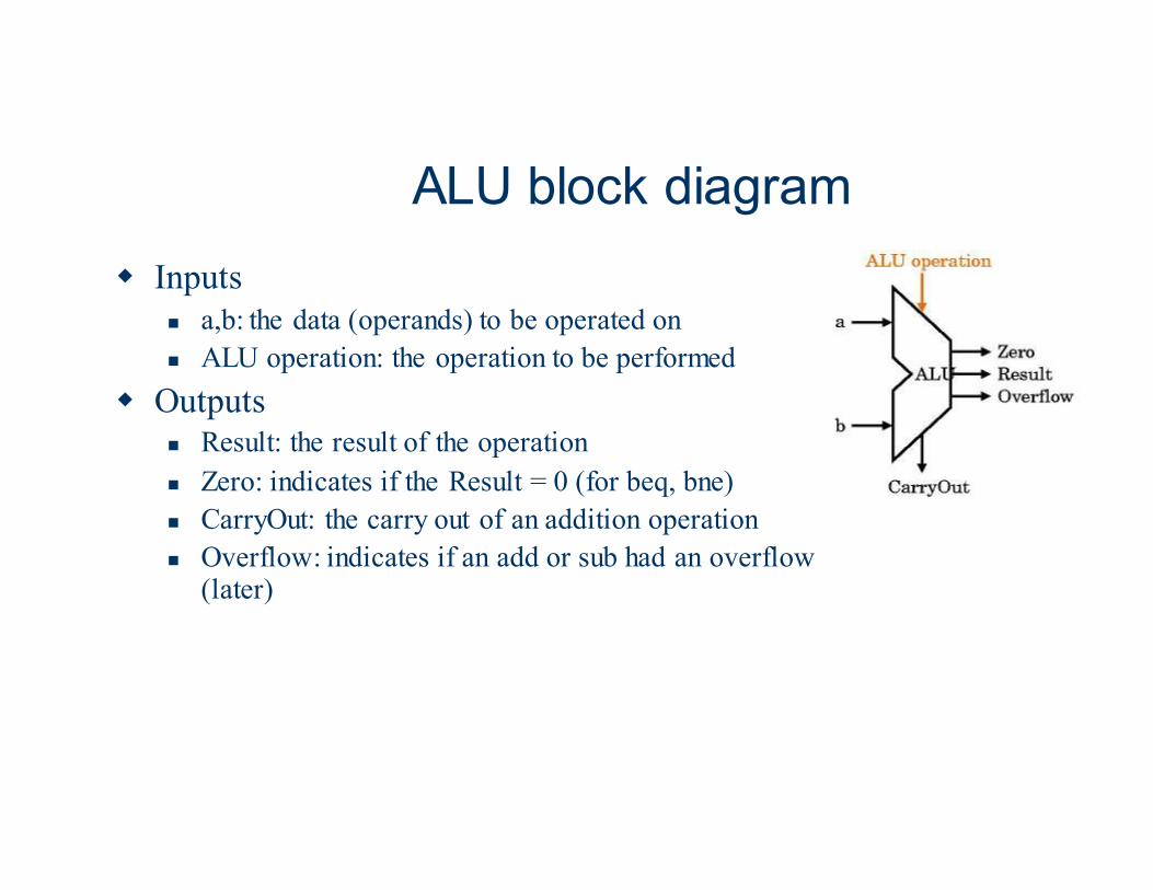
ALU block diagram
� Inputs
� a,b: the data (operands) to be operated on
� ALU operation: the operation to be performed
� Outputs� Result: the result of the operation
� Zero: indicates if the Result = 0 (for beq, bne)
� CarryOut: the carry out of an addition operation
� Overflow: indicates if an add or sub had an overflow (later)
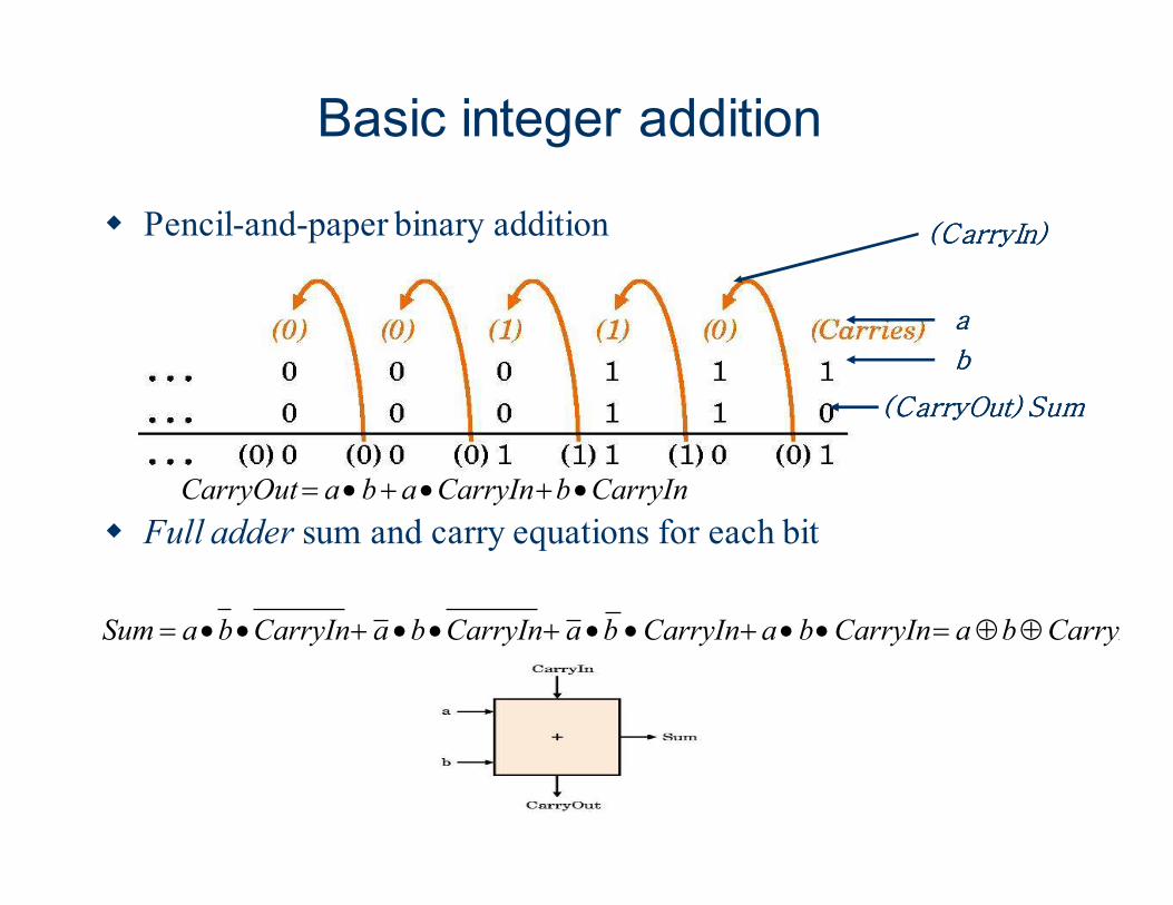
Basic integer addition
� Pencil-and-paper binary addition
� Full adder sum and carry equations for each bit
(CarryOut) Sum(CarryOut) Sum(CarryOut) Sum(CarryOut) Sum
CarryInbaCarryInbaCarryInbaCarryInbaCarryInbaSum ⊕⊕=••+••+••+••=
(CarryIn)(CarryIn)(CarryIn)(CarryIn)
CarryInbCarryInabaCarryOut •+•+•=
aaaa
bbbb
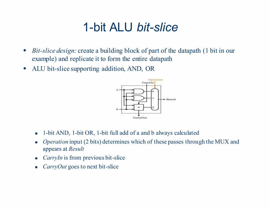
1-bit ALU bit-slice
� Bit-slice design: create a building block of part of the datapath (1 bit in our
example) and replicate it to form the entire datapath
� ALU bit-slice supporting addition, AND, OR
� 1-bit AND, 1-bit OR, 1-bit full add of a and b always calculated
� Operation input (2 bits) determines which of these passes through the MUX and
appears at Result
� CarryIn is from previous bit-slice
� CarryOut goes to next bit-slice
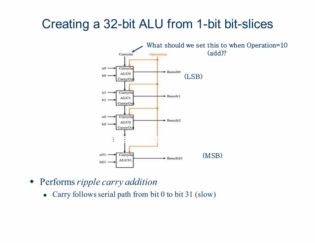
Creating a 32-bit ALU from 1-bit bit-slices
(LSB)(LSB)(LSB)(LSB)
(MSB)(MSB)(MSB)(MSB)
What should we set this to when Operation=10 What should we set this to when Operation=10 What should we set this to when Operation=10 What should we set this to when Operation=10 (add)?(add)?(add)?(add)?
� Performs ripple carry addition
� Carry follows serial path from bit 0 to bit 31 (slow)
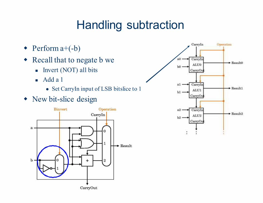
Handling subtraction
� Perform a+(-b)
� Recall that to negate b we
� Invert (NOT) all bits
� Add a 1
� Set CarryIn input of LSB bitslice to 1
� New bit-slice design
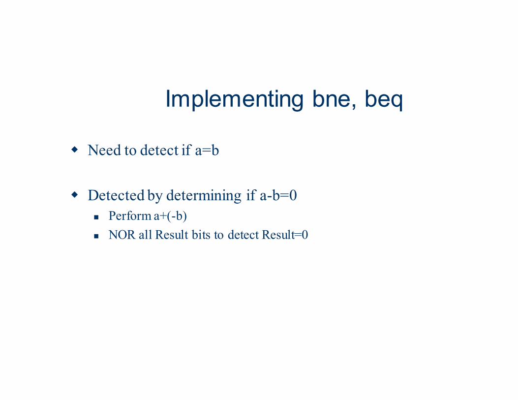
Implementing bne, beq
� Need to detect if a=b
� Detected by determining if a-b=0
� Perform a+(-b)
� NOR all Result bits to detect Result=0
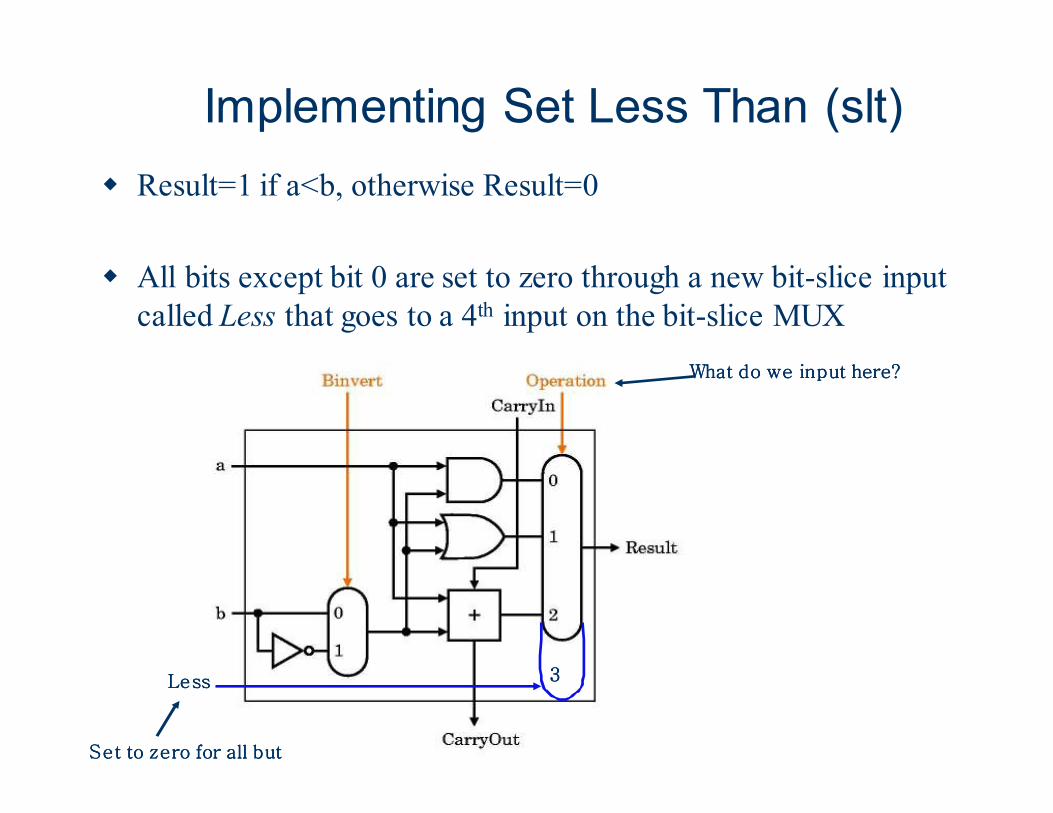
Implementing Set Less Than (slt)
� Result=1 if a<b, otherwise Result=0
� All bits except bit 0 are set to zero through a new bit-slice input
called Less that goes to a 4th input on the bit-slice MUX
3333LessLessLessLess
Set to zero for all but Set to zero for all but Set to zero for all but Set to zero for all but LSBLSBLSBLSB
What do we input here?What do we input here?What do we input here?What do we input here?
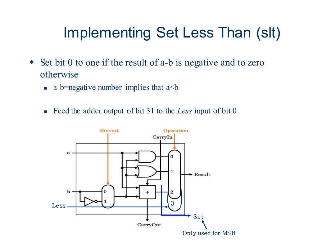
Implementing Set Less Than (slt)
� Set bit 0 to one if the result of a-b is negative and to zero
otherwise
� a-b=negative number implies that a<b
� Feed the adder output of bit 31 to the Less input of bit 0
3333LessLessLessLess
SetSetSetSet
Only used for MSBOnly used for MSBOnly used for MSBOnly used for MSB
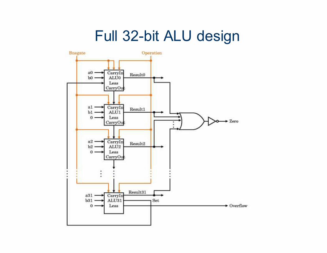
Full 32-bit ALU design
Full 32-bit ALU design
� Bnegate controls CarryIn input to bit 0 and Binvert input to
all bit-slices
� Both are 1 for subtract and 0 otherwise, so a single signal can be
used
� NOR, XOR, shift operations would also be included in a
MIPS implementation
Overflow
� Overflow occurs when the result from an operation cannot be
represented with the number of available bits (32 in our ALU)
� For signed addition, overflow occurs when
� Adding two positive numbers gives a negative result
� Example: 01110000N+00010000N=1000000N
� Adding two negative numbers gives a positive result
� Example: 10000000N+10000000N=0000000N
� For signed subtraction, overflow occurs when
� Subtracting a negative from a positive number gives a negative result
� Subtracting a positive from a negative number gives a
positive result
Overflow
� Overflow on unsigned arithmetic, which is primarily used for
manipulating addresses, is ignored in many ISAs (including
MIPS)
� Overflow on signed arithmetic causes an interrupt to deal with
the problem (Chapter 5)
� Overflow detection: XOR CarryIn of MSB with CarryOut of
MSB (problem 4.42)
Faster carry generation
� Ripple carry addition is too slow for wide adders
� Some alternative faster parallel schemes
� Carry lookahead
� Carry skip
� Carry select
� Cost is more hardware!
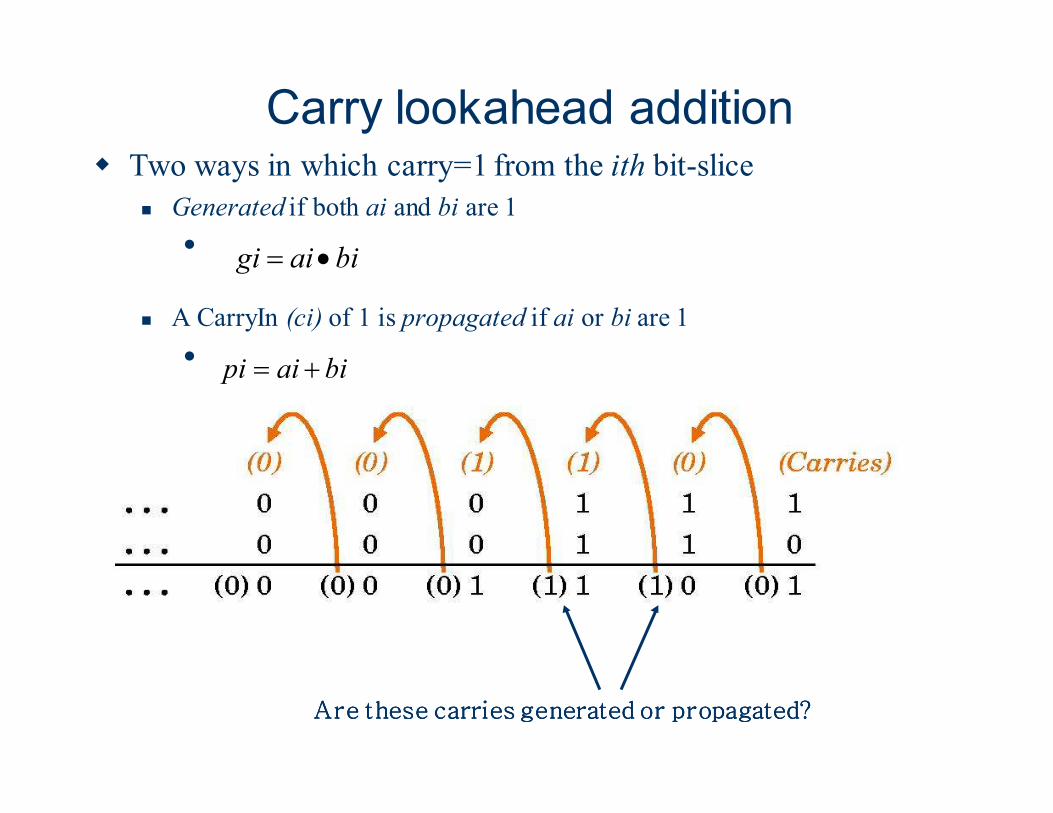
Carry lookahead addition� Two ways in which carry=1 from the ith bit-slice
� Generated if both ai and bi are 1
�
� A CarryIn (ci) of 1 is propagated if ai or bi are 1
�
biaigi •=
biaipi +=
Are these carries generated or propagated?Are these carries generated or propagated?Are these carries generated or propagated?Are these carries generated or propagated?
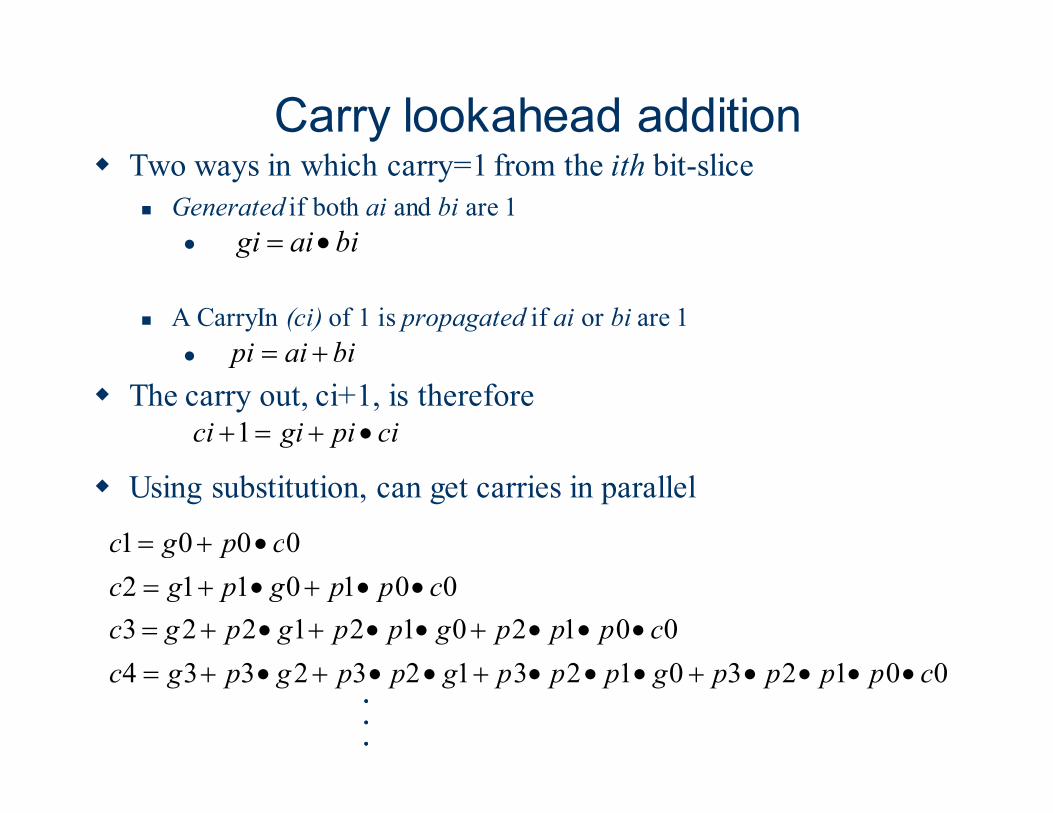
Carry lookahead addition� Two ways in which carry=1 from the ith bit-slice
� Generated if both ai and bi are 1
�
� A CarryIn (ci) of 1 is propagated if ai or bi are 1
�
� The carry out, ci+1, is therefore
� Using substitution, can get carries in parallel
biaigi •=
biaipi +=
cipigici •+=+1
0012301231232334
00120121223
0010112
0001
cppppgpppgppgpgc
cpppgppgpgc
cppgpgc
cpgc
••••+•••+••+•+=
•••+••+•+=
••+•+=
•+=
....
....
....
Carry lookahead addition
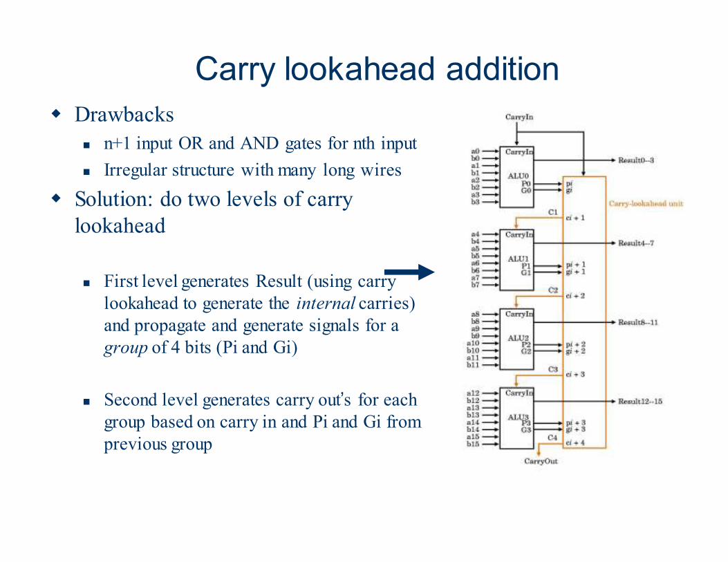
� Drawbacks
� n+1 input OR and AND gates for nth input
� Irregular structure with many long wires
� Solution: do two levels of carry
lookahead
� First level generates Result (using carry
lookahead to generate the internal carries)
and propagate and generate signals for a
group of 4 bits (Pi and Gi)
� Second level generates carry out’s for each
group based on carry in and Pi and Gi from
previous group
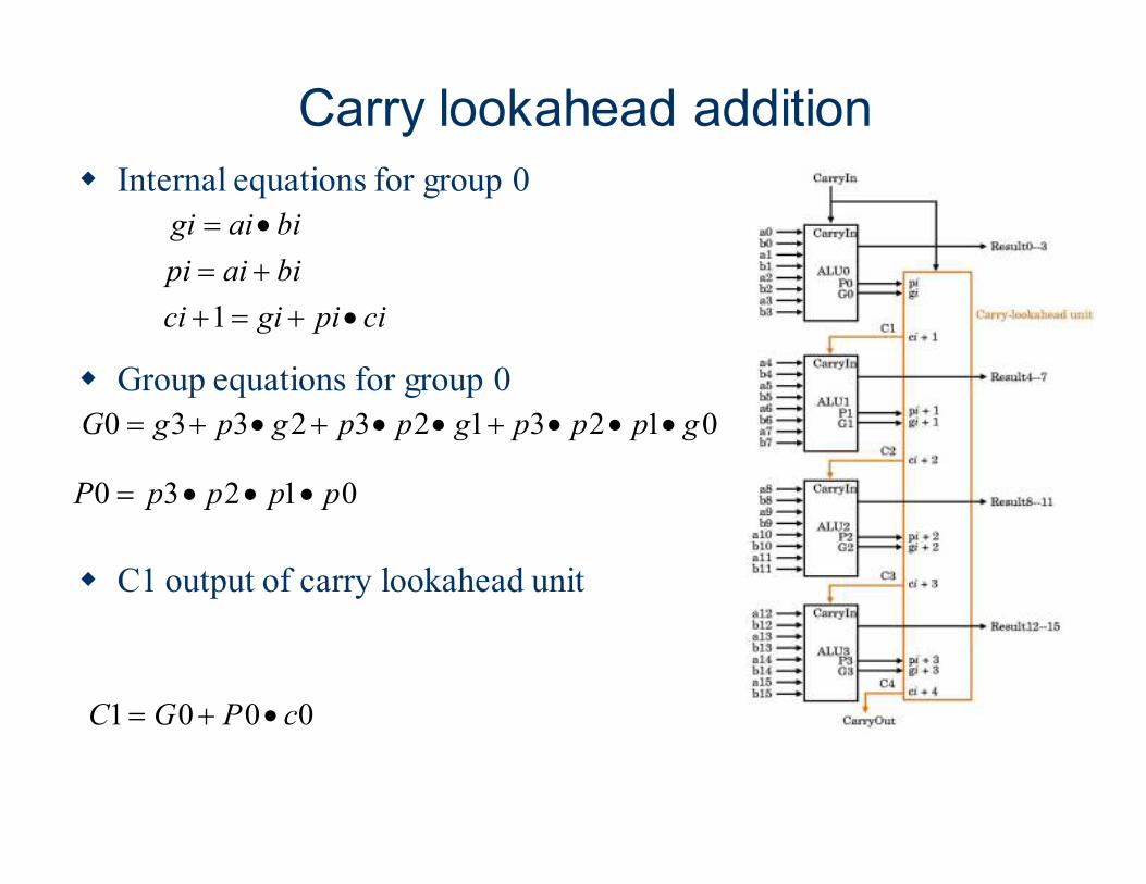
Carry lookahead addition
� Internal equations for group 0
� Group equations for group 0
� C1 output of carry lookahead unit
biaigi •=
biaipi +=
cipigici •+=+1
01231232330 gpppgppgpgG •••+••+•+=
01230 ppppP •••=
0001 cPGC •+=
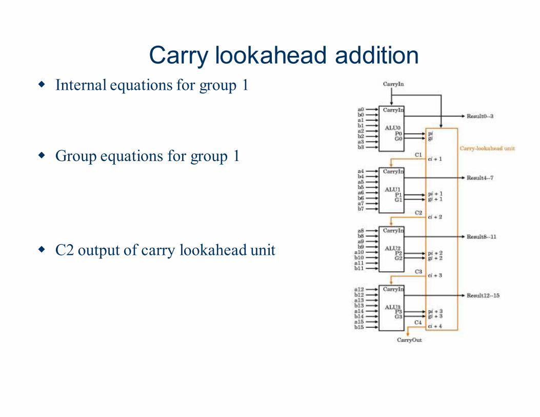
Carry lookahead addition� Internal equations for group 1
� Group equations for group 1
� C2 output of carry lookahead unit
Carry skip addition
� CLA group generate (Gi) hardware is complex
� Carry skip addition
� Generate Gi’s by ripple carry of a and b inputs with cin’s = 0 (except c0)
Generate Pi’s as in carry lookahead
� For each group, combine Gi, Pi, and cin as in carry
lookahead to form group carries
� Generate sums by ripple carry from a and b inputs and
group carries
Carry skip addition
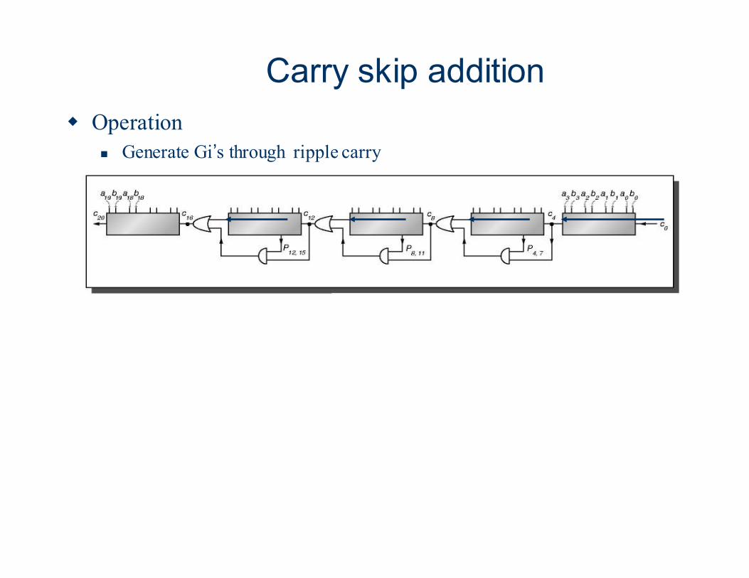
� Operation
� Generate Gi’s through ripple carry
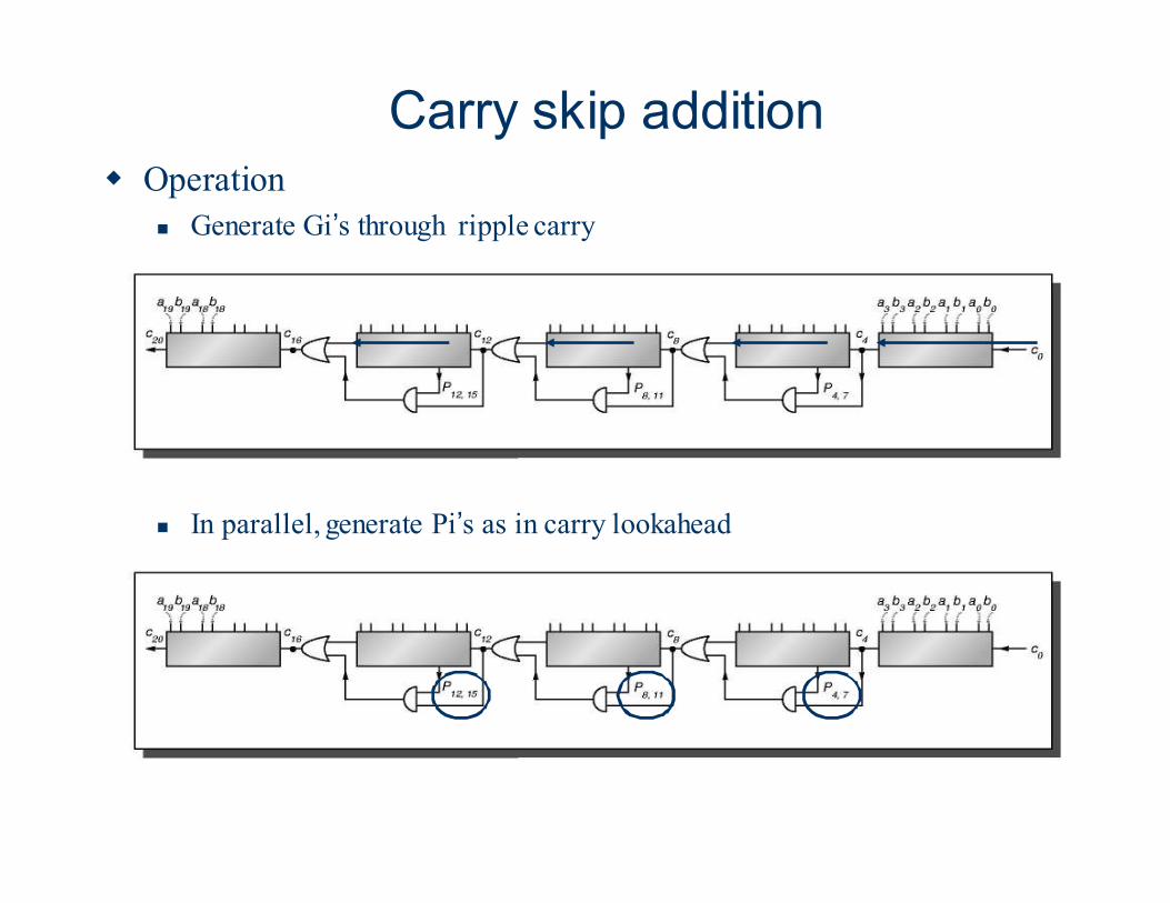
Carry skip addition� Operation
� Generate Gi’s through ripple carry
� In parallel, generate Pi’s as in carry lookahead
Carry skip addition
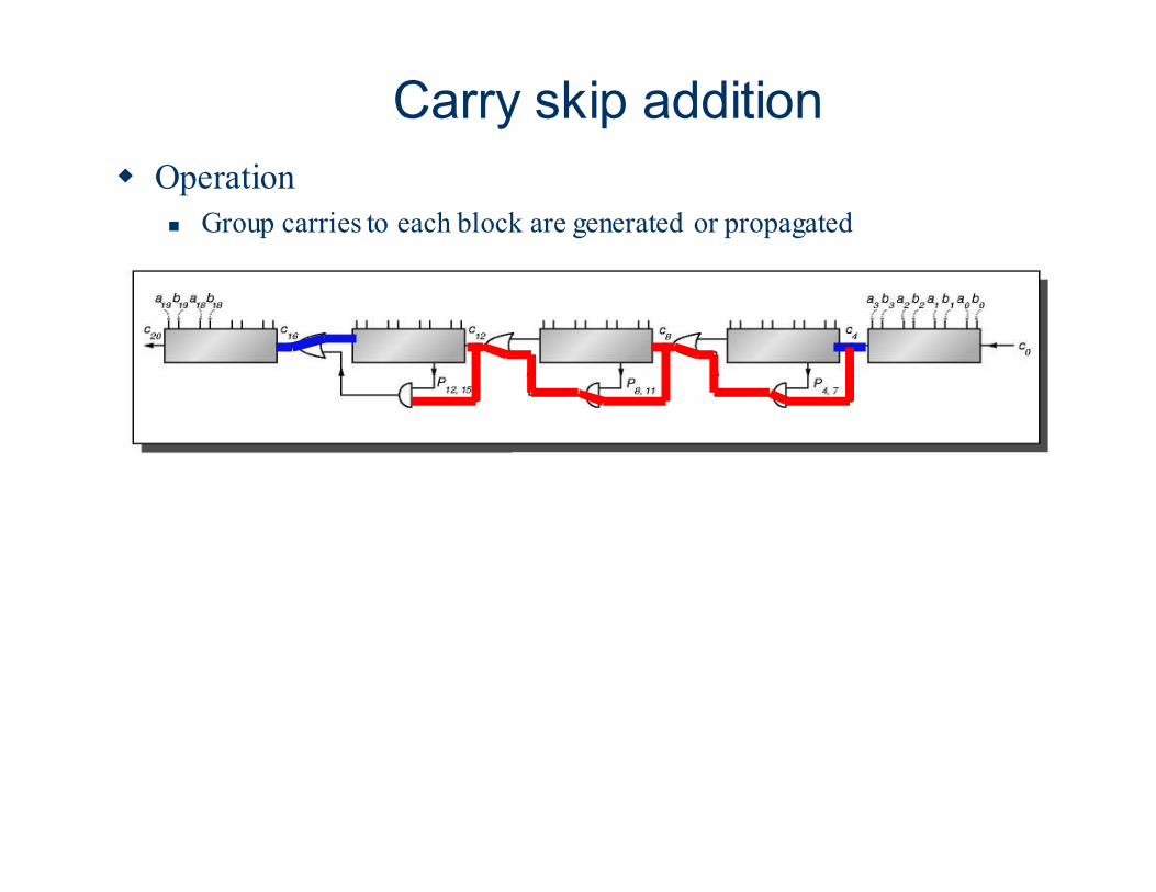
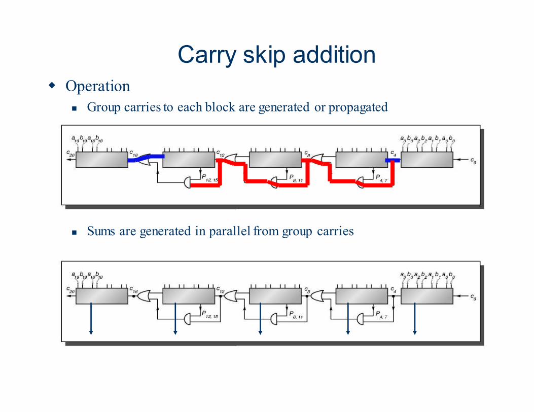
� Operation
� Group carries to each block are generated or propagated
Carry skip addition� Operation
� Group carries to each block are generated or propagated
� Sums are generated in parallel from group carries
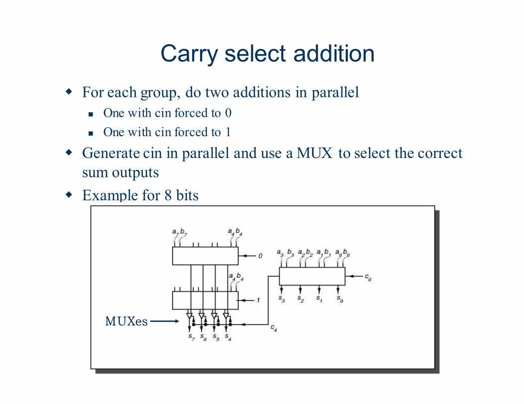
Carry select addition
� For each group, do two additions in parallel
� One with cin forced to 0
� One with cin forced to 1
� Generate cin in parallel and use a MUX to select the correct
sum outputs
� Example for 8 bits
MUXesMUXesMUXesMUXes
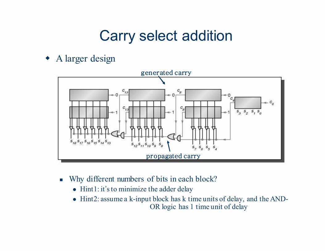
Carry select addition
� A larger design
� Why different numbers of bits in each block?
� Hint1: it’s to minimize the adder delay
� Hint2: assume a k-input block has k time units of delay, and the AND-OR logic has 1 time unit of delay
generated carrygenerated carrygenerated carrygenerated carry
propagated carrypropagated carrypropagated carrypropagated carry
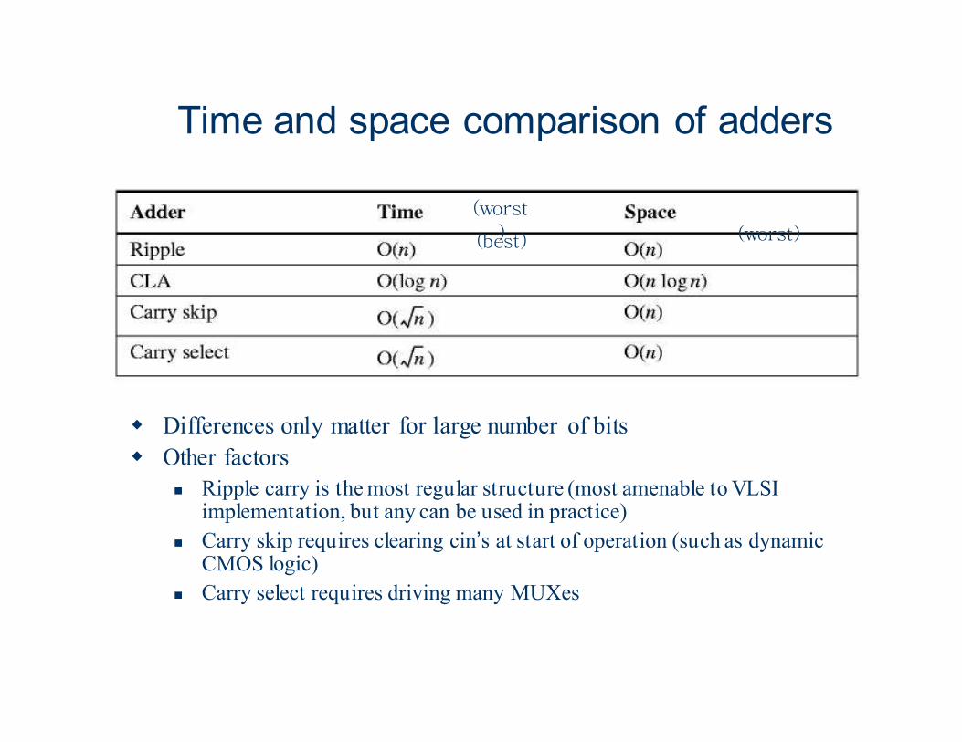
Time and space comparison of adders
� Differences only matter for large number of bits
� Other factors
� Ripple carry is the most regular structure (most amenable to VLSI implementation, but any can be used in practice)
� Carry skip requires clearing cin’s at start of operation (such as dynamic CMOS logic)
� Carry select requires driving many MUXes
(worst) (worst)(best)

Questions?