Embed Size (px)
Citation preview
Hardware Documentation
Hall-Effect Switch IC FamilyHAL® 1xy
Edition April 8, 2009DSH000150_001EN
Data Sheet
HAL1xy DATA SHEET
2 April 8, 2009; DSH000150_001EN Micronas
Copyright, Warranty, and Limitation of Liability
The information and data contained in this documentare believed to be accurate and reliable. The softwareand proprietary information contained therein may beprotected by copyright, patent, trademark and/or otherintellectual property rights of Micronas. All rights notexpressly granted remain reserved by Micronas.
Micronas assumes no liability for errors and gives nowarranty representation or guarantee regarding thesuitability of its products for any particular purpose dueto these specifications.
By this publication, Micronas does not assume respon-sibility for patent infringements or other rights of thirdparties which may result from its use. Commercial con-ditions, product availability and delivery are exclusivelysubject to the respective order confirmation.
Any information and data which may be provided in thedocument can and do vary in different applications,and actual performance may vary over time.
All operating parameters must be validated for eachcustomer application by customers’ technical experts.Any new issue of this document invalidates previousissues. Micronas reserves the right to review this doc-ument and to make changes to the document’s contentat any time without obligation to notify any person orentity of such revision or changes. For further adviceplease contact us directly.
Do not use our products in life-supporting systems,aviation, and aerospace applications! Unless explicitlyagreed to otherwise in writing between the parties,Micronas’ products are not designed, intended orauthorized for use as components in systems intendedfor surgical implants into the body, or other applica-tions intended to support or sustain life, or for anyother application in which the failure of the productcould create a situation where personal injury or deathcould occur.
No part of this publication may be reproduced, photo-copied, stored on a retrieval system or transmittedwithout the express written consent of Micronas.
Micronas Trademarks
– HAL
Micronas Trademarks
Choppered Offset Compensation protected byMicronas patents no. US5260614, US5406202,EP0525235 and EP0548391.
Third-Party Trademarks
All other brand and product names or company namesmay be trademarks of their respective companies.
Contents
Page Section Title
Micronas April 8, 2009; DSH000150_001EN 3
DATA SHEET HAL1xy
4 1. Introduction4 1.1. Family Overview5 1.2. Marking Code5 1.3. Operating Junction Temperature Range5 1.4. Solderability and Welding
6 2. Specifications6 2.1. Outline Dimensions8 2.2. Positions of Sensitive Areas8 2.3. Absolute Maximum Ratings8 2.4. Recommended Operating Conditions9 2.5. Characteristics10 2.6. Magnetic Characteristics Overview
11 3. Application Notes11 3.1. Ambient Temperature11 3.2. Extended Operating Conditions11 3.3. Start-up Behavior11 3.4. EMC and ESD
12 4. Data Sheet History
HAL1xy DATA SHEET
Hall-Effect Switch IC Family
Note: The HAL1xy family has been designed for com-mercial and industrial applications. It is not intended tobe used in automotive or automotive-like applications.
1. Introduction
The HAL1xy Hall switch family is produced in CMOStechnology. The sensors include a temperature-com-pensated Hall plate with active offset compensation, acomparator, and an open-drain output transistor. Thecomparator compares the actual magnetic flux throughthe Hall plate (Hall voltage) with the fixed referencevalues (switching points). Accordingly, the output tran-sistor is switched on or off.
The active offset compensation leads to magneticparameters which are robust against mechanicalstress effects. In addition, the magnetic characteristicsare constant in the full supply voltage and temperaturerange.
The HAL1xy family is available in the SMD-packageSOT89B-3 and in the leaded version TO92UA-6.
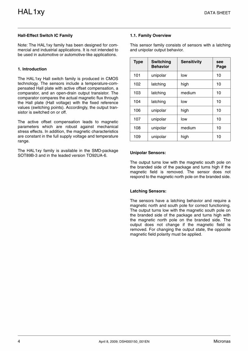
1.1. Family Overview
This sensor family consists of sensors with a latchingand unipolar output behavior.
Unipolar Sensors:
The output turns low with the magnetic south pole onthe branded side of the package and turns high if themagnetic field is removed. The sensor does notrespond to the magnetic north pole on the branded side.
Latching Sensors:
The sensors have a latching behavior and require amagnetic north and south pole for correct functioning.The output turns low with the magnetic south pole onthe branded side of the package and turns high withthe magnetic north pole on the branded side. Theoutput does not change if the magnetic field isremoved. For changing the output state, the oppositemagnetic field polarity must be applied.
Type SwitchingBehavior
Sensitivity seePage
101 unipolar low 10
102 latching high 10
103 latching medium 10
104 latching low 10
106 unipolar high 10
107 unipolar low 10
108 unipolar medium 10
109 unipolar high 10
4 April 8, 2009; DSH000150_001EN Micronas
DATA SHEET HAL1xy
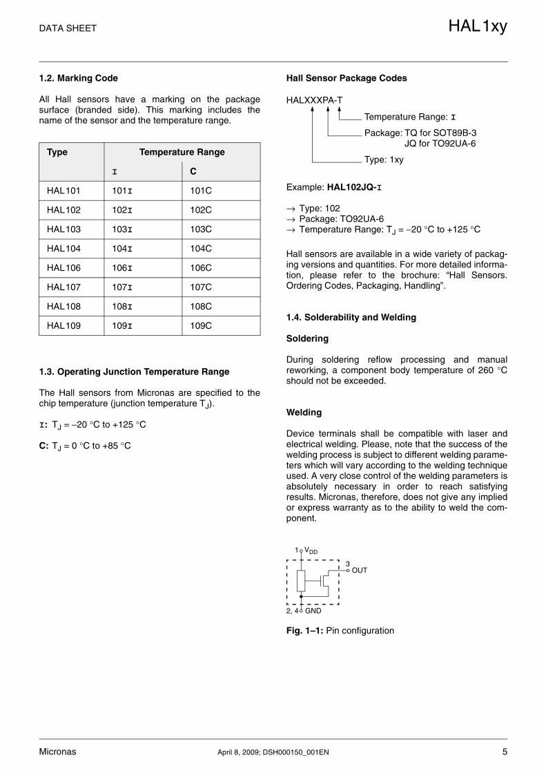
1.2. Marking Code
All Hall sensors have a marking on the packagesurface (branded side). This marking includes thename of the sensor and the temperature range.
1.3. Operating Junction Temperature Range
The Hall sensors from Micronas are specified to thechip temperature (junction temperature TJ).
I: TJ = −20 °C to +125 °C
C: TJ = 0 °C to +85 °C
Hall Sensor Package Codes
Hall sensors are available in a wide variety of packag-ing versions and quantities. For more detailed informa-tion, please refer to the brochure: “Hall Sensors.Ordering Codes, Packaging, Handling”.
1.4. Solderability and Welding
Soldering
During soldering reflow processing and manualreworking, a component body temperature of 260 °Cshould not be exceeded.
Welding
Device terminals shall be compatible with laser andelectrical welding. Please, note that the success of thewelding process is subject to different welding parame-ters which will vary according to the welding techniqueused. A very close control of the welding parameters isabsolutely necessary in order to reach satisfyingresults. Micronas, therefore, does not give any impliedor express warranty as to the ability to weld the com-ponent.
Fig. 1–1: Pin configuration
Type Temperature Range
I C
HAL101 101I 101C
HAL102 102I 102C
HAL103 103I 103C
HAL104 104I 104C
HAL106 106I 106C
HAL107 107I 107C
HAL108 108I 108C
HAL109 109I 109C
HALXXXPA-T
Temperature Range: I
Package: TQ for SOT89B-3JQ for TO92UA-6
Type: 1xy
Example: HAL102JQ-I
→ Type: 102→ Package: TO92UA-6→ Temperature Range: TJ = −20 °C to +125 °C
1 VDD
2, 4 GND
3OUT
Micronas April 8, 2009; DSH000150_001EN 5
HAL1xy DATA SHEET
2. Specifications
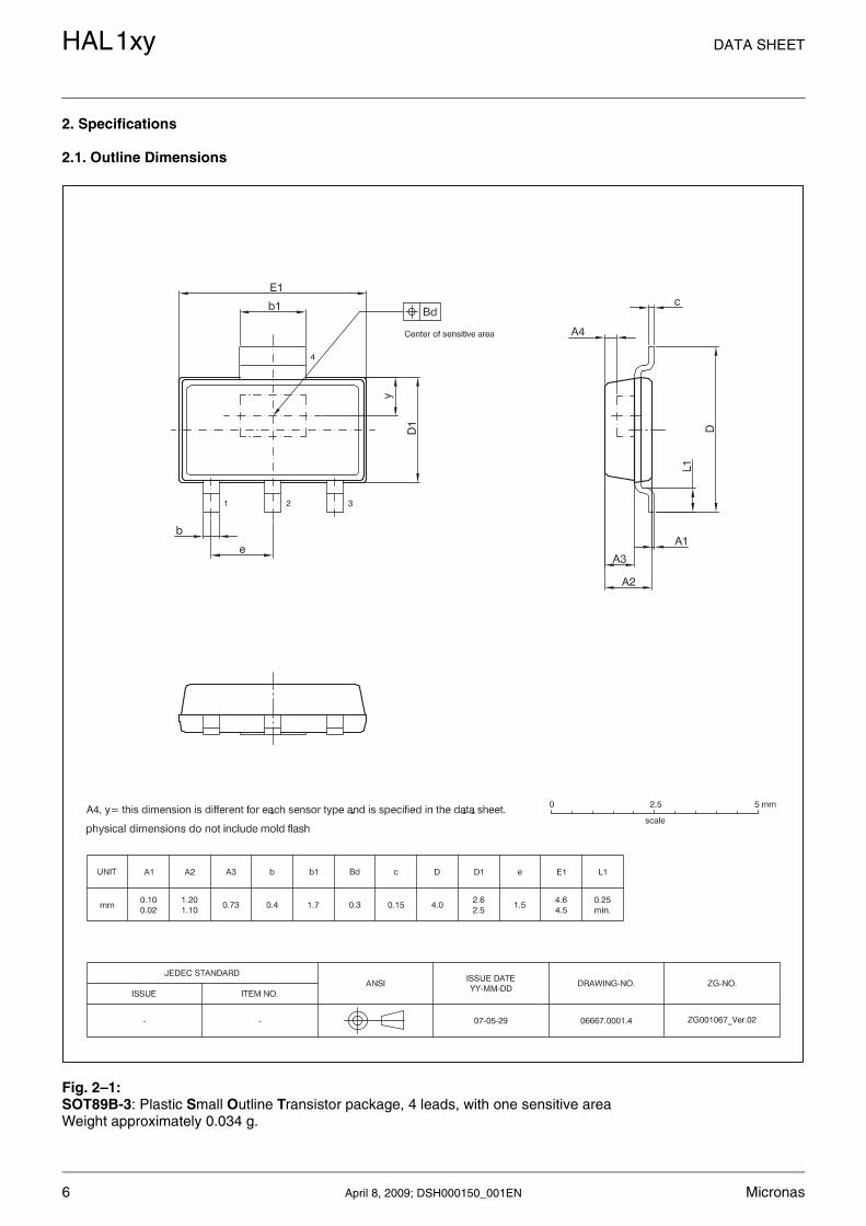
2.1. Outline Dimensions
Fig. 2–1:SOT89B-3: Plastic Small Outline Transistor package, 4 leads, with one sensitive areaWeight approximately 0.034 g.
6 April 8, 2009; DSH000150_001EN Micronas
DATA SHEET HAL1xy
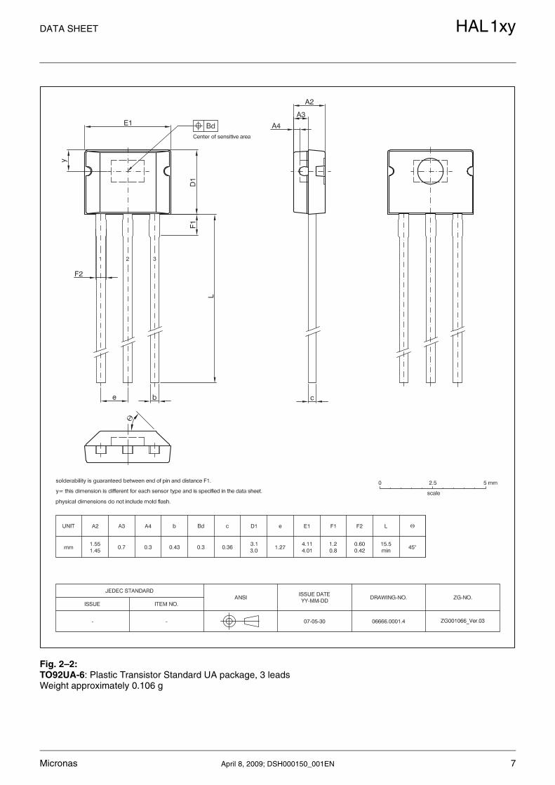
Fig. 2–2:TO92UA-6: Plastic Transistor Standard UA package, 3 leadsWeight approximately 0.106 g
Micronas April 8, 2009; DSH000150_001EN 7
HAL1xy DATA SHEET
2.2. Positions of Sensitive Areas
2.3. Absolute Maximum Ratings
Stresses beyond those listed in the “Absolute Maximum Ratings” may cause permanent damage to the device. Thisis a stress rating only. Functional operation of the device at these conditions is not implied. Exposure to absolutemaximum rating conditions for extended periods will affect device reliability.
This device contains circuitry to protect the inputs and outputs against damage due to high static voltages or electricfields; however, it is advised that normal precautions be taken to avoid application of any voltage higher than abso-lute maximum-rated voltages to this high-impedance circuit.
All voltages listed are referenced to ground (GND).
2.4. Recommended Operating Conditions
Functional operation of the device beyond those indicated in the “Recommended Operating Conditions/Characteris-tics” is not implied and may result in unpredictable behavior, reduce reliability and lifetime of the device.
All voltages listed are referenced to ground (GND).
SOT89B-3 TO92UA-6
y 0.95 mm nominal 1.08 mm nominal
A4 0.33 mm nominal 0.30 mm nominal
Symbol Parameter Pin Name Min. Max. Unit
VDD Supply Voltage 1 −15 281) V
VO Output Voltage 3 −0.3 281) V
IO Continuous Output On Current 3 − 501) mA
TJ Junction Temperature Range −40 1402) °C
1) as long as TJmax is not exceeded2) t < 1000 h
Symbol Parameter Pin Name Min. Max. Unit Comment
VDD Supply Voltage 1 3.8 24 V
IO Continuous Output on Current 3 0 20 mA
VO Output Voltage (output switched off)
3 0 24 V
8 April 8, 2009; DSH000150_001EN Micronas
DATA SHEET HAL1xy
2.5. Characteristics
at TJ = −20 °C to +125 °C, VDD = 3.8 V to 24 V, GND = 0 Vat Recommended Operation Conditions if not otherwise specified in the column “Conditions”.Typical Characteristics for TJ = 25 °C and VDD = 12 V.
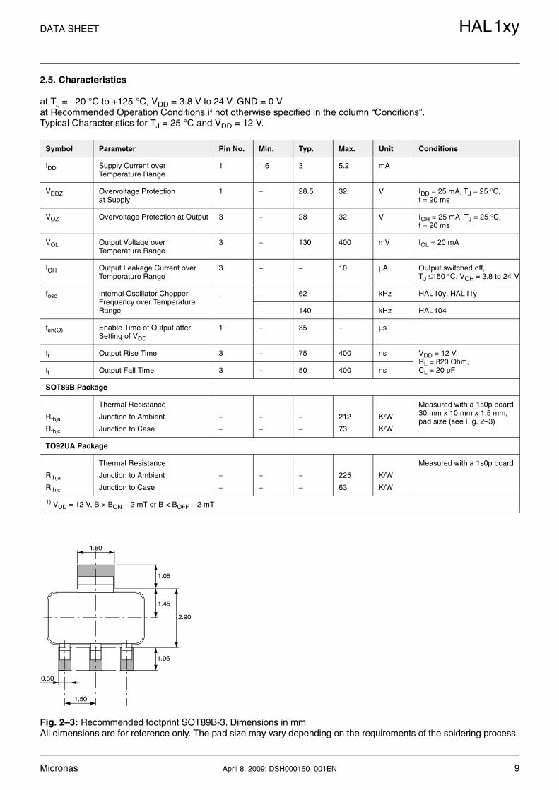
Fig. 2–3: Recommended footprint SOT89B-3, Dimensions in mm All dimensions are for reference only. The pad size may vary depending on the requirements of the soldering process.
Symbol Parameter Pin No. Min. Typ. Max. Unit Conditions
IDD Supply Current over Temperature Range
1 1.6 3 5.2 mA
VDDZ Overvoltage Protection at Supply
1 − 28.5 32 V IDD = 25 mA, TJ = 25 °C,t = 20 ms
VOZ Overvoltage Protection at Output 3 − 28 32 V IOH = 25 mA, TJ = 25 °C,t = 20 ms
VOL Output Voltage over Temperature Range
3 − 130 400 mV IOL = 20 mA
IOH Output Leakage Current over Temperature Range
3 − − 10 µA Output switched off,TJ ≤150 °C, VOH = 3.8 to 24 V
fosc Internal Oscillator Chopper Frequency over Temperature Range
− − 62 − kHz HAL10y, HAL11y
− 140 − kHz HAL104
ten(O) Enable Time of Output after Setting of VDD
1 − 35 − µs
tr Output Rise Time 3 − 75 400 ns VDD = 12 V, RL = 820 Ohm,CL = 20 pFtf Output Fall Time 3 − 50 400 ns
SOT89B Package
Rthja
Rthjc
Thermal Resistance
Junction to Ambient
Junction to Case
−
−
−
−
−
−
212
73
K/W
K/W
Measured with a 1s0p board30 mm x 10 mm x 1.5 mm,pad size (see Fig. 2–3)
TO92UA Package
Rthja
Rthjc
Thermal Resistance
Junction to Ambient
Junction to Case
−
−
−
−
−
−
225
63
K/W
K/W
Measured with a 1s0p board
1) VDD = 12 V, B > BON + 2 mT or B < BOFF − 2 mT
1.05
1.05
1.80
0.50
1.50
1.45
2.90
Micronas April 8, 2009; DSH000150_001EN 9
HAL1xy DATA SHEET
2.6. Magnetic Characteristics Overview
at TJ = −20 °C to +125 °C, VDD = 3.8 V to 24 V, Typical Characteristics for VDD = 12 V. Magnetic flux density values of switching points. Positive flux density values refer to the magnetic south pole at the branded side of the package.
Sensor Parameter On point BON Off point BOFF Hysteresis BHYS Unit
Switching Type TJ Min. Typ. Max. Min. Typ. Max. Min. Typ. Max.
HAL101 −20 °C 28 33 42 18 23 30 − 10.0 − mT
unipolar 25 °C 28 34 42 18 24 30 − 10.0 − mT
125 °C 26 32 42 17.5 22 30 − 10.0 − mT
HAL102 −20 °C 0.5 2.8 6.5 −6.5 −2.8 −0.5 − 5.6 − mT
latching 25 °C 0.5 2.6 6 −6 −2.6 −0.5 − 5.2 − mT
125 °C 0.1 2.4 5.5 −5.5 −2.4 −0.1 − 4.8 − mT
HAL103 −20 °C 5.5 8.4 12.5 −12.5 −8.6 −5.5 − 17 − mT
latching 25 °C 5 7.6 11.5 −11.5 −7.6 −5 − 15.2 − mT
125 °C 3.5 6.7 11.0 −11.0 −6.4 −3.5 − 13.1 − mT
HAL104 −20 °C 10.5 15.8 21.5 −21.5 −15.8 −10.5 − 31.6 − mT
latching 25 °C 10 14 18.5 −18.5 −14 −10 − 28 − mT
125 °C 6.0 10 15.5 −15.5 −10 −6.0 − 20 − mT
HAL106 −20 °C 8.8 12.5 18.0 4.5 7.0 11.0 − 5.5 − mT
unipolar 25 °C 8.1 12.0 16.5 4.2 6.5 10.4 − 5.5 − mT
125 °C 7.4 10.0 16.0 3.4 6.0 9.9 − 4.0 − mT
HAL107 −20 °C 19.6 27.5 35.8 16.9 23.0 31.3 − 4.5 − mT
unipolar 25 °C 19.6 26.5 35.0 16.9 22.5 30.6 − 4.0 − mT
125 °C 18.4 26.0 33.6 15.8 22.0 29.4 − 4.0 − mT
HAL108 −20 °C 13.1 17.5 25.0 11.9 15.7 23.0 − 1.8 − mT
unipolar 25 °C 12.7 17.0 23.8 11.4 15.0 21.9 − 2.0 − mT
125 °C 10.8 14.6 23.0 9.7 13.0 21.0 − 1.6 − mT
HAL109 −20 °C 2.3 8.1 12.0 1.8 5.9 11.5 − 2.2 − mT
unipolar 25 °C 2.3 7.9 12.0 1.8 5.7 11.5 − 2.2 − mT
125 °C 2.3 7.7 12.0 1.8 5.7 11.5 − 2.0 − mT
10 April 8, 2009; DSH000150_001EN Micronas
DATA SHEET HAL1xy
Micronas April 8, 2009; DSH000150_001EN 11
3. Application Notes
3.1. Ambient Temperature
Due to the internal power dissipation, the temperatureon the silicon chip (junction temperature TJ) is higherthan the temperature outside the package (ambienttemperature TA).
At static conditions and continuous operation, the fol-lowing equation applies:
If IOUT > IDD, please contact Micronas application sup-port for detailed instructions on calculating ambienttemperature.
For typical values, use the typical parameters. Forworst case calculation, use the max. parameters forIDD and Rth, and the max. value for VDD from theapplication.
For all sensors, the junction temperature range TJ isspecified. The maximum ambient temperature TAmaxcan be calculated as:
3.2. Extended Operating Conditions
All sensors fulfill the electrical and magnetic character-istics when operated within the Recommended Oper-ating Conditions (see page 8).
Supply Voltage Below 3.8 V
Typically, the sensors operate with supply voltagesabove 3 V, however, below 3.8 V some characteristicsmay be outside the specification.
Note: The functionality of the sensor below 3.8 V isnot tested. For special test conditions, pleasecontact Micronas.
3.3. Start-up Behavior
Due to the active offset compensation, the sensorshave an initialization time (enable time ten(O)) afterapplying the supply voltage. The parameter ten(O) isspecified in Section 2.5.: Characteristics on page 9.
During the initialization time, the output state is notdefined and the output can toggle. After ten(O), the out-put will be low if the applied magnetic field B is aboveBON. The output will be high if B is below BOFF.
For magnetic fields between BOFF and BON, the outputstate of the HAL sensor after applying VDD will beeither low or high. In order to achieve a well-definedoutput state, the applied magnetic field must be aboveBONmax, respectively, below BOFFmin.
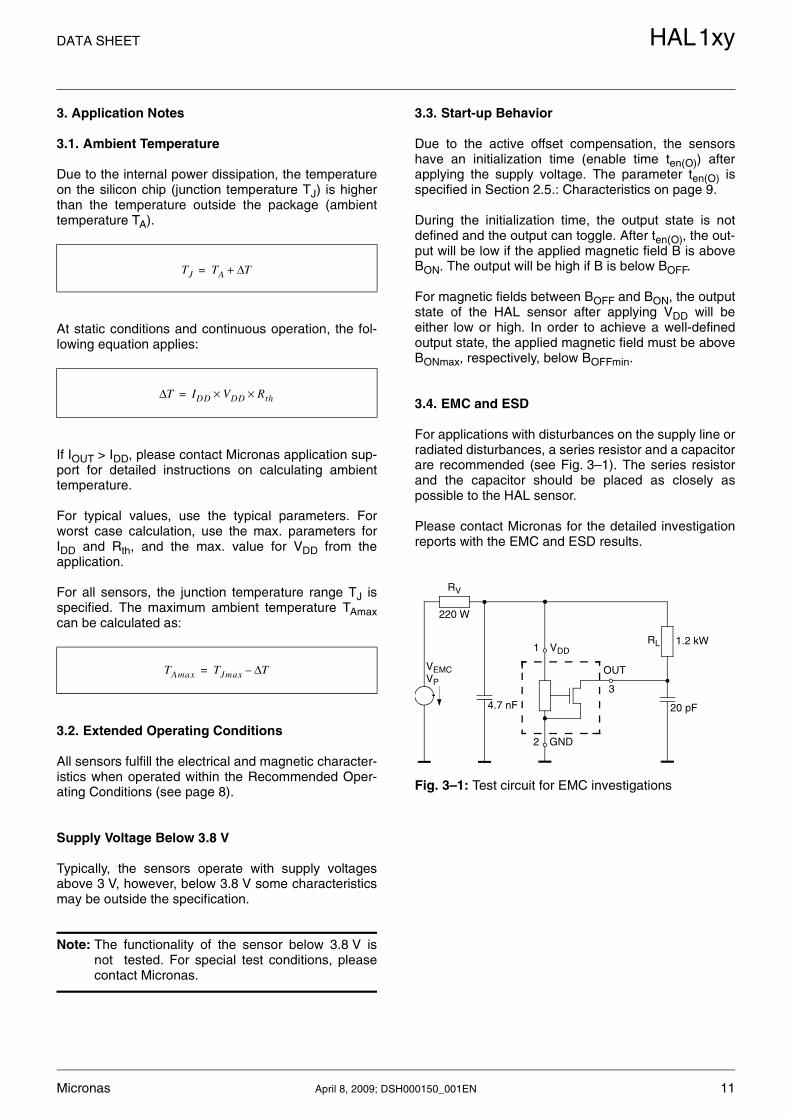
3.4. EMC and ESD
For applications with disturbances on the supply line orradiated disturbances, a series resistor and a capacitorare recommended (see Fig. 3–1). The series resistorand the capacitor should be placed as closely aspossible to the HAL sensor.
Please contact Micronas for the detailed investigationreports with the EMC and ESD results.
Fig. 3–1: Test circuit for EMC investigations
TJ TA TΔ+=
TΔ IDD VDD× Rth×=
TAmax TJmax TΔ–=
RV
220 W
VEMCVP
4.7 nF
VDD
OUT
GND
1
2
3
RL 1.2 kW
20 pF
HAL1xy DATA SHEET
12 April 8, 2009; DSH000150_001EN Micronas
Micronas GmbHHans-Bunte-Strasse 19 ⋅ D-79108 Freiburg ⋅ P.O. Box 840 ⋅ D-79008 Freiburg, Germany
Tel. +49-761-517-0 ⋅ Fax +49-761-517-2174 ⋅ E-mail: [email protected] ⋅ Internet: www.micronas.com
4. Data Sheet History
1. Data Sheet: “HAL1xy Hall-Effect Switch IC Family”, April 8, 2009, DSH000150_001EN. First release of the data sheet.