Embed Size (px)
Citation preview
HAL Id: jpa-00245880https://hal.archives-ouvertes.fr/jpa-00245880
Submitted on 1 Jan 1988
HAL is a multi-disciplinary open accessarchive for the deposit and dissemination of sci-entific research documents, whether they are pub-lished or not. The documents may come fromteaching and research institutions in France orabroad, or from public or private research centers.
L’archive ouverte pluridisciplinaire HAL, estdestinée au dépôt et à la diffusion de documentsscientifiques de niveau recherche, publiés ou non,émanant des établissements d’enseignement et derecherche français ou étrangers, des laboratoirespublics ou privés.
EL2 family in LEC and HB GaAsY. Mochizuki, T. Ikoma
To cite this version:Y. Mochizuki, T. Ikoma. EL2 family in LEC and HB GaAs. Revue de Physique Appliquee, 1988, 23(5), pp.747-763. �10.1051/rphysap:01988002305074700�. �jpa-00245880�
747
EL2 family in LEC and HB GaAs
Y. Mochizuki and T. Ikoma
Institute of Industrial Science, University of Tokyo 7-22-1, Roppongi, Minato-ku, Tokyo 106, Japan
(Reçu le 15 juillet 1987, accepté le 8 janvier 1988)
Résumé. 2014 On décrit des études sur les propriétés électriques et optiques de EL2 dans différents cristaux deGaAs en vue de cerner les caractéristiques de cette famille de défauts. On donne tout d’abord une revue de lavariation des niveaux d’énergie associés à la « famille » EL2. On montre que les caractéristiques de cettefamille sont observées aussi bien dans les effets de photoblocage (transition entre l’état normal et l’état
métastable) que dans les taux de transition vers les états excités. La modification des centres EL2 aprèsirradiation aux particules lourdes et recuits à basse température indique que la structure du défaut associé àEL2 est assez étendue et qu’elle inclut un ou des interstitiels d’arsenic. A partir des résultats expérimentaux, lavalidité du modèle d’ensemble d’atomes d’arsenic pour EL2 est corrélée à des modèles présentés par d’autresauteurs.
Abstract. 2014 Studies on the electrical and optical properties of EL2 in various GaAs crystals are describedespecially in view of the family characteristics. A variation in the trap energy levels among the EL2 family isfirst reviewed. It is shown that the family characteristics are also observed in the photoquenching effect(transitions between the normal and the metastable states) as well as the transition rate to the excited state.Change of EL2 centers after heavy particle bombardment and low temperature annealing indicate that thedefect structure responsible for EL2 is sizable, in which mobile interstitial As atom(s) are involved. Based onthe experimental results, validity of the As-cluster model for the origin of EL2 is presented and correlated withthe models proposed by other investigators.
Revue Phys. Appl. 23 (1988) 747-763 MAI 1988,
Classification
Physics Abstracts71.55E - 78.20J
1. Introduction.
EL2 is the native midgap electron trap in GaAswhich plays a dominant role in achieving semi-
insulating (SI) property of GaAs without intentionaldoping. Due to its importance from both basic andpractical viewpoints, intensive studies have been
carried out in order to clarify the microscopic defectstructure. In spite of such efforts, the origin of EL2is still controversial.
Sakai and Ikoma [1] first reported the thermalemission property of this midgap level. After that,people have reached an agreement on the energylevel and the capture cross section as summarized inreference [2]. Studies on the energy barrier for
electron capture process [3] and the large Franck-Condon shift [4] have revealed that EL2 undergoes alattice relaxation on capturing electron. Moreover,peculiar characteristics of EL2 are also reported ; alarge metastable relaxation (so called photoquench-ing effect [5]) and the existence of an internal excited
state [6]. These findings are very important for
discussing the atomic structure of EL2.Since Huber et al. [7] excluded the possibility that
EL2 is oxygen impurity-related, roles of native pointdefects have been studied as a candidate for the
origin of this level. The early electron spin resonance(ESR) studies [8] combined with the growth con-dition dependence [9] lead to an idea that an Asatom at the Ga site (the arsenic antisite, AsGa) is
responsible for EL2, which is in agreement with theprediction by Van Vechten [10] in 1975. However,some difficulties in attributing an isolated AsGa toEL2 have been pointed out both experimentally [11]and theoretically [12]. An isolated antisite has littlelattice relaxation and should have no metastability[12]. These features are different from experimentalobservations. As a consequence, various ASGa-re-lated complex defect models have been considered.
In 1983, it was further reported by the presentauthors’ group that EL2 is not a well defined singlelevel but a group of midgap levels with similar
Article published online by EDP Sciences and available at http://dx.doi.org/10.1051/rphysap:01988002305074700

748
properties [13, 14]. They first pointed out that all ofthe variation in thermal emission rate reported byseveral researchers cannot necessarily be attributedto an experimental error but it should be an actualvariation in the trap properties. Because of a com-mon characteristic of the photoquenching effect,they concluded that these traps belong to the same« family ». This conclusion has also provided analternative approach to an identification of EL2 ; theexcess As-cluster model proposed in 1984 [14].
In this paper, we focus our attention on the familycharacteristics of EL2. The main portion is devotedto the description of our recent results on the opticalproperties of EL2 together with a review of ourearlier results. Section 2 deals with the variation in
thermal and optical characteristics among the familyin various GaAs crystals. When the defect structureis to be argued, it is also useful to study its stability.The experimental results on this point are describedin section 3. Finally in section 4, validity of our As-cluster model for the origin of EL2 is shown and
comparative discussions with other models are
made. Section 5 is the summary of the present study.
2. Variation in properties of EL2 family.
2.1 CARRIER EMISSION PROPERTIES.
a) DLTS measurement. - A variation in the
thermal emission rate among the EL2 family in LECGaAs crystals was first reported by Taniguchi andIkoma [12], who measured capacitance DLTS spec-tra in various LEC GaAs crystals. In order to assurelarge Schottky-barrier height, all the measurementswere carried out by using Au-evaporated Schottkydiodes which have usually 0.85-0.90 eV barrier
height. We found that the peak temperatures ofDLTS spectra for EL2 show a variation dependingon measured spots, wafers or annealing.The DLTS spectra measured in two LEC-grown
samples are shown in figure 1. One of the samples iscut from the front (or seed end) section of an ingot,while the other is from the tail section of the same
ingot. It is clearly shown that the peak temperaturefor the midgap level in the front section (ETX-2) islower than that in the tail section (ETX-1) by morethan 20 degrees. Similar variations were also ob-served by changing bias in measurements and byannealing at 650 °C for 40 min [13]. These differ-ences cannot be attributed to an experimental errorbut should be due to an existence of similar midgaptraps (EL2 family).
Figure 2 shows a set of DLTS spectra taken fromanother ingot. The spectra provides evidence thattwo midgap levels simultaneously exist in the sameregion in this LEC GaAs. The spectral shapes in thisfigure are apparently broader than that expectedfrom a single deep level. Actually, they are well
Fig. 1. - DLTS spectra in front and tail sections of an as-grown LEC GaAs crystal. The samples are labeled as
LEC-1(F) and LEC-1(T), respectively.
Fig. 2. - DLTS spectra for the midgap level in anotherLEC GaAs. The calculated curves assuming the existenceof two levels are shown.
described by assuming contributions of two midgaplevels. In the theoretical fit, activation energy and
capture cross section for one of the levels are
0.76 eV and 3.7 x 10⁻¹³ cm2 and for the other level0.81 eV and 4.3 x 10⁻¹³ cm2, respectively. The sum(dotted curve) of the calculated curves (brokenlines) are in agreement with the experimental curve(solid curve) by assuming the same ratio of concen-trations for different rate windows. These trapparameters are almost the same as those of ETX-2and ETX-3 in reference [13]. The existence of morethan two midgap levels were also reported by otherresearch groups [15, 16].
b) Steady state photocapacitance measurements.- A variation is also observed in the optically-measured energy levels of the EL2 family. Although

749
the energy levels of the EL2 family fall within themidgap region, it has been found that there exist twotypes of levels which have different threshold ener-gies for photoionization. Figure 3 shows the result ofquasi steady state photocapacitance spectra at 77 K.The results are for (a) as-grown HB GaAs, (b)oxygen-implanted and 700 °C/15 min annealed HBGaAs and (c) oxygen-implanted and 800 °CI2 minannealed LPE GaAs. All the samples contain EL2as a major electron trap. It should be noted that EL2does not exist originally in LPE crystals. EL2 in HBGaAs is also annihilated after oxygen ion implan-tation. However, post-implantation annealing in therange 650-800 °C creates a new midgap level. Thislevel has a similar energy level to EL2 and shows
photoquenching effect as well. Therefore, the newlycreated level is regarded to belong to EL2 family,which is labeled as EL2-0 [17].
Fig. 3. - Quasi steady state photocapacitance spectra for(A) as-grown HB GaAs, (B) oxygen-implanted and
700 °C/15 min annealed HB GaAs and (C) oxygen:’im-planted and 800 °C/2 min LPE GaAs.
Table I. - List of the samples used in the study.
As shown in the figure, large capacitance increasewas observed at 0.67 eV in the oxygen-implantedsamples, both HB and LPE, while in the as-grownHB wafer, it was at 0.74 eV, as marked by thearrows. Therefore, these levels are different even
though the thermal emission rates are similar. Ionimplantation of other species such as nitrogen andgallium also creates EL2-0, which has the samephotocapacitance threshold energy at 0.67 eV [18].The possibility is, therefore, excluded that oxygenimpurity is the origin of EL2-0. A smaller increaseof capacitance at 0.67 eV was also observed in
the as-grown HB GaAs. This increase means that
EL2-0 is also contained in as-grown HB GaAs.
LEC GaAs shows a similar spectrum ; there existtwo types of traps which have the photoionizationthreshold at 0.67 and 0.74 eV, respectively. How-ever, in the case of LEC samples, increase at
0.67 eV was the major portion in contrast to theresult for HB GaAs. Similar results of existence oftwo types of midgap levels is also found in a VPEGaAs layer [19].
2.2 PHOTOQUENCHING EFFECT. - A peculiar opti-cal characteristic called the photoquenching effecthas been observed for EL2. Photocapacitance[5, 20], absorption coefficient [21] or luminescenceintensity [22] decreases under illumination
(h v = 1.1 eV) at low temperatures. This effect is
explained by a transformation of EL2 centers totheir metastable states. Several models have been sofar reported for this metastability. They can beactually classified into two categories ; the modelbased on a large lattice relaxation at the metastablestate [20] and one on the Coulombic interactions[23].
In this section, a variation in the transition charac-teristics between the normal and metastable states of
the EL2 family is discussed.

750
2.2.1 Transition from the normal state to the meta-stablc state. - First, a variation in the photoquench-ing transients and photoquenching spectra at EL2centers in various GaAs crystals are reproduced infigures 4a and 4b, which were reported by Tan-iguchi and Ikoma [14]. The samples studied are
listed in table 1 and the midgap levels in respectivesamples are also labeled. Main features in
figure 4b are that photoquenching rate increases atthe higher energy region than 1.3 eV for all the EL2centers and that a variation among the EL2 family ismore pronounced here than in the Gaussian regionaround 1.13 eV. This observation strongly suggeststhat the EL2 family has a variation in the energy
Fig. 4. - (a) Capacitance transients due to photocapaci-tance at the EL2 family in various GaAs crystals. (b)Photoquenching spectra for the EL2 family. Peak heightsare normalized to the values at 1.12 eV.
configuration between the normal and the meta-stable states.
This point is actually explored more in detail forthe case of EL2 in the Czochralski (LEC) growncrystal (referred to as ETX-1). This center (as wellas EL2-0 in oxygen implanted and annealed LPEGaAs) readily shows a strong non-exponentiality infigure 4a, suggesting that similar traps with differ-ent photoquenching rates exist in this crystal. In
order to eliminate the effect due to nonlinear
relationship between capacitance and ionized trapdensity, we performed a constant capacitancemeasurements where the change in applied voltage,0394V, necessary to maintain the depletion layer-widthconstant was monitored. In this case, OV is express-ed as
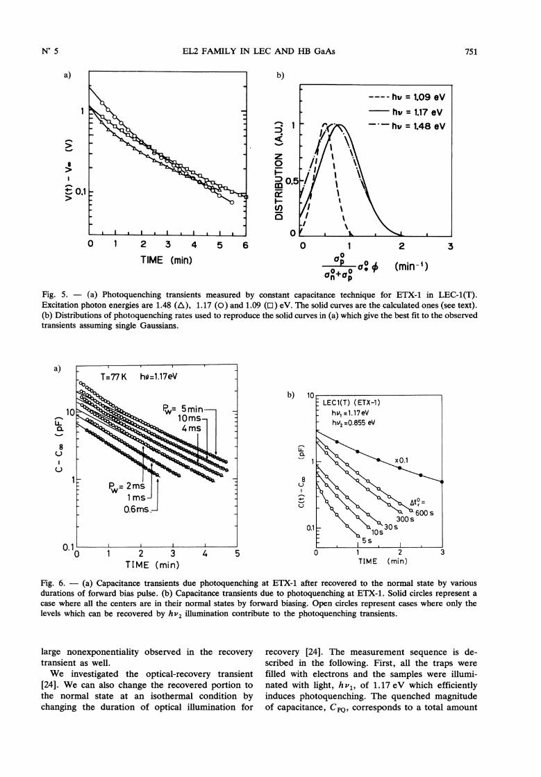
where Vbi, Vapp, and Nd are built-in potential,applied voltage and shallow donor density, respect-ively. It is directly seen that the change in voltage isproportional to that in space charge density 039403C1.Figure 5a shows the result of the constant capaci-tance method for ETX-1 at three excitation photonenergies. It is concluded that the non-exponentialityis not due to experimental error but due to theinherent property of EL2. This level may consist of
traps with slightly different photoquenching rates.The resultant rate is expected to be broadened witha certain distribution. A Gaussian distribution wasassumed for simplicity in the study. Figure 5b
displays the distributions which gave the best fits
(solid curves in Fig. 5a) to the experimental tran-sients. Values of a measure of broadening (thestandard deviation normalized to the mean value,denoted as NSD) were 0.38, 0.52 and 0.69 at photonenergies of 1.09, 1.17 and 1.48 eV, respectively.However, as shown in the figure these distributionsof photoquenching rate tend to extend into the
negative region. This has no physical meaning andmay suggest that the simple Gaussian distribution isnot really adequate.
Figure 6a shows photoquenching capacitancetransients when the width of injection-pulse for
recovery from the metastable to normal states is
varied from 0.6 ms to 5 min. When the pulse width is5 mit, all the EL2 centers change from the normalstate to the metastable state by shining 1.17 eV-light, while for the 0.5 ms, approximately 20 % ofthe EL2 centers change from the normal to themetastable state. It is apparent that the nonexponen-tiality was decreased by decreasing electrical pulsewidth. At the same time, the slope approaches thefastest component in the case of PW = 5 min. Thismeans that centers with a larger probability for therecovery by free electron injection have larger crosssections for photoquenching. A variation in the
recovery probability was actually confirmed by a
751
Fig. 5. - (a) Photoquenching transients measured by constant capacitance technique for ETX-1 in LEC-1(T).Excitation photon energies are 1.48 (0394), 1.17 (0 ) and 1.09 (0) eV. The solid curves are the calculated ones (see text).(b) Distributions of photoquenching rates used to reproduce the solid curves in (a) which give the best fit to the observedtransients assuming single Gaussians.
Fig. 6. - (a) Capacitance transients due photoquenching at ETX-1 after recovered to the normal state by variousdurations of forward bias pulse. (b) Capacitance transients due to photoquenching at ETX-1. Solid circles represent acase where all the centers are in their normal states by forward biasing. Open circles represent cases where only thelevels which can be recovered by hv2 illumination contribute to the photoquenching transients.
large nonexponentiality observed in the recoverytransient as well.We investigated the optical-recovery transient
[24]. We can also change the recovered portion tothe normal state at an isothermal condition bychanging the duration of optical illumination for
recovery [24]. The measurement sequence is de-scribed in the following. First, all the traps werefilled with electrons and the samples were illumi-nated with light, h vl, of 1.17 eV which efficientlyinduces photoquenching. The quenched magnitudeof capacitance, CPQ, corresponds to a total amount
752
of EL2 in a sample. After a sufficiently long timeillumination, all the EL2 centers are considered tobe transferred to their metastable states. In order to
study the effect of optical recovery, secondary light,hV2, is sent. The number of EL2 centers whichrecovered to the normal state was monitored by themagnitude of photoquenching, Cf, under h v illumi-nation. Ct is functions of h v 1 and the illuminationperiod, àtf.The results of optical recovery are described in the
next subsection. Here, only the photoquenchingtransients at the recovered centers are concerned
with. Open circles in figure 6b shows thus obtainedcapacitance transients due to photoquenching at theEL2 centers which are recovered optically. Thetransient due to photoquenching at all the EL2
centers are also shown by solid circles for compari-son. In this case, all the centers were recovered fromthe metastable state by forward biasing for a suffi-ciently long time. It is apparent from the figure thatthe EL2 centers which recover optically have largerphotoquenching cross sections as compared to thoseof centers which cannot be recovered. Although thistendency is similar to the case of electrical recovery,a nonexponentiality is more pronounced for a shorterduration of illumination. Although both of electricaland optical recovery transients have large nonex-ponentialities, the photoquenching rates of the re-covered centers are different in these recoveryprocesses. _
For studying the family characteristics of EL2, it isinteresting to examine whether the broadening inphotoquenching rate is photon energy dependent. If
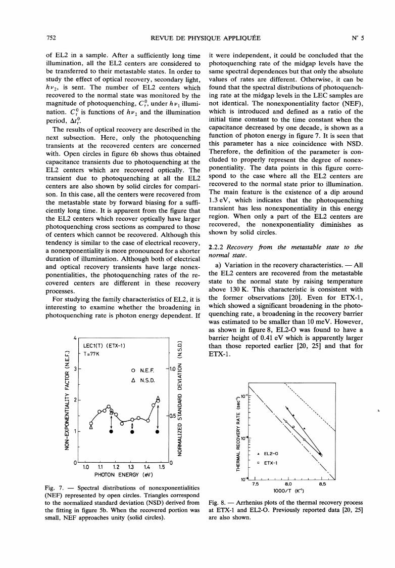
it were independent, it could be concluded that thephotoquenching rate of the midgap levels have thesame spectral dependences but that only the absolutevalues of rates are different. Otherwise, it can befound that the spectral distributions of photoquench-ing rate at the midgap levels in the LEC samples arenot identical. The nonexponentiality factor (NEF),which is introduced and defined as a ratio of theinitial time constant to the time constant when the
capacitance decreased by one decade, is shown as afunction of photon energy in figure 7. It is seen thatthis parameter has a nice coincidence with NSD.Therefore, the definition of the parameter is con-cluded to properly represent the degree of nonex-ponentiality. The data points in this figure corre-spond to the case where all the EL2 centers arerecovered to the normal state prior to illumination.The main feature is the existence of a dip around1.3 eV, which indicates that the photoquenchingtransient has less nonexponentiality in this energyregion. When only a part of the EL2 centers arerecovered, the nonexponentiality diminishes as
shown by solid circles.
2.2.2 Recovery from the metastable state to the
normal state.
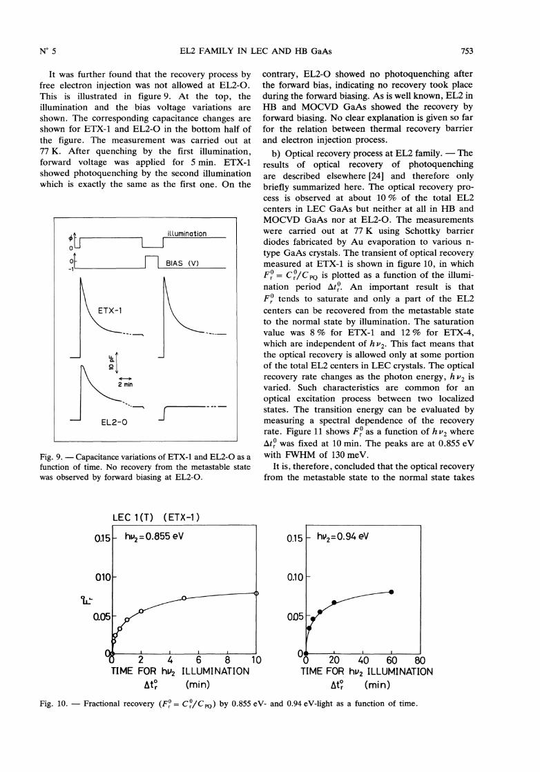
a) Variation in the recovery characteristics. - Allthe EL2 centers are recovered from the metastable
state to the normal state by raising temperatureabove 130 K. This characteristic is consistent with
the former observations [20]. Even for ETX-1,which showed a significant broadening in the photo-quenching rate, a broadening in the recovery barrierwas estimated to be smaller than 10 meV. However,as shown in figure 8, EL2-0 was found to have abarrier height of 0.41 eV which is apparently largerthan those reported earlier [20, 25] and that forETX-1.
Fig. 7. - Spectral distributions of nonexponentialities(NEF) represented by open circles. Triangles correspondto the normalized standard deviation (NSD) derived fromthe fitting in figure 5b. When the recovered portion wassmall, NEF approaches unity (solid circles).
Fig. 8. - Arrhenius plots of the thermal recovery processat ETX-1 and EL2-0. Previously reported data [20, 25]are also shown.
753
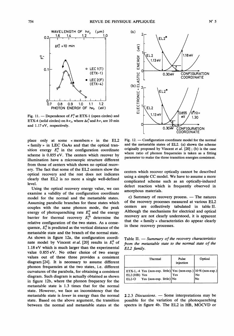
It was further found that the recovery process byfree electron injection was not allowed at EL2-0.This is illustrated in figure 9. At the top, the
illumination and the bias voltage variations are
shown. The corresponding capacitance changes areshown for ETX-1 and EL2-0 in the bottom half ofthe figure. The measurement was carried out at
77 K. After quenching by the first illumination,forward voltage was applied for 5 min. ETX-1showed photoquenching by the second illuminationwhich is exactly the same as the first one. On the
Fig. 9. - Capacitance variations of ETX-1 and EL2-0 as afunction of time. No recovery from the metastable state
was observed by forward biasing at EL2-0.
contrary, EL2-0 showed no photoquenching afterthe forward bias, indicating no recovery took placeduring the forward biasing. As is well known, EL2 inHB and MOCVD GaAs showed the recovery byforward biasing. No clear explanation is given so farfor the relation between thermal recovery barrier
and electron injection process.b) Optical recovery process at EL2 family. - The
results of optical recovery of photoquenchingare described elsewhere [24] and therefore onlybriefly summarized here. The optical recovery pro-cess is observed at about 10 % of the total EL2
centers in LEC GaAs but neither at all in HB and
MOCVD GaAs nor at EL2-0. The measurementswere carried out at 77 K using Schottky barrier
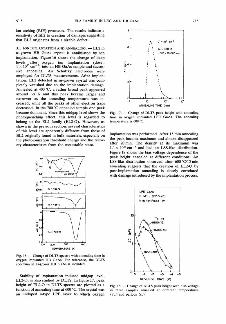
diodes fabricated by Au evaporation to various n-type GaAs crystals. The transient of optical recoverymeasured at ETX-1 is shown in figure 10, in whichF? = C°/CPQ is plotted as a function of the illumi-nation period Ato. An important result is that
Fo tends to saturate and only a part of the EL2centers can be recovered from the metastable state
to the normal state by illumination. The saturationvalue was 8 % for ETX-1 and 12 % for ETX-4,which are independent of h v2. This fact means thatthe optical recovery is allowed only at some portionof the total EL2 centers in LEC crystals. The opticalrecovery rate changes as the photon energy, h v2 isvaried. Such characteristics are common for an
optical excitation process between two localized
states. The transition energy can be evaluated bymeasuring a spectral dependence of the recoveryrate. Figure 11 shows F r 0 as a function of h v2 whereàtt was fixed at 10 min. The peaks are at 0.855 eVwith FWHM of 130 meV.
It is, therefore, concluded that the optical recoveryfrom the metastable state to the normal state takes
Fig. 10. - Fractional recovery (F0r = C°/CPQ) by 0.855 eV- and 0.94 eV-light as a function of time.
754
Fig. 11. - Dependence of Fo at ETX-1 (open circles) andETX-4 (solid circles) on h V2, where 0394t0r and h Pl are 10 minand 1.17 eV, respectively.
place only at some « members » in the EL2« family » in LEC GaAs and that the optical tran-sition energy Eo in the configuration coordinatescheme is 0.855 eV. The centers which recover byillumination have a microscopic structure differentfrom those of centers which shows no optical recov-ery. The fact that some of the EL2 centers show the
optical recovery and the rest does not indicates
clearly that EL2 is no more a single well-definedlevel.
Using the optical recovery energy value, we canexamine a validity of the configuration coordinatemodel for the normal and the metastable states.
Assuming parabolic branches for these states whichcouples with the same phonon mode, the peakenergy of photoquenching rate 170 and the energybarrier for thermal recovery Erh determine the
relative configuration of the two states. As a conse-quence, Eo is predicted as the vertical distance of themetastable state and the branch of the normal state.As shown in figure 12a, the configuration coordi-nate model by Vincent et al. [20] results in Eo of1.18 eV which is much larger than the experimentalvalue 0.855 eV. No other choice of two energyvalues out of these three provides a consistent
diagram [24]. It is necessary to assume different
phonon frequencies at the two states, i.e. differentcurvatures of the parabola, for obtaining a consistentdiagram. Such diagram is actually obtained as shownin figure 12b, where the phonon frequency for themetastable state is 1.3 times that for the normalstate. However, we face an inconsistency that themetastable state is lower in energy than the normalstate. Based on the above argument, the transitionbetween the normal and metastable states at the
Fig. 12. - Configuration coordinate model for the normaland the metastable states of EL2. (a) shown the schemeoriginally proposed by Vincent et al. [20] ; (b) is the casewhere ratio of phonon frequencies is taken as a fittingparameter to make the three transition energies consistent.
centers which recover optically cannot be describedusing a simple CC model. We have to assume a morecomplicated scheme such as an optically-induceddefect reaction which is frequently observed in
amorphous materials.
c) Summary of recovery process. - The naturesof the recovery processes measured at various EL2centers are collectively tabulated in table II.
Although the mechanisms for electrical and opticalrecovery are not clearly understood, it is apparentthat the « family » characteristics do appear clearlyin these recovery processes.
Table II. - Summary of the recovery characteristicsfrom the metastable state to the normal state of theEL2 family.
2.2.3 Discussions. - Some interpretations may bepossible for the variation of the photoquenchingspectra in figure 4b. The EL2 in HB, MOCVD or

755
VPE GaAs can be regarded as a well defined center.At these centers, the photoquenching spectrumconsists of a Gaussian shape spectrum (Region 1)centered at 1.18 eV and a spectrum increasing above1.3 eV up to the bandgap energy (Region II). Thesimplest interpretation for the shape of ETX-1 isthat it has a broader Gaussian shape which obscurethe valley. However, this model is not likely becausewith this model a uniform NEF distribution shouldbe expected, being in disagreement with figure 7. Itis more advantageous to assume at least two types ofcenters which have slightly different photoquenchingspectra as illustrated in figure 13. One has a rela-tively large cross section in Region I as compared toRegion II, while the other has an inverse relation-ship. Based on this model, the NEF spectrum infigure 7 is interpreted as a superposition of twodifferent photoquenching rates. The dip around
1.3 eV is expected because the values of quenchingcross sections of the two centers become similar
around 1.3 eV.
Fig. 13. - An illustration of two types of EL2 centersassumed to explain the spectral distribution of NEF atETX-1 in figure 7.
The Type-A center in figure 13 shows a similarphotoquenching spectrum to that for EL2 in HB orMOCVD crystal. However, it should be reminded
that EL2 which recovers optically from the meta-stable state has a larger quenching rate than that ofEL2 at which this recovery process is not allowed.
This result claims that EL2 which recovers opticallybelongs to Type-A because this type has a largerphotoquenching rate at 1.17 eV. It is concluded,therefore, that not all of the Type-A EL2 in LECGaAs can be regarded as identical centers to those inHB or MOCVD GaAs. This conclusion leads to an
existence of more than three types of EL2 centers inGaAs at least according to the aforementioned basicclassification.
2.3 ZERO PHONON TRANSITION TO THE EXCITEDSTATE. - After Kaminska et al. [6] reported theintracenter absorption at EL2, characteristics of theexcited state have been intensively explored. In ourprevious papers [26, 27], we clarified the opticaltransition mechanisms at EL2 using a novel SpectralPhotocapacitance Transient Analysis (SPTA) tech-nique as well as the experimental evidences reportedso far. The SPTA technique clearly revealed the roleof the excited state in the charge transfer to themetastable state. In this paper, we will shed light onthe fine structures in photoquenching rate spectraobtained by the SPTA technique. A variation in theSPTA spectra was again observed in various GaAscrystals.
2.3.1 General features o f SPTA spectra. - SPTA isa modified version of photocapacitance measure-ment. In the SPTA measurement, excitation photonenergy is slowly scanned and a local derivative ofcapacitance transient due to photoquenching is
measured with a micro-computer controlled system.As a result, either photoionization or photoquench-ing rate spectrum can be obtained with a very fineresolution. Additional advantage over the absorptionmeasurement is the applicability to thin epitaxialfilms since the measurement accesses the depletionregion.The result is shown in figure 14. Besides the
Gaussian spectrum, a fine oscillatory structure isobserved at 1.03 to 1.08 eV. The first sharp peak islocated at 1.039 eV followed by an oscillation withan interval of approximately 11 meV at the higherenergy side. The feature is similar to the fine
structures observed in the intracenter absorption,where the zero-phonon line (ZPL) is at 1.039 eV andthe separation of phonon replica is 11 meV. There-fore, it can be concluded from such a similarity thatthe zero-phonon transition and its interaction withphonon(s) are also observed in the SPTA spectra.
Further information of significant importance is
obtained from the SPTA spectrum. It should benoted that the ZPL in the SPTA spectrum at
1.039 eV has a negative peak. Since the transitionrate in figure 14 corresponds to an increasing rate ofnegative charge in the space charge region, the ZPLtransition indicates a decrease of negative charge,which does not mean an enhancement of photo-quenching as pointed out by Kaminska et al. [6]..This result positively identifies that the ZPL tran-rsition acts as a path for electrons to relax to theconduction band.
2.3.2 Sample dependence. - A family nature of
EL2 revealed in the SPTA spectra was studied bycomparing the results measured in different GaAscrystals. Figure 15 compares the fine structures
measured in MOCVD and LEC GaAs. It has been
found that EL2 in LEC GaAs exhibits a broader

756
Fig. 14. - The SPTA spectrum of photoquenching rate measured with a high resolution. The inset shows the overallSPTA spectrum.
Fig. 15. - Comparison of the fine structures in the SPTAspectra for EL2 in different GaAs crystals.
spectrum than that of EL2 in MOCVD GaAs. TheFWHM of ZPL in LEC GaAs is 3.6 meV, while it is1.9 meV in MOCVD GaAs.A broadening of the Gaussian spectrum in LEC
GaAs is observed in the SPTA, being consistent withpoint-by-point measurement [14], in which the non-exponentiality is larger in LEC GaAs than in
MOCVD GaAs indicating that a variation amongthe EL2 family in LEC crystals is larger than that inMOCVD GaAs. The SPTA spectrum is deviated
from the Gaussian and again consistent with theprevious result that a double-peak spectrum wasobserved at some of the EL2 in LEC GaAs. It also
seems reasonable that the ZPL for LEC GaAs is
broader than that for MOCVD GaAs. This is the
first observation of the family nature of EL2 in theZPL spectra. However, it should be pointed out that
the ZPL of intracenter absorption reported bySkowronski et al. [28] is not so broad as that ob-
served by SPTA. Although the ZPL spectra of
absorption cannot be attributed to a single opticaltransition line but a convolution of two (or more)lines, the FWHM is much less than the value for theSPTA result.
The reason for this discrepancy is explained asfollows. In LEC GaAs, the EL2 centers are sizablepoint defects end may have slightly modified atomicstructures to each other. Although the main charac-teristic such as a ZPL transition to the excited state iscommon due to a common involvement of a certain
defect, a variation in the additional defect may causea slight change in the energy splitting between theground and the excited states. Such a scheme is
consistent with the larger variation observed in LECGaAs rather than that in MOCVD GaAs. At a moredistorted center, the transition probability to theexcited state should be smaller. A rapid decrease inthe probability may give rise to a rather sharp ZPLwhich has been observed in intracenter absorption.However, the lattice relaxation may also change,which would enhance a probability of electrontransfer from the excited state to the conductionband. This enhancement may cause a more pro-nounced broadening in SPTA spectra, since this
method monitors the overall transfer rate to the final
state, i.e. to the conduction band.
3. Stability of members of EL2 family.
In this section, effects of damages introduced byheavy particle bombardment on EL2 natures arediscussed. Change of EL2 is studied after GaAs
crystals are subjected to ion implantation or reactive
757
ion etching (RIE) processes. The results indicate asensitivity of EL2 to creation of damages suggestingthat EL2 originates from a sizable defect.
3.1 ION IMPLANTATION AND ANNEALING. - EL2 in
as-grown HB GaAs crystal is annihilated by ionimplantation. Figure 16 shows the change of deeplevels after oxygen ion implantation (dose :1 x 10¹³ CM-2) into an HB GaAs sample and succes-sive annealing. Au Schottky electrodes were
employed for DLTS measurements. After implan-tation, EL2 detected in as-grown crystal was com-pletely vanished due to the implantation damage.Annealed at 400 °C, a rather broad peak appearedaround 360 K and this peak became larger andnarrower as the annealing temperature was in-
creased, while all the peaks of other electron trapsdecreased. In the 700 °C annealed sample one peakbecame dominant. Since this midgap level shows thephotoquenching effect, this level is regarded to
belong to the EL2 family (EL2-0). However, asshown in the previous section, several characteristicsof this level are apparently different from those ofEL2 originally found in bulk materials, especially onthe photoionization threshold energy and the recov-ery characteristics from the metastable state.
Fig. 16. - Change of DLTS spectra with annealing time inoxygen implanted HB GaAs. For reference, the DLTSspectrum in as-grown HB GaAs is included.
Stability of implantation induced midgap level,EL2-0, is also studied by DLTS. In figure 17, peakheight of EL2-0 in DLTS spectra are plotted as afunction of annealing time at 600 °C. The crystal wasan undoped n-type LPE layer to which oxygen
Fig. 17. - Change of DLTS peak height with annealingtime in oxygen implanted LPE GaAs. The annealingtemperature is 600 °C.
implantation was performed. After 15 min annealingthe peak became maximum and almost disappearedafter 20 min. The density at its maximum was1.1 x 1016 cm- 3 and had an LSS-like distribution.
Figure 18 shows the bias voltage dependence of thepeak height annealed at different conditions. AnLSS-like distribution observed after 600 °C/15 min
annealing suggests that the creation of EL2-0 bypost-implantation annealing is closely correlatedwith damage introduced by the implantation process.
Fig. 18. - Change of DLTS peak height with bias voltagein three samples annealed at different temperatures( TA ) and periods (tA ).
758
Since the results were similar by changing the
implanted species such as nitrogen, gallium andarsenic, it is not likely that an involvement of theimplanted species is essential for the creation ofEL2-0.
Distribution of EL2-0 after 650 °C/30 min in
figure 18 may coincide with the anneal-out of latticedefects by the implantation process. After a longertime (100 min at 600 °C, for instance) or a highertemperature annealing (700 °C for 15 min, for in-stance), the peak was not detected. This result
indicates that EL2-0 is rather unstable in this
temperature range. This level is related to the
intermediate stage of defect annealing. Usual electri-cal activation of implanted impurities is classified
into two stages ; (1) anneal-out of lattice defectsintroduced by bombardment, which occurs around600 °C and (2) anneal-out of point defects and site-occupation by impurity atoms, which occur around800 °C. The appearance of EL2-0 is in accordancewith the stage-(1). Thus, EL2-0 is more likely to bea sizable defect created during the defect migrationthan a simple point defect.
3.2 ANNIHILATION OF EL2 BY REACTIVE ION ETCH-
ING (RIE). - In the ion implantation process,
damages introduced are so large as to disturb thehost lattice structure. During RIE process, a sampleis also subjected to heavy particle bombardment byplasma. However, in this case, damage is far less andwe can obtain a rather nice Schottky barrier even atthe as-etched state. This situation makes a more
accurate characterization of deep levels possible.
a) Experimental. - The wafers used in the studywere undoped n-type HB GaAs. First, Si02(400 nm) was deposited by plasma-assisted chemicalvapor deposition on the surface of the wafers. Priorto etching, Ohmic electrodes were formed on thebackside by evaporating AuGelNi/Au and alloyingat 400 °C, 5 min. After the patterning of Schottkyelectrodes, Si02 was etched by RIE. The etchingambient was CHF3 at the pressure of 0.08 Torr andthe input power was 3.5 W/cm 2. Then the wafer waswet-etched with a solution of HF : NH4F = 1 : 6 for1 min. Schottky electrodes were formed by vacuumevaporation of Au with’a thickness of 200 nm. Forreference, Schottky diodes without RIE were fabri-cated. In this case, Si02 was etched by a solution ofHF : NH4F = 1 : 6 for 1 min. It was found that Au-Schottky electrodes on RIE-etched wafers are easilypeeled off, which is likely to be due to the degra-dation of dry-etched surface. However, Au is suit-able for characterization of midgap traps due to alarge barrier height of a Schottky diode. Barrier
height is required to be larger than the energy levelof a trap when a junction capacitance method is
adopted.
Characterization of the diodes was carried out byI-V, C-V and TDS-ICTS [29] measurements. C-Vprofiling of deep levels was also performed bycontrolling delay time for C-V profiling.
b) Results and discussions. - From the 1-V
characteristics, it was revealed that the barrier
height is lower and the saturation current is largerfor RIE samples. In these samples, the extrapolatedbarrier height from C-V measurement is largelyshifted which may be due to the reduction of
ND - NA near the surface regions. Therefore, thedry-etched samples have poorer Schottky character-istics than that of the wet-etched samples. However,barrier height of RIE samples fall in the region0.82 ± 0.04 eV, which is high enough for the charac-terization of EL2 whose energy level is
Ec - 0.74 eV.In the wet-etched samples EL2 was the dominant
electron trap, whose emission time constant at room
temperature was 23 ± 2 s and concentration was
2.7-4.4 x 1016 cm- 3, respectively. The variation inthe emission time constant is attributed to that in
temperature as well as noise in the measured EL2
spectra. The spectral shapes of EL2 agreed well ingeneral with those reproduced from a calculationassuming a single level. The observed EL2 concen-trations are reasonable values in HB GaAs crystals.On the other hand, no apparent EL2 signal was
observed in the TDS-ICTS spectra near the surface
regions of dry-etched samples as shown in
figure 19(a) which was measured at the bias voltageof - 1 V. Instead, a broad signal around 20 ms and avery slow transient which extends to 500 s wereobserved. DLTS measurements revealed that theformer can be identified as a trap called ED5 [30],which has an activation energy Ea = 0.51 eV. It is
most likely that this level is closely related to thedamage introduced by the RIE process. The originof the latter transient is not known at present. In the
deeper regions, ED5 signal was much reduced andEL2 became the dominant signal as shown in
figure 19b. The unidentified slow transient was stillobserved. These results indicate that ED5 decreases
while EL2 increases toward inside in the RIE
processed sample.To examine the spatial variation more in detail, C-
V profiling method was applied. Broken curve infigure 20a shows the profile of EL2 concentrationin the wet-etched sample, which was derived fromthe C-V measurements Of td = 10 ms and td = 50 s.Trap concentration NT was calculated using a re-lation
Here, À is the distance between the depletion layer

759
Fig. 19. - TDS-ICTS spectra for the reactive ion etchedsample at room temperature. The bias conditions are (a)0 V/- 1 V and (b) - 5 V/- 8 V.
edge and the point at which trap level and the bulkFermi level crosses. It is seen that the EL2 concen-tration in bulk GaAs is almost constant alongdistance from the surface. However, EL2 concen-tration in the dry-etched samples were greatly re-duced near the surface as shown in figure 20(b). Inthis case, C-V measurements with td =1 s andtd = 50 s were carried out to obtain the trap profilesfor ED5 and EL2 separately. Since the energy levelof ED5 is unknown, À was calculated using theactivation energy 0.52 eV of this level, which corres-
ponds to the estimation of the maximum concen-tration of ED5. In the surface region, ED5 prevailsEL2 and rapidly decreases toward inside. Further-more, a gradual increase of EL2 toward inside wasobserved. Although a slow ionization co-existswhich cannot be attributed to the emission from
EL2, C-V measurement with td = 50 s dominantlymonitors the ionized EL2 centers.The profiling method of deep levels clearly revea-
led that the annihilation of EL2 has a nice spatialcorrelation with the creation of the damage-inducedlevel, ED5, as can be seen in figure 20b. It is
Fig. 20. - Profiles of the trap concentrations for (a) thereference sample and (b) the RIE-processed sample.
concluded that EL2 centers are annihilated by abombardment damage which is introduced to the
depth of 0.2 03BCm. This characteristic depth agreeswith that observed in WSijGaAs system [30] wheremetal deposition was carried out by RF sputtering.In this case, ED5 was also introduced to a depth of0.2 )JLm and reduction of EL2 was observed. Duringa sputtering process, a wafer is subjected to plasmabombardment similarly to the situation for RIE.
In both cases, the defect structure of EL2 centersare recovered after a low temperature annealingaround 300 °C. In the WSijGaAs Schottky diodesfabricated by sputtering, EL2 concentration, whichwas reduced after the deposition, increased by afactor of 1.6 after 324 °C annealing, Peak tempera-ture in DLTS spectrum approached that of EL2 inas-grown GaAs wafers and the spectra became
sharper. Although the increased amount is small,reconstruction of the EL2 centers by such a lowtemperature annealing was confirmed. EL2 in thedry-etched samples were also recovered to the
original concentration after 350 °C annealing. These

760
results provide evidence that the defect componentof EL2 is highly mobile even at low temperatures.This is one of the reasons why we conclude that aninterstitial, such as AsI, rather than a vacancy defectshould be responsible for EL2 formation.
It is not possible so far as to attribute ED5 as adirectly transformed defect from EL2, althoughED5 has a complementary profile to that of EL2.Originally, no EL2 was detected in the VPE samplesprobably due to the large electron concen-
tration [31], whereas a large concentration of ED5was introduced by RIE. Measurements were carriedout on RIE-etched n-type VPE GaAs
(n = 2 x 1017 cm-3). In this case, no EL2 was
detected in both unprocessed and dry-etched layers.However, a damage-induced level, ED5 was againobserved in the surface region of the dry-etchedsample as shown in figure 21. The concentration ofED5 seems to have a correlation with the originalfree electron concentration. Therefore, this defect ismore likely to be assigned as a displaced shallowdonor impurity or a complex of shallow donor
impurity with a native defect produced by thebombardment damage. Anyhow, identification ofED5 is beyond the scope of the present paper andnot discussed further.
Fig. 21. - Profile of ED5 concentration in RIE-processedVPE GaAs.
4. A model for the atomic structure of EL2 family
4.1 As CLUSTER MODEL. - Recent assessment isthat EL2 is closely related to the excess arsenicconditions. A model for the atomic structure is
required to successfully explain the experimentalfacts which are summarized as follows ;
(i) EL2 appears during an intermediate stage ofannealing after heavy particle bombardment such asion implantation.
(ii) EL2 easily dissociates by the sputtering or dryetching damage and recovers its structure after a lowtemperature annealing as low as 300 °C.
(iii) The trap parameters of EL2 havé variationsso as to form a family of levels (EL2 family).
(iv) A large metastable relaxation takes place atEL2, which is beyond the harmonic oscillator ap-proximation. Furthermore, the energy configurationof the normal state and the metastable state is not
uniquely determined.(v) The defect responsible for EL2 consists of a
rigid point defect like ASGA and an easily displaceddefect which mainly contributes to the metastability.
Details are not described concerning (v) since theresults have been obtained not from the familycharacteristics of EL2 but from an optical characteri-zation which has been described elsewhere [27].
Items (i) and (ii) indicate that EL2 is annihilatedand created at low temperatures which is consider-ably lower than that for simple point defects andsupport the idea that EL2 should be originated froma sizable defect. Furthermore, a defect componentof EL2 is required to be mobile at low temperaturesas mentioned above. We speculate that AsI is the
most probable candidate. The trap characteristics asstated in the rest of the items also suggest that EL2should be a sizable complex defect which enables avariation among the family. Furthermore, its bond-ing is likely to be « soft » so that the metastabilityand the family characteristics occur.
Following the item (v), the principle characteristicsare likely to be determined by ASGa + VAs orASGa + AsI. Taking into account the argumentabove, the latter structure is more probable. It is
necessary to assume the third (or more) defect(s) toaccount for the results on EL2 in LEC GaAs as a
consequence of the argument in section 2.2 and 2.3.It is naturally expected that AsI is such a defect(s).Accordingly, the atomic structure of the EL2 familycan be tentatively expressed as ASGa + nAsl (n 2 ).Atomic arrangement is hardly known so far but thisdefect can be regarded as an aggregate of more than7 arsenic atoms. In such a phase, it is not likely thatthe coordinations in the host lattice are conserved.
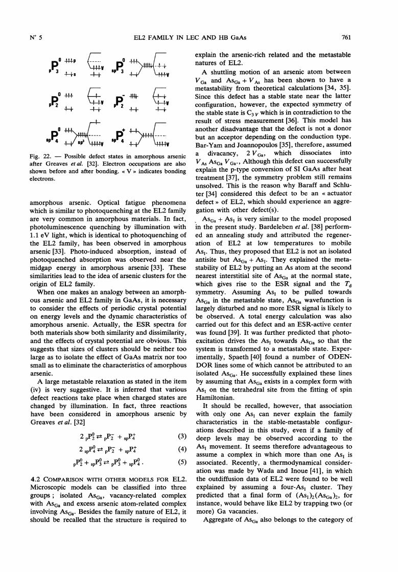
Information on the bulk amorphous arsenic [32]gives an insight into the properties of the As-aggre-gate. Three-fold coordinated arsenic as shown in
figure 22 is a normal configuration in amorphousarsenic. Defect states in this phase are two-fold andfour-fold coordinated arsenic atoms. As can be seenin figure 22, pP2 and s p Po 4 have an unpaired electronand are spin-active. (We follow the conventionalnotation : pP2 means a two-fold coordinated neutralarsenic atom whose predominant type of bonding isp-like.) It is interesting to note that s p Po 4 has a similaratomic configuration to an antisite arsenic ASGA,corresponding to a singly ionized state D+ in GaAs,which is detected by ESR measurements. Accordingto Greaves et al. [32], furthermore, s Po forms a levelnear the midgap in the band gap (1.25 eV) of
761
Fig. 22. - Possible defect states in amorphous arsenicafter Greaves et al. [32]. Electron occupations are alsoshown before and after bonding. « V » indicates bondingelectrons.
amorphous arsenic. Optical fatigue phenomenawhich is similar to photoquenching at the EL2 familyare very common in amorphous materials. In fact,photoluminescence quenching by illumination with1.1 eV light, which is identical to photoquenching ofthe EL2 family, has been observed in amorphousarsenic [33]. Photo-induced absorption, instead of
photoquenched absorption was observed near themidgap energy in amorphous arsenic [33]. These
similarities lead to the idea of arsenic clusters for the
origin of EL2 family.When one makes an analogy between an amorph-
ous arsenic and EL2 family in GaAs, it is necessaryto consider the effects of periodic crystal potentialon energy levels and the dynamic characteristics ofamorphous arsenic. Actually, the ESR spectra forboth materials show both similarity and dissimilarity,and the effects of crystal potential are obvious. Thissuggests that sizes of clusters should be neither too
large as to isolate the effect of GaAs matrix nor toosmall as to eliminate the characteristics of amorphousarsenic.
A large metastable relaxation as stated in the item(iv) is very suggestive. It is inferred that various
defect reactions take place when charged states arechanged by illumination. In fact, three reactions
have been considered in amorphous arsenic byGreaves et al. [32]
4.2 COMPARISON WITH OTHER MODELS FOR EL2.
Microscopic models can be classified into three
groups ; isolated ASGA, vacancy-related complexwith AsGa and excess arsenic atom-related complexinvolving AsGa. Besides the family nature of EL2, itshould be recalled that the structure is required to
explain the arsenic-rich related and the metastablenatures of EL2.
A shuttling motion of an arsenic atom betweenVoa and ASGa +VA, has been shown to have ametastability from theoretical calculations [34, 35].Since this defect has a stable state near the latter
configuration, however, the expected symmetry ofthe stable state is C3 y which is in contradiction to theresult of stress measurement [36]. This model hasanother disadvantage that the defect is not a donorbut an acceptor depending on the conduction type.Bar-Yam and Joannopoulos [35], therefore, assumeda divacancy, 2 VGa, which dissociates into
VA, ASGa vGa., Although this defect can successfullyexplain the p-type conversion of SI GaAs after heattreatment [37], the symmetry problem still remainsunsolved. This is the reason why Baraff and Schlu-ter [34] considered this defect to be an « actuatordefect » of EL2, which should experience an aggre-gation with other defect(s).
, ASGA + Asi is very similar to the model proposedin the present study. Bardeleben et al. [38] perform-ed an annealing study and attributed the regener-ation of EL2 at low temperatures to mobile
AsI. Thus, they proposed that EL2 is not an isolatedantisite but ASGA + As,. They explained the meta-stability of EL2 by putting an As atom at the secondnearest interstitial site of ASGA at the normal state,which gives rise to the ESR signal and the Tdsymmetry. Assuming As, to be pulled towards
ASGa in the metastable state, ASGA wavefunction islargely disturbed and no more ESR signal is likely tobe observed. A total energy calculation was also
carried out for this defect and an ESR-active center
was found [39]. It was further predicted that photo-excitation drives the AsI towards AsGa so that thesystem is transformed to a metastable state. Exper-imentally, Spaeth [40] found a number of ODEN-DOR lines some of which cannot be attributed to an
isolated AsGa. He successfully explained these linesby assuming that ASGA exists in a complex form withAs, on the tetrahedral site from the fitting of spinHamiltonian.
It should be recalled, however, that associationwith only one AsI can never explain the familycharacteristics in the stable-metastable configur-ations described in this study, even if a family ofdeep levels may be observed according to the
AsI movement. It seems therefore advantageous toassume a complex in which more than one AsI is
associated. Recently, a thermodynamical consider-ation was made by Wada and Inoue [41], in whichthe outdiffusion data of EL2 were found to be well
explained by assuming a four-AsI cluster. Theypredicted that a final form of (ASI)2(AsGa)2, for
instance, would behave like EL2 by trapping two (ormore) Ga vacancies.
Aggregate of AsGa also belongs to the category of

762
excess arsenic atom-related defects. These modelsare mainly based on the ESR results and in anattempt to overcome the inconsistencies between thecharacteristics of EL2 and ASGA signal. Meyer andSpaeth [42] performed a photoquenching experimenton AsGa signal in MCD with changing the excitationintensity. EL2-type quenching occurred only at ahigh excitation level, whereas the bleached AsGa hada different recovery characteristics from EL2. Theyinterpreted the result in such a way that EL2-typequenching takes place when AsGa defects form anaggregate and nearby defects are simultaneouslyphotoexcited. Thus, they proposed an AsGa-aggre-gate model. However, the EL2 absorption wasquenched at low intensities at which no ASGA quench-ing was observed. Aggregation (complex formation)of AsGa requires either an aggregation of VGa whichtrap Asi or Asi-aggregate which trap many VGa. Acomplete occupation of Ga-sites by AsI are hardlyexpected and it is more likely that VGa or AsI arealso involved in the excess-arsenic defect aggregate.Therefore, this type of defects can be also identifiedas As-clusters.
5. Summary.
Studies on the electrical and optical properties ofEL2 in various GaAs crystals are described especiallyin view of the family characteristics. Together withthe variation in the trap energy levels, those ob-served in the photoquenching effect (transitionsbetween the normal and the metastable states) aswell as the transition rate to the excited state are
shown to exist. Change of EL2 centers after heavyparticle bombardment and low temperature an-
nealing indicate that the defect structure responsiblefor EL2 is sizable, in which mobile interstitial As
atom(s) are involved. Based on the experimentalresults, validity of the As-cluster model for the
origin of EL2 is presented and correlated with themodels proposed by other investigators.
Acknowledgment.
The authors are grateful to Dr. M. Taniguchi ofNippon Mining Co. Ltd. for carrying out exper-iments and discussions in the early stage.
References
[1] SAKAI, K. and IKOMA, T., Appl. Phys. 5 (1974) 165.[2] MARTIN, G. M., MITTONEAU, A. and MIRCEA, A.,
Electron. Lett. 13 (1977) 191.[3] HENRY, C. H. and LANG, D. V., Phys. Rev. B 15
(1977) 988.[4] CHANTRE, A., VINCENT, G. and BOIS, D., Phys.
Rev. B 23 (1981) 5335.[5] VINCENT, G. and BOIS, D., Solid State Commun. 27
(1978) 431.[6] KAMINSKA, M., SKOWRONSKI, M., LAGOWSKI, J.,
PARSEY, J. M. and GATOS, H. C., Appl. Phys.Lett. 43 (1983) 302.
[7] HUBER, A. M., LINH, N. T., VALLADON, M.,DEBRUN, J. L., MARTIN, G. M., MIRCEA, A.and MITTONEAU, A., J. Appl. Phys. 50 (1979)4022.
[8] WAGNER, R. J., KREBS, J. J., STAUSS, G. H. andWHITE, A. M., Solid State Commun. 36 (1980)15.
[9] HOLMES, D. E., CHEN, R. T., ELLIOTT, K. R. andKIRKPATRICK, C. G., Appl. Phys. Lett. 40
(1982) 46.[10] VAN VECHTEN, J. A., J. Electrochem. Soc. 122
(1975) 419 and 423.[11] MEYER, B. K., SPAETH, J.-M. and SCHEFFLER, M.,
Phys. Rev. Lett. 52 (1984) 851.[12] BACHELET, G. B. and SCHEFFLER, M., Proc. 17th
Int. Conf. on Defects in Semiconductors, EdsL. C. Kimmerling and J. M. Parsey, Jr. (AIME,Warrendale, 1985) p. 199.
[13] TANIGUCHI, M. and IKOMA, T., J. Appl. Phys. 54(1983) 6448.
[14] TANIGUCHI, M. and IKOMA, T., Appl. Phys. Lett. 45(1983) 69.
[15] WATANABE, M. O., TANAKA, A., NAKANISHI, T.and ZOHTA, Y., Jpn J. Appl. Phys. 22 (1983)L429.
[16] YAHATA, A. and NAKAJIMA, M., Jpn J. Appl. Phys.23 (1984) L313.
[17] TANIGUCHI, M. and IKOMA, T., Semi-Insulating III-V Materials, Evian 1982 (Shiva, London, 1982)p. 283.
[18] TANIGUCHI, M. and IKOMA, T., Gallium Arsenideand Related Compounds, Inst. Phys. Conf. Ser.No. 65 (1983) p. 65.
[19] IKOMA, T., TANIGUCHI, M. and MOCHIZUKI, Y.,Gallium Arsenide and Related Compounds,Inst. Phys. Conf. Ser. No. 75 (1985) p. 65.
[20] VINCENT, G., BOIS, D. and CHANTRE, A., J. Appl.Phys. 53 (1982) 3643.
[21] MARTIN, G. M., Appl. Phys. Lett. 39 (1981) 747.
[22] LEYRAL, P., VINCENT, G., NOUHAILAT, A. and
VINCENT, G., Solid State Commun. 42 (1982) 67.[23] LEVINSON, M., Phys. Rev. B 28 (1983) 3660.
[24] MOCHIZUKI, Y. and IKOMA, T., Jpn J. Appl. Phys.24 (1985) L895.
[25] MITTONEAU, A. and MIRCEA, A., Solid State Com-mun. 30 (1979) 157.
[26] MOCHIZUKI, Y. and IKOMA, T., Semi-Insulating III-V Materials, Hakone 1986, Eds H. Kukimotoand S. Miyazawa (Ohm-sha, 1986) p. 323.
[27] MOCHIZUKI, Y. and IKOMA, T., Mater. Sci. Forum10-12, Part 1, p. 323.
763
[28] SKOWRONSKI, M., LAGOWSKI, J. and GATOS, H. C.,J. Appl. Phys. 59 (1986) 2451.
[29] OKUMURA, T., Jpn J. Appl. Phys. 24 (1985) L437.[30] MAKIMOTO, T., TANIGUCHI, M., OGIWARA, K.,
IKOMA, T. and OKUMURA, T., ExtendedAbstracts of 16th Conf. on Solid State Devicesand Materials (1984) p. 189.
[31] LAGOWSKI, J., GATOS, H. C., PARSEY, J. M. Jr.,WADA, K., KAMINSKA, M. and WALUKIEWICZ,W., Appl. Phys. Lett. 40 (1982) 342.
[32] GREAVES, G. N., ELLOITT, S. G. and DAVIS, D. A.,Adv. Phys. 28 (1979) 49.
[33] BISHOP, S. G., STORM, V. and TAYLOR, P. C., SolidState Commun. 18 (1976) 573.
[34] BARAFF, G. A. and SCHLUTER, M., Phys. Rev. Lett.55 (1985) 2340.
[35] BAR-YAM, Y. and JOANNOPOULOS, D., Proc. 18thInt. Conf. on Physics of Semiconductors, Ed. O.Engstrom (World Scientific Publishing) 2 (1987)809.
[36] KAMINSKA, M., SKOWRONSKI, M. and KUSZKO, W.,Phys. Rev. Lett. 55 (1985) 2204.
[37] LAGOWSKI, J., GATOS, H. C., KANG, C. H., SKOW-RONSKI, M., Ko, K. Y. and LIN, D. G., Appl.Phys. Lett. 49 (1986) 892.
[38] VON BARDELEBEN, H. J., STIEVENARD, D., DERE-SMES, D., HUBER, A. and BOURGOIN, J. C.,Phys. Rev. B 34 (1986) 7192.
[39] SCHLUTER, M. and BARRAF, G. A., Proc. 18th Int.Conf. on Phys. Semiconductors, Ed. O. En-
gstrom (World Scientific Publishing) 2 (1987)793.
[40] SPAETH, J.-M., Semi-Insulating III-V Materials,Hakone 1986, Eds. H. Kukimoto and S. Miyaza-wa (Ohm-sha, 1986) p. 299.
[41] WADA, K. and INOUE, N., Appl. Phys. Lett. 47
(1985) 945.[42] MEYER, B. K. and SPAETH, J.-M., J. Phys. C 18
(1985) L99.