Embed Size (px)
Citation preview
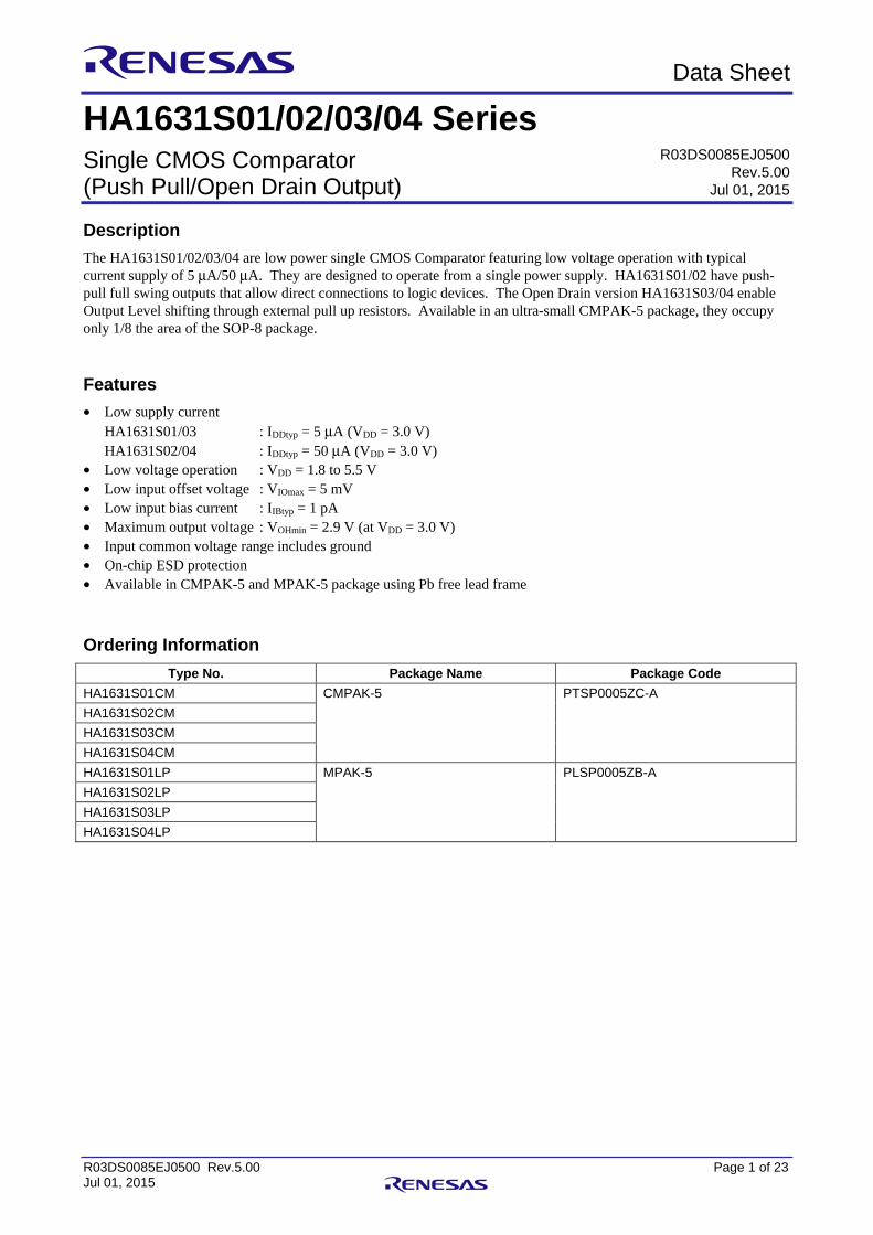
R03DS0085EJ0500 Rev.5.00 Page 1 of 23 Jul 01, 2015
Preliminary Data Sheet
HA1631S01/02/03/04 Series Single CMOS Comparator (Push Pull/Open Drain Output)
Description
The HA1631S01/02/03/04 are low power single CMOS Comparator featuring low voltage operation with typical current supply of 5 μA/50 μA. They are designed to operate from a single power supply. HA1631S01/02 have push-pull full swing outputs that allow direct connections to logic devices. The Open Drain version HA1631S03/04 enable Output Level shifting through external pull up resistors. Available in an ultra-small CMPAK-5 package, they occupy only 1/8 the area of the SOP-8 package.
Features
• Low supply current HA1631S01/03 : IDDtyp = 5 μA (VDD = 3.0 V) HA1631S02/04 : IDDtyp = 50 μA (VDD = 3.0 V)
• Low voltage operation : VDD = 1.8 to 5.5 V • Low input offset voltage : VIOmax = 5 mV • Low input bias current : IIBtyp = 1 pA • Maximum output voltage : VOHmin = 2.9 V (at VDD = 3.0 V) • Input common voltage range includes ground • On-chip ESD protection • Available in CMPAK-5 and MPAK-5 package using Pb free lead frame
Ordering Information
Type No. Package Name Package Code
HA1631S01CM CMPAK-5 PTSP0005ZC-A
HA1631S02CM
HA1631S03CM
HA1631S04CM
HA1631S01LP MPAK-5 PLSP0005ZB-A
HA1631S02LP
HA1631S03LP
HA1631S04LP
R03DS0085EJ0500Rev.5.00
Jul 01, 2015
HA1631S01/02/03/04 Series
R03DS0085EJ0500 Rev.5.00 Page 2 of 23 Jul 01, 2015
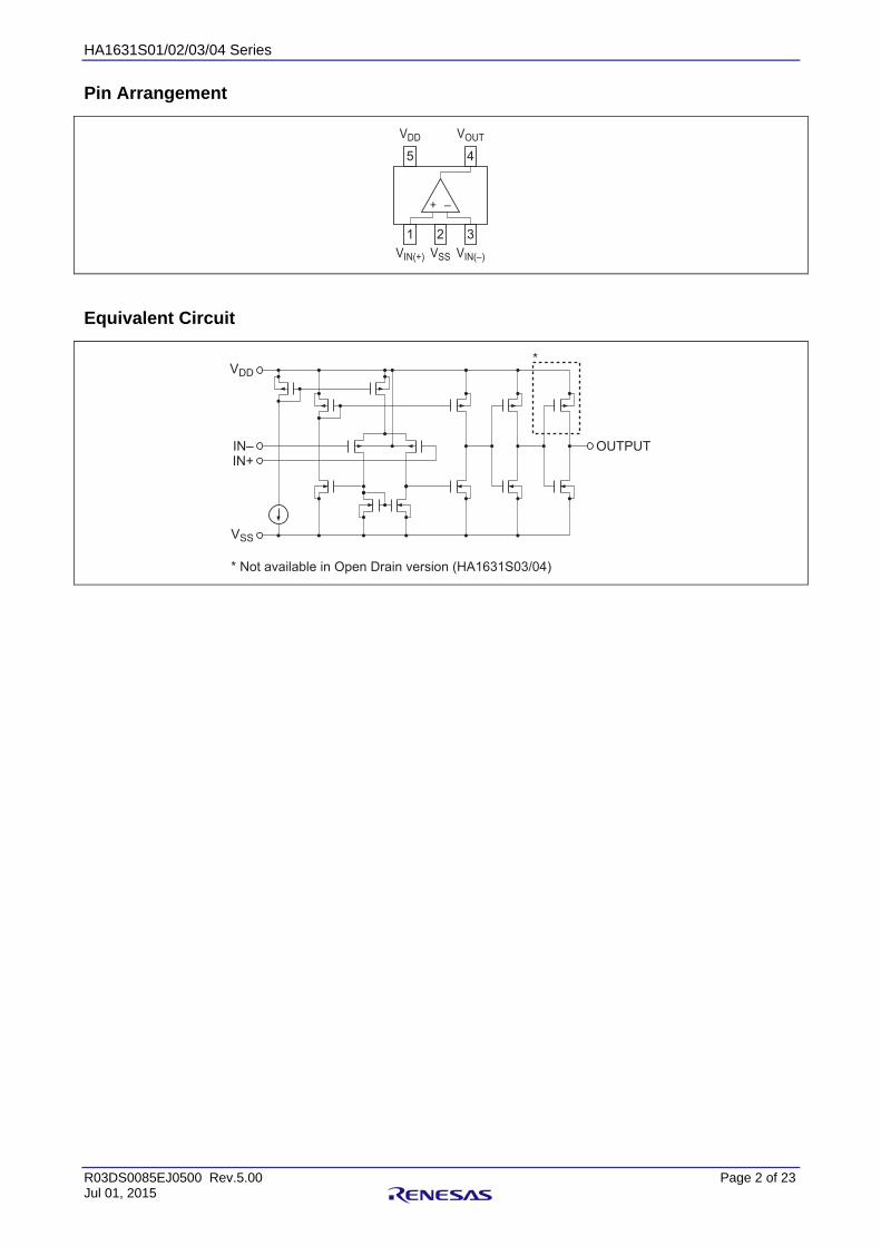
Pin Arrangement
VIN(+)
1
VSS
2
VIN(–)
VDD VOUT
3
5 4
+ –
Equivalent Circuit
VDD
IN– OUTPUT
* Not available in Open Drain version (HA1631S03/04)
*
IN+
VSS
HA1631S01/02/03/04 Series
R03DS0085EJ0500 Rev.5.00 Page 3 of 23 Jul 01, 2015
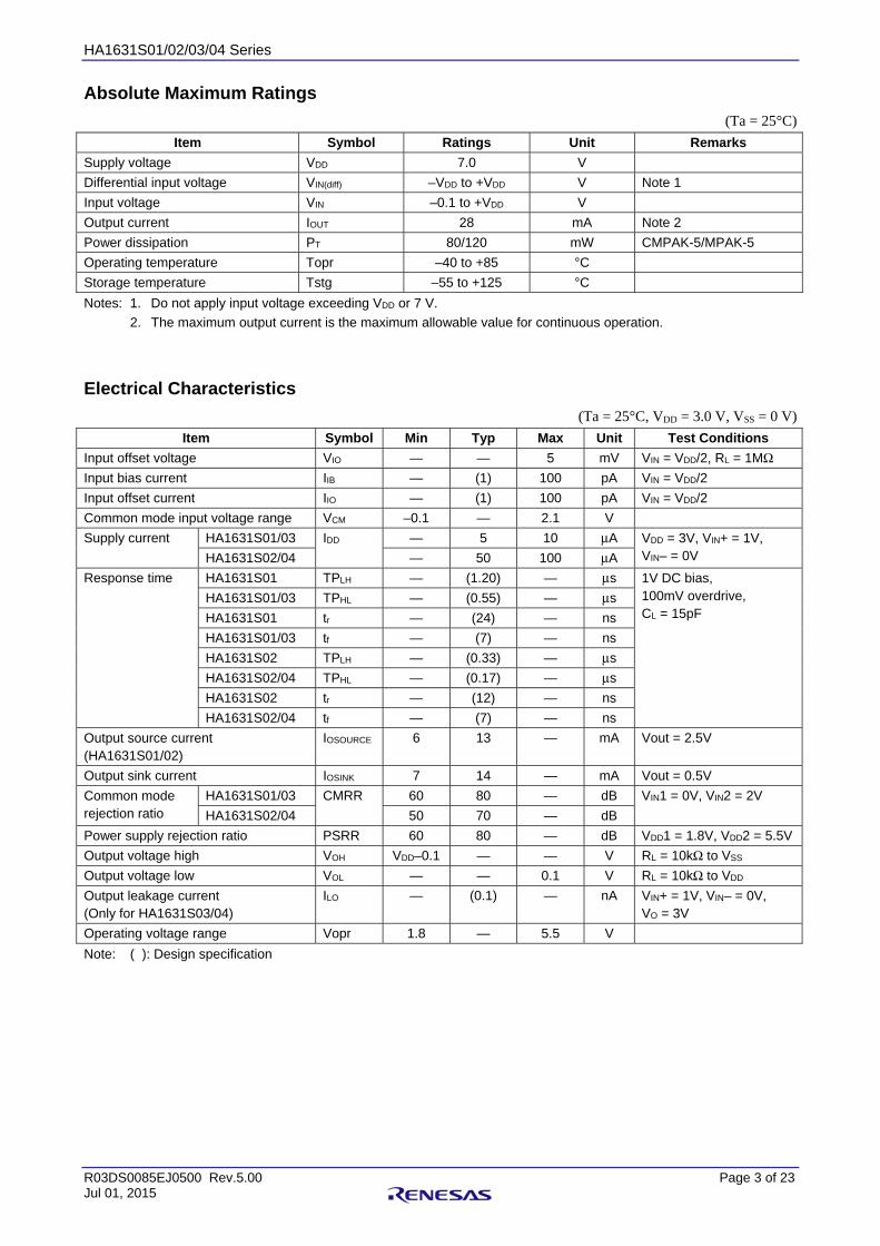
Absolute Maximum Ratings
(Ta = 25°C)
Item Symbol Ratings Unit Remarks
Supply voltage VDD 7.0 V
Differential input voltage VIN(diff) –VDD to +VDD V Note 1
Input voltage VIN –0.1 to +VDD V
Output current IOUT 28 mA Note 2
Power dissipation PT 80/120 mW CMPAK-5/MPAK-5
Operating temperature Topr –40 to +85 °C
Storage temperature Tstg –55 to +125 °C
Notes: 1. Do not apply input voltage exceeding VDD or 7 V.
2. The maximum output current is the maximum allowable value for continuous operation.
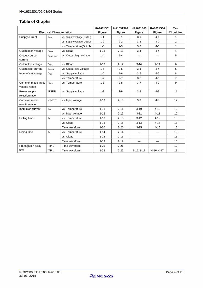
Electrical Characteristics
(Ta = 25°C, VDD = 3.0 V, VSS = 0 V)
Item Symbol Min Typ Max Unit Test Conditions
Input offset voltage VIO — — 5 mV VIN = VDD/2, RL = 1MΩ
Input bias current IIB — (1) 100 pA VIN = VDD/2
Input offset current IIO — (1) 100 pA VIN = VDD/2
Common mode input voltage range VCM –0.1 — 2.1 V
Supply current HA1631S01/03 IDD — 5 10 μA VDD = 3V, VIN+ = 1V, VIN– = 0V HA1631S02/04 — 50 100 μA
Response time HA1631S01 TPLH — (1.20) — μs 1V DC bias, 100mV overdrive, CL = 15pF
HA1631S01/03 TPHL — (0.55) — μs
HA1631S01 tr — (24) — ns
HA1631S01/03 tf — (7) — ns
HA1631S02 TPLH — (0.33) — μs
HA1631S02/04 TPHL — (0.17) — μs
HA1631S02 tr — (12) — ns
HA1631S02/04 tf — (7) — ns
Output source current (HA1631S01/02)
IOSOURCE 6 13 — mA Vout = 2.5V
Output sink current IOSINK 7 14 — mA Vout = 0.5V
Common mode rejection ratio
HA1631S01/03 CMRR 60 80 — dB VIN1 = 0V, VIN2 = 2V
HA1631S02/04 50 70 — dB
Power supply rejection ratio PSRR 60 80 — dB VDD1 = 1.8V, VDD2 = 5.5V
Output voltage high VOH VDD–0.1 — — V RL = 10kΩ to VSS
Output voltage low VOL — — 0.1 V RL = 10kΩ to VDD
Output leakage current (Only for HA1631S03/04)
ILO — (0.1) — nA VIN+ = 1V, VIN– = 0V, VO = 3V
Operating voltage range Vopr 1.8 — 5.5 V
Note: ( ): Design specification
HA1631S01/02/03/04 Series
R03DS0085EJ0500 Rev.5.00 Page 4 of 23 Jul 01, 2015
Table of Graphs
Electrical Characteristics
HA1631S01
Figure
HA1631S02
Figure
HA1631S03
Figure
HA1631S04
Figure
Test
Circuit No.
Supply current IDD vs. Supply voltage(Out H) 1-1 2-1 3-1 4-1 1
vs. Supply voltage(Out L) 1-2 2-2 3-2 4-2 2
vs. Temperature(Out H) 1-3 2-3 3-3 4-3 1
Output high voltage VOH vs. Rload 1-18 2-18 3-4 4-4 4
Output source
current
IOSOURCE vs. Output high voltage 1-4 2-4 — — 5
Output low voltage VOL vs. Rload 1-17 2-17 3-14 4-14 6
Output sink current IOSINK vs. Output low voltage 1-5 2-5 3-4 4-4 5
Input offset voltage VIO vs. Supply voltage 1-6 2-6 3-5 4-5 8
vs. Temperature 1-7 2-7 3-6 4-6 7
Common mode input
voltage range
VCM vs. Temperature 1-8 2-8 3-7 4-7 9
Power supply
rejection ratio
PSRR vs. Supply voltage 1-9 2-9 3-8 4-8 11
Common mode
rejection ratio
CMRR vs. Input voltage 1-10 2-10 3-9 4-9 12
Input bias current IIB vs. Temperature 1-11 2-11 3-10 4-10 10
vs. Input voltage 1-12 2-12 3-11 4-11 10
Falling time tf vs. Temperature 1-13 2-13 3-12 4-12 13
vs. Cload 1-15 2-15 3-13 4-13 13
Time waveform 1-20 2-20 3-15 4-15 13
Rising time tr vs. Temperature 1-14 2-14 — — 13
vs. Cload 1-16 2-16 — — 13
Time waveform 1-19 2-19 — — 13
Propagation delay
time
TPLH Time waveform 1-21 2-21 — — 13
TPHL Time waveform 1-22 2-22 3-16, 3-17 4-16, 4-17 13
HA1631S01/02/03/04 Series
R03DS0085EJ0500 Rev.5.00 Page 5 of 23 Jul 01, 2015
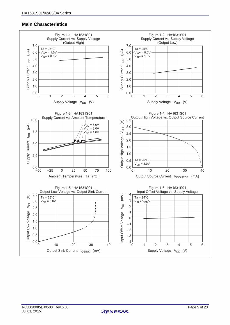
Main Characteristics
7.0
0.00 1 2 3
Supply Voltage VDD (V)
Figure 1-1 HA1631S01Supply Current vs. Supply Voltage
(Output High)
Figure 1-3 HA1631S01
Supply Current vs. Ambient Temperature
Figure 1-2 HA1631S01Supply Current vs. Supply Voltage
(Output Low)
Figure 1-4 HA1631S01Output High Voltage vs. Output Source Current
4 5 6
–50 –25 0 25
Ambient Temperature Ta (°C)
50 75 100
0 1 2 3
Supply Voltage VDD (V)
4 5 6
0 10 20
Output Source Current IOSOURCE (mA)
30 40
Figure 1-5 HA1631S01Output Low Voltage vs. Output Sink Current
0 10 20
Output Sink Current IOSINK (mA)
30 40
1.0
2.0
3.0
Supply
Curr
ent I D
D (μ
A)
Supply
Curr
ent I D
D (μ
A)
4.0
5.0
6.0
10.0
0.0
2.5
5.0
7.5
7.0
0.0
1.0
2.0
3.0
Supply
Curr
ent I D
D (μ
A)
4.0
5.0
6.0
3.5
0.0
0.5
1.0
1.5
Outp
ut H
igh V
oltage V
OH
(
V)
2.0
2.5
3.0
3.5
0.0
0.5
1.0
1.5
Outp
ut Low
Voltage V
OL (
V)
2.0
2.5
3.0
Ta = 25°C
VIN+ = 1.0V
VIN– = 0.0V
VDD = 5.0V
VDD = 3.0V
VDD = 1.8V
Ta = 25°C
VIN+ = 0.0V
VIN– = 1.0V
Ta = 25°C
VDD = 3.0V
Ta = 25°C
VDD = 3.0V
4
–40 1 2 3
Supply Voltage VDD (V)
Figure 1-6 HA1631S01Input Offset Voltage vs. Supply Voltage
4 5 6
–3
–2
–1
0
Input O
ffset V
oltage V
IO (
mV
)
1
2
3Ta = 25°C
VIN = VDD/2
HA1631S01/02/03/04 Series
R03DS0085EJ0500 Rev.5.00 Page 6 of 23 Jul 01, 2015
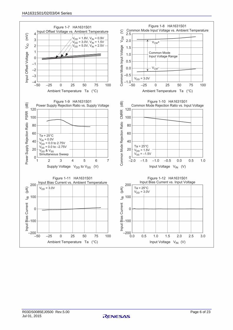
Figure 1-7 HA1631S01
Input Offset Voltage vs. Ambient Temperature4
–4
–3
–2
–1
0
Inp
ut
Off
se
t V
olta
ge
V
IO (
mV
)
1
2
3
–50 –25 0 25
Ambient Temperature Ta (°C)
50 75 100
VDD = 1.8V, VIN = 0.9V
VDD = 3.0V, VIN = 1.5V
VDD = 5.0V, VIN = 2.5V
–50 –25 0 25 50 75 100
Figure 1-11 HA1631S01
Input Bias Current vs. Ambient Temperature200
–200
–100
0
Inp
ut
Bia
s C
urr
en
t
I IB (
pA
)
100
Ambient Temperature Ta (°C)
VDD = 3.0V
Supply Voltage VDD to VSS (V)
Figure 1-9 HA1631S01Power Supply Rejection Ratio vs. Supply Voltage
1 2 3 4 5 6 7
120
0
20
40
60
Pow
er
Supply
Reje
ctio
n R
atio
P
SR
R (
dB
)
80
100
Ta = 25°C
VIN = 0.0V
VDD = 0.0 to 2.75V
VSS = 0.0 to –2.75V
VDD & VSS
Simultaneous Sweep
Figure 1-10 HA1631S01Common Mode Rejection Ratio vs. Input Voltage
–2.0 –1.5 –1.0 0.0–0.5
Input Voltage VIN (V)
0.5 1.0
120
0
20
40
60
80
100C
om
mon M
ode R
eje
ctio
n R
atio
C
MR
R (
dB
)
Ta = 25°C
VDD = 1.5V
VSS = –1.5V
–50 –25 0 25 50 75 100
Figure 1-8 HA1631S01
Common Mode Input Voltage vs. Ambient Temperature
Com
mon M
ode Input V
olta
ge V
CM
(
V)
2.5
–1.0
–0.5
0.0
0.5
1.0
1.5
2.0
Ambient Temperature Ta (°C)
VCM+
VCM–
VDD = 3.0V
Common ModeInput Voltage Range
0.0 0.5 1.0 1.5
Input Voltage VIN (V)
2.0 2.5 3.0
Figure 1-12 HA1631S01Input Bias Current vs. Input Voltage
200
–200
–100
0
Inp
ut
Bia
s C
urr
en
t
I IB (
pA
)
100
Ta = 25°C
VDD = 3.0V
HA1631S01/02/03/04 Series
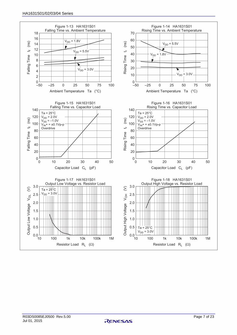
R03DS0085EJ0500 Rev.5.00 Page 7 of 23 Jul 01, 2015
Capacitor Load CL (pF)
Figure 1-15 HA1631S01Falling Time vs. Capacitor Load
0 10 20 30 40 50
Fa
llin
g T
ime
t
f
(ns)
140
0
20
40
60
80
100
120Ta = 25°C
VDD = 2.0V
VSS = –1.0V
VIN+ = ±0.1Vp-p
Overdrive
Figure 1-13 HA1631S01Falling Time vs. Ambient Temperature
18
0
2
4
6
8
Fa
llin
g T
ime
t
f
(ns)
10
12
14
16
–50 –25 0 25
Ambient Temperature Ta (°C)
50 75 100
VDD = 1.8V
VDD = 5.5V
VDD = 3.0V
Figure 1-14 HA1631S01Rising Time vs. Ambient Temperature
–50 –25 0 25 50 75 100
Ris
ing
Tim
e
tr
(ns)
70
0
10
20
30
40
50
60
Ambient Temperature Ta (°C)
VDD = 1.8V
VDD = 5.5V
VDD = 3.0V
Capacitor Load CL (pF)
Figure 1-16 HA1631S01Rising Time vs. Capacitor Load
0 10 20 30 40 50
Ris
ing
Tim
e
tr
(ns)
140
0
20
40
60
80
100
120Ta = 25°C
VDD = 2.0V
VSS = –1.0V
VIN+ = ±0.1Vp-p
Overdrive
Resistor Load RL (Ω)
Figure 1-17 HA1631S01Output Low Voltage vs. Resistor Load
10 100 1k 10k 1M100k
Ou
tpu
t L
ow
Vo
lta
ge
V
OL
(V
) 3.0
0.0
0.5
1.0
1.5
2.0
2.5
Ta = 25°C
VDD = 3.0V
10 100 1k 10k 1M100k
Resistor Load RL (Ω)
Figure 1-18 HA1631S01Output High Voltage vs. Resistor Load
Ou
tpu
t H
igh
Vo
lta
ge
V
OH
(
V) 3.0
0.0
0.5
1.0
1.5
2.0
2.5
Ta = 25°C
VDD = 3.0V
HA1631S01/02/03/04 Series
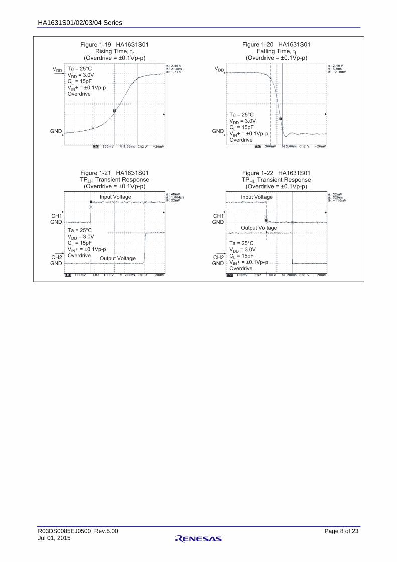
R03DS0085EJ0500 Rev.5.00 Page 8 of 23 Jul 01, 2015
VDD
GND
Ta = 25°C
VDD = 3.0V
CL = 15pF
VIN+ = ±0.1Vp-p
Overdrive
Figure 1-19 HA1631S01Rising Time, tr
(Overdrive = ±0.1Vp-p)
Figure 1-20 HA1631S01Falling Time, tf
(Overdrive = ±0.1Vp-p)
VDD
GND
Ta = 25°C
VDD = 3.0V
CL = 15pF
VIN+ = ±0.1Vp-p
Overdrive
Ta = 25°C
VDD = 3.0V
CL = 15pF
VIN+ = ±0.1Vp-p
Overdrive
Figure 1-21 HA1631S01TPLH Transient Response
(Overdrive = ±0.1Vp-p)
CH1GND
CH2GND
Input Voltage
Output Voltage
Ta = 25°C
VDD = 3.0V
CL = 15pF
VIN+ = ±0.1Vp-p
Overdrive
Figure 1-22 HA1631S01TPHL Transient Response
(Overdrive = ±0.1Vp-p)
CH1GND
CH2GND
Input Voltage
Output Voltage
HA1631S01/02/03/04 Series
R03DS0085EJ0500 Rev.5.00 Page 9 of 23 Jul 01, 2015
70
00 1 2 3 4 5 6
–50 –25 0 25 50 75 100
0 1 2 3 4 5 6
0 10 20 30 40
0 10 20 30 40
10
20
30
40
50
60
100
0
25
50
75
70
0
10
20
30
40
50
60
3.5
0.0
0.5
1.0
1.5
2.0
2.5
3.0
3.5
0.0
0.5
1.0
1.5
2.0
2.5
3.0
Ta = 25°C
VIN+ = 1.0V
VIN– = 0.0V
VDD = 5.0V
VDD = 3.0V
VDD = 1.8V
Ta = 25°C
VIN+ = 0.0V
VIN– = 1.0V
Ta = 25°C
VDD = 3.0V
Ta = 25°C
VDD = 3.0V
Supply Voltage VDD (V) Supply Voltage VDD (V)
Figure 2-1 HA1631S02Supply Current vs. Supply Voltage
(Output High)
Figure 2-3 HA1631S02
Supply Current vs. Ambient Temperature
Figure 2-2 HA1631S02Supply Current vs. Supply Voltage
(Output Low)
Figure 2-4 HA1631S02Output High Voltage vs. Output Source Current
Ambient Temperature Ta (°C) Output Source Current IOSOURCE (mA)
Figure 2-5 HA1631S02Output Low Voltage vs. Output Sink Current
Output Sink Current IOSINK (mA)
Su
pp
ly C
urr
en
t I D
D (μ
A)
Su
pp
ly C
urr
en
t I D
D (μ
A)
Su
pp
ly C
urr
en
t I D
D (μ
A)
Ou
tpu
t H
igh
Vo
lta
ge
V
OH
(
V)
Ou
tpu
t L
ow
Vo
lta
ge
V
OL (
V) 4
–41 2 3 4 5 6
–3
–2
–1
0
1
2
3Ta = 25°C
VIN = VDD/2
Supply Voltage VDD (V)
Figure 2-6 HA1631S02Input Offset Voltage vs. Supply Voltage
Input O
ffset V
oltage V
IO (
mV
)
HA1631S01/02/03/04 Series
R03DS0085EJ0500 Rev.5.00 Page 10 of 23 Jul 01, 2015
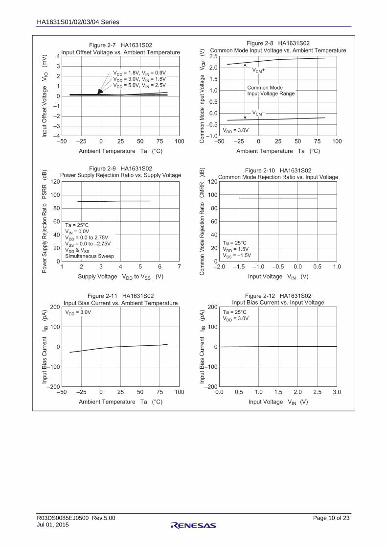
1 2 3 4 5 6 7
120
0
20
40
60
80
100
Ta = 25°C
VIN = 0.0V
VDD = 0.0 to 2.75V
VSS = 0.0 to –2.75V
VDD & VSS
Simultaneous Sweep
Supply Voltage VDD to VSS (V)
Figure 2-9 HA1631S02Power Supply Rejection Ratio vs. Supply Voltage
Pow
er
Supply
Reje
ctio
n R
atio
P
SR
R (
dB
)
–2.0 –1.5 –1.0 0.0–0.5 0.5 1.0
120
0
20
40
60
80
100
Ta = 25°C
VDD = 1.5V
VSS = –1.5V
Figure 2-10 HA1631S02Common Mode Rejection Ratio vs. Input Voltage
Input Voltage VIN (V)
Com
mon M
ode R
eje
ctio
n R
atio
C
MR
R (
dB
)
4
–4
–3
–2
–1
0
1
2
3
–50 –25 0 25 50 75 100
VDD = 1.8V, VIN = 0.9V
VDD = 3.0V, VIN = 1.5V
VDD = 5.0V, VIN = 2.5V
Figure 2-7 HA1631S02
Input Offset Voltage vs. Ambient Temperature
Inp
ut
Off
se
t V
olta
ge
V
IO (
mV
)
Ambient Temperature Ta (°C)
–50 –25 0 25 50 75 100
200
–200
–100
0
100
VDD = 3.0V
Figure 2-11 HA1631S02
Input Bias Current vs. Ambient Temperature
Inp
ut
Bia
s C
urr
en
t
I IB (
pA
)
Ambient Temperature Ta (°C)
–50 –25 0 25 50 75 100
2.5
–1.0
–0.5
0.0
0.5
1.0
1.5
2.0 VCM+
VCM–
VDD = 3.0V
Figure 2-8 HA1631S02
Common Mode Input Voltage vs. Ambient Temperature
Com
mon M
ode I
nput
Volta
ge
VC
M (
V)
Ambient Temperature Ta (°C)
Common ModeInput Voltage Range
0.0 0.5 1.0 1.5 2.0 2.5 3.0
200
–200
–100
0
100
Ta = 25°C
VDD = 3.0V
Input Voltage VIN (V)
Figure 2-12 HA1631S02Input Bias Current vs. Input Voltage
Inp
ut
Bia
s C
urr
en
t
I IB (
pA
)
HA1631S01/02/03/04 Series
R03DS0085EJ0500 Rev.5.00 Page 11 of 23 Jul 01, 2015
0 10 20 30 40 50
120
0
20
40
60
80
100
Ta = 25°C
VDD = 2.0V
VSS = –1.0V
VIN+ = ±0.1Vp-p
Overdrive
Capacitor Load CL (pF)
Figure 2-15 HA1631S02Falling Time vs. Capacitor Load
Fa
llin
g T
ime
t
f (n
s)
20
0
2
4
6
8
10
12
14
16
18
–50 –25 0 25 50 75 100
VDD = 1.8V
VDD = 5.5V
VDD = 3.0V
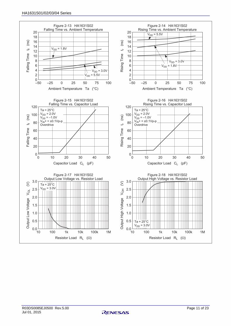
Figure 2-13 HA1631S02Falling Time vs. Ambient Temperature
Fa
llin
g T
ime
t
f (n
s)
Ambient Temperature Ta (°C)
–50 –25 0 25 50 75 100
20
0
2
4
6
8
10
12
14
16
18
VDD = 1.8V
VDD = 5.5V
VDD = 3.0V
Figure 2-14 HA1631S02Rising Time vs. Ambient Temperature
Ris
ing
Tim
e
tr (n
s)
Ambient Temperature Ta (°C)
0 10 20 30 40 50
120
0
20
40
60
80
100
Ta = 25°C
VDD = 2.0V
VSS = –1.0V
VIN+ = ±0.1Vp-p
Overdrive
Capacitor Load CL (pF)
Figure 2-16 HA1631S02Rising Time vs. Capacitor Load
Ris
ing
Tim
e
tr (n
s)
3.0
0.0
0.5
1.0
1.5
2.0
2.5
Ta = 25°C
VDD = 3.0V
Resistor Load RL (Ω)
Figure 2-17 HA1631S02Output Low Voltage vs. Resistor Load
Ou
tpu
t L
ow
Vo
lta
ge
V
OL (
V) 3.0
0.0
0.5
1.0
1.5
2.0
2.5
Ta = 25°C
VDD = 3.0V
Resistor Load RL (Ω)
Figure 2-18 HA1631S02Output High Voltage vs. Resistor Load
Ou
tpu
t H
igh
Vo
lta
ge
V
OH
(
V)
10 100 1k 10k 1M100k 10 100 1k 10k 1M100k
HA1631S01/02/03/04 Series
R03DS0085EJ0500 Rev.5.00 Page 12 of 23 Jul 01, 2015
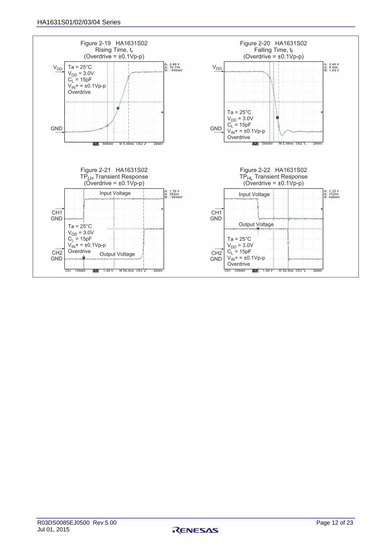
Ta = 25°C
VDD = 3.0V
CL = 15pF
VIN+ = ±0.1Vp-p
Overdrive
CH1GND
CH2GND
Figure 2-22 HA1631S02TPHL Transient Response
(Overdrive = ±0.1Vp-p)
Input Voltage
Output Voltage
VDD
GND
Ta = 25°C
VDD = 3.0V
CL = 15pF
VIN+ = ±0.1Vp-p
Overdrive
Figure 2-19 HA1631S02Rising Time, tr
(Overdrive = ±0.1Vp-p)
VDD
GND
Ta = 25°C
VDD = 3.0V
CL = 15pF
VIN+ = ±0.1Vp-p
Overdrive
Figure 2-20 HA1631S02Falling Time, tf
(Overdrive = ±0.1Vp-p)
Ta = 25°C
VDD = 3.0V
CL = 15pF
VIN+ = ±0.1Vp-p
Overdrive
CH1GND
CH2GND
Figure 2-21 HA1631S02TPLH Transient Response
(Overdrive = ±0.1Vp-p)
Input Voltage
Output Voltage
HA1631S01/02/03/04 Series
R03DS0085EJ0500 Rev.5.00 Page 13 of 23 Jul 01, 2015
7.0
0.00 1 2 3 4 5 6
–50 –25 0 25 50 75 100
0 1 2 3 4 5 6
1.0
2.0
3.0
4.0
5.0
6.0
10.0
0.0
2.5
5.0
7.5
7.0
0.0
1.0
2.0
3.0
4.0
5.0
6.0Ta = 25°C
VIN+ = 1.0V
VIN– = 0.0V
VDD = 5.0V
VDD = 3.0V
VDD = 1.8V
Ta = 25°C
VIN+ = 0.0V
VIN– = 1.0V
0 10 20 30 40
3.5
0.0
0.5
1.0
1.5
2.0
2.5
3.0Ta = 25°C
VDD = 3.0V
Supply Voltage VDD (V) Supply Voltage VDD (V)
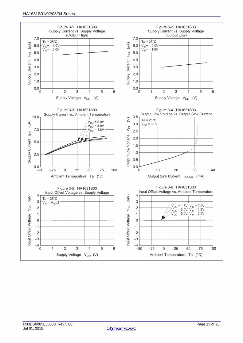
Figure 3-1 HA1631S03Supply Current vs. Supply Voltage
(Output High)
Figure 3-3 HA1631S03
Supply Current vs. Ambient Temperature
Figure 3-2 HA1631S03Supply Current vs. Supply Voltage
(Output Low)
Ambient Temperature Ta (°C)
Figure 3-4 HA1631S03Output Low Voltage vs. Output Sink Current
Output Sink Current IOSINK (mA)
Su
pp
ly C
urr
en
t I D
D (μ
A)
Su
pp
ly C
urr
en
t I D
D (μ
A)
Su
pp
ly C
urr
en
t I D
D (μ
A)
Ou
tpu
t L
ow
Vo
lta
ge
V
OL (
V)
4
–40 1 2 3 4 5 6
–3
–2
–1
0
1
2
3Ta = 25°C
VIN = VDD/2
Supply Voltage VDD (V)
Figure 3-5 HA1631S03Input Offset Voltage vs. Supply Voltage
Input O
ffset V
oltage V
IO (
mV
) 4
–4
–3
–2
–1
0
1
2
3
–50 –25 0 25 50 75 100
VDD = 1.8V, VIN = 0.9V
VDD = 3.0V, VIN = 1.5V
VDD = 5.0V, VIN = 2.5V
Figure 3-6 HA1631S03
Input Offset Voltage vs. Ambient Temperature
Input O
ffset V
oltage V
IO (
mV
)
Ambient Temperature Ta (°C)
HA1631S01/02/03/04 Series
R03DS0085EJ0500 Rev.5.00 Page 14 of 23 Jul 01, 2015
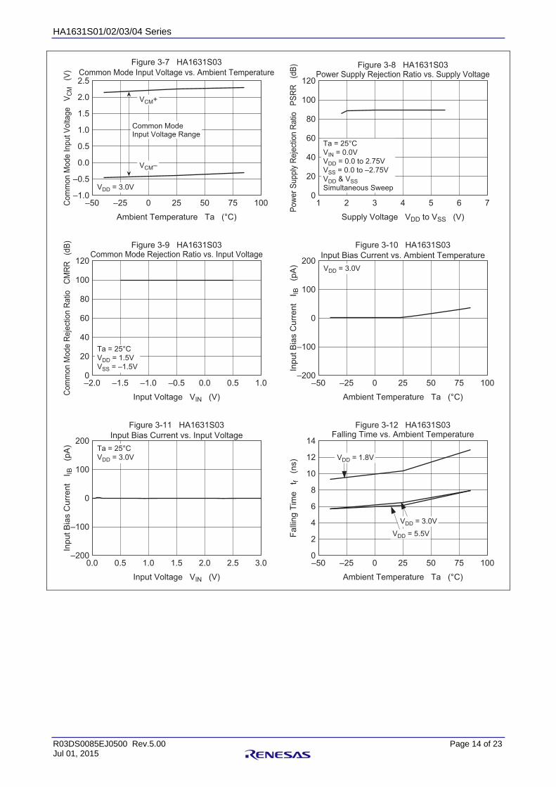
1 2 3 4 5 6 7
120
0
20
40
60
80
100
Ta = 25°C
VIN = 0.0V
VDD = 0.0 to 2.75V
VSS = 0.0 to –2.75V
VDD & VSS
Simultaneous Sweep
Supply Voltage VDD to VSS (V)
Figure 3-8 HA1631S03Power Supply Rejection Ratio vs. Supply Voltage
Pow
er
Supply
Reje
ctio
n R
atio
P
SR
R (
dB
)
–2.0 –1.5 –1.0 0.0–0.5 0.5 1.0
120
0
20
40
60
80
100
Ta = 25°C
VDD = 1.5V
VSS = –1.5V
Figure 3-9 HA1631S03Common Mode Rejection Ratio vs. Input Voltage
Input Voltage VIN (V)
Com
mon M
ode R
eje
ctio
n R
atio
C
MR
R (
dB
)
0.0 0.5 1.0 1.5 2.0 2.5 3.0
200
–200
–100
0
100
Ta = 25°C
VDD = 3.0V
Input Voltage VIN (V)
Figure 3-11 HA1631S03
Input Bias Current vs. Input Voltage
Inp
ut
Bia
s C
urr
en
t
I IB (
pA
)
–50 –25 0 25 50 75 100
200
–200
–100
0
100
VDD = 3.0V
Figure 3-10 HA1631S03
Input Bias Current vs. Ambient Temperature
Inp
ut
Bia
s C
urr
en
t
I IB (
pA
)
Ambient Temperature Ta (°C)
–50 –25 0 25 50 75 100
2.5
–1.0
–0.5
0.0
0.5
1.0
1.5
2.0 VCM+
VCM–
VDD = 3.0V
Figure 3-7 HA1631S03
Common Mode Input Voltage vs. Ambient TemperatureC
om
mon M
ode I
nput
Volta
ge
VC
M (
V)
Ambient Temperature Ta (°C)
Common ModeInput Voltage Range
14
0
2
4
6
8
10
12
–50 –25 0 25 50 75 100
VDD = 1.8V
VDD = 5.5V
VDD = 3.0V
Figure 3-12 HA1631S03Falling Time vs. Ambient Temperature
Fa
llin
g T
ime
t
f (n
s)
Ambient Temperature Ta (°C)
HA1631S01/02/03/04 Series
R03DS0085EJ0500 Rev.5.00 Page 15 of 23 Jul 01, 2015
Ta = 25°C
VDD = 3.0V
CL = 15pF
VIN+ = ±0.1Vp-p
Overdrive
CH1GND
CH2GND
0 10 20 30 40 50
45
0
5
10
1520
15
25
30
35
40Ta = 25°C
VDD = 2.0V
VSS = –1.0V
VIN+ = ±0.1Vp-p
Overdrive
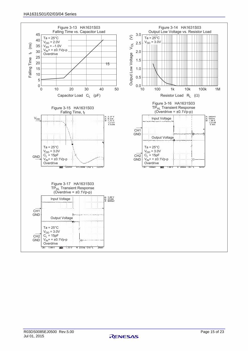
Figure 3-13 HA1631S03Falling Time vs. Capacitor Load
Fa
llin
g T
ime
t
f (n
s)
Capacitor Load CL (pF)
VDD
GND
Ta = 25°C
VDD = 3.0V
CL = 15pF
VIN+ = ±0.1Vp-p
Overdrive
Figure 3-15 HA1631S03Falling Time, tf
Figure 3-17 HA1631S03TPHL Transient Response
(Overdrive = ±0.1Vp-p)
Ta = 25°C
VDD = 3.0V
CL = 15pF
VIN+ = ±0.1Vp-p
Overdrive
CH1GND
CH2GND
Figure 3-16 HA1631S03TPHL Transient Response
(Overdrive = ±0.1Vp-p)
Input Voltage
Output Voltage
Input Voltage
Output Voltage
3.0
0.0
0.5
1.0
1.5
2.0
2.5
Ta = 25°C
VDD = 3.0V
Resistor Load RL (Ω)
Figure 3-14 HA1631S03Output Low Voltage vs. Resistor Load
Ou
tpu
t L
ow
Vo
lta
ge
V
OL (
V)
10 100 1k 10k 1M100k
HA1631S01/02/03/04 Series
R03DS0085EJ0500 Rev.5.00 Page 16 of 23 Jul 01, 2015
70
00 1 2 3 4 5 6
–50 –25 0 25 50 75 100
0 1 2 3 4 5 6
10
20
30
40
50
60
100
0
25
50
75
70
0
10
20
30
40
50
60Ta = 25°C
VIN+ = 1.0V
VIN– = 0.0V
VDD = 5.0V
VDD = 3.0V
VDD = 1.8V
Ta = 25°C
VIN+ = 0.0V
VIN– = 1.0V
0 10 20 30 40
3.5
0.0
0.5
1.0
1.5
2.0
2.5
3.0Ta = 25°C
VDD = 3.0V
Supply Voltage VDD (V) Supply Voltage VDD (V)
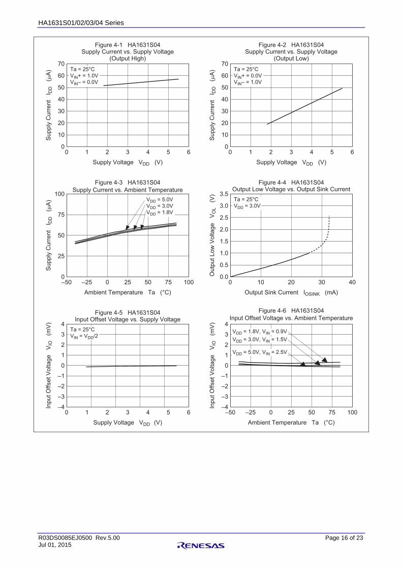
Figure 4-1 HA1631S04Supply Current vs. Supply Voltage
(Output High)
Figure 4-3 HA1631S04
Supply Current vs. Ambient Temperature
Figure 4-2 HA1631S04Supply Current vs. Supply Voltage
(Output Low)
Ambient Temperature Ta (°C)
Figure 4-4 HA1631S04Output Low Voltage vs. Output Sink Current
Output Sink Current IOSINK (mA)
Su
pp
ly C
urr
en
t I D
D (μ
A)
Su
pp
ly C
urr
en
t I D
D (μ
A)
Su
pp
ly C
urr
en
t I D
D (μ
A)
Ou
tpu
t L
ow
Vo
lta
ge
V
OL (
V)
4
–40 1 2 3 4 5 6
–3
–2
–1
0
1
2
3Ta = 25°C
VIN = VDD/2
Supply Voltage VDD (V)
Figure 4-5 HA1631S04Input Offset Voltage vs. Supply Voltage
Input O
ffset V
oltage V
IO (
mV
) 4
–4
–3
–2
–1
0
1
2
3
–50 –25 0 25 50 75 100
VDD = 5.0V, VIN = 2.5V
VDD = 3.0V, VIN = 1.5V
VDD = 1.8V, VIN = 0.9V
Figure 4-6 HA1631S04
Input Offset Voltage vs. Ambient Temperature
Input O
ffset V
oltage V
IO (
mV
)
Ambient Temperature Ta (°C)
HA1631S01/02/03/04 Series
R03DS0085EJ0500 Rev.5.00 Page 17 of 23 Jul 01, 2015
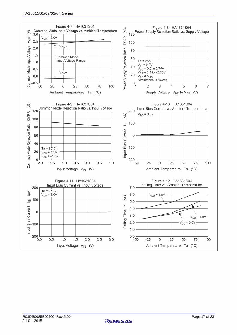
1 2 3 4 5 6 7
120
0
20
40
60
80
100
Ta = 25°C
VIN = 0.0V
VDD = 0.0 to 2.75V
VSS = 0.0 to –2.75V
VDD & VSS
Simultaneous Sweep
Supply Voltage VDD to VSS (V)
Figure 4-8 HA1631S04Power Supply Rejection Ratio vs. Supply Voltage
Pow
er
Supply
Reje
ctio
n R
atio
P
SR
R (
dB
)
–2.0 –1.5 –1.0 0.0–0.5 0.5 1.0
120
0
20
40
60
80
100
Ta = 25°C
VDD = 1.5V
VSS = –1.5V
Figure 4-9 HA1631S04Common Mode Rejection Ratio vs. Input Voltage
Input Voltage VIN (V)
Com
mon M
ode R
eje
ctio
n R
atio
C
MR
R (
dB
)
0.0 0.5 1.0 1.5 2.0 2.5 3.0
200
–200
–100
0
100
Ta = 25°C
VDD = 3.0V
Input Voltage VIN (V)
Figure 4-11 HA1631S04
Input Bias Current vs. Input Voltage
Inp
ut
Bia
s C
urr
en
t
I IB (
pA
)
–50 –25 0 25 50 75 100
200
–200
–100
0
100
VDD = 3.0V
Figure 4-10 HA1631S04
Input Bias Current vs. Ambient Temperature
Inp
ut
Bia
s C
urr
en
t
I IB (
pA
)
Ambient Temperature Ta (°C)
–50 –25 0 25 50 75 100
3.0
–0.5
0.0
0.5
1.0
1.5
2.0
2.5
VCM+
VCM–
VDD = 3.0V
Figure 4-7 HA1631S04
Common Mode Input Voltage vs. Ambient TemperatureC
om
mon M
ode I
nput
Volta
ge
VC
M (
V)
Ambient Temperature Ta (°C)
Common ModeInput Voltage Range
7.0
0.0
1.0
2.0
3.0
4.0
5.0
6.0
–50 –25 0 25 50 75 100
VDD = 1.8V
VDD = 5.5V
VDD = 3.0V
Figure 4-12 HA1631S04Falling Time vs. Ambient Temperature
Fa
llin
g T
ime
t
f (n
s)
Ambient Temperature Ta (°C)
HA1631S01/02/03/04 Series
R03DS0085EJ0500 Rev.5.00 Page 18 of 23 Jul 01, 2015
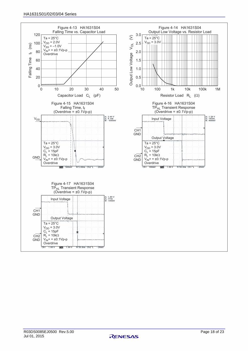
0 10 20 30 40 50
120
0
20
40
60
80
100
Ta = 25°C
VDD = 2.0V
VSS = –1.0V
VIN+ = ±0.1Vp-p
Overdrive
Capacitor Load CL (pF)
Figure 4-13 HA1631S04Falling Time vs. Capacitor Load
Fa
llin
g T
ime
t
f (n
s)
3.0
0.0
0.5
1.0
1.5
2.0
2.5
Ta = 25°C
VDD = 3.0V
Resistor Load RL (Ω)
Figure 4-14 HA1631S04Output Low Voltage vs. Resistor Load
Ou
tpu
t L
ow
Vo
lta
ge
V
OL (
V)
VDD
GND
Ta = 25°C
VDD = 3.0V
CL = 15pF
RL = 10kΩ
VIN+ = ±0.1Vp-p
Overdrive
Figure 4-15 HA1631S04Falling Time, tf
(Overdrive = ±0.1Vp-p)
CH1GND
CH2GND
Ta = 25°C
VDD = 3.0V
CL = 15pF
RL = 10kΩ
VIN+ = ±0.1Vp-p
Overdrive
Figure 4-16 HA1631S04TPHL Transient Response
(Overdrive = ±0.1Vp-p)
Input Voltage
Output Voltage
CH1GND
CH2GND
Ta = 25°C
VDD = 3.0V
CL = 15pF
RL = 10kΩ
VIN+ = ±0.1Vp-p
Overdrive
Figure 4-17 HA1631S04TPHL Transient Response
(Overdrive = ±0.1Vp-p)
Input Voltage
Output Voltage
10 100 1k 10k 1M100k
HA1631S01/02/03/04 Series
R03DS0085EJ0500 Rev.5.00 Page 19 of 23 Jul 01, 2015
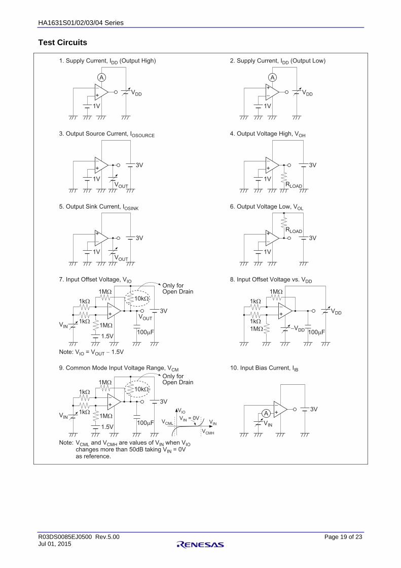
Test Circuits
−
+
A
1V
1. Supply Current, IDD (Output High)
VDD
−
+A
VIN
+
−
A
1V
2. Supply Current, IDD (Output Low)
VDD
VDD
−
+
1V
3. Output Source Current, IOSOURCE
3V
VOUT
−
+
1V
4. Output Voltage High, VOH
3V
RLOAD
+
−
1V
5. Output Sink Current, IOSINK
3V
VOUT
+
−
1V
6. Output Voltage Low, VOL
3V
3V
RLOAD
7. Input Offset Voltage, VIO 8. Input Offset Voltage vs. VDD
3V
Note: VIO = VOUT − 1.5V
VOUT
−
+
1.5V100μF
1MΩ1kΩ
1kΩ
VIN
1MΩ
10kΩ
Only forOpen Drain
−
+
100μF1MΩ
1kΩ
1kΩ
1MΩ
−VDD
9. Common Mode Input Voltage Range, VCM 10. Input Bias Current, IIB
3V
Note: VCML and VCMH are values of VIN when VIO
changes more than 50dB taking VIN = 0V as reference.
−
+
1.5V100μF
1MΩ1kΩ
1kΩ
VIN
1MΩ
10kΩ
Only forOpen Drain
VIO
VIN
VCMH
VIN = 0VVCML
HA1631S01/02/03/04 Series
R03DS0085EJ0500 Rev.5.00 Page 20 of 23 Jul 01, 2015
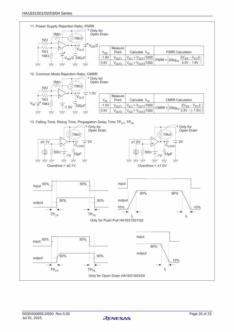
11. Power Supply Rejection Ratio, PSRR
VOUT
−
+
VOUT
100μF
1kΩ
1kΩ
100μF
1MΩ
10kΩ
Only forOpen Drain
1MΩ
1MΩ
VDD/2
−VDD/2
−1.5V
12. Common Mode Rejection Ratio, CMRR
1.5V−
+
1kΩ
1kΩ
VIN
1MΩ
10kΩ
Only forOpen Drain
CLOAD
15pF50Ω
±0.1V
−1V
13. Falling Time, Rising Time, Propagation Delay Time TPLH, TPHL
2V−
+
10kΩ
Only forOpen Drain
Overdrive = ±0.1V Overdrive = ±1.0V
−1.8V
5.5V
VOUT1
VOUT2
VIO1 = VOUT1/1000
VIO2 = VOUT2/1000
MeasurePointVDD Calculate VIO PSRR Calculation
PSRR = 20log10
|(VIO2 − VIO1)|
5.5V − 1.8V
−1.5V
0.5V
VOUT1
VOUT2
VIO1 = VOUT1/1000
VIO2 = VOUT2/1000
MeasurePointVIN Calculate VIO CMRR Calculation
CMRR = 20log10
|(VIO2 − VIO1)|
0.5V − (−1.5V)
CLOAD
15pF50Ω
±1.0V
−1V
2V−
+
10kΩ
Only forOpen Drain
50%
50% 50%
50%
10% 10%
10%
50%
TPLH
50% 50%
50%
90% 90%
90%
inputinput
output
output
input
input
output
output
TPLH TPHL
TPHL
Only for Push Pull HA1631S01/02
Only for Open Drain HA1631S03/04
tr tf
tf
HA1631S01/02/03/04 Series
R03DS0085EJ0500 Rev.5.00 Page 21 of 23 Jul 01, 2015
Mark Indication
(1) (2)
HA1631S01CMHA1631S02CMHA1631S03CMHA1631S04CM
HA1631S01LPHA1631S02LPHA1631S03LPHA1631S04LP
(1)0000
(2)ABCD
Trace Code
HA1631S01/02/03/04 Series
R03DS0085EJ0500 Rev.5.00 Page 22 of 23 Jul 01, 2015
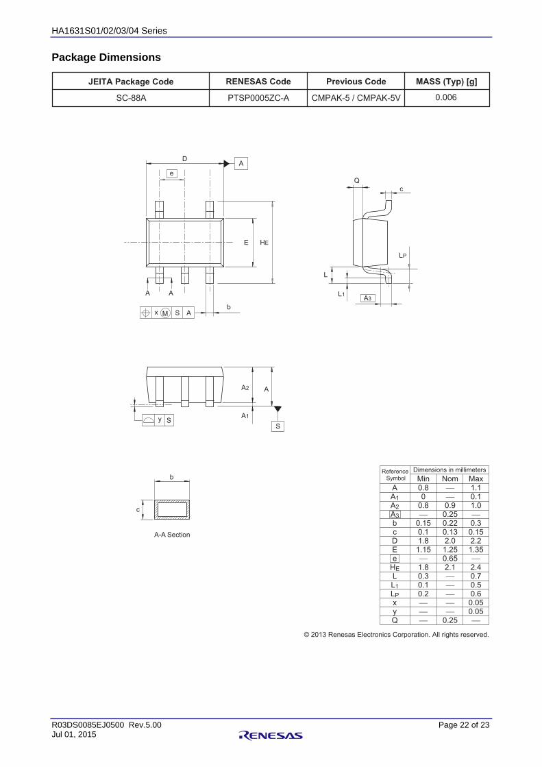
Package Dimensions
MASS (Typ) [g]
0.006
Previous CodeRENESAS Code
PTSP0005ZC-A CMPAK-5 / CMPAK-5V
JEITA Package Code
SC-88A
© 2013 Renesas Electronics Corporation. All rights reserved.
Dimensions in millimeters
AA1A2A3bc DEe
HELL1LPxyQ
0.80
0.8⎯
0.150.11.8 1.15⎯1.80.30.1 0.2⎯⎯⎯
Min NomReference
Symbol Max⎯⎯0.90.250.220.132.01.250.65 2.1⎯⎯⎯⎯⎯
0.25
1.10.11.0⎯0.30.152.2 1.35⎯2.40.70.50.60.050.05⎯
eA
E HE
L
L1
Qc
D
b
A AA3
LP
S
AA2
A1
ASMx
Sy
b
A-A Section
c
HA1631S01/02/03/04 Series
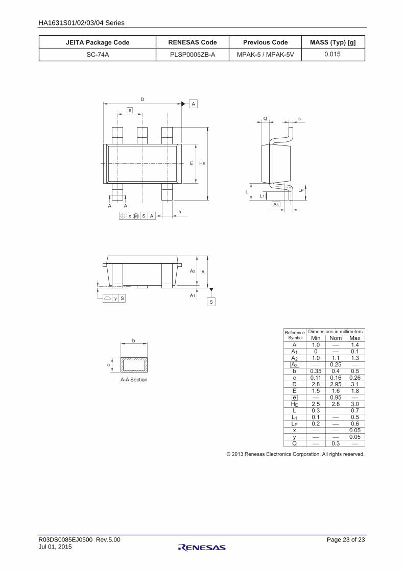
R03DS0085EJ0500 Rev.5.00 Page 23 of 23 Jul 01, 2015
MASS (Typ) [g]
0.015
Previous CodeRENESAS Code
PLSP0005ZB-A MPAK-5 / MPAK-5V
JEITA Package Code
SC-74A
© 2013 Renesas Electronics Corporation. All rights reserved.
Dimensions in millimeters
AA1A2A3bcDEe
HELL1LPxyQ
1.00
1.0⎯
0.350.112.81.5⎯2.50.30.10.2⎯⎯⎯
Min NomReference
Symbol Max⎯⎯1.10.250.40.162.951.60.952.8⎯⎯⎯⎯⎯0.3
1.40.11.3⎯0.50.263.11.8⎯3.00.70.50.60.050.05⎯
D
eA
Q c
A Ab
x S A
AA2
A1
M
E
L
HE
L1LP
A3
y SS
b
A-A Section
c
Notice1. Descriptions of circuits, software and other related information in this document are provided only to illustrate the operation of semiconductor products and application examples. You are fully responsible for
the incorporation of these circuits, software, and information in the design of your equipment. Renesas Electronics assumes no responsibility for any losses incurred by you or third parties arising from the
use of these circuits, software, or information.
2. Renesas Electronics has used reasonable care in preparing the information included in this document, but Renesas Electronics does not warrant that such information is error free. Renesas Electronics
assumes no liability whatsoever for any damages incurred by you resulting from errors in or omissions from the information included herein.
3. Renesas Electronics does not assume any liability for infringement of patents, copyrights, or other intellectual property rights of third parties by or arising from the use of Renesas Electronics products or
technical information described in this document. No license, express, implied or otherwise, is granted hereby under any patents, copyrights or other intellectual property rights of Renesas Electronics or
others.
4. You should not alter, modify, copy, or otherwise misappropriate any Renesas Electronics product, whether in whole or in part. Renesas Electronics assumes no responsibility for any losses incurred by you or
third parties arising from such alteration, modification, copy or otherwise misappropriation of Renesas Electronics product.
5. Renesas Electronics products are classified according to the following two quality grades: "Standard" and "High Quality". The recommended applications for each Renesas Electronics product depends on
the product's quality grade, as indicated below.
"Standard": Computers; office equipment; communications equipment; test and measurement equipment; audio and visual equipment; home electronic appliances; machine tools; personal electronic
equipment; and industrial robots etc.
"High Quality": Transportation equipment (automobiles, trains, ships, etc.); traffic control systems; anti-disaster systems; anti-crime systems; and safety equipment etc.
Renesas Electronics products are neither intended nor authorized for use in products or systems that may pose a direct threat to human life or bodily injury (artificial life support devices or systems, surgical
implantations etc.), or may cause serious property damages (nuclear reactor control systems, military equipment etc.). You must check the quality grade of each Renesas Electronics product before using it
in a particular application. You may not use any Renesas Electronics product for any application for which it is not intended. Renesas Electronics shall not be in any way liable for any damages or losses
incurred by you or third parties arising from the use of any Renesas Electronics product for which the product is not intended by Renesas Electronics.
6. You should use the Renesas Electronics products described in this document within the range specified by Renesas Electronics, especially with respect to the maximum rating, operating supply voltage
range, movement power voltage range, heat radiation characteristics, installation and other product characteristics. Renesas Electronics shall have no liability for malfunctions or damages arising out of the
use of Renesas Electronics products beyond such specified ranges.
7. Although Renesas Electronics endeavors to improve the quality and reliability of its products, semiconductor products have specific characteristics such as the occurrence of failure at a certain rate and
malfunctions under certain use conditions. Further, Renesas Electronics products are not subject to radiation resistance design. Please be sure to implement safety measures to guard them against the
possibility of physical injury, and injury or damage caused by fire in the event of the failure of a Renesas Electronics product, such as safety design for hardware and software including but not limited to
redundancy, fire control and malfunction prevention, appropriate treatment for aging degradation or any other appropriate measures. Because the evaluation of microcomputer software alone is very difficult,
please evaluate the safety of the final products or systems manufactured by you.
8. Please contact a Renesas Electronics sales office for details as to environmental matters such as the environmental compatibility of each Renesas Electronics product. Please use Renesas Electronics
products in compliance with all applicable laws and regulations that regulate the inclusion or use of controlled substances, including without limitation, the EU RoHS Directive. Renesas Electronics assumes
no liability for damages or losses occurring as a result of your noncompliance with applicable laws and regulations.
9. Renesas Electronics products and technology may not be used for or incorporated into any products or systems whose manufacture, use, or sale is prohibited under any applicable domestic or foreign laws or
regulations. You should not use Renesas Electronics products or technology described in this document for any purpose relating to military applications or use by the military, including but not limited to the
development of weapons of mass destruction. When exporting the Renesas Electronics products or technology described in this document, you should comply with the applicable export control laws and
regulations and follow the procedures required by such laws and regulations.
10. It is the responsibility of the buyer or distributor of Renesas Electronics products, who distributes, disposes of, or otherwise places the product with a third party, to notify such third party in advance of the
contents and conditions set forth in this document, Renesas Electronics assumes no responsibility for any losses incurred by you or third parties as a result of unauthorized use of Renesas Electronics
products.
11. This document may not be reproduced or duplicated in any form, in whole or in part, without prior written consent of Renesas Electronics.
12. Please contact a Renesas Electronics sales office if you have any questions regarding the information contained in this document or Renesas Electronics products, or if you have any other inquiries.
(Note 1) "Renesas Electronics" as used in this document means Renesas Electronics Corporation and also includes its majority-owned subsidiaries.
(Note 2) "Renesas Electronics product(s)" means any product developed or manufactured by or for Renesas Electronics.
http://www.renesas.comRefer to "http://www.renesas.com/" for the latest and detailed information.
Renesas Electronics America Inc.2801 Scott Boulevard Santa Clara, CA 95050-2549, U.S.A.Tel: +1-408-588-6000, Fax: +1-408-588-6130
Renesas Electronics Canada Limited9251 Yonge Street, Suite 8309 Richmond Hill, Ontario Canada L4C 9T3Tel: +1-905-237-2004
Renesas Electronics Europe LimitedDukes Meadow, Millboard Road, Bourne End, Buckinghamshire, SL8 5FH, U.KTel: +44-1628-585-100, Fax: +44-1628-585-900
Renesas Electronics Europe GmbHArcadiastrasse 10, 40472 Düsseldorf, GermanyTel: +49-211-6503-0, Fax: +49-211-6503-1327
Renesas Electronics (China) Co., Ltd.Room 1709, Quantum Plaza, No.27 ZhiChunLu Haidian District, Beijing 100191, P.R.ChinaTel: +86-10-8235-1155, Fax: +86-10-8235-7679
Renesas Electronics (Shanghai) Co., Ltd.Unit 301, Tower A, Central Towers, 555 Langao Road, Putuo District, Shanghai, P. R. China 200333Tel: +86-21-2226-0888, Fax: +86-21-2226-0999
Renesas Electronics Hong Kong LimitedUnit 1601-1611, 16/F., Tower 2, Grand Century Place, 193 Prince Edward Road West, Mongkok, Kowloon, Hong KongTel: +852-2265-6688, Fax: +852 2886-9022
Renesas Electronics Taiwan Co., Ltd.13F, No. 363, Fu Shing North Road, Taipei 10543, TaiwanTel: +886-2-8175-9600, Fax: +886 2-8175-9670
Renesas Electronics Singapore Pte. Ltd.80 Bendemeer Road, Unit #06-02 Hyflux Innovation Centre, Singapore 339949Tel: +65-6213-0200, Fax: +65-6213-0300
Renesas Electronics Malaysia Sdn.Bhd.Unit 1207, Block B, Menara Amcorp, Amcorp Trade Centre, No. 18, Jln Persiaran Barat, 46050 Petaling Jaya, Selangor Darul Ehsan, MalaysiaTel: +60-3-7955-9390, Fax: +60-3-7955-9510
Renesas Electronics India Pvt. Ltd.No.777C, 100 Feet Road, HALII Stage, Indiranagar, Bangalore, IndiaTel: +91-80-67208700, Fax: +91-80-67208777
Renesas Electronics Korea Co., Ltd.12F., 234 Teheran-ro, Gangnam-Gu, Seoul, 135-080, KoreaTel: +82-2-558-3737, Fax: +82-2-558-5141
SALES OFFICES
© 2015 Renesas Electronics Corporation. All rights reserved.
Colophon 5.0