Embed Size (px)
Citation preview
Datasheet
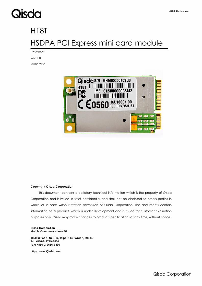
H18T HSDPA PCI Express mini card module
Datasheet
Rev. 1.0
2010/09/30
Copyright Qisda Corporation
This document contains proprietary technical information which is the property of Qisda
Corporation and is issued in strict confidential and shall not be disclosed to others parties in
whole or in parts without written permission of Qisda Corporation. The documents contain
information on a product, which is under development and is issued for customer evaluation
purposes only. Qisda may make changes to product specifications at any time, without notice.
Qisda Corporation Mobile Communications BG 18 JiHu Road, Nei-Hu, Taipei 114, Taiwan, R.O.C. Tel: +886-2-2799-8800 Fax: +886-2-2656-6390 http://www.Qisda.com
H18T Datasheet
HISTORY
Version Date Notes
VER: 1.0 2010-SEP-30 OFFICIAL RELEASE

1. INTRODUCTION..................................................................................................... 4
1.1 Description ...................................................................................................4 1.2 Application Device....................................................................................4
2. FEATURES ............................................................................................................... 5
2.1 General Characteristics ...........................................................................5 2.2 RF Functionalities ........................................................................................6
3. HARDWARE DESCRIPTION .................................................................................. 10
3.1 System Interface.......................................................................................10 3.2 Functional Diagram .................................................................................11 3.3 Pin Assignment and Description ..........................................................12 3.4 Terminal Definition....................................................................................14 3.5 Electrical Characteristics .......................................................................16 3.6 Environmental ...........................................................................................19 3.7 Physical Package ....................................................................................20
4. SOFTWARE CHARACTERISTICS ........................................................................... 23
4.1 Introduction................................................................................................23 4.2 Software Architecture .............................................................................23 4.3 Supported OS ............................................................................................24
1. INTRODUCTION
1.1 Description
Overview
This document describes all the functions, features, and interfaces of the HSDPA PCI
Express Mini Card Module – H18T from Qisda. Qisda H18T HSDPA module supports tri-band
WCDMA/HSDPA and quad-band GSM/GPRS/EDGE network connection capability.
Qisda H18T HSDPA card can provides high speed data connection, the data speed of
downlink and uplink path is up to 3.6Mbps and 384Kbps respectively. Furthermore, users can
ease to use this module by using the “HSPA Modem” application software that we provide for
Windows XP and Vista system.
With the Qisda H18T HSDPA module, devices are enhanced in both functionality and
usability based on state of the art wireless technology.
1.2 Application Device
Scope
Qisda H18T module is a high speed modem card with PCI Express minicard form factor
and is focusing on the E-Book, Wireless Router and other portable device marketing.
E-Book
Wireless Router
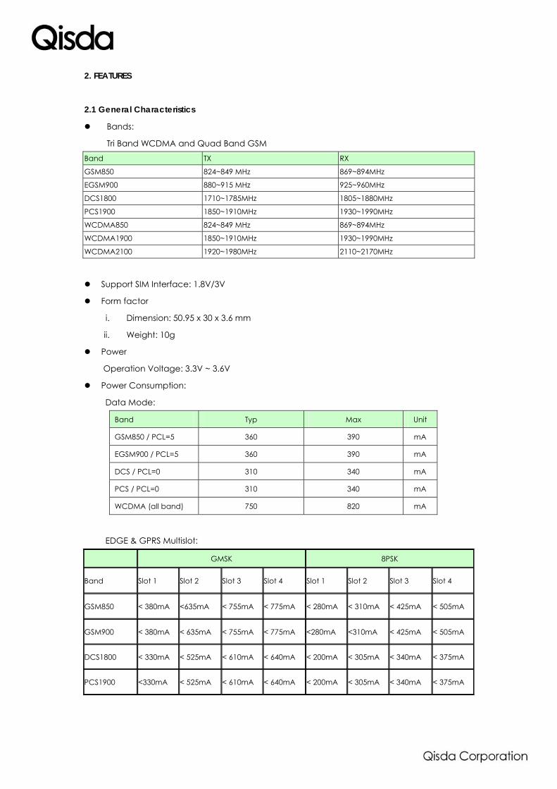
2. FEATURES
2.1 General Characteristics
Bands:
Tri Band WCDMA and Quad Band GSM
Band TX RX
GSM850 824~849 MHz 869~894MHz
EGSM900 880~915 MHz 925~960MHz
DCS1800 1710~1785MHz 1805~1880MHz
PCS1900 1850~1910MHz 1930~1990MHz
WCDMA850 824~849 MHz 869~894MHz
WCDMA1900 1850~1910MHz 1930~1990MHz
WCDMA2100 1920~1980MHz 2110~2170MHz
Support SIM Interface: 1.8V/3V
Form factor
i. Dimension: 50.95 x 30 x 3.6 mm
ii. Weight: 10g
Power
Operation Voltage: 3.3V ~ 3.6V
Power Consumption:
Data Mode:
Band Typ Max Unit
GSM850 / PCL=5 360 390 mA
EGSM900 / PCL=5 360 390 mA
DCS / PCL=0 310 340 mA
PCS / PCL=0 310 340 mA
WCDMA (all band) 750 820 mA
EDGE & GPRS Multislot:
GMSK 8PSK
Band Slot 1 Slot 2 Slot 3 Slot 4 Slot 1 Slot 2 Slot 3 Slot 4
GSM850 < 380mA <635mA < 755mA < 775mA < 280mA < 310mA < 425mA < 505mA
GSM900 < 380mA < 635mA < 755mA < 775mA <280mA <310mA < 425mA < 505mA
DCS1800 < 330mA < 525mA < 610mA < 640mA < 200mA < 305mA < 340mA < 375mA
PCS1900 <330mA < 525mA < 610mA < 640mA < 200mA < 305mA < 340mA < 375mA
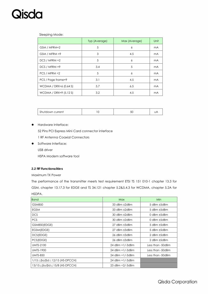
Sleeping Mode:
Typ (Average) Max (Average) Unit
GSM / MFRM=2 5 6 mA
GSM / MFRM =9 3 4.5 mA
DCS / MFRM =2 5 6 mA
DCS / MFRM =9 3.4 5 mA
PCS / MFRM =2 5 6 mA
PCS / Page frame=9 3.1 4.5 mA
WCDMA / DRX=6 (0.64 S) 5.7 6.5 mA
WCDMA / DRX=9 (5.12 S) 3.2 4.5 mA
Shutdown current 10 50 uA
Hardware Interface:
52 Pins PCI Express Mini Card connector interface
1 RF Antenna Coaxial Connectors
Software Interface:
USB driver
HSPA Modem software tool
2.2 RF Functionalities
Maximum TX Power
The performance of the transmitter meets test requirement ETSI TS 151 010-1 chapter 13.3 for
GSM, chapter 13.17.3 for EDGE and TS 34.121 chapter 5.2&5.4.3 for WCDMA, chapter 5.2A for
HSDPA.
Band Max Min
GSM850 33 dBm ±2dBm 5 dBm ±5dBm
EGSM 33 dBm ±2dBm 5 dBm ±5dBm
DCS 30 dBm ±2dBm 0 dBm ±5dBm
PCS 30 dBm ±2dBm 0 dBm ±5dBm
GSM850(EDGE) 27 dBm ±3dBm 5 dBm ±5dBm
EGSM(EDGE) 27 dBm ±3dBm 5 dBm ±5dBm
DCS(EDGE) 26 dBm ±3dBm 2 dBm ±5dBm
PCS(EDGE) 26 dBm ±3dBm 2 dBm ±5dBm
UMTS-2100 24 dBm +1/-3dBm Less than -50dBm
UMTS-1900 24 dBm +1/-3dBm Less than -50dBm
UMTS-850 24 dBm +1/-3dBm Less than -50dBm
1/15≦βo/βd≦12/15 (HS-DPCCH) 24 dBm +1/-3dBm
13/15≦βo/βd≦15/8 (HS-DPCCH) 23 dBm +2/-3dBm
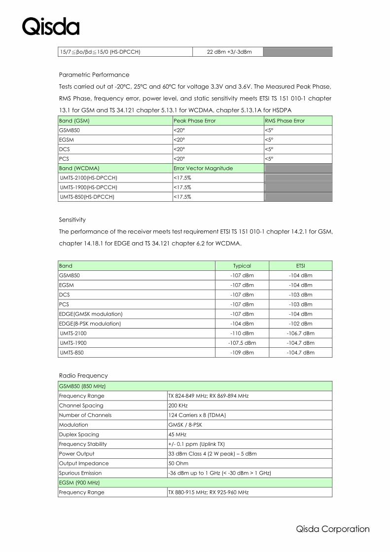
15/7≦βo/βd≦15/0 (HS-DPCCH) 22 dBm +3/-3dBm
Parametric Performance
Tests carried out at -20ºC, 25ºC and 60ºC for voltage 3.3V and 3.6V. The Measured Peak Phase,
RMS Phase, frequency error, power level, and static sensitivity meets ETSI TS 151 010-1 chapter
13.1 for GSM and TS 34.121 chapter 5.13.1 for WCDMA, chapter 5.13.1A for HSDPA
Band (GSM) Peak Phase Error RMS Phase Error
GSM850 <20° <5°
EGSM <20° <5°
DCS <20° <5°
PCS <20° <5°
Band (WCDMA) Error Vector Magnitude
UMTS-2100(HS-DPCCH) <17.5%
UMTS-1900(HS-DPCCH) <17.5%
UMTS-850(HS-DPCCH) <17.5%
Sensitivity
The performance of the receiver meets test requirement ETSI TS 151 010-1 chapter 14.2.1 for GSM,
chapter 14.18.1 for EDGE and TS 34.121 chapter 6.2 for WCDMA.
Band Typical ETSI
GSM850 -107 dBm -104 dBm
EGSM -107 dBm -104 dBm
DCS -107 dBm -103 dBm
PCS -107 dBm -103 dBm
EDGE(GMSK modulation) -107 dBm -104 dBm
EDGE(8-PSK modulation) -104 dBm -102 dBm
UMTS-2100 -110 dBm -106.7 dBm
UMTS-1900 -107.5 dBm -104.7 dBm
UMTS-850 -109 dBm -104.7 dBm
Radio Frequency
GSM850 (850 MHz)
Frequency Range TX 824-849 MHz; RX 869-894 MHz
Channel Spacing 200 KHz
Number of Channels 124 Carriers x 8 (TDMA)
Modulation GMSK / 8-PSK
Duplex Spacing 45 MHz
Frequency Stability +/- 0.1 ppm (Uplink TX)
Power Output 33 dBm Class 4 (2 W peak) – 5 dBm
Output Impedance 50 Ohm
Spurious Emission -36 dBm up to 1 GHz (< -30 dBm > 1 GHz)
EGSM (900 MHz)
Frequency Range TX 880-915 MHz; RX 925-960 MHz
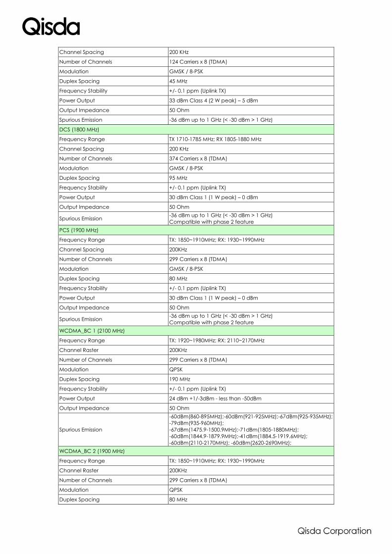
Channel Spacing 200 KHz
Number of Channels 124 Carriers x 8 (TDMA)
Modulation GMSK / 8-PSK
Duplex Spacing 45 MHz
Frequency Stability +/- 0.1 ppm (Uplink TX)
Power Output 33 dBm Class 4 (2 W peak) – 5 dBm
Output Impedance 50 Ohm
Spurious Emission -36 dBm up to 1 GHz (< -30 dBm > 1 GHz)
DCS (1800 MHz)
Frequency Range TX 1710-1785 MHz; RX 1805-1880 MHz
Channel Spacing 200 KHz
Number of Channels 374 Carriers x 8 (TDMA)
Modulation GMSK / 8-PSK
Duplex Spacing 95 MHz
Frequency Stability +/- 0.1 ppm (Uplink TX)
Power Output 30 dBm Class 1 (1 W peak) – 0 dBm
Output Impedance 50 Ohm
Spurious Emission -36 dBm up to 1 GHz (< -30 dBm > 1 GHz) Compatible with phase 2 feature
PCS (1900 MHz)
Frequency Range TX: 1850~1910MHz; RX: 1930~1990MHz
Channel Spacing 200KHz
Number of Channels 299 Carriers x 8 (TDMA)
Modulation GMSK / 8-PSK
Duplex Spacing 80 MHz
Frequency Stability +/- 0.1 ppm (Uplink TX)
Power Output 30 dBm Class 1 (1 W peak) – 0 dBm
Output Impedance 50 Ohm
Spurious Emission -36 dBm up to 1 GHz (< -30 dBm > 1 GHz) Compatible with phase 2 feature
WCDMA_BC 1 (2100 MHz)
Frequency Range TX: 1920~1980MHz; RX: 2110~2170MHz
Channel Raster 200KHz
Number of Channels 299 Carriers x 8 (TDMA)
Modulation QPSK
Duplex Spacing 190 MHz
Frequency Stability +/- 0.1 ppm (Uplink TX)
Power Output 24 dBm +1/-3dBm - less than -50dBm
Output Impedance 50 Ohm
Spurious Emission
-60dBm(860-895MHz);-60dBm(921-925MHz);-67dBm(925-935MHz); -79dBm(935-960MHz); -67dBm(1475.9-1500.9MHz);-71dBm(1805-1880MHz); -60dBm(1844.9-1879.9MHz);-41dBm(1884.5-1919.6MHz); -60dBm(2110-2170MHz); -60dBm(2620-2690MHz);
WCDMA_BC 2 (1900 MHz)
Frequency Range TX: 1850~1910MHz; RX: 1930~1990MHz
Channel Raster 200KHz
Number of Channels 299 Carriers x 8 (TDMA)
Modulation QPSK
Duplex Spacing 80 MHz
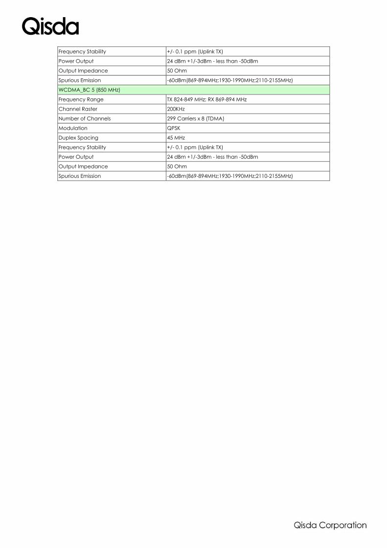
Frequency Stability +/- 0.1 ppm (Uplink TX)
Power Output 24 dBm +1/-3dBm - less than -50dBm
Output Impedance 50 Ohm
Spurious Emission -60dBm(869-894MHz;1930-1990MHz;2110-2155MHz)
WCDMA_BC 5 (850 MHz)
Frequency Range TX 824-849 MHz; RX 869-894 MHz
Channel Raster 200KHz
Number of Channels 299 Carriers x 8 (TDMA)
Modulation QPSK
Duplex Spacing 45 MHz
Frequency Stability +/- 0.1 ppm (Uplink TX)
Power Output 24 dBm +1/-3dBm - less than -50dBm
Output Impedance 50 Ohm
Spurious Emission -60dBm(869-894MHz;1930-1990MHz;2110-2155MHz)
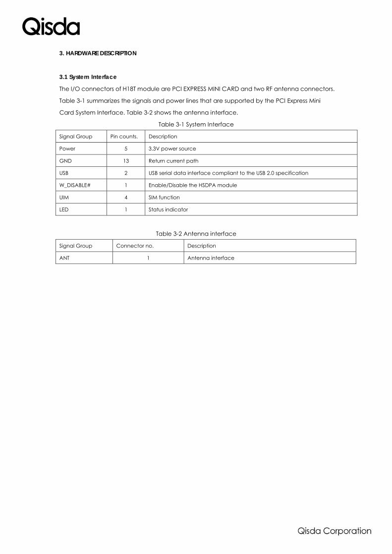
3. HARDWARE DESCRIPTION
3.1 System Interface
The I/O connectors of H18T module are PCI EXPRESS MINI CARD and two RF antenna connectors.
Table 3-1 summarizes the signals and power lines that are supported by the PCI Express Mini
Card System Interface. Table 3-2 shows the antenna interface.
Table 3-1 System Interface
Signal Group Pin counts. Description
Power 5 3.3V power source
GND 13 Return current path
USB 2 USB serial data interface compliant to the USB 2.0 specification
W_DISABLE# 1 Enable/Disable the HSDPA module
UIM 4 SIM function
LED 1 Status indicator
Table 3-2 Antenna interface
Signal Group Connector no. Description
ANT 1 Antenna interface
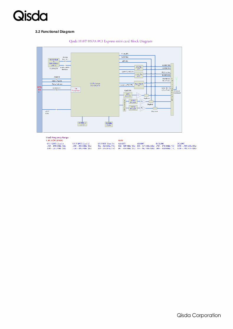
3.2 Functional Diagram
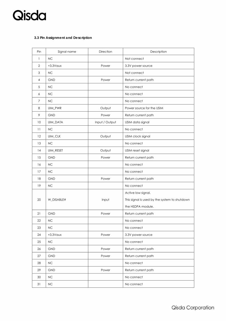
3.3 Pin Assignment and Description
Pin Signal name Direction Description
1 NC Not connect
2 +3.3Vaux Power 3.3V power source
3 NC Not connect
4 GND Power Return current path
5 NC No connect
6 NC No connect
7 NC No connect
8 UIM_PWR Output Power source for the USIM
9 GND Power Return current path
10 UIM_DATA Input / Output USIM data signal
11 NC No connect
12 UIM_CLK Output USIM clock signal
13 NC No connect
14 UIM_RESET Output USIM reset signal
15 GND Power Return current path
16 NC No connect
17 NC No connect
18 GND Power Return current path
19 NC No connect
20 W_DISABLE# Input
Active low signal.
This signal is used by the system to shutdown
the HSDPA module.
21 GND Power Return current path
22 NC No connect
23 NC No connect
24 +3.3Vaux Power 3.3V power source
25 NC No connect
26 GND Power Return current path
27 GND Power Return current path
28 NC No connect
29 GND Power Return current path
30 NC No connect
31 NC No connect
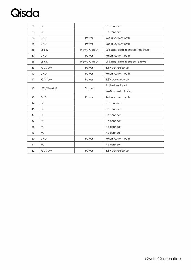
32 NC No connect
33 NC No connect
34 GND Power Return current path
35 GND Power Return current path
36 USB_D- Input / Output USB serial data interface (negative)
37 GND Power Return current path
38 USB_D+ Input / Output USB serial data interface (postive)
39 +3.3Vaux Power 3.3V power source
40 GND Power Return current path
41 +3.3Vaux Power 3.3V power source
42 LED_WWAN# Output Active low signal.
WAN status LED driver.
43 GND Power Return current path
44 NC No connect
45 NC No connect
46 NC No connect
47 NC No connect
48 NC No connect
49 NC No connect
50 GND Power Return current path
51 NC No connect
52 +3.3Vaux Power 3.3V power source
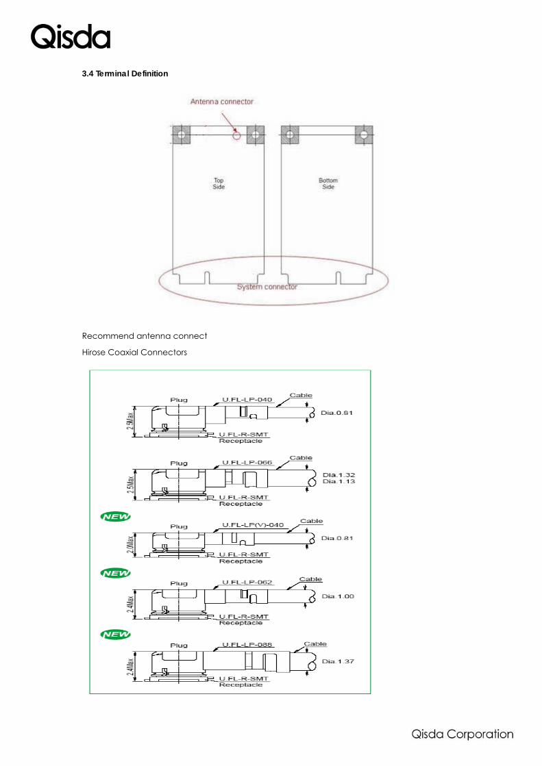
3.4 Terminal Definition
Recommend antenna connect
Hirose Coaxial Connectors
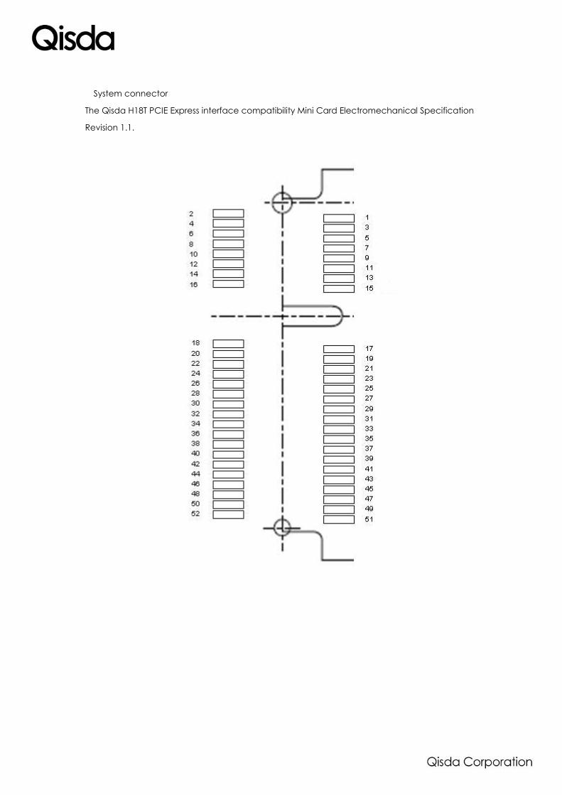
System connector
The Qisda H18T PCIE Express interface compatibility Mini Card Electromechanical Specification
Revision 1.1.
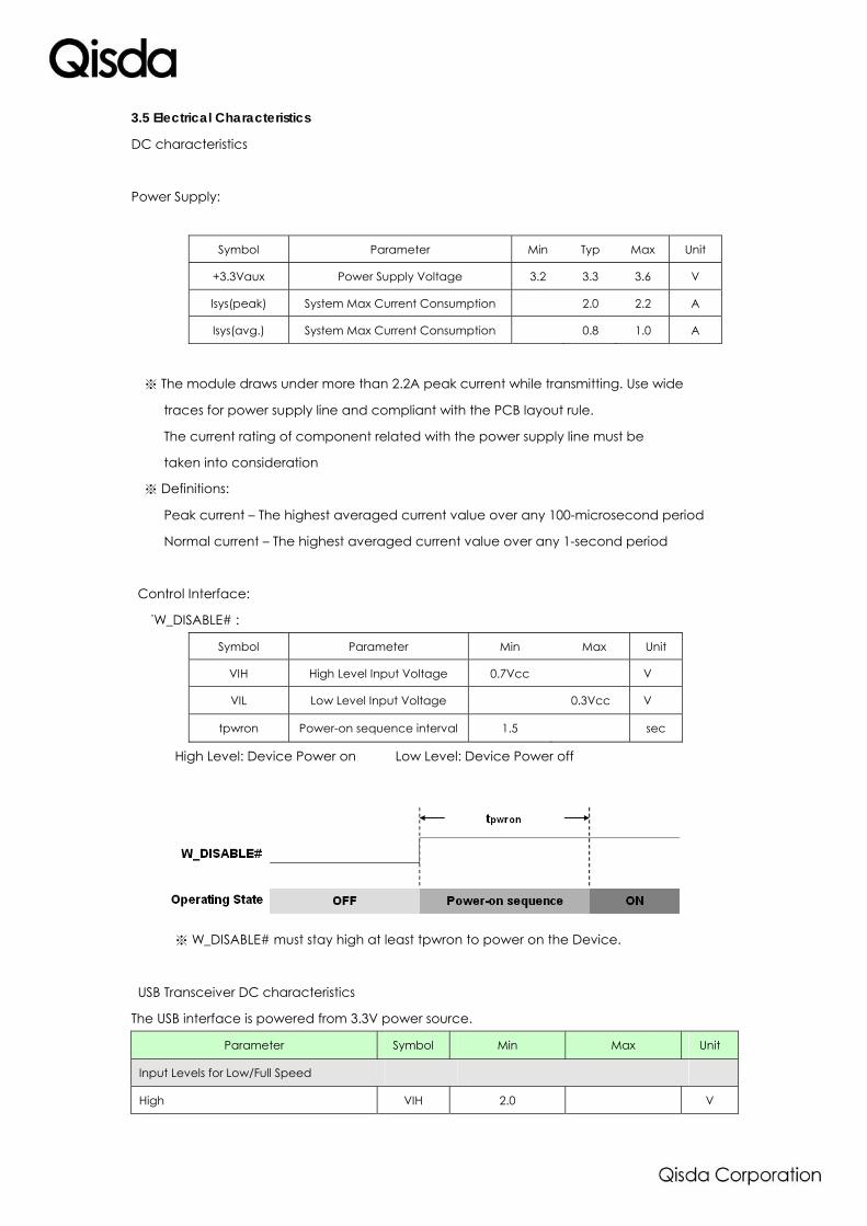
3.5 Electrical Characteristics
DC characteristics
Power Supply:
Symbol Parameter Min Typ Max Unit
+3.3Vaux Power Supply Voltage 3.2 3.3 3.6 V
Isys(peak) System Max Current Consumption 2.0 2.2 A
Isys(avg.) System Max Current Consumption 0.8 1.0 A
※ The module draws under more than 2.2A peak current while transmitting. Use wide
traces for power supply line and compliant with the PCB layout rule.
The current rating of component related with the power supply line must be
taken into consideration
※ Definitions:
Peak current – The highest averaged current value over any 100-microsecond period
Normal current – The highest averaged current value over any 1-second period
Control Interface:
˙W_DISABLE# :
Symbol Parameter Min Max Unit
VIH High Level Input Voltage 0.7Vcc V
VIL Low Level Input Voltage 0.3Vcc V
tpwron Power-on sequence interval 1.5 sec
High Level: Device Power on Low Level: Device Power off
※ W_DISABLE# must stay high at least tpwron to power on the Device.
USB Transceiver DC characteristics
The USB interface is powered from 3.3V power source.
Parameter Symbol Min Max Unit
Input Levels for Low/Full Speed
High VIH 2.0 V
Low VIL 0.8 V
Differential Input Sensitivity VDI 0.2 V
Input Levels for High Speed
High Speed Squelch Detection Threshold VHSSQ 100 150 mV
High Speed Disconnection Detection
Threshold
VHSDSC 100 150 mV
Output Levels for Low/Full Speed
Low VOL 0.0 0.3 V
High VOH 2.85 3.3 V
Output Levels for High Speed
High Speed Idle Level VHSOI -10.0 10.0 mV
High Speed Data Signaling High VHSOH 360 440 mV
High Speed Data Signaling Low VHSOL -10.0 10.0 mV
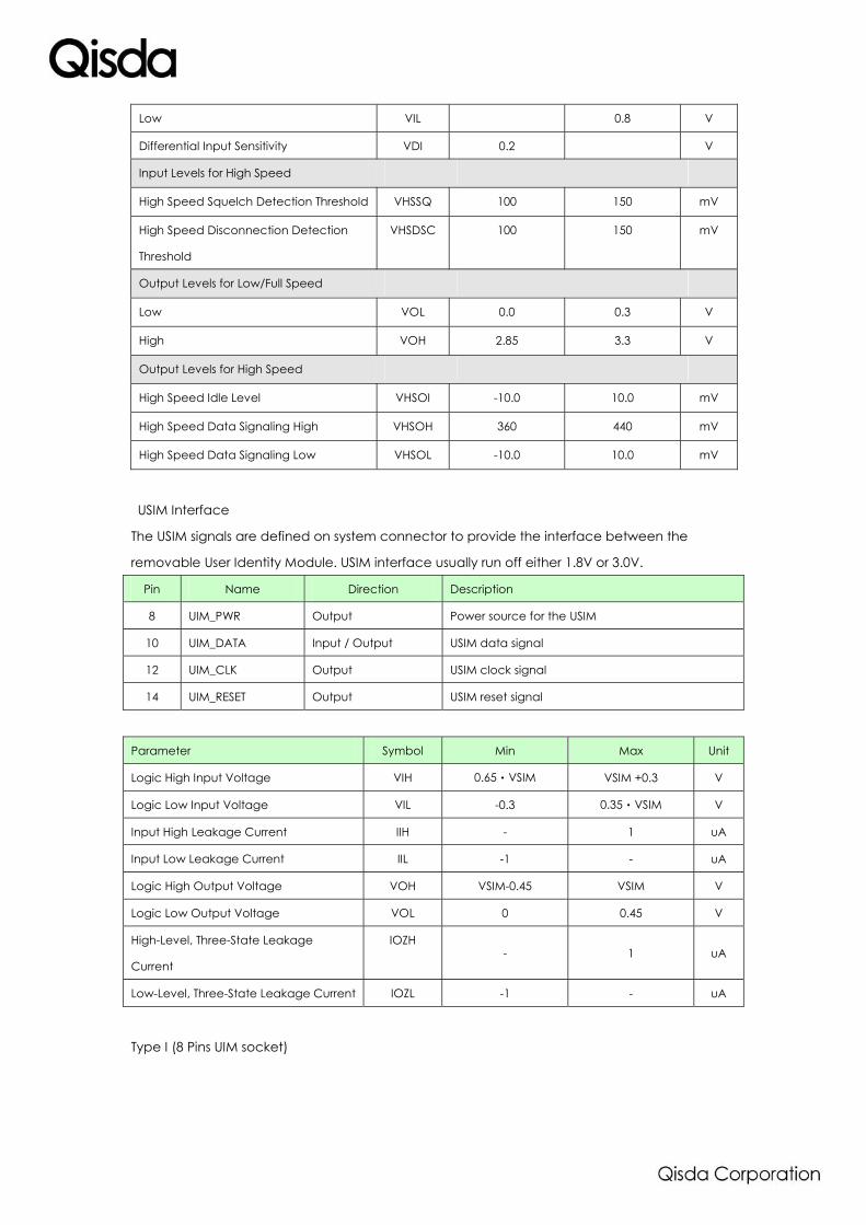
USIM Interface
The USIM signals are defined on system connector to provide the interface between the
removable User Identity Module. USIM interface usually run off either 1.8V or 3.0V.
Pin Name Direction Description
8 UIM_PWR Output Power source for the USIM
10 UIM_DATA Input / Output USIM data signal
12 UIM_CLK Output USIM clock signal
14 UIM_RESET Output USIM reset signal
Parameter Symbol Min Max Unit
Logic High Input Voltage VIH 0.65‧VSIM VSIM +0.3 V
Logic Low Input Voltage VIL -0.3 0.35‧VSIM V
Input High Leakage Current IIH - 1 uA
Input Low Leakage Current IIL -1 - uA
Logic High Output Voltage VOH VSIM-0.45 VSIM V
Logic Low Output Voltage VOL 0 0.45 V
High-Level, Three-State Leakage
Current
IOZH - 1 uA
Low-Level, Three-State Leakage Current IOZL -1 - uA
Type I (8 Pins UIM socket)
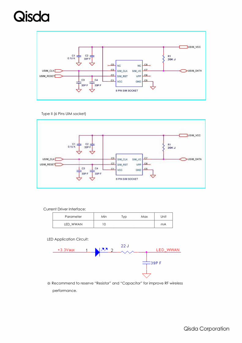
Type II (6 Pins UIM socket)
Current Driver Interface:
Parameter Min Typ Max Unit
LED_WWAN 10 mA
LED Application Circuit:
※ Recommend to reserve “Resistor” and “Capacitor” for improve RF wireless
performance.
3.6 Environmental
Operational temperature: -20 ~ +60 ℃
Functional temperature: -20 ~ +70 ℃
Storage temperature: -40 ~ +85 ℃
Note:
The maximum case temperature (Tc) of shielding case cover should be under 90 ℃ (@RF TX
power = 24dBm) for ensure all of the characteristics of H18T module can be fulfilled the ETSI
specification.
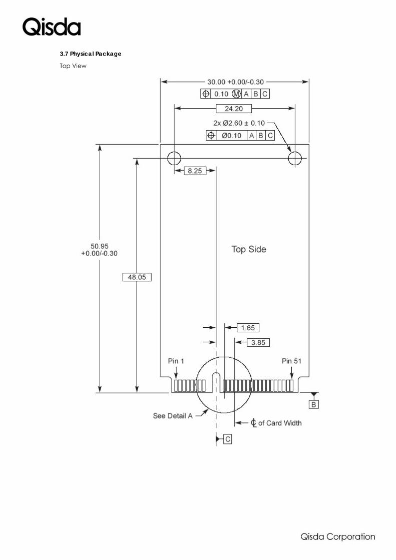
3.7 Physical Package
Top View
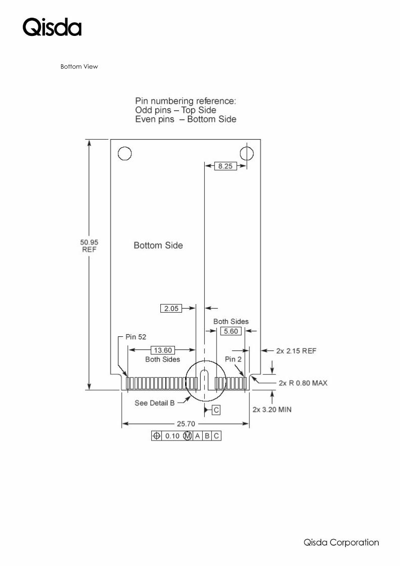
Bottom View
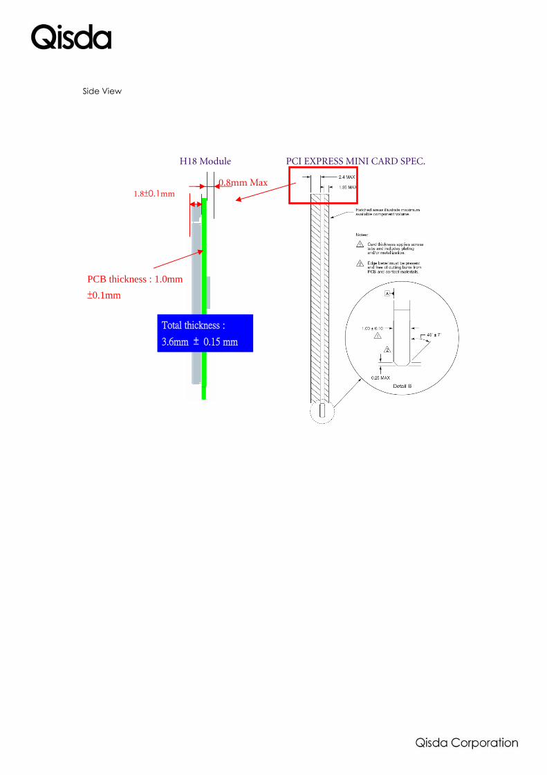
Side View
1.8±0.1mm 0.8mm Max
PCI EXPRESS MINI CARD SPEC.
PCB thickness : 1.0mm±0.1mm
Total thickness :
3.6mm ± 0.15 mm
H18 Module
4. SOFTWARE CHARACTERISTICS
4.1 Introduction
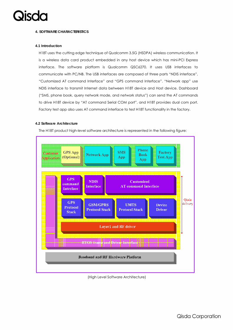
H18T uses the cutting edge technique of Qualcomm 3.5G (HSDPA) wireless communication. It
is a wireless data card product embedded in any host device which has mini-PCI Express
interface. The software platform is Qualcomm QSC6270. It uses USB interfaces to
communicate with PC/NB. The USB interfaces are composed of three parts “NDIS interface”,
“Customized AT command Interface” and “GPS command Interface”. “Network app” use
NDIS interface to transmit Internet data between H18T device and Host device. Dashboard
(“SMS, phone book, query network mode, and network status”) can send the AT commands
to drive H18T device by “AT command Serial COM port”, and H18T provides dual com port.
Factory test app also uses AT command interface to test H18T functionality in the factory.
4.2 Software Architecture
The H18T product high-level software architecture is represented in the following figure:
(High Level Software Architecture)
4.3 Supported OS
a. Windows XP/Vista/7 32bit and 64bit
b. MAC OS 10.4/10.5/10.6
c. Linux 2.6.x
d. WIN CE 5.0


![S-104 [87 97 feet]...S-104 [97 - 107] Figure A-9.21. Westside Subway Extension, Project No. 4953-10-1561 By: Y.N. 6/15/11, Checked By: APR 6/30/2011 S-104 [107 – 117 feet] Figure](https://img.pdfslide.us/doc/110x75/5f429e3b11751020710ee8c8/s-104-87-97-feet-s-104-97-107-figure-a-921-westside-subway-extension.jpg)