Embed Size (px)
DESCRIPTION
IC Catalog
Citation preview
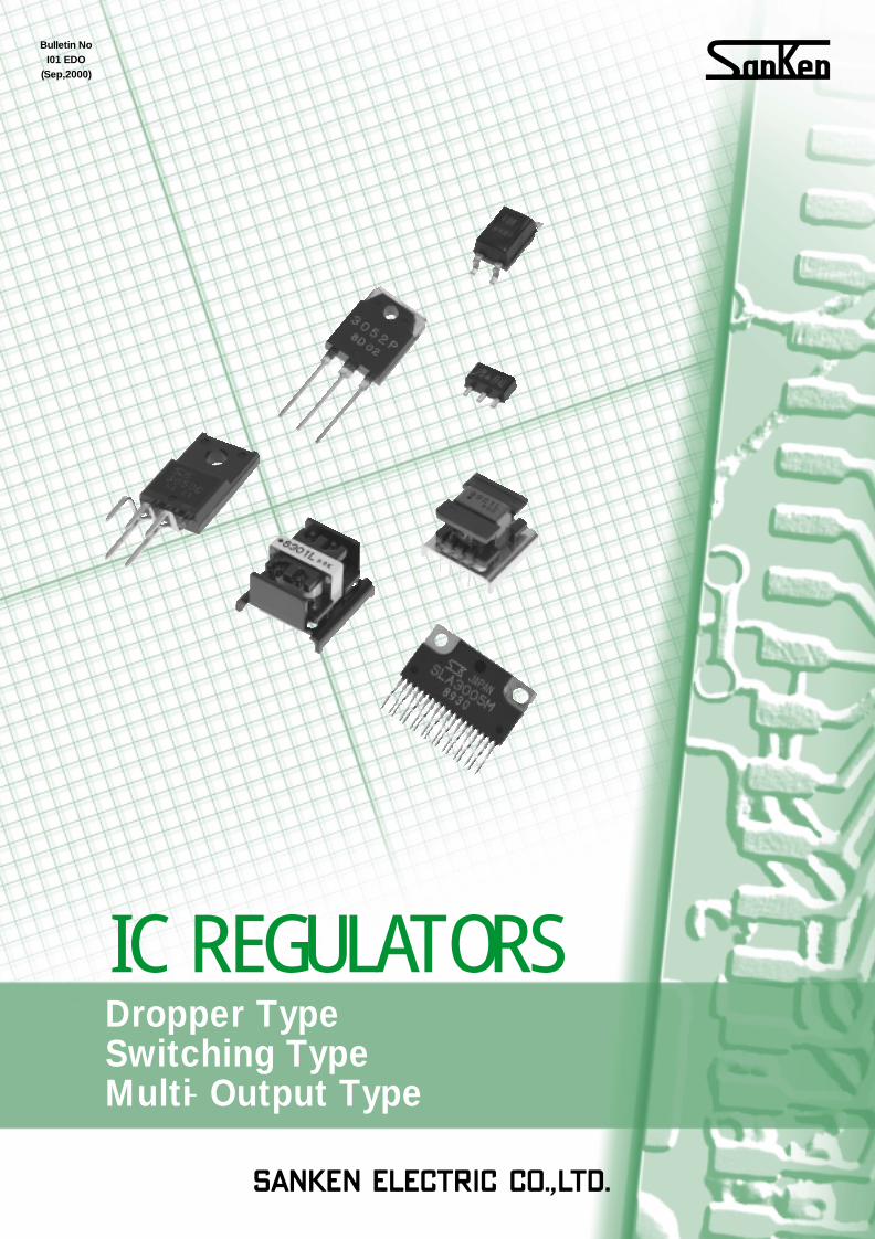
Bulletin NoI01 EDO
(Sep,2000)
IC REGULATORS Dropper TypeSwitching TypeMulti‐Output Type
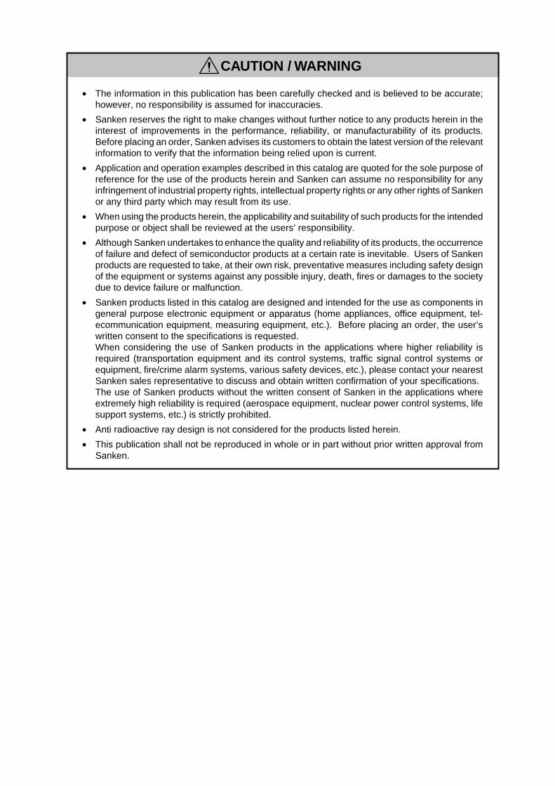
• The information in this publication has been carefully checked and is believed to be accurate;however, no responsibility is assumed for inaccuracies.
• Sanken reserves the right to make changes without further notice to any products herein in theinterest of improvements in the performance, reliability, or manufacturability of its products.Before placing an order, Sanken advises its customers to obtain the latest version of the relevantinformation to verify that the information being relied upon is current.
• Application and operation examples described in this catalog are quoted for the sole purpose ofreference for the use of the products herein and Sanken can assume no responsibility for anyinfringement of industrial property rights, intellectual property rights or any other rights of Sankenor any third party which may result from its use.
• When using the products herein, the applicability and suitability of such products for the intendedpurpose or object shall be reviewed at the users’ responsibility.
• Although Sanken undertakes to enhance the quality and reliability of its products, the occurrenceof failure and defect of semiconductor products at a certain rate is inevitable. Users of Sankenproducts are requested to take, at their own risk, preventative measures including safety designof the equipment or systems against any possible injury, death, fires or damages to the societydue to device failure or malfunction.
• Sanken products listed in this catalog are designed and intended for the use as components ingeneral purpose electronic equipment or apparatus (home appliances, office equipment, tel-ecommunication equipment, measuring equipment, etc.). Before placing an order, the user’swritten consent to the specifications is requested.When considering the use of Sanken products in the applications where higher reliability isrequired (transportation equipment and its control systems, traffic signal control systems orequipment, fire/crime alarm systems, various safety devices, etc.), please contact your nearestSanken sales representative to discuss and obtain written confirmation of your specifications.The use of Sanken products without the written consent of Sanken in the applications whereextremely high reliability is required (aerospace equipment, nuclear power control systems, lifesupport systems, etc.) is strictly prohibited.
• Anti radioactive ray design is not considered for the products listed herein.
• This publication shall not be reproduced in whole or in part without prior written approval fromSanken.
CAUTION / WARNING
1
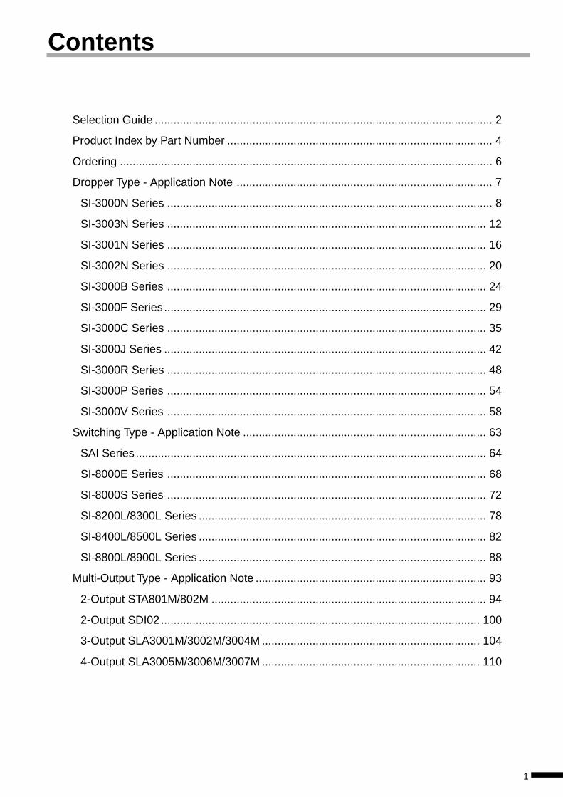
Selection Guide ........................................................................................................... 2
Product Index by Part Number .................................................................................... 4
Ordering ...................................................................................................................... 6
Dropper Type - Application Note ................................................................................. 7
SI-3000N Series ....................................................................................................... 8
SI-3003N Series ..................................................................................................... 12
SI-3001N Series ..................................................................................................... 16
SI-3002N Series ..................................................................................................... 20
SI-3000B Series ..................................................................................................... 24
SI-3000F Series...................................................................................................... 29
SI-3000C Series ..................................................................................................... 35
SI-3000J Series ...................................................................................................... 42
SI-3000R Series ..................................................................................................... 48
SI-3000P Series ..................................................................................................... 54
SI-3000V Series ..................................................................................................... 58
Switching Type - Application Note ............................................................................. 63
SAI Series............................................................................................................... 64
SI-8000E Series ..................................................................................................... 68
SI-8000S Series ..................................................................................................... 72
SI-8200L/8300L Series ........................................................................................... 78
SI-8400L/8500L Series ........................................................................................... 82
SI-8800L/8900L Series ........................................................................................... 88
Multi-Output Type - Application Note ......................................................................... 93
2-Output STA801M/802M ....................................................................................... 94
2-Output SDI02 ..................................................................................................... 100
3-Output SLA3001M/3002M/3004M ..................................................................... 104
4-Output SLA3005M/3006M/3007M ..................................................................... 110
Contents
2
Selection Guide
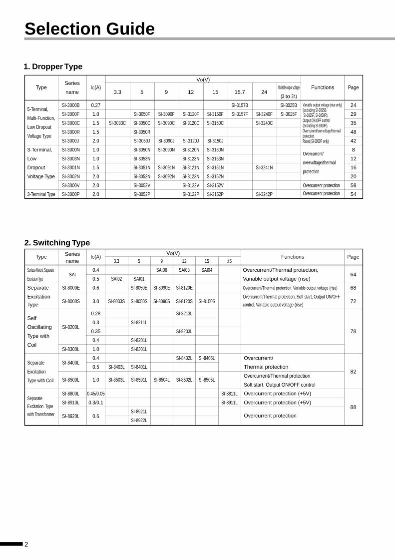
Type
5-Terminal,
Multi-Function,
Low Dropout
Voltage Type
3-Terminal,
Low
Dropout
Voltage Type
3-Terminal Type
Series
name
SI-3000B
SI-3000F
SI-3000C
SI-3000R
SI-3000J
SI-3000N
SI-3003N
SI-3001N
SI-3002N
SI-3000V
SI-3000P
IO(A)
0.27
1.0
1.5
1.5
2.0
1.0
1.0
1.5
2.0
2.0
2.0
Type
Surface-Mount, Separate
Excitation Type
Separate
Excitation
Type
Self
Oscillating
Type with
Coil
Separate
Excitation
Type with Coil
Separate
Excitation Type
with Transformer
Seriesname
SAI
SI-8000E
SI-8000S
SI-8200L
SI-8300L
SI-8400L
SI-8500L
SI-8800L
SI-8910L
SI-8920L
IO(A)
0.4
0.5
0.6
3.0
0.28
0.3
0.35
0.4
1.0
0.4
0.5
1.0
0.45/0.05
0.3/0.1
0.6
Functions
Overcurrent/Thermal protection,
Variable output voltage (rise)
Overcurrent/Thermal protection, Variable output voltage (rise)
Overcurrent/Thermal protection, Soft start, Output ON/OFF
control, Variable output voltage (rise)
Overcurrent/
Thermal protection
Overcurrent/Thermal protection
Soft start, Output ON/OFF control
Overcurrent protection (+5V)
Overcurrent protection (+5V)
Overcurrent protection
1. Dropper Type
2. Switching Type
Page
64
68
72
78
82
88
Page
24
29
35
48
42
8
12
16
20
58
54
Functions
Overcurrent/
overvoltage/thermal
protection
Overcurrent protection
Overcurrent protection
VO(V)
3.3 5 9 12 15 ±5
SAI06 SAI03 SAI04
SAI02 SAI01
SI-8050E SI-8090E SI-8120E
SI-8033S SI-8050S SI-8090S SI-8120S SI-8150S
SI-8213L
SI-8211L
SI-8203L
SI-8201L
SI-8301L
SI-8402L SI-8405L
SI-8403L SI-8401L
SI-8503L SI-8501L SI-8504L SI-8502L SI-8505L
SI-8811L
SI-8911L
SI-8921L
SI-8922L
Variable output voltage (rise only)(excluding SI-3025B, SI-3025F, SI-3050R),Output ON/OFF control(excluding SI-3050R),Overcurrent/overvoltage/thermalprotection,Reset (SI-3050R only)
VO(V)
3.3 5 9 12 15 15.7 24Variable output voltage
(3 to 24)
SI-3157B SI-3025B
SI-3050F SI-3090F SI-3120F SI-3150F SI-3157F SI-3240F SI-3025F
SI-3033C SI-3050C SI-3090C SI-3120C SI-3150C SI-3240C
SI-3050R
SI-3050J SI-3090J SI-3120J SI-3150J
SI-3050N SI-3090N SI-3120N SI-3150N
SI-3053N SI-3123N SI-3153N
SI-3051N SI-3091N SI-3121N SI-3151N SI-3241N
SI-3052N SI-3092N SI-3122N SI-3152N
SI-3052V SI-3122V SI-3152V
SI-3052P SI-3122P SI-3152P SI-3242P
3
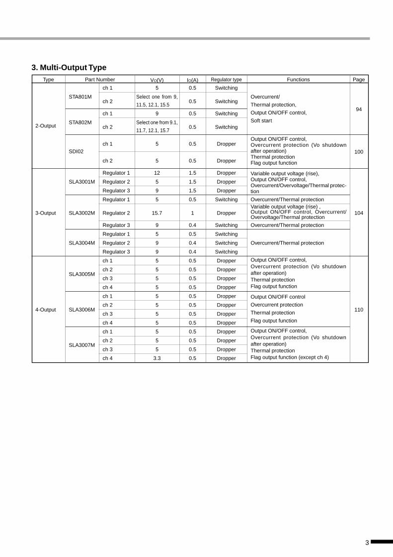
VO(V)
5
Select one from 9,
11.5, 12.1, 15.5
9
Select one from 9.1,
11.7, 12.1, 15.7
5
5
12
5
9
5
15.7
9
5
9
9
5
5
5
5
5
5
5
5
5
5
5
3.3
Functions
Overcurrent/Thermal protection
Overcurrent/Thermal protection
Overcurrent/Thermal protection
IO(A)
0.5
0.5
0.5
0.5
0.5
0.5
1.5
1.5
1.5
0.5
1
0.4
0.5
0.4
0.4
0.5
0.5
0.5
0.5
0.5
0.5
0.5
0.5
0.5
0.5
0.5
0.5
Regulator type
Switching
Switching
Switching
Switching
Dropper
Dropper
Dropper
Dropper
Dropper
Switching
Dropper
Switching
Switching
Switching
Switching
Dropper
Dropper
Dropper
Dropper
Dropper
Dropper
Dropper
Dropper
Dropper
Dropper
Dropper
Dropper
3. Multi-Output TypePage
94
100
104
110
Overcurrent/
Thermal protection,
Output ON/OFF control,
Soft start
Variable output voltage (rise),Output ON/OFF control,Overcurrent/Overvoltage/Thermal protec-tion
Output ON/OFF control,Overcurrent protection (Vo shutdownafter operation)Thermal protectionFlag output function
Output ON/OFF control
Overcurrent protection
Thermal protection
Flag output function
Variable output voltage (rise) ,Output ON/OFF control, Overcurrent/Overvoltage/Thermal protection
Output ON/OFF control,Overcurrent protection (Vo shutdownafter operation)Thermal protectionFlag output function
Part Number
ch 1
STA801Mch 2
ch 1
STA802Mch 2
ch 1SDI02
ch 2
Regulator 1
SLA3001M Regulator 2
Regulator 3
Regulator 1
SLA3002M Regulator 2
Regulator 3
Regulator 1
SLA3004M Regulator 2
Regulator 3
ch 1
SLA3005Mch 2
ch 3
ch 4
ch 1
SLA3006Mch 2
ch 3
ch 4
ch 1
SLA3007Mch 2
ch 3
ch 4
Output ON/OFF control,Overcurrent protection (Vo shutdownafter operation)Thermal protectionFlag output function (except ch 4)
Type
2-Output
3-Output
4-Output
4
Product Index by Part Number
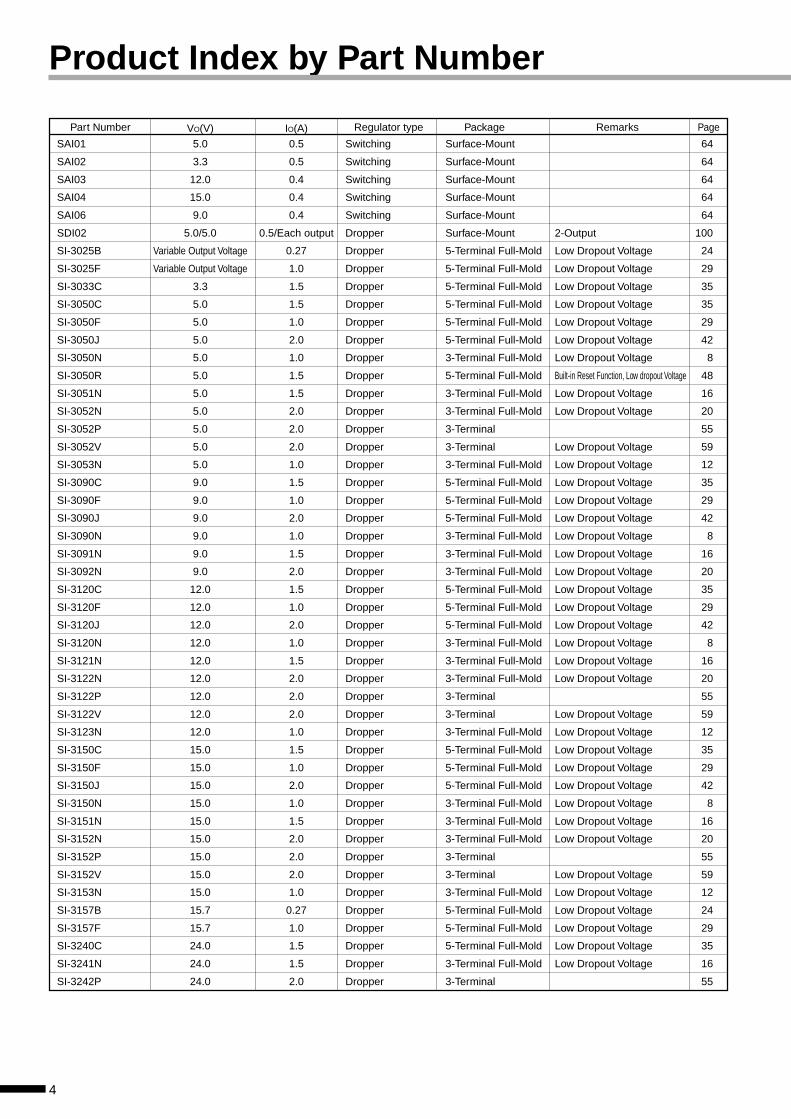
Part Number VO(V) IO(A) Regulator type Package Remarks Page
SAI01 5.0 0.5 Switching Surface-Mount 64
SAI02 3.3 0.5 Switching Surface-Mount 64
SAI03 12.0 0.4 Switching Surface-Mount 64
SAI04 15.0 0.4 Switching Surface-Mount 64
SAI06 9.0 0.4 Switching Surface-Mount 64
SDI02 5.0/5.0 0.5/Each output Dropper Surface-Mount 2-Output 100
SI-3025B Variable Output Voltage 0.27 Dropper 5-Terminal Full-Mold Low Dropout Voltage 24
SI-3025F Variable Output Voltage 1.0 Dropper 5-Terminal Full-Mold Low Dropout Voltage 29
SI-3033C 3.3 1.5 Dropper 5-Terminal Full-Mold Low Dropout Voltage 35
SI-3050C 5.0 1.5 Dropper 5-Terminal Full-Mold Low Dropout Voltage 35
SI-3050F 5.0 1.0 Dropper 5-Terminal Full-Mold Low Dropout Voltage 29
SI-3050J 5.0 2.0 Dropper 5-Terminal Full-Mold Low Dropout Voltage 42
SI-3050N 5.0 1.0 Dropper 3-Terminal Full-Mold Low Dropout Voltage 8
SI-3050R 5.0 1.5 Dropper 5-Terminal Full-Mold Built-in Reset Function, Low dropout Voltage 48
SI-3051N 5.0 1.5 Dropper 3-Terminal Full-Mold Low Dropout Voltage 16
SI-3052N 5.0 2.0 Dropper 3-Terminal Full-Mold Low Dropout Voltage 20
SI-3052P 5.0 2.0 Dropper 3-Terminal 55
SI-3052V 5.0 2.0 Dropper 3-Terminal Low Dropout Voltage 59
SI-3053N 5.0 1.0 Dropper 3-Terminal Full-Mold Low Dropout Voltage 12
SI-3090C 9.0 1.5 Dropper 5-Terminal Full-Mold Low Dropout Voltage 35
SI-3090F 9.0 1.0 Dropper 5-Terminal Full-Mold Low Dropout Voltage 29
SI-3090J 9.0 2.0 Dropper 5-Terminal Full-Mold Low Dropout Voltage 42
SI-3090N 9.0 1.0 Dropper 3-Terminal Full-Mold Low Dropout Voltage 8
SI-3091N 9.0 1.5 Dropper 3-Terminal Full-Mold Low Dropout Voltage 16
SI-3092N 9.0 2.0 Dropper 3-Terminal Full-Mold Low Dropout Voltage 20
SI-3120C 12.0 1.5 Dropper 5-Terminal Full-Mold Low Dropout Voltage 35
SI-3120F 12.0 1.0 Dropper 5-Terminal Full-Mold Low Dropout Voltage 29
SI-3120J 12.0 2.0 Dropper 5-Terminal Full-Mold Low Dropout Voltage 42
SI-3120N 12.0 1.0 Dropper 3-Terminal Full-Mold Low Dropout Voltage 8
SI-3121N 12.0 1.5 Dropper 3-Terminal Full-Mold Low Dropout Voltage 16
SI-3122N 12.0 2.0 Dropper 3-Terminal Full-Mold Low Dropout Voltage 20
SI-3122P 12.0 2.0 Dropper 3-Terminal 55
SI-3122V 12.0 2.0 Dropper 3-Terminal Low Dropout Voltage 59
SI-3123N 12.0 1.0 Dropper 3-Terminal Full-Mold Low Dropout Voltage 12
SI-3150C 15.0 1.5 Dropper 5-Terminal Full-Mold Low Dropout Voltage 35
SI-3150F 15.0 1.0 Dropper 5-Terminal Full-Mold Low Dropout Voltage 29
SI-3150J 15.0 2.0 Dropper 5-Terminal Full-Mold Low Dropout Voltage 42
SI-3150N 15.0 1.0 Dropper 3-Terminal Full-Mold Low Dropout Voltage 8
SI-3151N 15.0 1.5 Dropper 3-Terminal Full-Mold Low Dropout Voltage 16
SI-3152N 15.0 2.0 Dropper 3-Terminal Full-Mold Low Dropout Voltage 20
SI-3152P 15.0 2.0 Dropper 3-Terminal 55
SI-3152V 15.0 2.0 Dropper 3-Terminal Low Dropout Voltage 59
SI-3153N 15.0 1.0 Dropper 3-Terminal Full-Mold Low Dropout Voltage 12
SI-3157B 15.7 0.27 Dropper 5-Terminal Full-Mold Low Dropout Voltage 24
SI-3157F 15.7 1.0 Dropper 5-Terminal Full-Mold Low Dropout Voltage 29
SI-3240C 24.0 1.5 Dropper 5-Terminal Full-Mold Low Dropout Voltage 35
SI-3241N 24.0 1.5 Dropper 3-Terminal Full-Mold Low Dropout Voltage 16
SI-3242P 24.0 2.0 Dropper 3-Terminal 55
5
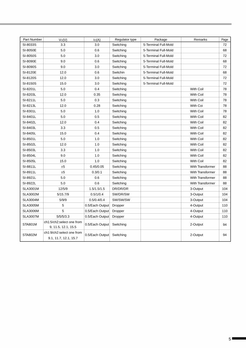
Part Number VO(V) IO(A) Regulator type Package Remarks Page
SI-8033S 3.3 3.0 Switching 5-Terminal Full-Mold 72
SI-8050E 5.0 0.6 Switching 5-Terminal Full-Mold 68
SI-8050S 5.0 3.0 Switching 5-Terminal Full-Mold 72
SI-8090E 9.0 0.6 Switching 5-Terminal Full-Mold 68
SI-8090S 9.0 3.0 Switching 5-Terminal Full-Mold 72
SI-8120E 12.0 0.6 Switchin 5-Terminal Full-Mold 68
SI-8120S 12.0 3.0 Switching 5-Terminal Full-Mold 72
SI-8150S 15.0 3.0 Switching 5-Terminal Full-Mold 72
SI-8201L 5.0 0.4 Switching With Coil 78
SI-8203L 12.0 0.35 Switching With Coil 78
SI-8211L 5.0 0.3 Switching With Coil 78
SI-8213L 12.0 0.28 Switching With Coi 78
SI-8301L 5.0 1.0 Switching With Coil 78
SI-8401L 5.0 0.5 Switching With Coil 82
SI-8402L 12.0 0.4 Switching With Coil 82
SI-8403L 3.3 0.5 Switching With Coil 82
SI-8405L 15.0 0.4 Switching With Coil 82
SI-8501L 5.0 1.0 Switching With Coil 82
SI-8502L 12.0 1.0 Switching With Coil 82
SI-8503L 3.3 1.0 Switching With Coil 82
SI-8504L 9.0 1.0 Switching With Coil 82
SI-8505L 15.0 1.0 Switching With Coil 82
SI-8811L ±5 0.45/0.05 Switching With Transformer 88
SI-8911L ±5 0.3/0.1 Switching With Transformer 88
SI-8921L 5.0 0.6 Switching With Transformer 88
SI-8922L 5.0 0.6 Switching With Transformer 88
SLA3001M 12/5/9 1.5/1.5/1.5 DR/DR/DR 3-Output 104
SLA3002M 5/15.7/9 0.5/1/0.4 SW/DR/SW 3-Output 104
SLA3004M 5/9/9 0.5/0.4/0.4 SW/SW/SW 3-Output 104
SLA3005M 5 0.5/Each Output Dropper 4-Output 110
SLA3006M 5 0.5/Each Output Dropper 4-Output 110
SLA3007M 5/5/5/3.3 0.5/Each Output Dropper 4-Output 110
STA801Mch1:5/ch2:select one from
0.5/Each Output Switching 2-Output9, 11.5, 12.1, 15.5
94
STA802Mch1:9/ch2:select one from
0.5/Each Output Switching 2-Output 949.1, 11.7, 12.1, 15.7
6
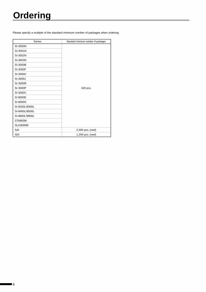
Ordering
Please specify a multiple of the standard minimum number of packages when ordering.
SI-3000N
SI-3001N
SI-3002N
SI-3003N
SI-3000B
SI-3000F
SI-3000C
SI-3000J
SI-3000R
SI-3000P
SI-3000V
SI-8000E
SI-8000S
SI-8200L/8300L
SI-8400L/8500L
SI-8800L/9800L
STA800M
SLA3000M
SAI
SDI
100 pcs.
2,000 pcs. (reel)
1,200 pcs. (reel)
Series Standard minimum number of packages
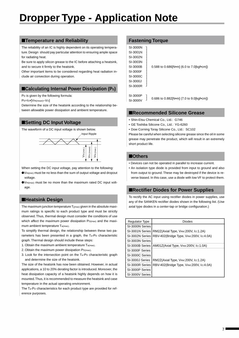
Temperature and ReliabilityThe reliability of an IC is highly dependent on its operating tempera-
ture. Design should pay particular attention to ensuring ample space
for radiating heat.
Be sure to apply silicon grease to the IC before attaching a heatsink,
and to secure it firmly to the heatsink.
Other important items to be considered regarding heat radiation in-
clude air convection during operation.
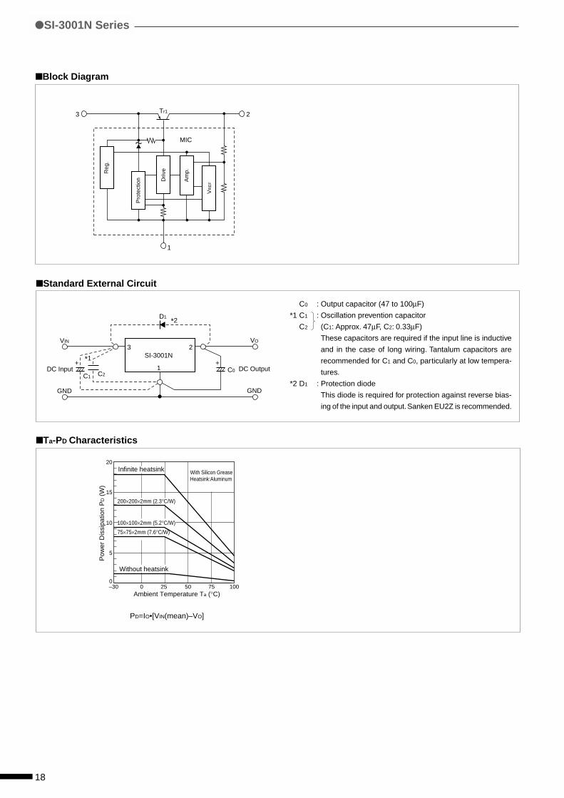
Calculating Internal Power Dissipation (PD)PD is given by the following formula:
PD=IO•[VIN(mean)–VO]
Determine the size of the heatsink according to the relationship be-
tween allowable power dissipation and ambient temperature.
Setting DC Input VoltageThe waveform of a DC input voltage is shown below.
When setting the DC input voltage, pay attention to the following:
VIN(min) must be no less than the sum of output voltage and dropout
voltage.
VIN(max) must be no more than the maximum rated DC input volt-
age.
Heatsink DesignThe maximum junction temperature Tj(max) given in the absolute maxi-
mum ratings is specific to each product type and must be strictly
observed. Thus, thermal design must consider the conditions of use
which affect the maximum power dissipation PD(max) and the maxi-
mum ambient temperature Ta(max).
To simplify thermal design, the relationship between these two pa-
rameters has been presented in a graph, the Ta-PD characteristic
graph. Thermal design should include these steps:
1. Obtain the maximum ambient temperature Ta(max).
2. Obtain the maximum power dissipation PD(max).
3. Look for the intersection point on the Ta-PD characteristic graph
and determine the size of the heatsink.
The size of the heatsink has now been obtained. However, in actual
applications, a 10 to 20% derating factor is introduced. Moreover, the
heat dissipation capacity of a heatsink highly depends on how it is
mounted. Thus, it is recommended to measure the heatsink and case
temperature in the actual operating environment.
The Ta-PD characteristics for each product type are provided for ref-
erence purposes.
7
Dropper Type - Application Note
VIN
(m
in.)
VIN
(m
ean
)
VIN
(m
ax.
)
Input Ripple
Regulator Type Diodes
SI-3000N Series
SI-3001N Series RM2Z(Axial Type, VRM:200V, IO:1.2A)
SI-3002N Series RBV-402(Bridge Type, VRM:200V, IO:4.0A)
SI-3003N Series
SI-3000B Series AM01Z(Axial Type, VRM:200V, IO:1.0A)
SI-3000F Series
SI-3000C Series
SI-3000J Series RM2Z(Axial Type, VRM:200V, IO:1.2A)
SI-3000R Series RBV-402(Bridge Type, VRM:200V, IO:4.0A)
SI-3000P Series
SI-3000V Series
Fastening TorqueSI-3000N
SI-3001N
SI-3002N
SI-3003N
SI-3000B 0.588 to 0.686[N•m] (6.0 to 7.0[kgf•cm])
SI-3000F
SI-3000C
SI-3000J
SI-3000R
SI-3000P0.686 to 0.882[N•m] (7.0 to 9.0[kgf•cm])
SI-3000V
Recommended Silicone Grease• Shin-Etsu Chemical Co., Ltd.: G746
• GE Toshiba Silicone Co., Ltd.: YG-6260
• Dow Corning Toray Silicone Co., Ltd.: SC102
Please be careful when selecting silicone grease since the oil in some
grease may penetrate the product, which will result in an extremely
short product life.
Others• Devices can not be operated in parallel to increase current.
• An isolation type diode is provided from input to ground and also
from output to ground. These may be destroyed if the device is re-
verse biased. In this case, use a diode with low VF to protect them.
Rectifier Diodes for Power SuppliesTo rectify the AC input using rectifier diodes in power supplies, use
any of the SANKEN rectifier diodes shown in the following list. (Use
axial type diodes in a center-tap or bridge configuration.)
8
Parameter
DC Input Voltage
DC Output Current
Power Dissipation
Junction Temperature
Ambient Operating Temperature
Storage Temperature
Thermal Resistance (junction to case)
Thermal Resistance (junction to ambient air)
Symbol
VIN
IO
PD1
PD2
Tj
Top
Tstg
Rth(j-c)
Rth(j-a)
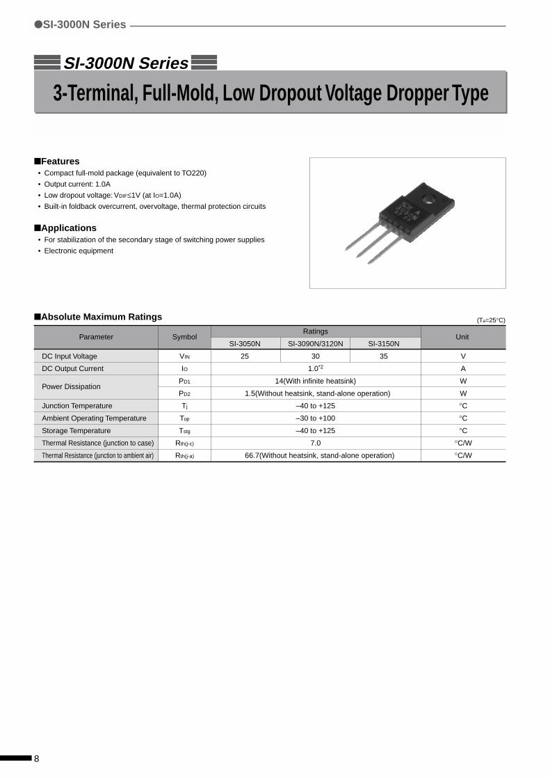
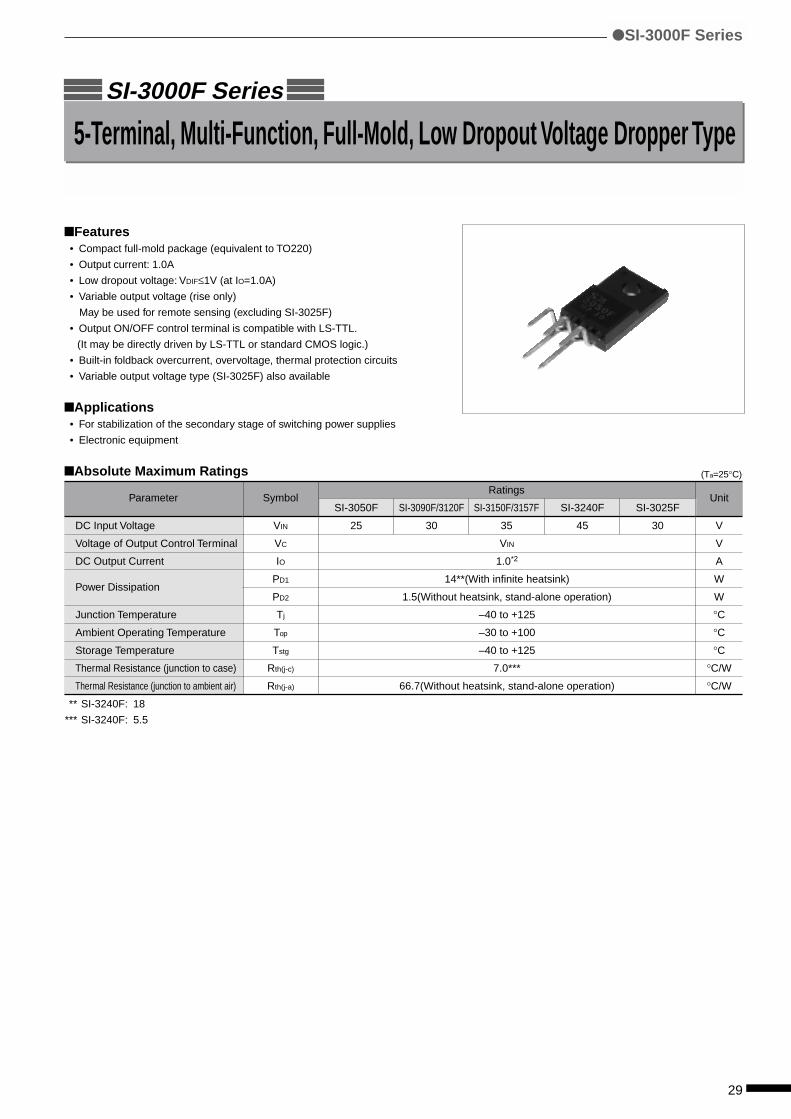
Features• Compact full-mold package (equivalent to TO220)
• Output current: 1.0A
• Low dropout voltage: VDIF≤1V (at IO=1.0A)
• Built-in foldback overcurrent, overvoltage, thermal protection circuits
Applications• For stabilization of the secondary stage of switching power supplies
• Electronic equipment
Absolute Maximum Ratings (Ta=25°C)
SI-3000N Series
3-Terminal, Full-Mold, Low Dropout Voltage Dropper Type
SI-3000N Series
Ratings
SI-3050N SI-3090N/3120N SI-3150N
25 30 35
1.0*2
14(With infinite heatsink)
1.5(Without heatsink, stand-alone operation)
–40 to +125
–30 to +100
–40 to +125
7.0
66.7(Without heatsink, stand-alone operation)
Unit
V
A
W
W
°C
°C
°C
°C/W
°C/W
9
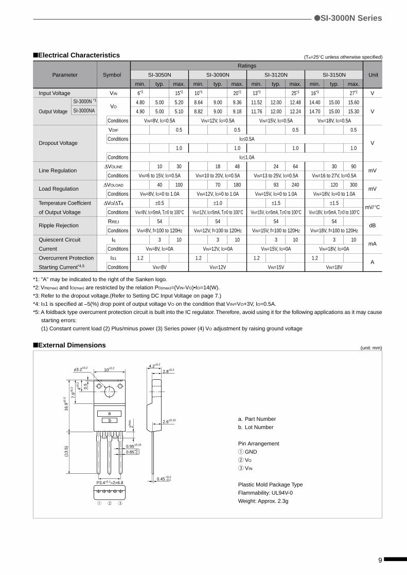
Parameter
Input Voltage
Output Voltage
Dropout Voltage
Line Regulation
Load Regulation
Temperature Coefficient
of Output Voltage
Ripple Rejection
Quiescent Circuit
Current
Overcurrent Protection
Starting Current*4,5
Electrical Characteristics
Unit
V
V
V
mV
mV
mV/°C
dB
mA
A
SI-3000N *1
SI-3000NA
*1: "A" may be indicated to the right of the Sanken logo.
*2: VIN(max) and IO(max) are restricted by the relation PD(max)=(VIN-VO)•IO=14(W).
*3: Refer to the dropout voltage.(Refer to Setting DC Input Voltage on page 7.)
*4: IS1 is specified at –5(%) drop point of output voltage VO on the condition that VIN=VO+3V, IO=0.5A.
*5: A foldback type overcurrent protection circuit is built into the IC regulator. Therefore, avoid using it for the following applications as it may cause
starting errors:
(1) Constant current load (2) Plus/minus power (3) Series power (4) VO adjustment by raising ground voltage
External Dimensions
a. Part Number
b. Lot Number
Pin Arrangement
q GND
w VO
e VIN
Plastic Mold Package Type
Flammability: UL94V-0
Weight: Approx. 2.3g
0.95±0.15
0.85+0.2
10±0.2 4.2±0.2
2.8±0.2
2.6±0.15
q w e
3.2±0.2
2max
.
0.5
16.9
±0.3 7.
9±0.2 4±0
.2
(13.
5)
0.45+0.2–0.1
P3.4±0.1×2=6.8
–0.1
φ
a
b
SI-3000N Series
(unit: mm)
(Ta=25°C unless otherwise specified)
Ratings
SI-3050N SI-3090N SI-3120N SI-3150N
min. typ. max. min. typ. max. min. typ. max. min. typ. max.
6*3 15*2 10*3 20*2 13*3 25*2 16*3 27*2
4.80 5.00 5.20 8.64 9.00 9.36 11.52 12.00 12.48 14.40 15.00 15.60
4.90 5.00 5.10 8.82 9.00 9.18 11.76 12.00 12.24 14.70 15.00 15.30
VIN=8V, IO=0.5A VIN=12V, IO=0.5A VIN=15V, IO=0.5A VIN=18V, IO=0.5A
0.5 0.5 0.5 0.5
IO≤0.5A
1.0 1.0 1.0 1.0
IO≤1.0A
10 30 18 48 24 64 30 90
VIN=6 to 15V, IO=0.5A VIN=10 to 20V, IO=0.5A VIN=13 to 25V, IO=0.5A VIN=16 to 27V, IO=0.5A
40 100 70 180 93 240 120 300
VIN=8V, IO=0 to 1.0A VIN=12V, IO=0 to 1.0A VIN=15V, IO=0 to 1.0A VIN=18V, IO=0 to 1.0A
±0.5 ±1.0 ±1.5 ±1.5
VIN=8V, IO=5mA, Tj=0 to 100°C VIN=12V, IO=5mA, Tj=0 to 100°C VIN=15V, IO=5mA, Tj=0 to 100°C VIN=18V, IO=5mA, Tj=0 to 100°C
54 54 54 54
VIN=8V, f=100 to 120HZ VIN=12V, f=100 to 120HZ VIN=15V, f=100 to 120HZ VIN=18V, f=100 to 120HZ
3 10 3 10 3 10 3 10
VIN=8V, IO=0A VIN=12V, IO=0A VIN=15V, IO=0A VIN=18V, IO=0A
1.2 1.2 1.2 1.2
VIN=8V VIN=12V VIN=15V VIN=18V
Symbol
VIN
VO
Conditions
VDIF
Conditions
Conditions
∆VOLINE
Conditions
∆VOLOAD
Conditions
∆VO/∆Ta
Conditions
RREJ
Conditions
Iq
Conditions
IS1
Conditions
10
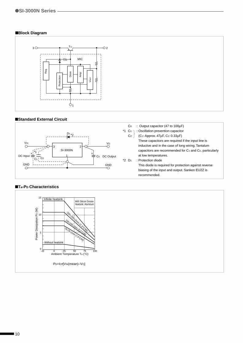
Block Diagram
Standard External Circuit
3R
eg.
Pro
tect
ion Am
p.
VR
EF
Driv
e
MIC
1
2Tr1
D1
C0C2C1
DC Input DC Output
VIN VO
GND GND
3 2
1
SI-3000N*1
*2
+ +
Ta-PD Characteristics
PD=IO•[VIN(mean)–VO]
C0 : Output capacitor (47 to 100µF)
*1 C1 : Oscillation prevention capacitor
C2 (C1: Approx. 47µF, C2: 0.33µF)
These capacitors are required if the input line is
inductive and in the case of long wiring. Tantalum
capacitors are recommended for C1 and C0, particularly
at low temperatures.
*2 D1 : Protection diode
This diode is required for protection against reverse
biasing of the input and output. Sanken EU2Z is
recommended.
SI-3000N Series
15
10
5
0–30 0 25 50
Ambient Temperature Ta (°C)
Pow
er D
issi
patio
n P
D (
W)
75 100
200×200×2mm (2.3°C/W)
100×100×2mm (5.2°C/W)
75×75×2mm (7.6°C/W)
Infinite heatsink
Without heatsink
With Silicon GreaseHeatsink: Aluminum
11
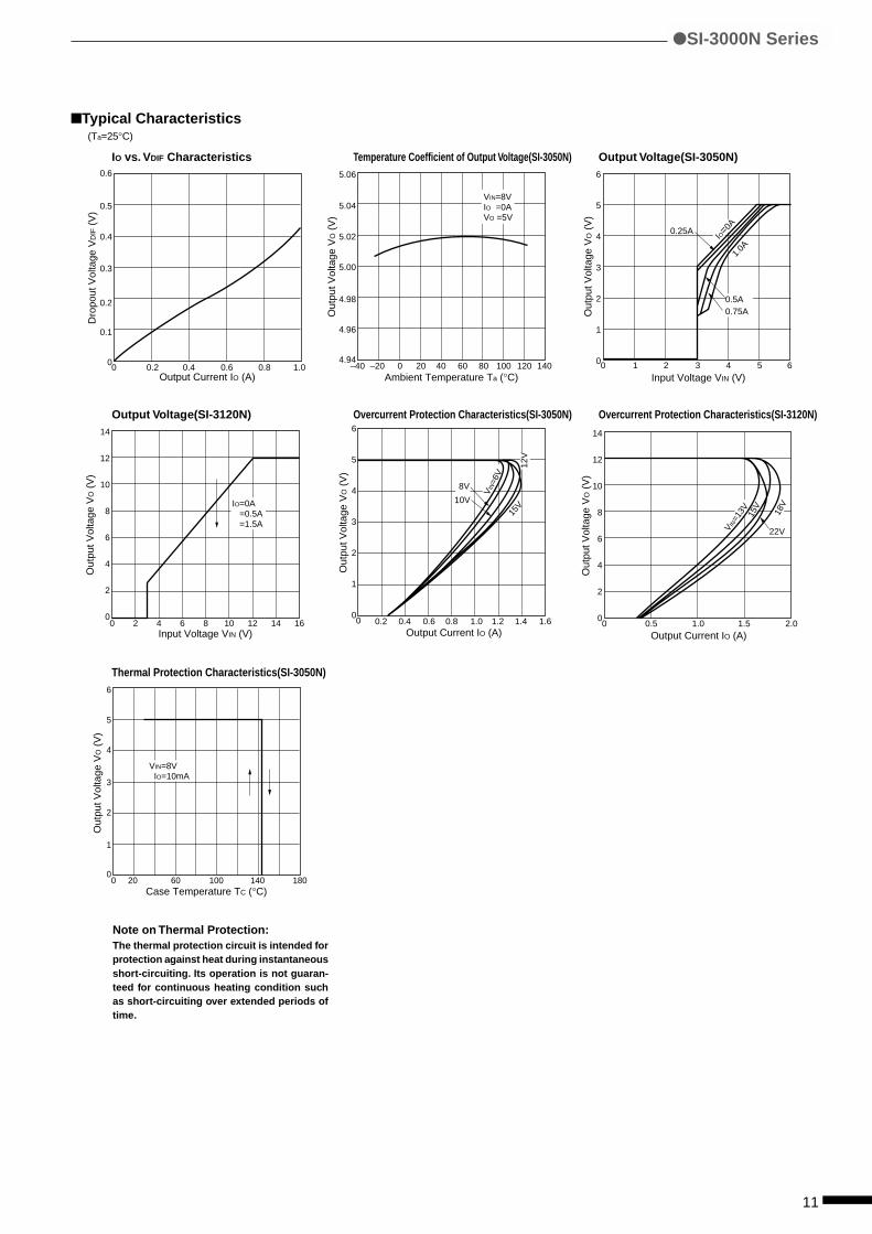
Typical Characteristics
IO vs. VDIF Characteristics Temperature Coefficient of Output Voltage(SI-3050N) Output Voltage(SI-3050N)
Output Voltage(SI-3120N) Overcurrent Protection Characteristics(SI-3050N) Overcurrent Protection Characteristics(SI-3120N)
Thermal Protection Characteristics(SI-3050N)
Output Current IO (A)
Dro
pout
Vol
tage
VD
IF (
V)
0.6
0.5
0.4
0.3
0.2
0.1
00 0.2 0.4 0.6 0.8 1.0
Ambient Temperature Ta (°C)
Out
put V
olta
ge V
O (
V)
5.06
5.04
5.02
5.00
4.98
4.96
4.94–40 –20 0 20 40 60 80 100 120 140
VIN=8VIO =0AVO =5V
Out
put V
olta
ge V
O (
V)
0.25A
0 1 2 3 4
Input Voltage VIN (V)5 6
IO=0A
6
5
4
3
2
1
0
0.5A0.75A
1.0A
Case Temperature TC (°C)
Out
put V
olta
ge V
O (
V)
6
5
4
3
2
1
00 20 60 100 140 180
VIN=8V IO=10mA
Output Current IO (A)
6
5
4
3
2
1
00 0.2 0.4 0.6 0.8 1.0 1.2 1.4 1.6
VIN
=6V
8V
10V
12V
15V
Out
put V
olta
ge V
O (
V)
Output Current IO (A)
Out
put V
olta
ge V
O (
V)
14
12
10
8
6
4
2
00.50 1.0 1.5 2.0
VIN=1
3V 15V
22V
18V
Note on Thermal Protection:The thermal protection circuit is intended forprotection against heat during instantaneousshort-circuiting. Its operation is not guaran-teed for continuous heating condition suchas short-circuiting over extended periods oftime.
(Ta=25°C)
SI-3000N Series
Input Voltage VIN (V)
Out
put V
olta
ge V
O (
V)
14
12
10
8
6
4
2
00 2 4 6 8 10 12 14 16
IO=0A =0.5A =1.5A
12
Parameter
DC Input Voltage
DC Output Current
Power Dissipation
Junction Temperature
Ambient Operating Temperature
Storage Temperature
Thermal Resistance (junction to case)
Thermal Resistance (junction to ambient air)
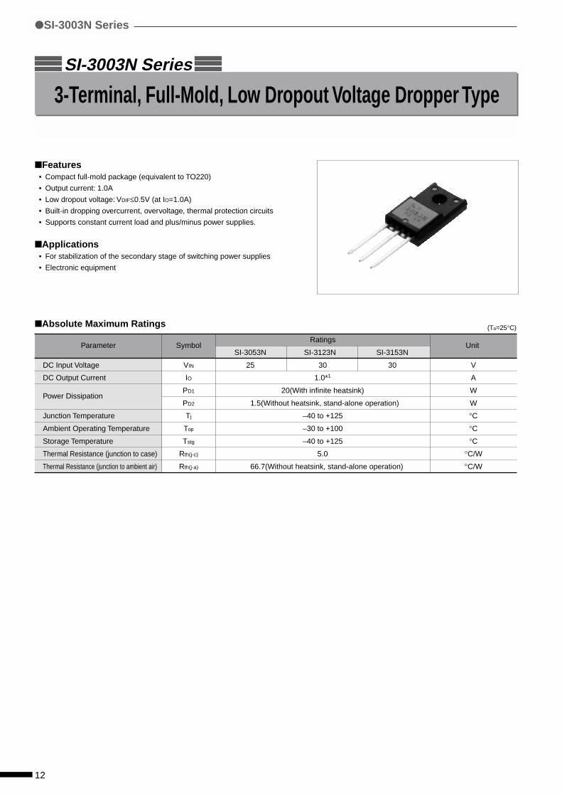
Features• Compact full-mold package (equivalent to TO220)
• Output current: 1.0A
• Low dropout voltage: VDIF≤0.5V (at IO=1.0A)
• Built-in dropping overcurrent, overvoltage, thermal protection circuits
• Supports constant current load and plus/minus power supplies.
Applications• For stabilization of the secondary stage of switching power supplies
• Electronic equipment
Absolute Maximum Ratings (Ta=25°C)
SI-3003N Series
3-Terminal, Full-Mold, Low Dropout Voltage Dropper Type
SI-3003N Series
Ratings
SI-3053N SI-3123N SI-3153N
25 30 30
1.0*1
20(With infinite heatsink)
1.5(Without heatsink, stand-alone operation)
–40 to +125
–30 to +100
–40 to +125
5.0
66.7(Without heatsink, stand-alone operation)
Symbol
VIN
IO
PD1
PD2
Tj
Top
Tstg
Rth(j-c)
Rth(j-a)
Unit
V
A
W
W
°C
°C
°C
°C/W
°C/W
13
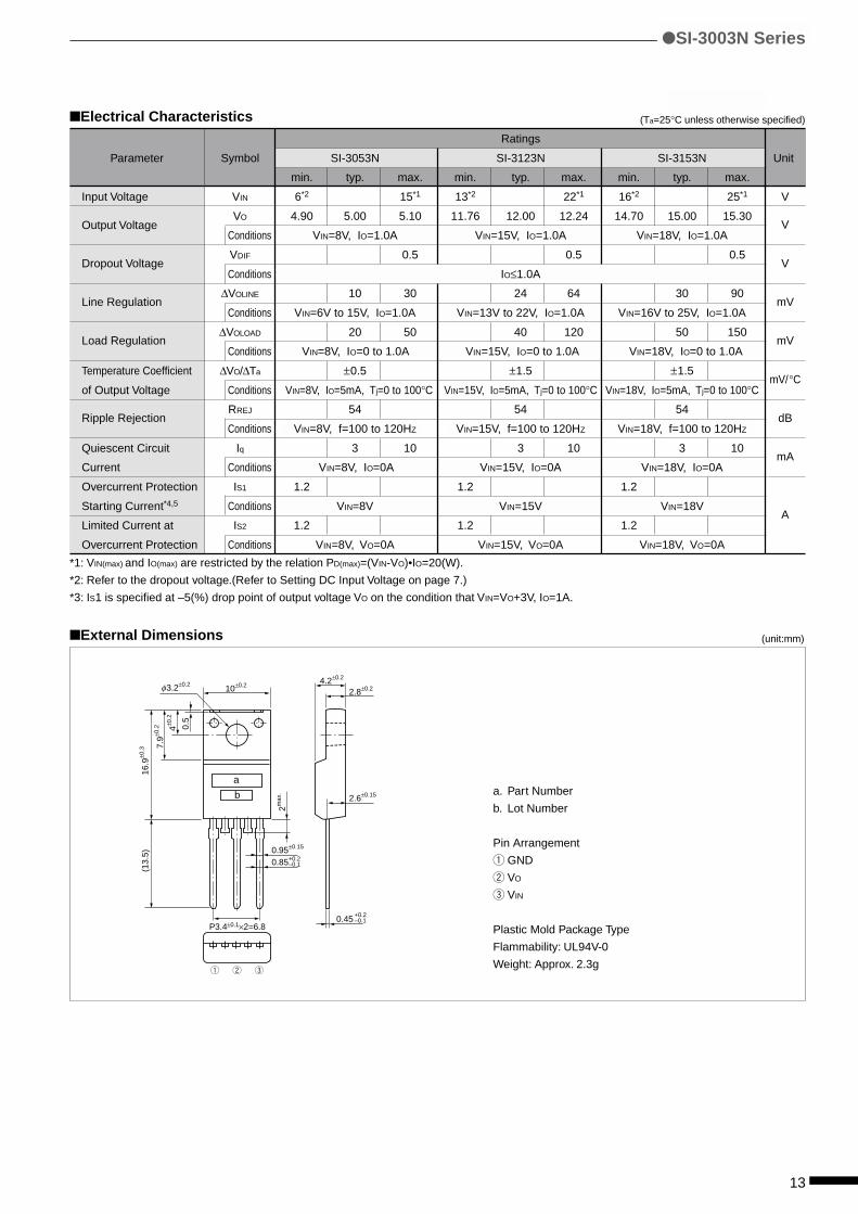
Electrical Characteristics
Unit
V
V
V
mV
mV
mV/°C
dB
mA
A
External Dimensions
a. Part Number
b. Lot Number
Pin Arrangement
q GND
w VO
e VIN
Plastic Mold Package Type
Flammability: UL94V-0
Weight: Approx. 2.3g
0.95±0.15
0.85+0.2
10±0.2 4.2±0.2
2.8±0.2
2.6±0.15
q w e
3.2±0.2
2max
.
0.5
16.9
±0.3 7.
9±0.2 4±0
.2
(13.
5)
0.45+0.2–0.1
P3.4±0.1×2=6.8
–0.1
φ
a
b
SI-3003N Series
Symbol
VIN
VO
Conditions
VDIF
Conditions
∆VOLINE
Conditions
∆VOLOAD
Conditions
∆VO/∆Ta
Conditions
RREJ
Conditions
Iq
Conditions
IS1
Conditions
IS2
Conditions
(unit:mm)
(Ta=25°C unless otherwise specified)
Parameter
Input Voltage
Output Voltage
Dropout Voltage
Line Regulation
Load Regulation
Temperature Coefficient
of Output Voltage
Ripple Rejection
Quiescent Circuit
Current
Overcurrent Protection
Starting Current*4,5
Limited Current at
Overcurrent Protection
*1: VIN(max) and IO(max) are restricted by the relation PD(max)=(VIN-VO)•IO=20(W).
*2: Refer to the dropout voltage.(Refer to Setting DC Input Voltage on page 7.)
*3: IS1 is specified at –5(%) drop point of output voltage VO on the condition that VIN=VO+3V, IO=1A.
Ratings
SI-3053N SI-3123N SI-3153N
min. typ. max. min. typ. max. min. typ. max.
6*2 15*1 13*2 22*1 16*2 25*1
4.90 5.00 5.10 11.76 12.00 12.24 14.70 15.00 15.30
VIN=8V, IO=1.0A VIN=15V, IO=1.0A VIN=18V, IO=1.0A
0.5 0.5 0.5
IO≤1.0A
10 30 24 64 30 90
VIN=6V to 15V, IO=1.0A VIN=13V to 22V, IO=1.0A VIN=16V to 25V, IO=1.0A
20 50 40 120 50 150
VIN=8V, IO=0 to 1.0A VIN=15V, IO=0 to 1.0A VIN=18V, IO=0 to 1.0A
±0.5 ±1.5 ±1.5
VIN=8V, IO=5mA, Tj=0 to 100°C VIN=15V, IO=5mA, Tj=0 to 100°C VIN=18V, IO=5mA, Tj=0 to 100°C
54 54 54
VIN=8V, f=100 to 120HZ VIN=15V, f=100 to 120HZ VIN=18V, f=100 to 120HZ
3 10 3 10 3 10
VIN=8V, IO=0A VIN=15V, IO=0A VIN=18V, IO=0A
1.2 1.2 1.2
VIN=8V VIN=15V VIN=18V
1.2 1.2 1.2
VIN=8V, VO=0A VIN=15V, VO=0A VIN=18V, VO=0A
14
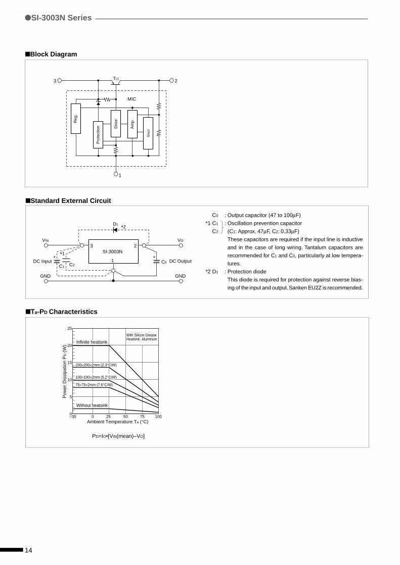
Block Diagram
Standard External Circuit
3R
eg.
Pro
tect
ion Am
p.
VR
EF
Driv
e
MIC
1
2Tr1
D1
C0C2C1
DC Input DC Output
VIN VO
GND GND
3 2
1
SI-3003N *1
*2
+ +
Ta-PD Characteristics
PD=IO•[VIN(mean)–VO]
C0 : Output capacitor (47 to 100µF)
*1 C1 : Oscillation prevention capacitor
C2 (C1: Approx. 47µF, C2: 0.33µF)
These capacitors are required if the input line is inductive
and in the case of long wiring. Tantalum capacitors are
recommended for C1 and C0, particularly at low tempera-
tures.
*2 D1 : Protection diode
This diode is required for protection against reverse bias-
ing of the input and output. Sanken EU2Z is recommended.
25
20
15
10
5
0
Pow
er D
issi
patio
n P
D (
W)
75×75×2mm (7.6°C/W)
100×100×2mm (5.2°C/W)
200×200×2mm (2.3°C/W)
–30 0 25 50Ambient Temperature Ta (°C)
75 100
Infinite heatsink
Without heatsink
With Silicon GreaseHeatsink: Aluminum
SI-3003N Series
15
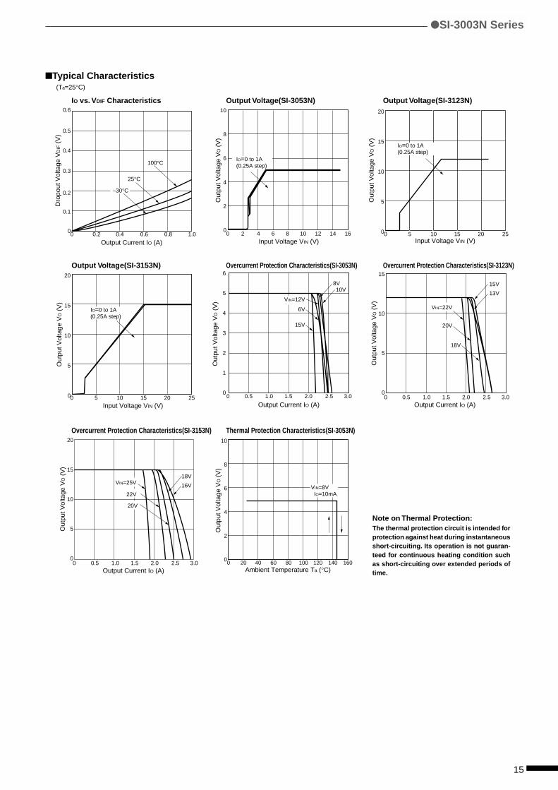
Typical Characteristics
IO vs. VDIF Characteristics Output Voltage(SI-3053N) Output Voltage(SI-3123N)
Output Voltage(SI-3153N) Overcurrent Protection Characteristics(SI-3053N) Overcurrent Protection Characteristics(SI-3123N)
Overcurrent Protection Characteristics(SI-3153N) Thermal Protection Characteristics(SI-3053N)
Out
put V
olta
ge V
O (
V)
0 2 4 6 8
Input Voltage VIN (V)10 12 14 16
10
8
6
4
2
0
IO=0 to 1A(0.25A step)
Input Voltage VIN (V)
Out
put V
olta
ge V
O (
V)
20
15
10
5
00 5 10 15 20 25
IO=0 to 1A(0.25A step)
Out
put V
olta
ge V
O (
V)
Input Voltage VIN (V)
20
15
10
5
0
IO=0 to 1A(0.25A step)
0 5 10 15 20 25Output Current IO (A)
6
5
4
3
2
1
00 0.5 1.0 1.5 2.0 2.5 3.0
VIN=12V
8V10V
6V
15V
Out
put V
olta
ge V
O (
V)
Output Current IO (A)
15
10
5
00 0.5 1.0 1.5 2.0 2.5 3.0
VIN=22V
15V
13V
18V
20V
Out
put V
olta
ge V
O (
V)
Output Current IO (A)
20
15
10
5
00 0.5 1.0 1.5 2.0 2.5 3.0
VIN=25V18V
16V
22V
Out
put V
olta
ge V
O (
V)
20V
Ambient Temperature Ta (°C)
Out
put V
olta
ge V
O (
V)
10
8
6
4
2
00 20 40 60 80 100 120 140 160
VIN=8V IO=10mA
Note on Thermal Protection:The thermal protection circuit is intended forprotection against heat during instantaneousshort-circuiting. Its operation is not guaran-teed for continuous heating condition suchas short-circuiting over extended periods oftime.
(Ta=25°C)
SI-3003N Series
Output Current IO (A)
Dro
pout
Vol
tage
VD
IF (
V)
0.6
0.5
0.4
0.3
0.2
0.1
00 0.2 0.4 0.6 0.8 1.0
–30°C
25°C
100°C

16
Parameter
DC Input Voltage
DC Output Current
Power Dissipation
Junction Temperature
Ambient Operating Temperature
Storage Temperature
Thermal Resistance (junction to case)
Thermal Resistance (junction to ambient air)
Unit
V
A
W
W
°C
°C
°C
°C/W
°C/W
Features• Compact full-mold package (equivalent to TO220)
• Output current: 1.5A
• Low dropout voltage: VDIF≤1V (at IO=1.5A)
• Built-in foldback overcurrent, overvoltage, thermal protection circuits
Applications• For stabilization of the secondary stage of switching power supplies
• Electronic equipment
Absolute Maximum Ratings (Ta=25°C)
SI-3001N Series
3-Terminal, Full-Mold, Low Dropout Voltage Dropper Type
SI-3001N Series
Symbol
VIN
IO
PD1
PD2
Tj
Top
Tstg
Rth(j-c)
Rth(j-a)
Ratings
SI-3051N/3091N SI-3121N/3151N SI-3241N
35 35 45
1.5*2
18(With infinite heatsink)
1.5(Without heatsink, stand-alone operation)
–40 to +125
–30 to +100
–40 to +125
5.5
66.7(Without heatsink, stand-alone operation)
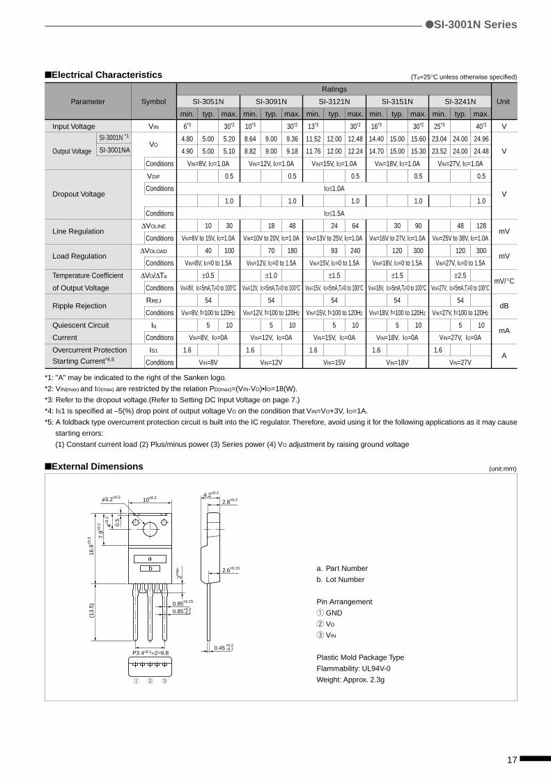
17
Electrical Characteristics
Unit
V
V
V
mV
mV
mV/°C
dB
mA
A
*1: "A" may be indicated to the right of the Sanken logo.
*2: VIN(max) and IO(max) are restricted by the relation PD(max)=(VIN-VO)•IO=18(W).
*3: Refer to the dropout voltage.(Refer to Setting DC Input Voltage on page 7.)
*4: IS1 is specified at –5(%) drop point of output voltage VO on the condition that VIN=VO+3V, IO=1A.
*5: A foldback type overcurrent protection circuit is built into the IC regulator. Therefore, avoid using it for the following applications as it may cause
starting errors:
(1) Constant current load (2) Plus/minus power (3) Series power (4) VO adjustment by raising ground voltage
External Dimensions
a. Part Number
b. Lot Number
Pin Arrangement
q GND
w VO
e VIN
Plastic Mold Package Type
Flammability: UL94V-0
Weight: Approx. 2.3g
0.95±0.15
0.85+0.2
10±0.2 4.2±0.2
2.8±0.2
2.6±0.15
q w e
3.2±0.2
2max
.
0.5
16.9
±0.3 7.
9±0.2 4±0
.2
(13.
5)
0.45+0.2–0.1
P3.4±0.1×2=6.8
–0.1
φ
a
b
SI-3001N Series
Symbol
VIN
VO
Conditions
VDIF
Conditions
Conditions
∆VOLINE
Conditions
∆VOLOAD
Conditions
∆VO/∆Ta
Conditions
RREJ
Conditions
Iq
Conditions
IS1
Conditions
(unit:mm)
Ratings
SI-3051N SI-3091N SI-3121N SI-3151N SI-3241N
min. typ. max. min. typ. max. min. typ. max. min. typ. max. min. typ. max.
6*3 30*2 10*3 30*2 13*3 30*2 16*3 30*2 25*3 40*2
4.80 5.00 5.20 8.64 9.00 9.36 11.52 12.00 12.48 14.40 15.00 15.60 23.04 24.00 24.96
4.90 5.00 5.10 8.82 9.00 9.18 11.76 12.00 12.24 14.70 15.00 15.30 23.52 24.00 24.48
VIN=8V, IO=1.0A VIN=12V, IO=1.0A VIN=15V, IO=1.0A VIN=18V, IO=1.0A VIN=27V, IO=1.0A
0.5 0.5 0.5 0.5 0.5
IO≤1.0A
1.0 1.0 1.0 1.0 1.0
IO≤1.5A
10 30 18 48 24 64 30 90 48 128
VIN=6V to 15V, IO=1.0A VIN=10V to 20V, IO=1.0A VIN=13V to 25V, IO=1.0A VIN=16V to 27V, IO=1.0A VIN=25V to 38V, IO=1.0A
40 100 70 180 93 240 120 300 120 300
VIN=8V, IO=0 to 1.5A VIN=12V, IO=0 to 1.5A VIN=15V, IO=0 to 1.5A VIN=18V, IO=0 to 1.5A VIN=27V, IO=0 to 1.5A
±0.5 ±1.0 ±1.5 ±1.5 ±2.5
VIN=8V, IO=5mA,Tj=0 to 100°C VIN=12V, IO=5mA,Tj=0 to 100°C VIN=15V, IO=5mA,Tj=0 to 100°C VIN=18V, IO=5mA,Tj=0 to 100°C VIN=27V, IO=5mA,Tj=0 to 100°C
54 54 54 54 54
VIN=8V, f=100 to 120HZ VIN=12V, f=100 to 120HZ VIN=15V, f=100 to 120HZ VIN=18V, f=100 to 120HZ VIN=27V, f=100 to 120HZ
5 10 5 10 5 10 5 10 5 10
VIN=8V, IO=0A VIN=12V, IO=0A VIN=15V, IO=0A VIN=18V, IO=0A VIN=27V, IO=0A
1.6 1.6 1.6 1.6 1.6
VIN=8V VIN=12V VIN=15V VIN=18V VIN=27V
(Ta=25°C unless otherwise specified)
Parameter
Input Voltage
Output Voltage
Dropout Voltage
Line Regulation
Load Regulation
Temperature Coefficient
of Output Voltage
Ripple Rejection
Quiescent Circuit
Current
Overcurrent Protection
Starting Current*4,5
SI-3001N *1
SI-3001NA
18
Block Diagram
Standard External Circuit
3R
eg.
Pro
tect
ion Am
p.
VR
EF
Driv
e
MIC
1
2Tr1
D1
C0C2C1
DC Input DC Output
VIN VO
GND GND
3 2
1
SI-3001N *1
*2
+ +
Ta-PD Characteristics
PD=IO•[VIN(mean)–VO]
C0 : Output capacitor (47 to 100µF)
*1 C1 : Oscillation prevention capacitor
C2 (C1: Approx. 47µF, C2: 0.33µF)
These capacitors are required if the input line is inductive
and in the case of long wiring. Tantalum capacitors are
recommended for C1 and C0, particularly at low tempera-
tures.
*2 D1 : Protection diode
This diode is required for protection against reverse bias-
ing of the input and output. Sanken EU2Z is recommended.
SI-3001N Series
15
20
10
5
0–30 0 25 50
Ambient Temperature Ta (°C)
Pow
er D
issi
patio
n P
D (
W)
75 100
75×75×2mm (7.6°C/W)
100×100×2mm (5.2°C/W)
200×200×2mm (2.3°C/W)
Infinite heatsink
Without heatsink
With Silicon GreaseHeatsink:Aluminum
19
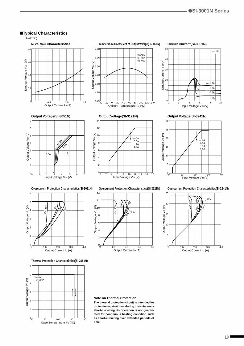
Typical Characteristics
IO vs. VDIF Characteristics Temperature Coefficient of Output Voltage(SI-3051N) Circuit Current(SI-3051N)
Output Voltage(SI-3051N) Output Voltage(SI-3121N) Output Voltage(SI-3241N)
Overcurrent Protection Characteristics(SI-3051N) Overcurrent Protection Characteristics(SI-3121N) Overcurrent Protection Characteristics(SI-3241N)
Thermal Protection Characteristics(SI-3051N)
Ambient Temperature Ta (°C)
Out
put V
olta
ge V
O (
V)
5.08
5.06
5.04
5.02
5.00
4.98
4.96–40 –20 0 20 40 60 80 100 120 140
VIN=8VIO =0AVO =5V
Gro
und
Cur
rent
IG (
mA
)
0 1 4 6
Input Voltage VIN (V)8 10
50
40
30
20
10
0
VO =5V
IO =1.5A
1.0A
0.5A
0A
Out
put V
olta
ge V
O (
V)
0 1 2 3 4Input Voltage VIN (V)
5 76
7
6
5
4
3
2
1
0
1A0.5A
IO=0A
1.5A
Input Voltage VIN (V)
Out
put V
olta
ge V
O (
V)
14
12
10
8
6
4
2
00 2 4 6 8 10 12 14 1816
IO=0A 0.5A
1A 1.5A
Input Voltage VIN (V)
Out
put V
olta
ge V
O (
V)
30
25
20
15
10
5
00 10 20 30 40
IO=0A 0.5A
1A 1.5A
Output Current IO (A)
Out
put V
olta
ge V
O (
V)
6
5
4
3
2
1
00 1.0 2.0 3.0 4.0
8V15
V6V
VIN
=30
V
Output Current IO (A)
Out
put V
olta
ge V
O (
V)
14
12
10
8
6
4
2
00 1.0 2.0 3.0 4.0
VIN
=30
V
13V
15V
25V
20V
Output Current IO (A)
Out
put V
olta
ge V
O (
V)
25
20
15
10
5
00 1.0 2.0 3.0 4.0
VIN
=40
V
30V
35V
25V
27V
Note on Thermal Protection:The thermal protection circuit is intended forprotection against heat during instantaneousshort-circuiting. Its operation is not guaran-teed for continuous heating condition suchas short-circuiting over extended periods oftime.
(Ta=25°C)
SI-3001N Series
0.8
0.6
0.4
0.2
00 0.5 1.0 1.5
Output Current IO (A)
Dro
pout
Vol
tage
VD
IF (
V)
Case Temperature TC (°C)
Out
put V
olta
ge V
O (
V)
6
5
4
3
2
1
020 60 100 140 180
VIN=8V IO=10mA
20
Unit
V
A
W
W
°C
°C
°C
°C/W
°C/W
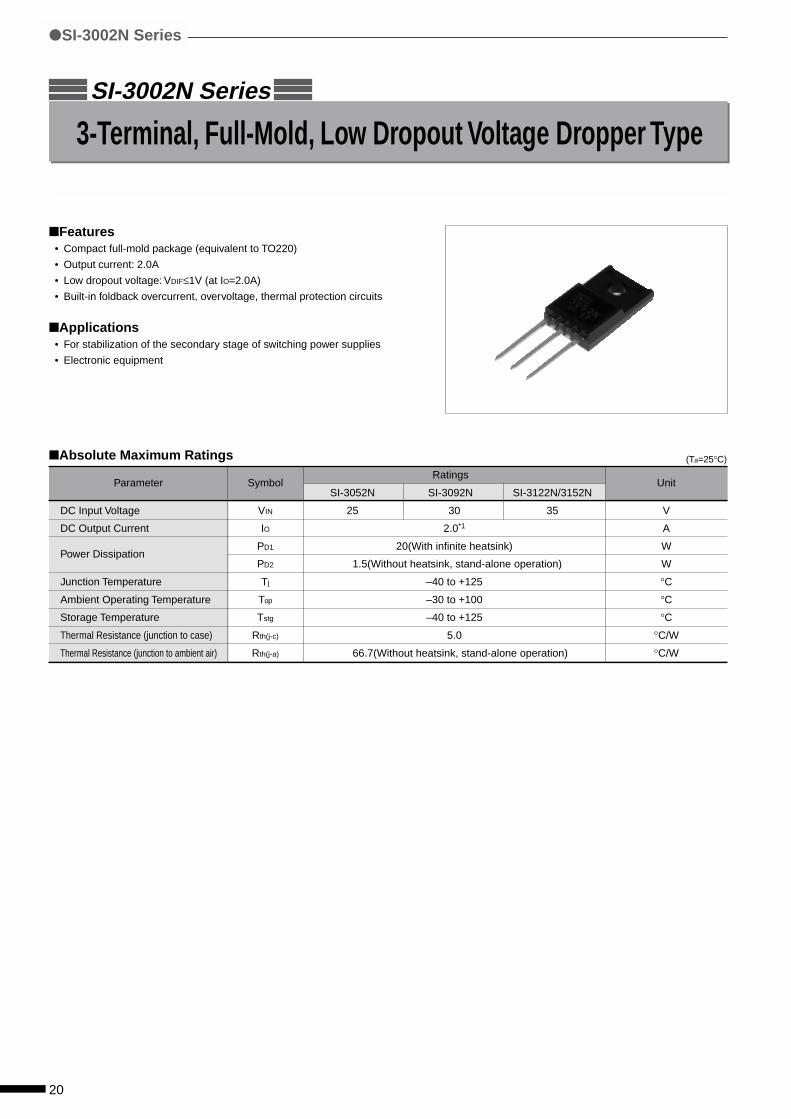
Features• Compact full-mold package (equivalent to TO220)
• Output current: 2.0A
• Low dropout voltage: VDIF≤1V (at IO=2.0A)
• Built-in foldback overcurrent, overvoltage, thermal protection circuits
Applications• For stabilization of the secondary stage of switching power supplies
• Electronic equipment
Absolute Maximum Ratings (Ta=25°C)
SI-3002N Series
3-Terminal, Full-Mold, Low Dropout Voltage Dropper Type
SI-3002N Series
Symbol
VIN
IO
PD1
PD2
Tj
Top
Tstg
Rth(j-c)
Rth(j-a)
Ratings
SI-3052N SI-3092N SI-3122N/3152N
25 30 35
2.0*1
20(With infinite heatsink)
1.5(Without heatsink, stand-alone operation)
–40 to +125
–30 to +100
–40 to +125
5.0
66.7(Without heatsink, stand-alone operation)
Parameter
DC Input Voltage
DC Output Current
Power Dissipation
Junction Temperature
Ambient Operating Temperature
Storage Temperature
Thermal Resistance (junction to case)
Thermal Resistance (junction to ambient air)
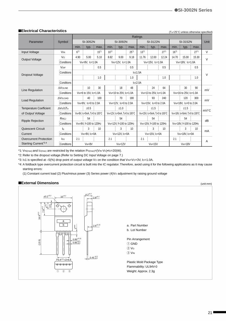
21
Parameter
Input Voltage
Output Voltage
Dropout Voltage
Line Regulation
Load Regulation
Temperature Coefficient
of Output Voltage
Ripple Rejection
Quiescent Circuit
Current
Overcurrent Protection
Starting Current*3.4
Electrical Characteristics
Symbol
VIN
VO
Conditions
VDIF
Conditions
Conditions
∆VOLINE
Conditions
∆VOLOAD
Conditions
∆VO/∆Ta
Conditions
RREJ
Conditions
Iq
Conditions
IS1
Conditions
*1: VIN(max) and IO(max) are restricted by the relation PD(max)=(VIN-VO)•IO=20(W).
*2: Refer to the dropout voltage.(Refer to Setting DC Input Voltage on page 7.)
*3: IS1 is specified at –5(%) drop point of output voltage VO on the condition that VIN=VO+3V, IO=1.0A.
*4: A foldback type overcurrent protection circuit is built into the IC regulator. Therefore, avoid using it for the following applications as it may cause
starting errors:
(1) Constant current load (2) Plus/minus power (3) Series power (4)VO adjustment by raising ground voltage
External Dimensions
a. Part Number
b. Lot Number
Pin Arrangement
q GND
w VO
e VIN
Plastic Mold Package Type
Flammability: UL94V-0
Weight: Approx. 2.3g
0.95±0.15
0.85+0.2
10±0.2 4.2±0.2
2.8±0.2
2.6±0.15
q w e
3.2±0.2
2max
.
0.5
16.9
±0.3 7.
9±0.2 4±0
.2
(13.
5)
0.45+0.2–0.1
P3.4±0.1×2=6.8
–0.1
φ
a
b
SI-3002N Series
(unit:mm)
Unit
V
V
V
mV
mV
mV/°C
dB
mA
A
(Ta=25°C unless otherwise specified)
Ratings
SI-3052N SI-3092N SI-3122N SI-3152N
min. typ. max. min. typ. max. min. typ. max. min. typ. max.
6*2 15*1 10*2 25*1 13*2 27*1 16*2 27*1
4.90 5.00 5.10 8.82 9.00 9.18 11.76 12.00 12.24 14.70 15.00 15.30
VIN=8V, IO=1.0A VIN=12V, IO=1.0A VIN=15V, IO=1.0A VIN=18V, IO=1.0A
0.5 0.5 0.5 0.5
IO≤1.5A
1.0 1.0 1.0 1.0
IO≤2.0A
10 30 18 48 24 64 30 90
VIN=6 to 15V, IO=1.0A VIN=10 to 20V, IO=1.0A VIN=13 to 25V, IO=1.0A VIN=16 to 25V, IO=1.0A
40 100 70 180 93 240 120 300
VIN=8V, IO=0 to 2.0A VIN=12V, IO=0 to 2.0A VIN=15V, IO=0 to 2.0A VIN=18V, IO=0 to 2.0A
±0.5 ±1.0 ±1.5 ±1.5
VIN=8V, IO=5mA, Tj=0 to 100°C VIN=12V, IO=5mA, Tj=0 to 100°C VIN=15V, IO=5mA, Tj=0 to 100°C VIN=18V, IO=5mA, Tj=0 to 100°C
54 54 54 54
VIN=8V, f=100 to 120HZ VIN=12V, f=100 to 120HZ VIN=15V, f=100 to 120HZ VIN=18V, f=100 to 120HZ
3 10 3 10 3 10 3 10
VIN=8V, IO=0A VIN=12V, IO=0A VIN=15V, IO=0A VIN=18V, IO=0A
2.1 2.1 2.1 2.1
VIN=8V VIN=12V VIN=15V VIN=18V
22
Block Diagram
Standard External Circuit
3R
eg.
Pro
tect
ion Am
p.
VR
EF
Driv
e
MIC
1
2Tr1
D1
C0C2C1
DC Input DC Output
VIN VO
GND GND
3 2
1
SI-3002N*1
*2
+ +
Ta-PD Characteristics
PD=IO•[VIN(mean)–VO]
C0 :Output capacitor (47 to 100µF)
*1 C1 :Oscillation prevention capacitor
C2 (C1: Approx. 47µF, C2: 0.33µF)
These capacitors are required if the input line is inductive
and in the case of long wiring. Tantalum capacitors are rec-
ommended for C1 and C0, particularly at low temperatures.
*2 D1 :Protection diode
This diode is required for protection against reverse biasing
of the input and output. Sanken EU2Z is recommended.
SI-3002N Series
25
20
15
10
5
0
Pow
er D
issi
patio
n P
D (
W)
75×75×2mm (7.6°C/W)
100×100×2mm (5.2°C/W)
200×200×2mm (2.3°C/W)
–30 0 25 50Ambient Temperature Ta (°C)
75 100
Infinite heatsink
Without heatsink
With Silicon GreaseHeatsink: Aluminum
23
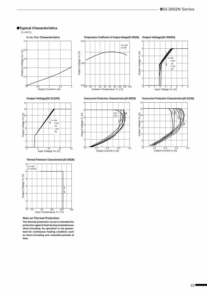
Typical Characteristics
IO vs. VDIF Characteristics Temperature Coefficient of Output Voltage(SI-3052N) Output Voltage(SI-3052N)
Output Voltage(SI-3122N) Overcurrent Protection Characteristics(SI-3052N) Overcurrent Protection Characteristics(SI-3122N)
Thermal Protection Characteristics(SI-3052N)
Note on Thermal Protection:The thermal protection circuit is intended forprotection against heat during instantaneousshort-circuiting. Its operation is not guaran-teed for continuous heating condition suchas short-circuiting over extended periods oftime.
0 0.5 1 1.5 2
1.0
0.8
0.6
0.4
0.2
0
Output Current IO (A)
Dro
pout
Vol
tage
VD
IF (
V)
–40 0–20 4020 8060 140100 120
5.02
5.00
4.98
Ambient Temperature Ta (°C)
Out
put V
olta
ge V
O (
V)
VIN=8VlO=0A
0 1 32 54 86 7
6
5
4
3
2
1
0
Input Voltage VIN (V)
Out
put V
olta
ge V
O (
V)
lO=0A0.5A1A1.5A2A
0 2.01.0 3.0 4.0
6
5
4
3
2
1
0
Output Current IO (A)
Out
put V
olta
ge V
O (
V)
6V
8V
15V
12V10V
0 2.01.0 3.0 4.0Output Current IO (A)
14
12
10
8
6
4
2
0
Out
put V
olta
ge V
O (
V) 27
V
25V
22V
13V
18V
15V
(Ta=25°C)
SI-3002N Series
0 5 10 15 20
14
12
10
8
6
4
2
0
Input Voltage VIN (V)
Out
put V
olta
ge V
O (
V)
lO=0A0.5A1A1.5A2A
0 20 10060 140 180Case Temperature TC (°C)
VIN=8VlO=10mA
6
5
4
3
2
1
0
Out
put V
olta
ge V
O (
V)
24
Ratings
35
VIN
0.27*1
14(With infinite heatsink)
1.5(Without heatsink, stand-alone operation)
–40 to +125
–30 to +100
–40 to +125
7.0
66.7(Without heatsink, stand-alone operation)
Paarameter
DC Input Voltage
Voltage of Output Control Terminal
DC Output Current
Power Dissipation
Junction Temperature
Ambient Operating Temperature
Storage Temperature
Thermal Resistance (junction to case)
Thermal Resistance (junction to ambient air)
Unit
V
V
A
W
W
°C
°C
°C
°C/W
°C/W
Symbol
VIN
VC
IO
PD1
PD2
Tj
Top
Tstg
Rth(j-c)
Rth(j-a)
SI-3000B Series
5-Terminal, Multi-Function, Full-Mold, Low Dropout Voltage Dropper Type
SI-3000B Series
Features• Compact full-mold package (equivalent to TO220)
• Output current: 0.27A
• Low dropout voltage: VDIF≤0.5V (at IO=0.27A)
• Output ON/OFF control terminal is compatible with LS-TTL. (It may be directly
driven by LS-TTL or standard CMOS logic.)
• Built-in foldback overcurrent, thermal protection circuits
• Accurate overcurent protection starting current
SI-3157B : 0.3 to 0.7A (VIN=18V)
SI-3025B : 0.3 to 0.7A (When VIN=18V, at VO=15.7V)
0.3 to 0.75A (When VIN=18V, at VO=11.7V)
• Variable output voltage type (SI-3025B) also available
Applications• For BS and CS antenna power supplies
• Electronic equipment
Absolute Maximum Ratings (Ta=25°C)
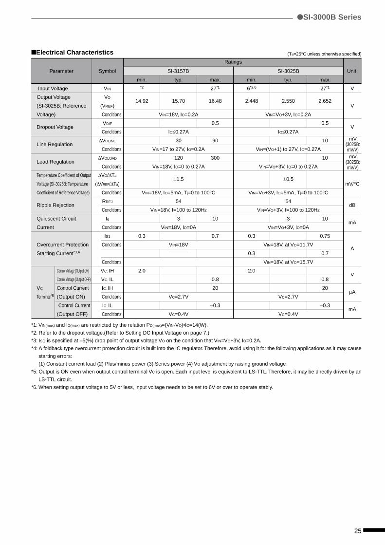
25
Parameter
Input Voltage
Output Voltage
(SI-3025B: Reference
Voltage)
Dropout Voltage
Line Regulation
Load Regulation
Temperature Coefficient of Output
Voltage (SI-3025B: Temperature
Coefficient of Reference Voltage)
Ripple Rejection
Quiescent Circuit
Current
Overcurrent Protection
Starting Current*3,4
Control Voltage (Output ON)
Control Voltage (Output OFF)
VC Control Current
Terminal*5 (Output ON)
Control Current
(Output OFF)
SI-3000B Series
Electrical Characteristics
*1: VIN(max) and IO(max) are restricted by the relation PD(max)=(VIN-VO)•IO=14(W).
*2: Refer to the dropout voltage.(Refer to Setting DC Input Voltage on page 7.)
*3: IS1 is specified at –5(%) drop point of output voltage VO on the condition that VIN=VO+3V, IO=0.2A.
*4: A foldback type overcurrent protection circuit is built into the IC regulator. Therefore, avoid using it for the following applications as it may cause
starting errors:
(1) Constant current load (2) Plus/minus power (3) Series power (4) VO adjustment by raising ground voltage
*5: Output is ON even when output control terminal VC is open. Each input level is equivalent to LS-TTL. Therefore, it may be directly driven by an
LS-TTL circuit.
*6. When setting output voltage to 5V or less, input voltage needs to be set to 6V or over to operate stably.
Symbol
VIN
VO
(VREF)
Conditions
VDIF
Conditions
∆VOLINE
Conditions
∆VOLOAD
Conditions
∆VO/∆Ta
(∆VREF/∆Ta)
Conditions
RREJ
Conditions
Iq
Conditions
IS1
Conditions
Conditions
VC. IH
VC. IL
IC. IH
Conditions
IC. IL
Conditions
Ratings
(Ta=25°C unless otherwise specified)
SI-3157B
min. typ. max.*2 27*1
14.92 15.70 16.48
VIN=18V, IO=0.2A
0.5
IO≤0.27A
30 90
VIN=17 to 27V, IO=0.2A
120 300
VIN=18V, IO=0 to 0.27A
±1.5
VIN=18V, IO=5mA, Tj=0 to 100°C
54
VIN=18V, f=100 to 120HZ
3 10
VIN=18V, IO=0A
0.3 0.7
VIN=18V
2.0
0.8
20
VC=2.7V
–0.3
VC=0.4V
Unit
V
V
V
mV/°C
dB
mA
A
V
µA
mA
SI-3025B
min. typ. max.
6*2,6 27*1
2.448 2.550 2.652
VIN=VO+3V, IO=0.2A
0.5
IO≤0.27A
10
VIN=(VO+1) to 27V, IO=0.27A
10
VIN=VO+3V, IO=0 to 0.27A
±0.5
VIN=VO+3V, IO=5mA, Tj=0 to 100°C
54
VIN=VO+3V, f=100 to 120HZ
3 10
VIN=VO+3V, IO=0A
0.3 0.75
VIN=18V, at VO=11.7V
0.3 0.7
VIN=18V, at VO=15.7V
2.0
0.8
20
VC=2.7V
–0.3
VC=0.4V
mV(3025B:mV/V)mV
(3025B:mV/V)
26
External Dimensions
Block Diagram
SI-3157B SI-3025B
1
2
5
Reg
.
ON
/OF
F
Pro
tect
ion Driv
e
Am
p.
VR
EF
3
4MIC
Tr1
Equivalent to LS-TTL
1
2
5
Reg
.
ON
/OF
F
Pro
tect
ion Driv
e
Am
p.
VR
EF
3
4
MIC
Tr1
Equivalentto LS-TTL
(unit:mm)
SI-3000B Series
10.0±0.24.2±0.2
0.95±0.15
8.2±0.7
2.6±0.1
3.9±0.7 (4.3)
(4.6
)
(8.0
)(1
7.9)
(2.0
)0.85
+0.2–0.1
0.45+0.2–0.1
3.2±0.2
4.0±0
.2
7.9±0
.2
5.0±0
.6
16.9
±0.3
0.5
1 2 3 4 5
P1.7±0.7×4=6.8±0.7
2.8±0.2
φ
a
b
Forming No. 1101
a. Part Number
b. Lot Number
Pin Arrangement
SI-3157B SI-3025B
q GND q GND
w VC w VC
e VO e VO
r VOS r VREF
t VIN t VIN
Plastic Mold Package Type
Flammability: UL94V-0
Weight: Approx. 2.3g
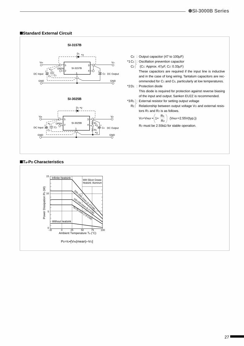
27
SI-3157B
Ta-PD Characteristics
Standard External Circuit
SI-3025B
D1
C0C2C1
DC Input DC Output
VIN VO
GND GND
5SI-3157BOPEN
2
3
41
*1
*2
+ +
D1
C0
R1
R2
C2
C1
DC Input DC Output
VIN VO
GND GND
5
OPEN 2
3
4
1
SI-3025B *1
*3
*3
*2
+ +
C0 : Output capacitor (47 to 100µF)
*1C1 : Oscillation prevention capacitor
C2 (C1: Approx. 47µF, C2: 0.33µF)
These capacitors are required if the input line is inductive
and in the case of long wiring. Tantalum capacitors are rec-
ommended for C1 and C0, particularly at low temperatures.
*2D1 : Protection diode
This diode is required for protection against reverse biasing
of the input and output. Sanken EU2Z is recommended.
*3R1 : External resistor for setting output voltage
R2 Relationship between output voltage VO and external resis-
tors R1 and R2 is as follows.
VO=VREF • 1+ R1
(VREF=2.55V(typ.))R2
R2 must be 2.55kΩ for stable operation.
PD=IO•[VIN(mean)–VO]
SI-3000B Series
15
10
5
0–30 0 25 50
Ambient Temperature Ta (°C)
Pow
er D
issi
patio
n P
D (
W)
75 100
200×200×2mm (2.3°C/W)
100×100×2mm (5.2°C/W)
75×75×2mm (7.6°C/W)
Infinite heatsink
Without heatsink
With Silicon GreaseHeatsink: Aluminum
28
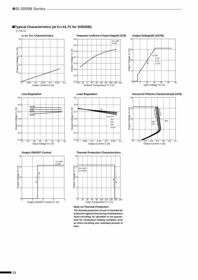
Typical Characteristics (at VO=15.7V for SI3025B)
IO vs. VDIF Characteristics Temperature Coefficient of Output Voltage(SI-3157B) Output Voltage(SI-3157B)
Line Regulation Load Regulation Overcurrent Protection Characteristics(SI-3157B)
Output ON/OFF Control Thermal Protection Characteristics
Note on Thermal Protection:The thermal protection circuit is intended forprotection against heat during instantaneousshort-circuiting. Its operation is not guaran-teed for continuous heating condition suchas short-circuiting over extended periods oftime.
0 0.05 0.1 0.15 0.2 0.25 0.3
0.5
0.4
0.3
0.2
0.1
0
Output Current IO (A)
Dro
pout
Vol
tage
VD
IF (
V)
–40 0–20 4020 8060 140100 120
16.0
15.9
15.8
15.7
15.6
15.5
15.4
15.3
Ambient Temperature TC (°C)
Out
put V
olta
ge V
O (
V)
VIN=18VlO=0A
14 1816 2220 24 26 28
16.1
15.9
15.7
15.5
15.3
15.1
14.9
Input Voltage VIN (V)
Out
put V
olta
ge V
O (
V) lO=0A
0.1A0.2A
0.27A
0 0.10.05 0.15 0.2 0.25 0.3
16.1
15.9
15.7
15.5
15.3
15.1
14.9
Output Current IO (A)
Out
put V
olta
ge V
O (
V)
VIN=27V25V22V18V16.5V
0 0.1 0.3 0.40.2 0.5 0.6 0.7
20
15
10
5
0
Output Current IO (A)
Out
put V
olta
ge V
O (
V)
18V22V
25V
VIN=
27V
VIN=16.5V
0 1 2 3 4
20
15
10
5
0
Output ON/OFF Control VC (V)
Out
put V
olta
ge V
O (
V)
VIN=18VlO=0A
0 4020 1008060 140 160120 180
20
15
10
5
0
Case Temperature TC (°C)
Out
put V
olta
ge V
O (
V)
VIN=18VlO=10mA
(Ta=25°C)
SI-3000B Series
0 5 1510 2520 30
20
15
10
5
0
Input Voltage VIN (V)
Out
put V
olta
ge V
O (
V)
lO=0A0.1A0.2A0.27A
29
Features• Compact full-mold package (equivalent to TO220)
• Output current: 1.0A
• Low dropout voltage: VDIF≤1V (at IO=1.0A)
• Variable output voltage (rise only)
May be used for remote sensing (excluding SI-3025F)
• Output ON/OFF control terminal is compatible with LS-TTL.
(It may be directly driven by LS-TTL or standard CMOS logic.)
• Built-in foldback overcurrent, overvoltage, thermal protection circuits
• Variable output voltage type (SI-3025F) also available
Applications• For stabilization of the secondary stage of switching power supplies
• Electronic equipment
Absolute Maximum Ratings (Ta=25°C)
SI-3000F Series
5-Terminal, Multi-Function, Full-Mold, Low Dropout Voltage Dropper Type
Symbol
VIN
VC
IO
PD1
PD2
Tj
Top
Tstg
Rth(j-c)
Rth(j-a)
Ratings
SI-3050F SI-3090F/3120F SI-3150F/3157F SI-3240F SI-3025F
25 30 35 45 30
VIN
1.0*2
14**(With infinite heatsink)
1.5(Without heatsink, stand-alone operation)
–40 to +125
–30 to +100
–40 to +125
7.0***
66.7(Without heatsink, stand-alone operation)
Parameter
DC Input Voltage
Voltage of Output Control Terminal
DC Output Current
Power Dissipation
Junction Temperature
Ambient Operating Temperature
Storage Temperature
Thermal Resistance (junction to case)
Thermal Resistance (junction to ambient air)
SI-3000F Series
Unit
V
V
A
W
W
°C
°C
°C
°C/W
°C/W
** SI-3240F: 18
*** SI-3240F: 5.5
30
*1: "A" may be indicated to the right of the Sanken logo.
*2: VIN(max) and IO(max) are restricted by the relation PD(max)=(VIN-VO)•IO=14W(SI-3240F: 18W).
*3: Refer to the dropout voltage.(Refer to Setting DC Input Voltage on page 7.)
*4: IS1 is specified at –5(%) drop point of output voltage VO on the condition that VIN=VO+3V, IO=0.5A.
*5: Output is ON even when output control terminal VC is open. Each input level is equivalent to LS-TTL. Therefore, it may be directly driven by an
LS-TTL circuit.
*6: When setting output voltage to 5V or less, input voltage needs to be set to 6V or over to operate stably.
*7: A foldback type overcurrent protection circuit is built into the IC regulator. Therefore, avoid using it for the following applications as it may cause
starting errors:
(1) Constant current load (2) Plus/minus power (3) Series power (4) VO adjustment by raising ground voltage
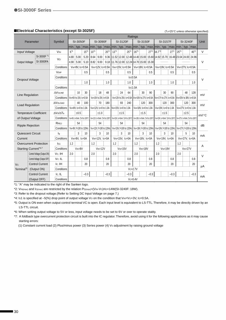
SI-3000F Series
Parameter
Input Voltage
Output Voltage
Dropout Voltage
Line Regulation
Load Regulation
Temperature Coefficient
of Output Voltage
Ripple Rejection
Quiescent Circuit
Current
Overcurrent Protection
Starting Current*4,7
Control Voltage (Output ON)
Control Voltage (Output OFF)
Control Current
(Output ON)
Control Current
(Output OFF)
Electrical Characteristics (except SI-3025F)
SI-3000F *1
SI-3000FA
Unit
V
V
V
mV
mV
mV/°C
dB
mA
A
V
µA
mA
Symbol
VIN
VO
Conditions
VDIF
Conditions
Conditions
∆VOLINE
Conditions
∆VOLOAD
Conditions
∆VO/∆Ta
Conditions
RREJ
Conditions
Iq
Conditions
IS1
Conditions
VC. IH
VC. IL
IC. IH
Conditions
IC. IL
Conditions
(Ta=25°C unless otherwise specified)
VC
Terminal*5
Ratings
SI-3050F SI-3090F SI-3120F SI-3150F SI-3157F SI-3240F
min. typ. max. min. typ. max. min. typ. max. min. typ. max. min. typ. max. min. typ. max.
6*3 15*2 10*3 20*2 13*3 25*2 16*3 27*2 16.7*3 27*2 25*3 40*2
4.80 5.00 5.20 8.64 9.00 9.36 11.52 12.00 12.48 14.40 15.00 15.60 14.92 15.70 16.48 23.04 24.00 24.96
4.90 5.00 5.10 8.82 9.00 9.18 11.76 12.00 12.24 14.70 15.00 15.30
VIN=8V, IO=0.5A VIN=12V, IO=0.5A VIN=15V, IO=0.5A VIN=18V, IO=0.5A VIN=19V, IO=0.5A VIN=27V, IO=0.5A
0.5 0.5 0.5 0.5 0.5 0.5
IO≤0.5A
1.0 1.0 1.0 1.0 1.0 1.0
IO≤1.0A
10 30 18 48 24 64 30 90 30 90 48 128
VIN=6V to 15V, IO=0.5A VIN=10V to 20V, IO=0.5A VIN=13V to 25V, IO=0.5A VIN=16V to 27V, IO=0.5A VIN=17V to 27V, IO=0.5A VIN=25V to 38V, IO=0.5A
40 100 70 180 93 240 120 300 120 300 120 300
VIN=8V, IO=0 to 1.0A VIN=12V, IO=0 to 1.0A VIN=15V, IO=0 to 1.0A VIN=18V, IO=0 to 1.0A VIN=19V, IO=0 to 1.0A VIN=27V, IO=0 to 1.0A
±0.5 ±1.0 ±1.5 ±1.5 ±1.5 ±2.5
VIN=8V, IO=5mA, Tj=0 to 100°C VIN=12V, IO=5mA, Tj=0 to 100°C VIN=15V, IO=5mA, Tj=0 to 100°C VIN=18V, IO=5mA, Tj=0 to 100°C VIN=19V, IO=5mA, Tj=0 to 100°C VIN=27V, IO=5mA, Tj=0 to 100°C
54 54 54 54 54 54
VIN=8V, f=100 to 120HZ VIN=12V, f=100 to 120HZ VIN=15V, f=100 to 120HZ VIN=18V, f=100 to 120HZ VIN=19V, f=100 to 120HZ VIN=27V, f=100 to 120HZ
3 10 3 10 3 10 3 10 3 10 5 10
VIN=8V, IO=0A VIN=12V, IO=0A VIN=15V, IO=0A VIN=18V, IO=0A VIN=19V, IO=0A VIN=27V, IO=0A
1.2 1.2 1.2 1.2 1.2 1.2
VIN=8V VIN=12V VIN=15V VIN=18V VIN=19V VIN=27V
2.0 2.0 2.0 2.0 2.0 2.0
0.8 0.8 0.8 0.8 0.8 0.8
20 20 20 20 20 20
VC=2.7V
–0.3 –0.3 –0.3 –0.3 –0.3 –0.3
VC=0.4V
31
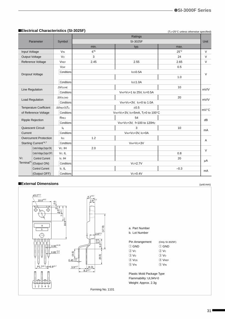
(Ta=25°C unless otherwise specified)
Parameter
Input Voltage
Output Voltage
Reference Voltage
Dropout Voltage
Line Regulation
Load Regulation
Temperature Coefficient
of Reference Voltage
Ripple Rejection
Quiescent Circuit
Current
Overcurrent Protection
Starting Current*4,7
Control Voltage (Output ON)
Control Voltage (Output OFF)
Control Current
(Output ON)
Control Current
(Output OFF)
External Dimensions
Electrical Characteristics (SI-3025F)
Forming No. 1101
(unit:mm)
SI-3000F Series
Unit
V
V
V
V
mV/V
mV/V
mV/°C
dB
mA
A
V
µA
mA
Symbol
VIN
VO
VREF
VDIF
Conditions
Conditions
∆VOLINE
Conditions
∆VOLOAD
Conditions
∆VREF/∆Ta
Conditions
RREJ
Conditions
Iq
Conditions
IS1
Conditions
VC. IH
VC. IL
IC. IH
Conditions
IC. IL
Conditions
VC
Terminal*5
Ratings
SI-3025F
min. typ. max.
6*6 25*2
3 24
2.45 2.55 2.65
0.5
IO≤0.5A
1.0
IO≤1.0A
10
VIN=VO+1 to 25V, IO=0.5A
20
VIN=VO+3V, IO=0 to 1.0A
±0.5
VIN=VO+3V, IO=5mA, Tj=0 to 100°C
54
VIN=VO+3V, f=100 to 120HZ
3 10
VIN=VO+3V, IO=0A
1.2
VIN=VO+3V
2.0
0.8
20
VC=2.7V
–0.3
VC=0.4V
10.0±0.24.2±0.2
0.95±0.15
8.2±0.7
2.6±0.1
3.9±0.7 (4.3)
(4.6
)
(8.0
)(1
7.9)
(2.0
)
0.85+0.2–0.1
0.45+0.2–0.1
3.2±0.2
4.0±0
.2
7.9±0
.2
5.0±0
.6
16.9
±0.3
0.5
1 2 3 4 5
P1.7±0.7×4=6.8±0.7
2.8±0.2
φ
a
b a. Part Number
b. Lot Number
Pin Arrangement (Only SI-3025F)
q GND q GND
w VC w VC
e VO e VO
r VOS r VREF
t VIN t VIN
Plastic Mold Package Type
Flammability: UL94V-0
Weight: Approx. 2.3g
32
C0 : Output capacitor (47 to 100µF)
*1 C1 : Oscillation prevention capacitor
C2 (C1: Approx. 47µF, C2: 0.33µF)
These capacitors are required if the input line is inductive
and in the case of long wiring. Tantalum capacitors are rec-
ommended for C1 and C0, particularly at low temperatures.
*2 D1 : Protection diode
This diode is required for protection against reverse bias-
ing of the input and output. Sanken EU2Z is recommended.
*3 R1 : External resistor for setting output voltage
R2 Relationship between output voltage VO and external re-
sistors R1 and R2 is as follows.
VO=VREF• 1+R1
(VREF=2.55V(typ.))R2
R2 must be 2.55kΩ for stable operation.
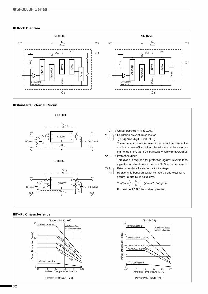
Block Diagram
SI-3000F SI-3025F
Ta-PD Characteristics
Standard External Circuit
SI-3025F
SI-3000F
PD=IO•[VIN(mean)–VO]
1
2
5
Reg
.
ON
/OF
F
Pro
tect
ion Driv
e
Am
p.
VR
EF
3
4MIC
Tr1
Equivalent to LS-TTL
1
2
5
Reg
.
ON
/OF
F
Pro
tect
ion Driv
e
Am
p.
VR
EF
3
4
MIC
Tr1
Equivalent to LS-TTL
D1
C0C2C1
5SI-3000FOPEN
2
3
41
*1
*2
+ +DC Input DC Output
VIN VO
GND GND
D1
C0
R1
R2
C2
C1
DC Input DC Output
VIN VO
GND GND
5
OPEN 2
3
4
1
SI-3025F*1
*3
*3
*2
+ +
SI-3000F Series
15
10
5
0–30 0 25 50
Ambient Temperature Ta (°C)
Pow
er D
issi
patio
n P
D (
W)
75 100
200×200×2mm (2.3°C/W)
100×100×2mm (5.2°C/W)
75×75×2mm (7.6°C/W)
Infinite heatsink
Without heatsink
With Silicon GreaseHeatsink: Aluminum
(Except SI-3240F)
15
20
10
5
0–30 0 25 50
Ambient Temperature Ta (°C)
Pow
er D
issi
patio
n P
D (
W)
75 100
Infinite heatsink
Without heatsink
75×75×2mm (7.6°C/W)
100×100×2mm (5.2°C/W)
200×200×2mm (2.3°C/W)
With Silicon GreaseHeatsink: Aluminum
(SI-3240F)
PD=IO•[VIN(mean)–VO]
33
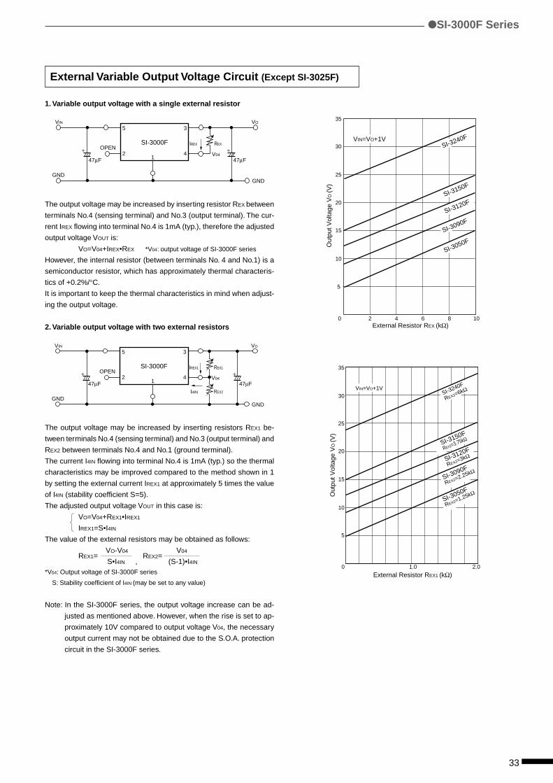
1. Variable output voltage with a single external resistor
The output voltage may be increased by inserting resistor REX between
terminals No.4 (sensing terminal) and No.3 (output terminal). The cur-
rent IREX flowing into terminal No.4 is 1mA (typ.), therefore the adjusted
output voltage VOUT is:
VO=V04+IREX•REX *V04: output voltage of SI-3000F series
However, the internal resistor (between terminals No. 4 and No.1) is a
semiconductor resistor, which has approximately thermal characteris-
tics of +0.2%/°C.
It is important to keep the thermal characteristics in mind when adjust-
ing the output voltage.
2. Variable output voltage with two external resistors
The output voltage may be increased by inserting resistors REX1 be-
tween terminals No.4 (sensing terminal) and No.3 (output terminal) and
REX2 between terminals No.4 and No.1 (ground terminal).
The current I4IN flowing into terminal No.4 is 1mA (typ.) so the thermal
characteristics may be improved compared to the method shown in 1
by setting the external current IREX1 at approximately 5 times the value
of I4IN (stability coefficient S=5).
The adjusted output voltage VOUT in this case is:
VO=V04+REX1•IREX1
IREX1=S•I4IN
The value of the external resistors may be obtained as follows:
REX1= VO-V04
REX2= V04
S•I4IN , (S-1)•I4IN
*V04: Output voltage of SI-3000F series
S: Stability coefficient of I4IN (may be set to any value)
Note: In the SI-3000F series, the output voltage increase can be ad-
justed as mentioned above. However, when the rise is set to ap-
proximately 10V compared to output voltage V04, the necessary
output current may not be obtained due to the S.O.A. protection
circuit in the SI-3000F series.
GNDGND
OPEN
5
2
3
41
SI-3000F IREX REX
47µF 47µF
VO
V04
VIN
+ +
GNDGND
OPEN
5
2
3
41
SI-3000F IREX1 REX1
REX2
47µF 47µF
VO
I4IN
V04
VIN
+ +
35
20
25
30
15
10
5
0 2 4 6 8 10
Out
put V
olta
ge V
O (V
)External Resistor REX (kΩ)
VIN=VO+1VSI-3240F
SI-3150F
SI-3120F
SI-3090F
SI-3050F
External Resistor REX1 (kΩ)
35
20
25
30
15
10
5
0 1.0 2.0
Out
put V
olta
ge V
O (V
)
VIN=VO+1V
SI-3150F
REX2=3.75kΩ
SI-3050F
REX2=1.25kΩ
SI-3120F
REX2=3kΩ
SI-3090F
REX2=2.25kΩ
SI-3240F
REX2=6kΩ
SI-3000F Series
External Variable Output Voltage Circuit (Except SI-3025F)
34
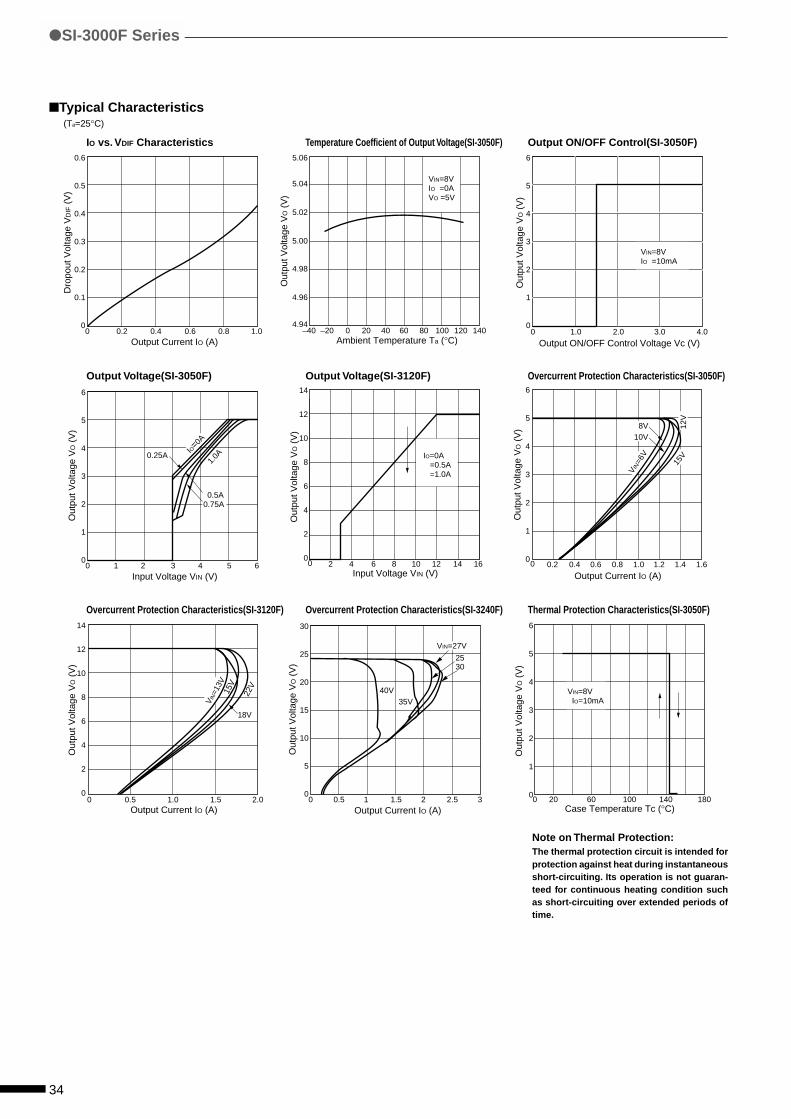
Typical Characteristics
IO vs. VDIF Characteristics Temperature Coefficient of Output Voltage(SI-3050F) Output ON/OFF Control(SI-3050F)
Output Voltage(SI-3050F) Output Voltage(SI-3120F) Overcurrent Protection Characteristics(SI-3050F)
Overcurrent Protection Characteristics(SI-3120F) Overcurrent Protection Characteristics(SI-3240F) Thermal Protection Characteristics(SI-3050F)
0.6
0.5
0.4
0.3
0.2
0.1
00 0.2 0.4 0.6
Output Current IO (A)
Dro
pout
Vol
tage
VD
IF (
V)
0.8 1.0
5.06
5.04
5.02
5.00
4.98
4.96
4.94
Ambient Temperature Ta (°C)
Out
put V
olta
ge V
O (
V)
–40 –20 0 20 40 60 80 100 120 140
VIN=8VIO =0AVO =5V
Out
put V
olta
ge V
O (
V)
6
5
4
3
2
1
00 1.0 2.0
Output ON/OFF Control Voltage Vc (V)3.0 4.0
VIN=8VIO =10mA
Out
put V
olta
ge V
O (
V)
0.25A
0.5A
1.0A
6
5
4
3
2
1
00 1 2 3 4
Input Voltage VIN (V)5 6
0.75A
IO=0A
Input Voltage VIN (V)
14
12
10
8
6
4
2
0
Out
put V
olta
ge V
O (
V)
0 2 4 6 8 10 12 14 16
IO=0A =0.5A =1.0A
Output Current IO (A)
6
5
4
3
2
1
0
Out
put V
olta
ge V
O (
V)
0 0.2 0.4 0.6 0.8 1.0 1.2 1.4 1.6
VIN=6
V
12V
15V
8V10V
Out
put V
olta
ge V
O (
V)
14
12
10
8
6
4
2
00 0.5 1.0 1.5 2.0
18V
22V
Output Current IO (A)
VIN=1
3V15
V
(Ta=25°C)
SI-3000F Series
Note on Thermal Protection:The thermal protection circuit is intended forprotection against heat during instantaneousshort-circuiting. Its operation is not guaran-teed for continuous heating condition suchas short-circuiting over extended periods oftime.
6
5
4
3
2
1
0
Case Temperature Tc (°C)
Out
put V
olta
ge V
O (
V)
0 20 60 100 140 180
VIN=8V IO=10mA
Out
put V
olta
ge V
O (
V)
30
25
20
15
10
5
00 0.5 1 1.5 2
Output Current IO (A)2.5 3
VIN=27V
2530
40V35V
35
Unit
V
V
A
W
W
°C
°C
°C
°C/W
°C/W
Symbol
VIN
VC
IO
PD1
PD2
Tj
Top
Tstg
Rth(j-c)
Rth(j-a)
Features• Compact full-mold package (equivalent to TO220)
• Output current: 1.5A
• Low dropout voltage: VDIF≤1V (at IO=1.5A)
• Variable output voltage (rise only)
May be used for remote sensing
• Output ON/OFF control terminal is compatible with LS-TTL.
(It may be directly driven by LS-TTL or standard CMOS logic.)
• Built-in foldback overcurrent (SI-3033C: Drooping type overcurrent),
overvoltage, thermal protection circuits
Applications• For stabilization of the secondary stage of switching power supplies
• Electronic equipment
Absolute Maximum Ratings (Ta=25°C)
SI-3000C Series
5-Terminal, Multi-Function, Full-Mold, Low Dropout Voltage Dropper Type
Ratings
SI-3033C SI-3050C/3090C SI-3120C/3150C SI-3240C
20 35 35 45
VIN
1.5*2
18(With infinite heatsink)
1.5(Without heatsink, stand-alone operation)
–40 to +125
–30 to +100
–40 to +125
5.5
66.7(Without heatsink, stand-alone operation)
SI-3000C Series
Parameter
DC Input Voltage
Voltage of Output Control Terminal
DC Output Current
Power Dissipation
Junction Temperature
Ambient Operating Temperature
Storage Temperature
Thermal Resistance (junction to case)
Thermal Resistance (junction to ambient air)
36
Parameter
Input Voltage
Output Voltage
Dropout Voltage
Line Regulation
Load Regulation
Temperature Coefficient
of Output Voltage
Ripple Rejection
Quiescent Circuit Current
Overcurrent Protection
Starting Current*4,6
Control Voltage (Output ON)
Control Voltage (Output OFF)
Control Current
(Output ON)
Control Current
(Output OFF)
Symbol
VIN
VO
Conditions
VDIF
Conditions
Conditions
∆VOLINE
Conditions
∆VOLOAD
Conditions
∆VO/∆Ta
Conditions
RREJ
Conditions
Iq
Conditions
IS1
Conditions
VC. IH
VC. IL
IC. IH
Conditions
IC. IL
Conditions
Electrical Characteristics
*1: "A" may be indicated to the right of the Sanken logo.
*2: VIN(max) and IO(max) are restricted by the relation PD(max)=(VIN-VO)•IO=18(W).
*3: Refer to the dropout voltage.(Refer to Setting DC Input Voltage on page 7.)
*4: IS1 is specified at –5(%) drop point of output voltage VO on the condition that VIN=VO+3V, IO=1A.
*5: Output is ON even when output control terminal VC is open. Each input level is equivalent to LS-TTL. Therefore, it may be directly driven by an
LS-TTL circuit.
*6: A foldback type overcurrent protection circuit is built into the IC regulator (excluding SI-3033C). Therefore, avoid using it for the following applica-
tions as it may cause starting errors:
(1) Constant current load (2) Plus/minus power (3) Series power (4) VO adjustment by raising ground voltage
Unit
V
V
V
mV
mV
mV/°C
dB
mA
A
V
µA
mA
SI-3000C *1
SI-3000CA
Ratings
SI-3033C SI-3050C SI-3090C
min. typ. max. min. typ. max. min. typ. max.*3 15*2 6*3 30*2 10*3 30*2
3.168 3.300 3.432 4.80 5.00 5.20 8.64 9.00 9.36
3.234 3.300 3.366 4.90 5.00 5.10 8.82 9.00 9.18
VIN=5V, IO=1.0A VIN=8V, IO=1.0A VIN=12V, IO=1.0A
0.5 0.5 0.5
IO≤1.0A
1.0 1.0 1.0
IO≤1.5A
10 30 10 30 18 48
VIN=4.5 to 12V, IO=1.0A VIN=6 to 15V, IO=1.0A VIN=10 to 20V, IO=1.0A
40 100 40 100 70 180
VIN=5V, IO=0 to 1.5A VIN=8V, IO=0 to 1.5A VIN=12V, IO=0 to 1.5A
±0.5 ±0.5 ±1.0
VIN=5V, IO=5mA, Tj=0 to 100°C VIN=8V, IO=5mA, Tj=0 to 100°C VIN=12V, IO=5mA, Tj=0 to 100°C
54 54 54
VIN=5V, f=100 to 120HZ VIN=8V, f=100 to 120HZ VIN=12V, f=100 to 120HZ
3 10 5 10 5 10
VIN=5V, IO=0A VIN=8V, IO=0A VIN=12V, IO=0A
1.6 1.6 1.6
VIN=5V VIN=8V VIN=12V
2.0 2.0 2.0
0.8 0.8 0.8
20 20 20
VC=2.7V
–0.3 –0.3 –0.3
VC=0.4V
(Ta=25°C unless otherwise specified)
SI-3000C Series
VC
Terminal*5
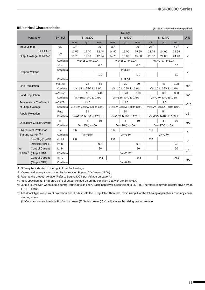
37
Parameter
Input Voltage
Output Voltage
Dropout Voltage
Line Regulation
Load Regulation
Temperature Coefficient
of Output Voltage
Ripple Rejection
Quiescent Circuit Current
Overcurrent Protection
Starting Current*4,6
Control Voltage (Output ON)
Control Voltage (Output OFF)
Control Current
(Output ON)
Control Current
(Output OFF)
Electrical Characteristics
*1: "A" may be indicated to the right of the Sanken logo.
*2: VIN(max) and IO(max) are restricted by the relation PD(max)=(VIN-VO)•IO=18(W).
*3: Refer to the dropout voltage.(Refer to Setting DC Input Voltage on page 7.)
*4: IS1 is specified at –5(%) drop point of output voltage VO on the condition that VIN=VO+3V, IO=1A.
*5: Output is ON even when output control terminal VC is open. Each input level is equivalent to LS-TTL. Therefore, it may be directly driven by an
LS-TTL circuit.
*6: A foldback type overcurrent protection circuit is built into the IC regulator. Therefore, avoid using it for the following applications as it may cause
starting errors:
(1) Constant current load (2) Plus/minus power (3) Series power (4) VO adjustment by raising ground voltage
Unit
V
V
V
mV
mV
mV/°C
dB
mA
A
V
µA
mA
Symbol
VIN
VO
Conditions
VDIF
Conditions
Conditions
∆VOLINE
Conditions
∆VOLOAD
Conditions
∆VO/∆Ta
Conditions
RREJ
Conditions
Iq
Conditions
IS1
Conditions
VC. IH
VC. IL
IC. IH
Conditions
IC. IL
Conditions
SI-3000C Series
(Ta=25°C unless otherwise specified)
VC
Terminal*5
SI-3000C *1
SI-3000CA
Ratings
SI-3120C SI-3150C SI-3240C
min. typ. max. min. typ. max. min. typ. max.
13*3 30*2 16*3 30*2 25*3 40*2
11.52 12.00 12.48 14.40 15.00 15.60 23.04 24.00 24.96
11.76 12.00 12.24 14.70 15.00 15.30 23.52 24.00 24.48
VIN=15V, IO=1.0A VIN=18V, IO=1.0A VIN=27V, IO=1.0A
0.5 0.5 0.5
IO≤1.0A
1.0 1.0 1.0
IO≤1.5A
24 64 30 90 48 128
VIN=13 to 25V, IO=1.0A VIN=16 to 25V, IO=1.0A VIN=25 to 38V, IO=1.0A
93 240 120 300 120 300
VIN=15V, IO=0 to 1.5A VIN=18V, IO=0 to 1.5A VIN=27V, IO=0 to 1.5A
±1.5 ±1.5 ±2.5
VIN=15V, IO=5mA, Tj=0 to 100°C VIN=18V, IO=5mA, Tj=0 to 100°C VIN=27V, IO=5mA, Tj=0 to 100°C
54 54 54
VIN=15V, f=100 to 120HZ VIN=18V, f=100 to 120HZ VIN=27V, f=100 to 120HZ
5 10 5 10 5 10
VIN=15V, IO=0A VIN=18V, IO=0A VIN=27V, IO=0A
1.6 1.6 1.6
VIN=15V VIN=18V VIN=27V
2.0 2.0 2.0
0.8 0.8 0.8
20 20 20
VC=2.7V
–0.3 –0.3 –0.3
VC=0.4V

38
a. Part Number
b. Lot Number
Pin Arrangement
q GND
w VC
e VO
r VOS
t VIN
Plastic Mold Package Type
Flammability: UL94V-0
Weight: Approx. 2.3g
Block Diagram
SI-3000C
Standard External Circuit
C0 : Output capacitor (47 to 100µF)
*1 C1 : Oscillation prevention capacitor
C2 (C1: Approx. 47µF, C2: 0.33µF)
These capacitors are required if the input line is inductive
and in the case of long wiring. Tantalum capacitors are rec-
ommended for C1 and C0, particularly at low temperatures.
*2 D1 : Protection diode
This diode is required for protection against reverse biasing
of the input and output. Sanken EU2Z is recommended.
External Dimensions
1
2
5
Reg
.
ON
/OF
F
Pro
tect
ion Driv
e
Am
p.
VR
EF
3
4MIC
Tr1
Equivalent to LS-TTL
D1
C0C2C1
DC Input DC Output
VIN VO
GND GND
5SI-3000COPEN
2
3
41
*1
*2
+ +
(unit:mm)
SI-3000C Series
10.0±0.24.2±0.2
0.95±0.15
8.2±0.7
2.6±0.1
3.9±0.7 (4.3)
(4.6
)
(8.0
)(1
7.9)
(2.0
)
0.85+0.2–0.1
0.45+0.2–0.1
3.2±0.2
4.0±0
.2
7.9±0
.2
5.0±0
.6
16.9
±0.3
0.5
1 2 3 4 5
P1.7±0.7×4=6.8±0.7
2.8±0.2
φ
Forming No. 1101
a
b

39
Ta-PD Characteristics
PD=IO•[VIN(mean)–VO]
SI-3000C Series
15
20
10
5
0–30 0 25 50
Ambient Temperature Ta (°C)
Pow
er D
issi
patio
n P
D (
W)
75 100
75×75×2mm (7.6°C/W)
100×100×2mm (5.2°C/W)
200×200×2mm (2.3°C/W)
Infinite heatsink
Without heatsink
With Silicon GreaseHeatsink: Aluminum
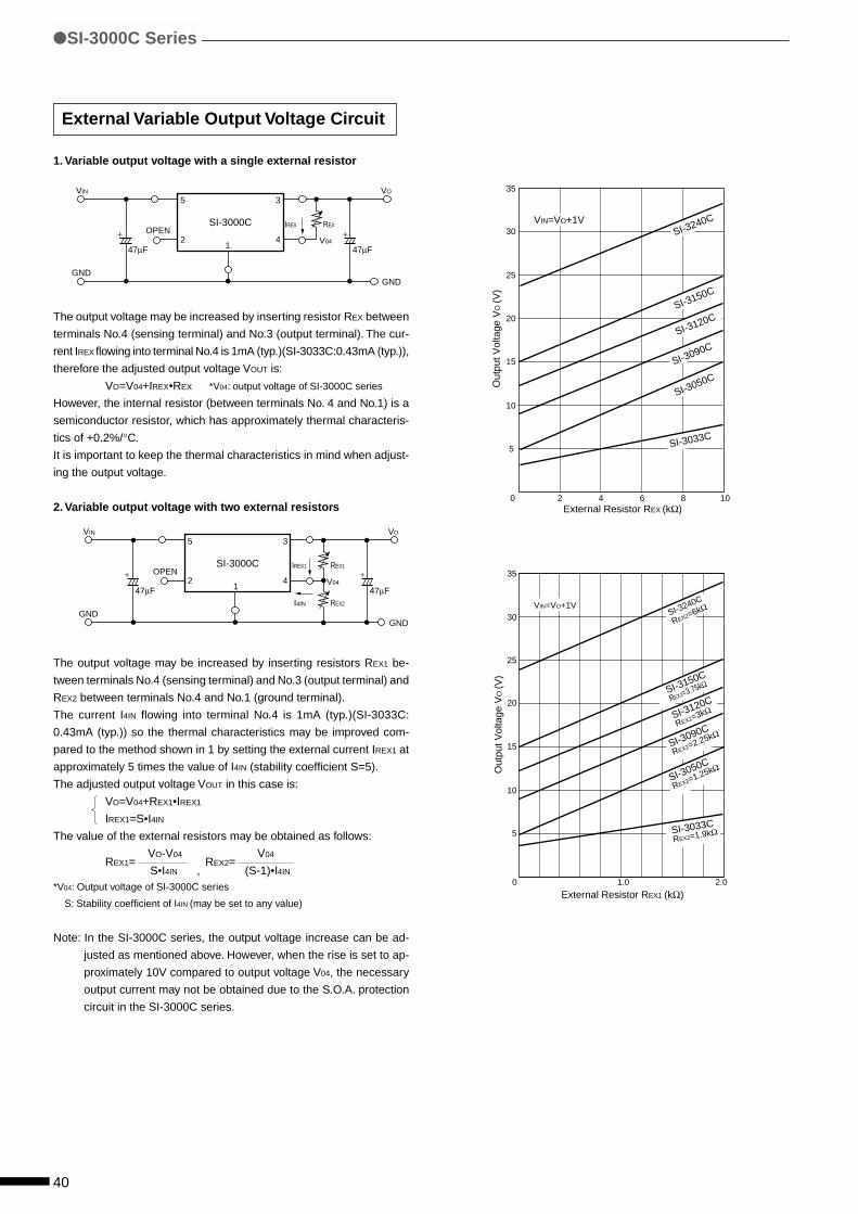
40
1. Variable output voltage with a single external resistor
The output voltage may be increased by inserting resistor REX between
terminals No.4 (sensing terminal) and No.3 (output terminal). The cur-
rent IREX flowing into terminal No.4 is 1mA (typ.)(SI-3033C:0.43mA (typ.)),
therefore the adjusted output voltage VOUT is:
VO=V04+IREX•REX *V04: output voltage of SI-3000C series
However, the internal resistor (between terminals No. 4 and No.1) is a
semiconductor resistor, which has approximately thermal characteris-
tics of +0.2%/°C.
It is important to keep the thermal characteristics in mind when adjust-
ing the output voltage.
2. Variable output voltage with two external resistors
The output voltage may be increased by inserting resistors REX1 be-
tween terminals No.4 (sensing terminal) and No.3 (output terminal) and
REX2 between terminals No.4 and No.1 (ground terminal).
The current I4IN flowing into terminal No.4 is 1mA (typ.)(SI-3033C:
0.43mA (typ.)) so the thermal characteristics may be improved com-
pared to the method shown in 1 by setting the external current IREX1 at
approximately 5 times the value of I4IN (stability coefficient S=5).
The adjusted output voltage VOUT in this case is:
VO=V04+REX1•IREX1
IREX1=S•I4IN
The value of the external resistors may be obtained as follows:
REX1= VO-V04
REX2= V04
S•I4IN , (S-1)•I4IN
*V04: Output voltage of SI-3000C series
S: Stability coefficient of I4IN (may be set to any value)
Note: In the SI-3000C series, the output voltage increase can be ad-
justed as mentioned above. However, when the rise is set to ap-
proximately 10V compared to output voltage V04, the necessary
output current may not be obtained due to the S.O.A. protection
circuit in the SI-3000C series.
GNDGND
OPEN
5
2
3
41
SI-3000C IREX REX
47µF 47µF
VO
V04
VIN
+ +
GNDGND
OPEN
5
2
3
41
SI-3000C IREX1 REX1
REX2
47µF 47µF
VO
I4IN
V04
VIN
+ +
35
20
25
30
15
10
5
0 2 4 6 8 10O
utpu
t Vol
tage
VO
(V)
External Resistor REX (kΩ)
VIN=VO+1VSI-3240C
SI-3150C
SI-3120C
SI-3090C
SI-3050C
SI-3033C
External Resistor REX1 (kΩ)
35
20
25
30
15
10
5
0 1.0 2.0
Out
put V
olta
ge V
O (V
)
VIN=VO+1V
SI-3150C
REX2=3.75kΩ
SI-3033C
REX2=1.9kΩ
SI-3050C
REX2=1.25kΩ
SI-3120C
REX2=3kΩ
SI-3090C
REX2=2.25kΩ
SI-3240C
REX2=6kΩ
SI-3000C Series
External Variable Output Voltage Circuit
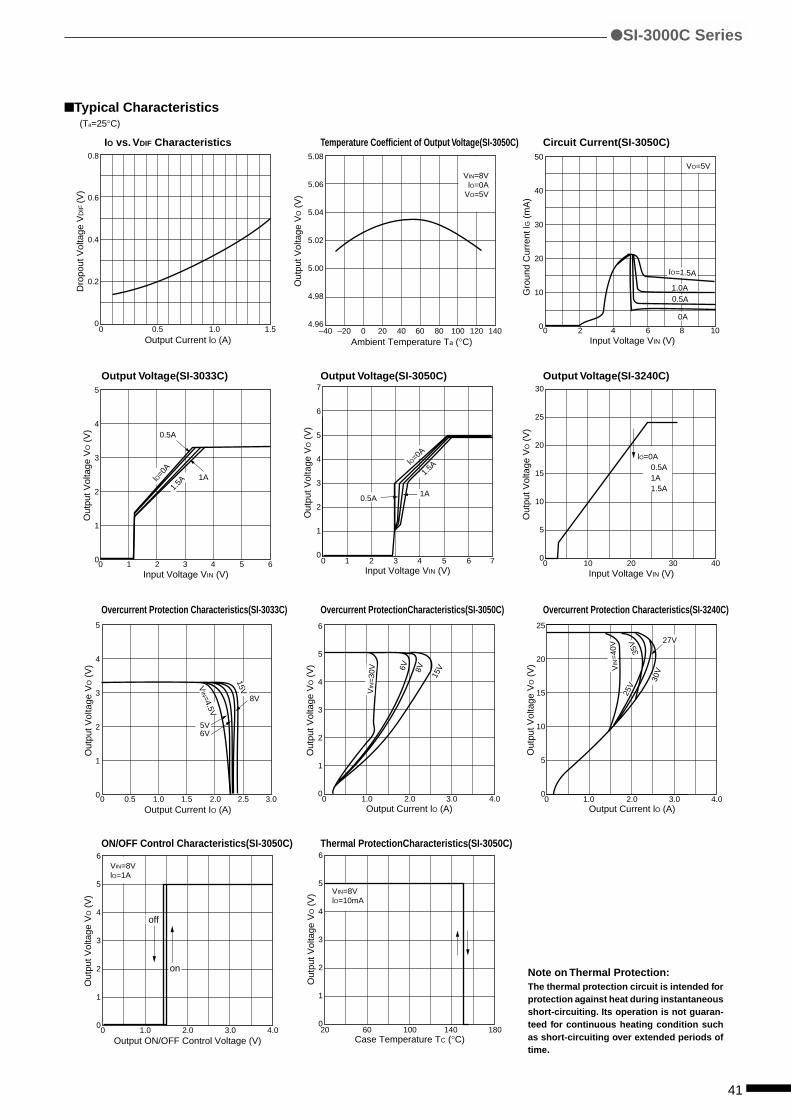
41
Typical Characteristics
IO vs. VDIF Characteristics Temperature Coefficient of Output Voltage(SI-3050C) Circuit Current(SI-3050C)
Output Voltage(SI-3033C) Output Voltage(SI-3050C) Output Voltage(SI-3240C)
Overcurrent Protection Characteristics(SI-3033C) Overcurrent ProtectionCharacteristics(SI-3050C) Overcurrent Protection Characteristics(SI-3240C)
ON/OFF Control Characteristics(SI-3050C) Thermal ProtectionCharacteristics(SI-3050C)
–40 –20 0 20 40 60 80 100 120 140
5.08
5.06
5.04
5.02
5.00
4.98
4.96
Ambient Temperature Ta (°C)
Out
put V
olta
ge V
O (
V)
VIN=8V lO=0AVO=5V
0 1.0 2.0 3.0 4.0
6
5
4
3
2
1
0
Output Current lO (A)
Out
put V
olta
ge V
O (
V)
8V
15V6V
VIN
=30
V
0 0.5 1.0 1.5 2.0 2.5 3.0
5
4
3
2
1
0
Output Current IO (A)
Out
put V
olta
ge V
O (
V)
VIN=4.5V
5V6V
8V
15V
0 1.0 2.0 3.0 4.0
6
5
4
3
2
1
0
Output ON/OFF Control Voltage (V)
Out
put V
olta
ge V
O (
V)
VIN=8VlO=1A
off
on
20 60 100 140 180
6
5
4
3
2
1
0
Case Temperature TC (°C)
Out
put V
olta
ge V
O (
V) VIN=8V
lO=10mA
(Ta=25°C)
SI-3000C Series
Note on Thermal Protection:The thermal protection circuit is intended forprotection against heat during instantaneousshort-circuiting. Its operation is not guaran-teed for continuous heating condition suchas short-circuiting over extended periods oftime.
0 0.5 1.0 1.5
0.8
0.6
0.4
0.2
0
Output Current lO (A)
Dro
pout
Vol
tage
VD
IF (V
)
0 2 4 6 8 10
50
40
30
20
10
0
Input Voltage VIN (V)
Gro
und
Cur
rent
lG (
mA
)
VO=5V
IO=1.5A
1.0A0.5A
0A
0 1 2 3 4 5 6
5
4
3
2
1
0
Input Voltage VIN (V)
Out
put V
olta
ge V
O (
V)
1A1.
5AlO=0A
0.5A
0 1 2 3 4 5 6 7
7
6
5
4
3
2
1
0
Input Voltage VIN (V)
Out
put V
olta
ge V
O (
V)
1.5AlO=0A
0.5A1A
0 10 20 30 40
30
25
20
15
10
5
0
Input Voltage VIN (V)
Out
put V
olta
ge V
O (
V)
lO=0A0.5A1A1.5A
0 1.0 2.0 3.0 4.0
25
20
15
10
5
0
Output Current lO (A)
Out
put V
olta
ge V
O (
V) VIN
=40
V
30V
35V
25V
27V
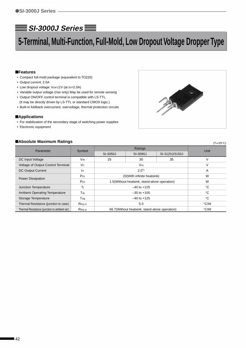
42
Parameter
DC Input Voltage
Voltage of Output Control Terminal
DC Output Current
Power Dissipation
Junction Temperature
Ambient Operating Temperature
Storage Temperature
Thermal Resistance (junction to case)
Thermal Resistance (junction to ambient air)
Features• Compact full-mold package (equivalent to TO220)
• Output current: 2.0A
• Low dropout voltage: VDIF≤1V (at IO=2.0A)
• Variable output voltage (rise only) May be used for remote sensing
• Output ON/OFF control terminal is compatible with LS-TTL.
(It may be directly driven by LS-TTL or standard CMOS logic.)
• Built-in foldback overcurrent, overvoltage, thermal protection circuits
Applications• For stabilization of the secondary stage of switching power supplies
• Electronic equipment
Absolute Maximum Ratings
SI-3000J Series
5-Terminal, Multi-Function, Full-Mold, Low Dropout Voltage Dropper Type
SI-3000J Series
Unit
V
V
A
W
W
°C
°C
°C
°C/W
°C/W
(Ta=25°C)
Symbol
VIN
VC
IO
PD1
PD2
Tj
Top
Tstg
Rth(j-c)
Rth(j-a)
Ratings
SI-3050J SI-3090J SI-3120J/3150J
25 30 35
VIN
2.0*1
20(With infinite heatsink)
1.5(Without heatsink, stand-alone operation)
–40 to +125
–30 to +100
–40 to +125
5.0
66.7(Without heatsink, stand-alone operation)
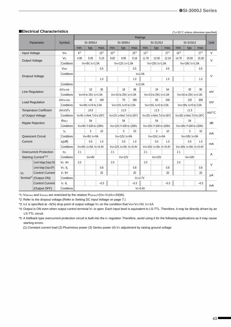
43
Parameter
Input Voltage
Output Voltage
Dropout Voltage
Line Regulation
Load Regulation
Temperature Coefficient
of Output Voltage
Ripple Rejection
Quiescent Circuit
Current
Overcurrent Protection
Starting Current*3,5
Control Voltage (Output ON)
Control Voltage (Output OFF)
Control Current
(Output ON)
Control Current
(Output OFF)
SI-3000J Series
Unit
V
V
V
mV
mV
mV/°C
dB
mA
mA
A
V
µA
mA
*1: VIN(max) and IO(max) are restricted by the relation PD(max)=(VIN-VO)•IO=20(W).
*2: Refer to the dropout voltage.(Refer to Setting DC Input Voltage on page 7.)
*3: IS1 is specified at –5(%) drop point of output voltage VO on the condition that VIN=VO+3V, IO=1A.
*4: Output is ON even when output control terminal VC is open. Each input level is equivalent to LS-TTL. Therefore, it may be directly driven by an
LS-TTL circuit.
*5: A foldback type overcurrent protection circuit is built into the IC regulator. Therefore, avoid using it for the following applications as it may cause
starting errors:
(1) Constant current load (2) Plus/minus power (3) Series power (4) VO adjustment by raising ground voltage
Ratings
SI-3050J SI-3090J SI-3120J SI-3150J
min. typ. max. min. typ. max. min. typ. max. min. typ. max.
6*2 15*1 10*2 25*1 13*2 27*1 16*2 27*1
4.90 5.00 5.10 8.82 9.00 9.18 11.76 12.00 12.24 14.70 15.00 15.30
VIN=8V, IO=1.0A VIN=12V, IO=1.0A VIN=15V, IO=1.0A VIN=18V, IO=1.0A
0.5 0.5 0.5 0.5
IO≤1.5A
1.0 1.0 1.0 1.0
IO≤2.0A
10 30 18 48 24 64 30 90
VIN=6 to 15V, IO=1.0A VIN=10 to 20V, IO=1.0A VIN=13 to 25V, IO=1.0A VIN=16 to 25V, IO=1.0A
40 100 70 180 93 240 120 300
VIN=8V, IO=0 to 2.0A VIN=12V, IO=0 to 2.0A VIN=15V, IO=0 to 2.0A VIN=18V, IO=0 to 2.0A
±0.5 ±1.0 ±1.5 ±1.5
VIN=8V, IO=5mA, Tj=0 to 100°C VIN=12V, IO=5mA, Tj=0 to 100°C VIN=15V, IO=5mA, Tj=0 to 100°C VIN=18V, IO=5mA, Tj=0 to 100°C
54 54 54 54
VIN=8V, f=100 to 120HZ VIN=12V, f=100 to 120HZ VIN=15V, f=100 to 120HZ VIN=18V, f=100 to 120HZ
3 10 3 10 3 10 3 10
VIN=8V, IO=0A VIN=12V, IO=0A VIN=15V, IO=0A VIN=18V, IO=0A
0.5 1.0 0.5 1.0 0.5 1.0 0.5 1.0
VIN=8V, IO=0A, VC=0.4V VIN=12V, IO=0A, VC=0.4V VIN=15V, IO=0A, VC=0.4V VIN=18V, IO=0A, VC=0.4V
2.1 2.1 2.1 2.1
VIN=8V VIN=12V VIN=15V VIN=18V
2.0 2.0 2.0 2.0
0.8 0.8 0.8 0.8
20 20 20 20
VC=2.7V
–0.3 –0.3 –0.3 –0.3
VC=0.4V
VC
Terminal*4
Symbol
VIN
VO
Conditions
VDIF
Conditions
Conditions
∆VOLINE
Conditions
∆VOLOAD
Conditions
∆VO/∆Ta
Conditions
RREJ
Conditions
Iq
Conditions
Iq(off)
Conditions
IS1
Conditions
VC. IH
VC. IL
IC. IH
Conditions
IC. IL
Conditions
Electrical Characteristics (Ta=25°C unless otherwise specified)
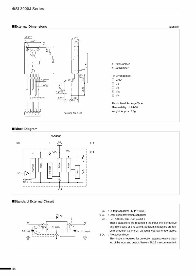
44
Block Diagram
SI-3000J
Standard External Circuit
C0 : Output capacitor (47 to 100µF)
*1 C1 : Oscillation prevention capacitor
C2 (C1: Approx. 47µF, C2: 0.33µF)
These capacitors are required if the input line is inductive
and in the case of long wiring. Tantalum capacitors are rec-
ommended for C1 and C0, particularly at low temperatures.
*2 D1 : Protection diode
This diode is required for protection against reverse bias-
ing of the input and output. Sanken EU2Z is recommended.
External Dimensions
D1
C0C2C1
DC Input DC Output
VIN VO
GND GND
5SI-3000JOPEN
2
3
41
*1
*2
+ +
(unit:mm)
SI-3000J Series
10.0±0.24.2±0.2
0.95±0.15
8.2±0.7
2.6±0.1
3.9±0.7 (4.3)
(4.6
)
(8.0
)(1
7.9)
(2.0
)
0.85+0.2–0.1
0.45+0.2–0.1
3.2±0.2
4.0±0
.2
7.9±0
.2
5.0±0
.6
16.9
±0.3
0.5
1 2 3 4 5
P1.7±0.7×4=6.8±0.7
2.8±0.2
φ
Forming No. 1101
a
b
1
2
5
ON
/OF
F
Pro
tect
ion Driv
e
Reg
.
Am
p.
VR
EF
3
4MIC
Tr1
Equivalent to LS-TTL
a. Part Number
b. Lot Number
Pin Arrangement
q GND
w VC
e VO
r VOS
t VIN
Plastic Mold Package Type
Flammability: UL94V-0
Weight: Approx. 2.3g
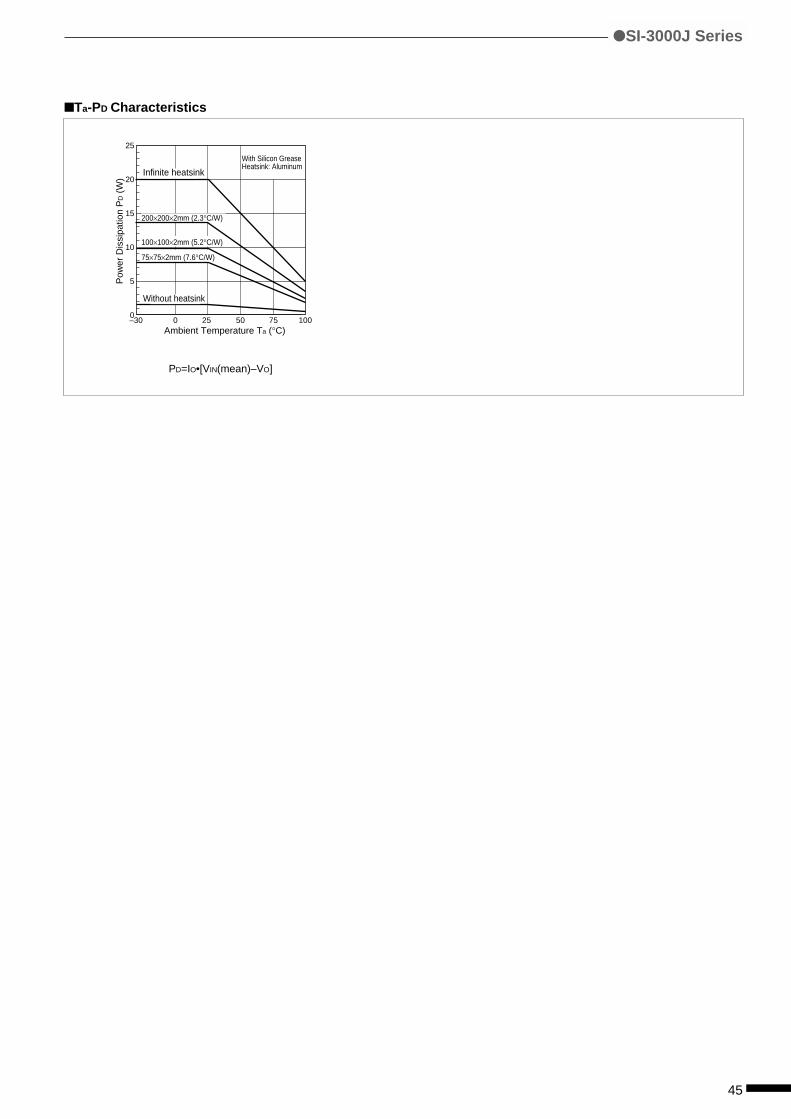
45
Ta-PD Characteristics
PD=IO•[VIN(mean)–VO]
SI-3000J Series
25
20
15
10
5
0
Pow
er D
issi
patio
n P
D (
W)
75×75×2mm (7.6°C/W)
100×100×2mm (5.2°C/W)
200×200×2mm (2.3°C/W)
–30 0 25 50Ambient Temperature Ta (°C)
75 100
Infinite heatsink
Without heatsink
With Silicon GreaseHeatsink: Aluminum
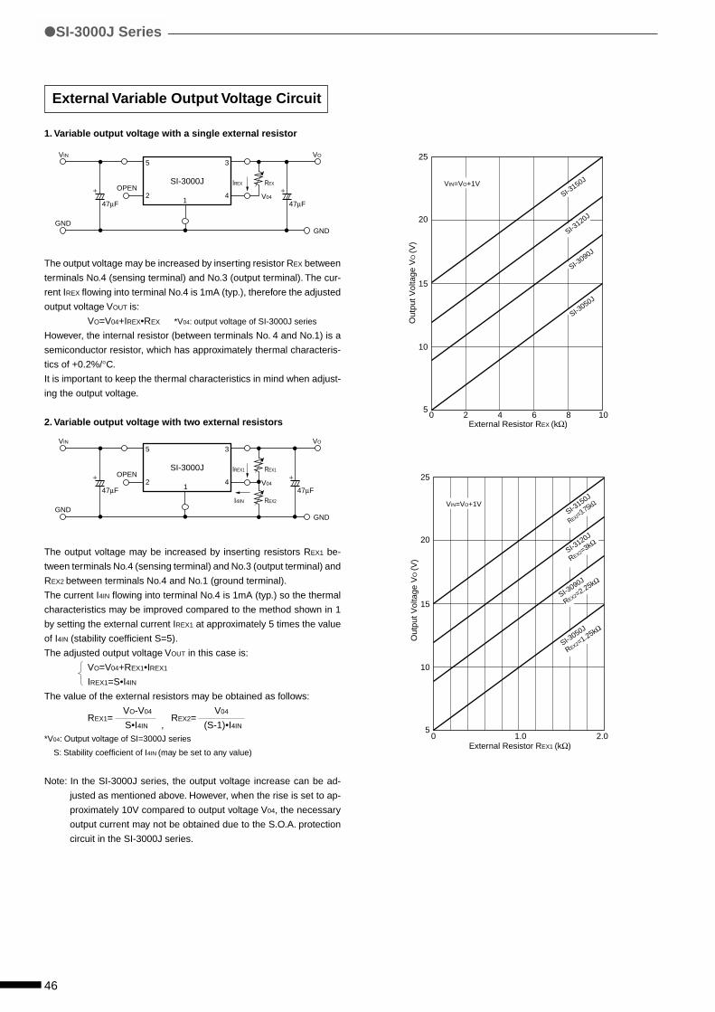
46
1. Variable output voltage with a single external resistor
The output voltage may be increased by inserting resistor REX between
terminals No.4 (sensing terminal) and No.3 (output terminal). The cur-
rent IREX flowing into terminal No.4 is 1mA (typ.), therefore the adjusted
output voltage VOUT is:
VO=V04+IREX•REX *V04: output voltage of SI-3000J series
However, the internal resistor (between terminals No. 4 and No.1) is a
semiconductor resistor, which has approximately thermal characteris-
tics of +0.2%/°C.
It is important to keep the thermal characteristics in mind when adjust-
ing the output voltage.
2. Variable output voltage with two external resistors
The output voltage may be increased by inserting resistors REX1 be-
tween terminals No.4 (sensing terminal) and No.3 (output terminal) and
REX2 between terminals No.4 and No.1 (ground terminal).
The current I4IN flowing into terminal No.4 is 1mA (typ.) so the thermal
characteristics may be improved compared to the method shown in 1
by setting the external current IREX1 at approximately 5 times the value
of I4IN (stability coefficient S=5).
The adjusted output voltage VOUT in this case is:
VO=V04+REX1•IREX1
IREX1=S•I4IN
The value of the external resistors may be obtained as follows:
REX1= VO-V04
REX2= V04
S•I4IN , (S-1)•I4IN
*V04: Output voltage of SI=3000J series
S: Stability coefficient of I4IN (may be set to any value)
Note: In the SI-3000J series, the output voltage increase can be ad-
justed as mentioned above. However, when the rise is set to ap-
proximately 10V compared to output voltage V04, the necessary
output current may not be obtained due to the S.O.A. protection
circuit in the SI-3000J series.
GNDGND
OPEN
5
2
3
41
SI-3000J IREX REX
47µF 47µF
VO
V04
VIN
+ +
GNDGND
OPEN
5
2
3
41
SI-3000J IREX1 REX1
REX2
47µF 47µF
VO
I4IN
V04
VIN
+ +
25
20
15
10
50 2 4 6 8 10
Out
put V
olta
ge V
O (V
)
External Resistor REX (kΩ)
VIN=VO+1V
SI-3150J
SI-3120J
SI-3090J
SI-3050J
External Resistor REX1 (kΩ)
25
20
15
10
50 1.0 2.0
Out
put V
olta
ge V
O (V
)
VIN=VO+1V S
I-3150J
REX2=3.75kΩ
SI-3120J
REX2=3kΩ
SI-3050J
REX2=1.25kΩ
SI-3090J
REX2=2.25kΩ
SI-3000J Series
External Variable Output Voltage Circuit
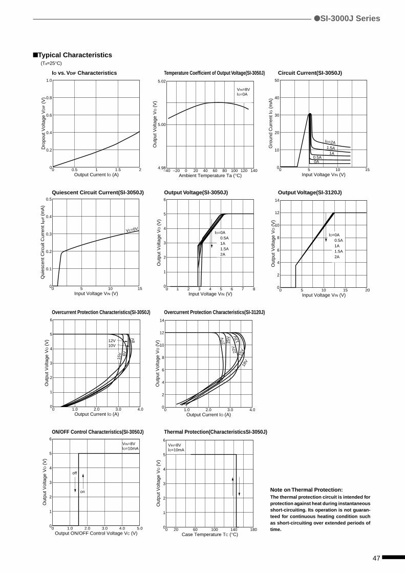
47
Typical Characteristics
IO vs. VDIF Characteristics Temperature Coefficient of Output Voltage(SI-3050J) Circuit Current(SI-3050J)
Quiescent Circuit Current(SI-3050J) Output Voltage(SI-3050J) Output Voltage(SI-3120J)
Overcurrent Protection Characteristics(SI-3050J) Overcurrent Protection Characteristics(SI-3120J)
ON/OFF Control Characteristics(SI-3050J) Thermal Protection(CharacteristicsSI-3050J)
0 0.5 1 1.5 2
1.0
0.8
0.6
0.4
0.2
0
Output Current IO (A)
Dro
pout
Vol
tage
VD
IF (
V)
–40 0–20 4020 8060 140100 120
5.02
5.00
4.98
Ambient Temperature Ta (°C)
Out
put V
olta
ge V
O (
V)
VIN=8VlO=0A
0 1 32 54 86 7
6
5
4
3
2
1
0
Input Voltage VIN (V)
Out
put V
olta
ge V
O (
V)
lO=0A0.5A1A1.5A2A
0 20 10060 140 180Case Temperature TC (°C)
VIN=8VlO=10mA
6
5
4
3
2
1
0
Out
put V
olta
ge V
O (
V)
0 1.0 3.02.0 4.0 5.0
6
5
4
3
2
1
0
Output ON/OFF Control Voltage VC (V)
Out
put V
olta
ge V
O (
V)
VIN=8VlO=10mA
on
off
0 5 10 15
0.5
0.4
0.3
0.2
0.1
0
Input Voltage VIN (V)
Qui
esce
nt C
ircui
t Cur
rent
Iqof
f (m
A)
VC=0V
(Ta=25°C)
SI-3000J Series
Note on Thermal Protection:The thermal protection circuit is intended forprotection against heat during instantaneousshort-circuiting. Its operation is not guaran-teed for continuous heating condition suchas short-circuiting over extended periods oftime.
0 5 10 15 20
14
12
10
8
6
4
2
0
Input Voltage VIN (V)
Out
put V
olta
ge V
O (
V)
lO=0A0.5A1A1.5A2A
0 2.01.0 3.0 4.0
6
5
4
3
2
1
0
Output Current IO (A)
Out
put V
olta
ge V
O (
V)
6V
8V
15V
12V10V
0 5 10 15
50
40
30
20
10
0
Input Voltage VIN (V)
Gro
und
Cur
rent
IG (
mA
)
lO=2A1.5A
1A
0A0.5A
0 2.01.0 3.0 4.0Output Current IO (A)
14
12
10
8
6
4
2
0
Out
put V
olta
ge V
O (
V)
27V
25V
22V
13V
18V
15V
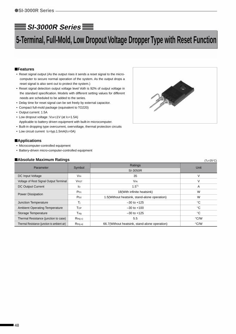
48
Parameter
DC Input Voltage
Voltage of Rest Signal Output Terminal
DC Output Current
Power Dissipation
Junction Temperature
Ambient Operating Temperature
Storage Temperature
Thermal Resistance (junction to case)
Thermal Resistance (junction to ambient air)
SI-3000R Series
5-Terminal, Full-Mold, Low Dropout Voltage Dropper Type with Reset Function
Features• Reset signal output (As the output rises it sends a reset signal to the micro-
computer to secure normal operation of the system. As the output drops a
reset signal is also sent out to protect the system.)
• Reset signal detection output voltage level Voth is 92% of output voltage in
the standard specification. Models with different setting values for different
needs are scheduled to be added to the series.
• Delay time for reset signal can be set freely by external capacitor.
• Compact full-mold package (equivalent to TO220)
• Output current: 1.5A
• Low dropout voltage :VDIF≤1V (at IO=1.5A)
Applicable to battery driven equipment with built-in microcomputer.
• Built-in dropping type overcurrent, overvoltage, thermal protection circuits
• Low circuit current ID=typ.1.5mA(IO=0A)
Applications• Microcomputer-controlled equipment
• Battery-driven micro-computer-controlled equipment
Absolute Maximum Ratings (Ta=25°C)
Unit
V
V
A
W
W
°C
°C
°C
°C/W
°C/W
Symbol
VIN
VRST
IO
PD1
PD2
Tj
TOP
Tstg
Rth(j-c)
Rth(j-a)
Ratings
SI-3050R
35
VIN
1.5*1
18(With infinite heatsink)
1.5(Without heatsink, stand-alone operation)
–30 to +125
–30 to +100
–30 to +125
5.5
66.7(Without heatsink, stand-alone operation)
SI-3000R Series
49
Parameter
Input Voltage
Output Voltage
Dropout Voltage
Line Regulation
Load Regulation
Ripple Rejection
Quiescent Circuit
Current
Overcurrent Protection Starting
Current (Dropping Type)
Limited Current at Overcurrent
Protection Operation
DLY Threshold
Terminal Source
Reset Threshold Voltage Level
(Voth: Threshold Output Voltage)
Reset Threshold Voltage Hysteresis
H-level Output Voltage
L-level Output Voltage
Sink Current at H level
Source Current at L level
Electrical Characteristics
*1: VIN(max) and IO(max) are restricted by the relation PD(max)=(VIN-VO)•IO=18(W).
*2: Refer to the dropout voltage.(Refer to Setting DC Input Voltage on page 7.)
*3: IS1 is specified at –5(%) drop point of output voltage VO on the condition that VIN=8V, IO=1.0A.
*4: Reset signal output terminal VRST is an open-collector output. Use a pull-up resistor when connecting it to a logic circuit.
Unit
V
V
V
mV
mV
dB
mA
A
A
V
µA
%
mV
V
V
µA
mA
Symbol
VIN
VO
Conditions
VDIF
Conditions
Conditions
∆VOLINE
Conditions
∆VOLOAD
Conditions
RREJ
Conditions
Iq
Conditions
IS1
Conditions
IS2
Conditions
VDLyth
IDLY
Voth/VO
∆Voth
VRSTH
VRSTL
IRSTH
IRSTL
Ratings
SI-3050R
min. typ. max.
6*2 30*1
4.80 5.00 5.20
VIN=8V, IO=1.0A
0.5
IO≤1.0A
1.0
IO≤1.5A
30
VIN=6 to 15V, IO=1.0A
100
VIN=8V, IO=0 to 1.5A
54
VIN=8V, f=100 to 120HZ
1.5 5.0
VIN=8V, IO=0A
1.6
VIN=8V
1.6
VIN=8V
2.7 2.9 3.1
25 35 45
90 92 94
50 100 150
VCC–1
0.8
–20
–16
(Ta=25°C unless otherwise specified)
SI-3000R Series
VRST
Terminal*4
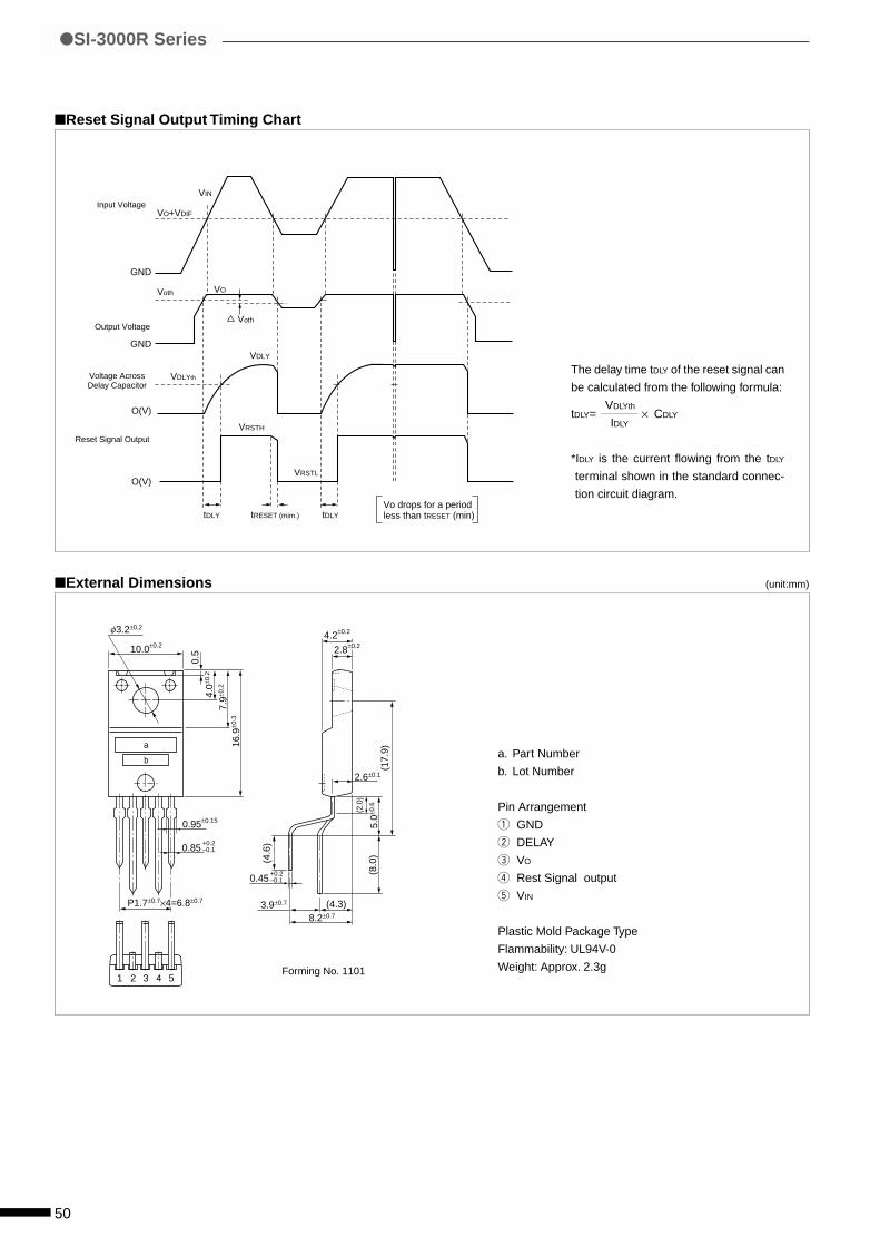
50
Reset Signal Output Timing Chart
External Dimensions
GND
GND
O(V)
O(V)
VO+VDIF
Voth
VDLYth
Voth
VDLY
VRSTH
tDLY tDLYtRESET (mim.)
VRSTL
VO
VIN
Input Voltage
Output Voltage
Voltage AcrossDelay Capacitor
Reset Signal Output
Vo drops for a periodless than tRESET (min)
(unit:mm)
SI-3000R Series
10.0±0.24.2±0.2
0.95±0.15
8.2±0.7
2.6±0.1
3.9±0.7 (4.3)
(4.6
)
(8.0
)(1
7.9)
(2.0
)
0.85+0.2–0.1
0.45+0.2–0.1
3.2±0.2
4.0±0
.2
7.9±0
.2
5.0±0
.6
16.9
±0.3
0.5
1 2 3 4 5
P1.7±0.7×4=6.8±0.7
2.8±0.2
φ
Forming No. 1101
a
ba. Part Number
b. Lot Number
Pin Arrangement
q GND
w DELAY
e VO
r Rest Signal output
t VIN
Plastic Mold Package Type
Flammability: UL94V-0
Weight: Approx. 2.3g
The delay time tDLY of the reset signal can
be calculated from the following formula:
tDLY= VDLYth
× CDLY IDLY
*IDLY is the current flowing from the tDLY
terminal shown in the standard connec-
tion circuit diagram.
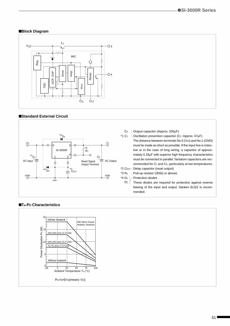
51
Block Diagram
Standard External Circuit
C0 : Output capacitor (Approx. 200µF)
*1 C1 : Oscillation prevention capacitor (C1: Approx. 47µF)
The distance between terminals No.5 (VIN) and No.1 (GND)
must be made as short as possible. If the input line is induc-
tive or in the case of long wiring, a capacitor of approxi-
mately 0.33µF with superior high frequency characteristics
must be connected in parallel. Tantalum capacitors are rec-
ommended for C1 and C0, particularly at low temperatures.
*2 CDLY : Delay capacitor (reset output)
*3 R1 : Pull-up resistor (300Ω or above)
*4 D1 : Protection diodes
These diodes are required for protection against reverse
biasing of the input and output. Sanken EU2Z is recom-
mended.
Ta-PD Characteristics
PD=IO•[VIN(mean)–VO]
5Tr1
3
1
MIC
4
2
Dri
ve
Am
p.
Res
et
Reg
.
TS
D OC
P, O
VP
VR
EF
SI-3000R Series
D2
*4D1
3
4
5
1 2
D2*4
C1*1
R1*3
*2CDLY
C0++
SI-3050R
DC Input DC OutputReset SignalOutput Terminal
VIN VO
GND GND
15
20
10
5
0–30 0 25 50
Ambient Temperature Ta (°C)
Pow
er D
issi
patio
n P
D (
W)
75 100
75×75×2mm (7.6°C/W)
100×100×2mm (5.2°C/W)
200×200×2mm (2.3°C/W)
Infinite heatsink
Without heatsink
With Silicon GreaseHeatsink: Aluminum
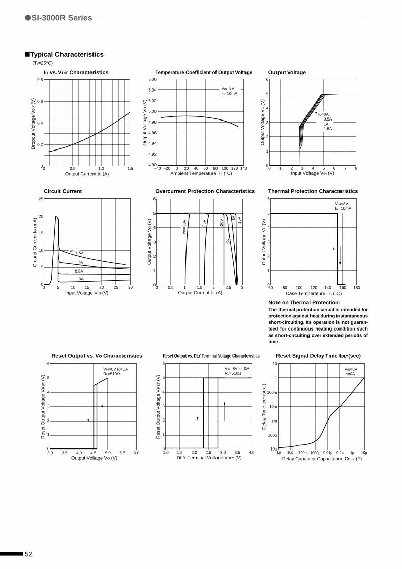
52
Typical Characteristics
IO vs. VDIF Characteristics Temperature Coefficient of Output Voltage Output Voltage
Circuit Current Overcurrent Protection Characteristics Thermal Protection Characteristics
Reset Output vs. VO Characteristics Reset Output vs. DLY Terminal Voltage Characteristics Reset Signal Delay Time tDLY(sec)
–40 –20 0 20 40 60 80 100 120 140
5.06
5.04
5.02
5.00
4.98
4.96
4.94
4.92
4.90
Ambient Temperature Ta (°C)
Out
put V
olta
ge V
O (
V)
VIN=8VlO=10mA
0 0.5 1 1.5 2 2.5 3
6
5
4
3
2
1
0
Output Current lO (A)
Out
put V
olta
ge V
O (
V)
VIN
=30
V
25V
20V
6V
15V8V
60 80 100 120 140 160 180
6
5
4
3
2
1
0
Case Temperature TC (°C)
Out
put V
olta
ge V
o (V
)
VIN=8VlO=10mA
1.0 1.5 2.0 2.5 3.0 3.5 4.0
6
5
4
3
2
1
0
DLY Terminal Voltage VDLY (V)
Res
et O
utpu
t Vol
tage
VR
ST (
V)
VIN=8V lO=0ARL=510Ω
1p 10p 100p 1000p 0.01µ 0.1µ 1µ 10µ
10
1
100m
10m
1m
100µ
10µ
Delay Capacitor Capacitance CDLY (F)
Del
ay T
ime
tDLY
(sec
.)
VIN=8VlO=0A
3.0 3.5 4.0 4.5 5.0 5.5 6.0Output Voltage VO (V)
6
5
4
3
2
1
0
VIN=8V lO=0ARL=510Ω
Res
et O
utpu
t Vol
tage
VR
ST (
V)
(Ta=25°C)
SI-3000R Series
Note on Thermal Protection:The thermal protection circuit is intended forprotection against heat during instantaneousshort-circuiting. Its operation is not guaran-teed for continuous heating condition suchas short-circuiting over extended periods oftime.
0 0.5 1.0 1.5
0.8
0.6
0.4
0.2
0
Output Current lo (A)
Dro
pout
Vol
tage
VD
IF (V
)
0 1 2 3 4 5 6 7 8
6
5
4
3
2
1
0
Input Voltage VIN (V)
Out
put V
olta
ge V
O (
V)
lO=0A0.5A1A1.5A
0 5 10 15 20 25 30
25
20
15
10
5
0
Input Voltage VIN (V)
Gro
und
Cur
rent
IG (
mA
)
lO=1.5A
1A
0.5A
0A

53
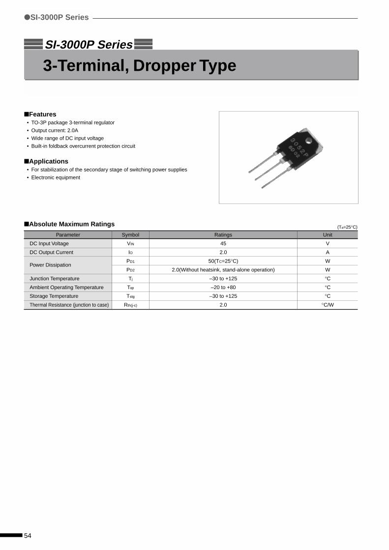
54
Unit
V
A
W
W
°C
°C
°C
°C/W
Symbol
VIN
IO
PD1
PD2
Tj
Top
Tstg
Rth(j-c)
Ratings
45
2.0
50(TC=25°C)
2.0(Without heatsink, stand-alone operation)
–30 to +125
–20 to +80
–30 to +125
2.0
SI-3000P Series
3-Terminal, Dropper Type
SI-3000P Series
Features• TO-3P package 3-terminal regulator
• Output current: 2.0A
• Wide range of DC input voltage
• Built-in foldback overcurrent protection circuit
Applications• For stabilization of the secondary stage of switching power supplies
• Electronic equipment
Absolute Maximum Ratings (Ta=25°C)
Parameter
DC Input Voltage
DC Output Current
Power Dissipation
Junction Temperature
Ambient Operating Temperature
Storage Temperature
Thermal Resistance (junction to case)
55
Parameter
Input Voltage
Output Voltage
Dropout Voltage
Line Regulation
Load Regulation
Temperature Coefficient of Output Voltage
Ripple Rejection
Overcurrent Protection
Starting Current
Limited Current at
Overcurrent Protection
SI-3000P Series
External Dimensions (unit:mm)
Electrical Characteristics
Symbol
VIN
VO
Conditions
VDIF
Conditions
∆VOLINE
Conditions
∆VOLOAD
Conditions
∆VO/∆Ta
RREJ
Conditions
IS1
Conditions
IS2
Conditions
(Ta=25°C)
unit
V
V
V
mV
mV
mV/°C
dB
A
A
Ratings
SI-3052P SI-3122P SI-3152P SI-3242P
min. typ. max. min. typ. max. min. typ. max. min. typ. max.
8 30 15 35 18 40 27 40
4.9 5.0 5.1 11.8 12.0 12.2 14.8 15.0 15.2 23.8 24.0 24.2
VIN=10V, IO=0.5A VIN=19V, IO=0.5A VIN=23V, IO=0.5A VIN=33V, IO=0.5A
3 3 3 3
IO=2.0A
2 10 10 30 10 30 25 50
VIN=8.5 to 11.5V, IO=0.5A VIN=16 to 22V, IO=0.5A VIN=19.5 to 26.5V, IO=0.5A VIN=28 to 38V, IO=0.5A
40 100 80 200 80 200 120 300
VIN=10V, IO=0 to 2.0A VIN=19V, IO=0 to 2.0A VIN=23V, IO=0 to 2.0A VIN=33V, IO=0 to 2.0A
±0.5 ±1.5 ±1.5 ±2.5
60 60 60 60
f=100 to 120HZ
2.4 2.4 2.4 2.4
VIN=10V VIN=19V VIN=23V VIN=33V
0.6 0.6 0.6 0.6
VIN=10V VIN=19V VIN=23V VIN=33V
15.6±0.34.8max.
15.8±0.2
5.45±0.1 5.45±0.1
13.6±0.2
9.6±0.2
3.2±0
.1
20.0
min
.
2.0
4.0
3.5
14.9
±0.3
19.9
±0.3
1.05
3.0
0.65
1.7
2.0
2.0max.
+0.2–0.1
+0.2–0.1
+0.2–0.3
+0.2–0.1
+0.2–0.1
q w e
φ
a
b
A foldback type overcurrent protection circuit is built into the IC regulator. Therefore, avoid using it for the following applications as it may cause
starting errors:
(1) Constant current load (2) Plus/minus power (3) Series power (4) VO adjustment by raising ground voltage
a. Part Number
b. Lot Number
Pin Arrangement
q VO
w VIN (backside of case)
e GND
Plastic Mold Package Type (TO-3P)
Flammability: UL94V-0
Weight: Approx. 6g
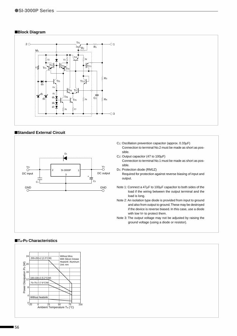
56
Ta-PD Characteristics
Standard External Circuit
C1: Oscillation prevention capacitor (approx. 0.33µF)Connection to terminal No.2 must be made as short as pos-sible.
C2: Output capacitor (47 to 100µF)Connection to terminal No.1 must be made as short as pos-sible.
D1: Protection diode (RM1Z)Required for protection against reverse biasing of input andoutput.
Note 1: Connect a 47µF to 100µF capacitor to both sides of theload if the wiring between the output terminal and theload is long.
Note 2: An isolation type diode is provided from input to groundand also from output to ground. These may be destroyedif the device is reverse biased. In this case, use a diodewith low VF to protect them.
Note 3: The output voltage may not be adjusted by raising theground voltage (using a diode or resistor).
SI-3000P Series
VIN VO
D1
C2C1
2 1
3
SI-3000P
+DC input DC output
GND GND
24
20
16
12
8
4
0–20 0 25 50 75 100
Ambient Temperature Ta (°C)
Pow
er D
issi
patio
n P
D (
W)
75×75×2 (7.6°C/W)
100×100×2 (5.2°C/W)
200×200×2 (2.3°C/W)
Without heatsink
Without MicaWith Silicon GreaseHeatsink: AluminumUnit: mm
Block Diagram
R3
R4
3
1
M1
2
C1r9Tr9
r7r6
r8
R2
Tr1
r10
R1
Tr12
Tr6
Tr8
Tr4
Tr3
r2
Tr5
r1
r4
r5
d5
d6
d7
r3
Tr7
Tr2Tr1
Tr11
d1
d3
d2
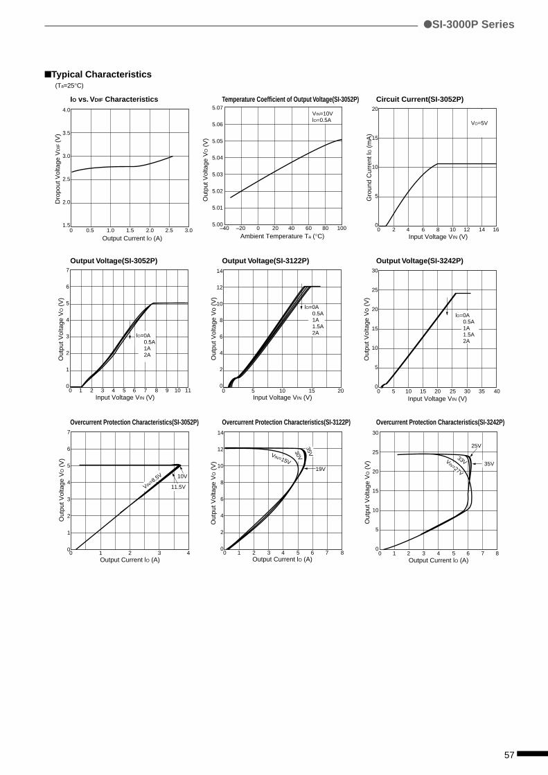
57
Typical Characteristics
IO vs. VDIF Characteristics Temperature Coefficient of Output Voltage(SI-3052P) Circuit Current(SI-3052P)
Output Voltage(SI-3052P) Output Voltage(SI-3122P) Output Voltage(SI-3242P)
Overcurrent Protection Characteristics(SI-3052P) Overcurrent Protection Characteristics(SI-3122P) Overcurrent Protection Characteristics(SI-3242P)
–40 –20 0 20 40 60 80 100
5.07
5.06
5.05
5.04
5.03
5.02
5.01
5.00
Ambient Temperature Ta (°C)
Out
put V
olta
ge V
O (
V)
VIN=10VlO=0.5A
0 2 4 6 8 10 12 14 16
20
15
10
5
0
Input Voltage VIN (V)
Gro
und
Cur
rent
lG (
mA
)
VO=5V
0 1 2 3 4
7
6
5
4
3
2
1
0
Output Current lO (A)
Out
put V
olta
ge V
O (
V)
VIN=8.5V
11.5V
10V
0 1 2 3 4 5 6 7 8
14
12
10
8
6
4
2
0
Output Current lO (A)
Out
put V
olta
ge V
O (
V)
35VVIN=15V19V
30V
0 1 2 3 4 5 6 7 8
30
25
20
15
10
5
0
Output Current lO (A)
Out
put V
olta
ge V
O (
V)
25V
VIN=27V
35V33V
SI-3000P Series
(Ta=25°C)
0 0.5 1.0 1.5 2.0 2.5 3.0
4.0
3.5
3.0
2.5
2.0
1.5
Output Current lO (A)
Dro
pout
Vol
tage
VD
IF (V
)
0 1 2 3 4 5 6 7 8 9 10 11
7
6
5
4
3
2
1
0
Input Voltage VIN (V)
Out
put V
olta
ge V
O (
V)
lO=0A 0.5A 1A 2A
0 5 10 15 20
14
12
10
8
6
4
2
0
Input Voltage VIN (V)
Out
put V
olta
ge V
o (V
)
lO=0A 0.5A 1A 1.5A 2A
0 5 10 15 20 25 30 35 40
30
25
20
15
10
5
0
Input Voltage VIN (V)
Out
put V
olta
ge V
o (V
)
lO=0A 0.5A 1A 1.5A 2A
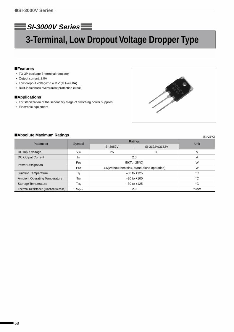
58
Unit
V
A
W
W
°C
°C
°C
°C/W
Symbol
VIN
IO
PD1
PD2
Tj
Top
Tstg
Rth(j-c)
Parameter
DC Input Voltage
DC Output Current
Power Dissipation
Junction Temperature
Ambient Operating Temperature
Storage Temperature
Thermal Resistance (junction to case)
SI-3000V Series
3-Terminal, Low Dropout Voltage Dropper Type
Features• TO-3P package 3-terminal regulator
• Output current: 2.0A
• Low dropout voltage: VDIF≤1V (at IO=2.0A)
• Built-in foldback overcurrent protection circuit
Applications• For stabilization of the secondary stage of switching power supplies
• Electronic equipment
Absolute Maximum Ratings (Ta=25°C)
Ratings
SI-3052V SI-3122V/3152V
25 30
2.0
50(TC=25°C)
1.6(Without heatsink, stand-alone operation)
–30 to +125
–20 to +100
–30 to +125
2.0
SI-3000V Series
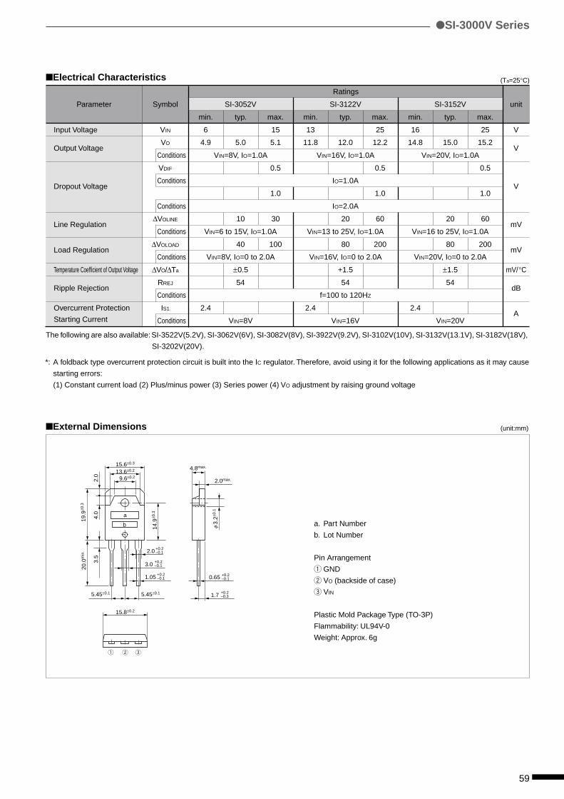
59
External Dimensions (unit:mm)
Parameter
Input Voltage
Output Voltage
Dropout Voltage
Line Regulation
Load Regulation
Temperature Coefficient of Output Voltage
Ripple Rejection
Overcurrent Protection
Starting Current
Electrical Characteristics
unit
V
V
V
mV
mV
mV/°C
dB
A
(Ta=25°C)
Symbol
VIN
VO
Conditions
VDIF
Conditions
Conditions
∆VOLINE
Conditions
∆VOLOAD
Conditions
∆VO/∆Ta
RREJ
Conditions
IS1
Conditions
Ratings
SI-3052V SI-3122V SI-3152V
min. typ. max. min. typ. max. min. typ. max.
6 15 13 25 16 25
4.9 5.0 5.1 11.8 12.0 12.2 14.8 15.0 15.2
VIN=8V, IO=1.0A VIN=16V, IO=1.0A VIN=20V, IO=1.0A
0.5 0.5 0.5
IO=1.0A
1.0 1.0 1.0
IO=2.0A
10 30 20 60 20 60
VIN=6 to 15V, IO=1.0A VIN=13 to 25V, IO=1.0A VIN=16 to 25V, IO=1.0A
40 100 80 200 80 200
VIN=8V, IO=0 to 2.0A VIN=16V, IO=0 to 2.0A VIN=20V, IO=0 to 2.0A
±0.5 +1.5 ±1.5
54 54 54
f=100 to 120HZ
2.4 2.4 2.4
VIN=8V VIN=16V VIN=20V
SI-3000V Series
The following are also available: SI-3522V(5.2V), SI-3062V(6V), SI-3082V(8V), SI-3922V(9.2V), SI-3102V(10V), SI-3132V(13.1V), SI-3182V(18V),
SI-3202V(20V).
15.6±0.34.8max.
15.8±0.2
5.45±0.1 5.45±0.1
13.6±0.2
9.6±0.2
3.2±0
.1
20.0
min
.
2.0
4.0
3.5
14.9
±0.3
19.9
±0.3
1.05
3.0
0.65
1.7
2.0
2.0max.
+0.2–0.1
+0.2–0.1
+0.2–0.3
+0.2–0.1
+0.2–0.1
q w e
φ
a
b
*: A foldback type overcurrent protection circuit is built into the IC regulator. Therefore, avoid using it for the following applications as it may cause
starting errors:
(1) Constant current load (2) Plus/minus power (3) Series power (4) VO adjustment by raising ground voltage
a. Part Number
b. Lot Number
Pin Arrangement
q GND
w VO (backside of case)
e VIN
Plastic Mold Package Type (TO-3P)
Flammability: UL94V-0
Weight: Approx. 6g
60
Ta-PD Characteristics
Standard External Circuit
C1: Oscillation prevention capacitor (approx. 0.33µF)Connection to terminal No.3 must be made as short aspossible.
C2: Output capacitor (47 to 100µF)Connection to terminal No.2 must be made as short aspossible.
D1: Protection diode (RM1Z)Required for protection against reverse biasing of input andoutput.
Note 1: Prevention of oscillation at low temperaturesAt low temperatures, oscillation may occur unless anoutput capacitor with good tanδ is used. Be sure toconnect a tantalum capacitor (approx. 10µF) in paral-lel with output capacitor C2.
Note 2: An isolation type diode is provided from input to groundand also from output to ground. These may be de-stroyed if the device is reverse biased. In this case,use a diode with low VF to protect them.
Note 3: The output voltage may not be adjusted by raising theground voltage (using a diode or resistor).
VIN VO
D1
C2C1
3 2
1
SI-3000V
+–
DC input DC output
GNDGND
SI-3000V Series
24
20
16
12
8
4
0–20 0 25 50 75 100
200×200×2 (2.3°C/W)
100×100×2 (5.2°C/W)
75×75×2 (7.6°C/W)
Ambient Temperature Ta (°C)
Pow
er D
issi
patio
n P
D (
W)
Without heatsink
Without MicaWith Silicon GreaseHeatsink: AluminumUnit: mm
Block Diagram
3 2
1
Tr1
R1R2
R3
R5
R4M1
Reg
.
Pro
tect
ion
Driv
e
Am
p.
VR
EF
61
Typical Characteristics
IO vs. VDIF Characteristics Temperature Coefficient of Output Voltage(SI-3052V) Circuit Current(SI-3052V)
Output Voltage(SI-3052V) Output Voltage(SI-3122V) Output Voltage(SI-3152V)
Overcurrent Protection Characteristics(SI-3052V) Overcurrent Protection Characteristics(SI-3122V) Overcurrent Protection Characteristics(SI-3152V)
–60 –40 –20 0 20 40 60 80 100 120 140
5.06
5.04
5.02
5.00
4.98
4.96
4.94
Ambient Temperature Ta (°C)
Out
put V
olta
ge V
O (V
)
VIN=8VlO=1V
0 5 10 15 17.5
70
60
50
40
30
20
10
0
Input Voltage VIN (V)
Gro
und
Cur
rent
lG (
mA
)
lo=2.0A
1.5A
0A
0.5A1.0A
0 1 2 3 4 5 76
6
5
4
3
2
1
0
Input Voltage VIN (V)
Out
put V
olta
ge V
O (
V)
RL=2.
5 to
∞Ω
0 2 4 6 8 10 1612 14
16
14
12
10
8
6
4
2
0
Input Voltage VIN (V)
Out
put V
olta
ge V
o (V
)
RL=6 to
∞Ω
0 2 4 6 8 10 181612 14
18
16
14
12
10
8
6
4
2
0
Input Voltage VIN (V)
Out
put V
olta
ge V
O (
V)
RL=7.
5 to
∞Ω
0 1 2 3 4 5 6 7
6
5
4
3
2
1
0
Output Current lo (A)
Out
put V
olta
ge V
o (V
) 10V
8V
VIN=6
V
15V
0 1 2 3 4 5 6 7
16
14
12
10
8
6
4
2
0
Output Current lo (A)
Out
put V
olta
ge V
o (V
)
VIN
=13V 16
V
20V
0 1 2 3 4 5 6 7
18
16
14
12
10
8
6
4
2
0
Output Current lO (A)
Out
put V
olta
ge V
O (
V)
VIN
=16V 20
V
(Ta=25°C)
SI-3000V Series
0 0.5 1.0 1.5 2.0
0.8
0.6
0.4
0.2
0
Output Current lO (A)
Dro
pout
Vol
tage
VD
IF (V
)

62
Temperature and ReliabilityThe reliability of an IC is highly dependent on its operating tempera-ture. Design should pay particular attention to ensuring ample spacefor radiating heat.Be sure to apply silicon grease to the IC before attaching a heatsink,and to secure it firmly to the heatsink. Allow sufficient margine whichdesigning the heatsink.Other important items to be considered regarding heat radiation in-clude air convection during operation.The reliability of peripheral components such as capacitors and coilsis closely related to temperature. A high operating temperature mayreduce the service life. Exceeding the allowable temperature may burnthe coils or damage capacitors. It is important to make sure that thetemperature of output smoothing coils and input/output capacitors donot exceed their allowable levels during operation. Allow for variationin the ratings of the coils and minimize heat emission as far as pos-sible. (For peripheral components, refer to the user manuals.)
Internal Power DissipationPD can be obtained from the following formula.• With built-in flywheel diode:
(SI-8000L series)
PD=VO•IO (100
–1) ηx• With external flywheel diode:
(SAI series, SI-8000E series, SI-8000S series)
PD=VO•IO(100
–1)–VF•IO(1–VO
) ηx VIN
Efficiency ηx depends on the input/output conditions. The efficiencycharacteristics of each product type are provided for reference pur-poses.
VO : Output voltageVIN : Input voltageIO : Output currentηx : Efficiency(%)VF : Diode forward voltage
Heatsink DesignThe maximum junction temperature Tj(max) given in the absolute maxi-mum ratings is specific to each product type and must be strictlyobserved. Thus, thermal design must consider the conditions of usewhich affect the maximum power dissipation PD(max) and the maxi-mum ambient temperature Ta(max).To simplify thermal design, the relationship between these two pa-rameters has been presented in a graph, the Ta-PD characteristicgraph. Thermal design should include these steps:1. Obtain the maximum ambient temperature Ta(max).
2. Obtain the maximum power dissipation PD(max).3. Look for the intersection point on the Ta-PD characteristic graph
and determine the size of the heatsink.The size of the heatsink has now been obtained. However, in actualapplications, a 10 to 20% derating factor is introduced. Moreover,the heat dissipation capacity of a heatsink highly depends on how itis mounted. Thus, it is recommended to measure the heatsink andcase temperature in the actual operating environment.The Ta-PD characteristics for each product type are provided for ref-
erence purposes.
Switching Type - Application Note
63
Fastening TorqueSI-8000E
0.588 to 0.686[N•m] (6.0 to 7.0[kgf•cm])SI-8000S
Recommended Silicon Grease• Shin-Etsu Chemical Co., Ltd.: G746
• GE Toshiba Silicone Co., Ltd.: YG-6260
• Dow Corning Toray Silicone Co., Ltd.: SC102
Please be careful when selecting silicone grease since the oil in some
grease may penetrate the product, which will result in an extremely
short product life.
Others• Parallel operation can not be performed for increasing current.
• This type IC regulators can not be used for boosting current and
raising voltage.
Rectifier Diodes for Power SuppliesTo rectify the AC input using rectifier diodes in power supplies, use
any of the SANKEN rectifier diodes shown in the following list. (Use
axial type diodes in a center-tap or bridge configuration.)
Regulator Type Diodes
SAI Series SFPM-62(Surface-Mount Type, VRM:200V, IO:1.0A)
SI-8000E Series
SI-8200L Series AM01Z(Axial Type, VRM:200V, IO:1.0A)
SI-8400L Series
SI-8000S Series
RM 4Z(Axial Type,VRM:200V, IO:3.0A)
RBV-402(Bridge Type, VRM:200V, IO:4.0A)
SI-8300L SeriesRM10Z(Axial Type, VRM:F200V, IO:1.5A)
SI-8500L Series,
SI-8800L SeriesAM01Z(Axial Type, VRM:200V, IO:1.0A)
SI-8900L Series
64
Parameter
DC Input Voltage
Power Dissipation
Junction Temperature
Storage Temperature
SW Terminal Applied Reverse Voltage
Thermal Resistance(junction to case)
Parameter
DC Input Voltage Range
Output Current Range
Operating Junction Temperature Range
Symbol
VIN
PD
Tj
Tstg
VSW
Rth(j-c)
Features• Surface-mount package
• Output current: 0.4 to 0.5A
• High efficiency: 75 to 89%
• Requires only 4 external components
• Phase correction and output voltage adjustment performed internally
• Built-in reference oscillator (60kHz)
• Built-in overcurrent and thermal protection circuits
Applications• Power supplies for telecommunication equipment
• Onboard local power supplies
Lineup
SAI Series
Surface-Mount, Separate Excitation Switching Type
SAI Series
Unit
V
A
°C
Symbol
VIN
IO
Tjop
Absolute Maximum Ratings
Recommended Operating Conditions
Part Number SAI01 SAI02 SAI03 SAI04 SAI06
VO(V) 5.0 3.3 12.0 15.0 9.0
IO(A) 0.5 0.4
Ratings
35
0.75
+125
–40 to +125
–1
20
Unit
V
W
°C
°C
V
°C/W
Ratings
SAI01 SAI02 SAI03 SAI04 SAI06
7 to 33 5.3 to 28 15 to 33 18 to 33 12 to 33
0 to 0.5 0 to 0.4
–30 to +125
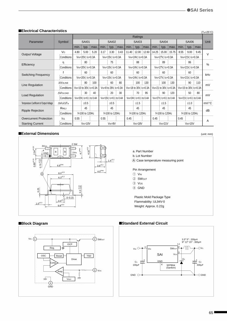
65
Parameter
Output Voltage
Efficiency
Switching Frequency
Line Regulation
Load Regulation
Temperature Coefficient of Output Voltage
Ripple Rejection
Overcurrent Protection
Starting Current
Electrical Characteristics (Ta=25°C)
SAI Series
External Dimensions
a. Part Number
b. Lot Number
A Case temperature measuring point
Pin Arrangement
q VIN
w SWOUT
e VOS
r GND
Plastic Mold Package Type
Flammability: UL94V-0
Weight: Approx. 0.22g
Block Diagram
A
3VOS
4.GND
2 SW
1VIN
6.8max.
4.0max.
4.7m
ax.
2.54
±0.2
5
4.32
±0.2
8.0±0.5
3.6±0.2
1.4±0.2
3.0±0.2
9.8±0.3
0~0.15
6.3±0.2
1.0±0.3
0.89
±0.1
5
0.25
0.75
+0.
15–0
.05
0.3
+0.
15–0
.05
a b
SWOUT
VOS
VIN
4
GND
3
21
OSC
Reg.
OCP
Comp.
Reset
Drive
TSD
Amp.
VREF
Symbol
VO
Conditions
η
Conditions
f
Conditions
∆VOLINE
Conditions
∆VOLOAD
Conditions
∆VO/∆Ta
RREJ
Conditions
IS1
Conditions
Standard External Circuit
VIN
C1
D1
L1
3.3V 5V : 200µH9V 12V 15V : 300µH
100µFC2
330µF
VIN
SFPB54
GND
GND
SAI
SWOUT
VOS
1 2
3
4
+ +
VO
GND
(Sanken)
Unit
V
%
kHZ
mV
mV
mV/°C
dB
A
Ratings
SAI01 SAI02 SAI03 SAI04 SAI06
min. typ. max. min. typ. max. min. typ. max. min. typ. max. min. typ. max.
4.80 5.00 5.20 3.17 3.30 3.43 11.40 12.00 12.60 14.25 15.00 15.75 8.55 9.00 9.45
VIN=20V, IO=0.3A VIN=15V, IO=0.3A VIN=24V, IO=0.3A VIN=27V, IO=0.3A VIN=21V, IO=0.3A
80 75 88 89 86
VIN=20V, IO=0.3A VIN=15V, IO=0.3A VIN=24V, IO=0.3A VIN=27V, IO=0.3A VIN=21V, IO=0.3A
60 60 60 60 60
VIN=20V, IO=0.3A VIN=15V, IO=0.3A VIN=24V, IO=0.3A VIN=27V, IO=0.3A VIN=21V, IO=0.3A
80 100 60 80 100 130 100 130 90 110
VIN=10 to 30V, IO=0.3A VIN=8 to 28V, IO=0.3A VIN=18 to 30V, IO=0.3A VIN=21 to 30V, IO=0.3A VIN=15 to 30V, IO=0.3A
30 40 20 30 70 95 90 120 50 80
VIN=20V, IO=0.1 to 0.4A VIN=15V, IO=0.1 to 0.4A VIN=24V, IO=0.1 to 0.4A VIN=27V, IO=0.1 to 0.4A VIN=21V, IO=0.1 to 0.4A
±0.5 ±0.5 ±1.5 ±1.5 ±1.0
45 45 45 45 45
f=100 to 120HZ f=100 to 120HZ f=100 to 120HZ f=100 to 120HZ f=100 to 120HZ
0.55 0.55 0.45 0.45 0.45
VIN=10V VIN=8V VIN=18V VIN=21V VIN=15V
(unit: mm)
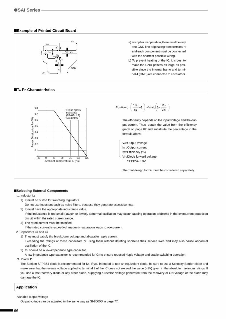
66
Selecting External Components1. Inductor L1
1) It must be suited for switching regulators.
Do not use inductors such as noise filters, because they generate excessive heat.
2) It must have the appropriate inductance value.
If the inductance is too small (150µH or lower), abnormal oscillation may occur causing operation problems in the overcurrent protection
circuit within the rated current range.
3) The rated current must be satisfied.
If the rated current is exceeded, magnetic saturation leads to overcurrent.
2. Capacitors C1 and C2
1) They must satisfy the breakdown voltage and allowable ripple current.
Exceeding the ratings of these capacitors or using them without derating shortens their service lives and may also cause abnormal
oscillation of the IC.
2) C2 should be a low-impedance type capacitor.
A low-impedance type capacitor is recommended for C2 to ensure reduced ripple voltage and stable switching operation.
3. Diode D1
The Sanken SFPB54 diode is recommended for D1. If you intended to use an equivalent diode, be sure to use a Schottky Barrier diode and
make sure that the reverse voltage applied to terminal 2 of the IC does not exceed the value (–1V) given in the absolute maximum ratings. If
you use a fast recovery diode or any other diode, supplying a reverse voltage generated from the recovery or ON voltage of the diode may
damage the IC.
Application
Variable output voltage
Output voltage can be adjusted in the same way as SI-8000S in page 77.
Example of Printed Circuit Board
a) For optimum operation, there must be only
one GND line originating from terminal 4
and each component must be connected
with the shortest possible wiring.
b) To prevent heating of the IC, it is best to
make the GND pattern as large as pos-
sible since the internal frame and termi-
nal 4 (GND) are connected to each other.
Ta-PD Characteristics
The efficiency depends on the input voltage and the out-
put current. Thus, obtain the value from the efficiency
graph on page 67 and substitute the percentage in the
formula above.
VO:Output voltage
IO :Output current
ηx :Efficiency (%)
VF :Diode forward voltage
SFPB54-0.3V
Thermal design for D1 must be considered separately.
+
+
VIN
DI1 C1L1
C2GND
SW
VO
12
3 4
SAI
0.8
0.7
0.6
0.5
0.4
0.3
0.2
0.1
0–30 0 25 50 75 100 125
Pow
er D
issi
patio
n P
D (
W)
Ambient Temperature Ta (°C)
• Glass epoxy substrate (95×69×1.2)• No airflow
SAI Series
PD=VO•IO 100
–1
–VF•IO 1– VO
ηχ VIN
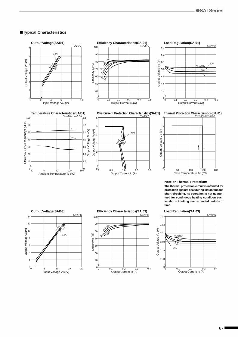
67
Typical Characteristics
Output Voltage(SAI01) Efficiency Characteristics(SAI01) Load Regulation(SAI01)
Temperature Characteristics(SAI01) Overcurrent Protection Characteristics(SAI01) Thermal Protection Characteristics(SAI01)
Output Voltage(SAI03) Efficiency Characteristics(SAI03) Load Regulation(SAI03)
100
90
80
70
60
50
40
0
Effi
cien
cy η
(%)
0 0.1 0.2 0.3
Output Current IO (A)0.4 0.5
Ta=25°C
VIN =7V
20V
33V
10V
25V
5.3
5.2
5.1
5.0
4.9
4.8
4.7
0
VIN=33V20V
10V
7V
Out
put V
olta
ge V
O (V
)
0 0.1 0.2 0.3Output Current IO (A)
0.4 0.5
Ta=25°C
100
90
80
70
60
50
40
0
Effi
cien
cy η
(%)
Fre
quen
cy f
(kH
z)
Out
put V
olta
ge V
O (
V)
–50 0 50Ambient Temperature Ta (°C)
100 150
VIN=20V, IO=0.3A
VO
f
5.3
5.2
5.1
5.0
4.9
4.8
4.7
0
η
0
100
90
80
70
60
50
40
00.1 0.2
Output Current IO (A)0.3 0.4
Ta=25°C
VIN=15V
24V 33V
Effi
cien
cy η
(%
)
0
12.3
12.2
12.1
12.0
11.9
11.8
00.1 0.2
Output Current IO (A)0.3 0.4
Out
put V
olta
ge V
O (
V)
Ta=25°C
VIN=33V24V
20V
15V
Out
put V
olta
ge V
O (V
)
6
5
4
3
2
1
00 0.5 1.0Output Current IO (A)
1.5 2.0
Ta=25°CVIN
=7V
20V
33V
SAI Series
Note on Thermal Protection:The thermal protection circuit is intended forprotection against heat during instantaneousshort-circuiting. Its operation is not guaran-teed for continuous heating condition suchas short-circuiting over extended periods oftime.
6
5
4
3
2
1
00 2 4 6
Input Voltage VIN (V)
0.1A
Out
put V
olta
ge V
O (
V)
8 10
Ta=25°CIO
=0A
0.5A
0
6
5
4
3
2
1
050 100
Case Temperature TC (°C)150 200
VIN=20V, IO=20mA
Out
put V
olta
ge V
O (
V)
0
14
12
10
8
6
4
2
05 10
Input Voltage VIN (V)15 20
Ta=25°C
IO=0
A
0.2A
0.4A
Out
put V
olta
ge V
O (V
)
68
Features• Compact full-mold package (equivalent to TO220)
• High efficiency: 80 to 88%
• Requires only 4 external components
• Phase correction and output voltage adjustment performed internally
• Built-in reference oscillator (60kHz)
• Built-in overcurrent and thermal protection circuits
Applications• Power supplies for telecommunication equipment
• Onboard local power supplies
Lineup
Full-Mold, Separate Excitation Switching Type
Unit
V
A
°C
°C
SI-8000E Series
SI-8000E Series
Symbol
VIN
PD1
PD2
Tj
Tstg
Rth(j-c)
Rth(j-a)
Unit
V
W
W
°C
°C
°C/W
°C/W
Recommended Operating Conditions
Absolute Maximum RatingsRatings
43
14(With infinite heatsink)
1.5(Without heatsink, stand-alone operation)
+125
–40 to +125
7.0
66.7
Parameter
DC Input Voltage
Power Dissipation
Junction Temperature
Storage Temperature
Thermal Resistance(junction to case)
Thermal Resistance(junction to ambient air)
Part Number SI-8050E SI-8090E SI-8120E
VO(V) 5.0 9.0 12.0
IO(A) 0.6
Parameter
DC Input Voltage Range
Output Current Range
Operating Junction Temperature Range
Operating Temperature Range
Symbol
VIN
IO
Tjop
Top
Ratings
SI-8050E SI-8090E SI-8120E
7 to 40 11 to 40 14 to 40
0 to 0.6
–30 to +125
–30 to +125
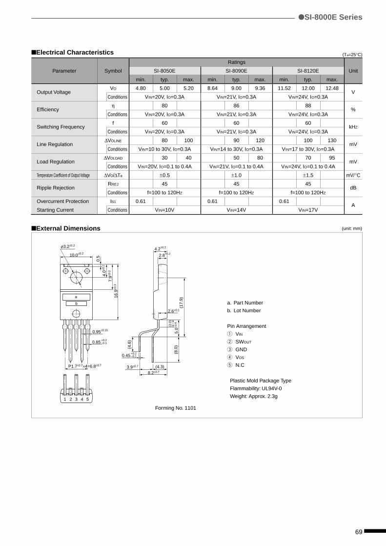
69
Parameter
Output Voltage
Efficiency
Switching Frequency
Line Regulation
Load Regulation
Temperature Coefficient of Output Voltage
Ripple Rejection
Overcurrent Protection
Starting Current
SI-8000E Series
Forming No. 1101
External Dimensions
Symbol
VO
Conditions
η
Conditions
f
Conditions
∆VOLINE
Conditions
∆VOLOAD
Conditions
∆VO/∆Ta
RREJ
Conditions
IS1
Conditions
Unit
V
%
kHZ
mV
mV
mV/°C
dB
A
Ratings
SI-8050E SI-8090E SI-8120E
min. typ. max. min. typ. max. min. typ. max.
4.80 5.00 5.20 8.64 9.00 9.36 11.52 12.00 12.48
VIN=20V, IO=0.3A VIN=21V, IO=0.3A VIN=24V, IO=0.3A
80 86 88
VIN=20V, IO=0.3A VIN=21V, IO=0.3A VIN=24V, IO=0.3A
60 60 60
VIN=20V, IO=0.3A VIN=21V, IO=0.3A VIN=24V, IO=0.3A
80 100 90 120 100 130
VIN=10 to 30V, IO=0.3A VIN=14 to 30V, IO=0.3A VIN=17 to 30V, IO=0.3A
30 40 50 80 70 95
VIN=20V, IO=0.1 to 0.4A VIN=21V, IO=0.1 to 0.4A VIN=24V, IO=0.1 to 0.4A
±0.5 ±1.0 ±1.5
45 45 45
f=100 to 120HZ f=100 to 120HZ f=100 to 120HZ
0.61 0.61 0.61
VIN=10V VIN=14V VIN=17V
Electrical Characteristics (Ta=25°C)
a. Part Number
b. Lot Number
Pin Arrangement
q VIN
w SWOUT
e GND
r VOS
t N.C
Plastic Mold Package Type
Flammability: UL94V-0
Weight: Approx. 2.3g
(unit: mm)
10.0±0.24.2±0.2
0.95±0.15
8.2±0.7
2.6±0.1
3.9±0.7 (4.3)
(4.6
)
(8.0
)(1
7.9)
(2.0
)
0.85+0.2–0.1
0.45+0.2–0.1
3.2±0.2
4.0±0
.2
7.9±0
.2
5.0±0
.6
16.9
±0.3
0.5
1 2 3 4 5
P1.7±0.7×4=6.8±0.7
2.8±0.2
φ
a
b
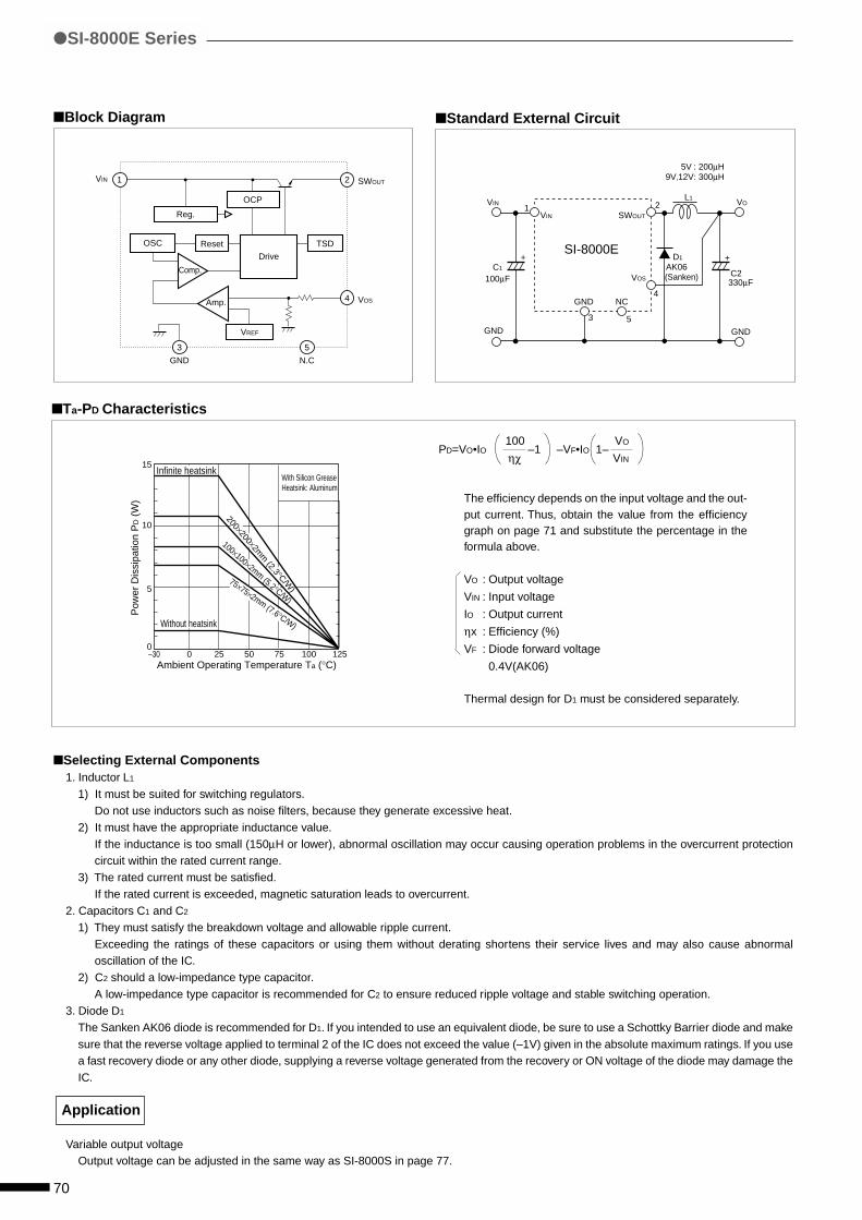
70
Block Diagram Standard External Circuit
Ta-PD Characteristics
SWOUT
VOS
VIN
3
GND
5
N.C
4
21
OSC
Reg.
OCP
Comp.
Reset
Drive
TSD
Amp.
VREF
VIN
C1
D1
L1
5V : 200µH9V,12V: 300µH
100µF
VIN VO
AK06
GND NC
GND GND
SI-8000E
SWOUT
VOS
1 2
3
+
C2330µF
+
5
4
(Sanken)
15
10
5
0–30 0 25 50
Ambient Operating Temperature Ta (°C)
Pow
er D
issi
patio
n P
D (
W)
75 100 125
200×200×2mm
(2.3°C/W)
100×100×2mm (5.2°C/W)
75×75×2mm (7.6°C/W)
Infinite heatsink
Without heatsink
With Silicon GreaseHeatsink: Aluminum
SI-8000E Series
Selecting External Components1. Inductor L1
1) It must be suited for switching regulators.Do not use inductors such as noise filters, because they generate excessive heat.
2) It must have the appropriate inductance value.If the inductance is too small (150µH or lower), abnormal oscillation may occur causing operation problems in the overcurrent protectioncircuit within the rated current range.
3) The rated current must be satisfied.If the rated current is exceeded, magnetic saturation leads to overcurrent.
2. Capacitors C1 and C2
1) They must satisfy the breakdown voltage and allowable ripple current.Exceeding the ratings of these capacitors or using them without derating shortens their service lives and may also cause abnormaloscillation of the IC.
2) C2 should a low-impedance type capacitor.A low-impedance type capacitor is recommended for C2 to ensure reduced ripple voltage and stable switching operation.
3. Diode D1
The Sanken AK06 diode is recommended for D1. If you intended to use an equivalent diode, be sure to use a Schottky Barrier diode and makesure that the reverse voltage applied to terminal 2 of the IC does not exceed the value (–1V) given in the absolute maximum ratings. If you usea fast recovery diode or any other diode, supplying a reverse voltage generated from the recovery or ON voltage of the diode may damage theIC.
Application
Variable output voltageOutput voltage can be adjusted in the same way as SI-8000S in page 77.
The efficiency depends on the input voltage and the out-put current. Thus, obtain the value from the efficiencygraph on page 71 and substitute the percentage in theformula above.
VO : Output voltage
VIN : Input voltage
IO : Output current
ηx : Efficiency (%)
VF : Diode forward voltage
0.4V(AK06)
Thermal design for D1 must be considered separately.
PD=VO•IO 100
–1
–VF•IO 1– VO
ηχ VIN
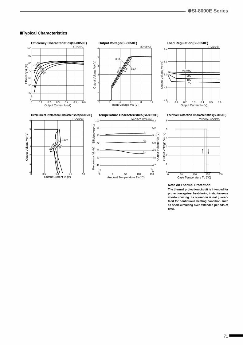
71
Typical Characteristics
Efficiency Characteristics(SI-8050E) Output Voltage(SI-8050E) Load Regulation(SI-8050E)
Overcurrent Protection Characteristics(SI-8050E) Temperature Characteristics(SI-8050E) Thermal Protection Characteristics(SI-8050E)
100
90
80
70
60
50
40
00 0.1 0.2 0.3 0.4 0.5
(Ta=25°C)
0.6Output Current IO (A)
Effi
cien
cy
(%
)η
VIN=7V
10V20V
30V40V
5.2
5.1
5.0
4.9
4.80 0.1 0.2 0.3 0.4 0.5 0.6
Output Current IO (V)
Out
put V
olta
ge V
O (
V)
20V
10V7V
(Ta=25°C)
VIN=40V
100
90
80
70
60
50
40
0
5.3
5.2
5.1
5.0
4.9
4.8
4.7
00 0 50 100
VO
f
150Ambient Temperature Ta (°C)
f (k
Hz)
Out
put V
olta
ge V
O (
V)
(VIN=20V, IO=0.3A)
(
%)
η η
Effi
cien
cyF
requ
ency
6
5
4
3
2
1
00 0.5 1.0 1.5 2.0
Output Current IO (V)
Out
put V
olta
ge V
O (
V)
20V
(Ta=25°C)
VIN=7
V
40V
SI-8000E Series
Note on Thermal Protection:The thermal protection circuit is intended forprotection against heat during instantaneousshort-circuiting. Its operation is not guaran-teed for continuous heating condition suchas short-circuiting over extended periods oftime.
6
5
4
3
2
1
00 2 4 6 8 10Input Voltage VIN (V)
Out
put V
olta
ge V
O (
V)
0.3A
0.6A
(Ta=25°C)
0.1A
IO=0
A
0
6
5
4
3
2
1
050 100
Case Temperature TC (°C)150 200
VIN=20V, IO=20mA
Out
put V
olta
ge V
O (
V)
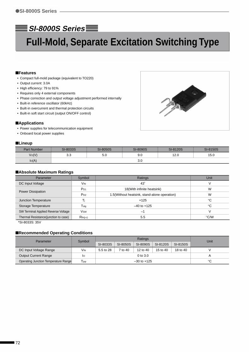
72
Features• Compact full-mold package (equivalent to TO220)
• Output current: 3.0A
• High efficiency: 79 to 91%
• Requires only 4 external components
• Phase correction and output voltage adjustment performed internally
• Built-in reference oscillator (60kHz)
• Built-in overcurrent and thermal protection circuits
• Built-in soft start circuit (output ON/OFF control)
Applications• Power supplies for telecommunication equipment
• Onboard local power supplies
Lineup
Full-Mold, Separate Excitation Switching TypeSI-8000S Series
Unit
V
A
°C
Symbol
VIN
IO
Tjop
Symbol
VIN
PD1
PD2
Tj
Tstg
VSW
Rth(j-c)
*SI-8033S: 35V
Recommended Operating Conditions
Absolute Maximum RatingsUnit
V
W
W
°C
°C
V
°C/W
Parameter
DC Input Voltage Range
Output Current Range
Operating Junction Temperature Range
Parameter
DC Input Voltage
Power Dissipation
Junction Temperature
Storage Temperature
SW Terminal Applied Reverse Voltage
Thermal Resistance(junction to case)
Ratings
43*
18(With infinite heatsink)
1.5(Without heatsink, stand-alone operation)
+125
–40 to +125
–1
5.5
Part Number SI-8033S SI-8050S SI-8090S SI-8120S SI-8150S
VO(V) 3.3 5.0 9.0 12.0 15.0
IO(A) 3.0
Ratings
SI-8033S SI-8050S SI-8090S SI-8120S SI-8150S
5.5 to 28 7 to 40 12 to 40 15 to 40 18 to 40
0 to 3.0
–30 to +125
SI-8000S Series
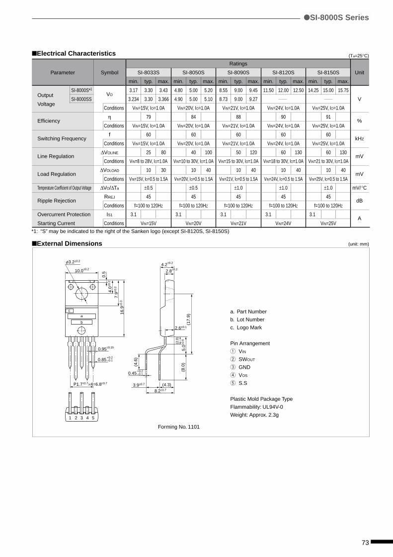
73
Symbol
VO
Conditions
η
Conditions
f
Conditions
∆VOLINE
Conditions
∆VOLOAD
Conditions
∆VO/∆Ta
RREJ
Conditions
IS1
Conditions
Ratings
SI-8033S SI-8050S SI-8090S SI-8120S SI-8150S
min. typ. max. min. typ. max. min. typ. max. min. typ. max. min. typ. max.
3.17 3.30 3.43 4.80 5.00 5.20 8.55 9.00 9.45 11.50 12.00 12.50 14.25 15.00 15.75
3.234 3.30 3.366 4.90 5.00 5.10 8.73 9.00 9.27
VIN=15V, IO=1.0A VIN=20V, IO=1.0A VIN=21V, IO=1.0A VIN=24V, IO=1.0A VIN=25V, IO=1.0A
79 84 88 90 91
VIN=15V, IO=1.0A VIN=20V, IO=1.0A VIN=21V, IO=1.0A VIN=24V, IO=1.0A VIN=25V, IO=1.0A
60 60 60 60 60
VIN=15V, IO=1.0A VIN=20V, IO=1.0A VIN=21V, IO=1.0A VIN=24V, IO=1.0A VIN=25V, IO=1.0A
25 80 40 100 50 120 60 130 60 130
VIN=8 to 28V, IO=1.0A VIN=10 to 30V, IO=1.0A VIN=15 to 30V, IO=1.0A VIN=18 to 30V, IO=1.0A VIN=21 to 30V, IO=1.0A
10 30 10 40 10 40 10 40 10 40
VIN=15V, IO=0.5 to 1.5A VIN=20V, IO=0.5 to 1.5A VIN=21V, IO=0.5 to 1.5A VIN=24V, IO=0.5 to 1.5A VIN=25V, IO=0.5 to 1.5A
±0.5 ±0.5 ±1.0 ±1.0 ±1.0
45 45 45 45 45
f=100 to 120HZ f=100 to 120HZ f=100 to 120HZ f=100 to 120HZ f=100 to 120HZ
3.1 3.1 3.1 3.1 3.1
VIN=15V VIN=20V VIN=21V VIN=24V VIN=25V
SI-8000S Series
a. Part Number
b. Lot Number
c. Logo Mark
Pin Arrangement
q VIN
w SWOUT
e GND
r VOS
t S.S
Plastic Mold Package Type
Flammability: UL94V-0
Weight: Approx. 2.3g
Forming No. 1101
External Dimensions
Electrical Characteristics (Ta=25°C)
(unit: mm)
10.0±0.24.2±0.2
0.95±0.15
8.2±0.7
2.6±0.1
3.9±0.7 (4.3)
(4.6
)
(8.0
)(1
7.9)
(2.0
)
0.85+0.2–0.1
0.45+0.2–0.1
3.2±0.2
4.0±0
.2
7.9±0
.2
5.0±0
.6
16.9
±0.3
0.5
1 2 3 4 5
P1.7±0.7×4=6.8±0.7
2.8±0.2
φ
a
b
c
Parameter
SI-8000S*1
OutputSI-8000SS
Voltage
Efficiency
Switching Frequency
Line Regulation
Load Regulation
Temperature Coefficient of Output Voltage
Ripple Rejection
Overcurrent Protection
Starting Current
Unit
V
%
kHZ
mV
mV
mV/°C
dB
A
*1: “S” may be indicated to the right of the Sanken logo (except SI-8120S, SI-8150S)

74
Block Diagram
Standard External Circuit
Ta-PD Characteristics
2
Reg. OCP
OSC Reset
Amp.
TSD
VREF
Comp.
Drive
1
4 VOS
VIN SWOUT
GNDS.S.5 3
VIN
C1
D1
L1VIN VO
GNDS.S
GND GND
SI-8000S
SWOUT
VOS
1 2
3
+C2
+
5
4
15
20
10
5
0–25 0 25 50
Ambient Operating Temperature Ta (°C)
Pow
er D
issi
patio
n P
D (
W)
75 125100
200×200×2mm(2.3°C/W)
100×100×2mm (5.2°C/W)
75×75×2mm (7.6°C/W)
Infinite heatsink
Without heatsink
With Silicon GreaseHeatsink: Aluminum
C1,2 : 1000µF
L1 : 150µH
D1 : RK46(Sanken)
The efficiency depends on the input voltage and the out-
put current. Thus, obtain the value from the efficiency graph
on page 75 and substitute the percentage in the formula
above.
VO : Output voltage
VIN : Input voltage
IO : Output current
ηx : Efficiency (%)
VF : Diode forward voltage
0.5V(RK46)
Thermal design for D1 must be considered separately.
PD=VO•IO 100
–1
–VF•IO 1– VO
ηχ VIN
SI-8000S Series
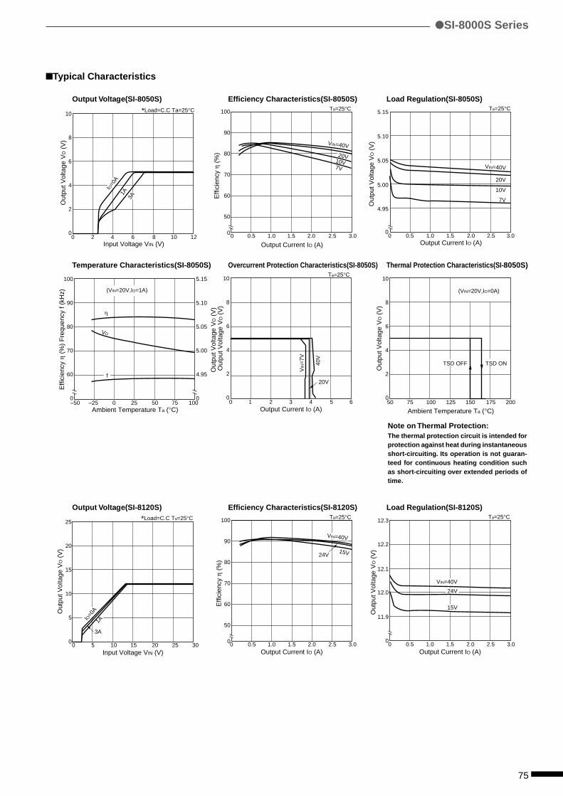
75
Typical Characteristics
Output Voltage(SI-8050S) Efficiency Characteristics(SI-8050S) Load Regulation(SI-8050S)
Temperature Characteristics(SI-8050S) Overcurrent Protection Characteristics(SI-8050S) Thermal Protection Characteristics(SI-8050S)
Output Voltage(SI-8120S) Efficiency Characteristics(SI-8120S) Load Regulation(SI-8120S)
0
10
8
6
4
2
02 4 6
Input Voltage VIN (V)
Out
put V
olta
ge V
O (
V)
8 10 12
*Load=C.C Ta=25°C
3A
1A
IO=0
A
Output Current IO (A)
Effi
cien
cy η
(%
)
0
100
90
80
70
60
50
0 0.5 1.0 1.5 2.0 2.5 3.0
Ta=25°C
VIN=40V
7V10V20V
Out
put V
olta
ge V
O (
V)
Output Current IO (A)0
5.15
5.10
5.05
5.00
4.95
00.5 1.0 1.5 2.0 2.5 3.0
Ta=25°C
10V
VIN=40V
7V
20V
Out
put V
olta
ge V
O (
V)
–50
100
90
80
70
60
0
5.15
5.10
5.05
5.00
4.95
0–25 0 25Ambient Temperature Ta (°C)
Effi
cien
cy η
(%
) F
requ
ency
f (k
Hz)
50 75 100
(VIN=20V,IO=1A)
VO
f
η
Out
put V
olta
ge V
O (
V)
Output Current IO (A)0
10
8
6
4
2
01 2 3 4 5 6
Ta=25°C
20V
40V
VIN
=7V
Out
put V
olta
ge V
O (
V)
50
10
8
6
4
2
075 100 125
Ambient Temperature Ta (°C)150 175 200
(VIN=20V,IO=0A)
TSD ONTSD OFF
Ta=25°C
24V15V
Output Current IO (A)
Effi
cien
cy η
(%
)
0
100
90
80
70
60
50
0 0.5 1.0 1.5 2.0 2.5 3.0
VIN=40V
Output Current IO (A)
Ta=25°C
Out
put V
olta
ge V
O (
V)
0
12.3
12.2
12.1
12.0
11.9
00.5 1.0 1.5 2.0 2.5 3.0
24V
15V
VIN=40V
Note on Thermal Protection:The thermal protection circuit is intended forprotection against heat during instantaneousshort-circuiting. Its operation is not guaran-teed for continuous heating condition suchas short-circuiting over extended periods oftime.
SI-8000S Series
0
25
20
15
10
5
05 10 15
Input Voltage VIN (V)
Out
put V
olta
ge V
O (
V)
20 25 30
*Load=C.C Ta=25°C
IO=0
A1A
3A
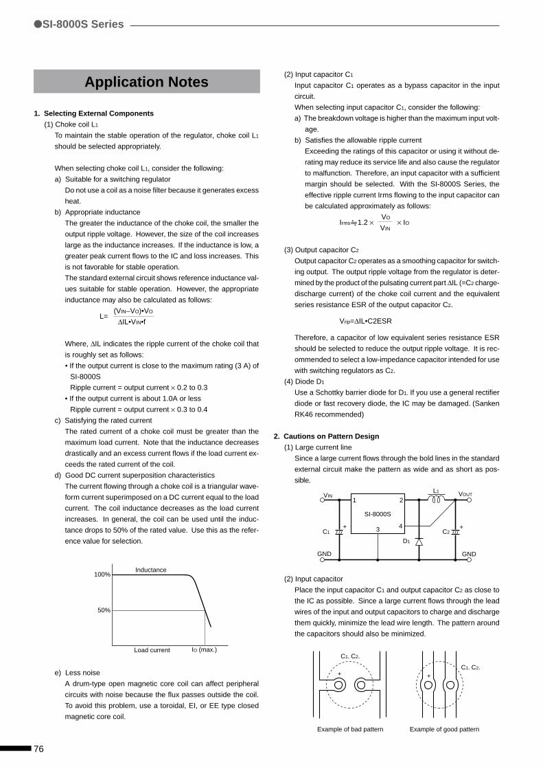
76
Application Notes
1. Selecting External Components
(1) Choke coil L1
To maintain the stable operation of the regulator, choke coil L1
should be selected appropriately.
When selecting choke coil L1, consider the following:
a) Suitable for a switching regulator
Do not use a coil as a noise filter because it generates excess
heat.
b) Appropriate inductance
The greater the inductance of the choke coil, the smaller the
output ripple voltage. However, the size of the coil increases
large as the inductance increases. If the inductance is low, a
greater peak current flows to the IC and loss increases. This
is not favorable for stable operation.
The standard external circuit shows reference inductance val-
ues suitable for stable operation. However, the appropriate
inductance may also be calculated as follows:
L= (VIN–VO)•VO
∆IL•VIN•f
Where, ∆IL indicates the ripple current of the choke coil that
is roughly set as follows:
• If the output current is close to the maximum rating (3 A) of
SI-8000S
Ripple current = output current × 0.2 to 0.3
• If the output current is about 1.0A or less
Ripple current = output current × 0.3 to 0.4
c) Satisfying the rated current
The rated current of a choke coil must be greater than the
maximum load current. Note that the inductance decreases
drastically and an excess current flows if the load current ex-
ceeds the rated current of the coil.
d) Good DC current superposition characteristics
The current flowing through a choke coil is a triangular wave-
form current superimposed on a DC current equal to the load
current. The coil inductance decreases as the load current
increases. In general, the coil can be used until the induc-
tance drops to 50% of the rated value. Use this as the refer-
ence value for selection.
100%
50%
IO (max.)
Inductance
Load current
e) Less noise
A drum-type open magnetic core coil can affect peripheral
circuits with noise because the flux passes outside the coil.
To avoid this problem, use a toroidal, EI, or EE type closed
magnetic core coil.
SI-8000S Series
(2) Input capacitor C1
Input capacitor C1 operates as a bypass capacitor in the input
circuit.
When selecting input capacitor C1, consider the following:
a) The breakdown voltage is higher than the maximum input volt-
age.
b) Satisfies the allowable ripple current
Exceeding the ratings of this capacitor or using it without de-
rating may reduce its service life and also cause the regulator
to malfunction. Therefore, an input capacitor with a sufficient
margin should be selected. With the SI-8000S Series, the
effective ripple current Irms flowing to the input capacitor can
be calculated approximately as follows:
Irms 1.2 × VO
× IO VIN
(3) Output capacitor C2
Output capacitor C2 operates as a smoothing capacitor for switch-
ing output. The output ripple voltage from the regulator is deter-
mined by the product of the pulsating current part ∆IL (=C2 charge-
discharge current) of the choke coil current and the equivalent
series resistance ESR of the output capacitor C2.
Vrip=∆IL•C2ESR
Therefore, a capacitor of low equivalent series resistance ESR
should be selected to reduce the output ripple voltage. It is rec-
ommended to select a low-impedance capacitor intended for use
with switching regulators as C2.
(4) Diode D1
Use a Schottky barrier diode for D1. If you use a general rectifier
diode or fast recovery diode, the IC may be damaged. (Sanken
RK46 recommended)
2. Cautions on Pattern Design
(1) Large current line
Since a large current flows through the bold lines in the standard
external circuit make the pattern as wide and as short as pos-
sible.
21
3 4
SI-8000S
VIN
GND
C1 C2
L1
D1
VOUT
GND
+ +
(2) Input capacitor
Place the input capacitor C1 and output capacitor C2 as close to
the IC as possible. Since a large current flows through the lead
wires of the input and output capacitors to charge and discharge
them quickly, minimize the lead wire length. The pattern around
the capacitors should also be minimized.
C1. C2.
C1. C2.++
Example of bad pattern Example of good pattern
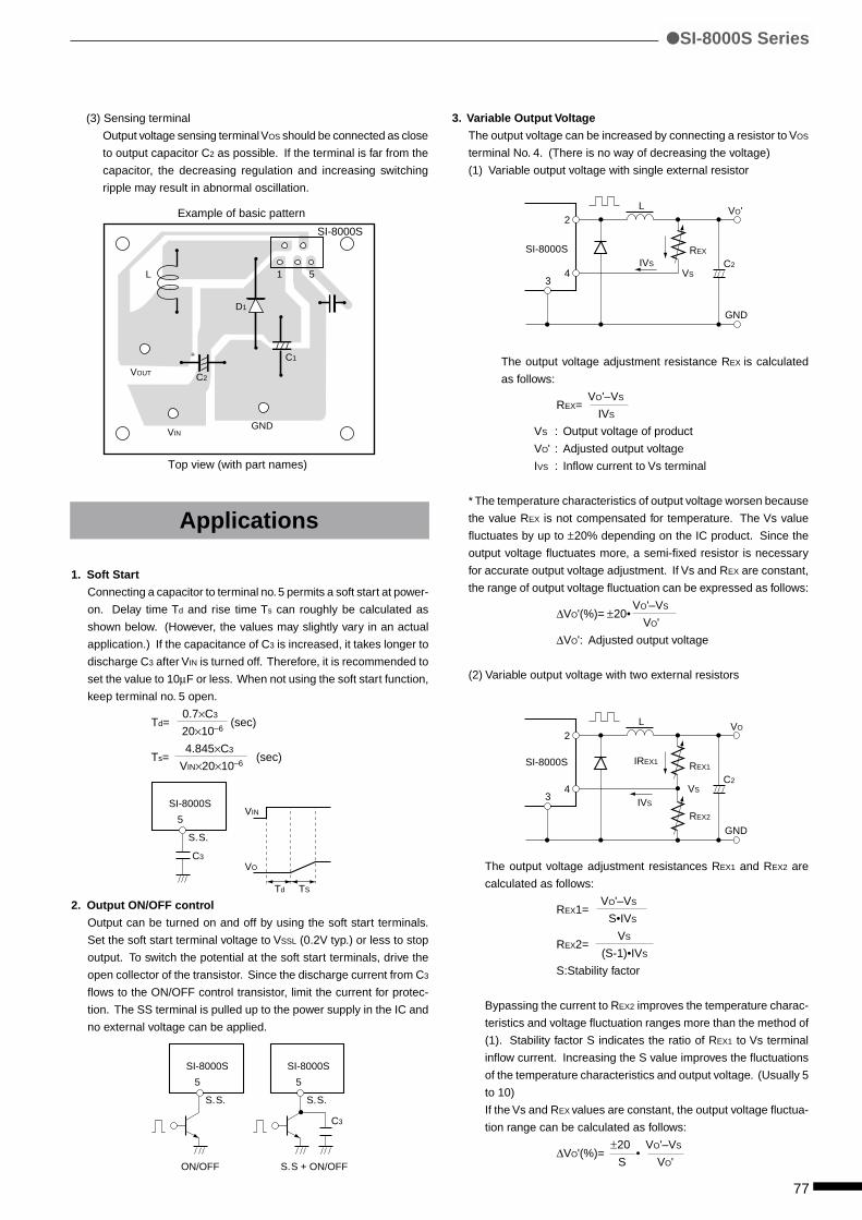
77
1. Soft Start
Connecting a capacitor to terminal no. 5 permits a soft start at power-
on. Delay time Td and rise time Ts can roughly be calculated as
shown below. (However, the values may slightly vary in an actual
application.) If the capacitance of C3 is increased, it takes longer to
discharge C3 after VIN is turned off. Therefore, it is recommended to
set the value to 10µF or less. When not using the soft start function,
keep terminal no. 5 open.
Td= 0.7×C3
(sec)20×10–6
Ts= 4.845×C3
(sec) VIN×20×10–6
SI-8000S
S. S.
C3
VIN
VO
Td TS
5
2. Output ON/OFF control
Output can be turned on and off by using the soft start terminals.
Set the soft start terminal voltage to VSSL (0.2V typ.) or less to stop
output. To switch the potential at the soft start terminals, drive the
open collector of the transistor. Since the discharge current from C3
flows to the ON/OFF control transistor, limit the current for protec-
tion. The SS terminal is pulled up to the power supply in the IC and
no external voltage can be applied.
SI-8000S
S. S + ON/OFF
S. S.
5
C3
SI-8000S
S. S.
5
ON/OFF
Applications
SI-8000S Series
(3) Sensing terminal
Output voltage sensing terminal VOS should be connected as close
to output capacitor C2 as possible. If the terminal is far from the
capacitor, the decreasing regulation and increasing switching
ripple may result in abnormal oscillation.
+
L 1 5
VOUT
VINGND
C1
C2
D1
SI-8000S
Example of basic pattern
Top view (with part names)
3. Variable Output Voltage
The output voltage can be increased by connecting a resistor to VOS
terminal No. 4. (There is no way of decreasing the voltage)
(1) Variable output voltage with single external resistor
SI-8000S
2
4
VO'
GND
C2
REX
VS
IVS
L
3
The output voltage adjustment resistance REX is calculated
as follows:
REX= VO'–VS
IVS
VS : Output voltage of product
VO' : Adjusted output voltage
IVS : Inflow current to Vs terminal
* The temperature characteristics of output voltage worsen because
the value REX is not compensated for temperature. The Vs value
fluctuates by up to ±20% depending on the IC product. Since the
output voltage fluctuates more, a semi-fixed resistor is necessary
for accurate output voltage adjustment. If Vs and REX are constant,
the range of output voltage fluctuation can be expressed as follows:
∆VO'(%)= ±20• VO'–VS
VO'
∆VO': Adjusted output voltage
(2) Variable output voltage with two external resistors
SI-8000S
2
4
VO
GND
C2
REX1
REX2
IREX1
IVS
VS
L
3
The output voltage adjustment resistances REX1 and REX2 are
calculated as follows:
REX1= VO'–VS
S•IVS
REX2= VS
(S-1)•IVS
S:Stability factor
Bypassing the current to REX2 improves the temperature charac-
teristics and voltage fluctuation ranges more than the method of
(1). Stability factor S indicates the ratio of REX1 to Vs terminal
inflow current. Increasing the S value improves the fluctuations
of the temperature characteristics and output voltage. (Usually 5
to 10)
If the Vs and REX values are constant, the output voltage fluctua-
tion range can be calculated as follows:
∆VO'(%)= ±20
• VO'–VS
S VO'
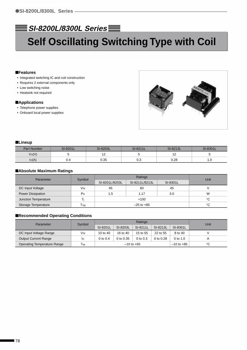
78
Features• Integrated switching IC and coil construction
• Requires 2 external components only
• Low switching noise
• Heatsink not required
Applications• Telephone power supplies
• Onboard local power supplies
Lineup
Self Oscillating Switching Type with Coil
Symbol
VIN
PD
Tj
Tstg
Symbol
VIN
IO
Top
SI-8200L/8300L Series
Unit
V
W
°C
°C
Recommended Operating Conditions
Absolute Maximum Ratings
Parameter
DC Input Voltage Range
Output Current Range
Operating Temperature Range
Parameter
DC Input Voltage
Power Dissipation
Junction Temperature
Storage Temperature
Part Number SI-8201L SI-8203L SI-8211L SI-8213L SI-8301L
VO(V) 5 12 5 12 5
IO(A) 0.4 0.35 0.3 0.28 1.0
Ratings
SI-8201L/8203L SI-8211L/8213L SI-8301L
45 60 45
1.5 1.17 3.0
+100
–25 to +85
Ratings
SI-8201L SI-8203L SI-8211L SI-8213L SI-8301L
10 to 40 16 to 40 15 to 55 22 to 55 8 to 40
0 to 0.4 0 to 0.35 0 to 0.3 0 to 0.28 0 to 1.0
–10 to +65 –10 to +85
Unit
V
A
°C
SI-8200L/8300L Series
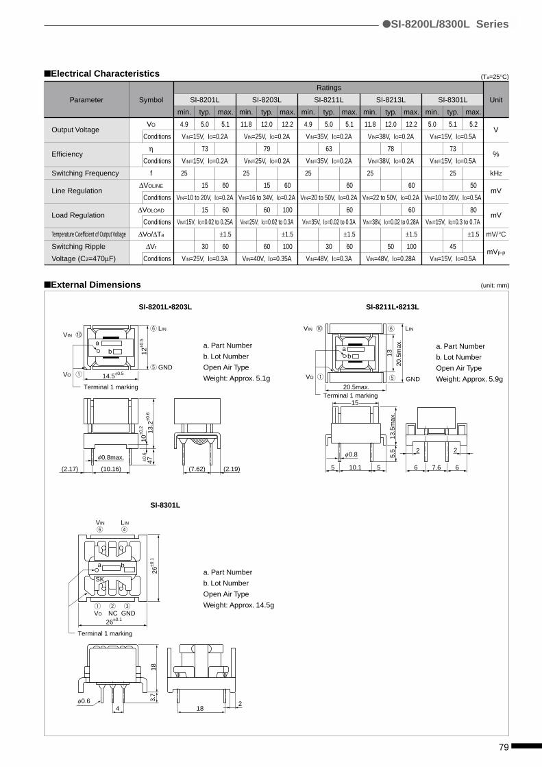
79
Electrical Characteristics (Ta=25°C)
a. Part Number
b. Lot Number
Open Air Type
Weight: Approx. 5.1g
Unit
V
%
kHZ
mV
mV
mV/°C
mVp-p
SI-8201L•8203L SI-8211L•8213L
a. Part Number
b. Lot Number
Open Air Type
Weight: Approx. 5.9g
a. Part Number
b. Lot Number
Open Air Type
Weight: Approx. 14.5g
SI-8301L
q
y
t
!0VIN
VO
0.8max.
LIN
GND
(10.16) (7.62) (2.19)(2.17)
14.5±0.5
12±0
.5
13.2
±0.6
10±0
.2
47±0.6φ
ab
Terminal 1 marking
y
q w e
r
SK
VIN
VO NC GND
LIN
183.
726
±0.1
26±0.1
0.64 18
2φ
a b
Terminal 1 marking
Parameter
Output Voltage
Efficiency
Switching Frequency
Line Regulation
Load Regulation
Temperature Coefficient of Output Voltage
Switching Ripple
Voltage (C2=470µF)
Symbol
VO
Conditions
η
Conditions
f
∆VOLINE
Conditions
∆VOLOAD
Conditions
∆VO/∆Ta
∆Vr
Conditions
Ratings
SI-8201L SI-8203L SI-8211L SI-8213L SI-8301L
min. typ. max. min. typ. max. min. typ. max. min. typ. max. min. typ. max.
4.9 5.0 5.1 11.8 12.0 12.2 4.9 5.0 5.1 11.8 12.0 12.2 5.0 5.1 5.2
VIN=15V, IO=0.2A VIN=25V, IO=0.2A VIN=35V, IO=0.2A VIN=38V, IO=0.2A VIN=15V, IO=0.5A
73 79 63 78 73
VIN=15V, IO=0.2A VIN=25V, IO=0.2A VIN=35V, IO=0.2A VIN=38V, IO=0.2A VIN=15V, IO=0.5A
25 25 25 25 25
15 60 15 60 60 60 50
VIN=10 to 20V, IO=0.2A VIN=16 to 34V, IO=0.2A VIN=20 to 50V, IO=0.2A VIN=22 to 50V, IO=0.2A VIN=10 to 20V, IO=0.5A
15 60 60 100 60 60 80
VIN=15V, IO=0.02 to 0.25A VIN=25V, IO=0.02 to 0.3A VIN=35V, IO=0.02 to 0.3A VIN=38V, IO=0.02 to 0.28A VIN=15V, IO=0.3 to 0.7A
±1.5 ±1.5 ±1.5 ±1.5 ±1.5
30 60 60 100 30 60 50 100 45
VIN=25V, IO=0.3A VIN=40V, IO=0.35A VIN=48V, IO=0.3A VIN=48V, IO=0.28A VIN=15V, IO=0.5A
SI-8200L/8300L Series
External Dimensions (unit: mm)
q
y
t
!0VIN
VO
LIN
GND20.5max.
20.5
max
.13
.5m
ax.
5.5
13
15
10.1 6 67.65 5
2 2 0.8φ
ab
Terminal 1 marking
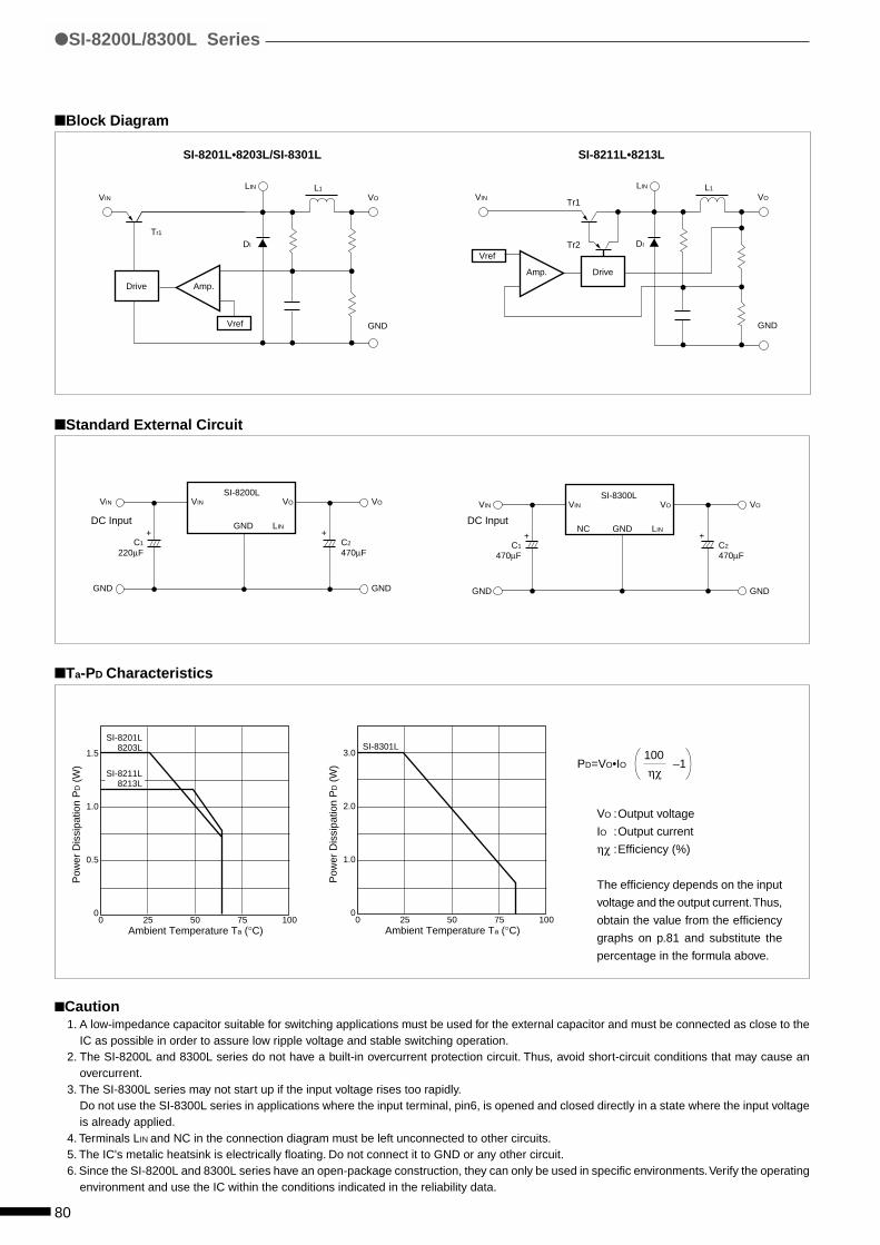
80
SI-8201L•8203L/SI-8301L SI-8211L•8213L
Block Diagram
Standard External Circuit
VIN
Vref
LIN L1
DI
Tr1
VO
GND
Amp.Drive
VIN
Vref
LIN L1
DI
Tr1
Tr2
VO
GND
Amp. Drive
VIN
GND
SI-8200LVIN
GND
LIN+ +
C1
220µFC2
470µF
GND
VOVO
DC Input
VIN VIN
NC GND
SI-8300L
GNDGND
LIN+ +
C1
470µFC2
470µF
VOVO
DC Input
Ta-PD Characteristics
VO :Output voltage
IO :Output current
ηχ :Efficiency (%)
The efficiency depends on the input
voltage and the output current. Thus,
obtain the value from the efficiency
graphs on p.81 and substitute the
percentage in the formula above.
PD=VO•IO 100
–1ηχ
1.5
1.0
0.5
00 25 50 75 100
Pow
er D
issi
patio
n P
D (
W)
Ambient Temperature Ta (°C)
SI-8201L8203L
SI-8211L8213L
Caution1. A low-impedance capacitor suitable for switching applications must be used for the external capacitor and must be connected as close to the
IC as possible in order to assure low ripple voltage and stable switching operation.2. The SI-8200L and 8300L series do not have a built-in overcurrent protection circuit. Thus, avoid short-circuit conditions that may cause an
overcurrent.3. The SI-8300L series may not start up if the input voltage rises too rapidly.
Do not use the SI-8300L series in applications where the input terminal, pin6, is opened and closed directly in a state where the input voltageis already applied.
4. Terminals LIN and NC in the connection diagram must be left unconnected to other circuits.5. The IC's metalic heatsink is electrically floating. Do not connect it to GND or any other circuit.6. Since the SI-8200L and 8300L series have an open-package construction, they can only be used in specific environments. Verify the operating
environment and use the IC within the conditions indicated in the reliability data.
SI-8200L/8300L Series
3.0
2.0
1.0
00 25 50 75 100
Pow
er D
issi
patio
n P
D (
W)
Ambient Temperature Ta (°C)
SI-8301L
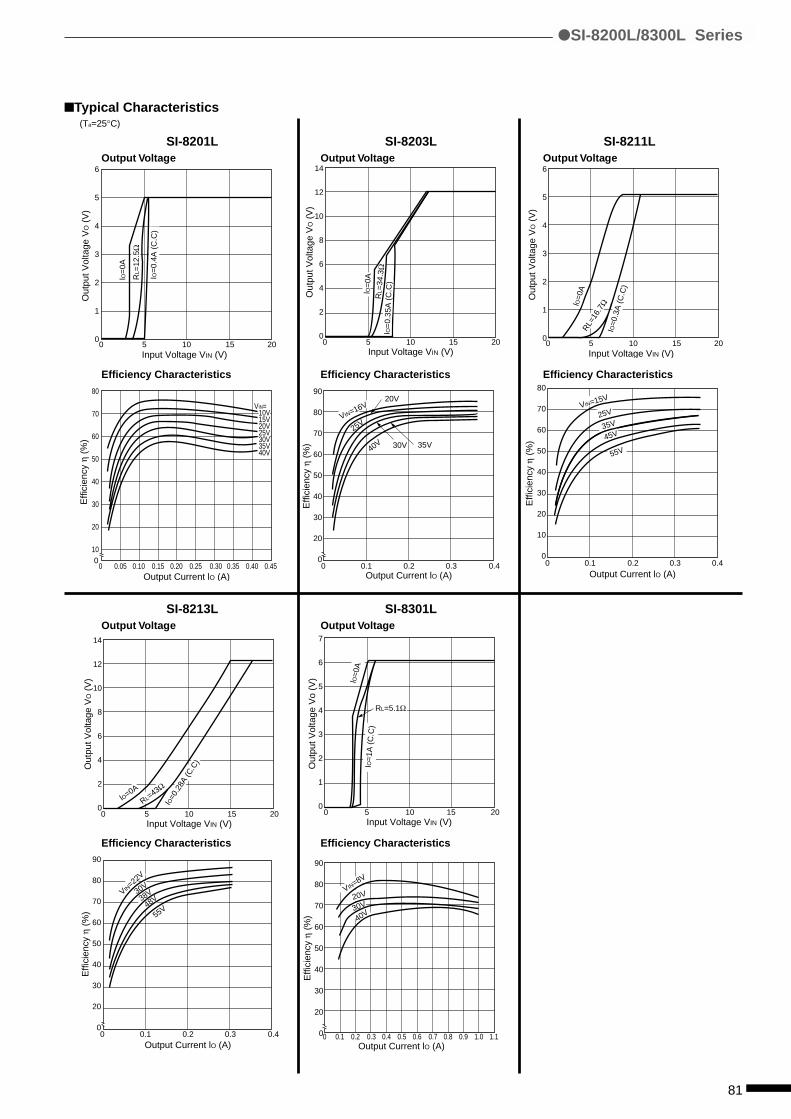
81
Typical Characteristics
SI-8213L SI-8301LOutput Voltage Output Voltage
Efficiency Characteristics Efficiency Characteristics
0 5 10 15 20Input Voltage VIN (V)
Out
put V
olta
ge V
O (
V)
14
12
10
8
6
4
2
0
IO=0
.28A
(C.C
)
lO=0A
RL=43Ω
0 0.1 0.2 0.3 0.4Output Current lO (A)
Effi
cien
cy η
(%
)
90
80
70
60
50
40
30
20
0
VIN=22
V
48V
55V
30V
38V
0 5 10 15 20Input Voltage VIN (V)
Out
put V
olta
ge V
o (V
)
7
6
5
4
3
2
1
0
IO=
1A (
C.C
)
lO=0
A
RL=5.1Ω
0 0.3 0.4 0.50.1 0.2 0.70.6 0.9 1.00.8 1.1Output Current lO (A)
Effi
cien
cy η
(%
)
90
80
70
60
50
40
30
20
0
VIN=8V
20V
30V
40V
SI-8201L SI-8203L SI-8211LOutput Voltage Output Voltage Output Voltage
Efficiency Characteristics Efficiency Characteristics Efficiency Characteristics
0 5 10 15 20Input Voltage VIN (V)
Out
put V
olta
ge V
O (
V)
6
5
4
3
2
1
0
IO=
0.4A
(C
.C)
lO=
0A
RL=
12.5
Ω
00
0.100.05 0.20 0.25 0.300.15 0.35 0.40 0.45Output Current lO (A)
Effi
cien
cy η
(%
)
80
70
60
50
40
30
20
10
VIN= 10V15V20V25V30V35V40V
0 5 10 15 20Input Voltage VIN (V)
Out
put V
olta
ge V
O (
V)
14
12
10
8
6
4
2
0 IO=
0.35
A (
C.C
)
lO=
0AR
L=34
.3Ω
0 0.1 0.2 0.3 0.4Output Current lO (A)
Effi
cien
cy η
(%
)
90
80
70
60
50
40
30
20
0
VIN=16V
40V
20V
35V30V
25V
6
5
4
3
2
1
0
IO=0
.3A
(C
.C)
lO=0
AR
L=16
.7Ω
0 5 10 15 20Input Voltage VIN (V)
Out
put V
olta
ge V
O (
V)
0 0.1 0.2 0.3 0.4
80
70
60
50
40
30
20
10
0
Output Current lO (A)
Effi
cien
cy η
(%
)
VIN=15V
25V
35V
45V
55V
(Ta=25°C)
SI-8200L/8300L Series
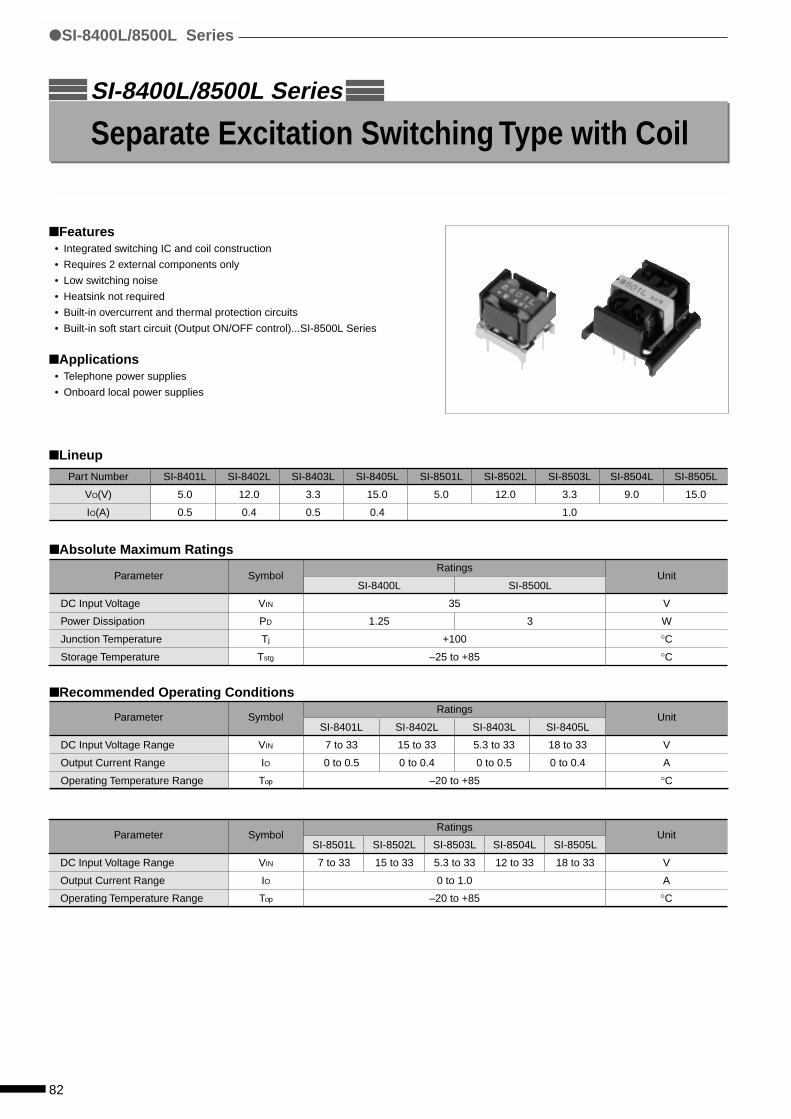
82
Unit
V
A
°C
Features• Integrated switching IC and coil construction
• Requires 2 external components only
• Low switching noise
• Heatsink not required
• Built-in overcurrent and thermal protection circuits
• Built-in soft start circuit (Output ON/OFF control)...SI-8500L Series
Applications• Telephone power supplies
• Onboard local power supplies
Lineup
Separate Excitation Switching Type with Coil
Symbol
VIN
PD
Tj
Tstg
SI-8400L/8500L Series
Recommended Operating Conditions
Absolute Maximum Ratings
Unit
V
A
°C
Unit
V
W
°C
°C
Symbol
VIN
IO
Top
Symbol
VIN
IO
Top
Ratings
SI-8400L SI-8500L
35
1.25 3
+100
–25 to +85
Part Number SI-8401L SI-8402L SI-8403L SI-8405L SI-8501L SI-8502L SI-8503L SI-8504L SI-8505L
VO(V) 5.0 12.0 3.3 15.0 5.0 12.0 3.3 9.0 15.0
IO(A) 0.5 0.4 0.5 0.4 1.0
Parameter
DC Input Voltage Range
Output Current Range
Operating Temperature Range
Parameter
DC Input Voltage Range
Output Current Range
Operating Temperature Range
Parameter
DC Input Voltage
Power Dissipation
Junction Temperature
Storage Temperature
Ratings
SI-8401L SI-8402L SI-8403L SI-8405L
7 to 33 15 to 33 5.3 to 33 18 to 33
0 to 0.5 0 to 0.4 0 to 0.5 0 to 0.4
–20 to +85
Ratings
SI-8501L SI-8502L SI-8503L SI-8504L SI-8505L
7 to 33 15 to 33 5.3 to 33 12 to 33 18 to 33
0 to 1.0
–20 to +85
SI-8400L/8500L Series
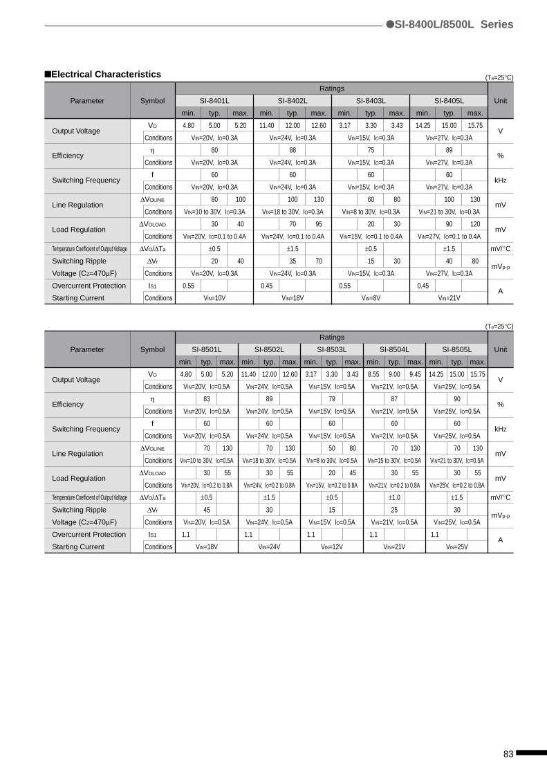
83
(Ta=25°C)
Unit
V
%
kHZ
mV
mV
mV/°C
mVp-p
A
Electrical Characteristics (Ta=25°C)
Unit
V
%
kHZ
mV
mV
mV/°C
mVp-p
A
Symbol
VO
Conditions
η
Conditions
f
Conditions
∆VOLINE
Conditions
∆VOLOAD
Conditions
∆VO/∆Ta
∆Vr
Conditions
IS1
Conditions
Parameter
Output Voltage
Efficiency
Switching Frequency
Line Regulation
Load Regulation
Temperature Coefficient of Output Voltage
Switching Ripple
Voltage (C2=470µF)
Overcurrent Protection
Starting Current
Parameter
Output Voltage
Efficiency
Switching Frequency
Line Regulation
Load Regulation
Temperature Coefficient of Output Voltage
Switching Ripple
Voltage (C2=470µF)
Overcurrent Protection
Starting Current
Symbol
VO
Conditions
η
Conditions
f
Conditions
∆VOLINE
Conditions
∆VOLOAD
Conditions
∆VO/∆Ta
∆Vr
Conditions
IS1
Conditions
Ratings
SI-8401L SI-8402L SI-8403L SI-8405L
min. typ. max. min. typ. max. min. typ. max. min. typ. max.
4.80 5.00 5.20 11.40 12.00 12.60 3.17 3.30 3.43 14.25 15.00 15.75
VIN=20V, IO=0.3A VIN=24V, IO=0.3A VIN=15V, IO=0.3A VIN=27V, IO=0.3A
80 88 75 89
VIN=20V, IO=0.3A VIN=24V, IO=0.3A VIN=15V, IO=0.3A VIN=27V, IO=0.3A
60 60 60 60
VIN=20V, IO=0.3A VIN=24V, IO=0.3A VIN=15V, IO=0.3A VIN=27V, IO=0.3A
80 100 100 130 60 80 100 130
VIN=10 to 30V, IO=0.3A VIN=18 to 30V, IO=0.3A VIN=8 to 30V, IO=0.3A VIN=21 to 30V, IO=0.3A
30 40 70 95 20 30 90 120
VIN=20V, IO=0.1 to 0.4A VIN=24V, IO=0.1 to 0.4A VIN=15V, IO=0.1 to 0.4A VIN=27V, IO=0.1 to 0.4A
±0.5 ±1.5 ±0.5 ±1.5
20 40 35 70 15 30 40 80
VIN=20V, IO=0.3A VIN=24V, IO=0.3A VIN=15V, IO=0.3A VIN=27V, IO=0.3A
0.55 0.45 0.55 0.45
VIN=10V VIN=18V VIN=8V VIN=21V
Ratings
SI-8501L SI-8502L SI-8503L SI-8504L SI-8505L
min. typ. max. min. typ. max. min. typ. max. min. typ. max. min. typ. max.
4.80 5.00 5.20 11.40 12.00 12.60 3.17 3.30 3.43 8.55 9.00 9.45 14.25 15.00 15.75
VIN=20V, IO=0.5A VIN=24V, IO=0.5A VIN=15V, IO=0.5A VIN=21V, IO=0.5A VIN=25V, IO=0.5A
83 89 79 87 90
VIN=20V, IO=0.5A VIN=24V, IO=0.5A VIN=15V, IO=0.5A VIN=21V, IO=0.5A VIN=25V, IO=0.5A
60 60 60 60 60
VIN=20V, IO=0.5A VIN=24V, IO=0.5A VIN=15V, IO=0.5A VIN=21V, IO=0.5A VIN=25V, IO=0.5A
70 130 70 130 50 80 70 130 70 130
VIN=10 to 30V, IO=0.5A VIN=18 to 30V, IO=0.5A VIN=8 to 30V, IO=0.5A VIN=15 to 30V, IO=0.5A VIN=21 to 30V, IO=0.5A
30 55 30 55 20 45 30 55 30 55
VIN=20V, IO=0.2 to 0.8A VIN=24V, IO=0.2 to 0.8A VIN=15V, IO=0.2 to 0.8A VIN=21V, IO=0.2 to 0.8A VIN=25V, IO=0.2 to 0.8A
±0.5 ±1.5 ±0.5 ±1.0 ±1.5
45 30 15 25 30
VIN=20V, IO=0.5A VIN=24V, IO=0.5A VIN=15V, IO=0.5A VIN=21V, IO=0.5A VIN=25V, IO=0.5A
1.1 1.1 1.1 1.1 1.1
VIN=18V VIN=24V VIN=12V VIN=21V VIN=25V
SI-8400L/8500L Series
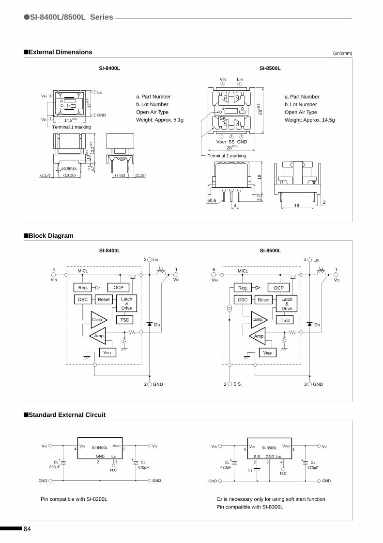
84
External Dimensions
a. Part Number
b. Lot Number
Open Air Type
Weight: Approx. 5.1g
SI-8400L SI-8500L
a. Part Number
b. Lot Number
Open Air Type
Weight: Approx. 14.5g
SI-8400L SI-8500L
Block Diagram
Standard External Circuit
q
e
w
rVIN
Vo
0.8max.
LIN
GND
(10.16) (7.62) (2.19)(2.17)
14.5±0.5
12±0
.5
13.2
±0.6
10±0
.2
4.7
±0.6φ
ab
Terminal 1 marking
y
q w e
r
SK
VIN
VOUT SS GND
LIN
183.
726
±0.1
26±0.1
0.64 18
2φ
a b
Terminal 1 marking
Reg. OCP
OSC Reset
Amp.
TSD
VREF
Comp.
Latch&
Drive
2
VIN VO
LIN
L1
Di1
MIC1
GND
4 1
3
VOVIN
GND GND
C1 C2
220µF 470µF
+ +
14
3
N.C
2
VOUT
LINGND
SI-8400LVIN VOVIN
GND GND
C1 C2
C3470µF 470µF
+ +
16
3 4
N.C
2
VOUT
LINGNDS.S
SI-8500LVIN
Pin compatible with SI-8200L C3 is necessary only for using soft start function.
Pin compatible with SI-8300L
32
Di1
MIC1
GNDS.S.
6 1
4
L1
Reg. OCP
OSC Reset
Amp.
TSD
VREF
Comp.
Latch&
Drive
VIN VO
LIN
SI-8400L/8500L Series
(unit:mm)
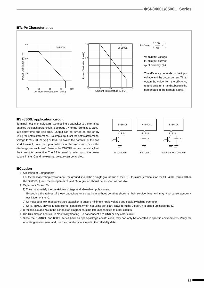
85
Ta-PD Characteristics
SI-8500L application circuitTerminal no.2 is for soft start. Connecting a capacitor to the terminal
enables the soft start function. See page 77 for the formulas to calcu-
late delay time and rise time. Output can be turned on and off by
using the soft start terminal. To stop output, set the soft start terminal
voltage to VSSL (0.2V typ.) or less. To switch the potential of the soft
start terminal, drive the open collector of the transistor. Since the
discharge current from C3 flows to the ON/OFF control transistor, limit
the current for protection. The SS terminal is pulled up to the power
supply in the IC and no external voltage can be applied.
Caution1. Allocation of Components
For the best operating environment, the ground should be a single ground line at the GND terminal (terminal 2 on the SI-8400L, terminal 3 on
the SI-8500L), and the wiring from C1 and C2 to ground should be as short as possible.
2. Capacitors C1 and C2
1) They must satisfy the breakdown voltage and allowable ripple current.
Exceeding the ratings of these capacitors or using them without derating shortens their service lives and may also cause abnormal
oscillation of the IC.
2) C2 must be a low-impedance type capacitor to ensure minimum ripple voltage and stable switching operation.
3) C3 (SI-8500L only) is a capacitor for soft start. When not using soft start, leave terminal 2 open. It is pulled up inside the IC.
3. Terminals LIN and NC in the connection diagram must be left unconnected to other circuits.
4. The IC's metalic heatsink is electrically floating. Do not connect it to GND or any other circuit.
5. Since the SI-8400L and 8500L series have an open-package construction, they can only be operated in specific environments. Verify the
operating environment and use the conditions indicated in the reliability data.
1.5
1.0
0.5
00 25 50
Ambient Temperature Ta (°C)
Pow
er D
issi
patio
n P
D (
W)
75 100
SI-8400L
3.0
2.0
1.0
00 25 50 75 100
SI-8500L
Ambient Temperature Ta (°C)
Pow
er D
issi
patio
n P
D (
W)
SI-8500L SI-8500L
S.S.2 S.S.2 S.S.
C3C3
2
VO. ON/OFF Soft start Soft start +VO ON/OFF
SI-8500L
SI-8400L/8500L Series
VO :Output voltage
IO :Output current
ηχ :Efficiency (%)
The efficiency depends on the input
voltage and the output current. Thus,
obtain the value from the efficiency
graphs on p.86, 87 and substitute the
percentage in the formula above.
PD=VO•IO 100
–1ηχ
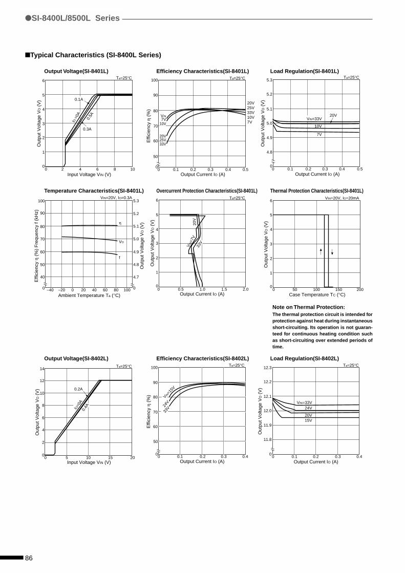
86
Typical Characteristics (SI-8400L Series)
Output Voltage(SI-8401L) Efficiency Characteristics(SI-8401L) Load Regulation(SI-8401L)
Temperature Characteristics(SI-8401L) Overcurrent Protection Characteristics(SI-8401L) Thermal Protection Characteristics(SI-8401L)
Output Voltage(SI-8402L) Efficiency Characteristics(SI-8402L) Load Regulation(SI-8402L)
0
6
5
4
3
2
1
02 4 6
Input Voltage VIN (V)
Out
put V
olta
ge V
O (
V)
8 10
Ta=25°CIO
=0A
0.5A
0.3A
0.1A
Output Current IO (A)
Effi
cien
cy η
(%
)
0
100
90
80
70
60
50
00.1 0.2 0.3 0.4 0.5
Ta=25°C
VIN7V
10V
20V25V33V
20V25V33V10V7V
Out
put V
olta
ge V
O (
V)
Output Current IO (A)0
5.3
5.2
5.1
5.0
4.9
4.8
00.1 0.2 0.3 0.4 0.5
Ta=25°C
VIN=33V20V
10V
7V
VIN=20V, IO=0.3A
Out
put V
olta
ge V
O (
V)
–400 0
100
90
80
70
60
50
40
5.3
5.2
5.1
5.0
4.9
4.8
4.7
–20 0 20Ambient Temperature Ta (°C)
Effi
cien
cy η
(%
) F
requ
ency
f (k
Hz)
40 60 80 100
VO
f
η
Out
put V
olta
ge V
O (
V)
Output Current IO (A)0
6
5
4
3
2
1
00.5 1.0 1.5 2.0
Ta=25°C20
V33
V
VIN
=7V
Out
put V
olta
ge V
O (
V)
0
6
5
4
3
2
1
050 100
Case Temperature TC (°C)150 200
VIN=20V, IO=20mA
0
14
12
10
6
8
2
0
4
5 10Input Voltage VIN (V)
Out
put V
olta
ge V
O (
V)
15 20
Ta=25°C
0.4A
0.2A
IO=0
A
0
100
90
80
70
60
50
00.1 0.2 0.3 0.4
VIN=1
5V
24V
33V
Output Current IO (A)
Effi
cien
cy η
(%
)
Ta=25°C
Out
put V
olta
ge V
O (
V)
0
12.3
12.2
12.1
12.0
11.9
11.8
00.1 0.2 0.3 0.4
VIN=33V24V
20V15V
Output Current IO (A)
Ta=25°C
SI-8400L/8500L Series
Note on Thermal Protection:The thermal protection circuit is intended forprotection against heat during instantaneousshort-circuiting. Its operation is not guaran-teed for continuous heating condition suchas short-circuiting over extended periods oftime.
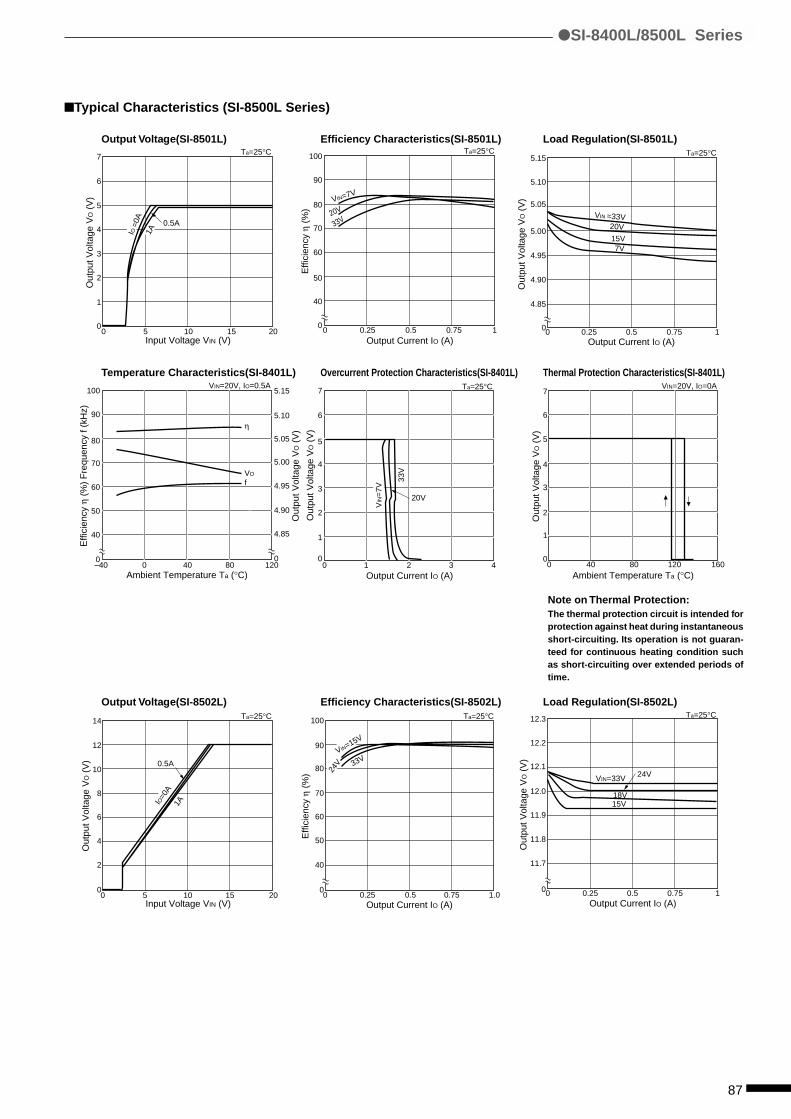
87
Typical Characteristics (SI-8500L Series)
Output Voltage(SI-8501L) Efficiency Characteristics(SI-8501L) Load Regulation(SI-8501L)
Temperature Characteristics(SI-8401L) Overcurrent Protection Characteristics(SI-8401L) Thermal Protection Characteristics(SI-8401L)
Output Voltage(SI-8502L) Efficiency Characteristics(SI-8502L) Load Regulation(SI-8502L)
0
7
6
5
4
3
2
1
05 10 15 20
Ta=25°C
IO =
0A1A
0.5A
Input Voltage VIN (V)
Out
put V
olta
ge V
O (
V)
0
100
90
80
70
60
50
40
00.25 0.5 0.75 1
Ta=25°C
VIN=7V
20V
33V
Output Current IO (A)
Effi
cien
cy η
(%
)
0
5.15
5.10
5.05
5.00
4.95
4.90
4.85
0 0.25 0.5 0.75 1
Ta=25°C
20V
15V
VIN =33V
7V
Out
put V
olta
ge V
O (
V)
Output Current IO (A)
–400
5.15
5.10
5.05
5.00
4.95
4.90
4.85
0 40 80 120
VO
η
f
VIN=20V, IO=0.5A
Out
put V
olta
ge V
O (
V)
0
100
90
80
70
60
50
40
Ambient Temperature Ta (°C)
Effi
cien
cy η
(%
) F
requ
ency
f (k
Hz)
0
7
6
5
4
3
2
1
01 2 3 4
VIN
=7V
20V
Ta=25°C
33V
Out
put V
olta
ge V
O (
V)
Output Current IO (A)0
7
6
5
4
3
2
1
040 80 120 160
Out
put V
olta
ge V
O (
V)
Ambient Temperature Ta (°C)
VIN=20V, IO=0A
0
14
12
10
6
8
2
0
4
5 10 15 20Input Voltage VIN (V)
Out
put V
olta
ge V
O (
V)
Ta=25°C
IO=0
A1A
0.5A
0
100
90
80
60
70
40
0
50
0.25 0.5 0.75 1.0
VIN=15V
24V 33V
Output Current IO (A)
Effi
cien
cy η
(%
)
Ta=25°C
0
12.3
12.2
12.1
11.9
12.0
11.7
0
11.8
0.25 0.5 0.75 1
Out
put V
olta
ge V
O (
V)
VIN=33V 24V
18V15V
Output Current IO (A)
Ta=25°C
SI-8400L/8500L Series
Note on Thermal Protection:The thermal protection circuit is intended forprotection against heat during instantaneousshort-circuiting. Its operation is not guaran-teed for continuous heating condition suchas short-circuiting over extended periods oftime.
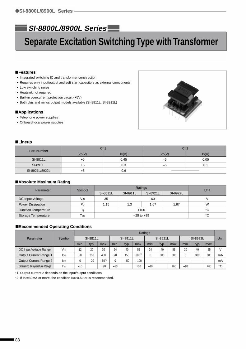
88
Features• Integrated switching IC and transformer construction
• Requires only input/output and soft start capacitors as external components
• Low switching noise
• Heatsink not required
• Built-in overcurrent protection circuit (+5V)
• Both plus and minus output models available (SI-8811L, SI-8911L)
Applications• Telephone power supplies
• Onboard local power supplies
Lineup
Separate Excitation Switching Type with Transformer
Unit
V
W
°C
°C
SI-8800L/8900L Series
Absolute Maximum Rating
Unit
V
mA
mA
°C
Symbol
VIN
IO1
IO2
Top
*1: Output current 2 depends on the input/output conditions
*2: If IO2=50mA or more, the condition IO1>0.5×IO2 is recommended.
Recommended Operating Conditions
Parameter
DC Input Voltage Range
Output Current Range 1
Output Current Range 2
Operating Temperature Range
Parameter
DC Input Voltage
Power Dissipation
Junction Temperature
Storage Temperature
Part Number
SI-8811L
SI-8911L
SI-8921L/8922L
Ch1 Ch2
VO(V) IO(A) VO(V) IO(A)
+5 0.45 –5 0.05
+5 0.3 –5 0.1
+5 0.6
Symbol
VIN
PD
Tj
Tstg
Ratings
SI-8811L SI-8911L SI-8921L SI-8922L
35 60
1.15 1.3 1.67 1.67
+100
–25 to +85
Ratings
SI-8811L SI-8911L SI-8921L SI-8922L
min. typ. max. min. typ. max. min. typ. max. min. typ. max.
12 20 30 24 40 55 24 40 55 20 40 55
50 250 450 20 150 300*2 0 300 600 0 300 600
0 –20 –50*1 0 –50 –100
–10 +70 –10 +60 –10 +65 –10 +65
SI-8800L/8900L Series
89
Electrical Characteristics (Ta=25°C)
Unit
V
V
%
kHZ
mVp-p
mVp-p
V
Symbol
VO1
Conditions
VO2
Conditions
η
Conditions
f
∆Vr1
Conditions
∆Vr2
Conditions
VSt
Conditions
External Dimensions
a. Part Number
b. Lot Number
Open Air Type
Weight: Approx. 9.3g
SK
q t
o y
16.8±0.2
22±0.2
19±0
.2
22±0
.2
18±0
.6
1±0.1
4±0.60.8max. (16.5)
(4×P3.175=12.7)
ab
Terminal 1 marking
SI-8811L, 8911L, 8921L, 8922L
Parameter
Output Voltage 1
Output Voltage 2
Efficiency
Switching Frequency
Switching Ripple
Voltage 1
Switching Ripple
Voltage 2
Operation Starting
Voltage
Ratings
SI-8811L SI-8911L SI-8921L SI-8922L
min. typ. max. min. typ. max. min. typ. max. min. typ. max.
4.75 5.00 5.25 4.75 5.00 5.25 4.95 5.10 5.20 4.95 5.10 5.20
Recommended operating conditions
–4.75 –5.00 –5.25 –4.75 –5.00 –5.25
Recommended operating conditions
72 65 72 72
Recommended operating conditions (typ.)
50 68 60 68 80 60 68 80
50 50 50 80 50 80
Recommended operating conditions (typ.)
50 50
Recommended operating conditions (typ.)
22 24 22 24 17 20
Recommended operating conditions (typ.)
SI-8800L/8900L Series
(unit: mm)
90
Standard External Circuit
SI-8811L SI-8911L
Block Diagram
SI-8921L/8922L
VIN
(+)
Tr1
VO1
1
4
2 S.S 5 6
3
9
8
7VO2
GNDT1
VIN
(–)
OSC
OCP Reg.
Drive
VrefAmp.
PWM
Start
31
Amp.
PWM
9
OSC
OCP –Reg.
Drive
Vref
Start
2 S.S
Tr1
T1
VO1
VO2
GND
5 4
7
6
8VIN
31
Amp.
PWM
7
OSC
OCP
Drive
Vref
Start
2 S.S
Tr1
T1
VOVIN
GND5
6
SI-8811L
VIN
VO1
VO2
GNDC1
C2
1
2
3
4
5
9
8
7
6
C4
C5
C3
(+)
VIN
(–)
+
+
+
+
+
SI-8911L
VIN
VO1
VO2
GND
GND
C1
C2
C3
1
2
3
4
5
9
8
C5
C4
+
+
+
+
+
6
7
SI-8921L
SI-8922L
VIN
VO
GND
GND
C1
C2
1
2
3
4
7
6
C3
+
+ +
5
SI-8800L/8900L Series
C1(for smoothing VIN) : 35V/470µF
C2(for soft start) : 16V/10µF
C3(for smoothing VO2Reg input) : 10V/220µF
C4(for smoothing VO1) : 16V/1200µF
C5(for smoothing VO2) : 10V/47µF
C1,2,3,5 : Nippon Chemi-con SME Series or equivalent
C4 : Nippon Chemi-con SXE Series or equivalent
C1(for smoothing VIN) : 63V/220µF
C2(for soft start) : 10V/33µF
C3(for smoothing VO2Reg input) : 10V/220µF
C4(for smoothing VO1) : 16V/1200µF
C5(for smoothing VO2) : 10V/100µF
C1,2,3,5 : Nippon Chemi-con SME Series or equivalent
C4 : Nippon Chemi-con SXE Series or equivalent
C1(for smoothing VIN) : 63V/180µF
C2(for soft start) : 10V/22µF
C3(for smoothing VO) : 10V/1200µF
C1,2 : Nippon Chemi-con SME Series or equivalent
C3 : Nippon Chemi-con SXE Series or equivalent
91
Ta-PD Characteristics
Caution1. A low-impedance capacitor suitable for switching applications must be used for the external capacitor and must be connected as close to the
IC as possible in order to assure low ripple voltage and stable switching operation.
2. The SI-881L/8911L series does not have a built-in overcurrent protection circuit on VO2(–5V). Thus, avoid short-circuit conditions that may
cause an overcurrent.
3. Do not connect VIN(–) of SI-8811L to GND. The overcurrent protection circuit may not work if they are connected.
4. Terminals left unconnected in the connection diagram must not be connected to other circuits.
5. The IC's metallic heatsink is electrically floating. Do not connect it to GND or any other circuit.
6. Since the SI-8800L and 8900L series have an open-package construction, they can be operated in specific environments. Verify the operating
environment and use the IC within the conditions indicated in the reliability data.
1.5
1.0
0.5
00 25 50
Ambient Temperature Ta (°C)
Pow
er D
issi
patio
n P
D (
W)
75 100
SI-8811L
SI-8911L
SI-
8911
L
SI-
8921
L
892
2L
SI-8921L 1.5
1.0
0.5
00 25 50
Ambient Temperature Ta (°C)
Pow
er D
issi
patio
n P
D (
W)
75 100
8922L
SI-8800L/8900L Series
VO :Output voltage
IO :Output current
ηχ :Efficiency (%)
The efficiency depends on the input
voltage and the output current. Thus,
obtain the value from the efficiency
graphs on p.92 and substitute the
percentage in the formula above.
PD=VO•IO 100
–1ηχ
92
Typical Characteristics
SI-8811L SI-8911L SI-8921LOutput Voltage Output Voltage Output Voltage
Efficiency Characteristics Efficiency Characteristics Efficiency Characteristics
Input Voltage VIN (V)
VO2
(V)
Out
put V
olta
ge V
O1
(V)
6
4
2
0
–2
–4
–6
2 4 6 8 10 12 14 16 18 20
lO1=50mA lO2 =0mA
lO1=250mA lO2 =–20mA
lO1=450mA lO2 =–50mA
lO1=50mA lO2 =0mAlO1=250mA lO2 =–20mA
lO1=450mA lO2 =–50mA
VIN
(V)
0 50 250100 150 200 300 400 450350 500Output Current 1 lO1 (A)
Effi
cien
cy η
(%
)
80
75
70
65
60
0
IO2 = –50mA constant
VIN=12V15V
20V
25V
30V
6
4
2
0
–2
–4
–6
5 10 15 20 25 30 35 40VIN
(V)
Input Voltage VIN (V)
VO2
(V)
Out
put V
olta
ge V
O1
(V)
lO120 to 30mA
lO20 to 100mA
0 20050 100 150 250 300 350 400
80
70
60
50
40
30
0
Output Current 1 lO1 (A)
Effi
cien
cy η
(%
)
IO2 = –100mA constant
VIN=55V
40V 24V
0 205 10 15 25 30 35 4540
6
5
4
3
2
1
0
0.6AlO=0
0.3A
Input Voltage VIN (V)
Out
put V
olta
ge V
O (
V)
0 0.40.1 0.2 0.3 0.5 0.6 0.7 0.8
80
70
60
50
40
30
20
0
Output Current lO (A)
Effi
cien
cy η
(%
)
VIN=55V48V40V30V
24V
SI-8922LOutput Voltage
0
8
7
6
5
4
3
2
1
0 10 20
Input Voltage VIN (V)
Out
put V
olta
ge V
O (
V)
30 40
IO=
0.4A
0.5A
0.6A
0
70
80
60
50
40
30
20
0 0.1 0.2 0.3 0.4 0.5 0.6 0.7 0.8Output Current lO (A)
Effi
cien
cy η
(%
)
VIN=55V48V40V30V
24V
(Ta=25°C)
SI-8800L/8900L Series
Efficiency Characteristics
Multi-Output Type - Application Note
93
Heat Radiation and ReliabilityThe reliability of an IC is highly dependent on its operating tempera-
ture. Design should pay particular attention to ensuring ample space
for radiating heat.
Be sure to apply silicon grease to the IC before attaching a heatsink,
and to secure it firmly to the heatsink.
Other important items to be considered regarding heat radiation in-
clude air convection during operation.
The reliability of peripheral components such as capacitors and coils
is closely related to temperature. A high operating temperature may
reduce the service life. Exceeding the allowable temperature may
burn the coils or damage capacitors. It is important to make sure that
the temperature of output smoothing coils and input/output capaci-
tors do not exceed their allowable levels during operation. Allow for
variation in the ratings of the coils and minimize heat emission as far
as possible. (For peripheral components, refer to the user manuals.)
Heatsink DesignThe maximum junction temperature Tj(max) given in the absolute maxi-
mum ratings is specific to each product type and must be strictly
observed. Thus, thermal design must consider the conditions of use
which affect the maximum power dissipation PD(max) and the maxi-
mum ambient temperature Ta(max).
To simplify thermal design, the relationship between these two pa-
rameters has been presented in a graph, the Ta-PD characteristic
graph. Thermal design should include these steps:
1. Obtain the maximum ambient temperature Ta(max).
2. Obtain the maximum power dissipation PD(max).
3. Look for the intersection point on the Ta-PD characteristic graph
and determine the size of the heatsink.
The size of the heatsink has now been obtained. However, in actual
applications, a 10 to 20% derating factor is introduced. Moreover, the
heat dissipation capacity of a heatsink highly depends on how it is
mounted. Thus, it is recommended to measure the heatsink and case
temperature in the actual operating environment.
The Ta-PD characteristics for each product type are provided for ref-
erence purposes.
Fastening TorqueSTA800M Series (when using a spring)
0.588 to 0.784 [N•m](6.0 to 8.0[kgf•cm]
SLA3000M Series
0.588 to 0.784 [N•m](6.0 to 8.0[kgf•cm]
Recommended Silicon Grease• Shin-Etsu Chemical Co., Ltd.: G746
• GE Toshiba Silicone Co., Ltd.: YG-6260
• Dow Corning Toray Silicone Co., Ltd.: SC102
Please be careful when selecting silicone grease since the oil in some
grease may penetrate the product, which will result in an extremely
short product life.
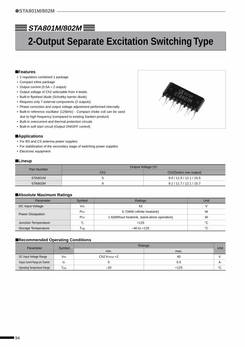
94
Features• 2 regulators combined 1 package
• Compact inline package
• Output current (0.5A × 2 output)
• Output voltage of Ch2 selectable from 4 levels.
• Built-in flywheel diode (Schottky barrier diode)
• Requires only 7 external components (2 outputs)
• Phase correction and output voltage adjustment performed internally
• Built-in reference oscillator (125kHz) - Compact choke coil can be used
due to high frequency (compared to existing Sanken product)
• Built-in overcurrent and thermal protection circuits
• Built-in soft start circuit (Output ON/OFF control)
Applications• For BS and CS antenna power supplies
• For stabilization of the secondary stage of switching power supplies
• Electronic equipment
Lineup
2-Output Separate Excitation Switching Type
Unit
V
W
W
°C
°C
Symbol
VIN
PD1
PD2
Tj
Tstg
STA801M/802M
Recommended Operating Conditions
Absolute Maximum Ratings
STA801M/802M
Unit
V
A
°C
Parameter
DC Input Voltage
Power Dissipation
Junction Temperature
Storage Temperature
Part Number
STA801M
STA802M
Parameter
DC Input Voltage Range
Output Current Range per Channel
Operating Temperature Range
Output Voltage (V)
Ch1 Ch2(Select one output)
5 9.0 / 11.5 / 12.1 / 15.5
9 9.1 / 11.7 / 12.1 / 15.7
Ratings
43
6.7(With infinite heatsink)
1.6(Without heatsink, stand-alone operation)
+125
–40 to +125
Symbol
VIN
IO
Tjop
Ratings
min. max.
Ch2 VOmax.+2 40
0 0.5
–20 +125
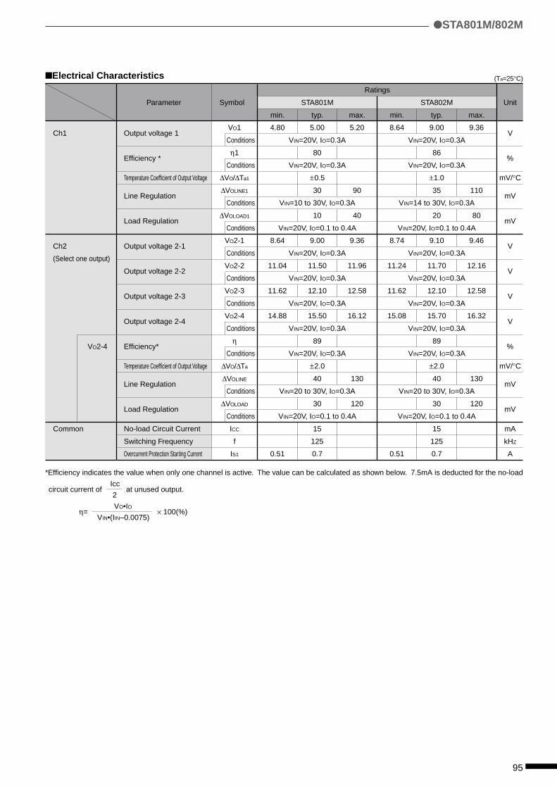
95
STA801M/802M
Electrical Characteristics (Ta=25°C)
*Efficiency indicates the value when only one channel is active. The value can be calculated as shown below. 7.5mA is deducted for the no-load
circuit current of Icc
at unused output.2
η= VO•IO
× 100(%) VIN•(IIN–0.0075)
Ch1
Ch2
(Select one output)
VO2-4
Common
Unit
V
%
mV/°C
mV
mV
V
V
V
V
%
mV/°C
mV
mV
mA
kHZ
A
Symbol
VO1
Conditions
η1
Conditions
∆VO/∆Ta1
∆VOLINE1
Conditions
∆VOLOAD1
Conditions
VO2-1
Conditions
VO2-2
Conditions
VO2-3
Conditions
VO2-4
Conditions
η
Conditions
∆VO/∆Ta
∆VOLINE
Conditions
∆VOLOAD
Conditions
ICC
f
IS1
Ratings
STA801M STA802M
min. typ. max. min. typ. max.
4.80 5.00 5.20 8.64 9.00 9.36
VIN=20V, IO=0.3A VIN=20V, IO=0.3A
80 86
VIN=20V, IO=0.3A VIN=20V, IO=0.3A
±0.5 ±1.0
30 90 35 110
VIN=10 to 30V, IO=0.3A VIN=14 to 30V, IO=0.3A
10 40 20 80
VIN=20V, IO=0.1 to 0.4A VIN=20V, IO=0.1 to 0.4A
8.64 9.00 9.36 8.74 9.10 9.46
VIN=20V, IO=0.3A VIN=20V, IO=0.3A
11.04 11.50 11.96 11.24 11.70 12.16
VIN=20V, IO=0.3A VIN=20V, IO=0.3A
11.62 12.10 12.58 11.62 12.10 12.58
VIN=20V, IO=0.3A VIN=20V, IO=0.3A
14.88 15.50 16.12 15.08 15.70 16.32
VIN=20V, IO=0.3A VIN=20V, IO=0.3A
89 89
VIN=20V, IO=0.3A VIN=20V, IO=0.3A
±2.0 ±2.0
40 130 40 130
VIN=20 to 30V, IO=0.3A VIN=20 to 30V, IO=0.3A
30 120 30 120
VIN=20V, IO=0.1 to 0.4A VIN=20V, IO=0.1 to 0.4A
15 15
125 125
0.51 0.7 0.51 0.7
Parameter
Output voltage 1
Efficiency *
Temperature Coefficient of Output Voltage
Line Regulation
Load Regulation
Output voltage 2-1
Output voltage 2-2
Output voltage 2-3
Output voltage 2-4
Efficiency*
Temperature Coefficient of Output Voltage
Line Regulation
Load Regulation
No-load Circuit Current
Switching Frequency
Overcurrent Protection Starting Current
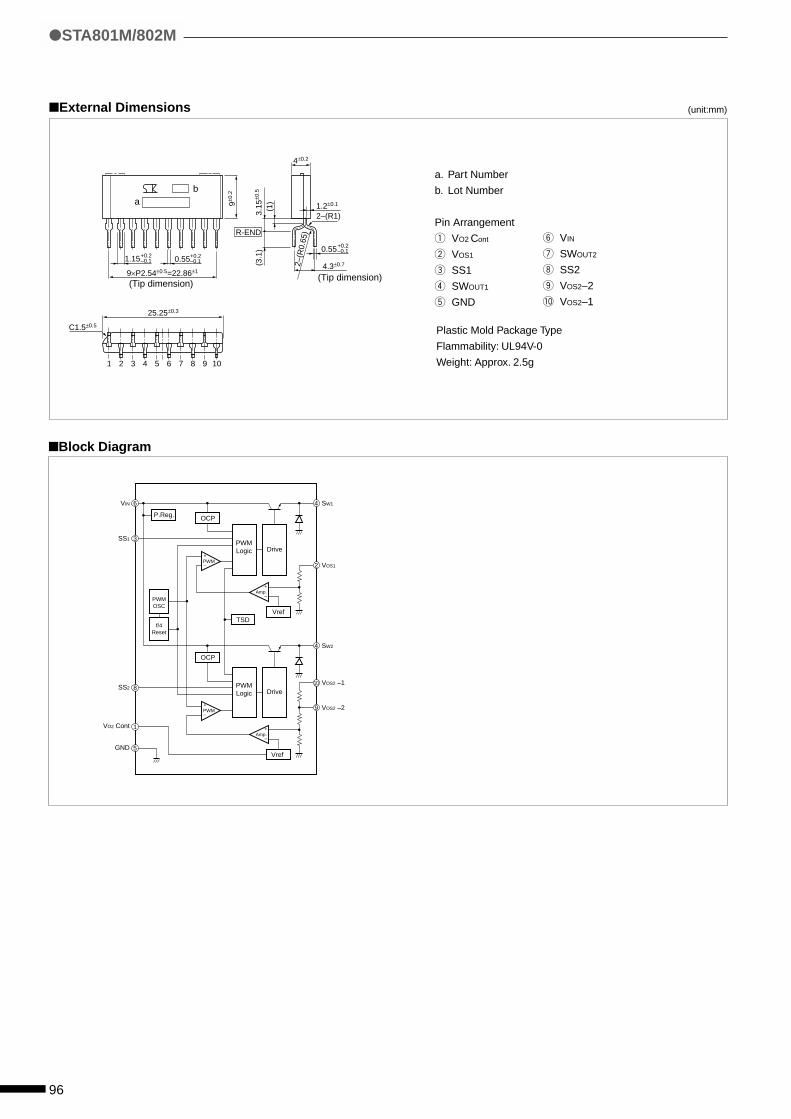
96
External Dimensions
Block Diagram
SW1VIN
SS1
SS2
VO2 Cont
GND
6
3
1
5
4
VOS12
DrivePWMLogic
PWM+
–
+
–
Vref
P.Reg.
SW2
VOS2 –18
4
VOS2 –29
10Drive
PWMLogic
PWM+
–
+
–
Vref
OCP
TSD
OCP
PWMOSC
f/4Reset
Amp.
Amp.
1.15
25.25±0.3
C1.5±0.5
1 2 3 4 5 6 7 8 9 10
+0.2–0.1 0.55+0.2
–0.1
9×P2.54±0.5=22.86±1
9±0.2
(1)
3.15
±0.5
(3.1
)
4±0.2
1.2±0.1
2–(R1)
4.3±0.7
R-END
2–(R
0.65
)
0.55+0.2–0.1
ab
(Tip dimension)(Tip dimension)
STA801M/802M
(unit:mm)
a. Part Number
b. Lot Number
Pin Arrangement
q VO2 Cont
w VOS1
e SS1
r SWOUT1
t GND
Plastic Mold Package Type
Flammability: UL94V-0
Weight: Approx. 2.5g
y VIN
u SWOUT2
i SS2
o VOS2–2
!0 VOS2–1
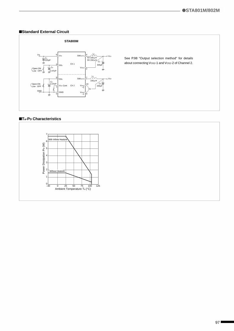
97
Ta-PD Characteristics
STA800M
Standard External Circuit
+
4SWOUT1VINVIN
VO2 Cont
GNDGND
SS1
SS2
VOS1
VOS2
VOS2
SWOUT2
–2
–1
2
7
10
9
6
3
8
1
5
L1
Ch 1
Ch 2
VO1
VO2
Or
L2
150 Hµ
5V:100 H9V:150 H
Open:ONLow :OFF
µµ
330 FC3
C2
µ
330 Fµ
C1220 F
C4
0.47 F
C50.47 F
µ
µ
µ+
+
+
+Open:ONLow :OFF
7
6
5
4
3
2
1
0
Pow
er D
issi
patio
n P
D (
W)
Ambient Temperature Ta (°C)0–30 25 50 75 100 125
Without Heatsink
With Infinite Heatsink
See P.98 "Output selection method" for details
about connecting VOS2-1 and VOS2-2 of Channel 2.
STA801M/802M
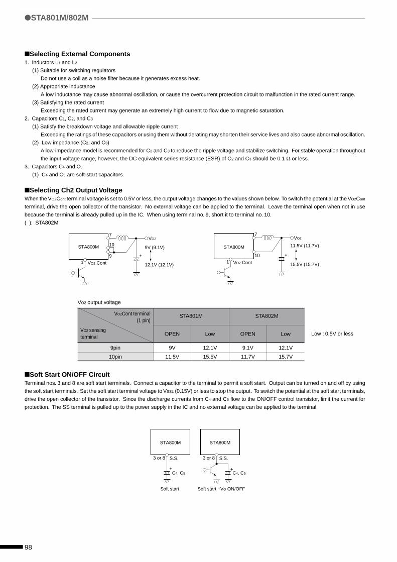
98
Selecting External Components1. Inductors L1 and L2
(1) Suitable for switching regulators
Do not use a coil as a noise filter because it generates excess heat.
(2) Appropriate inductance
A low inductance may cause abnormal oscillation, or cause the overcurrent protection circuit to malfunction in the rated current range.
(3) Satisfying the rated current
Exceeding the rated current may generate an extremely high current to flow due to magnetic saturation.
2. Capacitors C1, C2, and C3
(1) Satisfy the breakdown voltage and allowable ripple current
Exceeding the ratings of these capacitors or using them without derating may shorten their service lives and also cause abnormal oscillation.
(2) Low impedance (C2, and C3)
A low-impedance model is recommended for C2 and C3 to reduce the ripple voltage and stabilize switching. For stable operation throughout
the input voltage range, however, the DC equivalent series resistance (ESR) of C2 and C3 should be 0.1 Ω or less.
3. Capacitors C4 and C5
(1) C4 and C5 are soft-start capacitors.
Selecting Ch2 Output VoltageWhen the VO2Cont terminal voltage is set to 0.5V or less, the output voltage changes to the values shown below. To switch the potential at the VO2Cont
terminal, drive the open collector of the transistor. No external voltage can be applied to the terminal. Leave the terminal open when not in use
because the terminal is already pulled up in the IC. When using terminal no. 9, short it to terminal no. 10.
( ): STA802M
Soft Start ON/OFF CircuitTerminal nos. 3 and 8 are soft start terminals. Connect a capacitor to the terminal to permit a soft start. Output can be turned on and off by using
the soft start terminals. Set the soft start terminal voltage to VSSL (0.15V) or less to stop the output. To switch the potential at the soft start terminals,
drive the open collector of the transistor. Since the discharge currents from C4 and C5 flow to the ON/OFF control transistor, limit the current for
protection. The SS terminal is pulled up to the power supply in the IC and no external voltage can be applied to the terminal.
9pin
10pin
STA801M STA802M
OPEN Low OPEN Low
9V 12.1V 9.1V 12.1V
11.5V 15.5V 11.7V 15.7V
STA800M
VO2 Cont19
10
7VO2
9V (9.1V)
12.1V (12.1V)
+
STA800M
VO2 Cont110
7VO2
11.5V (11.7V)
15.5V (15.7V)
+
STA800M
S.S.
C4, C5
3 or 8
+
STA800M
Soft start Soft start +VO ON/OFF
S.S.
C4, C5
3 or 8
+
VO2Cont terminal(1 pin)
VO2 sensingterminal
VO2 output voltage
Low : 0.5V or less
STA801M/802M
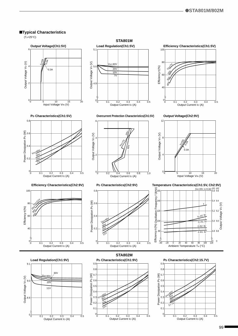
99
Typical Characteristics
PD Characteristics(Ch1:5V) Overcurrent Protection Characteristics(Ch1:5V) Output Voltage(Ch2:9V)
Efficiency Characteristics(Ch2:9V) PD Characteristics(Ch2:9V) Temperature Characteristics(Ch1:5V, Ch2:9V)
STA801M
Load Regulation(Ch1:9V) PD Characteristics(Ch1:9V) PD Characteristics(Ch2:15.7V)
6
4
2
00 5 10 15 20
Input Voltage VIN (V)
Out
put V
olta
ge V
O (
V)
0.3A
IO=0
A
0.5A
5.1
5.0
4.9
00 0.1 0.2 0.3 0.4 0.5
Output Current IO (A)
Out
put V
olta
ge V
O (
V)
VIN=40V
20V10V7V
100
80
60
40
00 0.1 0.2 0.3 0.4 0.5
Output Current IO (A)
Effi
cien
cy
(%)
VIN=7
V20
V30
V40
V
η
0.8
0.6
0.4
0.2
00 0.1 0.2 0.3 0.4 0.5
Output Current IO (A)
Pow
er D
issi
patio
n P
D (
W)
30V
7V
VIN=40V
20V
6
4
2
00 0.2 0.4 0.6 0.8 1.0
Output Current IO (A)
Out
put V
olta
ge V
O (
V)
VIN=7
V20
V40
V
100
80
60
40
00 0.1 0.2 0.3 0.4 0.5
Output Current IO (A)
Effi
cien
cy
(%)
20V
30Vη
VIN=11
V
40V
0.8
0.6
0.4
0.2
00 0.1 0.2 0.3 0.4 0.5
Output Current IO (A)
Pow
er D
issi
patio
n P
D (
W)
30V
11V
VIN=40V
20V
0.9
0.8
0.7
0.6
0.5
0.4
0.3
0.2
0.1
00 0.1 0.2 0.3 0.4 0.5
Output Current IO (A)
Pow
er D
issi
patio
n P
D (
W)
20V30VVIN
=40V
17.7V
0.9
0.8
0.7
0.6
0.5
0.4
0.3
0.2
0.1
00 0.1 0.2 0.3 0.4 0.5
Output Current IO (A)
Pow
er D
issi
patio
n P
D (
W)
30V
20V
11V
VIN=40V
9.1
9.0
8.9
00 0.1 0.2 0.3 0.4 0.5
Output Current IO (A)
Out
put V
olta
ge V
O (
V) VIN=40V
30V
20V
11V
160
140
120
100
80
0
5.6
5.4
5.2
5.0
4.8
0
9.6
9.4
9.2
9.0
8.8
0–40 –20 0 20 40 60 80 100 120
f
Ambient Temperature Ta (°C)
Osc
illat
ion
Fre
quen
cy f
(kH
z)
Out
put V
olta
ge V
O (
V)
(VIN=20V, IO=0.3A) ch1 ch2
Effi
cien
cy
(%)
η
VO ch2 9V
VO ch1 5V
η ch2 9V
η ch1 5V
STA802M
Output Voltage(Ch1:5V) Load Regulation(Ch1:5V) Efficiency Characteristics(Ch1:5V)
(Ta=25°C)
STA801M/802M
12
8
4
00 5 10 15 20
Input Voltage VIN (V)
Out
put V
olta
ge V
O (
V)
IO=0
A
0.3A
0.5A
100
Parameter
DC Input Voltage
Voltage of Output Control Terminal
DC Output Current
Power Dissipation
Junction Temperature
Ambient Operating Temperature
Storage Temperature
Thermal Junction (junction-to-ambient air)
Thermal Junction (junction-to-lead)
Features• Two 5V/0.5A output regulators in one package
• Surface-mount 16 pin package
• Low dropout voltage: VDIF ≤ 0.5V (at IO = 0.5A)
• Output-independent ON/OFF control terminal compatible with LS-TTL (Active
High)
• Built in output-independent overcurrent and thermal protection circuits
• Open collector flag-output terminals built in to output OCP operation to each
output terminal (Active Low)
• Buitl-in anti-malfunction delay circuit whose time can be set with an external
capacitor
Applications• USB power supplies
• Electronic equipment
Absolute Maximum Ratings
2-Output, Low Dropout Voltage Dropper Type for USBSDI02
SDI02
Symbol
VIN
VC
IO
PD
Tj
TOP
Tstg
Rth(j-a) 1
Rth(j-a) 2
Rth(j-l) 1
Rth(j-l) 1
Ratings
18
VIN
0.5
3.1*1
–30 to +125
–30 to +100
–30 to +125
42*2
32*1
11*3
14*4
(Ta=25°C)
*1: With simultaneous operation of both two channels when mounted on glass-epoxy board 56.5mm x 56.5mm (copper foil area 50%).
*2: With operation of one channel when mounted on glass-epoxy board 56.5mm x 56.5mm (copper foil area 50%).
*3: Junction - to - pin 14 (CH1)
*4: Junction - to - pin 10 (CH2)
Parameter
DC Input Voltage Range
Output Current Range
Ambient Operating Temperature
Junction Operating Temperature
Symbol
VIN
IO
Taop
Tjop
Ratings
5.5*1 to 8.0
0 to +0.5
–10 to +85
–10 to +100
Unit
V
A
°C
°C
(Ta=25°C)Recommended Operating Control
*1: VIN(min) must be no less than the sum of output voltage and dropout voltage.
Unit
V
V
A
W
°C
°C
°C
°C/W
°C/W
°C/W
°C/W
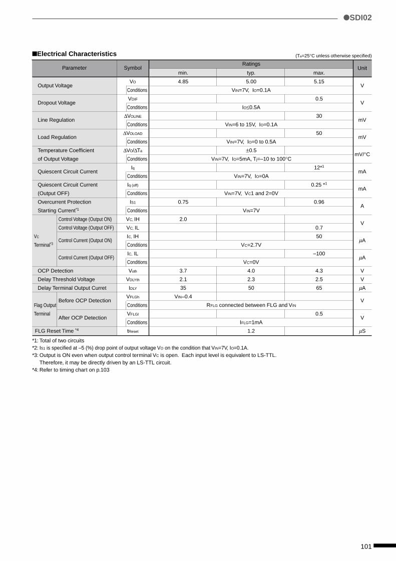
101
SDI02
Electrical Characteristics
*1: Total of two circuits*2: IS1 is specified at –5 (%) drop point of output voltage VO on the condition that VIN=7V, IO=0.1A.*3: Output is ON even when output control terminal VC is open. Each input level is equivalent to LS-TTL.
Therefore, it may be directly driven by an LS-TTL circuit.*4: Refer to timing chart on p.103
(Ta=25°C unless otherwise specified)
Parameter
Output Voltage
Dropout Voltage
Line Regulation
Load Regulation
Temperature Coefficient
of Output Voltage
Quiescent Circuit Current
Quiescent Circuit Current
(Output OFF)
Overcurrent Protection
Starting Current*1
Control Voltage (Output ON)
Control Voltage (Output OFF)
VCControl Current (Output ON)
Terminal*3
Control Current (Output OFF)
OCP Detection
Delay Threshold Voltage
Delay Terminal Output Curret
Before OCP DetectionFlag Output
TerminalAfter OCP Detection
FLG Reset Time *4
Symbol
VO
Conditions
VDIF
Conditions
∆VOLINE
Conditions
∆VOLOAD
Conditions
∆VO/∆Ta
Conditions
Iq
Conditions
Iq (off)
Conditions
IS1
Conditions
VC, IH
VC, IL
IC, IH
Conditions
IC, IL
Conditions
Voth
VDLYth
IDLY
VFLGh
Conditions
VFLGl
Conditions
tReset
Unit
V
V
mV
mV
mV/°C
mA
mA
A
V
µA
µA
V
V
µA
V
V
µS
Ratings
min. typ. max.
4.85 5.00 5.15
VIN=7V, IO=0.1A
0.5
IO≤0.5A
30
VIN=6 to 15V, IO=0.1A
50
VIN=7V, IO=0 to 0.5A
±0.5
VIN=7V, IO=5mA, Tj=–10 to 100°C12*1
VIN=7V, IO=0A
0.25 *1
VIN=7V, VC1 and 2=0V
0.75 0.96
VIN=7V
2.0
0.7
50
VC=2.7V
–100
VC=0V
3.7 4.0 4.3
2.1 2.3 2.5
35 50 65
VIN–0.4
RFLG connected between FLG and VIN
0.5
IFLG=1mA
1.2
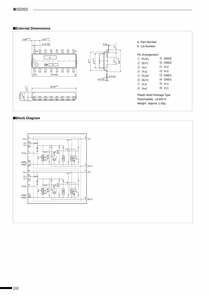
102
SDI02
External Dimensions
Block Diagram
SK
16 9
Pin1 20 max 8
0.75+0.15–0.05
0.3+0.15–0.05
2.54±0.25
8±0.5
6.3±0
.2
3±0.2
1±0.30.25
0~0.15
9.8±0
.3
3.6±0
.2
4 m
ax
1.4±0
.2 19.56±0.2
0.89±0.15
a
b
VO134
15
16
1
13
14
8
11
12
5
910
2
7
6
Reset
Set
VIN1
VC1
FLG1
DLY1
VC1
GND1
GND1
+ –
+–
–+
OC
P
TS
D
Latc
h
VO2
Reset
Set
VC2
FLG2
DLY2
VIN2
+ –
+–
–+
OC
P
TS
D
Latc
h
GND2
GND2
VC2
a. Part Number
b. Lot Number
Pin Arrangement
q FLG1
w DLY1
e VO1
r VIN1
t FLG2
y DLY2
u VO2
i VIN2
o GND2
!0 GND2
!1 VC2
!2 VC2
!3 GND1
!4 GND1
!5 VC1
!6 VC1
Plastic Mold Package Type
Flammability: UL94V-0
Weight: Approx. 1.05g
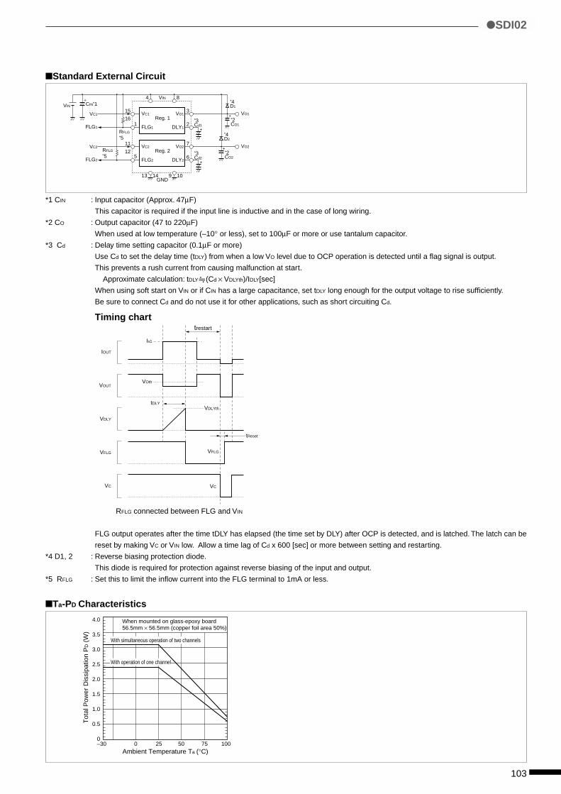
103
SDI02
Standard External Circuit
*1 CIN : Input capacitor (Approx. 47µF)
This capacitor is required if the input line is inductive and in the case of long wiring.
*2 CO : Output capacitor (47 to 220µF)
When used at low temperature (–10° or less), set to 100µF or more or use tantalum capacitor.
*3 Cd : Delay time setting capacitor (0.1µF or more)
Use Cd to set the delay time (tDLY) from when a low VO level due to OCP operation is detected until a flag signal is output.
This prevents a rush current from causing malfunction at start.
Approximate calculation: tDLY (Cd × VDLYth)/IDLY[sec]
When using soft start on VIN or if CIN has a large capacitance, set tDLY long enough for the output voltage to rise sufficiently.
Be sure to connect Cd and do not use it for other applications, such as short circuiting Cd.
Timing chart
RFLG connected between FLG and VIN
FLG output operates after the time tDLY has elapsed (the time set by DLY) after OCP is detected, and is latched. The latch can be
reset by making VC or VIN low. Allow a time lag of Cd x 600 [sec] or more between setting and restarting.
*4 D1, 2 : Reverse biasing protection diode.
This diode is required for protection against reverse biasing of the input and output.
*5 RFLG : Set this to limit the inflow current into the FLG terminal to 1mA or less.
Ta-PD Characteristics
VIN
8
3
1
5
1413 109
2
7
6
15
16
11
12
4
VO1
CIN*1
RFLG*5
RFLG*5
+
VC1
FLG1
VC1
FLG1
VO1Reg. 1
DLY1
VIN
*3Cd1
*2CO1
*4D1
+
+
+
VO2VC2
FLG2
VC2
FLG2
VO2Reg. 2
DLY2
GND
*3Cd2
*2CO2
*4D2
+
IOUT
Is1
trestart
VDLYth
VFLG
tReset
VC
VOth
tDLY
VOUT
VDLY
VFLG
VC
4.0
3.5
3.0
2.5
2.0
1.5
1.0
0.5
0
Tot
al P
ower
Dis
sipa
tion
PD (
W)
Ambient Temperature Ta (°C)0–30 25 50 75 100
With operation of one channel
With simultaneous operation of two channels
When mounted on glass-epoxy board56.5mm × 56.5mm (copper foil area 50%)
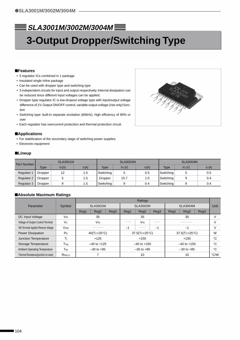
104
Features• 3 regulator ICs combined in 1 package
• Insulated single inline package
• Can be used with dropper type and switching type
• 3 independent circuits for input and output respectively. Internal dissipation can
be reduced since different input voltages can be applied.
• Dropper type regulator IC is low-dropout voltage type with input/output voltage
difference of 1V. Output ON/OFF control, variable output voltage (rise only) func-
tion
• Switching type: built-in separate excitation (60kHz), high efficiency of 80% or
over
• Each regulator has overcurrent protection and thermal protection circuit.
Applications• For stabilization of the secondary stage of switching power supplies
• Electronic equipment
Lineup
3-Output Dropper/Switching TypeSLA3001M/3002M/3004M
SLA3001M/3002M/3004M
Symbol
VIN
VC
VSW
PD
Tj
Tstg
Top
Rth(j-c)
Absolute Maximum Ratings
Parameter
DC Input Voltage
Voltage of Output Control Terminal
SW Terminal Applied Reverse Voltage
Power Dissipation
Junction Temperature
Storage Temperature
Ambient Operating Temperature
Thermal Resistance(junction-to-case)
Part Number
Regulator 1
Regulator 2
Regulator 3
SLA3001M SLA3002M SLA3004M
Type VO(V) IO(A) Type VO (V) IO(A) Type VO (V) IO (A)
Dropper 12 1.5 Switching 5 0.5 Switching 5 0.5
Dropper 5 1.5 Dropper 15.7 1.0 Switching 9 0.4
Dropper 9 1.5 Switching 9 0.4 Switching 9 0.4
Ratings
SLA3001M SLA3002M SLA3004M
Reg1 Reg2 Reg3 Reg1 Reg2 Reg3 Reg1 Reg2 Reg3
35 35 35
VIN VIN
–1 –1 –1
40(TC=25°C) 37.5(TC=25°C) 37.5(TC=25°C)
+125 +150 +150
–40 to +125 –40 to +150 –40 to +150
–30 to +85 –30 to +85 –30 to +85
7 10 10
Unit
V
V
V
W
°C
°C
°C
°C/W
105
SLA3001M/3002M/3004M
Electrical Characteristics
Unit
V
V
V
%
mV
mV
kHZ
A
V
V
V
V
V
%
mV
mV
kHZ
A
V
V
V
V
V
%
mV
mV
kHZ
A
V
V
*1: IS1 of Dropper Type is specified at –5(%) drop point of output voltage VO. IS1 of Switching Type is specified at –10(%) drop point of output voltage VO.*2: Output is ON when VC terminal is open.
Symbol
VIN1
VO1
Conditions
VDIF1
Conditions
η1
Conditions
∆VOLINE1
Conditions
∆VOLOAD1
Conditions
f1
Conditions
IS1, 1
Conditions
VCIH, 1
VCIL, 1
VIN2
VO2
Conditions
VDIF2
Conditions
η2
Conditions
∆VOLINE2
Conditions
∆VOLOAD2
Conditions
f2
Conditions
IS1, 2
Conditions
VCIH, 2
VCIL, 2
VIN3
VO3
Conditions
VDIF3
Conditions
η3
Conditions
∆VOLINE3
Conditions
∆VOLOAD3
Conditions
f3
Conditions
IS1, 3
Conditions
VCIH, 3
VCIL, 3
(Ta=25°C unless otherwise specified)
Ratings
SLA3001M SLA3002M SLA3004M
min. typ. max. min. typ. max. min. typ. max.
13 25 7 33 7 33
11.52 12.00 12.48 4.75 5.00 5.25 4.75 5.00 5.25
VIN=15V, IO=1.0A VIN=20V, IO=0.3A VIN=20V, IO=0.3A
1.0
IO=1.5A
80 80
VIN=20V, IO=0.3A VIN=20V, IO=0.3A
24 64 80 100 80 110
VIN=13 to 25V, IO=1.0A VIN=10 to 30V, IO=0.3A VIN=10 to 30V, IO=0.3A
93 240 30 40 30 40
VIN=15V, IO=0 to 1.5A VIN=20V, IO=0.1 to 0.4A VIN=20V, IO=0.1 to 0.4A
60 60
VIN=20V, IO=0.3A VIN=20V, IO=0.3A
1.6 0.55 0.55
VIN=15V VIN=10V VIN=10V
2.0
0.8
6 15 17 30 12 33
4.85 5.00 5.15 14.92 15.70 16.48 8.55 9.00 9.45
VIN=8V, IO=1.0A VIN=19V, IO=0.5A VIN=21V, IO=0.3A
1.0 1.0
IO=1.5A IO=1.0A
85
VIN=21V, IO=0.3A
10 30 30 90 90 110
VIN=6 to 15V, IO=1.0A VIN=17 to 25V, IO=0.5A VIN=14 to 30V, IO=0.3A
40 100 120 300 50 80
VIN=8V, IO=0 to 1.5A VIN=19V, IO=0 to 0.1A VIN=21V, IO=0.1 to 0.4A
60
VIN=21V, IO=0.3A
1.6 1.2 0.45
VIN=8V VIN=19V VIN=14V
2.0 2.0
0.8 0.8
10 20 12 33 12 33
8.64 9.00 9.36 8.55 9.00 9.45 8.64 9.00 9.36
VIN=12V, IO=1.0A VIN=21V, IO=0.3A VIN=21V, IO=0.3A
1.0
IO=1.5A
85 85
VIN=21V, IO=0.3A VIN=21V, IO=0.3A
18 48 90 110 90 110
VIN=10 to 20V, IO=1.0A VIN=14 to 30V, IO=0.3A VIN=14 to 30V, IO=0.3A
70 180 50 80 50 80
VIN=15V, IO=0 to 1.5A VIN=21V, IO=0.1 to 0.4A VIN=21V, IO=0.1 to 0.4A
60 60
VIN=21V, IO=0.3A VIN=21V, IO=0.3A
1.6 0.45 0.45
VIN=12V VIN=14V VIN=14V
2.0
0.8
Parameter
Recommended DC Input Voltage
Output Voltage
Dropout Voltage
Efficiency
Line Regulation
Load Regulation
Switching Frequency
Overcurrent Protection
Starting Current*1
VC Control Voltage (Output ON)
Terminal*2 Control Voltage (Output OFF)
Recommended DC Input Voltage
Output Voltage
Dropout Voltage
Efficiency
Line Regulation
Load Regulation
Switching Frequency
Overcurrent Protection
Starting Current*1
VC Control Voltage (Output ON)
Terminal*2 Control Voltage (Output OFF)
Recommended DC Input Voltage
Output Voltage
Dropout Voltage
Efficiency
Line Regulation
Load Regulation
Switching Frequency
Overcurrent Protection
Starting Current*1
VC Control Voltage (Output ON)
Terminal*2 Control Voltage (Output OFF)
Reg
ulat
or 1
Reg
ulat
or 2
Reg
ulat
or 3
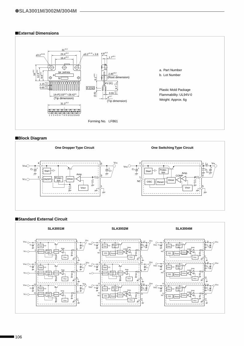
106
SLA3001M SLA3002M SLA3004M
Standard External Circuit
External Dimensions
Forming No. LF861
One Dropper Type Circuit One Switching Type Circuit
Block Diagram
VO1
VIN1
VC1
4
2
C1C4
5
3
1
Amp.Start
DriveON/OFF Protec-tion
VREF
++VIN1
VIN2
1
NC
C1
C4D1
3
4
5
Start
ResetDrive
++
Amp.COMP
L1
OSC
Protec-tion
VREF
SLA3001M/3002M/3004M
31±0.2
31.3±0.2
3.2±0.15 × 3.8 3.2±0.15 24.4±0.2
16.4±0.2 1.7±0.1
2.45±0.2
4±0.7
4.8±0.2
16±0
.2
12.9
±0.2
9.9±0
.2
6.1±0
.5
9.7
(3.6
)
4–(R1)
R-END
0.55+0.7–0.1
+1
–0.51.15
+0.2–0.1
0.65+0.2–0.1
14×P2.03±0.7=28.42±1
1 2 3 4 5 6 7 8 9 10 1112131415
SK JAPAN
φ φ
ab
(Tip dimension)(Tip dimension)
(Root dimension)
VIN1VO1
VO2
VO3
VC1
VIN2
VC2
VIN3
VC3
4
9
7
14
12
2
C1
C2
C3
C4
C5
C6
5
3
1
10
8
6
13
15
11
Amp.
Start
DriveON/OFF Protec-tion
VREF
Amp.
Start
DriveON/OFF Protec-tion
VREF
Amp.Start
DriveON/OFF Protec-tion
VREF
+
+
+
+
+
VO2
VC
9
7
C2C5
10
8
6
++
+
VO12
1
NC
C1
C4D1
D2
D2D2
D1
3
4
5
Start
ResetDrive
++
VIN3
VIN2
VIN1
VO312
11
NC
C3
C4
15
14
15
++
VO12
1
C1
L1
L2
C4
3
4
5
++
VO27
2
C2
C5
8
9
10
++
L3
VIN3
VIN2
VIN3
VO312
11
C3
C6
13
14
15
Amp.COMP
++
NC
NC
NC
L1
L2
Amp.Start
DriveON/OFF
OSC
Protec-tion
Protec-tion
VREF
VREF
Start
ResetDrive
Amp.COMP
OSC
Protec-tion
VREF
Start
ResetDrive
Amp.COMP
OSC
Protec-tion
VREF
Start
ResetDrive
Amp.COMP
OSC
Protec-tion
VREF
Start
ResetDrive
Amp.COMP
OSC
Protec-tion
VREF
a. Part Number
b. Lot Number
Plastic Mold Package
Flammability: UL94V-0
Weight: Approx. 6g
107
Selecting External components for dropper type regulatorInput capacitor (Approx. 47µF)
Output capacitor (Approx. 47 to 100µF)
Low ESR capacitors are recommended for input and output when using them in low temperature conditions (0°C or less)
Selecting External components for switching type regulatorInput capacitor (Approx. 100µF)
Output smoothing capacitor (Approx. 330µF)
Input capacitor and output capacitor must satisfy allowable ripple current.
Low ESR capacitors are recommended for reducing output ripple voltage.
Low ESR capacitors are recommended for input and output when using them in low temperature conditions (0°C or less)
Choke coil (200µH when VO is 3.3V or 5V, 300µH when VO is other)
When its winding resistance is high, its efficiency may decrease and the rated value may not be achieved.
Pay attention to heat from the choke coil due to magnetic saturation caused by overload, short circuit of load, etc. because the overcurrent
protection starting current is approx. 1A.
Flywheel diode (Sanken AK04 recommended)
Use a Schottky barrier diode for D1, D2 and D3 and make sure that the reverse voltage applied to SW output terminal does not exceed the value
(–1V) given in the maximum ratings.
If you use a fast recovery diode or any other diode, application of a reverse voltage generated from the recovery or ON voltage of the diode may
damage the IC.
SLA3001M/3002M/3004M
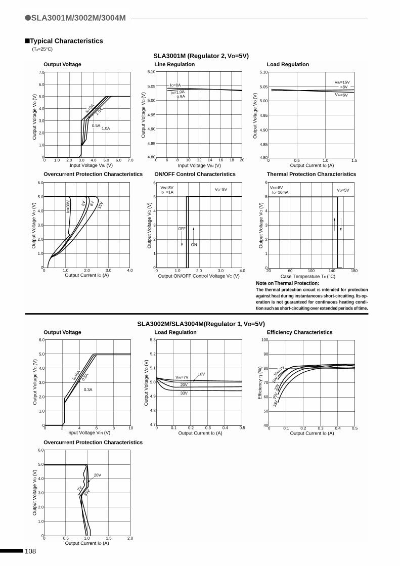
108
Typical Characteristics
Output Voltage Line Regulation Load Regulation
Overcurrent Protection Characteristics ON/OFF Control Characteristics Thermal Protection Characteristics
Output Voltage Load Regulation Efficiency Characteristics
SLA3001M (Regulator 2, VO=5V)
Overcurrent Protection Characteristics
SLA3002M/SLA3004M(Regulator 1, VO=5V)
Out
put V
olta
ge V
O (V
)
7.0
6.0
5.0
4.0
3.0
2.0
1.0
00 1.0 2.0 3.0 4.0 5.0 6.0 7.0
Input Voltage VIN (V)
IO=0
A1.
5A
0.5A1.0A
5.10
5.05
5.00
4.95
4.90
4.85
4.800 6 8 10 12 14 16 18 20
IO=0A
IO=1.0A0.5A
Out
put V
olta
ge V
O (V
)
Input Voltage VIN (V)
Out
put V
olta
ge V
O (V
)
5.10
5.05
5.00
4.95
4.90
4.85
4.800 0.5 1.0 1.5
Output Current IO (A)
VIN=15V =8V
VIN=6V
Output Current IO (A)
6.0
5.0
4.0
3.0
2.0
1.0
0
Out
put V
olta
ge V
O (
V)
0 1.0 2.0 3.0 4.0
6V 8V
15V
IO=
30V
6
5
4
3
2
1
0
Out
put V
olta
ge V
O (
V)
Output ON/OFF Control Voltage VC (V)0 1.0 2.0 3.0 4.0
VIN=8V VO=5VIO =1A
ON
OFF
6.0
5.0
4.0
3.0
2.0
1.0
00 2 4 6 8 10
Out
put V
olta
ge V
O (V
)
Input Voltage VIN (V)
IO=0
A0.
5A
0.3A
5.3
5.2
5.1
5.0
4.9
4.8
4.7
VIN=7V10V
Out
put V
olta
ge V
O (
V)
0 0.1 0.2 0.3 0.4 0.5Output Current IO (A)
33V
20V
100
90
80
70
60
50
40
Effi
cien
cy η
(%
)
0 0.1 0.2 0.3Output Current IO (A)
0.4 0.5
VIN=7V
20V
33V
10V
25V
6.0
5.0
4.0
3.0
2.0
1.0
00 0.5 1.0
Output Current IO (A)1.5 2.0
20V
33V7V
Out
put V
olta
ge V
O (V
)
(Ta=25°C)
SLA3001M/3002M/3004M
Note on Thermal Protection:The thermal protection circuit is intended for protectionagainst heat during instantaneous short-circuiting. Its op-eration is not guaranteed for continuous heating condi-tion such as short-circuiting over extended periods of time.
6
5
4
3
2
1
0
Case Temperature Tc (°C)20 60 100 140 180
VIN=8V IO=10mA VO=5V
Out
put V
olta
ge V
O (
V)

109
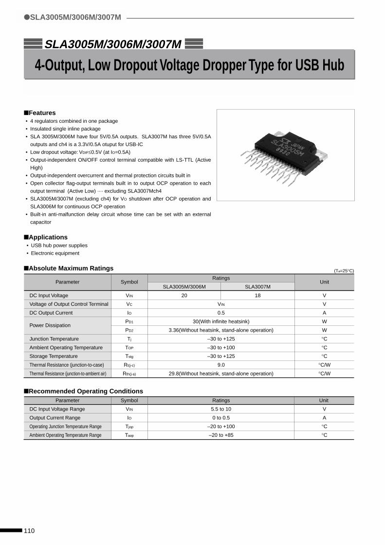
110
Features• 4 regulators combined in one package
• Insulated single inline package
• SLA 3005M/3006M have four 5V/0.5A outputs. SLA3007M has three 5V/0.5A
outputs and ch4 is a 3.3V/0.5A otuput for USB-IC
• Low dropout voltage: VDIF≤0.5V (at IO=0.5A)
• Output-independent ON/OFF control terminal compatible with LS-TTL (Active
High)
• Output-independent overcurrent and thermal protection circuits built in
• Open collector flag-output terminals built in to output OCP operation to each
output terminal (Active Low) ···· excluding SLA3007Mch4
• SLA3005M/3007M (excluding ch4) for VO shutdown after OCP operation and
SLA3006M for continuous OCP operation
• Built-in anti-malfunction delay circuit whose time can be set with an external
capacitor
Applications• USB hub power supplies
• Electronic equipment
Absolute Maximum Ratings
Symbol
VIN
VC
IO
PD1
PD2
Tj
TOP
Tstg
Rt(j-c)
Rth(j-a)
4-Output, Low Dropout Voltage Dropper Type for USB HubSLA3005M/3006M/3007M
SLA3005M/3006M/3007M
Unit
V
A
°C
°C
Symbol
VIN
IO
Tjop
Taop
(Ta=25°C)
Recommended Operating Conditions
Parameter
DC Input Voltage
Voltage of Output Control Terminal
DC Output Current
Power Dissipation
Junction Temperature
Ambient Operating Temperature
Storage Temperature
Thermal Resistance (junction-to-case)
Thermal Resistance (junction-to-ambient air)
Parameter
DC Input Voltage Range
Output Current Range
Operating Junction Temperature Range
Ambient Operating Temperature Range
Ratings
5.5 to 10
0 to 0.5
–20 to +100
–20 to +85
Ratings
SLA3005M/3006M SLA3007M
20 18
VIN
0.5
30(With infinite heatsink)
3.36(Without heatsink, stand-alone operation)
–30 to +125
–30 to +100
–30 to +125
9.0
29.8(Without heatsink, stand-alone operation)
Unit
V
V
A
W
W
°C
°C
°C
°C/W
°C/W
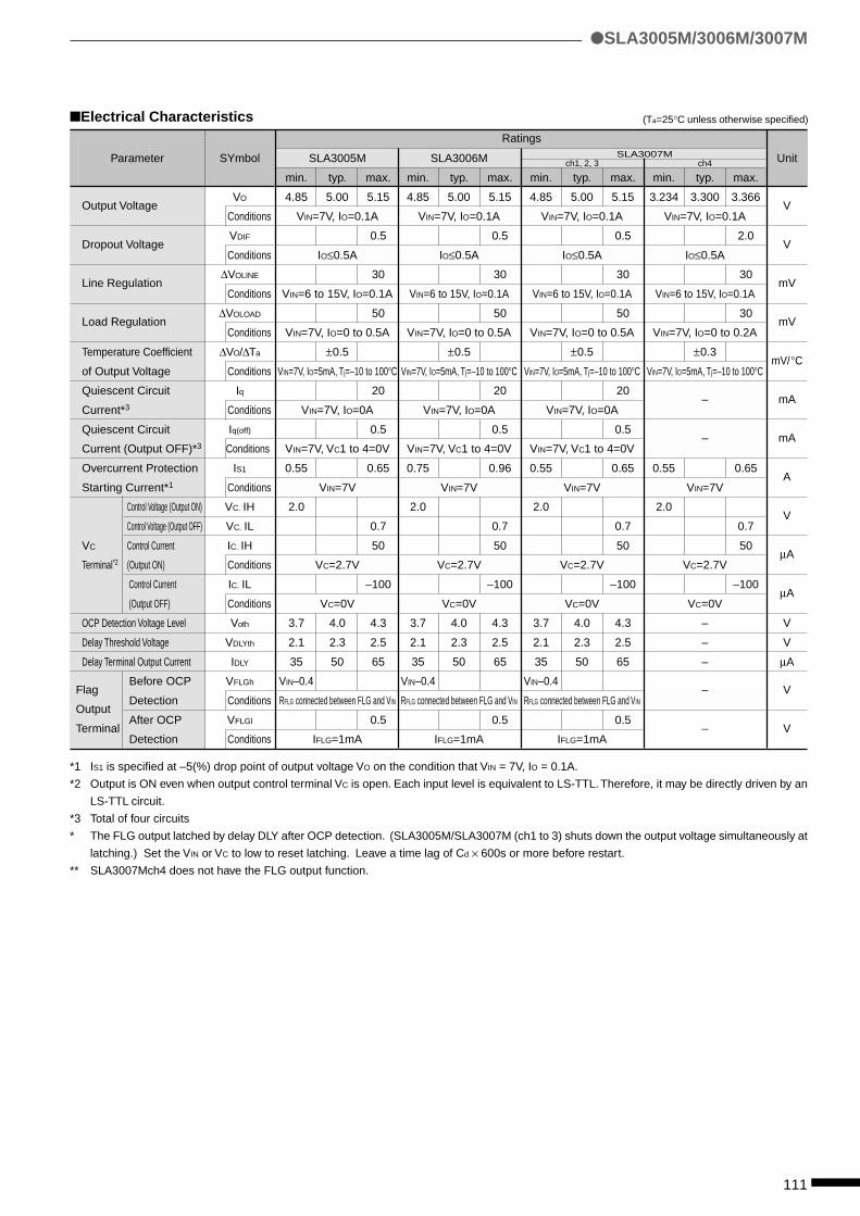
111
Parameter
Output Voltage
Dropout Voltage
Line Regulation
Load Regulation
Temperature Coefficient
of Output Voltage
Quiescent Circuit
Current*3
Quiescent Circuit
Current (Output OFF)*3
Overcurrent Protection
Starting Current*1
Control Voltage (Output ON)
Control Voltage (Output OFF)
VC Control Current
Terminal*2 (Output ON)
Control Current
(Output OFF)
OCP Detection Voltage Level
Delay Threshold Voltage
Delay Terminal Output Current
FlagBefore OCP
OutputDetection
TerminalAfter OCP
Detection
SLA3005M/3006M/3007M
*1 IS1 is specified at –5(%) drop point of output voltage VO on the condition that VIN = 7V, IO = 0.1A.
*2 Output is ON even when output control terminal VC is open. Each input level is equivalent to LS-TTL. Therefore, it may be directly driven by an
LS-TTL circuit.
*3 Total of four circuits
* The FLG output latched by delay DLY after OCP detection. (SLA3005M/SLA3007M (ch1 to 3) shuts down the output voltage simultaneously at
latching.) Set the VIN or VC to low to reset latching. Leave a time lag of Cd × 600s or more before restart.
** SLA3007Mch4 does not have the FLG output function.
Unit
V
V
mV
mV
mV/°C
mA
mA
A
V
µA
µA
V
V
µA
V
V
Electrical Characteristics
SLA3005M
min. typ. max.
4.85 5.00 5.15
VIN=7V, IO=0.1A
0.5
IO≤0.5A
30
VIN=6 to 15V, IO=0.1A
50
VIN=7V, IO=0 to 0.5A
±0.5
VIN=7V, IO=5mA, Tj=–10 to 100°C
20
VIN=7V, IO=0A
0.5
VIN=7V, VC1 to 4=0V
0.55 0.65
VIN=7V
2.0
0.7
50
VC=2.7V
–100
VC=0V
3.7 4.0 4.3
2.1 2.3 2.5
35 50 65
VIN–0.4
RFLG connected between FLG and VIN
0.5
IFLG=1mA
SLA3006M
min. typ. max.
4.85 5.00 5.15
VIN=7V, IO=0.1A
0.5
IO≤0.5A
30
VIN=6 to 15V, IO=0.1A
50
VIN=7V, IO=0 to 0.5A
±0.5
VIN=7V, IO=5mA, Tj=–10 to 100°C
20
VIN=7V, IO=0A
0.5
VIN=7V, VC1 to 4=0V
0.75 0.96
VIN=7V
2.0
0.7
50
VC=2.7V
–100
VC=0V
3.7 4.0 4.3
2.1 2.3 2.5
35 50 65
VIN–0.4
RFLG connected between FLG and VIN
0.5
IFLG=1mA
(Ta=25°C unless otherwise specified)
Ratings
SYmbol
VO
Conditions
VDIF
Conditions
∆VOLINE
Conditions
∆VOLOAD
Conditions
∆VO/∆Ta
Conditions
Iq
Conditions
Iq(off)
Conditions
IS1
Conditions
VC. IH
VC. IL
IC. IH
Conditions
IC. IL
Conditions
Voth
VDLYth
IDLY
VFLGh
Conditions
VFLGl
Conditions
ch1, 2, 3
min. typ. max.
4.85 5.00 5.15
VIN=7V, IO=0.1A
0.5
IO≤0.5A
30
VIN=6 to 15V, IO=0.1A
50
VIN=7V, IO=0 to 0.5A
±0.5
VIN=7V, IO=5mA, Tj=–10 to 100°C
20
VIN=7V, IO=0A
0.5
VIN=7V, VC1 to 4=0V
0.55 0.65
VIN=7V
2.0
0.7
50
VC=2.7V
–100
VC=0V
3.7 4.0 4.3
2.1 2.3 2.5
35 50 65
VIN–0.4
RFLG connected between FLG and VIN
0.5
IFLG=1mA
SLA3007Mch4
min. typ. max.
3.234 3.300 3.366
VIN=7V, IO=0.1A
2.0
IO≤0.5A
30
VIN=6 to 15V, IO=0.1A
30
VIN=7V, IO=0 to 0.2A
±0.3
VIN=7V, IO=5mA, Tj=–10 to 100°C
–
–
0.55 0.65
VIN=7V
2.0
0.7
50
VC=2.7V
–100
VC=0V
–
–
–
–
–
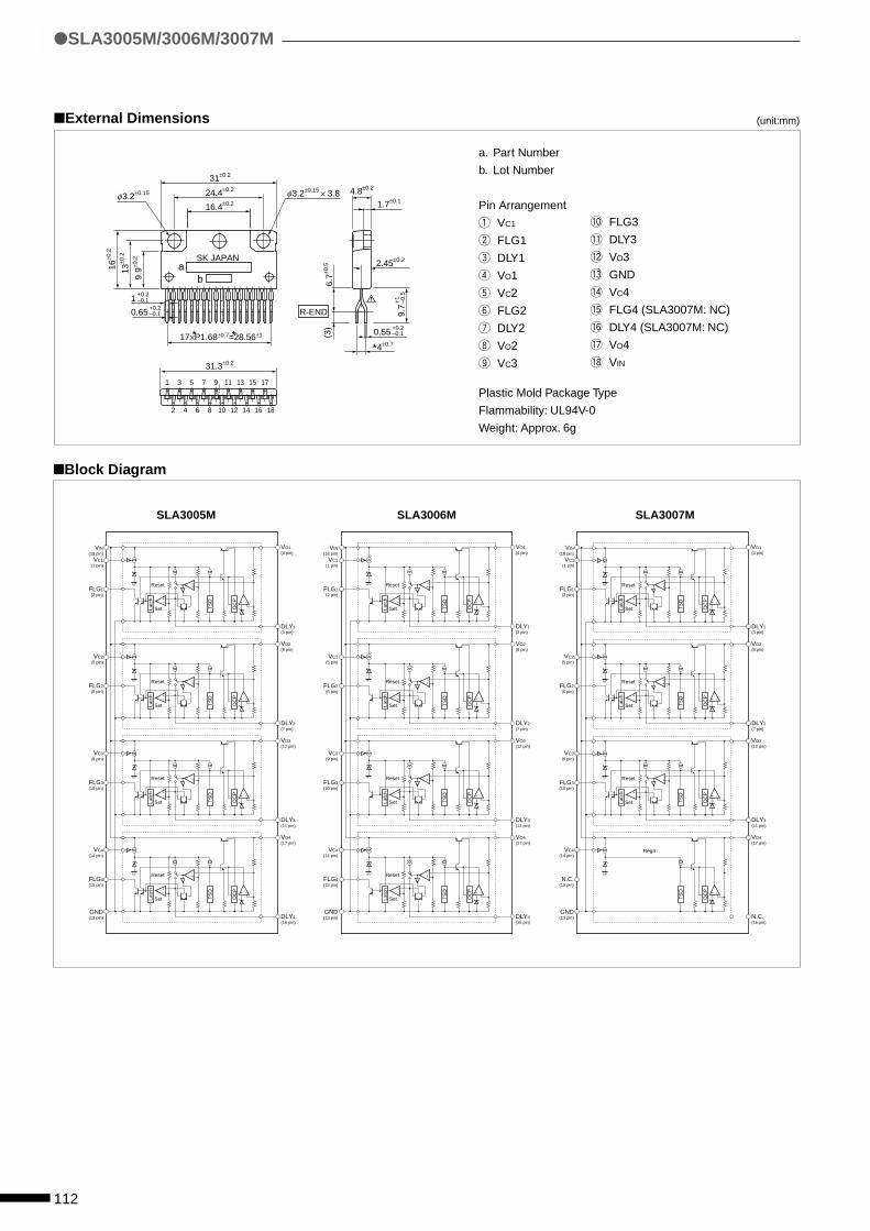
112
External Dimensions
Block Diagram
a. Part Number
b. Lot Number
Pin Arrangement
q VC1
w FLG1
e DLY1
r VO1
t VC2
y FLG2
u DLY2
i VO2
o VC3
!0 FLG3
!1 DLY3
!2 VO3
!3 GND
!4 VC4
!5 FLG4 (SLA3007M: NC)
!6 DLY4 (SLA3007M: NC)
!7 VO4
!8 VIN
SLA3005M SLA3006M SLA3007M
31±0.2
31.3±0.2
3.2±0.15 × 3.8 3.2±0.15 24.4±0.2
16.4±0.2 1.7±0.1
2.45±0.2
4±0.7
4.8±0.2
16±0
.2
13±0
.2
9.9±0
.2
6.7±0
.5
9.7
(3)
R-END
0.55+0.2–0.1
+1
–0.51
+0.2–0.1
0.65+0.2–0.1
17×P1.68±0.7=28.56±1
1 3 5 7 9 11 13 15 17
18161412108642
SK JAPAN
φ φ
ab
* **
SLA3005M/3006M/3007M
(unit:mm)
Plastic Mold Package Type
Flammability: UL94V-0
Weight: Approx. 6g
VO1(4 pin)
Reset
Set
VIN(18 pin)
VC1(1 pin)
FLG1(2 pin)
DLY1(3 pin)
+ –
+–
–+
OC
P
TS
D
Latc
h
VO2(8 pin)
Reset
Set
VC2(5 pin)
FLG2(6 pin)
DLY2(7 pin)
+ –
+–
–+
OC
P
TS
D
Latc
h
VO3(12 pin)
Reset
Set
VC3(9 pin)
FLG3(10 pin)
DLY3(11 pin)
+ –
+–
–+
OC
P
TS
D
Latc
h
VO4(17 pin)
Reset
Set
VC4(14 pin)
FLG4(15 pin)
GND(13 pin) DLY4
(16 pin)
+ –
+–
–+
OC
P
TS
D
Latc
h
Reset
Set
+ –
+–
–+
OC
P
TS
D
Latc
h
Reset
Set+ –
+–
–+
OC
P
TS
D
Latc
h
Reset
Set
+ –
+–
–+
OC
P
TS
D
Latc
h
VO1(4 pin)
Reg4
VIN(18 pin)
VC1(1 pin)
FLG1(2 pin)
DLY1(3 pin)
VO2(8 pin)
VC2(5 pin)
FLG2(6 pin)
DLY2(7 pin)
VO3(12 pin)
VC3(9 pin)
FLG3(10 pin)
DLY3(11 pin)
VO4(17 pin)
VC4(14 pin)
N.C.(15 pin)
GND(13 pin) N.C.
(16 pin)
+ –
OC
P
TS
D
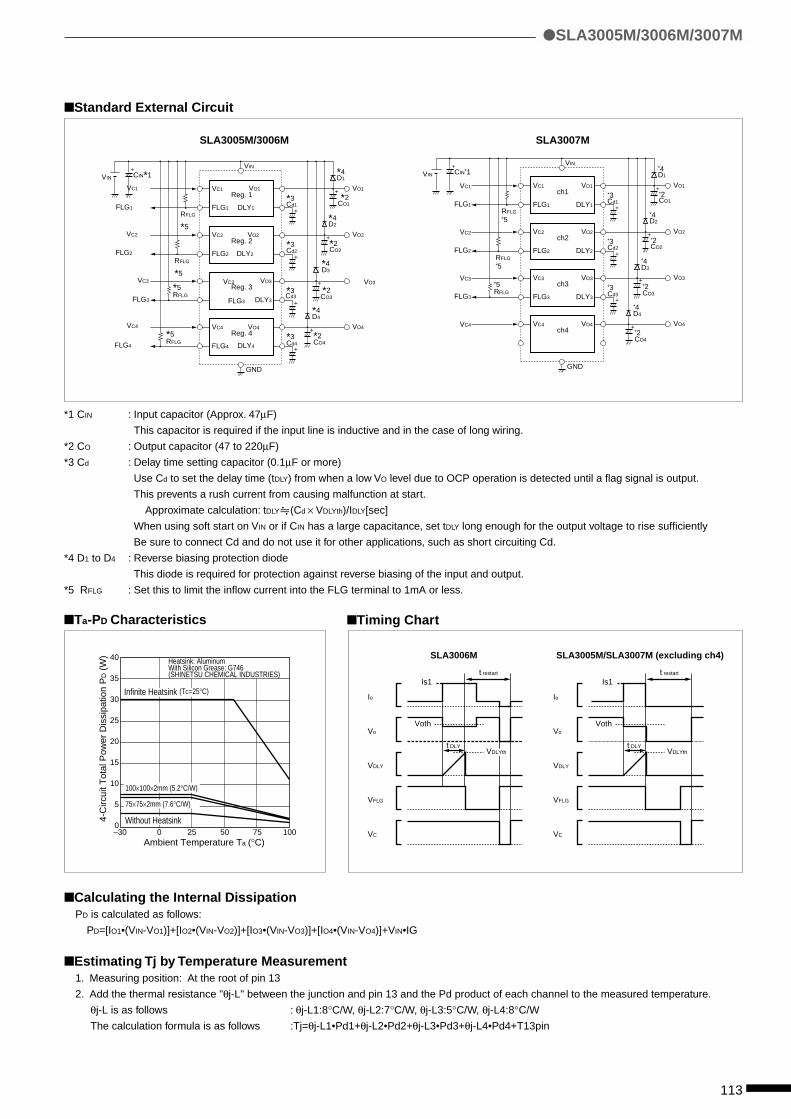
113
Ta-PD Characteristics
Standard External Circuit
*1 CIN : Input capacitor (Approx. 47µF)
This capacitor is required if the input line is inductive and in the case of long wiring.
*2 CO : Output capacitor (47 to 220µF)
*3 Cd : Delay time setting capacitor (0.1µF or more)
Use Cd to set the delay time (tDLY) from when a low VO level due to OCP operation is detected until a flag signal is output.
This prevents a rush current from causing malfunction at start.
Approximate calculation: tDLY (Cd × VDLYth)/IDLY[sec]
When using soft start on VIN or if CIN has a large capacitance, set tDLY long enough for the output voltage to rise sufficiently
Be sure to connect Cd and do not use it for other applications, such as short circuiting Cd.
*4 D1 to D4 : Reverse biasing protection diode
This diode is required for protection against reverse biasing of the input and output.
*5 RFLG : Set this to limit the inflow current into the FLG terminal to 1mA or less.
VIN
VIN
VO1
CIN*1
RFLG
*5
+
VC1
FLG1
VC1
FLG1
VO1Reg. 1
DLY1
*3Cd1
*2CO1
*4D1
+
+
+
+
VO2
RFLG
*5
VC2
FLG2
VC2
FLG2
VO2Reg. 2
DLY2
*3Cd2
*2CO2
*4D2
+
VO3VC3
FLG3
VC3
FLG3
VO3Reg. 3
DLY3
*3
*2CO3
*4D3
+
VO4
*5RFLG
*5RFLG
VC4
FLG4
VC4
FLG4
GND
VO4Reg. 4
DLY4
*3Cd4
*2CO4
*4D4
+
+
Cd3
40
35
30
25
20
15
10
5
0
4-C
ircui
t Tot
al P
ower
Dis
sipa
tion
PD (
W)
Ambient Temperature Ta (°C)0–30 25 50 75 100
100×100×2mm (5.2°C/W)
75×75×2mm (7.6°C/W)
(TC=25°C)Infinite Heatsink
Without Heatsink
Heatsink: AluminumWith Silicon Grease: G746(SHINETSU CHEMICAL INDUSTRIES)
Calculating the Internal DissipationPD is calculated as follows:
PD=[IO1•(VIN-VO1)]+[IO2•(VIN-VO2)]+[IO3•(VIN-VO3)]+[IO4•(VIN-VO4)]+VIN•IG
Estimating Tj by Temperature Measurement1. Measuring position: At the root of pin 13
2. Add the thermal resistance "θj-L" between the junction and pin 13 and the Pd product of each channel to the measured temperature.
θj-L is as follows : θj-L1:8°C/W, θj-L2:7°C/W, θj-L3:5°C/W, θj-L4:8°C/W
The calculation formula is as follows :Tj=θj-L1•Pd1+θj-L2•Pd2+θj-L3•Pd3+θj-L4•Pd4+T13pin
SLA3005M/3006M/3007M
SLA3005M/3006M SLA3007M
Timing Chart
SLA3006M
Is1
Voth
t restart
t DLY
Io
Vo
VDLY
VFLG
VC
SLA3005M/SLA3007M (excluding ch4)
Is1
Voth
VDLYth
t restart
t DLY
Io
Vo
VDLY
VFLG
VC
VDLYth
VIN
VIN
VO1
CIN*1
RFLG*5
+
VC1
FLG1
VC1
FLG1
VO1ch1
DLY1
*3Cd1
*2CO1
*4D1
+
+
+
+
VO2
RFLG*5
VC2
FLG2
VC2
FLG2
VO2ch2
DLY2
*3Cd2
*2CO2
*4D2
+
VO3VC3
FLG3
VC3
FLG3
VO3ch3
DLY3
*3Cd3
*2CO3
*4D3
+
VO4
*5RFLG
VC4 VC4
GND
VO4ch4 *2
CO4
*4D4
+
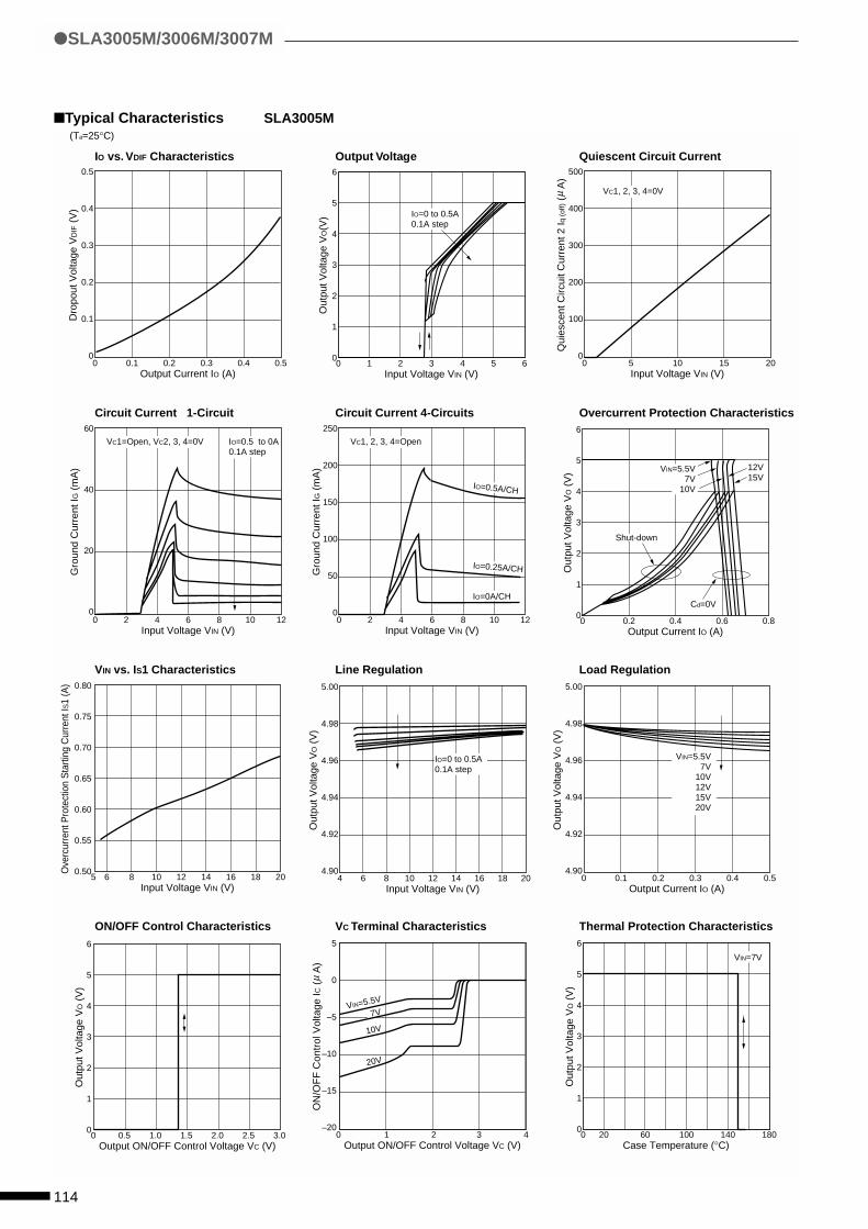
114
Typical Characteristics SLA3005M
IO vs. VDIF Characteristics Output Voltage Quiescent Circuit Current
Circuit Current 1-Circuit Circuit Current 4-Circuits Overcurrent Protection Characteristics
VIN vs. IS1 Characteristics Line Regulation Load Regulation
ON/OFF Control Characteristics VC Terminal Characteristics Thermal Protection Characteristics
0.5
0.4
0.3
0.2
0.1
00 0.1 0.2 0.3 0.4 0.5
Output Current IO (A)
Dro
pout
Vol
tage
VD
IF (
V)
500
400
300
200
100
00 5 10 15 20
Input Voltage VIN (V)
Qui
esce
nt C
ircui
t Cur
rent
2 Iq
(of
f) (
A
)µ VC1, 2, 3, 4=0V
60
40
20
00 2 4 6 8 10 12
Input Voltage VIN (V)
Gro
und
Cur
rent
IG (
mA
)
VC1=Open, VC2, 3, 4=0V IO=0.5 to 0A0.1A step
250
200
150
100
50
00 2 4 6 8 10 12
Input Voltage VIN (V)
Gro
und
Cur
rent
IG (
mA
)
VC1, 2, 3, 4=Open
IO=0.5A/CH
IO=0.25A/CH
IO=0A/CH
6
5
4
3
2
1
00 0.2 0.4 0.6 0.8
Output Current IO (A)
Out
put V
olta
ge V
O (
V) VIN=5.5V
7V10V
Cd=0V
Shut-down
12V15V
0.80
0.75
0.70
0.65
0.60
0.55
0.505 6 8 10 12 14 16 18 20
Input Voltage VIN (V)
Ove
rcur
rent
Pro
tect
ion
Sta
rting
Cur
rent
IS1
(A) 5.00
4.98
4.96
4.94
4.92
4.904 6 8 10 12 14 16 18 20
Input Voltage VIN (V)
Out
put V
olta
ge V
O (
V)
IO=0 to 0.5A0.1A step
6
5
4
3
2
1
00 20 60 100 140 180
Case Temperature (°C)
Out
put V
olta
ge V
O (
V)
VIN=7V
6
5
4
3
2
1
00 0.5 1.0 1.5 2.0 2.5 3.0
Output ON/OFF Control Voltage VC (V)
Out
put V
olta
ge V
O (
V)
5.00
4.98
4.96
4.94
4.92
4.900 0.1 0.2 0.3 0.4 0.5
Output Current IO (A)
Out
put V
olta
ge V
O (
V)
VIN=5.5V7V
10V12V15V20V
(Ta=25°C)
SLA3005M/3006M/3007M
6
5
4
3
2
1
00 1 2 3 4 5 6
Input Voltage VIN (V)
Out
put V
olta
ge V
O(V
) IO=0 to 0.5A0.1A step
5
0
–5
–10
–15
–200 1 2 3 4
Output ON/OFF Control Voltage VC (V)
ON
/OF
F C
ontr
ol V
olta
ge IC
(
A)
µ
VIN=5.5V
7V
10V
20V
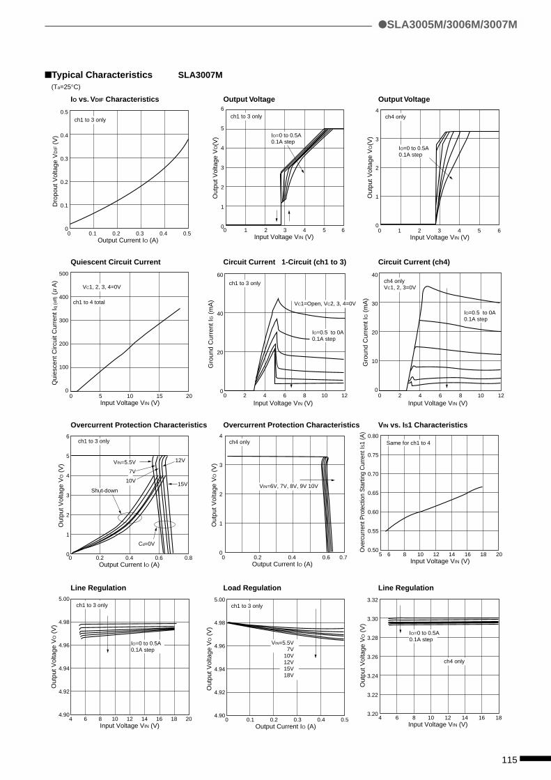
115
SLA3005M/3006M/3007M
Typical Characteristics SLA3007M (Ta=25°C)
IO vs. VDIF Characteristics Output Voltage Output Voltage
Quiescent Circuit Current Circuit Current 1-Circuit (ch1 to 3) Circuit Current (ch4)
Overcurrent Protection Characteristics Overcurrent Protection Characteristics VIN vs. IS1 Characteristics
Line Regulation Load Regulation Line Regulation
0.5
0.4
0.3
0.2
0.1
00 0.1 0.2 0.3 0.4 0.5
Output Current IO (A)
Dro
pout
Vol
tage
VD
IF (
V)
ch1 to 3 only
6
5
4
3
2
1
00 1 2 3 4 5 6
Input Voltage VIN (V)
Out
put V
olta
ge V
O(V
) IO=0 to 0.5A0.1A step
ch1 to 3 only 4
3
2
1
00 1 2 3 4 5 6
Input Voltage VIN (V)
Out
put V
olta
ge V
O(V
)
IO=0 to 0.5A0.1A step
ch4 only
500
400
300
200
100
00 5 10 15 20
Input Voltage VIN (V)
Qui
esce
nt C
ircui
t Cur
rent
Iq (
off) (
A
)µ VC1, 2, 3, 4=0V
ch1 to 4 total
60
40
20
00 2 4 6 8 10 12
Input Voltage VIN (V)
Gro
und
Cur
rent
IG (
mA
)
ch1 to 3 only
IO=0.5 to 0A0.1A step
VC1=Open, VC2, 3, 4=0V
40
30
20
10
00 2 4 6 8 10 12
Input Voltage VIN (V)
Gro
und
Cur
rent
IG (
mA
)
ch4 onlyVC1, 2, 3=0V
IO=0.5 to 0A0.1A step
6
5
4
3
2
1
00 0.2 0.4 0.6 0.8
Output Current IO (A)
Out
put V
olta
ge V
O (
V)
Cd=0V
Shut-down
12V
15V
VIN=5.5V
7V
10V
ch1 to 3 only4
3
2
1
00 0.2 0.4 0.70.6
Output Current IO (A)
Out
put V
olta
ge V
O (
V)
VIN=6V, 7V, 8V, 9V 10V
ch4 only 0.80
0.75
0.70
0.65
0.60
0.55
0.505 6 8 10 12 14 16 18 20
Input Voltage VIN (V)
Ove
rcur
rent
Pro
tect
ion
Sta
rting
Cur
rent
IS1
(A)
Same for ch1 to 4
5.00
4.98
4.96
4.94
4.92
4.904 6 8 10 12 14 16 18 20
Input Voltage VIN (V)
Out
put V
olta
ge V
O (
V)
IO=0 to 0.5A0.1A step
ch1 to 3 only5.00
4.98
4.96
4.94
4.92
4.900 0.1 0.2 0.3 0.4 0.5
Output Current IO (A)
Out
put V
olta
ge V
O (
V)
VIN=5.5V7V
10V12V15V18V
ch1 to 3 only3.32
3.30
3.28
3.26
3.24
3.22
3.204 6 8 10 12 14 16 18
Input Voltage VIN (V)
Out
put V
olta
ge V
O (
V)
IO=0 to 0.5A0.1A step
ch4 only
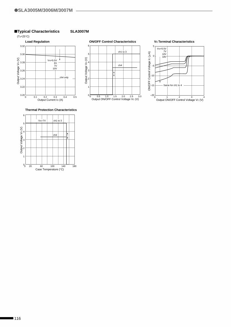
116
Typical Characteristics SLA3007M (Ta=25°C)
Load Regulation ON/OFF Control Characteristics VC Terminal Characteristics
Thermal Protection Characteristics
SLA3005M/3006M/3007M
3.32
3.30
3.28
3.26
3.24
3.22
3.200 0.1 0.2 0.3 0.4 0.5
Output Current IO (A)
Out
put V
olta
ge V
O (
V)
VIN=5.5V6V7V
10V
ch4 only
6
5
4
3
2
1
00 0.5 1.0 1.5 2.0 2.5 3.0Output ON/OFF Control Voltage VC (V)
Out
put V
olta
ge V
O (
V)
ch1 to 3
ch4
5
0
–5
–10
–15
–200 1 2 3 4
Output ON/OFF Control Voltage VC (V)
ON
/OF
F C
ontr
ol V
olta
ge IC
(
A)
µ
Same for ch1 to 4
VIN=5.5V7V
10V18V
6
5
4
3
2
1
00 20 60 100 140 180
Case Temperature (°C)
Out
put V
olta
ge V
O (
V)
VIN=7V ch1 to 3
ch4
Bulletin NoI01 EDO
(Sep,2000)
特 K
IC REG
Sanken Electric Co.,Ltd.1-11-1 Nishi -Ikebukuro,Toshima-ku, TokyoPHONE: 03-3986-6164FAX: 03-3986-8637TELEX: 0272-2323(SANKEN J)
Overseas Sales OfficesAsiaSanken Electric Singapore Pte.Ltd.150 Beach Road,#14-03 The Gateway West,Singapore 0718PHONE: 291-4755FAX: 297-1744
Sanken Electric Hong Kong Co.,Ltd.1018 Ocean Centre, Canton Road,Kowloon, Hong KongPHONE: 2735-5262FAX: 2735-5494TELEX: 45498 (SANKEN HX)
Sanken Electric Korea Co.,Ltd.SK Life B/D 6F,168 Kongduk-dong, Mapo-ku, Seoul, 121-705, KoreaPHONE: 82-2-714-3700FAX: 82-2-3272-2145
North AmericaAllegro MicroSystems,Inc.115 Northeast Cutoff, Box 15036Worcester, Massachusetts 01615, U.S.A.PHONE: (508)853-5000FAX: (508)853-7861
EuropeAllegro MicroSystems Europe Limited.Balfour House, Churchfield Road,Walton-on-Thames, Surrey KT12 2TD, U.K.PHONE: 01932-253355FAX: 01932-246622
PRINTED in JAPAN H1-I01ED0-0009025ND
Dropper TySwitching Multi‐Outp