Embed Size (px)
Citation preview

ZERO-VOLTAGE SWITCHED RESONANT AND PWM CONVERTERS: DESIGN-ORIENTED ANALYSIS AND PERFORMANCE EVALUATION
by
Juan A. Sabate
Dissertation submitted to the Faculty of the
Virginia Polytechnic Institute and State University
in partial fulfillment of the requirements for the degree of
Doctor of Philosophy
in
Electrical Engineering
APPROVED:
::fud; C. L I
Fred C. Lee, Chairman
h /. C4= Bo H. Cho
~~c~ Dusan Borojevic
April 26, 1994
Blacksburg, Virginia
"'~~ ~ ,~"~~~Q~ Milan M. Jovanovic
R.8~~.J R. Dean Riess

L'J 5~S5 Vg5b 199 LtS~j5

-ZERO-VOLTAGE SWITCHED RESONANT AND PWM CONVERTERS: DESIGN-ORIENTED ANALYSIS AND PERFORMANCE EV ALUA TION
by
Juan A. Sabate
Fred C. Lee, Chainnan
Electrical Engineering
(ABSTRACT)
The relative perfonnance evaluation of the different alternatives of bridge topologies with
zero-voltage switching is presented. A design-oriented analysis is developed to optimize
implementation of the converters in tenns of efficiency. Efficiency optimization requires
minimizing the circulating currents which are directly proportional to the reactive energy
required by the resonant tank. The comparison of the different converters is based on the
reactive energy required for ZVS. The study considers resonant converters with
conventional variable frequency control and with phase-shift control, and the zero-
voltage-switched full-bridge PWM converter (ZVS-FB-PWM). Also, a systematic
procedure to determine all possible resonant converters with two or three reactive
elements is presented, and the design-oriented analysis used to classifY them according to
their properties.
The analysis for the resonant converters uses the fundamental approximation which is
verified by comparison with the existing exact analysis for the series resonant converter
(SRC), the parallel resonant converter (pRe) and the LCC resonant converter (LCC-RC).
Comparison of design examples shows a superior performance for the LCC-RC, and less
circulating current for the conventional variable-frequency resonant converters than for the

phase-shifted control version. Experimental verification is provided for the phase-shifted
resonant converters.
The effect of switch capacitance on the zero-voltage switching (ZVS) of resonant
converters is studied for the SRC, PRC and LCC-RC. The effect of switch capacitance is
more' pronounced for low Q designs. Consequently, it is of primary importance for the
LCC-RC whose optimal design requires low Q values. The results have been verified
experimentally in an LCC-RC prototype.
A complete analysis and design procedure are provided for the new ZVS-FB-PWM
converter, including a new active clamp circuit that completely eliminates the ringing in
the I rectifiers. The design procedure and design considerations have been verified with
three' experimental prototypes.
The comparison of the resonant converters with the ZVS-FB-PWM converter based on
the reactive power required for ZVS, shows that the ZVS-FB-PWM converter is a
superior alternative to resonant converters. The ZVS-FB-PWM converter always has less
circulating current than the resonant converters when it is designed for a limited ZVS
range.

To my parents Josep
and M3 del Carme
iv


Acknowledgements
I would like to express my sincere appreciation to my advisor, Prof Fred C. Lee,
for his guidance, encouragement, and constant support through the course of this work.
His extensive knowledge and creative thinking have been an invaluable help to my
research work.
I also wish to thank Dr. Milan M. Jovanovic, Dr. Bo H. Cho, Dr. DuSan
Borojevic, and Dr. R. Dean Riess for their contributions as members of my doctoral
committee and for their suggestions regarding the final manuscript.
It has been a pleasure associating with excellent faculty, staff, and students at the
Virginia Power Electronics Center (VPEC). The frienships, enlightening discussions, and
creative ideas have made my stay in the Ph. D. program enjoyable.
Special thanks are due to Mr. Vlatko Vlatkovic, his friendship and willingness
to discuss technical problems have been invaluable to me. Also I would like to thank
my .fellow students Dr. Richard Farrington, Dr. Qing Chen, Mr. Eddie Yeow, Mr.
Guichao Hua, Dr. Eric Yang, Mrs. Liliana GrajaJes, Mr. Carlos Cuadros, Mr. Pablo
Espinosa, Ms. Silva Hiti, Mr. Goran Stojcic, Mr. Slovodan Gataric, Mr. Yuri Panov, Dr.
B. C. Choi, Dr. AshrafLotfi, Mr. Bob Watson, Mr. Chih Y. Lin, and Mr. Yimin Jiang, for
m~ng my stay at Virginia Tech an enjoyable one.
AcknQwledgements v

Recognition is extended to Mr. Grant G. Carpenter, Mr. Richard T. Gean, and
Mr. Bill Cockey who have been of invaluable help to me by providing equipment and parts
for my experimental work.
Thanks are also due to Ms. Tammy Jo Hinner and Ms. Teresa Shaw, who were
always kind and ready to help, and Ms. Kathleen Tolley for her help in editing my
manuscript.
I particularly would like to thank my parents whose encouragement and support
have been a source of confidence and inspiration to me.
The work has been partially supported by IBM, Kingston, NY, and by the VPEC
Industry-University Partnership Program, for which I am grateful.
Aeknowledgements vi

Table of Contents
1. Introduction •••.•••••..•..•.••.•..•.••••••.•.....•••••••.....•••••.•.•..••.••..•....••••..•.•..•..•••.•...••.•••..••••..••. 1
1. 1 ,Background and Motivation ....................................................................................... 1
1.2 Objectives of the Research ....................................... : ............................................... 12
1.3 Major Results .......................................................................................................... 16
2 .. Design-Oriented Analysis of Resonant Converters ................................................ 19
2.1 Introduction ............................................................................................................. 19
2.2 Resonant Converter Structure .................................................................................. 20
2.3 Frequency-Domain Analysis ..................................................................................... 24
2.4 Soft Switching with Resonant Converters .......................... '" ................................... 29
2.5 Resonant Converters with Two Reactive Elements ................................................... 35
2.5.1 Possible Topologies ................................................................................ 35
2.6,Design Characteristics for Two-Element Resonant Converters ............................... 39
2.6.1 Series Resonant Converter ...................................................................... 41
2.6.2 Parallel Resonant Converter ..................................................................... 52
2.7 Resonant Converters with Three Reactive Elements ........... eo ................................. eo. 64
2.7.1 Possible Topologies with Three Elements ................................................ 64
2.7.2 LCC Resonant Converter ..................... '" ................................................ 84
2.8 Comparison of Resonant Converters and Conclusions .......... eo ................................ 100
3. Design and Performance Evaluation of Resonant Converters with Phase-Shift
Control •..•...•..•..•.••..•••.•....•..•..........••••••....•..•.•.•..••.••••••..••.•..•••...••...•••••••..••••••••.•.•.•. 113
Table of Contents vii

3 .1 Introduction ........................................................................................................... 113
3.2 Fixed-Frequency Operation of Resonant Converters ............................................... 115
3.3 Frequency-Domain Analysis of Phase-Shifted Resonant Converters ....................... 119
3.4 Phase-Shifted Series Resonant Converter ............................................................... 120
3.5 Phase-Shifted Parallel Resonant Converter ............................................................. 129
3.6 Phase-Shifted LCC Resonant Converter ................................................................. 134
3.7 Comparison of Phase-Shifted SRC and PRC .......................................................... 139
3.7.1 Design Objectives ................................................................................. 139
3.7.2 Design ofa Series Resonant Converter. ................................................. 139
3.7.3 Design ofa Parallel Resonant Converter ................................................ 143
3.7.4 Experimental Results ............................................................................. 146
3.8 Comparison ofPS-PRC and PS-LCC Resonant Converter ..................................... 152
4. Effect of Switch Output Capacitance on Zero-Voltage Switching of Resonant
converters ........................................................................................................... 163
4.1 Significance of Switch Capacitance for Zero-Voltage Switching ............................. 163
4.2 Analysis Including Switch Capacitance ................................................................... 166
4.2.1 Analysis of the SRC Including Switch Capacitance ................................ 168
4.2.2 Analysis of the PRC and LCC-RC Including Switch Capacitance .......... 171
4.3 Effects of Switch Capacitance .... , .......................................................................... 177
4.3.1 Effects ofCsw on the SRC .................................................................... 177
4.3.2 Effects ofCsw on the PRC .................................................................... 178
4.3.3 Effects ofCsw on the LCC-RC ............................................................. 184
4.4 Experimental Verifications ..................................................................................... 189
Table of Contents viii

4.5 Summary and Conclusions ..................................................................................... 193
5. Phase-Shifted Full ... Bridge PWM Converter with Active Clamp ......................... 197
5.1 Introduction ........................................................................................................... 197
5.2 Operation Principle ................................................................................................ 202
5.3 Converter Analysis ................................................................................................. 210
5.3.1 Conditions for Zero-Voltage Switching ................................................. 210
5.3.2 Critical Current for Zero-Voltage Switching .......................................... 215
5.3.3 DC Voltage Conversion Ratio ............................................................... 216
5.4 Active Clamp for the Rectifier Stage ...................................................................... 221
5.4.1 Transitions on the Rectifier Stage ........................................................ 221
5.4.2 Circuit Operation ................................................................................ 223
5.4.3 Active Clamp Analysis and Characteristics .......................................... 228
5.5 Design Trade-off's .................................................................................................. 233
5.5.1 Analysis of Conduction Losses .............................................................. 235
5.6 Design Procedure ................................................................................................... 238
5.6.2 Clamp Design Considerations ................................................................ 243
5.6.3 Design Procedure .................................................................................. 243
5.6.4 Design Example ... r ................................................................................ 247
5.7 Experimental Results ............................................................................................. 251
5.7.1 Circuit Without External Inductance ..................................................... 251
5.7.2 Circuit with External Inductance ........................................................... 258
5.8, Comparison of ZVS-FB-PWM with Resonant Converters ...................................... 274
Table of Contents ix

6. Conclusions and Future Work .•••••.•.•••.•.••••••••••.•.•.••••••••.....•.•..••.•...•...••.••...••••••..••• 282
7. References .............................................................................................................. 288
Vita ............................................................................................................................. 309
Table of Contents x

List of Illustrations
Figure 2.1: Resonant converter structure ..................................................................... 23
Figure 2.2: Resonant tank excitation: a) voltage excitation circuit, b) current excitation
circuit ........................................................................................................ 25
Figure 2.3: Resonant tank load: a) rectifier with capacitive filter, b) rectifier with
inductive filter ........................................................................................... 28
Figure 2.4: Equivalent load of the inverter stage .......................................................... 32
Figure 2.5: ZVS operation ofa resonant converter ...................................................... 33
Figure 2.6: ZCS operation of a resonant converter ....................................................... 34
Figure 2.7: Possible resonant networks with two reactive elements .............................. 37
Figure 2.8: Resonant networks with two reactive elements that do not correspond to a
resonant converter ..................................................................................... 38
Figure 2.9: Series resonant converter model. ............................................................... 40
Figure 2.10: Comparison of voltage gain of the SRC obtained with the exact solution (thin
lines) with the fundamental approximation analysis result (thick lines) ........ 42
Figure 2.11: Error between the exact analysis and the fundamental approximation analysis
for the SRC voltage ·gain ........................................................................... 43
Figure 2.12: Phase of the input impedance to the resonant tank for different loads as a
function of frequency ................................................................................. 46
Figure 2.13: Normalized input current to the resonant tank for different loads and
constant gain current as a function of frequency ......................................... 47
List of Dlustrations xi

Figure 2.14: Input current to the resonant tank normalized with respect to the output
power for different loads as a function of frequency ................................... 50
Figure 2.15: Power factor at the input of the resonant tank for different loads as a
function offrequency ................................................................................. 51
Figure 2.16: Parallel resonant converter model. ............................................................. 53
Figure 2.17: Comparison of voltage gain of the PRC obtained with the exact solution (thin
lines) with the fundamental approximation analysis result (thick lines) ........ 54
Figure 2.18: Error between the exact analysis and the fundamental approximation analysis
for the PRC voltage gain ........................................................................... 55
Figure 2.19: Phase of the input impedance to the resonant tank for different loads as a
function offrequency .................................................................................. 57
Figure 2.20: Normalized input current to the resonant tank for different loads and
constant gain current as a function of frequency ......................................... 59
Figure 2.21: Input current to the resonant tank normalized with respect to output power
for different loads as a function of frequency ............................................. 60
Figure 2.22: Power factor at the input of the resonant tank for different loads as a
function of frequency ................................................................................. 63
Figure 2.23: Possible resonant networks with three reactive elements ............................ 66
Figure 2.24: Topologies with in/out symmetry ............................................................... 73
Fig~lfe 2.25: Topologies without in/out symmetry .......................................................... 74
Figure 2.26: Topologies with different input and output sources ................................... 75
Figure 2.27: Gain of topologies similar to the SRC (1) .................................................. 79
Figure 2.28: Gain of topologies similar to the SRC (2) .................................................. 80
List of DlustratioDs xii

Figure 2.29: Gain of topologies similar to the PRC (1) .................................................. 81
Figure 2.30: Gain of topologies similar to the PRC (2) .................................................. 82
Figure 2.31: Gain of topologies similar to the PRC (3) .................................................. 83
Figure 2.32: LCC resonant converter model. ................................................................. 85
Figure 2.33: Voltage gain of the LCC-RC obtained for Cn= 1. Exact solution thin lines,
and approximate solution thick lines .......................................................... 86
Figure 2.34: Voltage gain of the LCC-RC obtained for Cn = 2 ...................................... 87
Figure 2.35: Voltage gain of the LCC-RC obtained for Cn = 1/2 . .................................. 88
Figure 2.36: Phase of the input impedance to the resonant tank for different loads as a
function offrequency ................................................................................. 90
Figure 2.37: Normalized input current to the resonant tank for different loads and
constant gain current as a function of frequency ......................................... 92
Figure 2.38: Input current to the resonant tank normalized with respect to the output
power for different loads as a function of frequency, for Cn=1. .................. 93
Figure 2.39: Input current to the resonant tank normalized with respect to the output
power for different loads as a function of frequency, for Cn=1/2 ................ 94
Figure 2.40: Input current to the resonant tank normalized with respect to the output
power for different loads as a function of frequency, for Cn=2 ................... 95
Figure 2.41: Power factor at the input of the resonant tank for different loads as a
function of frequency for Cn= 1 .................................................................. 97
Figure 2.42: Power factor at the input of the resonant tank for different loads as a
function of frequency for Cn=2 .................................................................. 98
List of Dlustrations xiii

Figure 2.43: Power factor at the input of the resonant tank for different loads as a
function of frequency for Cn=1/2 . .............................................................. 99
Figure 2.44: Series resonant converter design .............................................................. 108
Figure 2.45: Parallel resonant converter design ............................................................ 109
Figure 2.46: LCC resonant converter design with en =0.5 ........................................... 110
Figure 2.47: Lee resonant converter design with Cn = 1. ............................................. 111
Fig"lfe 2.48: LCe resonant converter design with en =2 .............................................. 112
Figure 3.1: Phase-shifted resonant converter circuits topology ................................... 117
Figure 3.2: Switching waveforms and tank voltage .................................................... 118
Figure 3.3: Ratio of the voltage gain with phase-shift control to the voltage gain with
conventional resonant with respect to the duty cycle ................................ 121
Figure 3.4: Ratio of the power factor with phase-shift control to the power factor with
conventional resonant, with respect to the duty cycle ............................... 122
Figure 3.5: Tank voltage and current in the tank with zero-voltage switching ............ 123
Figure 3.6: Tank voltage and current in the tank without zero-voltage switching ....... 124
Figure 3.7: DC voltage gain for the PS-series resonant converter for a switching
frequency 1.1 times the resonant frequency, comparing exact analysis (thin
lines) with fundamental approximation (thick lines) .................................. 127
Figure 3.8: DC voltage gain for the PS-series resonant converter for a switching
frequency 1.2 times the resonant frequency, comparing exact analysis (thin
lines) with fundamental approximation (thick lines) .................................. 128
Figure 3.9: Tank voltage and inductor current for the PS-parallel resonant converter.I31
List of DlustratioDs xiv

Figure 3.10: DC voltage gain for the PS-PRC at 1.1 times the resonant frequency,
comparing exact analysis (thin lines) with fundamental approximation (thick
lines) ....................................................................................................... 132
Figure 3.11: DC voltage gain for the PS-PRC at 1.2 times the resonant frequency,
comparing exact analysis (thin lines) with fundamental approximation (thick
lines) ....................................................................................................... 133
Figure 3.12: DC voltage gain ~or the PS-LCC resonant converter for a switching
frequency 1.2 times the resonant frequency, for Cn = 2, 1, and 0.5,
respectively ............................................................................................. 136
Figure 3.13: DC voltage gain for the PS-LCC resonant converter for a switching
frequency 1.1 times the resonant frequency, for Cn = 2, 1, and 0.5,
respectively ............................................................................................. 137
Figure 3.14: DC voltage gain for the PS-LCC resonant converter for a switching
frequency equal to the resonant frequency, for Cn = 2, 1, and 0.5,
respectively. . ........................................................................................... 138
Figure 3.15: Circuit for the PS-SRC above resonant frequency .................................... 141
Figure 3.16: Operating region for the PS-SRC design .................................................. 142
Figure 3.17: Circuit for the PS-PRC design ................................................................. 144
Figure 3.18: Operating region for the PS-parallel resonant converter design ................ 145
Figure 3.19: Measured efficiency for the PS-PRC (thick lines) and for the PS-SRC (thin
lines), for high-line and low line-cases ...................................................... 148
Figure 3.20: Tank voltage and inductor current for the PS-SRC. (Scales: voltage 100
V/div., current 0.5 Aldiv., time 500 nsec.ldiv.) ......................................... 149
List of Dlustrations xv

Figure 3.21: Tank voltage and inductor current for the PS-PRC. (Scales: voltage 100
V/div., current 1 Aldiv., time SOO nsec./div.) ........................................... 150
Figure 3.22: Tank voltage and inductor current for the PS-PRC at low line, no load
condition. (Scales: voltage 100 V/div., current O.S Aldiv., time SOO
nsec./div.) ................................................................................................ 151
Figure 3.23: Designs for the PS-PRC, frequencies of operation selected ...................... 155
Figure 3.24: Designs for the PS-PRC, operating regions .............................................. 156
Figure 3.25: PS-LCC resonant converter designs with Cn=0.5, frequencies of operation
selected ................................................................................................... 157
Figure 3.26: PS-LCC resonant converter designs with Cn=O.S, operating regions ........ 158
Figure 3.27: PS-LCC resonant converter designs with Cn=l , frequencies of operation
selected ................................................................................................... 159
Figure 3.28: PS-LCC resonant converter designs with Cn=l, operating regions ........... 160
Figure 3.29: PS-LCC resonant converter designs with Cn=2, frequencies of operation
selected ................................................................................................... 161
Figure 3.30: PS-LCC resonant converter designs with Cn =2, operating regions .......... 162
Figure 4.1: Resonant converter .................................................................................. 165
Figure 4.2: SRC topological modes ........................................................................... 169
Figure 4.3: SRC typical waveforms, indicating the topological modes, for operation
above resonant frequency ........................................................................ 170
Figure 4.4: PRC and LCC-RC topological modes ...................................................... 172
List of DlustratioDs xvi

Figure 4.5: LCC-RC typical waveforms, indicating the topological modes, for operation
with: a) continuous capacitor voltage, and b) discontinuous capacitor
voltage .................................................................................................... 173
Figure 4.6: Dc characteristics for the SRC with ideal switches. ZVS operation for all
frequencies above the resonant frequency, (fsw/fo» 1. ............................. 179
Figure 4.7: Dc characteristics ofSRC , for different values ofCsw ............................ 180
Figure 4.8: Dc characteristics for the PRC with ideal switches ................................... 181
Figure 4.9: Dc characteristics ofPRC , for different values ofCsw ............................ 182
FiIDlfe 4.10: Dc characteristics of an ideal PRC, for different values ofCsw ............... 183
Figure 4.11: Dc characteristics of an ideal SPRC ......................................................... 185
Figure 4.12: Dc characteristics of SPRC for Cn=Cs/Cp=1 and: a) Csn=CslCsw=10, b)
Csn=4, and c) Csn =1 .............................................................................. 186
Figure 4.13: Dc characteristics of SPRC for Cn=2 and: a) Csn=10, b) Csn=4, and c)
Csn=2 ...................................................................................................... 187
Figure 4.14: Dc characteristics of SPRC for Cn=0.5 and: Csn=10, b) Csn=4, and c)
Csn=I ...................................................................................................... 188
Figure 4.15: Dc characteristics for Csn= 10 .................................................................. 191
Figure 4.16: Voltage and current waveforms of switch Q 1, with ZVS operation .......... 192
Figure 4.17: Dc characteristics for Csn = 4 .................................................................. 195
Figure 4.18: Voltage and current of switch Q 1, without ZVS operation ....................... 196
Figure 5.1: Conventional full-bridge PWM converter topology .................................. 200
Figure 5.2: Full bridge ZVS PWM converter topology .............................................. 201
Figure 5.3: Circuit topology, primary current and voltage, and secondary voltage ...... 203
List of Dlustrations xvii

Figure 5.3.1: Current path when Q4 is turned off ......................................................... 205
Figure 5.3.2: Current path when D1 is conducting ........................................................ 206
Figure 5.3.3: Current path when Ql and Q2 are conducting ......................................... 207
Figure 5.3.4: Current path when Ql is turned off ..................................................... , ... 208
Figure 5.3.5: Current path when Q2 and D3 are conducting ......................................... 209
Figure 5.4: Current through switch Q2 and voltage rising edge for different load
conditions ................................................................................................ 212
Figure 5.5: Current through switch Q2 and voltage rising edge .................................. 214
Figure 5.6: Primary and secondary voltage and current waveforms ............................ 217
Figure 5.7: ZVS-FB-PWM Voltage gain for severa1load conditions .......................... 220
Figure 5.8: ZVS-FB-PWM converter with the secondary clamp ................................. 222
Figure 5.9: Typical waveforms for the ZVS-FB-PWM converter with the secondary
clamp ...................................................................................................... 227
Figur,e 5.10: Ratio V csN ocs vs. secondary duty cycle for L1k=5 ~ 25 ~ and ........ 231
Figure 5.11: External Inductor Testing Results: In each picture, top waveforms are
primary current and vo1tage, and bottom waveforms are the clamp current
and the voltage across the rectifier ........................................................... 242
Figure 5.12: Current through the transformer primary normalized with respect to for
different values of Q vs. duty cycle .......................................................... 249
Figure 5.13: 2 kW ZVS-FB-PWM converter with a dissipative clamp .......................... 253
Figure 5.14: 2 kW ZVS-FB-PWM converter with the active clamp ............................. 254
Figure 5.15: Waveforms at 2 kW with a dissipative clamp ........................................... 255
List of Hlustrations xviii

FigUre 5.16: a) Voltage and current in the primary (top waveforms) and voltage across the
rectifier (lower waveform) for 2.1 A load current, b) detail of the rising edge
(no-ZVS). (Scales: Voltage: 200 V/div., current: 2 Aldiv., time: 2
j..lsec/div.) ................................................................................................ 256
Figure 5.17: Waveforms at 2 kW with an active clamp (bottom), and with a dissipative
clamp (top) .............................................................................................. 257
Figure 5.18: Waveforms at 1 kW .with the active clamp ............................................... 259
Figure 5. 19: Comparison of calculated and measured active clamp voltage with respect to
effective duty cycle .................................................................................. 260
Figure 5.20: Transformer structure for cases a and b ................................................... 263
FigJ,Jre 5.21: Transformer structure for cases c and d ................................................... 264
Figure 5.22: 8 kW converter schematic with an active clamp ....................................... 266
Figure 5.23: Waveforms at 8 kWwith an active clamp ................................................ 267
Figure 5.24: Waveforms at 2 kW with an active clamp ................................................ 268
Figure 5.25: Waveforms at 1 kW with active clamp, in discontinuous operation mode. 269
Figure 5.26: Efficiency measurements versus load for the 8 kW ZVS-FB-PWM converter
with an active clamp ................................................................................ 272
Figure 5.27: Power factor corresponding to the operating region of the ZVS-FB-PWM
converter design ZVS only at full load ..................................................... 277
Figure 5.28: Power factor corresponding to the operating region of the ZVS-FB-PWM
converter designs with 100% and 75% ZVS range ................................... 278
Figure 5.29: Power factor corresponding to the operating region of the ZVS-FB-PWM
converter designs with 50% and 25% ZVS range ..................................... 279
List of Dlustrations xix

I
Figure 5.30: Power factor corresponding to the operating region of the SRC and PRC
designs, respectively ................................................................................ 280
Figure 5.31: Power factor corresponding to the operating region of the LCC designs for
Cn=O.5, 1, and 2, respectively .................................................................. 281
List of DJustrations xx

List of Tables
Table 2.1: Possible Three-Elements Topologies I. ........................................................ 68
Table 2.2: Possible Three-Elements Topologies 11. ....................................................... 69
Table 2.3: Gain Functions of Three-Elements Resonant Converters I ........................... 76
Table 2.4: Definition of the Constants Used in Table 2.3 .............................................. 77
Table 2.5: Characteristics of Three Elements Resonant Converters 11. .......................... 78
Table 2.6: Parameters Selected for the Three Designs ................................................ 105
Table 2.7: Frequency Range, Current Stress, and Voltage Stress for SRC and PRC
Designs ..................................................................................................... 106
Table 2.8: Frequency Range, Current Stress, and Voltage Stress for the Three Design of
the LCC Resonant Converter ..................................................................... 107
Table 3.1: Designs for the PS-PRC and PS-LCC Resonant Converter ........................ 154
Table 5.1: Loss Breakdown for the 8 kW ZVS-FB-PWM Converter .......................... 273
Table 5.2: Designs for the ZVS-FB-PWM Converters ................................................ 276
List of Tables xxi


1. Introduction
1.1 Background and Motivation
The increasing demand for power processors with higher power density has led
to a progressive increase of the switching frequencies. Operation at higher frequencies
results in a considerable size reduction for transformers and filters. However, losses
associated with high-frequency operation have to be kept as low as possible to achieve
efficient power conversion. At high frequencies, switching losses become very high,
making many conventional circuits impractical, or at least partially limiting the size
reduction and resulting in poor efficiencies.
The main factors that contribute to the high-frequency switching losses are:
• Semiconductor devices used as switches in power processors have non-zero tum-on
and tum-off times, and as a result, during switching transitions between on-state and
1. Introduction 1

off-state, the devices can be conducting significant current while there is a large voltage
applied across them. This current and voltage overlap results in a large amount of
energy being dissipated in the switching device. At high frequencies the energy lost in
the overlap becomes the largest part of the total losses in the switches.
• Due to the high dv/dt and di/dt required at high frequencies, voltage and current
oscillations are induced in parasitic capacitances and inductances during the switching
transitions. These oscillations result in higher peak current and voltage in the switches,
increasing the losses due to the voltage and current overlap, and requiring switching
devices with higher voltage arid current ratings. Also, these oscillations generate E:MI
that can couple other parts of the converter, or even surrounding electronic equipment.
• Every time a device is turned on while there is voltage applied across it, the energy
stored in the parasitic capacitance across the devices is dissipated in the switch. This
power loss in the switches increases proportionally to the frequency and to the square
of the switches' off-voltage.
Soft-switching techniques have been developed to reduce switching losses,
allowing efficient power conversion even for frequencies in the megahertz range for low
powers, and hundreds of kilohertz for multikilowatt powers. Soft-switching for the power
devices can be achieved either with zero-current switching (ZCS) or with zero-voltage
switching (ZVS). Zero-current switching consists of turning off the switches when there is
no current circulating through them. ZCS is also called natural commutation. Zero-voltage
1. Introduction 2

switching consists of turning on the switches when there is no voltage applied across
them.
Common to all approaches to soft-switching is the use of reactive elements,
present in the circuit as parasitics, or purposely added. The reactive elements shape the
currents and voltages to achieve ZVS or ZCS.
According to the principle of operation, soft-switching converters can be
grouped in three families: resonant converters, quasi-resonant and multi-resonant
converters, and PWM converters with resonant transitions.
The basic resonant converter structure consists of a square wave inverter, a
reactive network, a rectifier stage, and an output filter. The inverter applies a square wave
of voltage or current to the reactive network, also called the resonant tank. In the voltage
inverter case, the resonant tank is designed so that it presents high impedance to the high
frequency harmonics of the square waves at the output of the inverter stage, avoiding
sharp edges in the current waveforms drawn from the inverter. In the current inverter case,
the resonant tank is designed so that the voltage at the output of the inverter has soft
transitions.
Due to the reactive nature of the resonant tank, the load of the inverter stage can
have a leading or lagging power factor. In the voltage inverter case, a load with a leading
power factor forces the current through the switching device to be zero before it is turned
off, resulting in ZCS. A lagging power factor load forces the antiparallel diode of each
switch to be conducting when the device is turned on, resulting in ZVS. The reactive
1. Introduction 3

power factor implies that a certain amount of energy is returned to the source each
switching cycle. This excess of energy delivered to the resonant tank is always required to
aohieve soft-switching. The design has to be such that the increased conduction losses due
to the circulating energy do not outweigh the savings in switching losses. The
consideration .of the reactive power that circulates between the resonant tank and the
inverter stage is critical in the design. The work presented here provides a design-oriented
analysis that can be applied to all resonant converters, and that provides a general way to
determine the reactive power for each resonant converter.
An additional advantage of resonant converters is that the sinusoidal nature of
currents or voltages also provides soft transitions (ZVS or ZCS) for the rectifier stage, I
reducing switching losses and oscillations on the rectifier diodes.
The topologies used for the inverter stage are half-bridge [A-3, A-4, A-8], full-
bridge [A-5, A-8], push-pull [A-8, A-46] or single ended, also called class-E [E-l, E-4].
This work deals mostly with bridge topologies. Two main reasons support this choice.
The first is that bridge topologies are used for medium and high power levels at which
parasitics can become significant even at frequencies of several kilohertz, requiring a
converter topology able to operate efficiently even in the presence of parasitic reactances,
and consequently, this has been the typical application of resonant converters. The second
reason is that the bridge inverter naturally limits peak current or voltage in the switching
devices, resulting in reduced stresses on them compared with single-ended topologies [A-
8, F-9].
1. Introduction 4

Resonant converters were first introduced to make possible the use of switches
without controllable tum-off capability (i.e. thyristors) to interrupt dc voltage or current
[A-I, A-2]. Hence, the first resonant converters were used for zero-current switching.
ZCS also proved to be beneficial for circuits using BIT's, because it reduces the tum-off
delay associated with bipolar devices. However, zero-voltage switching is more
advantageous for high-frequency operation. The maximum frequency for zero-current
switching is limited by the tum-on losses associated with the discharge of the output
capacitance of the switches. This loss is proportional to the value of the output
capacitance and switching frequency of the devices and is dependent quadratically on the
switch voltage prior to tum-on.
Zero-voltage switching eliminates the losses associated with the discharge of
their output capacitance, and allows the use of external capacitors across the switches as
lossless snubbers [A-8, A-24, A-28, A-29]. Also, for bridge topologies, ZVS avoids
increased tum-on losses due to the reverse recovery current in the diodes in parallel with
the switches [A-8, C-19, C-20].
Consequently, ZVS operation offers considerable advantages when compared to
ZCS: Slow diodes can be used, making it possible for MOSFET's to use their internal
body diode reducing the number of components. Also, with the addition of capacitors as
lossless snubbers the tum-off losses can be drastically reduced, resulting in a converter
with negligible switching losses [A-25]. The work presented here is devoted to ZVS
operation for bridge topologies.
1. Introduction 5

Conventional resonant converters use an inductor in series with a capacitor as a
resonant tank. Two basic configurations are possible for the load connection: For the
parallel resonant converter (PRC) the rectifier-load stage is placed in parallel with the
resonant tank capacitor, and for the series resonant converter (SRC) the rectifier-load
stage is placed in series with the LC tank [A-4, A-S]. Studies of the performance and
design of these two resonant converters include dc-characteristics [A-3 to 5, A-S, A-I3,
A-16 to 17], small-signal analysis [A-7, A-9, A-II, A-52], and design optimization [A-19,
A-21, A-25, A-2S, A-39]. A few studies consider the effect of resonant components with
losses [A-12, A-32].
At high frequencies parasitic reactances in the circuit cannot be neglected, and if
the parasitics cannot be considered part of the LC series resonant tank, the converters'
characteristics are significantly modified. Analysis of several new topologies with more
than two resonant elements that-can not be reduced to a series LC has shown that in some
cases the resulting converter may have desirable features for some applications [B-4, B-5].
This has motivated the analysis of many possible resonant tank topologies with three or
more elements [B-14, B-23].
The best known topology with three resonant elements consists of a series LC
branch in series with a capacitor in parallel with the rectifierlload stage [B-2 to B-5, B-6
to B-13, B-15 to B-23, B-2S]. The resulting converter is called a series-parallel resonant
converter because it combines features of the SRC and PRe. Another common name for
the converter is LeC resonant converter. The LCe resonant converter improves the
partial load efficiency compared to the PRe and provides better regulation than the SRC
1. Introduction

for line-load variations [B-4]. Also, the series resonant capacitor provides dc blocking that
is required when using a transformer for isolation. The LCC resonant converter will be
used to compare three-element resonant converters with the conventional two-element
resonant converters (SRC and PRC).
A large number of new topologies are possible using more than two resonant
elements. Some have been analyzed, but a more comprehensive and systematic analysis is
required to assess their potential advantages. This work presents a set of rules for an
exhaustive search of possible topologies, and a design-oriented analysis that permits
evaluation of trade-offs involved in each topology for ZVS operation. The generality of
the analysis allows a comparative evaluation of the topologies found.
The ZVS operation requires the voltage across the devices to be zero when the
device is turned on. Since for an efficient design the amount of energy available for ZVS is
minimized, the parasitic output capacitance of the devices becomes a critical parameter to
c~nsidered in order to ensure ZVS. The output capacitance of the switches cannot be
considered part of the resonant tank because it is only active during each of the switching
transitions. Consequently, their effect has to be analyzed separately. In this work it will be
shown that this capacitance reduces the load and voltage range for which ZVS can be
achi~ved, and alters the characteristics of the converter [H-I to H-4, H-6].
The control of resonant converters typically requires variable-frequency
operation [A-2, A-IS, A-18, A-22, A-23, A-34, A-4I]. For wide input-voltage range and
load range, the frequency range can be large. The magnetic components have to be
1. Introduction 7

designed to operate over the whole frequency range, making their optimization difficult.
A1s~, the bandwidth of the closed-loop control, determined by the minimum switching
frequency, is compromised. Several control techniques allow operation at fixed frequency
[C-I, C-3, C-4, C-7, C-l1]. All of them consist of applying a quasi-square wave of
variable duty cycle to the tank, and using this duty cycle to regulate the output. When
using a quasi-square wave of variable duty cycle, ZVS or ZCS may not be retained for the
whole input voltage range or load range [C-II, C-lS]. Some topologies result in a more
efficient design while retaining soft-switching over all load and line variations. A
systematic study is needed to determine which resonant tank configuration would provide
the most desirable properties. The same procedure used for the conventional resonant
converters is applied in this work to constant frequency resonant converters. This 'permits
the comparison of the performance of constant-frequency resonant converters with two
and three elements with their variable frequency counterparts.
Quasi-resonant and multi-resonant converters are derived from pulse-width
modulated (PWM) topologies by adding reactive elements to shape the current and
vol~age in the switches [F-l, F-2]. Power regulation is still achieved by varying the ratio
between on and off-time of the switches. However, variable frequency is required in most
cases for regulation. Typically, ZCS converters are controlled using fixed on-time for the
switches, and ZVS converters using fixed off-time [F-3, F-9, F-IO]. Variable frequency
control results in problems similar to the ones mentioned for resonant converters.
Several families of quasi-resonant and multi-resonant converters with fixed
frequency operation have been developed [F-17]. The fixed frequency is achieved at the
1. Introduction 8

cost of increased complexity of the circuit. The resulting topologies have efficiencies and
sizes similar to their variable frequency counterparts, but their main advantage is in better
control characteristics and easier suppression ofEW.
ZVS for quasi-resonant and multi-resonant converters has been implemented in
single-ended converters and bridge topologies as well. The major disadvantage of single
ended topologies is that the peak voltage across the switches is much larger than for their
PWM counterparts. In bridge topologies the peak voltage in the switches is clamped by
the input voltage supply and that makes bridge topologies more attractive. A
comprehensive study of topologies and design procedures can be found in Refs. [F -1 to
F-21].
A different approach to obtaining ZVS is given by the PWM converters with
resonant transitions. The main difference between this approach and the resonant
approaches is that the ZVS is achieved with a resonance during the switching transition
that does not play any significant part in the energy transfer.
Recently these techniques have gained considerable interest because they
combine the good features ofPWM converters: fixed-frequency operation and trapezoidal
shape voltages and currents. The ZVS is achieved by discharging the capacitance in
parallel with the switches by means of the parasitic inductance present in the circuit. Early
works report the ZVS features inherent to bridge topologies operated with phase-shift
control [G-l to G-3] without mention of the proper design to fully utilize the ZVS
capability. The design equations and optimization procedure for the power stage is
1. Introduction 9

presented in this work; the results obtained have been published in Refs. [G-17, G-22, G-
24].
The most popular converter is the zero-voltage-switched full-bridge PWM (ZVS
FB-PWM) converter [G-6, G-9, G-IO, G-17, G-lS]. This circuit uses a full-bridge
topology with phase-shift control for the switches in the bridge and does not require any
additional resonant components. The parasitic leakage inductance of the transformer at the
output of the bridge introduces a phase-lag between the current supplied by the bridge and
the square wave voltage forcing the diodes in the bridge to conduct before any switch is
turned on, in a way similar to how ZVS is achieved for resonant converters in bridge
topologies. However, the loss of ZVS with partial loads is gradual, and therefore less
detrimental to the performance than in the case of the phase-shifted resonant converters
[G-22].
The application of this technique has been extended to other topologies such as
the two-switch forward [G-19] and push-pull [G-2S], and also for dc-dc transformers
without output voltage regulation [G-4, G-20, G-36].
The need for optimized control of the phase-shifted ZVS-FB-PWM converter has
motivated the development of small-signal models [G-21, G-26]. The feasibility of current
mode control has been proved [G-13, G-17, G-24] and even commercial Ie's are already
available for their control [G-25]. Other control techniques are also possible like one that
uses asymmetrical control of a half-bridge topology [G-19].
1. Introduction 10

The leakage inductance used to achieve ZVS can be replaced in some cases by a
saturable reactor in series with the transformer; which reduces the energy storage needed
in the inductance in series with the transformer for extended ZVS range and reduces the
severity of the oscillations in the rectifier [G~32]. However, the high-frequency losses in
saturable reactors for the magnetic materials available limit its application to low power
and medium switching frequencies.
Also, several works propose the use of the magnetizing inductance to achieve
ZVS. This is made possible by disconnecting the secondary during the switching
transitions, either by switches [G-28] or saturable reactors [G-15, G-31]. The saturable
reactors have the limitations mentioned in the previous paragraph, while the use of
additional switches is not always desirable for high-frequency high-power applications.
A major problem for high power and high-voltage applications is that when a
large ZVS range is required the relatively large leakage inductance of the power
transformer rings with the rectifiers' capacitance. This causes large oscillations in the
secondary voltage that are difficult to snubber. To reduce the amplitude of the ringing,
several possible clamp circuits for the secondary have been proposed [G-l1, G-17]. In this
work a new active clamp circuit that completely eliminates the ringing in the rectifier is
presented. The results of the analysis of the active clamp and hardware implementation
have been published [G-24].
1. Introduction 11

Other alternatives that add external reactive elements or circuits not in series with
the main power path to obtain ZVS are outside the scope of this work. -For reference
purposes, since they are in the same area of interest, the main alternatives are:
• To add a resonant-pole. The energy to discharge the output capacitance of the devices
is provided by the current circulating through the resonant pole branch duting the
switching transitions. The resulting converter waveforms are very similar to the ones
obtained for resonant converters [G-5, G-7, G-8, G-29, G-33].
• To use an auxiliary network with an active switch that is active during the on-off
transitions and the off-time of the main switch [G-35]. The purpose of the auxiliary
network is to force the antiparallel diode of the main switch to conduct before the
switch is turned on, and to recover the energy stored in the switch's output capacitance.
ZVS is achieved at the cost of increased complexity of the circuit and the added losses
of the auxiliary circuitry. It is an attractive option for some single-ended topologies [G-
35, G-37].
1.2 Objectives of the Research
The need for high-density, reliable and efficient dc to dc converters for the
medium to high-power range has motivated the study of ZVS techniques for bridge
1. Introduction 12

topologies. The many options available make their selection for a particular application
extremely difficult.
This work's main objective is to provide design procedures to minimize the
circulating currents, because circulating currents result in increased conduction losses and
larger transformer size. Since the circulating currents are directly proportional to the
reactive energy required by the resonant tank, a comparison of designs is based on the
reactive energy required for ZVS.
The design-oriented analysis provides the reactive power required for ZVS by
each of the converters studied. Since the same analysis approach is used for the
conventional resonant converters with variable-frequency control and resonant converters
with fixed frequency control (phase-shift), the two cases can be easily compared to assess
their relative merits and limitations.
The analysis of resonant converters neglects the reactive parasitics not included
in the resonant tank. However, for ZVS the switch capacitance is of primary importance,
and because it only affects the operation during the switches' transitions, cannot be
included in the resonant tank. The use of low Q designs and external capacitors as lossless
snubbers modifies the ZVS limits and characteristics of resonant converters. Conventional
two-element resonant converters in general use designs with Q> 1, but new resonant
converters with three elements (like the LCC resonant converters) require operation with
low'Q values resulting in a more pronounced effect of the switch capacitance. This effect
1. Introduction 13

is studied for the SRC, PRC and LCC converters, showing the effect for each case. Design
rules taking this effect into account are provided.
The new ZVS-FB-PWM converter is studied as a superior alternative to resonant
converters in most cases. A complete analysis and design procedure are provided,
including a new active clamp circuit that eliminates the ringing in the rectifiers.
The generality of the design-oriented approach used for resonant converters
allows a comparison of the resonant converter with the ZVS-FB-PWM converter.
The detailed objectives for each of the converter types studied are:
• For resonant converter topologies with variable-frequency control:
• Development of an analysis procedure for assessment of merits and limitations
of resonant topologies that can be applied to all resonant converters.
• To define a systematic design procedure for resonant converters based on the
required reactive power.
• To determine a systematic procedure to derive ail possible topologies of
resonant converters with two and three reactive elements in the resonant tank.
• Comparison of the LCC topology with three resonant elements to the SRC
andPRC.
• Analysis of the effect of switch capacitance in the converters' performance .
• For resonant converters with constant-frequency control techniques:
• Assessment of merits and limitations of constant-frequency control techniques.
1. Introduction 14

• Comprehensive design-oriented analysis of phase-shift-controlled (clamped
mode) seties and parallel resonant converters.
• Design-oriented analysis of phase-shift-controlled LCC resonant converter.
• Comparison of phase-shifted series an parallel resonant converters with the
phase-shifted LCC resonant converter .
• For the zero-voltage-switched full-bridge PWM (ZVS-FB-PWM) converter:
• Comprehensive analysis of phase-shifted ZVS-FB-PWM converters.
• Determination of the design procedure for ZVS-FB-PWM converters.
• Evaluation of performance of practical implementation of ZVS-FB-PWM
converters. The effects of parasitics and circuit variations.
• Development of an active clamp to eliminate the rectifier ringing: Analysis and
design procedure.
4) Comparison ofZVS-PWM techniques with resonant techniques.
1. Introduction 15

1.3 Major Results
The major results of the research can be summarized as follows:
1. The development of a design-oriented analysis of resonant converters for assessment
of merits and limitations of possible topologies has produced:
• An analysis technique with general application to resonant converters
with an arbitrary resonant network.
• Validation of the analysis technique compared to the exact analysis.
• Definition of rules to generate all new possible resonant networks with
two and three reactive elements, and their classification according to
general properties.
• Assessment of ZVS implementation feasibility.
• To determine how to relate the normalized results to actual stresses in
the switches and the resonant elements, and use of the reactive power
analysis to optimize the converters for minimum circulating currents.
• Comparison of SRC and PRC with LCC resonant converter designs to
show that the LCC resonant converter has superior performance in
terms of circulating currents and frequency range required for control. .
2. The study of the ZVS implementation with resonant converters operated at constant
frequency has produced:
1. Introduction 16

• A simplified analysis technique to determine characteristics of phase
shift-controlled resonant converters.
• Comparison of the results with the exact analysis for the SRC and PRC
with phase-shift control.
• Design optimization in terms of reactive power.
• Assessment of ZVS capabilities of different resonant networks with
more than two reactive elements.
• Comparison ofPS-SRC and PS-PRC in terms ofZVS capabilities.
• Experimental verification of the comparison ofPS-SRC and PS-PRC.
• Comparison of PS-SRC and PS-PRC with a converter with three
reactive elements, PS-LCC, in terms of ZVS capabilities, and circulating
currents.
• The comparison of phase-shifted resonant converters with their variable
frequency-control counterparts to show that the phase-shift-control
designs result in larger reactive powers.
3. Analysis of resonant converters including the effect of parasitics on the ZVS.
Generalization to multi-element resonant converters.
• Analysis of the effect of switch capacitances in the ZVS performance of
SRC, PRC, and LCe resonant converters.
• Extension of the conclusions to other possible resonant networks.
• Experimental verification for the Lee resonant converter.
4. The comprehensive analysis of the ZVS-FB-PWM converter has produced:
1. Introduction 17

• Design-oriented analysis of the ZVS-FB-PWM converter.
• Determination of ZVS capabilities with input voltage range and load
variation.
• Determination of a systematic design procedure.
• A modified converter with the addition of a secondary voltage clamp.
Analysis and design procedure.
• Optimization of the design in terms of reactive power.
• Experimental verification of the design procedure, and practical
considerations required for two prototypes used as examples.
5. Evaluation of performances of ZVS-FB-PWM converters and comparison to the
resonant converter alternatives has produced:
• The ZVS-FB-PWM converter results in superior perfonnance than the
resonant converters when it is designed for a limited ZVS range.
Part of the results obtained have been published in Refs. [C-18, C-19, C-20, C-
31, G-20, G-24, G-25, G-27].
1 .. Introduction 18

2. Design-Oriented Analysis of Resonant
Converters
2.1 Introduction
This chapter consists of three major parts. The first part presents the definition of
resonant converters and a simplified analysis that uses the fundamentals of currents and
voltages in the converters. The analysis is used on all the topologies of resonant converters
with two elements to determine their basic properties.
The second part presents a systematic search of possible resonant converters with
three reactive elements using the definition provided at the beginning of the chapter. The
simplified analysis is used to determine the transfer functions for all possible topologies,
and to evaluate their main properties. Their properties are related to the well-known
conventional resonant converters, series resonant converter (SRC), and parallel resonant
converter (PRC). The LCC resonant converter is selected for comparison in design with
the SRC and PRC because of its special characteristics.
2. Design-Oriented Analysis of Resonant CODverters 19

Finally, in the third part the design considerations for resonant converters are
addressed. The resonant tanks provide soft switching for the devices in the inverter bridge
and the rectifier. However, the reactive nature of the resonant tank results in a certain
amount of reactive power that circulates between the converter and the input source.
Using the simplified analysis presented in this chapter, the current stresses in the devices in
the bridge, and the reactive power delivered to the converter can be determined
normalized with respect to the output power. This allows the evaluation of the increase in
current stress with respect to PWM converters, and also the comparison of different
resonant converters. A comparison of designs for the SRC, PRC and LCC resonant
converter summarizes the comparison.
2.2 Resonant Converter Structure
A great number of publications about resonant converters are available in the
literature. However, no clear definition of what a resonant converter is has been reported.
Among the descriptions available, we have:
• In a very early publication by Schwarz [A-2] , he refers to resonant converters as:
"Converter philosophy for controlled transfer and transformation' of electric energy
through internal series resonant circuits," with, "control of the continuously
oscillating high Q series resonant circuit", where, "the converter's output circuit
extracts cyclically and in a controlled fashion energy from this oscillating circuit to
satisfy the load"
2. Design-Oriented Analysis of Resonant Converters 20

• Also, Steigerwald [A-IO], refers to them as: "Transistor dc-dc converters which employ
. a resonant circuit. " And, describing the circuit he adds, "The resonant circuit is driven
with square waves of current or voltage, and by adjusting the frequency around the
resonant point, the voltage on the resonant components can be adjusted to any
practical voltage level. "
• Also a very general, more functional description by Oruganti [A-14], calls a resonant
converter, 'j( power converter that uses the circuit resonance to commutate a power
device, with the objectives of reducing the switching losses and stresses of the power
devices so that higher efficiencies and higher power conversion frequencies can be
obtained"
• Probably the more accurate description of what is known as resonant converters is given
by Severns [B-22]. He describes a resonant converter as a power processor that fits the
two following statements:
1. - "The power transfer from input to output is primarily via the fundamental
component of the switching frequency. The harmonics of the source and load
contribute little to the power transfer. (i.e. Resonant tank acts as either a
bandpass or lowpass filter, isolating the input and output at harmonics of the
switching frequency). "
2. - "The waveforms of the voltage or current response of the tank to the excitation of
the source and the load is piecewise sinusoidal. "
2. Design-Oriented Analysis of Resonant Converters 21
Using this last definition, the general structure of a dc to dc resonant converter is
depicted in Fig. 2.1. An input voltage or current source connected to an inverter through
the input filter. The inverter provides a square voltage or current that excites the resonant
network, which may contain a transformer. Following the resonant network a rectifier is
placed, which provides a unidirectional voltage or current. Finally, after passing through
the output filter, dc voltage or current is obtained for the load.
The combination input source and filter, and output filter and load, can be
considered ideal sources for a properly designed filter. The selection of the resonant
network affects the performance of the converter mainly in the following:
• power transfer characteristics,
• how soft-switching is achieved for the devices in the inverter and rectifier,
• the stresses for the devices,
In the next section, a frequency domain analysis for design purposes is presented.
This will provide a very general way to determine the power transfer characteristics for
different resonant tanks, and also determine the effect on the devices of the inverter and
the rectifier.
The design oriented analysis also provides a general way to determine for which
operating conditions zero-current switching (ZCS) or zero-voltage switching (ZVS) for
the power devices can be achieved, and the reactive power delivered to the resonant
network.
2. Design-Oriented Analysis of Resonant Converters 22

I--- - - !-- - t--
SOURCE FILTER INVERTER RESONANT RECTIFIER FILTER LOAD
NETWORK (R) (L-C-XFRM)
- :-- I-- - I-- ;---:
i
Square wave source Square wave source
Figure 2.1: Resonant converter structure
2. Design-Oriented Analysis of Resonant Converters 23

2.3 Frequency-Domain Analysis
The frequency domain analysis is based on the fact that the energy transfer is
done at the fundamental of the switching frequency. The resonant tank is designed to
eliminate the high-frequency harmonics. Consequently, the design for the resonant
converters can be done considering only the fundamental of the waveforms involved in the
process. The results obtained with this analysis are compared with the results of the exact
analysis for some resonant converters, when available. Also, secondary effects that affect
the design and that require a more detailed analysis are presented separately.
The first step in this analysis is to define the inverter excitation and load of the
resonant tank in terms of the switching frequency fundamental. Figure 2.2 presents the
combination of the input source filter and inverter which provides the resonant tank input
excitation.
Using Fourier series decomposition the voltage or current excitation can be
expressed as:
4 00 sin(n.cosw·t) Vin = - . Vin . L
1t n=1,3... n (2.1)
. 4 00 sin(n·cosw·t) lin = - ·Iin . L ,
1t n=1,3... n (2.2)
where Yin and lin are the dc input voltage and current, respectively.
2. Design-Oriented Analysis of Resonant Converters 24

a)
Vdc
V / in /
b) Ide
G.---------;
in
Figure 2.2: Resonant tank excitation: a) voltage excitation circuit, b) current
excitation circuit.
2. Design-Oriented Analysis of Resonant Converters 25

The load of the resonant network is a rectifier with a capacitive or inductive
filter. This results in a square wave of current or voltage applied to the tank. An inductive
filter results in a current square wave associated to a sinusoidal voltage in the tank, and a
capacitive filter results in a square voltage associated to a sinusoidal current in the tank.
Since this square wave is applied to the tank by the rectifier, the current and voltage are
always in phase. Using the fact that the energy transfer is done at the fundamental
frequency of the switching frequency, this load can be represented by a resistor, Rae ,that
corresponds to the ratio of the fundamental components of the voltage and the current at
the input of the rectifier. The rectifier load side of the converter is depicted in Fig. 2.3.
For the capacitive filter case (Fig. 2.3a), the fundamental of the voltage and the
current at the input of the rectifier are
Vac = 4 . Vout . sin(co sw . t) for a voltage inverter, and (2.3) 1t
iac = ; -lout· sin{ (0 sw . t) for a current inverter (2.4)
where Vout and lout are the dc output voltage and current, respectively. Consequently the
equivalent resistance is
R Vac 8 R ac =-1-=2' out,
ac 1t (2.5)
where Rout is the actual dc load resistance of the converter.
Proceeding analogously for the inductive filter case, we have:
Vac = ;. Vout .sin(co sw -t), (2.5)
2. Design-Oriented Analysis of Resonant Converters 26

iac = 4 -lout· sin(ro sw . t) , and 1t
Rac = Vac = n2
. Rout . lac 8
(2.6)
(2.7)
The voltage or current gain of the dc to dc converter corresponds to the gain of
the resonant network multiplied by a constant. Four cases have to be considered:
• Voltage inverter, and capacitive filter after the rectifier:
(2.8)
• Current inverter, and inductive filter after the rectifier:
(2.9)
• Voltage inverter, and inductive filter after the rectifier:
(2.10)
• Current inverter, and capacitive filter after the rectifier:
(2.11)
The currents and voltages in the converter can be calculated USIng the
fundamental component of the input source, the corresponding equivalent resistor, and the
impedances of the resonant network at the switching frequency.
2. Design-Oriented Analysis of Resonant Converters 27

a)
10 iae .. iae + +
.. + 0
vae Vo RI vae Rae
-J b)
10 iac .... .. + +
+ vae
T Vo RI vae Rae
Figure 2.3: Resonant tank load: a) rectifier with capacitive filter, b) rectifier with
inductive filter.
2. Design-Oriented Analysis of Resonant Converters 28

2.4 Soft Switching with Resonant Converters
Rectifier
Soft switching consists on avoiding voltage and current overlap during the on-off
transitions on the devices, and a finite-slope increase of the voltage or current after the
transition. In the rectifier, the transition for the diodes is done at the zero crossing of the
ac voltage or current applied from the tank varying sinusoidally. Consequently, the
switching losses and ringing are considerably reduced with respect to the PWM converters
case. However, parasitics, such as diode capacitance, and leakage inductance of the
transformer, together with reverse recovery currents, can still result in switching losses
and ringing because the current or the voltage increase sharply.
The ability of resonant converters to minimize the effects of the parasitics on the
rectifier stage depends on how effectively a topology can incorporate the parasitics into
the resonant network. The diodes· capacitance can be incorporated either into the output
filter in the capacitive filter case, or into a capacitor of the resonant network in parallel
with the diodes. The transformer leakage inductance has to be part of an inductance of the
resonant network. This issue will be addressed when presenting the possible resonant
network topologies.
Inverter
2. Design-Oriented Analysis of Resonant Converters 29

Since the inverter transitions are externally controlled, soft switching depends on
the relative signs of current and voltage at the on-off transition. The equivalent circuit seen
from the inverter output is shown in Fig. 2.4. Due to the reactive nature of the resonant
tank,the load of the inverter stage, Zin, at the switching frequency, can have a leading or
lagging power factor.
In the voltage inverter case, the switches can block current in one direction. In
the voltage inverter case, a load with leading power factor forces the current through the
switching device to be zero before it is turned off: providing ZCS. A lagging power factor
load forces the antiparallel diode of each switch to be conducting when the device is
turned on, resulting on ZVS. Figure 2.5 and 2.6 show the typical waveforms for these two
cases, when a voltage inverter is used.
Also in the current inverter case a lagging power factor results in ZCS operation,
and a leading power factor results in ZVS operation. However, ZVS in general cannot be
achieved for the switches. The MOSFET switches require a series blocking diode because
they do not have reverse blocking capability, and the series diode prevents the output
capacitance of the switch from discharging before the MOSFET is turned on.
The inverters in Figs. 2.5 and 2.6 are implemented with MOSFET's. In the ZCS
case the MOSFETs require fast antiparallel diodes, because the diodes are hard switched.
The tum-on of each MOSFET turns off the diode in parallel with the other switch in the
same leg. Since the diodes are turned off with high dv/dt and di/dt, they go through a
severe reverse recovery process. To avoid shorting the input source because of the slow
2. Design-Oriented Analysis of Resonant Converters 30

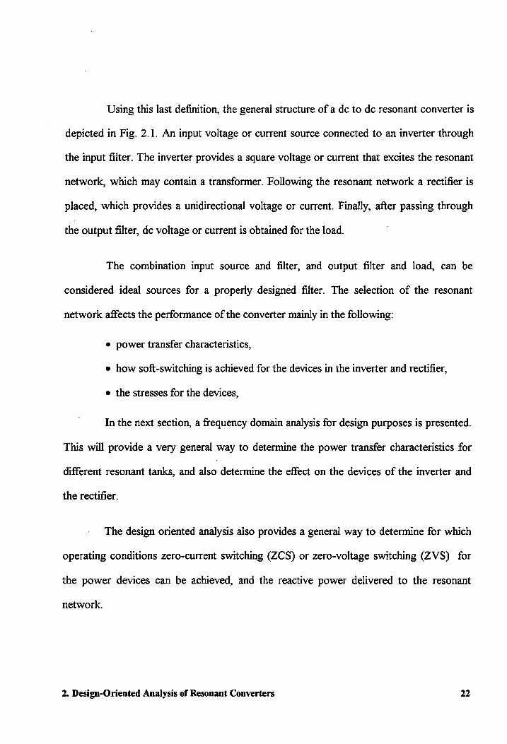
recovery of the MOSFET's body diode, an additional external diode is placed in series to
block the body diode and a fast external antiparallel diode is used.
The ZVS or ZCS operating regions can be determined by calculating the value of
the phase of the impedance seen by the inverter. The fundamental approximation method
just described provides a simple way to perform this calculation. In addition to that, as will
be shown for several converters, the method is very accurate around the transition of the
tank impedance from capacitive to inductive. A case for which circuit parasitics have to be
considered is presented in Chapter 4. The analysis in Chapter 4 shows the effect of
significant switch capacitance on the ZVS range.
The reactive power factor implies that a certain amount of energy is returned to
the source each switching cycle. This excess energy delivered to the resonant tank is
always required to achieve soft-switching. The design has to be such that the increased
conduction losses due to the circulating energy do not overcome the savings in switching
losses. The reactive energy required for a particular design depends on the resonant
network employed. This is going to be the basis of comparing different resonant networks
in the following chapters.
2. Design-Oriented Analysis of Resonant Converters 31

SOURCE
Zin
RESONANT
NETWORK
Figure 2.4: Equivalent load of the inverter stage.
2. Design-Oriented Analysis of Resonant Converters
LOAD (I or V)
Zout
32

01 01 04 04
Vg J J 03
02 02
J~ 03 I I J~ -:- -:- -:- -:-
V out
RESONANT TRANSF.
Vt RECTIF. Rload TANK
+ FILTER
Vg 03 03
-+- 04 --..+4---04 ___
I (t)
o----+---~-----+_--~-----_+--~~
-Vg 02
01
02
Figure 2.5: ZVS operation of a resonant converter.
I
2. Design-Oriented Analysis of Resonant Converters 33

Q1 J Vg f.l....~ : .
1 .... _- ... _~ Q3J~
Vg
o
-Vg
01
03
Q1
Q2
1 I
Vt
+
04
Jra_·_·1
i t._ .... __ ............ .r
02
J~
RESONANT
TANK
I (t)
01
02
04
02
i TRANSF.
RECTIF.
FilTER
Q3
Q4
Figure 2.6: ZCS operation of a resonant converter.
2. Design-Oriented Analysis of Resonant Converters
V out
03
04
R load
34

2.5 Resonant Converters with Two Reactive
Elements
Conventional resonant converters have a resonant network consisting of an
inductor and a capacitor. In this section all possible configurations for two element
resonant converters will be presented. The definition of resonant converter is going to be
used to determine the possible networks. Also the transfer function of each network is
provided.
2.5.1 Possible Topologies
The inverter stage acts as a square waveform ac source connected to the resonant
network. In the following it will be considered an input ac source (voltage or current) for
the resonant network. Using the definitions provided at the beginning of the chapter, in
order to operate as a resonant converter the circuit topologies have to comply with the
following rules:
• Voltage sources or capacitor loops are not allowed.
• Current sources or inductor cut-sets are not allowed.
• The resonant network has to filter the high-frequency harmonics of the input
source.
2. Design-Oriented Analysis of Resonant Converters 35

• The resonant network has to filter the high-frequency harmonics from the load
rectifier side.
Also, some components are redundant, namely,
• An inductor in parallel with the input voltage source does not alter the power
conversion.
• A capacitor in series with the input voltage source does not alter the power
conversion.
Following the former rules, the possible topologies for two-elements resonant
converters are depicted in Fig. 2.7. The converters in the left column of Fig. 2.7 are the
well-known Series Resonant Converter (SRC) and Parallel Resonant Converter (PRC),
the ones in the right column are their duals.
Figure 2.8 shows the possible topologies that do not result in a resonant
converter. All three topologies shown in Fig. 2.8 do not filter the high frequency
harmonics, and consequently, the sharp edges in the current or the voltage in the rectifier
would be seen at the inverter, and vice versa.
The current gain function for the dual SRC and dual PRC are the same as the
voltage gain function for the SRC and the PRe.
The two bottom converters in Fig. 2.7 have the same circuit diagram. However,
they are different because the output source corresponding to the rectifier-load side of the
converter is not an independent source.
2. Design-Oriented Analysis of Resonant Converters 36

Ls Cs J"y\r-.r' (
Lp ~ Cp \ (' t - / tl
Ls Ls J'..f'r'n I ~-
I
Cp I Cp
Figure 2.7: Possible resonant networks with two reactive elements.
2. Design-Oriented Analysis of Resonant Converters 37

Lp r Cp-
Cs .----1 t---( ----1 -
+ ' ~~ ) Lp c I c ,
) Lp
Figure 2.8: Resonant networks with two reactive elements that do not correspond
to a resonant converter.
2. Design-Oriented Analysis of Resonant Converters 38

2.6 Design Characteristicsfor Two-Element
Resonant Converters
This section presents a design-oriented analysis of the SRC, and PRC. The
objective is not to provide a new analysis method of these resonant converters, but to
provide a clear idea of the trade-oft's involved in the design of the two converters. This
provides a sound way to compare their performance and assess their suitability for
different applications.
The design-oriented characteristics presents the stresses in the converter devices
and shows their relation to the reactive power involved in the power processing. The soft
switching for resonant converters always involves reactive power delivered by the source.
This reactive power results in increased conduction losses and larger reactive components.
The two converters analyzed have different reactive power requirements to provide soft
switching over the whole operating range. Their relative performance is going to be
pr.esented with the help ofa design example at the end of the chapter.
The fundamental approximation analysis has the advantage of allowing one to
determine the characteristics of the converter as close-form equations. The close form
characteristics equations can be easily manipulated to present the characteristics in the best
suitable form for the design choices.
2. Design-Oriented Analysis of Resonant Converters 39

Cs Lo ....--------I! NYVli--l
Ve + Req
Vo
Zi
Figure 2.9: Series resonant converter model.
2. Design-Oriented Analysis of Resonant Converters 40

The cumbersome exact method requires extensive computation, and in general
the design is based in normalized characteristics that do not provide a clear understanding
of the actual values of the voltages and currents until they are denormalized according to
the design parameters selected.
2.6.1 Series Resonant Converter
The series resonant converter model is presented in Figure 2.9. The input voltage
source to the resonant tank, Ve , is an ac source corresponding to the fundamental of the
voltage at the output of the inverter stage. The dependent voltage source corresponding to
the rectifier is replaced by a resistor as described in the former section. Using the method
of analysis described in the previous section, the voltage gain for the SRC is
(2.12)
normalizing the frequency and impedances with
1 and (2.13)
and defining
Qs=~. R'oad
(2.14)
The results of this analysis are compared with the exact analysis presented in
[A-4]. Figure 2.10 presents the voltage gain with respect to the frequency for the exact
solution and the fundamental approximation method.
2. Design-Oriented Analysis of Resonant Converters 41

VoNin 1.2 r------,--------,-----.,....-------...,-------.,.------,
0.8 r--.... --............. ~ .. , ...................... -....... -... _/_ ........ ~ .. ,/- ,.,·· .. ·-!:I-!I .. ·· .. ·· .. -······~· .. ···· .... · .. ·",' .. ,,··l\:
0.6 1--.. ····-··· .. · .... ·• ...... -··0
o ~--~--------~---------~-------~--------~-~ 0.6 0.8 1.2 1.4
f5/fo
0=1.5
0=2
0=3
0=4
Figure 2.10: Comparison of voltage gain of the SRC obtained with the exact
solution (thin lines) with the fundamental approximation analysis
result (thick lines).
2. Design-Oriented Analysis of Resonant Converters 42

Error (%) 10 ~----~----------------------------------------------~----~
5, ...... ··········· .. ·T·· .. ·· .. ········· .... · .. ······ .. ·· .... ···············r············ .. ··········· .... ··· .. ··· .. · .. ··· .. ······ .. 1· .. · .. ··· .... ····· .... ~~= .. ···-~~ .. ··= ........ = .. ·· .. · .. = .. ·-· .. = ....... = ........ = ......... ± .. ~ ... = ........ = ........ ~ ...... .. o ~----~--------------------~~~--------~----------~----~
-5
-10
-15
-20 0.6 O.S 1.2 1.4
fS/fo
Figure 2.11: Error between the exact analysis and the fundamental approximation
analysis for the SRC voltage gain.
2. Design-Oriented Analysis of Resonant Converters 43

Figure 2. 11 presents the error with respect to the frequency for different loads.
The error is minimal for frequencies of interest around the resonant frequency. Also, the
ap~roximated method is more accurate for large Q values. The error is smaller at
frequencies above resonance because the high frequency harmonics get nlore attenuation
from the resonant tank characteristics.
The SRC converter behaves as a bandpass filter, with the passband centered at
the resonant frequency. The gain in the bandpass is equal to one, independently of the
load. The high frequency slope is -20 dB/dec .. This corresponds to the frequency response
of a second-order system with a real zero at the origin and a pair of complex conjugate
poles at the resonant frequency.
The input impedance to the resonant tank, Zi , determines the soft-switching
characteristics of the SRC. Using the fundamental approximation method, the normalized
input impedance to the tank is,
(2.15)
Figure 2.12 shows the plot of the phase of the input impedance. It can be seen
that the impedance changes from inductive to capacitive at the resonant frequency,
independently of the load. This shows that the converter operates with zero-voltage
switching above the resonant frequency, and with zero-current switching below the
resonant frequency. If the switches have a significant capacitance compared to the
resonant capacitors, operation slightly above resonance is required to achieve ZVS. A
2. Design-Oriented Analysis of Resonant Converters 44

complete analysis of the effect of the switches capacitance on the ZVS limit can be found
in Chapter 4.
The rms value of the normalized input current to the tank can be expressed as a
function of the normalized input impedance to the tank as
(2.16)
Using Eq. (2.12) and Eq. (2.16), the normalized input current to the tank for constant gain
can be calculated. Figure 2.13 shows the normalized input current to the tank with respect
to the frequency showing the constant gain current. The characteristics show that the
current for constant gain changes almost proportionally to the load. This is a good
characteristic of the SRC that results in good partial load efficiencies. Also, the
characteristics show that a large frequency range is required to keep the voltage gain
constant over a load variation.
However, all the characteristics are normalized with respect to parameters that
have to be chosen for each specific design. The rms value of the actual input current to the
tank can be expressed as
(2.17)
where n corresponds to the transformer turns ratio required for the design. The
transformer turns ratio can be determined from,
(2.18)
2. Design-Oriented Analysis of Resonant Converters 45
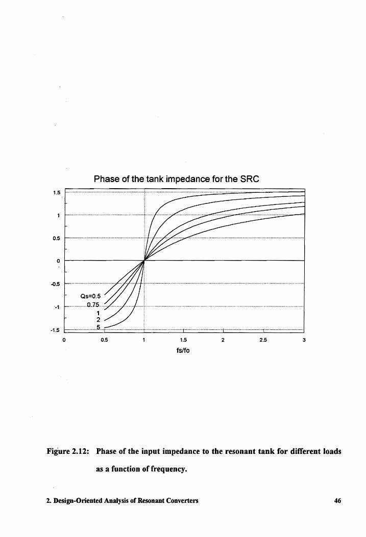
Phase of the tank impedance for the SRC 1.5 F~==========F========::::=~;:::;~======:::::::=::J
1
0.5 1-.... , .......................... - ............... _ .......................... · .. ·· .. ·!' .. f
o I----------------~--------------------------------~
-0.5
'·1
Os=0.5 _ ................. 0.15 ............... _ ....... .. · .. · .. -1 .. ···· .. ·,;· .... · .. · .... · .... ·_· .. ···· .. ,· .... · .... · .. ····· .... ·· .................... _ ........................................................... · .. · .. ····· .... · .. ····· .. ······ .. ·_· .. ·1
1 2
·1.5 r....-... _ ..... _ ..... _ ..... _ ..... _ ...... _5.-.!... •••• _ ...... _ ..... _ ...... _ .... _ ..... _ ..... _ .... __ .... J.... .... _ ..... _ ..... _ ..... _ ..... _ ..... _ ..... _ ...... ....1.. •• __ .... _ ..... _ ..... _ ..... _ ..... _ ..... _ ..... _ ..... J.... .... _ ...... _ •••.• _ .... _ ...... _ ..... _ ..... _._ .. -.!... ... _ ..... _ ... __ .... __ ••• _ ..... _ ..... _ .•••. ......J_ ....
o 0.5 1.5
fS/fo
2 2.5 3
Figure 2.12: Phase of the input impedance to the resonant tank for different loads
as a function of frequency.
2. Design-Oriented Analysis of Resonant Converten 46

lin/lb 5 ~----------------------~Ii~~~~~----~~--------~~--~
4 1:.;;;::: ....................... ;, ............................. .
Ii
M = 0.25--/! 0.5 ---LJ 0.75 /!
3 ~ .... -................ ~ ... -....................................... -···· .. ·-· .......... · .. ·-·-.. f-~·~
2 ~ .... -................ , ........................ -..... -.......................... ,~~k~·-·~
a ~----~--------~~----------~--------~----------~----~ 0.6 0.8 1.2 1.4
fs/fo
Figure 2.13: Normalized input current to the resonant tank for ditTerent loads and
constant gain current as a function of frequency.
2. Design-Oriented Analysis of Resonant Converters 47

Putting this in Eq. (2.17),
( ) V;ut I rn( (0 n, Os) lin (On,Qs =R V; 2{ )
load' in Mv (On,Os . Os (2.19)
The first term of Eq. (2.19) is the output power divided by the input voltage,
which corresponds to the minimum current required to provide the output power required
from an input-output power balance point ofvie\v.
Figure 2.14 shows the plot of the term
(2.20)
The minimum current through the resonant tank for the SRC occurs at the
resonant frequency, and consequently the switching frequency for the design has to be
chosen as close to resonance as possible.
Also, from Fig. 2.14 it can be seen that the current required in the tank can be
several times the minimum current. This is one of the main problems associated with
resonant converters when compared to PWM converters. For PWM converters the rms
input current that has to be provided by the inverter is approximately only the output
power divided by the input voltage and times the square root of the duty cycle.
The extra current required by the SRC compared to a PWM converter is due to
the reactive power that has to be delivered by the inverter. The reactive power to be
provided by the inverter can be represented by the power factor of the loaded resonant
tank. For the SRC the power factor seen by the inverter is
2. Design-Oriented Analysis of Resonant Converters 48

(2.21)
where S corresponds to the product of the rms values of the current and the voltage at the
input of the resonant tank.
Figure 2.15 shows the power factor at the input of the resonant tank. The graph
shows that the power factor is largest at the resonant frequency, and consequently a
design operating close to this frequency requires the minimum amount of reactive power.
2. Design-Oriented Analysis of Resonant Converters 49

f(w,Q) 6~~------~------~----------------~
5 Q=4
4 Q=3
3 Q=2
2 Q=1
1
o~~------~------~----~------~~ 0.6 0.8 1 1.2 1.4 fs/fo
Figure 2.14: Input current to the resonant tank normalized with respect to the
output power for different loads as a function of frequency.
2. Design-Oriented Analysis of Resonant Converters 50

PolS
1
0.8
0.6
0.4
0.2
o 0.5 1 1.5
fs/fo
2
Q=O.S
2.
Figure 2.15: Power factor at the input of the resonant tank for different loads as a
function of frequency.
2. Design-Oriented Analysis of Resonant Converters 51

2.6.2 Parallel Resonant Converter
The parallel resonant converter model is presented in Figure 2.16. The input
v<?ltage source to the resonant tank, Ve , is an ac source corresponding to the fundamental
of the voltage at the output of the inverter stage. The dependent voltage source
corresponding to the rectifier is replaced by a resistor as described the previous section.
Using the method of analysis described in the previous section, the voltage gain for the
PRe is,
Mv( co nJ Qp) = ---"-2 -_Q-:.p---
~ . Qp . ( 1- Cl ~ ) + j. Cl n
(2.22)
normalizing the frequency and impedances with,
1 co 0 = -~;=L=s =. c=p=- and (2.23)
and defining
Q _ R10ad
p - Zo . (2.24)
The results of this analysis are compared with the exact analysis presented in Ref.
[A-7]. Figure 2.17 presents the voltage gain with respect to frequency for the exact
solution and the fundamental approximation method. Figure 2.18 presents the error with
respect to the frequency for different loads. The error is minimal around the resonant
frequency, and remains small for large values ofQ and at high frequencies.
2. Design-Oriented Analysis of Resonant Converters 52
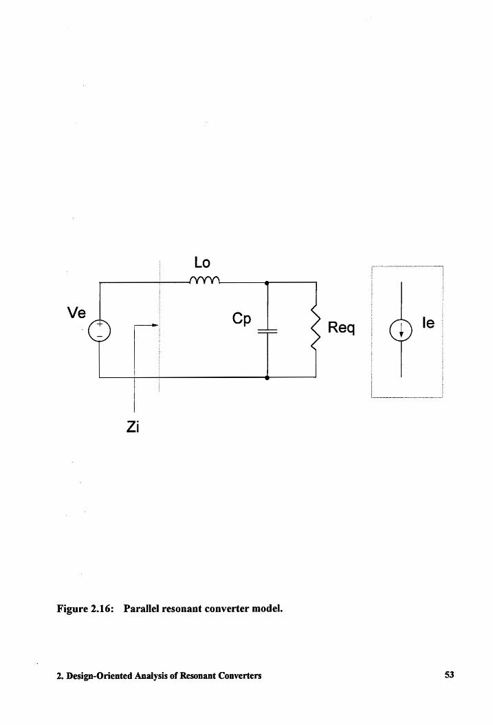
La
Ve Cp Req Ie
Zi
Figure 2.16: Parallel resonant converter model.
2. Design-Oriented Analysis of Resonant Converters 53

VoNin 5 ~--~----------~----------~--------------------~----~
Q=4 4 ~ .. -.................. ~.-..................................................... + .................. _ ................. - ..... ~~, ................................ - .............. ·······i····· .... · .... · .. ·····-·-·- .. •• .... ···• .... • .. · .. ·-~·· .. ···•·•••· ...... • .. • .. · .. i
3 ~ ..... -............... + ............................................... - ..... + .................. -.~~ ......... ,-~,-~
2 ~ .... -....... -..................................... -..................... ~~
1 ~==~~~~~~~~~~~~ ................................... ~ ... =~~~~ ............ ~ .......................... ~ o ~--~----------~----------~--------~----------~----~
0.6 0.8 1.2 1.4
fslfo
Figure 2.17: Comparison of voltage gain of the PRC obtained with the exact
solution (thin lines) with the fundamental approximation analysis
result (thick lines).
2. Design-Oriented Analysis of Resonant Conveners 54

error 0/0 10
5
0
-5
-10
-15
-20 0.6 0.8 1
fs/fo
1.2 1.4
Figure 2.18: Error between the exact analysis and the fundamental approximation
analysis for the PRe voltage gain.
2. Design-Oriented Analysis of Resonant Conveners 55

The PRC behaves as a lowpass filter with the comer frequency at the resonant
frequency. Since the gain function has a pair of complex conjugate poles the amplitude of
the gain at the comer frequency depends on the load. The region of the characteristic with
practical use is actually the region where the gain is load dependent, around the comer
frequency, because it is where the reactive power is minimal. The high frequency slope is-
40 dB/dec ..
The input impedance to the resonant tank, Zi, determines the soft switching
characteristics of the PRC . Using the fundamental approximation method, the normalized
input impedance to the tank is
(2.25)
Figure 2.19 shows the plot of the phase of the input impedance. It can be seen
that the impedance changes from inductive to capacitive at a frequency dependent on the
load. The frequency limit between ZVS operation and ZCS operation corresponds to the
peak of the voltage gain. The peak gain frequency is
'h-J: ron = l- Q~ (2.26)
The parasitic switch capacitance modifies the frequency of operation required to
achieve ZVS. A complete analysis of the effect of the switches capacitance on the ZVS
limit can be found in Chapter 4.
2. Design-Oriented Analysis of Resonant Converters 56

Phase of the tank impedance for the PRe
1.5
0.5
o
-0.5
2
-1 .... ·-···· ........ · .. -· .. · .. ···· .... ·· .. O·p;4·· .. ·--· .. · .. ·_ .. · .. · ...... ··
-1.5 ......................... _ ..................... _ ••••••••••••••••• - •••• _.-.- ..................... - ....................................................................................................... -t ......... - .................... -.-.-.................. -.-.-... ..
o 0.5 1.5 2
fs/fo
Figure 2.19: Phase of the input impedance to the resonant tank for different loads
as a function of frequency.
2. Design-Oriented Analysis of Resonant Converters 57

The rms value of the normalized input current of the tank can be expressed as a
function of the normalized input impedance to the tank as,
(2.27)
Using Eq. (2.22) and Eq. (2.27), the normalized input current to the tank for
constant gain can be calculated. Figure 2.20 shows the normalized input current to the
tank with respect to the frequency showing the constant gain current. The characteristics
show that the current for constant gain remains almost constant when the load changes.
Also, the characteristics show that a smaller frequency range than in the SRC case is
required to keep the voltage gain constant over a load range variation.
The rms value of the actual input current to the tank can be expressed as,
(2.28)
Figure 2.21 shows the plot of the term
(2.29)
The minimum current through the resonant tank for the PRC corresponds to the
frequency at which the maximum gain occurs for each Q. Consequently, the minimum
switching frequency should be chosen as close as possible to the peak voltage gain.
2. Design-Oriented Analysis of Resonant Converters 58

lin/lb 5 ~----~----------~----------~--------~----------~----~
4 r························l·· .......... ·· .. ····· .. ······ .... · .. ···· .... ····· .. · .... + .... ·· .. · .... ~~~~· .. ···· .. 7 .... · .. · .... ··,·-.... ···· .. ~ ................... _ .................... , ............................................... · .. · ...... ·1··· .. ·· .. ·· .... ·· ...... ·· .... i
3 ~ ....................... ;i ............................ - ........... ·.~~~ .... ~~.~
2 ~ .. ·· ...... ·· .... · .. · .. ··: ...... ·· ...... · .. ·· ........ ··· .... · .. ·~ .. · .... ·· .... tf~~~ ...................................... : ................................... ~~ ........... "~~~ ......................................... + .................. -..... ···i
a ~----~----------~--------~~--------~----------~----~ 0.6 0.8 1.2 1.4
fs/fo
Figure 2.20: Normalized input current to the resonant tank for different loads and
constant gain current as a function of frequency.
2. Design-Oriented Analysis of Resonant Converters 59

f(w,Q)
6
PRe 5
4
3
2
o ~--~--------~------~--------~------~--~ 0.6 0.8 1.2 1.4
f8/fo
Figure 2.21: Input current to the resonant tank normalized with respect to output
power for ditTerent loads as a function of frequency.
2. Design-O riented Analysis of Resonant Converters 60

The behavior with respect to the load, Q, shows that for Q values lower than 1
the input current increases. The minimum values of Q should be selected equal to one or
larger. However, the lower the Q value is, the larger is the frequency range required for
regulation. The frequency range required increases dramatically for values of Q equal to
one and lower.
An important difference with respect to the SRC is that the input current to the
resonant tank is always larger for ZVS operation than for ZCS operation. This is because
the reactive power required by the tank is larger for ZVS operation. ZVS requires
operation above resonance, and for those frequencies the impedance of the capacitor in
parallel with the load has lower impedance, and consequently, the circulating current is
larger at higher frequencies.
Figure 2.21 shows that the current required in the tank can be several times the
minimum current. The reactive power to be provided by the inverter can be represented by
the power factor of the loaded resonant tank. For the PRe the power factor seen by the
inverter is,
(2.30)
where S corresponds to the product of the rms values of the current and the voltage at the
input of the resonant tank.
2. Design-Oriented Analysis of Resonant Converters 61

Figure 2.22 shows the power factor at the input of the resonant tank. The
reactive power required for the tank is lower below the peak voltage gain frequency, and
is .minimal for Q= 1.
2. Design-Oriented Analysis of Resonant Converters

olS
1
~8
.6
.4
.2
o ,0.5
Q=1
1 1.5
fs/fo
2 2.5
Figure 2.22: Power factor at the input of the resonant tank for different loads as a
function offrequency ..
2. Design-Oriented Analysis of Resonant Converters 63

2. 7 Resonant Converters with Three Reactive
Elements
Since power regulation and soft switching for resonant converters can be
achieved with only two reactive elements, the addition of more resonant components may
seem initially undesirable. However, in some cases the additional reactive elements are
already present in the circuit as parasitics, with capacitance or inductance values
comparable to the resonant elements, changing the resonant converter characteristics.
Also, in some cases the additional elements are added to modify the characteristics of the
converters in a desirable way, without significantly increasing the size and cost of the
converter, giving the designer an added choice to achieve the desired conversion
characteristics. This has motivated the exhaustive search of topologies with three resonant
elements, in order to determine their properties.
The number of possible topologies with three resonant components is
considerably larger than the number with two elements, requiring a more systematic way
to determine all the possibilities. In the next section an exhaustive search of the possible
three element networks is presented. Also, the diversity of voltage and current gains for all
the topologies found are given in a table.
2.7.1 Possible Topologies with Three Elements
The three reactive elements can be arranged in two possible modes, either
forming a T network or a n network. Figure 2.23 shows the two possibilities with a table
2. Design-Oriented Analysis of Resonant Converters 64

showing the possible placement of the reactances. The placement of a reactance is marked
on the table as X, a short is marked as S, and an infinite inductance or open circuit is
marked as O. The possibility of an open circuit in the B position is excluded for the IT
network case because it disconnects the input and the output. Also, the case of a short in
the b position for the T -networks is excluded for the same reason.
Networks TI and ITI are only a wire connection and do not contain reactive
elements; consequently, they are discarded. The rest correspond to only five different
possibilities,
• Series Network: Cases n3, T2, T5, and T6 correspond to having a series
parallel combination of the three elements in series between input source and
the load.
• Parallel Network: Cases IT2, IT5, IT6, and T3 correspond to having a series
parallel combination of the three elements in parallel with the input source and
the load.
• Series-Parallel Networks: Cases IT4, IT7, T4, and T7 correspond to having a
reactive network or element in series between input and load, and a reactive
network or element in parallel with the input source or the load.
• n-Network: Case ITS corresponds to having three single reactive elements in
a IT-network arrangement.
2. Design-Oriented Analysis of Resonant Converters 65

A
n
1
2
3
4
.5
6
7
8
II-Network
B
A B
0 S
0 S
0 X
0 X
X S
X S
X X
X X
c
C
0
X
0
X
0
X
0
X
T-Network
a
b
T I a b
1 S 0
2 S 0
3 S X
4 S X
5 X 0
6 X 0
7 X X
8 X X
Figure 2.23: Possible resonant networks with three reactive elements.
2. Design-Oriented Analysis of Resonant Converters
c
c
S
X
S
X
S
X
S
X
66

• T-Network: Case T8 corresponds to having three single reactive elements in a
T -network arrangement.
Tables 2.1 and 2.2 show all the possibilities, indicating the source type at input
and output to have a resonant converter. A description of the rule not fulfilled by the
networks which do not result in a resonant converter is also indicated in the table.
The number of possible topologies is 26. These topologies can be grouped in
terms of input-output supplies in three groups:
• Converters with input voltage and output voltage, or input current and output
current, that are symmetrical, i. e. interchanging input and output sides results in the same
converter. Figure 2.24 shows the'four topologies that fit this description. The converters
in the left column are the duals of the converters in the right column .
• Converters with input voltage and output voltage, or input current and output
current, that are not symmetrical. Two different converters are obtained for each of the
resonant networks of these type, depending on which side is considered input. Figure 2.25
shows the resulting converters. The converters in the left column are the duals of the
converters in the right column .
• Converters with input voltage and output current, or vice versa. For each of the
corresponding resonant networks two converters are possible depending on which side is
considered input. Figure 2.26 shows the resulting converters. Also, the converters in the
left column are the duals of the converters in the right column.
2. Design-Oriented Analysis of Resonant Converters 67

Table 2.1: Possible Three-Elements Topologies I
Network type Position Input Output Comments
A B C
Series Network L+(C//L) Voltage Voltage
II3, T2, T5, T6 LII(C+L) Voltage Voltage
C+(C//L} Not low pass filter
C//(L+C} Not low pass filter
Parallel Network L+(C//L) Not low pass filter
II2, TI5, II6, T3 LII(C+L} Not low pass filter
C+(C//L) Current Current
C//(L+C} Current Current
Series-Parallel L C//L Voltage Current
Network L C+L Voltage Voltage
II4, II7, T4, T7 C C//L Current Current
C C+L Not low pass filter
C//L L Current Voltage
C+L 'L Voltage Voltage
C//L C Current Current
C+L C Not low pass filter
L C//L Not low pass filter
L C+L Voltage Voltage
C C//L Current Current
C C+L Current Voltage
C//L L Not low ~ass filter
C+L L Voltage Voltage I
C//L C Current Current
C+L C Voltage Current
2. Design-Oriented Analysis of Resonant Converters 68

Table 2.2: Possible Three-Elements Topologies IT
N~twork type Position Input Output Comments
A B C
II-Network L L L Not low pass filter
ITS L L C Voltage Current
L C L Not low pass filter
L C C Current Current
C L L Current Voltage
C L C Current Current
C C L Current Current
C C C Not low pass filter
T-Network L L L Not low pass filter
T8 L L C Voltage Voltage
L C L Voltage Voltage
L C C oltage Current
C L L Voltage Voltage
C L C Not low pass filter
C C L Current Voltage
C C C Not low pass filter
2. 'Design~Oriented Analysis of Resonant Converters 69

Table 2.3 presents the gain for each of the converters. Table 2.4 shows the values
of the constants used in the equations in Table 2.3 for each converter, using the notation
of Figs. 2.24 to 2.26, and the following definitions:
For converters with 2 C and 1 L:
1 0)0 = ~L' Ceq ,
For converters with 2 Land 1 C:
Kc _ 1+Cn 1 - C .
n
1 0> 0 = ~Leq' C '
Zo =t; , _ L1'L2
Leq - L1 +L2 '
2. Design-Oriented Analysis of Resonant Converters
(2.31)
(2.32)
(2.33)
(2.34)
(2.35)
(2.36)
(2.37)
(2.38)
(2.39)
(2.40)
70

KL = 1+L on, (2.41)
(2.42)
and normalizing the load
Z Q =_0_ or 5 R ' eq
(2.43)
(2.44)
Table 2.5 summarizes the main properties of the three-elements topologies.
According to the frequency of the gain, the converters can be grouped into two main
categories:
• Bandpass filter characteristic. They have a load independent gain at the middle
of the pass-band. The SRC is the corresponding two-element resonant converter with
bandpass characteristics .
• Lowpass filter characteristic. They have a low frequency gain of one. The PRC
is the corresponding two-element resonant converter with lowpass characteristics.
However, the association with SRC or PRC characteristics have to be taken into
consideration also if there is overshoot in the voltage gain for high-Q loads, as is the case
for the PRC. The peaking in the characteristics for high-Q values, as in the case of the
PRe for frequencies around IDo' determines the characteristics of the converter. The high
frequency roll-off slope determines the high frequency harmonics contents of the output,
2. Design-Oriented Analysis of Resonant CODverters 71

and is consequently a more important magnitude for inverter applications when a
sinusoidal output is required.
Figures 2.27 and 2.28 show the gain characteristics for the converters with
"SRC-type" voltage gain, all of them with a high frequency roll-off frequency of -20
dB/dec .. Figures 2.29 to 2.31 show the converters with tlPRC-type" voltage gain, all of
them show peaking dependent on the load (Q).
An interesting case is the LeC converter, designated in the list as 7d(r). This
converter has a bandpass characteristic and a -40 dB/dec. roll-off slope at high
frequencies. It also has a load-independent gain at the bandpass frequency (resonance of
the LC series), but it has peaking in the voltage gain like the PRC.
In the next sections the performance and design characteristics of the LCC are
addressed, and they will be used in the comparison with SRC, and PRC designs at the end
of the chapter. The effects of the peaking in the characteristics and the bandpass behavior
are analyzed in terms of device stresses and reactive power. This analysis will help to
match the characteristics of the three-elements resonant converters presented with a
specific desired performance.
2. Design-Oriented Analysis of Resonant Converters 72

1d
2d
3d L
c C 1 2
Figure 2.24: Topologies with in/out symmetry.
2. Design-Oriented Analysis of Resonant Converters 73

4
C 2
C 1
6
Figure 2.25: Topologies without in/out symmetry.
2. Design-Oriented Analysis of Resonant Converters 74

C
7d
c~, PI
1
8
C 1-r----)
- !
Figure 2.26: Topologies with different input and output sources.
2. Design-Oriented Analysis of Resonant CODverters 75

Table 2.3: Gain Functions of Three-Elements Resonant Converters I
Ci~cuits Gain Zeros
1, 1d, 2, (1-ro~.Kn) 1 2d,4, ro z = ~Kn
( 1- ro ~ . Kd1 J - jro n 0 0 . Kd2 0 (1- ro ~ . Kd3 J 4d(l) roz=oo
3,3d 1 roz=oo
( 1- ro ~ . Kd1 J + jro n . 0 . Kd2 . ( 1- ro ~ )
4(r), 0 roz=oo 4d(r) 0+ jron ·~2
5,5d(l) ron roz=O (SRC) ron - j.Q.{1-ro~) roz=oo
6,6d(l) ro~ ·Kn roz=O
ro ~ . ~1 - jro n . 0 . ( 1- ro ~ J roz=oo
7, 7d(l) 0 ro z = 00
o . Kd1 . ( 1- ro ~ J + jro n . ~2
5,5d(r), -ro~ oKn roz=O 6,6d(r) (1-ro~ . Kd1) + jron' O ·Kd2 .(1-ro~ .Kd3J
roz=oo (LCC)
7, 7d(r), jron' Q·Kn ro z 0 8,8d(r) (1- ro~. Kd1J + jron ·0· Kd2 . (1- ro~ . Kd3J roz=oo
I
8,8d(1) 0 roz=oo (PRC) jro n + Q . { 1- ro ~ J
2. Design-Orieoted Analysis of Resonant Converters 76

Ta~le 2.4: Definition of the Constants Used in Table 2.3
Circuits Gain type Q Kn Kd1 Kd2 Kd3 1 Mv Qs K~.Kf L KL Ko· 1 KL
0 Kf ld Mj Qp K~.Kf K~.Kf KC KC
0 1 2 Mv Qs Kf Kf L KL Ko· 1 1
2d M· Qp KC KC K~.Kf 1 I 1 1 3 Mv Qs --- KL L KL ---
0 Ko· 1
3d M· Qp --- KC K~.Kf ---I 0
4(1) M· I Qp ~C K~.Kf --- ~C 4d(l) Mv Qs Kr K~.Kf --- Kf 4(r) Mj Qs --- --- ~C ---4d(r) Mv Qp --- --- Kr ---5(1) M· I Qp --- --- --- ---5d(l) Mv Qs --- --- --- ---5(r) M· Qp KC K~.Kf KC ~C I
0 0
5d(r) Mv Qs KL 0
KL KL o· 1 KL 0 Kf
6(1) M· Qp KC K~.Kf KC ---I 1 0
. 6d(1) Mv Qs Kf K~.Kr KL ---0
6(r) M· Qp KC KC 1 1 I 1 1 6d(r) Mv Qs Kf Kf 1 1
7(1) Mv Qp --- KL KL Kr 0 0
7d(1) Mj Qs --- KC KC KC 0 0 1
7(r) Mj Qs Kf Kf L L Ko·K1 1
7d(r) Mv Qp ~C ~C K~.Kf 1
8(r) M· Qs 1 K~.Kr KL Kr I 0
8d(r) Mv Qp 1 K~.Kf KC KC 0 1
8(1) Mv Qp --- --- --- ---8d(l) M· I Qs --- --- --- ---
2. Design-Oriented Analysis of Resonant Converters 77

Table 2.5: Cbaracteristics of Tbree Elements Resonant Converters n
Circuits Load Independent Gain Filter Characteristics
1, 1d, 1 band pass, 2,,2d, M= 1 at con = ,JK; high-frequency gain slope 4,4d(l) Kn -20 dB/dec.
M= 1 at con = 0
~,3d M= 1
low pass, at con = 1 high-frequency gain slope
1-Kd1 -60 dB/dec.
M= 1 at con=O
4,4d(r) M=1 at con=O low pass, high-frequency gain slope -20 dB/dec.
5, 5d(l) M=1 at con = 1 band pass,
(SRC) high-frequency gain slope -20 dB/dec.
6,6d(l) 1 band pass, M=- at con = 1 high-frequency gain slope
Kd1 -20 dB/dec.
7,7d(l) 1 low pass, (LeC) M=- at con = 0 high-frequency gain slope
Kd2 -40 dB/dec.
5, 5d(r), M= Kn 1 band pass,
6,6d(r) at con = JKd3 high-frequency gain slope Kd1 -Kd3 Kd3 -20 dB/dec.
7,7d(r), Kn ·Kd1 1 band pass, 8,8d(r) IM=
Kd2 . ( 1- Kd3) at
con = ~Kd1 high-frequency gain slope -40 dB/dec.
8, 8d(l) M=1 at con=O low pass,
(PRC) high-frequency gain slope -40 dB/dec.
2. Design-Oriented Analysis of Resonant Converters 78

VoNin 1.2
1
0.8
0.6
0.4
0.2
0
VoNin
0.6
Circuits 5(1), 5d(l) [SRC]
0.8 1
fs/fo
Circuits 3, 3d
1.2 1.4
1.2 ....--~---~-------!"----~---------.
Ln=1
0.8 1---._._._ ........ .;.-.... -._ ...... _ ...... _ ..... _._ ......... ··+····_····-1
0.6 ~.-... -................ -.-... -.......... -.-................... ;..#
0.2 k:: ................... ,'"" ......... '\:
o ~--~-~~~---~------~---~-~ 0.6 0.8 1
fs/fo
Figure 2.27: Gain of topologies similar to the SRC (1).
2. Design-Oriented Analysis of Resonant Converters
1.2 1.4
79

Circuits 6(1), 6d(l) oM
.6 ~----------------------~----------~ Ln = 1
.5 .. ···· .. ···QF1.·················· .. ·;::::.;_· .. ···;;;,;·······CL ..... ;::: ....... ~......-~~~:::-:~:::.:==:1
.4
.3
.2 ~ .. ···· .. · .. · .. i· .. · .. · .. · .. · .. ·· .... ·· .. · .... ·· .. · ...... · .. +· .... · .. · .. · .... · .................... -..... + ....... , .................................... ~ ........................................... + ...... , ............. /
0.6
VoNi
0.8 1
fslfo
1.2
Circuits 4(r), 4d(r)
1.4
1.2 r------~----~------,------r Ln = 1
0.8
O. 6 I--...... · .... · .. · .. · .. · .. · .. · .. · .. , .... · .... · .. ··· .. · ...... ·,i· .......... · ............ ·-.......... ~.......,. .............. .;, ............................................................. + ........... :"'---=
O. 4 1--.......................................................... , ............................................................. + ............................................ ~oo;:± .............. - ......................... -~
0=1 0.2 1--_-L......_--l-__ ...l....-_--l-__ L..--_-1--_-..!..---I
o 0.4 0.8
fs/fo
Figure 2.28: Gain of topologies similar to the SRC (2).
2. Design-Oriented Analysis of Resonant CODverters
1.2
80

oNin Circuits 8(1), 8d(l) [PRC] 5~~------~------~------------~---'
Q=4 4 1---................ :.-.-.-......................... - ........... , ............................... - ....... ~"""' ............................... -.-.-.-.. ~ ................. - .................. - ...... : ................. - .. .
3 t-.................. ; ....... - ......................... - ............ ; ... -.-.-.-..... .,.
2 1---................ ; .... - ...................... - ............. ,:#'-
Q=1 1 .................. -.... -.-........ , ... -.-.-.-.-............ -.-.. .
o~~------~------~------~----~--~ 0.6 0.8 1
f5/fo
VoM Circuits 3, 3d
1.2 1.4
1.4 ,---------,,....---------,--------.------.-----......--------,
Ln = 1 . .
1 2 :::
• 1--... _ .............. , ....... _ ........................ _ ............ > ••••••••••• - ••••• ~ ••• - •••••••••• ; •••••••••• - •••• - •.•••••••••••••••• -.-••••• , •••••••.• -.-.-•••••••••••••••••• - •••••••••• ~ •••••.••••••••••••••••
1 I--.................. ~-............................. -.-...... -1-
o. 8 I--... - .............. ~~
0.6
0.4 ~----!o-=
0.2 I-----" __ .... ~ ....... :::::_._ .... _ ........ l .. _ .... _._ ................................. ! .......... -.... -............... . .. . IQ=4
0.6 0.8 1
f5/fo
Figure 2.29: Gain of topologies similar to the PRe (1).
2. Design-Oriented Analysis of Resonant Converters
1.2 1.4
81
VoNin Circuits 7(r), 7d(r), 8(r), 8d(r) [LCe] 7------------------------------------~
0=3 6~··· .. ···············~·· .... · ...... · .... ·· .... · .. · .. · .... · .. · .. · .. ·· ..... ~ ........................... -......... --...... ~
Cn=1 5~ .. · .. · .. ··· .. ·--.... +· ...... -.... · .... --·· .......... ·-.... · ...... · .. ·i ............. · .... · .. ·-· .. · .. ·-........ ·+·++·· .. · .. ··-.. ·· .... · .. · ...... · ...... ·-· .. i~· .. • .............. -.-.-.-.................. + ..................... ~
4r .................... + ................................................. ~ .................... ,.~ ............ ~ , ............................................................................................. -j ................... - ... ~
3 ~ .................... + .................................................... ; .................................. .,1-
. 2 r· .... ···· .. ··· .. · .. ·;.· .. · .. · .... · .. ···· .. · .. · .. ···· .. · .. · ........ · .... ·;.· .................... .,.
1 I--..................... + ..................................... ~.....,.,.,-:: ........................................ =--==:
o--~--------------~----~----------~ 0.6 0.8 1
f5/fo
VoNin Circuits 7(1), 7d(l)
1.2 1.4
10------------------------------------Ln=1
0=4 81~ .................... ~ ....... -..................................... --i-..................................... --.~~ ........... --.............................. + .............................................. + ..................... ~
6 11-.................... ; ................................................ + ..................... I·
4 t-.................... ~ ................................. -......... .,'"
o--~------------~--------------~~ 0.6 0.8 1
fs/fo
Figure 2.30: Gain of topologies similar to the PRe (2).
2 •. Design-Oriented Analysis of Resonant Converters
1.2 1.4
82

VoNi Circuits 5(r), 5d(r), 6(r), 6d(r) 5 ~--~----~------~------~------~--~
Ln=1 4 r··-·· .. ···········~~·~· .. ······ .... ······ .... ·· .. · .. ·· .. · .... ··· .. j, ... -.~ ....................................... : ............................................... : .............. ~ ............... - .... - •.• ••• .. ~····· .. ·-.. •• .. ·-· .. ·I
3 ~-.-............... , ... ~ ........... # ........................... +-....... ~ ................................... , ............................................ ·+ .... · .... - .... ·· .. · .. ····· .. · .... · .. ·· .. ·· .. ·~ ........ · ...... · .. · .... I
2 ~-.... · ...... · .... ·; .. ·I·
1
0.6 0.8 1
fs/fo
1.2
Figure 2.31: Gain of topologies similar to the PRe (3).
2. Design-Oriented Analysis of Resonant Converters
1.4
83

2.7.2 LCC Resonant Converter
The LCC resonant converter model is presented in Figure 2.32. The input voltage
source to the resonant tank, Ve, is an ac source corresponding to the fundamental of the
voltage at the output of the inverter stage. The dependent voltage source corresponding to
the rectifier is replaced by a resistor as described in previous sections. Using the method of
analysis described in the previous section, the voltage gain for the LCC is
, (2.45)
normalizing the frequency and impedances with
1 Olo =-;====
~Ls . Ceq and (2.46)
and defining
Q _ Rload P-~' (2.47)
Figure 2.33 shows the voltage gain of the LCC resonant converter for Cn equal
to 1, comparing the approximate analysis and the exact solution. Figures 2.34, and 2.35
show the voltage gain of the LCC resonant converter for Cn equal to 2, and 0.5,
respectively. It can be seen that the converter has load-independent gain at the frequency
that corresponds to the resonance of the inductor with the series capacitor.
2. Design-Oriented Analysis of Resonant Converters 84

Cs Lo
Va Cp Req Ie
Zi
Figure 2.32: LCC resonant converter model.
2. Design-Oriented Analysis of Resonant Converters 85

Vo/Vin 7
Cn=1 Q=RI/Zo 6
5
4
3
2 Q=O.5
o 0.6 0.8 1.2 1.4
fs/fo
Figure 2.33: Voltage gain of the LCC-RC obtained for Cn= 1. Exact solution thin
lines, and approximate solution thick lines.
2. Design-Oriented Analysis of Resonant Converters 86

Vo/Vin
Cn=2 ........... " .......... - .... , ................................. " .................... , ................................... ::=:::::::::: ... . ....................................................................... -..................... _ .......... ,....... .. ................ ' ......... .
0.6 0.8 1 f5/fo
1.2
Figure 2.34: Voltage gain of the LCC-RC obtained for Cn = 2.
2. Design-Oriented Analysis of Resonant Converters
1.4
87

Vo/Vin
en =0.
,. .................................................................................... ··· .. · .. · .. · .. ···· .. ······ .... ·· .. · .. 0 .. ··· .... · .. · ....................................................................................................................................................... .
0.6 0.8 1 fs/fo
1.2
Figure 2.35: Voltage gain of the LCC .. RC obtained for Cn = 1/2.
2. Design-Oriented Analysis of Resonant Converters
1.4
88

The peak voltage gain for the LCC resonant converter is Q p . (1 + en) instead of
Qp, as was the case for the PRC ..
The characteristics of the converter approach those of the SRC as Cn tends to
zero. The dominant behavior in the characteristics is similar to the PRC case for large
values of Cn . Consequently, the converter behaves with a combination of properties of
the SRC and the PRC, and may be closer to one or the other depending on the value of
Cn. This capability allows a larger reduction of the circulating current for ZVS operation
than for the PRC, but still retaining the step-up capabilities of the PRC.
The input impedance to the resonant tank, Zh determines the soft-switching
characteristics of the LCC resonant converter. Using the fundamental approximation
method, the normalized input impedance. to the tank is
Figure 2.36 shows the plot of the phase of the input impedance for Cn equal to 1,
2, and 0.5. It can be seen that the impedance changes from inductive to capacitive at a
frequency dependent on the load, as was the case for the PRe. However, the load
dependence is smaller than for the PRC. The converter operates with zero-voltage
switching for frequencies above the peak of the voltage gain. The effect of the switch
capacitance on the ZVS limit can be found in Chapter 4.
2. Design-Oriented Analysis of Resonant Converters 89

C n= 1/2 Phase(Zi) 1.5
1
0.5 0
-0.5 -1
-1.5 0.6 0.8 1 1.2 1.4
fs/fo
Cn=1 Phase(Zi) 1.5
1 ._ .... -...................................... -....... _...................... .
0.5
o ~------~~-+~------------~ -0.5
0=1 ·-e·:(}-:5··"·"·"·· . ................ ....... . .... _ ............................................ _._ ....................... .
-1 -1 . 5 E:::::::~~:t::::~-1...-.....--"'"--......L-__ --L--.J
0.6 0.8 1 1.2 1.4
fs/fo
Cn=2 Phase(Zi) 1 .5 r---------::~~~!!!!!!!!!!!!!!!!!!!!II..,
1 ................................................................ m.··· .... ·
0.5 o r-----------~r-----------~
0=2 :~9::::9:~§~:~~:~:::: .. ··· .... ····- .. ...... . . ......................... _ ........................... _ .................. .. -0.5
-1 -1 . 5 t::=====~~:8
-2 ~~~--~~--~~~--~~~ 0.6 0.8 1 1.2 1.4
fs/fo
Figure 2.36: Phase of the input impedance to the resonant tank for different loads
as a function of frequency.
2. Design-Oriented Analysis of Resonant Converters 90

The rms value of the normalized input current to the tank can be expressed as a
function of the normalized input impedance to the tank as,
(2.49)
Using Eq. (2.44) and Eq. (2.49), the normalized input current to the tank for
constant gain can be calculated. Figure 2.37 shows the normalized input current to the
tank with respect to frequency showing the constant gain current. The characteristics
show·that the current for constant gain remains almost constant when the load changes for
large voltage gains, as is the case for the PRe. However, for low voltage gains the current
decreases slightly when the load decreases. The current decreases further at low voltage
gains and smaller values of en as the converter approaches SRC behavior. Also, the
characteristics show that the frequency range to keep the voltage gain constant over a load
variation is larger than for the PRe.
The rms value of the actual input current to the tank can be expressed as,
(2.50)
Figures 2.38-2.40 show the plot of the term,
(2.51)
2. DeSign-Oriented Analysis of Resonant Converters 91

in I(V s IZo)
12~------------r-----------~~~--------------------~--~
10~·-··-···· ...... · .. ··;· .. · .. ·· .. ······ .. · .... ··· .. -·· .... ·· .. ·· .... · .. · .... ··~·· .. ·· .. ··· .. · .. ······· .... · ...... · .. · .... ·· .... f········i·· .. , ........ , .......................................... " ................................. · .. ••••••• .. ••••• ...... +··· .. ······ .. · ........ · .... t
8 ~ ... ,.~ ...... , ..... -.. ;.-.-.... , ............................. , .... ~-.-..... + ............. "-.-.... , ........ ,." .... ·-·,·+· .. ··,·~····~4 .. ····,' .. ····-.. ·· .. · .. ··· .... ··· .... · .. ·~· .. ·_ .... · .. · .. ·_· ...... ··· .. · .. ··•· .... · ........ ·· .. ·+ ...... ·· .. · .. · .. ·, .. · ...... ·1
6 ~ ... -................ ;.-................. , .................... , ............. + .. , ...... ··_·~ .. ·· ...... ·.~ .. n·· .... · .. · .. · .. + .. · .. · .. ·· .. ~
4 ~ .................. -.. i .... - ................... -.-.-........... ~~~,
2 ~ ....................... ;.-........................ ~~.
o ~--~----------------------~----------------------~----0.6 0.8 1
fs/fo 1.2 1 .4
Figure 2.37: Normalized input current to the resonant tank for different loads and
constant gain current as a function of frequency.
2. Design-Oriented Analysis of Resonant Converters 92

f( w, Q )
6 ~--~----------'---------~--------~----~--r-~~~
5
4
3
2 t-·_·-""'IilIIr,;:·_·-i······ .. ····"'"""""""
1 Q = 0.5
o ~--~--------------------~-------------------------0.6 0.8 1
fs/fo 1 .2 1 .4
Figure 2.38: Input current to the resonant tank normalized with respect to the
output power for different loads as a function of frequency, for Cn=l.
2. Design-Oriented Analysis of Resonant Converters 93

f(w,Q) Cn=1/2 6 ~--~--------~------------------~------~~~~
5
4
9=0.25 3; · .. · .. ············ .. r························ .. ···· .. ······ ............ -.~.-.................. -.-.................. -·-·····r············~-·············-····-·-··········;······I~ .. ···········-·······-··-············-;······ ............... , •.. ,
2
1
o 0.6 0.8 1
fslfo
1.2 1.4
Figure 2.39: Input current to the resonant tank normalized with respect to the
output power for different loads as a function of frequency, for
Cn=1/2.
2. Design-Oriented Analysis of Resonant Converters 94

f(w,Q) Cn=2 6 ~--~--------~------~--------~~~~--~---,
5
4'
3 .-..................... , .... " ........... ,'-'_ ......................... ,,-.;. ............ ,'"' ....................................... .; ...................... .
2 ~ ................ =.~ ......... ~ ....... ~ ............ ~~ .............. ~ .. ~~ ............ ~ ..... , ..................... + ... ···#n'··············-····· .. ···········~··-·······-···· ........... -.-.-................... ~ .... - ............... "'-i
1
o ~--~--~----~--~--~----~--~----~--~--~ 0.6 0.8 1
fs/fo
1.2 1.4
Figure 2.40: Input current to the resonant tank normalized with respect to the
output power for ditTerent loads as a function of frequency, for Cn=2.
2. Des~gn-Oriented Analysis of Resonant Conveners 95

The discussion for the PRC can be repeated here, with the difference that the
current increases for different Q values according to Cn. Also the behavior between SRC
and PRC can be seen in the fact that the slope of the curves for high frequencies
decreases, and the current values at low frequencies are higher than for the PRC.
Also, from Figs. 2.38-2.40 it can be seen that the current required in the tank, can
be several times the minimum current. The reactive power to be provided by the inverter
can be represented by the power factor of the loaded resonant tank. F or the LCC
converter the power factor seen by the inverter is,
where S corresponds to the product of the rms values of the current and the voltage at the
input of the resonant tarue
Figures 2.41-2.43 show the power factor at the input of the resonant tank for
several values of Cn. It is clear that the curves are closer to the ones for the SRC for low
C~ values, and closer to the PRC for large Cn values.
2. Design-Oriented Analysis of Resonant Converters 96

PolS
1
0.8
0.6
0.4
0.2
o 0.5 1 1.5
fs/fo
Cn=1
2 2.5
Figure 2.41: Power factor at the input of the resonant tank for different loads as a
function of frequency for Cn=l.
2. Design-Oriented Analysis of Resonant Converters 97

PolS
1~--------~----------~--------~----------~
Cn=2 0.8
0.6
0.4
0.2 -----
oL-~~-L--~~~~~~------~ 0.5 1 1.5
fs/fo
2 2.5
Figure 2.42: Power factor at the input of the resonant tank for different loads as a
function of frequency for Cn=2.
2. Design-Oriented Analysis of Resonant Converters 98

olS
1
.8
06
.4
.2
0 0.5
Q=O.5
Q=2
1
Cn=1/2
1.5
fs/fo
2 2.5
Figure 2.43: Power factor at the input of the resonant tank for different loads as a
function of frequency for Cn=1/2.
2. Design-Oriented Analysis of Resonant Converters 99

2.8 Comparison of Resonant Converters and
Conclusions
To compare the SRC, PRC, and LCC, three converters are designed for the
foUpwing specs.:
• Input voltage range from 200 V to 300 V,
• Output voltage 5 V,
• Output Power range from 100 W to 10 W,
• Minimum switching frequency 500 kHz.
The converters are designed for ZVS operation. As has been described in section
2.3, ZVS operation eliminates the need for series blocking diodes and fast antiparallel
diodes, resulting in a more efficient converter. The trade-off's described in the previous
section have been considered for the converters as follows:
SRC
The Q value at full load has to be selected as high as possible to reduce the
frequency range that is going to be needed for output voltage regulation. However, very
high Q values make the circuit very sensitive to the tolerance of the resonant components,
and also the resonant capacitor voltage increases with Q. At resonance the peak capacitor
voltage is largest and would reach a value of Q times the input voltage. The Q value
selected for full load is 5, and hence at 10% load the minimum Q is 0.5.
2. Design-Oriented Analysis of Resonant Converters 100
Zero-voltage switching requires operation above resonant frequency. The
operating frequency is selected as close to resonance as possible to minimize the
circulating currents in the resonant tank and some margin has to be allowed for the
tolerance of the components. The operating frequency selected is 1.05 times the resonant
frequency.
With the value of switching frequency and Q the rest of the parameters can be
calculated.
PRe
The value of Q at full load has to be selected above one to reduce the currents in
the tank, but large values result in reduced frequency range for the control. However, the
inductor current increases very fast for higher values of Q. Therefore· the value selected
for full load is 2, and hence at 10% load the Q value is 20.
The switching frequency has to be selected as close to the peak voltage gain for
the Q selected for ZVS operation, and to minimize circulating currents. The operating area
in Fig. 2.45 shows that a smaller Q would not improve the reactive power required for this
design at full load.
With the value of switching frequency and Q the rest of the parameters can be
calculated.
2. Design-Oriented Analysis of Resonant Converters 101
Lee
The considerations for this converter are fairly similar to the ones for the PRC,
witp the exception that a series-to-parallel capacitor ratio has to be selected. Three designs
are presented for the LCC: Cn=l, Cn=2, and Cn=O.5. Smaller capacitor ratios result in a
larger frequency range required· for the control, and larger ratios result in increased
currents at full load high-line, as is the case for the PRC.
With the value of switching frequency, capacitor ratio, and Q the rest of the
parameters can be calculated.
Table 2.6 presents the parameters selected for the six designs.
The currents' range, and peak capacitor voltages are given in Table 2.7 for the
SRC and PRe designs, and in Table 2.8 for the three Lee converter designs. Figures
2.44-2.48 show the operating region of the six designs, and the power factor associated
with each region. The following are the main general conclusions about the designs for the
three converters.
• Switching frequency range: The SRC results in the larger frequency range, showing
the difficulties faced in the design of this converter when large load and input voltage
range are required. The LCC results in a larger frequency range than the PRC .
• Resonant inductor current: This current can be predicted from the power factor
characteristics. The minimum current at full load corresponds to the LeC converter,
which allows the design with the highest power factor. However, the current for the
2. Design-Oriented Analysis of Resonant Converters 102

LCC at fu1110ad high-line is larger than for the SRC for Cn equal to 0.5 and 2, which
has the same current at high line and at low line. The PRC results in the larger currents,
and this currents remain constant over the whole load range.
• Capacitor voltage: The largest voltage across the resonant capacitor corresponds to
the SRC, which value could be reduced at the cost of reducing the power factor for the
converter. The smallest values of voltage correspond to the Lee (Cn=0.5), because it
can operate with a transformer turns ratio lower than the PRe.
For the three LCe resonant converter designs, the lowest current variation over
the input voltage variation corresponds to a capacitance ratio of one. The lowest
capacitance ratio (0.5) results in a larger frequency range. The highest capacitor ratio has
the smallest frequency range required. However, the series capacitor voltage becomes
extremely high. Capacitance ratios close to one result in a superior performance, i. e. lower
currents and frequency range over line and load variations.
Among the three different resonant converters, the LCe converter results in the
superior performance, because it can combine advantages of SRC and PRC. The efficiency
at light load is worse than for the SRC. However, it results in lower currents and voltages
than !he PRC, at the cost of increasing the frequency range for regulation compared to the
PRC. The frequency range required for the LCC design is still much smaller than the one
required for the SRC.
However, the three converters have to operate with a power factor at the input
of the resonant tank smaller than the one required for a PWM converter, which is
2. Design-Oriented Analysis of Resonant Converters 103

practically unity. Consequently, the voltage and current stresses for the resonant
converters are always larger than for PWM converters. The main motivations for their use
are the presence of large parasitic capacitance and/or inductance in the circuit that require
a topology that can use them without energy loss, and the significant reduction in
switching losses by ZVS or ZCS operation for high switching frequencies.
Several alternatives attempting to combine resonant switching and PWM
operation are presented in the next chapters.
2. Design-Oriented Analysis of Resonant Converters 104

Table 2.6: Parameters Selected for the Three Designs
Converter SRC PRC LCC LCC LCC
CplCs ---- --- 0.5 1 2
!
min. con 1.05 1.05 0.95 1.0 1.0
max. con 2.7 1.29 1.29 1.14 1.13
Q full load 5 2 0.75 1 0.5
Q min. load 0.5 20 7.5 10 5
Lo (in Jili) 490 229 240 509 573
Cs (in nF) 0.23 ---- 1.14 0.4 0.27
Cp (in nF) ---- 0.49 0.57 0.4 80.53
Trans. turns ratio 34.3 74 60 80 60
2. Design-Oriented Analysis of Resonant Converters 105

Table 2.7: Frequency Range, Current Stress, and Voltage Stress for SRC and PRC Designs
Converter Load level Parameter High Line Low Line
SRC Full load con 1.123 1.05
IL 0.648 0.648
VCPK 1198 1282
I 10 % load con 2.7 1.6
IL 0.065 0.065
VCPK 49.8 84 ,
PRC Full load COn 1.2 1.05
IL 0.76 0.675
VCPK 581.8 581.8
10 % load con 1.29 1.2
IL 0.77 0.72
VCPK 581.8 581.8
2. Design-OrieDted Aoalysis of ReSOD ant CODver1ers 106

Table 2.8: Frequency Range, Current Stress, and Voltage Stress for the Three Design of the LCC Resonant Converter
CrlC ... Load level Parameter High Line Low Line
Cn =0.5 Full load COn 1.13 0.95
IT 0.68 0.61
V rPK (c;:pnpc::) 227.4 240.7
VrpJ( r .. "' 383 383
10 % load COn 1.29 1.17
IT 0.66 0.61
VrpJ( (c::pnpc::) 192 192
V("'PJ( .. .1 "' 383 383
Cn Full load COn 1.082 1.0
IT. 0.64 0.6
VrpJ( (~np ... \ 671 677.96
VrpJ( II "'
628.3 628.3
10 % load COn 1.14 1.1
IT 0.63 0.61 I
V C:PK (~erie~\ 628.8 628.6
VrpJ( {n~rnllpl\ 581.8 581.8
C =2 n Full load COn 1.06 0.95
IT 0.66 0.63
V C:PK (~rie~) 1057 1071
VrpJ( .1 "'
471.7 471.3
10 % load COn 1.13 1.09
IT 0.62 0.6
V rPK (~erie ... \ 943.7 943.7
VC:PK i .. "\ 471.3 471.3
2. Design-Oriented Analysis of Resonant Converters 107

Va/Vin
1.2----------------~------~------~------~
1
c .......................... + ..................................... + .......... , ......................... i 0.857
o . 6 W-··I~···········I··-····.,-···,+·~··: -~=''''I 0.571
0.4r-.. ~ ........ · .. ·~··· .. · .. ·· .. I .. ·r· .... r···'~· .................. ·+~~ .. · .. · .. · .. · .. · .. ·· .... · .... +· .. · .. ·-· .. ·~~ ...... ·-·t .............. ·~~~~· .. t
0.2r .. · .... #· ...... ·-· .. ·· .. ··· .. +·t···+··, .... ·· .. ·· .. · .... · .. ~~· .. ! .. ···· .... · .. ···· .. ··· .. · .. ·· .. ·I· .... ·•··· .. ·-·· .... ~ __ W=·· .... ····· .... ·~· .... ···· ...... t
o ~------~~----~--------~------~--~--~ 0.5 1.5:
PolS
1
0.8
0.6
0.4
0.2
o 0.5 1 1.5
:fs/fo I I I I I 1 I I
fs/fo
2
2
Figure 2.44: Series resonant converter design.
2. Design-Oriented Analysis of Resonant Converters
2.5 3
2.5 3
108

Po/Vin
6
5
4
3
2
PRe
n~~""'.'."'._ ........... * ........... ~ •••••••• _ •• H,... ....... .... , .... _ ..... " ................ _ ..... _. ........... , ........ _ ..................... ...................• -_._ ................ ....... _ ............. I I I
a 0.6 0.8 1.2: 1.4
I
oNin fs/fo I I
4
3
2
1
0 0.6 0.8
fs/io 1 t2 1 .. 4
PolS 1
0.8
0.6
0.4
0.2
0 0.6 0.8 1 1 .2 1 .4
fs/fo
Figure 2.45: Parallel resonant converter design.
2. Design-Oriented Analysis of Resonant Converters
1 .85
1 .24
109

PoNin 6~--~--------------------------------~--~~--~~~~
5~'-""""""""+''''-'-''''''''''''''''''''''''-''''''''''.~ ........................ - .................... + ....................................... , .......... + ......... ~
4r .......... · .. · ..... -+ .......... · ..................................... + .... ·· .. ·· .... ···· .. ····· .. · .. ·· ...... ··· .... · .... i· .... · ............ · .. ·· .. ··•• .. · ................. #
3~······· .... · .. · .... +· .. ·~t-~· .... ·· .... · .. · .. ··· .. ·· .. · .. ~· .. · ...... · .. · ..................................... ? ................................. ~~ .•...• +.~~
2 ·;~S;:· ............ · .... · .. ·· .... · .... ········ .. ··f-· .. · .. ~~~ ...... ···· ...... ~ ............................................... -l ..................... ..
1 fi ...... 5: ... 5: ... ,,~ .... ~ .. ..:..; .... ; ..... 5: .... 5: ..... ;:; ..... ; ..... iii ..... iii .... = ..... = .... J .. ., ....... ~ .... : ..... ~ .... ;; ..... = ... _liii .... iiii ... ii .... ii ..... ~ .. ; ......... __ .__~__ __ ~____ ____ . ___ -L _____ _ Q~0.15 a'=0.5: I: II i :
: I ;
o~--~----------~------~~----~--~----------~--~ 0.6 0.8 1 1.2 1.4
VoMn
4r---~----------~------~----~--~--~--------~-----,
Cn=1/2 3~· .. ·, .... ··· .. ····· .. ~· .. · .. · .... · ...... ··· .. · .. · .. · .. · .. · .. ··· .... ·~· .. · .................... + ...... +~~: ....... -........ ,\ ......... ~ ................ ~ ........... · ...... · .. · .. ·· .. · .. · .. , .. ··· .. ··· .... ! .... · .. · .... ·· .... ·,· .. i
2r .. · ........ · .. ···· .. ~· .. · .. · .. · .... ···· .... ·· .. · .. · .. · .. ··· ........ ··i· .. · ...... ~,~ ........... -+ ....... + ................. ~~ ...... ~ ............................. · .......... ·· .. · .. · .. · ........ ·· .. · .... !, .. • .......... • ........ ··I
1.22
t====i~~~~ 0.814
0 0.6 0.8 1 1.4
PolS
1
0.8
0.6
0.4
0.2
0 0.6 0.8 1.2 1.4
fslfo
Figure 2.46: Lee resonant converter design with en =0.5.
2. Design-Oriented Analysis of Resonant Converters 110

PoMn 6~--------------~----------~----------~-----*~~~~--~
5
·4
3
2 r-----i....~
I I
1 ...................... ~ ......... : ........................................ i .................................... ··············t····················j· .. ················ .......... ; ................................................... , ....................... . i Q=0.75· I:! ;
O~----~--------~-----------+----~I------~----------~--~ 0.6 0.8 1.2 1.4
VoNin 4.-----~---------,--------~~~r-+------:-----------:----~
'Cn=1 3 r· .. · .. · .. ····· .... · .. ·~ ...... · ...... · .. · .. · .. · ...... ·-·· .. · .. · .. · .... -·~ .. -· ...... · .. · .. · .. ·· .. · .. ·-·~·#fl:7·-.. ··'~· .. ·~·-i ...... · .. - .... ·· .. · .... · .. · .. ·~· .. ·· .... ·· .. · .... · .. · .. ·-·-...... ·· .... -·· .. · .. ~·-.. · .... ·· .... -· .. · .. i
2 r· ...... ·_· .. ·· .. · .... ·, .... _ .. ···· .. · .... ·· .. · .... _·_ .. · .. · .... ·· .... _·;·· .. · .. ·· .. · .. · .. · .. ··n~ .. · .. ~~c.~=
1 r .... ·· .. ······ .. · .... ·;··· .......... ···· .. · .... ·· ........ ·····:.:.;o~;: .. : .... • .. ·· .. ·· ........ ··· .... ······· .. · .. ···~~ .. ···· .. · .. -I~·"""··~,,; .... ··· .. · ............................................................. ..
0 0.6
. PolS
1
0.8
0.6
. 0.4
0.2
0 0.6
0.8
0.8
1 I I
1
fsIfo
1.2 1.4
.... i .. ·I ...... · .. ·~ .... ··· ...... ;· ...... · .. · .......... · .. -· .... · .... · .. · .... · .. - .. - .......
... ~"""' ......... ~.-................................................ -...................... .
1.2 1.4
Figure 2.47: LCC resonant converter design with Cn =1.
2. Design-Oriented Analysis of Resonant Converters
2
1.33
111

PoNin 6r---~----------~~------~----~--+-~.r~r---~----.
5~"""''''''''''''''+''''-'~~~'~'''-''''''''''''''''''''+'''''---''''''~ ..... - .................... ~ .... - ........... ~
4~~ .... · .. · .... ·+·-·-.. · .... ··· .. · ...... -........ · .... ·~~ .. · .. · .. · ...... · ........ -, .................... + ............. #
3
2
1 ....... -............ ; ..... -......................................... ..;. ... -.-.~ ...... ~ ...... ~ ....... ~.-... ~ ..... ~ ...... ~ .... ~ ............ : ......... -..................... ~ .......................... -..... -.. · .. ·· .. · .. -·~·-........ · .. · .. ·· .... I
o~--~----------~--------~--~------~--------~--~ 0.6 0.8 1 1.2 1.4
VoNin l 4r----,----------~-------r~'~~------:---------~----.
Cn=2 3~·-...... · .... · .. · .. ·• .. -...... · ........ · .... · .. · .. · .. ·-··· .. · .. · .. ··-· .... · ........ · ...... · .. -· .. · .. -··t~··.~ .. · .. ·.·tl~ .... ·-·-· .. · .. · .... · .... ··· .. -~· .. ··· ........ ·· .. · .. ··· .. · .. ·· .... ··· .... · .. · .. ·~·-· .. · .. · .... ·· .. · .... ·f
2~·-.... ·· .... ··· .... ·~· .. · .... ······ ...... ·· .. · .. ·-.... · .... · .. · .. · .. ·-, .. ·-........................... ~ ............ + .... -.~ ................................... ~· .. · .. · .... · .. · ...... -·· .... ·· .. ··· .. · .......... ·~ .. · .. · .... · .. ··· .. · .. ·f
1 ~ ................... + ...... - ...................................... + ... - .. ~~~~ ......... + ........... :
o~--~----~----~--~----~--+-~----~--~----~--~ 1 0.6 0.8 1.2 1.4
p~ I 1 ~--~----------~--------~I--~~----~--------~----~
0.8 ~ ..................... +.-.............................................. -"" ..... -.................... :1.
0.6 1-..................... :-.................................................... ;.. ............ #
0.6 0.8 1.2 1.4 fsffo
Figure 2.48: Lee resonant converter design with en =2.
2. :Qesign-Oriented Analysis of Resonant Converters
1.5
1.
112

3. Design and Performance Evaluation of
Resonant Converters with Phase-Shift Control
3.1 Introduction
Control of conventional resonant converters requires variable frequency
operation. Consequently, even if the converter has been designed for minimal reactive
power at one extreme of the line range for full-load conditions, the converter has to
operate with high reactive power at the other extreme of the line range for full-load. The
only way to adjust the voltage gain for conventional resonant converters is varying the
switching frequency to change the reactance of the tank, and hence changing the amount
of reactive power required from the source inverter. The large reactive power results in
large currents through the devices, and poor efficiency. Also, the magnetics have to be
designed for the frequency range required for control over the load and input voltage
variations, not taking full advantage of the highest frequency required at full load to
optimize their volume and weight.
Phase-shift control allows operation at fixed frequency. This is achieved by
applying a quasi-square wave of variable duty cycle to the resonant tank, instead of a
square wave, as is the case for conventional resonant converters. The regulation in this
case can be accomplished by varying the duty cycle of the voltage or current applied to the
resonant tank:.
3. Design and Performance Evaluation of Resonant Converters with Phase-Shift Control 113

Phase-shift control of resonant converters provides the advantage of operating at
a fixed frequency, while retaining most of the desired features of conventional converters.
The variation of reactive power over the line and load ranges is smaller than for
conventional resonant converters, because with the constant frequency of operation the
reactance of the resonant tank does not change from low-line to high-line conditions,
resulting in less increase of reactive power over the input voltage variation. Also, the
switching frequency can be optimized to result in minimum input current to the resonant
tank for the required load. However, as it will be shown, to keep ZVS the designs using
phase-shift control require higher reactive power than the ones using frequency control.
The phase-shift control has circulating current during the time the input voltage to the
tank is kept at zero.
In the previous chapter it was shown for which frequencies SRC, PRC, and LCC
operate with zero-voltage switching (ZVS) and zero-current switching (ZCS). For reasons
stated in the previous chapter, ZVS results in superior performance for converters
employing MOSFET's; consequently this chapter addresses the ZVS operation of phase
shifted resonant converters (PS-RC).
Conventional series and· parallel resonant converters operate with zero voltage
for the active devices when the switching frequency is above the resonant frequency for
the SRC, and above the frequency corresponding to the peak: voltage gain for the PRC
and LCC. Since the conventional operation corresponds to phase-shift operation with
unity duty cycle, phase-shift operation with large duty cycles also provides zero-voltage
switching for the same frequencies as the conventional resonant converters. However, this
3. Design and Performance Evaluation of Resonant Converters with Phase-Shift Control 114

property is not retained when the duty cycle of the input voltage to the tank is reduced.
The results are different for the SRC and PRC (and LCC). While the SRC cannot retain
ZVS from full load to no load, it is possible to design the PRC and LCC to retain ZVS
from full-load to no-load. The ZVS conditions and the design trade-offs involved in each
case are analyzed in this chapter.
The fundamental appro~mation analysis presented for the conventional resonant
converters in the previous chapter is also used for the phase-shifted resonant converters,
and its accuracy compared with the available exact analysis.
Finally, the designs for a PS-SRC, PS-PRC, and PS-LCC converter are
compared to assess the relative performance of the three converters, and experimental
results are provided.
3.2 Fixed-Frequency Operation of Resonant
Converters
Phase-shift operation of resonant converters uses a full-bridge resonant converter
topology (Fig. 3.1). However, the operation and control of this circuit is different from
conventional resonant converters. In each leg of the bridge, the switches are on and off in
a complementary manner (1800 out of phase), and the duty cycle for each switch is 50%.
A phase shift is introduced between the gate drive signals for the two legs of the bridge to
regulate the converter.
3. Design and Performance Evaluation of Resonant Converters with Phase-Shift Control 115

Regulation is accomplished by regulating either the time that each of the two
diagonally-opposite switches conduct simultaneously, or duty cycle D, which is the
complement of the phase shift time, (I-D). Zero phase shift corresponds to a maximum
duty cycle. During the time when only one of the switches in each diagonal is on, the
voltage across the resonant tank is clamped to zero. Then, the voltage applied to the tank
is a quasi-square with positive and negative parts which can be regulated in a PWM
manner (Fig. 3.2).
The converters are regulated by the PWM technique. The operation for a large
duty cycle (i.e. tank voltage close to the . square wave) is basically that of a conventional
resonant converter. However, when the pulse width of the square wave is reduced,
different resonant tanks behave differently.
Zero-voltage switching requires the zero crossing of the input current to the
resonant tank to be lagging the leading edge of the voltage applied to the tank. Hence,
zero phase for the impedance at the input of the tank is no longer the zero-voltage limit
condition. The phase lag introduced by the tank's reactance has to be larger than half the
phase shift.
3. Design and Performance Evaluation of Resonant Converters with Phase-Shift Control 116

01
J 01 Q4
J 04
03 Q2
J 02
Jt 1. •
V out TRANSF.
RESONANT RECTIF. Rload
TANK FILTER
Figure 3.1: Phase-shifted resonant converter circuits topology.
3. Design and Performance Evaluation of Resonant Converters with Phase-Shift Control 117

V tank av.
/ , /
D(Ts/2) D(Ts/2)
Figure 3.2: Switching waveforms and tank voltage.
3. Design and Performance Evaluation of Resonant Converters witb Phase-Shift Control 118
3.3 Frequency-Domain Analysis of Phase-Shifted
Resonant Converters
The simplified analysis presented in the previous chapter can also be applied to
the phase-shift-controlled resonant converters. The inverter stage provides a quasi-square
wave at the input of the tank, which can be expressed in Fourier series form as
(3.1)
U sing only the fundamental component of the input to the tank, the gain of the
converters corresponds to the gain of the resonant converter at the switching frequency
selected times the factor that determines the fundamental of the input to the resonant tank
as a function of the duty cycle:
(3.2)
where Mps is the gain of the phase-shift-controlled resonant converter whose resonant
tank: has a frequency-dependent gain Mconv.. Figure 3.3 shows the relation between the
two gains.
The phase-shift control modifies the input rms values of current and voltage to
the tank and the output power as well. The power factor of the inverter stage load for the
phase-shifted resonant converters can be calculated with the power factor of its
3. Design and Performance Evaluation of Resonant Converters witb Pbase-Shift Control 119

conventional converter counterpart at the switching frequency of operation selected for
the phase-shift version times a factor function of the duty cycle. The relation between both
can be expressed as:
Si{;'O ) P.F·ps= Jf5 ·P.F·conv. (3.3)
Figure 3.4 shows this factor. It is noteworthy to mention that the power factor is
actually improved for duty cycles slightly lower than one. This can be attributed to a
smaller amount of power returned to the source than in the square wave case.
3.4 Phase-Shifted Series Resonant Converter
The load current in a series resonant converter is the tank current, rectified and
filt~red. When the load current is reduced, so is the circulating current in the tank. At a
certain point, the circulating current is not enough to keep the zero-voltage switching, and
two of the switches are turned on with voltage [C-ll,C-19,C-20].
The operation with zero-voltage switching is depicted in Fig. 3.5. The sequence of
conduction for the devices is QI-Q2, D3-Q2, D3-04, Q3-Q4, DI-Q4, DI-D2. Every
device starts conducting immediately after the diode in parallel with it conducts, so it turns
on with virtually no voltage applied across it. However, when the pulse width decreases
(Fig. 3.6), the conducting sequence is QI-Q2, 03-Q2, Q3-02, Q3-Q4, DI-Q4, QI-D4. In
this case, Q2 and Q4 are turned on with voltage, and conducting the reverse recovery
current of diodes D4 and D2, respectively.
3. Design and Performance Evaluation of Resonant Converters with Phase-Shift Control 120

1 ~------~--------T-------~--------~---=~~
0.8+--------+--------r-------~--------r--------1
0.6 +-------_+---------biC--------+---------+__------__i
Vout
Vout max 0.4 +--------+----;r------r_-------t---------r_------_1
0.2 +------F----t---------r_------_t_--------t----------i
04-~~~-+~~--~+--~~~-t-~~~--+--~~~--i
o 0.2 0.4 0.6 0.8 1
D
Figure 3.3: Ratio of tbe voltage gain with pbase-shift control to the voltage gain
with conventional resonant with respect to the duty cycle.
3. Design and Performance Evaluation of Resonant Converters with Phase-Shift Control 121

P. F.ps/P. F. co nv.
1 ~ ~
/ v
// ~-7
0.8
0.6
0.4
( 0.2
~ o o I
0.2 0.4 0.6
D
~
I
0.8 1
Figure 3.4: Ratio of the power factor with phase-shift control to the power factor
with conventional resonant, with respect to the duty cycle.
3. Design and Performance Evaluation of Resonant Converters with Phase-Shift Control 122

Q1
2
3
4
01 Q1 Q2 02
Q2 03 Q3Q4 03 04
,
Q4 01
Figure 3.5: Tank voltage and current in the tank with zero-voltage switching.
r L
3. Design and Performance Evaluation of Resonant Converters with Phase-Shift Control 123

1
2
3
4
Vc
I
Vt
01 Q102
04
0203 02 03 Q4
Q3
Q401
Figure 3.6: Tank voltage and current in the tank without zero-voltage switching.
3. Design and Performance Evaluation of Resonant Converters with Phase-Shift Control 124

However, they tum off naturally when the current through them becomes zero, and then
the anti parallel diode of the other switch in the same bridge leg starts conducting.
The voltage gain of the· phase-shift controlled series resonant converter can be
calculated using Eqs. (3.3) and (2.12) as)
(3.4)
The zero-voltage-switching limit condition can be determined from the phase of
the tank impedance and the duty cycle by:
7t 2 ·0::;; arg(Zin) (3.5)
where Zin has been defined in Eq. (2.15) for the SRC.
The characteristics are normalized with the same parameters as the conventional
resonant converters.
Figures 3.7 and 3.8 show the dc voltage gain when operating at switching
frequencies 1.1 and 1.2 times the resonant frequency, respectively) indicating the region
where the converter operates with ZVS. Figures 3.7 and 3.8 also show the results using
the exact analysis [C-Il]. The maximum voltage-gain error corresponds to the unity duty
cycle, and this is the error in determining the voltage gain of the conventional SRC at the
selected frequency (Le. 1.1 and 1.2 times the resonant frequency in this case). The error
becomes smaller for smaller duty cycles, and the voltage gain follows exactly the same
pattern.
3. Design and Performance Evaluation of Resonant Converters with Phase-Shift Control 125

However, a significant error is observed in the prediction of the ZVS range. The
approximated analysis shows that ZVS is lost at a higher duty cycle than it is at the one
predicted by the exact analysis. The error becomes smaller for frequencies closer to the
resonant frequency. In terms of general performance, both analyses show that the PS-SRC
cannot operate from full load to no load with ZVS.
Using Eqs. (3.4), and (2.21). The power factor can be expressed as,
3. Design and Performance Evaluation of Resonant Converters with Phase-Shift Control 126

Vo/Vin 1
Wn = 1 1
.8~····"············-·-·-·-···············-·L ................... -.......... -...................• ~ ................ ······· .................... - .... -4 ........ ~~~~~.) .. ·.-... ~~~~~
No- S .6 ~ .... -.......................................... ; .............................. ··· .. ·· .... ··· .. -· .. ·· .. ;· .... ··~~~~ .. ·,,/-·· .. · .. r~~F·-· .. ·-· .. · .. ·· ......................... ; .................................................... ~
.4 ~·· .. -...... ·· .... -.. ·· .......... · .... ···· .. ·-·t .... ···· .... ·· .. ~~~7~V .. ·~~-................ ~ ......... # .................. + ..................................... -.-...... -...................................................... ~
.2 ~· .. · ........ · .. · .. -· .. · .. · ... w#··~· .... ·· .. ·· .. · .. ··r .... -· .... · .. ·~ .. · .. · .. ·;· .... · .. ··· .... · .. · .. · .... · .. ·· .... · .. · .. · .. · ...... f .............. ··· .. · ........ · .............. · .. · .... , .... ·· .... · .. · .. · .. · .... · .... ·· ........ ·· ...... · .. ·· .. i
o G-~~ ____ ~ ________ ~ ________ ~ ________ ~ ______ ~
o 0.2 0.4
D
Exact
0.6 0.8 1
Q 1.5
Q =2
Q =3
Q =4
Figure 3.7: DC voltage gain for the PS-series resonant converter for a switching
frequency 1.1 times the resonant frequency, comparing exact analysis
(thin lines) with fundamental approximation (thick lines).
3. Design and Performance Evaluation of Resonant Converters with Phase-Shift Control 127

Va /Vin 1
n = 1 2
0.8~·· .. -··· .. · .. · .. ·· .. ···-····· .... · .. ·· .. · .. + ........ ···· .... · .. -· .. ·_ .... _ ................. + ................ -._ .............................. , ... · .... ·· .... -· .. ·· .. -1
0.6~· .. · ...... ·· .. ···· .. · .... ············ ...... · .... ;··· .. ·-·· .. ·· .. · ........ -.................... -.+ ................... -.-.... ~
0.2
O~~~------------~------~------~------~ o 0.2 0.4 0.6 0.8 1
D
zvs
Q = 1.E
Q =2
Q =3
Q =4
Figure 3.8: DC voltage gain for the PS-series resonant converter for a switching
frequency 1.2 times tbe resonant frequency, comparing exact analysis
(thin lines) with fundamental approximation (thick lines).
3. Design and Performance Evaluation of Resonant Converters witb Pbase-Sbift Control 128

3.5 Phase-Shifted Parallel Resonant Converter
As for conventional resonant converters, the variation in load current does not
strongly affect the circulating current through the tank. The consequence is that as the
load current decreases and the pulse width becomes small, the converter can still retain
zero-voltage switching for the active devices [C-I8, C-20].
Figure 3.9 shows the typical operation waveforms for the phase-shifted parallel
resonant converter. The sequence of operation is the same as for the series resonant when
operating with zero-voltage switching (QI-Q2, D3-Q2, D3-D4, Q3-Q4, DI-Q4, DI-Q2).
The voltage gain for the phase shifted PRC, using Eqs. (2.22) and (3.2), is,
(3.6)
The normalized dc voltage gain is presented in Figures 3.10 and 3.11, comparing
ex~ct and fundamental approximation analysis at frequencies 1.1 and 1.2 times the
resonant frequency, respectively. The voltage-gain error has a maximum at unity duty
cycle corresponding to that of the conventional PRC at this frequency.
The ZVS condition for the PS-PRC is the same as that one for the PS-SRC (Eq.
(3.5», except for using the input impedance defined for the PRe in Eq. (2.25). The
approximate analysis error observed for the ZVS area is significant, as it was for the PS-
3. Design and Performance Evaluation of Resonant Converters with Phase-Shift Control 129

SRt. Also, the error is smaller for frequencies closer to the resonant frequency than at
other frequencies.
The small region near the ongtn (closed dotted line) corresponds to the
conditions where two of the switches lose zero-voltage switching. This small region only
exists for operating frequencies <On=1.2 or lower. The phase-shifted parallel resonant
converter can always be designed to operate from full load to no load with zero-voltage
switching. It is necessary only to keep a circulating current through the tank almost
constant at any load. This last fact is responsible for low partial-load efficiency, but it is
less harmful for the reliable operation of the circuit than the loss of zero-voltage switching,
as can be seen in the experimental results.
Using Eqs. (3.3), and (2.30). The power factor can be expressed as,
Sin(~) (3.7) .Jfj'
3. Design and Performance Evaluation of Resonant Converters with Phase-Shift Control 130

1
2
<3
4
o
I
101 Q1
102 Q2
Q2
03
,
03 Q3
04 Q4
01
Q4
Figure 3.9: Tank voltage and inductor current for the PS-parallel resonant
converter.
3. Design and Performance Evaluation of Resonant Converters with Phase-Shift Control 131

Vo/Vin 3 ~------------------------------__ ----------__ --------~
Wn = 1. Q =4
2.5~· .. ······ .. ······· .... ·· .. · .... ·· .. · .. · .. ·· .. · .. ··· .. : .. ··· .. · .................................................... ~ ........................................................ + ................................................ ~~
2 ~· ...... ····.······· .. ·· .. ····· .. ·····-·····.· .. · .. i .. ··············· .. · .. · .. ···· .. ········ .. ·· .... ··········i········· ............................. -.,.~ ....... ~ .......................... ~.~ ........... ; ........................................... - .............. t
1.5~· .. · .... ·· .... · .. ·· ...... ·· .... · .. ··· .... · .. · .. ··· .. ;· .... · ........ · ........ · ....... ~
1
NO-ZVS
0.4
D
Exact
Q =2
Q = 1
0.6 0.8 1
Figure 3.10: DC voltage gain for the PS-PRC at 1.1 times the resonant frequency,
comparing exact analysis (thin lines) with fundamental approximation
(thick lines).
3. Design and Performance Evaluation of Resonant Converters with Pbase-Sbift Control 132

VoNin
2
1.5
1
0.5
o o
.n=1.2
0.2 0.4
___ '"""'t 0=4
0=3
0=2
0=1
0.6 0.8 1
D Exact
Figure 3 .. 11: DC voltage gain for the PS-PRC at 1.2 times the resonant frequency,
comparing exact analysis (thin lines) with fundamental approximation
(thick lines).
3. Design and Performance Evaluation of Resonant Converters with Phase-Shift Control 133
3.6 Phase-Shifted LCC Resonant Converter
As for the PS-PRC, the variation in load current does not strongly affect the
circulating current through the tank:. The consequence is that as the load current decreases
and the pulse width becomes small, the converter can still retain zero-voltage switching for
the active devices [C-1S, C-20].
The typical operation waveforms for the phase-shifted LCC resonant converter
are the same as those corresponding to the PS-PRC and PS-SRC. The sequence of
operation is the same as for the series resonant when operating with zero-voltage
switching (QI-Q2, D3-Q2, 03-04, Q3-Q4, DI-Q4, 01-Q2).
The voltage gain for the phase shifted LCC, using Eqs. (2.45) and (3.2), is
(3.8)
The voltage gain versus the duty cycle for different loads is presented for
diff~rent capacitance ratios in Figs. 3.12-3.15 for frequencies 1.2, 1.1 and 1.0 times the
resonant frequency.
The ZVS condition for the PS-LCC is the same as that for the PS-SRC and PS-
PRC (Eq. (3.5», but using for input impedance the input impedance of the LCC-RC
defined in Eq. (2.48).
3. Design and Performance Evaluation of Resonant Converters with Phase-Shift Control 134

F or frequencies larger than the resonant frequency the small region close to the
origin (closed dotted line), corresponds to the conditions where two of the switches lose
zero-voltage switching.for frequencies larger than the resonant frequency. This region is
smaller than for the PS-PRC at the same frequency because the LCC resonant converter
achieves ZVS at frequencies lower than the resonant frequency for higher Q's than the
PRC. The voltage gain courves at the resonant frequency show a ZVS range similar the
one for the PS-SRC. The voltage gain COUlVes show the intermediate behavior between
the SRC and PRC. However, the PS-LCC resonant converter can be designed to operate
from full load to no load with zero-voltage switching is a proper frequency is chosen,
while the PS-SRC can never work with ZVS from full load to no load.
Using Eqs. (3.3) and (2.52), the power factor can be expressed as
Sin(~) .Jf5
(3.9)
The performance of the PS-LCC is expected to correspond to a combination of
the properties of the PS-SRC and PS-PRC, and this will be shown in the design examples
at the end of this chapter.
3. Design and Performance Evaluation of Resonant Converters with Phase-Shift Control 135

Cn=2, wn=1.2 VoNin 1.2 ....----,-------,,------,------,-----,
0.8 r--.-.-................ -+ •. -.-............... -. .;.-.~ ..................... + ..... · .. · ........ · .. · .. ··,.;.··· ........ · .... · .. · .. ·· .. ·1
0.4 r--......................... :-........................ "' ... ~~ ~--....,Q=O.5
0.2 I-....................... J.~-' ............ + .................. -...... + ... ....................... ;-. ..... " ..................... j
0.2
VoNin
0.4 0.6 o
Cn=1, wn=1.2
0.8
1.2 ,--------,.----,...-----,-----,----,
Q=3 --!---==~ Q =2 0.8 r--...... -- .............. ~ ........................... ~ .......................... ! ........ ~~~ .. •· .... · ...... · .. ·-.. ·· .. I
0=1
-,,-_--r 0=0.5 0.4 r-- ....................... ; .......... :".",..~.,.-c.+ ............. ~~-..................... · .. · .... ··· .... · .. ·· ........ · .... 1
0.2
0.2
VoNin
0.4 0.6
o
Cn=O.5, wn=1.2
0.8
1.2 ....---__ ~-____,~--~-__ r------, 0=3
0=2
0.8 r-- ........................ !-........................... ~ ........ '-/~,...-;-........................... t:.:=.o--"""I Q=1
0.6 r--.......................................... /~; ............ __ """" .... ; ................. ·· .. · .... ·; .. · .. · ...... ·· ........ ·· .. ·1
---,-_--r 0=0.5 0.4 1-........................ +-~6I'
0.2
0.2 0.4 0.6 0.8
o
Figure 3.12: DC voltage gain for the PS-LCC resonant converter for a switching
frequency 1.2 times the resonant frequency, for Cn = 2, 1, and 0.5,
respectively.
3. Design and Performance Evaluation of Resonant Converters with Phase-Shift Control 136

Cn=2, wn= 1.1 VoNin
2r·-·-.... ·· .. ·········~ .. ····· .. ··········,·· .. ··,-.. -·-·· .... ··· .. -· .. ~· .. ,·· .. ,····· ...... ··, .. ·,······-.... ··· ...... ·-·i
1.5 ~ ....... -.... " ....... .,.-.-.................. -;-............ --.......... ~ ... ·-······· .. -.... --.. ~· .... -........ ·· .... ··--1
0.5 I-....................... i-.... ~",-:
0.2
VoN in
0.4 0.6
o
Cn=1, wn=1.1
0.8
2 t-.................. ·· .. _; .. · .. ·_··· ........ · .... ·f'· .. · .... ·· .. ··•• .... • .. ·-+· .. ·" ...................... ,. ........ " ................ j __ ,Q=3
___ - ,Q=2 1.5 ~· .. · .... -.. ·· .. ······ .. i·· .... -·" ...... ··,,· .... ·~· .. ·-·· .. · ...... · .. · .... +""~ ·"..-.=; .. ·,. .. · .... ··· .............. ·1
~----r Q=1
.._--+---..., Q=0.5 0.5
0.2
VoNin
0.4 0.6
o
Cn=O.S, wn=1.1
2 1-........................ , ............................ ; ........................... + .. .
0.8
Q=3 ~::: ...................... -I
_-,Q=2
1.5 ~·· .. ···-.... ·· .. ·· .... f· .. ·• .. • .... ·· ............ ·+ .. ·· ...... .;..····· .... -i:.o.~· .... • .... • .. • .. ·+ .. · .............. · .. '"· .. i
:..-_-0 0:::1
0.5
0.2 0.4 0.6 0.8
o
Figure 3.13: DC voltage gain for the PS-LCC resonant converter for a switching
frequency 1.1 times the resonant frequency, for Cn = 2, 1, and 0.5,
respectively.
3. Design and Performance Evaluation of Resonant Converters with Phase-Shift Control 137

Cn=2. wn=1 VoNin 10~--~----~----~-----~---+~
0=3 8~··"···············"'····i-...... ··.··.·"· .. ··"· .. ;···· ........................ ; .... ~~ ....... ; .................. ~
6 f-· .. ···· .. ············· .. ·f·· .. · .. ··•··••····· ........ j_·_:.;.oo'-.............. ~, ............................ != ... --I 0 =2
0.2
VeNin
~_~----, 0=1
:l ____ ~~::::;....-r_-I 0=0.5
0.4
o Cn=1, wn=1
0.6 0.8
10 r----------~------..,
8 ~ ..................... -~ ........................... ~.-....................... + ......................... + ........................... ,
6 ~· .... ··-··· .. ··· ...... ~·-·-· .... ······ ...... · .. ·1-.. · .. ···· .. ···• .... ·-· .. ·~ ........ ···· .. · .. · .. · .. - .. ·,···~=-~~~3
4 f-......................... ~ ............................ ~.~~ ............. ~ .. · .. · .............. · .. ~~~--~~2
2 I-.......................... ~""" ~~·1· ...... ·· .... ·· .. ···=~~~~----1~1
o ~~~E;;~~~~:::L~=r==J ~O.5 o 0.2
VolVin
0.4 0.6
o Cn=O.5, wn=1
0.8
10~----~----~----~----~--~
8~ .. ·· .. · .... ·········· .... i ........................... i.-................... · .. · .... ,· .. ·· .......... - .. · .. ·· ... , .... · ............ ·· .. · .... ··1
6 1-......................... .; ............................ + ........................... ~ ................ -........... ; ................ ,
:~-----, 0=3 41-· ............ ···· .... · .. ·~· .. · .. ··········· .. ·· .. · .. ·•· .... · ...... ····· .... ····· .. ; .... ·=--= .. ·· .. i· ...... ·~
_,;;,..,,-----10=2 2~ ......................... " ........ ~~ ........ ~~---~~ .... -+ .................. ~r..: ............................. ,
:l_--:::?,."e:::..-t--, 0=1
o L....i~~e5~~~5:==J:=:J Q=0.5 o 0.2 0.4 0.6 0.8
o
Figure 3.14: DC voltage gain for the PS-Lee resonant converter for a switching
frequency equal to the resonant frequency, for en = 2, 1, and 0.5,
respectively.
3. Design and Performance Evaluation of Resonant Converters with Phase-Shift Control 138

3. 7 Comparison of Phase-Shifted SRC and PRe
3.7.1 Design Objectives
In order to compare the phase-shifted parallel and series resonant converters, two
prototypes have been designed with the following specifications:
Input voltage range 200 to 300 v.
Output voltage 5 V.
Output power 100 W.
Switching frequency 500 kHz range.
The comparison of the two designs shows the difference in load range with zero
voltage. The implementation of the designs as breadboard prototypes verifies the
coriclusions of the analysis and permits a comparison of the loss breakdown.
3.7.2 Design of a Series Resonant Converter
The operation with zero-voltage tum-on for the active switches also provides
natural tum-off for the diodes. Then there is no need to use fast-recovery diodes and the
internal diodes of the MOSFET's can be used. The power stage is shown in Fig. 3. 15.
In order to avoid losing zero-voltage switching, the value of Q at full load has to
be as high as possible, and the converter has to operate sufficiently above the resonant
frequency. However, large values of Q result in large circulating currents (low power
factor), as has been shown for the conventional SRC, and, to also avoid large circulating
currents the switching frequency has to be close to the resonant frequency.
3. Design and Performance Evaluation of Resonant Converters witb Pbase-Sbift Control 139

A feasible switching frequency to provide enough ZVS margin and to avoid
excessive circulating currents was found to be O>n=1.2. The Q at maximum load was
cho~en to be 3.5. Figure 3.16 shows the operating region for the voltage gain, and the
power factor of the resonant tank.
The maximum duty cycle obtainable with the control logic circuit used is 0.8. The
Q selected for full load is the smallest Q that provides the desired voltage gain for the
maXimum duty cycle. The voltage gain 0.5 was selected because it is the value at which
maximum power can be transferred to the load, according to previous studies of the series
resonant converter [A-14]. The minimum voltage gain (for high-input voltage) is 0.35.
The minimum value of duty cycle for which ZVS is achieved at full load is 0.4 for low line,
and 0.5 for high line. These ZVS limits correspond to a minimum load of 86 W at high line
and 60 W at low line.
Then, the transformer turns ratio is calculated by
M -Vi . n = max m,mm = 18 turns.
Vout + Vdiode
The other circuit parameters are calculated by
Zo = Qmax·Rout _n2 = 306 nand fs = 1.2·fo = 557 kHz
3. Design and Performance Evaluation of Resonant Converters with Phase-Shift Control 140

Q1 01
IRF730J Co 1.1 nF
Q3
IRF730J~
D3 -
Q4
Lo J 95 uH
J~ .
19:1
IRF730
IRF730
Or1 Cf= 1500 uF
0r2
28CPQ40
Figure 3.15: Circuit for the PS-SRC above resonant frequency.
3. Design and Performance Evaluation of Resonant Converters with Phase-Shift Control 141
R

PolS PS-SRC wn=1.2 1 ~--------------------~----~------~
O. 8 I-· .. · .. · .. ············· .. ······· .. ·····t···· .. ········ .. ··············· .. ·····_·t· .. ··················_··· .. ········:.::J:.;:;.;.;;.;-------+;,;,;0;,;,;;,;;;;;;;::::::: .. ···' .. · ..... 1 0=1.5 0=2
O. 6 1-..................................... + ........... .,..",-:; ........ ~:.+ ..... .:;.,-:=
~~ ___ -.I 0=3 r:=..-i-----+-___ , 0=3.5
0.4 I-................... ".~:- .... + .. ~ .. ~~ ... """~~+ ............ : .................. + ....................... -............... + ...................................... ----/ 0=4
O. 2 1-.... ',,"" .................... + .................................... ···;"····· .. f .. · .. ·· .... : .. · .... •· .. ····· .. + .. ····· .. · .. ····· .. ··· .. · ............... , ........................................ -1
O--~~~--~--~~~--~--~~--~--~ o 0.2 0.6 Oj8 1
VoNin 1 ~------------~~~--------~----~
O. 8 I--............................. _ .... -!-....................................... ;; ........ , ............ i .................. + ................ .,. ........... .,. ..... !::,;;".oo-.::7:~-.. -........ - .......... ..., .. -I 0=1.5
---""'10=2
O. 6 r .. · ...... n .. ·I::'·-· .. · .. ·····;····· .. ·· .. · ........ ··· .......... ·' .... ~t·· .. · .. i ...... · .. ·Y .. · .. f7'~·'/ .. · .. ··· .. · .... ·-·'-...... · .. ·'i' .... · .. ·-·:::::;;;;,;;.;;----=f 0=3 _----1 0=3.5
~~,.....-___ -----1 0=4
O. 4 I--........ ·u·:·.aa·-.. · .. ; .. · .... ····· .... ······~r:···"..·~;-·.
O. 2 1--......................... :;II;.,.+;;JIfISIII"~"'" ........... /-..... -i-.................... - ................. , ......................................... ; ............. • .. · .. · ...... • .... • .. • .. • .. 1
O~~~-L--~--~~~~--~--~--~~
o 0.2 0.4 0.6 0.8 1
D
Figure 3.16: Operating region for the PS-SRC design.
3. Design and Performance Evaluation of Resonant Converters with Phase-Shift Control 142

Figure 3.16 shows the power factor of the operating region. The power factor is
less than 0.5, so the currents at the input of the resonant tank are larger than the values
obtained in chapter 2 for conventional resonant converters. The main reason for the low
power factor is the high frequency of operation selected (1.2 fo)'
3.7.3 Design of a Parallel Resonant Converter
As a basis for comparison, the power stage uses the same active components
(MOSFETs and diodes) used for the PS-SRC. The switching frequency is also selected the
same as for the PS-SRC case (1.2·fo). However, the PS-PRC can be designed to operate
from full load to no load with zero-voltage switching. The zero-voltage switching allows
the use of the internal diodes of the MOSFETs. The circuit used is presented in Fig. 3.17.
The minimum Q is chosen to be 1.67 which gives a gain ofM=l for D=0.8. The
corresponding values at high line are M=O. 66 and 0=0.44. Then, the transformer turns
ratio is calculated by
M .V; . n = max In,mln = 36 turns .
Vout + Vdiode
The other circuit parameters are calculated by
R .n2 Zo = ~t. = 202 nand fs = t 2 . fo = 557 kHz
min
3. Design and Performance Evaluation of Resonant Converters witb Pbase-Sbift Control 143

01 01 04
IRF730J
J IRF730
Co Lo 1.69 nF 70 uH
03 IRF730
IRF73J1 D3
J~ -
Or1 10 uH Cf= 250 uF
Or2 28CP040
Figure 3.17: Circuit for the PS-PRC design.
3. Design and Performance Evaluation of Resonant Converters with Phase-Shift Control 144

PolS PS-PRC wn= 1.2 1 ~----~------~------~------~----~
O. 8 f-......................................... ; ........................................... + ......................................... .;. ........................................... , ..................... ··•····••••• .. · .. · .. ·1
O. 6 1-........................................ , ............................................. ~ .......................................... ~ .......................................... , .......................................... I 0 = 1
~~~~0=1.67 0=2
~--~----__ ~0=3
; ............ ~ .................................. ~ ..... : .......................................... 1 0=4
0.2 0.4 0.6 0.8 1
o VoNin
2 ~----~~--~~~----~----~~----~
1.5
1 1
0.5 1--.............................. .~, .... '""' .. ""' ...... -l ....... "'"' .... """",-.:; ......................... , ............................................ , ................................... , ...... ~
o o 0.2 0.4
D
0.6 0.8 1
No load
0=4 0=3
0=2
0=1.67
0=1
Figure 3.18: Operating region for the PS-parallel resonant converter design.
3. Design and Performance Evaluation of Resonant Converters with Phase-Shift Control 145

The operating region is shown in Fig. 3.18. The maximum power factor for this
design is close to that of the PS-SRC design. Consequently, the currents at the input of the
resonant tank are very similar to those for the PS-SRC. However, for this design ZVS is
achieved from full load to no load. A more advantageous design is possible for the PS
PRC. An optimized design and comparison with the PS-LCC converter are provided in the
next section.
3.7.4 Experimental Results
The experimental circuits were built using the values calculated in Sects. 3.7.2
and 3.7.3. The duty cycle required was found to be larger than expected according to the
ideal model characteristics. The tank and switching loss have a damping effect, which
, requires larger current and larger duty cycles.
The maximum load current for the PS-SRC for low line with the maximum duty
cycle was found to be 18 A. Also, for high line (300 V) and 18 A output current, the PS
SRCloses zero-voltage switching. This can be seen with the decrease of the efficiency due
to the switching losses (Fig. 3.19).
Figure 3.19 shows the efficiency versus load current for both converters at low
and high line, respectively. It can be seen that efficiency deteriorates dramatically when the
zero-voltage switching is lost for the PS-SRC, although the current through the tank is
decreasing. This is due to the reverse recovery of the internal diodes of the MOSFET's
when the zero-voltage switching is lost. The efficiency reduction observed for the PS-PRC
is due to the large circulating current at partial loads.
3. Design and Performance Evaluation of Resonant Converters witb Pbase-Sbift Control 146

The efficiency of the circuit .was measured for the operation between full load
and the minimum load, which corresponds to the area below the boundary of zero-voltage
switching for the PS-SRC, provided that the switching loss was below the maximum
power dissipation allowed in the devices.
The efficiency of the PS-PRC decreases rapidly at partial loads because the tank
current remains practically constant. As can be seen in the operating region the power
factor for the PS-PRC goes' to zero at no load, and consequently it has much larger
currents at low loads than the PS-SRC.
Figures 3.20 shows the waveforms for the PS-SRC at full load for high and low
line. Figure 3.21 shows the waveforms for the PS-PRC at full load for high and low line
conditions, and Fig. 3.22 shows the waveforms at no load for the PS-PRC. The
waveforms show the ZVS operation in all cases.
The maximum efficiency obtainable in both cases is almost the same, but the
performance of the PS-PRC is superior for two reasons:
• The PS-PRC can achieve ZVS from full load to no load, and
• PS-PRC is more efficient at high line than the PS-SRC, since for the PS-PRC,
the input current to the tank changes less over the line variations.
3. Design and Performance Evaluation of Resonant Converters with Phase-Shift Control 147

Efficiency Measurements at wn=1.2
90 ~----~--~--~----~--~--~----~--~--~
80
70
60
50
40
30 .. ......................... . ............................................................................................................................................................................................................ .
I 20 ~----~--~--~----~--~--~----~--~--~ 2 4 6 8 10 12 14 16 18 20
lout
PS-PRC PS-SRC
Figure 3.19: Measured efficiency for the PS-PRC (thick lines) and for the PS-SRC
(thin lines), for high-line and low line-cases.
3. Design and Performance Evaluation of Resonant CODverters with Phase-Shift Control 148

Full load, High Line
Full load, Low line
Figure 3.20: Tank voltage and inductor current for the PS-SRC. (Scales: voltage
100 V/div., current 0.5 Aldiv., time 500 nsec./div.).
3. Design and Performance Evaluation of Resonant Converters with Phase-Shift Control 149

Full load, High Line
Full load, ,Low line
Figure 3.21: Tank voltage and inductor current for the PS-PRC. (Scales: voltage
100 V/div., current 1 Aldiv., time 500 nsec./div.).
3. Design and Performance Evaluation of Resonant Converters with Phase-Shift Control 150

No load
Figure 3.22: Tank voltage and inductor current for the PS-PRC at low line, no load
condition. (Scales: voltage 100 V/div., current 0.5 Aldiv., time 500
nsec./div.).
3. Design aDd Performance Evaluation of Resonant Converters with Phase-Shift Control 151

3.8 Comparison of PS-PRC and PS-LCC Resonant
Converter
The performances of the PS-PRC and PS-LCC resonant converters are compared
using several designs for the same specifications used in the previous section. The PS-SRC
is not considered here because is has been determined that it has worse performance than
the PS-PRC in terms of efficiency, and also the PS-SRC cannot achieve ZVS from no load
to full load, while the PS-PRC and PS-LCC can.
Using the voltage gain for the PS-LCC shown in Figs. 3.12 and 3.13 and the
voltage gain for the PS-PRC shown in Figs. 3.10 and 3.11, for con = 1.1 and con = 1.2,
respectively. Several designs are considered for the PS-PRC and PS-LCC with Cn =2 , 1,
and 0.5. The converters have been designed to operate with ZVS from full load to no
load, and for a maximum duty cycle of 0.9. The minimum gain to achieve full-load range
ZVS is used in each case, because it results in the minimum Q. The lowest Q for the
frequencies considered corresponds to the minimum input current to the resonant tank.
Figures 3.23, 3.25, 3.27, and 3.29 show the inductor current, the voltage gain
and the power factor as a function of the frequency, indicating the values corresponding to
the' frequencies selected for the phase-shifted designs. These figures show the maximum
power factor achievable for each design, and th~ input current to the tank normalized with
respect to PoutNin' Figures 3.24, 3.26, 3.28, and 3.30 show the voltage gain operating
3. Design and Performance Evaluation of Resonant Converters with Phase-Shift Control 152

operating regions foe each design with respect to the duty cycle, these figures illustrate the
selection of Q for ZVS operation over the whole load and input voltage range, and the
required duty cycle variation. Table 3.1 summarizes the designs parameters.
The values of input current to the resonant tank: are calculated with Eqs. (2.28),
and (2.50) for the PS-PRC and PS-LCC, respectively.
The performance of the PS-PRC is better than that of the PS-LCC. This is
because the PS-PRC requires less reactive power at full load than the PS-LCC to retain
ZVS over the whole range of operation. The best design for the PS-PRC has a power
factor of 0.58, while the best design for the PS-LCC has a power factor of 0.55
The duty-cycle variation at full load for the designs presented is from 0.9 at low
line to 0.458 at high line. The variation of power factor from low line to high line can be
calculated using Eqs. (3.7) and (3.9) as,
Si{ ~ . Dhigh-line )
P.F·low-line= P.F'high-line' . (1t ) sin 2' Dlow-line
resulting in a variation of 1.07.
D1ow-line
Dhigh-line ' (3.10)
The designs result in input currents to the tank higher than for the conventional
resonant converters design presented in Figs. 2.45-2.48. This is because the choice ofQ to
achieve ZVS over the whole line range forces the converter to require more reactive
power. This results in input currents larger than those of the conventional resonant
converter.
3. Design and Performance Evaluation of Resonant Converters with Phase-Shift Control 153

Table 3.1: Designs for the PS-PRC and PS-LCC Resonant Converter
Converter oon=1.1 oon=1.2 II
PS-PRC Min. Voltage gain 1.6 0.65 Min. Q (fuUload) 3.4 1.4 NnINs 96 39 Input current low line 1.79 2.13 +(P out /Vin ) high line 2.68 3.2 Power factor low line 0.58 0.5 at full load high line 0.56 0.46
PS-LCC Min. Voltage gain 1 0.4 Cn =0.5 Min. Q (fuUload) 1.5 0.64
NnlN~ 60 24 Input current low line 1.93 2.62 +(POllt /Vin ) high line 2.89 3.93 Power factor low line 0.55 0.40 at fuIlload high line 0.51 ,0.38
PS-LCC Min. Voltage gain 0.65 0.25 C =1 n Min. Q (full load) 0.741 0.327
NnlNs 39 15 Input current low line 2.1 3.34 +(P out /Vin ) high line ! 3.12 5.01 Power factor low line .0.51 0.32 at full load high line 0.48 0.3
PS-LCC Min. Voltage gain 0.4 0.15 C =2 n Min. Q (full load) 0.34 0.15
NnINs 24 9 Input current low line 2.57 4.89 +(P out /Vin ) high line 3.85 7.34 Power factor low line 0.41 0.22 at full load high line 0.38 0.2
3. Design and Performance Evaluation of Resonant Converters with Phase-Shift Control 154

PoMn 6~--~------~----------~--~~------~--~
: i i /,//'/'./
5 :-············· .. ······f· .. ·· .... ····,···· .. ··,· .. · .. · .. · .. · .. ··· .. ···· .. ·{···· .. · .. ······· .... ···· .. ···· .. ···· .... ······· .. ·f· .. ···· ' .................. · .. ·, .. ·· .. · .. · .. · .. ·I .. ·· .... ·· .. · ...... ·,,' .. · ........ ·-r· .... · .. · .. ·~ .... · .... ,~, .............. i . : i / ////'" .,///
~ ~~i~~=i~~t~-~-~-~-~~~E~~~ /V --- .
0=2 09=1.4 I O~--~--~--~--~----~--~---r--~----~~
0.6 0.8 1 1 2 1.4
VoNin
4 // 1'\ PRe 0=4 / ~ \
/ ; \
1 l B ~ o~! --~--~~--~--~--~--~~--r---~--~--~
0.6 0.8 1 1 2 1.4
olS 1 ~--~--------------------+---~----------~
[
.8 1-· .. · .. ·_, .... ·· .. +lI· ...... • ..... • .. • .. • .. • .. •• .... • .. • .... • .......... ~ .. , .... ·-....... ,.-"~, ..................... "'""""'.' .... " ••• ".,.................. j 0=1.4 .//>/ ~ --------------T-----
:: r-·_·_ .. _· .... • .. ·+_· ........ --O=3 A 4.~~E
.2 ...................... ..,_ ...... ,_ .................. ..
O~--~--~--~--~----~--~--~--~--~--~
0.6 0.8 1 1.2 1.4
fsw/fo
Figure 3.23: Designs for the PS-PRC, frefluencies of operation selected.
3. Design and Performance Evaluation of Resonant Converters with Phase-Shift Control 155

Va /Vin 3 ~------~--------~------~--------~------~ Wn = 1.
2 ~ ..... -............... -..................... ; .. -......................... -................... -; .............. :
1 . 5 1---............................................ ! .. -..................... ~~ ....... ;;I1'~, ..... :::ll~ ..................... ·····• ........ j· .............. · .... • .. ::::.:;o...--= .... ·.,,, .. · .... · ........ · .... ··t· .. · .. ·· ............... ..
1
0.5~·· .. · .. · .... ~~ .. ·~~ .... ··~:· .. · .. ·· .. ~ .... · .... -~~~~ ...... · .... · .. · .. ·-.- ............... + ...... -............ --........................ ~ .. -..................... -t--.... , ................. ..
o ~~~==~--------~------~--------~--~--~ o 0.2 0.4 0.6 0.8 1
NO-ZVS D 0.9
2
wn=1.2 0=31
.5 0=4
0=2
1 0=1
.5
o o 0.2 0.4 0.6 0.8 1
D 0.9
Figure 3.24: Designs for the PS-PRC, operating regions.
3. Design and Performance Evaluation of Resonant Converters with Phase-Shift Control 156

PoMn 6~--~------~--------~--~----~------~~~
5 ··_····_···········T· .. ···· .. ····················· .. · .. ··· ......... -1 .... _ ........................................... j........................ . ................... .
4 .................... + .... _ .......................................... j ................................................. ; ......................... ...................... +."' ......... v, ........... ,.., .. _ ... ·:/-.
Q- 11 5 : l / !
: :~:~~@~~~;-]~;;~;;;=]~;~;~~~~~::~::::::[::: 0=1 09=0.64
o~--~------~--------~--~----~------~--~ 0.6 0.8 1 1 2 1.4
VoMn 4~--~!--------~!--------~--~--~~------~--~
,Cn=1/2 i Q=2 i
: ~-~-I~~--~~:~:~r;;~~1~\~~-. ~;:~~:~~I ..... _ ......................................... + ...................... ~ 1 0=9-64
B . O~--~--~--~----~--~--~--~~~----~--~ 0.6 0.8 1 1 2 1.4
PolS 1 ~--~------~--------~--~---;--------~--~
0.8 ................... + .... ::,..-.. .-.::; .................................. + ................... " . .; ....... ~ ............. +·;,.,: .. • .... · ...... • .... 1· .. ·· .. · .. · .. · ........................................................ ~ ..................... ..
O. 6 1-..................... ;. ........ "-:Il., ........... ,,"OiI .. ;, ... : .... ; ................................................ + ......... "'-<::.,'; .... , ...................................................................... , ..................... ..
O. 4 1-.................... + ................................................ ; ................................................. : .......................... I .. :~>:--.;~:.. . ... B ............................... .1 ................. -... .
0.2 1-..................... + .............................. _._ ........... + .... -.-........... ·· .... · .. · .. · .. ·· ...... · .. ·+ .. ·_· ...... · .. · .... ··1
O~--~--~--~----~--~--~--~----~--~--~
0.6 0.8 1 1.2 1.4
fswlfo
Figure 3.25: PS-LCC resonant converter designs with Cn=O.5, frequencies of
operation selected.
3. Design and Performance Evaluation of Resonant Converters with Phase-Shift Control 157

VoNin Cn=O.5, wn=1.1
__ ---'T Q=3
_---t Q=2
1.5 ....................................... : ........... --=----~~£-..~~-----'--=.....,......-===4 Q= 1.5
1
o o
VoNin 1.2
0.2
Q=1
_--+----r--, Q=0.5
0.4 0.6 0.8 1 D 0.9
Cn=O.5, wn=1.2 .._-"1 Q=3 ..----"'1 Q=2 1 .. · .. ························ .. ····· .. ·1 .. · ........ · .. · .... ····· .. · ................ j ........................................... ~.... ........ .. ........... """"... ,...."., ............................................ j
: ~ ~
-0.8
0.4
0.2
o o
. .
...................................... 1 ............................................................ ...... 'ill""-. ~ ........ .; ........................................... ; ... = __ ~~ Q= 1
0.2 0.4 0.6 0.8 1
D 0.9
Figure 3.26: PS .. LCC resonant converter designs with Cn=O.5, operating regions.
3. Design and Performance Evaluation of Resonant Converters with Phase-Shift Control 158

PoNin
6 j i ~ 5 .... -.Q~.~ ............................................ -+········· .. ·········· .... ······· .. ···············f·_··················· .. I .. ·· .. · .. · .. · .. · .. j ....... ·,..· ........ ••• .. • ........ .-· .. ·/. .... • .. ······~r
:~:~i~-~~::-~:E~~~::-::~I~:~~,~ ... J ............ ; ... : · .. ··· .. ···I···· ........ ·.:-,;{:· .. ···· .. · .. · .. · .. ·········· .... ·.; ........................ -/
Q '0 46 "'.' ", , : I,
1--..... ==;--~-- ....... _- .._- -:::.,,--,_ ;::~~:~L:.::.____ O~--~--~~--~--------~---+--~r---~--~~--~
0.6 0.8 1 1 2 1.4
VeNin 4~--~--------~------~r--~----+----r--------~--~
Q=2,' i\ I : \ Cn=1
3
2
1 I-....................... ; ...................................... ~""""': =0.46
O~--~--~----~--~----~---T--~r=~~--~--~
0.6 0.8 1 1 2 1.4
PolS 1 ~------------~------------~---+------------~
0.8 0' .................... ,..: ................... " ......... :,; ................................................................................................ .; ..................... ..
0.6 ;.>'""' ..................... -:,~"~ ......... + .............................................. ···1 .. · .. "" .... ·" ......... t· .... ·· .. · .. · .......... I·· .... ·· .... · .... ·• .. · .. ···· ........................................... ..
0.4 F-..................... ; .................. ~ ......... ~ .. ~.= ... + .............. · ........ · ........ · .. · .. · .. ······ .. f· .. ·•• .. · ....... · .. · · .. ·8 .. ········ .... · .. · .. · .... · .... ··1 .. ·· .. · .. · .... ··· .. ·····
0.2 1-...................... , ................................................... i .... _ ............................................ , ....................... ..
o~--~--~----~--~----~--~------------~--~ 0.6 0.8 1 1.2 1.4
fswlfo
Figure 3.27: PS-LCC resonant converter designs with Cn=1 , frequencies of
operation selected.
3. Design and Performance Evaluation of Resonant Converters with Phase-Shift Control 159

VoNin
2
1.5
Cn=1, wn=1.1
___ -1 0=3 -----, 0=2
; __ -----1 0= 1 1 r--.-.................. -............. ~ .... ===;;=.:;:~~=~~~~~~.........,,~ 0=0.74
0.5 .......................... _ ... .
o o
VoMn
~~~~~-+--:::::::;;;;; ____ -=i==:~====t 0=0.5
0.2 0.4 0.6
D
Cn=1, wn=1.2
0.8 1
0.9
1.2 r---------o------r----~------r-------,
1
0.8
0.6
0.4
0.2
o o
0=3 0=2
0=1
~----t 0=0.5
-~--+-~~------____;:;?....-:=..-----'---___:_::_f;~:::::=ot-----; 0=0.33
0.2 0.4 0.6 0.8 0.9 1 o
Figure 3.28: PS-LCC resonant converter designs with Cn=l, operating regions.
3. Design and Performance Evaluation of Resonant CODverters with Phase-Shift Control 160

PolS 1 ~--~.----------.------------~----r-------------~
~ ~ :
0.8 .................... b.~.Q:o.4.6 ................ l. · .. ·-········7··<~~~=:~~·>·;,.::··· .. ···· .. ········· .. ··· ....................................................................... ! ...... · .. · .. · .. ·········1
0.6 /' f'\ . ................... + .............................................. ~ ... ,-~::. ................................... !. .... ::\:~ ..................................................................................... , ....................... {
.1··/
O.4=~~=I=~~~'=~~~::[~:~~'~~~~i.i:.~~. "."",,, 0.2:: :::r--;~;::· .... · .......... -·· ...... · .. ·· .. ·;·-····-·-· .. ···· .. · .. i
o~--~----~--~----~--~----~--------~--~--~ 0.6 0.8 1 1.2 1.4
fswlfo
Figure 3.29: PS-LCC resonant converter designs with Cn=2, frequencies of
operation selected.
3. Design and Performance Evaluation of Resonant Converters witb Pbase-Sbift Control 161
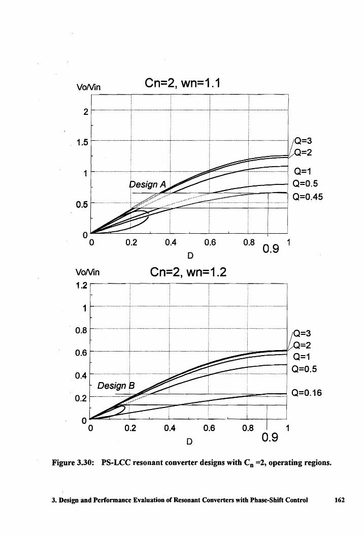
VoNin Cn=2, wn=1.1
2 ...... -.............................. ~ ....... -.................. · .... · .. · .. · .. + .. ·· .... ··· .. ·· .. · .... ······· .. · .. ···· .. l· .. · .. ······· .. ········· .. · .. ··········T···· .. · .. · .. ··············· .. · .. · .. · .. ···
1 .. ·· .... · .. ······· .... ···· .. · .. ······l······ .. · .. · .. ············· .............. ;. .................................. .
0.5
Q=1 --l----....., Q=0.5
Q=0.45
O~~~~--~--~--~--~~---L--~~
o
VoMn 1.2
1
0.8
0.2 0.4 0.6
D 0.8 0.9 1
Cn=2, wn= 1.2
i/Q=3 // =2 0.6 1 .. · .. _······· .. · .... ···· .. · .. ······1'··· .. ··· .. ··· .. · .. · .. ···· .. ··· ............ 1" ......................................... j ...................... -:::.::;;~::::::===r Q = 1
0.4 ~ ..................................... + ..... -............. " ....... -.......... ; .... ".~~ ............ ~ __ ~ .. " ........................ :" .. ·· .. ···· .. ······· .... ······· .. · .. · .. ···1
0.2
o o 0.2 0.4
D
0.6 0.8 1 0.9
Q=O.S
Figure 3.30: PS-LCC resonant converter designs with Cn =2, operating regions.
3. Design and Performance Evaluation of Resonant Converters with Phase-Shift Control 162

4. Effect of Switch Output Capacitance on
.Zero-Voltage Switching of Resonant Converters
4.1 Significance o/Switch Capacitance/or Zero-Voltage
Switching
Generally, bridge-type resonant converters can operate with ZVS without
increased voltage stress on the devices. However, ZVS topologies still suffer from higher
switch currents as compared to their pulse-width-modulated (PWM) counterparts. To
minimize the conduction loss, large MOSFET devices with inherently large output
capacitances are usually employed. In addition, lossless capacitive snubbers are often used
across the devices to reduce their tum-off losses and minimize undesirable ringing due to
parasitic inductances. As a result, the effective capacitance across the devices can be
relatively large, which significantly affects the operation of the converter.
4. Effect of Switch Capacitance 163

In analyses of resonant converters that assume ideal switches, ZVS operation is
predicted to occur whenever the switching frequency is above the resonant frequency of
the tank. However, it has been found that if the capacitance of the devices is sufficiently
large, ZVS cannot be achieved above resonant frequency because the energy in the
resonant inductor is not sufficient to discharge the output capacitance of the devices. This
is especially true for resonant converters designed to operate with a low Q-factor of the
res?nant tank at full load. For example, this is always the case in a properly designed LCC
resonant converter (LCC-RC), also called series parallel resonant converter (SPRC) [B-3,
B-7].
Therefore, the effect of switch capacitance on ZVS operation and voltage
conversion characteristics is of prime importance for a proper design of resonant
converters operating with low Q-factor.
The analysis presented in this paper predicts the operating conditions of resonant
converters at which ZVS is obtained as a function of the capacitance of the switches,
allowing the designer to make the right choice of switching devices and capacitive
snubbers. The inclusion of switch capacitance adds complexity to the analysis. Extra
resonant components have to be added ( switch capacitance), and two more topological
stages, corresponding to the switching transitions, have to be considered. Also, a
numerical algorithm has to be employed to generate the dc characteristics and to
determine operating regions with ZVS.
The analysis to be presented is experimentally verified on a LCe-RC.
4. Effect of Switcb Capacitance 164

Q1J Q4 J Vi
-+
Q3 J Q2 J
RESONANT
NElWORK Dr1 Dr4
Filter
Cor RI
LC
Dr3 Dr2
SRC PRC
CO Lo Lo
Co :;;: ~
LCC-RC
Co Lo
Figure 4.1: Resonant converter.
4. Effect of Switcb Capacitance 165

4.2 Analysis Including Switch Capacitance
Resonant converters have been analyzed previously by means of the conventional
approach, without taking the effect of switch capacitance into consideration. Several
methods of analysis are available for resonant converters [A-9, A-II, A-I4, D-I B-4]. The
approach used for the dc analysis presented in this paper is the time-domain analysis [A-9,
A-II]. This approach requires determining the sequence of topological stages of the
converter, formulating the differential equations in each case, and solving them by
matching the initial conditions at the beginning and the end of the period. This method is
very general and can be applied to any resonant converter. The main difficulty is that the
solution of the differential equations in most cases can be only solved numerically.
In this paper, the effect of the switch capacitance is analyzed for the SRC, PRC,
and LCC-RC. Figure 4.1 shows the general schematic for a resonant converter. The filter
stage is an LC filter for the PRC and LCC-RC, and only a C for the SRC. The analysis
including the switch capacitance results in two additional topological stages corresponding
to the switching transitions. In these two stages the switches' capacitances are modeled as
a capacitor Csw ' For a full-bridge topology, Csw corresponds to the total capacitance
across one of the switches, including the output capacitance of the MOSFET1s, Coss, plus
any external capacitor added as a lossless snubber. The capacitances across QI and Q2 are
in parallel, and their equivalent capacitance is in series with the equivalent capacitances
across Q3 and Q4 which are in parallel.
4. Effect of Switch Capacitance 166

In the analysis, C sw is assumed to be a linear capacitance. This assumption is
only valid if snubber capacitors much larger than Coss are added across the switches.
Otherwise, if only the switch capacitance is present, the value of the linear capacitance
Csw is chosen so that it stores the same charge as the actual nonlinear Coss .of the
switches at the operating voltage:
C - 2 C(at,'Vrn) sw - . oss
The differential equations are solved using a numerical algorithm. The equations
are normalized with respect to the following normalization factors:
- resonant frequency
1
where Co corresponds to Cs for the SRC, to Cp for the PRC, and Cs . cp /( Cs + Cp ) for the
LCC-RC.
- current and voltage normalization factors,
where Zo = ~ Lo I Co .
The switch capacitance is expressed as
for the SRC and LCe, and as
4. Effect of Switch Capacitance 167

forthePRC.
4.2.1 Analysis of the SRC Including Switch Capacitance.
Figure 4.2 shows the equivalent circuit representation used in the analysis; Ve
takes the values shown in the table in Fig. 4.2, according to the devices that are
conducting. Between switching intervals the circuit for mode I is used for the analysis,
while the circuit for mode II is used for the converter operation during the switching
transitions. Figure 4.3 shows the typical waveforms for the SRC, indicating the
topological modes corresponding to each interval of the switching period.
The equations describing current and voltages in topological mode I are:
n (onl Vn) ( ) ·onl . ( ) Vn) V c = V c - e • cos co 0 t + 'L . sin co 0 t + e (4.1)
ir = (_v~nl + v~). sin(ro ot) + i~nl. cos(ro ot) (4.2)
The equations corresponding to mode II are:
vn = 1· .(c vonll _ vonll + Vn) + 1 . (Vonll + vonll _ Vn) .cos( t~1 + C ) + c 1 C sn c sw e C c sw e O}o sn
+ ~ 1+ ~
+ 1 .fnll.sin(w t '1+C) (4.3) ~1+Csn L a V ~
vn = Csn _(_vonll + V:' +vnJ+ Csn . (vonll +vonJf -Vn)-cos(c.o t~l+C )+ sw C c eel C c sw e 0 sn
1+ sn sn + ~
+ Csn . ionll. sin(c.o t '1 + C ) (4.4) ~1+Csn L 0 V sn
4. Effect of Switch Capacitance 168

Ve
Mode I Cs
+
La
Topological
mode
I
I
n
I
I
n
Conducting
on Print.
QI-Q2
QI-Q2
none
Q3-Q4
Q3-Q4
none
Figure 4.2: SRC topological modes.
4. Effect of Switch Capacitance
Mode II
Ve
Conducting Ve
on Sec.
Dr3-Dr4 +Vj+Vout
Drl-Dr2 +Vi-Vout
Drl-Dr2 +Vi-Vout
DrI-Dr2 -Vi-Vout
Dr3-Dr4 -Vj+Vout
Dr3-Dr4 -Vi+Vout
169

Vt
o
t t t t t Mode II Mode I Mode II Mode I Mode II
Figure 4.3: SRC typical waveforms, indicating tbe topological modes, for
operation above resonant frequency.
4. Effect of Switch Capacitance 170

-n 1 (onll onll Vn) . _f t Ie) -onll (t Ie) IL = . - V c - V sw + e . Slrl\<O 0 ,,1 + sn + IL • cos CD 0 ,,1 + sn ~l+Csn
(4.5)
where ven and iLn, are the normalized capacitor voltage and inductor current; vc°nI, vc°nII,
iL onI, and iL onIl, are the initial values for the voltage and current at the beginning of the
interval corresponding to each mode.
4.2.2 Analysis of the PRe and LCC-RC Including Switch Capacitance.
Figure 4.4 shows the equivalent circuit representation used in the analysis; Ve
and Ie take the values shown in the table in Fig. 4.4, according to the devices that are
conducting. Between switching intervals the circuit for mode I is used for the analysis,
while the circuit for mode II is used for the converter operation during the switching
transitions. The circuit for mode III corresponds to the discontinuous capacitor voltage
operation. Figure 4.5 shows the typical waveforms for the PRC and LCC-RC, indicating
the topological modes corresponding to each interval of the switching period. The only
difference in this case is that for the PRC, Cs is not considered, or is assumed large
enough so that it does not affect the converter operation.
The equations describing topological mode I for the PRC are:
n (onl Vn) ( ) (.onl In) 'n{ ) Vn V c = V c - e ,cos CD 0 t + 'L - e . SI CD 0 t + e (4.6)
(4.7)
4. Effect of Switcb Capacitance 171

Ve
Ve
Model Cs
Mode II
Lo
Cp
Csw Cs Lo
Topologkal
mode
I
I
II
ill
I
I
II
ill
Conducting
on Prim.
QI-Q2
QI-Q2
none
QI-Q2
Q3-Q4
Q3-Q4
Q3-Q4
Q3-Q4
Mode III Cs
Ve
Conducting Ve
on Sec.
Dr3-Dr4 +\'i
Drl-Dr2 +Vi
Drl-Dr2 +V~ I
all +y..
I
Drl-Dr2 -y..
I
Dr3-Dr4 -Vi
Dr3-Dr4 -y..
I
all -y..
I
Figure 4.4: PRC and LCC-RC topological modes.
4. Effect of Switcb Capacitance
Lo
Ie
-lout
+Iout
+Iout
short
+Iout
-lout
-lout
short
172

a)
t t t t i Modell Model Modell Model Modell
b)
Vt '"
t Modell
r u~ou~: r t ~Modell
I UMAil~: r t ~Modell
Model Model
Figure 4.5: LCC-RC typical waveforms, indicating the topological modes, for
operation with: a) continuous capacitor voltage, and b) discontinuous
capacitor voltage.
4. Effect of Switch Capacitance 173

The equations corresponding to mode II are:
Vn onll n on II e - V c ( (~ C)) 1 ·onll ·_f t~ C ) v c = V c + . 1 - cos co 0 t I + sn + . IL . Sir, co 0 1 + sn -
l+Csn .Jl+Csn
where v~, and ir, are the normalized parallel capacitor voltage and normalized inductor
current, respectively. The values v~nl, v~nll, i~nl and i~nll, are the corresponding initial
values at the beginning of topological modes I and II.
The equations for topological mode III are:
(4.11)
in - jonlll + Vn . t L - L e COo , (4.12)
where irnlll , is the inductor current at the beginning of topological mode III.
For the LCC-RC the equations can be expressed as a function of the ratio of the
series and the parallel capacitors, defined as
4. Effect of Switch Capacitance 174

and using for Ve and Ie the values shown in the table of Fig. 4.4.
The equations describing topological mode I for the LCC are:
+ ~. i~nl. sin(root) + ~ .(1- cos(root)). V~ + en 2' [ro ot - sin(ro ot)].I~ r 1 + n 1 + n (1 + en)
(4.13)
i~ = -'v~l. sin(root) - v~~I. sin(ro at) + i~nl. cos(ro at) +
+V~ . sin(root) + ~ .(1- cos(root))·I~ (4.15) 1+ n
where v~, v~P' and ir, correspond to the normalized voltage for the series and parallel
capacitors and normalized inductor current, respectively. The values v~~I, v~~I, and irl are
the corresponding initial values at the beginning of topological mode 1
4. Effect of Switch Capacitance 175

The equations for topological mode II are obtained from the equations for mode
I by replacing Cs with Cs + Csw ' After substitution and simplification,
(4.16)
n 1 Cp [AA N' onll Cn 1 n] on (4 V =-.--- N-cosat+BA -Slna -v +2·1t---· ·t·1 +v -1 sw t c:s ne sw . . 2 Csw I+Cn l+Cn +Csn
n C (nil nil) en t In d Vep = n' Ves -Ves -2-1t· . n' e' an
l+Cn
(4.18)
where
t V~IJ + vg~1I + 2 . V~" -1 AAN = ---~----
1+Cn +Csn '
·on BAN = (
~(1+Cn)·(1+Cn +Csn)'
CAN = 1+vg~ -2- V~ +AAN,(Cn + Csn},
and T sw is the switching period.
The equations for topological mode III are:
(4.20)
4. Effect of Switcb Capacitance 176

n - 0 Vcp - ,
where ad = ( ~11 ( 1 + Cn) ) . (00 • t.
(4.21)
(4.22)
The equations for the three topological modes can be solved numerically for each
set; of operating conditions. The dc conversion characteristics are obtained by integrating
the parallel capacitor voltage v~p.
4.3 Effects of Switch Capacitance
Resonant converters operate with zero-voltage switching (ZVS) if the switches
are turned on after their output capacitance is completely discharged. This requires the
inductor current to be exactly zero at the instant of switching, after discharging the
switches' output capacitance, or to have current flowing through the anti-parallel diodes of
the MOSFET's that are about to be turned on.
4.3.1 EtTects of Csw on the SRC
For ideal switches, Coss=O and with no external snubber capacitors, the ZVS is
achieved at any frequency above the frequency that corresponds to the peak of the voltage
gain for given Q (Q = Zo/Rload)' Figure 4.6 shows the dc voltage gailt characteristics of
the SRC with ideal switches.
Figures 4.7a and 4.7b show the voltage gain characteristics for different switch
capacitance values. Also the region where the converter operates with zero voltage
4. Effect of Switcb Capacitance 177

switching for the switches in the bridge is shown in each case. Two major effects can be
noticed:
• The voltage gain decreases when Csw increases, and this is more pronounced for
low Q values.
• The ZVS can only be achieved at frequencies higher than the resonant frequencies.
The frequency has to be higher when Csw increases, and it changes more for the
low Q values. No ZVS operation is possible for the lower Q's; for instance no ZVS
operation is possible for Q<0.75 for CswfCs=0.2.
4.3.2 Effects of Csw on the PRC
F or ideal switches, Coss =0 and with no external snubber capacitors, the ZVS is
achieved at any frequency above the frequency that corresponds to the peak of the voltage
gain for given Q (Q = R1oad/Zo )' Figure 4.8 shows the dc voltage gain characteristics of
the PRC with ideal switches.
Figure 4.9 shows the dc characteristics for different values of switch capacitance,
with the ZVS limit for ideal switches and the new one. It can be seen that the voltage gain
is almost unchanged when including the switch capacitance. However, the ZVS limit is
pushed to higher frequencies. Since the dc characteristics are not changed, all ZVS limits
can be shown on the same graph. Figure 4.10 shows different ZVS limits corresponding to
several Csw'
4. Effect of Switch Capacitance 178

1
0.8
0.6
M· 0.4
0.2
o 1
0=5.0
1.2 1.4 1.6 1.8 2
fsw/fo
Figure 4.6: Dc characteristics for the SRC with ideal switches. ZVS operation for
all frequencies above the resonant frequency, (fsJfo}>l.
4. Effect of Switch Capacitance 179

a) Csw/Cs=O.1 1......,...-----,---------,.-------,------.
0.8
o. 6 t--............... \-... -.... -.... , ............ ~,-.-............... ~.-.-... r-
M 0.4 "'······· .. ····r-······· .... ·······;.·-, .. ·· .. ·········~ .. · .. ·-·J···· .. ·················· .. ·······f···Q=·.1.~Q···· .. ···
o. 2 ··· .. ·· .. ····· .... ·· .. ·········T········ .. · .. · .. · .. · .... ·· .... ····,. ...... .
0=5.0
o~-~--~--~--~-~
1 1.2 1.4 1.6 1.8 2
b) Csw/Cs=O.2 1 ~-~-----,----~--~--~
0.8 " ......... :, .... ~ , ......... +~O':':" ................. -.,~ .. /-.. , .......... -............... ~ .......... -....................... .
Q=0.5
0.6 .... .... · ...... i ......... ·-·· ...... ···tQ=O~75 .... ··
M 0.4
o. 2 ··· ........ · .. ····· .. ···· .. ··· .. ;···· .. · .. ·········· ...... ··· .... · .... i .... ;::0",..... ~··· .. •• .... , .. ····-··· .. i .. ·· .... ··· .. ·· .. ··· .. · .... ··· .. ·· .. ·j· ............ · .. •·• ...... · .. •·· ...... ·1
, 0=5.0
OL...-------J..------l..--------l....-----...i.-------' 1 1.2 1.4 1.6 1.8 2
fsw/fo
Figure 4.7: Dc characteristics of SRC, for different values of Csw-
4. Effect of Switch Capacitance 180

zvs
3
1
o 0.6 0.8 1 1.2 1.4 1.6 1.8 2
fs/fo
Figure 4.8: Dc characteristics for the PRe with ideal switches.
4. Effect of Switcb Capacitance 181

, Csw/Cp=O.1 a)
4
3
M
2
1
o 0.6
b) Csw/Cp=O.2
4
3
2
o 0.6
0.8 1
0.8 1
1.2
1.2
fs/fo
1.4 1.6
1.4 1.6
Figure 4.9: Dc characteristics of PRC, for different values of Csw•
4. Effect of Switch Capacitance
1.8 2
1.8 2
182

4
3
2
1
0.6
ideal 10 5
• _. m ..................... 3 ............ -._._ .... _ .............. -.-................. -....... -.......................................... -.-.......... .
1 1.2 1.4
fs/fo
Figure 4.10: Dc characteristics of an ideal PRC, for different values of Csw.
4. Effect of Switch Capacitance 183

4.3.3 Effects ofCsw on the LCC-RC
For ideal switches, Coss=O, and with no external snubber capacitors, the ZVS is
achieved at any frequency above the frequency that corresponds to the peak of the voltage
gain for a given Q (Q = Rload/Zo), as is the case for the PRC. Figure 4.11 shows the dc
voltage gain characteristics of the LCC-RC with ideal switches for Cn=I with the ZVS
regions indicated.
The next subsections discuss the effect of switch capacitance on the dc
characteristics of the LCC-RC for different values ofCn and Csn.
A) Effects of Csw at Constant Cs/Cp
Figures 4 .12( a)-( c) show the dc gain characteristics of the LCC-RC for different
ratios of series capacitance Cs to switch capacitance Csw, ie., for Csn equal to 10, 4, and
1, respectively. Also the regions with ZVS operation are indicated in each graph. As can
be seen, the ZVS range shrinks for larger switch capacitance because the ZVS boundary
moves towards higher frequencies (away from frequencies for which the voltage gain is
maximal for a particular Q). In addition, larger switch capacitances reduce the voltage
gain, particularly the peak voltage gains for lower values of Q. Consequently, a wider
frequency range is required to regulate the output voltage of the converter against line and
load variations. For very large Csw, as for example in Fig. 4 .12( c), ZVS is also lost at high
frequency, especially for lower values ofQ. In fact, in Fig. 4.12(c) no ZVS operation is
achievable for Q::;; 0.25.
4. Effect of Switcb Capacitance 184

zvs 3
2
M
1
o ~--~----~----~----~--~----~----~--~ 0.8 1 1.2 1.4
fs/fo
Figure 4.11: Dc characteristics of an ideal SPRC
4. Effect of Switch Capacitance 185

a) 3.5 NO~ CslCp=1.0
3 CslCsw=10.0
2.5 Q=:1.5
M 2
1.0 1.5 "·0:75······_· ..
O.SO
0.25
0.5
0 O.S 0.9 1.1 1.2 1.3
fslfo 3.5
b) Nq,ZVS ZVS CslCp=1.0
3
a=;.5 CslCsw=4.0
2.5
2 M
1.5
0.5
0 O.S 0.9 1.1 1.2 1.3
fslfo c) 3.5
N9 ZVS ZVS
3 ... -.................. " ........ ~ .................................. ) ................................. . CslCp=1.0
CslCs1A=1.0
2.5
2 M
1.5
0.5 . . ~~"~~~~-i--~~ .. · .. · .. ······· ....... · .. · .. · .. ··,.,··· .... ··· .. · .. O:2fi'· .. ···· .. F"_ .... _ ...... _ .. ~_..:...
NO!ZVS o ~--------------~--------~------~------~ 0.8 0.9 1.1 1.2 1.3
fslfo
Figure 4.12: Dc characteristics of SPRC for Cn=Cs/Cp=1 and: a) Csn=Cs/Csw=10,
b) Csn=4, and c) Csn =1.
4. Effect of Switch Capacitance 186

a)
M
b)
M
3 NOZVS
2.5
2
0=1.5 1.5 !--.................................. j ...... ,.J1II'1
0.5
0 0.7
3
1.0 0.75
.. 0.50. ................... .
0.25
0.8
NOZvS
0.9
,ZVS
fslfo
ZVS
2.5 ....................................... ; ............................................ ; ....................................... .
0=1.5 2
1.5
CslCp=2.0
CslCsw=10.
1.1 1.2 1.3
CslCp=2.0
CslCsw=4.0
0.5 ...... - ..................... ~..... ""'-"=.o .. · .... · .... ·· ....... ····· .... ' .... ··· .... · .. · .. ··== .. r----..~=~ 0.25
o 0.8
c} 3
M
2.5
2
1.5
0.5
o 0.8
0.9
NO
0=1.5
1.0
0.75
0.9
1.1 1.2 1.3 fslfo
CslCp=2.0
CslCsw=2.0
O.SO
Nqzvs
1.1 1.2 1.3
fsJfo
Figure 4.13: Dc characteristics ofSPRC for Cn=2 and: a) Csn=10, b) Csn=4, and c)
Csn=2.
4. Effect of Switch Capacitance 187

al 5 ~------~-------r--------~--------------~
NOzv,S ZVS CsJCp=O.5
4 .................... _ ............. ,............................. .. CsJCsw=10. I Q=1.5
3
M
2
0.25 i
o ~------~------~--------~------~------~ 0.8 0.$ 1.1 1.2 1.3 fslfo
b} 5 .-------~------~--------~--------------~ NO~S
CsJCp=0.5
4 ...... _ ............ _ ....... _ .................. _ .... _ ........... . CsJCsw--4.0
IQ=1.5
3 .................... -............. ,. ............ -.-.-..........
M I 1.0
2
0 0.8 0.9 1.1 1.2 1.3
fslfo c) 5
N9 ZVS ZVS CsJCp=0.5
4 CslCsw=1.0
Q=1.5
3
M
2
°0.~8-------0~.9~------~------~1~.1------~1.~2------~1~
fsIfo
Figure 4.14: Dc characteristics of SPRC for Cn=O.5 and: Csn=10, b) Csn=4, and c)
Csn=1.
4. Effect of Switch Capacitance 188
B) Effects of Csw for different Cn= Cst Cp
To analyze the effect of Csw for different values of Cn, Figs. 4.13 and 4.14 show
sets of dc characteristics for Cn= 0.5 and Cn= 2, respectively. As can be seen by
comparing Figs. 4.12, 4.13, and 4.14, the effect of switch capacitance is more pronounced
for larger values of Cn (larger values of Cs), i.e., when the converter behaves more as a
series-resonant converter (SRC). On the other hand, larger values of Cp that make the
converter behave more as a parallel-resonant converter (PRC) diminish the effects of
switch capacitance. In both cases, however, the ZVS range decreases and the peak dc
voltage gain reduces as the switch capacitance is increased. For example, for Cn = 2 and
Csn = 2 (Fig. 4. 13(c», ZVS is completely lost for Q<0.5, while for Cn = 1 and Csn = 1
(Fig. 4.12(c)), ZVS is lost for Q<O.25.
For larger values ofCn (larger Cs, smaller Cn)the LCC-RC behaves like an SRC,
and for lower values of Cn (smaller Cs, larger Cp) like a PRC. The effect of the switch
capaCitance is perfectly consistent with this property of the LCC-RC. For the same Csw
ZVS requires operation at higher frequency for the LCC-RC with large Cn values. Also
the sensitivity of the voltage gain characteristics to Csw is higher for large Cn, as it is for
the SRC.
4.4 Experimental Verifications
To verify the analysis, a prototype LCC-RC has been designed with the following
specifications:
4. Effect of Switch Capacitance 189

• input voltage range from 40 to 60 V,
• output voltage 10 V,
• output power 50 W, and
• minimum switching frequency 900 kHz.
The converter was designed following the guidelines described in chapter 2.
According to the guidelines, the optimal design of a LCC-RC requires that the full-load,
low-line operating point is selected with a low Q (Q ~ 0.5) and for Cn ~ 1. For the
experimental converter, Cn = 1 is selected, and the full-load, low-line operating point is
placed on the Q = 0.5 curve. The required turns ratio of the transformer for this selection
of the operating point is n = NplNs = 4, and the resulting resonant components are: Cs =
4.7 nF, Cp = 73 nF (secondary side), and L = 9.2~.
To examine the effect of switch capacitance, two devices with significantly
different values of Coss were used for the primary switches. Figure 4.15, shows the
operating region of the converter when IRFP240 devices (RDSon = 0.18 n, Coss = 350
pF at 25 V) are used. Note that for the dc characteristics in Fig. 4.15, esn = 10, which is
close "to the value of the ratio for the series resonant capacitor (Cs = 4.7 nF and the output
capacitance of IRFP240 (Coss = 350 pF). As can be seen from Fig. 4.15, the operating
point A (Vin = 48 V) is within the ZVS region. Figure 4.16 that shows the oscillograms of
the gate-drive signal, drain-to-source, and current for one of the switches of the
experimental circuit with the IRFP240 devices confirms this result.
4. Effed of Switcb Capacitance 190

3.5 r-----....,......-----j~---__r_-------___,
NO jZVS...--.....J-+--IIoo-ZVS
3 ._._ .............. _.-._ ......... , ..... _._._._ .............. "._ ... , .. '\ ........... _._ .................. _._ .... i
2.5
Q=1.5
M 2
1.0
1.5 0.75
0.50
0.25
0.5
Cs/Cp=1.0
Cs/Csw=10.0
o ~----~----~---~-----~---~ 0.8 0.9 1.1 1.2 1.3
fs/fo
Figure 4.15: Dc characteristics for Csn=10.
4. Effect of Switch Capacitance 191

Vgs
20 V/div.
Vds
20 V/div.
lLo
2 Aldiv.
200 nsee/div.
Figure 4.16: Voltage and current waveforms of switch Ql, with ZVS operation.
4. Effect of Switch Capacitance 192

Figure 4.17 shows the operating region of the converter when IRFP150 devices
(RnSon = 0.055 n, Coss = 1 nF at 25 V) are used. For the dc characteristics in Fig. 4.10,
Csn = 4 corresponds to the Csn of the experimental converter with the IRFP150's. The
operating point for Yin = 48 V (point B in Fig. 4.10) in this design is in the region where
ZYS 'is lost. The oscillogram in Fig. 4.18 verifies this finding. As can be seen, the voltage
across the device peaks before reaching the input voltage, and consequently, the
antiparallel diode is not turned on before the device starts conducting. The loss of ZYS
results in increased switching losses and increased voltage ringing across the devices.
4.5 Summary and Conclusions
An analysis of the resonant converters (SRC, PRC and LCC-RC) operating
above resonant frequency that includes the effects of the capacitance of the primary
switches is presented. It was shown that switch capacitance has significant effects on the
dc voltage-conversion ratio characteristics and the zero-voltage-switching range of the
converter.
The SRC is the most sensitive of the three, with significant changes in the ZVS
range and voltage gain. The PRC is the least sensitive, with negligible changes in voltage,
but still changes in the ZYS range.
For all three converters the effects are especially pronounced for lower values of
the Q-factor of the resonant tank and higher ratios of the series to' parallel resonant
capacitors. Since the optimal design of the LCC-RC requires operation at lower values of
Q, the results of the analysis are extremely useful in design optimization of the LCC-RC in
4. Effect of Switch Capacitance 193

the presence of a significant capacitance across the primary switches, either because of a
large' output capacitance in the devices or an intentionally added capacitance of lossless
capacitive snubbers.
The analysis is verified experimentally on a 50 W, 900 kHz LCC-RC converter.
4. Effect of Switch Capacitance 194

3.5 ...,-------,-----_-----t"--------_
M
3
2.5
2
1
~o ZVS-4--+--...... ZVS
a=r·5
Cs/Cp=1.0
CS/C5W=4.0
0.5 J-.. -.... , ..... '"".-.-.-., ............... ~-.- .... -............ -.-....... - .... ;~"' .. -...................................... ;. .......... -."., ....... , ... :::'!'!'!oooo"""""".
o ~----~----~----~-----~---~ 0.8 0.9 1 1.1 1.2 1.3
f5/fo
Figure 4.17: Dc characteristics for Csn = 4.
4. Effect of Switch Capacitance 195

, Vgs
20 V/div.
Vds
20 V/div.
ILo
2 Aldiv.
200 Dsec/div.
Figure 4.18: Voltage and current of switch Ql, without ZVS operation.
4. Effect of Switch Capacitance 196

5. Phase-Shifted Full-Bridge PWM Converter
with Active Clamp
5.1 Introduction
The research and application of zero-voltage switching (ZVS) for the class of
PWM converters is gaining increasing attention, as this converter family combines the
simplicity of PWM converters· with the soft-switching characteristics of resonant
converters. The member of this family that is most widely used, especially in high-power
and high-voltage applications, is the ZVS full-bridge (FB) PWM converter [G-6, G-ll, G-
17 ]. This converter is controlled by the phase-shifted PWM technique which enables the
use of all parasitic elements in the bridge to provide ZVS conditions for the active
switches.
When conventional PWM converters are operated at high frequencies, the circuit
parasitics have detrimental effects on the converter performance. Switching losses are
5. Phase-Shifted Full-Bridge PWM Converter 197

especially pronounced in high-power high-voltage applications. Snubbers are required,
thus adding significant losses in high-frequency operation. In the conventional full-bridge
PWM converter, the diagonally opposite switches (QI and Q2, or Q3 and Q4) are turned
on and off simultaneously, as shown in Fig. 5.1. When all four switches are turned off the
load current freewheels through the rectifiers, and the energy stored in the leakage
inductance of the power transformer causes severe ringing with FET junction
capacitances.
To minimize the parasitic ringing, the gate signals for Q2 and Q4 are delayed
(phase-shifted) with respect to those ofQl and Q3, so that the primary of the transformer
is either connected to the input voltage or shorted. The leakage inductance current is
never interrupted, thus solving the problem of the parasitic ringing associated with the
conventional full-bridge PWM converter. Furthermore, the energy stored in the leakage
inductance can be used to discharge the energy stored in the FET junction capacitances to
achieve ZVS conditions for all four switches in the primary side. The converter requires
no additional resonant components; Fig. 5.2 shows the topology of the converter and the
gate drive signals required.
The current stress for the bridge is larger than for the conventionally operated
PWM full-bridge, but it provides low-loss switching and reduced ringing amplitude in the
prjrnary switches, together with a less restricted design of the power stage transformer,
which may have a significant leakage inductance without detrimental effects on the
converter performance.
Summarizing the main features of the ZVS-FB-PWM converter [G-17] are:
s. Phase-Shifted Full-Bridge PWM Converter 198

• PWM control at a fixed frequency.
• ZVS for the active switches with much reduced switching stress, switching
losses and EMI.
• A minimal number of components.
• The internal diodes of the MOSFET's can be used since fast recovery diodes
are not required in the bridge.
• The leakage inductance in the transfonner is used to provide the ZVS.
These advantages, however, are accompanied by the following disadvantages
with respect to a conventional FB-PWM converter:
• The rms currents in the bridge are increased due to the presence of circulating
current components.
• The effective-duty-cycle range is reduced as the leakage inductance of the
transfonner increases in order to attain ZVS.
5. Phase-Shifted Full-Bridge PWM Converter 199

01
Vi
Q3
J 03 Uk Q2 J
Lf
Rload
Q1 I ~
Q2 -- ! Q3
-Q4
o (TsI2)
V AS
o .. _._._ .. r--- -.... -................ --...... -............... -- ......... -............................. --......... r--- .-........ ..
-
Figure 5.1: Conventional full-bridge PWM converter topology.
5. Phase-Shifted FuB-Bridge PWM CODverter 200

Vi
Q3
J 02
Lf
Cf Rload
Q1 -Q2
--Q3 i
Q4
o (Ts/2)
v AB
o ............ r--- .................................................... - ........................................................ 1....-_
-Figure 5.2: Full bridge ZVS PWM converter topology.
s. Phase-Shifted Full-Bridge PWM CODverter 201

5.2 Operation Principle
Figure 5.3 shows the waveforms of the primary voltage and current and the
secondary voltage, highlighting their main characteristics. The converter operation for a
half cycle is described as follows:
tl to tl: In the primary, Q4 and DI are conducting. In the secondary Dc and Dd are
conducting. The primary current follows the output filter current.
tl-: Switch Q4 turns off, and the current through the primary of the transformer
charges the output capacitance of Q4 and discharges the output capacitance of
Q2, turning on the diode D2.
tl: Diode D2 starts conducting, Q2 can be turned on with virtually no voltage
applied (only the forward drop of the parallel diode), (Fig. 5.3.1).
tl to t3: The primary current circulates through diodes D 1 and D2. The secondary of the
transformer is shorted by the diodes of the rectifier stage. (Fig. 5.3.2.).
t3 to t4 The primary current circulates through Q 1 and Q2. The secondary of the
transformer is shorted. (Fig. 5.3.2.).
t4 to tS: The voltage in the secondary of the transformer starts increasing, and the leakage
inductance of the transformer starts resonating with the diodes' capacitance. (Fig.
5.3.3.).
5. Phase-Shifted Full-Bridge PWM Converter 202

Vi
Ip 11
o
o
01
03
J 03
slope =
t1 t2 i
02
Uk J
Vi-Yo If
02
i t4 t5
Lf
~
If
? .... -....... , .• " ....... --~ ..• ,-.-,' ....... , ... ~ ........... -., .......................................................... - .....
01 02
..YL Uk
Q1Q2 ~Q2 03
03 D4
Cf Rload
V AS /
/
Q3Q4
_V......o._\ ______ 1 ...... _ ............................................. 1 I -_... __ .. '_ .. _ .. ,- --------....
Figure 5.3: Circuit topology, primary current and voltage, and secondary voltage.
5. Phase-Shifted Full-Bridge PWM Converter 203

ts-: Switch Q 1 turns off and the current through the primary discharges the output
capacitance of Q3 and charges the output capacitance of Q 1. When Q 1 turns off,
the current through the primary of the transformer is the output current reflected
to the primary. The energy of the output filter inductor is used to achieve ZVS,
and therefore ZVS is easily attained for switches Ql and Q3.(Fig. 5.3.4)
ts: Diode D3 is turned on. After D3 starts conducting, Q3 can be turned on with no
voltage applied across it (Fig. 5.3.5).
In summary, the switching conditions for the switches are:
• Q2 and Q4 tum on with ZV when the energy stored in the leakage inductance
is enough to discharge their output capacitances.
• Q 1 and Q3 tum on with ZV over a range that is always larger than that of Q2
and Q4, because the energy in the output filter inductor is used to discharge
the switches' capacitance.
s. Phase-Sbifted Full-Bridge PWM Converter 204

Vi
Ip
11
o
o
1
Q4 turns off
(Q2tums on)
01 01 01Q2
Q4 02
Figure 5.3.1: Current path when Q4 is turned otT.
s. Phase-Sbifted Full-Bridge PWM Converter
02 03
Lf
: f B
: J
03 D4
Sinusoidal charge
4 diodes conducting
Rload
V AB
/ Q3Q4
205

o
Vi
03
J
Llk is charged current switches from
01-02 to 01-02
i !
;._ .... _ ........... ...-__ J ..................................... _ ............................ ..
01 Q4
01
02
!
Vi
Llk
Q1 Q2
Figure 5.3.2: Current path when Dl is conducting.
s. Phase-Shifted Full-Bridge PWM CODverter
D4
D2
Q2
D3
Lf
03 tu
4 diodes still conducting
Rload
V AS
/ Q3Q4
206

Vi
03
J
Voltage builds up in the secondary
(filter inductor gets charged)
slope = Vt-Vo
Ip 11
u
D4
02
Lf
o ,.-....... -......... r---+ ....... ~J-......... , ........... -........................ -.-............... -.-.. ~-...,. !
Q1 Q2 Q2
! 03 D3 D4
Cf
V AB
/ Q3Q4
O ;.~.~.~._ ........ r--_V_S \ ___ 1.----------J..-1 __ ----I-.~._ ............... _._._._ ............ .
W
Figure 5.3.3: Current path when Ql and Q2 are conducting.
5. Phase-Shifted FuU-Bridge PWM Converter
Rload
207

Vi
o
04
02
Linear charge Lf
Q1 turns off
(Q3tumson)
Voltage drops in the secondary
,· .. ······· .. ······ .. ..------+ .... · .. ·,·1····· .. • .. ., .. ··· .. • .... ···•• .. •· .......... _ ............................ .-.--,
01 Q4
01 02
;
Q1Q2 Q2
jD3 i i
03 D4
V AS
/ Q3Q4
Rload
O ; .................... ,..---Vs \-----Lf.m ....... m .. _._._ .. ____ 1 ----tl ....................................... . U .
Figure 5.3.4: Current path when Ql is turned otT.
5. Phase-Shifted Full-Bridge PWM CODverter 208

04
Vi
D2
Lf
Primary voltage clamped to zero
-Vo
Ip i""~~~:::.~:::::::::::~.:~:::,::'~::::',:":::~::~::::~:::::===:.:::=:;;:;.::;;.:.;~ __ ... L ... f ~ 11 :, ....
o ; ......... , .... , .. , ... ..----' ... " ... ,,# ..•.. , .. , .•.......•.•... , ....•• " ..... ,." ............ , ...................... - ... i
01 Q4
01 02
,
Q1Q2 Q2
os
Figure 5.3.5: Current path when Q2 and D3 are conducting.
5. Phase-Shifted Full-Bridge PWM Converter
D3 04
Rload
VAS
/ Q3Q4
209

5.3 Converter Analysis
5.3~1 Conditions for Zero-Voltage Switching
The FB-ZVS-PWM converter provides ZVS for all four switches in the bridge.
However, the mechanism by which ZVS is achieved is different for both legs of the bridge.
For transistors Q2 and Q4, the ZVS is provided by the resonance between the
leakage inductance, Llk, and the output capacitance of the switch. Figure 4.4 shows the
waveform of the current through 02-Q2 and the rising edge of the transformer primary
voltage waveform for different operating conditions.
Before Q2 is turned off, the current in the primary is flowing through the diode
03 and transistor Q2. The primary voltage is clamped to zero, and the value of the of the
priI;nary current is equal to the reflected filter-inductor current. When Q2 turns off, the
current through the primary reduces rapidly. This causes the filter-inductor current to start
freewheeling through the rectifiers. The energy stored in the primary leakage inductance
turns on diode D4. In order to tum on 04, the output capacitance of Q4 has to be
discharged first and the output capacitance of Q2 charged up to the input Voltage. The
energy available for charging the output capacitances of Q4 and Q2 is the energy stored in
Llk when Q2 is turned off. The transformer winding capacitance across the primary
winding also has to be charged in the process. To accomplish this, the following inequality
has to be met:
(5.1)
5. Phase-Shifted Full-Bridge PWM Converter 210

where 12 is the current through the primary when Q2 turns off, Yin is the input voltage,
Llk is the transformer leakage inductance, CMOS is the output capacitance of the switch
at Yin, and 4r is the transformer winding capacitance. The term ~.CMOS· v~ corresponds
to two times the energy stored in the nonlinear drain-to-source capacitor, whose
capacitance is inversely proportional to the square root of the voltage.
The resonance between Llk, CMOS, and Ctr provides a sinusoidal voltage across
the capacitances that reaches a maximum at one fourth of the resonant frequency period.
The dead time between Q2 and Q4 has to be set at o'tmax. to ensure that there is sufficient
time to charge/discharge the capacitances. The dead time required to ensure ZVS with the
maximum possible load range can be determined by the following equation:
T 7t ~ &tmax = - = ."L1k·C 4 2
(5.2)
Figure 5.4 presents the voltage across the transistor Q2 at turn-off. In the first
voltage waveform, the energy in Llk is equal to the energy required to charge the
capacitances. In the second voltage waveform, the energy in Llk is larger than the energy
required to charge the capacitors. The switch output capacitance is charged in less than
O'tmax, and the voltage is clamped to the input voltage. In the last voltage waveform, the
energy in Llk is not enough to charge the output capacitances, and ZVS is lost after the
dead time, o'tmax.; Q4 (or Q2) is turned on; and the voltage increases immediately to Yin.
5. Phase-Shifted Full-Bridge PWM Converter 211

Lf
04 turns off (02 tums on)
Ip ~ ........ " ................ _ ...................................................... ~=....-__ 11
o
iD1
;04
RISING EDGE DETAIL
V
jAa
Vi
.-GL Uses only energy in Llk
: 1 B Sinusoidal charge
4 diodes conducting
Rload
Vi Vi
.j=
Figure 5.4: Current through switch Q2 and voltage rising edge for different load
conditions.
5. Phase-Shifted Full-Bridge PWM Converter 212

Whether ZVS can be achieved for Q2 and Q4 is dependent on the load level of
the converter. For light loads, the current through Llk, when Q2 or Q4 are turned off, may
not be enough to tum on the antiparallel diode.
F or switches Q 1 and Q3, ZVS is provided by a different mechanism. Before Q 1
is t~rned off, the current in the primary is reaching its peak value. The primary current is
the filter inductor current reflected to the primary. When Q 1 is turned off, the energy
available to charge the output capacitance of Q 1 and discharge the output capacitance of
Q3 is the energy stored in Llk and the energy in the output filter inductor. This energy in
the output filter inductor is available because the filter inductor current does not freewheel
. through the rectifier until the voltage across the secondary has fallen to zero.
Since the energy in the filter inductor is large compared to the energy stored in
the capacitances in the primary, the charging of the switches can be approximated by a
linear charging with a constant current. Consequently, the dead time Ot'l, required
between the turn-off of Q 1 and the turn-on of Q3 can be determined from the equation
(5.3)
where the term 4·CMOSVin, corresponds to twice the charge stored in the nonlinear
output capacitance of the MOSFET, and Ip is the peak current in the output filter inductor
reflected to the primary. The dead time can be calculated for the minimum Ip chosen to
achieve ZVS. If load current is further reduced, the ZVS property can not be maintained.
Figure 5.5 presents the current through DI-Ql and the detail waveform during the linear
charge interval of the output capacitances of the switches.
5. Phase-Shifted Full-Bridge PWM Converter 213

t : D1 D4
Vi
D2
~ :
Linear charge u
Q1 tums off Rloa
(Q3tumson)
Voltage drops in the secondary
Ip : .... :=~~~::::~:::::::::=:::~:=:::::::::::::=:::~==:::::::::::.:;;.:;;:;.;:;.:= __ 11 f---
o
VAS
/
Q1 Q2 Q2
03
Vi DETAIL OF THE EDGE
Energy in ouput filter inductor available
Figure 5.5: Current through switch Q2 and voltage rising edge.
5. Phase-Shifted Full-Bridge PWM Converter 214

5.3.2 Critical Current for Zero-Voltage Switching
The ZVS for Q 1 and Q3 can be achieved even at light loads because D 1 and D3
can always be turned on by the energy stored in the output filter inductance. However,
ZVS for Q2 and Q4 can only be achieved for a load current above the critical value, lcrit-
Using Eq. (5.1),
(5.4)
The available current through Llk at t2 can be calculated by
I Ns (I ~I Vout ( ) T) 2 = -0 load +-- . 1-0 0-
Np 2 Llk +Lf 2 (5.5)
where Lf is the filter inductance, Vout is the output voltage, D is the duty cycle in the
pri~ary, T is the switching period, lload is the average output filter current, AI is the
current ripple of the output filter inductor, and Np and N s are the number of turns in the
primary and secondary of the transformer, respectively.
Finally, ZVS is achieved for a load current so that 12> lcrit, which can be
expressed as:
Np AI Vout ( ) T Iload ~-·Icrit--+ ·1-0 .-
Ns 2 Llk +Lf 2 (5.6)
The magnetizing current can only be used to achieve ZVS when the load current
reflected to the primary is lower than the magnetizing current (i.e.: at light loads). For
such light loads the energy available to charge/discharge the output capacitances of the
5. Phase-Shifted Full-Bridge PWM CODverter 215

switches Q2 and Q4 at times t2 and t6, respectively, is the energy stored in the leakage
inductance plus the energy stored in the magnetizing inductance of the transfonner. This is
because the magnetizing current can not circulate through the secondary of the
transformer during intervals tl to t2 and t5 to t6, due to the low output inductor filter
currents freewheeling through the rectifier. The use of the magnetizing current has been
fully described in [G-9]. The primary leakage inductance and output capacitance of the
deyices are used to achieve ZVS, as has been described in Section 5.3.1. The transformer
does not need to be designed to minimize its leakage inductance as would be necessary for
a conventional PWM converter. However, the parasitic capacitances of the windings have
an adverse effect. They need to be discharged at the same time that the output
capacitances of the devices are discharged. This increases the total energy required to
implement ZVS of the primary switches, as presented in Eqs. (5.1) and (5.3), resulting in a
larger minimum critical current required to achieve ZVS. Therefore, the transformer
design has to aim to reduce the winding parasitic capacitance.
5.3.3 DC Voltage Conversion Ratio.
ZVS is achieved over a greater load range if a larger Llk is used. However, the
finite slopes in the rising and falling edges of the primary current cause the effective duty
cycle available in the transformer secondary to reduce; therefore there is a reduction of the
converter voltage gain. Consequently, the converter gain is dependent on the leakage
inductance, the frequency of operation, and the load.
s. Phase-Shifted Full-Bridge PWM Converter 216

Ip '11
o
slope = Vi-Vo
Lf
DeffT/2
i ~''''-''''-'''''''''''''''--~'''''''''''''''''''''-''''!' ................................................................................. ---.
. SIO~=
l I
IL\ DT/2 i
Vi
Llk
DT/2
TI2
;< >: Vs ~------------~
\
V AS
/
o L··· .. •·· .... • .... ···· .. ·r-----.. ·· ...... · .... · .... ······· .. · .... ····· ................................................ ----........................................................ .
Figure 5.6: Primary and secondary voltage and current waveforms ..
5. Phase-Shifted Full-Bridge PWM Converter 217

Figure 5.6 shows transformer primary current waveform with the expressions for
the different slopes during each switching time interval.
The voltage gain of the ZVS-PWM converter can be expressed as:
(5.7)
where Np and Ns are the number oftums in the primary and secondary of the transformer, I
respectively, and Deffis the duty cycle of the secondary voltage.
The primary duty cycle can be expressed as:
D = Deff+~D, (5.8)
where M> is the loss of duty cycle due to the finite slope of the rising and falling edges of
the primary current. Using the variables defined in Fig. 5.4, M> can be expressed as:
(5.9)
and
Ns
AD = Np .(2.lload _ Vout -(1-0)- T) . \'in. T Lf 2
5.10)
Llk 2
s. Phase-Shifted Full-Bridge PWM Converter 218

Putting Eq. (5.10) into (5.8) and using Eq. (5.7), the following expression is
obtained:
1+ 4·Llk ·fs _ Llk R' L' 0 - f
- _1 __ Llk (5.11)
Deft LIt
where R'= Rload (Np / Ns)2 and Llf= 4(Np / Ns)2 are the load resistance and the filter
inductor reflected to the primary, respectively.
When the term containing (1 - D) in Eq. (5.10) is small compared to 2 Iload, Eq.
(5.11) can be simplified to:
(5.12)
For a given output power, input/output voltage ratio, and maximum duty cycle,
the transformer turns ratio, switching frequency, and leakage inductance have to be chosen
to satisfy
(5.13)
Figure 5.7 shows the voltage gain Deff for several loads, and the following
converter characteristics:
• transformer turns ratio NplNs= 1
• switching frequency 100 kHz
• Full load resistance R'= 64.8 n ( P out= 2 kW, Vout= 360 V)
5. Phase-Shifted Full-Bridge PWM Converter 219

Voltage Gain M
O. 9 / ................................................... ! ................................................. + ................................................ ;. ................................................ ,.
O. 8 ,·_· .. · .. ·· .. ················ .. ··· .... · .. · ...... ·· .. i .... ···· .. · .. · ................................. + ........................................... :/--....................................... 7' ..... + .......... -:/"
O. 7 1 .. · ...... · .... · .... ·••· .. · ...... • .... •· ...... · .. +· .. ·· .... · .. ···· .. ·· .... ····· ..... _ .......... ;,;r. ........... ..
0.6 1· .. ·_· .. ·· .... • ...... ··• .. · .. • .... ·· .. · .... · .. ·.,.· ...... ••···· ...... • .. _· .. ·"""
0.5
1J
11:
2/:
F.I
0.3 1....-________________ ---'-____ --'-___ -----'
0.5 0.6 0.7 0.8 0.9
D
Figure 5.7: ZVS-FB-PWM Voltage gain for several load conditions.
5. Phase-Shifted Full-Bridge PWM CODverter 220

5.4 Active Clamp for the Rectifier Stage
5.4.1 Transitions on the Rectifier Stage
The ringing across the output rectifier is the result of resonant oscillation among
the leakage inductance of the transformer, the windings capacitance, and the rectifier
diodes' capacitances. This ringing appears across the rectifier when the voltage in the
transformer secondary rises. When the voltage is applied to the secondary, one of the
rectifier diodes is reverse biased, and the leakage of the transformer rings with the diode's
capacitance and transformer winding capacitances. For Shottky diodes, the peak voltage
of the oscillation would be two times the voltage across the secondary, because they
behave as an ideal capacitor when reverse biased. However, for pn-junction diodes, the
reverse recovery current significantly increases the peak voltage.
The ringing has to be snubbed, but the use of an RC snubber in parallel with the
rectifier would introduce large losses. The ringing frequency is:
1 fmg = ---:::-::----- (5.14)
2·1t· . .JL1k • C Ns
Due to the large values of Llk, the ringing frequency is usually less than 10 times
the switching frequency. This makes the use of an RC snubber in the secondary
impractical [G-24]. The problem is particularly severe in high-voltage, high-power
applications, where the reverse recovery time of the rectifiers is excessive because Shottky
diodes cannot be used.
s. Phase-Shifted Full-Bridge PWM Converter 221

~ 01 ~ 04
Vi
~1 03
~1 02
Uk
Vs Lf
Dd Cs
~CfT R
~ Db
Figure 5.8: ZVS-FB-PWM converter with the secondary clamp.
5. Phase-Shifted Full-Bridge PWM Converter 222

Several solutions to this problem have been suggested. The simplest one [G-ll]
is to use a passive clamp circuit across the rectifiers. The clamp circuit limits the peak
voltage in the secondary, but does nothing to damp or prevent the ringing. The excessive
ringing causes EMI and control problems. The power dissipation of the clamp circuit also
makes it impractical for use in high-voltage, high-power applications above several
hundred volts and several kilowatts.
Another method is to use a low-leakage power transformer with a separate
inductor in the primary, and to clamp the voltage in the primary circuit [G-16]. This
approach has two drawbacks. One is the requirement for an extra inductor, which
increases the size and reduces the efficiency of the converter. The .other is the high
frequency ringing between the parasitic capacitance of the rectifiers and the leakage
induc~ance, which requires the use of a dissipative snubber in the secondary.
The use of the active clamp circuit presented in this section completely eliminates
voltage overshoot and ringing in a nondissipative manner. These attributes make the active
clamp particularly useful in high voltage, high-power applications.
5.4.2 Circuit Operation
The proposed converter is shown in Fig. 5.8. When the secondary voltage is
high, the active snubber (Qs, Ds, Cs) connects a large capacitor in parallel with the
rectifiers. The resonant frequency of the clamp capacitor and leakage inductance has to be
smaIl compared to the switching frequency, i.e. 21t· ~n2 . Llk . Cs » Ts , where T s' is the
5. Phase-Shifted Full-Bridge PWM CODverter 223

switching period. Consequently, the rectifier voltage is clamped to the steady state value l
of the clamp capacitor, and there is no overshoot in the secondary.
In steady-state operation, the average current through the clamp capacitor is
zero. The energy from the leakage inductance of the transformer charges the snubber
capacitor through the clamp diode. The capacitor returns energy to the output through the
MOSFET.
The bridge is operated with phase-shift control in the same manner as in the
conventional ZVS-FB-PWM converter [G-24]. Figure 5.9 shows the typical waveforms
for the converter with the clamp circuit, the current through the clamp capacitor, and the
driver signal for the clamp MOSFET. The converter operation for a half cycle is described
as follows:
tl to t2: In the primary, Q4 and DI are conducting. In the secondary Dc and Dd are
conducting. The primary current follows the output filter current.
t2-: Switch Q4 turns off, and the current through the primary of the transformer
charges the output capacitance of Q4 and discharges the output capacitance of
Q2, turning on diode D2~
t2: Diode D2 starts conducting, Q2 can be turned on with virtually no voltage
applied (only the forward drop of the parallel diode).
t2 ~o t3: The plimary current circulates through diodes D 1 and D2. The secondary of the
transformer is shorted by diodes Da to Dd.
s. Phase-Shifted Full-Bridge PWM Convener 224

t3 to t4 The pnmary current circulates through Ql and Q2. The secondary of the
transformer is shorted.
t4: The primary current reaches the reflected filter inductor current.
t4 to t5: The voltage in the secondary of the transformer starts increasing, and the leakage
inductance of the transformer starts resonating with the diodes' capacitance.
t5: The secondary voltage, V s, reaches the clamp capacitor, and the clamp diode
starts conducting. The secondary is clamped to the capacitor voltage.
t5 to t6: The current through the clamp capacitor decreases until it reverses sign at t6. At
this time the clamp's MOSFET has to already be turned on.
t6: The clamp current naturally commutates from Ds to Qs. For this reason Ds does
not need to be a fast diode, and the body diode of Qs is used.
t6 to t7: The current flows through the MOSFET Qs until Q 1 is turned off The clamp's
MOSFET has to be turned off when the secondary voltage starts decreasing.
t7: When the voltage in the secondary starts decreasing, the primary current is
smaller than the reflected filter inductor current. Therefore, the output filter
inductor current starts free-wheeling through the rectifier. The secondary is
shorted.
The current in the leakage inductance charges the output capacitance of Q 1 and
discharges the capacitance of Q3; and diode D3 is subsequently turned on.
5. Phase-Shifted Full-Bridge PWM Converter 225

t7 to t8: The primary current remains constant (assuming that the switches have zero
resistance and the diodes have zero voltage drop). The secondary is still shorted.
t8: I The primary current reaches the reflected output filter inductor current. Rectifier
diodes Dc and Dd stop conducting.
The most important changes in the converter operation due to the introduction of
the clamp are:
• There is no ringing in the secondary voltage, reducing the voltage stress in the
rectifiers, and eliminating snubber losses.
• The transformer secondary current is the sum of the output :filter inductor
current and the current trough the clamp capacitor.
• The peak primary current is reduced because the current through the snubber
capacitor is negative when the output filter inductor current reaches its peak.
• ZVS for Q 1 and Q3 is achieved in exactly the same manner as for Q2 and Q4.
The output filter inductor does not intervene in the process.
5. Phase-Shifted Full-Bridge PWM Converter 226

o
Vs
o
I Cs
o
01 Q4
01 01 02 02
Q1 Q2
t6
01 Q2
Q2
03 03 03 04 04
Q3 Q4
Figure 5.9: Typical waveforms for the ZVS ... FB-PWM converter with the
secondary clamp.
5. Phase-Shifted Full-Bridge PWM Converter 227

5.4~3 Active Clamp Analysis and Characteristics
Assuming that the clamp capacitor is chosen sufficiently large, the voltage in the
secondary is a square wave with a peak value equal to the voltage across the clamp
capacitor. Consequently, the output voltage, Vout, is determined by the duty cycle of the
secondary voltage, V cs, by:
(5.15)
The analysis of the ZVS-FB-PWM presented in section 5.3.3 shows how to
calculate the primary duty cycle, D, knowing the circuit parameters. That part of the
analysis is also valid for this circuit. The goal of the analysis presented here is to determine
the, snubber capacitor voltage.
During the interval t5 to t7, the slope of the transformer secondary current, SIs, is
determined by:
(5.16)
where V in is the input voltage, n is the transformer turns ratio (n = Ns jNp ), V cs is the
steady-state voltage of the clamp capacitor, and Llk is the leakage inductance of the
transformer. The current through the snubber capacitor is the difference between the
secondary current and the filter inductor current. The slope of the snubber capacitor
current is:
S n· "'in - Vcs les = 2
n ·L,k (5.17)
5. Phase-Shifted FuI.I-Bridge PWM Converter 228

where Vout is the output voltage, , and Lfis the value of the output filter inductor.
The difference between transformer secondary current and the filter inductor
current at time t5 corresponds to the resonance between Llk and the rectifiers' capacitance
when the voltage reaches V cs, plus the reverse recovery current through the rectifiers that
are'turned off Assuming that the rectifiers' capacitance is constant, this current difference,
Llisec, can be calculated as [G-24]:
A' _ Vin· n [ . -1(Vcs -n.Vjn)] 21* I Ll1sec - #E' cos sin + . Irr ~ n·Vjn Csec
(5.18)
where Csec is the sum of rectifiers' and transformer winding capacitances, and irr is the
peak reverse current through one rectifier diode due to reverse recovery.
Since the average current through the clamp capacitor is zero in steady state, the following
implicit expression for the snubber capacitor voltage is obtained:
(5.19)
where T s is the switching period.
Using Eq.(5.7), Eq.(5.19) can be written as a function of the effective duty cycle:
[v. (1-0eff 1 J Vjn] Deff·Ts - n·Vjn [ « -1( Vcs 1)] 21' I cs + ---. - -cossin --- + -Irr· Lf n2 ·Llk n.L1k 4 ~ Llk n· V;n
Csec
(5.20)
5. Pbase-Sbifted Full-Bridge PWM Converter 229

To illustrate the variation of V cs with respect to Def£ V cs is compared with the steady
state secondary voltage in the ideal case, Csec=O, irr=O. In this ideal case, Eq. (5.20)
gives:
(5.21)
Figure 5.10 shows the ratio V csNo cs, as a function of Deff for different values of Llk,
and for the following circuit parameters:
• Csec = 130 pF • n = 1
• "in = 600 V • Ts = 10 J.tsec
5. Phase-Shifted Full-Bridge PWM Converter 230

CLAMP CAPACITOR VOLTAGE
1.8
\ \ ! \
1.6 \
1.4 ".
1.2
\
\ \
\ \
\ "-
"
Uk=52uH
Uk=25uH
Uk=5uH
\ "-
"-, " " " " "
",
'---"'--~'~l----~----'-'--"'-'--~"'-'---"'--'-'--'-'-'~"-1
0.2 0.4 0.6 0.8 1
o eff
Figure 5.10: Ratio V csNocs vs. secondary duty cycle for Llk=5 JlH, 25 ).lH, and
50 ).lB.
5. Pbase-Sbifted Full-Bridge PWM CODverter 231

The graph in Fig. S.l ° shows several things that influence the design of the
converter with the snubber. First, the steady state secondary voltage with the snubber is
always higher than the secondary voltage for the ideal case; the secondary voltage
increases with an increase ofLlk and/or Csec. Secondly, there is a sharp increase in Vcs as
Detr is small (less than 0.2). This operation should be avoided because of the increased
voltage stress on the rectifier diodes.
Figure S.l ° is not shown for values of duty cycle smaller than O. OS because these
duty cycles correspond to a time shorter than the time required for the secondary voltage
to rise (i.e. Detr=0.OS, or DetrTr=O.2S J.lsec). For these small duty cycles Eq.(S.20) is not
valid. The rising time of the secondary voltage can be calculated from knowing the
leakage inductance and the total capacitance in the secondary:
trise = ; . ~Llk . Csec , (S.22)
where trise corresponds to the time required for the secondary to reach n,Vin.
5. Pbase-Shifted Full-Bridge PWM Converter 232

5.5,Design Trade-offs
As has been shown in the previous chapter, this converter cannot maintain ZVS
from full load to no load. The selection of the ZVS range as part of the design requires
considering the trade-offs involved in the choice. This chapter addresses the trade-offs
involved in the selection of switching frequency and leakage inductance. The experimental
results obtained in two prototypes are presented and used to verifY the analysis and the
design procedure.
The zero-voltage switching range of the ZVS-FB-PWM can be arbitrarily extended
by increasing the value of the primary inductance, adding an external inductor ifnecessaty.
However, larger values of primary inductance result in a larger loss of duty cycle as shown
in Eq. (5.10). Consequently, for a larger ZVS range the conduction losses in the primaty
will 'increase, not only because of' longer transition times for the current, but also because
a lower transformer turns ratio would have to be selected (Eq. 5.7).
The addition of the active clamp to the converter influences the choices for the
ZVS range. The current through the clamp capacitor depends on the leakage inductance
value, and the reverse recovery current of the rectifier's diodes. Consequently, the
selection of the inductance in series with the transformer affects the clamp current in two
ways:
• The peak current through the clamp depends on the characteristic impedance of
the resonant circuit formed by the effective inductance in series with the
transformer reflected to the secondaty and the diodes' capacitance. Hence, the
5. Phase-Shifted Full-Bridge PWM Converter 233

clamp current due to the resonance increases when the inductance is reduced
(Eq. (5.18».
• Also the slope of the current is inversely proportional to the inductance in series
with the transformer. The current slope determines the dildt seen by the rectifier's
diodes, and the reverse recovery current, irr, increases with the dil dt seen by the
diodes.
As has been presented in Chapter 2, zero-voltage switching for resonant
converters depends on the phase shift between the current and the voltage in the loaded
resonant tank. The control action required to regulate the output voltage when the load
changes can be to vary the frequency or the duty cycle applied to the resonant tank. Both
control actions change the phase shift between the current and voltage in the tank.
Consequently, for resonant converters load changes and the corresponding control action
result in an abrupt loss of zero-voltage switching once the ZVS limit is passed. A good
feature of the converter is that the loss of ZVS at partial loads is graduaL ZVS is lost
because the energy in the primary inductance is not enough to discharge the output
capacitance of the switches. Consequently, the voltage at which the switches are turned on
increases from zero at the ZVS limit, up to the full input voltage, if the primary current is
zero. However, the primary current minimum value is the magnetizing frequency. When
the load current reflected to the primary is comparable to the magnetizing current, the
energy in the magnetizing inductance is used to discharge the output capacitance of the
devices.
5. Phase-Shifted Full-Bridge PWM Converter 234

The gradual loss of zero-voltage switching for the phase-shifted full-bridge PWM
converter allows for practical designs with limited zero-voltage switching range. If the
zero-voltage switching is lost at partial loads, since the conduction losses in the devices
are already reduced and the switching losses increase gradually, the thermal dissipation
limit is not exceeded.
Also, several trade-offs are involved in the selection of the switching frequency.
ZVS allows operation at high frequencies without increased switching losses. However,
for the same ZVS range, higher frequencies result in a larger loss of duty cycle. And since
the ZVS range is always limited, an upper frequency limit exists for the case when ZVS
loss cannot be tolerated, even at very light loads, because switching losses can exceed the
thermal dissipation for the devices.
These trade-offs are explored in the following sections for specific design, with its
hardware implementation of that design is presented in the last section of this chapter.
5.5.1. Analysis of Conduction Losses
The ZVS-FB-PWM converter provides ZVS for the devices, but it has larger rms
currents in the primary than the conventional FB-PWM converter. It is of primary interest
to quantifY the conduction losses and to compare them with the conventional design.
The conduction losses due to the channel resistance of the switches can be
calculated by
PQ = Ron .I~s' (5.23)
5. Ph ase-S hif ted Full-Bridge PWM Converter 235

where Ron is the channel resistance of the switch, and Inns· is the nns current through the
switch. The conduction losses for the switches are:
eQ20rQ4
(S.24)
e Ql orQ3
'1 LlD 2 Ll1 [( )2 ( 12J ] PQ1,3 = Ron' .J3 '2+ 'out +3 .Deft , (S.25)
I -11 I -12 where, using the variables defined in Fig. S.6, Lll1 = T' Lll2 = P 2
Ip +11 and 'out = -2-'
For a conventional PWM converter, LlD == 0, and there is no conduction during
the interval (I-D)-T2. The conduction loss for each of the switches is:
(5.26)
where the variables used are defined in Fig. S.6.
The conduction losses on the bridge diodes are:
Po = Vdiode ·Iav , (S.27)
where V diode is the forward voltage drop on the diodes, and lav is the average current
through the diodes. The conduction loss of the diodes can be written as:
s. Phase-Shifted Full-Bridge PWM CODverter 236

• D2 orD4
AD =(~)'Vf·~D 2,4 2 2 (5.28)
• D1 orD3
(5.29)
These losses are negligible for a conventional FB-PWM converter.
The conduction losses in the rectifier are the same for a conventional PWM and a
ZVS-PWM:
• Rectifier
(5.30)
assuming a FB rectifier is used.
From the loss expressions, it can be deduced that the ZVS-PWM converter has
larger conduction losses than the conventional PWM bridge, particularly when using a
small duty cycle and a large Llk that imply a large (1 - D) and a large M), respectively.
The main advantage for the ZVS-PWM in terms of efficiency is the much-reduced
switching losses and the elimination of the need for snubber circuits across the bridge
switches. In the next chapter the bridge currents for the ZVS-PWM converter are
compared to the currents in conventional PWM converters and resonant converters.
5. Phase-Shifted Full-Bridge PWM Converter 237

5.6 Design Procedure
5.6.1 Zero-Voltage Switching Range Selection
Once the capacitance of the switches in the bridge is known, the minimum ZVS
range corresponds to the minimum leakage inductance possible for the transformer.
Increasing the ZVS range results in larger currents in the primary. Consequently, in terms
of conduction losses smaller ZVS ranges are desirable. However, a practical design
requires other considerations:
• When ZVS is lost, large dv/dt is present in the voltage across the switches,
resulting not only in switchin8. losses, but also in noise generation that requires
additional filtering at the input. Also the noise generated can cause problems by
being coupled to other parts of the system through heatsink capacitance or
radiation. The effect of the noise and its relative detrimental effects depend on the
input voltage and power level of the converter, requiring a case by case design
decision.
• The reverse recovery current and the voltage ringing across the rectifier depend
on the value of the inductance in series with the transformer. Large inductances
reduce the ringing frequency and the peak current associated with the ringing.
While the reduction in peak current is desirable, the low frequency ringing is
undesirable because it increases the losses in the snubbers used across the
rectifiers. However, when using the active clamp described in the previous
chapter, larger inductances reduce the current in the clamp, resulting in reduced
5. Phase-Shifted Full-Bridge PWM Converter 238

currents reflected to the primary and keeping the advantages of low dildt values
for the current waveforms.
Adjustment of the ZVS range can be achieved to a limited extend with the design
of the transformer for the required leakage inductance. However, the optimization of the
transformer does not leave flexibility in adjusting its leakage inductance. A large leakage
inductance results in general in larger transformers or in poor efficiency. Consequently, the
preferred way to adjust the ZVS range is with an external inductor in series with the
transformer.
The selection of the inductance in series with the transformer is based on two
main effects on the converter operation:
• The rms currents through the secondary clamp .
• The ZVS operation range.
At a given voltage level the value of the current through the clamp depends on
the slope of the transformer current during the secondary voltage rise, the equivalent
capacitance of the rectifier diodes, and the clamp voltage level. Expressions for the clamp
voltage were presented in the analysis in the previous chapter. The clamp voltage depends
on I input voltage, secondary voltage duty cycle, Deff, inductance in series with the
transformer, output filter inductance, and the diodes' capacitance and reverse-recovery
effect.
5. Pbase-Sbifted Full-Bridge PWM Converter 239

Since the effect of the inductance depends on the characteristics of the diodes,
the optimal selection of inductance requires testing with the actual hardware components
to be used. To illustrate the effect of the inductance value on the clamp current and the
converter waveforms, several values of inductance were tested in prototype with the
following characteristics:
• Input voltage 325 V to 400 V
• Output voltage 360 V
• Transformer turns ratio NplNs= 0.75
• Transformer leakage inductance Llk= 0.8 JlH
• Output power 8 kW
The complete circuit diagram with the values for the is shown in Fig. 5.12.
Figure 5.11 shows primary current and voltage, rectifier voltage, and clamp
current for three possible external inductors:
• Lext= 0, Ltot= Llk +Lext= 0.8 J.lH
• Lext= 3.8 Jill, Ltot= Llk+Lext= 4.6 JlH
• Lext= 1.5 JlH, Ltot= LJk+Lext= 2.3 JlH
Without an external inductor, the current through the clamp is excessively large.
This not only increases the losses in the clamp switch but also modifies notably the
primary current. On the other hand, the improvement by more than doubling the external
inductor (Lext= 3.8 JlH) is small, and since the ac current through this inductor is very
5. Phase-Shifted Full-Bridge PWM Converter 240

large,' the smallest possible value of inductance is desired. The inductor selected was Lext
= 1.5 j.J.H.
With the selected value of external inductance, the loss of duty cycle during the
current change of sign in the primary is:
• at high line (400 V) LID = 0.07
• at low line (320 V) D = 0.08
With the selected external inductor the load level at which ZVS begins to be partially lost
was calculated to be 35% of the full rated load for the high-line case. The complete circuit
used for this test is presented in section 5.7.2.
5. Phase-Shifted Full-Bridge PWM CODverter 241

No ext. inductor
: .: ." : .. ;
....... -, .. . -, ........ : " .. ;
.0.. ...... . .
.. ........ ~~~.... . . .... :. ~ .~.
i·:::·::·r::::·: ·::·:r':::
Scales: Voltage: 50 V/div.
Primary Current: 5 Aldiv. Clamp Current: 1 Aldiv. Time: 2 flsec/div.
Figure 5.11: External Inductor Testing Results: In each picture, top waveforms are
primary current and voltage, and bottom waveforms are the clamp
current and the voltage across the rectifier.
5. Phase-Shifted Full-Bridge PWM CODverter 141

5.6.2 Clamp Design Considerations
The active clamp circuit eliminates the ringing on the voltage across the rectifiers.
The voltage across the rectifiers is kept almost constant during the time the secondary
voltage is high. To achieve this, the clamp capacitor has to be large enough to allow a very
small voltage change when the excess energy in Llk is discharged in it. It was found
experimentally that good results were obtained for a resonant frequency of Llk and the
clamp capacitor three times smaller than the switching frequency. Hence, the clamp
capacitor value can be calculated from
(5.31)
5.6.3 Design Procedure
The equations presented in the analysis and the design trade-offs presented in this
chapter are used to design the ZVS-FB-PWM converter. The interdependence of the
several choices requires an iterative procedure that is outlined in this section.
Specifications needed to start the design are V in, Vout, P out, and m3X1mum
current ripple allowed at the output filter, L\iout . The design procedure can be performed in
the following steps.
1. Choose Dmax. Dmax should be chosen as large as possible to maximize NplNs and
subsequently reduce the conduction losses in the primary (Eqs. 5.23-5.25). Dmax is,
however, limited by the duty cycle range allowed by the PWM controller.
5. Phase-Shifted Full-Bridge PWM Converter 243

2. Choose V sec' V sec should be chosen as low as possible to reduce the voltage stress of
the rectifiers, and to maximize Np"Ns . However, reducing Vsec , i.e. increasing NpfNs'
reduces the primary current and consequently increases the value of Llk required to
achieve a desired ZVS range. For this reason the initial choice of V sec is somewhat
arbitrary, and the final value is obtained after several iterations 0 steps 2-5.
V sec has to satisfY:
and
Vout Vsec ~-Dmax
(5.32)
(5.33)
The initial choice of V sec should be somewhat higher than V oulDmax. Once V sec is
chosen, it is straightforward to calculate NplNs, Defffrom Eq. (5.7) and aD from Eq.
(5.10).
3. Choose the ZVS range, i.e. the load current, Imi~ZVS , at which ZVS is lost. To
achieve the desired ZVS range, an inductance in series with the transformer has to be
selected. However, since the loss of duty cycle is already fixed, the leakage inductance
~an not be chosen independently of the frequency.
The ZVS range depends on the current available at the switching of Q2 and Q4. This
. current can be determined knowing the current ripple, and the loss of duty cycle at the
load for which ZVS is lost. However, since the leakage inductance, output filter
5. Phase-Shifted Full-Bridge PWM Converter 244

inductance, and switching frequency are still not determined, an iteration process of
steps 3-5 is required to determine the final values.
To start the iteration 12=Imin,zVS is assumed, and after going through steps 4 and 5 12
. is recalculated from Eq. 5.5. The process is repeated until changes in 12 are negligible.
4. Calculate Llk from Eq. 5.4 as,
(5.34)
To perform this calculation, it is necessary to choose the devices for the bridge, and
estimate the parasitic capacitance of the transformer. In order to make the selection, an
estimate of the rms current trough the primary of the transformer and the bridge can be
obtained from the following normalized equation
2 [ 1 p Q+-·fn 2 Q I prim= ( out). 1t • 1--·0 1- .
Vout O·Q 3 Q+ 2 .fn 1t
Assuming
N Vrnin P in min -=--·0 ff
Ns Vout e
and using Eq. 5.12, the effective duty cycle can be expressed as
with Q defined as
o Oeff = 2 1.
1+-·Jl 1t Q
s. Phase-Shifted Full-Bridge PWM Converter
(5.35)
(5.36)
(5.37)
245

(S.38)
where Zo = ~Llk/Ceq is obtained from the leakage inductance and the equivalent
capacitance seen from the primary, defined as
8 Ceq = 3 . Cmos + Ctr . (S.39)
The definition of Q is linked to the ZVS condition expressed in Eq. S.6. After
normalizing and some manipulation it can be rewritten as
(S.40)
The normalized switching frequency, fn, is defined as
(S.41)
The value of fn can be estimated from the time that the voltage transition across the
switches takes. The transition time should be short compared to the switching period,
and consequently the value of fn is in general smaller than 0.1. This value for fn does
~ot significantly affect the primary current.
Figure S .12 shows the values of Ip . (\ljn /P out) for fn =0.1 and different values of Q .
. Knowing the ZVS range, the effective duty cycle, and the converter input-output
specs., the current through the switches and the transformer primary can be estimated,
and used to select the switches and allow a transformer design to calculate the
capacitance that affects the ZVS.
5. Calculate the switching frequency from Eq. S. 4 by
5. Phase-Shifted Full-Bridge PWM Converter 246

fsw = n2
·Rload . (Dmax -1). 4·L1k Deft
(5.42)
The filter inductance can be calculated from
L 0 "in - Vout 1 f = eft· A'I
L1 2·fs · (5.43)
The duty cycle at the ZVS limit can be calculated using Eq. 5.11, and the new value of
12 is determined from
I I ~i Vout ( 0 ) 1 2 = zvs,min +2"- Llk +L
f' 1- zvs . 2.f
sw ' (5.44)
and return to step 3 to recalculate.
After completing these steps, the initial design is obtained. This design, however,
may not be satisfactory from the point of view of circuit realization. The following cases
may occur:
,. Switching frequency too low (high): In this case it is possible to go to step 4 and
reduce (increase) the ZVS range or return to step 2 and increase ( decrease) V sec
• Llk too high (low): In this case it is possible to go to step 4 and reduce (increase)
the ZVS range or to return to step 2 and increase ( decrease) V sec .
5.6:4 Design Example
To illustrate the design procedure, a ZVS-FB-PWM converter is designed with
the following specifications:
5. Phase-Shifted Full-Bridge PWM CODverter 247

• input voltage, Vin = 600 V, • output power, Pout = 2000 W (lout = 5.56 A),
• output voltage, Vout = 360 V, • current ripple .tliout = 2.3 A.
5. p'hase-Shifted Full-Bridge PWM Converter 248

Ip/(Pout/Vin)
3
0=0.33
2 r···················_·································, .•.........•••......•• - •....•.••• ,~ ... ~~ ..• ! .... - ••..•......••......• _ .........•................... ! ....... ·· .. ················································1
1
o ~--~----~----~--~----~----~--~----~ 0.2 0.4 0.6 0.8 1
Figure 5.12: Current through the transformer primary normalized with respect to
Ip. ("in/Pout) for different values ofQ vs. duty cycle.
5. Pbase-Sbifted FuD-Bridge PWM CODverter 249

Using the design procedure, the following were chosen:
1. The maximum duty cycle was selected to be Dmax = 0.8,
2. The maximum secondary voltage was selected to be V sec = 600 V, hence the
transformer turns ratio is n = 1,
3. The ZVS range is chosen to be from full-load to 50% load; this implies a minimum load
current for ZVS of2.78 A. Consequently, the initial value for 12 is 2.78 A.
4. To determine the switches' and the transformer capacitances the current is estimated
based in Fig. 5.12. The switches selected IRFPE50 have Cmos = 82 pF. The
transformer with n = 1 and the current determined is assumed to have Ctr = 100 pF ..
Hence, the inductance required calculated with Eq. 5.34 is Llk = 14.8 ~H.
5. Using Eqs. 5.42 to 5.44, the following values were obtained,
fsw = 368.5 kHz, 4= 105 t.tH, and DzvS =0.67.
These values give a value ofl2 = 2.1 A. Recalculating from step 3 with the values
obtained, fsw = 212 kHz, Llk = 26 J-lH.
After going through the' design steps several more times, the following results
were obtained:
Llk = 52 JJ.H, fsw = 95 kHz, 4= 314 J.tH, and DZVS =0.79.
This converter was built and the results are presented in the next section.
s. 'Phase-Shifted Full-Bridge PWM Converter 150

5. 7 Experimental Results
5.7.1 Circuit Without External Inductance
The circuit designed in section 5.6.4 was constructed using a transformer with a
core EE-55/55/21 ofH7C4 material from TDK, and Np = Ns = 26 turns. The transformer
was built with a proper winding arrangement to have a leakage inductance of Llk = 52 J..1
H.
To clamp the ringing across the rectifier stage, the active clamp proposed in
section 5.4 was implemented. Also a conventional dissipative clamp was implemented for
comparison purposes. Figures 5.13 and 5.14 show the circuits with the dissipative clamp,
and the active clamp, respectively.
Figure 5.15 shows the current and voltage in the primary (top waveforms) and
the voltage across the secondary rectifier for the dissipative clamp implementation at full
load. The absence of ringing in the voltage waveform shows the ZVS operation. The
ringing in the primary current is related to the secondary voltage ringing. The secondary
voltage ringing is clamped to 850 V. The ringing is clamped for the first two cycles. The
damping in the ringing path is very small. The ringing frequency (3.2 1\1Hz) is low
compared to the switching frequency. If an RC snubber was used, the snubber losses
would be very high.
5. Phase-Shifted Full-Bridge PWM Converter 251

When the load current is decreased below 2.7 A, ZVS is lost, as wanted. Figure
5.16 shows the waveforms for a load current of 2.1 A. The waveforms correspond to the
predictions of the analysis. The voltage in the primary increases sinusoidally until Llk has
been fully discharged, then the switch is turned on with 200 V between the drain and
source.
The waveforms of the circuit using the active clamp are shown in Fig. 5.17
compared with the ones with a dissipative clamp. The ringing is completely eliminated.
Figure 5.18 shows the converter waveforms at a power level of 1 kW. The
current through the clamp capacitor has not changed significantly. This supports the
assumptions made to derive the clamp capacitor value. The slope of the current when
reverse voltage is applied to the diodes is limited by the leakage inductance. Consequently
the reverse recovery current, irr is relatively small and does not vary significantly with the
load.
Figure 5.19 shows the measured values of the clamp capacitor voltage as a
function of Deff , compared with the analysis prediction. The rectifier parameters used in
the calculation are: diodes' capacitance Csec = 130 pF, and reverse recovery current lirr 1=
0.6A.
5. Phase-Shifted Full-Bridge PWM Converter 252

4xIRFPE50
~ Dl ~ D4
I -... - Vi
600V
~1 D3 ~1 D2
LIk 52uH
Cd Lf 360V
2uf Os 314uH Dd
R
Cs 56
Db luf Ohm
4xlN6630
Figure 5.13: 2 kW ZVS-FB .. PWM converter with a dissipative clamp.
5. Phase-Shifted Full-Bridge PWM CODverter 253

4xlR FPE 50
~ 01 ~ 04
-... Vi
600V
~1 03
~1 02
Llk 52uH
Lf 360V
Od
Cf..L R
01 DS5Ur 56
Db Oh
4xl N 6630
Figure 5.14: 2 kW ZVS-FB-PWM converter with the active clamp.
s. Phase-Shifted Full-Bridge PWM Converter 254

Vprim
(200 V/div.)
Iprim
(5 Aldiv.)
Vreet
(200 V/div.)
2 J..lsec/div.
Figure 5.15: Waveforms at 2 kW with a dissipative clamp.
5. Phase-Shifted Full-Bridge PWM Converter 255

a)
. . . . . . . . . .: :..: : : : : : : ......... : ......... : ......... : ......... : ........... : .......... : ......... : ......... : ......... : ........ . .... : : :-.: : = : : :
b)
. '" '" . '" . '" .. .
::::::::r::::::r::::::f::::::F::~:.:::::::::::;::::::: ::;:::::::: :;:::::::: :;:::::=: ·········r········; ·········r······· ·········r········r········r········; ·········r········
. . . '" . '" '" ,. '" . ·· .. ····r········E ......... ~ ........ ·r········~····· ····r···· .... ; ......... ; ......... ~ ........ .
Figure 5.16: a) Voltage and current in the primary (top waveforms) and voltage
across the rectifier (lower waveform) for 2.1 A load current, b) detail
of the rising edge (no-ZVS). (Scales: Voltage: 200 V/div., current: 2
A/div., time: 2 J.l,sec/div.).
5. Phase-Shifted Full-Bridge PWM CODverter 256

(200 V/div.) ,
(5 A/div.)
( 200 V/div.) ~ .. . .. .. . .. . .. .. • .. I .. .. .. • ..
: : : ! : : : : :
2 J.1sec/ div.
(.200 V/div.)
( 5 Aldiv.)
Vrect
( 200 V/div.)
ICs ... ....... .. .. .. .. .. .. ..
( 5 Aldiv.) .. . .. .. .. .. .. .. .. .. .. .. .... " • ., ........... ~ ........................ to........ ...... .. .... ........................................ .... .... ................ .. .......... .... ...... ..... .. ...... ,. ~ ... a •• .. .
: : : : : :: ; .. .. ...... ~ .,.. .. .. : ...... a .... ,. .. .. .... ~" .. .. .... .. .......... ~ ." .. .. .. .... • • .. •
.. .. .. .. .. .... .. .. .. .. .. .. .... . .. .. .. .. .. ... .. .................. . ..
2 J.1sec/div.
Figure 5.17: Waveforms at 2 kW with an active clamp (bottom), and with a
dissipative clamp (top).
5. Phase-Shifted Full-Bridge PWM Converter 257

5.7.2 Circuit with External Inductance
Another circuit was constructed to verifY the generality of the analysis and the
clamp performance for a higher power converter. Also the circuit design required
additional design considerations to achieve thermal stability for the transformer.
The specifications for the converter are:
• input voltage, Yin = 325 V to 400 V,
• output voltage, Vout = 360 V,
• output power, Pout = 8000 W (Iout = 22.22 A),
• current ripple Lliout = ±4 A
Following the design procedure the converter parameters are:
• maximum duty cycle, Dmax = 0.8 V,
• effective duty cycle, DFe = 0.6 V,
• secondary voltage with clamp, V sec = 750 V,
• VS range from full load to 30 % load,
• leakage inductance required Llk = 4 J.1H
• output filter inductance 4 = 90 J,JH
However, its implementation operation proved that the design of the transformer
with the required leakage inductance was not practical and an external inductance was
added to provide the required inductance for ZVS. The following summarizes the
considerations for the transformer design.
s. Phase-Shifted Full-Bridge PWM CODverter 158

Vprim
(200 V/div.)
(2 AJdiv.)
(200 V/div.)
(2 AJdiv.) ....... . :: .... ;.:: .. L .. :: ... :::; ... i..:::'.: .... 'i o
•
.. . : .. .~.. ': ": .. , .. TO .... ~... ': ':':
2 tlsec/div.
Figure 5.18: 'Waveforms at 1 kW with the active clamp.
s. Phase-Shifted Full-Bridge PWM Converter 259

Vcs IYn 1.5~--~------__ ------~~------~------~
1.4H---+--------r------~--
1.3~r_+--------r------~~------~------~
1.2~--~------~------~~-·-----~------~
1 --------------------------------------~ 0.2 0.4 0.6 0.8 1
Deff
Figure 5.19: Comparison of calculated and measured active clamp voltage with
respect to effective duty cycle.
5. Phase-Shifted Full-Bridge PWM CODverter 260

Transformer design considerations
Large currents in the transformer generate large magnetic fields in the windings.
These fields affect the current distribution in the windings and consequently, are a major
factor in determining copper losses in the transformer. The field distribution and hence the
eddy current losses in the windings depend heavily on the winding geometry. It was found
that some specific arrangements of the windings reduce the peak magnetic fields, reducing
dramatically the copper losses by allowing a better utilization of the available copper
section of the windings.
The transformer design required experimental comparison of several alternatives
to obtain a satisfactory solution. The required transformer turns ratio n = 1.8 is
acc.omplished with Np = 9 turns and Ns = 16 turns.
Figures 5.20 and 5.21 show the different winding distributions tested for the .
EC90 and EIC90 cores of PC40 material from TDK. The wire used for the windings is
Litz wire 1100/40.
a) The first alternative tested (Fig. 5.20a) uses an EIC core with the following winding
distribution:
- secondary with 16 turns of Litz wire in three consecutive layers, and
- primary 9 turns of two parallel wires in three consecutive layers. This transformer
has a leakage inductance of 4 J..ili. However, the copper losses are too high. The
steady-state winding temperature at 6 kWexceeds 100 °C.
s. Phase-Shifted Full-Bridge PWM Converter 261

b) The second alternative was tested using an EC90 core (Fig. 5.20b). The larger size of
the core allowed single-layer primary and secondary windings. The leakage
inductance was smaller than for the previous case, but was still acceptable for the
converter.
, This alternative does not modifY appreciably the magnetic fields in the windings, but it
provides more surface for the removal of the heat from the windings. Unfortunately,
the heat removal by natural convection was not sufficient to decrease the temperature
in the windings to safe levels.
c) A third alternative was tested using the EIC90 core with the same number of turns as
the two former transformers, but alternating the layers of the primary and secondary
windings (Fig. 5.21a). This transformer had a leakage inductance of2 fJH. This is too
small for ZVS operation of the converter, and an external inductor was used to
provide the additional inductance required. The copper losses were reduced
approximately by a factor of two. However, the temperature in the hottest part of the
windings was still too high for safe operation.
d) Finally a transformer using an EC90 core and interleaving was built using two layers
of 16 turns in parallel for the secondary and two layers of nine turns each in parallel
for the primary, and alternating primary and secondary layers (Fig. 5.21b). The
transformer operates with a maximum temperature of 80 °C at full-load. The leakage
inductance of the transformer is less than 1 J..1H, and consequently an external inductor
of 3 fJ.H is required for the desired ZVS range.
5. Phase-Shifted Full-Bridge PWM CODverter 262

a)
EIC90
insulation
prim ary secondary
b) insulation
EC90
prim ary secondary
Figure 5.20: Transformer structure for cases a and b.
5. Phase-Shifted Full-Bridge PWM Converter 263

c)
EIC90
d)
EC90
insulation
insulatio n
primary secondary
Figure 5.21: Transformer structure for cases c and d.
s. Phase-Shifted Full-Bridge PWM Converter 264

The interleaving significantly reduces the copper resistance because it reduces the peak
magnetic field in the windings, reducing the proximity effect and providing a more even
distribution of currents in the windings. However, the effective copper section used is
much smaller than the real copper section. The copper section had to be selected to keep
the copper losses at a reasonable level for thermal stability.
Figure 5.22 shows the converter schematic with the parts selected for the
converter. The waveforms show good agreement with the expected results from the
analysis of the circuit with the active clamp_ Figure 5.23 shows the converter waveforms
at full load. The voltage across the secondary shows absolutely no ringing. The negative
slC?pe of the primary current shows that the secondary voltage is clamped at the voltage of
Cc1amp , higher than n· V in . In this case the voltage was selected to be 750 V.
Figure 5.24 shows the waveforms for2 kW output power. The ZVS is lost, but
there is no ringing across the primary voltage, and all the waveforms are very clean. The
current trough the clamp has only decreased to a peak value of 5 A compared to 7 A at
full load. This verifies the validity of the analysis using the reverse recovery current for the
diodes at full load, which is the worst case, with minimum error for design purposes.
Figure 5.25 shows the waveforms for 1 kW output power when discontinuous current in
the output filter is reached. No deterioration in the performance is observed at this power
level.
5. Phase-Shifted FuJI-Bridge PWM Converter 265

OOV
01
Vi
03 02
Cs 1uf
'1~ Os
Lf
46uH
Lf
4xOSE 12-10ARFPE60 46uH
Figure 5.22: 8 kW converter schematic with an active clamp.
5. Pbase-Sbifted Full-Bridge PWM CODverter
360V
R 8 Ohm
266

Vprlm
( ioo V/div.)
Iprim
(20 A/div.)
Vrect
( 200 V/div.) ~ •• ~ ... , • .. • • • • .. ... ." <> .... ~ * .. ..... . . .. . . ~ ..... .
Ies -, ................. . . .. , ." .......... ..
( 10 Aldiv.) . . ........ ~ ...... ; ....... :-... . ~.. .. ~... ..;.... ; . .
1 fJ.sec/div.
Figure 5.23: Waveforms at 8 kW with an active clamp.
5. Phase-Shifted Full-Bridge PWM Converter 267

( 100 V/div.)
( 10 Aldiv.)
Vrect
( 200 V/div.)
: : : · . . · . . ............................. · . . · . . · . . · . . ~ .. " ....................................... . · . . · . . · . .
'::::':::::::::1:.:::::1.
Ies
(5 Aldiv.)
1 J..lsec/div.
Figure 5.24: Waveforms at 2 kW with an active clamp.
s. Phase-Shifted Full-Bridge PWM CODverter 268

Vprim
( 100 V/div.)
Iprim'
(20 Aldiv.)
Vreet ... . ~. ...... .. ..... .
( 200 V /div.) • • • *. • • • •• ~ .. ..
les'
( I Aldiv.)
1 J,1sec/ div.
Figure 5.25: Waveforms at 1 kW with active clamp, in discontinuous operation
mode.
5. Pbase-Sbifted Full-Bridge PWM CODverter 269

Efficiency measurements
Figure 5.26 shows the. measurements of efficiency vs. load. The efficiency
remains almost constant until after the ZVS is lost and the switching losses start to
increase. The increase of switching losses is followed by a further drop in efficiency due to
the low output power.
Table 5.1 presents the loss breakdown at full load and at 25% load (after losing ZVS).
The conduction losses on the bridge switches, rectifier diodes, and clamp switch were
calculated using the rms values of the measured waveforms. The transformer core losses
were calculated, and the copper losses estimated from the temperature increase measured.
The output filter inductor losses were calculated: the core losses were calculated using the
design parameters and the copper losses were found using the ac and dc resistances
mea~ured from the inductor used .. The difference between the measured losses and analysis
is assumed to be due to the switching losses in the bridge devices.
The switching losses at full load are practically zero, because of the ZVS operation. The
switches are turned on with zero voltage, consequently, with no tum-on losses. The fast
tum-off of the switches together with a large value of output capacitance minimizes the
current-voltage overlap during tum-off. The switching losses are negligible until ZVS is
lost. The operation without ZVS does not cause any problem, because when the ZVS is
lost, the total power loss in the bridge devices is much lower than at full load.
5. Phase-Shifted Full-Bridge PWM Converter 270

The main losses are due to the channel resistance of the MOSFETs and the conduction
losses in the rectifier. The transformer losses are kept low by the design because the
transformer is cooled only by natural convection.
The clamp losses are smaller than for the dissipative clamp used in the 2 kW version.
However, the impact of these losses in the converter efficiency is minimal because of their
small relative value in both cases." The main achievement in using the active clamp circuit
is to completely eliminate any ringing in the secondary without any extra losses.
s. Phase-Shifted Full-Bridge PWM Converter 271

Mea sure d effie ie n e y Efficiency 00
c...
95 ..---....-- '-' r" .
L ~
ir/' 90
85
80 o 5 10 15
Output Current (A)
..c. ...... ,
20 25
Figure 5.26: Efficiency measurements versus load for the 8 kW ZVS-FB-PWM
converter with an active clamp.
5. Phase-Shifted Full-Bridge PWM Converter 272

Table 5.1: Loss Breakdown for the 8 kW ZVS-FB-PWM Converter.
switching fr~guency 100 kHz 100 kHz
input voltage 355 V 355 V
output volta~_e 360V 360V
output power 8kW 2kW
efficiency 95.8% 95%
switches' cond. 175.2 W 50.5% 26.0W 24.7%
transformer 41.2 W 11.9 % 31.9W 30.4%
external inductor 11.2 W 3.2% 5.3W 5.0%
filter inductor 17.9W 5.2% 5.9W 5.6%
rectifier 94.5W 27.2% 24.5W 23.3%
switching O.OW 0.0% 7.5W 7.1 %
clamp 7.2W 2.1 % 4.3W 4.1 %
Total losses 347.2 W 100.0 % 105.0 W 100.0 %
5. Phase-Shifted Full-Bridge PWM Converter 273

5.8 Comparison of ZVS-FB-PWM with Resonant
Converters
To compare the ZVS-FB-PWM converter with the resonant converters, a
converter has been designed for the same specs as the resonant converters in chapter 2:
• Output power 100 W,
• Output Voltage 5 V,
• Input Voltage from 200 V to 300 V,
• Switching frequency 500 kHz.
Three designs are have ZVS from full load to 100%, 75%, 50%, and 25% load,
respectively. Table 5.2 presents the main parameters for the four designs.
The expression for the primary current has been given in Eq. (5.13). The power
factor of the primary of the ZVS-FB-PWM converter is
o 1 PFZVS-FB = L .-;=========================
1+4-_lk_.fsw Rtoad 2 1 o 1-- 0 0- 1---~--
3 1+40_L_lk_ofsw Rtoad
(5.45)
5. Phase-Shifted Full-Bridge PWM Converter 274

Figure 5.27 shows the operating region for the design with ZVS only at full load.
The top graph of Figure 5.27 shows the primary current normalized with respect to the
output power divided by the input voltage, and the bottom graph shows the operating
region power factor. Lower power factors correspond to higher primary currents.
Figures 5.28 and 5.29 present the operating region power factor for the four
designs. The power factor is reduced for designs with a wider ZVS range.
For comparison purposes Figures 5.30 reproduces the operating region power
factor for the designs for the SRC and PRC obtained in Chapter 2, and Figure 5.31
reproduces the operating region power factor for the LCC-RC designs.
The ZVS-FB-PWM results in less circulating current than the resonant
converters' designs, except for the cases with ZVS at high line from full load to 50% load
and 25 % load, respectively. The SRC results in better power factor than the ZVS-FB
PWM with ZVS range larger than form full load to 50 %. Large ZVS range result in more
loss of duty cycle, and consequently in larger circulating currents. The circulating currents
can be kept lower than for the resonant converters sleeting the ZVS range apropiately ..
5. Phase-Shifted Full-Bridge PWM Converter 275

Table 5.2:Designs for the ZVS-FB-PWM Converters
Design 1 Design 2 Design 3 Design 4
L~ (JlH) 7 11.75 22 39
NpINs 34 33 30 20
ZVS high line 100 75 50 25
low line 74 56 37 18
D (fuIlload) high line 0.6 0.6 0.6 0.6 I
low line 0.9 0.9 0.9 0.9
LID (full load) high line 0.027 0.047 0.098 0.26
low line 0.041 0.071 0.147 0.39
D (10 % load) high line 0.57 0.56 0.51 0.36
low line 0.85 0.83 0.77 0.54
Iprim (rms) high line 0.58 0.60 0.65 0.91
low line 0.58 0.59 0.63 0.86
s. Phase-Shifted FuJI-Bridge PWM Converter 276

lin/(PoNin) ZVS 100% HL, 74% LL 4
FL
3 \\ '\
" ~~ ~ ~1It..::~
2
1
100/0L
o 0 0.2 0.4 °r6 0.8 1
Design 1 0
PolS
1 FL
10%L 0.8
0.6
0.4
0.2 ..
0 0 0.2 0.4 0.6 0.8 1
D
Figure 5.27: Power factor corresponding to the operating region of the ZVS-FB-
PWM converter design ZVS only at fuD load.
5. Phase-Shifted Full-Bridge PWM Converter 277

ZVS 1000/0 HL, 740/0 LL PolS
1~--~----~----~----~----~ Fl
O. 6 1-.............................. ; ......................... :.>"':;.-r ................................. , .. •• .. • .. • .. •• .. •• .... ••• ...... + .. ····· .... · ........ · .. · ...... ··1
0.4 /-...................... ""', .. ; .............................. ..,. ....................... · ........ , .. · .. · .. · .... · ........ · .. · .. · .. + .. · .. · .... ·· .. ·· ........ · .... · .. 1
0.2 .. f .... ·· .. · .... · .. ··· .... · .. ~ ........ · .... · ...... · .. · .. · .. · .. ·f ...... • .. • .. • .. • .. · .. • .. • .. • .. · .. ;· .... • .. • .. · .. · ...... "·· .. ••· .. ·: ........ ,, ...... • .... ··--.. • .. 1
O~~~~~~--~~--~~--~~
o 0.2 0.4 0.6 0.8 1
o
ZVS 75% HL, 56% LL PolS
1 FL
0.8 /-.............................. ; .............................. ~ ..... " ........ · .. · .. · .... ·· .... ;· .. :~~·· .... ·; .... · .... ·· .... ·· .. · .. · .. · ...... i 10%L
0.6
0.4
0.2 ..
0 0 0.2 0.4 0.6 0.8 1
o
Figure 5.28: Power factor corresponding to the operating region of the ZVS-FB
PWM converter designs with 100% and 75% ZVS range.
5. Phase-Shifted Full-Bridge PWM Converter 278

ZVS 50% HL, 37% LL PolS
1 ~----~----~----~----~--~ FL
0.6 /-............................. i ............................ ~.i ........... "''''': .............. ~ ......................... _ •••• _i·· ........ •• ...... · .... • .. •• .. ···1
0.2 /-··f;r'-·········· .. · .. ·_·_<_ .. • .. · .. • .. · ...... • .... • .... • .. ; .. •· .. • .. ···•••• .. • .. · ........ • .. j ...... •••• .. • .... ••• .... · .. ••••• .. f·· .. · .. · .. · .. · .. · ...... · .. • .. · .. ·1
0.2 0.4 0.6 0.8 1
D
ZVS 25% HL, 18% LL PolS
1 ~----~----~----~----~--~ FL
10%l 0.8 /-.............................. f-................................ ; ................................. ', ................ ~~ .......... ;: .................................. I
0.4 I-.......................... :>"',~ ................................. ; .. :;.:-."'-............. · ...... i· · .... •··· .. ····· .... • .......... ·, .... • ...... · .... • ........ · .. · .... · .. 1
0.2 /-· .. i .. ·· .. · .. :;~, .... · .. ·-··~··· .. · .. ·· .. · ........ · .. ···· .... ·, .... ·-·-·· ...................... " ..................... , ......... "" ................................ \
0.2 0.4 0.6 0.8 1
o
Figure 5.29: Power factor corresponding to the operating region of the ZVS-FB
PWM converter designs with 50% and 25% ZVS range.
5. Phase-Shifted Full-Bridge PWM Converter 279

PolS
SRC 0.8
0.6
0.4
0.2
0 0.5 1.5 2 2.5 3
fs/fo
PolS
1
RC 0.8
0.6
0.4
0.2
0 0.6 0.8 1 1.2 1.4
fs/fo
Figure 5.30: Power factor corresponding to the operating region of the SRC and
PRe designs, respectively.
S. Phase-Shifted Full-Bridge PWM CODverter 280

PolS
Cn=O O.S f-.... -............. ~::::; .......... "~::; ......... '7'f' ............................... ~.j"'f.:\ ........................................ + ......................... ·· .......... ·· .... +·· .... ···· .. ·· .. ···i
0.6 c.-~; .. ;· .... ·····f'\··= .. 1t· .. · .. ·•·· .. · .... ; ........ -·-· ...... ••··· ........ ····t· .. ·· ..... ·:
0.4 f-......... " ....... ; ........................................... .; .............................. ,'.-....... ~ ........ \: ....... :
0.2 t--.... -.............. ; .................................. - ...... ~ .......... """""' ......................... :; ........ ..
0.6 O.S 1.2 1.4
fSlfo
PolS
en=1 O.S I-.. ···-· .. · ........ ·i· .... •·••••· .... ·· ............ • .... ···".~ ...... •·• .. ···• ....... , .................. "" .......................................... , ............................................. , ..................... !
0.6 f-................... ; ....... ~ ............................ ~ .. ;/--................................ .,..iH
0.2 1-.................... , ............................................ + ............................... ., ........ + ....... " ..... ..
0.6
PolS
O.S 1
fsIfo
1.2 1.4
1~--~------~--------~----------------~--~
Cn=2 0.8 f-................... ! ........................................... + ....................... ,
0.6 1-.................. + ........................................... .;.-......... #
0.4 t--.................. { ................................ ~..-....... <" ................ :I-
0.2 F;;,;;,;.;.;.;;;~--=:::; .... ··-· .... · .. ·t .... ·· .. -.. ·· .. ··· .. · .. · .. ·· .. /· .. -.... t' .... ··,
0.6 0.8 1.2 1.4
fsIfo
Figure 5.31: Power factor corresponding to the operating region of the LCC
designs for Cn=O.5, 1, and 2, respectively.
5. Phase-Shifted Fun-Bridge PWM CODverter 281


6. Conclusions and Future Work
This dissertation presents a comparative evaluation of different zero-voltage
switching (ZVS) bridge converters, and a comprehensive analysis of several alternatives,
providing a design procedure to optimize the efficiency_
A design-oriented analysis for resonant converters is developed. This analysis
uses the fundamental of the voltages and currents in the converter. The results obtained
have been verified and compared with those of the exact analysis, available for the SRC,
the PRC, and the LCC-RC.
The simplified analysis gives an expression for the input current to the resonant
tank normalized with respect to the output power divided by the input voltage. This
normalization provides a clear representation of how the selection of parameters affects
the currents in the resonant tank and the inverter bridge, and thus facilitating the selection
of parameters to minimize the currents for an optimally efficient design. Also, the reactive
power required at the resonant tank can be calculated using the simplified analysis
approach. The reactive power required by the tank is a good measure of the current in the
bridge and can be used as the basis for comparison of the different converters considered.
A systematic procedure to obtain all possible resonant converters with two or
thr~e reactive elements in the resonant tank is provided. All the possible topologies have
been presented, and the analysis has been used to determine their basic properties.
6. Conclusions and Future Work 282

The possible resonant converters with two reactive elements are the SRC, the
PRC,- and their duals. The determination of the gain characteristics for the three-element
resonant converters shows that they can be grouped into two major categories according
to the similarity of their gain characteristics with the SRC and the PRC. The similarity of
the behavior of the LCC-RC to an SRC or to a PRC varies according to the parameters
selected in its design.
To compare the SRC and PRC with the LCC-RC, a design example has been
used. The comparison of the designs for the SRC and PRC and several designs of the
LCC-RC for different capacitor ratios show that the LCC-RC is a superior alternative.
The selection of a capacitor ratio for the LCC-RC allows a design that requires less
reactive power than the PRC over the whole load and line range, while requiring a smaller
frequency range than the SRC, and requiring no more reactive power than the SRC at full
load.
The analysis has been extended to the constant-frequency phase-shifted resonant
converters. The results obtained have been verified comparing them with the exact analysis
available for the PS-SRC and the PS-PRC.
Designs of the PS-SRC and the PS-PRC have been built to compare their
characteristics. The PS-SRC cannot be designed to operate from full load to no load with
ZVS. However, the efficiencies obtained at full load are very similar for both.
A comparison of the PS-PRC and the PS-LCC is based on the design procedure
defined by the simplified analysis. The designs for both options minimize the reactive
6. Conclusions and Future Work 283

po~er required for the tank: in order to optimize the efficiency, and allow operation with
ZVS from full load to no load. The results show that better efficiency is expected for the
PS-LCC, because choosing a capacitance ratio, Cn=O.5, less reactive power is required to
achieve ZVS over the whole load and line ranges.
The designs show that the efficiency of the phase-shifted resonant converter is
lower than for its conventional counterparts because in order to achieve ZVS over the
whole line and load range a design with higher reactive power is required.
The effect of the switch capacitance on the ZVS is critical particularly when
designs with low Q are used. Since the designs that result in less reactive power being
required by the resonant tank for the PS-LCC have Q values lower than one, it is of great
interest to analyze this effect. The analysis requires a numerical procedure to solve the
circuit's differential equations since the fundamental approximation cannot be used in this
case.
The effect of the output capacitance of the switch is more pronounced for the
SRC, resulting in a higher frequency of operation required to achieve ZVS, and even
making it impossible to achieve ZVS below a certain value ofQ. The increase in frequency
and Q values results in a higher reactive power required by the resonant tank, and
consequently, a reduction in efficiency. The effect is minimal for the PRC, for which only
very large values of the switch capacitance significantly change the ZVS limit frequency
for'the Q's of interest, and there is no appreciable loss of voltage gain. The effect on the
LCC-RC is somewhere in between the effect on the SRC and on the PRC, according to
the capacitance ratio selected. For a lower capacitance ratio (Cn=CplCJ, the converter's
6. Conclusions and Future Work 284

characteristics approach those of an SRC and the effect is more pronounced, while for
large capacitance ratios the effect is less pronounced, as it is for the PRC.
The results are presented such that the information is easily usable for design
purPoses. The results have been verified experimentally with a hardware prototype of an
LCC-RC.
An alternative with efficiency superior to that of the resonant converters is the
ZVS-FB-PWM converter. This converter achieves ZVS by allowing the leakage
inductance of the transformer to resonate with the output capacitance of the devices of the
bridge using phase-shift controL This new converter has recently become very commonly
used, and a new complete analysis is presented together with the its design procedure.
The main feature of the ZVS-FB-PWM is its PWM control with the low rms
currents, characteristic of PWM converters. ZVS cannot be achieved from full load to no
load for the leading leg of the bridge. However, unlike resonant converters, the ZVS loss
is gradual, decreasing proportionally to the energy available in the leakage inductance, and
operation at light loads without ZVS is practical.
The analysis and design procedure have been verified in two prototypes with 2
kW and 8 kW output power respectively, resulting in efficiencies higher than 95% at full
load.
A major problem for the ZVS-FB-PWM for relatively large output voltages is the
ringing across the rectifier. Since the leakage inductance is used to achieve ZVS for the
bridge inverter, it is designed to be larger than that of a conventional PWM converter, or
6. Conclusions and Future Work 285

even with an external inductor added if necessary. This results in a low-frequency ringing
across the rectifiers that results in very large losses if a conventional dissipative snubber is
used. A new active clamp circuit is presented that completely eliminates the ringing across
the rectifiers in a nondissipative manner.
The new active clamp circuit analysis is provided and the design procedure is
verified with a hardware implementation for a 2 kW and an 8 kW prototype.
Finally, the primary current and the reactive power required at the output of the
inverter bridge are calculated to allow a comparison with the resonant converters. The
current in the bridge increases when increasing the ZVS range for the design, which
requires more reactive power by the primary. A design with the same specifications used
for the comparison with the resonant converters shows that the ZVS-FB-PWM results in
lower currents and reactive power than the resonant converters, if the ZVS range is
selected to be from full load to a load above 50% at high input line.
Many areas are of interest for future research in the areas of resonant converters
and the ZVS-FB-PWM. Among them, the following have considerable potential interest:
In tbe area of soft-switcbed FB-PWM converters:
• Further improvements in the ZVS-FB-PWM converter, like the use of the
energy in the magnetizing inductance to achieve ZVS over a wider load and
line range with less increase in circulating current, and the use of saturable
inductors to reduce the amount of energy stored to achieve ZVS, and reduce
6. Conclusions and Future Work 286
the ringing across the rectifiers. The pursuit of this line can lead to new ZVS
FB-PWM converters with better characteristics for specific applications.
• Study of zero-current switching techniques for PWM-controlled bridge
topologies for cases when input current is required, or slow tum-off devices
are used.
In the area of resonant converters:
• Detailed study of three-element resonant converters for applications in which
the parasitics can be part of the resonant tank. Such cases can include
induction-heating applications where the load is highly inductive, high-voltage
converters for which the capacitance and leakage inductance of the
transformer are comparable to the values of the resonant tank, components or
applications in which the magnetizing inductance of the transformer is small
and has to be considered part of the resonant tank.
• Evaluation of possible advantages in topologies with more than three reactive
elements in the resonant tank for specific applications.
• Improvements for the fixed-frequency resonant converters. Specific
topologies with more than two reactive elements can result in better
performance than the SRC, PRC or LCC-RC topologies with the choice of the
right parameters.
6. Conclusions and Future Work 287
7. References
(A) Series and parallel resonant converters
[A-I] F.C. Schwarz, "A Method for Resonant Current Pulse Modulation for
Power Converters." IEEE Trans. on Ind Elec. and Cont. Inst., Vol.IECI-17,
No.3, May 1970, pp. 209-221.
[A-2] F.C. Schwarz, "An Improved Method for Resonant Current Pulse
Modulation for Power Converters." IEEE Power Electronics Specialists
Conference Proc., 1975, pp. 194-204.
[A-3] R.1. King, and T.A. Stuart, tfA Normalized Model for the Half-Bridge Series
Resonant Converter. tt IEEE Trans. on Aerospace and Elec. Systems, Vol. AES-
17, No.2, March 1981, pp. 190-198.
[A-4] V. Vorperian, and S. Cuk, "A Complete Analysis of the Series Resonant
Converter." IEEE Power Electronics Specialists Conference Proc., 1982, pp.
85-100.
[A-5] R.1. King, and T.A. Stuart, "Modeling the Full-Bridge Series Resonant
Converter." IEEE Trans. on Aerospace and Elec. Systems, Vol. AES-18, No.
42, July 1982, pp. 449-459.
[A-6] R.I. King, and T.A. Stuart, "Transformer Induced Instability of the Series
Resonant Converter." IEEE Trans. on Aerospace and Elec. Systems, Vol. AES-
19, No.3, May 1983, pp. 474-482.
[A-7] V. Vorperian, and S. Cuk, "Small-Signal Analysis of Resonant Converters."
IEEE Power Electronics Specialists Conference Proc., 1983, pp. 269-282.
[A-:8] R.L. Steigerwald, "High-Frequency Resonant Transistor DC-DC
Converters." IEEE Trans on Industrial Electronics, Vol. IE-31, No.2, May
1984, pp. 181-191.
7. References 288

[A-9] R.J. King, and T.A. Stuart, "Small-Signal Model for the Series Resonant
Converter." IEEE Trans. on Aerospace and Elec. Systems, Vol. AES-21, No.3,
May 1985, pp. 301-319.
[A-IO] R.L. Steigerwald, "Analysis of a Resonant Transistor DC-DC Converter
with Capacitive Output Filter. n IEEE Trans. on Industrial Electronics, Vol.
IE-32, No.4, Nov. 1985, pp. 439-444.
[A-II] V. Vorperian, ItHigh-Q Approximation on the Small-Signal Analysis of
Resonant Converters. It IEEE Power Electronics Specialists Conference Proc.,
1985, pp. 707-715.
[A-I2] R. Oruganti, and F.C. Lee, "Effects of Parasitic losses on the Performance of
Series Resonant Converter. It IEEE Industrial ApplicatiOns SOCiety, Annual
Meeting Proceedings, 1985, pp. 1233-1243.
[A-I3] R. Oruganti, and F.C. Lee, "State-Plane Analysis of Parallel Resonant
Converter." IEEE Power Electronics Specialists Conference Proc., 1985, pp.
56-73.
[A-14] R. Oruganti, and F.C. Lee, "Resonant Power Processors, Part I - State-Plane
Analysis." IEEE Trans. on Industry Applications, Vol. IA-21, No.6, Nov/Dec
1985, pp. 1453-1460.
[A-1S] R. Oruganti, and F.C. Lee, "Resonant Power Processors, Part n - Methods of
Control." IEEE Trans. on Industry Applications, Vol. IA-21, No.6, Nov/Dec
1985, pp. 1461-1471.
[A-16] A.F. Witulski, and R.W. Erickson, "Steady-State Analysis of the Series
Resonant Converter." IEEE Trans. on Aerospace and Elec. Systems, Vol. AES-
21, No.6, Nov. 1985, pp. 791-799.
[A-I 7] T. Ninomiya, T. Higashi, K. Harada, N. Tsuya, T. Gohnai, and Y. Honda,
"Analysis of the Static and Dynamic Characteristics of Push-Pull Parallel
Resonant Converters."· IEEE Power Electronics Specialists Conference Proc.,
1986, pp. 367-374.
[A-IS] R.J. King, and R.L. Laubacher, tt A Modified Series Resonant DCIDC
Converter." IEEE Power Electronics Specialists Conference Proc., 1986, pp.
343-350.
7. References 289

[A-19] S.D. Johnson, and R.W. Erickson, "Steady-State Analysis and Design of the
Parallel Resonant Converter." IEEE Power Electronics Specialists Conference
Proc., 1986, pp. 154-165.
[A-20] C.Q. Lee, and K. Siri, "Analysis and Design of Series Resonant Converter by
State-Plane Diagram." IEEE Trans. on Aerospace and Elec. Systems, Vol.
AES-22, No.6, Nov. 1986, pp. 757-763.
[A-21] A.F. Witulski, and R.W. Erickson, "Design of the Series Resonant Converter
for Minimum Component Stress." IEEE Trans. on Aerospace and Elec.
Systems, Vol. AES-22, No.4, July 1986, pp. 356-363.
[A";22] Y.S. Lee, and Y.C. Cheng, "Design of Switching Regulator with Combined
FM and On-OtT Control." IEEE Trans. on Aerospace and Elec. Systems, Vol.
AES-22, No.6, Nov. 1986, pp. 725-731.
[A-23] G.B. Joung, C.T. Rim, and G.H. Cho, "An Integral Cycle Mode Control of
Series Resonant Converter. n IEEE Power Electronics Specialists Conference
Proc., 1988, pp. 575-582.
[A-24] A.K.S. Bhat, and M.M. Swamy, "Loss Calculation in Transistorized Parallel
Resonant Converters Operating Above Resonance." IEEE Power Electronics
Specialists Conference Proc., 1988, pp. 583-582.
[A-25] K. Karube, T. Nomura, and T. Nakano, "High-Frequency Resonant MOSFET
DC-DC Converter." IEEE Power Electronics Specialists Conference Proc.,
1988, pp. 26-32.
[A-26] D. Temkin, Uno Carlsson, G. Dakermanji, "Development of a Multiple Output
Resonant Converter for Space Applications. t9 IEEE Applied Power
Electronics Conference Proc., 1988, pp. 167-181.
[A-27] C.Q. Lee, I. Batarseh, R. Liu, and A. Upadhyay, "Comparison of Capacitive
and Inductive Coupled Parallel Resonant Converter. n IEEE Applied Power
Electronics Conference Proc., 1988, pp. 157-166.
[A-28] A.K.S. Bhat, and M.M. Swamy, "Analysis and Design of a High-Frequency
Parallel Resonant Converter Operating Above Resonance. tt IEEE Applied
Power Electronics Conference Proc., 1988, pp. 182-189.
7. References 290

[A':29] F.M. Magalhaes, F.r. Dickens, G.R. Westerman, and N.G. Ziesse, "Zero
Voltage-Switched Resonant Half-Bridge High-Voltage DC-DC Converter."
High Frequency Power Conversion Conference Proc., 1988, pp. 332-343.
[A-30] F.S. Tsai, and F.C. Lee, "Effects of Load on the Performance of the Mapham
Resonant Inverter." 23rd IECEC Conference Record, 1988, pp. 655-661.
[A-31] A.K.S. Bhat, "Analysis and Design of a DCIDC Converter Using Square
Wave Output Resonant Inverter. tt IEEE Trans. on Industrial Electronics,
Vol. 35, No.4, Nov. 1988, pp. 494-501.
[A-32] Y.S. Lee, and Y.C. Chen, "Calculation of resonance current in High
Frequency Series-Resonant DC-DC Converters." IEEE Trans. on Aerospace
andElec. Systems, Vol. AES-24, No.2, March 1988, pp. 124-132.
[A-33] K. Harada, H. Sakamoto, and M. Shoyama, "Phase-Controlled DC-AC
Converter Controlled with High-Frequency Switching. tt IEEE Trans. on
Power Electronics, Vol. 3, No.4, Oct. 1988, pp. 406-411.
[A-34] K. AI Haddad, V. RajagopaJan, Y. Cheron, and H. Foch, "Novel Method of
Power Control of a DC to DC Resonant Converter." IEEE Power Electronics
Specialists Conference Proc., 1989, pp. 736-743.
[A-35] S.H. Weinberger, and C.D. Manning, "An Assessment of the Use of Resonant
Mode Topologies for High-Frequency Power Conversion." European Space
Power Conference Proc., 1989, pp. 331-337.
[A-36] M. Rico, 1. Sebastian, 1. Uceda, and M.A. Perez, "A New Vision to Model the
Parallel Resonant Converter." European Space Power Conference Proc.,
1989, pp. 339-343.
[A-37] 1.P. Agrawal, S.H. Kim, and C.Q. Lee, "Capacitor Voltage Clamped Series
Resonant Power Supply with Improved cross Regulation." IEEE Industrial
Applications Society, Annual Meeting Proceedings, 1989, pp. 1141-1146.
[A-38] S. Sooksatra and C.Q. Lee, "Series Resonant Converter with inductive
output filtering. tt IEEE Industrial Applications Society, Annual Meetin.fl:
Proceedings, 1989, pp. 1135- 1140.
7. References 291

[A-39] M.M. Swamy and A.K.S. Bhat, "A Comparison of Parallel Resonant
Converters Operated in Lagging Power Factor Mode." IEEE Power
Electronics Specialists Conference Proc' J 1990, pp. 250-256.
[A-40] A. Gahary, and B.H. Cho, "Design of a Transcutaneous Energy Transmission
System. ft IEEE Power Electronics Specialists Conference Proc., 1990J pp. 1-8.
[A-4~] K. Harada, A. Katsuki, M. Fujiwara, H. Nakajima, and H. Matsushita,
"Resonant Converter Controlled by Variable Capacitance devices." IEEE
Power Electronics Specialists Conference Proc., 1990, pp. 273-280.
[A-42] S. Sooksatra, C.Q. Lee, "Current Driven Series Resonant Converter." IEEE
AppliedPower Electronics Conference Proc., 1990, pp. 128-136.
[A-43] J.P. Agrawal, and C.Q. Lee, "Performance Characteristics and Output
Coupling Techniques in Multi-Output Resonant Converters. " lEE
Proceedings, 1990, pp. 21-26.
[A-44] J.P. Agrawal, R. Liu, C.Q. Lee and A. Upadhay, "Cross Regulation in Multi
Output Parallel Resonant Converters. tt High Frequency Power Conversion
Conference Proc., 1990, pp. 215-222.
[A-4S] S.S. Valtchev, and lB. Klaassens, "Efficient Resonant Power Techniques."
IEEE Trans on Industrial Electronics, Vol. 37, No.6, Dec. 1990, pp. 490-495.
[A-46] Y.K. Rozanov, A.A. Loginov, I.V. Ivanov, A.A. Nikiforov, "High Frequency
Resonant Converter With Zero-Voltage Commutation." High Frequency
Power Conversion Conference Proc., 1991, pp. 226-235.
[A-47] M. Ito, K. Seo, Y. Suzuki, Y. Kii and R. Saito, "A Rectifier Unit Using Series
Resonant Converter with Voltage Resonant Control for Light Load." IEEE
International Telecommunications Energy Conference Proceedings, 1991, pp.
322-328.
[A-48] M.M. Swamy and A.K.S. Bhat, "Analysis, Design, and Optimization of a
Secondary-Side Resonant Converter Operating in the Discontinuous
Capacitor Voltage Mode. tt IEEE Power Electronics Specialists Conference
Proc., 1991, pp. 490-497.
7. References 292

[A-49] A.F. Hernandez, R.W. Erickson, S. Lofton, and P. Anderson, "A Large Signal
Computer Model for the Series Resonant Converter. " IEEE Power
Electronics Specialists Conference Proc., 1991, pp. 737-744.
[A-50] G. Ivensky, A. Abramovitz, M. Gulko, S.B. Yaakov, "A Resonant DC-DC
Transformer." IEEE Applied Power Electronics Conference Proc., 1992, pp.
731-737.
[A-51] J.P. Gegner, V.A. CaIiskan, C.Q. Lee, "Improved Characterization of Two
ZVS DCIDC Resonant Converters Using a Third Order Commutation
Network." IEEE Applied Power Electronics Conference Proc., 1992, pp. 237-
244.
[A-52] E.X. Yang, F.C. Lee, M.M. Jovanovic, "Small-signal modelling of Series and
Parallel Resonant Converters." IEEE Applied Power Electronics Conference
Proc., 1992, pp. 785-792.
[A-53] V.A. Caliskan, J.P. Gegner, C.Q. Lee, "Current Driven Zero Voltage
Switched Resonant Converter with Capacitive Output Filter: Analysis and
Experimental Results." IEEE Applied Power Electronics Conference Proc.,
1992, pp. 211-218.
(B) Multielement resonant converters
[B-I] S. Muroyama and K. Sakakibara, "Characteristics of a New Series Resonant
Converter." IEEE Power Electronics Specialists Conference Proc., 1982, pp.
111-116.
[B-2] J. Chen and R. Bonert "Load Independent ACIDC Power Supply for Higher
Frequencies with Sine-Wave Output." IEEE Trans. on Industry Applications,
Mar/Apr 1983, Vol. IA-19 No.2, pp. 223-227.
[B-3] A.K.S. Bhat and S.B. Dewan "Analysis and Design of a High-Frequency
Resonant Converter Using LCC Type Commutation. tt IEEE Power
Electronics Specialists Conference Proc., 1986, pp. 657-663. Also: IEEE
Industrial Applications SOCiety, Annual Meeting Proceedings, 1986, pp. 359-
366, and IEEE Trans. on Aerospace and Elec. Systems, Vol 2 Num. 4, pp. 291-
301, July 1987.
7. References 293

[B-4] R.L. Steigerwald "A Comparison of Half-Bridge Resonant Converter
Topologies.tt IEEE Applied Power Electronics Conference Proc., 1987, pp.
135-144. Also: IEEE Trans. on Power Electronics, Vol. 3 No.2, April 1988, pp.
174-156.
[B-5] S.D. Johnson, A.F. Witulski, and R.W. Erickson "A Comparison of Resonant
Topologies in High Voltage DC Applications." IEEE Applied Power
Electronics Conference Proc., 1987, pp. 145-165.
[B-61 D.V. Jones itA New Resonant Converter Topology." High Frequency Power
Conversion Conference Proc., 1987, pp. 48-53.
[B-1] R. Liu and C.Q. Lee "Analysis and Design of LLC-Type Series Resonant
Converter." IEEE Electronics Letters, Nov. 1988, Vol. 24 No. 24, pp. 1517-
1519.
[B-8] E.G. Schmidtner "A New Higb Frequency Resonant Converter Topology."
High Frequency Power Conversion Conference Proc., 1988, pp. 390-402.
[B-9] A.K.S. Bhat and S.B. Dewan "Steady-State Analysis of a LCC-Type Load
Committed High-Frequency Inverter." IEEE Power Electronics Specialists
Conference Proc., 1988, pp. 1220-1227.
[B-IO] C.Q. Lee, I.E. Batarseh, and R. Liu "Design of the Capacitive Coupled LCC
Type Parallel Resonant Converter." IECON'88, pp. 672-677.
[B-ll] A.K.S. Bhat and S.B. Dewan "Resonant Inverters for Photovoltaic Array
Utility Interface." IEEE Trans. on Aerospace and Elec. Systems, July 1988,
Vol. AES-24 No.4, pp. 337-386.
[B-12] A.K.S. Bhat "A 48 V Output DCIDC Resonant Converter Suitable for
Telecommunications Applications." IEEE International Telecommunications
Energy Conference Proceedings, 1989, pp. 20.4-1,20.4-8.
[B-13] I.E. Batarseh and C.Q. Lee "Steady-State Analysis of the PRC with LLCC
Type Commutation Network." IEEE Power Electronics Specialists
Conference Proc., 1989, pp. 971-978.
7. References 294

[B-14] R. Severns "Generalized Topologies for Converters with Reactive Energy
Storage." IEEE Industrial Applications Society, Annual Meeting Proceedings,
1989, pp. 1147-1151.
[B-15] R.A. Fisher, C.S. Korman, G.A. Franz, G.W. Ludwig, J.P. Walden, S.A. EI
Hamamsy, K. Shenai, and M. Kuo "Performance of Low Loss Synchronous
Rectifiers in a Series-Parallel Resonant DC-DC Converter." IEEE Applied
Power Electronics Conference Proc., 1989, pp. 240-246.
[B-16] A.K.S. Bhat itA Resonant Converter Suitable for 650 V DC Bus Operation."
IEEE Applied Power Electronics Conference Proc., 1989, pp. 231-239.
[B-17] 1. Batarseh, R. Liu and C.Q. Lee, and Anand K. Upadhyay "150 Watts and 140
kHz Multi-Output LCC-Type Parallel Resonant Converter. It IEEE Applied
Power Electronics Conference Proc., 1989, pp. 221-230.
[B-18] R. Liu, I. Batarseh and C.Q. Lee "The LCC-Type and the Class-E Resonant
Converter." High Frequency Power Conversion Conference Proc., 1989, pp.
486-496.
[B-19] A.K.S. Bhat "Analysis, Optimization and Design of a Series-Parallel
Resonant Converter. It IEEE Applied Power Electronics Conference Proc.,
1990, pp. 155-164.
[B-20] S. Shah and A.K. Upadhyay "Analysis and Design of a Half-Bridge Series
Parallel Resonant Converter Operating in Discontinuous Conduction
Mode." IEEE Applied Power Electronics Conference Proc., 1990, pp. 165-174.
[B-2l] R. Liu, C.Q. Lee and A.K. Upadhay "Experimental Investigation of the LLC
Type Parallel Resonant Converter. tt IEEE Applied Power Electronics
Conference Proc., 1990, pp. 723-732.
[B-22] R. Severns "Topologies for Three Element Resonant Converters. tt IEEE
AppliedPower Electronics Conference Proc., 1990, pp. 712-722.
[B-23] R. Liu, C.Q. Lee and A.K. Upadhay "A Multi-Output LLC-Type Parallel
Resonant Converter O.perating Above Resonance." High Frequency Power
Conversion Conference Proc., 1990, pp. 34-44.
7. References 295

[B-24] S. Sooksatra and C.Q. Lee "A Full-Bridge Zero Voltage Switching Resonant
Converter." High Frequency Power Conversion Conference Proc., 1990, pp.
58-65.
[B-2~] H.P. Ludeke, N. FrohIeke, H. Grostollen "Analysis of a Series-Parallel
Loaded Resonant Converter with Tertiary Side Resonance for High Output
Power and Low Output Voltage." European Conference on Power Electronics
and Applications Proc., 1991, pp. 4-139,4-144.
[B-26] R. Liu, C.Q. Lee and A.K. Upadhyay "Experimental Study of the LLC-Type
Series Resonant Converter." IEEE Applied Power Electronics Conference
Proc., 1991, pp. 31-37.
[B-27] M. Shioya, H. Takano, Y. Shiozawa, and M. Hanawaka "150 W Resonant
Converter with T -Type Tank Circuit. tt IEEE Applied Power Electronics
Conference Proc., 1991, pp. 58-64.
[B-28] B.C. Pollard, R.M. Nelms "Using the Series-Parallel Resonant Converter in
Capacitor Charging Applications." IEEE Applied Power Electronics
Conference Proc., 1992, pp. 245-252.
[B-29] R.L. Steigerwald, W. Roshen, C.F. Saj "A High-Density 1 kW Resonant
Power Converters with a Transient Boost Function." IEEE Applied Power
Electronics Conference Proc., 1992, pp. 693-702.
[B-3 0] E.X. Yang, and F.C. Lee "Small-Signal Modeling of LLC-Type Series
Resonant Converter." High Frequency Power Conversion Conference Proc.,
1990, pp. 186-197.
[B-31] E.X. Yang, F.C. Lee, and M.M. Jovanovic "Small-Signal Modeling of LCC
Type Resonant Converter." IEEE Power Electronics Specialists Conference
Proc., 1989, pp. 941-949.
[B-32] E.X. Yang, B. Choi, F.e. Lee, and B.H. Cho "Dynamic Analysis and Control
Design of LCC Resonant Converter." IEEE Power Electronics Specialists
Conference Proc., 1989, pp. 362-369.
(C) Clamped-mode resonant converters
7. References 296

[C-I] M. Nakaoka, P. Savary, and T. Maruhashi "Improved Sequential-Switching
High-Power High-Frequency Inverters and Their Control Techniques."
IEEE Power Electronics Specialists Conference Proc., 1983, pp. 194-205.
[C-2] F.S. Tsai, R. Oruganti, and F.C. Lee "A Novel Control for Bidirectional
Power Flow of a Parallel Resonant Converter." IEEE Industrial Applications
Society, Annual Meeting Proceedings, 1985, pp. 1124-1129.
[C-3] 1.1. Pitel "Phase-Modulated, Resonant Power Conversion Techniques for
High-Frequency Link Inverters." IEEE Industrial Applications Society,
Annual Meeting Proceedings, 1985, pp. 1163-1172.
[C ... 4] P. Savary, M. Nakaoka, and T. Maruhashi "Resonant Vector Control Base
High Frequency Invert~r." IEEE Power Electronics Specialists Conference
Proc., 1985, pp. 204-213.
[C-5] F.S. Tsai, Y. Chin, and F.C. Lee "State-Plane Analysis of Clamped-Mode
Parallel-Resonant Converter. n IEEE International Telecommunications
Energy Conference Proceedings, 1987, pp. 220-227.
[C-6] Y. Chin, and F.C. Lee "Constant-Frequency Parallel-Resonant Converter."
IEEE Industrial Applications Society, Annual Meeting Proceedings, 1987, pp.
705-710.
[C-7] F.S. Tsai, P.N. Matern, and F.C. Lee "Constant-Frequency, Oamped-Mode
Resonant Converters. tt IEEE Power Electronics Specialists . Conference Proc.,
1987, pp. 557-566.
[C-8] K.D.T Ngo "Analysis of Series Resonant Converter Pulse-Width-Modulated
or Current ControUed for Low Switching Loss." IEEE Power Electronics
Specialists Conference Proc., 1987, pp. 527-536.
[C-g] S.G. Trabert, and R.W. Erickson "Steady-State Analysis of the Duty-cycle
Controlled Series Resonant Converter." IEEE Power Electronics Specialists
Conference Proc., 1987, pp. 545-556.
[C-IO] P. Savary, S. Nagai, M. Nakaoka, and T. Maruhashi "A 450 kHz Multi
Kilowatt Resonant Power Supply with Phase-Shifting Regulation
Technique." Presented at the High Frequency Power Conversion Conference
1987.
7 • .References 297

[e-II] F.S. Tsai, and F.C. Lee "A Complete DC Characterization of a Constant
Frequency, Clamped-Mode Series Resonant Converter." IEEE Power
Electronics Specialists Conference Proc., 1988, pp. 987-996.
[e-I2] B.S. Jacobson, and T.A. Weil "Sequential Switching Series Resonant
Converter with Phase-Shift Control." IEEE Applied Power Electronics
Conference Proc., 1988, pp. 190-199.
[e-I3] J.P. Vandelac, P.D. Ziogas itA DC to DC PWM Series Resonant Converter
Operated at Resonant Frequency." IEEE Trans. on Industrial Electronics,
Aug 1988, Vol. 35, No.3, pp. 451-460.
[C-I3] S. Nagai, A. Chibani, M. Nakaoka uA New Phase-Shifting PWM Regulated
Mode Resonant Inverter Using Static Induction Power Devices for
Induction Heating and Melting Applications." European Conference on
Power Electronics and Applications Proc., 1989, pp. 347-352.
[e-I4] A.K.S. Bhat "Fixed Frequency PWM Series-Parallel Resonant Converter."
IEEE Industrial Applications Society, Annual Meeting Proceedings, 1989, pp.
1115-1121.
[C-I5] P. Jain "Performance Comparison of PWM Resonant Mode DCIDC
Converter for Space Applications." IEEE Industrial Applications Society,
Annual Meeting Proceedings, 1989, pp. 1106-1114.
[C-I6] P. Jain, and M. Tanju "A 20 kHz Hybrid Resonant Power Source for the
Space Station." IEEE Trans. on Aerospace and Elec. Systems, July 1989, Vol.
25 No.4, pp. 491-496.
[e-I7] R.J. King "A Design Procedure for the Phase-Controlled Parallel-Loaded
Resonant Inverter." IEEE Trans. on Aerospace and Elec. Systems, July 1989,
Vol. 25 No.4, pp. 497-507.
[C-IS] F.S. Tsai, lA. Sabate, and F.C. Lee "Constant-Frequency Zero-Voltage
Switched Clamped-Mode Parallel-Resonant Converter." IEEE International
Telecommunications Energy Conference Proceedings, 1989, pp. 16.4-1,16.4-7.
[e-19] J.A. Sabate, and F.C. Lee "OtT-Line Application of the Fixed-Frequency
Clamped-Mode Series-Resonant Converter. " IEEE Applied Power
Electronics Conference Proc., 1989, pp. 213-220.
7. References 298

[C-20] lA. Sabate, and F.C. Lee "Zero-Voltage-Switching with Fixed-Frequency
Clamped-Mode Resonant Converters." 7th annual VPEC seminar, 1989, pp.
89-31.
[C-21] B.S. Jacobson and R.A. Di Perna "Series Resonant Converter with Clamped
Tank Capacitor Voltage." IEEE Applied Power Electronics Conference Proc.,
1990, pp. 137-146.
[C-22] S. Sooksatra, and C.Q. Lee "PWM Controlled Series Resonant Converter
with Inductive Output Filter at Constant Switching Frequency. tt IEEE
Power Electronics Specialists Conference Proc., 1990, pp. 258-265.
[C-23] K. Siri and C.Q. Lee "PWM Controlled LLC-Type Series Resonant
Converter." High Frequency Power Conversion Conference Proc., 1990, pp.
77-88.
[C~24] P. Jain "Designing a High-Frequency DC/AC Inverter Utilizing Dual
Asymmetrical Resonant Bridges." IEEE Industrial Applications Society,
Annual Meeting Proceedings, 1990, pp. 1138-1148.
[C-25] P. Jain tt A Constant-Frequency Resonant DCIDC Converter with Zero
Switching Losses." IEEE Industrial Applications Society, Annual Meeting
Proceedings, 1991, pp. 1067-1073.
[C-26] C.Q. Lee, S. Sooksatra, and R. Liu "Constant Frequency ControUed LCC
Type Parallel Resonant Converter." IEEE Applied Power Electronics
Conference Proc., 1991,·pp. 587-593.
[C-27] A.L. Aguiar, and A.S. Reis "A Parallel Resonant Converter with Pulse
Width Modulation Control." IEEE Power Electronics Specialists Conference
Proc., 1991, pp. 510-515.
[C-28] K. Kobayashi, Y. Arai, Y. Sait, and K. Abe "Two Types of Control in the
Current Mode Resonant Converter. If IEEE International Telecommunications
Energy Conference Proceedings, 1991, pp. 345-353.
[C-29] P. Jain, D. Baunard, M~ Cardella tlA Phase-Shift Modulated Double Tuned
Resonant DCIDC Converter: Analysis and Experimental Results." IEEE
Applied Power Electronics Conference Proc., 1992, pp. 90-97.
7. References 299

[C-30] A.K.S. Bhat "Analysis and Design of a Fixed-Frequency LCL-type
Resonant Converters." IEEE Applied Power Electronics Conference Proc.,
1992, pp. 253-260.
[C-31] lA. Sabate, M.M. Jovanovic, F.C. Lee and R.T. Gean "Design of LCC
Resonant Inverter for a High-Frequency AC Distributed Power System."
High Frequency Power Conversion Conference Proc., 1992, pp. 406-415.
(D) Frequency domain analysis
(0-1] A.K.S. Bhat and S.B. Dewan, "A Generalized Approach for the Steady-State
Analysis of Resonant Inverters." IEEE Trans. on Industry Applications, Vol.
25, No.2, Mar/Apr 1989, pp. 326-338.
[D-2] C. Cutrona, C. Di Miceli, L. Fiorella, "A Mathematical Model for a Series
Resonant Converter." IEEE International Telecommunications Energy
Conference Proceedings, 1990, pp. 330-335.
[0-3] A.K.S. Bhat, ttA Unified Approach for the Steady-State Analysis of
Resonant Converters." IPEC Conference Proceedings, 1990, pp. 191-197.
[0-4] P. Jain, "A Novel Frequency Domain Analysis of a Series Resonant DCIDC
Converter. tt IEEE International Telecommunications Energy Conference
Proceedings, 1990, pp. 343-349.
[D-5] M. Emsennann, nAn Approximate Steady State and SmaU Signal Analysis of
the Parallel Resonant Converter Running Above Resonance. 9f lEE
Proceedings, 1990, pp. 9-14.
(0-6] P.P. Roy, S.R. Doradla, and Sujoy Deb, "Analysis of the Series Resonant
Converter Using a Frequency Domain Model." IEEE Power Electronics
SpeCialists Conference Proc., 1991, pp. 482-489.
[D-7] Om P. Mandhana, R.G .. Hoft, ttSteady State Frequency Domain Analysis of
Parallel-Series Resonant Converter." IEEE Applied Power Electronics
Conference Proc., 1992, pp. 229-236.
7. References 300
[D-8] V.A. Caliskany, R. Liu, and C.Q. Lee, "AC Analysis of DCIDC Resonant
Converters." IEEE Power Electronics Specialists Conference Proc., 1992, pp.
354-361.
(E) Class-E converters
[B-1] R. Redl, B. Molnar, and N.O. Sokal, "Class-E Resonant Regulated DCIDC
Power Converters: Analysis of Operation, and Experimental results at 1.5
MHz." IEEE Power Electronics Specialists Conference Proc., 1983, pp. 50-60.
[E-2] K. Harada and W.l Gu, "Steady State Analysis of Class-E Resonant DC-DC
Converter Regulated Under Fixed Switching Frequency." IEEE Power
Electronics Specialists Conference Proc., 1988, pp. 3-8.
[B-3] C.Q. Lee, R. Liu and S. Sooksatra, "Novel Class-E Converters." IEEE Power
Electronics Specialists Conference Proc., 1989, pp. 221-228.
[E-4] A.l Forsyth, "Operating Characteristics of an Unusual Single-Ended
Parallel-Resonant Converter." lEE Proceedings, Vol. 137, No.1, Jan 1990,
pp.25-34.
(F) Quasi-resonant and multi-resonant converters
[F-l] K. Liu, and F.C. Lee, "Resonant Switches: a Unified Approach to Improve
Performance of Switching Converters. n IEEE International
Telecommunications Energy Conference Proceedings, 1984, pp. 334-341.
[F-2] K. Liu, R. Oruganti, and F.C. Lee, "Resonant Switches: Topologies and
Characteristics." IEEE Power Electronics SpeCialists Conference Proc., 1985,
pp. 106-116.
[F-3] K. Liu, and F.C. Lee, "Zero-Voltage Switching Technique in DCIDC
Converters. n IEEE Power Electronics SpeCialists Conference Proc., 1986, pp.
58-70.
[F-4] K.H. Liu, R. Oruganti, and F.C. Lee, "Quasi-Resonant Converters -
Topologies and Characteristics." IEEE Trans. on Power Electronics, Vol. PE-
2, No.1, Jan 1987, pp. 62-71.
7. References 301

[F-5] M.M. Jovanovic, K.H. Liu, R. Oruganti, and F.e. Lee, "State-Plane Analysis of
Quasi-Resonant Converters." IEEE Trans. on Power Electronics, Vol. PE-2,
No.1, Jan 1987, pp. 36-44.
[F-6] D.C. Hopkins, M.M. Jovanovic, F.C. Lee, and F.W. Stephenson, "Two
Megahertz OtT-Line Hybridized Quasi-Resonant Converter." IEEE Applied
Power Electronics Conference Proc., 1987, pp. 105-114.
[F-7] V. Vorperian, "Equivalent Circuit Models for Resonant and PWM
Switches. n IEEE International Symposium on Circuits and Systems Proc.,
1987, pp. 1080-1087.
[F-8] M.M. Jovanovic, and F.e. Lee, "Stability Analysis of Push-Pull and Bridge
Type Zero-Current-Switched Quasi-Resonant Converters." IEEE Power
Electronics Specialists Conference Proc., 1988, pp. 553-540.
[F-9] M.M. Jovanovic, W.A. Tabisz, and F.C. Lee, "Zero-Voltage Switching
Technique in High-Frequency OtT-Line Converters." IEEE Applied Power
Electronics Conference Proc., 1988, pp. 130-138.
[F-IO] W.A. Tabisz, and F.C. Lee, "Zero-Voltage Switching Multi-Resonant
Technique- a Novel Approach to Improved performance of High-Frequency
Quasi-Resonant Converters." IEEE Applied Power Electronics Conference
Proc., 1988, pp. 9-17.
[F-II] R.B. Ridley, A. W. Lotti, V. Vorperian, and F.e. Lee, "Design and Control of
a Fun-Wave, Quasi-Resonant Flyback Converter." IEEE Applied Power
Electronics Conference Proc., 1988, pp. 41-49.
[F-12] A.W. Lotti, V. Vorperian, and F.C. Lee, "Comparison of Stresses in Quasi
Resonant and Pulse-Width-Modulated Converters." IEEE Power Electronics
Specialists Conference Proc., 1988, pp. 591-598.
[F-13] W.A. Tabisz, and F.C. Lee, "A Novel, Zero-Voltage-Switched Multi
Resonant Forward Converter. .. High Frequency Power Conversion
Conference Proc., 1988, pp. 309-318.
[F-14] R.B. Ridley, W.A. Tabisz, and F.C. Lee, "Multi-Loop Control for High
Frequency Quasi-Resonant Converters. tt High Frequency Power Conversion
Conference Proc., 1988, pp. 381-389.
7. References 302

[F-15] D. Maksimovic, and S. Cuk, "Constant-Frequency Control of Quasi
Resonant Converters. n. High Frequency Power Conversion Conference Proc.,
1989, pp. 241-253.
[F-16] D. Maksimovic, and S. Cuk, "A General Approach to Synthesis and Analysis
of Quasi-Resonant Converters." IEEE Power Electronics Specialists
Conference Proc., 1989, pp. 713-727.
[F-17] R.W. Farrington, M.M. Jovanovic, and F.C. Lee, "Constant-Frequency Zero
Voltage Switching Multi-Resonant Converters: Analysis, Design, and
Experimental Results." IEEE Power Electronics Specialists Conference Proc.,
1990, pp. 33-40.
[F-18] U. Kirkenberger, D. Srhoder, nA Multiresonant Half-Bridge Converter for
High-Output Voltage. tt IPEC 1990, pp. 169-176.
[F-19] T. Mizoguchi, T. Ninomiya, and K. Harada, "Analysis and Design of Voltage
Mode Resonant Cuk Converter." IEEE International Telecommunications
Energy Conference Proceedings, 1991, pp. 480-487.
[F-20] H.P. Ludeke, N. Frohleke, H. Grostollen, "Comparative Stress Analysis of
Zero-Current-Switched Quasi-Resonant Half-Bridge Topologies. tt European
Conference on Power Electronics and Applications Proc., 1991, pp. 4-184,4-
189.
[F-21] R.W. Farrington, M.M. Jovanovic, and F.C. Lee, "Comparison of Single
Ended-Parallel Multi-Resonant Converter and Forward Multi-Resonant
Converter." IEEE Applied Power Electronics Conference Proc., 1992, pp. 203-
210.
[F-22] R.W. Farrington, M.M. Jovanovic, and F.C. Lee, "Analysis of Reactive Power
in Resonant Converters. tt IEEE Power Electronics SpeCialists Conference
Proc., 1992, pp. 197-205.
(G) Zero-voltage switched PWM converters
[G-I] R. Goldfarb, "A New Non-Dissipative Load-Line Shaping Technique Eliminates
Switching Stress in Bridge Converters. II Proceedings of POWERCON-8, 1981,
pp. D4-1, D4-6.
7. References 303

[G-2] Z.D. Fang, D.Y. Chen, and F.C. Lee, "Designing a High-Frequency Snubberless
FET Power Inverter." Proceedings of POWERCON-11, 1984, pp. D 1-4-1, D 1 -4-
10.
[G-3] D.l. Becker, "A 3000 W High-Frequency, Single-Phase, Switchmode Type,
Telecommunications Battery Charger .. " IEEE International
Telecommunications Energy Conference Proceedings, 1986, pp. 81-87.
[G-4] A.R. Prasad, P.D. Ziogas, S. Manias, and G. Olivier, "A High-Frequency OtT
Line SMR Converter with Improved Performance Characteristics." IEEE
Industrial Applications Society, Annual Meeting Proceedings, 1987, pp. 734-
741.
[G-S] O.D. Patterson, and D.M. Divan, "Pseudo-Resonant Full-Bridge DCIDC
Converter." IEEE Power Electronics Specialists Conference Proc., 1987, pp.
424-430.
[G-6] R.A. Fisher, K.D.T. Ngo, and M.H. Kuo, "A 500 kHz, 250 W DC-DC
Converter with Multiple Outputs Controlled by Phase-Shifted PWM and
Magnetic Amplifiers." High Frequency Power Conversion Conference Proc.,
1988, pp. 100-110.
[G-7] D.M. Divan, "Diodes as Pseudo Active Elements in High-Frequency DCIDC
Converters." IEEE Power Electronics Specialists Conference Proc., 1988, pp.
1024-1030.
[G-S] C.P. Henze, H.C. Martin, and D.W. Parsley, "Zero-Voltage Switching High
Frequency Power Converters Using Pulse Width Modulation. " IEEE
Applied Power Electronics Conference Proc., 1988, pp. 33-40.
[G-9l D.M. Sable, and F.C. Lee, "The Operation of a Full-Bridge Zero-Voltage
Switched, PWM Converter." 7th annual VPEC Seminar, 1989, pp. 1-6.
[G-IO] M.M. Walters, and W.M. Polivka, "A High Density Modular Power Processor
for Distributed Military Power Systems." IEEE Applied Power Electronics
Conference Proc., 1989, pp. 403-412.
[G-l1] L.H. Mweene, C.A. Wright, and M.S. Schlecht, "A 1 kW, 500 kHz Front-End
Converter for a Distributed Power Supply System. n IEEE Applied Power
Electronics Conference Proc., 1989, pp. 423-432.
7. References 304

[G-12] R.A. Fisher, R.L. Steigerwald, and C.F. Saj, "A Frequency/PWM Controlled
Converter with Two Independently Regulated Outputs." High Frequency
Power Conversion Conference Proc., 1989, pp. 495-471.
[G-13] G.W. Ludwig, and G.A. Franz, "Control Study of a 500 kHz 250 W DC-DC
Converter." IEEE Applied Power Electronics Conference Proc., 1989, pp. 433-
438.
[G-14] Eui-Cheol Nbo, Gyu-Hyeong Cho, "A Novel Soft Switched DC-DC Converter
with Wide Load Range. tf IEEE Industrial ApplicationS SOCiety, Annual
Meeting Proceedings, 1989, pp. 1122-1127.
[G-lS] S. Hamada, T. Kanazawa, Y. Ogino, and M. Nakaoka, "A New Constant
Frequency Phase-Shifted PWM Zero-Voltage Switching DC-DC Converter
Incorporating Non-Controlled Saturable Reactors." IEEE Trans. on
Magnetics, Sept 1989, Vol. 25, No.5, pp. 3991-3993.
[G-16] R. RedI, N.O. SokaI, and L. Balogh, "A Novel Soft-Switching Full-Bridge
DCIDC Converter: Analysis, Design Considerations, and Experimental
Results at 1.5 kW, 100 kHz." IEEE Power Electronics Specialists Conference
Proc., 1990, pp. 162-172.
[G-17] I.A. Sabate, V. Vlatkovic, R.B. Ridley, F.C. Lee, and B.H. Cho, "Design
Considerations for High-Voltage High-Power FuB-Bridge Zero-Voltage
Switched PWM Converter. tt IEEE Applied Power Electronics Conference
Proc., 1990, pp. 275-284.
[G-18] D.B. Dalal, "A 500 kHz Multi-Output Converter with Zero-Voltage
Switching." IEEE Applied Power Electronics Conference Proc., 1990, pp. 265-
274.
[G-19] P. Imbertson, and N. Mohan, "New PWM Converter Combining Zero
Switching Loss with Low Conduction Loss." IEEE International
Telecommunications Energy Conference Proceedings, 1990, pp. 179-185.
[G-20] M.H. Kheraluwala, D.M. Divan, and E. Bauman, "Design Considerations for
High-Power Density DCIDC Converters." High Frequency Power Conversion
Conference Proc., 1990, pp. 324-335.
7. References 305

[G-21] V. Vlatkovic, lA. Sabate, R.B. Ridley, F.C. Lee, and B.H. Cho, "Small-Signal
Analysis of Zero-Voltage-Switched Full-Bridge PWM Converter. n High
Frequency Power Conversion Conference Proc., 1990, pp. 262-272.
[G-22] A.W. Lotti, lA. Sabat~, and F.C. Lee, "Design Optimization of the Zero
Voltage-Switched PWM Converter." 8th annual VPEC Seminar, 1990, pp.
30-37.
[G-23] S. Hamada, E. Fujiwara, Y. Ogino, and M. Nakaoka, "A New Non- Resonant
Mode Zero-Voltage Switching DC-DC Converter Using Phase-Shifted
PWM." lEE Proceedings, 1990,pp. 27-33.
[G~24] lA. Sabate, V. Vlatkovic, R.B. Ridley, and F.C. Lee, "High-Voltage High
Power, ZVS, Full-Bridge PWM Converter Employing an Active Snubber." IEEE Applied Power Electronics Conference Proc., 1991, pp. 158-163.
[G-2S] B. Mammano, and J. Putsch, "Phase-Shifted PWM Control - A New
Integrated Controller Eases the Design of Efficient High-Frequency Bridge
Power Switching." IEEE Applied Power Electronics Conference Proc., 1991,
pp.263-268.
[G-26] F.S. Tsai, ttSmall-Analysis of a Zero-Voltage-Switched, Phase-Controlled
PWM Converter Using Averaged Switch Model. tt IEEE Industrial
Applications Society, Annual Meeting Proceedings, 1991, pp. 1010-1016.
[G-27] 1. Norigoe, Y. Uchiyama, and T. Kohuchi, "ZVS PWM Modified Bridge
Converter Utilizing Partial Resonance. n IEEE International
Telecommunications Energy Conference Proceedings, 199 J, pp. 624-630.
[G.,28] M. Shoyama, and K. Harada, "Zero-Voltage-Switching Realized by
Magnetizing Current of Transformer in Push-Pull DC-DC Converter."
IEEE International Telecommunications Energy Conference Proceedings, J991,
pp. 640-647.
[G-29] T. Miyazaki, N. Katsuyama, and Y. Ueki, "Zero Cross Switch at Tum-OfT for
PWM Switching Converter." IEEE International Telecommunications Energy
Conference Proceedings, 199J, pp. 655-662.
7. References 306

[G-30] S. Atoh, H. Yoshike, Y. Sekino, "PWM DC-DC Converter with a Resonant
Commutation Means. tt IEEE International Telecommunications Energy
Conference Proceedings, 1991, pp. 308-313.
[G-31] S. Hamada and N. Nakaoka, "Analysis and Design of a Saturable Reactor
Assisted Soft-Switching Full-Bridge DC-DC Converter." IEEE Power
Electronics Specialists Conference Proc., 1991. pp. 155-162.
[G-32] G.C. Hua, and F.C. Lee, "An Improved Zero-Voltage-Switched PWM
Converter Using a Saturable Reactor." IEEE Power Electronics Specialists
Conference Proc., 1991. pp. 189-194.
[G-33] K. Chen, and T.A. Stuart, ttA 1.6 kW, 110 kHz DC-DC Converter Optimized
for IGBTs." IEEE Power Electronics Specialists Conference Proc., 1991, pp.
139-147.
[G-34] J. Petzoldt, "A Novel Control Strategy for DC-DC Resonant Converter."
European Conference on Power Electronics and Applications Proc., 1991, pp.
4-509,4-510.
[G-35] G.C. Hua, and F.C. Lee, "A New Class of Zero-Voltage-Switched PWM
Converters." High Frequency Power Conversion Conference Proc., 1991, pp.
244-251.
[G-36] L.H. Mweene, D.M. Otten, and M.S. Schlecht, itA High-Efficiency 1.5 kW,
390-50 V Half-Bridge Converter Operated at 1000/0 Duty-Ratio." IEEE
Applied Power Electronics Conference Proc., 1992, pp. 723-730.
[G-37] G.C. Hua, C.S. Leu, and F.C. Lee, "Novel Zero-Voltage Transition PWM
Converters." IEEE Power Electronics Specialists Conference Proc., 1992, pp.
55-61.
(H) Components and parasitics effects for highfrequency converters
[H ... I] G. Schulze, H. Stut, L. Lorenz, "Influence of Parasitic Effects of the
Switching and Commutation Behavior of Fast Power Semiconductors."
European Conference on Power Electronics and Applications Proc., 1989.
7. References 307

[H-2] W.A. Roshen, R.L. Steigerwald, R. Charles, W. Earls, G. Claydon, C.F. Saj,
"High Efficiency High Density MHz Magnetic Components for a low
Profile Converter. tt IEEE Applied Power Electronics Conference Proc., 1992.
[H-3] N. Frohleke, 1. Kunze, A. Fiedler, H. Gro sstoll en, "Contribution to the AC
Analysis of Resonant Converters." IEEE Applied Power Electronics
Conference Proc., 1992, pp. 219-228.
[H":4] U. Kirkenberger, and D. Schroder, "Comparison of Multiresonant Half
Bridge DC-DC Converters for High Voltage and High Output Power."
IEEE Industrial Applications Society, Annual Meeting Proceedings, 1992, pp.
902-909.
(H-5] U. Kirkenberger, M. Marx, and D. Schroder, ttA Contribution to the Design
Optimization of Resonant Inductors for High Power Resonant DC-DC
Converters. tf IEEE Industrial Applications Society, Annual Meeting
Proceedings, 1992, pp. 994-1001.
[H-6] I.A. Sabate, R.W. Farrington, M. M. Jovanovic, and F.C. Lee, "EtTect of Switch
Capacitance on Zero-Voltage Switching of Resonant Converters." IEEE
Power Electronics Specialists Conference Proc., 1992, pp. 213-220.
(I) General
[I-I] S.K. Ghandhi, "Semiconductor Power Devices," published by John Wiley
Interscience, New York, 1977.
[1-2] L.W. Johnson, and R.D. Riess, "Numerical Analysis," published by Addison
Wesley Publishing Company, Inc., 1982.
[1-3]· R.P. Severns, and G. Bloom, "Modern DC-to-DC Switchmode Power
Converter Circuits," published by Van Nostrand Reinhold Company, New
York, 1985.
[1-4] N. Balabanian, and T.A. Bickart, "Linear Network Theory," published by
Matrix Publishers, Inc., 1988.
[1-5] B.W. Williams, "Power Electronics," published by McGraw Hill, Inc., 1992.
7. References 308


Vita
The author was born in Vilafranca del Penedes, Barcelona, Spain. He received his B.S . .
degree from the Polytechnic University of Catalunya in 1982, and his M.S. degree from
Virginia Polytechnic Institute and State University, Blacksburg, VA, in 1988, both in
electrical engineering.
He had a position as research engineer and instructor in the Electronics Department of the
Polytechnic University of Catalunya from 1983 to 1986. He taught electronics courses and
worked in project of the Univer.sity-Industry partnership. He also worked as a design
engineer for Mobba, Badalona, Spain, from September 1985 to July 1986.
In September 1986, he enrolled at Virginia Polytechnic Institute and State University and
joined the research group at the Virginia Power Electronics Center. His research interests
include modeling, testing, evaluation of resonant converters and soft-switched PWM
converters.
The author is a member of the IEEE Power Electronics Society, and the Professional
Association of Engineers of Catalunya.
Vita 309