Embed Size (px)
Citation preview

GW1NR series of FPGA Products
Data Sheet
DS117-2.9.2E, 08/20/2021
V. 09/21
Singel 3 | B-2550 Kontich | Belgium | Tel. +32 (0)3 458 30 33 | [email protected] | www.alcom.be
Rivium 1e straat 52 | 2909 LE Capelle aan den Ijssel | The Netherlands | Tel. +31 (0)10 288 25 00 | [email protected] | www.alcom.nl

Copyright©2021 Guangdong Gowin Semiconductor Corporation. All Rights Reserved.
, Gowin, and GOWINSEMI are trademarks of Guangdong Gowin Semiconductor Corporation and are registered in China, the U.S. Patent and Trademark Office, and other countries. All other words and logos identified as trademarks or service marks are the property of their respective holders. No part of this document may be reproduced or transmitted in any form or by any denotes, electronic, mechanical, photocopying, recording or otherwise, without the prior written consent of GOWINSEMI.
Disclaimer
GOWINSEMI®, LittleBee®, Arora, and the GOWINSEMI logos are trademarks of GOWINSEMI and are registered in China, the U.S. Patent and Trademark Office and other countries. All other words and logos identified as trademarks or service marks are the property of their respective holders, as described at www.gowinsemi.com.cn. GOWINSEMI assumes no liability and provides no warranty (either expressed or implied) and is not responsible for any damage incurred to your hardware, software, data, or property resulting from usage of the materials or intellectual property except as outlined in the GOWINSEMI Terms and Conditions of Sale. All information in this document should be treated as preliminary. GOWINSEMI may make changes to this document at any time without prior notice. Anyone relying on this documentation should contact GOWINSEMI for the current documentation and errata.

Revision History
Date Version Description
06/06/2018 1.6E Initial version published.
06/25/2018 1.7E
The PLL structure view updated. The input clock is CLKIN;
MG81 package content added; PSRAM description and electrical characteristics added.
08/01/2018 1.8E The systemIO status for blank chips added.
09/25/2018 1.9E PSRAM description modified and PSRAM data width added.
12/13/2018 2.0E
The recommended working conditions updated; The package and the memory table added; The device of GW1NR-4B added; The step delay of IODELAY changed from 25ps to 30ps The part name updated.
01/09/2019 2.1E Oscillator frequency updated; QN88 of GW1NR-4 embedded with PSRAM added; Reference manuals of SDRAM and PSRAM updated.
07/09/2019 2.2E
The supply voltage of UV devices updated; Both LV devices and UV devices have same static
supply current; “Environment temperature” in Table 4-1 changed to
“Junction temperature”; The GW1NR-9 MG100 pacakge added.
08/23/2019 2.3E PSRAM capacity and data width updated.
11/18/2019 2.4E
Number of Max. I/O updated; LQ144 package size updated; GW1NR-9 static current parameters added; IODELAY description added.
03/04/2020 2.5E Description of User Flash updated.
04/16/2020 2.6E GW1NR-9 added. CFU view updated.
05/18/2020 2.6.1E The GW1NR-9 MG100PF package added.
06/12/2020 2.6.2E
GW1NR-9C revised to GW1NR-9; Figures of part naming updated; One note for MG100PF added in 2.3 Package
Information.
07/10/2020 2.7E GW1NR-1 added; MIPI transmission rate for the GW1NR-9 device added; A note to “Package Mark Example” added.
07/28/2020 2.8E The GW1NR-9 MG100PD package added.
09/28/2020 2.8.1E GW1NR-9 MG100PA, MG100PT, and MG100PS
added; GW1NR-9 MG100PD removed.
02/04/2021 2.9E The new device of GW1NR-2 added.
06/02/2021 2.9.1E The description of configuration modes supported by GW1NR-2 MG49P added.
08/20/2021 2.9.2E HCLK distribution views added and user Flash description updated.

Contents
DS117-2.9.2E i
Contents
Contents ............................................................................................................... i
List of Figures .................................................................................................... iii
List of Tables ....................................................................................................... v
1 About This Guide ............................................................................................. 1
1.1 Purpose .............................................................................................................................. 1
1.2 Related Documents ............................................................................................................ 1
1.3 Abbreviations and Terminology ........................................................................................... 2
1.4 Support and Feedback ....................................................................................................... 3
2 General Description ......................................................................................... 4
2.1 Features .............................................................................................................................. 4
2.2 Product Resources ............................................................................................................. 7
2.3 Package Information ........................................................................................................... 7
3 Architecture ...................................................................................................... 9
3.1 Architecture Overview ......................................................................................................... 9
3.2 Memory ............................................................................................................................. 11
3.3 Configurable Function Unit ............................................................................................... 14
3.4 IOB .................................................................................................................................... 17
3.5 Block SRAM (BSRAM) ..................................................................................................... 29
3.6 User Flash (GW1NR-1) .................................................................................................... 36
3.7 User Flash (GW1NR-2/4/9) .............................................................................................. 36
3.8 DSP................................................................................................................................... 37
3.9 MIPI D-PHY (GW1NR-2) .................................................................................................. 40
3.10 Clock ............................................................................................................................... 41
3.11 Long Wire (LW) ............................................................................................................... 46
3.12 Global Set/Reset (GSR) ................................................................................................. 46
3.13 Programming Configuration ............................................................................................ 47
3.14 On Chip Oscillator........................................................................................................... 47
4 AC/DC Characteristics................................................................................... 49
4.1 Operating Conditions ........................................................................................................ 49
4.2 ESD................................................................................................................................... 51

Contents
DS117-2.9.2E ii
4.3 DC Electrical Characteristics ............................................................................................ 51
4.4 Switching Characteristics ................................................................................................. 56
4.5 User Flash Characteristics ............................................................................................... 60
4.6 Configuration Interface Timing Specification .................................................................... 63
5 Ordering Information ..................................................................................... 64
5.1 Part Name ......................................................................................................................... 64
5.2 Package Mark Example .................................................................................................... 66

List of Figures
DS117-2.9.2E iii
List of Figures
Figure 3-1 GW1NR-1/4/9 Architecture Overview ............................................................................... 9
Figure 3-2 GW1NR-2 Architecture Overview ..................................................................................... 10
Figure 3-3 CFU View.......................................................................................................................... 14
Figure 3-4 Register in CLS ................................................................................................................ 15
Figure 3-5 IOB Structure View ........................................................................................................... 17
Figure 3-6 GW1NR-1/4/9 I/O Bank Distribution ................................................................................. 18
Figure 3-7 GW1NR-2 I/O Bank Distribution ....................................................................................... 18
Figure 3-8 True LVDS Design ............................................................................................................ 22
Figure 3-9 I/O Logic Output ............................................................................................................... 23
Figure 3-10 I/O Logic Input ................................................................................................................ 23
Figure 3-11 IODELAY ......................................................................................................................... 24
Figure 3-12 Register Structure in I/O Logic ....................................................................................... 24
Figure 3-13 IEM Structure .................................................................................................................. 24
Figure 3-14 I/O Logic in Basic Mode.................................................................................................. 25
Figure 3-15 I/O Logic in SDR Mode ................................................................................................... 26
Figure 3-16 I/O Logic in DDR Input Mode ......................................................................................... 26
Figure 3-17 I/O Logic in DDR Output Mode ....................................................................................... 27
Figure 3-18 I/O Logic in IDES10 Mode .............................................................................................. 27
Figure 3-19 I/O Logic in OSER4 Mode .............................................................................................. 27
Figure 3-20 I/O Logic in IVideo Mode ................................................................................................ 27
Figure 3-21 I/O Logic in OVideo Mode .............................................................................................. 28
Figure 3-22 I/O Logic in IDES8 Mode ................................................................................................ 28
Figure 3-23 I/O Logic in OSER8 Mode .............................................................................................. 28
Figure 3-24 I/O Logic in IDES10 Mode .............................................................................................. 28
Figure 3-25 I/O Logic in OSER10 Mode ............................................................................................ 29
Figure 3-26 I/O Logic in IDES16 Mode .............................................................................................. 29
Figure 3-27 I/O Logic in OSER16 Mode ............................................................................................ 29
Figure 3-28 Pipeline Mode in Single Port, Dual Port and Semi Dual Port ......................................... 33
Figure 3-29 Independent Clock Mode ............................................................................................... 35
Figure 3-30 Read/Write Clock Mode .................................................................................................. 35
Figure 3-31 Single Port Clock Mode .................................................................................................. 36
Figure 3-32 DSP Macro ..................................................................................................................... 38

List of Figures
DS117-2.9.2E iv
Figure 3-33 PLL Structure (GW1NR-1/4/9) ........................................................................................ 42
Figure 3-34 PLL Structure (GW1NR-2) .............................................................................................. 43
Figure 3-35 GW1NR-1 HCLK Distribution ......................................................................................... 45
Figure 3-36 GW1NR-2 HCLK Distribution ......................................................................................... 45
Figure 3-37 GW1NR-4 HCLK Distribution ......................................................................................... 46
Figure 3-38 GW1NR-9 HCLK Distribution ......................................................................................... 46
Figure 4-1 GW1NR User Flash Read Operation ............................................................................... 62
Figure 4-2 GW1NR User Flash Program Operation ........................................................................... 62
Figure 4-3 GW1NR User Flash Erase Operation ................................................................................ 62
Figure 5-1 Part Naming–ES ............................................................................................................... 64
Figure 5-2 Part Naming–Production .................................................................................................. 65
Figure 5-3 Package Mark Example.................................................................................................... 66

List of Tables
DS117-2.9.2E v
List of Tables
Table 1-1 Abbreviations and Terminologies ....................................................................................... 2
Table 2-1 Product Resources ............................................................................................................. 7
Table 2-2 Package and Memory Information ..................................................................................... 7
Table 2-3 Package Information, Max. I/O, and LVDS Pairs ............................................................... 8
Table 3-1 Register Description in CLS ............................................................................................... 15
Table 3-2 Output I/O Standards and Configuration Options .............................................................. 19
Table 3-3 Input I/O Standards and Configuration Options ................................................................. 20
Table 3-4 Memory Size Configuration ................................................................................................ 30
Table 3-5 Dual Port Mixed Read/Write Data Width Configuration ..................................................... 32
Table 3-6 Semi Dual Port Mixed Read/Write Data Width Configuration ............................................ 32
Table 3-7 Clock Operations in Different BSRAM Modes ................................................................... 34
Table 3-8 DSP Ports Description ....................................................................................................... 38
Table 3-9 Internal Registers Description ............................................................................................ 39
Table 3-10 PLL Ports Definition.......................................................................................................... 42
Table 3-11 PLL Ports Definition .......................................................................................................... 43
Table 3-12 GW1NR-4 Oscillator Output Frequency Options ............................................................. 47
Table 3-13 GW1NR-9 Oscillator Output Frequency Options ............................................................. 48
Table 4-1 Absolute Max. Ratings ....................................................................................................... 49
Table 4-2 Recommended Operating Conditions ................................................................................ 50
Table 4-3 Power Supply Ramp Rates ................................................................................................ 50
Table 4-4 Hot Socket Specifications .................................................................................................. 50
Table 4-5 POR Characteristics ........................................................................................................... 50
Table 4-6 GW1NR ESD – HBM ......................................................................................................... 51
Table 4-7 GW1NR ESD - CDM .......................................................................................................... 51
Table 4-8 DC Electrical Characteristics over Recommended Operating Conditions ......................... 51
Table 4-9 Static Current ..................................................................................................................... 52
Table 4-10 Programming Current....................................................................................................... 53
Table 4-11 I/O Operating Conditions Recommended ........................................................................ 53
Table 4-12 IOB Single‐Ended DC Electrical Characteristic ............................................................. 54
Table 4-13 IOB Differential Electrical Characteristics ........................................................................ 55
Table 4-14 CFU Block Internal Timing Parameters ............................................................................ 56
Table 4-15 BSRAM Internal Timing Parameters ................................................................................ 56

List of Tables
DS117-2.9.2E vi
Table 4-16 DSP Internal Timing Parameters ..................................................................................... 56
Table 4-17 Gearbox Internal Timing Parameters ............................................................................... 57
Table 4-18 Single-ended IO Fmax ..................................................................................................... 57
Table 4-19 External Switching Characteristics ................................................................................... 58
Table 4-20 On chip Oscillator Output Frequency ............................................................................... 58
Table 4-21 PLL Switching Characteristics .......................................................................................... 58
Table 4-22 User Flash DC Characteristics ......................................................................................... 60
Table 4-23 User Flash Timing Parameters ........................................................................................ 60
1 About This Guide 1.1 Purpose
DS117-2.9.2E 1(66)
1About This Guide
1.1 Purpose This data sheet describes the features, product resources and
structure, AC/DC characteristics, timing specifications of the configuration interface, and the ordering information of the GW1NR series of FPGA product. It is designed to help you understand the GW1NR series of FPGA products quickly and select and use devices appropriately.
1.2 Related Documents The latest user guides are available on GOWINSEMI Website. You
can find the related documents at www.gowinsemi.com:
1. DS117, GW1NR series of FPGA Products Data Sheet 2. UG290, Gowin FPGA Products Programming and Configuration User
Guide 3. UG119, GW1NR series of FPGA Products Package and Pinout 4. UG116, GW1NR-4 Pinout 5. UG803, GW1NR-9 Pinout 6. UG804, GW1NR-1 Pinout 7. UG805, GW1NR-2 Pinout

1 About This Guide 1.3 Abbreviations and Terminology
DS117-2.9.2E 2(66)
1.3 Abbreviations and Terminology The abbreviations and terminologies used in this manual are set out in
Table 1-1 below.
Table 1-1 Abbreviations and Terminologies
Abbreviations and Terminology Name
FPGA Field Programmable Gate Array
SIP System in Package
SDRAM Synchronous Dynamic Random Access Memory
PSRAM Pseudo Static Random Access Memory
CFU Configurable Function Unit
CLS Configurable Logic Section
CRU Configurable Routing Unit
LUT4 4-input Look-up Tables
LUT5 5-input Look-up Tables
LUT6 6-input Look-up Tables
LUT7 7-input Look-up Tables
LUT8 8-input Look-up Tables
REG Register
ALU Arithmetic Logic Unit
IOB Input/Output Block
SSRAM Shadow Static Random Access Memory
BSRAM Block Static Random Access Memory
SP Single Port 16K BSRAM
SDP Semi Dual Port 16K BSRAM
DP True Dual Port 16K BSRAM
DSP Digital Signal Processing
DQCE Dynamic Quadrant Clock Enable
DCS Dynamic Clock Selector
PLL Phase-locked Loop
GPIO Gowin Programmable IO
TDM Time Division Multiplexing
MIPI Mobile Industry Processor Interface
QN88 QFN88
MG81 MBGA81
MG49P MBGA49P
MG49G MBGA49G
MG49PG MBGA49PG
MG100P MBGA100P

1 About This Guide 1.4 Support and Feedback
DS117-2.9.2E 3(66)
Abbreviations and Terminology Name
MG100PF MBGA100PF
MG100PT MBGA100PT
MG100PA MBGA100PA
MG100PS MBGA100PS
LQ144 LQFP144
1.4 Support and Feedback Gowin Semiconductor provides customers with comprehensive
technical support. If you have any questions, comments, or suggestions, please feel free to contact us directly using the information provided below.
Website: www.gowinsemi.com
E-mail: [email protected]

2 General Description 2.1 Features
DS117-2.9.2E 4(66)
2General Description
The GW1NR series of FPGA products are the first generation products in the LittleBee® family and represent one form of SIP chip.The main difference between the GW1N series and the GW1NR series is that the GW1NR series integrates abundant Memory chip. The GW1NR series also provides low power consumption, instant on, low cost, non-volatile, high security, various packages, and flexible usage.
GOWINSEMI provides a new generation of FPGA hardware development environment through market-oriented independent research and development that supports the GW1NR series of FPGA products and applies to FPGA synthesizing, layout, place and routing, data bitstream generation and download, etc.
2.1 Features User Flash (GW1NR-1)
- 100,000 write cycles
- Greater than10 years data retention at +85℃
- Selectable 8/16/32 bits data-in and data-out - Page size: 256 bytes - 3 μA standby current - Page write time: 8.2 ms
User Flash (GW1NR-2/4/9) - 10,000 write cycles
- Greater than10 years Data Retention at +85℃
- Data Width: 32 - GW1NR-2 capacity: 48 rows x 64 columns x 32 = 96K bits - GW1NR-4 capacity: 128 rows x 64 columns x 32 = 256K bits - GW1NR-9 capacity: 304 rows x 64 columns x 32 = 608 K bits - Page Erase Capability: 2,048 bytes per page - Word Programming Time:≤16 μs - Page Erasure Time:≤120 ms
Lower power consumption - 55 nm embedded flash technology - LV: supports 1.2 V core voltage

2 General Description 2.1 Features
DS117-2.9.2E 5(66)
- UV: Built-in linear voltage regulator unit, unified power supply of VCC/ VCCX/ VCCO
- Clock dynamically turns on and off Integrate SDRAM/ PSRAM/ NOR FLASH Hard Core - MIPI D-PHY RX (GW1NR-2)
- Interfaces to MIPI DSI, RX devices - IO Bank6 supports MIPI D-PHY RX - MIPI transmission rate up to 1.5Gbps; - Supports up to 4 data lanes and one clock lane
Soft Core - MIPI D-PHY RX/TX (GW1NR-2) - Interfaces to MIPI CSI2 and DSI, RX and TX devices - IO Bank0, IO Bank3, IO Bank4, and IO Bank5 support MIPI D-PHY
TX, and the transmission speed can be up to 1.5 Gbps - IO Bank2 supports MIPI D-PHY RX, transmission rate can be up to
1.2Gbps Multiple I/O standards
- LVCMOS33/25/18/15/12; LVTTL33, SSTL33/25/18 I, SSTL33/25/18 II, SSTL15; HSTL18 I, HSTL18 II, HSTL15 I; PCI, LVDS25, RSDS, LVDS25E, BLVDSE
- MLVDSE, LVPECLE, RSDSE - Input hysteresis option - Supports 4 mA,8 mA,16 mA,24 mA,etc. drive options - Slew rate option - Output drive strength option - Individual bus keeper, weak pull-up, weak pull-down, and open
drain option - Hot socket - BANK0 of GW1NR-9 supports MIPI I/O Input, and the MIPI
transmission rate can be up to 1.2 Gbps - BANK2 of GW1NR-9 supports MIPI I/O Output, and the MIPI
transmission rate can be up to 1.2 Gbps - BANK0 and BANK2 of GW1NR-9 support I3C OpenDrain/PushPull
conversion High performance DSP
- High performance digital signal processing ability - Supports 9 x 9,18 x 18,36 x 36 bits multiplier and 54 bits
accumulator; - Multipliers cascading - Registers pipeline and bypass - Adaptive filtering through signal feedback - Supports barrel shifter
Abundant slices - Four-input LUT (LUT4) - Double-edge flip-flops - Supports shift register and distributed register
Block SRAM with multiple modes - Supports dual port, single port, and semi-dual port - Supports bytes write enable
Flexible PLLs - Frequency adjustment (multiply and division) and phase

2 General Description 2.1 Features
DS117-2.9.2E 6(66)
adjustment - Supports global clock
Built-in flash programming - Instant-on - Supports security bit operation - Supports AUTO BOOT and DUAL BOOT
Configuration - JTAG configuration - GW1NR-4 Version B supports JTAG transparent transmission - Offers up to seven GowinCONFIG configuration modes:
AUTOBOOT, SSPI, MSPI, CPU, SERIAL, DUAL BOOT, I2C Slave

2 General Description 2.2 Product Resources
DS117-2.9.2E 7(66)
2.2 Product Resources Table 2-1 Product Resources
Device GW1NR-1 GW1NR-2 GW1NR-4 GW1NR-9
LUT4 1,152 2304 4,608 8,640
Flip-Flop (FF) 864 2304(FF+Latch,where FF: 2016)
3,456 6,480
Shadow SRAM SSRAM (bits)
0 0 0 17,280
Block SRAM BSRAM (bits)
72K 72K 180K 468K
BSRAM quantity BSRAM
4 4 10 26
User Flash (bits) 96K 96K 256K 608K
SDR SDRAM (bits) – – 64M 64M
PSRAM(bits) – 64M(MG49P) 32M(MG49PG)
32M(QN88P) 64M(MG81P)
64M(QN88P/LQ144P/MG100PT/MG100PS) 128M(MG100P/MG100PF/ MG100PA)
NOR FlASH (bits) 4M 4M(MG49G/ MG49PG)
– –
18 x 18 Multiplier 0 0 16 20
PLLs 1 1 2 2
Total number of I/O banks 4 7 4 4
Max. I/O
120 126 218 276
Core Voltage (LV) 1.2V 1.2V 1.2V 1.2V
Core Voltage (UV) – 1.8V/2.5V/3.3V 2.5V/3.3V
2.3 Package Information Table 2-2 Package and Memory Information
Package Device Memory Capacity Bit Width
QN88 GW1NR-4 SDR SDRAM 64M 16 bits
GW1NR-9 SDR SDRAM 64M 16 bits
QN88P GW1NR-4 PSRAM 32M 8 bits GW1NR-9 PSRAM 64M 16 bits
MG81P GW1NR-4 PSRAM 64M 16 bits MG100P GW1NR-9 PSRAM 128M 32 bits MG100PF GW1NR-9 PSRAM 128M 32 bits MG100PA GW1NR-9 PSRAM 128M 32 bits MG100PT GW1NR-9 PSRAM 64M 16 bits MG100PS GW1NR-9 PSRAM 64M 16 bits
LQ144P GW1NR-9 PSRAM 64M 16 bits FN32G GW1NR-1 NOR FLASH 4M 1 bit MG49P GW1NR-2 PSRAM 64M 16 bits MG49G GW1NR-2 NOR FLASH 4M 1 bit
MG49PG GW1NR-2 PSRAM 32M (PSRAM) 8 bits NOR FLASH 4M (NOR FLASH) 1 bit

2 General Description 2.3 Package Information
DS117-2.9.2E 8(66)
Table 2-3 Package Information, Max. I/O, and LVDS Pairs
Package
Pitch(mm) 尺寸(mm) GW1NR-1 GW1NR-2[2]
GW1NR-4
GW1NR-9
QN88 0.4 10 x 10 – 70(11) 70(19)
QN88P 0.4 10 x 10 – 70(11) 70(17)
MG49P 0.5 3.8 x 3.8 – 30(8) – –
MG49PG 0.5 3.8 x 3.8 – 30(8) – –
MG49G 0.5 3.8 x 3.8 – 30(8) – –
MG81P 0.5 4.5 x 4.5 – 68(10) -
MG100P 0.5 5 x 5 – - 87(16)
MG100PF[1]
0.5 5 x 5 – - 87(16)
MG100PA 0.5 5 x 5 – – 87(17)
MG100PT 0.5 5 x 5 – – 87(17)
MG100PS 0.5 5 x 5 – – 87(17)
LQ144P 0.5 20 x 20 – - 120(20)
FN32G 0.4 4 x 4 26 – –
Note!
[1] MG100PF: The pinout of ball C1/C2/D2/F1/F9/A7/A6 adjusted on the basis of MG100P.
[2] GW1NR-2 MG49P/ MG49PG / MG49G only supports the configuration mode of I2C and Autoboot. When I
2C is supported, the SDA and SCL pins need to be external
pulled up.
The package types in this data sheet are written with abbreviations. See 5.1 Part Name.
For more detailed information, please refer to UG804,GW1NR-1 Pinout,UG805,GW1NR-2 Pinout, UG116, GW1NR-4 Pinout, UG801, GW1NR-9 Pinout, and UG803,
GW1NR-9 Pinout.
JTAGSEL_N and JTAG pins cannot be used as I/O simultaneously. The Max. I/O noted in this table is referred to when the four JTAG pins (TCK, TDI, TDO, and TMS) are used as I/O. When mode [2:0] = 001, JTAGSEL_N and the four JTAG pins (TCK, TDI, TDO, and TMS) can be used as GPIO simultaneously, and the Max. user I/O is increased by one. See UG119, GW1NR series of FPGA Products Package and Pinout Manual for more details.

3 Architecture 3.1 Architecture Overview
DS117-2.9.2E 9(66)
3Architecture
3.1 Architecture Overview Figure 3-1 GW1NR-1/4/9 Architecture Overview
CFU
Block SRAM
CFU
PLL
IOB
IOB
DSP
IOB
CFU
DSP
CFU
User Flash
IOB
IOB
IOB
IOB
IOB
IOB
OSC
PLL User Flash
CFU
CFU
CFU CFU CFU CFU
Block SRAM
CFU CFU CFU CFU OSC
CFU CFU CFU
CFU CFU CFU CFU CFU
Memory
I/OBank0
I/OB
ank1
I/OBank2
I/OB
ank3
Memory
CFU CFU

3 Architecture 3.1 Architecture Overview
DS117-2.9.2E 10(66)
Figure 3-2 GW1NR-2 Architecture Overview
Top IO
Left IO
CFU
Bottom IO
Rig
ht IO
Block SRAM
CFU
PLL
IOB
IOB
IOB
CFU
CFU
CFU
User Flash
IOB
IOB
IOB
IOB
IOB
IOB
OSC
PLL User Flash
CFU
CFU
CFU CFU CFU CFU
Block SRAM
CFU CFU CFU CFU OSC
CFU CFU CFU
CFU CFU CFU CFU CFU
CFU
MIPI D -
PHY RX
MIPI D-PHY RX
CFU
CFU CFU CFU CFU CFU
Memory Memory
Figure 3-1 presents an overview of the architecture of the GW1NR devices. GW1NR is one form of SIP chip, integrated with the GW1N series of FPGA products and Memory chip. For SDRAM features and overview, see 3.2 Memory. Figure 3-2 is the architecture overview of GW1NR-2. MIPI D-PHY RX is also embedded in GW1NR-2. See Table 2-1for more detailed information.
The core of the GW1NR devices is the array of logic unit surrounded by IO blocks. GW1NR also provides BSRAM, DSP, PLL, user Flash, and on chip oscillator and supports Instant-on. See Table 2-1 for more detailed information on internal resources.
Configurable Function Unit (CFU) is the base cell for the array of the GW1NR series of FPGA Products. Devices with different capacities have different numbers of rows and columns. CFU can be configured as LUT4 mode, ALU mode, and memory mode. Memory mode is supported in GW1NR-6 and GW1NR -9. See 3.3 Configurable Function Unit for more detailed information.
The I/O resources in the GW1NR series of FPGA products are arranged around the periphery of the devices in groups referred to as banks. The I/O resources are connected with SDRAM for data storage. Partial of the I/O resources are bounded out. The I/O resources support multiple level standards, and support basic mode, SRD mode, and generic DDR mode. See 3.4 IOB for more detailed information.
The BSRAM is embedded as a row in the GW1NR series of FPGA products. Each BSRAM has 18,432 bits (18 Kbits) and supports multiple configuration modes and operation modes. See 3.5 Block SRAM (BSRAM) for more detailed information.

3 Architecture 3.2 Memory
DS117-2.9.2E 11(66)
The User Flash is embedded in the GW1NR series of FPGA products, without loss of data even if power off. See 3.6 User Flash (GW1NR-1) and 3.7 User Flash (GW1NR-2/4/9) for more detailed information.
The GW1NR series of FPGA products also provide DSP. DSP blocks are embedded as a row in the FPGA array. Each DSP block contains two Macros, and each Macro contains two pre-adders, two multipliers with 18 by 18 inputs, and a three input ALU54. See 3.8 DSP for more detailed information.
Note!
GW1NR-1 and GW1NR-2 do not support DSP resources.
GW1NR provides one PLL. PLL blocks provide the ability to synthesize clock frequencies. Frequency adjustment (multiply and division), phase adjustment, and duty cycle can be adjusted using the configuration of parameters. There is an internal programmable on-chip oscillator in each of the GW1NR series of the FPGA product. The on-chip oscillator supports the clock frequencies ranging from 2.5 MHz to 125 MHz, providing the clock resource for the MSPI mode. It also provides a clock resource for user designs with the clock precision reaching ±5%. See 3.10 Clock, 3.14 On Chip Oscillator for more detailed information.
GW1NR-2 provides the hard core MIPI D-PHY RX IP and also the soft core MIPI D-PHY RX TX IP. For further details, please refer to 3.9 MIPI D-PHY (GW1NR-2)
FPGA provides abundant CRUs, connecting all the resources in the FPGA. For example, routing resources distributed in CFU and IOB connect resources in CFU and IOB. Routing resources can automatically be generated by Gowin software. In addition, the GW1NR series of FPGA Products also provide abundant GCLKs, long wires (LW), global set/reset (GSR), and programming options, etc. See 3.10 Clock, 3.11 Long Wire (LW), 3.12 Global Set/Reset (GSR) for more detailed information.
3.2 Memory Different packages for the GW1NR series of FPGA products have
different capacities and types. Please refer to 2.3 Package Information for details.
3.2.1 SDR SDRAM
Features
Access time: 4.5 ns/4.5 ns Clock rate: 200/166/143 MHz Data width: 16bits Synchronous operation Internal pipeline architecture Four internal Banks (1024K x 16 bits x 4BANK) Programmable mode
- Column address strobe latency: 2 or 3 - Burst length: 1, 2, 4, 8 bytes or full page - Burst type: sequential mode or interval mode

3 Architecture 3.2 Memory
DS117-2.9.2E 12(66)
- Burst-Read-Single-Write - Burst stop function
Byte masking function Auto refresh and self refresh 4,096 refresh cycle / 64 ms
3.3V±0.3V power supply1
LVTTL Interface
Note!
For the more detailed information about power supply, please refer to Table 4-2.
Overview
SDRAM integrated in the GW1NR series of FPGA Products is a high-speed CMOS synchronous DRAM containing 64Mb. SDRAM consists of four banks, each BANK with size of 1M x16 bits, and each BANK consists of 4096 rows x 256 columns x 16 bits of memory arrays. Support read-write operation burst mode, accesses start at a selected location and continue for a programmed number of locations in a programmed sequence. The activation command is a must before reading or writing. Read or write burst lengths provide 1, 2, 4, and 8 bytes or full page, with a burst termination option. An auto pre-charge function may be enabled to provide a self-timed row pre-charge that is initiated at the end of the burst sequence. Both the auto- and self- refresh functions are easy to use.Through the use of a programmable mode register; the system can choose the most suitable modes to maximize performance.
The supply voltage for the SDRAM interface is 3.3V; the BANK voltage that connects to the SDRAM needs to be 3.3V. For more details, please refer toTable 4-2.
The IP Core Generator that is integrated into Gowin YunYuan Software supports both built-in and external SDR SDRAM controller IP. This controller IP can be used for the SDRAM power-up, initialization, read calibration, etc., by following the controller read/write timing. For the further detailed information, please refer to IPUG279, Gowin SDRAM Controller User Guide.
3.2.2 PSRAM
Note!
The features described below apply to the packages of MG81P, QN88P, LQ144P, MG100P, MG100PF, MG100PT, and MG100PS.
Features
Clock frequency:166 MHz, the maximum frequency can be DDR332 32Mb storage space for one PSRAM Double-edge data transmission Data width: 16bits(QN88/LQ144) / 32bits (MG100) Read/write data latching (RWDS) Temperature compensated refresh Partial arrays self-refresh (PASR) Hybird sleep mode

3 Architecture 3.2 Memory
DS117-2.9.2E 13(66)
Deep power down (DPD) Drive capability: 35,50,100 and 200 Ohm Burst access 16/32/64/128 bytes burst mode Status/control register 1.8V supply voltage1
Note!
The features described below apply to the packages of MG100PA, MG49P, and MG49PG.
Features
Clock rate up to 233MHz, 466MB/s read/write throughput 32Mb storage space for one PSRAM Partial arrays self-refresh (PASR) Data Mask (DM) for write data Write burst length, maximum 1024 bytes, minimum 2 bytes
Note!
For the more information about power supply, please refer to UG804, GW1NR-1 Pinout,UG805, GW1NR-2 Pinout,UG116, GW1NR-4 Pinout and UG803, GW1NR-9 Pinout.
The power supply for the PSRAM interface is 1.8V; the BANK voltage that connects to the PSRAM needs to be 1.8V. Please refer to Table 4-2 further details.
The IP Core Generator that is integrated into Gowin YunYuan Software supports both built-in and external PSRAM controller IP. This controller IP can be used for the PSRAM power-up, initialization, read calibration, etc., by following the controller read/write timing. For the further detailed information, please refer to IPUG525, Gowin PSRAM Memory Interface IP User Guide.
3.2.3 NOR FLASH
Features
4Mb of storage, 256 bytes per page; Supports SPI; Clock frequency: 100MHz (3.0V ~ 3.6V);
- Dual Output Data Transfer up to160Mbits/s ~ 70MHz (2.1V~3.0V) - Dual Output Data Transfer up to120Mbits/s ~ 50MHz (1.65V~2.1V) - Dual Output Data Transfer up to 80Mbits/s
Software/Hardware Write Protection - All/Partial write protection via software setting - Top/Bottom Block protection
Minimum 100,000 Program/Erase cycles; Fast program/ Erase Speed
- Page program time: 1.6ms; - Sector erase time: 150ms; - Block erase time: 0.5s/0.8s; - Chip erase time: 6s/3s
Flexible Architecture - Sector: 4K byte - Block: 32/64K byte

3 Architecture 3.3 Configurable Function Unit
DS117-2.9.2E 14(66)
Low power - Stand-by current: 0.1uA; - Power down current: 0.1uA;
Security Features - 128 bits unique ID for each device;
Data retention: 20 years
3.3 Configurable Function Unit
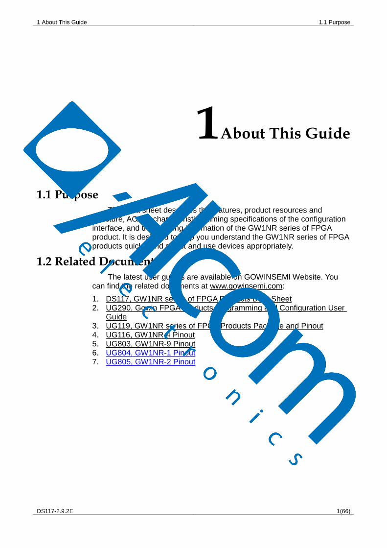
3.3.1 Introduction
The configurable function unit and the configurable logic unit are two basic units for FPGA core of GOWINSEMI. As shown in Figure 3-3, each unit consists of four configurable logic sections and its configurable routing unit. Each of the three configurable logic sections contains two 4-input LUTs and two registers, and the other one only contians two 4-input LUTs.
Configurable logical sections in CLU cannot be configured as SRAM, but as basic logic, ALU, and ROM. The configurable logic sections in the CFU can be configured as basic logic, ALU, SRAM, and ROM depending on the applications. This section takes CFU as an example to introduce CFU and CLU.
Figure 3-3 CFU View
CRU
CLS2
CFU
LUT
LUT
LUT
LUT
REG
REG
LUT
LUT
REG
REG
LUT
LUT
REG
REG
CLS3
CLS1
CLS0
Carry to Right CFU
Carry from left CFU
REG/
SREG
REG/
SREG
Note!
SERG needs special patch supporting. Please contact Gowin technical support or local Office for this patch.
3 Architecture 3.3 Configurable Function Unit
DS117-2.9.2E 15(66)
For further information of CFU, please refer to UG288E, Gowin Configurable Function Unit (CFU) User Guide.
3.3.2 CLU
The CLU supports three operation modes: basic logic mode, ALU mode, and memory mode.
Basic Logic Mode
Each LUT can be configured as one four input LUT. A higher input number of LUT can be formed by combining LUT4 together.
- Each CLS can form one five input LUT5. - Two CLSs can form one six input LUT6. - Four CLSs can form one seven input LUT7. - Eight CLSs (two CLUs) can form one eight input LUT8.
ALU Mode
When combined with carry chain logic, the LUT can be configured as the ALU mode to implement the following functions.
- Adder and subtractor - Up/down counter - Comparator, including greater-than, less-than, and not-equal-to - MULT
Memory mode
GW1NR-9 supports memory mode. In this mode, a 16 x 4 SSRAM or ROM can be constructed by using CLSs.
This SSRAM can be initialized during the device configuration stage. The initialization data can be generated in the bit stream file from Gowin Yunyuan software.
Register
Each Configurable Logic Section (CLS0~CLS2) has two registers (REG), as shown in Figure 3-4 below.
Figure 3-4 Register in CLS
D
CE
CLK
SR
GSR
Q
Table 3-1 Register Description in CLS
Signal I/O Description
D I Data input[ 1]
CE I CLK enable, can be high or low effective [2]
CLK I Clock, can be rising edge or falling edge trigging [2]
SR I Set/Reset, can be configured as
[2]:
Synchronized reset Synchronized set

3 Architecture 3.3 Configurable Function Unit
DS117-2.9.2E 16(66)
Signal I/O Description
Asynchronous reset Asynchronous set Non
GSR3,4
I
Global Set/Reset, can be configured as[4]
: Asynchronous reset Asynchronous set Non
Q O Register
Note!
[1] The source of the signal D can be the output of a LUT, or the input of the CRU; as such, the register can be used alone when LUTs are in use.
[2] CE/CLK/SR in CFU is independent.
[3] In the GW1NR series of FPGA products, GSR has its own dedicated network.
[4] When both SR and GSR are effective, GSR has higher priority.
3.3.3 CRU
The main functions of the CRU are as follows:
Input selection: Select input signals for the CFU. Configurable routing: Connect the input and output of the CFUs,
including inside the CFU, CFU to CFU, and CFU to other functional blocks in FPGA.

3 Architecture 3.4 IOB
DS117-2.9.2E 17(66)
3.4 IOB
3.4.1 Introduction
The IOB in the GW1NR series of FPGA products includes IO buffer, IO logic, and its routing unit. As shown in Figure 3-5, each IOB connects to two pins (Marked A and B). They can be used as a differential pair or as two single-end input/output.
Figure 3-5 IOB Structure View
PAD B
Buffer Pair A & B
“True” “Comp”
PAD A
Routing Routing
Differential Pair
PAD B
“True” “Comp”
PAD A
Differential Pair
IO Logic
A
IO Logic
B
TO
DO DI
TO
DO DI
Ro
utin
g
Ou
tpu
t
CL
K
Buffer Pair A & B
IO Logic
A
IO Logic
B
TO
DO DI
TO
DO DI
Ro
utin
g
Inp
ut
Ro
utin
g
Ou
tpu
t
CL
K
Ro
utin
g
Inp
ut
Ro
utin
g
Ou
tpu
t
CL
K
Ro
utin
g
Inp
ut
Ro
utin
g
Ou
tpu
t
CL
K
Ro
utin
g
Inp
ut
IOB Features:
VCCO supplied with each bank LVCMOS, PCI, LVTTL, LVDS, SSTL, and HSTL Input hysteresis option Output drive strength option Slew rate option Individual bus keeper, weak pull-up, weak pull-down, and open drain
option Hot socket IO logic supports basic mode, SRD mode, and generic DDR mode BANK0 of GW1NR-9 supports MIPI Input BANK2 of GW1NR-9 supports MIPI Output BANK0 and BANK2 of GW1NR-9 support I3C OpenDrain/PushPull
conversion For further information about IOB, please refer to UG289, Gowin
Programmable IO (GPIO) User Guide.

3 Architecture 3.4 IOB
DS117-2.9.2E 18(66)
3.4.2 I/O Buffer
There are four IO Banks in the GW1NR-1/4/9, as shown in Figure 3-6. GW1NR-2 includes seven IO Banks, as shown in Figure 3-7. To support SSTL, HSTL, etc., each bank also provides one independent voltage source (VREF) as referenced voltage. The user can choose from the internal reference voltage of the bank (0.5 x VCCO) or the external reference voltage using any IO from the bank.
Figure 3-6 GW1NR-1/4/9 I/O Bank Distribution
GW1NR
I/O Bank0
I/O Bank2
I/O B
an
k1
I/O B
an
k3
Figure 3-7 GW1NR-2 I/O Bank Distribution
GW1NR-2
I/O Bank0
I/O Bank2
I/O B
an
k3
Top
Bottom
Left
Rig
ht
I/O B
an
k4I/O
Ban
k5
I/O B
an
k1I/O
Ban
k6I/O
Ban
k1
The GW1NR series of FPGA products support LV and UV.
LV devices support 1.2V VCC to meet users’ low power needs.
VCCO of LV devices can be set as 1.2V, 1.5V, 1.8V, 2.5V, or 3.3V according to requirements1.
Linear voltage regulator is integrated in UV devices to facilitate single power supply. The core voltage supports 1.8V, 2.5V, and 3.3V.
VCCX supports 1.8 V, 2.5 V, or 3.3 V power supply.
In GW1NR-9 devices, I/O of Bank0 supports MIPI input and I/O of Bank2 supports MIPI output. I/O of Bank0 and Bank2 support MIPI I3C OpenDrain/PushPull conversion.
Note!
By default, the Gowin Programmable IO is tri-stated weak pull-up.
3 Architecture 3.4 IOB
DS117-2.9.2E 19(66)
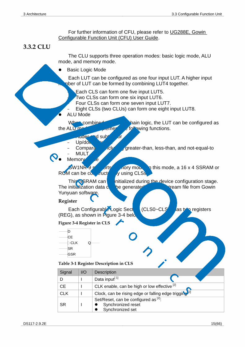
For the recommended working conditions for different packages, please refer to 4.1Operating Conditions
For the VCCO requirements of different I/O standards, see Table 3-2.
Table 3-2 Output I/O Standards and Configuration Options
I/O Type (Output) Single/Differ Bank VCCO (V) Drive Strength (mA) Application
MIPI[1]
Differ (TLVDS) 1.2 8 Mobile industry processor interface
LVDS25[2]
Differ (TLVDS) 2.5/3.3 3.5/2.5/2/1.25 high-speed point-to-point data transmission
RSDS[2]
Differ (TLVDS) 2.5/3.3 2 high-speed point-to-point data transmission
MINILVDS[2]
Differ (TLVDS) 2.5/3.3 2 LCD timing driver interface and column driver interface
PPLVDS[2]
Differ (TLVDS) 2.5/3.3 3.5 LCD row/column driver
LVDS25E Differ 2.5 8 high-speed point-to-point data transmissio
BLVDS25E Differ 2.5 16 Multi-point high-speed data transmission
MLVDS25E Differ 2.5 16 LCD timing driver interface and column driver interface
RSDS25E Differ 2.5 8 high-speed point-to-point data transmission
LVPECL33E Differ 3.3 16 High-speed data transmission
HSTL18D_I Differ 1.8 8 memory interface
HSTL18D_II Differ 1.8 8 memory interface
HSTL15D_I Differ 1.5 8 memory interface
SSTL15D Differ 1.5 8 memory interface
SSTL18D_I Differ 1.8 8 memory interface
SSTL18D_II Differ 1.8 8 memory interface
SSTL25D_I Differ 2.5 8 memory interface
SSTL25D_II Differ 2.5 8 memory interface
SSTL33D_I Differ 3.3 8 memory interface
SSTL33D_II Differ 3.3 8 memory interface
LVCMOS12D Differ 1.2 6/2 universal interface
LVCMOS15D Differ 1.5 8/4 universal interface
LVCMOS18D Differ 1.8 8/12/4 universal interface
LVCMOS25D Differ 2.5 8/16/12/4 universal interface
LVCMOS33D Differ 3.3 8/16/12/4 universal interface
HSTL15_I Single 1.5 8 memory interface

3 Architecture 3.4 IOB
DS117-2.9.2E 20(66)
I/O Type (Output) Single/Differ Bank VCCO (V) Drive Strength (mA) Application
HSTL18_I Single 1.8 8 memory interface
HSTL18_II Single 1.8 8 memory interface
SSTL15 Single 1.5 8 memory interface
SSTL18_I Single 1.8 8 memory interface
SSTL18_II Single 1.8 8 memory interface
SSTL25_I Single 2.5 8 memory interface
SSTL25_II Single 2.5 8 memory interface
SSTL33_I Single 3.3 8 memory interface
SSTL33_II Single 3.3 8 memory interface
LVCMOS12 Single 1.2 4,8 universal interface
LVCMOS15 Single 1.5 4,8 universal interface
LVCMOS18 Single 1.8 4,8,12 universal interface
LVCMOS25 Single 2.5 4,8,12,16 universal interface
LVCMOS33/ LVTTL33
Single 3.3 4,8,12,16,24 universal interface
PCI33 Single 3.3 N/A PC and embedded system
Note!
[1] GW1NR-2 Bank0/Bank3/Bank4/Bank5 supports MIPI I/O output; GW1NR-9 Bank2 supports MIPI I/O output.
[2] GW1NR-1does not support this I/O type.
Table 3-3 Input I/O Standards and Configuration Options
I/O Type (Input) Single/Differ Bank VCCO (V) HYSTERESIS Need VREF
MIPI[1]
Differ (TLVDS) 1.2 No No
LVDS25 Differ (TLVDS) 2.5/3.3 No No
RSDS Differ (TLVDS) 2.5/3.3 No No
MINILVDS Differ (TLVDS) 2.5/3.3 No No
PPLVDS Differ (TLVDS) 2.5/3.3 No No
LVDS25E Differ 2.5/3.3 No No
BLVDS25E Differ 2.5/3.3 No No
MLVDS25E Differ 2.5/3.3 No No
RSDS25E Differ 2.5/3.3 No No
LVPECL33E Differ 3.3 No No
HSTL18D_I Differ 1.8/2.5/3.3 No No
HSTL18D_II Differ 1.8/2.5/3.3 No No
HSTL15D_I Differ 1.5/1.8/2.5/3.3 No No
SSTL15D Differ 1.5/1.8/2.5/3.3 No No
SSTL18D_I Differ 1.8/2.5/3.3 No No
SSTL18D_II Differ 1.8/2.5/3.3 No No
SSTL25D_I Differ 2.5/3.3 No No

3 Architecture 3.4 IOB
DS117-2.9.2E 21(66)
I/O Type (Input) Single/Differ Bank VCCO (V) HYSTERESIS Need VREF
SSTL25D_II Differ 2.5/3.3 No No
SSTL33D_I Differ 3.3 No No
SSTL33D_II Differ 3.3 No No
LVCMOS12D Differ 1.2/1.5/1.8/2.5/3.3 No No
LVCMOS15D Differ 1.5/1.8/2.5/3.3 No No
LVCMOS18D Differ 1.8/2.5/3.3 No No
LVCMOS25D Differ 2.5/3.3 No No
LVCMOS33D Differ 3.3 No No
HSTL15_I Single 1.5 or 1.5/1.8/2.5/3.3
[2]
No Yes
HSTL18_I Single 1.8 or 1.8/2.5/3.3[3]
No Yes
HSTL18_II Single 1.8 or 1.8/2.5/3.3[3]
No Yes
SSTL15 Single 1.5 or 1.5/1.8/2.5/3.3
[2]
No Yes
SSTL18_I Single 1.8 or 1.8/2.5/3.3[3]
No Yes
SSTL18_II Single 1.8 or 1.8/2.5/3.3[3]
No Yes
SSTL25_I Single 2.5 or 2.5/3.3[4]
No Yes
SSTL25_II Single 2.5 or 2.5/3.3[4]
No Yes
SSTL33_I Single 3.3 No Yes
SSTL33_II Single 3.3 No Yes
LVCMOS12 Single 1.2/1.5/1.8/2.5/3.3 Yes No
LVCMOS15 Single 1.2/1.5/1.8/2.5/3.3 Yes No
LVCMOS18 Single 1.2/1.5/1.8/2.5/3.3 Yes No
LVCMOS25 Single 1.2/1.5/1.8/2.5/3.3 Yes No
LVCMOS33/ LVTTL33
Single 1.2/1.5/1.8/2.5/3.3 Yes No
PCI33 Single 3.3 Yes No
LVCMOS33OD25 Single 2.5 No No
LVCMOS33OD18 Single 1.8 No No
LVCMOS33OD15 Single 1.5 No No
LVCMOS25OD18 Single 1.8 No No
LVCMOS25OD15 Single 1.5 No No
LVCMOS18OD15 Single 1.5 No No
LVCMOS15OD12 Single 1.2 No No
LVCMOS25UD33 Single 3.3 No No
LVCMOS18UD25 Single 2.5 No No
LVCMOS18UD33 Single 3.3 No No
LVCMOS15UD18 Single 1.8 No No
LVCMOS15UD25 Single 2.5 No No
LVCMOS15UD33 Single 3.3 No No
LVCMOS12UD15 Single 1.5 No No

3 Architecture 3.4 IOB
DS117-2.9.2E 22(66)
I/O Type (Input) Single/Differ Bank VCCO (V) HYSTERESIS Need VREF
LVCMOS12UD18 Single 1.8 No No
LVCMOS12UD25 Single 2.5 No No
LVCMOS12UD33 Single 3.3 No No
Note!
[1] GW1NR-2 Bank2, GW1NR-2 Bank6 (Hard core), GW1NR-9 Bank0 supports MIPI I/O input.
[2] When VREF is INTERNAL, the VCCO of this I/O type is 1.5V; when VREF is VREF1_LOAD, the VCCO of this I/O type is 1.5 V/1.8 V/2.5 V/3.3 V.
[3] When VREF is INTERNAL, the VCCO of this I/O type is 1.8 V; when VREF is VREF1_LOAD, the VCCO of this I/O type is 1.8 V /2.5 V /3.3 V.
[4] When VREF is INTERNAL, the VCCO of this I/O type is 2.5 V; when VREF is VREF1_LOAD, the VCCO of this I/O type is 2.5 V /3.3 V.
3.4.3 True LVDS Design
Except GW1NR-1, BANK1/2/3 in the GW1NR devices support true LVDS output, but BANK1/2/3 do not support internal 100Ω input differential matched resistance. Bank0 supports internal 100Ω input differential matched resistance. BANK 0/1/2/3 support LVDS25E, MLVDS25E, BLVDS25E,etc. For the detailed information on different levels, please refer to UG289, Gowin Programmable IO (GPIO) User Guide.
For more detailed information on true LVDS, please refer to UG804, GW1NR-2 Pinout, UG116, GW1NR-4 Pinout and UG803, GW1NR-9 Pinout.
True LVDS input I/O needs external 100Ω terminal resistance for matching. SeeFigure 3-8for the true LVDS design.
Figure 3-8 True LVDS Design
Logic Array
SenderGW1NR-2/4/9
txout+
txout-
rxin+
rxin-
100Ω
IO Buffer IO Buffer
txout+
txout-
rxin+
rxin-
Receiver
50Ω
50Ω
50Ω
50Ω
For more detailed information about LVDS25E, MLVDS25E, and
BLVDS25E on IO terminal matched resistance, please refer to UG289, Gowin Programmable IO (GPIO) User Guide.

3 Architecture 3.4 IOB
DS117-2.9.2E 23(66)
3.4.4 I/O Logic
Figure 3-9 shows the I/O logic output of the GW1NR series of FPGA products.
Figure 3-9 I/O Logic Output
TCFF
SER
OUTFF
ISI
GND
IODELAY
TCTRL
TDATA
Figure 3-10 shows the I/O logic input of the GW1NR series of FPGA products.
Figure 3-10 I/O Logic Input
IODELAYINFF
IEM IDESRate
Sel
CI
DI
DIN
Q
A description of the I/O logic modules of the GW1NR series of FPGA products is presented below:
IODELAY
See Figure 3-11 for an overview of the IODELAY. Each I/O of the GW1NR series of FPGA products has an IODELAY cell. A total of 128(0~127) step delay is provided, with one-step delay time of about 30ps.

3 Architecture 3.4 IOB
DS117-2.9.2E 24(66)
Figure 3-11 IODELAY
DLY UNIT
DLY ADJ
DI
SDTAP
SETN
VALUE
DO
DF
The delay cell can be controlled in two ways:
Static control: Dynamic control: Usually used to sample delay window together with
IEM. The IODELAY cannot be used for both input and output at the same time
I/O Register
See Figure Figure 3-12 for the I/O register in the GW1NR series of FPGA products. Each I/O provides one input register, INFF, one output register, OUTFF, and a tristate Register, TCFF.
Figure 3-12 Register Structure in I/O Logic
D Q
CE
CLK
SR
Note!
CE can be either active low (0: enable)or active high (1: enable).
CLK can be either rising edge trigger or falling edge trigger.
SR can be either synchronous/asynchronous SET or RESET or disable.
The register can be programmed as register or latch.
IEM
IEM is for sampling clock edge and is used in the generic DDR mode. See Figure 3-13 for the IEM structure.
Figure 3-13 IEM Structure
IEM
CLK
D
RESET
MCLK
LEAD
LAG

3 Architecture 3.4 IOB
DS117-2.9.2E 25(66)
De-serializer DES and Clock Domain Transfer
The GW1NR series of FPGA products provides a simple serializer SER for each output I/O to support advanced I/O protocols.
Serializer SER
The GW1NR series of FPGA products provides a simple serializer (SER) for each output I/O to support advanced I/O protocols.
3.4.5 I/O Logic Modes
The I/O Logic in the GW1NR series of FPGA products supports several modes. In each operation, the I/O (or I/O differential pair) can be configured as output, input, and INOUT or tristate output (output signal with tristate control).
Not all the device pins support I/O logic. The pins IOL10 (A, B, C ... .J) and IOR10 (A, B, C ..., J) of GW1NR-4 do not support IO logic. All GW1NR-9 pins support IO logic.
Basic Mode
In basic mode, the I/O Logic is as shown in Figure 3-14, and the TC, DO, and DI signals can connect to the internal cores directly through CRU.
Figure 3-14 I/O Logic in Basic Mode
TC
DO
DI
IO PAD
SDR Mode
In comparison with the basic mode, SDR utilizes the IO register, as shown in Figure 3-15. This can effectively improve IO timing.

3 Architecture 3.4 IOB
DS117-2.9.2E 26(66)
Figure 3-15 I/O Logic in SDR Mode
D Q
CE
>CLK
SR
D Q
CE
>CLK
SR
D Q
CE
>CLK
SRI_SR
I_CLK
I_CE
DIN
O_SR
O_CLK
O_CE
DOUT
TCTRL
IO PAD
Note!
CLK enable O_CE and I_CE can be configured as active high or active low;
O_CLK and I_CLK can be either rising edge trigger or falling edge trigger;
Local set/reset signal O_SR and I_SR can be either synchronized reset, synchronized set, asynchronous reset, asynchronous set, or no-function;
I/O in SDR mode can be configured as basic register or latch.
Generic DDR Mode
Higher speed I/O protocols can be supported in generic DDR mode. GW1NR-9 devices support IDES16 mode and OSER16 mode. The other devices do not support.
Figure 3-16 shows the generic DDR input, with a speed ratio of the internal logic to PAD 1:2.
Figure 3-16 I/O Logic in DDR Input Mode
IDDR
D
CLK
Q[1:0]2
Figure 3-17 shows the generic DDR output, with a speed ratio of the PAD to FPGA internal logic 2:1.

3 Architecture 3.4 IOB
DS117-2.9.2E 27(66)
Figure 3-17 I/O Logic in DDR Output Mode
ODDR
D[1:0]
CLK
Q2
IDES4
In IDES4 mode, the speed ratio of the PAD to FPGA internal logic is 1:4.
Figure 3-18 I/O Logic in IDES10 Mode
IDES4
D
FCLK
PCLK Q[3:0]
CALIB4
RESET
OSER4 Mode
In OSER4 mode, the speed ratio of the PAD to FPGA internal logic is 4:1.
Figure 3-19 I/O Logic in OSER4 Mode
OSER4
TX[1:0]
D[3:0]
FCLK Q[1:0]
PCLK
RESET
2
4
2
IVideo Mode
In IVideo mode, the speed ratio of the PAD to FPGA internal logic is 1:7.
Figure 3-20 I/O Logic in IVideo Mode
IVideo
D
CALIB
FCLK
Q[6:0]PCLK
CE
RESET
7
Note!
IVideo and IDES8/10 will occupy the neighboring I/O logic. If the I/O logic of a single port is occupied, the pin can only be programmed in SDR or BASIC mode.
OVideo Mode
In OVideo mode, the speed ratio of the PAD to FPGA internal logic is

3 Architecture 3.4 IOB
DS117-2.9.2E 28(66)
7:1.
Figure 3-21 I/O Logic in OVideo Mode
OVideo
D[6:0]
FCLK
QPCLK
7
IDES8 Mode
In IDES8 mode, the speed ratio of the PAD to FPGA internal logic is 1:8.
Figure 3-22 I/O Logic in IDES8 Mode
IDES8
D
FCLK
PCLK Q[7:0]
RESET
8
CALIB
OSER8 Mode
In OSER8 mode, the speed ratio of the PAD to FPGA internal logic is 8:1.
Figure 3-23 I/O Logic in OSER8 Mode
OSER8
TX[3:0]
D[7:0]
FCLK Q[1:0]
PCLK
RESET
2
4
8
IDES10 Mode
In IDES10 mode, the speed ratio of the PAD to FPGA internal logic is 1:10.
Figure 3-24 I/O Logic in IDES10 Mode
IDES10
D
FCLK
PCLK Q[9:0]
RESET
10
CALIB
OSER10 Mode
In OSER10 mode, the speed ratio of the PAD to FPGA internal logic is

3 Architecture 3.5 Block SRAM (BSRAM)
DS117-2.9.2E 29(66)
10:1.
Figure 3-25 I/O Logic in OSER10 Mode
OSER10
D[9:0]
FCLK
PCLKQ
RESET
10
IDES16 Mode
In IDES16 mode, the speed ratio of the PAD to FPGA internal logic is 1:16.
Figure 3-26 I/O Logic in IDES16 Mode
IDES16
D
FCLK
PCLK Q[15:0]
RESET
16
CALIB
OSER16 Mode
In OSER16 mode, the speed ratio of the PAD to FPGA internal logic is 16:1.
Figure 3-27 I/O Logic in OSER16 Mode
OSER16
D[15:0]
FCLK
PCLKQ
RESET
16
3.5 Block SRAM (BSRAM)
3.5.1 Introduction
GW1NR series FPGA products provide abundant SRAM. The Block SRAM (BSRAM) is embedded as a row in the FPGA array and is different from SSRAM (Shadow SRAM). Each BSRAM has 18,432 bits (18Kbits). There are five operation modes: single port, dual port, semi-dual port, ROM, and FIFO.
An abundance of BSRAM resources provide a guarantee for the user's high-performance design. BSRAM features include the following:
Max.18,432 bits per BSRAM BSRAM itself can run at 190 MHz at max Single port Dual port Semi-dual port Parity bits ROM

3 Architecture 3.5 Block SRAM (BSRAM)
DS117-2.9.2E 30(66)
Data width from 1 to 36 bits Mixed clock mode Mixed data width mode Enable Byte operation for double byte or above Normal Read and Write Mode Read-before-write Mode Write-through Mode
For further details about BSRAM, please refer to UG285E, Gowin BSRAM & SSRAM User Guide.
3.5.2 Configuration Mode
The BSRAM mode in the GW1NR series of FPGA products supports different data bus widths. See Table 3-4.
Table 3-4 Memory Size Configuration
Single Port Mode
Dual Port Mode1
Semi-Dual Port Mode
Read Only
16K x 1 16K x 1 16K x 1 16K x 1
8K x 2 8K x 2 8K x 2 8K x 2
4K x 4 4K x 4 4K x 4 4K x 4
2K x 8 2K x 8 2K x 8 2K x 8
1K x 16 1K x 16 1K x 16 1K x 16
512 x 32 - 512 x 32 512 x 32
2K x 9 2K x 9 2K x 9 2K x 9
1K x 18 1K x 18 1K x 18 1K x 18
512 x 36 - 512 x 36 512 x 36
Note!
[1]The GW1NR-9 device does not support Dual Port Mode.
Single Port Mode
In the single port mode, BSRAM can write to or read from one port at one clock edge. During the write operation, the data can show up at the output of BSRAM. Normal-Write Mode and Write–through Mode can be supported. When the output register is bypassed, the new data will show at the same write clock rising edge.
For further information about Single Port Block Memory ports and the related description, please refer to SUG283E, Gowin Primitives User Guide > 3 Memory.
Dual Port Mode
BSRAM support dual port mode. The applicable operations are as follows:
Two independent read Two independent write An independent read and an independent write at different clock
frequencies For further information about Dual Port Block Memory ports and the
3 Architecture 3.5 Block SRAM (BSRAM)
DS117-2.9.2E 31(66)
related description, please refer to SUG283E, Gowin Primitives User Guide > 3 Memory.
Semi-Dual Port Mode
Semi-Dual Port supports read and write at the same time on different ports, but it is not possible to write and read to the same port at the same time. The system only supports write on Port A, read on Port B.
For further information about Semi-Dual Port Block Memory ports and the related description, please refer to SUG283E, Gowin Primitives User Guide > 3 Memory.
Read Only
BSRAM can be configured as ROM. The ROM can be initialized during the device configuration stage, and the ROM data needs to be provided in the initialization file. Initialization completes during the device power-on process.
Each BSRAM can be configured as one 16 Kbits ROM. For further information about Read Only Port Block Memory ports and the related description, please refer to SUG283E, Gowin Primitives User Guide > 3 Memory.

3 Architecture 3.5 Block SRAM (BSRAM)
DS117-2.9.2E 32(66)
3.5.3 Mixed Data Bus Width Configuration
BSRAM in the GW1NR series of FPGA products supports mixed data bus width operation. In the dual port and semi-dual port modes, the data bus width for read and write can be different. For the configuration options that are available, please see Table 3-5 and Table 3-6 below.
Table 3-5 Dual Port Mixed Read/Write Data Width Configuration
Read Port
Write Port
16K x 1 8K x 2 4K x 4 2K x 8 1K x 16 2K x 9 1K x 18
16K x 1 * * * * *
8K x 2 * * * * *
4K x 4 * * * * *
2K x 8 * * * * *
1K x 16 * * * * *
2K x 9 * *
1K x 18 * *
Note!
”*”denotes the modes supported.
Table 3-6 Semi Dual Port Mixed Read/Write Data Width Configuration
Read Port
Write Port
16K x 1 8K x 2 4K x 4 2K x 8 1K x 16 512 x 32 2K x 9 1K x 18 512 x 36
16K x 1 * * * * * *
8K x 2 * * * * * *
4K x 4 * * * * * *
2K x 8 * * * * * *
1K x 16 * * * * * *
512x32 * * * * * *
2K x 9 * * *
1K x 18 * * *
Note!
”*”denotes the modes supported.
3.5.4 Byte-enable
The BSRAM in the GW1NR series of FPGA products supports byte-enable. For data longer than a Byte, the additional bits can be blocked, and only the selected portion is allowed to be written into. The blocked bits will be retained for future operation. Read/write enable ports (WREA, WREB), and byte-enable parameter options can be used to control the BSRAM write operation.
3 Architecture 3.5 Block SRAM (BSRAM)
DS117-2.9.2E 33(66)
3.5.5 Parity Bit
There are parity bits in BSRAMs. The 9th bit in each byte can be used as a parity bit to check the correctness of data transmission.It can also be used for data storage.
3.5.6 Synchronous operation
All the input registers of BSRAM support synchronous write; The output registers can be used as pipeline register to improve design
performance; The output registers are bypass-able.
3.5.7 Power up Conditions
BSRAM initialization is supported when powering up. During the power-up process, BSRAM is in standby mode, and all the data outputs are “0”. This also applies in ROM mode.
3.5.8 BSRAM Operation Modes
BSRAM supports five different operations, including two read operations (Bypass Mode and Pipeline Read Mode) and three write operations (Normal Write Mode, Write-through Mode, and Read-before-write Mode).
Read Mode
Read data from the BSRAM via output registers or without using the registers.
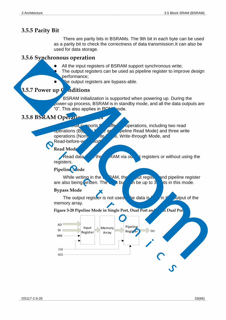
Pipeline Mode
While writing in the BSRAM, the output register and pipeline register are also being written. The data bus can be up to 36 bits in this mode.
Bypass Mode
The output register is not used. The data is kept in the output of the memory array.
Figure 3-28 Pipeline Mode in Single Port, Dual Port and Semi Dual Port
InputRegister
DI
OCE
CLK
PipelineRegister DO
WRE
ADMemory
Array

3 Architecture 3.5 Block SRAM (BSRAM)
DS117-2.9.2E 34(66)
InputRegister
Memory Array
DIA
CLKA
CLKB
InputRegister
DOB
PipelineRegister
OCEB
ADA
ADB
InputRegister
Memory Array
DIA
DOA
DIB
CLKA CLKB
InputRegisterWREA
PipelineRegister
DOB
PipelineRegister
OCEAOCEB
WREB
ADA ADB
Write Mode
NORMAL WRITE MODE
In this mode, when the user writes data to one port, and the output data of this port does not change. The data written in will not appear at the read port.
WRITE-THROUGH MODE
In this mode, when the user writes data to one port, and the data written in will also appear at the output of this port.
READ-BEFORE-WRITE MODE
In this mode, when the user writes data to one port, and the data written in will be stored in the memory according to the address. The original data in this address will appear at the output of this port.
3.5.9 Clock Operations
Table 3-7 lists the clock operations in different BSRAM modes:
Table 3-7 Clock Operations in Different BSRAM Modes
Clock Operations Dual Port Mode Semi-dual Port Mode Single Port Mode
Independent Clock Mode
Yes No No
Read/Write Clock Mode
Yes Yes No
Single Port Clock Mode
No No Yes

3 Architecture 3.5 Block SRAM (BSRAM)
DS117-2.9.2E 35(66)
Independent Clock Mode
Figure 3-29 shows the independent clocks in the dual port mode with each port with one clock. CLKA controls all the registers at Port A; CLKB controls all the registers at Port B.
Figure 3-29 Independent Clock Mode
InputRegister
Memory Array
DIA
DOA
WREBWREA
DIB
DOB
CLKA CLKB
OutputRegister
InputRegister
OutputRegister
WREA WREB
ADA ADB
Read/Write Clock Operation
Figure 3-30 shows the read/write clock operations in the semi-dual port mode with one clock at each port. The write clock (CLKA) controls Port A data inputs, write address and read/write enable signals. The read clock (CLKB) controls Port B data output, read address, and read enable signals.
Figure 3-30 Read/Write Clock Mode
InputRegister
Memory Array
CLKA CLKB
InputRegister
PipelineRegister

3 Architecture 3.6 User Flash (GW1NR-1)
DS117-2.9.2E 36(66)
Single Port Clock Mode
Figure 3-31shows the clock operation in single port mode.
Figure 3-31 Single Port Clock Mode
InputRegister
OutputRegister
Memory Array
DI
DO
WRE
CLK
ADWRE
3.6 User Flash (GW1NR-1) GW1NR-1 devices support User Flash with 12 Kbytes (48 page x 256
Bytes). The features are as following:
100,000 write cycles
Greater than10 years Data Retention at +85 ℃
Selectable 8/16/32 bits data-in and data-out Page size: 256 Bytes 3 μA standby current Page Write Time: 8.2 ms
For further information about the user Flash in GW1NR-1, please refer to UG295, Gowin User Flash User Guide.
3.7 User Flash (GW1NR-2/4/9) The GW1NR series of FPGA products support User Flash. The
capacity of the user Flash in GW1NR-2 is 96Kbits.The capacity of the user Flash in GW1NR-4 is 256Kbits. The capacity of the user flash in GW1NR-9 is 608Kbits. The user Flash memory is composed of row memory and column memory. One row memory is composed of 64 column memories. The capacity of one column memory is 32 bits, and the capacity of one row memory is 64*32=2048 bits. Page erase is supported, and one page capacity is 2048 bytes, i.e., one page includes 8 rows. The features are shown below:
10,000 write cycles
Greater than10 years Data Retention at +85 ℃
Data Width: 32 GW1NR-2 capacity: 48 rows x 64 columns x 32 = 96kbits GW1NR-4 capacity: 128 rows x 64 columns x 32 = 256kbits GW1NR-9 capacity: 304 rows x 64 columns x 32 = 608kbits Page Erase Capability: 2,048 bytes per page Fast Page Erasure/Word Programming Operation Clock frequency: 40 MHz Word Programming Time: ≤16 μs

3 Architecture 3.8 DSP
DS117-2.9.2E 37(66)
Page Erasure Time: ≤120 ms Electric current
- Read current/duration: 2.19 mA/25 ns (VCC) & 0.5 mA/25 ns (VCCX) (MAX)
- Program / Erase operation: 12/12 mA (MAX) For further information of CFU, please refer to UG295-1.0E_Gowin
User Flash Guide.
3.8 DSP
3.8.1 Introduction
The GW1NR series of FPGA products have abundant DSP modules. Gowin DSP solutions can meet user demands for high performance digital signal processing design, such as FIR, FFT, etc. DSP blocks have the advantages of stable timing performance, high-usage, and low-power.
DSP offers the following functions:
Multiplier with three widths: 9-bit, 18-bit, 36-bit 54-bit ALU Multipliers cascading to support wider data Barrel shifter Adaptive filtering through signal feedback Computing with options to round to a positive number or a prime
number Supports pipeline mode and bypass mode
For further information of CFU, please refer to UG287-1.2E_Gowin DSP User Guide.
Macro
DSP blocks are embedded as a row in the FPGA array. Each DSP block contains two Macro, and each Macro contains two pre-adders, two 18 x 18 bit multipliers, and one three-input ALU.
Figure 3-32 shows the structure of one Macro:

3 Architecture 3.8 DSP
DS117-2.9.2E 38(66)
Figure 3-32 DSP Macro
+/-
REG_PADDSUBREGCMUXA0
REGA0
MUXB0
REGB0
MUXA1
REGA1
MUXB1
REGB1
+/-
MUXMA0
REGMA0
MUXMB0
REGMB0MUXMA1
REGMA1
MUXMB1
REGMB1
×
REG_CNTLI
REGP0 REG_CNTLP
×
REGP1
A_MUX B_MUX
C_
MU
X
OMUX
REGOUT
MUXSD
REGSD
ALU
“0”
A0[17:0]
SDIA INC[17:0]
“0”
B0[17:0]
INA0
PADDSUB[1:0]
“0”
A1[17:0]
INA0
INC[44:27]“0”
B1[17:0]
INA1
SBI[17:0] C[53:0]
INC
INA0
INB0
INA1 INB1
SBO[17:0]
PADDSUN[0] PADDSUB[1]
SIB[17:0]
SIA[17:0]
A0
PADD0
B0INC[17:0]
ALUSEL ALUMODEPADD1
B1INC[44:27]
MROB1
SOB[17:0]MROA1
SOA[17:0]
MROA0
MROB0
M0 M1
MD0 MD1
LOADA“0”
alusel[1:0] alusel[3:2]“0”
LOADB MDI<<18
alusel[6:4]
C_OUT
A_OUT alumode[3:0] B_OUT“0”
CASI>>18
CASI[54:0]
INC
LOADA
RND_INIT
RND_INIT-1
ALU_OUT/STATUS
MDO/MD1
DOUT[35:0]
CASO[54:0]
LOADA={INC[17:0],INA};
LOADB={INC[44:27],INB};
INA={MROB,MROA0};
INB={MROB1,MROA1}
ALU
MULT
Pre-adder
ASEL[1:0]
2BSEL[1:0]
ASIGN[1:0]
BSIGN[1:0]
4CLK[3:0]
CE[3:0]
RESET[3:0]
A1
18 18 18 18 182 54
18
18
18
18
1818
54
18 18
18
18
18
2
2
2
18
18
18
18 18
18
1818
18
18
18
4
4
18
36 36
55
54
54
54
4
54
36
55
Table 3-8 shows DSP ports description.
Table 3-8 DSP Ports Description
Port Name I/O Description
A0[17:0] I 18-bit data input A0
B0[17:0] I 18-bit data input B0
A1[17:0] I 18-bit data input A1
B1[17:0] I 18-bit data input B1

3 Architecture 3.8 DSP
DS117-2.9.2E 39(66)
Port Name I/O Description
C[53:0] I 54-bit data input C
SIA[17:0] I
Shift data input A, used for CASCADE connection. The input signal SIA is directly connected to the output signal SOA of previously adjacent DSP and the delay from SIA to SOA inside a DSP is one clock cycle.
SIB[17:0] I
Shift data input B, used for CASCADE connection. The input signal SIB is directly connected to the output signal SOB of previously adjacent DSP and the delay from SIB to SOB inside a DSP is one clock cycle.
SBI[17:0] I Pre‐adder logic shift input, backward direction.
CASI[54:0] I ALU input from previous DSP block, used for cascade connection.
PADDSI0[1:0] I Source select for Multiplier or pre-adder input A
BSEL[1:0] I Source select for Multiplier input B
ASIGN[1:0] I Sign bit for input A
BSIGN[1:0] I Sign bit for input B
PADDSUB[1:0] I Operation control signals of pre-adder, used for pre-adder logic add/subtract selection
CLK[3:0] I Clock input
CE[3:0] I Clock Enable
RESET[3:0] I Reset input, synchronous or asynchronous
SOA[17:0] O Shift data output A
SOB[17:0] O Shift data output B
SBO[17:0] O Pre‐adder logic shift output, backward direction.
DOUT[35:0] O DSP output data
CASO[54:0] O ALU output to next DSP block for cascade connection, the highest bit is sign-extended.
Table 3-9 Internal Registers Description
Register Description and Associated Attributes
A0 register Registers for A0 input
A1 register Registers for A1 input
B0 register Registers for B0 input
B1 register Registers for B1 input
C register C register
P1_A0 register Registers for A0 input of left multiplier
P1_A1 register Registers for A1 input of right multiplier
P1_B0 register Registers for B0 input of left multiplier
P1_B1 register Registers for B1 input of right multiplier
P2_0 register Registers for pipeline of left multiplier
P2_1 register Registers for pipeline of right multiplier
OUT register Registers for DOUT output
OPMODE register Registers for operation mode control
SOA register Registers for shift output at port SOA
PADD
Each DSP macro features two units of pre-adders to implement pre-add, pre-subtraction, and shifting.
PADD locates at the first stage with two inputs:

3 Architecture 3.9 MIPI D-PHY (GW1NR-2)
DS117-2.9.2E 40(66)
Parallel 18-bit input B or SBI; Parallel 18-bit input A or SIA.
Each input end supports pipeline mode and bypass mode. GOWINSEMI PADD can be used as function block independently, which supports 9-bit and 18-bit width.
MULT
Multipliers locate after the pre-adder. Multipliers can be configured as 9 x 9, 18 x 18, 36 x 18 or 36 x 36. Pipeline Mode and Bypass Mode are supported both in input and output ports. The configuration modes that a macro supports include:
One 18 x 36 multiplier Two 18 x 18 multipliers Four 9 x 9 multipliers
Two adjacent DSP macros can form a 36 x 36 multiplier.
ALU
Each Macro has one 54 bits ALU54, which can further enhance MULT’s functions. Registered Mode and Bypass Mode are supported both in input and output ports. The functions are as following:
Multiplier output data / 0, addition/subtraction operations for data A and data B;
Multiplier output data / 0, addition/subtraction operations for data B and bit C;
Addition/subtraction operations for data A, data B, and bit C;
3.8.2 DSP Operations
Multiplier Accumulator MULTADDALU
For further information about DSP, please refer to UG287E, Gowin DSP User Guide.
3.9 MIPI D-PHY (GW1NR-2) Hard Core - MIPI D-PHY RX
GW1NR-2 provides the hard core - MIPI D-PHY RX IP. This IP applies to the display serial interface (DSI), which is designed to receive and send image data or video data. MIPI D-PHY provides a physical layer definition.
Features are as follows:
Supports MIPI Alliance Standard for D-PHY Specification, version 2.1; Interfaces to MIPI DSI, RX devices; Supports unidirectional High-speed (HS) mode; Supports bidirectional Low-power operation mode; Deserializes serial high-speed data into byte data packets; Supports MIPI D-PHY RX 1:8 mode and 1:16 mode; Supports MIPI IO; In HS mode, MIPI transmission speed can be up to 1.5 Gbps;

3 Architecture 3.10 Clock
DS117-2.9.2E 41(66)
In LP mode, the data transmission speed is 10Mbps; Supports up to 4 data lanes and one clock lane; IO Bank6 supports MIPI D-PHY RX.
Soft Core - MIPI D-PHY RX/TX
GW1NR-2 also provides the soft core - MIPI D-PHY RX/TX IP. This IP applies to the display serial interface (DSI) and the camera serial interface (CSI), which are designed to receive and send image data or video data. MIPI D-PHY provides a physical layer definition.
Features are as follows:
Supports MIPI Alliance Standard for D-PHY Specification, version 1.2; Interfaces to MIPI CSI2 and DSI, RX and TX devices; Supports unidirectional High-speed (HS) mode; Supports bidirectional Low-power operation mode; Deserializes serial high-speed data into byte data packets; Supports MIPI D-PHY RX 1:8 mode and 1:16 mode; Supports IO Types of ELVDS, TLVDS, and MIPI IO; IO Bank0, IO Bank3, IO Bank4, and IO Bank5 supports MIPI D-PHY
TX, and the transmission speed can be up to 1.5 Gbps; IO Bank2 supports MIPI D-PHY RX, transmission speed can be up to
1.2Gbps; Supports up to 4 data lanes and one clock lane.
For further detailed information, please refer to IPUG112, Gowin MIPI D-PHY RX TX user guide.
3.10 Clock The clock resources and wiring are critical for high-performance
applications in FPGA. The GW1NR series of FPGA products provide the global clock network (GCLK) which connects to all the registers directly. Besides the global clock network, the GW1NR series of FPGA products provide high-speed clock HCLK. PLL, etc are also provided.
For further information of CFU, please refer to UG286-1.5E_Gowin Clock User Guide.
3.10.1 Global Clock
The GCLK is distributed in GW1NR series of FPGA products as two quadrants, L and R. Each quadrant provides eight GCLKs. The optional clock resources of GCLK can be pins or CRU. Users can employ dedicated pins as clock resources to achieve better timing.
3.10.2 PLL
Phase-locked Loop (PLL) is one kind of a feedback control circuit. The frequency and phase of the internal oscillator signal is controlled by the external input reference clock.
PLL blocks provide the ability to synthesize clock frequencies. Frequency adjustment (multiply and division), phase adjustment, and duty cycle can be adjusted by configuring the parameters.

3 Architecture 3.10 Clock
DS117-2.9.2E 42(66)
GW1NR-1/4/9
See Figure 3-33 for the PLL structure.
Figure 3-33 PLL Structure (GW1NR-1/4/9)
IDIVCLKIN
PFD
+
ICP
FBDIV
CLKFB
ODSEL[5:0]
VCO VCODIV
PS&DCA
IDSEL[5:0]
FBDSEL[5:0]
PSDA[3:0]
CLKOUT
CLKOUTP
CLKOUTD
CLKOUTD3
SDIV
/3
DIV
LOCKLOCK
Detector
LPF
RESET RESET_P DUTYDA[3:0] FDLY[3:0]
6 6
6
4 4 4
Table 3-10 PLL Ports Definition
Port Name Signal Description
CLKIN [5:0] I Reference clock input
CLKFB I Feedback clock input
RESET I PLL reset
RESET_P I PLL Power Down
INSEL[2:0] I Dynamic clock control selector: 0~5
IDSEL [5:0] I Dynamic IDIV control: 1~64
FBDSEL [5:0] I Dynamic FBDIV control:1~64
PSDA [3:0] I Dynamic phase control (rising edge effective)
DUTYDA [3:0] I Dynamic duty cycle control (falling edge effective)
FDLY[3:0] I CLKOUTP dynamic delay control
CLKOUT O Clock output with no phase and duty cycle adjustment
CLKOUTP O Clock output with phase and duty cycle adjustment
CLKOUTD O Clock divider from CLKOUT and CLKOUTP (controlled by SDIV)
CLKOUTD3 O clock divider from CLKOUT and CLKOUTP (controlled by DIV3 with the constant division value 3)
LOCK O PLL lock status: 1: locked, 0: unlocked
The PLL reference clock source can come from an external PLL pin or from internal routing GCLK, HCLK, or general data signal. PLL feedback signal can come from the external PLL feedback input or from internal routing GCLK, HCLK, or general data signal.

3 Architecture 3.10 Clock
DS117-2.9.2E 43(66)
For PLL features, please refer to Table 4-21 PLL Switching Characteristics.
PLL can adjust the frequency of the input clock CLKIN (multiply and division). The formulas for doing so are as follows:
1. fCLKOUT = (fCLKIN*FBDIV)/IDIV 2. fVCO = fCLKOUT*ODIV 3. fCLKOUTD = fCLKOUT/SDIV 4. fPFD = fCLKIN/IDIV = fCLKOUT/FBDIV
Note!
fCLKIN: The frequency of the input clock CLKIN
fCLKOUT: The clock frequency of CLKOUT and CLKOUTP
fCLKOUTD: The clock frequency of CLKOUTD, and CLKOUTD is the clock CLKOUT after division
fPFD: PFD Phase Comparison Frequency, and the minimum value of fPFD should be no less than 3MHz.
Adjust IDIV, FBDIV, ODIV, and SDIV to achieve the required clock frequency.
GW1NR-2
See Figure 3-34 for the PLL structure of GW1NR-2.
Figure 3-34 PLL Structure (GW1NR-2)
IDIV
(1-64)
FBDIV
(1-64)
CP+LPF
+VCO
A0
B0
C0
D0
A1
B1
C1
D1
ODIV.A
(1-128)
ODIV.B
(1-128)
PFD
PS
PS
DT A2 CLKEN
ODIV.C
(1-128)
ODIV.D
(1-128)
PS
PS
C2 CLKEN
DT B2 CLKEN
D2 CLKEN
8
DPA
PSDIR
PSSEL[1:0]
PSPULSE
CLKIN
CLKFB
CLKOUTA
CLKOUTB
CLKOUTC
CLKOUTD
LOCK
ENCLKA,ENCLKB,ENCLKC,ENCLKD
RESET, RESET_P, RESET_I,RESER_S
IDSEL [5:0],FBDSEL [5:0], ODSELA[6:0], ODSELB[6:0], ODSELC[6:0],ODSELD[6:0], DTA[3:0], DTB[3:0], ICPSEL[4:0], LPFRES[2:0]
See Table 3-11 for a definition of the PLL ports.
Table 3-11 PLL Ports Definition
Port Name Signal Description
CLKIN I Reference clock input
CLKFB I Feedback clock input
RESET I PLL reset
RESET_P I PLL Power Down
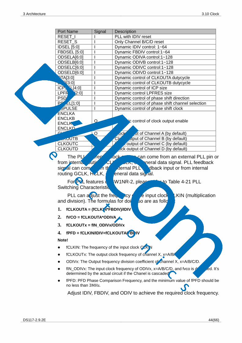
3 Architecture 3.10 Clock
DS117-2.9.2E 44(66)
Port Name Signal Description
RESET_I I PLL with IDIV reset
RESET_S I Only Channel B/C/D reset
IDSEL [5:0] I Dynamic IDIV control: 1~64
FBDSEL [5:0] I Dynamic FBDIV control:1~64
ODSELA[6:0] I Dynamic ODIVA control:1~128
ODSELB[6:0] I Dynamic ODIVB control:1~128
ODSELC[6:0] I Dynamic ODIVC control:1~128
ODSELD[6:0] I Dynamic ODIVD control:1~128
DTA[3:0] I Dynamic control of CLKOUTA dutycycle
DTB[3:0] I Dynamic control of CLKOUTB dutycycle
ICPSEL[4:0] I Dynamic control of ICP size
LPFRES[2:0] I Dynamic control LPFRES size
PSDIR I Dynamic control of phase shift direction
PSSEL[1:0] I Dynamic control of phase shift channel selection
PSPULSE I Dynamic control of phase shift clock
ENCLKA ENCLKB ENCLKC ENCLKD
O Dynamic control of clock output enable
CLKOUTA O Clock output of Channel A (by default)
CLKOUTB O Clock output of Channel B (by default)
CLKOUTC O Clock output of Channel C (by default)
CLKOUTD O Clock output of Channel D (by default)
The PLL reference clock source can come from an external PLL pin or from internal routing GCLK, HCLK, or general data signal. PLL feedback signal can come from the external PLL feedback input or from internal routing GCLK, HCLK, or general data signal.
For PLL features of GW1NR-2, please refer to Table 4-21 PLL Switching Characteristics.
PLL can adjust the frequency of the input clock CLKIN (multiplication and division). The formulas for doing so are as follows:
1. fCLKOUTA = (fCLKIN*FBDIV)/IDIV
2. fVCO = fCLKOUTA*ODIVA
3. fCLKOUTx = fIN_ODIVx/ODIVx
4. fPFD = fCLKIN/IDIV=fCLKOUTA/FBDIV
Note!
fCLKIN: The frequency of the input clock CLKIN
fCLKOUTx: The output clock frequency of channel X, x=A/B/C/D.
ODIVx: The Output frequency division coefficient of channel X, x=A/B/C/D.
fIN_ODIVx: The input clock frequency of ODIVx, x=A/B/C/D, and fvco is defaulted. It’s determined by the actual circuit if the Chanel is cascaded.
fPFD: PFD Phase Comparison Frequency, and the minimum value of fPFD should be no less than 3MHz.
Adjust IDIV, FBDIV, and ODIV to achieve the required clock frequency.

3 Architecture 3.10 Clock
DS117-2.9.2E 45(66)
3.10.3 HCLK
HCLK is the high-speed clock in the GW1NR series of FPGA products. It can support high-performance data transfer and is mainly suitable for source synchronous data transfer protocols. For HCLK distribution views, see Figure 3-35, Figure 3-36, Figure 3-37, and Figure 3-38.
Figure 3-35 GW1NR-1 HCLK Distribution
I/O Bank0
I/O B
an
k1
I/O Bank2
I/O B
an
k3
L R
IO Bank HCLK
Figure 3-36 GW1NR-2 HCLK Distribution
I/O Bank0
I/O B
an
k1
I/O Bank2
L R
IO Bank HCLK
I/O B
an
k4/3
I/O B
an
k5
T
B

3 Architecture 3.11 Long Wire (LW)
DS117-2.9.2E 46(66)
Figure 3-37 GW1NR-4 HCLK Distribution
Figure 3-38 GW1NR-9 HCLK Distribution
I/O Bank0
I/O B
an
k1
I/O Bank2
I/O B
an
k3
L R
IO Bank HCLK
3.11 Long Wire (LW) As a supplement to the CRU, the GW1NR series of FPGA products
provides another routing resource, Long wire, which can be used as clock, clock enable, set/reset,or other high fan out signals.
3.12 Global Set/Reset (GSR) A global set/rest (GSR) network is built into the GW1NR series of
FPGA product. There is a direct connection to core logic. It can be used as asynchronous/synchronous set or asynchronous/synchronous reset, registers in CFU and I/O can be configured independently.
I/O Bank0
I/O B
an
k1
I/O Bank2
I/O B
an
k3
L R
IO Bank HCLK

3 Architecture 3.13 Programming Configuration
DS117-2.9.2E 47(66)
3.13 Programming Configuration The GW1NR series of FPGA products support SRAM and Flash. The
Flash programming mode supports on-chip Flash and off-chip Flash. The GW1NR series of FPGA products support DUAL BOOT, providing a selection for users to backup data to off chip Flash according to requirements.
Besides JTAG, the GW1NR series of FPGA products also supports GOWINSEMI's own configuration mode: GowinCONFIG (AUTO BOOT, SSPI, MSPI, DUAL BOOT, SERIAL, and CPU). All the devices support JTAG and AUTO BOOT. For the detailed information, please refer to UG290, Gowin FPGA Products Programming and Configuration Guide.
3.13.1 SRAM Configuration
When you adopt SRAM to configure the device, every time the device is powered on, the bit stream file needs to be downloaded to configure the deviece.
3.13.2 Flash Configuration
The Flash configuration data is stored in the on-chip flash. Each time the device is powered on, the configuration data is transferred from the Flash to the SRAM, which controls the working of the device. This mode can complete configuration within a few ms, and is referred to as “Quick Start”.
B version of GW1NR devices has the feature of transparent transmission. That is to say, the B version device can program the on-chip Flash or off-chip Flash via the JTAG interface without affecting the current working state. During programming, the B version device works according to the previous configuration. After programming, provide one low pulse for RECONFIG_N to complete the online upgrade. This feature applies to the applications with long online time and irregular upgrades.
The GW1NR series of FPGA products also support off-chip Flash configuration and dual-boot. Please refer to UG290, Gowin FPGA Products Programming and Configuration Guide for more detailed information.
3.14 On Chip Oscillator There is an internal oscillator in each of the GW1NR series of FPGA
product. During the configuration process, it can provide a clock for the MSPI mode. See Table 3-12 for the output frequency.
Table 3-12 GW1NR-4 Oscillator Output Frequency Options
Mode Frequency Mode Frequency Mode Frequency
0 2.1MHz[1]
8 6.6MHz 16 13.1MHz
1 4.6MHz 9 7MHz 17 15MHz
2 4.8MHz 10 7.5MHz 18 17.5MHz
3 5MHz 11 8.1MHz 19 21MHz
4 5.3MHz 12 8.8MHz 20 26.3MHz

3 Architecture 3.14 On Chip Oscillator
DS117-2.9.2E 48(66)
5 5.5MHz 13 9.5MHz 21 35MHz
6 5.8MHz 14 10.5MHz 22 52.5MHz
7 6.2MHz 15 11.7MHz 23 105MHz[2]
Table 3-13 GW1NR-9 Oscillator Output Frequency Options
Mode Frequency Mode Frequency Mode Frequency
0 2.5MHz1 8 7.8MHz 16 15.6MHz
1 5.4MHz 9 8.3MHz 17 17.9MHz
2 5.7MHz 10 8.9MHz 18 21MHz
3 6.0MHz 11 9.6MHz 19 25MHz
4 6.3MHz 12 10.4MHz 20 31.3MHz
5 6.6MHz 13 11.4MHz 21 41.7MHz
6 6.9MHz 14 12.5MHz 22 62.5MHz
7 7.4MHz 15 13.9MHz 23 125MHz2
Note!
[1] Default Frequency.
[2] 125MHz is not suitable for MSPI programming mode.
The on-chip oscillator also provides a clock resource for user designs. Up to 64 clock frequencies can be obtained by setting the parameters.
The following formual is employed to get the output clock frequency for GW1NR-9 devices:
fout=250MHz/Param
The following formual is employed to get the output clock frequency for GW1NR-4 device:
fout=210MHz/Param
“Param” is the configuration parameter with a range of 2~128. It supports even number only.

4 AC/DC Characteristics 4.1 Operating Conditions
DS117-2.9.2E 49(66)
4AC/DC Characteristics
Note!
Users should ensure GOWINSEMI products are always used within recommended operating conditions and range. Data beyond the working conditions and range are for reference only. GOWINSEMI does not guarantee that all devices will operate as expected beyond the standard operating conditions and range.
4.1 Operating Conditions
4.1.1 Absolute Max. Ratings
Table 4-1 Absolute Max. Ratings
Name Description Min. Max.
VCC LV: Core Power -0.5V 1.32V
UV:Core Power -0.5V 3.75V
VCCO I/O Bank Power -0.5V 3.75V
VCCX Auxiliary Power -0.5V 3.75V
Storage Temperature Storage Temperature -65 ℃ +150 ℃
Junction Temperature Junction Temperature -40 ℃ +125 ℃
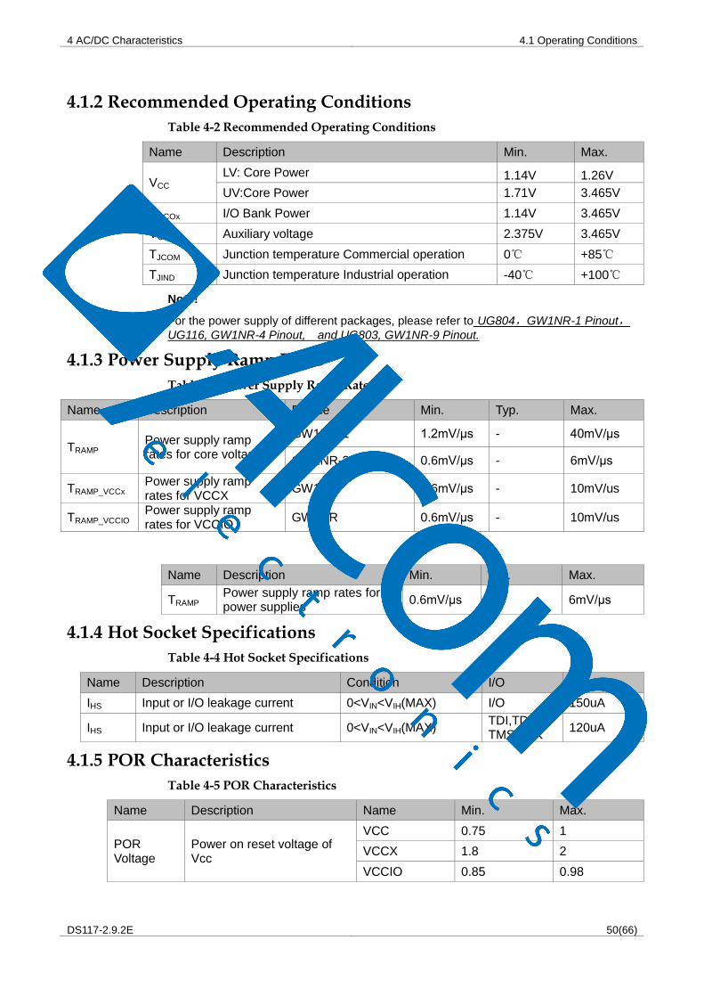
4 AC/DC Characteristics 4.1 Operating Conditions
DS117-2.9.2E 50(66)
4.1.2 Recommended Operating Conditions
Table 4-2 Recommended Operating Conditions
Name Description Min. Max.
VCC LV: Core Power 1.14V 1.26V
UV:Core Power 1.71V 3.465V
VCCOx I/O Bank Power 1.14V 3.465V
VCCX Auxiliary voltage 2.375V 3.465V
TJCOM Junction temperature Commercial operation 0℃ +85℃
TJIND Junction temperature Industrial operation -40℃ +100℃
Note!
For the power supply of different packages, please refer to UG804,GW1NR-1 Pinout,
UG116, GW1NR-4 Pinout, and UG803, GW1NR-9 Pinout.
4.1.3 Power Supply Ramp Rates
Table 4-3 Power Supply Ramp Rates
Name Description Device Min. Typ. Max.
TRAMP Power supply ramp rates for core voltage
GW1NR-1 1.2mV/μs - 40mV/μs
GW1NR-2/4/9 0.6mV/μs - 6mV/μs
TRAMP_VCCx Power supply ramp rates for VCCX
GW1NR 0.6mV/μs - 10mV/us
TRAMP_VCCIO Power supply ramp rates for VCCIO
GW1NR 0.6mV/μs - 10mV/us
Name Description Min. Typ. Max.
TRAMP Power supply ramp rates for all power supplies
0.6mV/μs - 6mV/μs
4.1.4 Hot Socket Specifications
Table 4-4 Hot Socket Specifications
Name Description Condition I/O Max.
IHS Input or I/O leakage current 0<VIN<VIH(MAX) I/O 150uA
IHS Input or I/O leakage current 0<VIN<VIH(MAX) TDI,TDO, TMS,TCK
120uA
4.1.5 POR Characteristics
Table 4-5 POR Characteristics
Name Description Name Min. Max.
POR Voltage
Power on reset voltage of Vcc
VCC 0.75 1
VCCX 1.8 2
VCCIO 0.85 0.98

4 AC/DC Characteristics 4.2 ESD
DS117-2.9.2E 51(66)
4.2 ESD Table 4-6 GW1NR ESD – HBM
Device GW1NR-1 GW1NR-2 GW1NR-4 GW1NR-9
QN88 - - HBM>1,000V HBM>1,000V
MG49P/MG49G/MG49PG - HBM>1,000V
MG81 - - HBM>1,000V -
MG100P/MG100PF/MG100PA/ MG100PT/ MG100PS
- - - HBM>1,000V
LQ144 - - - HBM>1,000V
FN32G HBM>1,000V - - -
Table 4-7 GW1NR ESD - CDM
Device GW1NR-1 GW1NR-2 GW1NR-4 GW1NR-9
QN88 - - CDM>500V CDM>500V
MG49P/MG49G/MG49PG - HBM>1,000V
MG81 - - CDM>500V -
MG100P/MG100PF/MG100PA/ MG100PT/ MG100PS
- - - CDM>500V
LQ144 - - - CDM>500V
FN32G CDM>500V - - -
4.3 DC Electrical Characteristics
4.3.1 DC Electrical Characteristics over Recommended Operating Conditions
Table 4-8 DC Electrical Characteristics over Recommended Operating Conditions
Name Description Condition Min. Typ. Max.
IIL,IIH Input or I/O leakage
VCCO<VIN<VIH (MAX) - - 210 µA
0V<VIN<VCCO - - 10 µA
IPU I/O Active Pull-up Current
0<VIN<0.7VCCO -30 µA - -150 µA
IPD I/O Active Pull-down Current
VIL (MAX)<VIN<VCCO 30 µA - 150 µA
IBHLS Bus Hold Low Sustaining Current
VIN=VIL (MAX) 30 µA - -
IBHHO Bus Hold High Sustaining Current
VIN=0.7VCCO -30 µA - -
IBHLO Bud HoldLow Overdrive Current
0≤VIN≤VCCO - - 150 µA
IBHHO BusHoldHigh Overdrive Current
0≤VIN≤VCCO - - -150 µA
VBHT Bus hold trip points
VIL (MAX) - VIH (MIN)
C1 I/O Capacitance 5 pF 8 pF

4 AC/DC Characteristics 4.3 DC Electrical Characteristics
DS117-2.9.2E 52(66)
Name Description Condition Min. Typ. Max.
VHYST Hysteresis for Schmitt Trigge inputs
VCCO=3.3V, Hysteresis= Large - 482mV -
VCCO=2.5V, Hysteresis= Large - 302mV -
VCCO=1.8V, Hysteresis= Large - 152mV -
VCCO=1.5V, Hysteresis= Large - 94mV -
VCCO=3.3V, Hysteresis= Small - 240mV -
VCCO=2.5V, Hysteresis= Small - 150mV -
VCCO=1.8V, Hysteresis= Small - 75mV -
VCCO=1.5V, Hysteresis= Small - 47mV -
4.3.2 Static Current
Table 4-9 Static Current
Device Name Description LV/UV Typ. (mA) Max.(mA)
GW1NR-1
ICC Core 电源电流(VCC=1.2V) LV 1.8 –
ICCX VCCX电源电流(VCCX=3.3V) LV 1 –
ICCO I/O Bank 电源电流(VCCO=2.5V) LV 0.8 –
GW1NR-4
ICC Core 电源电流 (VCC=1.2V) LV/UV 2.8 –
ICCX VCCX电源电流(VCCX=3.3V) LV/UV 1.15 –
ICCO I/O Bank 电源电流(VCCO=2.5V) LV/UV 0.55 –
GW1NR-9
ICC Core 电源电流(VCC=1.2V) LV/UV 3.5 –
ICCX VCCX电源电流(VCCX=3.3V) LV/UV 5 –
ICCO I/O Bank 电源电流(VCCO=2.5V) LV/UV 2 –

4 AC/DC Characteristics 4.3 DC Electrical Characteristics
DS117-2.9.2E 53(66)
4.3.3 Programming Current
Table 4-10 Programming Current
Device Description LV/UV Typ. (mA) Max.(mA)
GW1NR-1
Core current when programming Flash (VCC=1.2V)
LV – 1.9
VCCX current when programming Flash (VCCX=3.3V)
LV – 2.74
I/O Bank current when programming Flash (VCCO=2.5V)
LV 0.06 –
GW1NR-4
Core current when programming Flash (VCC=1.2V)
LV – –
VCCX current when programming Flash (VCCX=3.3V)
LV – –
I/O Bank current when programming Flash (VCCO=2.5V)
LV – –
GW1NR-9
Core current when programming Flash (VCC=1.2V)
LV –
VCCX current when programming Flash (VCCX=3.3V)
LV – –
I/O Bank current when programming Flash (VCCO=2.5V)
LV – –
4.3.4 I/O Operating Conditions Recommended
Table 4-11 I/O Operating Conditions Recommended
Name Output VCCO (V) Input VREF (V)
Min. Typ. Max. Min. Typ. Max.
LVTTL33 3.135 3.3 3.465 - - -
LVCMOS33 3.135 3.3 3.465 - - -
LVCMOS25 2.375 2.5 2.625 - - -
LVCMOS18 1.71 1.8 1.89 - - -
LVCMOS15 1.425 1.5 1.575 - - -
LVCMOS12 1.14 1.2 1.26 - - -
SSTL15 1.425 1.5 1.575 0.68 0.75 0.9
SSTL18_I 1.71 1.8 1.89 0.833 0.9 0.969
SSTL18_II 1.71 1.8 1.89 0.833 0.9 0.969
SSTL25_I 2.375 2.5 2.645 1.15 1.25 1.35
SSTL25_II 2.375 2.5 2.645 1.15 1.25 1.35
SSTL33_I 3.135 3.3 3.465 1.3 1.5 1.7
SSTL33_II 3.135 3.3 3.465 1.3 1.5 1
HSTL18_I 1.71 1.8 1.89 0.816 0.9 1.08
HSTL18_II 1.71 1.8 1.89 0.816 0.9 1.08
HSTL15 1.425 1.5 1.575 0.68 0.75 0.9
PCI33 3.135 3.3 3.465 - - -

4 AC/DC Characteristics 4.3 DC Electrical Characteristics
DS117-2.9.2E 54(66)
Name Output VCCO (V) Input VREF (V)
Min. Typ. Max. Min. Typ. Max.
LVPECL33E 3.135 3.3 3.465 - - -
MLVDS25E 2.375 2.5 2.625 - - -
BLVDS25E 2.375 2.5 2.625 - - -
RSDS25E 2.375 2.5 2.625 - - -
LVDS25E 2.375 2.5 2.625 - - -
SSTL15D 1.425 1.5 1.575 - - -
SSTL18D_I 1.71 1.8 1.89 - - -
SSTL18D_II 1.71 1.8 1.89 - - -
SSTL25D_I 2.375 2.5 2.625 - - -
SSTL25D_II 2.375 2.5 2.625 - - -
SSTL33D_I 3.135 3.3 3.465 - - -
SSTL33D_II 3.135 3.3 3.465 - - -
HSTL15D 1.425 1.575 1.89 - - -
HSTL18D_I 1.71 1.8 1.89 - - -
HSTL18D_II 1.71 1.8 1.89 - - -
4.3.5 IOB Single‐Ended DC Electrical Characteristic
Table 4-12 IOB Single‐Ended DC Electrical Characteristic
Name VIL VIH VOL
(Max) VOH (Min)
IOL
(mA) IOH
(mA) Min Max Min Max
LVCMOS33 LVTTL33
-0.3V 0.8V 2.0V 3.6V 0.4V VCCO-0.4V
4 -4
8 -8
12 -12
16 -16
24 -24
0.2V VCCO-0.2V 0.1 -0.1
LVCMOS25 -0.3V 0.7V 1.7V 3.6V 0.4V VCCO-0.4V
4 -4
8 -8
12 -12
16 -16
0.2V VCCO-0.2V 0.1 -0.1
LVCMOS18 -0.3V 0.35 x VCCO 0.65 x VCCO 3.6V 0.4V VCCO0.4V
4 -4
8 -8
12 -12
0.2V
VCCO-0.2V 0.1 -0.1
LVCMOS15 -0.3V 0.35 x VCCO 0.65 x VCCO 3.6V 0.4V VCCO-0.4V 4 -4
8 -8

4 AC/DC Characteristics 4.3 DC Electrical Characteristics
DS117-2.9.2E 55(66)
Name VIL VIH VOL
(Max) VOH (Min)
IOL
(mA) IOH
(mA) Min Max Min Max
0.2V VCCO-0.2V 0.1 -0.1
LVCMOS12 -0.3V 0.35 x VCCO 0.65 x VCCO 3.6V 0.4V VCCO-0.4V
2 -2
6 -6
0.2V VCCO-0.2V 0.1 -0.1
PCI33 -0.3V 0.3 x VCCO 0.5 x VCCO 3.6V 0.1 x VCCO
0.9 x VCCO 1.5 -0.5
SSTL33_I -0.3V VREF-0.2V VREF+0.2V 3.6V 0.7 VCCO-1.1V 8 -8
SSTL25_I -0.3V VREF-0.18V VREF+0.18V 3.6V 0.54V VCCO-0.62V 8 -8
SSTL25_II -0.3V VREF-0.18V VREF+0.18V 3.6V NA NA NA NA
SSTL18_II -0.3V VREF-0.125V VREF+0.125V 3.6V NA NA NA NA
SSTL18_I -0.3V VREF-0.125V VREF+0.125V 3.6V 0.40V VCCO-0.40V 8 -8
SSTL15 -0.3V VREF-0.1V VREF+ 0.1V 3.6V 0.40V VCCO-0.40V 8 -8
HSTL18_I -0.3V VREF-0.1V VREF+ 0.1V 3.6V 0.40V VCCO-0.40V 8 -8
HSTL18_II -0.3V VREF-0.1V VREF+ 0.1V 3.6V NA NA NA NA
HSTL15_I -0.3V VREF-0.1V VREF+ 0.1V 3.6V 0.40V VCCO-0.40V 8 -8
HSTL15_II -0.3V VREF-0.1V VREF+ 0.1V 3.6V NA NA NA NA
4.3.6 IOB Differential Electrical Characteristics
Table 4-13 IOB Differential Electrical Characteristics
Name Description Condition Min. Typ. Max. Unit
VINA,VINB Input Voltage 0 - 2.4 V
VCM Input Common Mode Voltage Half the Sum of the Two Inputs
0.05 - 2.35 V
VTHD Differential Input Threshold Difference Between the Two Inputs
±100 - - mV
IIN Input Current Power On or Power Off
- - ±10 µA
VOH Output High Voltage for VOP or VOM
RT = 100Ω - - 1.60 V
VOL Output Low Voltage for VOP or VOM
RT = 100Ω 0.9 - - V
VOD Output Voltage Differential (VOP - VOM), RT = 100Ω
250 350 450 mV
ΔVOD Change in VOD Between High and Low
- - 50 mV
VOS Output Voltage Offset (VOP + VOM)/2, RT = 100Ω
1.125 1.20 1.375 V
ΔVOS Change in VOS Between High and Low
- - 50 mV
IS Short-circuit current VOD = 0V output short-circuit
- - 15 mA

4 AC/DC Characteristics 4.4 Switching Characteristics
DS117-2.9.2E 56(66)
4.4 Switching Characteristics
4.4.1 Internal Switching Characteristics
Table 4-14 CFU Block Internal Timing Parameters
Name Description Speed Grade
Unit Min Max
tLUT4_CFU LUT4 delay - 0.674 ns
tLUT5_CFU LUT5 delay - 1.388 ns
tLUT6_CFU LUT6 delay - 2.01 ns
tLUT7_CFU LUT7 delay - 2.632 ns
tLUT8_CFU LUT8 delay - 3.254 ns
tSR_CFU Set/Reset to Register output - 1.86 ns
tCO_CFU Clock to Register output - 0.76 ns
4.4.2 BSRAM Internal Timing Parameters
Table 4-15 BSRAM Internal Timing Parameters
Name Description Speed Grade
Unit Min Max
tCOAD_BSRAM Clock to output from read address/data - 5.10 ns tCOOR_BSRAM Clock to output from output register - 0.56 ns
4.4.3 DSP Internal Timing Parameters
Table 4-16 DSP Internal Timing Parameters
Name Description Speed Grade
Unit Min Max
tCOIR_DSP Clock to output from input register - 4.80 ns tCOPR_DSP Clock to output from pipeline register - 2.40 ns tCOOR_DSP Clock to output from output register - 0.84 ns

4 AC/DC Characteristics 4.4 Switching Characteristics
DS117-2.9.2E 57(66)
4.4.4 Gearbox Switching Characteristics
Table 4-17 Gearbox Internal Timing Parameters
Device Name Description Min. Unit
GW1NR-1/4
FMAXIDDR 2:1 Gearbox maximum input serial rate 1000 Mbps
FMAXIDES4 4:1 Gearbox maximum input serial rate 500 Mbps
FMAXIDESx 7:1/8:1/10:1 Gearbox maximum input serial rate
1000 Mbps
FMAXODDR 1:2 Gearbox maximum input serial rate 1000 Mbps
FMAXOSER4 1:4 Gearbox maximum output serial rate 500 Mbps
FMAXOSERx 1:7/1:8/1:10 Gearbox maximum output serial rate
1000 Mbps
GW1NR-9
FMAXIDDR 2:1 Gearbox maximum input serial rate 1200 Mbps
FMAXIDES4 4:1 Gearbox maximum input serial rate 600 Mbps
FMAXIDESx 7:1/8:1/10:1/16:1 Gearbox maximum input serial rate
1200 Mbps
FMAXODDR 1:2 Gearbox maximum output serial rate 1200 Mbps
FMAXOSER4 1:4 Gearbox maximum output serial rate 600 Mbps
FMAXOSERx 1:7/1:8/1:10/1:16 Gearbox maximum output serial rate
1200 Mbps
Note!
LVDS IO speed can be up to 1Gbps, but note that for 1:4 Gearbox and 1:2 Gearbox, the internal core may not reach the corresponding speed.
Table 4-18 Single-ended IO Fmax
Name Fmax
Min. Value(Mhz)
DriverStrength = 4mA DriverStrength > 4mA
LVTTL33 150 300
LVCMOS33 150 300
LVCMOS25 150 300
LVCMOS18 150 300
LVCMOS15 150 200
LVCMOS12 150 150
Note!
The test loading is 30pF capacitor.

4 AC/DC Characteristics 4.4 Switching Characteristics
DS117-2.9.2E 58(66)
4.4.5 External Switching Characteristics
Table 4-19 External Switching Characteristics
Name Description Device -4 -5 -6
Unit Max Max Max
HCLK Tree delay TBD TBD TBD 1ns TBD
PCLK Tree delay TBD TBD TBD 8ns TBD
Pin-LUT-Pin Delay TBD TBD TBD 2ns TBD
IO Buffer delay TBD TBD TBD TBD TBD
4.4.6 On chip Oscillator Output Frequency
Table 4-20 On chip Oscillator Output Frequency
Name Description Min. Typ. Max.
fMAX
On chip Oscillator Output Frequency
(0 ~ +85℃)
GW1NR-4 99.75MHz 105MHz 110.25MHz
GW1NR-1/2/9 118.75MHz 125MHz 131.25MHz
On chip Oscillator Output Frequency
(-40 ~ +100℃)
GW1NR-4 94.5MHz 105MHz 115.5MHz
GW1NR-1/2/9 112.5MHz 125MHz 137.5MHz
tDT Clock Duty Cycle 43% 50% 57%
tOPJIT Clock Period Jitter 0.01 UIPP 0.012 UIPP 0.02 UIPP
4.4.7 PLL Switching Characteristics
Table 4-21 PLL Switching Characteristics
Device Speed Name Min. Max.
GW1NR-4
C6/I5 A4
CLKIN 3MHZ 400MHZ
PFD 3MHZ 400MHZ
VCO 400MHZ 1000MHZ
CLKOUT 3.125MHZ 500MHZ
C5/I4
CLKIN 3MHZ 320MHZ
PFD 3MHZ 320MHZ
VCO 320MHZ 800MHZ
CLKOUT 2.5MHZ 400MHZ
GW1NR-9
C7/I6 C6/I5
CLKIN 3MHZ 400MHZ
PFD 3MHZ 400MHZ
VCO 400MHZ 1200MHZ
CLKOUT 3.125MHZ 600MHZ
C5/I4
CLKIN 3MHZ 320MHZ
PFD 3MHZ 320MHZ
VCO 320MHZ 960MHZ
CLKOUT 2.5MHZ 480MHZ

4 AC/DC Characteristics 4.4 Switching Characteristics
DS117-2.9.2E 59(66)
Device Speed Name Min. Max.
GW1NR-1
C6/I5
CLKIN 3MHZ 400MHZ
PFD 3MHZ 400MHZ
VCO 400MHZ 900MHZ
CLKOUT 3.125MHZ 450MHZ
C5/I4
CLKIN 3MHZ 320MHZ
PFD 3MHZ 320MHZ
VCO 320MHZ 720MHZ
CLKOUT 2.5MHZ 360MHZ
GW1NR-2 C7/I6
CLKIN 3MHZ 400MHZ
PFD 3MHZ 400MHZ
VCO 400MHZ 800MHZ
CLKOUT 3.125MHZ[1]
800MHZ
Note!
[1]The min. output frequency for different channels may be different. The min. output frequency for channel A is VCO/128, which is 3.125MHZ/2.5MHZ; Channel B/C/D needs to be judged according to whether it is cascaded (parameter). If it is not cascaded, it is the same as channel A; if it is cascaded, it needs to be divided by 128 again.

4 AC/DC Characteristics 4.5 User Flash Characteristics
DS117-2.9.2E 60(66)
4.5 User Flash Characteristics
4.5.1 DC Characteristics 1
(TJ = -40~+100℃, VCC = 1.08~1.32V, VCCX = 1.62~3.63V, VSS = 0V)
Table 4-22 User Flash DC Characteristics
Name Parameter Max.
Unit Wake-up Time
Condition VCC
3 VCCX
Read mode (w/I 25ns)
1
ICC12
2.19 0.5 mA NA Min. Clcok period, duty cycle 100%, VIN = “1/0”
Write mode 0.1 12 mA NA
Erase mode 0.1 12 mA NA
Page Erasure Mode
0.1 12 mA NA
Read mode static current (25-50ns)
ICC2 980 25 μA NA
XE=YE=SE=“1”, between T=Tacc and T=50ns, I/O=0mA; later than T=50ns, read mode is turned off, and I/O current is the current of standby mode.
Standby mode
ISB 5.2 20 μA 0 VSS, VCCX, and VCC
Note!
[1] Means the average current, and the peak value is higher than the average one.
[2] Caculated in different Tnew clock periods.
- Tnew< Tacc is not allowed
- Tnew = Tacc
- Tacc< Tnew - 50ns: ICC1 (new) = (ICC1 - ICC2)(Tacc/Tnew) + ICC2
- Tnew>50ns: ICC1 (new) = (ICC1 - ICC2)(Tacc/Tnew) + 50ns x ICC2/Tnew + ISB
- t > 50ns, ICC2 = ISB
[3] VCC must be greater than 1.08V from the zero wake-up time.
4.5.2 Timing Parameters1,5,6
(TJ = -40~+100℃, VCC = 0.95~1.05V, VCCX = 1.7~3.45V, VSS = 0V)
Table 4-23 User Flash Timing Parameters
User Modes Parameter Name Min. Max. Unit
Access time2
WC1
Tacc3
- 25 ns
TC - 22 ns
BC - 21 ns
LT - 21 ns
WC - 25 ns
Program/Erase to data storage Tnvs 5 - μs
Data storage hold time Tnvh 5 - μs
Data storage hold time (Overall erase) Tnvh1 100 - μs
Time from data storage to program setup
Tpgs 10 - μs

4 AC/DC Characteristics 4.5 User Flash Characteristics
DS117-2.9.2E 61(66)
User Modes Parameter Name Min. Max. Unit
Program hold time Tpgh 20 - ns
Write time Tprog 8 16 μs
Write ready time Twpr >0 - ns
Erase hold time Twhd >0 - ns
Time from control signal to write/Erase setup
Tcps -10 - ns
Time from SE to read setup Tas 0.1 - ns
E pulse high level time Tpws 5 - ns
Adress/data setup time Tads 20 - ns
Adress/data hold time Tadh 20 - ns
Data hold-up time Tdh 0.5 - ns
Read mode address hold time
3
WC1 Tah 25 - ns
TC 22 - ns
BC 21 - ns
LT 21 - ns
WC 25 - ns
SE pulse low level time Tnws 2 - ns
Recovery time Trcv 10 - μs
Data storage time Thv4
- 6 ms
Erasure time Terase 100 120 ms
Overall erase time Tme 100 120 ms
Wake-up time from power down to standby mode
Twk_pd 7 - μs
Standby hold time Tsbh 100 - ns
VCC setup time Tps 0 - ns
VCCX hold time Tph 0 - ns
Note!
[1] The parameter values may change;
[2] The values are simulation data only.
[3]After XADR, YADR, XE, and YE are valid, Tacc start time is SE rising edge. DOUT is kept until the next valid read operation;
[4]Thv is the time between write and the next erasure.The same address can not be written twice before erasure, so does the same register. This limitation is for safety;
[5]Both the rising edge time and falling edge time for all waveform is 1ns;
[6] TX, YADR, XE, and YE hold time need to be Tacc at leaset, and Tacc start from SE rising edge.

4 AC/DC Characteristics 4.5 User Flash Characteristics
DS117-2.9.2E 62(66)
4.5.3 Operation Timing Diagrams
Figure 4-1 GW1NR User Flash Read Operation
Figure 4-2 GW1NR User Flash Program Operation
Figure 4-3 GW1NR User Flash Erase Operation

4 AC/DC Characteristics 4.6 Configuration Interface Timing Specification
DS117-2.9.2E 63(66)
4.6 Configuration Interface Timing Specification The GW1NR series of FPGA products GowinCONFIG support six
configuration modes: AUTO BOOT, SSPI, MSPI, DUAL BOOT, SERIAL, and CPU. For more detailed information, please refer to UG290, Gowin FPGA Products Programming and Configureation User Guide.

5 Ordering Information 5.1 Part Name
DS117-2.9.2E 64(66)
5Ordering Information
5.1 Part Name Part naming description is as shown in Figure 5-1 and Figure 5-2.
Note!
For further pin number and package type information, please refer to 2.2 Product Resources and 2.3 Package Information.
The LittleBee® family devices and Arora family devices of the same speed level have
different speed.
Both “C” and “I” are used in GOWIN part name marking for one same device, such as C6/I5, C7/I6, etc. GOWIN devices are screened using industrial standards, so one same device can be used for both industrial (I) and commercial (C) applications. The
maximum temperature of the industrial grade is 100℃, and the maximum
temperature of the commercial grade is 85℃. Therefore, if the same chip meets the
speed level 7 in the commercial grade application, the speed level is 6 in the industrial grade application.
Figure 5-1 Part Naming–ES
-
Product Series
GW1NR
Logic Density
1 1,152 LUTs
4 4,608 LUTs
9 8,640 LUTs
Core Supply Voltage
LV 1.2V
UV 3.3VPackage
QN88 (QFN88, 0.4mm)
QN88P (QFN88P, 0.4mm)
MG81P (MBGA81P, 0.5mm)
MG100P (MBGA100P, 0.5mm)
MG100PF (MBGA100PF, 0.5mm)
MG100PA (MBGA100PA, 0.5mm)
MG100PT (MBGA100PT, 0.5mm)
MG100PS (MBGA100PS, 0.5mm)
LQ144P (LQFP144P, 0.5mm)
FN32G (QFN32G, 0.4mm)
GW1NR XX ESX XXXXXX
Optional Suffix
ES Engineering Sample

5 Ordering Information 5.1 Part Name
DS117-2.9.2E 65(66)
Figure 5-2 Part Naming–Production
-
Product Series
GW1NR
Logic Density
1 1,152 LUTs
2 2,304 LUTs
4 4,608 LUTs
9 8,640 LUTs
Core Supply Voltage
LV 1.2V
UV 3.3VPackage
QN88 (QFN88, 0.4mm)
QN88P (QFN88P, 0.4mm)
MG49P (MBGA49P, 0.5mm)
MG49G (MBGA49G, 0.5mm)
MG49PG (MBGA49PG, 0.5mm)
MG81P (MBGA81P, 0.5mm)
MG100P (MBGA100P, 0.5mm)
MG100PF (MBGA100PF, 0.5mm)
MG100PA (MBGA100PA, 0.5mm)
MG100PT (MBGA100PT, 0.5mm)
MG100PS (MBGA100PS, 0.5mm)
LQ144P (LQFP144P, 0.5mm)
FN32G (QFN32G, 0.4mm)
Grade
C Commercial
I Industrial
Speed
4 Slowest /5 /6 /7 Fastest
GW1NR XX CX/IXX XXXXXX

5 Ordering Information 5.2 Package Mark Example
DS117-2.9.2E 66(66)
5.2 Package Mark Example The device information of GOWINSEMI is marked on the chip surface,
as shown in Figure 5-3.
Figure 5-3 Package Mark Example
GW1NR-LV4 Q N 8 8 C 6 / I 5 Y Y W W L L L L L L L L L
GW1NR-LV4LQ144C6/I5
YYWW
LLLLLLLLL
Part Number
Date Code
Lot Number
Part Number[1]
Date CodeLot Number
GW1NR-LV4 Q N 8 8 C 6 / I 5 Y Y W W B L L L L L L L L L
GW1NR-LV4LQ144C6/I5
YYWW B
LLLLLLLLL
Part Number
Date Code[2]
Lot Number
Part Number[1]
Date Code[2]
Lot Number
GW1NR-LV9 Q N 8 8 C 6 / I 5 Y Y W W C L L L L L L L L L
GW1NR-LV9LQ144C6/I5
YYWWC
LLLLLLLLL
Part Number
Date Code[3]
Lot Number
Part Number[1]
Date Code[3]
Lot Number
GW1NR-LV2MG49PC7/I6
YYWWXXXX
LLLLLLLLL
Part NumberDate Code
Lot Number
GW1NR-LV2
MG49PC7/I6
YYWWXXXX
LLLLLLLLL
Part Number[1]
Part Number[1]
Date CodeLot Number
Note!
[1] The first two lines in the right figure above are the “Part Number”.
[2] The Data Code followed by a “B” is for B version devices.
[3] The Data Code followed by a “C” is for C version devices.

Singel 3 | B-2550 Kontich | Belgium | Tel. +32 (0)3 458 30 33 | [email protected] | www.alcom.be
Rivium 1e straat 52 | 2909 LE Capelle aan den Ijssel | The Netherlands | Tel. +31 (0)10 288 25 00 | [email protected] | www.alcom.nl