Embed Size (px)
Citation preview
Growth, Defect Structure and Critical Currentsin YBa2Cu3O7¡± Thin Films
Groei, Defektstruktuur en Kritische Stromenin Dunne YBa2Cu3O7¡± Lagen

Cover: three dimensional impression of the surface of a laser ablated YBa2Cu3O7¡±
…lm, etched in the dislocation speci…c wet-chemical etchand Br/ethanol (and imagedby means of atomic force microscopy). At dislocation sites the …lm dissolves faster,resulting in the formation of square, sharp bottomed etch pits. The density of etchpits is a measure for the density of dislocations emerging at the …lm surface.
This work is part of the research program of FOM (stichting Fundamenteel Onderzoekder Materie), which is …nancially supported by NWO (Nederlandse organisatie voorWetenschappelijk Onderzoek). The work was carried out at:
Vrije UniversiteitFaculty of SciencesDivision of Physics and AstronomyDe Boelelaan 1081NL-1081 HV AmsterdamThe Netherlands
ISBN 90 ¡ 9014604 ¡ 0
VRIJE UNIVERSITEIT
Growth, Defect Structure and Critical Currentsin YBa2Cu3O7¡± Thin Films
ACADEMISCH PROEFSCHRIFT
ter verkrijging van de graad van doctor aande Vrije Universiteit te Amsterdam,op gezag van de rector magni…cus
prof.dr. T. Sminia,in het openbaar te verdedigen
ten overstaan van de promotiecommissievan de faculteit der Exacte Wetenschappen n Natuurkunde en Sterrenkunde
op dinsdag 1 mei 2001 om 13.45 uurin het hoofdgebouw van de universiteit,
De Boelelaan 1105
door
Jeroen Marcel Huijbregtse
geboren te Middelburg

Promotor: prof.dr. R.P. GriessenCopromotor: dr. B. Dam

Voor mijn ouders

Contents
1 General introduction 11.1 The microstructural basis of high jc . . . . . . . . . . . . . . . . . . . . . . . . . . . . . . . . 21.2 Basic ingredients . . . . . . . . . . . . . . . . . . . . . . . . . . . . . . . . . . . . . . . . . . . . . . . . . 4
1.2.1 Growth of epitaxial …lms . . . . . . . . . . . . . . . . . . . . . . . . . . . . . . . . . . . . 41.2.2 Strong vortex pinning . . . . . . . . . . . . . . . . . . . . . . . . . . . . . . . . . . . . . . . 6
1.3 Strategy . . . . . . . . . . . . . . . . . . . . . . . . . . . . . . . . . . . . . . . . . . . . . . . . . . . . . . . . 8References . . . . . . . . . . . . . . . . . . . . . . . . . . . . . . . . . . . . . . . . . . . . . . . . . . . . . . 9
2 Conditions for stoichiometric transfer in pulsed laser deposition 112.1 Introduction . . . . . . . . . . . . . . . . . . . . . . . . . . . . . . . . . . . . . . . . . . . . . . . . . . . . 122.2 PLD set-up and experimental procedures . . . . . . . . . . . . . . . . . . . . . . . . . . 132.3 Stoichiometry and …lm properties . . . . . . . . . . . . . . . . . . . . . . . . . . . . . . . . . 15
2.3.1 Amorphous YBa2Cu3O6+x …lms . . . . . . . . . . . . . . . . . . . . . . . . . . . . 152.3.2 Crystalline YBa2Cu3O7¡± …lms . . . . . . . . . . . . . . . . . . . . . . . . . . . . . 19
2.4 Laser-target interaction . . . . . . . . . . . . . . . . . . . . . . . . . . . . . . . . . . . . . . . . . . 242.4.1 Region I: target degradation . . . . . . . . . . . . . . . . . . . . . . . . . . . . . . . . 242.4.2 Region II: di¤usion-assisted preferential ablation . . . . . . . . . . . . . . 252.4.3 Region III: stoichiometric deposition . . . . . . . . . . . . . . . . . . . . . . . . . 30
2.5 Conclusions . . . . . . . . . . . . . . . . . . . . . . . . . . . . . . . . . . . . . . . . . . . . . . . . . . . . 32References . . . . . . . . . . . . . . . . . . . . . . . . . . . . . . . . . . . . . . . . . . . . . . . . . . . . . 33
3 Origin of high critical currents 373.1 Introduction . . . . . . . . . . . . . . . . . . . . . . . . . . . . . . . . . . . . . . . . . . . . . . . . . . . . 383.2 Revealing dislocations . . . . . . . . . . . . . . . . . . . . . . . . . . . . . . . . . . . . . . . . . . . 39
3.2.1 Principle of etching . . . . . . . . . . . . . . . . . . . . . . . . . . . . . . . . . . . . . . . . 393.2.2 Etching sputtered …lms . . . . . . . . . . . . . . . . . . . . . . . . . . . . . . . . . . . . 413.2.3 Repetitive etching . . . . . . . . . . . . . . . . . . . . . . . . . . . . . . . . . . . . . . . . . 42
3.3 Dislocation density and distribution . . . . . . . . . . . . . . . . . . . . . . . . . . . . . . . 443.3.1 Tuning the dislocation density . . . . . . . . . . . . . . . . . . . . . . . . . . . . . . 443.3.2 Dislocation distribution . . . . . . . . . . . . . . . . . . . . . . . . . . . . . . . . . . . . 45
i

3.4 Strong pinning by dislocations . . . . . . . . . . . . . . . . . . . . . . . . . . . . . . . . . . . . 493.4.1 The characteristic …eld . . . . . . . . . . . . . . . . . . . . . . . . . . . . . . . . . . . . . 493.4.2 Comparison with arti…cial linear defects . . . . . . . . . . . . . . . . . . . . . . 533.4.3 Implications for vortex pinning . . . . . . . . . . . . . . . . . . . . . . . . . . . . . . 55
3.5 Conclusions . . . . . . . . . . . . . . . . . . . . . . . . . . . . . . . . . . . . . . . . . . . . . . . . . . . . 56References . . . . . . . . . . . . . . . . . . . . . . . . . . . . . . . . . . . . . . . . . . . . . . . . . . . . . 56
4 Comparison of dislocations with alternative pinning sites 594.1 Introduction . . . . . . . . . . . . . . . . . . . . . . . . . . . . . . . . . . . . . . . . . . . . . . . . . . . . 604.2 The post-anneal treatment . . . . . . . . . . . . . . . . . . . . . . . . . . . . . . . . . . . . . . . 61
4.2.1 E¤ect on the superconducting current . . . . . . . . . . . . . . . . . . . . . . . . 614.2.2 Microstructural consequences . . . . . . . . . . . . . . . . . . . . . . . . . . . . . . . 64
4.3 Vortex pinning mechanisms . . . . . . . . . . . . . . . . . . . . . . . . . . . . . . . . . . . . . . 704.3.1 Linear defects . . . . . . . . . . . . . . . . . . . . . . . . . . . . . . . . . . . . . . . . . . . . . 704.3.2 Planar defects . . . . . . . . . . . . . . . . . . . . . . . . . . . . . . . . . . . . . . . . . . . . 734.3.3 Point defects. . . . . . . . . . . . . . . . . . . . . . . . . . . . . . . . . . . . . . . . . . . . . . 784.3.4 Precipitates . . . . . . . . . . . . . . . . . . . . . . . . . . . . . . . . . . . . . . . . . . . . . . 784.3.5 Surface roughness e¤ects . . . . . . . . . . . . . . . . . . . . . . . . . . . . . . . . . . . 79
4.4 Conclusions . . . . . . . . . . . . . . . . . . . . . . . . . . . . . . . . . . . . . . . . . . . . . . . . . . . . 79References . . . . . . . . . . . . . . . . . . . . . . . . . . . . . . . . . . . . . . . . . . . . . . . . . . . . . 81
5 Mechanisms of dislocation formation 855.1 Introduction . . . . . . . . . . . . . . . . . . . . . . . . . . . . . . . . . . . . . . . . . . . . . . . . . . . . 865.2 Substrate-induced dislocations . . . . . . . . . . . . . . . . . . . . . . . . . . . . . . . . . . . . 875.3 Growth-induced dislocations . . . . . . . . . . . . . . . . . . . . . . . . . . . . . . . . . . . . . . 905.4 Conclusions . . . . . . . . . . . . . . . . . . . . . . . . . . . . . . . . . . . . . . . . . . . . . . . . . . . . 93
References . . . . . . . . . . . . . . . . . . . . . . . . . . . . . . . . . . . . . . . . . . . . . . . . . . . . . 94
6 The …rst stages of hetero-epitaxial growth: phase stability 956.1 Introduction . . . . . . . . . . . . . . . . . . . . . . . . . . . . . . . . . . . . . . . . . . . . . . . . . . . . 966.2 Single terminated (100) SrTiO3 . . . . . . . . . . . . . . . . . . . . . . . . . . . . . . . . . . . 98
6.2.1 Determining the termination . . . . . . . . . . . . . . . . . . . . . . . . . . . . . . . . 986.2.2 SrO-terminated substrates . . . . . . . . . . . . . . . . . . . . . . . . . . . . . . . . . 105
6.3 Preferential precipitation of YBaCuO. . . . . . . . . . . . . . . . . . . . . . . . . . . . . 1056.3.1 Origin . . . . . . . . . . . . . . . . . . . . . . . . . . . . . . . . . . . . . . . . . . . . . . . . . . 1066.3.2 Experimental observations . . . . . . . . . . . . . . . . . . . . . . . . . . . . . . . . . 1066.3.3 Stacking sequence . . . . . . . . . . . . . . . . . . . . . . . . . . . . . . . . . . . . . . . . 110
6.4 E¤ect on threading dislocations . . . . . . . . . . . . . . . . . . . . . . . . . . . . . . . . . . 1126.5 Conclusions . . . . . . . . . . . . . . . . . . . . . . . . . . . . . . . . . . . . . . . . . . . . . . . . . . . 114
References . . . . . . . . . . . . . . . . . . . . . . . . . . . . . . . . . . . . . . . . . . . . . . . . . . . . 114
7 The …rst stages of hetero-epitaxial growth: coherent islanding 1177.1 Introduction . . . . . . . . . . . . . . . . . . . . . . . . . . . . . . . . . . . . . . . . . . . . . . . . . . . 118
ii

7.2 AFM and XRD observations . . . . . . . . . . . . . . . . . . . . . . . . . . . . . . . . . . . . 1197.2.1 Surface morphology . . . . . . . . . . . . . . . . . . . . . . . . . . . . . . . . . . . . . . . 1197.2.2 Crystal structure . . . . . . . . . . . . . . . . . . . . . . . . . . . . . . . . . . . . . . . . . 1227.2.3 In-plane ordering . . . . . . . . . . . . . . . . . . . . . . . . . . . . . . . . . . . . . . . . . 125
7.3 Nucleation, growth and dislocation formation . . . . . . . . . . . . . . . . . . . . . . 1287.3.1 Correlating the two component rocking curves to the defect
structure . . . . . . . . . . . . . . . . . . . . . . . . . . . . . . . . . . . . . . . . . . . 1287.3.2 The coherent Stranski-Krastanow growth mode . . . . . . . . . . . . . . 1337.3.3 Formation of threading dislocations . . . . . . . . . . . . . . . . . . . . . . . . . 137
7.4 Conclusions . . . . . . . . . . . . . . . . . . . . . . . . . . . . . . . . . . . . . . . . . . . . . . . . . . . 140References . . . . . . . . . . . . . . . . . . . . . . . . . . . . . . . . . . . . . . . . . . . . . . . . . . . . 141
Summary 145
Samenvatting 149
List of publications 155
Cirruculum Vitae 159
Dankwoord 161
iii

Chapter 1
General introduction
Fundamental investigations of high-Tc superconductors have mainly been done forsingle crystalline materials. In this thesis we consider thin …lms and show that theirintrinsic defect structure quite paradoxically leads to improved superconducting prop-erties. In particular, this thesis addresses three central questions: (i) what is thestructural defect that is responsible for the extremely high superconducting currentsthat can be passed without dissipation (ii) what is the mechanism by which thesedefects are induced during …lm growth and (iii) can we control the growth processin such a way that we can tune the superconducting properties? In this chapter thebasic concepts are introduced and a research strategy is developed.
2 Chapter 1 General introduction
1.1 The microstructural basis of high jcAfter the discovery of the …rst high-Tc (HTc) superconductor in 1986 [1], the transi-tion temperature Tc, below which the zero resistivity state is reached, quickly raisedabove the liquid nitrogen temperature of 77 K for YBa2Cu3O7¡± in 1987 [2]. Sincethis temperature is commercially feasible, technological application of HTc cuprates inhigh current, high frequency and highly sensitive magnetic devices have become moreinteresting [3]. Examples of large scale applications are power cables that transportelectrical currents with low energy dissipation and powerful superconducting mag-nets. One of the major drawbacks of the cuprates is their brittleness, which makestheir processing di¢cult. Thin …lms do not su¤er from this limitation. They are ap-plicable in electronic applications such as passive microwave components (resonators,antennas), magnetometers and digital circuits.However, as outlined below, a problem arises if one tries to pass a transport currentat density j without dissipation through such a material. Cuprate superconductorsare characterized [4] by an extremely small coherence length », which is of the orderof the unit cell (for instance, » = 1:5 nm for YBa2Cu3O7¡± along the CuO2 planesat low temperatures). This parameter sets the length scale for spatial variations inthe superconducting order parameter (or the density of superconducting electrons).On the other hand, the length scale for the spatial variations in magnetic induction(the magnetic penetration depth ¸) is two orders of magnitude larger. It can beshown [4] that for ¸=» > 1=
p2 a mixed state occurs above a magnetic …eld Bc1 in
which normal and superconducting regions coexist. These normal regions of size 2»carry a quantized amount of magnetic ‡ux ©0 = 2:068 £ 10¡15 Tm2 and are calledvortices. The areal density nv of vortices is given by B = nv©0, where B = ¹0His the local magnetic induction. The presence of vortices within a superconductingmatrix is not a problem by itself. As long as the vortex cores do not overlap, thereis a fully superconducting path within the material. However, if a current (density) jis passed through the superconductor, a Lorentz force FL is exerted on the vortices,which equals j©0 per unit length in a perpendicular con…guration. The problem isthat these vortices will start to move under in‡uence of FL. In such a situation anelectrical current passes through the normal core of the vortex [5], causing dissipationand noise.To avoid this problem, either the creation of vortices has to be prevented or vortexmotion must be prohibited. Let us consider the creation of vortices …rst. As dis-cussed above, at magnetic …elds below Bc1 = ©0 ln(¸=»)=(4¼¸2) there are no vortices.In cuprate superconductors the penetration depth ¸ is large, which results in a smalllower critical …eld Bc1. Therefore, the self-…eld of a current that is passed throughsuch a superconductor will immediately introduce vortices. Moreover, in many tech-nological applications an external magnetic …eld is present (in addition to the earthmagnetic …eld). Hence, preventing the creation of vortices is not a feasible solution tocircumvent dissipation. Fortunately, nature provides an alternative solution. Withinthe superconductor, there are always energetically more favorable sites for vortices.These are defects in the crystal structure, ranging from small defects (such as oxygenvacancies) to extended defects (such as grain boundaries). At those sites, the super-
Section 1.1 The microstructural basis of high jc 3
conducting order parameter is depressed and it costs less energy to drive such regionsin the normal state within the superconducting condensate. Consequently, a certaincurrent (density) is necessary to depin a vortex from the energetically favorable de-fect sites. The current which overcomes the pinning force exerted by defects is calledthe critical current density jc.In this simple picture, the superconducting properties improve by adding defects!There is, however, an optimum for jc with respect to structural disorder. If thematerial becomes too defective, the superconducting order parameter is depressedeverywhere. The pinning sites in such a material are not very e¤ective, which resultsin a low jc. Hence, the highest jc is expected in structurally perfect superconductorscontaining localized defective regions. On the other hand, such regions should not beso large that they act as weak links between di¤erent parts of the superconductor.Weak links limit the critical current again.Soon after the discovery of bulk HTc superconductors, the …rst YBa2Cu3O7¡± singlecrystals were synthesized [6]. In single crystals the vortex pinning is facilitated byrandomly distributed point defects, resulting in a jc of the order of 1010 A/m2 [7].Arti…cially inducing columnar defects by means of heavy ion irradiation only locallydepresses superconductivity and jc increases by a factor of ten [8]. Surprisingly, thecritical currents in as-grown YBa2Cu3O7¡± …lms [9] (i.e., without any attempt toinduce disorder arti…cially) are even larger. As shown in this thesis, current densitiesup to 1012 A/m2 are found at low temperatures and small magnetic …elds. Comparedto single crystals, the structural quality of these …lms is much poorer [10]. Therefore,it was concluded [11, 12] that correlated disorder (extended defects) are responsible forboth the high currents and the strong magnetic …eld dependence of these currents,analogous to irradiated single crystals. However, somehow the natural disorder in…lms is far more e¤ective in pinning vortices than the arti…cially induced disorder insingle crystals.Remarkably, in the …rst ten years after the discovery of the …rst cuprate supercon-ductor, the speci…c defect responsible for the high currents in …lms was not identi…ed.Motivated by this peculiar state of a¤airs, in September 1996 the present Ph.D. workwas started to address pinning in …lms from a materials science point of view. Themain goal of this thesis is to identify the dominant natural pinning sites in thin …lmsof YBa2Cu3O7¡± grown by pulsed laser deposition on single crystalline (100) SrTiO3
substrates. Clearly, if one wishes to tune the superconducting properties, we needto control the density of these defects. Hence, the mechanism by which correlateddisorder is induced during the fabrication of such …lms is equally important.In the remaining of this chapter we expose the strategy (i) to identify the strongestpinning sites (ii) to unravel the mechanism by which they are created and (iii) to …nda way to tailor the superconducting properties of the …lms making use of the …rst twopoints. Finally, we note that this Ph.D. research project is divided into two parts. Thepresent thesis concentrates on the microstructural properties of the YBa2Cu3O7¡±
…lms. While our emphasis is on establishing qualitative (or semi-quantitative) corre-
4 Chapter 1 General introduction
lations between the defect structure and superconducting properties of these …lms, asubsequent thesis by F.C. Klaassen [13] will cover ‡ux pinning in detail.1
1.2 Basic ingredients
To investigate pinning in …lms, we …rst have to …nd a reproducible deposition process.Only when we can reproducibly vary one type of defects, we can identify the defectsthat are responsible for pinning. The two basic ingredients, …lm growth and ‡uxpinning, are shortly discussed below.
1.2.1 Growth of epitaxial …lms
In general, thin …lms result from condensation of the evaporated constituents ontoa substrate material. Although there are many techniques to evaporate these con-stituents [14], the process of …lm growth is, in …rst approximation, the same. In allthin …lm growth processes, elevated substrate temperatures and pressures are usedto ensure that the desired phase is thermodynamically stable and that it is kineti-cally allowed to form at the applied growth conditions. Inducing crystallization doesnot necessarily result in the formation of epitaxial …lms. Epitaxial …lms are struc-turally aligned with the substrate material. This is only possible if the substrate and…lm material are structurally compatible. For instance, the …lm and substrate ma-terial must have comparable lattice constants and thermal expansion coe¢cients. Inthis thesis, we grow orthorhombic YBa2Cu3O7¡± …lms epitaxially onto cubic (100)SrTiO3 substrates (1% lattice mismatch).We employ pulsed laser ablation (PLD) [15] to deposit the YBa2Cu3O7¡± …lms. Be-sides the relatively low capital costs as compared to for instance molecular beamepitaxy, the main strength of PLD is its simplicity. By repeatedly irradiating a tar-get material with an intense laser beam in the UV range, virtually any material canbe produced in thin …lm form. Moreover, the target composition is faithfully repro-duced in the …lm at su¢ciently large laser energies. In addition, due to the highbackground pressures that can be employed (up to about 1 mbar), there is no needfor a post-anneal treatment to correct for oxygen de…ciencies in the deposition ofoxide materials. The versatility of PLD is nicely illustrated by the various materi-als that we successfully evaporated during the last few years. Apart from epitaxialREBa2Cu3O7¡± …lms (RE = Y, Nd, Pr, Eu), these are: epitaxial RE2CuO4 …lms (RE= Sm, Pr, Nd), and epitaxial SrxLa1¡xCuO2 …lms (so-called in…nite layers [16], theparent structure of the cuprates), but also compounds such as nanocrystalline YHx
(switchable mirrors [17]) and submicron Y2O3 precipitates have been prepared.The basic simplicity of PLD turned out to be somewhat misleading. In the depositionof complex multi-component oxides such as YBa2Cu3O7¡± it is di¢cult to transferthe composition from the target exactly to the substrate. Non-stoichiometric transfer
1The critical current measurements that are presented in this thesis are performed by F.C.Klaassen. More extensive measurements, including measurements of the dynamical relaxation rate,will be presented in his thesis [13].
Section 1.2 Basic ingredients 5
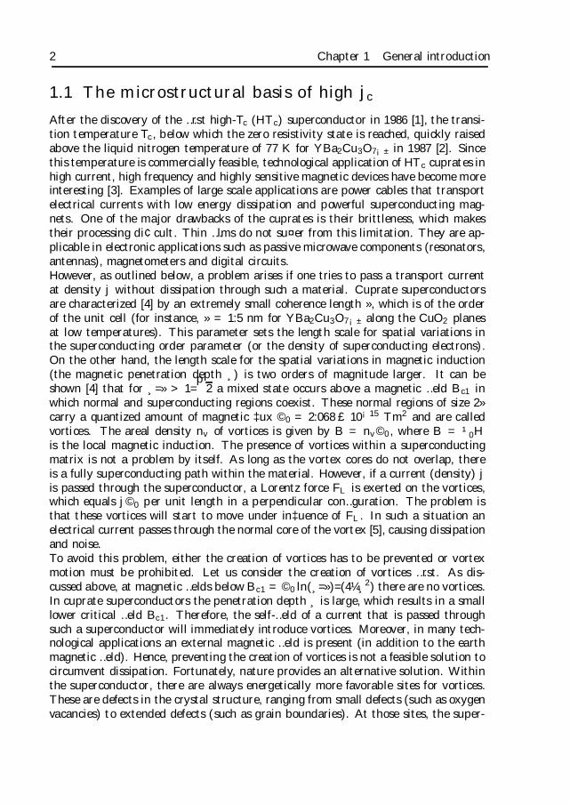
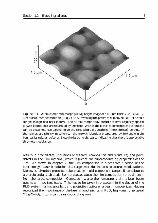
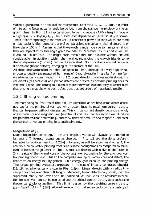
Figure 1.1: Atomic force microscope (AFM) height image of a 150 nm thick YBa2Cu3O7¡±…lm pulsed laser deposited on (100) SrTiO3, revealing the presence of many structural defects(bright is high and dark is low). The surface morphology consists of semi-regularly spacedgrowth islands that are separated by trenches. Within the trenches some deeper depressionscan be discerned, corresponding to the sites where dislocations (linear defects) emerge. Ifthe islands are slightly misoriented, the growth islands are separated by low-angle grainboundaries (planar defects). Note the large height scale, indicating that there is appreciablethickness modulation.
results in precipitates (inclusions of di¤erent composition and structure) and pointdefects in the …lm material, which in‡uence the superconducting properties of the…lm. As shown in chapter 2, the …lm composition is a sensitive function of thelaser energy. Laser irradiation of a target material induces structural modi…cations.Moreover, di¤usion processes take place in multi-component targets if constituentsare preferentially ablated. Both processes cause the …lm composition to be di¤erentfrom the target composition. Consequently, also the homogeneity of the laser beamspot is an important issue. This has to be taken into account in the design of thePLD system, for instance by using projection optics or a beam homogenizer. Havingrecognized the importance of the laser characteristics in PLD, high-quality epitaxialYBa2Cu3O7¡± …lms can be reproducibly grown.
6 Chapter 1 General introduction
Without going into the details of the microstructure of YBa2Cu3O7¡± …lms, a numberof interesting features can already be derived from the surface morphology of the as-grown …lms. In Fig. 1.1 a typical atomic force microscope (AFM) height image ofa high quality YBa2Cu3O7¡± …lm pulsed laser deposited on (100) SrTiO3 is shown.The surface morphology is far from ‡at. It consists of growth islands which are moreor less regularly distributed and are of comparable size (typically, their diameter is ofthe order of 100 nm). Assuming that the growth islands have a certain misorientation,they are separated by low angle grain boundaries. Moreover, as this particular …lmis around 150 nm thick, the height scale reveals that the thickness ‡uctuations areconsiderable. In addition, within the trenches separating the growth islands somedeeper depressions (”holes”) can be distinguished. Such locations are indicative ofdislocations (linear defects) emerging at the surface of the …lm.All these observations indicate that our epitaxial …lms, although of a very high overallstructural quality (as measured by means of X-ray di¤raction), are far from perfect.As schematically summarized in Fig. 1.2, point defects, thickness modulations, lin-ear defects (dislocations) and planar defects are present as possible pinning sites forvortices. These …lms belong to a class of materials which is completely di¤erent fromthat of single-crystals, where all defect densities are orders of magnitude smaller.
1.2.2 Strong vortex pinning
The morphological features of the thin …lm described above have some direct conse-quences for the pinning of vortices, which determines the maximum current densitythat can be passed without dissipation. This critical current density depends stronglyon temperature and magnetic …eld (number of vortices). In this section we introducethe parameters that determine jc and show how temperature and magnetic …eld enterthe concept of vortex pinning in a qualitative way.
Magnitude of jc
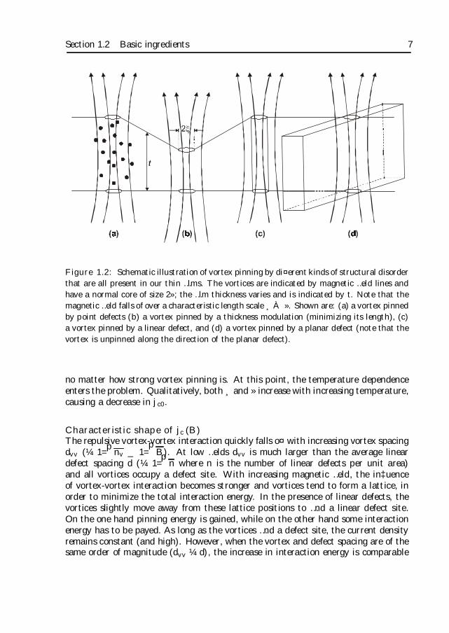
Due to its positive self-energy "l per unit length, a vortex will always try to minimizeits length. Thickness ‡uctuations as observed in Fig. 1.1 are, therefore, preferen-tial sites for vortices [see Fig. 1.2(b)]. However, as will be shown in chapter 4, thecontribution to vortex pinning from such surface corrugations as compared to struc-tural defects is insigni…cant in …lms. Structural defects with a size of the order of2» (the size of the normal core of the vortex) are responsible for the strongest vor-tex pinning phenomena. Due to the complete overlap of vortex core and defect, thecondensation energy is fully gained. This energy gain is called the pinning energy.The largest pinning e¤ects are expected in the case of linearly correlated disorder[18, 19], as schematically shown in Fig. 1.2(c). Linear defects with a radius ¼ »can pin vortices over their full length. Moreover, linear defects only locally depresssuperconductivity and leave the bulk una¤ected. At low …elds the repulsive interac-tion between vortices can be neglected and the critical current density approaches thetheoretical single-vortex limit. This limit is given by the depairing current densityjc0 = ©0=(3
p3¼¹0¸
2») [20]. Above the depairing limit superconductivity is destroyed,
Section 1.2 Basic ingredients 7
Figure 1.2: Schematic illustration of vortex pinning by di¤erent kinds of structural disorderthat are all present in our thin …lms. The vortices are indicated by magnetic …eld lines andhave a normal core of size 2»; the …lm thickness varies and is indicated by t. Note that themagnetic …eld falls of over a characteristic length scale ¸À ». Shown are: (a) a vortex pinnedby point defects (b) a vortex pinned by a thickness modulation (minimizing its length), (c)a vortex pinned by a linear defect, and (d) a vortex pinned by a planar defect (note that thevortex is unpinned along the direction of the planar defect).
no matter how strong vortex pinning is. At this point, the temperature dependenceenters the problem. Qualitatively, both ¸ and » increase with increasing temperature,causing a decrease in jc0.
Characteristic shape of jc (B)The repulsive vortex-vortex interaction quickly falls o¤ with increasing vortex spacingdvv (¼ 1=
pnv _ 1=
pB). At low …elds dvv is much larger than the average linear
defect spacing d (¼ 1=p
n where n is the number of linear defects per unit area)and all vortices occupy a defect site. With increasing magnetic …eld, the in‡uenceof vortex-vortex interaction becomes stronger and vortices tend to form a lattice, inorder to minimize the total interaction energy. In the presence of linear defects, thevortices slightly move away from these lattice positions to …nd a linear defect site.On the one hand pinning energy is gained, while on the other hand some interactionenergy has to be payed. As long as the vortices …nd a defect site, the current densityremains constant (and high). However, when the vortex and defect spacing are of thesame order of magnitude (dvv ¼ d), the increase in interaction energy is comparable

8 Chapter 1 General introduction
to the pinning energy and not all pinning sites can be occupied by vortices. Especiallypinning sites that are close to each other cannot be used e¤ectively. At this point jc
starts to decrease. At even larger magnetic …elds (dvv ¿ d), there are more vorticesthan pinning sites. In this situation, the additional vortices are only weakly pinnedand the critical current quickly decreases with increasing magnetic …eld.In this picture, a cross-over …eld B¤ [18, 19] is expected in the magnetic …eld de-pendence of jc. Below B¤ vortex-vortex interactions are less important than vortex-defect interactions and jc does not depend on the magnetic …eld (and approaches jc0).Above B¤ there are weakly pinned vortices and jc decreases rapidly with increasingmagnetic …eld. Apart from a geometrical constant re‡ecting the defect distribution,vortex-vortex interactions and the shape of the pinning potential (vortex-defect in-teraction), B¤ is essentially determined by the linear defect density n: B¤ ¼ n©0.
1.3 Strategy
Having introduced the basic ingredients, we now formulate the strategy that we followto prove that linear defects are the most important pinning sites in YBa2Cu3O7¡±
…lms.First of all, in order to correlate the microstructure and superconducting propertiesin di¤erent …lms, it is necessary to control the deposition process in such a waythat identical …lms can be made. The conditions for reproducibility in pulsed laserdeposition are investigated in chapter 2. Here, it is shown that the laser energy is acritical parameter in the deposition process. We develop a phenomenological modelthat explains the experimentally observed dependence of …lm composition on laserenergy.Next, we investigate the origin of high critical currents in these …lms (chapter 3). Toidentify linear defects as the dominant pinning sites, we …rst develop a technique todetermine the density as well as the length and lateral distribution of linear defectsin …lms. The density of linear defects turns out to be easily tunable by the depositionconditions. Measuring the superconducting current density as a function of magnetic…eld for a large series of …lms yields compelling evidence for the dominant behavior ofthreading dislocations as vortex pinning sites in …lms. A comparison is made between…lms containing natural linear defects (dislocations) and single crystals with arti…cialcolumnar defects (introduced by heavy ion irradiation).In chapter 4, the in‡uence of alternative natural pinning sites is investigated. In ad-dition to threading dislocations, the defect structure is characterized by point defects,precipitates, planar defects (such as twin planes, anti-phase boundaries and low-anglegrain boundaries) and thickness ‡uctuations. Employing a post-anneal treatment tochange the relative densities of these defects, we study the contribution to vortex pin-ning by defects other than linear defects. Special attention is paid to the critical cur-rent density at high magnetic …elds. Transmission electron microscopy is performedto show that threading dislocations are neither related to twinning dislocations norpart of low-angle grain boundaries.
References 9
Having established the importance of threading dislocations in vortex pinning in thin…lms of YBa2Cu3O7¡±, we concentrate now on how these linear defects are formedduring the growth process.Chapter 5 serves as an introduction to the remaining two chapters. It consists ofa discussion of the possible mechanisms for the formation of threading dislocations.Since the dislocations originate at or close to the substrate-…lm interface, these mech-anisms are either related to the substrate or to the initial stages of …lm growth. Allmechanisms related to the nature of the substrate material are shown to be inopera-tive and we concentrate on the YBa2Cu3O7¡± nucleation and growth mechanism inthe following two chapters.In chapter 6 we investigate whether threading dislocations are induced by precipi-tates, which form preferentially during nucleation of the …rst monolayer. Threadingdislocations may form when such precipitates are overgrown. The precipitates resultfrom non-unit cell nucleation of YBa2Cu3O7¡± on SrTiO3. This nucleation process isin‡uenced by the terminating plane of the substrate material. Therefore, we develop anew procedure to prepare SrO-terminated (100) SrTiO3 substrates (in addition to thewell-known TiO2-termination). Tailoring the substrate termination and/or the …lmcomposition, allows us to control preferential precipitation. Threading dislocationsare always present, showing that preferential precipitation during …lm nucleation can-not be the main origin of the dislocations. The dislocation density, however, can beenhanced by creating arti…cially secondary phases at the interface.If the threading dislocations in YBa2Cu3O7¡± …lms are also not created during thenucleation stage, they must form in the following stages of growth. In chapter 7, wemake use of the substrate termination to study the full growth mechanism. A self-assembled island structure develops above a critical …lm thickness, which dependssensitively on the substrate termination used. Threading dislocations are introducedfrom this point on. The relation between islands and threading dislocations is revealedand the in‡uence of the deposition parameters on the kinetics is discussed. Finally,we propose a general approach to study the growth of hetero-epitaxial systems.On the basis of our comprehensive and systematic investigation, we conclude that thepeculiar nature of hetero-epitaxial growth of complex oxides is basically responsiblefor the high critical currents in YBa2Cu3O7¡± …lms.
References
[1] J.G. Bednorz and K.A. Müller, Z. Phys. B 64, 189 (1986)
[2] M.K. Wu, J.R. Ashburn, C.J. Torng, P.H. Horr, R.L. Meng, L. Gao, Z.J. Huang,Y.Q. Wang, and C.W. Chu, Phys. Rev. Lett. 58, 908 (1987)
[3] M. Cyrot and D. Pavuna, Introduction to superconductivity and high-T c mate-rials (World Scienti…c, London, 1992)
[4] M. Tinkham, Introduction to superconductivity (McGraw-Hill, New York, 1996)
[5] J. Bardeen and M.J. Stephen, Phys. Rev. 140, 1197A (1965)
10 Chapter 1 General introduction
[6] L.S. Schneemeyer, J.V. Waszczak, T. Siegrist, R.B. van Dover, L.W. Rupp, B.Batlogg, R.J. Cava, and D.W. Murphy, Nature (London) 328, 601 (1987)
[7] L. Civale, A.D. Marwick, M.W. McElfresh, T.K. Worthington, A.P. Malozemo¤,F.H. Holtzberg, J.R. Thompson, and M.A. Kirk, Phys. Rev. Lett. 65, 1164(1990)
[8] L. Civale, A.D. Marwick, T.K. Worthington, M.A. Kirk, J.R. Thompson, L.Krusin-Elbaum, Y. Sun, J.R. Clem, and F. Holtzberg, Phys. Rev. Lett. 67, 648(1991)
[9] P. Chaudhari, R.H. Koch, R.B. Laibowitz, T.R. McGuire, and R.J. Gambino,Phys. Rev. Lett. 58, 2684 (1987)
[10] R. Ramesh, D.M. Hwang, T. Venkatesan, T.S. Ravi, L. Nazar, A. Inam, X.D.Wu, B. Dutta, G. Thomas, A.F. Marshall, and T.H. Geballe, Science 247, 57(1990)
[11] T.L. Hylton and M.R. Beasley, Phys. Rev. B 41, 11669 (1990)
[12] L.R. Tessler, J. Provost and A. Maignan, Appl. Phys. Lett. 58, 528 (1991)
[13] F.C. Klaassen, Ph.D. thesis in preparation (2001)
[14] R. Wördenweber, Supercond. Sci. Technol. 12, R86 (1999)
[15] D.B. Chrisey and G.K. Hubler, Pulsed Laser Deposition of Thin Films (Wiley,New York, 1994)
[16] M.G. Smith, A. Manthiram, J. Zhou, J.B. Goodenough, and J.T. Markert,Nature (London) 351, 549 (1991)
[17] J.N. Huiberts, R. Griessen, J.H. Rector, R.J. Wijngaarden, J.P. Dekker, D.G.de Groot, and N.J. Koeman, Nature (London) 380, 231 (1996)
[18] D.R. Nelson and V.M. Vinokur, Phys. Rev. Lett. 68. 2398 (1992)
[19] D.R. Nelson and V.M. Vinokur, Phys. Rev. B 48, 13060 (1993)
[20] G. Blatter, M.V. Feigel’man, V.B. Geshkenbein, A.I. Larkin, and V.M. Vinokur,Rev. Mod. Phys. 66, 1125 (1994)
Chapter 2
Conditions for stoichiometric transferin pulsed laser deposition
The laser ‡uence dependence of the composition of laser ablated YBa2Cu3O7¡± …lmsis investigated and interpreted in terms of laser induced target modi…cations. Bothtarget degradation (at ‡uence J < 1:0 J/cm2) and di¤usion-assisted preferential ab-lation (1:0 < J < 1:3 J/cm2) are responsible for non-stoichiometric transfer in pulsedlaser deposition. A one dimensional, moving boundary di¤usion-model is developedto describe di¤usion-assisted preferential ablation. This model predicts stoichiometrictransfer at large ablation rates. Indeed for J À 1:3 J/cm2 stoichiometric depositionis found, resulting in precipitate-free …lms. Slightly o¤-stoichiometric …lms, depositedin the di¤usion-assisted preferential ablation regime, exhibit the best superconduct-ing properties (Tc = 91:0 K, ¢Tc = 0:4 K). These high quality …lms can be producedwith a remarkably high reproducibility.1
1This chapter is based on the paper by J.M. Huijbregtse, B. Dam, J.H Rector, and R. Griessen,J. Appl. Phys. 86, 6528 (1999)
12 Chapter 2 Conditions for stoichiometric transfer in pulsed laser deposition
2.1 Introduction
Pulsed laser deposition (PLD) is a powerful technique for the deposition of thin …lmsof a wide range of materials, including metals, diamond, semiconductors and ceramicoxide materials [1]. One of the reasons for the widespread use of PLD is the abilityto directly transfer the composition from multi-component targets to the substrate.This stoichiometric deposition makes PLD highly suitable for the deposition of high-Tc superconductors such as YBa2Cu3O7¡±. In practice one …nds, however, that …lmsare only approximately stoichiometric.Although epitaxial YBa2Cu3O7¡± …lms are obtained by PLD that exhibit sharp re-sistive transitions at critical temperatures Tc > 90 K and critical current densities of1011 ¡ 1012 A/m2 at 4.2 K (see chapters 3 and 4 or Ref. [2] for a review), the surfacemorphology of these …lms is often poor. A large particle density is usually observedwhen examining the surface morphology by atomic force microscopy. Obviously, formany technological applications, a ‡at surface is required. Generally, two types of par-ticles are distinguished [3]: droplets (large particles with a diameter > 0:5 ¹m thatare transferred directly from the target) and precipitates (secondary phases). Thedensity of droplets is reduced by lowering the laser beam ‡uence [4, 5], changing thedeposition geometry [6], using velocity …ltration [7] or crossed ‡ux techniques [8]. Ithas also been shown that carefully preparing and conditioning the target material sig-ni…cantly reduces the droplet density [9, 10, 11]. Precipitates (diameter < 0:5 ¹m) aresegregation products, resulting from o¤-stoichiometries in the …lm. Due to the limitedsolubility in YBa2Cu3O7¡± [12], small deviations from the 123 stoichiometry induceprecipitates. O¤-stoichiometries also in‡uence the electrical and structural propertiesof the thin …lms [13, 14, 15, 16, 17]. Therefore, to optimize both the surface morphol-ogy and the physical properties, it is important to understand the mechanisms andthe limitations of the conservation of composition in the PLD process.Although several ablation mechanisms have been identi…ed [1, 18], in realistic thin…lm deposition processes the target is repeatedly irradiated by laser pulses and sub-surface processes become dominant. In the laser induced melt, phase transitions mayoccur. Moreover, any o¤-stoichiometric ablation process has to be sustained by vol-ume di¤usion if it is to yield persistently o¤-stoichiometric …lms. Therefore, in thelong run, these subsurface processes determine whether the material transfer is sto-ichiometric or not. In YBa2Cu3O7¡± for example, a phase separation in the targettakes place [4, 19, 20, 21] below the threshold ‡uence Jth = 1.0 J/cm2 and the re-sulting …lms are non-stoichiometric below Jth. Note, that in this case, we can notdraw any conclusion about the ablation mechanism itself. In the pulsed laser deposi-tion of SrTiO3 [21, 22] preferential ablation of Sr occurs. It was found, however, thatupon continued irradiation of the target surface, o¤-stoichiometric Sr-rich …lms canonly persistently be obtained if the volume di¤usion of Sr towards the target surfaceis fast enough to replenish the surface depletion of Sr. If the volume di¤usion cannot keep up with the preferential ablation speed, eventually stoichiometric …lms areobtained. Therefore, preferential ablation alone is not su¢cient to explain persistentnon-stoichiometric deposition.
Section 2.2 PLD set-up and experimental procedures 13
In the present chapter, we study the PLD of YBa2Cu3O7¡± …lms, without, how-ever, going into the details of the ablation mechanism itself. We show that above Jth
also in YBa2Cu3O7¡± di¤usion-assisted preferential ablation plays a role in the ab-lation process. Using a phenomenological model, we conclude that it is in fact thepulsed character in combination with di¤usion that is responsible for the persistenceof the non-stoichiometric deposition process. From the model it is also predicted thatstoichiometric transfer should eventually occur at large ‡uences. Indeed we observestoichiometric, precipitate-free …lms at J À 1:3 J/cm2. The best physical propertiesare found for slightly o¤-stoichiometric …lms (i.e., with some precipitates) that aredeposited in the di¤usion-assisted preferential ablation regime. Finally, special atten-tion is paid to the reproducibility. We …nd that the reproducibility of these …lms isremarkably good. Without any exception, all …lms exhibit a Tc > 90 K. This remark-able reproducibility is attributed to the excellent laser characteristics and the designof the laser beam trajectory, resulting in a well controlled, reproducible and uniformlaser spot.
2.2 PLD set-up and experimental procedures
In our pulsed laser deposition set-up a KrF excimer laser beam (QUESTEK Impulse4750GL: wavelength 248 nm, pulse duration ¿ = 30 ns) is guided into an ultra highvacuum system onto the target at an inclination of 45±, see Fig 2.1(a). The pulsefrequency of the laser is set at 5 Hz, while the ‡uence J [in J/cm2] is varied by meansof an optical attenuator. In order to obtain a spatially homogeneous spot on thetarget, projection optics (OPTEC SA) is used and a homogeneous part of the beamis selected by a circular mask with a diameter of 8.3 mm. This spot is projectedonto the target (5£ demagni…cation). To account for energy losses at windows andmirrors, the laser ‡uence is measured inside the deposition chamber at the positionof the target.All depositions are performed using a high density, polycrystalline tetragonal YBa2-Cu3O6+x target (PRAXAIR, > 99:9% pure raw materials) which can be rotatedduring deposition. The substrates are glued on a resistive heater with silver paintand the temperature is measured both with a thermocouple and a pyrometer. Duringall deposition runs, the target-to-substrate distance dT¡S is …xed at 3.5 cm and theoxygen pressure pO2 is set at 15 Pa. The deposition rate is measured with a retractablequartz crystal monitor, located 2 cm above the target.Using these settings, two sets of experiments are performed in which only the ‡uenceof the laser beam is varied. First, thin amorphous YBa2Cu3O6+x …lms are depositedon (100) Si substrates at room temperature from a stationary target. The composi-tion of these …lms is measured with Rutherford backscattering spectrometry (RBS),using 2.0 MeV He+. After …lm deposition, the composition of the irradiated tar-get spots is determined, also by means of RBS. Secondly, crystalline c-axis oriented140 nm thick YBa2Cu3O7¡± …lms are deposited onto (100) SrTiO3 substrates froma rotating target. In order to obtain superconducting …lms, the substrate is heatedto 815±C during deposition. Immediately after deposition, the …lms are quenched in
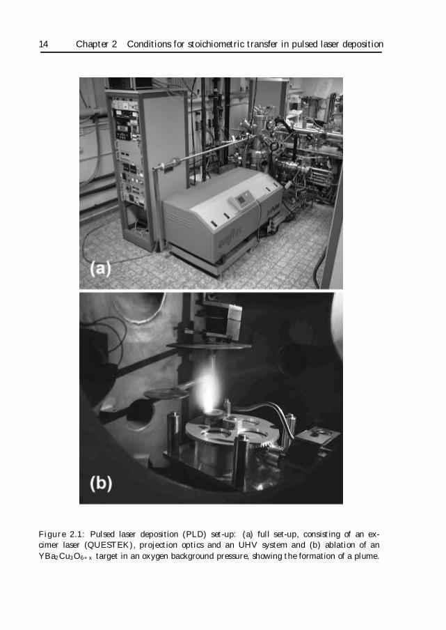
14 Chapter 2 Conditions for stoichiometric transfer in pulsed laser deposition
Figure 2.1: Pulsed laser deposition (PLD) set-up: (a) full set-up, consisting of an ex-cimer laser (QUESTEK), projection optics and an UHV system and (b) ablation of anYBa2Cu3O6+x target in an oxygen background pressure, showing the formation of a plume.
Section 2.3 Stoichiometry and …lm properties 15
pure oxygen. It is not necessary to perform additional heat treatments to optimizethe superconducting properties.To analyze the surface morphology of the crystalline …lms, we use atomic force mi-croscopy (AFM) in the tapping mode (NANOSCOPE IIIa multimode system). TheAFM measurements are performed ex situ, using Si tips. The …lms are structurallycharacterized by means of X-ray di¤raction (XRD) in a RIGAKU rotating anodedi¤ractometer, using CuK® radiation (¸ = 1:541871 Å). After carefully aligning the…lms with respect to the (00l)-axis, µ ¡ 2µ di¤raction scans are recorded. The c-axis length is determined by averaging the results obtained from several (00l)-lines(l = 1 ¡ 8). Rocking curves widths are determined by means of separate ! scans,using the (005)-re‡ection. For all crystalline …lms, we measured the transition tosuperconductivity resistively in a four point probe con…guration.
2.3 Stoichiometry and …lm properties
2.3.1 Amorphous YBa2Cu3O6+x …lms
Although PLD is generally known for its stoichiometric transfer, e.g. in SrTiO3 itwas found that this is only true at su¢ciently large ‡uences [21, 22]. In order to…nd the conditions for stoichiometric transfer in the PLD of YBa2Cu3O7¡± …lms, wemeasured the …lm composition as a function of ‡uence. However, it is not possibleto accurately determine the …lm composition by means of RBS of …lms deposited onSrTiO3 substrates, due to overlap of the substrate and …lm contributions in the RBSspectrum. Therefore, we performed RBS measurements on amorphous YBa2Cu3O6+x
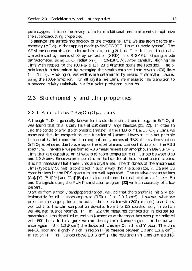
…lms that are deposited on Si wafers at room temperature at ‡uences between 0.50and 3.0 J/cm2. Since we are interested in the transfer of the di¤erent cation species,it is not necessary that these …lms are crystalline. The thickness of the amorphous…lms (typically 50 nm) is controlled in such a way that the substrate, Y, Ba and Cucontributions in the RBS spectrum are well separated. The relative concentrations[Cu]/[Y], [Ba]/[Y] and [Cu]/[Ba] are calculated from the total peak area of the Y, Baand Cu signals using the RUMP simulation program [23] with an accuracy of a fewpercent.Starting from a freshly sandpapered target, we …nd that the transfer is initially sto-ichiometric for all ‡uences employed (0.50 < J < 3.0 J/cm2). However, when wepreablate the target prior to the actual …lm deposition with 300 (or more) laser shots,we …nd that the …lm composition deviates from the 123 stoichiometry in certainwell-de…ned ‡uence regimes. In Fig. 2.2 the measured composition is plotted foramorphous …lms deposited at various ‡uences after the target has been preirradiatedwith 600 shots. In this …gure, we can identify three ‡uence regions. In the low ‡u-ence region I (J < 1:0 J/cm2) the deposited …lms are Cu rich and Y poor. The …lmsare Cu poor and slightly Y rich in region II (at ‡uences between 1.0 and 1.3 J/cm2).In region III ¡ at ‡uences above 1.3 J/cm2 ¡ the resulting thin …lms are stoichio-
16 Chapter 2 Conditions for stoichiometric transfer in pulsed laser deposition
0.5 1.0 1.5 2.0 2.5 3.01
2
3
4
com
posi
tion
ratio
fluence J [J/cm2]
IIII II
[Ba]/[Y]
[Cu]/[Ba]
[Cu]/[Y]
Figure 2.2: [Cu]/[Y], [Ba]/[Y] and [Cu]/[Ba] composition ratios of ¼ 50 nm thick amor-phous YBa2Cu3O6+x …lms deposited on Si as a function of the laser ‡uence J (at an oxygenpressure pO2 = 15 Pa and target-to-substrate distance dT¡S = 3:5 cm). Before each deposi-tion the stationary target is preablated with 600 laser shots. The shaded area represents the‡uence region in which crystalline …lms with optimal superconducting and morphologicalproperties are deposited.
Section 2.3 Stoichiometry and …lm properties 17
metric. These three ‡uence regions are always observed when preablating the target.Even after a preablation period of 104 shots, the same three regimes are found.From these measurements it also follows that the deposition is stoichiometric for all‡uences when starting from a fresh target (without preablation). Why do we usepreablation at all? The most important reason for using preablation is to clean thetarget material from loose grains which greatly a¤ect the quality of the …lm surface.Another practical reason is that we want to have a constant deposition rate. Sincethe deposition rate decreases rapidly with time to a constant value [19], preablationis required. Also, the target surface reorients itself towards the incoming laser beam[20], which causes an increase in ‡uence by a factor
p2 during ablation. Concluding,
preablation is applied to ensure a well-de…ned starting situation for the actual …lmdeposition.Region I extends up to the threshold ‡uence Jth = 1:0 J/cm2 and was reported earlier[4, 20]. However, as the Cu-de…ciency in region II is very small, the second regionwas not observed. Because ‡uence regime I is well understood [4, 20, 21], we focuson region II and the crossover to region III in the remaining of this chapter.How do we explain the persistent o¤-stoichiometry in region II? Apart from particular-ities of the laser-target interaction, a possible explanation for the non-stoichiometrictransfer in region II is scattering of the cations at ambient oxygen molecules [15].Since the scattering rate is di¤erent for each cation species, this could in principleinduce o¤-stoichiometries in the …lm. Foote et al. [15, 24] found that the e¤ect ofscattering increases with increasing oxygen pressure pO2
and target-to-substrate dis-tance dT¡S (at a …xed ‡uence). In our experiments the ‡uence is varied, while bothdT¡S and pO2 are kept constant. However, the most important parameter is the po-sition of the substrate with respect to the top of the plasma plume (see Fig. 2.1(b)for an example): when increasing the plume-substrate distance the e¤ect of scatter-ing increases. In our experimental set-up, there is a separation between the substrateand the plume below 1.3 J/cm2, whereas at higher ‡uences the substrate is inside theplume. If scattering is important, it should become more dominant at smaller ‡u-ences. In order to …nd out if scattering is the origin of the ‡uence dependence of thecomposition in region II, the deposition of amorphous …lms was repeated at a largerdT¡S of 4.5 cm. Now the plume touches the substrate at a ‡uence of 1.5 J/cm2. Ifscattering plays an important role, we expect that: (i) the e¤ect is more pronouncedand (ii) that region II extends up to 1.5 J/cm2. However, experimentally we …nd thatthe composition of the …lms deposited at dT¡S = 4:5 cm exhibits the same ‡uencedependence as in Fig. 2.2, showing the same three ‡uence regions. Thus, we concludethat scattering of cations at oxygen atoms is not the origin of region II.If the deviations from stoichiometry in region II are not induced during the transferof material from the target to the substrate, they must be induced at an earlier stage.Therefore, we investigated the irradiated target material in more detail. The compo-sition of the target spots, irradiated with ‡uences in region II and III, was measuredusing RBS with the He+ beam parallel to the direction of the incoming laser beam[see Fig. 2.3(a)]. The RBS spectrum is simulated with the two concentration pro…lesshown in Fig. 2.3(b), using the RUMP program [23]. Ideally, the target composi-
18 Chapter 2 Conditions for stoichiometric transfer in pulsed laser deposition
0 100 200 300 400 5000
1
2
3
4
targ
et
com
po
sitio
n
(b) depth [nm]
Ba
Y
Cu
1.5 1.6 1.7 1.80
20
40
60
Inte
nsi
ty [
a.u
.]
(a) energy [MeV]
Cu
Y
Ba
experiment simulation 1
simulation 2
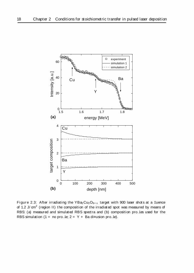
Figure 2.3: After irradiating the YBa2Cu3O6+x target with 900 laser shots at a ‡uenceof 1.2 J/cm2 (region II) the composition of the irradiated spot was measured by means ofRBS: (a) measured and simulated RBS spectra and (b) composition pro…les used for theRBS simulation (1 = no pro…le; 2 = Y + Ba di¤usion pro…le).
Section 2.3 Stoichiometry and …lm properties 19
tion should be Y1Ba2Cu3, independently of the depth within the target (simulation1). However, the simulated RBS spectrum shows that the Ba (and Y) content is toohigh, while the Cu content is too low. Introducing a gradual Cu enrichment (and anY + Ba depletion) towards the surface of the target brings the simulated and mea-sured spectra closer. Since the compositional deviations from stoichiometry in thetarget are opposite to those in the …lm (see Fig. 2.2), we infer that Y and Ba arepreferentially ablated with respect to Cu in region II.RBS measurements on target spots irradiated with a ‡uence from region III showthe same spectrum as the unirradiated target. These spectra show no indication ofconcentration pro…les. Since region II persists upon further irradiation, we concludethat the same di¤usion-assisted preferential ablation mechanism is active as in thePLD of SrTiO3 [21, 22]. This mechanism will be described in detail in the discussion.The ‡uence not only a¤ects the composition, but also the droplet density on the …lm.Generally, the droplet density increases with ‡uence [4, 5, 10]. Since on amorphous…lms all particles are droplets, the droplet density can directly be determined bymeans of optical microscopy. We …nd that the droplet density on amorphous …lmsincreases somewhat with ‡uence, but the absolute density is always low (< 104 percm2). We attribute this low droplet density to the use of a high density, tetragonaltarget [9, 10, 11]. Using a lower density orthorhombic target results in higher dropletdensities (> 105 per cm2). As will be shown in the next section, the density ofprecipitates on crystalline …lms is usually some orders of magnitude larger (106 ¡107
per cm2). Therefore, we conclude that compositional e¤ects are mainly determiningthe particle density of a …lm.
2.3.2 Crystalline YBa2Cu3O7¡± …lms
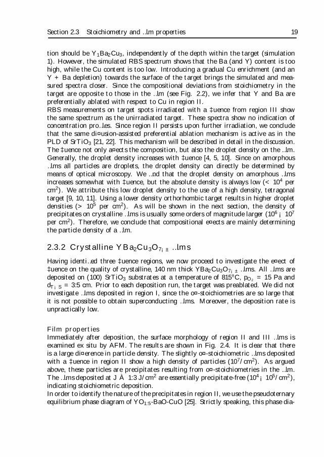
Having identi…ed three ‡uence regions, we now proceed to investigate the e¤ect of‡uence on the quality of crystalline, 140 nm thick YBa2Cu3O7¡± …lms. All …lms aredeposited on (100) SrTiO3 substrates at a temperature of 815±C, pO2 = 15 Pa anddT¡S = 3:5 cm. Prior to each deposition run, the target was preablated. We did notinvestigate …lms deposited in region I, since the o¤-stoichiometries are so large thatit is not possible to obtain superconducting …lms. Moreover, the deposition rate isunpractically low.
Film propertiesImmediately after deposition, the surface morphology of region II and III …lms isexamined ex situ by AFM. The results are shown in Fig. 2.4. It is clear that thereis a large di¤erence in particle density. The slightly o¤-stoichiometric …lms depositedwith a ‡uence in region II show a high density of particles (107/cm2). As arguedabove, these particles are precipitates resulting from o¤-stoichiometries in the …lm.The …lms deposited at J À 1:3 J/cm2 are essentially precipitate-free (104¡105/cm2),indicating stoichiometric deposition.In order to identify the nature of the precipitates in region II, we use the pseudoternaryequilibrium phase diagram of YO1:5-BaO-CuO [25]. Strictly speaking, this phase dia-
20 Chapter 2 Conditions for stoichiometric transfer in pulsed laser deposition
Figure 2.4: AFM height images of two crystalline YBa2Cu3O7¡± …lms laser deposited on(100) SrTiO3 substrates with a ‡uence in: (a) region II (J = 1:2 J/cm2); scan size 10 ¹mand (b) region III (J = 3:0 J/cm2); scan size 20 ¹m. Both …lms are deposited at 815±C,pO2 = 15 Pa and dT¡S = 3:5 cm. Note the di¤erence in scan size; bright is high and dark islow.
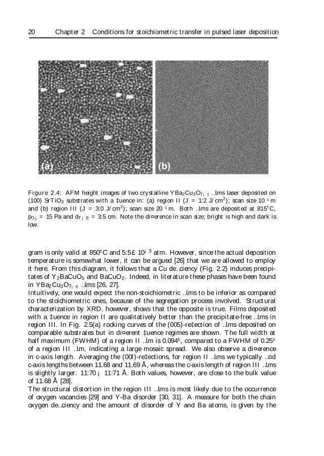
gram is only valid at 850±C and 5:5£10¡3 atm. However, since the actual depositiontemperature is somewhat lower, it can be argued [26] that we are allowed to employit here. From this diagram, it follows that a Cu de…ciency (Fig. 2.2) induces precipi-tates of Y2BaCuO5 and BaCuO2. Indeed, in literature these phases have been foundin YBa2Cu3O7¡± …lms [26, 27].Intuitively, one would expect the non-stoichiometric …lms to be inferior as comparedto the stoichiometric ones, because of the segregation process involved. Structuralcharacterization by XRD, however, shows that the opposite is true. Films depositedwith a ‡uence in region II are qualitatively better than the precipitate-free …lms inregion III. In Fig. 2.5(a) rocking curves of the (005)-re‡ection of …lms deposited oncomparable substrates but in di¤erent ‡uence regimes are shown. The full width athalf maximum (FWHM) of a region II …lm is 0.094±, compared to a FWHM of 0.25±
of a region III …lm, indicating a large mosaic spread. We also observe a di¤erencein c-axis length. Averaging the (00l)-re‡ections, for region II …lms we typically …ndc-axis lengths between 11.68 and 11.69 Å, whereas the c-axis length of region III …lmsis slightly larger: 11:70 ¡ 11:71 Å. Both values, however, are close to the bulk valueof 11.68 Å [28].The structural distortion in the region III …lms is most likely due to the occurrenceof oxygen vacancies [29] and Y-Ba disorder [30, 31]. A measure for both the chainoxygen de…ciency and the amount of disorder of Y and Ba atoms, is given by the
Section 2.3 Stoichiometry and …lm properties 21
0 50 100 150 200 250 3000
200
400
600
(b)
resi
stiv
ity [
µΩcm
]
temperature T [K]
80 90 1000
300
18.5 19.0 19.5 20.00.0
0.5
1.0
(a)
norm
aliz
ed in
tens
ity
angle ω
Figure 2.5: Comparison between two crystalline YBa2Cu3O7¡± …lms deposited on (100)SrTiO3 substrates at ‡uences in region II (full line; J = 1:2 J/cm2) and region III (dashedline; J = 3:0 J/cm2): (a) (005) XRD rocking curves and (b) resistivity ½ vs. temperature Tcurves. Both …lms are deposited at 815±C, pO2 = 15 Pa and dT¡S = 3:5 cm.
22 Chapter 2 Conditions for stoichiometric transfer in pulsed laser deposition
ratio of the integrated intensities of the (005) and (004)-re‡ections, I(005)/I(004)[29, 30, 31]. Ideally, in the absence of any disorder or de…ciency, this ratio is equalto 14.8. In oxygen de…cient …lms I(005)/I(004) increases, whereas disorder betweenY and Ba atoms causes I(005)=I(004) to decrease. We …nd that region II …lmsshow values that are very close to the optimal value (for the …lm shown in Fig. 2.5(a)I(005)=I(004) = 14:4). In region III, however, the observed ratio is signi…cantly largerthan the optimal value [I(005)=I(004) = 17:3 for the …lm in Fig. 2.5(a)], indicatingan oxygen de…ciency in the chains.As shown in Fig. 2.5(b), the oxygen de…ciencies in the region III …lms translateinto higher resistivities, lower critical temperatures Tc and broader transitions ascompared to region II …lms. The oxygen de…ciencies might be related to the fact thatthe substrate is not at its optimal position with respect to the plume: in region III thelength of the plume is much larger than the target-to-substrate distance. Indeed, theproperties of stoichiometric …lms improve when positioning the substrate in top of theplume (89 < Tc < 90 K). This is achieved by either increasing the target-substratedistance or by raising the background oxygen pressure [32]. However, the quality ofthese …lms is still not as good as that of the region II …lms.In fact, in literature it has often been reported that slightly o¤-stoichiometric …lmshave better properties than stoichiometric …lms [13, 15, 17, 26, 33]. If the di¤usionof one of the cation species during …lm growth is the rate limiting factor in formingYBa2Cu3O6+x, a small excess amount of this element actually promotes the growthprocess, yielding better superconducting properties. It has been suggested [34] thatY is this di¤usion rate limiting element. Indeed, in our region II …lms we have asmall Y-enrichment (see Fig. 2.2), indicating the importance of di¤usion for thegrowth process. Unfortunately, the o¤-stoichiometry in region II always results in theformation of precipitates (see Fig. 2.4).Consequently, we have to …nd a compromise between superconducting properties andthe quality of the surface. From Fig. 2.2 it follows that there are two optimal ‡uences:on the boundary between regions I and II and on the boundary between regions IIand III. Indeed, as reported in a previous paper [20], we …nd that at a ‡uence of 1.0J/cm2 excellent superconducting …lms are obtained. However, the surface morphologyof these …lms is not reproducible. We attribute this to the strong ‡uence dependenceof the composition transfer around 1.0 J/cm2 (Fig. 2.2). Due to small ‡uctuationsin the laser ‡uence, in practise the deposition is always o¤-stoichiometric. Therefore,the best …lms are found at the boundary between region II and III for J ¼ 1:3J/cm2, combining good superconducting properties and reasonably low precipitatedensities (106/cm2). The ‡uence for optimal …lms is indicated by the shaded areain Fig. 2.2. As will be shown in the next section …lms deposited at J = 1:3 J/cm2
exhibit a remarkable reproducibility, both in surface morphology and superconductingproperties.
ReproducibilityIn a period of several months, 30 …lms were deposited under identical depositionconditions at a ‡uence of 1.3 J/cm2. The distribution from …lm to …lm in Tc is
Section 2.3 Stoichiometry and …lm properties 23
89.7 90.1 90.5 90.9 91.3 91.7 92.1 92.50
5
10
15
(a) critical temperature Tc [K]
freq
uenc
y
0.0 0.2 0.4 0.6 0.8 1.00
5
10
15
(b)
freq
uenc
y
transition width ∆Tc [K]
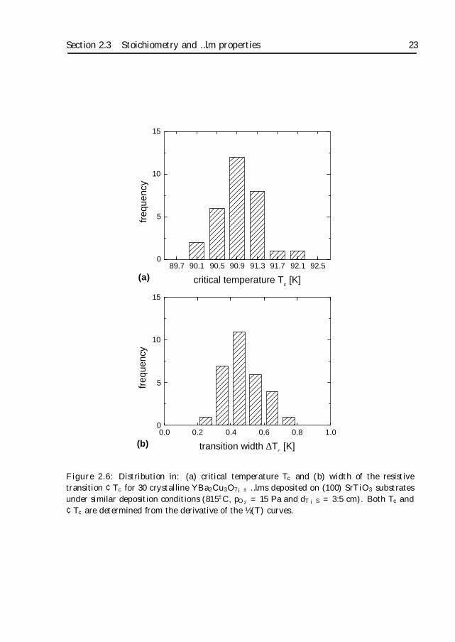
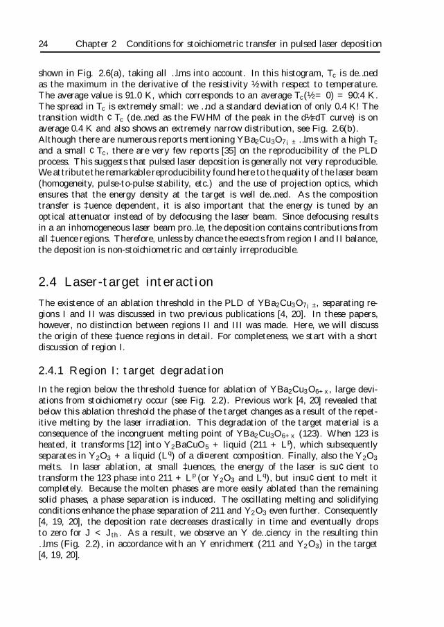
Figure 2.6: Distribution in: (a) critical temperature Tc and (b) width of the resistivetransition ¢Tc for 30 crystalline YBa2Cu3O7¡± …lms deposited on (100) SrTiO3 substratesunder similar deposition conditions (815±C, pO2 = 15 Pa and dT¡S = 3:5 cm). Both Tc and¢Tc are determined from the derivative of the ½ (T) curves.
24 Chapter 2 Conditions for stoichiometric transfer in pulsed laser deposition
shown in Fig. 2.6(a), taking all …lms into account. In this histogram, Tc is de…nedas the maximum in the derivative of the resistivity ½ with respect to temperature.The average value is 91.0 K, which corresponds to an average Tc(½ = 0) = 90:4 K.The spread in Tc is extremely small: we …nd a standard deviation of only 0.4 K! Thetransition width ¢Tc (de…ned as the FWHM of the peak in the d½=dT curve) is onaverage 0.4 K and also shows an extremely narrow distribution, see Fig. 2.6(b).Although there are numerous reports mentioning YBa2Cu3O7¡± …lms with a high Tc
and a small ¢Tc, there are very few reports [35] on the reproducibility of the PLDprocess. This suggests that pulsed laser deposition is generally not very reproducible.We attribute the remarkable reproducibility found here to the quality of the laser beam(homogeneity, pulse-to-pulse stability, etc.) and the use of projection optics, whichensures that the energy density at the target is well de…ned. As the compositiontransfer is ‡uence dependent, it is also important that the energy is tuned by anoptical attenuator instead of by defocusing the laser beam. Since defocusing resultsin a an inhomogeneous laser beam pro…le, the deposition contains contributions fromall ‡uence regions. Therefore, unless by chance the e¤ects from region I and II balance,the deposition is non-stoichiometric and certainly irreproducible.
2.4 Laser-target interaction
The existence of an ablation threshold in the PLD of YBa2Cu3O7¡±, separating re-gions I and II was discussed in two previous publications [4, 20]. In these papers,however, no distinction between regions II and III was made. Here, we will discussthe origin of these ‡uence regions in detail. For completeness, we start with a shortdiscussion of region I.
2.4.1 Region I: target degradation
In the region below the threshold ‡uence for ablation of YBa2Cu3O6+x, large devi-ations from stoichiometry occur (see Fig. 2.2). Previous work [4, 20] revealed thatbelow this ablation threshold the phase of the target changes as a result of the repet-itive melting by the laser irradiation. This degradation of the target material is aconsequence of the incongruent melting point of YBa2Cu3O6+x (123). When 123 isheated, it transforms [12] into Y2BaCuO5 + liquid (211 + Lp), which subsequentlyseparates in Y2O3 + a liquid (Lq) of a di¤erent composition. Finally, also the Y2O3
melts. In laser ablation, at small ‡uences, the energy of the laser is su¢cient totransform the 123 phase into 211 + Lp (or Y2O3 and Lq), but insu¢cient to melt itcompletely. Because the molten phases are more easily ablated than the remainingsolid phases, a phase separation is induced. The oscillating melting and solidifyingconditions enhance the phase separation of 211 and Y2O3 even further. Consequently[4, 19, 20], the deposition rate decreases drastically in time and eventually dropsto zero for J < Jth. As a result, we observe an Y de…ciency in the resulting thin…lms (Fig. 2.2), in accordance with an Y enrichment (211 and Y2O3) in the target[4, 19, 20].
Section 2.4 Laser-target interaction 25
We note that the incongruent melting of YBa2Cu3O7¡± is the origin of the phaseseparation. Therefore, in congruently melting materials, this mechanism for non-stoichiometric transfer is absent. Indeed, in congruently melting SrTiO3, the lowest‡uence region is not found [21]. We do, however, observe non-stoichiometric deposi-tion of SrTiO3 at low ‡uences, completely analogous to the region II that was foundin the present investigation of YBa2Cu3O7¡±.
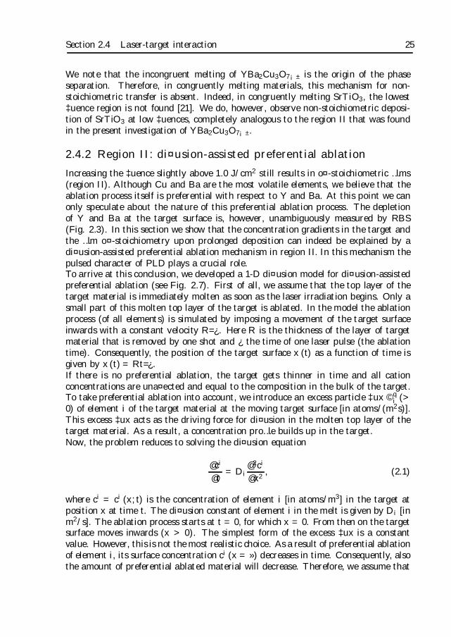
2.4.2 Region II: di¤usion-assisted preferential ablation
Increasing the ‡uence slightly above 1.0 J/cm2 still results in o¤-stoichiometric …lms(region II). Although Cu and Ba are the most volatile elements, we believe that theablation process itself is preferential with respect to Y and Ba. At this point we canonly speculate about the nature of this preferential ablation process. The depletionof Y and Ba at the target surface is, however, unambiguously measured by RBS(Fig. 2.3). In this section we show that the concentration gradients in the target andthe …lm o¤-stoichiometry upon prolonged deposition can indeed be explained by adi¤usion-assisted preferential ablation mechanism in region II. In this mechanism thepulsed character of PLD plays a crucial role.To arrive at this conclusion, we developed a 1-D di¤usion model for di¤usion-assistedpreferential ablation (see Fig. 2.7). First of all, we assume that the top layer of thetarget material is immediately molten as soon as the laser irradiation begins. Only asmall part of this molten top layer of the target is ablated. In the model the ablationprocess (of all elements) is simulated by imposing a movement of the target surfaceinwards with a constant velocity R=¿ . Here R is the thickness of the layer of targetmaterial that is removed by one shot and ¿ the time of one laser pulse (the ablationtime). Consequently, the position of the target surface x (t) as a function of time isgiven by x (t) = Rt=¿ .If there is no preferential ablation, the target gets thinner in time and all cationconcentrations are una¤ected and equal to the composition in the bulk of the target.To take preferential ablation into account, we introduce an excess particle ‡ux ©q
i (>0) of element i of the target material at the moving target surface [in atoms/(m2s)].This excess ‡ux acts as the driving force for di¤usion in the molten top layer of thetarget material. As a result, a concentration pro…le builds up in the target.Now, the problem reduces to solving the di¤usion equation
@ci
@t= Di
@2ci
@x2, (2.1)
where ci = ci (x; t) is the concentration of element i [in atoms/m3] in the target atposition x at time t. The di¤usion constant of element i in the melt is given by Di [inm2/s]. The ablation process starts at t = 0, for which x = 0. From then on the targetsurface moves inwards (x > 0). The simplest form of the excess ‡ux is a constantvalue. However, this is not the most realistic choice. As a result of preferential ablationof element i, its surface concentration ci (x = ») decreases in time. Consequently, alsothe amount of preferential ablated material will decrease. Therefore, we assume that
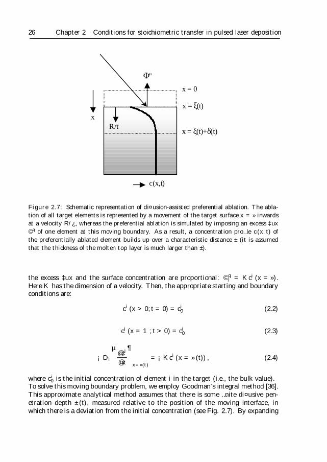
26 Chapter 2 Conditions for stoichiometric transfer in pulsed laser deposition
x = 0
x = ξ(t)
x = ξ(t)+δ(t)
x
c(x,t)
R/τ
Φ"
Figure 2.7: Schematic representation of di¤usion-assisted preferential ablation. The abla-tion of all target elements is represented by a movement of the target surface x = » inwardsat a velocity R/¿ , whereas the preferential ablation is simulated by imposing an excess ‡ux©q of one element at this moving boundary. As a result, a concentration pro…le c (x; t) ofthe preferentially ablated element builds up over a characteristic distance ± (it is assumedthat the thickness of the molten top layer is much larger than ±).
the excess ‡ux and the surface concentration are proportional: ©qi = Kci (x = »).
Here K has the dimension of a velocity. Then, the appropriate starting and boundaryconditions are:
ci (x > 0; t = 0) = ci0 (2.2)
ci (x = 1; t > 0) = ci0 (2.3)
¡Di
µ@ci
@x
¶
x=»(t)
= ¡Kci (x = » (t)) , (2.4)
where ci0 is the initial concentration of element i in the target (i.e., the bulk value).
To solve this moving boundary problem, we employ Goodman’s integral method [36].This approximate analytical method assumes that there is some …nite di¤usive pen-etration depth ± (t), measured relative to the position of the moving interface, inwhich there is a deviation from the initial concentration (see Fig. 2.7). By expanding
Section 2.4 Laser-target interaction 27
0 10 20 30 40 500.50
0.75
1.00
c(x,
t)/c
0
x-ξ [nm]
30 n
s
1 ns
stationary
integral
exact
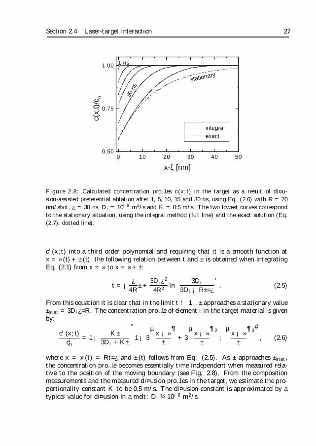
Figure 2.8: Calculated concentration pro…les c (x; t) in the target as a result of di¤u-sion-assisted preferential ablation after 1, 5, 10, 15 and 30 ns, using Eq. (2.6) with R = 20nm/shot, ¿ = 30 ns, Di = 10
¡8 m2/s and K = 0:5 m/s. The two lowest curves correspondto the stationary situation, using the integral method (full line) and the exact solution (Eq.(2.7), dotted line).
ci (x; t) into a third order polynomial and requiring that it is a smooth function atx = » (t) + ± (t), the following relation between t and ± is obtained when integratingEq. (2.1) from x = » to x = » + ±:
t = ¡ ¿
4R± +
3Di¿2
4R2ln
3Di
3Di ¡ R±=¿
¸. (2.5)
From this equation it is clear that in the limit t ! 1, ± approaches a stationary value±stat = 3Di¿=R. The concentration pro…le of element i in the target material is givenby:
ci (x; t)
ci0
= 1 ¡ K±
3Di + K±
"1 ¡ 3
µx ¡ »
±
¶+ 3
µx ¡ »
±
¶2
¡µ
x ¡ »
±
¶3#
, (2.6)
where x = x (t) = Rt=¿ and ± (t) follows from Eq. (2.5). As ± approaches ±stat,the concentration pro…le becomes essentially time independent when measured rela-tive to the position of the moving boundary (see Fig. 2.8). From the compositionmeasurements and the measured di¤usion pro…les in the target, we estimate the pro-portionality constant K to be 0.5 m/s. The di¤usion constant is approximated by atypical value for di¤usion in a melt: Di ¼ 10¡8 m2/s.
28 Chapter 2 Conditions for stoichiometric transfer in pulsed laser deposition
In Fig. 2.8, also the exact steady state solution is shown. This solution is:
ci (x; t)
ci0
= 1 ¡ K
K + R=¿exp
¡R (x ¡ »)
Di¿
¸. (2.7)
In fact, the integral method is a polynomial expansion of the exact solution. Inthe stationary situation, the di¤erence between the two solutions is expected to bemaximal. Therefore, from Fig. 2.8 we conclude that the integral method gives anestimate of the non-stationary di¤usion pro…les within 5%. However, the most impor-tant source of errors is the model itself. In principle, one should solve both the heatand di¤usion equations in the presence of two moving boundaries in the target ma-terial: a vapor-liquid interface and a liquid-solid interface. Additional complicationsare the temperature dependence of the properties of the target material and the factthat both interfaces are not straight. However, we use the model to understand qual-itatively how non-stoichiometric transfer can occur in PLD and, more importantly,what conditions are needed to reach persistent stoichiometric transfer of the targetcomposition to the substrate.As argued above, in region II there are two excess particle ‡uxes of the preferentiallyablated Y and Ba atoms, ©q
Y and ©qBa. The total ‡ux F q
i of each preferentially ablatedatom species i (= Y or Ba) as a function of time contains two contributions:
(i) The ‡ux as a result of the ablation of all elements. For element i this corre-sponds to a ‡ux of Rci (x = »)=¿ .
(ii) The excess ‡ux as a result of the preferential ablation of element i: ©qi =
Kci (x = »).
Using Eq. (2.6), the total ‡ux can now be written as
F qi (t) =
K + R¿
1 + K±(t)3Di
ci0, (2.8)
where i = Y or Ba. The important point now is that all ‡uxes Fi¶¶are proportional tothe bulk target concentration ci
0 as soon as the stationary state is reached (F qi = Rci
0=¿when ± = ±stat). Therefore, in the stationary state the deposition is stoichiometric.So, as long as the stationary situation is not reached the transfer is non-stoichiometric.To get an impression of how fast this steady state is reached, the time dependence ofthe penetration depth ± (t) is plotted in Fig. 2.9, taking typical removal rates R = 2,20 and 200 nm/shot for a …xed ablation time ¿ = 30 ns. From Fig. 2.9, it is clearthat there is a considerable non-stationary and, therefore, o¤-stoichiometric periodwithin the ablation time ¿ , depending on the value of R.The situation described above applies to continuous irradiation, whereas in PLD wehave repetitive laser irradiation. The period between the laser pulses is 0.2 s, manyorders of magnitude larger than the actual ablation time of 30 ns. Therefore, theconcentration pro…le in the target material that is induced during one laser shot asa result of preferential ablation, will be smoothed due to di¤usion from the bulk.
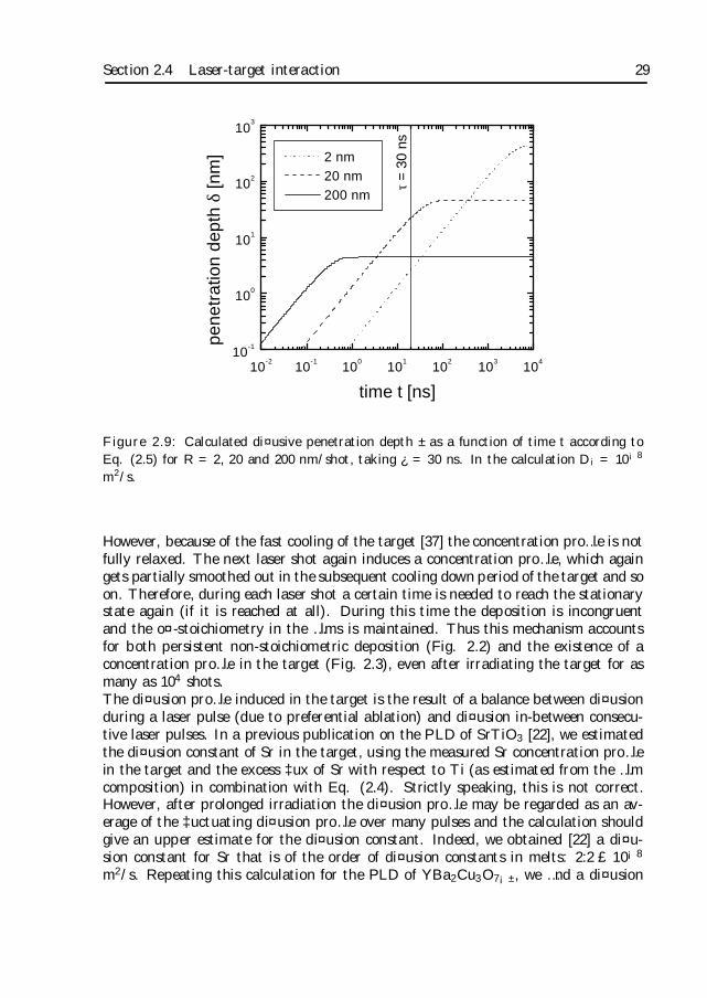
Section 2.4 Laser-target interaction 29
10-2
10-1
100
101
102
103
104
10-1
100
101
102
103
pene
trat
ion
dept
h δ
[nm
]
time t [ns]τ
= 3
0 ns
2 nm
20 nm
200 nm
Figure 2.9: Calculated di¤usive penetration depth ± as a function of time t according toEq. (2.5) for R = 2, 20 and 200 nm/shot, taking ¿ = 30 ns. In the calculation Di = 10¡8
m2/s.
However, because of the fast cooling of the target [37] the concentration pro…le is notfully relaxed. The next laser shot again induces a concentration pro…le, which againgets partially smoothed out in the subsequent cooling down period of the target and soon. Therefore, during each laser shot a certain time is needed to reach the stationarystate again (if it is reached at all). During this time the deposition is incongruentand the o¤-stoichiometry in the …lms is maintained. Thus this mechanism accountsfor both persistent non-stoichiometric deposition (Fig. 2.2) and the existence of aconcentration pro…le in the target (Fig. 2.3), even after irradiating the target for asmany as 104 shots.The di¤usion pro…le induced in the target is the result of a balance between di¤usionduring a laser pulse (due to preferential ablation) and di¤usion in-between consecu-tive laser pulses. In a previous publication on the PLD of SrTiO3 [22], we estimatedthe di¤usion constant of Sr in the target, using the measured Sr concentration pro…lein the target and the excess ‡ux of Sr with respect to Ti (as estimated from the …lmcomposition) in combination with Eq. (2.4). Strictly speaking, this is not correct.However, after prolonged irradiation the di¤usion pro…le may be regarded as an av-erage of the ‡uctuating di¤usion pro…le over many pulses and the calculation shouldgive an upper estimate for the di¤usion constant. Indeed, we obtained [22] a di¤u-sion constant for Sr that is of the order of di¤usion constants in melts: 2:2 £ 10¡8
m2/s. Repeating this calculation for the PLD of YBa2Cu3O7¡±, we …nd a di¤usion
30 Chapter 2 Conditions for stoichiometric transfer in pulsed laser deposition
constant for Y and Ba of the same order of magnitude (3 £ 10¡8 m2/s). Therefore,the di¤usion constant used for the calculations is reasonable.We conclude that the non-stoichiometric transfer in region II is caused by di¤usion-assisted preferential ablation of Y and Ba from the target. This mechanism persistsbecause of the pulsed character of the deposition method. Between consecutive laserpulses the di¤usion pro…le in the target partially relaxes. Therefore, there always isa period of non-stationary di¤usion during the next laser pulse, yielding persistentnon-stoichiometric transfer.
2.4.3 Region III: stoichiometric deposition
Although it is expected that preferential ablation of Y and Ba still takes place at ‡u-ences J > 1:3 J/cm2, truly stoichiometric …lms are deposited in region III. Followingthe line of reasoning of the preceding section, stoichiometric transfer only takes placeif the stationary state is almost immediately reached during each laser pulse. FromFig. 2.9 it follows that the stationary state is reached sooner for larger R, the thick-ness of the layer removed from the target by one shot. Since R is proportional to thedeposition rate, one should reach stoichiometric deposition when increasing the depo-sition rate. In …gure 2.10 the measured deposition rate is plotted versus the ‡uenceafter 600 shots of preablation (starting from a fresh target, the rate decays roughly ex-ponentially with time to a constant value [19]). Below Jth = 1:0 J/cm2 this depositionrate is zero and increases monotonically above Jth. Therefore, at large J stoichiomet-ric deposition is expected. From this argument it follows, that the crossover betweenregion II and III is not so abrupt, as was already suggested by the shaded area in Fig.2.2. This is the reason that some precipitates are always found around 1.3 J/cm2. Atvery large ‡uences, however, the precipitate density is greatly reduced and we …ndthat the deposition process is truly stoichiometric [see Fig. 2.4(b)]. In fact, Aucielloand co-workers [38] already observed in 1988 that the …lm composition approachesstoichiometry at large ‡uences. They proposed that at such high ‡uences also tar-get material from a thickness larger than the compositionally altered surface layer isremoved.One may wonder at this point whether increasing the ‡uence is the only way to reachstoichiometric deposition. From a dimensional analysis we know that the stationarystate is reached at a time of the order of t¤ (see also Fig. 2.9), which is de…ned as
t¤ = Di
³ ¿
R
´2
. (2.9)
This relation shows that it is in fact the ablation rate R=¿ that determines how fastthe stationary state is reached. Thus, an alternative way to reach stoichiometricdeposition is to reduce the pulse duration ¿ . By decreasing the laser pulse duration,it should be possible to reach stoichiometric deposition for all ‡uences larger than thethreshold ‡uence.In the previous section, it was shown that the properties of stoichiometric …lms de-posited at high ‡uences are relatively poor (see Fig. 2.5). Since it is the thickness Rof the layer that is removed by one shot and not the deposition rate itself that de-
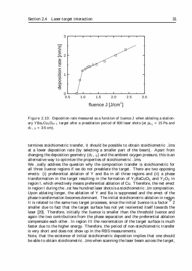
Section 2.4 Laser-target interaction 31
0.5 1.0 1.5 2.0 2.5 3.00
1
2
3
de
po
sitio
n r
ate
[n
m/s
]
fluence J [J/cm2]
Figure 2.10: Deposition rate measured as a function of ‡uence J when ablating a station-ary YBa2Cu3O6+x target after a preablation period of 600 laser shots (at pO2 = 15 Pa anddT¡S = 3:5 cm).
termines stoichiometric transfer, it should be possible to obtain stoichiometric …lmsat a lower deposition rate (by selecting a smaller part of the beam). Apart fromchanging the deposition geometry (dT¡S) and the ambient oxygen pressure, this is analternative way to optimize the properties of stoichiometric …lms.We …nally address the question why the composition transfer is stoichiometric forall three ‡uence regions if we do not preablate the target. There are two opposinge¤ects: (i) preferential ablation of Y and Ba in all three regions and (ii) a phasetransformation in the target resulting in the formation of Y2BaCuO5 and Y2O3 inregion I, which e¤ectively means preferential ablation of Cu. Therefore, the net e¤ectin region I during the …rst few hundred laser shots is a stoichiometric …lm composition.Upon ablating longer, the ablation of Y and Ba is suppressed and the e¤ect of thephase transformation becomes dominant. The initial stoichiometric ablation in regionII is related to the same two target processes, since the initial ‡uence is a factor
p2
smaller due to fact that the target surface has not yet reoriented itself towards thelaser [20]. Therefore, initially the ‡uence is smaller than the threshold ‡uence andagain the two contributions from the phase separation and the preferential ablationcompensate each other. In region III the reorientation of the target surface is muchfaster due to the higher energy. Therefore, the period of non-stoichiometric transferis very short and does not show up in the RBS measurements.Note, that the existence of initial stoichiometric deposition implies that one shouldbe able to obtain stoichiometric …lms when scanning the laser beam across the target,
32 Chapter 2 Conditions for stoichiometric transfer in pulsed laser deposition
independently of the applied ‡uence or beam homogeneity. However, the drawbackis that some target grains are ejected from the target to the substrates, resulting in apoor …lm surface morphology.
Summarizing, there are two mechanisms by which non-stoichiometric transfer occursduring the pulsed laser deposition of YBa2Cu3O7¡±: (i) phase separation in the targetmaterial and (ii) di¤usion-assisted preferential ablation. These mechanisms apply tothe PLD of other materials as well. For instance, it was illustrated [21] that thesecond mechanism is responsible for the non-stoichiometric deposition in the PLD ofSrTiO3 at ‡uences below 1.3 J/cm2, whereas the phase separation does not occurin this congruently melting material. We note that the numerical values for thethreshold ‡uences quoted here depend on the quality of the target material (i.e.,density, preferential orientation, etc.). Therefore, they may di¤er slightly from targetto target.
2.5 Conclusions
We …nd that in PLD of YBa2Cu3O7¡± , the …lm composition is a sensitive function ofthe laser ‡uence. This is a direct consequence of laser induced modi…cations in thetarget material, much more than a change in ablation mechanism. Below the thresh-old ‡uence Jth = 1:0 J/cm2 (‡uence region I), a phase separation is induced in thetarget. As a result, the deposited …lms are non-stoichiometric. At ‡uences slightlylarger than the threshold ‡uence (region II: 1:0 < J < 1:3 J/cm2), the ablation pro-cess is preferential with respect to Y and Ba. Since also di¤usion pro…les of Y and Baare observed in the ablated target material, we attribute the non-stoichiometric trans-fer to volume-di¤usion-assisted preferential ablation. This mechanism is described bya phenomenological 1-D di¤usion model, in which the ablation process is simulatedby a moving boundary and the preferential ablation of Y and Ba is taken into ac-count by imposing two additional atom ‡uxes at the (moving) boundary. From themodel, it follows that the material transfer from the target to the substrate is non-stoichiometric as long as the di¤usion in the target is non-stationary. Because of thepulsed character of the deposition technique, the di¤usion pro…le relaxes in-betweenconsecutive laser pulses and there always is a period of non-stationary di¤usion giv-ing persistent non-stoichiometric deposition. However, the non-stationary periodsare reduced considerably by increasing the ablation rate. Consequently, stoichiomet-ric deposition is expected to take place for: (i) large ‡uences and/or (ii) short laserpulses.Indeed, for ‡uences J À 1:3 J/cm2 the exact Y1Ba2Cu3 composition is found (regionIII). As a result of the stoichiometric deposition, the surface quality of these …lms isvery good. We …nd precipitate densities of 104/cm2 in combination with reasonablesuperconducting (89 < Tc < 90 K) and structural (0:1± < FWHM < 0:2±) properties.In region II, the di¤usion-assisted preferential ablation regime, higher precipitatedensities are observed (107/cm2). However, the structural (FWHM < 0:1±) and
References 33
superconducting (90 < Tc < 91 K) quality is better than in region III, suggestingthat the growth process actually requires some o¤-stoichiometry.In conclusion, the best YBa2Cu3O7¡± …lms are found at the boundary between re-gions II and III at a ‡uence of 1.3 J/cm2. These …lms, combine both a low precipitatedensity (typically 106/cm2), superior structural (FWHM < 0:1± and c = 11:70 Å)and superconducting properties (Tc = 91:0 K; ¢Tc = 0:4 K) with a remarkable repro-ducibility. Our experiments show that PLD can be a highly reproducible depositiontechnique, when a well-de…ned, uniform and reproducible laser spot is used.2 Theexcellent reproducibility allows us to relate the superconducting properties to themicrostructure, as will be shown in the following chapters.
References
[1] D.B. Chrisey and G.K. Hubler, Pulsed Laser Deposition of Thin Films (Wiley,New York, 1994)
[2] R.K. Singh and D. Kumar, Mat. Sci. Eng. R 22, 113 (1998)
[3] S. Proyer, E. Stangl, M. Borz, B. Hellebrand, and D. Bäuerle, Physica C 257,1 (1996)
[4] B. Dam, J. Rector, M.F. Chang, S. Kars, D.G. de Groot, and R. Griessen, Appl.Surf. Sci. 86, 13 (1995)
[5] Y. Watanabe, M. Tanamura, S. Matsumoto, and Y. Seki, J. Appl. Phys. 78,2029 (1995)
[6] B. Holzapfel, B. Roas, L. Schultz, P. Bauer, and G. Saemann-Ischenko, Appl.Phys. Lett. 61, 3178 (1992)
[7] E.V. Pechen, A.V. Varlashkin, S.I. Krasnosvobodtsev, B. Brunner, and K.F.Renk, Appl. Phys. Lett. 66, 2292 (1995)
[8] M.D. Strikovsky, E.B. Klyuenkov, S.V. Gaponov, J. Schubert, and C.A. Copetti,Appl. Phys. Lett. 63, 1146 (1993)
[9] R.K. Singh, D. Bhattacharya, and J. Narayan, Appl. Phys. Lett. 61, 483 (1992)
[10] D.S. Misra and S.B. Palmer, Physica C 176, 43 (1991)
[11] C.C. Chang, X.D. Wu, R. Ramesh, X.X. Xi, T.S. Ravi, T. Venkatesan, D.M.Hwang, R.E. Muenchenhausen, S. Foltyn, and N.S. Nogar, Appl. Phys. Lett.57, 1814 (1990)
2These observations have been used in the design and development of a second PLD system inour group, consisting of a LAMBDA PHYSIK KrF (¸ = 248 nm, ¿ = 25 ns) laser, projection optics(including a beam homogenizer) and a relatively small high vaccuum system. The use of a beamhomogenizer resulted in a reproducible lowering of the density of precipitates to about 105/cm2 ata ‡uence of 1.4 J/m2. No noticeable di¤erences in microstructural and superconducting propertiesbetween YBa2Cu3O7¡± …lms deposited in the QUESTEK and LAMBDA PHYSIK system are found,showing that PLD is indeed a highly reproducible deposition technique.
34 Chapter 2 Conditions for stoichiometric transfer in pulsed laser deposition
[12] M. Murakami, M. Morita, K. Doi, K. Miyamoto, and H. Hamada, Jpn. J. Appl.Phys. 28, L399 (1989)
[13] N.G. Chew, S.W. Goodyear, J.A. Edwards, J.S. Satchell, S.E. Blenkinsop, andR.G. Humpreys, Appl. Phys. Lett. 57, 2016 (1990)
[14] Y. Watanabe, Y. Seo, M. Tanamura, H. Asami, and Y. Matsumoto, J. Appl.Phys. 78, 5126 (1995)
[15] M.C. Foote, B.B. Jones, B.D. Hunt, J.B. Barner, R.P. Vasquesz, and L.J. Bajuk,Physica C 201, 176 (1992)
[16] M.E. Gaevski, A.V. Bobyl, D.V. Shantsev, R.A. Suris, V.V. Tret’yakov, Y.M.Galperin, and T.H. Johansen, J. Appl. Phys. 84, 5089 (1998)
[17] V. Matijasevic, P. Rosenthal, K. Shinohara, A.F. Marshall, R.H. Hammond,and M.R. Bearsley, J. Mater. Res. 6, 682 (1991)
[18] R. Kelly, J.J. Cuomo, P.A. Leary, J.E. Rothenberg, B.E. Braren, and C.F.Aliotta, Nucl. Instrum. Methods Phys. Rev. B 9, 329 (1985)
[19] S.R. Foltyn, R.C. Dye, K.C. Ott, E. Peterson, K.M. Hubbard, W. Hutchinson,R.E. Muenchausen, R.C. Estler, and X.D. Wu, Appl. Phys. Lett. 59, 594 (1991)
[20] B. Dam, J. Rector, M.F. Chang, S. Kars, D.G. de Groot, and R. Griessen, Appl.Phys. Lett. 65, 1581 (1994)
[21] B. Dam, J.H. Rector, J. Johansson, S. Kars, and R. Griessen, Appl. Surf. Sci.96-98, 679 (1996)
[22] B. Dam, J.H. Rector, J. Johansson, J. Huijbregtse, and D.G. de Groot, J. Appl.Phys. 83, 3386 (1998)
[23] L.R. Doolittle, Nucl. Instrum. Methods Phys. Rev. B 9, 344 (1985)
[24] M.C. Foote, R.P. Vasquez, B.B. Jones, B.D. Hunt, and J.B. Barner, J. ElectronicMater. 23, 849 (1994)
[25] B.T. Ahn, V.Y. Lee, R. Beyers, T.M. Gür, and R.A. Huggins, Physica C 167,529 (1990)
[26] J.P. Gong, M. Kawasaki, F. Fujito, R. Tsuchiya, M. Yoshimoto, and H. Koinuma,Phys. Rev. B 50, 3280 (1994)
[27] O. Eibl and B. Roas, J. Mater. Res. 5, 2620 (1990)
[28] F. Izumi, H. Asano, T. Ishigaki, E. Takayama-Mromachi, Y. Uchida, N. Watan-abe, and T. Nishikawa, Jpn. J. Appl. Phys. 26, L649 (1987)
[29] Jinhua Ye and Keikichi Nakamura, Phys. Rev. B 48, 7554 (1993)
[30] Jinhua Ye and Keikichi Nakamura, Phys. Rev. B 50, 7099 (1994)
[31] Jinhua Ye and Keikichi Nakamura, Physica C 254, 113 (1995)
[32] H.S. Kim and H.S. Kwok, Appl. Phys. Lett. 61, 2234 (1992)
[33] N. Kanda, M. Kawasaki, T. Kitajima, and H. Koinuma, Phys. Rev. B 56, 8419(1997)

References 35
[34] B. Dam, J.H. Rector, J.M. Huijbregtse, and R. Griessen, Physica C 305, 1(1998)
[35] A. Wong, R. Liang, M. Gardner, and W.N. Hardy, J. Appl. Phys. 82, 3019(1997)
[36] T.R. Goodman, Advances in Heat Transfer, edited by T.F. Irvin and J.P. Hart-nett (Acadamic Press, New York, 1964), Vol. 1, p. 51
[37] A.N. Jette and W.J. Green, J. Appl. Phys. 68, 5273 (1990)
[38] O. Auciello, A.R. Krauss, J. Santiago-Aviles, A.F. Schreiner, and D.M. Gruen,Appl. Phys. Lett. 52, 239 (1988)

Chapter 3
Origin of high critical currents
Thin …lms of the high-temperature superconductor YBa2Cu3O7¡± exhibit both alarge critical current (the superconducting current density generally lies between 1011
and 1012 A/m2 at 4.2 K in zero magnetic …eld) and a rapid decrease in currentwith magnetic …eld. Both features point to the importance of strong vortex pinningalong extended defects. However, it has hitherto been unclear which type of defect¡ dislocations, grain boundaries, surface corrugation and anti-phase boundaries ¡ isresponsible. Making use of a novel sequential wet-chemical etching technique, we …ndthat: (i) all dislocations (edge, screw and mixed) can be mapped quantitatively bythis technique and (ii) threading dislocations are the defects that provide the strongpinning centres responsible for the high critical currents observed in these thin …lms.In contrast to arti…cially generated columnar defects, these natural linear defectsexhibit self-organized short-range order. Therefore, YBa2Cu3O7¡± thin …lms o¤er anattractive system for investigating the properties of vortex matter in a superconductorwith a tailored defect structure.1
1This chapter is based on papers by B. Dam, J.M. Huijbregtse, F.C. Klaassen, R.C.F. van derGeest, G. Doornbos, J.H. Rector, A.M. Testa, S. Freisem, J.C. Martinez, B. Stäuble-Pümpin, andR. Griessen, Nature (London) 399, 439 (1999) and by J.M. Huijbregtse, B. Dam, R.C.F. van derGeest, F.C. Klaassen, R. Elberse, J.H. Rector and R. Griessen, Phys. Rev. B 62, 1338 (2000)
38 Chapter 3 Origin of high critical currents
3.1 Introduction
In the last few years the quality of high-Tc superconducting thin …lms has improvedsigni…cantly. Thin …lms have become more and more single-crystalline like. However,the magnitude of the superconducting current density js in …lms is still orders ofmagnitude larger than in single crystals.2 In YBa2Cu3O7¡± …lms for example, js isas high as 1012 A/m2 (at small magnetic …elds and low temperatures) while in singlecrystals it is typically 1010 A/m2 [2]. The high js of …lms is generally attributed[3] to the strong pinning [4, 5] of vortices to extended defects. In single crystals thetransport properties are mainly determined by randomly distributed point defects(e.g. oxygen vacancies), leading to weak collective pinning [5]. The high js valuesfound in …lms must thus be caused by extended defects which are speci…c for …lmssuch as substrate induced anti-phase boundaries [6], dislocations [7, 8, 9] or surfaceroughness [9, 10]. Although there are experimental results [11, 12] pointing to theimportance of pinning by dislocations in …lms, no quantitative relation between thedislocation density and the pinning properties could be established. In this chapter, wedemonstrate that the linear defect structure of a …lm can be mapped quantitativelyand that an unambiguous relation exists between the as-grown dislocation densityndisl and the strong pinning behavior of js in YBa2Cu3O7¡± thin …lms.Instead of looking at the as-grown surface morphology, we investigate wet-etched …lms.It has been suggested [7] that the density of screw dislocations can be determined bycounting the number of spiral outcrops [13, 14] at the …lm surface. However, in thisway the total dislocation density (edge, screw and dislocations of mixed character)is severely underestimated [15] for two reasons: (i) edge dislocations do not giverise to such a clear topological structure and (ii) not all screw dislocations generategrowth spirals. Wet-chemical etching in combination with atomic force microscopyreveals the full dislocation structure and allows for a statistical analysis. Not only thelength but also the lateral dislocation distribution can be determined. We …nd thatdislocations are generated in the early stages of growth, i.e. close to the substrate-…lminterface. Since dislocations cannot end inside a crystal [16], they persist up to the …lmsurface parallel to the c-axis, resulting in a uniform length distribution. In principle,such threading dislocations can pin vortices along their entire length. At …rst sightthis situation seems very similar to arti…cial linear defects created by irradiatingsingle crystals with heavy ions [17, 18]. However, in our …lms the linear defectsare inherently growth-induced and exhibit short-range ordering, whereas arti…cialcolumnar defects are randomly distributed. In principle, the non-random dislocationdistribution enhances the pinning e¢ciency. Since we can also tune the threadingdislocation density at will without a¤ecting either the length or the lateral distributionof these linear defects, …lms are very attractive to study vortex matter. For instance,the predicted Mott-insulator vortex phase [4, 19] may be observable in thick laserablated YBa2Cu3O7¡± …lms at low dislocation densities.
2Due to thermal activation [1], the measured superconducting current density js is always smallerthan the true critical current density jc (the di¤erence increases with temperature). We use thesymbol jc for: (i) theoretical estimates and (ii) when correcting js for relaxation e¤ects.
Section 3.2 Revealing dislocations 39
3.2 Revealing dislocations
As is well-known in (bulk) metallurgy [20], dislocation densities can be reliably deter-mined by counting the number of etch pits formed upon applying a suitable dislocationsensitive etchand. In the case of YBa2Cu3O7¡± …lms, the etchand is a 1 Vol.% Br inethanol solution [15, 21, 22, 23, 24]. To analyze the surface morphology of both theas-grown and the etched …lms, we use atomic force microscopy (AFM) in the tappingmode. In order to investigate the persistence of etch pits upon repeated etching, aspeci…c area on the …lm surface is identi…ed by means of two perpendicular engravedmarkers. Using the large range of the AFM tube scanner (maximum scan size 100¹m), horizontal displacements of the AFM tip of about 20 ¹m with respect to thesereference markers can be reproduced. In this way surface features can be traced back,even after repeatedly etching and remounting of the sample.Below, we show how wet-chemical etching in 1 Vol.% Br-ethanol reveals dislocations.As a …rst step, the development of etch pits at defect sites is described. Since sputtered…lms exhibit spiral outcrops (i.e. screw dislocations), we use these …lm to test ouretching technique. Finally, the persistence of etch pits upon repeated etching at defectsites is probed in PLD …lms, indicating that the defects that are revealed are indeedlinear defects.
3.2.1 Principle of etching
The surface morphology of as-grown PLD …lms3 is generally characterized by a semi-regularly spaced array of growth islands, separated by trenches [see Fig. 3.1(a)].These trenches have a depth of up to 20% of the …lm thickness. In the trenches somedeeper depressions can be discerned. Changing the deposition conditions (substratetemperature Tsub and oxygen pressure pO2) mainly a¤ects the size D of the islands,i.e. the spacing between trenches. Since our PLD …lms grow by 2D nucleation andgrowth [15, 25], there are no spiral outcrops at the surface. Therefore, from the surfacemorphology only, it is not possible to determine the (screw) dislocation density.In order to reveal dislocations ending at the …lm surface, we apply a dislocationsensitive etchand. For etching to start on a ‡at, defect-free crystal surface, a negative(or inverse) 2D-nucleus has to be formed [20, 26]. Analogously to growth by 2D-nucleation, the radius of this nucleus, R, has to exceed some critical value R¤ tobecome a stable and expanding nucleus. This is due to the positive edge free energyterm in the total Gibbs free energy change:
¢G (r) = ¡¼R2h¢¹ + 2¼R°h. (3.1)
Here ° is the edge free energy, h the height of the nucleus and ¢¹ the di¤erencein chemical potential between atoms in the solid and those dissolved (¢¹ > 0).After a stable (negative) nucleus has been formed, dissolution proceeds by fast lateral
3All PLD …lms in this chapter are prepared in the QUESTEK set-up, using 3:0 < dT¡S < 3:5cm, 750 < Tsub < 850±C and 15 < pO2
< 50 Pa at a ‡uence J = 1:3 J/cm2 (as measured at thetarget).
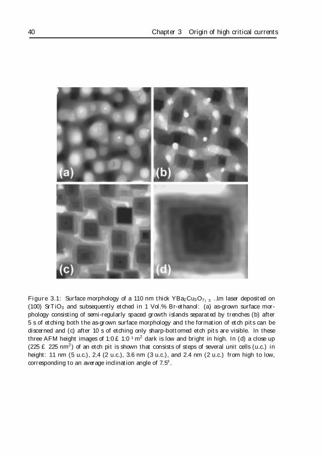
40 Chapter 3 Origin of high critical currents
Figure 3.1: Surface morphology of a 110 nm thick YBa2Cu3O7¡± …lm laser deposited on(100) SrTiO3 and subsequently etched in 1 Vol.% Br-ethanol: (a) as-grown surface mor-phology consisting of semi-regularly spaced growth islands separated by trenches (b) after5 s of etching both the as-grown surface morphology and the formation of etch pits can bediscerned and (c) after 10 s of etching only sharp-bottomed etch pits are visible. In thesethree AFM height images of 1:0£ 1:0 ¹m2 dark is low and bright in high. In (d) a close up(225 £ 225 nm2) of an etch pit is shown that consists of steps of several unit cells (u.c.) inheight: 11 nm (5 u.c.), 2.4 (2 u.c.), 3.6 nm (3 u.c.), and 2.4 nm (2 u.c.) from high to low,corresponding to an average inclination angle of 7.5±.
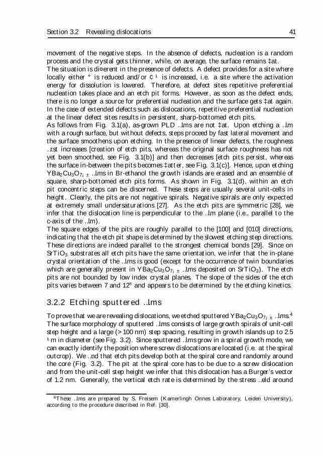
Section 3.2 Revealing dislocations 41
movement of the negative steps. In the absence of defects, nucleation is a randomprocess and the crystal gets thinner, while, on average, the surface remains ‡at.The situation is di¤erent in the presence of defects. A defect provides for a site wherelocally either ° is reduced and/or ¢¹ is increased, i.e. a site where the activationenergy for dissolution is lowered. Therefore, at defect sites repetitive preferentialnucleation takes place and an etch pit forms. However, as soon as the defect ends,there is no longer a source for preferential nucleation and the surface gets ‡at again.In the case of extended defects such as dislocations, repetitive preferential nucleationat the linear defect sites results in persistent, sharp-bottomed etch pits.As follows from Fig. 3.1(a), as-grown PLD …lms are not ‡at. Upon etching a …lmwith a rough surface, but without defects, steps proceed by fast lateral movement andthe surface smoothens upon etching. In the presence of linear defects, the roughness…rst increases [creation of etch pits, whereas the original surface roughness has notyet been smoothed, see Fig. 3.1(b)] and then decreases [etch pits persist, whereasthe surface in-between the pits becomes ‡atter, see Fig. 3.1(c)]. Hence, upon etchingYBa2Cu3O7¡± …lms in Br-ethanol the growth islands are erased and an ensemble ofsquare, sharp-bottomed etch pits forms. As shown in Fig. 3.1(d), within an etchpit concentric steps can be discerned. These steps are usually several unit-cells inheight. Clearly, the pits are not negative spirals. Negative spirals are only expectedat extremely small undersaturations [27]. As the etch pits are symmetric [28], weinfer that the dislocation line is perpendicular to the …lm plane (i.e., parallel to thec-axis of the …lm).The square edges of the pits are roughly parallel to the [100] and [010] directions,indicating that the etch pit shape is determined by the slowest etching step directions.These directions are indeed parallel to the strongest chemical bonds [29]. Since onSrTiO3 substrates all etch pits have the same orientation, we infer that the in-planecrystal orientation of the …lms is good (except for the occurrence of twin boundarieswhich are generally present in YBa2Cu3O7¡± …lms deposited on SrTiO3). The etchpits are not bounded by low index crystal planes. The slope of the sides of the etchpits varies between 7 and 12± and appears to be determined by the etching kinetics.
3.2.2 Etching sputtered …lms
To prove that we are revealing dislocations, we etched sputtered YBa2Cu3O7¡± …lms.4
The surface morphology of sputtered …lms consists of large growth spirals of unit-cellstep height and a large (>100 nm) step spacing, resulting in growth islands up to 2.5¹m in diameter (see Fig. 3.2). Since sputtered …lms grow in a spiral growth mode, wecan exactly identify the position where screw dislocations are located (i.e. at the spiraloutcrop). We …nd that etch pits develop both at the spiral core and randomly aroundthe core (Fig. 3.2). The pit at the spiral core has to be due to a screw dislocationand from the unit-cell step height we infer that this dislocation has a Burger’s vectorof 1.2 nm. Generally, the vertical etch rate is determined by the stress …eld around
4These …lms are prepared by S. Freisem (Kamerlingh Onnes Laboratory, Leiden University),according to the procedure described in Ref. [30].
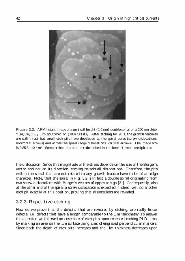
42 Chapter 3 Origin of high critical currents
Figure 3.2: AFM height image of a unit cell height (1.2 nm) double spiral on a 200 nm thickYBa2Cu3O7¡± …lm sputtered on (100) SrTiO3. After etching for 20 s, the growth featuresare still intact but small etch pits have developed at the spiral cores (screw dislocations,horizontal arrows) and across the spiral (edge dislocations, vertical arrows). The image sizeis 0:85£ 1:0 ¹m2. Some etched material is redeposited in the form of small precipitates.
the dislocation. Since this magnitude of the stress depends on the size of the Burger’svector and not on its direction, etching reveals all dislocations. Therefore, the pitswithin the spiral that are not related to any growth feature have to be of an edgecharacter. Note, that the spiral in Fig. 3.2 is in fact a double spiral originating fromtwo screw dislocations with Burger’s vectors of opposite sign [31]. Consequently, alsoat the other end of the spiral a screw dislocation is expected. Indeed, we …nd anotheretch pit exactly at this position, proving that dislocations are revealed.
3.2.3 Repetitive etching
How do we prove that the defects, that are revealed by etching, are really lineardefects, i.e. defects that have a length comparable to the …lm thickness? To answerthis question we followed an ensemble of etch pits upon repeated etching PLD …lms,by marking an area on the …lm surface using a set of engraved perpendicular markers.Since both the depth of etch pits increases and the …lm thickness decreases upon
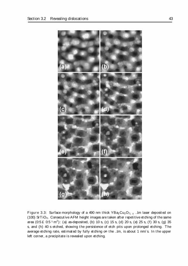
Section 3.2 Revealing dislocations 43
Figure 3.3: Surface morphology of a 490 nm thick YBa2Cu3O7¡± …lm laser deposited on(100) SrTiO3. Consecutive AFM height images are taken after repetitive etching of the samearea (0:5£ 0:5 ¹m2): (a) as-deposited, (b) 10 s, (c) 15 s, (d) 20 s, (e) 25 s, (f) 30 s, (g) 35s, and (h) 40 s etched, showing the persistence of etch pits upon prolonged etching. Theaverage etching rate, estimated by fully etching o¤ the …lm, is about 1 nm/s. In the upperleft corner, a precipitate is revealed upon etching.
44 Chapter 3 Origin of high critical currents
repeated etching, we are able to follow the etch pits in the …lm. A sequence ofconsecutive etch experiments is shown in Fig. 3.3.In this …gure, it can be seen that etch pits develop at the periphery of the islandsand that all etch pits persist upon repeated etching. Since the bottoms of the etchpits do not turn ‡at but remain sharp, there is a persistent source for preferentialetching. Thus, we conclude that we are indeed dealing with linear defects of a con-siderable length. In Fig. 3.3 some etch pits are hampered in their development (seefor instance the etch pit in the upper left corner). Upon prolonged etching …rst aprecipitate is revealed and then an etch pit forms again, indicating that dislocationscan end and originate again at precipitates [16]. However, in all etching experimentsthis fraction is small (< 5%). Since the lateral size of the etch pits increases uponrepeated etching (Fig. 3.3), it becomes more and more di¢cult to follow the individ-ual etch pits. Although initially overlapping etch pits can still be distinguished dueto their pronounced square shape, at a certain moment this is not possible any more.Consequently, it is impossible to follow the etching process down to the substrate. Abetter method to investigate the length distribution of linear defects is to etch …lmsof various thickness (see section 3.3.2).
Concluding, we …nd that the density of linear defects in YBa2Cu3O7¡± …lms can bequantitatively determined by combining Br-ethanol etching with AFM. We identi…edsome of the pits as being due to screw dislocations with a unit-cell Burger’s vector.As etch pit formation is due to the stress energy within the dislocation core (and doesnot depend on the direction of the Burger’s vector) both edge and screw dislocationswith Burger’s vectors of one unit-cell or higher are revealed. Although in principlewe can observe dislocations tilted with respect to the c-axis, none of those weredetected. Note that dislocations running parallel to the substrate are not revealed inour experiments.
3.3 Dislocation density and distribution
3.3.1 Tuning the dislocation density
Having a tool to determine dislocation densities, we investigate now the mechanismby which dislocations are induced during growth. Therefore, we take a closer look atthe position of the dislocations (or etch pits) with respect to the as-grown …lm surface.Figure 3.4 shows two AFM height images recorded directly after deposition and afteretching the same …lm. Since these images are taken on the same position, we infer thatdislocations are mainly situated around the islands in the holes in the trenches (in factthis can also be seen in Figs. 3.1(b) and 3.3). Apparently, surface depressions form atpositions where dislocations emerge at the …lm surface. Indeed, Frank predicted [32]such depressions to form as a result of the strain energy associated with dislocations.However, the depressions in our …lms are much wider than predicted and they do notform around all dislocations.
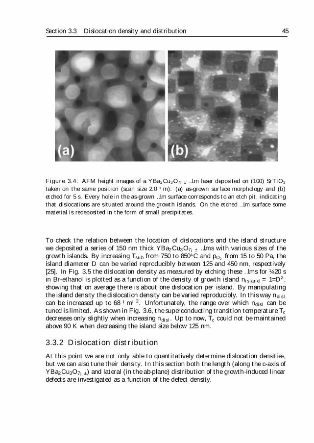
Section 3.3 Dislocation density and distribution 45
Figure 3.4: AFM height images of a YBa2Cu3O7¡± …lm laser deposited on (100) SrTiO3
taken on the same position (scan size 2.0 ¹m): (a) as-grown surface morphology and (b)etched for 5 s. Every hole in the as-grown …lm surface corresponds to an etch pit, indicatingthat dislocations are situated around the growth islands. On the etched …lm surface somematerial is redeposited in the form of small precipitates.
To check the relation between the location of dislocations and the island structurewe deposited a series of 150 nm thick YBa2Cu3O7¡± …lms with various sizes of thegrowth islands. By increasing Tsub from 750 to 850±C and pO2 from 15 to 50 Pa, theisland diameter D can be varied reproducibly between 125 and 450 nm, respectively[25]. In Fig. 3.5 the dislocation density as measured by etching these …lms for ¼20 sin Br-ethanol is plotted as a function of the density of growth island nisland = 1=D2,showing that on average there is about one dislocation per island. By manipulatingthe island density the dislocation density can be varied reproducibly. In this way ndisl
can be increased up to 68 ¹m¡2. Unfortunately, the range over which ndisl can betuned is limited. As shown in Fig. 3.6, the superconducting transition temperature Tc
decreases only slightly when increasing ndisl. Up to now, Tc could not be maintainedabove 90 K when decreasing the island size below 125 nm.
3.3.2 Dislocation distribution
At this point we are not only able to quantitatively determine dislocation densities,but we can also tune their density. In this section both the length (along the c-axis ofYBa2Cu3O7¡±) and lateral (in the ab-plane) distribution of the growth-induced lineardefects are investigated as a function of the defect density.
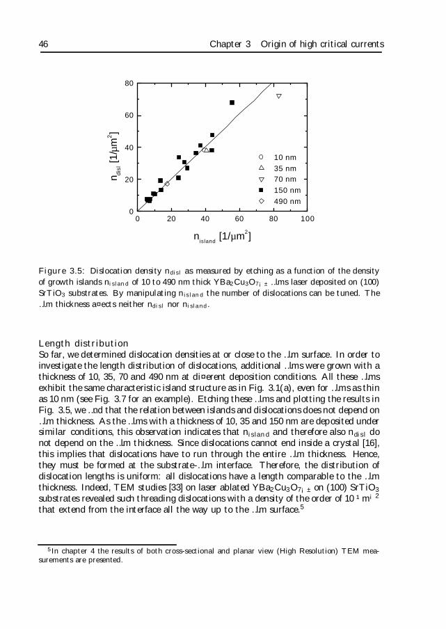
46 Chapter 3 Origin of high critical currents
0 20 40 60 80 1000
20
40
60
80
n dis
l [1
/µm
2]
nisland
[1/µm2]
10 nm
35 nm
70 nm
150 nm
490 nm
Figure 3.5: Dislocation density ndisl as measured by etching as a function of the densityof growth islands nisland of 10 to 490 nm thick YBa2Cu3O7¡± …lms laser deposited on (100)SrTiO3 substrates. By manipulating nisland the number of dislocations can be tuned. The…lm thickness a¤ects neither ndisl nor nisland.
Length distributionSo far, we determined dislocation densities at or close to the …lm surface. In order toinvestigate the length distribution of dislocations, additional …lms were grown with athickness of 10, 35, 70 and 490 nm at di¤erent deposition conditions. All these …lmsexhibit the same characteristic island structure as in Fig. 3.1(a), even for …lms as thinas 10 nm (see Fig. 3.7 for an example). Etching these …lms and plotting the results inFig. 3.5, we …nd that the relation between islands and dislocations does not depend on…lm thickness. As the …lms with a thickness of 10, 35 and 150 nm are deposited undersimilar conditions, this observation indicates that nisland and therefore also ndisl donot depend on the …lm thickness. Since dislocations cannot end inside a crystal [16],this implies that dislocations have to run through the entire …lm thickness. Hence,they must be formed at the substrate-…lm interface. Therefore, the distribution ofdislocation lengths is uniform: all dislocations have a length comparable to the …lmthickness. Indeed, TEM studies [33] on laser ablated YBa2Cu3O7¡± on (100) SrTiO3
substrates revealed such threading dislocations with a density of the order of 10 ¹m¡2
that extend from the interface all the way up to the …lm surface.5
5In chapter 4 the results of both cross-sectional and planar view (High Resolution) TEM mea-surements are presented.
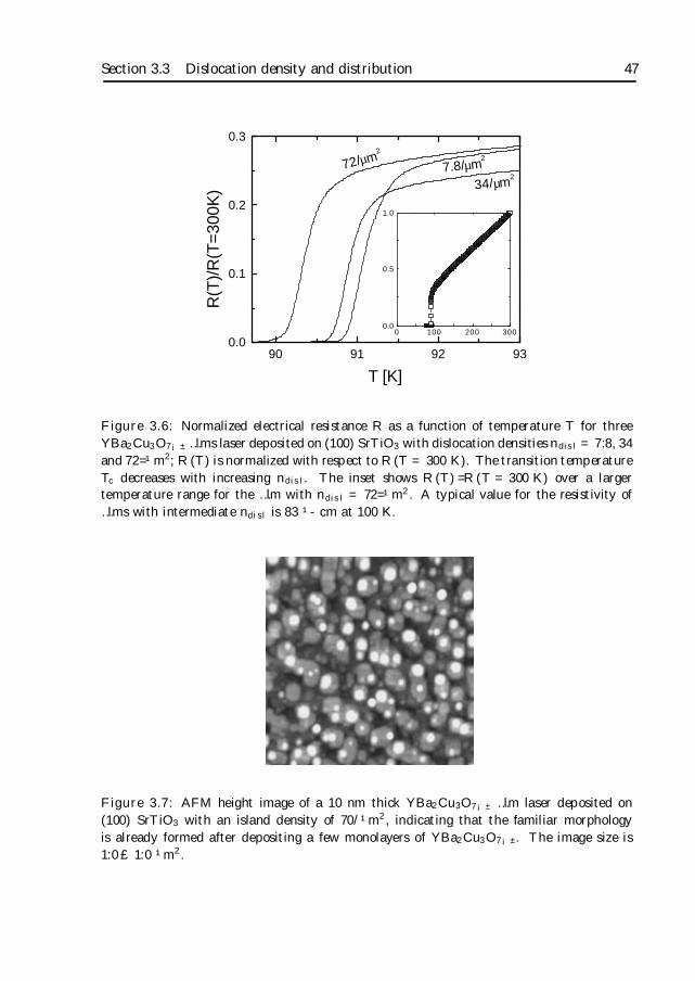
Section 3.3 Dislocation density and distribution 47
90 91 92 930.0
0.1
0.2
0.3
T [K]
R(T
)/R
(T=
300K
)
72/µm2
7.8/µm2
34/µm2
0 100 200 3000.0
0.5
1.0
Figure 3.6: Normalized electrical resistance R as a function of temperature T for threeYBa2Cu3O7¡± …lms laser deposited on (100) SrTiO3 with dislocation densities ndisl = 7:8, 34and 72=¹m2; R (T ) is normalized with respect to R (T = 300 K). The transition temperatureTc decreases with increasing ndisl. The inset shows R (T ) =R (T = 300 K) over a largertemperature range for the …lm with ndisl = 72=¹m2. A typical value for the resistivity of…lms with intermediate ndisl is 83 ¹cm at 100 K.
Figure 3.7: AFM height image of a 10 nm thick YBa2Cu3O7¡± …lm laser deposited on(100) SrTiO3 with an island density of 70/¹m2, indicating that the familiar morphologyis already formed after depositing a few monolayers of YBa2Cu3O7¡±. The image size is1:0£ 1:0 ¹m2.
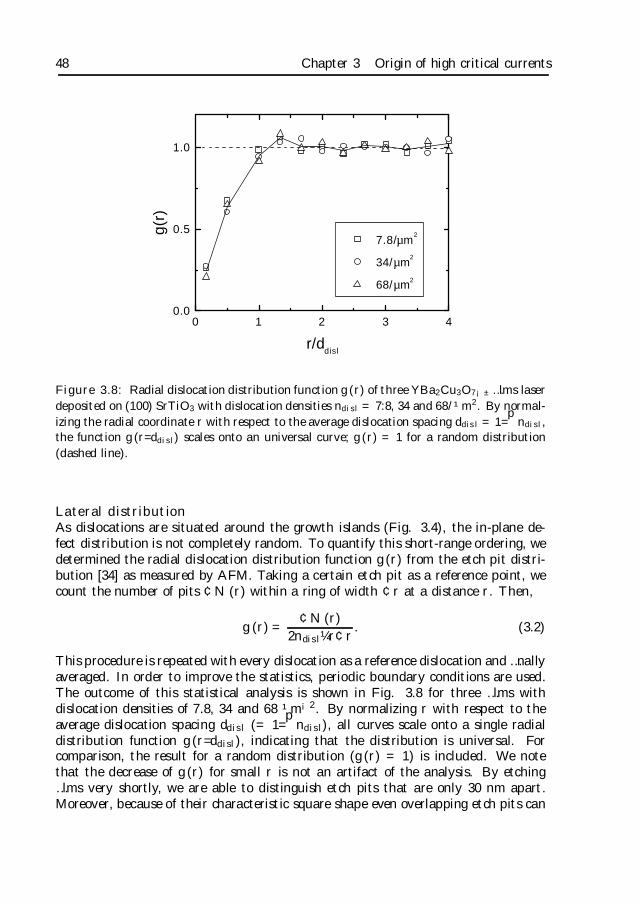
48 Chapter 3 Origin of high critical currents
0 1 2 3 40.0
0.5
1.0g
(r)
r/ddisl
7.8/µm2
34/µm2
68/µm2
Figure 3.8: Radial dislocation distribution function g (r) of three YBa2Cu3O7¡± …lms laserdeposited on (100) SrTiO3 with dislocation densities ndisl = 7:8, 34 and 68/¹m2. By normal-izing the radial coordinate r with respect to the average dislocation spacing ddisl = 1=
pndisl,
the function g (r=ddisl) scales onto an universal curve; g (r) = 1 for a random distribution(dashed line).
Lateral distributionAs dislocations are situated around the growth islands (Fig. 3.4), the in-plane de-fect distribution is not completely random. To quantify this short-range ordering, wedetermined the radial dislocation distribution function g (r) from the etch pit distri-bution [34] as measured by AFM. Taking a certain etch pit as a reference point, wecount the number of pits ¢N (r) within a ring of width ¢r at a distance r. Then,
g (r) =¢N (r)
2ndisl¼r¢r. (3.2)
This procedure is repeated with every dislocation as a reference dislocation and …nallyaveraged. In order to improve the statistics, periodic boundary conditions are used.The outcome of this statistical analysis is shown in Fig. 3.8 for three …lms withdislocation densities of 7.8, 34 and 68 ¹m¡2. By normalizing r with respect to theaverage dislocation spacing ddisl (= 1=
pndisl), all curves scale onto a single radial
distribution function g (r=ddisl), indicating that the distribution is universal. Forcomparison, the result for a random distribution (g (r) = 1) is included. We notethat the decrease of g (r) for small r is not an artifact of the analysis. By etching…lms very shortly, we are able to distinguish etch pits that are only 30 nm apart.Moreover, because of their characteristic square shape even overlapping etch pits can
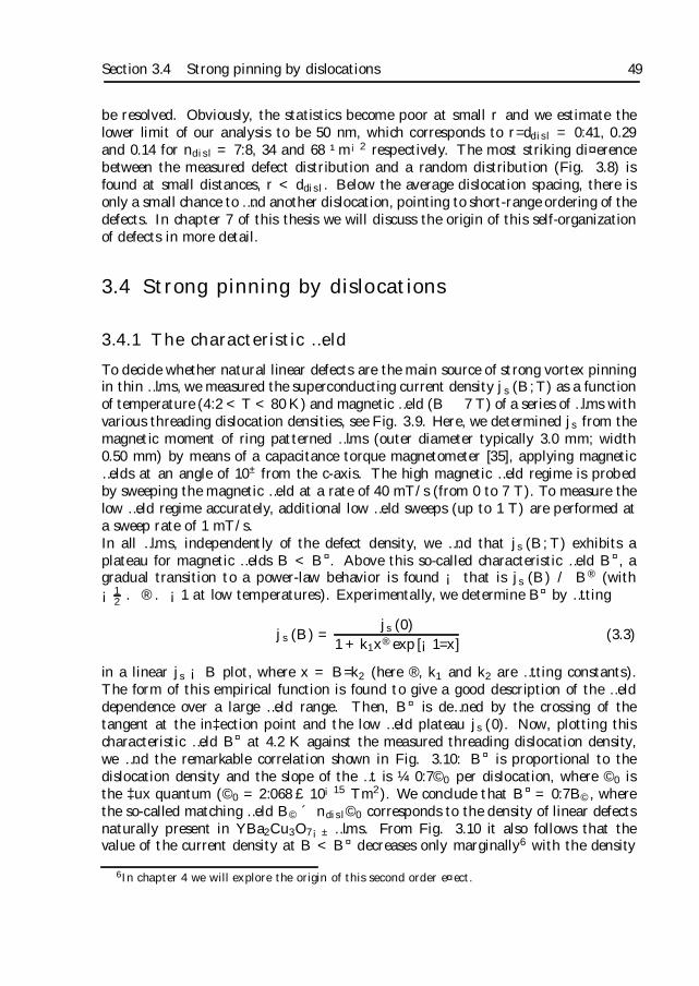
Section 3.4 Strong pinning by dislocations 49
be resolved. Obviously, the statistics become poor at small r and we estimate thelower limit of our analysis to be 50 nm, which corresponds to r=ddisl = 0:41, 0.29and 0.14 for ndisl = 7:8, 34 and 68 ¹m¡2 respectively. The most striking di¤erencebetween the measured defect distribution and a random distribution (Fig. 3.8) isfound at small distances, r < ddisl. Below the average dislocation spacing, there isonly a small chance to …nd another dislocation, pointing to short-range ordering of thedefects. In chapter 7 of this thesis we will discuss the origin of this self-organizationof defects in more detail.
3.4 Strong pinning by dislocations
3.4.1 The characteristic …eld
To decide whether natural linear defects are the main source of strong vortex pinningin thin …lms, we measured the superconducting current density js (B;T ) as a functionof temperature (4:2 < T < 80 K) and magnetic …eld (B 7 T) of a series of …lms withvarious threading dislocation densities, see Fig. 3.9. Here, we determined js from themagnetic moment of ring patterned …lms (outer diameter typically 3.0 mm; width0.50 mm) by means of a capacitance torque magnetometer [35], applying magnetic…elds at an angle of 10± from the c-axis. The high magnetic …eld regime is probedby sweeping the magnetic …eld at a rate of 40 mT/s (from 0 to 7 T). To measure thelow …eld regime accurately, additional low …eld sweeps (up to 1 T) are performed ata sweep rate of 1 mT/s.In all …lms, independently of the defect density, we …nd that js (B; T ) exhibits aplateau for magnetic …elds B < B¤. Above this so-called characteristic …eld B¤, agradual transition to a power-law behavior is found ¡ that is js (B) / B® (with¡1
2. ® . ¡1 at low temperatures). Experimentally, we determine B¤ by …tting
js (B) =js (0)
1 + k1x® exp [¡1=x](3.3)
in a linear js ¡ B plot, where x = B=k2 (here ®, k1 and k2 are …tting constants).The form of this empirical function is found to give a good description of the …elddependence over a large …eld range. Then, B¤ is de…ned by the crossing of thetangent at the in‡ection point and the low …eld plateau js (0). Now, plotting thischaracteristic …eld B¤ at 4.2 K against the measured threading dislocation density,we …nd the remarkable correlation shown in Fig. 3.10: B¤ is proportional to thedislocation density and the slope of the …t is ¼ 0:7©0 per dislocation, where ©0 isthe ‡ux quantum (©0 = 2:068 £ 10¡15 Tm2). We conclude that B¤ = 0:7B©, wherethe so-called matching …eld B© ´ ndisl©0 corresponds to the density of linear defectsnaturally present in YBa2Cu3O7¡± …lms. From Fig. 3.10 it also follows that thevalue of the current density at B < B¤ decreases only marginally6 with the density
6In chapter 4 we will explore the origin of this second order e¤ect.
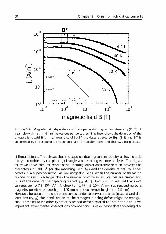
50 Chapter 3 Origin of high critical currents
10-3
10-2
10-1
100
101
108
109
1010
1011
1012
80 K
60 K
40 K
4.2 K
B*
j s [
A/m
2 ]
magnetic field B [T]
0.00 0.02 0.04 0.06
3.0x10¹¹
3.2x10¹¹
B*
Figure 3.9: Magnetic …eld dependence of the superconducting current density js (B;T ) ofa sample with ndisl = 6=¹m2 at various temperatures. The inset shows the de…nition of thecharacteristic …eld B¤: in a linear plot of js (B) the data is …tted to Eq. (3.3) and B¤ isdetermined by the crossing of the tangent at the in‡ection point and the low …eld plateau.
of linear defects. This shows that the superconducting current density at low …elds issolely determined by the pinning of single vortices along extended defects. This is, asfar as we know, the …rst report of an unambiguous quantitative relation between thecharacteristic …eld B¤ (or the matching …eld B©) and the density of natural lineardefects in a superconductor. At low magnetic …elds, when the number of threadingdislocations is much larger than the number of vortices, all vortices are pinned andjs is of the order of the depairing current jc0 [4, 5]. For B < B¤ we …nd transportcurrents up to 7 £ 1011 A/m2, close to jc0 ¼ 4 £ 1012 A/m2 (corresponding to amagnetic penetration depth ¸ = 140 nm and a coherence length » = 1:5 nm).However, because of the one-to-one correspondence between islands (nisland) and dis-locations (ndisl) the identi…cation of the strongest pinning defect might be ambigu-ous. There could be other types of extended defects related to the island size. Twoimportant experimental observations provide conclusive evidence that threading dis-
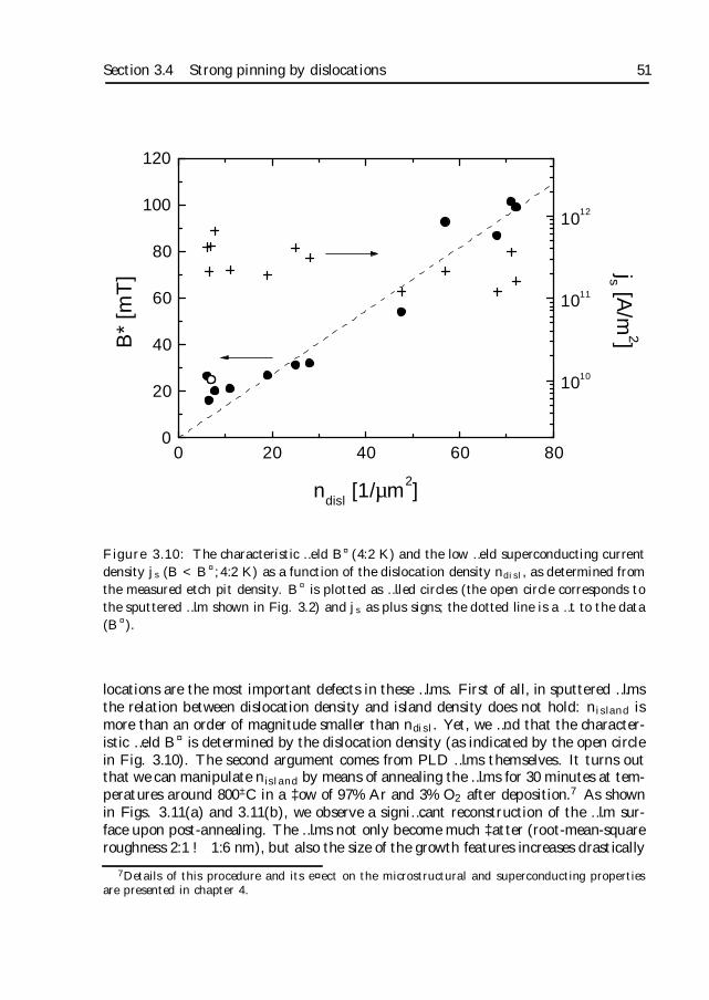
Section 3.4 Strong pinning by dislocations 51
0 20 40 60 800
20
40
60
80
100
120
B*
[mT
]
ndisl
[1/µm2]
1010
1011
1012
js [A/m
2]
Figure 3.10: The characteristic …eld B¤ (4:2 K) and the low …eld superconducting currentdensity js (B < B¤;4:2 K) as a function of the dislocation density ndisl, as determined fromthe measured etch pit density. B¤ is plotted as …lled circles (the open circle corresponds tothe sputtered …lm shown in Fig. 3.2) and js as plus signs; the dotted line is a …t to the data(B¤).
locations are the most important defects in these …lms. First of all, in sputtered …lmsthe relation between dislocation density and island density does not hold: nisland ismore than an order of magnitude smaller than ndisl. Yet, we …nd that the character-istic …eld B¤ is determined by the dislocation density (as indicated by the open circlein Fig. 3.10). The second argument comes from PLD …lms themselves. It turns outthat we can manipulate nisland by means of annealing the …lms for 30 minutes at tem-peratures around 800±C in a ‡ow of 97% Ar and 3% O2 after deposition.7 As shownin Figs. 3.11(a) and 3.11(b), we observe a signi…cant reconstruction of the …lm sur-face upon post-annealing. The …lms not only become much ‡atter (root-mean-squareroughness 2:1 ! 1:6 nm), but also the size of the growth features increases drastically
7Details of this procedure and its e¤ect on the microstructural and superconducting propertiesare presented in chapter 4.
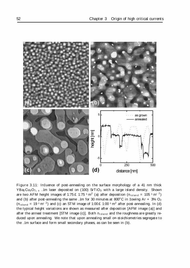
52 Chapter 3 Origin of high critical currents
Figure 3.11: In‡uence of post-annealing on the surface morphology of a 41 nm thickYBa2Cu3O7¡± …lm laser deposited on (100) SrTiO3 with a large island density. Shownare two AFM height images of 1:75£ 1:75 ¹m2 (a) after deposition (nisland = 105 ¹m¡2)and (b) after post-annealing the same …lm for 30 minutes at 800±C in ‡owing Ar + 3% O2
(nisland = 19 ¹m¡2) and (c) an STM image of 1:00£ 1:00 ¹m2 after post-annealing. In (d)the typical height variations are shown as measured after deposition [AFM image (a)] andafter the anneal treatment [STM image (c)]. Both nisland and the roughness are greatly re-duced upon annealing. We note that upon annealing small o¤-stoichiometries segregate tothe …lm surface and form small secondary phases, as can be seen in (b).
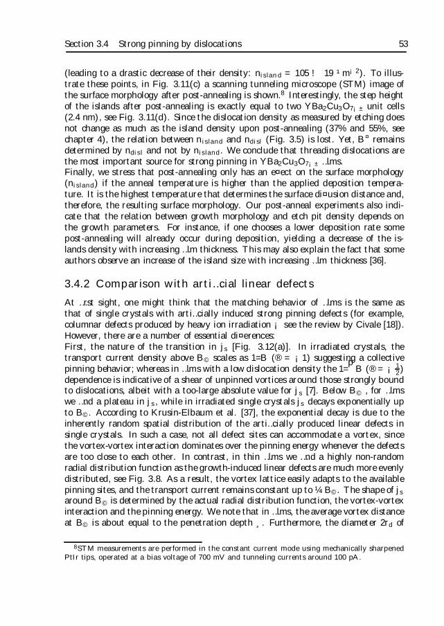
Section 3.4 Strong pinning by dislocations 53
(leading to a drastic decrease of their density: nisland = 105 ! 19 ¹m¡2). To illus-trate these points, in Fig. 3.11(c) a scanning tunneling microscope (STM) image ofthe surface morphology after post-annealing is shown.8 Interestingly, the step heightof the islands after post-annealing is exactly equal to two YBa2Cu3O7¡± unit cells(2.4 nm), see Fig. 3.11(d). Since the dislocation density as measured by etching doesnot change as much as the island density upon post-annealing (37% and 55%, seechapter 4), the relation between nisland and ndisl (Fig. 3.5) is lost. Yet, B¤ remainsdetermined by ndisl and not by nisland. We conclude that threading dislocations arethe most important source for strong pinning in YBa2Cu3O7¡± …lms.Finally, we stress that post-annealing only has an e¤ect on the surface morphology(nisland) if the anneal temperature is higher than the applied deposition tempera-ture. It is the highest temperature that determines the surface di¤usion distance and,therefore, the resulting surface morphology. Our post-anneal experiments also indi-cate that the relation between growth morphology and etch pit density depends onthe growth parameters. For instance, if one chooses a lower deposition rate somepost-annealing will already occur during deposition, yielding a decrease of the is-lands density with increasing …lm thickness. This may also explain the fact that someauthors observe an increase of the island size with increasing …lm thickness [36].
3.4.2 Comparison with arti…cial linear defects
At …rst sight, one might think that the matching behavior of …lms is the same asthat of single crystals with arti…cially induced strong pinning defects (for example,columnar defects produced by heavy ion irradiation ¡ see the review by Civale [18]).However, there are a number of essential di¤erences:First, the nature of the transition in js [Fig. 3.12(a)]. In irradiated crystals, thetransport current density above B© scales as 1=B (® = ¡1) suggesting a collectivepinning behavior; whereas in …lms with a low dislocation density the 1=
pB (® = ¡ 1
2)dependence is indicative of a shear of unpinned vortices around those strongly boundto dislocations, albeit with a too-large absolute value for js [7]. Below B© , for …lmswe …nd a plateau in js, while in irradiated single crystals js decays exponentially upto B©. According to Krusin-Elbaum et al. [37], the exponential decay is due to theinherently random spatial distribution of the arti…cially produced linear defects insingle crystals. In such a case, not all defect sites can accommodate a vortex, sincethe vortex-vortex interaction dominates over the pinning energy whenever the defectsare too close to each other. In contrast, in thin …lms we …nd a highly non-randomradial distribution function as the growth-induced linear defects are much more evenlydistributed, see Fig. 3.8. As a result, the vortex lattice easily adapts to the availablepinning sites, and the transport current remains constant up to ¼ B©. The shape of js
around B© is determined by the actual radial distribution function, the vortex-vortexinteraction and the pinning energy. We note that in …lms, the average vortex distanceat B© is about equal to the penetration depth ¸. Furthermore, the diameter 2rd of
8STM measurements are performed in the constant current mode using mechanically sharpenedPtIr tips, operated at a bias voltage of 700 mV and tunneling currents around 100 pA.
54 Chapter 3 Origin of high critical currents
10-2 10-1 100 101
10-1
100
(b)
(a)
j s/j s
0
B/BΦ
B-1/2
B-1
B*film
BΦ = 2.4 T (crystal) BΦ = 0.037 T (film)
0 15 30 45 60 75 900.0
0.2
0.4
0.6
0.8
1.0
B*(
T)/
B*(
T=
4.2
K)
temperature T [K]
BΦ = 12 mT (film)BΦ = 60 mT (film)BΦ = 16 mT (film)BΦ = 2.4 T (crystal)
Figure 3.12: Comparison of a heavy-ion-irradiated YBa2Cu3O7¡± single crystal [37] (B©equals the irradiation dose) with a thin …lm (B© equals ndisl): (a) the superconductingcurrent density js normalized to its value at 4.2 K (js0); due to the non-random spatialorder of natural linear defects, the current density of the thin …lms remains approximatelyconstant up to B© and (b) the characteristic …eld B¤ normalized to its value at 4.2 K; forthe thin …lms, B¤ remains …nite up to at least 80 K.
Section 3.5 Conclusions 55
dislocations (2rd ¼ 1 ¡ 2 nm [38]) is much smaller than the that of columnar defects(2rCD ¼ 7¡ 10 nm) and is comparable to the coherence length of the superconductor(» = 1:5 nm at 4.2 K).Second, the temperature dependence of B¤ [Fig. 3.12(b)]. In thin …lms we do notobserve any deleterious thermal depinning e¤ects, which in irradiated samples reduceB¤ to zero at a thermal depinning temperature Tdp = 40 K. In …lms, B¤ initially alsodecreases linearly with temperature but, instead of a sudden drop to zero at ¼40 K,a ‡attening is observed above 50 K [Fig. 3.12(b)]. The absence of low temperaturedepinning behavior is in agreement with calculations [4, 5, 37] which imply thatideally Tdp is above 80 K. The reduced Tdp in single crystals is attributed to the factthat the irradiation process not only generates amorphous tracks but also numerouspoint defects around these tracks [37]. Natural linear defects leave the bulk of thesuperconducting …lm intact and Tdp is not depressed.
3.4.3 Implications for vortex pinning
The short-range ordering of the defect structure could make YBa2Cu3O7¡± …lms agood candidate for observing the true Mott-insulator vortex phase [4, 19], which waspredicted to occur at low temperatures when the applied magnetic …eld (k c-axis)exactly equals the matching …eld B© = ndisl©0. In this situation all linear defects areoccupied by exactly one vortex. Consequently, introducing another vortex requires alarge energy. Therefore, both a characteristic jump in the (reversible) magnetizationas well as a diverging tilt and compression modulus of the vortex lattice are expected.So far, however, only remnants of these characteristics have been observed [39]. Aswas numerically shown by Wengel and Täuber [39, 40], this is not surprising becausethe true Mott-insulator phase is only expected for (i) weakly interacting vortices,i.e. when the average defect spacing ddisl is considerably larger than the magneticpenetration depth ¸ (¸=ddisl ¿ 0) and (ii) for a regular array of columnar defects.Since in our …lms the defect distribution exhibits short-range ordering, the lattercondition is much better satis…ed than for randomly distributed columnar defects inirradiated single crystals. What about the …rst condition? The smallest dislocationdensity obtained thus far is 7.8 ¹m¡2, corresponding to ddisl = 358 nm, i.e. largerthat the bulk ab-penetration depth at zero temperature ¸ab (0) = 145 nm [41]. Yet, wedid not observe the predicted characteristic jump in the magnetization. However, inthin …lms one should compare ddisl to the e¤ective [42] penetration depth ¤ ¼ 2¸2=t,where t is the …lm thickness, which is signi…cantly larger (¤ ¼ 280 nm for t = 150nm). Therefore, in order to observe the Mott insulator phase one should (i) decrease¤ by depositing thicker …lms and (ii) increase ddisl by depositing …lms with lowerdislocation densities (using Tsub > 850±C). As in our …lms both the length and theradial distribution do not depend on the …lm thickness (for 10 < t < 490 nm) nor onthe defect density (for 7:8 < ndisl < 68 ¹m¡2), it will be meaningful to search for theMott-insulator phase in thick laser ablated YBa2Cu3O7¡± …lms with a low density ofnatural linear defects.
56 Chapter 3 Origin of high critical currents
3.5 Conclusions
In this chapter, the origin of the high transport current densities in YBa2Cu3O7¡± thin…lms compared to single crystals was identi…ed. Threading dislocations were found tobe the dominant source of strong pinning in …lms. To arrive at this conclusion, we …rstdeveloped a sequential wet-chemical etching technique which enables us to determinethe density of all dislocations (edge, screw and mixed character), when combined withatomic force microcopy. Since dislocations can only end at interfaces, they persistfrom the substrate-…lm interface up to the …lm surface parallel to the c-axis, resultingin a uniform length distribution. As these threading dislocations are mainly situatedaround growth islands, we can tune their density between 5 and 70 ¹m¡2 reproduciblyby manipulating the size of the growth features. To obtain a certain defect densitywe only need to adjust the substrate temperature and oxygen background pressure.Measuring the superconducting current density as a function of the applied magnetic…eld, we …nd a plateau: the current is constant up to a characteristic …eld B¤ anddecays rapidly at larger …elds. The proportionality between B¤ and the measureddislocation density in both PLD and sputtered …lms is compelling evidence that thehigh current densities in YBa2Cu3O7¡± thin …lms are due to strong vortex pinningby natural linear defects.Statistical analysis of the lateral defect distribution in …lms with various dislocationdensities shows that the radial dislocation distribution function g (r) can be scaledonto a single curve g (r=ddisl), where ddisl is the average dislocation spacing. Boththe length as well as the radial dislocation distribution do not depend on the densityof defects nor on the …lm thickness. Interestingly, g (r=ddisl) approaches zero forsmall distances r < ddisl, indicating that the defect distribution exhibits short-rangeordering. As a result, …lms behave essentially di¤erent from heavy ion irradiated singlecrystals, containing randomly distributed columnar defects. For instance, in …lms thepinning sites are more e¢ciently used due to the reduced in‡uence of vortex-vortexinteractions. Moreover, the bulk of single crystals is also a¤ected by the irradiationprocess (resulting in a strongly reduced depinning temperature).Both the tunability of the defect density and the self-organization of threading dis-locations provide an attractive possibility to study vortex matter in a new class ofmaterials: …lms with a tailored non-random distribution of linear strong pinning de-fects. For technological applications the challenge is to …nd ways to increase thedislocation density while keeping the non-random radial distribution intact.
References
[1] H.G. Schnack, R. Griessen, J.G. Lensink, and W. Hai-Hu, Phys. Rev. B 48,13178 (1993)
[2] L. Civale, A.D. Marwick, M.W. McElfresh, T.K. Worthington, A.P. Malozemo¤,F.H. Holtzberg, J.R. Thompson, and M.A. Kirk, Phys. Rev. Lett. 65, 1164(1990)
References 57
[3] T.L. Hylton and M.R. Beasley, Phys. Rev. B 41, 11669 (1990)
[4] D.R. Nelson and V.M. Vinokur, Phys. Rev. B 48, 13060 (1993)
[5] G. Blatter, M.V. Feigel’man, V.B. Geshkenbein, A.I. Larkin, and V.M. Vinokur,Rev. Mod. Phys. 66, 1125 (1994)
[6] T. Haage, J. Zegenhagen, J.Q. Li, H.-U. Habermeier, M. Cardona, Ch. Jooss,R. Warthmann, A. Forkl, and H. Kronmüller, Phys. Rev. B 56, 8404 (1997)
[7] J. Mannhart, D. Anselmetti, J.G. Bednorz, A. Catana, Ch. Gerber, K.A. Müller,and D.G. Schlomm, Z. Phys. B 86, 177 (1992)
[8] H. Douwes, P.H. Kes, Ch. Gerber, and J. Mannhart, Cryogenics 33, 486 (1993)
[9] F.C. Klaassen, J.M. Huijbregtse, B. Dam, R. van der Geest, G. Doornbos, J.H.Rector, R. Elberse, and R. Griessen, in Physics and Materials Science of VortexStates, Flux Pinning and Dynamics, edited by R. Kossowsky, S. Bose, V. Pan,and Z. Durusoy (Kluwer Academic, Dordrecht, 1999)
[10] Ch. Jooss, A. Forkl, R. Warthmann, H.-U. Habermeier, B. Leibold, and H.Kronmüller, Physica C 266, 235 (1996)
[11] D.H. Lowndes, D.K. Christen, C.E. Klabunde, Z.L. Wang, D.M. Kroeger, J.D.Budai, Shen Zhu, D.P. Norton, Phys. Rev. Lett. 74, 2355 (1995)
[12] A. Díaz, L. Mechin, P. Berghuis, and J.E. Evetts, Phys. Rev. Lett. 80, 3855(1998)
[13] Ch. Gerber, D. Anselmetti, J.G. Bednorz, J. Mannhart, and D.G. Schlomm,Nature 350, 279 (1991)
[14] M. Hawley, I.D. Raistrick, J.G. Beery, and R.J. Houlton, Science 251, 1587(1991)
[15] B. Dam, N.J. Koeman, J.H. Rector, B. Stäuble-Pümpin, U. Poppe, and R.Griessen, Physica C 261, 1 (1996)
[16] D. Hull, Introduction to dislocations (Pergamon Press, Oxford, United King-dom, 1975)
[17] L. Civale, A.D. Marwick, T.K. Worthington, M.A. Kirk, J.R. Thompson, L.Krusin-Elbaum, Y. Sun, J.R. Clem, and F. Holtzberg, Phys. Rev. Lett. 67, 648(1991)
[18] L. Civale, Supercond. Sci. Technol. 10, A11 (1997)
[19] D.R. Nelson and V.M. Vinokur, Phys. Rev. Lett. 68, 2398 (1992)
[20] R.B. Heimann, in Au‡ösung von Kristallen, edited by V.D. Fréchette, H. Kirsch,L.B. Sand, and F. Trojer (Springer-Verlag, Vienna, Austria, 1975)
[21] R.P. Vasquez, B.D. Hunt, and M.C. Foote, Appl. Phys. Lett. 53, 2692 (1988)
[22] A. Roshko, S.E. Russek, K.A. Trott, S.C. Sanders, M.E. Johansson, J.S. Martens,and D. Zhang, IEEE Trans. Appl. Supercond. 5, 1733 (1995)
[23] F. Miletto Granozio, U. Scotti di Uccio, M. Valentino, G.G. Condorelli, I.L.Fragalà, and G. Malandrino, Physica C 271, 83 (1996)
58 Chapter 3 Origin of high critical currents
[24] C.T. Lin and W.Y. Liang, Physica C 225, 275 (1994)
[25] B. Dam, J.H. Rector, J.M. Huijbregtse, and R. Griessen, Physica C 305, 1(1998)
[26] F.R.N. Nabarro, Theory of Crystal Dislocations (Oxford University Press, Ox-ford, Great Britain, 1967)
[27] B. Dam and B. Stäuble-Pümpin, J.Mat. Sci.: Mater. Electron. 9, 217 (1998)
[28] D. Eissler, H.S. Wang, and W. Dietsche, Appl. Phys. Lett. 62, 1292 (1993)
[29] L.E.C. van de Leemput, P.J.M. van Bentum, F.A.J.M. Driessen, J.W. Gerritsen,H. van Kempen, and L.W.M. Scheurs, J. Cryst. Growth 98, 551 (1989)
[30] S. Freisem, A. Brockho¤, D.G. de Groot, B. Dam, and J. Aarts, J. Magn. Magn.Mat. 165, 380 (1997
[31] H.P. Lang, H. Haefke, G. Leemann, and H.-J. Güntherodt, Physica C 194, 81(1992)
[32] F.C. Frank, Acta Crystallogr. 4, 498 (1951)
[33] O. Eibl and B. Roas, J. Mater. Res. 5, 2620 (1990)
[34] D. Rose, K. Durose, W. Palosz, A. Szczerbakow, and K. Grasza, J. Phys. D:Appl. Phys. 31, 1009 (1998)
[35] M. Qvarford, K. Heeck, J.G. Lensink, R.J. Wijngaarden, and R. Griessen, Rev.Sci. Instrum. 63, 5726 (1992)
[36] D.H.A. Blank, M.E. Bijlsma, R. Moerman, H. Rogalla, F.J.B. Stork, and A.Roshko, J. Alloys Compd. 251, 31 (1997)
[37] L. Krusin-Elbaum, L. Civale, J.R. Thomson, and C. Field, Phys. Rev. B 53,11744 (1996)
[38] Y. Gao, K.L. Merkle, G. Bai, H.L.M. Chang, and D.J. Lam, Physica C 174, 1(1991)
[39] C. Wengel and U.C. Täuber, Phys. Rev. Lett. 78, 4845 (1997)
[40] C. Wengel and U.C. Täuber, Phys. Rev. B 58, 6565 (1998)
[41] J.E. Sonier, R.F. Kie‡, J.H. Brewer, D.A. Bonn, J.F. Carolan, K.H. Chow,P. Dosanjh, W.N. Hardy, Ruixing Liang, W.A. MacFarlane, P. Mendels, G.D.Morris, T.M. Riseman, and J.W. Schneider, Phys. Rev. Lett. 72, 744 (1994)
[42] E.H. Brandt, Rep. Prog. Phys. 58, 1465 (1995)
Chapter 4
Comparison of dislocations withalternative pinning sites
Although vortex pinning in YBa2Cu3O7¡± …lms on (100) SrTiO3 is dominated bythreading dislocations, many other natural pinning sites are present. To identify thecontribution from twin planes, surface corrugations and point defects, we manipu-late the relative densities of all defects by post-annealing …lms with various as-growndislocation densities, ndisl. While a universal magnetic …eld B dependence of the su-perconducting current density js (B;T ) is observed (independently of ndisl, temper-ature T and the anneal treatment), the defect structure changes considerably uponannealing. Correlating the microstructure to js (B;T ), it becomes clear that surfaceroughness, twins and point defects are not important at low magnetic …elds comparedto linear defect pinning. Transmission electron microscopy indicates that threadingdislocations are not part of grain boundaries neither are they related to the twindomain structure. These results con…rm that js (B; T ) is essentially determined bypinning along threading dislocations, naturally induced during the growth process.Even in high magnetic …elds, where the vortex density outnumbers ndisl, it appearsthat linear defects stabilize the vortex lattice via the vortex-vortex interaction.1
1This chapter is based on the paper by J.M. Huijbregtse, F.C. Klaassen, A. Szepielow, J.H.Rector, B. Dam, R. Griessen, B.J. Kooi, and J.Th.M. de Hosson, to be submitted to Supercond. Sci.Technol.
60 Chapter 4 Comparison of dislocations with alternative pinning sites
4.1 Introduction
The early observation of both high superconducting current densities (typically be-tween 1011 and 1012 A/m2 at low temperatures in zero magnetic …eld) and numerousstructural defects in thin epitaxial …lms of the high-Tc superconductor YBa2Cu3O7¡±
called for the identi…cation of the strongest pinning defect [1]. Grain boundaries [2, 3],twin boundaries [4, 5], anti-phase boundaries [6, 7, 8], screw dislocations [9, 10, 11, 12],edge dislocations [13, 14], precipitates [15, 16, 17] and surface roughness [18, 19, 20, 21]have been suggested as good candidates. Due to the di¢culties in controlling the de-fect density, quantitative studies unambiguously relating the density of a speci…c de-fect to the superconducting current density characteristics could not be performedso far. In the previous chapter, we succeeded in controlling threading dislocations inthin …lms of YBa2Cu3O7¡± by carefully manipulating the growth conditions. This al-lowed us to relate the high superconducting current densities in these …lms to strongpinning of vortices along dislocations in a semi-quantitative way: a plateau B¤ wasfound in the magnetic …eld dependence of the superconducting current density js (B),which is directly proportional to the measured density of all dislocations (i.e., bothedge, screw and dislocations of mixed character). The proportionality constant wasdetermined to be 0:7©0 at low temperatures, where ©0 = 2:068 £ 10¡15 Tm2 is the‡ux quantum, showing that dislocations are the main origin of the high currents.Recently, Klaassen et al. [22] reported the existence of a similar plateau in the dy-namical relaxation rate below B¤. Moreover, the temperature dependence of bothB¤ and js (B < B¤) was explained in terms of the Bose glass theory [23, 24], tak-ing thermal ‡uctuations into account [25]. Thus the long existing question why …lmscan carry such high currents compared to single crystals [26, 27] appears to be solvednow.In the present chapter, we focus our attention to alternative natural pinning sites(such as twin boundaries, precipitates, point defects and surface roughness) thatare operative in combination with threading dislocations. In order to manipulatethe relative densities of all defects, we perform annealing experiments on …lms withvarious as-grown dislocation densities. Indeed signi…cant changes are found, both inthe superconducting current characteristics and in the microstructure of these …lms.As a result, the contribution from the alternative pinning sites compared to lineardefect pinning can be identi…ed. Remarkably, the e¤ect of linear defects is not con…nedto the low magnetic …eld region. It appears that linear defects stabilize the vortexlattice via the long-ranged vortex-vortex interactions up to …elds as high as 7 T (atlow temperatures). The results indicate that natural linear defects are extremelye¢cient pinning sites compared to arti…cially induced columnar defects [28], whichare usually introduced at much higher densities.This chapter is organized as follows. First, we discuss the post-annealing procedureand the results of the torque measurements and the microstructural investigation.Next, we correlate vortex pinning to the defect structure, using some additional trans-mission electron microscope observations to distinguish threading dislocations fromtwinning dislocations and low-angle grain boundaries.
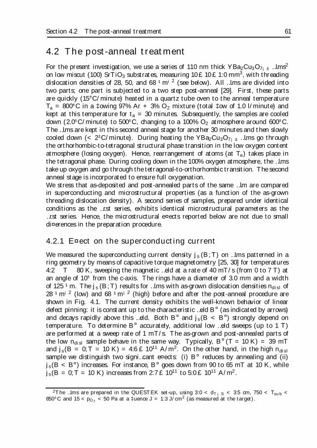
Section 4.2 The post-anneal treatment 61
4.2 The post-anneal treatment
For the present investigation, we use a series of 110 nm thick YBa2Cu3O7¡± …lms2
on low miscut (100) SrTiO3 substrates, measuring 10 £10 £1:0 mm3, with threadingdislocation densities of 28, 50, and 68 ¹m¡2 (see below). All …lms are divided intotwo parts; one part is subjected to a two step post-anneal [29]. First, these partsare quickly (15±C/minute) heated in a quartz tube oven to the anneal temperatureTa = 800±C in a ‡owing 97% Ar + 3% O2 mixture (total ‡ow of 1.0 l/minute) andkept at this temperature for ta = 30 minutes. Subsequently, the samples are cooleddown (2.0±C/minute) to 500±C, changing to a 100% O2 atmosphere around 600±C.The …lms are kept in this second anneal stage for another 30 minutes and then slowlycooled down (< 2±C/minute). During heating the YBa2Cu3O7¡± …lms go throughthe orthorhombic-to-tetragonal structural phase transition in the low oxygen contentatmosphere (losing oxygen). Hence, rearrangement of atoms (at Ta) takes place inthe tetragonal phase. During cooling down in the 100% oxygen atmosphere, the …lmstake up oxygen and go through the tetragonal-to-orthorhombic transition. The secondanneal stage is incorporated to ensure full oxygenation.We stress that as-deposited and post-annealed parts of the same …lm are comparedin superconducting and microstructural properties (as a function of the as-grownthreading dislocation density). A second series of samples, prepared under identicalconditions as the …rst series, exhibits identical microstructural parameters as the…rst series. Hence, the microstructural e¤ects reported below are not due to smalldi¤erences in the preparation procedure.
4.2.1 E¤ect on the superconducting current
We measured the superconducting current density js (B;T ) on …lms patterned in aring geometry by means of capacitive torque magnetometry [25, 30] for temperatures4:2 T 80 K, sweeping the magnetic …eld at a rate of 40 mT/s (from 0 to 7 T) atan angle of 10± from the c-axis. The rings have a diameter of 3.0 mm and a widthof 125 ¹m. The js (B;T ) results for …lms with as-grown dislocation densities ndisl of28 ¹m¡2 (low) and 68 ¹m¡2 (high) before and after the post-anneal procedure areshown in Fig. 4.1. The current density exhibits the well-known behavior of lineardefect pinning: it is constant up to the characteristic …eld B¤ (as indicated by arrows)and decays rapidly above this …eld. Both B¤ and js(B < B¤) strongly depend ontemperature. To determine B¤ accurately, additional low …eld sweeps (up to 1 T)are performed at a sweep rate of 1 mT/s. The as-grown and post-annealed parts ofthe low ndisl sample behave in the same way. Typically, B¤ (T = 10 K) = 39 mTand js(B = 0; T = 10 K) = 4:6 £ 1011 A/m2. On the other hand, in the high ndisl
sample we distinguish two signi…cant e¤ects: (i) B¤ reduces by annealing and (ii)js(B < B¤) increases. For instance, B¤ goes down from 90 to 65 mT at 10 K, whilejs(B = 0; T = 10 K) increases from 2:7 £ 1011 to 5:0 £ 1011 A/m2.
2The …lms are prepared in the QUESTEK set-up, using 3:0 < dT¡S < 3:5 cm, 750 < Tsub <850±C and 15 < pO2 < 50 Pa at a ‡uence J = 1:3 J/cm2 (as measured at the target).
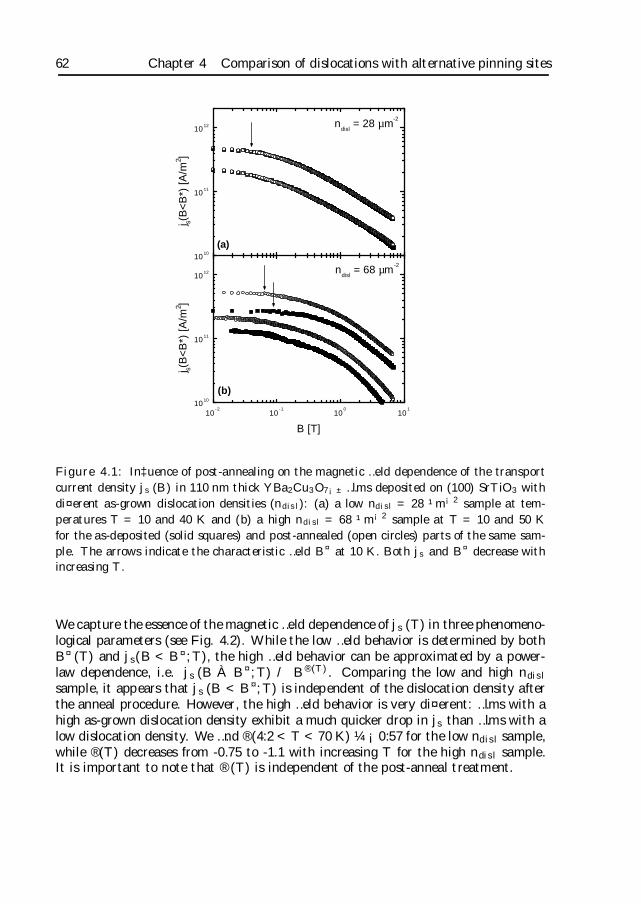
62 Chapter 4 Comparison of dislocations with alternative pinning sites
1010
1011
1012
(a)
ndisl
= 68 µm-2
ndisl
= 28 µm-2
j s(B
<B
*) [
A/m
2 ]
10
-210
-110
010
110
10
1011
1012
(b)
B [T]
j s(B
<B
*) [
A/m
2 ]
Figure 4.1: In‡uence of post-annealing on the magnetic …eld dependence of the transportcurrent density js (B) in 110 nm thick YBa2Cu3O7¡± …lms deposited on (100) SrTiO3 withdi¤erent as-grown dislocation densities (ndisl): (a) a low ndisl = 28 ¹m¡2 sample at tem-peratures T = 10 and 40 K and (b) a high ndisl = 68 ¹m¡2 sample at T = 10 and 50 Kfor the as-deposited (solid squares) and post-annealed (open circles) parts of the same sam-ple. The arrows indicate the characteristic …eld B¤ at 10 K. Both js and B¤ decrease withincreasing T .
We capture the essence of the magnetic …eld dependence of js (T ) in three phenomeno-logical parameters (see Fig. 4.2). While the low …eld behavior is determined by bothB¤ (T ) and js(B < B¤; T ), the high …eld behavior can be approximated by a power-law dependence, i.e. js (B À B¤; T ) / B®(T). Comparing the low and high ndisl
sample, it appears that js (B < B¤; T ) is independent of the dislocation density afterthe anneal procedure. However, the high …eld behavior is very di¤erent: …lms with ahigh as-grown dislocation density exhibit a much quicker drop in js than …lms with alow dislocation density. We …nd ®(4:2 < T < 70 K) ¼ ¡0:57 for the low ndisl sample,while ®(T ) decreases from -0.75 to -1.1 with increasing T for the high ndisl sample.It is important to note that ® (T ) is independent of the post-anneal treatment.
Section 4.2 The post-anneal treatment 63
0
40
80
120
ndisl
= 68 µm-2
ndisl
= 28 µm-2
B*
[mT
]
0.0
2.0
4.0
6.0
j s(B
<B
*) in
1011
A/m
2
0 20 40 60 80-0.4
-0.6
-0.8
-1.0
-1.2
α
T [K]0 20 40 60 80
T [K]
Figure 4.2: In‡uence of post-annealing on the transport current density js (B; T ) in 110nm thick YBa2Cu3O7¡± …lms on (100) SrTiO3 with a low (ndisl = 28 ¹m¡2, left column)and high (ndisl = 68 ¹m¡2, right column) as-grown dislocation density. Shown are the tem-perature dependence of: (top panel) the characteristic …eld B¤ (T ), (middle panel) the lowmagnetic …eld transport current density js (B < B¤; T ), and (lower panel) the high magnetic…eld power-law exponent ®(T ) for the as-deposited (solid squares) and post-annealed parts(open circles).
64 Chapter 4 Comparison of dislocations with alternative pinning sites
To correlate these characteristics in the superconducting current density to pinningby various natural defects, we now investigate the microstructure of the …lms beforeand after the post-anneal procedure in detail.
4.2.2 Microstructural consequences
The annealing procedure takes place at a temperature comparable to the averagedeposition temperature (typically, Tsub ¼ Ta = 800±C) of the YBa2Cu3O7¡± …lms.Therefore, we expect clear changes in the microstructure. Combining atomic forcemicroscopy (AFM), x-ray di¤raction (XRD), Rutherford backscattering spectrometry(RBS) and electrical resistivity measurements, we …nd four pronounced e¤ects.
Surface roughnessThe large e¤ect of post-annealing on the surface roughness was already mentioned inchapter 3 for a …lm with a high as-grown dislocation density. Here, we discuss this ef-fect in a more general context. In Fig. 4.3, AFM height images of three …lms depositedat decreasing substrate temperature Tsub = 850, 800 and 750±C (increasing disloca-tion density) are shown before and after the post-anneal treatment. The as-grownsurface morphology consists of semi-regularly spaced islands separated by trenches.As shown in chapter 3, the deeper depressions within the trenches correspond tothe sites where threading dislocations emerge. Since dislocations are situated aroundthe islands in as-deposited …lms, the island density nisland and dislocation densityare proportional (the proportionality constant being close to 1). Therefore, nisland
can be used as a quick measure for ndisl. Upon annealing the island density de-creases, suggesting that the dislocation density has changed. In addition, the surface‡attens considerably (note that the same height scales are used). For example, theroot-mean-square (rms) roughness decreases from 4 to 2 nm, typically.3
Dislocation densityTo check whether the dislocation density changes upon annealing or not, we performwet-chemical etching experiments. In …gure 4.4, AFM images corresponding to thesame …lms as in Fig. 4.3 are shown after etching in 1% Br-ethanol, to reveal allthreading dislocations. ndisl is determined by averaging the number of square, sharp-bottomed etch pits for di¤erent areas of the same …lm, using etch times between20 and 90 s. We …nd that the dislocation density only decreases signi…cantly in…lms with the highest as-grown dislocation density (from ndisl = 68 ¹m¡2 to 43¹m¡2). Indeed dislocation annihilation is expected to be easier in these …lms, sincethe average distance ddisl between dislocations is relatively small (ddisl ¼ 1=
pndisl).
It is important to note that the correlation between island density and dislocationdensity is lost upon post-annealing: the dislocation density outnumbers the islanddensity.
3See chapter 3 for the AFM cross-sections of an as-grown and a post-annealed sample.
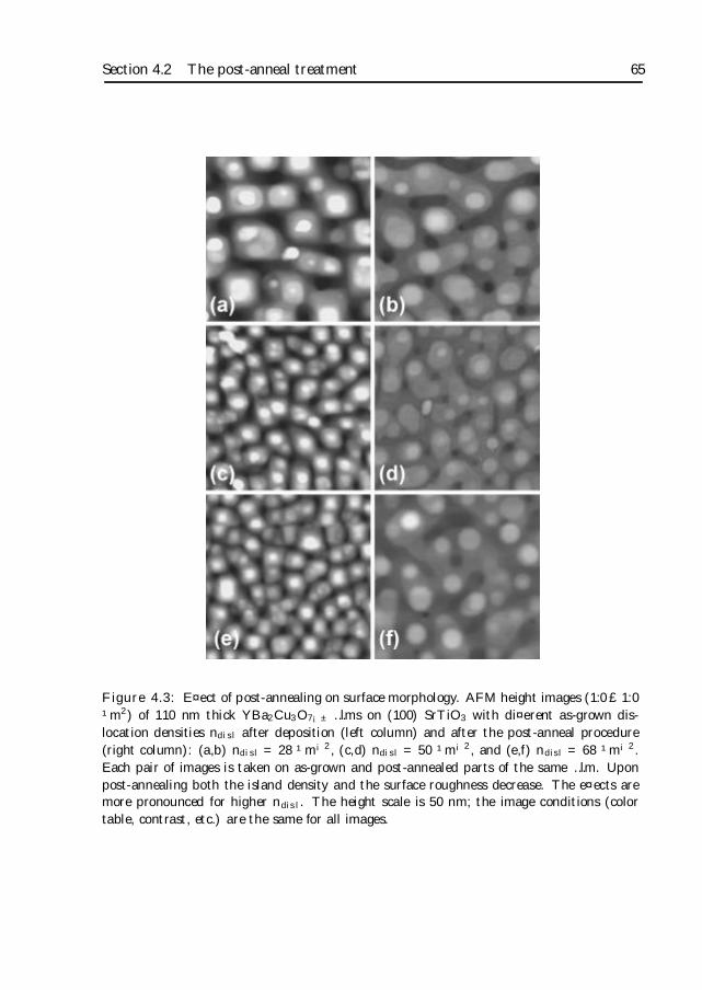
Section 4.2 The post-anneal treatment 65
Figure 4.3: E¤ect of post-annealing on surface morphology. AFM height images (1:0£1:0¹m2) of 110 nm thick YBa2Cu3O7¡± …lms on (100) SrTiO3 with di¤erent as-grown dis-location densities ndisl after deposition (left column) and after the post-anneal procedure(right column): (a,b) ndisl = 28 ¹m¡2, (c,d) ndisl = 50 ¹m¡2, and (e,f) ndisl = 68 ¹m¡2.Each pair of images is taken on as-grown and post-annealed parts of the same …lm. Uponpost-annealing both the island density and the surface roughness decrease. The e¤ects aremore pronounced for higher ndisl. The height scale is 50 nm; the image conditions (colortable, contrast, etc.) are the same for all images.
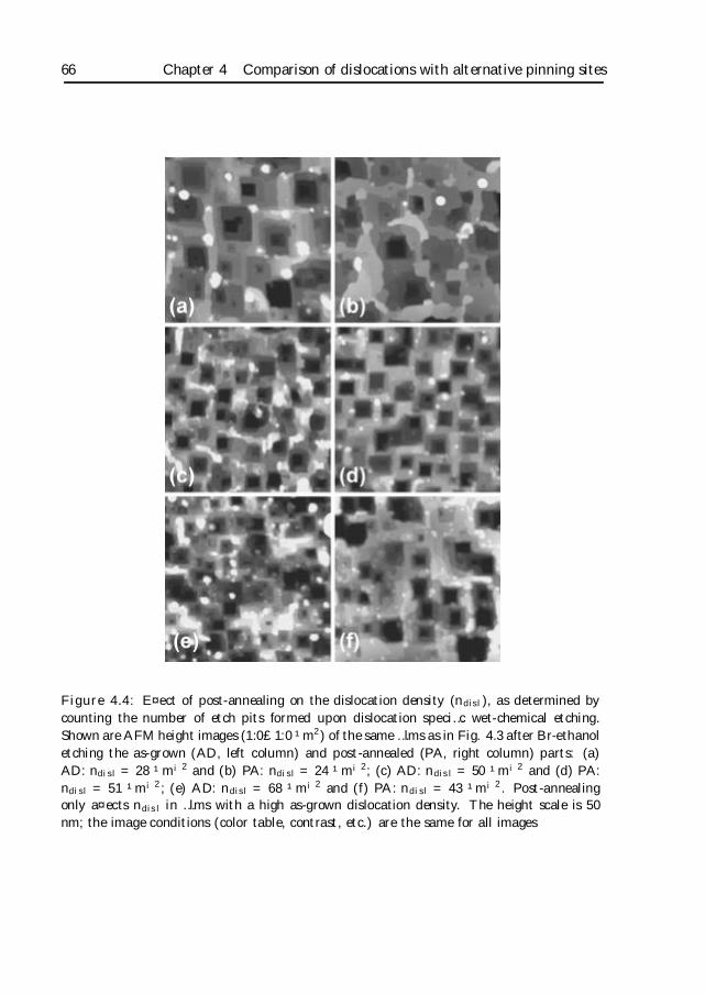
66 Chapter 4 Comparison of dislocations with alternative pinning sites
Figure 4.4: E¤ect of post-annealing on the dislocation density (ndisl), as determined bycounting the number of etch pits formed upon dislocation speci…c wet-chemical etching.Shown are AFM height images (1:0£1:0 ¹m2) of the same …lms as in Fig. 4.3 after Br-ethanoletching the as-grown (AD, left column) and post-annealed (PA, right column) parts: (a)AD: ndisl = 28 ¹m¡2 and (b) PA: ndisl = 24 ¹m¡2; (c) AD: ndisl = 50 ¹m¡2 and (d) PA:ndisl = 51 ¹m¡2; (e) AD: ndisl = 68 ¹m¡2 and (f) PA: ndisl = 43 ¹m¡2. Post-annealingonly a¤ects ndisl in …lms with a high as-grown dislocation density. The height scale is 50nm; the image conditions (color table, contrast, etc.) are the same for all images
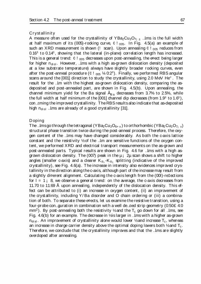
Section 4.2 The post-anneal treatment 67
CrystallinityA measure often used for the crystallinity of YBa2Cu3O7¡± …lms is the full widthat half maximum of its (005)-rocking curve, ¢!005. In Fig. 4.5(a) an example ofsuch an XRD measurement is shown (! scan). Upon annealing ¢!005 reduces from0.16± to 0.14±, showing that the lateral (in-plane) correlation length has increased.This is a general trend: ¢!005 decreases upon post-annealing, the e¤ect being largerfor higher ndisl. However, …lms with a high as-grown dislocation density (depositedat a low substrate temperature) always have slightly broader rocking curves, evenafter the post-anneal procedure (¢!005 ¼ 0:2±). Finally, we performed RBS angularscans around the [001] direction to study the crystallinity, using 2.0 MeV He+. Theresult for the …lm with the highest as-grown dislocation density, comparing the as-deposited and post-annealed part, are shown in Fig. 4.5(b). Upon annealing, thechannel minimum yield for the Ba signal ÂBa decreases from 3.7% to 2.5%, whilethe full width at half minimum of the [001] channel dip decreases (from 1.9± to 1.6±),con…rming the improved crystallinity. The RBS results also indicate that as-depositedhigh ndisl …lms are already of a good crystallinity [31].
DopingThe …lms go through the tetragonal (YBa2Cu3O6+x) to orthorhombic (YBa2Cu3O7¡±)structural phase transition twice during the post-anneal process. Therefore, the oxy-gen content of the …lms may have changed considerably. As both the c-axis latticeconstant and the resistivity ½ of the …lm are sensitive functions of the oxygen con-tent, we performed XRD and electrical transport measurements on the as-grown andpost-annealed parts. Typical results are shown in Fig. 4.6 for …lms with a high as-grown dislocation density. The (007) peak in the µ ¡ 2µ scan shows a shift to higherangles (smaller c-axis) and a clearer K®1
-K®2splitting (indicative of the improved
crystallinity), see Fig. 4.6(a). The increase in intensity also evidences improved crys-tallinity in the direction along the c-axis, although part of the increase may result froma slightly di¤erent alignment. Calculating the c-axis length from the (00l)-re‡ectionsfor l = 1 ¡ 8, we observe a general trend: on the average, the c-axis decreases from11.70 to 11:69 Å upon annealing, independently of the dislocation density. This ef-fect can be attributed to (i) an increase in oxygen content, (ii) an improvement ofthe crystallinity, including Y/Ba disorder and O chain ordering or (iii) a combina-tion of both. To separate these e¤ects, let us examine the resistive transition, using afour-probe con…guration in combination with a well de…ned strip geometry (0:50£4:0mm2). By post-annealing both the resistivity ½ and the Tc go down for all …lms, seeFig. 4.6(b) for an example. The decrease in ½ is larger in …lms with a higher as-grownndisl. An improvement of crystallinity alone would lower ½ and increase Tc, whereasan increase in charge carrier density above the optimal doping lowers both ½ and Tc.Therefore, we conclude that the crystallinity improves and that the …lms are slightlyoverdoped after annealing.
68 Chapter 4 Comparison of dislocations with alternative pinning sites
-0.2 -0.1 0.0 0.1 0.20.0
0.5
1.0 AD PA
(a)
I/I
max
∆ω005
[°]
-4 -2 0 2 40
500
1000
AD PA
(b)
I [a.
u.]
tilt angle [°]
Figure 4.5: E¤ect of post-annealing on the crystallinity of 110 nm thick YBa2Cu3O7¡±…lms on (100) SrTiO3: (a) XRD (005)-rocking curve for the …lm with an as-grown dislocationdensity ndisl = 50 ¹m¡2, and (b) RBS [001] channel dip measurement for the Ba signal ofthe …lm with an as-grown ndisl = 68 ¹m¡2 (AD = as-deposited; PA = post-annealed). Sinceboth the XRD peak and the RBS channel dip narrow, we conclude that the crystallinityimproves upon annealing.
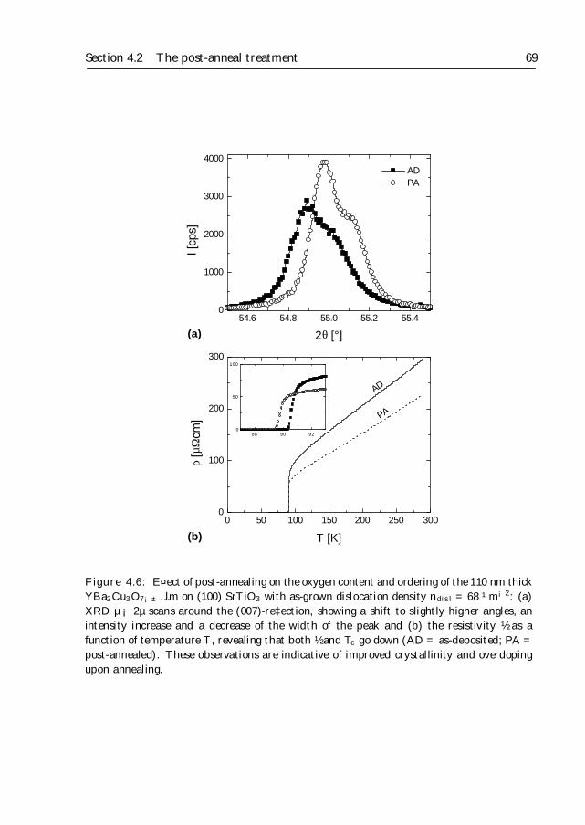
Section 4.2 The post-anneal treatment 69
0 50 100 150 200 250 3000
100
200
300
AD
PA
(b)
ρ [µ
Ωcm
]
T [K]
88 90 920
50
100
54.6 54.8 55.0 55.2 55.40
1000
2000
3000
4000
AD PA
(a)
I [cp
s]
2θ [°]
Figure 4.6: E¤ect of post-annealing on the oxygen content and ordering of the 110 nm thickYBa2Cu3O7¡± …lm on (100) SrTiO3 with as-grown dislocation density ndisl = 68 ¹m¡2: (a)XRD µ ¡ 2µ scans around the (007)-re‡ection, showing a shift to slightly higher angles, anintensity increase and a decrease of the width of the peak and (b) the resistivity ½ as afunction of temperature T , revealing that both ½ and Tc go down (AD = as-deposited; PA =post-annealed). These observations are indicative of improved crystallinity and overdopingupon annealing.
70 Chapter 4 Comparison of dislocations with alternative pinning sites
Summarizing, there are multiple e¤ects of post-annealing on the microstructure. Alle¤ects are more pronounced in …lms with a higher as-grown dislocation density, sincethese …lms are deposited at a substrate temperature lower than the annealing temper-ature (Tsub < Ta). Our observations have some important implications for producing…lms with an extremely low or high dislocation density, while maintaining a criti-cal temperature above 90 K (see chapter 3). First, ultra-low temperature deposition(Tsub ¿ 800±C) and post-annealing cannot be combined to produce …lms with bothhigh ndisl and good crystallinity, since dislocations are annihilated. Therefore, we arebound to manipulate the deposition conditions to obtain ndisl À 68 ¹m2, for instanceby using higher deposition rates. An alternative method to increase ndisl, making useof an additional processing step, will be presented in chapter 5. Secondly, in lowndisl …lms, dislocations are too far apart to annihilate by annealing, implying thathigher anneal temperatures Ta (> Tsub) and/or longer annealing times ta are neces-sary to produce essentially dislocation-free …lms. Preliminary experiments indicatethat the surface roughness and island density are reduced far more by annealing 240minutes (instead of 30 minutes), suggesting that threading dislocations can indeed beeliminated.
4.3 Vortex pinning mechanisms
In our YBa2Cu3O7¡± thin …lms di¤erent types of correlated disorder are naturallypresent, among which are linear defects (dislocations), planar defects (twin bound-aries), precipitates and thickness ‡uctuations. The microstructural e¤ects of post-annealing described above make it possible to probe the in‡uence of di¤erent naturaldefects on the superconducting current density js (B;T ) and therefore on vortex pin-ning in these …lms. We discuss these pinning e¤ects and the in‡uence of point defectsbelow, using additional (HR)TEM observations to identify some defects.
4.3.1 Linear defects
In literature, many experimental observations point to the importance of pinning bydislocations. Apart from the direct observation of the interaction between vorticesand crystal dislocations in Bi2Sr2CaCu2O8 [32] and Nb [33] single crystals4, therewere numerous attempts to relate the density of spiral outcrops (screw dislocations)in YBa2Cu3O7¡± thin …lms to the superconducting properties [11, 34]. However, asmost of these studies consider (i) only spirals (i.e., a fraction of all dislocations) and(ii) only the magnitude of the superconducting current density at zero magnetic …eldand usually at 77 K, a signi…cant correlation could not be established.We …nd that the characteristic shape of js (B;T ) is independent of both the dislocationdensity and the post-anneal procedure. In agreement with the results of chapter 3, thecharacteristic …eld at low temperatures is determined by the total dislocation density
4We note that the density of dislocations in single crystals is usually orders of magnitude smallerthan in epitaxial …lms.
Section 4.3 Vortex pinning mechanisms 71
as measured by wet-chemical etching, according to:
B¤ ¼ 0:7ndisl©0. (4.1)
Both B¤ and js (B < B¤) are a function of the superconducting parameters [i.e., thecoherence length » = » (T ) and the magnetic penetration depth ¸ = ¸ (T )]. The tem-perature dependence of these parameters in combination with thermal ‡uctuations,which decrease the pinning energy, are responsible for the observed decrease in B¤ (T )and js (B < B¤; T ) with increasing temperature [25].Post-annealing of a sample with a high as-grown ndisl (see Fig. 4.2), reduces B¤.This is a direct consequence of the annihilation of dislocations during annealing(ndisl = 68 ! 43 ¹m¡2, see Fig. 4.4). Indeed, B¤ corresponds well with the mea-sured density of dislocations after post-annealing, following Eq. (4.1). However,the reason for the increase in js (B < B¤) is not a priori clear. In the single vor-tex regime, where vortex-vortex interactions can be neglected, the current densityis determined by the depinning of isolated vortices from linear defects. Therefore,the same value of js (B < B¤) is expected for all …lms, independently of ndisl. Be-fore post-annealing, however, …lms with a low as-grown dislocation density usuallycarry somewhat larger currents than …lms with a high as-grown ndisl (see Fig. 4.1and 4.2 for an example). This is a consequence of the method used to increase ndisl.Since high dislocation densities are induced at relatively low substrate temperatures(750±C in this investigation), the corresponding rocking curves are usually broader(typically, ¢!005 ¼ 0:2±) and the resistivities are higher (½RT ¼ 300 ¹cm) com-pared to low ndisl …lms (¢!005 ¼ 0:1± and ½RT ¼ 250 ¹cm). These e¤ects areindicative of a poorer crystallinity and lower doping. Post-annealing (partly) correctsfor both issues and the current increases in the high ndisl …lm. Indeed, similar ef-fects of post-annealing on the superconducting current density in YBa2Cu3O7¡± …lmshave been reported [35]. The improvement in overall crystallinity (including oxygenstoichiometry) of the …lms, ensures that the depression in the superconducting orderparameter as well as » and ¸ are the same for all …lms. Probably, due to the sharpen-ing of the pinning potential upon annealing, js (B < B¤) approaches a universal valueof 6 £ 1011 A/m2 at 4.2 K, characteristic for pinning of a single vortex by a disloca-tion. Surprisingly, the overdoping upon annealing does not a¤ect the current density.Note that when taking relaxation e¤ects into account [25], at low temperatures andsmall magnetic …elds we …nd a universal critical current density jc that is close to thedepairing current density limit j0 ¼ 4 £ 1012 A/m2 and consequently jc ¼ 0:2j0.As linear defects play a dominant role for pinning in these …lms, we started a cross-sectional TEM investigation.5 Generally, dislocations are di¢cult to observe in cross-section [36], as their density is relatively low and their core size is small [37]. Despite
5TEM measurements are performed by B.J. Kooi (Materials Science Centre, University of Gronin-gen) in a JEOL 4000 EX/II microscope operating at 400 kV (point resolution of 0.165 nm). Cross-section specimens are prepared by a standard procedure: face-to-face glued specimens in cross-sectiongeometry are polished down to a …nal thickness of about 15 ¹m using a Tripod polisher, followedby a 4 kV ion milling. To prevent damaging of the YBa2Cu3O7¡± …lm, it turned out essential touse liquid-nitrogen cooling during this ion milling. Care was taken to prevent contamination of thesurface during TEM specimen treatment.
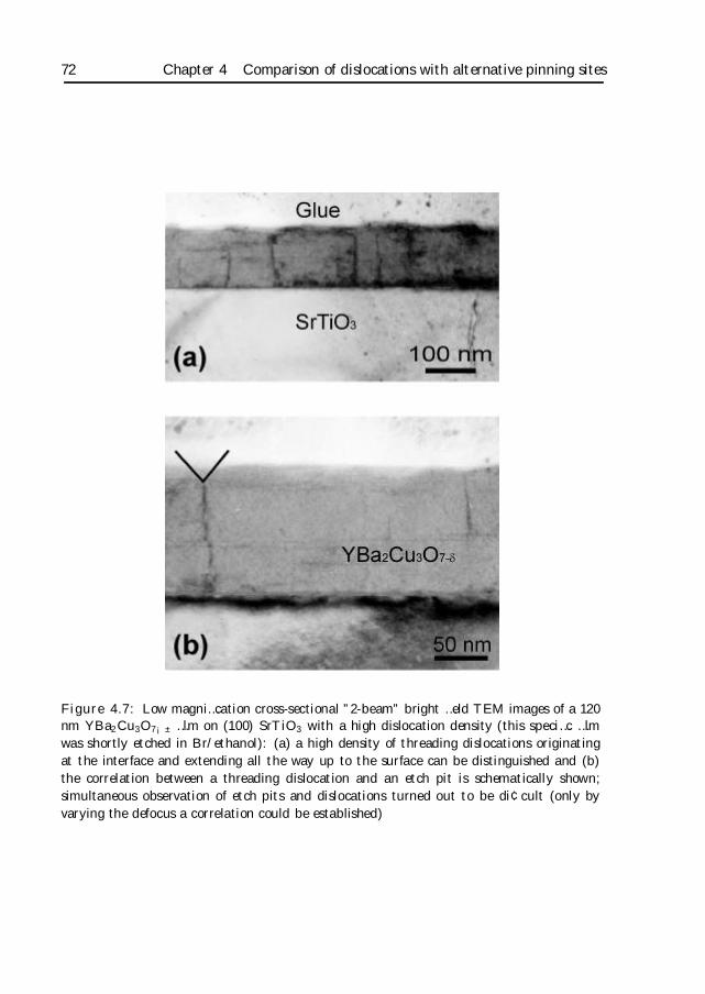
72 Chapter 4 Comparison of dislocations with alternative pinning sites
Figure 4.7: Low magni…cation cross-sectional ”2-beam” bright …eld TEM images of a 120nm YBa2Cu3O7¡± …lm on (100) SrTiO3 with a high dislocation density (this speci…c …lmwas shortly etched in Br/ethanol): (a) a high density of threading dislocations originatingat the interface and extending all the way up to the surface can be distinguished and (b)the correlation between a threading dislocation and an etch pit is schematically shown;simultaneous observation of etch pits and dislocations turned out to be di¢cult (only byvarying the defocus a correlation could be established)
Section 4.3 Vortex pinning mechanisms 73
di¢culties in the TEM sample preparation, we were able to identify threading dis-locations in a sample with a high dislocation density, see the ”2-beam” bright …eldimages in Fig. 4.7 (strong di¤racting beam parallel to the c-axis). Dislocations orig-inating at the substrate-…lm interface and extending up to the surface in a directionclose to the c-axis can be seen. By varying the di¤raction vector g in dark …eld,the threading dislocations can not be discerned when g is parallel to the c-axis, sug-gesting that these are screw dislocations. This speci…c …lm was shortly etched in1% Br/ethanol in order to correlate etch pits and dislocations directly. Since pitsor dislocations can only be discerned by varying the defocus, simultaneous observa-tion of both etch pits and threading dislocations is di¢cult. However, it appears thatetch pits are present at the positions where dislocation lines emerge at the surface,as schematically indicated in Fig. 4.7(b). We note, that preferential etch pit forma-tion was recently unambiguously related to threading dislocations of screw and mixedcharacter in …lms of GaN on (0001)-sapphire [38], combining AFM and cross-sectionalTEM analysis. Thus, wet-chemical etching in a dislocation sensitive etchand revealsall dislocations emerging at the surface of a …lm.Finally we note that the linear defects we found by TEM resemble the ”columnargrowth defect” structures as reported by Lowndes et al. [39] in YBa2Cu3O7¡± …lmsgrown on 1.6± miscut, mosaic (100) LaAlO3 substrates. Unfortunately, the nature ofthose defects was not further characterized. The appearance of an extra (asymmetric)peak in the angular dependence of js at a …eld direction close to the c-axis wasassociated with a vortex pinning e¤ect by these columns. Clearly, a peak in theangular dependence of js is expected when the magnetic …eld is parallel to the lineardefects. However, they also report that the peak e¤ect is absent in …lms on ‡at (100)SrTiO3 substrates. This observation is in contradiction with the results of Roas et al.[40], who show that an additional peak arises at low …elds. So far, we also did notdetect the expected peak e¤ect by means of angular dependent torque magnetometry.However, this discrepancy may be related to the method (transport or inductive) andthe exact procedure used to measure the peak e¤ect. Apart from this issue, all resultspoint to dislocations being the strong pinning sites in YBa2Cu3O7¡± …lms. In theremaining part we will show that all other types of correlated disorder are far lessimportant.
4.3.2 Planar defects
A network of planar defects in principle provides for an alternative source of strongpinning [41], with a similar matching behavior. At low …elds, the vortices will beconcentrated at the planar defects. At higher …elds, vortex-vortex interactions play arole and not all vortices can be accommodated by planar defects. The cross-over …eldis set by the condition that the vortex spacing becomes of the order of ¸. Assumingthat the planar defects are spaced by a distance d, Doornbos et al. [42] calculated across-over …eld
B¤ ¼ 2©0
¸d. (4.2)
74 Chapter 4 Comparison of dislocations with alternative pinning sites
Using experimentally determined characteristic …elds, we …nd defect spacings thatshould be of the same order as the dislocation spacing (d ¼ ddisl ¼ 100 nm). There-fore, our experimental results could also be interpreted in terms of strong pinningby a network of planar defects. Below, we consider three types of planar defects:twin boundaries, anti-phase boundaries and (low-angle) grain boundaries. Also, therelation between threading dislocations, twinning dislocations and low-angle grainboundaries is investigated. We note that vortices can slide along the planar defects.They are thus not very e¤ective in one direction.
Twin boundariesDuring the tetragonal-to-orthorhombic phase transition upon cooling down, (110) and(110) twins form. In Fig. 4.8, a planar view TEM image6 is shown of an as-grownsample with a low dislocation density (about 10 ¹m¡2 as estimated from the islanddensity), showing that twins of each orientation are distributed in domains, containingeither (110) or (110) twin boundaries. To relieve the mismatch between the domains,twinning dislocations [43] with a dislocation line parallel to the c-axis will be formedat the domain boundaries if the mutual distance between subsequent twin planes inthe domains is large enough (i.e., larger than 50 nm). However, this distance forthe …lm investigated is generally less than 40 nm [see Fig. 4.8(b)], which avoids thenecessity of introducing twinning dislocation at the domain boundaries. Furthermore,assuming that the threading dislocations are twinning dislocations, they are expectedto be distributed in a network which is characterized by the twin domain lengthscale (about 1 ¹m, see Fig. 4.8). Clearly, this length scale is much larger than thethreading dislocation spacing. In addition, twinning dislocations need to have anedge component in order to accommodate the mismatch, while we observe mainlyscrew dislocations. Apparently, the deformations are elastically accommodated andwe conclude that twinning dislocations are not present in our YBa2Cu3O7¡± …lms.Since the twin planes are parallel to the c-axis, these planar defects might give rise tomatching …eld behavior. In our experiment, the annealing must have changed the twinstructure, since the …lms are cooled down in a very di¤erent way: the as-depositedsample is quenched in pure oxygen (> 100 mbar) to room temperature within a fewminutes, whereas the post-annealed sample is cooled down much more slowly. Ithas been shown that post-annealed samples exhibit longer and more ordered twinsdue the improved kinetics [44]. Yet, no signi…cant di¤erence in js (B;T ) is foundin the low ndisl …lm (see Fig. 4.1), indicating that twin boundaries are relativelyunimportant compared to linear defect pinning. Indeed, by means of detwinningthe same YBa2Cu3O7¡± single crystal it was shown that twins only contribute tovortex pinning at high temperatures [45]. However, the measured current densities intwinned single crystals are still orders of magnitude smaller [46] than in …lms for alltemperatures and magnetic …elds. Therefore, we conclude that twin boundaries arenot important pinning sites in …lms.
6Plan-view specimens were ground, dimpled and ion milled from one side in order to obtain anelectron transparent area just in the …lm surface. Care was taken to prevent contamination of thesurface during TEM specimen treatment.
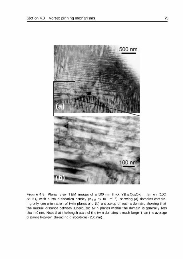
Section 4.3 Vortex pinning mechanisms 75
Figure 4.8: Planar view TEM images of a 500 nm thick YBa2Cu3O7¡± …lm on (100)SrTiO3 with a low dislocation density (ndisl ¼ 10 ¹m¡2), showing (a) domains contain-ing only one orientation of twin planes and (b) a close-up of such a domain, showing thatthe mutual distance between subsequent twin planes within the domain is generally lessthan 40 nm. Note that the length scale of the twin domains is much larger than the averagedistance between threading dislocations (250 nm).
76 Chapter 4 Comparison of dislocations with alternative pinning sites
Anti-phase boundariesAnti-phase boundaries (APB’s) may be induced by vicinal steps in the substrate (0.4nm in height, corresponding to ¼ c=3) [47]. Generally, APB’s are easily annihilatedby inserting stacking faults parallel to the ab-plane. Therefore, in order to generatea signi…cant number of APB’s that persist over a large part of the …lm thickness,substrates with a large miscut angle are needed. For this purpose, (106) SrTiO3
substrates have been employed [6, 7, 8], which have a miscut angle of 9.5± withrespect to the (100) plane. Indeed an anisotropy in js was reported in these miscutsamples: along the vicinal steps a higher current density is found than perpendicularto them. We used substrates with a vicinal angle of only 0.15± and the number ofAPB’s is expected to be small. Although we previously found indications for theexistence of a network of anti-phase boundaries [48], our present TEM investigationsdid not con…rm such networks. We attribute this di¤erence to (i) the use of betterquality substrates (smaller miscut angles, di¤erent supplier, better characterization)and (ii) our new substrate preparation and cleaning procedure.7 Although APB’s areabsent in our …lms on ‡at substrates, we …nd current densities that are as high asthose obtained on miscut samples [6, 7, 8]. In our opinion, vortex pinning in …lmson miscut substrates may also be dominated by threading dislocations, while thereduction in js in the direction normal to the substrate steps arises from a reductionin crystallinity in this direction. As shown here, crystallinity in‡uences the magnitudeof the superconducting current and can, therefore, account for an anisotropy in js.
(Low-angle) grain boundariesAs discussed above, any network of planar defects might give rise to matching …eldbehavior, see Eq. (4.2). In particular, the observed island morphology of the …lmssuggest that the islands could be separated by (hidden) grain boundaries [3]. Sincelarge angle (> 5±) grain boundaries strongly a¤ect the magnitude of the supercon-ducting current density [49], the observed large currents imply that only low-angle(< 5±) grain boundaries can be present. In chapter 3 we found a scaling between theisland density nisland and threading dislocation density ndisl and observed that thedislocations are situated around the islands. Therefore, it is tempting to assume thatthe threading dislocations are distributed in low-angle grain boundaries, separatingthe growth islands.We can calculate the angle # between adjacent islands using the Shockley-Read for-mula [50]:
ddisl =b
2 sin (#=2), (4.3)
where b is the magnitude of the Burger’s vector and ddisl is the average distance be-tween dislocations (ddisl ¼ 1=
pndisl). Although we observe mostly screw dislocations,
7We discuss this procedure in chapter 6. It will be shown that we have essentially SrO-terminated(100) SrTiO3 substrates. The termination only a¤ects the microstructure of ultra thin …lms (< 25nm). There is no signi…cant di¤erence in superconducting and microstructural parameters in thicker…lms.
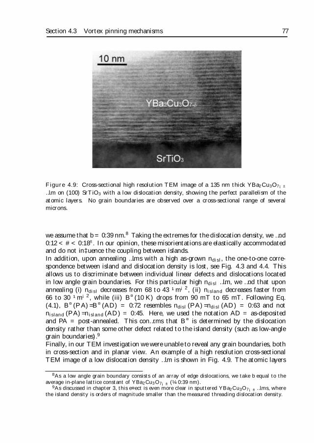
Section 4.3 Vortex pinning mechanisms 77
Figure 4.9: Cross-sectional high resolution TEM image of a 135 nm thick YBa2Cu3O7¡±…lm on (100) SrTiO3 with a low dislocation density, showing the perfect parallelism of theatomic layers. No grain boundaries are observed over a cross-sectional range of severalmicrons.
we assume that b = 0:39 nm.8 Taking the extremes for the dislocation density, we …nd0:12 < # < 0:18±. In our opinion, these misorientations are elastically accommodatedand do not in‡uence the coupling between islands.In addition, upon annealing …lms with a high as-grown ndisl, the one-to-one corre-spondence between island and dislocation density is lost, see Fig. 4.3 and 4.4. Thisallows us to discriminate between individual linear defects and dislocations locatedin low angle grain boundaries. For this particular high ndisl …lm, we …nd that uponannealing (i) ndisl decreases from 68 to 43 ¹m¡2, (ii) nisland decreases faster from66 to 30 ¹m¡2, while (iii) B¤ (10 K) drops from 90 mT to 65 mT. Following Eq.(4.1), B¤ (P A) =B¤ (AD) = 0:72 resembles ndisl (PA) =ndisl (AD) = 0:63 and notnisland (PA) =nisland (AD) = 0:45. Here, we used the notation AD = as-depositedand PA = post-annealed. This con…rms that B¤ is determined by the dislocationdensity rather than some other defect related to the island density (such as low-anglegrain boundaries).9
Finally, in our TEM investigation we were unable to reveal any grain boundaries, bothin cross-section and in planar view. An example of a high resolution cross-sectionalTEM image of a low dislocation density …lm is shown in Fig. 4.9. The atomic layers
8As a low angle grain boundary consists of an array of edge dislocations, we take b equal to theaverage in-plane lattice constant of YBa2Cu3O7¡± (¼ 0:39 nm).
9As discussed in chapter 3, this e¤ect is even more clear in sputtered YBa2Cu3O7¡± …lms, wherethe island density is orders of magnitude smaller than the measured threading dislocation density.
78 Chapter 4 Comparison of dislocations with alternative pinning sites
are continuous over tens of microns apart from some stacking faults parallel to theab-plane (also introduced by the ion milling during TEM sample preparation).
4.3.3 Point defects
The e¤ect of point defects on the superconducting properties is di¢cult to capture dueto the numerous types of point defects that may be present (vacancies and interstitialsin various sublattices, cation disorder, etc.). Moreover, since point defects are usuallyassociated with weak collective pinning e¤ects [51], they have relatively little in‡uenceon js at low magnetic …elds in …lms containing linear defects. In general, a post-annealtreatment reduces the point defect concentration, since equilibrium is approachedmuch closer than during the …lm growth process. As a result, the pinning capabilityshould decrease [52, 53]. Focussing on the low …eld behavior, we …nd that in the samplewith a low as-grown ndisl, js (B; T ) is independent of the post-anneal treatment.On the other hand, at high …elds a weak e¤ect of point disorder on js (B;T ) wasdemonstrated [54] in YBa2Cu3O7¡± …lms after the introduction of point defects bylow energetic (25 MeV) irradiation with 16O ions. In our picture of linear defectpinning, above B¤ each linear defect pins one vortex and the additional vortices arepinned by other defects [12]. Therefore, at …elds B À B¤ point defects may play arole in combination with linear defects. Surprisingly, the characteristic power-law de-pendence at high …elds does not change upon post-annealing, see Fig. 4.1 and 4.2.Yet, the relative amount of di¤erent types of point defects must have changed, im-plying that, in …rst approximation, point defects do not determine the high magnetic…eld behavior.In fact, the robustness of the high …eld behavior suggests that linear defects still playan important role [25]. The high-…eld power-law exponent ® (T ) is either close to ¡ 1
2(low ndisl) or ¡1 (high ndisl), which can be understood from vortex shear betweenunpinned vortices and vortices pinned by linear defects [24, 55] and collective pinningby linear defects [24], respectively. The cross-over takes place at a dislocation densityof the order 1=¸2 ¼ 45 ¹m2 at low temperatures [25]. Although the details of thepinning mechanism operative at high …elds are not clear to us at this moment, allresults point to linear defects still being e¤ective at B À B¤.
4.3.4 Precipitates
Also a high density of precipitates facilitates vortex pinning [15, 16, 17], since a vortexcan gain condensation energy. Within YBa2Cu3O7¡± …lms mostly Y2O3 precipitateshave been found [56]. By planar view TEM we also …nd some Y2O3 precipitates. Sincetheir density is relatively low (4/¹m2 in the sample shown in Fig. 4.8), we infer thattheir pinning e¤ect is insigni…cant. On the other hand, precipitates and dislocationsare closely connected, since around a precipitate dislocations can be generated [56]. Aswill be shown in chapter 5, we can employ this e¤ect to increase ndisl in our …lms: bydepositing Y2O3 precipitates on a bare substrate prior to the actual …lm depositionwe can substantially increase ndisl in the …lm deposited on top. This issue is alsoencountered in melt-textured YBa2Cu3O7¡±/Y2BaCuO5 composites. Although these
Section 4.4 Conclusions 79
211 precipitates are generally believed to be the origin of the high current densitiesfound in these materials [57], our results imply that (additional) dislocations generatedby Y2BaCuO5 precipitates might well be the actual reason for the high currents inthese bulk materials [58]. The precipitate density naturally present in our …lms,however, is too low to fully account for the high density of threading dislocations.
4.3.5 Surface roughness e¤ects
In our explanation for the higher current densities in …lms compared to single crys-tals so far, we left out the contribution from thickness ‡uctuations [18, 19, 20, 21]. Inprinciple, roughness contributes to the pinning of vortices, since a vortex may lowerits energy by minimizing its length [19]. Obviously, roughness e¤ects are more im-portant in …lms compared to single crystals due to their relatively small thickness.As the substrate-…lm interface is atomically ‡at [59] (see also Fig. 4.9), we concen-trate on the e¤ect of surface roughness. Assuming a sinusoidal thickness modulation±t sin (2¼x=L), the pinning force per unit length fp is calculated to be [19]:
fp ¼ 2¼"l±t
Lt. (4.4)
In this expression, "l is the line energy of a vortex [51]. Clearly, smoother surfacemodulations reduce vortex pinning. Annealing reduces the surface roughness (therms roughness after annealing is about half of the roughness of the as-grown sam-ples). However, we …nd no corresponding decrease in the superconducting currentdensity upon annealing. Therefore, we conclude that the contribution of the surfaceto js (B;T ) is negligible compared to linear defect pinning.
In conclusion, we have shown that linear defect pinning dominates in thin …lms ofYBa2Cu3O7¡± for the full temperature and magnetic …eld range investigated, irre-spective of the density of threading dislocations and the anneal treatment. In orderto tune the superconducting current density js (B; T ), we …rst need to control thedensity of these natural linear defects and their distribution. This is only possibleif we know the origin of the dislocations. Although we have shown that the thread-ing dislocations are neither related to low-angle grain boundaries nor to twin domainboundaries, the exact mechanism by which they are formed has not been identi…ed.This will be the subject of the three following chapters.
4.4 Conclusions
We correlate the microstructure of YBa2Cu3O7¡± thin …lms, laser ablated on (100)SrTiO3 substrates, to the superconducting current density js (B; T ). The defect struc-ture of these …lms is characterized by threading dislocations, surface corrugations,twin planes, precipitates, and point defects. As a tool to manipulate the relativeamount of these defects, we employ an ex-situ post-anneal treatment at a tempera-ture close to the average deposition temperature.
80 Chapter 4 Comparison of dislocations with alternative pinning sites
We …nd that:
(i) Threading dislocations are the dominant pinning sites for vortices, giving riseto the well-known matching …eld behavior in js (B; T ): it is constant up to acharacteristic …eld B¤ (T ) and decreases rapidly according to a power-law B®(T)
above B¤. On the average, js (B < B¤; T ) decreases slightly with increasingas-grown dislocation density ndisl. We attribute this e¤ect to the somewhatpoorer quality of these …lms, which determines the exact shape of the pinningpotential. Annealing the …lms indeed reveals a universal js (B < B¤; 4:2 K) =6£1011 A/m2, as expected for linear defect pinning in the single vortex regime.As a result, the superconducting current density characteristics can now besummarized by three phenomenological parameters only: B¤, js (B < B¤) and®. Here, B¤ is proportional to ndisl, while ® is close to ¡1
2 for ndisl . 45 ¹m¡2
and close to ¡1 for ndisl & 45 ¹m¡2, indicative of a shear and a collectivepinning mechanism, respectively.
(ii) Some dislocations are annihilated during annealing of …lms with a high as-grown ndisl (small dislocation spacing) and consequently B¤ decreases. More-over, the one-to-one correspondence between island density nisland and ndisl islost upon annealing. This allows us to discriminate between individual disloca-tions and dislocations being part of low-angle grain boundaries. As B¤ followsthe measured ndisl and not nisland, the islands are not loosely connected bymeans of low-angle grain boundaries (or some other defect related to the islandsize).
(iii) By post-annealing, the surface roughness and the point defect density decrease,while also the twin structure changes. Since in …lms with a low as-grown ndisl
neither js (B; T ) nor ndisl are a¤ected at all, we argue that these type of defectsdo not contribute signi…cantly to vortex pinning at low magnetic …elds. Inaddition, it appears that overdoping does not a¤ect the magnitude of js (B;T ).
As a …nal step, we perform cross-sectional and planar view transmission electronmicroscopy investigations to verify these conclusions. Indeed, threading dislocationsare observed. These dislocations are neither part of low-angle grain boundaries norare they related to twin domain boundaries. In addition, the precipitate density isvery low, while anti-phase boundaries are absent.We conclude that threading dislocations fully determine the vortex pinning propertiesof thin …lms of YBa2Cu3O7¡±, recon…rming our conclusion of chapter 3. Remarkably,it appears that even the high magnetic …eld behavior seems to be determined bythe presence of linear defects. Apparently, the vortex-vortex interactions stabilizethe entire vortex lattice up to …elds as high as 7 T. Therefore, the growth-induced,ordered threading dislocations in YBa2Cu3O7¡± …lms are extremely interesting bothfrom a technological and a fundamental point of view.
References 81
References
[1] R. Ramesh, D.M. Hwang, T. Venkatesan, T.S. Ravi, L. Nazar, A. Inam, X.D.Wu, B. Dutta, G. Thomas, A.F. Marshall, and T.H. Geballe, Science 247, 57(1990)
[2] K.S. Harshavardhan, M. Rajeswari, D.M. Hwang, C.Y. Chen, T. Sands, T.Venkatesan, J.E. Tkaczyk, K.W. Lay, and A. Safari, Appl. Phys. Lett. 60, 1902(1992)
[3] E. Mezzetti, R. Gerbaldo, G. Ghigo, L. Gozzelino, B. Minetti, C. Camerlingo,A. Monaco, G. Cuttone, and A. Rovelli, Phys. Rev. B 60, 7623 (1999)
[4] H. Safar, J.Y. Coulter, M.P. Maley, S. Foltyn, P. Arendt, X.D. Wu, and J.Q.Willis, Phys. Rev. B 52, R9875 (1995)
[5] C. Villard, G. Koren, D. Cohen, E. Polturak, B. Thrane, and D. Chateignier,Phys. Rev. Lett. 77, 3913 (1996)
[6] T. Haage, J. Zegenhagen, J.Q. Li, H.-U. Habermeier, M. Cardona, Ch. Jooss,R. Warthmann, A. Forkl, and H. Kronmüller, Phys. Rev. B 56, 8404 (1997)
[7] Ch. Jooss, R. Warthmann, H. Kronmüller, T. Haage, H.-U. Habermeier, and J.Zegenhagen, Phys. Rev. Lett. 82, 632 (1999)
[8] Ch. Jooss, R. Warthmann, and H. Kronmüller, Phys. Rev. B 61, 12433 (2000)
[9] Ch. Gerber, D. Anselmetti, J.G. Bednorz, J. Mannhart, and D.G. Schlom, Na-ture 350, 279 (1991)
[10] M. Hawley, I.D. Raistrick, J.G. Beery, and R.J. Houlton, Science 251, 1587(1991)
[11] J. Mannhart, D. Anselmetti, J.G. Bednorz, A. Catana, Ch. Gerber, K.A. Müller,and D.G. Schlom, Z. Phys. B 86, 177 (1992)
[12] H. Douwes, P.H. Kes, Ch. Gerber, and J. Mannhart, Cryogenics 33, 486 (1993)
[13] V.M. Pan, A.L. Kasatkin, V.L. Svetchnikov, and H.W. Zandbergen, Cryogenics33, 21 (1993)
[14] A. Diáz, L. Mechin, P. Berghuis, and J.E. Evetts, Phys. Rev. Lett. 80, 3855(1998)
[15] M. Murakami, M. Morita, K. Doi, and K. Miyamoto, Jpn. J. Appl. Phys. 28,1189 (1989)
[16] K. Watanabe, T. Matsushita, N. Kobayashi, H. Kawabe, E. Aoyagi, K. Hiraga,H. Yamane, H. Kurosawa, T. Hirai, and Y. Muto, Appl. Phys. Lett. 56, 1490(1990)
[17] Y.J. Tian, L.P. Guo, L. Li, Y.Q. Zhou, Y. Yang, Z.X. Zhao, S.F. Xu, H.B. Lu,Y.L. Zhou, Z.H. Chen, D.F. Cui, and G.Z. Yang, Appl. Phys. Lett. 65, 234(1994)
82 Chapter 4 Comparison of dislocations with alternative pinning sites
[18] M. McElfresh, T.G. Miller, D.M. Schai¤er, R. Reifenberger, R.E. Muenchen-hausen, M. Hawley, S.R. Foltyn, and X.D. Wu, J. Appl. Phys. 71, 5099 (1992)
[19] P. Kes, in Materials and crystallographic aspects of HT c-superconductivity, editedby E. Kaldis (Kluwer Academic, Dordrecht, 1997), p. 407
[20] Ch. Jooss, A. Forkl, R. Warthmann, H.-U. Habermeier, B. Leibold, and H.Kronmüller, Physica C 266, 235 (1996)
[21] Ch. Jooss, A. Forkl and H. Kronmüller, Physica C 268, 87 (1996)ndon) 399,439 (1999)
[22] F.C. Klaassen, G. Doornbos, J.M. Huijbregtse, B. Dam, and R. Griessen, J.Low Temp. Phys. 117, 1549 (1999)
[23] D.R. Nelson and V.M. Vinokur, Phys. Rev. Lett. 68. 2398 (1992)
[24] D.R. Nelson and V.M. Vinokur, Phys. Rev B 48, 13060 (1993)
[25] F.C. Klaassen, G. Doornbos, J.M. Huijbregtse, R.C.F. van der Geest, B. Dam,and R. Griessen (to be published)
[26] P. Chaudhari, R.H. Koch, R.B. Laibowitz, T.R. McGuire, and R.J. Gambino,Phys. Rev. Lett. 58, 2684 (1987)
[27] See for instance L. Civale, A.D. Marwick, M.W. McElfresh, T.K. Worthington,A.P. Malozemo¤, F.H. Holtzberg, J.R. Thompson, and M.A. Kirk, Phys. Rev.Lett. 65, 1164 (1990) and references therein.
[28] L. Civale, Supercond. Sci. Technol. 10, A11 (1997)
[29] R. Feenstra, D.K. Christen, C.E. Klabunde, and J.D. Budai, Phys. Rev. B 45,7555 (1992)
[30] M. Qvarford, K. Heeck, J.G. Lensink, R.J. Wijngaarden, and R. Griessen, Rev.Sci. Instrum. 63, 5726 (1992)
[31] D. Hüttner, O. Meyer, J. Reiner, and G. Linker, Nucl. Instr. and Meth. in Phys.Res. B 118. 578 (1996)
[32] K.E. Bagnall, I.V. Grigorieva, J.W. Steeds, G. Balakrishnan, and D. McK Paul,Supercond. Sci. Technol. 8, 605 (1995)
[33] S. Horiuchi, M. Cantoni, M. Uchida, T. Tsuruta, and Y. Matsui, Appl. Phys.Lett. 73, 1293 (1998)
[34] T. Ishida, K. Okuda, K. Hirata, H.P. Lang, and H.-J. Günterodt, Physica C266, 1 (1996)
[35] H. Huhtinen, E. Lähderanta and P. Paturi, J. Low Temp. Phys. 117, 795 (1999)
[36] D.G. Schlom, D. Anselmetti, J.G. Bednorz, R.F. Broom, A. Catana, T. Frey,Ch. Gerber, H.-J. Günterhodt, H.P. Lang, and J. Mannhart, Z. Phys. B 86, 163(1992)
[37] Y. Gao, K.L. Merkle, G. Bai, H.L.M. Chang, and D.J. Lam, Physica C 174, 1(1991)
References 83
[38] T. Hino, S. Tomiya, T. Miyajima, K. Yanashima, S. Hashimoto, and M. Ikeda,Appl. Phys. Lett. 76, 3421 (2000)
[39] D.H. Lowndes, D.K. Christen, C.E. Klabunde, Z.L. Wang, D.M. Kroeger, J.D.Budai, Shen Zhu, and D.P. Norton, Phys. Rev. Lett. 74, 2355 (1995)
[40] B. Roas, L. Schultz and G. Saemann-Ishenko, Phys. Rev. Lett. 64, 479 (1990)
[41] A. Gurevich and L.D. Cooley, Phys. Rev. 50, 13563 (1994)
[42] G. Doornbos, B. Dam, J.C. Martinez, R. Surdeanu, U. Poppe, and R. Griessen,Physica C 282-287, 2303 (1997)
[43] Y. Zhu and M. Suenaga, Phil. Mag. A 66, 457 (1992)
[44] B.M. Lairson, S.K. Strei¤er, and J.V. Bravman, Phys. Rev. B 42, 10067 (1990)
[45] L.J. Swartzendruber, D.L. Kaiser, F.W. Gayle, L.H. Bennet, and A. Roytburd,Appl. Phys. Lett. 58, 1566 (1991)
[46] J.Z. Liu, Y.X. Jia, R.N. Shelton, and M.J. Fluss, Phys. Rev. Lett. 66, 1354(1991)
[47] J.G. Wen, C.Træholt and H.W. Zandbergen, Physica C 205, 354 (1993)
[48] B. Dam, C. Træholt, B. Stäuble-Pümpin, J. Rector, and D.G. De Groot, J.Alloys and Compounds 251, 27 (1997)
[49] N.F. Heinig, R.D. Redwing, J.E. Nordman, and D.C. Larbalestier, Phys. Rev.B 60, 1409 (1999)
[50] J.P. Hirth and J. Lothe, in Theory of dislocations (Wiley, New York, 1982)
[51] G. Blatter, M.V. Feigel’man, V.B. Geshkenbein, A.I. Larkin, and V.M. Vinokur,Rev. Mod. Phys. 66, 1125 (1994)
[52] T.L. Hylton and M.R. Beasley, Phys. Rev. B 41, 11669 (1990)
[53] L.R. Tessler, J. Provost and A. Maignan, Appl. Phys. Lett. 58, 528 (1991)
[54] B. Roas, B. Hensel, G. Saemann-Ischenko, and L. Schultz, Appl. Phys. Lett.54, 1051 (1989)
[55] R. Wördenweber, Phys. Rev. B 46, 3076 (1992)
[56] A. Catana, R.F. Broom, J.G. Bednorz, J. Mannhart, and D.G. Schlom, Appl.Phys. Lett. 60, 1016 (1992)
[57] B. Martínez, X. Obradors, A. Gou, V. Gomis, S. Piñol, J. Fontcuberta, and H.van Tol, Phys. Rev. B 53, 2797 (1996)
[58] B. Martínez, F. Sandiumenge, T. Puig, X. Obradors, L. Richard, and J. Rabier,Appl. Phys. Lett. 74, 73 (1999)
[59] J.G. Wen, T. Morishita, N. Koshizuka, C. Traeholt, and H.W. Zandbergen,Appl. Phys. Lett. 66, 1830 (1995)

Chapter 5
Mechanisms of dislocation formation
Having identi…ed threading dislocations as the dominant ‡ux pinning centers in thin…lms of YBa2Cu3O7¡± deposited on (100) SrTiO3 substrates, we now proceed toinvestigate the process of dislocation formation. We group the possible mechanismsinto two main categories: (i) substrate-induced dislocations (such as inheritance ofdislocations from the substrate and release of substrate-…lm mis…t strain) and (ii)growth-induced dislocations (merging of misaligned growth fronts). After exploringthese mechanisms, incorporating some new experimental results, we conclude thatthe last mechanism is operative. It is illustrated that dislocation formation is closelyrelated to the YBa2Cu3O7¡± nucleation and growth mechanism and proceeds eithervia the (initial) coalescence of growth islands or via overgrowing precipitates that arepreferentially induced in the nucleation stage. Although we can not yet determineunambiguously which mechanism is operative, experimental evidence is presented infavor of precipitate generated threading dislocations. If con…rmed, this would o¤ergreat opportunities for tailoring the linear defect distribution.1
1This chapter is based on the paper by J.M. Huijbregtse, B. Dam, R.C.F. van der Geest, F.C.Klaassen, R. Elberse, J.H. Rector, and R. Griessen, Phys. Rev. B 62, 1338 (2000)
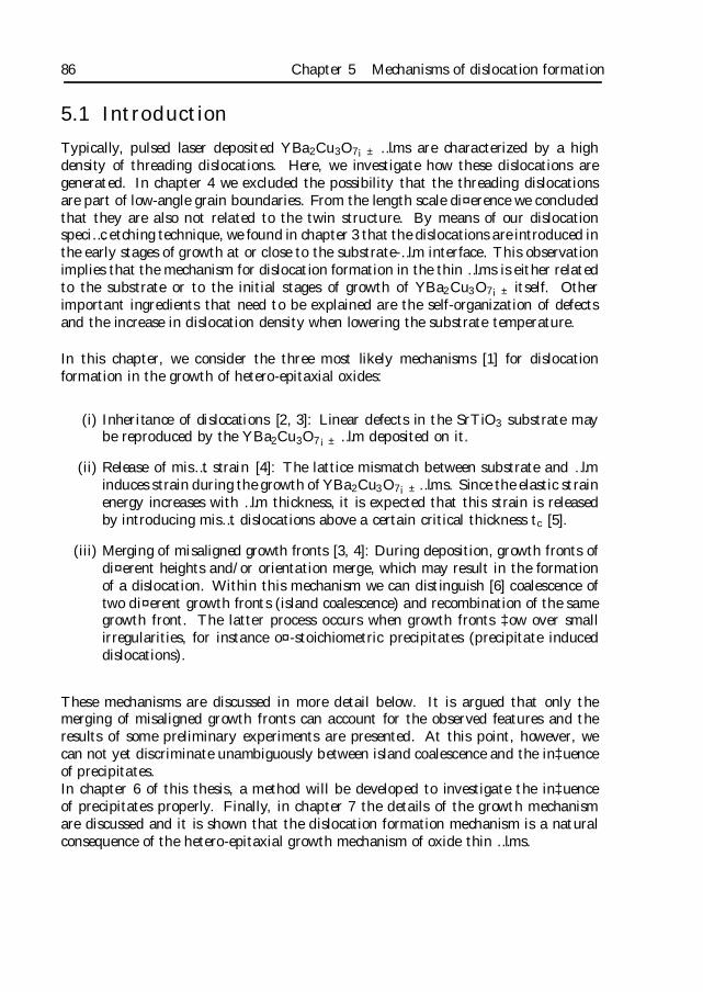
86 Chapter 5 Mechanisms of dislocation formation
5.1 Introduction
Typically, pulsed laser deposited YBa2Cu3O7¡± …lms are characterized by a highdensity of threading dislocations. Here, we investigate how these dislocations aregenerated. In chapter 4 we excluded the possibility that the threading dislocationsare part of low-angle grain boundaries. From the length scale di¤erence we concludedthat they are also not related to the twin structure. By means of our dislocationspeci…c etching technique, we found in chapter 3 that the dislocations are introduced inthe early stages of growth at or close to the substrate-…lm interface. This observationimplies that the mechanism for dislocation formation in the thin …lms is either relatedto the substrate or to the initial stages of growth of YBa2Cu3O7¡± itself. Otherimportant ingredients that need to be explained are the self-organization of defectsand the increase in dislocation density when lowering the substrate temperature.
In this chapter, we consider the three most likely mechanisms [1] for dislocationformation in the growth of hetero-epitaxial oxides:
(i) Inheritance of dislocations [2, 3]: Linear defects in the SrTiO3 substrate maybe reproduced by the YBa2Cu3O7¡± …lm deposited on it.
(ii) Release of mis…t strain [4]: The lattice mismatch between substrate and …lminduces strain during the growth of YBa2Cu3O7¡± …lms. Since the elastic strainenergy increases with …lm thickness, it is expected that this strain is releasedby introducing mis…t dislocations above a certain critical thickness tc [5].
(iii) Merging of misaligned growth fronts [3, 4]: During deposition, growth fronts ofdi¤erent heights and/or orientation merge, which may result in the formationof a dislocation. Within this mechanism we can distinguish [6] coalescence oftwo di¤erent growth fronts (island coalescence) and recombination of the samegrowth front. The latter process occurs when growth fronts ‡ow over smallirregularities, for instance o¤-stoichiometric precipitates (precipitate induceddislocations).
These mechanisms are discussed in more detail below. It is argued that only themerging of misaligned growth fronts can account for the observed features and theresults of some preliminary experiments are presented. At this point, however, wecan not yet discriminate unambiguously between island coalescence and the in‡uenceof precipitates.In chapter 6 of this thesis, a method will be developed to investigate the in‡uenceof precipitates properly. Finally, in chapter 7 the details of the growth mechanismare discussed and it is shown that the dislocation formation mechanism is a naturalconsequence of the hetero-epitaxial growth mechanism of oxide thin …lms.
Section 5.2 Substrate-induced dislocations 87
Figure 5.1: AFM height images of two (100) SrTiO3 substrates, etched for 30 s in a 1 HF: 2 HNO3 : 2 H2O solution, showing the spread in dislocation density ndisl between twodi¤erent substrates: (a) a typical substrate with ndisl = 10¡2 ¹m¡2 (image size 100£ 100¹m2) and (b) a ”bad” substrate with ndisl = 1 ¹m¡2 (image size 20£ 20 ¹m2).
5.2 Substrate-induced dislocations
In this section, we investigate the two mechanism that are related to the nature ofthe substrate (i.e., inheritance and release of mis…t strain). Determining the disloca-tion density in the substrate material and using larger lattice mismatched substrates,respectively, allows us to exclude these mechanisms.
Inheritance of dislocationsAs Eissler, Wang and Dietsche [2] suggested that dislocations are inherited from thesubstrate, we determined the dislocation density in SrTiO3 substrates by means ofetching in 1 HF: 2 HNO3: 2 H2O. As in the etching of YBa2Cu3O7¡± …lms, etchpits form at linear defect sites. In …gure 5.1 AFM images of two di¤erent SrTiO3
substrates are shown after etching (note the large scan sizes), giving an idea of therange of dislocation densities that can be found in the substrate material. Usually,we …nd densities that are three orders of magnitude smaller (10¡2 ¹m¡2) than thosein the …lms (10 ¹m¡2), see Fig. 5.1(a). The highest dislocation density observedin substrates so far [about 1 ¹m¡2, see Fig. 5.1(b)], is still smaller than the lowestdislocation density achieved in …lms, indicating that inheritance is not the main originof dislocations in …lms.This is again shown, when we arti…cially create linear defects in the SrTiO3 substrateby bombardment with 500 keV Xe4+ (with a dose of 200 ¹m¡2). YBa2Cu3O7¡±
88 Chapter 5 Mechanisms of dislocation formation
…lms grown on these substrates, all show the expected dislocation densities (i.e., ofthe order of 10 ¹m¡2) rather than the implanted dose in the substrate (we checkedthat the linear defects due to implantation were still present after …lm deposition byetching o¤ the …lm and subsequently etching the substrate). Although inheritancecannot be ruled out completely, we conclude that the linear defects in the …lm arerelatively insensitive to the surface properties of the substrate.
Release of mis…t strainAnother possibility for the formation of dislocations at the interface is the relaxationof strain, originating from the mismatch between substrate and …lm.2 Generally, a…lm may release this strain either by introducing mis…t dislocations [4] or by formingcracks [7]. Clearly, crack formation does not take place in our YBa2Cu3O7¡± …lmsand we will concentrate on the formation of mis…t relieving dislocations. Becausethe substrate-…lm mismatch is in the ab-plane, the mechanism leading to the creationof dislocations along the c-axis is not a priori clear. It has been suggested [4, 5]that dislocation half-loops created at the …lm surface glide towards the substrate-…lminterface to form strain relieving mis…t dislocations. The dislocation segments left ateach end of the mis…t dislocation thread the …lm (parallel to the c-axis).Such dislocation half-loops must have at least an edge component in order to relievethe in-plane substrate-…lm mis…t. However, as was shown in chapter 4, the thread-ing dislocations that we …nd in our …lms are mainly screw dislocations, making thismechanism very unlikely. In addition, the activation energy for the formation of suchhalf-loops is extremely high [1]. It also fails to explain why the number of disloca-tions created at the interface decreases substantially when growing a …lm with largerislands, i.e. at higher substrate temperatures. Given the large activation energy asso-ciated with the formation of half-loops [1], one would rather expect a larger numberof loops (and thus a larger number of threading dislocations) at higher depositiontemperatures. Moreover, we do not observe the merging of etch pits upon repeatedetching or any other sign that they originate from dislocation half-loops.The most convincing argument, however, against the in‡uence of the substrate mis-match on ndisl is found in YBa2Cu3O7¡± …lms deposited on (100) MgO substrates.3
Since the mismatch between YBa2Cu3O7¡± and MgO is about 9%, which is muchlarger than the mismatch with SrTiO3 (1.2%), more strain relieving dislocations areneeded when using MgO substrates. Indeed, dislocation densities up to 103 ¹m¡2 havebeen revealed by transmission electron microscopy (TEM) of YBa2Cu3O7¡± …lms onMgO [8]. In Fig. 5.2, AFM images of the surface morphology of two YBa2Cu3O7¡±
…lms laser deposited on MgO with di¤erent dislocation densities are shown. It turnsout that also on MgO the dislocation density can be decreased by increasing the sub-strate temperature Tsub and/or the oxygen pressure pO2 , analogous to …lms deposited
2A detailed experimental investigation and discussion of the strain relaxation process will bepresented in chapter 7.
3All …lms presented in this chapter are prepared in the QUESTEK set-up, using 3:0< dT¡S < 3:5cm, 750 < Tsub < 850±C and 15 < pO2
< 50 Pa at a ‡uence J = 1:3 J/cm2 (as measured at thetarget).
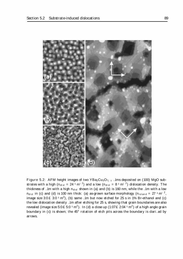
Section 5.2 Substrate-induced dislocations 89
Figure 5.2: AFM height images of two YBa2Cu3O7¡± …lms deposited on (100) MgO sub-strates with a high (ndisl = 24 ¹m¡2) and a low (ndisl = 8 ¹m¡2) dislocation density. Thethickness of …lm with a high ndisl shown in (a) and (b) is 160 nm, while the …lm with a lowndisl in (c) and (d) is 100 nm thick: (a) as-grown surface morphology (nisland = 27 ¹m¡2,image size 3:0£ 3:0 ¹m2), (b) same …lm but now etched for 25 s in 1% Br-ethanol and (c)the low dislocation density …lm after etching for 25 s, showing that grain boundaries are alsorevealed (image size 5:0£5:0 ¹m2). In (d) a close up (1:07£2:04 ¹m2) of a high angle grainboundary in (c) is shown; the 45± rotation of etch pits across the boundary is clari…ed byarrows.
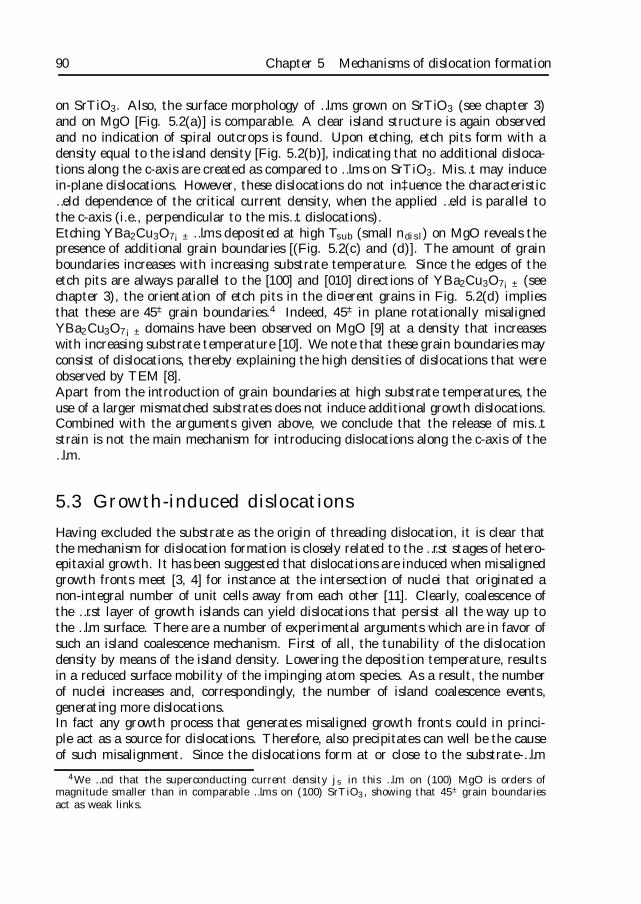
90 Chapter 5 Mechanisms of dislocation formation
on SrTiO3. Also, the surface morphology of …lms grown on SrTiO3 (see chapter 3)and on MgO [Fig. 5.2(a)] is comparable. A clear island structure is again observedand no indication of spiral outcrops is found. Upon etching, etch pits form with adensity equal to the island density [Fig. 5.2(b)], indicating that no additional disloca-tions along the c-axis are created as compared to …lms on SrTiO3. Mis…t may inducein-plane dislocations. However, these dislocations do not in‡uence the characteristic…eld dependence of the critical current density, when the applied …eld is parallel tothe c-axis (i.e., perpendicular to the mis…t dislocations).Etching YBa2Cu3O7¡± …lms deposited at high Tsub (small ndisl) on MgO reveals thepresence of additional grain boundaries [(Fig. 5.2(c) and (d)]. The amount of grainboundaries increases with increasing substrate temperature. Since the edges of theetch pits are always parallel to the [100] and [010] directions of YBa2Cu3O7¡± (seechapter 3), the orientation of etch pits in the di¤erent grains in Fig. 5.2(d) impliesthat these are 45± grain boundaries.4 Indeed, 45± in plane rotationally misalignedYBa2Cu3O7¡± domains have been observed on MgO [9] at a density that increaseswith increasing substrate temperature [10]. We note that these grain boundaries mayconsist of dislocations, thereby explaining the high densities of dislocations that wereobserved by TEM [8].Apart from the introduction of grain boundaries at high substrate temperatures, theuse of a larger mismatched substrates does not induce additional growth dislocations.Combined with the arguments given above, we conclude that the release of mis…tstrain is not the main mechanism for introducing dislocations along the c-axis of the…lm.
5.3 Growth-induced dislocations
Having excluded the substrate as the origin of threading dislocation, it is clear thatthe mechanism for dislocation formation is closely related to the …rst stages of hetero-epitaxial growth. It has been suggested that dislocations are induced when misalignedgrowth fronts meet [3, 4] for instance at the intersection of nuclei that originated anon-integral number of unit cells away from each other [11]. Clearly, coalescence ofthe …rst layer of growth islands can yield dislocations that persist all the way up tothe …lm surface. There are a number of experimental arguments which are in favor ofsuch an island coalescence mechanism. First of all, the tunability of the dislocationdensity by means of the island density. Lowering the deposition temperature, resultsin a reduced surface mobility of the impinging atom species. As a result, the numberof nuclei increases and, correspondingly, the number of island coalescence events,generating more dislocations.In fact any growth process that generates misaligned growth fronts could in princi-ple act as a source for dislocations. Therefore, also precipitates can well be the causeof such misalignment. Since the dislocations form at or close to the substrate-…lm
4We …nd that the superconducting current density js in this …lm on (100) MgO is orders ofmagnitude smaller than in comparable …lms on (100) SrTiO3, showing that 45± grain boundariesact as weak links.
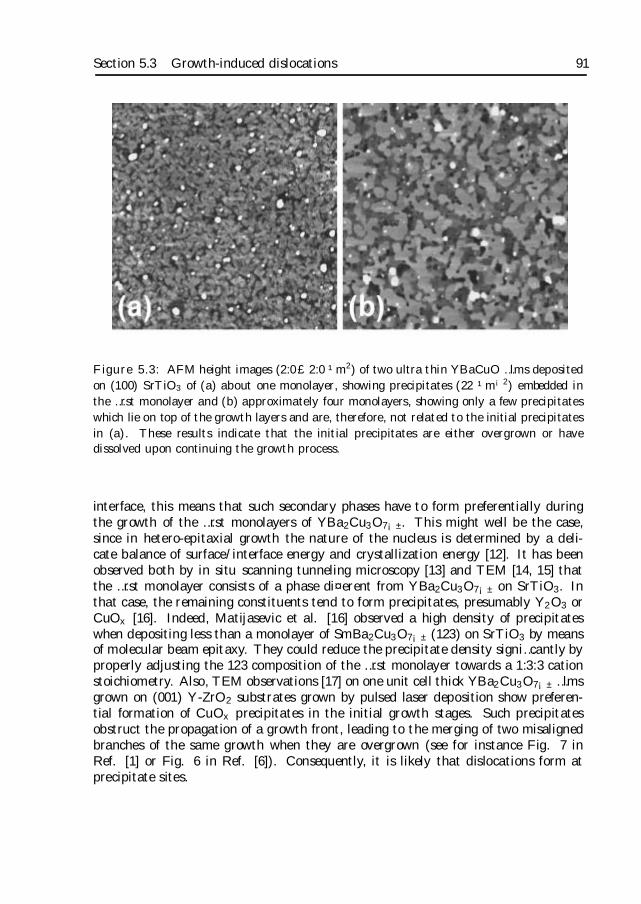
Section 5.3 Growth-induced dislocations 91
Figure 5.3: AFM height images (2:0£2:0 ¹m2) of two ultra thin YBaCuO …lms depositedon (100) SrTiO3 of (a) about one monolayer, showing precipitates (22 ¹m¡2) embedded inthe …rst monolayer and (b) approximately four monolayers, showing only a few precipitateswhich lie on top of the growth layers and are, therefore, not related to the initial precipitatesin (a). These results indicate that the initial precipitates are either overgrown or havedissolved upon continuing the growth process.
interface, this means that such secondary phases have to form preferentially duringthe growth of the …rst monolayers of YBa2Cu3O7¡±. This might well be the case,since in hetero-epitaxial growth the nature of the nucleus is determined by a deli-cate balance of surface/interface energy and crystallization energy [12]. It has beenobserved both by in situ scanning tunneling microscopy [13] and TEM [14, 15] thatthe …rst monolayer consists of a phase di¤erent from YBa2Cu3O7¡± on SrTiO3. Inthat case, the remaining constituents tend to form precipitates, presumably Y2O3 orCuOx [16]. Indeed, Matijasevic et al. [16] observed a high density of precipitateswhen depositing less than a monolayer of SmBa2Cu3O7¡± (123) on SrTiO3 by meansof molecular beam epitaxy. They could reduce the precipitate density signi…cantly byproperly adjusting the 123 composition of the …rst monolayer towards a 1:3:3 cationstoichiometry. Also, TEM observations [17] on one unit cell thick YBa2Cu3O7¡± …lmsgrown on (001) Y-ZrO2 substrates grown by pulsed laser deposition show preferen-tial formation of CuOx precipitates in the initial growth stages. Such precipitatesobstruct the propagation of a growth front, leading to the merging of two misalignedbranches of the same growth when they are overgrown (see for instance Fig. 7 inRef. [1] or Fig. 6 in Ref. [6]). Consequently, it is likely that dislocations form atprecipitate sites.
92 Chapter 5 Mechanisms of dislocation formation
Figure 5.4: AFM height image (3:0£ 3:0 ¹m2) of Y2O3 precipitates laser deposited on a(100) SrTiO3 substrate. The density of Y2O3 precipitates is 54 ¹m¡2. The vicinal steps inthe substrate of 0.4 nm in height are along the [110] direction and are separated 177 nm,corresponding to a miscut angle of 0.13±.
In the scenario of precipitate induced dislocations, the temperature dependence of thedislocation density is explained in terms of the segregation kinetics of the precipitates.At lower temperatures, the spacing between precipitates is smaller due to the smallersurface di¤usion distance, resulting in a higher precipitate density (higher dislocationdensity). The self-organization of dislocations can be understood by assuming thatthe kinetics are di¤usion controlled.We have therefore two mechanisms, i.e. dislocations induced by overgrowing precip-itates or by islands coalescence, which are potentially leading to the observed phe-nomena. In order to decide which mechanism is dominant we started investigatingultra thin …lms. In Fig. 5.3(a) an AFM image, recorded ex-situ, of a YBa2Cu3O7¡±
…lm with a thickness slightly over one unit cell (u.c.) is shown. The substrate is fullycovered with one monolayer of YBa2Cu3O7¡± (or a related phase [13, 14, 15, 16]).Embedded in this matrix, we observe a signi…cant number of precipitates (22 ¹m¡2).As shown in Fig. 5.3(b), these precipitates are almost absent in …lms of 4 u.c. inthickness, showing that the initial precipitates are either overgrown or have dissolvedagain (and are incorporated as defects in the …lm). Apparently, precipitates are char-acteristic for the …rst layer only.Nevertheless, these secondary phases may generate dislocations when they are over-grown. The density of precipitates is larger than the dislocation density as expected
Section 5.4 Conclusions 93
for a thicker YBa2Cu3O7¡± …lm deposited under the same deposition conditions (7.8¹m¡2). However, we should stress that not all precipitates necessarily generate dis-location when they are overgrown.To prove that precipitates can generate dislocations, we deposited small particlesfrom a Y2O3 target on a bare SrTiO3 substrate prior to the actual …lm deposition,see Fig. 5.4. In this …gure Y2O3 precipitates can be distinguished with a density of54 ¹m¡2. Now depositing a YBa2Cu3O7¡± …lm on top of this precipitate structure ata substrate temperature of 850±C, yields a …lm with a threading dislocation densityof 41 ¹m¡2. This is more than 5 times larger than the dislocation density in …lmsdeposited under identical condition on clean substrates (7.8 ¹m¡2) and we concludethat precipitates serve as nucleation sites for dislocations.
Having shown that (i) preferential precipitation takes place in the …rst stages ofYBa2Cu3O7¡± growth and (ii) Y2O3 precipitates induce additional dislocation, it istempting to conclude that dislocations are induced by precipitates formed in the …rstmonolayer as a result of the peculiarities of the nucleation mechanism. However, islandcoalescence can equally well explain the temperature dependence of the dislocationdensity and their distribution. Therefore, in order to decide which one of the twomechanisms is operative, we …rst need to control the preferential precipitation process(chapter 6).
5.4 Conclusions
As an introduction to the remaining part of this thesis, we discussed various mech-anisms by which threading dislocations can be induced in YBa2Cu3O7¡± …lms. It isshown that linear defects are not related to the SrTiO3 substrate. First, the disloca-tion density in the substrate is typically two orders of magnitude lower than in the…lm. Secondly, increasing the mis…t between substrate and …lm by using (100) MgO(9% mis…t) instead of (100) SrTiO3 (1% mismatch) we …nd comparable dislocationdensities in the corresponding …lms, showing that our threading dislocations are notmis…t dislocations.We conclude that dislocations are induced as a consequence of the growth processitself via merging of misaligned growth fronts. At points where misoriented growthfronts meet, dislocation formation is facilitated. We identify at least one mechanism:we can enhance the density of pinning sites by depositing a layer of Y2O3 precipitatesbefore starting the YBa2Cu3O7¡± growth process. This opens up new possibilities intailoring the in-plane threading dislocation distribution. For instance by depositinga lattice of precipitates prior to the actual …lm growth, it may be possible to observethe predicted [18] Mott-insulator vortex phase (see chapter 3).Clearly, precipitation in the …rst monolayer resulting from the peculiarities of thenucleation mechanism of YBa2Cu3O7¡± on SrTiO3 (preferential precipitation) canaccount for the introduction of dislocations. In addition, also the temperature depen-dence of their density and distribution can be explained in a qualitative way. Althoughwe …nd evidence for preferential precipitation in the …rst monolayers, there is a sec-
94 Chapter 5 Mechanisms of dislocation formation
ond mechanism which accounts equally well for all observed characteristics: islandcoalescence. We will explore these two mechanisms in the remaining two chapters ofthis thesis.
References
[1] B. Stäuble-Pümpin, V.C. Matijasevic, B. Ilge, J.E. Mooij, W.J.A.M. Peterse,P.M.L.O. Scholte, F. Tuinstra, H.J. Venvik, D.S. Wai, C. Træholt, J.G. Wen,and H.W. Zandbergen, Phys. Rev. B 52, 7604 (1995)
[2] D. Eissler, H.S. Wang, and W. Dietsche, Appl. Phys. Lett. 62, 1292 (1993)
[3] D.G. Schlom, D. Anselmetti, J.G. Bednorz, R.F. Broom, A. Catana, T. Frey,Ch. Gerber, H.-J. Günterhodt, H.P. Lang, and J. Mannhart, Z. Phys. B 86, 163(1992)
[4] S.J. Pennycook, M.F. Chisholm, D.E. Jesson, R. Feenstra, S. Zhu, X.Y. Zheng,and D.J. Lowndes, Physica C 202, 1 (1992)
[5] M. Yeadon, M. Aindow, F. Wellhöfer, and J.S. Abell, J. Cryst. Growth 172,145 (1997)
[6] D.G. Schlom, D. Anselmetti, J.G. Bednorz, Ch. Gerber, and J. Mannhart, J.Cryst. Growth 137, 259 (1994)
[7] M. Bauer, F. Baudenbacher, and H. Kinder, Physica C 246, 113 (1995)
[8] V. Svetchnikov, V. Pan, C. Traeholt, and H. Zandbergen, IEEE Trans. Appl.Supercond. 7, 1396 (1997)
[9] T.S. Ravi, D.M. Hwang, R. Ramesh, Siu Wai Chan, L. Nazar, C.Y. Chen, A.Inam, and T. Venkatesan, Phys. Rev. B 42, 10141 (1990)
[10] M. Kusunoki, Y. Takano, M. Makaida, and S. Ohshima, Physica C 321, 81(1999)
[11] S.K. Strei¤er, B.M. Lairson, C.B. Eom, B.M. Clemens, J.C. Bravman, and T.H.Geballe, Phys. Rev. B 43, 13007 (1991)
[12] B. Dam and B. Stäuble-Pümpin, J. Mater. Sci.: Mater.Electron. 9, 217 (1998)
[13] T. Haage, J. Zegenhagen, H.-U. Habermeier, and M. Cardona, Phys. Rev. Lett.80, 4225 (1998)
[14] J.G. Wen, T. Morishita, N. Koshizuka, C. Traeholt, and H.W. Zandbergen,Appl. Phys. Lett. 66, 1830 (1995)
[15] H.W. Zandbergen, J.G. Wen, C. Traeholt, and V. Svetchnikov, J. Alloys Compd.195, 85 (1993)
[16] V.C. Matijasevic, B. Ilge, B. Stäuble-Pümpin, G. Rietveld, F. Tuinstra, andJ.E. Mooij, Phys. Rev. Lett. 76, 4765 (1996)
[17] J.A. Alarco, G. Brorsson, H. Olin, and E. Olsson, J. Appl. Phys. 75, 3202 (1994)
[18] D.R. Nelson and V.M. Vinokur, Phys. Rev. Lett. 68, 2398 (1992)
Chapter 6
The …rst stages of hetero-epitaxialgrowth: phase stability
We investigate the origin of preferential precipitation in YBa2Cu3O7¡± (123) …lmsby varying the (100) SrTiO3 substrate termination. Using a newly developed ex-situmethod to prepare SrO-terminated substrates in addition to the well-known TiO2-termination, it is shown that: (i) preferential precipitation occurs when depositingsubmonolayer 123 …lms on SrO-terminated SrTiO3 and (ii) such precipitates are ab-sent on the TiO2-termination. The substrate termination determines both the startingand terminating layer of the 123 phase. Similar e¤ects are observed in submonolayerthick …lms with cation stoichiometries of 122, 124 and 133. However, when grow-ing several 123 monolayers on SrO-terminated substrates, no precipitates are formed.Instead, defects are introduced to accommodate the o¤-stoichiometry. Hence, thedensity of threading dislocations in thick …lms does not depend on the substratetermination, excluding preferential precipitation as the main origin of threading dis-location.1
1This chapter is based on the paper by J.M. Huijbregtse, J.H. Rector, and B. Dam, accepted forpublication in Physica C (2001)
96 Chapter 6 The …rst stages of hetero-epitaxial growth: phase stability
6.1 Introduction
In the previous chapter, we concluded that the merging of misaligned growth fronts[1] accounts for all the characteristics of the threading dislocation structure in thin…lms of YBa2Cu3O7¡± on SrTiO3. Misalignment is caused either by the coalescenceof growth islands, or by growth fronts ‡owing over irregularities, such as precipitates[2]. Depositing Y2O3 particles prior to the actual …lm deposition, indeed generatesdislocations. On the other hand, since dislocations only form at or close to theinterface, such precipitates must form preferentially in the early stages of hetero-epitaxial growth. Why would such a preferential precipitation process occur at all? Ifthe phase that initially forms has a cation composition di¤erent from 123 (such as 122or 133) [3], supplying the 123 composition automatically results in the formation ofprecipitates for the …rst monolayer (in addition to the 122 or 133 phase). Indeed, inthe case of SmBa2Cu3O7¡± …lms grown by molecular beam epitaxy it was shown [4]that such a precipitation process occurs. It was suppressed by properly adjusting thecomposition of the …rst monolayer towards a 133 stoichiometry, con…rming non-unitcell nucleation. Since the exact stacking sequence is governed by the substrate-…lminteraction, the substrate terminating layer is expected to have a large in‡uence onthe precipitate density and, possibly, on the dislocation density.In this chapter we report on the …rst stages of hetero-epitaxial growth, comparing SrOand TiO2-terminated (100) SrTiO3 substrates. Kawasaki et al. [5] have shown thatTiO2-terminated SrTiO3 substrates can be produced by selectively etching o¤ SrO ina pH-controlled bu¤ered NH4-HF (BHF) solution. This procedure results in nearly100% TiO2-terminated SrTiO3 substrates, as was con…rmed by ion beam analysistechniques [5, 6, 7, 8, 9]. Recently, Koster et al. [10] improved this procedure. Priorto the BHF etching, the substrates are dipped in water, leading to the formation of Sr-hydroxyls at the surface. These hydroxyls are easily removed in the BHF solution (aprocess which depends much less critically on the pH of the solution). After etching,the substrates are annealed at 950±C in ‡owing oxygen to straighten the pattern ofvicinal steps, leaving the TiO2 termination una¤ected. So far, however, there areno analogue ex-situ treatments that reproducibly yield SrO-terminated substrates.Instead, a monolayer of SrO was deposited on TiO2-terminated substrates [11, 12, 13].There are also reports [5, 14, 15] on the homo-epitaxial growth of SrTiO3 …lms onTiO2-terminated substrates having SrO as the stable terminating layer. In both cases,however, additional in-situ processing steps are performed prior to the actual thin …lmdeposition.Here, we show that the SrO-termination can be obtained reproducibly by annealingSrTiO3 substrates in ‡owing oxygen, after mechano-chemical polishing and cleaningin 1-propanol. Thereby we can study the in‡uence of the substrate-…lm interactionon the nucleation of YBa2Cu3O7¡± …lms. It is found that the …rst stages of growth ofYBa2Cu3O7¡± (123) are completely di¤erent on both type of substrates: preferentialprecipitation is observed on SrO, whereas 123 nucleates precipitate-free on the TiO2
termination. Preferential precipitation can also be prevented by supplying 122 or133 as the cation composition of the initial growth layer. Remarkably, precipitatesdisappear when growing thicker 123 …lms on SrO-terminated SrTiO3, indicating that
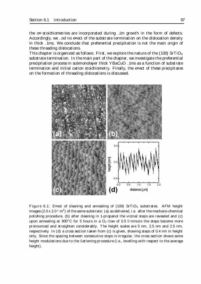
Section 6.1 Introduction 97
the o¤-stoichiometries are incorporated during …lm growth in the form of defects.Accordingly, we …nd no e¤ect of the substrate termination on the dislocation densityin thick …lms. We conclude that preferential precipitation is not the main origin ofthese threading dislocations.This chapter is organized as follows. First, we explore the nature of the (100) SrTiO3
substrate termination. In the main part of the chapter, we investigate the preferentialprecipitation process in submonolayer thick YBaCuO …lms as a function of substratetermination and initial cation stoichiometry. Finally, the e¤ect of these precipitateson the formation of threading dislocations is discussed.
Figure 6.1: E¤ect of cleaning and annealing of (100) SrTiO3 substrates. AFM heightimages (2.0 x 2.0 ¹m2) of the same substrate: (a) as delivered, i.e. after the mechano-chemicalpolishing procedure, (b) after cleaning in 1-propanol the vicinal steps are revealed and (c)upon annealing at 900±C for 5 hours in a O2-‡ow of 0.5 l/minute the steps become morepronounced and straighten considerably. The height scales are 5 nm, 2.5 nm and 2.5 nm,respectively. In (d) a cross section taken from (c) is given, showing steps of 0.4 nm in heightonly. Since the spacing between consecutive steps is irregular, the cross section shows someheight modulations due to the ‡attening procedure (i.e., levelling with respect to the averageheight).
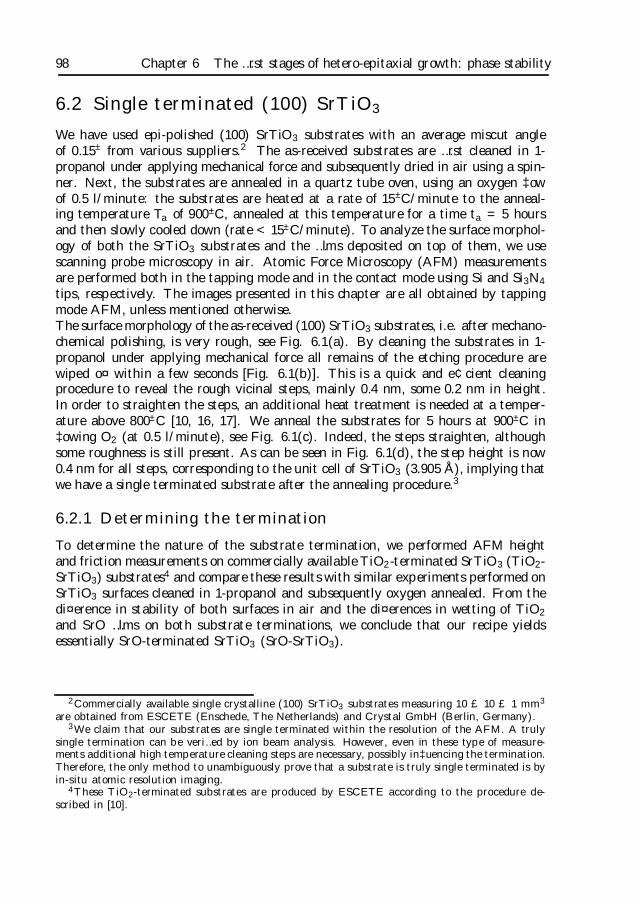
98 Chapter 6 The …rst stages of hetero-epitaxial growth: phase stability
6.2 Single terminated (100) SrTiO3
We have used epi-polished (100) SrTiO3 substrates with an average miscut angleof 0.15± from various suppliers.2 The as-received substrates are …rst cleaned in 1-propanol under applying mechanical force and subsequently dried in air using a spin-ner. Next, the substrates are annealed in a quartz tube oven, using an oxygen ‡owof 0.5 l/minute: the substrates are heated at a rate of 15±C/minute to the anneal-ing temperature Ta of 900±C, annealed at this temperature for a time ta = 5 hoursand then slowly cooled down (rate < 15±C/minute). To analyze the surface morphol-ogy of both the SrTiO3 substrates and the …lms deposited on top of them, we usescanning probe microscopy in air. Atomic Force Microscopy (AFM) measurementsare performed both in the tapping mode and in the contact mode using Si and Si3N4
tips, respectively. The images presented in this chapter are all obtained by tappingmode AFM, unless mentioned otherwise.The surface morphology of the as-received (100) SrTiO3 substrates, i.e. after mechano-chemical polishing, is very rough, see Fig. 6.1(a). By cleaning the substrates in 1-propanol under applying mechanical force all remains of the etching procedure arewiped o¤ within a few seconds [Fig. 6.1(b)]. This is a quick and e¢cient cleaningprocedure to reveal the rough vicinal steps, mainly 0.4 nm, some 0.2 nm in height.In order to straighten the steps, an additional heat treatment is needed at a temper-ature above 800±C [10, 16, 17]. We anneal the substrates for 5 hours at 900±C in‡owing O2 (at 0.5 l/minute), see Fig. 6.1(c). Indeed, the steps straighten, althoughsome roughness is still present. As can be seen in Fig. 6.1(d), the step height is now0.4 nm for all steps, corresponding to the unit cell of SrTiO3 (3.905 Å), implying thatwe have a single terminated substrate after the annealing procedure.3
6.2.1 Determining the termination
To determine the nature of the substrate termination, we performed AFM heightand friction measurements on commercially available TiO2-terminated SrTiO3 (TiO2-SrTiO3) substrates4 and compare these results with similar experiments performed onSrTiO3 surfaces cleaned in 1-propanol and subsequently oxygen annealed. From thedi¤erence in stability of both surfaces in air and the di¤erences in wetting of TiO2
and SrO …lms on both substrate terminations, we conclude that our recipe yieldsessentially SrO-terminated SrTiO3 (SrO-SrTiO3).
2Commercially available single crystalline (100) SrTiO3 substrates measuring 10 £ 10 £ 1 mm3
are obtained from ESCETE (Enschede, The Netherlands) and Crystal GmbH (Berlin, Germany).3We claim that our substrates are single terminated within the resolution of the AFM. A truly
single termination can be veri…ed by ion beam analysis. However, even in these type of measure-ments additional high temperature cleaning steps are necessary, possibly in‡uencing the termination.Therefore, the only method to unambiguously prove that a substrate is truly single terminated is byin-situ atomic resolution imaging.
4These TiO2-terminated substrates are produced by ESCETE according to the procedure de-scribed in [10].
Section 6.2 Single terminated (100) SrTiO3 99
Figure 6.2: Simultaneously recorded AFM contact mode height (left, height scale 2.5nm) and friction (right, full scale 0.05 V) images of two (100) SrTiO3 substrates: (a,b)TiO2-terminated and (c,d) 1-propanol cleaned and subsequently annealed at 900±C for 5hours in an O2-‡ow. The scan size is 1.0 ¹m; both the scan conditions and the image con-ditions (color table, contrast, etc.) are the same for all images. All vicinal steps are 0.4 nmin height, including the holes in the TiO2-terminated substrate.
Friction measurementsAFM friction measurements in principle provide a tool to determine the substratetermination [18]. In Fig. 6.2, the results of contact mode AFM measurements onboth type of substrates are shown. The scan conditions, including the tip, are exactlythe same. Both substrates were scanned directly after each other. In both heightimages [Fig. 6.2(a,c)] only vicinal steps of 0.4 nm in height are discerned. This wasrecon…rmed by tapping mode AFM measurements. Probably, the 1 unit cell deepholes in the TiO2-terminated substrate [Fig. 6.2(a,b)] are not annihilated duringannealing, because the annealing time ta for this very low miscut substrate (< 0.05±)was too short. Because we do not observe any friction contrast within each image[Fig. 6.2(b,d)], both substrates are characterized by a single terminating layer.
100 Chapter 6 The …rst stages of hetero-epitaxial growth: phase stability
As the vicinal steps can be more clearly discerned in the upper images, the resultssuggest that there is a di¤erence between the two types of substrates. However, thismay also be an e¤ect of the tip wearing out. In fact, this is exactly the problem indetermining the substrate termination by friction: absolute friction measurements areextremely di¢cult to obtain. Therefore, we can not conclude which termination isassociated with the larger friction force. Moreover, in literature con‡icting results arepresented. High friction domains are associated both with the TiO2 surface [10] andwith the SrO surface [9, 13, 18]. Although AFM friction measurements are a usefultool in proving that a substrate is single terminated, we conclude that it is not a goodmethod to determine the surface layer in case of a single substrate termination.
Aging e¤ectsSince SrO and TiO2 are chemically very di¤erent, we examine the stability of thesurface of both types of substrates in air, see Fig. 6.3. We …nd that TiO2-terminatedsubstrates are not a¤ected by storage in air at least for a period of several months,see Fig. 6.3(a). This is in sharp contrast with the substrates treated with 1-propanoland subsequently annealed. As seen in Fig. 6.3(b,c,d), the surface degrades with time(note the larger height scales). Since TiO2 is known to be stable in air [19] and SrOis not, we conclude that the termination of these substrates is SrO.Another example of surface degradation is shown in Fig. 6.4 for a substrate with adual termination. In the cross section in Fig. 6.4(b) steps of 0.2 nm in height can bediscerned. We note that a dual termination is rarely observed after our 1-propanolcleaning and annealing treatment. Apparently, the annealing time is too short forthis speci…c substrate to yield a single termination. Based on the previous results,we expect that the termination covering most of the surface is SrO. After storing thissubstrate in air for 2 months, we indeed …nd that the substrate termination coveringmost of the surface has roughened, whereas the remaining area did not deteriorate,see Fig. 6.4(c) [note the larger height scale]. This con…rms that SrO is unstable inair.In literature, it has been suggested that SrO reacts with water [9, 15], possibly trans-forming into a Sr-hydroxyl complex [10]. The a¢nity of SrO for H2O can be under-stood, if one realizes that the surface layer relaxes (rumpling). This rumpling causesthe surface to polarize. Both shell model calculations [20, 21, 22] and …rst princi-ples total energy calculations [23, 24] predict such a surface relaxation, although thedetails di¤er. Experimentally, it was recently found [25] that only the SrO surface ex-hibits a signi…cant inward relaxation (of the Sr atoms). As a result, the H2O molecules(dipoles) are electrostatically attracted by the SrO surface, causing a higher reactivitywith the SrO surface than with the TiO2 surface. In order to verify the a¢nity for wa-ter, we soaked both type of substrates in H2O. Since we observed a quick degradationof the SrO-terminated substrates, whereas the TiO2-terminated substrates remaineduna¤ected we conclude that the aging e¤ects are caused by water.
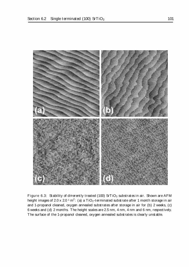
Section 6.2 Single terminated (100) SrTiO3 101
Figure 6.3: Stability of di¤erently treated (100) SrTiO3 substrates in air. Shown are AFMheight images of 2.0 x 2.0 ¹m2: (a) a TiO2-terminated substrate after 1 month storage in airand 1-propanol cleaned, oxygen annealed substrates after storage in air for (b) 2 weeks, (c)6 weeks and (d) 2 months. The height scales are 2.5 nm, 4 nm, 4 nm and 6 nm, respectively.The surface of the 1-propanol cleaned, oxygen annealed substrates is clearly unstable.
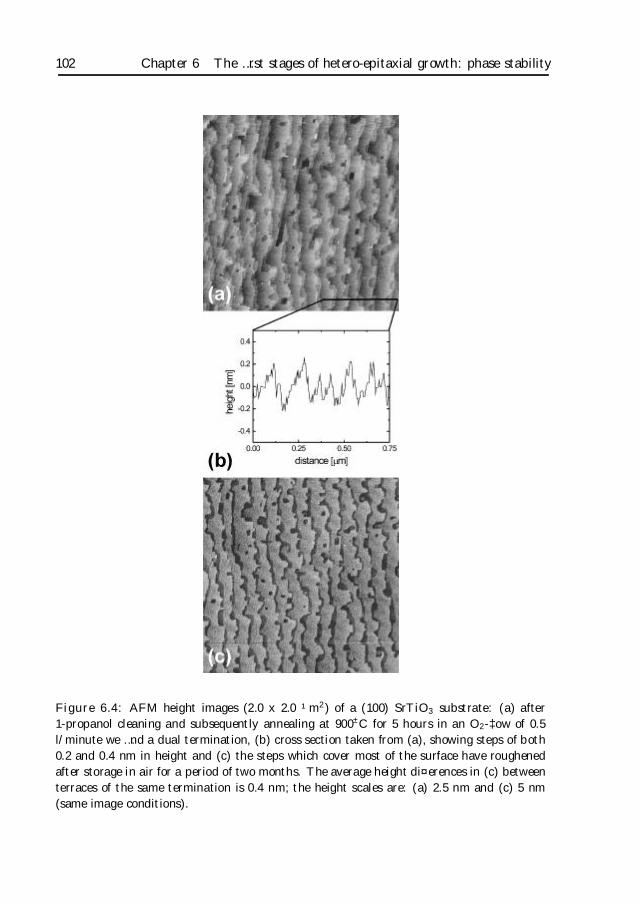
102 Chapter 6 The …rst stages of hetero-epitaxial growth: phase stability
Figure 6.4: AFM height images (2.0 x 2.0 ¹m2) of a (100) SrTiO3 substrate: (a) after1-propanol cleaning and subsequently annealing at 900±C for 5 hours in an O2-‡ow of 0.5l/minute we …nd a dual termination, (b) cross section taken from (a), showing steps of both0.2 and 0.4 nm in height and (c) the steps which cover most of the surface have roughenedafter storage in air for a period of two months. The average height di¤erences in (c) betweenterraces of the same termination is 0.4 nm; the height scales are: (a) 2.5 nm and (c) 5 nm(same image conditions).
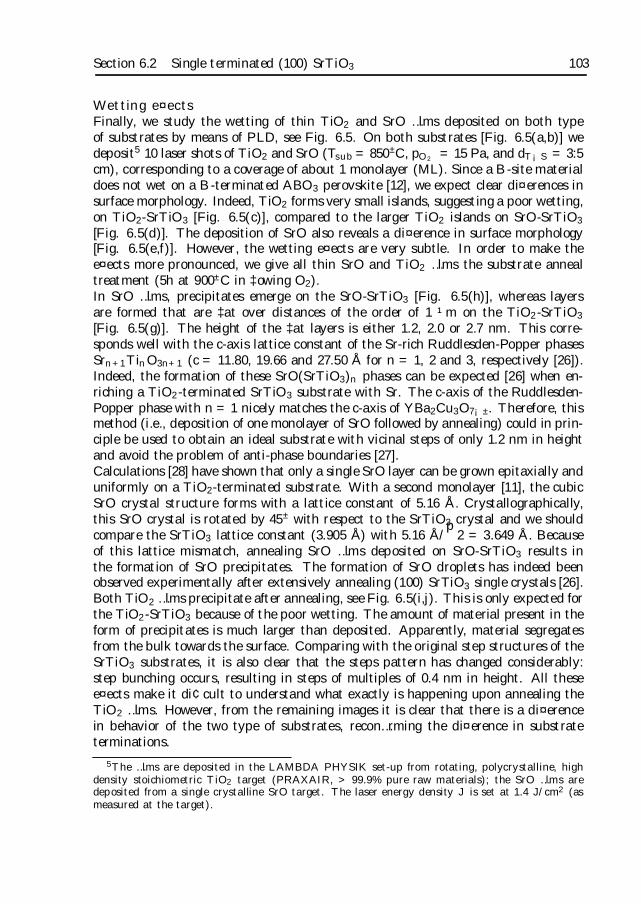
Section 6.2 Single terminated (100) SrTiO3 103
Wetting e¤ectsFinally, we study the wetting of thin TiO2 and SrO …lms deposited on both typeof substrates by means of PLD, see Fig. 6.5. On both substrates [Fig. 6.5(a,b)] wedeposit5 10 laser shots of TiO2 and SrO (Tsub = 850±C, pO2 = 15 Pa, and dT¡S = 3:5cm), corresponding to a coverage of about 1 monolayer (ML). Since a B-site materialdoes not wet on a B-terminated ABO3 perovskite [12], we expect clear di¤erences insurface morphology. Indeed, TiO2 forms very small islands, suggesting a poor wetting,on TiO2-SrTiO3 [Fig. 6.5(c)], compared to the larger TiO2 islands on SrO-SrTiO3
[Fig. 6.5(d)]. The deposition of SrO also reveals a di¤erence in surface morphology[Fig. 6.5(e,f)]. However, the wetting e¤ects are very subtle. In order to make thee¤ects more pronounced, we give all thin SrO and TiO2 …lms the substrate annealtreatment (5h at 900±C in ‡owing O2).In SrO …lms, precipitates emerge on the SrO-SrTiO3 [Fig. 6.5(h)], whereas layersare formed that are ‡at over distances of the order of 1 ¹m on the TiO2-SrTiO3
[Fig. 6.5(g)]. The height of the ‡at layers is either 1.2, 2.0 or 2.7 nm. This corre-sponds well with the c-axis lattice constant of the Sr-rich Ruddlesden-Popper phasesSrn+1TinO3n+1 (c = 11.80, 19.66 and 27.50 Å for n = 1, 2 and 3, respectively [26]).Indeed, the formation of these SrO(SrTiO3)n phases can be expected [26] when en-riching a TiO2-terminated SrTiO3 substrate with Sr. The c-axis of the Ruddlesden-Popper phase with n = 1 nicely matches the c-axis of YBa2Cu3O7¡±. Therefore, thismethod (i.e., deposition of one monolayer of SrO followed by annealing) could in prin-ciple be used to obtain an ideal substrate with vicinal steps of only 1.2 nm in heightand avoid the problem of anti-phase boundaries [27].Calculations [28] have shown that only a single SrO layer can be grown epitaxially anduniformly on a TiO2-terminated substrate. With a second monolayer [11], the cubicSrO crystal structure forms with a lattice constant of 5.16 Å. Crystallographically,this SrO crystal is rotated by 45± with respect to the SrTiO3 crystal and we shouldcompare the SrTiO3 lattice constant (3.905 Å) with 5.16 Å/
p2 = 3.649 Å. Because
of this lattice mismatch, annealing SrO …lms deposited on SrO-SrTiO3 results inthe formation of SrO precipitates. The formation of SrO droplets has indeed beenobserved experimentally after extensively annealing (100) SrTiO3 single crystals [26].Both TiO2 …lms precipitate after annealing, see Fig. 6.5(i,j). This is only expected forthe TiO2-SrTiO3 because of the poor wetting. The amount of material present in theform of precipitates is much larger than deposited. Apparently, material segregatesfrom the bulk towards the surface. Comparing with the original step structures of theSrTiO3 substrates, it is also clear that the steps pattern has changed considerably:step bunching occurs, resulting in steps of multiples of 0.4 nm in height. All thesee¤ects make it di¢cult to understand what exactly is happening upon annealing theTiO2 …lms. However, from the remaining images it is clear that there is a di¤erencein behavior of the two type of substrates, recon…rming the di¤erence in substrateterminations.
5The …lms are deposited in the LAMBDA PHYSIK set-up from rotating, polycrystalline, highdensity stoichiometric TiO2 target (PRAXAIR, > 99.9% pure raw materials); the SrO …lms aredeposited from a single crystalline SrO target. The laser energy density J is set at 1.4 J/cm2 (asmeasured at the target).
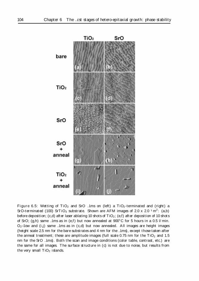
104 Chapter 6 The …rst stages of hetero-epitaxial growth: phase stability
Figure 6.5: Wetting of TiO2 and SrO …lms on (left) a TiO2-terminated and (right) aSrO-terminated (100) SrTiO3 substrate. Shown are AFM images of 2.0 x 2.0 ¹m2: (a,b)before deposition; (c,d) after laser ablating 10 shots of TiO2; (e,f) after deposition of 10 shotsof SrO; (g,h) same …lms as in (e,f ) but now annealed at 900±C for 5 hours in a 0.5 l/min.O2-‡ow and (i,j) same …lms as in (c,d) but now annealed. All images are height images(height scale 2.5 nm for the bare substrates and 4 nm for the …lms), except those taken afterthe anneal treatment; these are amplitude images (full scale 0.75 nm for the TiO2 and 1.5nm for the SrO …lms). Both the scan and image conditions (color table, contrast, etc.) arethe same for all images. The surface structure in (c) is not due to noise, but results fromthe very small TiO2 islands.
Section 6.3 Preferential precipitation of YBaCuO 105
6.2.2 SrO-terminated substrates
Alternative routes for preparing SrO-terminated SrTiO3 substrates all make use ofTiO2-terminated substrates. Two in-situ methods can be followed to convert thetermination into SrO:
1. Deposition of SrO [11, 12, 13]. Indeed, one monolayer SrO can be grownepitaxially on TiO2-SrTiO3 [11]. As mentioned above, a second SrO monolayerforms the cubic SrO crystal structure [28] together with the …rst monolayer.Therefore, not only the lattice matching between …lm and substrate will bein‡uenced by using more than one monolayer of SrO as a bu¤er layer, but alsoprecipitates may form [11, 26] which strongly deteriorate the substrate surfacemorphology.
2. Deposition of SrTiO3. From literature [5, 14, 15] it appears that the termi-nating layer of SrTiO3 …lms is SrO, suggesting that homo-epitaxial growth ofSrTiO3 can be used to produce a SrO-terminated substrate. However, Naka-mura et al. [6] report that TiO2 is the main terminating layer of the SrTiO3
and show that the stable surface layer in fact depends both on the depositiontechnique and the deposition conditions used [29]. Therefore, one should becareful when using this method, as it does not necessarily yield the desiredsubstrate termination.
In both cases it is crucial to deposit (multiples of) one monolayer. In practice this canonly be realized by in-situ monitoring the growth process by means of Re‡ection High-Energy Electron Di¤raction (RHEED). Apart from the fact that one more depositionstep is needed, deposition of the bu¤er layer may require deposition conditions whichare in con‡ict with the …lm deposition conditions. Clearly, both in-situ methods havedisadvantages compared to our ex-situ method to produce SrO-terminated substrates.In fact, we can directly compare method 1 with our ex-situ method [Figs. 6.5(e) vs.(b)]. Although our AFM measurements are performed ex-situ, we believe that thestarting situation for thin …lm deposition is much better de…ned using our process.
6.3 Preferential precipitation of YBaCuO
In this section, we investigate preferential precipitation in YBaCuO …lms as a functionof the substrate termination and initial cation stoichiometry of the …lm. Before takinga look at the di¤erences in hetero-epitaxial growth on TiO2 and SrO-terminated (100)SrTiO3 substrates, we …rst review some general aspects of YBa2Cu3O7¡± …lm growth.Next, the experimental results are presented. Finally, a new stacking sequence modelfor the …rst monolayer of YBaCuO is proposed which accounts for the experimentalobservations.
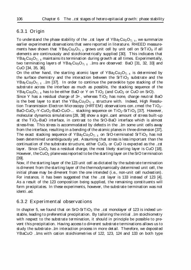
106 Chapter 6 The …rst stages of hetero-epitaxial growth: phase stability
6.3.1 Origin
To understand the phase stability of the …rst layer of YBa2Cu3O7¡±, we summarizeearlier experimental observations that were reported in literature. RHEED measure-ments have shown that YBa2Cu3O7¡± grows unit cell by unit cell on SrTiO3 if allelements are continuously and stoichiometrically supplied [30]. This indicates thatYBa2Cu3O7¡± maintains its termination during growth at all times. Experimentally,two terminating layers of YBa2Cu3O7¡± …lms are observed: BaO [31, 32, 33] andCuO [34, 35, 36].On the other hand, the starting atomic layer of YBa2Cu3O7¡± is determined bythe surface chemistry and the interaction between the SrTiO3 substrate and theYBa2Cu3O7¡± …lm [37]. In order to continue the perovskite type stacking of thesubstrate across the interface as much as possible, the stacking sequence of theYBa2Cu3O7¡± has to be either BaO or Y on TiO2 (and CuO2 or CuO on SrO).Since Y has a residual charge of 3+, whereas TiO2 has none, charge neutral BaOis the best layer to start the YBa2Cu3O7¡± structure with. Indeed, High Resolu-tion Transmission Electron Microscopy (HRTEM) observations con…rmed the TiO2-BaO-CuO2-Y-CuO2-BaO-CuO-... stacking sequence on TiO2-SrTiO3 [37]. However,molecular dynamics simulations [28, 38] show a signi…cant amount of stress built-upat the TiO2-BaO interface, in contrast to the SrO-BaO interface which is almoststress-free. This stress is accommodated by defects in the …lm some unit cells awayfrom the interface, resulting in a bending of the atomic planes in three dimension [37].The exact stacking sequence of YBa2Cu3O7¡± on SrO-terminated SrTiO3 has notbeen determined unambiguously yet. Assuming that stress is less important than thecontinuation of the substrate structure, either CuO2 or CuO is expected as the …rstlayer. Since CuO2 has a residual charge, the most likely starting layer is CuO [18].However, the CuO2 plane was reported to be the starting layer on the SrO termination[39].Now, if the starting layer of the 123 unit cell as dictated by the substrate terminationis di¤erent from the starting layer of the thermodynamically determined unit cell, theinitial phase may be di¤erent from the one intended (i.e., non-unit cell nucleation).For instance, it has been suggested that the …rst layer is 133 instead of 123 [4].As a result of the 123 composition being supplied, the remaining constituents willform precipitates. In these experiments, however, the substrate termination was notidenti…ed.
6.3.2 Experimental observations
In chapter 5, we found that on SrO-SrTiO3 the …rst monolayer of 123 is indeed un-stable, leading to preferential precipitation. By tailoring the initial …lm stoichiometrywith respect to the substrate termination, it should in principle be possible to pre-vent this precipitation. Having access to di¤erent substrate terminations allows us tostudy the substrate-…lm interaction process in more detail. Therefore, we depositedYBaCuO …lms with cation stoichiometries of 122, 123, 124 and 133 on both type
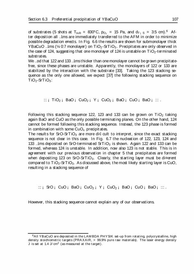
Section 6.3 Preferential precipitation of YBaCuO 107
of substrates (5 shots at Tsub = 830±C, pO2 = 15 Pa, and dT¡S = 3:5 cm).6 Af-ter deposition all …lms are immediately transferred to the AFM in order to minimizepossible degradation e¤ects. In Fig. 6.6 the results are shown for submonolayer thickYBaCuO …lms (¼ 0:7 monolayer) on TiO2-SrTiO3. Precipitates are only observed inthe case of 124, suggesting that one monolayer of 124 is unstable on TiO2-terminatedsubstrates.We …nd that 122 and 133 …lms thicker than one monolayer cannot be grown precipitate-free, since these phases are unstable. Apparently, the monolayers of 122 or 133 arestabilized by the interaction with the substrate [33]. Taking the 123 stacking se-quence as the only one allowed, we expect [37] the following stacking sequence onTiO2-SrTiO3:
::: ¡ TiO2 ¡ BaO ¡ CuO2 ¡ Y ¡ CuO2 ¡ BaO ¡ CuO ¡ BaO ¡ ::: .
Following this stacking sequence 122, 123 and 133 can be grown on TiO2 takingagain BaO and CuO as the only possible terminating planes. On the other hand, 124cannot be formed following this stacking sequence. Instead, the 123 phase is formedin combination with some CuOx precipitates.The results for SrO-SrTiO3 are more di¢cult to interpret, since the exact stackingsequence is not clear in this case. In Fig. 6.7 the nucleation of 122, 123, 124 and133 …lms deposited on SrO-terminated SrTiO3 is shown. Again 122 and 133 can beformed, whereas 124 is unstable. In addition, now also 123 is not stable. This is inagreement with our previous observation in chapter 5 that precipitates are formedwhen depositing 123 on SrO-SrTiO3. Clearly, the starting layer must be di¤erentcompared to TiO2-SrTiO3. As discussed above, the most likely starting layer is CuO,resulting in a stacking sequence of
::: ¡ SrO ¡ CuO ¡ BaO ¡ CuO2 ¡ Y ¡ CuO2 ¡ BaO ¡ CuO ¡ BaO ¡ ::: .
However, this stacking sequence cannot explain any of our observations.
6All YBaCuO are deposited in the LAMBDA PHYSIK set-up from rotating, polycrystalline, highdensity stoichiometric targets (PRAXAIR, > 99.9% pure raw materials). The laser energy densityJ is set at 1.4 J/cm2 (as measured at the target).
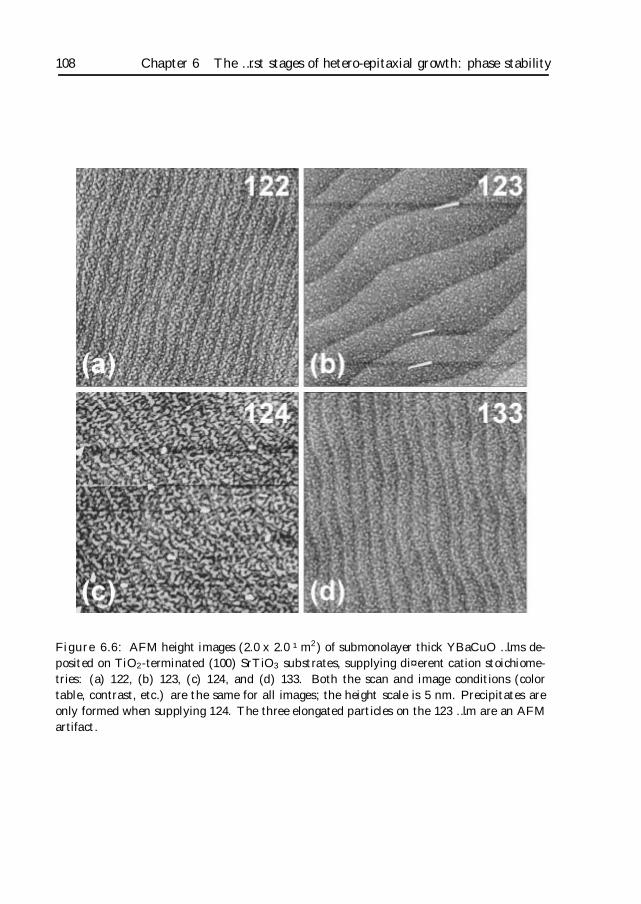
108 Chapter 6 The …rst stages of hetero-epitaxial growth: phase stability
Figure 6.6: AFM height images (2.0 x 2.0 ¹m2) of submonolayer thick YBaCuO …lms de-posited on TiO2-terminated (100) SrTiO3 substrates, supplying di¤erent cation stoichiome-tries: (a) 122, (b) 123, (c) 124, and (d) 133. Both the scan and image conditions (colortable, contrast, etc.) are the same for all images; the height scale is 5 nm. Precipitates areonly formed when supplying 124. The three elongated particles on the 123 …lm are an AFMartifact.
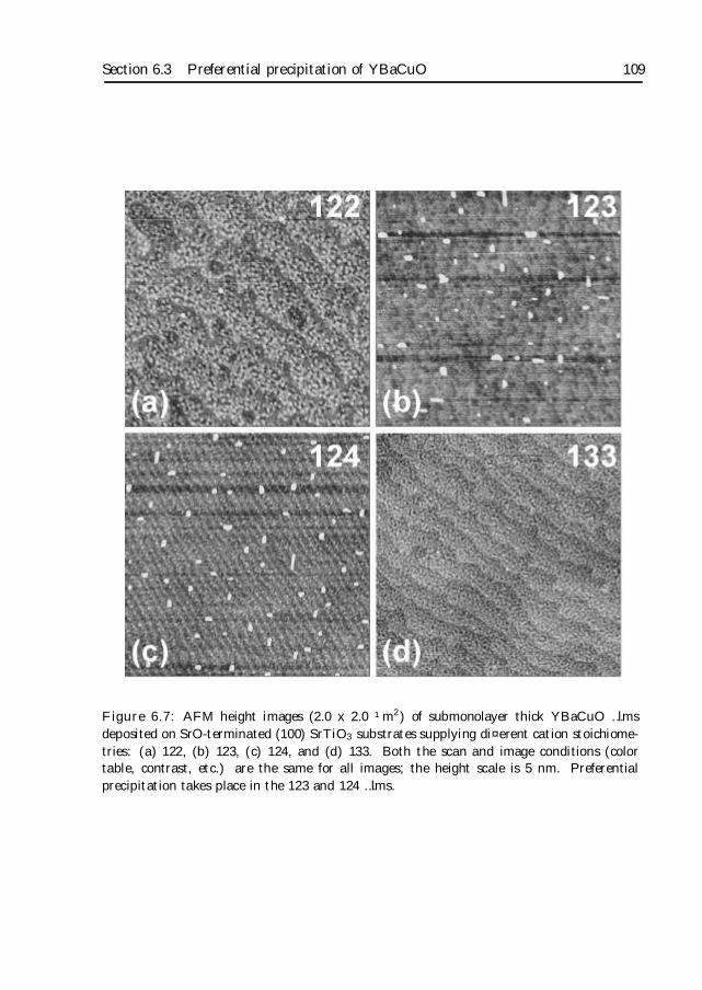
Section 6.3 Preferential precipitation of YBaCuO 109
Figure 6.7: AFM height images (2.0 x 2.0 ¹m2) of submonolayer thick YBaCuO …lmsdeposited on SrO-terminated (100) SrTiO3 substrates supplying di¤erent cation stoichiome-tries: (a) 122, (b) 123, (c) 124, and (d) 133. Both the scan and image conditions (colortable, contrast, etc.) are the same for all images; the height scale is 5 nm. Preferentialprecipitation takes place in the 123 and 124 …lms.
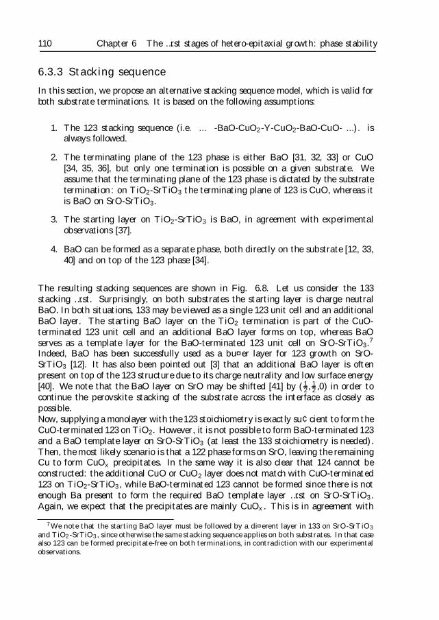
110 Chapter 6 The …rst stages of hetero-epitaxial growth: phase stability
6.3.3 Stacking sequence
In this section, we propose an alternative stacking sequence model, which is valid forboth substrate terminations. It is based on the following assumptions:
1. The 123 stacking sequence (i.e. ... -BaO-CuO2-Y-CuO2-BaO-CuO- ...). isalways followed.
2. The terminating plane of the 123 phase is either BaO [31, 32, 33] or CuO[34, 35, 36], but only one termination is possible on a given substrate. Weassume that the terminating plane of the 123 phase is dictated by the substratetermination : on TiO2-SrTiO3 the terminating plane of 123 is CuO, whereas itis BaO on SrO-SrTiO3.
3. The starting layer on TiO2-SrTiO3 is BaO, in agreement with experimentalobservations [37].
4. BaO can be formed as a separate phase, both directly on the substrate [12, 33,40] and on top of the 123 phase [34].
The resulting stacking sequences are shown in Fig. 6.8. Let us consider the 133stacking …rst. Surprisingly, on both substrates the starting layer is charge neutralBaO. In both situations, 133 may be viewed as a single 123 unit cell and an additionalBaO layer. The starting BaO layer on the TiO2 termination is part of the CuO-terminated 123 unit cell and an additional BaO layer forms on top, whereas BaOserves as a template layer for the BaO-terminated 123 unit cell on SrO-SrTiO3.7
Indeed, BaO has been successfully used as a bu¤er layer for 123 growth on SrO-SrTiO3 [12]. It has also been pointed out [3] that an additional BaO layer is oftenpresent on top of the 123 structure due to its charge neutrality and low surface energy[40]. We note that the BaO layer on SrO may be shifted [41] by ( 1
2,12 ,0) in order to
continue the perovskite stacking of the substrate across the interface as closely aspossible.Now, supplying a monolayer with the 123 stoichiometry is exactly su¢cient to form theCuO-terminated 123 on TiO2. However, it is not possible to form BaO-terminated 123and a BaO template layer on SrO-SrTiO3 (at least the 133 stoichiometry is needed).Then, the most likely scenario is that a 122 phase forms on SrO, leaving the remainingCu to form CuOx precipitates. In the same way it is also clear that 124 cannot beconstructed: the additional CuO or CuO2 layer does not match with CuO-terminated123 on TiO2-SrTiO3, while BaO-terminated 123 cannot be formed since there is notenough Ba present to form the required BaO template layer …rst on SrO-SrTiO3.Again, we expect that the precipitates are mainly CuOx. This is in agreement with
7We note that the starting BaO layer must be followed by a di¤erent layer in 133 on SrO-SrTiO3
and TiO2-SrTiO3, since otherwise the same stacking sequence applies on both substrates. In that casealso 123 can be formed precipitate-free on both terminations, in contradiction with our experimentalobservations.
Section 6.3 Preferential precipitation of YBaCuO 111
Figure 6.8: Proposed stacking sequences of YBaCuO on TiO2 and SrO-terminated SrTiO3
substrates supplying the cation stoichiometries 122, 123, 124, and 133. The 122 struc-ture is stabilized by the substrate, while 133 consist of a monolayer of BaO and eitherCuO-terminated 123 (on TiO2-SrTiO3) or BaO-terminated 123 (SrO-SrTiO3).
112 Chapter 6 The …rst stages of hetero-epitaxial growth: phase stability
what is usually observed [33, 42, 43]. Moreover, more precipitates are expected for124 on SrO than for both 123 on SrO and 124 on TiO2. Comparing the appropriate…gures, this indeed seems to be the case.Finally, we stress that one should be careful in drawing conclusions concerning thestacking sequence from AFM measurements only. In any case, it is clear that thenucleation of YBaCuO depends strongly on both the termination of the substrateand the initial composition that is supplied. Hence, careful preparation as well ascharacterization of substrates down to the atomic scale are extremely important.In fact, many controversies in literature may be related to di¤erences in substrateterminations (SrO, TiO2 or dual) or even poor substrate quality.
In summary, we can prevent preferential precipitation in submonolayer thick YBaCuO…lms by manipulating both the substrate termination and the initial …lm composition.On TiO2-terminated surfaces the starting layer as dictated by the substrate and thestarting layer of the 123 phase are the same, resulting in the absence of precipitates.On SrO-terminated substrates, precipitation of 123 may be prevented by depositing122 or 133, prior to the actual 123 deposition.
6.4 E¤ect on threading dislocations
The original purpose of our investigation of the preferential precipitation in the …rststages of growth was to …nd a way to prevent or manipulate the formation of thread-ing dislocations in 123. Disappointingly, we …nd no relation between the dislocationdensity and substrate termination used. Although preferential precipitation is ob-served on SrO-terminated substrates, these precipitates do not result in an enhanceddislocation density. On the other hand, in chapter 5 we have shown that precipitates(in this case Y2O3) can induce dislocations. This paradox may be explained by thedi¤erence between the interface region of thick 123 …lms and the very thin …lms dis-cussed here. While in the former case there is a continuous supply of material, herethe growth process is stopped, allowing the di¤using species much more time to reacha more stable con…guration. Apparently, in the thicker …lms the excess material isincorporated in the …lm, most likely in the form of point defects and stacking faults.This explanation also accounts for the absence of precipitates at the interface in ourcross sectional Transmission Electron Microscope (TEM) studies reported in chapter4.To illustrate the dissolution of precipitates during continuous deposition, we deposited123 …lms (15 shots, about 2 ML thick) on a TiO2 and a SrO-terminated substrate.The substrate and …lm morphologies are shown in Fig. 6.9. In both …lms no signof preferential precipitation is observed. Yet, a signi…cant di¤erence in precipitatedensity was shown for thin layers in the previous section. Therefore, there must beexcess Cu in the 123 …lm on SrO-SrTiO3. Indeed, there is a subtle di¤erence in thesurface morphology of the two …lms, see Fig. 6.9(b,d). While the YBaCuO nicelyreproduces the step structure of the TiO2-terminated substrate, the vicinal stepson the SrO-terminated substrates can no longer be discerned. As will be shown in
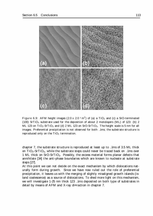
Section 6.5 Conclusions 113
Figure 6.9: AFM height images (2.0 x 2.0 ¹m2) of (a) a TiO2 and (c) a SrO-terminated(100) SrTiO3 substrate used for the deposition of about 2 monolayers (ML) of 123: (b) 2ML 123 on TiO2-SrTiO3 and (d) 2 ML 123 on SrO-SrTiO3. The height scale is 5 nm for allimages. Preferential precipitation is not observed for both …lms; the substrate structure isreproduced only on the TiO2 termination.
chapter 7, the substrate structure is reproduced at least up to …lms of 3.5 ML thickon TiO2-SrTiO3, while the substrate steps could never be traced back on …lms over1 ML thick on SrO-SrTiO3. Possibly, the excess material forms planar defects thatannihilate [34] the anti-phase boundaries which are known to nucleate at substratesteps [27].At this point we can not decide on the exact mechanism by which dislocations nat-urally form during growth. Since we have now ruled out the role of preferentialprecipitation, it leaves us with the merging of slightly misaligned growth islands (is-land coalescence) as a source of dislocations. To shed more light on this mechanism,we will investigate 1-25 nm thick 123 …lms deposited on both type of substrates indetail by means of AFM and X-ray di¤raction in chapter 7.
114 Chapter 6 The …rst stages of hetero-epitaxial growth: phase stability
6.5 Conclusions
We investigate preferential precipitation and the formation of threading dislocationsin YBa2Cu3O7¡± (123) …lms deposited on (100) SrTiO3. Since the SrTiO3 substrateo¤ers two possible terminations as a starting condition for …lm growth, we comparecommercially available TiO2-terminated substrates with SrO-terminated substratesproduced by our newly developed ex-situ method.We …nd that the …rst stages of hetero-epitaxial growth depend strongly on the sub-strate termination. In particular, precipitate-free 123 monolayers are only obtainedon TiO2-terminated SrTiO3 substrates. Our results suggest that the terminatingplane of the 123 phase on TiO2-terminated SrTiO3 is CuO, while BaO-terminated123 forms on the SrO substrate termination. However, on both substrates the startinglayer of the 123 phase is BaO. Therefore, when supplying a 123 cation stoichiome-try, CuO-terminated 123 nucleates on TiO2, whereas BaO-terminated 123 can notbe formed on SrO-SrTiO3. Instead, a 122 phase forms together with precipitates.However, by supplying a 133 cation composition, …rst a BaO template layer formson which BaO-terminated 123 nucleates precipitate-free. Clearly, precipitation de-pends both on the substrate termination and the initial cation stoichiometry that issupplied.Since arti…cially induced precipitates increase the dislocation density in our …lms, aprecipitation process which occurs preferentially in the …rst monolayer would explainthe high density of dislocations running from the interface to the YBa2Cu3O7¡± …lmsurface parallel to the c-axis. Yet, we …nd that the dislocation structure of the 123 …lmdoes not depend on the substrate termination. Apparently, preferential precipitationis not the mechanism of dislocation formation. It appears that precipitation of the 123…lms on the SrO termination is characteristic for ultra-thin …lms up to approximately 1monolayer in thickness. When growing thicker …lms, excess species are incorporated inthe …lm as point and planar defects and may play an important role in the annihilationof anti-phase boundaries. This will be investigated extensively in the next chapter.
References
[1] B. Stäuble-Pümpin, V.C. Matijasevic, B. Ilge, J.E. Mooij, W.J.A.M. Peterse,P.M.L.O. Scholte, F. Tuinstra, H.J. Venvik, D.S. Wai, C. Træholt, J.G. Wen,and H.W. Zandbergen, Phys. Rev. B 52 (1995) 7064
[2] D.G. Schlom, D. Anselmetti, J.G. Bednorz, Ch. Gerber, and J. Mannhart, J.Cryst. Growth 137 (1994) 259
[3] J.G. Wen, T. Morishita, N. Koshizuka, C. Traeholt, and H.W. Zandbergen,Appl. Phys. Lett. 66 (1995) 1830
[4] V.C. Matijasevic, B. Ilge, B. Stäuble-Pümpin, G. Rietveld, F. Tuinstra, andJ.E. Mooij, Phys. Rev. Lett. 76 (1996) 4765
[5] M. Kawasaki, K. Takahashi, T. Maeda, R. Tsuchiya, M. Shinohara, O. Ishiyama,T. Yonezawa, M. Yoshimoto, and H. Koinuma, Science 266 (1994) 1540
References 115
[6] T. Nakamura, H. Inada, and M. Ilyama, Jpn. J. Appl. Phys. 36 (1997) 90
[7] A. Ikeda, T. Nishimura, T. Morishita, Y. Kido, Surf. Sci. 433-435 (1999) 520
[8] T. Nishimura, A. Ikeda, H. Namba, T. Morishita, and Y. Kido, Surf. Sci. 421(1999) 237
[9] K. Iwahori, S. Watanabe, T. Komeda, M. Kawai, A. Saito, Y. Kuwahara, andM. Aono, Jpn. J. Appl. Phys. 38 (1999) 3946
[10] G. Koster, B.L. Kropman, G.J.H.M. Rijnders, D.H.A. Blank, and H. Rogalla,Appl. Phys. Lett. 73 (1998) 2920
[11] H. Nishikawa, M. Kanai, and T. Kawai, J. Cryst. Growth 179 (1997) 467
[12] R. Tsuchiya, M. Kawasaki, H. Kubota, J. Nishino, H. Sato, H. Akoh, and H.Koinuma, Appl. Phys. Lett. 71 (1997) 1570
[13] H. Tanaka, H. Tabata, and T. Kawai, Thin Solid …lms 342 (1999) 4
[14] S. Gonda, H. Nagata, M. Kawasaki, M. Yoshimoto, and H. Koinuma, PhysicaC 216 (1993) 160
[15] M. Yoshimoto, T. Maeda, K. Shimozono, H. Koinuma, M. Shinohara, KazuhiroEndo, Appl. Phys. Lett. 65 (1994) 3197
[16] R. Sum, H.P. Lang, and H.J. Günterodt, Physica C 242 (1995) 174
[17] G. Koster, B.L. Kropman, G.J.H.M. Rijnders, D.H.A. Blank, and H. Rogalla,Mat. Sci. Eng. B56 (1998) 209
[18] J. Fompeyrine, R. Berger, H.P. Lang, J. Perret, E. Mächler, Ch. Gerber, andJ.-P. Locquet, Appl. Phys. Lett. 72 (1998) 1697
[19] M. Komiyama and M. Gu, Appl. Surf. Sci. 120 (1997) 125
[20] S.P. Chen, J. Mater. Res. 13 (1998) 1848
[21] J. Prade, U. Schröder, W. Kress, F.W. de Wette, and A.D. Kulkarni, J. Phys.:Condens. Matter 5 (1993) 1
[22] S. Dorfman, D. Fuks, and E. Kotomin, Thin Solid Films 318 (1998) 65
[23] Z.-Q. Li, J.-L. Zhu, C.Q. Wu, Z. Tang, and Y. Kawazoe, Phys. Rev. B 58 (1998)8075
[24] J. Padilla, and D. Vanderbilt, Surf. Sci. 418 (1998) 64
[25] G. Charlton, S. Brennan, C.A. Muryn, R. McGrath, D. Norman, T.S. Turner,and G. Thornton, Surf. Sci. 457 (2000) L376
[26] K. Szot and W. Speier, Phys. Rev. B 60 (1999) 5909
[27] T. Haage, J. Zegenhagen, J.Q. Li, H.-U. Habermeier, M. Cardona, Ch. Jooss,R. Warthmann, A. Forkl, and H. Kronmüller, Phys. Rev. B 56 (1997) 8404
[28] M. Kubo, Y. Oumi, R. Miura, A. Stirling, A. Miyamoto, M. Kawasaki, M.Yoshimoto, and H. Koinuma, Phys. Rev. B 56 (1997) 13535
[29] T. Nakamura, H. Inada, and M. Iiyama, Appl. Surf. Sci. 130-132 (1998) 576
116 Chapter 6 The …rst stages of hetero-epitaxial growth: phase stability
[30] T. Terashima, Y. Bando, K. Iijima, K. Yamamoto, K. Hirata, K. Hayashi, K.Kamigaki and H. Terauchi, Phys. Rev. Lett. 65 (1990) 2684
[31] M. Kawasaki and M. Nantoh, Mater. Res. Bull. XIX (1994) 33
[32] G. Frank, Ch. Ziegler, and W. Gõpel, Phys. Rev. B 43 (1991) 2828
[33] J.-P. Locquet and E. Mächler, Mater. Res. Bull. XIX (1994) 39
[34] K.-i. Shimura, Y. Daitoh, Y. Yano, T. Terashima, Y. Bando, Yuji Matsuda, andS. Komiyama, Physica C 228 (1994) 91
[35] S.J. Pennycook, M.F. Chisholm, D.E. Jesson, R. Feenstra, S. Zhu, X.Y. Zheng,and D.J. Lowndes, Physica C 202 (1992) 1
[36] S. Tanaka, T. Nakamura, M. Iiyama, N. Yoshida, S. Takano, F. Shoji, and K.Oura, Appl. Phys. Lett. 59 (1991) 3637; S. Tanaka, T. Nakamura, H. Tokuda,and M. Iiyama, Appl. Phys. Lett. 62 (1993) 3040
[37] J.C. Wen, C. Traeholt, and H.W. Zandbergen, Physica C 205 (1993) 354
[38] M. Kubo, Y. Oumi, R. Miura, A. Stirling, A. Miyamoto, M. Kawasaki, M.Yoshimoto, and H. Koinuma, J. Chem. Phys. 19 (1998) 8601
[39] R. Ramesh, A. Inam, D.M. Hwang, T.S. Ravi, T. Sands, X.X. Xi, X.D. Wu, Q.Li, T. Venkatesan, and R. Kilaas, J. Mater. Res. 6 (1991) 2264
[40] M. Matsubara, T. Morishita, and I. Hirabayashi, Appl. Phys. Lett. 64 (1994)1868
[41] G. Koster, G. Rijnders, D.H.A. Blank, and H. Rogalla, Physica C 339, 215(2000)
[42] K. Hirata, F. Baudenbacher and H. Kinder, Physica C 214 (1993) 272
[43] N. Kanda, M. Kawasaki, T. Kitajima, and H. Koinuma, Phys. Rev. B 56 (1997)8419
Chapter 7
The …rst stages of hetero-epitaxialgrowth: coherent islanding
An extensive X-ray di¤raction and atomic force microscope study on the e¤ects ofthe two (100) SrTiO3 substrate terminations on the nucleation, growth and defectformation in YBa2Cu3O7¡± …lms is performed. In addition to the di¤erences innucleation observed in chapter 6, we …nd: (i) pseudomorphic 2D growth up to a criticalthickness tc;coh = 7:3 and 19 nm on the SrO and TiO2-termination, respectively, and(ii) coherent 3D islands (i.e., free of mis…t dislocations) at t > tc;coh, which relievepart of the mis…t strain. These results clearly illustrate the importance of interfaceenergy in hetero-epitaxial growth. Furthermore, in-plane XRD measurements reveala characteristic two components line shape. The broad component originates eitherfrom a small coherence length Lk (SrO) or a large tilt angle ®! (TiO2), which appearsto be correlated to the presence of o¤-stoichiometries and anti-phase boundaries,respectively. The narrow component results from a mosaicity limited in magnitudeby the substrate. It is attenuated by the introduction of mis…t dislocations at latergrowth stages (tc;coh < 25 nm < tc;mis). Non-mis…t relieving threading dislocations,which are responsible for the high superconducting critical currents, are introduced atthe edges of the coherent growth islands. Thicker …lms (t À 25 nm) exhibit identicalsurface morphologies and dislocation structures, showing that eventually the samemicrostructure evolves, irrespective of the substrate termination.1
1The central part of this chapter is based on the paper by J.M. Huijbregtse, B. Dam, B.J. Kooi,A. Mendoza, J.H. Rector, J.Th.M. de Hosson, and R. Griessen, to be submitted to Phys. Rev. B
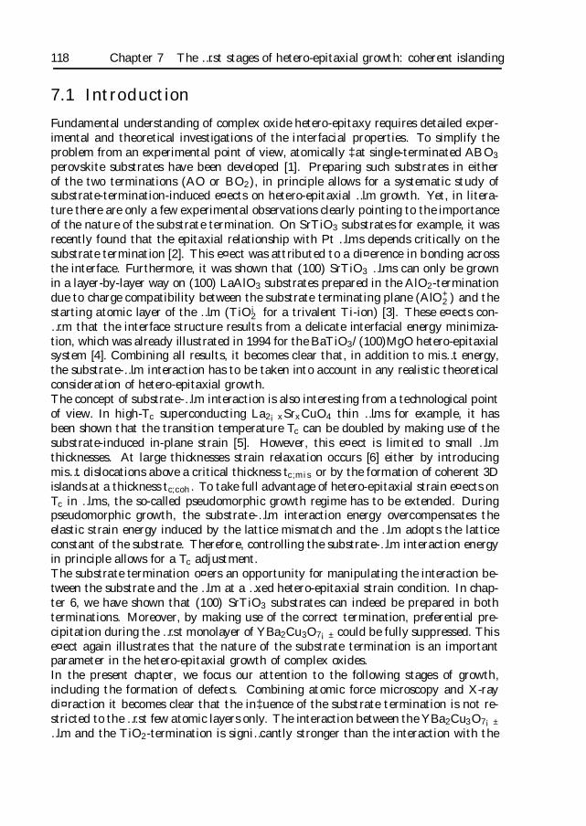
118 Chapter 7 The …rst stages of hetero-epitaxial growth: coherent islanding
7.1 Introduction
Fundamental understanding of complex oxide hetero-epitaxy requires detailed exper-imental and theoretical investigations of the interfacial properties. To simplify theproblem from an experimental point of view, atomically ‡at single-terminated ABO3
perovskite substrates have been developed [1]. Preparing such substrates in eitherof the two terminations (AO or BO2), in principle allows for a systematic study ofsubstrate-termination-induced e¤ects on hetero-epitaxial …lm growth. Yet, in litera-ture there are only a few experimental observations clearly pointing to the importanceof the nature of the substrate termination. On SrTiO3 substrates for example, it wasrecently found that the epitaxial relationship with Pt …lms depends critically on thesubstrate termination [2]. This e¤ect was attributed to a di¤erence in bonding acrossthe interface. Furthermore, it was shown that (100) SrTiO3 …lms can only be grownin a layer-by-layer way on (100) LaAlO3 substrates prepared in the AlO2-terminationdue to charge compatibility between the substrate terminating plane (AlO+
2 ) and thestarting atomic layer of the …lm (TiO¡
2 for a trivalent Ti-ion) [3]. These e¤ects con-…rm that the interface structure results from a delicate interfacial energy minimiza-tion, which was already illustrated in 1994 for the BaTiO3/(100)MgO hetero-epitaxialsystem [4]. Combining all results, it becomes clear that, in addition to mis…t energy,the substrate-…lm interaction has to be taken into account in any realistic theoreticalconsideration of hetero-epitaxial growth.The concept of substrate-…lm interaction is also interesting from a technological pointof view. In high-Tc superconducting La2¡xSrxCuO4 thin …lms for example, it hasbeen shown that the transition temperature Tc can be doubled by making use of thesubstrate-induced in-plane strain [5]. However, this e¤ect is limited to small …lmthicknesses. At large thicknesses strain relaxation occurs [6] either by introducingmis…t dislocations above a critical thickness tc;mis or by the formation of coherent 3Dislands at a thickness tc;coh. To take full advantage of hetero-epitaxial strain e¤ects onTc in …lms, the so-called pseudomorphic growth regime has to be extended. Duringpseudomorphic growth, the substrate-…lm interaction energy overcompensates theelastic strain energy induced by the lattice mismatch and the …lm adopts the latticeconstant of the substrate. Therefore, controlling the substrate-…lm interaction energyin principle allows for a Tc adjustment.The substrate termination o¤ers an opportunity for manipulating the interaction be-tween the substrate and the …lm at a …xed hetero-epitaxial strain condition. In chap-ter 6, we have shown that (100) SrTiO3 substrates can indeed be prepared in bothterminations. Moreover, by making use of the correct termination, preferential pre-cipitation during the …rst monolayer of YBa2Cu3O7¡± could be fully suppressed. Thise¤ect again illustrates that the nature of the substrate termination is an importantparameter in the hetero-epitaxial growth of complex oxides.In the present chapter, we focus our attention to the following stages of growth,including the formation of defects. Combining atomic force microscopy and X-raydi¤raction it becomes clear that the in‡uence of the substrate termination is not re-stricted to the …rst few atomic layers only. The interaction between the YBa2Cu3O7¡±
…lm and the TiO2-termination is signi…cantly stronger than the interaction with the
Section 7.2 AFM and XRD observations 119
SrO-termination. As a result, the overlayer maintains the tetragonal YBa2Cu3O6+x
crystal structure upon cooling down up to a critical …lm thickness tc;coh of 19 and7.3 nm for the TiO2 and SrO-termination, respectively. The pseudomorphic layer ex-hibits a kind of layer-by-layer growth, while island growth is observed above tc;coh,con…rming the well-known Stranski-Krastanow growth mode: 3D islands on top of athin wetting layer. Surprisingly, the islanding is a coherent process, as mis…t disloca-tions are introduced at later growth stages (tc;coh < 25 nm < tc;mis). In addition, wepresent evidence that the coherent island structure favors the subsequent formationof (non-mis…t relieving) threading dislocations, which are responsible for the high su-perconducting critical currents in these …lms. At the edges of the coherent islandsstrain is highly concentrated, which results in a local lowering of the activation en-ergy for dislocation formation. Hence, the threading dislocation structure adopts theself-assembled island structure when these islands merge. Finally, thick …lms (t À 25nm) exhibit identical properties, independently of the substrate termination.
7.2 AFM and XRD observations
Thin …lms of YBa2Cu3O7¡± are deposited on SrO and TiO2-terminated (100) SrTiO3
substrates with a small vicinal angle (typically 0.1±). The untreated substrates arepurchased from various suppliers in order to exclude preparation dependent e¤ects.The SrO-termination is obtained following the procedure presented in the chapter 6,whereas TiO2-terminated substrates are produced according to the modi…ed Kawasaki[7] procedure of Koster et al. [8]. Both the thickness t of the …lms and the substratetemperature Tsub are varied in order to investigate the temperature dependence ofYBa2Cu3O7¡± /(100)SrTiO3 hetero-epitaxy. We use substrate heater temperaturesTsub = 770, 805 and 850±C, while t is varied from 0.8 nm up to 24.3 nm.2 Forcomparison, the results of some additional thick (t À 25 nm) …lms are incorporated.
7.2.1 Surface morphology
In order to minimize possible degradation e¤ects, all …lms are immediately transferredto the atomic force microscope (AFM) after deposition, where we image the surfacemorphology in the tapping mode. The results of these measurements for …lms de-posited at Tsub = 805±C with a thickness 0:8 < t < 24:3 nm are shown in Fig. 7.1 and7.2, comparing both terminations. We note that identical scan and image conditions(contrast, color table, etc.) have been used in these …gures.We distinguish three main stages in the hetero-epitaxial growth of YBa2Cu3O7¡± on(100) SrTiO3: a nucleation stage (t . 1:2 nm), a 2D-growth regime (1.2 nm . t < tc)and, …nally, a 3D-growth regime (t > tc). The numerical value of the thickness tc
is determined by the substrate termination. In the following, we will shortly discussthese three growth regimes.
2All …lms are deposited in the LAMBDA PHYSIK set-up at pO2= 15 Pa, dT¡S = 3:5 cm and
J = 1:4 J/cm2 (as measured at the target).
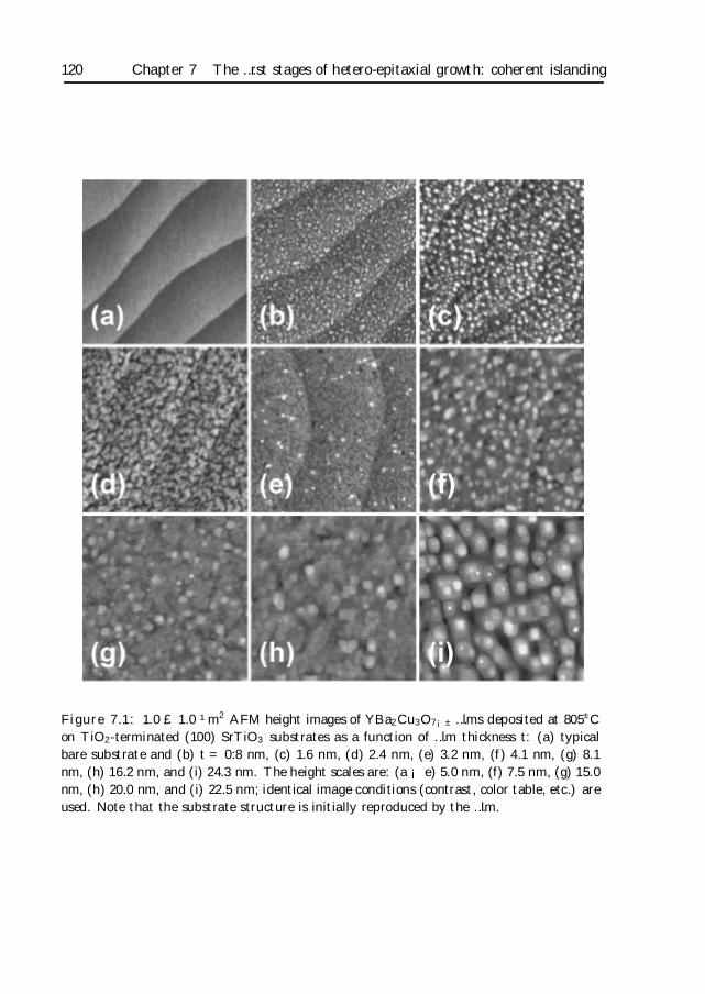
120 Chapter 7 The …rst stages of hetero-epitaxial growth: coherent islanding
Figure 7.1: 1.0 £ 1.0 ¹m2 AFM height images of YBa2Cu3O7¡± …lms deposited at 805±Con TiO2-terminated (100) SrTiO3 substrates as a function of …lm thickness t: (a) typicalbare substrate and (b) t = 0:8 nm, (c) 1.6 nm, (d) 2.4 nm, (e) 3.2 nm, (f ) 4.1 nm, (g) 8.1nm, (h) 16.2 nm, and (i) 24.3 nm. The height scales are: (a ¡ e) 5.0 nm, (f) 7.5 nm, (g) 15.0nm, (h) 20.0 nm, and (i) 22.5 nm; identical image conditions (contrast, color table, etc.) areused. Note that the substrate structure is initially reproduced by the …lm.
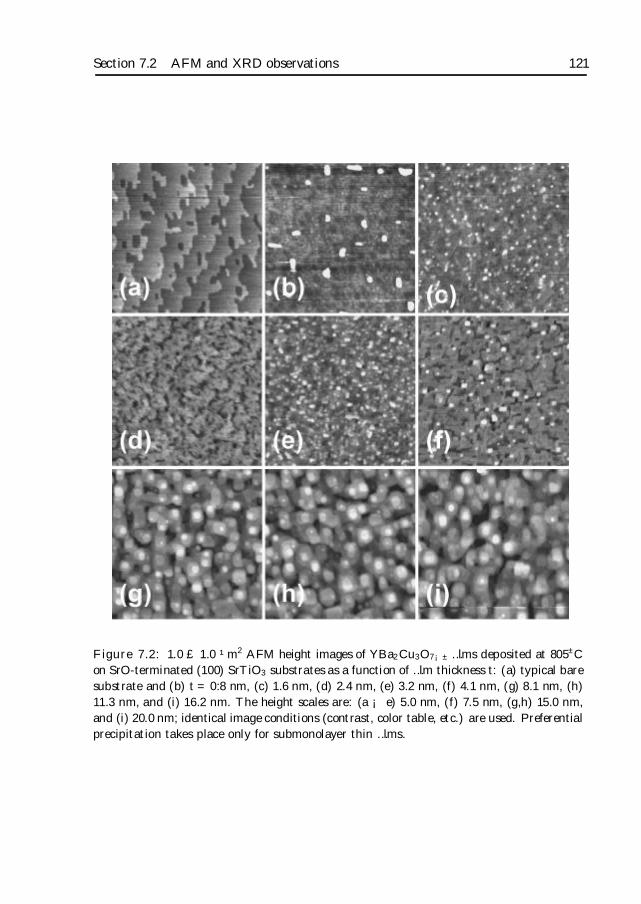
Section 7.2 AFM and XRD observations 121
Figure 7.2: 1.0 £ 1.0 ¹m2 AFM height images of YBa2Cu3O7¡± …lms deposited at 805±Con SrO-terminated (100) SrTiO3 substrates as a function of …lm thickness t: (a) typical baresubstrate and (b) t = 0:8 nm, (c) 1.6 nm, (d) 2.4 nm, (e) 3.2 nm, (f) 4.1 nm, (g) 8.1 nm, (h)11.3 nm, and (i) 16.2 nm. The height scales are: (a ¡ e) 5.0 nm, (f) 7.5 nm, (g,h) 15.0 nm,and (i) 20.0 nm; identical image conditions (contrast, color table, etc.) are used. Preferentialprecipitation takes place only for submonolayer thin …lms.
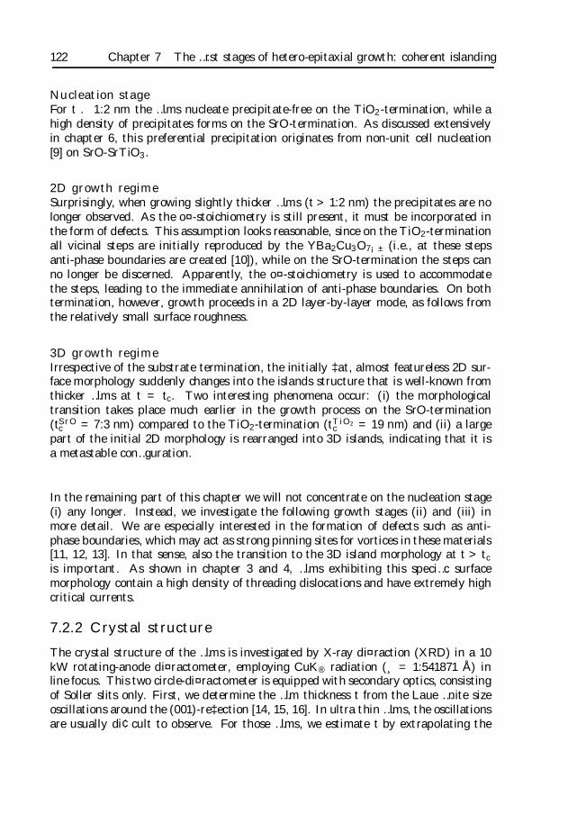
122 Chapter 7 The …rst stages of hetero-epitaxial growth: coherent islanding
Nucleation stageFor t . 1:2 nm the …lms nucleate precipitate-free on the TiO2-termination, while ahigh density of precipitates forms on the SrO-termination. As discussed extensivelyin chapter 6, this preferential precipitation originates from non-unit cell nucleation[9] on SrO-SrTiO3.
2D growth regimeSurprisingly, when growing slightly thicker …lms (t > 1:2 nm) the precipitates are nolonger observed. As the o¤-stoichiometry is still present, it must be incorporated inthe form of defects. This assumption looks reasonable, since on the TiO2-terminationall vicinal steps are initially reproduced by the YBa2Cu3O7¡± (i.e., at these stepsanti-phase boundaries are created [10]), while on the SrO-termination the steps canno longer be discerned. Apparently, the o¤-stoichiometry is used to accommodatethe steps, leading to the immediate annihilation of anti-phase boundaries. On bothtermination, however, growth proceeds in a 2D layer-by-layer mode, as follows fromthe relatively small surface roughness.
3D growth regimeIrrespective of the substrate termination, the initially ‡at, almost featureless 2D sur-face morphology suddenly changes into the islands structure that is well-known fromthicker …lms at t = tc. Two interesting phenomena occur: (i) the morphologicaltransition takes place much earlier in the growth process on the SrO-termination(tSrO
c = 7:3 nm) compared to the TiO2-termination (tTiO2c = 19 nm) and (ii) a large
part of the initial 2D morphology is rearranged into 3D islands, indicating that it isa metastable con…guration.
In the remaining part of this chapter we will not concentrate on the nucleation stage(i) any longer. Instead, we investigate the following growth stages (ii) and (iii) inmore detail. We are especially interested in the formation of defects such as anti-phase boundaries, which may act as strong pinning sites for vortices in these materials[11, 12, 13]. In that sense, also the transition to the 3D island morphology at t > tc
is important. As shown in chapter 3 and 4, …lms exhibiting this speci…c surfacemorphology contain a high density of threading dislocations and have extremely highcritical currents.
7.2.2 Crystal structure
The crystal structure of the …lms is investigated by X-ray di¤raction (XRD) in a 10kW rotating-anode di¤ractometer, employing CuK® radiation (¸ = 1:541871 Å) inline focus. This two circle-di¤ractometer is equipped with secondary optics, consistingof Soller slits only. First, we determine the …lm thickness t from the Laue …nite sizeoscillations around the (001)-re‡ection [14, 15, 16]. In ultra thin …lms, the oscillationsare usually di¢cult to observe. For those …lms, we estimate t by extrapolating the
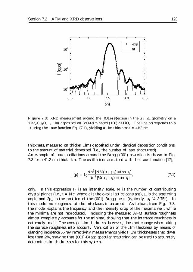
Section 7.2 AFM and XRD observations 123
6.5 7.0 7.5 8.0 8.5
101
102
103
exp
fit
I [c
ps]
2θ
Figure 7.3: XRD measurement around the (001)-re‡ection in the µ ¡ 2µ geometry on aYBa2Cu3O7¡± …lm deposited on SrO-terminated (100) SrTiO3. The line corresponds to a…t using the Laue function Eq. (7.1), yielding a …lm thickness t = 41:2 nm.
thickness, measured on thicker …lms deposited under identical deposition conditions,to the amount of material deposited (i.e., the number of laser shots used).An example of Laue oscillations around the Bragg (001)-re‡ection is shown in Fig.7.3 for a 41.2 nm thick …lm. The oscillations are …tted with the Laue function [17],
I (µ) = I0sin2 [N¼ (µ ¡ µ1) = tan µ1]
sin2 [¼ (µ ¡ µ1)= tan µ1], (7.1)
only. In this expression I0 is an intensity scale, N is the number of contributingcrystal planes (i.e., t = Nc, where c is the c-axis lattice constant), µ is the scatteringangle and 2µ1 is the position of the (001) Bragg peak (typically, µ1 ¼ 3:75±). Inthis model no roughness at the interfaces is assumed. As follows from Fig. 7.3,the model explains the frequency and the intensity drop of the maxima well, whilethe minima are not reproduced. Including the measured AFM surface roughnessalmost completely accounts for the minima, showing that the interface roughness isextremely small. The average …lm thickness, however, does not change when takingthe surface roughness into account. Veri…cation of the …lm thickness by means ofglancing incidence X-ray re‡ectivity measurements yields …lm thicknesses that di¤erless than 2%, showing that (001)-Bragg specular scattering can be used to accuratelydetermine …lm thicknesses for this system.
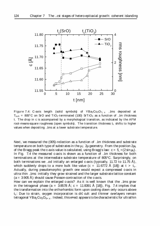
124 Chapter 7 The …rst stages of hetero-epitaxial growth: coherent islanding
0 5 10 15 20 25 3011.55
11.60
11.65
11.70
11.75
11.80 SrO
TiO2
c [Å
]
t [nm]
0
2
4tc(TiO2)t
c(SrO)
rms roughness [nm
]
Figure 7.4: C-axis length (solid symbols) of YBa2Cu3O7¡± …lms deposited atTsub = 805±C on SrO and TiO2-terminated (100) SrTiO3 as a function of …lm thicknesst. The drop in c is accompanied by a morphological transition, as indicated by the AFMroot-means-square roughness (open symbols). The transition thickness tc shifts to highervalues when depositing …lms at a lower substrate temperature.
Next, we measured the (005)-re‡ection as a function of …lm thickness and substratetemperature on both type of substrates in the µ¡2µ geometry. From the position 2µ5
of the Bragg peak the c-axis value is calculated, using Bragg’s law: c = 5¸= (2 sin µ5).In Fig. 7.4 the measured c-axis is shown as a function of …lm thickness for bothterminations at the intermediate substrate temperature of 805±C. Surprisingly, onboth terminations we …nd initially an enlarged c-axis (typically, 11.72 to 11.75 Å),which suddenly drops to a more bulk like value (c = 11:6772 Å [18]) at t > tc.Actually, during pseudomorphic growth one would expect a compressed c-axis inultra thin …lms: initially they grow strained and the larger substrate lattice constant(a = 3:905 Å) should cause Poisson-contraction of the c-axis.How can we explain the enlarged c-axis? As it is well known that the …lms growin the tetragonal phase (a = 3:8578 Å; c = 11:8391 Å [18]), Fig. 7.4 implies thatthe transformation into the orthorhombic form upon cooling down only occurs abovetc: Due to strain, oxygen incorporation is di¢cult and thinner overlayers remaintetragonal YBa2Cu3O6+x. Indeed, this e¤ect appears to be characteristic for ultrathin
Section 7.2 AFM and XRD observations 125
…lms [15, 19, 20]. As a result of the larger lattice constant of the substrate, the c-axisof the tetragonal phase is in fact contracted for t < tc, indicating tensile strain.These structural features are coupled to the morphological transition of Fig. 7.1and 7.2 (as indicated by the AFM roughness in Fig. 7.4) and we conclude thatpseudomorphic growth occurs below tc. Apparently, orthorhombic …lms only formupon cooling down …lms with a thickness t > tc, indicating that during growth somekind of strain relaxation process must have taken place at t = tc. Furthermore, we…nd that tc depends on the substrate temperature used. It shifts to larger values forlower temperatures (from 6.5 nm for Tsub = 850±C to 8.0 nm for Tsub = 770±C onthe SrO-termination), indicating that the 2D-3D transition is kinetically determined.These results show the importance of controlling the substrate termination once more.A good control over the substrate termination is essential in achieving a highly repro-ducible thin …lm deposition process. In fact, many of the controversies in literaturemay well be related to substrate termination e¤ects. In particular, the lower Tc ofultra thin …lms (t < tc) on the SrO-termination compared to …lms on TiO2-SrTiO3
[21] may be explained by the size of the tetragonal distortion reported above. As thecharge carrier density is related to the oxygen content, tetragonally distorted …lmsare underdoped, causing a lowering of Tc. Disappointingly, the fact that the struc-tural phase transition to the orthorhombic structure during cooling down is inhibitedfor …lms grown in the pseudomorphic regime (t < tc) makes YBa2Cu3O7¡± / (100)SrTiO3 an unsuitable system to investigate the e¤ect of hetero-epitaxial strain on Tc
[5]. The opposite e¤ects of doping and epitaxial strain are di¢cult to separate. In-deed, a Tc-enhancement was not detected in ultra thin sputtered YBa2Cu3O7¡± …lms[22].
7.2.3 In-plane ordering
To follow the in-plane ordering of the …lms, rocking curves (! scans) were takenaround the (005)-re‡ection as a function of …lm thickness. The results are presentedin Fig. 7.5 for both terminations. The (005)-rocking curves of YBa2Cu3O7¡± onboth SrO and TiO2-terminated (100) SrTiO3 substrates initially exhibit two com-ponents: a narrow (specular) resolution-limited component and a broader (di¤use)component. The occurrence of two-components in rocking curves are characteris-tic for high-quality, hetero-epitaxial systems. They are reported in a great diversityof such systems, among which are: ErAs/[001]GaAs [23], Nb/[1120]Al2O3 [24] andAlN/c-Al2O3 [25]. Also in submicron thick YBa2Cu3O7¡± …lms on (100) SrTiO3 aresolution-limited component was observed [26, 27, 28] although so far only in the(001) and (002)-re‡ection.Miceli et al. [29] explained the two components by considering a thin hetero-epitaxial…lm as spatially separated mosaic blocks on a substrate. Unlike in a conventionalmosaic crystal, the rotational disorder is now bounded in magnitude by the substratedue to the substrate-…lm interaction. For a large number of these crystallites thelattice planes are parallel and in phase (as dictated by the substrate). Hence, theX-rays are scattered coherently, giving rise to the narrow component. On the otherhand, the broad component re‡ects the local order within a mosaic block.
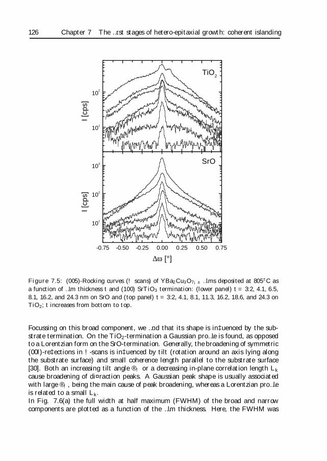
126 Chapter 7 The …rst stages of hetero-epitaxial growth: coherent islanding
-0.75 -0.50 -0.25 0.00 0.25 0.50 0.75
101
102
103
I [cp
s]
SrO
∆ω [°]
101
102
I [cp
s]
TiO2
Figure 7.5: (005)-Rocking curves (! scans) of YBa2Cu3O7¡± …lms deposited at 805±C asa function of …lm thickness t and (100) SrTiO3 termination: (lower panel) t = 3:2, 4.1, 6.5,8.1, 16.2, and 24.3 nm on SrO and (top panel) t = 3:2, 4.1, 8.1, 11.3, 16.2, 18.6, and 24.3 onTiO2; t increases from bottom to top.
Focussing on this broad component, we …nd that its shape is in‡uenced by the sub-strate termination. On the TiO2-termination a Gaussian pro…le is found, as opposedto a Lorentzian form on the SrO-termination. Generally, the broadening of symmetric(00l)-re‡ections in !-scans is in‡uenced by tilt (rotation around an axis lying alongthe substrate surface) and small coherence length parallel to the substrate surface[30]. Both an increasing tilt angle ®! or a decreasing in-plane correlation length Lkcause broadening of di¤raction peaks. A Gaussian peak shape is usually associatedwith large ®!, being the main cause of peak broadening, whereas a Lorentzian pro…leis related to a small Lk.In Fig. 7.6(a) the full width at half maximum (FWHM) of the broad and narrowcomponents are plotted as a function of the …lm thickness. Here, the FWHM was
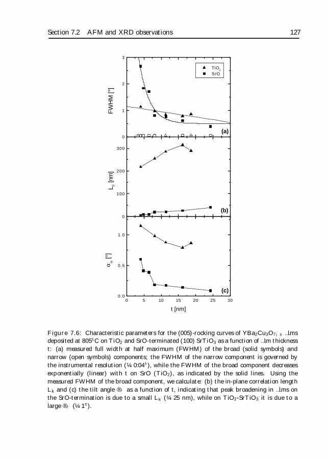
Section 7.2 AFM and XRD observations 127
0
1
2
3
(c)
(b)
(a)
TiO2
SrO
FW
HM
[°]
0
100
200
300
L // [n
m]
0 5 10 15 20 25 300.0
0.5
1.0
t [nm]
α ω [
°]
Figure 7.6: Characteristic parameters for the (005)-rocking curves of YBa2Cu3O7¡± …lmsdeposited at 805±C on TiO2 and SrO-terminated (100) SrTiO3 as a function of …lm thicknesst: (a) measured full width at half maximum (FWHM) of the broad (solid symbols) andnarrow (open symbols) components; the FWHM of the narrow component is governed bythe instrumental resolution (¼ 0:04±), while the FWHM of the broad component decreasesexponentially (linear) with t on SrO (TiO2), as indicated by the solid lines. Using themeasured FWHM of the broad component, we calculate: (b) the in-plane correlation lengthLk and (c) the tilt angle ®! as a function of t, indicating that peak broadening in …lms onthe SrO-termination is due to a small Lk (¼ 25 nm), while on TiO2-SrTiO3 it is due to alarge ®! (¼ 1±).
128 Chapter 7 The …rst stages of hetero-epitaxial growth: coherent islanding
determined by …tting the appropriate two component peak function. It follows thatthe FWHM of the narrow component is mainly determined by the instrumental res-olution.3 On the other hand, the FWHM of the broad component decreases rapidlywith …lm thickness. A linear decrease is found on the TiO2-termination, while anexponential decrease is observed on SrO-SrTiO3.Finally, we investigated the temperature dependence of the two component rockingcurves on the SrO-termination by depositing additional …lms at Tsub = 770 and 850±C.As follows from Fig. 7.7(a), the FWHM of the broad component decays exponentiallyto 0.5± for all temperatures, whereas the FWHM of the narrow component is closeto the instrumental resolution. In the next section, we will discuss these results morethoroughly.
7.3 Nucleation, growth and dislocation formation
In this section, we give a semi-quantitative analysis of the two component rockingcurves. To reveal the structural origin of the di¤use and specular component, wecombine the AFM and XRD data. Subsequently, the details of the YBa2Cu3O7¡±
growth mechanism, including the strain relaxation processes, are discussed. Finally,we identify the mechanism by which threading dislocations, the dominant strongpinning sites for vortices, are formed during this growth mode.
7.3.1 Correlating the two component rocking curves to thedefect structure
Here, we concentrate on the origin of the two components in the rocking curves andtheir dependence on the substrate termination. First, we relate the broad componentto the initial stages of growth as imaged by AFM and the formation of anti-phaseboundaries in particular. Next, we consider the narrow component and its relationwith mis…t dislocations.
Di¤use scatteringTo quantity the broadening of the di¤use component in the two component rockingcurves of Fig. 7.5, we use the method proposed by De Keijzer et al. [31] to separate thein‡uence of small Lk and large ®!. This method has been discussed comprehensivelyin a paper by Metzger et al [30]. They …t a pseudo-Voigt function, i.e. the convolutionof a Cauchy (Lorentzian) L (!) and Gaussian G (!) peak shape,
I (!) = I0 f´L (!) + [1 ¡ ´] G (!)g , (7.2)
to the measured rocking curves I (!). In this expression I0 is a scaling intensity and´ (0 ´ 1) is a measure for the ”Lorentzianness” of the peak. Determining ´, the
3The instrumental resolution of the rocking (!) scans, as determined by measuring a Si wafer, isapproximately 0:04±
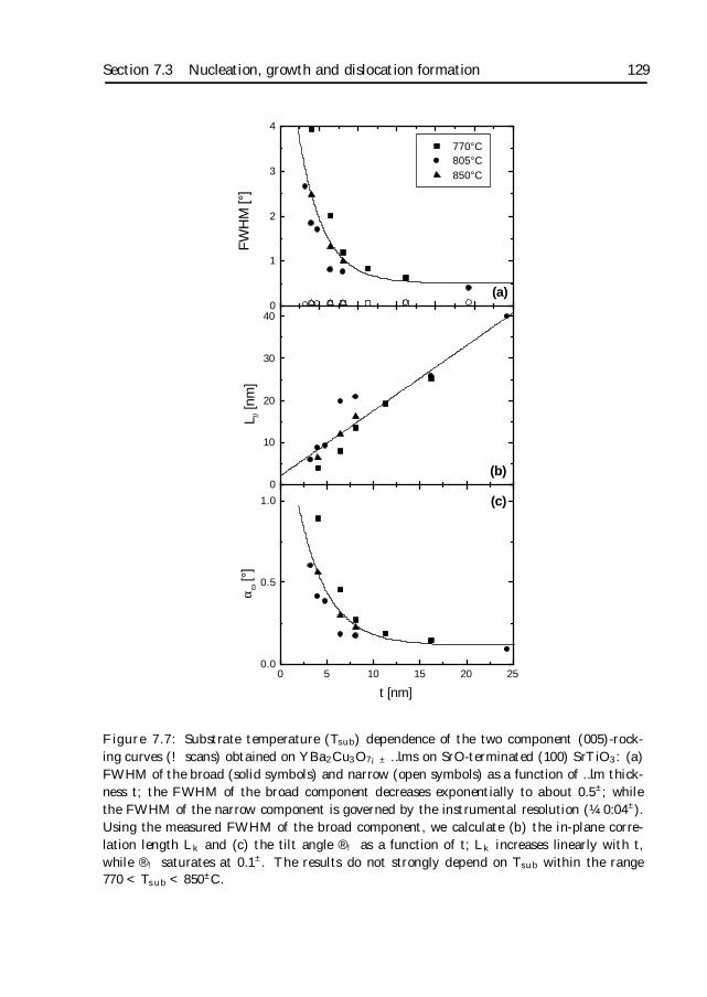
Section 7.3 Nucleation, growth and dislocation formation 129
0
10
20
30
40
L // [nm
]
0 5 10 15 20 250.0
0.5
1.0
α ω [°
]
t [nm]
0
1
2
3
4
(b)
(c)
(a)
FW
HM
[°]
770°C 805°C
850°C
Figure 7.7: Substrate temperature (Tsub) dependence of the two component (005)-rock-ing curves (! scans) obtained on YBa2Cu3O7¡± …lms on SrO-terminated (100) SrTiO3: (a)FWHM of the broad (solid symbols) and narrow (open symbols) as a function of …lm thick-ness t; the FWHM of the broad component decreases exponentially to about 0.5±; whilethe FWHM of the narrow component is governed by the instrumental resolution (¼ 0:04±).Using the measured FWHM of the broad component, we calculate (b) the in-plane corre-lation length Lk and (c) the tilt angle ®! as a function of t; Lk increases linearly with t,while ®! saturates at 0.1±. The results do not strongly depend on Tsub within the range770 < Tsub < 850
±C.
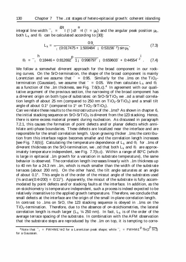
130 Chapter 7 The …rst stages of hetero-epitaxial growth: coherent islanding
integral line width ¯! =£R
I (!)d!¤=I (! = µ5) and the angular peak position µ5,
both Lk and ®! can be calculated according to [30]:
Lk =0:9¸
¯! (0:017475 + 1:500484´ ¡ 0:53156´2) sin µ5, (7.3)
®! = ¯!
h0:18446 + 0:812692
p1 ¡ 0:998797´ ¡ 0:659603´ + 0:44554´2
i. (7.4)
We follow a somewhat di¤erent approach for the broad component in our rock-ing curves. On the SrO-termination, the shape of the broad component is mainlyLorentzian and we assume that ´ = 0:95. Similarly for the …lms on the TiO2-termination (Gaussian), we assume that ´ = 0:05. We then calculate Lk and ®!
as a function of the …lm thickness, see Fig. 7.6(b,c).4 In agreement with our quali-tative argument of the previous section, the narrowing of the broad component hasa di¤erent origin on both type of substrates: on SrO-SrTiO3 we …nd a small correla-tion length of about 25 nm (compared to 250 nm on TiO2-SrTiO3) and a small tiltangle of about 0.1± (compared to 1± on TiO2-SrTiO3).Can we relate these results to the microstructure of the …lms? As shown in chapter 6,the initial stacking sequence on SrO-SrTiO3 is di¤erent from the 123 stacking. Hence,there is some excess material present during nucleation. As discussed in paragraph7.2.1, this causes the formation of point defects and/or planar defects which anni-hilate anti-phase boundaries. These defects are localized near the interface and areresponsible for the small correlation length. Upon growing thicker …lms the contribu-tion from this interface region becomes smaller and the correlation length increases[see Fig. 7.6(b)]. Calculating the temperature dependence of Lk and ®! for …lms ofdi¤erent thickness on the SrO-termination, we …nd that both Lk and ®! are approx-imately temperature independent, see Fig. 7.7(b,c). Within a range of 80±C (whichis large in epitaxial …lm growth for a variation in substrate temperature), the samebehavior is observed. The correlation length increases linearly with …lm thickness upto 40 nm for a 24.3 nm …lm, which is much smaller than the width of the substrateterraces (about 200 nm). On the other hand, the tilt angle saturates at an angleof about 0.1±. This angle is of the order of the miscut angle of the substrates used(¼ arctan(0:4=200) = 0:11±). Apparently, the miscut of the substrate is fully accom-modated by point defects and/or stacking faults at the interface. In addition, as theo¤-stoichiometry is temperature independent, such a process is indeed expected to berelatively insensitive to the applied growth temperature. Therefore, we conclude thatsmall defects at the interface are the origin of the small in-plane correlation length.In contrast to …lms on SrO, the 123 stacking sequence is obeyed in …lms on theTiO2-termination. Therefore, due to the absence of o¤-stoichiometries, the lateralcorrelation length is much larger (Lk ¼ 250 nm). In fact, Lk is of the order of theaverage terrace spacing of the substrate. In combination with the AFM observationthat the substrate steps are reproduced by the …lm on top, it is tempting to corre-
4Note that ¯! = FWHM£¼=2 for a Lorentzian peak shape; while ¯! = FWHM£p¼=(2pln 2)
for a Gaussian.
Section 7.3 Nucleation, growth and dislocation formation 131
late the XRD results for the TiO2-termination with anti-phase boundaries nucleatingat substrate steps. In such a picture, anti-phase boundaries cause rotational disorder(large ®!). In general, anti-phase boundaries are annihilated when growing thickerand thicker by inserting double CuO chains [10]. Indeed, the observations that thesubstrate structure can no longer be traced back in thicker …lms (Fig. 7.1) in com-bination with the decrease in ®! [Fig. 7.6(c)] point to such an annihilation process.Moreover, Wen et al. [10] have observed both anti-phase boundaries and bending ofthe atomic planes in …lms on TiO2-SrTiO3 by high resolution transmission electronmicroscopy (HRTEM). However, the relation between rotational disorder and the oc-currence of anti-phase boundaries is not clear to us at the moment. Additional crosssectional TEM measurements are necessary to identify the origin of the rotationaldisorder.
Specular scatteringAn alternative method to determine whether peak broadening is due to small corre-lation length Lk or large tilt angle ®! is measuring the dependence on the scatteringvector, i.e. measuring other orders of a re‡ection. Therefore, (00l)-rocking curveswere recorded (with l = 2, 4 and 5). Peak broadening due to a …nite in-plane cor-relation length is characterized by a constant width when measured in units of theparallel scattering vector qp = 4¼
¸ (cos µ5 ¡ cos!), while broadening as a result of ro-tational disorder yields a constant angular width [25]. In Fig. 7.8(a) (00l)-rockingcurves are shown for a 16.2 nm YBa2Cu3O7¡± thick …lm deposited on SrO-SrTiO3.Indeed, plotting the normalized intensity versus the parallel scattering vector showsthat the broad component does not depend on the order l of the re‡ection, suggest-ing that Lk is the limiting factor. On the other hand, the (00l)-rocking curves fora 165 nm thick …lm shown in Fig. 7.8(b) exhibit a constant width in angle space(¢! = ! ¡ µ5), suggesting that for these …lms the disorder is purely rotational. Inaddition, strong specular scattering is not observed.Miceli et al. [32] attributed a similar cross-over observed for the ErAs/GaAs systemto the introduction of mis…t-dislocations. In very thin …lms no mis…t dislocations areintroduced and in his model the weak disorder limit applies. In this limit, strongspecular scattering occurs even for large l and the di¤use scattering is correlationlength limited. In thicker …lms, mis…t dislocations are present at the interface torelieve the strain. In this strong disorder limit, both weak specular scattering (quicklydecreasing with l) and a di¤use component that is purely rotational in character areexpected. This situation applies for the SrO-termination (see Fig. 7.8): only someminor disorder is present in the very thin …lms (point disorder and/or in-plane stackingfaults and no extended defects), giving rise to both correlation length limited di¤usescattering and clear specular scattering. On the other hand, in thick …lms the disorderhas a rotational character and no specular scattering occurs due to the presence ofmis…t dislocations. In fact, this also explains why the specular component is notobserved for higher order re‡ections in thick YBa2Cu3O7¡± …lms (l > 2), even whenusing synchrotron radiation [26].
132 Chapter 7 The …rst stages of hetero-epitaxial growth: coherent islanding
-0.010 -0.005 0.000 0.005 0.010
100
101
norm
aliz
ed in
tens
ity [a
.u]
002
004
005
qp [1/Å]
-0.4 -0.2 0.0 0.2 0.410
0
101
102
103
104
(a)
(b)
norm
aliz
ed in
tens
ity [a
.u]
∆ω [°]
Figure 7.8: Normalized (00l)-rocking curves (! scans; l = 2, 4 and 5) of YBa2Cu3O7¡±…lms on SrO-terminated (100) SrTiO3: (a) a 16.2 nm thin …lm shows a constant width ofthe broad component as a function of the parallel scattering vector qp = 4¼
¸(cosµ5 ¡ cos!),
characteristic for a small correlation length while (b) a 165 thick …lm exhibits a …xed widthas a function of ¢! = ! ¡ µ5, indicative of rotational disorder (specular scattering is notobserved).
Section 7.3 Nucleation, growth and dislocation formation 133
On the other hand, we argued that in YBa2Cu3O7¡± …lms on the TiO2-terminationthe disorder has already a rotational character (see Fig. 7.6), suggesting that the weakdisorder limit does not fully apply here. Although we did not identify the microstruc-tural origin of this rotational disorder unambiguously, additional defects obscure thee¤ect of mis…t dislocations on the shape of the broad component. However, the nar-row component depends sensitively on the mis…t dislocation spacing [32]. Thus, thefact that the sharp peak in the (005)-rocking curves in Fig. 7.5 remains clearly vis-ible during the combined structural and morphological transition in …lms on bothterminations, indicates that mis…t dislocations are not yet introduced.This conclusion has an important implication: strain relaxation occurs by formingcoherent islands (i.e., islands that are essentially free of mis…t dislocation) at t =tc ´ tc;coh. Mis…t dislocation are induced at a later stage of growth (t > 25 nm), asevidenced by the disappearance of the sharp component, see Fig. 7.8. In the nextsection we explore both relaxation mechanisms in full detail.
7.3.2 The coherent Stranski-Krastanow growth mode
Already in the late eighties a structural discontinuity was deduced from re‡ectivehigh energy electron di¤raction data in YBa2Cu3O7¡± …lms on MgO substrates [33].Later morphological studies using SrTiO3 substrates were interpreted in terms of aclassical Stranski-Krastanow (SK) transition [34]: island growth on top of a thin pseu-domorphic wetting layer. In general, the SK-growth mode results from a competitionbetween the elastic strain energy due to lattice mismatch and the substrate-…lm in-teraction energy extending over several monolayers [35]. Ignoring kinetic e¤ects and(…lm) surface energy, the energy E per unit area of a pseudomorphic layer (materialA) of thickness t deposited on a substrate (material B) may be written as [35, 36]:
E (t) =¡C"2 ¡ ©AA
¢t + c¢. (7.5)
In this approach C is the Young’s modulus of the …lm material, " is the substrate-…lm mismatch (" = ¡0:012 for our hetero-epitaxial system growing in the tetragonalphase), and c is the c-axis lattice constant of the …lm. The energy per unit volumeof a thick pseudomorphic …lm is given by C"2 ¡ ©AA (©AA is the energy of bulkchemical AA bonds). At the interface the bonding energy between the substrate and…lm equals ¡©AB. Because of the wetting condition (¢ = ©AA ¡ ©AB < 0), thetotal energy of the system is lowered and a ‡at layer is favored. As the strain energyof the pseudomorphic wetting layer increases with thickness, strain relaxation takesplace at some critical layer thickness tc and a 2D-3D transition occurs. Classically,relaxation occurs by introducing mis…t dislocations at tc;mis [6], where the release instrain energy balances the dislocation formation energy.Fig. 7.9(a¡d) clearly demonstrate the transition from pseudomorphic growth to 3Disland growth, indicative of strain relaxation. Since the specular component in the(005)-rocking curve remains clearly visible during this transition (Fig. 7.5), we con-cluded that the mismatch strain is not accommodated by mis…t dislocations. Instead,strain relaxation takes place by the formation of coherently strained (i.e., free of mis-
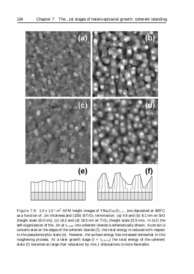
134 Chapter 7 The …rst stages of hetero-epitaxial growth: coherent islanding
Figure 7.9: 1.0 x 1.0 ¹m2 AFM height images of YBa2Cu3O7¡± …lms deposited at 805±Cas a function of …lm thickness and (100) SrTiO3 termination: (a) 4.9 and (b) 8.1 nm on SrO(height scale 15.0 nm); (c) 16.2 and (d) 19.5 nm on TiO2 (height scale 22.5 nm). In (e,f ) theself-organization of the …lm at tc;coh into coherent islands is schematically shown. As strain isconcentrated at the edges of the coherent islands (f), the total energy is reduced with respectto the pseudomorphic state (e). However, the surface energy has increased somewhat in thisroughening process. At a later growth stage (t = tc;mis) the total energy of the coherentstate (f) becomes so large that relaxation by mis…t dislocations is more favorable.
Section 7.3 Nucleation, growth and dislocation formation 135
…t dislocations) islands above a thickness tc;coh [37, 38], see Fig. 7.9(e,f). Althoughthe total …lm area increases (i.e., the surface energy increases), a signi…cant strain en-ergy release is achieved by forming coherent islands which are more or less strain-freenear their top and at the middle of their bases.The coherent SK-growth mode has been extensively studied in semiconductor hetero-structures [36, 39], where it is the cause for the formation of self-assembled quantumdots. Experimentally, it was found that the initial pseudomorphic layer thickness de-pends sensitively on both the size and the sign of the lattice mismatch [40]. Thedelay in coherent island formation in tensile systems was explained by strain inducedenhancement of the surface step free energy. However, the e¤ect of the interface en-ergy has not yet been addressed experimentally. Here, we introduce a new approach:as both strain energy C"2t and surface energy during pseudomorphic growth are thesame in …lms growing on the SrO or TiO2-termination, we can isolate the e¤ect of thesubstrate-…lm interaction energy. We attribute the termination dependence of tc;coh
to a di¤erence in interaction between the two substrate terminating planes and thestarting atomic layer of the …lm. Following Eq. (7.5) it is clear that a larger substrate-…lm interaction (more negative ¢) stabilizes a thicker wetting layer. Attributing theobserved di¤erence in tc;coh to the di¤erence in ¢, the interaction for the two termi-nations can be compared in …rst approximation by looking at the stacking sequences.Assuming BaO5 as the starting plane of the YBa2Cu3O7¡± structure [41, 42], wehave to consider the way it matches with the perovskite stacking of the substrate.Since BaO closely resembles SrO, it …ts almost perfectly on the TiO2-termination,maintaining the perovskite con…guration. Continuation of the perovskite stacking onthe SrO-termination is impossible and the BaO layer is shifted by ( 1
2 ,12 ,0), forming arocksalt interface con…guration [43]. Consequently, a smaller interface interaction isexpected.At this point, we must emphasis that the interface interaction may be slightly in‡u-enced by the o¤-stoichiometries present in …lms on the SrO-termination. The absoluteamount of defects is at most 20%, as estimated from the cation stoichiometry. How-ever, this amount is not entirely concentrated at the interface, but in thicker …lms itis also accommodated in the next layers. In fact, the weaker interaction of the …lmwith the SrO-termination as compared to the TiO2-termination may be responsiblefor the observation that the vicinal steps in the substrate are so easily overgrown.The o¤-stoichiometry only helps in this accommodation process. In the remaining ofthis discussion, we concentrate on the e¤ect of the substrate-…lm interaction, ratherthan on the o¤-stoichiometry.So far, we discussed our results from the viewpoint of energetics only. However, asfollows from the drastic redistribution at tc;coh, it is clear that the pseudomorphiclayer is metastable. In order to break up this layer, adatoms have to be created andhave to di¤use to form the coherent island structure. Such processes are thermallyactivated [44]. Indeed, we …nd that tc;coh decreases from 8.0 to 6.5 nm for the SrO-termination when increasing the temperature from 770 to 850±C. Moreover, we …nd
5As shown in chapter 6, BaO is the …rst atomic layer on both type of substrates, independentlyof the exact composition of the …rst monolayer (being either 122, 123 or 133).
136 Chapter 7 The …rst stages of hetero-epitaxial growth: coherent islanding
that the density of 3D islands decreases exponentially with the growth temperature,independently of the termination. The obtained activation energy is 1.7 eV, whichis in the range of typical activation energies for surface di¤usion [45]. This suggeststhat the di¤usion of (detached) adatoms determines the island size and thereby isa critical factor in the surface phase transition. Nevertheless, since we use identicaldeposition conditions for …lms on both terminations, we assume that the energy of thepseudomorphic layer at the instability thickness is the same for both terminations.From the condition E(tTiO2
c;coh) = E(tSrOc;coh), we obtain6
c (©Y BCO;T iO2 ¡ ©Y BCO;SrO) =¡C"2 ¡ ©Y BCO
¢(tTiO2
c;coh ¡ tSrOc;coh). (7.6)
Estimating the Young’s modulus C from the elastic sti¤ness constants c11 = 211 GPaand c12 = 93 GPa [46], according to [47]
C =(c11 ¡ c12) (c11 + 2c12)
(c11 + c12), (7.7)
we …nd an upper limit of c (©Y BCO;TiO2 ¡ ©Y BCO;SrO) = 0:40 J/m2 for the di¤erencein substrate-…lm interaction energy for the two terminations. This value is of thecorrect order of magnitude, since it is within the range of oxide surface energies(typically, 1 J/m2 [47]).The enhanced interface interaction for the TiO2-termination extends the kineticallylimited pseudomorphic growth regime. Clearly, at such large thicknesses, coherentislanding only occurs if mis…t dislocation formation is prohibited. Indeed, in complexoxides the activation energy for the formation of mis…t dislocations is huge. Usingisotropic dislocation theory, it was calculated [48] that the activation energy to forma dislocation half-loop with a Burger’s vector b = [101] is approximately 900 eV. Theleast conservative estimate, using anisotropic theory and b = [100], still yields anactivation energy of 30 eV [49]. Therefore, homogeneous nucleation in these coherentlayers is extremely unlikely. Moreover, the substrate-…lm interaction energy is notexplicitly taken into account in any existing mis…t dislocation model, which thereforecannot explain the dependence of tc on the termination.Finally, the strain energy of the coherent islands rises again with increasing thickness.In general, this always results in the formation of mis…t dislocations at a later stageof growth. The edges of the coherent islands, a location where strain is highly con-centrated [50], provide for a lowering of the dislocation formation activation energy.Indeed, from cross-section TEM observations on 120 to 140 nm thick …lms, we …ndthat in these thick …lms dislocations accommodate the mis…t. The rocking curvesof thick …lms adapt accordingly, see Fig. 7.8(b) and Ref. [26]. These mis…t dislo-cations must have formed at tc;mis > tc;coh. In fact, the observation of symmetricoscillations [51] in the 41.2 nm …lm of Fig. 7.3 suggests that full strain relaxation bymis…t dislocations has taken place, i.e. tc;mis < 41:2 nm for the SrO-termination. Asthe coherent island structure formes earlier in …lms on the SrO-termination, mis…t
6Note that the …lm surface energy is the same for pseudomorphic (‡at) …lms on both terminations.Therefore, these surface energies cancel when equating the total energies of both …lms.
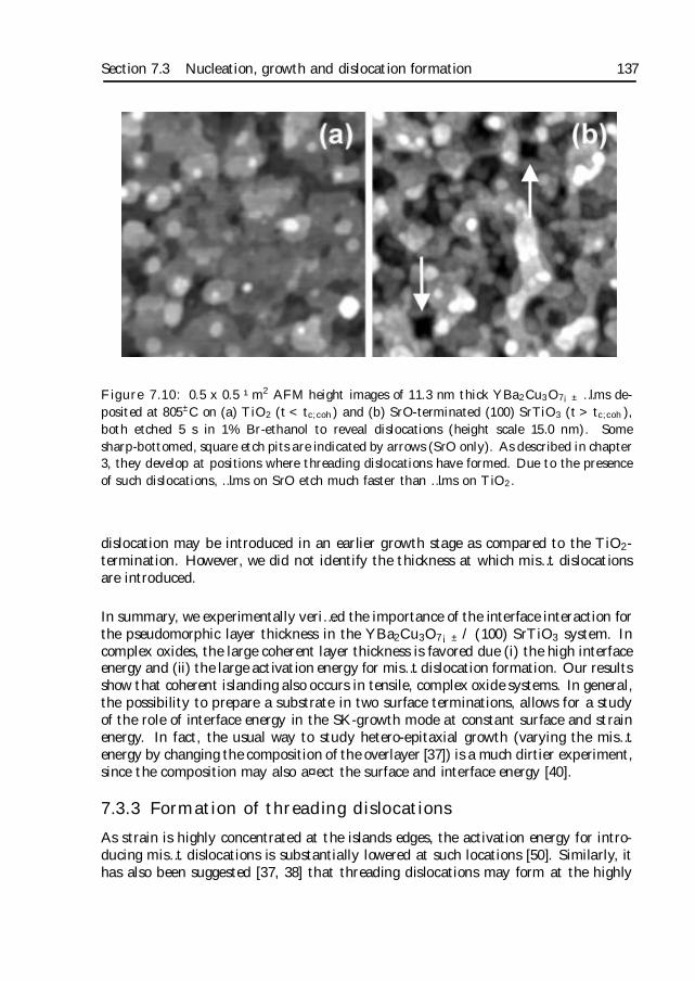
Section 7.3 Nucleation, growth and dislocation formation 137
Figure 7.10: 0.5 x 0.5 ¹m2 AFM height images of 11.3 nm thick YBa2Cu3O7¡± …lms de-posited at 805±C on (a) TiO2 (t < tc;coh) and (b) SrO-terminated (100) SrTiO3 (t > tc;coh),both etched 5 s in 1% Br-ethanol to reveal dislocations (height scale 15.0 nm). Somesharp-bottomed, square etch pits are indicated by arrows (SrO only). As described in chapter3, they develop at positions where threading dislocations have formed. Due to the presenceof such dislocations, …lms on SrO etch much faster than …lms on TiO2.
dislocation may be introduced in an earlier growth stage as compared to the TiO2-termination. However, we did not identify the thickness at which mis…t dislocationsare introduced.
In summary, we experimentally veri…ed the importance of the interface interaction forthe pseudomorphic layer thickness in the YBa2Cu3O7¡± / (100) SrTiO3 system. Incomplex oxides, the large coherent layer thickness is favored due (i) the high interfaceenergy and (ii) the large activation energy for mis…t dislocation formation. Our resultsshow that coherent islanding also occurs in tensile, complex oxide systems. In general,the possibility to prepare a substrate in two surface terminations, allows for a studyof the role of interface energy in the SK-growth mode at constant surface and strainenergy. In fact, the usual way to study hetero-epitaxial growth (varying the mis…tenergy by changing the composition of the overlayer [37]) is a much dirtier experiment,since the composition may also a¤ect the surface and interface energy [40].
7.3.3 Formation of threading dislocations
As strain is highly concentrated at the islands edges, the activation energy for intro-ducing mis…t dislocations is substantially lowered at such locations [50]. Similarly, ithas also been suggested [37, 38] that threading dislocations may form at the highly
138 Chapter 7 The …rst stages of hetero-epitaxial growth: coherent islanding
strained island edges when they merge. In chapter 3 and 4 it was shown that suchthreading dislocations are the main origin of the high critical current density (1012
A/m2) in high-Tc …lms. Indeed, these threading dislocation where found to originatenear the substrate-…lm interface. Moreover, we have observed that the threading dis-locations are situated in the trenches around the growth islands, independently ofthe substrate termination (see chapter 6). Hence, the merging of coherently strainedislands is a likely mechanism by which threading dislocations are introduced duringgrowth.In chapter 4, it was also shown by means of cross-sectional TEM that most of thesethreading dislocations have a screw character. Therefore, such dislocations do not re-lieve the mis…t. To verify the relation between formation of threading dislocationsand coherent islanding at tc;coh, we wet-etched 11.3 nm thick …lms on both termina-tions in a dislocation speci…c etchand (see Fig. 7.10). The …lm on SrO (t > tc;coh)shows some etch pit formation and is etched o¤ much more quickly, whereas the …lmon TiO2 (t < tc;coh) remains seemingly una¤ected. We conclude that threading dislo-cations are formed due to the merging of coherent islands at t > tc;coh, see Fig. 7.11.Initially, the …lms adopt the lattice constant of the substrate and grow pseudomor-phic [Fig. 7.11(a)]. At a certain …lm thickness tc;coh, which depends on the substratetermination, strain relaxation occurs by forming coherent islands [Fig. 7.11(b)] thatare heavily strained at their edges and are more or less strain free near their topand middle of their bases, see Fig. 7.9(e,f). In this 2D-3D roughening process, partof the original pseudomorphic layer breaks up again, showing that it is a kineticallylimited metastable con…guration. Upon continuing the growth, the coherent islandsmerge [Fig. 7.11(c)]. At these points strain is highly concentrated, which lowers theactivation energy for dislocation formation. As a result, threading dislocations areintroduced at these locations (i.e., in the trenches around the islands).
In fact, this mechanism is closely related to the merging of misaligned growth fronts(island coalescence) as suggested by Schlom et al. [52]. The short-ranged lateral or-dering of threading dislocations observed in chapter 3 is due to the lowered activationenergy for dislocations at the edges of the self-assembled coherent islands. Since thisisland structure is kinetically determined, surface di¤usion is the key factor in tuningthe dislocation density. By varying the deposition temperature, the island size canbe manipulated and, correspondingly, the dislocation density. Hence, the mechanismfor the formation of threading dislocations is now qualitatively explained.
Section 7.4 Conclusions 139
Figure 7.11: Schematic illustration of hetero-epitaxial growth and dislocation formationin YBa2Cu3O7¡± …lms on (100) SrTiO3: (a) pseudomorphic growth regime (t < tc;coh), (b)coherent islanding above tc;coh including part of the original pseudomorphic layer and (c)threading dislocations (dotted lines) are introduced at the island edges when they merge.The substrate termination determines tc;coh.
140 Chapter 7 The …rst stages of hetero-epitaxial growth: coherent islanding
7.4 Conclusions
We introduce a new approach to study hetero-epitaxial growth, using thin …lms ofYBa2Cu3O7¡± on (100) SrTiO3 substrates as a model system. By preparing eitherSrO or TiO2-terminated substrates, the in‡uence of the interfacial energy is separatedfrom the mis…t and surface energy. Combining atomic force microscopy and X-raydi¤raction measurements, we …nd that
(i) All …lms initially grow pseudomorphic (i.e., adopting the substrate lattice con-stant). Up to a critical thickness tc;coh the highly strained, pseudomorphic …lmsremain tetragonal upon cooling down. The orthorhombic crystal structure onlyforms in …lms with a thickness t > tc;coh, due to strain relaxation. This re-laxation process is accompanied by a morphological transition: the initially‡at almost featureless structure transforms into a 3D island morphology abovetc;coh. In other words, the …lms follow the Stranski-Krastanow growth mode.Remarkably, the critical thickness depends strongly on the substrate termina-tion (tSrO
c;coh = 7:3 nm and tTiO2c;coh = 19 nm), showing the importance of interface
energy in hetero-epitaxial growth. The substrate-…lm interaction energy is en-hanced by 0.40 J/m2 (upper limit) for the TiO2-termination, stabilizing thethicker pseudomorphic layer.
(ii) In-plane XRD measurements reveal two components up to a …lm thickness ofat least 25 nm. The di¤use component re‡ects the structural order of theindividual crystallites and is related to defects at the interface introduced dur-ing nucleation. On the SrO-termination point-like disorder and/or in-planestacking faults limit the in-plane correlation length. On the TiO2-terminationrotational disorder is found, which appears to be related to the occurrenceof anti-phase boundaries. The specular component arises from spatially sepa-rated individual crystallites that scatter x-rays coherently, since the rotationaldisorder of these crystallites is bounded in magnitude by the substrate. Asdescribed by the model of Miceli et al. [32], the presence of the specular com-ponent indicates that mis…t dislocations are not yet present. Therefore, the2D-3D roughening transition is a coherent strain relaxation process. In fact,YBa2Cu3O7¡± …lms on (100) SrTiO3 is the …rst hetero-epitaxial complex oxidesystem in which coherent Stranski-Krastanow growth is found. In addition, itis shown that the coherent islanding is kinetically limited.
(iii) In the case of coherent islanding, the strain energy also increases with increas-ing …lm thickness. Therefore, eventually mis…t dislocations are introduced.Although we did not exactly identify the thickness tc;mis at which this processoccurs, it is clear that tc;coh < 25 nm < tc;mis. All …lms with a thickness t À 25nm exhibit identical island morphologies and microstructures, independentlyof the substrate termination.
In view of the results of Locquet et al. [5], who used epitaxial in-plane strain to raisethe Tc, the pseudomorphic growth regime is extremely interesting. Complex oxides
References 141
favor a large pseudomorphic layer thickness due to the strong substrate-…lm interac-tion (and also the large activation energy for mis…t dislocation formation). Clearly,epitaxial strain e¤ects on Tc may bene…t from our observation that the substratetermination can be used as a tool to manipulate the substrate-…lm interaction.Finally, we identi…ed the mechanism by which threading dislocations are introduced.Since strain is highly concentrated at the coherent island edges, they provide for alowering of the dislocation formation activation energy. Therefore, the self-assembledcoherent island structure favors the subsequent formation of threading dislocations.Indeed, we …nd only (non-mis…t relieving) threading dislocations in …lms exhibitingan islands structure (i.e., for t > tc;coh). These threading dislocations act as orderedstrong pinning sites for vortices in YBa2Cu3O7¡± …lms.
References
[1] T. Ohnishi, K. Takahashi, M. Nakamura, M. Kawasaki, M. Yoshimoto, and H.Koinuma, Appl. Phys. Lett. 74, 2531 (1999)
[2] A.D. Polli, T. Wagner, T. Gemming, and M. Rühle, Surf. Sci. 448, 279 (2000)
[3] D.-W. Kim, D.-H. Kim, B.-S. Kang, T.W. Noh, D.R. Lee, and K.-B. Lee, Appl.Phys. Lett. 74, 2176 (1999)
[4] R.A. McKee, F.J. Walker, E.D. Specht, G.E. Jellison, Jr., L.A. Boatner, andJ.H. Harding, Phys. Rev. Lett. 72, 2741 (1994)
[5] J.-P. Locquet, J. Perret, J. Fompeyrine, E. Machler, J.W. Seo, and G.V. Ten-deloo, Nature (London) 394, 463 (1998)
[6] P. Politi, G. Grenet, A. Marty, A. Ponchet, and J. Villain, Phys. Rep. 324, 271(2000)
[7] M. Kawasaki, K. Takahashi, T. Maeda, R. Tsuchiya, M. Shinohara, O. Ishiyama,T. Yonezawa, M. Yoshimoto, and H. Koinuma, Science 266, 1540 (1994)
[8] G. Koster, B.L. Kropman, G.J.H.M. Rijnders, D.H.A. Blank, and H. Rogalla,Appl. Phys. Lett. 73, 2920 (1998)
[9] J.G. Wen, T. Morishita, N. Koshizuka, C. Traeholt, and H.W. Zandbergen,Appl. Phys. Lett. 66 (1995) 1830
[10] J.G. Wen, C.Træholt and H.W. Zandbergen, Physica C 205, 354 (1993)
[11] T. Haage, J. Zegenhagen, J.Q. Li, H.-U. Habermeier, M. Cardona, Ch. Jooss,R. Warthmann, A. Forkl, and H. Kronmüller, Phys. Rev. B 56, 8404 (1997)
[12] Ch. Jooss, R. Warthmann, H. Kronmüller, T. Haage, H.-U. Habermeier, and J.Zegenhagen, Phys. Rev. Lett. 82, 632 (1999)
[13] Ch. Jooss, R. Warthmann, and H. Kronmüller, Phys. Rev. B 61, 12433 (2000)
[14] T. Terashima, Y. Bando, K. Iijima, K. Yamamoto, K. Hirata, K. Hayashi, K.Kamigaki and H. Terauchi, Phys. Rev. Lett. 65 (1990) 2684
142 Chapter 7 The …rst stages of hetero-epitaxial growth: coherent islanding
[15] K. Kamigaki, H. Teauchi, T. Terashima, Y. Bando, K. Iijam, K. Yamamoto, K.Hirata, K. Hayashi, I. Nakagawa, and Y. Tomii, J. Appl. Phys. 68, 3653 (1991)
[16] O. Nakamura, E.E. Fullerton, J. Guimpel, and I.K. Schuller, Appl. Phys. Lett.60, 120 (1992)
[17] B.E. Warren, X-Ray Di¤raction (Addison-Wesley, London, 1968)
[18] F.S. Galasso, Perovskites and High Tc superconductors (Gordon and Breachscience publishers, New York, 1990)
[19] Q.D. Jiang, D.-M. Smilgies, R. Feidenhans’l, M. Cardona, and J. Zegenhagen,Sol. State Comm. 98, 157 (1996)
[20] A. del Vecchio, M.F. de Riccardis, L. Tapfer, C. Camerlingo, and M. Russo, J.Vac. Sci. Technol. A 18, 802 (2000)
[21] T. Nakamura, H. Inada, and M. Iiyama, Appl. Surf. Sci. 130-132 (1998) 576
[22] H.Y. Zhu and W.K. Chu, Appl. Phys. Lett. 76, 3469 (2000)
[23] P.F. Miceli, C.J. Palstrøm, and K.W. Moyers, Appl. Phys. Lett. 58, 160 (1991)
[24] P.M. Reimer, H. Zabel, C.P. Flynn, and J.A. Dura, Phys. Rev. B 45, 11426(1992)
[25] T. Metzger, R. Höpler, E. Born, S.Christiansen, M. Albrecht, H.P Strunk, O.Ambacher, M. Stutzmann, R. Stömmer, M. Schuster, and H. Göbel, Phys. Stat.Sol. A 162, 529 (1997)
[26] W.-J. Lin, P.D. Hatton, F. Baudenbacher, and J. Santiso, Appl. Phys. Lett. 73.2995 (1998)
[27] W.J. Lin, P.D. Hatton, F. Baudenbacher, and J. Santiso, Physica B 548, 56(1998)
[28] W.J. Lin, P.D. Hatton, F. Baudenbacher, and J. Santiso, IEEE Trans. Appl.Supercond. 9, 1852 (1999)
[29] P.F. Miceli and C.J. Palstrøm, Phys. Rev. B 51, 5506 (1995)
[30] T. Metzger, R. Höpler, E. Born, O. Ambacher, M. Stutzmann, R. Stömmer, M.Schuster, H. Göbel, S.Christiansen, M. Albrecht, and H.P Strunk, Phil. Mag.A 77, 1013 (1998)
[31] T.H. de Keijzer, E.J. Mittemeijer, and H.C.F. Rozendal, J. Appl. Crystallogr.16, 309 (1983)
[32] P.F. Miceli, J. Weatherwax, T. Krentsel, and C.J. Palstrøm, Physica B 221,230 (1996)
[33] T. Terashima, Y. Bando, K. Iijima, K. Yamamoto, K. Hirata, K. Kamigaki,and H. Terauchi, Physica C 162-164, 615 (1989)
[34] X.-Y. Zheng, D.H. Lowndes, S. Zhu, J.D. Dubai, and R.J. Warmack, Phys. Rev.B 45, 7584 (1992)
[35] I. Daruka and A.-L. Barabási, Phys. Rev. Lett. 79, 3708 (1997)
References 143
[36] V.A. Shchukin and D. Bimberg, Rev. Mod. Phys. 71, 1125 (1999)
[37] C.W. Snyder, B.G. Orr, D. Kessler, and L.M. Sander, Phys. Rev. Lett. 66, 302(1991)
[38] C.W. Snyder, J.F. Mans…eld, and B.G. Orr, Phys. Rev. B 46, 9551 (1992)
[39] See the April issue of MRS Bulletin 21 (1996)
[40] Y.H. Xie , G.H. Gilmer, C. Roland, P.J. Silverman, S.K. Buratto, J.Y. Cheng,E.A. Fitzgerald, A.R. Kortan, S. Schuppler, M.A. Marcus, and P.H. Citrin,Phys. Rev. Lett. 73, 3006 (1994)
[41] V.C. Matijasevic, B. Ilge, B. Stäuble-Pümpin, G. Rietveld, F. Tuinstra, andJ.E. Mooij, Phys. Rev. Lett. 76, 4765 (1996)
[42] T. Haage, J. Zegenhagen, H.-U. Habermeier, and M. Cardona, Phys. Rev. Lett.80, 4225 (1998)
[43] G. Koster, G. Rijnders, D.H.A. Blank, and H. Rogalla, Physica C 339, 215(2000)
[44] H.T. Dobbs, D.D. Vvedensky, A. Zangwill, J. Johansson, N. Carlsson, and W.Seifert, Phys. Rev. Lett. 79, 897 (1997)
[45] B. Dam and B. Stäuble-Pümpin, J. Mater. Sci.: Mater. Electron. 9, 217 (1998)
[46] M. Bauer, F. Baudenbacher, and H. Kinder, Physica C 246, 113 (1995)
[47] K.-N. Tu, J.W. Mayer, and L.C. Feldman, Electronic Thin Film Science forElectrical Engineers and Materials Scientists (Macmillan, New York, 1992)
[48] B. Stäuble-Pümpin, V.C. Matijasevic, B. Ilge, J.E. Mooij, W.J.A.M. Peterse,P.M.L.O. Scholte, F. Tuinstra, H.J. Venvik, D.S. Wai, C. Træholt, J.G. Wen,and H.W. Zandbergen, Phys. Rev. B 52, 7604 (1995)
[49] B. Stäuble-Pümpin (private communication)
[50] A.G. Cullis, A.J. Pidduck, and M.T. Emeny, Phys. Rev. Lett. 75, 2368 (1995)
[51] W.-J. Lin, P.D. Hatton, F. Baudenbacher, and J. Santiso, Appl. Phys. Lett. 72.2966 (1998)
[52] D.G. Schlom, D. Anselmetti, J.G. Bednorz, Ch. Gerber, and J. Mannhart, J.Cryst. Growth 137, 259 (1994)

Summary
The three primary characteristics of a type II superconductor are its critical tempera-ture Tc, upper critical …eld Hc2 and critical current density jc. Since the discovery ofhigh temperature superconductors, Tc increased roughly by a factor of …ve and Hc2
remained in the hundreds of Tesla. The most spectacular increase was witnessed for jc
which increased by a factor of 105 since 1987. This is a direct consequence of the factthat jc is essentially determined by imperfections. In a perfect superconductor thequantized vortices induced at high …elds are not pinned and start to move as soon asa transport current is fed through the superconductor. Structural defects act as pin-ning sites for vortices. Hence, up to certain limits, a structurally poor superconductoris more advantageous for high jc.This paradox is nicely illustrated in single crystals. Here, vortex pinning is governedby randomly distributed point defects. Such defects act as relatively weak pinningsites and a low jc is observed. On the other hand, in structurally inferior thin …lmsthe vortex pinning is so strong that the theoretical limit for jc comes into sight. Thespectacular high currents of YBa2Cu3O7¡± epitaxial …lms in combination with therelatively poor understanding of pinning in thin …lms are the main motivation for thisPh.D. research.In this thesis, we answered the following three central questions:
1. What is the structural defect responsible for the extremely high superconductingcurrents that can be passed without dissipation in YBa2Cu3O7¡± …lms?
We …nd that threading dislocations are the dominant pinning sites for vortices inYBa2Cu3O7¡± thin …lms. Such dislocations extend from the substrate-…lm interfaceall the way up to the …lm surface in a direction parallel to the c-axis of the …lm.To reveal threading dislocations, we applied a suitable wet-chemical etchand. Uponetching …lms in Br-ethanol, sharp-bottomed square etch pits form at sites where dis-locations emerge at the …lm surface. In combination with atomic force microscopy, alarge part of the …lm can be investigated, which allows for an accurate determinationof the dislocation density. Moreover, we …nd that the lateral dislocation distributionexhibits short-range ordering. In a large series of …lms with various dislocation densi-ties, we observe a universal magnetic …eld dependence of the critical current density:the current remains constant up to a characteristic …eld B¤ and decays rapidly athigher …elds. Here, B¤ is directly proportional to the measured density of threadingdislocations. In addition, the current density at low …elds is essentially independent ofthe dislocation density. These are exactly the characteristics of linear defect pinning.Indeed, we …nd threading dislocation by transmission electron microscopy.
146 Summary
The high pinning capability of threading dislocations arises for a number of reasons.First of all, a linear defect pins a vortex over a signi…cant length compared to the…lm thickness. In principle, vortices can even be pinned along their entire length.Secondly, a dislocation has the size of the normal core of the vortex. Hence, thefull condensation energy is gained. Indeed, we …nd current densities up to 20% of thetheoretical depairing current limit (at small magnetic …elds and low temperatures). Athigh …elds, there are more vortices than pinning sites. The additional vortices are lessstrongly pinned and jc quickly decreases with increasing magnetic …eld. The cross-overbetween the two regimes occurs at B¤. Due to the short-range ordering of defects,the proportionality constant between B¤ and the dislocation density is essentiallyequal to the ‡ux quantum at low temperatures. Finally, both jc and B¤ decreasewith temperature as a result of the temperature dependence of the superconductingparameters and thermal ‡uctuations.In fact, the ordering of the natural defects makes thin …lms completely di¤erent fromsingle crystals containing randomly distributed arti…cial columnar defects. Apartfrom the larger jc at low …elds, also the decrease in current density which magnetic…eld is slower in …lms. Hence, at high …elds the current densities that can be passedthrough …lms are even higher than in irradiated single crystals. We conclude thatthe intrinsic, self-organized defect structure of our pulsed laser deposited …lms is farbetter than the one created by brute force heavy ion bombardment.
2. What is the mechanism by which threading dislocations are induced during …lmgrowth?
We investigated a large number of mechanisms for introducing threading disloca-tions. Since the dislocations originate at or near the substrate-…lm interface, theymust be induced either by the substrate or during the …rst stages of …lm growth. We…nd that the dislocation structure in the …lm is insensitive to the substrate-…lm lat-tice mismatch, vicinal steps in the substrate, the termination of the substrate anddislocations already present in the substrate material. Moreover, most threading dis-location are shown to be screw dislocations. Hence, they cannot be related to mis…tdislocations, twinning dislocation or (low-angle) grain boundaries. Such dislocationsneed to have an edge component.Instead, the operative mechanism for dislocation formation is a result of the hetero-epitaxial growth mechanism of YBa2Cu3O7¡± …lms on (100) SrTiO3 substrates. We…nd that the …lms follow the well-known Stranski-Krastanow growth mode. Initially,they grow in a 2D mode, adopting the in-plane lattice parameter of the substrate. Thecorresponding increase in elastic energy is compensated by the large substrate-…lminteraction energy. However, at a certain …lm thickness, the interface energy can nolonger compensate the elastic energy and strain relaxation occurs. Surprisingly, strainrelaxation does not take place in the classical way by introducing mis…t dislocations.Instead, coherent 3D islands (i.e., free of mis…t dislocations) form that are highlystrained at the edges and are more or less stress free near their top and bases. Dueto these strain concentrations, the activation energy for introducing dislocations islowered at the coherent island edges. Threading dislocation are introduced at such
Summary 147
points when islands merge. Indeed, the short-ranged ordered threading dislocationdistribution re‡ects the self-assembled island structure. We conclude that threadingdislocations result from the peculiarities of the hetero-epitaxial growth mechanism.In establishing the mechanism of dislocation formation, we developed a new methodto obtain single terminated (100) SrTiO3 substrates. By properly cleaning and an-nealing, it can now be prepared in the (metastable) SrO-termination. This methodcomplements earlier methods to produce TiO2-terminated substrates. In fact, tuningthe substrate termination opens up a new approach to study hetero-epitaxial growth.By growing …lms on both termination, the interface energy is varied, independentlyof both the …lm surface energy and the substrate-…lm mis…t energy. We showed thatthe in‡uence of interface energy is severely underestimated in the growth of complexoxides. Depending on the termination, the …lm thickness at which coherent islandingof YBa2Cu3O7¡± occurs can be delayed by a factor of 2.5 for the TiO2-termination.
3. Can we control the growth process in such a way that we can tune the super-conducting properties of the …lms?
We are now in the position to tune the characteristic magnetic …eld dependence of thecritical current density jc(B) in our …lms. We …nd that jc(B) can be in‡uenced viathe threading dislocation density. Inducing dislocations results in: (i) an extension ofthe plateau B¤ up to which jc remains constant (B¤ is proportional to the dislocationdensity), (ii) a decrease of jc at low magnetic …elds (the pinning energy reducesslightly due to a decrease in the overall structural quality of the …lms) and (iii) afaster decrease of jc with increasing magnetic …eld at high …elds where jc _ B® (thepower-law exponent changes from ® ¼ ¡ 1
2to ® ¼ ¡1).
Tuning the dislocation density is achieved by controlling the coherent island struc-ture. Since the island formation is kinetically determined, surface di¤usion is therelevant parameter. We showed that the substrate temperature is an easy accessi-ble tool to adjust surface di¤usion, which allows for an adjustment of the dislocationdensity in both directions. By decreasing the substrate temperature, the density canbe increased by almost two orders of magnitude, leaving the lateral defect distribu-tion una¤ected. However, at too low substrate temperatures the critical temperaturestarts to go down. Depositing secondary phases on the bare substrate prior to theactual deposition can be used to add dislocations. When such precipitates are over-grown, dislocations form. On the other hand, so far we were not able to grow trulydislocation-free …lms by increasing the substrate temperature. Alternatively, dis-locations can be annihilated by annealing at a temperature around the depositiontemperature (typically 800±C) in an oxygen atmosphere. Moreover, the structuralquality improves, which results in an increase of the jc at low magnetic …elds to atruly universal value, independently of the dislocation density.
In conclusion, in this thesis we demonstrated the importance of knowing and control-ling the defect structure of a material in order to understand its physical processes.In particular, detailed understanding of the physical properties of the YBa2Cu3O7¡±
/ (100) SrTiO3 hetero-epitaxial system is only possible if its microstructure is known.

148 Summary
Since the microstructure is formed during preparation (…lm growth), the growth con-ditions are vital in controlling the physical properties.
Samenvatting
Eén van de belangrijkste eigenschappen van een supergeleider is dat zijn elektrischeweerstand verdwijnt beneden een zekere kritische ¡ zij het zeer lage ¡ temperatuurTc. Dit betekent dat elektrische stromen zonder verliezen (dissipatie) kunnen wordengetransporteerd! Naast Tc worden supergeleiders gekarakteriseerd door nog twee para-meters: het kritische magneetveld Hc2 en de kritische (elektrische) stroomdichtheid jc.Supergeleiding vindt alleen plaats beneden deze kritische waarden. Het zal duidelijkzijn dat het voor praktische toepassingen belangrijk is om Tc, Hc2 en jc op de een ofandere manier zo groot mogelijk te maken.Met de ontdekking van de hoge-Tc supergeleiders in 1986 is Tc inmiddels een faktorvijf toegenomen tot zo’n 170 K (ongeveer ¡100±C), terwijl Hc2 onveranderd groot isgebleven (enkele honderden Tesla’s). De meest spectaculaire toename is waargenomenvoor jc: maar liefst met een faktor 100.000! Dit is een direkt gevolg van het feit dat jc
wordt bepaald door defekten (kleine foutjes) in de stuktuur van de supergeleider. Ditkan men als volgt inzien. In deze supergeleiders dringt het magneetveld ¡ mits ditveld voldoende sterk is ¡ het materiaal binnen in de vorm van dunne buisjes. Dezebuisjes omvatten elk een vaste hoeveelheid magneetveld en worden vortices genoemd.Als er nu tevens een elektrische stroom door de supergeleider wordt gestuurd, on-dervinden de vortices een elektro-magnetische kracht. Hoe groter de stroom, des testerker deze Lorentzkracht op de vortices. Onder invloed van de Lorentzkracht zullenvortices gaan bewegen. Omdat deze beweging dissipatie veroorzaakt, wordt de su-pergeleidende toestand echter teniet gedaan. In een struktureel perfekte supergeleider(dus zonder defekten) kunnen de vortices ongehinderd bewegen, zodat jc = 0. Metandere woorden: elektrische stromen kunnen niet zonder dissipatie getransporteerdworden. Gelukkig zijn er in echte supergeleiders altijd defekten aanwezig, die de be-weging van vortices belemmeren (…guur 1.2). Defekten houden de vortices als hetware vast (we noemen dit pinnen), zodat elektrische stromen toch zonder verliezenkunnen worden gestransporteerd. Dit gaat goed tot de kritische stroomdichtheid isbereikt (nu is jc > 0).Merkwaardig genoeg kan een struktureel ”slechte” supergeleider dus een grotere elek-trische stroom zonder verliezen transporteren dan een bijna perfekte supergeleider!Deze paradox komt duidelijk naar voren als we éénkristallen (die weinig en zeer kleinedefekten bevatten) met dunne lagen (veel en grote defekten) van hetzelfde supergelei-dende materiaal vergelijken. In een éénkristal is de belemmerende werking van dekleine defekten gering, waardoor de elektrische stroomdichtheid jc die we door zo’nsoort supergeleider kunnen sturen voordat de vortices gaan bewegen erg klein is. Indunne lagen daarentegen, pinnen de vele grote defekten de vortices zo sterk dat jc
de theoretische limiet benadert. Hierbij moet men denken aan stroomdichtheden van

150 Samenvatting
de orde van 10.000 miljard Ampère per vierkante meter! Deze spectaculair grotestroomdichtheden zijn inderdaad waargenomen, bijvoorbeeld in dunne lagen van dehoge-Tc supergeleider YBa2Cu3O7¡±.Omdat er nog relatief weinig bekend is over de defekten die verantwoordelijk zijnvoor dergelijke grote stroomdichtheden heb ik mij hier in dit promotieonderzoek opgeconcentreerd. Hoe zien de defekten eruit? Hoe ontstaan ze? Kunnen we de su-pergeleidende eigenschappen ¡ door middel van deze defekten ¡ kontroleren? Ditzijn de drie centrale vragen in dit proefschrift.
1. Welk defekt in de microstruktuur van dunne YBa2Cu3O7¡± lagen is nu eigen-lijk verantwoordelijk voor de grote elektrische stromen die zonder dissipatie ge-transporteerd kunnen worden?
In dit promotieonderzoek is naar voren gekomen dat lineaire defekten (zogenaamdedislokaties) verantwoordelijk zijn voor de grote stroomdichtheden. Deze dislokatiesontstaan op het grensvlak tussen het substraat en de dunne laag die daarop gede-poneerd is. Vervolgens lopen ze in een rechte lijn naar het oppervlak van de dunnelaag in een richting loodrecht op het substraatoppervlak.Om dislokaties in dergelijke dunne lagen ”zichtbaar” te maken (de laagjes zijn ongeveer0.0001 mm dik ¡ dat is vele malen dunner dan een haar), hebben we de volgendetruc ontwikkeld. We dompelen de dunne laag enkele seconden in een chemisch oplos-middel (een oplossing van Broom in zeer zuivere alcohol). Het gevolg is dat de dunnelaag langzaam oplost (en dus nog dunner wordt). Overal waar dislokaties aan het op-pervlak komen, lost de dunne laag net iets sneller op. Hierdoor ontstaan er vierkanteputjes met een scherpe bodem in het oppervlak van de laag (zie bijvoorbeeld devoorkant van dit proefschrift). Ieder putje komt precies overeen met één dislokatie.Door nu met een speciale microscoop deze putjes te tellen, kunnen we de dichtheidaan dislokaties nauwkeurig bepalen. Bovendien zien we dat deze putjes min of meergeordend zijn: ze zitten bijna nooit vlak naast elkaar.Vervolgens hebben we in een hele reeks dunne lagen met verschillende dichthedenaan dislokaties (putjes) de kritische stroomdichtheid jc gemeten als functie van hetmagneetveld. Hierbij viel het ons al snel op dat alle dunne lagen zich min of meerhetzelfde gedragen. Voor kleine magneetvelden hangt jc niet af van het magneetvelddat we aanleggen: we zien dus een plateau. Echter, boven een karakteristiek mag-neetveld B¤ neemt jc zeer snel af (…guur 3.9). Het blijkt nu dat de (gemeten) waardevan B¤ direkt evenredig is met de (gemeten) dichtheid aan etsputjes (dislokaties).Bovendien zien we dat jc voor alle dunne lagen bij magneetvelden kleiner dan B¤
(de plateauwaarde) ongeveer gelijk is qua grootte (…guur 3.10). Dit zijn nu preciesde twee karakteristieke eigenschappen die je verwacht wanneer de beweging van vor-tices belemmerd wordt door lineaire defekten. Immers, bij kleine magneetvelden zijner weinig vortices en kan iedere vortex door een dislokatie op zijn plek vastgehoudenworden. Het resultaat is een zeer grote jc die niet afhangt van de hoeveelheid dis-lokaties (zolang het aantal vortices kleiner is dan het aantal dislokaties). Leggen weeen sterker magneetveld aan, dan ontstaan er meer vortices. Op een gegeven momentzijn er meer vortices dan defekten en niet iedere vortex kan door een dislokatie vastge-
Samenvatting 151
houden worden (er zijn immers niet genoeg defekten om alle vortices vast te houden).De vortices die niet door een dislokatie vastgehouden worden, kunnen gemakkelijkerbewegen. Het gevolg is dat we minder stroom kunnen transporteren zonder verliezen.Met andere woorden: jc neemt af bij grotere magneetvelden.Gezien het bovenstaande is niet verbazend dat de waarde van B¤ voorspeld kanworden door de dichtheid aan dislokaties te vermenigvuldigen met de hoeveelheidmagneetveld die een vortex draagt. Doordat de dislokaties geordend zijn hoevenbovendien geen extra numerieke faktoren in rekening te worden gebracht. Tot slotvermelden we nog dat we de dislokaties ook daadwerkelijk hebben waargenomen metspeciale microscopie (gebruikmakend van elektronenstralen ¡ …guur 4.7).Waarom kunnen nu juist lineaire defekten vortices zo stevig pinnen? Hiervoor zijneen aantal redenen. Ten eerste, omdat een dislokatie en een vortex parallel aan elkaarstaan wordt een vortex over zijn gehele lengte (de dikte van laag) vastgehouden. Hetis dus geen lokaal, maar een kollektief e¤ekt. Een tweede reden is dat de breedte vaneen vortex en een dislokatie van dezelfde orde van grootte zijn, waardoor de vortexook nog eens over zijn gehele breedte wordt vastgehouden. Het gevolg is dat westroomdichtheden meten die kunnen oplopen tot zo’n 20% van de theoretische limiet.Naast dislokaties ¡ die altijd aanwezig zijn in dunne lagen ¡ is er nog een andertype lineaire defekten. Door een materiaal te beschieten met zeer zware, doch kleinedeeltjes kun je ”buisjes” aanbrengen waarbinnen het materiaal sterk wanordelijk is.Dergelijke buisjes zijn, net als dislokaties, ook over de gehele laag gecorreleerd. Hetzijn dus ook lineaire defekten. Deze truc is inderdaad toegepast in éénkristallen (diegeen dislokaties bevatten). Zoals te verwachten is, neemt jc in éénkristallen zeer sterktoe door deze beschieting. Er zijn echter enkele belangrijke verschillen met dislokatiesin dunne lagen. Dislokaties worden door de natuur geïntroduceerd. Je krijgt ze alshet ware op de koop toe. Het beschieten is een kunstmatig proces dat veel energie(en dus geld) kost. In tegenstelling tot dislokaties, zijn deze kunstmatige defektenniet geordend. Het gevolg is dat jc in …lms (dislokaties) veel minder snel afneemt danin beschoten éénkristallen, wanneer we het magneetveld in sterkte laten toenemen.Met andere woorden: dunne lagen kunnen grotere stroomdichtheden transporterendan dergelijke éénkristallen! Kennelijk is de intrinsieke, door de natuur geordendestruktuur van dislokaties in dunne lagen veel e¢ciënter dan de struktuur van lineairedefekten die gecreëerd wordt door middel van ”bruut” bombarderen.
2. Hoe worden de dislokaties precies gegenereerd tijdens het maken van de dunneYBa2Cu3O7¡± lagen?
Omdat de dislokaties ontstaan aan het grensvlak tussen het substraat en de dunnelaag komen zij óf voort uit het substraatmateriaal zelf óf vormen zij in de eerstestadia van de groei van de dunne laag. Experimenteel hebben we vastgesteld datde dislokatiestruktuur ongevoelig is voor het verschil in roosterconstanten tussen hetsubstraatmateriaal en de dunne laag, stappen in het oppervlak van het substraat,de buitenste laag atomen van het substraat en dislokaties die al in het substraataanwezig zijn. Kennelijk hangen dislokaties in de dunne laag niet samen met hetsubstraat, maar zijn ze het gevolg van een ¡ nog niet geïdenti…ceerd ¡ proces dat
152 Samenvatting
optreedt tijdens het maken van dergelijk dunne lagen. Bovendien nemen we waar datwe te maken hebben met een bepaald type dislokaties: zogenaamde schroef dislokaties.Deze waarneming sluit direkt een groot aantal mogelijke mechanismen uit.Hoe ontstaan dislokaties dan wel? Hiervoor moeten we in detail kijken naar hoedergelijk dunne laagjes gemaakt worden (groeien). Uitgaande van een kaal substraat,groeit de laag steeds verder aan (en wordt dus dikker en dikker). We vinden datde lagen de zogenaamde Stranski-Krastanow groei volgen. Dit houdt in dat de laagin eerste instantie zeer vlak blijft (we noemen dit 2-dimensionale groei). Hierbijneemt een extreem dun laagje de roosterconstante van het substraat over (…guur 7.9).Aangezien de laag hierdoor oprekt, kost dit elastische energie. Deze elastisch energieneemt alleen maar toe naarmate het laagje dikker wordt. Aan de andere kant wordtenergie gewonnen doordat nu het substraat en de dunne laag zeer sterk aan elkaargebonden zijn. Deze interaktie-energie is onafhankelijk van de dikte van de laag. Hetgevolg is dat de 2-dimensionale groei slechts goed kan gaan tot een zekere laagdikte,namelijk zolang de interaktie-energie de elastische energie kan compenseren.Normaal gesproken relaxeert de dunne laag dan door plastische deformatie. Wijvinden echter een ander proces: er treedt zeer sterke verruwing op (zogenaamde 3-dimensionale groei). Het ¡ in eerste instantie vlakke ¡ oppervlak van de dunnelaag transformeert tot een struktuur van eilanden (een soort berglandschap). Dezeeilanden zijn nog steeds elastisch gedeformeerd. Echter, omdat de deformatie nuzeer sterk geconcentreerd is aan de zijkanten van de eilandjes kost deze toestand veelminder elastische energie. Het belangrijkste gevolg is dat dislokaties zeer gemakkelijkgeïntroduceerd kunnen worden op punten waar dergelijke eilanden bij elkaar komen(…guur 7.11). Dit verklaart direkt waarom de dislokatiestruktuur geordend is énsamenhangt met de struktuur van de eilandjes (die ook geordend zijn). Kennelijk zijnde dislokaties een direkt gevolg van de merkwaardige groei van een dergelijke dunnelaag op een ander, niet goed passend, materiaal (het substraat).We zijn tot bovenstaande konklusie gekomen door op een slimme manier gebruikte maken van het buitenste laagje atomen van het substraatmateriaal SrTiO3. Ditmateriaal bestaat namelijk uit lagen SrO en TiO2 die elkaar afwisselen. Er was aleen methode bekend die TiO2 als buitenste laag oplevert. Wij hebben een aanvul-lende methode ontwikkeld die SrO oplevert (…guur 6.1). Daarmee is het nu mogelijkgeworden om de groei van twee verschillende materialen op elkaar te besturen vol-gens een compleet nieuwe methode. Door dunne lagen van hetzelfde materiaal opbeide soorten substraten (dus buitenste laag SrO of TiO2) te prepareren, variërenwe slechts de grensvlakenergie tussen het substraat en de laag. De elastische energieen oppervlakte-energie van de dunne laag zijn in beide gevallen hetzelfde. Zodoendehebben we kunnen aantonen dat de grensvlakenergie een veel belangrijker parameteris dan men tot nu toe dacht. Voor dunne YBa2Cu3O7¡± lagen bijvoorbeeld, kunnenwe de overgang van 2 naar 3-dimensionale groei een faktor 2.5 (in laagdikte) vertragendoor gebruik te maken van de grotere grensvlak-energie met TiO2.
Samenvatting 153
3. Kunnen we de preparatie van de dunne YBa2Cu3O7¡± lagen op SrTiO3 sub-straten zodanig kontroleren dat we de supergeleidende eigenschappen naar wenskunnen sturen?
Met al deze nieuw verworven kennis zijn we in staat om de magneetveldafhankelijkheidvan de kritische stroomdichtheid jc (B) te sturen. We hadden al gevonden dat jc
constant is tot een zeker magneetveld B¤. Boven dit veld neemt jc zeer snel af.We kunnen jc (B) nu beïnvloeden via de dislokatiedichheid. Als we meer dislokatiesintroduceren nemen we drie e¤ecten waar. Ten eerste wordt het plateau waaroverjc constant is steeds langer (zoals we in het voorgaande al zagen, neemt B¤ toe methet aantal dislokaties). Ten tweede neemt de plateauwaarde van jc bij magneetveldenkleiner dan B¤ langzaam af. Dit komt omdat de sterkte waarmee dislokaties vorticeskunnen vasthouden afneemt doordat de dunne laag als geheel slechter wordt.1 Totslot zien we dat de afname van jc met toenemend magneetveld sneller gaat naarmatewe meer dislokaties introduceren.Hoe kunnen we nu de dislokatiedichtheid sturen? In het voorgaande hebben we geziendat dislokaties onstaan op punten waar de 3-dimensionale eilanden bij elkaar komen.De grootte van de eilanden bepaalt dus de afstand tussen de dislokaties (en dus hundichtheid - …guur 3.5). Deze eilandgrootte is kinetisch bepaald. Dit houdt in datde afstand waarover atomen getransporteerd kunnen worden (ofwel kunnen di¤un-deren) afhangt van de temperatuur tijdens preparatie. Dit is dus de knop waaraanwe moeten draaien om de gewenste dislokatiedichtheid in te stellen! Immers, bij eenlage substraattemperatuur tijdens preparatie kunnen de atomen niet ver di¤underenen er ontstaat een struktuur van kleine eilandjes. Het gevolg is dat er veel puntenzijn waar eilanden samenkomen en dus zullen er veel dislokaties ontstaan. Door detemperatuur te verlagen kunnen we meer dislokaties generen! Helaas gaat dit procesniet onbeperkt goed. Bij lage temperaturen begint één van de andere kritische pa-rameters (Tc) sterk af te nemen. Een alternatieve methode om de dislokatiedichtheidtoch verder te vergroten is om op het kale substrate zeer kleine deeltjes neer te leggen(zogenaamde precipitaten ¡ zie …guur 5.4). Als hieroverheen de dunne laag wordtaangebracht, ontstaan extra dislokaties op deze precipitaten.In principe moet het nu ook mogelijk zijn om dunne lagen zonder dislokaties te maken(dat wil zeggen: zeer hoge temperaturen gebruiken). Tot op heden zijn we hier echternog niet in geslaagd. Een methode die hierbij zou kunnen helpen is het langdurignabehandelen van de dunne lagen in een oven bij zeer hoge temperaturen. We vindennamelijk dat dislokaties dan langzaam verdwijnen.
In dit proefschrift hebben we voor dunne YBa2Cu3O7¡± lagen op SrTiO3 substratenlaten zien dat het uiterst belangrijk is om de microstruktuur (defekten) van dergelijkelagen goed in kaart te brengen. Alleen dan is het mogelijk op de fysische processen te
1Dit is eigenlijk niet in overeenstemming met hetgeen eerder vermeld werd (namelijk dat deplateauwaarde min of meer constant is). Echter, de geringe afname waarover we hier praten is hetgevolg van de methode die we gebruiken om dunne lagen met veel dislokaties te prepareren: wanneerwe meer dislocaties introduceren, wordt de …lm automatisch slechter (waardoor de plateauwaardeafneemt). Corrigeren we voor dit e¤ect, dan zien we dat de plateauwaarde inderdaad niet afhangtvan de dislocatiedichtheid.

154 Samenvatting
begrijpen. Aangezien de mikrostruktuur wordt gevormd tijdens preparatie, kunnen we¡ gebruikmakend van de preparatiekondities ¡ nu zelfs de gewenste microstruktuuren dus de gewenste fysische eigenschappen instellen.
List of publications
1. B. Dam, J.H. Rector, J. Huijbregtse, and R. Griessen, Spiral growth in pulsedlaser deposited YBa2Cu3O7¡± …lms, Physica C 282-287 (1997) 559 ¡ 560
2. Jeroen Huijbregtse, Fred Roozeboom, Jilt Sietsma, Johan Donkers, Ton Kuiper,and Erik van de Riet, High-frequency permeability of soft-magnetic Fe-Hf-O…lms with high resistivity, J. Appl. Phys. 83 (1998) 1569-1574
3. B. Dam, J.H. Rector, J. Johansson, J. Huijbregtse, and D.G. de Groot, Mecha-nism of incongruent ablation of SrTiO3, J. Appl. Phys. 83 (1998) 3386 ¡3389
4. B. Dam, J.H. Rector, J.M. Huijbregtse, and R. Griessen, The transition from2D-nucleation to spiral growth in pulsed laser deposited YBa2Cu3O7¡± …lms,Physica C 305 (1998) 1 ¡ 10
5. J.M. Huijbregtse, B. Dam, F.C. Klaassen, G. Doornbos, R. van der Geest, R.Elberse, and R. Griessen, Strong pinning mechanisms in pulsed laser depositedYBa2Cu3O7¡± …lms, in Advances in science and technology vol. 23: Scienceand Engineering of HTC superconductivity, edited by P. Vincenzini (TechnaSrl., Faenza, 1999) 617 ¡ 624
6. B. Dam, J.M. Huijbregtse, R. van der Geest, R. Elberse, J.H. Rector, S.Freisem, and J. Aarts, Dislocation speci…c etching of YBa2Cu3O7¡± thin …lms,in Advances in science and technology vol. 23: Science and Engineering ofHTC superconductivity, edited by P. Vincenzini (Techna, Faenza Srl., 1999)637 ¡ 645
7. F.C. Klaassen, J.M. Huijbregtse, B. Dam, R. van der Geest, G. Doornbos, J.H.Rector, R. Elberse, and R. Griessen, Strong pinning mechanisms in high-T c
superconducting YBa2Cu3O7¡± thin …lms in Physics and Materials Science ofVortex States, Flux Pinning and Dynamics, edited by R. Kossowsky, B. Bose,V. Pan, and Z. Durusoy (Kluwer Academic, Dordrecht, 1999) 331 ¡ 343
8. B. Dam, J.M. Huijbregtse, F.C. Klaassen, R.C.F. van der Geest, G. Doornbos,J.H. Rector, A.M. Testa, S. Freisem, J.C. Martinez, B. Stäuble-Pümpin, andR. Griessen, Origin of high critical currents in YBa2Cu3O7¡± superconductingthin …lms, Nature (London) 399 (1999) 439 ¡ 442
9. Oorsprong van de hoge kritische stromen, Nederlands Tijdschrift voor Na-tuurkunde 65 (1999) 230-231
156 List of publications
10.R. Surdeanu, R.J. Wijngaarden, E. Visser, J.M. Huijbregtse, J.H. Rector, B.Dam, and R. Griessen, Kinetic roughening of penetrating ‡ux fronts in high-T c
thin …lm superconductors, Phys. Rev. Lett. 83 (1999) 2054 ¡ 2057
11. J.M. Huijbregtse, B. Dam, J.H. Rector, and R. Griessen, High-quality o¤-stoichiometric YBa2Cu3O7¡± …lms produced by di¤usion-assisted preferentiallaser ablation, J. Appl. Phys. 86 (1999) 6528 ¡ 6537
12. J.M. Huijbregtse, F.C. Klaassen, R.C.F. van der Geest, B. Dam, and R. Griessen,Growth-induced strong pinning sites in laser ablated YBa2Cu3O7¡± …lms witha non-random distribution, J. Low Temp. Phys. 117 (1999) 663 ¡ 667
13.F.C. Klaassen, G. Doornbos, J.M. Huijbregtse, B. Dam, and R. Griessen, Crit-ical current density and dynamical relaxation rate below the matching …eld inthin …lms of YBa2Cu3O7¡±, J. Low Temp. Phys. 117 (1999) 1549 ¡ 1553
14. J.M. Huijbregtse, B. Dam, R.C.F. Van der Geest, F.C. Klaassen, R. Elberse,J.H. Rector, and R. Griessen, Natural strong pinning sites in laser ablatedYBa2Cu3O7¡± thin …lms, Phys. Rev. B 62 (2000) 1338 ¡ 1349
15. John T. Markert, Troy C. Messina, Bernard Dam, Jeroen Huijbregtse, Jan H.Rector, and Ronald Griessen, Laser-ablated thin …lms of in…nite-layer com-pounds and related materials, in Proceedings of SPIE Vol 4058: Superconduct-ing and Related Oxides: Physics and Nanoengineering, edited by David Pavunaand Ian Bozovic (2000) 141 ¡ 152
16. I.A. Khrebtov, B. Dam, A.D. Tkachenko, F.C. Klaassen, J.M. Huijbregtse, andK.V. Ivanov, YBCO …lms on SrTiO3 substrates with recordly low 1/f noise forbolometer applications, in Proceedings of the 4th European Workshop on LowTemperature Electronics-Wolte 4 (2000) 335 ¡ 339
17. I.A. Krebtov, A.D. Tkachenko, K.V. Ivanov, B. Dam, F.C. Klaassen, andJ.M. Huijbregtse, The noise characteristics of YBCO …lms with strong pin-ning, Techn. Phys. Lett. 26 (2000) 1078 ¡ 1080
18.Rinke J. Wijngaarden, R. Surdeanu, J.M. Huijbregtse, J.H. Rector, B. Dam,J. Einfeld, R. Wördenweber, and R. Griessen, Pattern formation due to non-linear vortex di¤usion, Physica C 341-348 (2000) 1011 ¡ 1014
19.M. Pannetier, R.J. Wijngaarden, R. Surdeanu, J.M. Huijbregtse, K. Heeck,B. Dam, and R. Griessen, Magneto-optical observation of the in‡uence of anarti…cial periodic magnetic pattern on the pinning of a YBa2Cu3O7¡± …lm,Physica C 341-348 (2000) 1019 ¡ 1022
20.F.C. Klaassen, G. Doornbos, J.M. Huijbregtse, B. Dam, and R. Griessen, Vor-tex pinning regimes in thin …lms of YBa2Cu3O7¡± , Physica C 341-348 (2000)1463 ¡ 1464
List of publications 157
21. J.M. Huijbregtse, B. Dam, F.C. Klaassen, J.H. Rector, and R. Griessen, YBa2-Cu3O7¡± …lms with self-organized natural linear defects, Physica C 341-348(2000) 1985 ¡ 1986
22. J.T. Markert, T.C. Messina, B. Dam, J. Huijbregtse, J. Rector, and R. Griessen,Observation of step-‡ow growth in laser-ablated thin …lms of the T¤-phase com-pound Pr2CuO4, Physica C 341-348 (2000) 2355 ¡ 2356
23.B. Dam, J.M. Huijbregtse, R.C.F. van der Geest, F.C. Klaassen, J.H. Rector,R. Elberse, and R. Griessen, Controlling the natural strong pinning sites inlaser ablated YBa2Cu3O7¡± thin …lms, Physica C 341-348 (2000) 2327-2330
24. J.M. Huijbregtse, J.H. Rector, and B. Dam, E¤ect of the two (100) SrTiO3
substrate terminations on the nucleation and growth of YBa2Cu3O7¡± thin…lms, accepted for publication in Physica C
25.F.C. Klaassen, G. Doornbos, J.M. Huijbregtse, R.C.F. van der Geest, B. Dam,and R. Griessen, General features of vortex pinning by natural linear defects inthin …lms of YBa2Cu3O7¡± , submitted to Phys. Rev. B
26. J.M. Huijbregtse, B. Dam, B.J. Kooi, A. Mendoza, J.H. Rector, J.Th.M.de Hosson, and R. Griessen, Coherent Stranski-Krastanow growth of YBa2-Cu3O7¡± on single terminated (100)SrTiO3, to be submitted to Phys. Rev.B
27. J.M. Huijbregtse, F.C. Klaassen, A. Szepielow, J.H. Rector, B. Dam, R. Gries-sen, B.J. Kooi, and J.Th.M. de Hosson, Vortex pinning in YBa2Cu3O7¡± thin…lms: identifying the contributions from dislocations, grain boundaries, surfaceroughness, twin boundaries and point defects, to be submitted to Supercond.Sci. Technol.

Cirruculum Vitae
Jeroen Marcel Huijbregtse werd geboren op 16 juni 1972 te Middelburg. In 1990voltooide hij het Gymnasium-¯ aan de Stedelijke Scholengemeenschap Middelburg omvervolgens aan zijn studie Materiaalkunde aan de Technische Universiteit in Delft tebeginnen. Gedurende deze opleiding werd zijn interesse voor fysica steeds duidelijker.Dit resulteerde in een afstudeerproject binnen de sectie metaalfysica van prof.dr.ir.A. van den Beukel op het gebied van zachtmagnetische dunne …lms voor eventueletoepassing in digitale videokoppen. Het experimentele werk werd uitgevoerd tijdenseen negen maanden durende stage bij Philips Research te Eindhoven in de groepMagnetisme van dr. F. Greidanus. In augustus 1996 studeerde hij hierop met lofaf. Bovendien werd hem voor dit afstudeeronderzoek ¡ getiteld Soft magnetic FeHfO…lms with a high resistivity: structural investigations and high frequency permeabil-ity calculations ¡ de prijs voor ”de beste afstudeerder van de studierichting Materi-aalkunde in het studiejaar 1995-1996 aan de Technische Universiteit Delft” toegekend.In september 1996 begon hij vervolgens aan zijn promotieonderzoek in de vakgroepVaste Stof Fysica van prof.dr. R. Griessen aan de Vrije Universiteit te Amsterdamonder direkte beleiding van dr. B. Dam. De resultaten van dit promotieonderzoekzijn vastgelegd in dit proefschrift. Op 1 maart treedt hij als Designer in dienst bijASM Lithography te Veldhoven in de groep Process Overlay.
The author was born on June 16, 1972 in Middelburg, the Netherlands. After …n-ishing the secondary school in 1990 (Stedelijke Scholengemeenschap Middelburg) hecontinued his education at the Technical University Delft. Here, he studied Materi-als Science at the Faculty of Chemical Technology and Materials Science. During hisstudies, he was more and more attracted towards Physics. As a result, he performedhis …nal research project in the group Physics of Metals of prof.dr.ir. A. van denBeukel, entitled Soft magnetic FeHfO …lms with a high resistivity: structural inves-tigations and high frequency permeability calculations. At that time, such …lms weregood candidates for application in digital magnetic video recording heads. The ex-perimental work was performed at Philips Research in Eindhoven (the Netherlands)in the group Magnetism of dr. F. Greidanus. He graduated successfully in August1996 and, in addition, he won the prize for the best graduation of that year at theMaterials Science department in Delft. Subsequently, in September 1996 he startedhis Ph.D. research in the group Condensed Matter Physics of prof.dr. R. Griessen atthe Vrije Universiteit in Amsterdam (the Netherlands) under supervision of dr. B.Dam. The results of this research project are described in the present Ph.D. thesis.On March 1, 2001 he starts working as a Designer at ASM Lithography in Veldhoven(the Netherlands) in the group Process Overlay.

Dankwoord
Ongelofelijk, maar het is al weer (ruim) vier en een half jaar geleden dat ik aan mijnpromotieonderzoek begon in de vakgroep Vaste Stof Fysica. Ik heb het in die tijdniet alleen uitstekend naar mijn zin gehad, maar ook ontzettend veel geleerd. Op dezeplaats wil ik de mensen bedanken die hieraan hebben bijgedragen.In de eerste plaats Ronald, mijn promotor, voor het gestelde vertrouwen en het mo-gelijk maken van mijn promotie. Jouw fysisch inzicht en kritische blik hebben eenbelangrijke bijdrage geleverd aan dit proefschrift. Ik zal de speurtocht naar de exacteoplossing van onze di¤erentiaalvergelijking niet snel vergeten.Vooral van Bernard, mijn copromotor en directe begeleider, heb ik heel veel opgesto-ken. Aan de informele kelderbesprekingen samen met jou en Jan (de ”basementbikkels”) bewaar ik prettige herinneringen. Hier werden de ideeën geboren waaropdit proefschrift gebaseerd is. Jouw enthousiasme en stimulans tot het schrijven vanartikelen hebben er toe geleid dat we zo’n produktief team vormden! Je passie voorItalië (en Italiaans koken) heeft aanstekelijk gewerkt: na ons reisje naar Florence benik voorgoed verkocht. Ook Jan, de therapeutische junior scientist, ben ik erg dankbaarvoor deze samenwerking en zijn eenvoudige oplossingen (waarom moeilijk doen als hetook makkelijk kan?) voor de talloze problemen, niet alleen op het technische vlak.Zonder mijn ”tweeling” promovendus Frodo had dit proefschrift er totaal anders uitgezien. We onderzochten hetzelfde probleem vanuit een verschillende invalshoek. Ikdenk dat we hebben bewezen hoe vruchtbaar een dergelijke samenwerking kan zijn.Succes met je promotie!Hoewel ik redelijk onafhankelijk heb gewerkt van de ”Switchable Mirrors” groep (opeen enkel irreversibel schakelexperiment van H2 met YBaCuO na), wil ik hen tochexpliciet bedanken voor hun bijdrage aan de goede sfeer binnen en buiten de vakgroep:Sense Jan (de andere Roberto Carlos van Premium Quality), Marcel (heeeh!) ennatuurlijk mijn ex-kamergenoot Jacob (keeltje smeren?).Veel dank ben ik verschuldigd aan de vele studenten die ik de afgelopen jaren hebbegeleid bij hun afstuderen of stage. Ronny heeft, met gevaar voor eigen leven,etsen doorontwikkeld tot een reproduceerbaar proces. In het daaropvolgende tijdperkRemko hebben we hier de vruchten van geplukt. Het was een genoegen om jullie tebegeleiden! Het werk van Mark is niet expliciet in dit proefschrift naar voren gekomen.Toch wil ik hem bedanken voor zijn tomeloze inzet en enthousiasme. Finally, I shouldnot forget the ¡ in arbitrary order ¡ social and scienti…c contributions from ourforeign students Pia and Agnieszka. Thank you all!Wat is onze vakgroep zonder Gerrie, Nico en de ¡ door Kier geregeerde ¡ ko¢epauze?Juist ja, een chaos. John: I greatly enjoyed your stays in Amsterdam (it did not sinkinto the sea, you know!). Thanks for the nice time in Austin, Texas. Uiteraard ook

162 Dankwoord
Radu, Chris, Gerben en alle andere (ex-)promovendi, post-docs, sta‡eden, studentenen gasten die ik niet bij name genoemd heb.
Tot slot wil ik mijn ouders en Floor bedanken voor hun onvoorwaardelijke steun inalle fasen van mijn promotietijd.