Embed Size (px)
Citation preview
GROWTH AND INVESTIGATIONS OF MnAl BINARY ALLOY
AND Co BASED HEUSLER ALLOY THIN FILMS FOR
SPINTRONIC APPLICATIONS
VINEET BARWAL
DEPARTMENT OF PHYSICS
INDIAN INSTITUTE OF TECHNOLOGY DELHI
FEBRUARY 2021

© Indian Institute of Technology Delhi, New Delhi, February 2021
GROWTH AND INVESTIGATIONS OF MnAl BINARY ALLOY
AND Co BASED HEUSLER ALLOY THIN FILMS FOR
SPINTRONIC APPLICATIONS
by
VINEET BARWAL
DEPARTMENT OF PHYSICS
Submitted
in the fulfillment of the requirement of the degree of the Doctor of Philosophy
to the
INDIAN INSTITUTE OF TECHNOLOGY DELHI
FEBRUARY 2021

To
My Family
&
Teachers
i
CERTIFICATE
This is to certify that the thesis entitled "Growth and Investigations of MnAl Binary Alloy and
Co Based Full Heusler Alloy Thin Films for Spintronic Applications," being submitted by Mr.
VINEET BARWAL to the Indian Institute of Technology Delhi, New Delhi, for the award of the
degree of Doctor of Philosophy in Physics is a record of bonafide research work carried out by
him. He has worked under my supervision and guidance and has fulfilled the requirements for the
submission of this thesis, which, in my opinion, has reached the requisite standard.
The results contained in this thesis have not been submitted, in part or full, to any other University
or Institute for the award of any degree/diploma.
Prof. Sujeet Chaudhary
Professor
Department of Physics
Indian Institute of Technology Delhi
New Delhi-110016
India
Date:

ii
ACKNOWLEDGEMENTS
I am thankful to all those who directly or indirectly were part of my journey as a research scholar
and helped me complete the work. First and foremost, I express gratitude and indebtedness towards
my research advisor Prof. Sujeet Chaudhary for his invaluable assistance, constant support,
guidance, and encouragement. His presence in the thin film lab (MS-401) sparked motivation and
ideas and the desire to learn physics. He inspired both a dedication to thoroughness as well as
providing a healthy environment for the discussion of both academic concerns as well as personal
ones. He gave me the somewhat daunting freedom to independently pursue many avenues of
research and made me learn how to provide critical analysis of my results.
I want to thank Prof. Dinesh K Pandya and Prof. Subhash C. Kashyap, for their valuable
suggestions and continuous encouragement.
I am thankful to my SRC committee members Prof. Mukesh C. Bhatnagar, Prof. Santanu Ghosh,
and Prof. Samaresh Das for their valuable feedback, encouragement, insightful comments, and
fruitful discussions during various progress meetings.
I would like to thank Professor Peter Svedlindh from Uppsala University, Sweden, for his
association, involvement, and scientific discussions.
I would like to convey my sincere thanks to Mr. Nagendra Chaudhary for the technical help and
support in the lab. I am also thankful to Mr. Subash Pai, Excel instruments, for his technical service
and support.
I am thankful to the University Grant Commission, Government of India, for providing me the
research fellowship.
I also acknowledge Professor K.L. Chopra, the founder of Thin Film Laboratory. I would like to

iii
thank the Department of Physics, Indian Institute of Technology Delhi, and all faculties for
providing me the needed facilities, support and guidance to complete my thesis work.
I will never forget the time spend with my seniors, juniors and lab mates. I would like to thank Dr.
Ankit, Dr. Dinesh, Dr. Anil, Dr. Shikha, Dr. Anjali, Dr. Nilamani, Dr. Sajid, Dr. Deepika, Dr.
Suchitra, Dr. Rekha, Dr. Raghav, Dr. Dhananjay and Dr. L. Saravanan for the constant support.I
am very much thankful to my colleagues and members of our research group; Dr. Akash, Dr.
Naveen, Pradeep, Ekta, Suraj, Abhay, Nanhe, Soumyarup, Parul, Lalit, Vireshwar, Naina, Nakul,
Deepak, Ravi, Avantika, Sarita, Kriti, Akashdeep, Siddharth, Kaushalya, Nikita, Radhika, Amar,
Sanjay, Rohit, and Rahul for making my stay at Thin Film Lab most memorable. My salute to my
friends Dinesh, Narendra, Ajay, Om Prakash and Suryansh, for their sparkling presence in my life.
This acknowledgment would be incomplete without expressing my sincere feelings towards my
family. Thanks to my parents Shri. Hemraj Barwal and Smt. Deepa Barwal, my brothers Vikas and
Rahul and sisters in law Anju and Babli and all the family members for their support,
encouragement and patience. Special thanks to my wife Rohila and my daughter Aaradhya for their
love and support which made this journey happier.
Lastly, I owe it all to Almighty God for the blessings.
VINEET BARWAL
(February 2021)
iv
ABSTRACT
Spin degree of freedom added new dimensionality to the electronics industry by providing new
avenues in terms of sensors, memory and logic applications utilizing spin current. Spin based
electronics had followed the path of constant improvement through changes in existing device
design or by introducing new materials having better spin filtering capabilities. Novel ways of
utilizing the pure spin current have been discovered. From the materials aspect, in memory-device
applications using Magnetic Tunnel Junction as a cell, there is a need for ferromagnetic (FM)
materials having low Gilbert damping (α) constant, high Curie temperature (Tc), and large spin
polarization (P) and moderate saturation magnetization (Ms) with large magnetocrystalline
anisotropy (Ku). The phase of MnAl is being studied rigorously for spintronic applications due to
its high Tc, moderate Ms and high Ku. Heusler alloys came into the picture due to their half-metallic
character and are now widely studied in various domains of research. Heusler alloys turned out to
be a promising class of material for numerous spintronic applications. The versatility in structural
and electronic properties of Heusler alloys due to various possible combinations of elements
present therein makes their study a challenging task. The present thesis work involved the growth
of MnAl binary alloy and Co2MnAl (CMA) and Mn2-xCo1+xAl (MCA) Heusler alloy thin films
using co-sputtering technique and study of their structural, magnetic (static as well as dynamic)
and transport properties for specific interest and reasons outlined below.
Out of the various possible alloys of MnAl, the phase holds a special position owing to its
magnetic properties specially the large value of Ku of 107 erg/cc and the fact that all other phases
of Mn-Al systems are non-magnetic in nature. However, being metastable, the phase poses
challenges in terms of its growth in thin films. The sputtering technique helps in achieving the
metastable phase since the deposition process is far from equilibrium. In the present thesis work,
v
we have grown MnAl thin films utilizing co-sputtering technique while maintaining an atomic
percent of Mn to be 55 at.% and Al to be 45 at.%. The structural and magneto-transport properties
of co-sputtered MnAl alloy thin films grown on Si(100) at various substrate temperatures (Ts)
ranging from room temperature to 500C are studied. The films are polycrystalline and multi-phase
in nature. The longitudinal resistivity shows semi-metallic behavior. Mooij's criterion for resistive
alloys is found to explain the crossover in temperature coefficient of resistance (TCR) observed on
lowering the temperature below about 250 K. The temperature dependence of Hall effect data
further corroborates the semi-metallic behavior. The magnetoresistance (MR) response of these
films is measured in the range of 10-300 K, both in the in-plane as well as out-of-plane transverse
magnetic field (~7 T) configurations. Analyses of the temperature-dependent Hall-effect and MR
data of these MnAl films revealed multi-band carrier effects, which are typical for semimetals.
Integration of Co-based Heusler alloy in spintronic devices requires a detailed investigation of the
magnetic anisotropy and magnetization dynamics properties. The Co2MnAl full Heusler alloy
system exhibits exotic magnetic and transport properties and is a promising material for spintronic
applications. The magnetization reversal mechanism has been investigated in CMA thin films
grown on Si(100) at different Ts. The magnetization reversal mechanism is inevitably essential to
study the anisotropy behavior of magnetic thin film. Moreover, measurement of the in-plane
angular dependence of coercivity (ADC) gives an insight into the mechanism of magnetization
reversal in the magnetic thin films. We have employed the longitudinal magneto-optical Kerr effect
(MOKE) measurements for this study. M shaped curve was observed in the in-plane ADC (0-360°)
measurements. The two-phase model well describes the magnetization reversal (M shaped ADC
behavior). Further, the analysis of the angular dependent squareness ratio (Mr/Ms) indicates that
our films exhibited two-fold uniaxial anisotropy, which is related to the self-steering effect arising
due to the obliquely incident atomic flux during the film-growth.
vi
The Mn2-xCo1+xAl (0≤x≤1.75) Heusler thin films are grown by co-sputtering. The idea was to
achieve the inverse Heusler Mn2CoAl alloy phase from Co2MnAl by systematically changing the
Co and Mn concentrations during co-sputtering. MCA being a spin gapless semiconductor (SGS),
has properties that are promising for future spintronic applications. The experiment elucidates the
change in magnetic behavior and structural ordering through a systematic change in Co and Mn
concentration. The MCA was found to be ferrimagnetic with a Tc ~ 417 K. The temperature-
dependent four-probe longitudinal resistivity (xx) measurements on thin films of MCA revealed
that the MCA exhibits gapless semiconducting behavior. The non-saturating positive MR (linear
in H) and temperature-dependent Hall and resistivity measurements hint towards the SGS like
behavior in MCA.
Finally, the change in the structural and dynamic magnetization response of CMA thin films with
respect to the structural ordering is also investigated. The varying degree of structural ordering in
these ternary compounds occurred due to the variation in growth temperature. FMR measurements
were carried for the magnetization dynamics study. For this, the CMA full Heusler alloy thin films
of constant thickness ~50nm were grown on Si (100) substrate at different substrate temperatures
(Ts) 30°C, 200°C, 300°C, 400°C and 500°C. Analysis of their XRD patterns revealed the formation
of the B2 ordered phase at Ts.~200°C and above. FMR technique has been used to determine the
damping constant (), resonance field (Hr), and line width (H) of the recorded spectra. The lowest
damping constant was found to be ~ 0.0070.002 for the film grown at Ts=200°C. Films exhibit
uniaxial magnetic anisotropy due to the employed configuration of different targets in a specific
geometry with respect to growing film. Anisotropy in damping constant () is also studied along
the easy and hard axis direction of these uniaxial samples. Along the two directions (easy and hard
axis), a remarkable change (~59%) in is observed. The low damping constant observed in these
investigated materials is indispensable for spintronics devices.
vii
सार
सपिन सिगरी की पवततरता न इलकटरॉसनकटस इिपरी म सपिन धारा का उियोग करत हए ससर, ममोरी और लॉसिक अनपरयोग क मामल
म नया आयाम समावसित सकय और इिपरी को नए रापत परदान सकए। सपिन आधाररत इलकटरॉसनकटस न मौिदा सिवाइस क सिजाइन
म िररवततन दवारा और बहतर सपिन सिलटररग कषमताओ वाल नए िदारथो को िि करक सनरतर सधार क मागत का अनसरण सकया ह।
िदध सपिन धारा क उियोग क नए तरीक खोि गए ह। िदारथो क िहल स मगनसटक टनल िकटिन को एक सल क रि म ममोरी-
सिवाइस अनपरयोगो म उियोग हत ऐस फरोमगनसटक (FM) िदारथो की आवशयकता होती ह, सिसम सनमन सगलबटत िमसिग सनयताक
(α), उचच कटयरी तािमान (Tc), उचच सपिन धरवीकरण (P), और बड मगनटोसिपटलाइन एसनसोरॉिी (Ku) क सारथ मधयम सतसि
चबकतव (Ms) होता ह। MnAl क - कला को इसक उचच Tc, मधयम Ms व उचच Ku क कारण सपिनरोसनक क अनपरयोगो क
सलए अधययन सकया िा रहा ह। हउसलर समशर धात अिन हालफ मटसलक परकसत क कारण वणतन म आए और अब अनसधान क
सवसिनन कषतरो म वयािक रि स अधययन सकए िा रह ह। सपिनरोसनक म अनपरयोगो क हत हउसलर समशर धात वगत का आिािनक
िदारथत क रि म उिरा । हउसलर क सरचनातमक और इलकटरॉसनक गणो म बहमखी परसतिा एव उसम मौिद ततवो क सवसिनन सिासवत
सयोिन इसक अधययन को एक चनौतीिणत कायत बनात ह। वततमान िोध परबध कायत म MnAl बाइनरी समशर धात और Co2MnAl
(CMA) और Mn2-xCo1+xAl (MCA) हउसलर समशर धात की ितली िरतो का सह-पिटररग तकनीक स सवकास और सवसिषट
कारणो और सहत क सलए उनक सरचनातमक, चबकीय (सपरथर और गसतिील), एव रासिोटत गणो का अधययन िासमल ह।
MnAl क सवसिनन सिासवत समशर धातओ म स, - कला अिन चबकीय गणो, सविष रि स असधक मान क Ku (107 erg/cc)
एव MnAl ससपटम क अनय सिी कला की गर-चबकीय परकसत क कारण एक सविष परथान रखता ह। हालासक, मटापटबल होन क
कारण - कला, तन िरतो क सवसदध क सदित म चनौसतया िि करता ह। पिटररग तकनीक मटापटबल चरण को पराि करन म मदद
करती ह कटयोसक इसम सनकषिण परसिया सतलन स दर होती ह। वततमान रथीससस कायत म, हमन MnAl ितली िरतो की सवसदध की,
सिसम सह-पिटररग तकनीक क उियोग स Mn 55 िरमाण परसतित % िर और Al 45% िर बनाया गया ह। कमर क तािमान स
लकर 500 °C तक सवसिनन सबसरट तािमान (Ts) िर Si (100) िर सवसदध की गई MnAl समशर धात की ितली िरतो क
सरचनातमक और मगनटो-रासिोटत गणो का अधययन सकया गया ह। िरत िॉलीसिपटलाइन और मलटीफज परकसत की ह। अनदधयत
परसतरोधकता का वयवहार समी मटसलक की तरह ह। तािमान को लगिग 250 K स कम करन िर परसतरोध क तािमान गणाक
(TCR) म िॉसओवर की वयाखया करन क सलए परसतरोधक समशर धातओ क मोइि की मािदणि स समझाया गया ह। हॉल परिाव क

viii
तािमान सनितरता स समी मटसलक वयवहार को और असधक िसषट समलती ह। इन िरतो की मगनटोरससपटस (MR) परसतसिया को 10-
300 K की रि म, दोनो इन-पलन और आउट-ऑफ-पलन रासवसत मगनसटक फीलि (~7T) सवनयास म मािा गया ह। इन MnAl
िरतो क तािमान िर सनितर हॉल-इफकटट और MR आकडो क सवशलषण स मलटी-बि वाहक परिाव का िता चलता ह, िो समी
मटलस क सलए सवसिषट ह।
सपिनरोसनक उिकरणो म Co-आधाररत हउसलर समशर धात क एकीकरण क सलए चबकीय असनसोरॉिी और मगनसटजिन िायनासमक
गणो की सवपतत िाच की आवशयकता होती ह। Co2MnAl िणत हउसलर समशर धात अिन अनोखी चबकीय और रासिोटत गणो को
परदसितत करता ह व सपिनरोसनक परयोगो क सलए एक उियोगी िदारथत ह। Si(100) िर सवसिनन Ts िर सवकससत की गयी CMA तन
िरतो म मगनसटजिन ररवसतल सियासवसध की िाच की गई ह। चबकीय ितली सफलम क असनसोरॉिी वयवहार का अधययन करन क
सलए मगनसटजिन ररवसतल सियासवसध असत आवशयक ह। इसक अलावा, इन-पलन एगलर सिििस ऑि कोएसीसवटी (ADC) का
मािन चबकीय तन िरतो म मगनसटजिन ररवसतल की सियासवसध म एक अतरदतसषट लाता ह। हमन इस अधययन क सलए अनदधयत मगनटो-
ऑसटटकल कर परिाव (MOKE) मािन का सनयोिन सकया ह। इन-पलन ADC (0-360°) माि म M आकार का वि दखा गया
ह। दो-चरण मॉिल अचछी तरह स मगनसटजिन ररवसतल (M क आकार का ADC वयवहार) का वणतन करता ह। इसक अलावा,
वगीय अनिात (Mr/Ms) क सवशलषण स सकत समलता ह सक हमारी िरतो म न दोहर वलन सवषमदसिकता का परदितन सकया, िो
सफलम-सवकास क दौरान सतरछ सगरन वाल िरमाण परवाह क कारण उतिनन हए आतम-पटीयररग परिाव स सबसधत ह।
Mn2-xCo1+xAl (0≤x≤1.75) हउसलर तन िरत सह-पिटररग दवारा सवकससत की गई ह। सह-पिटररग क दौरान Co और Mn
सादरता को वयवसपरथत रि स बदलकर Co2MnAl स सवयतिम हउसलर Mn2CoAl समशर धात चरण को पराि करन की योिना
रथी। MCA एक सपिन गिलस समीकिकटटर (SGS) ह, इसम ऐस गण ह िो िसवषय क सपिनरोसनक परयोगो क सलए आिािनक ह।
Co और Mn की परयोग सादरता म एक वयवसपरथत िररवततन चबकीय वयवहार और सरचनातमक िम म िररवततन को पिषट करता ह।
MCA को 417 K Tc क सारथ फरीमगनसटक िाया गया। MCA की तन िरतो िर तािमान आसशरत फोर परोब अनदधयत परसतरोधकता
मािो स िता चला सक MCA SGS िसा वयवहार परदसितत करता ह। गर-सति धनातमक MR (H म रसखक) और तािमान-
आसशरत हॉल और परसतरोधकता माि MCA म SGS िस वयवहार की तरफ सकत दत ह।
अततः, सरचनातमक िम क सबध म CMA तन िरतो क सरचनातमक और मगनसटजिन िायनासमक परसतसिया म िररवततन की िी
िाच की गई ह। इन टनतरी हउसलर म सरचनातमक िम की सिगरी म बदलाव, Ts म बदलाव क कारण हआ। मगनसटजिन िायनासमक
अधययन क सलए फरोमगनसटक अननाद (FMR) माि सकए गए रथ। इसक सलए CMA िणत हउसलर समशर धात की तन िरतो (सतत

ix
मोटाई ~ 50 nm) को सवसिनन Ts 30 °C, 200 °C, 300 °C, 400 °C और 500 °C िर Si (100) सबसरट िर सवकससत
सकया गया। उनक XRD िटनो क सवशलषण स Ts ~ 200 °C और उसस ऊिर क तािमान िर B2 ऑितर कला क गठन का िता
चलता ह। FMR तकनीक का उियोग ररकॉित सकए गए पिकटरा क िमसिग सनयताक (), अननाद कषतर (Hr) और लाइन चौडाई
(ΔH) को सनधातररत करन क सलए सकया गया ह। Ts = 200 °C िर सवकससत की गई िरत क सलए सबस कम ~ 0.007±0.002
िाया गया। सफलमो म एकाकषीय एसनसोरॉिी का परदितन होता ह िो की सवसिनन टागट म एक सवसिषट जयासमसत क सनयोसित सवनयास
क कारण ह। म असनसोरॉिी का अधययन इन एकाकषीय सफलमो की सरल और कसठन धरी सदिा क सारथ िी सकया गया ह। दो
सदिाओ (सरल और कसठन धरी) क सारथ, म एक उललखनीय िररवततन (~ 59%) िाया गया। इन िदारथो की िााच म िाया गया
कम , सपिनरोसनकटस उिकरणो क सलए अिररहायत ह।
x
TABLE OF CONTENTS
CONTENTS PAGE NO.
CERTIFICATE i
ACKNOWLEDGEMENTS ii
ABSTRACT iv
CONTENT x
LIST OF FIGURES xiii
LIST OF TABLES xx
Chapter 1: Introduction 1
1.1 Spintronics: Overview 1
1.2 Tunnel Magnetoresistance 5
1.3 Spin Transfer Torque MRAM 8
1.3.1 STT MRAM Switching 9
1.4 Magnetic Anisotropy 11
1.5 MnAl Binary Alloy 15
1.6 Half Metallicity and Heusler Alloys 17
1.6.1 Origin of Half Metallicity in Full Heulser Alloys 21
1.6.2 Magnetic Moment of Full Heusler alloys 22
1.7 Spin Gapless Semiconductors 23
1.8 Magnetization Dynamics 27
1.9 Anomalous Hall Effect 29
1.9.1 Major Contributions to Anomalous Hall Effect 31
1.10 Objectives of the Research Work 33
1.11 Thesis Plan 34
Chapter 2: Thin Film Deposition and Characterization Techniques 36
2.1 Thin Film Deposition: Pulsed DC Magnetron Sputtering 36
2.2 Characterization Techniques 39
2.2.1 Energy Dispersive X-ray Spectroscopy 39
2.2.2 X-ray Diffraction 43
2.2.3 X-Ray Reflectivity 46
xi
2.2.4 Atomic Force Microscopy 50
2.2.5 Magneto-optical Kerr Effect 52
2.2.6 Magnetization and Magnetotransport Measurement 55
2.2.6.1 Physical Property Measurement System:
Vibrating Sample Magnetometer
55
2.2.6.2 Physical Property Measurement System:
Transport Measurement
57
2.2.7 Ferromagnetic Resonance Spectroscopy 58
Chapter 3: Structural and Magneto-transport Properties of Co-
sputtered MnAl Thin Films
60
3.1 Introduction 60
3.2. Materials and Methods 62
3.3 Results and Discussion 64
3.4 Conclusions 78
Chapter 4: Growth Dependent Magnetization Reversal in Co2MnAl
Full Heusler Alloy Thin Films
79
4.1 Introduction 79
4.2 Experimental Details 83
4.3 Results and Discussion 83
4.4 Conclusions 97
Chapter 5: Spin Gapless Semiconducting Behavior in Inverse
Heusler Mn2-xCo1+xAl (0≤x≤1.75) Thin Films
99
5.1 Introduction 100
5.2 Materials and Methods 102
5.3 Results and Discussion 106
5.4 Conclusions 123
xii
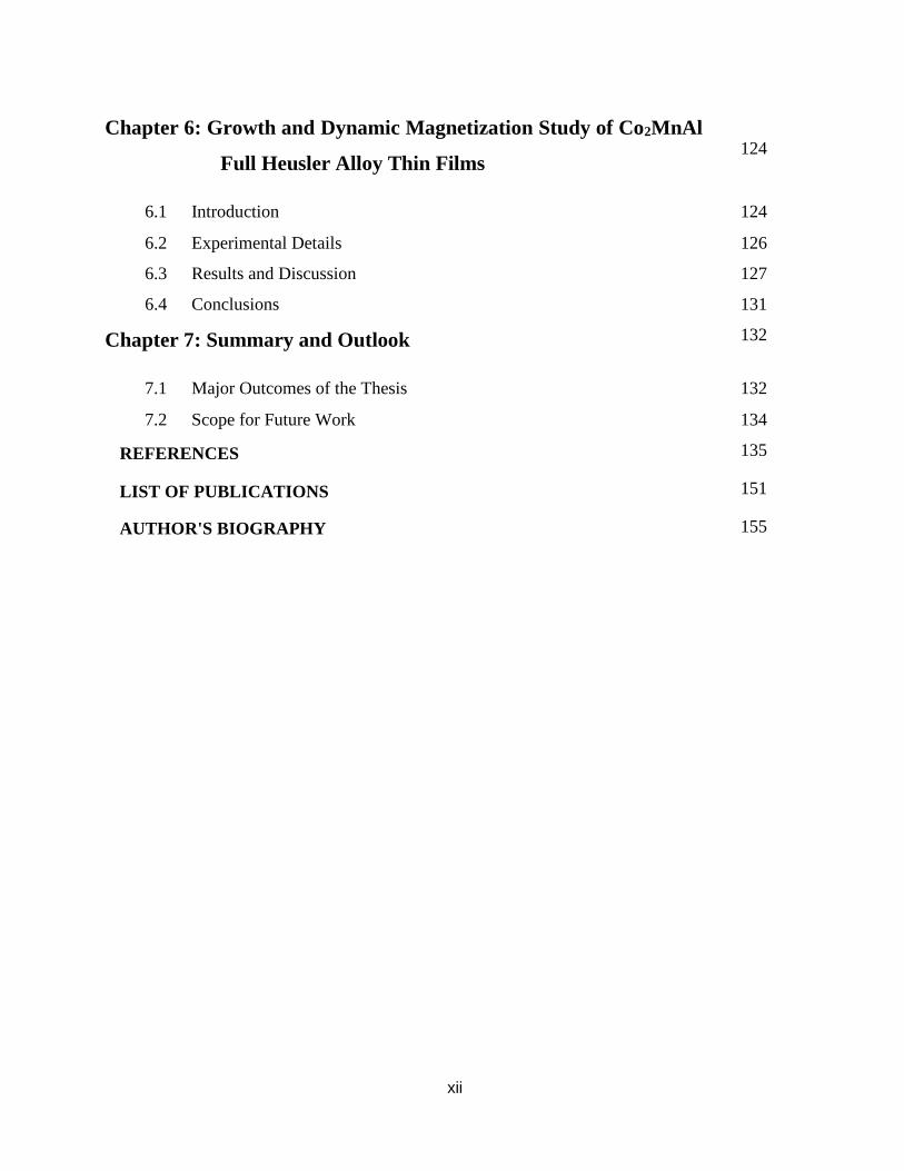
Chapter 6: Growth and Dynamic Magnetization Study of Co2MnAl
Full Heusler Alloy Thin Films
124
6.1 Introduction 124
6.2 Experimental Details 126
6.3 Results and Discussion 127
6.4 Conclusions 131
Chapter 7: Summary and Outlook 132
7.1 Major Outcomes of the Thesis 132
7.2 Scope for Future Work 134
REFERENCES 135
LIST OF PUBLICATIONS 151
AUTHOR'S BIOGRAPHY 155
xiii
LIST OF FIGURES
Fig. No. Figure Caption Page No.
Chapter 1
1.1 Schematic representation of an MTJ (left picture) and the TMR
phenomenon in the case of two identical FM metal layers separated by a
non-magnetic (NM) insulating barrier.
6
1.2 STT based MRAM cell structure. 8
1.3 Switching process in STT MRAM. 9
1.4 In plane (left) and out of plane (right) orientations of magnetization in a
film
12
1.5 Mn-Al binary phase diagram[1]. The hypothetical metastable phase
boundaries of the MnAl (L10) phase is highlighted using dashed lines
15
1.6 L10 MnAl structure with alternate stacking of (001) planes 16
1.7 Schematic showing the electronic density of states near Ef for
paramagnets (P=0), ferromagnets (P<1), and Half-metals (P=1).
17
1.8 Schematic of full Heusler alloy unit cell with (a) L21, (b) B2 and (c) A2
kind of ordering.
18
1.9 Hybridized energy levels in case of Co2MnGe. 21
1.10 Total magnetic moment evaluated using total number of valence electrons
for full Heusler alloys (Slater-Pauling rule) adapted from Ref. [2].
23
1.11 Energy band diagrams for 4 different kinds of SGS with parabolic
dispersion between energy and momentum.
24
1.12 Mn2 based Heusler compounds from both the inverse and full Heusler
structures, depending upon the element on Y position.
26
1.13 (a) Schematic of magnetization dynamics of the magnetization field under
an effective magnetic with the direction of torques in FMR, (b) FMR
absorption signal with its derivative representing resonance field and
linewidth of the spectrum.
27
1.14 Field and magnetization component in the plane of anomalous Hall Effect 30
xiv
measurement.
1.15 Three major contributions to AHE: (a) intrinsic deflection, (b) side jump,
and (c) skew scattering.
31
Chapter 2
2.1 Schematic illustration of four gun DC magnetron sputtering system
equipped with in-situ RHEED, used for thin film deposition in the present
study.
38
2.2 Schematic diagram showing the working principle of EDX 40
2.3 (a) The schematic of X-Pert PANalytical diffractometer showing various
components involved in the optics at the source and detector side to record
the measurement, courtesy of Malvern PANalytical. (b) the geometry of
diffraction from the atomic planes. The incident beam penetrates into the
lattice and scatters from atoms lying in its path.
44
2.4 Sketch showing the angles and indices of refraction along with the wave
vector directions when X-rays are incident from the air on the surface of a
sample having a refractive index less than 1.
48
2.5 Specular XRR profile of 40 nm MnAl thin film on Si(100) substrate
indicating the information provided by X-ray reflectivity profile.
48
2.6 Schematic of measurement set-up in AFM 50
2.7 Three geometries of MOKE experiment: Polar (left), Longitudinal
(middle), and Transverse (right). The red arrows indicate the incident and
reflected light contained in a plane, and green colored arrows show the
magnetization direction in the sample.
52
2.8 Schematic of MOKE measurement set-up in longitudinal geometry. 54
2.9 PPMS model 6000 Evercool II(left), PPMS probe(centre), VSM coil, and sample
puck for transport measurements(right). Courtesy of Quantum Design, Inc.
56
2.10 Measurement geometry (Leads attached) for (a) four-wire resistivity and (b) five-
wire Hall contact measurements (with offset nulling).
57
2.11 Schematic of the FMR measurement set-up (right) and the field lines
produced at the sample placed on the CPW(left).
59
xv
Chapter 3
3.1 XRD patterns of MnAl thin films grown at various Ts. The blue and red
colored dotted circles in the top panel (Ts=500C) highlight the well
separated (122) and (510) diffraction peaks due to the 2 and -phases,
respectively. The three bottom panels show all the standard diffraction
peaks corresponding to the different polycrystalline phases of the MnAl
system (i.e., , 2 and -phases) as per the JCPDS data files #330887,
#491279 and #300028. The dotted line represents the scattering angle (2)
of the most intense diffraction peak corresponding for the (101) plane of
metastable -phase as per JCPDS.
64
3.2 X-ray reflectivity spectra of MnAl films deposited at different Ts. Symbols
represent the experimentally observed reflectivity data, and the lines
represent the simulated reflectivity profiles obtained by modeling the film
sample as Si/SiO2/M/MOx (see text for details).
66
3.3 (a) The MH loops recorded at 300 K for the MnAl films grown at various
indicated Ts, It may be noted that in these plots, the moment contribution
from the underlying Si substrate has been subtracted for all the samples by
taking into account the measured slope of the moment vs. field data of the
bare substrate and also its actual mass. (b) The MH loops after subtracting
the linear contributions arising from the paramagnetic character of and
2 phases.
68
3.4 (a) Temperature dependence of xx and (b) ln (ρ) vs. 1/T for MnAl films
grown at different Ts. (Lines in (b) are fit to eq. 3.4)
69
3.5 Hall resistivity curves measured at different temperatures for the films
grown at (a) 300°C and (b) 400°C. The lower insets highlight the positive
slope of the transverse resistivity xy vs. H plots recorded at low
temperatures. The top right insets show the optical image of the five-point
contact measurement geometry used in these xy(H,T) measurements.
72
3.6 (a) Evolution of Hall Coefficient with temperature for the films grown at
300°C and 400°C, respectively. (b) and (c) shows the variation of carrier
73
xvi
concentration and mobility with temperature for the films grown at 300°C
and 400°C, respectively. The two shaded regions, colored as blue and red,
demarcate the regime dominated by holes and electrons, respectively as the
charge carriers.
3.7 (a) & (b) and (c) & (d) Variation in MR with H, recorded at various
measurement temperatures for the samples grown at 300°C and 400°C,
respectively. Inset: (a) and (b) schematic of MR measurement geometry for
in-plane (for Figs. (a) & (c)) and out-of-plane field configurations (for
Figs. (b) & (d)). (e) Comparison of the dependence of resistivity and the
in-plane-MR as well as out-of-plane-MR on the measurement temperature
for the MnAl film grown at 300°C
74
3.8 (a) (b) and (c) (d) shows the Kohler’s plot in the in-plane and out-of-plane
field geometry for the samples grown at 300°C and 400°C, respectively.
Inset: Schematic of MR measurement geometry for in-plane and out-of-
plane field configurations.
77
Chapter 4
4.1 (a) GIXRD patterns of the CMA thin films deposited at different growth
temperatures (Ts), (Inset: full range scan for the sample grown at
Ts=500°C). (b) the powder diffraction pattern (Relative intensity vs. 2)
for the L21, B2 and A2 structures of Co2MnAl obtained using PowderCell
2.4 freeware. (c) Ts dependence of the lattice constant (Open circles) and
crystallite size (filled circles). Lines connecting points are guide to the eye.
85
4.2 X-Ray Reflectivity spectra recorded for CMA films deposited at various
Ts. Symbols represent the experimental data, and lines are the fit to the
data.
87
4.3 (a) Schematic showing the film-plane and field configuration for MOKE
M-H measurements. Also shown are the EA and HA of the film employed
for ADC measurement. (b) and (c) show the normalized hysteresis loops
recorded for EA and HA configurations, respectively, for films sputtered
at different Ts.
88
xvii
4.4 Schematic of deposition geometry showing the obliquely incident flux. 90
4.5 (a) Polar plots showing the relative remnant magnetization (Mr/Ms)
response of films grown at different Ts. (b) Angular dependence of Hc in
polar form for CMA films grown at different Ts. Both Mr/Ms and Hc are
obtained from the MOKE magnetization loops recorded at an H -interval
of 10° rotation. For clarity, the points are not shown in the figure, instead,
continuous lines are shown. (c) H -dependence of Hr as inferred from the
FMR spectra recorded on film grown at 300C.
91
4.6 (a) Variation of coercivity with inverse of the grain size D for the films
sputtered at different Ts. Red line is the linear fit to the data. (b) The
saturation magnetization 4Ms for the films grown at different Ts. The
dotted line represents the bulk value of 4Ms. (c) Changes in the uniaxial
anisotropy (Ku) for all the samples grown at different Ts.
92
4.7 Normalized remanence and coercivity vs. in-plane field angle (𝜑𝐻 ) plots
for all the samples grown at different Ts. Remanence is fitted with 𝑀𝑟 =
𝑀𝑠׀ cos𝜑𝐻 ׀ and Hc/HA is fitted with eq. 4.5. In (b), the fittings of the Hc/HA
vs.𝜑𝐻 but in the limited range of 𝜑𝐻 using Kondorsky (solid red line) and
SW (solid blue line) models are also shown together with the fitting of the
Hc/HA vs.𝜑𝐻 in the entire range of 𝜑𝐻 is also shown (solid green line).
94
Chapter 5
5.1 (a) GIXRD patterns of the Mn2-xCo1+xAl thin films with x=0, 0.5, 0.75, 1,
1.25, 1.5 and 1.75. Solid lines in red are the fit for raw XRD data.
106
5.2 Lattice parameter and FWHM parameter (in deg.) of the Mn2-xCo1+xAl thin
films (x=0, 0.5, 0.75, 1, 1.25, 1.5 and 1.75) plotted as a function of Co and
Mn concentration; the x values are the nominal values while the Co
concentrations are those from the EDAX analysis.
109
5.3 In-plane MH loops for the Mn2-xCo1+xAl thin films (a) at 300K and (b) at
10K (inset of figure 3 (a) shows a zoomed view near H=0 to highlight the
coercivity values in the films)
111
xviii
5.4 Ms variation for Mn2-xCo1+xAl thin films at 300K and 10K with different
Mn and Co concentrations (as inferred from EDX measurements).
112
5.5 (a) Ms(T)/Ms(0) plotted as a function of temperature. Continuous line
(color online) represents the fitting of the data with eq. 5.2. The fitted
values of Tc for the respective thin films are also shown in panels.
113
5.6 The measured zero field longitudinal resistivity plotted as a function of
temperature for Mn2-xCo1+xAl.
115
5.7 MR at 300K for different compositions of Mn2-xCo1+xAl thin films. Inset
shows the contact geometry used for the measurement along with the
applied field direction. The asymmetry in the MR could be due to the
potential misalignment of contacts. This is substantiated from the
observation that higher MR-asymmetry is observed in films that have the
strongest Hall signal, i.e., films having high Mn concentration.
117
5.8 (a) Plot of Hall resistivity 𝜌𝑥𝑦 data as a function of applied magnetic field
H for Mn2-xCo1+xAl (0≤x≤1.75) films recorded at 10, 50, 150, 250, and
300 K (For clarity, the 5-probe contact geometry and colors corresponding
to different measurement temperatures are highlighted separately.
119
5.9 (a) Hall conductivity at 10K plotted as a function of a magnetic field for
the Mn2-xCo1+xAl films. (b) Anomalous Hall conductivity at 10K plotted as
function Co and Mn concentrations for Mn2-xCo1+xAl. (c) The 𝜌𝐴𝐻𝐸 plotted
as a function of 𝜌𝑥𝑥2 for Mn2CoAl film. The 4 points correspond to 10, 50,
150, and 250K. (d) Hall conductivity plotted as a function of the magnetic
field for Mn2CoAl film at 10K.
121
Chapter 6
6.1 Grazing incidence X ray diffraction pattern of CMA thin films grown at
Ts= 200°C, 300°C, 400°C and 500°C.
127
6.2 AFM images (10×10 m2) of CMA thin films, inset showing 𝜌𝑟𝑚𝑠 and Ts
for the thin film.
128
6.3 (a) f vs Hr plot for the Si/CMA (~50 nm) thin film grown at different Ts,
measured along easy axis and (b) Ts dependence of 4Meff obtained from
the Kittel’s equation.
128

xix
6.4 Line width vs. frequency plot the Si/CMA (~50 nm) thin film grown at
different Ts, measured along (a) easy axis and (b) hard axis.
129
6.5 Variation in Gilbert damping constant () with Ts along easy and hard axis
directions.
130
xx
LIST OF TABLES
Table No. Table Caption Page No.
1.1 Site occupancy, general formula, structure, Strukturberichte (SB)
Notation and Space group for different types of order/disorder
structures in full Heusler compounds.
19
3.1 The simulated parameters – layer thickness (t), surface/interface
roughness () and layer density () - for the Si/SiO2/MnAl thin films
sputtered at different Ts. Thin films are modeled as Si/SiO2/M/MOx for
simulations.
67
4.1 XRR simulated parameters for the Si/SiO2/CMA (~36 nm) samples,
viz. thickness (t), roughness (), and density (), obtained from XRR
fitting.
88
4.2 The variation of fitting parameters (as per eq. 4.5) with change in
substrate temperature. The fitting parameter y is obtained using the eq.
4.5 and calculated NN (=HA/Ms) and the in-plane demagnetization
parameter Nx=Nz describing the two-phase model.
96
5.1 Terminology for the Mn2-xCo1+xAl thin films, the DC power applied to
the individual targets, and relative composition of Co & Mn in the Mn2-
xCo1+xAl films (x).
103
5.2 The atomic concentration (in at.%) and film thickness(t) as determined
from the EDAX and XRR measurements, respectively.
104
![€¦ · Web viewThere have also been a few experimental and numerical investigations on the fire resistance of compressive and flexural aluminium alloy members [17-19]. In this study,](https://img.pdfslide.us/doc/110x75/5f07acb27e708231d41e2b76/web-view-there-have-also-been-a-few-experimental-and-numerical-investigations-on.jpg)