Embed Size (px)
Citation preview
This document is downloaded from DR‑NTU (https://dr.ntu.edu.sg)Nanyang Technological University, Singapore.
Growth and characterization of low‑k dielectricsfor multilevel interconnect applications
Wang, Minrui
2005
Wang, M. (2005). Growth and characterization of low‑k dielectrics for multilevelinterconnect applications. Master’s thesis, Nanyang Technological University, Singapore.
https://hdl.handle.net/10356/3674
https://doi.org/10.32657/10356/3674
Nanyang Technological University
Downloaded on 18 Feb 2022 05:36:02 SGT
GROWTH AND CHARACTERIZATION OF LOW-k DIELECTRICS FOR MULTILEVEL INTERCONNECT APPLICATIONS
WANG MINRUI
SCHOOL OF ELECTRICLAL & ELECTRONIC ENGINEERING NANYANG TECHNOLOGICAL UNIVERSITY
2005
ATTENTION: The Singapore Copyright Act applies to the use of this document. Nanyang Technological University Library
Growth and Characterization of Low- k Dielectrics for Multilevel Interconnect Applications
Wang Minrui
School of Electrical & Electronic Engineering
A thesis submitted to the Nanyang Technological University
in fulfillment of the requirement for the degree of
Master of Engineering
2005
ATTENTION: The Singapore Copyright Act applies to the use of this document. Nanyang Technological University Library
Acknowledgements
Nanyang Technological University I
Acknowledgements
I would like to thank my supervisor, Associate Professor, Rusli, School of
Electrical and Electronic Engineering, Nanyang Technological University, for the
patient guidance and advice, personal inspiration and encouragement, and kind
support in this period of my study. His erudition in plasma physics and carbon related
materials gives me deep impression, which greatly enhances my knowledge in these
fields.
I wish to express my heartfelt gratitude to Mr. Rakesh Kumar, Senior
Technological Manager, Micro-Fabrication of Semiconductor Process Technologies,
Institute of Microelectronics, for his strong and consistent support and
encouragement.
I am very grateful to Dr. Li Chaoyong, Process Modules of Semiconductor
Process Technologies, Institute of Microelectronics, for his valuable suggestion and
tremendous support in the progress of the study. Thanks go to Ms. Wang Shurui for
her assistance in AFM measurement, which is indispensable in my research work, Ms.
Catherine Li Weihong for help in EDX measurements, and Ms. Stella Yuan Yijing for
the annealing work. Very useful help to measure film thickness and refractive index
comes from Dr. Yu Mingbin, Silicon Photonics & Devices of Semiconductor Process
Technologies, Institute of Microelectronics, his strong background in material
characterization and experimental skill impress me very much.
ATTENTION: The Singapore Copyright Act applies to the use of this document. Nanyang Technological University Library
Acknowledgements
Nanyang Technological University II
I also wish to express my appreciation to the colleagues from the PECVD
group, for their help and precious friendship, their names will be remembered with
gratitude: Mr. Narayanan Babu, Mr. Xie Jielin, and Dr. Wang Yihua. The co-
operation from the Semiconductor Process Technologies lab, especially from Mrs. Lu
Peiwei and others are also acknowledged.
I wish to thank my wife and my lovely daughter, to whom my love is beyond
any words.
At last, I would like to acknowledge the support from Administration of
Institute of Microelectronics for this study.
ATTENTION: The Singapore Copyright Act applies to the use of this document. Nanyang Technological University Library
Table of Contents
Nanyang Technological University III
Table of Contents
Page
Acknowledgments I
Table of contents III
Summary XII
Chapter 1: Introduction 1
1.1 Background 1
1.2 Motivation for the work 1
1.3 Objectives of the work 2
1.4 Organization of the report 3
1.5 References 4
Chapter 2: Literature review 5
2.1 Introduction 5
2.2 Interconnect delay 7
2.3 Definition of low k 8
2.4 Mechanism of dielectric constant reduction 9
2.5 Requirements of low k dielectric 10
2.6 Low dielectric technology approach 11
2.7 Fundamental of plasma enhanced chemical vapor deposition 13
2.8 Low constant dielectric application 14
2.9 References 17
ATTENTION: The Singapore Copyright Act applies to the use of this document. Nanyang Technological University Library
Table of Contents
Nanyang Technological University IV
Chapter 3: Experimental setup 19
3.1 Introduction 19
3.2 Plasma enhanced chemical vapor deposition (PECVD) system 20
3.3 Low k annealing system 23
3.4 Film inspection and characterization techniques 23
3.4.1 Unpatterned wafer inspection system 23
3.4.2 Spectrometric reflectance tool 24
3.4.3 Fourier transforms infrared absorption
spectroscopy (FTIR) 24
3.4.4 Dielectric constant measurement - MIS structure 26
3.4.5 Atomic Force Microscopy (AFM) 26
3.4.6 Stress measurement 30
3.4.7 Energy Dispersive X-ray spectrometer (EDX) 32
3.5 Substrates 33
3.6 References 34
Chapter 4: Optimization of process steps and the effects of oxygen in the
growth process 35
4.1 Introduction 35
4.2. Experimental details 37
4.3. Results and discussion 37
4.3.1 Process reproducibility 37
4.3.2 Particle counts and element composition 38
4.3.3 Deposition rates 41
ATTENTION: The Singapore Copyright Act applies to the use of this document. Nanyang Technological University Library
Table of Contents
Nanyang Technological University V
4.3.4 Refractive index and dielectric constant 43
4.3.5 FTIR spectra 46
4.4 Conclusion 52
4.5 References 53
Chapter 5: Effects of annealing on low dielectric
constant carbon doped silicon oxide films 54
5.1 Introduction 54
5.2 Experimental details 54
5.3 Results and discussion 55
5.4 Conclusion 64
5.5 References 65
Chapter 6: Effects of changing process pressure 66
6.1 Introduction 66
6.2 Experimental details 66
6.3 Results and discussion 67
6.4 Conclusion 74
6.5 References 75
Chapter 7: Optical properties of the carbon doped oxide film 76
7.1 Introduction 76
7.2 Experimental details 77
ATTENTION: The Singapore Copyright Act applies to the use of this document. Nanyang Technological University Library
Table of Contents
Nanyang Technological University VI
7.3 Results and discussion 78
7.3.1 FTIR spectra and dielectric constants
of the SiO(C, H) film 78
7.3.2 Two-layer growth of the SiO(C, H) film 80
7.4 Conclusion 85
7.5 References 86
Chapter 8: Conclusion and recommendations 87
8.1 Conclusion 87
8.2 Recommendations for further research 89
Author’s publications 90
ATTENTION: The Singapore Copyright Act applies to the use of this document. Nanyang Technological University Library
Table of Contents
Nanyang Technological University VII
List of Figures Page
Figure 2.1: Technology evaluation and acceleration
– Moore’s Law (1975) 5
Figure 2.2: Decrease in interconnect delay and improved performances
are achieved using copper and low-k dielectrics 6
Figure 2.3: Capacitance occurs within and between metal layers 7
Figure 2.4: Cross-section of hierarchical scaling 16
Figure 3.1: Schematic diagram of inverse radial flow reactor
with perforated electrode 21
Figure 3.2: Schematic diagram of PECVD configuration 21
Figure 3.3: Atomic Force Microscope system layout 27
Figure 3.4: Inter atomic force vs. distance curve 28
Figure 3.5: Diagram of stress measuring apparatus 32
Figure 4.1: The pre (a) and post-deposition (b) maps of wafer 3
in experiment 2 deposited using recipe CVD1
with a thickness of 3000 Å 39
Figure 4.2: (a) SEM image showing a particle embedded in the carbon
doped silicon oxide films. (b) A typical EDX spectrum of
the particles revealing the presence of Si, O and C 40
Figure 4.3: (a) Deposition rates of films with different thickness using
recipe CVD1 and CVD2 in experiments 2 and 3 respectively,
ATTENTION: The Singapore Copyright Act applies to the use of this document. Nanyang Technological University Library
Table of Contents
Nanyang Technological University VIII
and (b) deposition rates of films with different O2/3MS
flow ratios in experiment 4 42
Figure 4.4: (a) Refractive indices and (b) k values of the films deposited
with different thickness using recipe CVD1 and CVD2
in experiments 2 and 3 respectively 44
Figure 4.5: Refractive indices and k values of the films deposited
with different O2/3MS flow ratios in experiment 4 45
Figure 4.6: FTIR spectra of the films deposited using recipe CVD1
in experiment 2 with different film thickness 47
Figure 4.7: FTIR spectra of the films deposited using recipe CVD2
in experiment 3 with different film thickness 47
Figure 4.8: (a) FTIR spectra of the films deposited with different
O2/3MS flow ratios in experiment 4. (b) Enlarged FTIR
spectra showing the main absorption bands 48
Figure 4.9: The integrated absorption area ratio of Si-CH3 and
Si-O bonds plotted (a) as a function of thickness for films
deposited in experiment 2 and 3, and (b) as a function of
O2/3MS flow ratio for films deposited in experiment 4 50
Figure 4.10: The k values versus the Si-CH3/Si-O integrated absorption
area ratio for films deposited in experiments 2, 3 and 4 51
Figure 5.1: Thickness shrinkage after annealing treatment
at different temperatures 56
ATTENTION: The Singapore Copyright Act applies to the use of this document. Nanyang Technological University Library
Table of Contents
Nanyang Technological University IX
Figure 5.2: Refractive indices of the films as a function
of the annealing temperature 56
Figure 5.3: Dielectric constant of the films as a function of the annealing
temperature 58
Figure 5.4: Surface morphology of the films (a) as deposited,
(b) annealing at 400°C, (c) annealing at 500°C,
(d) annealing at 600°C, (e) annealing at 700°C 59
Figure 5.5: The change of root mean square roughness
of the films as-deposited and annealed films 60
Figure 5.6: The FTIR spectra of as-deposited and annealed films 61
Figure 5.7: The integrated absorption area ratio
of the Si-CH3 bonds to Si-O bonds for
as-deposited and annealed films 62
Figure 5.8: The film stress for as-deposited and annealed films 63
Figure 6.1: Variation of deposition rate with changes of the
deposition pressure 67
Figure 6.2: Refractive indices of the SiO(C, H) films
on the deposition pressure 68
Figure 6.3: The dielectric constants of the SiO(C, H) films
on the deposition pressure 69
Figure 6.4: The FTIR spectra of the SiO(C,H) films 70
Figure 6.5: The Si-CH3/Si-O ratio of the SiO(C, H) films
on the deposition pressure 71
ATTENTION: The Singapore Copyright Act applies to the use of this document. Nanyang Technological University Library
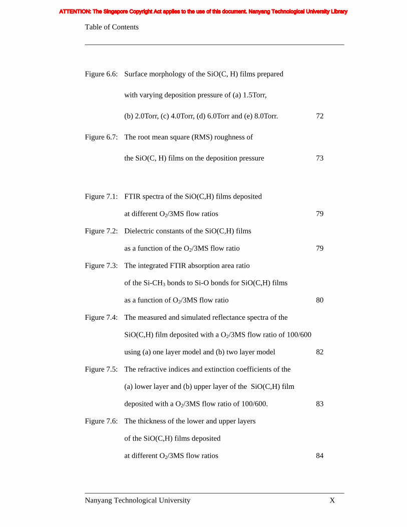
Table of Contents
Nanyang Technological University X
Figure 6.6: Surface morphology of the SiO(C, H) films prepared
with varying deposition pressure of (a) 1.5Torr,
(b) 2.0Torr, (c) 4.0Torr, (d) 6.0Torr and (e) 8.0Torr. 72
Figure 6.7: The root mean square (RMS) roughness of
the SiO(C, H) films on the deposition pressure 73
Figure 7.1: FTIR spectra of the SiO(C,H) films deposited
at different O2/3MS flow ratios 79
Figure 7.2: Dielectric constants of the SiO(C,H) films
as a function of the O2/3MS flow ratio 79
Figure 7.3: The integrated FTIR absorption area ratio
of the Si-CH3 bonds to Si-O bonds for SiO(C,H) films
as a function of O2/3MS flow ratio 80
Figure 7.4: The measured and simulated reflectance spectra of the
SiO(C,H) film deposited with a O2/3MS flow ratio of 100/600
using (a) one layer model and (b) two layer model 82
Figure 7.5: The refractive indices and extinction coefficients of the
(a) lower layer and (b) upper layer of the SiO(C,H) film
deposited with a O2/3MS flow ratio of 100/600. 83
Figure 7.6: The thickness of the lower and upper layers
of the SiO(C,H) films deposited
at different O2/3MS flow ratios 84
ATTENTION: The Singapore Copyright Act applies to the use of this document. Nanyang Technological University Library
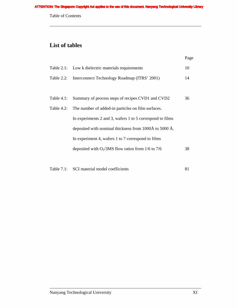
Table of Contents
Nanyang Technological University XI
List of tables
Page
Table 2.1: Low k dielectric materials requirements 10
Table 2.2: Interconnect Technology Roadmap (ITRS’ 2001) 14
Table 4.1: Summary of process steps of recipes CVD1 and CVD2 36
Table 4.2: The number of added-in particles on film surfaces.
In experiments 2 and 3, wafers 1 to 5 correspond to films
deposited with nominal thickness from 1000Å to 5000 Å.
In experiment 4, wafers 1 to 7 correspond to films
deposited with O2/3MS flow ratios from 1/6 to 7/6 38
Table 7.1: SCI material model coefficients 81
ATTENTION: The Singapore Copyright Act applies to the use of this document. Nanyang Technological University Library
Summary
Nanyang Technological University XII
Summary
This thesis focuses on the growth and characterization of carbon doped silicon
oxide (SiO(C,H)) low k dielectrics for multilevel interconnect applications.
SiO(C,H) films are formed by the plasma enhanced chemical vapor deposition
(PECVD) technique using linear organosilicate trimethylsilane (3MS) as precursor and
oxygen as oxidizer. The properties of this dielectric film have been investigated by
energy dispersive x-ray (EDX) spectrometer, Fourier transform infrared (FTIR)
absorption and atomic force microscopy (AFM). Other measurement tools applied
include KLA-Tencor® SP1 for blanket wafer particle counts, Thermawave Opti-probe
for thickness, uniformity and refractive index measurement, SSM® C-V system for k
value measurement and FSM system for stress measurement.
The properties of the PECVD prepared SiO(C,H) films are dependent not only
on the process parameters but also process sequences. The SiO(C,H) low k films
deposited using an initial recipe labelled as CVD1 suffer from serious particle issue. To
address the particle issue, we have optimized the oxygen and helium treatment process
sequence, immediately before and after film deposition step. Using this new recipe
CVD2, it has been found that the serious particle issue could be resolved. However this
rearrangement compromises the other properties of the films in terms of a slight
ATTENTION: The Singapore Copyright Act applies to the use of this document. Nanyang Technological University Library
Summary
Nanyang Technological University XIII
increase in the dielectric constant and non-uniform deposition rate as a function of film
thickness.
For films deposited with different O2/3MS gas flow ratio, it is found that the
deposition rate increases while the refractive index decreases with increasing oxygen
concentration in the gas feed. Dielectric constant as low as 2.9 has been obtained for the
as-deposited film with an optimized O2/3MS flow ratio of 100/600. Thermal annealing
has been found to reduce the dielectric constant of the films at 400°C. The films are also
found to be thermally stable up to as high as 500°C in terms of their composition and
chemical structure.
The effects of deposition pressure on the properties of SiO(C,H) films have
also been investigated. An increase in the deposition pressure resulted in films with
lower dielectric constants and refractive indices. A dielectric constant as low as 2.9 has
been obtained for the film deposited at 8.0Torr and a high deposition rate of 5120Å/min
has been obtained for films deposited at 4.0Torr.
We have also studied the optical properties of the SiO(C,H) films. Their
reflectivity were measured under normal incident and at 700 incident angle using
polarized light, over a range of wavelengths from 200nm to 1700nm, to determine their
optical constants (n and k) and thickness. It is found that the growth of SiO(C,H) films
involves a two-layer process, in which a layer of thin SiC:H film is first formed, which
ATTENTION: The Singapore Copyright Act applies to the use of this document. Nanyang Technological University Library
Summary
Nanyang Technological University XIV
is then followed by the growth of SiO(C,H) film. We have proposed a growth
mechanism to explain the two-layer growth process. Though the thin layer of SiC:H
does not have much influence on the dielectric constants of the SiO(C,H) films,
however, it may pose a potential challenge for these low k films in terms of advanced
integration, such as acting as an unexpected etch stop layer.
ATTENTION: The Singapore Copyright Act applies to the use of this document. Nanyang Technological University Library
Chapter 1: Introduction
Nanyang Technological University 1
Chapter 1: Introduction
1.1 Background
Continuous shrinking of interconnect pitch on integrated circuits increases
wire resistance of smaller metal line and makes the crosstalk effects between closer
metal space severer. Consequently these degrade interconnect RC delay and limit the
high performance of integrated circuits (IC). In order to reduce the RC delay, it is
necessary to decrease the capacitances among the metal lines by using low permittivity
(low k) dielectrics as isolation material, besides using lower resistance metal
interconnects. Hence, the International Technology Roadmap for Semiconductors
(ITRS) calls for the implementation of low k materials. As a result, over the past few
years, low dielectric materials have been under intensive research.
1.2 Motivation for the work
The implementation of low dielectric constant materials in ultra-large-scale
integrated (ULSI) devices has been repeatedly delayed and the technology is taking
much longer to move into production than originally planned [1,2]. Difficulties exist in
retaining the low dielectric permittivity properties and compatibility during the
integrated process. The challenges have proven to be substantial, requiring new
ATTENTION: The Singapore Copyright Act applies to the use of this document. Nanyang Technological University Library
Chapter 1: Introduction
Nanyang Technological University 2
approaches for characterization and integration of low k materials with copper [3]. If
the factors relating to the properties of low k materials have been fully understood right
from the beginning, then the implementation of low dielectric constant materials may
be as short as what it is expected to be.
1.3 Objectives of the work
This research topic will focus on the growth and characterization of low k
dielectric thin films for multilevel interconnect applications, including the
characterization of the material properties and the optimization of the process steps.
Specifically, the dielectric that we will be investigating is carbon doped silicon oxide
(SiO(C, H)) thin films deposited using the plasma enhanced chemical vapor deposition
(PECVD) process from organosilicon precursor trimethysilane (C3H10Si, also referred
to as 3MS) and oxygen. This dielectric is one of the most favorable low k materials due
to their low k (<3) and their key electrical and integration characteristics being similar
to those of SiO2 [3]. The molecular structure of 3MS necessitates the use of an oxidant
in the deposition process to provide a low k Si-O network [4]. The incorporation of
carbon atoms serves to reduce the dielectric constant due to their reduced polarizability
compared to silicon and oxygen [5].
The properties of the SiO(C,H) films depend on the process parameters such as
the flow rate and process pressure. In this work, we will focus on:
ATTENTION: The Singapore Copyright Act applies to the use of this document. Nanyang Technological University Library
Chapter 1: Introduction
Nanyang Technological University 3
1) optimizing the deposition process sequences,
2) evaluating the feed gas flow ratio impacts on the dielectric k value and
other properties,
3) investigating the thermal stability of the low dielectric constant films by
post annealing,
4) studying the process pressure effects on the dielectric k value and other
properties and
5) studying their optical properties.
1.4 Organization of the report
In the physical order, the chapters of this thesis are arranged as follows:
Chapter one gives an introduction, detailing the background, motivation and objective
of this study. Chapter two presents information about technology trend for low k/copper
including the single and dual damascene schematics. Chapter three describes the
experimental equipment and characterization tools used. Chapter four details the study
of oxygen influences on SiO(C,H) films and considers the impact of process sequences
on the properties of the films. Chapter five reports on the SiO(C,H) films prepared
using different O2/3MS flow ratios, and investigate their thermal stability through
post-deposition annealing. Chapter six presents the study of the SiO(C,H) films under
different process pressures. Chapter seven presents a study on the optical properties of
the films. Chapter 8 presents the conclusion and future work of our study.
ATTENTION: The Singapore Copyright Act applies to the use of this document. Nanyang Technological University Library
Chapter 1: Introduction
Nanyang Technological University 4
1.5 References
1 Katherine Derbyshire, Still waiting for low-k dielectrics, Semiconductor Manufacturing Magazine, January 2002 Vol. 3, No. 1.
2 Katherine Derbyshire, High frustration over low-k, Semiconductor
Manufacturing Magazine, October 2003 Vol. 3, No. 10. 3 Laura Peters, Industry divides on low k dielectric choices, Semiconductor
International, June 1998. 4 B. Narayanan, R. Kumar and P. D. Foo, “Properties of low-k SiCOH films
prepared by plasma-enhanced chemical vapor deposition using trimethylsilane”, Microelectronics Journal, Vol. 33, pp. 971 - 974, 2002.
5 Keith Buchanan, The evolution of interconnect technology for silicon
integrated circuitry, 2002 GaAsMANTECH Conference.
ATTENTION: The Singapore Copyright Act applies to the use of this document. Nanyang Technological University Library
Chapter 2: Literature review
Nanyang Technological University 5
Chapter 2: Literature Review
2.1 Introduction
Continuous improvement in integrated circuit feature size (miniaturization)
and device performance (faster operating speed and higher packing density) have
been achieved through multi-level metallization scheme. This trend in accordance
with Moore’s Law (the number of components per chip doubles every 18 months) [1]
as shown in Fig. 2.1. Multi-level metallization allows increased functionality
(transistor connectivity) whilst simultaneously decreases the average metal line
length, the latter being having a large influence on the interconnect-related R×C
(resistance × capacitance) signal propagation delay [2].
Figure 2.1: Technology evaluation and acceleration – Moore’s Law (1975).
Deleted: 
Deleted: two
Deleted: 1
ATTENTION: The Singapore Copyright Act applies to the use of this document. Nanyang Technological University Library
Chapter 2: Literature review
Nanyang Technological University 6
The speed of IC devices is limited by the resistance of metal layers and the
capacitance of dielectric insulating materials surrounding the metal lines. The speed
of devices can also be limited by transistor dimensions, however, these are already
very small in advanced processes, and are not longer the contributing factors to signal
propagation delay. Figure 2.2 illustrates that the interconnect delay is beginning to
dominate the overall device delay at 0.18 µm, therefore, it is important to switch to
lower resistivity metals such as copper as well as low k dielectric materials [3].
Figure 2.2: Decrease in interconnect delay and improved performances are achieved
using copper and low k dielectrics.
As device integration has been shown to be more difficult than predicted, the
transition from SiO2 (CVD k = 4.1 – 4.2) to new dielectric materials with k < 3.0 was
delayed by about three years, compared to the initial semiconductor industry
association Roadmap targets [4].
Deleted: 
Deleted: Literature survey¶¶What is low k?¶¶
A low dielectric constant material can be defined as a dielectric material with dielectric constant close to or less than about 3.¶¶Why low k?
Deleted: ¶In modern integrated circuits the feature size is scaled down while the chip area is scaled up, hence delays due to resistance and capacitance of interconnecting lines become the predominant part of the total delay. This will increasingly limit the performance of high-speed logic chips.
Deleted: ig.
Deleted: dominance of interconnect RC delay over gate delay for as feature size beyond 180 nm.
Deleted: 1
ATTENTION: The Singapore Copyright Act applies to the use of this document. Nanyang Technological University Library
Chapter 2: Literature review
Nanyang Technological University 7
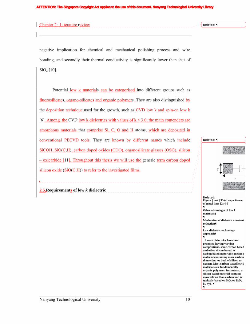
2.2 Interconnect delay
Interconnect delay is determined using the well-known formula:
T = RC (2.1)
where R is the line resistance of the interconnect metal and C is the
capacitance associated with the isolation dielectric. A schematic diagram of an
interconnect is shown in Fig. 2.3.
Figure 2.3: Capacitance occurs within and between metal layers [5].
The total resistance R of the metal line can be expressed as
R=2ρL / (PT) (2.2)
where ρ is the resistivity of the metal line, L is length of the interconnect line,
P is the pitch or line spacing, and T is the thickness of the line.
There are two types of capacitance: the vertical layer-to-layer capacitance CV
and the lateral line-to-line capacitance CLL. The total capacitance C can be expressed
as
Upper Metal Layer
Interconect Metal Layer
Lower Metal Layer
Deleted: 
Deleted: 
Figure 11:
Deleted: RC delayCalculated gate and interconnect delay versus technology generation. [1y]¶¶
Deleted: RC
Deleted: related to the line resistance of the interconnect metal (R) and capacitance associated with the isolation dielectric (C).
Deleted: as
Deleted: . [ ooo ]
Deleted: 
Deleted:
Deleted: /(
Deleted:
Deleted: 1
Deleted:
Deleted:
Deleted:
Deleted: spacing ,
Deleted:
Deleted: 
Deleted:
Deleted: ypes of capacitance
Deleted: s
Deleted: ,
Deleted: namely
Deleted:
Deleted: L
ATTENTION: The Singapore Copyright Act applies to the use of this document. Nanyang Technological University Library
Chapter 2: Literature review
Nanyang Technological University 8
C=2(CV+CLL) =2kεo(2LT/P+LP/2T) (2.3)
where k is the dielectric constant or relative permittivity and
εo= 8.85 x 10¹² F/m is the permittivity of vacuum.
Combining equations (2.1), (2.2) and (2.3), yields the equation for
interconnect delay
T=RC=2 ρ k εo L2(4/P2+ 1/T2) (2.4)
Equation (2.4) shows that the common chip geometry drivers, that is,
decreasing P and T, will result in larger RC delay. Furthermore, increasing system
complexity and size of die are causing L to increase [5]. Therefore, the RC delay can
only be reduced by decreasing ρ and k. Hence, besides using copper metallization,
there is a need for low dielectric constant (low k) materials to replace conventional
SiO2.
2.3 Definition of low k
The dielectric constant of a dielectric is defined as the ratio of its permittivity
to the permittivity of vacuum. A dielectric material having relatively greater
insulating property than silicon dioxide (SiO2), usually with a k<3.9 is termed as a
low dielectric constant material [6]. In practice, low k materials are mostly defined as
dielectrics with a bulk dielectric constant below 3.0 [7].
Deleted: 
Deleted:
Deleted: L
Deleted: )=
Deleted: (
Deleted: )
Deleted: (
Deleted: )
Deleted:
Deleted: 2
Deleted: where
Deleted:
Deleted:
Deleted: E
Deleted:
Deleted: (
Deleted: )
Deleted: (
Deleted:
Deleted: 3
Deleted: 
Deleted: 3
Deleted: increasing
Deleted: hus
Deleted: )
Deleted:
ATTENTION: The Singapore Copyright Act applies to the use of this document. Nanyang Technological University Library
Chapter 2: Literature review
Nanyang Technological University 9
2.4 Mechanism of dielectric constant reduction
There are two primary approaches towards achieving low dielectric constant
materials. The first approach is to reduce polarizability by lowering the electronic,
ionic, and/or the orientation contribution [8]. The electronic component refers to the
oscillation of electrons in chemical bonds and/or in the extended super molecular
structure. The latter two components constitute the nuclear response and are important
at lower frequencies (<1013 Hz), while the electronic response dominates at higher
frequencies (4.74 × 10¹⁴ Hz). At typical device operating frequencies, currently <109
Hz, all three components contribute to the dielectric constant and must be minimized
for optimum performance [4]. The second approach is to increase the porosity and
reduce the mass density [8], as this will lower the dielectric constant. The lower
dielectric constant of non-polar organic polymers (~2.0-2.8) relative to SiO2 (3.9-4.2)
is partly due to the presence of lighter C and H atoms versus Si and O atoms, as well
as the low packing density (d~1.0 g/cm3) relative to the denser tetrahedral silica
network (d~2.4 g/cm3). The incorporation of non-polar and space-occupying groups
such as methyl will also increase free volume in a silica network [4].
The SiO(C,H) films investigated in this work utilize a combination of both
approaches. However, the reduction in dielectric constant is usually achieved at the
expense of other desirable material properties and this can make integration more
difficult. In both cases the reduced network bonding and reduced density contribute
negatively to the film’s mechanical properties [9]. Two unavoidable consequences
will be resulted from the reduction in k value. Firstly, the films are not as hard, with
Deleted: 
ATTENTION: The Singapore Copyright Act applies to the use of this document. Nanyang Technological University Library
Chapter 2: Literature review
Nanyang Technological University 10
negative implication for chemical and mechanical polishing process and wire
bonding, and secondly their thermal conductivity is significantly lower than that of
SiO2 [10].
Potential low k materials can be categorised into different groups such as
fluorosilicates, organo-silicates and organic polymers. They are also distinguished by
the deposition technique used for the growth, such as CVD low k and spin-on low k
[6]. Among the CVD low k dielectrics with values of k < 3.0, the main contenders are
amorphous materials that comprise Si, C, O and H atoms, which are deposited in
conventional PECVD tools. They are known by different names which include
SiCOH, SiO(C,H), carbon doped oxides (CDO), organosilicate glasses (OSG), silicon
– oxicarbide [11]. Throughout this thesis we will use the generic term carbon doped
silicon oxide (SiO(C,H)) to refer to the investigated films.
2.5 Requirements of low k dielectric
Deleted: 
Deleted: 
Deleted: Figure [ ooo ]:Total capacitance of metal lines [2w].¶¶Other advantages of low k materials¶¶Mechanism of dielectric constant reduction¶¶Low dielectric technology approach¶¶
Low k dielectrics have been proposed having varying compositions, some carbon based and other silicon based. A carbon based material is meant a material containing more carbon than either or both of silicon or oxygen. Most carbon based low k materials are fundamentally organic polymers. In contrast, a silicon based material contains more silicon than carbon and is typically based on SiO2 or Si3N4 [3, 4y]. ¶¶
ATTENTION: The Singapore Copyright Act applies to the use of this document. Nanyang Technological University Library
Chapter 2: Literature review
Nanyang Technological University 11
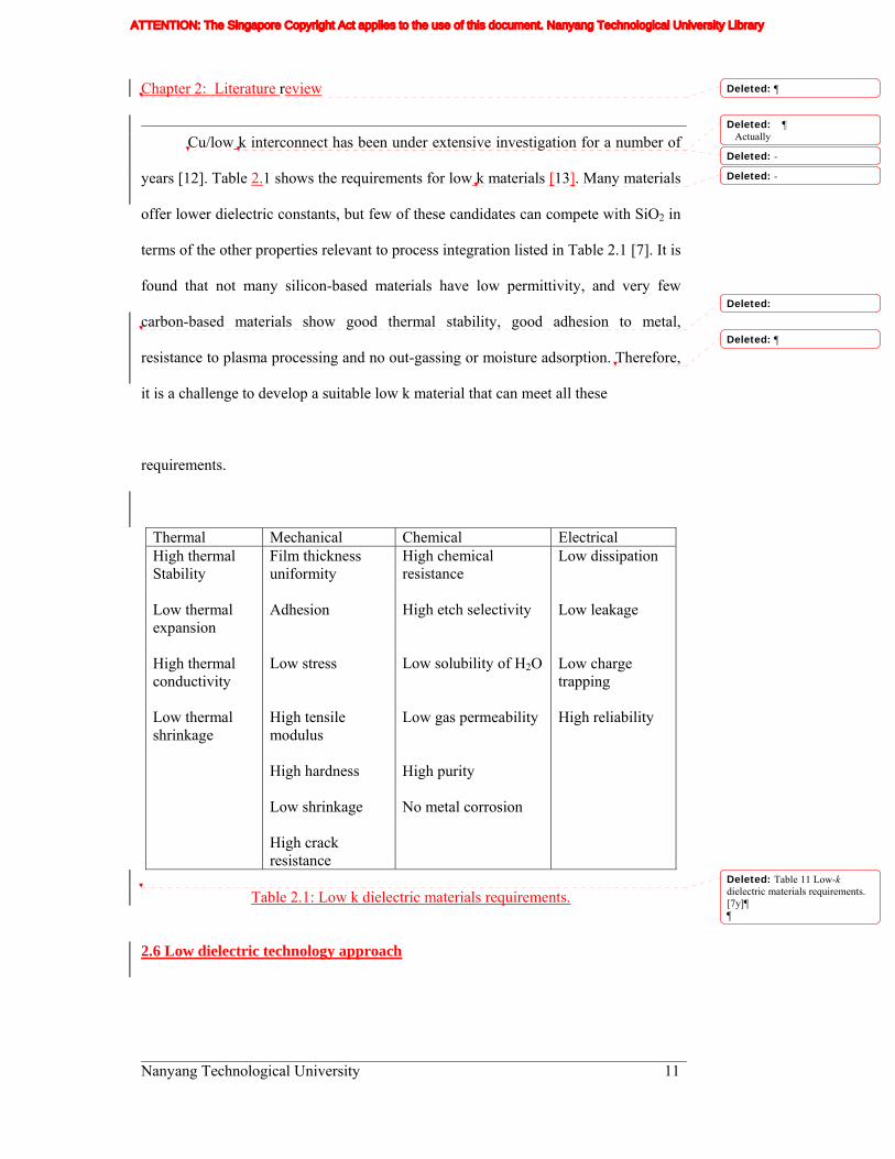
Cu/low k interconnect has been under extensive investigation for a number of
years [12]. Table 2.1 shows the requirements for low k materials [13]. Many materials
offer lower dielectric constants, but few of these candidates can compete with SiO2 in
terms of the other properties relevant to process integration listed in Table 2.1 [7]. It is
found that not many silicon-based materials have low permittivity, and very few
carbon-based materials show good thermal stability, good adhesion to metal,
resistance to plasma processing and no out-gassing or moisture adsorption. Therefore,
it is a challenge to develop a suitable low k material that can meet all these
requirements.
Thermal Mechanical Chemical Electrical High thermal Stability Low thermal expansion High thermal conductivity Low thermal shrinkage
Film thickness uniformity Adhesion Low stress High tensile modulus High hardness Low shrinkage High crack resistance
High chemical resistance High etch selectivity Low solubility of H2O Low gas permeability High purity No metal corrosion
Low dissipation Low leakage Low charge trapping High reliability
Table 2.1: Low k dielectric materials requirements.
2.6 Low dielectric technology approach
Deleted: 
Deleted: ¶Actually
Deleted: -
Deleted: -
Deleted:
Deleted: 
Deleted: Table 11 Low-k dielectric materials requirements. [7y]¶¶
ATTENTION: The Singapore Copyright Act applies to the use of this document. Nanyang Technological University Library
Chapter 2: Literature review
Nanyang Technological University 12
As the industry moves toward the 0.13 μm generation and beyond, first
generation low k materials such as fluorine-doped silicate glass (FSG, k=3.5 ~ 3.7)
will be replaced by the second generation low k films, with dielectric constant below
3.0, to allow the continued miniaturization of integrated circuits and to provide higher
speed and performance [8,14].
Recently, many researchers have proposed various organic and inorganic
materials as alternatives to SiO2. Organic materials have more significant integration
problems than inorganic materials, such as poor adhesion, thermal instability and low
resistance to O2 plasma. Films made from inorganic materials have better thermal and
mechanical stability, as well as better film adhesion during integration processing.
However, they generally have higher dielectric constants and more serious moisture
absorption than organic materials, and as a result they require additional liner and
capping layer. Therefore, SiO(C,H), a hybrid type film between organic and inorganic
materials has become a favorable low dielectric constant material suitable for ULSI
process integration [15].
In SiO(C,H), carbon is introduced, typically in the form of methyl (-CH3)
groups, bonded to Si atoms, and effectively terminate a proportion of the Si-O bonds.
This results in a reduction in the polarizability of the bonds, and a corresponding
decrease in the k value. This material, formed from plasma enhanced chemical vapor
deposition (PECVD) process by oxidizing methylsilane, is physically porous. The
porous structure contributes to a decrease in the material mass density and further
lowers the k value. However, the porosity also induces some undesirable integration
Deleted: 
Deleted: esees
Deleted: un
Deleted: an overall “loosing” of the lattice,
Deleted: a
Deleted: in
Deleted:
Deleted: the film density
Deleted: [7, 8y]
Deleted: ese
Deleted: s
Deleted: are
Deleted: grown
Deleted:
Deleted:
Deleted: k value
ATTENTION: The Singapore Copyright Act applies to the use of this document. Nanyang Technological University Library
Chapter 2: Literature review
Nanyang Technological University 13
problems.
SiO(C,H) materials have attracted considerable attention in the replacement of
SiO2 as the interlayer dielectric (ILD) and are expected to be a more cost-effective
solution for the immediate low-k needs primarily due to:
• Shorter lead-time for process development.
• Re-use of existing tool-set.
• Process extendibility to Cu-Damascene using conventional CVD
equipment and silicon-based materials.
• Superior thermal and mechanical stability over the organic materials,
making process integration relatively straightforward [16].
In this study, we will focus on the growth and characterization of SiO(C,H)
low k dielectrics for multilevel applications, deposited by the plasma enhanced
chemical vapor deposition (PECVD) process using organosilane trimethlysilane
(3MS) as the precursors and oxygen (O2) as the oxidizer.
2.7 Fundamental of plasma enhanced chemical vapor deposition
The plasma enhanced chemical vapor deposition (PECVD) of thin films is
widely used in microelectronics manufacturing. The PECVD process are generally
carried out at pressures of 1mTorr to 20Torr, substrate temperatures in the range of
100 to 500°C, rf power densities < 0.5W-cm-2, electron mean free paths of <0.1cm,
and average electron energies of 1 to 6 eV [17].
Deleted: 
Formatted: Bullets andNumbering
Deleted: ¶¶
Deleted: 
ATTENTION: The Singapore Copyright Act applies to the use of this document. Nanyang Technological University Library
Chapter 2: Literature review
Nanyang Technological University 14
When a plasma is initiated by the applied rf power, energy from the rf electric
field is coupled into the reactant gases via the kinetic energy of a few free electrons.
These electrons will gain energy rapidly through the electric field and lose energy
slowly through elastic collisions. The high-energy electrons are capable of inelastic
collisions that cause the reactant gas molecules to dissociate and ionize, producing
secondary electrons by various electron-impact reactions. Next, these reactive species
are transported from the plasma to the substrate surface concurrently with the
occurrence of many elastic and inelastic collision in both the plasma and sheath
regions. Following that is the absorption and /or reaction of reactive species at the
substrate surface. Finally, the reactive species and / or reaction products are
incorporated into the deposited films or re-emitted from surface back to the gas phase.
In general, the PECVD process can be qualitatively summarized below [18]:
• Transport of reactants to the growth region.
• Mass transport of reactants to the wafer surface.
• Adsorption of reactants.
• Physical-chemical reactions yielding the solid film and reaction
byproducts.
• Desorption of byproducts.
• Mass transport of byproducts to the main gas stream.
• Transport of byproducts away form the growth region.
Deleted: 
ATTENTION: The Singapore Copyright Act applies to the use of this document. Nanyang Technological University Library
Chapter 2: Literature review
Nanyang Technological University 15
In plasma enhanced CVD processing, physical and chemical properties of the
deposited film can be controlled by not only changing the type of reactive species, but
also varying deposition parameters such as temperature, rf power, pressure, reactant
gas mixture ratio, and type of reactant.
2.8 Low constant dielectric application
The International Technology Roadmap for Semiconductors (ITRS) calls for
the implementation of low k materials. Table 2.2 shows the interconnect technology
requirements (ITRS 2001 Edition, Interconnect) [19].
YEAR OF PRODUCTION 2001 2002 2003 2004 2005 2006 2007MPU/ASIC 1/2 PITCH (nm) 150 130 107 90 80 70 65Number of metal levels 8 8 8 9 10 10 10Number of optional levels - groundplanes/capacitors
2 2 4 4 4 4 4
Local wiring pitch (nm) 350 295 245 210 185 170 150Local wiring A/R (for Cu) 1.6 1.6 1.6 1.7 1.7 1.7 1.7Intermediate wiring pitch (nm) 450 380 320 265 240 215 195Intermediate wiring dual DamasceneA/R (Cu wire/via)
1.6/1.4 1.6/1.4 1.7/1.5 1.7/1.5 1.7/1.5 1.7/1.6 1.8/1.6
Global wiring dual Damascene A/R(Cu wire/via)
2.0/1.8 2.0/1.8 2.1/1.9 2.1/1.9 2.2/2.0 2.2/2.0 2.2/2.0
Interlevel metal insulator - effectivedielectric constant (k)
3.0-3.6 3.0-3.6 3.0-3.6 2.6-3.1 2.6-3.1 2.6-3.1 2.3-2.7
Interlevel metal insulator (minimumexpected) - bulk dielectric constant (k)
<2.7 <2.7 <2.7 <2.4 <2.4 <2.4 <2.1
Solutions exist & are being optimisedSolutions are knownSolutions are NOT known
Table 2.2: Interconnect Technology Requirements (ITRS’ 2001)
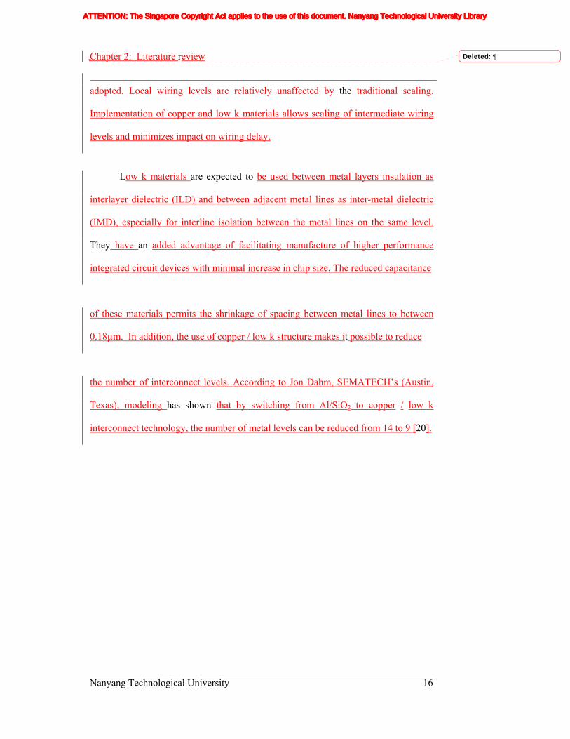
Figure 2.4 highlights a hierarchical scaling methodology that has been broadly
Deleted: 
Deleted: 1
ATTENTION: The Singapore Copyright Act applies to the use of this document. Nanyang Technological University Library
Chapter 2: Literature review
Nanyang Technological University 16
adopted. Local wiring levels are relatively unaffected by the traditional scaling.
Implementation of copper and low k materials allows scaling of intermediate wiring
levels and minimizes impact on wiring delay.
Low k materials are expected to be used between metal layers insulation as
interlayer dielectric (ILD) and between adjacent metal lines as inter-metal dielectric
(IMD), especially for interline isolation between the metal lines on the same level.
They have an added advantage of facilitating manufacture of higher performance
integrated circuit devices with minimal increase in chip size. The reduced capacitance
of these materials permits the shrinkage of spacing between metal lines to between
0.18µm. In addition, the use of copper / low k structure makes it possible to reduce
the number of interconnect levels. According to Jon Dahm, SEMATECH’s (Austin,
Texas), modeling has shown that by switching from Al/SiO2 to copper / low k
interconnect technology, the number of metal levels can be reduced from 14 to 9 [20].
Deleted: 
ATTENTION: The Singapore Copyright Act applies to the use of this document. Nanyang Technological University Library
Chapter 2: Literature review
Nanyang Technological University 17
Figure 2.4: Cross-section of hierarchical scaling
2.9 References
1. B. Narayanan, R. Kumar and P. D. Foo, “Properties of low-k SiCOH films prepared by plasma-enhanced chemical vapor deposition using trimethylsilane”, Microelectronics Journal, Vol. 33, pp. 971 - 974, 2002.
2. Keith Buchanan, The evolution of interconnect technology for silicon
integrated circuitry, 2002 GaAsMANTECH Conference.
3. Laura Peters, Pursuing the perfect low k dielectric, Semiconductor International, September 1998.
4. Josh H. Golden, Microbar Inc., Sunnyvale, Calif. Craig J. Hawker, Designing
porous low-k dielectrics, Semiconductor International, 5/1/2001.
Deleted: 
Deleted: AAA
ATTENTION: The Singapore Copyright Act applies to the use of this document. Nanyang Technological University Library
Chapter 2: Literature review
Nanyang Technological University 18
5. Michael E. Clarke, “Introducing low-k dielectrics into semiconductor
processing”, Mykrolis Corporation, Billerica, Massachusetts, <http://www.mykrolis.com>.
6. R. Singh and R.K. Ulrich, High and low dielectric constant materials, The
Electrochemical Society Interface, summer 1999, Pages 26-30.
7. Katherine Derbyshire, Still waiting for low-k dielectrics, Semiconductor Manufacturing Magazine, January 2002 Vol. 3, No. 1.
8. David Cheung, Black Diamond CVD low k films for copper damascene, Low
k dielectric materials technology, SEMICON West 1999, Pages F1-F10.
9. Mark ONeill, Aaron Lukas, Raymond Vrtis, Jean Vincent, Brian Peterson, Mark Bitner and Eugene Karwacki, Low-k Materials by Design, Semiconductor International, 6/1/2002.
10. Laura Peters, Industry divides on low k dielectric choices, Semiconductor
International, June 1998.
11. Alfred Grill and Deborah A. Neumayer, Structure of low dielectric constant to extreme low dielectric constant SiCOH films: Fourier transform infrared spectroscopy characterization, Journal of Applied Physics, Volume 94, Issue 10, pp. 6697-6707
12. Copper/Low-k Interconnect in Integrated Circuits, Motivations, Trends and
Difficulties, Reza Navid, Department of Electrical Engineering and Computer Science University of Michigan; Term Paper for EECS 598, Nanotechnology.
13. Development of Black Diamond™ Plasma Etching for Dual-Damascene
Metallization of VLSI, Ng Beng Teck, Industry Attachment Report at Institute of Microelectronics, Singapore.
14. Ben Pang, Wai-fan Yau, Peter Lee and Mehul Naik, A new CVD process for
damascene low k applications, Semiconductor Fabtech – 10th Edition, Pages 285-289.
15. Chang Shil Yang, Kyoung Suk Oh, Jai Yon Ryu, Doo Chul Kim, Jing Shou-
Yong, Chi Kyu Choi, Heon-Ju Lee, Se Hun Um and Hong Young Chang, A study on the formation and characteristics of the Si---O---C---H composite thin films with low dielectric constant for advanced semiconductor devices, Thin Solid Films , Volume 390, Issues 1-2 , Pages 113-118.
16. Lee, P.W.; Chi-I Lang; Sugiarto, D.; Li-Qun Xia; Gotuaco, M.; Yieh, E.;
Multi-generation CVD low κ films for 0.13 μm and beyond, Solid-State and Integrated-Circuit Technology, 2001. Proceedings. 6th International
Deleted: 
ATTENTION: The Singapore Copyright Act applies to the use of this document. Nanyang Technological University Library
Chapter 2: Literature review
Nanyang Technological University 19
Conference on, Volume:1, 22-25Oct. 2001 , Page(s): 358 -363 vol.1.
17. D.R. Cote etc al., Plasma-assisted chemical vapor deposition of dielectric thin film for ULSI semiconductor circuits, IBM J. RES. DEVELOP. VOL. 43 NO. ½ January/March 1999, Pages 5-39.
18. Stephen M. Rossnagel, Jerome J. Cuomo and William D. Westwood,
Handbook of Plasma Processing Technology, Noyes Publications, 1990, page 266.
19. The International Technology Roadmap Semiconductors: 2001,
Semiconductor Industry Association, San Jose, CA.
20. Peter Singer, Copper goes mainstream, low k to follow, Semiconductor International, Vol. 20, Issue 13, (1997), p67
Deleted: 
ATTENTION: The Singapore Copyright Act applies to the use of this document. Nanyang Technological University Library
Chapter 3: Experimental setup
Nanyang Technological University 19
Chapter 3: Experimental Setup 3.1 Introduction
In this work, a commercial plasma enhanced chemical vapor deposition
(PECVD) system ⎯ Applied Materials CENTURA 5200 system has been used for
deposition of carbon doped silicon oxide (SiO(C,H)) low dielectric thin films. Dow
Corning’s Semiconductor Grade linear silicon–source gas Trimethylsilane (3MS) has
been used as the precursor and oxygen gas as the oxidizer. The post-annealing of the
films were carried out using the TEL α SERIES LP – CVD from Tokyo Electron
Limited.
Many different characterization tools were used to investigate the properties of
the films. The defects on film surface were measured using scattered-light and defect
compositions were analysed using energy dispersive x-ray spectrometer (EDX). The
film thickness and refractive index were measured using spectrometric reflectance
spectrophotmetry. Dielectric constant measurements were carried out using a
Si/insulator/mecury probe structure. The atomic bonding and their relative
concentrations in the films were characterized by the Fourier Transform Infrared
(FTIR) spectroscopy. The film surface morphology was investigated using Atomic
force microscopy (AFM). The stresses of as-deposited and annealed films were
determined using FSM 7800iTC.
This chapter will present a description of the deposition system used, and a
general overview of the above characterization tools and their working principles.
ATTENTION: The Singapore Copyright Act applies to the use of this document. Nanyang Technological University Library
Chapter 3: Experimental setup
Nanyang Technological University 20
3.2 Plasma enhanced chemical vapor deposition (PECVD) system
PECVD is a process where plasma is used to lower the temperature required to
deposit films onto wafers. During the deposition process, gases containing the
insulator chemistry are decomposed and ionized by the plasma, and react on the
heated wafer surface, forming a thin film of solid material. Energy sources such as
heat and radio frequency (rf) power are used alone or in combination to achieve this
reaction. The advantage of the PECVD process is that it allows the use of low
deposition temperature, avoiding defect formation in the underlying silicon substrate,
dopant diffusion and degradation of the metal layers [1].
The Applied Materials CENTURA 5200 system 200mm deposition chamber
is a radial flow reactor. The chamber basic type is CVD, chamber variant is D × Z and
chamber effective volume is 5450cc.
A schematic diagram of the inverse radial flow reactor with perforated
electrode used in this experiment is described in Fig. 3.1[2]. The Centura system uses
a 13.56MHz compact rf delivery system consisting of a RF/DC generator and multi-
function adaptor. The generator rf output impedance range is 50 – 400 Ω and over
1000W output power at nominal line. A dry pump Edwards IQDP 80 is used to
achieve a base pressure of 24mTorr. The schematic diagram of the PECVD
configuration shown in Fig. 3.2.
ATTENTION: The Singapore Copyright Act applies to the use of this document. Nanyang Technological University Library
Chapter 3: Experimental setup
Nanyang Technological University 21
Figure 3.1: Schematic diagram of the inverse radial flow reactor with perforated electrode.
Figure 3.2: Schematic diagram of the PECVD system.
ATTENTION: The Singapore Copyright Act applies to the use of this document. Nanyang Technological University Library
Chapter 3: Experimental setup
Nanyang Technological University 22
In the experiment, the substrate temperature was maintained at 350°C, rf
power at 600W, and the discharge was struck between two 26.3 cm diameter
electrodes spaced 300mil apart. Unless otherwise specified, the process pressure was
fixed at 4.0Torr, O2 flow at 100sccm and 3MS flow at 600sccm. The precursors used
were linear organosilicate trimethylsilane (3MS) and oxygen (O2). Upon deposition,
the wafers were exposed to a continuous N2 flow of 350sccm for 120 seconds to cool
them down to room temperature.
During the deposition process, the wafers were loaded onto the lower
electrically grounded electrode. The perforated upper electrode is connected to the rf
generator through an impedance matching network. The plasma is generated between
two parallel circular electrodes. The reactants are fed in from the upper electrode,
with the gas flow directed radially outward. Working gases trimethylsilane (3MS) and
Oxygen (O2) are fed into the chamber via mass flow controllers (MFCs).
As film deposition occurs on the chamber wall as well as on the substrate
during the growth process [3], the process chamber has to be cleaned after each
growth. A plasma formed from source gases of C2F6, NF3 and O2 was used to clean
the chamber and the completion of this process is monitored by an in-situ optical
emission spectroscopy (OES) end point detector.
ATTENTION: The Singapore Copyright Act applies to the use of this document. Nanyang Technological University Library
Chapter 3: Experimental setup
Nanyang Technological University 23
3.3 Low k annealing system
The low k furnace used for the annealing of samples is a vertical LPCVD
system ALPHA – 8S – ZVFNS from Tokyo Electron Limited, Japan. The temperature
ramping up rate is 50°C/min and ramping down rate is 9°C/min. The over-shoot is
less than 5°C and stability is within 1°C. The process gas used during the annealing is
nitrogen (N2) with a gas flow rate of 1000sccm.The annealing pressure is 7.0Torr.
3.4 Film inspection and characterization techniques
3.4.1 Unpatterned wafer inspection system
The unpatterned wafer inspection system used in this study is Surfscan® SP1
from KLA Tencor. It is designed to perform highly sensitive inspection of
unpatterned silicon wafer surfaces. It uses a system of fixed illumination and
collection optics to illuminate the wafer surface, collect and analyze the scattered
light. The illumination is derived from an argon ion laser that operates at 30 mW
power with a wavelength of 488nm. Since defects and irregularities on and in the
wafer surface affect the scattering power of the surface, therefore variations in the
intensity of the scattered light can be correlated with surface features. The system
processes the scattered-light signal to produce data that identifies the size and location
of surface features [4].
The Surfscan SP1 has five scan data collection channels: Dark field wide
normal, dark field narrow normal, dark field narrow oblique, dark field wide oblique
ATTENTION: The Singapore Copyright Act applies to the use of this document. Nanyang Technological University Library
Chapter 3: Experimental setup
Nanyang Technological University 24
and bright field channel. Point defects detected in both the dark field wide channel
and the dark field narrow channel can be displayed as composite data.
3.4.2 Spectrometric reflectance tool
The spectrometric reflectance tool used in this study is the Opti-Probe 5240i
system from Therma-wave. It is a non-destructive dielectric film thickness
measurement tool used for the measurement of thin film thickness (d) and refractive
index (optical constants, n) by measuring the reflected light and modelling the film
parameters. It performs this function by integrating three film measurement
techniques: reflectivity as a function of incident angle (beam profile reflectometry),
reflectivity as a function of wavelength (spectrometry), and changes in polarization
state (ellipsometry). The refractive indices presented in this work are taken at a
specific wavelength of 6730Å for comparison purpose across different films. The
system allow a simultaneous measurement of thickness and refractive index, and
hence eliminates errors involved in other techniques that measure thickness across the
wafer while assuming a constant refractive index [5].
3.4.3 Fourier transform infrared absorption spectroscopy (FTIR)
Infrared absorption spectroscopy is a common and useful tool in material
characterization. For solid material or gas molecule, the interaction between atoms
causes vibrations or rotations. From quantum mechanical consideration, it is known
that the rotational and vibrational energy levels are not continuous and that only those
ATTENTION: The Singapore Copyright Act applies to the use of this document. Nanyang Technological University Library
Chapter 3: Experimental setup
Nanyang Technological University 25
transition, which obey the selection rule, are allowed. Therefore, a specific bond (or
molecule) has its characteristic rotational and vibrational energy levels and
transitional energy, which can be used for identification of the bonding structure (or
molecule) by its absorption spectrum.
When radiation passes through a sample, the light can be absorbed only if the
energy and hence the frequency corresponds to the energy difference between two
quantum levels in the sample. This is described by the Bohr frequency condition:
ΔE = E2 - E1 = hν (3.1)
where h is Plank’s constant and ν is the frequency of the light in Hz.
In classical electromagnetic theory, the periodic variation of the dipole
moment of a vibrating molecule results in absorption of radiation of the same
frequency as that of the oscillation of the dipole moment. Normally, the energy
difference between two quantum levels is so small that the corresponding frequency is
in the infrared range [6].
In order to obtain the absorption of the thin film alone, the absorption by
substrate should be subtracted. Therefore, a bare substrate is needed as a reference in
every measurement. In this work, the infrared spectra were measured using a Bio-
Rad’s QS2200 FTIR spectrometer in the mid-infrared region from 400 to 4000 cm-1,
with a resolution of 4 cm-1. Since absorbance is also proportional to sample thickness,
the integrated area ratio of the Si-CH3 to Si-O-Si peak absorbance will be used as a
measure of the carbon content in the films for samples with different thickness.
ATTENTION: The Singapore Copyright Act applies to the use of this document. Nanyang Technological University Library
Chapter 3: Experimental setup
Nanyang Technological University 26
3.4.4 Dielectric constant measurement - MIS structure
Metal oxide semiconductor (MOS) C-V measurements traditionally have been
used to measure the characteristics of an oxide with a known dielectric constant.
Conversely, the value for k can be determined using the Si/insulator/mecury (MIS)
probe structure, provided the thickness of the dielectric film and the contact area are
known, according to a parallel plate capacitor model :
Go
oxox
AWCk
ε= (3.2)
where Cox is the accumulation region of capacitance, Wox is the thickness of
dielectric film, εo is the permittivity of free space and AG is the electrical contact area
[7].
The mercury probe SSM 495 CV system (Solid State Measurements, Inc.)
used for k value measurements is an automatic mercury probe capacitance-voltage
(CV) measurement system. Cox were measured using the SSM’s standard
forward/reverse bias C-V measurement module at 0.926MHz in this study. Dielectric
constants were automatically calculated based on the accumulation region of the
capacitance-voltage curve obtained.
3.4.5 Atomic Force Microscopy (AFM)
Atomic force microscope (AFM) probes the surface of a sample, with a sharp
tip, a couple of microns long and often less than 100Ǻ in diameter. The tip is located
at the free end of a cantilever that is 100 to 200μm long. Forces between the tip and
ATTENTION: The Singapore Copyright Act applies to the use of this document. Nanyang Technological University Library
Chapter 3: Experimental setup
Nanyang Technological University 27
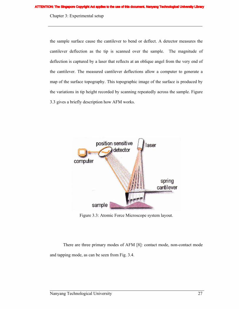
the sample surface cause the cantilever to bend or deflect. A detector measures the
cantilever deflection as the tip is scanned over the sample. The magnitude of
deflection is captured by a laser that reflects at an oblique angel from the very end of
the cantilever. The measured cantilever deflections allow a computer to generate a
map of the surface topography. This topographic image of the surface is produced by
the variations in tip height recorded by scanning repeatedly across the sample. Figure
3.3 gives a briefly description how AFM works.
Figure 3.3: Atomic Force Microscope system layout.
There are three primary modes of AFM [8]: contact mode, non-contact mode
and tapping mode, as can be seen from Fig. 3.4.
ATTENTION: The Singapore Copyright Act applies to the use of this document. Nanyang Technological University Library
Chapter 3: Experimental setup
Nanyang Technological University 28
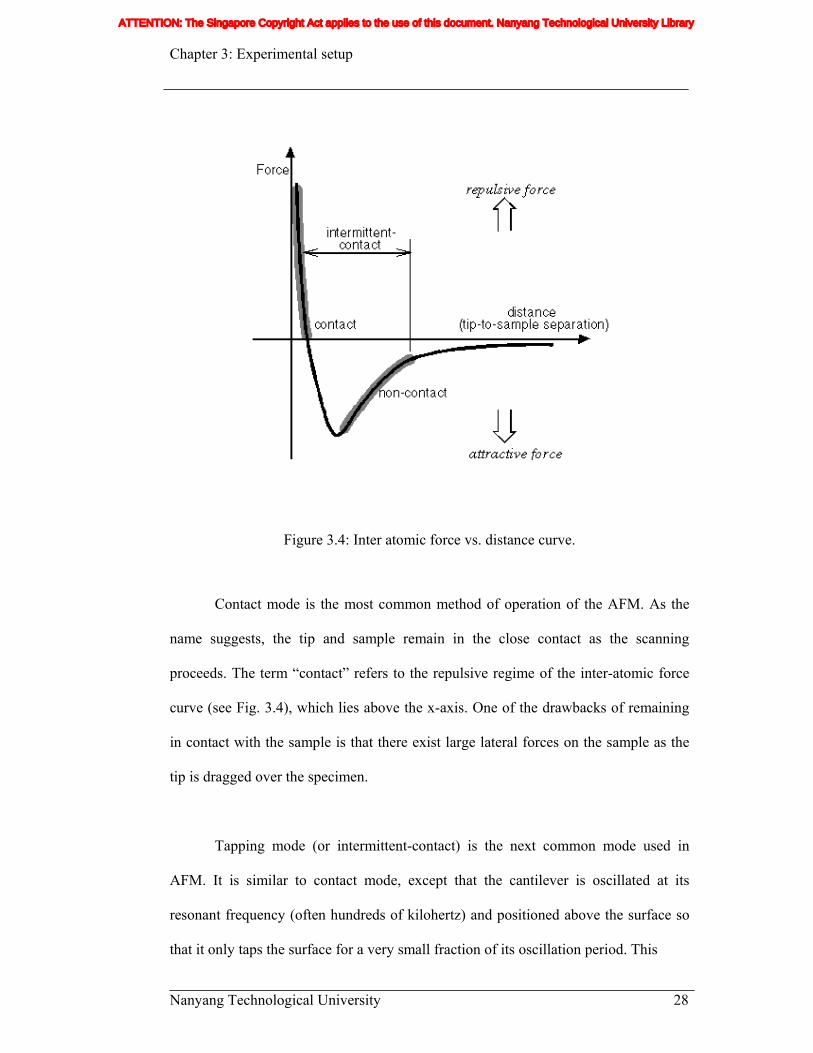
Figure 3.4: Inter atomic force vs. distance curve.
Contact mode is the most common method of operation of the AFM. As the
name suggests, the tip and sample remain in the close contact as the scanning
proceeds. The term “contact” refers to the repulsive regime of the inter-atomic force
curve (see Fig. 3.4), which lies above the x-axis. One of the drawbacks of remaining
in contact with the sample is that there exist large lateral forces on the sample as the
tip is dragged over the specimen.
Tapping mode (or intermittent-contact) is the next common mode used in
AFM. It is similar to contact mode, except that the cantilever is oscillated at its
resonant frequency (often hundreds of kilohertz) and positioned above the surface so
that it only taps the surface for a very small fraction of its oscillation period. This
ATTENTION: The Singapore Copyright Act applies to the use of this document. Nanyang Technological University Library
Chapter 3: Experimental setup
Nanyang Technological University 29
mode is still contact with the sample in the sense defined earlier, but the very short
time over which this contact occurs means that the lateral forces (friction or drag) are
dramatically reduced as the tip scans over the surface. When imaging poorly
immobilized or soft samples, tapping mode may be a far better choice than the contact
mode for imaging. In general, it has been found that tapping mode is more effective
than non-contact (which will be elucidated later) for imaging larger scan sizes that
may include greater variation in sample topography. Tapping mode AFM has become
an important AFM technique since it overcomes some of the limitations of both
contact and non-contact AFM.
Non-contact operation is another method that may be employed in AFM
application. The cantilever must be oscillated above the surface of the sample at such
a distance that we are no longer in the repulsive regime of the inter-atomic force curve
but in the attractive regime. In this mode, the system vibrates a stiff cantilever near its
resonant frequency with an amplitude of a few tens of angstroms. Then it detects
changes in the resonant frequency or vibration amplitude as the tip comes near the
sample surface. The sensitivity of this detection scheme provides sub-angstroms
vertical resolution in the image, as with contact mode. The resonant frequency of a
cantilever varies as the square roof of its spring constant while its spring constant
varies with the force gradient experienced by the cantilever. Finally the force gradient,
which is the slope of the force versus distance curve shown in Fig. 3.4, changes with
the tip-to-sample separation. Thus, changes in the resonant frequency of a cantilever
can be used as measure of changes in the force gradient, which reflects changes in the
tip-to-sample spacing or sample topography. One of the advantages of this mode of
ATTENTION: The Singapore Copyright Act applies to the use of this document. Nanyang Technological University Library
Chapter 3: Experimental setup
Nanyang Technological University 30
AFM is does not suffer the tip or sample degradation effects. It is preferable to use
non-contact mode AFM for measuring soft samples.
During all AFM measurements, roughness is one of the most important
parameters to be determined. Roughness measurements can be performed over an
entire image or a selected portion. The root mean square (RMS) roughness is the
standard deviation of the Z value within a given area,
RMS=N
N
iavei ZZ∑
=
−1
2)( (3.3)
where Zave is the average Z value within the given area, Zi is the current Z
value, and N is the number of points within a given area.
The AFM system used in this study is Dimension 3000 series from Digital
Instruments. Tapping mode AFM technique has been used to scan 0.5μm×0.5μm area
of the samples to investigate the roughness of as-deposited and annealed films.
3.4.6 Stress measurement
Stresses in as-deposited and annealed films were determined using the FSM
7800iTC from Frontier Semiconductor Measurements. The basic principle of stress
measurement is that a laser beam is reflected from the surface of the wafer and the
displacement of the reflected beam is measured as the wafer is scanned [9].
ATTENTION: The Singapore Copyright Act applies to the use of this document. Nanyang Technological University Library
Chapter 3: Experimental setup
Nanyang Technological University 31
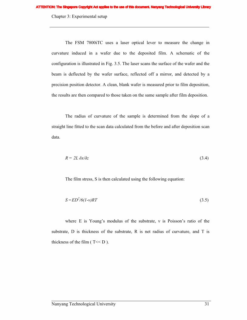
The FSM 7800iTC uses a laser optical lever to measure the change in
curvature induced in a wafer due to the deposited film. A schematic of the
configuration is illustrated in Fig. 3.5. The laser scans the surface of the wafer and the
beam is deflected by the wafer surface, reflected off a mirror, and detected by a
precision position detector. A clean, blank wafer is measured prior to film deposition,
the results are then compared to those taken on the same sample after film deposition.
The radius of curvature of the sample is determined from the slope of a
straight line fitted to the scan data calculated from the before and after deposition scan
data.
R = 2L δx/δz (3.4)
The film stress, S is then calculated using the following equation:
S =ED2/6(1-ν)RT (3.5)
where E is Young’s modulus of the substrate, ν is Poisson’s ratio of the
substrate, D is thickness of the substrate, R is net radius of curvature, and T is
thickness of the film ( T<< D ).
ATTENTION: The Singapore Copyright Act applies to the use of this document. Nanyang Technological University Library
Chapter 3: Experimental setup
Nanyang Technological University 32
Figure 3.5: Diagram of measuring apparatus.
3.4.7 Energy Dispersive X-ray Spectrometer (EDX)
EDX is used in electron microscopy to provide information about the element
composition of irradiate material. An electron beam from the SEM irradiates the
defect during the time that the system performs the EDX measurement. This enables
defect material analysis with high spatial resolution. EDX is normally performed at
45° tilt and an accelerating voltage of 5 keV or above to optimize EDX acquisition
time (approximately 10 seconds). During the EDX scan, a real time spectrum is
monitored in the materials analysis window, and the spectral peak energies are used
for material identification, which is performed following the acquisition of data
according to the analysis procedure.
The energy dispersive X-ray spectrometer (EDX) used in this study is the
SEMVision system from Applied Materials [10]. It supports automatic review,
classification and material analysis performed on unpatterned wafers. The instrument
ATTENTION: The Singapore Copyright Act applies to the use of this document. Nanyang Technological University Library
Chapter 3: Experimental setup
Nanyang Technological University 33
aligns the wafer, uses an optical microscope to find the defects, redetects the defects
using the scanning electron microscope (SEM), classifies the defect and automatically
performs energy dispersive X-ray spectrometer (EDX) on the defect so as to analyze
the results and identify the defect.
3.5 Substrates
In this study, bare Si wafers were used for film deposition and characterization.
The properties of the wafers used are as follows:
Wafer category: Test wafer
Substrate: Si
Wafer size/Diameter: 200mm
Type/orientation: P/<100>
Dopant: Boron
Resistivity: 1-50 Ohm-cm
Thickness: 700-750μm
The substrates used are commercial production grade wafers and require no
cleaning before deposition.
ATTENTION: The Singapore Copyright Act applies to the use of this document. Nanyang Technological University Library
Chapter 3: Experimental setup
Nanyang Technological University 34
3.6 References
1. Fabio Iacona, Giulio Ceriola and Francesco La Via, Structural properties of
SiO2 films prepared by plasma-enhanced chemical vapor deposition, Materials Science in Semiconductor Processing , Volume 4, Issues 1-3, Pages 43-46.
2. Stephen M. Rossnagel, Jerome J. Cuomo and William D. Westwood,
Handbook of Plasma Processing Technology, Noyes Publications, 1990, page 266.
3. Josh H. Golden, Microbar Inc., Sunnyvale, Calif. Craig J. Hawker, Designing
porous low-k dielectrics, Semiconductor International, 5/1/2001.
4. “Surfscan® SP1 unpatterned wafer inspection system user manual” of KL Tencor Corporation, #512516-27, Rev. A 6/98, , 1998.
5. “Opti-Probe 5240i system user manual” by Therma-wave.
6. Shen Xuechu, Optical Properties of Semiconductor Materials (in Chinese),
p21. Scientific Press (P.R.China) (1992).
7. Dimension™ of Low-k Dielectrics, Solid State Measurements, Inc., 2001.
8. “Dimension™ 5000 Scanning Probe Microscope Instruction Manual” of Digital Instruments, Version 4.22ce – 01MAR97.
9. “FSM 7800TC operation manual” of Frontier Semiconductor Measurement
Inc., Rev.1,1999.
10. “SEMVision user’s manual”, by Applied Materials PDC (process diagnostics and control), version 1 – Rev. A, March 2001.
ATTENTION: The Singapore Copyright Act applies to the use of this document. Nanyang Technological University Library
Chapter 4: Optimization of process steps and the effects of oxygen in the growth process
Nanyang Technological University 35
Chapter 4: Optimization of Process Steps and the Effects of Oxygen in the Growth Process 4.1 Introduction
In this chapter, we present results on the deposition of carbon doped silicon
oxide (SiO(C,H)) thin films using the plasma enhanced chemical vapour deposition
(PECVD) process with source gases trimethylsilane (C3H10Si, also referred to as
3MS) and oxygen (O2). Using a process recipe, known as CVD1, SiO(C,H) films with
dielectric constant as low as 3.0 have been obtained. The key process steps involved
in this recipe are shown in Table 4.1. However, these films suffer from high post
particle counts, which can reach up to 70000 on 8-inch wafers. A new recipe CVD2,
which is a modified version of recipe CVD1, has been applied successfully to reduce
the particle counts to about 50 or much less, within the specification required of such
films. The key steps of recipe CVD2 are also shown in Table 4.1 for comparison.
The main differences between the two recipes are as follows: 1) different
oxygen (O2) flow rates are used in the stabilization step (step A) and oxygen treatment
step (step B), which are 200sccm in recipe CVD1 and 700sccm in recipe CVD2; 2)
the pump down step (step C) that is part of recipe CVD1 is omitted in recipe CVD2.
Since there is no pump down step in recipe CVD2, the O2 flow rate was set at
700sccm in steps A and B, so as to maintain a constant total flow rate from step B to
step D, where the total flow rate of O2 and 3MS is also 700sccm. This will help
ensure minimum disruption to the plasma during the transition between the process
steps.
ATTENTION: The Singapore Copyright Act applies to the use of this document. Nanyang Technological University Library
Chapter 4: Optimization of process steps and the effects of oxygen in the growth process
Nanyang Technological University 36
Except for the above differences, the other process steps and parameters used
in the two recipes are identical. Indeed, the omission of step C in recipe CVD2 is
responsible for the reduction in the post particle counts, as shall be seen.
Recipe CVD1
Recipe CVD2
Process step Step description
Precursor (sccm)
Process pressure (Torr)
Precursor (sccm)
Process pressure (Torr)
A Stabilisation O2=200 4.0 O2=700 4.0
B Oxygen (O2) treatment O2=200 4.0 O2=700 4.0
C Pump down YES NO
D Film deposition
O2=100 3MS=600 4.0 O2=100
3MS=600 4.0
E Pump down YES YES
F Helium treatment He=1300 8.7 He=1300 8.7
G Pump down YES YES
Table 4.1: Summary of process steps of recipes CVD1 and CVD2
It was also found that films deposited using recipe CVD2 have slightly
different properties compared to those deposited using recipe CVD1, despite that all
the parameters for the actual deposition process (step D) in the two recipes are
identical. Investigations have shown that the residual oxygen derived from the process
steps prior to the actual film deposition in recipe CVD2 is responsible for the
differences observed. This suggests that oxygen has substantial influences on the
properties of carbon doped silicon oxide films. In this work, we compare the two
recipes, in terms of the critical process steps and their effects on the properties of the
films. We have also investigated in detail the influences of oxygen (O2) on SiO(C,H)
films. This work provides us with a better understanding of the dielectric properties of
ATTENTION: The Singapore Copyright Act applies to the use of this document. Nanyang Technological University Library
Chapter 4: Optimization of process steps and the effects of oxygen in the growth process
Nanyang Technological University 37
SiO(C,H) films in relation to the deposition process, and how they can be optimized
for use in deep submicron integrated circuit technology.
4.2. Experimental details
Four groups of experiments have been carried out: 1) 5 samples deposited by
both recipes CVD1 and CVD2 with film thickness of 5000 Å to ascertain
reproducibility and also for statistical analysis; 2) 5 samples deposited by recipe
CVD1 with nominal thickness ranging from 1000 Å to 5000 Å, in step of 1000 Å; 3)
5 samples deposited by recipe CVD2 with nominal thickness ranging from 1000 Å to
5000 Å, in step of 1000 Å; 4) 7 samples deposited by recipe CVD2 with different
O2/3MS flow ratios from 1/6 to 7/6 over a period of 44 seconds. In this experiment,
the flow rate of O2 was varied while that of 3MS was kept constant at 600sccm. All
the films were deposited on p-type <100> orientation bare silicon 8-inch wafers, with
a deposition temperature of 350oC, process pressure of 4.0 Torr and RF power of
600W.
4.3. Results and discussion
4.3.1 Process reproducibility
The average dielectric constant k and refractive index n of the films deposited
using recipe CVD1 in experiment 1 are 2.98 and 1.41 respectively. The corresponding
standard deviations of these parameters are 1.83×10⁻³ and 4.48×10⁻³. For the films
ATTENTION: The Singapore Copyright Act applies to the use of this document. Nanyang Technological University Library
Chapter 4: Optimization of process steps and the effects of oxygen in the growth process
Nanyang Technological University 38
deposited using recipe CVD2 in the same experiment, the average k and n values are
3.05 and 1.41 respectively, and the corresponding standard deviations are 4.47×10⁻³
and 5.36×10⁻⁴. These results confirmed that this carbon doped silicon oxide low
dielectric films deposited using the PECVD process in this work are highly
reproducible.
4.3.2 Particle counts and element composition
Particle contamination or random defects are the primary concern for low k
material development and application. As the manufacturing process approaches the
yield-monitoring phase of mature production, random defects become the dominant
source of yield loss. In general, large particles (>1μm) indicate mechanical problems
while small particles (<0.5μm) indicate process problems [1]. Table 4.2 summarizes
the number of added-in particles measured for films deposited using the two different
recipes in the four sets of experiments.
Experiment 1 Experiment 2 Experiment 3 Experiment 4
Process recipe
Recipe CVD1
Recipe CVD2
Recipe CVD1 with different
thickness
Recipe CVD2 with different
thickness
Recipe CVD2 with different O2/3MS flow
ratios 1 11 2 70002 11 8 2 2710 6 6799 51 18 3 2340 1 3125 34 14 4 2670 1 12 21 11 5 2847 4 13 5 13 6 16 W
afer
num
ber
7 46
Table 4.2: The number of added-in particles on film surfaces. In experiments 2 and 3, wafer 1 to 5 corresponds to films deposited with nominal thickness from 1000Å to 5000 Å. In experiment 4, wafers 1 to 7 correspond to films deposited with O2/3MS
flow ratios from 1/6 to 7/6.
ATTENTION: The Singapore Copyright Act applies to the use of this document. Nanyang Technological University Library
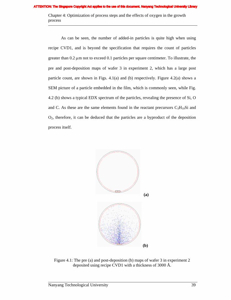
Chapter 4: Optimization of process steps and the effects of oxygen in the growth process
Nanyang Technological University 39
As can be seen, the number of added-in particles is quite high when using
recipe CVD1, and is beyond the specification that requires the count of particles
greater than 0.2 μm not to exceed 0.1 particles per square centimeter. To illustrate, the
pre and post-deposition maps of wafer 3 in experiment 2, which has a large post
particle count, are shown in Figs. 4.1(a) and (b) respectively. Figure 4.2(a) shows a
SEM picture of a particle embedded in the film, which is commonly seen, while Fig.
4.2 (b) shows a typical EDX spectrum of the particles, revealing the presence of Si, O
and C. As these are the same elements found in the reactant precursors C3H10Si and
O2, therefore, it can be deduced that the particles are a byproduct of the deposition
process itself.
(a)
(b)
Figure 4.1: The pre (a) and post-deposition (b) maps of wafer 3 in experiment 2 deposited using recipe CVD1 with a thickness of 3000 Å.
ATTENTION: The Singapore Copyright Act applies to the use of this document. Nanyang Technological University Library
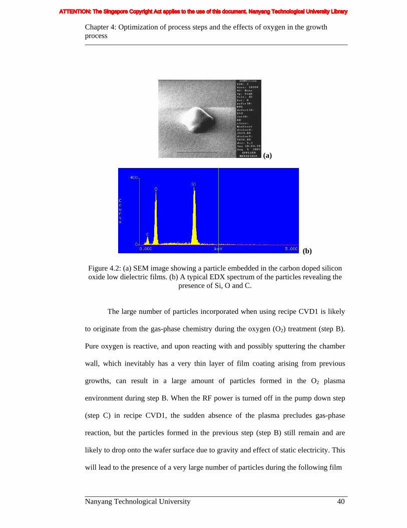
Chapter 4: Optimization of process steps and the effects of oxygen in the growth process
Nanyang Technological University 40
(a)
(b)
Figure 4.2: (a) SEM image showing a particle embedded in the carbon doped silicon oxide low dielectric films. (b) A typical EDX spectrum of the particles revealing the
presence of Si, O and C.
The large number of particles incorporated when using recipe CVD1 is likely
to originate from the gas-phase chemistry during the oxygen (O2) treatment (step B).
Pure oxygen is reactive, and upon reacting with and possibly sputtering the chamber
wall, which inevitably has a very thin layer of film coating arising from previous
growths, can result in a large amount of particles formed in the O2 plasma
environment during step B. When the RF power is turned off in the pump down step
(step C) in recipe CVD1, the sudden absence of the plasma precludes gas-phase
reaction, but the particles formed in the previous step (step B) still remain and are
likely to drop onto the wafer surface due to gravity and effect of static electricity. This
will lead to the presence of a very large number of particles during the following film
ATTENTION: The Singapore Copyright Act applies to the use of this document. Nanyang Technological University Library
Chapter 4: Optimization of process steps and the effects of oxygen in the growth process
Nanyang Technological University 41
deposition step (step D), and account for the many embedded particles seen [see Fig.
4.2(a)]. However, when using recipe CVD2 that omitted the pump down step, there is
no interruption to the RF power and O2 plasma environment, and the particles formed
in the previous oxygen (O2) treatment (step B) continue to float and drift inside the
plasma boundary while the film deposition process is ongoing. These particles will
finally drop onto the wafer surface at the end of film deposition step (step D) when
the rf power is turned off. They are then most likely sputtered away by the following
helium treatment step (step F). To confirm the origin of the particles in recipe CVD1
as being due to the sputtering of carbon doped silicon oxide film coated on the
chamber wall, we have performed an extended over-etched of the chamber using C2F6
and NF3 for 400 seconds, in comparison to standard etching time of 100 seconds, to
thoroughly clean the chamber. Indeed, it was found that films deposited using recipe
CVD1 immediately after the extended over-etched have particle counts reduced to
levels comparable to those achieved in recipe CVD2. Nevertheless, such over-etched
is not recommended as it will shorten the operational lifetime of the PECVD system,
and hence the large particle-count problem can only be resolved through using recipe
CVD2.
4.3.3 Deposition rates
For the films deposited in experiment 2 using recipe CVD1, the actual film
thickness matches the expected thickness from 1000 Å to 5000 Å very closely, which
suggests that the deposition rate is stable and uniform, as shown in Fig. 4.3(a). On the
other hand, for films deposited using recipe CVD2 in experiment 3, the deposition
ATTENTION: The Singapore Copyright Act applies to the use of this document. Nanyang Technological University Library
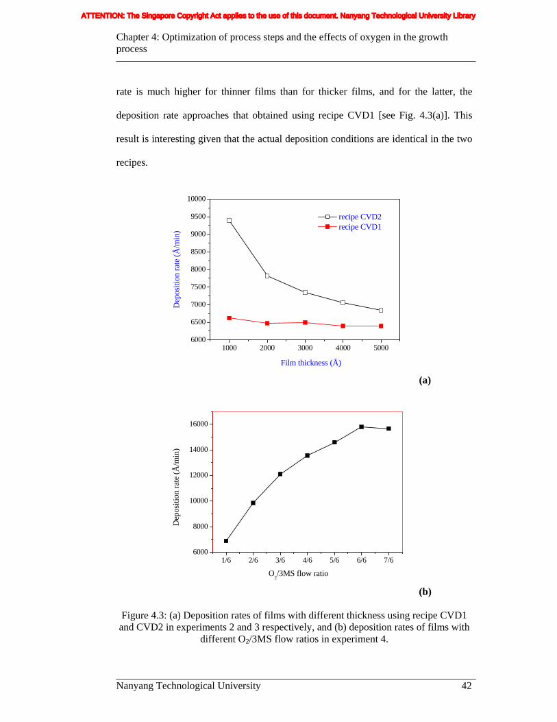
Chapter 4: Optimization of process steps and the effects of oxygen in the growth process
Nanyang Technological University 42
rate is much higher for thinner films than for thicker films, and for the latter, the
deposition rate approaches that obtained using recipe CVD1 [see Fig. 4.3(a)]. This
result is interesting given that the actual deposition conditions are identical in the two
recipes.
1000 2000 3000 4000 50006000
6500
7000
7500
8000
8500
9000
9500
10000
D
epos
ition
rate
(Å/m
in)
Film thickness (Å)
recipe CVD2 recipe CVD1
(a)
1/6 2/6 3/6 4/6 5/6 6/6 7/66000
8000
10000
12000
14000
16000
Dep
ositi
on ra
te (Å
/min
)
O2/3MS flow ratio
(b)
Figure 4.3: (a) Deposition rates of films with different thickness using recipe CVD1 and CVD2 in experiments 2 and 3 respectively, and (b) deposition rates of films with
different O2/3MS flow ratios in experiment 4.
ATTENTION: The Singapore Copyright Act applies to the use of this document. Nanyang Technological University Library
Chapter 4: Optimization of process steps and the effects of oxygen in the growth process
Nanyang Technological University 43
For recipe CVD2, due to the omission of the pump down step (step C), it is
expected that a certain amount of oxygen will remain in the chamber during the next
step of film deposition. The residual oxygen can lead to a higher initial partial
pressure of oxygen as compared to that of 3MS, and is believed to be responsible for
the larger initial deposition rates seen. As the film deposition process progresses, the
effect of residual oxygen diminishes and the concentration of oxygen species is then
only determined by the inlet oxygen gas flow. This accounts for the decreasing
growth rate for thicker samples grown over a longer period of time that ultimately
approaches that obtained using recipe CVD1, which is as expected given the identical
deposition conditions.
The proposed effect of oxygen on the deposition rate can be verified by
studying the series of films deposited using recipe CVD2 with different O2/3MS flow
ratios in experiment 4. The deposition rates for the films are shown in Fig. 4.3(b),
which indeed confirm that the deposition rates of the carbon doped silicon oxide low
k films are sensitive to the partial pressure of oxygen, being larger at a higher oxygen
partial pressure.
4.3.4 Refractive index and dielectric constant
The refractive indices and dielectric constants of the films deposited in
experiments 2 and 3 are shown in Figs. 4.4(a) and 4.4(b) respectively. The
corresponding parameters for the films deposited in experiment 4 are shown in Fig.
4.5.
ATTENTION: The Singapore Copyright Act applies to the use of this document. Nanyang Technological University Library
Chapter 4: Optimization of process steps and the effects of oxygen in the growth process
Nanyang Technological University 44
1000 2000 3000 4000 50001.385
1.390
1.395
1.400
1.405
1.410
1.415
1.420
1.425
1.430
1.435
1.440
Refra
ctiv
e In
dex
Film thickness (Å)
recipe CVD1 recipe CVD2
(a)
1000 2000 3000 4000 50002.925
2.950
2.975
3.000
3.025
3.050
3.075
3.100
k va
lue
Film thickness (Å)
recipe CVD1 recipe CVD2
(b)
Figure 4.4: (a) Refractive indices and (b) k values of the films deposited with different thickness using recipe CVD1 and CVD2 in experiments 2 and 3 respectively.
ATTENTION: The Singapore Copyright Act applies to the use of this document. Nanyang Technological University Library
Chapter 4: Optimization of process steps and the effects of oxygen in the growth process
Nanyang Technological University 45
1/6 2/6 3/6 4/6 5/6 6/6 7/6
1.375
1.380
1.385
1.390
1.395
1.400
1.405
1.410 Refractive Index k value
O2/3MS flow ratio
Refra
ctiv
e In
dex
3.0
3.2
3.4
3.6
3.8
4.0
k va
lue
Figure 4.5: Refractive indices and k values of the films deposited with different O2/3MS flow ratios in experiment 4
From Fig. 4.4(a), it can be seen that the refractive index is nearly uniform to
within ±0.015 and ±0.005 for films deposited with different thickness using recipes
CVD1 and CVD2 respectively. The refractive indices of the films deposited using
recipe CVD1 are slightly larger than those deposited by recipe CVD2 by about 0.015
on average, which is not significant. From Fig. 4.4(b), it can be seen that the k values
are slightly less than 3.00 for films deposited using recipe CVD1 and show a very
slight increase when using recipe CVD2. As both the refractive indices and k values
show no correlation with the thickness of the films, therefore it can be concluded that
the plasma environment is very stable for these processes and the residual oxygen in
recipe CVD2 due to the treatment step (step B) affects only the growth rate but does
not have much impact on these parameters.
ATTENTION: The Singapore Copyright Act applies to the use of this document. Nanyang Technological University Library
Chapter 4: Optimization of process steps and the effects of oxygen in the growth process
Nanyang Technological University 46
From Fig. 4.5, it can be seen that the refractive index shows a slight decrease
when the O2/3MS flow ratio increases from 1/6 to 3/6, and remains constant at higher
flow ratios. On the other hand, there is a continuous and more significant increase in
the k value from 3.02 to 3.95 with increasing O2/3MS flow ratio. This increase is
attributed to the lower number of Si-CH3 bonds resulting in reduced polarizability [2],
as shall be seen shortly. From the above and the deposition rate results presented
earlier, it can be concluded that oxygen has a significant impact on the growth rates of
the carbon doped silicon oxide low dielectric and their k values, but relatively less
effect on their refractive indices.
4.3.5 FTIR spectra
Figures 4.6, 4.7 and 4.8 show the FTIR spectra of the films deposited in
experiments 2, 3 and 4 respectively. The peaks observed at 780cm-1 and 1270cm-1 are
assigned to the symmetric deformation vibration of CH3 in the Si-CH3 group, while
the peak at 1040 cm-1 is assigned to the Si-O structure. The absorption at 2890 to
2990 cm-1, on the other hand, is assigned to the C-Hm, m=1-3 stretching mode [3, 4].
To investigate the effects of oxygen incorporation on the dielectric constants of
the films, the FTIR spectra around the Si-CH3 and Si-O groups absorption are fitted
with several Gaussian lineshape functions, and the integrated absorption area ratio
(Si-CH3/Si-O ratio) of the Si-CH3 group at 1270cm-1 and the Si-O group at 1040cm-1
are determined.
ATTENTION: The Singapore Copyright Act applies to the use of this document. Nanyang Technological University Library
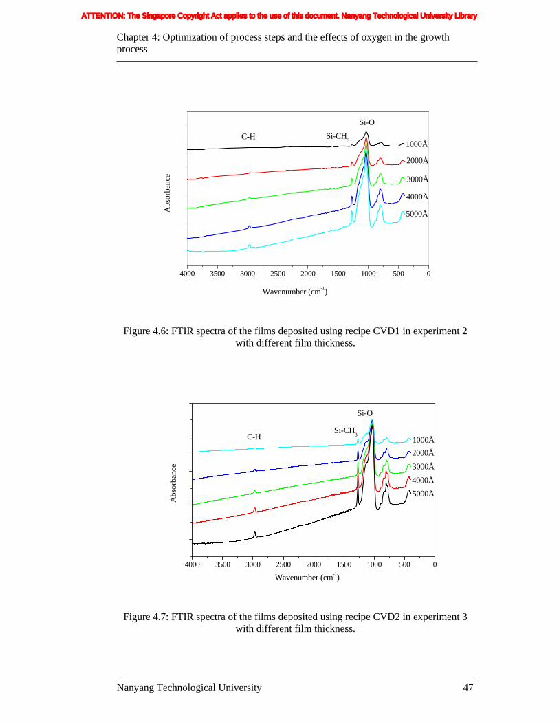
Chapter 4: Optimization of process steps and the effects of oxygen in the growth process
Nanyang Technological University 47
4000 3500 3000 2500 2000 1500 1000 500 0
1000Å
Abs
orba
nce 3000Å
Si-O
Si-CH3C-H
5000Å
4000Å
2000Å
Wavenumber (cm-1)
Figure 4.6: FTIR spectra of the films deposited using recipe CVD1 in experiment 2 with different film thickness.
4000 3500 3000 2500 2000 1500 1000 500 0
Abs
orba
nce
Si-O
Si-CH3C-H
5000Å4000Å
3000Å
2000Å1000Å
Wavenumber (cm-1)
Figure 4.7: FTIR spectra of the films deposited using recipe CVD2 in experiment 3 with different film thickness.
ATTENTION: The Singapore Copyright Act applies to the use of this document. Nanyang Technological University Library
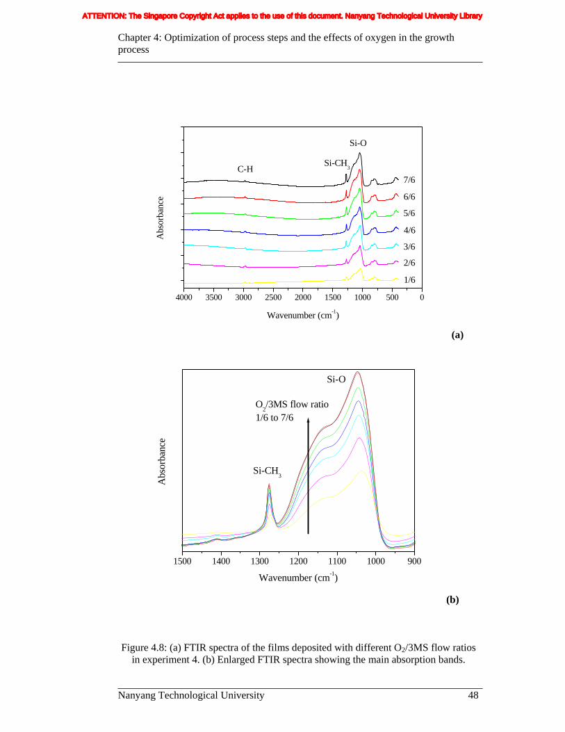
Chapter 4: Optimization of process steps and the effects of oxygen in the growth process
Nanyang Technological University 48
4000 3500 3000 2500 2000 1500 1000 500 0
1/6
2/6
3/6
4/6
5/6
6/6
7/6
Si-O
Si-CH3C-H
Abs
orba
nce
Wavenumber (cm-1)
(a)
1500 1400 1300 1200 1100 1000 900
Abs
orba
nce
O2/3MS flow ratio 1/6 to 7/6
Si-O
Si-CH3
Wavenumber (cm-1)
(b)
Figure 4.8: (a) FTIR spectra of the films deposited with different O2/3MS flow ratios in experiment 4. (b) Enlarged FTIR spectra showing the main absorption bands.
ATTENTION: The Singapore Copyright Act applies to the use of this document. Nanyang Technological University Library
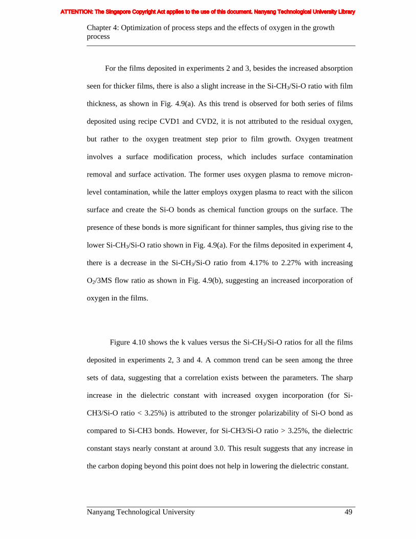
Chapter 4: Optimization of process steps and the effects of oxygen in the growth process
Nanyang Technological University 49
For the films deposited in experiments 2 and 3, besides the increased absorption
seen for thicker films, there is also a slight increase in the Si-CH3/Si-O ratio with film
thickness, as shown in Fig. 4.9(a). As this trend is observed for both series of films
deposited using recipe CVD1 and CVD2, it is not attributed to the residual oxygen,
but rather to the oxygen treatment step prior to film growth. Oxygen treatment
involves a surface modification process, which includes surface contamination
removal and surface activation. The former uses oxygen plasma to remove micron-
level contamination, while the latter employs oxygen plasma to react with the silicon
surface and create the Si-O bonds as chemical function groups on the surface. The
presence of these bonds is more significant for thinner samples, thus giving rise to the
lower Si-CH3/Si-O ratio shown in Fig. 4.9(a). For the films deposited in experiment 4,
there is a decrease in the Si-CH3/Si-O ratio from 4.17% to 2.27% with increasing
O2/3MS flow ratio as shown in Fig. 4.9(b), suggesting an increased incorporation of
oxygen in the films.
Figure 4.10 shows the k values versus the Si-CH3/Si-O ratios for all the films
deposited in experiments 2, 3 and 4. A common trend can be seen among the three
sets of data, suggesting that a correlation exists between the parameters. The sharp
increase in the dielectric constant with increased oxygen incorporation (for Si-
CH3/Si-O ratio < 3.25%) is attributed to the stronger polarizability of Si-O bond as
compared to Si-CH3 bonds. However, for Si-CH3/Si-O ratio > 3.25%, the dielectric
constant stays nearly constant at around 3.0. This result suggests that any increase in
the carbon doping beyond this point does not help in lowering the dielectric constant.
ATTENTION: The Singapore Copyright Act applies to the use of this document. Nanyang Technological University Library
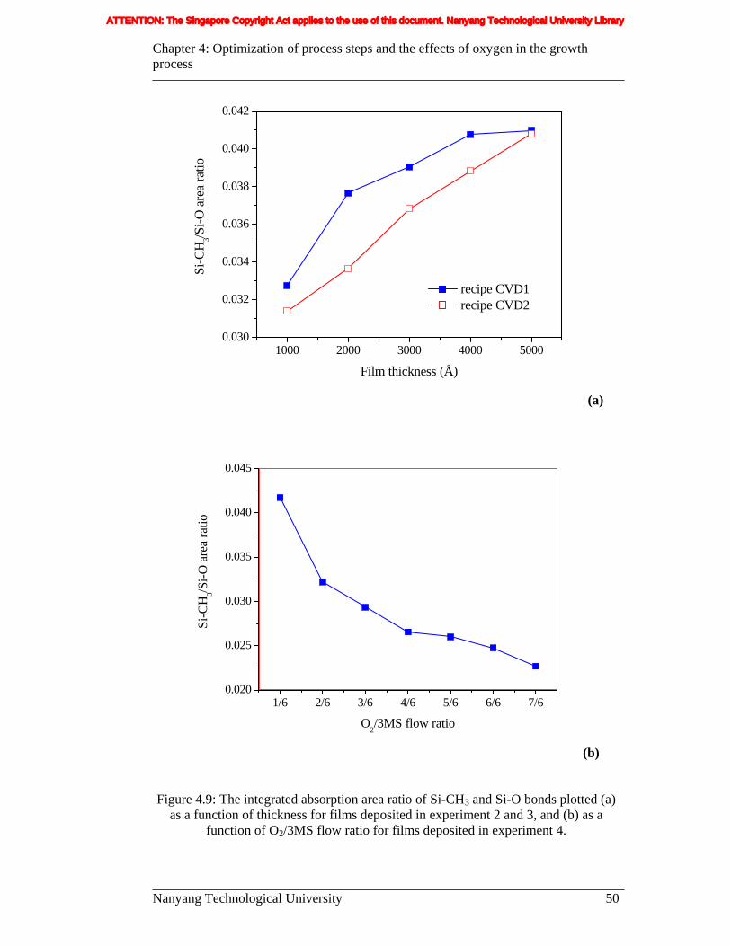
Chapter 4: Optimization of process steps and the effects of oxygen in the growth process
Nanyang Technological University 50
1000 2000 3000 4000 50000.030
0.032
0.034
0.036
0.038
0.040
0.042
Si-C
H3/S
i-O a
rea
ratio
Film thickness (Å)
recipe CVD1 recipe CVD2
(a)
1/6 2/6 3/6 4/6 5/6 6/6 7/60.020
0.025
0.030
0.035
0.040
0.045
Si-C
H3/S
i-O a
rea
ratio
O2/3MS flow ratio
(b) Figure 4.9: The integrated absorption area ratio of Si-CH3 and Si-O bonds plotted (a)
as a function of thickness for films deposited in experiment 2 and 3, and (b) as a function of O2/3MS flow ratio for films deposited in experiment 4.
ATTENTION: The Singapore Copyright Act applies to the use of this document. Nanyang Technological University Library
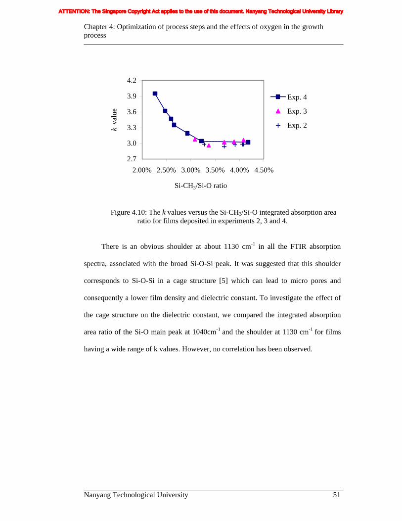
Chapter 4: Optimization of process steps and the effects of oxygen in the growth process
Nanyang Technological University 51
2.7
3.0
3.3
3.6
3.9
4.2
2.00% 2.50% 3.00% 3.50% 4.00% 4.50%
Si-CH3/Si-O ratio
k va
lue
Exp. 4
Exp. 3
Exp. 2
Figure 4.10: The k values versus the Si-CH3/Si-O integrated absorption area ratio for films deposited in experiments 2, 3 and 4.
There is an obvious shoulder at about 1130 cm-1 in all the FTIR absorption
spectra, associated with the broad Si-O-Si peak. It was suggested that this shoulder
corresponds to Si-O-Si in a cage structure [5] which can lead to micro pores and
consequently a lower film density and dielectric constant. To investigate the effect of
the cage structure on the dielectric constant, we compared the integrated absorption
area ratio of the Si-O main peak at 1040cm-1 and the shoulder at 1130 cm-1 for films
having a wide range of k values. However, no correlation has been observed.
ATTENTION: The Singapore Copyright Act applies to the use of this document. Nanyang Technological University Library
Chapter 4: Optimization of process steps and the effects of oxygen in the growth process
Nanyang Technological University 52
4.4. Conclusion
Carbon doped silicon oxide SiO(C, H) low k thin films (k~2.9) deposited by
the plasma enhanced chemical vapor deposition (PECVD) technique from
trimethylsilane (3MS) and oxygen (O2) have been studied. Two types of process
recipes, namely CVD1 and CVD2 were applied for film deposition. CVD1 is an
initial recipe that resulted in films with a uniform deposition rate irrespective of film
thickness and a low dielectric constant of about 2.9. However, it suffers from
extraordinarily high post particle counts. CVD2 is a modified recipe adopted to
address this issue. The main difference between the two recipes is that a pump down
step immediately before the film deposition has been omitted in recipe CVD2, and
this has successfully reduced the particle counts to a satisfactory level. However when
using recipe CVD2, the deposition rate is non-uniform and the dielectric constant is
slightly above 3.0, attributed to the residual oxygen in the process step prior to film
deposition.
ATTENTION: The Singapore Copyright Act applies to the use of this document. Nanyang Technological University Library
Chapter 4: Optimization of process steps and the effects of oxygen in the growth process
Nanyang Technological University 53
4.5. References
1. Novellus concept one / concept two, Dielectric PECVD process guide /
introduction to CVD processing, Volume 1, 73-10093-01, Rev. A, 12 December 1997, p 3-8.
2. Byung Keun Hwang, Mark J. Loboda, Glenn A. Cerny, Ryan F. Schneider,
Jeff A. Seifferly, and Tom Washer, Interconnect Technology Conference 2000, Proceedings of the IEEE 2000 International, 5-7 June 2000, Page(s): 52 –54
3. Shiuh-Ko JangJean, Ying-Lang Wang, Chuan-Pu Liu, Weng-Sing Hwang, and
Wei-Tsu Tseng, Chi-Wen Liu, In situ fluorine-modified organosilicate glass prepared by plasma enhanced chemical vapor deposition, Journal of Applied Physics, Volume 94, Issue 1, pp. 732-737
4. G. Socrates, Infrared characteristic group frequencies, John Willy & Sons,
New York, (1994).
5. Keith Buchanan, The evolution of interconnect technology for silicon integrated circuitry, 2002 GaAsMANTECH Conference.
ATTENTION: The Singapore Copyright Act applies to the use of this document. Nanyang Technological University Library
Chapter 5: Effects of annealing on low dielectric constant carbon doped silicon oxide films
Nanyang Technological University 54
Chapter 5: Effects of Annealing on Low Dielectric Constant Carbon Doped Silicon Oxide Films
5.1 Introduction
In chapter four, we have optimized the growth of carbon doped silicon oxide
(SiO(C,H)) films. Using oxygen to trimethylsilane (3MS) flow ratio of
100sccm:600sccm, SiO(C,H) films with a dielectric constant of 2.9 have been
achieved. In the chapter, we aim to study the thermal stability of the films by
annealing them at different temperatures from 400 0C to 700 0C in a N2 atmosphere
for 30 minutes. Currently, 400 °C is the highest processing temperature for the back
end of line structure, therefore, the stability of the dielectric material at this
temperature and possibly high temperatures is a critical issue [1]. This study will
provide us with a better understanding of SiO(C, H) films and their thermal stability,
and how their dielectric properties can be optimized for use in deep submicron
integrated circuit technology.
5.2 Experimental details
The films were deposited on p-type <100> orientation bare silicon 8 inches
wafers, with a deposition temperature of 350°C, process pressure of 4.0Torr and rf
power of 600W. In this work, we have adopted a simplified version of the recipes
discussed in chapter three. The process sequence comprised only gas stabilization,
film deposition for a period of 45 seconds and pump down. The flow rates of O2 and
ATTENTION: The Singapore Copyright Act applies to the use of this document. Nanyang Technological University Library
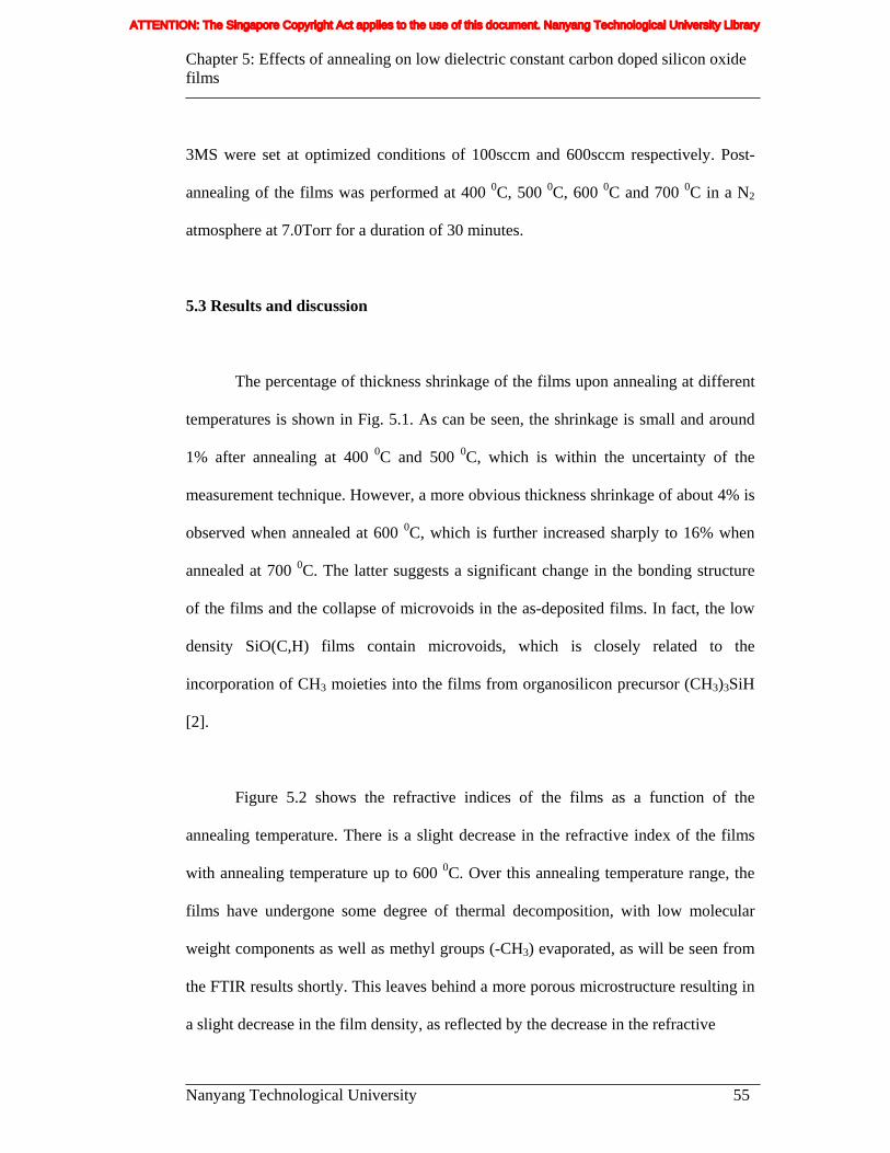
Chapter 5: Effects of annealing on low dielectric constant carbon doped silicon oxide films
Nanyang Technological University 55
3MS were set at optimized conditions of 100sccm and 600sccm respectively. Post-
annealing of the films was performed at 400 0C, 500 0C, 600 0C and 700 0C in a N2
atmosphere at 7.0Torr for a duration of 30 minutes.
5.3 Results and discussion
The percentage of thickness shrinkage of the films upon annealing at different
temperatures is shown in Fig. 5.1. As can be seen, the shrinkage is small and around
1% after annealing at 400 0C and 500 0C, which is within the uncertainty of the
measurement technique. However, a more obvious thickness shrinkage of about 4% is
observed when annealed at 600 0C, which is further increased sharply to 16% when
annealed at 700 0C. The latter suggests a significant change in the bonding structure
of the films and the collapse of microvoids in the as-deposited films. In fact, the low
density SiO(C,H) films contain microvoids, which is closely related to the
incorporation of CH3 moieties into the films from organosilicon precursor (CH3)3SiH
[2].
Figure 5.2 shows the refractive indices of the films as a function of the
annealing temperature. There is a slight decrease in the refractive index of the films
with annealing temperature up to 600 0C. Over this annealing temperature range, the
films have undergone some degree of thermal decomposition, with low molecular
weight components as well as methyl groups (-CH3) evaporated, as will be seen from
the FTIR results shortly. This leaves behind a more porous microstructure resulting in
a slight decrease in the film density, as reflected by the decrease in the refractive
ATTENTION: The Singapore Copyright Act applies to the use of this document. Nanyang Technological University Library
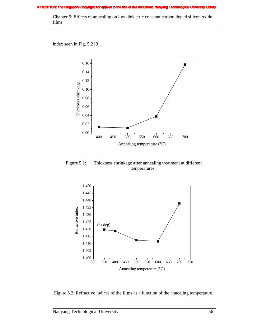
Chapter 5: Effects of annealing on low dielectric constant carbon doped silicon oxide films
Nanyang Technological University 56
index seen in Fig. 5.2 [3].
400 450 500 550 600 650 7000.00
0.02
0.04
0.06
0.08
0.10
0.12
0.14
0.16
Thic
knes
s shr
inka
ge
Annealing temperature (°C)
Figure 5.1: Thickness shrinkage after annealing treatment at different temperatures.
300 350 400 450 500 550 600 650 700 7501.400
1.405
1.410
1.415
1.420
1.425
1.430
1.435
1.440
1.445
1.450
(as dep)
Refra
ctiv
e in
dex
Annealing temperature (°C)
Figure 5.2: Refractive indices of the films as a function of the annealing temperature.
ATTENTION: The Singapore Copyright Act applies to the use of this document. Nanyang Technological University Library
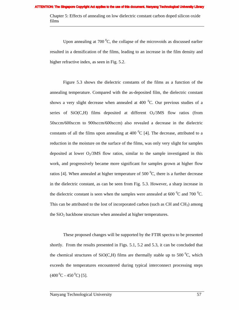
Chapter 5: Effects of annealing on low dielectric constant carbon doped silicon oxide films
Nanyang Technological University 57
Upon annealing at 700 0C, the collapse of the microvoids as discussed earlier
resulted in a densification of the films, leading to an increase in the film density and
higher refractive index, as seen in Fig. 5.2.
Figure 5.3 shows the dielectric constants of the films as a function of the
annealing temperature. Compared with the as-deposited film, the dielectric constant
shows a very slight decrease when annealed at 400 0C. Our previous studies of a
series of SiO(C,H) films deposited at different O2/3MS flow ratios (from
50sccm/600sccm to 900sccm/600sccm) also revealed a decrease in the dielectric
constants of all the films upon annealing at 400 0C [4]. The decrease, attributed to a
reduction in the moisture on the surface of the films, was only very slight for samples
deposited at lower O2/3MS flow ratios, similar to the sample investigated in this
work, and progressively became more significant for samples grown at higher flow
ratios [4]. When annealed at higher temperature of 500 0C, there is a further decrease
in the dielectric constant, as can be seen from Fig. 5.3. However, a sharp increase in
the dielectric constant is seen when the samples were annealed at 600 0C and 700 0C.
This can be attributed to the lost of incorporated carbon (such as CH and CH3) among
the SiO2 backbone structure when annealed at higher temperatures.
These proposed changes will be supported by the FTIR spectra to be presented
shortly. From the results presented in Figs. 5.1, 5.2 and 5.3, it can be concluded that
the chemical structures of SiO(C,H) films are thermally stable up to 500 0C, which
exceeds the temperatures encountered during typical interconnect processing steps
(400 0C - 450 0C) [5].
ATTENTION: The Singapore Copyright Act applies to the use of this document. Nanyang Technological University Library
Chapter 5: Effects of annealing on low dielectric constant carbon doped silicon oxide films
Nanyang Technological University 58
300 350 400 450 500 550 600 650 700 7501.400
1.405
1.410
1.415
1.420
1.425
1.430
1.435
1.440
1.445
1.450
(as dep)
Refra
ctiv
e in
dex
Annealing temperature (°C)
Figure 5.3: Refractive index of the films as a function of the annealing temperature.
Figure 5.4(a) shows the AFM image measured over a 5µm x 5µm surface area
for the as-deposited film, whereas Figs. 5.4(b) to 5.4(e) show the corresponding image
of the films annealed at 400 0C, 500 0C, 600 0C and 700 0C respectively.
ATTENTION: The Singapore Copyright Act applies to the use of this document. Nanyang Technological University Library
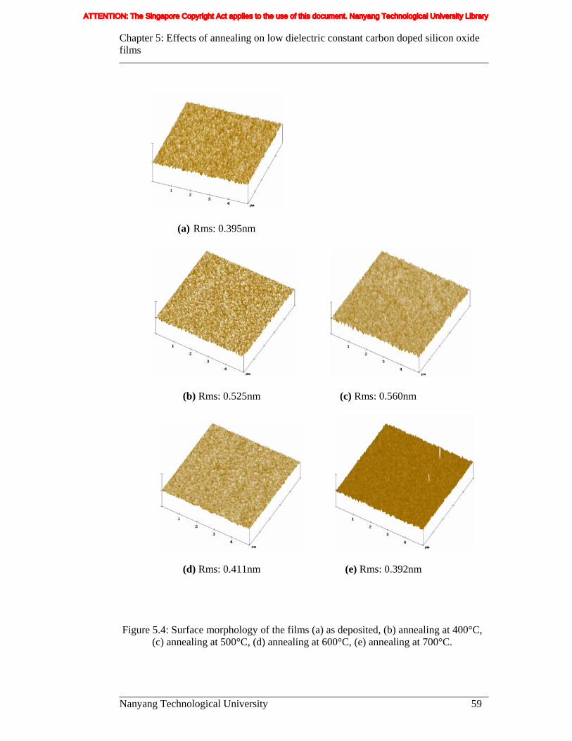
Chapter 5: Effects of annealing on low dielectric constant carbon doped silicon oxide films
Nanyang Technological University 59
(a) Rms: 0.395nm
(b) Rms: 0.525nm (c) Rms: 0.560nm
(d) Rms: 0.411nm (e) Rms: 0.392nm Figure 5.4: Surface morphology of the films (a) as deposited, (b) annealing at 400°C,
(c) annealing at 500°C, (d) annealing at 600°C, (e) annealing at 700°C.
ATTENTION: The Singapore Copyright Act applies to the use of this document. Nanyang Technological University Library
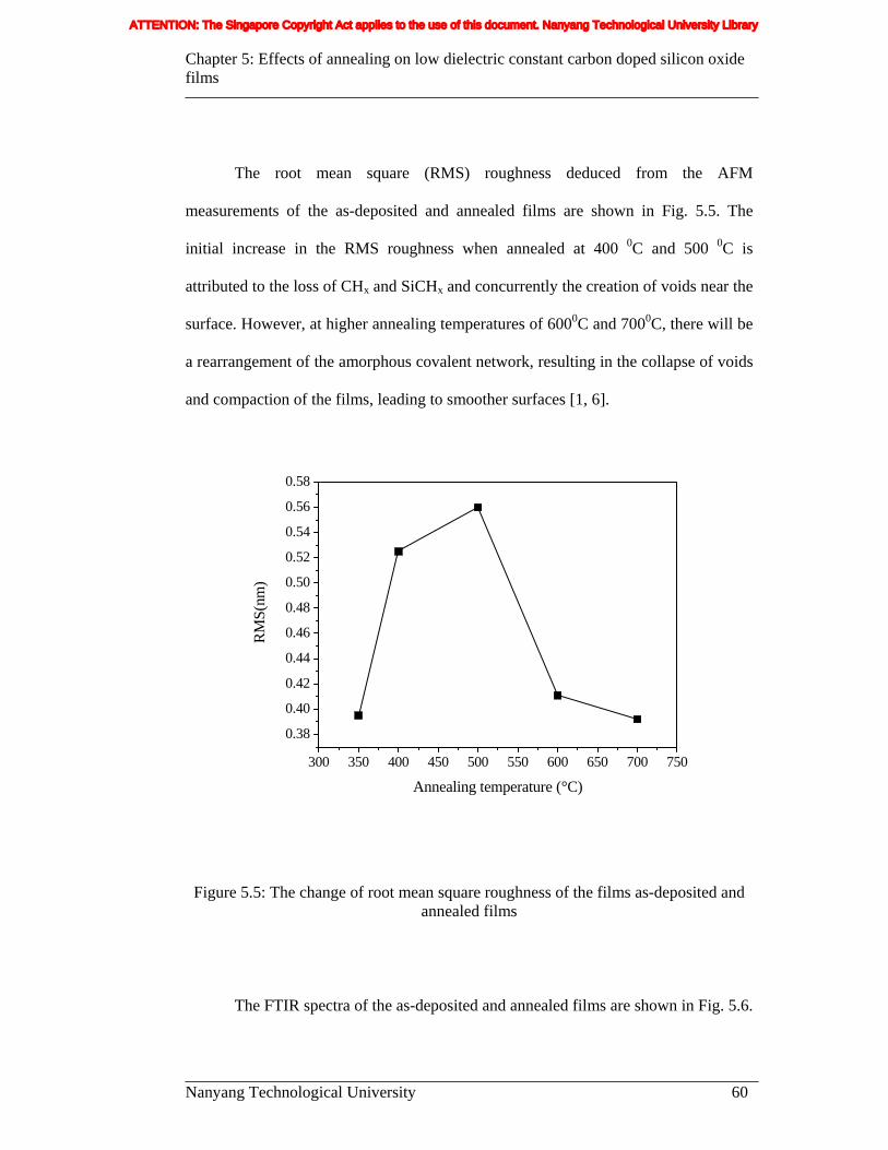
Chapter 5: Effects of annealing on low dielectric constant carbon doped silicon oxide films
Nanyang Technological University 60
The root mean square (RMS) roughness deduced from the AFM
measurements of the as-deposited and annealed films are shown in Fig. 5.5. The
initial increase in the RMS roughness when annealed at 400 0C and 500 0C is
attributed to the loss of CHx and SiCHx and concurrently the creation of voids near the
surface. However, at higher annealing temperatures of 6000C and 7000C, there will be
a rearrangement of the amorphous covalent network, resulting in the collapse of voids
and compaction of the films, leading to smoother surfaces [1, 6].
300 350 400 450 500 550 600 650 700 750
0.38
0.40
0.42
0.44
0.46
0.48
0.50
0.52
0.54
0.56
0.58
RMS(
nm)
Annealing temperature (°C)
Figure 5.5: The change of root mean square roughness of the films as-deposited and annealed films
The FTIR spectra of the as-deposited and annealed films are shown in Fig. 5.6.
ATTENTION: The Singapore Copyright Act applies to the use of this document. Nanyang Technological University Library
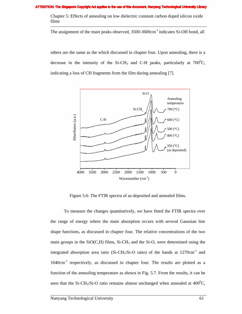
Chapter 5: Effects of annealing on low dielectric constant carbon doped silicon oxide films
Nanyang Technological University 61
The assignment of the main peaks observed, 3500-3600cm-1 indicates Si-OH bond, all
others are the same as the which discussed in chapter four. Upon annealing, there is a
decrease in the intensity of the Si-CH3 and C-H peaks, particularly at 7000C,
indicating a loss of CH fragments from the film during annealing [7].
4000 3500 3000 2500 2000 1500 1000 500 0
Abs
orba
nce
(a.u
.)
350 (°C)(as deposited)
500 (°C)
400 (°C)
600 (°C)
700 (°C)
Annealing temperature
Si-O
Si-CH3
C-H
Wavenumber (cm-1)
Figure 5.6: The FTIR spectra of as-deposited and annealed films.
To measure the changes quantitatively, we have fitted the FTIR spectra over
the range of energy where the main absorption occurs with several Gaussian line
shape functions, as discussed in chapter four. The relative concentrations of the two
main groups in the SiO(C,H) films, Si-CH3 and the Si-O, were determined using the
integrated absorption area ratio (Si-CH3/Si-O ratio) of the bands at 1270cm-1 and
1040cm-1 respectively, as discussed in chapter four. The results are plotted as a
function of the annealing temperature as shown in Fig. 5.7. From the results, it can be
seen that the Si-CH3/Si-O ratio remains almost unchanged when annealed at 4000C,
ATTENTION: The Singapore Copyright Act applies to the use of this document. Nanyang Technological University Library
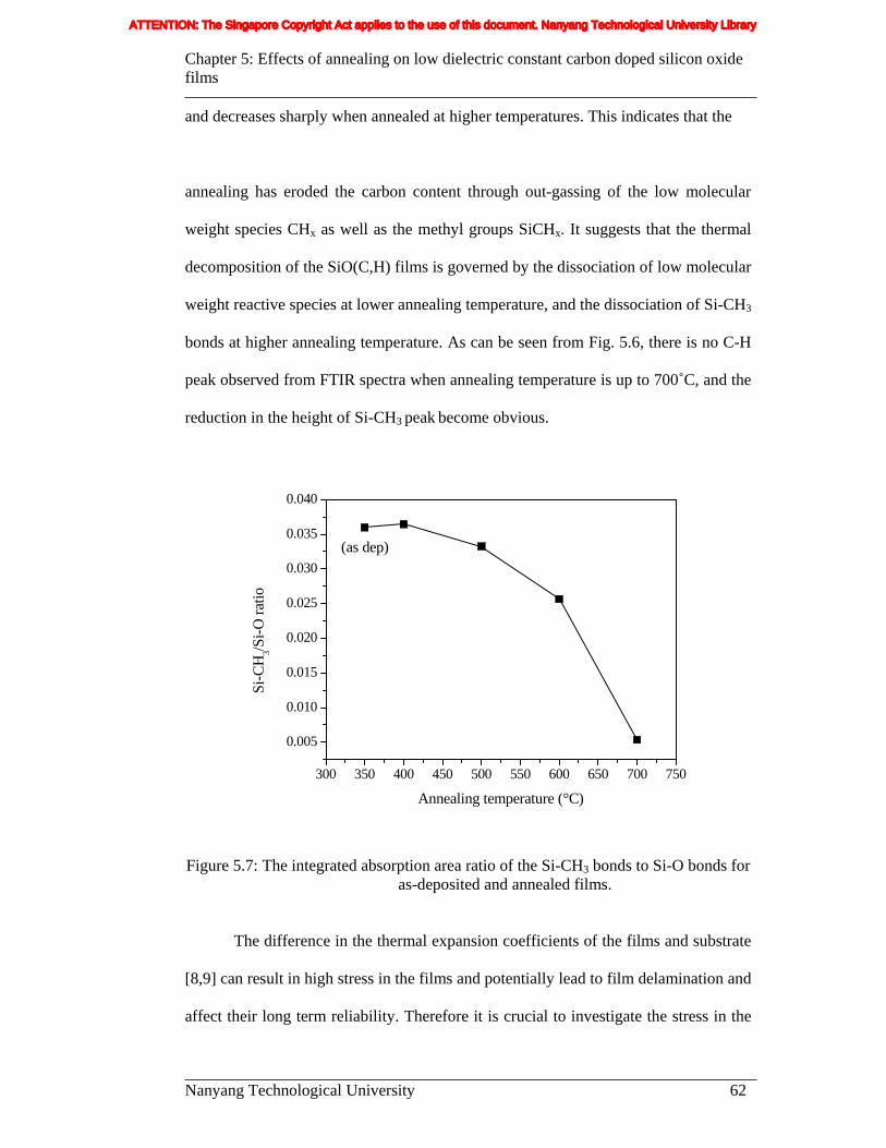
Chapter 5: Effects of annealing on low dielectric constant carbon doped silicon oxide films
Nanyang Technological University 62
and decreases sharply when annealed at higher temperatures. This indicates that the
annealing has eroded the carbon content through out-gassing of the low molecular
weight species CHx as well as the methyl groups SiCHx. It suggests that the thermal
decomposition of the SiO(C,H) films is governed by the dissociation of low molecular
weight reactive species at lower annealing temperature, and the dissociation of Si-CH3
bonds at higher annealing temperature. As can be seen from Fig. 5.6, there is no C-H
peak observed from FTIR spectra when annealing temperature is up to 700˚C, and the
reduction in the height of Si-CH3 peak become obvious.
300 350 400 450 500 550 600 650 700 750
0.005
0.010
0.015
0.020
0.025
0.030
0.035
0.040
(as dep)
Si-C
H3/S
i-O ra
tio
Annealing temperature (°C)
Figure 5.7: The integrated absorption area ratio of the Si-CH3 bonds to Si-O bonds for as-deposited and annealed films.
The difference in the thermal expansion coefficients of the films and substrate
[8,9] can result in high stress in the films and potentially lead to film delamination and
affect their long term reliability. Therefore it is crucial to investigate the stress in the
ATTENTION: The Singapore Copyright Act applies to the use of this document. Nanyang Technological University Library
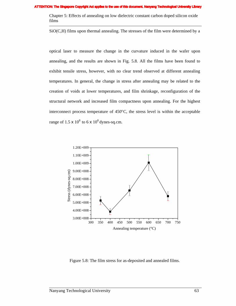
Chapter 5: Effects of annealing on low dielectric constant carbon doped silicon oxide films
Nanyang Technological University 63
SiO(C,H) films upon thermal annealing. The stresses of the film were determined by a
optical laser to measure the change in the curvature induced in the wafer upon
annealing, and the results are shown in Fig. 5.8. All the films have been found to
exhibit tensile stress, however, with no clear trend observed at different annealing
temperatures. In general, the change in stress after annealing may be related to the
creation of voids at lower temperatures, and film shrinkage, reconfiguration of the
structural network and increased film compactness upon annealing. For the highest
interconnect process temperature of 450°C, the stress level is within the acceptable
range of 1.5 x 10⁸ to 6 x 10⁸ dynes-sq.cm.
Figure 5.8: The film stress for as-deposited and annealed films.
300 350 400 450 500 550 600 650 700 7503.00E+008
4.00E+008
5.00E+008
6.00E+008
7.00E+008
8.00E+008
9.00E+008
1.00E+009
1.10E+009
1.20E+009
Stre
ss (d
ynes
-sq.
cm)
Annealing temperature (°C)
ATTENTION: The Singapore Copyright Act applies to the use of this document. Nanyang Technological University Library
Chapter 5: Effects of annealing on low dielectric constant carbon doped silicon oxide films
Nanyang Technological University 64
5.4 Conclusion
SiO(C,H) films deposited with O2 and 3MS flow rates of 100sccm and
600sccm respectively have been investigated. It was found that the thermal stability of
this low dielectric could be as high as 500°C. The shrinkage of post cured film is less
than 1%, with no obvious change in the film composition at this temperature. The
SiO(C,H) low k films were also found to exhibit tensile stress.
ATTENTION: The Singapore Copyright Act applies to the use of this document. Nanyang Technological University Library
Chapter 5: Effects of annealing on low dielectric constant carbon doped silicon oxide films
Nanyang Technological University 65
5.5 References
1. A. Grill and V. Patel, Journal of Applied Physics, Volume 85, Issue 6, Pages 3314-3318.
2. Zhen-Cheng Wu et al. J. Electrochem. Soc. 148, F127 (2001).
3. Licheng M. Han et al., June 27-29, 2000 VMIC Conference, 2000 IMIC–
200/00/0401(c), Page 401.
4. M.R.Wang, Rusli, M.B.Yu, N.Babu, C.Y.Li and K. Rakesh, Thin Solid Film, Volumes 462-463, Pages 219-222 (2004).
5. Michael Morgen, E. Todd Ryan, Jie-Hua Zhao, Chuan Hu, Taiheui Cho, Paul
S. Ho, Annual Review of Materials Science. Volume 30, Pages 645-680.
6. Byung Keun Hwang, Mark J. Loboda, Glenn A. Cerny, Ryan F. Schneider, Jeff A. Seifferly, and Tom Washer, Interconnect Technology Conference 2000, Proceedings of the IEEE 2000 International, 5-7 June 2000, Pages 52 –54
7. A. Grill and V. Patel, Applied Physics Letters, August 6, 2001, Volume 79,
Issue 6, Pages 803-805.
8. Masahiko Maeda and Manabu Itsumi, Physica B: Condensed Matter , Volume 324, Issues 1-4 , Pages 167-172.
9. Aboaf, J.A., Journal of the Electrochemical Society, Volume 116, Issue 12,
1969, Pages 1732-1736.
ATTENTION: The Singapore Copyright Act applies to the use of this document. Nanyang Technological University Library

Chapter 5: Effects of annealing on low dielectric constant carbon doped silicon oxide films
Nanyang Technological University 66
ATTENTION: The Singapore Copyright Act applies to the use of this document. Nanyang Technological University Library
Chapter 6: Effects of changing process pressure
Nanyang Technological University 66
Chapter 6: Effects of Changing Process Pressure
6.1 Introduction
The dielectric constants of carbon doped oxide films (SiO(C,H)) prepared by
the plasma enhanced chemical vapor deposition (PECVD) technique are strongly
dependent on the deposition conditions such as temperature, process pressure, rf
power and gas flow rate. In this chapter, SiO(C,H) films have been prepared by the
PECVD technique from trimethylsilane (3MS) in an oxygen (O2) environment with
different process pressures from 1.5Torr, 2.0Torr, 4.0Torr, 6.0Torr and 8.0Torr. The
effects of changing process pressure on the mechanical, optical and electrical
properties of the SiO(C,H) films were investigated. It has been found that the
refractive index decreased from 1.48 to 1.38 while dielectric constant decreased from
3.4 to 2.9 with increasing deposition pressure. FTIR spectra revealed that more -CH
and -CH3 groups were introduced into the silicon dioxide network of the films at
higher deposition pressure.
6.2 Experimental details
The films were deposited on p-type <100> orientation bare silicon 8 inches
wafers, with a deposition temperature of 350°C, rf power of 600W, O2 and 3MS flow
rate of 100sccm and 600sccm respectively. In this work, we have adopted a simplified
version of the recipes discussed in chapter three. The process sequence comprised
only gas stabilization, film deposition for a period of 45 seconds and pump down. A
ATTENTION: The Singapore Copyright Act applies to the use of this document. Nanyang Technological University Library
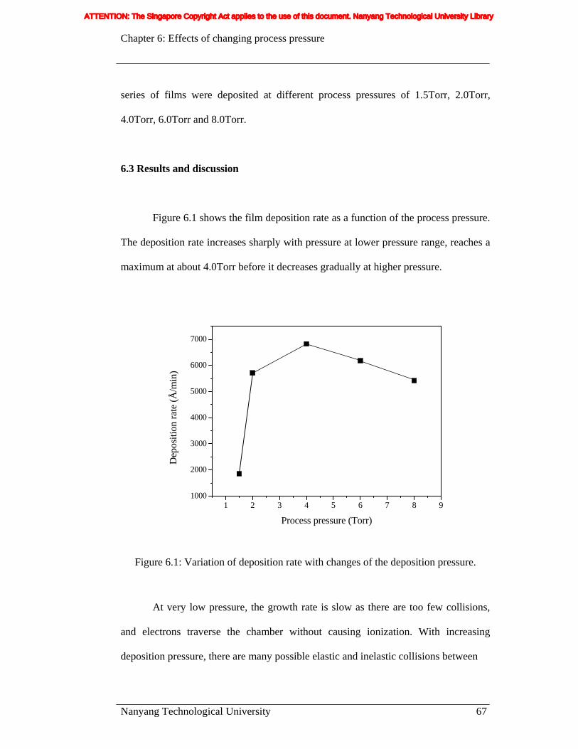
Chapter 6: Effects of changing process pressure
Nanyang Technological University 67
series of films were deposited at different process pressures of 1.5Torr, 2.0Torr,
4.0Torr, 6.0Torr and 8.0Torr.
6.3 Results and discussion
Figure 6.1 shows the film deposition rate as a function of the process pressure.
The deposition rate increases sharply with pressure at lower pressure range, reaches a
maximum at about 4.0Torr before it decreases gradually at higher pressure.
1 2 3 4 5 6 7 8 91000
2000
3000
4000
5000
6000
7000
Dep
ositi
on ra
te (Å
/min
)
Process pressure (Torr)
Figure 6.1: Variation of deposition rate with changes of the deposition pressure.
At very low pressure, the growth rate is slow as there are too few collisions,
and electrons traverse the chamber without causing ionization. With increasing
deposition pressure, there are many possible elastic and inelastic collisions between
ATTENTION: The Singapore Copyright Act applies to the use of this document. Nanyang Technological University Library
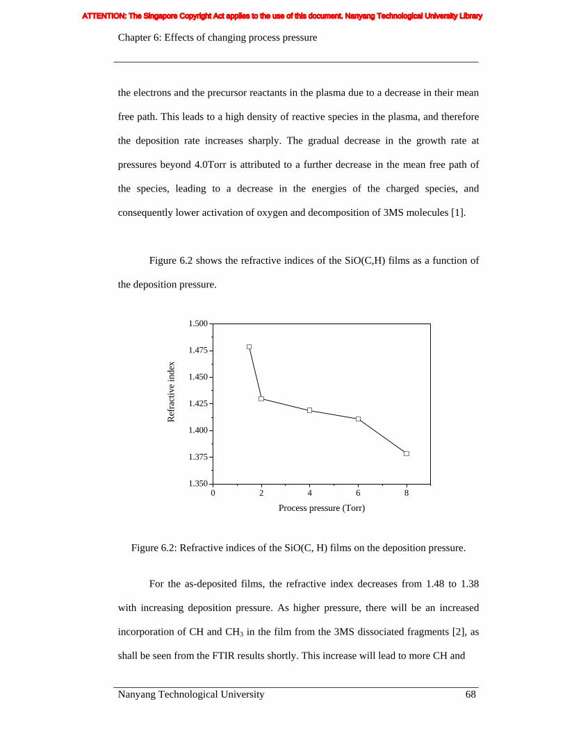
Chapter 6: Effects of changing process pressure
Nanyang Technological University 68
the electrons and the precursor reactants in the plasma due to a decrease in their mean
free path. This leads to a high density of reactive species in the plasma, and therefore
the deposition rate increases sharply. The gradual decrease in the growth rate at
pressures beyond 4.0Torr is attributed to a further decrease in the mean free path of
the species, leading to a decrease in the energies of the charged species, and
consequently lower activation of oxygen and decomposition of 3MS molecules [1].
Figure 6.2 shows the refractive indices of the SiO(C,H) films as a function of
the deposition pressure.
0 2 4 6 81.350
1.375
1.400
1.425
1.450
1.475
1.500
Refra
ctiv
e in
dex
Process pressure (Torr)
Figure 6.2: Refractive indices of the SiO(C, H) films on the deposition pressure.
For the as-deposited films, the refractive index decreases from 1.48 to 1.38
with increasing deposition pressure. As higher pressure, there will be an increased
incorporation of CH and CH3 in the film from the 3MS dissociated fragments [2], as
shall be seen from the FTIR results shortly. This increase will lead to more CH and
ATTENTION: The Singapore Copyright Act applies to the use of this document. Nanyang Technological University Library
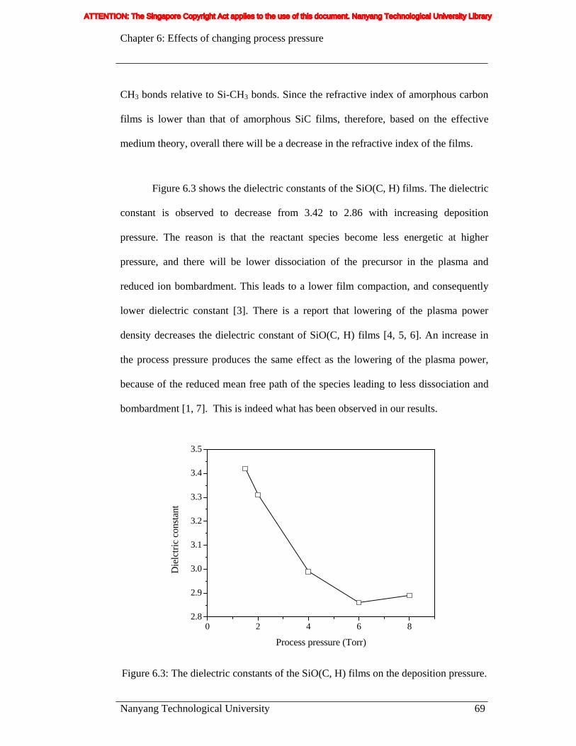
Chapter 6: Effects of changing process pressure
Nanyang Technological University 69
CH3 bonds relative to Si-CH3 bonds. Since the refractive index of amorphous carbon
films is lower than that of amorphous SiC films, therefore, based on the effective
medium theory, overall there will be a decrease in the refractive index of the films.
Figure 6.3 shows the dielectric constants of the SiO(C, H) films. The dielectric
constant is observed to decrease from 3.42 to 2.86 with increasing deposition
pressure. The reason is that the reactant species become less energetic at higher
pressure, and there will be lower dissociation of the precursor in the plasma and
reduced ion bombardment. This leads to a lower film compaction, and consequently
lower dielectric constant [3]. There is a report that lowering of the plasma power
density decreases the dielectric constant of SiO(C, H) films [4, 5, 6]. An increase in
the process pressure produces the same effect as the lowering of the plasma power,
because of the reduced mean free path of the species leading to less dissociation and
bombardment [1, 7]. This is indeed what has been observed in our results.
0 2 4 6 82.8
2.9
3.0
3.1
3.2
3.3
3.4
3.5
Die
lctri
c co
nsta
nt
Process pressure (Torr)
Figure 6.3: The dielectric constants of the SiO(C, H) films on the deposition pressure.
ATTENTION: The Singapore Copyright Act applies to the use of this document. Nanyang Technological University Library
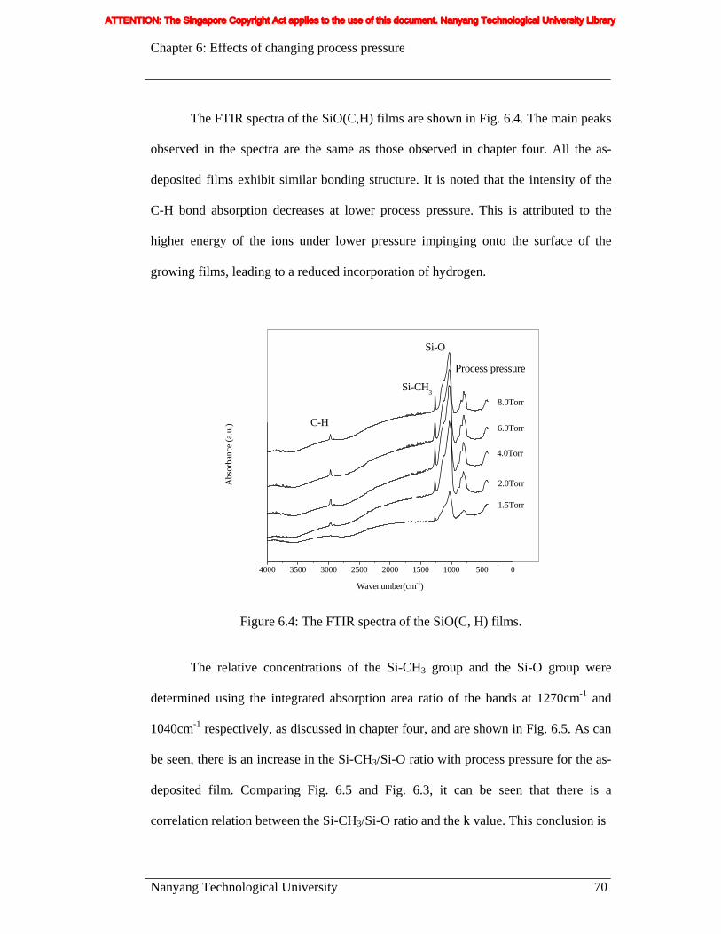
Chapter 6: Effects of changing process pressure
Nanyang Technological University 70
The FTIR spectra of the SiO(C,H) films are shown in Fig. 6.4. The main peaks
observed in the spectra are the same as those observed in chapter four. All the as-
deposited films exhibit similar bonding structure. It is noted that the intensity of the
C-H bond absorption decreases at lower process pressure. This is attributed to the
higher energy of the ions under lower pressure impinging onto the surface of the
growing films, leading to a reduced incorporation of hydrogen.
4000 3500 3000 2500 2000 1500 1000 500 0
1.5Torr
2.0Torr
4.0Torr
6.0Torr
8.0Torr
Process pressure
Si-O
Si-CH3
C-H
Abs
orba
nce
(a.u
.)
Wavenumber(cm-1)
Figure 6.4: The FTIR spectra of the SiO(C, H) films.
The relative concentrations of the Si-CH3 group and the Si-O group were
determined using the integrated absorption area ratio of the bands at 1270cm-1 and
1040cm-1 respectively, as discussed in chapter four, and are shown in Fig. 6.5. As can
be seen, there is an increase in the Si-CH3/Si-O ratio with process pressure for the as-
deposited film. Comparing Fig. 6.5 and Fig. 6.3, it can be seen that there is a
correlation relation between the Si-CH3/Si-O ratio and the k value. This conclusion is
ATTENTION: The Singapore Copyright Act applies to the use of this document. Nanyang Technological University Library
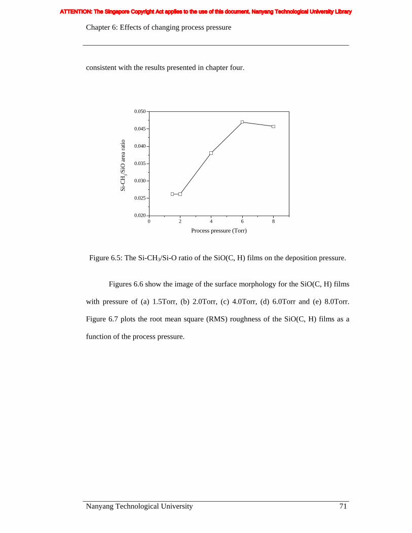
Chapter 6: Effects of changing process pressure
Nanyang Technological University 71
consistent with the results presented in chapter four.
0 2 4 6 80.020
0.025
0.030
0.035
0.040
0.045
0.050
Si-C
H3/S
iO a
rea
ratio
Process pressure (Torr)
Figure 6.5: The Si-CH3/Si-O ratio of the SiO(C, H) films on the deposition pressure.
Figures 6.6 show the image of the surface morphology for the SiO(C, H) films
with pressure of (a) 1.5Torr, (b) 2.0Torr, (c) 4.0Torr, (d) 6.0Torr and (e) 8.0Torr.
Figure 6.7 plots the root mean square (RMS) roughness of the SiO(C, H) films as a
function of the process pressure.
ATTENTION: The Singapore Copyright Act applies to the use of this document. Nanyang Technological University Library
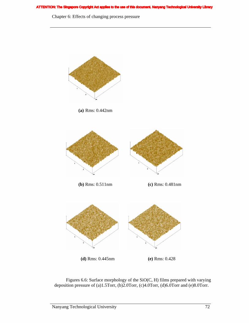
Chapter 6: Effects of changing process pressure
Nanyang Technological University 72
(a) Rms: 0.442nm
(b) Rms: 0.511nm (c) Rms: 0.481nm
(d) Rms: 0.445nm (e) Rms: 0.428
Figures 6.6: Surface morphology of the SiO(C, H) films prepared with varying deposition pressure of (a)1.5Torr, (b)2.0Torr, (c)4.0Torr, (d)6.0Torr and (e)8.0Torr.
ATTENTION: The Singapore Copyright Act applies to the use of this document. Nanyang Technological University Library
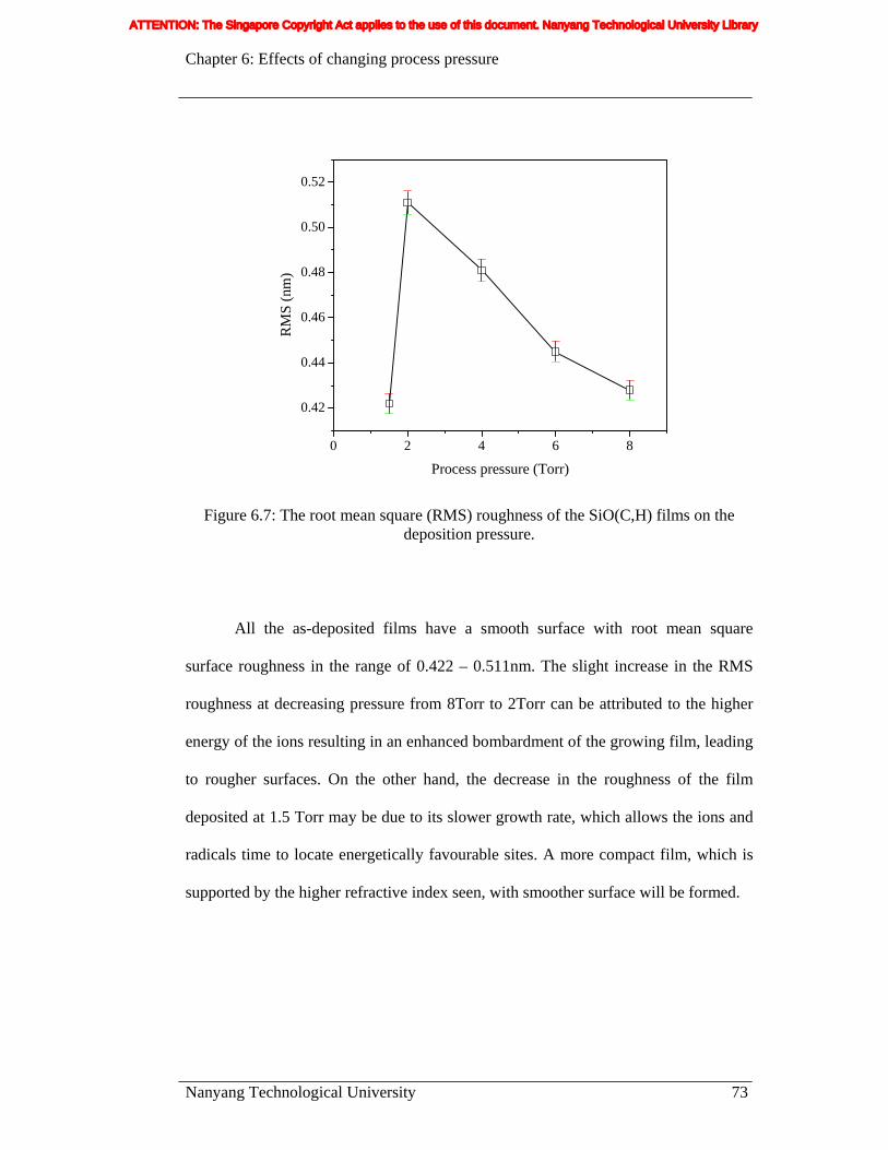
Chapter 6: Effects of changing process pressure
Nanyang Technological University 73
Figure 6.7: The root mean square (RMS) roughness of the SiO(C,H) films on the deposition pressure.
All the as-deposited films have a smooth surface with root mean square
surface roughness in the range of 0.422 – 0.511nm. The slight increase in the RMS
roughness at decreasing pressure from 8Torr to 2Torr can be attributed to the higher
energy of the ions resulting in an enhanced bombardment of the growing film, leading
to rougher surfaces. On the other hand, the decrease in the roughness of the film
deposited at 1.5 Torr may be due to its slower growth rate, which allows the ions and
radicals time to locate energetically favourable sites. A more compact film, which is
supported by the higher refractive index seen, with smoother surface will be formed.
0 2 4 6 8
0.42
0.44
0.46
0.48
0.50
0.52
RM
S (n
m)
Process pressure (Torr)
ATTENTION: The Singapore Copyright Act applies to the use of this document. Nanyang Technological University Library
Chapter 6: Effects of changing process pressure
Nanyang Technological University 74
6.4 Conclusion
The effects of process pressure on the properties of SiO(C,H) film deposited
by PECVD technique from trimethylsilane have been investigated. An increase in the
deposition pressure will result in films with low dielectric constant and low index.
Dielectric constant as low as 2.86 has been obtained from the prepared film at
8.0Torr. Deposition rate as high as 5120Å/minutes has been obtained for the film
deposited at 4.0Torr.
ATTENTION: The Singapore Copyright Act applies to the use of this document. Nanyang Technological University Library
Chapter 6: Effects of changing process pressure
Nanyang Technological University 75
6.5 References
1. Yong Chun Quan, Jongryang Joo, Sanghak Yeo and Donggeun Jung, Jpn. J. Appl. Phys. Vol.39 (2000) 1325-1326, Part 1, No. 3A, 15 March 2000
2. Yi Xu et al., Optimization of baking for flare organic low k dielectric material,
June 27-29, 2000 VMIC Conference, 2000 IMIC – 200/00/0393(c), Page 393.
3. Alfred Grill, Journal of Applied Physics, Volume 93, Issue 3, Pages 1785-1790 (2003).
4. P. Gonon, A. Sylvestre, H. Meynen, and L. Van Cotthem, J. Electrochem.
Soc.150, F47 (2003).
5. AGrill, Thin Solid Films, Volumes 398-399, Pages 527-532.
6. Takeshi Furusawa, Daisuke Ryuzaki, Ryo Yoneyama, Yoshio Homma, and Kenji Hinode, Journal of The Electrochemical Society, Volume 148, Issue 9, Pages F175-F179.
7. Yong Chun Quan, Jongryang Joo and Donggeun Jung, Jpn. J. Appl. Phys.
Vol.38 (1999) 1356-1358, Part 1, No. 3A, 15 March 1999.
8. Aboaf, J.A., Journal of the Electrochemical Society, Volume 116, Issue 12, 1969, Pages 1732-1736.
9. Masahiko Maeda and Manabu Itsumi, Physica B: Condensed Matter , Volume
324, Issues 1-4 , Pages 167-172.
ATTENTION: The Singapore Copyright Act applies to the use of this document. Nanyang Technological University Library

Chapter 7: Optical properties of the carbon doped oxide film
Nanyang Technological University 76
Chapter 7: Optical Properties of the Carbon Doped Oxide Film
7.1. Introduction
In this chapter, we have characterized the optical properties of carbon doped
oxide films (SiO(C, H)) by measuring their reflectivity under normal incident and at
700 incident angle with polarized light. These measurements were carried out over a
range of wavelengths from 200nm to 1700nm to determine the optical constants (n
and k) and thickness of the films.
From the optical results obtained, it is found that the growth of SiO(C,H)
films involves a two-layer process, in which a layer of thin SiC:H film is first formed,
which is then followed by the growth of SiO(C,H) film. For example, a SiO(C,H)
film of 525nm prepared with a O2/3MS flow ratio of 100/600 was found to consist of
25nm of SiC:H followed by 500nm of SiO(C,H) film.
In this work, we have investigated the deposition process and proposed a
growth mechanism for the SiO(C,H) films to explain the two-layer growth process.
Though the thin layer of SiC:H does not have much influence on the dielectric
constants of the SiO(C,H) films, however, it may pose a potential challenge for these
low k films in terms of advanced integration, such as acting as an unexpected etch
stop layer.
ATTENTION: The Singapore Copyright Act applies to the use of this document. Nanyang Technological University Library
Chapter 7: Optical properties of the carbon doped oxide film
Nanyang Technological University 77
7.2. Experiment details
The SiO(C,H) films were deposited using the Applied Materials CENTURA
5200 D×Z CVD system, as described in chapter four. The SiO(C,H) films were
deposited on p-type <100> orientation bare silicon 8 inches wafers, with a deposition
temperature of 350°C, process pressure of 4.0Torr and RF power of 600W. The O2
flow rate was set at 50sccm, 100sccm, 300sccm, 600sccm and 900sccm, while
keeping the 3MS flow rate constant at 600sccm. These conditions are similar to those
used in chapter four, except that the range of O2 flow rate has been increased. The
process sequence comprised gas stabilization, film deposition for a period of 45
seconds and pump down.
The spectrophotometer used for the optical characterization is FilmTek™
4000, an optical thin film measurement system from Scientific Computing
International (SCI). It combines fiber-optic spectrophotometry with material
modeling software for the simultaneous measurement of film thickness, index of
refraction, and extinction coefficient [1]. During the measurement, normal incident
and polarized 70 degree reflectance data were collected and used to calculate
thickness and index of refraction of the measured film. Absolute reflection data is
obtained by comparing sample data to the measured reflection of reference sample.
The software then performs a regression on the unknown parameters to fit the
simulated and experimental reflectance spectra.
The optical constants n and k are modelled using the SCI model, which is a
ATTENTION: The Singapore Copyright Act applies to the use of this document. Nanyang Technological University Library
Chapter 7: Optical properties of the carbon doped oxide film
Nanyang Technological University 78
generalization of the Lorentz Oscillator model given by [1],
⎟⎟⎠
⎞⎜⎜⎝
⎛−−
+= ∞ )(1 2
2
ivEEEA
center
εε (7.1)
where ε is dielectric constant and E is the photon energy. ∞ε is the high
frequency dielectric constant, Ecenter is the center energy, A is the amplitude (strength),
and ν is the vibration frequency of the oscillator. In the Lorentz oscillator model, all
oscillators are independent. The SCI model allows for coupling between the
oscillators and in the limit that the damping coefficient goes to zero, the SCI model
converges to the Lorentz Oscillator Model. The SCI model is well-suited for the
modeling of dielectric materials [1], and has been found to accurately describe the
optical constants of our films in the measured wavelength range.
7.3. Results and discussion
7.3.1 FTIR spectra and dielectric constants of the SiO(C, H) film
The FTIR spectra of the SiO(C,H) low k films deposited at different O2/3MS
flow ratios are shown in Fig. 7.1. The assignment of the various peaks observed have
been discussed in chapter four.
Figure 7.2 shows the dielectric constants of the films as a function of the
O2/3MS flow ratio. The lowest dielectric constant of 2.96 is obtained for the film
deposited at a O2/3MS flow ratio of 100/600. The k values of the as-deposited films
ATTENTION: The Singapore Copyright Act applies to the use of this document. Nanyang Technological University Library
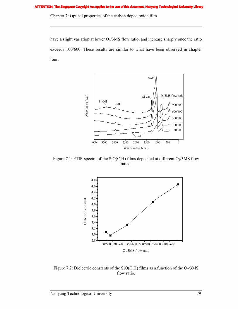
Chapter 7: Optical properties of the carbon doped oxide film
Nanyang Technological University 79
have a slight variation at lower O2/3MS flow ratio, and increase sharply once the ratio
exceeds 100/600. These results are similar to what have been observed in chapter
four.
4000 3500 3000 2500 2000 1500 1000 500 0-0.15-0.10-0.050.000.050.100.150.200.250.300.350.400.450.500.550.600.650.70
Si-H
Si-OH
50/600100/600
300/600
600/600
900/600
O2/3MS flow ratio
Si-O
Si-CH3
C-H
Abs
orba
nce
(a.u
.)
Wavenumber (cm-1)
Figure 7.1: FTIR spectra of the SiO(C,H) films deposited at different O2/3MS flow
ratios.
50/600 200/600 350/600 500/600 650/600 800/6002.8
3.0
3.2
3.4
3.6
3.8
4.0
4.2
4.4
4.6
4.8
Die
lect
ric c
onsta
nt
O2/3MS flow ratio
Figure 7.2: Dielectric constants of the SiO(C,H) films as a function of the O2/3MS flow ratio.
ATTENTION: The Singapore Copyright Act applies to the use of this document. Nanyang Technological University Library
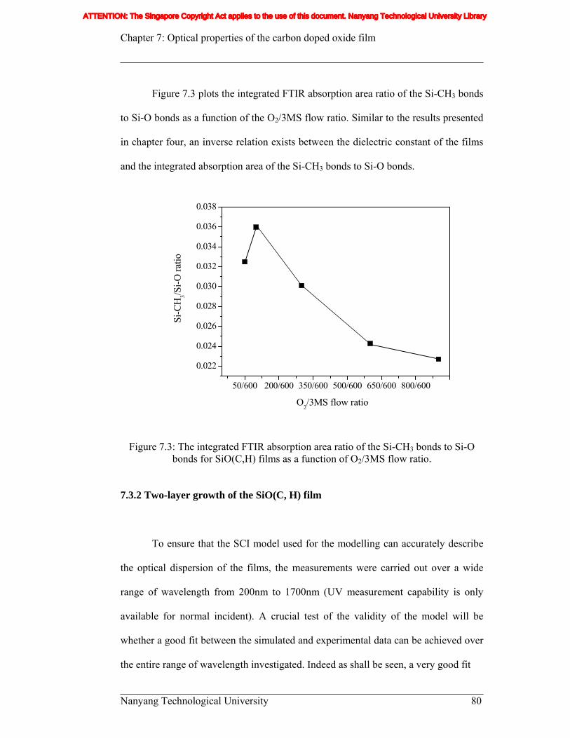
Chapter 7: Optical properties of the carbon doped oxide film
Nanyang Technological University 80
Figure 7.3 plots the integrated FTIR absorption area ratio of the Si-CH3 bonds
to Si-O bonds as a function of the O2/3MS flow ratio. Similar to the results presented
in chapter four, an inverse relation exists between the dielectric constant of the films
and the integrated absorption area of the Si-CH3 bonds to Si-O bonds.
50/600 200/600 350/600 500/600 650/600 800/600
0.022
0.024
0.026
0.028
0.030
0.032
0.034
0.036
0.038
Si-C
H3/S
i-O ra
tio
O2/3MS flow ratio
Figure 7.3: The integrated FTIR absorption area ratio of the Si-CH3 bonds to Si-O bonds for SiO(C,H) films as a function of O2/3MS flow ratio.
7.3.2 Two-layer growth of the SiO(C, H) film
To ensure that the SCI model used for the modelling can accurately describe
the optical dispersion of the films, the measurements were carried out over a wide
range of wavelength from 200nm to 1700nm (UV measurement capability is only
available for normal incident). A crucial test of the validity of the model will be
whether a good fit between the simulated and experimental data can be achieved over
the entire range of wavelength investigated. Indeed as shall be seen, a very good fit
ATTENTION: The Singapore Copyright Act applies to the use of this document. Nanyang Technological University Library
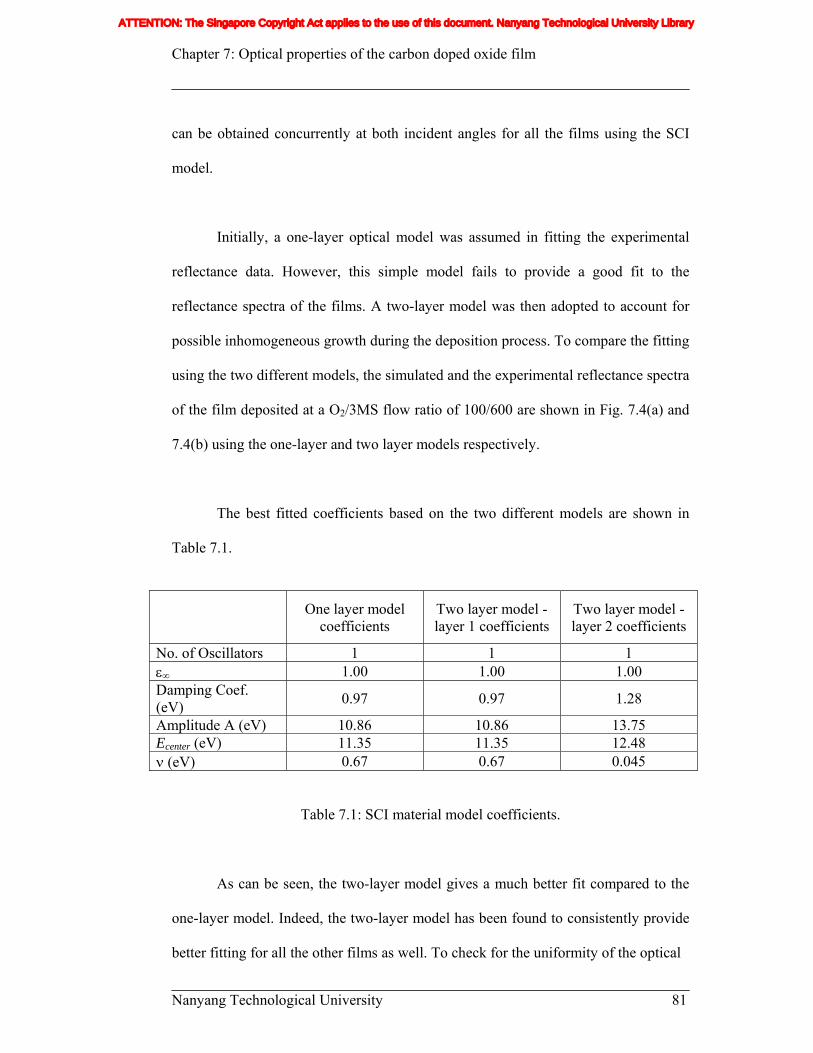
Chapter 7: Optical properties of the carbon doped oxide film
Nanyang Technological University 81
can be obtained concurrently at both incident angles for all the films using the SCI
model.
Initially, a one-layer optical model was assumed in fitting the experimental
reflectance data. However, this simple model fails to provide a good fit to the
reflectance spectra of the films. A two-layer model was then adopted to account for
possible inhomogeneous growth during the deposition process. To compare the fitting
using the two different models, the simulated and the experimental reflectance spectra
of the film deposited at a O2/3MS flow ratio of 100/600 are shown in Fig. 7.4(a) and
7.4(b) using the one-layer and two layer models respectively.
The best fitted coefficients based on the two different models are shown in
Table 7.1.
One layer model
coefficients Two layer model - layer 1 coefficients
Two layer model - layer 2 coefficients
No. of Oscillators 1 1 1 ε∞ 1.00 1.00 1.00 Damping Coef. (eV) 0.97 0.97 1.28
Amplitude A (eV) 10.86 10.86 13.75 Ecenter (eV) 11.35 11.35 12.48 ν (eV) 0.67 0.67 0.045
Table 7.1: SCI material model coefficients.
As can be seen, the two-layer model gives a much better fit compared to the
one-layer model. Indeed, the two-layer model has been found to consistently provide
better fitting for all the other films as well. To check for the uniformity of the optical
ATTENTION: The Singapore Copyright Act applies to the use of this document. Nanyang Technological University Library
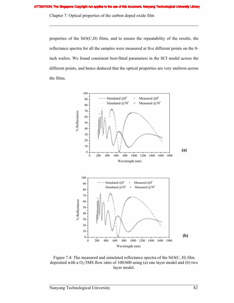
Chapter 7: Optical properties of the carbon doped oxide film
Nanyang Technological University 82
properties of the SiO(C,H) films, and to ensure the repeatability of the results, the
reflectance spectra for all the samples were measured at five different points on the 8-
inch wafers. We found consistent best-fitted parameters in the SCI model across the
different points, and hence deduced that the optical properties are very uniform across
the films.
0 200 400 600 800 1000 1200 1400 1600 18000
10
20
30
40
50
60
70
80
90
100
% R
efle
ctan
ces
Wavelength (nm)
Simulated @0o Measured @0o
Simulated @70o Measured @70o
0 200 400 600 800 1000 1200 1400 1600 18000
10
20
30
40
50
60
70
80
90
100
% R
efle
ctan
ces
Wavelength (nm)
Simulated @0o Measured @0o
Simulated @70o Measured @70o
Figure 7.4: The measured and simulated reflectance spectra of the SiO(C, H) film
deposited with a O2/3MS flow ratio of 100/600 using (a) one layer model and (b) two layer model.
(a)
(b)
ATTENTION: The Singapore Copyright Act applies to the use of this document. Nanyang Technological University Library
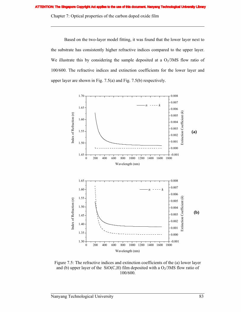
Chapter 7: Optical properties of the carbon doped oxide film
Nanyang Technological University 83
Based on the two-layer model fitting, it was found that the lower layer next to
the substrate has consistently higher refractive indices compared to the upper layer.
We illustrate this by considering the sample deposited at a O2/3MS flow ratio of
100/600. The refractive indices and extinction coefficients for the lower layer and
upper layer are shown in Fig. 7.5(a) and Fig. 7.5(b) respectively.
0 200 400 600 800 1000 1200 1400 1600 18001.45
1.50
1.55
1.60
1.65
1.70
n k
Wavelength (nm)
Inde
x of
Ref
ract
ion
(n)
-0.001
0.000
0.001
0.002
0.003
0.004
0.005
0.006
0.007
0.008
Extin
ctio
n Co
effic
ient
(k)
0 200 400 600 800 1000 1200 1400 1600 18001.30
1.35
1.40
1.45
1.50
1.55
1.60
1.65
n k
Wavelength (nm)
Inde
x of
Ref
ract
ion
(n)
-0.001
0.000
0.001
0.002
0.003
0.004
0.005
0.006
0.007
0.008Ex
tinct
ion
Coef
ficie
nt (k
)
Figure 7.5: The refractive indices and extinction coefficients of the (a) lower layer and (b) upper layer of the SiO(C,H) film deposited with a O2/3MS flow ratio of
100/600.
(a)
(b)
ATTENTION: The Singapore Copyright Act applies to the use of this document. Nanyang Technological University Library
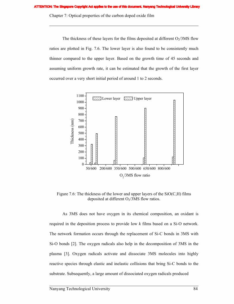
Chapter 7: Optical properties of the carbon doped oxide film
Nanyang Technological University 84
The thickness of these layers for the films deposited at different O2/3MS flow
ratios are plotted in Fig. 7.6. The lower layer is also found to be consistently much
thinner compared to the upper layer. Based on the growth time of 45 seconds and
assuming uniform growth rate, it can be estimated that the growth of the first layer
occurred over a very short initial period of around 1 to 2 seconds.
50/600 200/600 350/600 500/600 650/600 800/6000
100200300400500600700800900
10001100
Thic
knes
s (nm
)
O2/3MS flow ratio
Lower layer Upper layer
Figure 7.6: The thickness of the lower and upper layers of the SiO(C,H) films deposited at different O2/3MS flow ratios.
As 3MS does not have oxygen in its chemical composition, an oxidant is
required in the deposition process to provide low k films based on a Si-O network.
The network formation occurs through the replacement of Si-C bonds in 3MS with
Si-O bonds [2]. The oxygen radicals also help in the decomposition of 3MS in the
plasma [3]. Oxygen radicals activate and dissociate 3MS molecules into highly
reactive species through elastic and inelastic collisions that bring Si-C bonds to the
substrate. Subsequently, a large amount of dissociated oxygen radicals produced
ATTENTION: The Singapore Copyright Act applies to the use of this document. Nanyang Technological University Library
Chapter 7: Optical properties of the carbon doped oxide film
Nanyang Technological University 85
selectively oxidize Si-C bonds at the surface to form a complex containing Si-O
bonds. These complexes are then absorbed on the depositing surface to form the film.
Therefore, upon the initial growth of a thin layer of Si-C rich film with higher
refractive indices, the subsequent growth involves bulk material of SiO(C,H) film
with lower refractive indices. This will give rise to two optically distinct layers, and is
believed to account for the optical measurement results observed.
7.4 Conclusion
A detailed investigation of the optical properties of SiO(C,H) films using
reflectance spectrophotometry revealed a two-layer growth process for these films.
The results are attributed to the initial growth of a thin layer of Si-C rich film, before
the growth of the subsequent SiO(C,H) bulk material.
ATTENTION: The Singapore Copyright Act applies to the use of this document. Nanyang Technological University Library
Chapter 7: Optical properties of the carbon doped oxide film
Nanyang Technological University 86
7.5 References
1. “FilmTek 4000™ operations manual”, by Scientific Computing International,
2002. 2. Mark ONeill, Aaron Lukas, Raymond Vrtis, Jean Vincent, Brian Peterson,
Mark Bitner and Eugene Karwacki, Low-k Materials by Design, Semiconductor International, 6/1/2002.
3. M.R.Wang, Rusli, M.B.Yu, N.Babu, C.Y.Li and K. Rakesh, Thin Solid Film,
Volumes 462-463, Pages 219-222 (2004).
ATTENTION: The Singapore Copyright Act applies to the use of this document. Nanyang Technological University Library
Chapter 8: Conclusion and recommendations
Nanyang Technological University 87
Chapter 8: Conclusion and Recommendations
8.1 Conclusion
This thesis reports on the growth and characterization of carbon doped silicon
oxide (SiO(C, H)) low k dielectric thin films for multilevel interconnect applications.
The films were deposited using the plasma enhanced chemical vapour deposition
(PECVD) technique, with source gases of linear organosilicate trimethylsilane (3MS)
and oxygen. The films are hybrid materials consist of both organic and inorganic
contents. They therefore hold some unique properties such as low dielectric constant,
good thermal and mechanical stability. Their properties can also be tuned through
changing the process condition as well as process sequence.
In this work, we have first studied SiO(C, H) films deposited using two
recipes CVD1 and CVD2. The recipe CVD1 is an initial recipe that suffers from
extraordinarily high post particle counts. To address this issue, a modified recipe
CVD2 has been adopted. The main difference between the two recipes is that a pump
down step immediately before the film deposition has been omitted in recipe CVD2,
and this has successfully reduced the particle counts to a satisfactory level. However
this compromises the other properties of the film in terms of a slight increase in the
dielectric constant and non-uniform deposition rate as a function of film thickness.
ATTENTION: The Singapore Copyright Act applies to the use of this document. Nanyang Technological University Library
Chapter 8: Conclusion and recommendations
Nanyang Technological University 88
The thermal stability of the SiO(C, H) films was next investigated by
annealing them at different temperatures from 400 0C to 700 0C in a N2 atmosphere
for 30 minutes. It was found that the thermal stability of this SiO(C, H) films could be
as high as 500°C. Up to this temperature, the thickness shrinkage of the annealed film
is less than 1% and there is no obvious change in their chemical composition.
The effects of process pressure on the mechanical, optical and electrical
properties of the SiO(C, H) films have also been studied. The process pressure was
tuned from 1.5Torr to 8.0Torr while keeping the other growth parameters identical. It
has been found that the refractive index decreased from 1.48 to 1.38 while the
dielectric constant decreased from 3.4 to 2.9 with increasing deposition pressure.
Dielectric constant as low as 2.9 has been obtained for the film deposited at 8.0Torr
and deposition rate as high as 5120Å/minutes has been obtained for the film deposited
at 4.0Torr. The FTIR results revealed that more -CH and -CH3 groups were introduced
into the silicon dioxide network of the films at higher deposition pressure.
In this work, we have also investigated the deposition of SiO(C, H) films, and
proposed a growth mechanism to explain the observed two-layer growth process. We
have characterized the optical properties of SiO(C, H) films by measuring their
reflectivity under normal incident and at 700 incident angle with polarized light. From
the optical results obtained, it is found that the growth of SiO(C, H) films involves a
ATTENTION: The Singapore Copyright Act applies to the use of this document. Nanyang Technological University Library
Chapter 8: Conclusion and recommendations
Nanyang Technological University 89
two-layer process, in which a thin layer of SiC:H film is first formed, which is then
followed by the growth of SiO(C,H) film.
8.2 Recommendations for further research
The properties of the PECVD deposited SiO(C, H) films are not only
dependent on the deposition conditions such as process pressure and gas flow rate, but
also on the process temperature, rf power and other parameters. Therefore the effects
of the process temperature and rf power on the properties of the SiO(C, H) film need
to be further investigated. The integration of SiO(C, H) low k film as multilevel
interconnect dielectric using damascene structure need to be intensively studied in the
future work to assess its suitably as the next generation low k material.
ATTENTION: The Singapore Copyright Act applies to the use of this document. Nanyang Technological University Library
Author’s publication
Nanyang Technological University 90
Author’s Publications
Journal paper
1. M. R. Wang, Rusli, J. L. Xie, N. Babu, C. Y. Li and K. Rakesh, Study of
oxygen influences on carbon doped Silicon oxide low k thin films deposited by plasma enhanced chemical vapor deposition, Journal of Applied Physics, Volume 96, Issue1, pp.829-834.
2. M. R. Wang, Rusli, M. B. Yu, N. Babu, C. Y. Li and K. Rakesh, Low
dielectric constant films prepared by plasma-enhanced chemical vapor deposition from trimethylsilane, Thin Solid Films, Volumes 462-463, Pages 219-222 (2004).
3. Rusli, M. R. Wang, M. B. Yu, and C. Y. Li, Process pressure effect on
properties of carbon doped silicon oxide low dielectric constant films prepared by PECVD using trimethylsilane, Journal of Applied Physics, to be submitted.
4. Rusli, M. R. Wang, M. B. Yu, and C. Y. Li, Effects of annealing on low dielectric constant carbon doped silicon oxide films, Diamond and Related Materials, to be submitted.
Conference paper
1. M. R. Wang, Rusli, M. B. Yu, N. Babu, C. Y. Li and K. Rakesh, Low dielectric constant films prepared by plasma enhanced chemical vapor deposition from trimethylsilane, ICMAT2003, Singapore, p551.
2. Rusli, M. R. Wang, B. K. Tay, M. B. Yu, N. Babu, C. Y. Li and SH.R.Wang,
Two-layer growth of carbon doped silicon oxide low dielectric constant films prepared by PECVD using trimethylsilane, ThinFilm2004, Singapore.
ATTENTION: The Singapore Copyright Act applies to the use of this document. Nanyang Technological University Library