Embed Size (px)
Citation preview

Growth and Characterization of III-V Phosphide Nanowires
by
Praneeth Ranga
A Thesis Presented in Partial Fulfillmentof the Requirements for the Degree
Master of Science
Approved November 2016 by theGraduate Supervisory Committee:
Cun-Zheng Ning, ChairJoseph Palais
Meng Tao
ARIZONA STATE UNIVERSITY
December 2016

ABSTRACT
Nanowires are 1D rod like structures which are regarded as the basis for future tech-
nologies. III-V nanowires have attracted immense attention because of their stability,
crystal quality and wide use. In this work, I focus on the growth and characterization
of III-V semiconductor nanowires, in particular GaP, InP and InGaP alloys. These
nanowires were grown using a hot wall CVD(Chemical Vapor Deposition) setup and
are characterized using SEM (Scanning Electron Microscope), EDX (Energy Disper-
sive X-ray Spectroscopy) and PL (Photoluminescence) techniques.
In the first chapter, Indium Phosphide nanowires were grown using elemental
sources (In and P powders). I consider the various kinds of InP morphologies grown
using this method. The effect of source temperature on the stoichiometry and optical
properties of nanowires is studied. Lasing behavior has been seen in InP nanostruc-
tures, showing superior material quality of InP.
InGaP alloy nanowires were grown using compound and elemental sources. Nanowires
grown using compound sources have significant oxide incorporation and showed kinky
morphology. Nanowires grown using elemental sources had no oxide and showed bet-
ter optical quality. Also, these samples showed a tunable alloy composition across
the entire substrate covering more than 50% of the InGaP alloy system. Integrated
intensity showed that the bandgap of the nanowires changed from indirect to direct
bandgap with increasing Indium composition. InGaP alloy nanowires were compared
with Gallium Phosphide nanowires in terms of PL emission, using InGaP nanowires
it is possible to grow nanowires free of defects and oxygen impurities, which are
commonly encountered in GaP nanowires.
i

ACKNOWLEDGEMENTS
I would like to wholeheartedly thank my thesis adviser Prof.Cun-Zheng Ning for
giving me the opportunity to work in his group. This work would not be possible
without his guidance and support. I thank my committee members, Prof. Joseph
Palais and Prof. Meng Tao for their advice and suggestions to my work.
I thank all the present and previous members of the ASU Nanophotonics group.
Firstly, Seyed for his help with CVD growth setup, SEM and EDX analysis of samples
in this work. I appreciate the help of Fan Fan, Yueyang Yu, Dr. Gan Lin, Dongying
Li and Zhiyu Huang with optical characterization of nanowire samples.
I thank my parents for their support and encouragement throughout my studies
at ASU.
ii

TABLE OF CONTENTS
Page
LIST OF TABLES . . . . . . . . . . . . . . . . . . . . . . . . . . . . . . . . . . . . . . . . . . . . . . . . . . . . . . . . . v
LIST OF FIGURES . . . . . . . . . . . . . . . . . . . . . . . . . . . . . . . . . . . . . . . . . . . . . . . . . . . . . . . . vi
CHAPTER
1 INTRODUCTION . . . . . . . . . . . . . . . . . . . . . . . . . . . . . . . . . . . . . . . . . . . . . . . . . . . 1
1.1 Nanotechnology . . . . . . . . . . . . . . . . . . . . . . . . . . . . . . . . . . . . . . . . . . . . . . . . 1
1.2 Nanowires . . . . . . . . . . . . . . . . . . . . . . . . . . . . . . . . . . . . . . . . . . . . . . . . . . . . . . 2
2 GROWTH AND CHARACTERIZATION OF NANOWIRES . . . . . . . . . . . 5
2.1 Crystal Growth . . . . . . . . . . . . . . . . . . . . . . . . . . . . . . . . . . . . . . . . . . . . . . . . . 5
2.2 VLS Mechanism . . . . . . . . . . . . . . . . . . . . . . . . . . . . . . . . . . . . . . . . . . . . . . . . 6
2.3 Scanning Electron Microscope(SEM) . . . . . . . . . . . . . . . . . . . . . . . . . . . . . 8
2.4 Energy Dispersive X-ray Spectroscopy(EDX) . . . . . . . . . . . . . . . . . . . . . 9
2.5 Photoluminescence Spectroscopy(PL) . . . . . . . . . . . . . . . . . . . . . . . . . . . . 10
2.6 Experimental Setup . . . . . . . . . . . . . . . . . . . . . . . . . . . . . . . . . . . . . . . . . . . . . 12
2.7 Growth Process . . . . . . . . . . . . . . . . . . . . . . . . . . . . . . . . . . . . . . . . . . . . . . . . . 13
2.8 Nanowire Laser . . . . . . . . . . . . . . . . . . . . . . . . . . . . . . . . . . . . . . . . . . . . . . . . . 15
3 INDIUM PHOSPHIDE NANOWIRES . . . . . . . . . . . . . . . . . . . . . . . . . . . . . . . . 16
3.1 Motivation for Indium Phosphide Nanowires . . . . . . . . . . . . . . . . . . . . . . 16
3.2 Growth Setup . . . . . . . . . . . . . . . . . . . . . . . . . . . . . . . . . . . . . . . . . . . . . . . . . . 17
3.3 Results and Discussion . . . . . . . . . . . . . . . . . . . . . . . . . . . . . . . . . . . . . . . . . . 19
3.4 Growth Mechanism . . . . . . . . . . . . . . . . . . . . . . . . . . . . . . . . . . . . . . . . . . . . . 21
4 INDIUM GALLIUM PHOSPHIDE NANOWIRES . . . . . . . . . . . . . . . . . . . . . 27
4.1 Introduction and Background . . . . . . . . . . . . . . . . . . . . . . . . . . . . . . . . . . . . 27
4.2 Growth Setup . . . . . . . . . . . . . . . . . . . . . . . . . . . . . . . . . . . . . . . . . . . . . . . . . . 29
4.3 Results . . . . . . . . . . . . . . . . . . . . . . . . . . . . . . . . . . . . . . . . . . . . . . . . . . . . . . . . 30
iii

CHAPTER Page
4.4 Growth Mechanism . . . . . . . . . . . . . . . . . . . . . . . . . . . . . . . . . . . . . . . . . . . . . 39
4.5 Growth of GaP Nanowires . . . . . . . . . . . . . . . . . . . . . . . . . . . . . . . . . . . . . . . 40
4.6 Defects in Nanowires . . . . . . . . . . . . . . . . . . . . . . . . . . . . . . . . . . . . . . . . . . . . 40
4.7 Photodegradation . . . . . . . . . . . . . . . . . . . . . . . . . . . . . . . . . . . . . . . . . . . . . . . 42
5 SUMMARY . . . . . . . . . . . . . . . . . . . . . . . . . . . . . . . . . . . . . . . . . . . . . . . . . . . . . . . . . 46
REFERENCES . . . . . . . . . . . . . . . . . . . . . . . . . . . . . . . . . . . . . . . . . . . . . . . . . . . . . . . . . . . . 47
iv

LIST OF TABLES
Table Page
4.1 Growth parameters of InGaP nanowires . . . . . . . . . . . . . . . . . . . . . . . . . . . . . 31
v

LIST OF FIGURES
Figure Page
1.1 Graph of Lattice Constant vs Band Gap for Various Semiconductors . . . 3
2.1 Phase Diagram of Au-Si System Showing Different Stages of VLS
Mechanism . . . . . . . . . . . . . . . . . . . . . . . . . . . . . . . . . . . . . . . . . . . . . . . . . . . . . . . . 7
2.2 Moseley’s Law . . . . . . . . . . . . . . . . . . . . . . . . . . . . . . . . . . . . . . . . . . . . . . . . . . . . . 10
2.3 Different Recombination Mechanisms in a Semiconductor . . . . . . . . . . . . . 11
2.4 CVD Setup for Growth of Semiconductor Nanowires . . . . . . . . . . . . . . . . . . 12
2.5 Steps Involved in Growth of Nanowires via CVD Method . . . . . . . . . . . . . 13
2.6 Different Flow Regimes Inside a Tube . . . . . . . . . . . . . . . . . . . . . . . . . . . . . . . 14
3.1 Growth Setup of Three Zone Furnace . . . . . . . . . . . . . . . . . . . . . . . . . . . . . . . . 18
3.2 Picture of Quartz Tube Showing Different Deposition Regions . . . . . . . . . 19
3.3 Dependence of InP Morphologies on Growth Conditions . . . . . . . . . . . . . . 20
3.4 Comparison of InP Nanowires Grown with Different Source Conditions 23
3.5 PL Intensity with Different Pumping Power in a InP Belt Structure . . . 24
3.6 Lasing InP Nanobelt and Nanowire . . . . . . . . . . . . . . . . . . . . . . . . . . . . . . . . . 25
3.7 PL of Nanowire Under Different Power Density . . . . . . . . . . . . . . . . . . . . . . 25
3.8 Formation Mechanisms of InP Nanostructures . . . . . . . . . . . . . . . . . . . . . . . . 26
3.9 Effect of Phosphorus Vapor Pressure on InP Film . . . . . . . . . . . . . . . . . . . . 26
4.1 Indium Gallium Phosphide Band Gap vs Lattice Constant . . . . . . . . . . . 28
4.2 Growth Setup for InGaP Nanowires . . . . . . . . . . . . . . . . . . . . . . . . . . . . . . . . . 29
4.3 PL Spectrum of Nanowires Grown at Different Growth Conditions . . . . 31
4.4 FWHM of InGaP samples grown at 900 C . . . . . . . . . . . . . . . . . . . . . . . . . . . 32
4.5 Low and High Resolution Images InGaP Alloys Grown Under Different
Growth Conditions Samples 1(a,b), 2(c,d) and 3(e,f) . . . . . . . . . . . . . . . . . 35
4.6 Images of Samples with Different InGaP Alloy Composition . . . . . . . . . . . 36
vi

Figure Page
4.7 Change in Peak Wavelength Across the Length of the Substrate . . . . . . . 36
4.8 FWHM of Nanowires on a Single Substrate . . . . . . . . . . . . . . . . . . . . . . . . . . 37
4.9 PL Peak of Nanowires Scanned Across a Single Substrate . . . . . . . . . . . . . 37
4.10 Integrated Intensity Change with Band Gap of the Alloy . . . . . . . . . . . . . 38
4.11 Alloy Gradient Across a Single Substrate . . . . . . . . . . . . . . . . . . . . . . . . . . . . 38
4.12 Binary Phase Diagram of Indium-Gallium System . . . . . . . . . . . . . . . . . . . 39
4.13 EDX Analysis of Catalytic Particle(Top) and Nanowire Body(Bottom) . 40
4.14 Growth Setup for GaP Nanowires . . . . . . . . . . . . . . . . . . . . . . . . . . . . . . . . . . . 41
4.15 Defects in PL spectra of nanowires . . . . . . . . . . . . . . . . . . . . . . . . . . . . . . . . . . 42
4.16 ZnSe Defect Emission Under Different Growth Conditions . . . . . . . . . . . . 43
4.17 Comparison of GaP and InGaP Nanowires Under Different Growth
Conditions . . . . . . . . . . . . . . . . . . . . . . . . . . . . . . . . . . . . . . . . . . . . . . . . . . . . . . . . 44
4.18 Change in PL Intensity with Laser Irradiation in InGaP Nanowires . . . . 45
vii

Chapter 1
INTRODUCTION
1.1 Nanotechnology
Advances in civilization have been historically associated with breakthroughs
in material science, so much that different periods are named after the most prominent
material used(stone age, bronze age etc). The 20th century experienced a revolution
in study of materials like never before, with the creation of nanotechnology. Nanotech-
nology is the study of synthesis and manipulation of objects with critical dimension
on the scale of nanometers. When the size of an object reaches a few nanometers, its
properties are changed drastically compared to corresponding bulk materials. The
behaviour of the object cannot be understood classically as quantum effects dominate
its properties. This gives rise to unique and novel properties which are not found in
nature. Because of its broad applications, nanotechnology potentially can solve huge
challenges faced by mankind in energy, medicine, communications etc.
Though the idea for nanotechnology is present for a long time, progress
made in invention of new techniques to manipulate and characterize materials led to
rapid growth of the field. This gave us access to visualize and manipulate individual
atoms which was not possible previously, leading to the creation of new class of devices
made of nano objects. Miniaturization is one of the key themes in nanotechnology.
The semiconductor revolution is possible due to invention of top down techniques
which enabled to integrate millions of transistors on a single substrate. Traditional
semiconductor companies use a top-down approach, where a wafer is patterned using
a optical light source such as a laser. As the feature size of the device becomes smaller,
1
it becomes very difficult to make the pattern smaller. The other approach used in
nanotechnology is called the bottom up approach. Using this approach materials with
nanoscale dimensions can be made by assembling individual atoms. This reduces the
use of expensive equipment and allows to fabricate multiple structures in a single run.
1.2 Nanowires
Nanowires are 1D structures with diameters on the order of nanometers and
lengths in microns. Nanowire growth based on VLS mechanism was first observed in Si
whiskers, Wagner and Ellis observed that using an impurity like gold resulted in wires
with gold tips at their ends[1]. Since then rapid progress has been made in growth
of nanowires using a variety of methods like MOCVD, MBE, CBE, Solution phase
growth etc. Due to their high aspect ratio nanowires have a large surface area, which
allows them to outperform thin film electrodes for battery use. Due to their small
diameters, electrons are confined in the transverse direction but can move along the
axial direction. Nanowires are also useful to study physics in one dimensional objects
due to their unique structural and electronic properties. Most importantly, nanowires
can be grown using a bottom up approach with much lower cost compared to using a
top down approach. The diameter of the nanowires is simply controlled by the size of
gold droplet and the length is controlled by the growth rate. These properties make
nanowires a potential replacement for conventional CMOS devices which are difficult
too be miniaturized any further.
For the purpose of making optical devices, very high quality material is
required. If the thin film and the substrate are not closely lattice matched, dislocations
due to strain damage the performance of the device. Unlike thin films, nanowires can
withstand much more strain and can be grown on any arbitrary substrate. This
allows us to grow alloys and fabricate devices with superior material quality which
2
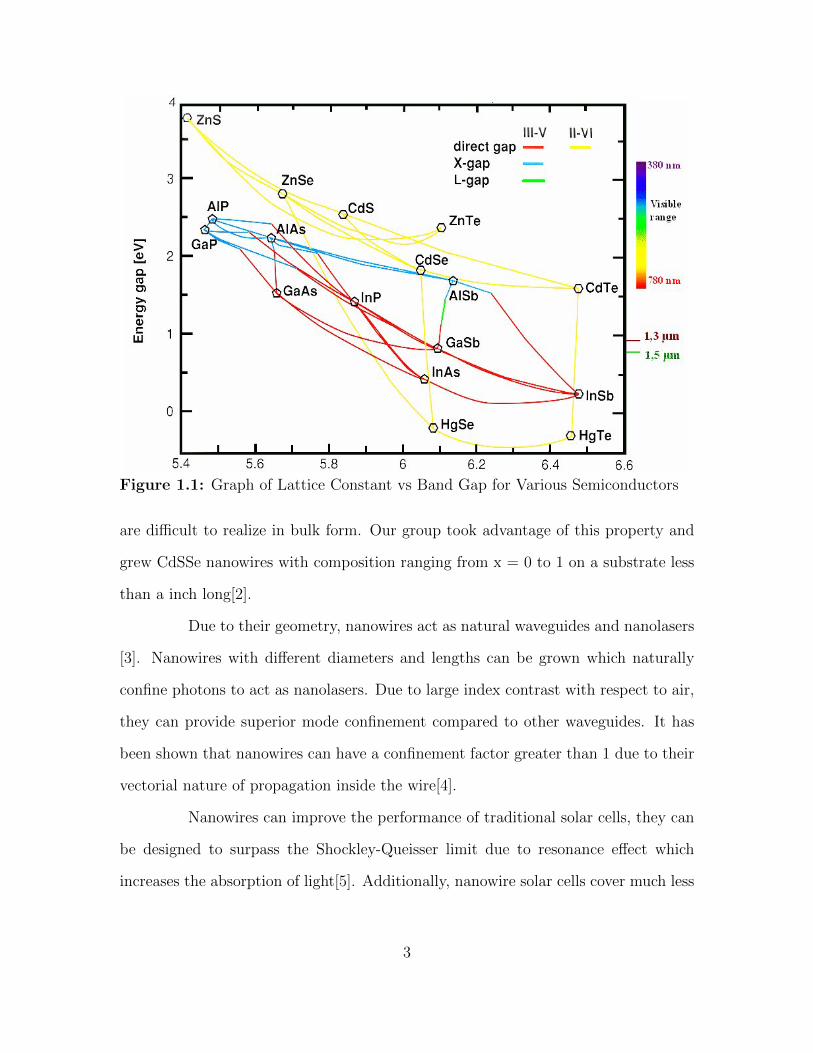
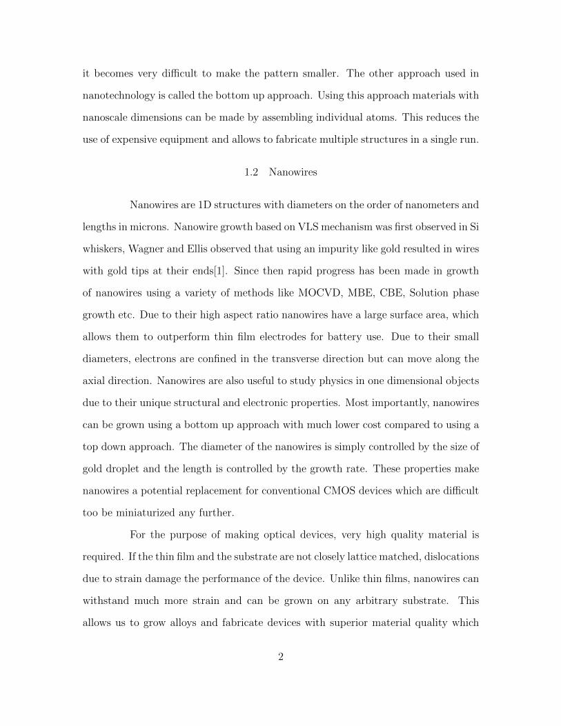
Figure 1.1: Graph of Lattice Constant vs Band Gap for Various Semiconductors
are difficult to realize in bulk form. Our group took advantage of this property and
grew CdSSe nanowires with composition ranging from x = 0 to 1 on a substrate less
than a inch long[2].
Due to their geometry, nanowires act as natural waveguides and nanolasers
[3]. Nanowires with different diameters and lengths can be grown which naturally
confine photons to act as nanolasers. Due to large index contrast with respect to air,
they can provide superior mode confinement compared to other waveguides. It has
been shown that nanowires can have a confinement factor greater than 1 due to their
vectorial nature of propagation inside the wire[4].
Nanowires can improve the performance of traditional solar cells, they can
be designed to surpass the Shockley-Queisser limit due to resonance effect which
increases the absorption of light[5]. Additionally, nanowire solar cells cover much less
3

area compared to thin film solar cells but can match their efficiency which can bring
down material costs substantially.
The crystal structure of nanowires can be controlled by changing the growth
conditions, which is difficult with bulk material. For example, recently wurtzite gal-
lium phosphide have been realized in nanowires[6][7]. This is possible because smaller
diameter nanowires prefer to grow in wurtzite phase under high supersaturation. Us-
ing nanowires we have better control over its crystalline properties resulting in novel
and efficient devices.
4

Chapter 2
GROWTH AND CHARACTERIZATION OF NANOWIRES
2.1 Crystal Growth
The growth of a crystal is only possible if its formation is thermodynami-
cally favorable. A system always tries to attain the lowest Gibbs free energy possible.
For growth to occur there need to be at least two phases which can ex-
change matter and energy. The chemical potential of a phase is defined as the energy
needed to add N particles to a phase at a constant temperature T and pressure P.
µ =∂G
∂N P,T(2.1)
Consider a simple system consisting of a crystal in contact with its monoatomic
gas.
The difference between the chemical potential of the vapor pressure and the
crystal phase is called supersaturation, the amount of supersaturation is the driving
force for crystal growth.
∆µvc = µv − µc (2.2)
The supersaturation for a simple system can be simplified as the ratio of gas pressure
P and the crystal equilibrium vapor pressure at a temperature P0.Where R is the
universal gas constant and T is temperature.
∆µvc = RT logP
P0
(2.3)
A crystal at a constant temperature T has a fixed equilibrium pressure P0.
As temperature increases the value of P increases. The ratio of external vapor pressure
5

P to P0 determines the supersaturation. If the value of ∆µ is positive crystal growth
takes place. If ∆µ = 0, the system remains in equilibrium and no growth occurs. If
the value is negative, etching of crystal takes place.
2.2 VLS Mechanism
Planar growth occurs as each monolayer is added to the surface and the
crystal grows upward. For 1D structures such as nanowires to grow, there are various
techniques to grow crystals anisotropically. The most common growth technique is
based on VLS (Vapor-Liquid-Solid) mechanism which uses a metal particle such as
gold to act as a catalyst. VLS mechanism was first observed in Silicon whiskers by
Wagner and Ellis in 1964 [1]. Understanding VLS mechanism gives us a good idea of
composition, sizes and crystalline directions of the nanowires.
The choice of catalyst for nanowire growth is subject to several conditions
[8]. The catalyst must have higher solubility in liquid phase. It must have low vapor
pressure and inert to chemical reaction. Generally noble and transition metals work
well with III-V and group IV materials. In situ TEM done by Yang et.al showed
that there are three distinct phases of the VLS mechanism(Alloying, Nucleation and
Growth) [9].
1. Alloying: Initially metal is in a solid phase, with increasing source vapor
they form a liquid alloy. The alloy crosses from a biphasic region to a single phase
region.
2. As the alloy crosses the liquidus line it enters Metal+Semiconductor
alloy and S(solid) region. Nucleation starts as the weight percentage of the semicon-
ductor is at larger value.
6

Figure 2.1: Phase Diagram of Au-Si System Showing Different Stages of VLSMechanism[8]
3.Once a semiconductor nucleus forms at the solid-liquid interface any ex-
tra adsorption of the vapor leads to precipitation of the crystal at the solid-liquid
interface. The incoming vapor prefers to crystallize at the interface due to the less
energy involved compared to forming a nucleus.
The diameter of the nanowires is larger than the initial metal nanoparticle
because of the alloying process. For obtaining nanowires with uniform diameters, it is
important to have metal particles with the same diameter. Even though the nanowire
diameter depends on the metal nanoparticle, there is a thermodynamic limit beyond
which the diameter cannot be decreased.
Rm =(2Vlσlv)
(RTln(s))(2.4)
7

Vl is the molar volume, σlv is the liquid vapor surface energy and s is the
degree of supersaturation of the vapor. The chemical potential of the component is
inversely proportional to the radius of the droplet.
∆µ =2γ
r(2.5)
This shows that it is difficult to supersaturate smaller alloy droplets. Be-
cause of this limit it is challenging to grow nanowires with sub 10 nm diameter.
Another issue is that small metal droplets prefer to form larger radius droplets due
to Otswald ripening, making it challenging to get metal particle with small diameter.
2.3 Scanning Electron Microscope(SEM)
Traditional optical microscopes use photons to image a sample, but the
resolution of such equipment is limited by the wavelength of light. A different tech-
nique is needed to image a nano sized object with the critical dimension less than the
wavelength of light.
A SEM(Scanning Electron Microscope) uses electrons instead of photons to
image a specimen. SEM is based on the DeBroglie principle, which predicts the wave
nature of electrons with very short wavelength upto picometer range. This enables
the SEM to resolve features on the size upto a few nanometers. The main working
blocks of an SEM are microscopic column, specimen chamber, vacuum system and
instrument controls. A digital image is generated by rastering the electron beam
across the surface of the sample and detecting the emitted signal from the surface
sample interaction. The key parameters controlling the SEM are accelerating voltage,
probe current, convergence angle and spot size. A SEM uses electromagnetic lenses
to control the beam, like optical lenses it suffers from aberrations, the main issues
affecting its performance are spherical aberration, chromatic aberration and astigma-
8

tism. The SEM needs to make corrections to reduce the disk of minimum confusion
in each case.
2.4 Energy Dispersive X-ray Spectroscopy(EDX)
Energy Dispersive X-ray Spectroscopy is a technique by which we can iden-
tify different atomic elements and estimate the composition of the sample under study.
When a sample is studied under a electron beam, characteristic and continuum X-
rays are generated. Characteristic X-rays form sharp peaks on the spectrum. These
peaks are unique for each atomic element.Given a spectrum we can match the data to
standard X-ray pattern for each element. The X-ray radiation is denoted by electron
shell from which the electron is ejected. If the vacancy is filled by the neighbouring
shell it is denoted by alpha . If the vacancy is filled by the second nearest shell it is
denoted by beta . The EDX principle is based on Moseley’s Law which states that the
energy of X-ray radiation corresponding to a particular shell increases with atomic
number. Elements with higher atomic number give more energetic radiation. This
is given by the expression E = C1(Z − C2)2, where C1 and C2 are constants and Z
is the atomic number. The minimum energy to observe X-ray emission is known as
critical ionization energy.
Generally multiple X-rays corresponding to different shells are observed
from each element. Light elements emit only K lines, intermediate elements emit
both K and L lines, we can estimate the atomic number by looking at number of
emission lines of the X-ray spectrum. Because X-rays are generated mostly deeper in
the sample than secondary electrons, EDX is not a surface technique and calculates
the composition of the sample under the electron beam.
9
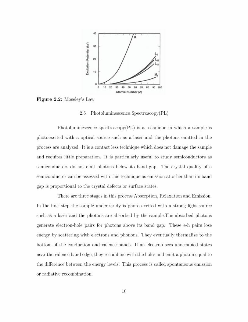
Figure 2.2: Moseley’s Law
2.5 Photoluminescence Spectroscopy(PL)
Photoluminescence spectroscopy(PL) is a technique in which a sample is
photoexcited with a optical source such as a laser and the photons emitted in the
process are analyzed. It is a contact less technique which does not damage the sample
and requires little preparation. It is particularly useful to study semiconductors as
semiconductors do not emit photons below its band gap. The crystal quality of a
semiconductor can be assessed with this technique as emission at other than its band
gap is proportional to the crystal defects or surface states.
There are three stages in this process Absorption, Relaxation and Emission.
In the first step the sample under study is photo excited with a strong light source
such as a laser and the photons are absorbed by the sample.The absorbed photons
generate electron-hole pairs for photons above its band gap. These e-h pairs lose
energy by scattering with electrons and phonons. They eventually thermalize to the
bottom of the conduction and valence bands. If an electron sees unoccupied states
near the valence band edge, they recombine with the holes and emit a photon equal to
the difference between the energy levels. This process is called spontaneous emission
or radiative recombination.
10
Figure 2.3: Different Recombination Mechanisms in a Semiconductor
There are other type of recombination called Shockley-Reed-Hall recombi-
nation or trap assisted recombination and Auger recombination. In SRH recombina-
tion, the electron transits from conduction to valence band via trap or defect states.
With higher trap density, the possibility of SRH recombination increases. Auger re-
combination is a three particle process, when the electron and hole recombine, instead
of emitting a photon they transfer the energy to a third electron in the conduction
band.Since it involves three particles, the Auger effect is dominant at high carrier
density. Since SRH and Auger recombination do not emit light, these are called non-
radiative recombination. The rate of recombination is dependant on the rate of each
of the individual processes.
dN
dt= −(An+Bn2 + Cn3) (2.6)
11

Figure 2.4: CVD Setup for Growth of Semiconductor Nanowires
2.6 Experimental Setup
The nanowire sample are grown using a three zone tube furnace via CVD
method. The three zones of the furnace can be individually separated using the
controller, each zone can reach a maximum temperature of 1200 C. This gives us
flexibility in adjusting the position and temperature of the precursors. A tube made
of quartz is used, in order to withstand the high temperature of the growth process.
The setup is shown in figure 2.4 , one end of the three zone furnace is connected to a
rotary vane pump in order to remove air from the system. A gas cylinder containing
a inert transport gas containing Ar + 5%H2 or N2 is connected to the other end. A
mass flow controller is used to control the amount of gas flowing through the tube.
12
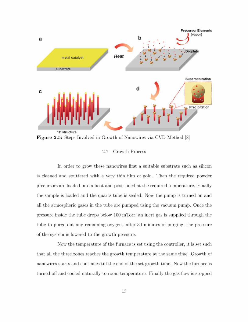
Figure 2.5: Steps Involved in Growth of Nanowires via CVD Method [8]
2.7 Growth Process
In order to grow these nanowires first a suitable substrate such as silicon
is cleaned and sputtered with a very thin film of gold. Then the required powder
precursors are loaded into a boat and positioned at the required temperature. Finally
the sample is loaded and the quartz tube is sealed. Now the pump is turned on and
all the atmospheric gases in the tube are pumped using the vacuum pump. Once the
pressure inside the tube drops below 100 mTorr, an inert gas is supplied through the
tube to purge out any remaining oxygen. after 30 minutes of purging, the pressure
of the system is lowered to the growth pressure.
Now the temperature of the furnace is set using the controller, it is set such
that all the three zones reaches the growth temperature at the same time. Growth of
nanowires starts and continues till the end of the set growth time. Now the furnace is
turned off and cooled naturally to room temperature. Finally the gas flow is stopped
13

and the sample is removed for further characterization.
Figure 2.6: Different Flow Regimes Inside a Tube
There are a variety of factors which effect nanowire properties, including
growth temperature, flow rate, pressure, mass of precursors, choice and size of cat-
alyst, type of substrate, carrier gas, pressure, growth time, source temperature etc.
Hence it is important to understand the effect of these parameters in order to grow
desired nanostructures.
Temperature and pressure are the key parameters in growth of nanowires.
Increasing source temperature increases the vapor pressure of the source material over
the substrate. Increasing the flow rate also increases the supply of the source over the
substrate. Increasing the pressure of the carrier increases the chemical potential of
the solid source and makes it difficult to evaporate. The choice of carrier gas effects
the growth pressure depending on the composition of the gas.
The type of flow is important to get uniform deposition of material. There
are three types of flow regimes, laminar, transitional and turbulent types [10]. The
classification of flow type is given by the Reynold’s number, which is the ratio of
14

inertial to viscous forces. If R is less than 2100 it is laminar, if R is greater than 4100
it is turbulent. An important characteristic of laminar flow is that, it has a uniform
profile through out the entire tube.
2.8 Nanowire Laser
Traditional lasers made by top down fabrication are time consuming and
need expensive equipment. Nanowires grown by bottom up method are less expen-
sive and much simpler. Also semiconductor materials with high crystalline quality
are more suitable for nanolaser applications. Certain II-VI materials are difficult to
handle using conventional clean room equipment.
For lasing to be observed in nanowires, a cavity must be formed between
the crystal facets enabling feedback, if the gain in a round trip balances the mirror
and absorption loss lasing can be achieved.
gτ >1
2Lln(
1
R1R2
) + αp (2.7)
Where τ is the confinement factor, L is the length of the wire, R1R1 are reflection
coefficients of the crystal facets and αp is the propagation loss. Due to their small
cavity length nanowires may have a scattering process at the interface instead of
a reflection process. This property of nanowires can reduce mirror loss compared
to traditional nanolasers. Also nanowires have much smaller cavity to attain gain
compared to other nanolasers. It has been shown that nanowire lasers can have
confinement factor larger than one [4]. Nanowire lasers have been demonstrated in a
wide range of materials including ZnO, CdS, InGaAs, InP, ZnS etc [3][11][2].
15

Chapter 3
INDIUM PHOSPHIDE NANOWIRES
3.1 Motivation for Indium Phosphide Nanowires
Indium Phosphide (InP) is a III-V compound semiconductor with a direct
band gap of 1.35eV for the fcc lattice zinc blende structure. InP nanowires can be
grown by either self-catalyzed and Au catalyzed mechanism using a wide range of
methods(MOCVD, MBE, CBE, CSS etc). Owing to its superior qualities it is used
in high frequency electronics and is preferred to alloy with other III-V materials.
III-V solar cells often have the highest conversion efficiency among differ-
ent material systems. Because of its low surface recombination velocity and high
electron mobility, InP is an attractive material for PV technology. InP has direct
band gap of 1.34 eV, matching the terrestrial solar spectrum which results in 31 %
theoretical conversion efficiency. These advantages coupled with reduced material us-
age, enhanced light trapping and ease of processing makes InP attractive material for
nanowire growth. Wallentin et.al fabricated a axial InP nanowire cell with efficiency
as high as 13.3% covering just 12% of the substrate[12].
One additional advantage for InP crystal growth is the ability to grow
thin film InP on amorphous substrate, where as other III-V materials need expensive
crystalline substrates [13, 14]. Recently the Javey group have applied VLS mechanism
on thin-film InP using Mo substrate. Solar cells made using poly-InP has efficiency
upto 12%[15], this low cost approach may result in wide spread use of InP PV module.
16

3.2 Growth Setup
Indium phosphide nanostructures are made grown using a Three-zone tube
furnace setup with Argon mixed with Hydrogen as carrier gas. For growth of high
quality nanostructures it is important to supply consistent amount of III and V pre-
cursor through out the growth period. If InP powder is used as source material,
the Phosphorus atoms in the source quickly sublimate leaving In behind. Nanowires
grown by this approach have uneven stoichiometry and low optical quality. To rem-
edy the problem, we use additional source containing pure Phosphorus powder at
lower temperature. Phosphorus has high vapor pressure with a boiling point of 431
C. To supply Indium we use metallic In source which is cheaper than commercial InP
powder and supplies more In vapor for lesser material. .
As mentioned before the three zone tube furnace consists of three zones
with separate heating elements for which temperature can be manually set. All the
zones are separated by thermally insulating materials which cannot sustain more than
300 C temperature difference. Taking advantage of this setup, we set zone three to
high temperature in which Indium is placed to accommodate its low vapor pressure.
The Phosphorus source is placed in zone one which is set to central temperature of
650 C. In order to insulate the zones we set the middle zone to 850 C and do not use
it for the growth purpose.
Initially the substrate usually Si 100 or 111 wafers is cut into small shapes
and coated with a thin layer of Gold using cressington Sputter/Coater system. The
source materials are loaded into the two zones and substrate is placed with a holder
downstream. The chamber is sealed and pumped until it reaches below 50 mTorr.
17

Figure 3.1: Growth Setup of Three Zone Furnace
Carrier gas is flown at a higher flow rate for additional 30 min to purge any residue
gases from the chamber. After purging the flow rate is decreased to 200 sccm which
sets the growth pressure. The furnace temperature is set with each zone set to a
different temperature. Because increasing the set temperature, increases the ramp
up time. The zones are started with a time gap so that all three zones reach the set
temperature simultaneously. Once the set temperature is reached the growth time is
recorded and after growth is completed the furnace temperature is set to zero and
the zones are cooled naturally to room temperature in a few hours.
18

Figure 3.2: Picture of Quartz Tube Showing Different Deposition Regions
3.3 Results and Discussion
Fig 3.2 shows the quartz tube after growth of InP, the tube shows three
visibly distinct regions. The first part consists of pure Indium on the sidewalls, next
we see a region of InP deposition followed by non-stoichiometric InP products.
The morphology of the InP crystals, depends strongly on the substrate
position inside the tube. If the sample is closer to the centre of the zone and is at a high
temperature it prefers VS growth and forms horizontal wires or thin film. Similarly if
the substrate is relatively farther away from the center of the tube, nanowire growth is
strongly favored. Different InP nanostructures grown using this procedure are shown
in fig.3.3 in the order of the substrate positions inside the quartz tube.
To study the effect of growth conditions on nanowire quality, we fix the
position of the substrate at 19 cm from the centre and vary the Indium source position,
keeping the Indium mass constant. Samples grown with Indium source at 5,10 and
14 cm away from the centre had similar density based on SEM images. To compare
the optical properties of the nanowires, PL test was done on each of the samples. PL
19

data showed that the sample grown with Indium at the highest temperature has the
most intense emission. PL of sample with Indium source at 5 cm has four times the
emission of sample with source at 10 cm. Comparing the FWHM of the PL spectra,
FWHM of the sample linearly drops as the Indium source is moved away from the
centre. Further EDX analysis revealed that the difference between PL intensity is
due to non-stoichiometry in the InP wires.
The vapor pressure of a material is strongly dependent on temperature.
Increasing the temperature of the Indium source will increase the vapor pressure of
(a) Thin Film (b) Bulk Wire
(c) Belt (d) Nanowire
Figure 3.3: Dependence of InP Morphologies on Growth Conditions
20
Indium over the substrate. This leads to better nucleation and formation of higher
quality InP crystals. Hence increasing the Indium vapor pressure improves the optical
qualities of the InP nanowires. Similar trend is observed if we change the mass of
the Indium instead of its position. In this case samples grown with more amount of
Indium content have better stoichiometry and higher quality.
The PL of the InP samples were measured using Nd:YLF laser, the pumping
power was set by changing the current. Fig 3.5 shows the evolution of PL spectra of
InP belt with varying pumping current. We can clearly see a strong increase in peak
intensity and a narrowing of linewidth, which is indicates a transition of spontaneous
emission to simulated emission. The peak intensity of the 932 nm mode is plotted
against pumping power in figure 3.6(a). This curve shows lasing behaviour as the
PL intensity increases rapidly after crossing the threshold. Similar measurements
were done with InP nanowires shown in fig 3.6(b). The nanowires show an onset of
simulated emission, but spontaneous emission is dominant at high pumping power.
This shows that the InP belt structures have superior properties in terms of geometry
and optical quality of the wires. The InP belt structures have a low threshold and
suppression of simulated emission compared to spontaneous emission.
3.4 Growth Mechanism
The morphology of InP depends on growth temperature and Indium avail-
ability. The source temperature decreases as we move away from the centre of the
tube. Similarly the amount of Indium available decreases as we move away from the
centre. In fig 3.2 we can see the deposition on the walls of the tube. When the
temperature of the tube is low enough, Indium starts forming on the wall. As we
move further InP formation can be seen.
If the substrate temperature is high and relatively more Indium is avail-
21

able, Indium forms large droplets on the surface. In fig 3.8 we can see the droplet
formation, as more Indium supplied the droplet expands and forms horizontal wire on
the surface. If even higher supersaturation is achieved InP thin film is formed almost
completely covering the substrate. The formation of the film is sensitive to phospho-
rus vapor pressure, if the phosphorus source evaporates too fast film formation does
not proceed. This phenomena is seen in fig3.9, the sample grown with phosphorus at
a high temperature has almost no InP formation. InP formation gradually improves
by changing phosphorus temperature and flow rate.
At lower supersaturation InP nanowires are formed, if there is VS growth
on top of the wire formation belt formation can be seen. These InP wires are a
combination of Au-catalyzed and self catalyzed wires. Fig 3.8 shows the side view of
the substrate, even though no gold was deposited there. To grown nanowires, we need
lower temperature and lower supersaturation conditions. SEM images of nanowires
show a of twinning and stacking faults along the length of the wires. Similar work was
done using InP nanowires where they control the period of the twinning superlattice
based on Zn dopant concentration and diameter of the wire[7, 16]. More systematic
analysis is required to establish any relation between growth conditions and defect
density.
22

6 0 0 7 0 0 8 0 0 9 0 0 1 0 0 0 1 1 0 0 1 2 0 00
2 0 0 04 0 0 0
6 0 0 0
8 0 0 0
1 0 0 0 01 2 0 0 0
1 4 0 0 0
1 6 0 0 0
1 8 0 0 0
Inten
sity (U
nits)
W a v e l e n g t h ( n m )
h i g h m e d i u m l o w
(a) PL of InP with In source Different Position
4 6 8 1 0 1 2 1 4
5 6
5 7
5 8
5 9
6 0
6 1
6 2
6 3
FWHM
(nm)
S o u r c e p o s i t i o n ( c m )
F W H M
(b) Linewidth of InP Samples vs Position
(c) SEM of InP NW Sample (d) EDS of InP Sample
Figure 3.4: Comparison of InP Nanowires Grown with Different Source Conditions
23

6 0 0 8 0 0 1 0 0 0 1 2 0 0
01 4 02 8 04 2 0 06 8 0
1 3 6 02 0 4 0
08 8 0 0
1 7 6 0 02 6 4 0 0
02 1 0 0 04 2 0 0 06 3 0 0 0
6 0 0 8 0 0 1 0 0 0 1 2 0 0
W a v e l e n g t h ( n m )
1 . 5 A
1 . 8 A
Inten
sity (C
ounts
)
1 . 9 A
2 . 0 A
Figure 3.5: PL Intensity with Different Pumping Power in a InP Belt Structure
24

1 . 5 1 . 6 1 . 7 1 . 8 1 . 9 2 . 0
0
1 0 0 0 0
2 0 0 0 0
3 0 0 0 0
4 0 0 0 0
5 0 0 0 0
6 0 0 0 0
7 0 0 0 0Int
ensity
(Cou
nts)
c u r r e n t ( A )
9 3 2 n m
(a) Light in Light out Curve for InP Nanobelt (b) Inp Nanowire
Figure 3.6: Lasing InP Nanobelt and Nanowire
6 0 0 8 0 0 1 0 0 0 1 2 0 00
1 7 0 0 0
3 4 0 0 0
5 1 0 0 0
0
2 1 0 0 0
4 2 0 0 0
6 3 0 0 0
0
2 1 0 0 0
4 2 0 0 0
6 3 0 0 0
6 0 0 8 0 0 1 0 0 0 1 2 0 0
W a v e l e n g t h ( n m )
2 . 0
2 . 2
Intensit
y (Coun
ts)
2 . 4
Figure 3.7: PL of Nanowire Under Different Power Density
25

(a) SEM Image of InP Droplet Formation (b) Image of InP Nanowires on the Substrate
Figure 3.8: Formation Mechanisms of InP Nanostructures
Figure 3.9: Effect of Phosphorus Vapor Pressure on InP Film
26

Chapter 4
INDIUM GALLIUM PHOSPHIDE NANOWIRES
4.1 Introduction and Background
III-V materials are the preferred materials for solar cells, lasers, LED’s
etc. They have high mobility and many of them have a direct band gap making
them attractive for many applications. Growing thin film alloys of a ternary system
is challenging due to the lattice constant requirement. One of the advantages of
nanowires is the ability grow different alloy compositions with controllable structural
phase. In this chapter we study the growth and characterization of InxGa1−xP alloy
nanowires based on the InP and GaP nanowire growth done in the previous chapter.
InxGa1−xP alloy system goes from a indirect band gap of 2.25eV to a
direct bandgap of 1.35 eV, covering visible to near infra red wavelength making it
useful in solar cell applications. Gallium Phosphide has a indirect band gap, by
increasing the Indium composition it becomes direct band gap for In 20-25% [17].
Full composition InGaP nanowires covering the entire spectrum were grown by using
a low temperature solution based synthesis method. No work has been done on
covering a wide composition range on a single substrate using a vapor deposition
approach.
There has been a increasing interest in growing InGaP nanowires. Sven-
son et.al [18] have fabricated a monolithic p-i-n GaAs/InGaP core shell LED’s using
MOCVD and studied the effect on EL and PL on substrate choice(Silicon and Gal-
lium Phosphide). Fakhr et.al[19] studied the growth of InGaP and studied the effect
of III/V impingement rate on stacking faults, growth mechanism, crystal structure
27

Figure 4.1: Indium Gallium Phosphide Band Gap vs Lattice Constant
and morphology. Wallentin et.al [20] studied the optical properties of a axial p-i-n
InGaP heterostructure and the effect of S and Zn doping on the nanowire proper-
ties. Ishizaka et.al[21] studied growth of InGaP nanowires on In (111) substrates
and worked the effects of Ga flux ratio on the height, diameter and structure of the
nanowires. They have observed that the composition of nanowires ranged from 0 -
15% of Gallium composition. All the previous work use expensive instrumentation
like MBE, MOCVD and use costly III-V substrates with gold catalyst which requires
complex wafer processing.
Recently Garnett et.al[22] achieved growth of InGaP nanowires over the
entire direct band gap range, but the approach involves using solution phase growth
which make it difficult to integrate with semiconductor substrate for device applica-
tions. In this chapter we try to study InGaP nanowires grown by CVD method by a
28

Figure 4.2: Growth Setup for InGaP Nanowires
self catalyzed mechanism using Si substrate
4.2 Growth Setup
InGaP nanowires can be grown using a range of source materials. Indium
is supplied using In spheres, Gallium can be supplied by using an elemental source or
Gallium Phosphide source. Similarly phosphorus can be supplied by either elemental
Phosphorus or Gallium Phosphide source. A Silicon substrate is used to support
nanowire growth, the Si substrate already has a layer of silicon dioxide. This helps
us relax lattice matching requirements faced in epitaxial growth. Since the nanowires
are grown by a spontaneously formed Ga-In droplet, no external catalyst is needed.
The growth procedure is similar to previous InP and GaP growth. The Si
substrates are cleaned and loaded into the tube furnace. The pressure of the system
is decreased below 100 mTorr using a mechanical pump. Next the furnace is purged
29

with a inert gas for 30 mins at 450 sccm to eliminate any residual atmospheric gases
left inside. Two sets of experiments were conducted taking advantage of the number
of available sources.
In one set of experiments the phosphorus species is supplied using a Gallium
Phosphide source. As Gallium Phosphide is prone to incongruent sublimation, the
3rd zone is set to 900 C. In both the experiments four substrates are placed nearly 1cm
apart, to get nanowires with different compositions. In the second set of experiments,
Phosphorus source is used. Elemental Indium and Gallium are used to supply the III
species. The three zones are set so that all three of them reach the set temperature
after 18 min. The growth is continued for 30-45 min and then the furnace is cooled
down to room temperature.
4.3 Results
In the first set of experiments grown with Gallium Phosphide source, SEM
and PL measurements were made to study structural and optical properties. To grow
samples with different alloy composition, the position of GaP, In and Ga sources
were changed . To prevent Phosphorus depletion, the temperature of the GaP source
was always kept under 900 C. Four substrates were placed downstream 1 cm apart
to cover alloys over a wide temperature range. Fig 4.3 shows the PL data collected
from InGaP samples with different alloy composition with emission ranging from
750 to 576 nm. Because of the lower formation enthalpy of Gallium Phosphide,
the nanowires are predominantly Gallium rich. Since we use a Gallium Phosphide
source for supplying Phosphorus, it is difficult to target the longer wavelength range.
FWHM of the PL peaks shows increasing trend, indicating lower quality as Indium
composition increases.
Due to the choice of our growth setup, samples nearer to the centre have
30

5 0 0 6 0 0 7 0 0 8 0 00 . 0
0 . 2
0 . 4
0 . 6
0 . 8
1 . 0
Inten
sity (
Coun
ts)
W a v e l e n g t h ( n m )
5 7 6 6 0 5 7 5 0 7 1 4 6 8 0 6 5 0
Figure 4.3: PL Spectrum of Nanowires Grown at Different Growth Conditions
Gallium rich composition. To grow In rich alloys the growth temperature must be low-
ered. Lowering the growth temperature increases the oxide content of the nanowires,
oxygen content can damage nanowire quality which is undesirable. The table shows
the growth conditions for three samples with different alloy composition.
TGrowth(C) TGallium(C) TIndium(C) TGalliumPhosphide(C) O%body wavelength(nm)
600 600 900 900 34.20 606
600 850 900 900 34.86 650
600 — 850,900 900 19.8 720
Table 4.1: Growth parameters of InGaP nanowires
The table shows different conditions used to vary InGaP alloy composition.
The nanowire tip and body has a significant amount of oxygen. The presence of
oxygen in the nanowire nucleus damages the crystallinity and wire structure. SEM
data shows nanowires have a lot of kinks which may be due to oxide content in the
31
5 6 0 5 8 0 6 0 0 6 2 0 6 4 0 6 6 0 6 8 0 7 0 0 7 2 0 7 4 0 7 6 03 0
4 0
5 0
6 0
7 0
8 0
9 0
1 0 0
1 1 0 f w h m
FWHM
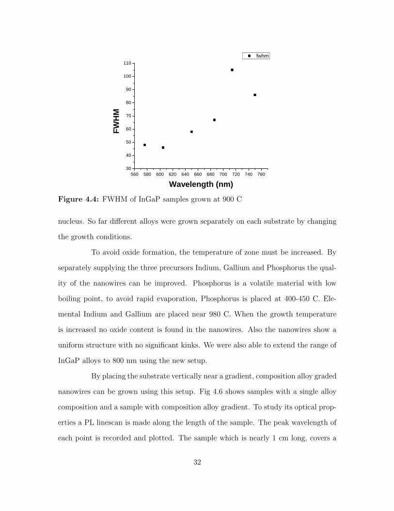
W a v e l e n g t h ( n m )Figure 4.4: FWHM of InGaP samples grown at 900 C
nucleus. So far different alloys were grown separately on each substrate by changing
the growth conditions.
To avoid oxide formation, the temperature of zone must be increased. By
separately supplying the three precursors Indium, Gallium and Phosphorus the qual-
ity of the nanowires can be improved. Phosphorus is a volatile material with low
boiling point, to avoid rapid evaporation, Phosphorus is placed at 400-450 C. Ele-
mental Indium and Gallium are placed near 980 C. When the growth temperature
is increased no oxide content is found in the nanowires. Also the nanowires show a
uniform structure with no significant kinks. We were also able to extend the range of
InGaP alloys to 800 nm using the new setup.
By placing the substrate vertically near a gradient, composition alloy graded
nanowires can be grown using this setup. Fig 4.6 shows samples with a single alloy
composition and a sample with composition alloy gradient. To study its optical prop-
erties a PL linescan is made along the length of the sample. The peak wavelength of
each point is recorded and plotted. The sample which is nearly 1 cm long, covers a
32

wavelength range of 170 nm. This corresponds to 0.5 eV of the total 0.9 InGaP alloy
range from InP to GaP.Which is about 55 % of the total alloys of the entire InGaP
range.
Another important aspect of the InGaP is that it has a transition from
indirect to direct band gap when In content is 20 - 25%. This gives us a unique
opportunity to study InGaP as all the alloys are grown at the same temperature on a
single substrate. Based on the fact that indirect band gap materials emit light weakly
compared to direct band gap materials, we compare the integrated intensity of the
PL line scan done across the sample. We can clearly see that alloys near the GaP
bandgap have two orders of magnitude less integrated intensity compared to Indium
rich alloys at longer wavelengths. This can be explained by the fact that the PL
intensity is affected by the difference between the energy values of τ and the X valley
given by 1/(1 + Be((Eτ − EX)/kt)) [22]. When the band gap is indirect the value is
smaller, when it is direct it is closer to 1. Further careful study of single nanowire
PL is needed to pinpoint this transition.
Figure 4.8 shows the variation of linewidth along the substrate. On average
the linewidth is around 70 nm, they show less variation compared to earlier alloy
samples. This shows that the most important factor that affects linewidth is growth
temperature. Since the entire alloy range is grown at the same temperature the
linewidth change is not much.
These InGaP nanowires may not contain a uniform single alloy composition
along the entire length. Solution based InGaP wires have a variation of 25 nm in peak
wavelength from wires grown in a single batch [22] . They observed that XRD and
Raman spectra of these wires are broad compared to InP or GaP. They explain
that this may be due to disordered alloy composition without a long range order
within a single wire. Particle assisted InGaP nanowires grown by MOCVD had
33

a linewidth around 100 nm, and a compositional variation of 8% within measured
sample [23]. Also going by the current procedure it is not possible to control the
nanowire length and diameter, wires with different diameters may show a variation in
its alloy composition. Further PL, XRD studies need to be done to be systematically
study the alloy composition variation between and within nanowires.
To verify the composition change across the single substrate SEM and EDX
characterization was done on the wires across the sample. EDX analysis showed that
the wires show a increasing In composition from bottom to top. At one end the
composition is close to Gallium Phosphide making it an indirect band gap as expected.
Sample shows nearly uniform morphology across a broad composition change. More
careful EDX analysis needs to be done to determine the precise alloy composition
change across the substrate.
34

(a) (b)
(c) (d)
(e) (f)
Figure 4.5: Low and High Resolution Images InGaP Alloys Grown Under DifferentGrowth Conditions Samples 1(a,b), 2(c,d) and 3(e,f)
35

Figure 4.6: Images of Samples with Different InGaP Alloy Composition
5 0 0 5 5 0 6 0 0 6 5 0 7 0 0 7 5 0 8 0 0 8 5 0
0 . 0
0 . 2
0 . 4
0 . 6
0 . 8
1 . 0
norma
lized in
tensity
w a v e l e n g t h ( n m )
p o i n t 1 1 p o i n t 1 3 p o i n t 1 5 p o i n t 1 7 p o i n t 1 9 p o i n t 2 1 p o i n t 2 3 p o i n t 2 5 p o i n t 2 7 p o i n t 2 9 p o i n t 3 1 p o i n t 3 3 p o i n t 3 5 p o i n t 3 7
Figure 4.7: Change in Peak Wavelength Across the Length of the Substrate
36

2 4 6 8 1 0 1 2
5 0
5 5
6 0
6 5
7 0
7 5
8 0
8 5
l i n e w i d t h p e a k w a v e l e n g t h
d i s t a n c e ( m m )
linewid
th (nm
)
5 6 05 8 06 0 06 2 06 4 06 6 06 8 07 0 07 2 07 4 07 6 0
peak
wavel
ength
(nm)
Figure 4.8: FWHM of Nanowires on a Single Substrate
2 4 6 8 1 0 1 25 6 05 8 06 0 06 2 06 4 06 6 06 8 07 0 07 2 07 4 07 6 0
p e a k w a v e l e n g t h e n e r g y b a n d g a p
d i s t a n c e ( m m )
peak
wave
length
(nm)
1 . 6
1 . 7
1 . 8
1 . 9
2 . 0
2 . 1
2 . 2
energ
y ban
dgap
(eV)
Figure 4.9: PL Peak of Nanowires Scanned Across a Single Substrate
37

1 . 8 1 . 9 2 . 0 2 . 1 2 . 2 2 . 31 0 0
1 0 0 0
1 0 0 0 0
1 0 0 0 0 0
1 0 0 0 0 0 0
Integ
rated
Inten
sity (
a.u)
B a n d G a p ( e V )Figure 4.10: Integrated Intensity Change with Band Gap of the Alloy
(a) Position 1 (b) Position 2
Figure 4.11: Alloy Gradient Across a Single Substrate
38
4.4 Growth Mechanism
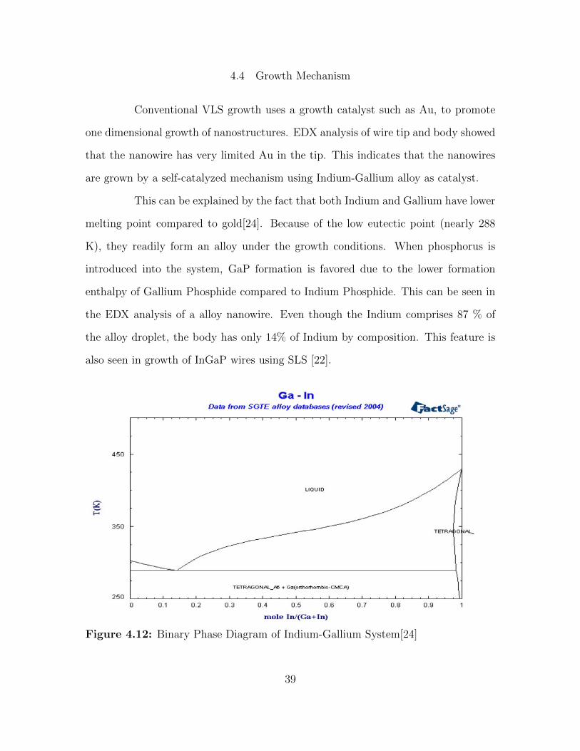
Conventional VLS growth uses a growth catalyst such as Au, to promote
one dimensional growth of nanostructures. EDX analysis of wire tip and body showed
that the nanowire has very limited Au in the tip. This indicates that the nanowires
are grown by a self-catalyzed mechanism using Indium-Gallium alloy as catalyst.
This can be explained by the fact that both Indium and Gallium have lower
melting point compared to gold[24]. Because of the low eutectic point (nearly 288
K), they readily form an alloy under the growth conditions. When phosphorus is
introduced into the system, GaP formation is favored due to the lower formation
enthalpy of Gallium Phosphide compared to Indium Phosphide. This can be seen in
the EDX analysis of a alloy nanowire. Even though the Indium comprises 87 % of
the alloy droplet, the body has only 14% of Indium by composition. This feature is
also seen in growth of InGaP wires using SLS [22].
Figure 4.12: Binary Phase Diagram of Indium-Gallium System[24]
39

Figure 4.13: EDX Analysis of Catalytic Particle(Top) and Nanowire Body(Bottom)
Because of the growth mechanism, the nanowire composition tends to be
comparatively Gallium rich. It is challenging to grow nanowires close to the band
gap of InP. As we need some amount of Gallium to form the catalytic particle, but
higher amount of Ga precursor leads to Gallium rich alloys.
4.5 Growth of GaP Nanowires
In the previous section, we studied the growth of self-catalyzed InGaP alloy
nanowires. To better assess the quality of the nanowires, we need to compare it with
pure GaP nanowires. Gallium Phosphide nanowires are grown used Au as catalyst
with GaP and Gallium as precursors. The main purpose is to study the optical
properties of GaP nanowires. These nanowires are grown under either Gallium rich
or Phosphide rich condition by adding the respective sources. The effect of the growth
setup on PL is studied.
4.6 Defects in Nanowires
The properties of nanowires depend strongly on the growth parameters,
non stoichiometric growth conditions can introduce defects in crystals. These defects
40

Figure 4.14: Growth Setup for GaP Nanowires
can be seen as broadband spectrum in the photoluminescence spectra of nanowires.
Many semiconductors such as GaP, ZnSe and ZnO suffer from these intrinsic point
defects[25]. These nanowires can show unintentional doping due to these point defects.
Nanowires have a large surface area which can affect its properties. Presence of surface
states can damage its optical properties.
Philipose et.al [26] studied the role of point defects in the growth of ZnSe
using CVD method. They studied the presence of Zn and Se vacancies, interstitials
and structural defects as a function of temperature, pressure and flux stoichiometry.
These charged defects form localized states in the band gap and are seen as broad
emission in the PL spectra. The concentration of these defects are proportional to the
Selenium vapor pressure. Also these defects disappear when the sample is annealed
under Zinc source.
At low Selenium vapor pressure a broad defect peak is observed. When an
extra Zinc source is added to the growth, the defect is completely suppressed. Based
on ZnSe growth, we can apply similar ideas to GaP growth. Gallium Phosphide
nanowires and substrate always suffer from midgap defect emission around 700 nm.
Nanowires grown with elemental Phosphorus source always show higher
defect emission than the band edge. This is expected as Phosphorus favors the for-
mation of DAP in the band gap. Adding a Gallium source and removing Phosphorus
from the setup results in significant defect suppression. But there is still some defect
emission in the PL. EDS of the as grown nanowires show 8% oxygen, the presence of
41

(a) Defects in Gallium Phosphide (b) Defects in Zinc Oxide
Figure 4.15: Defects in PL spectra of nanowires
oxygen may change formation of intrinsic defects.
Similar experiments done with InGaP nanowires showed that the defect
emission can be completely suppressed, while keeping the bandgap of the alloy close
to GaP. PL shows no visible defect emission and the nanowires show good crystalline
structure. This can be due to many different mechanisms, the change to self catalyzed
growth mechanism, presence of Indium in the nanowire, use of gallium source etc.
4.7 Photodegradation
The PL of the nanowire samples was tested using Nd:YLF laser (350nm)
with a repetition frequency of 1000hz. While testing the PL nanowire samples, the
PL intensity drops on exposure to the laser. This drop continues until the exposure is
removed. This drop is seen in both GaP and InGaP samples, although GaP is more
effected by this problem.
This phenomenon is also seen in II-VI material system like CdS, ZnSe or
ZnO materials [27]. Other researchers found that photodegradation is dependent to
42

Figure 4.16: ZnSe Defect Emission Under Different Growth Conditions
exposure time, beam intensity, environment and the surface of the crystals. One of
the ways photodegradation could happen is by photo oxidation of the surface. Similar
experiments done in vacuum showed less degradation, indicating the role of oxygen.
Local heating and photo induced point defects may also occur during laser irradiation.
Studies done in ZnSe nanowires showed that etching the sample after photo oxidation
restores the previous luminescence[26]. Passivation of the surface may improve the
optical properties of these nanowires.
43

5 0 0 5 5 0 6 0 0 6 5 0 7 0 0 7 5 0 8 0 00
5 0 0 0
1 0 0 0 0
1 5 0 0 0
2 0 0 0 0
2 5 0 0 0
3 0 0 0 0
3 5 0 0 0
4 0 0 0 0
p r a 3 - 2 1 - 2 s l i t 0 . 2e x p 2 s p o w e r 2 . 0 A
Inten
sity (
Coun
ts)
W a v e l e n g t h ( n m )
2 . 0 A 2 . 4 A 2 . 8 A
(a) GaP Nanowires Grown with GaP+Ga+P
Sources
5 0 0 5 5 0 6 0 0 6 5 0 7 0 0 7 5 0 8 0 00
2 0 0 0
4 0 0 0
6 0 0 0
8 0 0 0
1 0 0 0 0
1 2 0 0 0
1 4 0 0 0
1 6 0 0 0 p r a 2 - 3 4 - 3 e x p 2 s f r e q 2 0 0 0 h z s l i t 0 . 2
Inten
sity (
Coun
ts)W a v e l e n g t h ( n m )
2 . 0 A 2 . 2 A 2 . 4 A 2 . 6 A 2 . 8 A
(b) GaP Nanowires Grown with GaP+Ga
Sources
5 4 4 6 1 2 6 8 0 7 4 8
0
5 0 0 0
1 0 0 0 0
1 5 0 0 0
2 0 0 0 0
(c) PL Spectra of InGaP Nanowires (d) SEM Images of Gap Nanowires
Figure 4.17: Comparison of GaP and InGaP Nanowires Under Different GrowthConditions
44

5 0 0 5 5 0 6 0 0 6 5 0 7 0 0 7 5 0 8 0 00
1 0 0 0
2 0 0 0
3 0 0 0
4 0 0 0
Inten
sity (
Coun
ts)
W a v e l e n g t h ( n m )
0 s 1 s 2 s 3 s 4 s
Figure 4.18: Change in PL Intensity with Laser Irradiation in InGaP Nanowires
45

Chapter 5
SUMMARY
1D structures like nanowires are important due to their unique physical,
electronic and optical properties. The properties of these nanowires are controlled by
choice of synthesis method and growth procedure.
In chapter three, we studied the growth of InP nanowires using elemental
precursors. The morphology and optical properties of nanowires are strongly influ-
enced by its growth temperature. We have seen dependence of quality of nanowires
on growth temperature. Also the effect of the Phosphorus vapor pressure on InP for-
mation has been studied. Finally lasing behaviour has been observed on InP nanobelt
and nanowires. Indicating the high quality and ease of growth for InP material.
Taking advantage of unique properties of nanowires, we can grow alloys
across a wide composition range with tunable electronic and optical properties. First
InGaP nanowires were grown using GaP source, the as grown nanowires have signifi-
cant oxide content and kinky structure. In a second set of experiments, grown using
elemental sources, continuous alloy tuning across a single substrate of about 170 nm
has been achieved. Also the transition from direct to indirect composition can be
compared in terms of integrated intensity.
Using InGaP system it is possible to grow alloys with no observable defect
emission commonly seen in GaP nanowires. The progress made in the synthesis of
InGaP alloy system can be useful in fabricating next generation solar cells, nanolasers,
detectors etc over the a wide spectral range.
46

REFERENCES
[1] W. C. Ellis R. S. Wagner. Vapor-liquid-solid mechanism of single crystal growth.Appl. Phys. Lett., 4(89), 1964.
[2] Eunice S. P. Leong Ruibin Liu Alan H. Chin Bingsuo Zou Anlian Pan, We-ichang Zhou and C. Z. Ning. Continuous Alloy-Composition Spatial Gradingand Superbroad Wavelength-Tunable Nanowire Lasers on a Single Chip. NanoLett, 9(2), 2009.
[3] Andrew B.Wong Cun-Zheng Ning Samuel W.Eaton, Anthony Fu and PeidongYang. Semiconductor nanowire lasers . Nature Reviews Materials, 1(16028).
[4] C.Z Ning A Maslov. Modal Gain in a Semiconductor Nanowire Laser WithAnisotropic Bandstructure. IEEE Journal of Quantum Electronics, 40(10), 2004.
[5] Martin Heiss-Olivier Demichel Jeppe V. Holm Martin Aagesen Jesper NygardAnna Fontcuberta i Morral Peter Krogstrup, Henrik Ingerslev Jrgensen. Single-nanowire solar cells beyond the ShockleyQueisser limit. Nature Photonics,7:306310.
[6] S. Plissard D. Kriegner M. A. Verheijen G. Bauer A. Meijerink A. Belabbes F.Bechstedt J. E. M. Haverkort S. Assali, I. Zardo and E. P. A. M. Bakkers. DirectBand Gap Wurtzite Gallium Phosphide Nanowires. Nano Lett, 13(4), 2013.
[7] Magnus T. Borgstrom Lou-Fe Feiner George Immink Willem J. P. van EnckevortElias Vlieg Erik P. A. M. Bakkers Rienk E. Algra, Marcel A. Verheijen. Twinningsuperlattices in indium phosphide nanowires. Nature, 456, 2008.
[8] Heon-Jin Choi. Vapor-Liquid-Solid Growth of Semiconductor Nanowires, pages1–36. Springer Berlin Heidelberg, Berlin, Heidelberg, 2012.
[9] Yiying Wu and Peidong Yang. Direct Observation of Vapor-Liquid-SolidNanowire Growth. J. Am. Chem. Soc., 123:3165–3166, 2001.
[10] http://fluid.itcmp.pwr.wroc.pl/ znmp/dydaktyka/fundamFM/Lecture13.pdf.
[11] F. Fan Y. Yu-P. Ranga S. E. Hashemi Amiri, S. Turkdogan and C. Ning. Growthof Stoichiometric InP Nanowires/Nanobelts by a Facile Vapor Transport Method.Conference on Lasers and Electro-Optics, OSA Technical Digest (2016) (OpticalSociety of America, 2016), paper SM1R.6.
[12] Damir Asoli Maria Huffman Ingvar berg-Martin H. Magnusson Gerald SieferPeter Fuss-Kailuweit Frank Dimroth Bernd Witzigmann H. Q. Xu Lars Samuel-son Knut Deppert Magnus T. Borgstrom Jesper Wallentin, Nicklas Anttu. InPNanowire Array Solar Cells Achieving 13.8% Efficiency by Exceeding the RayOptics Limit. Science, 339(2275):1057–1060, 2013.
47

[13] Rehan Kapadia Junjun Zhang Mark Hettick-Zhibin Yu Kuniharu Takei Hsin-Hua Hank Wang Peter Lobaccaro Daisuke Kiriya, Maxwell Zheng and Ali Javey.Morphological and spatial control of InP growth using closed-space sublimation.Journal of Applied Physics, 112(123102), 2012.
[14] Hsin-Hua H. Wang Maxwell Zheng-Corsin Battaglia Mark Hettick DaisukeKiriya Kuniharu Takei Peter Lobaccaro Jeffrey W. Beeman Joel W. Ager RoyaMaboudian Daryl C. Chrzan Ali Javey Rehan Kapadia, Zhibin Yu. A directthin-film path towards low-cost large-area III-V photovoltaics. Scientific Reports,3(2275), 2013.
[15] Carolin M.Sutter-Fella Corsin Battaglia-Shaul Aloni Xufeng Wang James MooreJeffrey W. Beeman Mark Hettick Matin Amani Wei-Tse Hsu Joel W. Ager PeterBermel Mark Lundstrom Jr-Hau He Ali Javey Maxwell Zheng, Hsin-Ping Wang.Thin-Film Solar Cells with InP Absorber Layers Directly Grown on NonepitaxialMetal Substrates. Advanced Energy Materials, 5(1501337), 2015.
[16] Yiqian Wang Minghuan Zhang Zhenlian Han-SenPo Yip Lifan Shen Ning HanEdwin Y. B. Pun Johnny C. Ho Fengyun Wang, Chao Wang. Diameter Depen-dence of Planar Defects in InP Nanowires. Scientific Reports, 6(32910), 2016.
[17] Yong gang Zhang and Yi Gu. Al(ga)inp-gaas photodiodes tailored for specificwavelength range, photodiodes - from fundamentals to applications, 1999.
[18] Johanna Tragardh Christina Larsson-Michael Rask Dan HessmanLars Samue1lson C Patrik T Svensson, Thomas Martensson and JonasOhlsson. Monolithic GaAs/InGaP nanowire light emitting diodes on silicon.Nanotechnology, 19(30), 2008.
[19] Y M Haddara A Fakhr and R R LaPierre. Dependence of InGaP nanowiremorphology and structure on molecular beam epitaxy growth conditions. Nan-otechnology, 21(16), 2010.
[20] Anna M. Jansson Kilian Mergenthaler-Martin Ek Daniel Jacobsson L. ReineWallenberg Knut Deppert Lars Samuelson Dan Hessman Jesper Wallentin, LauraBarrutia Poncela and Magnus T. Borgstrm. Single GaInP nanowire p-i-n junc-tions near the direct to indirect bandgap crossover point. Applied Physics Letters,100:251103, 2012.
[21] Katsuhiro Tomioka Fumiya Ishizaka, Keitaro Ikejiri and Takashi Fukui. Indium-Rich InGaP Nanowires Formed on InP (111)A Substrates by Selective-AreaMetal Organic Vapor Phase Epitaxy. Japanese Journal of Applied Physics,52(4S), 2013.
[22] Nikolay Kornienko, Desir D. Whitmore, Yi Yu, Stephen R. Leone, and PeidongYang. Solution Phase Synthesis of Indium Gallium Phosphide Alloy Nanowires.ACS Nano, 9(4):3951–3960, 2015.
[23] D Kriegner T Etzelstorfer J Wallentin J B Wagner J Stang L Samuelson K Dep-pert D Jacobsson, J M Persson and M T Borgstrm. Particle-assisted GaxIn1xPnanowire growth for designed bandgap structures. Nanotechnology, 23(24), 2012.
48
[24] http://www.factsage.cn/fact/phasediagram.php?file = Ga − In.jpgdir =SGTE, 2011.
[25] Hyung Soon Im Chan Su Jung Han Sung Kim Jeunghee Park Kidong Park, JungAh Lee and Chang-Lyoul Lee. GaPZnS Pseudobinary Alloy Nanowires. NanoLett, 14(10), 2014.
[26] Usha Philipose. Role of intrinsic defects in nanowires, nanowires - fundamentalresearch, dr. abbass hashim (ed.), intech,, 2011.
[27] Yiqian Wang Minghuan Zhang Zhenlian Han SenPo Yip Lifan Shen Ning HanEdwin Y. B. Pun Johnny C. Ho Fengyun Wang, Chao Wang. Photodegradationof CdSe/ZnS semiconductor nanocrystals in a polymer film in air and undervacuum. Journal of Applied Spectroscopy, 77(5), 2010.
49