Embed Size (px)
Citation preview

Linköping Studies in Science and Technology Dissertation No. 1200
Growth and Characterization of AlN
From Nano Structures to Bulk Material
G. Reza Yazdi
Material Science Division
Department of Physics, Chemistry and Biology (IFM) Linköping University, S-581 83 Linköping, Sweden
2008

ii
Cover Background: A high-resolution transmission electron microscopy image from a single crystal
AlN nanowire grown on 4H-SiC substrate. The different contrast in color near to the edge is due
to the different thickness.
Inset: SEM image from well aligned hexagonally shaped AlN microrods. The average diameter
and length are about 12 µm and 17 µm, respectively. They were grown in the [0001] crystal
direction perpendicular to the (0001) 4H-SiC substrate at 1700 ºC and 400 mbar. They are
standing on the self organized 2H-SiC pyramids.
The line: a microwire grown on a 2H-SiC hexagonal pyramid.
Back side of the cover
Inset: SEM image from the initial stage growth of AlN microrods on the 2H-SiC hexagonal
pyramids. The plint

iii
In the name of Allah, the beneficent, the merciful
All praises are due to Allah Ta’ala, the sustainer of the entire world, the origin of science and
wisdom, and may Allah’s mercy and peace be upon our leader, Sayyidona Mohammad, his
family and companions.
I dedicate this thesis in honour of my parents. I wish that this achievement would complete the
dream that you had for me all those many years ago while you chose to offer me the best
education you could and to see me reasonably educated and cultured as well as to my wife who
encouraged me to accomplish this thesis and taking advantage of her cordiality, chumminess and
sincerity and to my the most precious enjoyable being who gives me peace, tranquility and
happiness, my sweet little son, Mohammad Ali.

iv

v
Abstract Aluminum nitride (AlN) exhibits a large direct band gap, 6.2 eV, and is thus suitable for
solid state white-light-emitting devices. It is capable in spintronics because of its high Curie
temperature if doped with transition metals. AlN can also be used as a buffer layer for growth of
device-grade GaN as well as for application in sensors, surface acoustic wave devices, and high-
temperature electronics. AlN shows excellent field-emission performance in vacuum
microelectronic devices due to its small electron affinity value, which is from negative to 0.6 eV.
In this sense, nanostructured AlN, such as AlN nanowires and nanorods, is important for
extending our knowledge on the potential of nanodevice applications. For growth of bulk AlN the
sublimation- recondensation (a kind of physical vapor transport growth) method is the most
successful and promising crystal growth technique.
In thesis the physical vapor transport (PVT) principle has been implemented for synthesis
of AlN on 4H-SiC in sublimation epitaxy close space configuration. It has been shown that the
AlN crystal morphology is responsive to the growth conditions given by temperature (1650-
1900oC) and nitrogen pressure (200-800 mbar) and each morphology kind (platelet-like, needles,
columnar structure, continuous layers, and free-standing quasi bulk material) occurs within a
narrow window of growth parameters. Controlled operation conditions for PVT growth of well
aligned perfectly oriented arrays of AlN highly symmetric hexagonal microrods have been
elaborated and the mechanism of microrod formation has been elucidated. Special patterned SiC
substrates have been created which act as templates for the AlN selective area growth. The
microrods revealed an excellent feature of boundary free coalescence with growth time,
eventually forming ~120 µm thick AlN layer which can be easily detached from the SiC substrate
due to a remarkable performance of structural evolution. It was discovered that the locally grown
AlN microrods emerge from sharp tipped hexagonal pyramids which consist of the rare 2H-SiC
polytype and a thin AlN layer on the surface. Two unique consequences appear from the finding,
the first is that the 2H-SiC polytype facilitates the nucleation of wurtzite AlN, and the second is
that the bond between the low angle apex of the pyramids and the AlN layer is very week, thus
allowing an easy separation to yield free standing wafers. AlN nanowires with an aspect ratio
as high as 600 have been grown with a high growth rate. Again, they have perfect alignment
along the c-axis of the wurtzite structure with small tilt given by the orientation of the SiC

vi
substrate. The nanowires possess a single crystal structure with high perfection, since neither
dislocations nor stacking faults were revealed.
The proposed growth concept can be further explored to enlarge the free standing AlN
wafers up to a size provided by commercially available SiC four inch wafers. Also, AlN wafers
fabricated by the present method may be used as seeds for large boule growth. AlN nanowires, as
obtained in this study, can be used for creating a piezoelectric generator and field emitters with
high efficiency.

vii
Populärvetenskaplig sammanfattning
Aluminium nitrid (AlN) har ett stort direkt bandgap (6.2 eV) och är lämplig för lysdioder.
Det är tillämpligt inom spinnelektronik eftersom det har en hög Marie Curie-temperatur när det är
dopad med övergångsmetaller. AlN kan även användas som ett buffertskikt för tillväxt av
komponentkvalitativt GaN likväl som för sensortillämpningar, ytvågsfilterkomponenter, och
högtemperaturelektronik. Aluminium nitrid visar excellent fältemission i vakuumkomponenter på
grund av sin låga elektronaffinitet, som är från negativt till 0.6 eV. I det här fallet så är
nanostrukturer av AlN, som nanotrådar och -stavar, viktiga för att utöka vår kunskap om
potentiella nanokomponenter. För tillväxt av AlN är sublimeringsmetoden den mest
framgångsrika och lovande framställningstekniken av kristaller.
I den här avhandlingen så har principen för den fysiska gastransporttekniken (PVT)
implementerats för syntes av AlN på 4H-SiC filmer i en ny konfiguration genom
sublimeringsepitaxi. Det demonstreras att morfologin hos AlN visar respons för
tillväxtförhållandena som ges av temperatur (1650-1900oC) och kvävetryck (200-800 mbar) och
olika morfologityper (skivlika, trådar, kolumnstrukturer, kontinuerliga skikt, och fristående
kvasibulkmaterial)uppstår inom ett snävt fönster av tillväxtparametrar. Kontrollerade operativa
förhållanden för PVT-tillväxt av räta perfekt orienterade ansamlingar av symmetriska AlN
mikrostavar har utvecklats och deras formationsmekanism diskuterats. Speciellt mönstrade SiC
substrat har skapats som agerar utgångsmaterial för selektiv AlN tillväxt. Mikrostavarna avslöjar
ett särdrag av sammanväxning utan gränslinjer med tillväxttid, som formar 120 µm tjocka AlN
skikt som lätt kan avskiljas från SiC substratet genom en anmärkningsvärd strukturell evolution.
Upptäckten gjordes att lokal tillväxt av AlN mikrostavar uppkommer från skarpa hexagonala
pyramider som består av den sällan förekommande 2H-SiC modifikationen och tunna AlN skikt
på ytan. Två unika följder uppkommer genom upptäckten, den första att 2H-SiC modifikationen
främjar bildning av wurtzite AlN, och den andra att bindningen mellan spetsen av pyramiden och
AlN skiktet är väldigt svag, vilket medger en enkel separering för att erhålla fristående wafers.
AlN nanotrådar med ett aspektförhållande så stort som 600 har blivit framställda med hög
framställningshastighet. Återigen, de har perfekt linjering längs c-axeln av wurtzite-strukturen
med en låg vinkling som ges av orienteringen av SiC substratet. Nanotrådarna har en perfekt
kristallstruktur eftersom varken dislokationer eller stackningsfel kunde observeras.

viii
Det föreslagna framställningskonceptet kan vidare utforskas för att utöka fristående AlN
wafers upp till en storlek som ges av kommersiellt tillgängliga SiC fyratumssubstrat. Vidare så
kan AlN wafers som framställs genom metoden användas som utgångsmaterial för kristaller för
framställning av stora götar. AlN nanotrådar, som utvecklats i denna studie, kan användas för att
skapa piezoelektriska generatorer och fältemissionskomponenter med hög effektivitet.
.

ix
Preface
This PhD thesis is a result of my research work from 2003 until 2008 in Materials Science
Division, Department of Physics, Chemistry and Biology (IFM) at Linköping University. This
work was supported by Swedish Research Council and Carl Tryggers foundation, and Ministry of
Science, Research and Technology of the Islamic Republic of Iran.

x
Papers included in this thesis
I- Sublimation growth of AlN crystals: Growth mode and structure evolution.
R. Yakimova, A. Kakanakova-Georgieva, G.R. Yazdi, G.K. Gueorguiev, M. Syväjärvi.
J. Cryst. Growth 281, (2005) 81
II- Fast epitaxy by PVT of SiC in hydrogen atmosphere.
M. Syväjärvi, R.R. Ciechonski, G.R. Yazdi, and R. Yakimova; J. Cryst. Growth 275 (2005)
1103
III- Growth and morphology of AlN crystals
G. R. Yazdi, M. Syväjärvi and R. Yakimova. Phys. Scr. T126 (2006) 127
IV- Aligned AlN nanowires and microrods by self-patterning
G.R. Yazdi, M. Syväjärvi, and R. Yakimova. Appl. Phys. Lett. 90 (2007) 123103
V- Formation of needle-like and columnar structures of AlN
G.R. Yazdi, M. Syväjärvi, R. Yakimova. Journal of Crystal Growth 300 (2007) 130
VI- Fabrication of free standing AlN crystals by controlled microcod growth
G.R. Yazdi, M. Syväjärvi, and R. Yakimova. Journal of Crystal Growth 310 (2008) 935
VII- Employing discontinuous and continuous growth modes for preparation of AlN
nanostructures on SiC substrates.
G.R. Yazdi, M. Syväjärvi, R. Vasiliauskas and R. Yakimova. Materials Science Forum Vols.
556-557 (2007) 1031

xi
G.R. Yazdi, M. Beckers, F. Giuliani, M. Syväjärvi, L. Hultman, and R. Yakimova.
Manuscript submitted
IX- Defect-free Single Crystal AlN Nanowires by Physical Vapor Transport
G.R. Yazdi, P.O.Å. Person, D. Gogova, L. Hultman, M. Syväjärvi and R. Yakimova. Manuscript
in final preparation
VIII- AlN single crystal growth enabled by self-organization of 2H-SiC pyramids on 4H-SiC
substrates.

xii
My contributions to the papers
Paper I I carried out most parts of growth experiments, and characterization. I was involved
in discussion of experimental results and manuscript preparation.
Paper II I performed all the AFM measurements, I also contributed to the discussion of the
results and to the contents of the paper.
Paper III I planed the study and performed all the growth experiments and characterization.
I wrote the first version of the paper
Paper IV I planed the study, and carried out all parts of growth experiments, and
characterization. I wrote the first version of the paper.
Paper V I planed the study, and carried out all parts of growth experiments, and
characterization. I wrote the first version of the paper.
Paper VI I took part in planning the study, and carried out most part of growth experiments,
and characterization. I wrote the first version of the paper.
Paper VII I took part in planning the study, and carried out most part of growth experiments,
and characterization. I wrote the first version of the paper.

xiii
Paper VIII I carried out all the growth experiments, and I performed AFM, SEM
characterization, and in XRD part I did pole figures and symmetric θ-2θ XRD. I
wrote the first version of the paper.
Paper IX I carried out all growth experiments, SEM, CL characterization and sample
preparation for TEM. I was involved in discussion of experimental results and
manuscript preparation.
xiv
Related papers not included in this thesis
1- High-Quality 2'' Bulk-Like Free-Standing GaN Grown by HydrideVapour Phase Epitaxy on a
Si-doped Metal Organic Vapour Phase Epitaxial GaN Template with an Ultra Low Dislocation
Density.
D. Gogova, H. Larsson, A. Kasic, G.R. Yazdi, I. Ivanov, R. Yakimova, B. Monemar, E.
Aujol, E. Frayssinet, J-P. Faurie, B. Beaumont, and P. Gibart; Jpn. J. Appl. Phys. 44 (2005)
1181
2- Stability of thick layers grown on (1 -1 0 0) and (11-2 0) orientations of 4H-SiC.
M. Syväjärvi, R. Yakimova, G.R. Yazdi, A. Arjunan, E. Toupitsyn, and T.S. Sudarshan.
Materials Science Forum Vols. 527-529 (2006) 227
3- Optical and morphological features of bulk and homoepitaxial ZnO.
R. Yakimova, G.R. Yazdi, N.T. Son, I. Ivanov, M. Syväjärvi, S. Sun, G. Tompa, A.
Kuznetsov, B. Svensson. Superlattices and Microstructures 39 (2006) 247
4- Formation of ferromagnetic SiC:Mn phases.
M. Syväjärvi, L. Nasi, G.R. Yazdi, G. Salviati, M. Izadifard, I.A. Buyanova, W.M. Chen,
and R. Yakimova; Proc. European Conference on SiC and Related Materials; Bologna, Italy;
Aug 31 - Sep 4, 2004; Mater. Sci. Forum(2005).
5- Structure Evolution of 3C-SiC on Cubic and Hexagonal Substrates.
Rositza Yakimova, G. Reza Yazdi, Nut Sritirawisarn and M. Syväjärvi. Materials Science
Forum Vols. 527-529 (2006) 283
6- A surface study of wet etched AlGaN epilayers grown by hot-wall MOCVD.
M. Syväjärvi, A. Kakanakova-Georgieva, G.R. Yazdi, A. Karar, U. Forsberg, and E. Janzén.
J. Crystal Growth 300 (2007) 242
7- Organosilane-functionalized wide bandgap semiconductor surfaces.

xv
R. M. Petoral Jr., G. R. Yazdi, A. Lloyd-Spetz, R. Yakimova and K. Uvdal. Appl. Phys.
Lett.90, (2007) 223904
8- Surface engineering of functional materials for biosensors.
C. Vahlberg, G.R. Yazdi, R.M.Petoral Jr., M. Syväjärvi, K. Uvdal, A. Lloyd Spetz, R.
Yakimova, Surface engineering of functional materials for biosensors, Proceedings IEEE
SENSORS 2005, Irvine, CA, USA, Oct.31-Nov.3, 2005, p. 504-507.
9- Surface functionalization and biomedical applications based on SiC
R. Yakimova, R.M.Petoral Jr., G.R. Yazdi, C. Vahlberg, A.Lloyd-Spetz and K. Uvdal.
Journal of Physics D. Applied Physics V. 40, N 20 (2007) 6435
10- Novel material concepts of transducers for chemical and biosensors
R. Yakimova, G. Steinhoff, R. M. Petoral Jr., C. Vahlberg, V. Khranovskyy, G.R. Yazdi, K.
Uvdal a, A. Lloyd Spetz. Biosensors and Bioelectronics 22 (2007) 2780
11- Investigation of ZnO as a perspective material for photonics
V. Khranovskyy , G. R. Yazdi, G. Lashkarev, A. Ulyashin, and R. Yakimova. phys. stat. sol.
(a) 205, No. 1, (2008) 144
12- Surface Functionalization of SiC for Biosensor Applications.
R.M. Petoral Jr., G.R. Yazdi, C. Vahlberg, M. Syväjärvi, A. Lloyd Spetz, K. Uvdal and R.
Yakimova. Materials Science Forum Vols. 556-557 (2007) 957
Conference contributions
During my studies I have participated in several international conferences. In most of them I
personally presented my results.
1- Growth and morphology of AlN crystals. The 21th Nordic Semiconductor meeting.
Sundvolden, Norway, 18–19 August (2005)-1 poster presentation.
xvi
2- Formation of needle-like and columnar structures of AlN. First International Symposium on
Growth of Nitrides (ISGN-1), Linköping, 4-7 June (2006)-1 poster presentation.
3- Employing discontinuous and continuous growth modes for preparation of AlN nanostructures
on SiC substrates. 6th European Conference on Silicon Carbide and Related Materials,
ECSCRM 2006, Newcastle upon Tyne, UK, September 3rd - 7th, 2006
4- Fabrication of free standing AlN crystals by controlled microcod growth - Oral presentation
Growth and characterization of AlN nanowires by self-patterning - Oral presentation
E-MRS - Strasbourg (France), May 28 to June 1 (2007)
5- Self-separation mechanism of AlN thick layers grown on SiC. 7th International Conference of
Nitride Semiconductors (ICNS-7). GMG GRAND Hotel • Las Vegas, Nevada, USA 16-21,
(2007)- Oral presentation, given by R. Yakimova, because this date coincided with the date
when my son was borne.

xvii
Acknowledgements
In any major undertaking such as writing a PhD thesis there are always people who offer
imperative support, encouragement and recommendation. This is an effort to pay compliment to
some of the many people who assisted me to accomplish this goal. This study (growth) would not
have been successful without the immense help of all those who assisted me to grow and develop
my knowledge (and growth of AlN). There are many people who have shared my journey and
assist me during this period. I cannot express my gratitude to you all and it is not possible to list
here all the people that I would like to appreciate. By this I want to acknowledge all those, who
stood with me, throughout this journey towards my Ph.D thesis and here the acknowledgement.
Firstly, I thank Allah, the Most High, for the opportunity He gave me to study, to research
and to write this dissertation. Thank Allah, my outmost thanks, for giving me the ability, the
strength, attitude and motivation through this research and to complete this work.
I wish to express my special gratitude to my supervisor Professor Rositza Yakimova for
accepting me as a PhD student at the Institute of Physics, Chemistry and Biology (IFM), material
science division. I am sincerely grateful for your guidance, wisdom, and specially your endless
patients in dealing with me throughout all these years. It is difficult to overstate my gratitude to
you, with your enthusiasm, your inspiration, and your great efforts make this approach easier.
Many thanks to you for assisting me throughout my thesis-writing period; you provided
encouragement, sound advice, good company, and lots of good ideas. Thank you for believing
me and for giving me good advice, support and freedom along the way. I’m grateful for all
scientific discussion we had in this journey and furthermore, all scientific travels across the
Europe and sharing fun time together. Especially, I would like to thank my co- supervisor
Docent Mikael Syväjärvi. I gratefully acknowledge you for your passion and interest and for your
support whenever I needed. Many thanks for your major guidance and teaching in growth
methods and sharing your wild knowledge and experiences in this issue. Thank you both Rositza
and Mikael for your patience and supports towards the final end of this thesis.
I have been extremely fortunate in having been located in an academic institute and
department in which stuff other than my supervisors also took an active and supportive interest in

xviii
my work. I would like to thanks the members of our Thin Film group, particularly, my special
thanks go to Prof. Lars Hultman for your support, fruitful discussions and constructive and
valuable comments on my paper VIII and IX. I also acknowledge professor Jens Birch for
helping me with XRD measurements.
My gratitude also goes to Per Persson, Finn Giuliani, Manfred Beckers for their help and their
contribution in papers VIII and IX
I am also grateful to Rafal Ciechonsky, Anelia Kakanakova, Amir Karim, Vanya
Darakchieva, Milena Beshkova, Parisa Sehati, Galia Pozina, and Ming Zhao, for your help
guidance.
I express my gratitude to Eva Wibom, for being available and helping me.
I would like to thank all technical engineers, which helped me during some measurements
in this period, especially Thomas Lingefelt, Ingemar Grahn, and Arne Eklund.
All my friends, colleagues and the staff (past and present) at the Institute of Physics,
Chemistry and Biology (IFM), especially the material science division are thanked for the
cooperation, helping in my work and creating great working environment.
I am really grateful to my family, especially to my parents without whose love and
backing I would not be where I am or who I am today, and I also want to thank my parents in low
for their continuous support and encouragement. Thanks for their distant taking care of me, and
my family through Internet and long phone call especially when my son was born, and sustain the
condition of not being around them. I want to express my special thanks to my wife; Fatemeh
Shafie who is PhD student as well and we start this scientific expedition together. I would not
have fulfilled my PhD thesis without her support. Finally, thanks to my little cute miracle, a
precious gift from Allah at the last stage of my PhD study, my son Mohammad Ali for cheering
me and giving me lots of happiness, joy and delight during the hard time of the final steps. My
love and longing for him are beyond words. He is the softest point of my heart. I am sorry for not
being able to accompany or witness every step of his growing up in the first year of his life.
In the end I want to express my sincere thanks to my sponsor, The Ministry of Science
and Technology of Islamic Republic of Iran and The Shahrood University of Technology.

xix
Contents Abstract v Populärvetenskaplig sammanfattning vii Preface ix Papers included in this thesis x My contributions to the papers xii Related papers not included in this thesis xiv Conference contributions xv Acknowledgments xvii
1- Overview of group III-nitride
1.1 Research Goals ………………………………………………………1 1.2 History of group III-Nitride semiconductor …………………………2 1.3 Growth and substrates in group III-nitrides …………………………..4 1.4 Properties of group III-nitrides ………………………………………6
1.4.1 Crystal structure……………………….……………………..6 1.4.2 Electrical and optical properties of III-nitrides .…………….7 1.4.3 Piezoelectricity………………………………….………..…10
2- Characteristic of AlN
2.1 Introduction …………………………………………………………..13 2.2 Brief history of AlN…………………………………………………..14
2.3 Crystalline structure ………………………………………………....15 2.4 Material properties of AlN……………………………..……………..18 2.5 Piezoelectricity of AlN………………………………………………..22 2.6 Importance of bulk AlN and nanowires……………………………….23
3- SiC as a substrate
3.1- Introduction…………………………………………………………..25 3.2- Crystalline structure of SiC…………………………………………..26 3.3- Material properties of SiC……………………………………………28
3.4- Substrate preparation…………………………………………………29 4- Overview of AlN growth 4.1- Introduction…………………………………………………………..33
4.2- Fundamentals physical vapor transport growth………………………35 4.3- Bulk crystals growth of AlN………………………………………….40

xx
4.3.1- Seeded and self-seeding growth of AlN…………………….40
4.3.2- Temperature and pressure effects…………………………...42 4.3.3- Crucible for growth of AlN…………………………………44
4.3.4- Initial nucleation in growth of AlN………………………….45 4.3.5- Thermodynamics of AlN crystal growth…………………………48
4.4- Nano-structures……………………………………………………….51
4.5- Impurities in AlN……………………………………………………..54
5- Characterization methods
5.1- Optical microscopy with Nomarski interference contrast……………57 5.2- KOH etching………………………………………………………….58 5.3- High-resolution X-ray diffraction…………………………………….59
5.4- Scanning electron microscopy (SEM) and cathodoluminescence……63 5.5- Atomic force microscopy……………………………………………..67
5.6- High-resolution transmission electron microscopy …………………..70 5.7- Raman spectroscopy…………………………………………………..72
6- Summery
6.1- Main results……………………………………………………………73 6.2- Future work …………………………………………………………..76
References
Papers I - IX

Chapter 1. Introduction
1
Chapter 1
Introduction 1.1 Research Goals
This Thesis has the following objectives:
• To investigate a novel concept based on physical vapour transport for growth of AlN on
SiC substrates with surface engineering which is appropriate to promote nucleation and
continuous growth of AlN bulk crystals.
• To gain deep understanding of important growth phenomena such as heterogeneous
nucleation of AlN and the crystal habit when growing on a seed via sublimation-
crystallization, as well as of fundamental limits in respect to crystal size, structural defects
and doping.
• To demonstrate AlN substrate crystals and to study the structural and optical properties of
the grown crystals in order to optimise the AlN material quality.
• To explore unrevealed potentials of the sublimation-crystallization method combined with
patterned substrates and extend the range of grown AlN crystals from bulk to1D crystals
(e.g. nanowires) for new applications.

Chapter 1. Introduction
2
1.2 History of group III-Nitride semiconductors
The group III-nitrides have been considered as promising semiconductor materials for devices
applications since 1970, especially for the development of light emitting diodes. The appearance
of aluminium nitride (AlN), gallium nitride (GaN), and indium nitride (InN) and their ternary and
even quaternary alloys opened a new field in semiconductor technology with a substantial effect
on human life and sciences. They are candidate materials for optoelectrical applications, because
they form a continuous alloy system (InGaN, InAlN, AlGaN, and AlInGaN) whose direct optical
band gaps for the hexagonal wurtzite phase range from 0.7 eV for InN to 3.4 eV for GaN to 6.2
eV for AlN, i.e. from infrared (IR) to the deep ultraviolet (UV) of electromagnetic spectrum [1-
4]. In comparison to silicon (Si), germanium (Ge), gallium arsenide GaAs, or zinc selenide
(ZnSe) based material systems, the group III-V nitrides have a higher bond strength and melting
point (leading to a chemical and physical stability, which make them suitable for harsh
environments like high electric currents, high temperature, and intense light illumination), high
thermal conductivities, high radiation hardness, larger avalanche breakdown fields, larger
piezoelectric constants, and larger theoretical room temperature electron mobility [5-10]. These
differences make them suitable for use in high-frequency and high-power optical and electrical
device applications.
Group III nitrides are regarded as one of the most promising materials for applications as
laser diodes (LDs), photodiodes (PDs), high power and high-temperature electronic devices, such
as switches because of their remarkable physical properties. Another application of III-nitrides is
light emitting diodes (LEDs) in the IR (1800 nm) to UV (200 nm) range. This flexibility in
tailoring of emission wavelengths makes LEDs practical for many applications including white
LEDs for conventional light sources, red and green LEDs for traffic signals, and UV LEDs for
military, medical, and biotechnology sensors. The advantages of the solid state LEDs compared
with other light sources include high luminous efficiency, low maintenance, small volume, quick
response speed and long life. To realize such novel devices, it is essential to grow high-quality
nitride single crystal and to control their electrical conductivity which is possible to achieve by
growth of heterostructures. At present, growth of heteroepitaxial structures of these
Chapter 1. Introduction
3
semiconductors is performed by different techniques on various substrates [11]. A brief history of
III-nitride semiconductor growth will now be presented.
The research on group III nitride semiconductors consisting of AlN, GaN, and InN started
in period 1960 to 1970 when a number of workers began applying heteroepitaxial growth to
produce reasonably high quality GaN films on sapphire substrates. The first AlN was produced
by the reaction between molten aluminum and nitrogen in 1862 [12], and for the first time Fichter
and Osterheld in 1915 reported that AlN crystals could be synthesized by sublimation of AlN
powder in nitrogen ambient [13]. In the beginning only small crystals were available, but
progress of the sublimation technique as well as the introduction of chemical vapor deposition
(CVD) enabled synthesis of larger AlN crystals. GaN was first synthesized in the 1932 by
passing ammonia (NH3) over liquid Ga at elevated temperature [14]. Later in 1938 Juza and
Hahn succeeded in producing small needles and platelets of GaN by the same technique, and InN
from InF6(NH4)3 reduction. The purpose of these initial studies was to investigate the crystal
structure and lattice constant of the materials [15, 16]. However, the progress in research and
development of GaN before the 1970s was slowed down due to the lack of modern crystal growth
techniques. With the technological development of characterization techniques and epitaxial
growth of high-quality thin films on appropriate substrate materials, in 1959 Grimmeiss et al
were able to do the first PL measurement on small crystals of GaN produced by the same method
as the group of Juza [17], and in 1969 the first large area GaN was epitaxially grown on sapphire
by Maruska and Tietjen. They used hydride vapor phase epitaxy (HVPE) method. The
availability of large area samples gave motion to GaN research [18]. In a traditional HVPE
reactor the group III element such as Ga is transported as a monochloride. Sapphire was chosen
as substrate material because it is a stable material, since it does not react with ammonia. Pankov
et al. were the first to fabricate GaN light emitting diode (LED) in 1971. This device consisted of
a low-doped n-type region, an insulating Zn-doped layer and an indium surface contact, but it
showed very low efficiency. It could emit blue, green, yellow or red light depending on the Zn
concentration in the light emitting region [19, 20]. Progress has continued at a remarkable rate
with the number of research group studying on the III-nitrides.
The first big step in III-nitride research appeared when the quality of the grown epilayer
improved, as demonstated by Yoshida et al. in 1983. They showed that the quality of GaN film

Chapter 1. Introduction
4
improved by growing a buffer layer of AlN on the sapphire substrate [21]. Amano and Akasaki
later in 1988/1989 further improved this technique and used a low-temperature AlN buffer layer
[22, 23]; following this, Nakamura et al. used a low-temperature GaN buffer layer before the
GaN growth [24, 25]. The next remarkable progress was achieved by Amano et al. when they
were producing the first p-type conductive GaN by using Mg as a dopant and low energy electron
beam irradiation [26]. Nakamura et al. later improved the activation of the Mg acceptors in
MOVPE-grown GaN by thermal annealing at ≥ 750 °C in N2 causing the resistivity to drop from
~106 to 2 Ωcm [27].
As mentioned above, for fabrication of LEDs, LDs, and FETs, a heterostructure
technology is important and that needs an AlGaN layer. The first p-n junction GaN based LED
was synthesized by Akasaki and co-workers in 1989, but the first AlGaN layers were grown by
Khan et al. in 1990 and by Itoh et al. 1991 [28, 29]. Nakamura produce the first InGaN/GaN and
AlGaN/GaN multiple quantum well structure in 1993, and later at Nichia Laboratories they
developed and commercialized blue and green LEDs. The first field effect transistor (FET) also
was fabricated in 1993 [30, 31]. Akasaki et al. reported for the first time stimulated emission
from AlGaN/GaN/GaInN quantum well devices by current injection at room temperature in 1995
[32]. The problem of high dislocation density was resolved by epitaxial lateral over-growth
(ELOG) GaN [33, 34] or pendeo-epitaxial growth [35]. In this way, several developments were
necessary for the improvements of laser diodes such as reduction of the threshold current and
extension of lifetime under continuous wave (CW) irradiation. The research and development
progress of III-nitride based devices, particularly GaN and its ternary alloy with AlN and InN,
was very rapid. In 2002 the Nichia group announced the development of high power InGaN
LEDs for white, blue, and green light emission with long lifetime about 100,000 hours, or 11
years [36]. Despite the rapid progress of semiconductor film growth of group III nitrides, better
substrates are still needed for high quality epitaxial growth.
1.3 Growth and substrates in group III-nitrides III-nitr ides have been fabricated by many different methods on different substrates. Growth
methods have included physical vapor transport (PVT), pulse laser deposition (PLD), metal

Chapter 1. Introduction
5
organic vapor phase epitaxy (MOVPE), molecular beam epitaxy (MBE), super sonic molecular
beams, and reactive sputter deposition among others. MOVPE growth produces the best quality
films at present, and is thus widely used. However, recent advances in MBE growth have resulted
in high quality films as well. MBE growth has the advantage that it is done at low pressure
allowing the growth process to be monitored using electron diffraction techniques.
The choice of a suitable substrate for group III-Nitride semiconductors is driven by (a)
device requirements such as electrical and thermal conductivity and chemical stability, (b)
structural properties relating to crystal structure type, composition, symmetry, lattice constants,
(c) interface properties relating to chemical-free energy, nucleation and adhesion [37], chemical
reactivity, surface termination relating to crystal and macroscopic polarity and (d) for commercial
device production, the substrate has to meet additional criterias such as minimum size (2 inch),
atomically flat surfaces, and availability in large quantities at a competitive price [38].
Researchers have grown III-Nitrides on many different substrate materials including
oxides, metals, nitrides, and semiconductors. But nowadays the most common substrates for
group III-nitride are SiC [39, 40] and sapphire (Al2O3) [41, 42], while they are not closely lattice
and thermal conductivity-matched to the III-N overgrown device layers. As a consequence, this
leads to a high defect density, typically 108 - 1011 cm-2, in nitride layers and therefore limiting
device performance and lifetime. The production simplicity of sapphire leads to costs
significantly less than using SiC. Although sapphire is hexagonal, but the lattice mismatch is very
large for the GaN-Al2O3 and AlN-Al2O3 systems, which is about 15% difference at the closest
distance. This results in strain in the film. SiC is also a hexagonal semiconductor that exists in a
number of polytypes, which is a difference in stacking arrangements along the c-axis, and of the
polytypes 4H and 6H are most common and commercially available. The arrangement of the
atoms on the (0001) basal plane is similar to that of the III-Nitrides and is on this plane on which
GaN and AlN are grown. The lattice mismatch between the GaN and 6H-SiC is about 3%.
Silicon carbide can also be n and p-type doped; thus it is possible to fabricate vertical devices
using GaN grown on SiC, unlike the case for sapphire as substrate. Usually SiC substrates are
used as a substrate for high-power, high frequency and high-temperature devices.
Successful approaches, in addition to appropriate surface preparation of the substrate,
were used such as nitridation and deposition of low-temperature (LT) AlN or GaN buffer layers,

Chapter 1. Introduction
6
multiple LT buffer layers [43], as well as including ELOG [44], PENDEO-epitaxy [45], and
other techniques [46-48]. These efforts have resulted in heteroepitaxial GaN layers with
dislocation densities below 107 cm-2. Recent overgrowth techniques have been reported to reduce
defect levels to the mid 106 cm-2.
Additional limitations of the currently available substrates are presence of cracks on the
device layers due to the large thermal mismatch, and poor thermal conductivity. Consequently,
by the availability of native, thermally and lattice matched substrates the performance of III-
nitride semiconductor devices will be greatly improved. High quality of AlN or GaN single
crystal substrates with low dislocation densities are expected to decrease defect density in the
overgrown device structures by several orders of magnitude and thus greatly improve the
performance and lifetime of III-nitride devices. Bulk GaN crystals grown by high pressure
techniques reveal dislocation densities at levels down to 102 cm-2 [49], which have been
demonstrated to greatly improve the electrical characteristics of GaN devices [50].
1.4 Properties of group III-nitrides 1.4.1 Crystal Structure The group III-nitride semiconductors have three common crystal structures, which are rock salt
(NaCl), wurtzite, and zinc blende (Fig. 1.1). The thermodynamically stable structure for AlN,
GaN and InN is the wurtzite structure. However, under special conditions they can also be grown
in the zinc blende structure. The wurtzite nitrides are grown and studied almost exclusively. In
the wurtzite structure, there are two interpenetrating hexagonal close-packed (HCP) lattices, each
displaced from the other ideally by (3/8) c and each atom is bonded to four atoms of the other
type in a tetrahedron as shown in Fig. 1.1 a. The primitive unit cell is a simple hexagonal with a
basis of four atoms, two of each species and the space group is C46v. There is no inversion
symmetry in this lattice along the [001] direction (same holds true for zinc blende structure along
[111] direction), resulting in all atoms on the same plane at each side of a bond being the same.
Hence, an AlN crystal has two distinct faces, the Al-face and the N-face. The lattice parameters
of wurtzite structure is characterized by three parameters, the edge length of the basal hexagon a,
the height of the hexagonal lattice cell c, and the cation-anion bond length ratio u along the
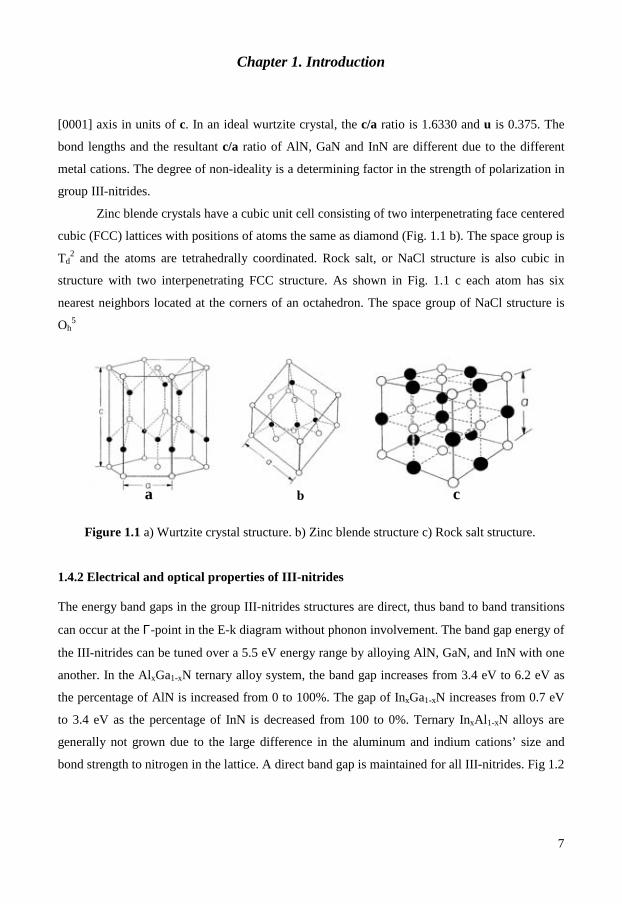
Chapter 1. Introduction
7
[0001] axis in units of c. In an ideal wurtzite crystal, the c/a ratio is 1.6330 and u is 0.375. The
bond lengths and the resultant c/a ratio of AlN, GaN and InN are different due to the different
metal cations. The degree of non-ideality is a determining factor in the strength of polarization in
group III-nitrides.
Zinc blende crystals have a cubic unit cell consisting of two interpenetrating face centered
cubic (FCC) lattices with positions of atoms the same as diamond (Fig. 1.1 b). The space group is
Td2 and the atoms are tetrahedrally coordinated. Rock salt, or NaCl structure is also cubic in
structure with two interpenetrating FCC structure. As shown in Fig. 1.1 c each atom has six
nearest neighbors located at the corners of an octahedron. The space group of NaCl structure is
Oh5
Figure 1.1 a) Wurtzite crystal structure. b) Zinc blende structure c) Rock salt structure.
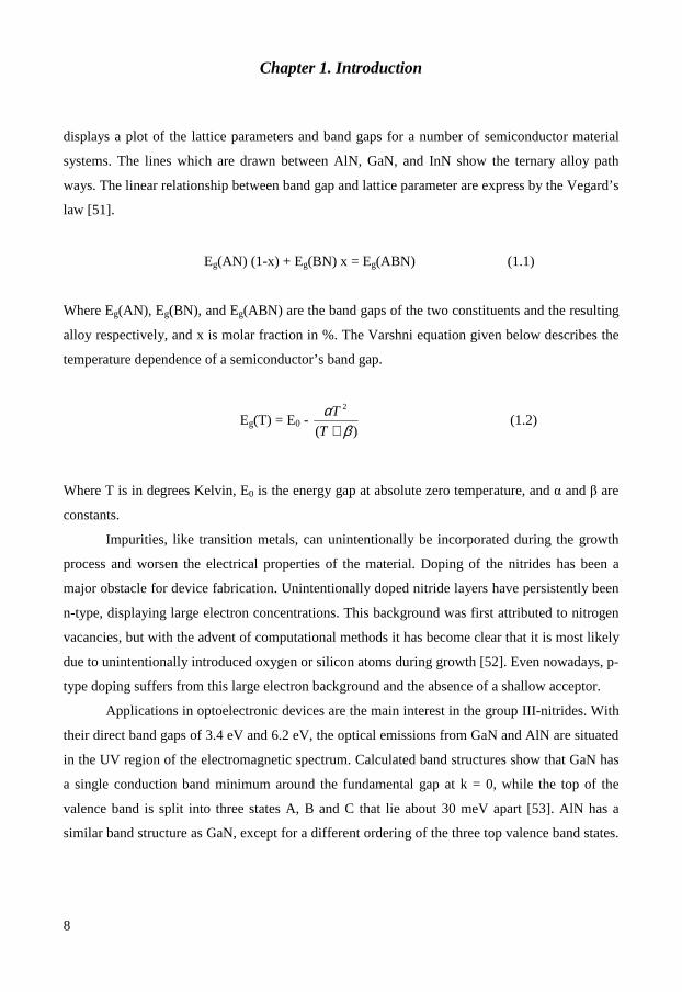
1.4.2 Electrical and optical properties of III-nitrides The energy band gaps in the group III-nitrides structures are direct, thus band to band transitions
can occur at the Γ-point in the E-k diagram without phonon involvement. The band gap energy of
the III-nitrides can be tuned over a 5.5 eV energy range by alloying AlN, GaN, and InN with one
another. In the AlxGa1-xN ternary alloy system, the band gap increases from 3.4 eV to 6.2 eV as
the percentage of AlN is increased from 0 to 100%. The gap of InxGa1-xN increases from 0.7 eV
to 3.4 eV as the percentage of InN is decreased from 100 to 0%. Ternary InxAl 1-xN alloys are
generally not grown due to the large difference in the aluminum and indium cations’ size and
bond strength to nitrogen in the lattice. A direct band gap is maintained for all III-nitrides. Fig 1.2
a b ca b c
Chapter 1. Introduction
8
displays a plot of the lattice parameters and band gaps for a number of semiconductor material
systems. The lines which are drawn between AlN, GaN, and InN show the ternary alloy path
ways. The linear relationship between band gap and lattice parameter are express by the Vegard’s
law [51].
Eg(AN) (1-x) + Eg(BN) x = Eg(ABN) (1.1)
Where Eg(AN), Eg(BN), and Eg(ABN) are the band gaps of the two constituents and the resulting
alloy respectively, and x is molar fraction in %. The Varshni equation given below describes the
temperature dependence of a semiconductor’s band gap.
Eg(T) = E0 - )(
2
βα
+T
T (1.2)
Where T is in degrees Kelvin, E0 is the energy gap at absolute zero temperature, and α and β are
constants.
Impurities, like transition metals, can unintentionally be incorporated during the growth
process and worsen the electrical properties of the material. Doping of the nitrides has been a
major obstacle for device fabrication. Unintentionally doped nitride layers have persistently been
n-type, displaying large electron concentrations. This background was first attributed to nitrogen
vacancies, but with the advent of computational methods it has become clear that it is most likely
due to unintentionally introduced oxygen or silicon atoms during growth [52]. Even nowadays, p-
type doping suffers from this large electron background and the absence of a shallow acceptor.
Applications in optoelectronic devices are the main interest in the group III-nitrides. With
their direct band gaps of 3.4 eV and 6.2 eV, the optical emissions from GaN and AlN are situated
in the UV region of the electromagnetic spectrum. Calculated band structures show that GaN has
a single conduction band minimum around the fundamental gap at k = 0, while the top of the
valence band is split into three states A, B and C that lie about 30 meV apart [53]. AlN has a
similar band structure as GaN, except for a different ordering of the three top valence band states.

Chapter 1. Introduction
9
Due to the difficulties in growing good quality InN layers, it has proven difficult to determine the
value of its band gap. Up to 2002 the most likely value of the band gap was 1.8-2.0 eV. More
recently, however, several groups have report values around 0.7 eV for good quality layers [54,
55]. The exact band gap energy of InN therefore remains an open question. In principle, light
emission at any energy between 0.7-1.89 eV (InN) and 6.2 eV (AlN) can be achieved by band
gap engineering.
Apart from controlling the optical emission energy, band gap engineering of ternary nitrides is
also used in the production of quantum wells, wires and dots. A quantum well is a structure
where a thin semiconducting layer is sandwiched between two layers that have a larger band gap.
As a result, the carriers are confined to a two-dimensional region in space. Quantum wires and
quantum dots are similar structures where carriers are confined to one and zero dimensions,
respectively. This confinement results in a quantization of the carrier energy levels
Figure 1.2 Band gap energy vs. lattice parameter of some common semiconductors.

Chapter 1. Introduction
10
that is related to the dimensions of the structure, thereby introducing a certain degree of freedom
to tune the energy of the light emission. Such quantum structures are widely used in
commercially available GaN-based LEDs and laser diodes.
1.4.3 Piezoelectricity Group-III nitrides semiconductors are particular among the III-V compound semiconductors
because of present nitrogen, which is the smallest and the most electronegative group-V element.
This has a strong impact on the properties of the III-nitrides. Because of the electronic
configuration of the nitrogen atom, or rather the lack of electrons occupying outer electron
orbitals, the electrons involved in the metal-nitrogen covalent bond will be strongly attracted by
the coulomb potential of the nitrogen atomic nucleus. This means that the metal nitrogen covalent
bond will have stronger ionicity compared to other III-V covalent bonds. This ionicity (a
localized polarization) will result in macroscopic polarization if there is a lack of inversion
symmetry in the crystal. As there is strong ionicity of the metal nitrogen bond and also no
inversion symmetry in the wurtzitie III-nitrides along the c-axis, this results in a strong
macroscopic polarization along the [0001] direction in the III nitrides. Since this polarization
effect occurs in the equilibrium lattice of the III-nitrides at zero strain, it is called spontaneous
polarization [56]. If stress is applied to the III-nitride lattice, the ideal lattice parameters c and a
of the crystal structure will be changed to accommodate the stress. Thus the polarization strength
will be changed. This additional polarization in strained III-nitride crystals, in addition to the
spontaneous polarization already present, is called piezoelectric polarization [56]. For example, if
the nitride crystal is under biaxial compressive stress, the in-plane lattice constant a will decrease
and the vertical lattice constant c will increase, making the c/a ratio increase towards the ideal
lattice value of 1.6330. This will decrease the polarization strength of the crystal, since the
piezoelectric polarization and the spontaneous polarization will act in opposite directions. On the
other hand, if the nitride crystal is under tensile stress, the in-plane lattice constant will increase

Chapter 1. Introduction
11
and the vertical lattice constant will decrease, lowering the c/a ratio further away from the ideal
value 1.6330. This will increase the overall polarization, since the piezoelectric and the
spontaneous polarizations now act in the same direction.


Chapter 2. Characterization of AlN
13
Chapter 2
Characteristics of AlN 2.1 Introduction The excellent properties of AlN make it a highly attractive substrate candidate for III-nitride
epitaxy. The crystalline structures of hexagonal AlN and GaN are the same, hexagonal wurtzite
(2H), with a lattice mismatch about 2.5% in the c-plane. As AlN makes a continuous range of
solid solutions with GaN, it plays an important role in GaN-based devices and is highly suited as
a substrate for AlGaN devices with high Al concentrations. Its high resistivity is beneficial for
high-frequency applications. Its direct and large band gap makes it suitable for ultraviolet
applications down to wavelengths as short as 200 nm. Its high thermal conductivity makes it
desirable for high-temperature electronic and high-power microwave devices where heat
dissipation is critical. It is also discerned by high hardness, and chemical and thermal stability.
AlN shows also excellent field-emission performance in vacuum microelectronic devices due to
its small electron affinity value, which is from negative to 0.6 eV [55]. In this sense,
nanostructured AlN, such as AlN nanowires and nanorods, is important for extending our
knowledge on the potential of nano device applications.
There have been many reports on the growth of bulk AlN crystals by vaporization [57],
ammonothermal method [58], hydride vapor phase epitaxy (HVPE) [59], sublimation-
recondensation [60] and solution growth [61], but large AlN single crystals are still not available
in large quantities. In contrast, the efforts of several researchers (e.g. Slack and McNelly [60],

Chapter 2. Characterization of AlN
14
Rojo et al. [61], Bickermann et al. [62]) demonstrate that the sublimation growth is the most
promising method to grow AlN bulk crystals with very high quality and good sizes suitable as
III-nitride substrates.
2.2 Brief history of AlN Aluminium nitride is a synthetic compound and does not occur naturally. It was first made in
1862 by reacting molten aluminium with nitrogen gas. The first macroscopic crystals of AlN
were probably unintentionally produced by Serpek around 1910, in a furnace by a reaction of
bauxite, coke, and nitrogen gas at 1800 °C to1900 °C [63]. More recently, the reaction of AlF3
with NH3 gas at 1000°C was used to produce stoichiometric AlN powder [64]. In 1915 Fichter
and Oesterheld synthesized AlN crystals in an electrically heated furnace consisting of graphite
or tungsten tubes, which was employed to heat AlN powder in one atmosphere nitrogen ambient
[65]. The recondensed material consisted of AlN crystals and metallic Al. Crystals grown in
carbon tubes contained C inclusions. Early reports of AlN bulk single crystal growth began to
appear after 1960 [66, 67]. Most methods consisted of vapor transport in a nitrogen atmosphere
by vaporization of Al metal or by sublimation of AlN powder.
Taylor and Lenie in 1960 [66] reported that whiskers, prismatic needles and thin platelets
were grown in the temperature ranges 1450°–1750°C, 1800°–1900°C, and 1900°C, respectively.
Hexagonal prismatic needles were 0.5 mm in diameter and up to 30 mm long. Whiskers with 18–
20 mm length were grown with average growth rates of 1.5 mm/hr by Davies and Evans [68].
The grown crystals were colorless [69] or of different colors such as white [66], various shades of
blue [64], light yellow, and brown. Taylor and Lenie investigated an earlier claim that blue
coloration was due to the presence of aluminum oxycarbide (Al2OC), which is isomorphous with
AlN. Crystals were grown in different ambient, pure nitrogen, nitrogen with 0.5–2% carbon
monoxide, and nitrogen with 1% methane. In the presence of CO only blue color crystals were
grown, and a deeper shade of blue was observed with increasing amount of CO in nitrogen.
Chemical analysis confirmed the presence of carbon and oxygen in the crystals.

Chapter 2. Characterization of AlN
15
2.3 Crystalline structure
Aluminium nitride can appear in three types of crystal structure, wurtzite α-AlN (Fig.2.1a), zinc-
blende (β-AlN), and rocksalt structure (Fig. 1.1 b and c), but the wurtzite structure is stable
thermodynamically at ambient conditions. As shown in Fig.1.1 b and c both zinc-blende and
rocksalt have cubic structures (which form at very high pressure). The space group symmetry of
zinc-blende (indirect band gap ∼5.1 eV [70, 71]) and rocksalt structures are 2dT and 5
hO
respectively, and their lattice constants are a= 4.38Å and a = 4.043 - 4.045Å respectively.
The wurtzite structure consists of two interpenetrating hexagonal close-packed (HCP)
lattices, each with one type of atoms, displaced by z8c5 from each other. Each unit cell contains
6 atoms of each type. The space group symmetry of this structure is P63mc (which is the same
for hexagonal 4H and 6H-SiC polytypes) and point group symmetry is 6mm (C6v). The lattice
constants reported are from 3.110Å to 3.113Å for a and from 4.978Å to 4.982Å for c, and the c/a
ratio varies from 1.000 to 1.602 [71, 72].
Figure 2.1 a) Schematic of the AlN structure b) The tetrahedral structure of Al and N
atoms in AlN.

Chapter 2. Characterization of AlN
16
The zinc-blende and wurtzite structures form in a tetrahedron structure of Al, which has a
nitrogen atom in its geometrical center (Fig.2.1b). Since a=3.113Å and c=4.982Å, the length of
Al-N bonds are 3.1137Å. As shown in Fig.2.1b the height of the tetrahedron is 5.657Å. Using the
X-ray technique, the deduced AlN valency is –1.8 ± 0.8e, which is approximately midway
between the ionic and covalent limits [73]. In the wurtzite structure, the hexagonal lattice points
A, B, C (Fig.2.2b) are occupied in the following stacking sequence ..ABAB.. along the [0001]
direction (Fig.2.2c), hence it is of the 2H polytype. The polytypes are conventionally denoted by
their Ramsdell notation nL, where n is the periodicity of tetrahedra along the c-axis and L
indicates the Bravais lattice. Hexagonal polytypes are obtained when n is an even integer, giving
the 2H, 4H, and 6H polytypes that are relevant in growth. As shown in Fig. 2.2d, in the zinc-
blende structure all three-lattice points are occupied leading to the stacking sequence
...ABCABC.. along the [111] direction.
Figure 2.2 a) The basal plane and c axis b) hexagonal lattice points c) The double layer stacking
sequence of wurtzite structure. d) stacking sequence of zinc-blende.
Both wurtzite and zinc-blende structures have polar axes due to the lack of inversion
symmetry. Especially the bonds in the <0001> direction for wurtzite and <111> direction for
zince-blende are all faced by nitrogen in the same direction and by the cation in the opposite
direction. Both bulk and surface properties can depend significantly on whether the surface is

Chapter 2. Characterization of AlN
17
faced by nitrogen or metal atoms [11]. The polarity of AlN is important in controlling impurity
incorporation and piezoelectric effects in epitaxial GaN films [74].
The polarity of AlN can be defined with respect to the position of the Al atom in the
0001 bilayer [11]. In Al-face AlN, the Al atom occupies the top position in the bilayer, while in
N-face AlN the top position is occupied by N, corresponding to filling by Al of either upward-
pointing or downward-pointing tetrahedral sites (Fig. 2.3-down). The terms Al-face and N-face
are used here to refer to the orientation of the AlN lattice, and describe lattices related to each
other by an inversion operation. They do not refer to the surface termination, which is
independent of the polar orientation. By convention the crystallographic [0001] axis points from
the N-face to the Al-face. Therefore, the Al-face and N-face polarities are also referred to as +c
and –c polar, respectively (Fig. 2.3-up).
Figure 2.3 Schematic drawing of the AlN primitive unit cell indicating Down a) Al-polar b) N-
polar structures Up a) Al face (+c) polarity b) N face (-c) polarity.

Chapter 2. Characterization of AlN
18
Inversion domains (IDs) are extended defects that have a polarity opposite to the polarity
of the surrounding crystal matrix. They have been studied in AlN sintered ceramics [75] and in
thin films grown by metal organic chemical vapor deposition (MOCVD) on sapphire substrates
[76] and models of the domain wall structure have been formulated. The different response to
etching of +c and -c polar 0001 nitride surfaces has been observed in thin films and bulk
crystals of GaN and AlN [77, 78] and can be used to identify defects such as IDs on these
surface.
Figure 2.4 SEM image of a) Al polar and b) N polar AlN single crystal [77].
Fig.2.4 The N-polar and Al-polar surfaces of AlN single crystals. AlN crystals with Al-
polarity form hexagonal pits (Fig.2.4 a) and with N –polarity form hexagonal hillocks (Fig.2.4 b)
after etching.
2.4 Material properties of AlN
The energy band gaps of AlN (at room temperature 6.2 eV) is direct at the Γ point of Brillouin
zone. The AlN band gap has been measured by ellipsometry [79], optical absorption [80, 81],
cathodoluminescence (CL) [82], and photoluminescence (PL) [83], their different result were
likely due to crystal quality. By measurement on high-quality of bulk crystals and epilayers the
Chapter 2. Characterization of AlN
19
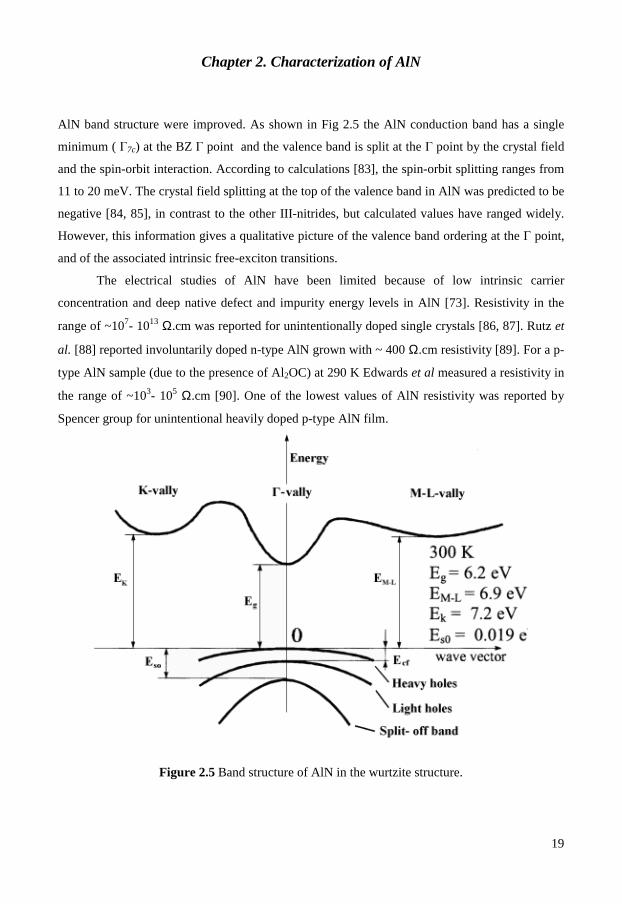
AlN band structure were improved. As shown in Fig 2.5 the AlN conduction band has a single
minimum ( Γ7c) at the BZ Γ point and the valence band is split at the Γ point by the crystal field
and the spin-orbit interaction. According to calculations [83], the spin-orbit splitting ranges from
11 to 20 meV. The crystal field splitting at the top of the valence band in AlN was predicted to be
negative [84, 85], in contrast to the other III-nitrides, but calculated values have ranged widely.
However, this information gives a qualitative picture of the valence band ordering at the Γ point,
and of the associated intrinsic free-exciton transitions.
The electrical studies of AlN have been limited because of low intrinsic carrier
concentration and deep native defect and impurity energy levels in AlN [73]. Resistivity in the
range of ~107- 1013 Ω.cm was reported for unintentionally doped single crystals [86, 87]. Rutz et
al. [88] reported involuntarily doped n-type AlN grown with ~ 400 Ω.cm resistivity [89]. For a p-
type AlN sample (due to the presence of Al2OC) at 290 K Edwards et al measured a resistivity in
the range of ~103- 105 Ω.cm [90]. One of the lowest values of AlN resistivity was reported by
Spencer group for unintentional heavily doped p-type AlN film.
Figure 2.5 Band structure of AlN in the wurtzite structure.
Chapter 2. Characterization of AlN
20
To study chemical properties of AlN many researchers have investigated wet etching. The
wide variation in etch rates shows that it is dependent on the crystallinity, quality, polarity, and
orientation of the material. Polycrystalline AlN has been etched in hot (~85 oC) H3PO4 [90, 91]
and amorphous AlN in hot (~100 oC) HF/H2O [66, 92], NaOH [93], and HF/HNO3 [94]. Etching
by KOH over the temperature range from 23 to 80oC has been reported by Pearton et al. [95, 96].
Zhuang et al. showed that only on the polar (0001) plane for bulk AlN crystal etched in a 45 wt%
KOH solution at 60oC, the other polar ( 1000 ) plane and other crystal planes did not etch. Since
the Al-face is more stable than the N face, the polarity of AlN can be determined by wet etching
[77]. These results were in conformity with Schowalter’s group results [97], therefore just N-
polar (–c face) of AlN is etched.
The thermal expansion coefficients of AlN along the c-axis and in the basal plane are
different due to the anisotropy of the structure. It has been determined experimentally from low
(77 K) to intermediate temperatures (1623 K) [66, 98]. To determine the thermal expansion
between 77 and 1269 K, Slack and Bartram used x-ray lattice parameter measurements of AlN
powder obtained by reacting high-purity aluminum trifluoride powder with ammonia (<1 wt%
oxygen impurities). Semi-empirical multi-frequency Einstein model was used to predict the
thermal expansion of AlN and 6H-SiC at high temperatures.
A number of studies have been done by Slack’s group to evaluate thermal conductivity
(κ) of AlN [99, 100]. The earliest results (κ = 0.145–2.0 Wcm-1K-1 at 300 K) were in agreement
with literature values. The large variation in values was related to differences in the density and
purity of the AlN. The most common impurities were oxygen and carbon. It was found that the
lattice parameter decreases with increasing oxygen content.
Oxygen is integrated in AlN via lattice dissolution and appears to be a substitutional
impurity [100]. AlN has the ability to accommodate oxygen to levels exceeding 4 at.%. The
mechanism of the large accommodation of oxygen is of high scientific and technological interest
due to the effect of oxygen on the thermal conductivity of AlN [101]. However, the local atomic
structure of the oxygen point defects in AlN is still a controversial issue [102]. These defects and
impurities scatter phonons, which are the heat carriers in AlN, and thus reduce the thermal
conductivity of the material. Oxygen substitutes for nitrogen in AlN and aluminium vacancies are

Chapter 2. Characterization of AlN
21
created as a direct consequence of the compensation of oxygen impurities [100, 102]. In
principle, one triple negative Al vacancy is required for three positive donors to satisfy charge
neutrality after incorporation of oxygen donors (i.e. for every three oxygen atoms incorporated on
nitrogen sites there exists one aluminum vacancy)[103]. It also appears that phonon scattering in
oxygen-containing samples is caused by the mass defect of the Al vacancies. Table 2.1 contain
some of the physical and electronic properties of AlN and provides a comparison with some other
semiconductors.
Materials→→→→ Properties↓↓↓↓
Si
GaAs
6H-SiC
4H-SiC
InN
GaN
AlN
Crystal structure
Diamond Zincblende Wurtzite Wurtzite Wurtzite Wurtzite Wurtzite
Lattic onstant a (Å)
5.431 5.653 3.081 3.073 3.548 3.189 3.112
c(Å) ---- --- 15.117 10.53 5.760 5.185 4.982
Band gap (eV)
1.1 1.42 3.0 3.2 1.89 3.4 6.2
Breakdown Electric field
(MV/cm)
0.6
0.6
3.2
3.0
---
3
1.2
Saturated Electron Drift Velocity (××××107
cm/sec)
1 1
2
2
2.5
4.2
1.4
Thermal Conductivity
(W/mK)
150
50
490
490
450
130
340
Hardness ( Kg/mm2)
1150
750
2800
2800
1200-1700
800
Melting Point (°°°°C)
1685 1510 No melt No melt 1646 2500 3546
Table 2.1 Physical and electronic properties of AlN and some other semiconductors.

Chapter 2. Characterization of AlN
22
2.5 Piezoelectricity of AlN
The piezoelectric effect is defined as the generation voltage within a material in the presence of
an applied stress. The converse piezoelectric effect is the reverse of this process, where an
applied voltage induces a stress or deformation in the material. AlN is a suitable material to use
in piezoelectric applications.
There are some materials, such as certain perovskites (calcium titanium oxide, CaTiO3),
with a few times larger piezoelectric coefficients than AlN. However, many of these materials are
not suitable for piezoelectric micro-electromechanical systems (MEMS) fabrication, because of
either specialized growth conditions or incompatibility with the fabrication process. Table 2.2
is a table of material properties for three piezoelectric materials that are compatible with
microprocessing and are commonly used in MEMS.
Materials→→→→ Properties↓↓↓↓
ZnO
PZT
AlN
Pizoelectric constant (C/m2) e31 = -0.57 e33 = 1.32
e31 = -6.5 e33 = 23.3
e31 = -0.58 e33 = 1.55
Band gap (eV) 3.4 2.67 6.2
Resistivity (ΩΩΩΩ cm) 1×10⁷
1×10⁹
1×10¹¹
Acoustic velocity (m/s) 10127
5700
3900
Thermal Conductivity (W/cm.oC)
0.6
0.018
3.2
Density ( Kg/m3) 5610 7570
3230
Thermal expansion (1/ oC) αa = 6.5 × 10⁻⁶ αc =3.0 × 10⁻⁶
α = 2 × 10⁻⁶
αa = 4.2 × 10⁻⁶ αc = 5.3 × 10⁻⁶
Young’s modulus (GPa) 201 68 308
Table 2.2 Properties of some common MEMS piezoelectrics.

Chapter 2. Characterization of AlN
23
AlN has several advantages compared with ZnO and lead zironate titanate (PZT). The
first advantage is that it is very compatible with standard MEMS processing techniques. It is very
selective to many wet chemical and dry plasma etches but can be readily etched in a chlorine
environment. Its very high hardness and melting point ensure that films will not degrade during
processing. Secondly, AlN exhibits both moderate electromechanical coupling in conjunction
with high acoustic and surface velocities, making it a useful material for surface acoustic wave
(SAW) and bulk acoustic wave (BAW) devices [104]. Thirdly, AlN films with excellent
crystallinity and orientation can be grown on many different substrates and films, such as
semiconductors, dielectrics, and metals. Finally, AlN does not have very high piezoelectric
coefficients, but for many applications, which do not require large response, their strong crystal
quality is suitable for very sensitive devices with high quality factors. The eminence for AlN
transducers can be 24 times higher than comparable PZT transducers due to its low dielectric
losses and high breakdown field [105].
2.6 Importance of bulk AlN and nanowires Besides high thermal conductivity of AlN (introducing it as a suitable heat sink in the electronics
industry), other attractive properties (bulk crystal) make it an ideal candidate as III-nitrides (GaN,
InN) substrate. Heterostructures deposited on AlN substrates have a wide range of applications in
high temperature/high power microelectronics and optoelectronic devices. Because of the
nitrogen pressure excess in AlN vapour is several orders of magnitude smaller than in GaN
vapour (in the other hand, the equilibrium N2 vapor pressure on AlN is relatively low compared
with GaN), growth of bulk GaN crystals via high nitrogen pressure solution is difficult and needs
high system pressure and high temperature. Although developed HVPE methods can successfully
produce bulk crystals of GaN, the large lattice mismatches between the epilayers and substrates
(mostly SiC and sapphire) causes a high dislocation density in heteroepitaxial GaN, typically in
the range of 108 – 1011 cm-2 [106, 107].
These dislocations combined with other defects such as stacking faults, micropipes, and
inversion domain boundaries, increase the reverse bias leakage currents, device threshold voltage,

Chapter 2. Characterization of AlN
24
and reduce the charge mobility and thermal conductivity, which result in reduced efficiency, and
lifetime [108].
As discussed in section 1.2, another problem is the thermal expansion mismatch between
substrate and epilayer which produces stress and consequently cracks in the epilayer. Thus
according to the discussion, AlN is a very good substrate for epitaxial growth of GaN due to the
same wurtzite crystal structure, small mismatch in both lattice constant (∼2.4% along the a axis)
and thermal expansion coefficient, good thermal stability (melting point >2500 °C), high
resistivity. In comparison to GaN bulk crystals, AlN is even a better substrate for high Al-content
AlGaN epitaxy.
Other applications of bulk AlN crystals is fabrication of AlGaN LEDs [109], using as
insulating films (due to high electrical resistivity), deep UV emitters, high quality GaN epilayers
[110, 111], multi-quantum well structures [112-114], AlGaN/GaN HFET devices [115], and (as
mentioned in section 2.5) surface acoustic wave and bulk acoustic wave devices and piezoelectric
MEMS. Its high thermal and chemical stability, breakdown electric fields, and maximum electron
velocities are advantageous for application areas such as high-power, high-frequency, and high-
temperature devices.
Recently, various one-dimensional (e.g. nanowires) nanoscale materials, including metals
[116], oxides [117], and nitrides [118], have attracted much attention because of their unique
properties derived from their low dimensionality, which can be potentially applicable to novel
magnetic materials, molecular electronics, catalysts, and nanoelectronic and optoelectronic
devices. When nanowires are formed, the surface effect becomes more important as the surface-
volume ratio increases, which is important when fabricating gas sensor devices. As AlN has a
wide band gap, and has large exciton binding energy, and very small electron affinity, these make
it potentially applicable in surface acoustic wave devices, ultraviolet sensors, and field-emission
devices [119, 120]. Several routes have been developed to prepare AlN nanowires, such as a
carbon nanotube confined reaction [121], CVD [122, 123], MOCVD [124], plasma process
[125], silica-assisted catalytic growth [126], and vapor–liquid–solid (VLS) growth process [127,
128].
Chapter 3. SiC as substrate
25
Chapter 3
SiC as substrate 3.1 Introduction Silicon carbide (SiC) is very rarely found in nature. SiC properties such as high thermal
conductivity, chemical stability, and its ability to operate at high temperature, and in high
radiation environment make it very attractive for many electronic applications. High power
devices, high temperature controllers and sensors, high voltage switching, and microwave
components are some of SiC applications.
The first SiC was synthesized in 1824 by the Swedish scientist Jöns Jocab Berzelius
[129]. The process of SiC powder production was introduced in 1892 by Acheson [130]. In this
process SiC was manufactured by the electrochemical reaction of sand and carbon at high
temperatures (up to 2550oC). Because of its extreme hardness the resulting material was used in
polishing applications. The first electrical property (electroluminesence of SiC light emitting
diode) of SiC was measured in 1907 [131]. In 1955 Lely used a new method for growth of high
quality SiC, which was based on sublimation and enabled growth of SiC platelets [132]. Tairov
and Tsvetkov improved this process in 1978 when they introduced a SiC seed crystal on which
the vapor species deposited, resulting in a boule of the material [133]. This method is called
sublimation growth and is based on physical vapour transport (PVT). It reduces the problems
with polytype control and yield. Nowadays, the interest in silicon carbide is high and several
corporations have formed to produce large boules having a particular crystal structure and

Chapter 3. SiC as substrate
26
controlled concentrations of impurities that determine the electrical and optical properties. There
are commercially available 4 inches single crystal wafers of 4H-SiC with micropipe densities less
than 1 cm-2 in 4-inch wafers. Today, the common method to grow SiC epitaxial layers is CVD.
The advantageous of this method is in providing good structural quality and excellent doping
control.
3.2 Crystal structure of SiC SiC is a IV-IV compound semiconductor with a covalent Si-C bonds (88% covalent and 12%
ionic). The crystallography and polytypism in SiC are important to have control regarding the
properties and the nature of the surfaces available for the epitaxial growth of III-nitride
semiconductors. SiC is the only chemically stable compound containing only Si and C. Its
crystalline structure consists of close-packed stacking of double layers of Si and C atoms. The
fundamental unit in the SiC structure is a covalently bonded tetrahedron with 4-fold symmetry,
consisting of either SiC4 or CSi4, as shown in Fig 3.1. The distance between the two neighboring
silicon or carbon atoms, a, is about 3.08 Å, while the very strong sp3 bond between carbon and
silicon atoms, b, is because of the very short distance, approximately 1.89 Å.
Figure 3.1 a). Basic unit cell of silicon carbide. The distance between Si-Si or C-C atoms, a, is
about 3.08 Å, and between C-Si atoms, b, is approximately 1.89 Å. (b). The two
configurations of silicon and carbons atoms, rotated 180º.

Chapter 3. SiC as substrate
27
As shown in Fig 3.1 b the spacing between the silicon layers is approximately 2.51 Å.
The unit cell is bonded through the corner atoms of the tetrahedron; as shown in Fig. 3.1b there
are two possible orientations of adjacent tetrahedral (by 60º rotation). The various rotations and
translations conduce to the many different stacking arrangements (or polytypes) of the Si-C
bilayers along the c-axis.
Figure 3.2 Possible stacking orientations of atoms in a close packed hexagonal structure.
The possible atomic arrangements of the atoms in the hexagonal wurtzite unit cell are
shown in Fig. 3.2. One can denote the first layer of atoms with position A, and then the atoms in
the next layer may sit at either position B or position C. Thus the simplest polytype is the 2H
(…ABAB…). The cubic (zincblende) structure of 3C-SiC has a stacking sequence
of…ABCABC…(or …ACBACB…). The most common forms of SiC are the 6H and the 4H
polytypes with the …ABCACBABCACB… and the …ABCBABCB … stacking, respectively.
Here we use Ramsdell notation, which is common to describing the polytypes [134]. The number
in the name of polytype refers to the number of layers needed to repeat the pattern and the letter
in a polytype’s name corresponds to the 1st letter of the crystal system (C for Cubic, H for
Hexagonal, and R Rhombohedral).

Chapter 3. SiC as substrate
28
Fig. 3.3 shows the stacking sequence for 3C, 2H, 4H, and 6H SiC polytypes. Since there
is no rotation in the stacking sequence of cubic polytype compared with the hexagonal polytypes,
the 3C structure proceeds in a straight line and hexagonal structures proceed in a zigzag pattern.
As shown in this figure in 4H-SiC the A position is a cubic site (k), and B position is a hexagonal
site (h). In 6H-SiC, the A position is a hexagonal site, and B and C are the cubic and denoted by
k1 and k2. More than 200 SiC polytypes have been found, some with a stacking period of several
hundred bilayers [135]. The properties of SiC depend on the polytypes and also the atom position
and its surrounding in the polytype.
Figure 3.3 Stacking sequence of SiC polytypes. 3.3 Material properties of SiC Each polytype has a unique set of electronic properties associated with its crystal structure. The
bandgap range is from 2.3 eV for 3C-SiC to 3.3 eV for 2H-SiC. The outstanding physical and
electrical properties of SiC make it a perfect semiconductor for radiation resistance, high power,
high temperature, and high frequency electronic device. A summary of electrical properties of
3C, 4H, and 6H SiC polytypes is shown in table 3.1.
The wide energy bandgap of SiC enables it to operate at extremely high temperature
without suffering from intrinsic conduction effect. It also allows SiC to emit and detect short

Chapter 3. SiC as substrate
29
wavelength light (for fabrication of blue light emitting diodes and UV photodetector). At room
temperature SiC has a larger thermal conductivity than any metal. This property allows devices
based on SiC to operate at high power levels and still dissipate the large amount of extra heat
generated. Due to the high saturated electron drift velocity it can act at high frequency (RF and
microwave).
3C-SiC 4H-SiC 6H-SiC
Bandgap (eV) – (T<<<< 5K) 2.39 3.26 3.02
Saturated drift velocity (cm/s) 2.0×10⁷ 2.0×10⁷ ---
Breakdown electric field (V/cm) 2.1×10⁶ 2.2×10⁶ 2.4×10⁶
Electron Mobility (cm 2/V.s) – (300) 800 1000 400
Hole Mobility (cm2/V.s) – (300 K) 40 115 101
Static dielectric constant 9.72 --- 9.66
Electrical resistivity (undoped)-ΩΩΩΩ.cm
--- 102 - 103 ---
Table 3.1 Electrical properties of SiC
In contrast to sapphire, hexagonal SiC has a better lattice and thermal expansion
coefficient match with the III-nitrides. SiC is also high-temperature compatible for use in the
high-temperature CVD growth environment. SiC wafers are also available in n-type form,
allowing fabrication of backside contact directly to the substrate. It is also available in a semi-
insulating form, which is required for most electronic device applications. Due to the smaller
lattice mismatch, the cleaving problem in the case of sapphire substrates is not present. Table 3.2
shows some physical properties of three SiC polytypes.
3.4 Substrate preparation
In the present work, as grown 4H-SiC epilayers deposited on Si terminated 4H-SiC
(0001) commercial wafers with an 8o off-cut from the basal plane in the [ 0211 ] direction were
employed as substrates. This is the fastest lateral growth direction and the direction of the step

Chapter 3. SiC as substrate
30
3C-SiC 4H-SiC 6H-SiC Structure Zincblende Wurtzite Wurtzite
Lattice constant: a (Å) 3.083 3.076 3.08
Lattice constant: c (Å) 7.55 10.046 15.12
Bandgap (eV) 2.390 3.263 3.0
Thermal expansion coefficient
(a-axis) (K-1)
---
---
4.2 × 10⁻⁶
Thermal expansion coefficient
(c-axis) (K-1)
3.8 × 10⁻⁶
---
4.68 × 10⁻⁶
Thermal Conductivity (W/cm K)
3.6 3.7 4.9
Electron Affinity (eV) --- --- 3.5
Table 3.2 Physical properties of three SiC polytypes.
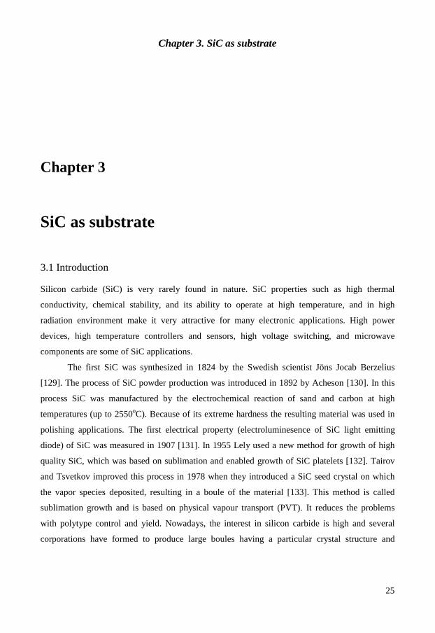
flow mechanism during SiC epitaxy. The results of a series of experiments with and without a
SiC epilayer confirm that the SiC epilayer avoids the effect of scratches normally present on
commercial substrates, which may initiate uncontrolled nucleation of AlN. Moreover, such
epilayers serve as templates for self-organized growth of hexagonal hillocks that further
transform to SiC based pyramids. The SiC epitaxy was conducted in the same furnace by
sublimation growth method. The thickness of the epilayer was about 50 µm, which prevents a
direct impact of the commercial wafer surface on the AlN deposition.
As mention above, a good surface morphology of the substrate is essential for growth of
high quality layers, as well as for device fabrication. In this work we deposited a 4H-SiC epilayer
with higher quality than the substrate [136]. During the SiC epitaxy on off-axis substrate via step-
flow growth typical morphological features (elongated grooves, shallow pits, and triangular
shaped defects) possibly will appear in the layer [137, 138]. We have grown featureless epilayer
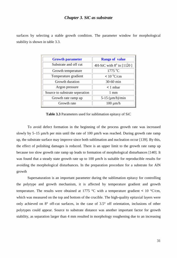
Chapter 3. SiC as substrate
31
surfaces by selecting a stable growth condition. The parameter window for morphological
stability is shown in table 3.3.
Growth parameter Range of value Substrate and off cut 4H-SiC with 8o in [ 0211 ]
Growth temperature 1775 oC
Temperature gradient < 10 oC/cm
Growth duration 30-60 min
Argon pressure < 1 mbar
Source to substrate seperation 1 mm
Growth rate ramp up 5-15 (µm/h)/min
Growth rate 100 µm/h
Table 3.3 Parameters used for sublimation epitaxy of SiC
To avoid defect formation in the beginning of the process growth rate was increased
slowly by 5–15 µm/h per min until the rate of 100 µm/h was reached. During growth rate ramp
up, the substrate surface may improve since both sublimation and nucleation occur [139]. By this,
the effect of polishing damages is reduced. There is an upper limit to the growth rate ramp up
because too slow growth rate ramp up leads to formation of morphological disturbances [140]. It
was found that a steady state growth rate up to 100 µm/h is suitable for reproducible results for
avoiding the morphological disturbances. In the preparation procedure for a substrate for AlN
growth
Supersaturation is an important parameter during the sublimation epitaxy for controlling
the polytype and growth mechanism, it is affected by temperature gradient and growth
temperature. The results were obtained at 1775 °C with a temperature gradient < 10 °C/cm,
which was measured on the top and bottom of the crucible. The high-quality epitaxial layers were
only achieved on 8° off-cut surfaces, in the case of 3.5° off orientation, inclusions of other
polytypes could appear. Source to substrate distance was another important factor for growth
stability, as separation larger than 4 mm resulted in morphology roughening due to an increasing

Chapter 3. SiC as substrate
32
influence of graphite wall on the growth species (reacting with the graphite causes unstable
growth behaviour). The morphology of thick layers grown under optimized conditions is
remarkably good considering layer thickness (50 - 100 µm) and growth rate (100 µm/h).
We have studied several ways to prepare SiC substrates for AlN growth. Since it was
observed that thermal etching of the surface is rather influential for creating a special pattern on
the substrate surface, we attempted a study in which hydrogen gas was involved in the growth
environment [141]. This was motivated by the expectation to have a better control over the
pattern formation since it is known that hydrogen etching is commonly used in the CVD of SiC
epilayers. Hexagonal defects in sublimation grown layers using hydrogen were observed. These
defects are not present in layers grown in vacuum or argon conditions while local shallow defects
with a resemblance to the hexagonal features appear in all samples. We have concluded from this
study that hydrogen can not contribute to a formation of well arranged patterns and therefore
studies only with in-process thermal etching where further considered.

Chapter 4. Overview of AlN growth
33
Chapter 4
Overview of AlN growth 4.1 Introduction Since the melting point of AlN is exceeding 3000 °C [142] at a high nitrogen pressure of about
100 bar [143], bulk crystals cannot be grown by known methods such as Czochralski or
Bridgman growth from stoichiometric melts, as is usually done with semiconductors such as Si
and GaAs. Therefore, the lower temperature methods including solution [144] and vaporization
routes [145] have to be applied. There have been many reports on growth of bulk AlN crystals by
vapor and solution (flux) growth methods. Flux growth makes it possible to grow crystals at a
lower temperature compared with melt growth. However, this method for AlN is limited by the
lack of a solvent that dissolves AlN and simultaneously remains inert to reactions with the
crucible. The solubility of nitrogen in most solvents is low, for example less than 10-3 at% in
liquid aluminum at 1000°C.
Among the vapor growth techniques, magnetron sputtering [146], molecular beam epitaxy
(MBE) [147, 148], metal organic chemical vapor deposition (MOCVD) [149, 150], are
conventional methods for AlN thin film growth. The magnetron sputtering technique is
considered to be the favorable choice due to its easily deposited high c-axis orientation. High
quality AlN thin films can be grown on Sapphire and SiC substrates by MOCVD with growth
rates of about 10 µm/h. By using the MOCVD method with epitaxial lateral overgrowth (ELO)
technique the dislocation densities can be reduce down to 106 cm-2 [33, 151]. Relatively low

Chapter 4. Overview of AlN growth
34
growth temperature, better control of growth parameters, and absence of gas carrier are some
advantages in the MBE method. High quality AlN quasi-bulk crystals have been grown
successfully by the hydride vapor phase epitaxy (HVPE) method [80, 152], but fabrication of
freestanding AlN crystals still needs to be developed in this method.
The sublimation-recondensation (a kind of physical vapor transport, PVT, growth of the
crystals) method is the most successful crystal growth technique. It can be divided into two parts,
epitaxial and bulk growth. In this technique, first successfully developed by Slack and McNelly
in 1976 [153], at first a hot AlN source decomposes to Al and N2 via the reaction
AlN (s) ⇔ Al (g) + 2
1N2
Then the vapor species are transported to a seed at a lower temperature by temperature gradient
between the source and seed, and finally the vapor species recondense as a single crystal on the
seed (often growth take place in N2 atmosphere to enhance and control the growth rate). It has
several advantages over melt growth in terms of lower growth temperature, easy implementation
of the process, and morphological stability. The major drawbacks of vapor growth are the
relatively low growth rate and parasitic nucleation [154].
Research in growth of 1D AlN nanowires has been performed due to their promising
application in optoelectronic and field-emission nanodevices (see section 2.6). Compared with
the GaN nanostructure, as a rapid developmental and attractive III-V semiconductor, AlN
nanostructure growth has relatively lagged behind. Nevertheless, low-dimensional AlN
nanowires have been synthesized by several routes including a confined method of an anodic
porous alumina template [155], carbon nanotube confined reaction [121], and direct nitridation of
Al or Al alloy in a mixture of N2 and NH3 [156, 157]. A flow of NH3 was employed as the
necessary nitrogen source in these methods, and it is an important parameter for synthesis of AlN
nanowires.

Chapter 4. Overview of AlN growth
35
4.2 Fundamentals of physical vapor transport growth In the PVT method a temperature gradient between source and substrate is an important
parameter for the growth performance. The source material at a temperature sublimes and the
vapors are transported to an area at lower temperature where they recrystallize. There is a self-
seeded growth if nucleation occurs at the crucible walls (or top or bottom), and a seeded growth
if a seed crystal is used. Different factors such as growth temperature, ambient gas pressure, mass
transport, impurity incorporation, thermodynamics, and growth kinetics influence the quality of
the final crystals.
Figure 4.1 µ(T) of the two-phase equilibrium. Stable phases (solid lines), and metastable phases
(dashed lines).
Fig 4.1 shows a sketch of the chemical potential function, µ(T), in the neighborhood of a
first-order phase transition. The µ (the Gibbs potential) has a different dependence from the
intensive variables in the two phases. Only at equilibrium these potentials are equal. But away
from equilibrium the potentials of the solid µs and fluid (vapor) µv are different. The difference in

Chapter 4. Overview of AlN growth
36
temperatures (∆T = Te – T, where Te is the equilibrium temperature) indicates the driving force of
crystallization or growth affinity as
sv µµµ∆ −= (4.1)
Crystalli zation occurs when the vapor pressure of the gaseous species at the vapor - solid
interface is higher than the corresponding equilibrium (saturated vapor pressure) of the solid
phase. Therefore the vapor is supersaturated with respect to the solid with a degree of
supersaturation σ, this relative supersaturation is given by the following equation in terms of
vapor pressures.
P
PP
pressuremequilibriu
onersaturatisuptotalσ
e
e−== (4.2)
where P and Pe are actual and equilibrium pressure, respectively. For small values of σ and
making the assumption that the vapor as an ideal gas, the chemical potential difference ∆µ in
terms of the supersaturation is
( ) σkTσ1lnkTP
PlnkTµ∆
e
≅+=
= (4.3)
where T is the temperature of the solid and k is Boltzmann’s constant. This equation shows that
crystallization driving force is approximately proportional to the supersaturation. Therefore the
supersaturation is the driving force for crystallization processes, and the prevailing level of
supersaturation will drive the nucleation and growth kinetics. By manipulating the
supersaturation level the crystal size distribution can be controlled. High supersaturation can lead
to excessive nucleation and disordered (including polycrystalline) crystal growth. There is a near
relationship between transport rates, surface reaction kinetics, and crystal growth rates and
modes. The flux of vapor J(T) to the crystal surface from kinetic gas theory is given by the Hertz-
Knudsen equation

Chapter 4. Overview of AlN growth
37
( )mkTπ2
PPα)T(J e−
= (4.4)
where m is the mass of the vapor species, and α is the sticking coefficient, which shows the
probability that an impinging vapor specie is adsorbed onto the surface. The maximum growth
rate value Vg max for the PVT process from the equilibrium vapor pressures on the source (P) and
seed (Pe) (by assumption α = 1 and ignoring gas phase diffusion between source and seed) can be
deduced by using equation 4.4 as the following equation
( ) ( )
e
eeemaxg
P
PP
mkTπ2
PΩ
mkTπ2
PPΩV
−=
−= (4.5)
where Ω is the atomic volume. From equations 4.2 and 4.5 it can be concluded that the growth
rate is proportional to the supersaturation. Effects of gas phase diffusion on growth rates has been
considered in references [154, 158]. The maximum growth rate is obtained when all atoms
leaving the vapor phase and entering the surface are incorporated into the crystalline phase. This
can occur when the surfaces are uneven and rough, or all of the lattice points are at kink positions
(this is called adhesive growth.). Kink sites are special surface positions, at which the chemical
potential is equal to that of the bulk crystal.
In about 1949 Burton, Cabrera, and Frank [159 – 161] developed the crystal growth
theory (BCF theory) and explained the equilibrium structure of crystal surfaces, the step
movement (velocity) on crystal surfaces, and growth rate of crystal surfaces. According to this
theory, during growth a flux of atoms from the vapor phase impinges on the surface. Atoms
become adsorbed and these adatoms can execute jumps to adjacent surface sites or desorb (back
to the vapor phase). These adatoms reside on the surface until they acquire the required
adsorption energy Ea, which is created through heat fluctuations. The mean lifetime τs (the
average amount of time an adatom would spend on the surface before adsorbtion or desorbing
back to the gas phase) can be express as

Chapter 4. Overview of AlN growth
38
= −
kT
Eexpντ a1
s (4.6)
where ν is a frequency term of adatoms on the order of the atomic frequency of vibration (~1013
s-1). During the lifetime τs, the adatoms are not fixed in the same position, they diffuse over the
surface. If they diffuse sufficiently on the terrace and reach a kink before they desorb into the
vapor phase, then they can be acquired by the crystal phase. By assuming that the activation
energy for the adatoms diffusing on the surface is Esd (the energy needed to move adatoms to an
adjacent lattice point), the surface diffusion coefficient is given by
−=
kT
EexpνaD sd2
s (4.7)
where a is the lattice constant. The average distance λs that the adatoms diffuse during the
lifetime τs can be calculate by the Einstein formula
ss
2s τDλ =
or
−=
kT
EEexpaλ sda
s (4.8)
Esd is smaller than Ea and has a typical magnitude such that λs∼ 102 a if the crystals are growing
in the vapor phase. It means that atoms can contribute to the growth if atoms entering a position
at a distance of λs or less from a kink. This indicates that in the vapor phase growth surface
diffusion plays an important role.
Once the adatoms attach at a kink, the kink moves forward one step. This means the step
moves forward across the surface and this is the way that the crystal growth process proceeds.
This growth mechanism is called lateral growth. By identifying the forward speed of step (step
velocity) the growth rate of this growth method can be determined. According to the BCF theory

Chapter 4. Overview of AlN growth
39
the surface concentration of adatoms near steps is maintained at its equilibrium value ne and far
from steps the adatom concentration n is in equilibrium with the supersaturated vapor phase, as
n = (1+ σ) ne (4.9)
By using these and the surface diffusion equations the velocity of a single step on the surface is
given by
s
se
λ
Dσθ2V =∞ (4.10)
Here, θe is the equilibrium surface coverage given by ne/nt, where nt is the total concentration of
surface sites [162]. This solution implies that only a strip of width 2λs around steps is active for
the collection of adatoms. The velocity of a parallel train of steps is determined by
= ∞
sBCF
λ2tanhVV
l (4.11)
where l is the average spacing between steps. The vertical growth rate Vg of the crystal is then
given by
BCFg Vh
V
=l
(4.12)
where h is the step height and VBCF is given by equation (4.11). Growth of semiconductors on
vicinal surfaces is an example of a laterally growing parallel train of steps, which can be assumed
as a series of terraces of low index notation separated by regularly spaced steps (crystal growth
followed by step flow mechanism). According to the equations (4.10) and (4.11), in the steady
state all steps move at the same velocity and the step velocity (therefore the vertical growth rate)
is proportional to the supersaturation.

Chapter 4. Overview of AlN growth
40
4.3 Bulk crystal growth of AlN AlN bulk crystals have been grown by different methods such as sublimation-recondensation [60,
158], hydride vapor phase epitaxy [163, 152], vaporization [57, 164], ammonothermal [165], and
solution growth [166, 167]. The use of sublimation of AlN at high temperature shows the most
promising results. This method yields high quality material and possibility for larger crystal size
for fabrication of device [115, 168]. But a number of subjects are still left to study, including
understanding the negative effects of various impurities in AlN and their reduction,
contamination from the crucible, stability and lifetime of crucible and etc.
The sublimation growth process can be divided into several stages such as, sublimation of
the source materials, mass transfer of the active species through the gas phase (molecular and
convective transport), adsorption on the surface, re-crystallization (surface diffusion, surface
chemical reaction), and surface desorption [154, 158]. The growth process requires (I)
preparation of chemically inert closed crucible, (II) positioning of the crucible inside the stable
hot zone ensuring proper temperature difference between the cold (crystal) and hot (source) parts
and (III) heating the system to growth temperature in suitable gas ambient. Growth temperature,
the pressure of ambient gas, growth kinetics, mass transport, thermodynamics, and impurity,
influence the resulting quality of crystals. Research on sublimation growth of AlN is demanding
because of absence of suitable substrate materials, its high temperature process, and lack of high
chemically and physically stable crucible materials.
4.3.1 Seeded and self-seeding growth of AlN
Seeded growth of AlN on SiC substrates seems to be a suitable way to obtain large area
AlN crystals, since SiC wafers up to 3 inches in diameter are currently available. Many
researchers have used seeded growth for AlN [169-172]. As there are no commercially available
AlN single crystal wafers, seeded growth of bulk AlN is usually performed on SiC substrates
which is available in high quality and large size. It has small thermal expansion mismatch and
lattice mismatch with AlN, which is about 1% for 6H-SiC and 1.2% for 4H-SiC a-lattice, and
Chapter 4. Overview of AlN growth
41
also good thermal stability. In 1960 Campbell and Chang were the first to use SiC as a seed to
grow AlN [173]. In 1997 seeded growth of AlN on 6H-SiC in graphite crucibles was first
performed by Balkas et al. [174]. They prepared layers up to 1mm thickness on 10 × 10 mm2
substrates. The grown AlN layer had Si, C, and O contamination, screw dislocation, and cracks.
Edgar and coworkers designed a novel sublimation sandwich technique and established relatively
large area up to 8 mm in diameter, but also thin layers grown on SiC [175-177]. Enlargement of
selected AlN crystal from 0.5 to 5mm in BN crucibles has been demonstrated by Sitar’s group
[169].
Generally, there are three methods in crystal growth technology to achieve seeded growth
(or to prepare an initial seed crystal) of a new material: (I) growth of sufficiently large free-
standing single crystals suitable for preparation of particularly oriented seeds; (II) use of grain
selection in directional crystallization, which may result in single crystal growth; (III) using a
foreign single-crystalline material which is available as large-area substrate, allows for
heteroepitaxial growth and is stable in the corresponding growth environment. Bickermann and
coworkers used this three procedures for preparing seeds for AlN by using (I) free-standing
crystals up to 15 mm in length; (II) grain selection in boules of 50 mm in diameter and up to 15
mm in height; (III) growth on (0 0 0 1) 4H–SiC substrates 25 mm in diameter [172].
In the case of seeding growth compared to self-seeding, it is possible to control the
growth direction and growth interface polarity (Al or N face) of the AlN bulk crystal. But there
are some problems in seeded growth; the first is decomposition of SiC during the growth and
adding Si and C into the AlN and also formation of AlN and SiC alloys. The second problem is
formation of cracks in the AlN layer, which is due to the higher thermal expansion coefficient of
AlN compared to SiC and the low critical shear stress of SiC. The third one is the difficulty to
achieve 2D growth on the Si-face of SiC due to a preferred growth through screw dislocations
[178].
Single crystal AlN layers with 3 mm thickness on Si-face of 6H-SiC (on-axis) and 4H-
SiC (off-axis) were grown by Sitar and coworkers [179]. They used two-step growth, first an AlN
layer was grown at a low temperature (1850 ºC) with a growth rate about 10 – 30 µm/hr, then the
temperature was increased of about 100 – 200ºC to achieve a higher growth rate, about 70 µm/hr.
Most recently, seeded sublimation growth of AlN on SiC substrates was investigated by Sitar,

Chapter 4. Overview of AlN growth
42
Edgar and coworkers [170]. Large diameter (15–20mm) and thick (1–2 mm) AlN layers were
demonstrated on Si-face, 3.5o off-axis 6H-SiC. A c-axis growth rate of 15–20 µm/h was achieved
at 1830oC, and the surface morphology was highly textured.
For the first time seeded growth of AlN on native seeds (AlN) by the sublimation method
was reported by Schlesser et al. [169]. Transparent, single-crystal c-platelets (prepared by
vaporization of Al) were used as seeds. Growth was performed in a BN crucible at 2200°C with a
temperature gradient along the source and seed of approximately 3°C/mm.
The first self-seeded growth of AlN was introduced by Slack and McNelly in 1976 [153].
In self-seeded growth, AlN source materials sublime at elevated temperature, then vapors
recondense at the cooler part of the crucible, and start crystallize as a single crystals on the
crucible wall. In this method many nucleation sites start to form without any possibility to control
their orientation, some of them lead to formation of single crystal grains. By coalescence of
grains a polycrystalline AlN layer begins to form, as the growth process continues some grains
expand in the c-plane and grow over smaller grains. Finally some of single crystal grains will
dominate the growing surface and appear as a crystal boule.
Self-seeding compared with seeding growth produces higher quality crystals, because of
absence of thermal and lattice mismatch. Since there is no substrate decomposition in self-
seeding growth, the growth temperature and consequently growth rate is higher than in the seeded
growth. Slack and coworkers have developed AlN bulk sublimation growth process capable of 2
inch AlN single crystal wafers with low dislocation density (104 cm-2) [180]. The AlN wafers are
crack-free and have more than 85% usable area suitable for device fabrication.
4.3.2 Temperature and pressure effects As summarized in Fig. 4.2 (experimental results in this thesis) temperature and nitrogen pressure
are the most important factors controlling the crystal growth habit [176, 181, 182]. The growth
temperature in sublimation method is broad and indefinite, as bulk growth mode can be achieved
in principle at any temperature ensuring an appropriate balance between the rate of species
diffusion on the growing interface and the rate of material transport toward the interface. As the
Al-vapor pressure over liquid aluminum becomes less than Al-vapor pressure over solid AlN at

Chapter 4. Overview of AlN growth
43
some high temperatures (about 2450 oC), then solid AlN may decompose into Al-liquid and
nitrogen. Formation of Al liquid droplets on growth surface is detrimental for crystal quality and
since liquid aluminum is very reactive at such high temperatures it also destroys any hot zone
materials. Therefore temperature about 2400oC should be considered as an upper limitation for
AlN crystal growth [183, 153].
Epelbaum et al. have found that the growth habit of freestanding AlN crystals is highly
dependent on temperature, they grown sharp needles of AlN at temperatures less than 2000 ºC,
six-sided prismatic needles at 2050 ºC, columnar rhombohedral AlN crystals at 2150 ºC, and
thick faceted crystals were obtained at 2250 ºC [172, 184].
Figure 4.2 Crystal habit and nitrogen pressure versus growth temperature. a) Platelet-like, b) Columnar, c) Continuous surface with crack, d) Nanowires, e) Needle like, f) Free standing without cracks [182].
As mentioned above the pressure is also effective on the morphology. Reducing the N2
pressure leads to higher sublimation rate, at extreme condition (e.g. high vacuum) the mass
transport of reactive species switches from diffusion to drift, resulting in several orders of

Chapter 4. Overview of AlN growth
44
magnitude higher growth rate [185]. However, N2 has extremely low sticking coefficient at the
growth surface, which means that only a small fraction of the N2 arriving at the surface adsorbs
on the crystal and the rest desorbs from the surface. To control the growth rate the availability of
nitrogen atoms at the growing surface is important. Thus, excess N2 has to be provided and
system pressure needs to be kept over 100 torr to enhance AlN growth [186]. Furthermore, under
supersaturation conditions (low pressure and high temperature), the relative high Al vapor mole
fraction will degrade the performance of furnace fixture due to the unstable nature of aluminum
vapor.
4.3.3 Crucibles for growth of AlN Contamination from the crucible in AlN sublimation growth is a problem, because of high
temperatures (1800-2300oC) in this method. In the method, different crucible materials such as
graphite and SiC coated graphite, tantalum carbide TaC, nitrides crucibles (e.g. BN, TiN, Ta2N)
and high melting metals (Zr, Nb, W, Re, W-Re alloys) have been tried. Properties of a suitable
crucible for AlN sublimation growth include: (I) a small source of contamination during the
growth progress; (II) compatible with extreme temperatures without degradation; (III) inert to
chemically destructive Al vapor; (IV) long lifetime; (V) producible in different size and shapes,
(VI) inexpensive [187].
During the decades in 1950-1970 researchers for sublimation growth of AlN employed
carbon crucibles, but carbon contamination was significant. Many of AlN crystals grown in
graphite crucible contain carbon impurities as Al2OC and are often colored blue, green, or black.
This produces a broad, characteristic optical absorption band peaking at 1.86 eV. The carbon in
the furnaces also can be transport as CN, C2N2, CO, AlCN and other gaseous molecules. To
surmount these problems some researchers used SiC coated graphite crucible (via chemical vapor
deposition). Although the crucible stability improved, the Al vapor slowly diffused through the
SiC barrier coating, reacted with the graphite at the interface and finally caused the coating to
peel. The lifetime of crucibles was sufficient to accomplish several 10-15 experiments [63, 153,
174].

Chapter 4. Overview of AlN growth
45
To suppress carbon contamination, some researcher used W crucibles (e.g. Slack and
McNelly [153] in 1976 and L. Liu and J. H. Edgar [154] in 2000), and successfully grew AlN
crystals. The tungsten crucible exhibited the least chemical degradation in comparion to tungsten-
rhenium and rhenium crucibles [63]. One of the problems that limited the maximum size of the
crystals was the tungsten crucible tended to develop pin-holes with about 5 µm in diameter [60].
BN is also a good choice for AlN crystal growth; some groups have reported successful
AlN crystal growth using hot pressed or BN crucibles by the sublimation method. Some
researcher observed striations in the c-axis direction of the AlN crystal when they used this kind
of crucible; they suggested that these striations may be due to the presence of boron in the growth
environment, as they are not seen in AlN grown in other crucible materials [175, 74, 164]. AlN
nucleates in a much higher density on TaC compared with BN, rapidly forming a continuous
layer. Prismatic needles and hexagonal hillocks were obtained in TaC and niobium carbide (NbC)
coated graphite crucible [188]. However, crucibles made of nitrides or carbides suffer severe
cracking, which was caused by the diffusion of aluminum and nitrogen along the grain
boundaries and/or mismatch of thermal expansion coefficients [187-189]. In the present work a
graphite crucible with TaC coat was used for growth of AlN.
4.3.4 Initial nucleation in growth of AlN The initial stages of AlN growth on SiC were studied by a number of authors. The morphology
and composition of AlN crystals on SiC at the initial stage of crystal growth were investigated by
Liu et al [190]. They performed 15 minutes AlN growth on Si-terminated of 6H-SiC (0001)
substrates under different temperature (1800–1900°C) and pressure conditions. AlN nucleated as
individual hexagonal hillocks and platelets in an island-like growth mode during the initial stages
of growth. The nuclei size and density increased with increasing growth temperature at constant
pressure. At constant growth temperature, reduced pressures yielded coalesced, irregularly
shaped platelet crystals. Scanning Auger microscopy (SAM) measurements indicated varying
relative compositions of Al, N, Si, and C on different crystal facets of the AlN nuclei.
AFM studies on AlN grown on SiC indicated scratches and steps on as-received 6H-SiC
substrates, which served as nucleation sites for individual AlN grains grown in a three-
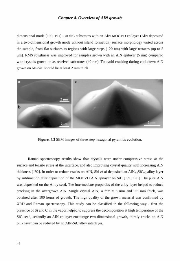
Chapter 4. Overview of AlN growth
46
dimensional mode [190, 191]. On SiC substrates with an AlN MOCVD epilayer (AlN deposited
in a two-dimensional growth mode without island formation) surface morphology varied across
the sample, from flat surfaces to regions with large steps (120 nm) with large terraces (up to 5
µm). RMS roughness was improved for samples grown with an AlN epilayer (5 nm) compared
with crystals grown on as-received substrates (40 nm). To avoid cracking during cool down AlN
grown on 6H-SiC should be at least 2 mm thick.
Figure. 4.3 SEM images of three step hexagonal pyramids evolution.
Raman spectroscopy results show that crystals were under compressive stress at the
surface and tensile stress at the interface, and also improving crystal quality with increasing AlN
thickness [192]. In order to reduce cracks on AlN, Shi et al deposited an AlN0.8SiC0.2 alloy layer
by sublimation after deposition of the MOCVD AlN epilayer on SiC [171, 193]. The pure AlN
was deposited on the Alloy seed. The intermediate properties of the alloy layer helped to reduce
cracking in the overgrown AlN. Single crystal AlN, 4 mm x 6 mm and 0.5 mm thick, was
obtained after 100 hours of growth. The high quality of the grown material was confirmed by
XRD and Raman spectroscopy. This study can be classified in the following way - first the
presence of Si and C in the vapor helped to suppress the decomposition at high temperature of the
SiC seed, secondly an AlN epilayer encourage two-dimensional growth, thirdly cracks on AlN
bulk layer can be reduced by an AlN-SiC alloy interlayer.

Chapter 4. Overview of AlN growth
47
Figure. 4.4 SEM images of a) lateral growth b) 1D growth on the top of hexagonal pyramids
In the present work we also observed hexagonal hillocks at the initial stage of AlN
growth, similar to previous observations. In this thesis we introduced a mechanism to explain
Figure. 4.5 a) SEM image of microrods grown on hexagonal pyramids. b) Freestanding AlN
single crystal. c) SEM image of a nanowire.

Chapter 4. Overview of AlN growth
48
formation of hexagonal hillocks and their effects to synthesize freestanding AlN single crystal
[181, 194]. We believe that in the beginning of the growth process on the SiC substrate
hexagonal etch pits start to form. Then plinths started to grow inside the pits. As the growth
continues, hexagonal cap covers the filled etch pit and convert to hexagonal pyramids (Fig. 4.3).
By choosing proper N2 pressure we can select 1D (nanowires) and 2D growth mode on the top of
hexagonal pyramids (Fig. 4.4).
By choosing lower pressure hexagonal microrods form on pyramids (Fig.4.4 a), by
continuation of the growth process, they coalesced and formed a continuous layer (Fig. 4.4 b),
and if we chose higher pressure we can synthesize nanowires (Fig.4.4 c).
4.3.5 Thermodynamics of AlN crystal growth
Since having high growth rates, which are required for commercial production of bulk AlN
crystals, is important, the sublimation growth of AlN became an object of microscopic transport
and thermodynamic studies [195-197]. Growth mechanism of PVT includes the following
elementary reaction steps:
1- Source sublimation (surface diffusion and desorption by surface dissociation reaction)
2- Mass transfer of the active species through the gas phase (molecular and convective
transport)
3- Condensation on the cooler surface (adsorption).
4- Re-crystallization (surface diffusion, surface chemical reaction) [158].
AlN (s) ⇔ Al (g) + 2
1N2 (g) (4.13)
The deposition of crystalline AlN takes place on a cooler surface and is described by the reverse
reaction. The existence of gaseous AlN molecules has not been clearly established and one may
safely assume that AlN (g) is negligible as a vapor species.
The transport of growth species from source to growing interface is often the rate-limiting
step in vapor crystal growth. In fact, for the above conditions, it is reported that the experimental

Chapter 4. Overview of AlN growth
49
growth rate is few orders of magnitude smaller than that predicted by thermodynamics alone, i.e.
the equilibrium pressure difference between the source and seed [197]. This suggests that the
transport in the sublimation process is one of the basic laws determining the growth. The
understanding of the various parameters for transport that influence crystal growth is important
for the optimization of the process.
The ideal equilibrium gas phase composition for above reaction is given by the
thermodynamic expression of the equilibrium constant:
( )
−=
−==RT
H∆
R
S∆exp
RT
G∆expPPK 2/1
NAlp 2 (4.14)
where Pi (i = Al, N2) are partial pressure of the gas species (Al, N2) over AlN(s) , ∆S, ∆H and
∆G are the entropy, enthalpy, Gibbs free energy of sublimation, respectively, and R is the
universal gas constant, and T is the temperature in K. For the stoichiometric vapor, 2NAl P2P =
the equation (4.14) can be expressed in terms of the Pi by:
( ) ( ) 2/3N
2/3Al
2/1p 2
P2P2K == − (4.15)
Dryburgh [197] and Slack et al [153] have calculated vapor pressures of Al and N2 for the
stoichiometric vapor in equilibrium with AlN(s) over a range of temperatures. Slack and McNelly
observed that for typical AlN growth pressures (100-800 Torr) and temperatures (above 1800°C)
AlN(s) is the only condensed phase present. They have also shown that above 2493°C AlN(s) in
equilibrium with its stoichiometric vapor decomposes into Al(l ) and N2(g), and the temperature
at which the total pressure inside a sealed container holding AlN reaches 1 atm is 2433°C.
Therefore PVT growth of AlN can be understood in terms of the solid-vapor equilibrium at the
source (hot part) and seed (cool part).
As growth of AlN usually is performed in a nitrogen ambient (partial pressure of N2 is
much larger than of Al vapor), therefore in the absence of any other kinetic limitations, transport

Chapter 4. Overview of AlN growth
50
of Al(g) to the seed is the rate limiting step. Thus growth rate is proportional to the flux of Al(g)
transported and consequently it is proportional to the difference between the equilibrium partial
pressures of Al(g) above the source and seed surfaces. From kinetic theory formulations
Dryburgh [197] calculated the maximum growth rate (Fig. 4.5), which is in the range of 187 -
9360 µm/hr.
Figure. 4.6 Calculated values of maximum possible growth rate of AlN versus seed temperature
T2. The source temperature T1 is higher than T2 by an amount ∆T = T1 - T2 [197].
A one-dimensional mass transfer model for the high-temperature growth was developed
by Noveski et al, which showed that at total N2 pressures in the range of 400 - 800 Torr the
growth rate is diffusion limited [158]. Liu and Edgar used a two-dimensional model of mass
transport in the gas phase to determine the activation energy of AlN growth at pressures over 200
Torr, the calculated activation energy was 681 kJ/mol, which is close to the heat of AlN
sublimation [154]. The studies of several authors show that at low pressure (10-4 Torr) vapor
transport was controlled by drift of the reactive species (Al and N2), while at high pressure (760
Torr) it was controlled by diffusion in the gas phase [185, 198].
Atomic nitrogen is not assumed as a gas phase species because of high dissociation
energy of the N2 molecule (∼9.8 eV/ molecule), consequently adsorption of N2 is an essential step
in the growth process. However, N2 molecules interact weakly with nitride surfaces. Some

Chapter 4. Overview of AlN growth
51
authors have also studied effect of surface kinetics on AlN growth. The results indicated that the
low sticking coefficient of N2 on AlN results in a kinetic limitation for AlN growth rate at low N2
pressures. Dreger and coworkers have measured sticking coefficient of nitrogen by Langmuir
free-evaporation technique and assuming that evaporation and sticking coefficients are equal
(valid for a surface in equilibrium with its vapor) [199]. By using these measured values a
temperature-dependent expression for the evaporation coefficient of N2 formulated by
Averyanova et al. [200].
−×=T
61272exp1014.7α 8
e (4.16)
where T is the temperature in K. According to the equations (4.15) and (4.16) the N2 adsorption
rate is high in AlN growth at higher nitrogen partial pressure (by increasing the N2 impingement
rate) and higher temperature (by increasing the sticking coefficient). In this discussion all authors
assumed that the importance gas phase species are Al and N2, but some researchers have
observed AlnN (2 = 2, 3, 4) species [201, 202]. Based on first principles calculation AlN is
predicted as the least stable species in the family of AlN, Al2N, Al3N, and Al4N, and its mole
fraction is so small (< 10-5) that it does not significantly contribute to the gas environment; but
Al nN species are supersaturated with respect to the AlN crystal and may contribute to the growth
[203].
4.4 Nano-structures
The fundamental difference between nanostructure materials and ordinary materials are the ratio
of surface (or interface) atoms to bulk atoms. This ratio is negligible in ordinary materials, but
can be very high in a nanostructure material. The unique properties of nanostructures can be
roughly separated into two primary categories, surface related effect as mention above and
quantum confinement effects. Surface effects arise because atoms at the surface of a crystalline
solid experience a different chemical environment than other atoms, changing their behavior. In
Chapter 4. Overview of AlN growth
52
bulk material the proportion of surface atoms to bulk atoms is completely negligible, and process
that take place at the surface of a material are usually of little consequence to the behavior of the
material as a whole. However, on the nanoscale the surface to volume ratio of a structure is high
enough that surface effects often cannot be ignored.
Quantum effects occur when the wavelength of an electron in a material is the same order
as a material dimension. This limits the motion of an electron in the material, which becomes
quantized in the confining dimension. The density of state of the electrons is then determined by
the number of dimensions in which electron are quantized. When a nanowire is created, the
confinement effect coupled with the surface effect brings new properties, which is not present in
the bulk or in films. In the semiconducting nanowires, it has been found that the band gap of
semiconducting nanowires decreases with diameter due to quantum confinement. The best model
for this phenomenon is a 1/dn where d is the nanowire diameter and 1 < n < 2. For silicon
nanowires, n was found to be 1.7 while for InP, it was 1.45 [204]. It was also observed that the
melting temperature decreases in nanowires. Melting point measurements of Ge nanowires
covered in carbon sheaths indicate a 280 K reduction compare with bulk melting temperature
[205].
The formation of one-dimensional structure can be accomplished by a variety of
techniques. In general, there are two main methods of nanowire growth: template-directed and
freestanding. Template-directed growth confines the forming crystal to a predefine shape. This
type of growth may also involve preferential nucleation along the length of the template, as in v-
groove template nanowire growth [206]. Size limitation is determined by the resolution of the
lithographic technique.
Freestanding nanowires are typically grown outwards away from a single nucleation
point, with confinement due to only the relative growth rates of the different dimensions. The
smaller size can be obtained by freestanding method compare with template-directed. Growth of
nanowires with assistance of small foreign material is the most common type of freestanding
method. These particles act as catalyst and increase the growth rate in one dimension. Particle-
assisted freestanding nanowires can be grown from vapor or solution, with or without substrate.
Another technique for growth via freestanding is oxide-assisted growth, in which a mobile oxide

Chapter 4. Overview of AlN growth
53
layer on the surface acts to passivate side facet for 1D growth. The selected area is another
method, which was optimized by Fukui et al. to grow nanowires over a large area [207].
It is a common belief that device applications will significantly benefit of utilizing 1D
nanostructures with controlled shapes and sizes. Further enhancement of the device performance
is expected by exploiting arrays of well-aligned nanowires. Understanding growth mechanism
and control of the growth conditions are of utmost importance for fabrication of single crystal
defect–free 1D nanostructures. The first model to explain growth of Si whiskers was proposed by
Wagner and Ellis [208], in which the key ingredient is a Si-Au eutectic droplet resulting in the
vapor-liquid-solid (VLS) mechanism. However, the involvement of foreign components as well
as the formation of liquid eutectic makes the VLS process rather complicated and difficult to
control the diameter and structure quality of the nanowires. Calleja et al. [209] have discussed
growth, morphology and structural properties of group III-nitride nanocolumns deposited by
plasma-assisted MBE without applying templates or catalyst assistance, i.e. by a vapor-solid
mechanism. The role of nitrogen rich ambience in the morphological evolution has been
addressed.
Outstanding properties of 1D AlN (section 2.2) excited researchers to synthesis of AlN
nanostructures, such as nanowires [210], nanotubes [211], nanocones [212], nanotips [213],
hierarchical comb-like structures [214] and nanobelts [215]. Recently, several routes for synthesis
of AlN nanowires have been proposed [210, 216-218] in which vapor-solid mechanism typically
takes place. In respect to better control of the growth conditions the vapor-solid mechanism is
preferable because it is both of fundamental and practical concern to understand its operation.
Concomitantly, pathways towards preparation of well aligned and highly oriented single crystal
1D structures may be elaborated.
In this present work, we have grown AlN nanowires with high aspect ratio, a diameter
ranging 40-500 nm and length up to 100 µm. The nanowires are defect-free single crystals
perfectly oriented along the c-direction of the wurtzite structure. Our experimental findings that
the nanowires change the thickness after they have reached a critical length contribute to the
understanding of the growth mechanism of AlN nanowires fabricated by physical vapor transport
(sublimation epitaxy). The N/Al ratio governs the growth morphology of AlN. Similar
conclusions have been made by Calleja et al [209] for GaN grown by MBE. Perceptibly the
Chapter 4. Overview of AlN growth
54
physical vapor transport techniques are more likely to support catalyst-free vapor-solid growth
mechanism. Indications of particular mechanical and piezoelectric properties for potential
applications have been outlined [manuscript included in this thesis].
4.5 Impurities in AlN Study of unintentional impurities incorporation in bulk AlN crystal is very important because the
impurities not only change the physical, electrical, and optical properties, but also can change the
initiation of crystal defect, growth mechanism and crystal morphology. As even high purity
commercial AlN sources contain 1.0 wt% oxygen, impurities in AlN crystals are difficult to
avoid [177, 154]. Oxygen can occur as a substitutional impurity on nitrogen sites at concentration
up to 7×1020 cm-3 [101]. At low oxygen concentration, oxygen impurities and Al vacancies are
correlated defects due to a columbic interaction [219, 63]. At higher concentration, a slight
change in the Al atom position eradicated the vacancy site and yields an octahedral coordinated
Al site. At still higher oxygen level extended defects such as inversion domain boundaries (IDBs)
and oxygen containing stacking faults formed. The defect formed by oxygen produces a thermal
resistivity at room temperature, and some fraction of oxygen in the AlN may act as resonance
scattering centers. The phonon scattering by impurities (specially oxygen), drastically reduce its
thermal conductivity and lattice parameter [99, 100].
In 1976-77 studies of the optical absorption coefficient, α, of AlN crystals grown via
sublimation/recondensation method at room temperature were reviewed by G.A. Slack and T.F.
McNelly. AlN single crystals up to 1 cm long and 0.3 cm in diameter were grown by using
tungsten tube furnace and sealed tungsten crucibles at 2250oC and 0.03 cm/hr. They characterized
AlN crystals at temperature range of 2000-2330oC by optical absorption in wave-number range of
5000-50000 cm-1 (Fig. 4.7). They attributed the absorption peak at 2.8 eV to oxygen impurities.
They also found that the N face picks up more impurities and/or N vacancies than Al face during
the growth [153, 60].
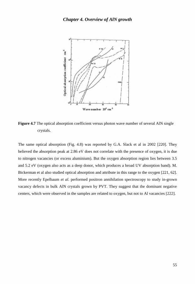
Chapter 4. Overview of AlN growth
55
Figure 4.7 The optical absorption coefficient versus photon wave number of several AlN single
crystals.
The same optical absorption (Fig. 4.8) was reported by G.A. Slack et al in 2002 [220]. They
believed the absorption peak at 2.86 eV does not correlate with the presence of oxygen, it is due
to nitrogen vacancies (or excess aluminium). But the oxygen absorption region lies between 3.5
and 5.2 eV (oxygen also acts as a deep donor, which produces a broad UV absorption band). M.
Bickerman et al also studied optical absorption and attribute in this range to the oxygen [221, 62].
More recently Epelbaum et al. performed positron annihilation spectroscopy to study in-grown
vacancy defects in bulk AlN crystals grown by PVT. They suggest that the dominant negative
centers, which were observed in the samples are related to oxygen, but not to Al vacancies [222].

Chapter 4. Overview of AlN growth
56
Figure. 4.8 Optical absorption coefficient of AlN crystals as a function of photon energy.
For PVT growth of AlN there are more impurities than oxygen, M. Bickermann and co-workers
have reported C (which mainly comes from the graphite crucible and graphite furnace) and
different metal contaminations. Table 2 shows the chemical analysis of impurities in the grown
AlN boule by this group. As shown in this table the carbon and oxygen are significant impurities.
There is also W contamination because they used a tungsten crucible [221]. Carbon is highly
soluble in AlN and can appear as Al2OC. Formation of Al4C3 is also possible [174]
C O W Na Si Ti S P As Fe Zn
∼100 ∼86 7.9 7.3 2.5 2.5 1.3 0.56 0.23 0.15 0.12
Table. 4.1 Chemical analysis of impurities in the grown AlN boule (all values in ppm wt %).

Chapter 5. Characterization methods
57
Chapter 5
Characterization methods
5.1 Optical microscopy with Nomarski interference contrast
The first step of our surface morphology study of grown materials was done by an optical
microscope with Nomarski interference contrast. It is a useful tool for imaging of defects and
Figure 5.1 a) Photo of the opitical microscope used in this thesis. b) Schematic of the principle
of Nomarski interference contrast.
Polarizer
Mirror
Nomarski prism
Objective lens
Sample
Ordinary rayExtraordinary ray
Polarizer
Mirror
Nomarski prism
Objective lens
Sample
Ordinary rayExtraordinary ray
Polarizer
Mirror
Nomarski prism
Objective lens
Sample
Ordinary rayExtraordinary ray
Polarizer
Mirror
Nomarski prism
Objective lens
Sample
Ordinary rayExtraordinary ray

Chapter 5. Characterization methods
58
obtaining information about their formation mechanism. The main principle of the Nomarski
interference contrast is based on the difference of the optical path (Fig. 5.1).
Interference contrast makes use of polarized light that is divided by a Nomarski prism into
two orthogonal light packets. These slightly displaced light packets hit the specimen at two
different points and return to the prism through different paths. The differences in the routes of
the reflected packets will produce interference contrasts in the image when the packets are
recombined by the prism upon their return. Surface defects or features such as etch pits and
cracks that are difficult to see under bright field illumination can stand out clearly under
Nomarski mode.
5.2 KOH etching
Etching is a reasonable, reliable and simple method to study interfaces, polarity of surface,
analyze the structure and density of dislocations and other defects in III-nitrides. Defect-selective
etching produces etch hillocks or pits on the surface (see Fig.2.4) due to the different etching rate
at defects, which are caused by chemical and structural dissimilarity due to surrounding
dislocations by stress and impurities. This method of measuring dislocation density has some
advantages such as investigate on large area, inexpensive, simple, and not requiring any special
sample preparation (e.g. like for TEM). As a disadvantage, only defects, which penetrate the
etched surface, can be visualized; defects running parallel to it are not recognizable. And, of
course, this is a destructive method.
In the self-seeding growth process the crystal facing the nucleation surface is
predominately N-polar and in seeded growth on Si face of SiC substrates the growing surface has
Al-polarity [74]. Etching of AlN in aqueous potassium hydroxide (KOH) solution is effective in
identifying crystal polarity. The Al polarity is more inert than the N-polarity, which Al-polarity
remains unchanged after etching in an aqueous KOH solution (45 wt%) at 60 oC for 10 minutes,
while at the same condition N-polarity surface forms hexagonal hillocks after etching.
It was shown that defect-selective etching is best performed in molten eutectic NaOH–
KOH at temperatures ranging from 170 to 360 oC depending on the AlN face to be etched [77].
Chapter 5. Characterization methods
59
After etching in the eutectic KOH/NaOH alloy, hexagonal pits formed on the Al polar AlN (0 0 0
1) crystals. AlN crystals with N-polarity form hexagonal hillocks after etching. Etching in
KOH/NaOH and KOH/NaOH + MgO (which increases the etchant viscosity) shows that it is
reliable for quick assessment of the dislocation density in Al polarity by comparing the calculated
results of etching pattern with synchrotron white beam X-ray topography (SWBXT) scan. The
most favorable etching parameters depend on polarity, defect type, density and distribution. The
etching temperature for Al-polarity is in the range of 350– 380 oC, which is typically 50-100 oC
higher than that for N-polarity, indicating higher stability of Al face.
In the present work, to study interfaces between the substrate and AlN crystal, defect
density, and the polarity of the AlN layer, surface etching was performed in molten KON and
aqueous KOH solution. As no etching was observed on the (0001) surfaces of AlN free standing
crystals in aqueous KOH solution, they are identified as Al-polar surfaces. The estimated
dislocation density by molten KOH was confirmed by TEM measurement results.
5.3 High-resolution X-ray diffraction
X-ray diffraction (XRD) is a non-destructive techniques and can be applied to the most of solid
samples without any special sample preparation. It is a versatile technique used for qualitative
and quantitative analysis of a crystalline materials. This experimental technique has been used to
determine the overall structure of bulk solids, including lattice constants, identification of
unknown materials, orientation of single crystals, orientation of polycrystalline, stress, texture,
films thickness, etc. A schematic of the basic geometry in the XRD is shown in Fig. 5.2.
The information provided by XRD is concerned with periodicity in a structure. Each atom in a
periodic structure acts as a point of scattering for waves. The X-rays reflected by the sample will
interfere constructively when they satisfied the Bragg’s law
θsind2λn = (5.1)

Chapter 5. Characterization methods
60
Figure 5.2 Schematic of the basic geometry in XRD
where n is integer, λ is the wavelength of X ray beam, d is the distance between periodic atoms,
and θ is diffraction angle. The constructive interference requires that the path difference (2dsinθ)
between the scattered rays is equal to an integer number of X-rays wavelength (Fig. 5.3). Since
periodicity and symmetry are components of ordered crystal structures, XRD provides
information regarding crystal structure. Distortions or alterations to the periodic structure can also
be observed through distortions in the x-ray diffractogram, this gives information regarding
texture, grain size, epitaxy and even residual stress.
Figure 5.3 Schematic of Bragg reflection from lattice planes in a polycrystalline solid.

Chapter 5. Characterization methods
61
Plotting the angular positions and intensities I (I over 2θ) of the resultant diffracted peaks of
radiation produce a pattern, which is characteristic of the sample. Where a mixture of different
phases is present, the resultant diffractogram is formed by addition of the individual patterns.
On the other hand, XRD can be viewed through the von Laue construction and the Ewald
sphere. As shown in Figure 5.4, a set of lattice planes separated by a distance d are represented in
the reciprocal space by a line of points separated by 2π/d along the direction normal to the lattice
planes. In Ewald sphere construction, a sphere with the incident X-ray wave vector ki as radius
vector is drawn, so that ki ends at the origin of the reciprocal space. Diffraction occurs if a
reciprocal lattice point, at the scattering vector G, lies on the surface of the sphere. The direction
of the scattered X-ray wave vector ks is thus determined by ks = ki + G . For elastically scattering
of x-ray on the sample we have
λ
π2kik s == (5.2)
the resulting reciplocal scattering vector G, then given by
θsinλ
π4kkG si =−= (5.3)
where λ is the X-ray wavelength, θ the angle between the incident X-ray and the atomic plane.

Chapter 5. Characterization methods
62
Figure. 5.4 Schematic showing the Ewald sphere.
A sample during performing XRD analysis can have many methods to rotating as shown in Fig.
5.2. Each method gives different information regarding the crystal of interest. The common XRD
scanning is mentioned in the following.
The most common type of XRD carry out is the so-called θ-2θ scans. In this method,
during the scanning both ψ and φ are constant at particular values. The incoming beam angle, ω
(= θ), and the reflected angle that is scanned, 2θ, are varied in tandem. In practice, the x-ray
source is fixed and sample moves along the θ axis while the detector moves in the θ axis at twice
the speed. In vector space, one can imagine the incident wave vector, ki, remaining constant,
while the reciprocal lattice is rotated (as the crystal rotates around θ). A peak is formed when the
Ewald sphere cuts the reciprocal lattice.
Omega is another important XRD measurement, this scan using to determine the
relationship of planes with the surface of single crystal samples and to conclude the full width
half-maximum (FWHM) of the peak of interest. Surfaces of single crystal samples may have
misorientation in respect to the orientation of interest, a small offset can be determined with such

Chapter 5. Characterization methods
63
an omega scan. The detector and x-ray source are fixed while the sample is rotated a few degrees
in the ω (θ) direction.
In order to determine preferred orientation or epitaxial relationship between substrate and
grown layer pole figure technique is suitable. A pole figure can be measured for each crystalline
peak that is present in the material. The incoming beam angle and reflected beam angle, θ and 2θ,
are fixed during the scanning at a particular value corresponding to an expected peak, while the
sample rotating around φ is performed for each ψ value. The result can be displayed in1, 2, 2,5 or
3 dimensional plots. An example of a 2 dimensional pole figure is shown in [194].
Reciprocal space mapping (RSM) is a valuable XRD tool when ordinary θ-2θ XRD
investigations are limited due to overlapping reflections or when strain fields exist within the
grain. Basically RMS builds on wave vector translation into the reciprocal space, as mention
above. By accumulation of a series of ordinary ω-2θ scan with an ω offset between each scan, the
areas of reciprocal space can be mapped (Fig. 5.4). As a result, a 2D map of the intensity
distribution within a certain area is displayed as a contour-plot. The intensity distribution and the
shape of RSM provide important information, such as film –substrate mismatch, dislocation
density, stress, crystal quality and lattice parameter In this thesis work, a Philips X’pert X-ray
diffractometer with Cu Kα1 radiation (λ=1.5406 Å) was used for all high-resolution X-ray
diffraction (HR-XRD) measurements.
5.4 Scanning electron microscopy (SEM) and cathodoluminescence
In 1942, the first SEM was developed and commercialized around 1965. In scanning electron
microscopy (SEM) an electron beam is used to scan the surface of a sample and create a three-
dimensional image of the specimen. SEM can be used for various purposes including topographic
studies, chemical composition, elemental mapping, elemental analysis by energy dispersive x-
rays (EDX), and microstructure analysis. The measurement is nondestructive for the sample and
also any difficult preparation of samples, as we needed for TEM measurement, are prevented.
The combination of easy to use, large depth focus, high magnification, and good resolution make
the SEM technique one of the most useful surface sensitive instruments used in research. The

Chapter 5. Characterization methods
64
experimental setup consists of an electron gun, column, scanning system, substrate chamber, and
detectors, as shown in Fig. 5.6. They can work in two modes, which primary and secondary
electrons.
Figure 5.5 Schematic of the primary components of a SEM.
Primary electrons are thermionically or field emitted by a cathode filament (W or LaB6)
or a filed emission gun (W-tip) and after that accelerated with high energy typically 1-30KeV.
The electron beam is steered with scanning coils over the area of the interest. Upon interaction
with material, the primary electrons decelerate as well as losing their energy by transferring it
non-elastically to other atomic electron and to the lattice. Due to continuous scattering events the
primary beam spreads up with different energies depending on source origin, as shown in Fig.
5.6a. The interaction volume with various electrons emitted and their respective energy is shown
in Fig 5.6b. Due to the interactions of high-energy incident electrons with the conduction band
electrons in the sample, the secondary electrons, which are produced within a very short distance

Chapter 5. Characterization methods
65
from the surface, are able to leave the sample and be collected by the detector. Since this mode
guarantees high resolution of the topographical images, it is the most common mode of the SEM.
Secondary electrons (1-50eV) are mostly used for, (I) imaging topographically, (II) contrast and
reproduce the surface, (III) high energy elastically backscattered, electrons depend on the atomic
number (Z) of the element, which is useful to obtain Z-contrast, (IV) X-ray characteristic can be
used to qualitatively and quantitatively analyze the elemental composition and distribution in the
sample.
Figure 5.6 a) Electron interactions with the surface during electron bombardment. b) Type of
electrons and corresponding energies of the emitted electrons after element
interaction. c) Effect of surface topography on electron emission [223].
Cathodoluminescence (CL) is a measurement technique suitable to examine the optical
properties of simple and complex semiconductor structures spatially, spectrally and time-
resolved. The focused beam of a scanning electron microscope is scanned over the sample (plan
view or cross section) and excitation of carriers results in luminescence from the sample, which is
subsequently detected with a variety of monochromator/detector combinations. There are two
cathodoluminescence modes- CL spectroscopy and CL microscopy. In the spectroscopy mode a
luminescence spectrum from a specified region of the sample is obtained, and in the microscopy
mode luminescence maps of the regions are displayed. The application of CL can be to evaluate:

Chapter 5. Characterization methods
66
(I) space distribution of luminescence and therefore the space distribution of defects or impurities
that give rise to the CL, (II) the influence of mechanical defects on the distribution of
luminescence centers, (III) electronic band structure of the material, (IV) microcharacterization of
semiconductor devices.
Luminescence is the emission of light from a solid, when carriers excited by some form of
energy to excited states relax radiatively to the ground state. Electron beam is used as an
excitation source in cathodoluminescence. The luminescence process is due to electronic
transitions from higher energy state including the conduction band to the lower energy state such
as the valence band. It may also occur between defect levels placed within the forbidden
bandgap. There are many transition processes that may occur, as shown in Fig. 5.7.
Figure 5.7 Radiative recombination after exciting electron-hole pair in a semiconductor. The
following recombinations are denoted in the figure by B-B (band to band), FE (free
exciton), D-BE (donor bound exciton), FB (free-to-bound exciton), and DAP (donor-
acceptor pair).
Upon the excitation with energy higher than the bandgap, free electrons are formed in the
conduction band together with free holes in the valence band; these carriers will recombine in the
relaxation process. This is an intrinsic luminescence. If an electron and hole have Coulomb
interaction and form a pair, an exciton may be formed, this is called a free exciton (FE) as it is
Chapter 5. Characterization methods
67
mobile in the lattice. A free exciton may be captured by a defect or an impurity, resulting in
bound exciton (BE). There is also a possibility for a hole (electron) bound to an acceptor (donor)
to recombine with an electron (hole) directly from the conduction (valence) band. These are
transitions into the localized states in the bandgap. They are called free-to-bound transitions.
Finally, a radiative recombination may occur between an electron bound to a donor and a hole
bound to an acceptor resulting in donor to acceptor pair (DAP) luminescence. Both donor and
acceptor are being charged in the process, the donor positively and the acceptor negatively. The
Coulomb interaction between them yields an additional energy in the final state. This energy is
added to the radiative recombination and depends on the relative distance between the donor and
acceptor (R) impurities and is only possible with the assistance of phonons. CL can be performed
at room temperature, but to reduce noise and thermal line-broadening cooling of the specimen to
about 4 K is preferable in many cases. Thus the shallow impurity transitions may be resolved.
5.5 Atomic force microscopy The surface morphology of AlN was studied by using the taping mode AFM in a Nanoscope IIIa
system (Digital Instrument, Santa Barbra, CA). The atomic force microscope (AFM) or scanning
force microscope (SFM) was invented in 1986 by Binnig, Quate and Gerber. Atomic force
microscopy has become an important surface analytical method because of this technique can
give information about the surface morphology on nanometer scale without vacuum condition
requirement. Like all other scanning probe microscopes, the AFM utilizes a sharp probe moving
over the surface of a sample in a raster scan. In the case of the AFM, the probe is a tip (usually
couple of micrometers long and often less than 100 Å in diameter) on the end of a cantilever (100
to 200 µm long), which bends in response to the force between the tip and the sample (Fig. 5.8).
As shown in Fig 5.8 the cantilever flexes, the light from the laser is reflected onto the split photo-
diode. By measuring the difference signal, changes in the bending of the cantilever can be
measured. Since the cantilever obeys Hook’s law for small displacements, the interaction force
between the tip and the sample can be found. The high precision control of the tip movement is
made by the use of piezoelectric ceramics. The scanner is capable of

Chapter 5. Characterization methods
68
Figure 5.8 A schematic of AFM operation.
subangstrom resolution in x-, y- and z-directions. The z-axis is conventionally perpendicular to
the sample. AFMs can achieve a resolution in the x-y plane ranging from 0.1 to 1.0 nm and in the
z direction is 0.01 nm (atomic resolution), and unlike electron microscopes, can image samples in
air and under liquids.
In principle, AFM resembles a number of refinements that enable it to achieve atomic-
scale resolution: sensitive detection, flexible cantilevers, sharp tips, high-resolution tip-sample
positioning, and force feedback. The AFM can be operated in two principal modes: with
feedback control, and without feedback control. If the electric feedback is switched on, then the
positioning piezo which is moving the sample (or tip) up and down can respond to any changes in
force, which are detected and alter the tip-sample separation to restore the force to predetermined
value. This mode of operation is known as constant force, and usually enables a fairly faithful
topographical image to be obtained. If the feed back electrons are switched off, then the
microscope is said to be operating in constant height or deflection mode. This is particularly
useful for imaging very flat samples at high resolution. Often it is best to have a small amount of

Chapter 5. Characterization methods
69
feedback-loop gain, to avoid problems with thermal drift or the possibility of a rough sample
damaging the tip and/or the cantilever. The force, most commonly associated with AFM, is an
interaction force called the van der Waals force.
Figure 5.9 Interatomic force vs. distance curve
The dependence of the van der Waals force upon the distance between the tip and the
sample is shown in Fig. 5.9. Two distance regimes are labeled in the figure, as the contact regime
and non-contact regime. In the contact regime, the cantilever is held less than a few angstroms
from the sample surface, and the interatomic force between the cantilever and the sample is
repulsive. In the non-contact regime, the cantilever is held on the order of tens to hundreds of
angstroms from the sample surface, and the interatomic force between the cantilever and the
sample is attractive (largely result of the long-range van der Waals interaction). The force
between the tip and the sample surface is very small, typically less than 10-9 N. The taping mode
technique, which is used in this work, is another technique. This technique is performed by
alternatively placing the tip in contact with the surface, to provide the high resolution, and lifting

Chapter 5. Characterization methods
70
the tip off the surface to avoid dragging the tip cross the surface. Tapping mode prevents the tip
from sticking to the surface and causing damage during scanning. One of the most important
factors influencing the resolution of the image, which may be achieved with an AFM, is the
sharpness of the tip. The best tips may have the radius of curvature of only around 5nm. The need
for sharp tips is normally explained in terms of tip convolution. This term is often (slightly
incorrectly) to group together any influence, which the tip has on the image. The main influences
are: broadening, compression, interaction forces, and aspect ratio.
Tip broadening takes pale when the radius of curvature of the tip is comparable with, or
grater than the size of the feature trying to be imaged, as the tip scan over the specimen, the side
of the tip makes contact before the apex, and the microscope begins to respond to the feature.
Compression occurs when the tip is over the feature trying to be imaged. The aspect ratio (or
cone angle) of particular tip is crucial when imaging steep sloped features. Apart from the
topographic imaging that can be obtained, the phase imaging mode, which goes beyond the
simple topographic mapping to detect variation in composition, adhesion, friction, and
viscoelasticity, etc. is possible. In this phase mode the image is obtained through the phase lag of
the cantilever oscillation, relative to the signal sent to the cantilever piezo driver, and the phase
lag corresponds to the variation in material properties such as adhesion and viscoelasticity
providing nanometer-scale information about surface structure nit obtained by other scanning
probe microscopy techniques.
5.6 High-resolution transmission electron microscopy
The base of operation of a transmission electron microscope (TEM) is similar to an optical
microscope; the only differences are that the electron microscope uses electrons to illuminate the
sample instead of photons, and magnetic lenses instead of glass lenses. TEM was used to study
nonstructural and microstructures of biological system, semiconductors, and alloys TEM. It
works by accelerating high energetic electrons to penetrate the sample. Materials for TEM must
be specially prepared to thicknesses that will allow electrons to be transmitted through the sample

Chapter 5. Characterization methods
71
and high vacuum is required to enable the electrons to reach the sample (long mean free path of
the electrons). Figure 5.10 shows a schematic of the TEM electron optics.
Figure 5. 10 Schematic of the TEM electron optics
A TEM system consists of the following components:
1- Electron source at high negative potential surrounded by “Wehnelt cylinder” and an anode,
which forms beam of electrons.
2- Two condenser lenses to focus the electron beam on the sample.
3- Objective lens, which is a very important and critical component in the microscope since the
resolution highly depends on it.
4- Intermediate and projector lenses. Both of them are used for the image magnification.
5- Objective aperture in the objective back focal plane to improve the contrast.

Chapter 5. Characterization methods
72
There are two different ways to create the image in TEM, phase contrast and diffraction
contrast. In phase contrast, electrons leaving the TEM sample are recombined so that the phase
differences from two or more beams are converted into intensity differences in the image, while
in the diffraction contrast the diffracted electrons leaving the exit surface of a crystalline TEM
sample are either collected for, or prevented from, contributing to an image.
5.7 Raman spectroscopy Raman spectroscopy is a valuable tool to structural characterization of a semiconductor. Since it
is sensitive to strain and crystal structure changes, it can be used to detect stress and to
characterize the crystalline quality. Raman spectroscopy is also capable of determining the free
carrier concentration and sample composition. When a light is scattered from the surface of a
sample, the scattered light mainly has the same wavelengths that were incident on the sample.
However, scattered light of different wavelengths, representing the interaction of incident light
with optical phonons (Raman scattering), is also detectable, though their intensity is low. Raman
spectrum is provided by measuring the intensities of such Raman scattered light. The Raman
spectroscopy measurements in this thesis were performed at room temperature in backscattering
geometry from the (0001) surface of the wurtzite structure (z direction). The polarization
configuration was either parallel z(x,x)-z or perpendicular z(x,y)-z. For excitation, the 488 nm
laser line of an Ar laser was used.

Chapter 6. Summary
73
Chapter 6
Summary
6.1 Main results
- Physical vapor transport (PVT) principle has been implemented for synthesis of AlN on
4H-SiC in sublimation epitaxy close space configuration previously developed in the
group for growth of SiC thick epitaxial layers. It has been shown that the AlN crystal
morphology is responsive to the growth conditions given by temperature (1650-1900oC)
and nitrogen pressure (200-800 mbar) and each morphology kind occurs within a narrow
window of growth parameters. AlN crystal habit then can be assorted from platelet-like to
needles, columnar structure, continuous layers and free-standing quasi bulk material.
(Papers I and III).
These results represent a valuable contribution to the crystal growth field because
they address morphological diversity of AlN and its dependence on the growth
conditions (7 citations to Paper I).

Chapter 6. Summary
74
- Controlled operation conditions for PVT growth of well aligned perfectly oriented arrays
of AlN highly symmetric hexagonal microrods have been elaborated and the mechanism
of microrod formation has been elucidated. Special patterned SiC substrates have been
created which act as templates for the AlN selective area growth. The pattern is shaped
during the initial stage of the growth process when conditions for thermal etching of SiC
are set, resulting in asymmetric hexagonal pits at the outcrop of threading dislocations in
the substrate. This is only possible if Si-face of 8o off cut (from [0001]) 4H-SiC
commercial wafers is overgrown by a thick homoepitaxial layer using sublimation epitaxy.
This is a main distinction from other researchers’ approach, which utilizes commercial
SiC wafers. (Papers II, IV and V)
Such arrays of hexagonally facetted microrods are reported for the first time. It is
believed that the structures and the understanding of their growth mechanism
will possible have a constructive impact on the group III-nitrides growth
developments.
- The microrods revealed an excellent feature of boundary free coalescence with growth
time, eventually forming ~120 µm thick AlN layer which can be easily detached from the
SiC substrate due to a remarkable performance of structural evolution. It was discovered
that the locally grown AlN microrods emerge from sharp tipped hexagonal pyramids
which consist of the rare 2H-SiC polytype and a thin AlN layer on the surface. Since 2H-
SiC is a metastable phase, this result was unexpected but it can be explained by the
presence of AlN species in the growth environment. Two unique consequences appear
from the finding, the first is that the 2H-SiC polytype facilitates the nucleation of wurtzite

Chapter 6. Summary
75
AlN , and the second is that the bond between the low angle apex of the pyramids and the
AlN layer is very week, thus allowing an easy separation to yield free standing wafers.
The procedure is fully reproducible and can be applied to extend the diameter of the free
standing wafers up to the size of the SiC substrate, ultimately 4 inch, with a high growth
rate, ~250µm/hour. (Papers VI and VIII)
These results point to a two folded contribution to the field: (i) Fundamental issues
of self-organized structure formation as illustrated by pyramid growth, synthesis
and growth of single crystalline 2H-SiC, and boundary free coalescence of hexagonal
highly oriented microrods; (ii) A possible route to fabrication of large diameter AlN
wafers.
- The fabricated free standing AlN wafers (diameter of 10 mm) have been entirely
characterized in respect of structure, composition, defects, and polarity by means of x-ray
diffraction methods, scanning electron microscopy with energy dispersive analysis,
cathodoluminescence, transmission electron microscopy and hot KOH etching. It has
been unambiguously evidenced that the fabricated material is stress-free wurtzite AlN
with a dislocation density of ~2x106 cm-2. The top face is Al-terminated. The prismatic
facets of the AlN microrods are nearly to atomically flat and their coalescence by lateral
enlargement is most probably defect free, therefore we believe that the measured
dislocation density is related to misfit dislocations generated due to although small but
still existing in plane lattice and thermal mismatch between AlN and SiC. (Papers VI,
VII and VIII)

Chapter 6. Summary
76
- AlN nanowires with an aspect ratio as high as 600 have been grown with a high growth
rate. Again, they have perfect alignment along the c-axis of the wurtzite structure with
small tilt given by the orientation of the SiC substrate. The length of the nanowires can
reach ~100 µm with a growth rate ~800 mm/hour, which may be not surprising for
whisker growth. Worth noting is that we are dealing here with vapor-solid growth
mechanism which is catalyst free and is not enhanced by a liquid phase as in the VLS
model. The nanowires posses a single crystal structure with high perfection, since neither
dislocations nor stacking faults were revealed. (Papers IV, V and IX).
Long and ordered AlN nanowires of the observed extent are reported for the first
time and their growth mode has been elucidated. They are intriguing for several
applications, e.g. employing their mechanical strength and piezoelectrical
properties. Most of all they are fascinating objects for high efficiency field emitters.
6.2 Future outlook
From the prospective of potential and already realized device applications of group III-nitride
materials and considering a relative immaturity of substrate technology today, we believe that
extensive and innovative research is needed to comply with the community expectations. The
results attained in this Thesis have fuelled our interest in the following research topics for
future work.

Chapter 6. Summary
77
- Exploration of the proposed growth concept to enlarge the free standing AlN wafers
up to a size provided by commercially available SiC four inch wafers. Implementation
of AlN wafers, fabricated by the present method, as seeds for large boule growth.
The quality of epitaxial structures grown on this substrate material can be additionally
secured by depositing AlN buffer layers using the MOCVD technique.
- Further insight to the microrod boundary free coalescence and addressing the issue of
declining the dislocation density in the free standing material.
- Detailed analysis of impurities in AlN with an emphasis on oxygen and related deep
level defects by means of EPR methods. Elaboration on doping with Si for field
emitter applications. Focus on electrical measurements.
- Prioritized efforts on (i) field emission tests of AlN nanowires, and (ii) MOCVD
growth on free standing AlN substrates prepared by the proposed method.
.


References
79
References
[1] J. Wu, et al., Appl. Phys. Lett. 80 (2002) 3967.
[2] V. Yu. Davydov, et al. Phys. Stat. Solidi, B 229 (2002) R1.
[3] S. Strite and H. Morkoc, J. Vav. Sci. Techol. B 10 (4) (1992) 1237
[4] E. Kuokstis, et al., Appl. Phys. Lett. 79 (2001) 4375.
[5] S. Nakamura, et al. Jpn. J. Appl. Phys. Part 2, 34 (1995) L1332.
[6] T. Mukai, H. Narimatsu, and S. Nakamura, Jpn. J. Appl. Phys., Part 2, 37 (1998) L479.
[7] S. Nakamura, M. Senoh, A. Nagahama, N. Iwasa, T. Matsushita, and T. Mukai, Appl.
Phys. Lett. 76 (2000) 22.
[8] R.R. Siergiej. et al, Mater. Sci. Eng. B61/62 (1999) 9.
[9] S. C. Jain, M. Willander, J. Narayan, R.Van Overstraeten, JAP 87 (2000) 965.
[10] S. N. Mohammad, H. Morkoc, Prog. Quant. Electr. 20 (1996) 361.
[11] O. Ambacher, J. Phys. D 31 (1998) 2653.
[12] F. Brieglib and A. Geuther, Ann. Chem. 123 (1862) 228.
[13] F. Fichter and G. Osterheld, Z. Electrochem. Soc. 121 (1915) 159.
[14] W. C. Johnson, J. Parsons, and M. C. Crew, J. Phys. Chem. 36 (1932) 2561.
[15] R. Juza and H. Hahn, Z. Anorg. Allgem. Chem. 234 (1938) 282.
[16] R. Juza and H. Hahn, Z. Anorg. Allgem. Chem. 244 (1940) 133.
[17] H. Grimmeiss and Z. H-Koelmans, Nature (London) 14a (1659) 264
[18] H. P. Maruska and J. J. Tietjen, Appl. Phys. Lett. 15 (1969) 327.
[19] J. I. Pankove, E. A. Miller, and J. E. Berkeyheiser, RCA Rev, 32 (1971) 383.
[20] J. I. Pankove, E. A. Miller, and J. E. Berkeyheiser, J. Lumin 5 (1972) 84.
[21] S. Yoshida, S. Misawa, and S. Gonda, App. Phys. Lett. 42 (1983) 427.
[22] H. Amano, I. Akasaki, K. Hiramatsu, and N. Koide, Thin Solid Films 163 (1988) 415.
[23] I. Akasaki, H. Amano, Y. Koide, K. Hiramatsu, and N. Sawaki, J. Cryst. Growth 98
(1989) 209.
[24] S. Nakamura, Jpn. J. Appl. Phys. Part 2, 30 (1991) L1705.

References
80
[25] S. Nakamura, M. Senoh, and T. Mukai, Jpn. J. Appl. Phys. Part 2 30 (1991) L1708.
[26] H. Amano, I. Akasaki, T. Kozawa, K. Hiramatsu, N. Sawaki, K. Ikeda, and Y. Ishi, J.
Lumin. 40-41 (1988) 121.
[27] S. Nakamura, T. Mukai, M. Senoh, and N. Iwasa, Jpn. J. Appl. Phys. 31 (1992) L139.
[28] M. A. Khan, R. A. Skogman, and J. M. Van Hove, Appl. Phys. Lett. 56 (1990)1257.
[29] K. Itoh, T.Kawamoto, H. Amano, K. Hiramatsu, and I. Akasaki, Jpn. J. Appl. Phys. Part 1
30 (1991) 1924.
[30] S. Nakamura, T. Mukai, M. Senoh, S.Nagahama, and N. Iwasa, J. Appl. Phys. 74 (1993)
3911.
[31] M. A. Khan, J. N. Kuznia, A. R. Bhattarai, and D. T. Olsen, Appl. Phys. Lett. 62 (1993)
1787.
[32] I. Akasaki, et al., Jpn. J. Appl. Phys. 34 (1995) L1517.
[33] O. H. Nam, et al. Appl. Phys. Lett, 71 (1997) 2638.
[34] S. Nakamura, et al., Jpn. J. Appl. Phys., 36 (1997) L1568.
[35] T. S. Zheleva, et al., MRS Internet J. Nitride Semicond. Res. 4S1 (1999) G3.38.
[36] Following link, http://www.nichia.com/about_nichia/2002/2002_030401.html
[37] S. Zamir, B. Meyler, E. Zolotoyabko and J. Salzman, J. Crystal Growth 218 (2000) 181.
[38] C.R. Miskys, M.K. Kelly, O. Ambacher and M. Stutzmann, Phys. Stat. Sol. C 0 (2003)
1627.
[39] M. Zetterling, M. Ostling, N. Nordell, O. Schon, and M. Deschler, M. App. Phys. Lett. 70
(1997) 3549.
[40] M. Losurdo, et al. App. Phys. Lett. 86, (2005) 021920.
[41] M. Imura, et al. Jpn. J. Appl. Phys. 45, No. 11, (2006) 8639.
[42] Y. Kumagai, T. Yamane and A. Koukitu. J. Cryst. Growth, 281 (2005) 62.
[43] H. Amano, et al. J. Appl. Phys. 37 (1998) L1540.
[44] B. Beaumont, P. Vennéguès and P. Gibart, Phys. Stat. Sol. B 227 (2001) 1.
[45] T.S. Zheleva, S.A. Smith, D.B. Thomson, K.J. Linthicum, P. Rajagopal and R.P. Davis,
J. Electron. Mater. 28 (1999) 5.
[46] H. Lahrèche, P. Vennéguès, B. Beaumont and P. Gibart, J. Cryst. Growth 205 (1999) 245.
[47] C.I.H. Ashby, et al., Appl. Phys. Lett. 77 (2000) 3233.

References
81
[48] T. Detchprophm, et al., Jpn. J. Appl. Phys. 40 (2001) L16.
[49] I. Grzegory, S. Porowski, Thin Solid Films 367 (2000) 281.
[50] X.A. Cao and S. D. Arthur, Appl. Phys. Lett. 85, (2004) 3971.
[51] L. Vegard, Die Konstitution der Mischkristalle und die Raumfullung der Atome. Z. Phys.
5 (1921) 17.
[52] C. G. Van de Walle and J. Neugebauer, J. Appl. Phys. 95 (2004) 3851.
[53] B. Monemar, J. Mater. Sci.: Mater. Electron. 10 (1999) 227.
[54] V. Y. Davydov, et al., Phys. Stat. Sol. B 230 (2002) R4.
[55] V. M. Bermudez, T. M. Jung, K. Doverspike, and A. E. Wickenden, J. Appl.
Phys. 79 (1996) 110.
[56] F. Bernardini, V. Fiorentini, and D. Vanderbilt, Phys. Rev. B 56 (1997) R10024.
[57] K. M. Taylor and C. Lenie, J. Electrochem. Soc. 107 (1960) 308.
[58] Hashimoto, T., Wu, F., Speck, J. S. & S., Nakamura. Nature 6 (2007) 568.
[59] Martin, D., Carlin, J.F., Wagner, V., Buhlmann, H.J. & Ilegems, M. Phys. Stat.
Sol. (a) 194 (2002) 520.
[60] G. A. Slack and T. F. McNelly, J. Cryst. Growth 42, (1977) 560.
[61] J. C. Rojo, G. A. Slack, K. Morgan B. Raghothamachar, M. Dudley, and L. J.
Schowalter, J. Cryst. Growth 231 (2001) 317.
[62] M. Bickermann, B. M. Epelbaum, and A. Winnacker, J. Cryst. Growth 269 (2004)
432.
[63] Glen A. Slack, Mat. Res. Soc. Symp. Proc. 512 (1998) 35.
[64] H. Funk and H. Boehland, Z. Anorg. Allgem. Chem. 334 (1964) 155.
[65] F. Fichter and G. Oesterheld, Z. Electrochem. 21 (1915) 50.
[66] K. M. Taylor and C. Lenie, J. Electrochem. Soc. 107 (1960) 308.
[67] P. E. Evans and T. J. Davies, Nature 197 (1963) 587.
[68] T. J. Davies and P. E. Evans, Nature 207 (1965) 254.
[69] C. M. Drum, J. Appl. Phys. 36 (1965) 816.
[70] W.R.L. Lambrecht and B.Segall. Phys. Rev. B 43 (1991) 7070.
[71] Quan Li, I.W. Kim, S.A. Arnett, L.D. Marks. J. Mater. Res.17 (2002) 1224.
[72] P.E.Van Camp, V.E.Van Doren, J.T. Devreese. Phys. Rev. B 44 (1991) 9056.

References
82
[73] S. Strite and H.Morkoc. J. Vac. Sci. Technol. B 10 (1992) 1237.
[74] D. Zhuang, J . H. Edgar, L. Liu, B. Liu and L.Walker. MRS Internet J.
Nitride semicond. Res. 7 (2002) 4.
[75] A. D. Westwood and M. R. Notis, J. Am. Ceram. Soc. 74 (1991) 1226.
[76] J. Jasinski, Z. Liliental-Weber, Q. S. Paduano, and D. W. Weyburne, Appl. Phys.
Lett. 83 (2003) 2811.
[77] D.Zhuang, J.H.Edgar, B. Strojek, J. Chaudhuri, Z.Rek. Journal of Crystal Growth
262 (2004) 89.
[78] J. L. Rouviere, J. L. Weyher, M. Seelmann-Eggebert, and S. Porowski, Appl. Phys. Lett.
73 (1998) 668.
[79] T. Wethkamp, et al. Phys. Rev. B 59 (1999)1845.
[80] W. M. Yim, et al. J. Appl. Phys. 44 (1973) 292.
[81] E. Silveira, et al. Appl. Phys. Lett. 84 (2004) 3501.
[82] E. Kuokstis, et al. Appl. Phys. Lett. 81 (2002) 2755.
[83] I. Vurgaftman and J. R. Meyer, J. Appl. Phys. 94 (2003) 3675.
[84] M. Suzuki, T. Uenoyama, and A. Yanase, Phys. Rev. B 52 (1995) 8132.
[85] J. M. Wagner and F. Bechstedt, Phys. Rev. B 66 (2002) 115202.
[86] P. B. Perry, and R. F. Rutz, Appl. Phys. Lett. 33 (1978) 319.
[87] B. Luo, et al. Solid State Electron. 46 (2002) 573.
[88] R. F. Rutz, Appl. Phys. Lett. 28 (1976) 379.
[89] J. Edwards, K. Kawabe, G. Stevens, and R. H. Tredgold, Solid State commun. 3 (1965)
99.
[90] T. Pauleau, J. Electrochem. Soc. 129 (1982) 1045.
[91] T. Y. Sheng, Z. Q. Yu, and G. J. Collins, Appl. Phys. Lett. 52 (1988) 576.
[92] N. J. Barret, G. D. Grange, B. J Sealy and K. G. Stephens, J. Appl. Phys.
57 (1985) 5470.
[93] G. R. Kline and K. M. Lakin, Appl. Phys. Lett. 43 (1983) 750.
[94] C. R. Aita, C. J. Gawlak, J. Vac. Sci. Technol. A 1 (1983) 403.
[95] J. R. Mileham, et al. J. Vac. Sci. Technol. A 14 (1996) 836.
[96] C. Vartuli, S. J. Pearton, J. Lee, J. Electrochem. Soc. 143 (1996) 3681.
References
83
[97] L. J. Schowatlter, et al. MRS Internet J. Nitride semicond. Res. 5S1 (2000) W6.7.
[98] G. A. Slack, J. Appl. Phys. 46 (1975) 89.
[99] G. A. Slack, J. Phys. Chem. Sol. 34 (1973) 321.
[100] G. A. Slack, R. A. Tanzilli, R. O. Pohl, and J. W. Vandersande, J. Phys. Chem. Sol. 48
(1987) 641.
[101] R. A. Youngman, and J. H. Harris, J. Am. Ceram. Soc. 73 (1990) 3238.
[102] M. Kazan, B. Ruffle, Ch. Zgheib and P. Masri, J. App. Phys. 98 (2005)103529.
[103] T. Mattila, and R. M. Nieminen, Phys. Rev. B 55 (1997) 9571.
[104] F. Engelmark, J. Vac. Sci. Technol, A 19 (2001) 2664.
[105] X. Xu, H. Wu, F. Zhang, J. Duan, and Z. Li, Rare Metal Materials and Engineering,
31(2002) 456.
[106] D. Kapolnek, et al. Appl. Phys. Lett. 67 (1995) 1541.
[107] F.A. Ponce, B.S. Krusor, J.S.M. Jr., W.E. Plano, and D.F. Welch, Appl. Phys. Lett. 67
(1995) 410.
[108] S. Mahajan, Acta Mater. 48 (2000) 137.
[109] T. Nishida, T. Makimoto, H. Saito, and T. Ban, Appl. Phys. Lett. 84 (2004) 1002.
[110] G. Tamulaties, et al. Appl. Phys. Lett. 83 (2003) 3507.
[111] G. Tamulaties, et al. Mat. Res. Soc. Symp. Pro. 743 (2003) L3.34.
[112] J.C. Rojo, et al. Mat. Res. Soc. Symp. Proc. 772 (2002) K1.1.
[113] X. Hu, et al. Mat. Res. Soc. Symp. Proc. 743 (2003) L6.30.
[114] R. Gaska, et al. Appl. Phys. Lett. 81 (2002) 4658.
[115] X. Hu, et al. Appl. Phys. Lett. 82 (2003) 1299.
[116] S. Vaddiraju, H. Chandrasekaran, M.K. Sunkara, J. Am. Chem. Soc. 125, (2003) 10792.
[117] X. Xiang, C.B. Cao, H.Z. Zhai, B. Zhang, H.S. Zhu, Appl. Phys. A 80 (2005) 1129.
[118] J. Zhan, X. Hao, S. Wen, M. Jiang, Physica E 25 (2005) 409.
[119] A.T. Sowers, et al. Appl. Phys. Lett. 71 (1997) 2289.
[120] M. Kasu, and N. Kobayashi, Appl. Phys. Lett. 76 (2000) 2910.
[121] Y. Zhang, et al. Chem. Mater. 13 (2001) 3899.
[122] K. Komeya, J. Ceram. Soc. Jpn. 101 (1993) 1319.
[123] M. Radwan, M. Bahgat, J. Mater. Proc. Tech. 181 (2007) 99.

References
84
[124] V. Cimalla, Ch. Foerster,D. Cengher,K.Yonisch, O. Ambacher, Phys. Stat. Sol. 243
(2006) 1476.
[125] Y.J. Tian, Y.P. Jia, Y.J. Bao, Y.F. Chen, Diamond Relat. Mater. 16 (2007) 302.
[126] C.C. Tang, S.S. Fan, M.L. de la Chapelle, P. Li, Chem. Phys. Lett. 333 (2001) 12.
[127] J.H. He, et al. Adv. Mater. 18 (2006) 650.
[128] J.H. Duan, et al. J. Cryst. Growth 283 (2005) 291.
[129] J. J. Berzelius, Ann. Phys. Lpz 1 (1824) 169.
[130] A.G. Acheson, Engl. Pat, (1892) 17911.
[131] H. J. Round, Electric World, 19 (1907) 309.
[132] J. A. Lely, Ber. Deut. Keram. Ges, 32 (1955) 229.
[133] Y. M. Tairov and V.F. Tsvetkov, J. Cryst. Growth, 43 (1978) 209.
[134] L. S. Ramsdell, Am. Min. 32 (1947) 64.
[135] A. R. Verma and P. Krishna, Polymorphism and polytypism in crystals (john Wiley &
Sons Inc. New York, 1966).
[136] M. Syväjärvi, R. Yakimova, H. Jacobsson, and E. Janzén, J. Appl. Phys. 88 (2000) 1407.
[137] T. Kimoto, A. Itoh, H. Matsunami, Phys. Stat. Sol. B 202 (1997) 247.
[138] J.A. Powell and D.J. Larkin, Phys. Stat. Sol B 202 (1997) 529.
[139] Yu. A. Vodakov, E. N. Mokhov, M. G. Ramm, and A. D. Roenkov, Krist. Tech. 14
(1979) 729.
[140] M. Syväjärvi, et al. J. Cryst. Growth 197 (1999) 155.
[141] M. Syväjärvi, R. R. Ciechonski, G. R. Yazdi, and R. Yakimova, J. Cryst. Growth 275
(2005) 1103.
[142] J. A. Van Vechten, Phys. Rev. B 7 (1973)1479.
[143] W. Class, Contract Rep., NASA-Cr-I I 71 (1968).
[144] C.O. Dugger, Mat. Res. Bull. 9 (1974) 331.
[145] J. Pastrnák and L. Roscovková, Phys. Stat. Sol. 7 (1964) 331.
[146] W. J. Liua, S. J. Wub, C. M. Chenc, Y. C. Laic, C. H. Chuanga, J. Cryst. Growth 276
(2005) 525.
[147] S. Yoshida, S. Misawa, and A. Itoh, Appl. Phys. Lett. 26 (1975) 461.
[148] H.U. Baier and W. Mönch, J. Appl. Phys. 68 (1990) 586.

References
85
[149] A. Sazler, P. Kung, C.J. Sun, E. Bigan, and M. Razeghi, Appl. Phys. Lett. 64 (1994) 339.
[150] P. Kung, et al. Appl. Phys. Lett. 66 (1995) 2958.
[151] T. Kunisato, et al. Phys. Stat. Sol. C 7 (2003) 2063.
[152] T. Nagashima, et al. J. Cryst. Growth. 305 (2007) 355.
[153] G. A. Slack, and T. F. McNelly. J. Cryst. Growth 34 (1976) 263.
[154] L. Liu, J. H. Edgar. J. Cryst. Growth 220 (2000) 243.
[155] Q.Wu, et al. Diamond Relat. Mater. 13 (2004) 38.
[156] Q. Zhao, et al. Appl. Phys. Lett. 86 (2005) 193101.
[157] J. Duan, et al. J. Phys. Chem. B 109 (2005) 3701.
[158] V. Noveski, R. Schlesser, S. Mahajan, S. Beaudoin, and Z. Sitar, J. Cryst. Growth 264
(2004) 369.
[159] W. K. Burton and N. Cabrera, Discuss. Faraday Soc. 5 (1949) 40.
[160] F. C. Frank, Discuss. Faraday Soc. 5 (1949) 48.
[161] W. K. Burton, N. Cabrera, and F. C. Frank, Phil. Trans. Roy. Soc. Ser. A 243 (1951) 299.
[162] R. Ghez and S. S. Iyer, IBM J. Res. Develop. 32 (1988) 804.
[163] Y. Kumagai, et al. Phys. Stat. Sol. (c) 0 (2003) 2498.
[164] R. Schlesser and Z. Sitar, J. Cryst. Growth 234 (2002) 349.
[165] R. Dwilinski, MRS Internet J. Nitride Semicond. Res. 3 (1998) 25.
[166] H. Isobe, et al. Jpn. J. Appl. Phys. 44 (2005) L488.
[167] K. Kamei, et al. Phys. Stat. Sol. A 203 (2006) 1720.
[168] T. Nishida, T. Makimoto, H. Saito, and T. Ban, Appl. Phys. Lett. 84 (2004) 1002.
[169] R. Schlesser, R. Dalmau, Z. Sitar, J. Cryst. Growth 241 (2002) 416.
[170] P. Lu, et al. J. Cryst. Growth 310 (2008) 2464.
[171] Y. Shi, et al. phys. stat. sol. A 188 (2001) 757.
[172] B.M. Epelbaum, M. Bickermann, A. Winnacker, J. Cryst. Growth 275 (2005) e479.
[173] R.B. Campbell and H.-C. Chang, U.S. Govt. Res. Develop. Fed. Sci. Tech. Inform.
(AD-815895) (1969) 164.
[174] C.M. Balkas, et al, J. Crystal Growth 179 (1997) 363.
[175] J.H. Edgar, et al. J. Crystal Growth 246 (2002) 187.
[176] L. Liu, B. Liu, Y. Shi, J.H. Edgar, MRS Internet J. Nitride Semicond. Res. 6 (2001) 7.

References
86
[177] Y. Shi, et al. J. Crystal Growth 233 (2001) 177.
[178] L. Liu, J.H. Edgar, Mater. Sci. Eng, R37 (2002) 61.
[179] R. Dalmau, R. Schlesser, B.J. Rodriguez, R.J. Nemanich, Z. Sitar, J. Crystal Growth
281 (2005) 68.
[180] R. T. Bondokov, K. E. Morgan, G. A. Slack, and L. J. Schowalter. MRS, Symp. Proc.
955 (2007) 0955-103-08.22.
[181] G.R. Yazdi, M. Syväjärvi, and R. Yakimova. Appl. Phys. Lett. 90 (2007) 123103.
[182] G. R. Yazdi, M. Syväjärvi and R. Yakimova. Phys. Scr. T126 (2006) 127.
[183] B.M. Epelbaum, et al. J. Cryst. Growth 305 (2007) 317.
[184] B.M. Epelbaum, C. Seitz, A. Magerl, M. Bickermann, and A. Winnacker, J. Cryst.
Growth 265 (2004) 577.
[185] S.Y. Karpov, et al. Phys. Stat. Sol. A 176 (1999) 435.
[186] L. Liu and J.H. Edgar, J. Electrochem. Soc. 149 (2002) G12.
[187] R. Schlesser, R. Dalmau, D. Zhuang, R. Collazo, and Z. Sitar, J. Cryst. Growth 281
(2005) 75.
[188] K. Balakrishnan, et al. Mat. Res. Soc. Symp. Proc. 831 (2005) 607.
[189] R. Dalmau, B. Raghothamachar, M. Dudley, R. Schlesser and Z. Sitar, Mat. Res. Soc.
Symp. Proc. 798 (2004) Y 2.9.
[190] B. Liu, Y. Shi, B. Liu, J. H. Edgar, D. N. Braski, Mat. Res. Soc. Symp. Proc. 639 (2001)
G3.13.1.
[191] L. Liu, et al. Phys. Stat. Sol. A 188 (2001) 769.
[192] L. Liu, B. Liu, J. H. Edgar, S. Rajasingam, M. Kuball, J. Appl. Phys. 92 (2002) 5183.
[193] Y. Shi, et al. MRS Internet J. Nitride Semicond. Res. 6 (2001) 5
[194] Submitted manuscript included in this thesis
[195] S. Krukowski, J. Chem. Phys. 117 (2002) 5866.
[196] N. L. Yakovlev, J. C. Rojo, L. J. Schowalter, Surf. Sci. 493 (2001) 519.
[197] P.M. Dryburgh, J. Cryst. Growth 125 (1992) 65.
[198] A. S. Segal, et al. J. Cryst. Growth 211 (2000) 68.
[199] L. H. Dreger, V. V. Dadape, and J. L. Margrave, J. Phys. Chem. 66 (1962) 1556.
[200] M. V. Averyanova, et al. MRS Internet J. Nitride Semicond. Res. 1 (1996) 31.
References
87
[201] G. Meloni and K. A. Gingerich, J. Chem. Phys. 113 (2000) 10978.
[202] B. D. Leskiw and J. A. W. Castleman, J. Chem. Phys. 114 (2001) 1165.
[203] Y. Li and D. W. Brenner, Ph. R. L. 92 (2004) 075503.
[204] H. Lu, J. Li, R. A. Loomis, L. M. Wang, and W. E Buhro, Nat. Mater. 2 (2003) 517.
[205] Y. Wu and P. Yang, Adv. Mater. 13 (2001) 520.
[206] A. Gustafsson, F. Reinhardt, G. Biasiol, E. Kapon, Appl. Phys. Lett. 67 (1995) 3673.
[207] J. Noborisaka, J. Motohisa, T. Fukui, Appl. Phys. Lett. 86 (2005) 213102.
[208] R. Wagner and W. Ellis, Appl. Phys. Lett. 4 (1964) 89.
[209] E. Calleja et al., Phys. Stat. Sol. B 244 (2007) 2816.
[210] Q.L. Liu, Y. Bando, J.Q. Hu, J. Cryst. Growth 306 (2007) 288.
[211] Q. Wu, et al. J. Am. Chem. Soc. 125 (2003) 10 176.
[212] C. Liu, et al. J. Am. Chem. Soc. 127 (2005) 1318.
[213] Q. Zhao, J. Xu, X. Y. Xu, Z. Wang, D. P. Yu, Appl. Phys. Lett. 85 (2004) 5331.
[214] L. W. Yin, et al. Adv. Mater. 17 (2005) 110.
[215] K. J. Lee, D. H. Ahn, Y. S. Kim, J. Am. Ceram. Soc. 83 (2000) 1117.
[216] Q. Zhao, et al. Appl. Phys. Lett. 86 (2005) 193101.
[217] J. Duan, et al. J. Phys. Chem. B 109, (2005) 3701.
[218] H. He, Jr., et al. Adv. Mater. 18 (2006) 650.
[219] J. H. Harris, R. A. Youngman, and R. G. Teller, J. Mate. Sci. 5 (1990) 1763.
[220] G. A. Slack, L. J. Schowalter, D. Morelli, J. A. Freitas Jr. J. Cryst. Growth 246 (2002)
287.
[221] M. Bikermann, B. M. Epelbaum, and A. Winnacker. Phys. Stat. Sol. C 0 (2003) 1993.
[222] F. Tuomisto, J.-M. Mäki, T. Yu. Chemekova, Yu. N. Makarov, O. V. Avdeev, E. N.
Mokhov, A. S. Segal, M. G. Ramm, S. Davis, G. Huminic, H. Helava, M. Bickermann, B.
M. Epelbaum, Characterization of bulk AlN crystals with positron annihilation
spectroscopy. J. Cryst. Growth. Accepted manuscript (2008).
[223] Milton Ohring “Materials science of thin films, deposition and structure” Academic Press
(2001).