Embed Size (px)
Citation preview
ElectroMagneticWorks Inc. | 8300 St-Patrick, Suite 300, H8N 2H1, Lasalle, Qc, Canada | +1 (514) 634 9797 | www.emworks.com
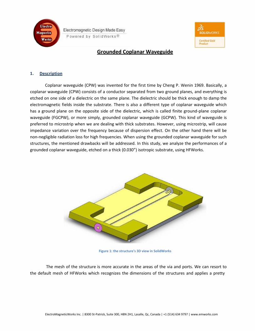
Grounded Coplanar Waveguide
1. Description
Coplanar waveguide (CPW) was invented for the first time by Cheng P. Wenin 1969. Basically, a
coplanar waveguide (CPW) consists of a conductor separated from two ground planes, and everything is
etched on one side of a dielectric on the same plane. The dielectric should be thick enough to damp the
electromagnetic fields inside the substrate. There is also a different type of coplanar waveguide which
has a ground plane on the opposite side of the dielectric, which is called finite ground-plane coplanar
waveguide (FGCPW), or more simply, grounded coplanar waveguide (GCPW). This kind of waveguide is
preferred to microstrip when we are dealing with thick substrates. However, using microstrip, will cause
impedance variation over the frequency because of dispersion effect. On the other hand there will be
non-negligible radiation loss for high frequencies. When using the grounded coplanar waveguide for such
structures, the mentioned drawbacks will be addressed. In this study, we analyze the performances of a
grounded coplanar waveguide, etched on a thick (0.030”) isotropic substrate, using HFWorks.
Figure 1: the structure's 3D view in SolidWorks
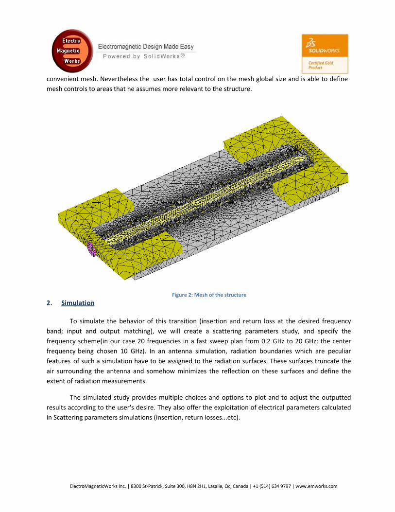
The mesh of the structure is more accurate in the areas of the via and ports. We can resort to
the default mesh of HFWorks which recognizes the dimensions of the structures and applies a pretty
ElectroMagneticWorks Inc. | 8300 St-Patrick, Suite 300, H8N 2H1, Lasalle, Qc, Canada | +1 (514) 634 9797 | www.emworks.com
convenient mesh. Nevertheless the user has total control on the mesh global size and is able to define
mesh controls to areas that he assumes more relevant to the structure.
2. Simulation Figure 2: Mesh of the structure
To simulate the behavior of this transition (insertion and return loss at the desired frequency
band; input and output matching), we will create a scattering parameters study, and specify the
frequency scheme(in our case 20 frequencies in a fast sweep plan from 0.2 GHz to 20 GHz; the center
frequency being chosen 10 GHz). In an antenna simulation, radiation boundaries which are peculiar
features of such a simulation have to be assigned to the radiation surfaces. These surfaces truncate the
air surrounding the antenna and somehow minimizes the reflection on these surfaces and define the
extent of radiation measurements.
The simulated study provides multiple choices and options to plot and to adjust the outputted
results according to the user's desire. They also offer the exploitation of electrical parameters calculated
in Scattering parameters simulations (insertion, return losses...etc).
ElectroMagneticWorks Inc. | 8300 St-Patrick, Suite 300, H8N 2H1, Lasalle, Qc, Canada | +1 (514) 634 9797 | www.emworks.com
3. Load/ Restraint
The coplanar waveguide is composed of signal and ground conductors. Each one could be
assigned Signal and PEC materials during the step of assignment of solids and materials.
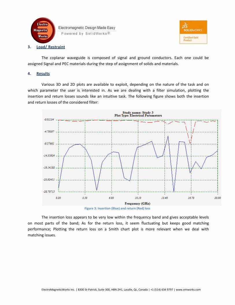
4. Results
Various 3D and 2D plots are available to exploit, depending on the nature of the task and on
which parameter the user is interested in. As we are dealing with a filter simulation, plotting the
insertion and return losses sounds like an intuitive task. The following figure shows both the insertion
and return losses of the considered filter:
Figure 3: Insertion (Blue) and return (Red) loss
The insertion loss appears to be very low within the frequency band and gives acceptable levels
on most parts of the band; As for the return loss, it seem fluctuating but keeps good matching
performance; Plotting the return loss on a Smith chart plot is more relevant when we deal with
matching issues.
ElectroMagneticWorks Inc. | 8300 St-Patrick, Suite 300, H8N 2H1, Lasalle, Qc, Canada | +1 (514) 634 9797 | www.emworks.com
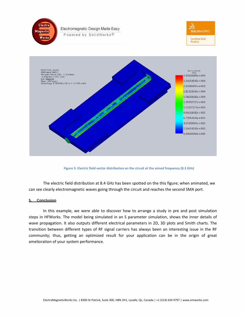
Figure 5: Electric field vector distribution on the circuit at the aimed frequency (8.3 GHz)
The electric field distribution at 8.4 GHz has been spotted on the this figure; when animated, we
can see clearly electromagnetic waves going through the circuit and reaches the second SMA port.
5. Conclusion
In this example, we were able to discover how to arrange a study in pre and post simulation
steps in HFWorks. The model being simulated in an S parameter simulation, shows the inner details of
wave propagation. It also outputs different electrical parameters in 2D, 3D plots and Smith charts. The
transition between different types of RF signal carriers has always been an interesting issue in the RF
community; thus, getting an optimized result for your application can be in the origin of great
amelioration of your system performance.


![A Compact Ultra Wideband CPW-Fed Circular Polarized Slot ... · waveguide type, coaxial, and microstrip are the deferent technical feeding structures in UWB antennas [4]. The coplanar](https://img.pdfslide.us/doc/110x75/5e945e8f1e74497797241759/a-compact-ultra-wideband-cpw-fed-circular-polarized-slot-waveguide-type-coaxial.jpg)
![Plasmonic coaxial waveguide-cavity deviceswsshin/pdf/mahigir2015oe.pdf · Fig. 2. (a) Top view schematic at z = 0 [Fig. 1(e)] of a plasmonic coaxial waveguide side- coupled to a short-circuited](https://img.pdfslide.us/doc/110x75/5fc20b138de1875eb605c10a/plasmonic-coaxial-waveguide-cavity-devices-wsshinpdf-fig-2-a-top-view-schematic.jpg)