Embed Size (px)
Citation preview
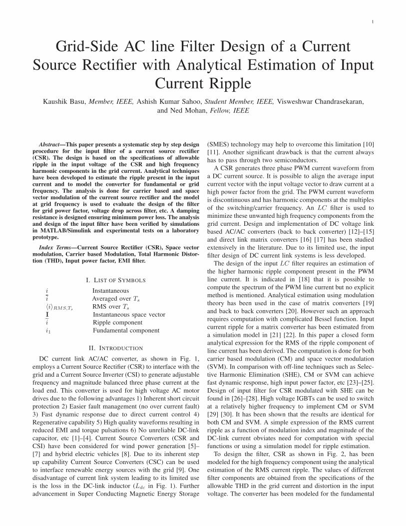
1
Grid-Side AC line Filter Design of a CurrentSource Rectifier with Analytical Estimation of Input
Current RippleKaushik Basu, Member, IEEE, Ashish Kumar Sahoo, Student Member, IEEE, Visweshwar Chandrasekaran,
and Ned Mohan, Fellow, IEEE
Abstract—This paper presents a systematic step by step designprocedure for the input filter of a current source rectifier(CSR). The design is based on the specifications of allowableripple in the input voltage of the CSR and high frequencyharmonic components in the grid current. Analytical techniqueshave been developed to estimate the ripple present in the inputcurrent and to model the converter for fundamental or gridfrequency. The analysis is done for carrier based and spacevector modulation of the current source rectifier and the modelat grid frequency is used to evaluate the design of the filterfor grid power factor, voltage drop across filter, etc. A dampingresistance is designed ensuring minimum power loss. The analysisand design of the input filter have been verified by simulationsin MATLAB/Simulink and experimental tests on a laboratoryprototype.
Index Terms—Current Source Rectifier (CSR), Space vectormodulation, Carrier based Modulation, Total Harmonic Distor-tion (THD), Input power factor, EMI filter.
I. LIST OF SYMBOLS
i Instantaneousi Averaged over Ts
⟨i⟩RMS,TsRMS over Ts
I Instantaneous space vectori Ripple componenti1 Fundamental component
II. INTRODUCTION
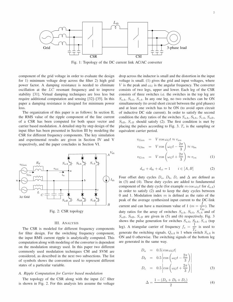
DC current link AC/AC converter, as shown in Fig. 1,employs a Current Source Rectifier (CSR) to interface with thegrid and a Current Source Inverter (CSI) to generate adjustablefrequency and magnitude balanced three phase current at theload end. This converter is used for high voltage AC motordrives due to the following advantages 1) Inherent short circuitprotection 2) Easier fault management (no over current fault)3) Fast dynamic response due to direct current control 4)Regenerative capability 5) High quality waveforms resulting inreduced EMI and torque pulsations 6) No unreliable DC-linkcapacitor, etc [1]–[4]. Current Source Converters (CSR andCSI) have been considered for wind power generation [5]–[7] and hybrid electric vehicles [8]. Due to its inherent stepup capability Current Source Converters (CSC) can be usedto interface renewable energy sources with the grid [9]. Onedisadvantage of current link system leading to its limited useis the loss in the DC-link inductor (Ldc in Fig. 1). Furtheradvancement in Super Conducting Magnetic Energy Storage
(SMES) technology may help to overcome this limitation [10][11]. Another significant drawback is that the current alwayshas to pass through two semiconductors.
A CSR generates three phase PWM current waveform froma DC current source. It is possible to align the average inputcurrent vector with the input voltage vector to draw current at ahigh power factor from the grid. The PWM current waveformis discontinuous and has harmonic components at the multiplesof the switching/carrier frequency. An LC filter is used tominimize these unwanted high frequency components from thegrid current. Design and implementation of DC voltage linkbased AC/AC converters (back to back converter) [12]–[15]and direct link matrix converters [16] [17] has been studiedextensively in the literature. Due to its limited use, the inputfilter design of DC current link systems is less developed.
The design of the input LC filter requires an estimation ofthe higher harmonic ripple component present in the PWMline current. It is indicated in [18] that it is possible tocompute the spectrum of the PWM line current but no explicitmethod is mentioned. Analytical estimation using modulationtheory has been used in the case of matrix converters [19]and back to back converters [20]. However such an approachrequires computation with complicated Bessel function. Inputcurrent ripple for a matrix converter has been estimated froma simulation model in [21] [22]. In this paper a closed formanalytical expression for the RMS of the ripple component ofline current has been derived. The computation is done for bothcarrier based modulation (CM) and space vector modulation(SVM). In comparison with off-line techniques such as Selec-tive Harmonic Elimination (SHE), CM or SVM can achievefast dynamic response, high input power factor, etc [23]–[25].Design of input filter for CSR modulated with SHE can befound in [26]–[28]. High voltage IGBTs can be used to switchat a relatively higher frequency to implement CM or SVM[29] [30]. It has been shown that the results are identical forboth CM and SVM. A simple expression of the RMS currentripple as a function of modulation index and magnitude of theDC-link current obviates need for computation with specialfunctions or using a simulation model for ripple estimation.
To design the filter, CSR as shown in Fig. 2, has beenmodeled for the high frequency component using the analyticalestimation of the RMS current ripple. The values of differentfilter components are obtained from the specifications of theallowable THD in the grid current and distortion in the inputvoltage. The converter has been modeled for the fundamental
2
CSR
Ldc
CSI
3-phase loadGrid
Fig. 1: Topology of the DC current link AC/AC converter
component of the grid voltage in order to evaluate the designfor 1) minimum voltage drop across the filter 2) high gridpower factor. A damping resistance is needed to eliminateoscillation at the LC resonant frequency and to improvestability [31]. Virtual damping techniques are loss less butrequire additional computation and sensing [32]–[35]. In thispaper a damping resistance is designed for minimum powerloss.
The organization of this paper is as follows: In section II,the RMS value of the ripple component of the line currentof a CSR has been computed for both space vector andcarrier based modulation. A detailed step by step design of theinput filter has been presented in Section III by modeling theCSR for different frequency components. The key simulationand experimental results are given in Section IV and Vrespectively, and the paper concludes in Section VI.
SaA SbA
SbB ScB
VdcA
B
SaB
van
c
b
a
L
Rd
ia
C
Idc
ScA
3φ Grid
iGa
vGan
n
Fig. 2: CSR topology
III. ANALYSIS
The CSR is modeled for different frequency componentsfor filter design. For the switching frequency component,the input RMS current ripple is analytically computed. Thiscomputation along with modeling of the converter is dependenton the modulation strategy used. In this paper two differentcommonly used modulation techniques CM and SVM areconsidered, as described in the next two subsections. The listof symbols shows the convention used to represent differentstates of a particular variable.
A. Ripple Computation for Carrier based modulation
The topology of the CSR along with the input LC filteris shown in Fig. 2. For this analysis lets assume the voltage
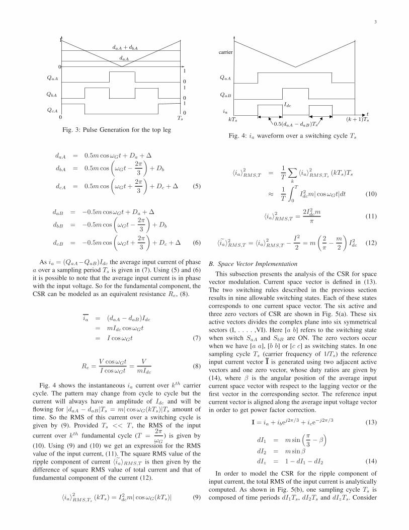
drop across the inductor is small and the distortion in the inputvoltage is small. (1) gives the grid and input voltages, whereV is the peak and ωG is the angular frequency. The converterconsists of two legs, upper and lower. Each leg of the CSRconsists of three switches i.e. the switches in the top leg areSaA, SbA, ScA. In any one leg, no two switches can be ONsimultaneously (to avoid short circuit between the grid phases)and at least one switch has to be ON (to avoid open circuitof inductive DC side current). In order to satisfy the secondcondition the duty ratios of the switches SaA, SbA, ScA, SaB ,SbB , ScB should satisfy (2). The first condition is met byplacing the pulses according to Fig. 3. Ts is the sampling orequivalent carrier period.
vGan = V cosωGt ≈ van
vGbn = V cos
(ωGt−
2π
3
)≈ vbn
vGcn = V cos
(ωGt+
2π
3
)≈ vcn (1)
dai + dbi + dci = 1 i ∈ [A,B] (2)
Four offset duty cycles Da, Db, Dc and ∆ are defined asin (3) and (4). These duty cycles are added to fundamentalcomponent of the duty cycle (for example m cosωGt for daA)in order to satisfy (2) and to keep the duty cycles between0 and 1. Modulation index m is defined as the ratio of thepeak of the average synthesized input current to the DC-link
current and can have a maximum value of 1 (m =I
Idc). The
duty ratios for the array of switches SaA, SbA, ScA and ofSaB , SbB , ScB are given in (5) and (6) respectively. Fig. 3shows the pulse generation for switches SaA, SbA, ScA (top
leg). A triangular carrier of frequency fs =1
Tsis used to
generate the switching signals. QaA is 1 when switch SaA isON and 0 otherwise. The switching signals of the bottom legare generated in the same way.
Da = 0.5| cosωGt|
Db = 0.5
∣∣∣∣cos(ωGt−
2π
3
)∣∣∣∣
Dc = 0.5
∣∣∣∣cos(ωGt+
2π
3
)∣∣∣∣ (3)
∆ =1− (Da +Db +Dc)
2(4)
3
1
daA + dbA
daA
0
0
QaA
QcA
QbA
1
01
01
Ts
0
Fig. 3: Pulse Generation for the top leg
daA = 0.5m cosωGt+Da +∆
dbA = 0.5m cos
(ωGt−
2π
3
)+Db
dcA = 0.5m cos
(ωGt+
2π
3
)+Dc +∆ (5)
daB = −0.5m cosωGt+Da +∆
dbB = −0.5m cos
(ωGt−
2π
3
)+Db
dcB = −0.5m cos
(ωGt+
2π
3
)+Dc +∆ (6)
As ia = (QaA−QaB)Idc the average input current of phasea over a sampling period Ts is given in (7). Using (5) and (6)it is possible to note that the average input current is in phasewith the input voltage. So for the fundamental component, theCSR can be modeled as an equivalent resistance Re, (8).
ia = (daA − daB)Idc
= mIdc cosωGt
= I cosωGt (7)
Re =V cosωGt
I cosωGt=
V
mIdc(8)
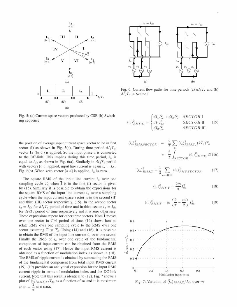
Fig. 4 shows the instantaneous ia current over kth carriercycle. The pattern may change from cycle to cycle but thecurrent will always have an amplitude of Idc and will beflowing for |daA − daB|Ts = m| cosωG(kTs)|Ts amount oftime. So the RMS of this current over a switching cycle isgiven by (9). Provided Ts << T , the RMS of the input
current over kth fundamental cycle (T =2π
ωG) is given by
(10). Using (9) and (10) we get an expression for the RMSvalue of the input current, (11). The square RMS value of theripple component of current ⟨ia⟩RMS,T is then given by thedifference of square RMS value of total current and that offundamental component of the current (12).
⟨ia⟩2RMS,Ts(kTs) = I2dcm| cosωG(kTs)| (9)
Idc
QaA
QaB
ia
kTs
t(k + 1)Ts
carrier
0.5(daA − daB)Ts
Fig. 4: ia waveform over a switching cycle Ts
⟨ia⟩2RMS,T =1
T
∑
k
⟨ia⟩2RMS,Ts(kTs)Ts
≈1
T
∫ T
0
I2dcm| cosωGt|dt (10)
⟨ia⟩2RMS,T =2I2dcm
π(11)
⟨ia⟩2RMS,T = ⟨ia⟩2RMS,T −I2
2= m
(2
π−
m
2
)I2dc (12)
B. Space Vector Implementation
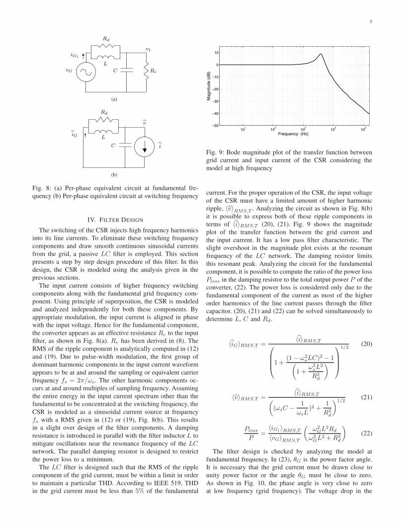
This subsection presents the analysis of the CSR for spacevector modulation. Current space vector is defined in (13).The two switching rules described in the previous sectionresults in nine allowable switching states. Each of these statescorresponds to one current space vector. The six active andthree zero vectors of CSR are shown in Fig. 5(a). These sixactive vectors divides the complex plane into six symmetricalsectors (I, . . . . ,VI). Here [a b] refers to the switching statewhen switch SaA and SbB are ON. The zero vectors occurwhen we have [a a], [b b] or [c c] as switching states. In onesampling cycle Ts (carrier frequency of 1/Ts) the referenceinput current vector I is generated using two adjacent activevectors and one zero vector, whose duty ratios are given by(14), where β is the angular position of the average inputcurrent space vector with respect to the lagging vector or thefirst vector in the corresponding sector. The reference inputcurrent vector is aligned along the average input voltage vectorin order to get power factor correction.
I = ia + ibej2π/3 + ice
−j2π/3 (13)
dI1 = m sin(π3− β
)
dI2 = m sinβ
dIz = 1− dI1 − dI2 (14)
In order to model the CSR for the ripple component ofinput current, the total RMS of the input current is analyticallycomputed. As shown in Fig. 5(b), one sampling cycle Ts iscomposed of time periods dI1Ts, dI2Ts and dIzTs. Consider
4
I1
I6
II I2
I5
Iβ
I3
I4
I
III
V VI
IV
[a b]
[a c]
[c b]
[c a]
[b a]
[b c]
(a)
dIz
0
dI2dI1
1t/Ts
IzI1 I2
(b)
Fig. 5: (a) Current space vectors produced by CSR (b) Switch-ing sequence
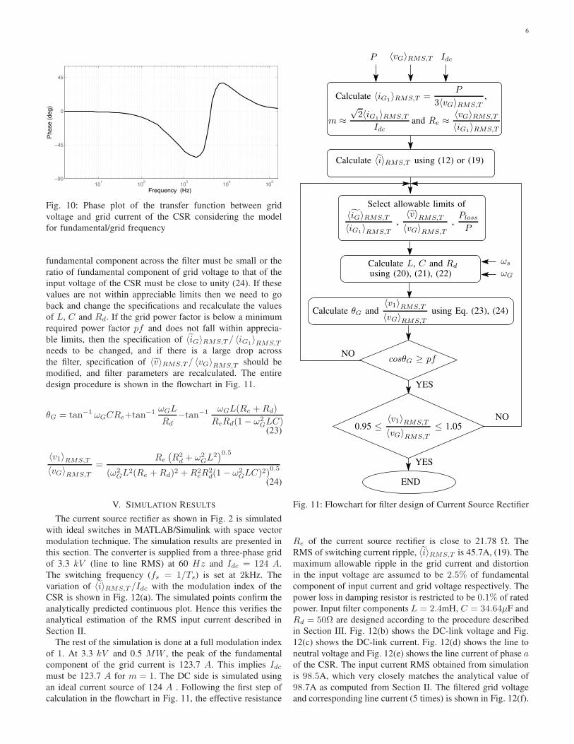
the position of average input current space vector to be in firstsector (I) as shown in Fig. 5(a). During time period dI1Ts,vector I1 ([a b]) is applied. So the input phase a is connectedto the DC-link. This implies during this time period, ia isequal to Idc as shown in Fig. 6(a). Similarly in dI2Ts periodwith vectors [a c] applied, input line current is again ia = Idc,Fig. 6(b). When zero vector [a a] is applied, ia is zero.
The square RMS of the input line current ia over onesampling cycle Ts when I is in the first (I) sector is givenby (15). Similarly it is possible to obtain the expressions forthe square RMS of the input line current ia over a samplingcycle when the input current space vector is in the second (II)and third (III) sector respectively, (15). In the second sectoria = Idc for dI1Ts period of time and in third sector ia = Idcfor dI2Ts period of time respectively and it is zero otherwise.These expressions repeat for other three sectors. Note I movesover one sector in T/6 period of time. (16) shows how torelate RMS over one sampling cycle to the RMS over onesector assuming T ≫ Ts. Using (14) and (16), it is possibleto obtain the RMS of the input line current ia over one sector.Finally the RMS of ia over one cycle of the fundamentalcomponent of input current can be obtained from the RMSof each sector using (17). Hence the input RMS current isobtained as a function of modulation index as shown in (18).The RMS of ripple current is obtained by subtracting the RMSof the fundamental component from total input RMS current(19). (19) provides an analytical expression for the input RMScurrent ripple in terms of modulation index and the DC-linkcurrent. Note that this result is identical to (12). Fig. 7 shows aplot of ⟨ia⟩RMS,T /Idc as a function of m and it is maximum
at m =2
π≈ 0.6366.
ia
va
Idc
ia = Idc
vcvb
(a)
ia
vcva
ia = Idc
Idc
vb
(b)
Fig. 6: Current flow paths for time periods (a) dI1Ts and (b)dI2Ts in Sector I
⟨ia⟩2RMS,Ts=
⎧⎪⎨
⎪⎩
dI1I2dc + dI2I2dc SECTOR I
dI1I2dc SECTOR II
dI2I2dc SECTOR III
(15)
⟨ia⟩2RMS,SECTOR =6
T
∑
k
⟨ia⟩2RMS,Ts(kTs)Ts
≈6
T
∫
SECTOR⟨ia⟩2RMS,Ts
dt (16)
⟨ia⟩2RMS,T =1
3
∑
i=I,II,III
⟨ia⟩2RMS,SECTORi(17)
⟨ia⟩2RMS,T =2m
πI2dc (18)
⟨ia⟩2RMS,T = m
(2
π−
m
2
)I2dc (19)
0 0.2 0.4 0.6 0.8 10
0.1
0.2
0.3
0.4
0.5
Modulation index = m
⟨ia⟩ R
MS
,T/I d
c
Fig. 7: Variation of ⟨ia⟩RMS,T /Idc over m
5
CL
v1
RevG
iG1
Rd
(a)
v
L
C
iG
Rd
i
(b)
Fig. 8: (a) Per-phase equivalent circuit at fundamental fre-quency (b) Per-phase equivalent circuit at switching frequency
IV. FILTER DESIGN
The switching of the CSR injects high frequency harmonicsinto its line currents. To eliminate these switching frequencycomponents and draw smooth continuous sinusoidal currentsfrom the grid, a passive LC filter is employed. This sectionpresents a step by step design procedure of this filter. In thisdesign, the CSR is modeled using the analysis given in theprevious sections.
The input current consists of higher frequency switchingcomponents along with the fundamental grid frequency com-ponent. Using principle of superposition, the CSR is modeledand analyzed independently for both these components. Byappropriate modulation, the input current is aligned in phasewith the input voltage. Hence for the fundamental component,the converter appears as an effective resistance Re to the inputfilter, as shown in Fig. 8(a). Re has been derived in (8). TheRMS of the ripple component is analytically computed in (12)and (19). Due to pulse-width modulation, the first group ofdominant harmonic components in the input current waveformappears to be at and around the sampling or equivalent carrierfrequency fs = 2π/ωs. The other harmonic components oc-curs at and around multiples of sampling frequency. Assumingthe entire energy in the input current spectrum other than thefundamental to be concentrated at the switching frequency, theCSR is modeled as a sinusoidal current source at frequencyfs with a RMS given in (12) or (19), Fig. 8(b). This resultsin a slight over design of the filter components. A dampingresistance is introduced in parallel with the filter inductor L tomitigate oscillations near the resonance frequency of the LCnetwork. The parallel damping resistor is designed to restrictthe power loss to a minimum.
The LC filter is designed such that the RMS of the ripplecomponent of the grid current, must be within a limit in orderto maintain a particular THD. According to IEEE 519, THDin the grid current must be less than 5% of the fundamental
101 102 103 104 105−50
−40
−30
−20
−10
0
10
Mag
nitu
de (d
B)
Frequency (Hz)
Fig. 9: Bode magnitude plot of the transfer function betweengrid current and input current of the CSR considering themodel at high frequency
current. For the proper operation of the CSR, the input voltageof the CSR must have a limited amount of higher harmonicripple, ⟨v⟩RMS,T . Analyzing the circuit as shown in Fig. 8(b)it is possible to express both of these ripple components interms of ⟨i⟩RMS,T (20), (21). Fig. 9 shows the magnitudeplot of the transfer function between the grid current andthe input current. It has a low pass filter characteristic. Theslight overshoot in the magnitude plot exists at the resonantfrequency of the LC network. The damping resistor limitsthis resonant peak. Analyzing the circuit for the fundamentalcomponent, it is possible to compute the ratio of the power lossPloss in the damping resistor to the total output power P of theconverter, (22). The power loss is considered only due to thefundamental component of the current as most of the higherorder harmonics of the line current passes through the filtercapacitor. (20), (21) and (22) can be solved simultaneously todetermine L, C and Rd.
⟨iG⟩RMS,T =⟨i⟩RMS,T
⎛
⎜⎜⎝1 +(1 − ω2
sLC)2 − 1(1 +
ω2sL
2
R2d
)
⎞
⎟⎟⎠
1/2(20)
⟨v⟩RMS,T =⟨i⟩RMS,T
((ωsC −
1
ωsL)2 +
1
R2d
)1/2(21)
Ploss
P=
⟨iG1⟩RMS,T
⟨vG⟩RMS,T
(ω2GL
2Rd
ω2GL
2 +R2d
)(22)
The filter design is checked by analyzing the model atfundamental frequency. In (23), θG is the power factor angle.It is necessary that the grid current must be drawn close tounity power factor or the angle θG must be close to zero.As shown in Fig. 10, the phase angle is very close to zeroat low frequency (grid frequency). The voltage drop in the
6
101 102 103 104 105−90
−45
0
45
Phas
e (d
eg)
Frequency (Hz)
Fig. 10: Phase plot of the transfer function between gridvoltage and grid current of the CSR considering the modelfor fundamental/grid frequency
fundamental component across the filter must be small or theratio of fundamental component of grid voltage to that of theinput voltage of the CSR must be close to unity (24). If thesevalues are not within appreciable limits then we need to goback and change the specifications and recalculate the valuesof L, C and Rd. If the grid power factor is below a minimumrequired power factor pf and does not fall within apprecia-ble limits, then the specification of ⟨iG⟩RMS,T / ⟨iG1
⟩RMS,Tneeds to be changed, and if there is a large drop acrossthe filter, specification of ⟨v⟩RMS,T / ⟨vG⟩RMS,T should bemodified, and filter parameters are recalculated. The entiredesign procedure is shown in the flowchart in Fig. 11.
θG = tan−1 ωGCRe+tan−1 ωGL
Rd−tan−1 ωGL(Re +Rd)
ReRd(1− ω2GLC)
(23)
⟨v1⟩RMS,T
⟨vG⟩RMS,T
=Re
(R2
d + ω2GL
2)0.5
(ω2GL
2(Re +Rd)2 +R2eR
2d(1 − ω2
GLC)2)0.5
(24)
V. SIMULATION RESULTS
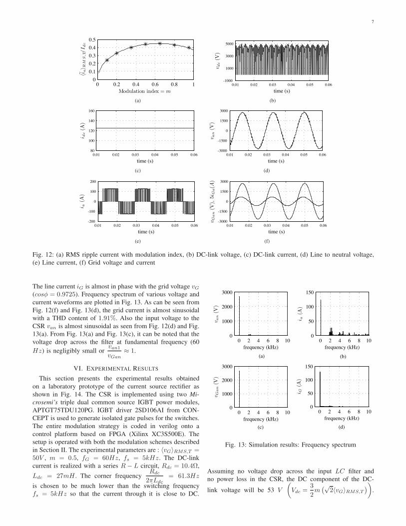
The current source rectifier as shown in Fig. 2 is simulatedwith ideal switches in MATLAB/Simulink with space vectormodulation technique. The simulation results are presented inthis section. The converter is supplied from a three-phase gridof 3.3 kV (line to line RMS) at 60 Hz and Idc = 124 A.The switching frequency (fs = 1/Ts) is set at 2kHz. Thevariation of ⟨i⟩RMS,T /Idc with the modulation index of theCSR is shown in Fig. 12(a). The simulated points confirm theanalytically predicted continuous plot. Hence this verifies theanalytical estimation of the RMS input current described inSection II.
The rest of the simulation is done at a full modulation indexof 1. At 3.3 kV and 0.5 MW , the peak of the fundamentalcomponent of the grid current is 123.7 A. This implies Idcmust be 123.7 A for m = 1. The DC side is simulated usingan ideal current source of 124 A . Following the first step ofcalculation in the flowchart in Fig. 11, the effective resistance
0.95 ≤⟨v1⟩RMS,T
⟨vG⟩RMS,T
≤ 1.05
⟨vG⟩RMS,TP Idc
YES
NOcosθG ≥ pf
⟨iG⟩RMS,T
⟨iG1⟩RMS,T
,⟨v⟩RMS,T
⟨vG⟩RMS,T
,Ploss
P
using (20), (21), (22)
YES
Calculate θG and⟨v1⟩RMS,T
⟨vG⟩RMS,T
using Eq. (23), (24)
END
Select allowable limits of
Calculate ⟨i⟩RMS,T using (12) or (19)
Calculate ⟨iG1⟩RMS,T =
P
3⟨vG⟩RMS,T,
NO
Calculate L, C and Rdωs
ωG
and Re ≈⟨vG⟩RMS,T
⟨iG1⟩RMS,T
m ≈√2⟨iG1
⟩RMS,T
Idc
Fig. 11: Flowchart for filter design of Current Source Rectifier
Re of the current source rectifier is close to 21.78 Ω. TheRMS of switching current ripple, ⟨i⟩RMS,T is 45.7A, (19). Themaximum allowable ripple in the grid current and distortionin the input voltage are assumed to be 2.5% of fundamentalcomponent of input current and grid voltage respectively. Thepower loss in damping resistor is restricted to be 0.1% of ratedpower. Input filter components L = 2.4mH, C = 34.64µF andRd = 50Ω are designed according to the procedure describedin Section III. Fig. 12(b) shows the DC-link voltage and Fig.12(c) shows the DC-link current. Fig. 12(d) shows the line toneutral voltage and Fig. 12(e) shows the line current of phase aof the CSR. The input current RMS obtained from simulationis 98.5A, which very closely matches the analytical value of98.7A as computed from Section II. The filtered grid voltageand corresponding line current (5 times) is shown in Fig. 12(f).
7
0 0.2 0.4 0.6 0.8 10
0.10.20.30.40.5
Modulation index = m
⟨ia⟩ R
MS
,T/I d
c
(a)
0.01 0.02 0.03 0.04 0.05 0.06-1000
1000
3000
5000
time (s)
v dc
(V)
(b)
0.01 0.02 0.03 0.04 0.05 0.0680
100
120
140
160
time (s)
i dc
(A)
(c)
0.01 0.02 0.03 0.04 0.05 0.06-3000
-1500
0
1500
3000
time (s)
v an
(V)
(d)
0.01 0.02 0.03 0.04 0.05 0.06-200
-100
0
100
200
time (s)
i a(A
)
(e)
0.01 0.02 0.03 0.04 0.05 0.06-3000
-1500
0
1500
3000
time (s)
v Ga
n(V
),5i
Ga(A
)
(f)
Fig. 12: (a) RMS ripple current with modulation index, (b) DC-link voltage, (c) DC-link current, (d) Line to neutral voltage,(e) Line current, (f) Grid voltage and current
The line current iG is almost in phase with the grid voltage vG(cosφ = 0.9725). Frequency spectrum of various voltage andcurrent waveforms are plotted in Fig. 13. As can be seen fromFig. 12(f) and Fig. 13(d), the grid current is almost sinusoidalwith a THD content of 1.91%. Also the input voltage to theCSR van is almost sinusoidal as seen from Fig. 12(d) and Fig.13(a). From Fig. 13(a) and Fig. 13(c), it can be noted that thevoltage drop across the filter at fundamental frequency (60
Hz) is negligibly small orvan1vGan
≈ 1.
VI. EXPERIMENTAL RESULTS
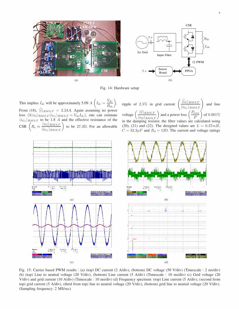
This section presents the experimental results obtainedon a laboratory prototype of the current source rectifier asshown in Fig. 14. The CSR is implemented using two Mi-
crosemi’s triple dual common source IGBT power modules,APTGT75TDU120PG. IGBT driver 2SD106AI from CON-CEPT is used to generate isolated gate pulses for the switches.The entire modulation strategy is coded in verilog onto acontrol platform based on FPGA (Xilinx XC3S500E). Thesetup is operated with both the modulation schemes describedin Section II. The experimental parameters are : ⟨vG⟩RMS,T =50V , m = 0.5, fG = 60Hz, fs = 5kHz. The DC-linkcurrent is realized with a series R− L circuit, Rdc = 10.4Ω,
Ldc = 27mH . The corner frequencyRdc
2πLdc= 61.3Hz
is chosen to be much lower than the switching frequencyfs = 5kHz so that the current through it is close to DC.
0 2 4 6 8 100
1000
2000
3000
frequency (kHz)
v an
(V)
0 2 4 6 8 100
1000
2000
3000
frequency (kHz)
v Ga
n(V
)
0 2 4 6 8 100
50
100
150
frequency (kHz)
i a(A
)
0 2 4 6 8 100
50
100
150
frequency (kHz)
i G(A
)
(a) (b)
(d)(c)
Fig. 13: Simulation results: Frequency spectrum
Assuming no voltage drop across the input LC filter andno power loss in the CSR, the DC component of the DC-
link voltage will be 53 V
(Vdc =
3
2m(√
2⟨vG⟩RMS,T
)).
8
(a)
3φ Grid
3 v
12 PWM
Board
Ldc
Rdc
Input Filter
CSR
FPGASensor
3 v
(b)
Fig. 14: Hardware setup
This implies Idc will be approximately 5.09 A
(Idc =
Vdc
Rdc
).
From (18), ⟨i⟩RMS,T = 2.24A. Again assuming no powerloss (3⟨vG⟩RMS,T ⟨iG1
⟩RMS,T = VdcIdc), one can estimate⟨iG1
⟩RMS,T to be 1.8 A and the effective resistance of the
CSR
(Re ≈
⟨vG⟩RMS,T
⟨iG1⟩RMS,T
)to be 27.3Ω. For an allowable
ripple of 2.5% in grid current
(⟨iG⟩RMS,T
⟨iG1⟩RMS,T
)
and line
voltage
(⟨v⟩RMS,T
⟨vG⟩RMS,T
)and a power loss
(Ploss
P
)of 0.001%
in the damping resistor, the filter values are calculated using(20), (21) and (22). The designed values are L = 0.37mH ,C = 32.3µF and Rd = 12Ω. The current and voltage ratings
(a) (b)
(c) (d)
Fig. 15: Carrier based PWM results : (a) (top) DC current (2 A/div), (bottom) DC voltage (50 V/div) (Timescale : 2 ms/div)(b) (top) Line to neutral voltage (20 V/div), (bottom) Line current (5 A/div) (Timescale : 10 ms/div) (c) Grid voltage (20V/div) and grid current (10 A/div) (Timescale : 10 ms/div) (d) Frequency spectrum: (top) Line current (5 A/div), (second fromtop) grid current (5 A/div), (third from top) line to neutral voltage (20 V/div), (bottom) grid line to neutral voltage (20 V/div).(Sampling frequency: 2 MS/sec)
9
(a) (b)
(c) (d)
Fig. 16: Space vector PWM results : (a) (top) DC current (2 A/div), (bottom) DC voltage (20 V/div) (Timescale : 2 ms/div) (b)(top) Line to neutral voltage (20 V/div), (bottom) Line current (5 A/div) (Timescale : 10 ms/div) (c) Grid voltage (20 V/div)and grid current (10 A/div) (Timescale : 10 ms/div) (d) Frequency spectrum: (top) Line current (5 A/div), (second from top)grid current (5 A/div), (third from top) line to neutral voltage (20 V/div), (bottom) grid line to neutral voltage (20 V/div).(Sampling frequency: 2 MS/sec)
of all semiconductor devices and passive components is chosento be higher than the operating conditions.
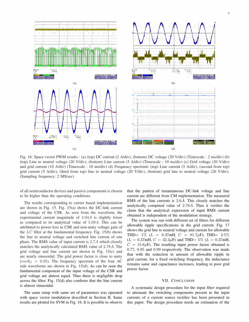
The results corresponding to carrier based implementationare shown in Fig. 15. Fig. 15(a) shows the DC-link currentand voltage of the CSR. As seen from the waveform, theexperimental current magnitude of 4.94A is slightly loweras compared to its analytical value of 5.09A. This can beattributed to power loss in CSR and non-unity voltage gain ofthe LC filter at the fundamental frequency. Fig. 15(b) showsthe line to neutral voltage and switched line current of onephase. The RMS value of input current is 2.7A which closelymatches the analytically calculated RMS value of 2.78A. Thegrid voltage and line current are shown in Fig. 15(c) andare nearly sinusoidal. The grid power factor is close to unity(cos θG = 0.95). The frequency spectrum of the four ACside waveforms are shown in Fig. 15(d). As can be seen thefundamental component of the input voltage of the CSR andgrid voltage are almost equal. Thus there is negligible dropacross the filter. Fig. 15(d) also confirms that the line currentis almost sinusoidal.
The same setup with same set of parameters was operatedwith space vector modulation described in Section II. Sameresults are plotted for SVM in Fig. 16. It is possible to observe
that the pattern of instantaneous DC-link voltage and linecurrent are different from CM implementation. The measuredRMS of the line currents is 2.6A. This closely matches theanalytically computed value of 2.78A. Thus it verifies theclaim that the analytical expression of input RMS currentobtained is independent of the modulation strategy.
The system was run with different set of filters for differentallowable ripple specifications in the grid current. Fig. 17shows the grid line to neutral voltage and current for allowableTHD= 1% (L = 0.37mH, C = 81.7µF), THD= 2.5%(L = 0.37mH, C = 32.3µF) and THD= 5% (L = 0.37mH,C = 15.8µF). The resulting input power factor obtained is0.77, 0.95 and 0.99 respectively. The observation was madethat with the reduction in amount of allowable ripple ingrid current, for a fixed switching frequency, the inductanceremains same and capacitance increases, leading to poor gridpower factor.
VII. CONCLUSION
A systematic design procedure for the input filter requiredto attenuate the switching components present in the inputcurrents of a current source rectifier has been presented inthis paper. The design procedure needs an estimation of the
10
(a)
(b)
(c)
Fig. 17: (a) Grid voltage (20 V/div) and current (5 A/div)for allowable THD= 1.0%, (b) Grid voltage (20 V/div) andcurrent (5 A/div) for allowable THD= 2.5%, (c) Grid voltage(20 V/div) and current (5 A/div) for allowable THD= 5.0%
ripple component present in the input line currents. This paperpresented an analytical method to estimate this ripple fortwo most commonly used modulation strategies. The derivedequations are a function of the modulation index of theCSR and the DC-link current. The design is based on thespecifications of the THD of the grid current and the allowableripple voltage at the input of the converter. The designedfilter ensures high input power factor, low voltage drop in thefilter and minimum ohmic loss in damping resistor. A detailedsimulation and experimental validation of the entire systemconfirms the analytical estimation of the input current rippleof the CSR and the proposed filter design.
VIII. APPENDIX
A. Differential mode EMI filter design of CSR
The main objective of the input AC line filter is to eliminatethe switching frequency components of the input current andto achieve a THD less than 5% (IEEE 519). But this is notthe complete story. One needs to design another filter (EMI)to meet the regulations in the frequency range of 150 kHz to30 MHz. Here a procedure for the differential mode EMI filterdesign of a CSR is presented. This EMI filter is designed asa next step after designing the input AC line filter followingthe procedure shown in the main paper. The common-modeEMI filter design follows a very similar procedure but requiresevaluation of parasitics and is out of the scope of this work.
Measurement of the high frequency component (150 kHzto 30 MHz) in the grid current is done by a network called
3φ Grid
50µH
CSR
Input Filter
+
LISN
0.1µF
100Ω
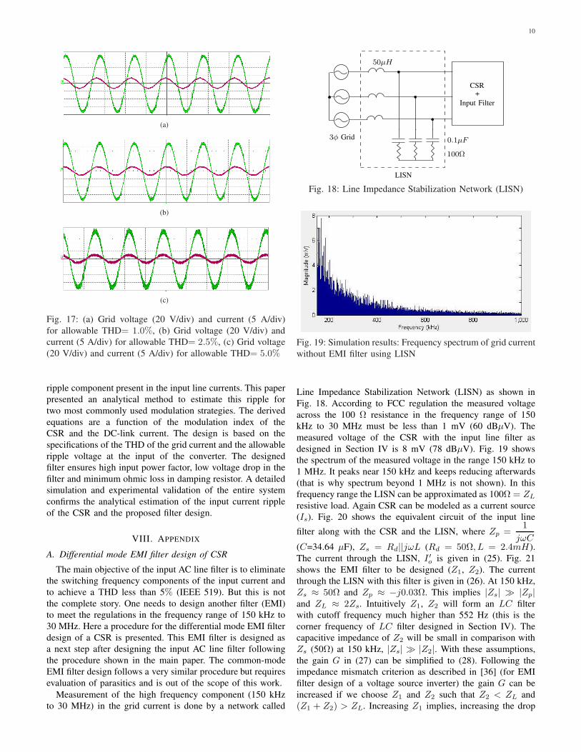
Fig. 18: Line Impedance Stabilization Network (LISN)
Fig. 19: Simulation results: Frequency spectrum of grid currentwithout EMI filter using LISN
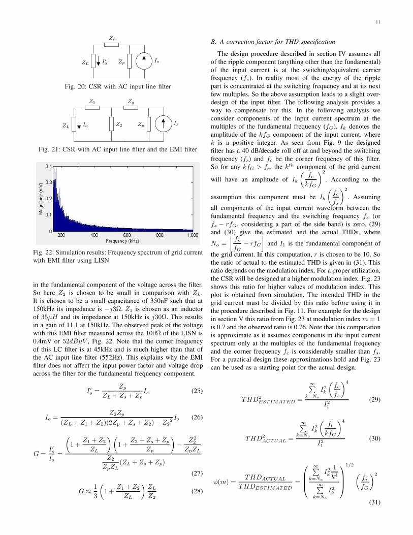
Line Impedance Stabilization Network (LISN) as shown inFig. 18. According to FCC regulation the measured voltageacross the 100 Ω resistance in the frequency range of 150kHz to 30 MHz must be less than 1 mV (60 dBµV). Themeasured voltage of the CSR with the input line filter asdesigned in Section IV is 8 mV (78 dBµV). Fig. 19 showsthe spectrum of the measured voltage in the range 150 kHz to1 MHz. It peaks near 150 kHz and keeps reducing afterwards(that is why spectrum beyond 1 MHz is not shown). In thisfrequency range the LISN can be approximated as 100Ω = ZL
resistive load. Again CSR can be modeled as a current source(Is). Fig. 20 shows the equivalent circuit of the input line
filter along with the CSR and the LISN, where Zp =1
jωC(C=34.64 µF), Zs = Rd||jωL (Rd = 50Ω, L = 2.4mH).The current through the LISN, I ′o is given in (25). Fig. 21shows the EMI filter to be designed (Z1, Z2). The currentthrough the LISN with this filter is given in (26). At 150 kHz,Zs ≈ 50Ω and Zp ≈ −j0.03Ω. This implies |Zs| ≫ |Zp|and ZL ≈ 2Zs. Intuitively Z1, Z2 will form an LC filterwith cutoff frequency much higher than 552 Hz (this is thecorner frequency of LC filter designed in Section IV). Thecapacitive impedance of Z2 will be small in comparison withZs (50Ω) at 150 kHz, |Zs| ≫ |Z2|. With these assumptions,the gain G in (27) can be simplified to (28). Following theimpedance mismatch criterion as described in [36] (for EMIfilter design of a voltage source inverter) the gain G can beincreased if we choose Z1 and Z2 such that Z2 < ZL and(Z1 + Z2) > ZL. Increasing Z1 implies, increasing the drop
11
ZL Zp
Zs
I′o Is
Fig. 20: CSR with AC input line filter
IsZL
Zs
ZpIo
Z1
Z2
Fig. 21: CSR with AC input line filter and the EMI filter
Fig. 22: Simulation results: Frequency spectrum of grid currentwith EMI filter using LISN
in the fundamental component of the voltage across the filter.So here Z2 is chosen to be small in comparison with ZL.It is chosen to be a small capacitance of 350nF such that at150kHz its impedance is −j3Ω. Z1 is chosen as an inductorof 35µH and its impedance at 150kHz is j30Ω. This resultsin a gain of 11.1 at 150kHz. The observed peak of the voltagewith this EMI filter measured across the 100Ω of the LISN is0.4mV or 52dBµV , Fig. 22. Note that the corner frequencyof this LC filter is at 45kHz and is much higher than that ofthe AC input line filter (552Hz). This explains why the EMIfilter does not affect the input power factor and voltage dropacross the filter for the fundamental frequency component.
I ′o =Zp
ZL + Zs + ZpIs (25)
Io =Z2Zp
(ZL + Z1 + Z2)(2Zp + Zs + Z2)− Z22Is (26)
G =I ′oIo
=
(1 +
Z1 + Z2
ZL
)(1 +
Z2 + Zs + Zp
Zp
)−
Z22
ZpZL
Z2
ZpZL(ZL + Zs + Zp)
(27)
G ≈1
3
(1 +
Z1 + Z2
ZL
)ZL
Z2
(28)
B. A correction factor for THD specification
The design procedure described in section IV assumes allof the ripple component (anything other than the fundamental)of the input current is at the switching/equivalent carrierfrequency (fs). In reality most of the energy of the ripplepart is concentrated at the switching frequency and at its nextfew multiples. So the above assumption leads to a slight over-design of the input filter. The following analysis provides away to compensate for this. In the following analysis weconsider components of the input current spectrum at themultiples of the fundamental frequency (fG). Ik denotes theamplitude of the kfG component of the input current, wherek is a positive integer. As seen from Fig. 9 the designedfilter has a 40 dB/decade roll off at and beyond the switchingfrequency (fs) and fc be the corner frequency of this filter.So for any kfG > fs, the kth component of the grid current
will have an amplitude of Ik
(fckfG
)2
. According to the
assumption this component must be Ik
(fcfs
)2
. Assuming
all components of the input current waveform between thefundamental frequency and the switching frequency fs (orfs − rfG, considering a part of the side band) is zero, (29)and (30) give the estimated and the actual THDs, where
No =
[fsfG
− rfG
]and I1 is the fundamental component of
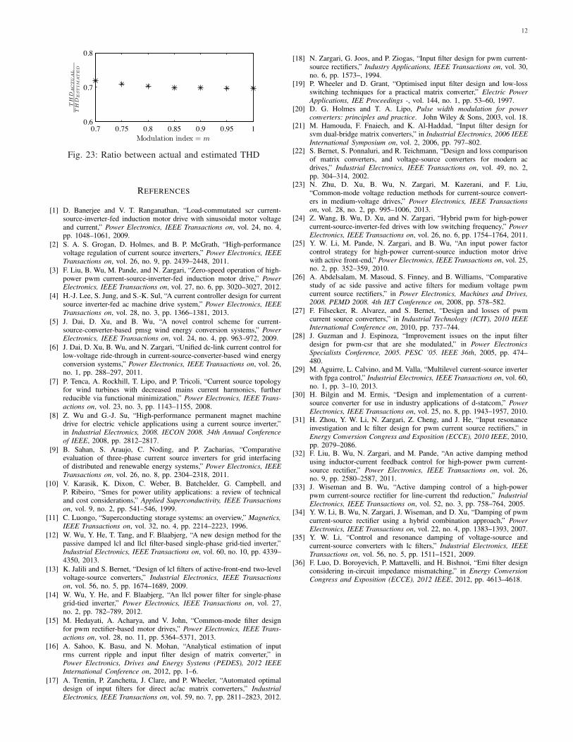
the grid current. In this computation, r is chosen to be 10. Sothe ratio of actual to the estimated THD is given in (31). Thisratio depends on the modulation index. For a proper utilization,the CSR will be designed at a higher modulation index. Fig. 23shows this ratio for higher values of modulation index. Thisplot is obtained from simulation. The intended THD in thegrid current must be divided by this ratio before using it inthe procedure described in Fig. 11. For example for the designin section V this ratio from Fig. 23 at modulation index m = 1is 0.7 and the observed ratio is 0.76. Note that this computationis approximate as it assumes components in the input currentspectrum only at the multiples of the fundamental frequencyand the corner frequency fc is considerably smaller than fs.For a practical design these approximations hold and Fig. 23can be used as a starting point for the actual design.
THD2
ESTIMATED =
∞∑k=No
I2k
(fcfs
)4
I21
(29)
THD2
ACTUAL =
∞∑k=No
I2k
(fckfG
)4
I21
(30)
φ(m) =THDACTUAL
THDESTIMATED=
⎛
⎜⎜⎝
∞∑k=No
I2k1
k4
∞∑k=No
I2k
⎞
⎟⎟⎠
1/2
(fsfG
)2
(31)
12
0.7 0.75 0.8 0.85 0.9 0.95 10.6
0.7
0.8
Modulation index = m
TH
DA
CT
UA
L
TH
DE
ST
IM
AT
ED
Fig. 23: Ratio between actual and estimated THD
REFERENCES
[1] D. Banerjee and V. T. Ranganathan, “Load-commutated scr current-source-inverter-fed induction motor drive with sinusoidal motor voltageand current,” Power Electronics, IEEE Transactions on, vol. 24, no. 4,pp. 1048–1061, 2009.
[2] S. A. S. Grogan, D. Holmes, and B. P. McGrath, “High-performancevoltage regulation of current source inverters,” Power Electronics, IEEETransactions on, vol. 26, no. 9, pp. 2439–2448, 2011.
[3] F. Liu, B. Wu, M. Pande, and N. Zargari, “Zero-speed operation of high-power pwm current-source-inverter-fed induction motor drive,” PowerElectronics, IEEE Transactions on, vol. 27, no. 6, pp. 3020–3027, 2012.
[4] H.-J. Lee, S. Jung, and S.-K. Sul, “A current controller design for currentsource inverter-fed ac machine drive system,” Power Electronics, IEEETransactions on, vol. 28, no. 3, pp. 1366–1381, 2013.
[5] J. Dai, D. Xu, and B. Wu, “A novel control scheme for current-source-converter-based pmsg wind energy conversion systems,” PowerElectronics, IEEE Transactions on, vol. 24, no. 4, pp. 963–972, 2009.
[6] J. Dai, D. Xu, B. Wu, and N. Zargari, “Unified dc-link current control forlow-voltage ride-through in current-source-converter-based wind energyconversion systems,” Power Electronics, IEEE Transactions on, vol. 26,no. 1, pp. 288–297, 2011.
[7] P. Tenca, A. Rockhill, T. Lipo, and P. Tricoli, “Current source topologyfor wind turbines with decreased mains current harmonics, furtherreducible via functional minimization,” Power Electronics, IEEE Trans-actions on, vol. 23, no. 3, pp. 1143–1155, 2008.
[8] Z. Wu and G.-J. Su, “High-performance permanent magnet machinedrive for electric vehicle applications using a current source inverter,”in Industrial Electronics, 2008. IECON 2008. 34th Annual Conferenceof IEEE, 2008, pp. 2812–2817.
[9] B. Sahan, S. Araujo, C. Noding, and P. Zacharias, “Comparativeevaluation of three-phase current source inverters for grid interfacingof distributed and renewable energy systems,” Power Electronics, IEEETransactions on, vol. 26, no. 8, pp. 2304–2318, 2011.
[10] V. Karasik, K. Dixon, C. Weber, B. Batchelder, G. Campbell, andP. Ribeiro, “Smes for power utility applications: a review of technicaland cost considerations,” Applied Superconductivity, IEEE Transactionson, vol. 9, no. 2, pp. 541–546, 1999.
[11] C. Luongo, “Superconducting storage systems: an overview,” Magnetics,IEEE Transactions on, vol. 32, no. 4, pp. 2214–2223, 1996.
[12] W. Wu, Y. He, T. Tang, and F. Blaabjerg, “A new design method for thepassive damped lcl and llcl filter-based single-phase grid-tied inverter,”Industrial Electronics, IEEE Transactions on, vol. 60, no. 10, pp. 4339–4350, 2013.
[13] K. Jalili and S. Bernet, “Design of lcl filters of active-front-end two-levelvoltage-source converters,” Industrial Electronics, IEEE Transactionson, vol. 56, no. 5, pp. 1674–1689, 2009.
[14] W. Wu, Y. He, and F. Blaabjerg, “An llcl power filter for single-phasegrid-tied inverter,” Power Electronics, IEEE Transactions on, vol. 27,no. 2, pp. 782–789, 2012.
[15] M. Hedayati, A. Acharya, and V. John, “Common-mode filter designfor pwm rectifier-based motor drives,” Power Electronics, IEEE Trans-actions on, vol. 28, no. 11, pp. 5364–5371, 2013.
[16] A. Sahoo, K. Basu, and N. Mohan, “Analytical estimation of inputrms current ripple and input filter design of matrix converter,” inPower Electronics, Drives and Energy Systems (PEDES), 2012 IEEEInternational Conference on, 2012, pp. 1–6.
[17] A. Trentin, P. Zanchetta, J. Clare, and P. Wheeler, “Automated optimaldesign of input filters for direct ac/ac matrix converters,” IndustrialElectronics, IEEE Transactions on, vol. 59, no. 7, pp. 2811–2823, 2012.
[18] N. Zargari, G. Joos, and P. Ziogas, “Input filter design for pwm current-source rectifiers,” Industry Applications, IEEE Transactions on, vol. 30,no. 6, pp. 1573–, 1994.
[19] P. Wheeler and D. Grant, “Optimised input filter design and low-lossswitching techniques for a practical matrix converter,” Electric PowerApplications, IEE Proceedings -, vol. 144, no. 1, pp. 53–60, 1997.
[20] D. G. Holmes and T. A. Lipo, Pulse width modulation for powerconverters: principles and practice. John Wiley & Sons, 2003, vol. 18.
[21] M. Hamouda, F. Fnaiech, and K. Al-Haddad, “Input filter design forsvm dual-bridge matrix converters,” in Industrial Electronics, 2006 IEEEInternational Symposium on, vol. 2, 2006, pp. 797–802.
[22] S. Bernet, S. Ponnaluri, and R. Teichmann, “Design and loss comparisonof matrix converters, and voltage-source converters for modern acdrives,” Industrial Electronics, IEEE Transactions on, vol. 49, no. 2,pp. 304–314, 2002.
[23] N. Zhu, D. Xu, B. Wu, N. Zargari, M. Kazerani, and F. Liu,“Common-mode voltage reduction methods for current-source convert-ers in medium-voltage drives,” Power Electronics, IEEE Transactionson, vol. 28, no. 2, pp. 995–1006, 2013.
[24] Z. Wang, B. Wu, D. Xu, and N. Zargari, “Hybrid pwm for high-powercurrent-source-inverter-fed drives with low switching frequency,” PowerElectronics, IEEE Transactions on, vol. 26, no. 6, pp. 1754–1764, 2011.
[25] Y. W. Li, M. Pande, N. Zargari, and B. Wu, “An input power factorcontrol strategy for high-power current-source induction motor drivewith active front-end,” Power Electronics, IEEE Transactions on, vol. 25,no. 2, pp. 352–359, 2010.
[26] A. Abdelsalam, M. Masoud, S. Finney, and B. Williams, “Comparativestudy of ac side passive and active filters for medium voltage pwmcurrent source rectifiers,” in Power Electronics, Machines and Drives,2008. PEMD 2008. 4th IET Conference on, 2008, pp. 578–582.
[27] F. Filsecker, R. Alvarez, and S. Bernet, “Design and losses of pwmcurrent source converters,” in Industrial Technology (ICIT), 2010 IEEEInternational Conference on, 2010, pp. 737–744.
[28] J. Guzman and J. Espinoza, “Improvement issues on the input filterdesign for pwm-csr that are she modulated,” in Power ElectronicsSpecialists Conference, 2005. PESC ’05. IEEE 36th, 2005, pp. 474–480.
[29] M. Aguirre, L. Calvino, and M. Valla, “Multilevel current-source inverterwith fpga control,” Industrial Electronics, IEEE Transactions on, vol. 60,no. 1, pp. 3–10, 2013.
[30] H. Bilgin and M. Ermis, “Design and implementation of a current-source converter for use in industry applications of d-statcom,” PowerElectronics, IEEE Transactions on, vol. 25, no. 8, pp. 1943–1957, 2010.
[31] H. Zhou, Y. W. Li, N. Zargari, Z. Cheng, and J. He, “Input resonanceinvestigation and lc filter design for pwm current source rectifiers,” inEnergy Conversion Congress and Exposition (ECCE), 2010 IEEE, 2010,pp. 2079–2086.
[32] F. Liu, B. Wu, N. Zargari, and M. Pande, “An active damping methodusing inductor-current feedback control for high-power pwm current-source rectifier,” Power Electronics, IEEE Transactions on, vol. 26,no. 9, pp. 2580–2587, 2011.
[33] J. Wiseman and B. Wu, “Active damping control of a high-powerpwm current-source rectifier for line-current thd reduction,” IndustrialElectronics, IEEE Transactions on, vol. 52, no. 3, pp. 758–764, 2005.
[34] Y. W. Li, B. Wu, N. Zargari, J. Wiseman, and D. Xu, “Damping of pwmcurrent-source rectifier using a hybrid combination approach,” PowerElectronics, IEEE Transactions on, vol. 22, no. 4, pp. 1383–1393, 2007.
[35] Y. W. Li, “Control and resonance damping of voltage-source andcurrent-source converters with lc filters,” Industrial Electronics, IEEETransactions on, vol. 56, no. 5, pp. 1511–1521, 2009.
[36] F. Luo, D. Boroyevich, P. Mattavelli, and H. Bishnoi, “Emi filter designconsidering in-circuit impedance mismatching,” in Energy ConversionCongress and Exposition (ECCE), 2012 IEEE, 2012, pp. 4613–4618.

13
Kaushik Basu (S07M13) received the BE. degreefrom the Bengal Engineering and Science Univer-sity, Shibpore, India, in 2003, the M.S. degree inelectrical engineering from the Indian Institute ofScience, Bangalore, India, in 2005, and the Ph.D.degree in electrical engineering from the Universityof Minnesota, Minneapolis, in 2012, respectively. Hewas a Design Engineer with ColdWatt India in 2006.He is currently the Electronics and Control Engineerwith Dynapower Corporation USA. His researchinterests include High frequency link converters,
PWM techniques and Grid tied converters with storage and renewable energysources.
Ashish Kumar Sahoo (S12) received the B.Tech.degree in electrical and electronics engineering fromthe National Institute of Technology, Trichy, India in2011 and the M.S. degree in electrical engineeringfrom the University of Minnesota, Minneapolis in2013. Currently, he is pursuing a Ph.D. in ElectricalEngineering at the University of Minnesota, Min-neapolis. His research interests are in modular multi-level converters, matrix converters, power electronictransformers and filter design.
Visweshwar Chandrasekaran received the B.E.degree in Electrical and Electronics Engineeringfrom SSN College of Engineering, Anna University,Chennai, India in 2011 and the M.S. degree in Elec-trical Engineering from the University of Minnesota,Minneapolis in 2013. He is currently working as aPower Electronics Engineer in Trane/Ingersoll Rand.His research interests are in power converters andelectric drives.
Ned Mohan (S72M73SM91F96) received theB.Tech. degree from the Indian Institute of Technol-ogy, Kharagpur, India, in 1967, the M.S. degree inelectrical engineering from the University of NewBrunswick, Fredericton, Canada, in 1969, and theM.S. degree in nuclear engineering and the Ph.D. de-gree in electrical engineering from the University ofWisconsin, Madison, in 1972 and 1973, respectively.He is currently the Oscar A. Schott Professor ofpower electronics with the University of Minnesota,Minneapolis, where he has been engaged in teaching
since 1976. He has numerous patents and publications in the field of powerelectronics, electric drives, and power systems. He has authored or coauthoredfive textbooks, one of which has been translated into six languages. He hasgraduated 35 PhDs as of 2013. Dr. Mohan received the 2008 IEEE PESOutstanding Educator Award, 2010 IEEE Undergraduate Teaching Award,2010 UWIG Achievement Award from Utility Wind Integration Group, 2011Distinguished Alumnus Award from IIT Kharagpur (India), and 2012 IEEEPower and Energy Society Ramakumar Family Renewable Energy ExcellenceAward. In 2013, he received the Innovative Program Award from the ECEDepartment Heads Association made up of over 250 universities in the UnitedStates. He is a member of National Academy of Engineering (NAE).